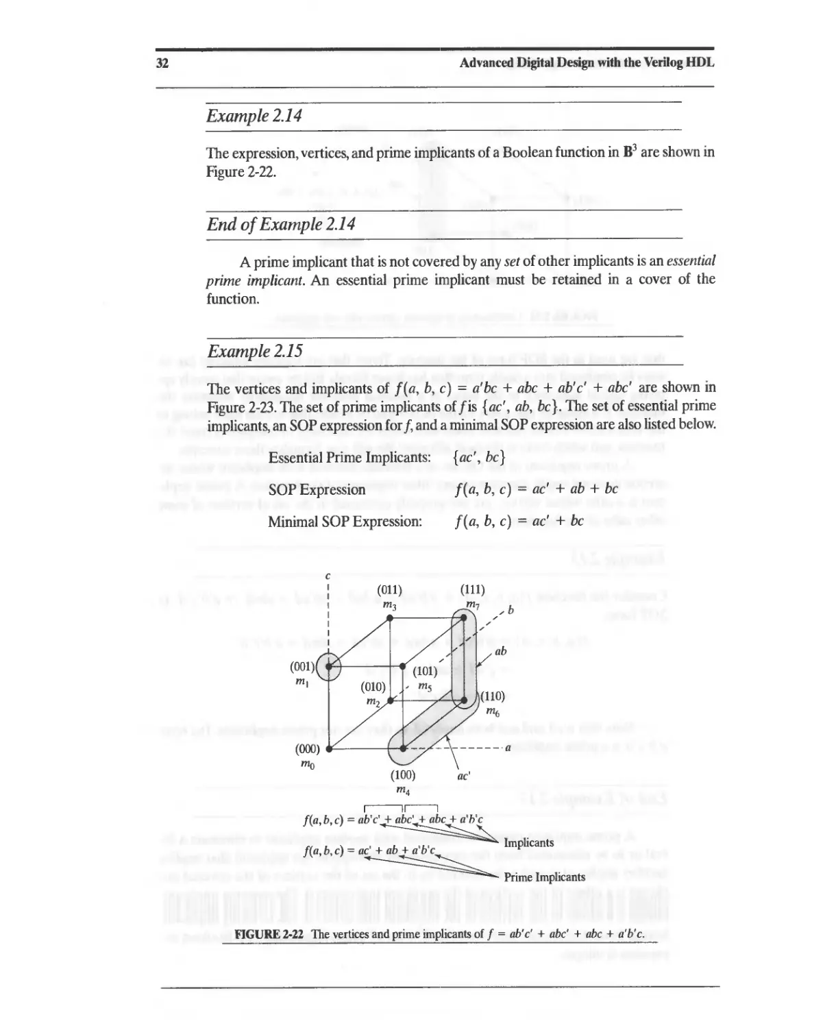
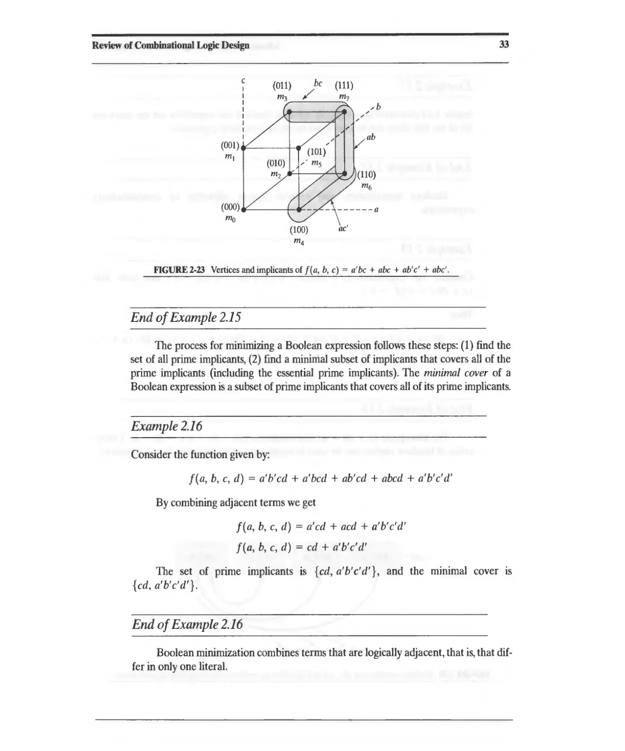
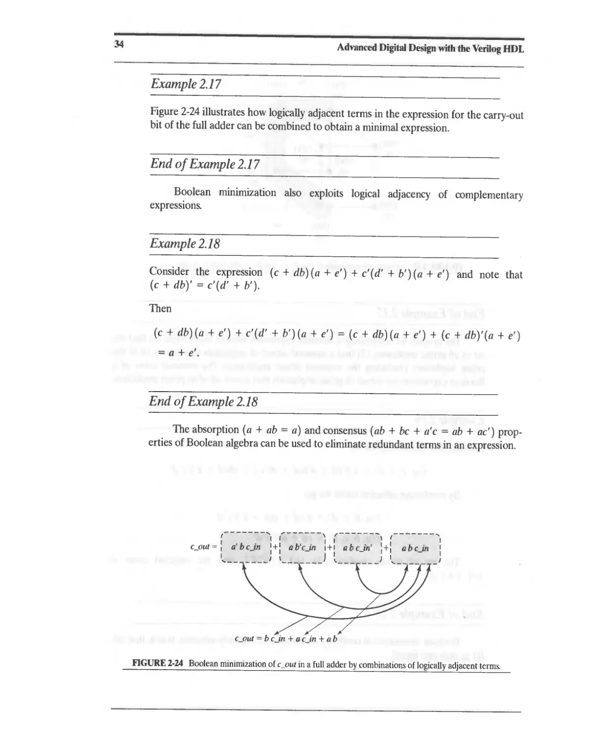
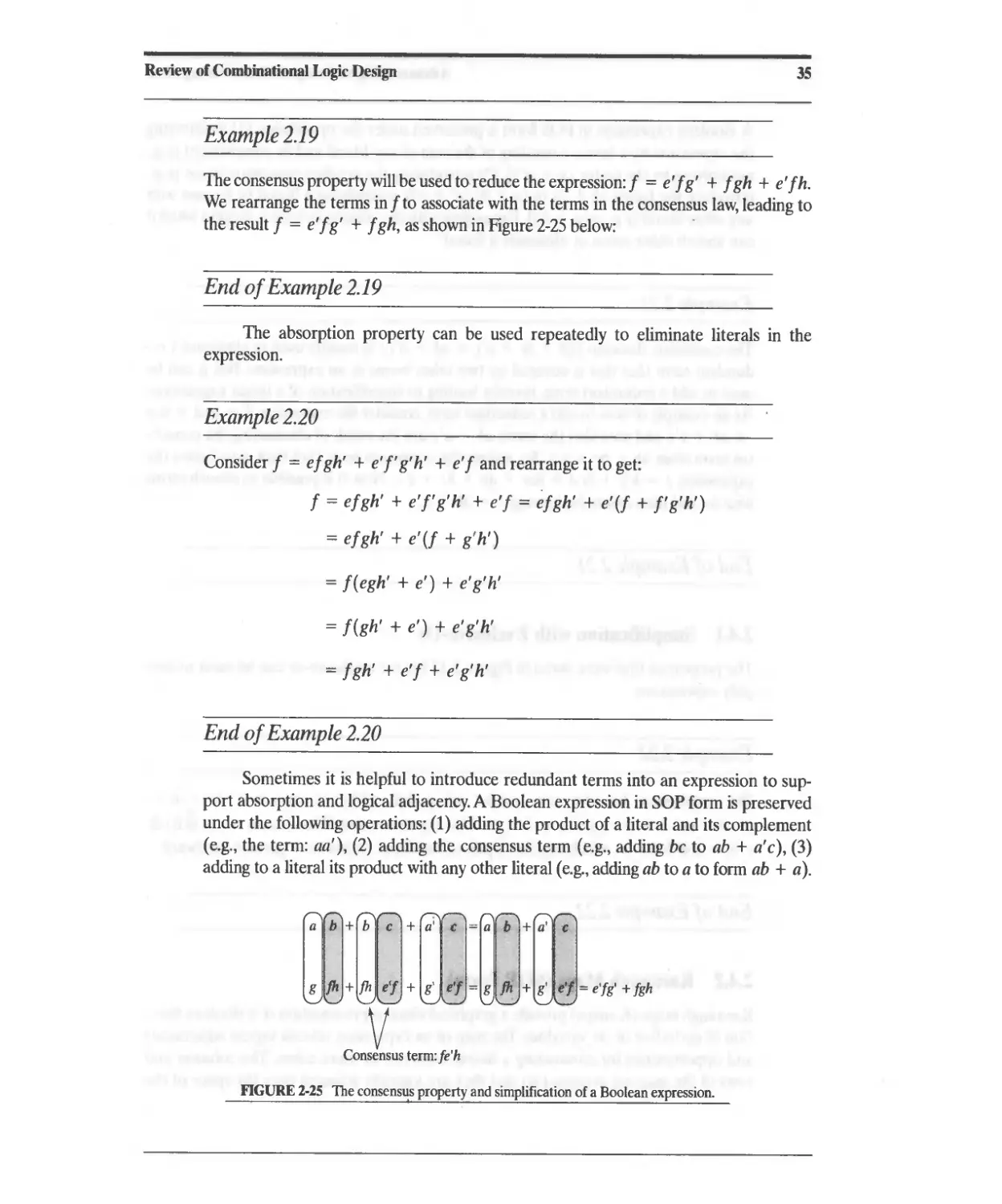
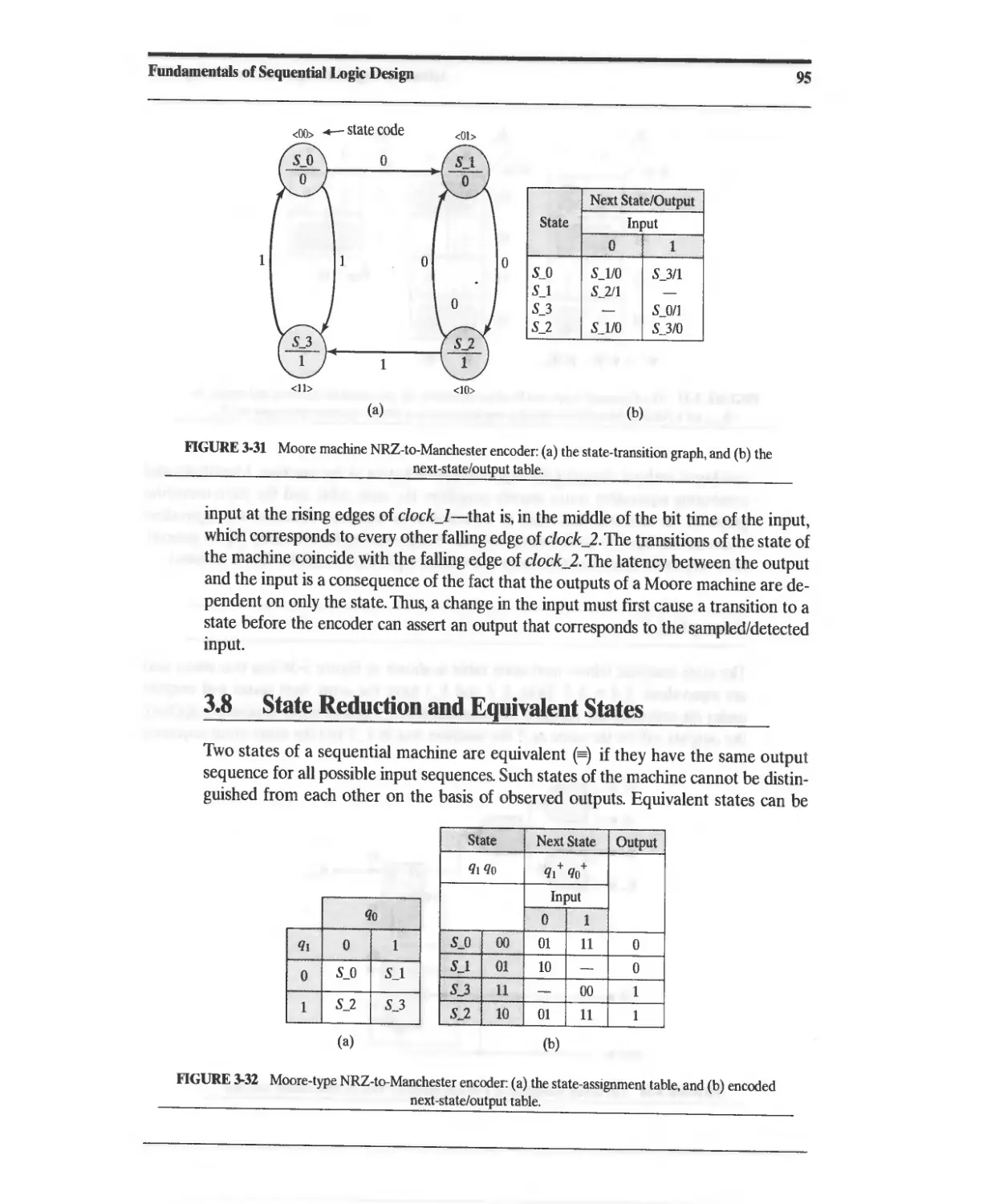
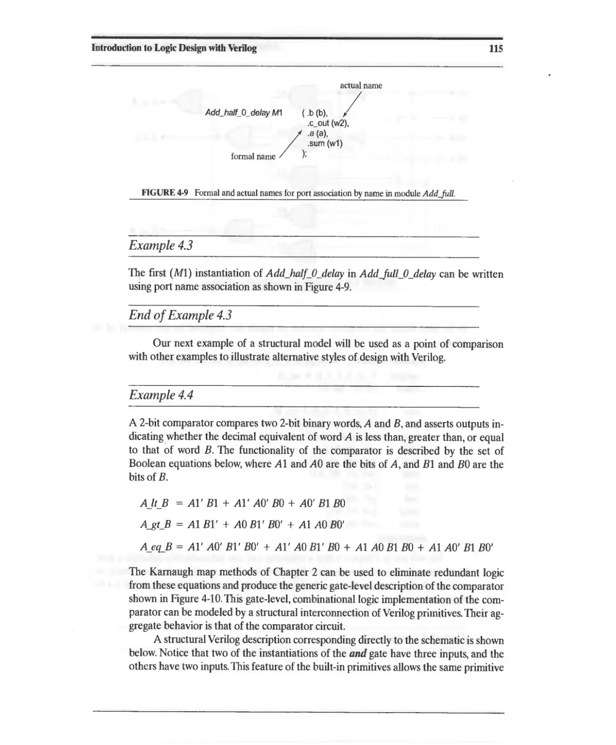
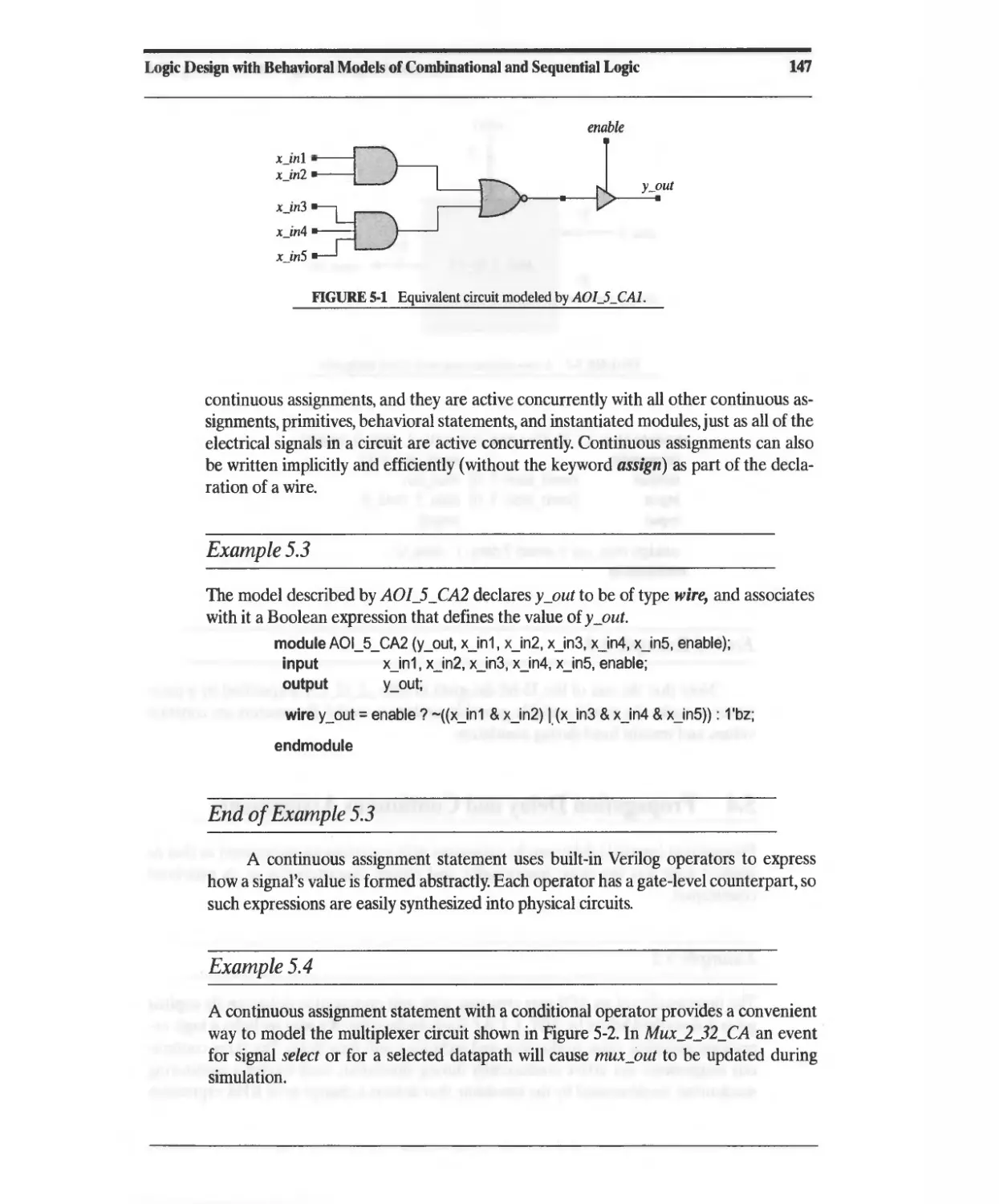
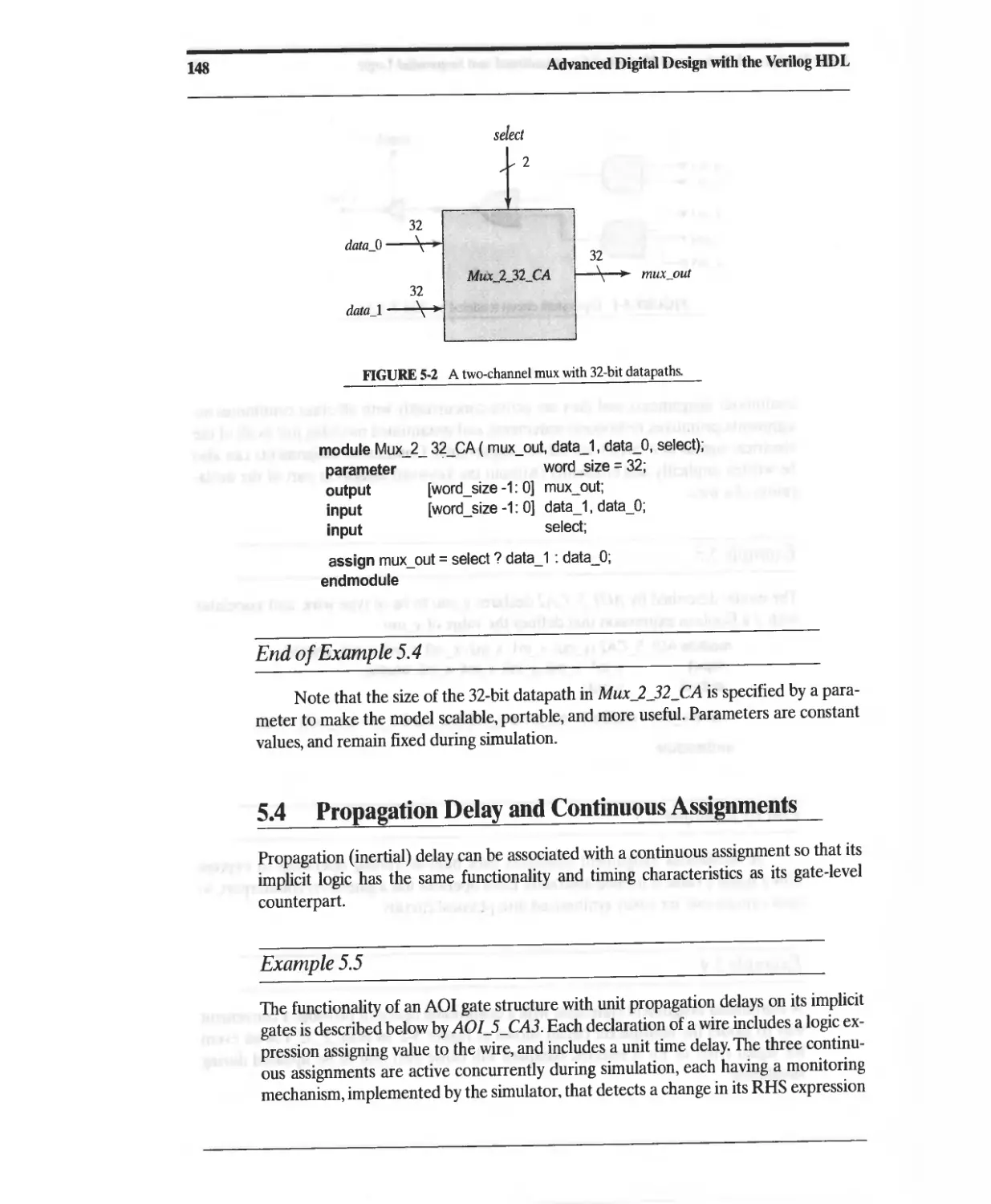
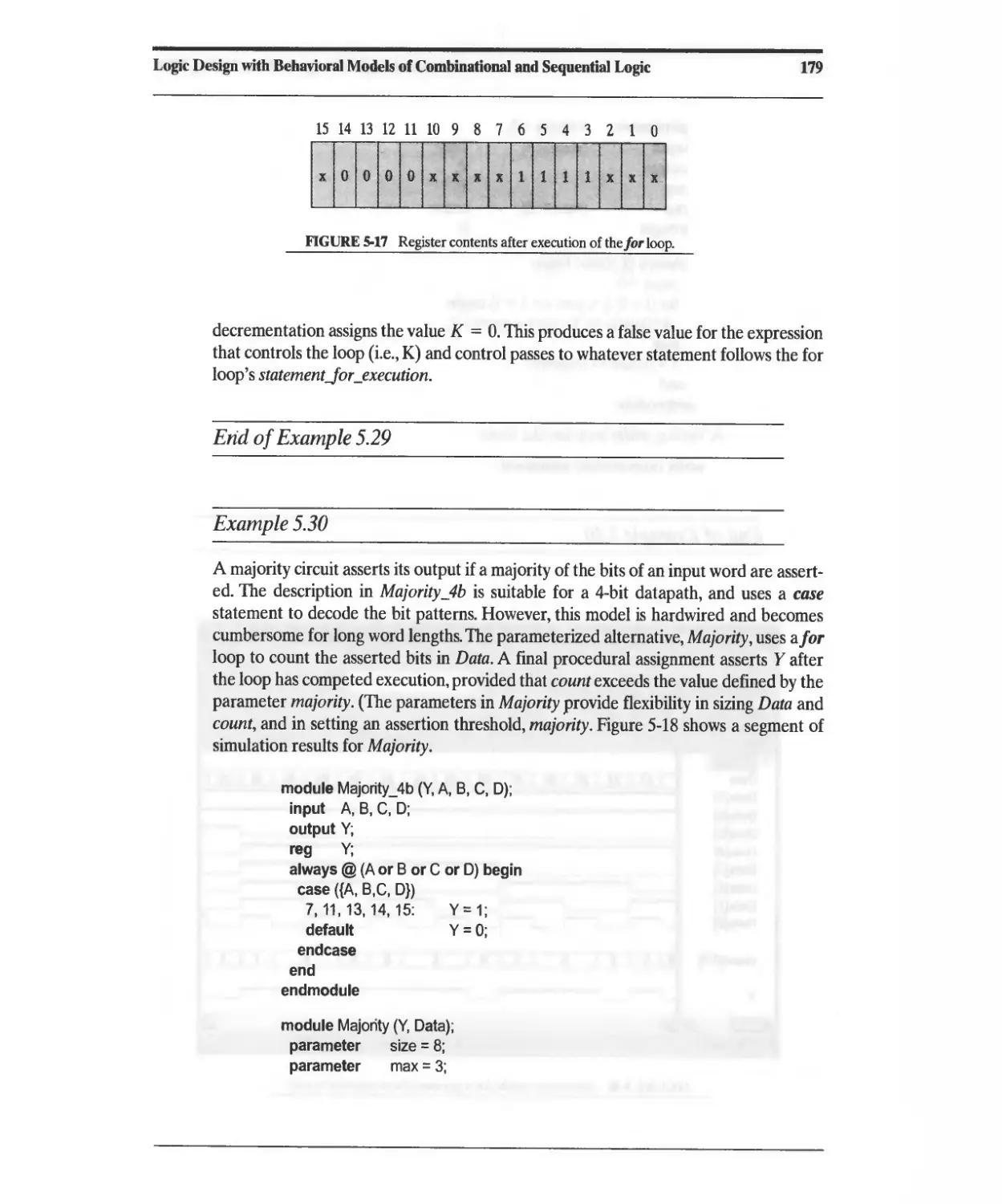
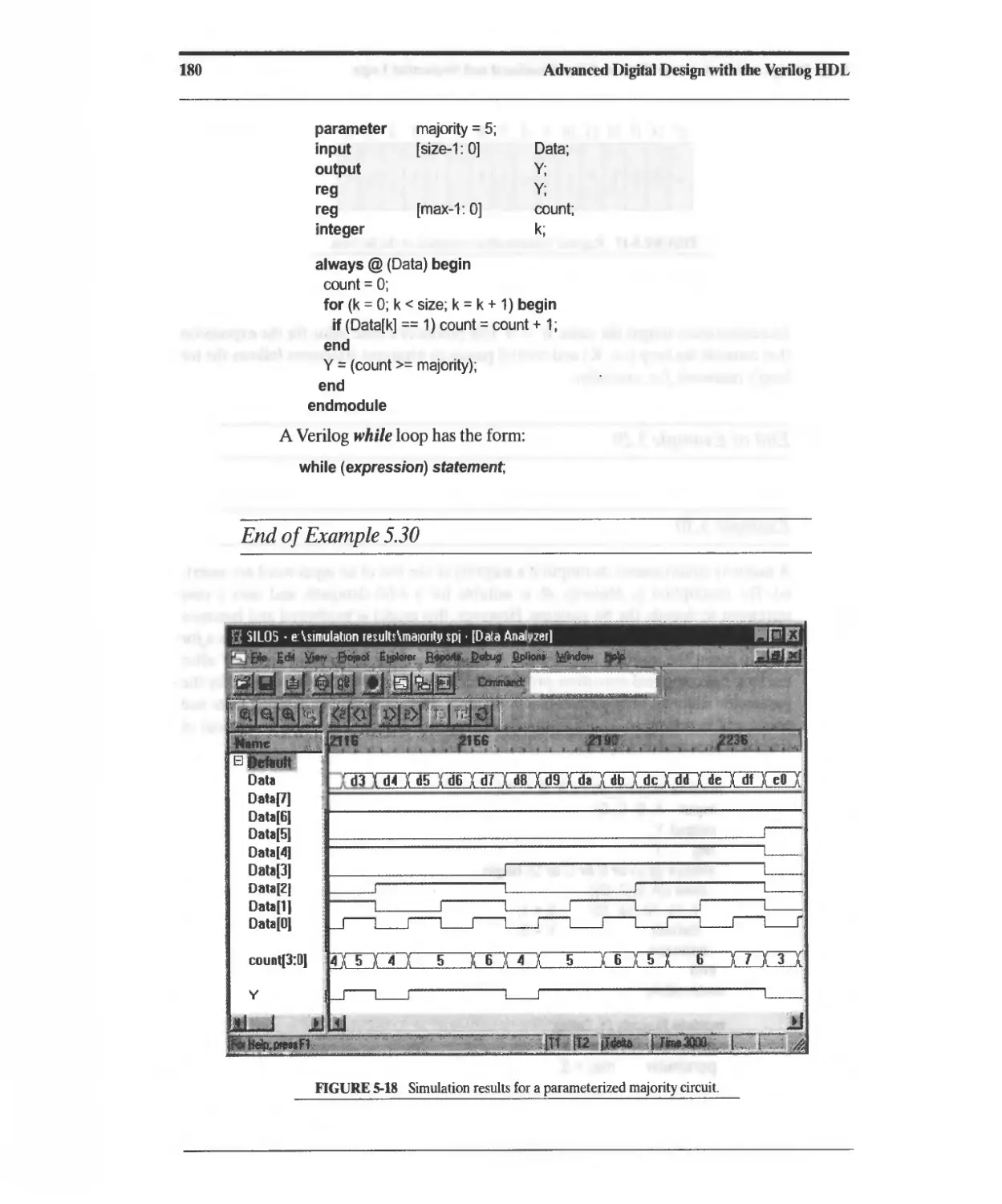
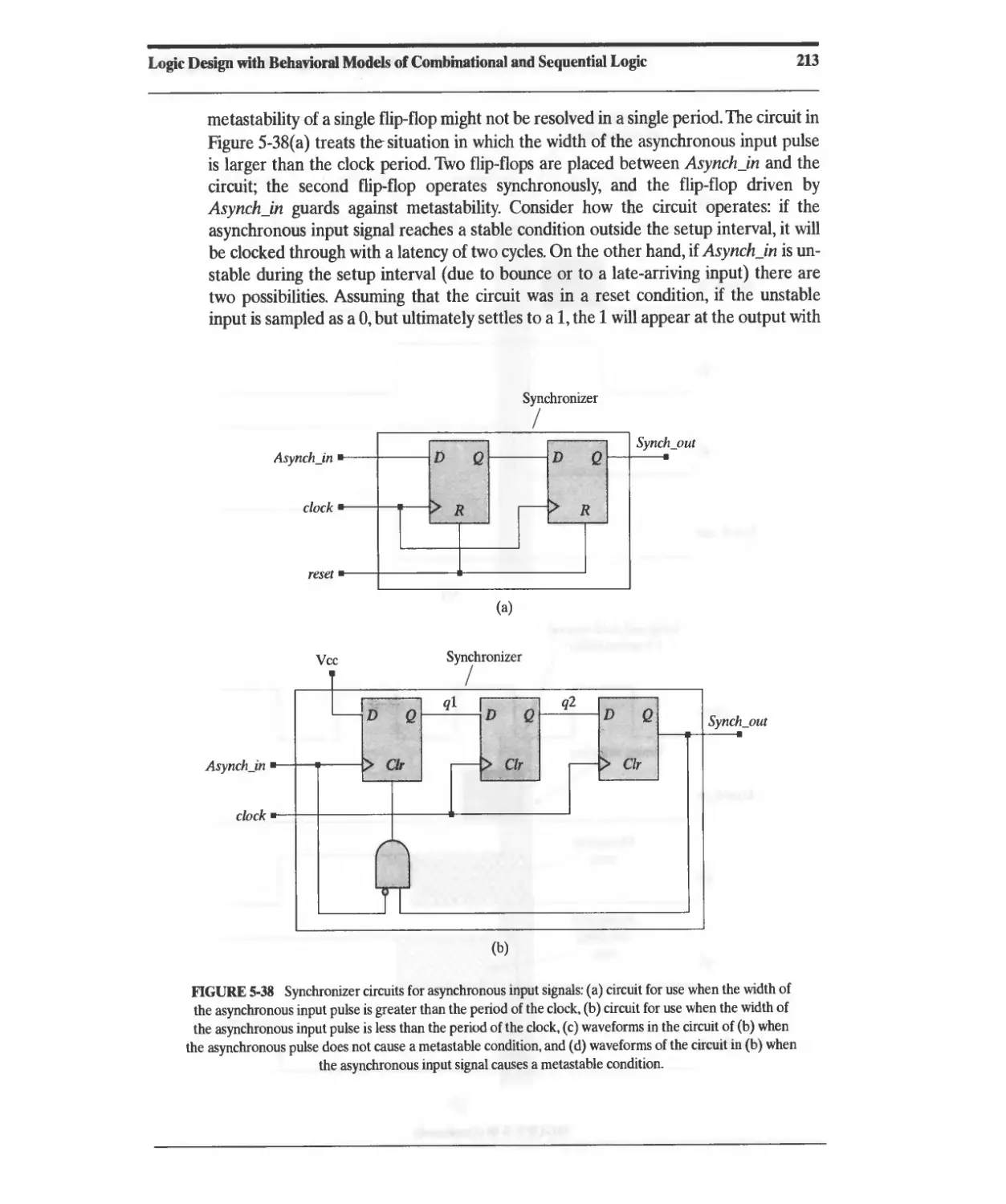
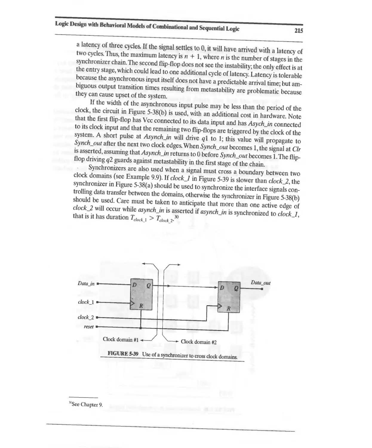
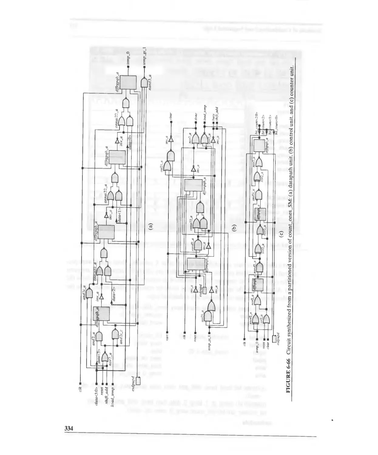
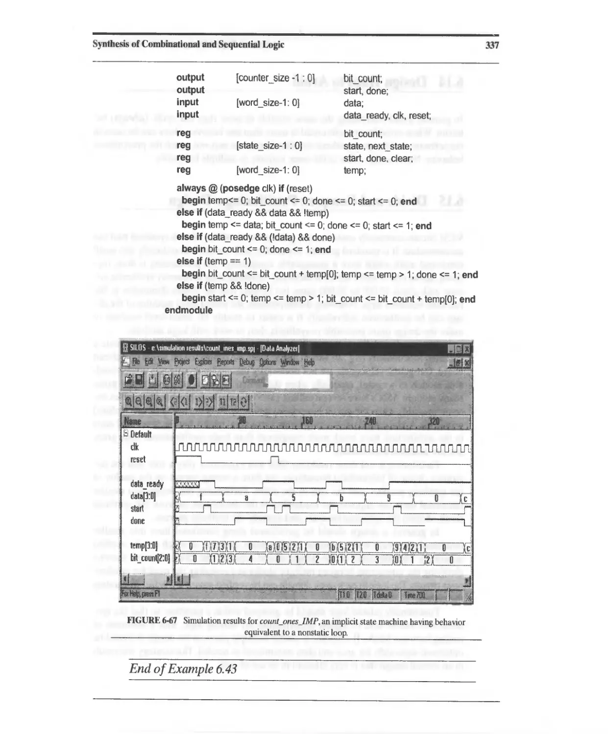
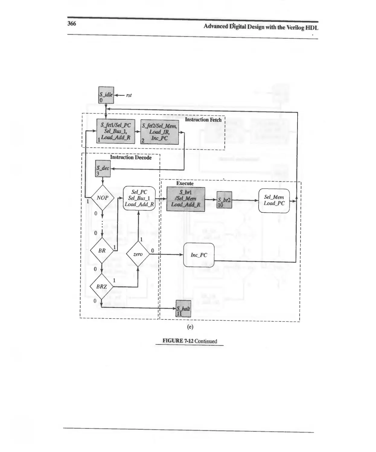
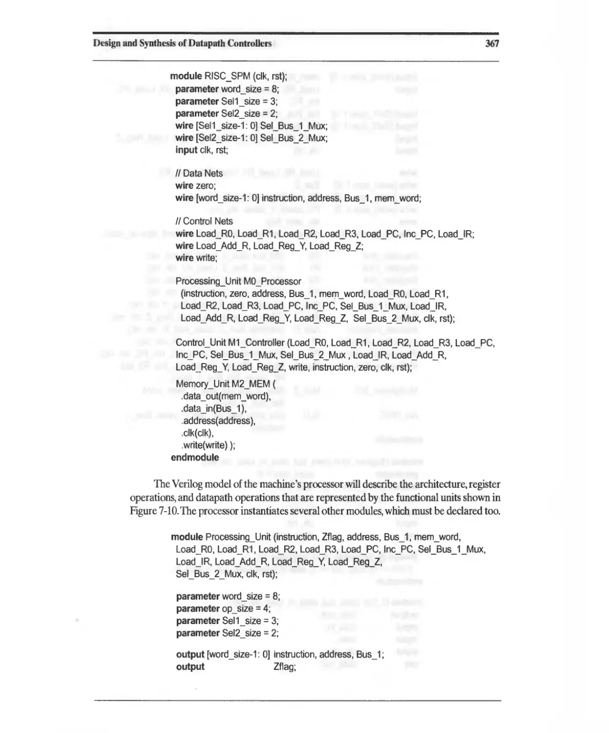
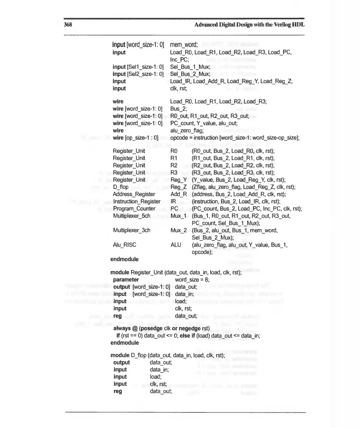
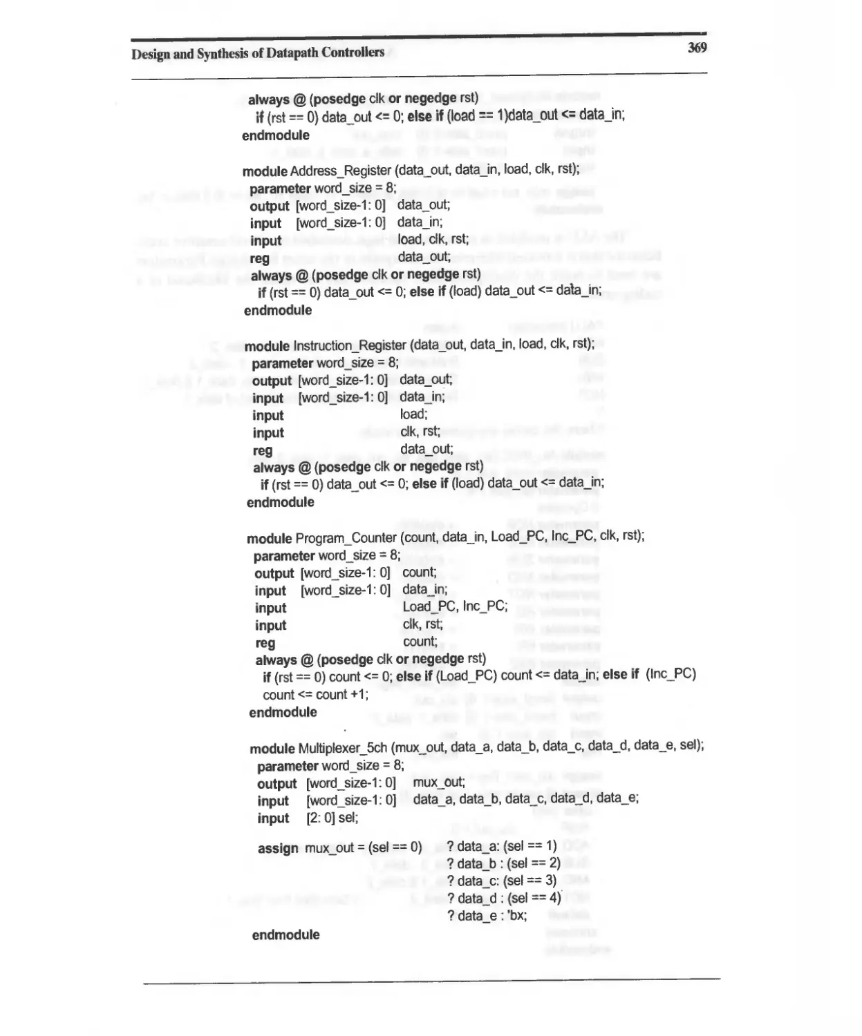
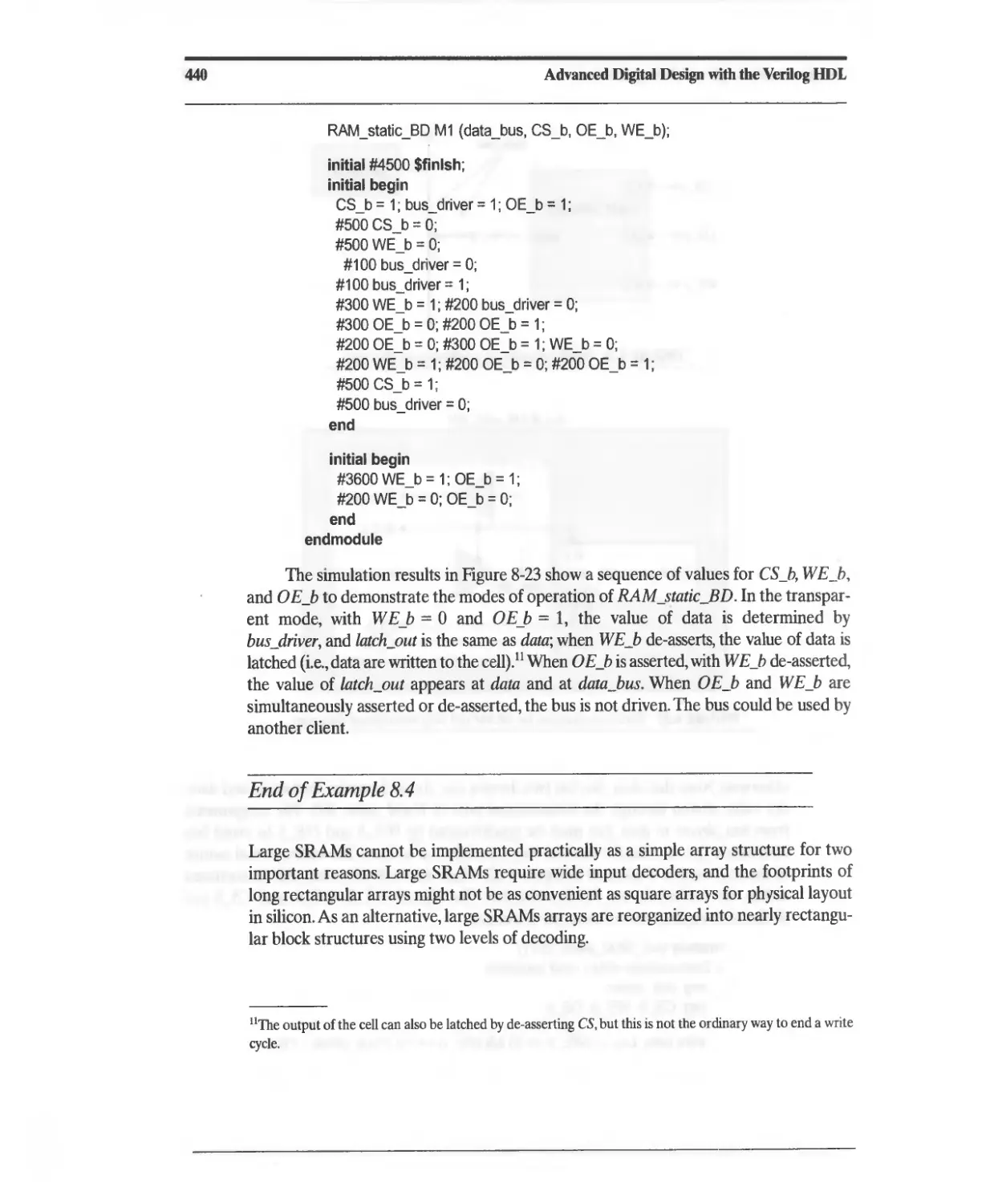
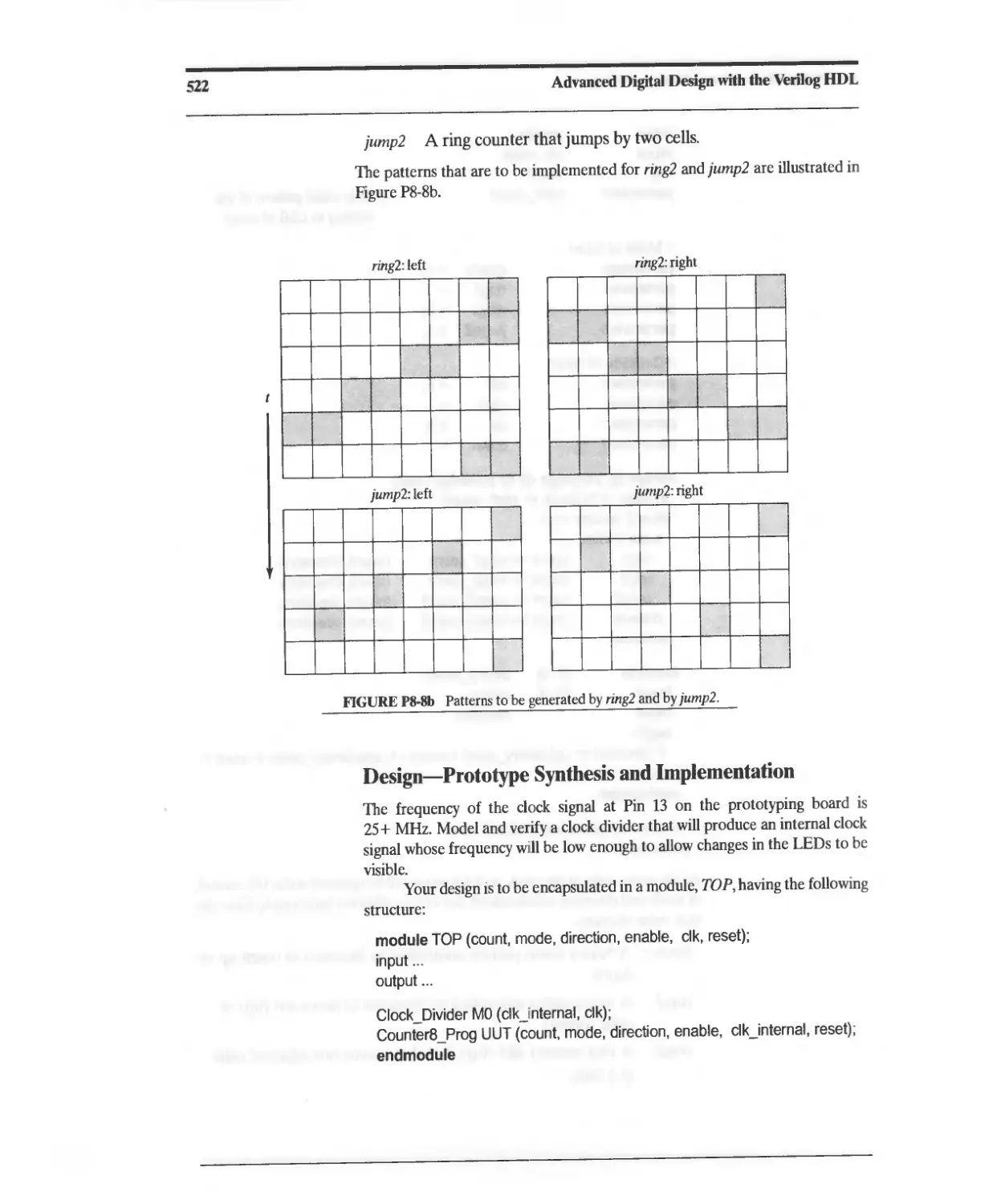
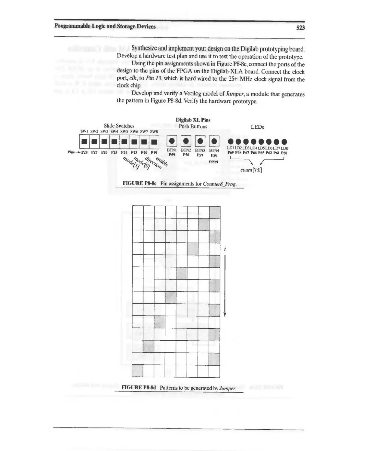
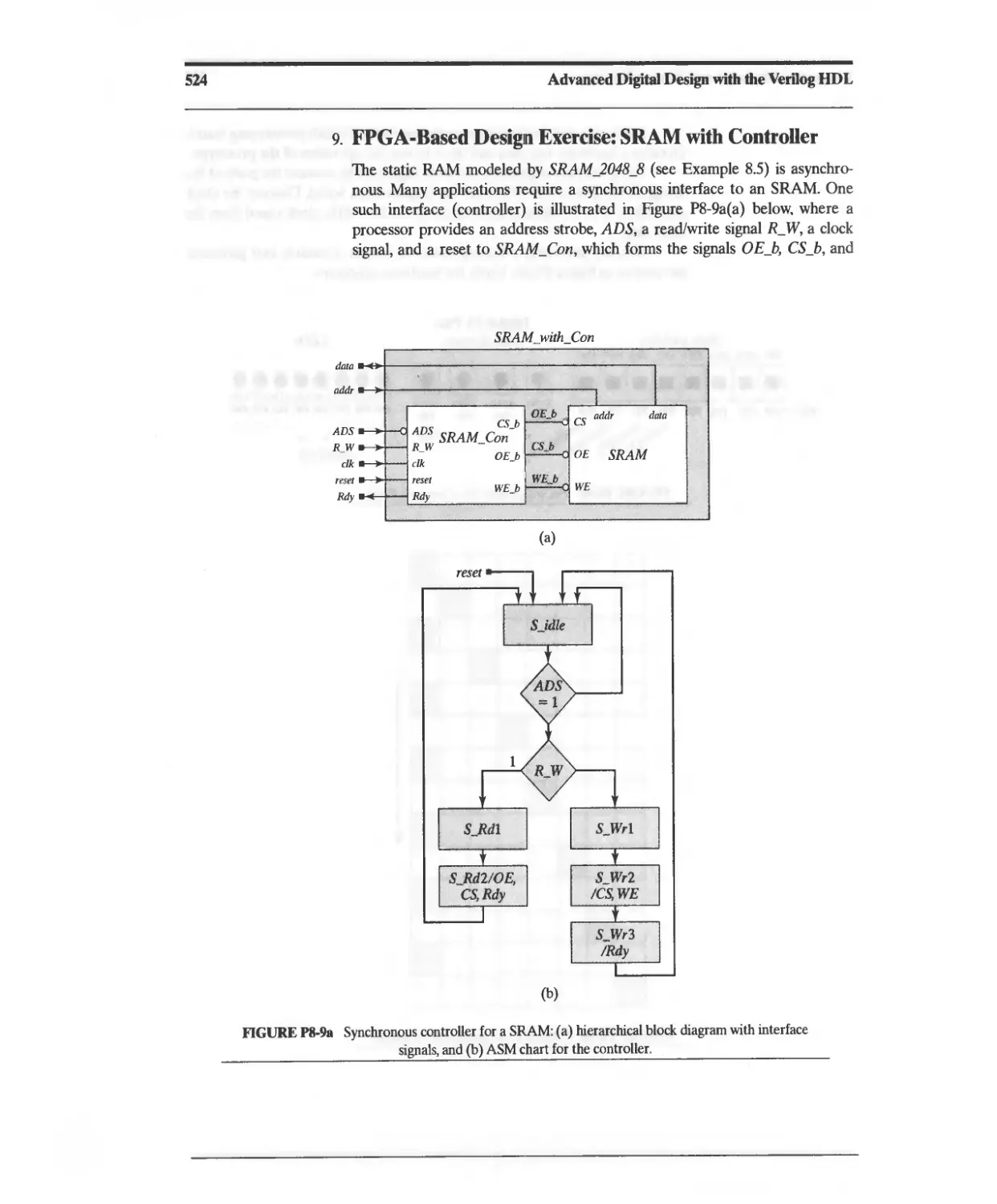
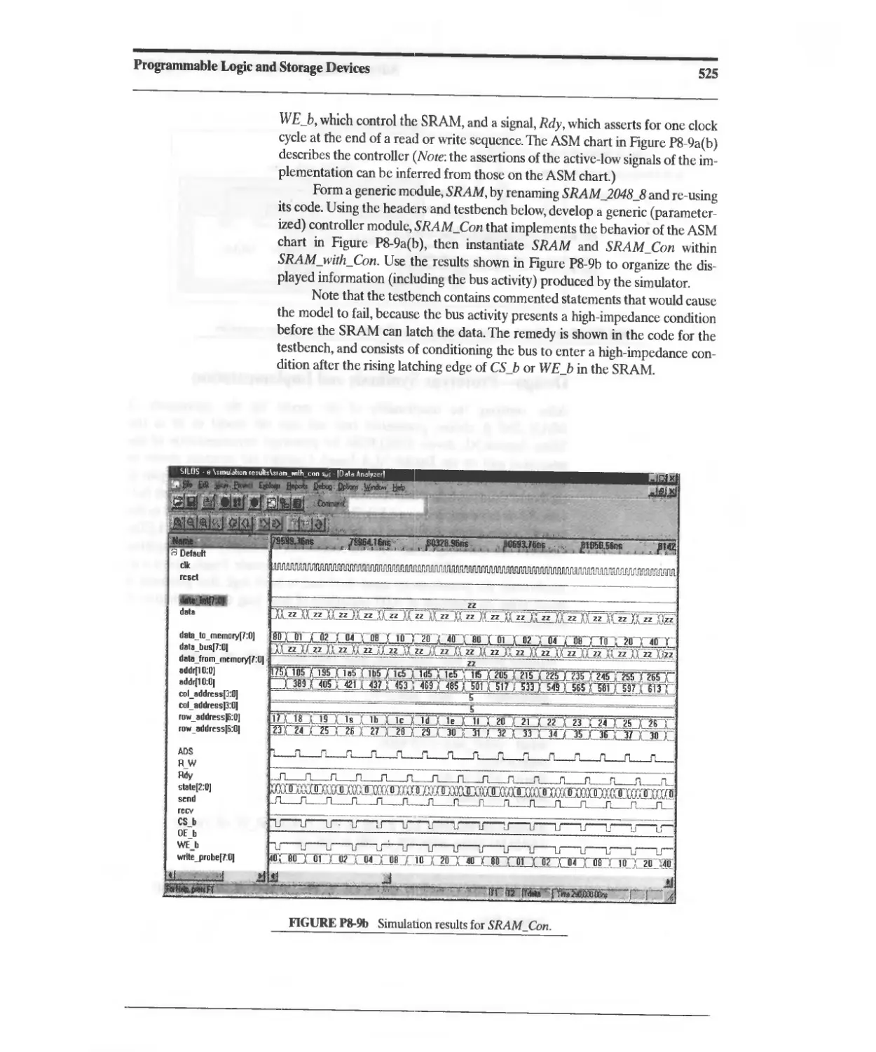
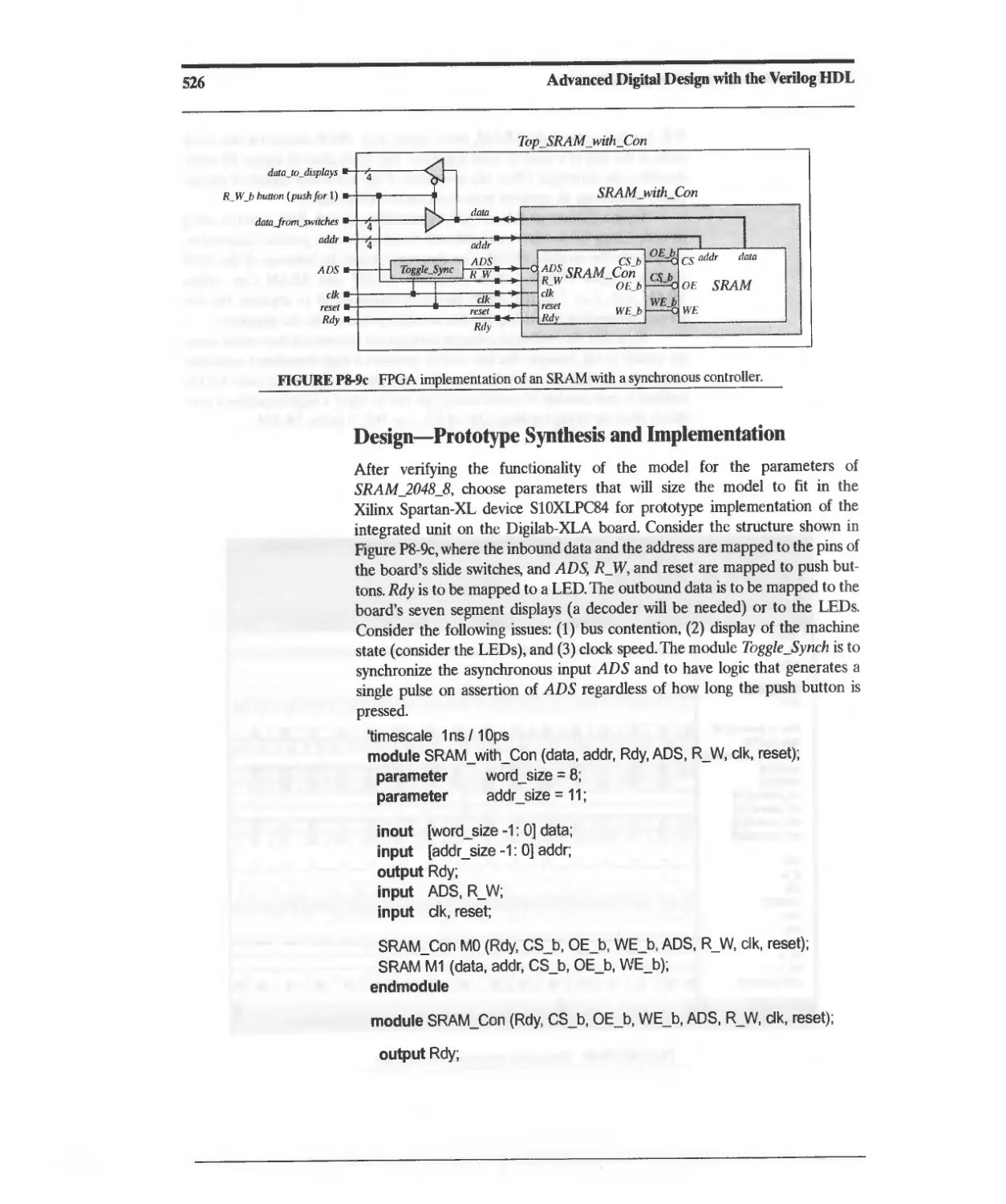
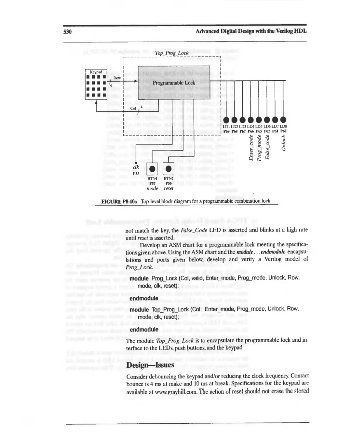
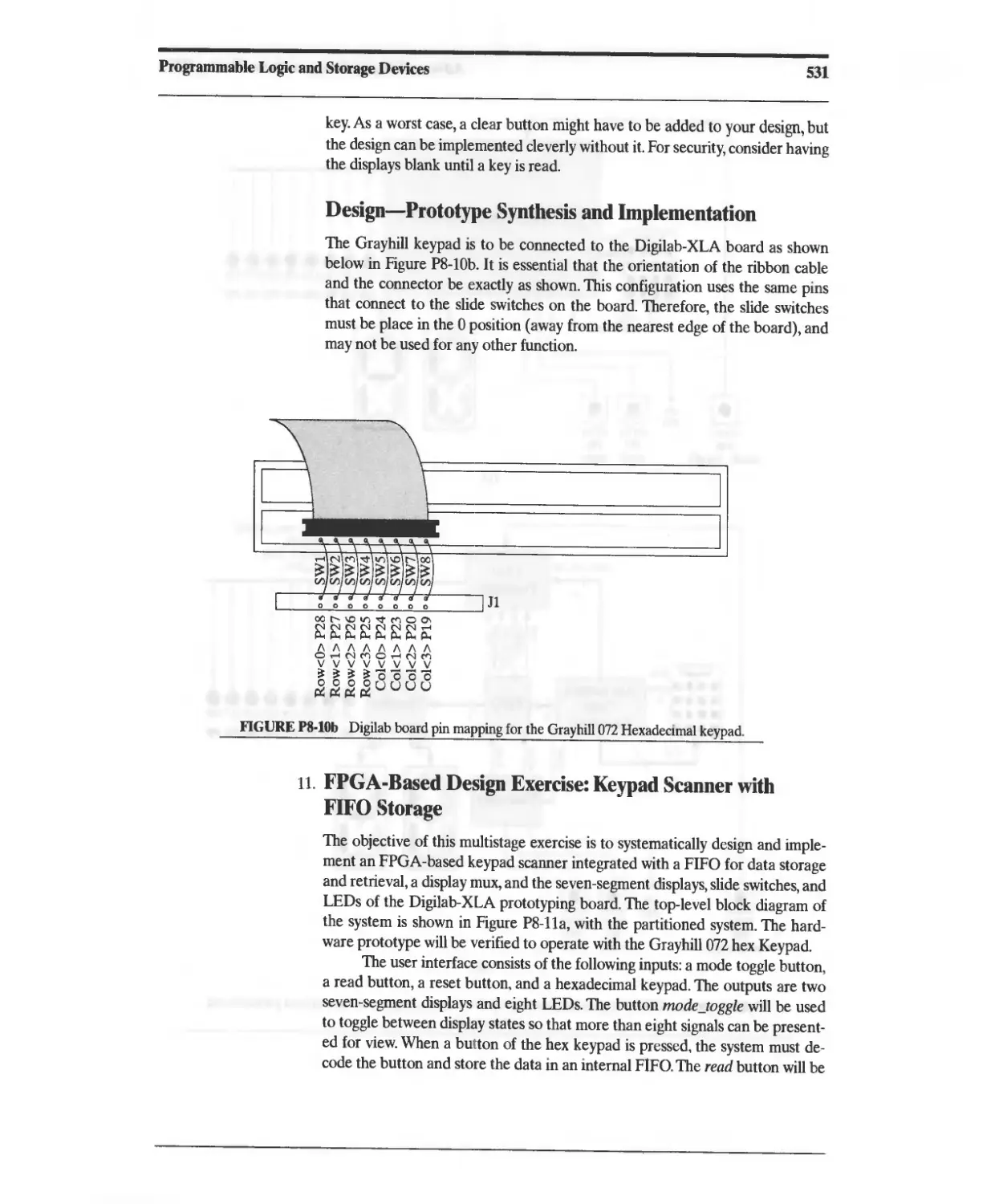
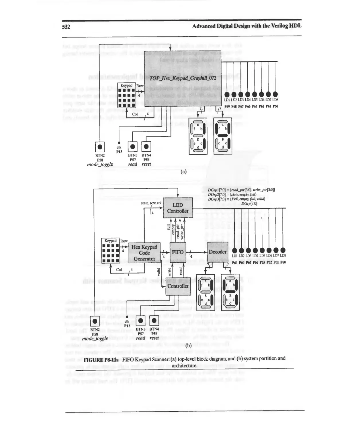
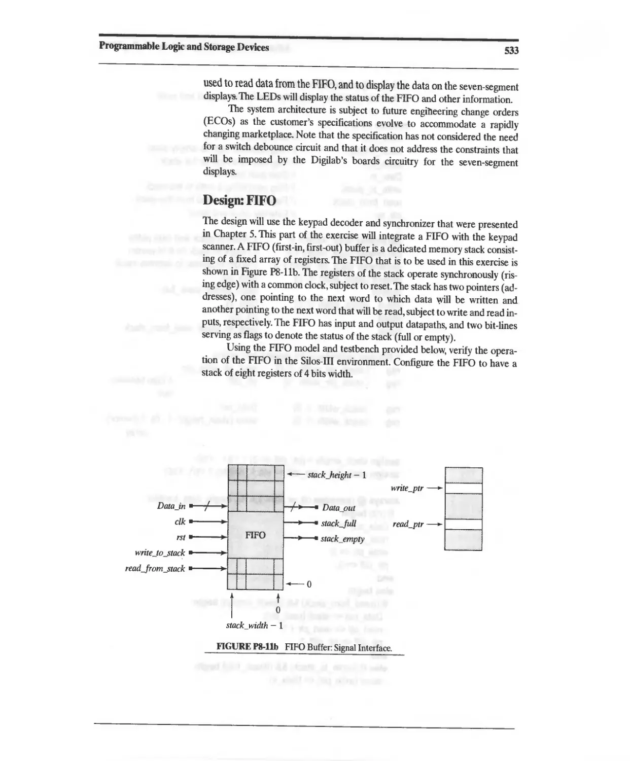
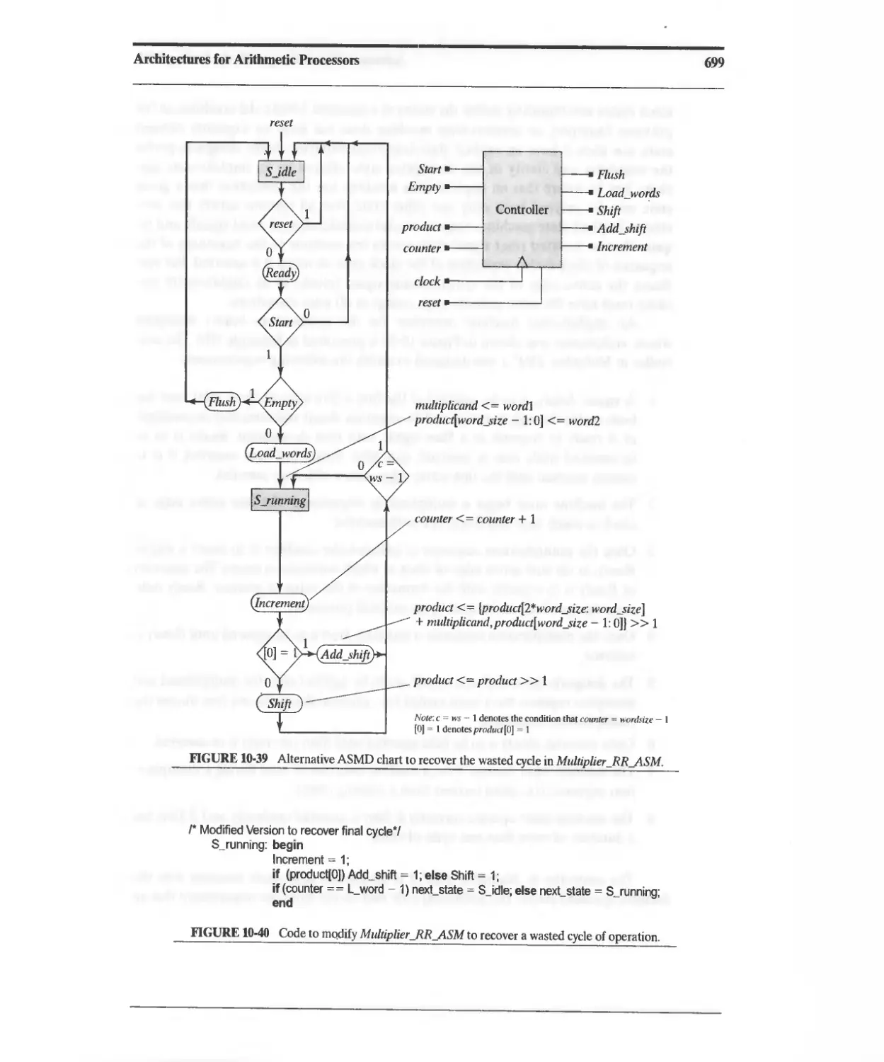
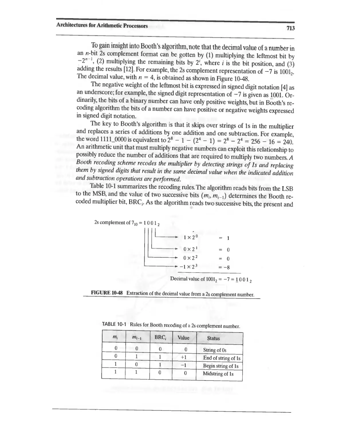
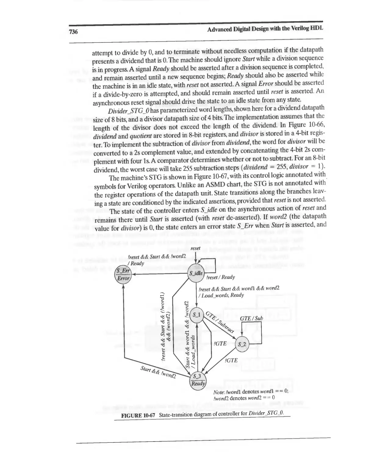
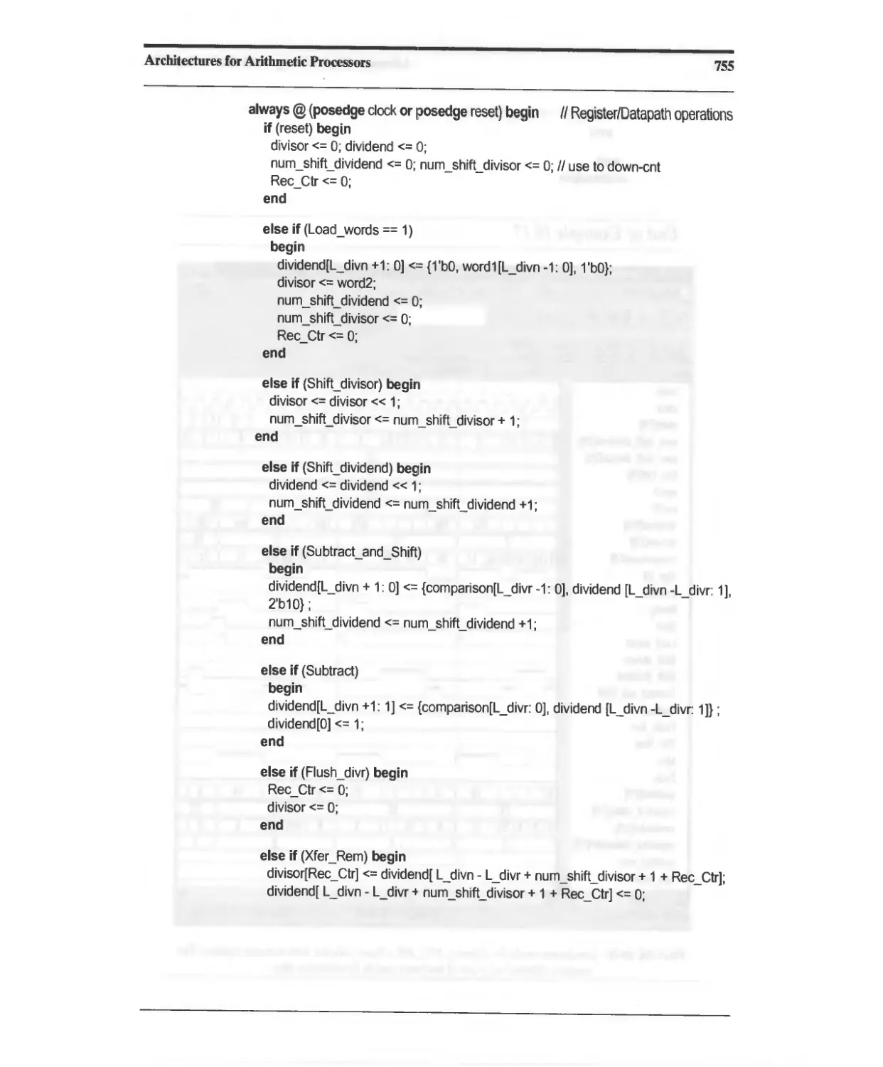
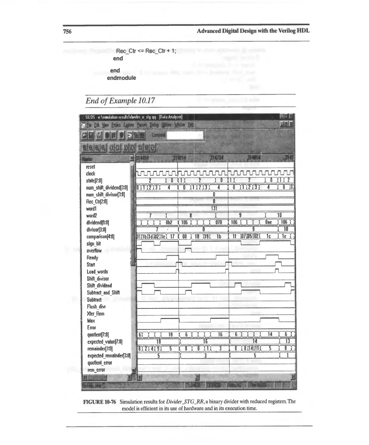
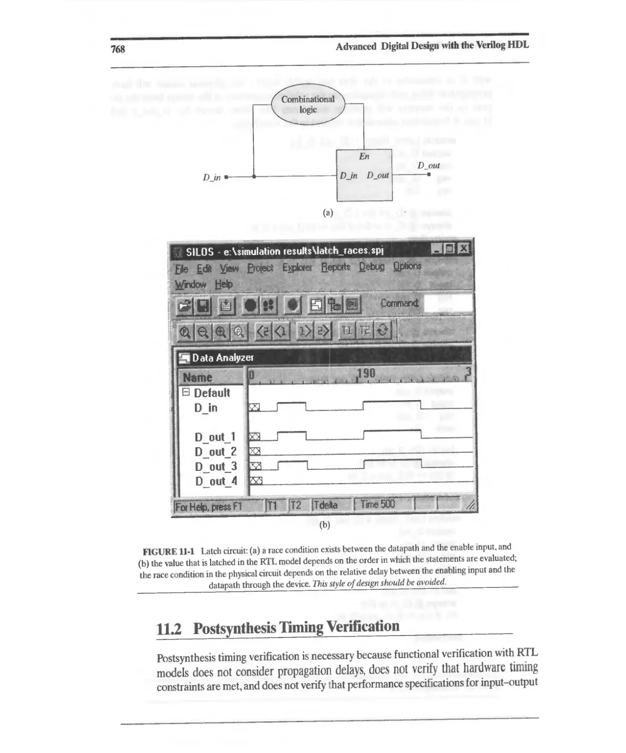
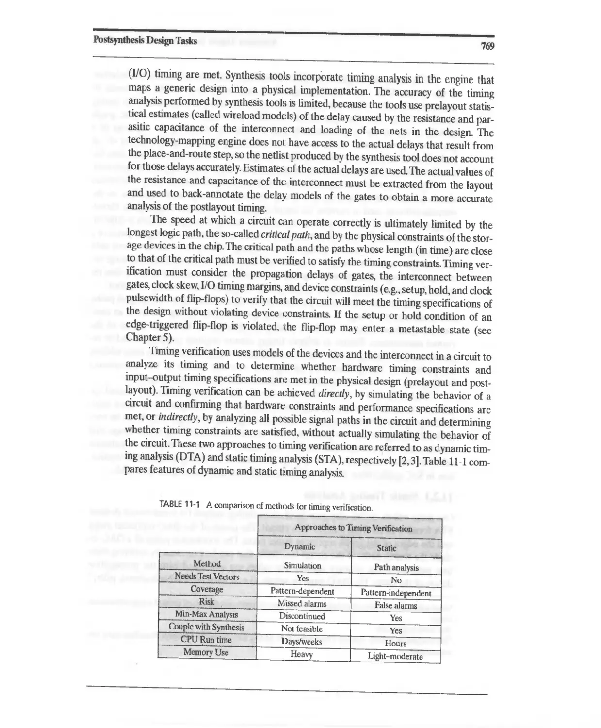
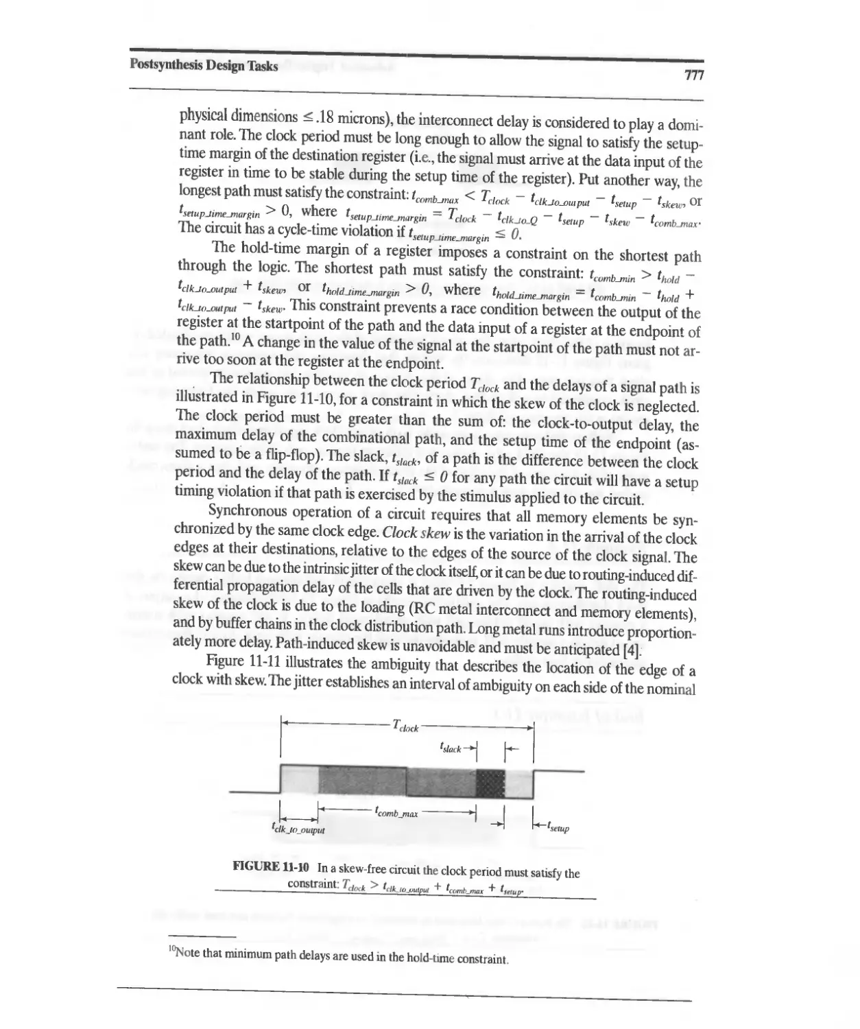
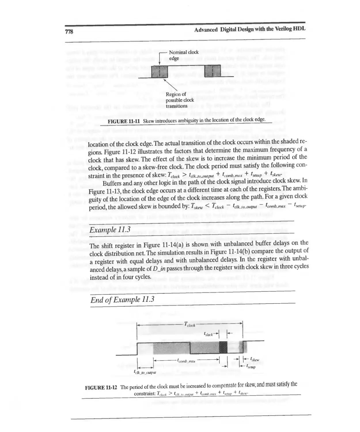
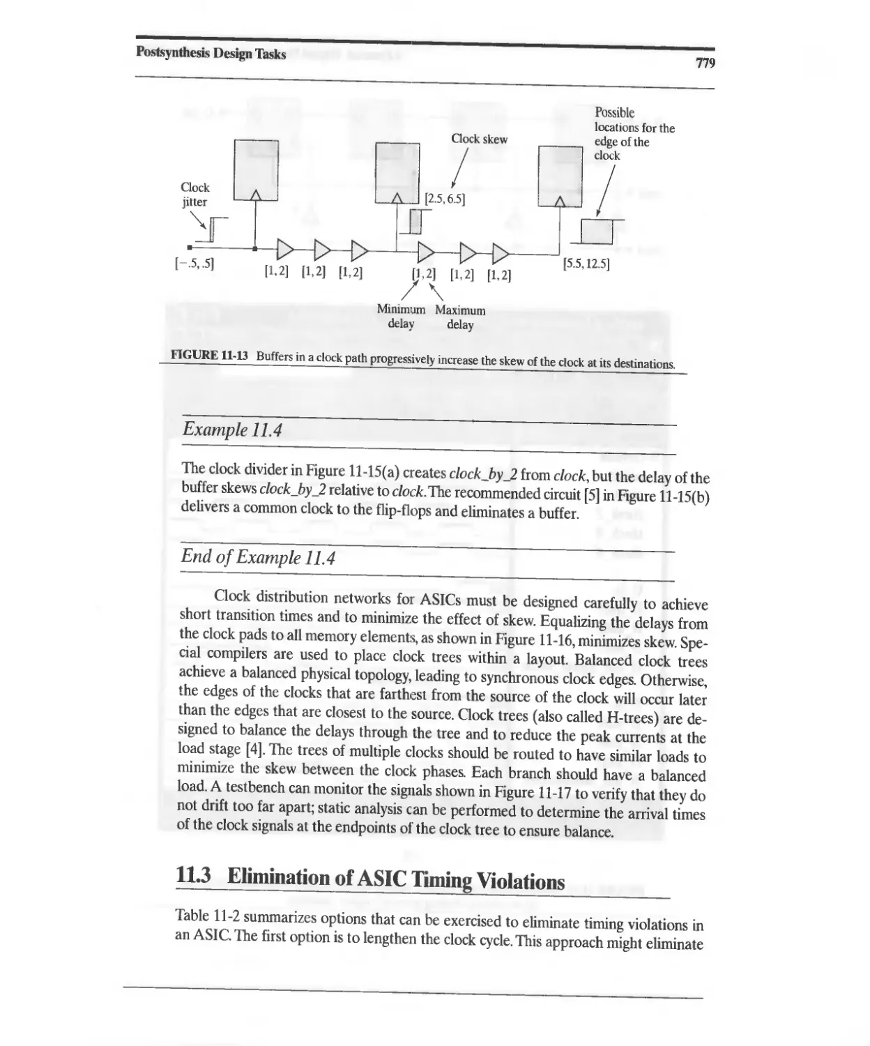
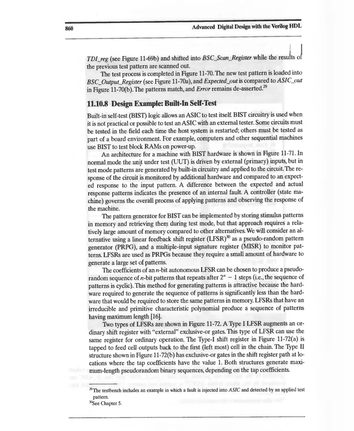
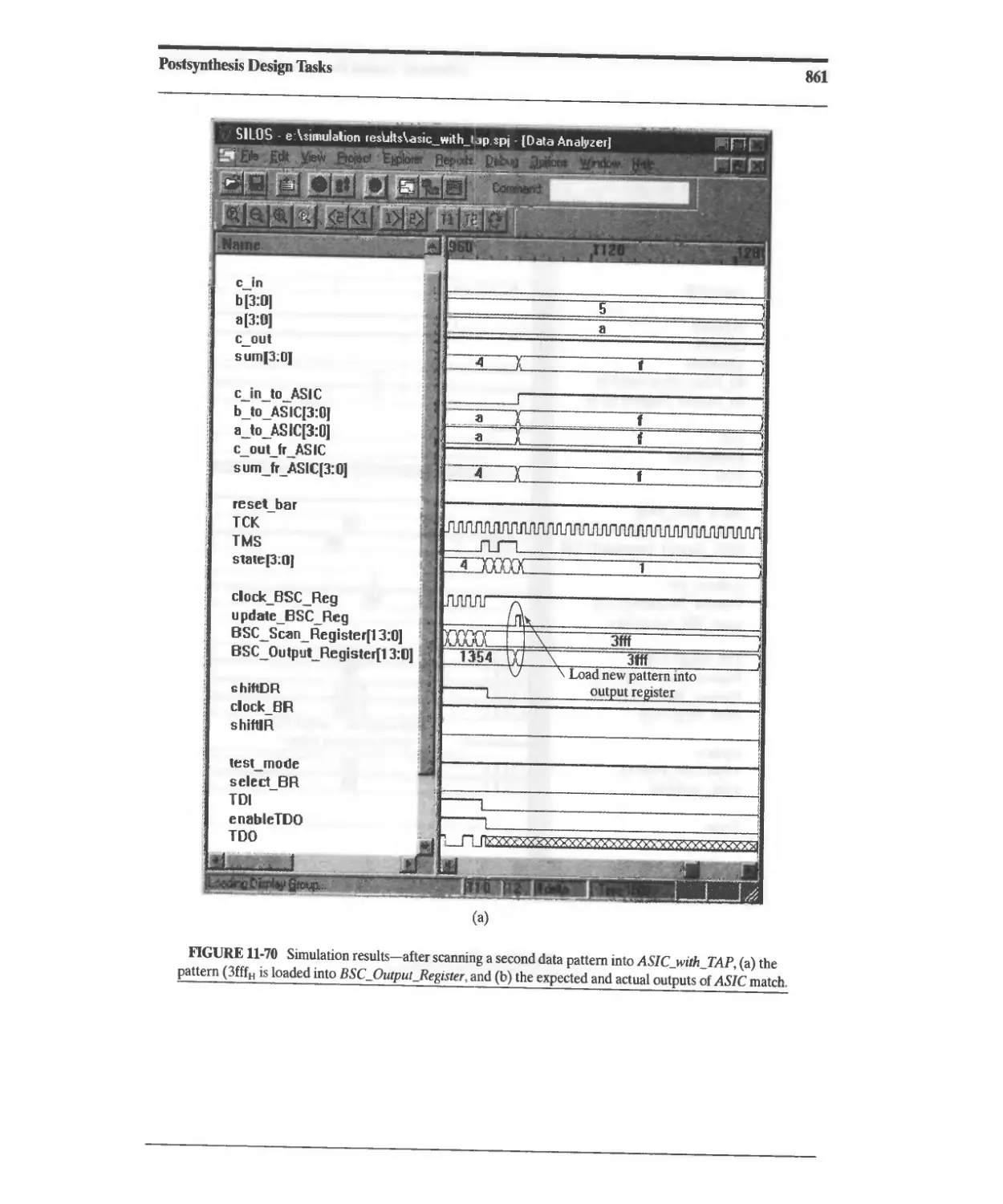
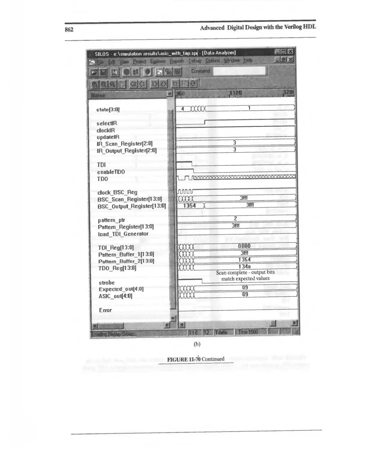
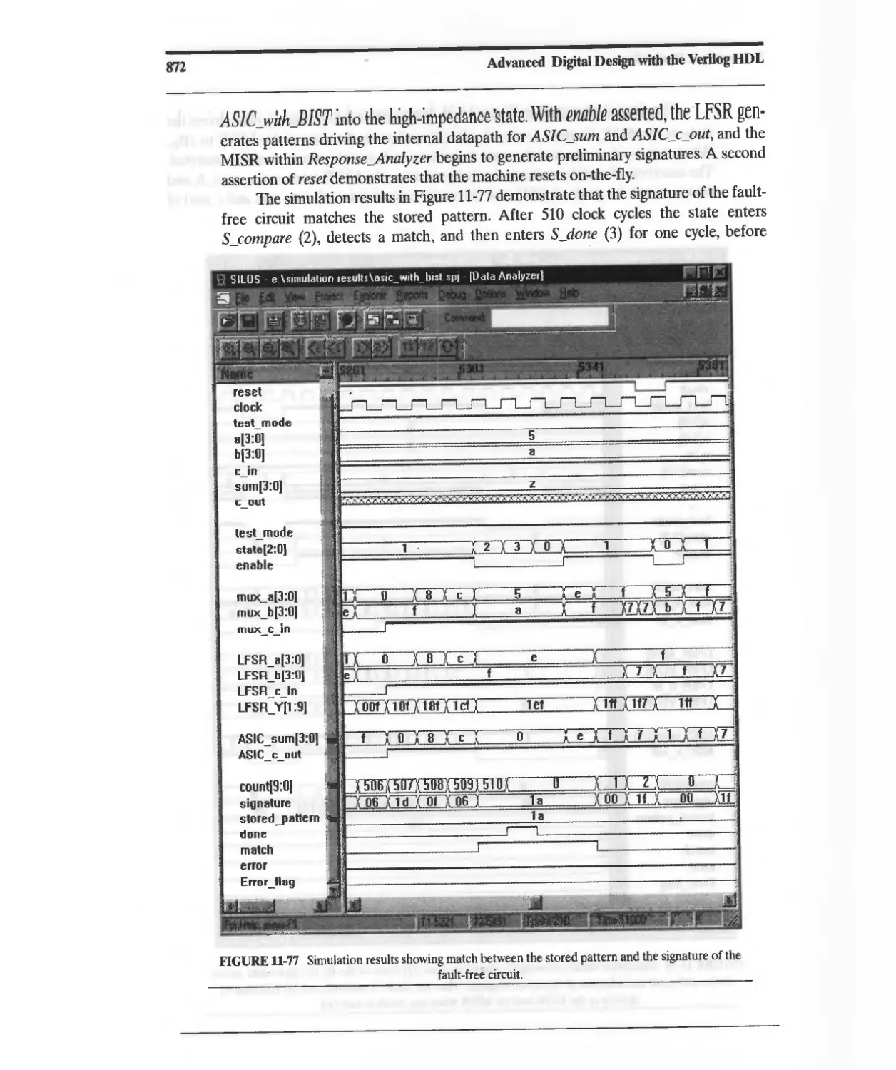
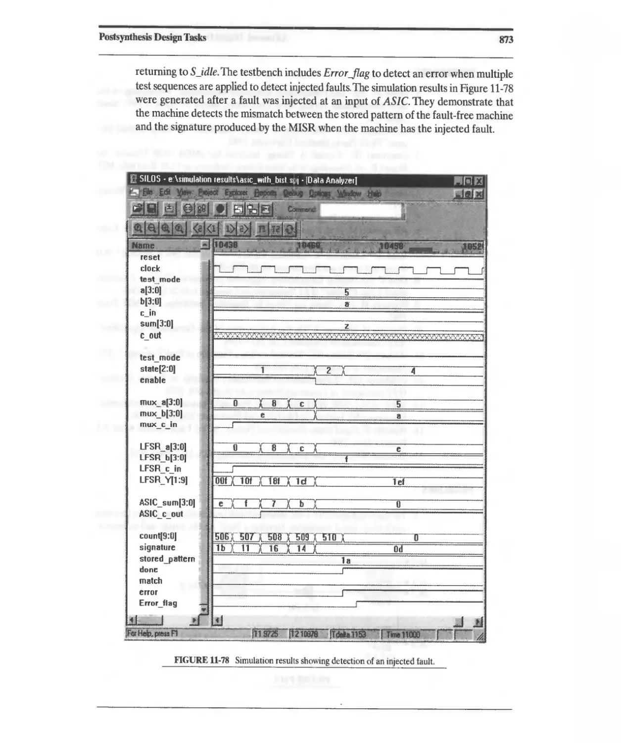
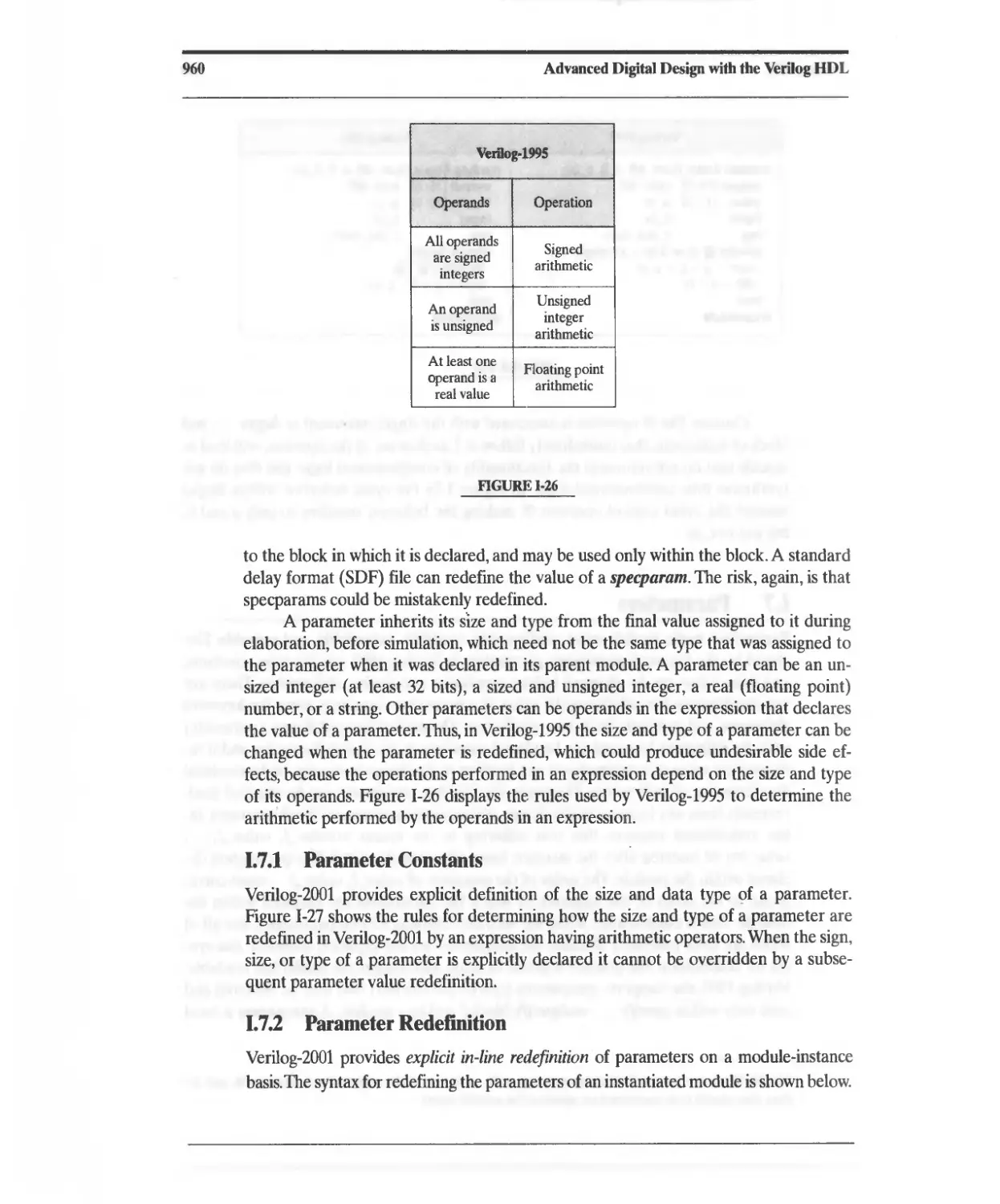
/


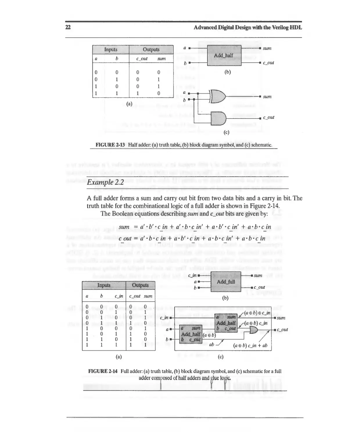


Текст
stern
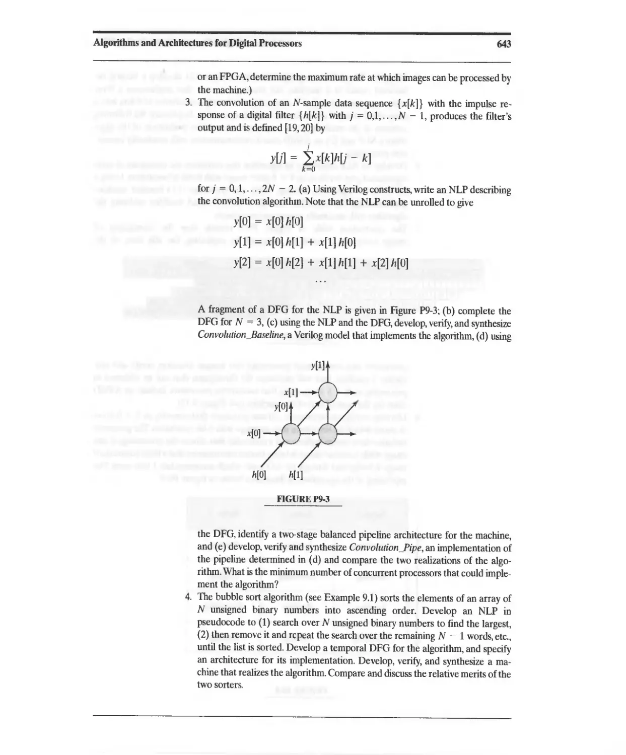
conomy
dition
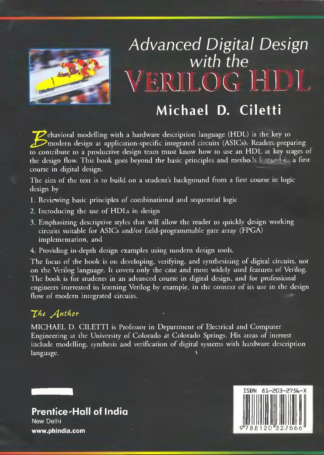
Advanced Digital Design
with the
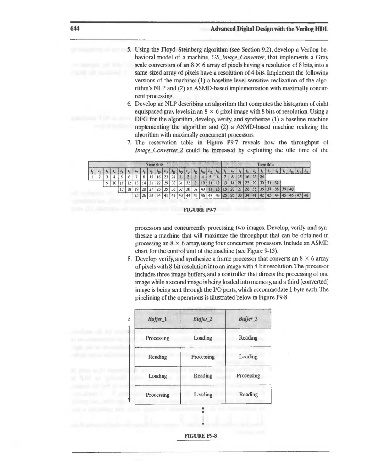
VERILOG HOL
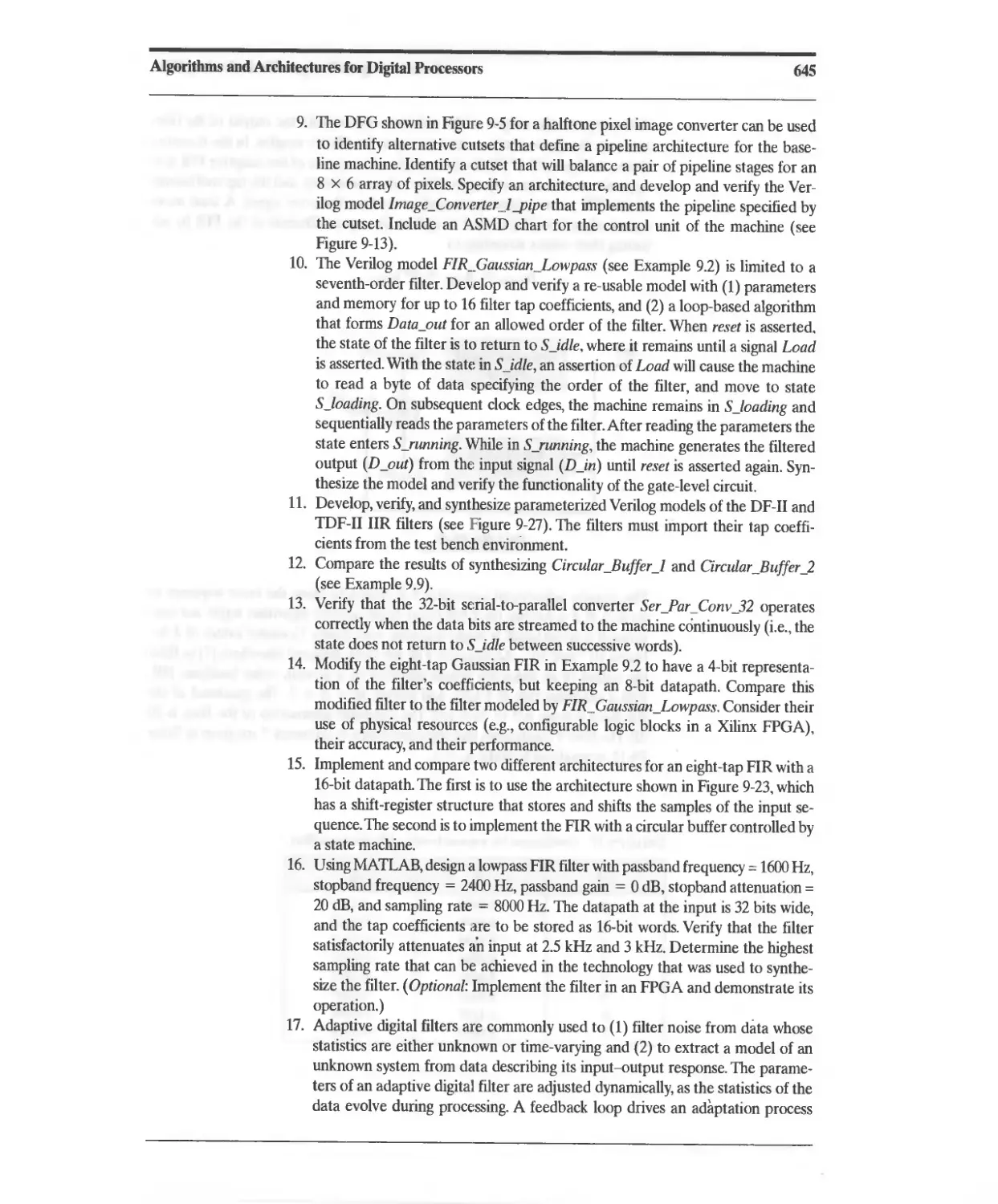
,
"
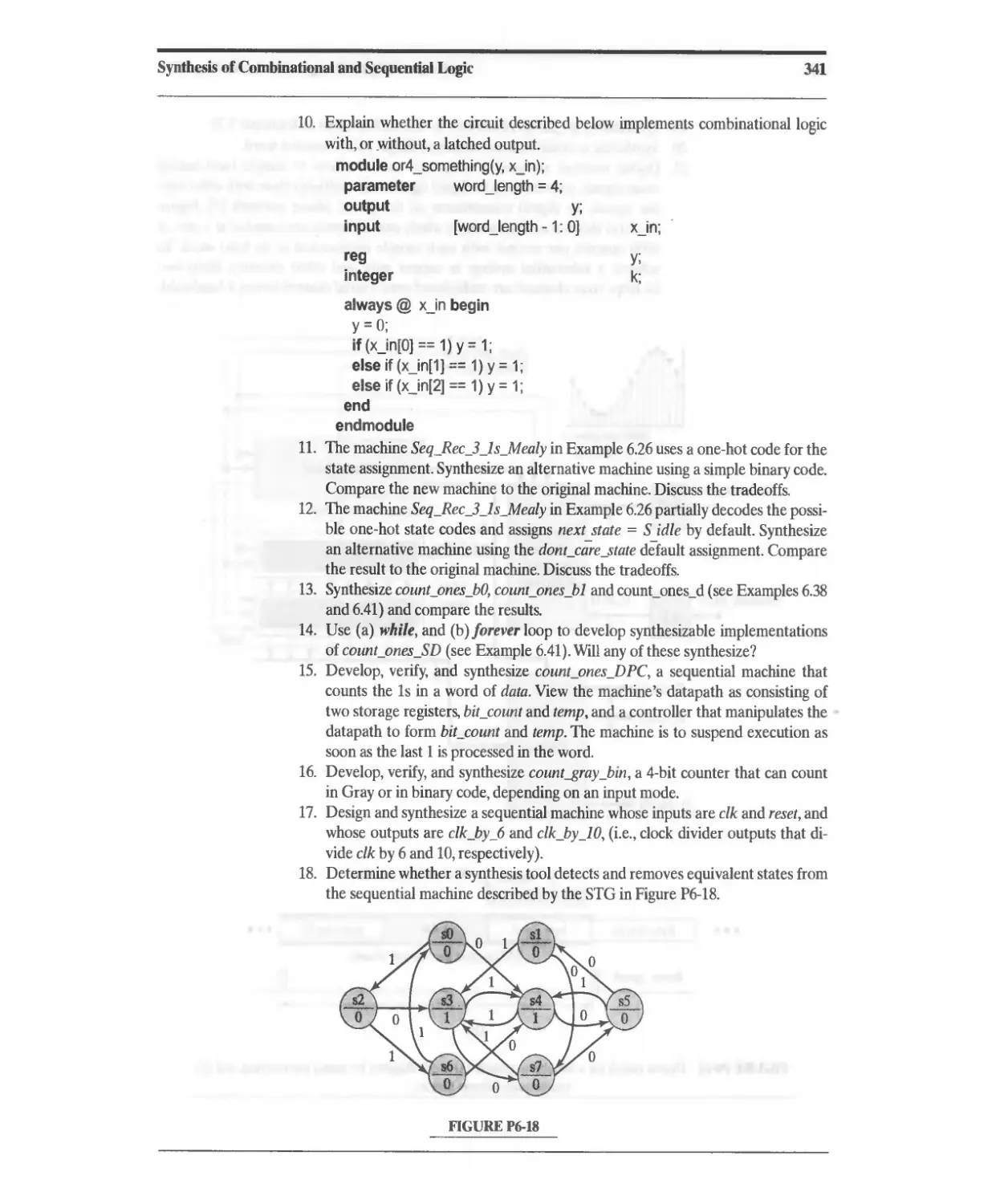
. .....
...
-
" .
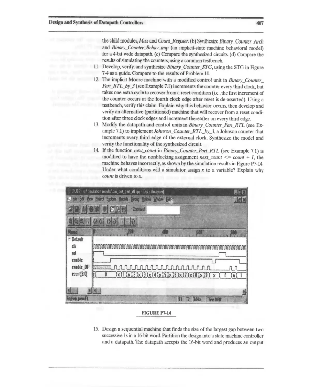
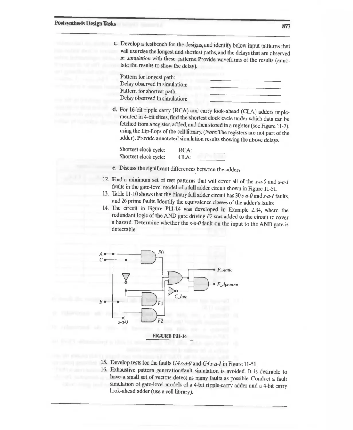
,, .. >
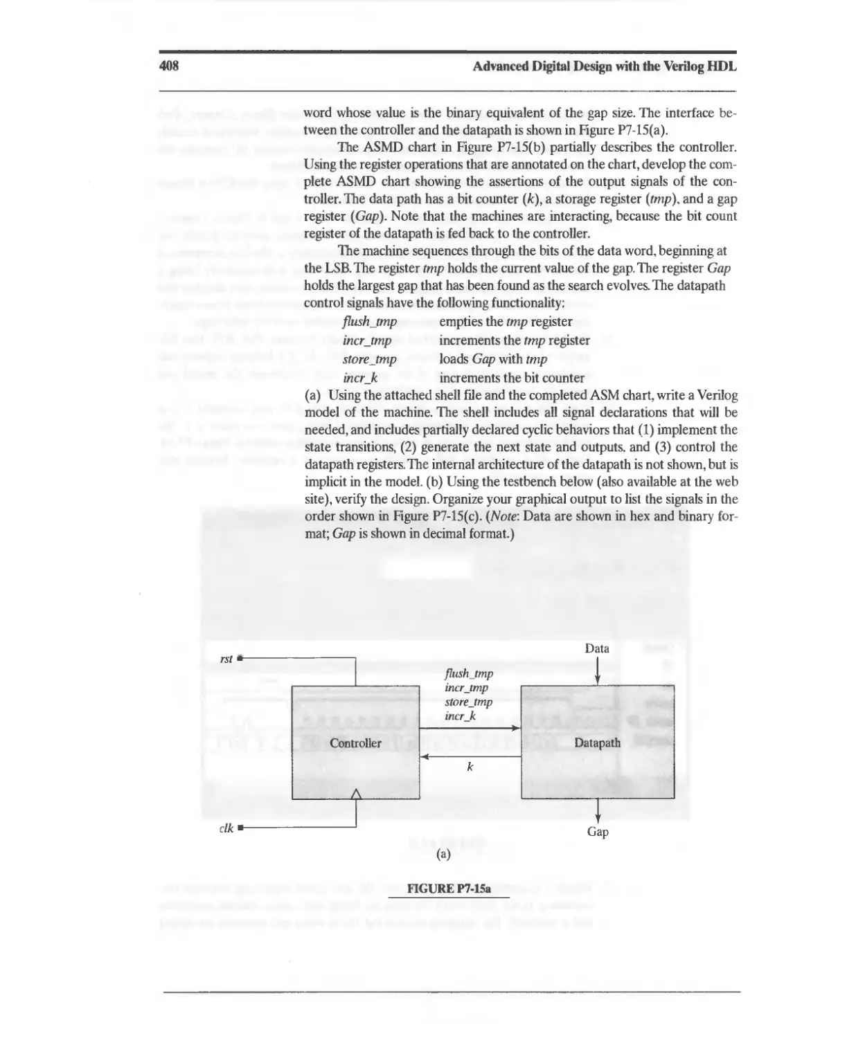
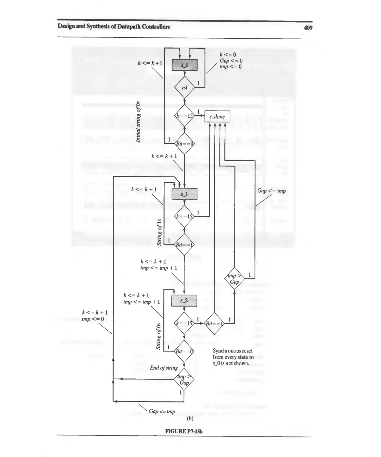
\
.oi -
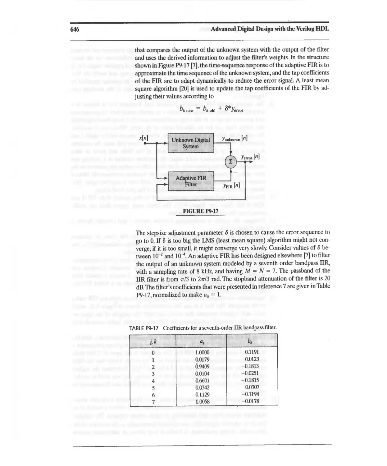
--
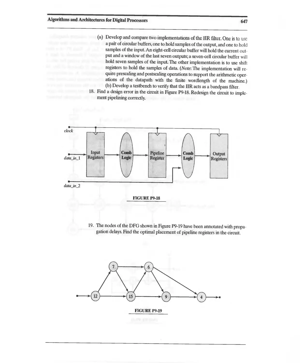
-
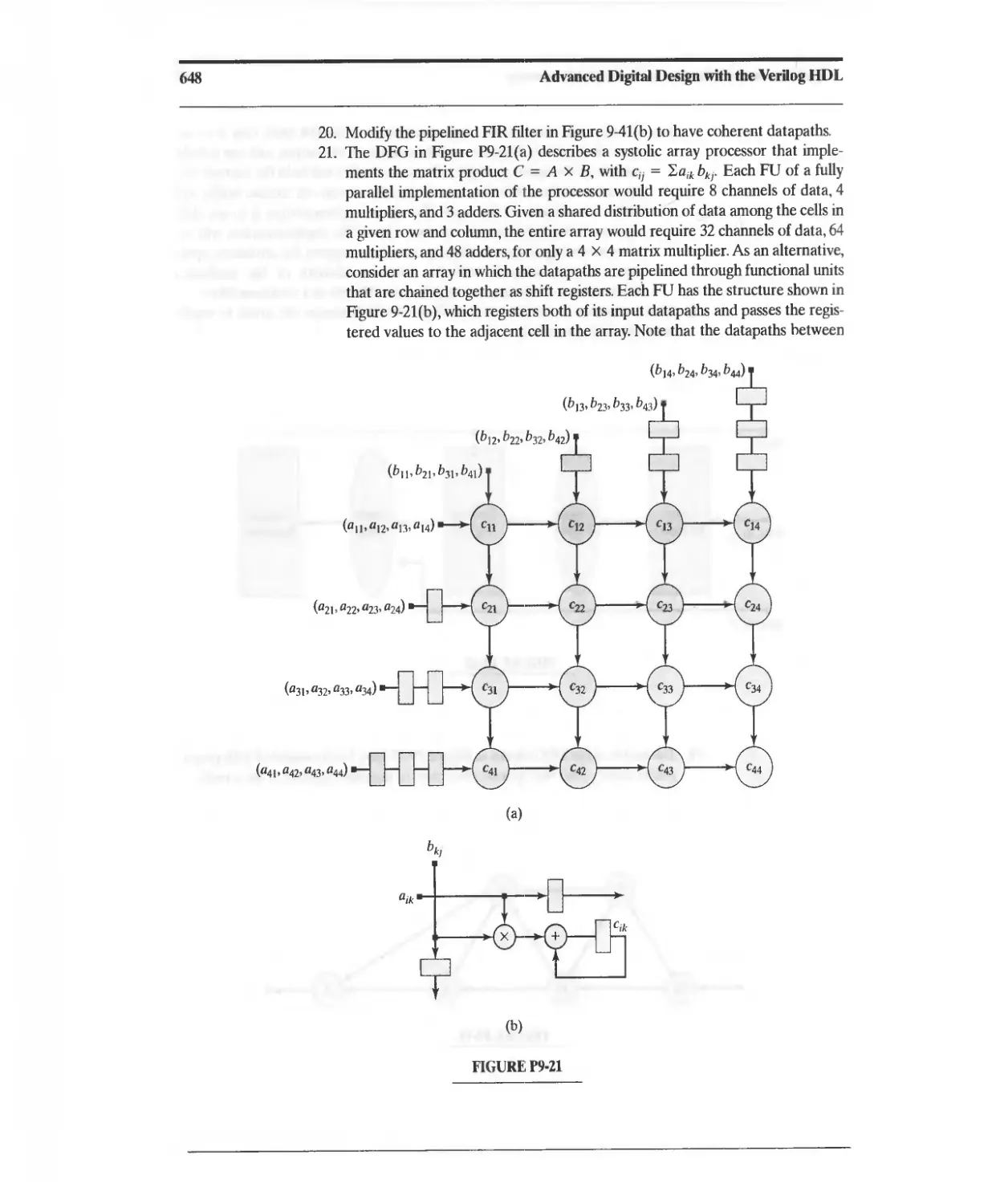
.... -". "
......... .".
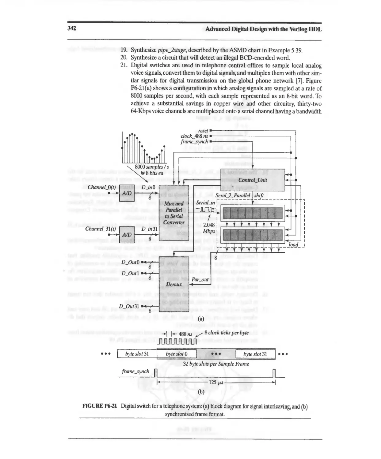
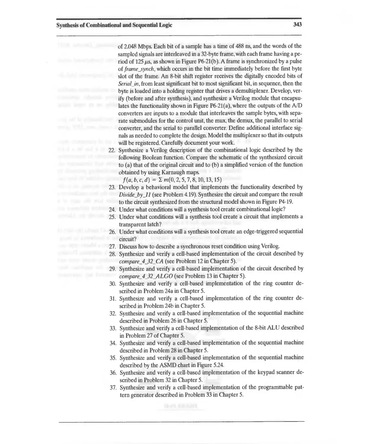
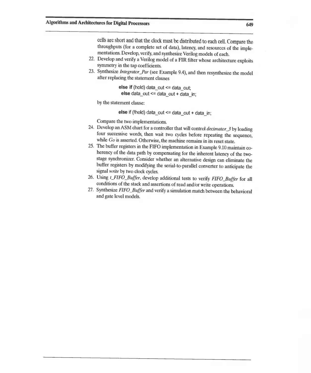
--::-
....
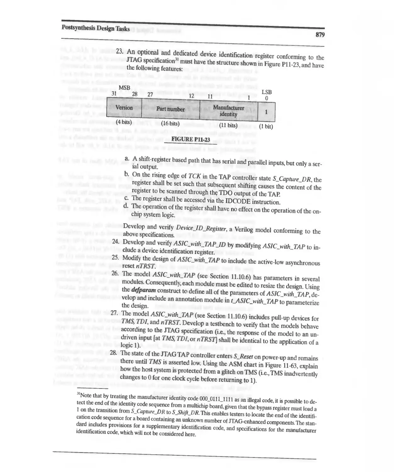
. . .",
Michael D. Ciletti
CD-ROM A
Included ...,
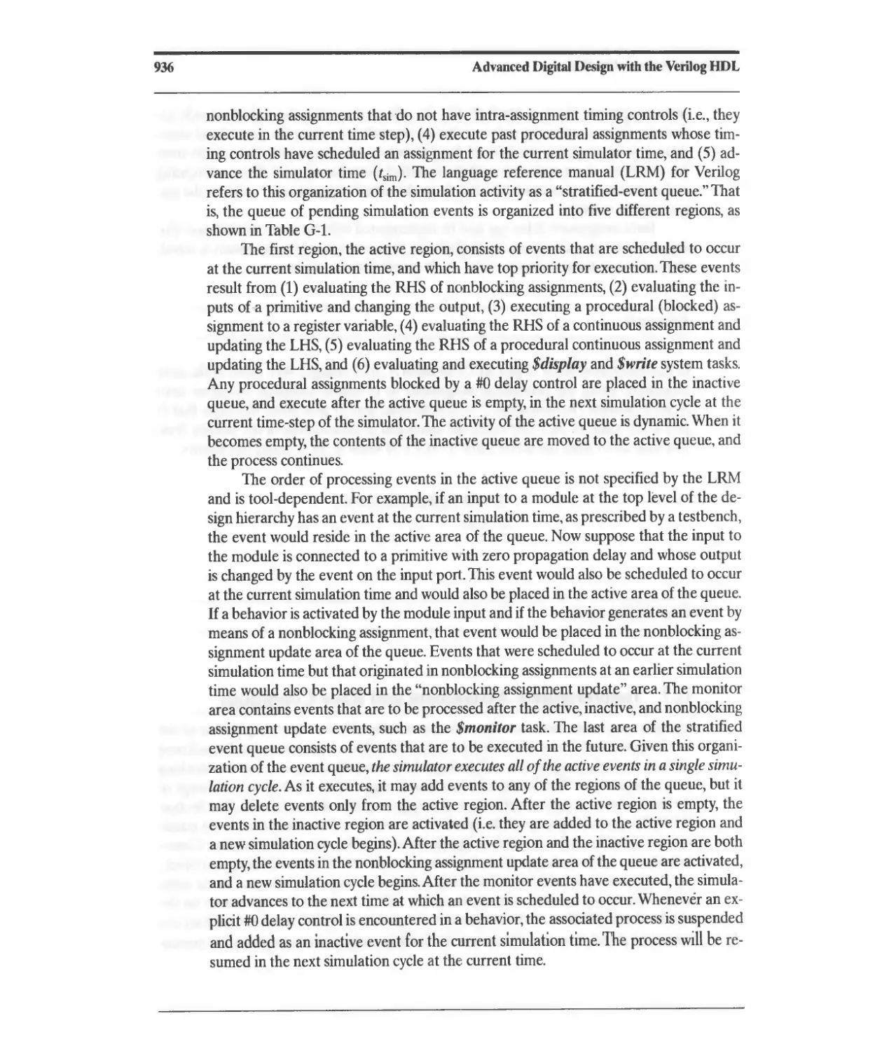
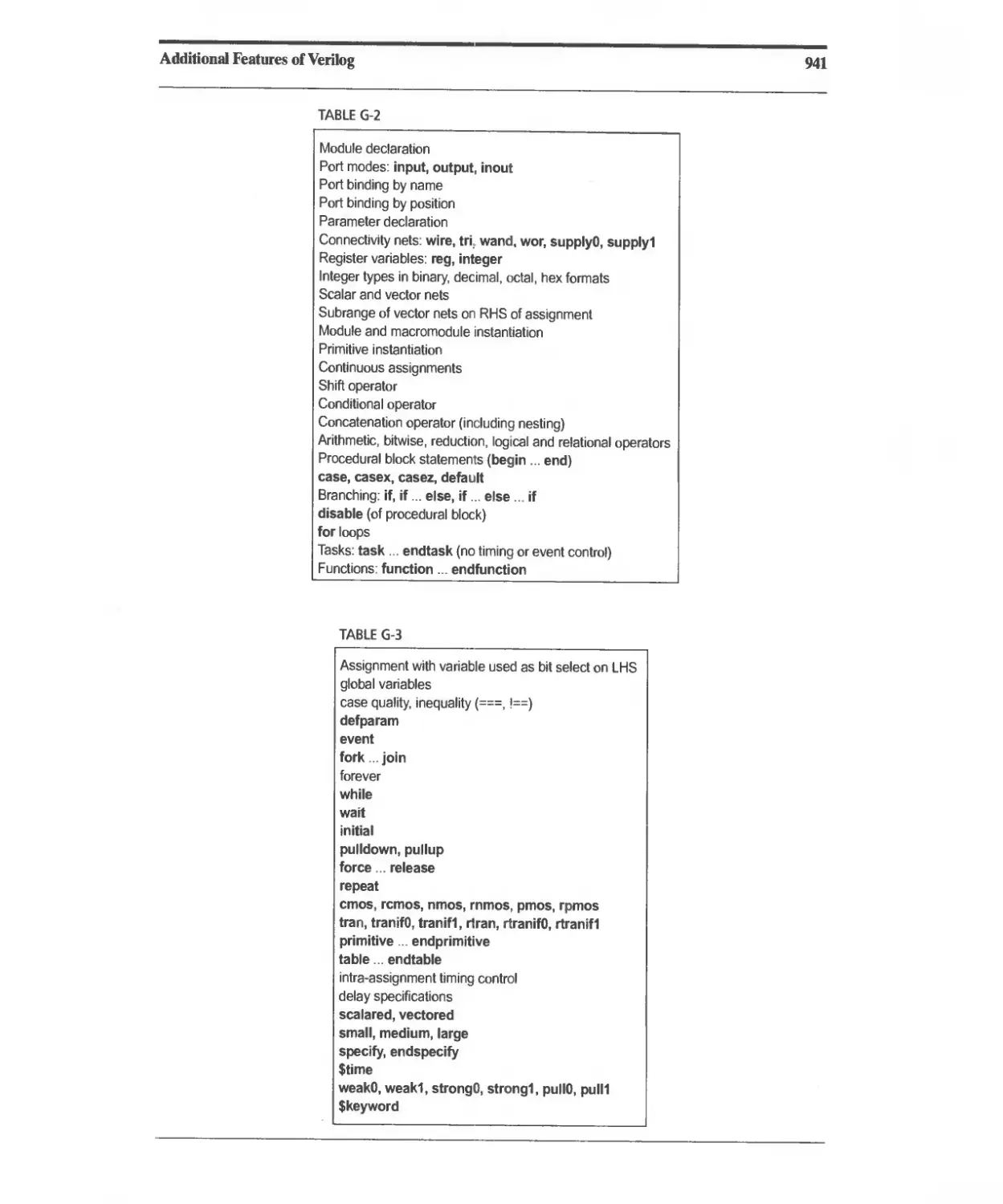
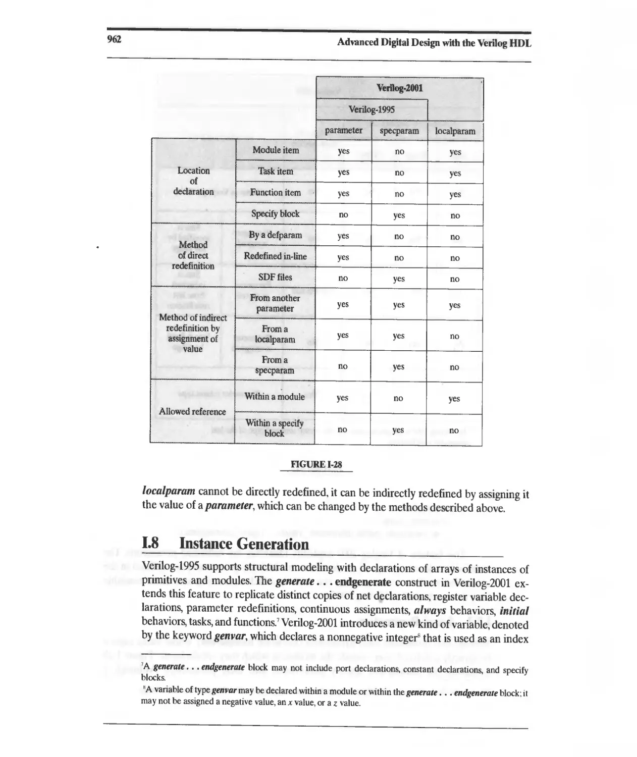
Summary of Key Verilog Features
(IEEE 1364)
Module
Encapsulates functionality; may be nested to any
depth.
module module_name (list of ports);
Dec!llfl/liol/S
Port modes: input, output, inout identifier;
Nets (e.g., wire A[3:0];)
Register variable (e.g., reg B[31: 0];)
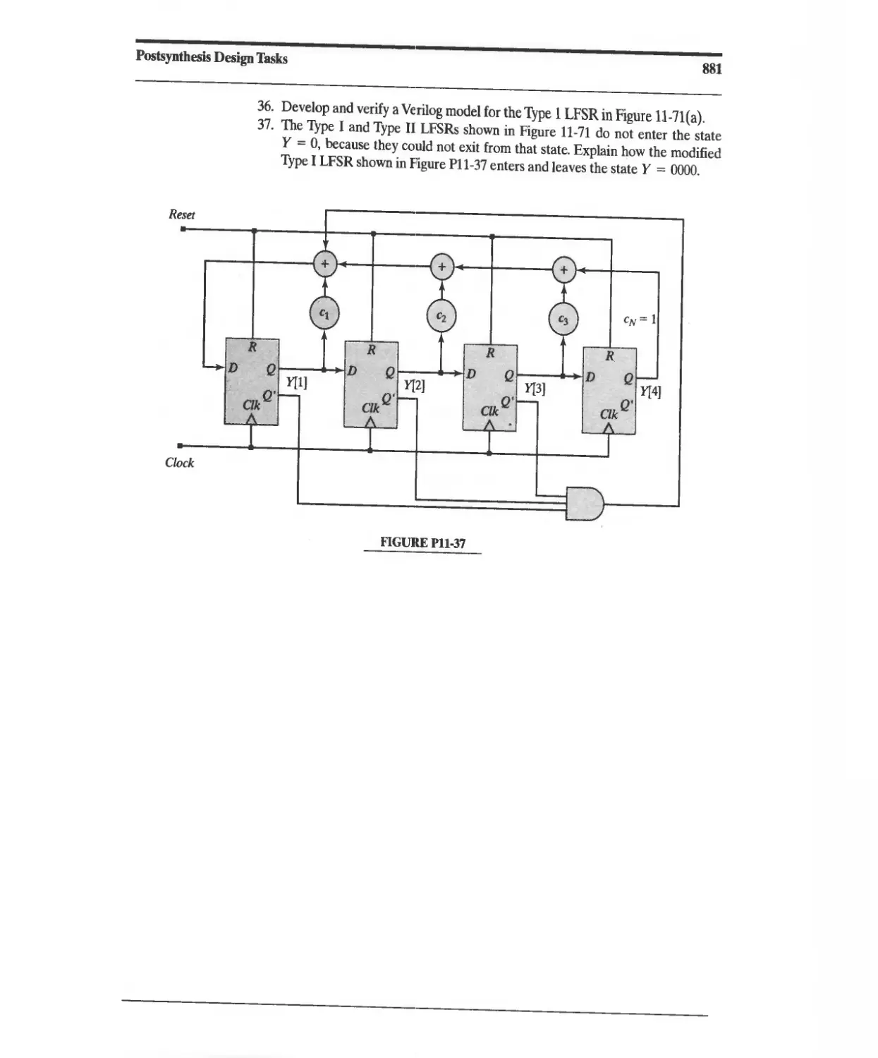
Constants: (e.g. parameter size = 8;)
Named events
Continuous assignments
(e.g. assign sum = A + B;)
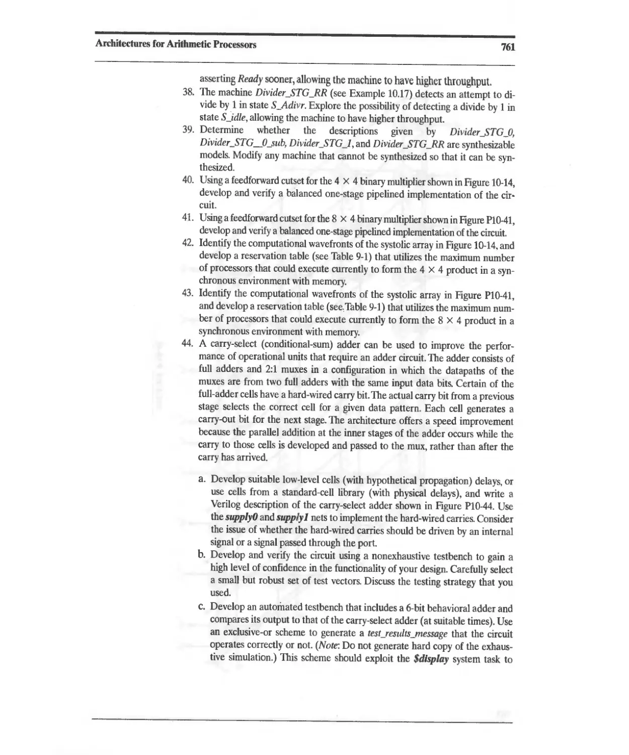
Behaviors always (cyclic), initial (single-pass)
specify . endspecify
function ... endfunction
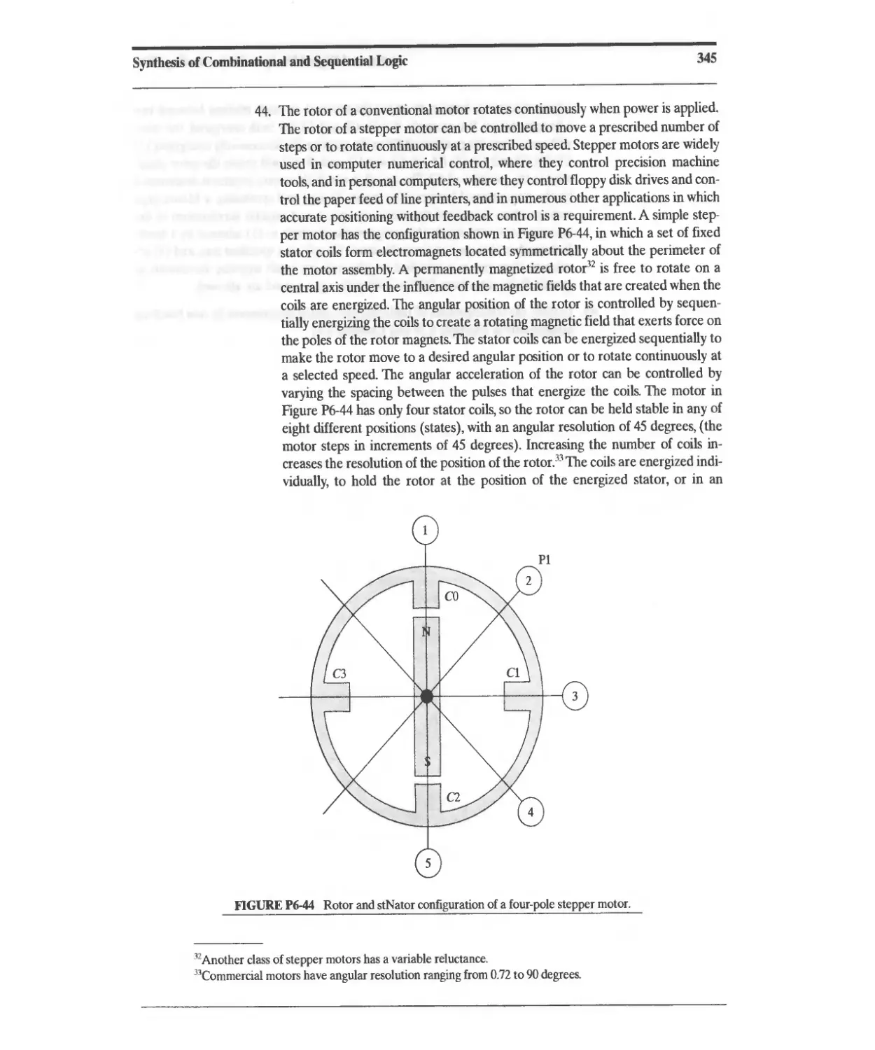
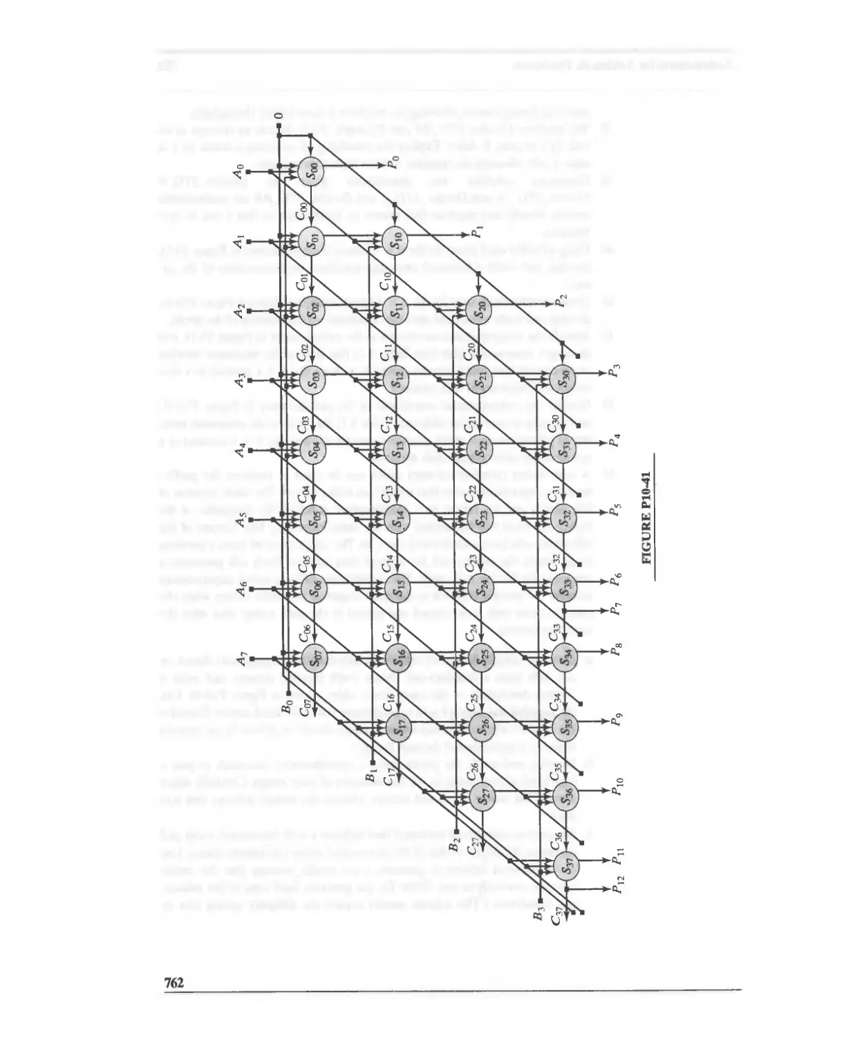
task ... endtask
!l/Sllllllilllioll.l'
primitives
modules
endmodule
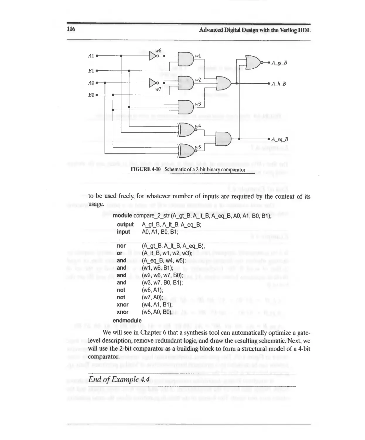
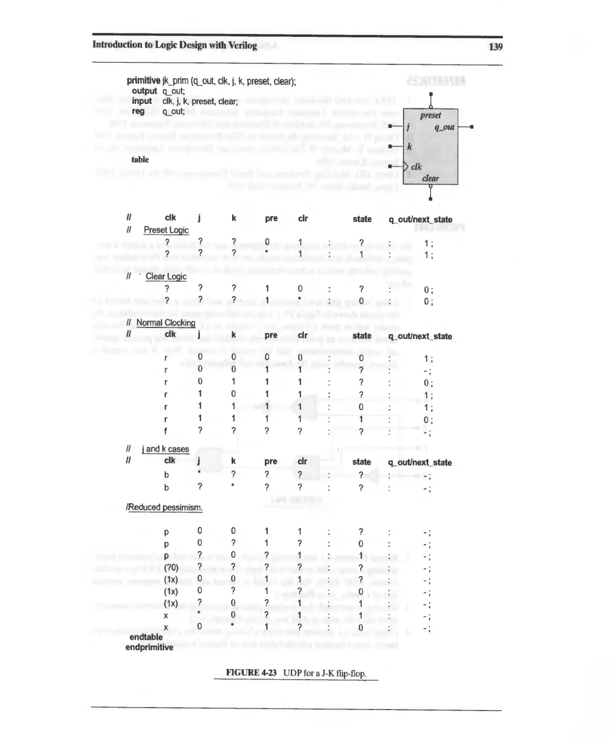
Multi Input Primitives
(Each input is a scalar)
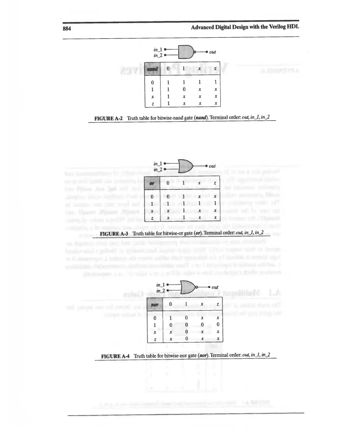
and (out, in1' in2' __. inN);
nand (out, in1' in2' p' inN);
or (out, in 1 , in2' ... inN);
nor (out, in1' in2' ... inN);
xor (out, in1' in2' ... inN);
xnor (out, in 1 , in2' ... inN);
Multi-Output Primitives
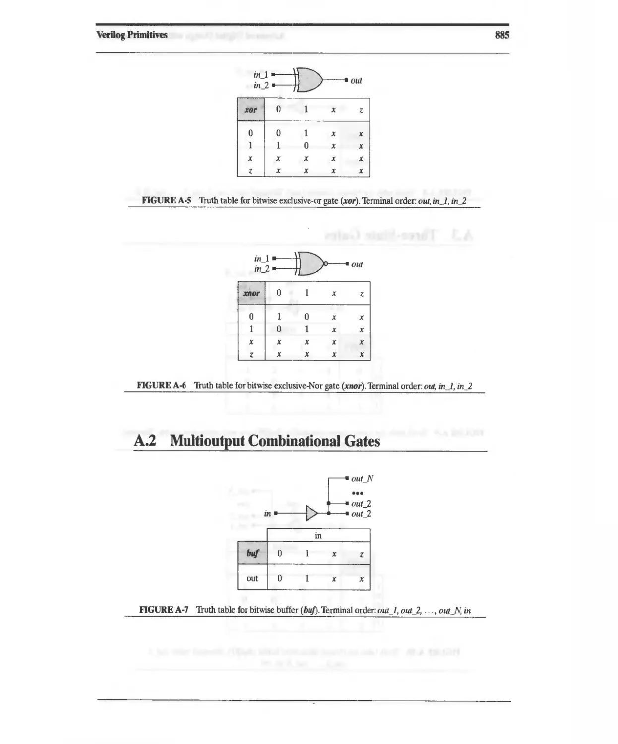
buf (out 1 , out 2 , p., out N , In); /I buffer
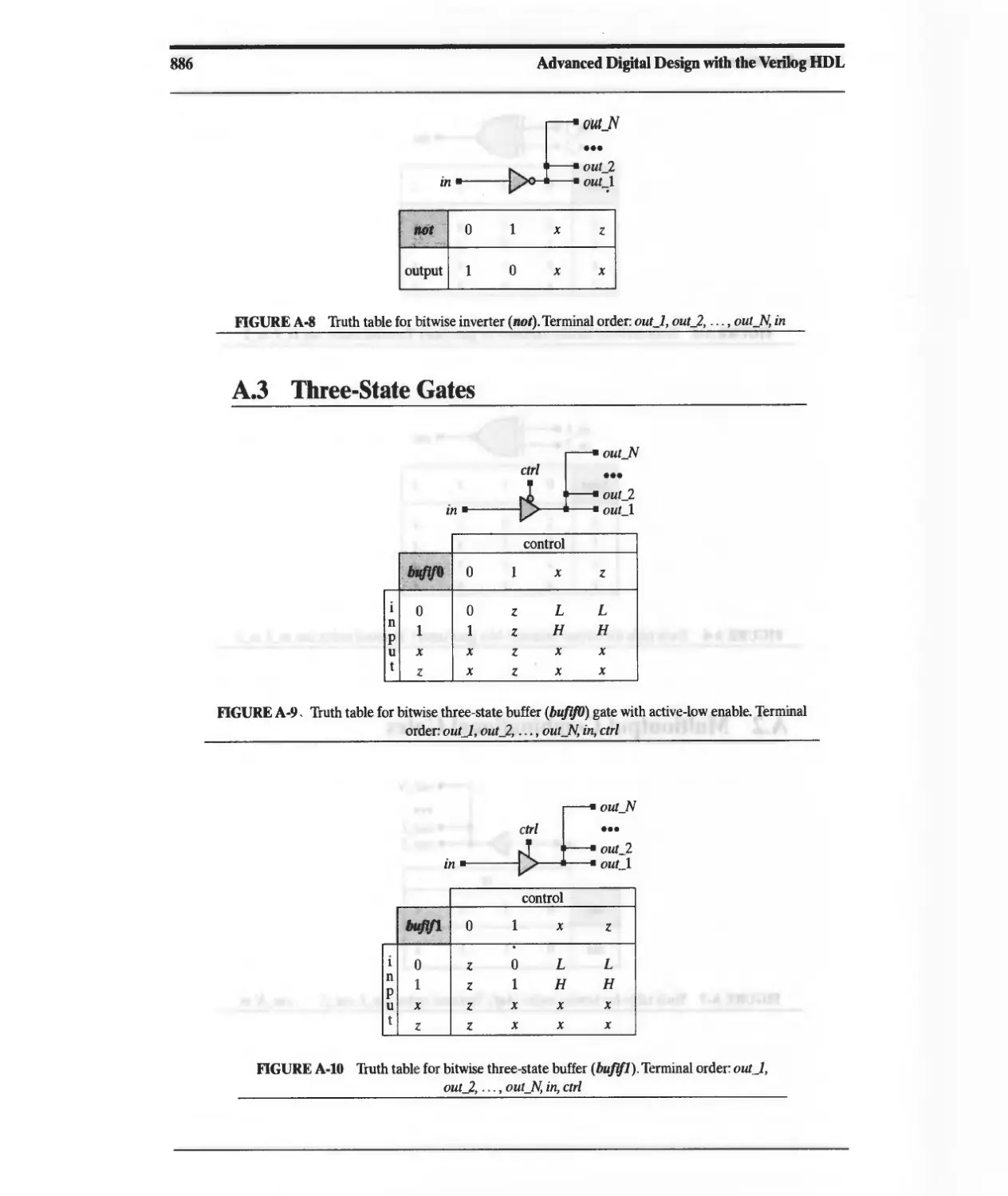
not (out 1 , out 2 , ..., out N , in); /I inverter
Three-State Multi-Output Primitives
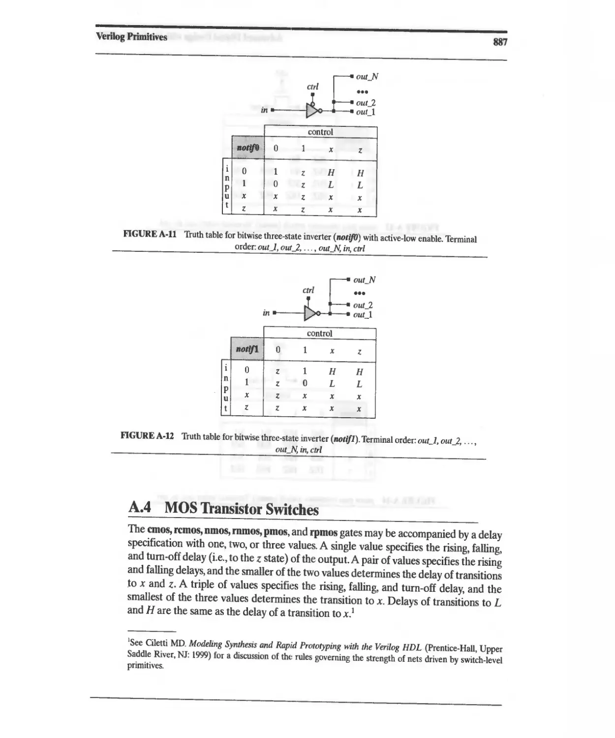
bufifO (out, in, control); bufif1 (out, in, control);
notifO (out, in, control); notif1 (out, in, control);
Pullups and Pull downs
pUliup (out_y); pUlidown (out_y);
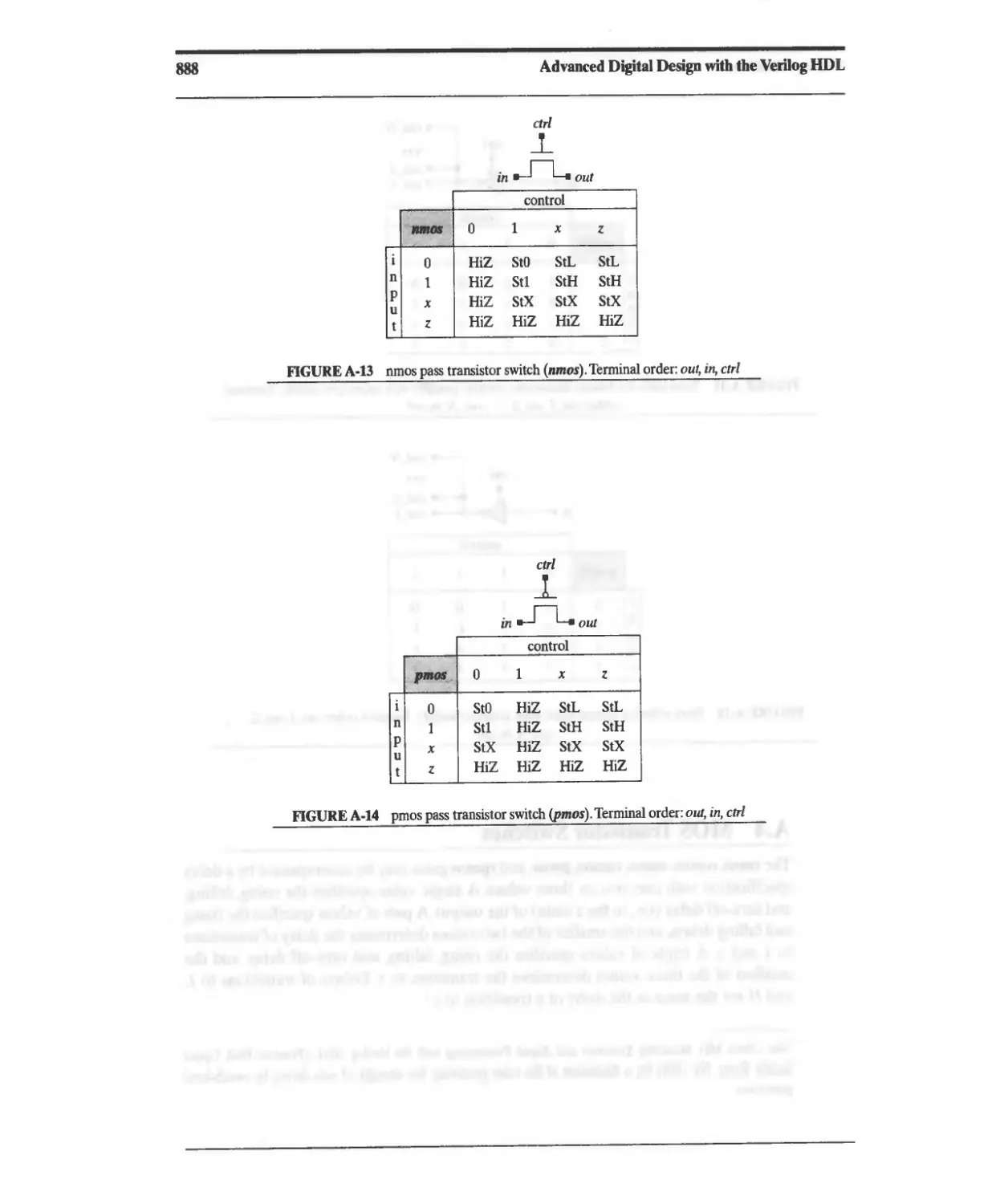
Propagation Delays
Single delay: and #3 G1 (y, a, b, c);
Rise/fall: and #(3, 6) G2 (y, a, b, c);
Rise/fall/turnoff: bufifO #(3,6,5) (y, x_in, en);
Min:typ:Max: bufif1 #(3:4:5, 4:5:6, 7,8:9)
-(y, x_in, en);
Command line options for single delay value simulation:
+maxdelays, +typdelays, +mindelays
Examp/e: verilog +mindelays testbench.v
Concurrent Behavioral Statements
May execute a level-sensitive assignment of value
to a net (keyword: assign), or may execute the state-
ments of a cyclic (keyword: always) or single-pass
(keyword: initial) behavior. The statements execute
sequentially, subject to level-sensitive or edge-sen-
sitive event control expressions.
Syntax:
assign net_name = [expression];
always begin [procedural statements] end
initial begin [procedural statements] end
Cyclic (always) and single-pass (initial) behaviors may
be level sensitive and/or edge sensitive.
Edge sensitive:
always @(posedge clock)
q <= data;
Level sensitive:
always @ (enable or data)
if (enable) q = data
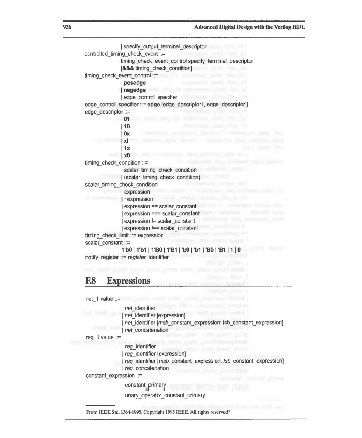
Data Types: Nets and Registers
Nets: Establish structural connectivity between
instantiated primitives and/or modules; may be tar.
get of a continuous assignment; e.g., wire, tri, wand,
wor.
Value is determined during simulation by the dri-
ver of the net; e.g., a primitive or a continuous assign-
ment. (Example: wire Y = A + B.)
Registers: Store information and retain value until
reassigned.
Value is determined by an assignment made by a
procedural statement.
Value is retained until a new assignment is made;
e.g., reg, integer, real, realtime, time.
Example:
atways @ (posedge clock)
if (reset) q_out <=0;
else q_out <= data_in;
Procedural Statements
Describe logic abstractly; statements execute
sequcntially to assign value to variables.
if ( expression _is_true) statement_1; else
statement_ 2;
case (case_expression)
casejtem: statement;
default: statement;
endcase
for (conditions) statement;
repeat constant_expression statement;
while (expression_is_true) statement;
forever statement;
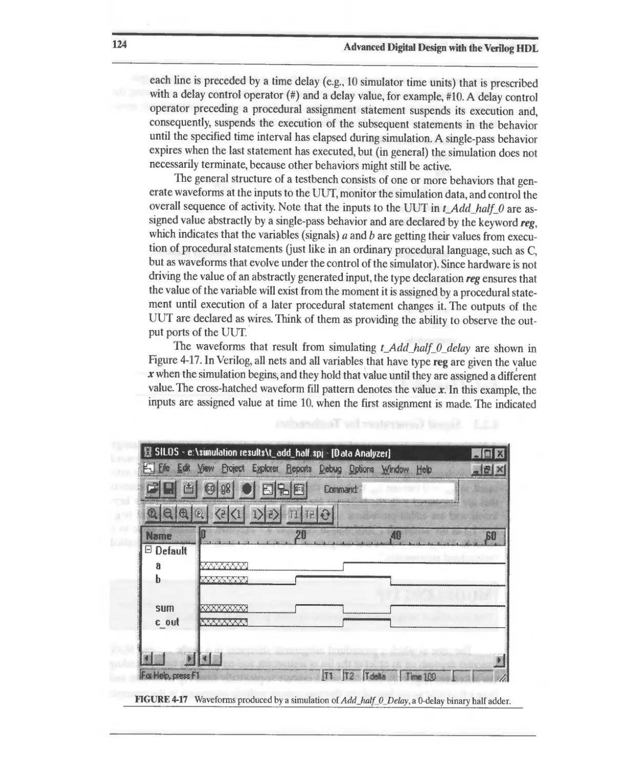
fork statements join 1/ execute in parallel
Assignments
Continuous: Continuously assigns the value of an
expression to a net.
Procedural (Blocked): Uses the = operator; exe-
cutes statements sequentially; a statement cannot
execute until the preceding statement completes
execution. Value is assigned immediately.
Procedural (Nonblocking): Uses the <= opera-
tor; executes statements concurrently, independent
of the order in which they are listed. Values are
assigned concurrently.
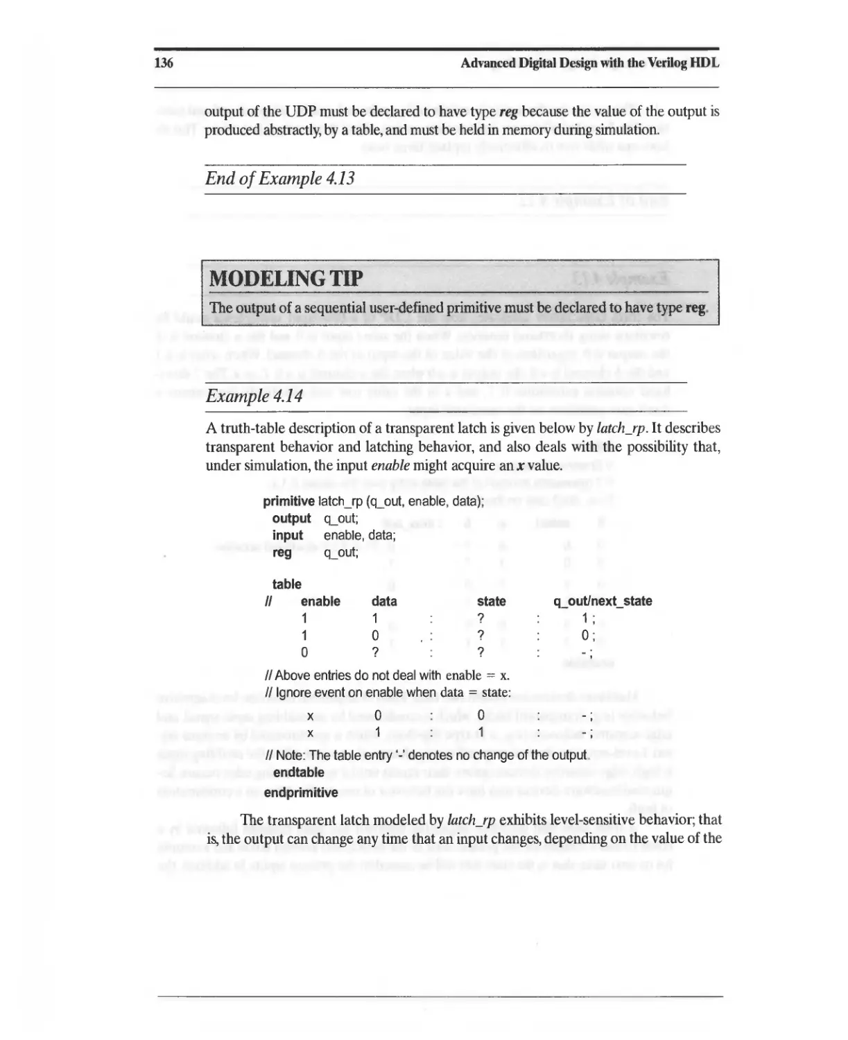
Procedural (Continuous):
assign ". deassign overrides procedural assignments
to a net.
force, ,. release overrides aU other assignments to a net
or a register.
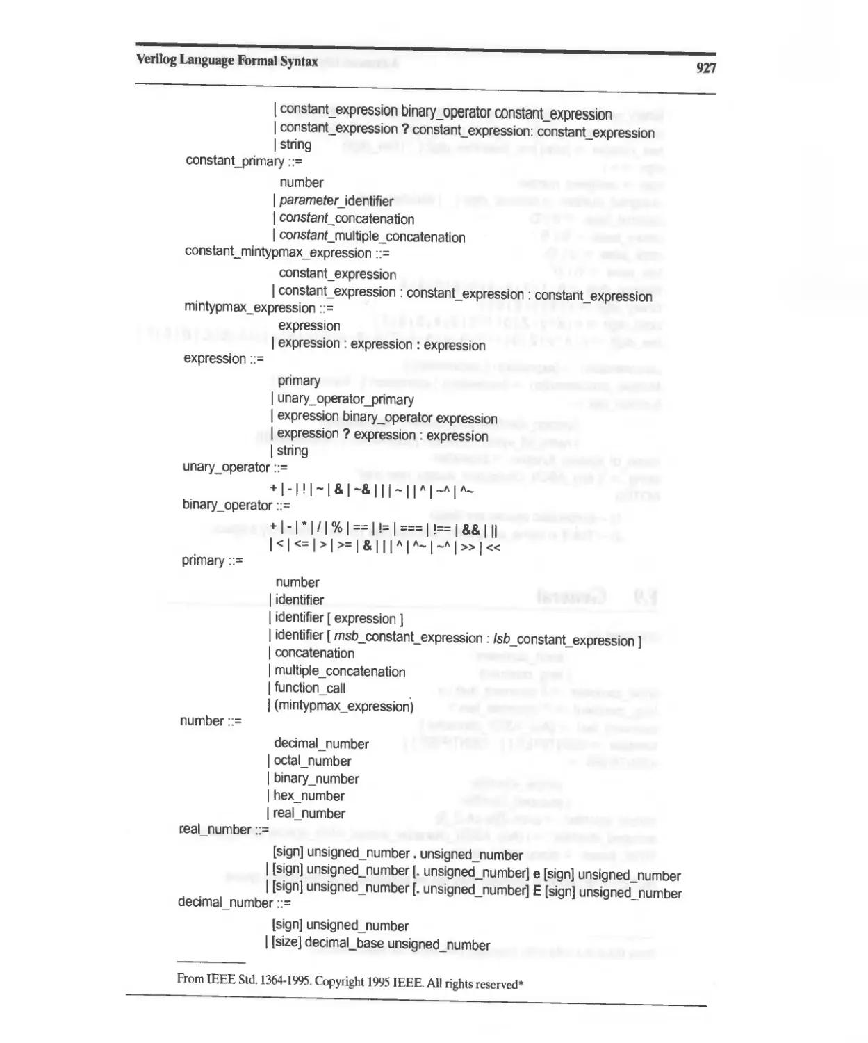
Operators
11.1111
+ - */
%
> >= < <=
'!
&&
II
!=
,==
&
I
/I....... or ",-'"
&
-&
-I
...... or /I......
«
»
'/,
or
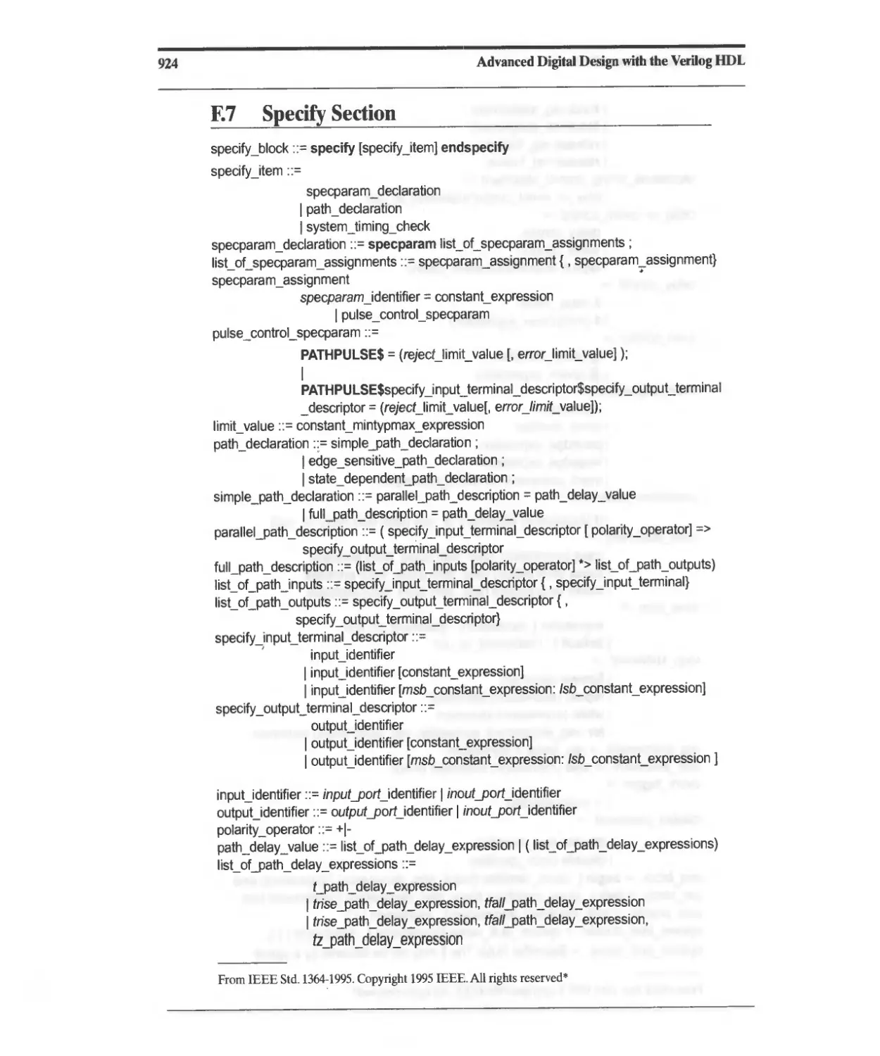
Specify Block
concatenation
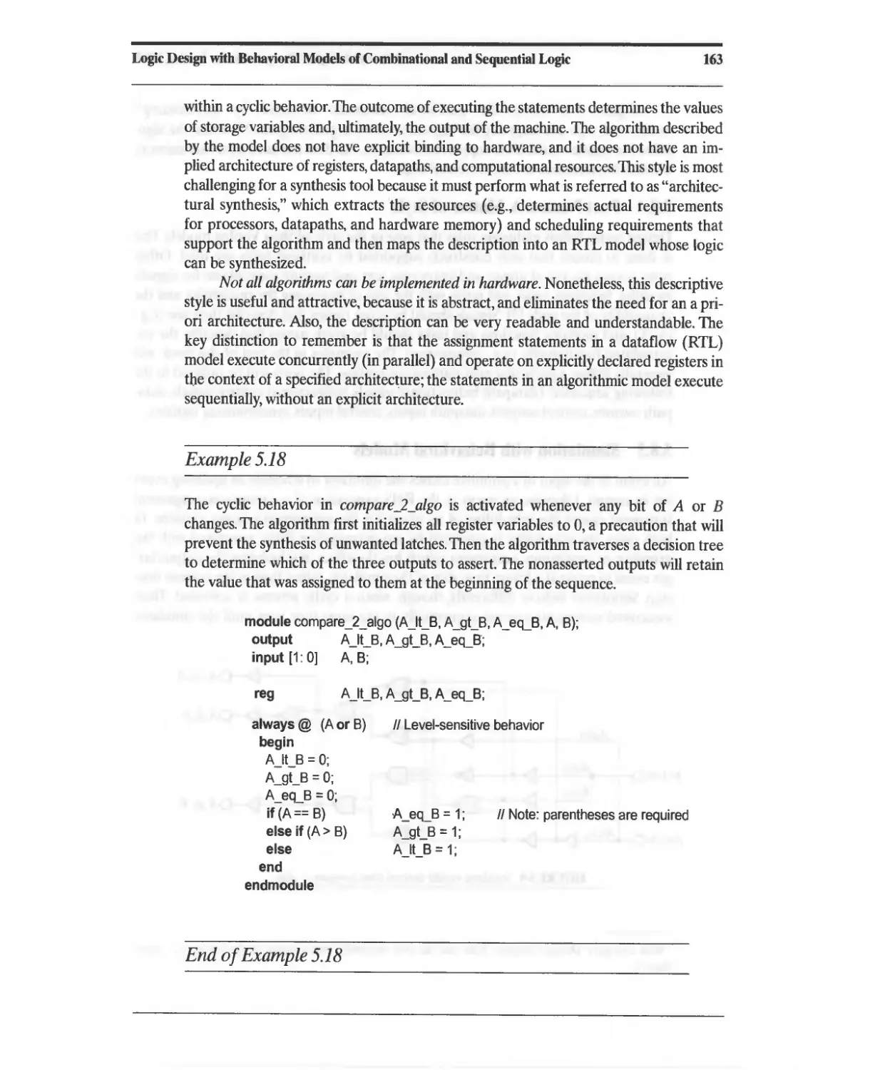
arithmetic
modulus
relational
logical negation
logical and
logical or
logical equality
logical inequality
case equality
case inequality
hitwise negation
hitwise and
hitwise or
h,twlSe exclusive-or
hitwise equivalence
reduction and
reduction nand
or
reduction nor
reduction exclusive-or
reduction xnor
left shift
right shift
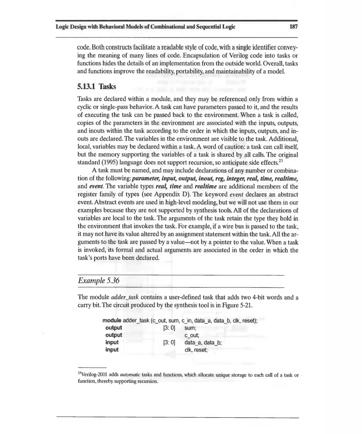
condiuonal
Event or
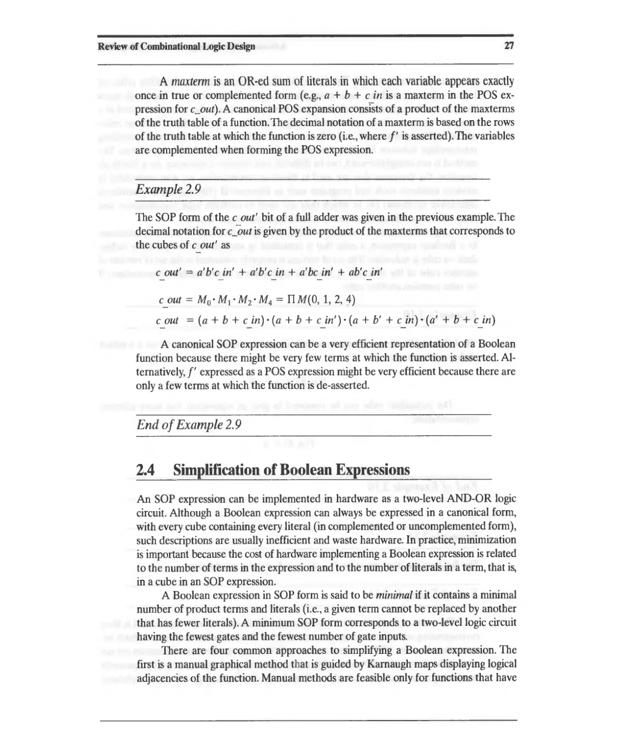
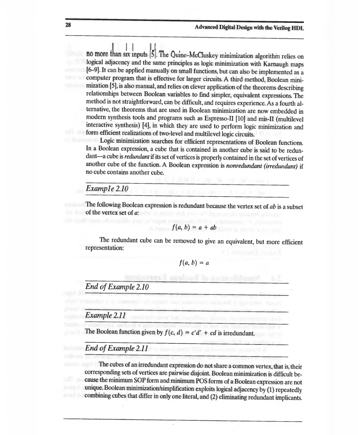
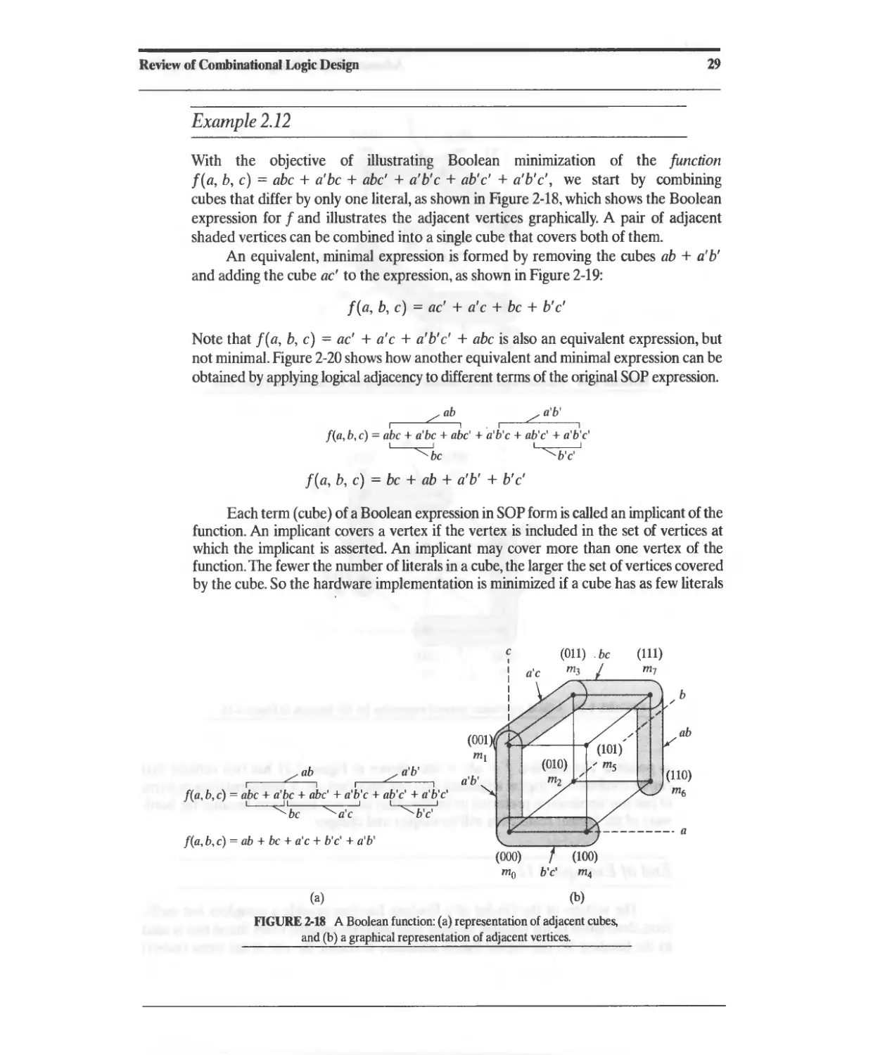
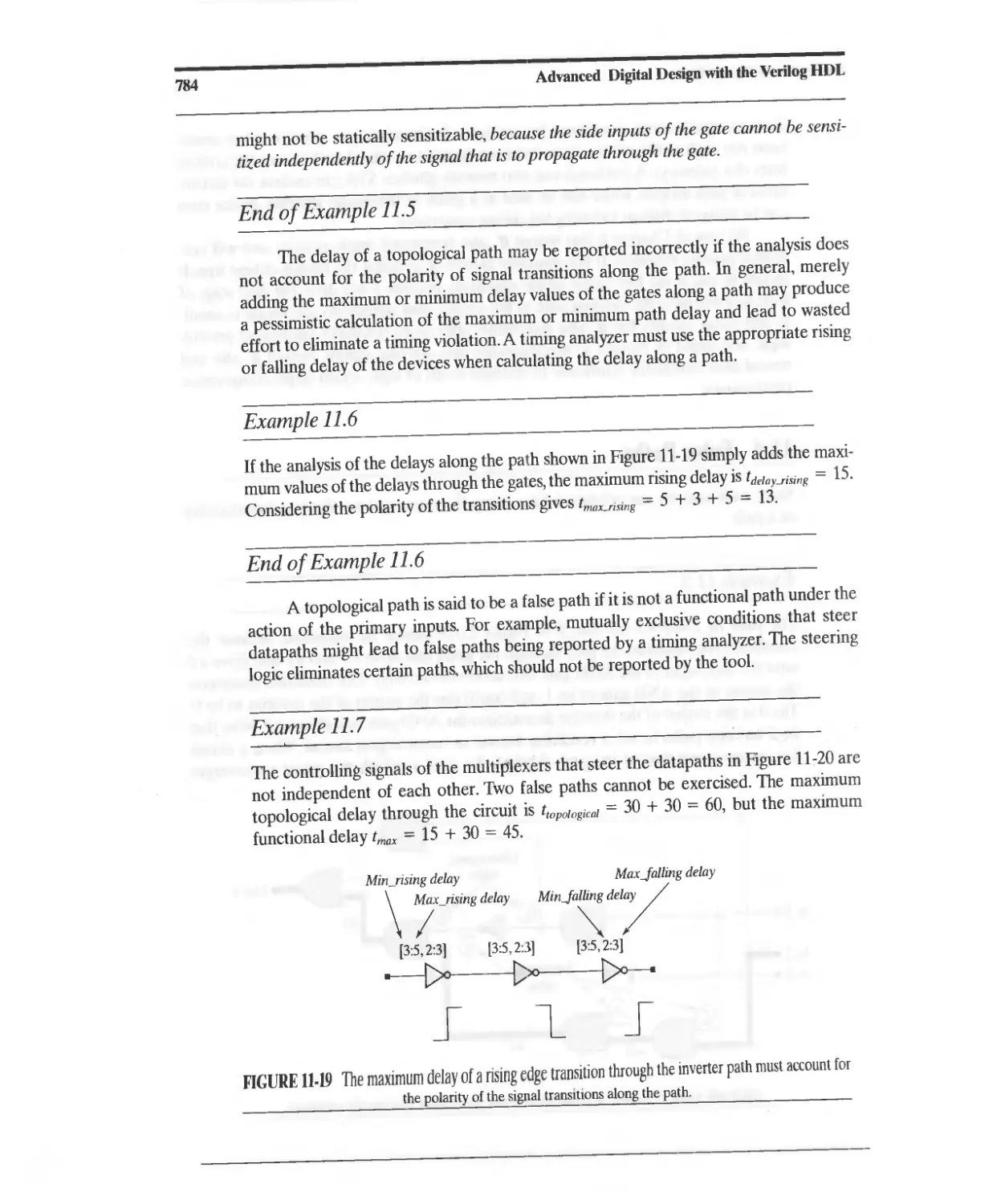
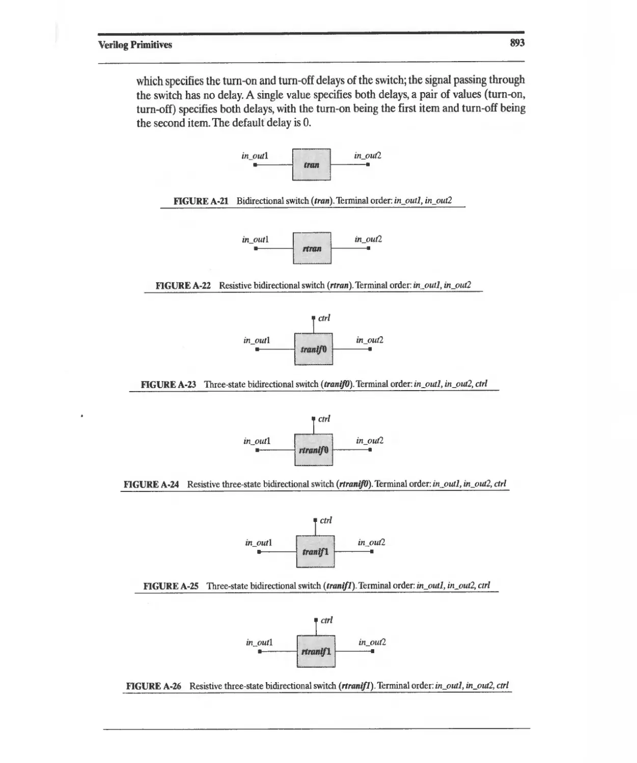
Example: Module Path Delays
specify
1/ specparam declarations (min: typ: max)
specparam U = 3;4:5, U = 4:5:6;
(A, B) *> Y) = (U, U); 1/ full
(Bus_1 => Bus_1) = (U, U); 1/ parallel
if (state == SO) (a, b *> y) = 2; 1/ state dep
(posedge clk => (y -: d_in)) = (3. 4); 1/ edge
endspecify
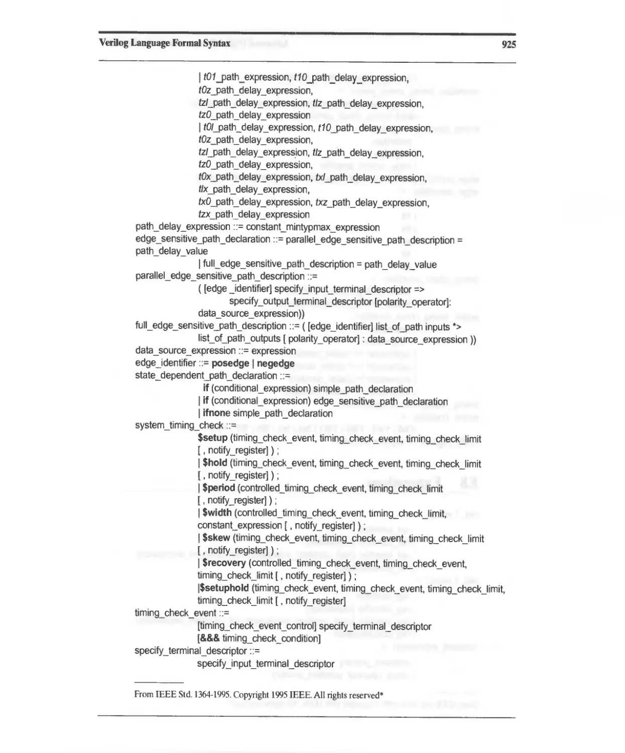
Example: Timing Checks
specify
specparam t_setup = 3:4:5, t_hold = 4:5:6;
$setup (data, posedge clock, t_setup);
$hold (posedge clock, data, t_hold);
endspecify
Memory
Declares an array of words.
Example: Memory declaration and readout
module memory_read _ displayO;
reg [31: 0] mem_array [1: 1024];
integer k;
Advanced Digital Design
with the Verilog HD L
Advanced Digital Design
with the Verilog HD L
Michael D. Ciletti
Department of Electrical and Computer Engineering
University of Colorado at Colorado Springs
Prentice,Hall of India [P[J [bB[illBO@dJ
New Delhi - 110 001
2005
+' , + + +
+ :+! :+ :+ + : '
+ + {(, + I(, + I(, +
.. ,, .. ., - .. , -
ADVANCED DIGITAL DESIGN WITH THE VERILOG HDL (with CD-ROM)
by Michael D. Citetti
@ 2003 by Prentice-Hall, Inc. (now known as Pearson Education, Inc.), Upper Saddle River, New
Jersey 07458, U.S.A. All rights reserved. No part of this book may be reproduced in any form, by
mimeograph or any other means, without permission in writing from the publisher.
The author and publisher 01 this book have used their best efforts in preparing this book. These efforts include
the development, research, and testing 01 the theories and programs to determine their effectiveness. The author
and publisher make no warranty 01 any kind, expressed or Implied, with regard to these programs or the
documentation contained in this book. The author and publisher shall not be liable in any event 101 incidental
or consequential damages in connection with, or arising out 01, the lurnlshing, performance, or use 01 these
proglarns.
Silos and Simucad are registered trademarks 01 Simucad, Inc., 32970 Alvarado-Niles Road, Union City, CA 94587.
Verilog is a registered trademark 01 Cadence Design Systems, Inc., 2655 Seely Avenue, San Jose, CA 95134.
ISBN-81-203-2756-X
Published by Asoke K. Ghosh, Prentice-Hall of India Private Limited, M-97, Connaught Circus, New
Delhi-110001 and Printed by Rajkamal Electric Press, 8-35/9, G.T. Kamal Road Industrial Area,
Delhi-110033.
Contents
Preface xvii
Simplify, Clarify, and Verify xvm
1 Introduction to Digital Design Methodology 1
1.1 Design Methodology-An Introduction 2
1.1.1 Design Specification 4
1.1.2 Design Partition 4
1.1.3 Design Entry 4
1.1.4 Simulation and Functional Verification 5
1.1.5 Design Integration and Verification 6
1.1.6 Presynthesis Sign-Off 6
1.1.7 Gate-Level Synthesis and Technology Mapping 6
1.1.8 Postsynthesis Design Validation 7
1.1.9 Postsynthesis Timing Analysis 8
1.1.10 Test Generation and Fault Simulation 8
1.1.11 Placement and Routing 8
1.1.12 Physical and Electrical Design Rules 9
1.1.13 Parasitic Extraction 9
1.1.14 Design Sign-Off 9
1.2 IC Technology Options 9
1.3 Overview 11
References 11
vi
Contents
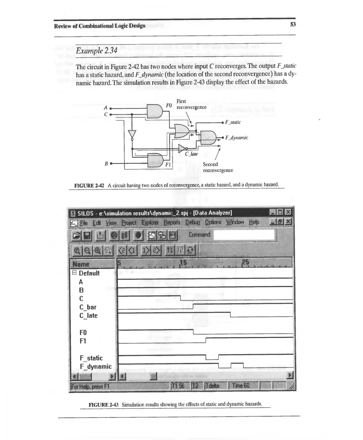
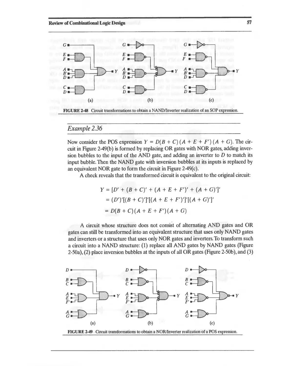
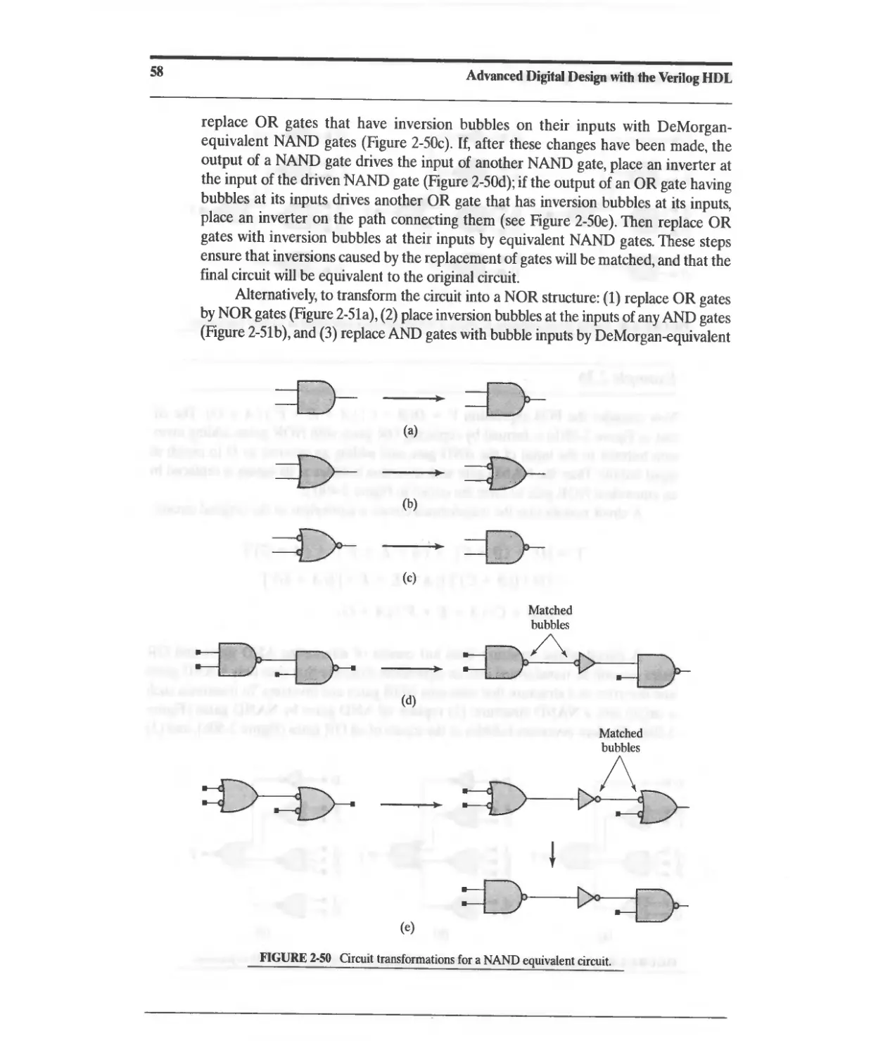
2 Review of Combinational Logic Design 13
2.1 Combinational Logic and Boolean Algebra 13
2.1.1 ASIC Library Cells 13
2.1.2 Boolean Algebra 16
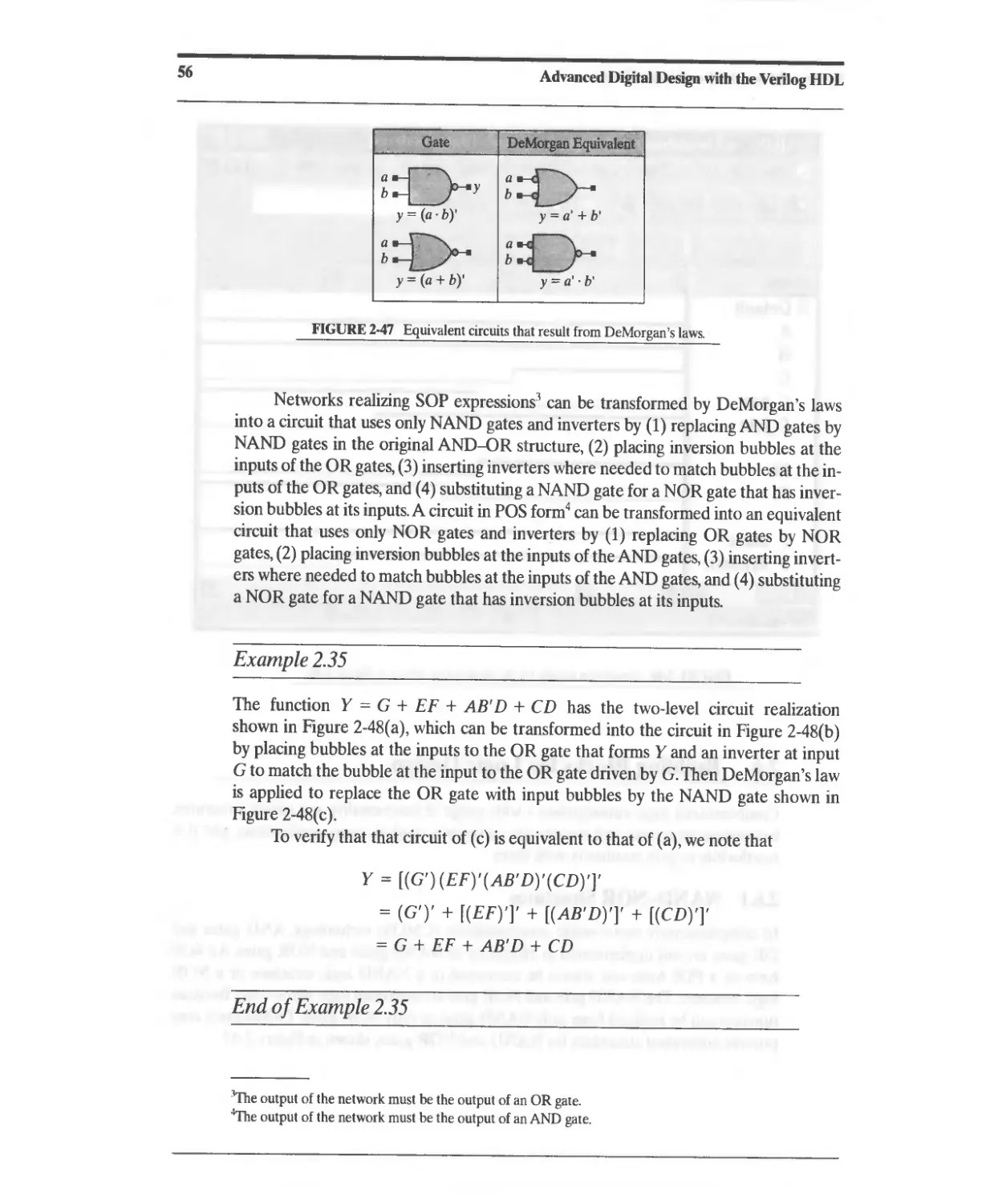
2.1.3 DeMorgan's Laws 18
2.2 Theorems for Boolean Algebraic Minimization 18
2.3 Representation of Combinational Logic 21
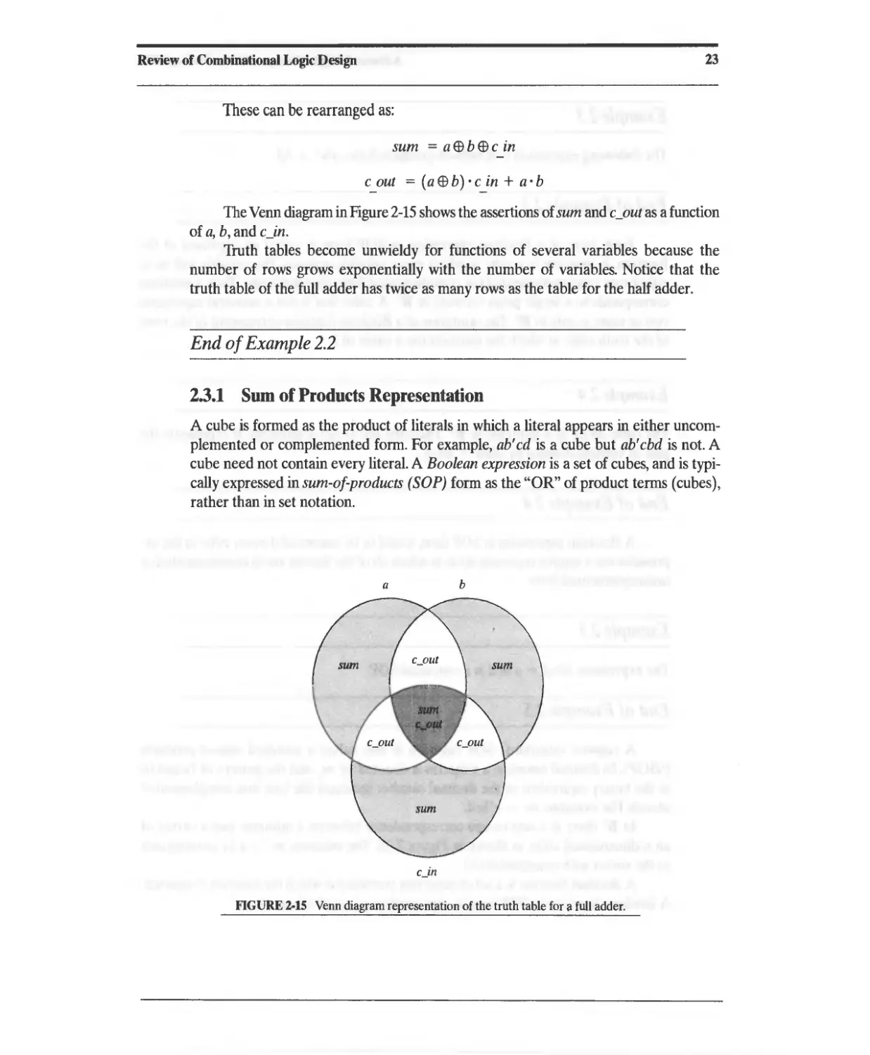
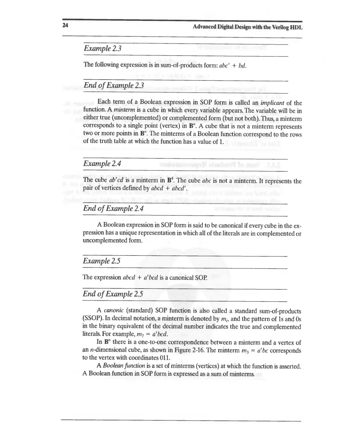
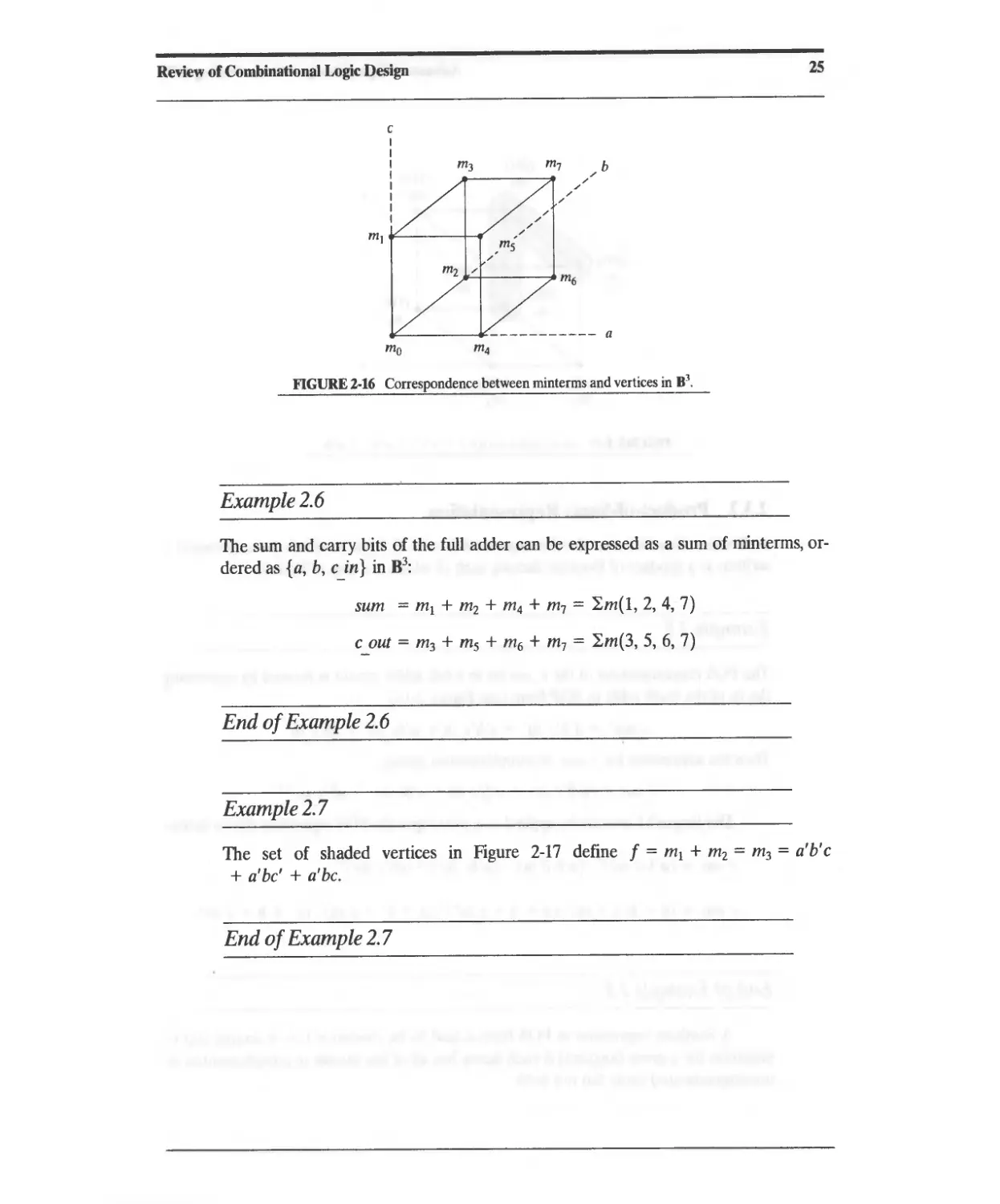
2.3.1 Sum of Products Representation 23
2.3.2 Product-of-Sums Representation 26
2.4 Simplification of Boolean Expressions 27
2.4.1 Simplification with Exclusive-Or 36
2.4.2 Karnaugh Maps (SOP Form) 36
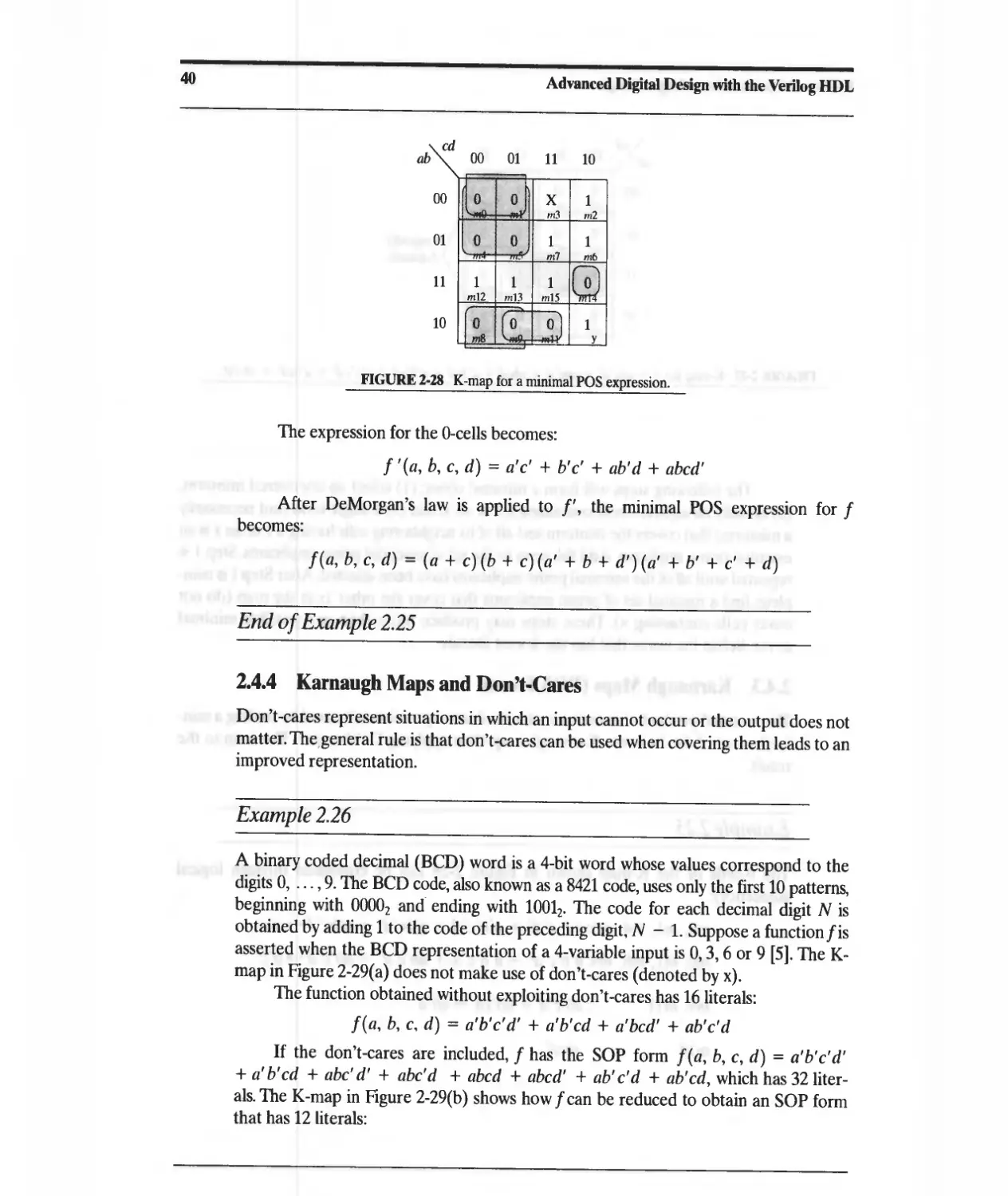
2.4.3 Karnaugh Maps (POS Form) 39
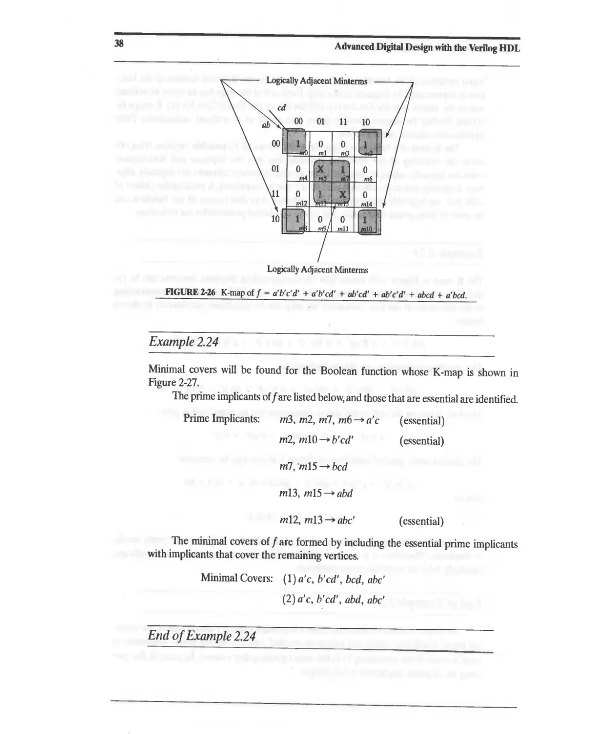
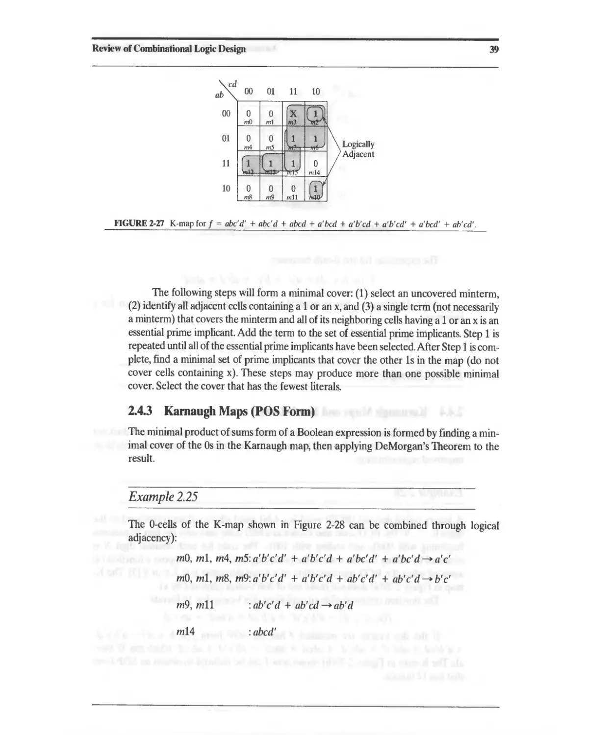
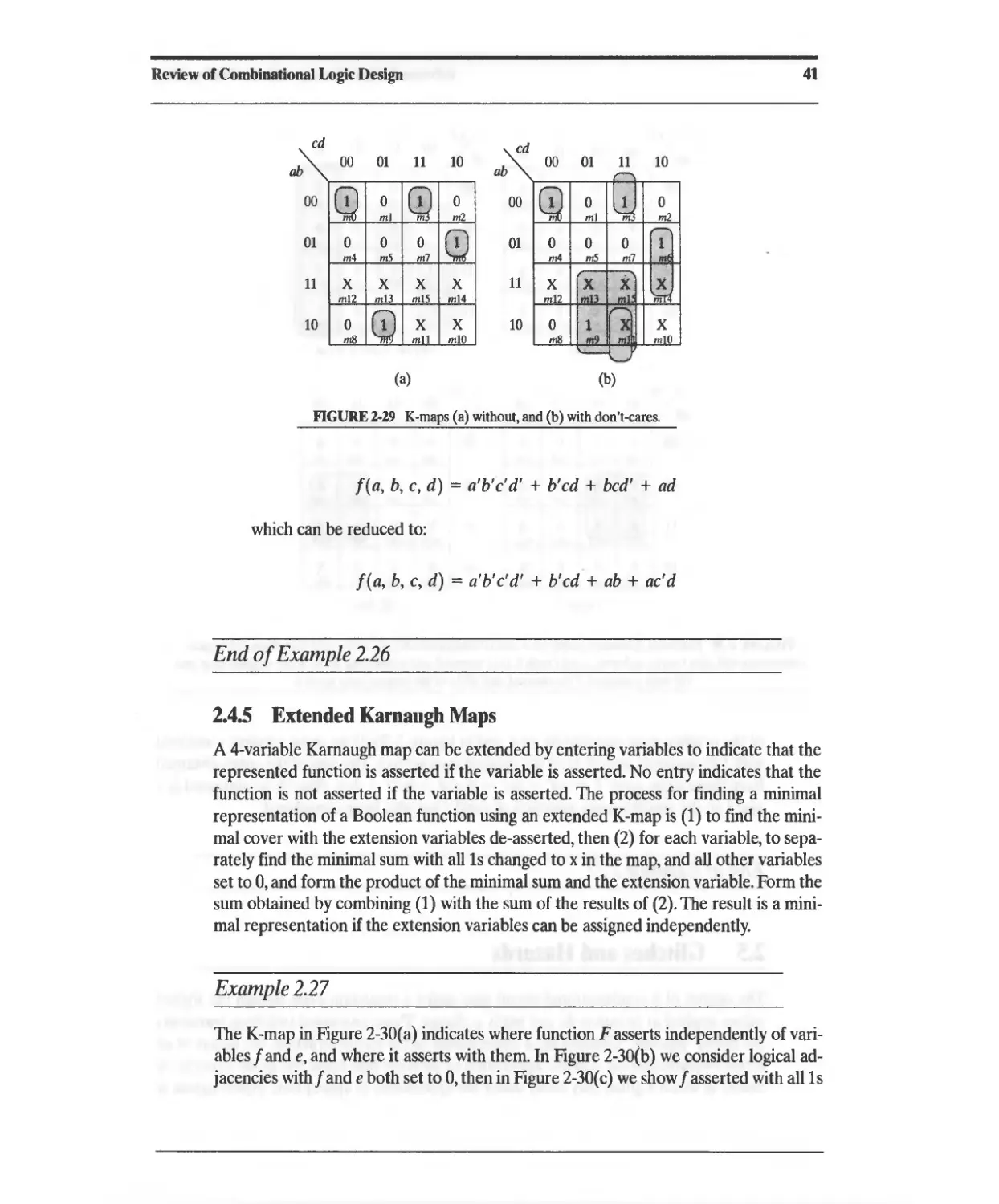
2.4.4 Karnaugh Maps and Don't-Cares 40
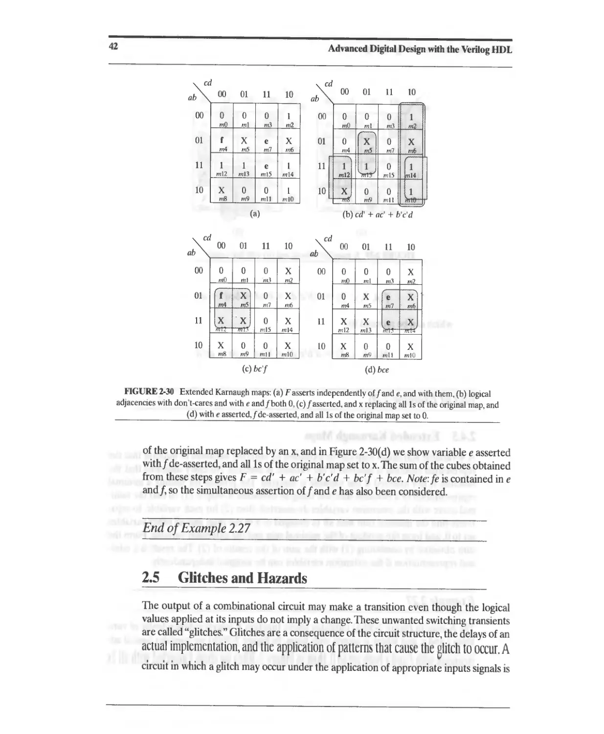
2.4.5 Extended Karnaugh Maps 41
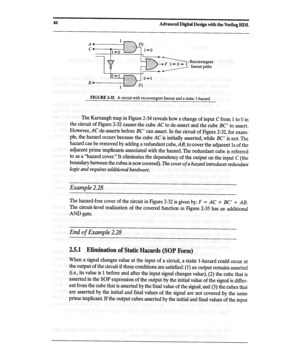
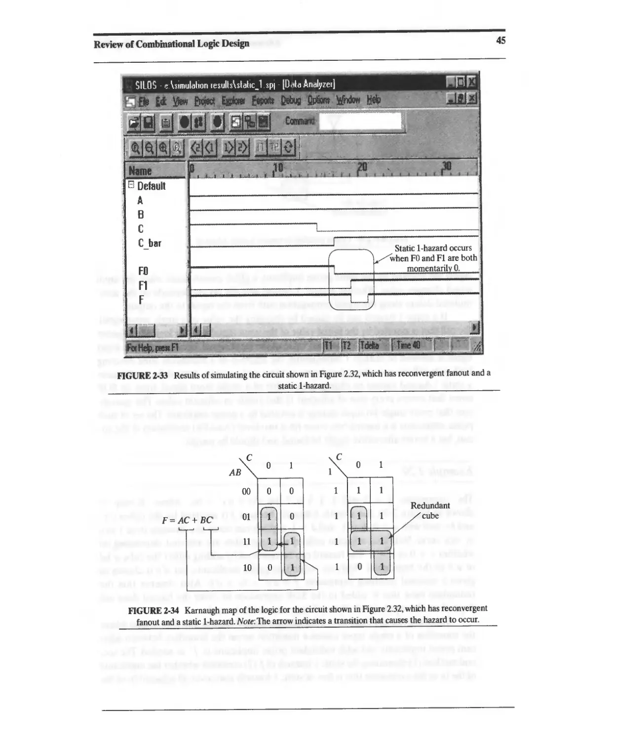
2.5 Glitches and Hazards 42
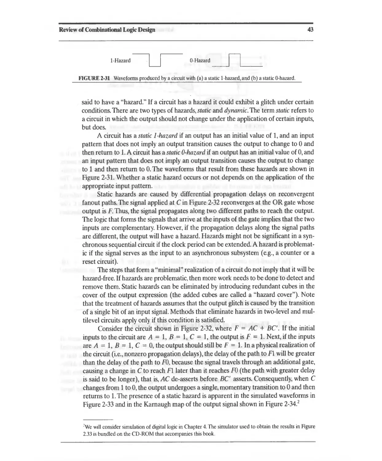
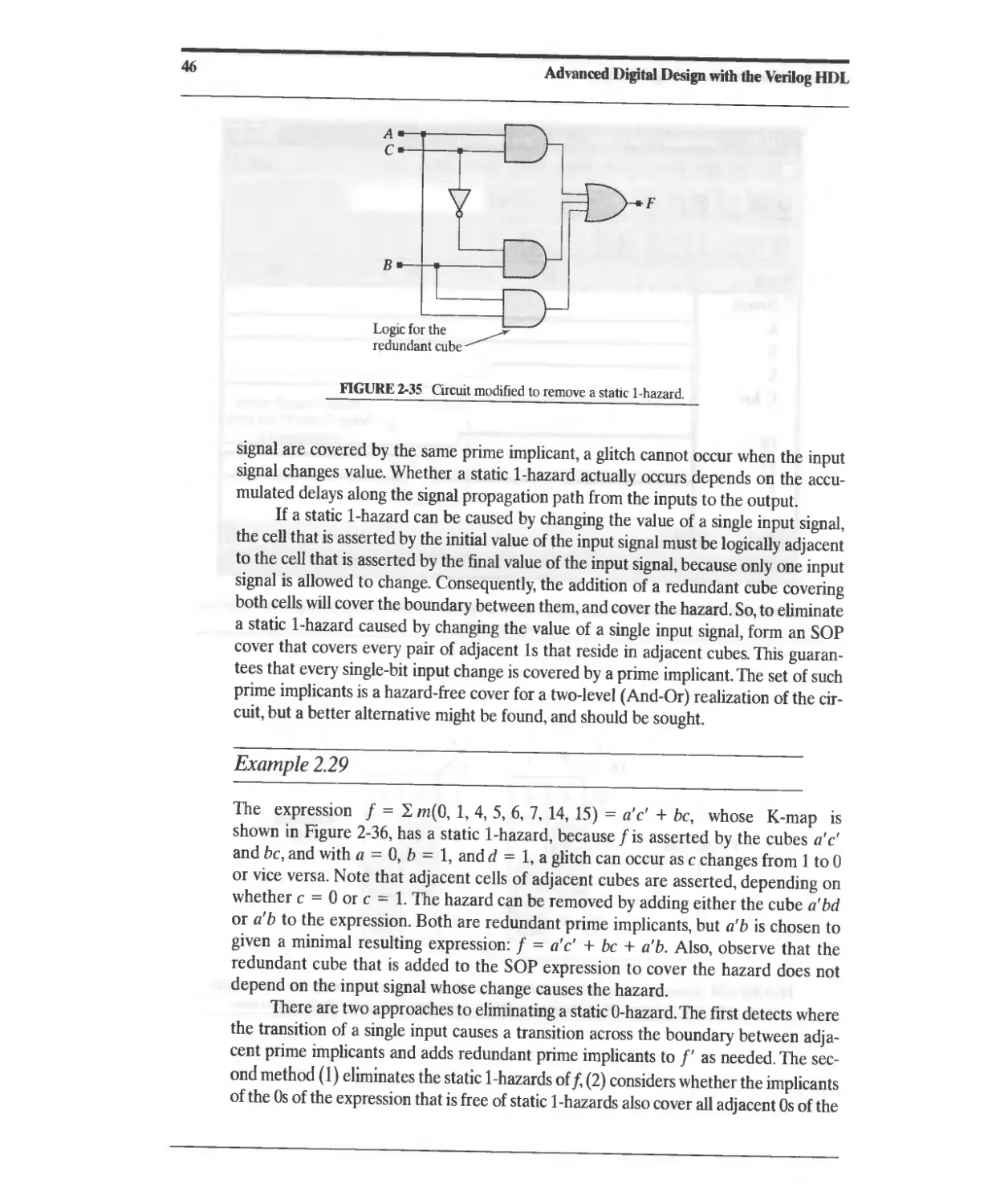
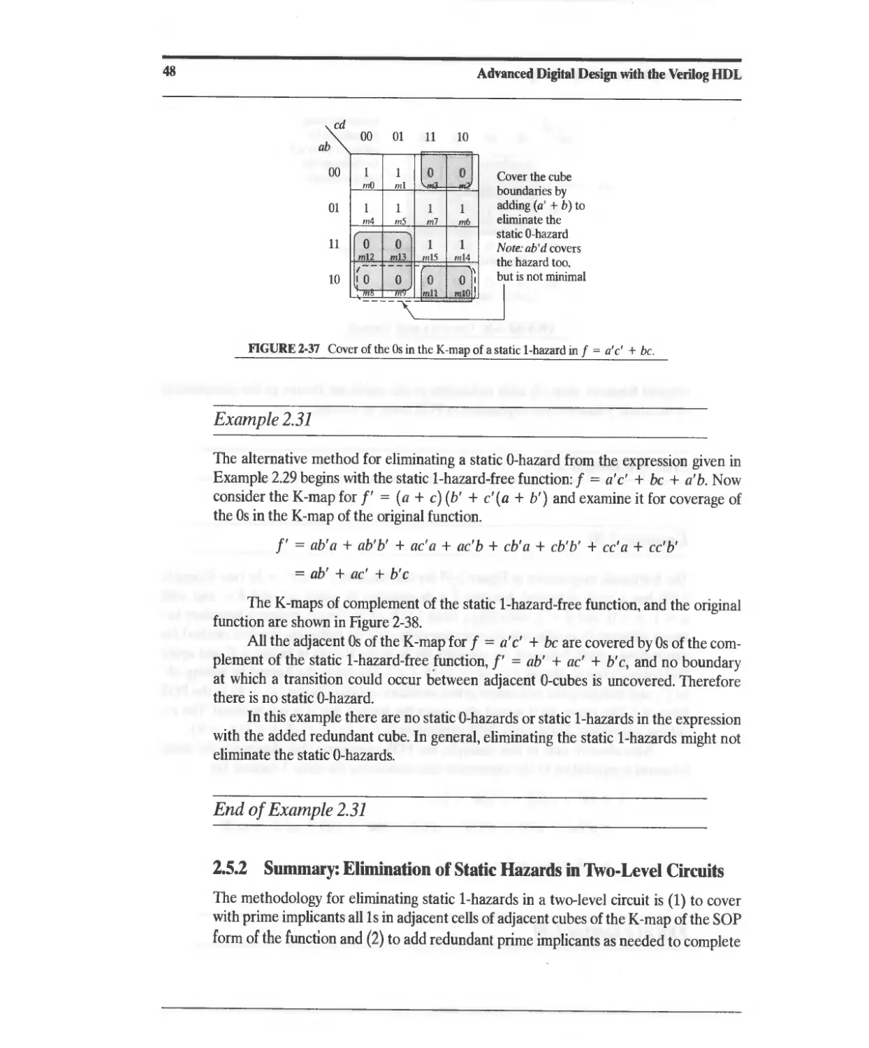
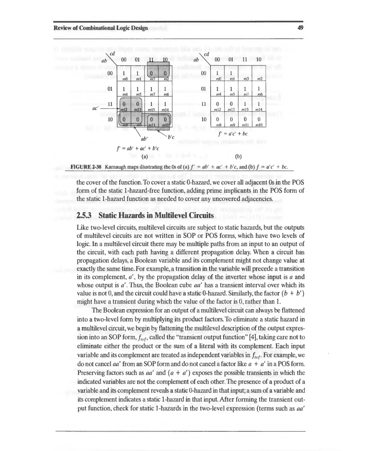
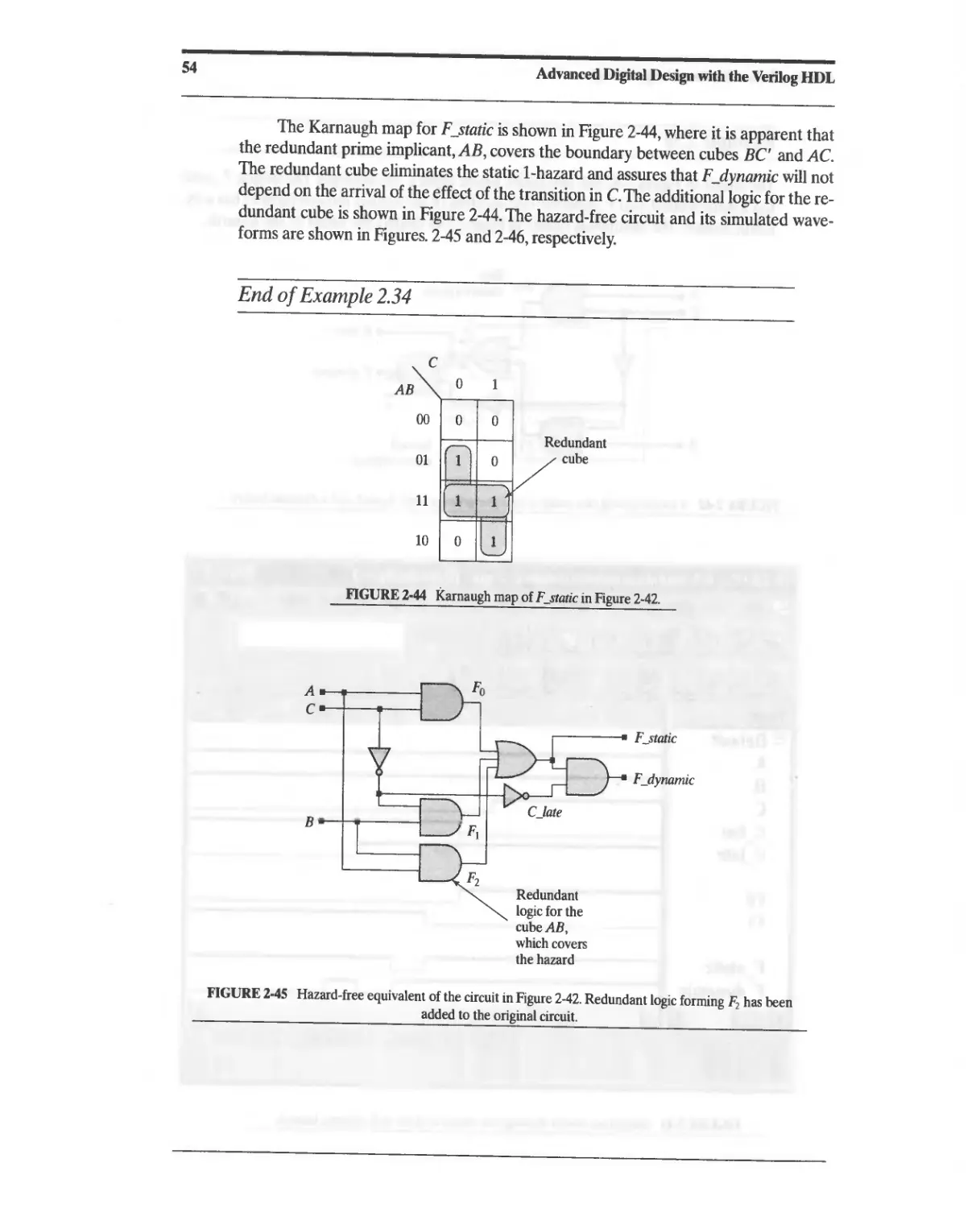
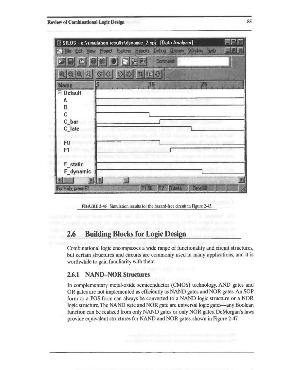
2.5.1 Elimination of Static Hazards (SOP F01lJ1) 44
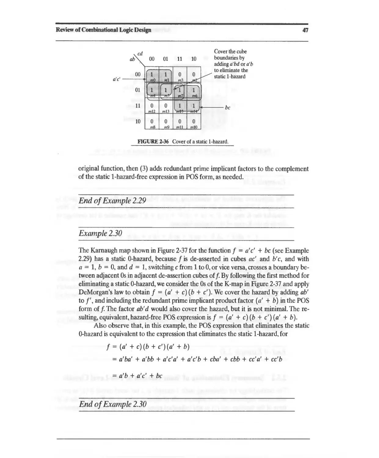
2.5.2 Summary: Elimination of Static Hazards in Two-Level Circuits 48
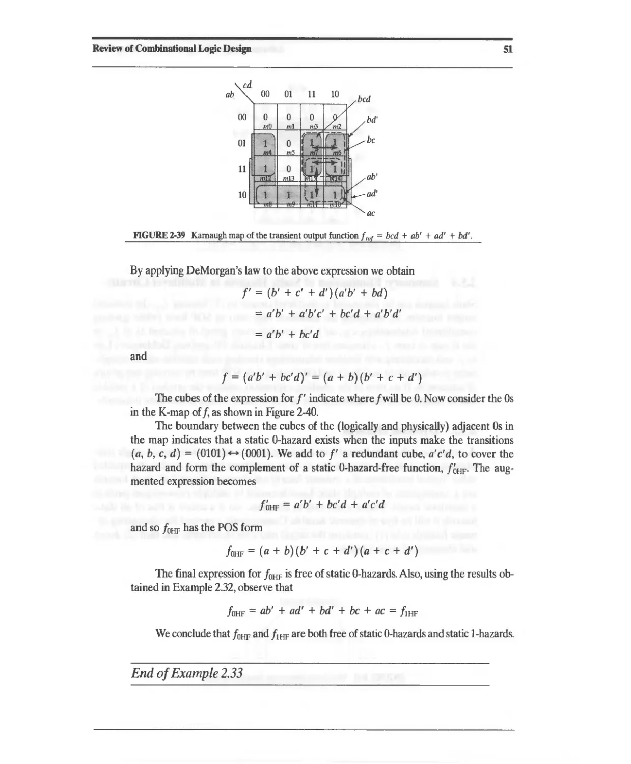
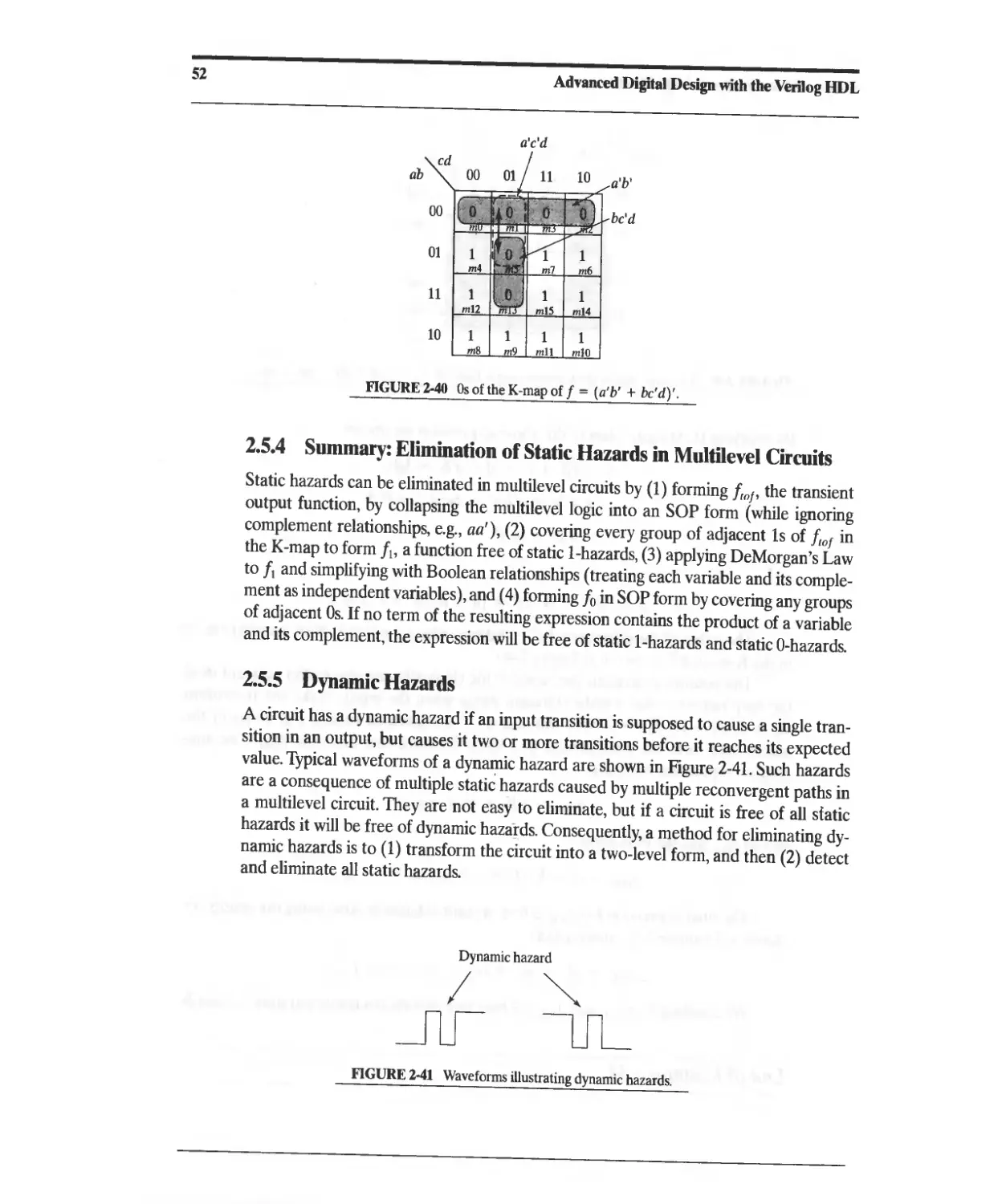
2.5.3 Static Hazards in Multilevel Circuits 49
2.5.4 Summary: Elimination of Hazards in Multilevel Circuits 52
2.5.5 Dynamic Hazards 52
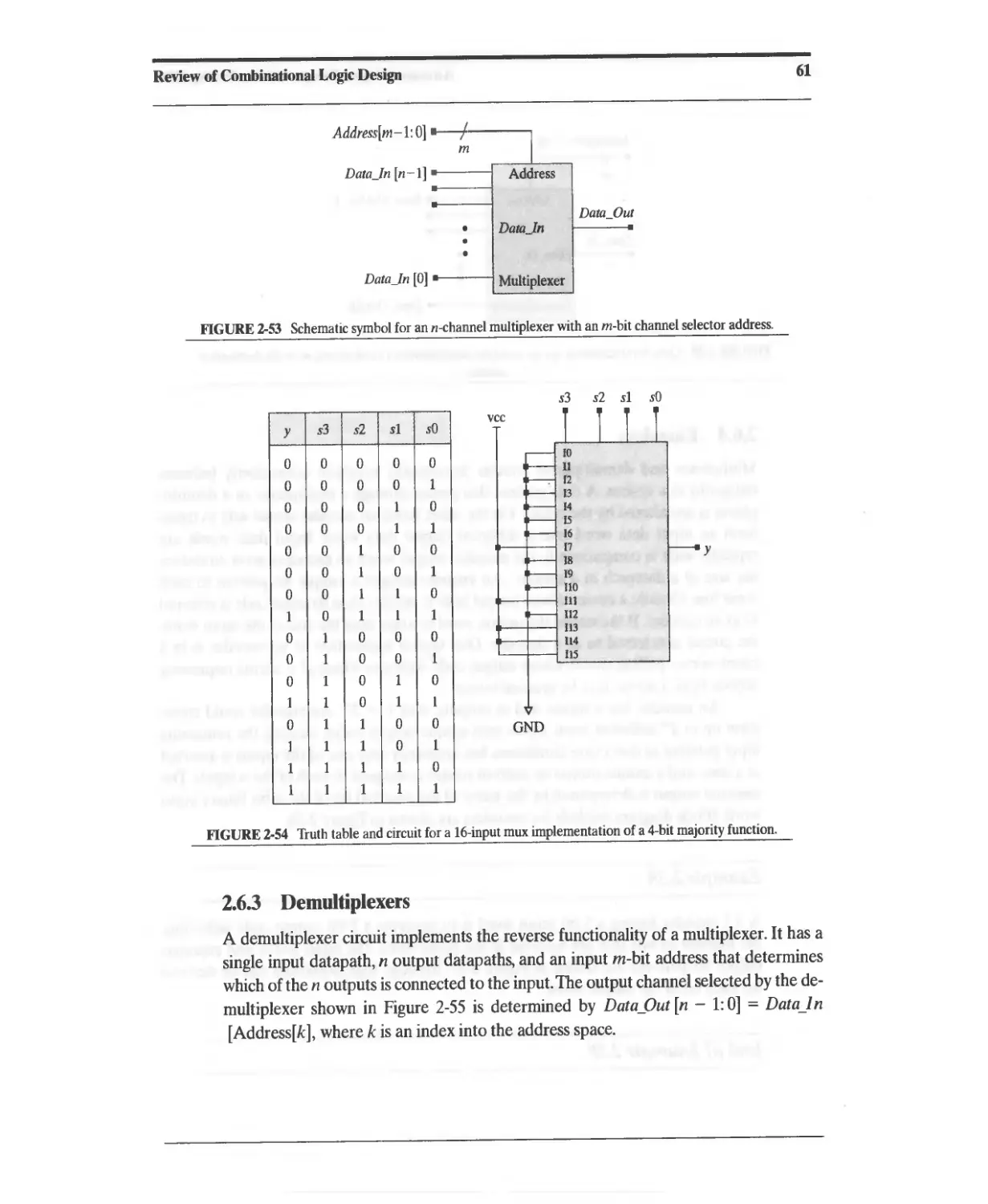
2.6 Building Blocks for Logic Design 55
2.6.1 NAND-NOR Structures 55
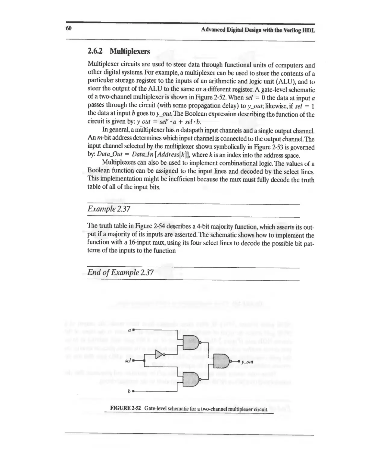
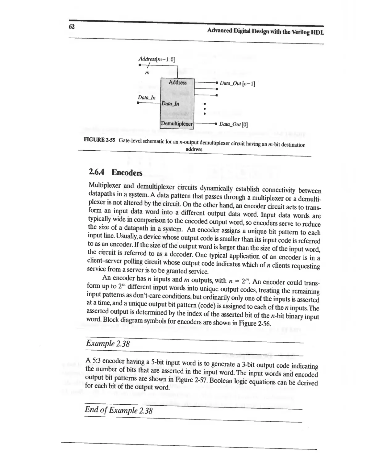
2.6.2 Multiplexers 60
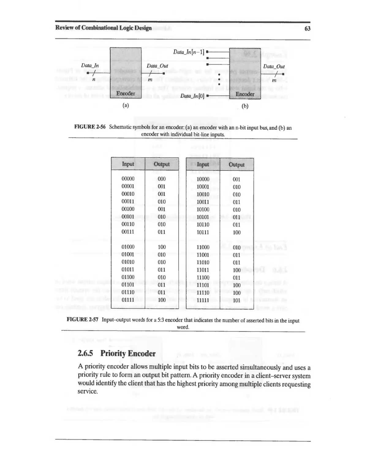
2.6.3 Demultiplexers 61
2.6.4 Encoders 62
2.6.5 Priority Encoder 63
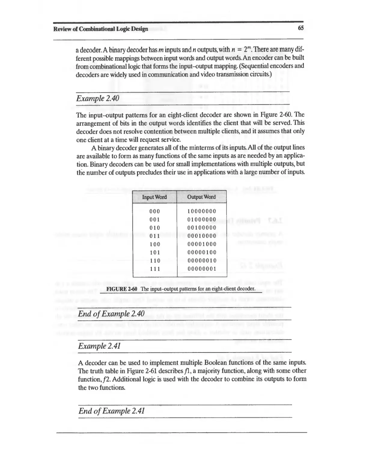
2.6.6 Decoder 64
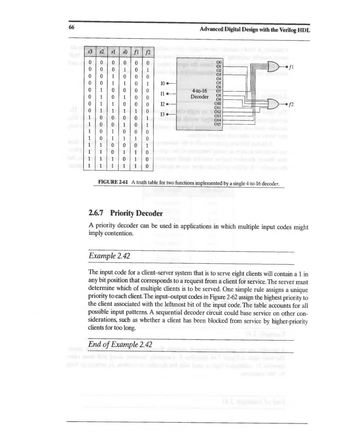
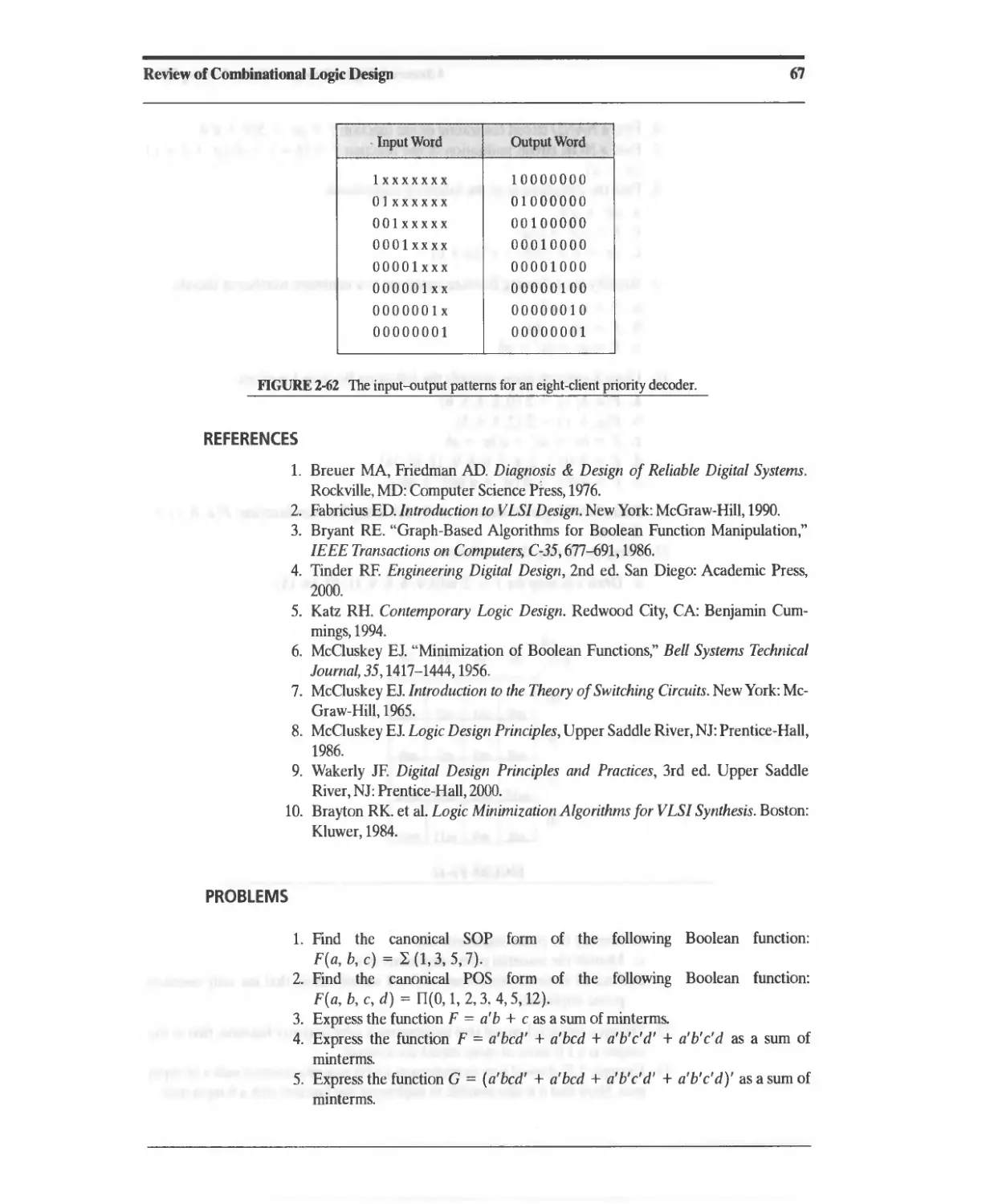
2.6.7 Priority Decoder 66
References 67
Problems 67
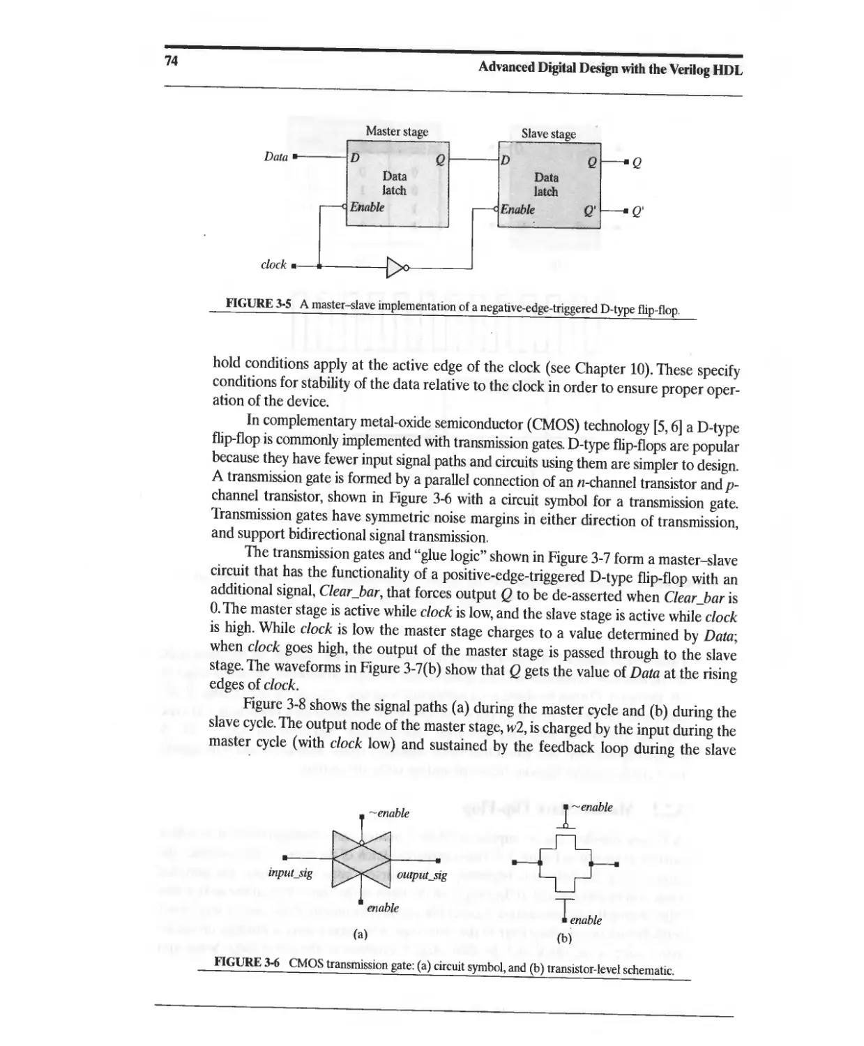
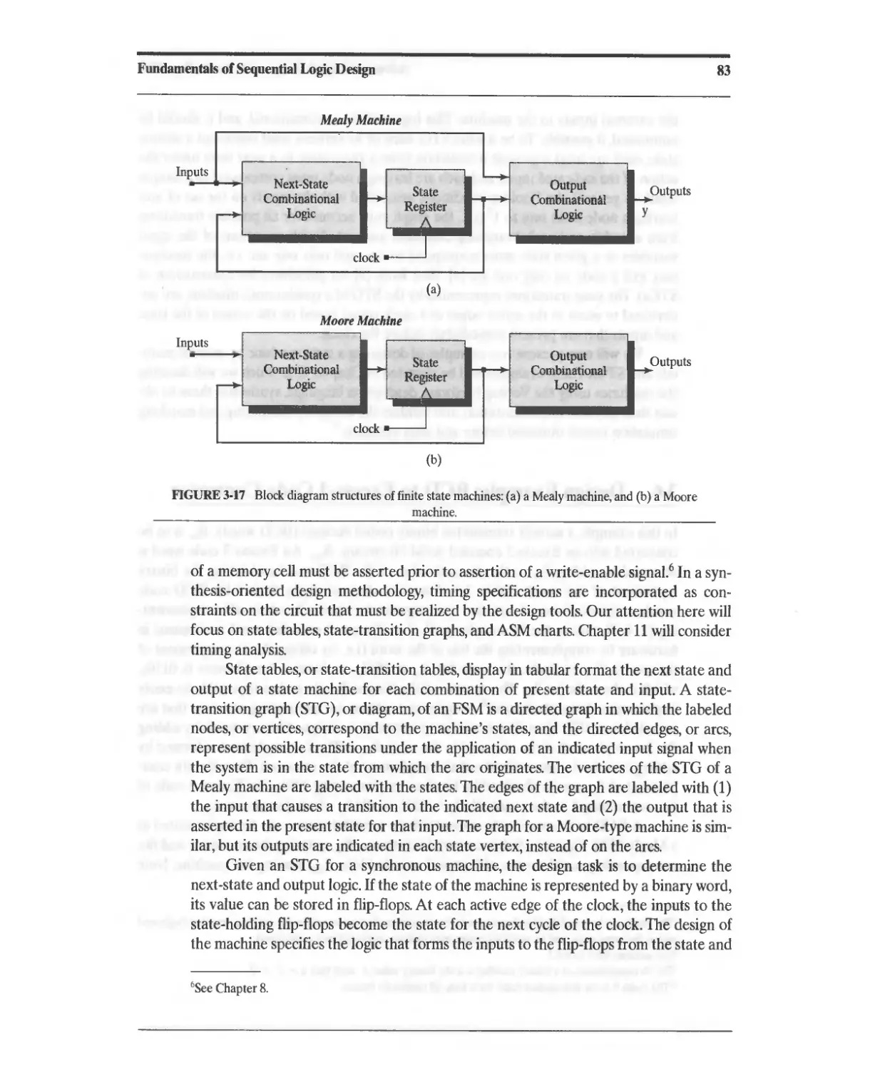
3 Fundamentals of Sequential Logic Design 69
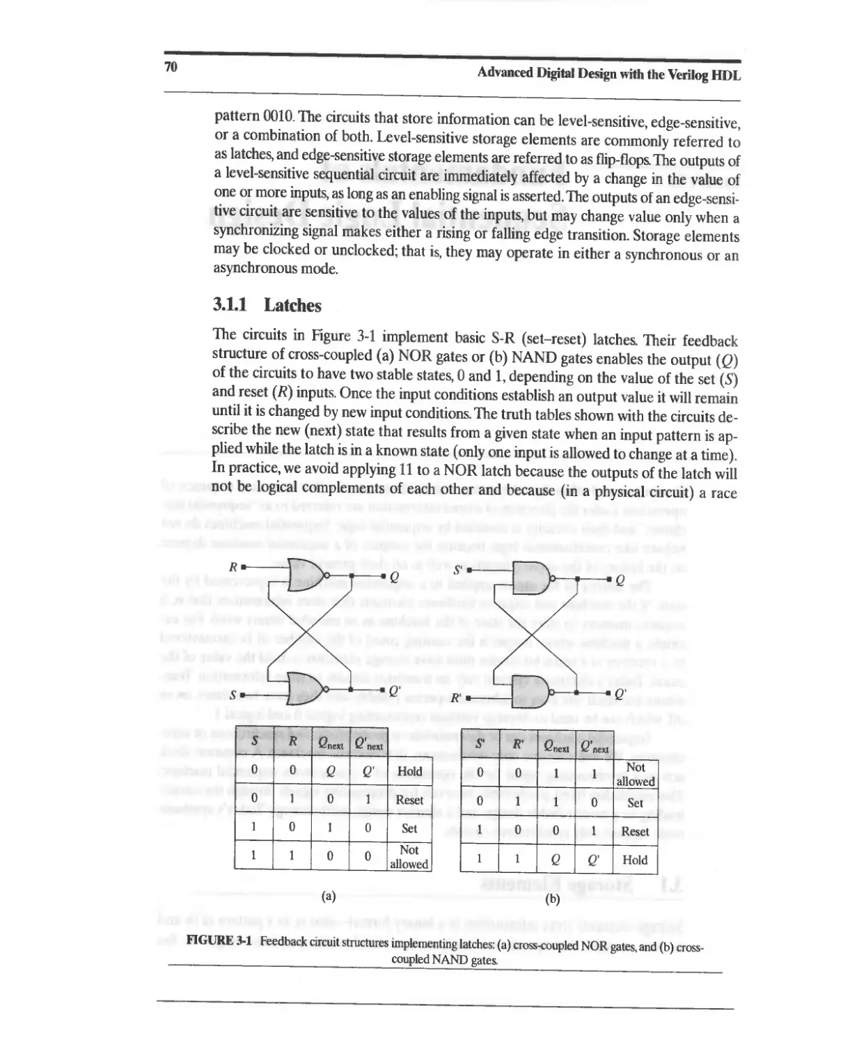
3.1 Storage Elements 69
3.1.1 Latches 70
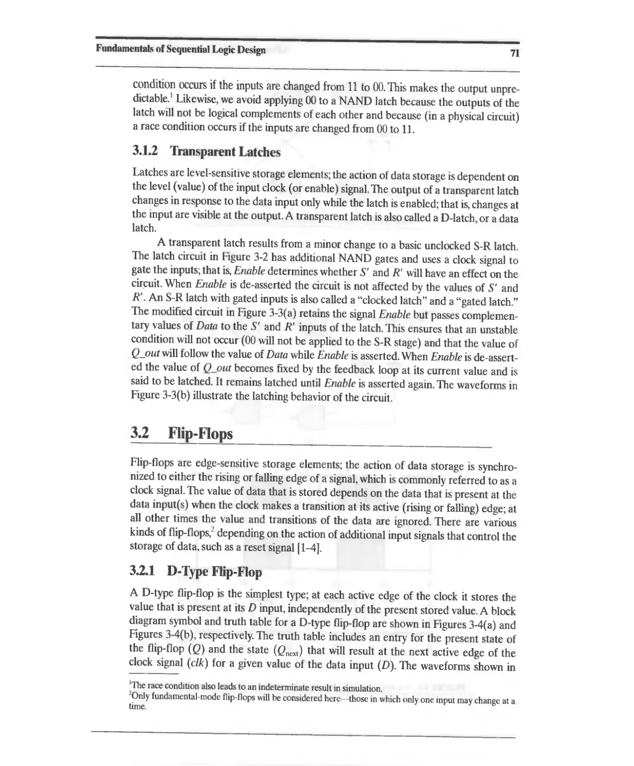
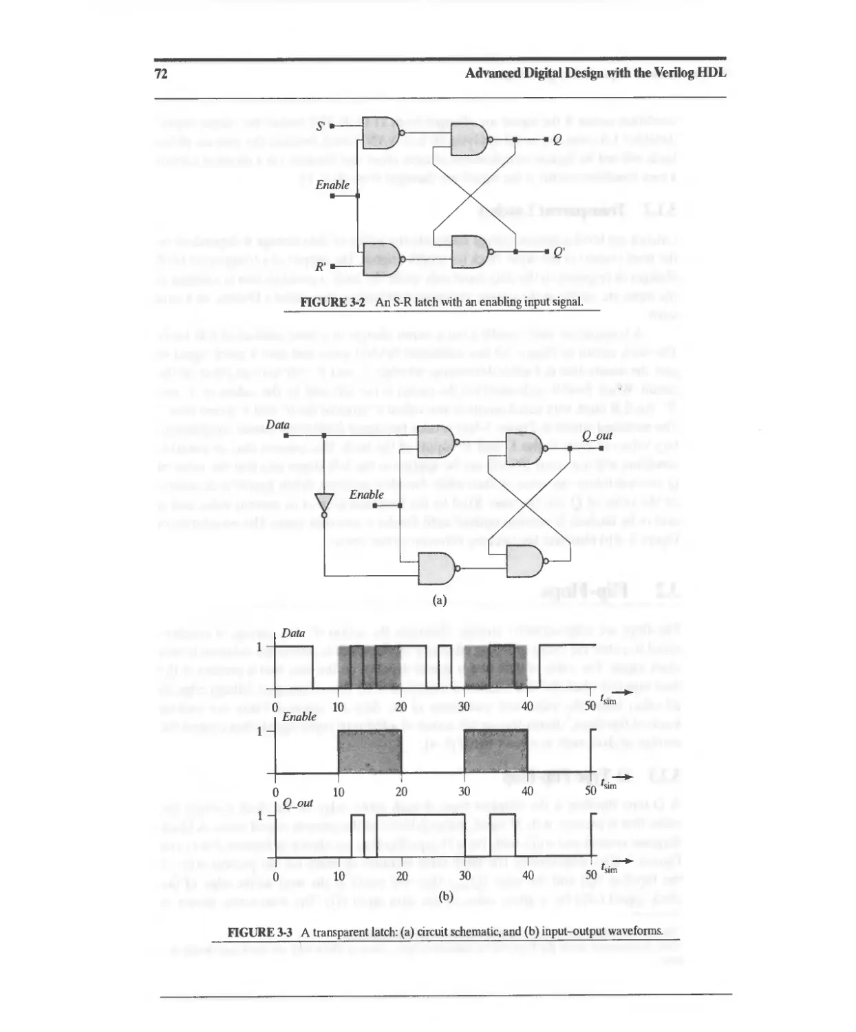
3.1.2 Transparent latches 71
3.2 Flip-Flops 71
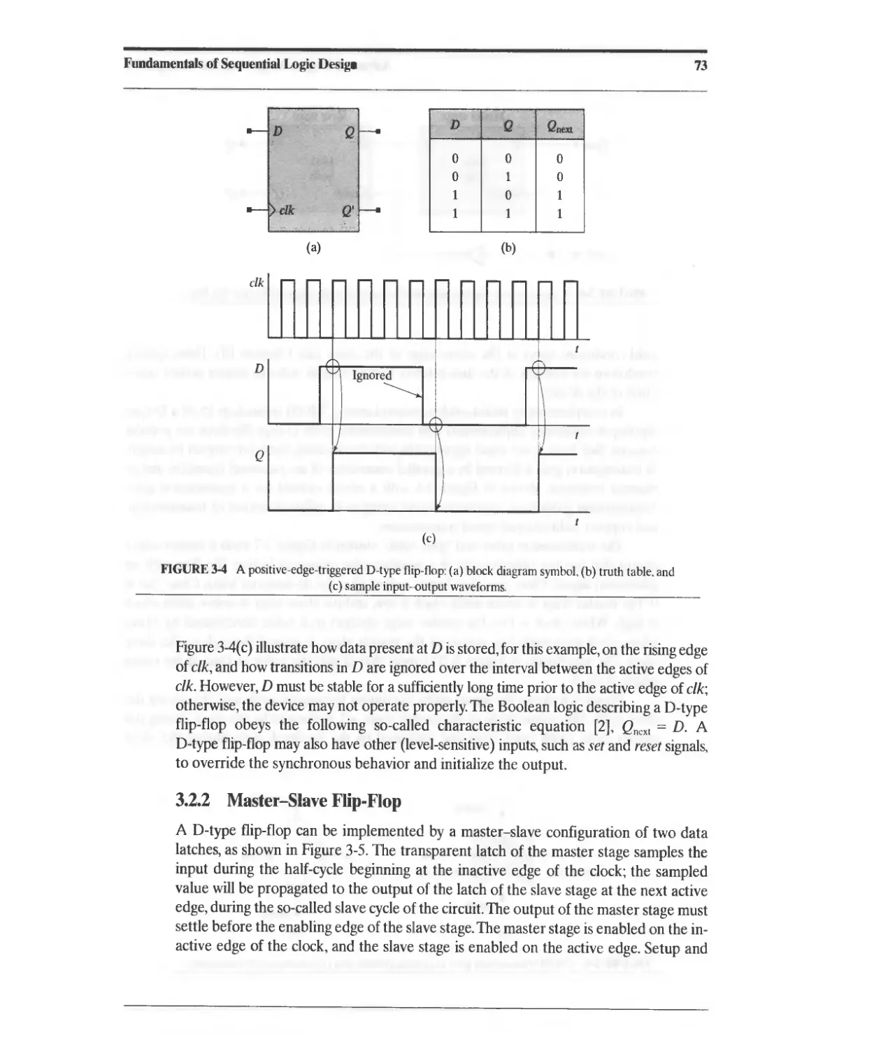
3.2.1 D-Type Flip-Flop 71
3.2.2 Master-Slave Flip-Flop 73
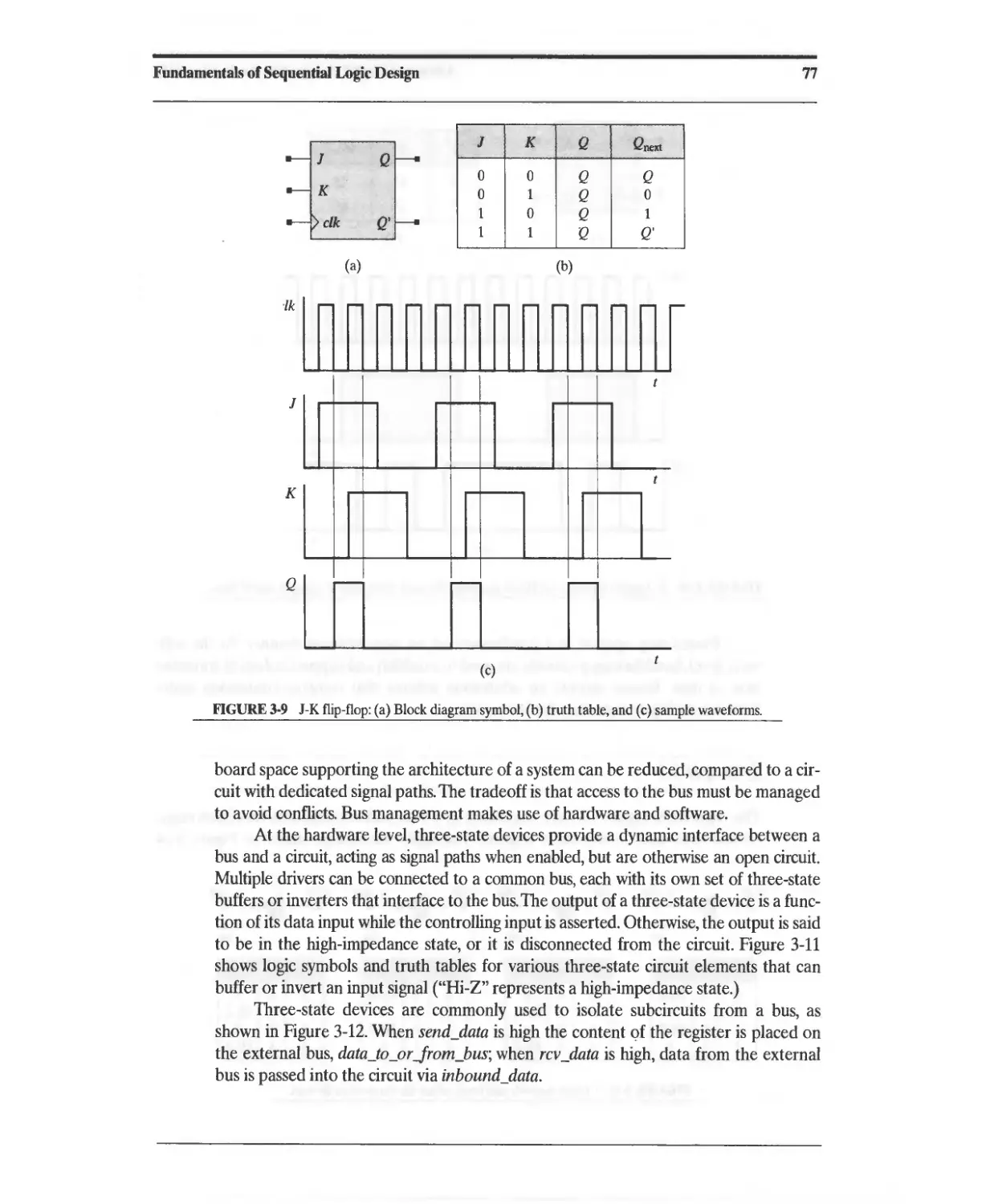
3.2.3 J-K Flip-Flop 75
3.2.4 T Flip-Flop 75
Contents
vii
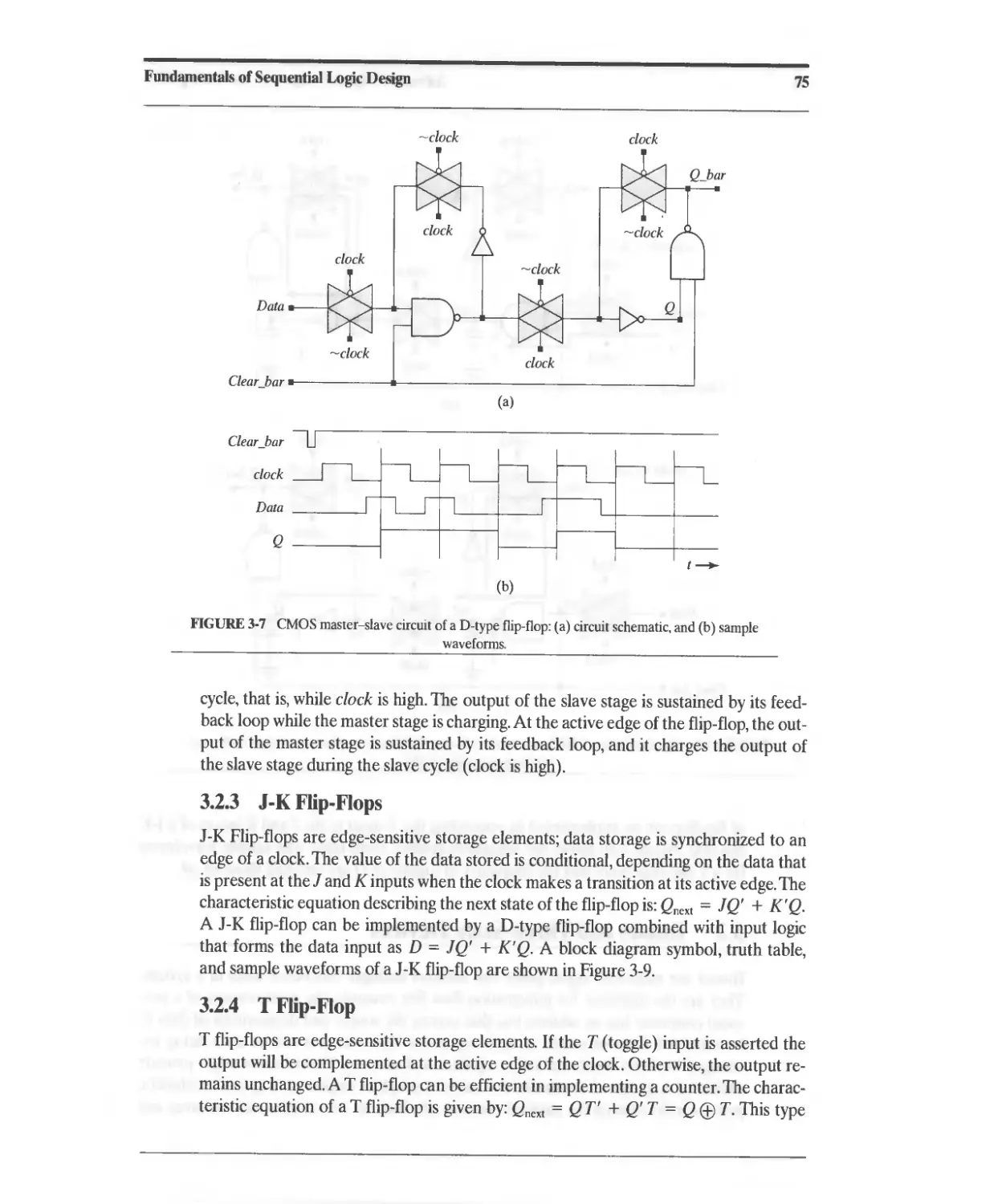
3.3 Busses and Three-State Devices 76
3.4 Design of Sequential Machines 80
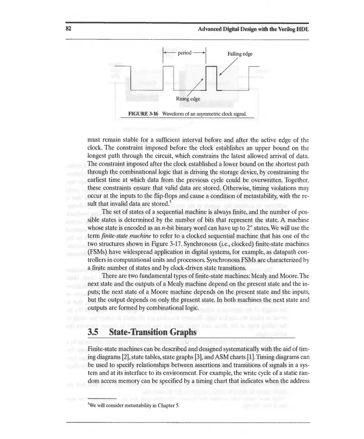
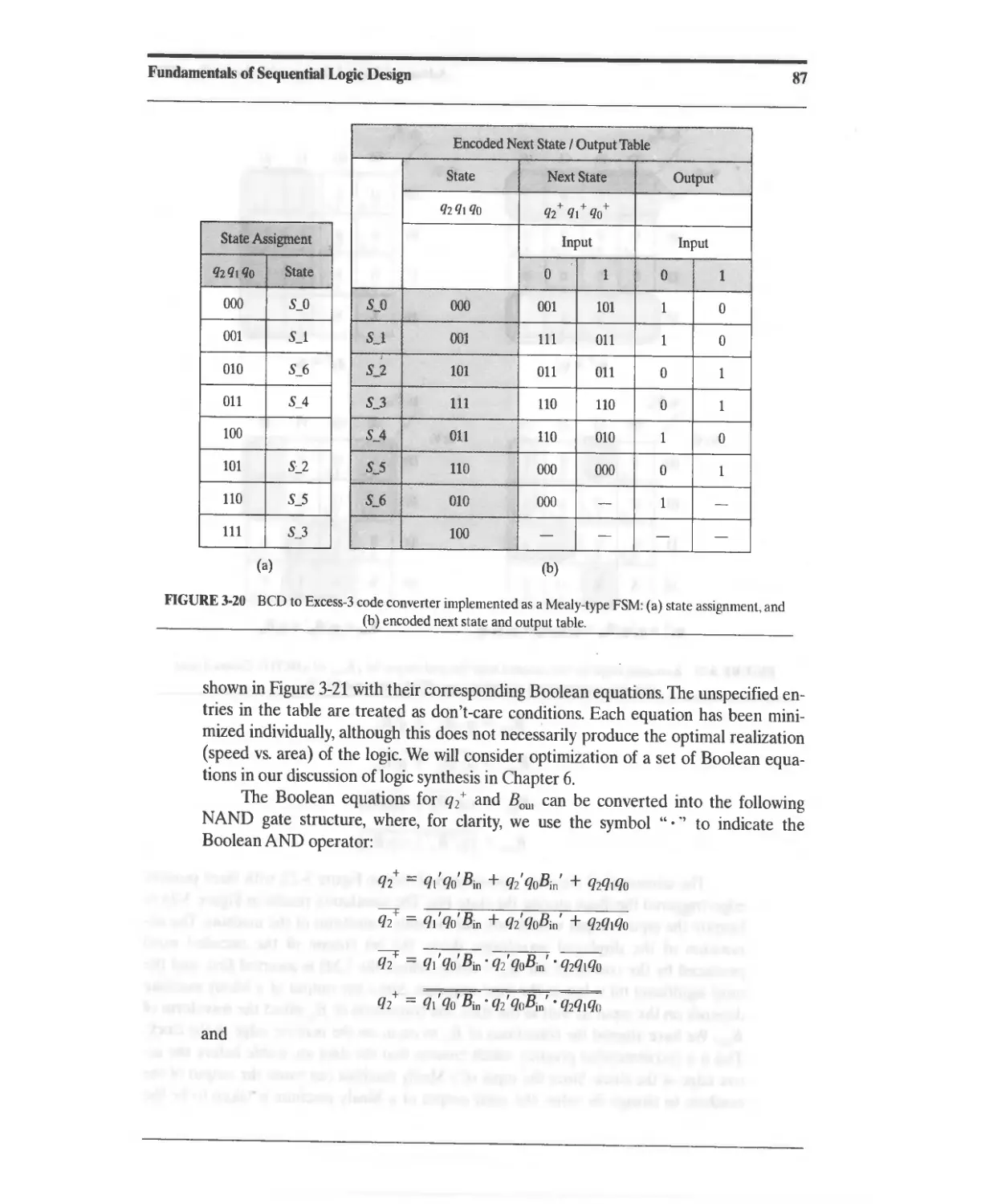
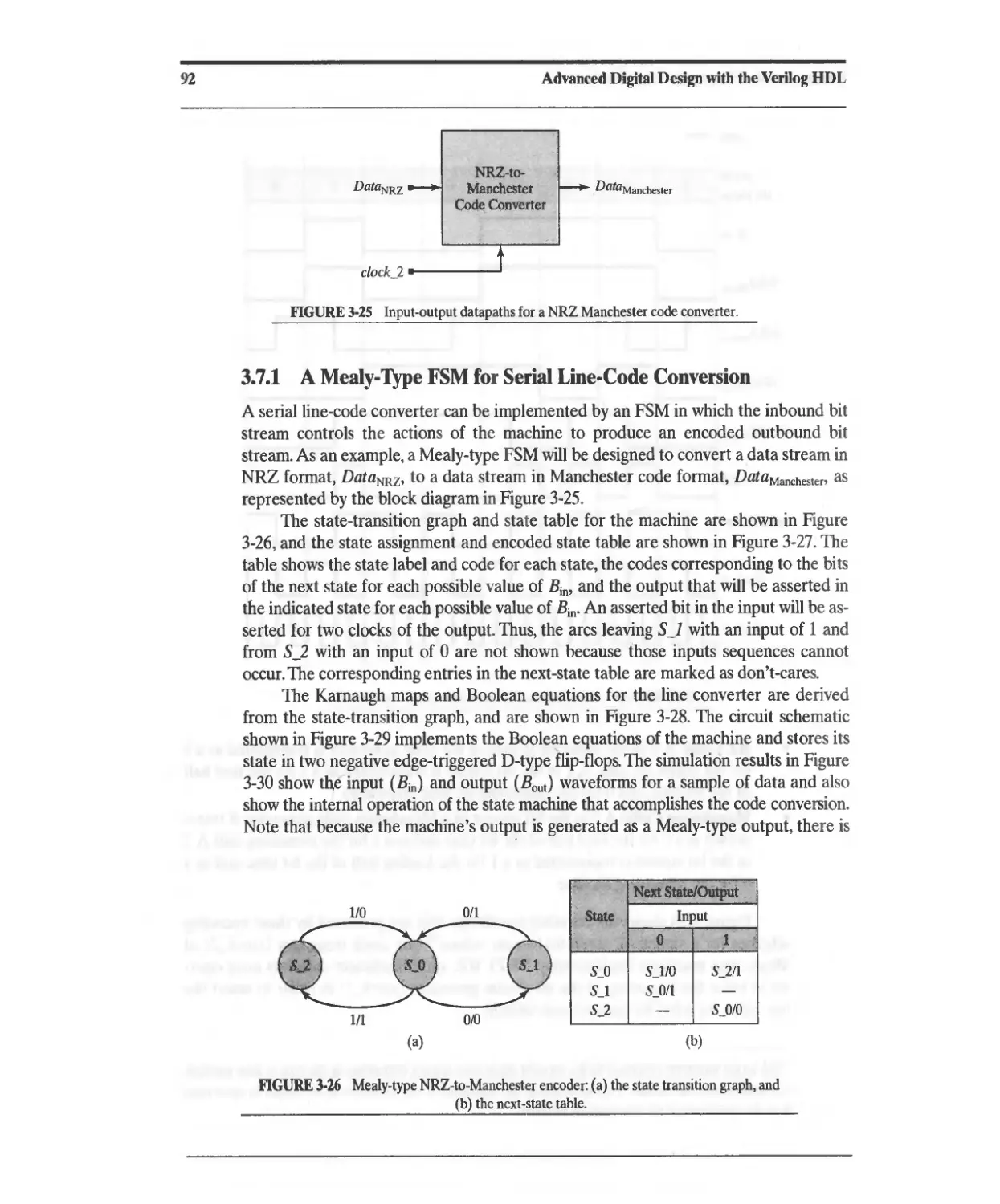
3.5 State-Transition Graphs 82
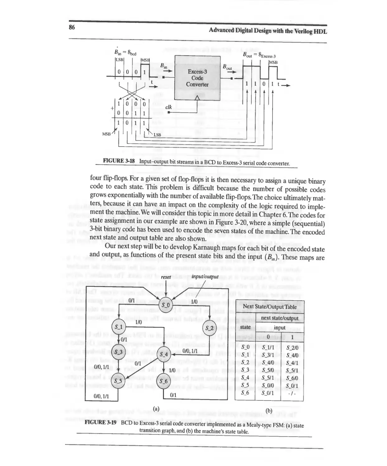
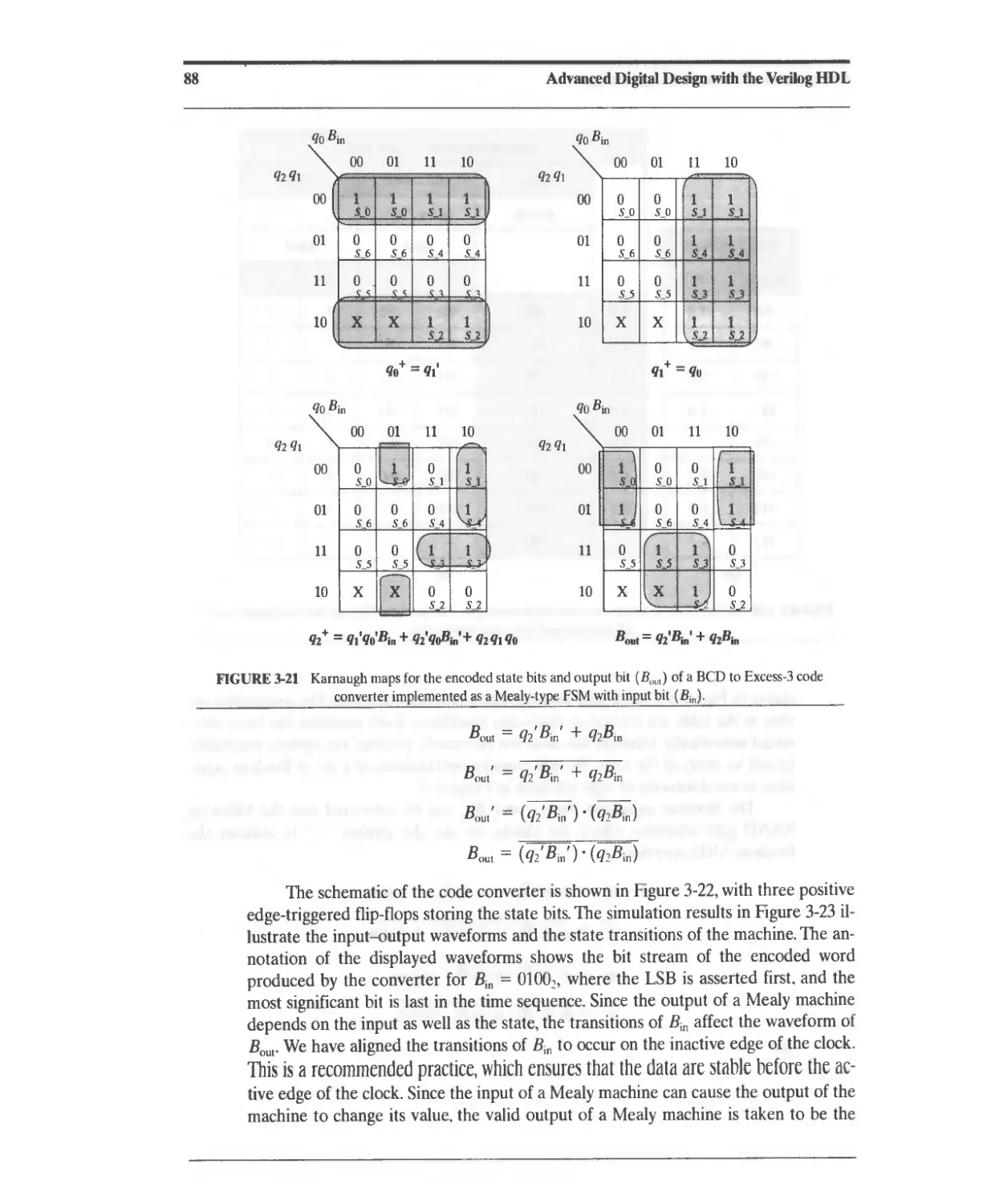
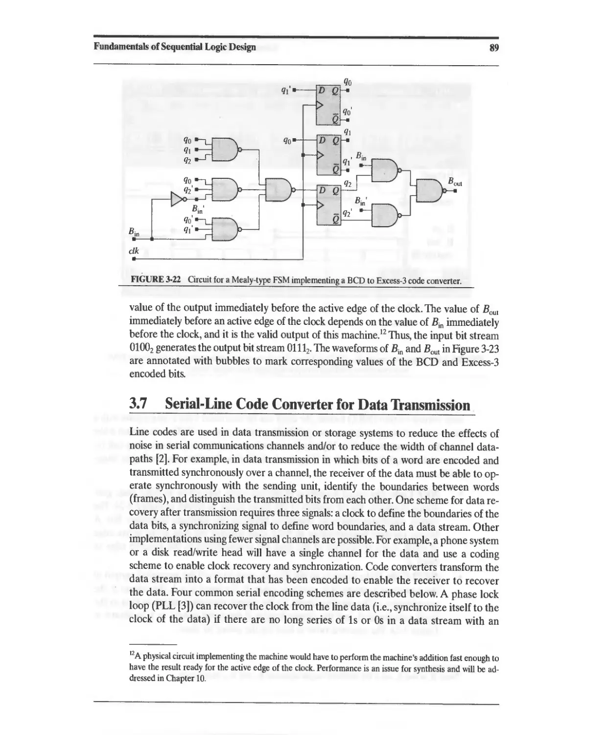
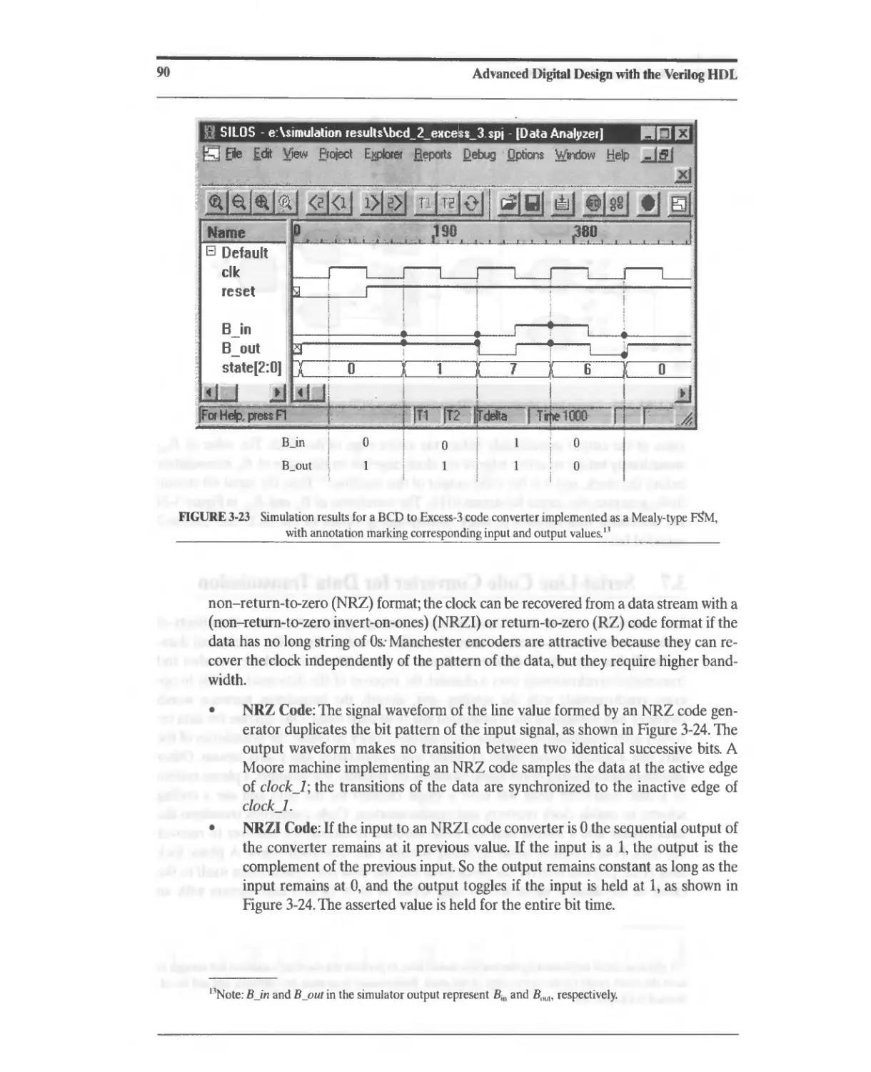
3.6 Design Example: BCD to Excess-3 Code Converter 84
3.7 Serial-Line Code Converter for Data Transmission 89
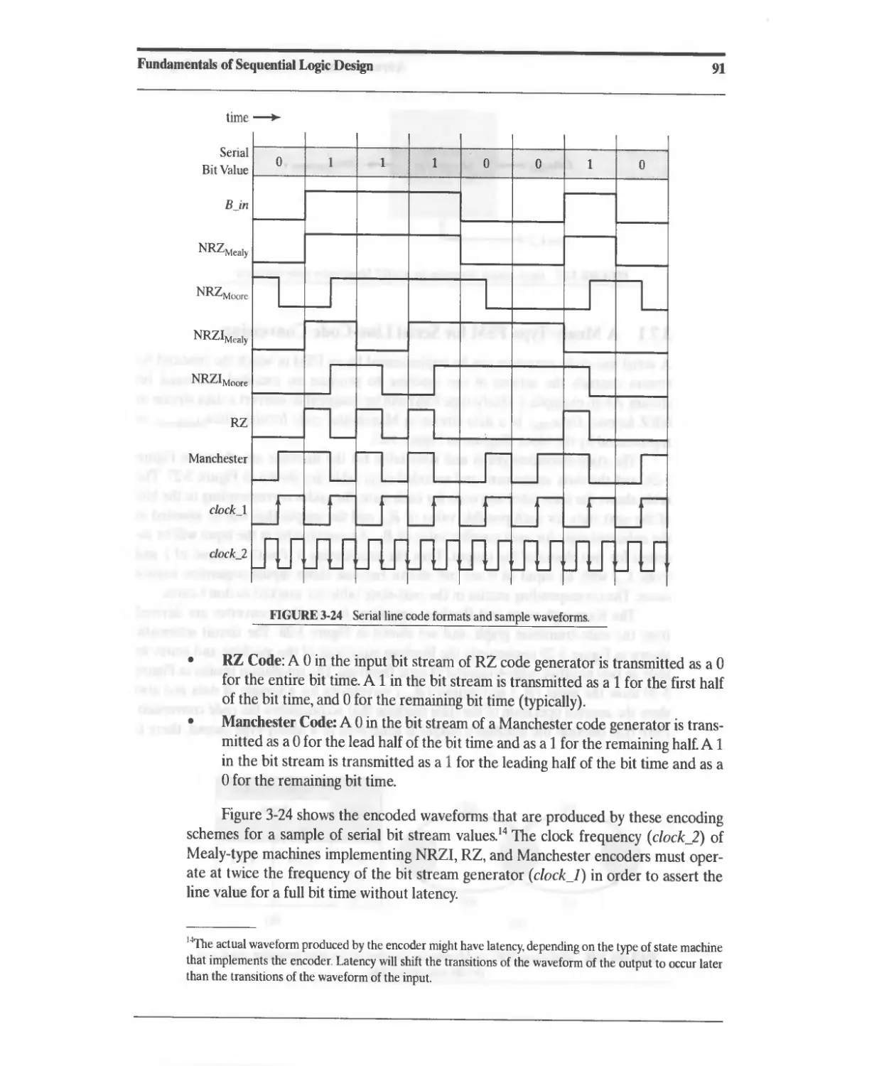
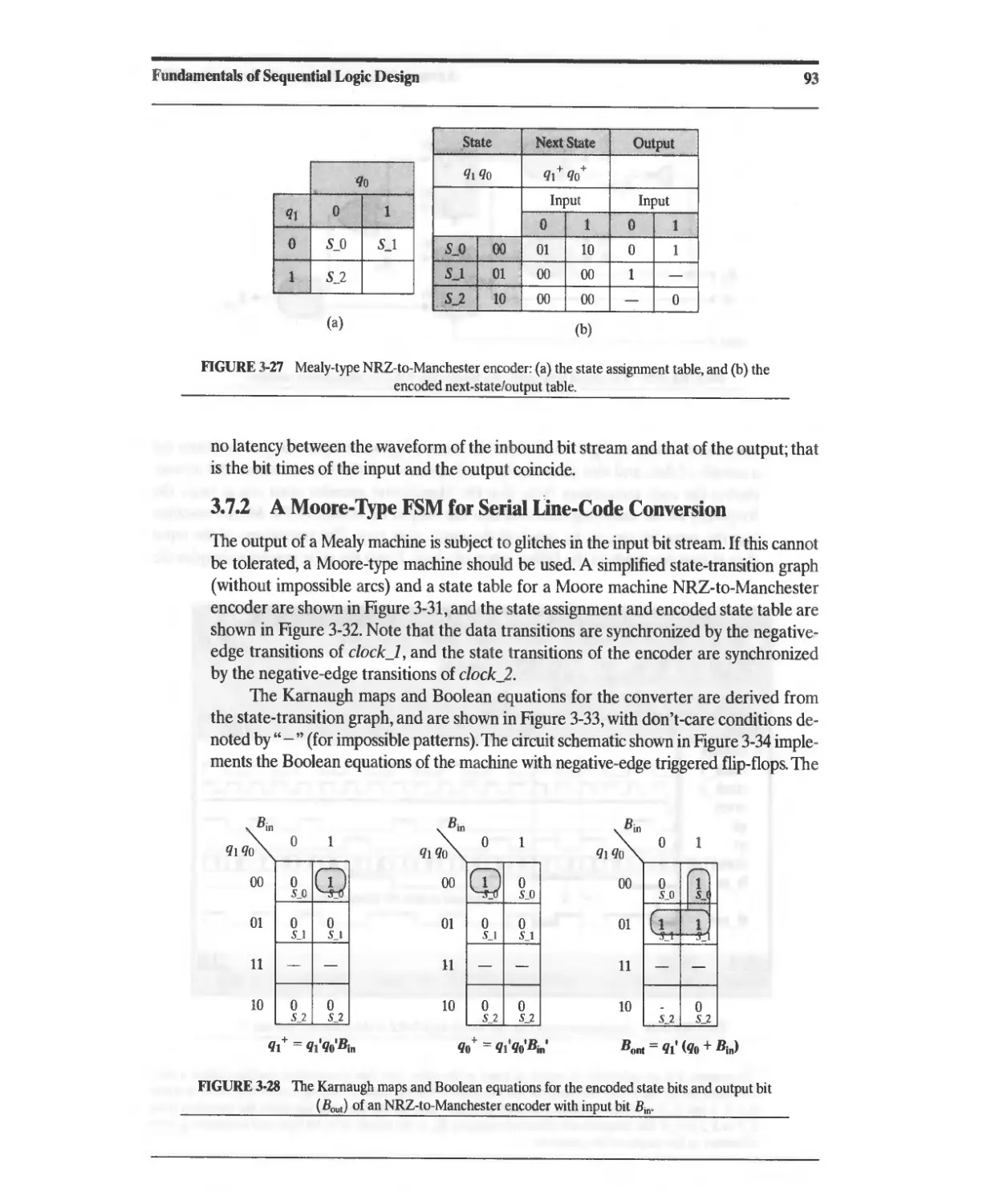
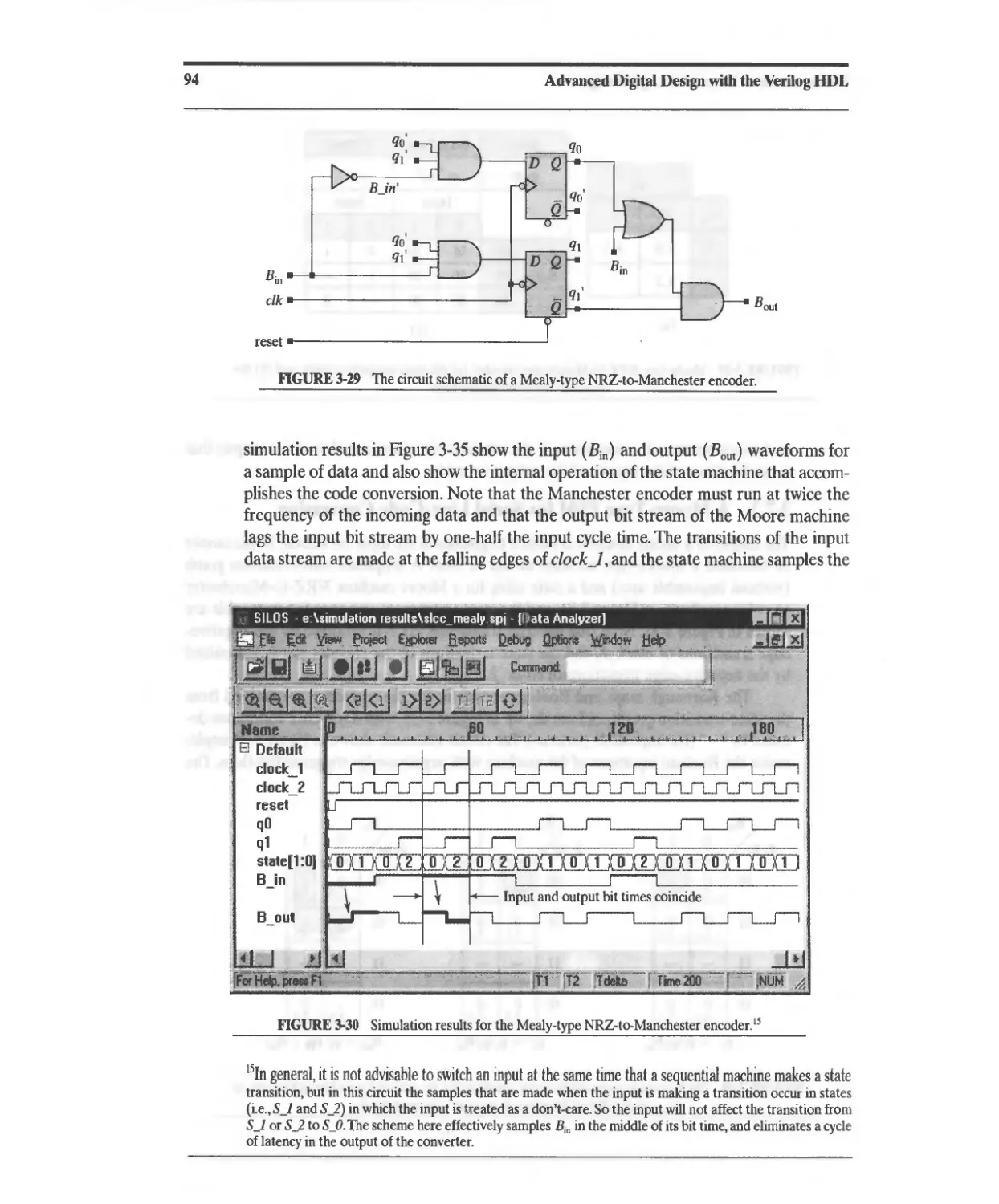
3.7.1 A Mealy-Type FSM for Serial Line-Code Conversion 92
3.7.2 A Moore-Type FSM for Serial Line-Code Conversion 93
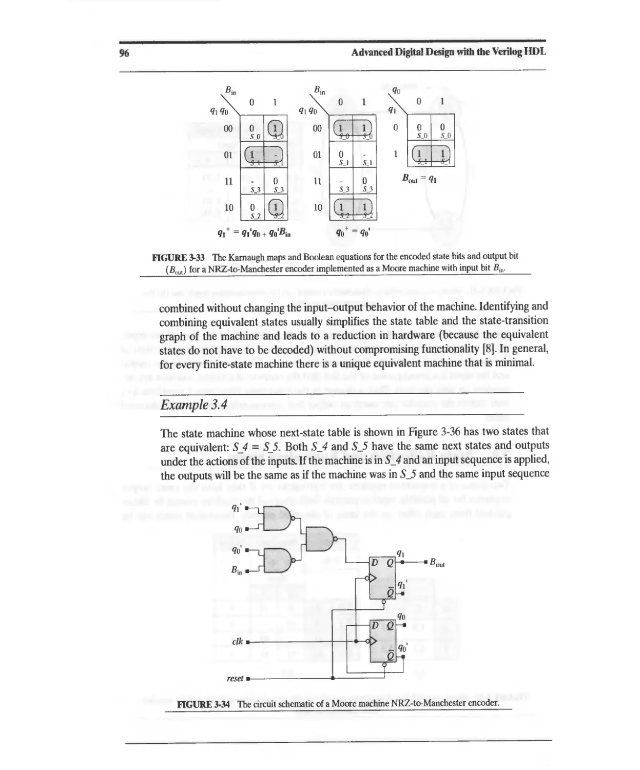
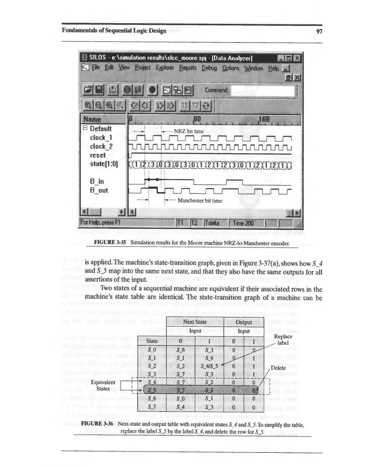
3.8 State Reduction and Equivalent States 95
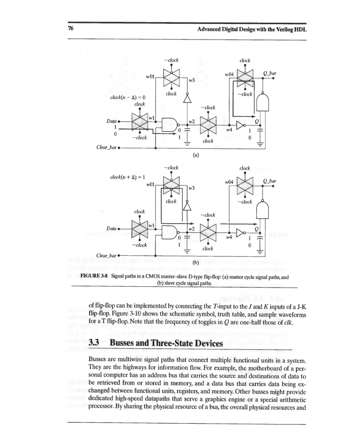
References 99
Problems 100
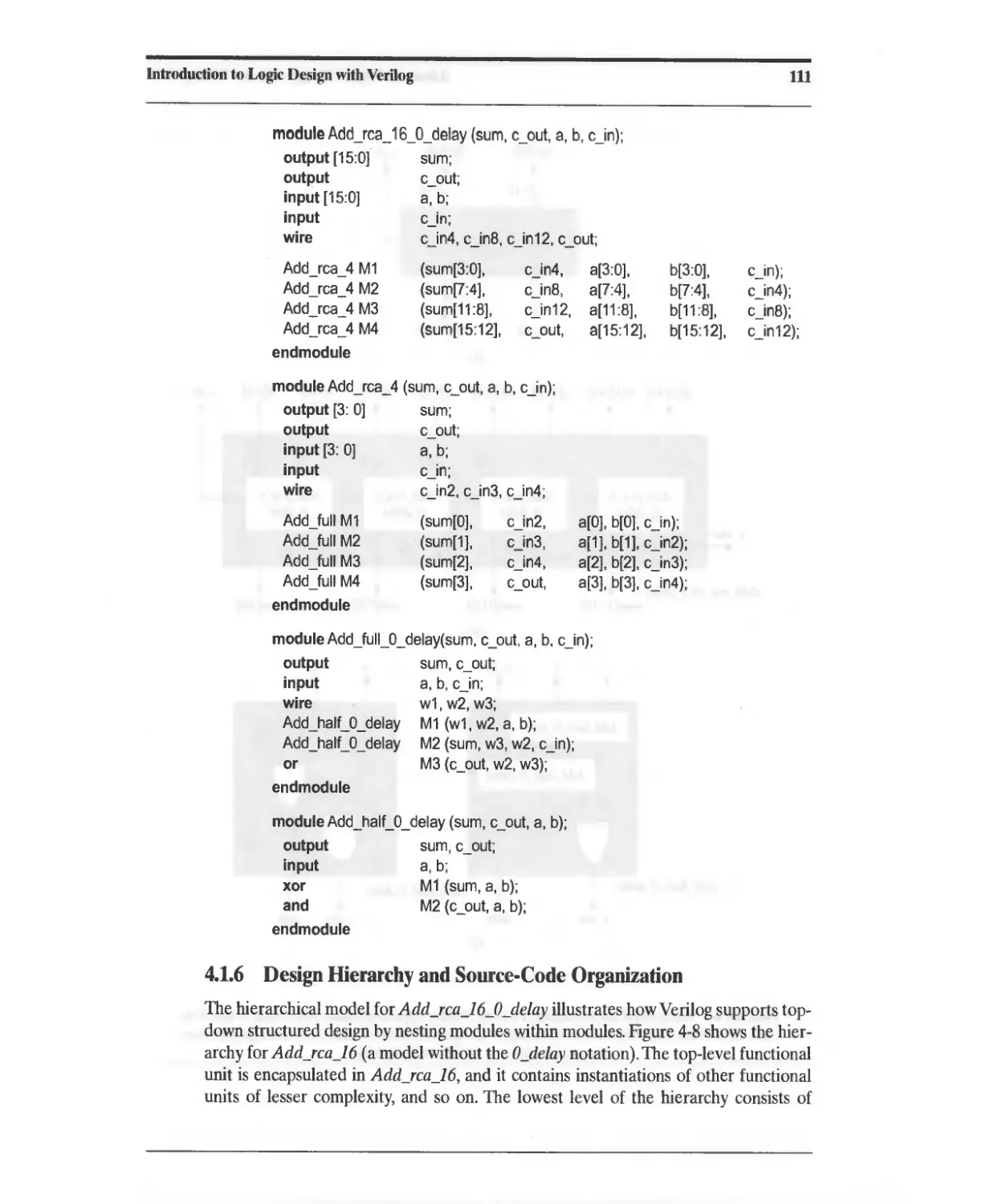
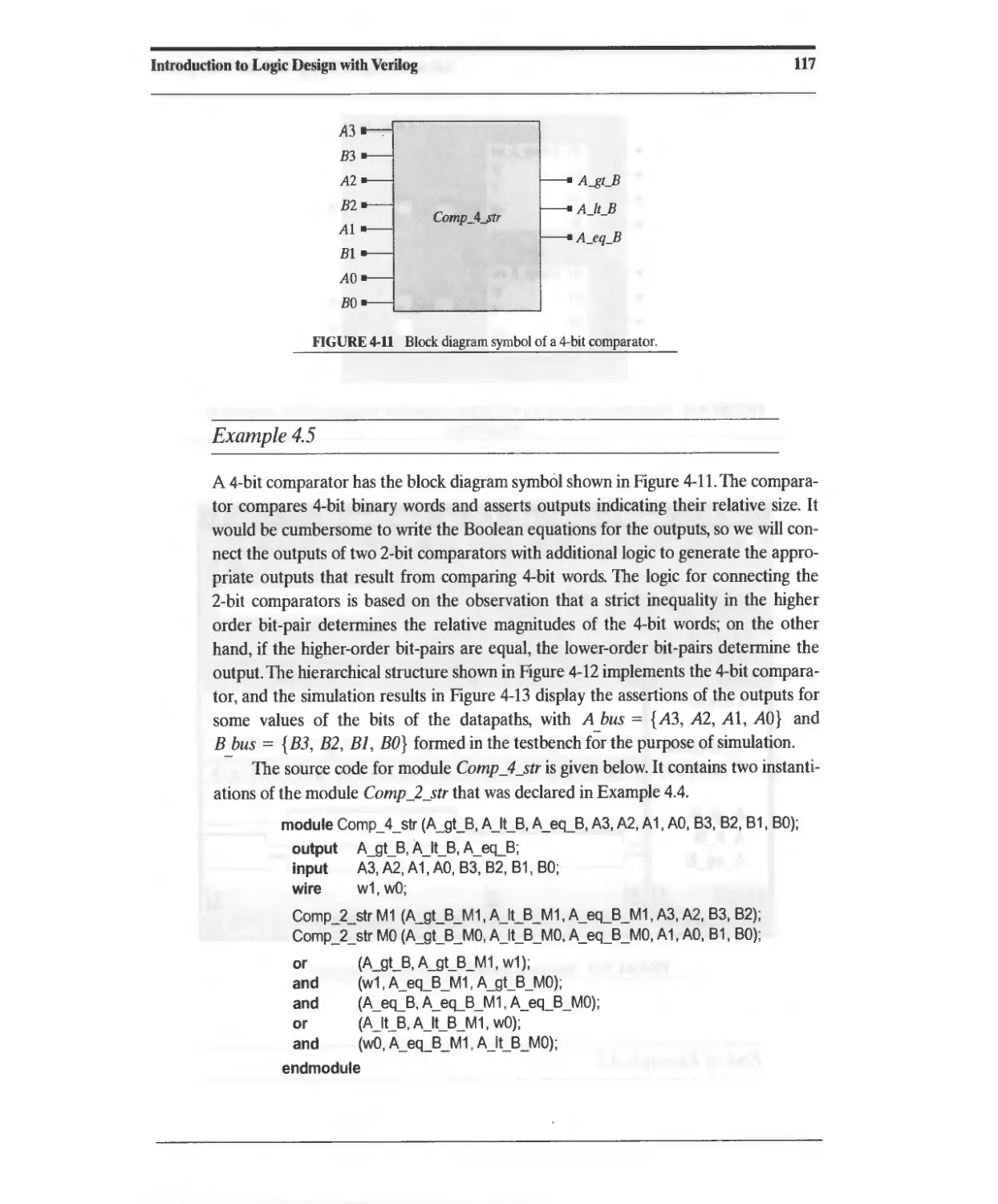
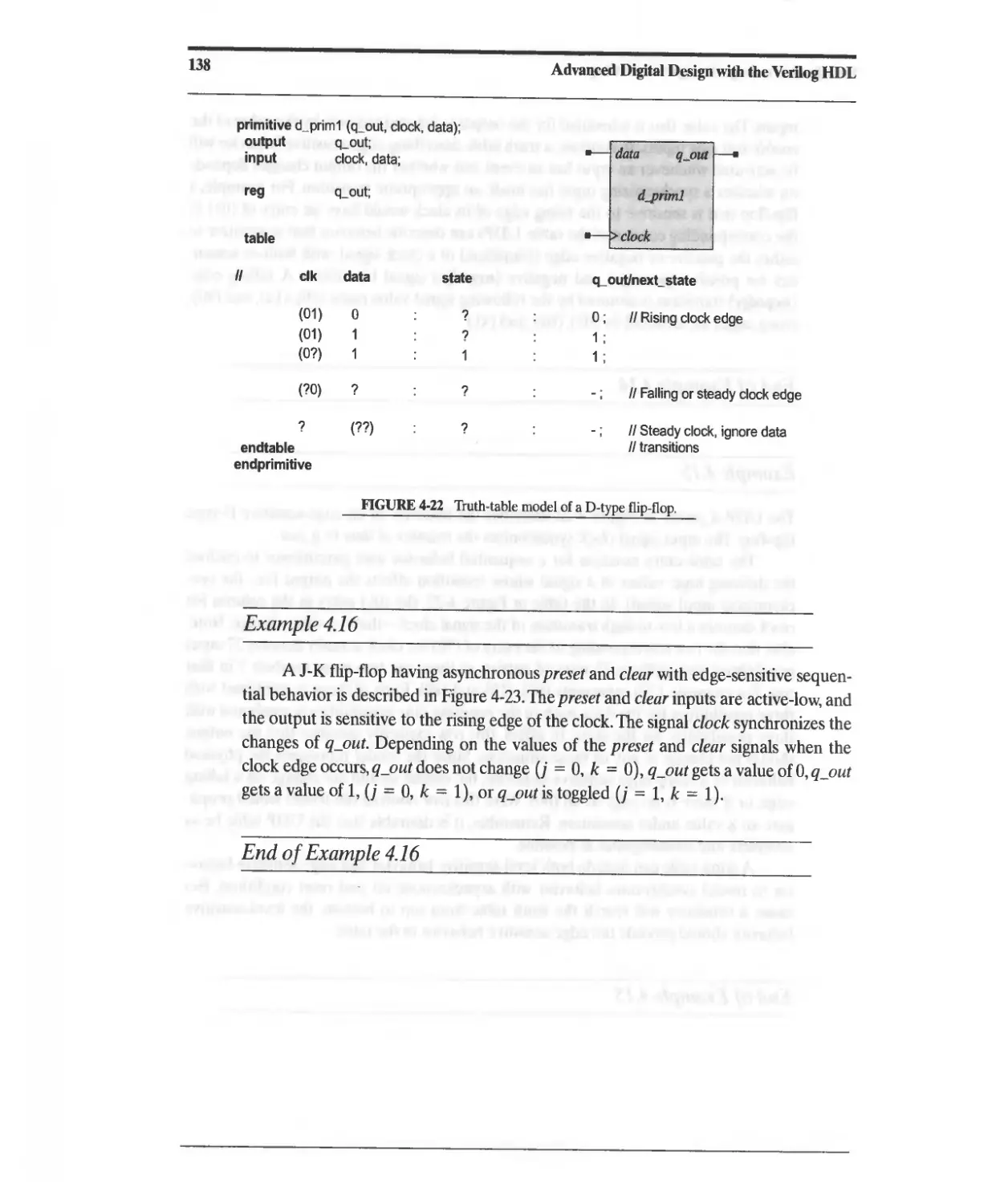
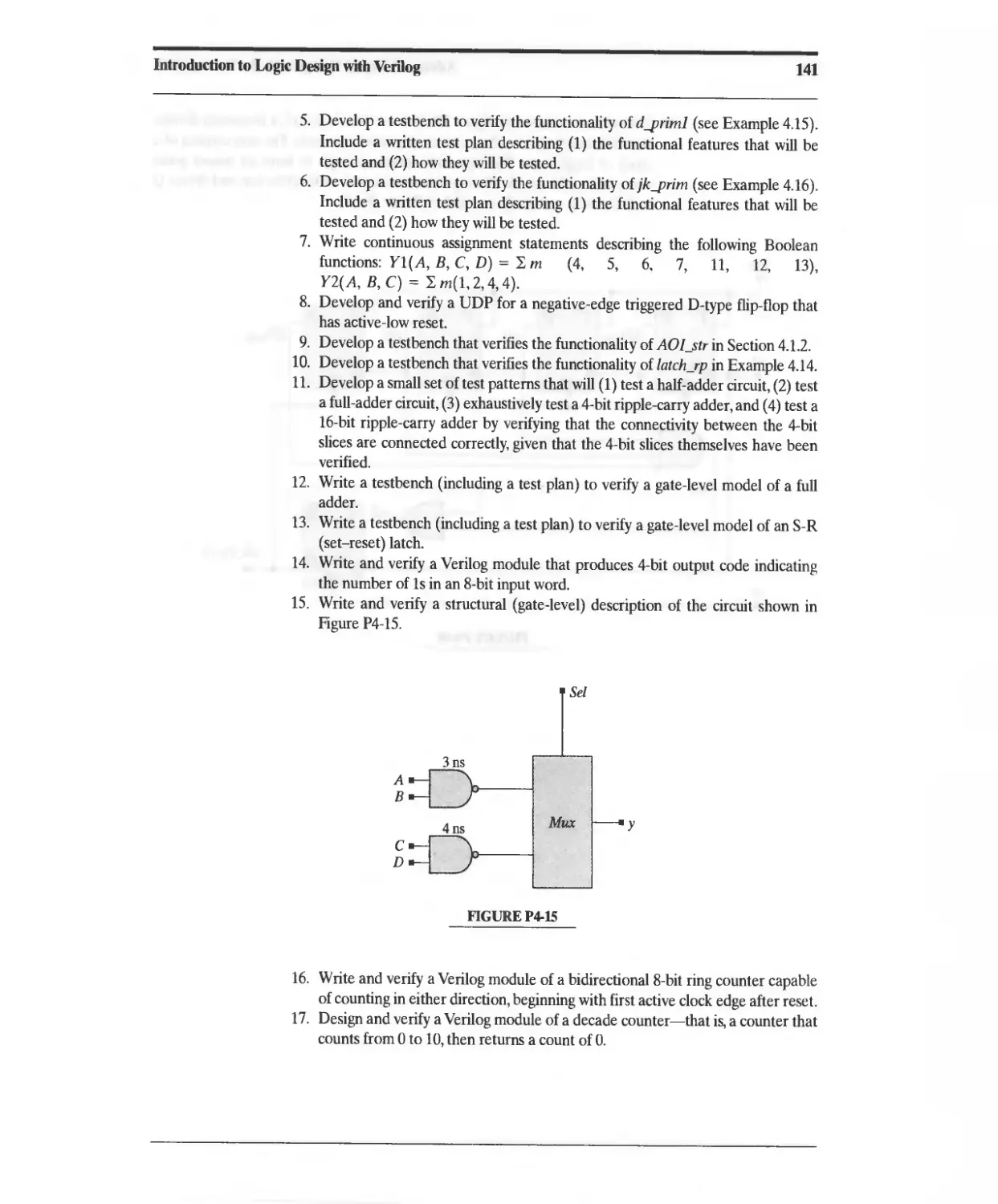
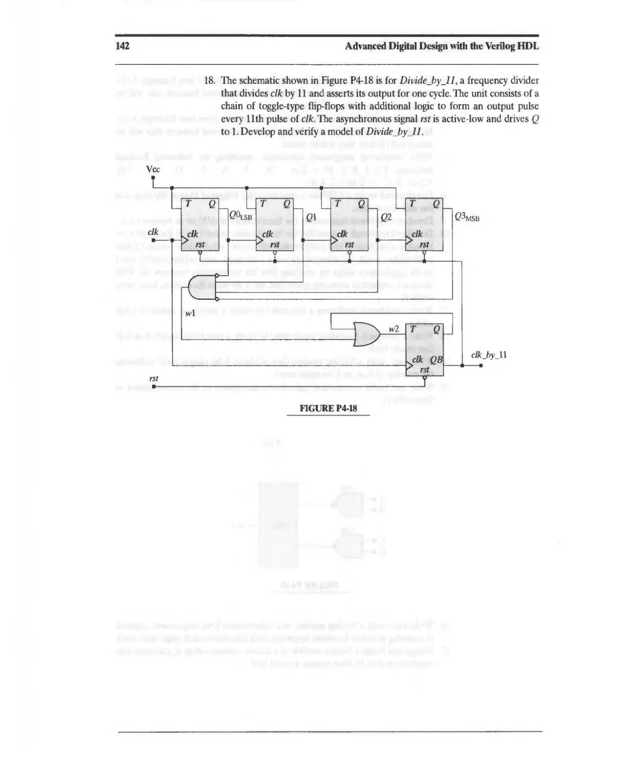
4 Introduction to Logic Design with Verilog 103
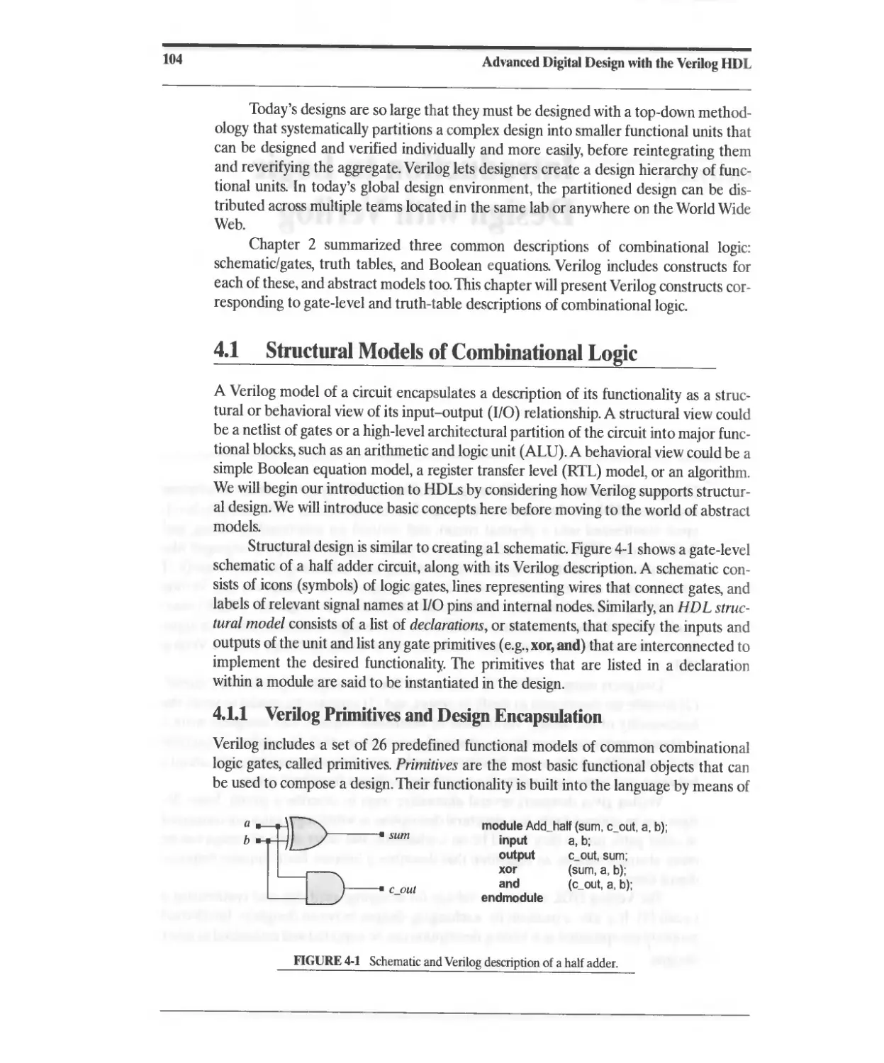
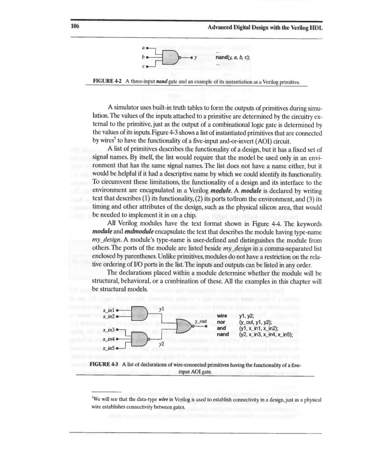
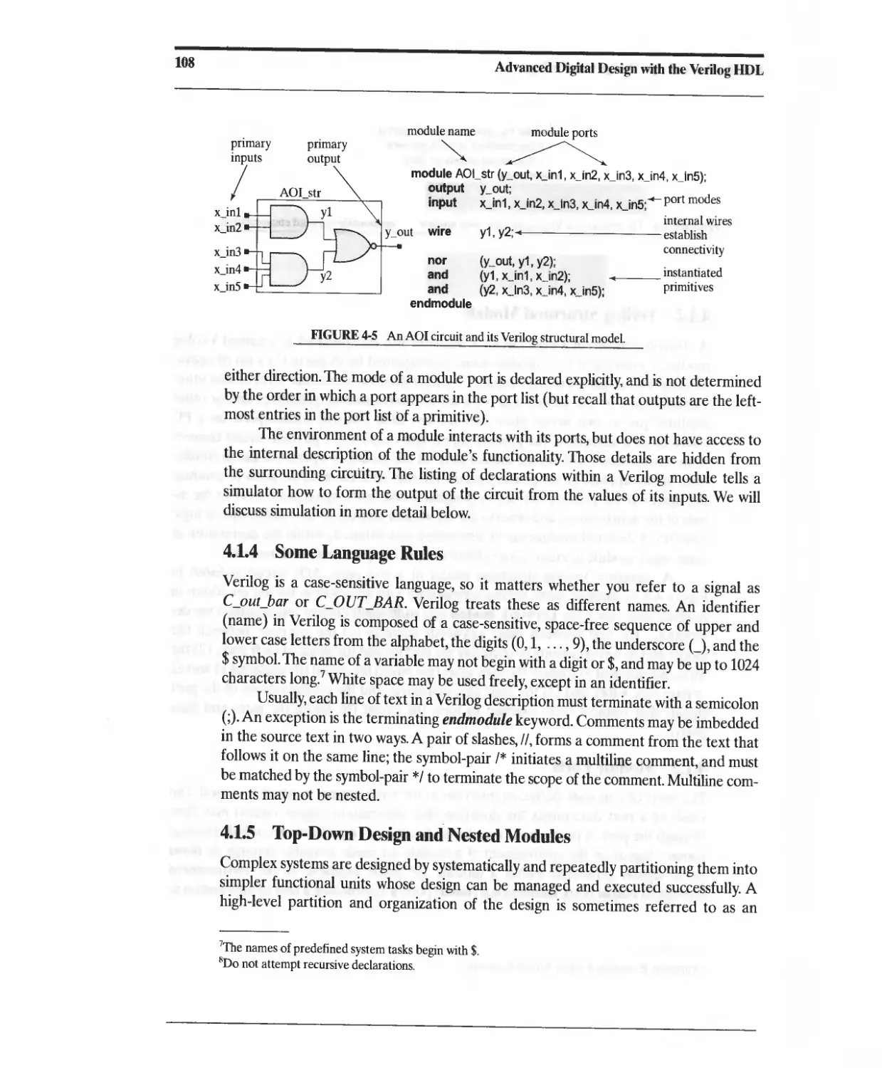
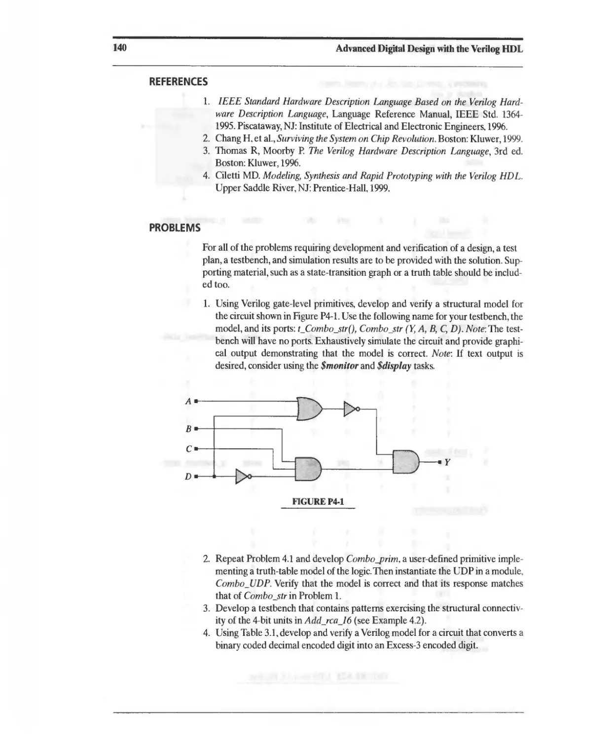
4.1 Structural Models of Combinational Logic 104
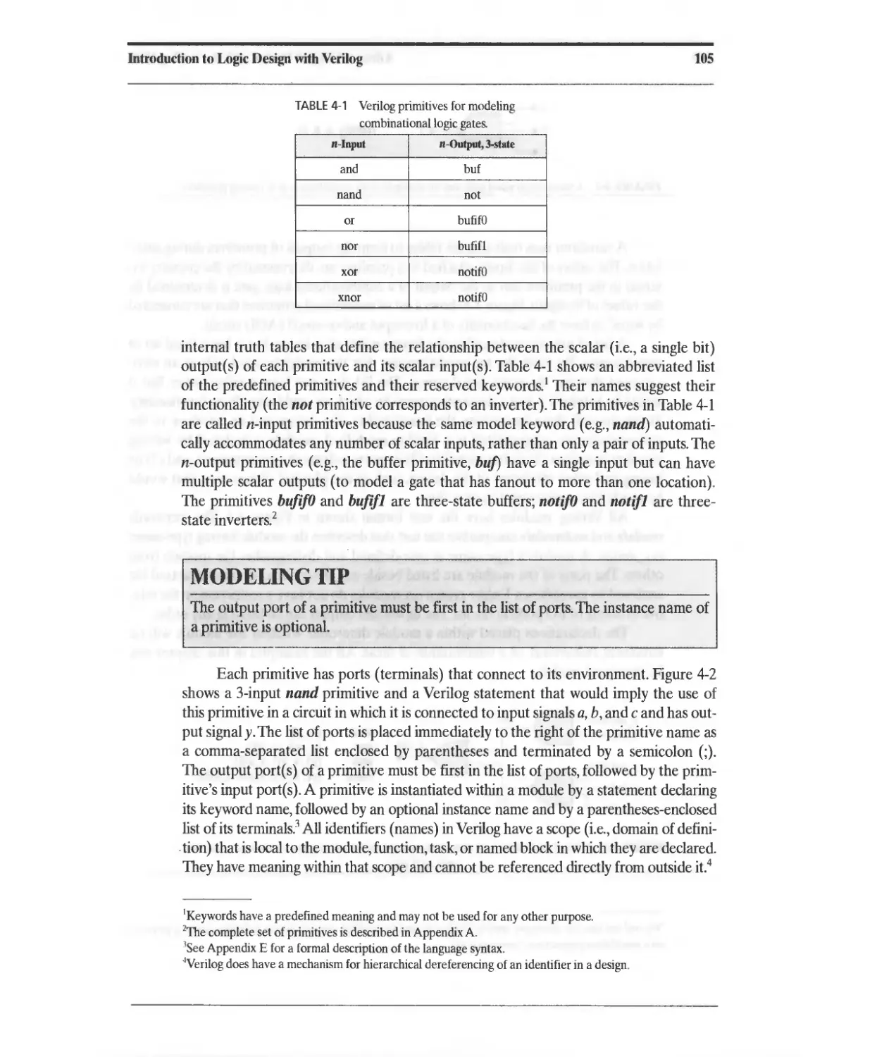
4.1.1 Verilog Primitives and Design Encapsulation 104
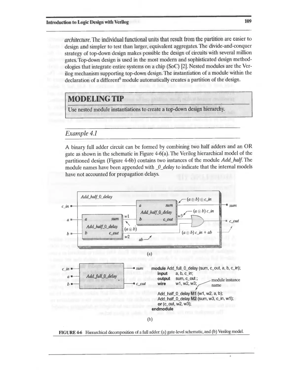
4.1.2 Verilog Structural Models 107
4.1.3 Module Ports 107
4.1.4 Some Language Rules 108
4.1.5 Top-Down Design and Nested Modules 108
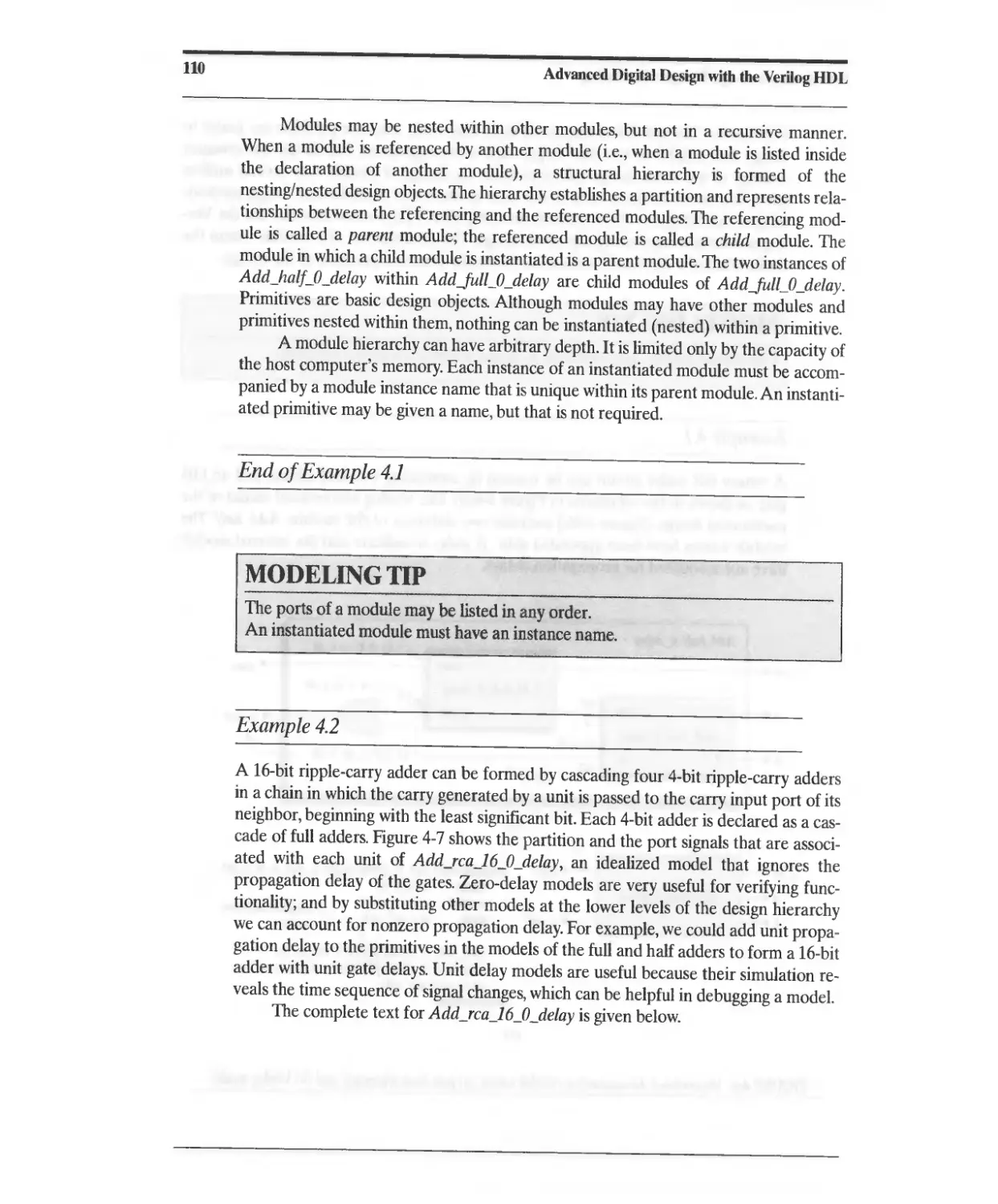
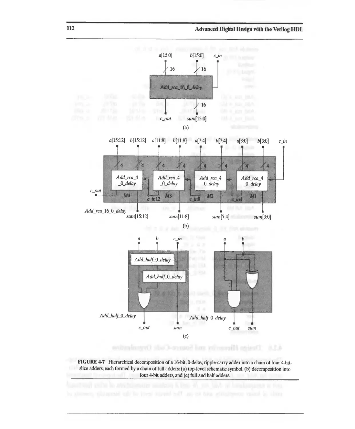
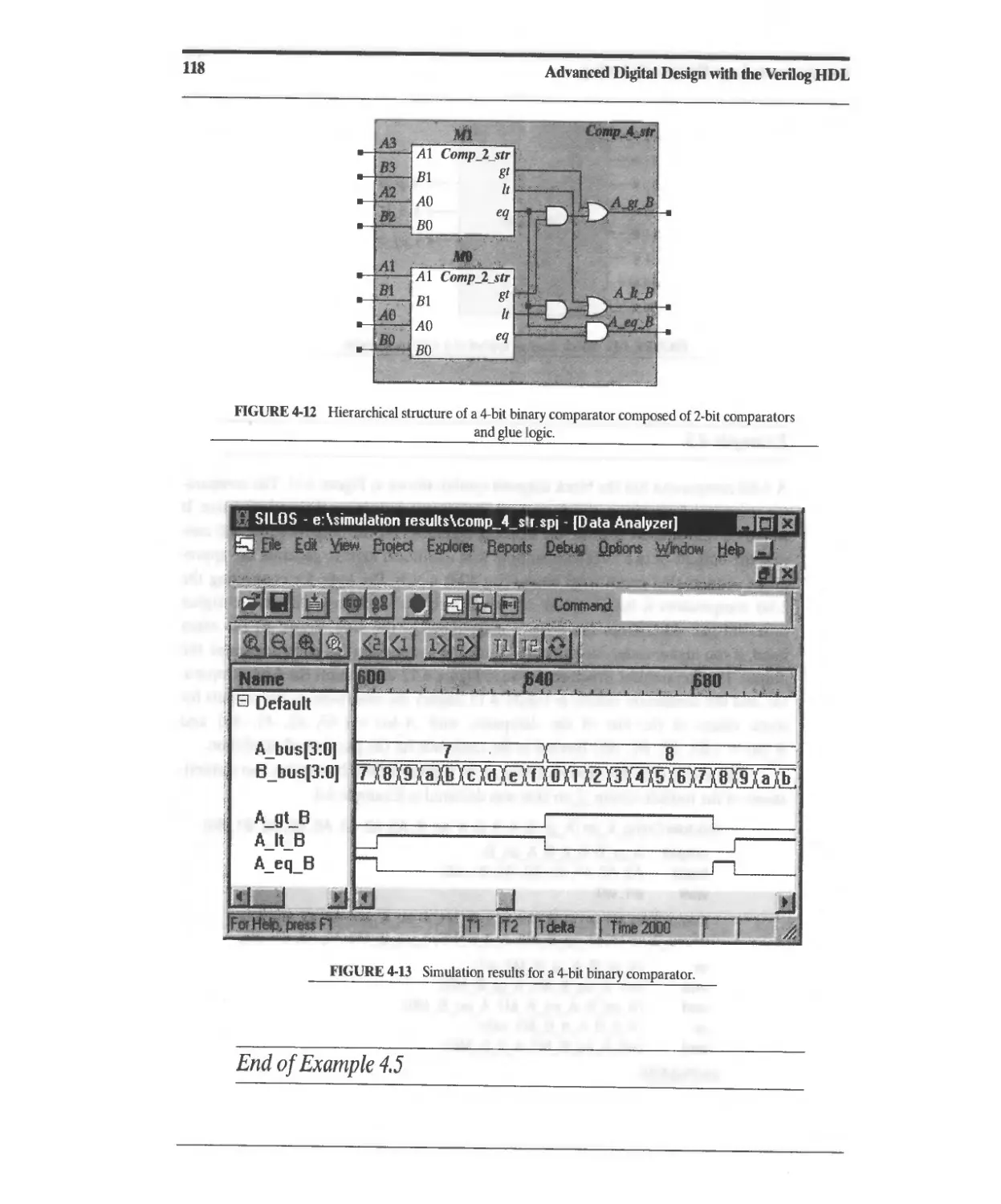
4.1.6 Design Hierarchy and Source-Code Organization 111
4.1.7 Vectors in Verilog 113
4.1.8 Structural Connectivity 114
4.2 Logic Simulation, Design Verification, and Test Methodology 119
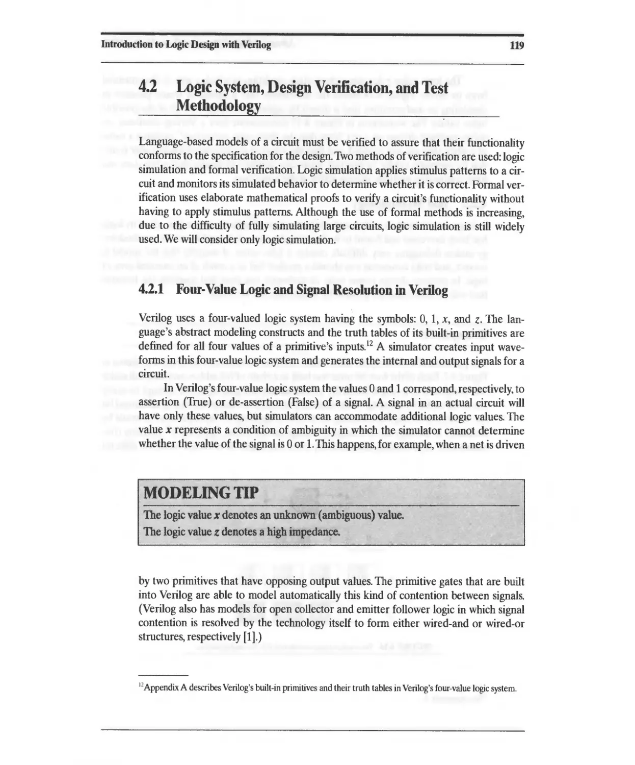
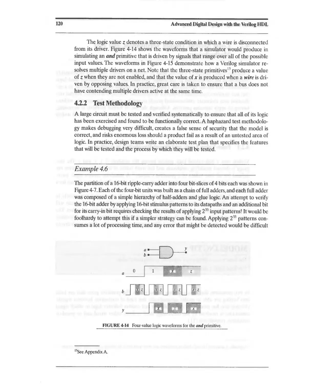
4.2.1 Four-Valued Logic and Signal Resolution in Verilog 119
4.2.2 Test Methodology 120
4.2.3 Signal Generators for Testbenches 123
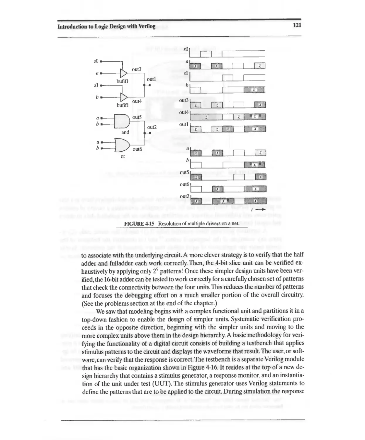
4.2.4 Event-Driven Simulation 125
4.2.5 Testbench Template 125
4.2.6 Sized Numbers 126
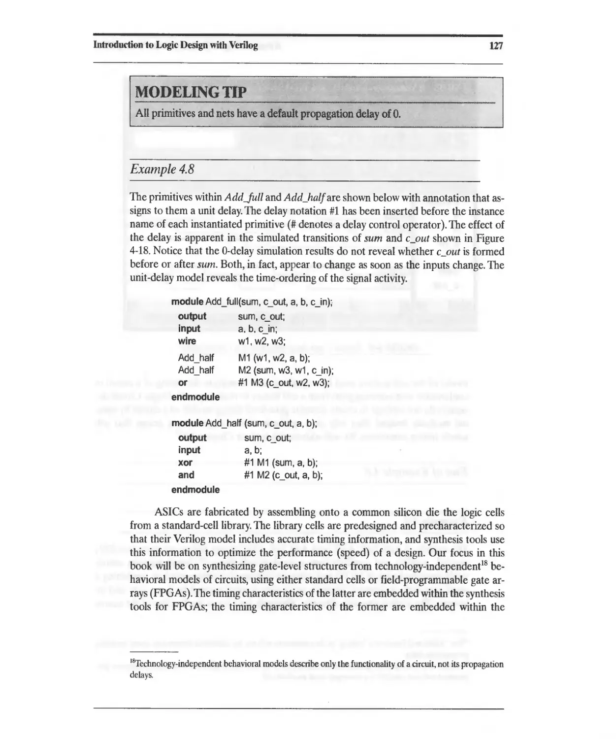
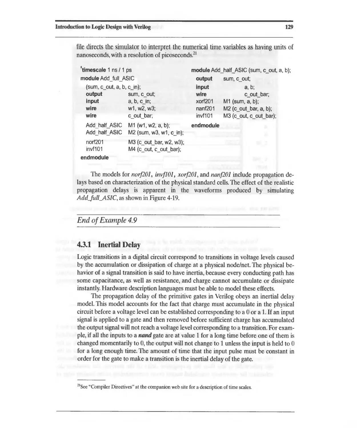
4.3 Propagation Delay 126
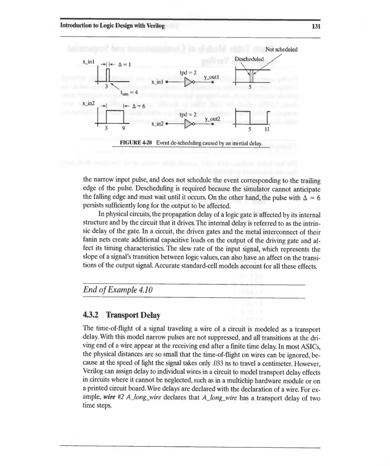
4.3.1 Inertial Delay 129
4.3.2 Transport Delay 131
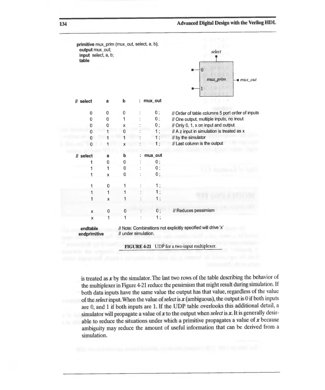
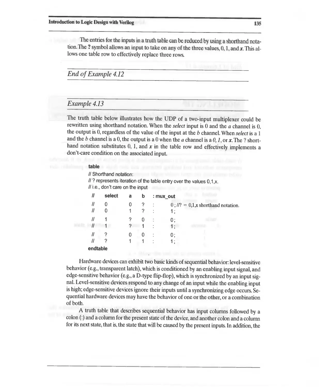
4.4 Truth Table Models of Combinational and Sequential Logic with
Verilog 132
References 140
Problems 140
5 Logic Design with Behavioral Models of Combinational
and Sequential Logic 143
5.1 Behavioral Modeling 143
5.2 A Brief Look at Data Types for Behavioral Modeling 145
5.3 Boolean-Equation-Based Behavioral Models of
Combinational Logic 145
viii
Contents
5.4 Propagation Delay and Continuous Assignments 148
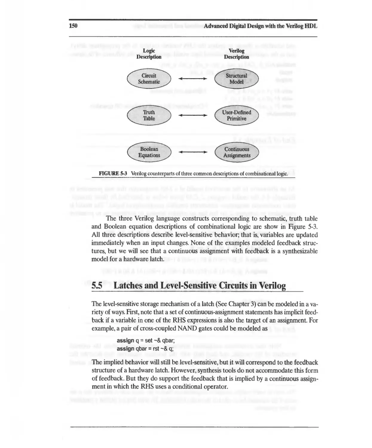
5.5 Latches and Level-Sensitive Circuits in Verilog 150
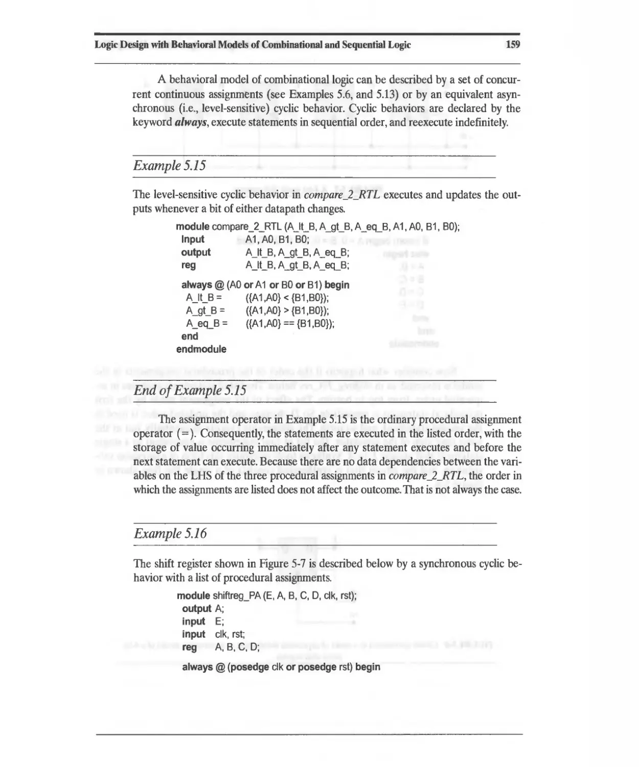
5.6 Cyclic Behavioral Models of Flip-Flops and Latches 153
5.7 Cyclic Behavior and Edge Detection 154
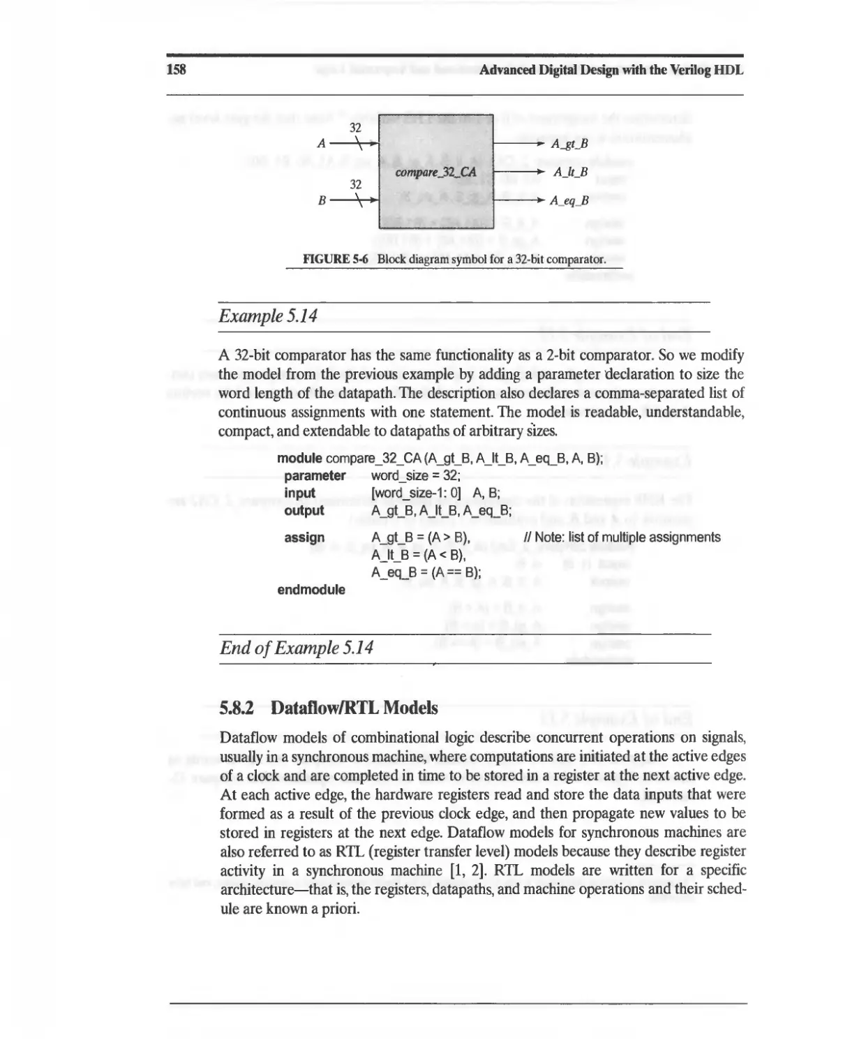
5.8 A Comparision of Styles for Behavioral Modeling 156
5.8.1 Continuous-Assignment Models 156
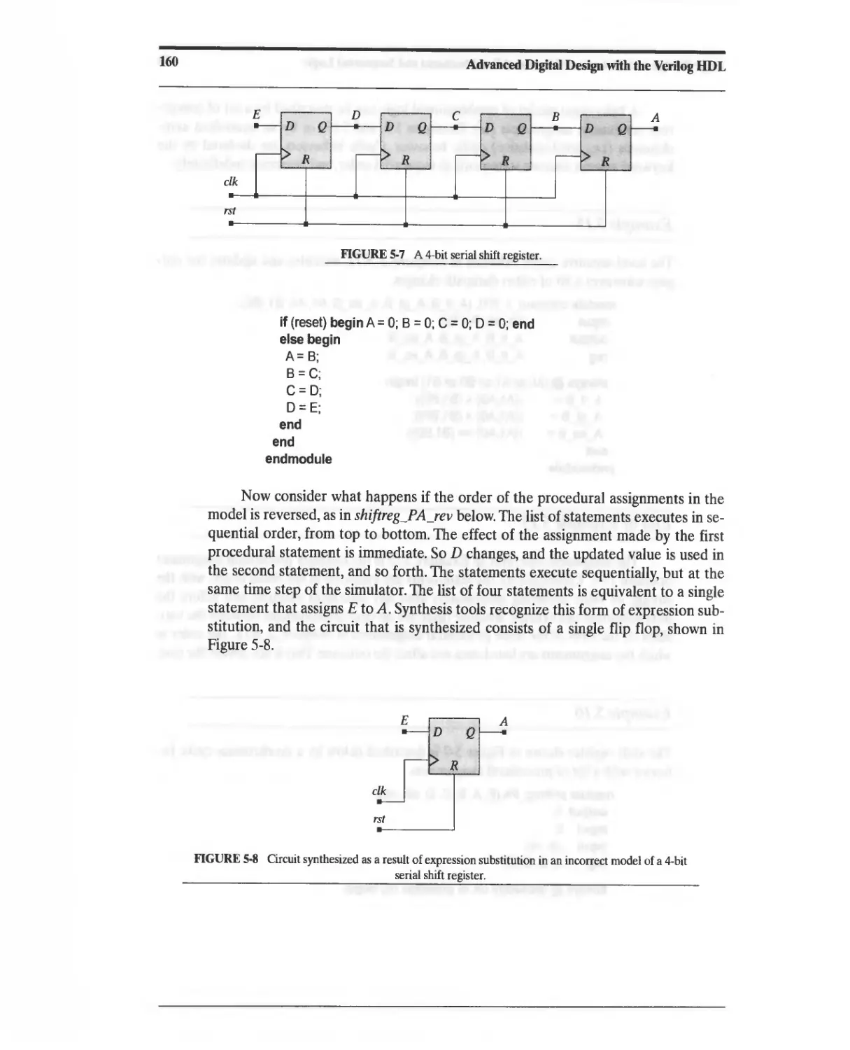
5.8.2 Dataflow/RTL Models 158
5.8.3 Algorithm-Based Models 162
5.8.4 Port Names: A MaUer of Style 164
5.8.5 Simulation with Behavioral Models 164
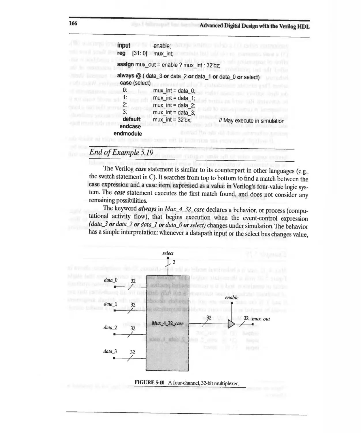
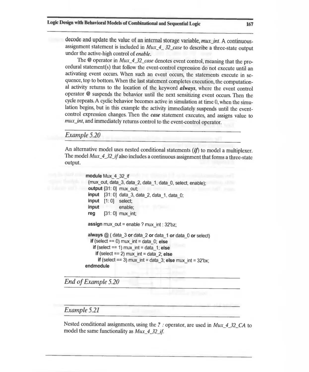
5.9 Behavioral Models of Multiplexers, Encoders, and Decoders 165
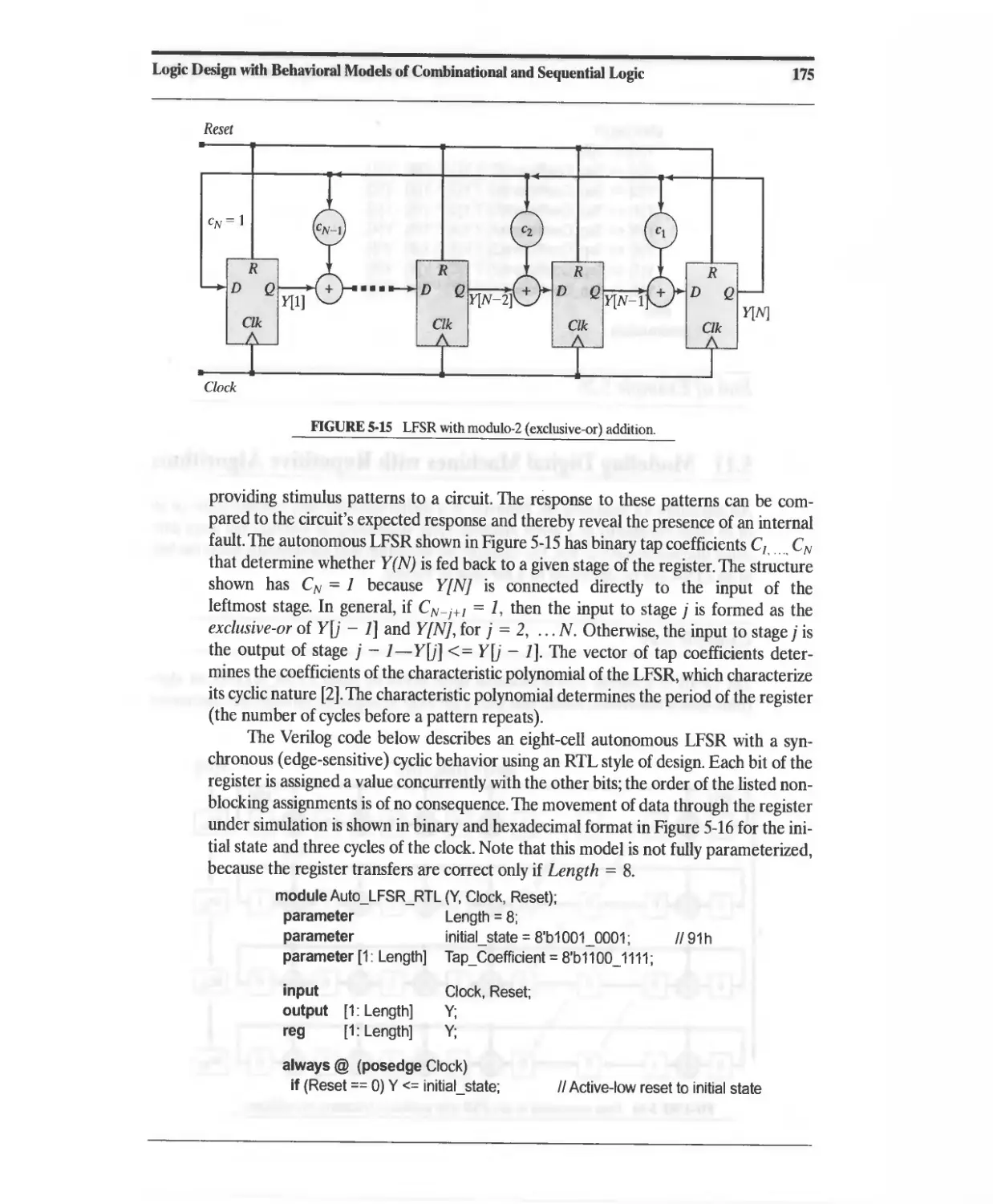
5.10 Dataflow Models of a Linear-Feedback Shift Register 174
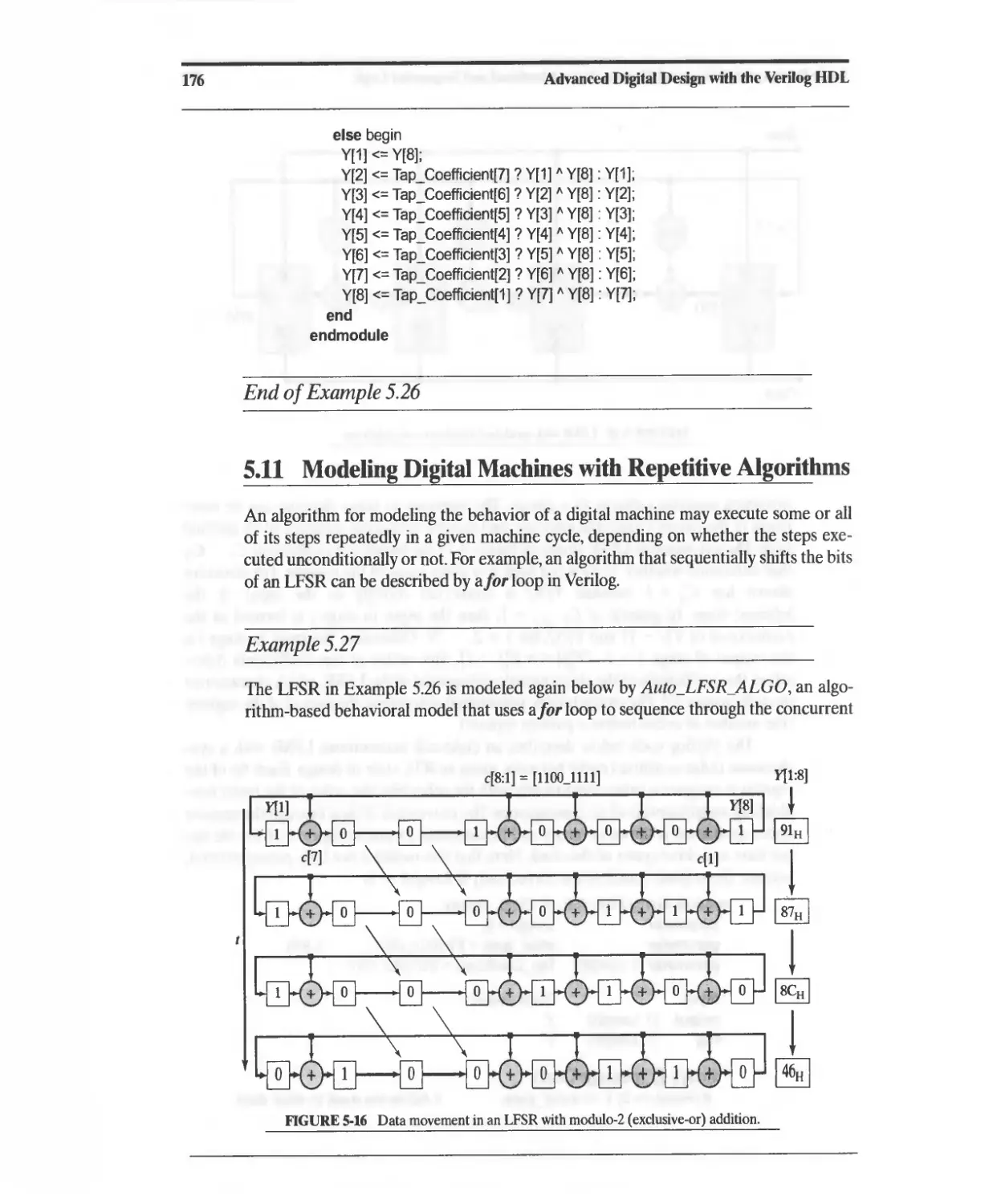
5.11 Modeling Digital Machines with Repetitive Algorithms 176
5.11.1 Intellectual Property Reuse and Parameterized Models 181
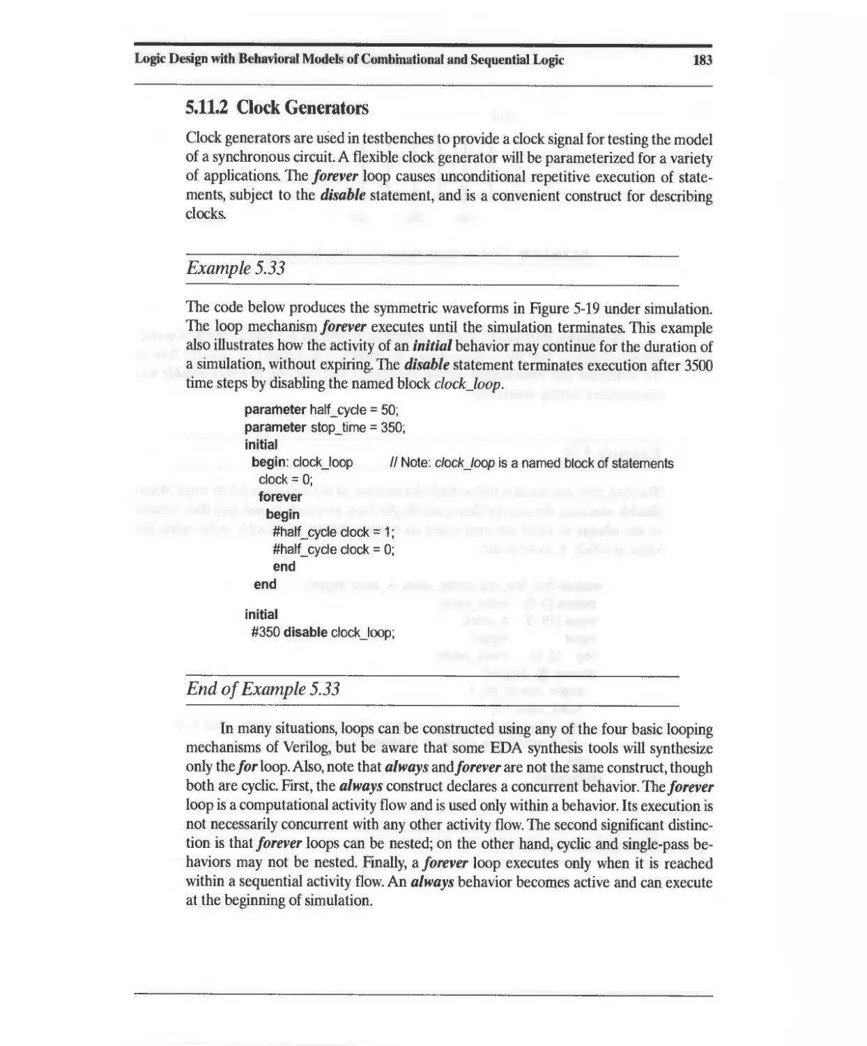
5.11.2 Clock Generators 183
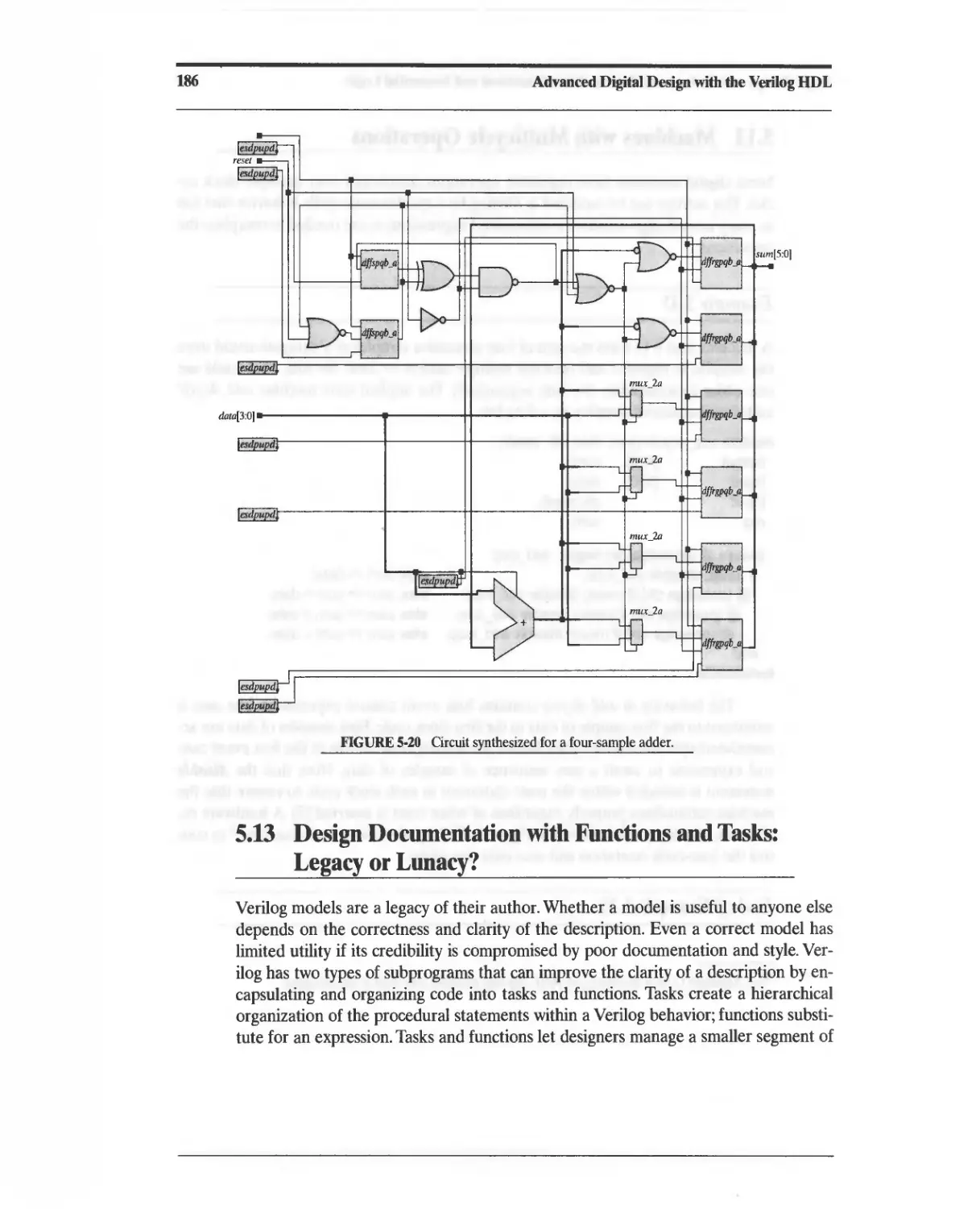
5.12 Machines with Multicycle Operations 185
5.13 Design Documentation with Functions and Tasks: Legacy
or Lunacy? 186
5.13.1 Tasks 187
5.13.2 Functions 189
5.14 Algorithmic State Machine Charts for Behavioral Modeling 190
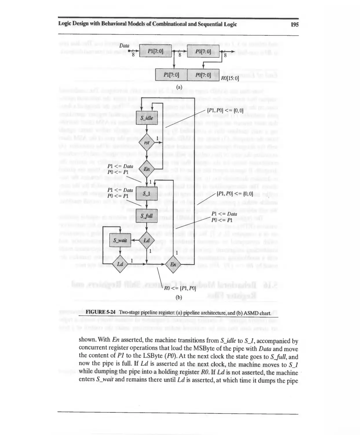
5.15 ASMD Charts 194
5.16 Behavioral Models of Counters, Shift Registers, and Register Files 196
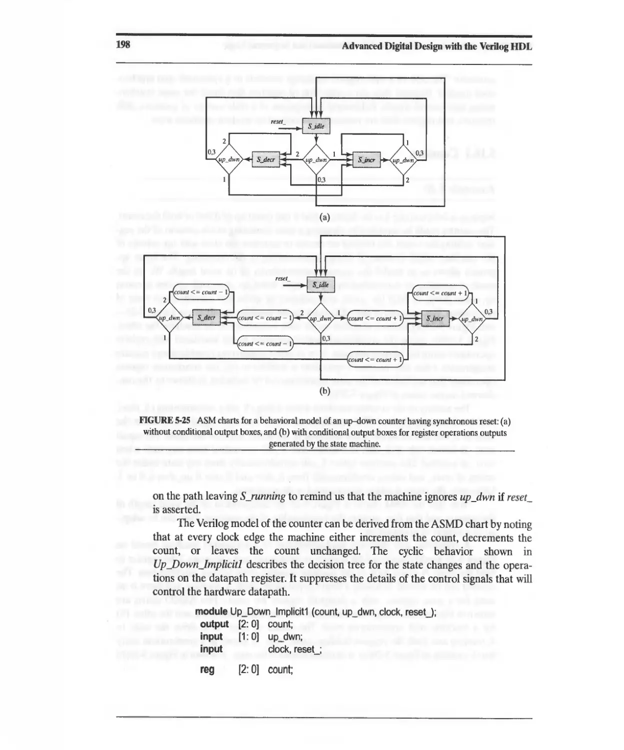
5.16.1 Counters 197
5.16.2 Shift Registers 203
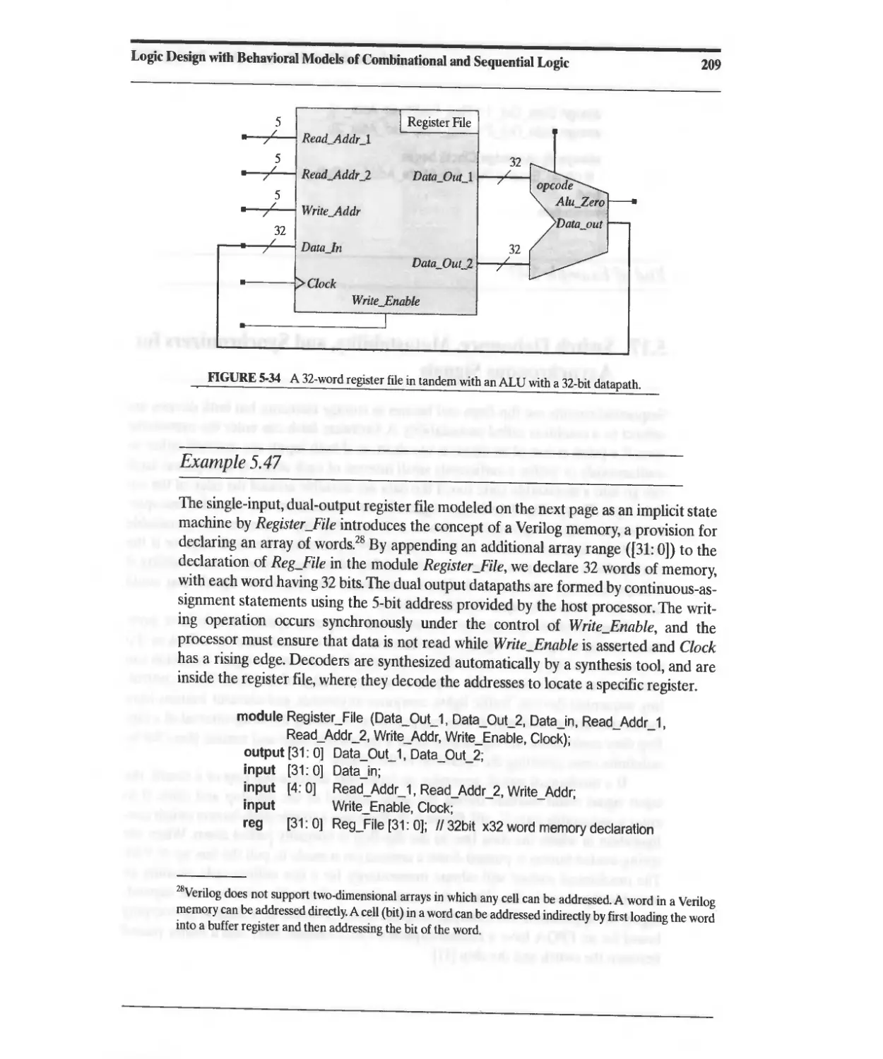
5.16.3 Register Files and Arrays of Registers (Memories) 207
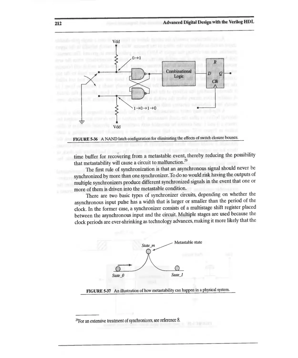
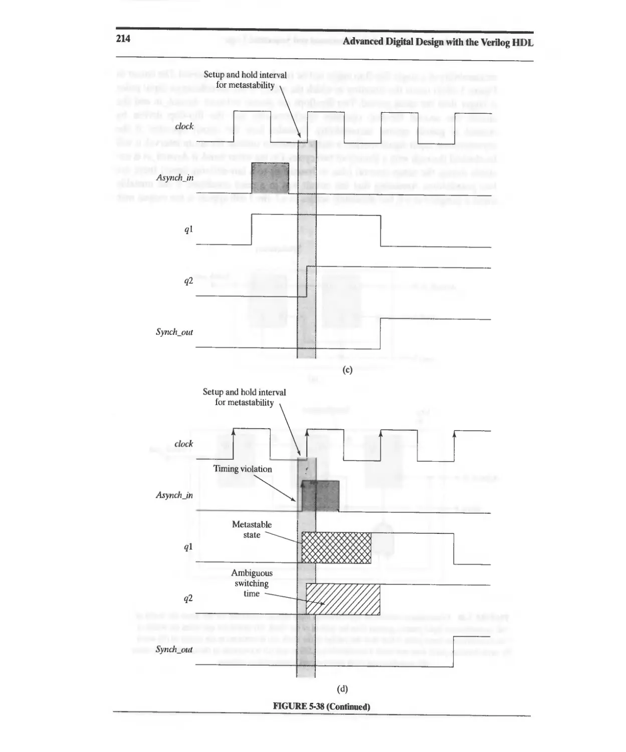
5.17 Switch Debounce, Metastability, and Synchronizers for Asynchronous Signals 210
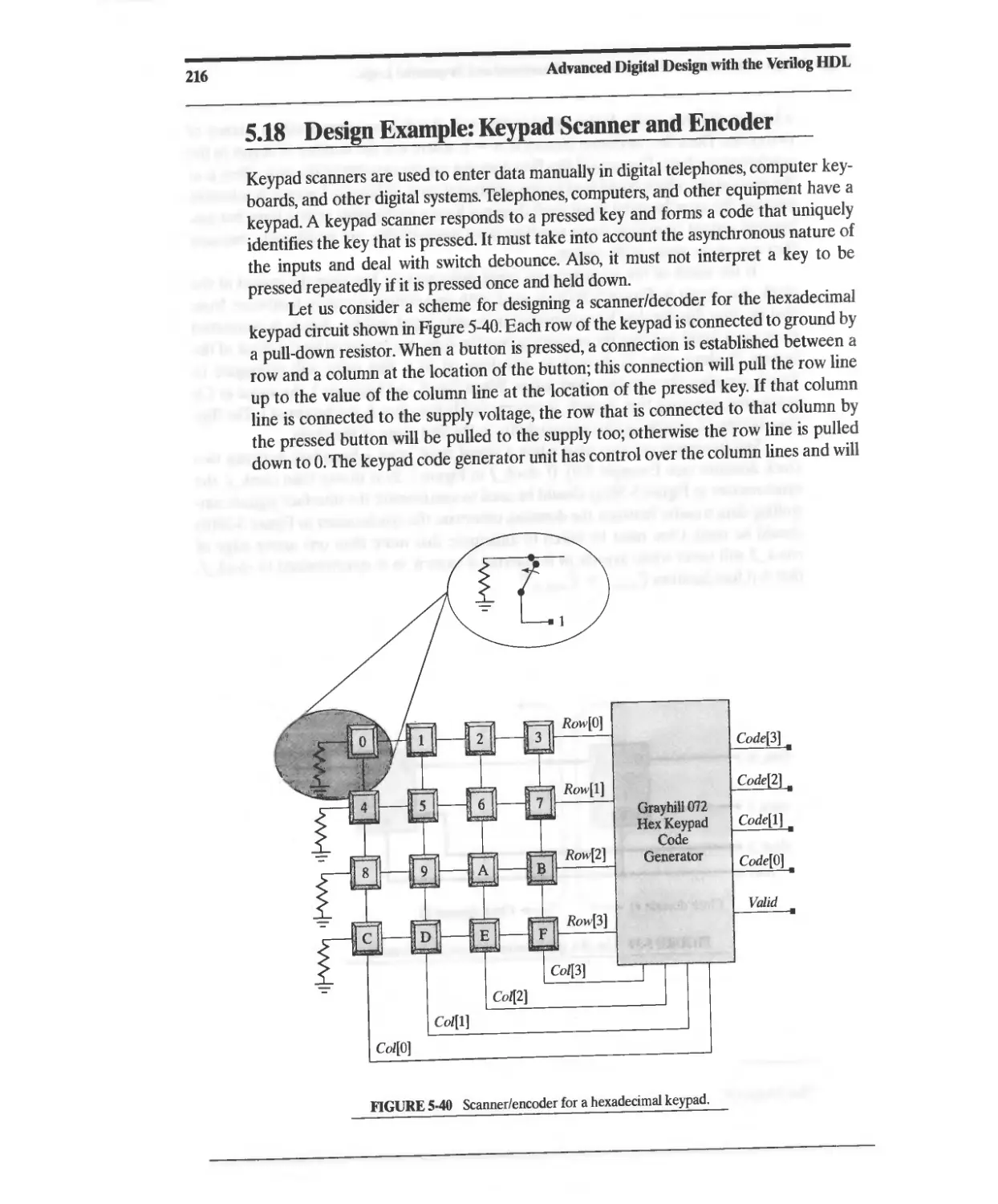
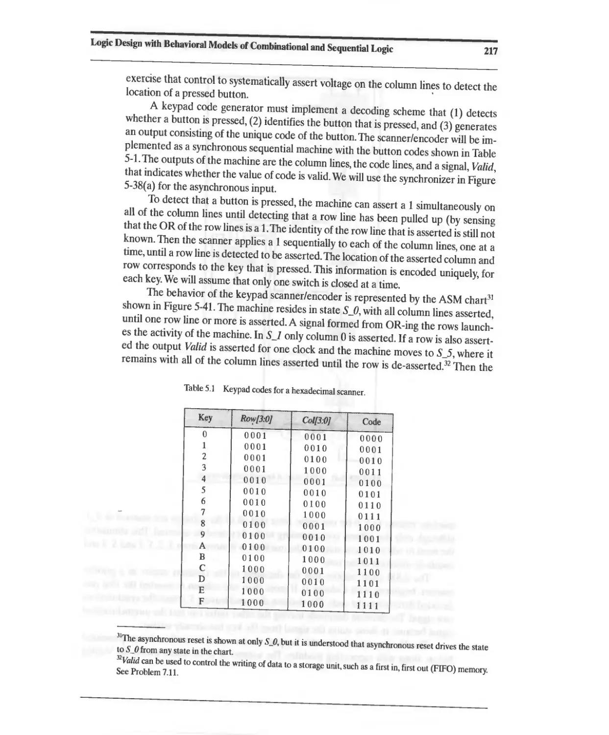
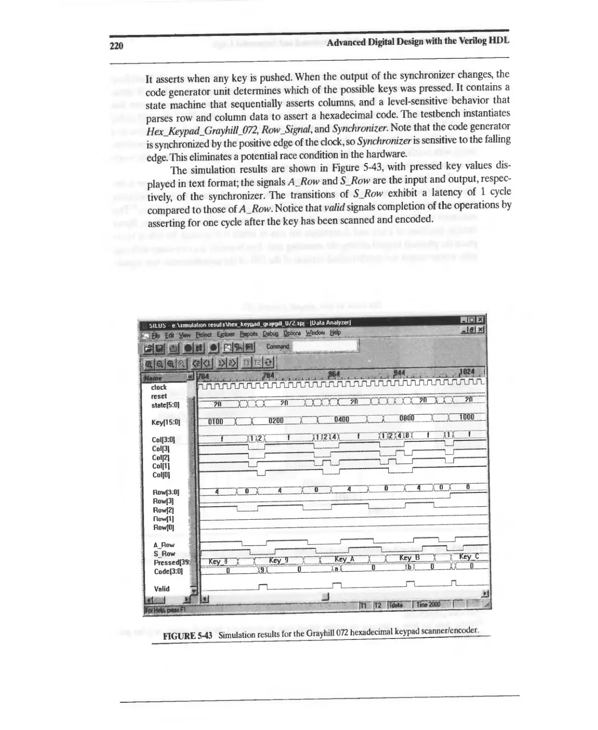
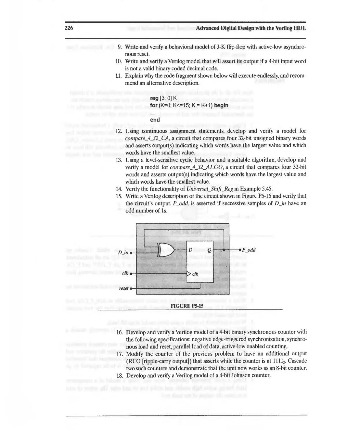
5.18 Design Example: Keypad Scanner and Encoder 216
References 224
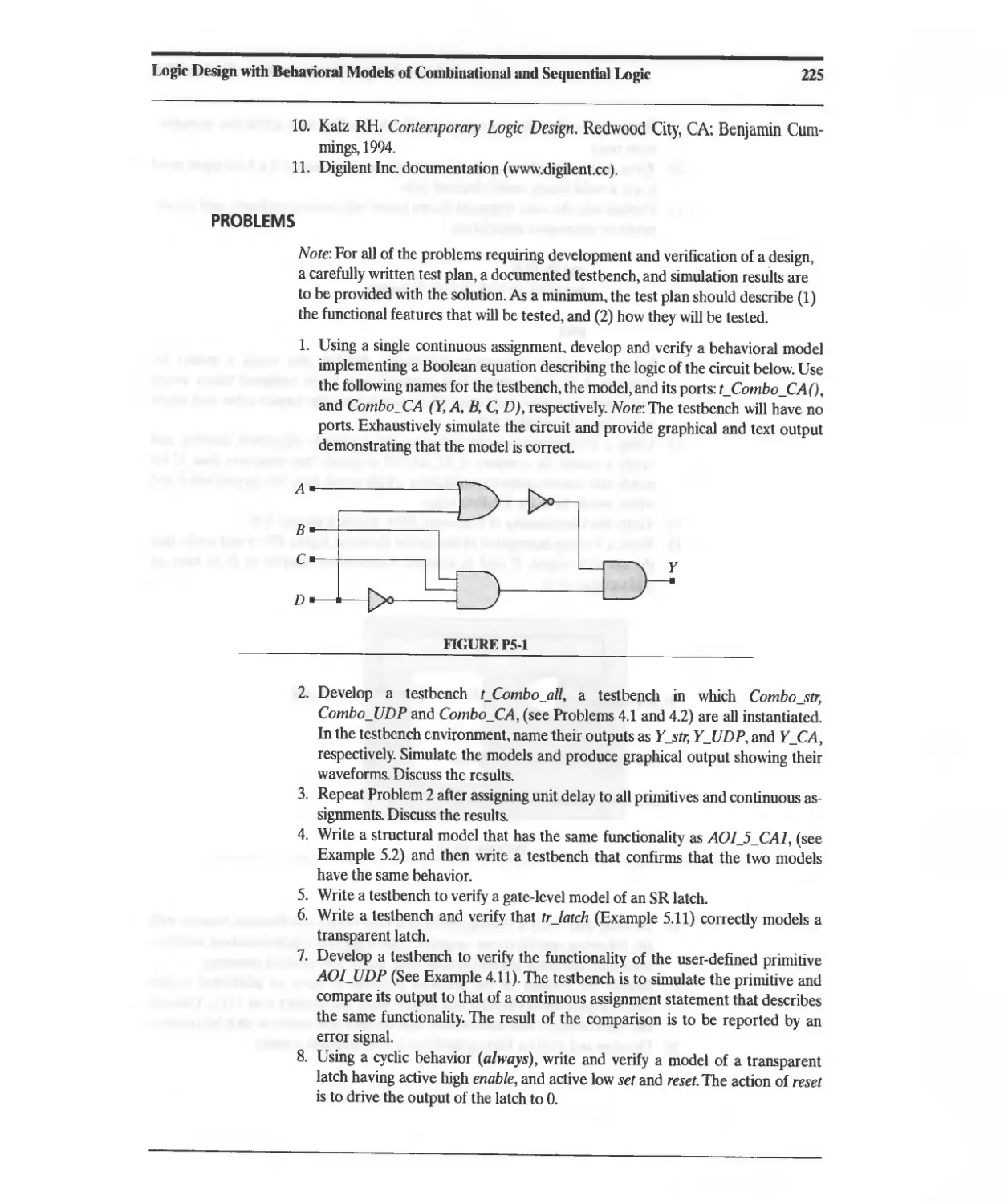
Problems 225
6 Synthesis of Combinational and Sequential Logic 233
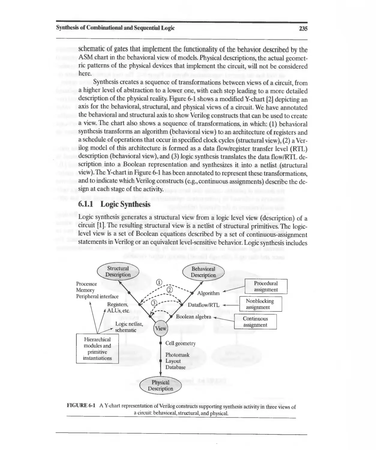
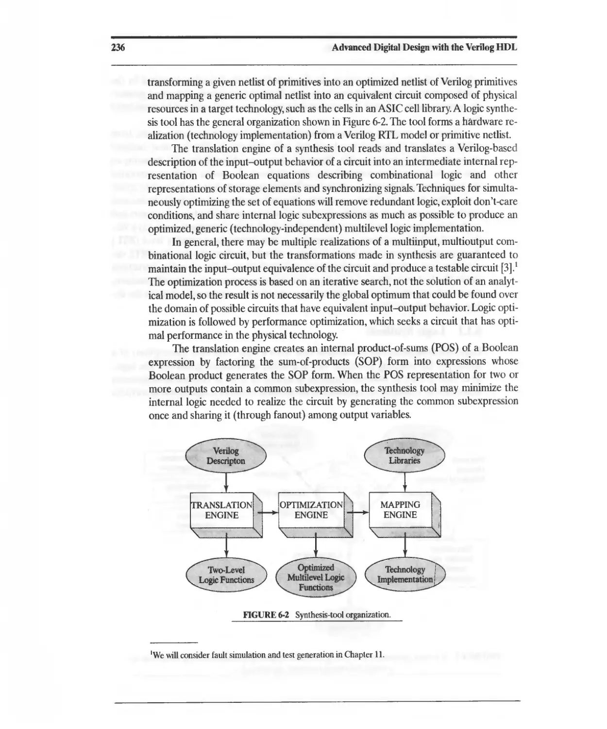
6.1 Introduction to Synthesis 234
6.1.1 Logic Synthesis 235
6.1.2 RTL Synthesis 243
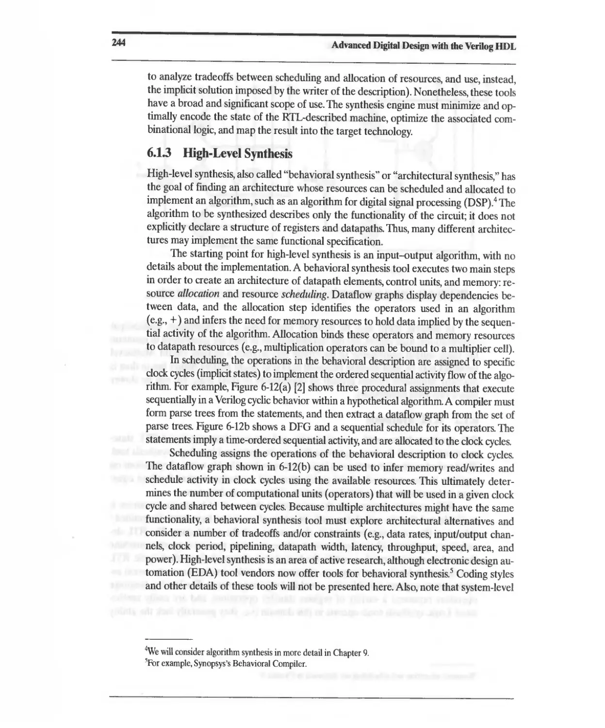
6.1.3 High-Level Synthesis 244
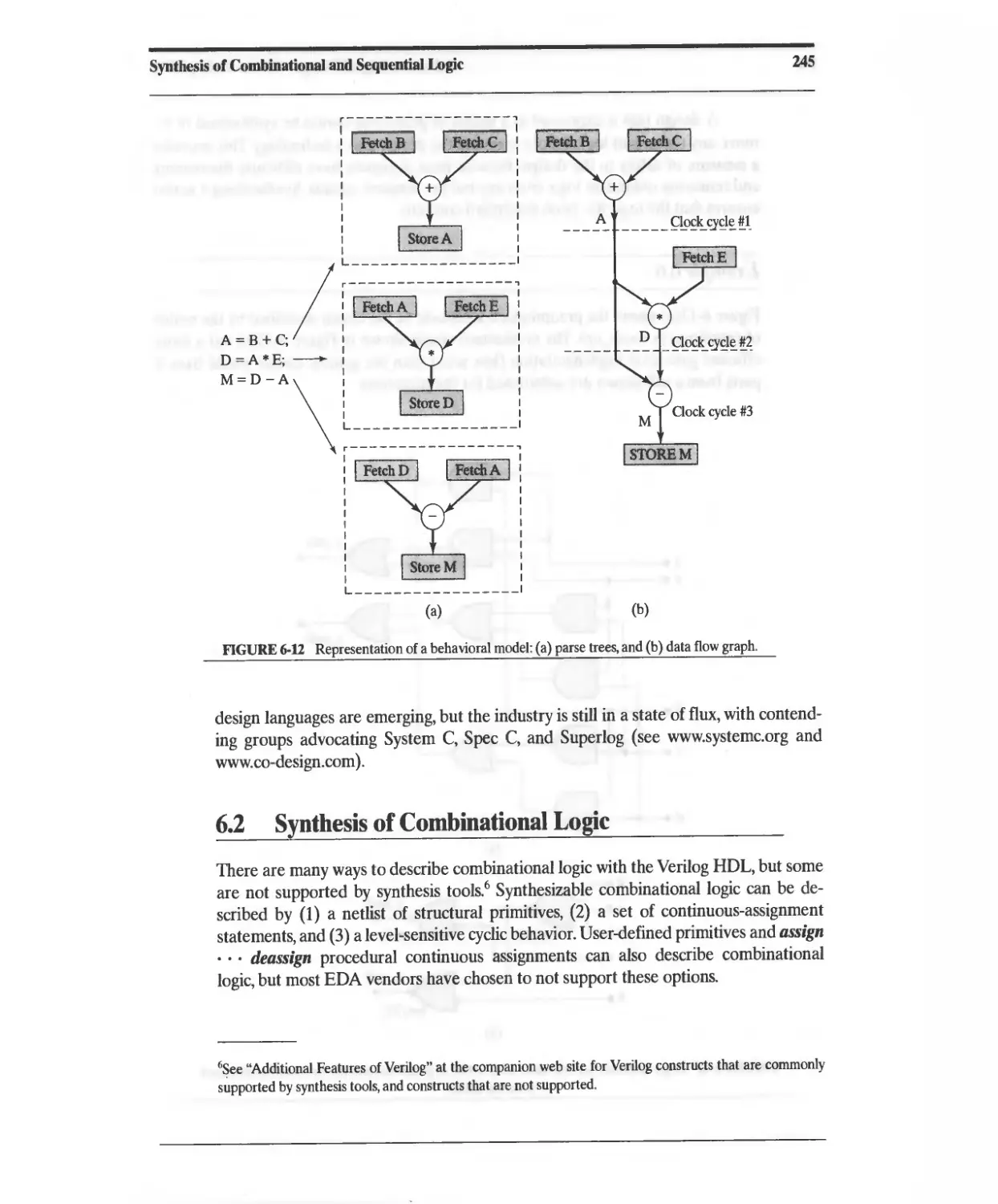
6.2 Synthesis of Combinational Logic 245
6.2.1 Synthesis of Priority Structures 250
6.2.2 Exploiting Logical Don't-Care Conditions 251
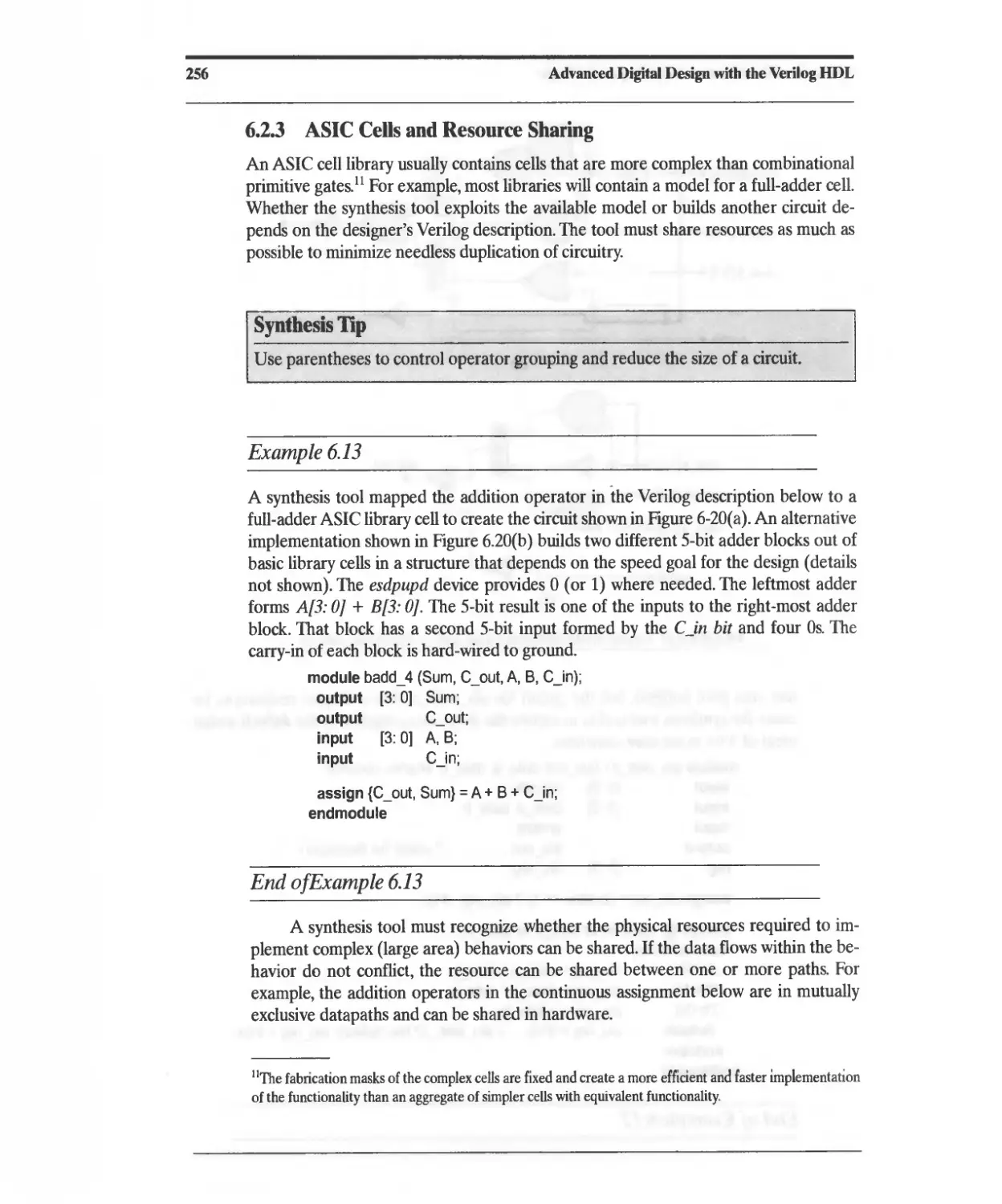
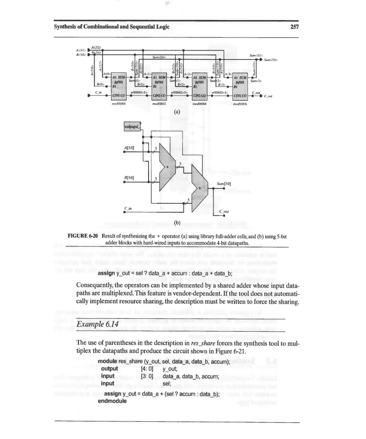
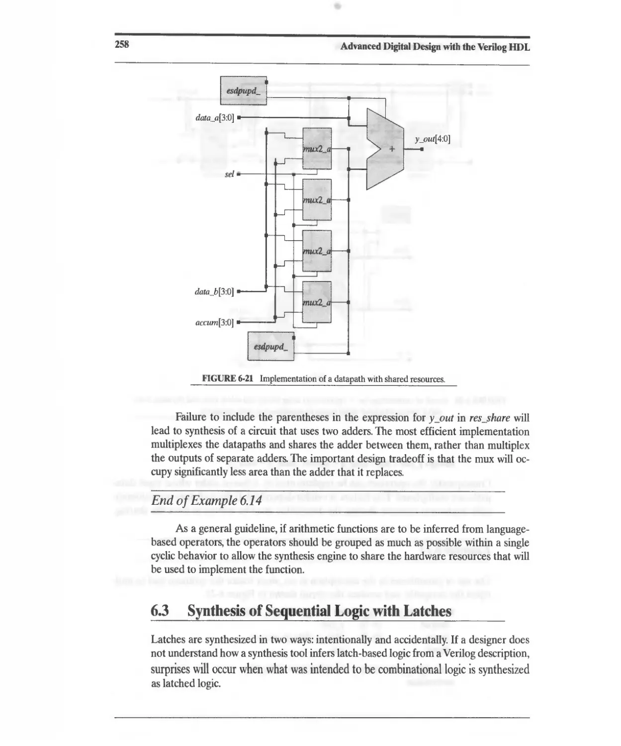
6.2.3 ASIC Cells and Resource Sharing 256
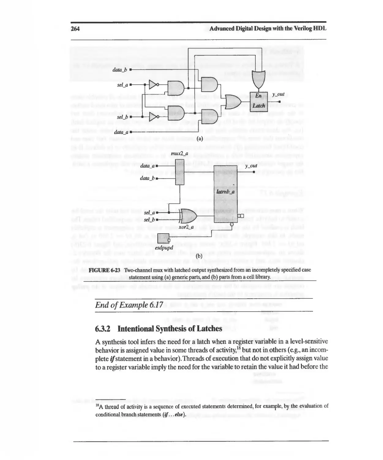
6.3 Synthesis of Sequential Logic with Latches 258
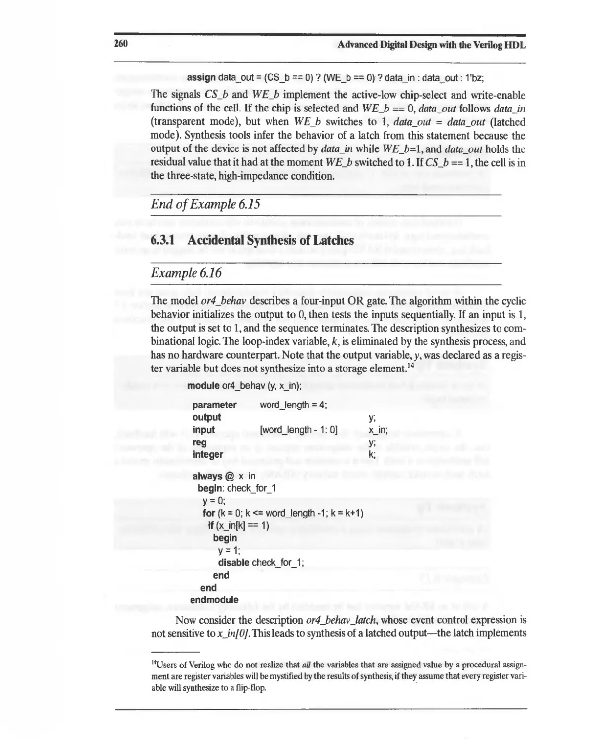
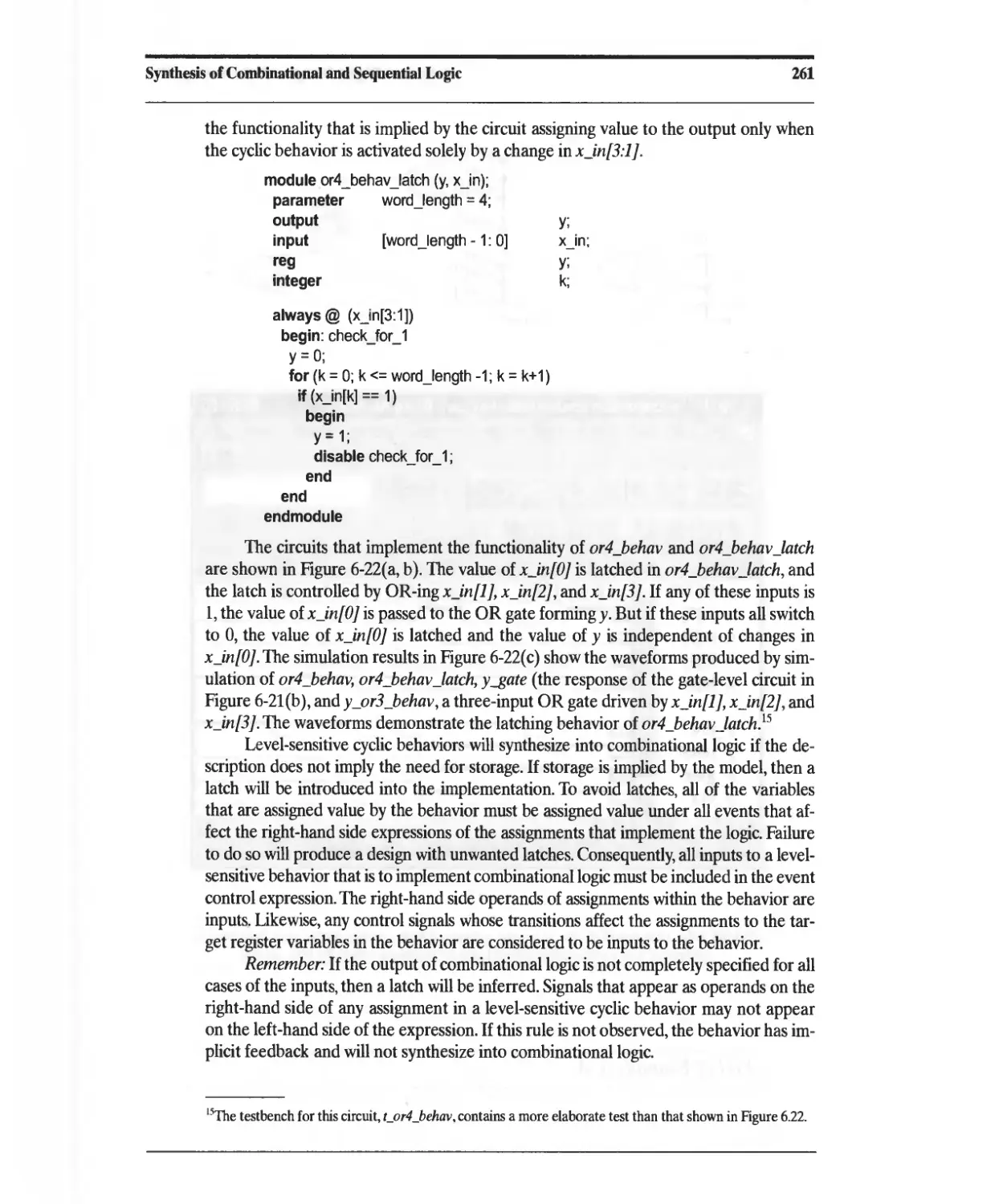
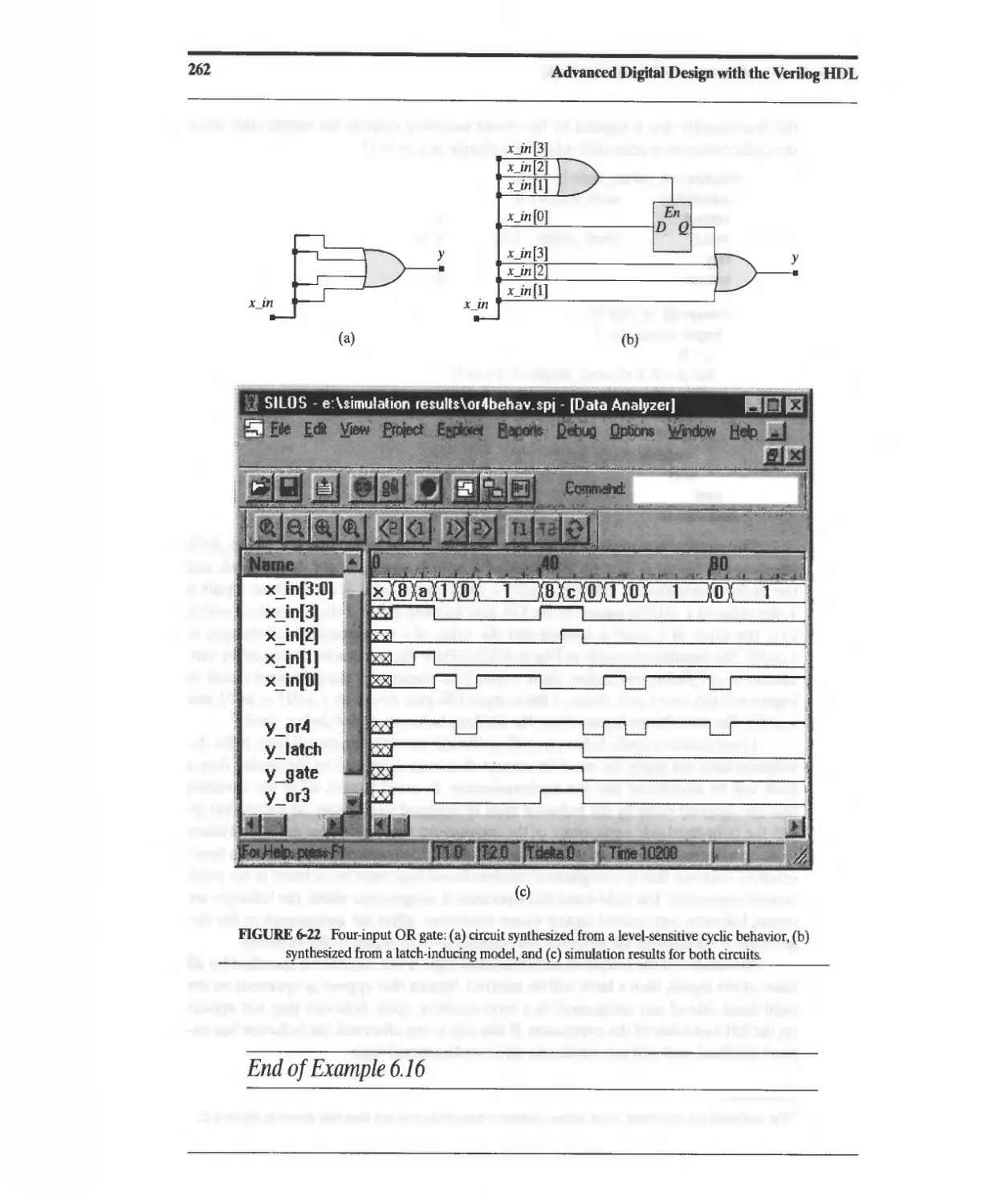
6.3.1 Accidental Synthesis of Latches 260
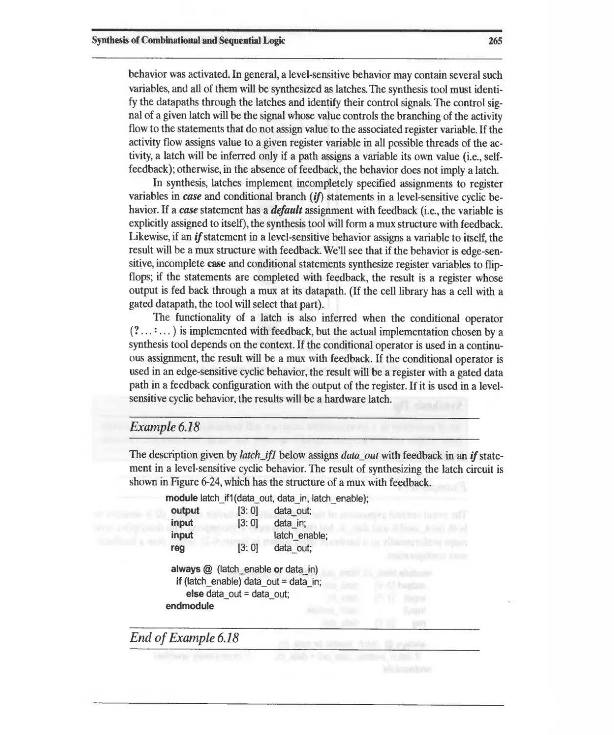
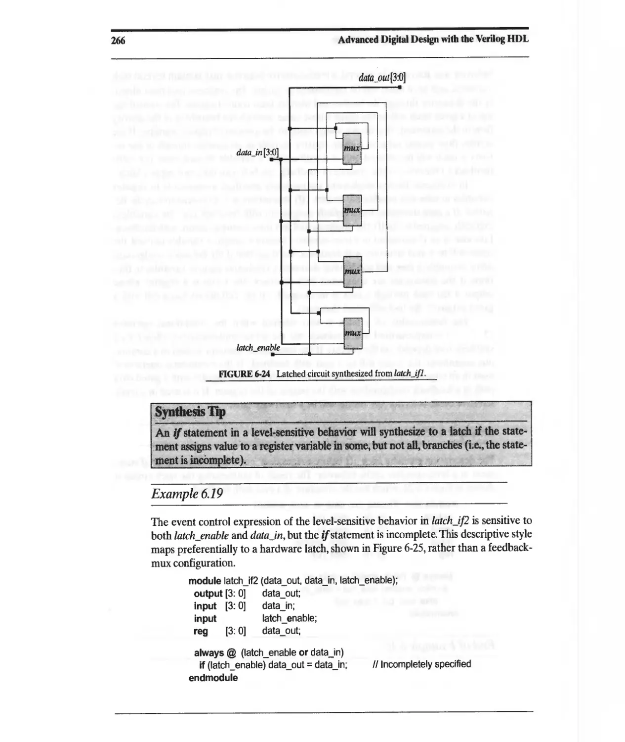
6.3.2 Intentional Synthesis of Latches 264
Contents
ix
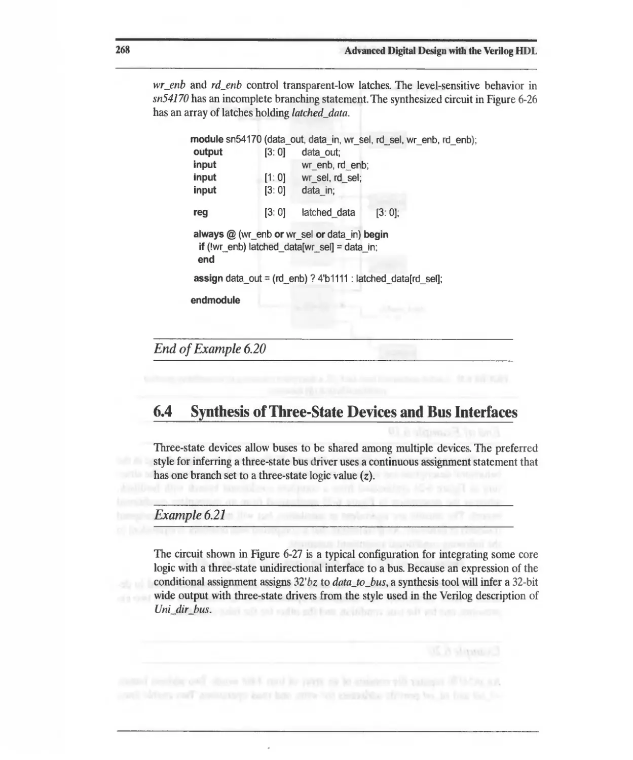
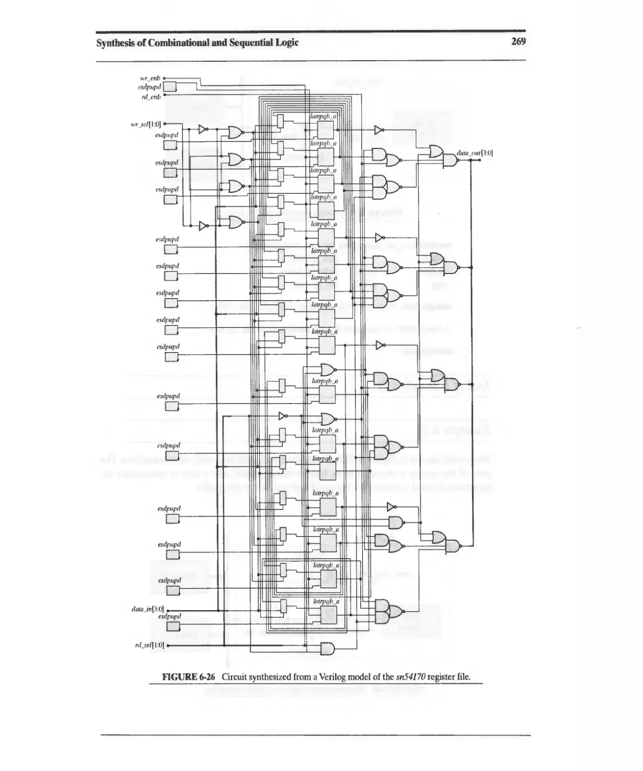
6.4 Synthesis of Three-State Devices and Bus Interfaces 268
6.5 Synthesis of Sequential Logic with Flip-Flops 271
6.6 Synthesis of Explicit State Machines 275
6.6.1 Synthesis of a BCD-to-Excess-3 Code Converter 275
6.6.2 Synthesis of a Mealy-Type NRZ-to-Manchester Line Code
Converter 280
6.6.3 Synthesis of a Moore-Type NRZ-to-Manchester Line Code
Converter 282
6.6.4 Synthesis of a Sequence Recognizer 283
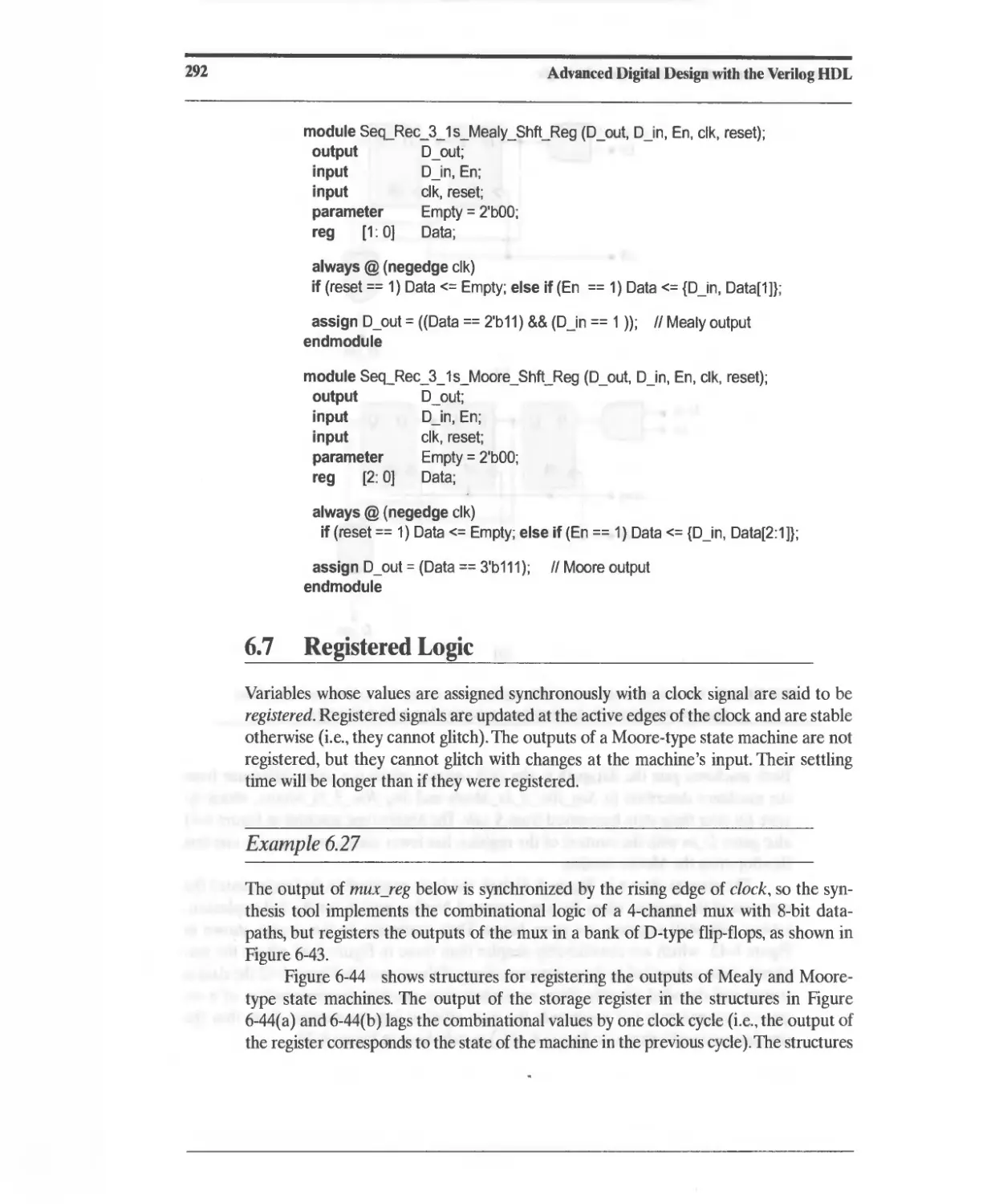
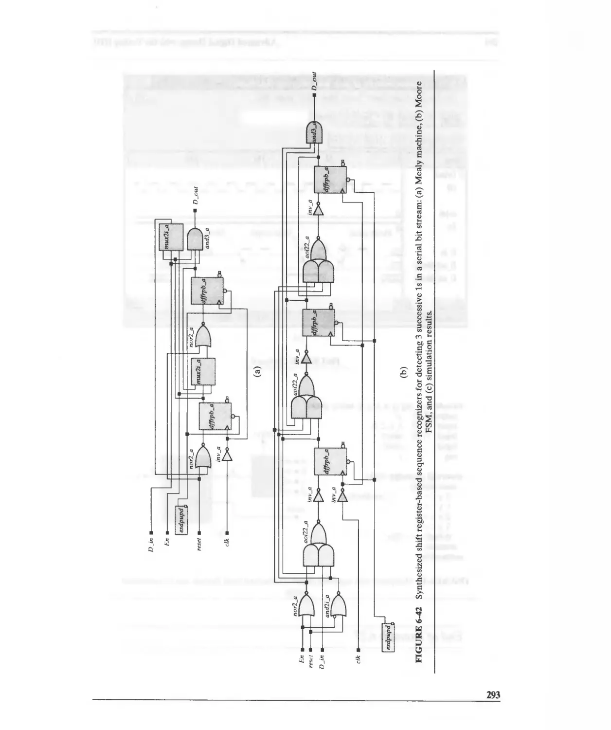
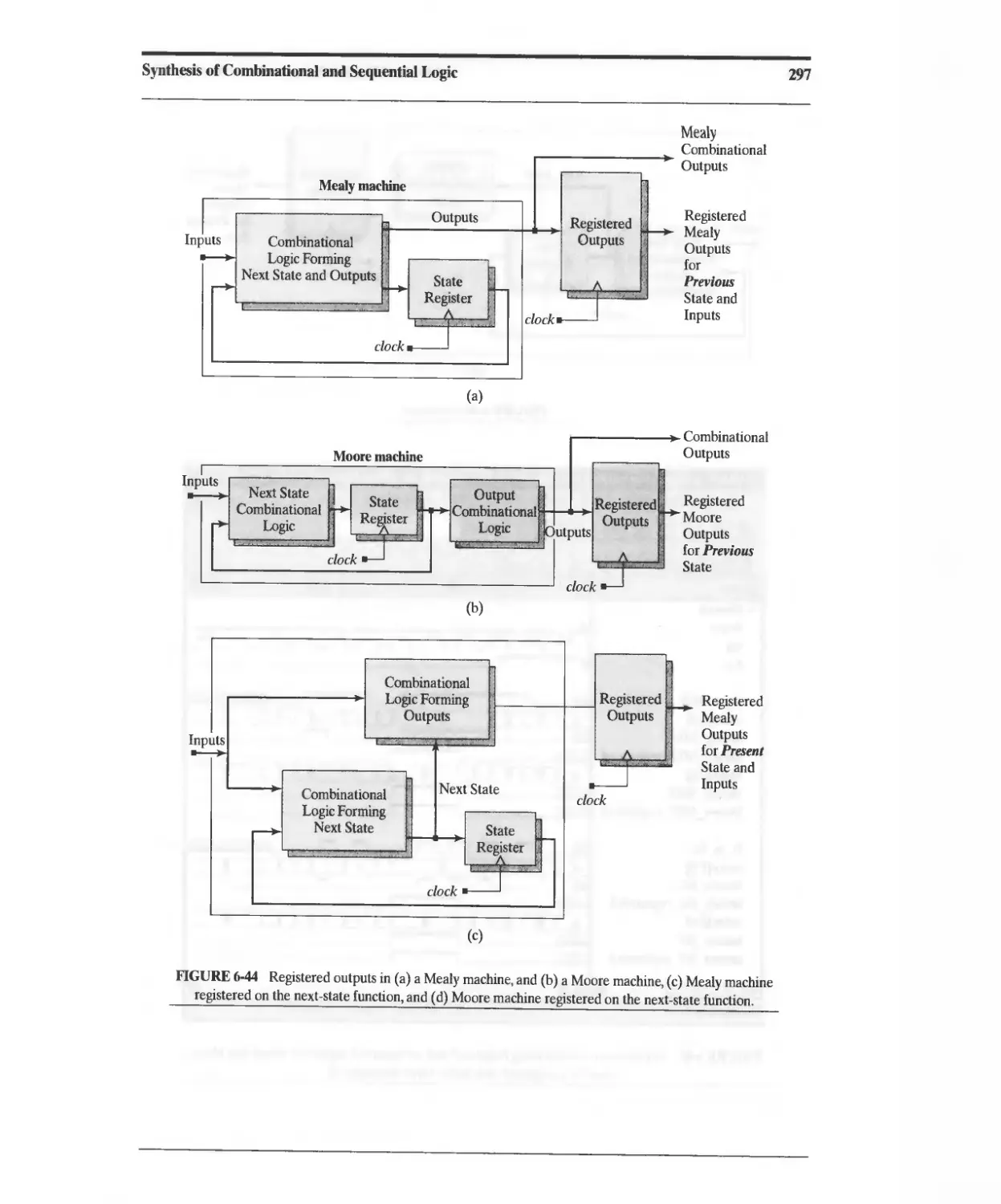
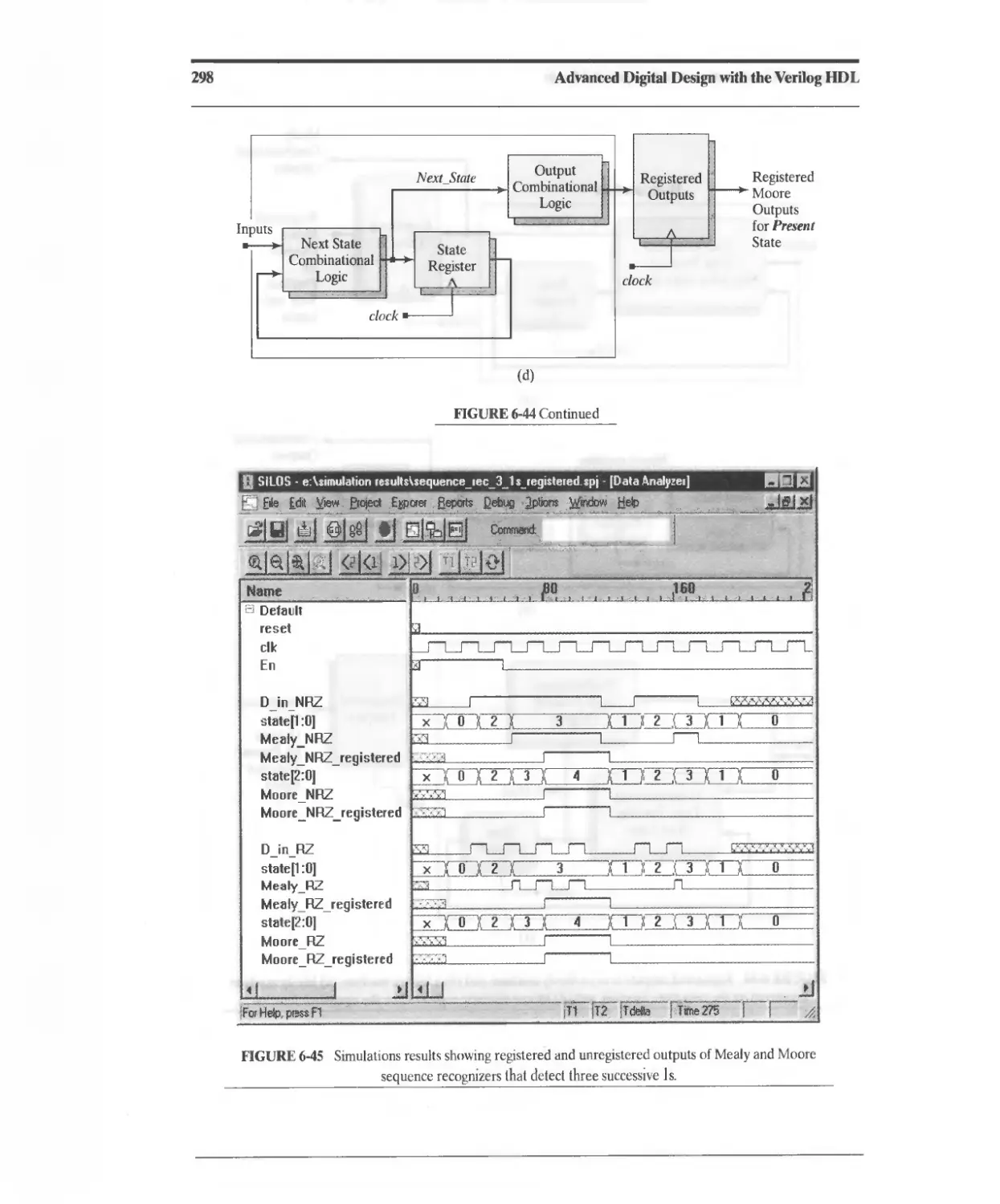
6.7 Registered Logic 292
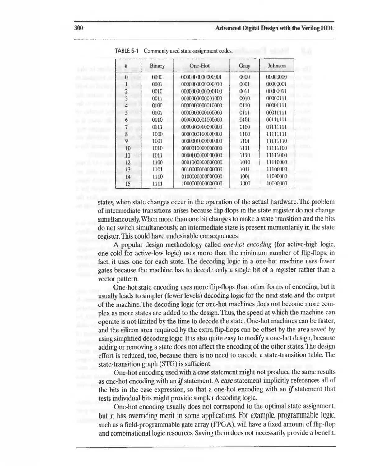
6.8 State Encoding 299
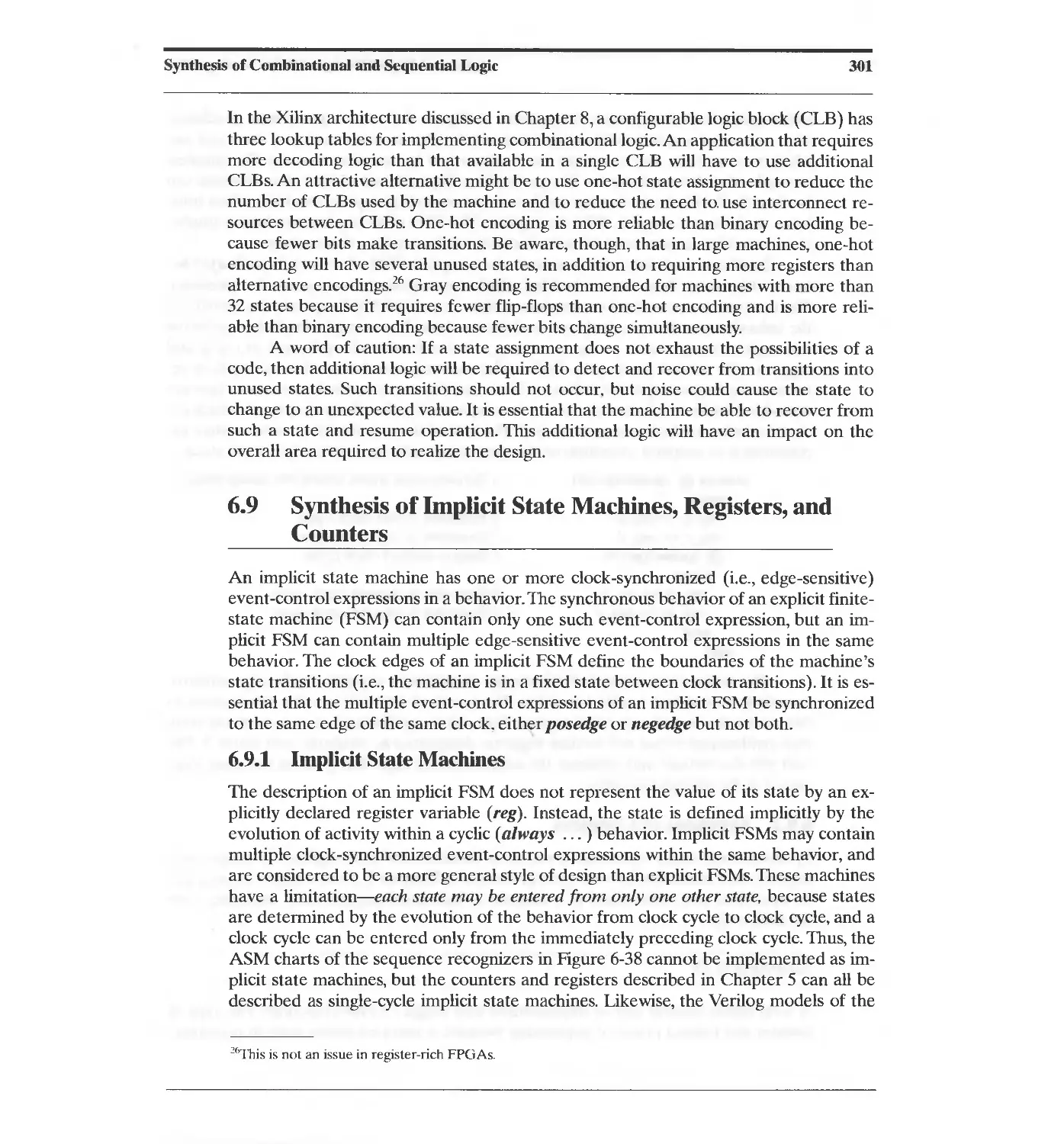
6.9 Synthesis of Implicit State Machines, Registers, and Counters 301
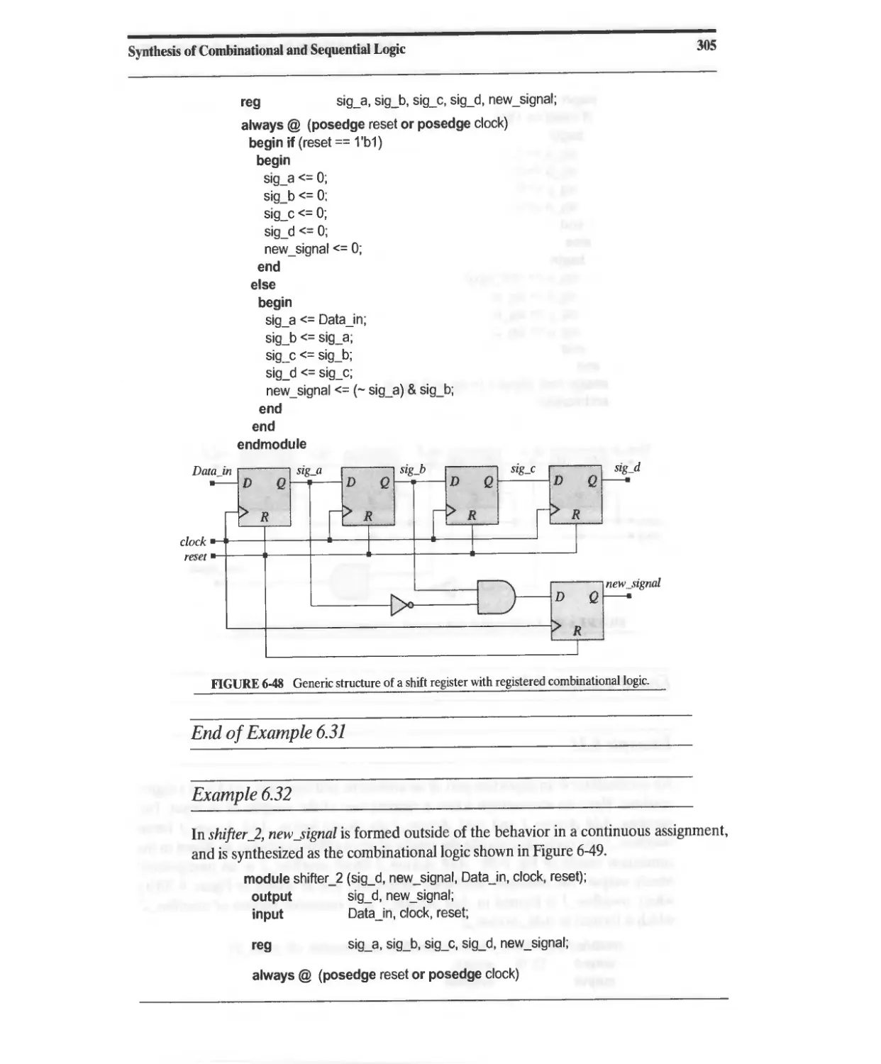
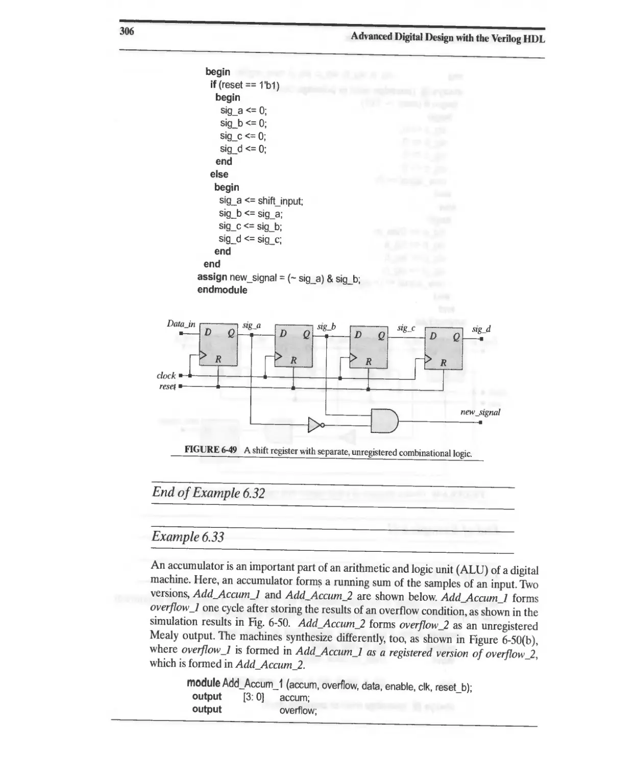
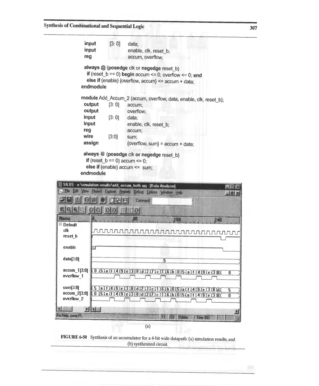
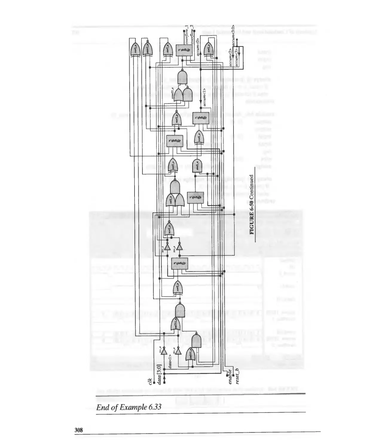
6.9.1 Implicit State Machines 301
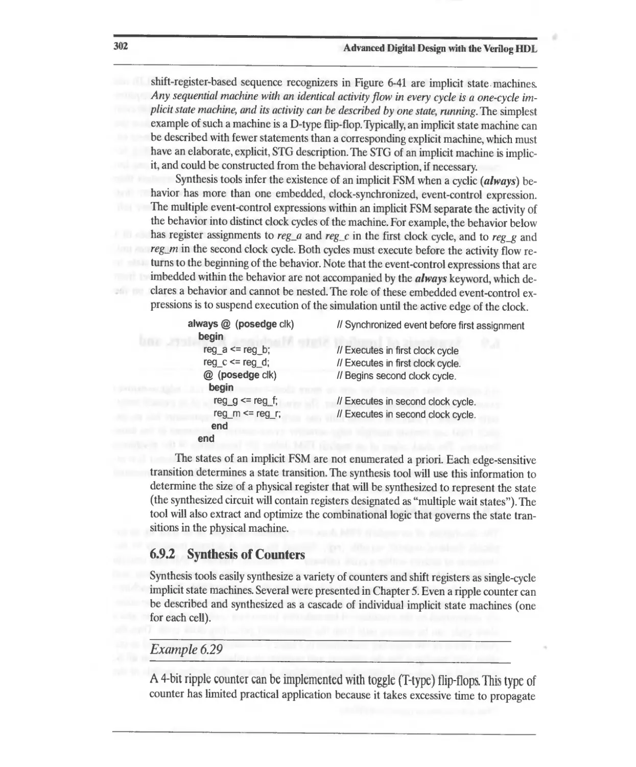
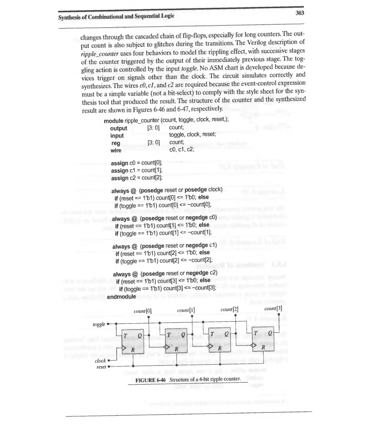
6.9.2 Synthesis of Counters 302
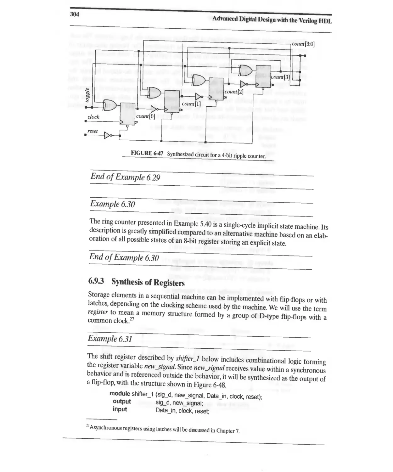
6.9.3 Synthesis of Registers 304
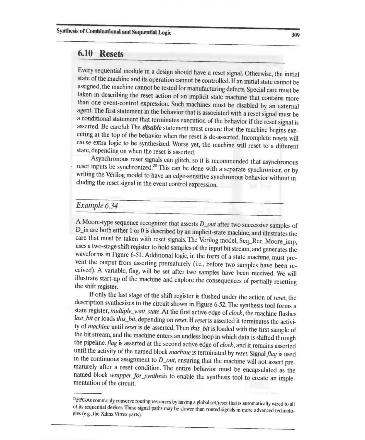
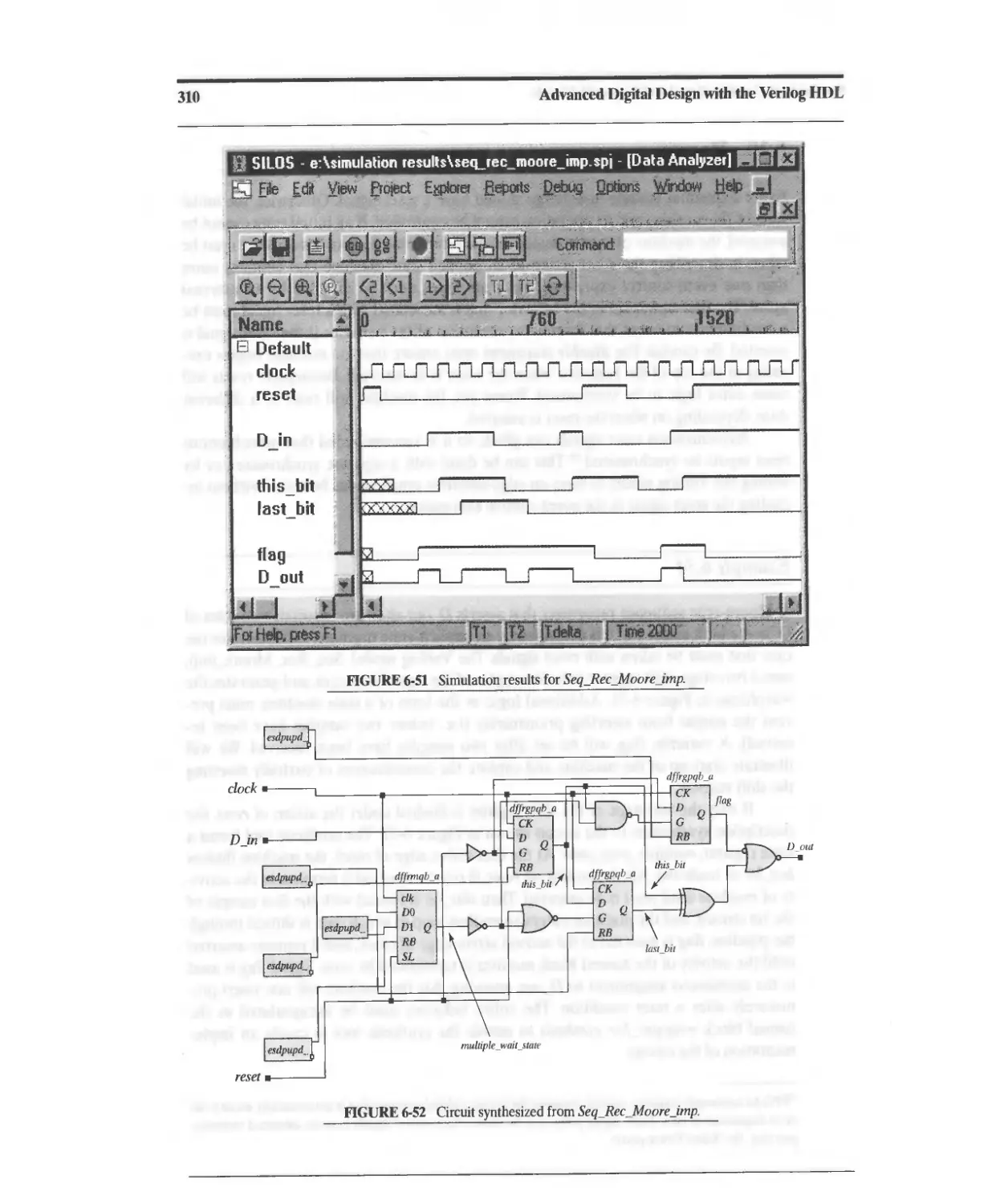
6.1 D Resets 309
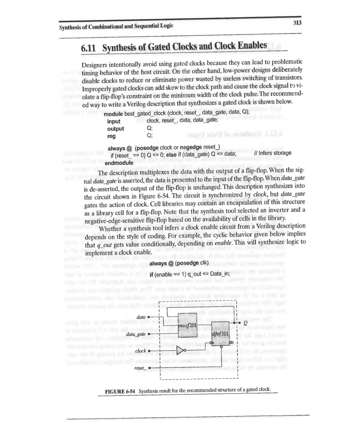
6.11 Synthesis of Gated Clocks and Clock Enables 313
6.12 Anticipating the Results of Synthesis 314
6.12.1 Synthesis of Data Types 314
6.12.2 Operator Grouping 314
6.12.3 Expression Substitution 316
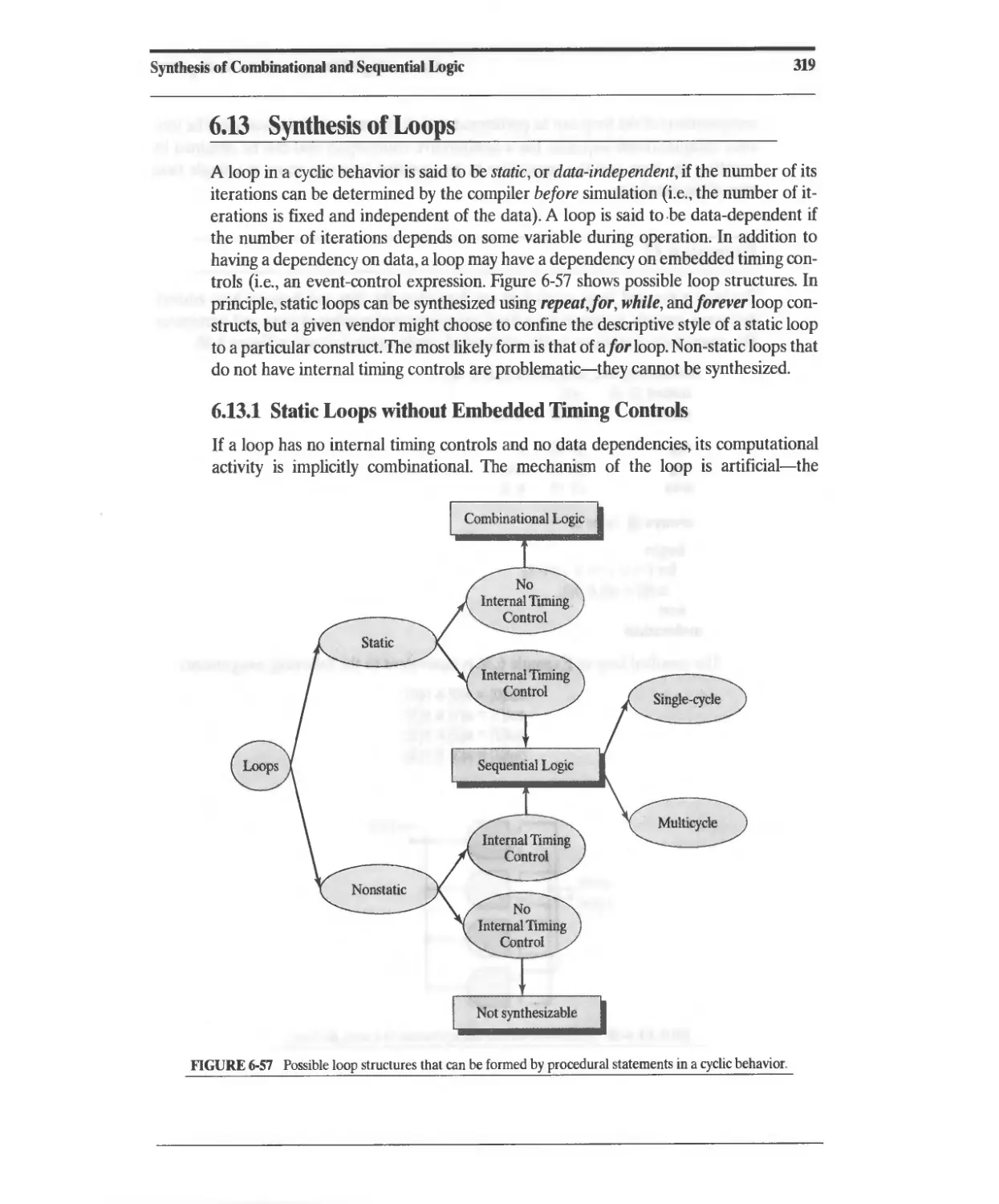
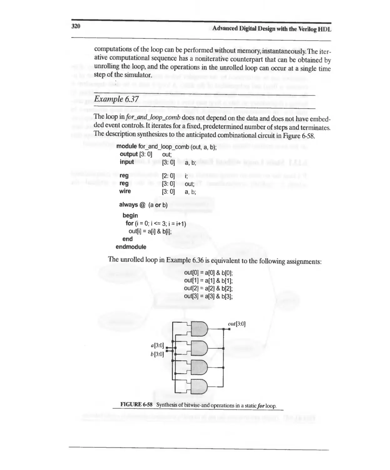
6.13 Synthesis of Loops 319
6.13.1 Static Loops without Embedded Timing Controls 319
6.13.2 Static Loops with Embedded Timing Controls 322
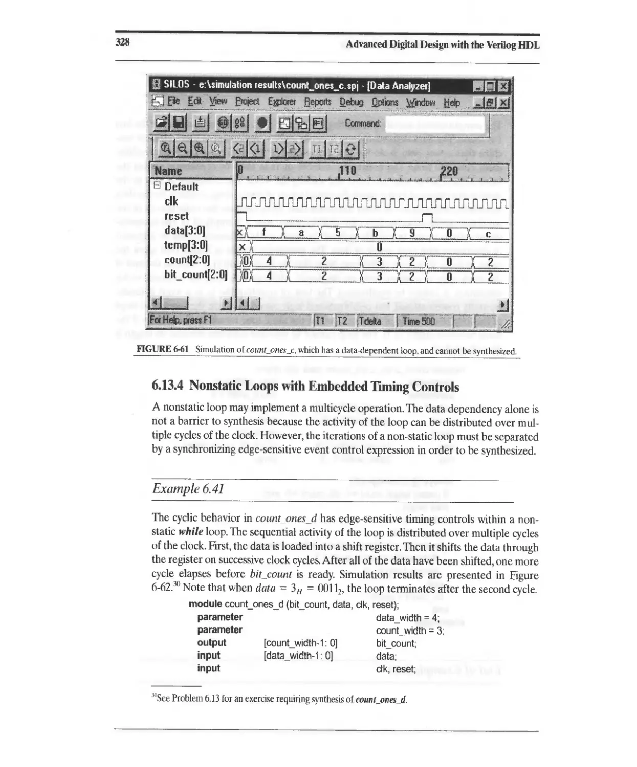
6.13.3 Nonstatic Loops without Embedded Timing Controls 326
6.13.4 Nonstatic Loops with Embedded Timing Controls 328
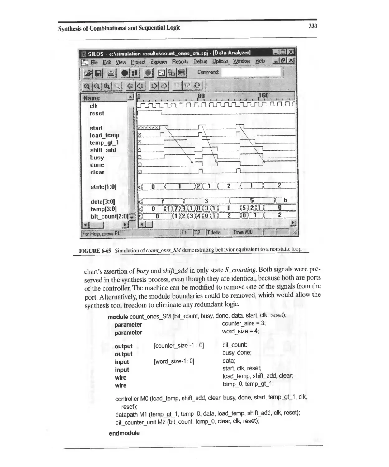
6.13.5 State-Machine Replacements for Unsynthesizable Loops 331
6.14 Design Traps to Avoid 338
6.15 Divide and Conquer: Partitioning a Design 338
References 339
Problems 339
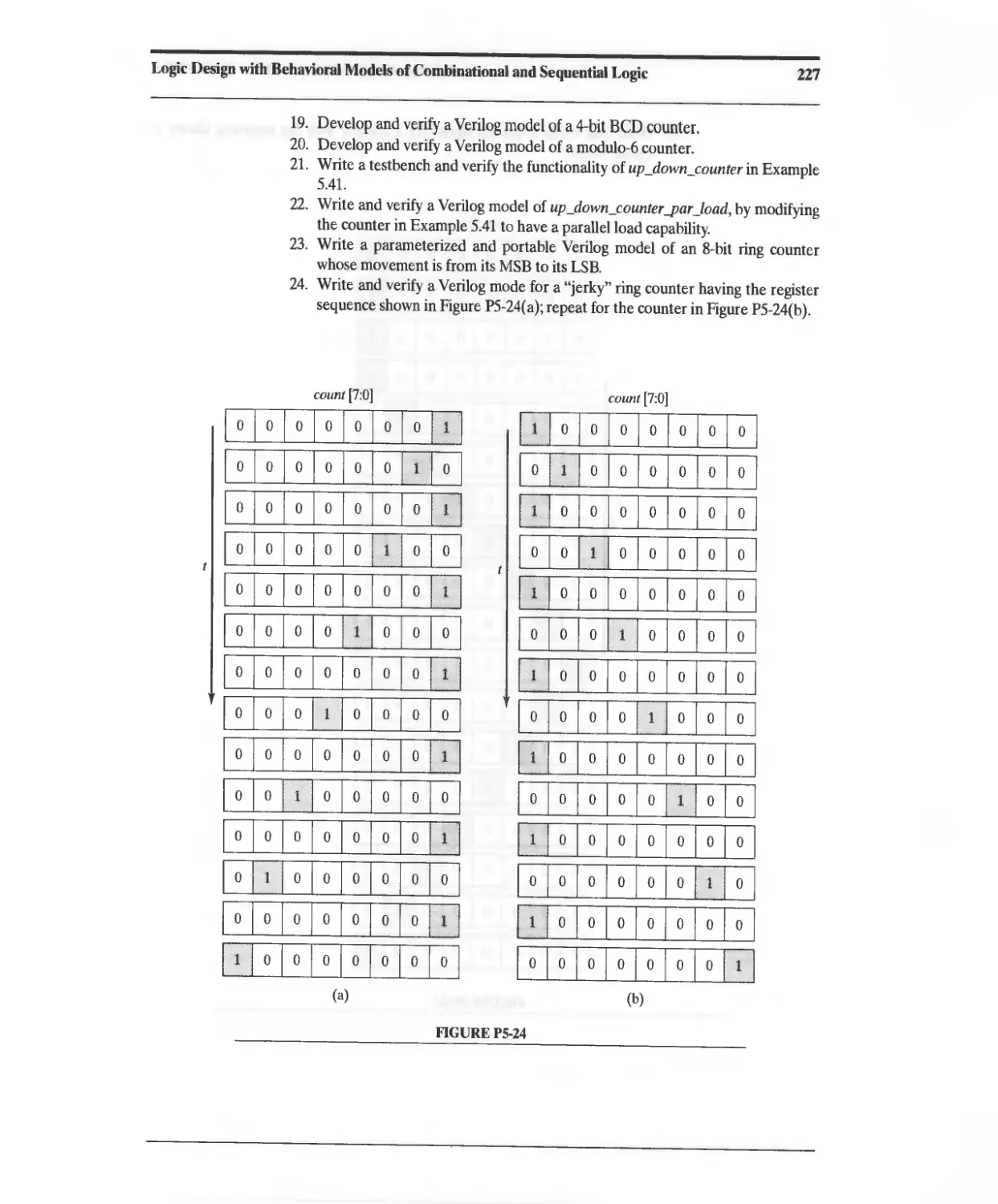
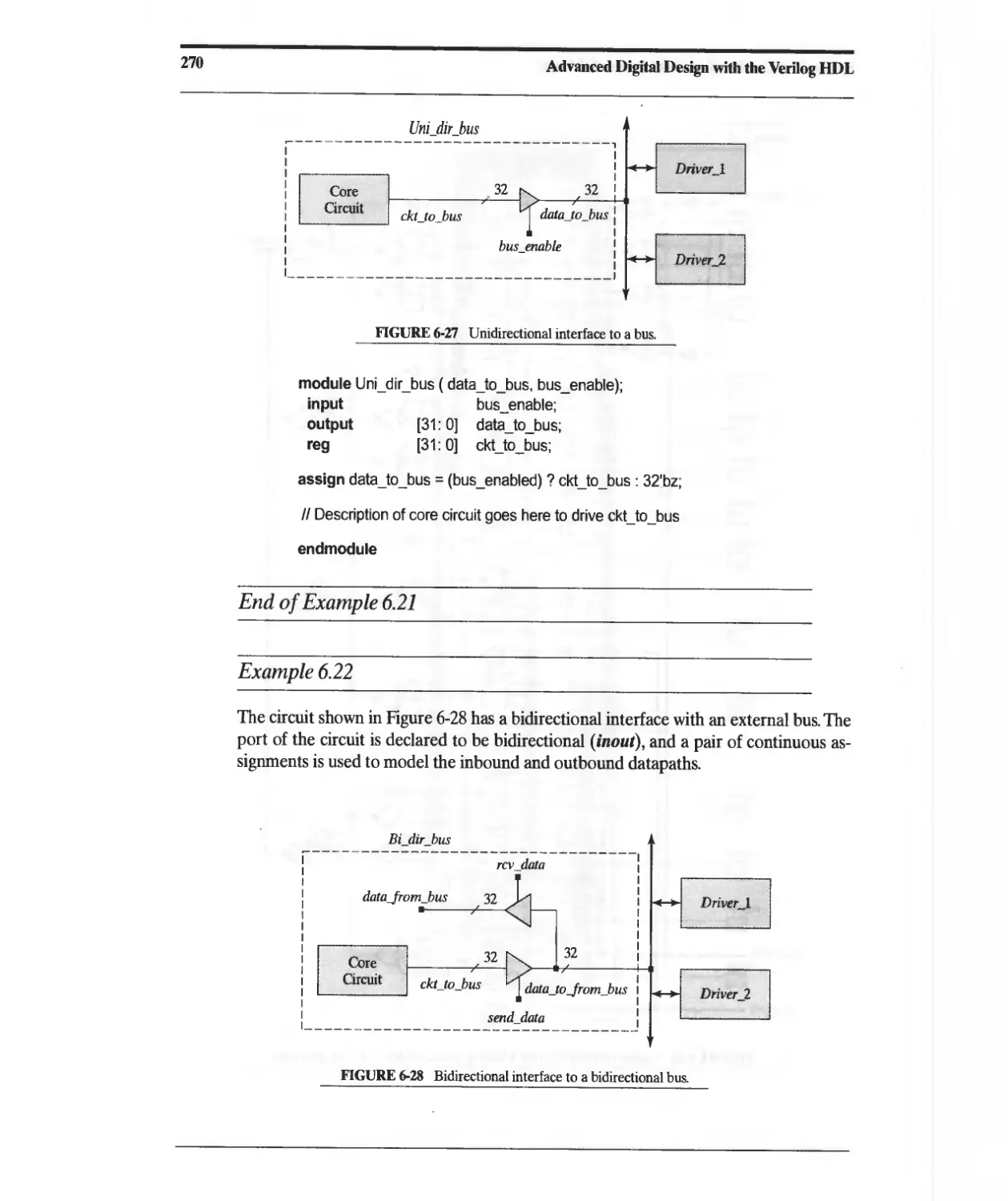
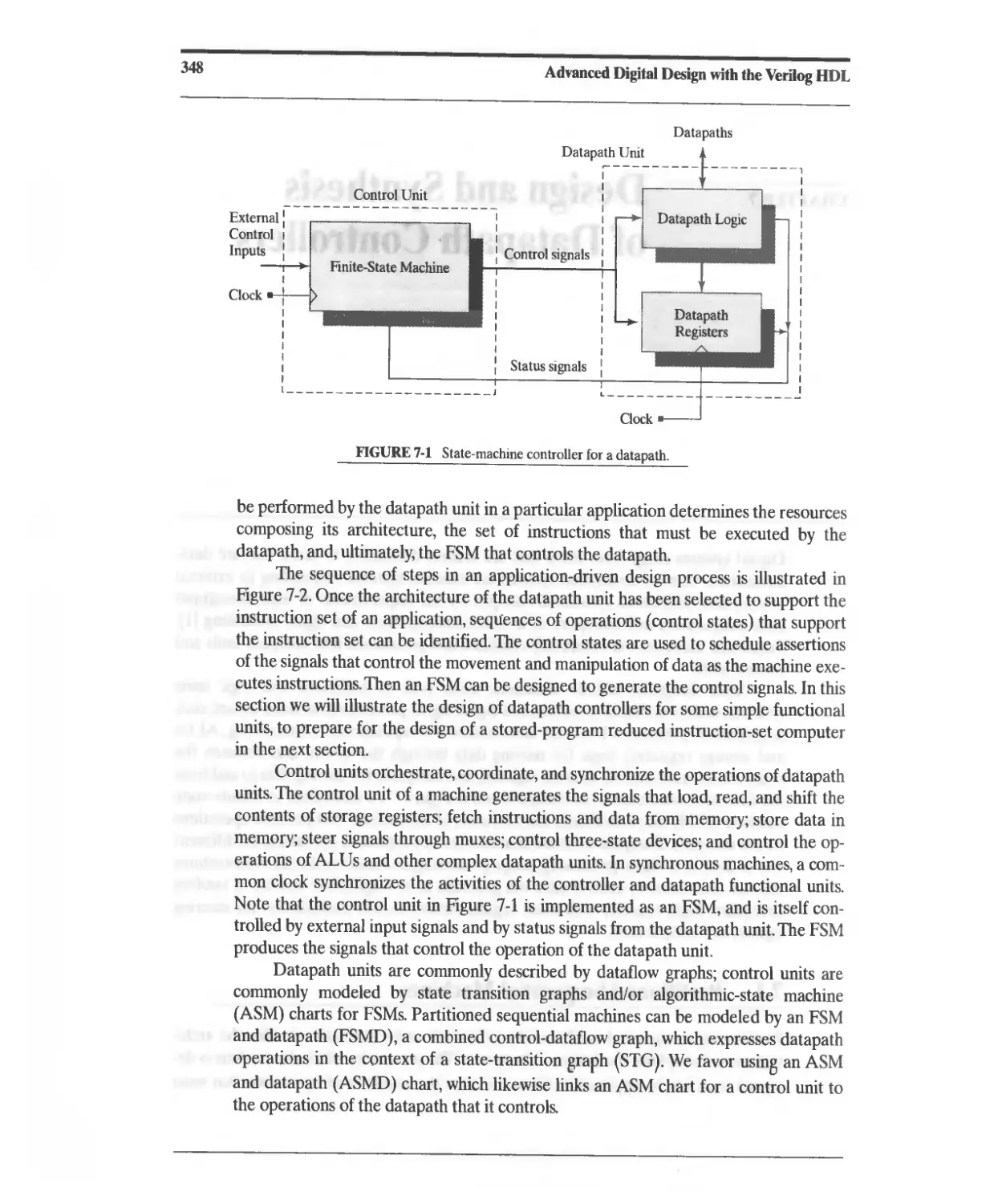
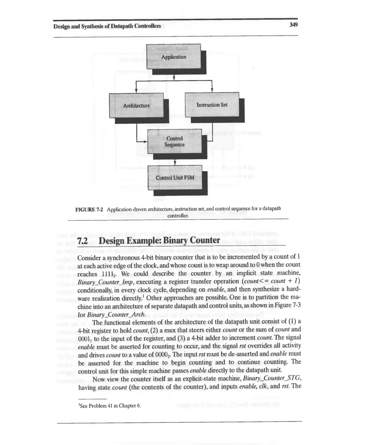
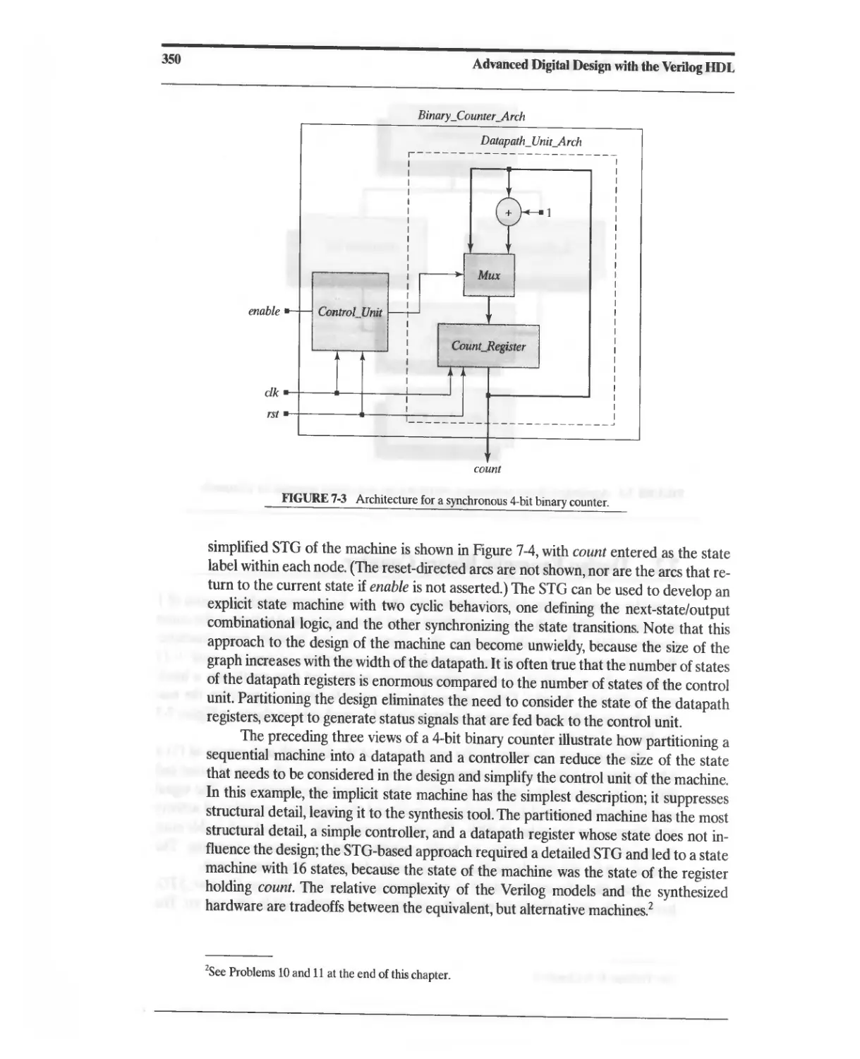
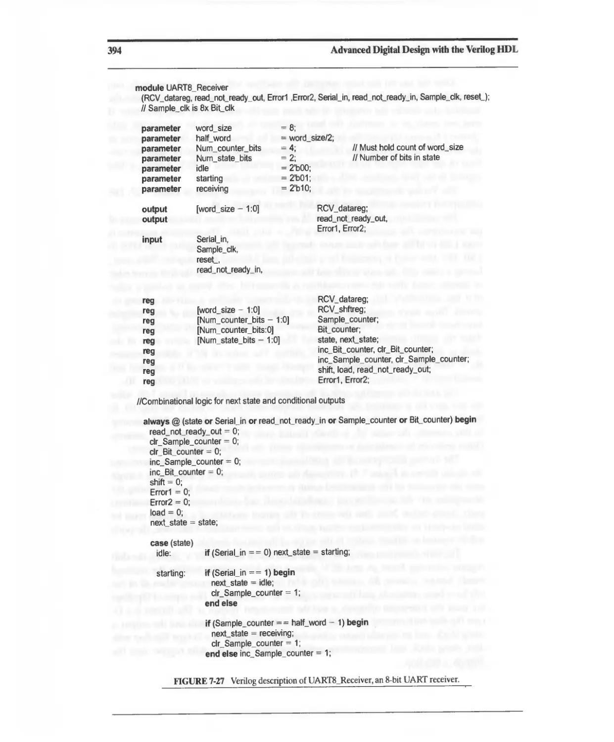
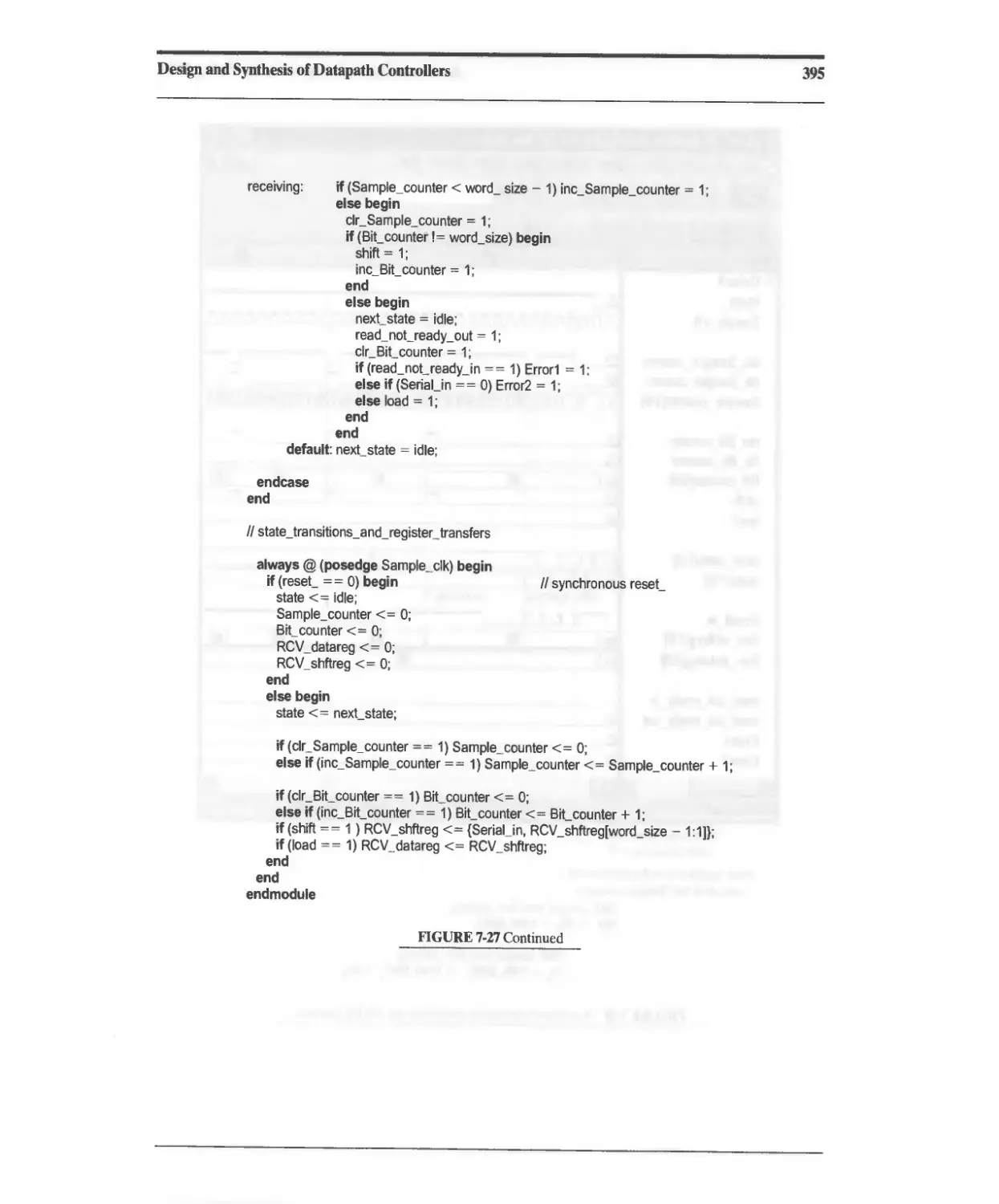
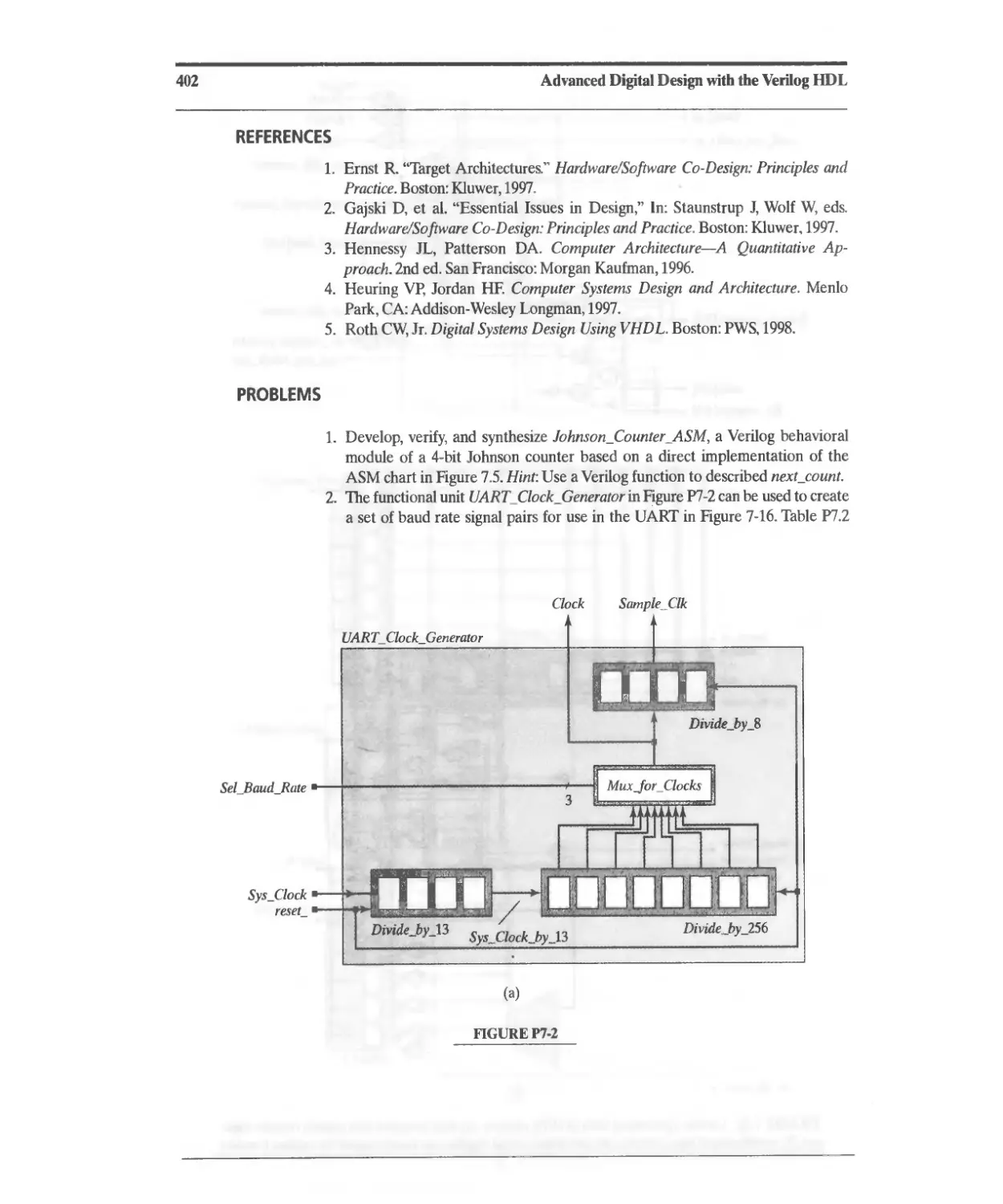
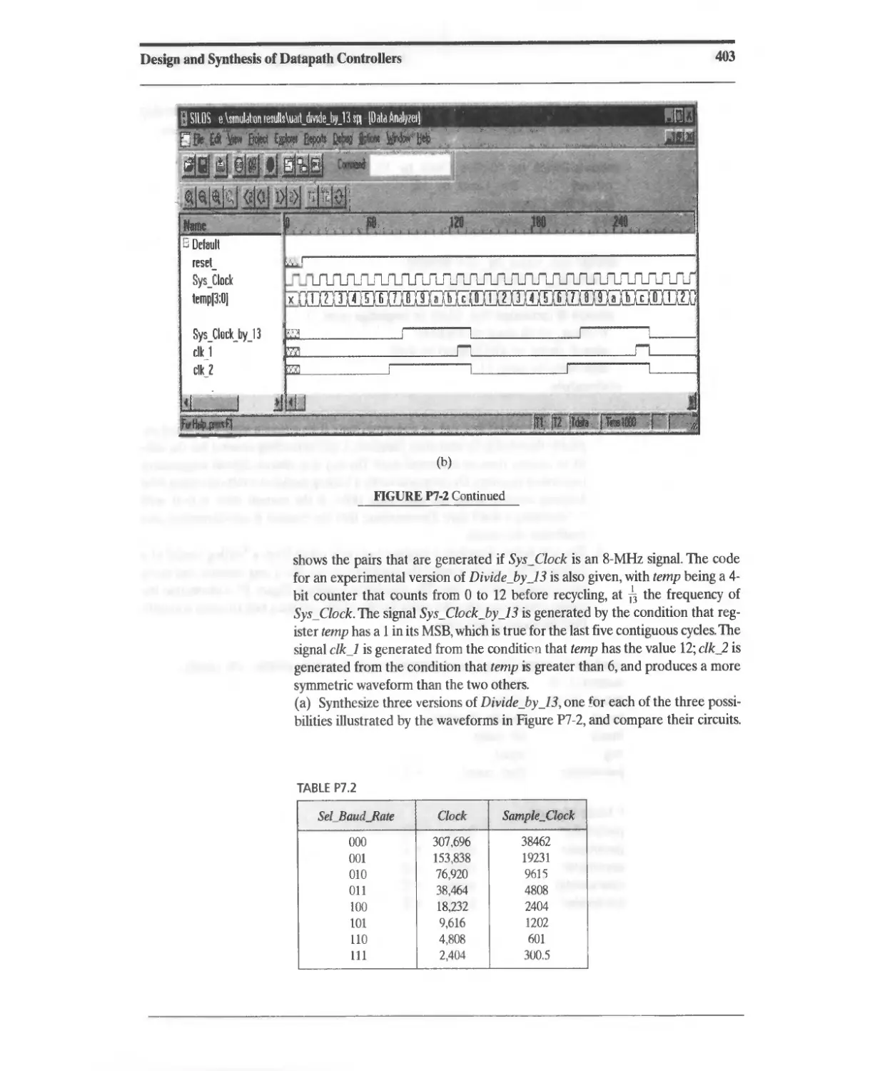
7 Design and Synthesis of Datapath Controllers 347
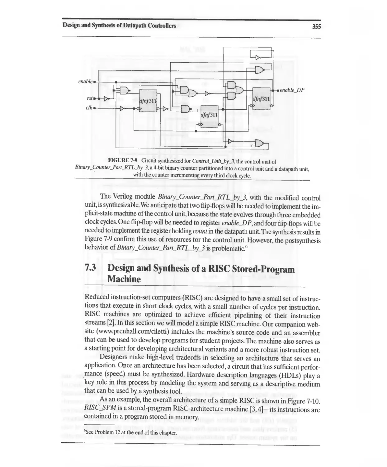
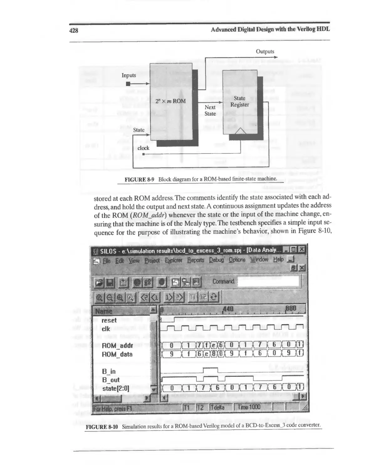
7.1 Partitioned Sequential Machines 347
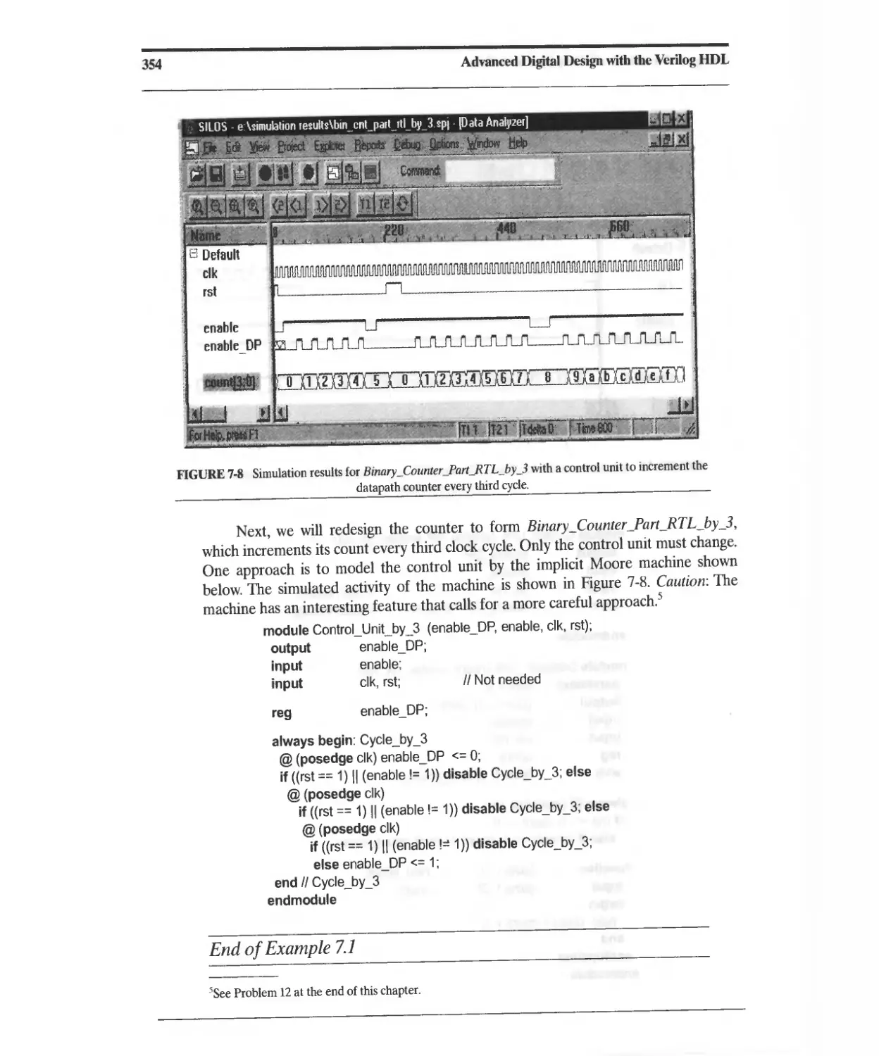
7.2 Design Example: Binary Counter 349
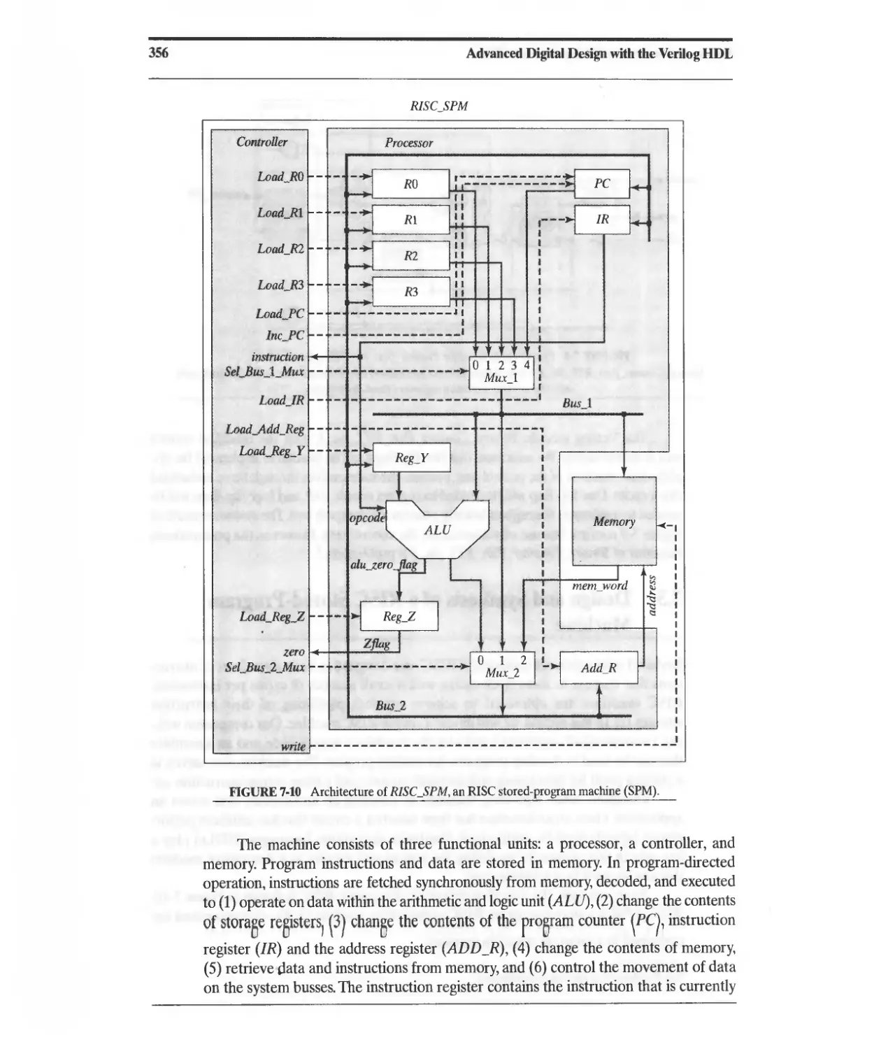
7.3 Design and Synthesis of a RISC Stored-Program Machine 355
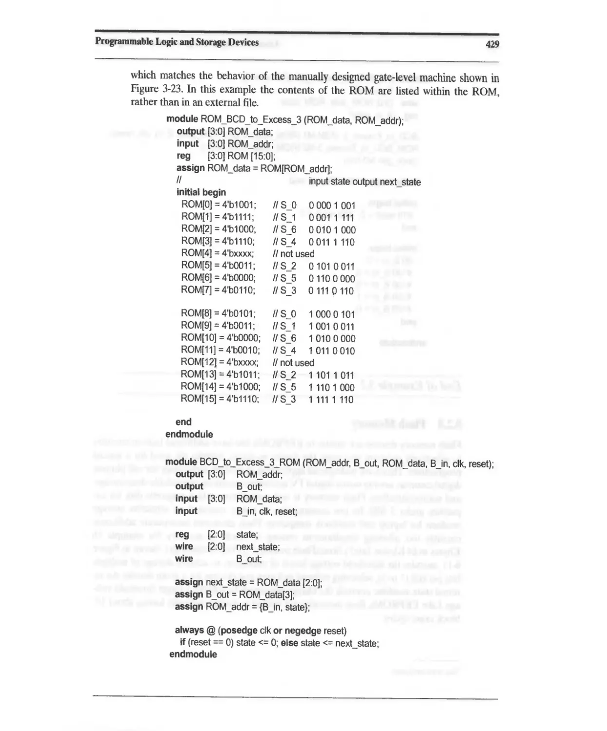
7.3.1 RISC SPM: Processor 357
7.3.2 RISC SPM: ALU 357
7.3.3 RISC SPM: Controller 357
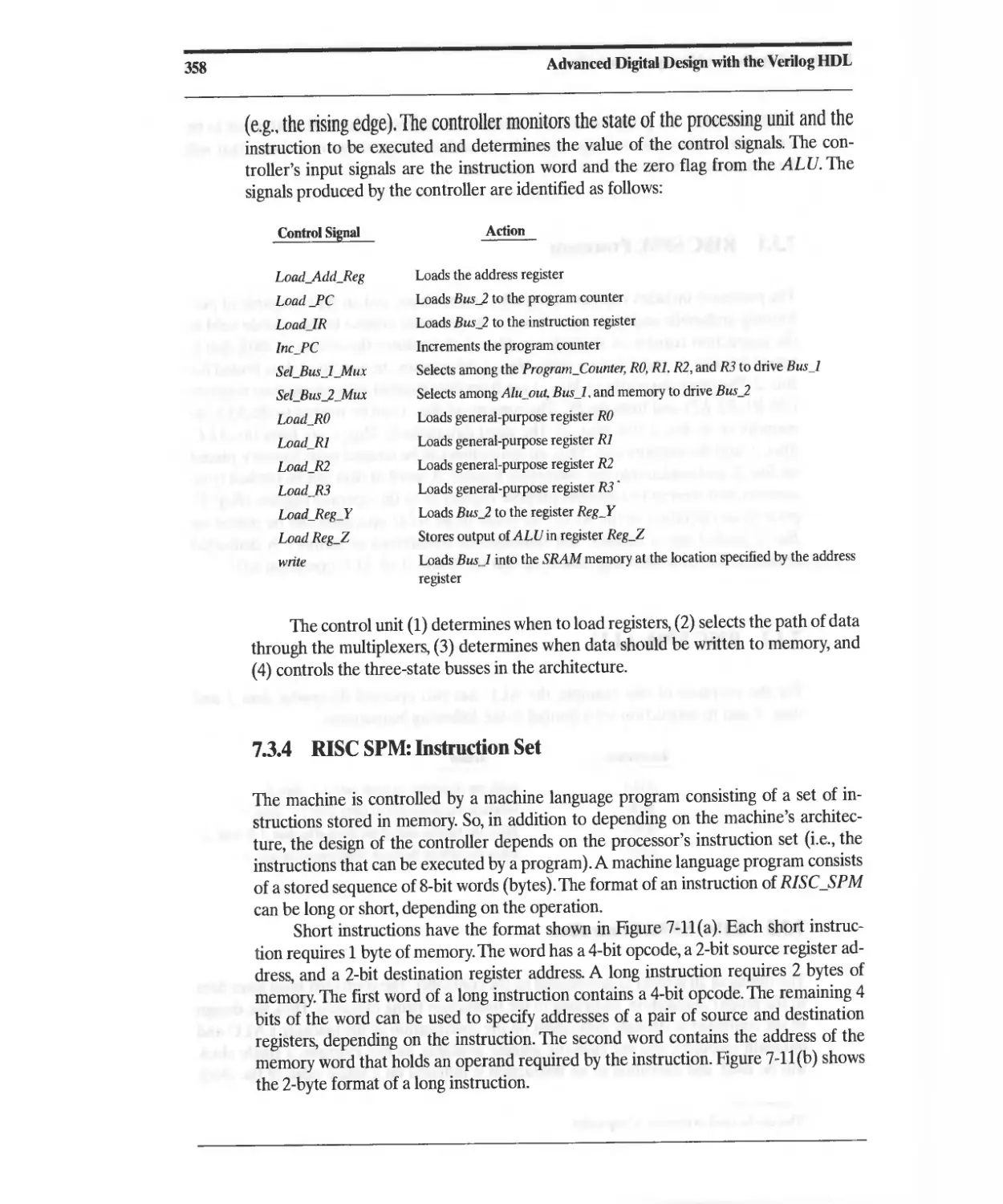
7.3.4 RISC SPM: Instruction Set 358
7.3.5 RISC SPM: Controller Design 360
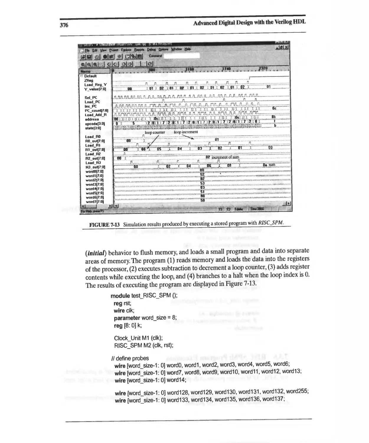
7.3.6 RISC SPM: Program Execution 375
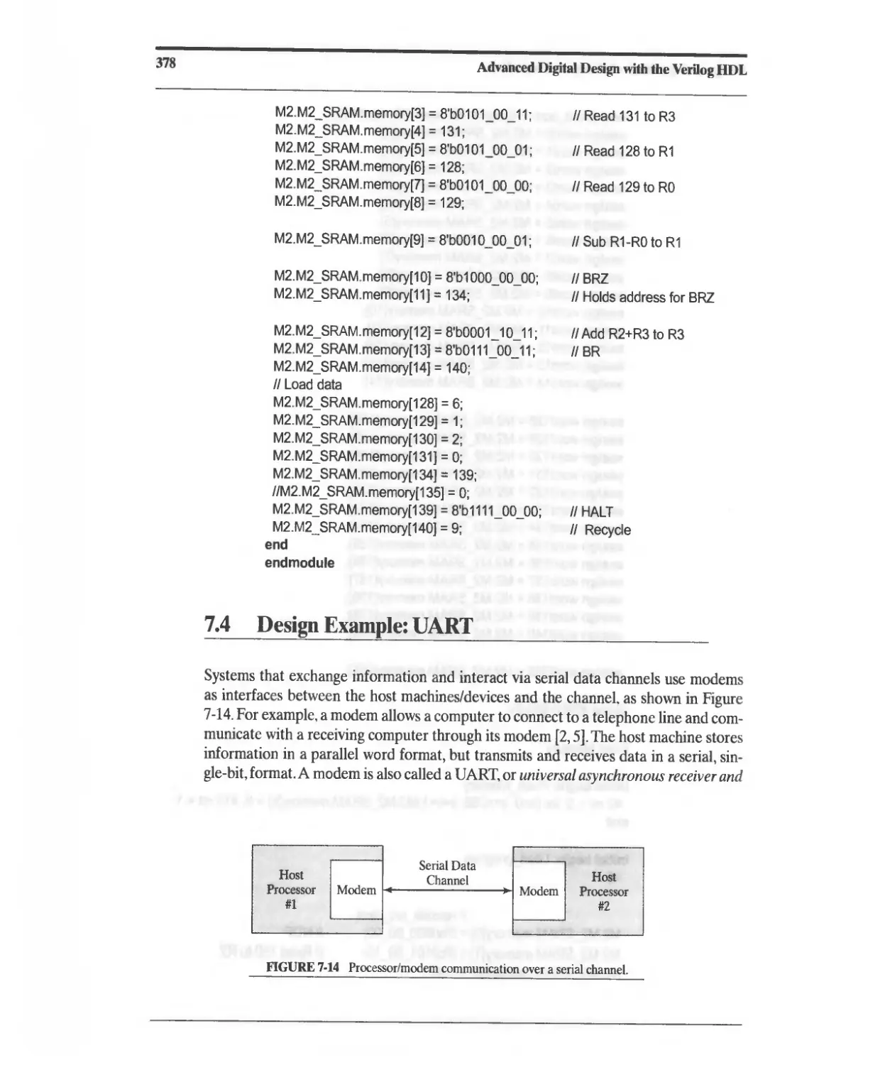
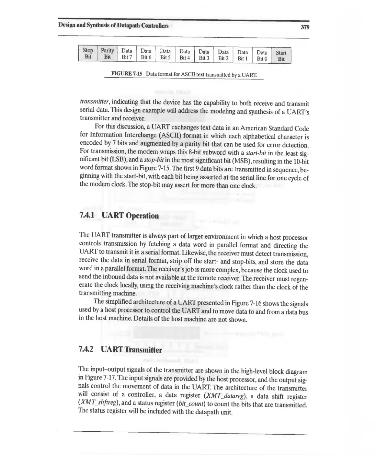
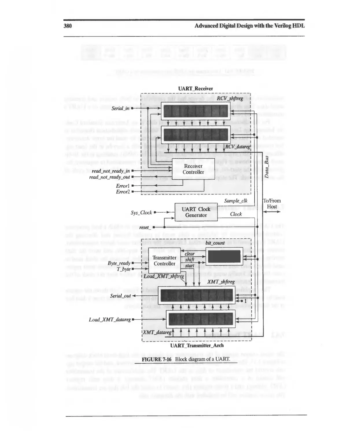
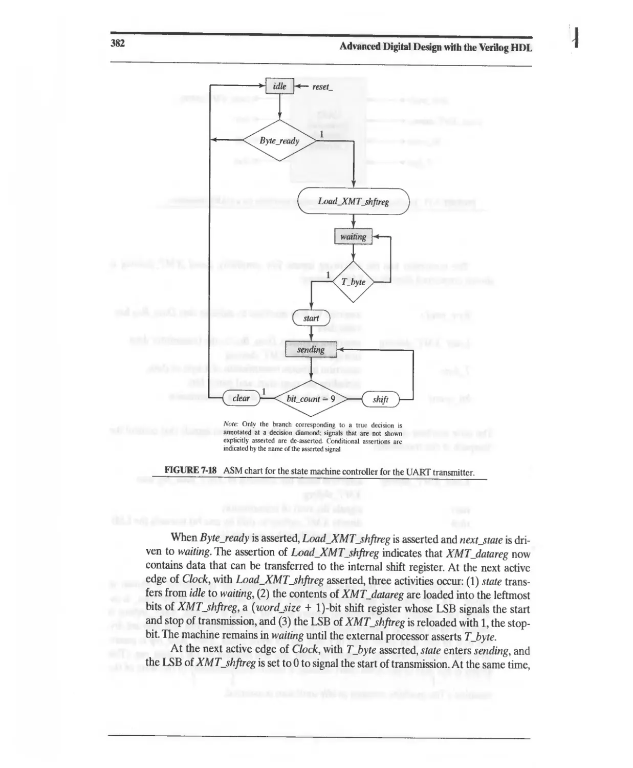
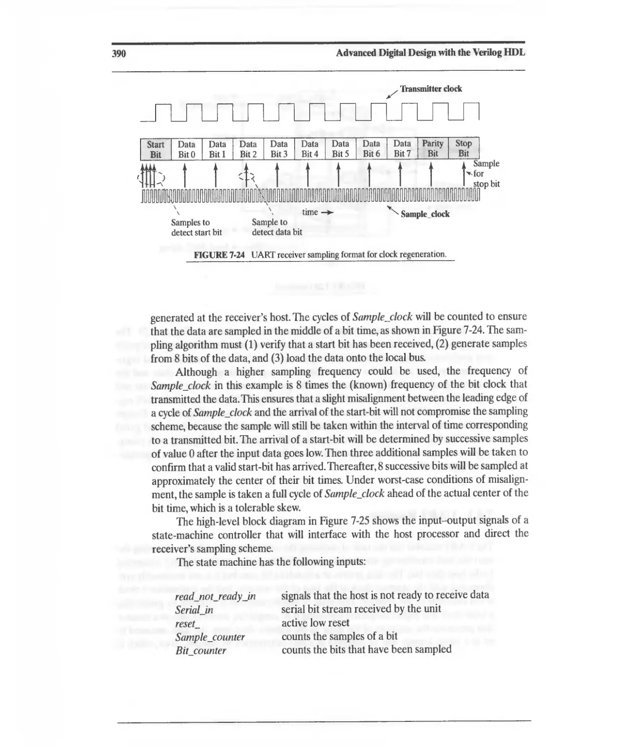
7.4 Design Example: UART 378
7.4.1 UART Operation 379
x
Contents
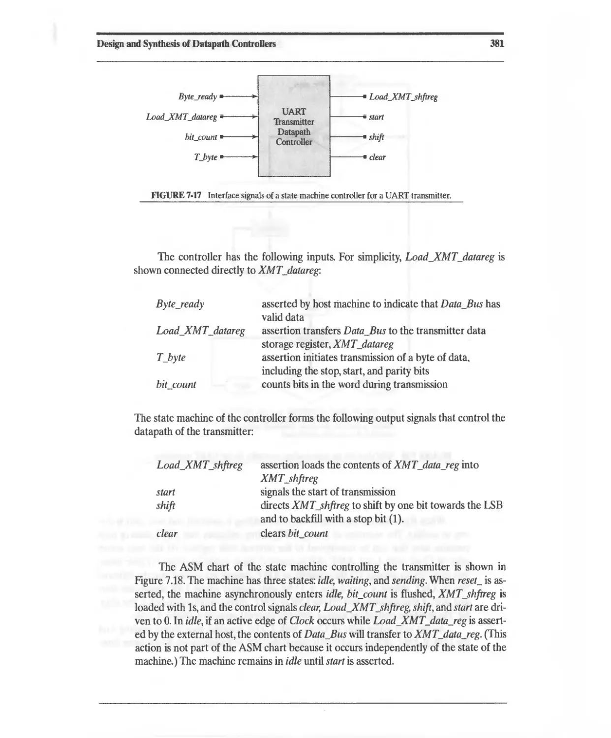
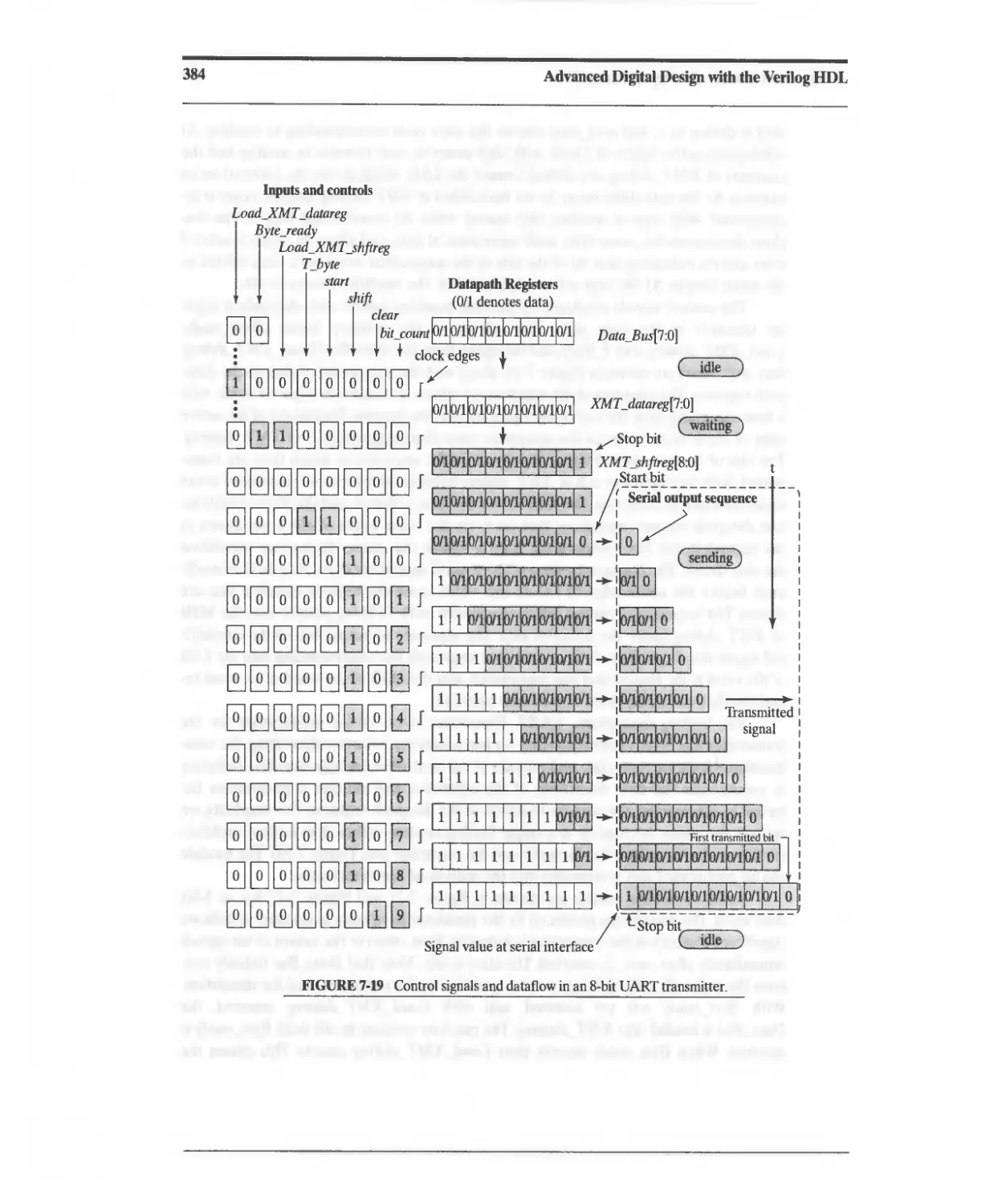
7.4.2 DART Transmitter 379
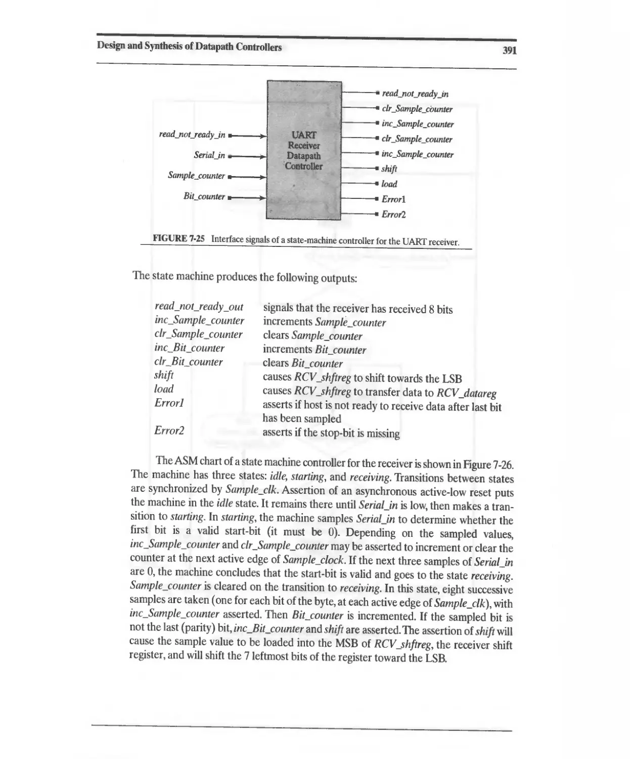
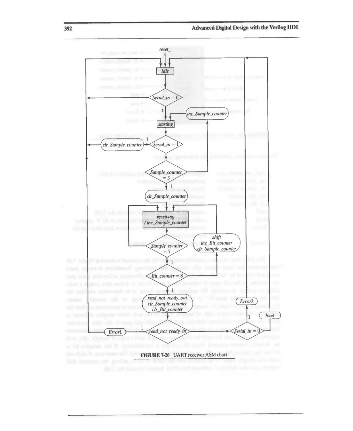
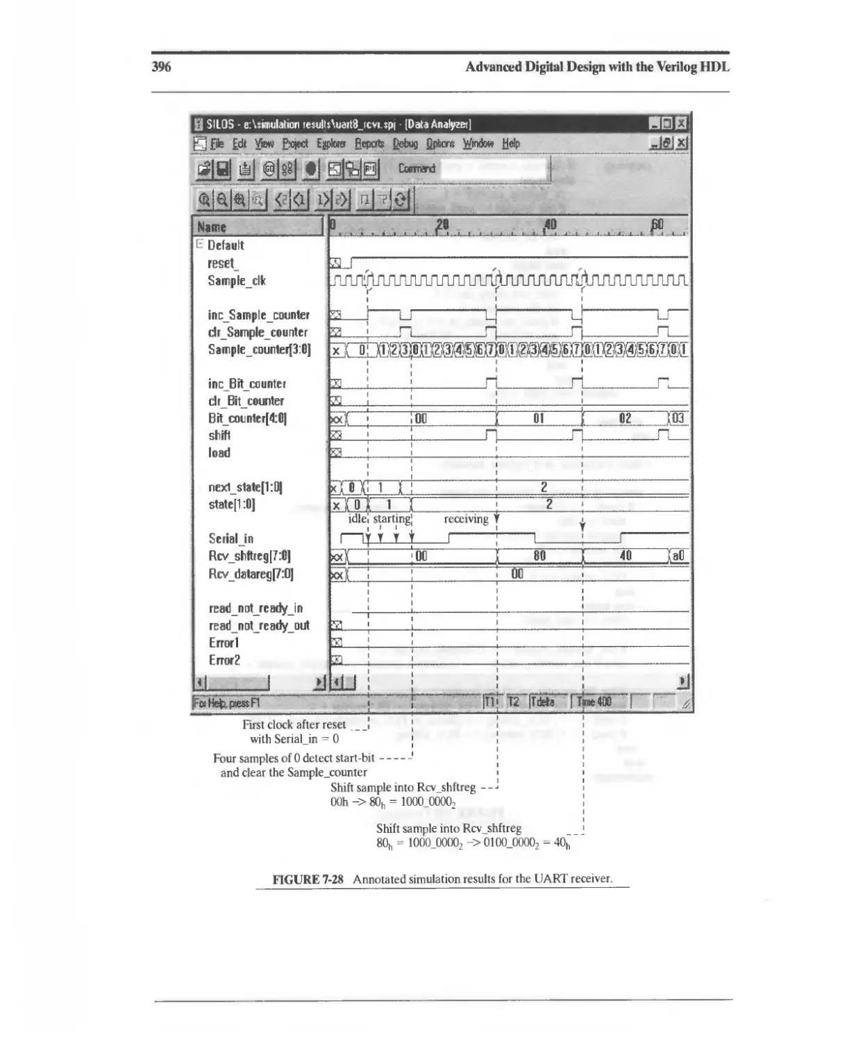
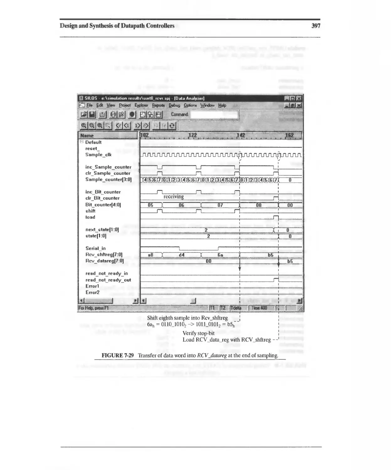
7.4.3 DART Receiver 389
References 402
Problems 402
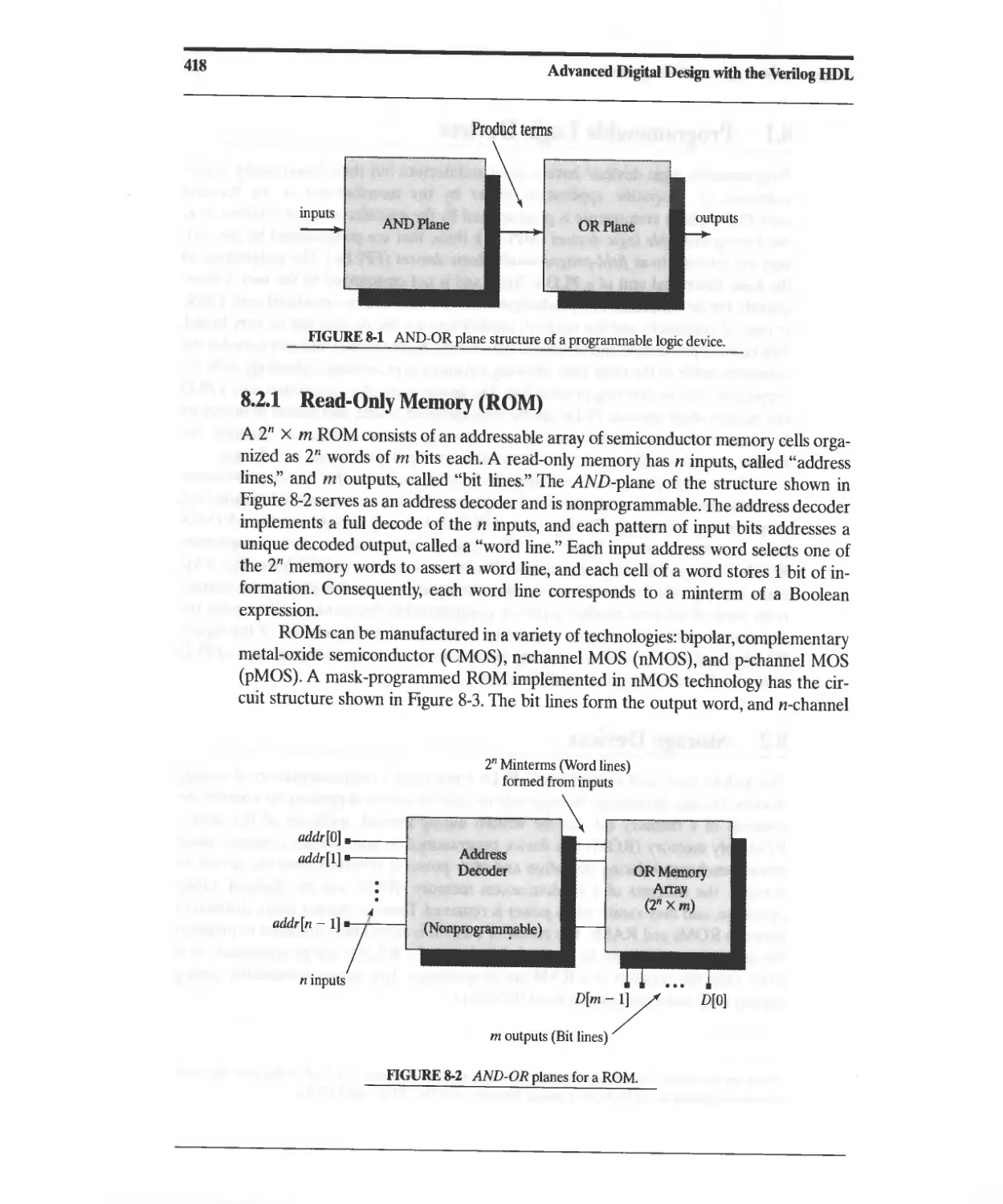
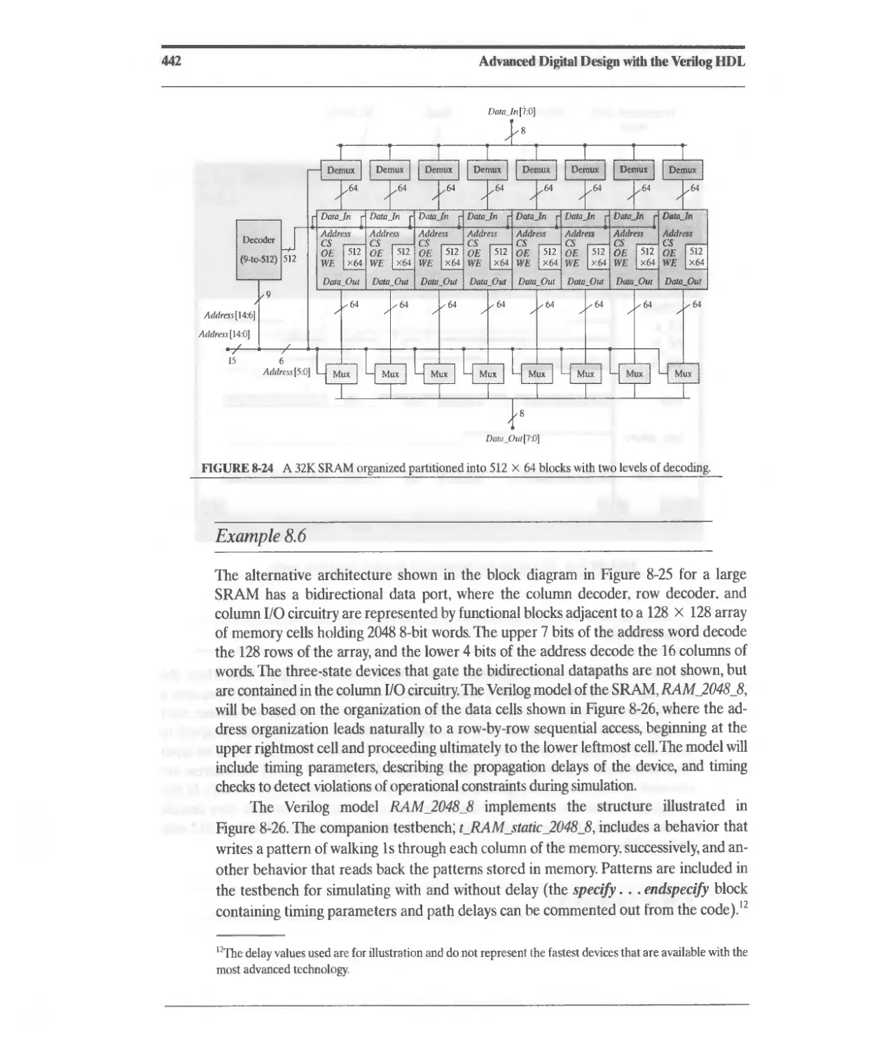
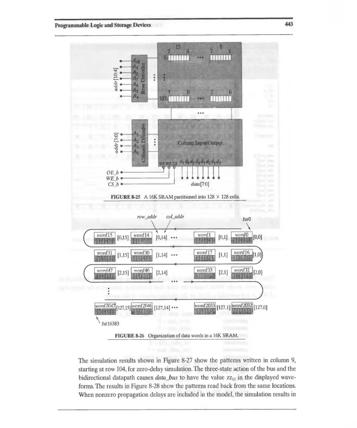
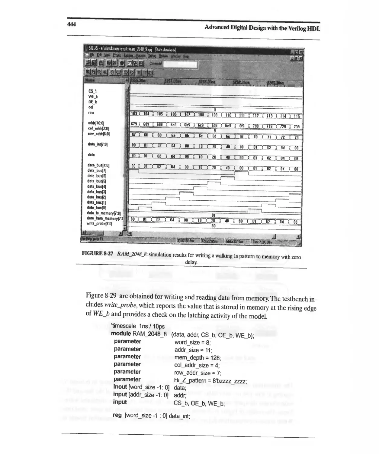
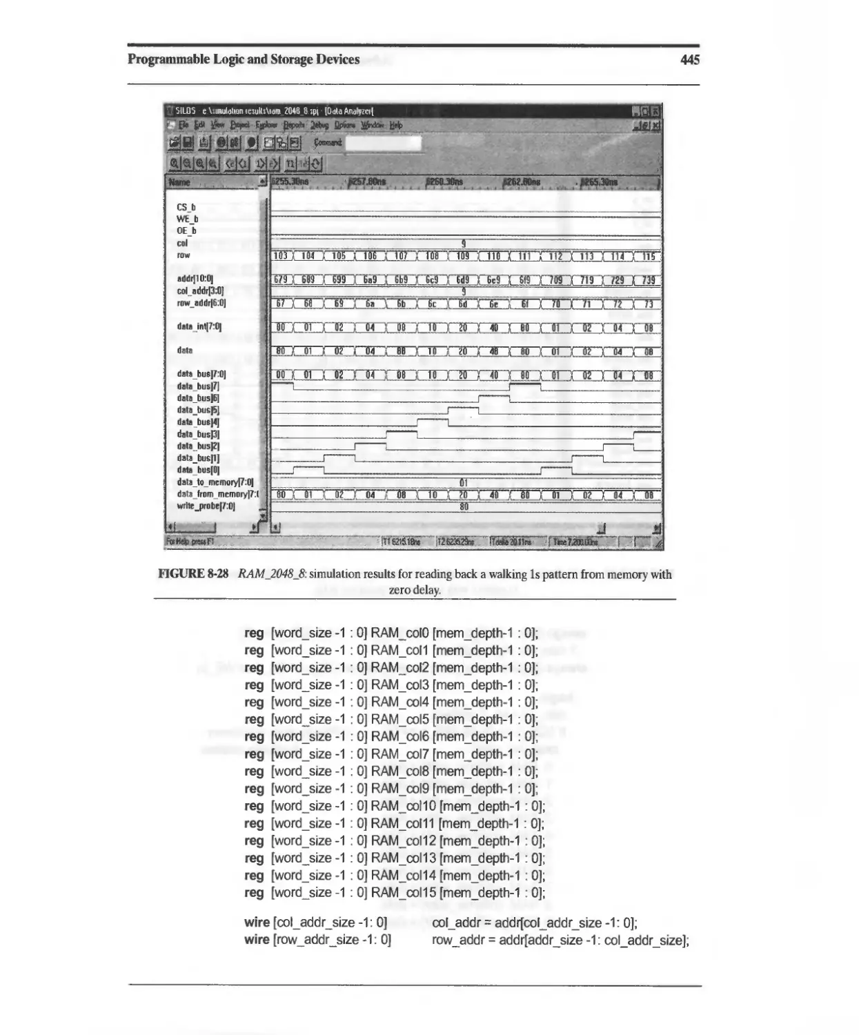
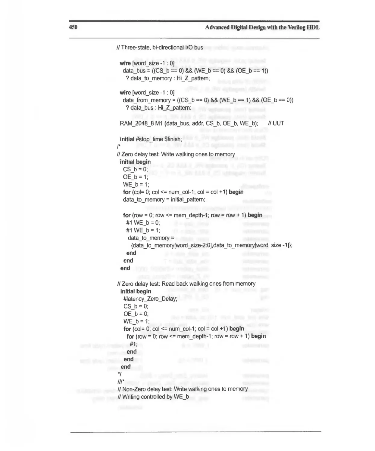
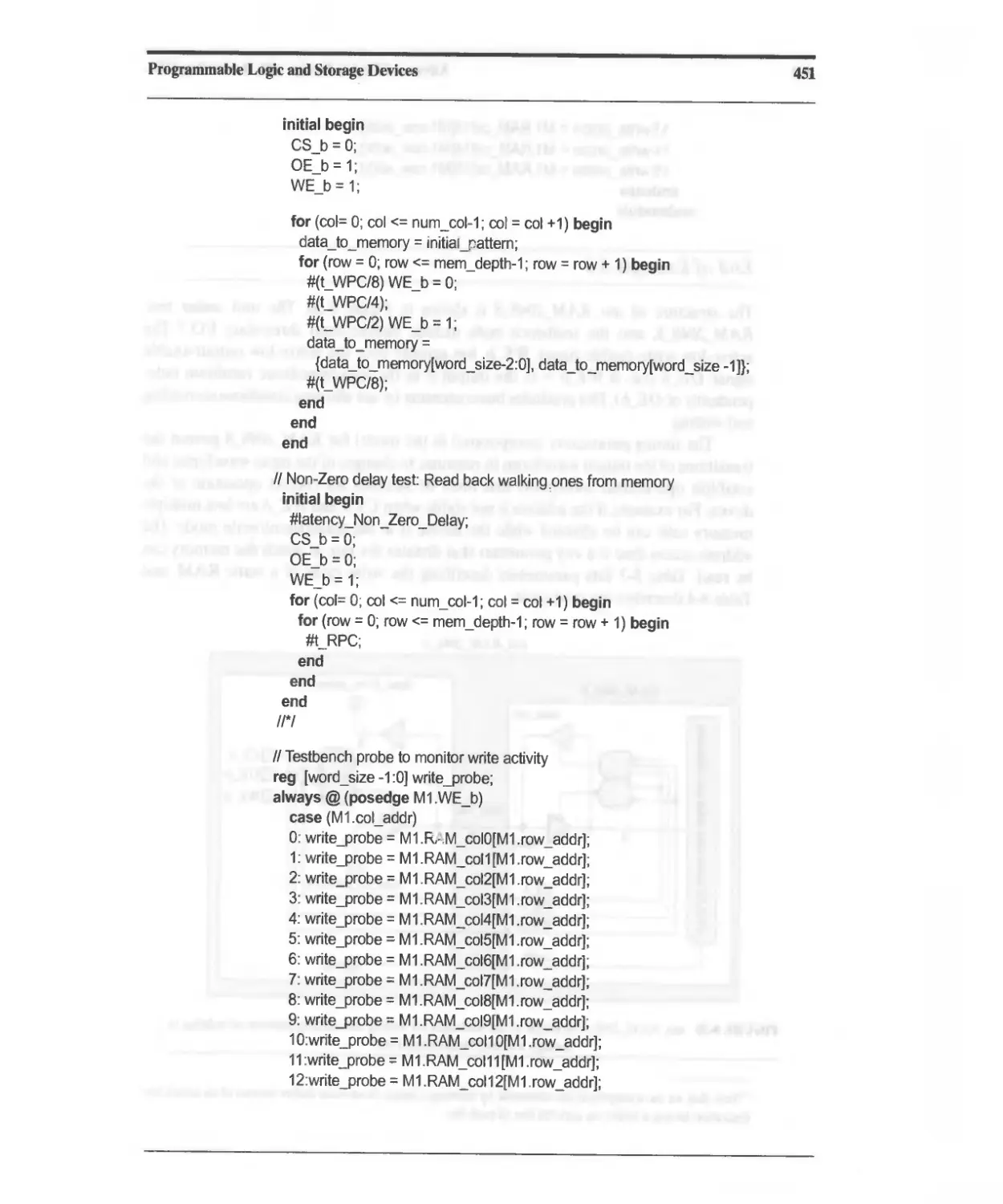
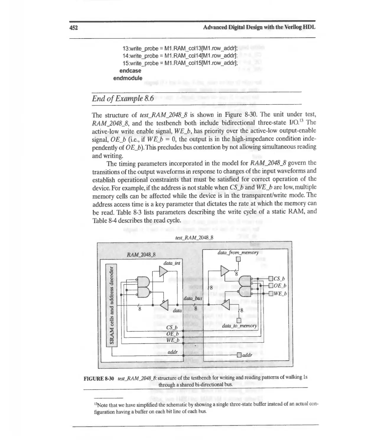
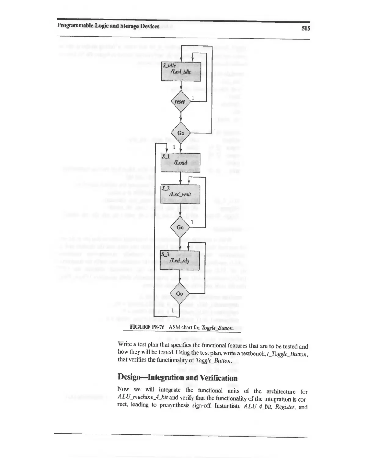
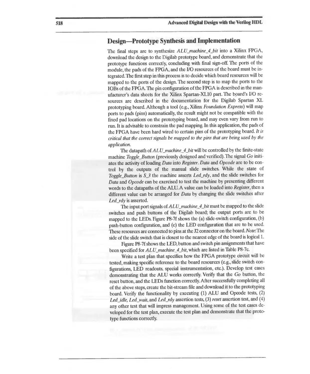
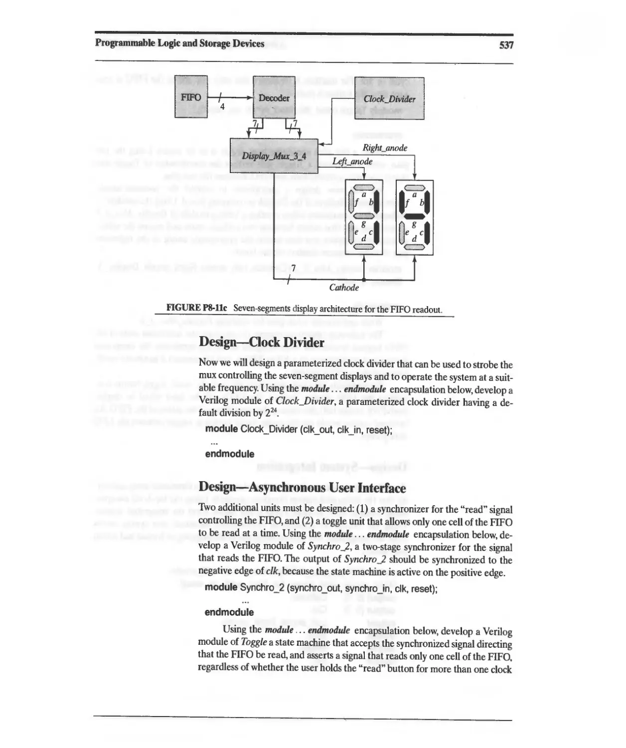
8 Programmable Logic and Storage Devices 415
8.1 Programmable Logic Devices 417
8.2 Storage Devices 417
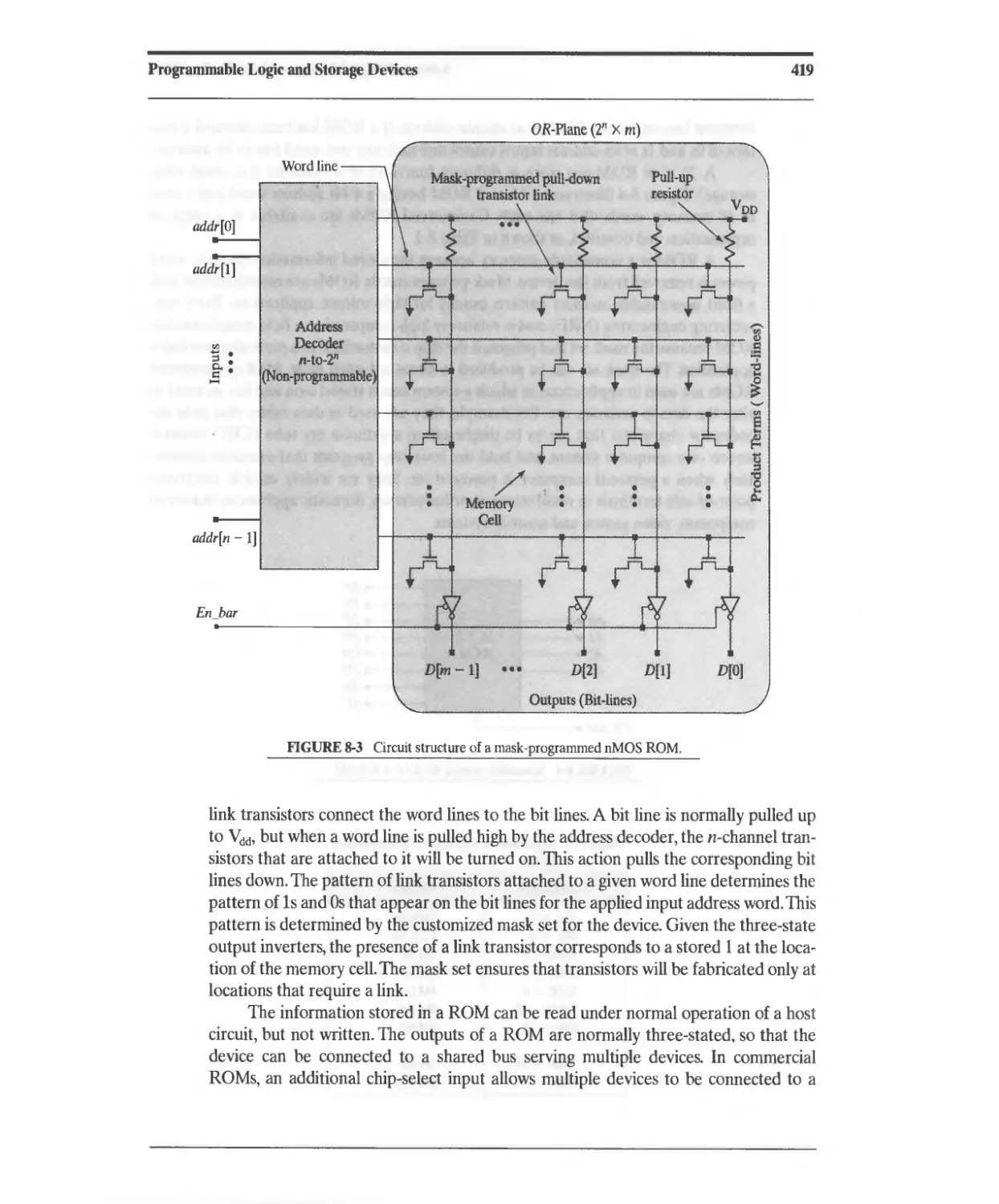
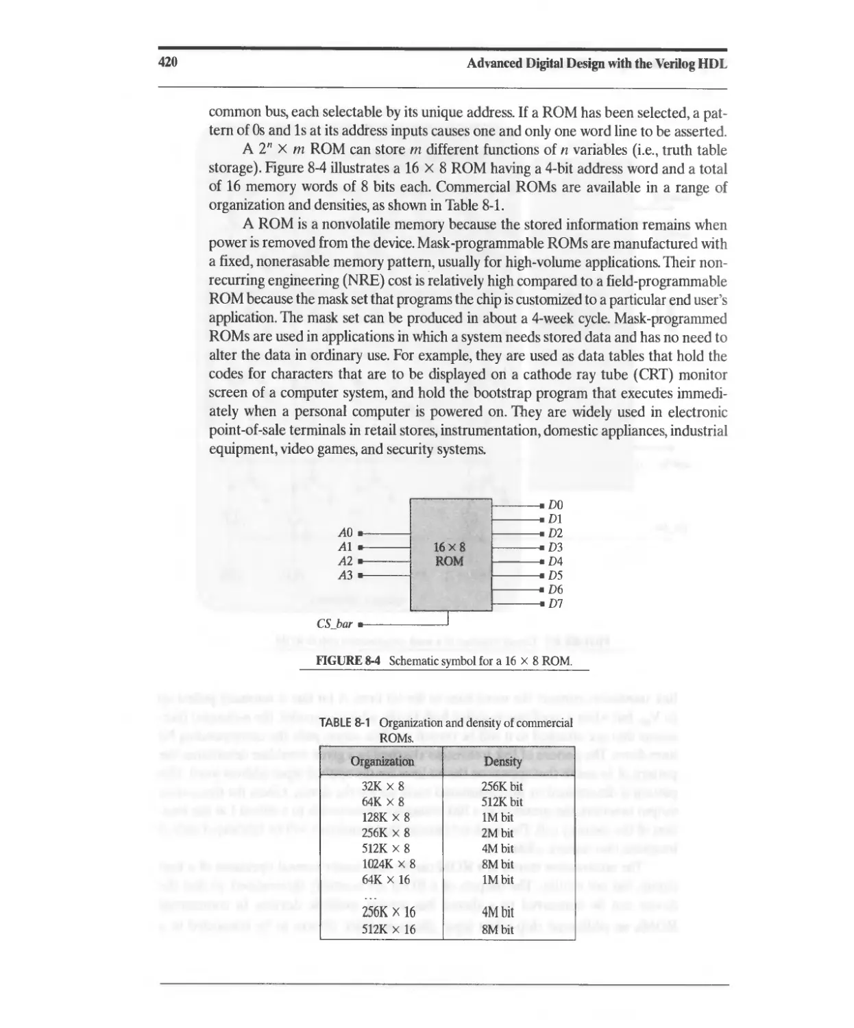
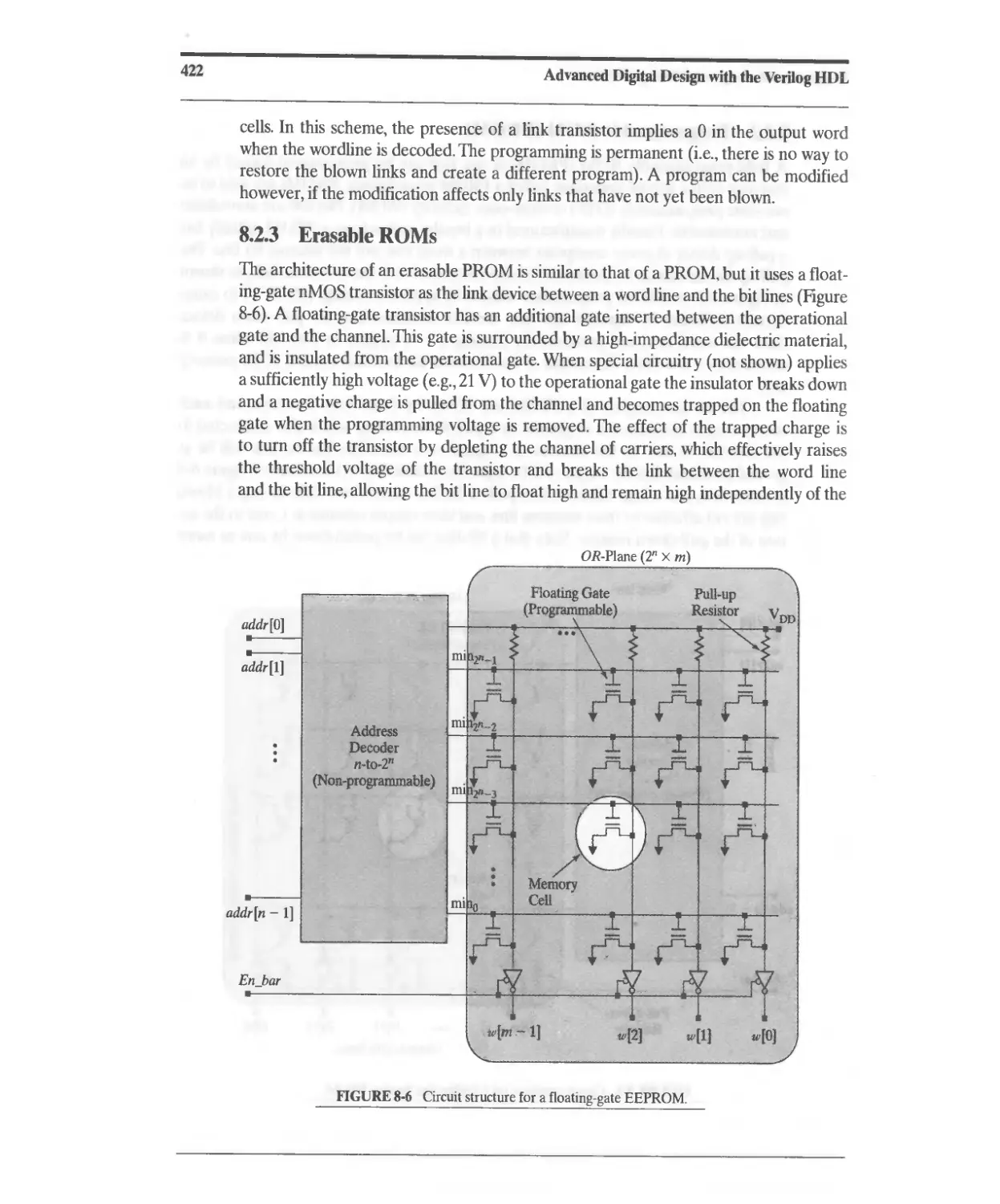
8.2.1 Read-Only Memory (ROM) 418
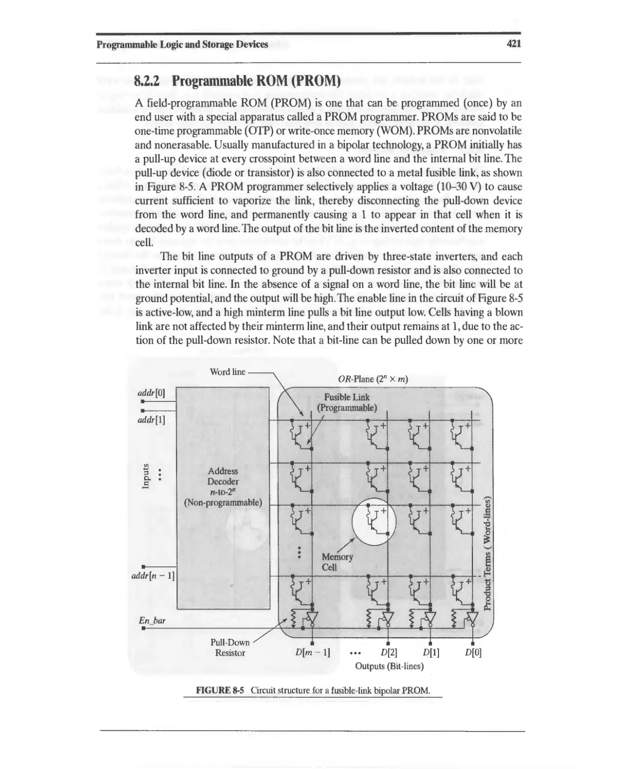
8.2.2 Programmable ROM (PROM) 421
8.2.3 Erasable ROMs 422
8.2.4 ROM-Based Implementation of Combinational Logic 423
8.2.5 Verilog System Tasks for ROMs. 424
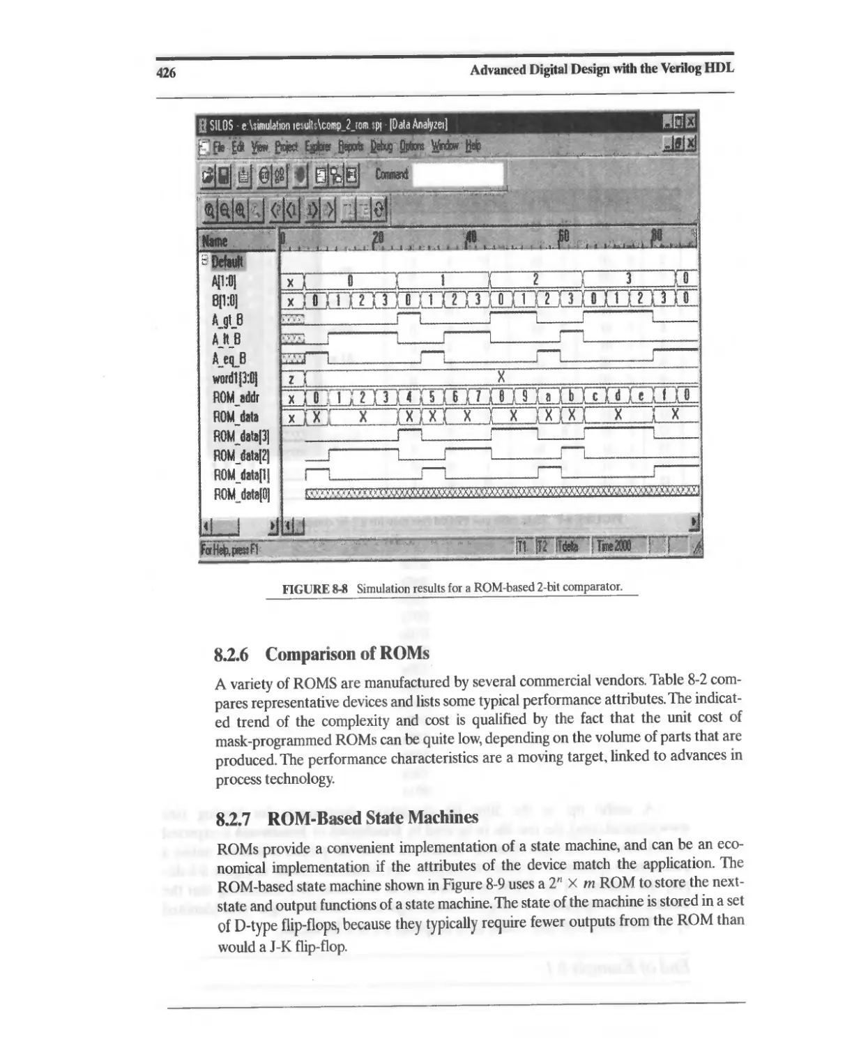
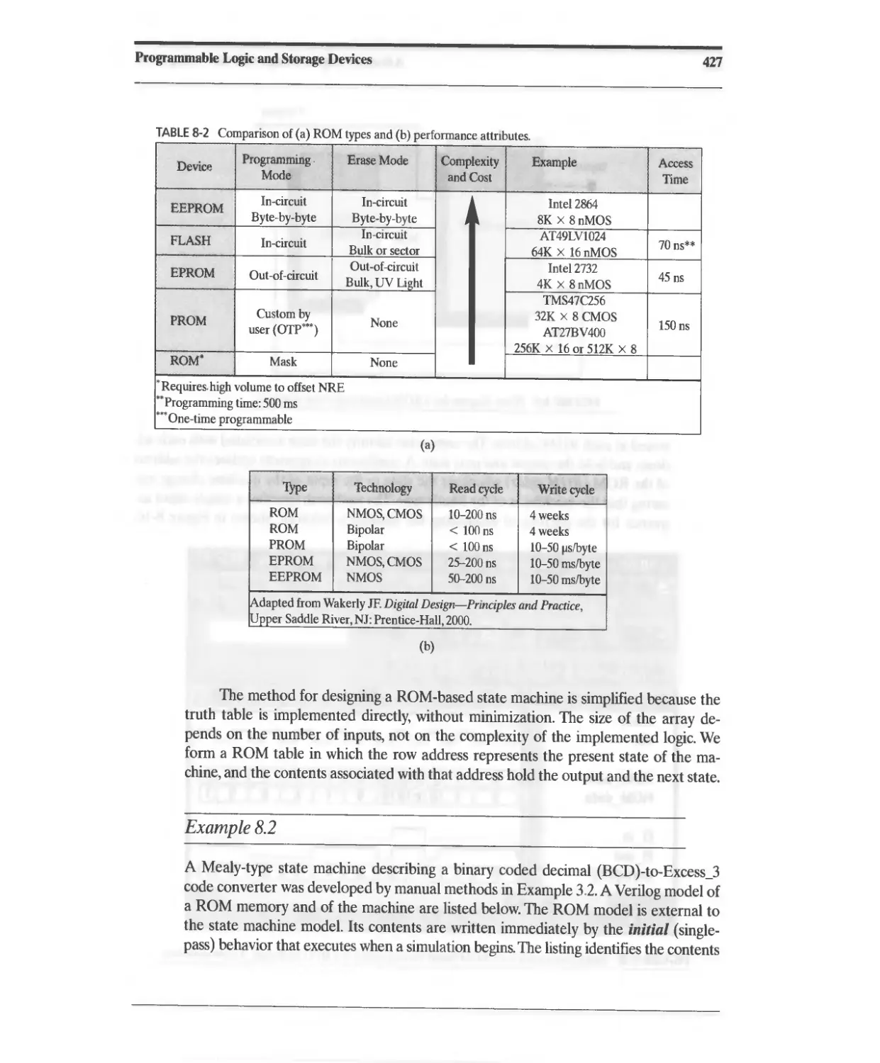
8.2.6 Comparison of ROMs 426
8.2.7 ROM-Based State Machines 426
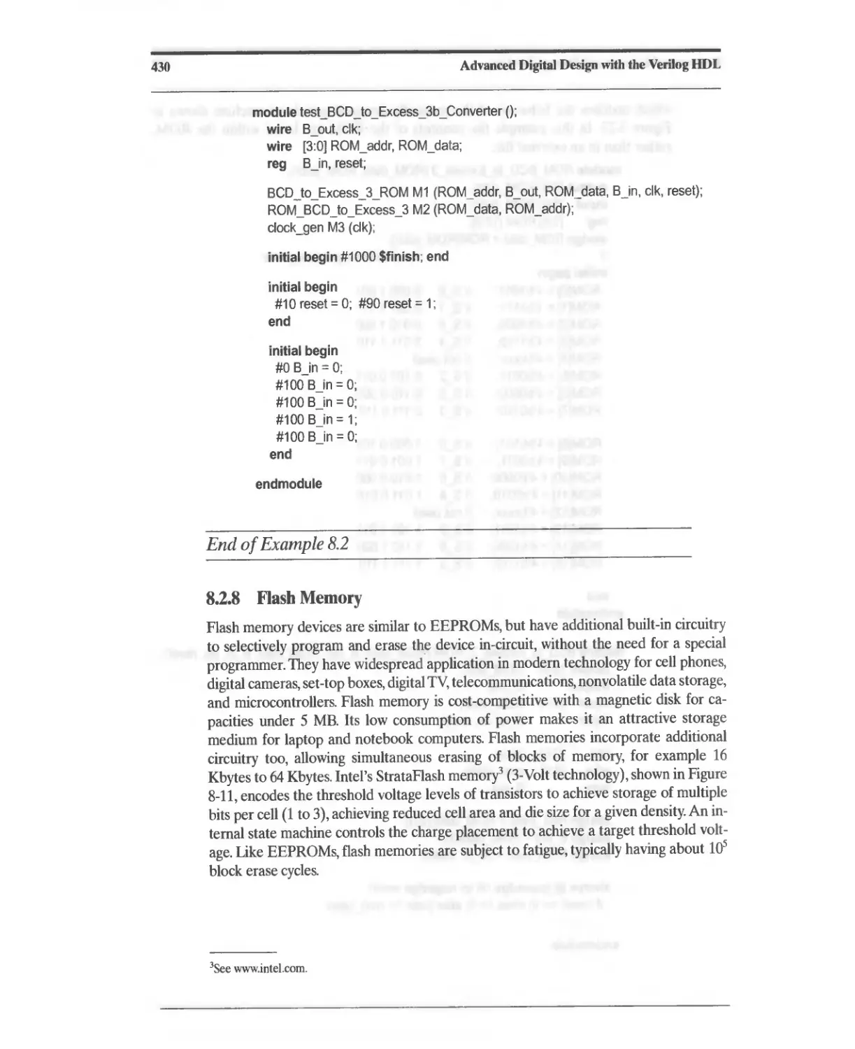
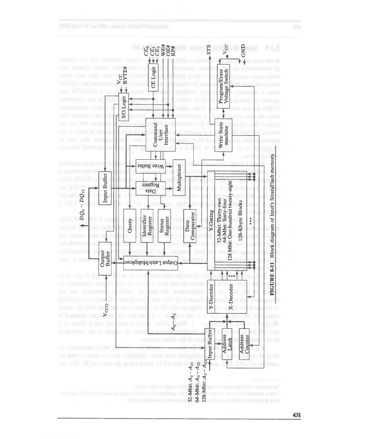
8.2.8 Flash Memory 430
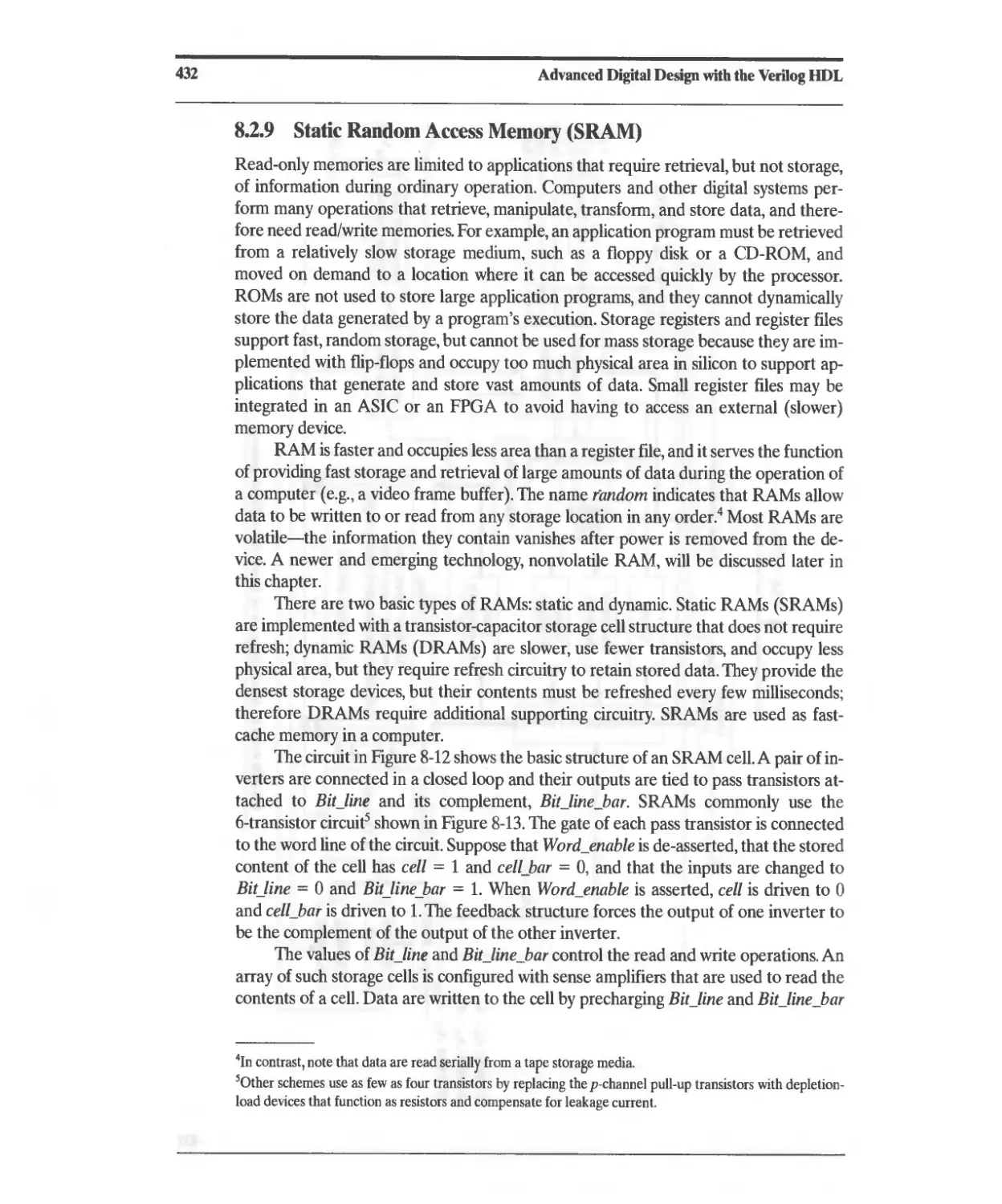
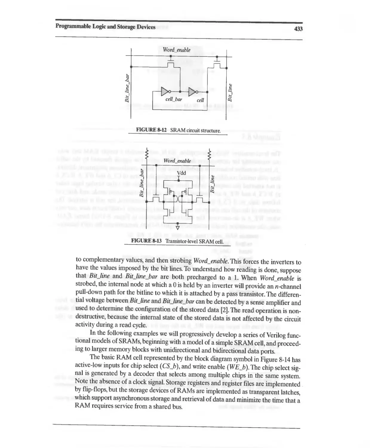
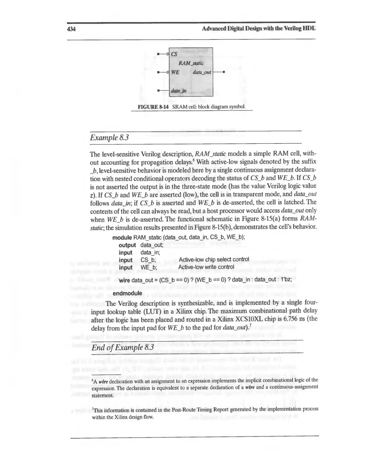
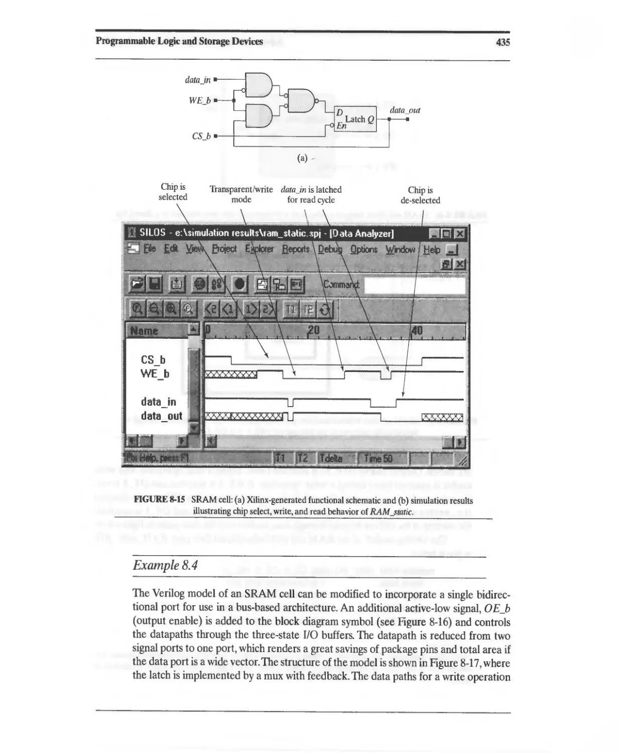
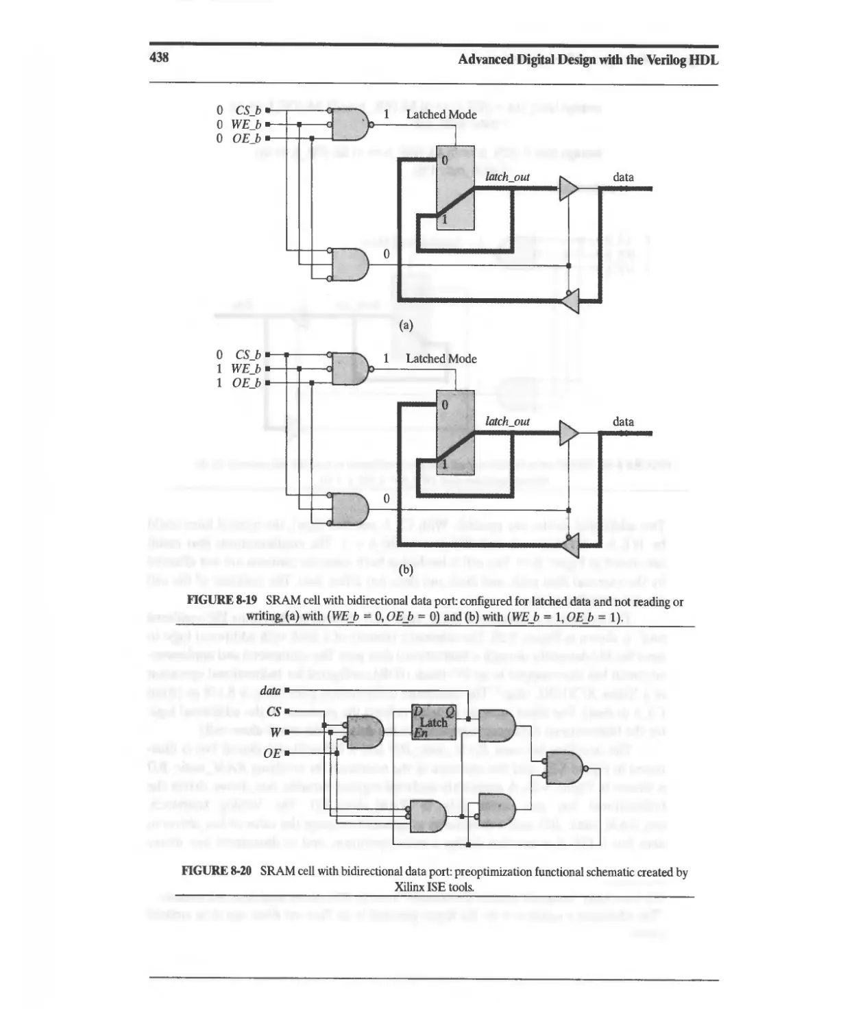
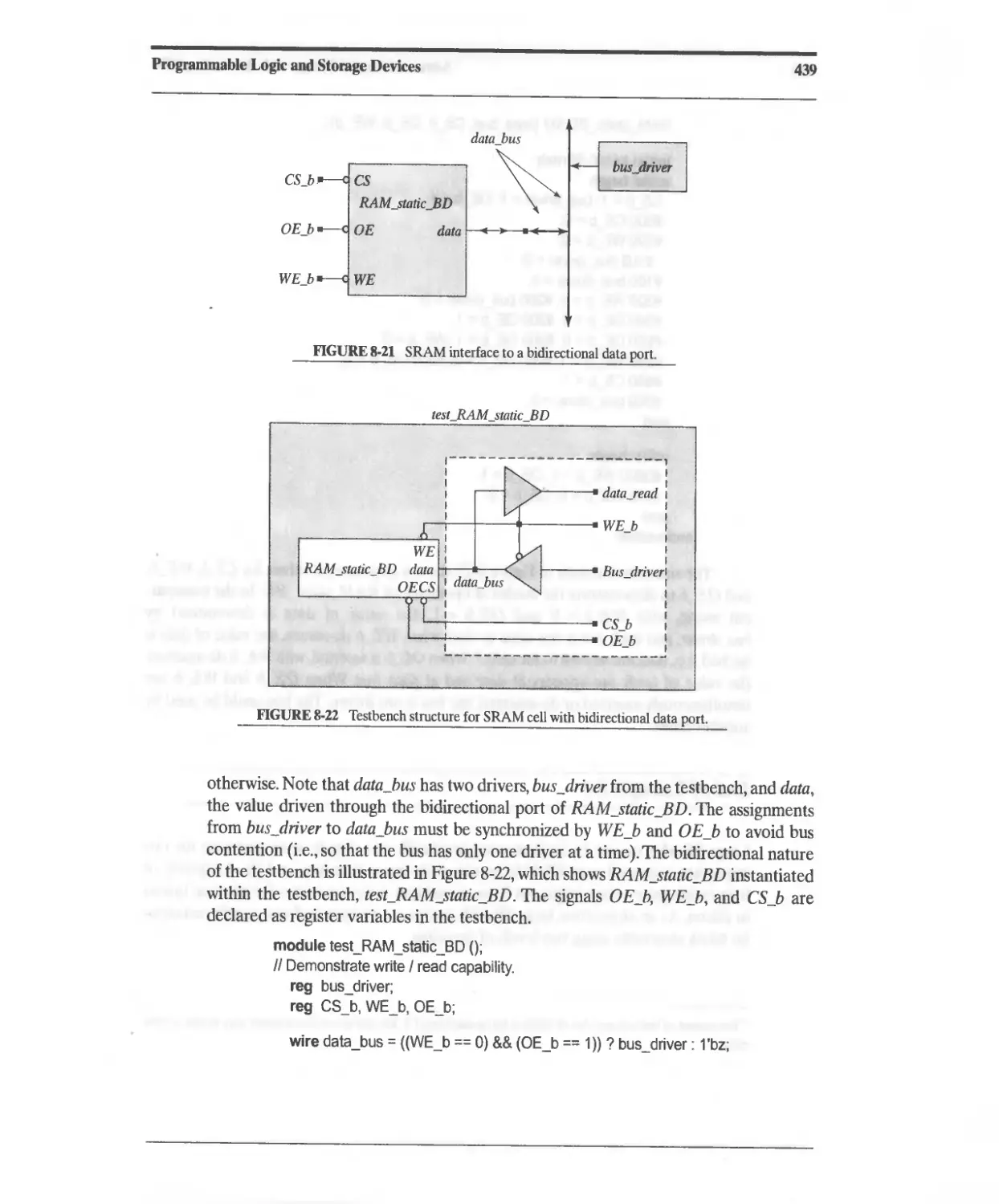
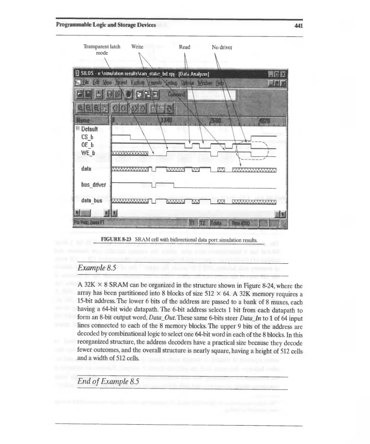
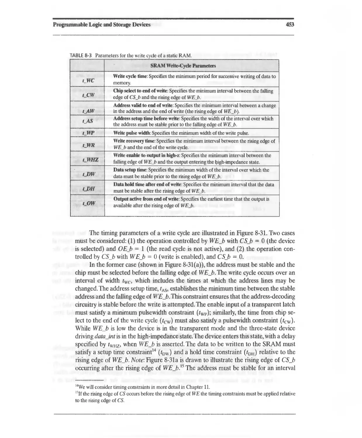
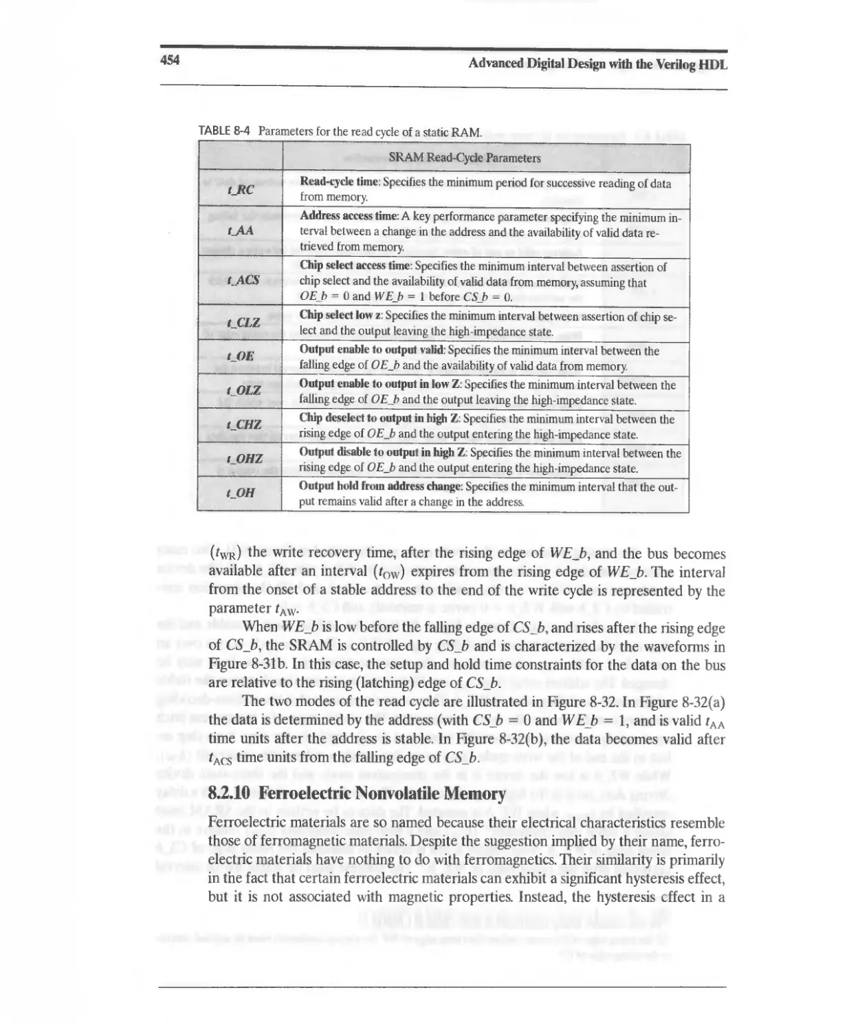
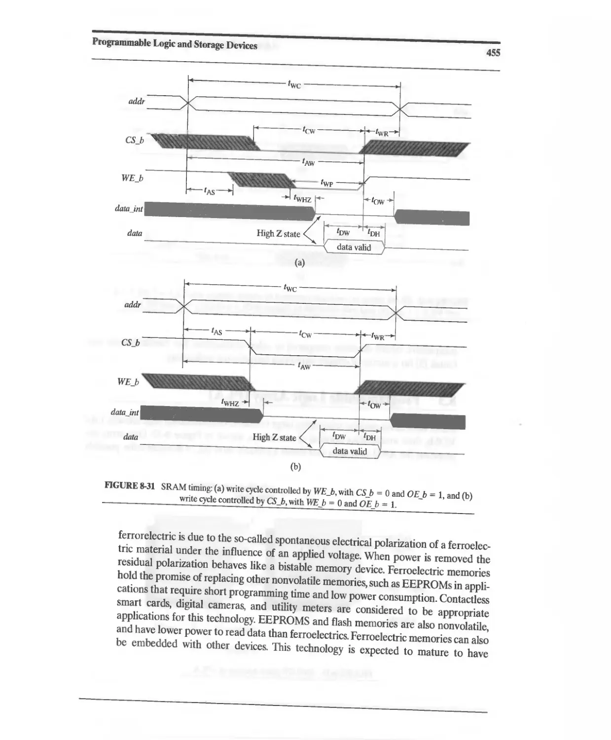
8.2.9 Static Random Access Memory (SRAM) 432
8.2.10 Ferroelectric Nonvolatile Memory 454
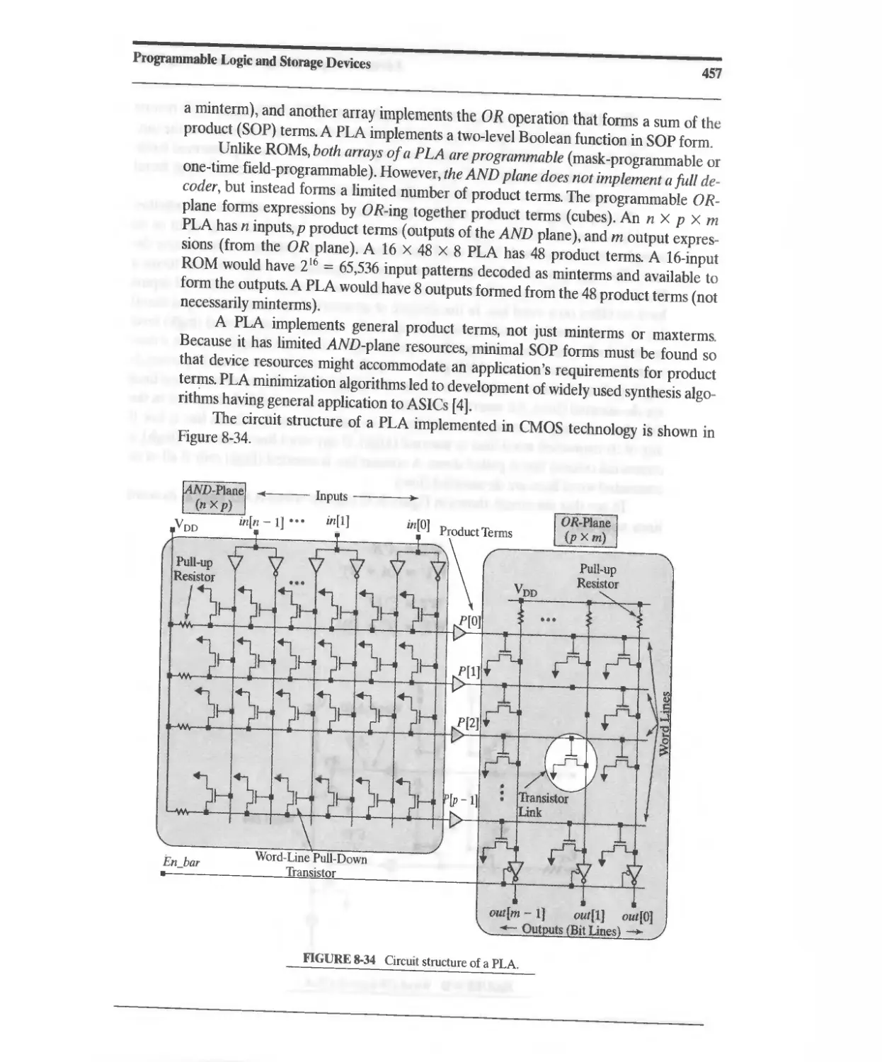
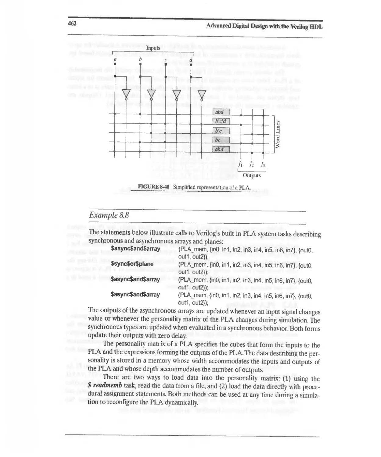
8.3 Programmable Logic Array (PLA) 456
8.3.1 PLA Minimization 459
8.3.2 PLA Modeling 461
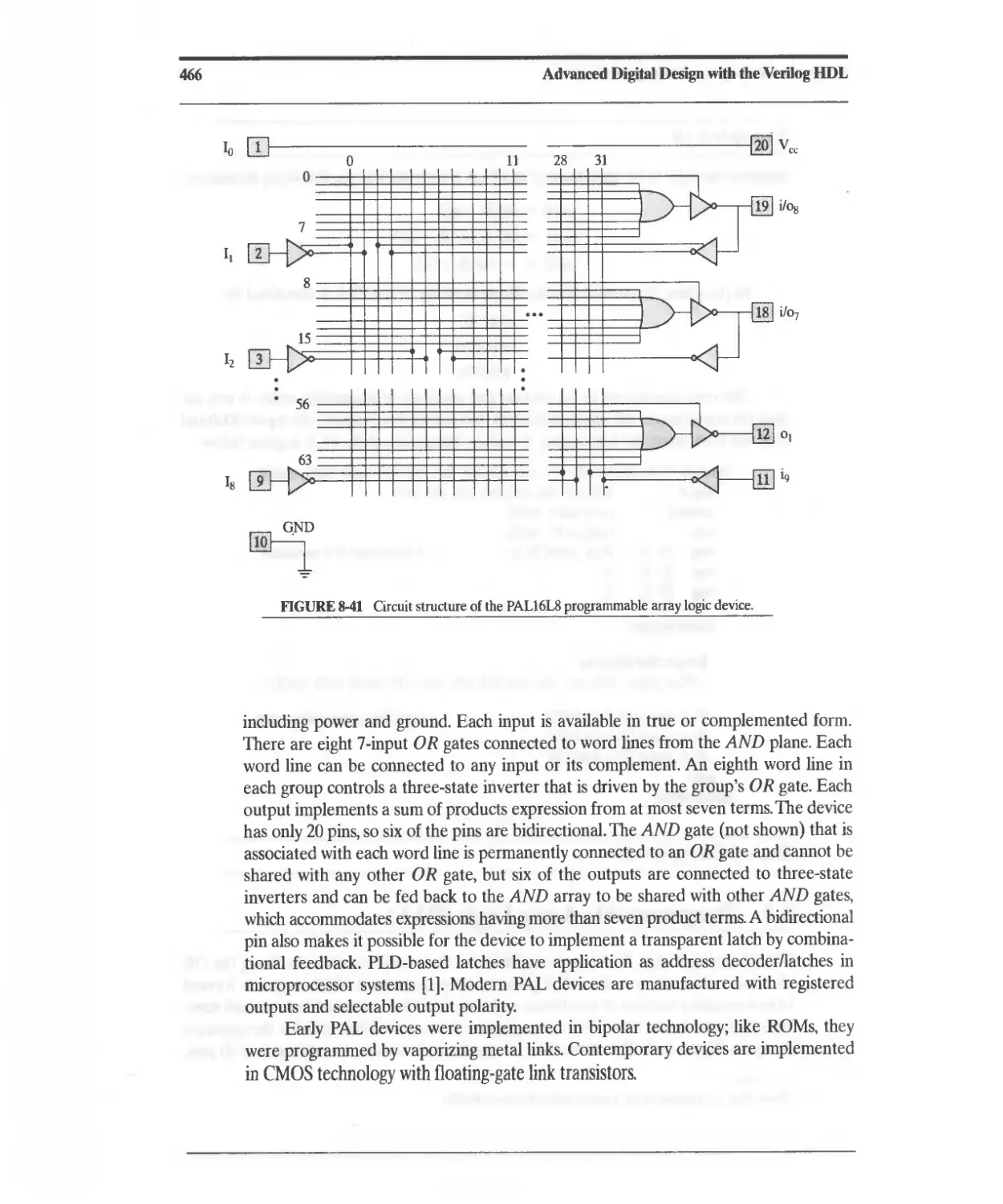
8.4 Programmable Array Logic (PAL) 465
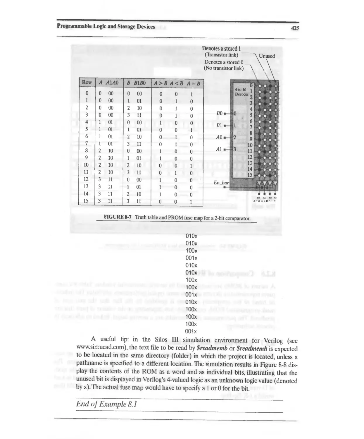
8.5 Programmability of PLDs 467
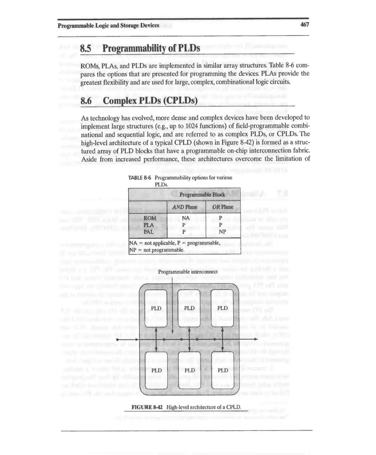
8.6 Complex PLDs (CPLDs) 467
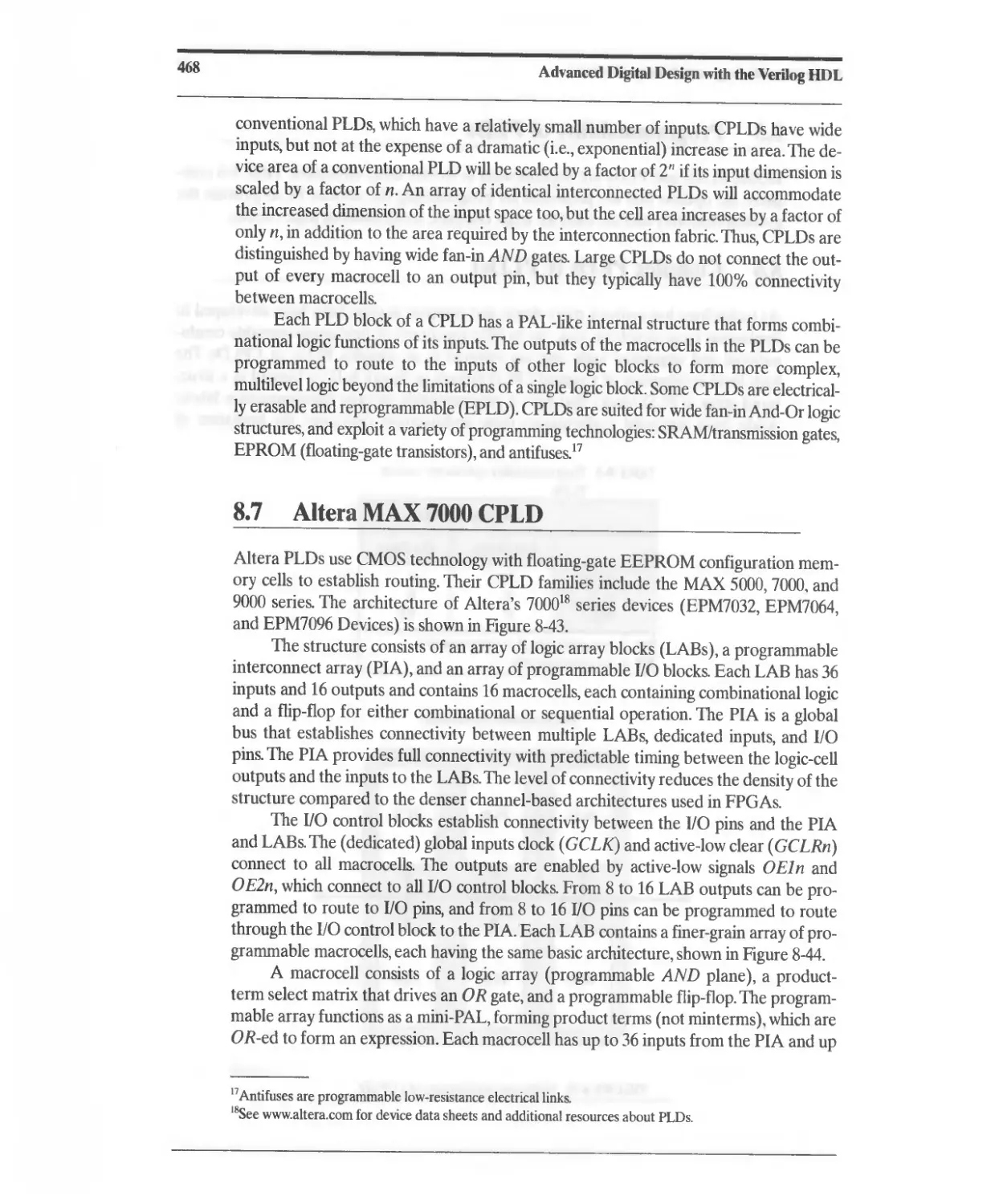
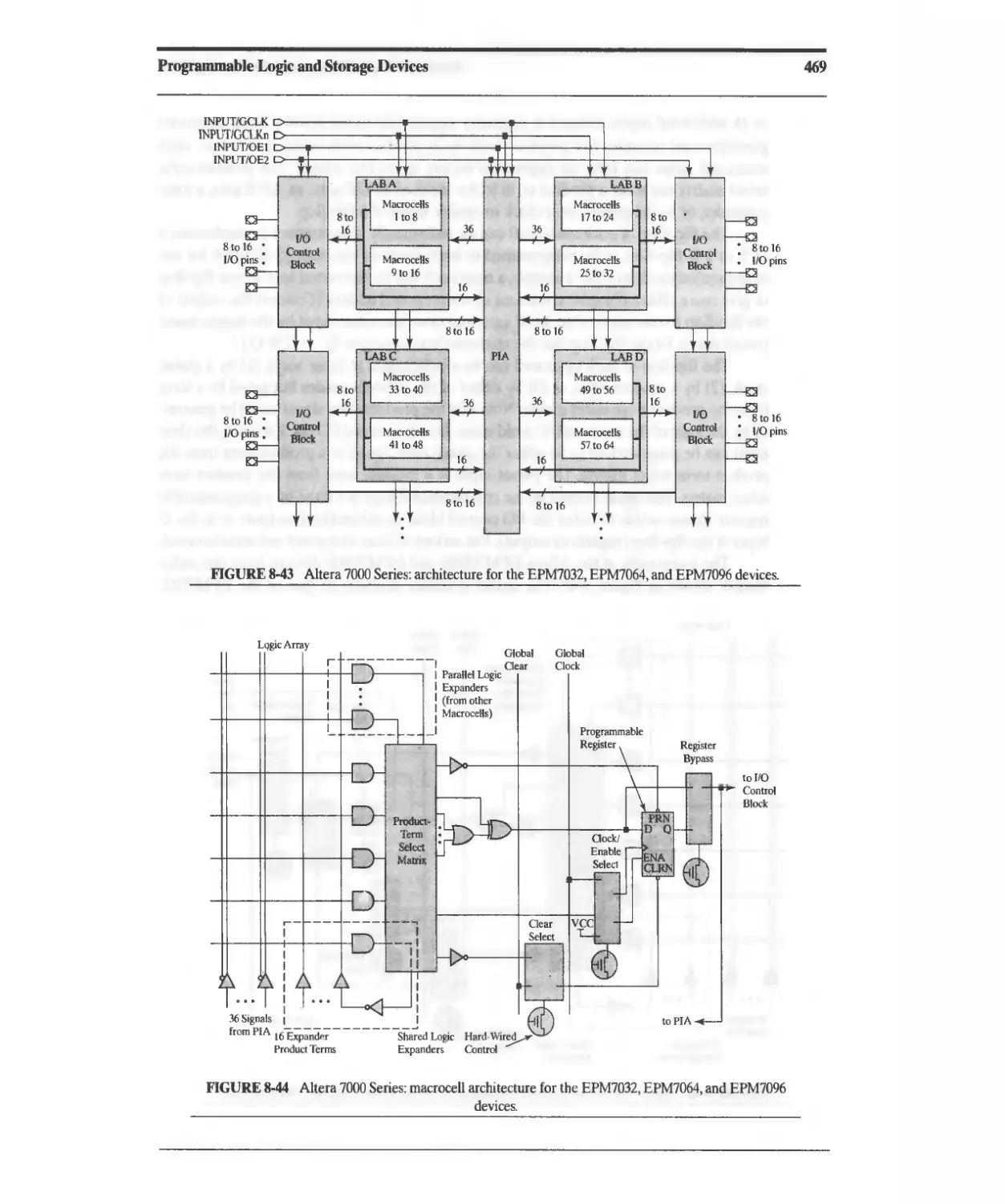
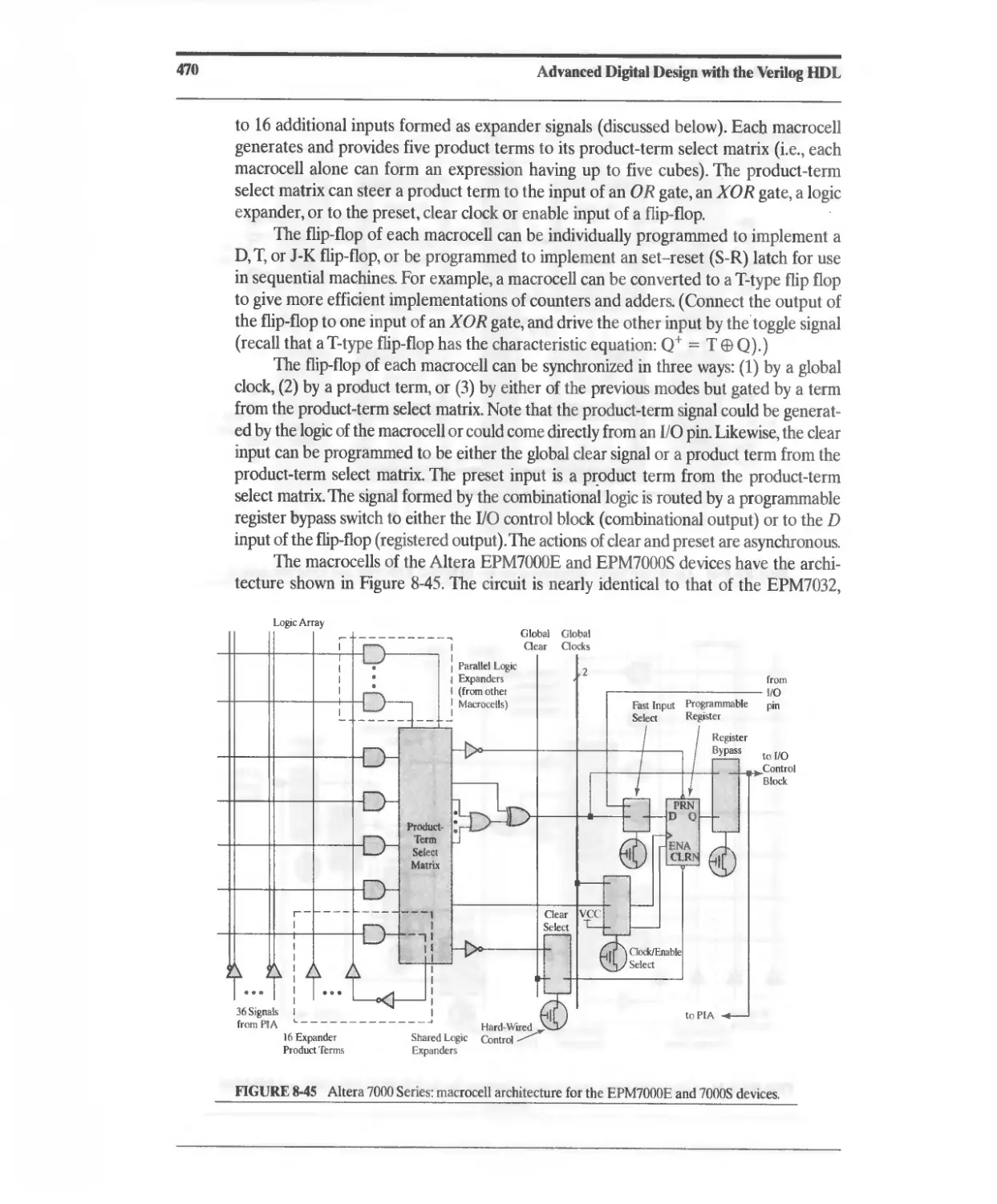
8.7 Altera MAX 7000 CPLD 468
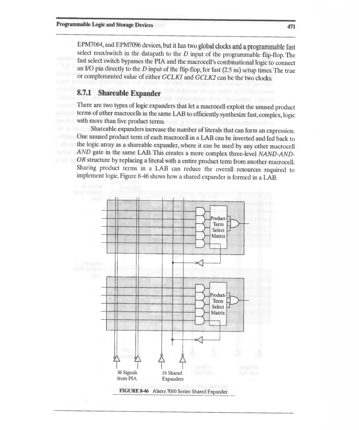
8.7.1 Shareable Expander 471
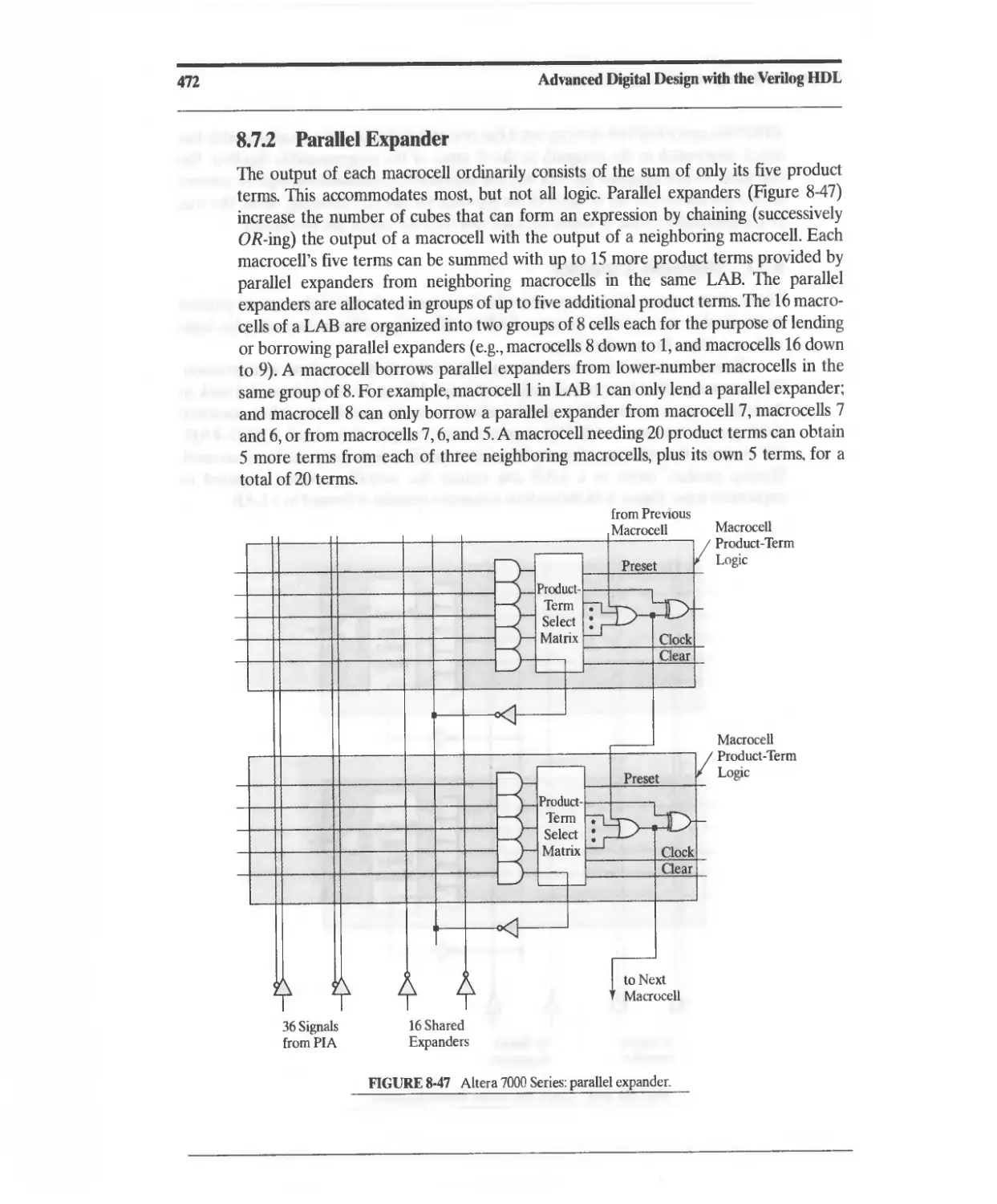
8.7.2 Parallel Expander 472
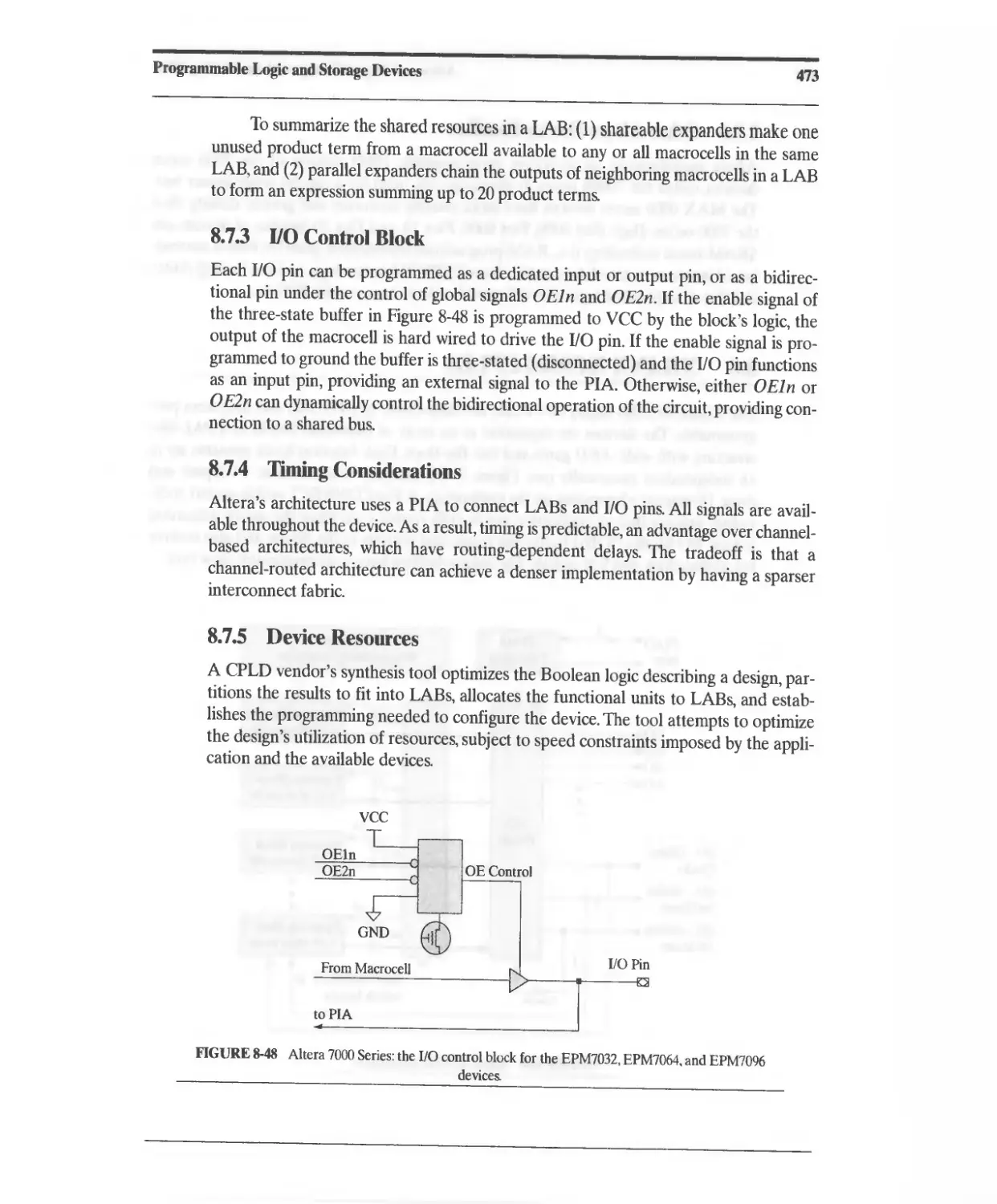
8.7.3 [/0 Control Block 473
8.7.4 Timing Considerations 473
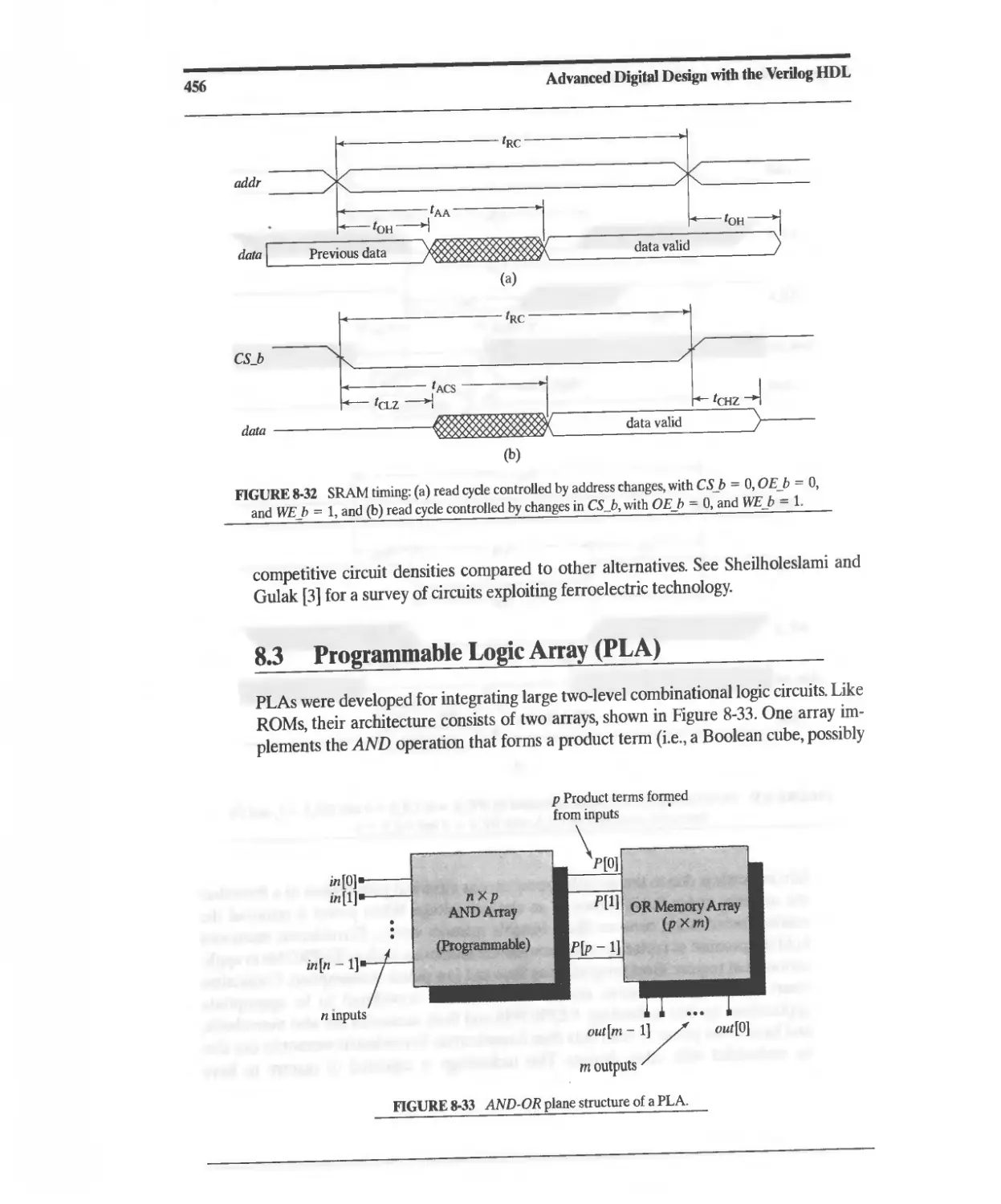
8.7.5 Device Resources 473
8.7.6 Other Altera Device Families 474
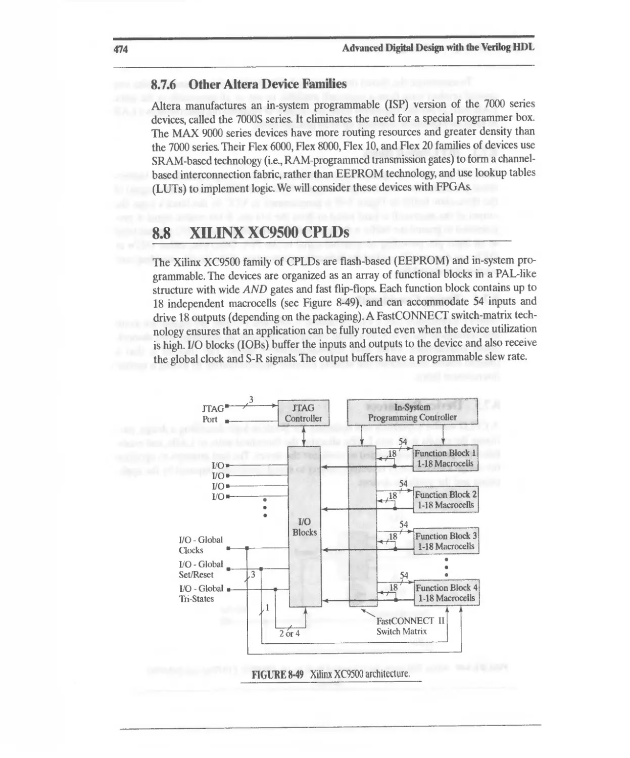
8. XILINX XC9500 CPLDs 474
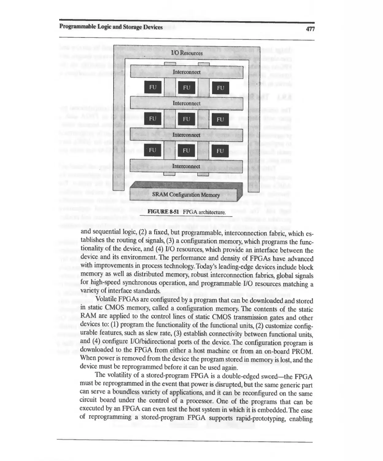
8.9 Field-Programmable Gate Arrays 476
8.9.1 The Role of FPGAs in the ASIC Market 478
8.9.2 FPGA Technologies 479
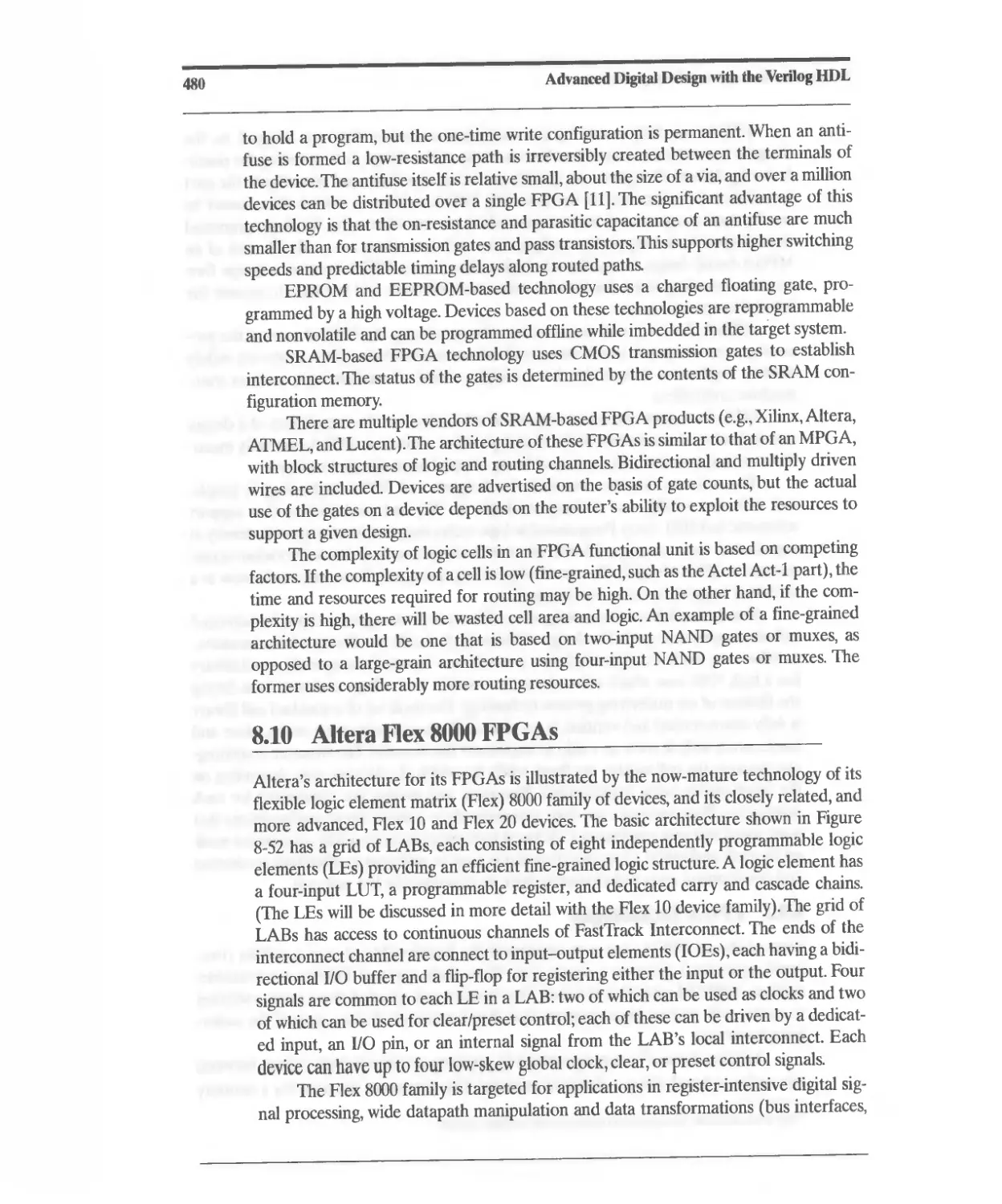
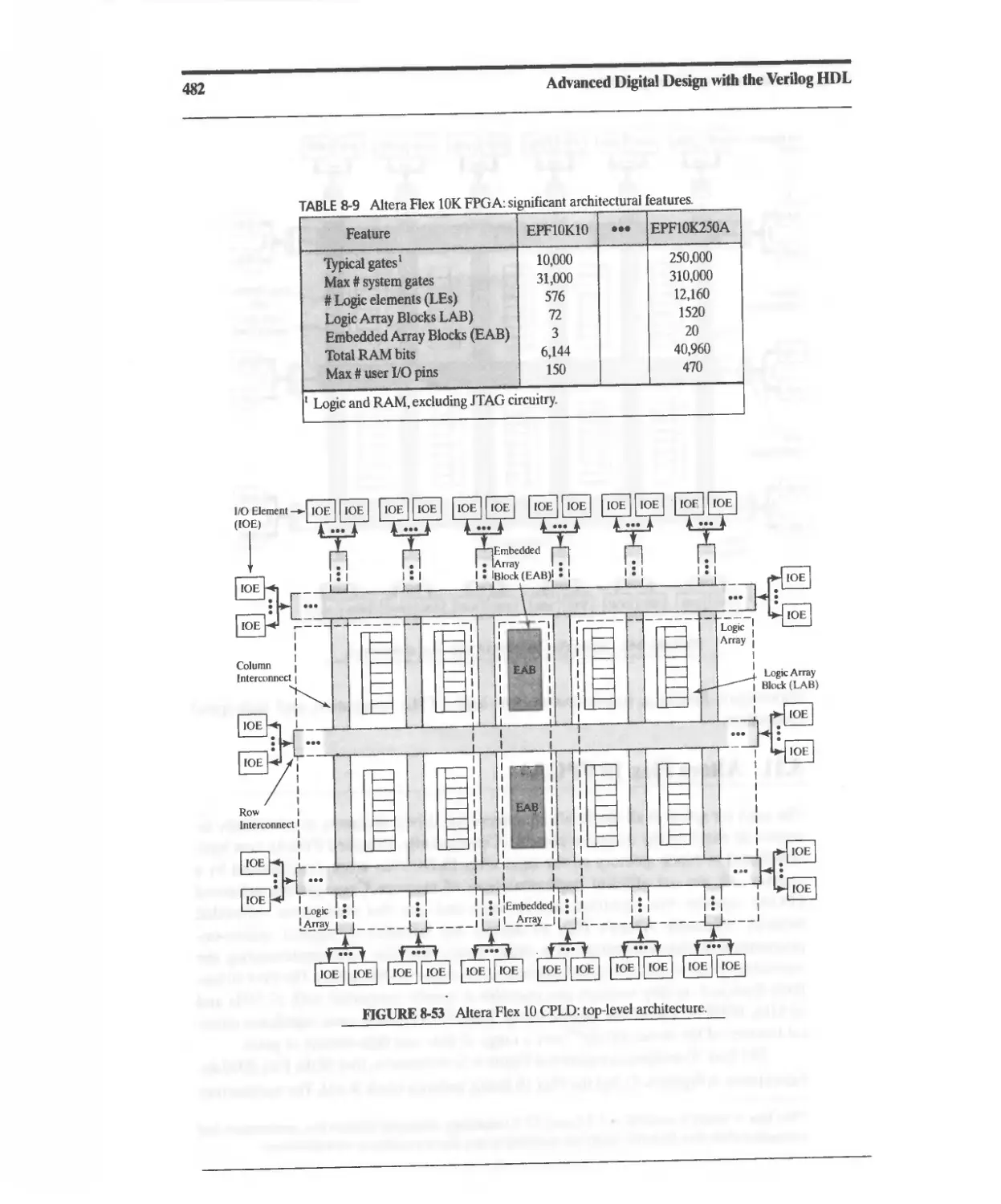
8.10 Altera Flex 8000 FPGAs 480
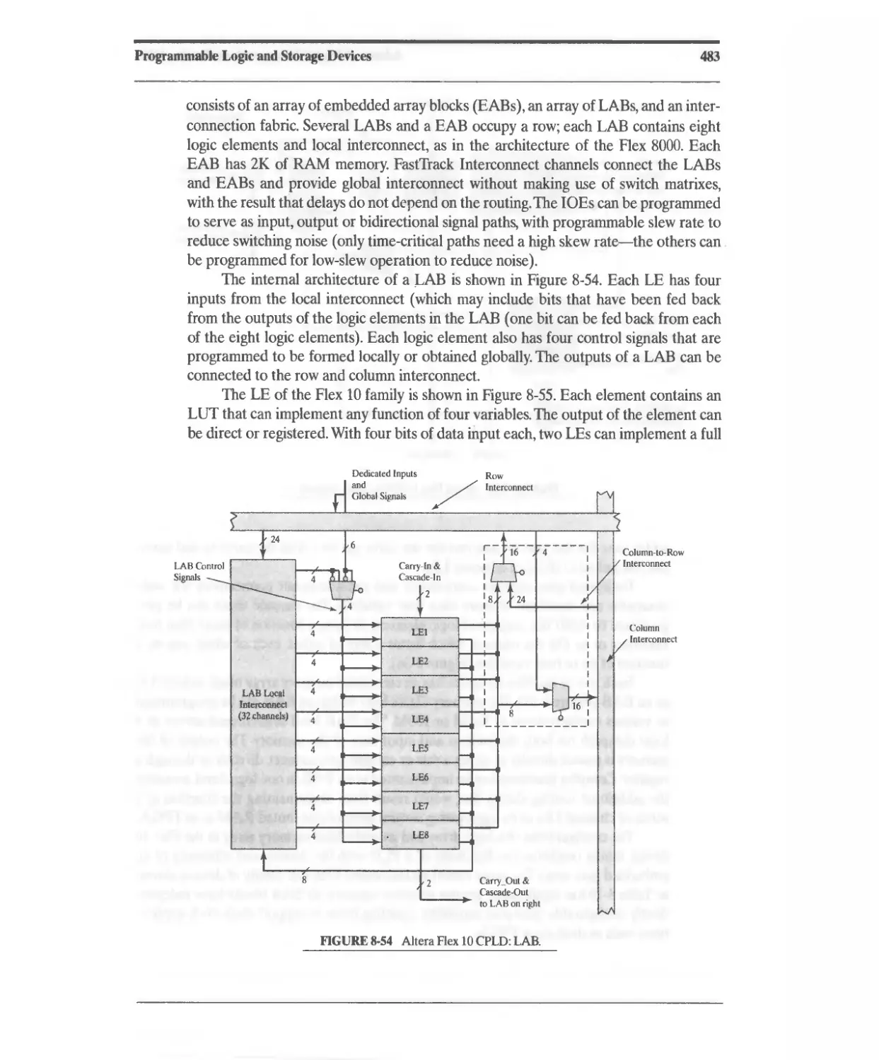
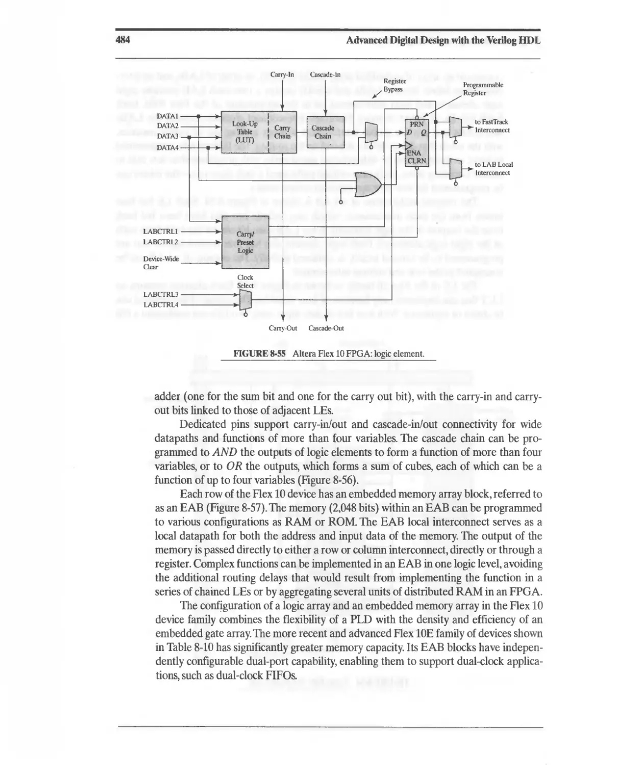
8.11 Altera Flex 10 FPGAs 481
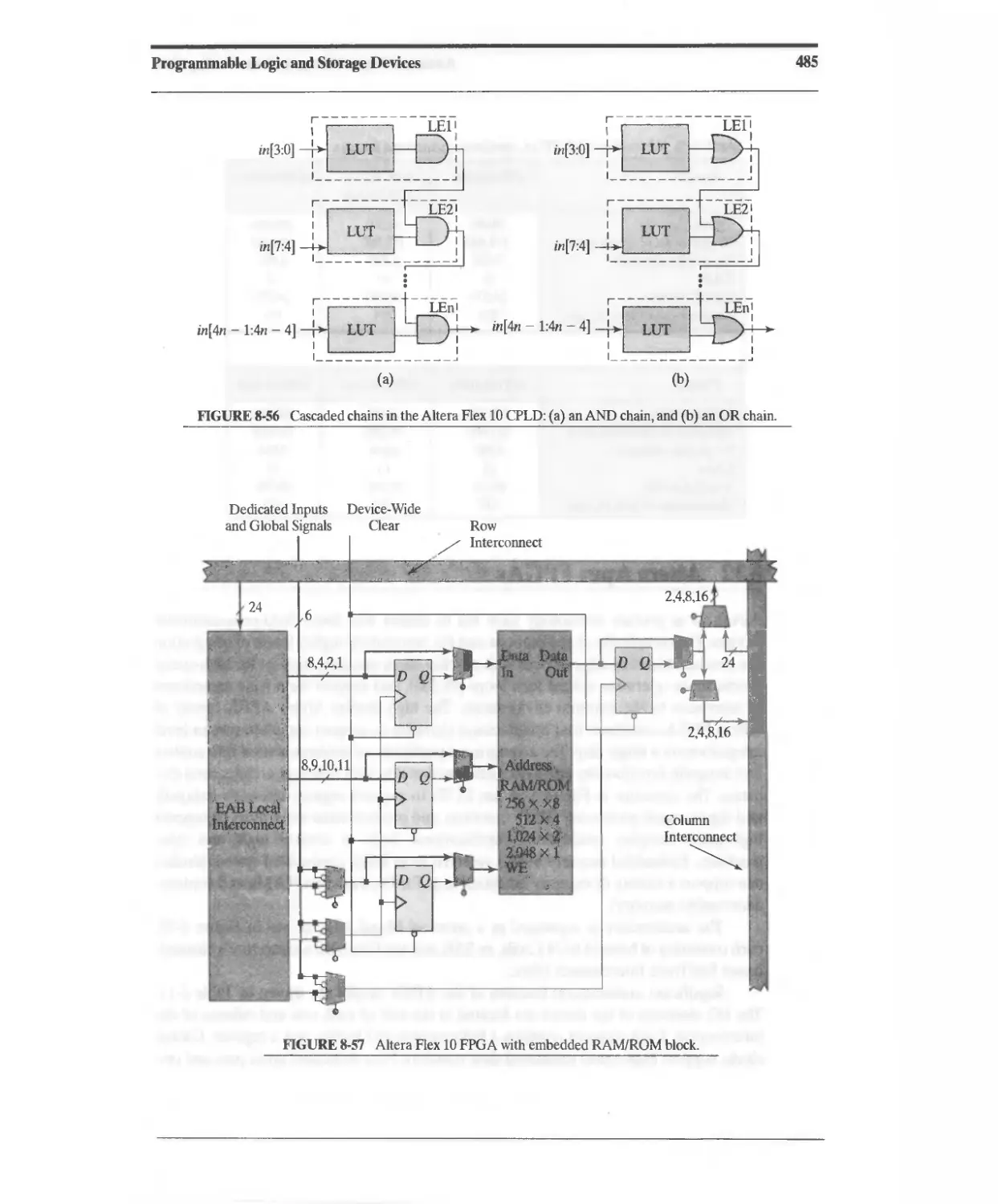
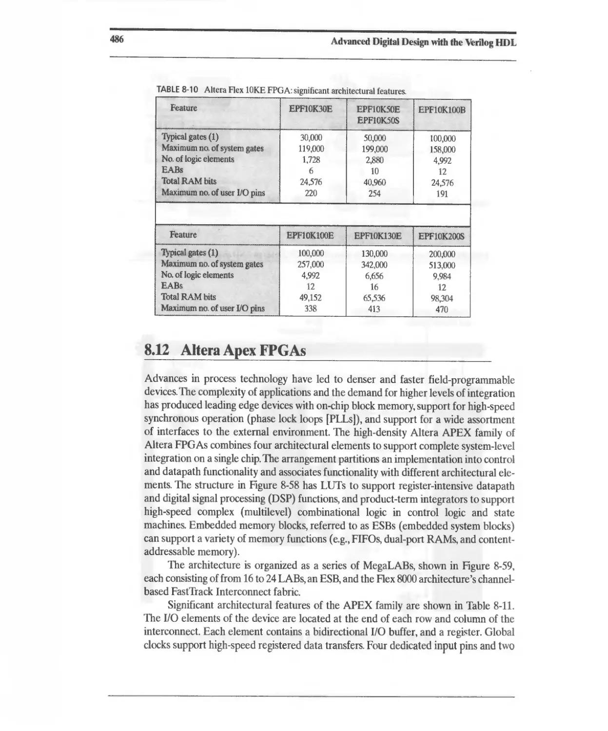
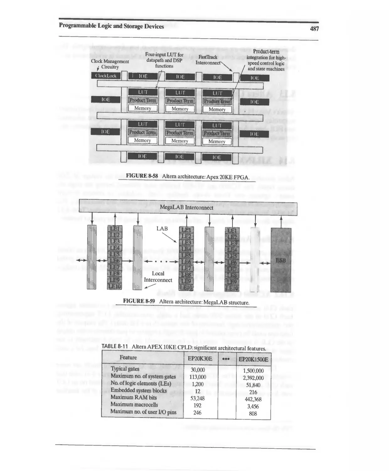
8.12 AHera Apex FPGAs 486
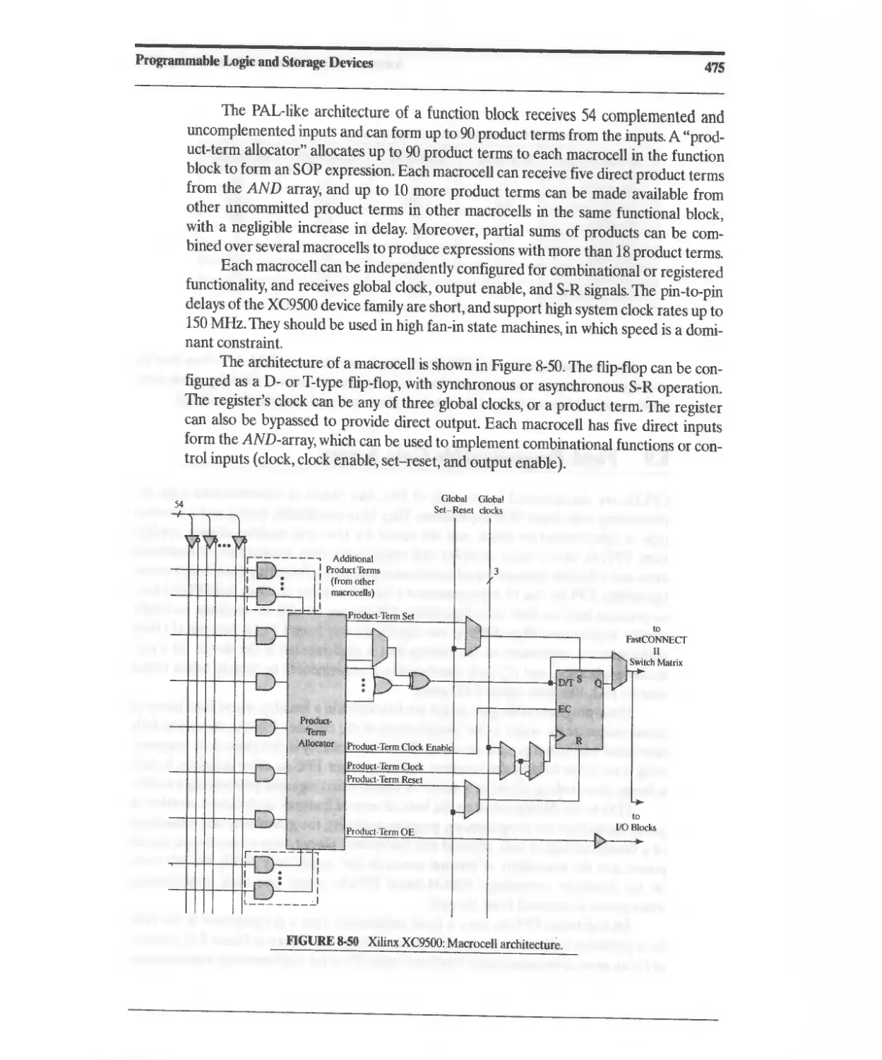
8.13 Altera Chip Programmability 488
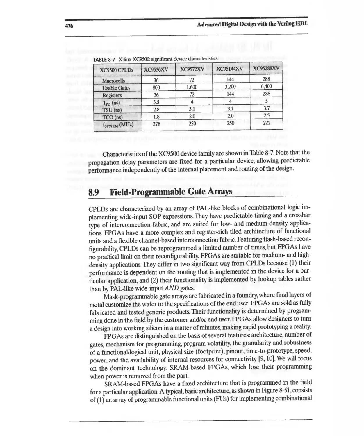
8.14 XILINX XC4000 Series FPGA 4S8
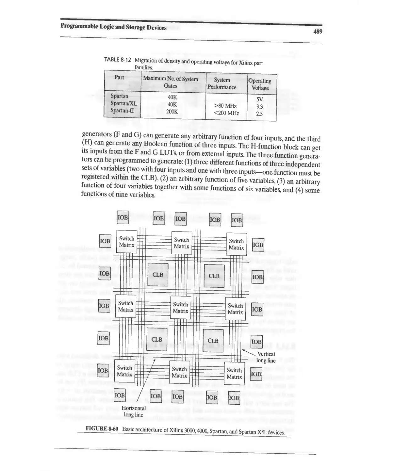
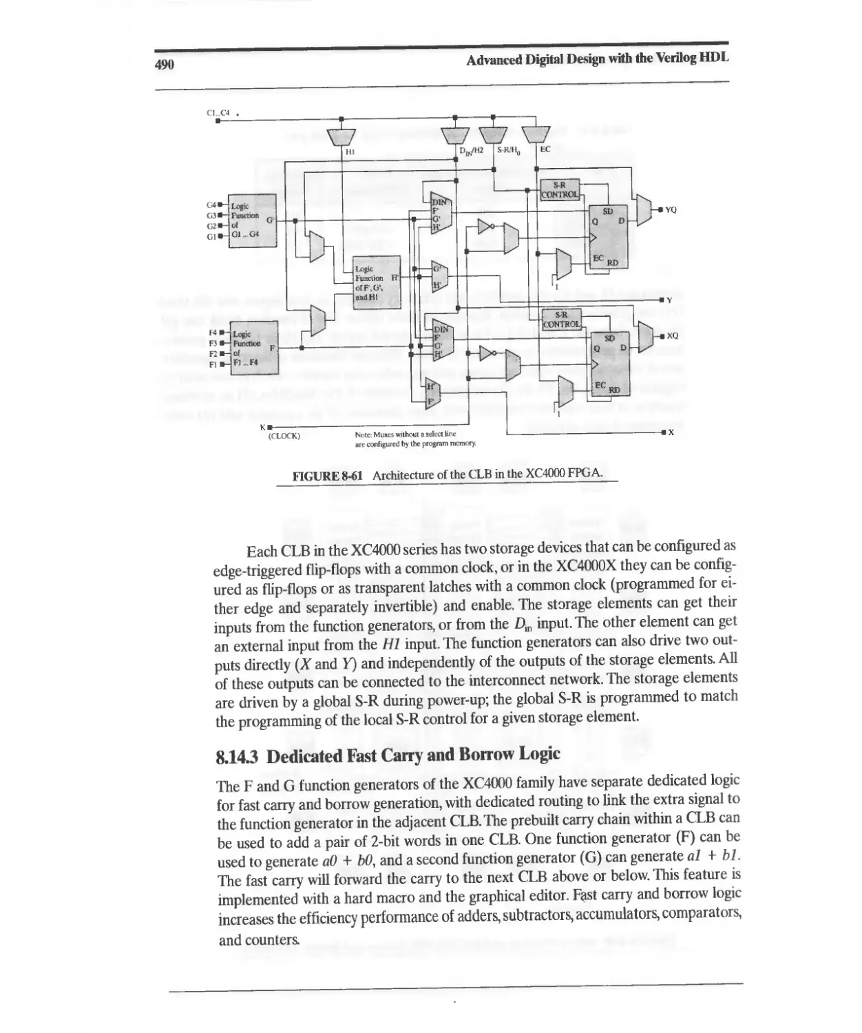
8.14.1 Basic Architecture 488
8.14.2 XC4000 Configurable Logic Block 488
Contents
xi
8.14.3 Dedicated Fast Carry and Borrow Logic 490
8.14.4 Distributed RAM 491
8.14.5 XC4000 Interconnect Resources 491
8.14.6 XC4000 I/O Block (lOB) 492
8.14.7 Enhancements in the XC4000E and XC4000X Series 495
8.14.8 Enhancements in the Spartan Series 495
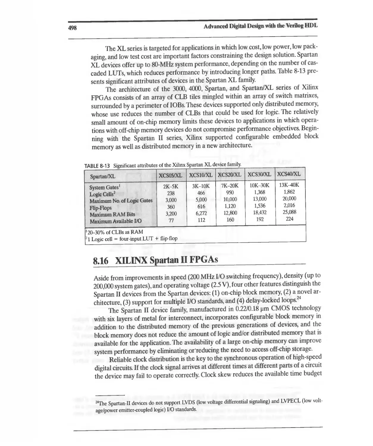
8.15 XIUNX Spartan XL FPGAs 497
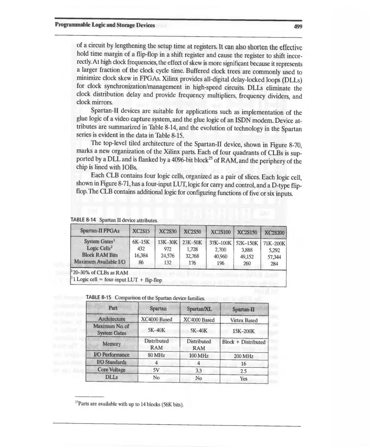
8.16 XIUNX Spartan II FPGAs 498
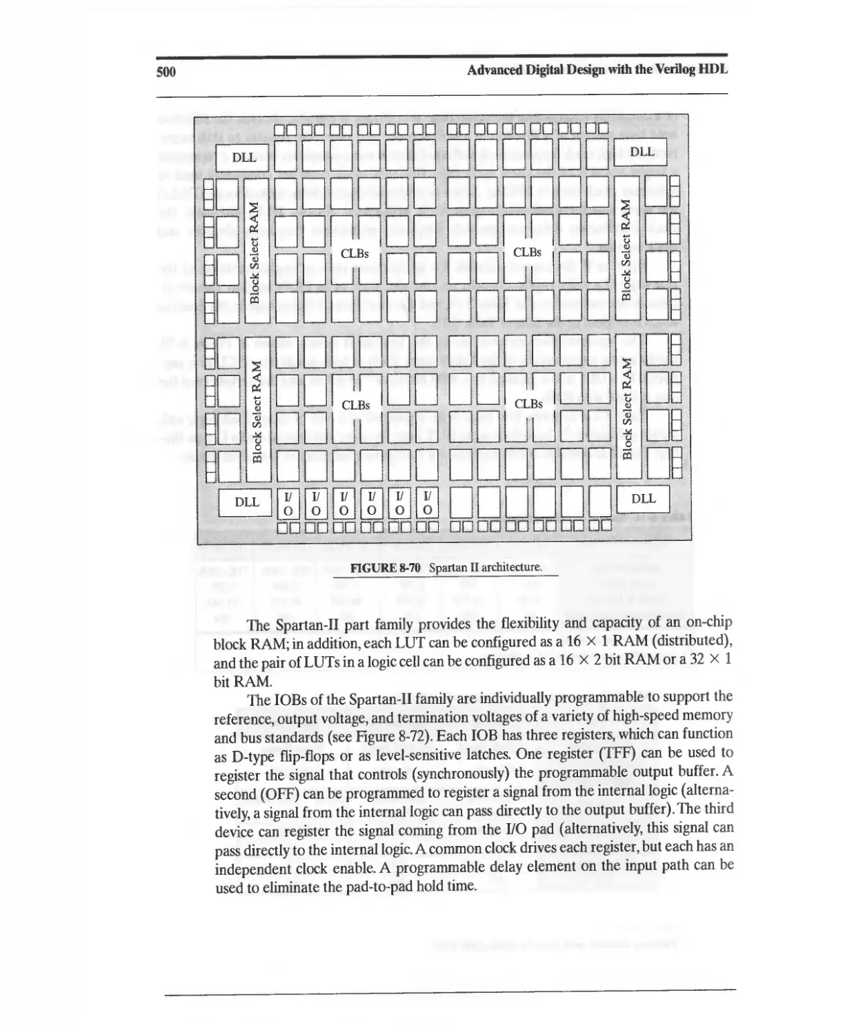
8.17 XIUNX Virtex FPGAs 502
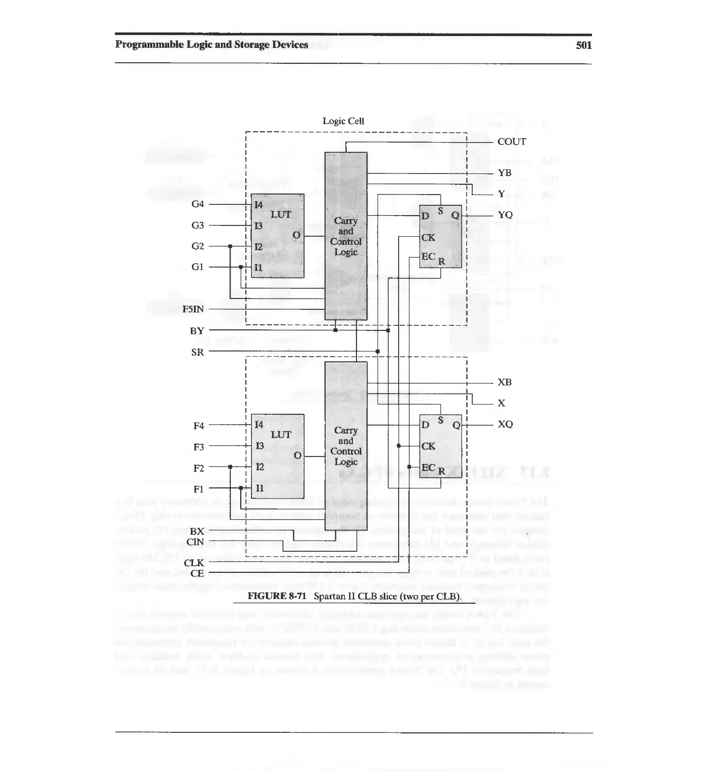
8.18 Embeddable and Programmable IP Cores for a System on a Chip
(SoC) 504
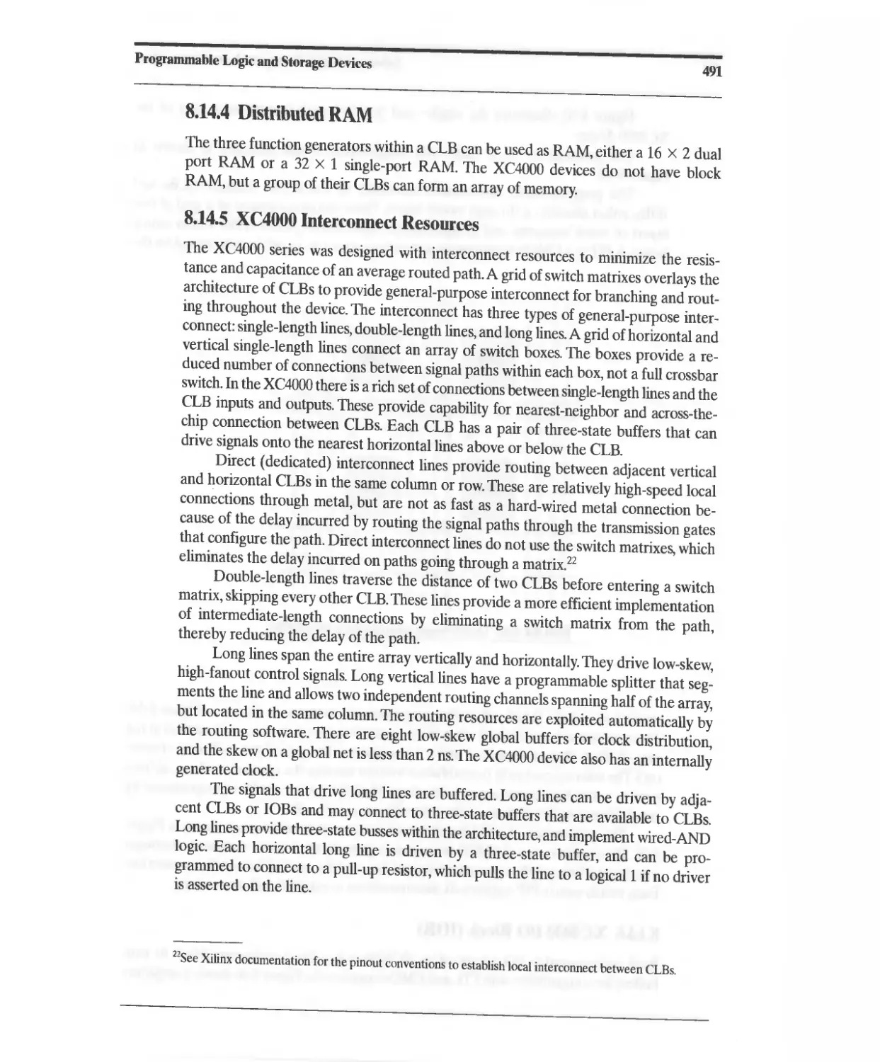
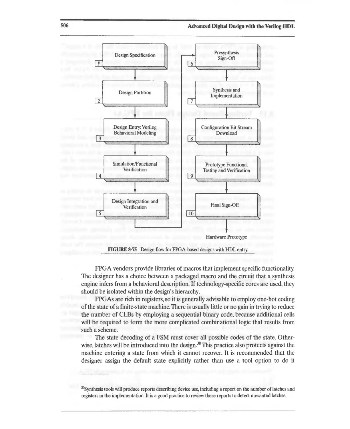
8.19 Verilog-Based Design Flows for FPGAs 505
8.20 Synthesis with FPGAs 505
References 508
Related Web Sites 509
Problems 509
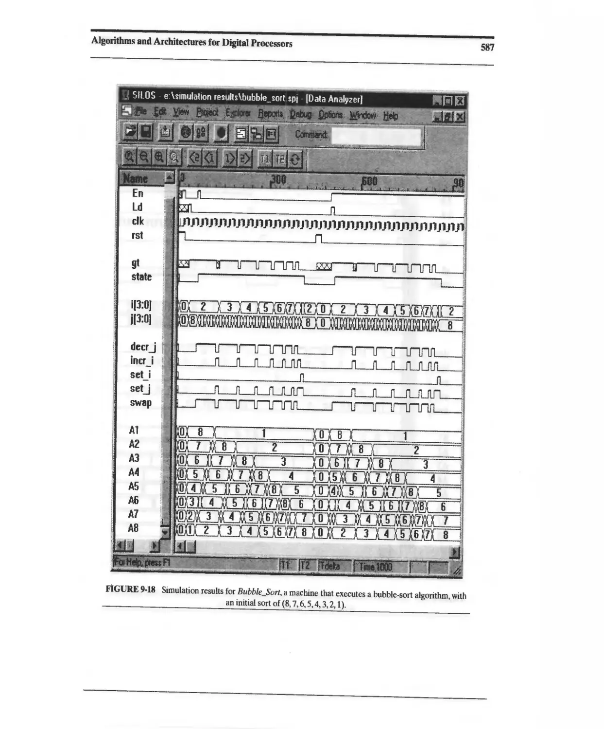
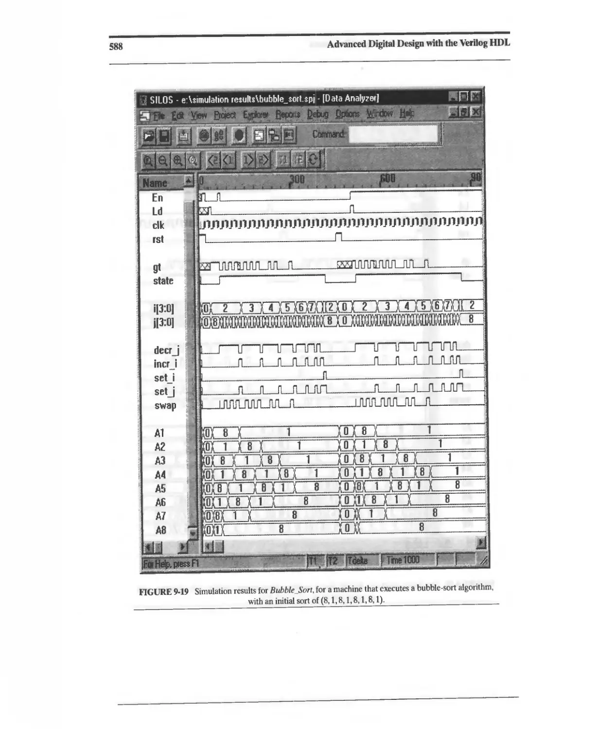
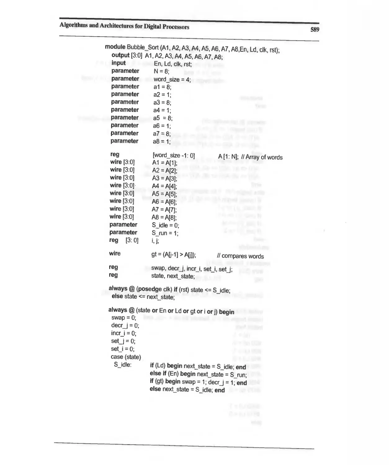
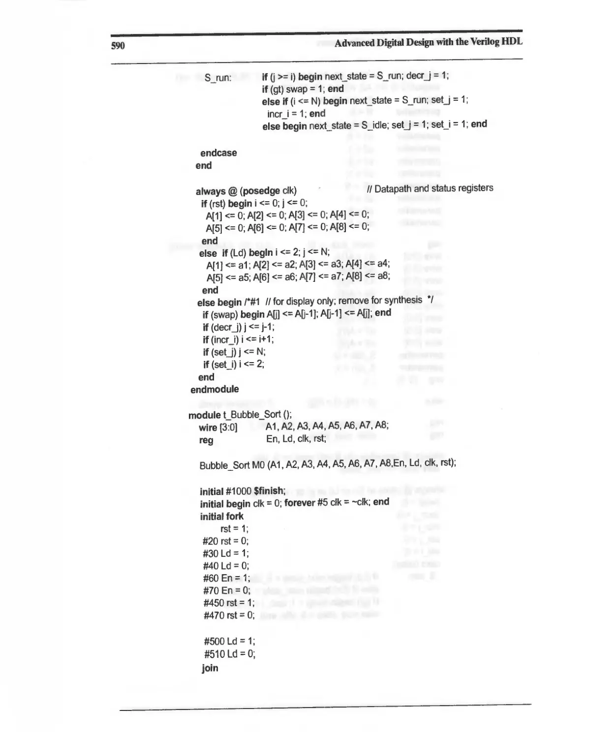
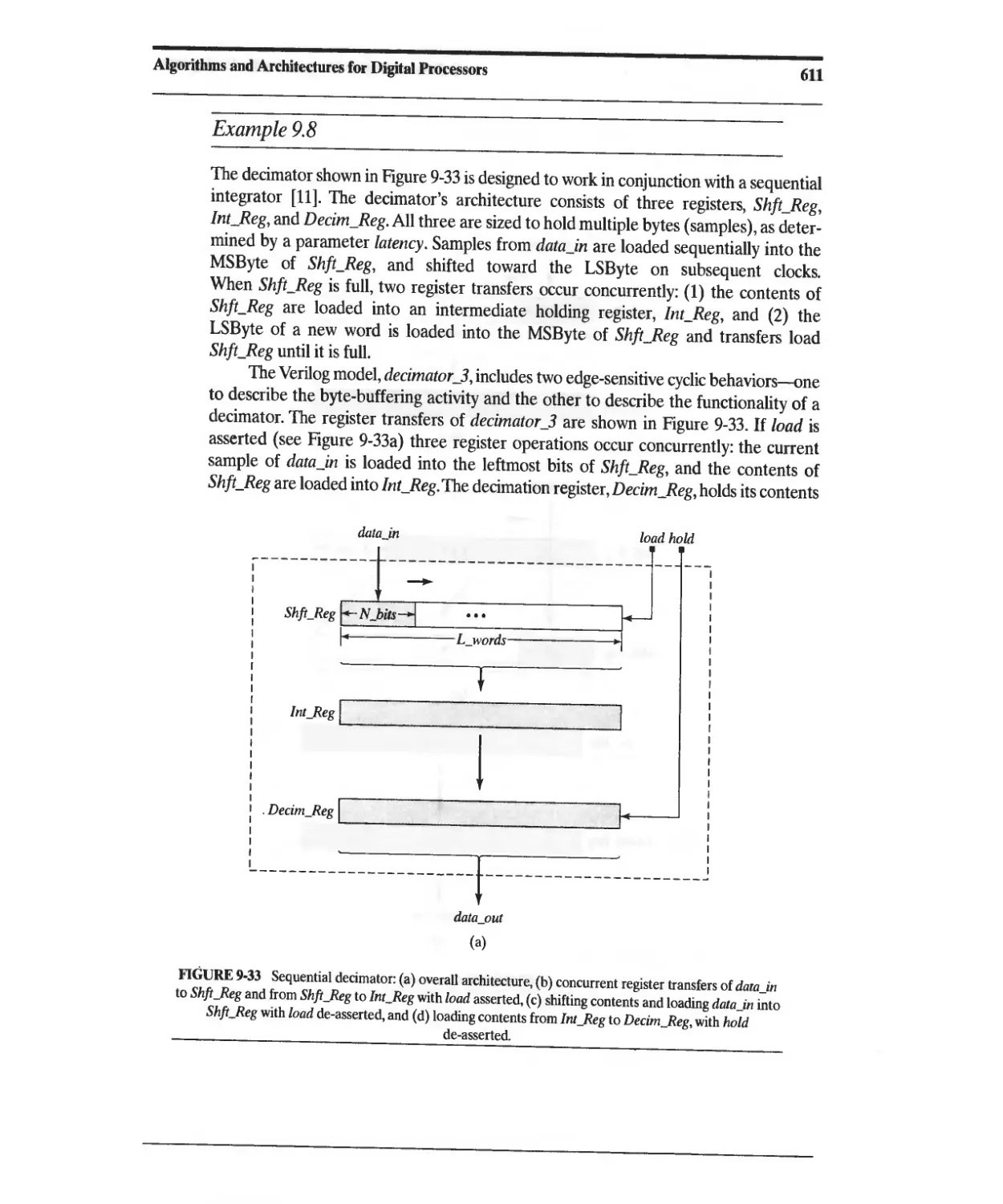
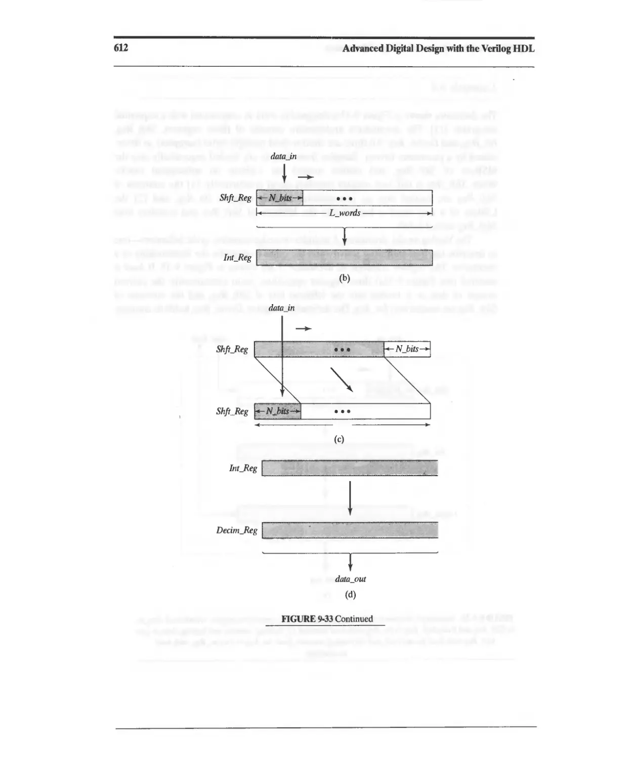
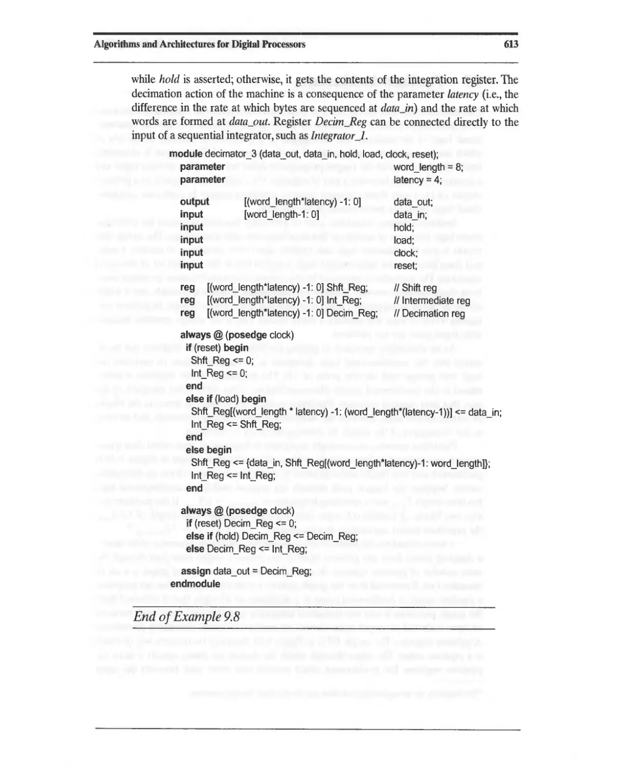
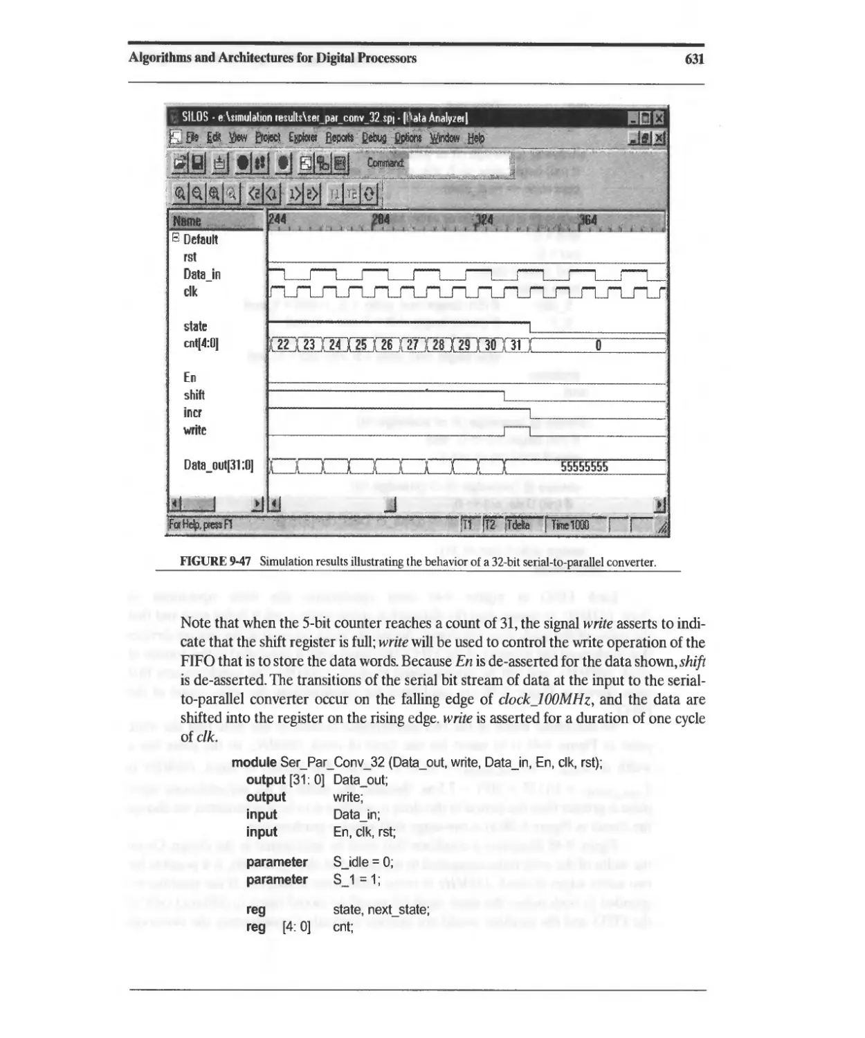
9 Algorithms and Architectures for Digital Processors 547
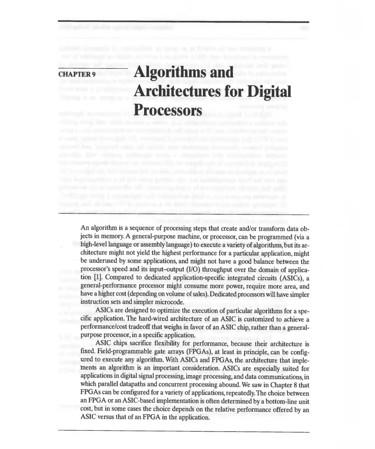
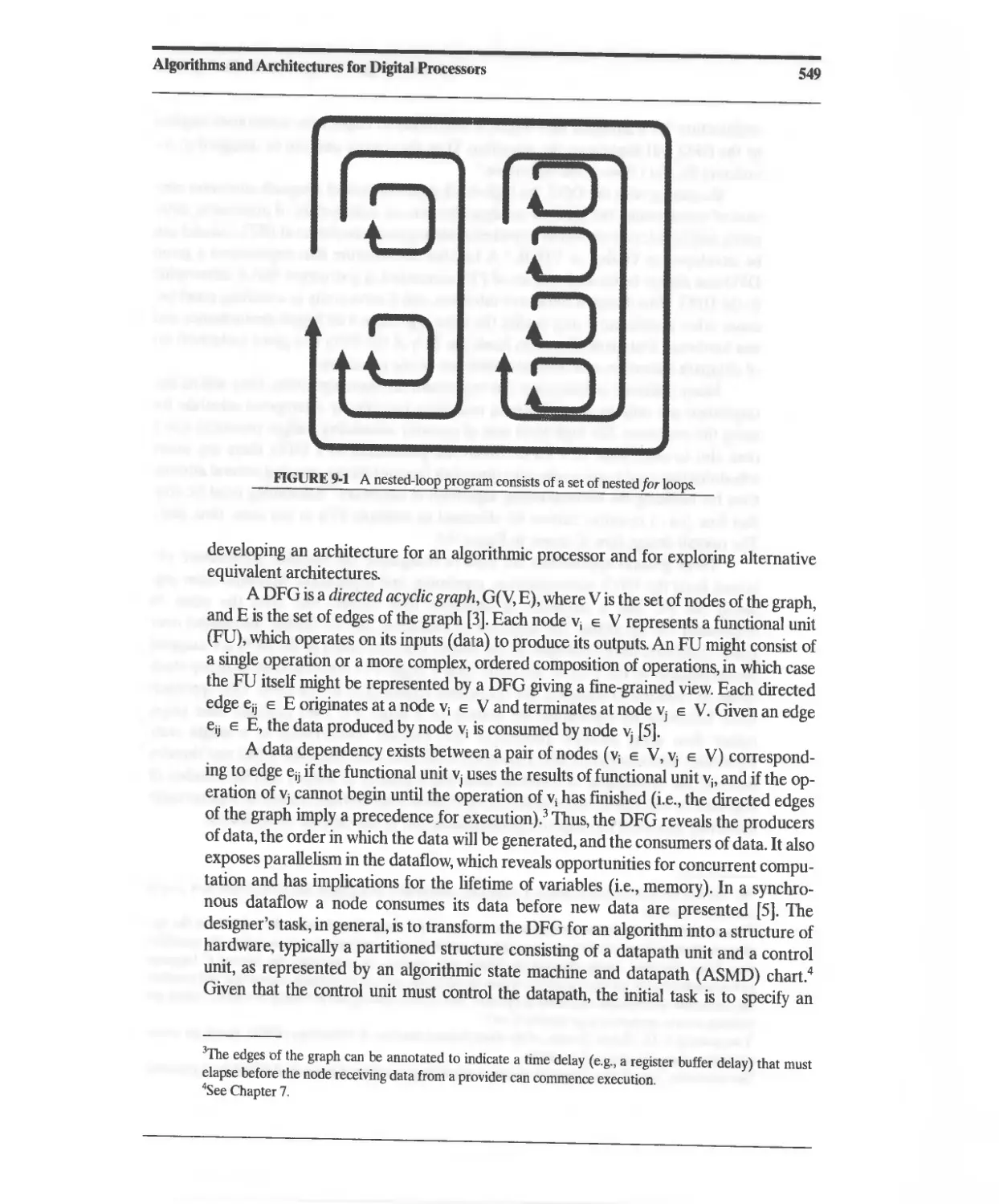
9.1 Algorithms, Nested-Loop Programs, and Data Flow Graphs 548
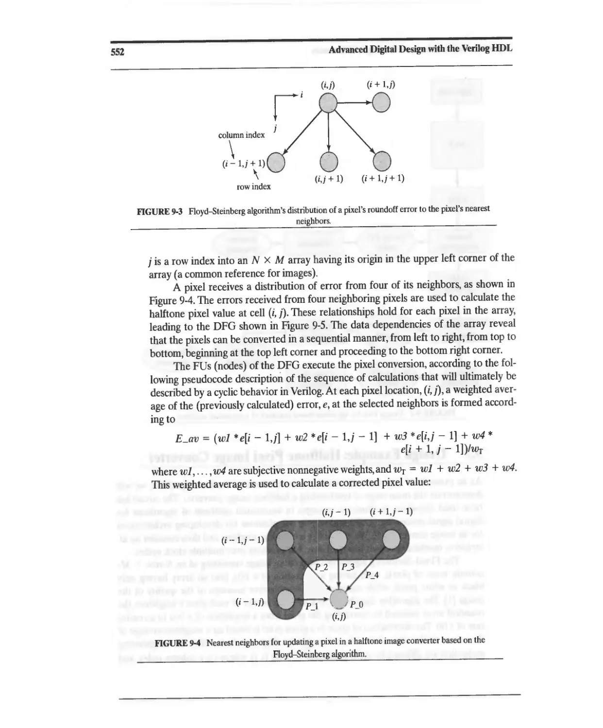
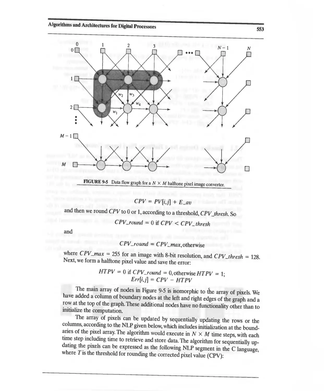
9.2 Design Example: Halftone Pixel Image Converter 551
9.2.1 Baseline Design for a Halftone Pixel Image Converter 554
9.2.2 NLP-Based Architectures for the Halftone Pixel Image
Converter 558
9.2.3 Concurrent ASMD-Based Architecture for a Halftone
Pixel Image Converter 570
9.2.4 Halftone Pixel Image Converter: Design Tradeoffs 583
9.2.5 Architectures for Dataflow Graphs with Feedback 584
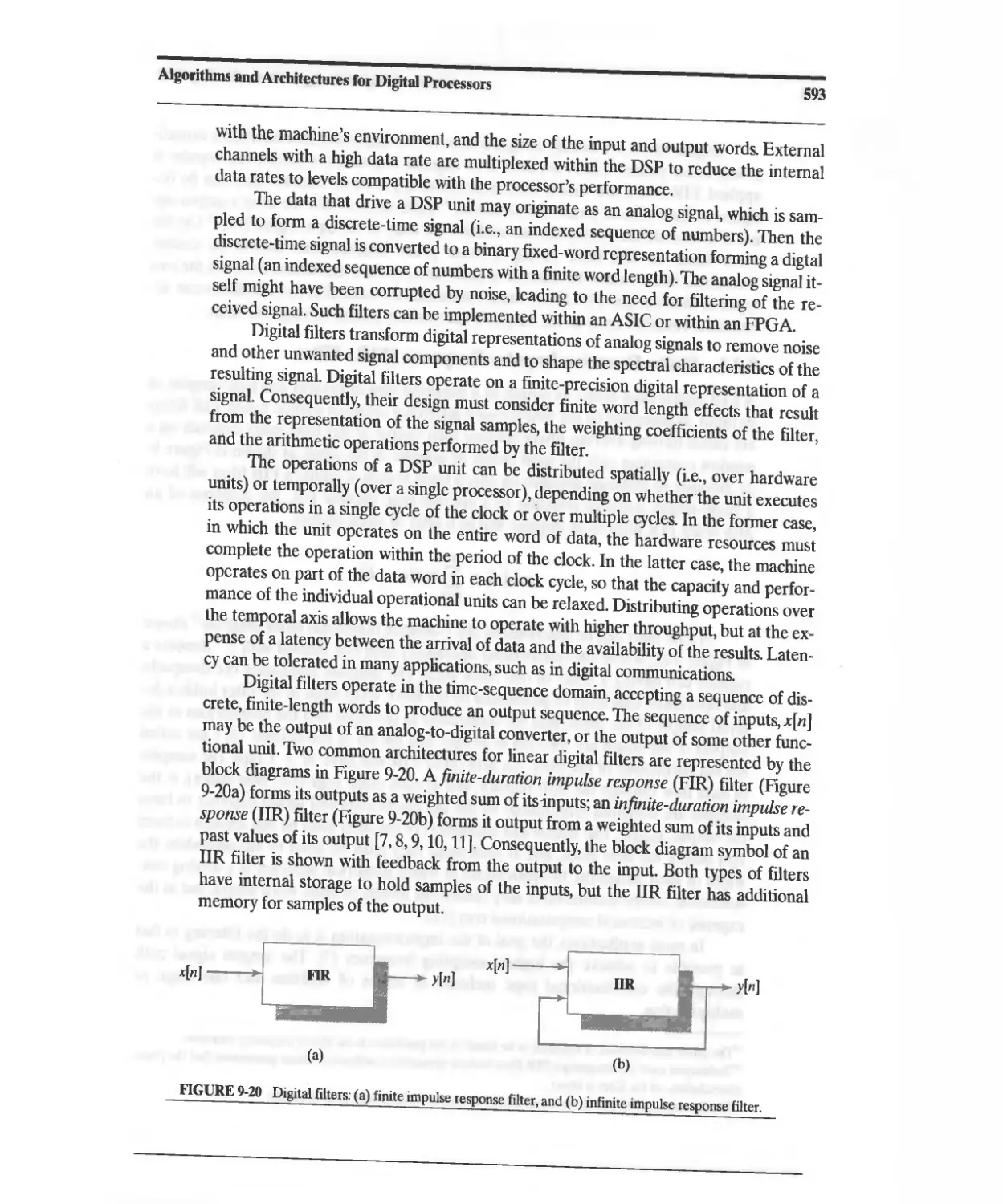
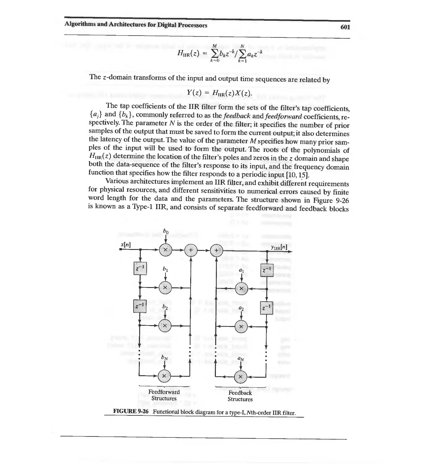
9.3 Digital Filters and Signal Processors 591
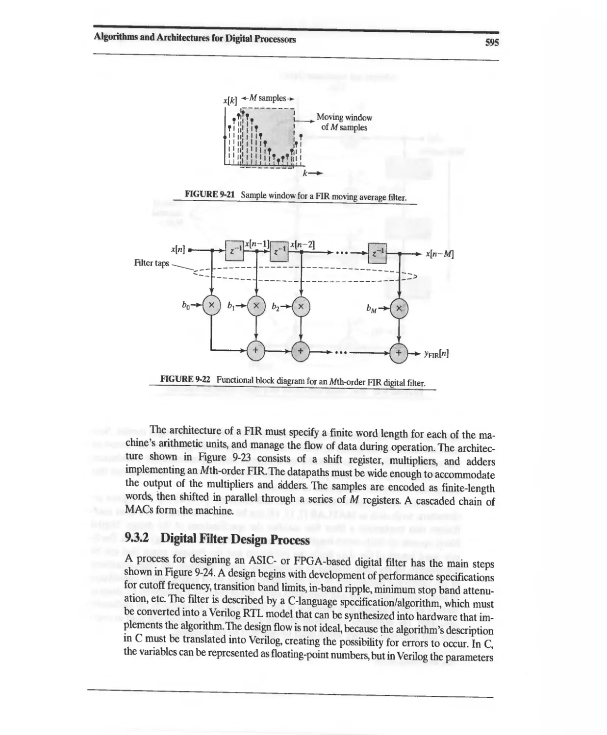
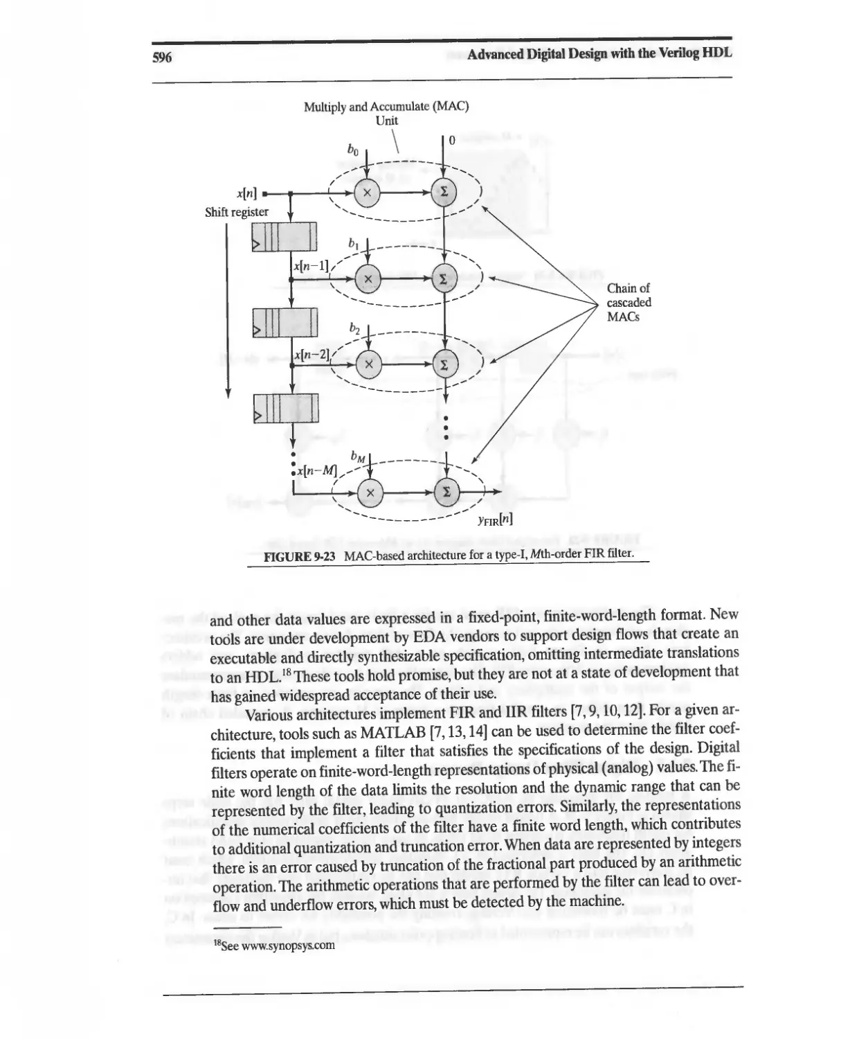
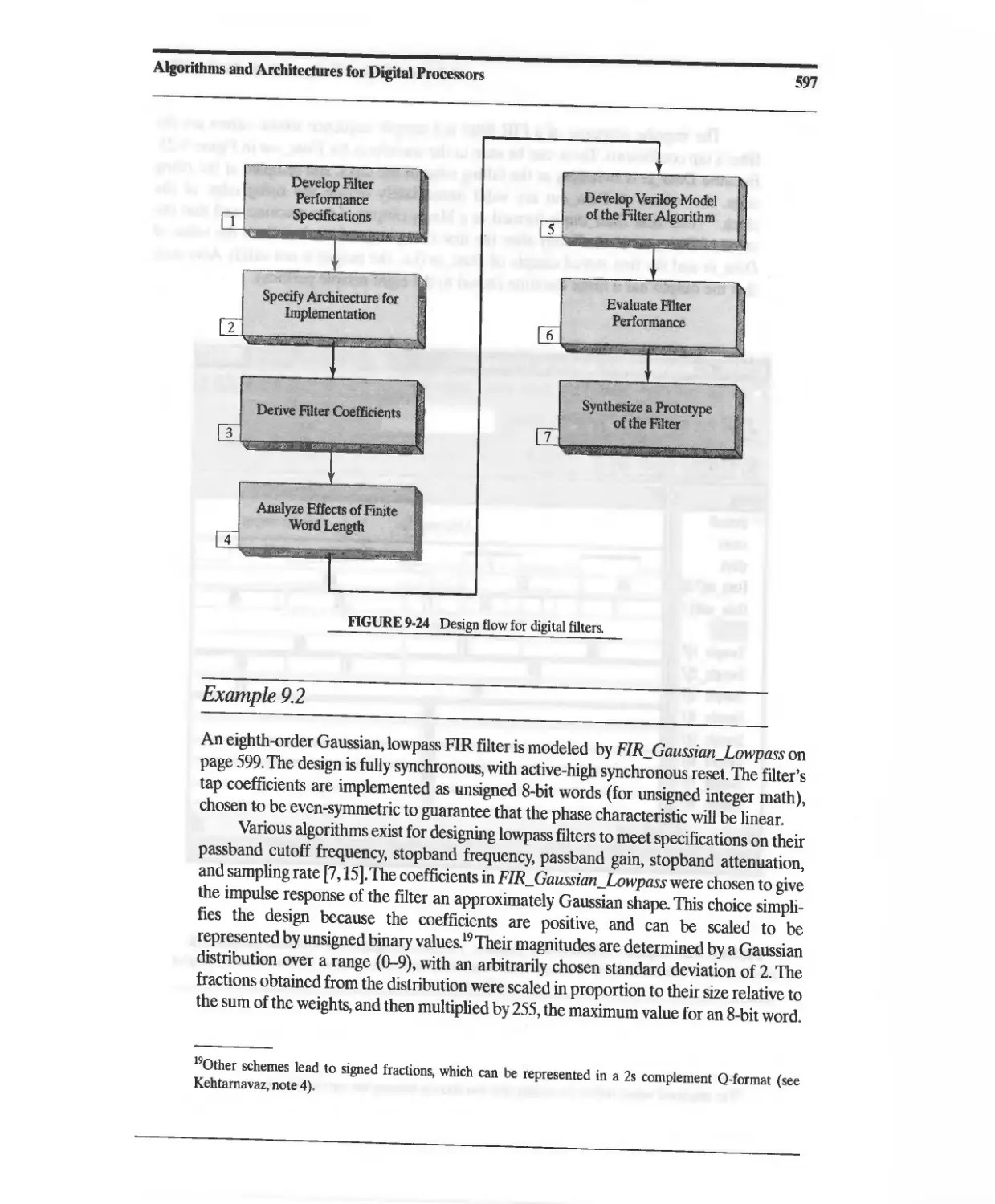
9.3.1 Finite-Duration Impulse Response (FIR) Filter 594
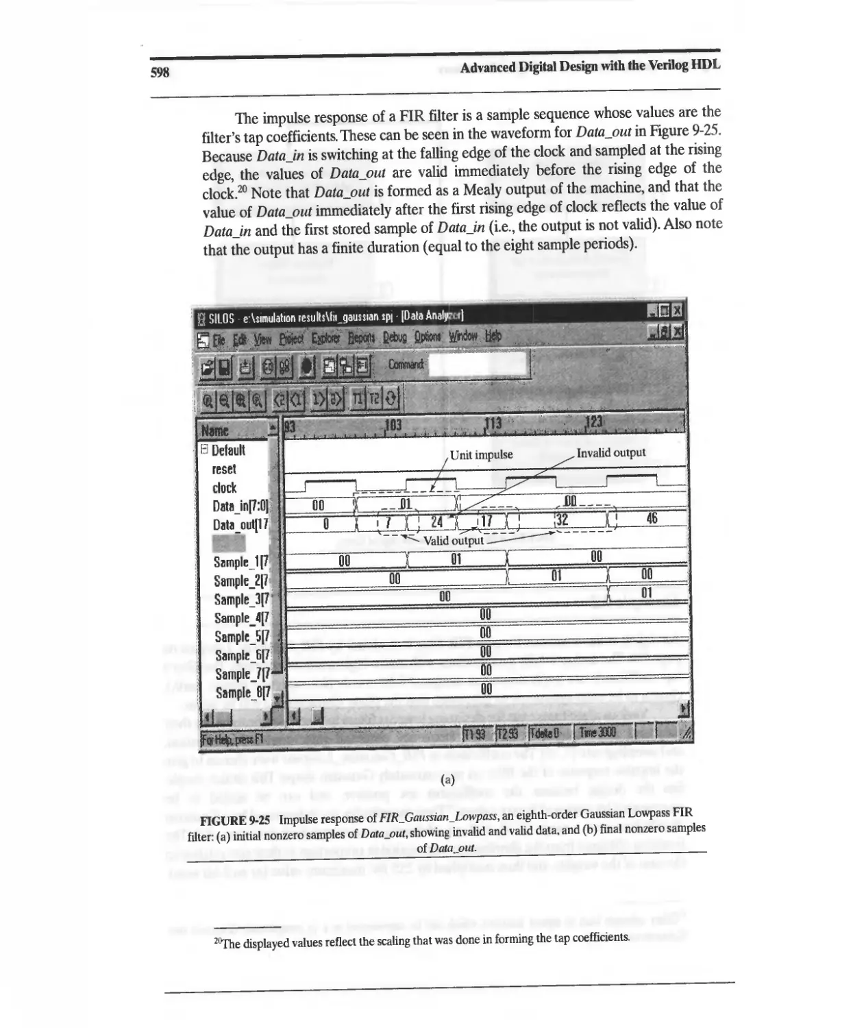
9.3.2 Digital Filter Design Process 595
9.3.3 Infinite-Duration Impulse Response (IIR) Filter 600
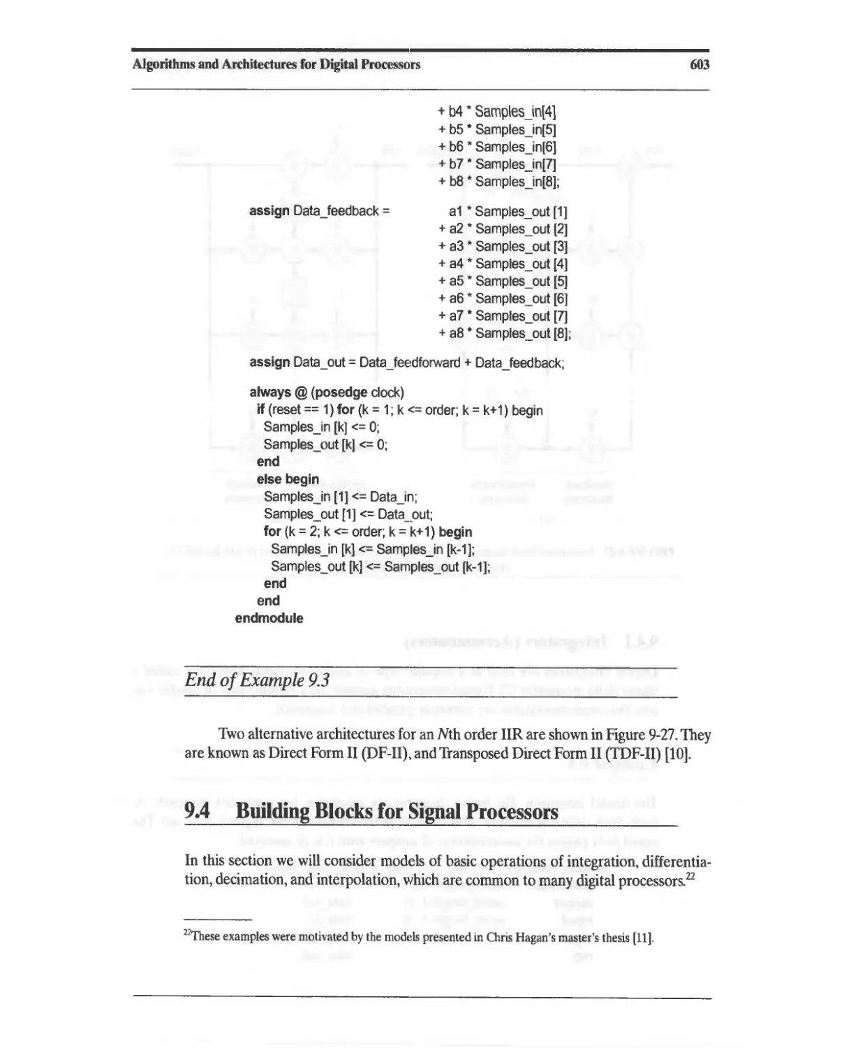
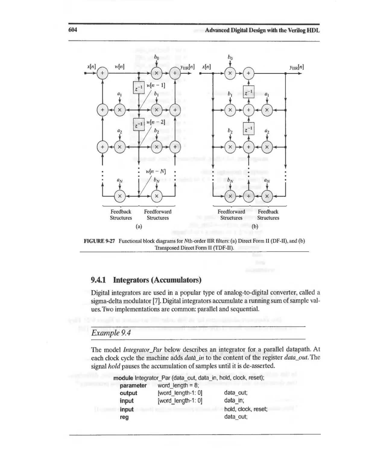
9.4 Building Blocks for Signal Processors 603
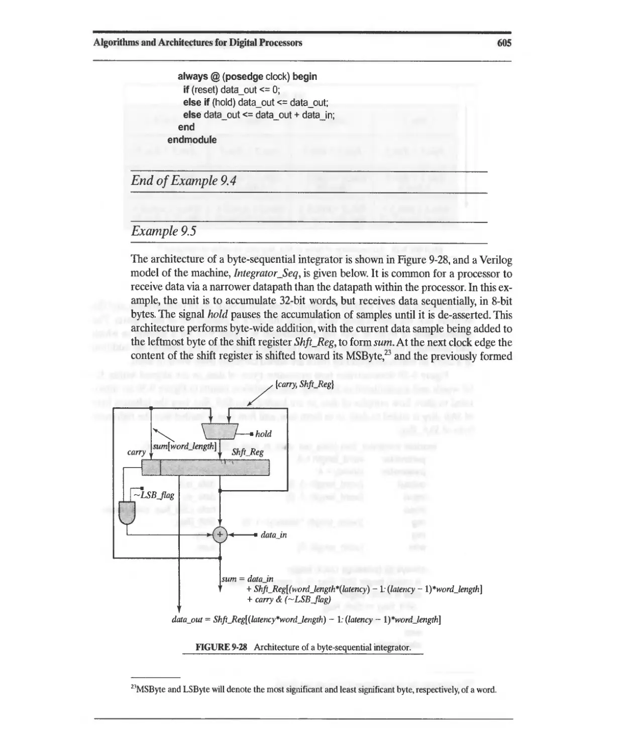
9.4.1 Integrators (Accumulators) 604
9.4.2 Differentiators 608
9.4.3 Decimation and Interpolation Filters 608
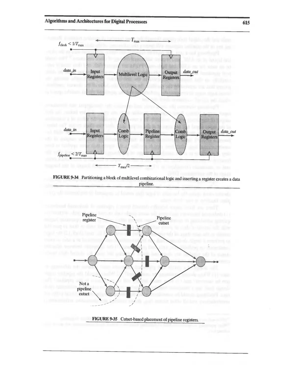
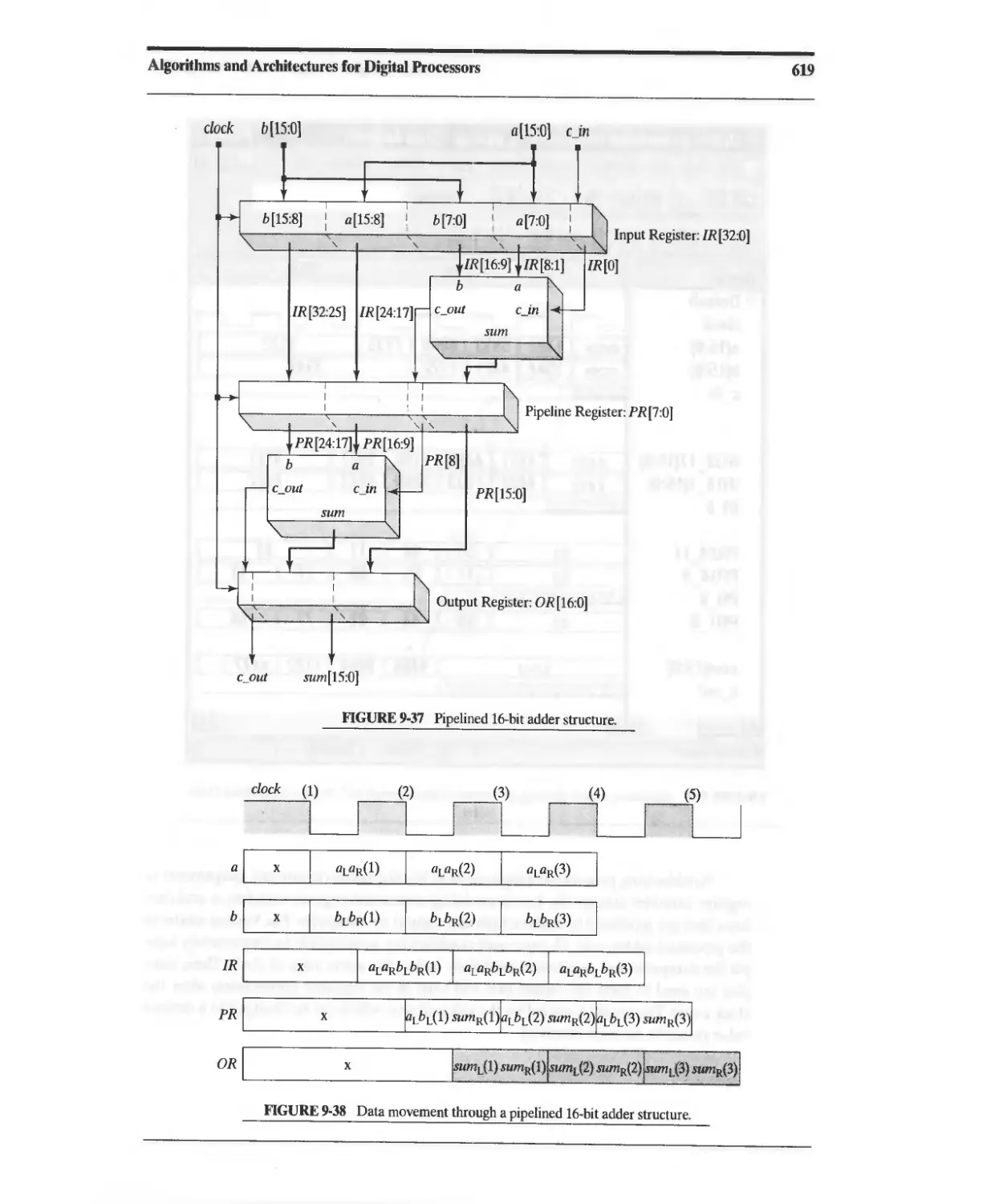
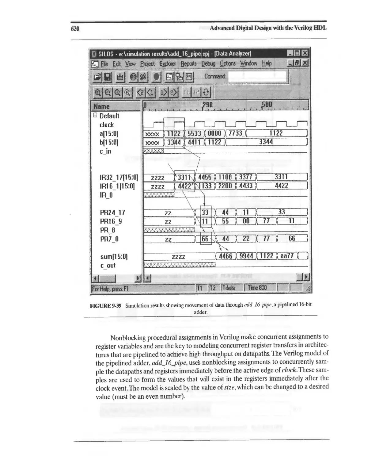
9.5 Pipelined Architectures 614
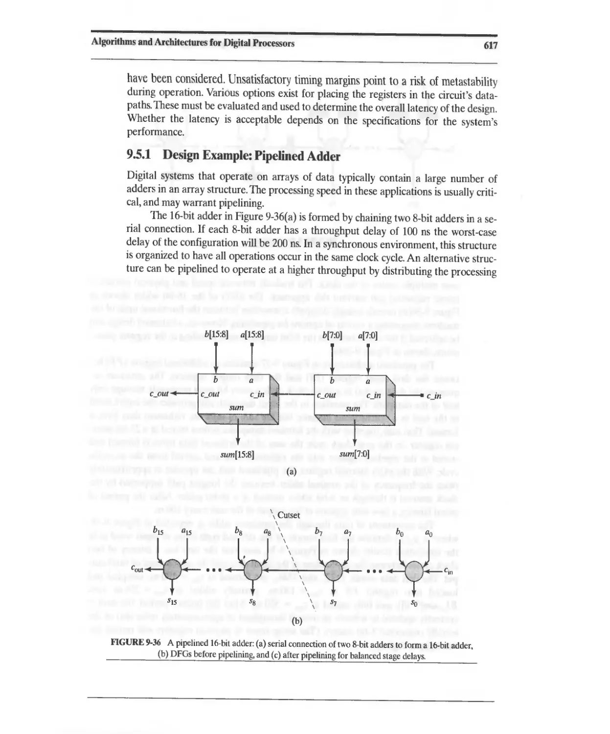
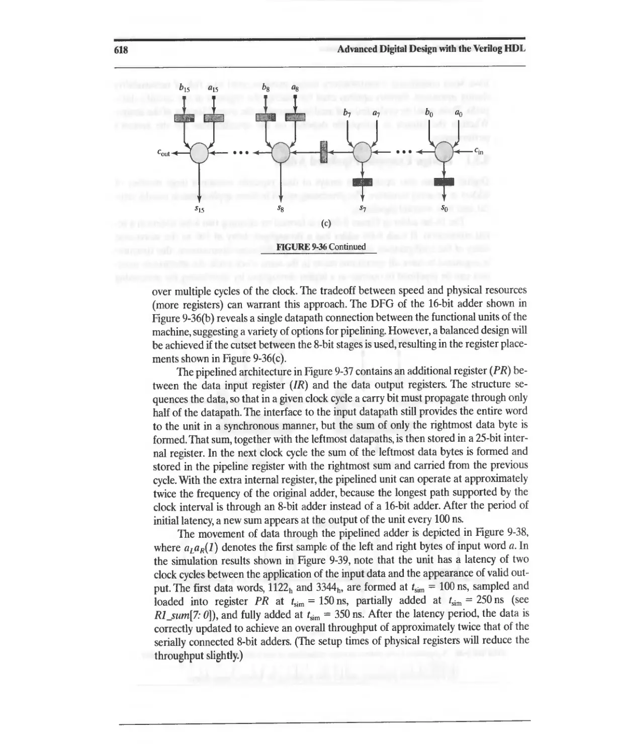
9.5.1 Design Example: Pipelined Adder 617
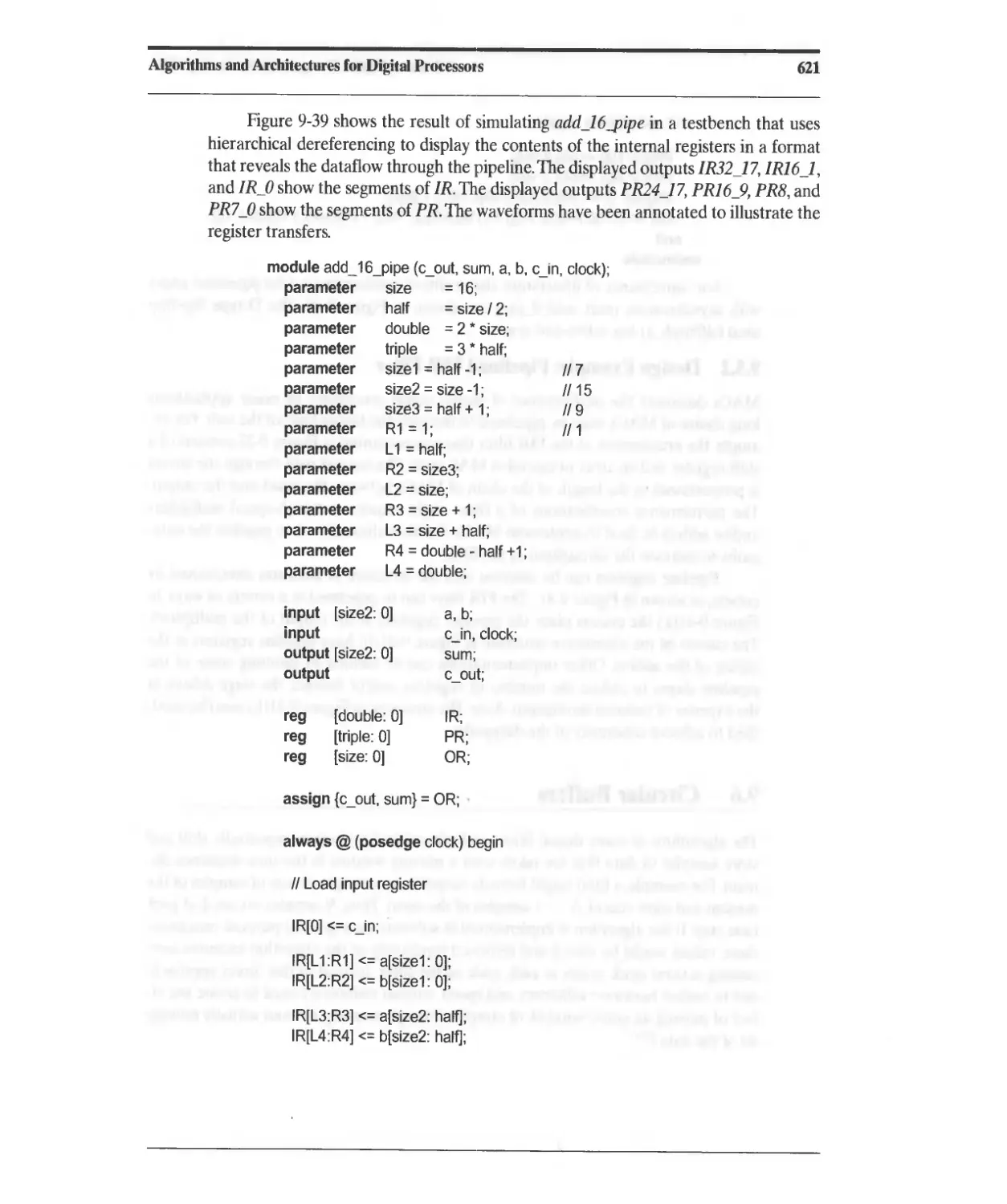
9.5.2 Design Example: Pipelined FIR Filter 622
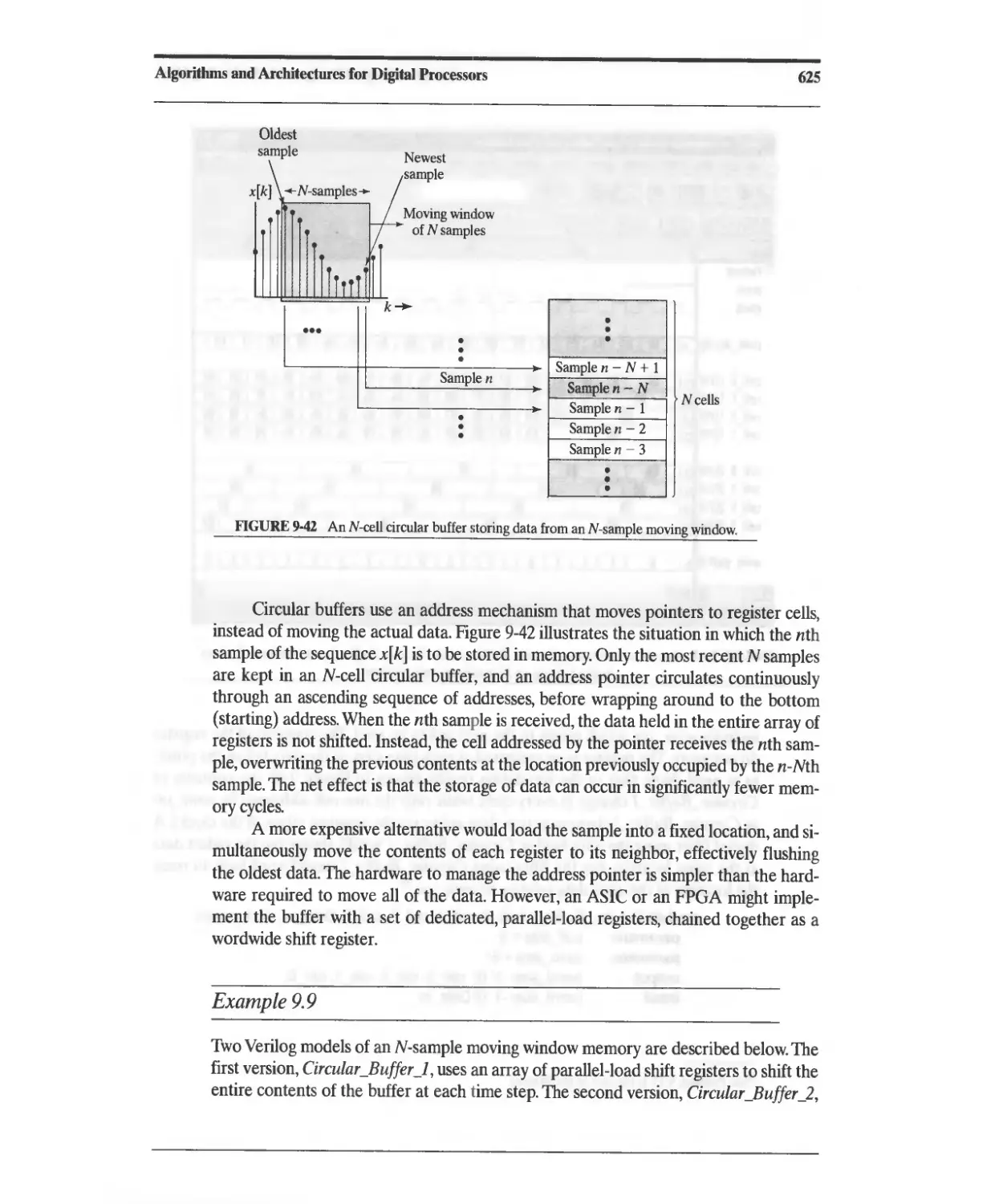
9.6 Circular Buffers 622
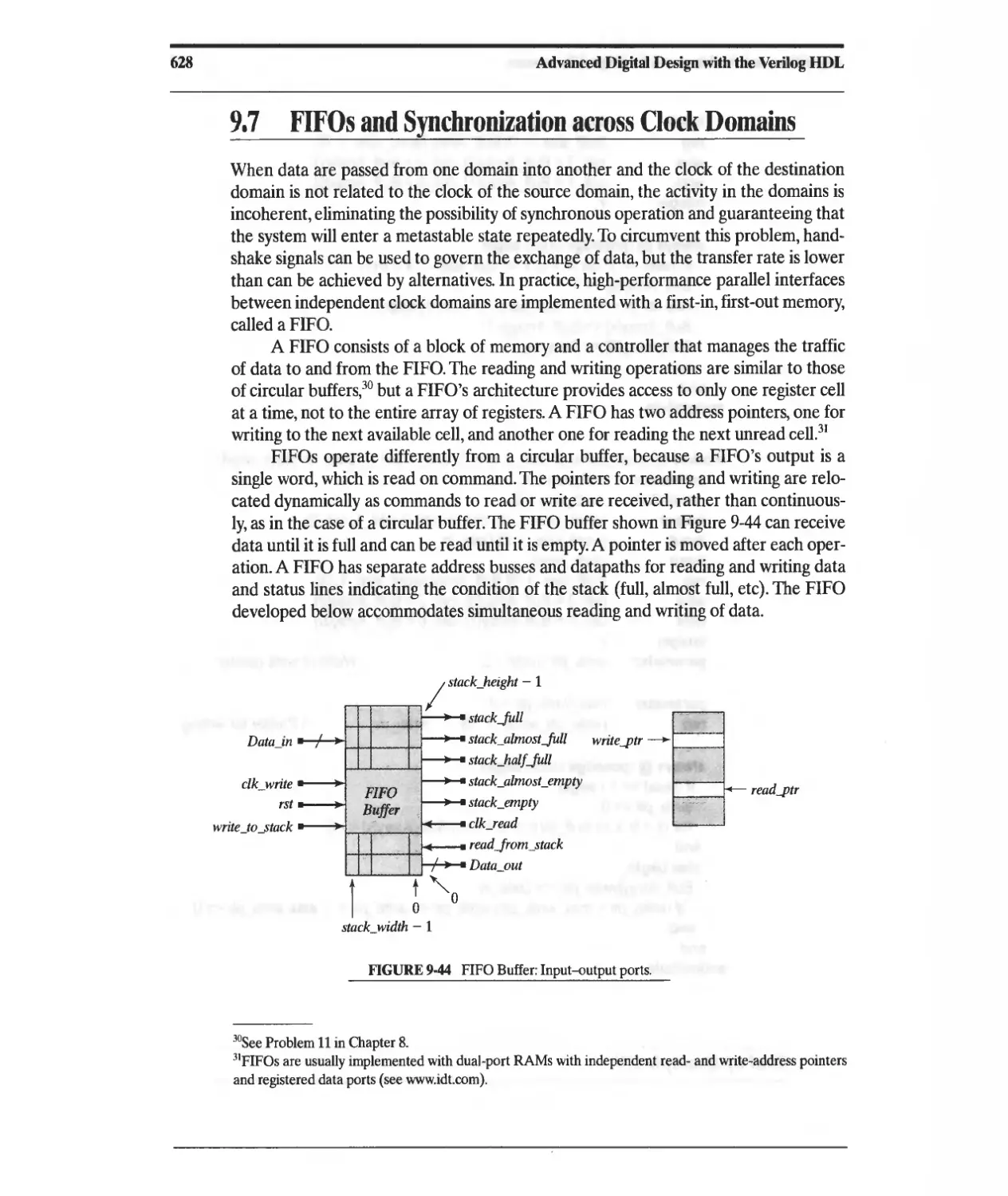
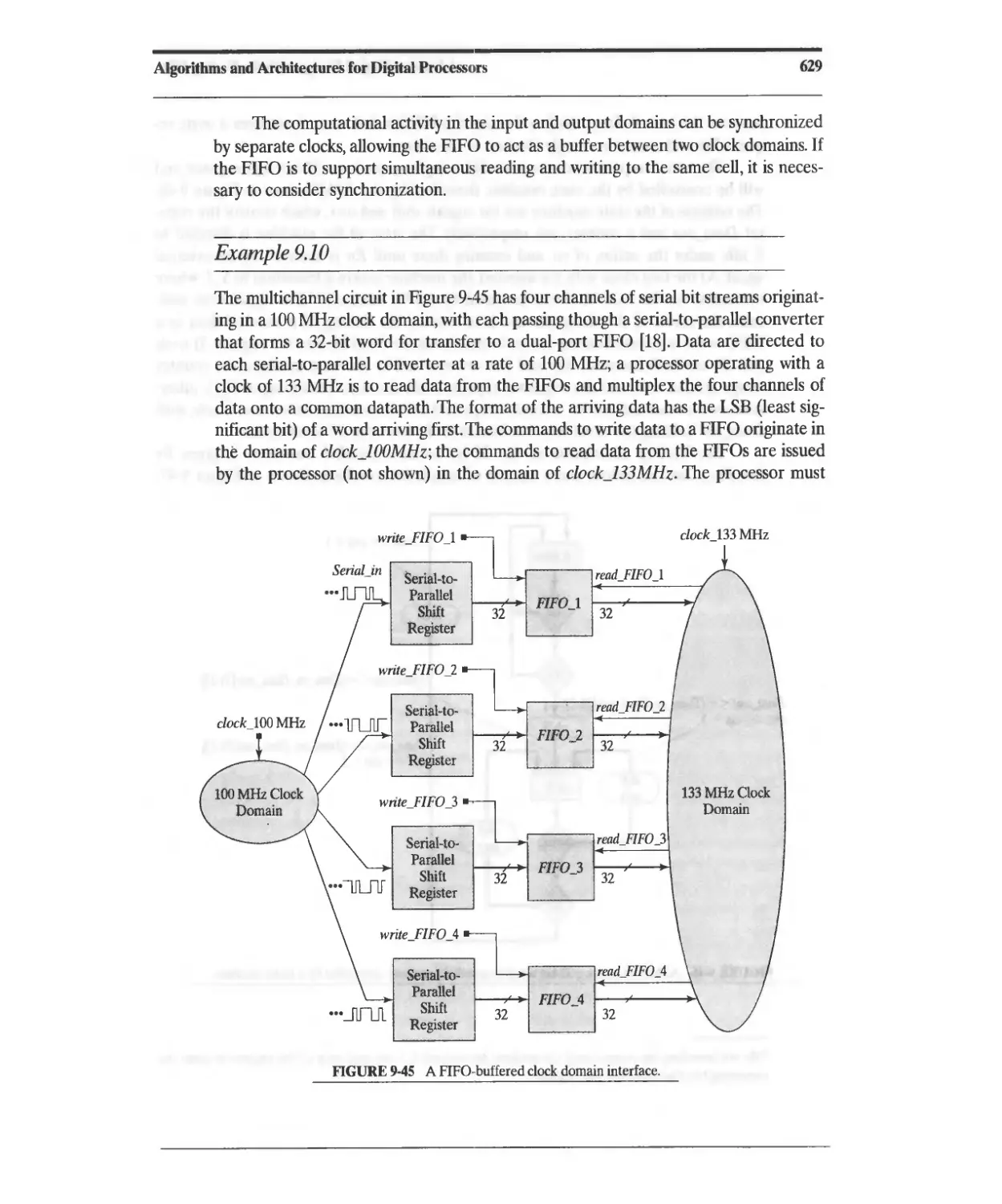
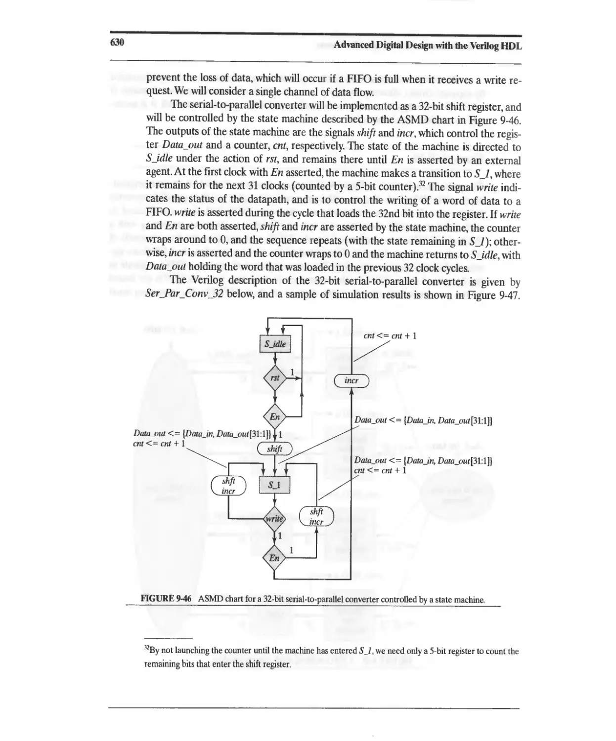
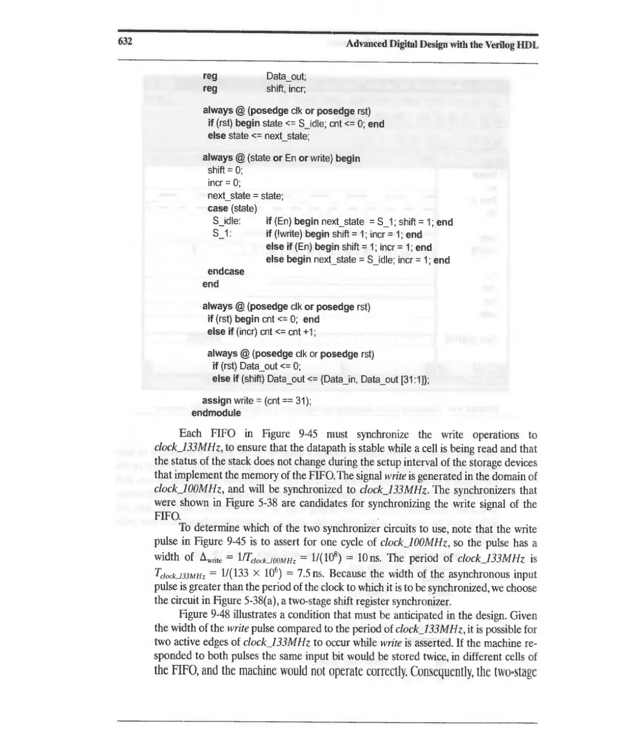
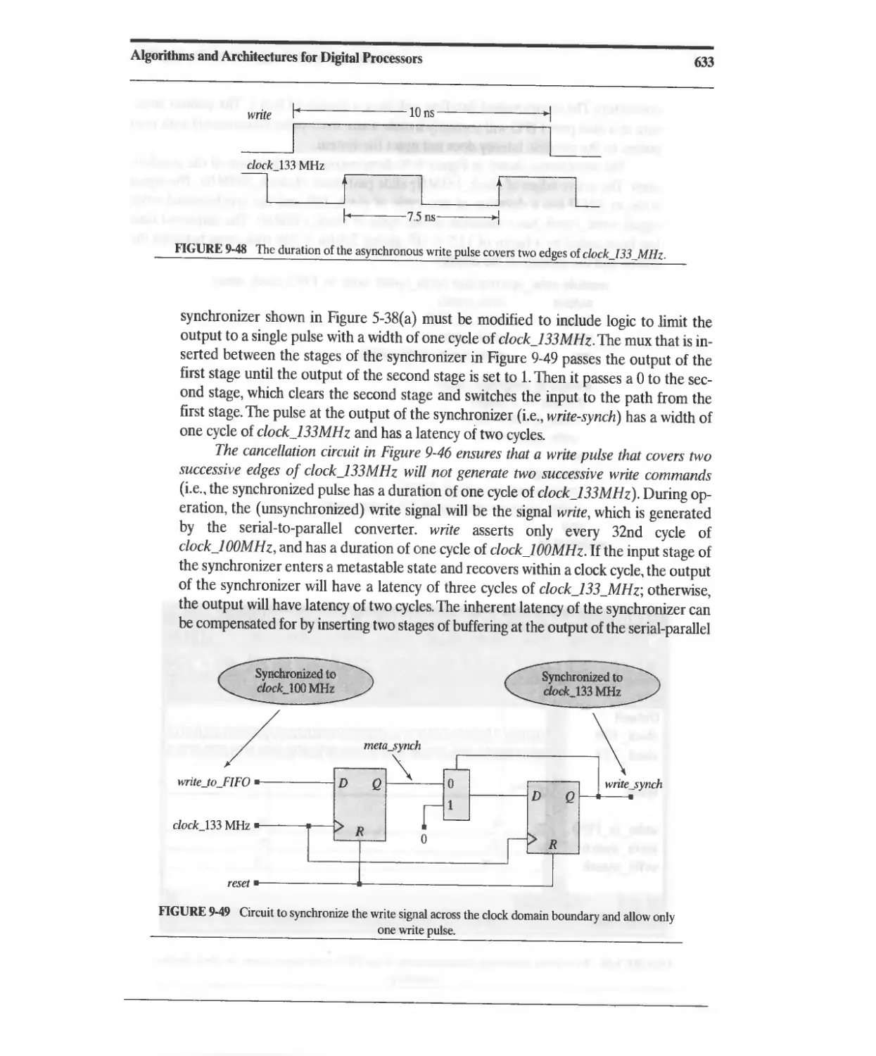
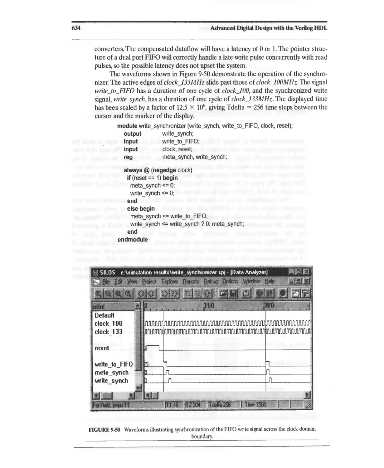
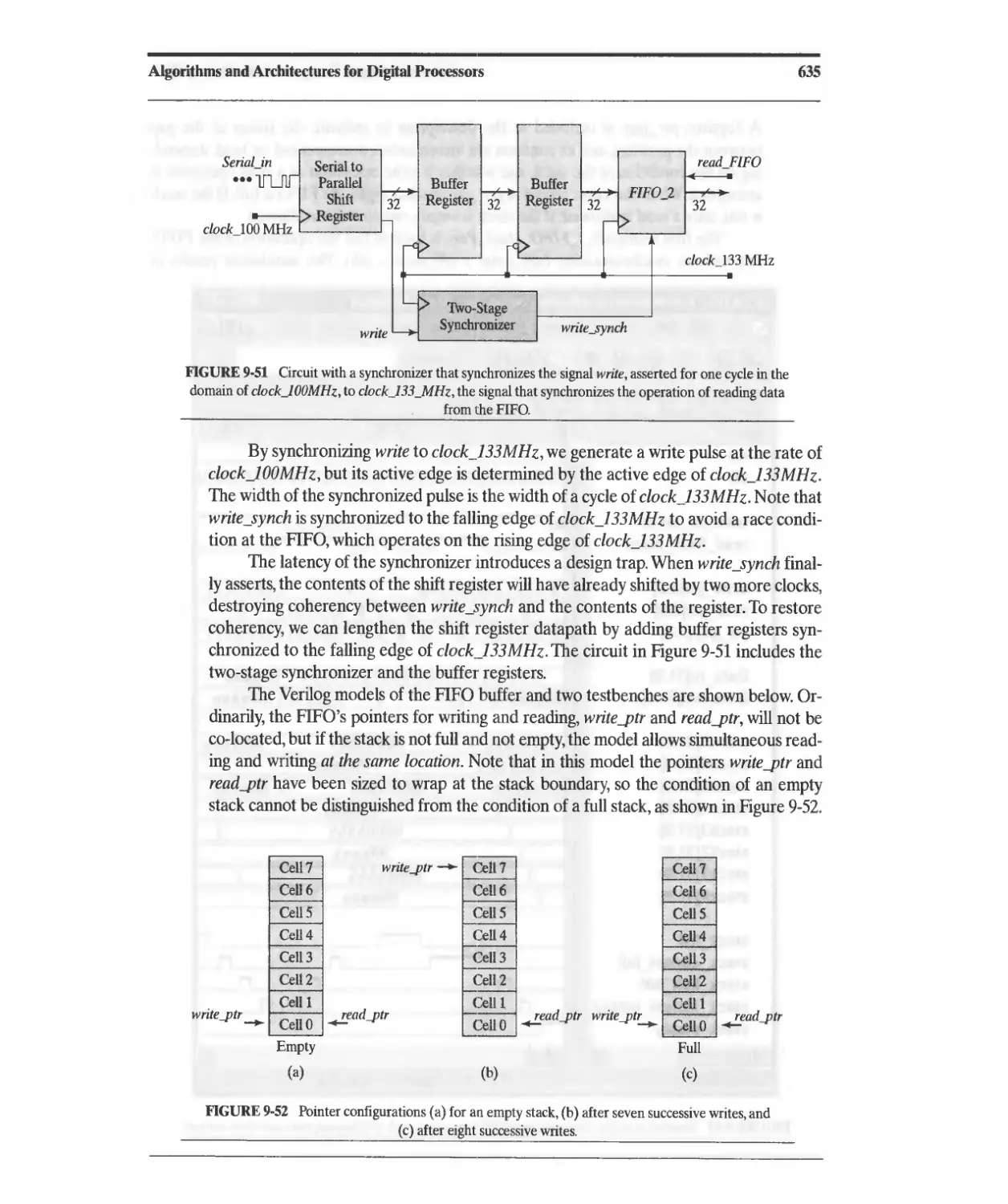
9.7 FIFOs and Synchronization across Clock Domains 628
References 642
Problems 642
xii
Contents
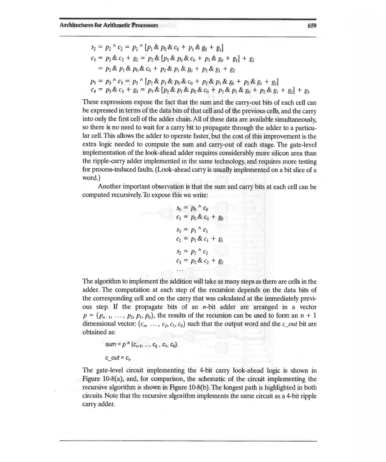
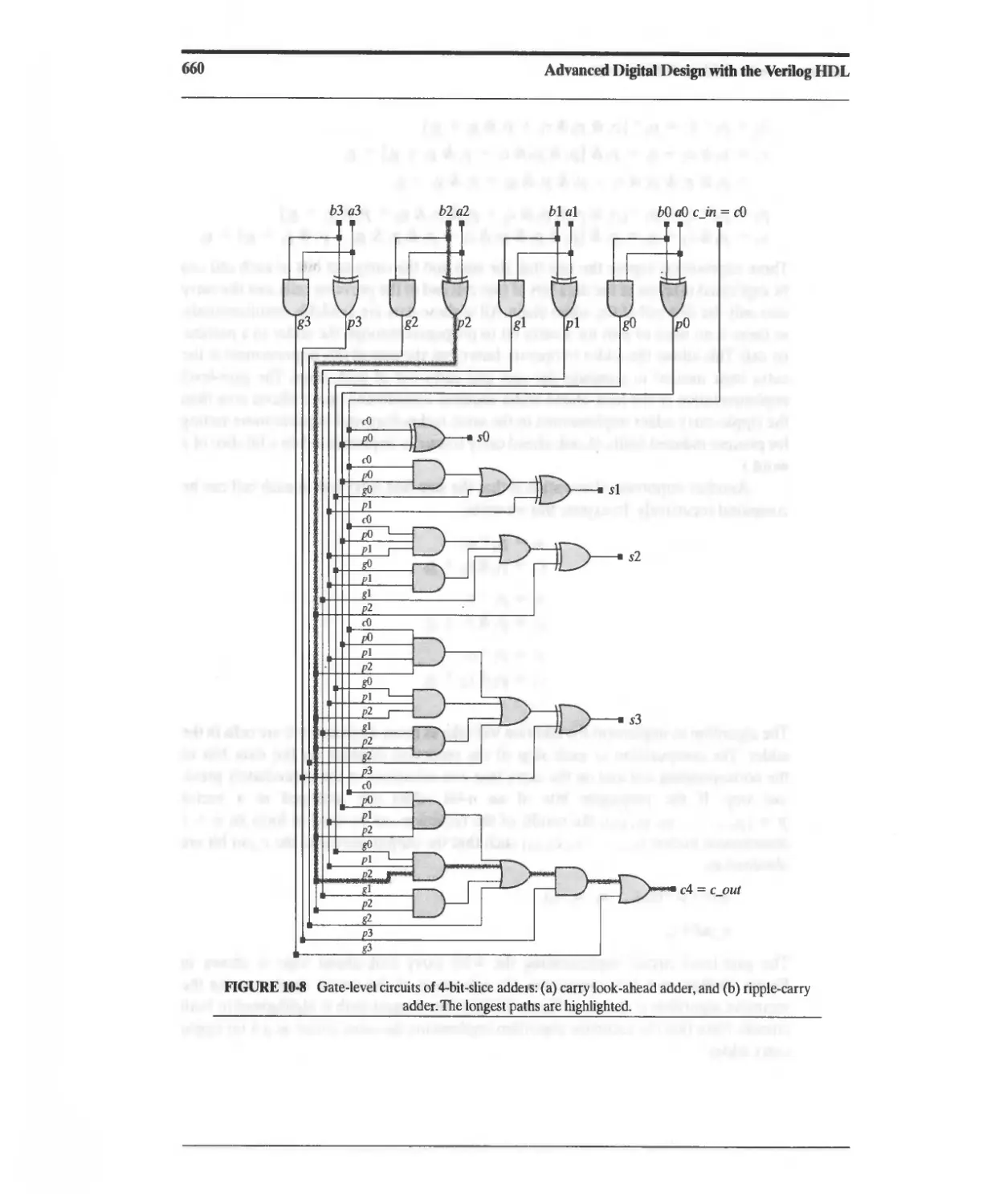
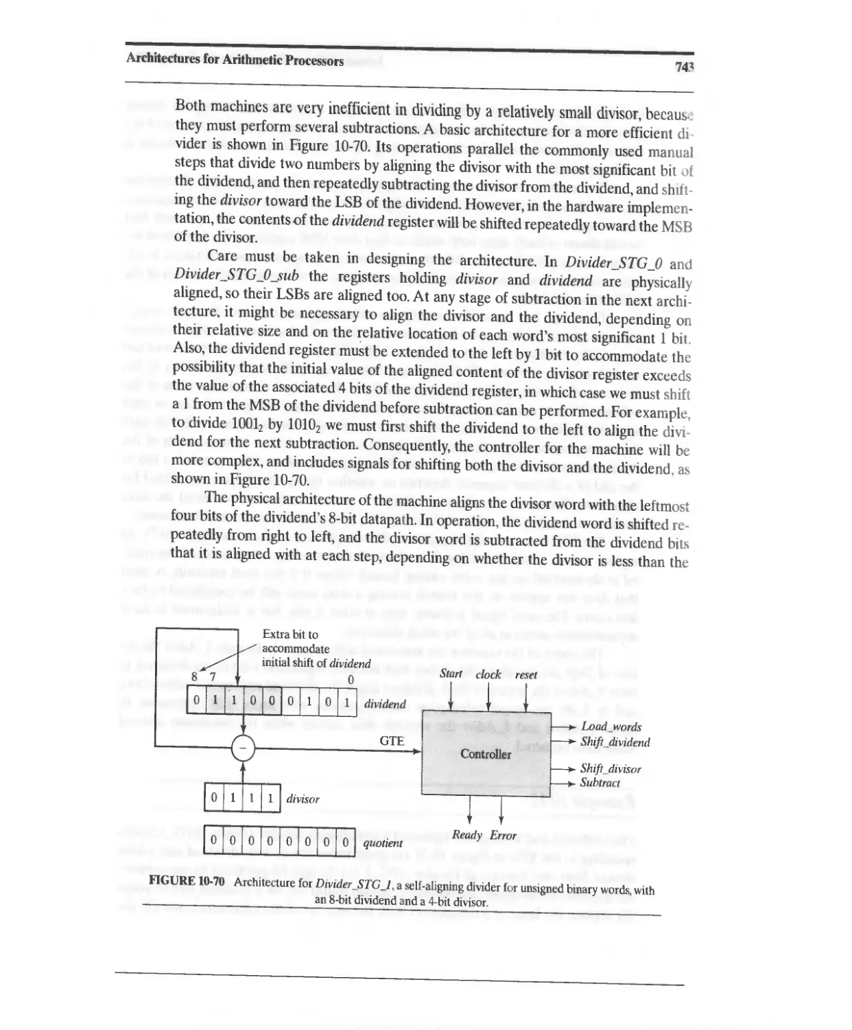
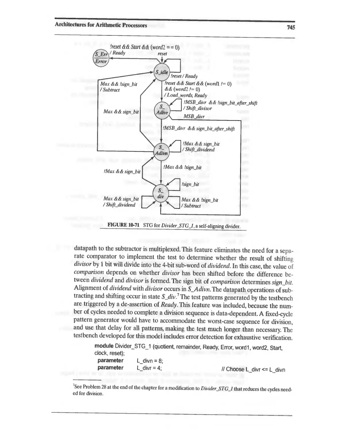
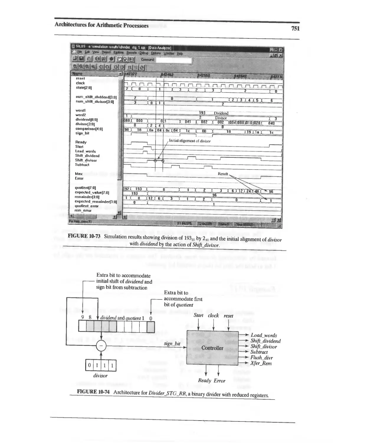
10 Architectures for Arithmetic Processors 651
10.1 Number Representation 651
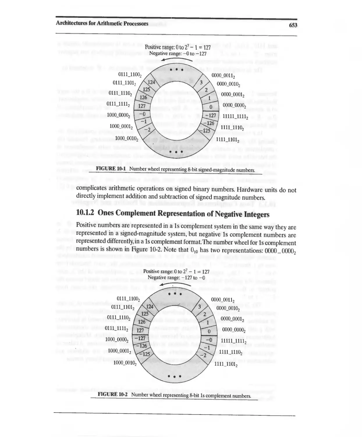
10.\.1 Signed Magnitude Representation of Negative Integers 652
10.1.2 Ones Complement Representation of Negative Integers 653
10.1.3 Twos Complement Representation of Positive and
Negative Integers 654
10.1.4 Representation of Fractions 656
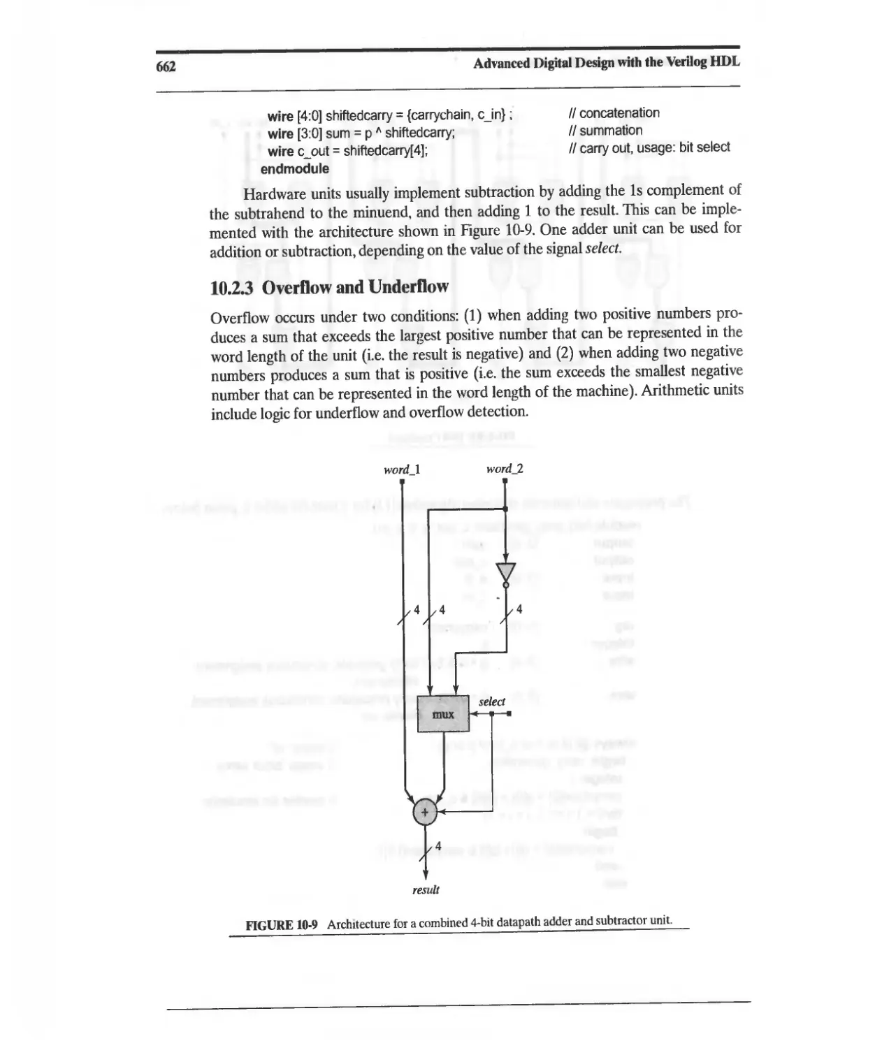
10.2 Functional Units for Addition and Subtraction 656
10.2.1 Ripple-Carry Adder 656
10.2.2 Carry Look-Ahead Adder 656
10.2.3 Overflow and Underflow 662
10.3 Functional Units for Multiplication 663
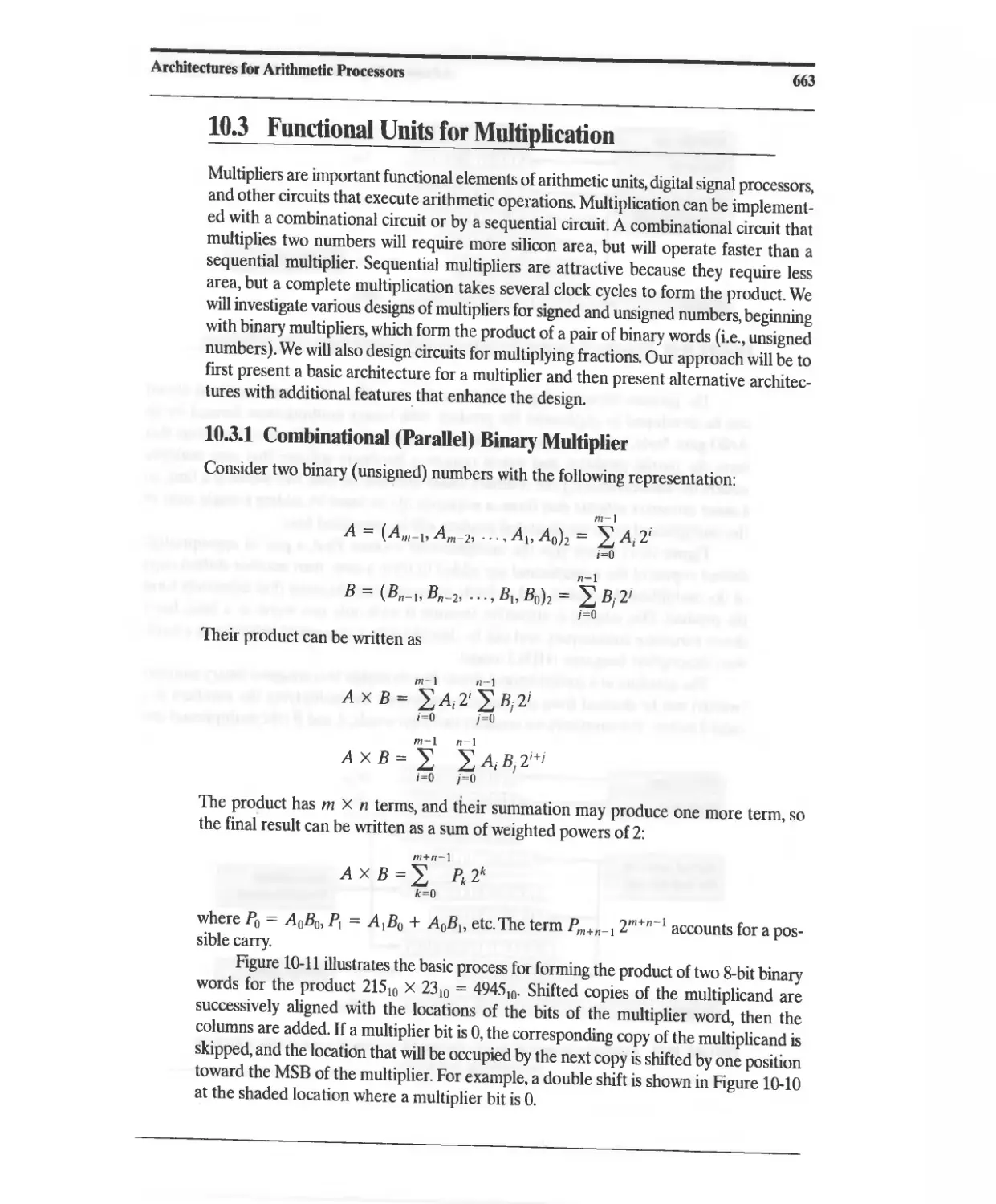
10.3.1 Combinational (Parallel) Binary Multiplier 663
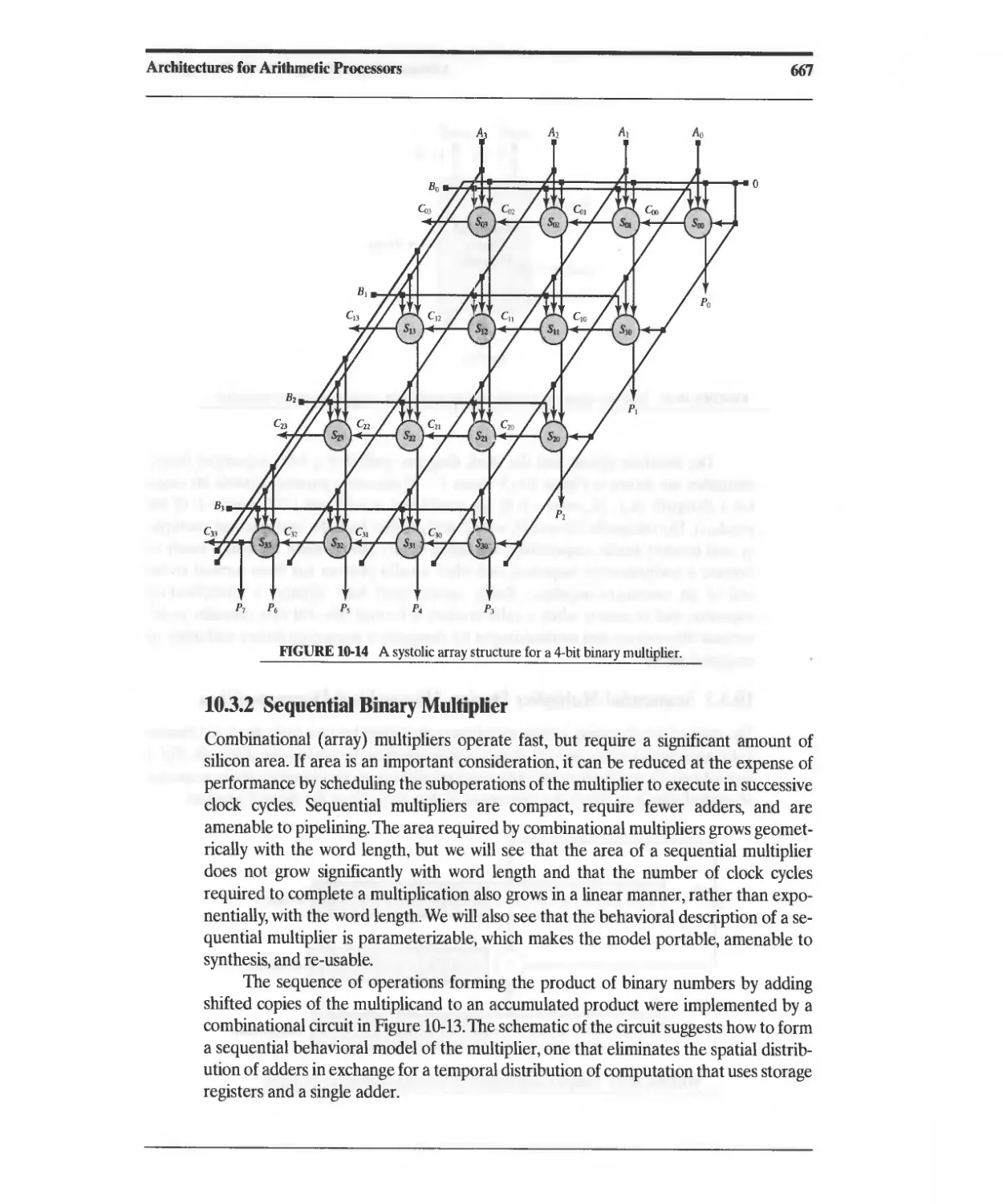
10.3.2 Sequential Binary Multiplier 667
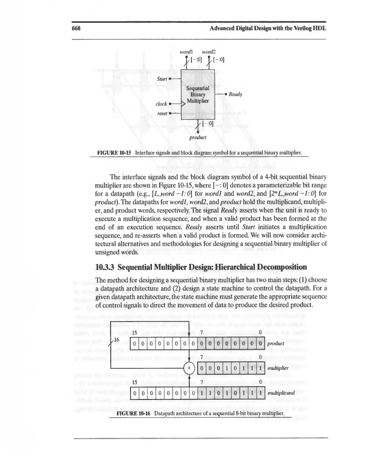
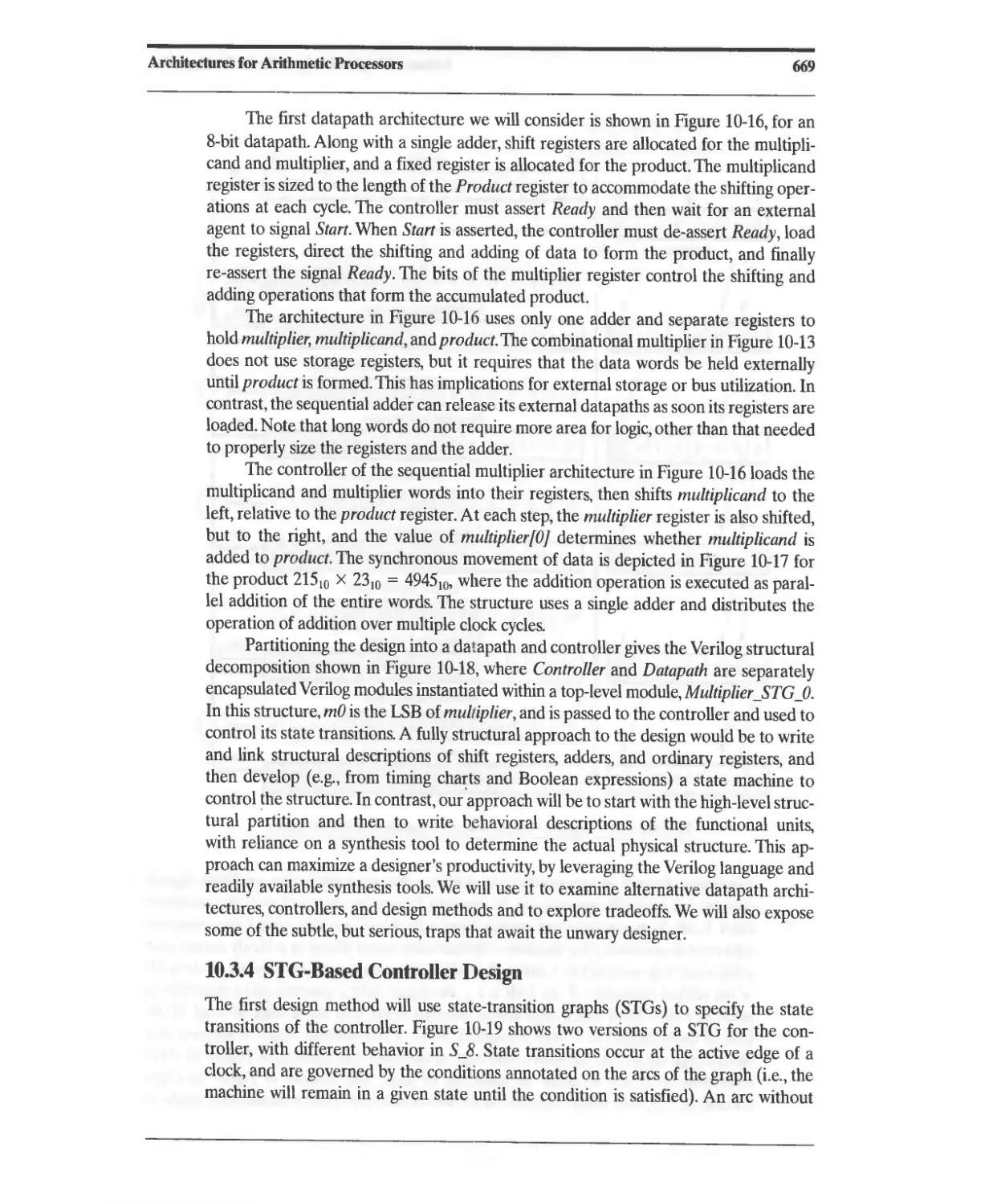
10.3.3 Sequential Multiplier Design: Hierarchical Decomposition 668
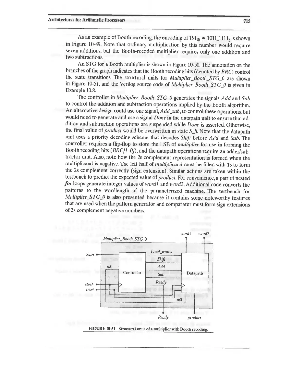
10.3.4 STG-Based Controller Design 669
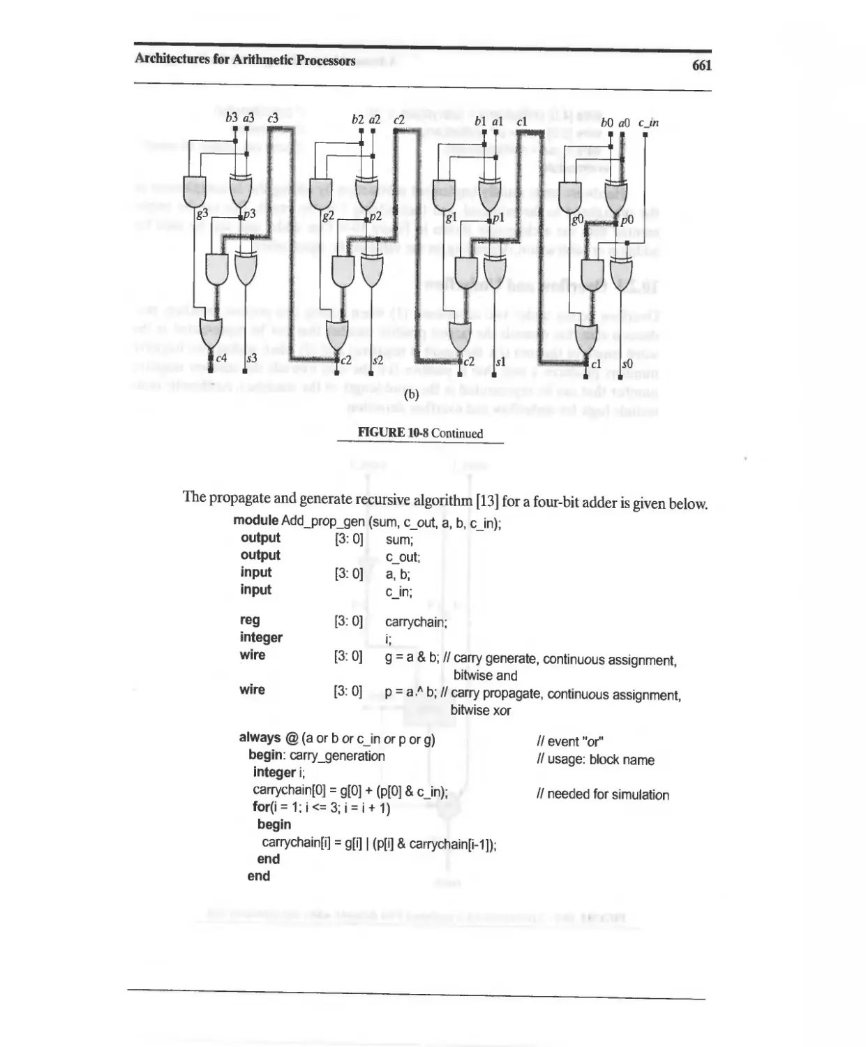
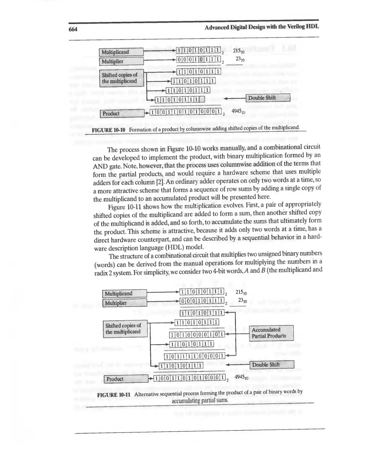
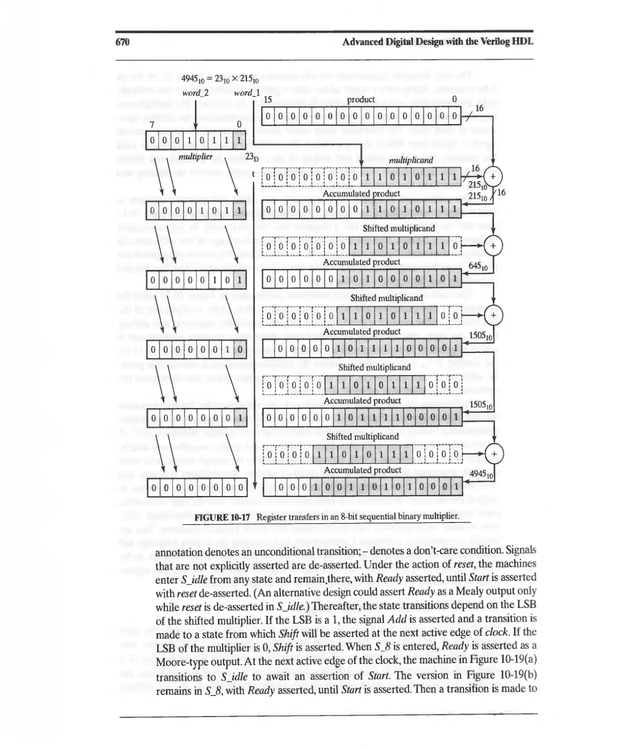
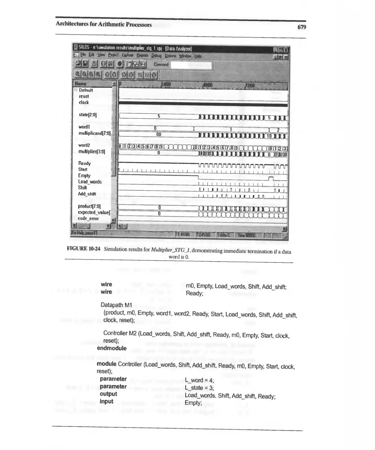
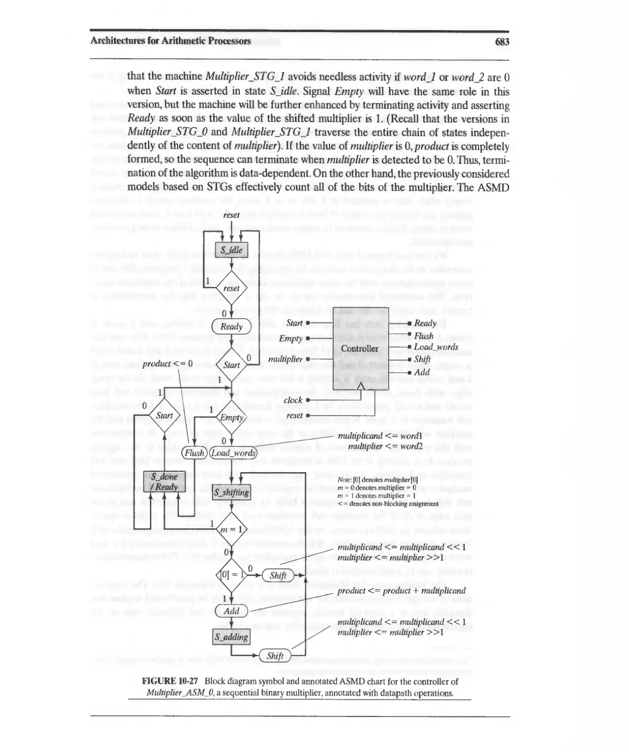
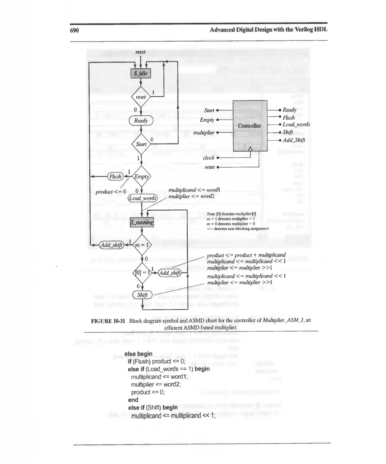
10.3.5 Efficient STG-Based Sequentiai Binary Multiplier 676
10.3.6 ASMD-Based Sequential Binary Multiplier 682
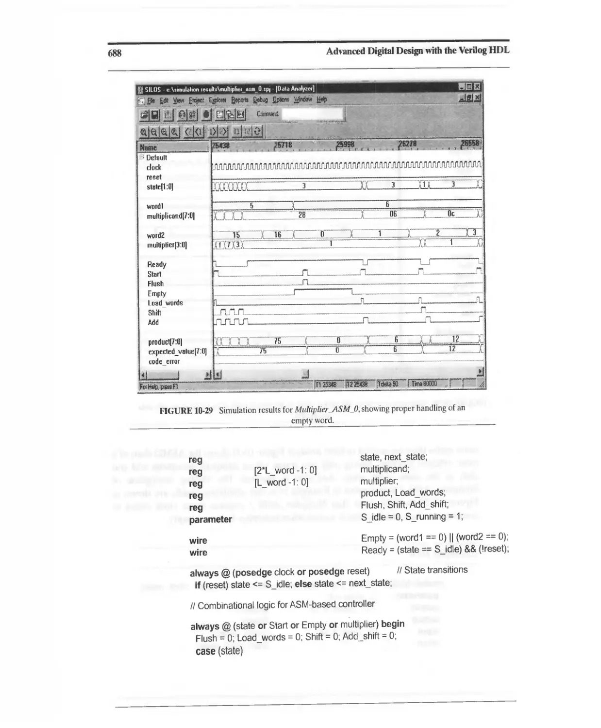
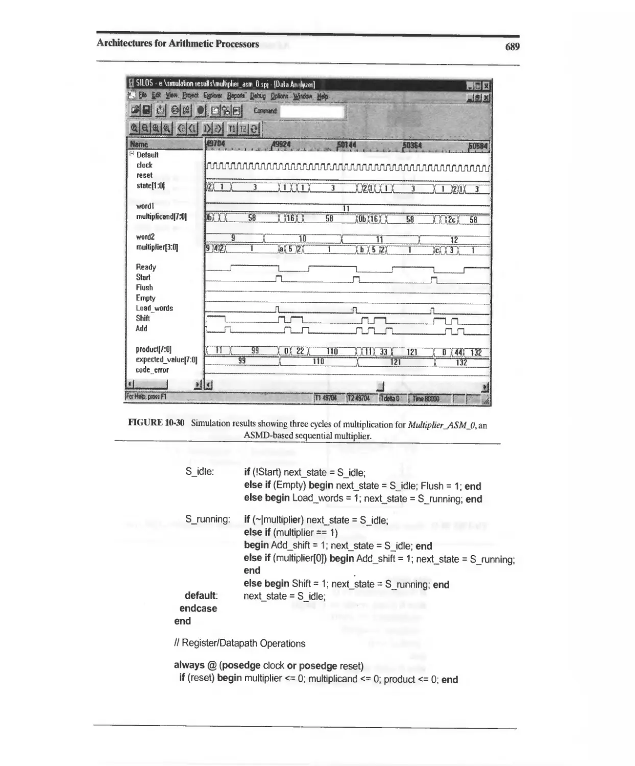
10.3.7 Efficient ASM-Based Sequential Multiplier 686
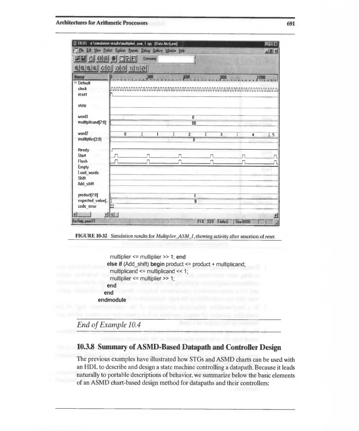
10.3.8 Summary of ASMD-Based Datapath Controller Design 691
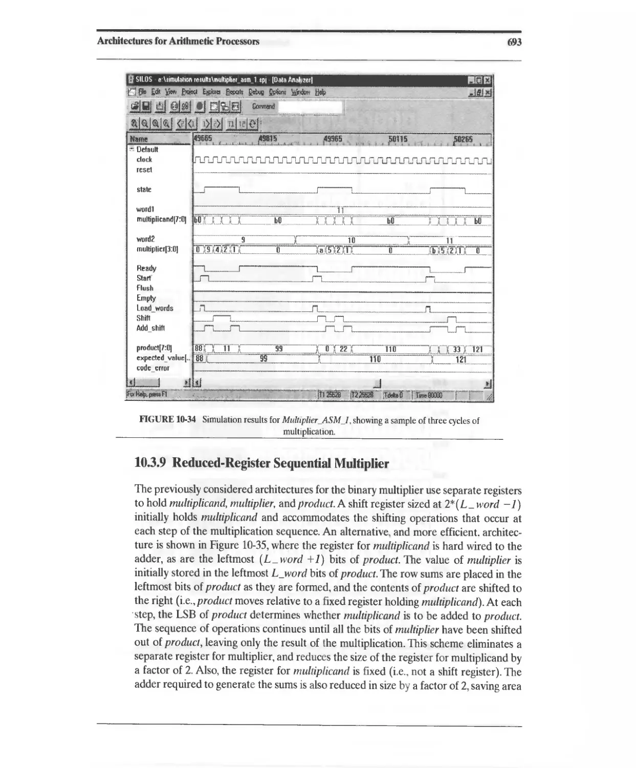
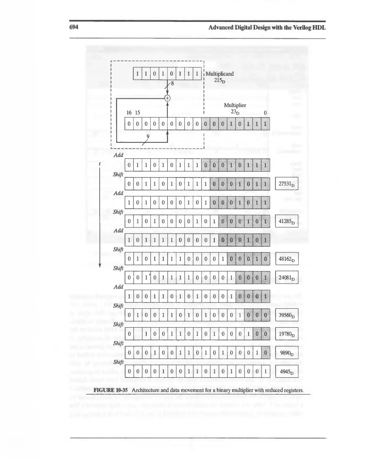
10.3.9 Reduced-Register Sequential Multiplier 693
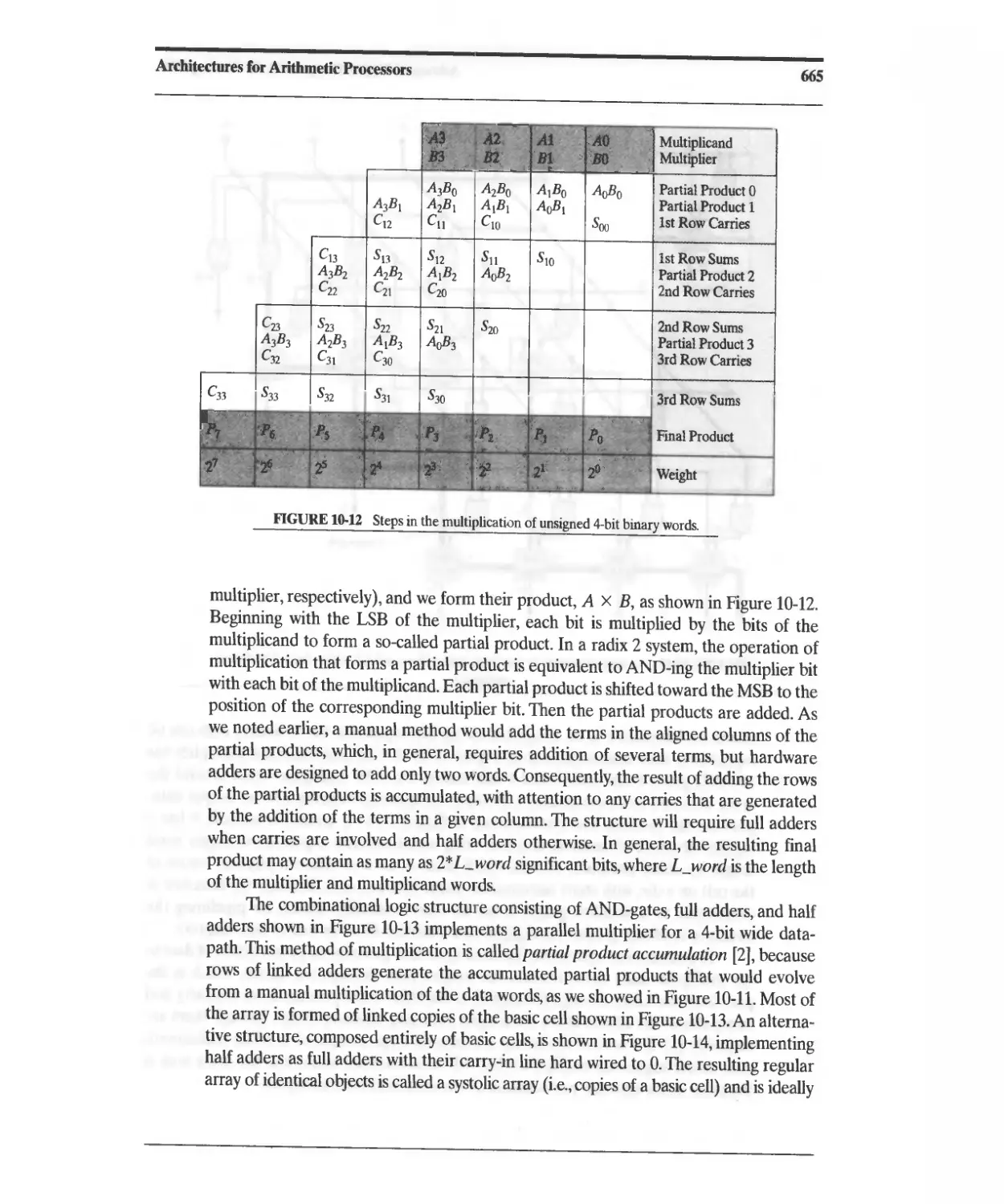
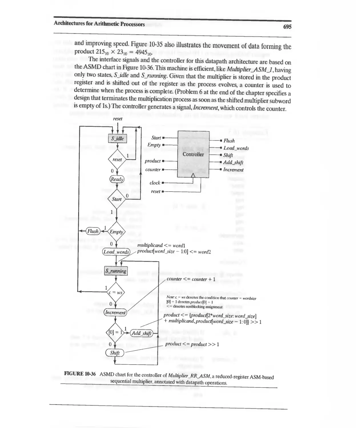
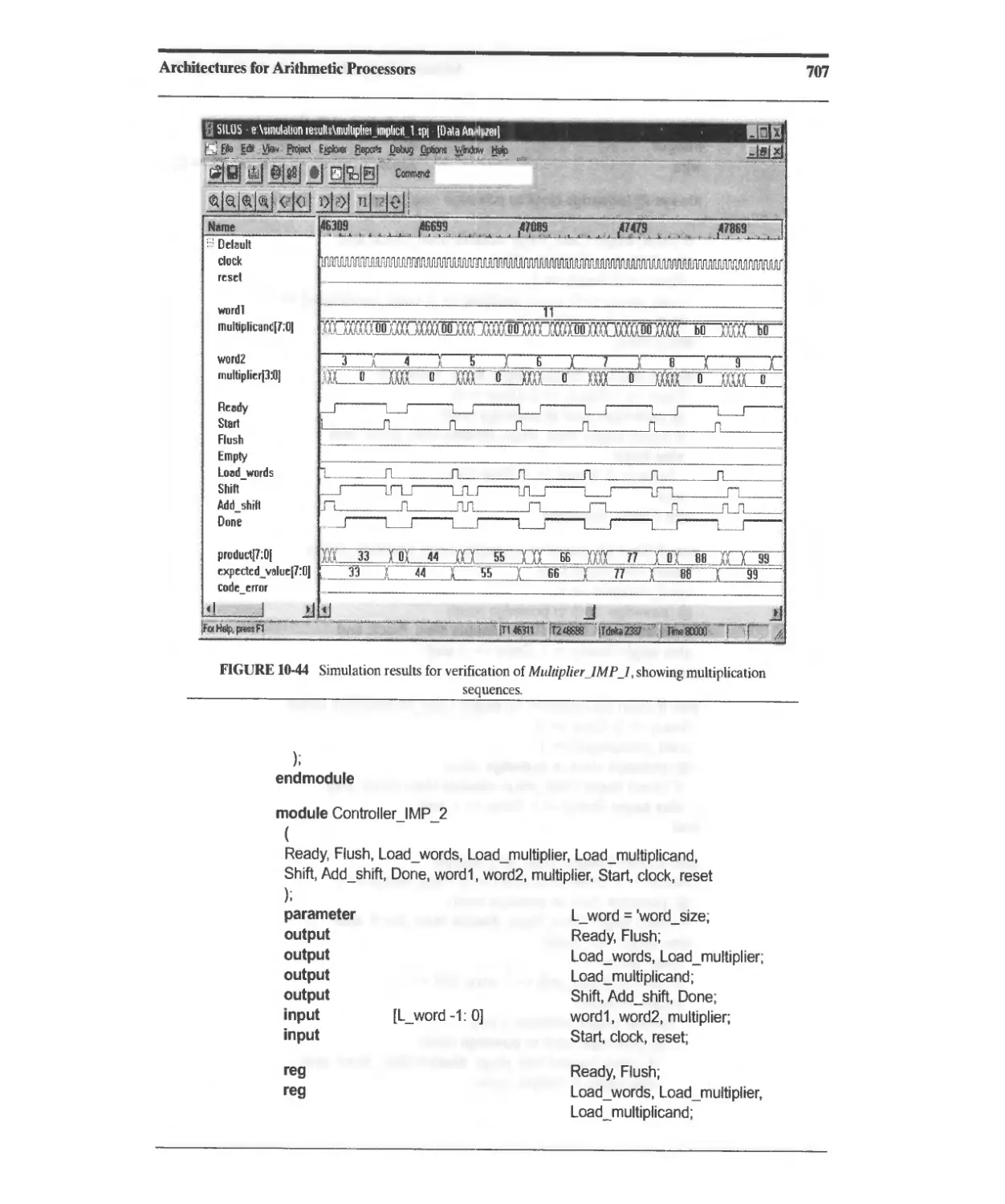
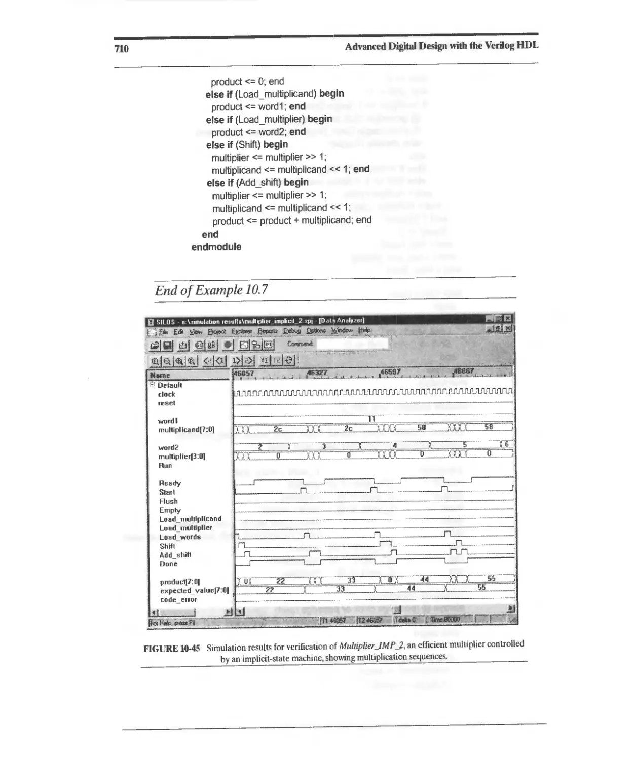
10.3.10 Implicit-State-Machine Binary Multiplier 698
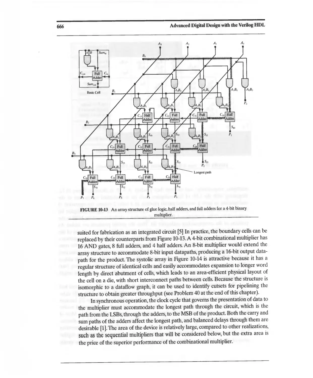
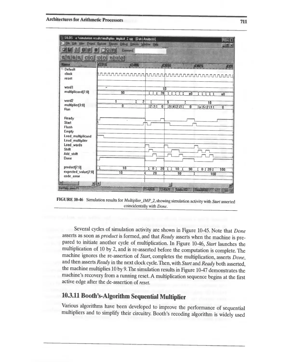
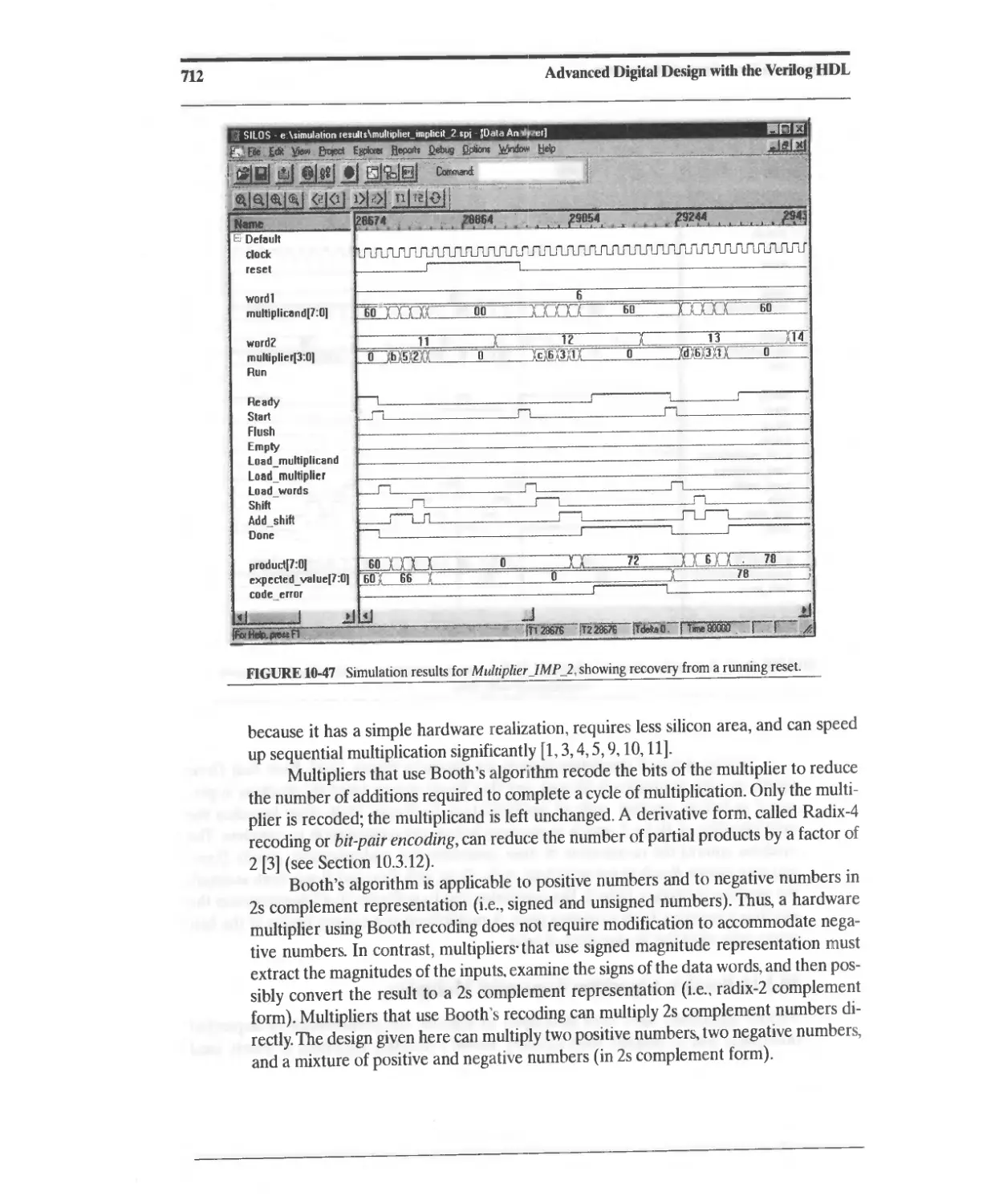
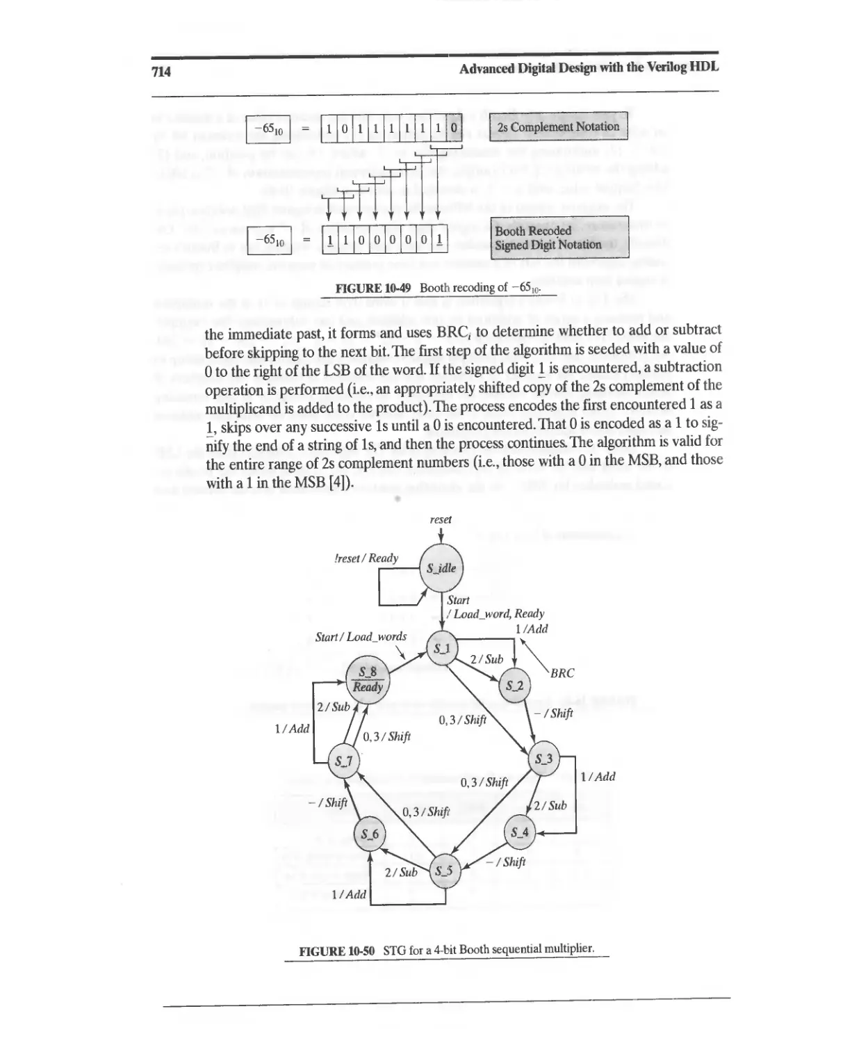
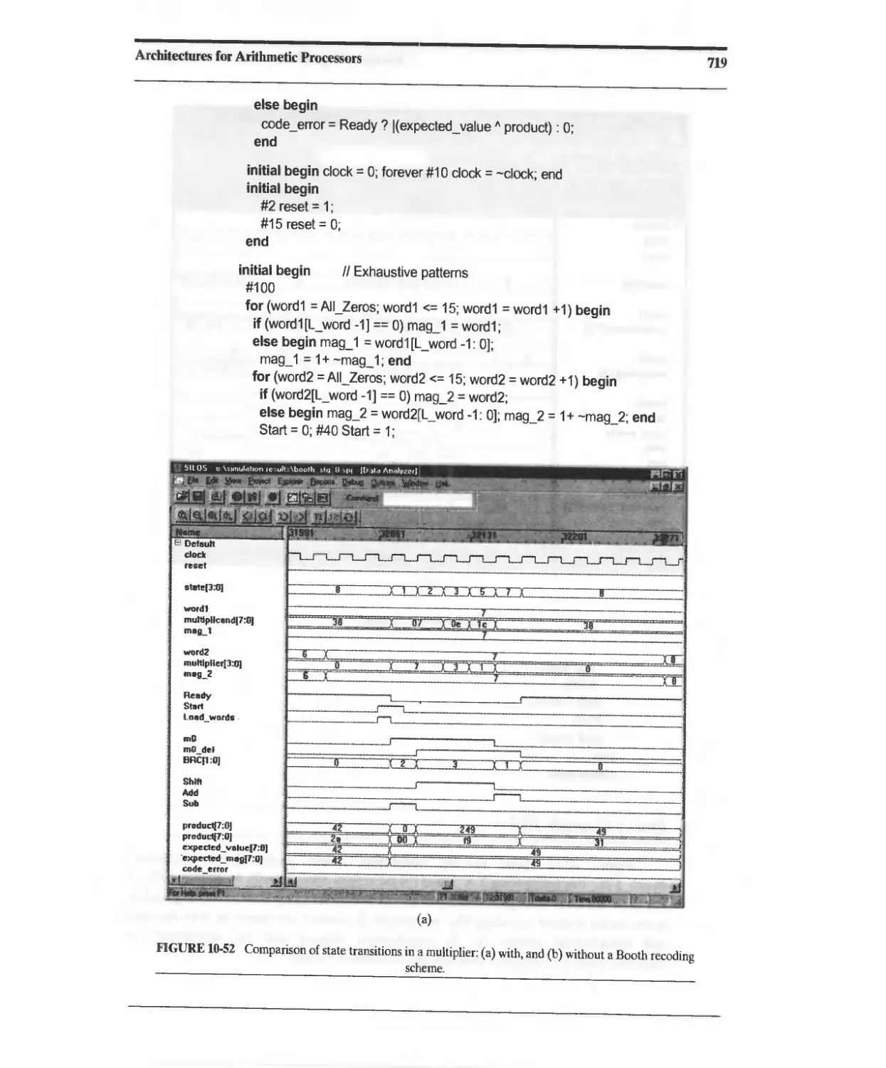
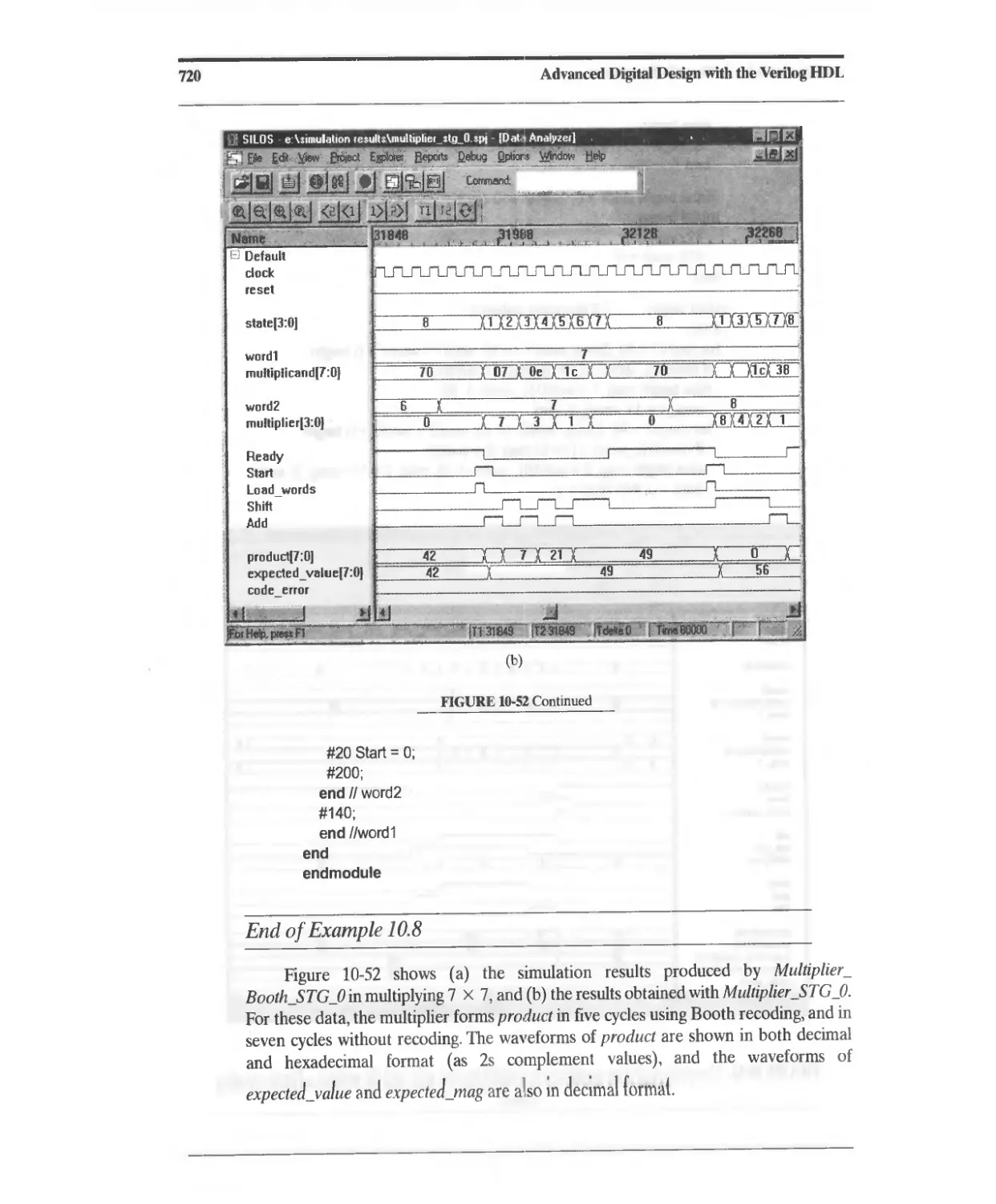
10.3.11 Booth's-Algorithm Sequential Multiplier 711
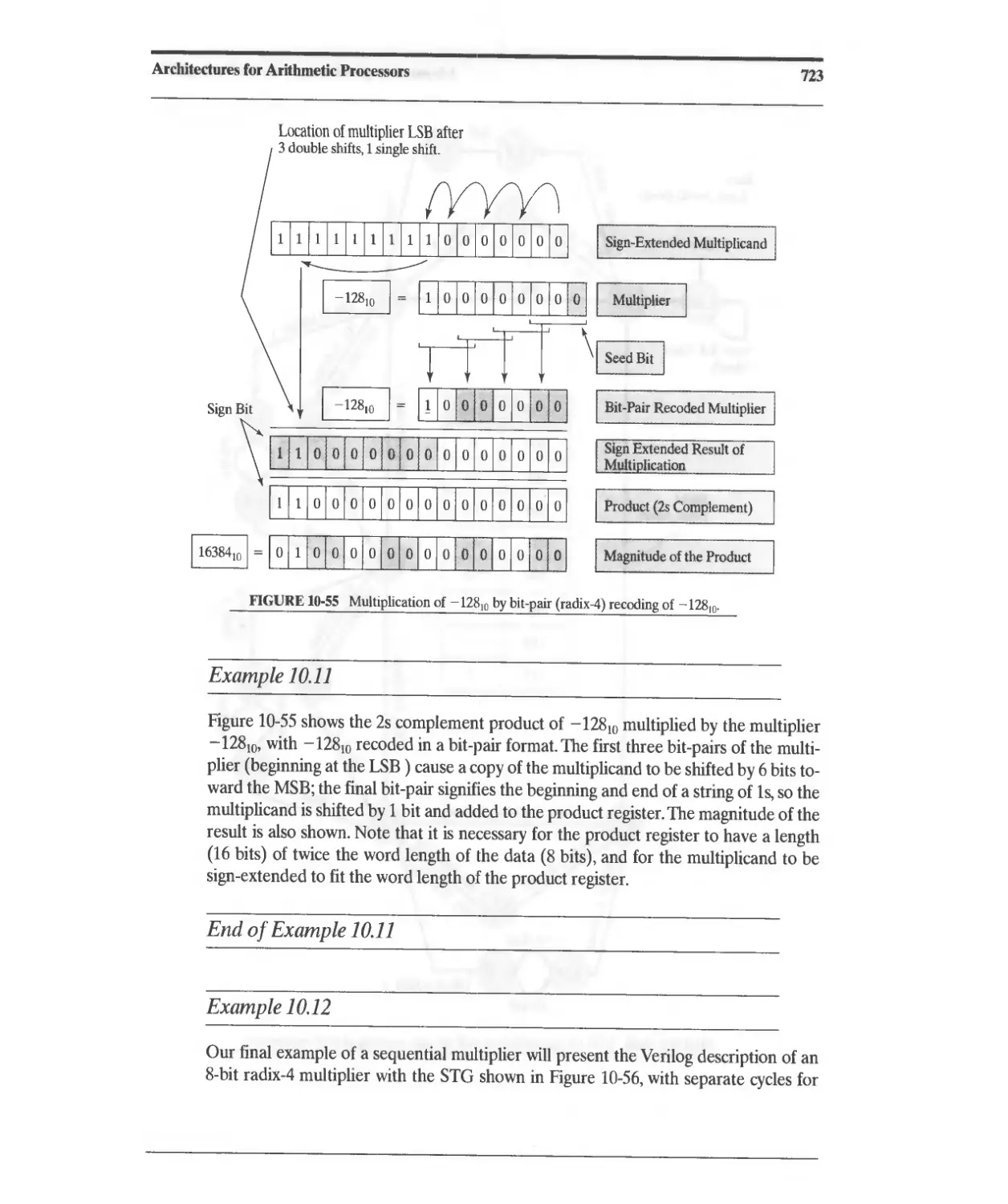
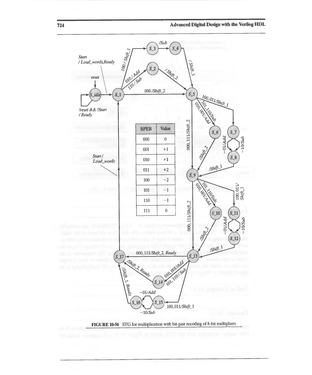
10.3.12 Bit-Pair Encoding 721
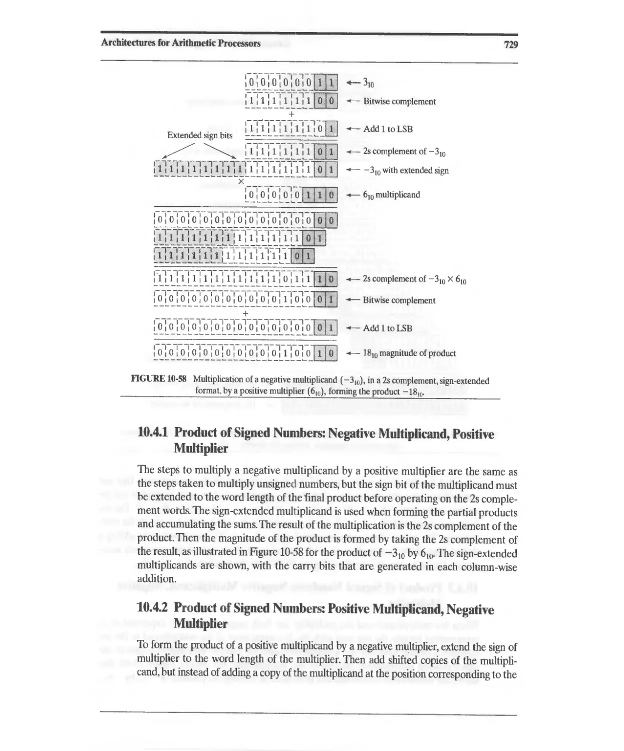
10.4 Multiplication of Signed Binary Numbers 728
10.4.1 Product of Signed Numbers: Negative Multiplicand, Positive
Multiplier 729
10.4.2 Product of Signed Numbers: Positive Multiplicand. Negative
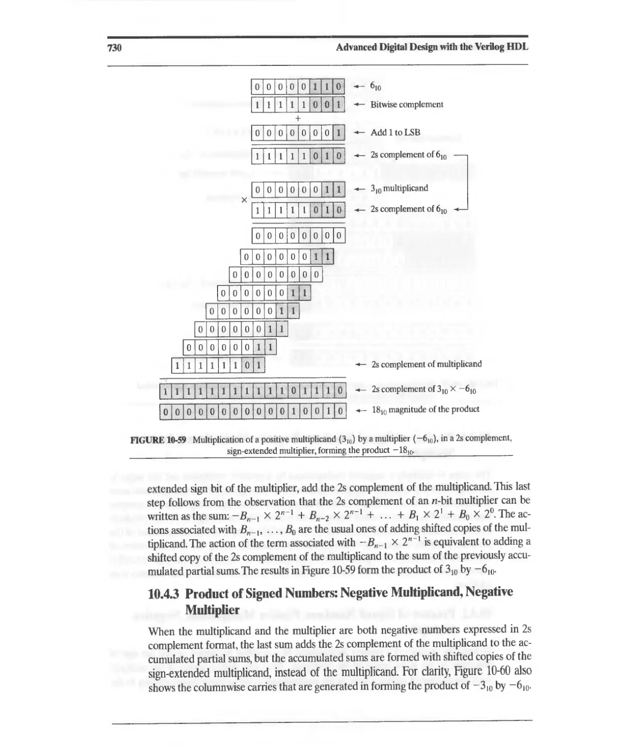
Multiplier 729
10.4.3 Product of Signed Numbers: Negative Multiplicand, Negative
Multiplier 730
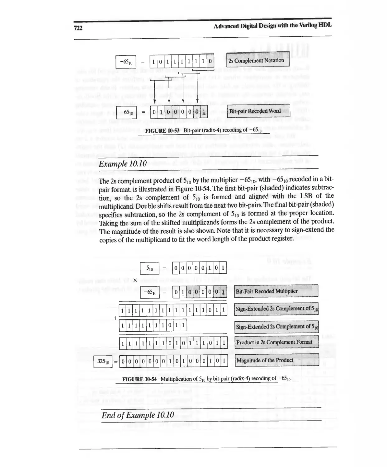
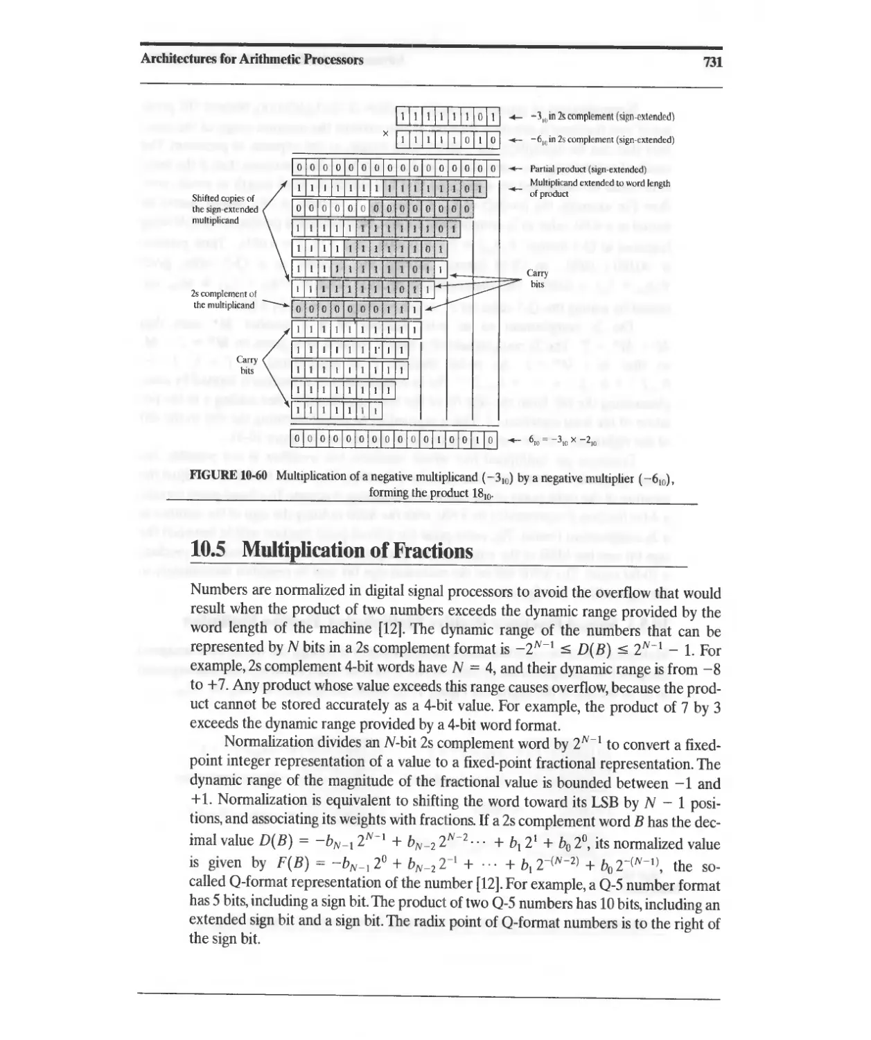
10.5 Multiplication of Fractions 731
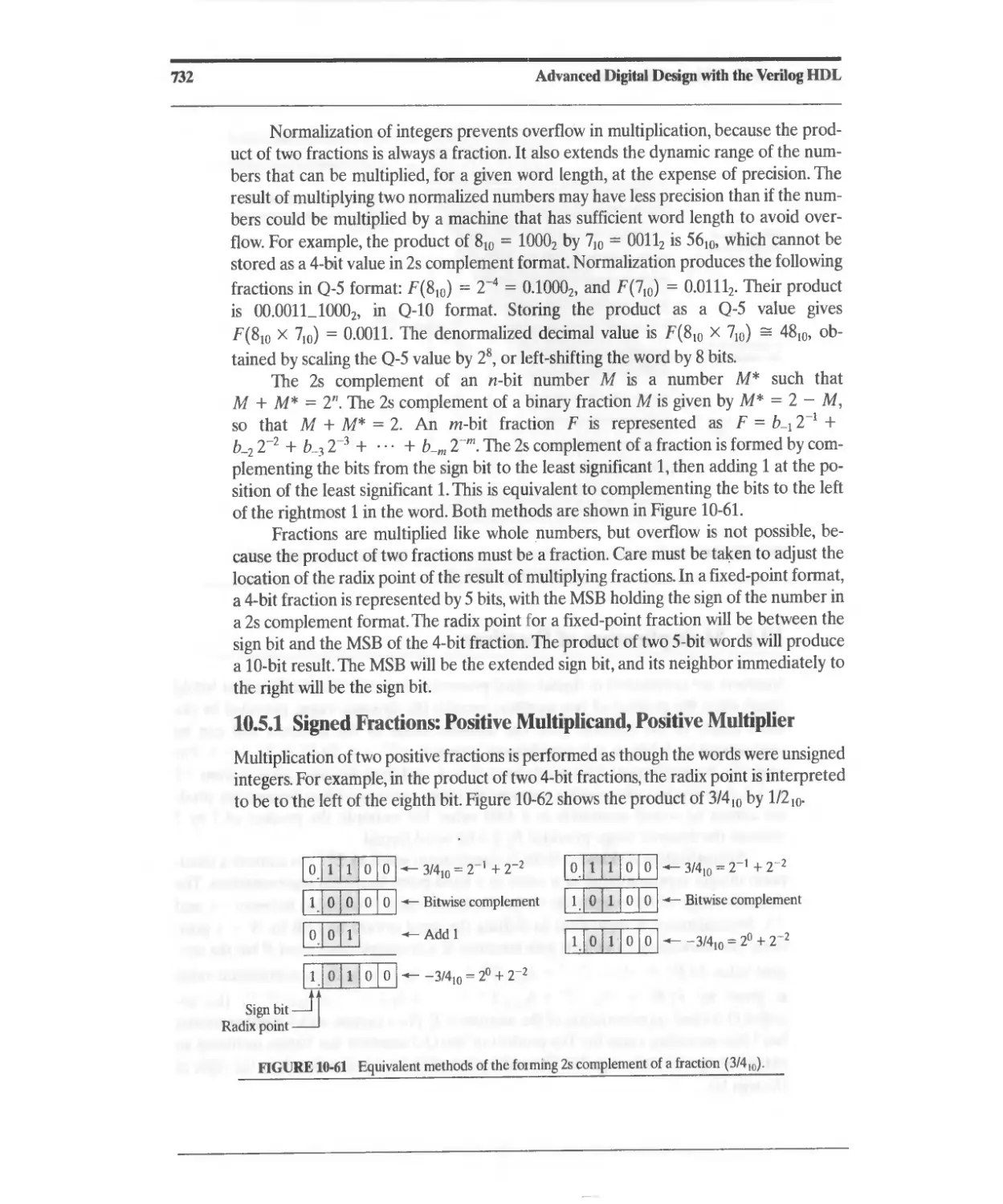
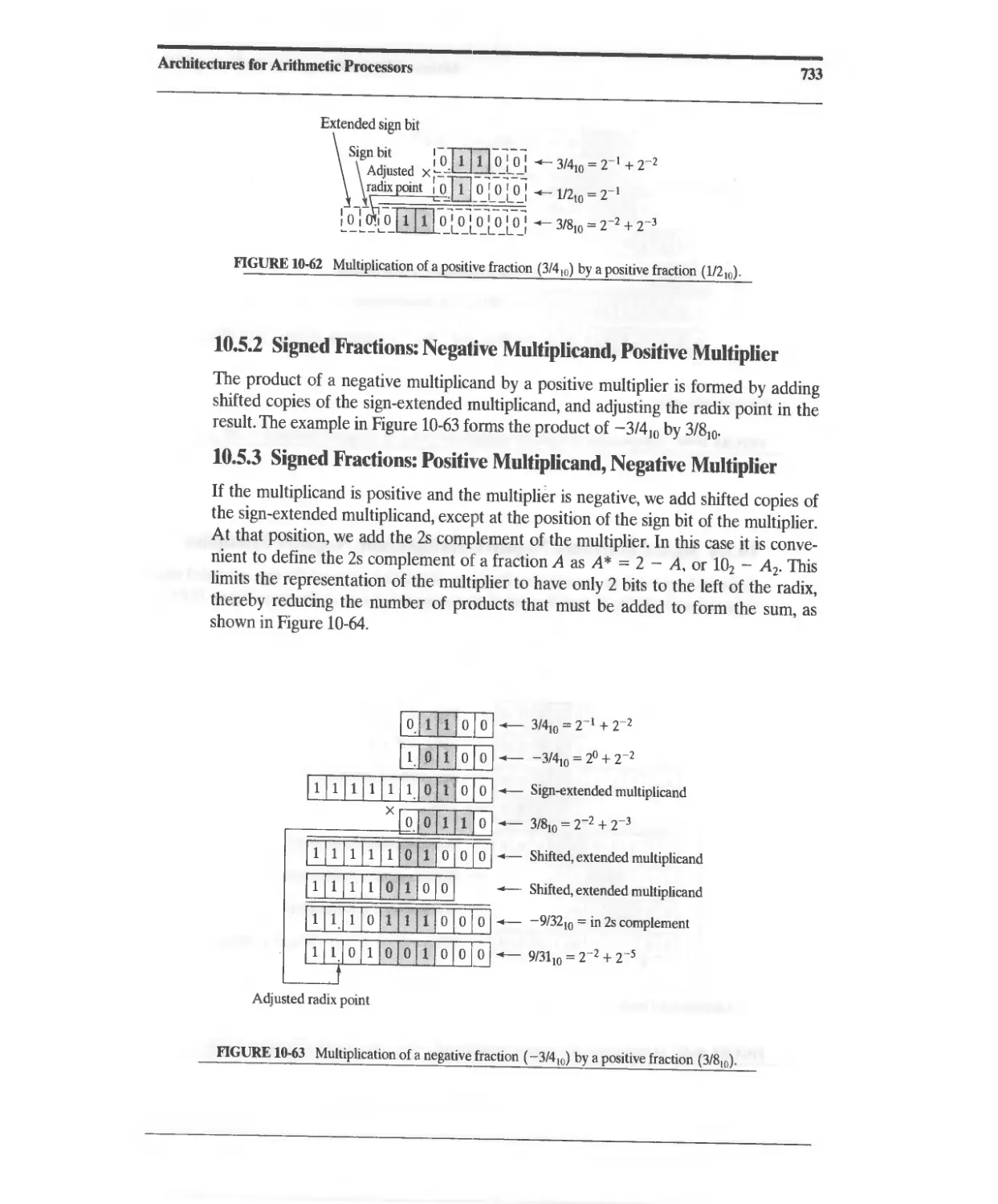
10.5.1 Signed Fractions: Positive Multiplicand, Positive Multiplier 732
10.5.2 Signed Fractions: Negative Multiplicand, Positive Multiplier 733
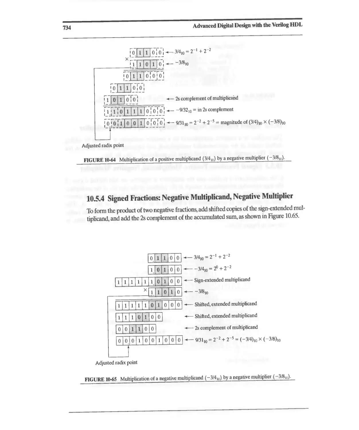
10.5.3 Signed Fractions: Positive Multiplicand, Negative Multiplier 733
10.5.4 Signed Fractions: Negative Multiplicand, Negative Multiplier 734
10.6 Functional Units for Division 735
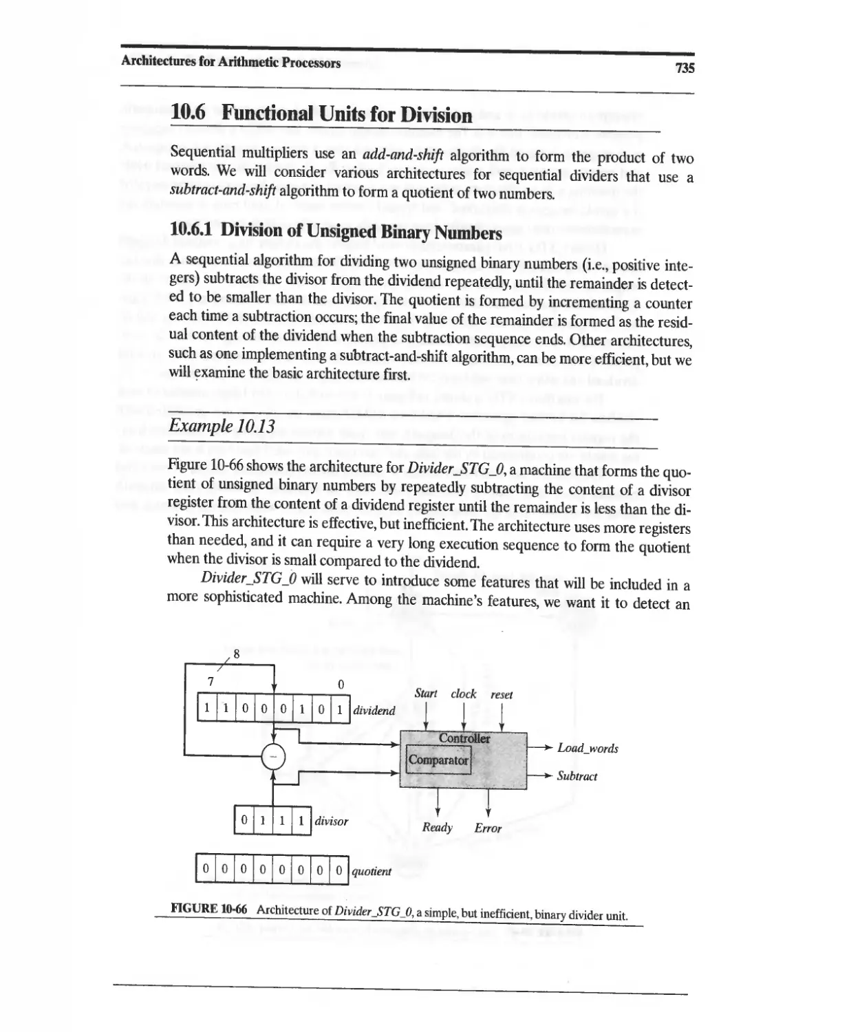
10.6.1 Division of Unsigned Binary Numbers 735
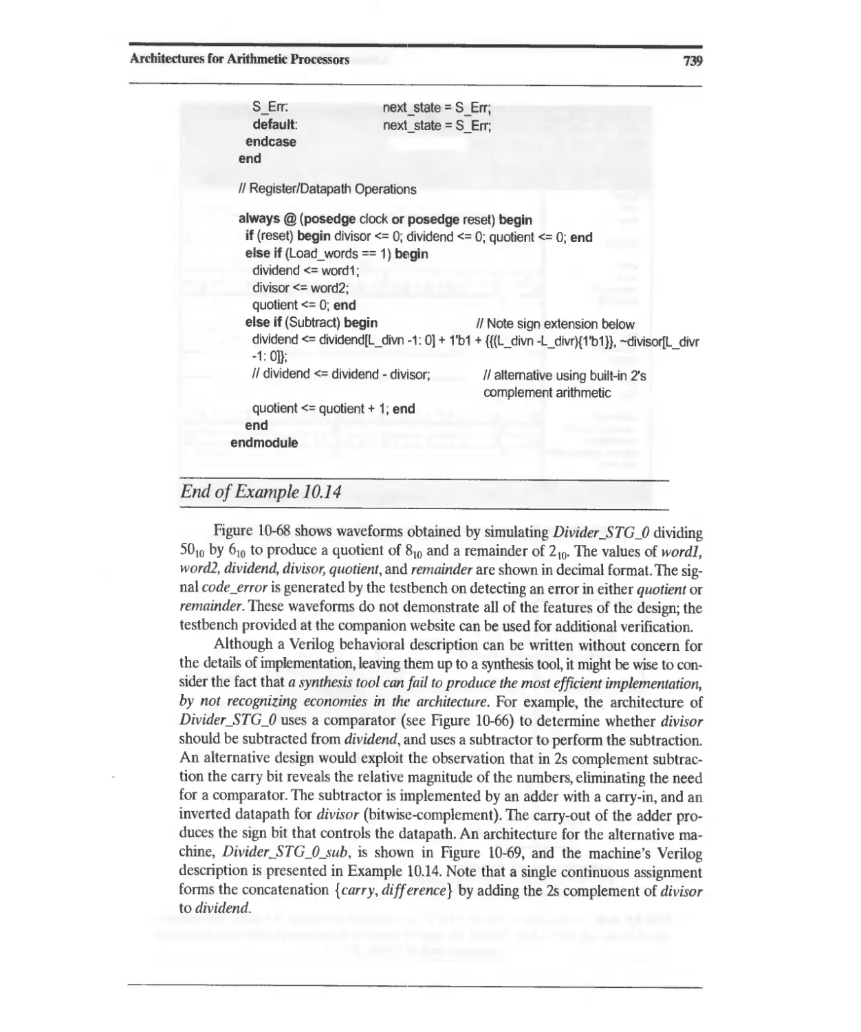
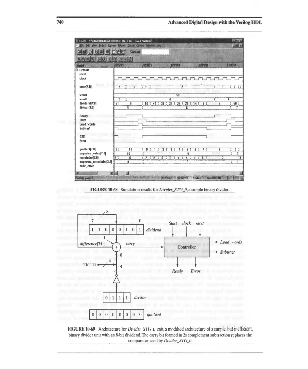
10.6.2 Efficient Division of Unsigned Binary Numbers 742
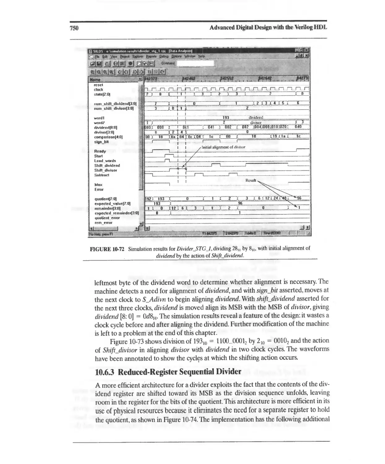
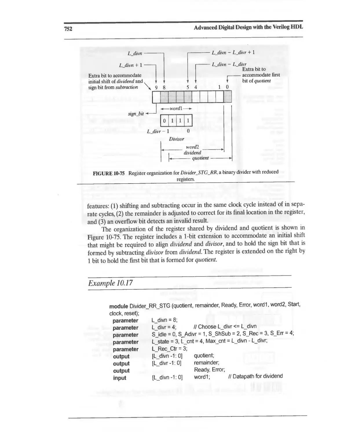
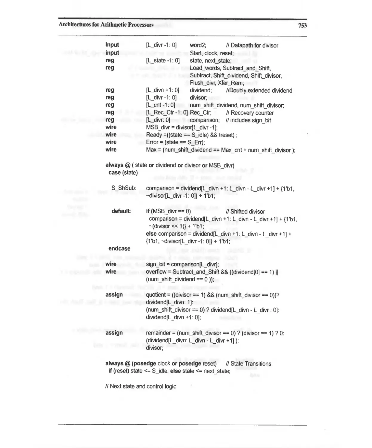
10.6.3 Reduced-Register Sequential Divider 750
10.6.4 Division of Signed (2s Complement) Binary Numbers 757
References 757
Problems 757
Contents xiii
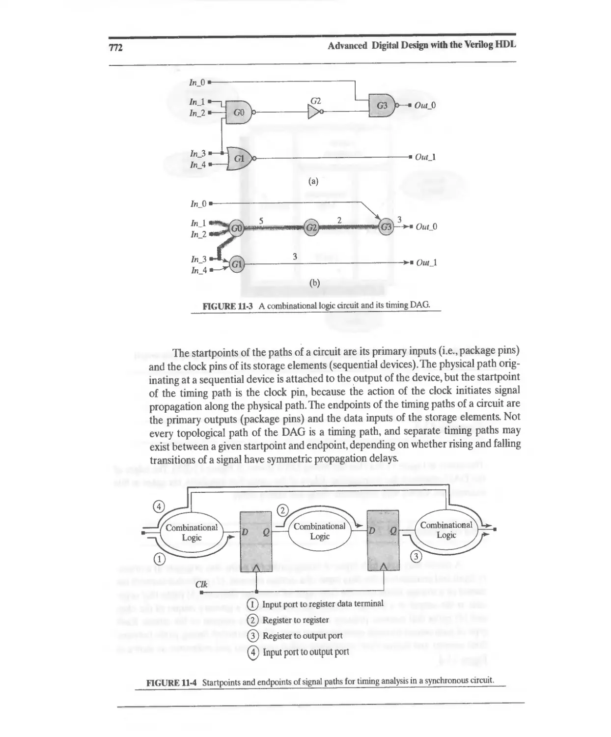
11 Postsynthesis Design Tasks 765
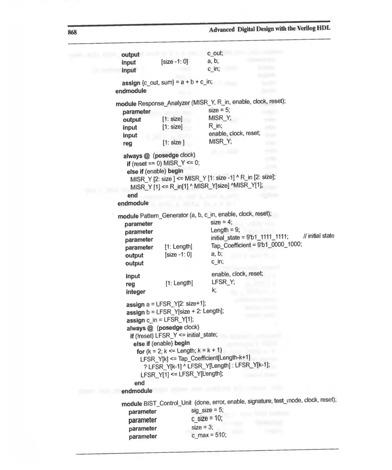
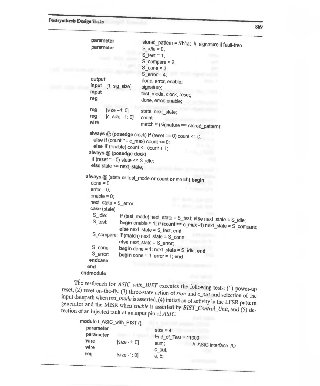
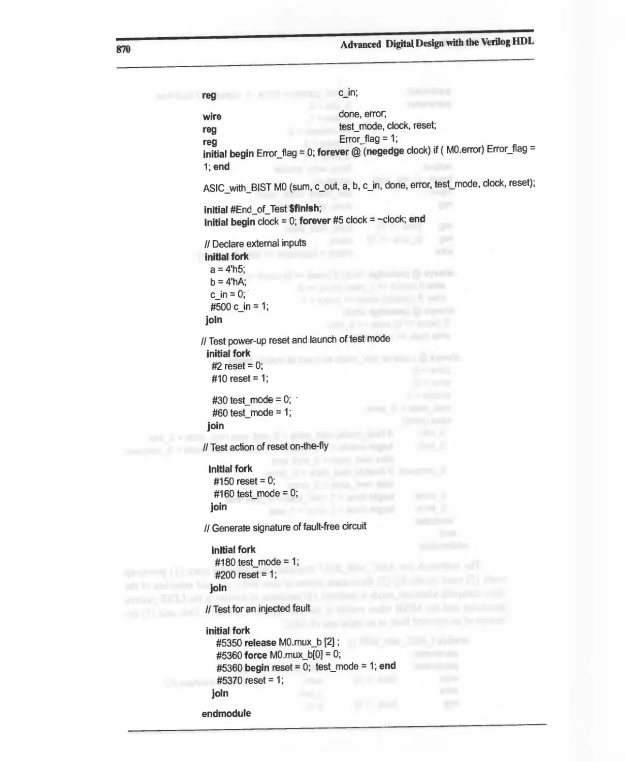
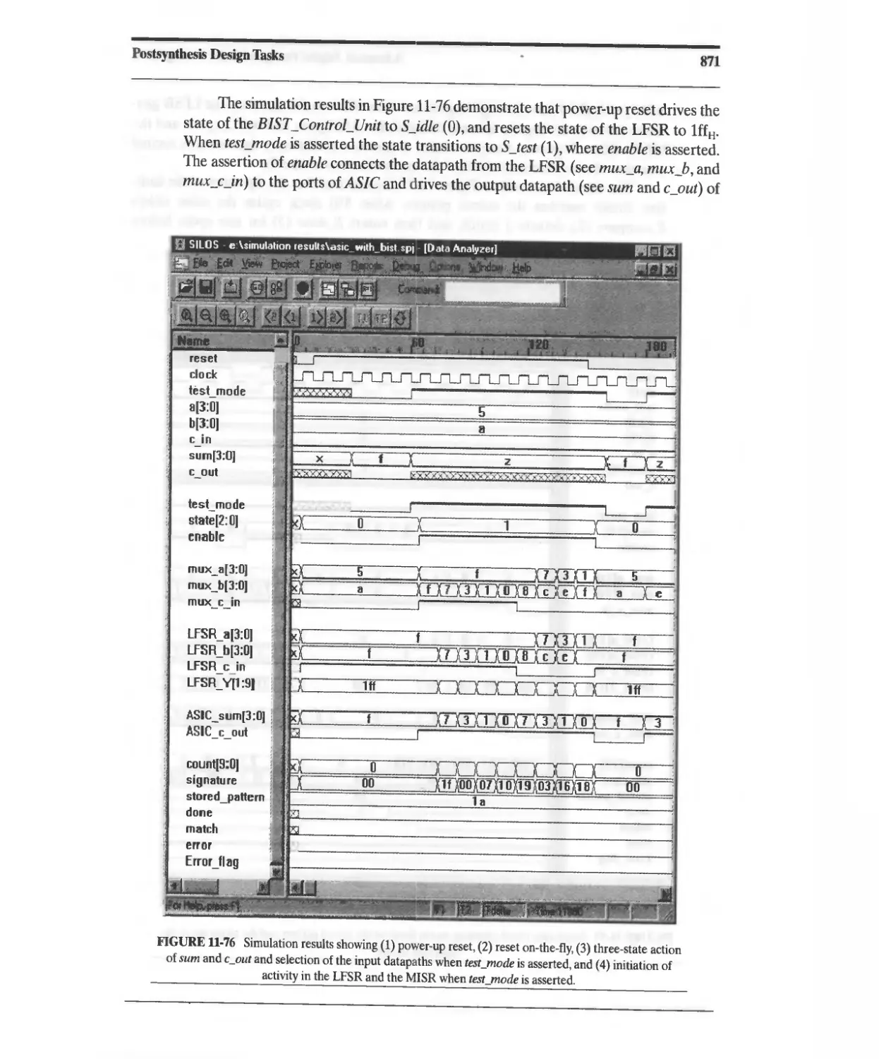
11.1 Postsynthesis Design Validation 765
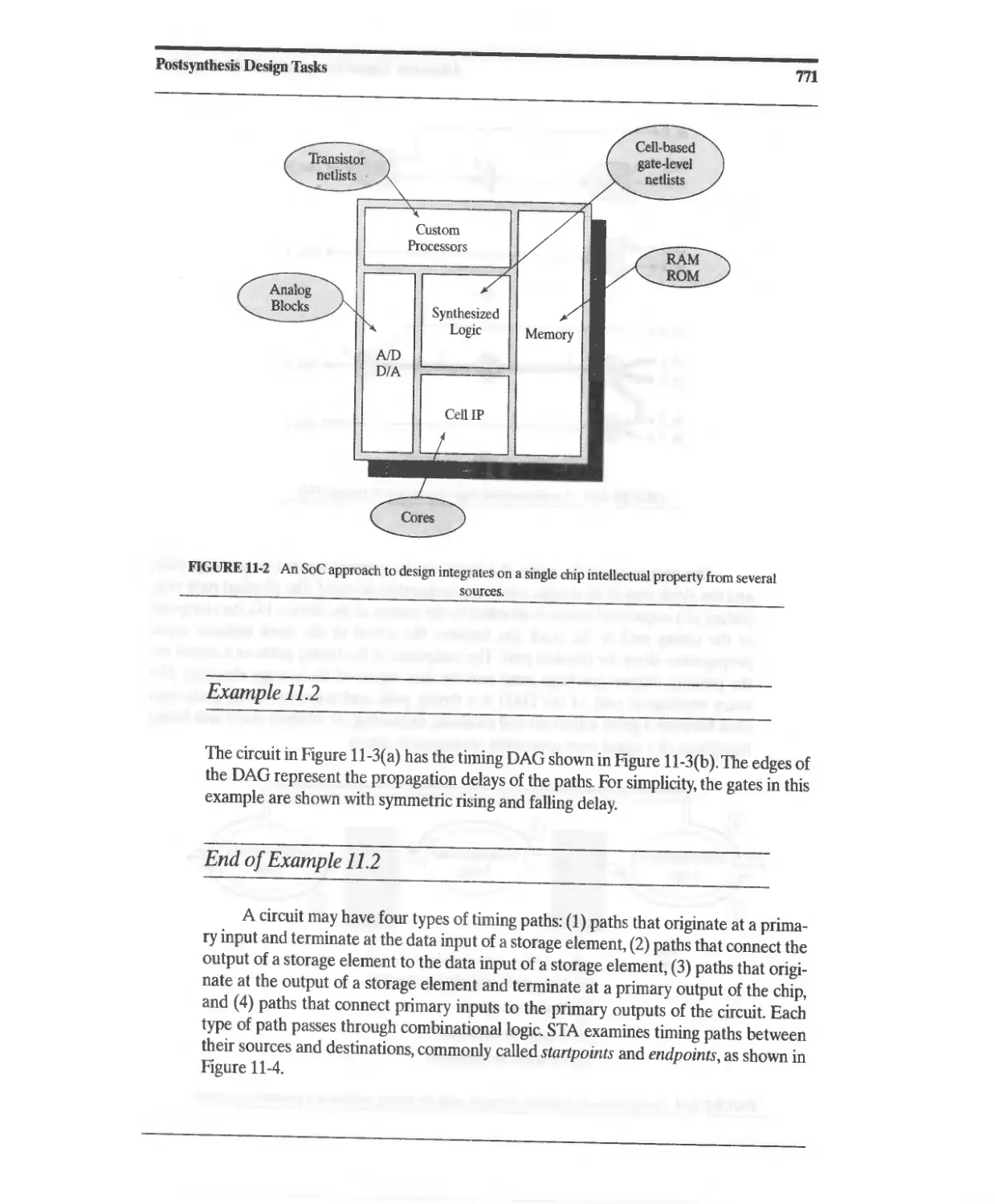
11.2 Postsynthesis Timing Verification 768
11.2.1 Static Timing Analysis 770
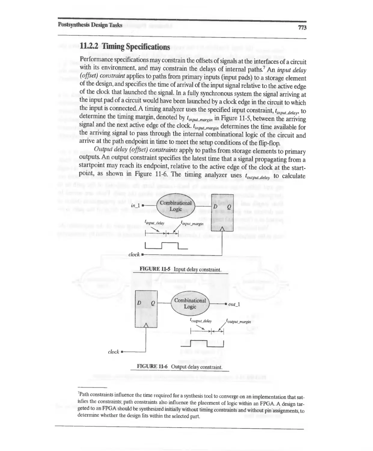
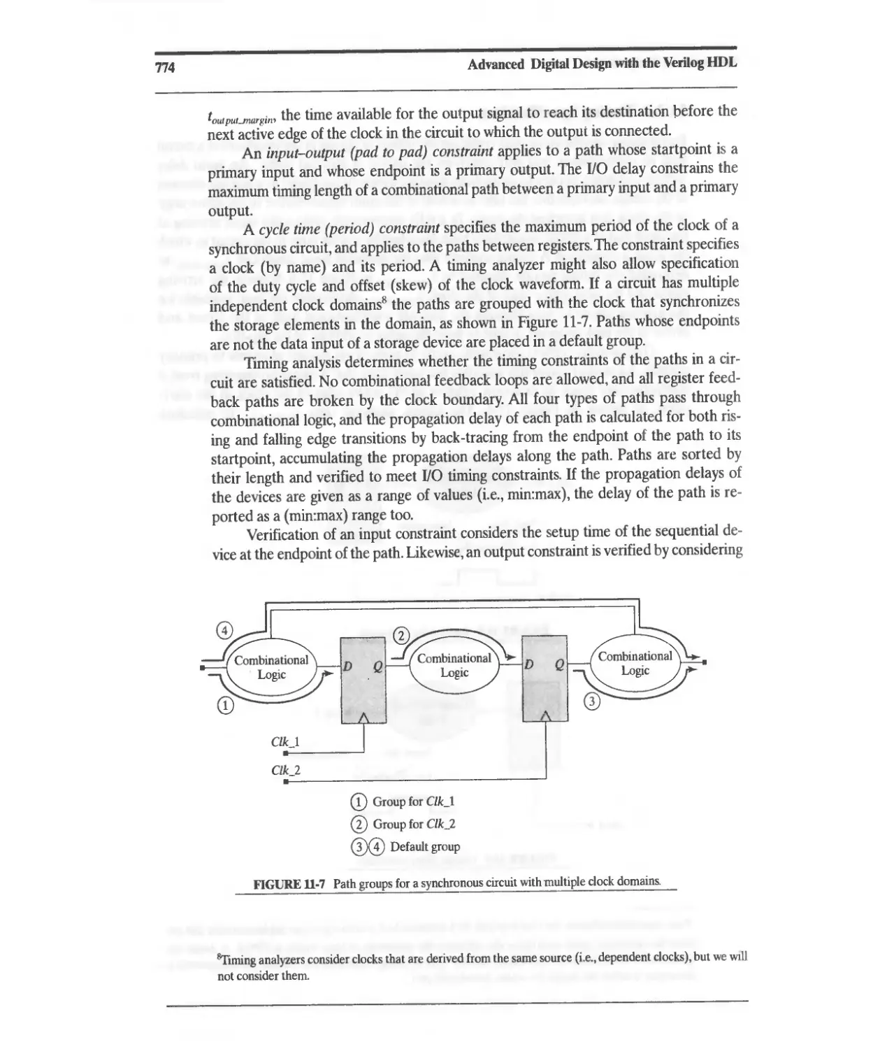
11.2.2 Timing Specifications 773
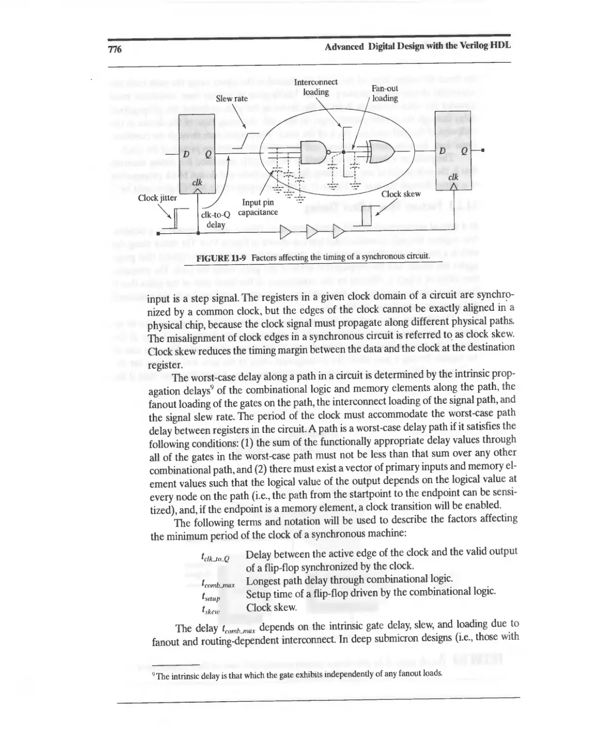
11.2.3 Factors That Affect Timing 775
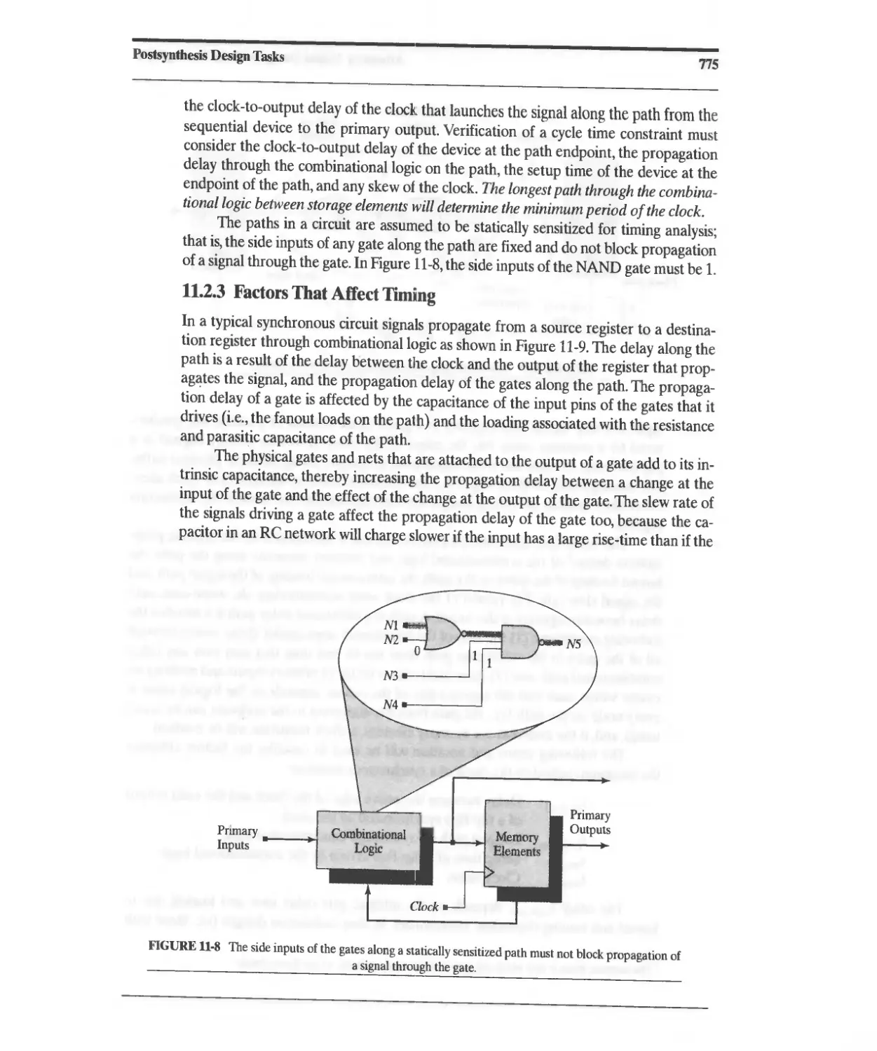
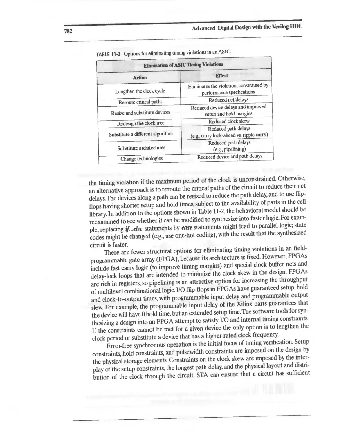
11.3 Elimination of ASIC Timing Violations 779
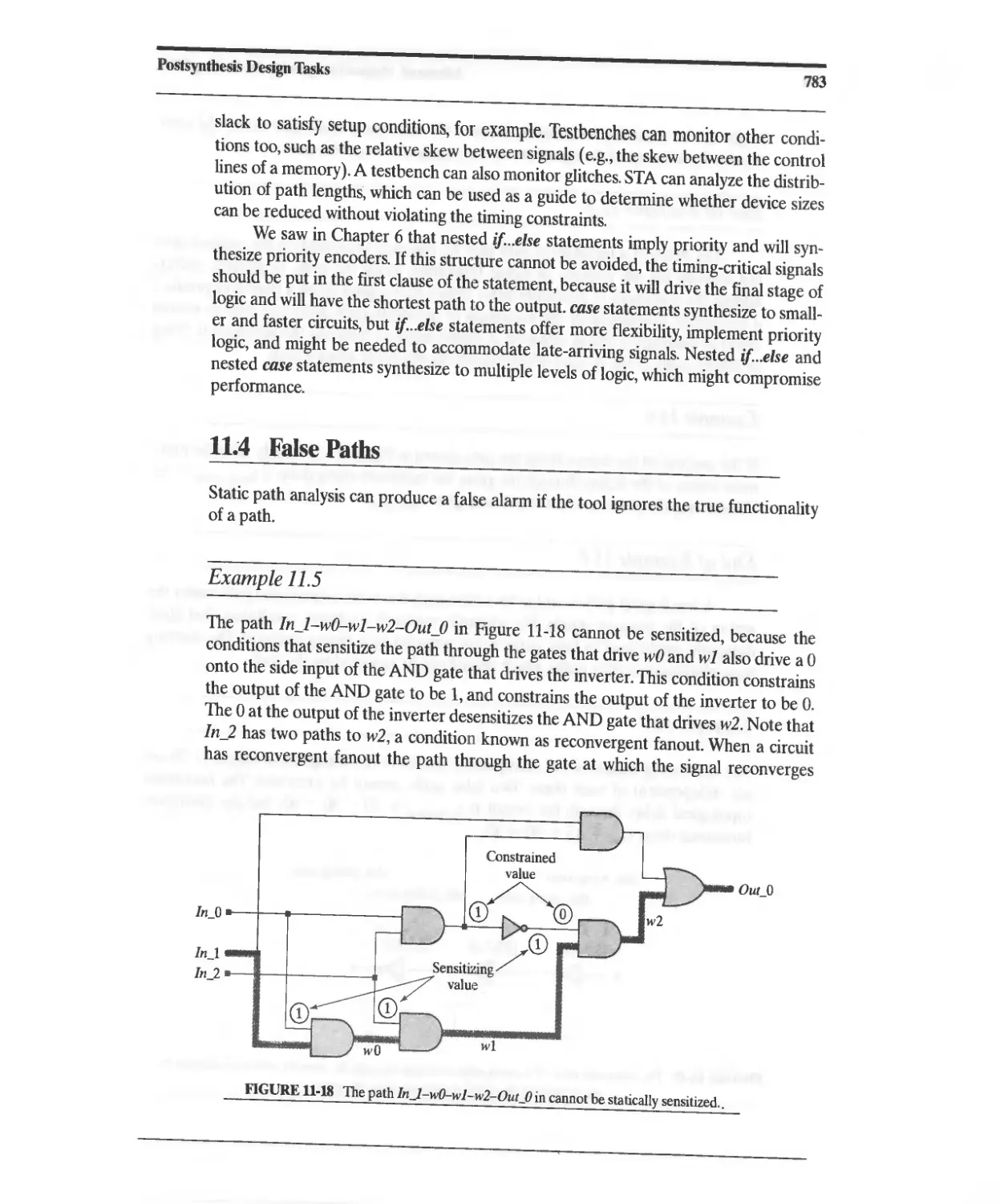
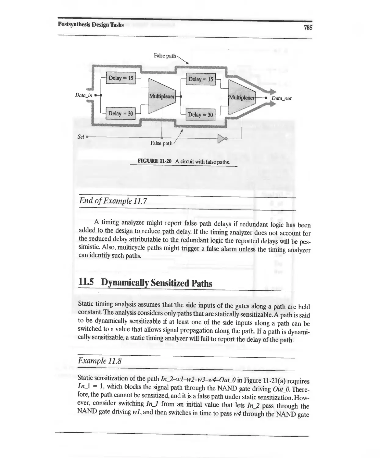
11.4 False Paths 783
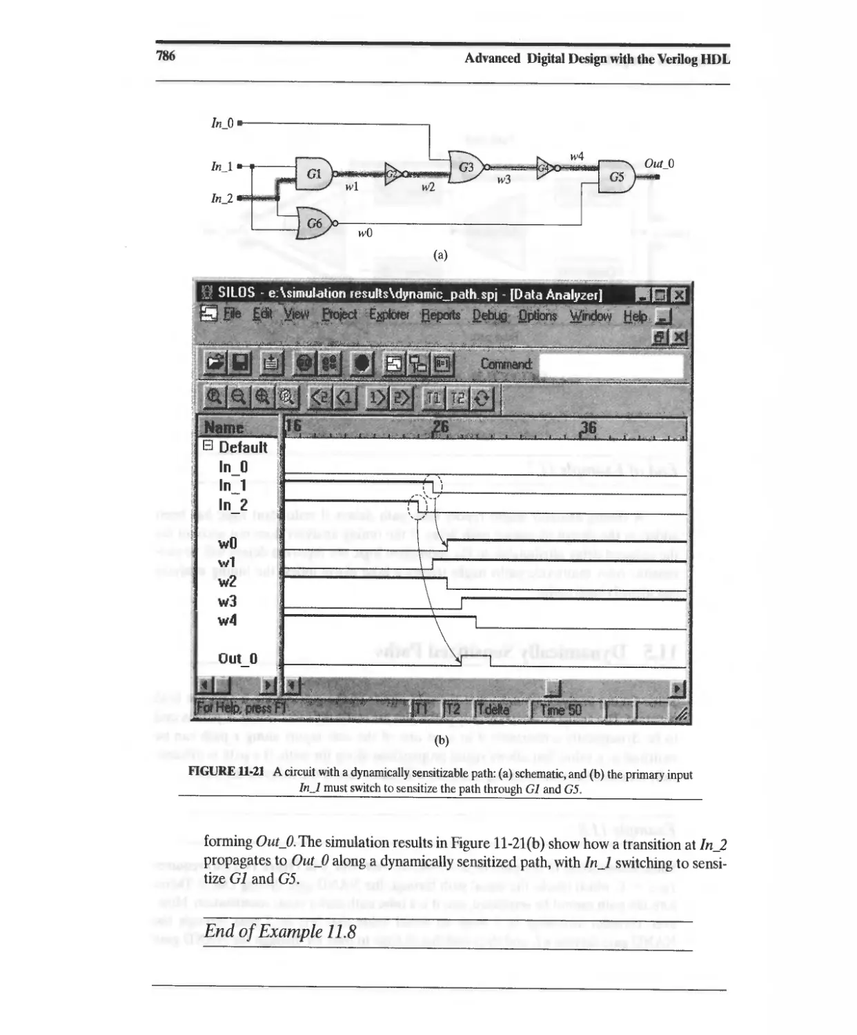
11.5 Dynamically Sensitized Paths 785
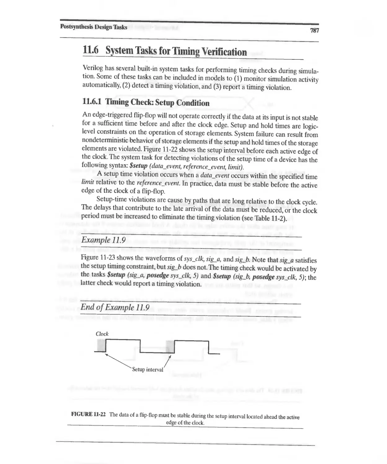
11.6 System Tasks for Timing Verification 787
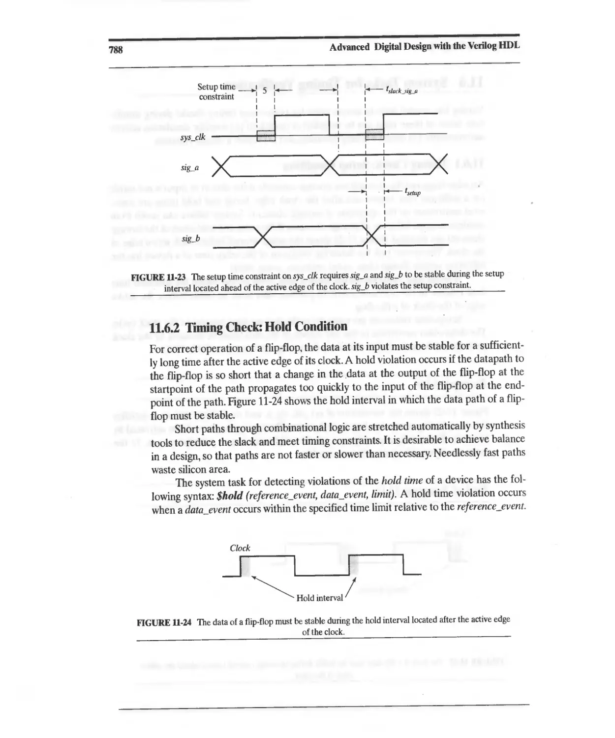
11.6.1 Timing Check: Setup Condition 787
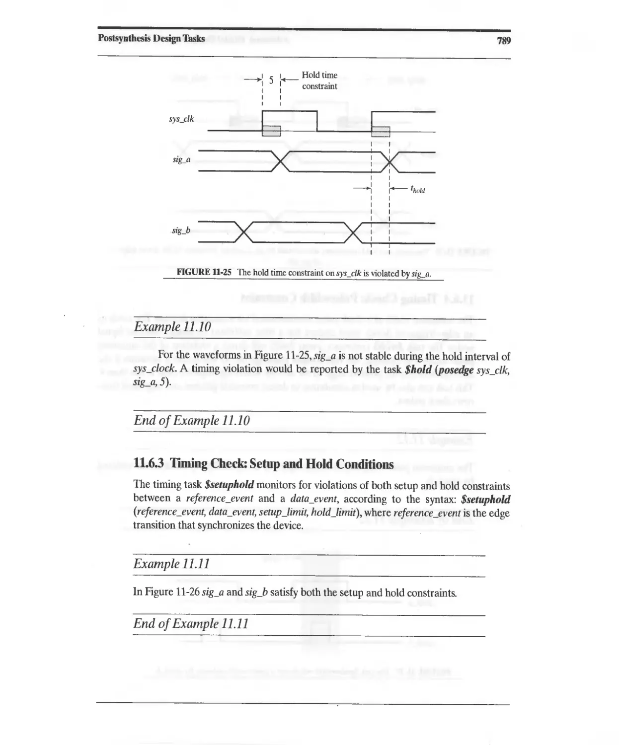
11.6.2 Timing Check: Hold Condition 788
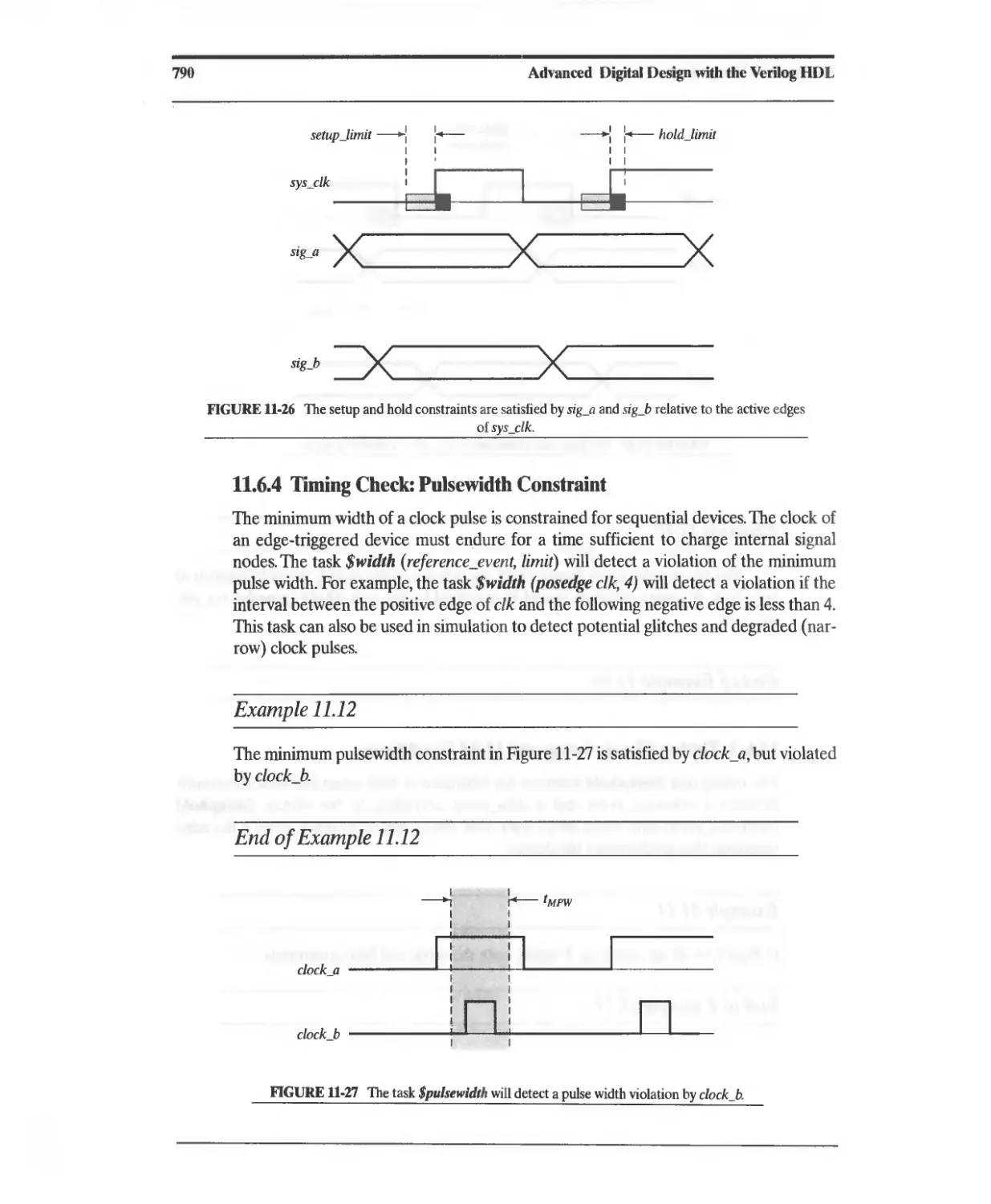
11.6.3 Timing Check: Setup and Hold Conditions 789
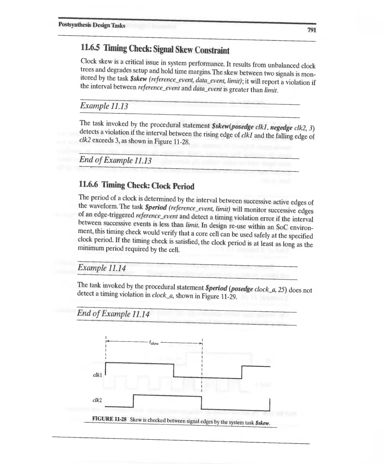
11.6.4 Timing Check: Pulsewidth Constraint 790
11.6.5 Timing Constraint: Signal Skew Constraint 791
11.6.6 Timing Check: Clock Period 791
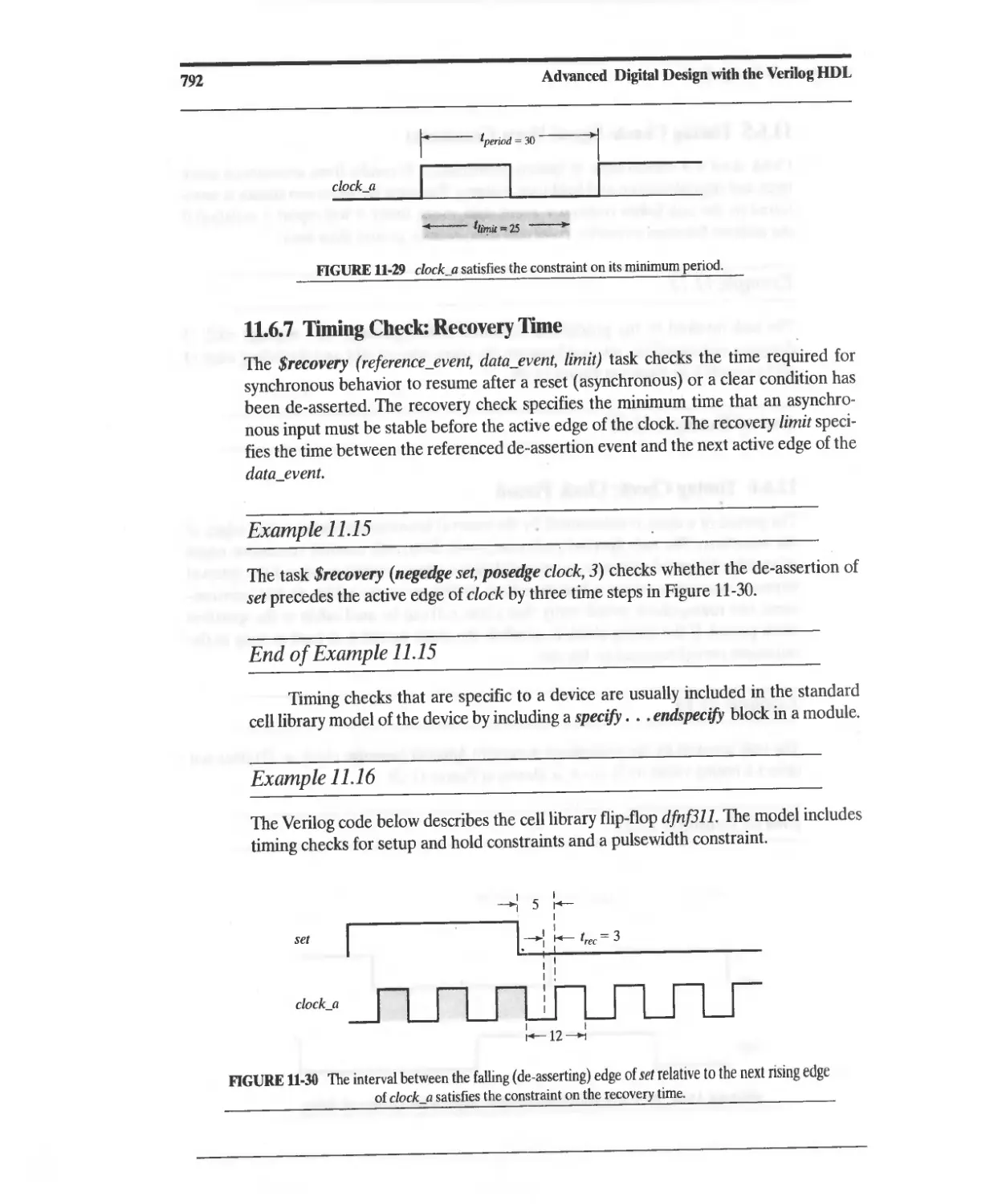
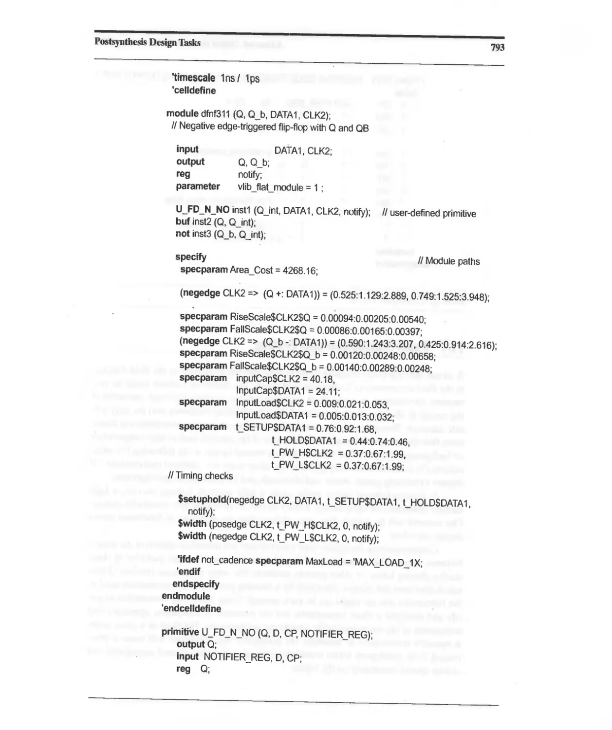
11.6.7 Timing Check: Recovery Time 792
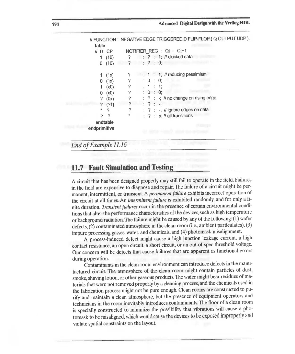
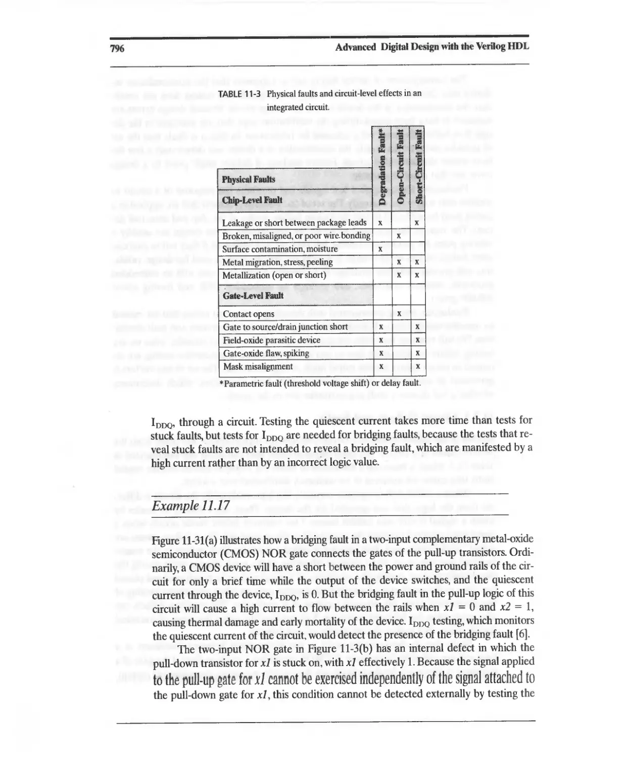
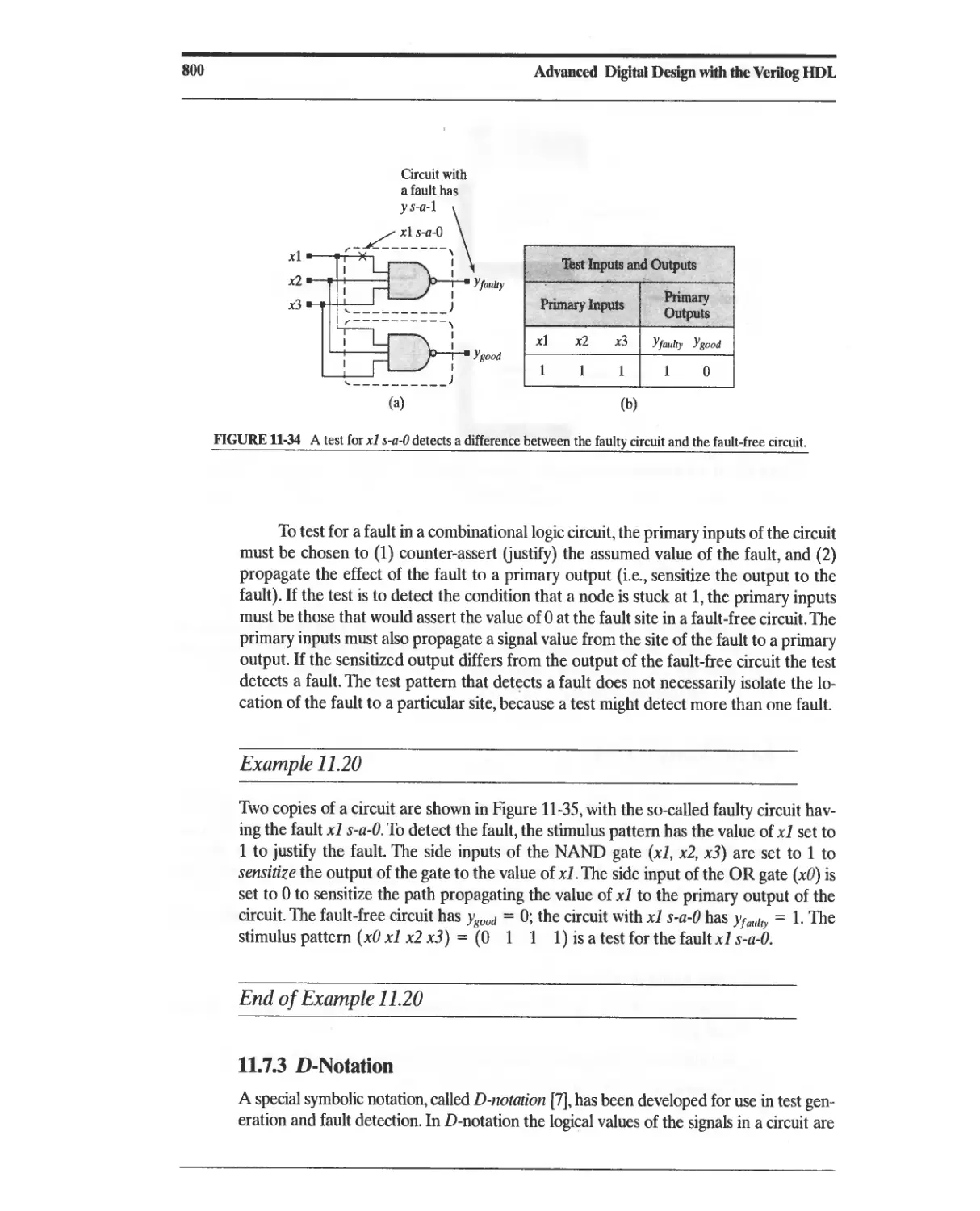
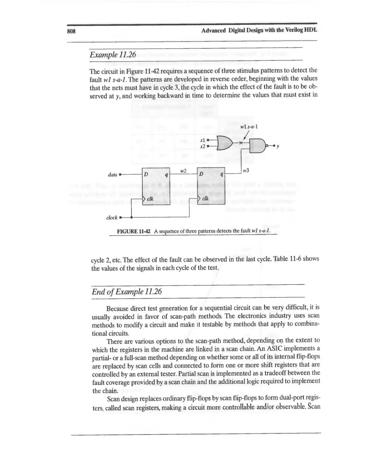
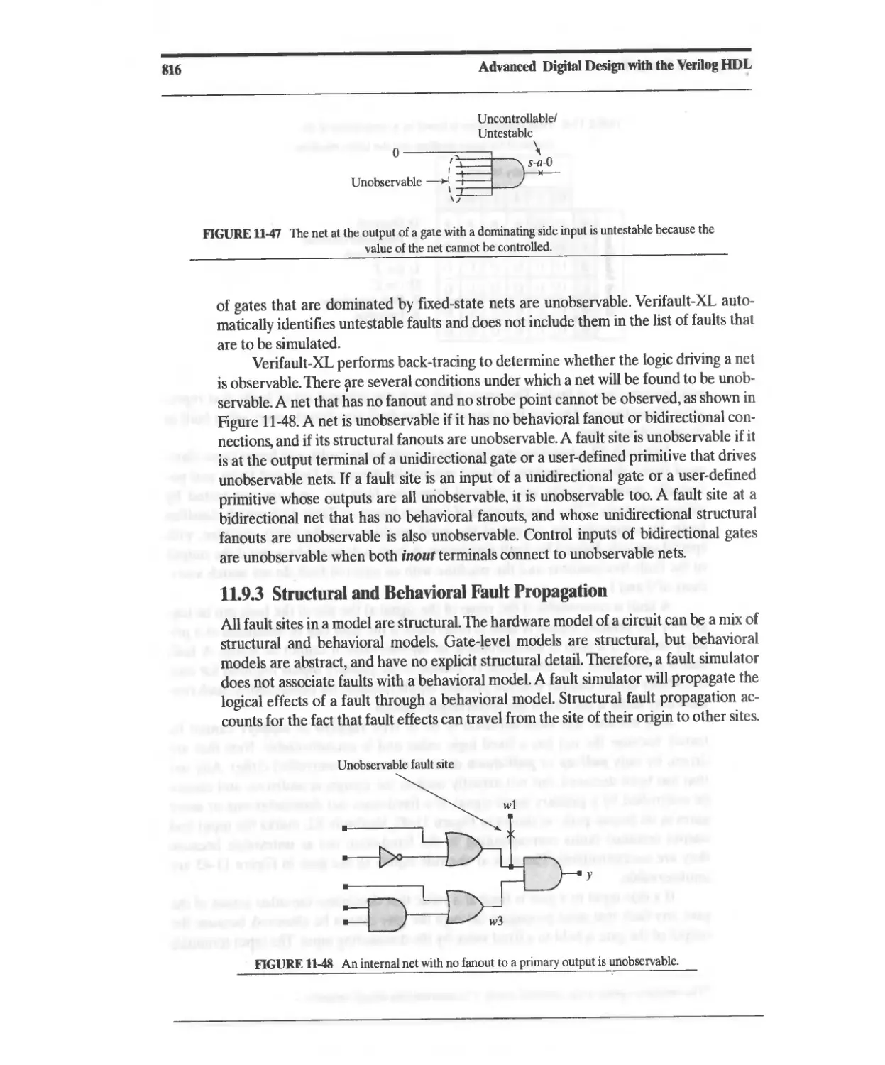
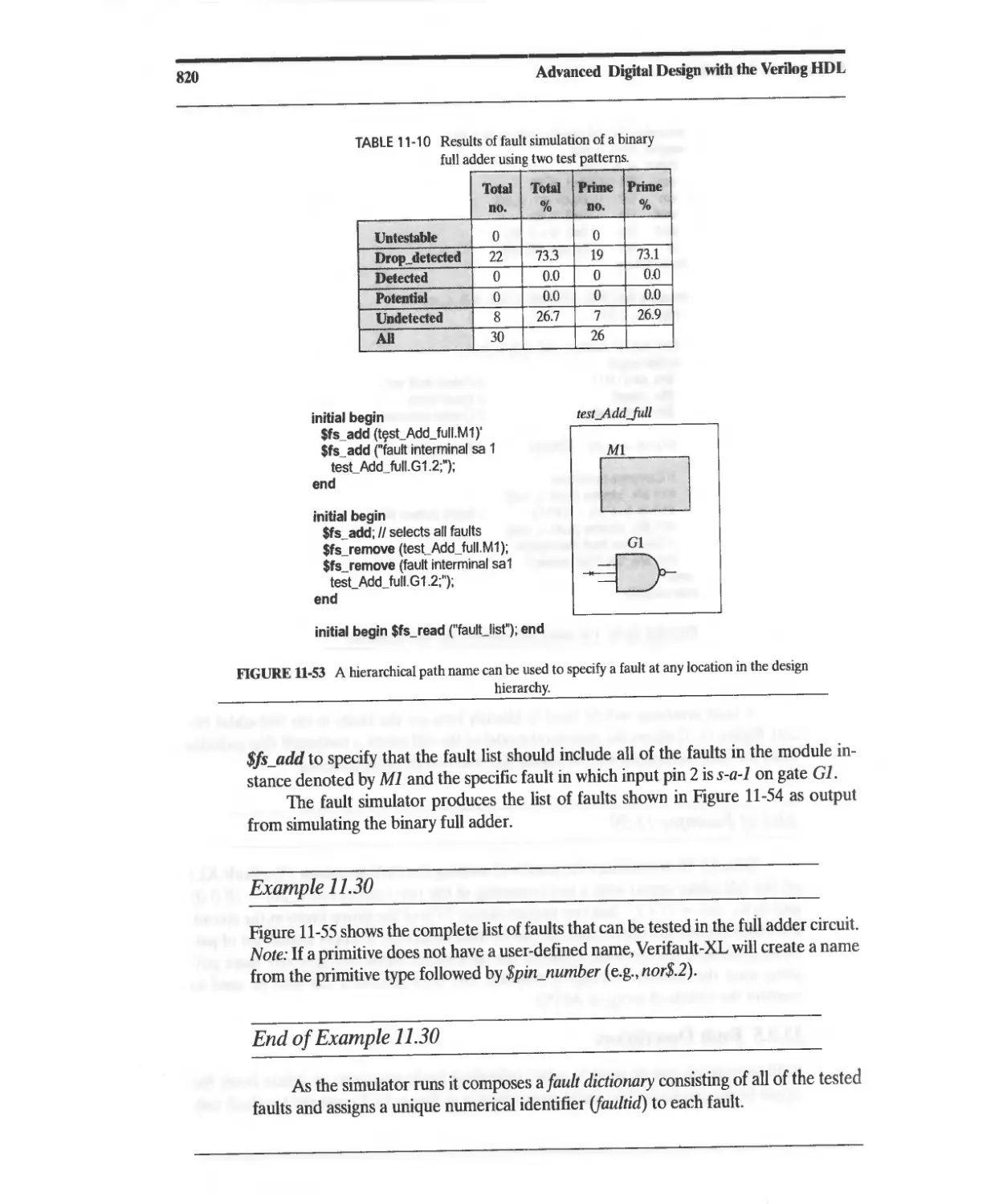
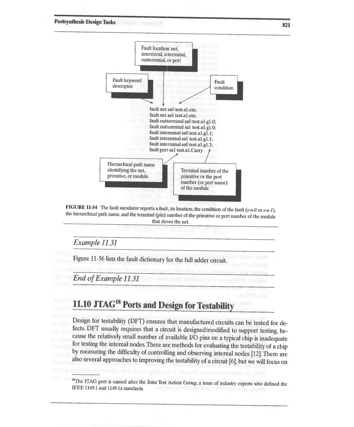
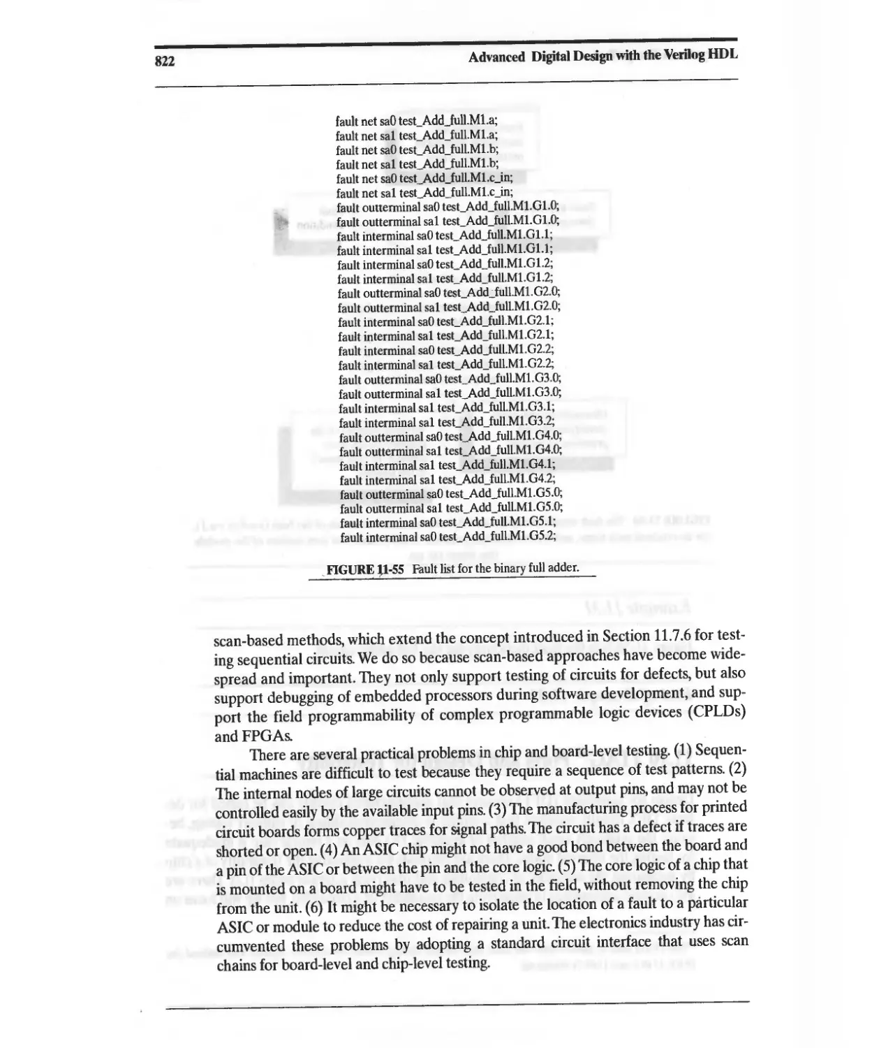
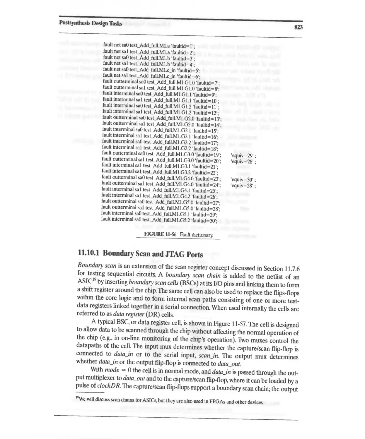
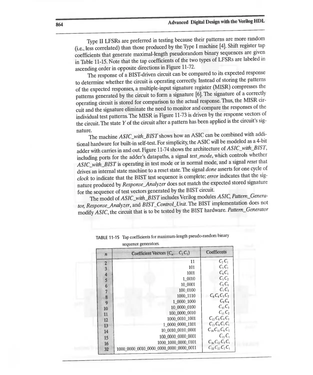
11.7 Fault Simulation and Testing 794
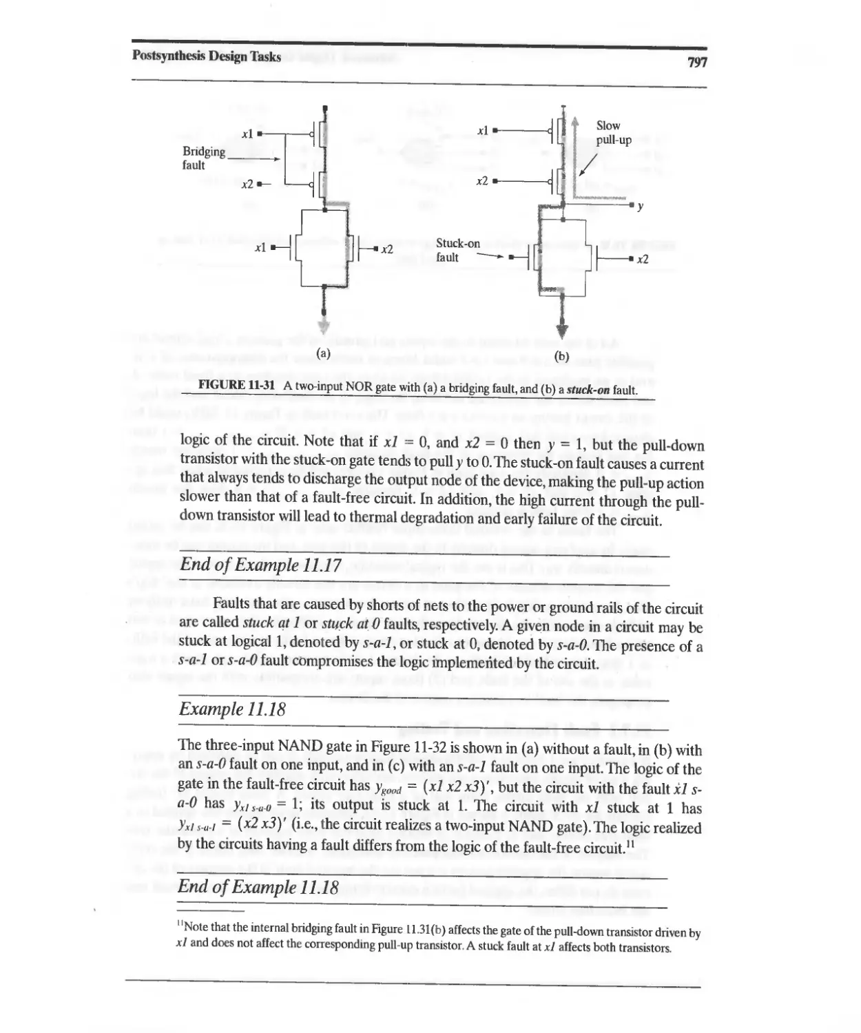
11.7.1 Circuit Defects and Faults 795
11.7.2 Fault Detection and Testing 798
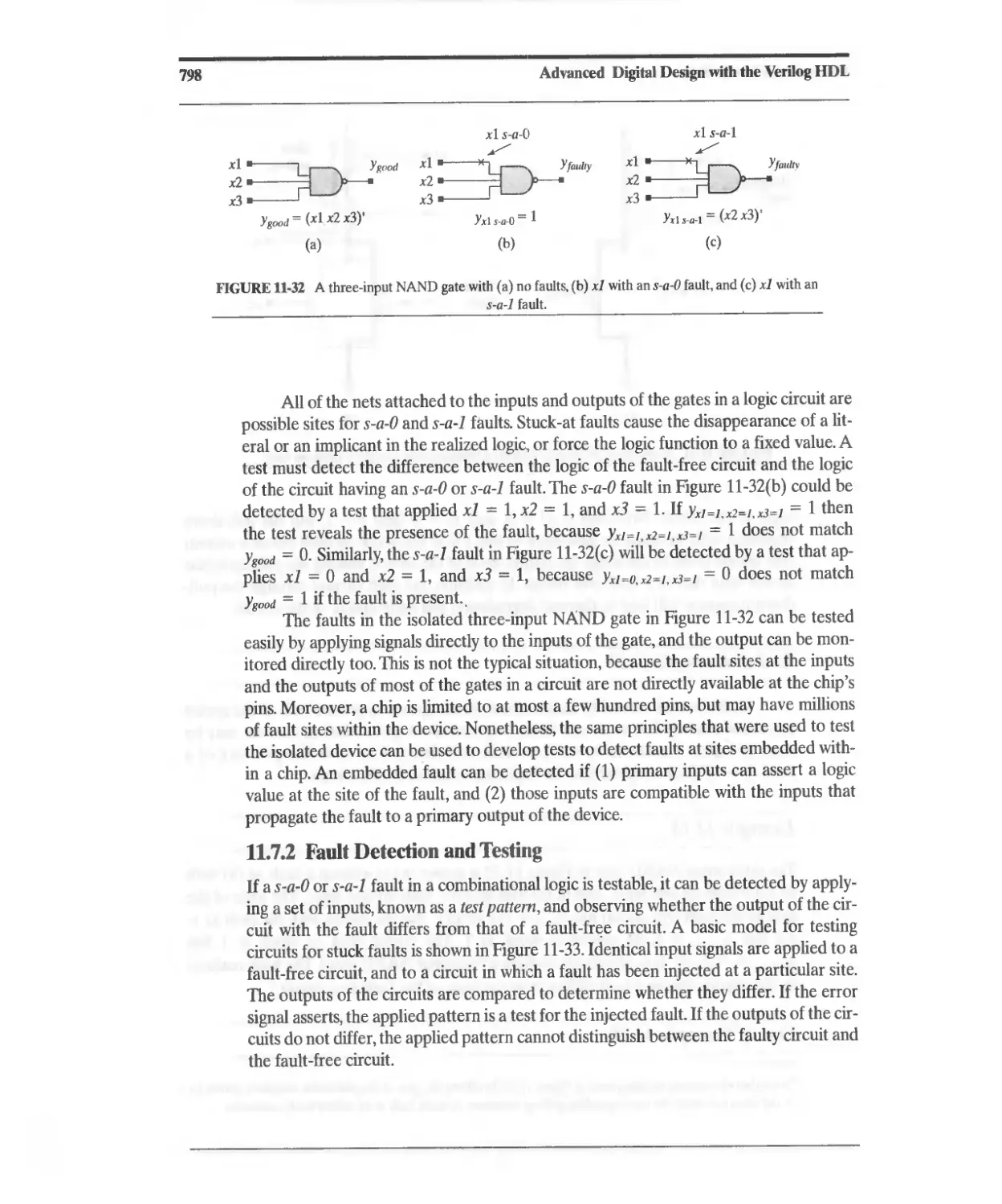
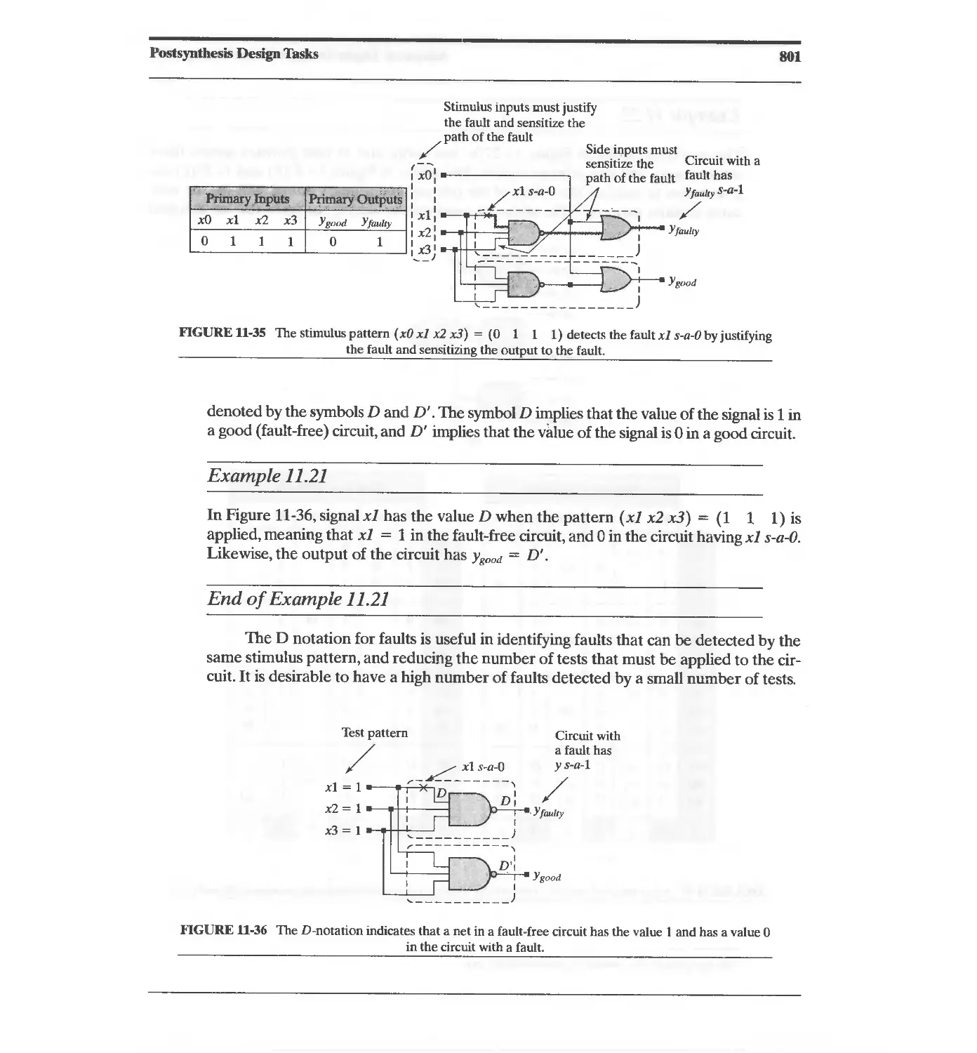
11.7.3 D-Notation 800
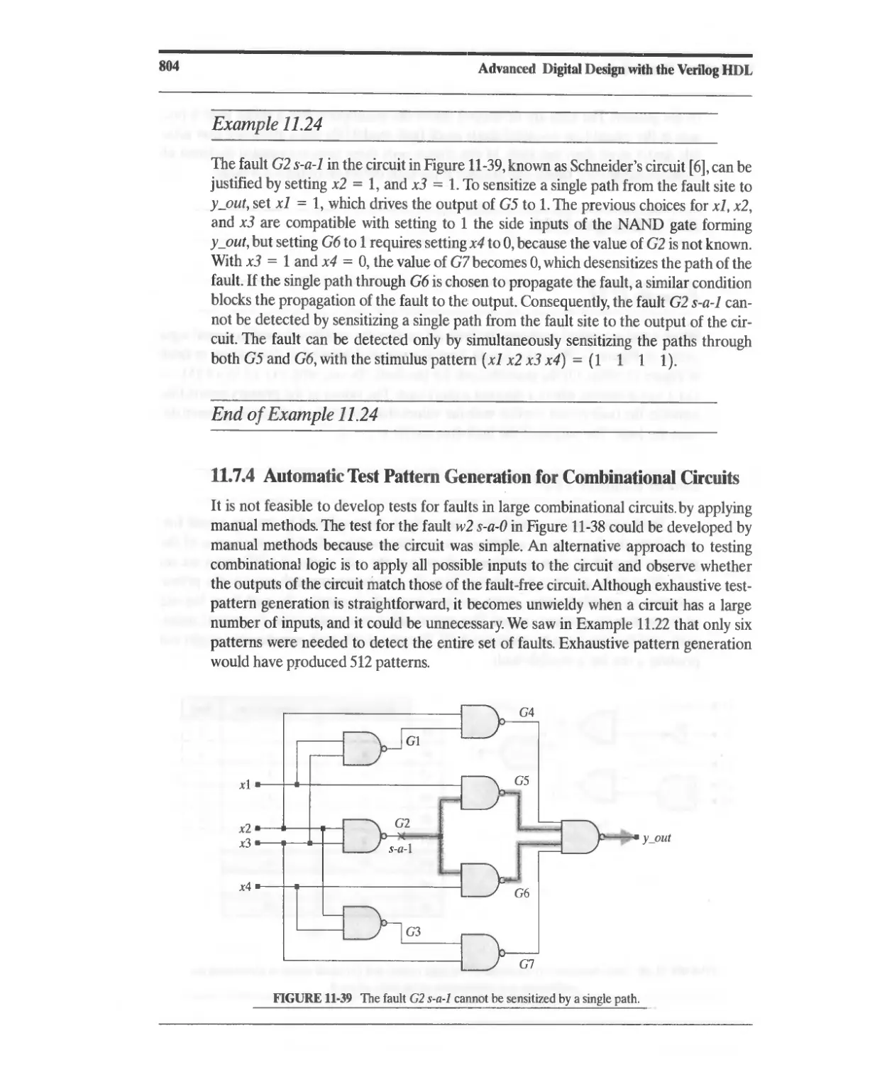
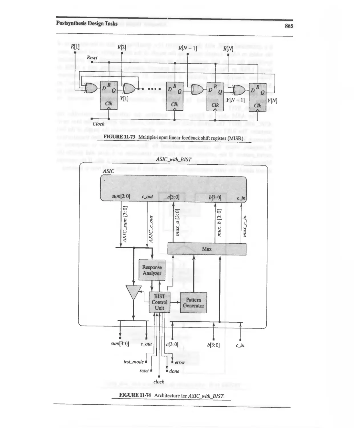
11.7.4 Automatic Test-Pattern Generation for Combinational Circuits 804
11.7.5 Fault Coverage and Defect Levels 805
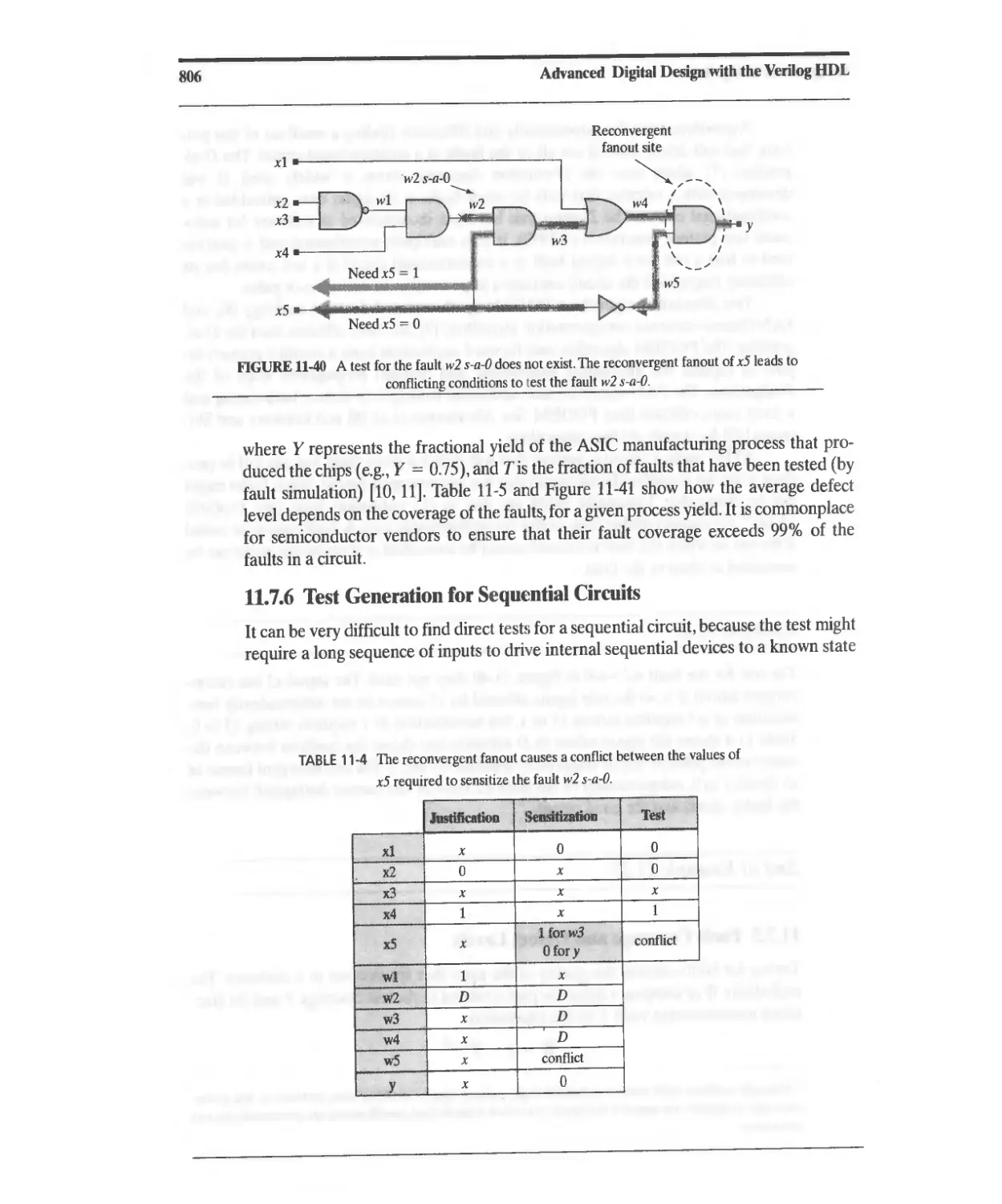
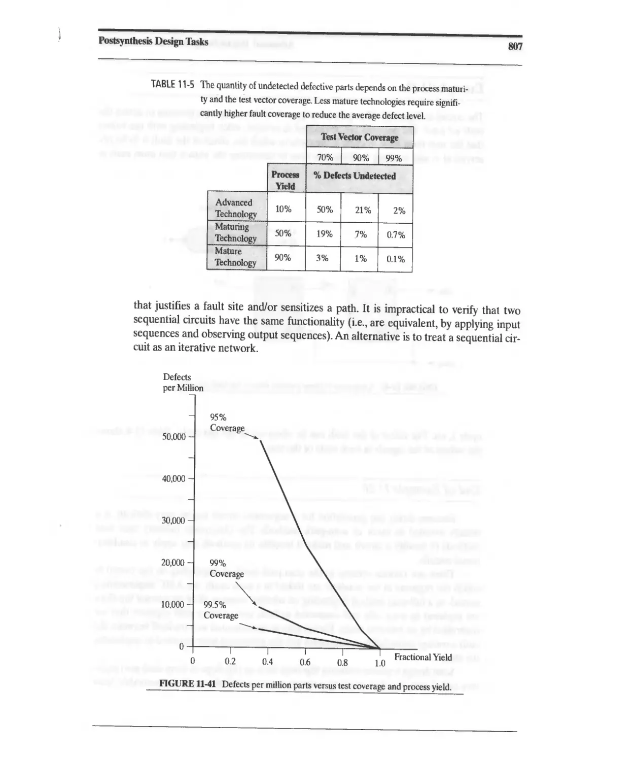
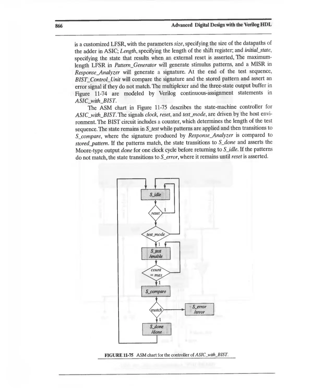
11.7.6 Test Generation for Sequential Circuits 806
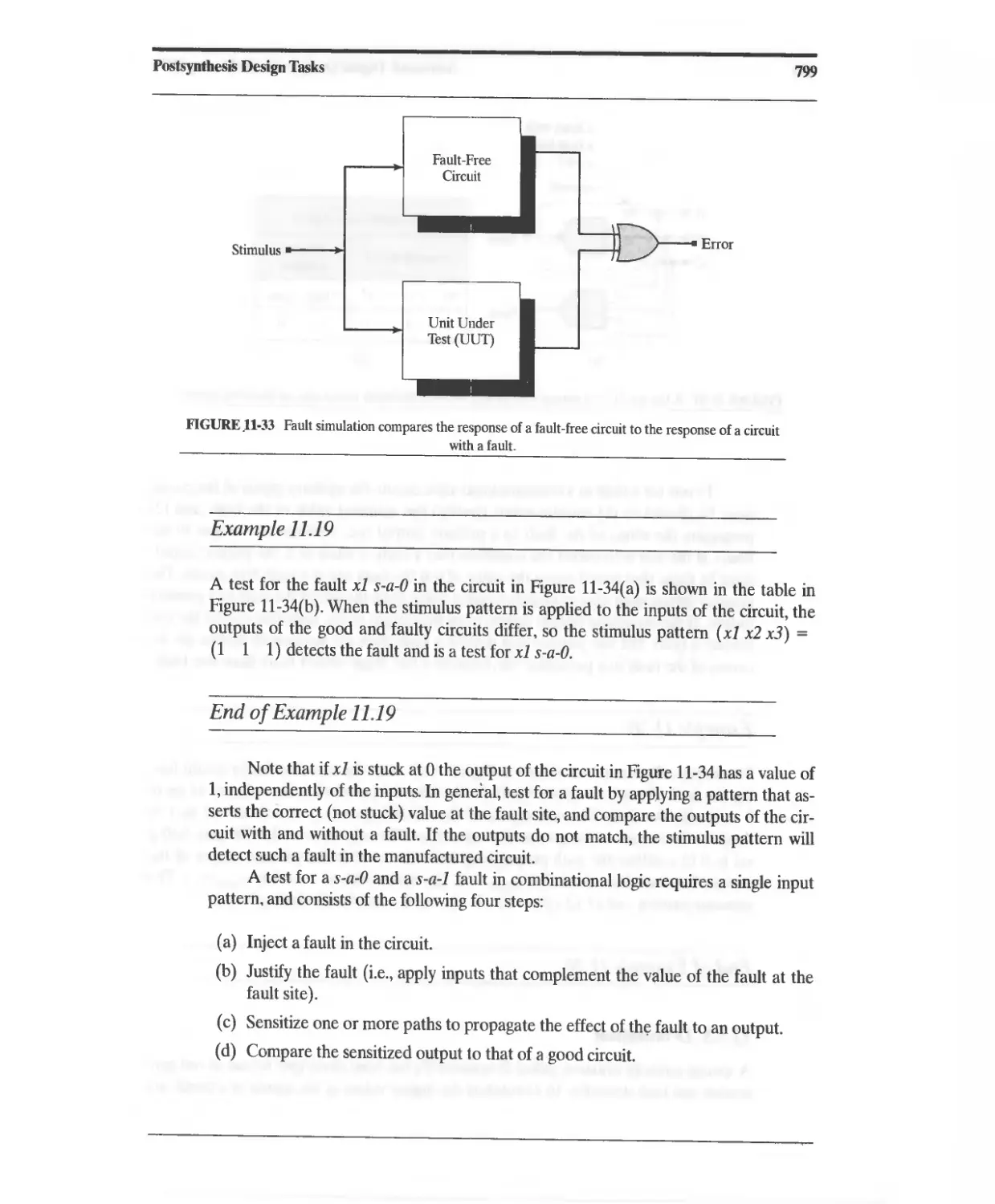
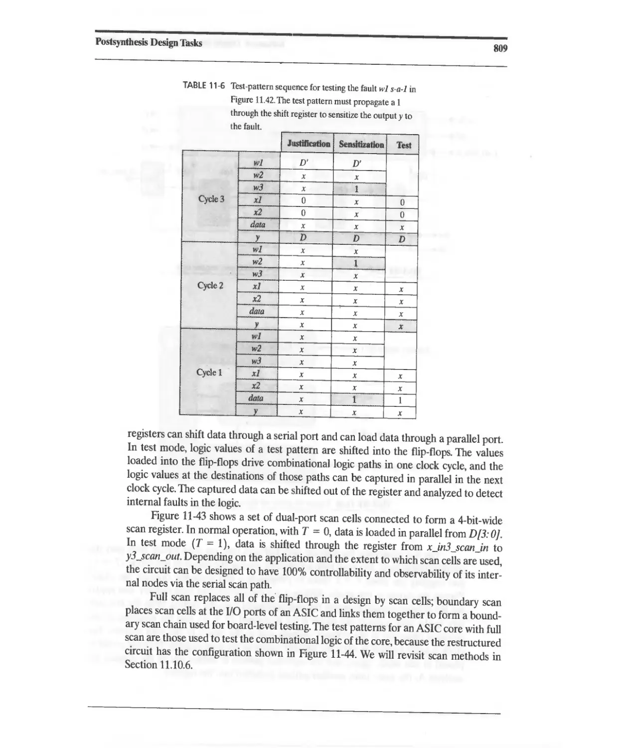
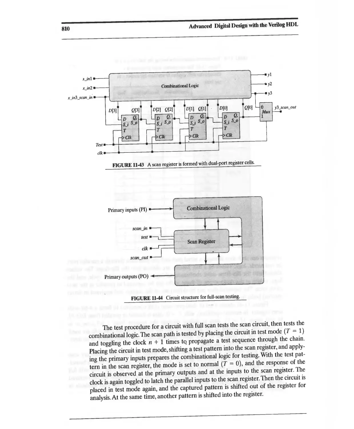
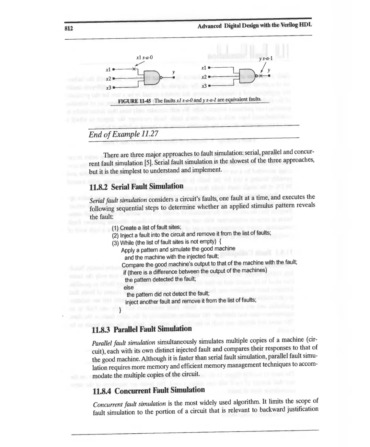
11.8 Fault Simulation 811
11.8.1 Fault Collapsing 811
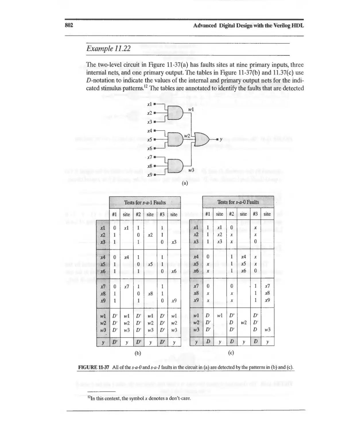
11.8.2 Serial Fault Simulation 812
11.8.3 Parallel Fault Simulation 812
11.8.4 Concurrent Fault Simulation 812
11.8.5 Probabilistic Fault Simulation 813
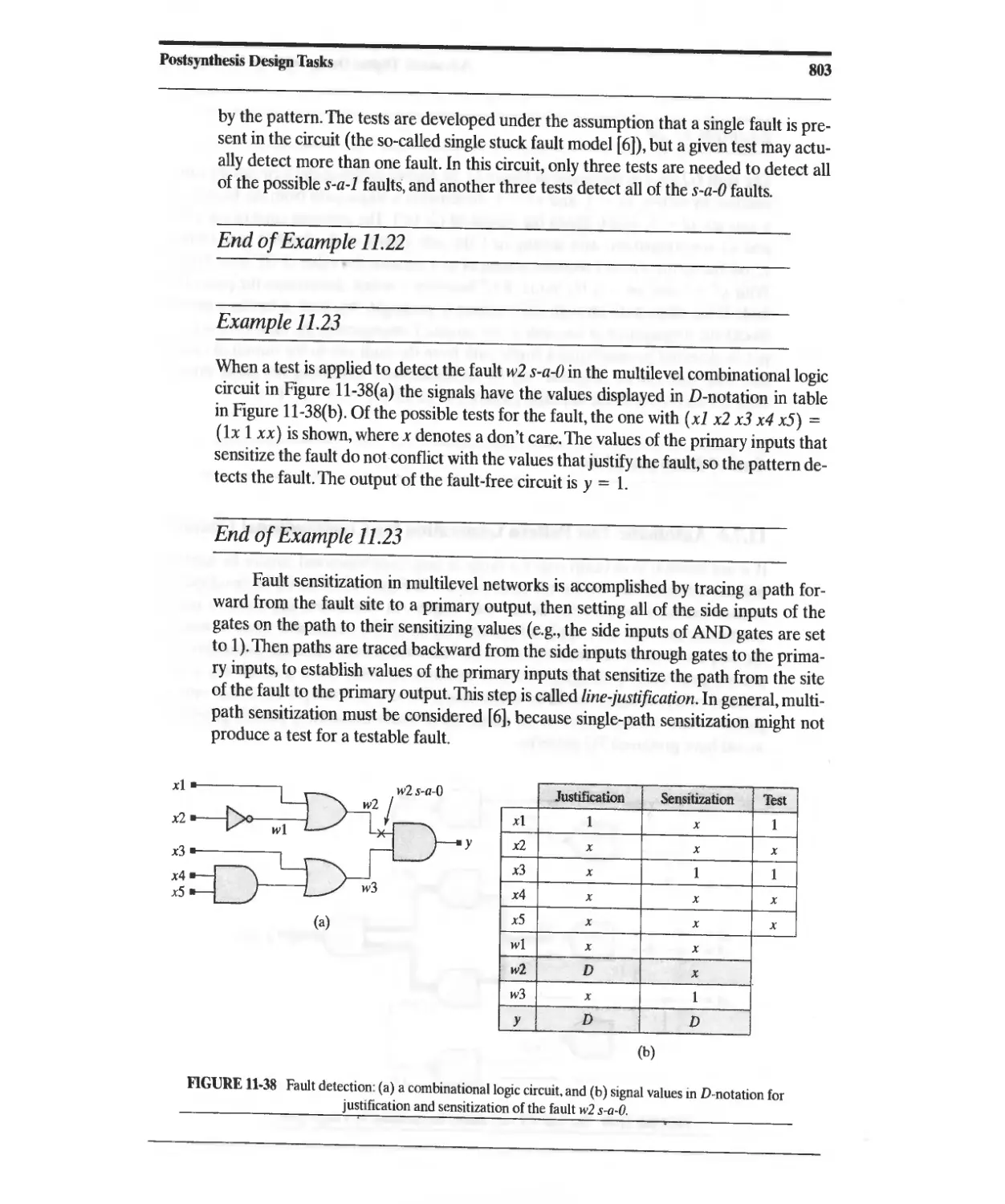
11.9 Fault Simulation with Verifault-XL 813
11.9.1 Tasks for Fault Simulation 813
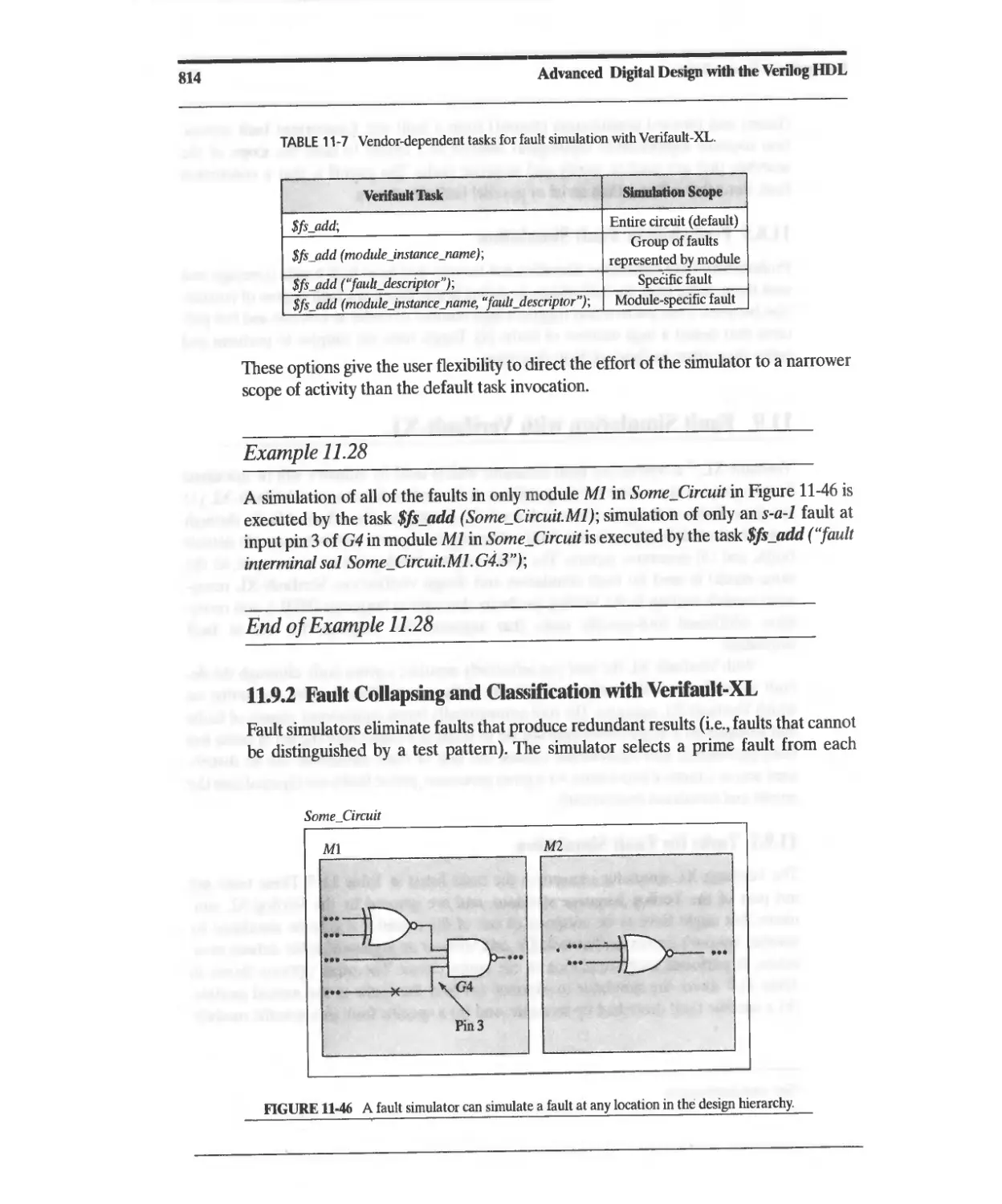
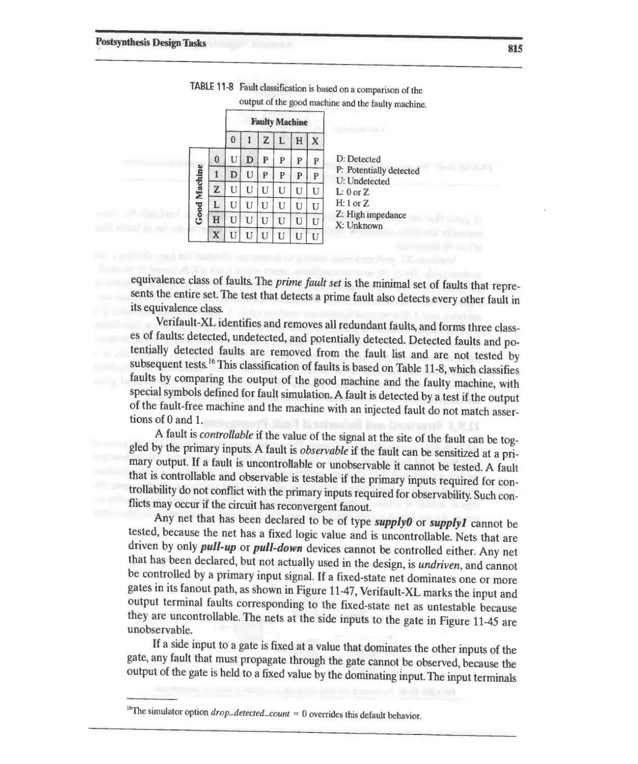
11.9.2 Fault Collapsing and Classification with Verifault-XL 814
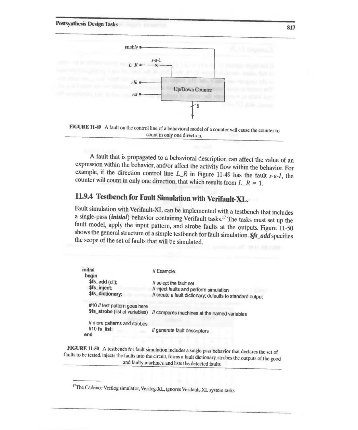
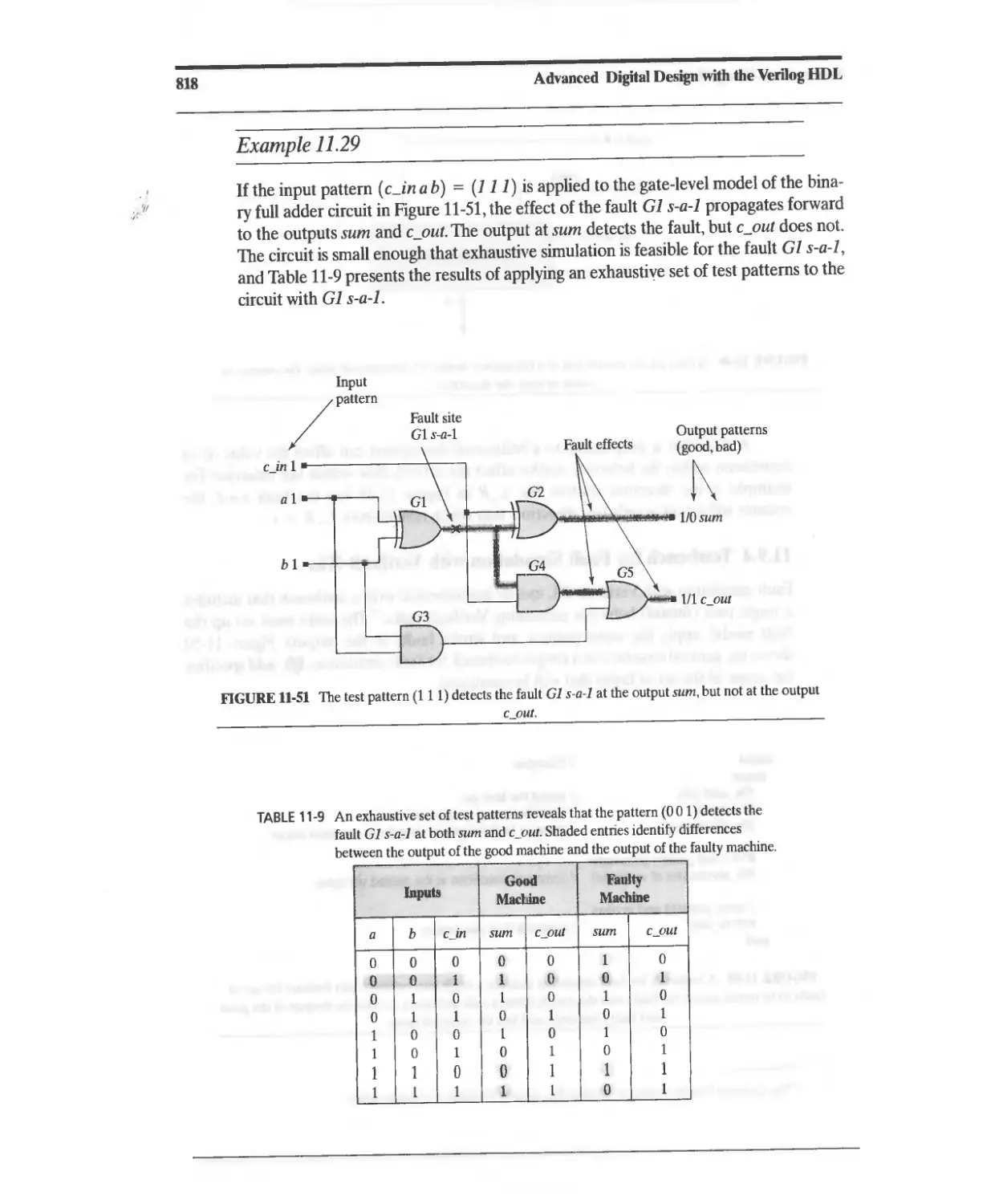
11.9.3 Structural and Behavioral Fault Propagation 816
11.9.4 Testbench for Fault Simulation with Verifault-XL 817
11.9.5 Fault Descriptors 819
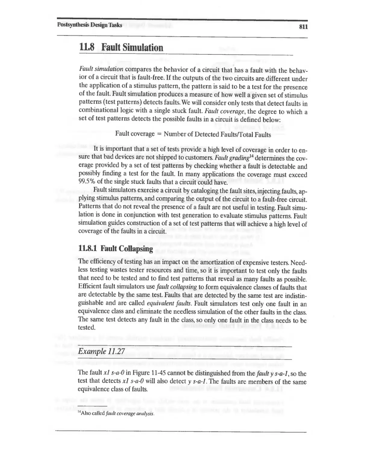
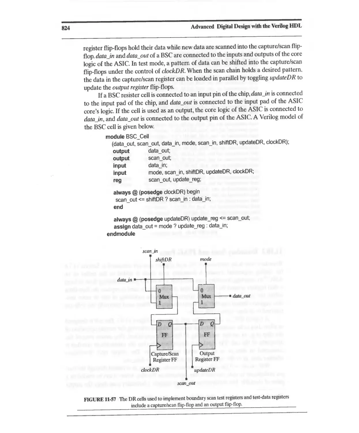
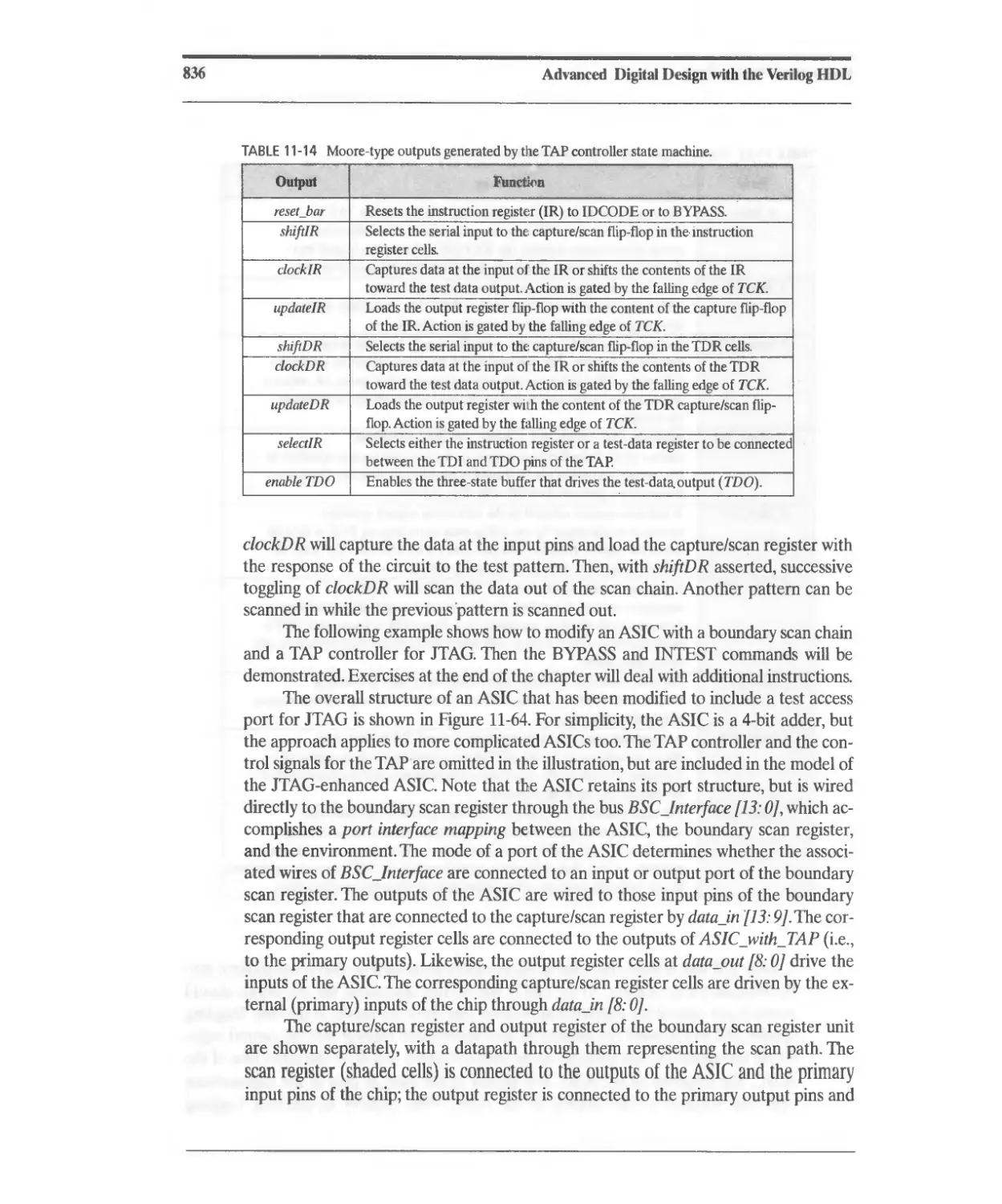
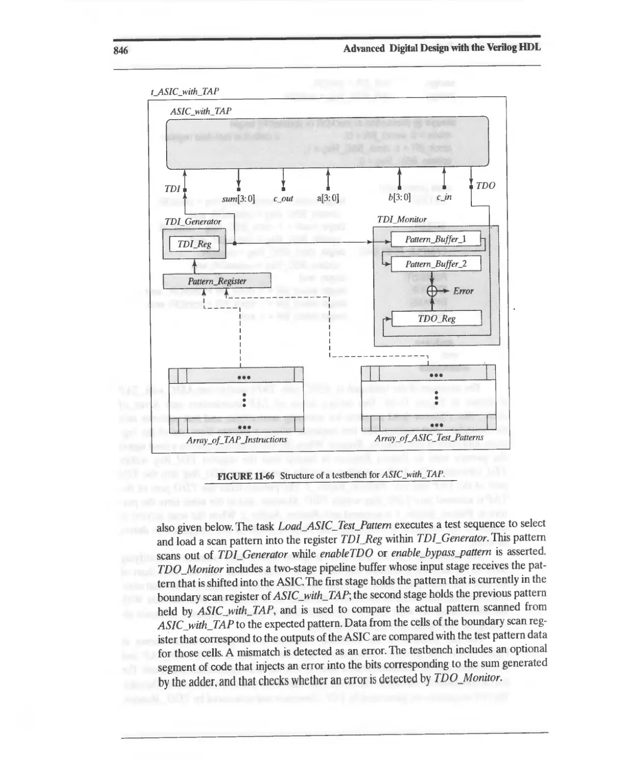
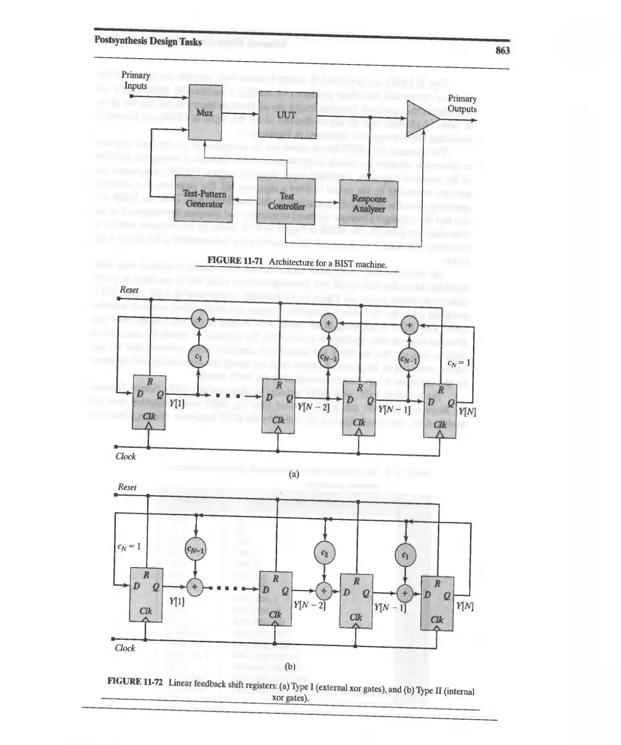
11.10 JTAG Ports and Design for Testability 821
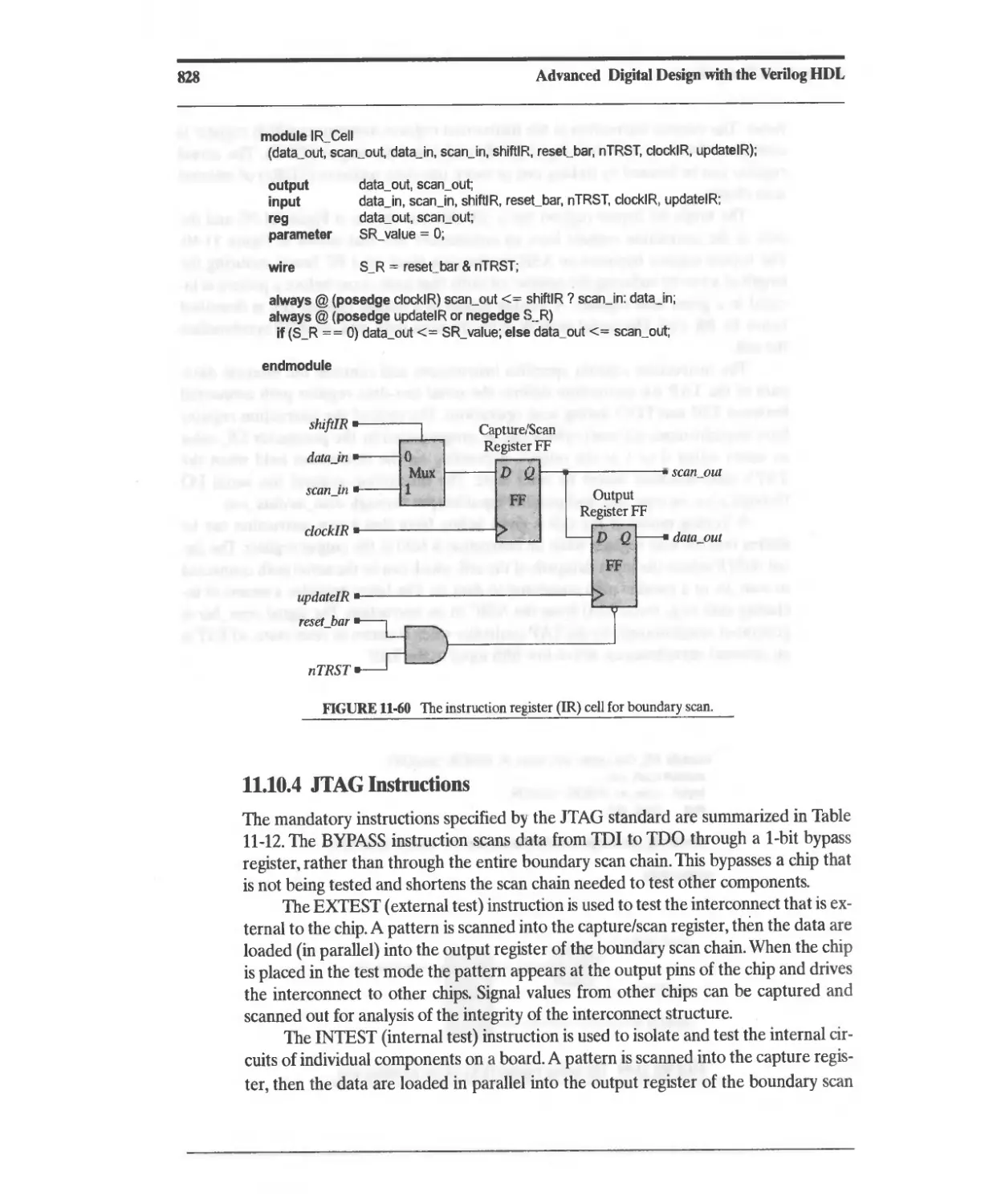
11.10.1 Boundary Scan and JTAG Ports 823
11.10.2 JTAG Modes of Operation 825
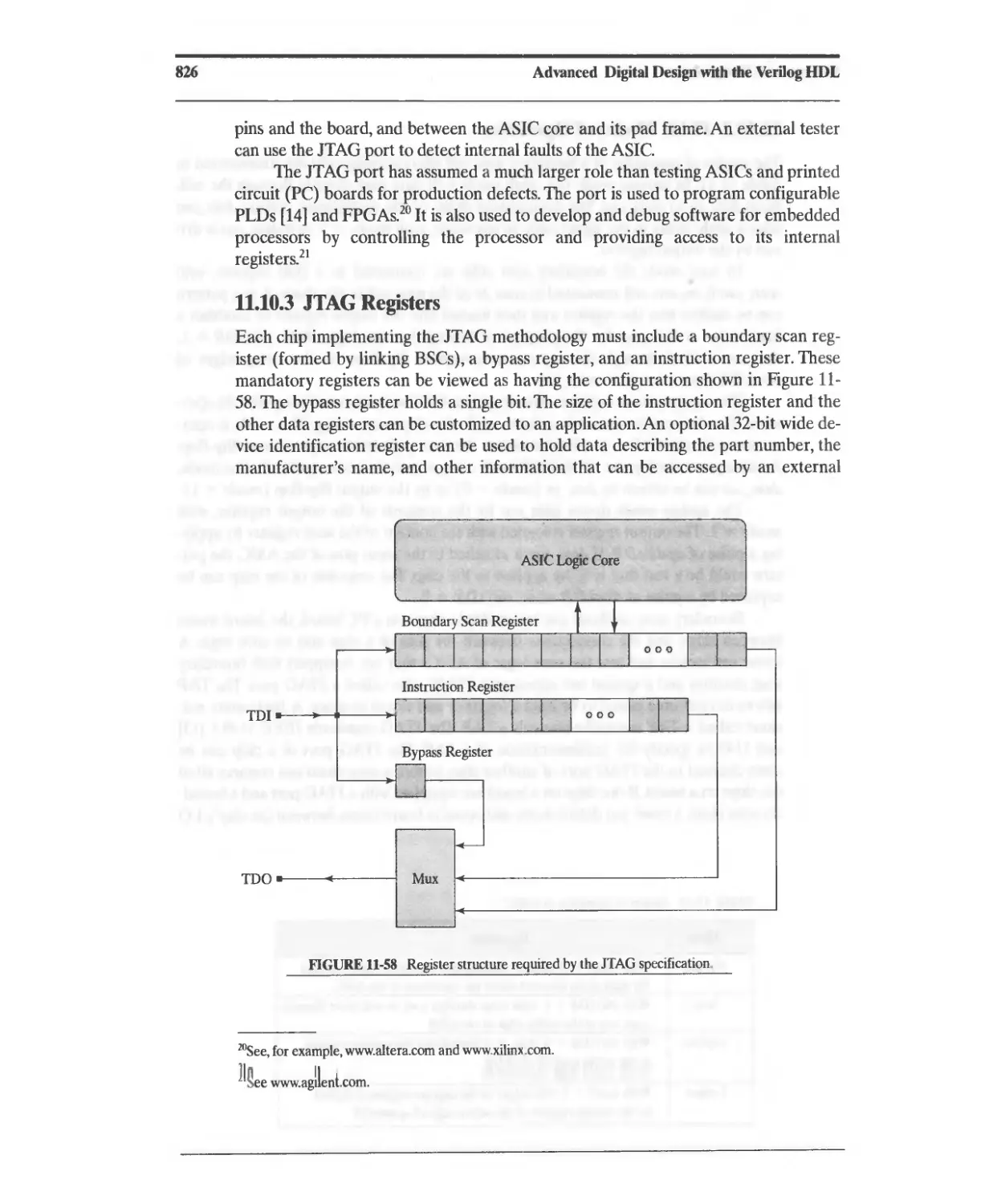
11.10.3 JTAG Registers 826
11.10.4 JTAG Instructions 828
xiv
Contents
UllwlL,II.I I I
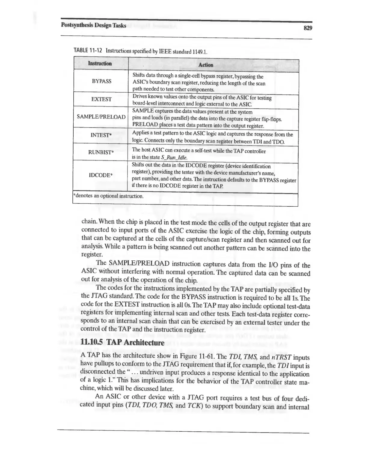
11.10.5 TAP Architecture 829
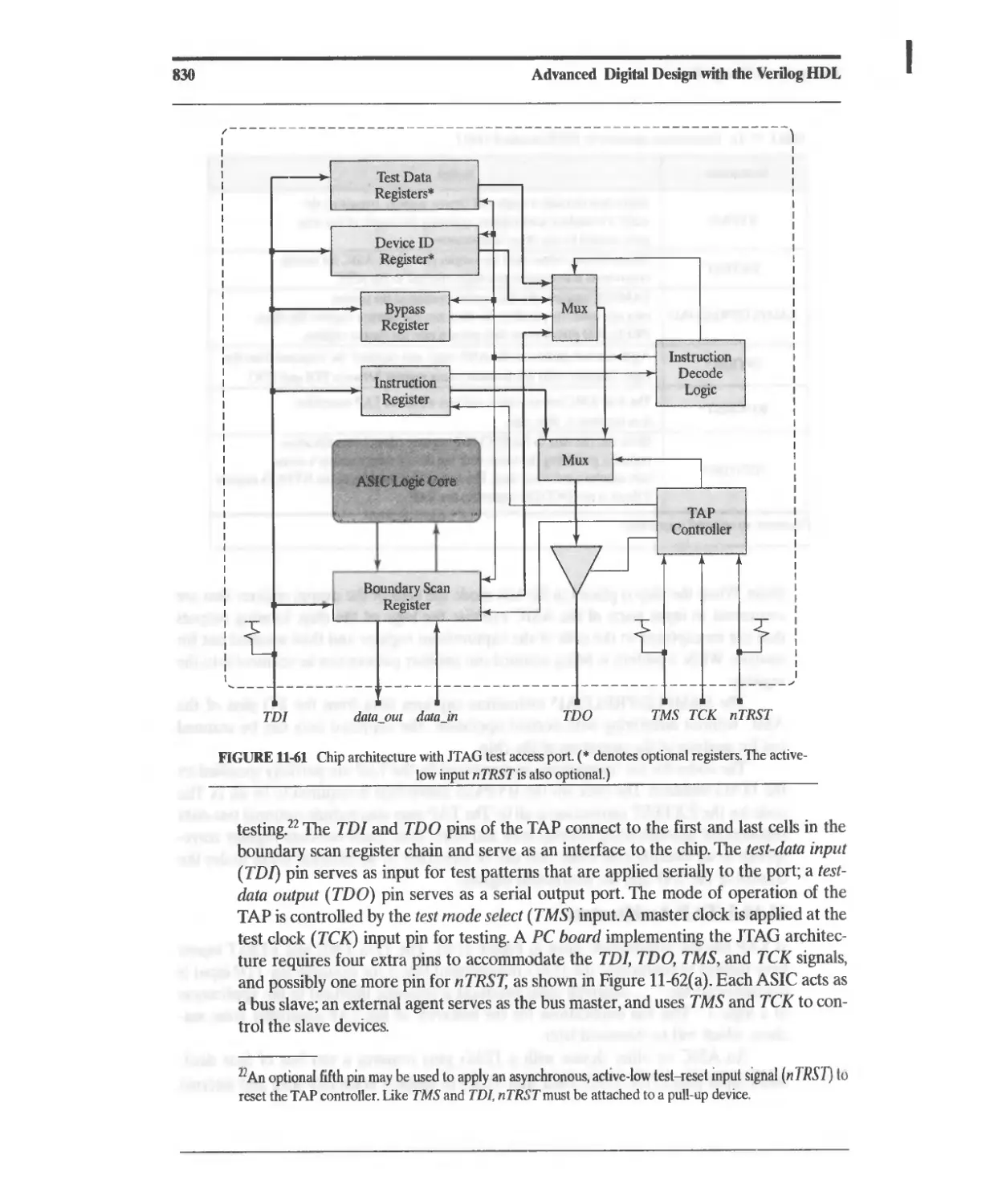
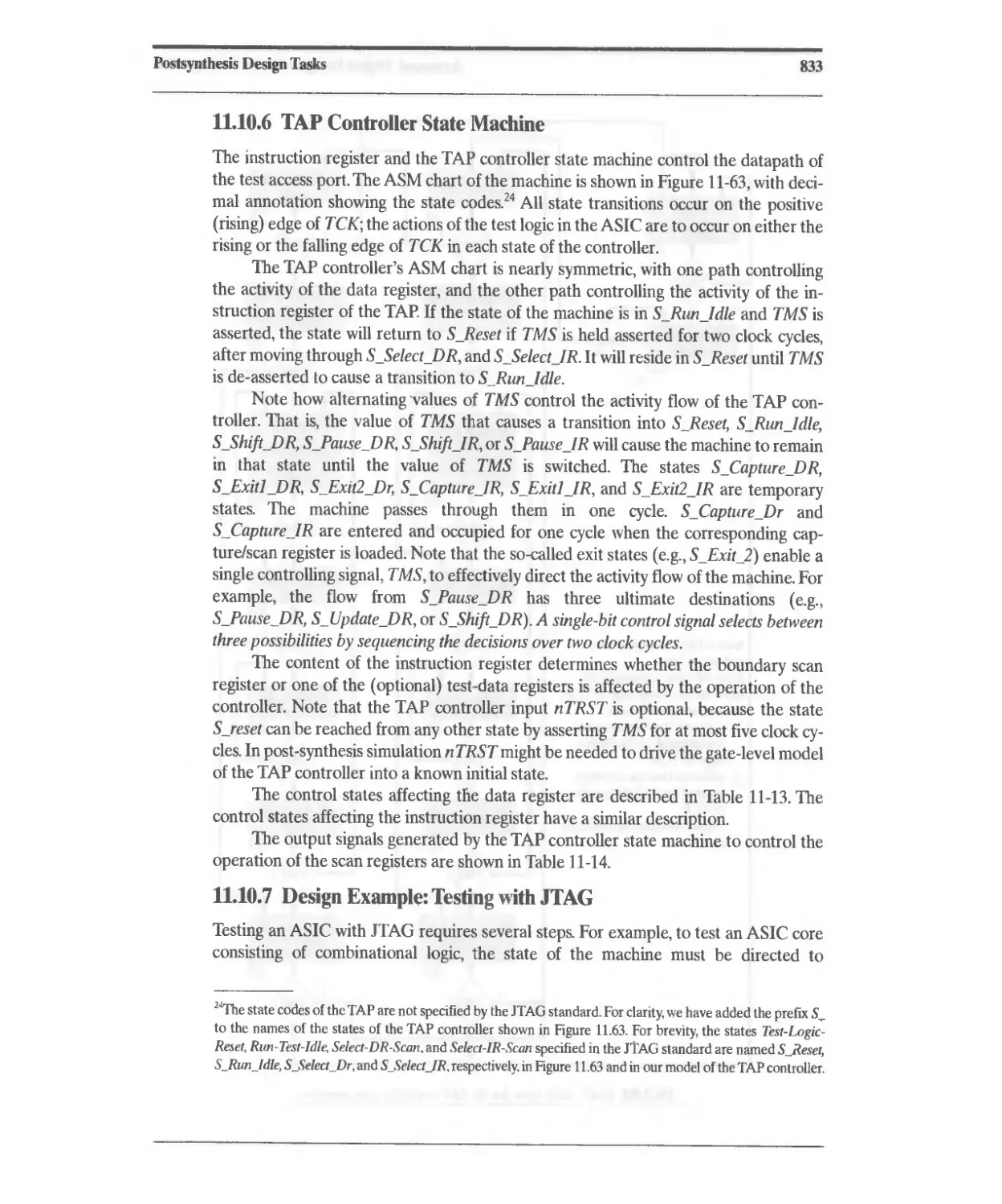
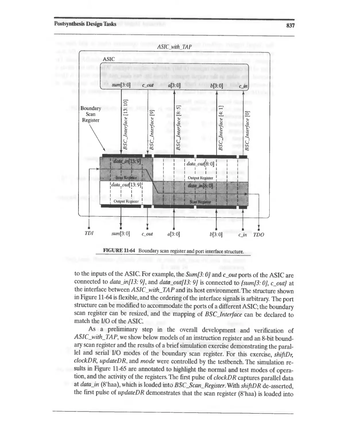
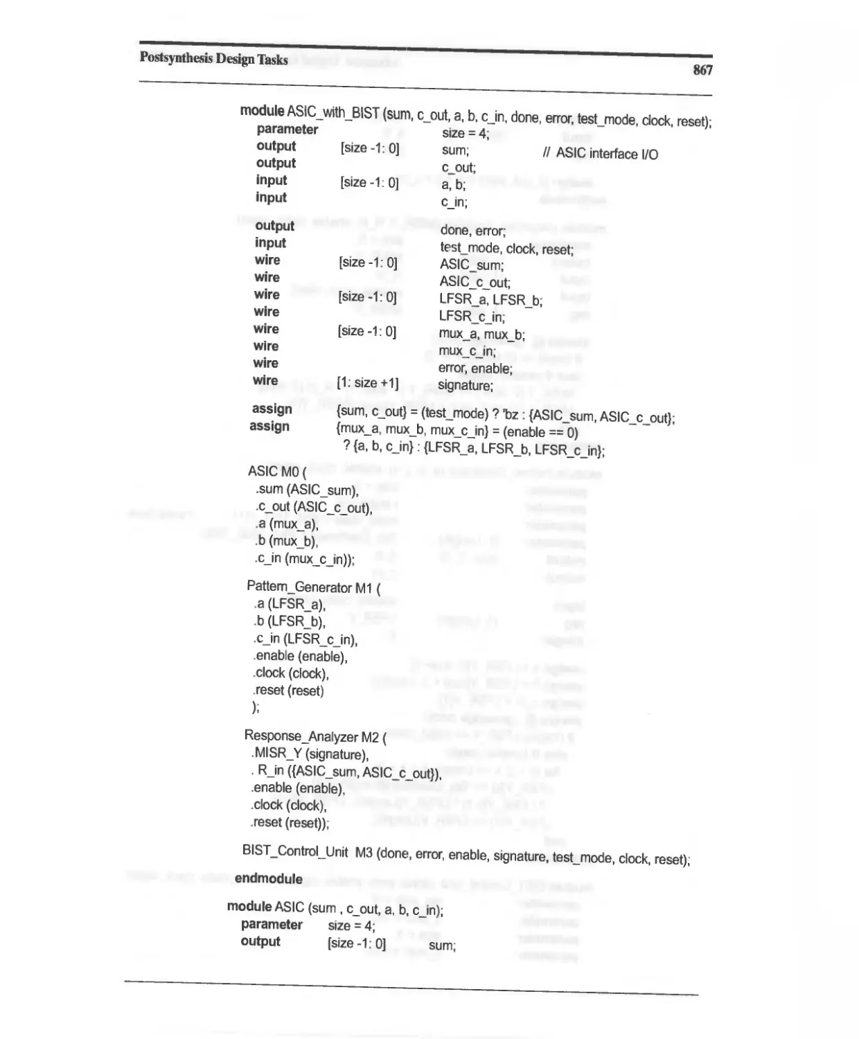
11.10.6 TAP Controller State Machine 833
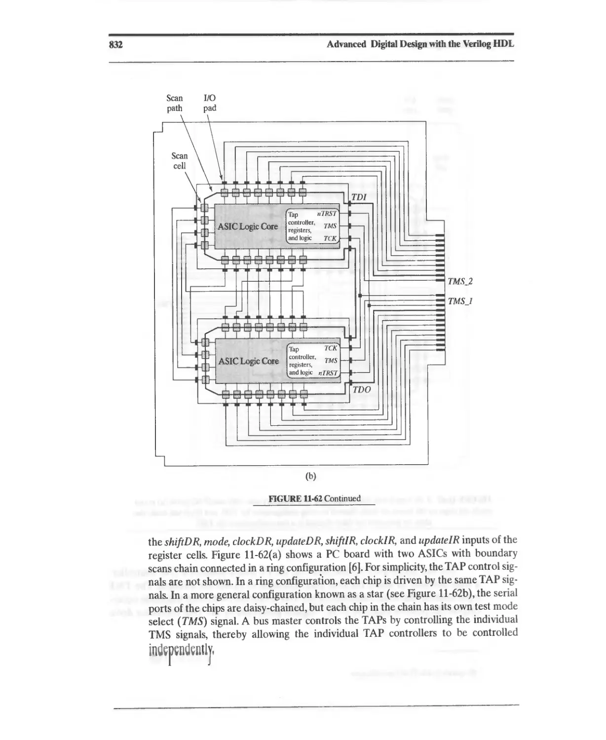
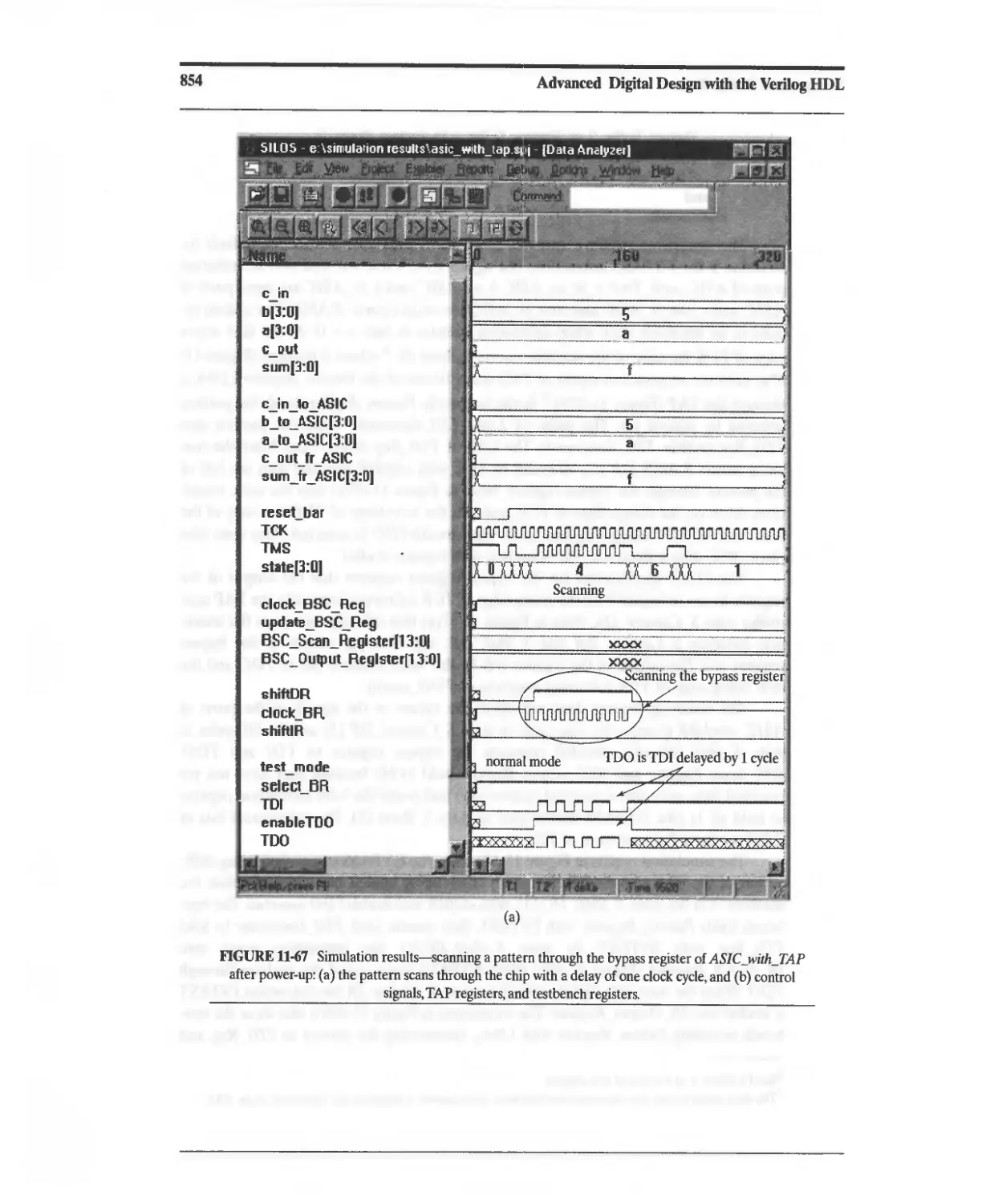
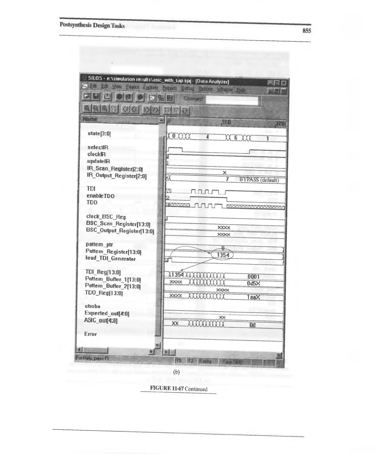
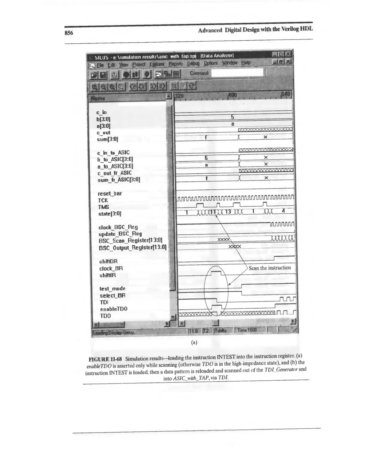
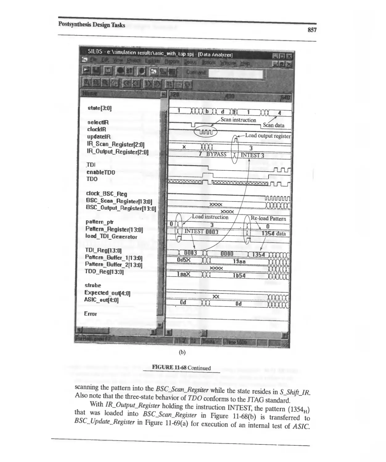
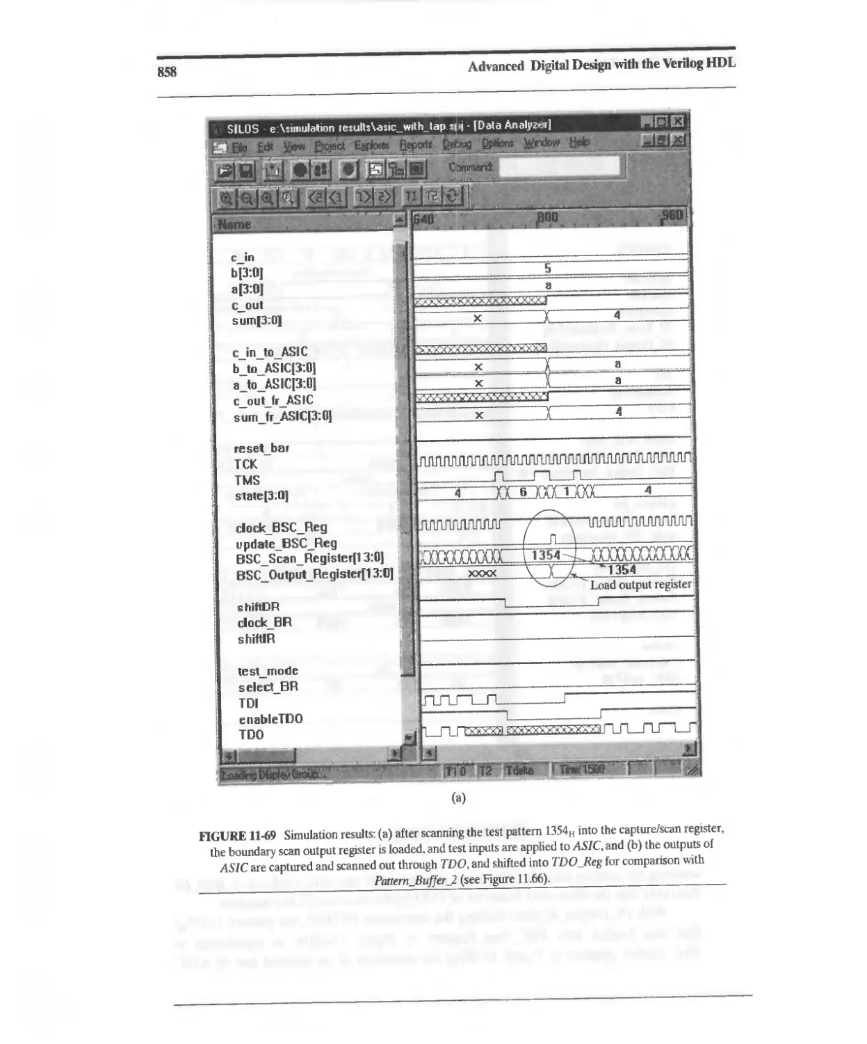
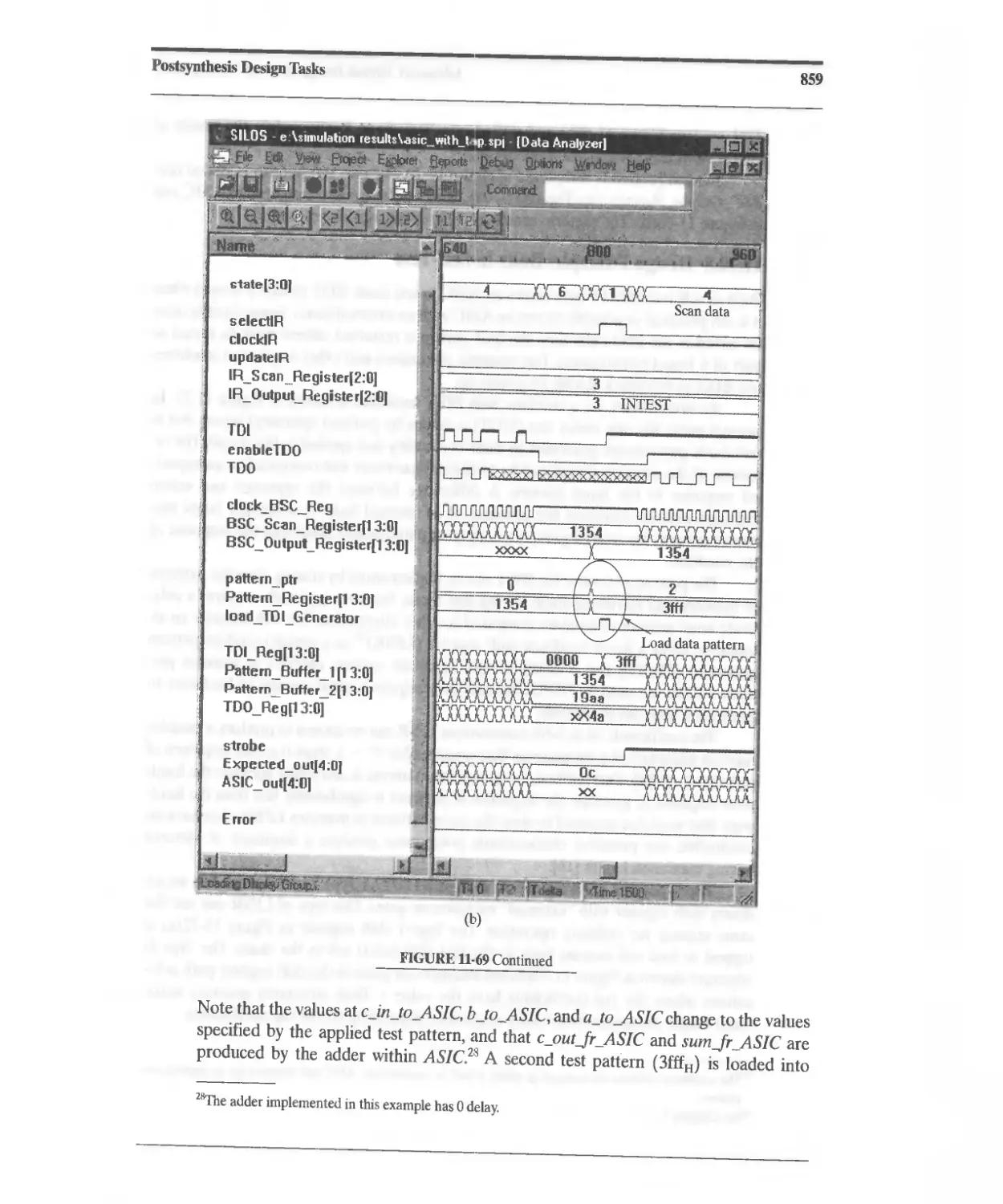
11.10.7 Design Example: Testing with JTAG 833
11.10.8 Design Example: Built-In Self-Test 860
References 874
Problems 874
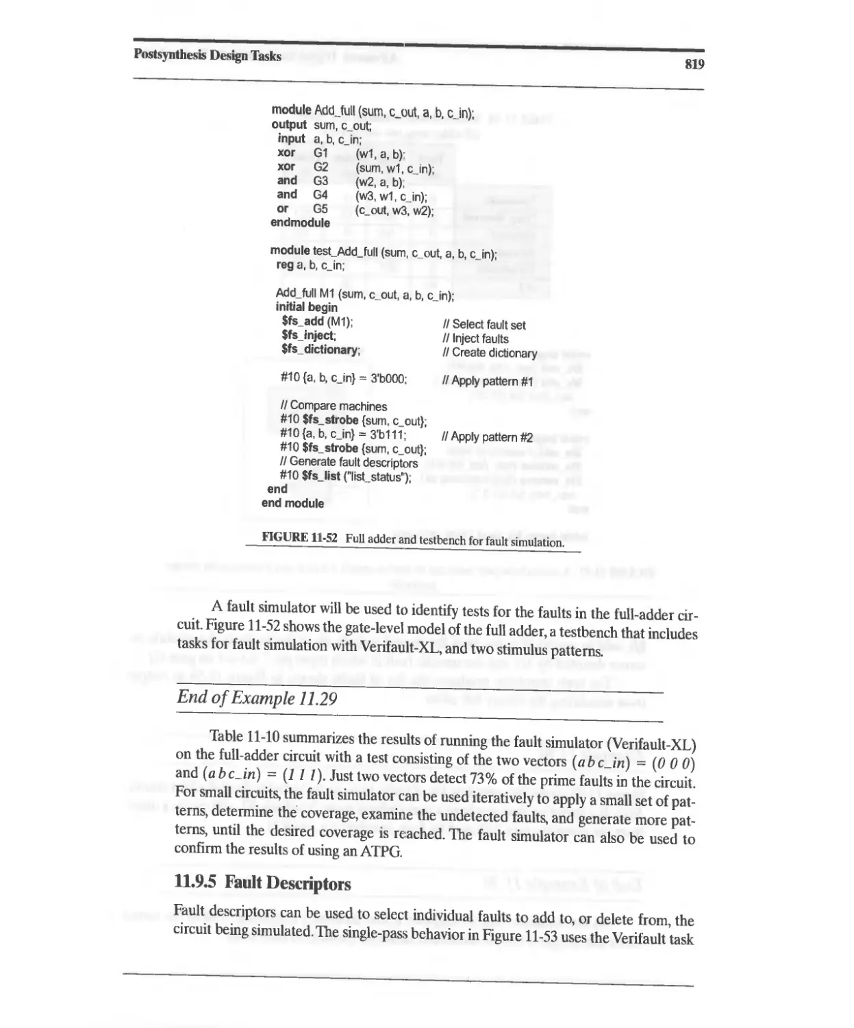
A Verilog Primitives 883
Al Multiinput Combinational Logic Gates 883
A2 Multioutput Combinational Gates 885
A3 Three-State Gates 886
A4 MOS Transistor Switches 889
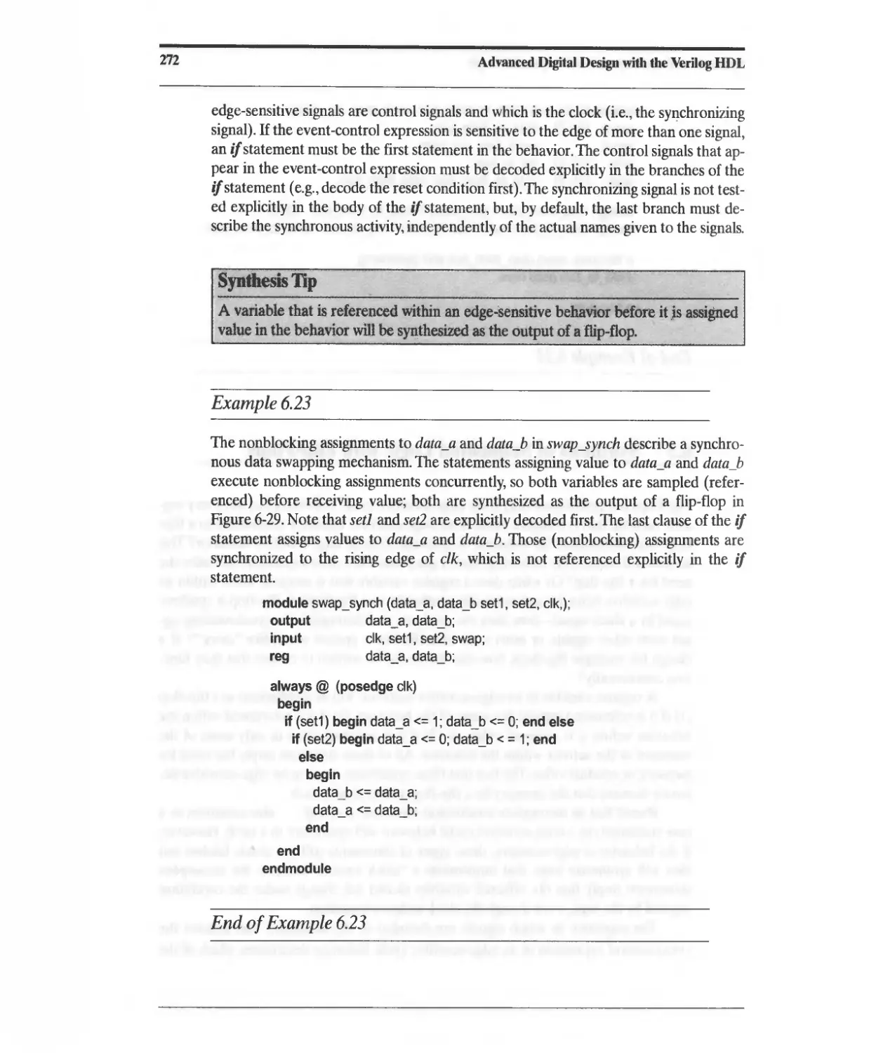
A5 MOS Pull-Up/Pull-Down Gates 892
A6 MOS Bidirectional Switches 892
B Verilog Keywords 895
C Verilog Data Types 897
C.1 Nets 897
C.2 Register Variables 898
C.3 Constants 902
C.4 Referencing Arrays of Nets or Regs 903
D Verilog Operators 905
D.1 Arithmetic Operators 905
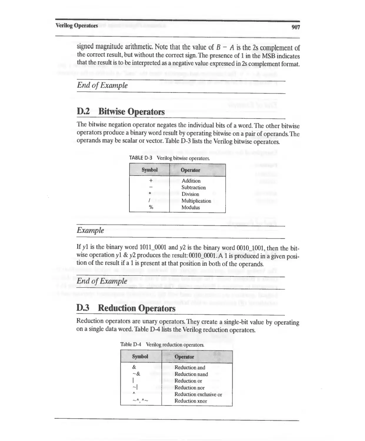
D.2 Bitwise Operators 907
DJ Reduction Operators 908
D.4 Logical Operators 909
D.5 Relational Operators 910
D.6 Shift Operators 910
D.7 Conditional Operator 910
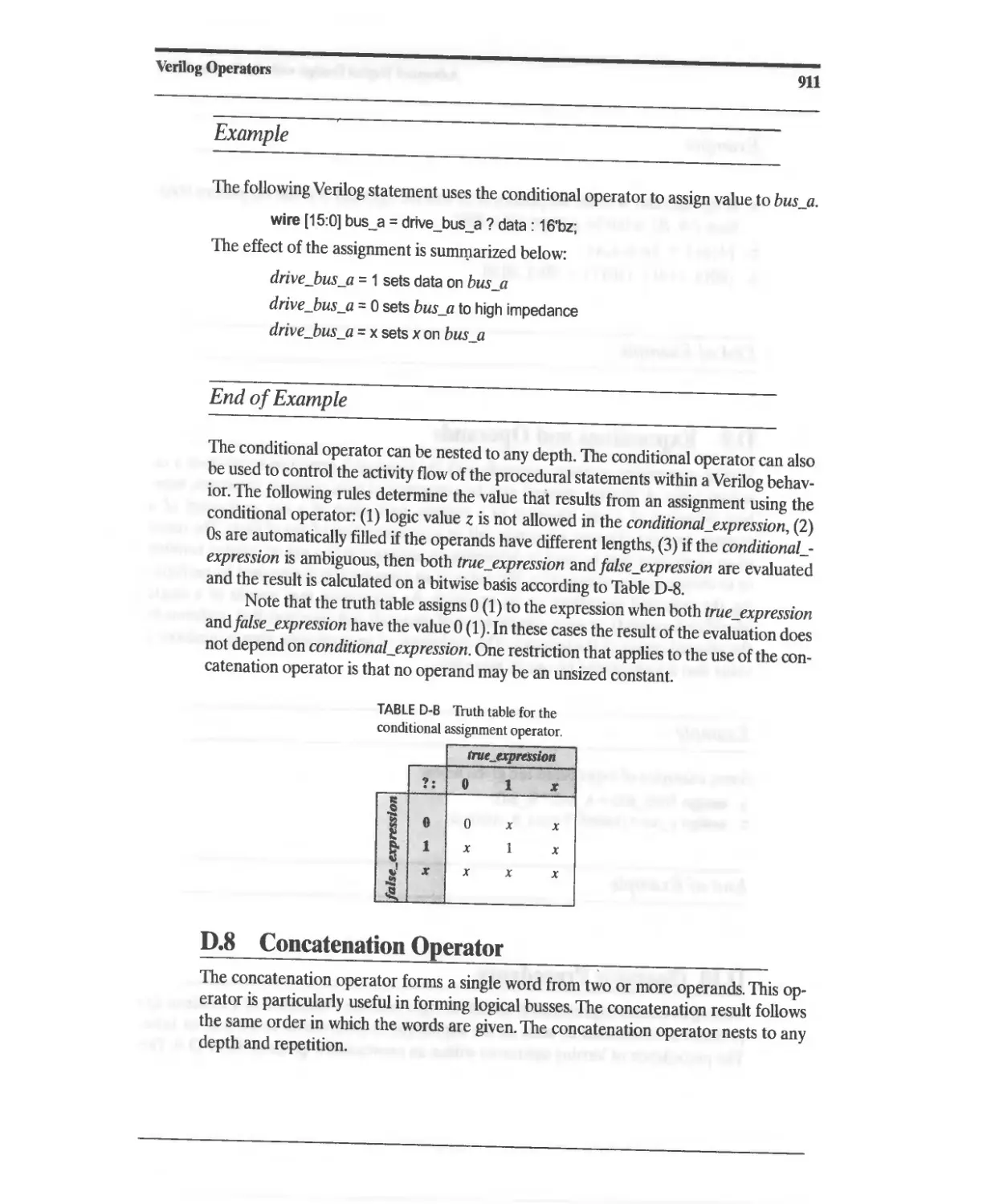
D.8 Concatenation Operator 911
D.9 Expressions and Operands 912
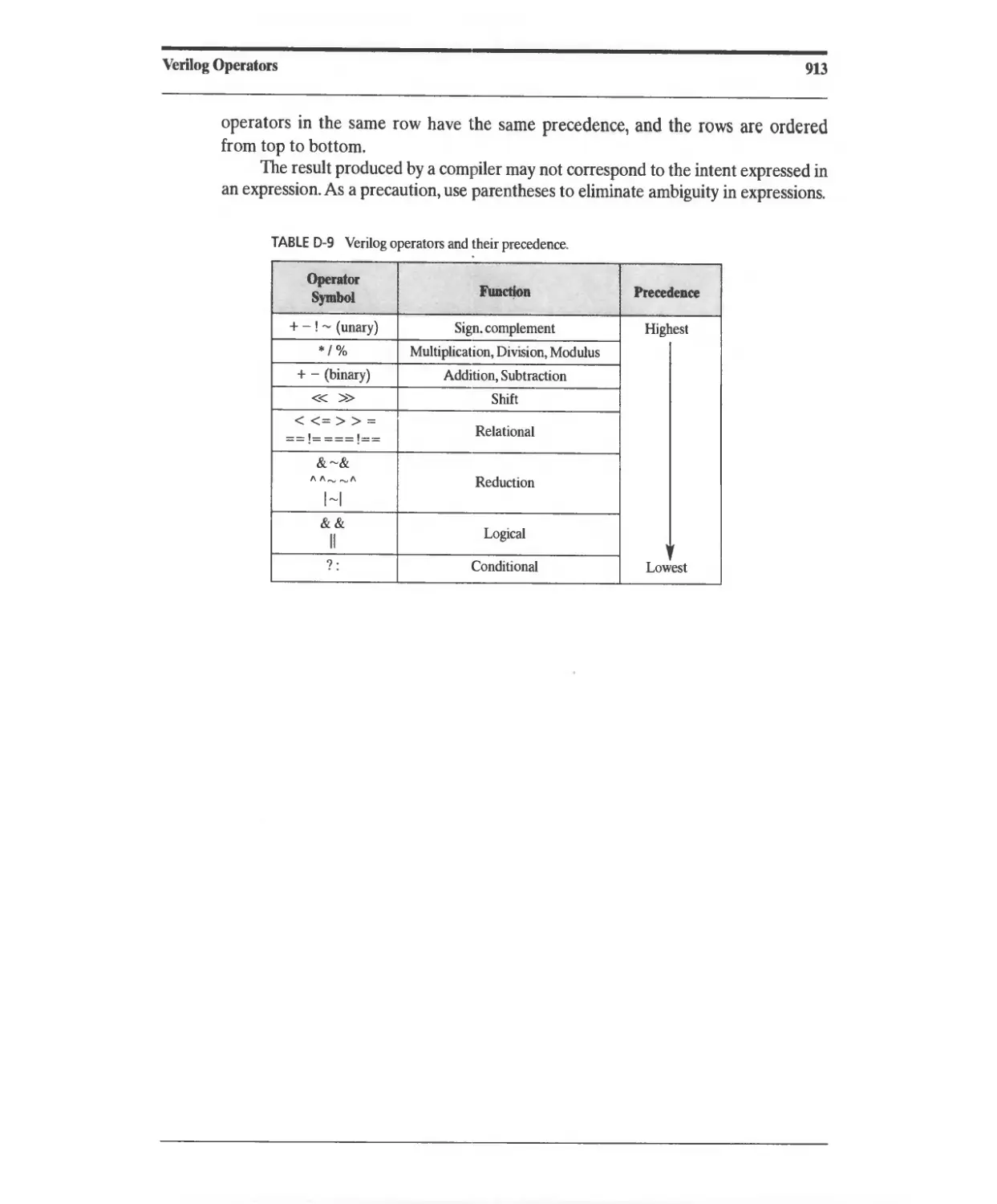
D.1O Operator Precedence 912
E Backus-Naur Formal Syntax Notation 915
.
F Verilog Language Formal Syntax 917
F.1 Source Text 917
F.2 Declarations 918
F.3 Primitive Instances 920
Contents xv
F4 Module Instantiation 921
F5 UDP Declaration and Instantiation 921
F6 Behavioral Statements 922
F7 Specify Section 924
F8 Expressions 926
F9 General 928
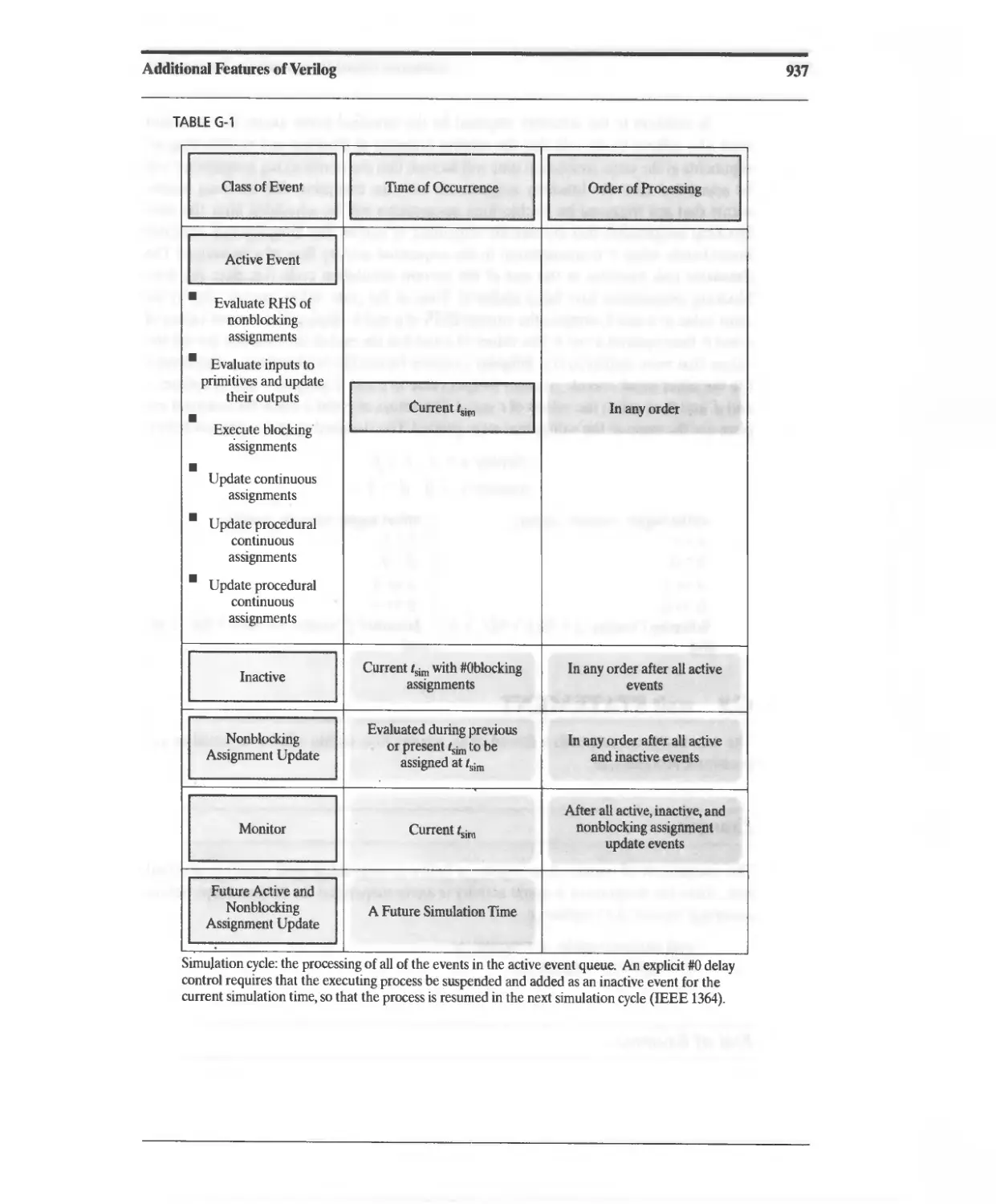
G Additional Features of Verilog 9'29
G.1 Arrays of Primitives 929
G.2 Arrays of Modules 929
G.3 Hierarchical Dereferencing 930
G.4 Parameter, Substitution 931
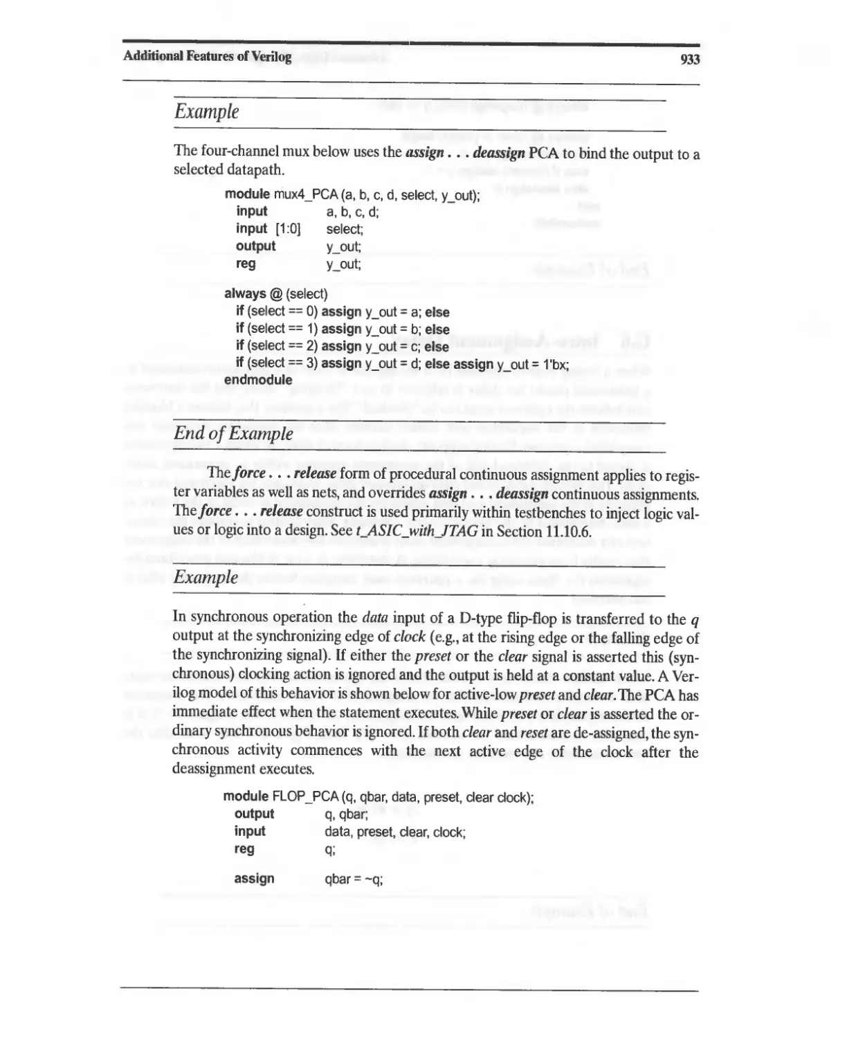
G.5 Procedural Continuous Assignment 932
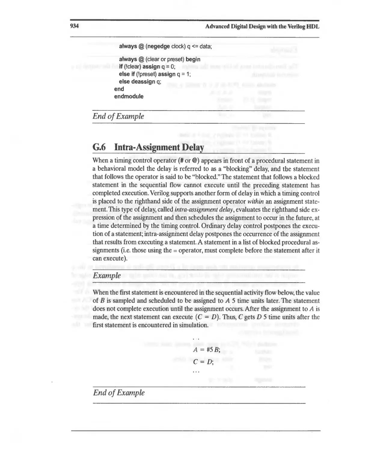
G.6 Intra-Assignment Delay 934
G.7 Indeterminate Assignment and Race Conditions 935
G.8 wait Statement 938
G.9 fork... join Statement 939
G.10 Named (Abstract) Events 939
G.11 Constructs Supported by Synthesis Tools 940
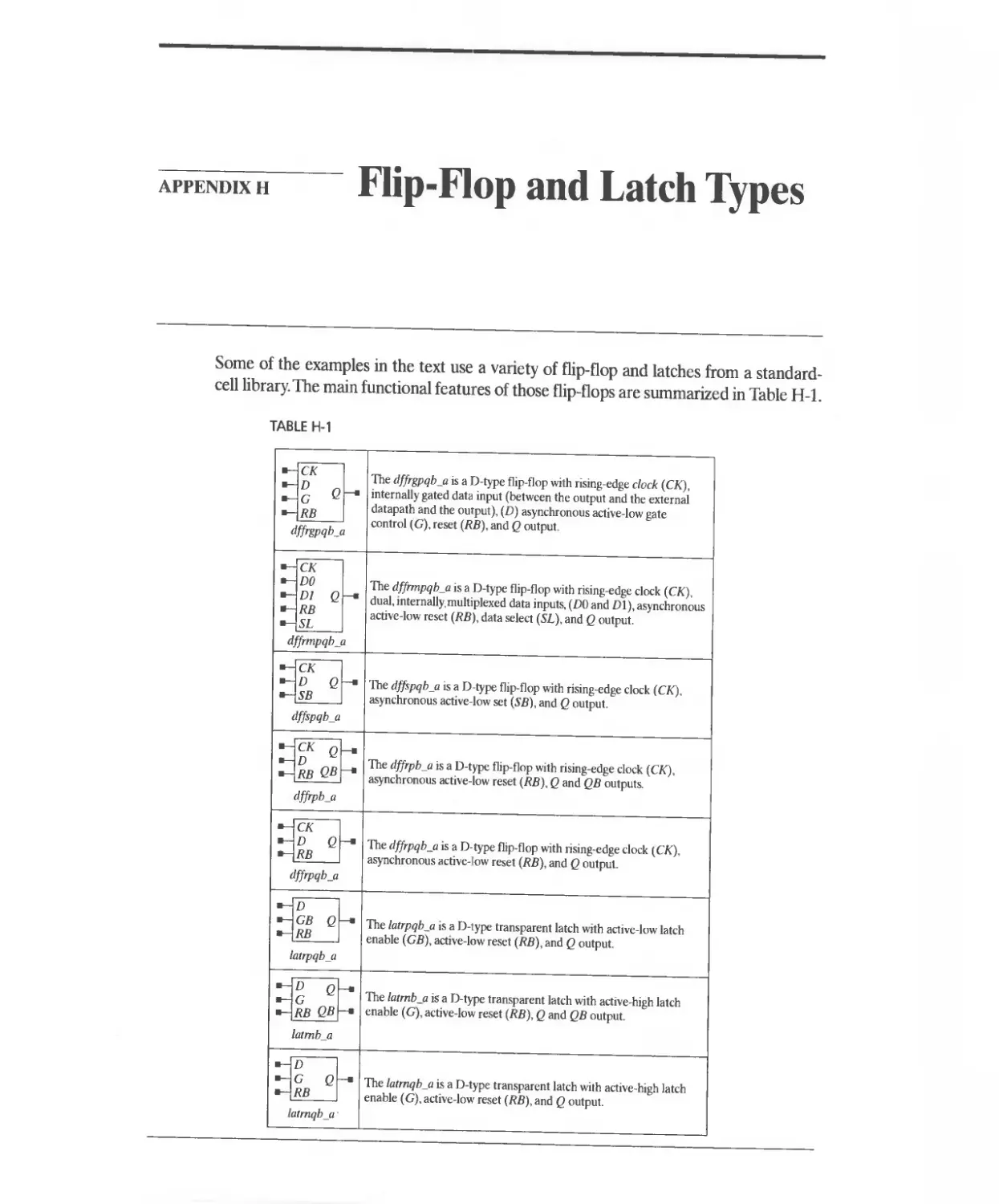
H Flip-Flop and Latch Types 943
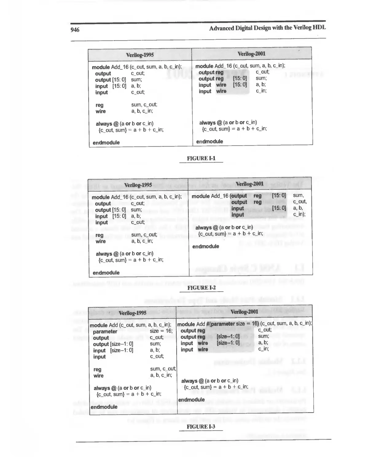
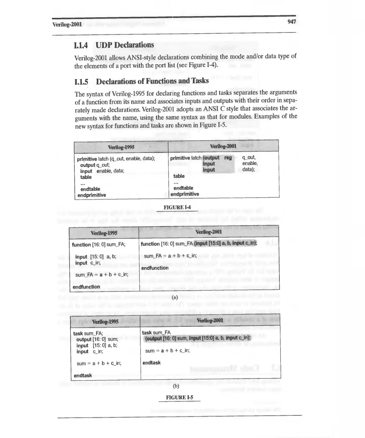
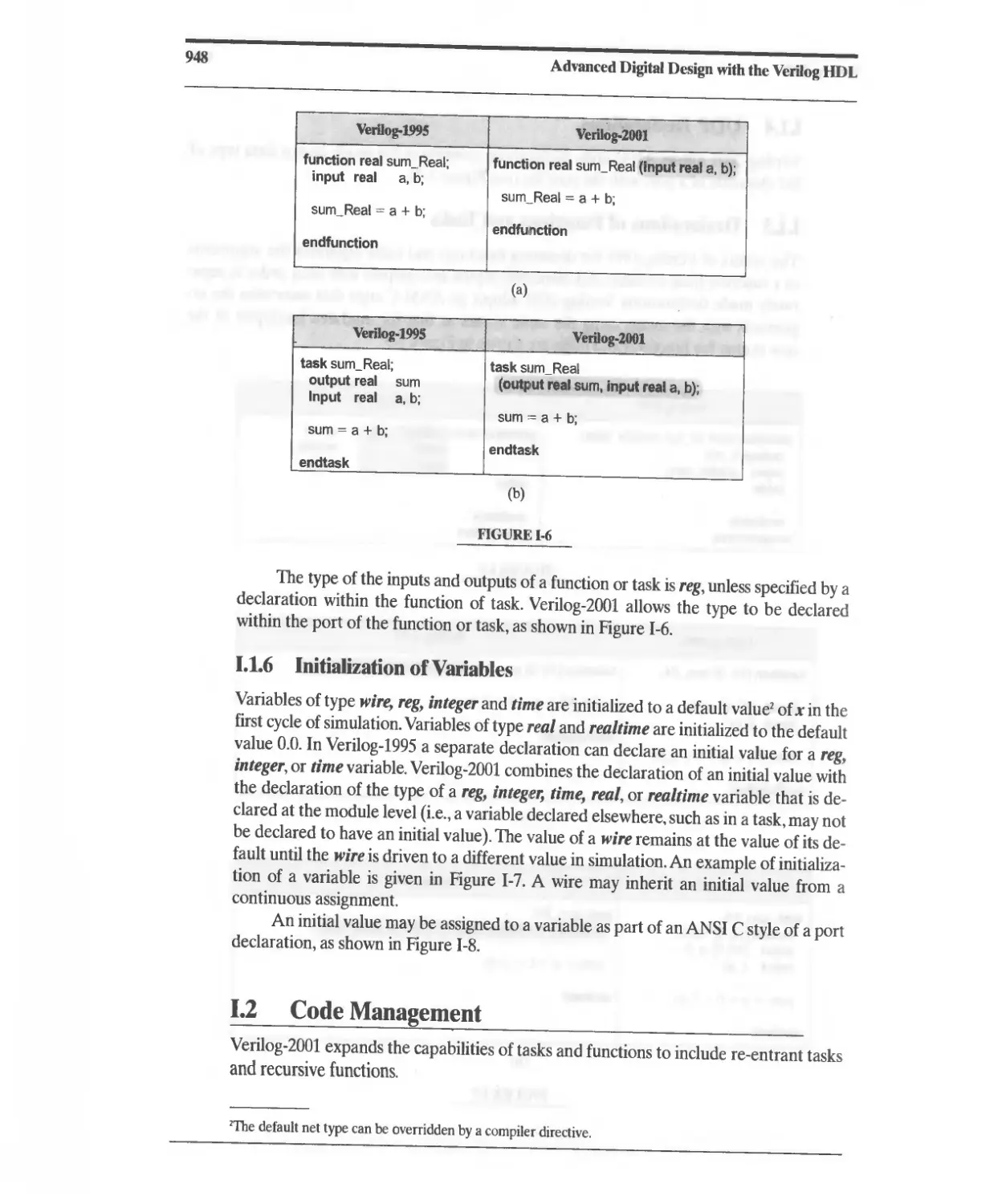
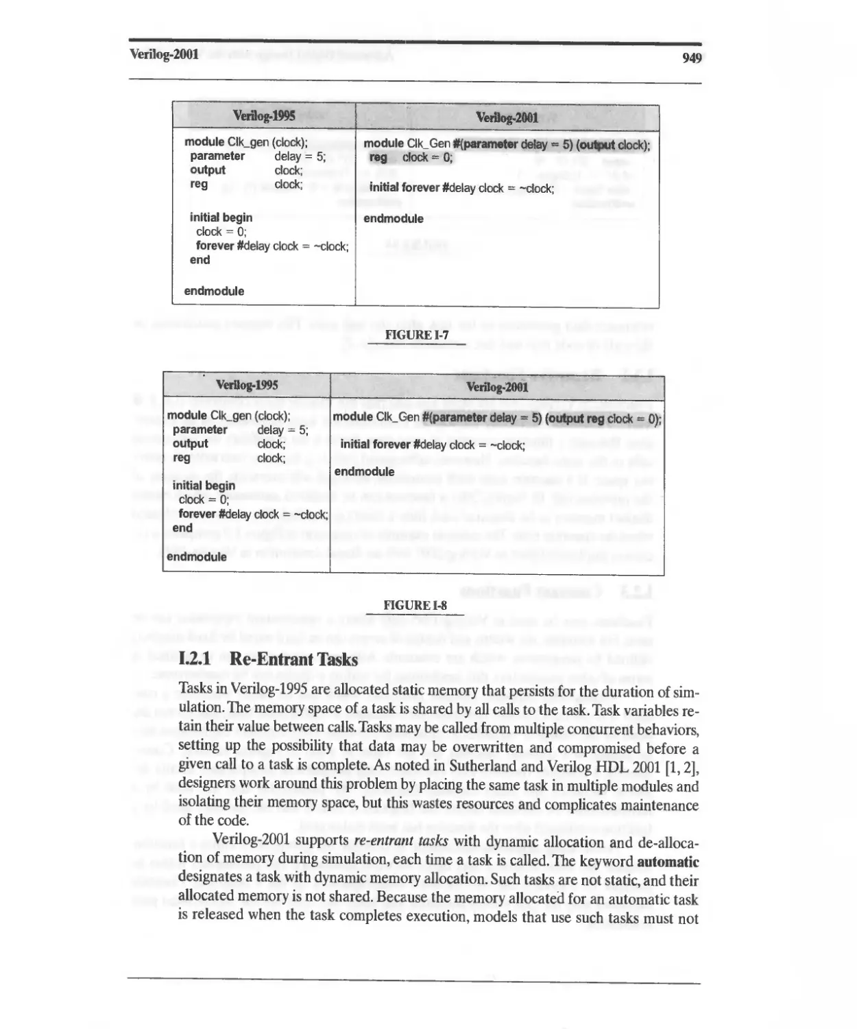
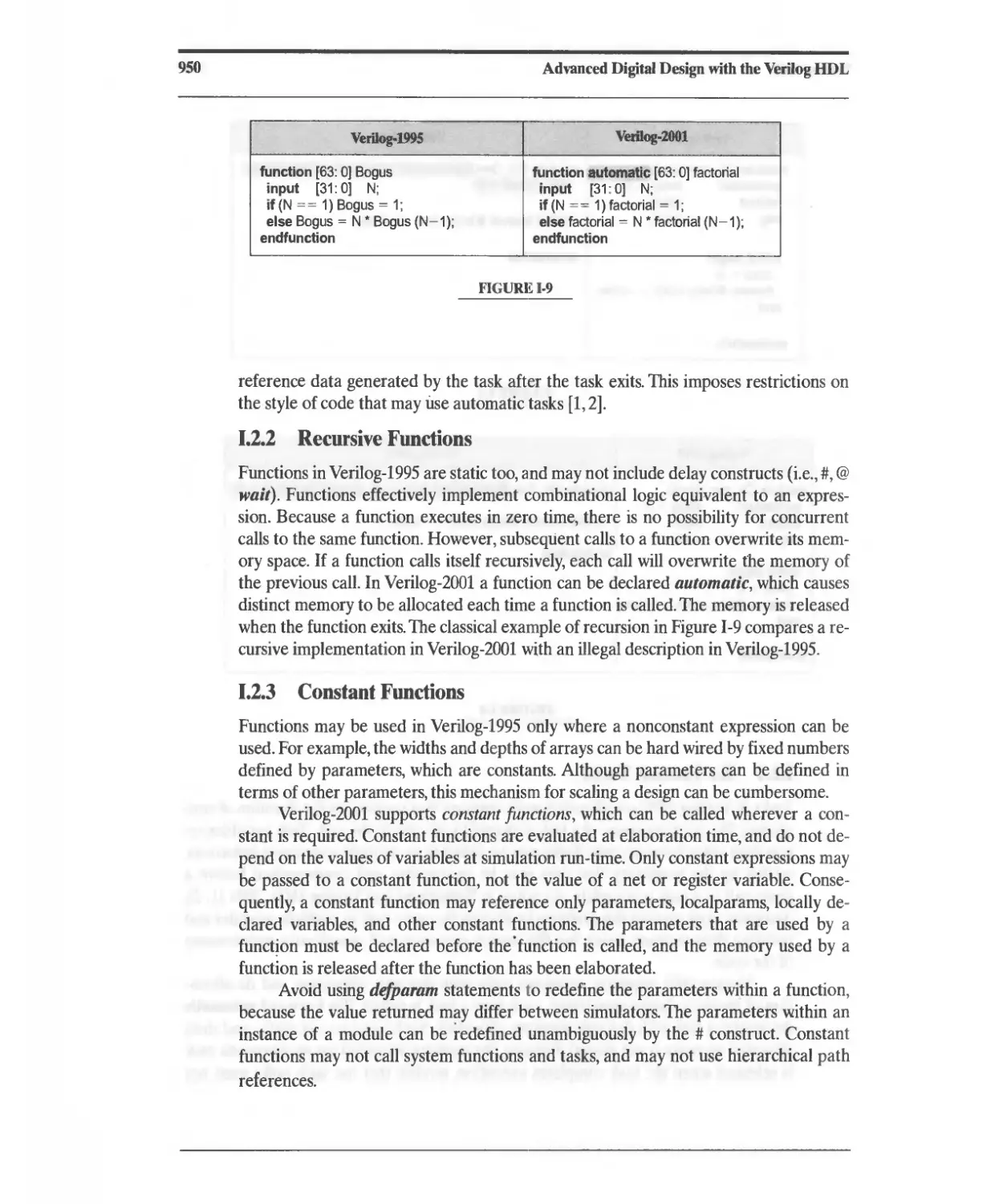
I Verilog-2001 945
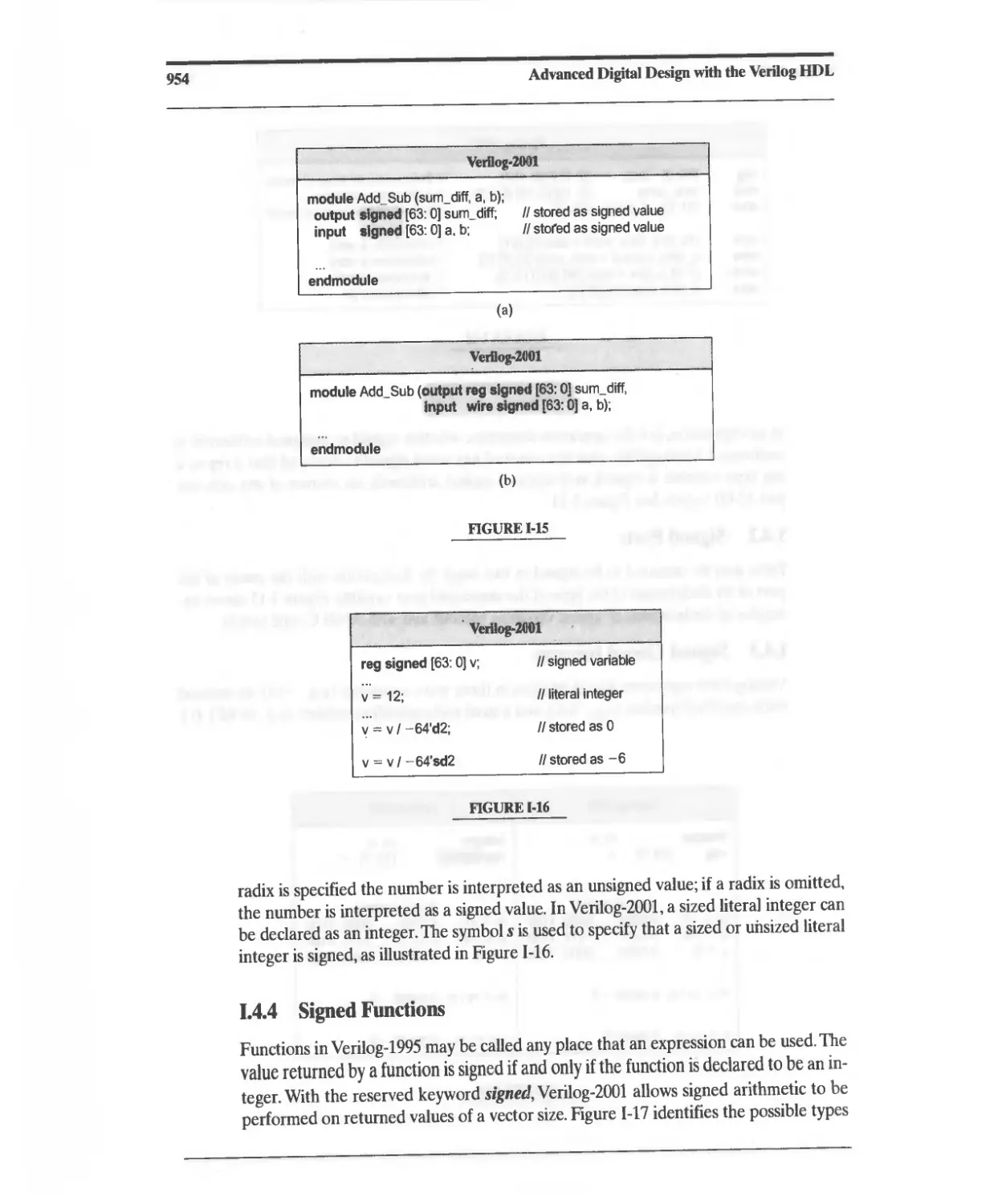
I.1 ANSI C Style Changes 945
1.2 Code Management 948
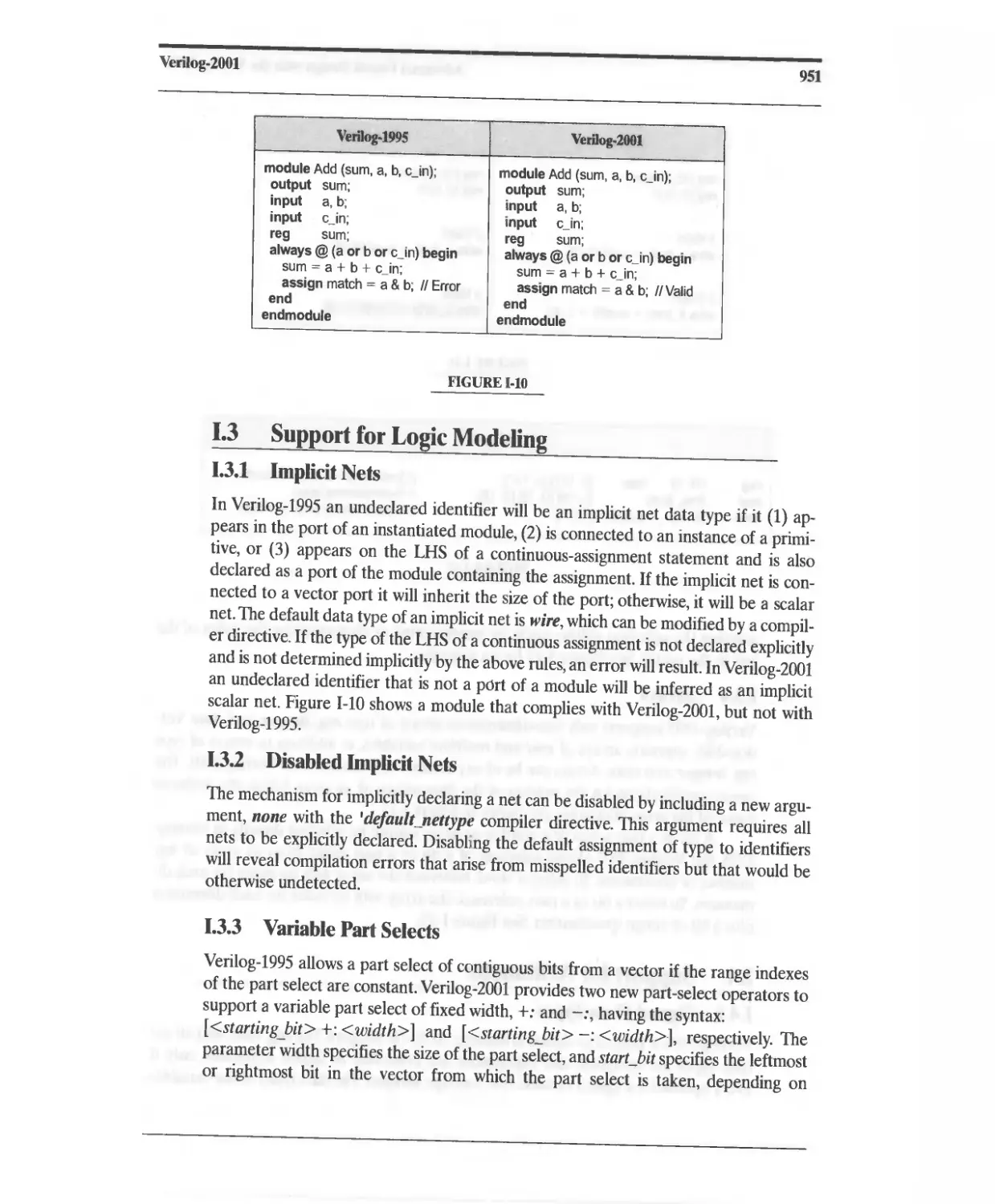
1.3 Support for Logic Modeling 951
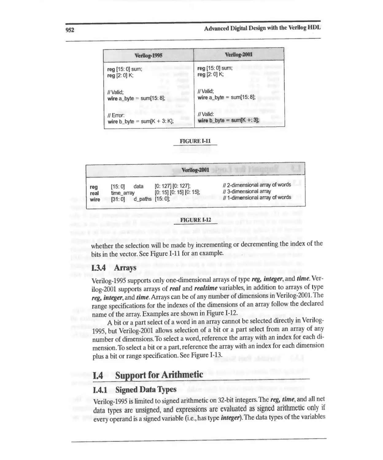
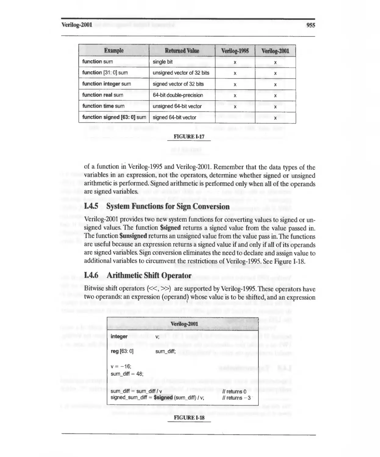
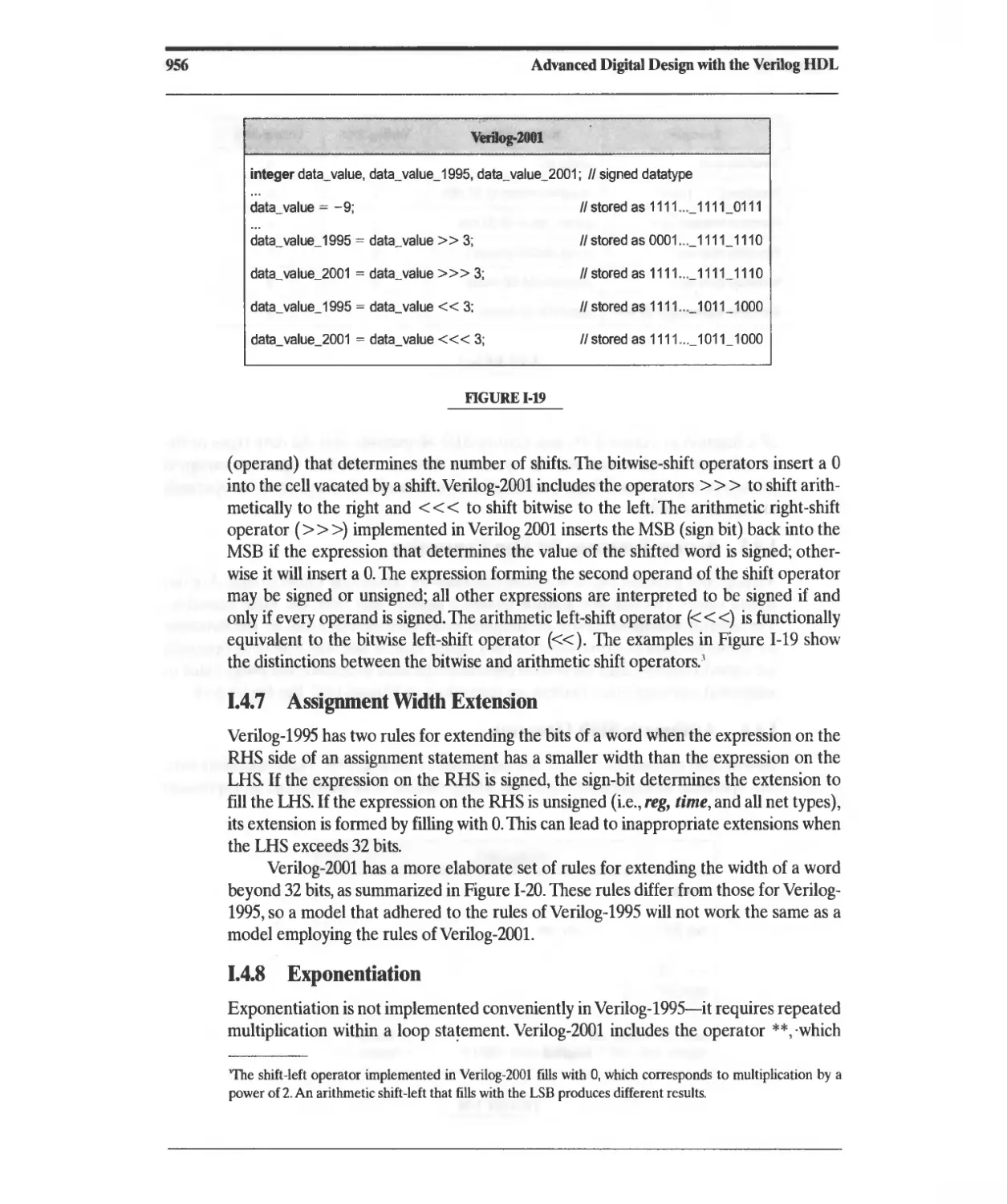
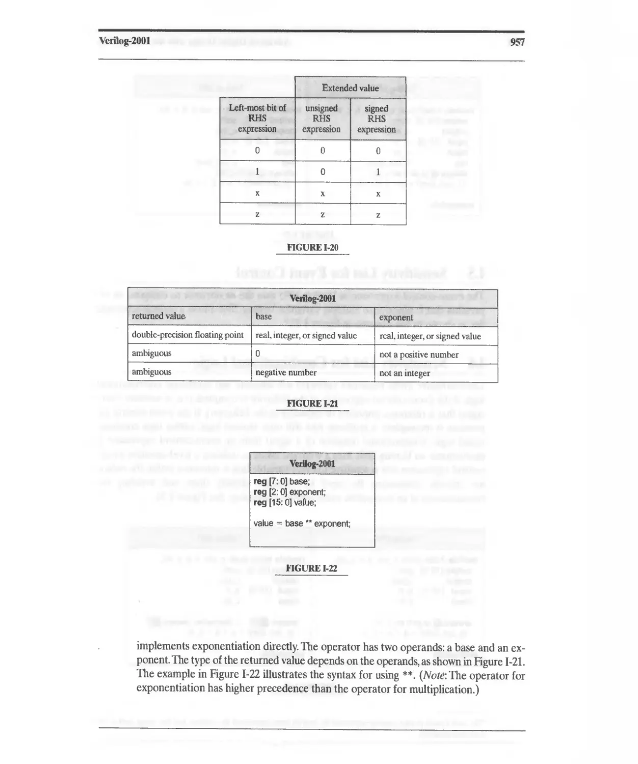
1.4 Support for Arithmetic 952
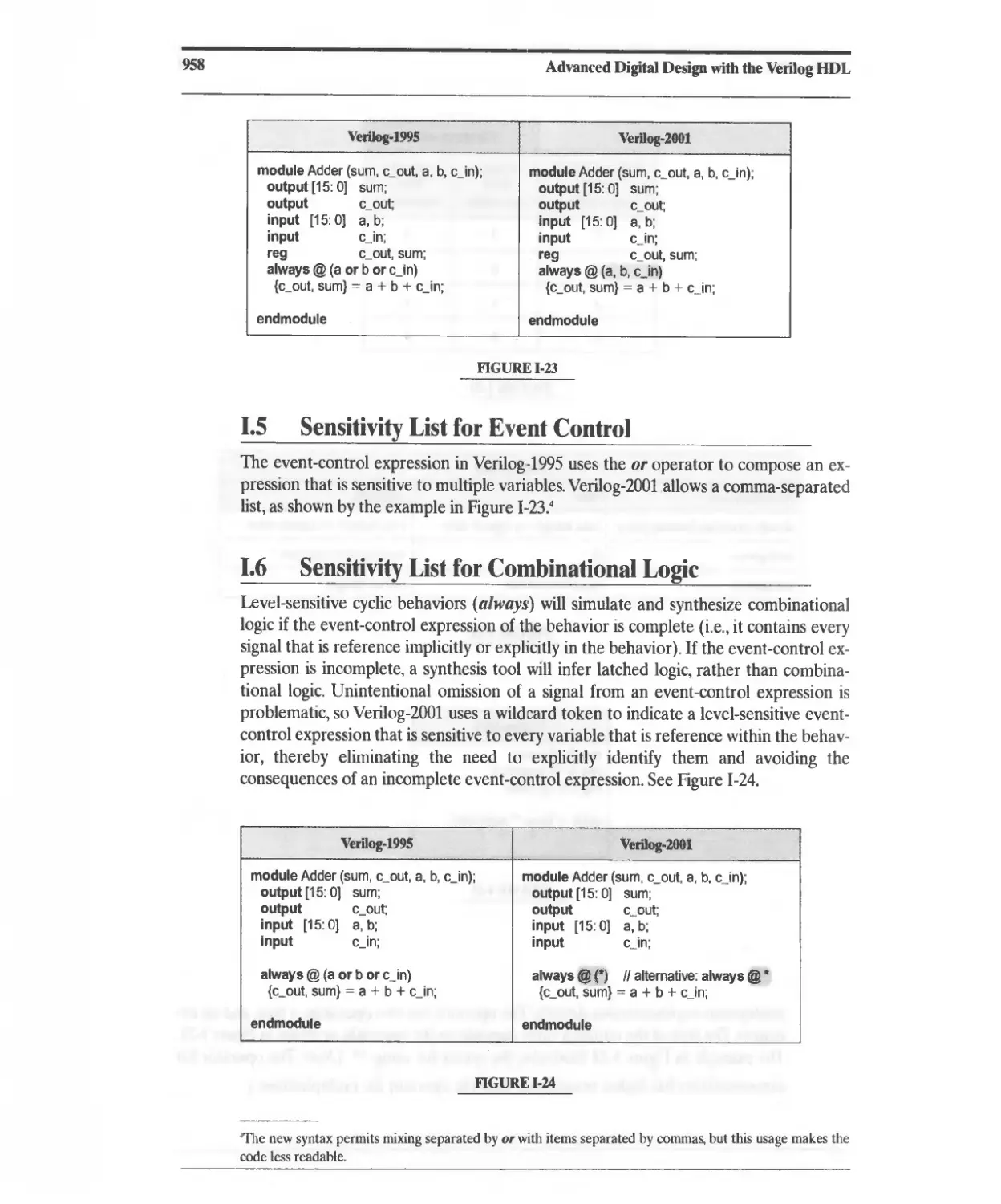
1.5 Sensitivity List for Event Control 958
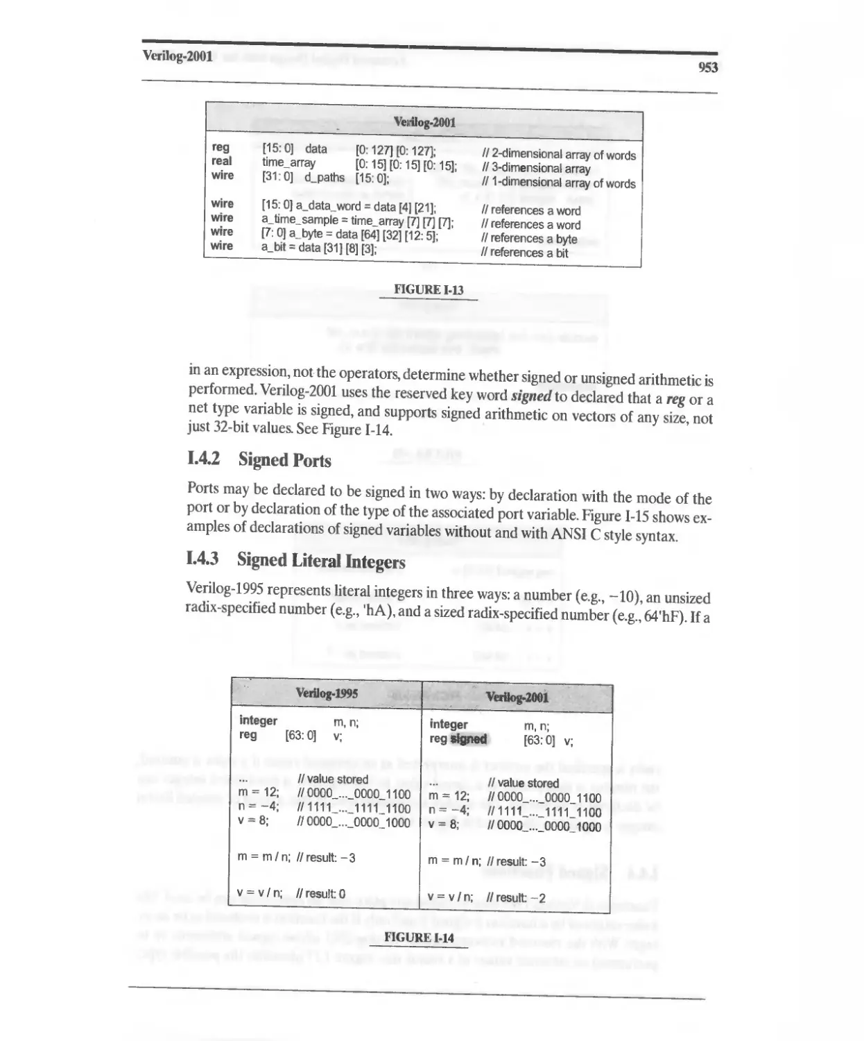
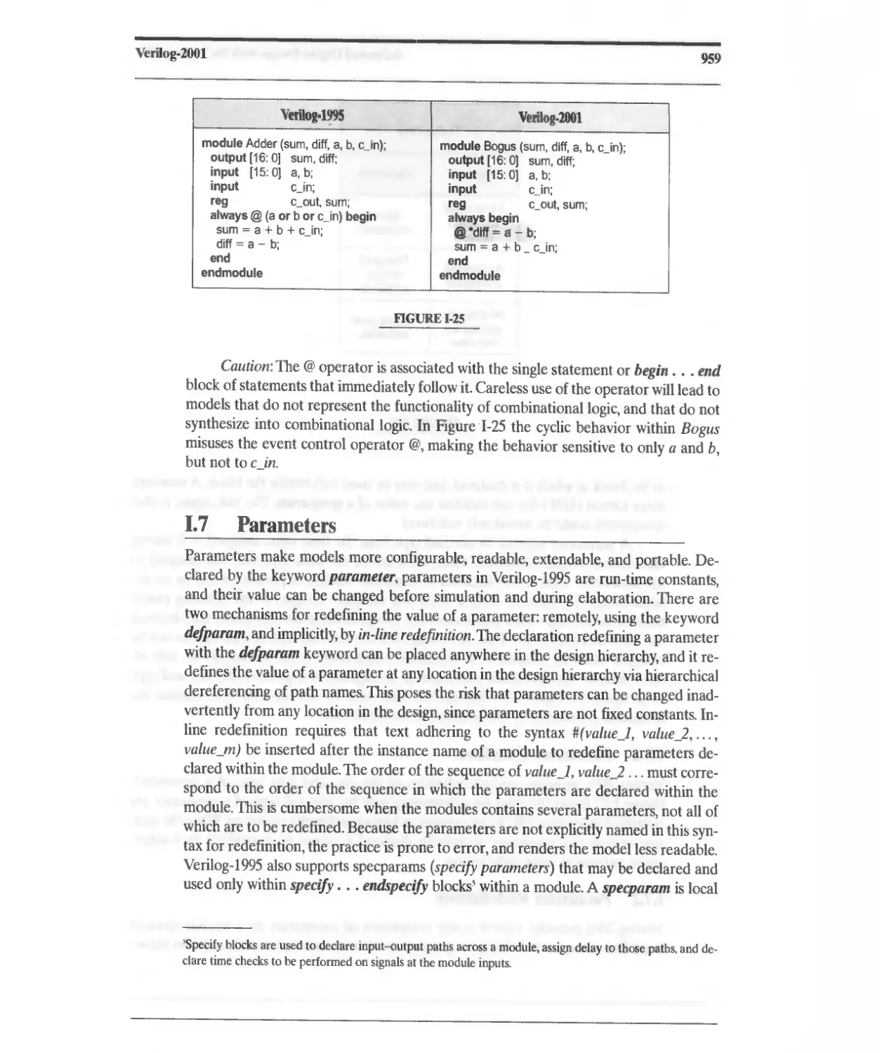
1.6 Sensitivity List for Combinational Logic 958
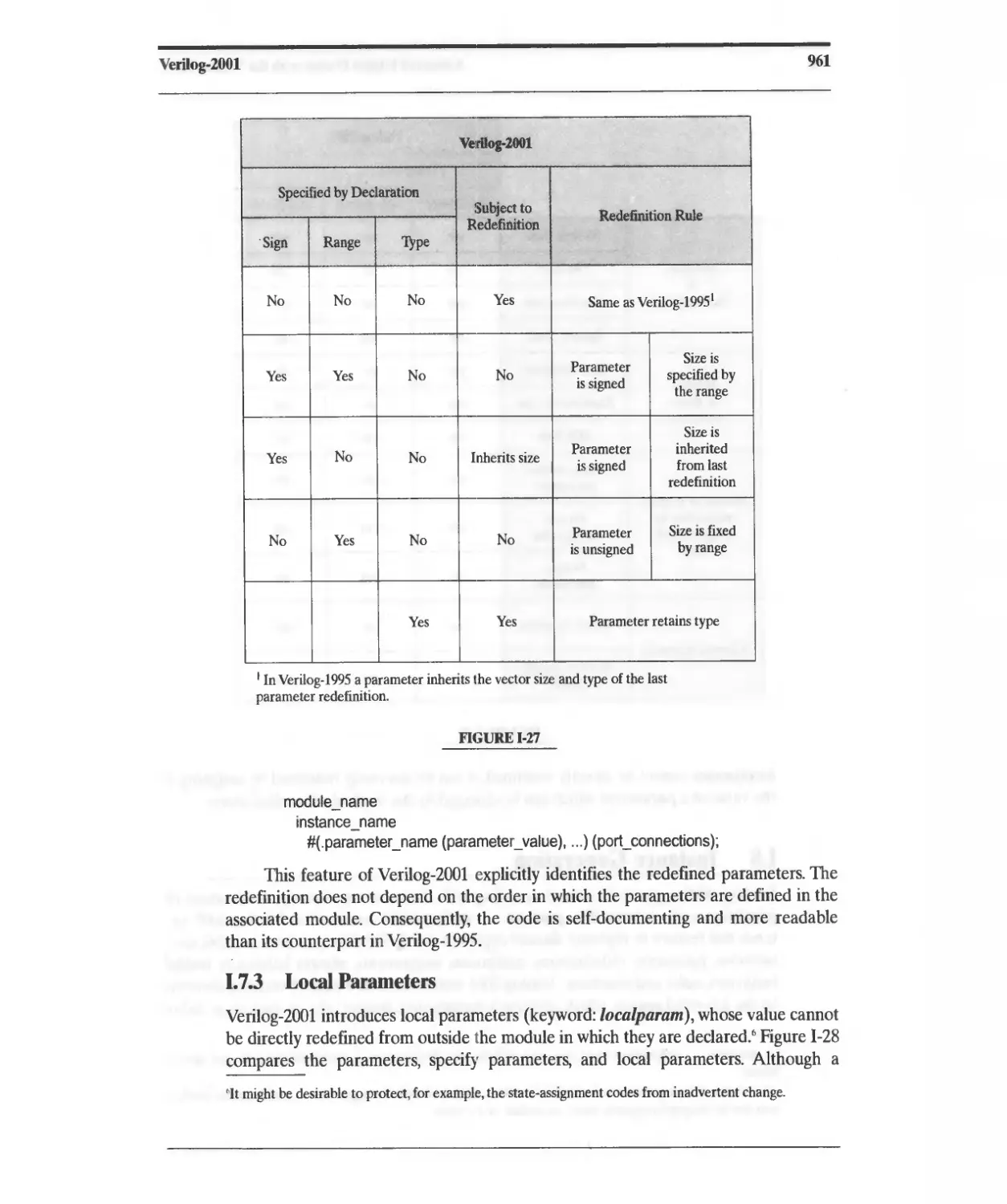
1.7 Parameters 959
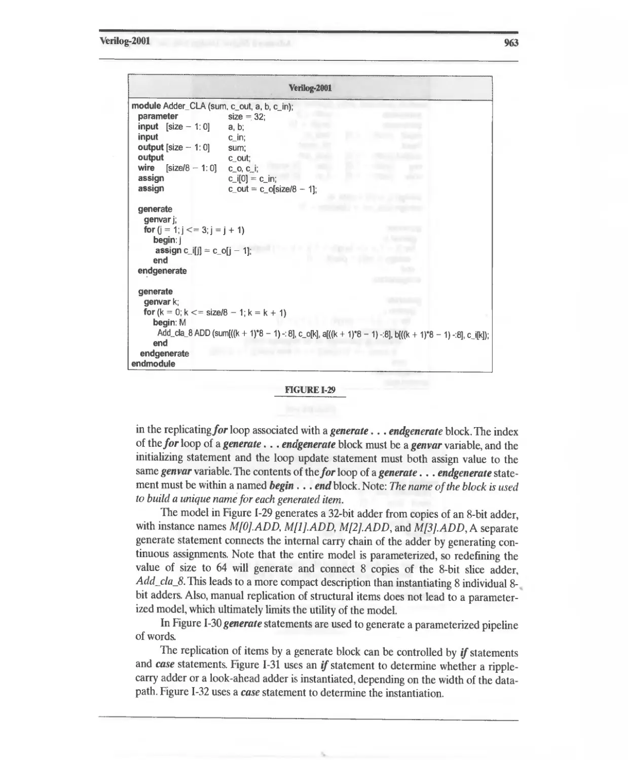
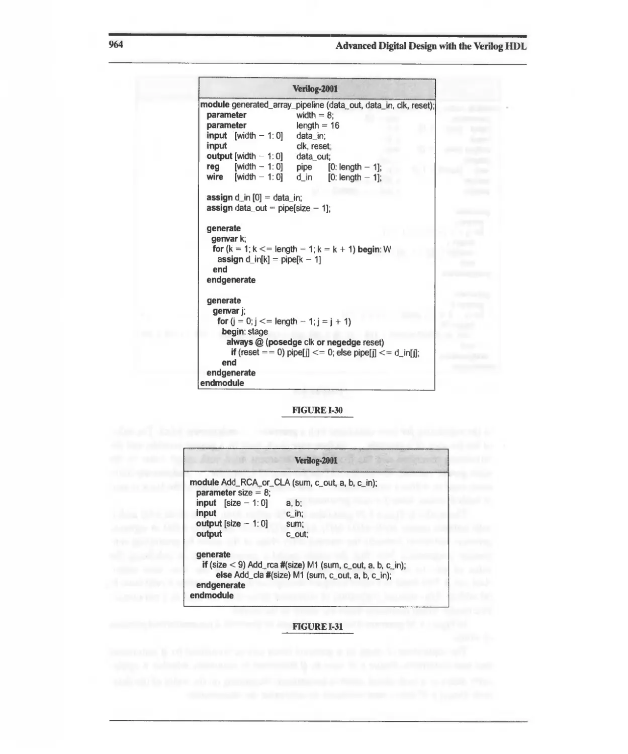
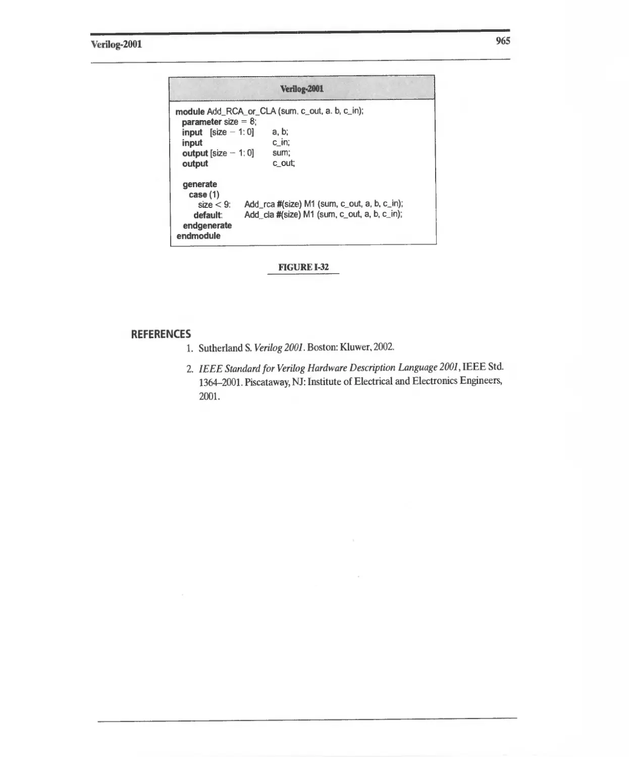
1.8 Instance Generation 962
J Programming Language Interface 967
K Websites 969
L Web-Based Tutorials 971
Index 973
Index of Veri log Modules and User-Defined Primitives 980
List of Tables 983
Preface
Simplify, Clarify, and Verify
Behavioral modeling with a hardware description language (HDL) is the key to modern design
of application-specific integrated circuits (ASICs). Today, most designers use an HDL-based de-
sign method to create a high-level, language-based, abstract description of a circuit, synthesize a
hardware realization in a selected technology, and verify its functionality and timing.
Students preparing to contribute to a productive design teau. must know how to use an
HDL at key stages of the design flow. ll1Us, there is a need for a course that goes beyond the
basic principles and methods learned in a first course in digital design. This book is written for
such a course.
Many books discussing HDLs are now available, but most are oriented toward robust ex-
planations of language syntax, and are not well.suited for classroom use. Our focus is on design
methodology enabled by an HDL.
Our goal in this book is to build on a student's background from a first course in logic de-
sign by (1) reviewing basic principles of combinational and sequential logic, (2) introducing the
use of HDLs in design, (3) emphasizing descriptive styles that will allow the reader to quickly de-
sign working circuits suitable for ASICs and/or field-programmable gate array (FPGA) imple-
mentation, and (4) providing in-depth design examples using modern design tools. Readers will
be encouraged to simplify, clarify, and verify their designs.
The widely used Verilog hardware description language (IEEE Standard 1364) serves as a
common framework supporting the design activities treated in this book, but our focus is on de-
veloping, verifying, and synthesizing designs of digital circuits, not on the Verilog language. Most
students taking a second course in digital design will be familiar with at least one programming
language and will be able to draw on that background in reading this textbook. We cover only
the core and most widely used features of Veri log. In order to emphasize using the language in a
synthesis-oriented design environment, we have purposely placed many details, features. and ex-
planations of syntax in the Appendices for reference on an "as-needed" basis.
Most entry-level courses in digital design introduce state machines, state-transition graphs.
and algorithmic-state machine (ASM) charts. We make heavy use of ASM charts and demonstrate
their utility in developing behavioral models of sequential machines. The important problem of
xviii
Advanced Digital Design with the Verilog HDL
designing a finite-state machine to control a complex datapath in a digital machine is treated in-
depth with ASMD charts (Le., ASM charts annotated to display the register operations of the
controlled datapath). The design of a reduced intruction-set computer central processing unit
(RISC CPU) and other important hardware units are given as examples. Our companion web-
site includes the RISC machine's source code and an assembler that can be used to develop pro-
grams for applications. The machine also serves as a starting point for developing a more robust
instruction set and architectural variants.
The Verilog language is introduced in an integrated, but selective manner, only as needed
to support design examples. The text has a large set of examples illustrating how to address the
key steps in a very large scale integrated (VLSI) circuit design methodology using the Verilog
HDL. Examples are complete, and include source code that has been verified with the Silos-III
simulator to be correct. Source code for all of the examples will be available (with important test
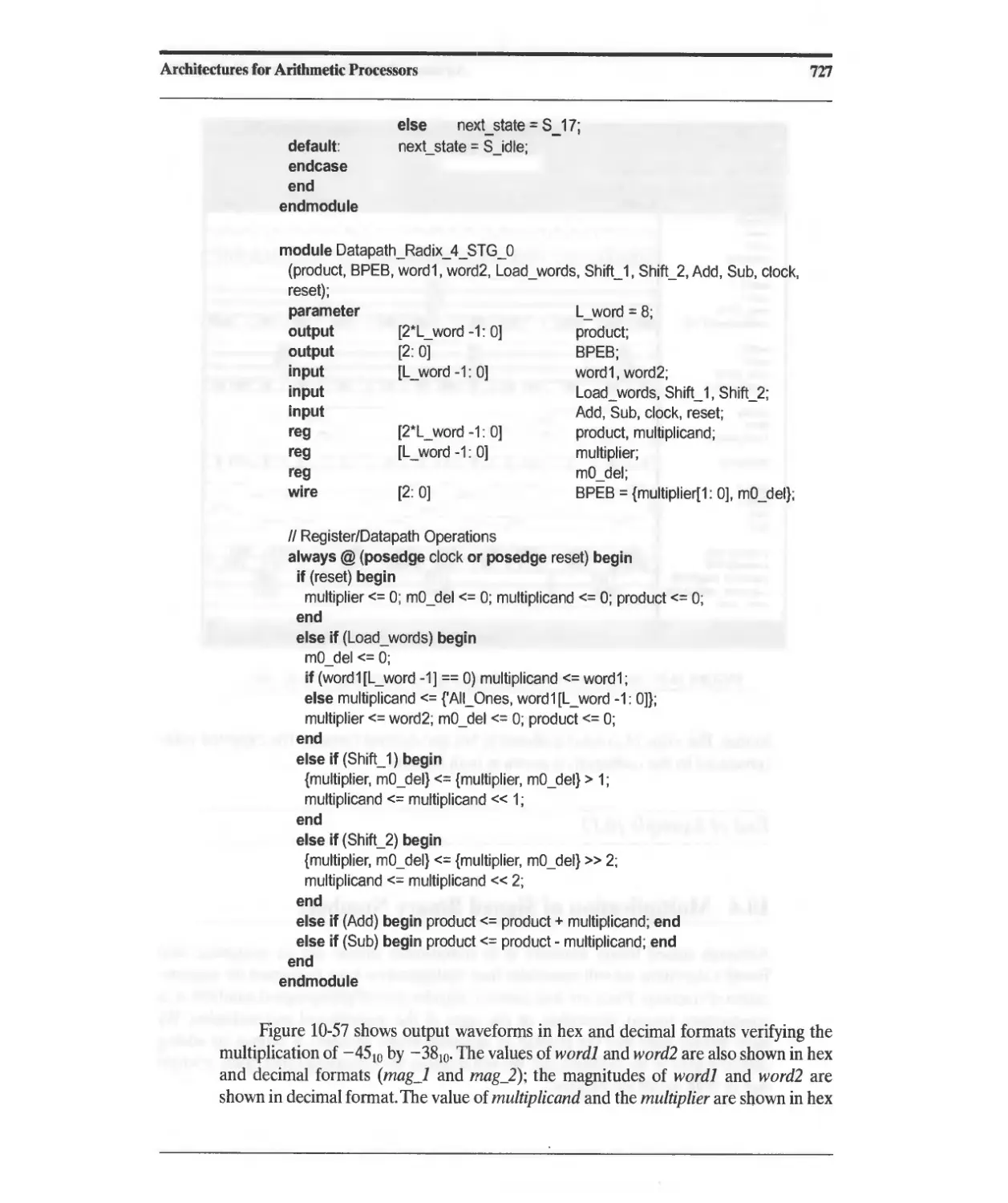
suites) at our website.
The Intended Audience
This book is for students in an advanced course in digital design, and for professional engineers in-
terested in learning Verilog by example, in the context of its use in the design flow of modern inte-
grated circuits. The level of presentation is appropriate for seniors and first-year graduate
students in electrical engineering, computer engineering, and computer science, as well as for
professional engineers who have had an introductory course in logic design. The book presumes
a basic background in Boolean algebra and its use in logic circuit design and a familiarity with
finite-state machines. Building on this foundation, the book addresses the design of several im-
portant circuits used in computer systems, digital signal processing, image processing, data
transfer across clock domains, built-in self-test (BlST), and other appiications. The book covers
the key design problems of modeling, architectural tradeoffs, functional verification, timing
analysis.. test generation, fault simulation, design for testability, logic synthesis, and postsynthesis
verification.
Special Features of the Book
· Begins with a brief review of basic principles in combinational and sequential logic
· Focuses on modern digital design methodology
· Illustrates and promotes a synthesis-ready style of register transfer level (RTL) and algorith-
mic modeling with Verilog
· Demonstrates the utility of ASM charts for behavioral modeling
· In-depth treatment of algorithms and architectures for digital machines (e.g., an image
processor, digital filters and circular buffers)
· In-depth treatment of synthesis for cell-based ASICs and FPGAs
· A practical treatment of timing analysis, fault simulation, testing, and design for testability,
with examples
· Comprehensive treatment of behavioral modeling
· Comprehensive design examples, including a RISC machine and data path controller
· Numerous graphical illustrations
· Prov des several problems whh a wide range of difficulty after each chapter
· Contains a worked xample with JTAG and BlST for testing
Preface
xix
. Contains over 250 fully verified examples
. An indexed list of all models developed in the examples
. A set of Xilinx FPGA-based laboratory-ready exercises linked to the book (e.g., arithmetic
and logic unit [ALU], a programmable lock, a key pad scanner with a FIFO, a serial communi-
cations link with error correction. an SRAM controller. and first in, first out [FIFO] memory)
. Contains an up-to-date chapter on programmable logic device (PLDs) and FPGAs
. Contains a packaged CD-ROM with the popular Silos-III Verilog design environment and
simulator and the Xilinx integrated synthesis environment (ISE) synthesis tool for FPGAs
. Contains an Appendix with full formal syntax of the Verilog HDL
. Covers major features of Verilog 2001, with examples
. Supported by an ongoing website containing:
1. Source files of models developed in the examples
2.. Source files of testbenches for simulating examples
3. An Instructor's Classroom Kit containing transparency files for a course based on the subject
matter
4. Solutions to selected problems
5. Jump-start tutorials helping students get immediate results with the Silos-III simulation envi-
ronment, the Xilinx FPGA synthesis tool, the Synopsys synthesis tools, and the Synopsys
Prime Time static timing analyzer
6. ASIC standard-cell library with synthesis and timing database
7. Answers to frequently asked questions (FAQs)
8. Clever examples submitted by readers
9. Revisions
Sequences for Course Presentation
The material in the text begins with a review of combinational and sequential logic design, but
then progresses in the order dictated by the design flow for an ASIC or an FPGA. Chapters 1 to 6
treat design topics through synthesis, and should be covered in order, but Chapters 7 to 10 can be
covered in any order. The homework exercises are challenging, and the laboratory-ready
Xilinx-based exercises are suitable for a companion laboratory or for end-of-semester projects.
Chapter 10 presents several architectures for arithmetic operations, affording a diversity of cov-
erage. Chapter 11 treats postsynthesis design validation, timing analysis, fault simulation, and de-
sign for testability. The coverage of these topics can be omitted, depending on the level and focus
of the course. Tools supporting Verilog 2001 are emerging, so an appendix discusses and illus-
trates the important new features of the language.
Chapter Descriptions
Chapter 1 briefly discusses the role of HDLs in design flows for cell-based ASICs and FPGAs.
Chapters 2 and 3 review mainstream topics that would be covered in a first course in digital design,
using classical methods (i.e. Kafllaugh maps). This material will refresh the reader's background,
and the examples will be used later to introduce HDL-based methods of design. Chapters 4 and 5
xx
Advanced Digital Design with the Verilog HDL
introduce modeling of combinational and sequential logic with the Verilog HDL, and place em-
phasis on coding styles that are used in behavioral modeling. Chapter 6 addresses cell-based syn-
thesis of ASI Cs, and introduces synthesis of combinational and sequential logic. Here we pursue
two main objectives: (1) present synthesis-friendly coding styles, and (2) form a foundation that
will enable the reader to anticipate the results of synthesis, especially when synthesizing sequen-
tial machines. Many sequential machines are partitioned into a datapath and a controller.
Chapter 7 covers examples that illustrate how to design a controller for a datapath. The designs
of a simple RISe CPU and a UART 1 serve as platforms for the subject matter. Chapter 8 covers
PLDs, complex PLDs (CPLDs), ROMs, and static random-access memories (SRAMs), then ex-
pands the synthesis target to include FPGAs. Verilog has been used extensively to design com-
puters and signal processors. Chapter 9 treats the modeling and synthesis of computational units
and algorithms found in computer architectures, digital filters, and other processors. Chapter 10
develops and refines algorithms and architectures for the arithmetic units of digital machines. In
Chapter 11 we use the Verilog HDL in conjunction with fault simulators and timing analyzers to
revisit a selection of previously designed machines and consider performance/timing issues and
testability, to complete the treatment of design flow tasks that rely heavily on designer interven-
tion. Chapter 11 models the test access port (TAP) controller defined by the IEEE 1149.1 stan-
dard (commonly known as the ITAG standard), and presents an example of its use. Another
elaborate example covers built-in self test (BIST).
Acknowledgments
The author is grateful for the support of colleagues and students who expanded his vision of
Verilog and contributed to this textbook. The reviewers of the original manuscript provided en-
couragement, critical judgment, and many helpful suggestions. Stu Sutherland helped the au-
thor gain a deeper appreciation for the issue of race conditions that can creep into the models
of a digital system. These insights led to the disciplined style of adhering to non blocking assign-
ments for modeling edge-sensitive behavior and blocked assignments for modeling level-sensi-
tive behavior. I owe a debt of gratitude to Dr. Jim Tracy and Dr. Rodger Ziemer, who supported
my efforts to develop courses in VLSI circuit design; to Bill Fuchs, who introduced me to the
Silos-III Verilog simulator from Simucad, Inc.. and placed a user-friendly design environment in
the hands of our students. Kirk Sprague and Scott Kukel were helpful in developing a Hamming
encoder to work with the UART. Cris Hagan's thesis led to the models presented in Chapter 9
for decimators and other functional units found in digital signal processors. Rex Anderson
proofread several chapters and scrubbed down my work. Terry Hansen and Lisa Horton provid-
ed the inspiration for the coffee vending machine example, and developed the assembler that
supports the RISe CPu. Dr. Greg Sajdak developed material relating chip defects to test cover-
age and process yield. Dr. Bruce Harmon provided material for a FIR filter example. My editors,
Tom Robbins and Eric Frank, have been a delight to work with. They supported the concept. en-
couraged my work and guided this book through the production process. My deep thanks to all
of you.
IUniversal asynchronous receiver and transmitter (UART), a circuit used in data transmission between
systems.
Preface
xxi
Dedication
This book is dedicated to the memory of Sr. Laurencia Rihn, RSM, and Fr. Jerry Wilson, CSc.
My life has been shaped by their faith, encouragement, and love. To my wife, Jerilynn, and our
children, Monica, Lucy, Rebecca, Christine, and Michael and their spouses, Mike McCormick,
David Steigerwald, Peter Van Dusen, and Michelle Puhr Ciletti, and our grandchildren, Michael,
Katherine, Brigid, David, Jackson, Samantha, Peter, Anthony, and Matthew-thank you for the
journey and the love we've shared.
CHAPTER 1
Introduction to Digital
Design Methodology
Classical design methods relied on schematics and manual methods to design a circuit,
but today computer-based languages are widely used to design circuits of enormous
size and complexity. There are several reasons for this shift in pra tice. No team of en-
gineers can correctly design and manage, by manual methods, the details of state-of-
the-art integrated circuits (ICs) containing several million gates, but using hardware
description languages (HDLs) designers easily manage the complexity of large designs.
Even small designs rely on language-based descriptions, because designers have to
quickly produce correct designs targeted for an ever-shrinking window of opportunity
in the marketplace.
Language-based designs are portable and independent of technology, allowing
design teams to modify and re-use designs to keep pace with improvements in technology.
As physical dimensions of devices shrink, denser circuits with better performance can
be synthesized from an original HDL-based model.
HDLs are a convenient medium for integrating intellectual property (IP) from a
variety of sources with a proprietary design. By relying on a common design language,
models can be integrated for testing and synthesized separately or together, with a net
reduction in time for the design cycle. Some simulators also support mixed descriptions
based on multiple languages.
The most significant gain that results from the use of an HDL is that a working
circuit can be synthesized automatically from a language-based description, bypassing
the laborious steps that characterize manual design methods (e.g., logic minimization
with Karnaugh maps).
HDL-based synthesis is now the dominant design paradigm used by industry.
Today, designers build a software prototype/model of the design, verify its functionality,
and then use a synthesis tool to automatically optimize the circuit and create a netlist
in a physical technology.
2
Advanced Digital Design with the Verilog HDL
HDLs and synthesis tools focus an engineer's attention on functionality rather
than on individual transistors or gates; they synthesize a circuit that will realize the de-
sired functionality, and satisfy area and/or performance constraints. Moreover, alterna-
tive architectures can be generated from a single HDL model and evaluated quickly to
perform design tradeoffs. Functional models are also referred to as behavioral models.
HDLs serve as a platform for several tools: design entry, design verification, test
generation, fault analysis and simulation, timing analysis and/or verification, synthesis,
and automatic generation of schematics. This breadth of use improves the efficiency of
the design flow by eliminating translations of design descriptions as the design moves
through the tool chain.
Two languages enjoy widespread industry support: Verilog™ [1] and VHDL [2].
Both languages are IEEE (Institute of Electrical and Electronics Engineers) stan-
dards; both are supported by synthesis tools for ASICs (application-specific integrated
circuits) and FPGAs (field-programmable gate arrays). Languages for analog circuit
design, such as Spice [3], play an important role in verifying critical timing paths of a
circuit, but these languages impose a prohibitive computational burden on large de-
signs, cannot support abstract styles of design, and become impractical when used on a
large scale. Hybrid languages (e.g., Verilog-A) [4] are used in designing mixed-signal
circuits, which have both digital and analog circuitry. System-level design languages,
such as SystemC [5] and Superlog'>I [6], are now emerging to support a higher level of
design abstraction than can be supported by Verilog or VHDL.
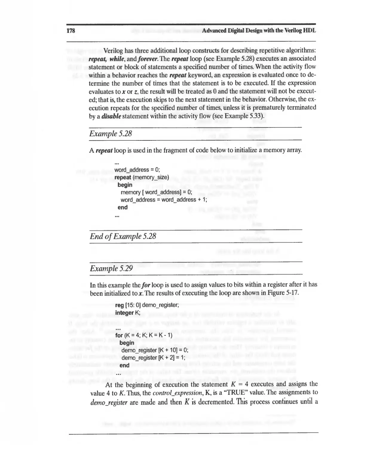
1.1 Design Methodology-An Introduction
ASICs and FPGAs are designed systematically to maximize the likelihood that a de-
sign will be correct and will be fabricated without fatal flaws. Designers follow a "de-
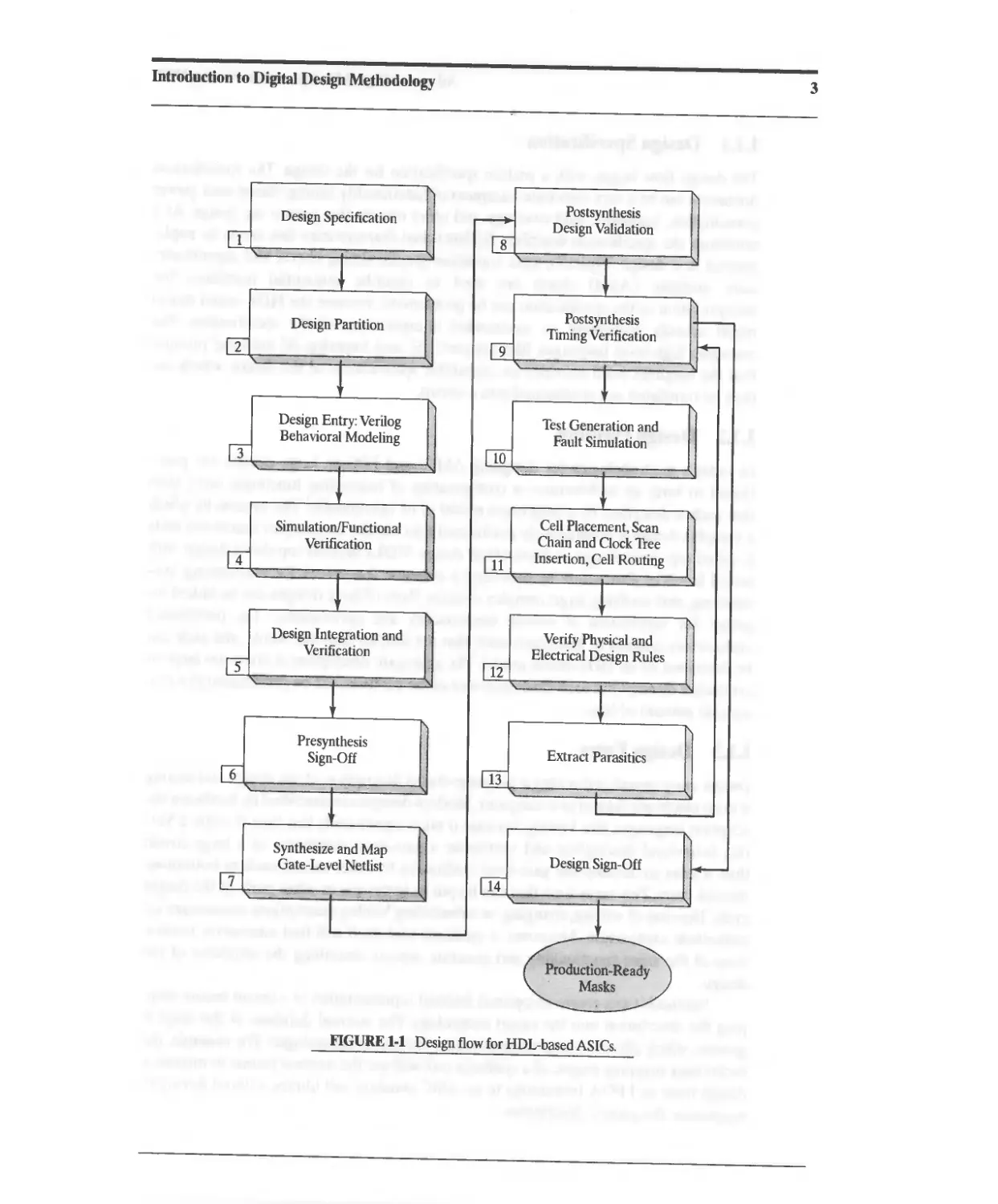
sign flow" like that shown in Figure 1-1, which specifies a sequence of major steps that
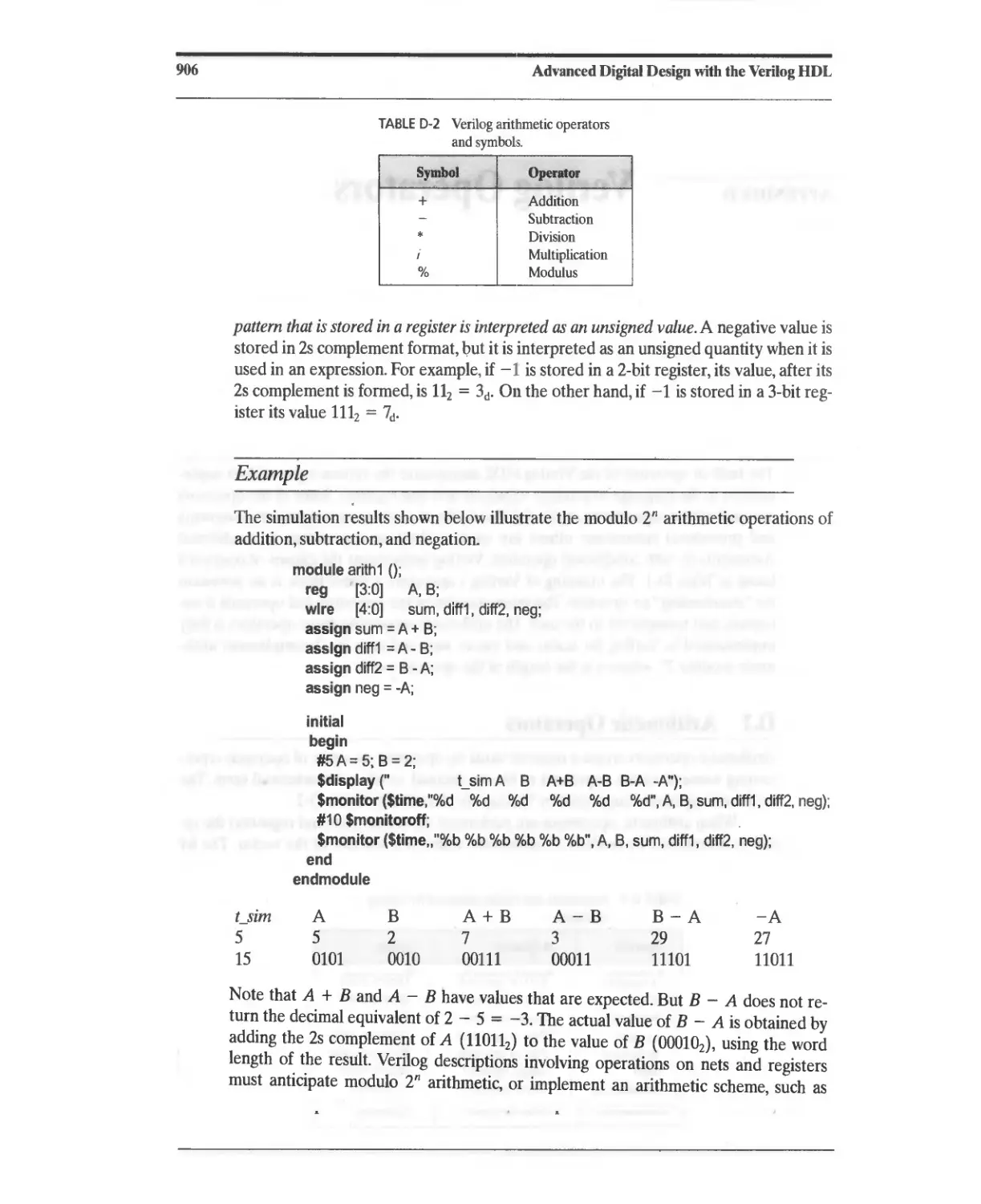
will be taken to design, verify, srnthesize, and test a digital circuit. ASIC design flows
involve several activities, from specification and design entry, to place-and-route and
timing closure of the circuit in silicon. Timing closure is attained when all of the signal
paths in the design satisfy the timing constraints imposed by the interface circuitry, the
circuit's sequential elements, and the system clock. Although the design flow appears
to be linear, in practice it is not. Various steps might be revisited as design errors are
discovered, requirements change, or performance and design constraints are violated.
For example. if a circuit fails to meet timing constraints, a new placement and routing
step will have to be taken, perhaps including redesign of critical paths.
Design flows for standard-cell-based ASICs are more complex than those for
FPGAs because the architecture of an ASIC is not fixed. Consequently, the perfor-
mance that can be realized from a design depends on the physical placement and rout-
ing of the cells on the die, as well as the underlying device properties. Interconnect
delays playa significant role in determining performance in submicron designs below
0.18 /lm, in which pre layout estimates of path delays do not guarantee timing closure
of the routed design.
The following sections will clarify the design flow described in Figure 1-1.
Introduction to Digital Design Methodology
3
Design Specification
Postsynthesis
Design Validation
8
Design Partition
Postsynthesis
Timing Verification
2
9
Design Entry: Verilog
Behavioral Modeling
Test Generation and
Fault Simulation
3
to
Simulation/Functional
Verification
Cell Placement, Scan
Chain and Clock Tree
Insertion, Cell Routing
4
11
Design Integration and
Verification
Verify Physical and
Electrical Design Rules
5
12
Presynthesis
Sign-Off
Extract Parasitics
6
13
Synthesize and Map
Gate-Level Netlist
Design Sign-Off
7
14
fi1GURE 1-1 Design flow for HDL-based ASICs.
4
Advanced Digital Design with the Verilog HDL
1.1.1 Design Specification
The design flow begins with a written specification for the design. The specification
document can be a very elaborate statement of functionality, timing, silicon area, power
consumption, testability, fault coverage, and other criteria that govern the design. At a
minimum, the specification describes the functional characteristics that are to be imple-
mented in a design. Typically, state transition graphs, timing charts, and algorithmic-
state machine (ASM) charts are used to describe sequential machines, but
interpretation of the specification can be problematic, because the HDL-based model
might actually implement an unintended interpretation of the specification. The
emerging high-level languages, like SystemC [5], and Superlog [6] hold the promise
that the language itself provides an executable specification of the design, which can
then be translated and synthesized into a circuit.
1.1.2 Design Partition
In today's methodologies for designing ASICs and FPGAs, large circuits are parti-
tioned to form an architecture-a configuration of interacting functional units, such
that each is described by a behavioral model of its functionality. The process by which
a complex design is progressively partitioned into smaller and simpler functional units
is called top-down design or hierarchical design. HDLs support top-down design with
mixed levels of abstraction by providing a common framework for partitioning, syn-
thesizing, and verifying large, complex systems. Parts of large designs can be linked to-
gether for verification of overall functionality and performance. The partitioned
architecture consists of functional units that are simpler than the whole, and each can
be described by an HDL-based model. The aggregate description is often too large to
synthesize directly, but each functional unit of the partition can be synthesized in a rea-
sonable amount of time.
1.1.3 Design Entry
Design entry means composing a language-based description of the design and storing
it in an electronic format in a computer. Modern designs are described by hardware'de-
scription languages, like Verilog, because it takes significantly less time to write a Ver-
ilog behavioral description and synthesize a gate-level realization of a large circuit
than it does to develop the gate-level realization by other means, such as bottom-up
manual entry. This saves time that can be put to better use in other parts of the design
cycle. The ease of writing, changing, or substituting Verilog descriptions encourages ar-
chitectural exploration. Moreover, a synthesis tool itself will find alternative realiza-
tions of the same functionality and generate reports describing the attributes of the
design.
Synthesis tools create an optimal internal representation of a circuit before map-
ping the description into the target technology. The internal database at this stage is
generic, which allows it to be mapped into a variety of technologies. For example, the
technology mapping engine of a synthesis tool will use the intern ill formilt to migrate a
design from an FPGA technology to an ASIC standard cell library, without having to
reoptimize the generic description.
Introduction to Digital Design Methodology
5
HDL-based designs are easier to debug than schematics. A behavioral descrip-
tion encapsulating complex functionality hides underlying gate-level detail, so there is
less information to cope with in trying to isolate problems in the functionality of the
design. Furthermore, if the behavioral description is functionally correct, it is a gold
standard for subsequent gate-level realizations.
HDL-based designs incorporate documentation within the design by using de-
scriptive names, by including comments to clarify intent, and by explicitly specifying ar-
chitectural relationships, thereby reducing the volume of documentation that must be
kept in other archives. Simulation of a language-based model explicitly specifies the
functionality of the design. Since the language is a standard, documentation of a design
can be decoupled from a particular vendor's tools.
Behavioral modeling is the predominant descriptive style used by industry, en-
abling the design of massive chips. Behavioral modeling describes the functionality of a
design by specifying what the designed circuit will do, not how to build it in hardware.
It specifies the input-output model of a logic circuit and suppresses details about phys-
ical, gate-level implementation.
Behavioral modeling encourages designers to (1) rapidly create a behavioral pro-
totype of a design (without binding it to hardware details), (2) verify its functionality,
and then (3) use a synthesis tool to optimize and map the design into a selected physi-
cal technology. If the model has been written in a synthesis-ready style, the synthesis
tool will remove redundant logic, perform tradeoffs between alternative architectures
and/or multilevel equivalent circuits, and ultimately achieve a design that is compatible
with area or timing constraints. By focusing the designer's attention on the functional-
ity that is to be implemented rather than on individual logic gates and their intercon-
nections, behavioral modeling provides the freedom to explore alternatives to a design
before committing it to production.
Aside from its importance in synthesis, behavioral modeling provides flexibility
to a design project by allowing parts of the design to be modeled at different levels of
abstraction. The Verilog language accommodates mixed levels of abstraction so that
portions of the design that are implemented at the gate level (i.e., structurally) can be
integrated and simulated concurrently with other parts of the design that are repre-
sented by behavioral descriptions.
1.1.4 Simulation and Functional Verification
The functionality of a design is verified (Step 4 in Figure 1-1) either by simulation or by
formal methods [7]. Our discussion will focus on simulation that is reasonable for the
size of circuits we can present here. The design flow iterates back to Step 3 until the
functionality of the design has been verified. The verification process is threefold; it in-
cludes (1) development of a test plan, (2) development of a test bench, and (3) execu-
tion of the test.
1.L4.1 Test Plan Development A carefully documented test plan is developed to
specify what functional features are to be tested and how they are to be tested. For ex-
ample, the test plan might specify that the instruction set of an arithmetic and logic unit
(ALU) will be verified by an exhaustive simulation of its behavior, for a specific set of
6
Advanced Digital Design with the Verilog DDL
input data. Test plans for sequential machines must be more elaborate to ensure a high
level of confidence in the design, because they may have a large number of states. A
test plan identifies the stimulus generators, response monitors, and the gold standard
response against which the model will be tested.
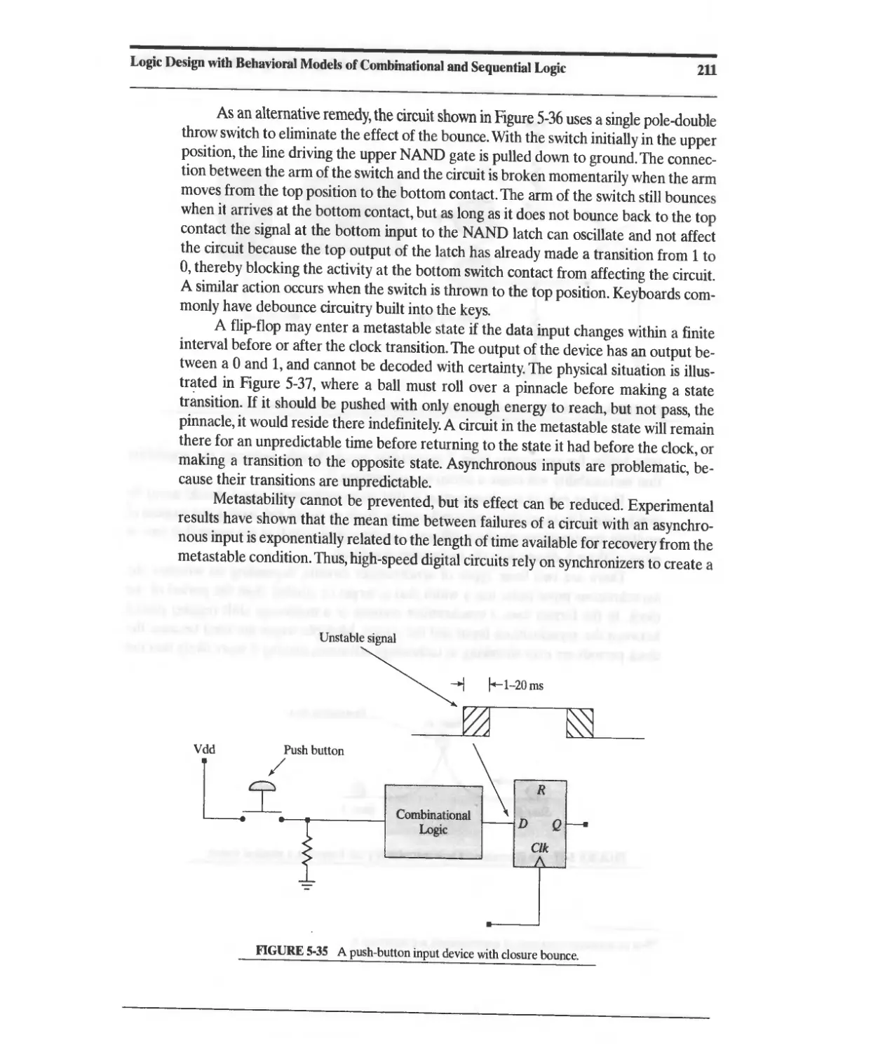
1.1.4.2 Testbench Development The testbench is a Verilog module in which the unit
under test (UUT) has been instantiated, together with pattern generators that are to
be applied to the inputs of the model during simulation. Graphical displays and/or re-
sponse monitors are part of the testbench. The testbench is documented to identify the
goals and sequential activity that will be observed during simulation (e.g., "Testing the
opcodes"). If a design is formed as an architecture of multiple modules, each must be
verified separately, beginning with the lowest level of the design hierarchy, then the in-
tegrated design must be tested to verify that the modules interact correctly. In this case,
the test plan must describe the functional features of each module and the process by
which they will be tested, but the plan must also specify how the aggregate is to be tested.
1.1.4.3 Test Execution and Model Verification The testbench is exercised accord-
ing to the test plan and the response is verified against the original specification for the
design, e.g. does the response match that of the prescribed ALU? This step is intended
to reveal errors in the design, confirm the syntax of the description, verify style con-
ventions, and eliminate barriers to synthesis. Verification of a model requires a system-
atic, thorough demonstration of its behavior. There is no point in proceeding further
into the design flow until the model has been verified.
1.1.5 Design Integration and Verification
After each of the functional subunits of a partitioned design have been verified to have
correct functionality, the architecture must be integrated and verified to have the cor-
rect functionality. This requires development of a separate testbench whose stimulus
generators exercise the input-output functionality of the top-level module, monitor
port and bus activity across module boundaries, and observe state activity in any em-
bedded state machines. This step in the design flow is crucial and must be executed
thoroughly to ensure that the design that is being signed off for synthesis is correct.
1.1.6 Presynthesis Sign-Off
A demonstration of full functionality is to be provided by the testbench, and any dis-
crepancies between the functionality of the Verilog behavioral model and the design
specification must be resolved. Sign-off occurs after all known functional errors have
been eliminated.
1.1.7 Gate-Level Synthesis and Technology Mapping
After all syntax and functional errors have been eliminated from the design and sign-
off has occurred, a synthesis tool is used to create an optimal Boolean description and
compose it in an available technology. In general, a synthesis tool removes redundant
logic and seeks to reduce the area of the logic needed to implement the functionality
Introduction to Digital Design Methodology
7
and satisfy performance (speed) specifications. This step produces a netlist of standard
cells or a database that will configure a target FPGA.
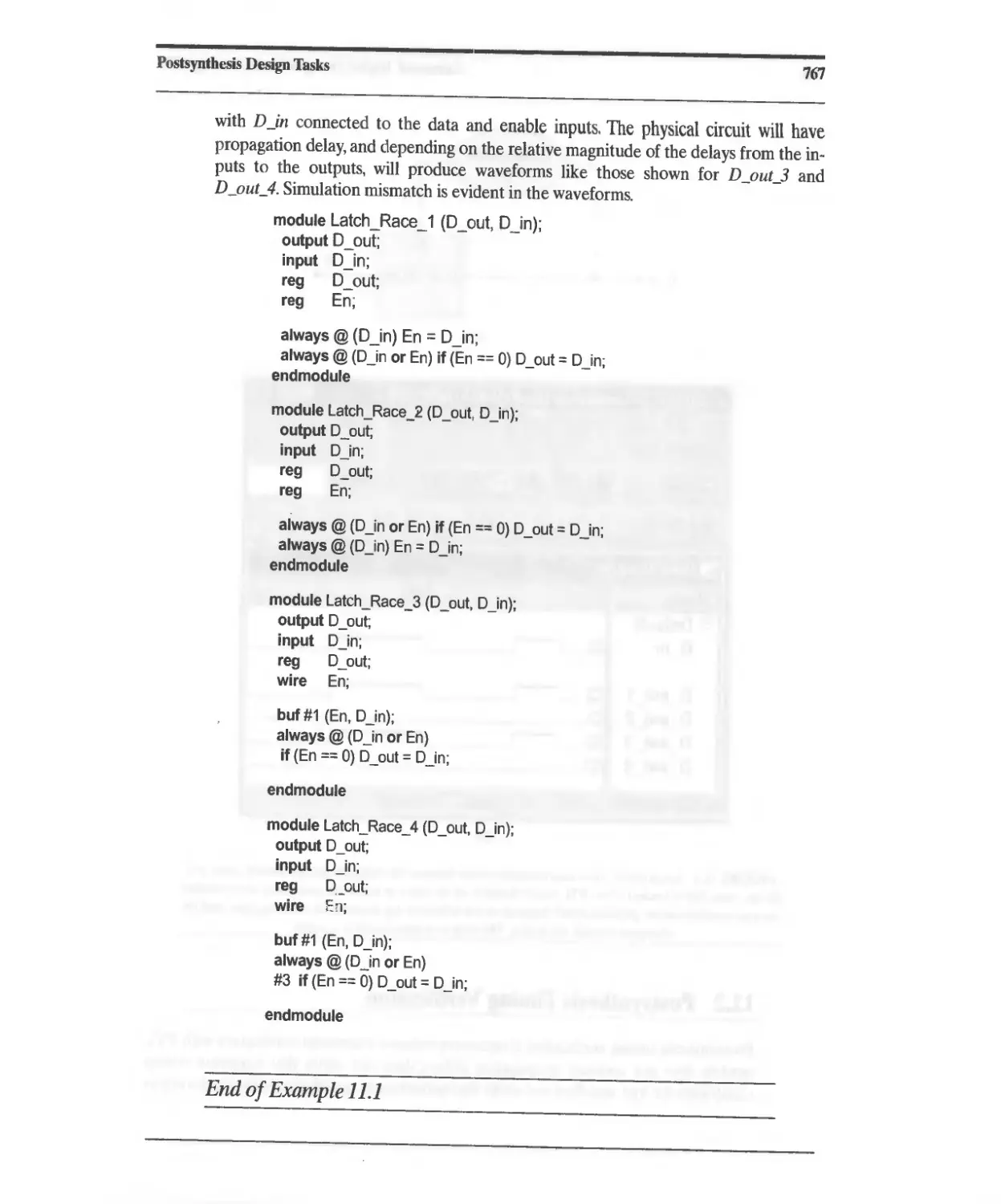
1.1.8 Postsynthesis Design Validati n
Design validation compares the response of the synthesized gate-level description to
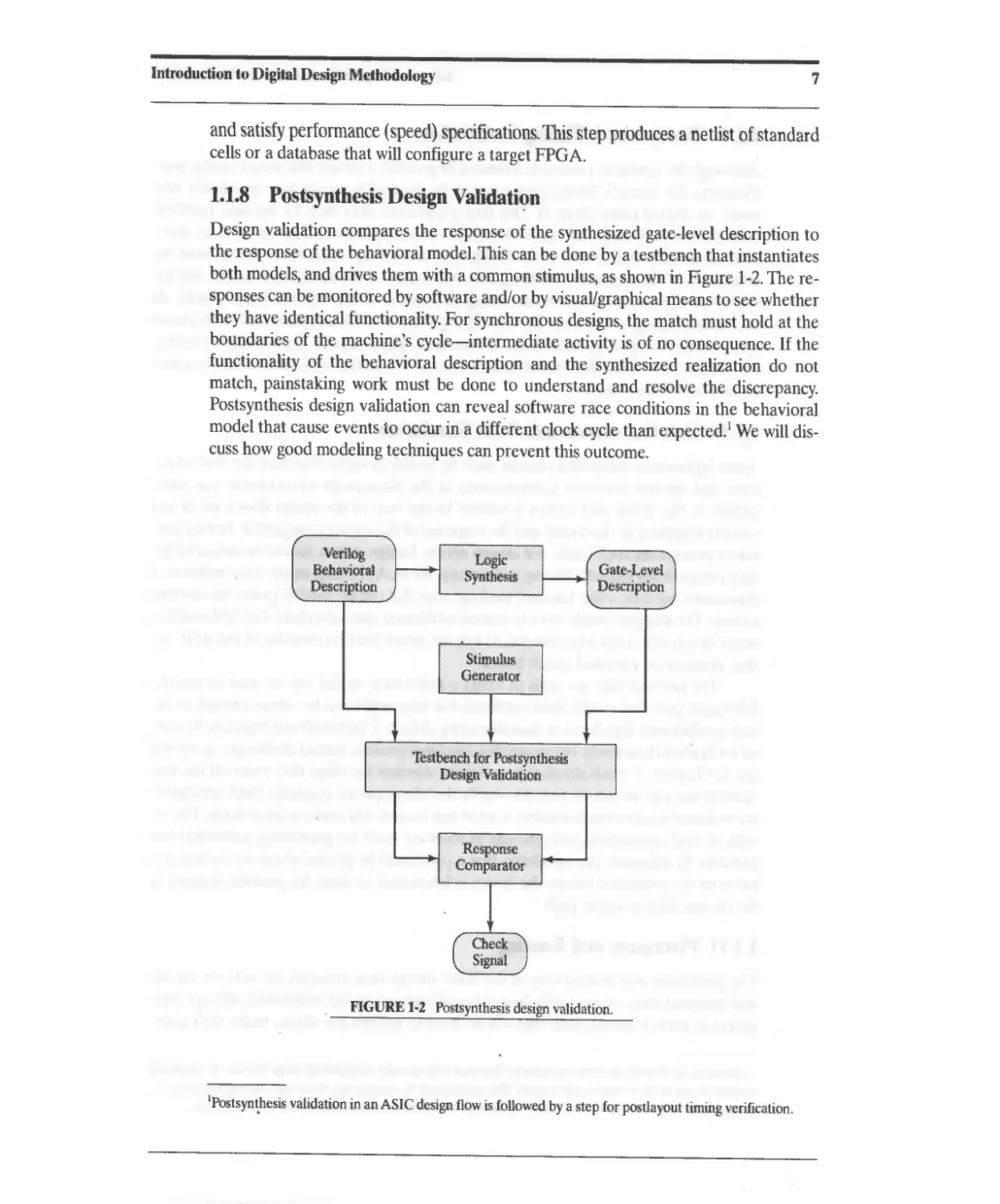
the response of the behavioral model. This can be done by a testbench that instantiates
both models, and drives them with a common stimulus, as shown in Figure 1-2. The re-
sponses can be monitored by software and/or by visual/graphical means to see whether
they have identical functionality. For synchronous designs, the match must hold at the
boundaries of the machine's cycle-intermediate activity is of no consequence. If the
functionality of the behavioral description and the synthesized realization do not
match, painstaking work must be done to understand and resolve the discrepancy.
Postsynthesis design validation can reveal software race conditions in the behavioral
model that cause events to occur in a different clock cycle than expected.! We will dis-
cuss how good modeling techniques can prevent this outcome.
Verilog
Behavioral
Description
Logic
Synthesis
Gate-Level
Description
Stimulus
Generator
Testbench for Postsynthesis
Design Validation
Response
Comparator
FIGURE 1.2 Postsynthesis design validation.
IPostsyn hesis validation in an ASIC design flow is followed by a step for postlayout timing verification.
8 Advanced Digital Design with the Verilog DDL
1.1.9 Postsyntbesis Timing Verification
Although the synthesis process is intended to produce a circuit that meets timing spec-
ifications, the circuit's timing margins must be checked to verify that speeds are ade-
quate on critical paths (Step 9). This step is repeated after Step 13, because synthesis
tools do not accurately anticipate the effect of the capacitive delays induced by inter-
connect metalization in the layout. Ultimately, these delays must be extracted from the
properties of the materials and the geometric details of the fabrication masks. The ex-
tracted delays are used by a static timing analyzer to verify that the longest paths do
not violate timing constraints. The circuit might have to be resynthesized or re-placed
and rerouted to meet specifications. Resynthesis might require (1) transistor resizing,
(2) architectural modifications/substitutions, and (3) device substitution (more speed
at the cost of more area).
1.1.10 Test Generation and Fault Simulation
After fabrication, integrated circuits must be tested to verify that they are free of de-
fects and operate correctly. Contaminants in the clean-room environment can cause
defects in the circuit and render it useless. In this step of the design flow a set of test
vectors is applied to the circuit and the response of the circuit is measured. Testing con-
siders process-induced faults, not design errors. Design errors should be detected be-
fore presynthesis sign-off. Testing is daunting, for an ASIC chip might have millions of
transistors, but only a few hundred package pins that can be used to probe the internal
circuits. The designer might have to embed additional, special circuits that will enable a
tester to use only a few external pins to test the entire internal circuitry of the ASIC, ei-
ther alone or on a printed circuit board.
The patterns that are used to verify a behavioral model can be used to test the
fabricated part that results from synthesis, but they might not be robust enough to de-
tect a sufficiently high level of manufacturing defects. Combinational logic can be test-
ed for faults exhaustively, but sequential machines present special challenges, as we will
see in Chapter 11. Fault simulation questions whether the chips that come off the fab-
rication line can, in fact, be tested to verify that they operate correctly. Fault simulation
is conducted to determine whether a set of test vectors will detect a set of faults. The re-
sults of fault simulation guide the use of software tools for generating additional test
patterns. To eliminate the possibility that a part could be produced but not tested, test
patterns are generated before the device is fabricated, to allow for possible changes in
the design, such as a scan path. 2
1.1.11 Placement and Routing
The placement and routing step of the ASIC design flow arranges the cells on the die
and connects their signal paths. In cell-based technology the individual cells are inte-
grated to form a global mask that will be used to pattern the silicon wafer with gates.
2 Scan paths are formed by replacing ordinary flip-flops with specially designed flip-flops that can be connected
together in test mode to form a shift register. Test patterns can be scanned into the design, and applied to the in-
ternal circuitry. The response of the circuit can be captured in the scan chain and shifted out for analysis.
Introduction to Digital Design Methodology
9
This step also might involve inserting a clock tree into the layout, to provide a skew-
free distribution of the clock signal to the sequential elements of the design. If a scan
path is to be used, it will be inserted in this step too.
1.1.12 Physical and Electrical Design Rule Checks
The physical layout of a design must be checked to verify that constraints on material
widths, overlaps, and separations are satisfied. Electrical rules are checked to verify
that fanout constraints are met and that signal integrity is not compromised byelectri-
cal crosstalk and power-grid drop. Noise levels are also checked to determine whether
electrical transients are problematic. Power dissipation is modeled and analyzed in this
step to verify that the heat generated by the chip will not damage the circuitry.
1.1.13 Parasitic Extraction
Parasitic capacitance induced by the layout is extracted by a software tool and then
used to produce a more accurate verification of the electrical characteristics and timing
performance of the design (Step 13). The results of the extraction step are used to up-
date the loading models that are used in timing calculations. Then the timing con-
straints are checked again to confirm that the design, as laid out, will function at the
specified clock speed.
1.1.14 Design Sign-Off
Final sign-off occurs after all of the design constraints have been satisfied and timing
closure has been achieved. The mask set is ready for fabrication. The description con-
sists of the geometric data (usually in GDS-II format) that will determine the photo-
masking steps of the fabrication process. At this point significant resources have been
expended to ensure that the fabricated chip will meet the specifications for its func-
tionality and performance.
1.2 IC Technology Options
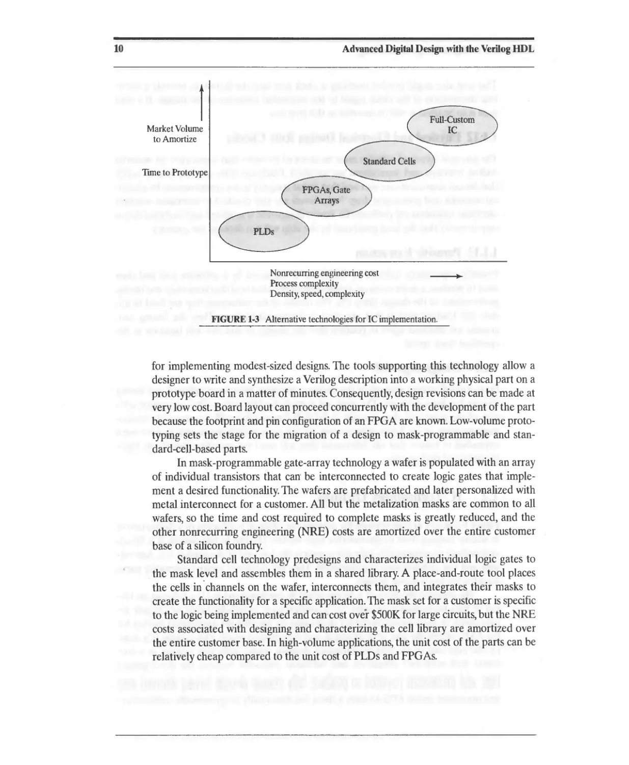
Figure 1-3 shows various options for creating the physical realization of a digital circuit
in silicon, ranging from programmable logic devices (PLDs) to full-custom ICs. Fixed-
architecture programmable logic devices serve the low end of the market (i.e., low vol-
ume and low performance requirements). They are relatively cheap commodity parts,
targeted for low-volume designs.
The physical database of a design might be implemented as (1) a full-custom lay-
out of high-performance circuitry, (2) a configuration of standard cells, or (3) gate ar-
rays (field- or mask-programmable), depending on whether the anticipated market for
the ASIC offsets the cost of designing it, and the required profit. Full-custom ICs occu-
py the high end of the cost-performance domain, where sufficient volume or a cus
tomer with corporate objectives and sufficient resources warrant the development
time and investment required to produce fully custom designs having minimal area
and maximum speed. FPGAs have a fixed, but electrically programmable architecture
10
Advanced Digital Design with the Verilog HDL
1
Market Volume
to Amortize
Time to Prototype
Nonrecurring engineering cost
Process complexity
Density, speed, complexity
»
FIGURE 1-3 Alternative technologies for IC implementation.
for implementing modest-sized designs. The tools supporting this technology allow a
designer to write and synthesize a Verilog description into a working physical part on a
prototype board in a matter of minutes. Consequently, design revisions can be made at
very low cost. Board layout can proceed concurrently with the development of the part
because the footprint and pin configuration of an FPGA are known. Low-volume proto-
typing sets the stage for the migration of a design to mask-programmable and stan-
dard-cell-based parts.
In mask-programmable gate-array technology a wafer is populated with an array
of individual transistors that can be interconnected to create logic gates that imple-
ment a desired functionality. The wafers are prefabricated and later personalized with
metal interconnect for a customer. All but the metalization masks are common to all
wafers, so the time and cost required to complete masks is greatly reduced, and the
other nonrecurring engineering (NRE) costs are amortized over the entire customer
base of a silicon foundry.
Standard cell technology predesigns and characterizes individual logic gates to
the mask l vel and assembles them in a shared library. A place-and-route tool places
the cells in channels on the wafer, interconnects them, and integrates their masks to
create the functionality for a specific application. The mask set for a customer is specific
to the logic being implemented and can cost over $500K for large circuits, but the NRE
costs associated with designing and characterizing the cell library are amortized over
the entire customer base. In high-volume applications, the unit cost of the parts can be
relatively cheap compared to the unit cost of PLDs and FPGAs.
Introduction to Digital Design Methodology
11
1.3 Overview
The following chapters will cover most of the steps in the design flow presented in
Figure 1-1, but not cell placement and routing, design-rule checking, or parasitic ex-
traction. These steps are conducted by separate tools, which operate on the physical
mask database rather than on an HDL model of the design, and they presume that a
functionally correct design has been synthesized successfully. The steps we cover are
the mainstream designer-driven steps in the overall ASIC flow.
In the remaining chapters, we will review manual methods for designing combi-
national and sequential logic design in Chapters 2 and 3. Then we will treat combina-
tionallogic design (Chapter 4) and sequential logic design (Chapter 5) using Verilog,
and by example, contrast manual and HDL-based methods. This chapter also intro-
duces the use of ASM charts and algorithmic state machine and datapath (ASMD)
charts, which prove to be very useful in writing behavioral models of sequential ma-
chines. Chapter 6 covers synthesis of combinational and sequential logic with Verilog
models. This chapter equips the designer with the background to compose synthesis-
friendly designs and to avoid common pitfalls that can thwart a design. Chapter 7 con-
tinues with a treatment of data path controllers. including a RISC CPU and a UART.
Chapter 8 introduces PLDs, CPLDs, RAMS and ROMS, and FPGAs. The problems at
the end of this chapter specify designs that can be implemented on a widely available
proto typing board. Chapter 9 covers algorithms and architectures for digital proces-
sors, and Chapter to treats architectures for arithmetic operations. Chapter 11 treats
the postsynthesis issues of timing verification, test generation, and fault simulation, in-
cluding JTAG and BIST. .
Three things matter in learning design with an HDL: examples, examples, and ex-
amples. We present several examples, with increasing difficulty, and make available
their Verilog descriptions. Several challenging problems are included at the end of each
chapter that require design with Verilog. We urge the reader to embrace the mantra:
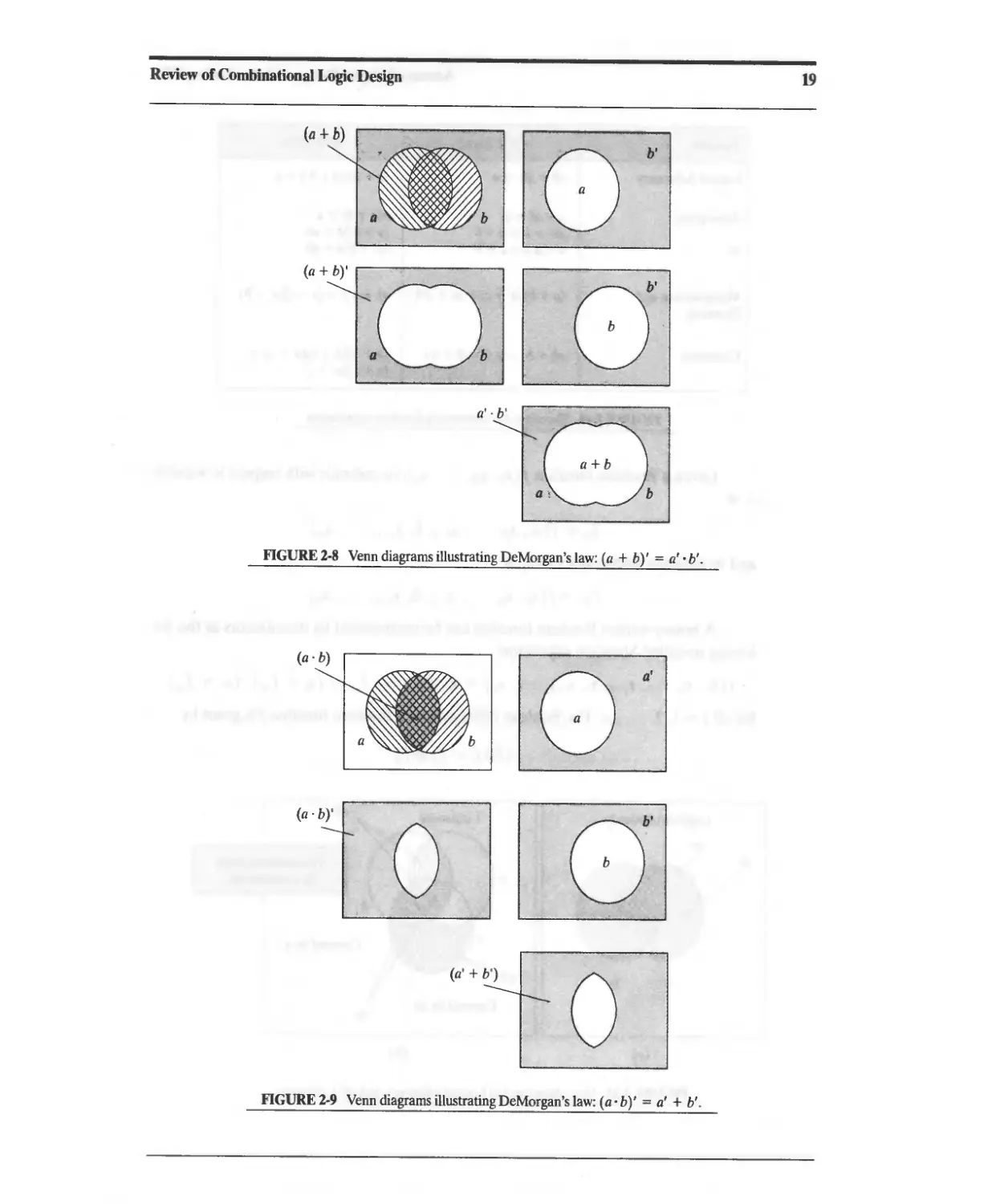
simplify, clarify, verify.
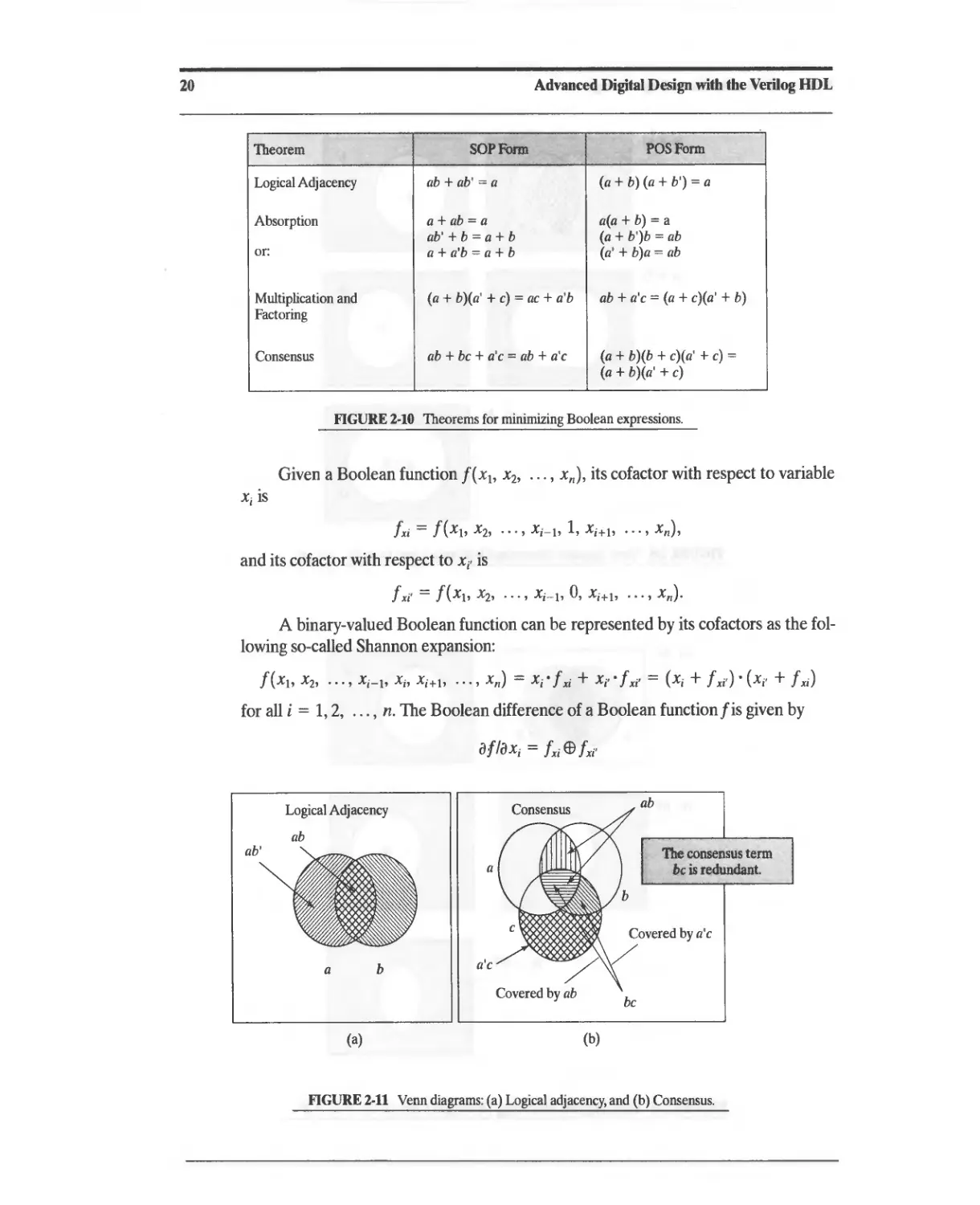
REFERENCES
1. IEEE Standard Hardware Description Language Based on the Verilog Hard-
ware Description Language, Language Reference Manual (LRM), IEEE
Std.1364-1995. Piscataway, NJ:. Institute of Electrical and Electronic Engineers,
1996.
2. IEEE Standard VHDL Language Reference Manual (LRM), IEEE Std,
1076-1987. Piscataway, NJ: Institute of Electrical and Electronic Engineers,
1988.
3. Negel LW. SPlCE2: A Computer Program to Simulate Semiconductor Circuits,
Memo ERL-M520, Department of Electrical Engineering and Computer Sci-
ence, University of California at Berkeley, May 9, 1975.
4. Fitzpatrick D, Miller I. Analog Behavioral Modeling with the Verilog-A Lan-
guage, Boston: Kluwer, 1998.
5. SystemC Draft Specification, Mountain View, CA: Synopsys, 1999.
12
Advanced Digital Design with the Verilog DDL
6. Rich, D., Fitzpatrick, T., "Advanced Verification Using the Superlog Language,"
Proc. Int. HDL Conference, San Jose, March 2002.
7. Chang H, et al. Surviving the SOC Revolution, Boston: Kluwer, 1999.
CHAPTER 2
Review of Combinational
Logic Design
This chapter will review manual methods for designing combinational logic. In Chapter 6
we will see how these steps can be automated with modern design tools.
2.1 Combinational Logic and Boolean Algebra
Combinational logic forms its outputs as Boolean functions of its input variables on an
instantaneous basis. That is, at any time t the outputs Yt> Yz, and Y3 in Figure 2-1 depend
on only the values of a, b, c, and d at time t. The outputs of combinational logic at any
time t are a function of only the inputs at time t. The outputs of other circuits may de-
pend on the history of the inputs up to time t, and they are called sequential circuits. Se-
quential circuits require memory elements in hardware.
The variables in a logic circuit are binary-they may have a value of 0 or 1. Hard-
ware implementations of logic circuits use either positive logic, in which a high voltage
level, say 5 volts, corresponds to a logical value of 1, and a low voltage, say 0, corre-
sponds to a logical O. In negative logic, a low electrical level corresponds to a logical I,
and a high electrical level corresponds to a O.
Some common logic gates are shown in Figure 2-2, together with the Boolean
equation that determines the value of the output of the gate as a function of its inputs,
and Table 2-1 lists common symbols for hardware-based Boolean logic operations.]
2.1.1 ASIC Library Cells
Logic gates are implemented physically by a transistor-level circuit. For example, in
CMOS (complementary metal-oxide semiconductor) technology, a logic inverter consists
I Note: The schematic symbol for the three-state buffer uses the symbol z to indicate the high impedance con-
dition of the device.
14
Advanced Digital Design with the Verilog HDL
a
Yl
b Combinational
Logk Y2
c
Y3
d
FIGURE 2-1 Block diagram symbol for combinational logic having four inputs and three outputs.
And Gate Or Gate
y=a.b y=a+b
:=o-y ::=[)-- y
Nand Gate Nor Gate
y=a.b y=a+b
: y ::=[>-y
Buffer
y=a
a ----t>--- y
Inverter
y=a
a ----[>0----- y
Xor Gate
y=a"b
::D-- y
Xnor Gate
y=a"b
:V- y
Three-State Buffer
y = a if enable = 1, else y = z
a -----I>-----. y
FIGURE 2-2 Schematic symbols and Boolean relationships for some common logic gates.
TABLE 2-1 Common Boolean logic symbols and
operations.
Symbol , LOgic Operation "., '<
< .<
+ Logic "or"
Logical "and"
E9 Exclusive "or"
A Exclusive "or"
I Logical negation
- Logical negation
(overbar)
of a series connection of p-channel and n-channel MOS transistors having a common
drain that serves as the output, and a common gate that serves as the input. When the
input is low, the p-channel device conducts and the n-channel device is an open circuit.
In this mode the output capacitor charges to V dd . When the input is high, the n-channel
device conducts, and the p-channel device is an open circuit. This discharges the output
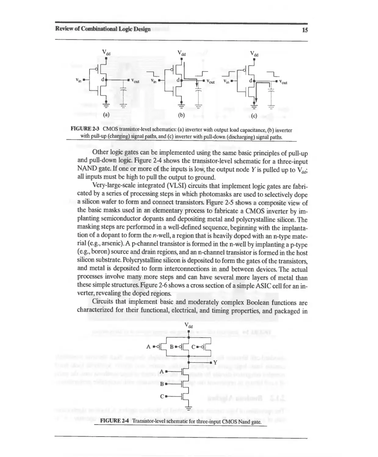
node capacitor to ground. Figure 2-3 shows (b) the pull-up and (c) pull-down paths for
current in the i verter in (a).
Review of Combinational Logic Design
15
V dd V dd
,;" d v out d v out
...i..
..,...
-=- n -=- ..
(a) (b)
V dd
-=-
(c)
FIGURE 2-3 CMOS transistor-level schematics: (a) inverter with output load capacitance, (b) inverter
with pull-up (charging) signal paths, and (c) inverter with pull-down (discharging) signal paths.
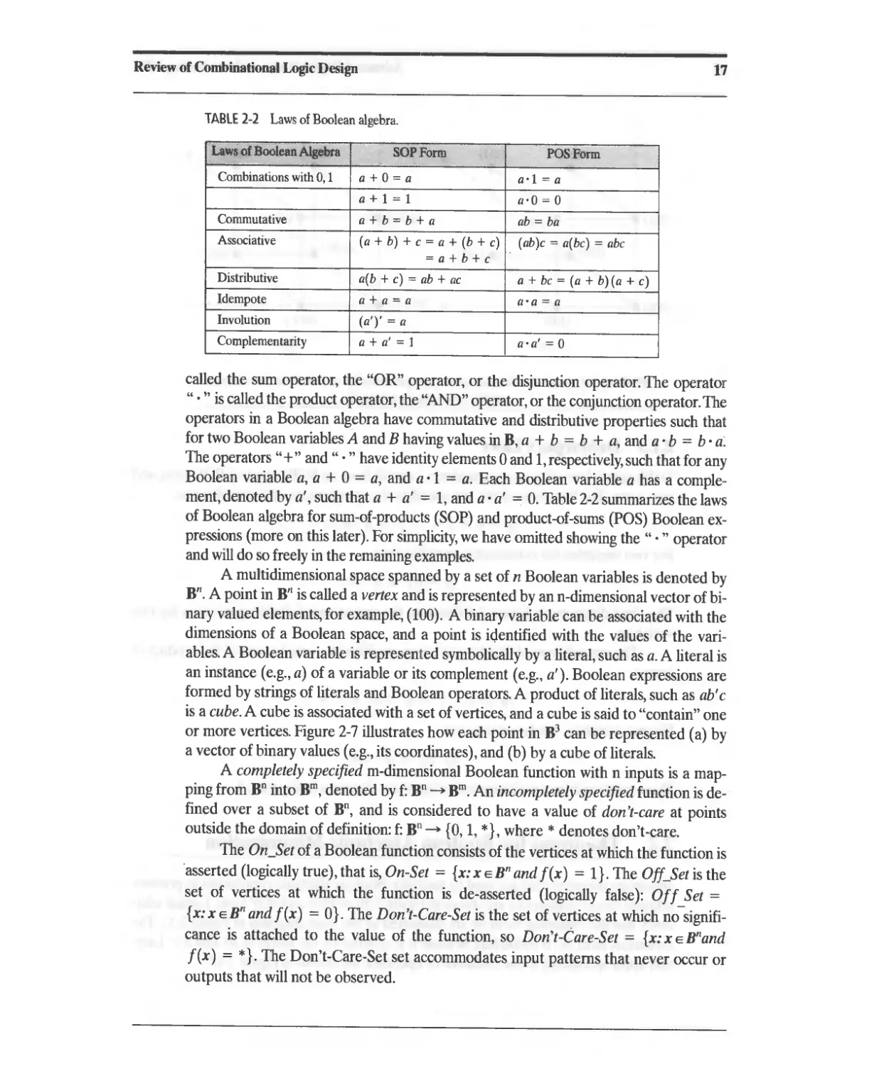
Other logic gates can be implemented using the same basic principles of pull-up
and pull-down logic. Figure 2-4 shows the transistor-level schematic for a three-input
NAND gate. If one or more of the inputs is low, the output node Y is pulled up to V dd ;
all inputs must be high to pull the output to ground.
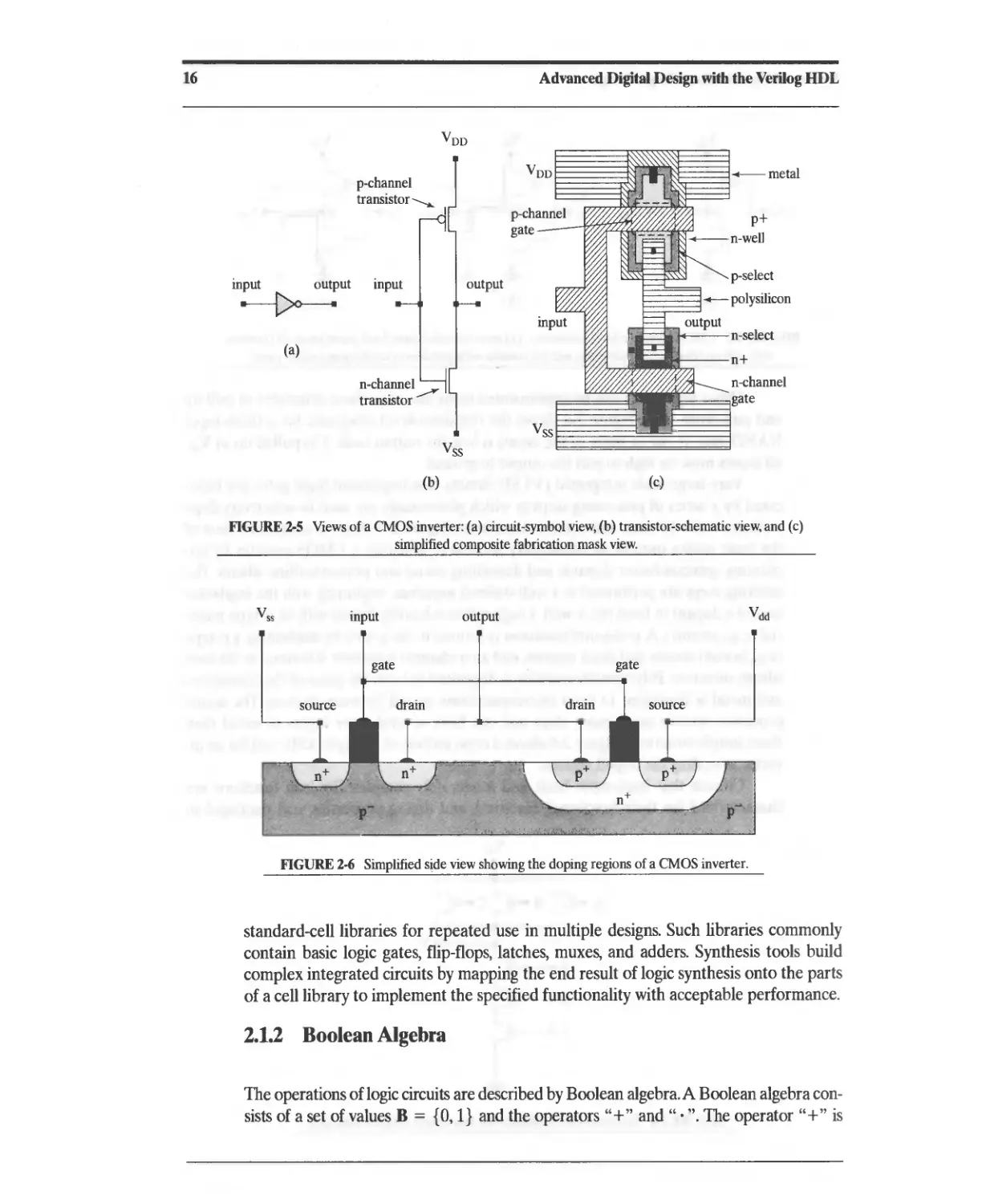
Very-large-scale integrated (VLSI) circuits that implement logic gates are fabri-
cated by a series of processing steps in which photomasks are used to selectively dope
a silicon wafer to form and connect transistors. Figure 2-5 shows a composite view of
the basic masks used in an elementary process to fabricate a CMOS inverter by im-
planting semiconductor dopants and depositing metal and polycrystalline silicon. The
masking steps are performed in a well-defined sequence, beginning with the implanta-
tion of a dopant to form the n-well, a region that is heavily doped with an n-type mate-
rial (e.g., arsenic). A p-channel transistor is formed in the n-well by implanting a p-type
(e.g., boron) source and drain regions, and an n-channel transistor is formed in the host
silicon substrate. Polycrystalline silicon is deposited to fonn the gates of the transistors,
and metal is deposited to form interconnections in and between devices. The actual
processes involve many more steps and can have several more layers of metal than
these simple structures, Figure 2-6 shows a cross section of a simple ASIC cell for an in-
verter, revealing the doped regions.
Circuits that implement basic and moderately complex Boolean functions are
characterized for their functional, electrical, and timing properties, and packaged in
V dd
A--1
y
-=-
FIGURE 2-4 Transistor-level schematic for three-input CMOS Nand gate.
16
Advanced Digital Design with the Verilog HDL
V oo
p-channel V oo --- metal
transistor -........
p-channel
gate
input output input p-select
.-- polysilicon
input n-select
(a) n+
n-channel n-channel
transistor ----- gate
V ss
V ss
(b) (c)
FIGURE 2-5 Views of a CMOS inverter: (a) circuit-symbol view, (b) transistor-schematic view, and (c)
simplified composite fabrication mask view.
V ss
input
output
V dd
gate
gate
," ,. f' 'I. ,,'-." :,",."-1,' ,( ,"",", , :'-.17",'.. 4' ', . '
FIGURE 2.6 Simplified side view showing the doping regions of a CMOS inverter.
standard-cell libraries for repeated use in multiple designs. Such libraries commonly
contain basic logic gates, flip-flops, latches, muxes, and adders. Synthesis tools build
complex integrated circuits by mapping the end result of logic synthesis onto the parts
of a cell library to implement the specified functionality with acceptable performance.
2.1.2 Boolean Algebra
The operations oflogic circuits are described by Boolean algebra. A Boolean algebra con-
sists of a set of values B = {O, 1} and the operators "+" and". ". The operator "+" is
Review of Combinational Logic Design
17
TABLE 2-2 Laws of Boolean algebra.
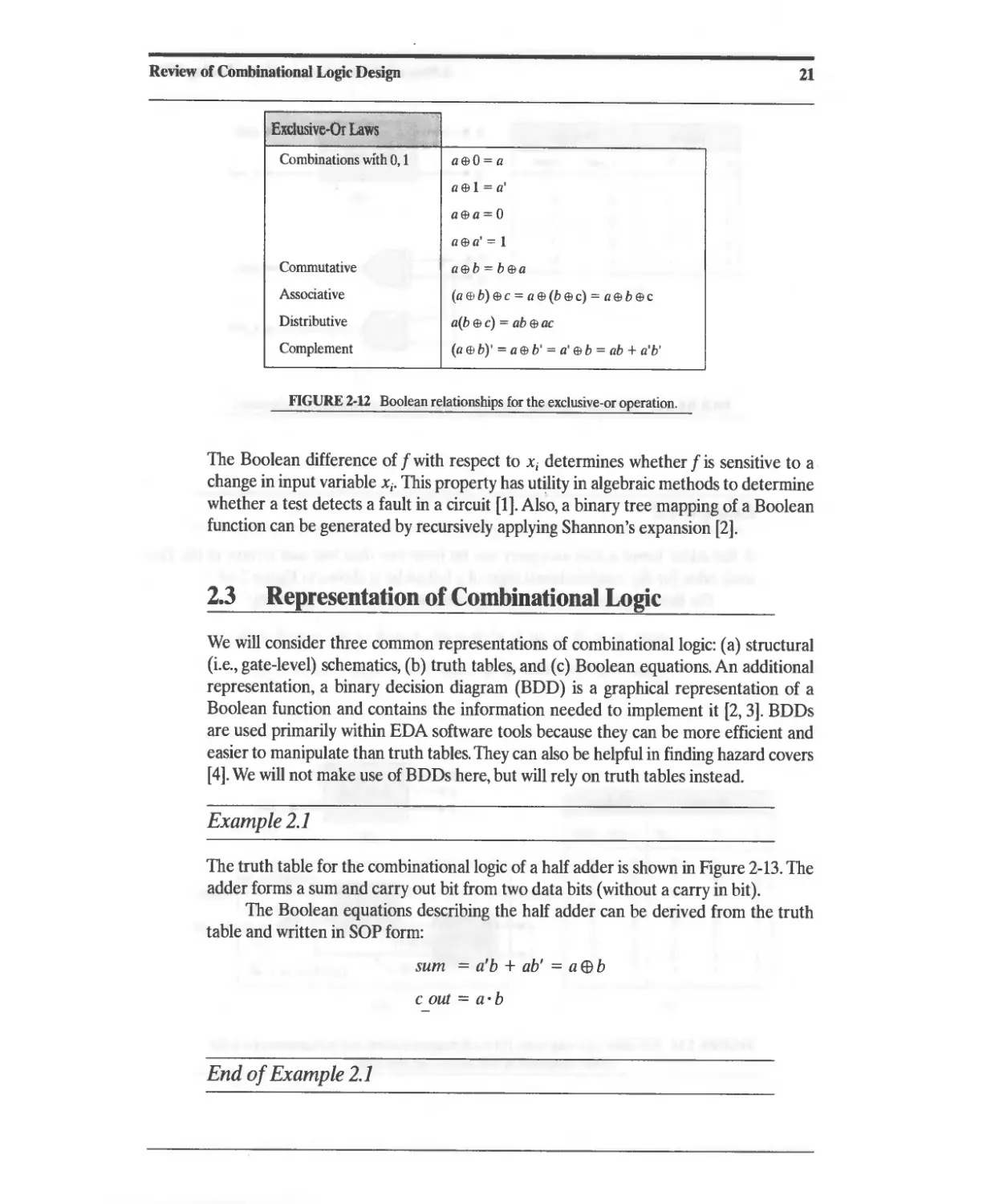
Laws of Boolean Algebra sop Form POS Form
Combinations with 0, 1 a+O=a a'i = a
a+I=1 a'O = 0
Commutative a+b=b+a ab=ba
Associative (a + b) + e = a + (b + e) (ab)e = a(be) = abe
=a+b+e
Distributive a(b + e) = ab + ae a + be = (a + b) (a + e)
Idempote a+a=a a'a = a
Involution (aT = a
Complementarity a + a/ = 1 a'a' = 0
called the sum operator, the "OR" operator, or the disjunction operator. The operator
" . " is called the product operator, the "AND" operator, or the conjunction operator. The
operators in a Boolean algebra have commutative and distributive properties such that
for two Boolean variables A and B having values in B, a + b = b + a, and a . b = b. a:
The operators "+" and"." have identity elements 0 and 1, respectively, such that for any
Boolean variable a, a + 0 = a, and a' 1 = a. Each Boolean variable a has a comple-
ment, denoted by a', such that a + a' = 1, and a . a' = O. Table 2-2 summarizes the laws
of Boolean algebra for sum-of-products (SOP) and product-of-sums (PaS) Boolean ex-
pressions (more on this later). For simplicity, we have omitted showing the"." operator
and will do so freely in the remaining examples,
A multidimensional space spanned by a set of n Boolean variables is denoted by
B n . A point in B n is called a vertex and is represented by an n-dimensional vector ofbi-
nary valued elements, for example, (100). A binary variable can be associated with the
dimensions of a Boolean space, and a point is identified with the values of the vari-
ables, A Boolean variable is represented symbolically by a literal, such as a. A literal is
an instance (e.g., a) of a variable or its complement (e.g., a'). Boolean expressions are
formed by strings of literals and Boolean operators, A product of literals, such as ab' c
is a cube. A cube is associated with a set of vertices, and a cube is said to "contain" one
or more vertices. Figure 2-7 illustrates how each point in B 3 can be represented (a) by
a vector of binary values (e.g., its coordinates), and (b) by a cube of literals.
A completely specified m-dimensional Boolean function with n inputs is a map-
ping from B n into B m , denoted by f: B n -+ B m . An incompletely specified function is de-
fined over a subset of B n , and is considered to have a value of don't-care at points
outside the domain of definition: f: B n -+ {O, 1, *}, where * denotes don't-care.
The On_Set of a Boolean function consists of the vertices at which the function is
'asserted (logically true), that is, On-Set = {x: x E B n and f(x) = I}. The Off_Set is the
set of vertices at which the function is de-asserted (logically false): Off_Set =
{x: x E B n and f(x) = O}. The Don't-Care-Set is the set of vertices at which no signifi-
cance is attached to the value of the function, so Don't-Care-Set = {x: x E Bnand
f(x) = *}. The Don't-Care-Set set accommodates input patterns that never occur or
outputs that will not be observed.
18
Advanced Digital Design with the Verilog HDL
c C
I I
I I
I (011) (111) ",b I
I '" I
I '" I
I '" I
'"
I '" I
I I
(001) (a'b'c)
(110)
(000) --------- a (a'b'c')
(100)
(a)
(a'bc) (abc) '" b
'"
'"
-'
'"
'"
(abc')
---------- a
(ab'c')
(b)
FIGURE 2-7 Points in a Boolean space: (a) represented by vectors of binary variables,
and (b) represented symbolically.
2.1.3 DeMorgan's Laws
DeMorgan's laws allow us to transfonn a circuit from an SOP form to a POS fonn, and
vice versa. The first fonn of the law specifies the complement of a sum of terms:
(a + b + c + ...)' = a'.b'.c'. ...
For two variables the relationship specifies that:
(a + b)' = a'.b'
The Venn diagrams in Figure 2-8 illustrate the operations of DeMorgan's laws for two
variables.
The second form of DeMorgan's laws specifies the complement of the product of
tenns:
(a.b.c...)' = a' + b' + c' +
For two variables, the law states that:
(a . b)' = a' + b'
These relationships are illustrated by the Venn diagrams in Figure 2-9.
2.2 Theorems for Boolean Algebraic Minimization
Important theorems that are used to minimize Boolean algebraic expressions to produce
efficient circuit realizations are shown in Figure 2-10, in POS and SOP form. Logical adja-
cency and the consensus theorem are illustrated by the Venn diagrams in Figure 2-11. The
consensus term, be, is redundant because it is covered bi the union of ab and a' c. Laws
that apply specifically to the exclusive-or operation are shown in Figure 2-12.
Review of Combinational Logic Design
19
(a + b)'
.Ob
o
b '
O'
a'. b'
, G " a+b..
O b
FIGURE 2-8 Venn diagrams illustrating DeMorgan's law: (a + b)' = a'. b'.
(a. b)
b
(a. b)'
---
o
(a' + b')
o
0'
O'
o
FIGURE2.' Venn diagrams illustrating DeMorgan's law: (aob)' = a' + b'.
20
Advanced Digital Design with the Verilog HDL
Theorem SOP Form P S Ponn
Logical Adjacency ab + ab' = a (a + b) (a + b') = a
Absorption a+ab=a a(a + b) = a
ab' + b = a + b (a + b')b = ab
or: a + a'b = a + b (a' + b)a = ab
Multiplication and (a + b)(a' + e) = ae + a'b ab + a'e = (a + e)(a' + b)
Factoring
Consensus ab + be + a'e = ab + a'e (a + b)(b + e)(a' + e) =
(a + b)(a ' + e)
FIGURE 2.10 Theorems for minimizing Boolean expressions.
Given a Boolean function f(x h X2, ..., x n ), its cofactor with respect to variable
Xi IS
fxi = f(XI' X2, ..., Xi-h 1, Xi+I, ..., x n ),
and its cofactor with respect to Xi' is
fXi' = f(Xh X2, ..., Xi-h 0, Xi+h ..., X n ).
A binary-valued Boolean function can be represented by its cofactors as the fol-
lowing so-called Shannon expansion:
f(Xh X2, ..., Xi-I' Xi' Xi+h ..., X n ) = xi'fxi + xi,.fxi' = (Xi + fXi').(Xi' + fxJ
for all i = 1,2, ..., n. The Boolean difference of a Boolean functionfis given by
aftaxi = fxi EI1 fXi'
a
ab
Logical Adjacency
ab
The consensus tenn
be is redundant.
Covered by a'e
a
b
a'e
Covered by ab
be
(a)
(b)
FIGURE 2.11 Venn diagrams: (a) Logical adjacency, and (b) Consensus.
Review of Combinational Logic Design
21
Exclusive-Or Laws
Combinations with 0, 1 aEl!O=a
aEl!l = a'
aEl!a=O
aEl!a' = 1
Commutative aEl!b = bEl!a
Associative (affib)EI!c = aEl!(bEl!c) = aEl!bEl!C
Distributive a(bEl!c) = abEl!ac
Complement (a ffi b)' = aEl!b' = a' El!b = ab + a'b'
FIGURE 2.ll Boolean relationships for the exclusive-or operation.
The Boolean difference of f with respect to Xj determines whether f is sensitive to a
change in input variable Xj. This property has utility in algebraic methods to determine
whether a test detects a fault in a circuit [1]. Also, a binary tree mapping of a Boolean
function can be generated by recursively applying Shannon's expansion [2].
2.3 Representation of Combinational Logic
We will consider three common representations of combinational logic: (a) structural
(i.e., gate-level) schematics, (b) truth tables, and (c) Boolean equations, An additional
representation, a binary decision diagram (BDD) is a graphical representation of a
Boolean function and contains the information needed to implement it [2, 3]. BDDs
are used primarily within EDA software tools because they can be more efficient and
easier to manipulate than truth tables, They can also be helpful in finding hazard covers
[4]. We will not make use of BDDs here, but will rely on truth tables instead.
Example 2.1
The truth table for the combinational logic of a half adder is shown in Figure 2-13. The
adder forms a sum and carry out bit from two data bits (without a carry in bit).
The Boolean equations describing the half adder can be derived from the truth
table and written in SOP form:
sum = a' b + ab' = a EI1 b
cout=a.b
End of Example 2.1
22
Advanced Digital Design with the Verilog HDL
Inputs Outputs
a b c_out sum
0 0 0 0
0 1 0 1
1 0 0 1
1 1 1 0
(a)
: :
: sum
COUI
Add_half
(b)
:
: -
cout
FIGURE 2-13 Half adder: (a) truth table, (b) block diagram symbol, and (c) schematic.
(c)
Example 2.2
A full adder fOTIns a sum and carry out bit from two data bits and a carry in bit. The
truth table for the combinational logic of a full adder is shown in Figure 2-14.
The Boolean equations describing sum and cout bits are given by:
sum = a' . b' . c in + a' . b . c in' + a. b' . c in' + a. b . c in
c out = a' . b . c in + a. b' . c in + a. b . c in' + a. b . c in
Inputs Outputs
a b c_in c_out sum
0 0 0 0 0
0 0 1 0 1
0 1 0 0 1
0 1 L 1 0
1 0 0 0 1
1 0 1 1 0
1 1 0 1 0
1 1 1 1 1
c_in
(a)
c_in b a ::::::J
AdcUull
:
(b)
a
c_out
b
a: sum
Add half
(i sum b ,_out
Add....ha1f (a E!J b)
b. COut
, ab
sum
(c)
FIGURE 2-14 FulL adder: (a) truth tabLe, (b) block diagram symbol, and (c) schematic for a full
adder comrsed of half adders and r 1ue IOriC.
Review of Combinational Logic Design
23
These can be rearranged as:
sum = a EI1 b EI1 c in
c_ out = (a EI1 b) . c_in + a. b
The Venn diagram in Figure 2-15 shows the assertions of sum and cout as a function
of a, b, and cin.
Truth tables become unwieldy for functions of several variables because the
number of rows grows exponentially with the number of variables. Notice that the
truth table of the full adder has twice as many rows as the table for the half adder.
End of Example 2.2
2.3.1 Sum of Products Representation
A cube is formed as the product of literals in which a literal appears in either uncom-
plemented or complemented fonn. For example, ab' cd is a cube but ab' cbd is not. A
cube need not contain every literal. A Boolean expression is a set of cubes, and is typi-
cally expressed in sum-of-products (SOP) form as the "OR" of product tenns (cubes),
rather than in set notation.
a
b
cout
Suh!'
;,.o
sum
cin
FIGURE 2-15 Venn diagram representation of the truth table for a full adder.
24
Advanced Digital Design with the Verilog DDL
Example 2.3
The following expression is in sum-of-products form: abc' + bd.
End of Example 2.3
Each term of a Boolean expression in SOP form is called an implicant of the
function. A minterm is a cube in which every variable appears. The variable will be in
either true (uncomplemented) or complemented form (but not both). Thus, a minterm
corresponds to a single point (vertex) in B n . A cube that is not a minterm represents
two or more points in B n . The minterms of a Boolean function correspond to the rows
of the truth table at which the function has a value of 1.
Example 2.4
The cube ab' cd is a minterm in B 4 . The cube abc is not a minterm. It represents the
pair of vertices defined by abed + abed'.
End of Example 2.4
A Boolean expression in SOP form is said to be canonical if every cube in the ex-
pression has a unique representation in which all of the literals are in complemented or
uncomplemented form.
Example 2.5
The expression abed + a' bed is a canonical SOP.
End of Example 2.5
A canonic (standard) SOP function is also called a standard sum-of-products
(SSOP). In decimal notation, a minterm is denoted by mi, and the pattern of 1s and Os
in the binary equivalent of the decimal number indicates the true and complemented
literals. For example, m7 = a' bcd.
In B n there is a one-to-one correspondence between a minterm and a vertex of
an n-dimensional cube, as shown in Figure 2-16. The minterm m3 = a' be corresponds
to the vertex with coordinates 011.
A Boolean function is a set of mintenns (vertices) at which the function is asserted.
A Boolean function in SOP form is expressed as a sum of minterms.
Review of Combinational Logic Design
25
C
I
I
I
I
I
I
I
I
m3
m7
m]
"
"
"
"
"
b
m6
mo m4
FIGURE 2.16 Correspondence between minterms and vertices in 0 3 .
Example 2.6
The sum and carry bits of the full adder can be expressed as a sum of mintenns, or-
dered as {a, b, c_in} in B3:
sum = ml + m2 + m4 + m7 = m(l, 2, 4, 7)
c_out = m3 + ms + m6 + m 7 = m(3, 5, 6, 7)
End of Example 2.6
Example 2.7
The set of shaded vertices m Figure 2-17 define f = ml + m2 = m3 = a'b'c
+ a'bc' + a'bc.
End of Example 2.7
26
Advanced Digital Design with the Verilog DDL
(001)
m l
/
/
/
/
/
b
(011)
m3
(110)
m6
(000) (100)
mo m4
FlGURE 2.17 Set ofminterlTIS for f = a'b'e + a'be' + a'be.
2.3.2 Product-or-Sums Representation
A Boolean function can also be expressed in a pas form in which the expression is
written as a product of Boolean factors, each of which is a sum of literals.
Example 2.8
The pas representation of the cout bit in a full adder circuit is fonned by expressing
the Os of the truth table in sap fonn (see Figure 2-14):
c out' = a'b'c in' + a'b'c in + a'bc in' + ab'c in'
Then the expression for c_out' is complemented, giving
c_out = (a'b'c_in' + a'b'c_in + a'bcJn' + ab'c_in')'
DeMorgan's Laws can be applied to cout to give the pas expression shown below:
c_out = (a'b'cJn')" (a'b'c_in)' 0 (a'bcJn')' 0 (ab'c_in')'
c_out = (a + b + c_in).(a + b + cJn') 0 (a + b' + cJn) 0 (a' + b + c_in)
End of Example 2.8
A Boolean expression in pas form is said to be canonical (i.e., a unique repre-
sentati for a given function) if each factor has aU of the literals in comr"mented or
uncomplemented form, but not both.
Review of Combinational Logic Design
27
A maxterm is an OR-ed sum of literals in which each variable appears exactly
once in true or complemented form (e.g., a + b + c in is a maxterm in the pas ex-
pression for cout). A canonical pas expansion consIsts of a product of the maxterms
of the truth table of a function. The decimal notation of a maxterm is based on the rows
of the truth table at which the function is zero (i.e., where f' is asserted). The variables
are complemented when forming the pas expression.
Example 2.9
The sop form of the c out' bit of a full adder was given in the previous example. The
decimal notation for cout is given by the product of the maxterms that corresponds to
the cubes of c out' as
c out' = a'b'c in' + a'b'c in + a'bc in' + ab'c in'
c_out = Mo' M I ' M z ' M4 = nM(O, 1, 2, )
c_out = (a + b + c_in) , (a + b + c_in') ' (a + b' + c_in) - (a' + b + c_in)
A canonical SOP expression can be a very efficient representation of a Boolean
function because there might be very few terms at which the function is asserted. Al-
ternatively, f' expressed as a pas expression might be very efficient because there are
only a few terms at which the function is de-asserted.
End of Example 2.9
2.4 Simplification of Boolean Expressions
An SOP expression can be implemented in hardware as a two-level AND-OR logic
circuit. Although a Boolean expression can always be expressed in a canonical form,
with every cube containing every literal (in complemented or uncomplemented form),
such descriptions are usually inefficient and waste hardware. In practice, minimization
is important because the cost of hardware implementing a Boolean expression is related
to the number of terms in the expression and to the number of literals in a term, that is,
in a cube in an SOP expression.
A Boolean expression in SOP form is said to be minimal if it contains a minimal
number of product terms and literals (i.e., a given tenn cannot be replaced by another
that has fewer literals). A minimum SOP form corresponds to a two-level logic circuit
having the fewest gates and the fewest number of gate inputs.
There are four common approaches to simplifying a Boolean expression. The
first is a manual graphical method that is guided by Karnaugh maps displaying logical
adjacencies of the function. Manual methods are feasible only for functions that have
28
Advanced Digital Design with the Verilog DDL
no more ttan sIx Inputs M. The Ou;ne-McCluskey minimization algorithin relies on
logical adjacency and the same principles as logic minimization with Karnaugh maps
[6-9]. It can be applied manually on small functions, but can also be implemented as a
computer program that is effective for larger circuits. A third method, Boolean mini-
mization [5], is also manual, and relies on clever application of the theorems describing
relationships between Boolean variables to find simpler, equivalent expressions. The
method is not straightforward, can be difficult, and requires experience. As a fourth al-
ternative, the theorems that are used in Boolean minimization are now embedded in
modern synthesis tools and programs such as Espresso-II [10] and mis-II (multilevel
interactive synthesis) [4], in which they are used to perform logic minimization and
form efficient realizations of two-level and multilevel logic circuits.
Logic minimization searches for efficient representations of Boolean functions.
In a Boolean expression, a cube that is contained in another cube is said to be redun-
dant-a cube is redundant if its set of vertices is properly contained in the set of vertices of
another cube of the function. A Boolean expression is nonredundant (irredundant) if
no cube contains another cube.
Example 2.10
The following Boolean expression is redundant because the vertex set of ab is a subset
of the vertex set of a:
/(a, b) = a + ab
The redundant cube can be removed to give an equivalent, but more efficient
representation:
/(a, b) = a
End of Example 2.10
Example 2.11
The Boolean function given by / (c, d) = c'd' + cd is irredundant.
End of Example 2.11
The cubes of an irredundant expression do not share a common vertex, that is, their
corresponding sets of vertices are pairwise disjoint. Boolean minimization is difficult be-
cause the minimum SOP fonn and minimum POS fonns of a Boolean expression are not
unique. Boolean minimization/simplification exploits logical adjacency by (1) repeatedly
combining cubes that differ in only one literal, and (2) eliminating redundant implicants.
Review of Combinational Logic Design
29
Example 2.12
With the objective of illustrating Boolean mInImIzation of the function
/(a, b, c) = abe + a' be + abc' + a'b'e + ab'e' + a'b'e', we start by combining
cubes that differ by only one literal, as shown in Figure 2-18, which shows the Boolean
expression for / and illustrates the adjacent vertices graphically. A pair of adjacent
shaded vertices can be combined into a single cube that covers both of them.
An equivalent, minimal expression is formed by removing the cubes ab + a' b'
and adding the cube ae' to the expression, as shown in Figure 2-19:
/(a, b, c) = ae' + a'e + be + b'e'
Note that /( a, b, c) = ae' + a' e + a' b' e' + abe is also an equivalent expression, but
not minimal. Figure 2-20 shows how another equivalent and minimal expression can be
obtained by applying logical adjacency to different tenns of the original SOP expression.
./' ab ./'a'b'
I 1 . I I
f(a,b, c) = abe + a'be + abc' + a'b'e + ab'e' + a'b'c'
I I I I
'-.... be '-.... b'e'
/(a, b, c) = be + ab + a'b' + b'e'
Each term (cube) of a Boolean expression in SOP form is called an implicant of the
function. An implicant covers a vertex if the vertex is included in the set of vertices at
which the implicant is asserted. An implicant may cover more than one vertex of the
function. The fewer the number of literals in a cube, the larger the set of vertices covered
by the cube. So the hardware implementation is minimized if a cube has as few literals
I ./' ab I I ./' a'b' I a'b'
f(a,b,e) = abc + a'be + abc' + a'b'e + ab'e' + a'b'e'
'be '-....a'e I I '-....b'e' I
. be (111)
m7
"
b
ab
------ a
f(a,b, c) = ab + be + a'e + b'e' + a'b'
(000)
mo b'e' m4
(a) (b)
FIGURE 2-18 A Boolean function: (a) representation of adjacent cubes,
and (b) a graphical representation of adjacent vertices.
30
Advanced Digital Design with the Verilog DDL
(011)
I a'e m]
i\
I
I
be
ml
(110)
m6
ae'
b'e'
FIGURE 2.19 A second, equivalent, minimal expression for the function in Figure 2-18.
a'b'
e
I
I
I
I
I
I
I
be
ab
---------a
(000)
mo b'e'
FIGURE 2.20 A third, equivalent minimal expression for the function in Figure 2-18.
as possible. The function f = abc + abc' shown in Figure 2-21 has two vertices that
can be combined by logical adjacency into one implicant, ab. A representation in terms
of just one implicant is preferred to another that uses two implicants because the hard-
ware of the former realization will be simpler and cheaper.
End of Example 2.12
The vertices of the On-Set of a Boolean function provide a complete, but ineffi-
cient, description of the function because each minterm includcs cvcry litcral that is used
by the function. We can exploit logical adjacency to reduce the size of the terms (cubes)
Review of Combinational Logic Design
31
(001)
C
I
I
I
I
I
I
I
I
(011)
(111)
"b
"
"
"
vertex
ab
f(a,b,c) = abc + abc'
=ab
I
implicant
(000)
--------- a
FIGURE 2.21 Combination of adjacent vertices into one implicant.
that are used in the SOP fonn of the fUnction. Terms that are logically adjacent can al-
ways be combined into a single term that has fewer literals. But be aware that merely ap-
plying logical adjacency to the cubes of a function does not necessarily minimize the
function. It is essential that every vertex be covered by a cube, that is, each must belong to
the vertex set of a cube; but how many such cubes are necessary to completely cover the
function, and which cover is the most efficient? We will now formalize these concepts.
A prime implieant of the On-Set of a Boolean function is an implicant whose as-
sertion does not imply assertion of any other implicant of the function. A prime impli-
cant is a cube whose vertices are not properly contained in the set of vertices of some
other cube of the function.
Example 2.13
Consider the function /(a, b, e, d) = a' b'ed + a'bed + ab'ed + abed + a'b'e'd' in
SOP form:
f(a, b, e, d) = a'b'ed + a'bed + ab'ed + abed + a'b'e'd'
= a'ed + aed + a'b'e'd'
= ed + a'b'e'd '
Note that a' ed and aed both imply ed, so they are not prime implicants. The term
a' b' e' d is a prime implicant.
End of Example 2.13
A prime implicant cannot be combined with another implicant to eliminate a lit-
eral or to be eliminated from the expression by absorption. An implicant that implies
another implicant is said to be covered by it; the set of the vertices of the covered im-
plicant is a subset of the vertices of the implicant that covers it. The covering implicant,
having fewer literals, has more vertices. The set of prime implicants of a Boolean ex-
pression is unique.
32
Advanced Digital Design with the Verilog DDL
Example 2.14
The expression, vertices, and prime implicants of a Boolean function in B 3 are shown in
Figure 2-22.
End of Example 2.14
A prime implicant that is not covered by any set of other implicants is an essential
prime implieant. An essential prime implicant must be retained in a cover of the
function.
Example 2.15
The vertices and implicants of I(a, b, e) = a' be + abe + ab'e' + abe' are shown in
Figure 2-23. The set of prime implicants of 1 is {ae', ab, be}. The set of essential prime
implicants, an SOP expression for f, and a minimal SOP expression are also listed below.
Essential Prime Implicants: {ae', be}
SOP Expression I( a, b, e) = ae' + ab + be
Minimal SOP Expression: I(a, b, e) = ae' + be
(001)
ml
C
I
I
I
I
I
I
I
(011)
m3
(111)
m7
ab
(000)
mo
(100) ac'
m 4
r---lr-l
f(a,b,c) = ab'c'
f, ( b ) = ' + b + ' b ' Implicants
J' a, ,c ac a a c
Prime Implicants
FIGURE 2-22 The vertices and prime implicants of f = ab' c' + abc' + abc + a' b' c.
Review of Combinational Logic Design
33
C
I
I
I
I
I
I
I
I
(001)
ml
ab
(011)
(111)
(000)
mo
(100) ac'
m 4
FIGURE 2.23 Vertices and imp Ii cants of f( a, b, c) = a' be + abc + ab' c' + abc'.
End of Example 2.15
The process for minimizing a Boolean expression follows these steps: (1) find the
set of all prime implicants, (2) find a minimal subset of implicants that covers all of the
prime implicants (including the essential prime implicants). The minimal cover of a
Boolean expression is a subset of prime implicants that covers all of its prime implicants.
Example 2.16
Consider the function given by:
f(a, b, c, d) = a'b'cd + a'bcd + ab'cd + abed + a'b'c'd'
By combining adjacent terms we get
f(a, b, c, d) = a' cd + acd + a'b'c'd'
f(a, b, c, d) = cd + a'b'c'd'
The set of prime implicants is {cd, a' b' c' d'}, and the minimal cover is
{cd. a'b'c'd'}.
End of Example 2.16
Boolean minimization combines terms that are logically adjacent, that is, that dif-
fer in only one literal.
34
Advanced Digital Design with the Verilog HDL
Example 2.17
Figure 2-24 illustrates how logically adjacent terms in the expression for the carry-out
bit of the full adder can be combined to obtain a minimal expression.
End of Example 2.17
Boolean minimization also exploits logical adjacency of complementary
expressIOns.
Example 2.18
Consider the expression (e + db) (a + e') + e'(d' + b') (a + e') and note that
(e + db)' = e'(d' + b').
Then
(e + db) (a + e') + e'(d' + b') (a + e') = (e + db) (a + e') + (e + db)'(a + e')
= a + e'.
End of Example 2.18
The absorption (a + ab = a) and consensus (ab + be + a'e = ab + ae') prop-
erties of Boolean algebra can be used to eliminate redundant terms in an expression.
---..----.... .'-----...... ------- -_...;,........_--'"
( .1 I i I \ I ,
c out =: a'bc_in :+: ab'c_in 1+: abc_in' H abcJn :
1,__ ____J \_______J '___ J ',____ _J
FIGURE 2.24 Boolean minimization of c_out in a full adder by combinations of logically adjacent terms.
Review of Combinational Logic Design
35
Example 2.19
The consensus property will be used to reduce the expression:f = e'fg' + fgh + e'fh.
We rearrange the terms in f to associate with the terms in the consensus law, leading to
the result f = e/ f g' + f gh, as shown in Figure 2-25 below: .
End of Example 2.19
The absorption property can be used repeatedly to eliminate literals in the
expressIOn.
Example 2.20
Consider f = efgh' + e'f'g'h' + e'f and rearrange itto get:
f = efgh' + e'f'g'h' + e'f = efgh' + e'(f + f'g'h')
= efgh' + e'(f + g'h')
= f(egh' + e') + e'g'h'
= f(gh' + e') + e'g'h'
= fgh' + e'f + e'g'h'
End of Example 2.20
Sometimes it is helpful to introduce redundant terms into an expression to sup-
port absorption and logical adjacency. A Boolean expression in SOP form is preserved
under the following operations: (1) adding the product of a literal and its complement
(e.g., the term: aa'), (2) adding the consensus term (e.g., adding be to ab + a' e), (3)
adding to a literal its product with any other literal (e.g., adding ab to a to form ab + a).
rrl+ rl + ffl=rfl+ffl
+ ld + lJd= +lJd= e'fg' + fgh
V
Consensus term:fe'h
FIGURE 2-25 The consens s property and simplification of a Boolean expression.
36
Advanced Digital Design with the Verilog HDL
A Boolean expression in POS form is preserved under the operations: (1) multiplying
the expression by a factor consisting of the sum of any literal and its complement [e.g.,
multiplying by the factor (a + a')], (2) introducing the product consensus factor [e.g.,
introduce the factor (b + e) in (a + b) (a' + e)], multiplying a literal by its sum with
any other literal [e.g., a (a + b)]. Expanding with the consensus term is helpful when it
can absorb other terms or eliminate a literal.
Example 2.21
The consensus theorem (ab + be + a' e = ab + a' e) is usually used to eliminate a re-
dundant term (be) that is covered by two other terms in an expression. But it can be
used to add a redundant term, thereby leading to simplification of a larger expression.
As an example of how to add a redundant term, consider the expression f = bed + bee
+ ab + a' e and note that the terms ab + a' e are the result of eliminating the consen-
sus term from ab + be + a' e. So, adding the consensus term (be) back into f gives the
expression f = b'e + bed + bee + ab + be + a'e. Now it is possible to absorb terms
with be and then delete be, leaving f = ab + e.
End of Example 2.21
2.4.1 Simplification with Exclusive-Or
The properties that were listed in Figure 2-12 for the exclusive-or can be used to sim-
plify expressions.
Example 2.22
The expression for the sum output of a full adder is sum = a'. b'. eJn +
a' . b. e_in' + a' b' . e_in' + a' b. e_in. This expression simplifies to sum = (a EB b) EB
e In = a EB b EB e _in, which requires a pair of two-input exclusive-or gates in hardware.
End of Example 2.22
2.4.2 Karnaugh Maps (SOP Form)
Karnaugh maps (K-maps) provide a graphical/visual representation of a Boolean func-
tion of up to five or six variables. The map of an expression reveals logical adjacencies
and opportunities for eliminating a literal from two or more cubes. The columns and
rows of the map are arranged so that they are logically adjacent over the space of the
Review of Combinational Logic Design
37
input variables of the function. Each vertex (point) in the Boolean domain of the func-
tion is represented by a square in the map. Each cell of the map has an entry to indicate
where the vertex is in the On-Set (1), Off-Set (0), or the Don't-Care-Set (x). K-maps fa-
cilitate finding the largest possible cubes that cover all Is without redundancy. Their
application requires manual effort.
The K-map of a function of four variables shows all 16 possible vertices. Also, ob-
serve the ordering of the rows and columns, and that the topmost and bottommost
rows are logically adjacent, and the leftmost and rightmost columns are logically adja-
cent. Logically adjacent cells that contain a 1 can be combined. A rectangular cluster of
cells that are logically adjacent can be combined. Any don't-cares of the function can
be used to form prime implicants and create additional possibilities for reduction.
Example 2.23
The K-map in Figure 2-26 shows how its corresponding Boolean function can be re-
duced by logical adjacency to give f = bd + b' e'. The SOP expression corresponding
to the minterms at the four corners of the map can be simplified successively as shown
below:
a'b'e'd' + a'b'ed' + a'b'e'd' + ab'e'd' = a'b'd' + b'e'd'
The resulting expression can also be reduced to
ab'ed' + ab'e'd' + ab'ed' + a'b'ed' = ab'd' + b'ed'
The four terms on the left of the above expression can be combined to give:
a'b'd' + b'e'd' + ab'd' + b'ed' = b'd'
The shaded inner quad of minterms in Figure 2-26 can also be reduced:
a'be'd + a' bed + abe'd + abed = be'd + bed = bd
and so
f = b'd' + bd = (b EB d)'
Note that each corner minterm implies b' d', and that b'd' does not imply anoth-
er implicant. Therefore, it is a prime implicant. It is also an essential prime implicant.
Similarly, bd is an essential prime implicant.
End of Example 2.23
To form a minimal realization from a Karnaugh map, (1) identify all of the essen-
tial prime implicants, using don't-cares as needed, and (2) use the prime implicants to
form a cover of the remaining Is in the map (ignoring don't-cares). In general, the cov-
ering set of prime implicants is not unique.
38
Advanced Digital Design with the Verilog HDL
Logically Adjacent Minterms
Logically Adjacent Minterms
FIGURE2.26 K-mapoff = a'b'e'd' + a'b'ed' + ab'ed' + ab'e'd' + abed + a'bed.
Example 2.24
Minimal covers will be found for the Boolean function whose K-map is shown in
Figure 2-27.
The prime implicants off are listed below, and those that are essential are identified.
Prime Implicants:
m3, m2, m7, m6---+a'e
m2, mlO ---+ b' cd'
( essential)
(essential)
m7, 'm15 ---+ bed
m13, m15 ---+ abd
m12, m13 ---+ abc'
(essential)
The minimal covers of f are formed by including the essential prime implicants
with implicants that cover the remaining vertices.
Minimal Covers: (1) a'e, b'ed', bcd, abc'
(2) a'e, b'ed', abd, abc'
End of Example 2.24
Review of Combinational Logic Design
39
cd
ab
00
01
11
10
11
Logically
Adjacent
00
01
10
FIGURE 2-27 K-map for f = abe'd' + abe'd + abed + a'bed + a'b'ed + a'b'ed' + a'bed' + ab'ed'.
The following steps will form a minimal cover: (1) select an uncovered minterm,
(2) identify all adjacent cells containing a 1 or an x, and (3) a single term (not necessarily
a mintenn) that covers the mintenn and all of its neighboring cells having a 1 or an x is an
essential prime implicant. Add the tenn to the set of essential prime implicants. Step 1 is
repeated until all of the essential prime implicants have been selected. After Step 1 is com-
plete, find a minimal set of prime implicants that cover the other 1s in the map (do not
cover cells containing x). These steps may produce more than one possible minimal
cover. Select the cover that has the fewest literals.
2.4.3 Karnaugh Maps (POS Form)
The minimal product of sums form of a Boolean expression is formed by finding a min-
imal cover of the Os in the Karnaugh map, then applying OeMorgan's Theorem to the
result.
Example 2.25
The O-cells of the K-map shown in Figure 2-28 can be combined through logical
adjacency):
mO, m1, m4, m5:a'b'e'd' + a'b'e'd + a'be'd' + a'be'd---+a'e'
mO, m1, m8, m9: a'b'e'd' + a'b'e'd + ab'e'd' + ab'e'd ---+ b'e'
m9, mll
: ab' e' d + ab' ed ---+ ab'd
m14
: abed'
40
Advanced Digital Design with the Verilog HDL
cd
ab 00 01 11 10
00 0 0 X 1
m3 m2
01 {) 0 1 1
m? m6
11
1
y
10
FIGURE 2.28 K-map for a minimal POS expression.
The expression for the O-cells becomes:
I '(a, b, e, d) = a'e' + b'e' + ab'd + abed'
After DeMorgan's law is applied to f', the minimal pas expression for I
becomes:
I(a, b, e, d) = (a + e)(b + e)(a' + b + d')(a' + b' + e' + d)
End of Example 2.25
2.4.4 Karnaugh Maps and Don't-Cares
Don't-cares represent situations in which an input cannot occur or the output does not
matter. The,general rule is that don't-cares can be used when covering them leads to an
improved representation.
Example 2.26
A binary coded decimal (BCD) word is a 4-bit word whose values correspond to the
digits 0, ...,9. The BCD code, also known as a 8421 code, uses only the first 10 patterns,
beginning with 0000 2 and ending with 1001 2 . The code for each decimal digit N is
obtained by adding 1 to the code of the preceding digit, N - 1. Suppose a function I is
asserted when the BCD representation of a 4-variable input is 0,3,6 or 9 [5]. The K-
map in Figure 2-29(a) does not make use of don't-cares (denoted by x).
The function obtained without exploiting don't-cares has 16 literals:
I(a, b, e, d) = a'b'e'd' + a'b'ed + a'bed' + ab'e'd
If the don't-cares are included, I has the SOP form I(a, b, e, d) = a'b'e'd'
+ a' b' cd + abe'd' + abe'd + abed + abed' + ab' e' d + ab' cd, which has 32 liter-
also The K-map in Figure 2-29(b) shows how I can be reduced to obtain an SOP form
that has 12 literals:
Review of Combinational Logic Design
41
cd
a
b 00 01 11 10
00 CD 0 0
mJ In m2
01 0 0 0 Q)
m4 m5 m?
11 X X X X
ml2 mJ3 ml5 mJ4
10 0 GJ X X
m8 mJl mto
(a)
FIGURE 2.29 K-maps (a) without, and (b) with don't-cares.
(b)
f(a, b, c, d) = a'b'c'd' + b'cd + bcd' + ad
which can be reduced to:
f(a, b, c, d) = a'b'c'd' + b'cd + ab + ac'd
End of Example 2.26
2.4.5 Extended Karnaugh Maps
A 4-variable Karnaugh map can be extended by entering variables to indicate that the
represented function is asserted if the variable is asserted. No entry indicates that the
function is not asserted if the variable is asserted. The process for finding a minimal
representation of a Boolean function using an extended K-map is (1) to find the mini-
mal cover with the extension variables de-asserted, then (2) for each variable, to sepa-
rately find the minimal sum with all1s changed to x in the map, and all other variables
set to 0, and form the product of the minimal sum and the extension variable. Form the
sum obtained by combining (1) with the sum of the results of (2). The result is a mini-
mal representation if the extension variables can be assigned independently.
Example 2.27
The K-map in Figure 2-30(a) indicates where function F asserts independently of vari-
ables f and e, and where it asserts with them. In Figure 2-30(b) we consider logical ad-
jacencies withfand e both set to 0, then in Figure 2-30(c) we show fasserted with all1s
42
Advanced Digital Design with the Verilog HDL
cd
a
b 00 01 11 10
00 0 0 0 1
mO ml m3 m2
01 r X e X
m4 m5 m7 1116
11 1 1 e 1
ml2 ml3 ml5 ml4
10 X 0 0 L
mB m9 mlJ mID
cd
00 01 11 10
ab
00 0 0 0 1
mO ml m3 m2
01 0 X 0 X
m4 m5 m7 m6
11 1
10
(b) cd' + ac' + b'c'd
cd
a
00 01 11 10
b
00 0 0 0 X
mO ml m3 m2
01 0 X e X
m4 m5 m7 m6
11 X X e X
ml2 ml3
LO X 0 0 X
mB m9 mil mlO
(a)
cd
a
00 01 11 10
b
00 0 0 0 X
mO ml m3 m2
01 f X 0 X
m4 m5 m7 m6
11 X 'x 0 X
ml5 ml4
10 X 0 0 X
mB m9 mil mlO
(d) bce
FIGURE 2-30 Extended Karnaugh maps: (a) F asserts independently of f and e, and with them, (b) logical
adjacencies with don't-cares and with e andfboth 0, (c) fasserted, and x replacing all Is of the original map, and
(d) with e asserted,f de-asserted, and all Is of the original map set to O.
(c) bc'f
of the original map replaced by an x, and in Figure 2- 30( d) we show variable e asserted
with I de-asserted, and allls of the original map set to x. The sum of the cubes obtained
from these steps gives F = cd' + ae' + b' e' d + be'l + bee. Note: Ie is contained in e
and f, so the simultaneous assertion of I and e has also been considered.
End of Example 2.27
2.5 Glitches and Hazards
The output of a combinational circuit may make a transition even though the logical
values applied at its inputs do not imply a change. These unwanted switching transients
are called "glitches." Glitches are a consequence of the circuit structure, the delays of an
actual implementation, and the application of patterns that cause the glitch to occur. A
circuit in which a glitch may occur under the application of appropriate inputs signals is
Review of Combinational Logic Design
43
I-Hazard Ls-- O-Hazard JL
FIGURE 2-31 Waveforms produced by a circuit with (a) a static I-hazard, and (b) a static O-hazard.
said to have a "hazard." If a circuit has a hazard it could exhibit a glitch under certain
conditions. There are two types of hazards, static and dynamic. The term static refers to
a circuit in which the output should not change under the application of certain inputs,
but does.
A circuit has a static l-hazard if an output has an initial value of 1, and an input
pattern that does not imply an output transition causes the output to change to 0 and
then return to 1. A circuit has a static O-hazard if an output has an initial value of 0, and
an input pattern that does not imply an output transition causes the output to change
to 1 and then return to O. The waveforms that result from these hazards are shown in
Figure 2-31. Whether a static hazard occurs or not depends on the application of the
appropriate input pattern.
Static hazards are caused by differential propagation delays on reconvergent
fanout paths. The signal applied at C in Figure 2-32 reconverges at the OR gate whose
output is F. Thus, the signal propagates along two different paths to reach the output.
The logic that forms the signals that arrive at the inputs of the gate implies that the two
inputs are complementary. However, if the propagation delays along the signal paths
are different, the output will have a hazard. Hazards might not be significant in a syn-
chronous seq uential circuit if the clock period can be extended. A hazard is problemat-
ic if the signal serves as the input to an asynchronous subsystem (e.g., a counter or a
reset circuit).
The steps that form a "minimal" realization of a circuit do not imply that it will be
hazard-free. If hazards are problematic, then more work needs to be done to detect and
remove them. Static hazards can be eliminated by introducing redundant cubes in the
cover of the output expression (the added cubes are called a "hazard cover"). Note
that the treatment of hazards assumes that the output glitch is caused by the transition
of a single bit of an input signal. Methods that eliminate hazards in two-level and mul-
tilevel circuits apply only if this condition is satisfied.
Consider the circuit shown in Figure 2-32, where F = AC + Be. If the initial
inputs to the circuit are A = 1, B = 1, C = 1, the output is F = 1. Next, if the inputs
are A = 1, B = 1, C = 0, the output should still be F = 1. In a physical realization of
the circuit (i.e., nonzero propagation delays), the delay of the path to Fl will be greater
than the delay of the path to PO, because the signal travels through an additional gate,
causing a change in C to reach Fllater than it reaches PO (the path with greater delay
is said to be longer), that is, AC de-asserts before BC' asserts. Consequently, when C
changes from 1 to 0, the output undergoes a single, momentary transition to 0 and then
returns to 1. The presence of a static hazard is apparent in the simulated waveforms in
Figure 2-33 and in the Karnaugh map of the output signal shown in Figure 2-34. 2
2We will consider simulation of digital logic in Chapter 4. The simulator used to obtain the results in Figure
2.33 is bundled on the CD-ROM that accompanies this book.
44
Advanced Digital Design with the Verilog HDL
A
C
-----
F 1 +- 0 +- 1 Reconvergent
____ fanout paths
0+-1
0+-1
B
1
FIGURE 2.32 A circuit with reconvergent fanout and a static I-hazard.
The Karnaugh map in Figure 2-34 reveals how a change of input C from 1 to 0 in
the circuit of Figure 2-32 causes the cube AC to de-assert and the cube BC' to assert.
However, AC de-asserts before BC' can assert. In the circuit of Figure 2-32, for exam-
ple, the hazard occurs because the cube AC is initially asserted, while BC' is not. The
hazard can be removed by adding a redundant cube, AB, to cover the adjacent Is of the
adjacent prime implicants associated with the hazard. The redundant cube is referred
to as a "hazard cover." It eliminates the dependency of the output on the input C (the
boundary between the cubes is now covered). The cover of a hazard introduces redundant
logic and requires additional hardware.
Example 2.28
The hazard-free cover of the circuit in Figure 2-32 is given by: F = AC + BC' + AB.
The circuit-level realization of the covered function in Figure 2-35 has an additional
AND gate.
End of Example 2.28
2.5.1 Elimination of Static Hazards (SOP Form)
When a signal changes value at the input of a circuit, a static I-hazard could occur at
the output of the circuit if three conditions are satisfied: (1) an output remains asserted
(i.e., its value is 1 before and after the input signal changes value), (2) the cube that is
asserted in the SOP expression of the output by the initial value of the signal is differ-
ent from the cube that is asserted by the final value of the signal, and (3) the cubes that
are asserted by the initial and final values of the signal are not covered by the same
prime implicant. If the output cubes asserted by the initial and final values of the input
Review of Combinational Logic Design
45
SILOS - :\simulalion lesulls\slalic_l.spj -10 .la Analyzel] Jitx
, tj td: : "" E- - :U ,' ndow HelP " ..tIJ .
:
. ' "","" ,,:;., . ,'"
: , .i J !J ' !l!!r!I ' - "Comm ' : y.." I .,n Jo;__, . II l IU IJ" :,
j ;:,
" .". "" .' ,".,', I"" .< '-,'-,- -......"
, ttl .£h, ,
'''. .- .'
Name r -cc 10" , " "'.', "'" 0 C'C 0
kJ,,"i:.l. bL ::, '0.,.
'J. ' "..1 ' "
i EJ Default
A
B
C I
C bur I
: - Static I-hazard occurs
, when FO and FI are both
FD momentarily O.
F1 r
: F
')
.1 -- t WJ - - lJ
\ ; '1/ .:. , ;; .,;<, ,.. J11 rnff "" ffllllC-i : ",,""
For He\>, pieU F1 '.M
FIGURE 2.33 Results of simulating the circuit shown in Figure 2.32, which has reconvergent fanout and a
static I-hazard.
C C
0 0 I
AB 1
00 0 0 I I I
F = AC + BC' 01 I 0 I
11 I I I
10 0 1 I
FIGURE 2.34 Karnaugh map of the logic for the circuit shown in Figure 2.32, which has reconvergent
fanout and a static I-hazard. Note: The arrow indicates a transition that causes the hazard to occur.
46
Advanced Digital Design with the Verilog HDL
A
C
F
B
Logic for the
redundant cube
FIGURE 2.35 Circuit modified to remove a static I-hazard.
signal are covered by the same prime implicant, a glitch cannot occur when the input
signal changes value. Whether a static I-hazard actually occurs depends on the accu-
mulated delays along the signal propagation path from the inputs to the output.
If a static I-hazard can be caused by changing the value of a single input signal,
the cell that is asserted by the initial value of the input signal must be logically adjacent
to the cell that is asserted by the final value of the input signal, because only one input
signal is allowed to change. Consequently, the addition of a redundant cube covering
both cells will cover the boundary between them, and cover the hazard. So, to eliminate
a static I-hazard caused by changing the value of a single input signal, form an SOP
cover that covers every pair of adjacent Is that reside in adjacent cubes. This guaran-
tees that every single-bit input change is covered by a prime implicant. The set of such
prime implicants is a hazard-free cover for a two-level (And-Or) realization of the cir-
cuit, but a better alternative might be found, and should be sought.
Example 2.29
The expression f = m(O, 1,4,5,6, 7, 14, 15) = a'e' + be, whose K-map is
shown in Figure 2-36, has a static I-hazard, because fis asserted by the cubes a'e'
and be, and with a = 0, b = 1, and d = 1, a glitch can occur as e changes from 1 to 0
or vice versa. Note that adjacent cells of adjacent cubes are asserted, depending on
whether e = 0 or e = 1. The hazard can be removed by adding either the cube a' bd
or a' b to the expression. Both are redundant prime implicants, but a' b is chosen to
given a minimal resulting expression: f = a' e' + be + a' b. Also, observe that the
redundant cube that is added to the SOP expression to cover the hazard does not
depend on the input signal whose change causes the hazard.
There are two approaches to eliminating a static O-hazard. The first detects where
the transition of a single input causes a transition across the boundary between adja-
cent prime implicants and adds redundant prime implicants to f' as needed. The sec-
ond method (1) eliminates the static 1-hazards off, (2) considers whether the implicants
of the Os of the expression that is free of static I-hazards also cover all adjacent Os of the
Review of Combinational Logic Design 47
cd Cover the cube
ab 00 01 11 10 boundaries by
adding a'bd or a'b
to eliminate the
00 static I-hazard
alcl
01
11 0 0 1 1 be
ml2 m13
10 0 0 0 0
m8 m9 mil mlO
FIGURE 2.36 Cover of a static I-hazard.
original function, then (3) adds redundant prime implicant factors to the complement
of the static I-hazard-free expression in pas form, as needed.
End of Example 2.29
Example 2.30
The Kamaugh map shown in Figure 2-37 for the function f = a' c' + be (see Example
2.29) has a static O-hazard, because f is de-asserted in cubes ac' and b' c, and with
a = 1, b = 0, and d = 1, switching c from 1 to 0, or vice versa, crosses a boundary be-
tween adjacent Os in adjacent de-assertion cubes off. By following the first method for
eliminating a static O-hazard, we consider the Os ofthe K-map in Figure 2-37 and apply
DeMorgan's law to obtain f = (a' + c) (b + c'), We cover the hazard by adding ab'
to f', and including the redundant prime implicant product factor (a' + b) in the pas
form of f. The factor ab'd would also cover the hazard, but it is not minimal. The re-
sulting, equivalent, hazard-free pas expression is f = (a' + c)( b + c')( a' + b),
Also observe that, in this example, the pas expression that eliminates the static
O-hazard is equivalent to the expression that eliminates the static I-hazard. for
f = (a' + c)(b + c')(a' + b)
= a'ba' + a'bb + a'c'a' + a'c'b + cba' + ebb + cc'a' + cc'b
= a'b +a'c' + be
End of Example 2.30
48
Advanced Digital Design with the Verilog HDL
Cover the cube
mO boundaries by
01 adding (a' + b) to
m4 eliminate the
static O-hazard
11 0 Note: ab' d covers
ml2 the hazard too,
,-
10 10 but is not minimal
I
FIGURE 2.37 Cover ofthe Os in the K-map of a static1-hazard in f = a' e' + be.
Example 2.31
The alternative method for eliminating a static O-hazard from the expression given in
Example 2.29 begins with the static I-hazard-free function: f = a/ c/ + be + a' b. Now
consider the K-map for /' = (a + c)(b' + c'(a + b') and examine it for coverage of
the Os in the K-map of the original function.
/' = ab'a + ab'b' + ac'a + ac'b + cb'a + cb'b' + cc'a + cc'b'
= ab' + ac' + b' c
The K-maps of complement of the static I-hazard-free function, and the original
function are shown in Figure 2-38.
All the adjacent Os of the K-map for f = a' c' + be are covered by Os of the com-
plement of the static I-hazard-free ,function, f' = ab' + ac' + b' c, and no boundary
at which a transition could occur between adjacent O-cubes is uncovered. Therefore
there is no static O-hazard.
In this example there are no static O-hazards or static I-hazards in the expression
with the added redundant cube. In general, eliminating the static I-hazards might not
eliminate the static O-hazards.
End of Example 2.31
2.5.2 Summary: Elimination of Static Hazards in Two-Level Circuits
The methodology for eliminating static I-hazards in a two-level circuit is (1) to cover
with prime implicants all Is in adjacent cells of adjacent cubes of the K -map of the SOP
form of the function and (2) to add redundant prime implicants as needed to complete
Review of Combinational Logic Design
49
d
ab
01 1 1 1 1
m4 m5 m7 m6
11 0 0 1 1
ae' mi2 til13 m15 m14
10 0
e
00 01 11 10
00 1 1
mO ml m3 m2
01 1 1 1 1
m4 m5 m7 m6
11 0 0 1 1
m12 mI3 mI5 mI4
10 0 0 0 0
m8 m9 mil mlO
f' = a'e' + be
f' = ab' + ae' + b'e
(a)
(b)
FIGURE 2-38 Karnaugh maps illustrating the Os of (a) f' = ab' + ae' + b'e, and (b)f = a'e' + be.
the cover of the function. To cover a static O-hazard, we cover all adjacent Os in the POS
form of the static I-hazard-free function, adding prime implicants in the POS form of
the static I-hazard function as needed to cover any uncovered adjacencies.
2.5.3 Static Hazards in Multilevel Circuits
Like two-level circuits, multilevel circuits are subject to static hazards, but the outputs
of multilevel circuits are not written in SOP or POS forms, which have two levels of
logic. In a multilevel circuit there may be multiple paths from an input to an output of
the circuit, with each path having a different propagation delay. When a circuit has
propagation delays, a Boolean variable and its complement might not change value at
exactly the same time. For example, a transition in the variable will precede a transition
in its complement, a', by the propagation delay' of the inverter whose input is a and
whose output is a'. Thus, the Boolean cube aa' has a transient interval over which its
value is not 0, and the circuit could have a static O-hazard. Similarly, the factor (b + b')
might have a transient during which the value of the factor is 0, rather than 1.
The Boolean expression for an output of a multilevel circuit can always be flattened
into a two-level form by multiplying its product factors. To eliminate a static hazard in
a multilevel circuit, we begin by flattening the multilevel description of the output expres-
sion into an SOP form, fro!, called the "transient output function" [4], taking care not to
eliminate either the product or the sum of a literal with its complement. Each input
variable and its complement are treated as independent variables in fto!. For example, we
do not cancel aa' from an SOP form and do not cancel a factor like a + a' in a POS form.
Preserving factors such as aa' and (a + a') exposes the possible transients in which the
indicated variables are not the complement of each other. The presence of a product of a
variable and its complement reveals a static O-hazard in that input; a sum of a variable and
its complement indicates a static I-hazard in that input. After forming the transient out-
put function, check for static I-hazards in the two-level expression (terms such as aa'
50
Advanced Digital Design with the Verilog HDL
can be ignored in this check), and add redundant prime implicants to cover adjacent Is
in the K-map. Then check to see whether the Os of the static I-hazard-free function cover
the Os of the original function. Introduce redundant terms as needed to create a hazard-
free cover (terms such as aa' reveal the variable that causes a static O-hazard).
Example 2.32
Consider the possibility of a static I-hazard in the multilevel function
I = bed + (a + b)(b' + d') = bed + ab' + ad' + bb' + bd'
with the transient output function:
= bed + ab' + ad' + bd'
l/Of
Note that I/Of does not include the cube bb' -it implies a static O-hazard and has
no influence on a possible I-hazard. The K-map of hOf without the bb' term is shown in
Figure 2-39.
The transient .output function has three static I-hazards, that is, three cube
boundaries across which the transition of a single input might cause a hazard, depend-
ing on the propagation delays of the circuit. The three possibilities are listed below,
where (1111) +-+ (1011) denotes a transition of (abed) between initial and final values.
(a, b, e, d) = (1111) +-+ (1011)
(a, b, e, d) = (1111) +-+ (1110)
(a, b, e, d) = (0111) +-+ (0110)
By adding two additional cubes, be and ae, to Iwe cover the hazards and form the
static I-hazard-free expression, IIHF:
IIHF = bed + ab' + ad' + bd' + be + ae
The final, minimal, form is obtained by removing the redundant cube bed:
IIHF = ab' + ad' + bd' + be + ae
Next, we illustrate the removal of a static O-hazard in a multilevel circuit.
End of Example 2.32
Example 2.33
The multilevel function I = bed + (a + b) (b' + d') has its complement given by:
f' = [bed + (a + b) (b' + d')]' = [bed]'[(a + b) (b' + d')]'.
Review of Combinational Logic Design
51
cd
ab 00 01 11 10 bed
00 bd'
01 be
11
ab'
10
ad'
ae
FIGURE 2.39 Kamaugh map ofthe transient output function f/o! = bed + ab' + ad' + bd'.
By applying DeMorgan's law to the above expression we obtain
f' = (b' + e' + d')(a'b' + bd)
= a'b' + a'b'e' + be'd + a'b'd'
= a'b' + be'd
and
f = (a'b' + be'd)' = (a + b) (b' + e + d')
The cubes of the expression for f' indicate where fwill be O. Now consider the Os
in the K-map off, as shown in Figure 2-40.
The boundary between the cubes of the (logically and physically) adjacent Os in
the map indicates that a static O-hazard exists when the inputs make the transitions
(a, b, e, d) = (0101) +-+ (0001). We add to f' a redundant cube, a'e'd, to cover the
hazard and form the complement of a static O-hazard-free function, fiJHF' The aug-
mented expression becomes
fiJHF = a'b' + be'd + a'e'd
and so fOHF has the pas form
fOHF = (a + b)(b' + e + d')(a + e + d')
The final expression for fOHF is free of static O-hazards. Also, using the results ob-
tained in Example 2.32, observe that
fOHF = ab' + ad' + bd' + be + ae = flHF
We conclude that fOHF and flHF are both free of static O-hazards and static I-hazards.
End of Example 2.33
52
Advanced Digital Design with the Verilog HDL
a'c'd
ab
a'b'
bc'd
10 1 1 1 1
mB m9 mIl mW
FIGURE 2-40 Os ofthe K-map of f = (a' b' + be' d)'.
2.5.4 Summary: Elimination of Static Hazards in Multilevel Circuits
Static hazards can be eliminated in multilevel circuits by (1) forming !co f , the transient
output function, by collapsing the multilevel logic into an SOP form (while ignoring
complement relationships, e.g., aa'), (2) covering every group of adjacent Is of !co f in
the K -map to form /10 a function free of static I-hazards, (3) applying DeMorgan's Law
to /1 and simplifying with Boolean relationships (treating each variable and its comple-
ment as independent variables), and (4) forming /0 in SOP form by covering any groups
of adjacent Os. If no term of the resulting expression contains the product of a variable
and its complement, the expression will be free of static I-hazards and static O-hazards.
2.5.5 Dynamic Hazards
A circuit has a dynamic hazard if an input transition is supposed to cause a single tran-
sition in an output, but causes it two or more transitions before it reaches its expected
value. Typical waveforms of a dynamic hazard are shown in Figure 2-41. Such hazards
are a consequence of multiple static hazards caused by multiple reconvergent paths in
a multilevel circuit. They are not easy to eliminate, but if a circuit is free of all static
hazards it will be free of dynamic hazards. Consequently, a method for eliminating dy-
namic hazards is to (1) transform the circuit into a two-level form, and then (2) detect
and eliminate all static hazards.
Dynamic hazard
/
-1lJ
lJL
FIGURE 2-41 Waveforms illustrating dynamic hazards.
53
Review of Combinationsl Logic Design
Example 2.34
The circuit in Figure 2-42 has two nodes where input C reconverges. The output F _static
has a static hazard, and F _dynamic (the location of the second reconvergence) has a dy-
namic hazard. The simulation results in Figure 2-43 display the effect of the hazards.
A
C
F _dynamic
F_static
B
Second
reconvergence
FIGURE 2.42 A circuit having two nodes of reconvergence, a static hazard, and a dynamic hazard.
ROD
i , ftle Edt,& ,, ftoject. ,E ." ,a s:, , " !l , Mt .!ie!p , .=Jlj ,
,.,.,,' ,." ....... , I
o SilOS - e:\simulation results\dynami,_2.spj - [Data Analyzer]
I" 'i ' "'''' '" .,.. "'i": "
" L "l+!J J , l , ' .;
. , t J J .. ..ili£f . :, >l; lt , JJiJm l
I : a lt . ,5. ".. ", ,[i.," .' .1: 5 ',:,:
A
B
C
C bar
elate
FO
Fl
i. ,' ' .'..'"
,I ':':' ..
,. " .',
"" , . .
,
" "'" I
" ",,' ,
I
I
I:
F static
F _dynamic
',( f . -'t1.1' i!J
'FOf'H......<" Fl
" .. """, pt(!SS
' , fl
. :....J
!J
I,TJ .$ 'ITr l Tdelta: f, Tiffie.GO ." rr :#
FIGURE 2-43 Simulation results showing the effects of static and dynamic hazards.
54
Advanced Digital Design with the Verilog HDL
The Karnaugh map for F_static is shown in Figure 2-44, where it is apparent that
the redundant prime implicant, AB, covers the boundary between cubes BC' and AC.
The redundant cube eliminates the static I-hazard and assures that F _dynamic will not
depend on the arrival of the effect of the transition in C. The additional logic for the re-
dundant cube is shown in Figure 2-44. The hazard-free circuit and its simulated wave-
forms are shown in Figures. 2-45 and 2-46, respectively,
End of Example 2.34
C
AB 0 1
00 0 0
01
11
10
F1GURE 2.44 Karnaugh map of F_static in Figure 2-42.
B
F _static
A
C
F_dynamic
Redundant
logic for the
cubeAB,
which covers
the hazard
FIGURE 2.45 Hazard-free equivalent of the circuit in Figure 2-42. Redundant logic forming F 2 has been
added to the original circuit.
Review of Combinational Logic Design
55
o SILOS - e:\simulation results\dynamic 2.spj - (Data Analyzer]
'I, ,f {£fit tew firiject E ,a $ .t! , ,.. ">,, ,,, '.,>
:. 'i.i[ t jI' :8t.e r ':J, '$ti1 J ', ;,;'" ..
l :J; , '(2'iQJ w T QJI >,
Name " .15
EI Default
A
i
B
C
C bar
elate
n')t
J1I,
"
"'.5
'.
-"I'''.. , "
,l
>
I
,
,
I
I
i
j
;
I
!
>
!
I
..- !J
A
FO
Fl
r
,
i
!
F static !
F _dynamic:
· r. ,', - I .':tJ t!J
fQf Help, Prest' F,l, : , ",;,
tF$ '"T""':eo
F1GURE 2-46 Simulation results for the hazard-free circuit in Figure 2-45.
2.6 Building Blocks for Logic Design
Combinational logic encompasses a wide range of functionality and circuit structures,
but certain structures and circuits are commonly used in many applications, and it is
worthwhile to gain familiarity with them.
2.6.1 NAND-NOR Structures
In complementary metal-oxide semiconductor (CMOS) technology, AND gates and
OR gates are not implemented as efficiently as NAND gates and NOR gates. An SOP
form or a POS form can always be converted to a NAND logic structure or a NOR
logic structure. The NAND gate and NOR gate are universal logic gates-any Boolean
function can be realized from only NAND gates or only NOR gates. DeMorgan's laws
provide equivalent structures for NAND and NOR gates, shown in Figure 2-47.
S6
Advanced Digital Design with the Verilog HDL
Gate DeMorgan Equivalent'
:[Yy :D-
y = (a . b)' y = a' + b'
==E> :0---
y = (a + b)' y=a'.b'
FIGURE 2.47 Equivalent circuits that result from DeMorgan's laws.
Networks realizing SOP expressions 3 can be transformed by DeMorgan's laws
into a circuit that uses only NAND gates and inverters by (1) replacing AND gates by
NAND gates in the original AND-OR structure, (2) placing inversion bubbles at the
inputs of the OR gates, (3) inserting inverters where needed to match bubbles at the in-
puts of the OR gates, and (4) substituting a NAND gate for a NOR gate that has inver-
sion bubbles at its inputs. A circuit in POS form 4 can be transformed into an equivalent
circuit that uses only NOR gates and inverters by (1) replacing OR gates by NOR
gates, (2) placing inversion bubbles at the inputs of the AND gates, (3) inserting invert-
ers where needed to match bubbles at the inputs of the AND gates, and (4) substituting
a NOR gate for a NAND gate that has inversion bubbles at its inputs.
Example 2.35
The function Y = G + EF + AB'D + CD has the two-level circuit realization
shown in Figure 2-48( a), which can be transformed into the circuit in Figure 2-48(b)
by placing bubbles at the inputs to the OR gate that forms Yand an inverter at input
G to match the bubble at the input to the OR gate driven by G. Then DeMorgan's law
is applied to replace the OR gate with input bubbles by the NAND gate shown in
Figure 2-48( c).
To verify that that circuit of (c) is equivalent to that of (a), we note that
Y = [(G') (EF)'(AB' D)'(CD)']'
= (G')' + r(EF)']' + [(AB'D)']' + [(CD)']'
= G + EF + AB'D + CD
End of Example 2.35
JThe output of the network must be the output of an OR gate.
1ne output of the network must be the output of an AND gate.
Review of Combinational Logic Design
57
G G G
E E E
F F F
A Y A y A Y
B' B' B'
D D D
C C C
D D D
(a) (b) (c)
FIGURE 2-48 Circuit transfonnations to obtain a NAND/Inverter realization of an SOP expression.
Example 2.36
Now consider the POS expression Y = D(B + C) (A + E + F') (A + G). The cir-
cuit in Figure 2-49(b) is formed by replacing OR gates with NOR gates, adding inver-
sion bubbles to the input of the AND gate, and adding an inverter to D to match its
input bubble. Then the NAND gate with inversion bubbles at its inputs is replaced by
an equivalent NOR gate to form the circuit in Figure 2-49(c).
A check reveals that the transformed circuit is equivalent to the original circuit:
Y = [D' + (B + C)' + (A + E + F')' + (A + G)']'
= (D')'[(B + C)']'[(A + E + F')']'[(A + G)']'
= D(B + C)(A + E + F')(A + G)
A circuit whose structure does not consist of alternating AND gates and OR
gates can still be transformed into an equivalent structure that uses only NAND gates
and inverters or a structure that uses only NOR gates and inverters. To transform such
a circuit into a NAND structure: (1) replace all AND gates by NAND gates (Figure
2-50a), (2) place inversion bubbles at the inputs of all OR gates (Figure 2-50b), and (3)
D D D
B B B
C C C
A y A y A Y
,E E E
F' F' F'
A A A
G G G
(a) (b) (c)
FIGURE 2-49 Circuit transformations to obtain a NOR/Inverter realization of a POS expression.
58
Advanced Digital Design with the Verilog HDL
replace OR gates that have inversion bubbles on their inputs with DeMorgan-
equivalent NAND gates (Figure 2-50c). [f, after these changes have been made, the
output of a NAND gate drives the input of another NAND gate, place an inverter at
the input of the driven NAND gate (Figure 2-50d); if the output of an OR gate having
bubbles at its inputs drives another OR gate that has inversion bubbles at its inputs,
place an inverter on the path connecting them (see Figure 2-50e). Then replace OR
gates with inversion bubbles at their inputs by equivalent NAND gates. These steps
ensure that inversions caused by the replacement of gates will be matched, and that the
final circuit will be equivalent to the original circuit.
Alternatively, to transform the circuit into a NOR structure: (1) replace OR gates
by NOR gates (Figure 2-51a), (2) place inversion bubbles at the inputs of any AND gates
(Figure 2-51b), and (3) replace AND gates with bubble inputs by DeMorgan-equivalent
=D- . =D-
(a)
=D- . =D-
.,
(b)
=D- . =D-
(c)
... ..
--LJ
.
(d)
:L>-:D-
. )
(e)
FIGURE 2-50 Circuit transformations for a NAND equivalent circuit.
Review of Combinational Logic Design 59
=D- =D-
(a)
=D- =D-
(b)
=D- . =D-
(c)
:=f>-:=D-
(d)
:=D-:D--
..
!
(e)
FIGURE 2.51 Circuit transformations for a NOR equivalent circuit.
NOR gates (Figure 2-51c). If, after these changes have been made, the output of a
NOR gate drives the input of another NOR gate, place an inverter at the input of the
driven NOR gate (Figure 2-51d); if the output of an AND gate with bubbles at its in-
puts drives another AND gate that has inversion bubbles at its inputs, place an inverter on
the path connecting them (see Figure 2-51e). Then replace the AND gate that has in-
version bubbles at its inputs with an equivalent NOR gate.
These rules ensure that inversion bubbles will be matched and guarantee that the
transformed (NAND or NOR) circuit is equivalent to the original circuit.
End of Example 2.36
60 Advanced Digital Design with the Verilog HDL
2.6.2 Multiplexers
Multiplexer circuits are used to steer data through functional units of computers and
other digital systems. For example, a multiplexer can be used to steer the contents of a
particular storage register to the inputs of an arithmetic and logic unit (ALV), and to
steer the output of the ALV to the same or a different register. A gate-level schematic
of a two-channel multiplexer is shown in Figure 2-52. When set = 0 the data at input a
passes through the circuit (with some propagation delay) to y_out; likewise, if set = 1
the data at input b goes to y _out. The Boolean expression describing the function of the
circuit is given by: y out = set' . a + set. b.
In general, a multiplexer has n datapath input channels and a single output channel.
An m-bit address determines which input channel is connected to the output channel. The
input channel selected by the multiplexer shown symbolically in Figure 2-53 is governed
by: Data_Out = DataJ n [Address[ k]], where k is an index into the address space.
Multiplexers can also be used to implement combinational logic. The values of a
Boolean function can be assigned to the input lines and decoded by the select lines.
This implementation might be inefficient because the mux must fully decode the truth
table of all of the input bits.
Example 2.37
The truth table in Figure 2-54 describes a 4-bit majority function, which asserts its out-
put if a majority of its inputs are asserted. The schematic shows how to implement the
function with a 16-input mux, using its four select lines to decode the possible bit pat-
terns of the inputs to the function
End of Example 2.37
a
y_out
sel
b
F1GURE 2-52 Gate-level schematic for a two-channel multiplexer circuit
Review of Combinational Logic Design
61
Addre 'S[m-l: 0] ----f
m I
Address
Data_Out
. DataJn
.
.
Multiplexer
Datajn [n-l]
Datajn [0]
FIGURE 2-53 Schematic symbol for an n-channel multiplexer with an m-bit channel selector address,
y s3 s2 sl sO
0 0 0 0 0
0 0 0 0 1
0 0 0 1 0
0 0 0 1 1
0 0 1 0 0
0 0 1 0 1
0 0 1 1 0
1 0 1 1 1
0 1 0 0 0
0 1 0 0 1
0 1 0 1 0
1 1 0 1 1
0 1 1 0 0
] 1 1 0 1
1 1 1 1 0
1 1 1 1 1
s3 s2 sl sO
vcc
IO
II
12
13
14
I5
t6
17 Y
18
19
110
111
U2
113
U4
115
GND
FIGURE 2.54 Truth table and circuit for a 16-input mux implementation of a 4-bit majority function.
2.6.3 Demultiplexers
A demultiplexer circuit implements the reverse functionality of a multiplexer. It has a
single input datapath, n output datapaths, and an input m-bit address that determines
which of the n outputs is connected to the input. The output channel selected by the de-
multiplexer shown in Figure 2-55 is determined by Data_Out [n - 1: 0] = Data_In
[Address[k], where k is an index into the address space.
62
Advanced Digital Design with the Verilog HDL
Address
Datajn
Datajn .
.
.
Demultiplexer
Data_Out [n-l]
Data_Out [0]
FIGURE 2-55 Gate-level schematic for an n-output demultiplexer circuit having an m-bit destination
address,
2.6.4 Encoders
Multiplexer and demultiplexer circuits dynamically establish connectivity between
datapaths in a system. A data pattern that passes through a multiplexer or a demulti-
plexer is not altered by the circuit. On the other hand, an encoder circuit acts to trans-
form an input data word into a different output data word. Input data words are
typically wide in comparison to the encoded output word, so encoders serve to reduce
the size of a datapath in a system. An encoder assigns a unique bit pattern to each
input line. Usually, a device whose output code is smaller than its input code is referred
to as an encoder. If the size of the output word is larger than the size of the input word,
the circuit is referred to as a decoder. One typical application of an encoder is in a
client-server polling circuit whose output code indicates which of n clients requesting
service from a server is to be granted service.
An encoder has n inputs and m outputs, with n = 2 m . An encoder could trans-
form up to 2 m different input words into unique output codes, treating the remaining
input patterns as don't-care conditions, but ordinarily only one of the inputs is asserted
at a time, and a unique output bit pattern (code) is assigned to each of the n inputs. The
asserted output is determined by the index of the asserted bit of the n-bit binary input
word. Block diagram symbols for encoders are shown in Figure 2-56.
Example 2.38
A 5:3 encoder having a 5-bit input word is to generate a 3-bit output code indicating
the number of bits that are asserted in the input word. The input words and encoded
output bit patterns are shown in Figure 2-57. Boolean logic equations can be derived
for each bit of the output word.
End of Example 2.38
Review of Combinational Logic Design
63
Data_In [n-l]
Data Out
-,
. /
. m
.
Encoder
Data In
-,
I
n
Data Out
, -
/
m
Encoder
(a)
Datajn [0]
(b)
FIGURE 2-56 Schematic symbols for an encoder: (a) an encoder with an n-bit input bus, and (b) an
encoder with individual bit-line inputs,
Input Output
00000 000
00001 001
00010 001
00011 010
00100 001
00101 010
00110 010
00111 011
01000 100
01001 010
01010 010
01011 011
01100 010
01101 011
01110 011
01111 100
Input Output
10000 001
10001 010
10010 010
10011 011
10100 010
10101 011
10110 011
10111 100
11000 010
11001 011
11010 011
11011 100
11100 011
11101 100
11110 100
11111 101
FIGURE 2.57 Input-output words for a 5:3 encoder that indicates the number of asserted bits in the input
word.
2.6.5 Priority Encoder
A priority encoder allows multiple input bits to be asserted simultaneously and uses a
priority rule to form an output bit pattern. A priority encoder in a client-server system
would identify the client that has the highest priority among multiple clients requesting
service.
64
Advanced Digital Design with the Verilog DDL
Example 2.39
The input-output patterns for an eight-client priority encoder are shown in Figure
2-58. (Note: x denotes a don't-care condition.) The client corresponding to the leftmost
i-bit of the input word has highest priority. This is a combinational scheme; a sequen-
tial machine could impose some rule providing all clients with some level of service.
Input Word Output Word
1xxxxxxx 000
01xxxxxx 001
001xxxxx 010
0001xxxx 011
OOOOlxxx 100
000001xx 101
OOOOOOlx 110
00000001 111
FIGURE 2.58 Input-output words for an 8:3 priority encoder.
End of Example 2.39
2.6.6 Decoder
A binary decoder interprets an input pattern of bits and forms a unique output word in
which only 1 bit is asserted. Decoders are commonly used to extract the opcode from
an instruction in a digital computer; row and column address decoders are used to lo-
cate a word in memory from its address. Figure 2-59 shows block diagram symbols for
Data_Out[n-1]
DataJn
I
I
m
Data_out
I
I
n
Data In
- J
I
m
.
.
.
Decoder
Decoder
Data_Out [0]
(a)
(b)
FIGURE 2.59 Block diagram symbols for decoders: (a) decoder with input/output busses, and (b) decoder
with an expanded output bus.
Review of Combinational Logic Design
65
a decoder. A binary decoder has m inputs and n outputs, with n = 2 m . There are many dif-
ferent possible mappings between input words and output words. An encoder can be built
from combinational logic that forms the input-Qutput mapping. (Sequential encoders and
decoders are widely used in communication and video transmission circuits.)
Example 2.40
The input-Qutput patterns for an eight-client decoder are shown in Figure 2-60. The
arrangement of bits in the output words identifies the client that will be served. This
decoder does not resolve contention between multiple clients, and it assumes that only
one client at a time will request service.
A binary decoder generates all of the minterms of its inputs. All of the output lines
are available to form as many functions of the same inputs as are needed by an applica-
tion. Binary decoders can be used for small implementations with multiple outputs, but
the number of outputs precludes their use in applications with a large number of inputs.
Input Word Output Word
000 10000000
001 01000000
010 00100000
011 00010000
100 00001000
101 00000100
110 0{)000010
111 00000001
FIGURE 2.60 The input-output patterns for an eight-client decoder.
End of Example 2.40
Example 2.41
A decoder can be used to implement multiple Boolean functions of the same inputs.
The truth table in Figure 2-61 describes fl, a majority function, along with some other
function, /2. Additional logic is used with the decoder to combine its outputs to form
the two functions.
End of Example 2.41
66
Advanced Digital Design with the Verilog DDL
53 s2 s1 sO fI f2
0 0 0 0 0 0
0 0 0 1 0 1
0 0 1 0 0 0
0 0 1 1 0 1
0 1 0 0 0 0
0 1 0 1 0 0
0 1 1 0 0 0
0 1 1 1 1 0
1 0 0 0 0 1
1 0 0 1 0 1
1 0 1 0 0 0
1 0 I 1 1 0
1 1 0 0 0 1
1 1 0 1 1 0
1 1 1 0 ] 0
1 1 1 1 1 0
00
01 fl
02
03
04
10 05
06
11 4-to-16 07
Decoder 08
09
12 010 f2
011
13 012
013
014
015
FIGURE 2-61 A truth table for two functions implemented by a single 4-to-16 decoder.
2.6.7 Priority Decoder
A priority decoder can be used in applications in which multiple input codes might
imply contention.
Example 2.42
The input code for a client-server system that is to serve eight clients will contain a 1 in
any bit position that corresponds to a request from a client for service. The server must
determine which of multiple clients is to be served. One simple rule assigns a unique
priority to each client. The input-Qutput codes in Figure 2-62 assign the highest priority to
the client associated with the leftmost bit of the input code. The table accounts for all
possible input patterns. A sequential decoder circuit could base service on other con-
siderations, such as whether a client has been blocked from service by higher-priority
clients for too long.
End of Example 2.42
Review of Combinational Logic Design
67
- Input Word Output Word
1xxxxxxx 10000000
O]xxxxxx 01000000
001xxxxx 00100000
0001xxxx 00010000
OOOOlxxx 00001000
000001xx 00000100
0000001x 00000010
00000001 00000001
FIGURE 2-62 The input-output patterns for an eight-client priority decoder.
REFERENCES
1. Breuer MA, Friedman AD. Diagnosis & Design of Reliable Digital Systems.
Rockville, MD: Computer Science Press, 1976.
2. Fabricius ED. Introduction to VLSI Design. New York: McGraw-HilI, 1990.
3. Bryant RE. "Graph-Based Algorithms for Boolean Function Manipulation,"
IEEE Transactions on Computers, C-35, 677--691,1986.
4. Tinder RE Engineering Digital Design, 2nd ed. San Diego: Academic Press,
2000.
5. Katz RH. Contemporary Logic Design. Redwood City, CA: Benjamin Cum-
mings, 1994.
6. McCluskey EJ. "Minimization of Boolean Functions," Bell Systems Technical
Journal, 35, 1417-1444, 1956.
7. McCluskey EJ. Introduction to the Theory of Switching Circuits. New York: Mc-
Graw-Hill,1965.
8. McCluskey EJ. Logic Design Principles, Upper Saddle River, NJ: Prentice-Hall,
1986.
9. Wakerly JE Digital Design Principles and Practices, 3rd ed. Upper Saddle
River, NJ: Prentice-Hall, 2000.
10. Brayton RK. et al. Logic Minimization Algorithms for VLSI Synthesis. Boston:
Kluwer, 1984.
PROBLEMS
1. Find the canonical SOP form of the following Boolean function:
F(a, b, c) = L (1,3,5,7).
2. Find the canonical POS form of the following Boolean function:
F(a, b, c, d) = 0(0,1,2,3.4,5,12).
3. Express the function F = a' b + c as a sum of minterms.
4. Express the function F = a'bcd' + a'bcd + a'b'c'd' + a'b'c'd as a sum of
minterms.
5. Express the function G = (a' bed' + a' bed + a'b'c'd' + a'b'c'd)' as a sum of
minterms.
68
Advanced Digital Design with the Verilog DDL
6. Find a NAND circuit realization of the function f = ae' + bed +. a' d.
7. Find a NOR circuit realization of the function f = (b + e + d)(a' + b + e)
(a' + d).
8. Find the complement of the following expressions:
a. ab' + a'b
b. b + (ed' + e)a'
c. (a' + b + e)(b' + e')(a + e)
9. Simplify the following Boolean functions to a minimum number of literals:
a. F = a + a'b
b. F = a( a ' + b)
c. F = ae + be' + ab
10. Using Karnaugh maps, simplify the following Boolean functions:
a. F(a, b, e) = (0,2,4,5, 6)
b. F(a, b, e) = (2,3,4,5)
c. F = be' + ae' + a' be + ab
d. F = (0.1, 2,4, 5,6,8,9, 12,13,14)
e. F = a'b'e' + b'ed' + a'bed' + ab'e'
11. Find a NAND gate realization of the following Boolean function: F( a, b, e) =
(0,6)'
12. Using the K-map diagram below:
a. Draw a K-map for f = m(O, 4, 6,8, 9,11,12,14,15)
cd
b 00 01 11 10
00
01
11
10
FlGURE P2-12
b. Identify the prime implicants of f
c. Identify the essential prime implicants of f
d. Find all minimal expressions of f and identify those that use only essential
prime implicants.
13. Design a two-level circuit that implements a 4-bit majority function, that is, the
output is a 1 if three or more inputs are asserted.
14. Example 237 showed how to implement a 4-bit majority function with a 16-input
mux. Show that it is also possible to implement this function with a 8-input mux.
CHAPTER 3
Fundamentals of
Sequential Logic Design
Computers and other digital systems that have memory or that execute a sequence of
operations under the direction of stored information are referred to as "sequential ma-
chines," and their circuitry is modeled by sequential logic. Sequential machines do not
behave like combinational logic because the outputs of a sequential machine depend
on the history of the applied inputs as well as on their present value.
The history of the inputs applied to a sequential machine is represented by the
state of the machine and requires hardware elements that store information; that is, it
requires memory to store the state of the machine as an encoded binary word. For ex-
ample. a machine whose output is the running count of the number of is encountered
by a receiver of a serial bit stream must have storage elements to hold the value of the
count. Today's electronic systems rely on transistor circuits to store infonnation. Tran-
sistors are small, are easy to fabricate, operate reliably, and they have two states. on or
off, which can be used to develop voltages representing logical 0 and logicall.
Sequential machines can be detenninistic or probabilistic, and synchronous or asyn-
chronous. We will consider only synchronous, detenninistic machines. A common clock
acts as a synchronizing signal for the operations of a synchronous sequential machine.
This establishes fixed, predictable, intervals for propagating signals through the circuit,
leading to a more reliable design and a simpler design methodology. Today's synthesis
tools support only synchronous circuits.
3.1 Storage Elements
Storage elements store information in a binary format-that is, as a pattern of Os and
is. For example, the opcode for addition in a simple microprocessor might be the
70
Advanced Digital Design with the Verilog DDL
pattern 0010. The circuits that store information can be level-sensitive, edge-sensitive,
or a combination of both. Level-sensitive storage elements are commonly referred to
as latches, and edge-sensitive storage elements are referred to as flip-flops. The outputs of
a level-sensitive sequential circuit are immediately affected by a change in the value of
one or more inputs, as long as an enabling signal is asserted. The outputs of an edge-sensi-
tive circuit are sensitive to th values of the inputs, but may change value only when a
synchronizing signal makes either a rising or falling edge transition. Storage elements
may be clocked or unclocked; that is, they may operate in either a synchronous or an
asynchronous mode.
3.1.1 Latches
The circuits in Figure 3-1 implement basic S-R (set-reset) latches. Their feedback
structure of cross-coupled (a) NOR gates or (b) NAND gates enables the output (Q)
of the circuits to have two stable states, 0 and 1, depending on the value of the set (5)
and reset (R) inputs. Once the input conditions establish an output value it will remain
until it is changed by new input conditions. The truth tables shown with the circuits de-
scribe the new (next) state that results from a given state when an input pattern is ap-
plied while the latch is in a known state (only one input is allowed to change at a time).
In practice, we avoid applying 11 to a NOR latch because the outputs of the latch will
not be logical complements of each other and because (in a physical circuit) a race
R
Q'
Q
S
S R Qnext Q'nexl
0 0 Q Q' Hold
0 ] 0 1 Reset
1 0 1 0 Set
1 1 0 0 Not
allowed
(a)
S'
Q'
Q
R'
S' R' Qnext Q'next
0 0 1 1 Not
allowed
0 1 1 0 Set
1 0 0 1 Reset
1 1 Q Q' Hold
(b)
FlGURE 3-1 Feedback circuit structures implementing latches: (a) cross-coupled NOR gates, and (b) cross-
coupled NAND gates.
Fundamentals of Sequential Logic Design
71
condition occurs if the inputs are changed from 11 to 00. This makes the output unpre-
dictable. 1 Likewise, we avoid applying 00 to a NAND latch because the outputs of the
latch will not be logical complements of each other and because (in a physical circuit)
a race condition occurs if the inputs are changed from 00 to 11.
3.1.2 Transparent Latches
Latches are level-sensitive storage elements; the action of data storage is dependent on
the level (value) of the input clock (or enable) signal. The output of a transparent latch
changes in response to the data input only while the latch is enabled; that is, changes at
the input are visible at the output. A transparent latch is also called a D-Iatch, or a data
latch.
A transparent latch results from a minor change to a basic unclocked S-R latch.
The latch circuit in Figure 3-2 has additional NAND gates and uses a clock signal to
gate the inputs; that is, Enable determines whether S' and R' will have an effect on the
cir uit. When Enable is de-asserted the circuit is not affected by the values of S' and
R'. An S-R latch with gated inputs is also called a "clocked latch" and a "gated latch."
The modified circuit in Figure 3-3(a) retains the signal Enable but passes complemen-
tary values of Data to the S' and R' inputs of the latch. This ensures that an unstable
condition will not occur (00 will not be applied to the S-R stage) and that the value of
Q_out will follow the value of Data while Enable is asserted. When Enable is de-assert-
ed the value of Q_out becomes fixed by the feedback loop at its current value and is
said to be latched. It remains latched until Enable is asserted again. The waveforms in
Figure 3- 3(b) illustrate the latching behavior of the circuit.
3.2 Flip- Flops
Flip-flops are edge-sensitive storage elements; he action of data storage is synchro-
nized to either the rising or falling edge of a signal, which is commonly referred to as a
clock signal. The value of data that is stored depends on the data that is present at the
data input(s) when the clock makes a transition at its active (rising or falling) edge; at
all other times the value and transitions of the data are ignored. There are various
kinds of flip-flops,2 depending on the action of additional input signals that control the
storage of data. such as a reset signal [1-4].
3.2.1 D- Type Flip-Flop
A D-type flip-flop is the simplest type; at each active edge of the clock it stores the
value that is present at its D input, independently of the present stored value. A block
diagram symbol and truth table for a D-type flip-flop are shown in Figures 3-4(a) and
Figures 3-4(b), respectively. The truth table includes an entry for the present state of
the flip-flop (Q) and the state (Qnext) that will result at the next active edge of the
clock signal (elk) for a given value of the data input (D). The waveforms shown in
'The race condition also leads to an indeterminate result in simulation.
20 n l y fundamental-mode flip-flops will be considered here-those in which only one input may change at a
time.
72
Advanced Digital Design with the Verilog DDL
S'
Q
Q'
R'
FlGURE 3-2 An S-R latch with an enabling input signal.
Data
Enable
Q_out
(a)
Data
1
, ,
-
0 10 20 30 40 SO t Slm
l r M I \ ,, - I '" ' ''' . -
0 10 20 30 40 SO t sim
1 f Oul I [lJ I LD, -
0 10 20 30 40 SO tsim
(b)
FlGURE 3.3 A transparent latch: (a) circuit schematic, and (b) input-output waveforms.
Fundamentals of Sequential Logic Desiga
73
elk Q'
D Q Qnex.r.
0 0 0
0 1 0
1 0 1
1 1 1
D Q
(a) (b)
Q
- - - - """" - - -
t
Ignore
I! (
elk
D
(c)
FIGURE 3.4 A positive-edge-triggered D-type flip-flop: (a) block diagram symbol. (b) truth table. and
(c) sample input-,output waveforms.
Figure 3-4( c) illustrate how data present at D is stored, for this example, on the rising edge
of elk, and how transitions in D are ignored over the interval between the active edges of
elk. However, D must be stable for a sufficiently long time prior to the active edge of elk;
otherwise, the device may not operate properly. The Boolean logic describing a O-type
flip-flop obeys the following so-called characteristic equation [2], Qncxt = D. A
Ootype flip-flop may also have other (level-sensitive) inputs, such as set and reset signals,
to override the synchronous behavior and initialize the output.
3.2.2 Master-Slave Flip- Flop
A Ootype flip-flop can be implemented by a master-slave configuration of two data
latches, as shown in Figure 3-5. The transparent latch of the master stage samples the
input during the half-cycle beginning at the inactive edge of the clock; the sampled
value will be propagated to the output of the latch of the slave stage at the next active
edge, during the so-called slave cycle of the circuit. The output of the master stage must
settle before the enabling edge of the slave stage. The master stage is enabled on the in-
active edge of the clock, and the slave stage is enabled on the active edge. Setup and
74
Advanced Digital Design with the Verilog DDL
Master stage Slave stage
Data . D Q D Q Q
Data Data
latch latch
Enable Enable Q' Q'
clock
FIGURE 3.5 A master-slave implementation of a negative-edge-triggered D-type flip-flop,
hold conditions apply at the active edge of the clock (see Chapter 10). These specify
conditions for stability of the data relative to the clock in order to ensure proper oper-
ation of the device.
In complementary metal-oxide semiconductor (CMOS) technology [5,6] aD-type
flip-flop is commonly implemented with transmission gates. D-type flip-flops are popular
because they have fewer input signal paths and circuits using them are simpler to design.
A transmis:o.ion gate is formed by a parallel connection of an n-channel transistor and p_
channel transistor, shown in Figure 3-6 with a circuit symbol for a transmission gate.
Transmission gates have symmetric noise margins in either direction of transmission,
and support bidirectional signal transmission.
The transmission gates and "glue logic" shown in Figure 3-7 form a master-slave
circuit that has the functionality of a positive-edge-triggered D-type flip-flop with an
additional signal, Clear _bar, that forces output Q to be de-asserted when Clear _bar is
O. The master stage is active while clock is low, and the slave stage is active while clock
is high. While clock is low the master stage charges to a value determined by Data;
when clock goes high, the output of the master stage is passed through to the slave
stage. The waveforms in Figure 3-7(b) show that Q gets the value of Data at the rising
edges of clock.
Figure 3-8 shows the signal paths (a) during the master cycle and (b) during the
slave cycle. The output node of the master stage, w2, is charged by the input during the
master cycle (with clock low) and sustained by the feedback loop during the slave
inpuCSig
-L-enable
outpucsig
(a)
Inable
(b)
FIGURE 3.6 CMOS transmission gate: (a) circuit symbol, and (b) transistor-level schematic.
Fundamentals of Sequential Logic Design
75
-clock
clock
Data
clock
Clear_bar
(a)
Clear _bllr U
clock
Data
Q
t__
(b)
FIGURE 3.7 CMOS master-slave circuit of a D-type flip-flop: (a) circuit schematic, and (b) sample
waveforms.
cycle, that is, while clock is high. The output of the slave stage is sustained by its feed-
back loop while the master stage is charging. At the active edge of the flip-flop, the out-
put of the master stage is sustained by its feedback loop, and it charges the output of
the slave stage during the slave cycle (clock is high).
3.2.3 J-K Flip-Flops
J-K Flip-flops are edge-sensitive storage elements; data storage is synchronized to an
edge of a clock. The value of the data stored is conditional, depending on the data that
is present at the J and K inputs when the clock makes a transition at its active edge. The
characteristic equation describing the next state ofthe flip-flop is: Qnext = JQ' + K'Q.
A J-K flip-flop can be implemented by a D-type flip-flop combined with input logic
that forms the data input as D = JQ' + K'Q. A block diagram symbol, truth table,
and sample waveforms of a J-K flip-flop are shown in Figure 3-9.
3.2.4 T Flip-Flop
T flip-flops are edge-sensitive storage elements. If the T (toggle) input is asserted the
output will be complemented at the active edge of the clock. Otherwise, the output re-
mains unchanged. A T flip-flop can be efficient in implementing a counter. The charac-
teristic equation of a T flip-flop is given by: Qnext = Q T' + Q'T = Q E8 T. This type
76
Advanced Digital Design with the VeriJog DDL
Data Q
1 1
0 0 I
clock
-=- -=-
Clear_bar
(a)
-clock clock
clock(n + L\) = 1 11104 Q_bar
11101 w3
-clock
-clock clock
wOl w04
w3
clock
Data
clock
Q
I
Clear_bar
-=-
(b)
FIGURE 3-8 Signal paths in a CMOS master-slave D-type flip-flop: (a) master cycle signal paths, and
(b) slave cycle signal paths.
of flip-flop can be implemented by connecting the T-input to the J and K inputs of a J-K
flip-flop. Figure 3-10 shows the schematic symbol, truth table, and sample waveforms
for a T flip-flop. Note that the frequency of toggles in Q are one-half those of elk.
3.3 Busses and Three-State Devices
Busses are multiwire signal paths that connect multiple functional units in a system.
They are the highways for information flow. For example, the motherboard of a per-
sonal computer has an address bus that carries the source and destinations of data to
be retrieved from or stored in memory, and a data bus that carries data being ex-
changed between functional units, registers, and memory. Other busses might provide
dedicated high-speed datapaths that serve a graphics engine or a special arithmetic
processor. By sharing the physical resource of a bus, the overall physical resources and
Fundamentals of Sequential Logic Design
77
J Q
K
elk Q'
J K Q Qnext
0 0 Q Q
0 1 Q 0
1 0 Q 1
1 1 Q Q'
(a) (b)
J
- r- - - - - r- - r- - r- -
t
t
'lk
K
Q
(c)
FIGURE 3.9 J-K flip-flop: (a) Block diagram symbol, (b) truth table, and (c) sample waveforms.
board space supporting the architecture of a system can be reduced, compared to a cir-
cuit with dedicated signal paths. The tradeoff is that access to the bus must be managed
to avoid conflicts. Bus management makes use of hardware and software.
At the hardware level, three-state devices provide a dynamic interface between a
bus and a circuit, acting as signal paths when enabled, but are otherwise an open circuit.
Multiple drivers can be connected to a common bus, each with its own set of three-state
buffers or inverters that interface to the bus. The output of a three-state device is a func-
tion of its data input while the controlling input is asserted. Otherwise, the output is said
to be in the high-impedance state, or it is disconnected from the circuit. Figure 3-11
shows logic symbols and truth tables for various three-state circuit elements that can
buffer or invert an input signal ("Hi-Z" represents a high-impedance state.)
Three-state devices are commonly used to isolate subcircuits from a bus, as
shown in Figure 3-12. When send_data is high the content Qf the register is placed on
the external bus, data_to_orJrom_bus; when rev_data is high, data from the external
bus is passed into the circuit via inbound_data.
78 Advanced Digital Design with the Verilog DDL
elk
T
T Q
elk Q'
T Q Qoexi
0 Q Q
1 Q Q'
(a) (b)
Q Lill
- r- .... ..... .... - ..... - r- .--
I I I t
t
LUI
(c)
FIGURE 3-10 T (toggle) flip-flop: (a) Block diagram, (b) truth table, and (c) sample waveforms.
Busses may operate in a synchronous or an asynchronous manner. At the soft-
ware level, handshaking protocols are used to establish and support coherent transmis-
sion of data. Busses include an arbitration scheme that resolves contention issues
between multiple requesters for bus service.
Example 3.1
The registers in Figure 3-13 are connected by a 4-bit bidirectional data bus. Each regis-
ter can send data to any other register. The signal waveforms shown in Figure 3-14
X w
en
'ifJn en YJJut
0 0 Hi-Z
0 1 0
1 0 Hi-Z
1 1 1
X w
en
x_in en j _out
0 0 0
0 1 Hi-Z
1 0 1
1 1 Hi-Z
XLtc::w
en
x_in en y _out
0 0 Hi-Z
0 1 1
1 0 Hi-Z
1 1 0
XLtc::ut
en
x_in en Y_(JUt
0 0 1
0 1 Hi-Z
1 0 0
1 1 Hi-Z
FIGURE 3-11 Circuit symbols and truth tables for three-state devic s.
Fundamentals of Sequential Logic Design
79
register
rev_data
inbound_data 32
32
32
reg_to_bus
datajo_or Jrom_bus
send_data
FIGURE 3.12 Bus isolation with three-state devices.
DB3 DB2 DB1 DBO
IE_b_O RO
IE D3 D2 Dl DO
eJk
OE 03 02 01 00
OE_b_O
IE_b_l Rl
IE D3 D2 Dl DO
elk
OE 03 02 01 00
OE_b_1
elk
IE_b_2 R2
IE D3 D2 Dl DO
elk
OE 03 02 01 00
OE_b_2
IE_b_3 R3
IE D3 D2 Dl DO
elk
OE 03 02 01 00
OE_b_3
Register outputs are
internally three-stated. Data_Bus
FIGURE 3.13 A register bank with a 4-bit-wide data bus.
80
Advanced Digital Design with the VeriJog DDL
OE_b_3
IE_b_l
Data transfer from R3 to Rl
at the active edge of elk
elk
Data_Bus
FIGURE 3.14 Bus isolation and data transfer with three-state devices.
would establish data paths connecting the output of registerR3 to the inputs of register
Rl via active-low three-state buffers that are built into the register circuit. To connect
the output of R3 to the input of Rl, both OE_3_b and IE_b_l must be low. The other
registers are not affected by the bus activity.
End of Example 3.1
3.4 Design_ of Sequential Machines
Unlike cornbinationallogic, whose output is an immediate function of only its present
inputs, sequential logic depends on the history of its inputs. This dependency is ex-
pressed by the concept of "state." The future behavior of a sequential machine is com-
pletely characterized by its input and its present state. At any time, the state of a system
is the minimal information that, together with the inputs to the system, is sufficient to
determine the future behavior of the system. For example, knowing the number of Is
that will appear at the input of a machine that counts 1s in a serial bit stream is not
enough information to determine the count at any time in the future. The present
count must also be known. Thus, the state of the counter is its present count.
Sequential machines are widely sed in applications that require prescribed se-
quential activity. For example, the outputs of a sequential machine control the syn-
chronous datapath and register operations of a computer. All sequential machines
have the general feedback structure shown in Figure 3-15, in which the next state of the
machine is formed from the present state and the present input. Combinational logic
forms the next state (NS) from the primary inputs and the stored value of the present
state (PS). A state register (memory) holds the value of the present state (PS), and the
value of the next state is formed from the inputs and the content of the state register.
In this structure the state transitions are asynchronous.
Fundamentals of Sequential Logic Design
81
Inputs
Next State
(NS)
I
Present
State
(PS)
Next-State Logic
Memory
Feedback of present state
FIGURE 3-15 Block diagram of a sequential machine.
The state transitions of an asynchronous sequential machine are unpredictable.
Most application-specific integrated circuits (ASICs) are designed for fast synchro-
nous operation because race conditions are very problematic for asynchronous ma-
chines, and they get worse as the physical dimensions of devices and signal paths
shrink. Synchronous machines overcome race issues by having a clock period that is
sufficient to stabilize the signals in the circuit. In an edge-triggered clocking scheme,
the clock isolates a storage register's inputs from its output, thereby allowing feedback
without race conditions. In fact, synchronous machines are widely used because timing
issues are reduced to (1) ensuring that setup and hold timing constraints 3 are satisfied
at flip-flops (for a given system clock), (2) ensuring that clock skew 4 induced by the
physical distribution of the clock signal to the storage elements does not compromise
the synchronicity of the design, and (3) providing synchronizers at the asynchronous
inputs to the system [2].
The state transitions of an edge-triggered 'flip-flop-based synchronous machine
are synchronized by the active edge (i.e., rising or falling) of a common clock. State
changes give rise to changes in the outputs of the combinational logic that determines
the next state and the outputs of the machine. Clock waveforms may be symmetric or
asymmetric. Figure 3-16 illustrates features of an asymmetric clock waveform, that is,
the length of the interval in which the clock is low is not equal to the length of the in-
terval in which the clock is high. Register transfers are all made at either the rising or
the falling edge of the clock, and input data are synchronized to change between the
active edges.
The period of the clock must be long enough to allow all transients activated by a
transition of the clock to settle at the outputs of the next-state combinational logic be-
fore the next active edge occurs. This establishes a lower bound on the cycle time (pe-
riod) of the clock of a sequential machine. The inputs to the state register's flip-flops
3S etup constraints require the data to be stable in an interval before the active edge of the clock; hold con-
straints require the data to be stable in an interval after the active edge,
4"Clock skew" refers to the condition that the active edge of the clock does not occur at exactly the same
time at every flip-flop.
82
Advanced Digital Design with the Verilog DDL
r-- period -] Falling edge
/
Rising edge
FIGURE 3-16 Waveform of an asymmetric clock signal.
must remain stable for a sufficient interval before and after the active edge of the
clock. The constraint imposed before the clock establishes an upper bound on the
longest path through the circuit, which constrains the latest allowed arrival of data.
The constraint imposed after the clock established a lower bound on the shortest path
through the combinational logic that is driving the storage device, by constraining the
earliest time at which data from the previous cycle could be overwritten. Together,
these constraints ensure that valid data are stored. Otherwise, timing violations may
occur at the inputs to the flip-flops and cause a condition of metastability, with the re-
sult that invalid data are stored. 5
The set of states of a sequential machine is always finite, and the number of pos-
sible states is determined by the number of bits that represent the state. A machine
whose state is encoded as an n-bit binary word can have up to 2" states. We will use the
term finite-state machine to refer to a clocked sequential machine that has one of the
two structures shown in Figure 3-17. Synchronous (i.e., clocked) finite-state machines
(FSMs) have widespread application in digital systems, for example, as datapath con-
trollers in computational units and processors. Synchronous FSMs are characterized by
a finite number of states and by clock-driven state transitions.
There are two fundamental types of finite-state machines: Mealy and Moore. The
next state and the outputs of a Mealy machine depend on the present state and the in-
puts; the next state of a Moore machine depends on the present state and the inputs,
but the output depends on only the present state. In both machines the next state and
outputs are formed by combinational logic.
3.5 State-Transition Graphs
Finite-state machines can be described and designed systematically with the aid of tim-
ing diagrams [2], state tables, state graphs [3], and ASM charts [1]. Timing diagrams can
be used to specify relationships between assertions and transitions of signals in a sys-
tem and at its interface to its environment. For example, the write cycle of a static ran-
dom access memory can be specified by a timing chart that indicates when the address
5We will consider metastability in Chapter 5.
Fundamentals of Sequential Logic Design
83
Mealy Machine
Inp
uts -
Next-State State Output
Combinational - Register Combination:!l -.:
- Logic A Logic Y
clock .--J
Outputs
(a)
Moore Machine
Inputs
Next-State
Combinational
Logic
Output
Combinational
Logic
Outputs
(b)
FIGURE 3.17 Block diagram structures offinite state machines: (a) a Mealy machine, and (b) a Moore
machine.
of a memory cell must be asserted prior to assertion of a write-enable signal. 6 In a syn-
thesis-oriented design methodology, timing specifications are incorporated as con-
straints on the circuit that must be realized by the design tools. Our attention here will
focus on state tables, state-transition graphs, and ASM charts. Chapter 11 will consider
timing analysis.
State tables, or state-transition tables, display in tabular format the next state and
output of a state machine for each combination of present state and input. A state-
transition graph (STG), or diagram, of an FSM is a directed graph in which the labeled
nodes, or vertices, correspond to the machine's states, and the directed edges, or arcs,
represent possible transitions under the application of an indicated input signal when
the system is in the state from which the arc originates. The vertices of the STG of a
Mealy machine are labeled with the states. The edges of the graph are labeled with (1)
the input that causes a transition to the indicated next state and (2) the output that is
asserted in the present state for that input. The graph for a Moore-type machine is sim-
ilar, but its outputs are indicated in each state vertex, instead of on the arcs.
Given an STG for a synchronous machine, the design task is to determine the
next-state and output logic. If the state of the machine is represented by a binary word,
its value can be stored in flip-flops. At each active edge of the clock, the inputs to the
state-holding flip-flops become the state for the next cycle of the clock. The design of
the machine specifies the logic that forms the inputs to the flip-flops from the state and
6S ee Chapter 8.
84
Advanced Digital Design with the Verilog DDL
the external inputs to the machine. This logic will be combinational, and it should be
minimized, if possible. To be a valid STG, each of its vertices must represent a unique
state, each arc must represent a transition from a given state to a next state under the
action of the indicated input, and each arc leaving a node must correspond to a unique
input. In general, the Boolean conditions associated with the inputs on the set of arcs
leaving a node must sum to 1 7 (i.e., the graph must account for all possible transitions
from anode), and each branching condition associated with assertions of the input
variables in a given state must correspond to one and only one are, i.e., the machine
may exit a node on only one arc [4]. (See Roth [3] for guidelines for construction of
STGs). The state transitions represented by the STG of a synchronous machine are un-
derstood to occur at the active edges of a clock signal, based on the values of the state
and inputs that are present immediately before the clock.
We will now present two examples of designing a state machine by manual meth-
ods and STGs. These examples will be revisited in Chapter 6, in which we will describe
the machines using the Verilog hardware description language, synthesize them to ob-
tain their physical implementation, and validate the design by comparing and matching
simulation results obtained before and after synthesis. s
3.6 Design Example: BCD to Excess-3 Code Converter
In this example, a serially transmitted binary coded decimal (BCD word), Bin, is to be
converted into an Excess-3 encoded serial bit stream, Bout. An Excess-3 code word is
obtained by adding 3 10 to the decimal value of the BCD word and taking the binary
equivalent of the result. Table 3-1 shows the decimal digits, their 4-bit BCD code
words, and their Excess-3 encoded counterparts. An Excess-3 code is self-complement-
ing [2, 4, 7], that is, the 9s complement 9 of an Excess-3 encoded word is obtained in
hardware by complementing the bits of the word (i.e., by taking the 1s complement of
the word). For example, the code for 6 10 is 10012; its bitwise complement is 01102>
which is the code for 310' This feature of the Excess-3 code makes it possible to easily
implement a diminished radix lO complement scheme for subtracting numbers that are
encoded in a BCD form. This is similar to subtraction of signed binary words by adding
the 2s complement of the minuend to the subtrahend. The 2s complement is formed by
adding 1 to the 1s (diminished radix) complement of the minuend. Thus, the 10s com-
plement of 6 10 can be obtained by bitwise complementing 1001 2 , the Excess-3 code of
6 10 , and adding 1 to the result: 0110 2 + 0001 2 = 01112> which decodes to 410'
A BCD to Excess-3 code converter for a serial bit stream can be implemented as
a Mealy FSM. Figure 3-18 shows a serial bit streaIp., Bin' entering the converter and the
corresponding serial stream of Excess-3 encoded bits, Bout, leaving the machine. Note
7The chart can be simplified by showing only the transitions that leave a state, by omitting arcs that begin and
end at the same state, and by omitting return arcs that are activated by a reset signal.
8S ee sections 6.6.1 to 6.6.3.
9The 9s complement of a binary number a is the binary value a' such that a + a' = 9.
l<The radix 9 is the diminished radix for a base 10 (decimal) system.
Fundamentals of Sequential Logic Design
85
TABLE 3-1 BCD and Excess-3 code words.
Decimal 8-4-2-1 Exc:ess.3
Digit Code Code
(BCD)
0 0000 0011
1 0001 0100
2 0010 0101
3 0011 0110
4 0100 0111
5 0101 1000
6 0110 1001
7 0111 1010
8 1000 1011
9 1001 1100
that the bits of Bin are transmitted in sequence, with the least significant bit (LSB) first.
Consequently, care must be taken to interpret the waveforms of Bin and Bout correctly.
The order of the bits in the waveforms is shown progressing from right to left (with in-
creasing t), with the LSB at the left and the most significant bit (MSB) at the right. The
pattern of bits in the waveform must be reversed, as shown in Figure 3-18, to form the
binary values of the transmitted and received words.
The STG ll of a serial code converter that implements the code in Table 3-1 is
shown in Figure 3-19(a), with an asynchronous reset signal that transfers the machine
to state 5_0 whenever it is asserted, independently of the clock. The machine's action
commences in 5_0 with the first clock edge after reset and continues indefinitely. re-
peating the addition of 0011 2 to successive 4-bit slices of the input stream. The LSB of
the word is the first bit in the sequence of input samples, and the first bit generated for
the output word. The state table in Figure 3-19(b) summarizes the same information
as the state transition graph, but in tabular format. The notation "-/-" indicates an un-
specified or impossible condition.
Systematic design of a D flip-flop realization of an FSM consists of the following
steps: (1) construct an STG for the machine, (2) eliminate equivalent states, (3) select a
state code (e.g., a binary code), (4) encode the state table, (5) develop Boolean equa-
tions describing the inputs of the D flip-flops that hold the state bits, and (6) using K-
maps, optimize the Boolean equations. In general, the number of flip-flops used to
represent the state of the machine must be sufficient to accommodate a binary repre-
sentation of the number of states-that is, a machine that has 12 states requires at least
liThe STG of a completely specified machine with n inputs must have 2" arcs leaving each node, and the
number of its states must be a power of 2. Otherwise, some bit patterns will be unused in the hardware
implementation.
86
Advanced Digital Design with the Verilog DOL
Bin = 8 bed
jhlJL SB MS
Bin
0001 -
Excess..3
Code
Converter
1 ° ° ° elk
+
° ° 1 1
1 ° 1 1
MSB LSB
Bout = 8Exeess-3
MSB
Bout
-
1 1 ° 1 t_
FlGURE 3-18 lnput-output bit streams in a BCD to Excess-3 senal code converter.
four flip-flops. For a given set of flop-flops it is then necessary to assign a unique binary
code to each state. This problem is difficult because the number of possible codes
grows exponentially with the number of available flip-flops. The choice ultimately mat-
ters, because it can have an impact on the complexity of the logic required to imple-
ment the machine. We will consider this topic in more detail in Chapter 6. The codes for
state assignment in our example are shown in Figure 3-20, where a simple (sequential)
3-bit binary code has been used to encode the seven states of the machine. The encoded
next state and output table are also shown.
Our next step will be to develop Karnaugh maps for each bit of the encoded state
and output, as functions of the present state bits and the input (Bin)' These maps are
reset input/output
010, 1/1
0/1
010, 1/1
0/0, 111
(a)
Next State lOut put Table
next stateloutput
state input
° 1
S_O S_1/1 S_2/0
S_l S_3/1 S310
S_2 S310 S3/1
S_3 S_SIO S_S/I
S3 S_S/l S_6/0
S_S S_O/O S_O/1
S_6 S_OIl -1-
(b)
FlGURE 3-19 BCD to Excess-3 serial code converter implemented as a Mealy-type FSM: (a) state
transition graph, and (b) the machine's state table.
Fundamentals of Sequential Logic Design
87
State Assigment
qz qt qo State
000 S_O
001 S_1
010 S_6
011 S3
100
101 S__2
110 S_5
111 S_3
(a)
Encoded Next State I Output Thble
State Next State Output
q2 qt qo q2 + qt + qo +
Input Input
0 1 0 1
5_0 000 001 101 1 0
S_l 001 111 011 1 0
j
5_2 101 011 011 0 1
S_3 111 no 110 0 1
S_4 011 110 010 1 0
S-,5 110 000 000 0 1
S_6 010 000 - 1 -
100 - - - -
(b)
FIGURE 3-20 BCD to Excess-3 code converter implemented as a Mealy-type FSM: (a) state assignment, and
(b) encoded next state and output table.
shown in Figure 3-21 with their corresponding Boolean equations. The unspecified en-
tries in the table are treated as don't-care conditions. Each equation has been mini-
mized individually, although this does not necessarily produce the optimal realization
(speed vs. area) of the logic. We will consider optimization of a set of Boolean equa-
tions in our discussion of logic synthesis in Chapter 6.
The Boolean equations for q2 + and BOUI can be converted into the following
NAND gate structure, where, for clarity, we use the symbol "."' to indicate the
Boolean AND operator:
and
+ - , ' B + ' B ' +
q2 - qt qo in q2 qo in q2qtqO
-::-:F , ' B + ' B ' +
q2 = ql qo in q2 qo in q2qlqO
-::-:F , ' B ' B ' -
q2 = ql qo in. q2 qo in . q2qtqO
q/ = qt'qo' Bin. q/qOB in '. q2qlqO
88
Advanced Digital Design with the Verilog HDL
qOBin
qOBin
q2ql
00 01 11 10
00 1 1 1 1
so so V SI
01 0 0 0 0
S 6 S6 S4 S4
11 0 0 0 0
< < < < < , < ,
10 1 x X L 1
U
q2ql
00 01 11 10
00 0 0 1 1
so so S_1 S t
01 0 0 1 1
S 6 S6 53 54
11 0 0 1 1
S5 S 5 S_3 5_3
10 X X 1 1
S_2 U
qo+ = q1' q1+ =qo
qOBin
00 01 11 10
q2ql q2 ql
00
01
11 0 1 1 0
S 5 S S3 S3
10 X X 0 0 10 X X 1 0
S 2 S2 S2
qz + = q1'qO'B;n + qz'qoB;n'+ QZQ1 Qo Bout = qz'B;n' + qzB;n
FIGURE 3-21 Karnaugh maps for the encoded state bits and output bit (B"u,) of a BCD to Excess-3 code
converter implemented as a Mealy-type FSM with input bit (Bin)'
Bout = q2' Bin' + q2 B m
Bout' = q2' Bin' + q2 B in
B oul ' = (Q2' Bin')' (Q2 B in)
B oul = ( Q2'B in ' )'( Q2 B in )
The schematic of the code converter is shown in Figure 3-22, with three positive
edge-triggered flip-flops storing the state bits. The simulation results in Figure 3-23 il-
lustrate the input-output waveforms and the state transitions of the machine. The an-
notation of the displayed waveforms shows the bit stream of the encoded word
produced by the converter for Bin = 0100 2 , where the LSB is asserted first. and the
most significant bit is last in the time sequence. Since the output of a Mealy machine
depends on the input as well as the state, the transitions of Bin affect the waveform of
Bout. We have aligned the transitions of Bin to occur on the inactive edge of the clock.
This is a recommended practice, which ensures that the data are stable before the ac-
tive edge of the clock. Since the input of a Mealy machine can cause the output of the
machine to change its value, the valid output of a Mealy machine is taken to be the
Fundamentals of Sequential Logic Design
89
Bin
elk
FIGURE 3.22 Circuit for a Mealy-type FSM implementing a BCD to Excess-3 code converter.
value of the output immediately before the active edge of the clock. The value of BoUl
immediately before an active edge of the clock depends on the value of Bin immediately
before the clock, and it is the valid output of this machine. 12 Thus, the input bit stream
0100 2 generates the output bit stream 0111 2 , The waveforms of Bin and Bout in Figure 3-23
are annotated with bubbles to mark corresponding values of the BCD and Excess-3
encoded bits.
3.7 Serial- Line Code Converter for Data Transmission
Line codes are used in data transmission or storage systems to reduce the effects of
noise in serial communications channels and/or to reduce the width of channel data-
paths [2]. For example, in data transmission in which bits of a word are encoded and
transmitted synchronously over a channel, the receiver of the data must be able to op-
erate synchronously with the sending unit, identify the boundaries between words
(frames), and distinguish the transmitted bits from each other. One scheme for data re-
covery after transmission requires three signals: a clock to define the boundaries of the
data bits, a synchronizing signal to define word boundaries, and a data stream. Other
implementations using fewer signal channels are possible. For example, a phone system
or a disk read/write head will have a single channel for the data and use a coding
scheme to enable clock recovery and synchronization. Code converters transform the
data stream into a format that has been encoded to enable the receiver to recover
the data. Four common serial encoding schemes are described below. A phase lock
loop (PLL [3]) can recover the clock from the line data (i.e., synchronize itself to the
clock of the data) if there are no long series of is or Os in a data stream with an
12 A physical circuit implementing the machine would have to perform the machine's addition fast enough to
have the result ready for the active edge of the clock. Performance is an issue for synthesis and will be ad-
dressed in Chapter 10.
90
Advanced Digital Design witb tbe Verilog HDL
B SilOS - e:\simulation resulb\bcd_2_ellce s_3.spi - (Data Analyzer) I!!ID IJ
lSd file ,Edit Yiew froject Ewtorer fl Qebug .Qptiom Window tlelp .::.fm
' '2ilii1.QJ;' .!J".!ili!J .!f
Name n 190 80
EI Default
elk
reset
K
I
I T * 1000
1
I
IH IT2"UT deita
B_in
B_out
o
1
o 1
1 1
o
o
K 0
! .lI
rrr.,
I
!
i
FIGURE 3.23 Simulation results for a BCD to Excess-3 code converter implemented as a Mealy-type FSM,
with annotation marking corresponding input and output values. H
non-return-to-zero (NRZ) format; the clock can be recovered from a data stream with a
(non-return-to-zero invert -on-ones) (NRZI) or return-to-zero (RZ) code format if the
data has no long string of Os: Manchester encoders are attractive because they can re-
cover the clock independently of the pattern of the data, but they require higher band-
width.
· NRZ Code: The signal waveform of the line value formed by an NRZ code gen-
erator duplicates the bit pattern of the input signal, as shown in Figure 3-24. The
output waveform makes no transition between two identical successive bits. A
Moore machine implementing an NRZ code samples the data at the active edge
of clock_I; the transitions of the data are synchronized to the inactive edge of
clock_I.
· NRZI Code: If the input to an NRZI code converter is 0 the sequential output of
the converter remains at it previous value. If the input is a 1, the output is the
complement of the previous input. So the output remains constant as long as the
input remains at 0, and the output toggles if the input is held at 1, as shown in
Figure 3-24. The asserted value is held for the entire bit time.
HNote: B_in and B_out in the simulator output represent Bin and Bnut> respectively.
Fundamentals of Sequential Logic Design
91
time -..
Serial
Bit Value
o
1
1
o
o
1
o
B_in
NRZMealy
NRZ Moore
NRZIMealy
RZ
NRZIMoore
Manchester
clock_l
clock_2
FIGURE 3-24 Serial line code formats and sample waveforms.
· RZ Code: A 0 in the input bit stream of RZ code generator is transmitted as a 0
for the entire bit time. A 1 in the bit stream is transmitted as a 1 for the first half
of the bit time, and 0 for the remaining bit time (typically).
· Manchester Code: A 0 in the bit stream of a Manchester code generator is trans-
mitted as a 0 for the lead half of the bit time and as a 1 for the remaining half. A 1
in the bit stream is transmitted as a 1 for the leading half of the bit time and as a
o for the remaining bit time.
Figure 3-24 shows the encoded waveforms that are produced by these encoding
schemes for a sample of serial bit stream values. 14 The clock frequency (clock_2) of
Mealy-type machines implementing NRZI, RZ, and Manchester encoders must oper-
ate at twice the frequency of the bit stream generator (clock_I) in order to assert the
line value for a full bit time without latency.
14The actual waveform produced by the encoder might have latency, depending on the type of state machine
that implements the encoder. Latency will shift the transitions of the waveform of the output to occur later
than the transitions of the waveform of the input.
92
Advanced Digital Design with the Verilog HDL
Da(aNRZ
NRZ.to-
Manchester
CocIe Converter
Da(aManchester
clock_2
FIGURE 3-25 Input-output datapaths for a NRZ Manchester code converter.
3.7.1 A Mealy-Type FSM for Serial Line-Code Conversion
A serial line-code converter can be implemented by an FSM in which the inbound bit
stream controls the actions of the machine to produce an encoded outbound bit
stream. As an example, a Mealy-type FSM will be designed to convert a data stream in
NRZ format, DataNRZ, to a data stream in Manchester code format, DataManchestw as
represented by the block diagram in Figure 3-25.
The state-transition graph and state table for the machine are shown in Figure
3-26, and the state assignment and encoded state table are shown in Figure 3-27. The
table shows the state label and code for each state, the codes corresponding to the bits
of the next state for each possible value of Bin' and the output that will be asserted in
the indicated state for each possible value of Bin' An asserted bit in the input will be as-
serted for two clocks of the output. Thus, the arcs leaving S_l with an input of 1 and
from S_2 with an input of 0 are not shown because those inputs sequences cannot
occur. The corresponding entries in the next-state table are marked as don't-cares.
The Karnaugh maps and Boolean equations for the line converter are derived
from the state-transition graph, and are shown in Figure 3-28. The circuit schematic
shown in Figure 3-29 implements the Boolean equations of the machine and stores its
state in two negative edge-triggered D-type flip-flops. The simulation results in Figure
3-30 show the input (Bin) and output (Bout) waveforms for a sample of data and also
show the internal operation of the state machine that accomplishes the code conversion.
Note that because the machine's output is generated as a Mealy-type output, there is
1/1
010
Next state/OutPUt "
State . Input
. 1
,.,. J)
S_O S_ I/O S_2/l
S_l S_OIl -
S_2 - S_O/O
I/O 0/1
}f
(a)
(b)
FIGURE 3.26 Mealy-type NRZ-to-Manchester encoder: (a) the state transition graph, and
(b) the next -state table.
Fundamentals of Sequential Logic Design
93
tJo
1]1 0 1
0 S_O S_l
1 S_2
State Next State Output
ql qo ql + qo +
Input Input
0 1 0 1
S_O 00 01 10 0 1
S_l 01 00 00 1 -
".5.J 10 00 00 - 0
(a)
(b)
FIGURE 3-27 Mealy-type NRZ-to-Manchester encoder: (a) the state assignment table, and (b) the
encoded next-state/output table.
no latency between the waveform of the inbound bit stream and that of the output; that
is the bit times of the input and the output coincide.
3.7.2 A Moore-Type FSM for Serial Line-Code Conversion
The output of a Mealy machine is subject to glitches in the input bit stream. If this cannot
be tolerated, a Moore-type machine should be used. A simplified state-transition graph
(without impossible arcs) and a state table for a Moore machine NRZ-to-Manchester
encoder are shown in Figure 3-31, and the state assignment and encoded state table are
shown in Figure 3-32. Note that the data transitions are synchronized by the negative-
edge transitions of clock_I, and the state transitions of the encoder are synchronized
by the negative-edge transitions of clock_2.
The Karnaugh maps and Boolean equations for the converter are derived from
the state-transition graph, and are shown in Figure 3-33, with don't-care conditions de-
noted by" -" (for impossible patterns). The circuit schematic shown in Figure 3-34 imple-
ments the Boolean equations of the machine with negative-edge triggered flip-flops. The
Bin Bin
ql qo 0 1 0 1
ql qo
00 OQ 00 CD 0
so so
01 0 0 01 0 0
S 1 S I S I S 1
11 11 11
10 0 0 10 0 0 10 0
S 2 S2 S2 S2 S 2 S2
qt + = qt'qO'Bin qo + = qt'qO'B;n' Bont = qt' (qo + Bin)
FIGURE 3.28 The Karnaugh maps and Boolean equations for the encoded state bits and output bit
(Bout) of an NRZ-to-Manchester encoder with input bit Bin'
94
Advanced Digital Design with the Verilog HDL
qo
D Q
_ qo'
Q
Bout
qo'
qt'
Bin
elk
reset
FIGURE 3-29 The circuit schematic of a Mealy-type NRZ-to-Manchester encoder.
simulation results in Figure 3-35 show the input (Bin) and output (Bout) waveforms for
a sample of data and also show the internal operation of the state machine that accom-
plishes the code conversion. Note that the Manchester encoder must run at twice the
frequency of the incoming data and that the output bit stream of the Moore machine
lags the input bit stream by one-half the input cycle time. The transitions of the input
data stream are made at the falling edges of clock_l, and the s.tate machine samples the
J SILOS - e:\simulation results\slcc_mealy.spj -(II ata Anallo'zer)
fSJ.E &dit 1 _ t E Repotls Q w"1I'Idqw H " '
J !lL I.! L!r _ and- --' "'.. -.. , !i
: 'ifuJ.QJ:'''' . "v
'Name 0 120,
: EJ Default
clock 1
clock 2
reset
qO
q1
state[1 :0)
Bjn
I!!ID IJ
, .
B_out
, \. 1
,,-' _o ;
IT:; - ; fT2 J deita - f tiine2bo
--W
, NUM 4
FIGURE 3-30 Simulation results for the Mealy-type NRZ-to-Manchester encoder. 15
I In general, it is not advisable to switch an input at the same time that a sequential machine makes a state
transition, but in this circuit the samples that are made when the input is making a transition occur in states
(i.e., Sj and S_2) in which the input is tfeated as a don't-care. So the input will not affect the transition from
S_l or S_2 to S_O. The scheme here effectively samples Boo in the middle of its bit time, and eliminates a cycle
of latency in the output of the converter.
Fundamentals of Sequential Logic Design
95
<00> - state code
<Db
°
1
°
°
Next State/Output
State Input
0 1
S_O S_1I0 S_3/1
S_1 S_2/1 -
S_3 - S_O/J
S_2 S_1I0 S_3/0
°
1
<11>
<10>
(a)
(b)
FIGURE 3.31 Moore machine NRZ-to-Manchester encoder: (a) the state-transition graph, and (b) the
next-state/output table.
input at the rising edges of clock_I-that is, in the middle of the bit time of the input,
which corresponds to every other falling edge of clock_2. The transitions of the state of
the machine coincide with the falling edge of clock_2. The latency between the output
and the input is a consequence of the fact that the outputs of a Moore machine are de-
pendent on only the state. Thus, a change in the input must first cause a transition to a
state before the encoder can assert an output that corresponds to the sampled/detected
input.
3.8 State Reduction and Equivalent States
Two states of a sequential machine are equivalent (=) if they have the same output
sequence for all possible input sequences. Such states of the machine cannot be distin-
guished from each other on the basis of observed outputs. Equivalent states can be
qo
qt 0 1
0 S_O S_1
1 S_2 S_3
State Next State Output
ql qo ql + qo +
Input
0 1
S_O 00 01 11 °
S_1 01 10 - °
S_3 11 - 00 1
S_Z 10 01 11 1
(a)
(b)
FIGURE 32 Moore-type NRZ-to-Manchester encooer: (a) the state-assignment table, and (b) encooed
next -state/output table.
96
Advanced Digital Design with the Verilog HDL
11 0
S3 S3
10 2 CW
q] + = q]'qo + qo'B in
qo
Bout = q]
qo + = qo'
FIGURE 3-33 The Karnaugh maps and Boolean equations for the encoded state bits and output bit
(B ou ,) for a NRZ-to-Manchester encoder implemented as a Moore machine with input bit Bin'
combined without changing the input-output behavior of the machine. Identifying and
combining equivalent states usually simplifies the state table and the state-transition
graph of the machine and leads to a reduction in hardware (because the equivalent
states do not have to be decoded) without compromising functionality [8]. In general,
for every finite-state machine there is a unique equivalent machine that is minimal.
Example 3.4
The state machine whose next-state table is shown in Figure 3-36 has two states that
are equivalent: S_4 == S_5. Both S_4 and S_5 have the same next states and outputs
under the actions of the inputs. If the machine is in S _ 4 and an input sequence is applied,
the output!i will be the same as if the machine was in S_5 and the same input sequence
qt'
qo
qo' ql
Bin D Q Bout
_ qt'
Q
elk
reset
FIGURE 3.34 The circuit schematic of a Moore machine NRZ-to-Manchester encoder.
Fundamentals of Sequential Logic Design
97
o SILOS - e:\simulation results\slcc_ oore.spj - [Data Analyzer] ROOD
: ,f5j}fiIe iY froject,Eper flt'pOrt$ QebUg".Qptiori ;Yl ,:t!eIp .:J
,. ", '.", " , " . 41211
:' I
" " . .' " .1
Name
B Default
clock 1
clock 2
reset
state[l :0)
1 l JID]J iCIDCD IDJJ ID1TIX X!RXDgIDJ
:: ! !
B in
Bout
r--- Manchester bit time
""
fftfT2 1 Tdelta" 1 'Time ' 200" ' r-:r,:4
FIGURE 3.35 Simulation results for the Moore machine NRZ-to-Manchester encoder.
is applied. The machine's state-transition graph. given in Figure 3-37( a), shows how S_ 4
and S_5 map into the same next state, and that they also have the same outputs for all
assertions of the input.
Two states of a sequential machine are equivalent if their associated rows in the
machine's state table are identical. The state-transition graph of a machine can be
Equivalent
States
State
S_O
S_1
S_2
-- = --
S4
"$-5
8_6
S_1
o
S_6
S_1
S_2
__8.:-1-_
S7
$\7,
S_O
S_4
Next State
Input
1
S_3
S_6
S3/S_5
-- }---
S2
""S:..2
S_1
S_3
Output
Input
Replace
label
Delete
FIGURE 3.36 Next-state and output table with equivalent states S_4 and S_5. To simplify the table,
replace the label S_5 by the label S_ 4, and delete the row for S_5.
98
Advanced Digital Design with the Verilog HDL
(a)
1/1
1/1
(b)
FIGURE 3-37 State-transition graph with equivalent states: (a) graph with S_4 and S_5, and (b) state-
transition graph after removal of S_5 and redirection of arcs.
pruned by removing all but one of the states that are equivalent and redirecting the af-
fected arcs to the remaining equivalent state. Likewise, the next-state table can be sim-
plified by eliminating one of the rows and replacing the labels of the deleted state by
the label of its equivalent state. But be careful-do not conclude that two states are not
equivalent if their state-table rows are different. The condition of matching rows of the
next-state table is a sufficient condition for the associated states to be equivalent, but is
not a necessary condition to ensure their equivalence. Merely comparing the rows of a
state table is not a foolproof way to identify equivalent states. Other states that are
equivalent might not be detected by such an approach.
A more general procedure for eliminating equivalent states relies on a recursive
definition of equivalence: Two states are equivalent if they have the same output for
each input value, and the states they reach for the same input value are equivalent. The
procedure (1) forms a triangular array (see Figure 3-38) showing the possible pairwise
combinations of distinct states, and (2) considers the conditions for the pair of states to
be equivalent (we already know that S_ 4 and S_5 of the original table are equivalent,
so we don't consider S_5). For example, .LO and S_4 can be equivalent only if the next
states they reach are equivalent and if they have the same output under the action of
each possible input value. The table entries in Figure 3-36 indicate that S_O and S_4
have the same outputs, but are equivalent only if 5_6 and SJ are equivalent, and if S
and S_3 are equivalent. Both conditions must be satisfied-we do not know in advance
whether S_2 and S_3 are equivalent and whether S_6 and S_7 are equivalent.
Fundamentals of Sequential Logic Design
99
S3
S_2 S_6-S_4
S_3 S_1 - S_7 S_2 - S_7
S_6 - S_3 S_ 4 - S_3
S_4 S_6 - S_7
S_3 - S_2
S_6 S_3 - S_1 S_7 - S_O
S_2 - S_1
S_7 S_6 - S_4 S_2 - S_3 S_O - S3
S_1 - S_3
,
S_O S_1 S_2 S_3 S_4 S_6
FIGURE 3.38 Triangular array showing possible pairwise combinations of states.
Within a given cell corresponding to a row and column of the table, list the pairs
of states that are reached from the states whose labels correspond to the row and column.
For example, if the machine is in S_l, its next states is S_l or S_6 if the input is ° or 1,
respectively. Likewise, if the machine is in S_3 it reaches SJ and S_3 under the same
applied input values. Thus, for S_l and S_3 to be equivalent, it is necessary and suffi-
cient that S_J and S_7 be equivalent states, and that S_6 and S_3 be equivalent states,
provided of course, that the outputs are the same. The cells of Figure 3-38 are annotat-
ed with the pairs of states that must be equivalent in order for the states corresponding
to the row and column to be equivalent. If a pair of states has a different output for
some input, the pair is eliminated and the cell is shaded to signify that the states cannot
be equivalent. For example, S _1 and S _4 cannot be equivalent because their output as-
sertions do not match. Next. any cells containing the labels of a state pair correspond-
ing to a shaded state pair are lined out, as shown in Figure 3-39. For example, the cell
containing the pairs (S_l. S_7 and S_3, S_6) is lined out because S_l and S_7 cannot be
equivalent. When this process is completed, the remaining labeled cells identify equiv-
alent states. The results in Figure 3-39 indicate that S_4 == S_5, S_O == S_7, S_2 == S_2,
and S _4 == S _6. This leads to the simplified state-transition graph shown in Figure 3-40,
having only four states, instead of eight.
End of Example 3.4
REFERENCES
1. Katz RH. Contemporary Logic Design. Redwood City, CA: Benjamin Cum-
mings, 1994.
2. Wakerly JE Digital Design Principles and Practices, 3rd ed. Upper Saddle
River, NJ: Prentice-Hall, 2000.
100
Advanced Digital Design with the Verilog HDL
5_1
5_2 5_6 - 5_4
5_3
5_4 5_6 - 53
5_3 - 5_2
5_6 5_3 - 5_1 5_7 - 5_0
5_2 - 5_1
53 5_6 - 5_4 5_2 - 5_3 5_0 - 5_4
5_1 - 5 3
5_0 5_1 5_2 5_3 53 5_6
FIGURE 3.39 Triangular array showing possible pairwise combinations of states.
3. Roth CH Jr. Fundamentals of Logic Design, 4th ed., St. Paul: West, 1992.
4. Tinder RF. Engineering Digital Design, 2nd ed. San Diego: Academic Press,
2000.
5. Weste N, Eshraghian K. Principles of CMOS VLSI Design. Reading, MA: Addi-
son-Wesley, 1993.
6. Smith MJS. Application-Specific Integrated Circuits. Reading, MA: Addison-
Wesley, 1997.
7. Breeding KJ. Digital Design Fundamentals. Upper Saddle River, NJ: Prentice-
Hall,1989.
8. Hachtel GD, Somenzi F. Logic Synthesis and Verification Algorithms. Boston:
Kluwer, 1996.
PROBLEMS
1. Using D-type flip-flops, design a synchronous Moore finite-state machine that
monitors two inputs, A and B,and asserts a scalar output if the number of 1s ob-
served on the inputs is a multiple of 4.
1/1
FIGURE 3-40 Completely pruned state-transition graph.
Fundamentals of Sequential Logic Design
101
2. Using D-type flip-flops, design a Moore machine whose output indicates the
even parity of its serial bit stream of inputs since reset.
3. Design a 3-bit counter that will count in the cyclic pattern of even numbers:
0 10 210 4 10 610'
4. Draw the state-transition graph of a Mealy machine that samples a serial bit
stream and asserts an output if the last three samples are 1. Assume that the
samples are made at the inactive edges of the clock. Design the machine with
D-type flip-flops.
5. Draw the state-transition graph of a Moore machine that samples a serial bit
stream and asserts an output if the last three samples are 1. Assume that the
samples are made at the inactive edges of the clock. Design the machine with
D-type flip-flops.
6. Examine the Mealy machine described by the K-maps in Figure 3-28 and iden-
tify possible glitches that could occur when the input makes a transition.
7. Draw the state-transition graph of a Moore-type state machine that receives a
serial bit stream and generates a serial output in which the output (1) is asserted
for one clock cycle if the input pattern 0111 is recognized, (2) remains de-asserted
until the pattern 0111 is recognized again, and (3) re-asserts on detecting the
second occurrence of 0111, and so forth, continuously.
8. Draw the state-transition graph of a machine that behaves like the machine in
Problem 7, but terminates its activity after it has detected six occurrences of
0111, until a reset condition is asserted.
9. Draw the state-transition graph of a Moore machine that converts a NRZ bit
stream into a NRZI bit stream.
10. Draw the state-transition graph of an NRZlline encoder.
CHAPTER 4
Introduction to Logic
Design with Verilog
Designers of application-specific integrated circuits (ASICs) use hardware description
languages (HDLs) at key steps in the design flow of a circuit. An HDL model is devel-
oped; synthesized into a physical circuit; and verified for functionality, timing, and
fault coverage. HDLs have some similarity to ordinary, general-purpose languages like
C, but they have additional features for modeling and simulating the functionality of
combinational and sequential circuits. Two languages are in widespread use: Verilog
and VHDL. Both are Institute of Electrical and Electronic Engineers (IEEE) stan-
dards, and both have enthusiastic users. Rather than compare, contrast, and even argue
the relative merits of the languages, our focus will be on digital design with the Verilog
HDL.
Designers using an HDL (1) write a text-based description (model) of a circuit,
(2) compile the description to verify its syntax, and (3) simulate the model to verify the
functionality of the design. Verification by simulation requires that designers write a
testbench containing descriptions of stimulus waveforms that are applied to exercise
the functionality of the circuit. Simulators display waveforms by exercising the circuit's
behavior, and some can analyze the waveforms to detect functional errors.
Verilog gives designers several alternative ways to describe a circuit. Some de-
signs can be entered easily as a structural description in which logic gates are connected
to other gates, just as they would be on a schematic. But other styles of design can be
more abstract, such as an algorithm that describes a lowpass finite impulse response
digital filter.
The Verilog HDL serves as a vehicle for designing, verifying, and synthesizing a
circuit [1]. It is also a medium for exchanging designs between designers. Intellectual
property encapsulated as a Verilog description can be exported and embedded in other
designs.
104
Advanced Digital Design with the Verilog DDL
Today's designs are so large that they must be designed with a top-down method-
ology that systematically partitions a complex design into smaller functional units that
can be designed and verified individually and more easily, before reintegrating them
and reverifying the aggregate. Verilog lets designers create a design hierarchy of func-
tional units. In today's global design environment, the partitioned design can be dis-
tributed across multiple teams located in the same lab or anywhere on the World Wide
Web.
Chapter 2 summarized three common descriptions of combinational logic:
schematic/gates, truth tables, and Boolean equations. Verilog includes constructs for
each of these, and abstract models too. This chapter will present Verilog constructs cor-
responding to gate-level and truth-table descriptions of combinational logic.
4.1 Structural Models of Combinational Logic
A Verilog model of a circuit encapsulates a description of its functionality as a struc-
tural or behavioral view of its input-output (I/O) relationship. A structural view could
be a netlist of gates or a high-level architectural partition of the circuit into major func-
tional blocks, such as an arithmetic and logic unit (ALU). A behavioral view could be a
simple Boolean equation model, a register transfer level (RTL) model, or an algorithm.
We will begin our introduction to HDLs by considering how Verilog supports structur-
al design. We will introduce basic concepts here before moving to the world of abstract
models.
Structural design is similar to creatmg al schematic. Figure 4-1 shows a gate-level
schematic of a half adder circuit, along with its Verilog description. A schematic con-
sists of icons (symbols) of logic gates, lines representing wires that connect gates, and
labels of relevant signal names at I/O pins and internal nodes. Similarly, an HDL struc-
tural model consists of a list of declarations, or statements, that specify the inputs and
outputs of the unit and list any gate primitives (e.g., xor, and) that are interconnected to
implement the desired functionality. The primitives that are listed in a declaration
within a module are said to be instantiated in the design.
4.1.1 Verilog Primitives and Design Encapsulation
Verilog includes a set of 26 predefined functional models of common combinational
logic gates, called primitives. Primitives are the most basic functional objects that can
be used to compose a design. Their functionality is built into the language by means of
a
b
D-- sum
cout
module Add_half (sum, c_out, a, b);
input a, b;
output c_out, sum;
xor (sum, a, b);
and (c_out, a, b);
endmodule
FIGURE 4.1 Schematic and Verilog description of a half adder.
Introduction to Logic DesiWl with Verilog
105
TABLE 4-1 Verilog primitives for modeling
combinational logic gates.
n-Input n-Output, 3-state
and buf
nand not
or bufifO
nor bufin
xor notifO
xnor notifO
internal truth tables that define the relationship between the scalar (i.e., a single bit)
output ( s) of each primitive and its scalar input( s). Table 4-1 shows an abbreviated list
of the predefined primitives and their reserved keywords. t Their names suggest their
functionality (the not primitive corresponds to an inverter). The primitives in Table 4-1
are called n-input primitives because the same model keyword (e.g., nand) automati-
cally accommodates any number of scalar inputs, rather than only a pair of inputs. The
n-output primitives (e.g., the buffer primitive, but) have a single input but can have
multiple scalar outputs (to model a gate that has fanout to more than one location).
The primitives bufifO and bufifl are three-state buffers; notifO and notifl are three-
state inverters. 2
MODELING TIP
The output port of a primitive must be first in the list of ports. The instance name of
a primitive is optional.
Each primitive has ports (terminals) that connect to its environment. Figure 4-2
shows a 3-input nand primitive and a Verilog statement that would imply the use of
this primitive in a circuit in which it is connected to input signals a, b, and c and has out-
put signal y. The list of ports is placed immediately to the right of the primitive name as
a comma-separated list enclosed by parentheses and tenninated by a semicolon (;).
The output port(s) of a primitive must be first in the list of ports, followed by the prim-
itive's input port(s). A primitive is instantiated within a module by a statement declaring
its keyword name, followed by an optional instance name and by a parentheses-enclosed
list of its terminals? All identifiers (names) in Verilog have a scope (i.e., domain of defini-
. tion) that is local to the module, function, task, or named block in which they are declared.
They have meaning within that scope and cannot be referenced directly from outside it. 4
'Keywords have a predefined meaning and may not be used for any other purpose.
2The complete set of primitives is described in Appendix A.
'See Appendix E for a formal description of the language syntax.
4Verilog does have a mechanism for hierarchical dereferencing of an identifier in a design.
106 Advanced DigitaJ Design with the Verilog HDL
y nandOl a, b, oj;
FIGURE 4.2 A three-input nand gate and an example of its instantiation as a Verilog primitive.
A simulator uses built-in truth tables to form the outputs of primitives during simu-
lation. The values of the inputs attached to a primitive are determined by the circuitry ex-
ternal to the primitive, just as the output of a combinational logic gate is determined by
the values of its inputs. Figure 4-3 shows a list of instantiated primitives that are connected
by wires 5 to have the functionality of a five-input and-or-invert (AOI) circuit.
A list of primitives describes the functionality of a design, but it has a fixed set of
signal names. By itself, the list would require that the model be used only in an envi-
ronment that has the same signal names. The list does not have a name either, but it
would be helpful if it had a descriptive name by which we could identify its functionality.
To circumvent these limitations, the functionality of a design and its interface to the
environment are encapsulated in a Verilog module. A module is declared by writing
text that describes (1) its functionality, (2) its ports to/from the environment, and (3) its
timing and other attributes of the design, such as the physical silicon area, that would
be needed to implement it in on a chip.
All Verilog modules have the text format shown in Figure 4-4. The keywords
module and end module encapsulate the text that describes the module having type-name
my_design. A module's type-name is user-defined and distinguishes the module from
others. The ports of the module are listed beside my_design in a comma-separated list
enclosed by parentheses. Unlike primitives. modules do not have a restriction on the rela-
tive ordering of I/O ports in the list. The inputs and outputs can be listed in any order.
The declarations placed within a module determine whether the module will be
structural, behavioral, or a combination of these. All the examples in this chapter will
be structural models.
x_inl
x_in2
wire
nor
and
nand
y1, y2;
(y_out, y1, y2);
(y1, x_in1, xjn2);
(y2, xjn3, xjn4, x_in5);
x_in3
x_in4
x_inS
FIGURE 4.3 A list of deClarations of wire-connected primitives having the functionality of a five-
input AOI gate.
'We will see that the data-type wire in Verilog is used to establish connectivity in a design, just as a physical
wire establishes connectivity between gates.
Introduction to Logic Design with Verilog
107
module my_design (module_ports);
..' 1/ Declarations of ports go here
." 1/ Functional details go here
endmodule
FIGURE 4.4 The format of a Verilog module, with module ... endmodule keyword encapsulation.
4.1.2 Verilog Structural Models
A structural model of a logic circuit is declared and encapsulated as a named Verilog
module, consisting of (1) a module name accompanied by its ports, (2) a list of opera-
tional modes of the ports (e.g., input), (3) an optional list of internal wires and/or other
variables used by the model, and (4) a list of interconnected primitives and/or other
modules, just as one would place and connect their physical counterparts on a PC
board or on a schematic. The primary inputs and outputs of a physical circuit connect
to its environment, and are the named ports of the model. In operation and in simula-
tion, signals applied at the primary inputs interact with the internal gates to produce
the signals at the primary outputs. A designer could apply signal generators to the in-
puts of the actual circuit and observe the inputs and outputs on an oscilloscope or logic
analyzer. A declared module can be referenced (instantiated) within the declaration of
some other module to create more elaborate and complex structural models.
A complete Verilog structural model of a five-input AOI circuit is listed in
Figure 4-5 to illustrate some Verilog terminology. (All keywords in the text are shown in
boldface italic type.) The keywords module and endmodule enclose (encapsulate) the de-
scription. 6 The text between these keywords declares (1) the interface between the
model and its environment (by declaring the port.list and the mode of each port), (2) the
wires that are used to connect the logic gates that model the circuit (by declaring y 1 and y 2
to have type wire), and (3) the logic gate primitives and the configurations of the port
signals that connect them together to form the circuit (by listing the gates and their
ports).
4.1.3 Module Ports
The ports of a module define its interface to the environment in which it is used. The
mode of a port detennines the direction that infonnation (signal values) may flow
through the port. A port's mode may be unidirectional (input, output) or bidirectional
(inout). Signals in the environment of a module are made available through its input
ports; signals generated within a module are made available to the environment
through its output ports. Bidirectional (inout) ports accommodate a flow of information in
6Appendix B contains a list of Veri log keywords.
108
Advanced Digital Design with the Verilog HDL
x_inl
x_in2
xjn3
x_in4
x_inS
primary
output
module name
module ports
module AOI_str (y_out, x_in1, x_in2, x_in3, x_in4, x_in5);
output y _out;
input xjn1, xjn2, x_ln3, x..Jn4, x...in5;-port modes
internal wires
wire y1, y2; · establish
connectivity
(y_out, y1, y2);
(y1, xjn1, x_in2);
(y2, x_ln3, x_in4, x_in5);
instantiated
primitives
nor
and
and
endmodule
FIGURE 4-5 An AOI circuit and its Verilog structural model.
either direction. The mode of a module port is declared explicitly, and is not determined
by the order in which a port appears in the port list (but recall that outputs are the left-
most entries in the port list of a primitive).
The environment of a module interacts with its ports, but does not have access to
the internal description of the module's functionality. Those details are hidden from
the surrounding circuitry. The listing of declarations within a Verilog module tells a
simulator how to form the output of the circuit from the values of its inputs. We will
discuss simulation in more detail below.
4.1.4 Some Language Rules
Verilog is a case-sensitive language, so it matters whether you refer to a signal as
C_oucbar or C_OULBAR. Verilog treats these as different names. An identifier
(name) in Verilog is composed of a case-sensitive, space-free sequence of upper and
lower case letters from the alphabet, the digits (0, 1, ..., 9), the underscore C), and the
$ symbol. The name of a variable may not begin with a digit or $, and may be up to 1024
characters long. 7 White space may be used freely, except in an identifier.
Usually, each line of text in a Verilog description must terminate with a semicolon
(;). An exception is the terminating endmodule keyword. Comments may be imbedded
in the source text in two ways. A pair of slashes, II, forms a comment from the text that
follows it on the same line; the symbol-pair 1* initiates a multiline comment, and must
be matched by the symbol-pair *1 to tenninate the scope of the comment. Multiline com-
ments may not be nested.
4.1.5 Top-Down Design and Nested Modules
Complex systems are designed by systematically and repeatedly partitioning them into
simpler functional units whose design can be managed and executed successfully. A
high-level partition and organization of the design is sometimes referred to as an
7The names of predefined system tasks begin with $.
8Do not attempt recursive declarations.
Introduction to Logic Design with Verilog
109
architccrurc. The individual functional units that result from the partition are easier to
design and simpler to test than larger, equivalent aggregates. The divide-and-conquer
strategy of top-down design makes possible the design of circuits with several million
gates. Top-down design is used in the most modern and sophisticated design method-
ologies that integrate entire systems on a chip (SoC) [2]. Nested modules are the Ver-
ilog mechanism supporting top-down design. The instantiation of a module within the
declaration of a different 8 module automatically creates a partition of the design.
MODELING TIP
Use nested module instantiations to create a top-down design hierarchy.
E.xample 4.1
A binary full adder circuit can be fonned by combining two half adders and an OR
gate as shown in the schematic in Figure 4-6( a). The Verilog hierarchical model of the
partitioned design (Figure 4-6b) contains two instances of the module Add_half. The
module names have been appended with _O_delay to indicate that the internal models
have not accounted for propagation delays.
Add_haLLO_deLay
r(aEBb)EBci n
c_in
a
sum
sum
b
AddJzaLf_O_deLay
b c_out
AddJzaLf-O_delay
b c_out
,.
(a EB b)
w2 11
ab- f
cout
a
a sum
wI
. ..,.'
(a)
b
cout
module Add_tulLO_delay (sum, c_out, a, b, c_in);
input a, b, cjn;
output sum, c_out ; module instance
wire w1, w2, W3Y name
Add_haICO_delay M1 (w1, w2, a,-b);
Add_haICO_delay M2 (sum, w3, c_in, w1);
or (c_out, w2, w3);
endmodule
C_1n
sum
a
AddJuLCO_deLay
(b)
FIGURE 4.6 Hierarchical decomposition of a full adder: (a) gate-level schematic, and (b) Verilog model.
110
Advanced DigitaJ Design with the Verilog DDL
Modules may be nested within other modules, but not in a recursive manner.
When a module is referenced by another module (i.e., when a module is listed inside
the declaration of another module), a structural hierarchy is formed of the
nesting/nested design objects. The hierarchy establishes a partition and represents rela-
tionships between the referencing and the referenced modules. The referencing mod-
ule is called a parent module; the referenced module is called a child module. The
module in which a child module is instantiated is a parent module. The two instances of
Add_haILO_delay within AddJulCO_delay are child modules of AddJuICO_delay.
Primitives are basic design objects. Although modules may have other modules and
primitives nested within them, nothing can be instantiated (nested) within a primitive.
A module hierarchy can have arbitrary depth. It is limited only by the capacity of
the host computer's memory. Each instance of an instantiated module must be accom-
panied by a module instance name that is unique within its parent module. An instanti-
ated primitive may be given a name, but that is not required.
End of E.xample 4.1
MODELING TIP
The ports of a module may be listed in any order.
An instantiated module must have an instance name.
Example 4.2
A 16-bit ripple-carry adder can be fonned by cascading four 4-bit ripple-carry adders
in a chain in which the carry generated by a unit is passed to the carry input port of its
neighbor, beginning with the least significant bit. Each 4-bit adder is declared as a cas-
cade of full adders. Figure 4-7 shows the partition and the port signals that are associ-
ated with each unit of AddJca_16_0_delay, an idealized model that ignores the
propagation delay of the gates. Zero-delay models are very useful for verifying func-
tionality; and by substituting other models at the lower levels of the design hierarchy
we can account for nonzero propagation delay. For example, we could add unit propa-
gation delay to the primitives in the models of the full and half adders to form a 16-bit
adder with unit gate delays. Unit delay models are useful because their simulation re-
veals the time sequence of signal changes, which can be helpful in debugging a model.
The complete text for AddJca_16_0_delay is given below.
Introduction to Logic Design with Verilog
111
module Add_rca_16_0_delay (sum, c_out, a, b, cjn);
output [15:of sum;
output c _out;
input [15:0] a, b;
input cjn;
wire cjn4, cjn8, cjn12, c_out;
Add_rca_ 4 M1 (sum[3:0], cjn4, a[3:0], b[3:0], c_in);
Add_rca_ 4 M2 (sum[7:4], cjn8, a[7:4], b[7:4], c_in4);
Add_rca_ 4 M3 (sum[11:8], cjn12, a[11 :8], b[11 :8], c jn8);
Add_rca_4 M4 (sum[15:12], c_out, a[15:12], b[15: 12], c_in12);
endmodule
module Add_rca_ 4 (sum, c_out, a, b, cjn);
output [3: 0] sum;
output c _out;
input [3: 0] a, b;
input cjn;
wire cjn2, cjn3, cjn4;
Add_full M1
Add_full M2
Add_full M3
Add_full M4
endmodule
(sum[O],
(sum[1],
(sum[2],
(sum[3],
cjn2,
cjn3,
cjn4,
c_out,
a[O], b[O], cjn);
a[1], b[1], cjn2);
a[2], b[2], c_in3);
a[3], b[3], cjn4);
module Add_full_O_delay(sum, c_out, a, b. cjn);
output
input
wire
Add_haICO_delay
Add_haICO_delay
or
endmodule
sum, c_out;
a, b, c_in;
w1, w2, w3;
M1 (w1, w2, a, b);
M2 (sum, w3, w2, cjn);
M3 (c_out, w2, w3);
module Add_haICO_delay (sum, c_out, a, b);
output sum, c_out;
input a, b;
xor M1 (sum, a, b);
and M2 (c_out, a, b);
endmodule
4.1.6 Design Hierarchy and Source-Code Organization
The hierarchical model for AddJca_16_0_delay illustrates howVerilog supports top
down structured design by nesting modules within modules. Figure 4-8 shows the hier-
archy for AddJca_16 (a model without the O_delay notation). The top-level functional
unit is encapsulated in AddJca_16, and it contains instantiations of other functional
units of lesser complexity, and so on. The lowest level of the hierarchy consists of
112
Advanced Digital Design with the Verilog DOL
a[15:0]
b[15:0]
cin
16
076'
c_out sum[15:0]
(a)
b[15:12] a[11:8] b[11:8]
. -rt=t
AddJca_ 4 kL ' . .. . ' ' . ' . ' AddJca_ 4
_O_delay ';'. _O_delay
c out "
- - '::" ,,'. ,MIL _ if f(a', "
AddJca_16_0_delay l
sum[15:12]
a[15:12]
r
.' 4
a[7:4] b[7:4] a[3:0] b[3:0] cin
i i i r
;) ,4 ,4' ,.4
, ' :, 1,
AddJca_ 4 1j : ,' . AdcCrca_ 4
_O_delay , _O_delay
,n 8 M2' ,,' Jn4: ')h "
sum [11:8]
(b)
sum[7:4]
sum[3:0]
a
b
cin
a
b
I
)',
" Add_half-O_delay I
>:
''' .W '''' '"
,
" ,
:.,
\'" ...
Add_half-O_delay
Add_half-O_delay
coul
sum
coul sum
(c)
FIGURE 4.7 Hierarchical decomposition of a 16-bit, O-delay, ripple-carry adder into a chain of four 4-bit-
slice adders, each fonned by a chain of full adders: (a) top-level schematic symbol, (b) decomposition into
four 4-bit adders, and (c) full and half adders.
Introduction to Logic Design with Verilog
113
... ... ...
M3
Add..full
... ... ...
M2
Add_half
FIGURE 4-8 Design hierarchy of a 16-bit ripple-carry adder.
primitives and/or modules that have no underlying hierarchical detail. All of the mod-
ules that compose a design must be placed in one or more text files that, when com-
piled together, completely describe the functionality of the top-level module. It does
not matter how the modules are distributed across multiple source code files, as long as
their individual descriptions reside in a single file. A simulator will compile designated
source files and extract the modules that it needs in order to integrate a complete de-
scription of any design hierarchy that is implied by the port structures and references
to nested/instantiated modules.
4.1.7 Vectors in Verilog
A vector in Verilog is denoted by square brackets, enclosing a contiguous range of
bits, e.g., sum[3:0] represents four bits from sum, which was declared in
AddJca_16_0_delay as a 16-bit signal. The language specifies that, for the purpose of
calculating the decimal equivalent value of a vector, the leftmost index in the bit range is
the most significant bit, and the rightmost is the least significant bit. An expression can be
the index of apart -select. If the index of a part -select is out of bounds the value x is re-
turned by a reference to the variable. 9 For example, if an 8-bit word veccword[7:0] has
a stored value of decimal 4, then veccword[2] has a value of 1; veccword[3:0] has a
value of 4; and veccword[5:1] has a value of 2.
9In Verilog's logic system, the symbol x represents an ambiguous (unknown) valUe, not a don't-care.
114 Advanced Digital Design with the Verilog HDL
4.1.8 Structural Connectivity
Wires in Verilog establish connectivity between design objects. They connect primitives
to other primitives and/or modules, and connect modules to other modules and/or
primitives. By themselves, wires have no logic. The variable type wire is a member of a
family of nets, all of which establish connectivity in a design. to
MODELING TIP
Use nets to establish structural connectivity.
The logic value of a wire (net) is determined dynamically during simulation by
what is connected to the wire. If a wire is attached to the output of a primitive (mod-
ule), it is said to be driven by the primitive (module), and the primitive (module) is said
to be its driver. For example, in Figure 4-5 y _out is driven by a nor gate (primitive). The
logic of the gate and the values of its inputs determine y_out. In that example we ex-
plicitly declared yl and y2 to have type wire, but did not have to do so. Any identifier
that is referenced without having a type declaration is by default of type wire. ll Conse-
quently, the input and output ports have default type wire too, unless we specifically
declare them to have a different type (e.g., we will see that a variable may have type.
reg).
MODELING TIP
An undeclared identifier is treated by default as a wire.
The ports of an instantiated module must be connected in a manner that is con-
sistent with the declaration of the module, but the names of the connecting signals need
not be the same. In Example 4.2 the formal name of the first port of Add_halLO _delay
(i.e.. the name given in the declaration of Add_haILO_delay) is Sum, but in instance Ml
the actual name of the port is wI. The actual ports were associated with the formal
ports by their position in the port list. This mechanism works well in models that
have only a few ports, but when the list of ports is large it is easier and safer to associate
ports by their names using the following convention in the port list:
.formaCname(actuaCname). This connects actuaCname to formaCname, regardless of
the position of this entry in the list. The formaCname is the name given in the declara-
tion of the instantiated module, and actuaCname is the name used in the instantiation
of the module.
l"rhe Verilog family of predefined nets is described in Appendix C.
lIThe default net type can be changed by a compiler directive.
Introduction to Logic Design with Verilog
115
Add_ha/CO_de/ay M1
( .b (b),
.c_out (w2),
/ .a(a),
.sum (w1)
formal name );
actual name
/
FIGURE 4-9 Formal and actual names for port association by name in module AddJull.
Example 4.3
e first (Ml) instantiation of Add_haILO_delay in AddJulCO_delay can be written
using port name association as shown in Figure 4-9.
End of Example 4.3
Our next example of a structural model will be used as a point of comparison
with other examples to illustrate alternative styles of design with Verilog.
Example 4.4
A 2-bit comparator compares two 2-bit binary words, A and B, and asserts outputs in-
dicating whether the decimal equivalent of word A is less than, greater than, or equal
to that of word B. The functionality of the comparator is described by the set of
Boolean equations below, where Al and AO are the bits of A, and Bl and BO are the
bits of B.
A It B = AI' Bl + AI' AO' BO + AO' Bl BO
A..gCB = Al Bl' + AO Bl' BO' + Al AO BO'
A_eq_B = AI' AO' Bl' BO' + AI' AO Bl' BO + Al AO Bl BO + Al AO' Bl BO'
The Karnaugh map methods of Chapter 2 can be used to eliminate redundant logic
from these equations and produce the generic gate-level description of the comparator
shown in Figure 4-10. This gate-level, combinational logic implementation of the com-
parator can be modeled by a structural interconnection of Verilog primitives. Their ag-
gregate behavior is that of the comparator circuit.
A structural Verilog description corresponding directly to the schematic is shown
below. Notice that two of the instantiations of the and gate have three inputs, and the
others have two inputs. This feature of the built-in primitives allows the same primitive
116
Advanced Digital Design with the Verilog HDL
Al
A...gcB
Bl
AD A_lCB
BO
A_eq_B
FIGURE 4-10 Schematic of a 2-bit binary comparator.
to be used freely, for whatever number of inputs are required by the context of its
usage.
module compare_2_str (A_gt_B, AJt_B, A_eq_B, AO, A1, BO, B1);
output A_gt_B, AJt_B, A_eq_B;
input AO, A 1, BO, B1;
nor (A_gt_B, AJt_B, A_eq_B);
or (AJt_B, w1, w2, w3);
and (A_eq_B, w4, w5);
and (w1, w6, B1);
and (w2, w6, w7, BO);
and (w3, w7, BO, B1);
not (w6,A1);
not (w7, AO);
xnor (w4,A1, B1);
xnor (w5, AO, BO);
endmodule
We will see in Chapter 6 that a synthesis tool can automatically optimize a gate-
level description, remove redundant logic, and draw the resulting schematic. Next, we
will use the 2-bit comparator as a building block to form a structural model of a 4-bit
comparator.
End of Example 4.4
Introduction to Lugic Design with Verilog
117
A3
B3
A2
B2
Al
Bl
AD
BO
Comp .4_str
A_geB
A_leB
A_eq_B
FIGURE 4-11 Block diagram symbol of a 4-bit comparator.
Example 4.5
A 4-bit comparator has the block diagram symbol shown in Figure 4-11. The compara-
tor compares 4-bit binary words and asserts outputs indicating their relative size. It
would be cumbersome to write the Boolean equations for the outputs, so we will con-
nect the outputs of two 2-bit comparators with additional logic to generate the appro-
priate outputs that result from comparing 4-bit words. The logic for connecting the
2-bit comparators is based on the observation that a strict inequality in the higher
order bit -pair determines the relative magnitudes of the 4-bit words; on the other
hand, if the higher-order bit-pairs are equal, the lower-order bit-pairs determine the
output. The hierarchical structure shown in Figure 4-12 implements the 4-bit compara-
tor, and the simulation results in Figure 4-13 display the assertions of the outputs for
some values of the bits of the datapaths, with A_bus = {A3, A2, AI, AD} and
B _bus = {B3, B2, B1, BO} formed in the testbench for the purpose of simulation.
The source code for module Comp _ 4 _str is given below. It contains two instanti-
ations of the module Comp_2_str that was declared in Example 4.4.
module Comp_ 4_str (A_gt_B, AJt_B, A_eq_B, A3, A2, A1, AO, B3, B2, B1, BO);
output A_gt_B, AJt_B, A_eq_B;
input A3, A2, A 1, AO, B3, B2, B1, BO;
wire w1, wO;
Comp_2_str M1 (A_gt_B_M1, AJt_B_M1, A_eq_B_M1, A3, A2, B3, B2);
Comp_2_str MO (A_gt_B_MO, AJt_B_MO, A_eq_B_MO, A1, AO, B1, BO);
or (A_gt_B,A_gt_B_M1, w1);
and (w1, A_eq_B_M1, A_gCB_MO);
and (A_eq_B. A_eq_B_M1, A_eq_B_MO);
or (AJt_B, AJt_B_M1, wO);
and (wO, A_eq_B_M1, AJt_B_MO);
endmodule
118
Advanced Digital Design with the Verilog HDL
, )/1>
A3
Al Comp_2_str!
B3 Bl gt
A2 it
AD
,lJ'l BO
Cintip-.4;;.nr.'
eq
.A1
'1Jl
:, Bl
,AO ,AD
BO ,I
.', BO
,'.. 119'" ,"
, Al Comp_2_str
gt ,
it
FIGURE 4.12 Hierarchical structure of a 4-bit binary comparator composed of 2-bit comparators
and glue logic.
'"'''',''''' """ ,"
'Name
B Default
A_bus[3:0)
B_bus[3:0) : 7
A _9t_ B
A It B
A_eq_B
, , , 112 I T deta' J Time 2000
-
lJ
rr',,d
FIGURE 4-13 Simulation results for a 4-bit binary comparator.
End of Example 4.5
Introduction to Logic Design with Verilog
119
4.2 Logic System, Design Verification, and Test
Methodology
Language-based models of a circuit must be verified to assure that their functionality
conforms to the specification for the design. Two methods of verification are used: logic
simulation and formal verification. Logic simulation applies stimulus patterns to a cir-
cuit and monitors its simulated behavior to determine whether it is correct. Formal ver-
ification uses elaborate mathematical proofs to verify a circuit's functionality without
having to apply stimulus patterns. Although the use of formal methods is increasing,
due to the difficulty of fully simulating large circuits, logic simulation is still widely
used. We will consider only logic simulation.
4.2.1 Four- Value Logic and Signal Resolution in Verilog
Verilog uses a four-valued logic system having the symbols: 0, 1, x, and z. The lan-
guage's abstract modeling constructs and the truth tables of its built-in primitives are
defined for all four values of a primitive's inputs. t2 A simulator creates input wave-
forms in this four-value logic system and generates the internal and output signals for a
circuit.
In Verilog's four-value logic system the values 0 and 1 correspond, respectively, to
assertion (True) or de-assertion (False) of a signal. A signal in an actual circuit will
have only these values, but simulators can accommodate additional logic values. The
value x represents a condition of ambiguity in which the simulator cannot determine
whether the value of the signal is 0 or 1. This happens, for example, when a net is driven
MODELING TIP
The logic value x denotes an unknown- (ambiguous) value.
The logic value z denotes a high impedance.
by two primitives that have opposing output values. The primitive gates that are built
into Verilog are able to model automatically this kind of contention between signals.
(Verilog also has models for open collector and emitter follower logic in which signal
contention is resolved by the technology itself to form either wired-and or wired-or
structures, respectively [1].)
12 Appendix A describes Verilog's built-in primitives and their truth tables in Verilog's four-value logic system.
120
Advanced Digital Design with the Verilog HDL
The logic value z denotes a three-state condition in which a wire is disconnected
from its driver. Figure 4-14 shows the waveforms that a simulator would produce in
simulating an and primitive that is driven by signals that range over all of the possible
input values. The waveforms in Figure 4-15 demonstrate how a Veri log simulator re-
solves multiple drivers on a net. Note that the three-state primitives 13 produce a value
of z when they are not enabled, and that the value of x is produced when a wire is dri-
ven by opposing values. In practice, great care is taken to ensure that a bus does not
have contending multiple drivers active at the same time.
4.2.2 Test Methodology
A large circuit must be tested and verified systematically to ensure that all of its logic
has been exercised and found to be functionally correct. A haphazard test methodolo-
gy makes debugging very difficult, creates a false sense of security that the model is
correct, and risks enormous loss should a product fail as a result of an untested area of
logic. In practice, design teams write an elaborate test plan that specifies the features
that will be tested and the process by which they will be tested.
Example 4.6
The partition of a 16-bit ripple-carry adder into four bit-slices of 4 bits each was shown in
Figure 4-7. Each of the four-bit units was built as a chain of full adders, and each full adder
was composed of a simple hierarchy of half-adders and glue logic. An attempt to verify
the 16-bit adder by applying 16-bit stimulus patterns to its datapaths and an additional bit
for its carry-in bit requires checking the results of applying 2 33 input patterns! It would be
foolhardy to attempt this if a simpler strategy can be found. Applying 2 33 patterns con-
sumes a lot of processing time, and any error that might be detected would be difficult
a
o
1
,x
z
y
FIGURE 4-14 Four-value logic waveforms for the and primitive.
13See Appendix A.
Introduction to Logic Design with Verilog
121
sO l n
sO a m
out3 [Xl n [Zl
a sl l
bufifl outl n I
sl b h
I I .. x " I
b out3 tz-l
out4 [Zl n fX7I
bufifl
a out4 1 z z [ · x · ]
b out2 out] tz-l
I z I x f "X ..
and
a
b a m
or ITXl n [Zl
b h III \ · 1
outS m n [X]
out6 h I. ,f ,) x I
out2 0 [, : '" ! II 1 [ ".." , x , .. I
(-
FIGURE 4-15 Resolution of multiple drivers on a net.
to associate with the underlying circuit. A more clever strategy is to verify that the half
adder and fulladder each work correctly. Then, the 4-bit slice unit can be verified ex-
haustively by applying only 2 9 patterns! Once these simpler design units have been ver-
ified, the 16-bit adder can be tested to work correctly for a carefully chosen set of patterns
that check the connectivity between the four units. This reduces the number of patterns
and focuses the debugging effort on a much smaller portion of the overall circuitry.
(See the problems section at the end of the chapter.)
We saw that modeling begins with a complex functional unit and partitions it in a
top-down fashion to enable the design of simpler units. Systematic verification pro-
ceeds in the opposite direction, beginning with the simpler units and moving to the
more complex units above them in the design hierarchy. A basic methodology for veri-
fying the functionality of a digital circuit consists of building a testbench that applies
stimulus patterns to the circuit and displays the waveforms that result. The user, or soft-
ware, can verify that the response is correct. The testbench is a separate Verilog module
that has the basic organization shown in Figure 4-16. It resides at the top of a new de-
sign hierarchy that contains a stimulus generator, a response monitor, and an instantia-
tion of the unit under test (UUT). The stimulus generator uses Verilog statements to
define the patterns that are to be applied to the circuit. During simulation the response
122
Advanced Digital Design with the Verilog DDL
Design_Unit3esCBench (DUTB)
Stimulus
Generator
UniCUnder3est (UUT)
CLl 5
Response
Monitor
FIGURE 4-16 Organization of a testbench for verifying a unit under test.
monitor selectively gathers data on signals within the design and displays them in a text
or graphical format. Testbenches can be very complex, containing a variety of pattern
generators and additional software to perform analysis on the gathered data to detect
and report functional errors.
A simulator performs three essential tasks: it (1) checks the source code, (2) re-
ports any violations of the language's syntax,14 and (3) simulates the behavior of the
circuit under the application of input signals that are defined in the testbench. Syntax
errors must be eliminated before a simulation can run, but be aware that absence of
syntax errors does not imply that the functionality of the model is correct.
End of Example 4.6
Example 4.7
The module below, CAdd_half, has the basic structure of a testbench for verifying
Add_half-0_delay in a simulator having a graphical user interfaceY Notice that it con-
tains an instantiation ofthe UUT,Add_half-O_delay. The waveforms that are to be ap-
plied to the UUT are not generated by hardware. Instead, they are generated
abstractly by a single-pass Verilog behavior, declared by the keyword initial and
14Appendix E presents the formal syntax of the Verilog language.
15See "Selected System Tasks and Functions" at the companion web sites for built-in system tasks, such as
$monitor. which can be used to display simulation results in a text format.
Introduction to Logic Design with Verilog
123
accompanied by statements enclosed by the block statement keyword pair begin
end. In this simple example the user serves as the response monitor by comparing the
output waveforms to their expected values. Constructs used in a testbench are intro-
duced in cAdd_half, and will be explained in the next section.
module t_Add_halfO;
wire sum, c_out;
reg a, b;
Add_haICO_delay M1 (sum. c_out, a, b);
I/UUT
initial begin
#100 $finish;
end
initial begin
#10 a = O;b = 0;
#lOb = 1;
#10 a = 1;
#lOb = 0;
end
endmodule
/I Time Out
/I Stimulus patterns
End of Example 4.7
4.2.3 Signal Generators for Testbenches
A Verilog behavior is a group of statements that execute during simulation to assign
value to simulation variables as though they were driven by hardware. The keyword
initial declares a single-pass behavior that begins executing when the simulator is acti-
vated, at t sim = 0 (we use t s1m to denote the timebase of the simulator). The statements
that are associated with the behavior are listed within the begin ... end block key-
words, and are called procedural statements. When each procedural statement (e.g.,
b = 1;) in the testbench cAdd_half in Example 4.7 executes, it assigns a value to a
variable. Using the procedural assignment operator, =, such statements are called
"procedural assignments."
MODELING TIP
Use procedural assigrtmentS to describe stimuluspatterns in a testbe-neh.
The time at which a procedural assignment statement in a begin ... end block
executes depends on its order in the list of statements, and on the delay time preceding
the statement (e.g., #10). The statements execute sequentially from top to bottom and
from left to right across lines of text that may contain multiple statements. In this example
124
Advanced Digital Design with the Verilog DDL
each line is preceded by a time delay (e.g., 10 simulator time units) that is prescribed
with a delay control operator (#) and a delay value, for example, #10. A delay control
operator preceding a procedural assignment statement suspends its execution and,
consequently, suspends the execution of the subsequent statements in the behavior
until the specified time interval has elapsed during simulation. A single-pass behavior
expires when the last statement has executed, but (in general) the simulation does not
necessarily terminate, because other behaviors might still be active.
The general structure of a testbench consists of one or more behaviors that gen-
erate waveforms at the inputs to the UUT, monitor the simulation data, and control the
overall sequence of activity. Note that the inputs to the UUT in CAdd_halLO are as-
signed value abstractly by a single-pass behavior and are declared by the keyword reg,
which indicates that the variables (signals) a and b are getting their values from execu-
tion of procedural statements Gust like in an ordinary procedural language, such as C,
but as waveforms that evolve under the control of the simulator). Since hardware is not
driving the value of an abstractly generated input, the type declaration reg ensures that
the value of the variable will exist from the moment it is assigned by a procedural state-
ment until execution of a later procedural statement changes it. The outputs of the
UUT are declared as wires. Think of them as providing the ability to observe the out-
put ports of the UUT.
The waveforms that result from simulating CAdd_halLO_delay are shown in
Figure 4-17. In Veri log, all nets and all variables that have type reg are given the value
J
x when the simulation begins, and they hold that value until they are assigned a different
value. The cross-hatched waveform fill pattern denotes the value x. In this example, the
inputs are assigned value at time 10, when the first assignment is made. The indicated
o SILOS - e:\sinulalion resulls\l_add_half.spj -llI)ala Analyzer)
(qJf Jle & t5,t ¥ t ElPofer ;QebYg Qptiom . ,!i
!'@' !I !J, i '
!r 2l2J .QtQJ'1!fuJ2JI
o
80 fJ
, , J ltl
J '
Name
EJ Default
II
b
AD
o
_"....a',l_"\", ,",
.,{ '.. ." . ,.... ....". .. .
sum ;<,,;,,
c out
1T1lT i r
" w r
!.I
in.
FIGURE 4-17 Waveforms produced by a simulation of Add_halLO_Delay, a O-delay binary half adder.
Introduction to Logic Design with Verilog
125
simulation time steps are dimensionless; a timescale directive can be used to associate
physical units with numerical values. 16 Note the correspondence between the wave-
forms specified by the stimulus generator in the testbench and the simulated wave-
forms applied to the circuit. Execution of each statement is delayed by 10 time steps, so
the final statement in the stimulus generator executes at time step 40 (i.e., in this ex-
ample the delays accumulate). The test bench includes a separate behavior for a stop-
watch that terminates the simulation after 100 time steps. The stopwatch executes a
built-in Verilog system task, $finish, which surrenders control to the operating system
of the host machine when time step 100 is reached. A stopwatch is optional and not
needed here, but, in general, it will prevent endless execution if the testbench other-
wise fails to terminate the simulation.
MODELING TIP
A Verilog simulator assigns an initial value of x to all nets and to variables that have
type reg.
4.2.4 Event-Driven Simulation
A change in the value of a signal (variable) during simulation is referred to as an
"event." The one-pass behavior in CAdd_haiLO programmed the inputs to
Add_haILO_delay to change at prescribed times, independently of the signals in the
circuit. However, the events of the outputs of the UUT, sum and cout, depend on the
occurrence of events at the inputs to the device, just as the signals in a physical circuit
change in response to the signals at the input. By knowing (1) the schedule of events at
the inputs and (2) the structure of a circuit, we can create a schedule for the events at
the outputs [3].
The simulators used for logic simulation are said to be event-driven because their
computational activity is driven by the propagation of events in a circuit. Event-driven
simulators are inactive during the interval between events. When an event occurs at the
input to the UUT, the simulator schedules updating events for the internal signals and
outputs of the UUT. Then the simulator rests until the next triggering event occurs at
the input. All of the gates and abstract behaviors are active concurrently [4], and it is
the simulator's job to detect events and schedule any new events that result from their
occurrence.
4.2.5 Testbench Template
Testbenches are an important tool in the design flow of an ASIC. Much effort is ex-
pended to develop a thorough testbench because it is an insurance policy against failure.
A test plan should be developed before the testbench is written. The plan, at a mini-
mum, should specify what features will be tested and how they will be tested in the
testbench. Testbenches are customized to the UUT, but the general structure given
below can be used to develop testbenches for the problems at the ends of the chapters.
16See Verilog's compiler directives at the companion web site.
126
Advanced Digital Design with the Verilog HDL
module t_DUTB_name 0;
initial #time_out $stop;
initial
/I substitute the name of the UUT
/I Declaration of register variables for primary
/I inputs of the UUT
wire ...; /I Dedaration of primary outputs of the UUT
parameter time_out = /I Provide a value
UUT_name M1jnstance_name (UUT ports go here);
initial $monitor ( ); /I Specification of signals to be monitored and
/I displayed as text
/I Stopwatch to assure termination of simulation
/I Develop one or more behaviors for pattem
/I generation and/or
/I error detection
reg ...;
begin
end
endmodule
/I Behavioral statements generating waveforms
/I to the input ports. and comments documenting
/I the test. Use the full repertoire of behavioral
/I constructs for loops and conditionals.
4.2.6 Sized Numbers
The values assigned to the stimulus waveforms in the test bench in Example 4.7 are
sized numbers. Sized numbers specify the number of bits that are to be stored for a
value. For example, 8' ha denotes an 8-bit stored value corresponding to the hexadeci-
mal number a; the binary value in memory will be 0000_1010. 17 Unsized numbers are
stored as integers having length determined by the host simulator (usually 32 bits).
Four formats are available: binary (b), decimal (d), octal (0), and hexadecimal (h). The
format specifier is not case-sensitive, and by default a number is interpreted to be a
decimal value.
4.3 Propagation Delay
Physical logic gates have a propagation delay between the time that an input changes
and the time that the output responds to the change. The primitives in Verilog have a
default delay of 0, meaning that the output responds to the input immediately, but a
nonzero delay can also be associated with a primitive. Timing verification ultimately
depends on realistic values of the propagation delays in a circuit, but simulation is com-
monly done with 0 delay to verify the functionality of a model quickly. Simulation with
a unit delay is often done, too, because it exposes the time sequence of signal activity,
which can be masked by O-delay simulation.
17In Verilog, the underscore may be inserted in the representation of a number to make it more readable.
Introduction to Logic Design with Verilog
127
MODELING TIP
All primitives and nets have a default propagation delay of O.
Example 4.8
The primitives within AddJull and Add_half are shown below with annotation that as-
signs to them a unit delay. The delay notation #1 has been inserted before the instance
name of each instantiated primitive (# denotes a delay control operator). The effect of
the delay is apparent in the simulated transitions of sum and c_out shown in Figure
4-18. Notice that the O-delay simulation results do not reveal whether cout is formed
before or after sum. Both, in fact, appear to change as soon as the inputs change. The
unit -delay model reveals the time-ordering of the signal activity.
module Add_full(sum, c_out, a, b, c_in);
output sum, c_out;
input a, b, cjn;
wire w1, w2, w3;
Add half M1 (w1, w2, a, b);
Add half M2 (sum, w3, w1, cjn);
or #1 M3 (c_out, w2, w3);
endmodule
module Add_half (sum, c_out, a, b);
output sum, c_out;
input a, b;
xor #1 M1 (sum, a, b);
and #1 M2 (c_out, a, b);
endmodule
ASICs are fabricated by assembling onto a common silicon die the logic cells
from a standard-cell library. The library cells are predesigned and precharacterized so
that their Verilog model includes accurate timing information, and synthesis tools use
this information to optimize the performance (speed) of a design. Our focus in this
book will be on synthesizing gate-level structures from technology-independent 18 be-
havioral models of circuits, using either standard cells or field-programmable gate ar-
rays (FPGAs). The timing characteristics of the latter are embedded within the synthesis
tools for FPGAs; the timing characteristics of the former are embedded within the
l&rechnology-independent behavioral models describe only the functionality of a circuit, not its propagation
delays.
128
Advanced Digital Design with the Verilog DOL
: lliiIl " Orsgl .!J : I1br r '
" (4lEif I J2JgJ ' ci 2 j .T jJ J:QJ ;
. Name 1 , , " 1"12'. ,
8 Default
.t. SILOS - e:\simulation results\t_add_full 1_delay.spj - [Dat.:! Analyzer] I!!ID fJ
iSJ..EiIe ,.Edit Yiew' Eroiect El!PIorer.Beports'!l ' .Q ' il}(!Ov4 tlelp.:l
,
" , l
'. '>,_,'".....t_;. _",_'<'
,.', ..\ '" "
". I ./ ,\<'c:<J"
a
b
c in I
L
sum
c out
.
, .-(: ,I'
:..1 . J; l TOeI,;' : ! T,ij>e l 60" P- I _
FIGURE 4.18 Results of unit-delay simulation of a I-bit full adder.
model of the cell and are used by a synthesis tool to analyze the timing of a circuit in
conjunction with selecting parts from a cell library to realize specified logic. Circuit de-
signers do not attempt to create accurate gate-level timing models of a circuit by man-
ual methods. Instead, they rely on a synthesis tool to implement a design that will
satisfy timing constraints. We will address this topic in Chapter 10. 19
End of Example 4.8
Example 4.9
The models of Add_half-ASIC and AddJull_ASIC shown below use parts (norj201,
invflOl, xorj201, and nanj201) from a standard-celllibrary.2o Complementary metal-
oxide semiconductor (CMOS) and gates are commonly implemented by combining a
nand gate with an inverter; likewise, an or gate is implemented by a nor gate and an
inverter. The Verilog timescale directive 'timescale Ins / Ips at the first line of the source
19See "Additional Features of Veri log" at the companion web site for additional information about modeling
propagation delay.
20 nor j201 is a two-input nor gate standard cell; invf101 is an inverter, xorj201 is a two-input excusive-or gate
standard cell; and nanj201 is a two-input nand standard cell.
Introduction to Logic Design with Verilog
129
file directs the simulator to interpret the numerical time variables as having units of
nanoseconds, with a resolution of picoseconds. 21
'timescale 1 ns /1 ps
module Add_full_ASIC
(sum, c_out, a, b, cjn);
output sum, c_out;
input a, b, cjn;
wire w1, w2, w3;
wire c_out_bar;
Add_haICASIC
Add_haICASIC
norf20 1
invf101
endmodule
M1 (w1, w2, a, b);
M2 (sum, w3, w1, cjn);
M3 (c_out_bar, w2, w3);
M4 (c_out, c_out_bar);
module Add_haICASIC (sum, c_out, a, b);
output sum, c_out;
input a, b;
wire c_out_bar;
xorf201 M1 (sum, a, b);
nanf201 M2 (c_out_bar, a, b);
invf101 M3 (c_out, c_out_bar);
endmodule
The models for norf201, invflOl, xorf201, and nanf201 include propagation de-
lays based on characterization of the physical standard cells. The effect of the realistic
propagation delays is apparent in the waveforms produced by simulating
AddJull_ASIC, as shown in Figure 4-19.
End of Example 4.9
4.3.1 Inertial Delay
Logic transitions in a digital circuit correspond,to transitions in voltage levels caused
by the accumulation or dissipation of charge at a physical node/net. The physical be-
havior of a signal transition is said to have inertia, because every conducting path has
some capacitance, as well as resistance, and charge cannot accumulate or dissipate
instantly. Hardware description languages must be able to model these effects.
The propagation delay of the primitive gates in Verilog obeys an inertial delay
model. This model accounts for the fact that charge must accumulate in the physical
circuit before a voltage level can be established corresponding to a 0 or a 1. If an input
signal is applied to a gate and then removed before sufficient charge has accumulated
the output signal will not reach a voltage level corresponding to a transition. For exam-
ple, if all the inputs to a nand gate are at value 1 for a long time before one of them is
changed momentarily to 0, the output will not change to 1 unless the input is held to 0
for a long enough time. The amount of time that the input pulse must be constant in
order for the gate to make a transition is the inertial delay of the gate.
21See "Compiler Directives" at the companion web site for a description of time scales,
130
Advanced Digital Design with the Verilog HDL
,0 SILOS. e:\simulation results\t_add_full asic.spj - [Data Analyzer) ROOD
': pie dt ew Es»orer Bepo,ts Q. ,,' ;Qpt , 's{ !:l ..d ,
.iJ x ,
'''' " . ' '' " .. , . , ,,' .1
' I
",'_.. ,,,--,,,,_ ," .," I
"". . . .."
a
b
c in
c out
sum
dlJ
... .'
IJr',;I:f' : IT CfeIt .:; I .:Tiine1QQ. ",,'"'' rr'
FIGURE 4.19 Results of simulating a I-bit full adder implemented with ASIC cells having technology-
dependent propagation delays.
Verilog uses the propagation delay of a' gate as the minimum width of an input
pulse that could affect the output; that is the value of propagation delay is also used as
the value of the inertial delay. The width of a pulse must be at least as long as the prop-
agation delay of the gate. The Verilog simulation engine detects whether the duration
of an input has been too short, and then deschedules previously scheduled outputs
triggered by the leading edge of a pulse. Inertial delay has the effect of suppressing
input pulses whose duration is shorter than the propagation delay of the gate.
Example 4.10
The input to the inverter in Figure 4-20 changes at t sim = 3. Because the inverter has a
propagation delay of 2, the effect of this change is to cause the output to be scheduled
to change at t sim = 5. However, for pulsewidth 11 = 1, the input changes back to the
initial value at t sim = 4. The simulator cannot anticipate this activity. The effect of the
two successive changes is to create a narrow pulse at the input to the inverter. Because
the pulsewidth is less than the propagation delay of the inverter, the simulator de-
schedules the previously scheduled output event corresponding to the leading edge of
Introduction to Logic Design with Verilog
131
Not scheduled
x_inl -..J I- t::. = 1
t sim = 4
tpd=2
, y_o t1
xjnl
5
Un2 lf =r 6
tpd=2
I'....... y_<:ut2
x_in2
t+--f
FIGURE 4.20 Event de-scheduling caused by an inertial delay.
the narrow input pulse, and does not schedule the event corresponding to the trailing
edge of the pulse. Descheduling is required because the simulator cannot anticipate
the falling edge and must wait until it occurs. On the other hand, the pulse with !1 = 6
persists sufficiently long for the output to be affected.
In physical circuits, the propagation delay of a logic gate is affected by its internal
structure and by the circuit that it drives. The internal delay is referred to as the intrin-
sic delay of the gate. In a circuit, the driven gates and the metal interconnect of their
fanin nets create additional capacitive loads on the output of the driving gate and af-
fect its timing characteristics. The slew rate of the input signal, which represents the
slope of a signal's transition between logic values, can also have an affect on the transi-
tions of the output signal. Accurate standard-cell models account for all these effects.
End of Example 4.10
4.3.2 Transport Delay
The time-of-flight of a signal traveling a wire of a circuit is modeled as a transport
delay. With this model narrow pulses are not suppressed, and all transitions at the dri-
ving end of a wire appear at the receiving end after a finite time delay. In most ASICs,
the physical distances are so small that the time-of-flight on wires can be ignored, be-
cause at the speed of light the signal takes only .033 ns to travel a centimeter. However,
Verilog can assign delay to individual wires in a circuit to model transport delay effects
in circuits where it cannot be neglected, such as in a multichip hardware module or on
a printed circuit board. Wire delays are declared with the declaration of a wire. For ex-
ample, wire #2 A_long_wire declares that A_long_wire has a transport delay of two
time steps.
132 Advanced Digital Design with the Verilog DOL
4.4 Truth Table Models of Combinational and Sequential
Logic With Verilog
Verilog supports truth-table models of combinational and sequential logic. Although
Verilog's built-in primitives correspond to simple combinational logic gates, and do not
include sequential parts, the language has a mechanism for building user-defined prim-
itives (UDPs), which use truth tables to describe sequential behavior and/or more
complex combinational complex logic. UDPs are widely used in ASIC cell libraries be-
cause they simulate faster and require less storage than modules.
Example 4.11
The text below declares AOI_UDP, a truth table version of the five-input AOI circuit
that was introduced in Section 4.1.2.
primitive AOI_UDP (y, x_in 1 , x_in2, xJn3, xJn4, xJn5);
output y;
input xJn1, x_in2, xJn3, xJn4, xJn5;
table
/I x1 x2 x3 x4 x5 : y
00000:1;
00001:1;
00010:1;
00011:1;
00100:1;
00101:1;
00110:1;
o 0 1 1 1 : 0;
01000:1;
01001:1;
01010:1;
01011:1;
01100:1;
01101:1;
01110:1;
o 1 1 1 1 : 0;
10000:1;
10001:1;
10010:1;
10011:1;
10100:1;
10101:1;
Introduction to Logic Design with Verilog
133
10110:1;
1 0 1 1 1 : 0;
1 1 0 0 0 : 0;
1 1 0 0 1 : 0;
1 1 0 1 0 : 0;
1 1 0 1 1 : 0;
1 1 1 0 0 : 0;
1 1 1 0 1 : 0;
1 1 1 1 0 : 0;
1 1 1 1 1 : 0;
endtable
endprimitive
UDPs are declared in a source file in the same way that a module is declared, but
with the encapsulating keyword pair primitive ... endprimitive. They can be instanti-
ated just like built-in primitives, with or without propagation delay. A UDP has only a
single, scalar (single-bit), output port; also, the input ports of a UDP must be scalars.
End of Example 4.11
MODELING TIP
The output of a user-defined primitive must be a scalar.
The truth table for a UDP consists of a section of columns, one for each input, fol-
lowed by a colon and a final column that specifies the output. The order of the input
columns must conform to the order in which the input ports are listed in the declaration. 22
A simulator references the table whenever one of its inputs changes, and proceeds
from the top toward the bottom of the table searching for a match. The search termi-
nates at the first match.
Example 4.12
The Verilog UDP mux-prim. shown in Figure 4-21 describes a two-input multiplexer
and includes comments citing some basic rules for UDP models.
A simulator will automatically assign the (default) value x to the output of a
UDP if its inputs have values that do not match a row of the table. An input value of z
22S ee "Rules for UDPs" at the companion web site for additional features and rules of use for UDPs.
134
Advanced Digital Design with the Verilog DDL
primitive mux_prim (mux_out, select. a, b);
output mux_out;
input select, a, b;
table
select
o
mux..prim
mux_out
1
1/ select a b mux_out
0 0 0 0; /I Order of table columns 5 port order of inputs
0 0 1 0; 1/ One output, multiple inputs, no inout
0 0 x 0; 1/ Only 0, 1, x on input and output
0 1 0 1 ; 1/ A z input in simulation is treated as x
0 1 1 1 ; 1/ by the simulator
0 1 x 1 ; 1/ Last column is the output
1/ select a b mux_out
1 0 0 0;
1 1 0 O.
1 x 0 O.
.
0 1 ;
1 1 ;
x 1 ;
x 0 0 O. /I Reduces pessimism
x 1 1 1 ;
endtable 1/ Note: Combinations not explicitly specified will drive 'x'
endprimitive 1/ under simulation.
FIGURE 4.21 um> for a two-input multiplexer.
is treated as x by the simulator. The last two rows of the table describing the behavior of
the multiplexer in Figure 4-21 reduce the pessimism that might result during simulation. If
both data inputs have the same value the output has that value, regardless of the value
of the select input. When the value of select is x (ambiguous), the output is 0 if both inputs
are 0, and 1 if both inputs are 1. If the UDP table overlooks this additional detail, a
simulator will propagate a value of x to the output when select is x. It is generally desir-
able to reduce the situations under which a primitive propagates a value of x because
ambiguity may reduce the amount of useful information that can be derived from a
simulation.
Introduction to Logic Design with Verilog
135
The entries for the inputs in a truth table can be reduced by using a shorthand nota-
tion. The ? symbol allows an input to take on any of the three values, 0, 1, and x. This al-
lows one table row to effectively replace three rows.
End of Example 4.12
Example 4.13
The truth table below illustrates how the UDP of a two-input multiplexer could be
rewritten using shorthand notation. When the select input is 0 and the a channel is 0,
the output is 0, regardless of the value of the input at the b channel. When select is a 1
and the b channel is a 0, the output is a 0 when the a channel is a 0, 1, or x. The ? short-
hand notation substitutes 0, 1, and x in the table row and effectively implements a
don't-care condition on the associated input.
table
/I Shorthand notation:
/I ? represents iteration of the table entry over the values 0,1 ,x.
/I Le., don't care on the input
/I select a b : mux_ out
/I 0
/I 0
/I 1
/I 1
/I ?
/I ?
endtable
0 ? 0; II? = O,l,x shorthand notation.
1 ? 1 .
,
? 0 0;
? 1 1 ;
0 0 0;
1 1 1 ;
Hardware devices can exhibit two basic kinds of sequential behavior: level-sensitive
behavior (e.g., transparent latch), which is conditioned by an enabling input signal, and
edge-sensitive behavior (e.g., a D-type flip-flop), which is synchronized by an input sig-
nal. Level-sensitive devices respond to any change of an input while the enabling input
is high; edge-sensitive devices ignore their inputs until a synchronizing edge occurs. Se-
quential hardware devices may have the behavior of one or the other, or a combination
of both.
A truth table that describes sequential behavior has input columns followed by a
colon (:) and a column for the present state of the device, and another colon and a column
for its next state, that is, the state that will be caused by the present inputs. In addition, the
136
Advanced Digital Design with the Verilog DDL
output of the UDP must be declared to have type reg because the value of the output is
produced abstractly, by a table, and must be held in memory during simulation.
End of Example 4.13
MODELING TIP
The output of a sequential user-defined primitive must be declared to have type reg
Example 4.14
A truth-table description of a transparent latch is given below by latchJP. It describes
transparent behavior and latching behavior, and also deals with the possibility that,
under simulation, the input enable might acquire an x value.
primitive latch_rp (q_out, enable, data);
output q_ out;
input enable, data;
reg q_ out;
table
/I enable
1
1
o
data
1
o
?
state
?
?
?
q_ out/next_state
1 ;
0;
II Above entries do not deal with enable = x.
II Ignore event on enable when data = state:
x
x
o
1
o
1
1/ Note: The table entry '-' denotes no change of the output
endtable
endprimitive
The transparent latch modeled by latchJP exhibits level-sensitive behavior; that
is, the output can change any time that an input changes, depending on the value of the
Introduction to Logic Design with Verilog
137
inputs. The value that is scheduled for the output is determined only by the value of the
enable and data inputs. In contrast, a truth table describing edge-sensitive behavior will
be activated whenever an input has an event, but whether the output changes depends
on whether a synchronizing input has made an appropriate transition. For example, a
flip-flop that is sensitive to the rising edge of its clock would have an entry of (01) in
the corresponding column of the table. UDPs can describe behavior that is sensitive to
either the positive or negative edge (transition) of a clock signal, with built-in seman-
tics for positive (posedge) and negative (negedge) signal transitions. A falling edge
(negedge) transition is denoted by the following signal value pairs: (10), (lx), and (xO);
rising edges are denoted by (01), (Ox), and (xl).
End of Example 4.14
Example 4.15
The UDP d..,priml in Figure 4-22 describes the behavior of an edge-sensitive D-type
flip-flop. The input signal clock synchronizes the transfer of data to q_out.
The table-entry notation for a sequential behavior uses parentheses to enclose
the defining logic values of a signal whose transition affects the output (i.e., the syn-
chronizing input signal). In the table in Figure 4-22, the (01) entry in the column for
clock denotes a low-to-high transition of the signal clock-that is a value change. Note,
also, that the row corresponding to the entry of (?O) for clock actually denotes 27 input
possibilities and replaces 27 rows of entries, as there are two more symbols ? in that
row. For example, (?O) represents (00), (10) and (xO). Each of these is combined with
three possibilities for the data; each of the resulting nine possibilities is combined with
three possibilities for the state. In effect, this row explicitly specifies that the output
should not change in any of these situations. Since the model represents the physical
behavior of a rising-edge sensitive behavior, the output should not change on a falling
edge, or if there is no edge at all (00). Were this row omitted the model would propa-
gate an X value under simulation. Remember, it is desirable that the UDP table be as
complete and unambiguous as possible.
A truth table can include both level-sensitive behavior and edge-sensitive behav-
ior to model synchronous behavior with asynchronous set and reset conditions. Be-
cause a simulator will search the truth table from top to bottom, the level-sensitive
behavior should precede the edge-sensitive behavior in the table.
End of Example 4.15
138
Advanced Digital Design with the Verilog DDL
primitive d_prim1 (q_out, clock, data);
output q_out;
input clock, data;
data
q_out
reg
q_ out;
d-p rim1
table
1/ elk data state
(01) 0 ?
(01) 1 ?
(O?) 1
(?O) ? ?
? (??) ?
endtable
endprimitive
clock
Q.. outinexC state
o ; /I Rising clock edge
1 ;
1 ;
1/ Falling or steady clock edge
/I Steady clock, ignore data
1/ transitions
FIGURE 4.22 Truth-table model of a D-type flip-flop.
Example 4.16
A J-K flip-flop having asynchronous preset and clear with edge-sensitive sequen-
tial behavior is described in Figure 4-23. The preset and clear inputs are active-low, and
the output is sensitive to the rising edge of the clock. The signal clock synchronizes the
changes of q_out. Depending on the values of the preset and clear signals when the
clock edge occurs, q_out does not change (j = 0, k = 0), q_out gets a value of 0, q_out
gets a value of 1, (j = 0, k = 1), or q_out is toggled (j = 1, k = 1).
End of Example 4.16
Introduction to Logic Design with Verilog
139
primitive jk_prim (q_out, clk, j, k, preset, clear);
output q_ out;
input elk, j. k, preset, clear;
reg q_ out;
preset
j q_QUt
k
table
elk
clear
1/ elk k pre elr state Q.. outinexC state
1/ Preset Lo g ic
? ? ? 0 ? 1 ;
? ? ? 1 ;
/I . Clear Lo g ic
? ? ? 0 ? 0;
? ? ? * 0 0;
1/ Normal Clockin g
1/ elk j k pre elr state Q.. outinexC state
0 0 0 0 0 1 ;
0 0 1 1 ?
0 1 1 1 ? 0;
1 0 1 1 ? 1 ;
1 1 1 1 0 1 ;
1 1 1 1 1 0;
f ? ? ? ? ?
1/ j and k cases
1/ elk k pre elr state q_ outinexCstate
b ? ? ? ?
b ? ? ? ?
/Reduced p essimism.
p 0 0 1 1 ?
p 0 ? 1 ? 0
P ? 0 ? 1 1
(?O) ? ? ? ? ?
(1x) 0 0 1 1 ?
(1x) 0 ? 1 ? 0
(1x) ? 0 ? 1 1
x 0 ? 1 1
x 0 * ? 0
endtable
endprimitive
FlGURE 4-23 UDP for a J-K flip-flop.
140
Advanced Digital Design with the Verilog DDL
REFERENCES
1. IEEE Standard Hardware Description Language Based on the Verilog Hard-
ware Description Language, Language Reference Manual, IEEE Std. 1364-
1995. Piscataway, NJ: Institute of Electrical and Electronic Engineers, 1996.
2. Chang H. et aI., Surviving the System on Chip Revolution. Boston: Kluwer, 1999.
3. Thomas R, Moorby P. The Verilog Hardware Description Language, 3rd ed.
Boston: Kluwer, 1996.
4. Ciletti MD. Modeling, Synthesis and Rapid Prototyping with the Verilog HD L.
Upper Saddle River, NJ: Prentice-Hall, 1999.
PROBLEMS
For all of the problems requiring development and verification of a design, a test
plan, a testbench, and simulation results are to be provided with the solution. Sup-
porting material, such as a state-transition graph or a truth table should be includ-
ed too.
1. Using Verilog gate-level primitives, develop and verify a structural model for
the circuit shown in Figure P4-1. Use the following name for your testbench, the
model, and its ports: CCombo_str(), Combo_str (Y, A, B, C, D). Note: The test-
bench will have no ports. Exhaustively simulate the circuit and provide graphi-
cal output demonstrating that the model is correct. Note: If text output is
desired, consider using the $monitor and $display tasks.
A
B
C
y
D
FlGURE P4.1
2. Repeat Problem 4.1 and develop Combo-prim, a user-defined primitive imple-
menting a truth-table model of the logic. Then instantiate the UDP in a module,
Combo_UDP. Verify that the model is correct and that its response matches
that of Combo_str in Problem 1.
3. Develop a testbench that contains patterns exercising the structural connectiv-
ity of the 4-bit units in AddJcaj6 (see Example 4.2).
4. Using Table 3.1. develop and verify a Verilog model for a circuit that converts a
binary coded decimal encoded digit into an Excess-3 encoded digit.
Introduction to Logic Design with Verilog
141
5. Develop a testbench to verify the functionality of d..priml (see Example 4.15).
Include a written test plan describing (1) the functional features that will be
tested and (2) how they will be tested.
6. Develop a testbench to verify the functionality ofjk..prim (see Example 4.16).
Include a written test plan describing (1) the functional features that will be
tested and (2) how they will be tested.
7. Write continuous assignment statements describing the following Boolean
functions: Y1(A, B, C, D) = L m (4, 5, 6. 7, 11, 12, 13),
Y2(A, B, C) = L m(l. 2, 4, 4).
8. Develop and verify a UDP for a negative-edge triggered D-type flip-flop that
has active-low reset.
9. Develop a testbench that verifies the functionality of AOLstr in Section 4.1.2.
10. Develop a testbench that verifies the functionality of latchJP in Example 4.14.
11. Develop a small set oftest patterns that will (1) test a half-adder circuit, (2) test
a full-adder circuit, (3) exhaustively test a 4-bit ripple-carry adder, and (4) test a
16-bit ripple-carry adder by verifying that the connectivity between the 4-bit
slices are connected correctly, given that the 4-bit slices themselves have been
verified.
12. Write a testbench (including a test plan) to verify a gate-level model of a full
adder.
13. Write a testbench (including a test plan) to verify a gate-level model of an S-R
(set-reset) latch.
14. Write and verify a Verilog module that produces 4-bit output code indicating
the number of Is in an 8-bit input word.
15. Write and verify a structural (gate-level) description of the circuit shown in
Figure P4-15.
Sel
3ns
A
B
4ns
Mm
y
C
D
FlGURE P4-15
16. Write and verify a Verilog module of a bidirectional 8-bit ring counter capable
of counting in either direction, beginning with first active clock edge after reset.
17. Design and verify a Verilog module of a decade counter-that is, a counter that
counts from 0 to 10, then returns a count of O.
142
Advanced Digital Design with the Verilog DDL
18. The schematic shown in Figure P4-18 is for Divide_by_ll, a frequency divider
that divides elk by 11 and asserts its output for one cycle. The unit consists of a
chain of toggle-type flip-flops with additional logic to form an output pulse
every 11th pulse of elk. The asynchronous signal rst is active-low and drives Q
to 1. Develop and verify a model of Divide_by_ll.
Vcc
T Q T Q T Q T Q
QOLSB QI Q2 Q3 MSB
elk elk elk elk elk
rst rst rst rst
wI
T
elk_by_ll
elk Q
rst
rsf
FlGURE P4.18
Logic Design with
Behavioral Models of
Combinational and
Sequential Logic
CHAPTER 5
In Chapter 2 we presented schematics, Boolean equations, and truth table descriptions
of combinational logic, and in Chapter 4 we presented their Verilog counterparts.
Chapter 3 reviewed fundamental models and manual methods for designing sequential
logic. This chapter will present Verilog models based on Boolean equations and intro-
duce a more general and abstract style of modeling for combinational and sequential
logic. Algorithmic state machine (ASM) charts will be introduced for developing be-
havioral models of finite-state machines. More general sequential machines consisting
of a datapath and a control unit will be designed by algorithmic state machine and
datapath (ASMD) charts, which link a state machine to the datapath that it controls.
We will also present some results of synthesizing behavioral models of circuits.
5.1 Behavioral Modeling
Verilog supports structural and behavioral modeling. Structural modeling connects
primitive gates and/or functional units to create a specified functionality (for example,
an adder) just as parts are connected on a chip or a circuit board. But gate-level
models are not necessarily the most convenient or understandable models of a circuit,
especially when the design involves more than a few gates. Many modern application-
specific integrated circuits (ASICs) have several million gates on a single chip! Also,
truth tables become unwieldy when the circuit has several inputs, limiting the utility of
144
Advanced Digital Design with the Verilog HDL
Verilog's user-defined primitives. In today's methodologies for designing ASICs and
field-programmable gate arrays (FPGAs), large circuits are partitioned to form an ar-
chitecture-that is, a configuration of functional units that communicate through their
ports-such that each unit is described by a behavioral model of its functionality.
Even though the architecture consists of simpler functional units than the whole, de-
signers do not form their gate-level implementation directly. Instead, they write so-
called behavioral models, which are automatically synthesized into a gate-level circuit
(structure).
Traditionally, designers have designed at the gate (structural) level, using
schematic-entry tools to connect gates to form a circuit. But modern design methodol-
ogy decomposes and represents a design at a meaningful level of abstraction and then
synthesizes it into gates. Synthesis tools translate and map the hardware description
language (HDL) into a physical technology, such as an ASIC standard-cell library, or a
library of programmable parts, such as FPGAs.
Behavioral modeling is the predominant descriptive style used by industry, en-
abling the design of massive chips. Behavioral modeling describes the functionality of a
design-that is, what the designed circuit will do, not how to build it in hardware. Be-
havioral models specify the input-output model of a logic circuit and suppress details
about its low-level internal structure (architecture) and physical implementation.
Propagation delays are not included in the behavioral model of the circuit, but the
propagation delays of the cells in the target technology are considered by the synthesis
tool when it imposes timing constraints on the physical realization of the logic. Behav-
ioral modeling encourages designers to (1) rapidly create a behavioral prototype of a
design (without binding it to hardware detail), (2) verify its functionality, and then (3)
use a synthesis tool to optimize and map the design into a selected physical technology,
subject to constraints on timing and/or area. If the behavioral model has been written
in a synthesis-ready style,1 the synthesis tool will remove redundant logic, analyze
tradeoffs between alternative architectures and/or multilevel equivalent circuits, and
ultimately achieve a design that is compatible with area or timing constraints. By fo-
cusing the designer's attention on the functionality that is to be implemented, rather
than on individual logic gates and their interconnections, behavioral modeling pro-
vides the freedom to explore alternatives and tradeoffs before committing a design to
production.
Aside from its importance in synthesis, behavioral modeling provides flexibility
to a design project by allowing portions of the design to be modeled at different levels
of abstraction and completeness. The Verilog language accommodates mixed levels of
abstraction, so that portions of the design that are implemented at the gate level (i.e.,
structurally) can be integrated and simulated concurrently with other portions of the
design that are represented by behavioral descriptions.
IChapter 6 will consider how to write synthesis-ready models of combinational and sequential logic in Verilog.
Logic Design with Behavioral Models of Combinational and Sequential Logic
145
5.2 A Brief Look at Data Types for Behavioral Modeling
Before considering behavioral models, we must first understand how information is
represented and used in a Verilog model. All computer programs represent informa-
tion as variables (e.g., integers and real numbers) that can be retrieved, manipulated,
and stored in memory. A variable may represent a number used in computation (such
as a loop index governing a repetitive sequence of steps), a value of data (such as a bi-
nary word), or a computed value (such as the sum of two numbers). In Verilog, a vari-
able can also represent a binary-encoded logic signal in a circuit. A Verilog model
describes how the waveforms of variables will evolve in a simulation environment. For
example, the sum and cout bits of a half adder evolve in the manner specified by the
interconnection of primitives in the model. Variables are declared and used according
to rules that govern the data types 2 supported by the language.
All variables in Verilog have a predefined type, and there are only two families of
d ta types: nets and registers. Net variables act like wires in a physical circuit and es-
tablish connectivity between design objects. Register variables act like variables in or-
dinary procedural languages-they store information while the program executes. Not
all data types are useful in a synthesis methodology, and we will use mainly the net type
wire and the register types reg and integer. A wire and a reg have a default size of 1 bit.
The size of an integer is automatically fixed at the word length supported by the host
computer, at least 32 bits.
5.3 Boolean- Equation- Based Behavioral Models of
Combinational Logic
A Boolean equation describes combinational logic by an expression of operations on
variables. Its counterpart in Verilog is the continuous assignment statement.
Example 5.1
The five-input and-or-invert (AOI) circuit that was shown in Figure 4.7 can be de-
scribed by a single continuous assignment statement that forms the output of the cir-
cuit from operations on its inputs, as shown in AO 1_5 _ CAO below.
module AOL5_CAO (y_out, xJn1, x_in2, x_in3, x_in4, x_in5);
input xJn1, xJn2, xJn3, xJn4, xJn5;
output y _out;
assign y_out = -((x_in1 & xjn2) I (x_in3 & x_in4 & x_in5));
endmodule
End of Example 5.1
2S ee Appendix C for a discussion of Veri log data types.
146
Advanced Digital Design with the Verilog HDL
The keyword assign declares a continuous assignment and binds the Boolean ex-
pression on the right -hand side (RHS) of the statement to the variable on the left-hand
side (LHS). Verilog has several built-in operators for arithmetic, logical, and machine-
oriented operations (e.g., concatenation, reduction, and shifting operators) that can be
used in expressions.
The expression in AO 1_5 _CAO in Example 5.1 uses the bitwise inversion ( ) op-
erator,3 the bitwise AND operator (&), and the bitwise OR operator (I). The assign-
ment is said to be sensitive to the variables in the RHS expression because any time a
variable in the RHS changes during simulation, the RHS expression is reevaluated and
the result is used to update the LHS. A continuous assignment is said to describe
implicit combinational logic because the RHS expression of the continuous assignment
is equivalent to logic gates that implement the same Boolean function; but note that a
continuous assignment can be more compact and understandable than a schematic or
a netlist of primitives.
Example 5.2
The five-input AOI circuit can be modified to have an additional input, enable, and to
have a three-state output, as described by AOC5_CAI below.
module AOL5_CA1 (y_out, xJn1, x_in2, x_in3, x_in4, xjn5, enable);
input xJn1, x_in2, xJn3, x_in4, xJn5, enable;
output y _out;
assign y_out = enable? -((xJn1 & xJn2) I (xJn3 & xJn4 & xJn5)) : 1'bz;
endmodule
The conditional operator (? :) acts like a software if-then-else switch that selects
between two expressions. In this example, if the value of enable is true in AOI_5_CAl,
the expressIon to the right of the? is evaluated and used to assign value to y_out; oth-
erwise, the expression to the right of the: is used. 4 This example also illustrates how to
write models that include three-state outputs. The value of y _out is formed by combi-
national logic while enable is asserted, but has the value z otherwise. This functionality
corresponds to the equivalent logic circuit shown in Figure 5-1. Note that the continu-
ous assignment statement is an implicit, abstract, and compact representation of the
structure described by an equivalent gate-level schematic or netlist of primitives.
End of Example 5.2
A continuous assignment statement establishes an event-scheduling rule be-
tween a target net variable and a Boolean expression. A module may contain multiple
3S ee Appendix D for a discussion and more examples of Veri log operators.
"The syntax of the conditional operator requires that both alternative expressions be specified.
Logic Design with Behavioral Models of Combinational and Sequential Logic
147
enable
x_in3
x_in4
x_inS
y_out
x_inl
x_in2
FIGURE 5-1 Equivalent circuit modeled by AOI_5_CAl.
continuous assignments, and they are active concurrently with all other continuous as-
signments, primitives, behavioral statements, and instantiated modules,just as all of the
electrical signals in a circuit are active concurrently. Continuous assignments can also
be written implicitly and efficiently (without the keyword assign) as part of the decla-
ration of a wire.
Example 5.3
The model described by AOI_5_CA2 declares y_out to be of type wire, and associates
with it a Boolean expression that defines the value of y _out.
module AOL5_CA2 (y_out, x_in1, x_in2, xjn3, xjn4, x_in5, enable);
input xjn1, xjn2, xjn3, xjn4, xjn5, enable;
output y_out;
wire y_out = enable? -((x_in1 & x_in2) \.(xJn3 & xjn4 & xJn5)) : 1'bz;
endmodule
End of Example 5.3
A continuous assignment statement uses built-in Verilog operators to express
how a signal's value is formed abstractly. Each operator has a gate-level counterpart, so
such expressions are easily synthesized into physical circuits.
Example 5.4
A continuous assignment statement with a conditional operator provides a convenient
way to model the multiplexer circuit shown in Figure 5-2. In Mux_2_32_CA an event
for signal select or for a selected datapath will cause mux_out to be updated during
simulation.
148
Advanced Digital Design with the Verilog HDL
select
2
32
data_O
32
MuX_2_32_CA
mux_out
32
data_l
FIGURE 5.2 A two-channel mux with 32-bit datapaths.
module Mux_2_ 32_CA ( mux_out, data_1, data_O, select);
parameter word_size = 32;
output [word_size -1: 0] mux_out;
input [word_size -1: 0] data_1, data_O;
input select;
assign mux_out = select? data_1 : data_O;
end module
End of Example 5.4
Note that the size of the 32-bit datapath in Mux_2_32_CA is specified by a para-
meter to make the model scalable, portable, and more useful. Parameters are constant
values, and remain fixed during simulation.
5.4 Propagation Delay and Continuous Assignments
Propagation (inertial) delay can be associated with a continuous assignment so that its
implicit logic has the same functionality and timing characteristics as its gate-level
counterpart.
Example 5.5
The functionality of an AOI gate structure with unit propagation delays on its implicit
gates is described below by AOL5_CA3. Each declaration of a wire includes a logic ex-
pression assigning value to the wire, and includes a unit time delay. The three continu-
ous assignments are active concurrently during simulation, each having a monitoring
mechanism, implemented by the simulator, that detects a change in its RHS expression
Logic Design with Behavioral Models of Combinational and Sequential Logic
149
and schedules a change to update the LHS variable (subject to the propagation delay),
just as the equivalent combinational logic would operate under the influence of its inputs.
module AOI_5 _CA3 (y_out, xjn1, xjn2, xjn3, xjn4);
input xjn1, xjn2, x_in3, xjn4;
output y _out;
wire #1 y1 = xjn1 & xjn2; /I Bitwise and operation
wire #1 y2 = xjn3 & xjn_ 4;
wire #1 y_out = - (y1 1 y2); /I Complement the result of bitwise OR operation
endmodule
End of Example 5.5
Example 5.6
As an alternative to the structural model of a 2-bit comparator that was presented in
Example 4.4, the model compare_2_CAO given below is described by three (concur-
rent) continuous assignment statements (implicit combinational logic V The model is
equivalent to compare_2_str but has no explicit binding to hardware or to primitive
gates
module compare_2_CAO (AJt_B, A--9t_B, A_eq_B, A1, AO, B1, BO);
input A1,AO, B1, BO;
output AJt_B, A_gt_B, A_eq_B;
assign AJt_B = (-A1) & B11 (-A1) & (-AO) & BO 1 (-AO) & B1 & BO;
assign A_gt_B = A1 & (-B1) I AO & (-B1) & (-BO) I A1 & AO & (-BO);
assignA_eq_B = (-A1) & (-AO) & (-B1) & (-BO) 1 (-A1) &AO & (-B1) & BO
IA1 &AO&B1 &BOIA1 &(-AO)&B1 & (-BO);
endmodule
End of Example 5.6
Note that continuous assignment statements suppress detail about the internal
structure of the module, and deal only with the Boolean equations that describe the
input-output relationships of the comparator. A synthesis tool will create the actual
hardware realization of the assignment.
5The order in which multiple continuous assignments are listed in the source code is arbitrary; that is, the
order of the statements has no effect on the results of simulation. The order does not establish a precedence
for their evaluation.
150
Advanced Digital Design with the Verilog HDL
Logic
Description
Verilog
Description
(
)
C (). ·
.. .
FIGURE 5-3 Verilog counterparts of three common descriptions of combinational logic.
The three Verilog language constructs corresponding to schematic, truth table
and Boolean equation descriptions of combinational logic are show in Figure 5-3.
All three descriptions describe level-sensitive behavior; that is, variables are updated
immediately when an input changes. None of the examples modeled feedback struc-
tures, but we will see that a continuous assignment with feedback is a synthesizable
model for a hardware latch.
5.5 Latches and Level-Sensitive Circuits in Verilog
The level-sensitive storage mechanism of a latch (See Chapter 3) can be modeled in a va-
riety of ways. First, note that a set of continuous-assignment statements has implicit feed-
back if a variable in one of the RHS expressions is also the target of an assignment. For
example, a pair of cross-coupled NAND gates could be modeled as
assign q = set -& qbar;
assign qbar = rst -& q;
The implied behavior will still be level-sensitive, but it will correspond to the feedback
structure of a hardware latch. However, synthesis tools do not accommodate this form
of feedback. But they do support the feedback that is implied by a continuous assign-
ment in which the RHS uses a conditional operator.
Logic Design with Behavioral Models of Combinational and Sequential Logic
151
Example 5.7
The output of a transparent latch follows the data input while the latch is enabled, but
otherwise will hold the value it had when the enable input was de-asserted. Example
4.14 presented a truth table model of a transparent latch. Here, Latch_CA uses a
continuous assignment statement with feedback to model this functionality.
module Latch_CA (q_out, datajn, enable);
output q_ out;
input data...,.in, enable;
assign q_out = enable? datajn : q_out;
end module
Figure 5-4 shows the waveforms produced by simulation of Latch_CA. Note how
q_out follows data_in while enable is asserted, and latches q_out to the value of data_in
when enable is de-asserted. The appearance of q_out in the RHS expression and as the
LHS target variable implies a structural feedback in hardware, and will be synthesized
as a latch.
End of Example 5.7
f SILOS - e:\$imulation re$ult$\Uatch ca.$pj - [Data Analyzer]
';t£};5ie, J;.dit ¥Jew :.." c:fOr ;.
I .
j
,,,..niX
"
" \ '
,., '..
1 ' i;;j": "; ;:I " ,:""":i'.'L:""<j; ," ' '' '' :r " ' 'i I '"' e . . .
J !l.I '.;..J :I,
/ .1iI:f t a d( ';'i , ... , ,,.. :. r ,,: '; ,i, ' 'hJi, :'; ,, ' ;. :, : ::,i.: ;,, ' -i< 1 ' :' i. ;: I "; :' '," " '''', , ",
I ,,,,, '. .k'.' ... .a:
! EJ Default
I enable
data in
q_out
-..
." "\. ,\ '\", ".\
; !
: 'IIi '
."
" t! <,',
If,,'::. II t 1 "" :/II... I , -"".I. I
FIGURE 5-4 Simulation results for a transparent latch modeled by a continuous assignment statement
with feedback.
152
Advanced Digital Design with the Verilog HDL
When feedback is used in a continuous-assignment statement with a conditional
operator, a synthesis tool will infer the functionality of a latch and its hardware imple-
mentation. Chapter 6 will discuss descriptive styles that lead to intentional and accidental
synthesis of latches.
Example 5.8
The latch model Latch_Rbar_CA below uses a nested conditional operator to add
the functionality of an active-low reset to a transparent latch. Simulation of
Latch_Rbar _CA produces the waveforms shown in Figure 5-5, in which the actions of
enable and reset are apparent.
module Latch_Rbar_CA (q_out, datajn, enable, reset);
output q_ out;
input datajn, enable, reset;
assign q_out = !reset? 0: enable? datajn : q_out;
endmodule
End of Example 5.8
J,
. SILOS - e:\simulation results\Uatch_r. ar_ca.spj - [Data Analyzer]
!!i:1-\ tJ,:' 'VU;W :.eroiE t :<i,.m Bel i" 'i1
! ' .
I '.'.... '-' ".,' " , "",,"", .\ iI , , 'I I , ,., '""
II J f , 'I lt "":i" "{ ,tcrkJ.J: ( , '
", " ,J!t ' ... -J :
1 '_ jsaJ&J . : ....
I ' " J""; I " " , "'''. h' .' '"''
. Nam;. + :;.It" ,"
ROOD
bi'i( .r
,iI ,
d'
o ; :/
f ' i
reset_bar;' :L....:1
enable I.,:
dataJn :
I q_out
i;
;;1
,i
;1 " 1. .:";',,,,,:,",';",, : r " "" ""' j:'.'u " "1M , :j ,.
,,'.I,.. '" .. ,me"
':.1!J:
, .J:
;f, "z..
-', :(' .:
FIGURE 5-5 Simulation results for a transparent latch with active-low reset and active-high enable.
Logic Design with Behavioral Models of Combinational and Sequential Logic
153
Verilog supports multiple descriptive styles that can define the same functionality.
Continuous assignments are convenient for modeling small Boolean expressions,
three-state behavior, and transparent latches. But designers writing large Boolean
equation models (continuous assignments) are prone to making mistakes when there
are several variables and large expressions. Also, the Boolean expressions might ob-
scure the functionality of the design, even if they are written correctly. So, it is worth-
while to consider other language constructs that offer simpler, but more readable
alternatives that describe edge-sensitive as well as level-sensitive behavior.
5.6 Cyclic Behavioral Models of Flip-Flops and Latches
Continuous-assignment statements are limited to modeling level-sensitive behavior-
combinational logic and transparent latches. They cannot model an element that has
edge-sensitive behavior, such as a flip-flop. Many digital systems operate synchronous-
ly, with activity triggered by an edge of a synchronizing signal (commonly called a
clock). Verilog uses a cyclic behavior to model edge-sensitive functionality. Like the
single-pass behaviors that are used to model signal generators in testbenches (see Ex-
ample 4.7), cyclic behaviors are abstract-they do not use hardware to specify signal
values. Instead, they execute procedural statements to generate the values of variables,
just like the statements of an ordinary procedural language (e.g., C) execute to extract,
manipulate, and store variables in memory. They are called cyclic behaviors because
they do not expire after their last procedural statement has executed; instead, they re-
execute. The execution of these statements can be unconditional or can be governed by
an optional event control expression. Cyclic behaviors are used to model (and synthesize)
both level-sensitive and edge-sensitive (synchronous) behavior (e.g., flip-flops).
Example 5.9
The keyword always in df-behav declares a cyclic behavior corresponding to an edge-
triggered flip-flop. At every rising edge of clk the behavior's procedural statements ex-
ecute, computing the value of q and storing it in memory. A continuous assignment
statement forms q_bar from q immediately after q has changed. The nonblocking, or
concurrent, assignment operator « =) will be explained later.
module dCbehav (q, q_bar, data, set, reset, elk);
input data, set, elk, reset;
output q, q_bar;
reg q;
assign q_bar = - q;
always @ (posedge elk) /I Flip-flop with synchronous set/reset
154
Advanced Digital Design with the Verilog DDL
begin
if (reset == 0) q <= 0;
else if (set ==0) q <= 1;
else q <= data;
end
end module
End of Example 5.9
In df-behav the action of reset is synchronous because it has no influence until
the procedural statements are evaluated at the active edge of elk. The variable q retains
its residual value until the next active edge of elk, as specified by posedge elk, because
q was declared as a register variable of type reg.
The operator (=) in a procedural statement is called a procedural-assignment
operator. A variable that is assigned value by a procedural-assignment operator in a
single-pass or cyclic behavior must be a declared register-type variable (i.e., not a net).
Register variables store information during simulation, but do not necessarily imply
that the synthesized circuit will have hardware registers,6
5.7 Cyclic Behavior and Edge Detection
A cyclic behavior is activated at the beginning of simulation, and it will execute its as-
sociated procedural statements subject to timing control imposed by delay control (#
operator) and event-control expressions (@ operator).? The Verilog keyword posedge
qualifies the event control expression to execute its procedural statements only when a
rising edge of the argument signal (e.g., elk in Example 5.9) has occurred. Edge semantics
for rising (posedge) and falling (negedge) edges are built into Verilog.
A simulator automatically monitors the variables in an event-control expression,
and when the expression changes value, the associated procedural statements execute
if the enabling change took place. When all the statements of a cyclic behavior com-
plete execution, the computational activity flow returns to the always keyword and
commences execution again, subject to its event-control expression. If a delay-control
operator or an event-control expression is encountered in one of the statements being
executed, the activity flow of the behavior is suspended to wait until the indicated time
has elapsed or until the event control expression detects the qualifying activity. The
conditionals in the procedural statements in the cyclic behavior in df-behav (if and else if)
test whether the associated expression evaluates to true. If it does, the associated state-
ment (or begin... end block statement) is executed.
6Chapter 6 will discuss whether a register variable in a model synthesizes to a hardware storage element.
7 A wait statement will also suspend execution. but it is not synthesized by the leading synthesis tools and will
not be discussed here or used in our models.
Logic Design with Behavioral Models of Combinational and Sequential Logic
155
Example 5.1 0
The reset action of a flip-flop can be asynchronous, The functionality modeled below
by asynch_dLbehav is sensitive to the rising edge of the clock, but also to the falling edge
of reset and set, with priority given to reset. The last clause in the conditional statement
executes at a rising edge of clk only if the asynchronous inputs are not asserted.
module asynch_dCbehav (q, q_bar, data, set, elk, reset);
input data, set, reset, elk;
output q, q_bar;
reg q;
assign CLbar = -q;
always @ (negedge set or negedge reset or posedge elk)
begin
if (reset == 0) q <= 0;
else if (set == 0) q <= 1;
else q <= data; 1/ synchronized activity
end
end module
End of Example 5.10
Note that clk and clock are not keywords, so it is important to place in the last con-
ditional clause of the if statement the computational activity associated with the synchro-
nizing signal of a synchronous behavior. This coding discipline allows a synthesis tool
to correctly (1) identify the synchronizing signal (its name and its location in the
event-control expression are not predetermined), and (2) infer the need for a flip-flop
to hold the value of q between the active edges of the synchronizing signal.
The cyclic behavior in asynch_dLbehav is activated at the beginning of simula-
tion and immediately suspends until its event-control expression changes,8 The expres-
sion is formed as an "event or" of set, reset, and clk. 9 The Verilog language allows a
mixture of level-sensitive and edge-qualified variables in an event-control expression,
but synthesis tools do not support such models of behavior. See that your description is
entirely edge-sensitive or entirely level-sensitive.
Example 5.11
A transparent latch is modeled in tr _latch by a cyclic behavior whose level-sensitive
event-control expression is sensitive to a change in enable or a change in data.
8 An event for elk occurs at the beginning of simulation if it is assigned a value of 1.
9Verilog 2001 (see Appendix H) introduces the option to form the event control-expression more conve-
niently as a comma-separated sensitivity list.
156
Advanced Digital Design with the Verilog HDL
module tUatch (q_out, enable, data);
output q_ out;
input enable, data;
reg q_ out;
always @ (enable or data)
begin
if (enable) Q...out = data;
end
end module
End of Example 5.11
When enable is asserted in tr _latch the behavior is activated, and q_out immedi-
ately gets the value of data. Then the activity flow returns to the always construct and
suspends to await the next change of the event-control expression. If data changes
while enable is asserted, the cycle of q_out getting data repeats. The control flow of the
if statement has no branch, so while enable is de-asserted q_out retains the value it had
when enable was de-asserted. While enable is de-asserted the events of data reactivate
the process, but no assignment is made to q_out.
5.8 A Comparison of Styles for Behavioral Modeling
We have already seen how the 2-bit comparator can be described by a gate-level struc-
ture (Example 4.4) and by a Boolean equation-based behavioral model (Example 5.6).
Next, we compare simpler and more readable alternatives that also use continuous as-
signments, and then we contrast modeling styles based on (1) continuous assignments,
(2) register transfer level logic (RTL), and (3) behavioral algorithms.
5.8.1 Continuous-Assignment Models
A modeling style based on continuous assignments describes level-sensitive behavior.
Continuous assignments execute concurrently with each other, with gate-level primi-
tives, and with all of the behaviors in a description.
Example 5 12
The functionality in comparc2_CAl is evident from the expressions in the continuous
assignment statements. Here, the Verilog concatenation operator ( {} ) concatenates the
bits of the datapaths to form 2-bit vectors. The Boolean value of the RHS expression
Logic Design with Behavioral Models of Combinational and Sequential Logic
157
determines the assignment of 0 or 1 to the LHS variable.lO Note that the gate-level im-
plementation is not apparent.
module compare_2_CA1 (AJt_B, A_gt_B,A_e B, A1, AO, B1, BO);
input A1,AO, B1, BO;
output AJt_B, A_gt_B, A_eq_B;
assign
assign
assign
end module
AJt_B = ({A1 ,AO} < {B1 ,BO});
A_gt_B = ({A 1,AO} > {B1 ,BO});
A_e B = ({A1,AO} == {B1,BO});
End of Example 5.12
Another simple, and elegant, implementation of the 2-bit comparator uses con-
tinuous-assignment statements and the relational operators, with declared 2-bit vectors
A and B, as shown next.
Example 5.13
The RHS expression of the continuous assignment statements in compare_2_CA2 are
sensitive to A and B, and evaluate to 1 (true) or 0 (false).
module compare_2_CA2 (AJt_B, A_gt_B, A_eq_B, A, B);
input [1: 0] A, B;
output AJt_B, A_gt_B, A_eq_B;
assign AJt_B = (A < B);
assign A_gt_B = (A> B);
assign A_e B = (A== B);
endmodule
End of Example 5.13
Suppose now that we want to extend this model to compare two 32-bit words, as
shown in Figure 5-6. It is not feasible to write the Boolean equations that compare 32-
bit words.
lOIn general, a Verilog expression is true if it evaluates to the binary equivalent of a positive integer, and false
otherwise.
158
Advanced Digital Design with the Verilog DDL
B
32
\
\
compare_32_CA
32
\
\
A.,.geB
A_leB
A
A_eq_B
FIGURE 5.6 Block diagram symbol for a 32-bit comparator.
Example 5.14
A 32-bit comparator has the same functionality as a 2-bit comparator. So we modify
the model from the previous example by adding a parameter declaration to size the
word length of the datapath. The description also declares a comma-separated list of
continuous assignments with one statement. The model is readable, understandable,
compact, and extendable to datapaths of arbitrary sizes,
module compare_32_CA(A_gt_B, AJt_B, A_eq_B, A, B);
parameter word_size = 32;
input [word_size-1: 0] A, B;
output A_gt_B, AJt_B, A_eq_B;
assign A_gt_B = (A> B), /I Note: list of multiple assignments
AJt_B = (A < B),
A_eq_B = (A == B);
end module
End of Example 5.14
5.8.2 DataflowlRTL Models
Dataflow models of combinational logic describe concurrent operations on signals,
usually in a synchronous machine, where computations are initiated at the active edges
of a clock and are completed in time to be stored in a register at the next active edge.
At each active edge, the hardware registers read and store the data inputs that were
formed as a result of the previous clock edge, and then propagate new values to be
stored in registers at the next edge. Dataflow models for synchronous machines are
also referred to as RTL (register transfer level) models because they describe register
activity in a synchronous machine [1, 2]. RTL models are written for a specific
architecture-that is, the registers, datapaths, and machine operations and their sched-
ule are known a priori.
Logic Design with Behavioral Models of Combinational and Sequential Logic
159
A behavioral model of combinational logic can be described by a set of concur-
rent continuous assignments (see Examples 5.6, and 5.13) or by an equivalent asyn-
chronous (i.e., level-sensitive) cyclic behavior. Cyclic behaviors are declared by the
keyword always, execute statements in sequential order, and reexecute indefinitely.
Example 5.15
The level-sensitive cyclic behavior in compare_2_RTL executes and updates the out-
puts whenever a bit of either datapath changes,
module eompare_2_RTL (AJt_B, A_gt_B, A_eq_B, A1, AO, B1, BO);
Input A1,AO, B1, BO;
output AJt_B, A_gt_B, A_eq_B;
reg AJt_B, A_gt_B, A_eq_B;
always @ (AO or A1 or BO or B1) begin
AJt_B = ({A1,AO} < {B1,BO});
A_gt_B = ({A 1 ,AO} > {B1 ,BO});
A_eq_B = ({A1,AO} == {B1,BO});
end
endmodule
End of Example 5.15
The assignment operator in Example 5.15 is the ordinary procedural assignment
operator (=). Consequently, the statements are executed in the listed order, with the
storage of value occurring immediately after any statement executes and before the
next statement can execute. Because there are no data dependencies between the vari-
ables on the LHS of the three procedural assignments in comparc2_RTL, the order in
which the assignments are listed does not affect the outcome. That is not always the case.
Example 5.16
The shift register shown in Figure 5-7 is described below by a synchronous cyclic be-
havior with a list of procedural assignments.
module shiftreg_PA (E, A, B, C, D, elk, rst);
output A;
input E;
input elk, rst;
reg A, B, C, D;
always @ (posedge elk or posedge rst) begin
160
Advanced Digital Design with the Verilog DDL
E
D
c
B
A
D Q
D Q
D Q
D Q
R
R
R
R
elk
rsf
FIGURE 5-7 A 4-bit serial shift register.
if (reset) begin A = 0; B = 0; C = 0; D = 0; end
else begin
A= B;
B=C;
C=D;
D=E;
end
end
endmodule
Now consider what happens if the order of the procedural assignments in the
model is reversed, as in shiftreg_PAJev below. The list of statements executes in se-
quential order, from top to bottom. The effect of the assignment made by the first
procedural statement is immediate. So D changes, and the updated value is used in
the second statement, and so forth. The statements execute sequentially, but at the
same time step of the simulator. The list of four statements is equivalent to a single
statement that assigns E to A. Synthesis tools recognize this form of expression sub-
stitution, and the circuit that is synthesized consists of a single flip flop, shown in
Figure 5-8.
E A
D Q
R
elk
rsf
FIGURE 5-8 Circuit synthesized as a result of expression substitution in an incorrect model of a 4-bit
serial shift register.
Logic Design with Behavioral Models of Combinational and Sequential Logic
161
module shiftreQ_PA_rev (A, E, elk, rst);
output A;
input E;
input elk, rst;
reg A, B, C, D;
always @ (posedge elk or posedge rst) begin
if (rst) begin A = 0; B = 0; C = 0; D = 0; end
else begin
D=E;
C=D;
B=C;
A=B;
end
end
end module
End of Example 5.16
Procedural assignments are called blocked assignments because a statement that
makes a procedural assignment must complete execution (i.e., write results to memo-
ry) before the next statement in the behavior can execute. The statements that follow a
procedural assignment are blocked from executing until the statement with the proce-
dural assuagement completes execution. This sets the stage for expression substitution.
Failure to appreciate the effects of expression substitution can lead to incorrect models.
An alternative Verilog dataflow model uses concurrent procedural assignments,
also called non-blocking assignments, in a cyclic behavior. Nonblocking assignments
are made with the nonblocking assignment operator «=), instead of the ordinary
(procedural, sequential) assignment operator (=). Nonblocking assignment state-
ments effectively execute concurrently (in parallel) rather than sequentially, so the
order in which they are listed has no effect. Moreover, a simulator must implement a
sampling mechanism by which all of the variables referenced by the RHS of the state-
ments with nonblocking assignments are sampled, held in memory, and used to update
the LHS variables concurrentlyY Consequently, changes to the listed order of the non-
blocking assignments do not affect the outcome of the assignments to the LHS variable,
because the assignments are based on the values that were held by the RHS variables im-
mediately before the statements executed.
lIlt is advisable to avoid having multiple behaviors assign value to the same variable, because software race
conditions make the outcome indeterminate. See "Additional Features of Veri log" at the companion website.
162
Advanced Digital Design with the Verilog DDL
Example 5.17
An equivalent model of the 4-bit serial shift register shown in Figure 5-7 is described
below with nonblocking assignment operators «=).
module shiftreg_nb (A, E, elk, rst);
output A;
input E;
input elk, rst;
reg A, 8, C, D;
always @ (posedge elk or posedge rst) begin
if (rst) begin A <= 0; 8 <= 0; C <= 0; D <= 0; end
else begin
A<=B;
B<=C;
C<=D;
D <;= E;
end
end
endmodule
/I
/I
/I
/I
D<= E;
C <;= D;
B <= D;
A<=B;
End of Example 5.17
The commented (/I) nonblocking assignments in shiftreg_nb have reversed order
and would lead to the same results in simulation, and will synthesize to the same struc-
ture. The statements in a list of nonblocking assignments execute concurrently, without
dependence on their relative order. This style describes the concurrency that is found
in actual hardware and the register transfers that occur within synchronous machines.
When a cyclic behavior executes nonblocking assignments, the simulator evalu-
ates each of the RHS expressions before assigning values to their LHS targets. This, in
general, prevents any interaction between the assignments and eliminates dependen-
cies on their relative order. This is not the case for ordinary (i.e., sequential) procedur-
al assignments (i.e., those using the = operator), because such statements execute in
sequence, and only after the immediately preceding statement has completed execu-
tion. If the functionality being modeled by a cyclic behavior does not depend on the
sequence in which the statements are written, either blocking or nonblocking assign-
ments can be used (see Example 5.15). However, if we are modeling logic that includes
edge-driven register transfers, it is strongly recommended that the edge-sensitive (syn-
chronous) operations be described by nonblocking assignments and that combination-
al logic be described with blocked assignments. This practice will prevent race
conditions between combinational logic and register operations.
5.8.3 Algorithm-Based Models
A behavioral model described by a circuit's input-output algorithm is more abstract than
an RTL description. The algorithm prescribes a sequence of procedural assignments
Logic Design with Behavioral Models of Combinational and Sequential Logic
163
within a cyclic behavior. The outcome of executing the statements determines the values
of storage variables and, ultimately, the output of the machine. The algorithm described
by the model does not have explicit binding to hardware, and it does not have an im-
plied architecture of registers, datapaths, and computational resources, This style is most
challenging for a synthesis tool because it must perform what is referred to as "architec-
tural synthesis," which extracts the resources (e.g., determines actual requirements
for processors, datapaths, and hardware memory) and scheduling requirements that
support the algorithm and then maps the description into an RTL model whose logic
can be synthesized.
Not all algorithms can be implemented in hardware. Nonetheless, this descriptive
style is useful and attractive, because it is abstract, and eliminates the need for an a pri-
ori architecture. Also, the description can be very readable and understandable. The
key distinction to remember is that the assignment statements in a dataflow (RTL)
model execute concurrently (in parallel) and operate on explicitly declared registers in
tbe context of a specified architecture; the statements in an algorithmic model execute
sequentially, without an explicit architecture.
Example 5.18
The cyclic behavior in comparc2_algo is activated whenever any bit of A or B
changes. The algorithm first initializes all register variables to 0, a precaution that will
prevent the synthesis of unwanted latches. Then the algorithm traverses a decision tree
to determine which of the three outputs to assert. The nonasserted outputs will retain
the value that was assigned to them at the beginning of the sequence.
module compare_2_algo (AJt_B, A_gt_B, A_eq_B, A, B);
output AJt_B, A_gt_B, A_eq_B';
input [1: 0] A, B;
reg AJt_B, A_gt_B, A_eq_B;
always @ (A or B)
begin
AJt_B = 0;
A_gt_B = 0;
A_eq_B = 0;
if (A== B)
else if (A> B)
else
end
endmodule
/I Level-sensitive behavior
A_eq_B = 1;
A_gt_B = 1;
AltB=1;
/I Note: parentheses are required
End of Example 5.18
164
Advanced Digital Design with the Verilog DDL
Figure j.9 shows the gate-level schematic obtained by synthesizing lZ
compare_2_algo and targeting the implementation to generic gates. Note that the algo-
rithm has register variables to support its execution, but does not need hardware memory
because it synthesizes to combinational logic.
5.8.4 Port Names: A Matter of Style
Design teams follow elaborate rules that govern the style of their Verilog models. This
is done to ensure that only constructs supported by synthesis tools are used. Other
rules govern the use of upper- and lower-case text, and naming conventions for signals,
modules, functions, tasks, and ports, with the aim of increasing the readability and the
re-usability of the code [3]. Signals should be given names that describe their use (e.g.,
clock), and modules, functions and tasks should be given names that describe the en-
capsulated functionality (e.g., comparator). The examples in the rest of this book will
generally follow a particular port-naming convention. The ports will be ordered in the
following sequence: (datapath bidirectional signals, bidirectional control signals, data-
path outputs, control outputs, datapath inputs, control inputs, synchronizing signals).
5.8.5 Simulation with Behavioral Models
An event at the input of a primitive causes the simulator to schedule an updating event
for its output. Likewise, an event in the RHS expression of a continuous-assignment
statement causes the scheduling of an event for the assignment's target variable. In
both cases, the scheduling is governed by any propagation delay associated with the
primitive or continuous assignment, which has the effect of scheduling the output/tar-
get event to occur at a future time step of the simulator, rather than in the current time
step. Simulators behave differently, though, when a cyclic process is activated. Their
associated statements execute sequentially, in the same time step, until the simulator
B<1:O>
A<1:O>
FIGURE 5-9 Synthesis results derived from compare_2_algo.
12With Synopsys' Design Compiler. Note that the tool represents vector ranges by the braces <> rather
than [ ].
Logic Design with Behavioral Models of Combinational and Sequential Logic
165
encounters either (1) a delay control operator (#), (2) an event control operator (@),
(3) a wait construct, or (4) the last statement of the behavior. The first three have the
effect of suspending the execution of the behavioral statement until a condition is sat-
isfied; the last possibility causes the activity to restart from the first statement of the
behavior. Models for primitives and continuous assignments cannot suspend them-
selves. They execute immediately. Cyclic behaviors can suspend themselves. When they
do, their activity can cause other behaviors, primitives, and continuous assignments to
be activated. But until an active behavior is suspended, the rest of the world waits for it
to suspend. A consequence of this is that a cyclic or single-pass behavior that has a loop
that does not include a mechanism for suspension of its activity will execute endlessly,
and consume the attention of the simulator. Good modeling will prevent this from hap-
pening; otherwise, reach for the offbutton.
If multiple behaviors are activated at the same time step, the order in which the
simulator executes them is indeterminate. Care must be taken to avoid having such be-
haviors assign value to the same register, because the outcome of the assignments will
be indeterminate. Synthesis tools will warn you of such features in your model.
5.9 Behavioral Models of Multiplexers, Encoders, and
Decoders
In Chapter 3, we examined some of the basic building blocks of combinational logic:
multiplexers, encoders, and decoders. Here we present their Verilog models to illus-
trate alternative level-sensitive behavioral descriptions, and the results of synthesizing
them into an ASIC libraryY
Example 5.19
Mux_ 4 _32_case is a behavioral model of the four-channel, 32-bit, multiplexer shown in
Figure 5.10 with a three-state output. The default case item covers cases that might
occur in simulation, and it is a recommended practice to avoid unintentional synthesis
of hardware latches if a case statement is not fully decoded for all possibilities that use
o and 1. If the case items are not completely decoded, then the default assignment
would be treated as a don't-care condition in synthesis and could lead to a smaller circuit.
module Mux_ 4_323ase
(mux_out, data_3, data_2, data_1, data_O, select, enable);
output [31: 0] mux_out;
input [31: 0] data_3, data_2, data_1, data_O;
input [1: 0] select;
13Styles for writing synthesis-friendly models of combinational and sequential logic will be presented in
Chapter 6.
166
Advanced Digital Design with the Verilog DDL
input
reg [31: 0]
enable;
mux jnt;
assign mux_out = enable? muxjnt: 32'bz;
always @ ( data _3 or data _2 or data _1 or data _ 0 or select)
case (select)
0: mux_int = data_O;
1 : mux jnt = data _1 ;
2: muxjnt = data_2;
3: muxjnt = data_3;
default: muxjnt = 32'bx; /I May execute in simulation
endcase
endmodule
End of Example 5.19
The Verilog case statement is similar to its counterpart in other languages (e.g.,
the switch statement in C). It searches from top to bottom to find a match between the
case expression and a case item, expressed as a value in Verilog's four-value logic sys-
tem. The case statement executes the first match found, and does not consider any
remaining possibilities.
The keyword always in Mux_4_32_case declares a behavior, or process (compu-
tational activity flow), that begins execution when the event-control expression
(data_3 or data_2 or data_lor data_O or select) changes under simulation. The behavior
has a simple interpretation: whenever a datapath input or the select bus changes value,
select
2
data_O 32
enable
data_l 32
data_2 Mux3..,32_cose
32
data_3 32
FIGURE 5-10 A four-channel, 32-bit multiplexer.
Logic Design with Behavioral Models of Combinational and Sequential Logic
167
decode and update the value of an internal storage variable, mux_int. A continuous-
assignment statement is included in Mux_4_ 32_case to describe a three-state output
under the active-high control of enable.
The @ operator in Mux_4_32_case denotes event control, meaning that the pro-
cedural statement(s) that follow the event-control expression do not execute until an
activating event occurs. When such an event occurs, the statements execute in se-
quence, top to bottom. When the last statement completes execution, the computation-
al activity returns to the location of the keyword always, where the event control
operator @ suspends the behavior until the next sensitizing event occurs. Then the
cycle repeats. A cyclic behavior becomes active in simulation at time 0, when the simu-
lation begins, but in this example the activity immediately suspends until the event-
control expression changes. Then the case statement executes, and assigns value to
mux_int, and immediately returns control to the event-control operator.
Example 5.20
An alternative model uses nested conditional statements (if) to model a multiplexer.
The model Mux_ 4 _32_il also includes a continuous assignment that forms a three-state
output.
module Mux_ 4_32_if
(mux_out, data_3, data_2, data_1, data_O, select, enable);
output [31: 0] mux_out;
input [31: 0] data_3, data_2, data_1, data_O;
input [1: 0] select;
input enable;
reg [31: 0] mux_int;
assign mux_out = enable? mux_int: 32'bz;
always @ ( data_3 or data_2 or data_1 or data_O or select)
if (select == 0) muxjnt = data_O; else
if (select == 1) mux_int = data_1; else
if (select == 2) muxjnt = data_2; else
if (select == 3) muxjnt = data_3; else mux_int = 32'bx;
endmodule
End of Example 5.20
Example 5.21
Nested conditional assignments, using the'! : operator, are used in Mux_4_32_CA to
model the same functionality as Mux_4_32_if
168
Advanced Digital Design with the Verilog DDL
module Mux3_32_CA (mux_out, data_3, data_2, data_1, data_O, select, enable);
output [31: 0] mux_out;
input [31: 0] data_3, data_2, data_1, data_O;
input [1: 0] select;
input enable;
wire [31: 0] muxjnt;
assign mux_out = enable? mux_int: 32'bz;
assign muxjnt = (select == 0) ? data_O :
(select == 1) ? data_1:
(select == 2) ? data_2:
(select == 3) ? data_3: 32'bx;
endmodule
End of Example 5.21
The combinational encoders and decoders discussed in Chapter 3 can be modeled
conveniently with cyclic behaviors.
Example 5.22
Two implementations of an 8:3 encoder are shown below. Neither decodes fully all pos-
sible patterns of Data, but both cover the remaining outcomes with a default assign-
ment. The result of synthesis. shown in Figure 5-11, is combinational. This model is
Data[7:0] 4 encoder Code[2:0]
or4_a
Data[4]
Data[6]
Code[2:0]
or4_a
Data[l]
Data[5]
Data[3]
Data[2]
or4_a
Data[7:0] Data[7]
FIGURE 5-11 Result of synthesizing an encoder described by if statements or a case statement, as shown
in Example 5.22.
Logic Design with Behavioral Models of Combinational and Sequential Logic
169
intended for applications in which only the indicated words of Data occur in operation.
The default assignments will be don't-cares in synthesis, and are needed to prevent syn-
thesis of a circuit having latched outputs.
module encoder (Code, Data);
output [2: 0] Code;
input [7: 0] Data;
reg [2: 0] Code;
always @ (Data)
begin
if (Data == 8'b00000001) Code = 0; else
if (Data == 8'bOOOOOO 10) Code = 1; else
if (Data == 8'b000001 00) Code = 2; else
if (Data == 8'b00001 000) Code = 3; else
if (Data == 8'b00010000) Code = 4; else
if (Data == 8'b00100000) Code = 5; else
if (Data == 8'b01000000) Code = 6; else
if (Data == 8'b10000000) Code = 7; else Code = 3'bx;
end
/* Alternative description is given below
always @ (Data)
case (Data)
8'b00000001
8'b00000010
8'b00000100
8'b00001000
8'b00010000
8'b00100000
8'b01000000
8'b 10000000
default
endcase
*/
endmodule
Code = 0;
Code = 1;
Code = 2;
Code = 3;
Code = 4;
Code = 5;
Code = 6;
Code = 7;
Code = 3'bx;
End of Example 5.22
170
Advanced Digital Design with the Verilog DOL
Example 5.23
Alternative behaviors describing an 8:3 priority encoder are shown below. 14 The result of
synthesizing the circuit is shown in Figure 5-12. Note that the conditional (if) statement
has an implied priority of execution, and that the casex statement combined with x in the
case items implies priority also. The casex statement ignores x and z in bits of the case item
(e.g., Data[6J) and the case expression (Data)-they are treated as don't -cares. The default
assignments in both styles provide flexibility to the logic optimizer of a synthesis tool.
module priority (Code, valid_data, Data);
output [2: 0] Code;
output valid_data;
input [7: 0] Data;
reg [2: 0] Code;
assign valid_data = IData; /I "reduction or" operator
always @ (Data)
begin
if (Data[7]) Code = 7; else
if (Data[6)) Code = 6; else
if (Data[5)) Code = 5; else
if (Data[4)) Code = 4; else
if (Data[3]) Code = 3; else
if (Data[2]) Code = 2; else
if (Data[1)) Code = 1; else
if (Data[O)) Code = 0; else
Code = 3'bx;
end
/*1/ Alternative description is given below
always @ (Data)
casex (Data)
8'b 1 xxxxxxx
8'b01xxxxxx
8'b001xxxxx
8'bOOO 1 xxxx
8'b00001xxx
8'b000001xx
8'bOOOOOO 1 x
8'b00000001
default
endcase
*/
end module
Code = 7;
Code = 6;
Code = 5;
Code = 4;
Code = 3;
Code = 2;
Code = 1;
Code = 0;
Code = 3'bx;
End of Example 5.23
14The reduction or operator is used to form the logic for valid_data. The operator forms the or of the bits in a
word.
Logic Design with Behavioral Models of Combinational and Sequential Logic
171
3
-1 t: Code[2:0]
Data[7:0] priority .
valzd_data
Data[7:0]
Code[2:0]
FIGURE 5-12 Circuit synthesized for the 8:3 priority encoder described in Example 5.23.
Example 5.24
A 3:8 decoder is described by the alternative behaviors shown below. The decoders
synthesize to the circuit in Figure 5-13.
module decoder (Data, Code);
output [7: 0] Data;
input [2: 0] Code;
reg [7: 0] Data;
always @ (Code)
begin
if (Code == 0) Data = 8'b00000001; else
if (Code == 1) Data = 8'b00000010; else
if (Code == 2) Data = 8'b00000100; else
if (Code == 3) Data = 8'b00001000; else
if (Code == 4) Data = 8'b00010000; else
if (Code == 5) Data = 8'b00100000; else
if (Code == 6) Data = 8'b01000000; else
if (Code == 7) Data = 8'b10000000; else
Data = 8'bx;
end
/* Alternative description is given below
always @ (Code)
172
Advanced Digital Design with the Verilog DOL
case (Code)
o Data = S'b00000001;
1 Data = S'b00000010;
2 Data = S'b00000100;
3 Data = S'b00001000;
4 Data = S'b00010000;
5 Data = S'b00100000;
6 Data = S'b01000000;
7 Data = S'b10000000;
default : Data = S'bx;
endcase
*/
endmodule
4 decoder DataI2:0]
End of Example 5.24
Code[O]
Code[l]
Code[2:0]
Code[2]
inv_a
nand2_a
nor3_a
nor2_a
nor2_a
and3_a
FIGURE 5-13 Circuit synthesized from a behavioral model of a 3:8 decoder.
Data[7:0]
Data[3]
Data[4]
Data[l]
Data[2]
Data[5]
Data[6]
Data[O]
Data[7]
173
Logic Design with Behavioral Models of Combinational and Sequential Logic
Example 5.25
The seven-segment light-emitting diode (LED) display depicted in Figure 5-14 is a use-
ful circuit in many applications using prototyping boards. Module Seven_Seg_Display
accepts 4-bit words representing binary coded decimal (BCD) digits and displays their
decimal value. The display has active-low illumination outputs,15 and can be imple-
mented with combinationallogic. t6 The description synthesizes into a combinational
circuit. Several of the input codes are unused and should not occur under ordinary op-
eration. One possibility is to assign don't-cares to those codes. However, this would dis-
play an output if such an input code occurred. Instead, the default assignment blanks
the display for all unused codes. This prevents a bogus display condition, and, as we will
see in Chapter 6, prevents the synthesis tool from synthesizing a latched output. Why?
If the default assignment is omitted, an event of an input that is not decoded will be de-
tected by the event control expression of the cyclic behavior, but will not cause Display
to be an assigned value. The implication is that the output should remain at whatever
value it had before the input event occurred; that is, it should behave like a latch! Con-
sequently, the displayed value of Display would not correspond to the BCD.
module Seven_Seg_Display (Display, BCD);
output [6: 0] Display;
input [3: 0] BCD;
reg [6: 0] Display;
/I abc_detg
parameter BLANK = 7'b111_1111;
parameter ZERO = 7'bOOO_0001;
parameter ONE = Tb100_1111;
parameter TWO = 7'b001_0010;
parameter THREE = 7'bOOO_0110;
parameter FOUR = 7'b1 00_11 00;
parameter FIVE = Tb01 0_01 00;
parameter SIX = Tb010_0000;
parameter SEVEN = 7'bOOO_1111;
parameter EIGHT = 7'bOOO_OOOO;
parameter NINE = 7'bOOO_0100;
always @ (BCD)
case (BCD)
0:
1 :
2:
Display = ZERO;
Display = ONE;
Display = TWO;
/I h01
/I h4t
/I h12
/I h06
/I h4c
/I h24
/I h20
/I hOt
/I hOO
/I h04
15An active-low signal is asserted if its value is O.
'&rhe underscore character is used in the parameters of Seven_seg_display to make the representation of a
number more readable.
174
Advanced Digital Design with the Verilog DDL
3:
4:
5:
6:
7:
8:
9:
default:
endcase
endmodule
Display = THREE;
Display = FOUR;
Display = FIVE;
Display = SIX;
Display = SEVEN;
Display = EIGHT;
Display = NINE;
Display = BLANK;
End of Example 5.25
5.10 Dataflow Models of a Linear-Feedback Shift Register
RTL models are popular in industry because they are easily synthesized by modern
tools for electronic design automation (EDA). The next example illustrates an RTL
model of a synchronous circuit, an autonomous linear-feedback shift register that exe-
cutes concurrent transformations on a datapath under the synchronizing control of its
only input, a clock signal.
Example 5.26
Linear-feedback shift registers (LFSRs) are commonly used in data-compression cir-
cuits implementing a signature analysis technique called cyclic-redundancy check
(CRe) [4]. Autonomous LFSRs are used in applications requiring pseudo-random bi-
nary numbers. t7 For example, an autonomous LFSR can be a random pattern generator
a
f --Ib
--
e g Ie
--
d
FIGURE 5-14 A seven-segment LED display.
17LFSRs are also used as fast counters when only the terminal count is needed.
Logic Design with Behavioral Models of Combinational and Sequential Logic
175
Reser
CN =]
...
R
D Q YIN-2] +
Clk
Clk
Clock
FIGURE 5.15 LFSR with modulo-2 (exclusive-or) addition.
providing stimulus patterns to a circuit. The response to these patterns can be com-
pared to the circuit's expected response and thereby reveal the presence of an internal
fault. The autonomous LFSR shown in Figure 5-15 has binary tap coefficients C/, ,. '. C N
that determine whether YeN) is fed back to a given stage of the register. The structure
shown has C N = 1 because Y[NJ is connected directly to the input of the
leftmost stage. In general, if CN-j+I = 1, then the input to stage j is formed as the
exclusive-or of YU - 1] and Y[NJ, for j = 2, ... N. Otherwise, the input to stage j is
the output of stage j - 1-YU] <= YU - 1]. The vector of tap coefficients deter-
mines the coefficients of the characteristic polynomial of the LFSR, which characterize
its cyclic nature [2]. The characteristic polynomial determines the period of the register
(the number of cycles before a pattern repeats).
The Verilog code below describes an eight-cell autonomous LFSR with a syn-
chronous (edge-sensitive) cyclic behavior using an RTL style of design. Each bit of the
register is assigned a value concurrently with the other bits; the order of the listed non-
blocking assignments is of no consequence. The movement of data through the register
under simulation is shown in binary and hexadecimal format in Figure 5-16 for the ini-
tial state and three cycles of the clock. Note that this model is not fully parameterized,
because the register transfers aTe correct only if Length = 8.
module Auto_LFSR_RTL (Y, Clock, Reset);
parameter Length = 8;
parameter initiaLstate = 8'b1001_0001; 1/91h
parameter [1: Length] Tap_Coefficient = 8'b1100_1111;
input
output [1: Length]
reg [1: Length]
Clock, Reset;
Y;
Y;
always @ (posedge Clock)
if (Reset == 0) Y <= initiaLstate;
1/ Active-low reset to initial state
176
Advanced Digital Design with the Verilog HDL
else begin
Y[1] <= Y[8];
Y[2] <= Tap_Coefficient[7] ? Y[1] "Y[8] : Y[1];
Y[3] <= Tap_Coefficient[6]? Y[2] " Y[8] : Y[2];
Y[4] <= Tap_Coefficient[5] ? Y[3] " Y[8] : Y[3];
Y[5] <= Tap_Coefficient[4]? Y[4] " Y[8] : Y[4];
Y[6] <= Tap_Coefficient[3] ? Y[5] " Y[8] : Y[5];
Y[7] <= Tap_Coefficient[2]? Y[6] " Y[8] : Y[6];
Y[8] <= Tap_Coefficient[1] ? Y[7] "Y[8] : Y[7];
end
endmodule
End of Example 5.26
5.11 Modeling Digital Machines with Repetitive Algorithms
An algorithm for modeling the behavior of a digital machine may execute some or all
of its steps repeatedly in a given machine cycle, depending on whether the steps exe-
cuted unconditionally or not. For example, an algorithm that sequentially shifts the bits
of an LFSR can be described by afor loop in Verilog.
Example 5.27
The LFSR in Example 5.26 is modeled again below by Auto_LFSR_ALGO, an algo-
rithm-based behavioral model that uses afor loop to sequence through the concurrent
e[8:1] = [11()(U111] Y{1:8]
IJHI
!
[ + 0 0 0 + 0 + I + 1 + 1 I 87 H I
t III
11HI
FIGURE 5-16 Data movement in an LFSR with modulo-2 (exclusive-or) addition.
Logic Design with Behavioral Models of Combinational and Sequential Logic
177
(nonblocking) register assignments one at a time, beginning with the cell to the right of
the MSB. The machine's activity in one clock cycle is determined by seven iterations of
the loop, followed by a final assignment statement that updates the cell of the MSB.
The performance of this machine is identical to that of the machine in Examp]e 5.26.
module Auto_LFSR_ALGO (Y, Clock, Reset);
parameter
parameter
parameter
input
output
integer
reg
Length = 8;
initiaLstate = 8'b1001_0001;
[1: Length] Tap_Coefficient = 8'b1100_1111;
Clock, Reset;
[1: Length] Y;
CelLptr;
y.
,
always @ (posedge Clock)
begin
if (Reset == 0) Y <= initiatstate; /I Arbitrary initial state, 91h
else begin for (CelLptr = 2; CelLptr <=Length; Cell_ptr = Cell_ptr +1)
if (Tap_Coefficient [Length - CelLptr + 1] == 1)
Y[Cell_ptr] <= Y[CelLptr - 1]" Y [Length];
else
Y[CeILptr] <= Y[CelLptr - 1];
Y[1] <= Y[Length];
end
end
endmodule
A for loop has the form:
for(initiaL statement; control_expression; index_statement)
statemenC for_execution;
End of Example 5.27
At the beginning of execution of afor loop, initiaCstatement executes once, usu-
ally to initialize a register variable (i.e., an integer or a reg) that controls the loop. If
controCexpression is true, the statementJor_execution will execute. 18 After the
statementJor _execution has executed, the index_statement will execute (usually to in-
crement a counter). Then the activity flow will return to the beginning of the for state-
ment and check the value of the controCexpression again. If controCexpression is false,
the loop terminates and the activity flow proceeds to whatever statement immediately
follows the statementJor_execution. (Note: The value of the register variable governed
by controCexpression in the for loop may be changed in the body of the loop during
execution. )
JRStatementJor _execution can be a single statement or a block statement (i.e., begin. . . end).
178
Advanced Digital Design with the Verilog DDL
Verilog has three additional loop constructs f-or describing repetitive algorithms:
repeat, while, and forever. The repeat loop (see Example 5.28) executes an associated
statement or block of statements a specified number of times. When the activity flow
within a behavior reaches the repeat keyword, an expression is evaluated once to de-
termine the number of times that the statement is to be executed. If the expression
evaluates to x or z, the result will be treated as 0 and the statement will not be execut-
ed; that is, the execution skips to the next statement in the behavior. Otherwise, the ex-
ecution repeats for the specified number of times, unless it is prematurely terminated
by a disable statement within the activity flow (see Example 5.33).
Example 5.28
A repeat loop is used in the fragment of code below to initialize a memory array.
word_address = 0;
repeat (memory_size)
begin
memory [word_address] = 0;
word_address = word_address + 1;
end
End of Example 5.28
Example 5.29
In this example the for loop is used to assign values to bits within a register after it has
been initialized tox. The results of executing the loop are shown in Figure 5-17.
reg [15: 0] demo_register;
integer K;
for (K = 4; K; K = K - 1)
begin
demo_register [K + 10] = 0;
demo_register [K + 2] = 1;
end
At the beginning of execution the statement K = 4 executes and assigns the
value 4 to K. Thus, the controCexpression, K, is a "TRUE" value. The assignments to
demo Jegister are made and then K is decremented. This process continues until a
Logic Design with Behavioral Models of Combinational and Sequential Logic
179
M U U U ill 9 876 543 2 1 0
x. 0 0 0 () Jr, It X x 1 1 1 1 Jr, x. x
FIGURE 5-17 Register contents after execution ofthe for loop.
decrementation assigns the value K = O. This produces a false value for the expression
that controls the loop (i.e., K) and control passes to whatever statement follows the for
loop's statementJor _execution.
En'd of Example 5.29
Example 5.30
A majority circuit asserts its output if a majority of the bits of an input word are assert-
ed. The description in Majority _ 4b is suitable for a 4-bit datapath, and uses a case
statement to decode the bit patterns. However, this model is hardwired and becomes
cumbersome for long word lengths. The parameterized alternative, Majority, uses afor
loop to count the asserted bits in Data. A final procedural assignment asserts Y after
the loop has competed execution, provided that count exceeds the value defined by the
parameter majority. (The parameters in Majority provide flexibility in sizing Data and
count, and in setting an assertion threshold, majority. Figure 5-18 shows a segment of
simulation results for Majority.
module Majority- 4b (Y, A, B, C, D);
input A, B, C, D;
output Y;
reg Y;
always @ (A or B or C or D) begin
case ({A, B,C, D})
7,11,13,14,15:
default
endcase
end
endmodule
Y= 1;
Y=o;
module Majority (Y, Data);
parameter size = 8;
parameter max = 3;
180
Advanced Digital Design with the Verilog DDL
parameter
input
output
reg
reg
integer
majority = 5;
[size-1: 0]
[max-1: 0]
Data;
Y;
Y;
count;
k'
I
always @ (Data) begin
count = 0;
for (k = 0; k < size; k = k + 1) begin
if (Data[k] == 1) count = count + 1;
end
Y = (count >= majority);
end
endmodule
A Verilog while loop has the form:
while (expression) statement;
End of Example 5.30
a SIL05 . e:\simulatlon lesult!\malority,spj . [Data Ana zel)
' :,idii, :'; ''': '' ;''( ' ' iW' U( , ',
' "'i" ,... 'iI ..' .. "" ' 1/!Ia'1 L n "1'Il1I1I' ! "
,(;# ' "I@ ge ,,'1 1 £5) Iib'if8 ; " ,
,,' ".':, ',' \' , " ,,,, , ,, ,, ,,f;, _ ,_.._u_.. I
,tEii Elf$. ht: .\ <it'I (it:, ,1)It:}':' ''tf;1 , t l 1 ':
.. I'_._.I. ' .
f'.me 'd ,118 · UiG", .: 'J'
EI 'eflult
Oata d3
Oata(7)
Oata(6)
Oata(5)
Oata[4)
Oata(3)
Data[2)
Oata(l )
Oata(O)
N[i! fJ
" ..JIJJ!f
,,," 6..
."
count(3:D)
y
:u
- I' ' -"
"",-:iwli2"lx "" {'J¥nf r., 1-,.,,"1''';,'',
FIGURE 5-18 Simulation results for a parameterized majority circuit
Logic Design with Behavioral Models of Combinational and Sequential Logic
181
When the while statement is encountered during the activity flow of a cyclic or
single-pass behavior, statement l9 executes repeatedly while a Boolean expression is
true. When the expression is false the activity flow skips to whatever statement follows
statement. For example, the statement below increments a synchronous counter while
enable is asserted.
while (enable) begin @ (posedge clock) count <= count + 1; end
5.11.1 Intellectual Property Reuse and Parameterized Models
Models have increased value if they are written to be extendable to more than one ap-
plication. Use parameters to specify bus widths, word length, and other details that
customize a model to an application.
Example 5.31
The model Auto_LFSR_Param describes the same functionality as Auto_LFSR_RTL
and Auto_LFSR_ALGO (see Example 5.26 and Example 5.27), but uses a parameter-
ized for loop, conditional operators, and concurrent assignments to the register cells.
Unlike Auto_LFSR_RTL, which was hard-wired to eight cells, Auto_LFSR..param is
easily extended to an arbitrary length by changing only its parameters. 20
module Auto_LFSR_Param (Y, Clock, Reset);
parameter Length = 8;
parameter initiaLstate = 8'b1001_0001; /I
parameter [1: Length] Tap_Coefficient = 8'b1100_1111;
Arbitrary initial state
input
output [1: Length]
reg [1: Length]
integer
Clock, Reset;
y-
,
Y;
k'
,
always @ (posedge Clock)
if (Reset==O) Y <= initial_state;
else begin
for (k = 2; k <= Length; k = k + 1)
Y[k] <= Tap_Coefficient[Length-k+1] ? Y[k-1] "Y[Length] : Y[k-1];
Y[1] <= Y[Length];
end
endmodule
End of Example 5.31
19Statement can be a single statement or a block statement (i.e., begin". end).
2°For example, a testbench could assign a different initial state.
182
Advanced Digital Design with the Verilog DDL
Example 5.32
The algorithm in counCoLls uses the Verilog right-shift operator (») in counting the
number of Is that are within a register, by counting the number of times that a 1 is ob-
served in the LSB as the word is shifted repeatedly to the right. 21 The right-shift
operator fills a 0 in the MSB position that is emptied by the shift operation.
begin: count_oC 1s II counCoC1s declares a named block of statements
reg [7: 0] temp_reg;
count = 0;
temp_reg = reg_a; II load a data word
while (temp_reg)
begin
if (temp_reg[O]) count = count + 1;
temp_reg = temp_reg» 1;
end
end
An alternative description is shown below:
begin: count_oC 1 s
reg [7: 0] temp_reg;
count = 0;
temp_reg = reg_a; II load a data word
while (temp_reg)
begin
count = count + temp_reg[O];
temp_reg = temp_reg» 1;
end
end
The right-shift operation will eventually cause tempJeg to have a value of 0,
thereby causing the loop to terminate.
End of Example 5.32
21In general, the operator can be accompanied by an integer value to shift a word by a specified number of
positions, e,g., the statement, word< = word» 3; will shift word by three bits to the right, and fill in with
Os from the left. The left-shift operator (<<) has similar effect, but in the reverse direction as the right-shift
operator.
Logic Design with Behavioral Models of Combinational and Sequential Logic
183
5.11.2 Clock Generators
Clock generators are used in testbenches to provide a clock signal for testing the model
of a synchronous circuit. A flexible clock generator will be parameterized for a variety
of applications. The forever loop causes unconditional repetitive execution of state-
ments, subject to the disable statement, and is a convenient construct for describing
clocks.
Example 5.33
The code below produces the symmetric waveforms in Figure 5-19 under simulation.
The loop mechanism forever executes until the simulation terminates. This example
also illustrates how the activity of an initial behavior may continue for the duration of
a simulation, without expiring. The disable statement terminates execution after 3500
time steps by disabling the named block clock_loop.
parameter halC cycle = 50;
parameter stop_time = 350;
initial
begin: clock-'oop /I Note: clock_loop is a named block of statements
clock = 0;
forever
begin
#halC cycle clock = 1;
#halC cycle clock = 0;
end
end
initial
#350 disable clock-'oop;
End of Example 5.33
In many situations, loops can be constructed using any of the four basic looping
mechanisms of Verilog, but be aware that some EDA synthesis tools will synthesize
only the for loop. Also, note that always and forever are not the same construct, though
both are cyclic. First, the always construct declares a concurrent behavior. The forever
loop is a computational activity flow and is used only within a behavior. Its execution is
not necessarily concurrent with any other activity flow. The second significant distinc-
tion is that forever loops can be nested; on the other hand, cyclic and single-pass be-
haviors may not be nested. Finally, a forever loop executes only when it is reached
within a sequential activity flow. An always behavior becomes active and can execute
at the beginning of simulation.
184
Advanced Digital Design with the Verilog HDL
clock
100
200
300
FIGURE 5-19 Clock waveforms implemented with aforever loop.
The disable statement is used to prematurely terminate a named block of proce-
dural statements. The effect of executing the disable is to transfer the activity flow to
the statement that immediately follows the named block or task in which disable was
encountered during simulation.
Example 5.34
The findJirscone module below finds the location of the first 1 in a 16-bit word. When
disable executes, the activity flow exits the for loop, proceeds to end, and then returns
to the always to await the next event on trigger. At that time index_value holds the
value at which A_word is one.
module find_first_one (index_value, A_word, trigger);
output [3: 0] index_value;
input [15: 0] A_word;
input trigger;
reg [3: 0] index_value:
always @ (trigger)
begin: search_for_1
index_value = 0;
for (index_value = 0; index_value <= 15; index_value = index_value + 1)
if (A _ word[index _value] == 1) disable search_for _1;
end
endmodule
End of Example 5.34
Logic Design with Behavioral Models of Combinational and Sequential Logic
185
5.12 Machines with Multicycle Operations
Some digital machines have repetitive operations distributed over multiple clock cy-
cles. This activity can be modeled in Verilog by a synchronous cyclic behavior that has
as many nested edge-sensitive event-control expressions as are needed to complete the
operations,
Example 5.35
A machine that is to form the sum of four successive samples of a datapath could store
the samples in registers and then use multiple adders to form the sum, or it could use
one adder to accumulate the sum sequentially. The implicit state machine add_ 4cycle
adds four successive samples on a data bus,
module add_ 4cycle (sum, data, elk, reset);
output [5: 0] sum;
input [3: 0] data;
input elk, reset;
reg sum;
always @ (posedge elk) begin: addJoop
if (reset) disable addJoop;
@ (posedge elk) if (reset) disable addJoop;
@ (posedge elk) if (reset) disable addJoop;
@ (posedge elk) if (reset) disable addJoop;
end
endmodule
The behavior in add_ 4cycle contains four event control expressions, The sum is
initialized to the first sample of data in the first clock cycle. Four samples of data are ac-
cumulated after four clock cycles, before the activity flow returns to the first event con-
trol expression to await a new sequence of samples of data. Note that the disable
statement is included within the reset statement in each clock cycle to ensure that the
machine reinitializes properly, regardless of when reset is asserted [5]. A hardware re-
alization of add_4cycle is shown in Figure 5-20. It synthesizes a state machine 22 to con-
trol the four-cycle operation and uses only one adder.
else sum <= data;
else sum <= sum + data;
else sum <= sum + data;
else sum <= sum + data;
End of Example 5.35
22S ee Appendix G for a description of ASIC flip-flop standard cells used in the examples.
186
Advanced Digital Design with the Verilog HDL
FIGURE 5.20 Circuit synthesized for a four-sample adder.
5.13 Design Documentation with Functions and Tasks:
Legacy or Lunacy?
Verilog models are a legacy of their author. Whether a model is useful to anyone else
depends on the correctness and clarity of the description. Even a correct model has
limited utility if its credibility is compromised by poor documentation and style. Ver-
ilog has two types of subprograms that can improve the clarity of a description by en-
capsulating and organizing code into tasks and functions. Tasks create a hierarchical
organization of the procedural statements within a Verilog behavior; functions substi-
tute for an expression. Tasks and functions let designers manage a smaller segment of
Logic Design with Behavioral Models of Combinational and Sequential Logic
187
code. Both constructs facilitate a readable style of code, with a single identifier convey-
ing the meaning of many lines of code. Encapsulation of Verilog code into tasks or
functions hides the details of an implementation from the outside world. Overall, tasks
and functions improve the readability, portability, and maintainability of a model.
5.13.1 Tasks
Tasks are declared within a module, and they may be referenced only from within a
cyclic or single-pass behavior. A task can have parameters passed to it, and the results
of executing the task can be passed back to the environment. When a task is called,
copies of the parameters in the environment are associated with the inputs, outputs,
and inouts within the task according to the order in which the inputs, outputs, and in-
outs are declared. The variables in the environment are visible to the task. Additional,
local, variables may be declared within a task. A word of caution: a task can call itself,
but the memory supporting the variables of a task is shared by all calls. The original
standard (1995) language does not support recursion, so anticipate side effects. 23
A task must be named, and may include declarations of any number or combina-
tion of the following: parameter, input, output, inout, reg, integer, real, time, realtime,
and event. The variable types real, time and realtime are additional members of the
register family of types (see Appendix D). The keyword event declares an abstract
event. Abstract events are used in high-level modeling, but we will not use them in our
examples because they are not supported by synthesis tools. All of the declarations of
variables are local to the task. The arguments of the task retain the type they hold in
the environment that invokes the task. For example, if a wire bus is passed to the task,
it may not have its value altered by an assignment statement within the task. All the ar-
guments to the task are passed by a value-not by a pointer to the value. When a task
is invoked, its formal and actual arguments are associated in the order in which the
task's ports have been declared.
Example 5.36
The module adder _task contains a user-defined task that adds two 4-bit words and a
carry bit. The circuit produced by the synthesis tool is in Figure 5-21.
module adder_task (c_out, sum, c_in, data_a, data_b, elk, reset);
output [3: 0] sum;
output c_out;
input [3: 0] data_a, data_b;
input elk, reset;
2JVerilog-200l adds automatic tasks and [unctions, which allocate unique storage to each call of a task or .
function, thereby supporting recursion.
188
Advanced Digital Design with the Verilog HDL
input
reg
reg
c in'
- ,
sum;
c_out;
always @ (posedge clk or posedge reset)
if (reset) {c_out, sum} <= 0; else
add_values (c_out, sum, data_a, data_b, cjn);
task add_values;
output
output
input
input
[3: 0] sum;
c _out;
[3: 0] data_a, data_b;
cjn;
begin
{c_out, sum} <= data_a + (data_b + cjn);
end
endtask
endmodule
End of Example 5.36
elk
q/JJI c_oul
b_a sum[3:0]
'ffrpqbJl
c_in
I/frpqb-Q
dala_a[3:0)
data_b[3:0)
'ffrpqb_a
reset
FIGURE 5-21 Circuit synthesized from addeuask.
Logic Design with Behavioral Models of Combinational and Sequential Logic
189
5.13.2 Functions
Verilog functions are declared within a parent module and can be referenced in any
valid expression-for example, in the RHS of a continuous-assignment statement. A
function is also implemented by an expression and returns a value at the location of the
function's identifier. Functions may implement only combinational behavior, that is,
they compute a value on the basis of the present value of the parameters that are
passed to the function. Consequently, they may not contain timing controls (no delay
control [#], event control [@], or wait statements), and may not invoke a task. Howev-
er, they may call other functions, but not recursively.
A function may contain a declaration of inputs and local variables. The value of a
function is returned by its name when the expression calling the function is executed.
Consequently, a function may not have any declared output or inout port (argument).
It must have at least one input argument. The execution, or evaluation, of a function
takes place in zero time, that is, in the same time step that the calling expression is eval-
uated by the host simulator. The definition of a function implicitly defines an internal
register variable with the same name, range, and type as the function itself; this variable
must be assigned value within the function body.
Example 5.37
The function aligned_word in word_aligner shifts «< is the left-shift operator) a word
to the left until the most significant bit is a 1. The input to word_aligner is an 8-bit word,
and the output is also an 8-bit word.
module word_aligner (word_out, wordJn);
output [7: 0] word_out;
input [7: 0] word_in;
assign word_out;:: aligned_word(wordJn);
function [7: 0] aligned_word;
input [7: 0] word;
begin
aligned_word = wordJn;
if (aligned_word != 0)
while (aligned_word[7] == 0) aligned_word;:: aligned_word« 1;
end
endfunction
end module
End of Example 5.37
190
Advanced Digital Design with the Verilog HDL
Example 5.38
The Verilog model arithmeticunit uses functions with descriptive names to make the
source code more readable. The combinational circuit synthesized from arithmeticunit
is shown in Figure 5-22.
module arithmetic_unit (result_1, result_2, operand_1, operand_2,);
output [4: 0] result_1;
output [3: 0] result_2;
input [3: 0] operand_1, operand_2;
assign result_1 = sum_oCoperands (operand_1, operand_2);
assign result_2 = largest_operand (operand_1, operand_2);
function [4: 0] sum_oCoperands;
input [3: 0] operand_1, operand_2;
sum_oCoperands = operand_1 + operand_2;
endfunction
function [3: 0] largest_operand;
input [3: 0] operand _1, operand _ 2;
largest_operand = (operand_1 >= operand_2)? operand_1 : operand_2;
endfunction
endmodule
End of Example 5.38
Functions and tasks are both used to improve the readability of a Verilog model
and to exploit re-usable code. Funotions are equivalent to combinational logic, and
cannot be used to replace code that contains event control (@) or delay control (#) op-
erators, Tasks are more general than functions, and may contain timing controls. Tasks
that are to be synthesized may contain event-control operators, but not delay-control
operators.
5.14 Algorithmic State Machine Charts for Behavioral
Modeling
Many sequential machines implement algorithms (i.e., multistep sequential computa-
tions) in hardware. A machine's activity consists of a synchronous sequence of opera-
tions on the registers of its datapaths, usually under the direction of a controlling state
machine. State-transition graphs (STGs) indicate the transitions that result from inputs
that are applied when a state machine is in a particular state, but STGs do not directly
Logic Design with Behavioral Models of Combinational and Sequential Logic
191
0'
M
N
..I
...
::!
6: 6:
=-
2:
6: 6:
=-
2:
5'
M
N
I
s::
::
'"
=-
5'
.....
I
::!
..
5'
ti
;1
s::
::
'"
..:;
'j;!
::!
oil
'"
E
'S
.;;:
1:1
S
o
.t::
"0
Q)
.!::i
'"
Q)
.c:
d
>.
'"
...
"5
u
...
U
.
It)
1:11:
;;J
s:
192
Advanced Digital Design with the Verilog DDL
display the evolution of states under the application of input data. Fortunately, there is
an alternative format for describing a sequential machine.
Algorithmic state machine (ASM) charts are an abstraction of the functionality
of a sequential machine, and are a key tool for modeling their behavior [1,2,6,7,8].
They are similar to software flowcharts, but display the time sequence of computation-
al activity (e.g., register operations) as well as the sequential steps that occur under the
influence of the machine's inputs. An ASM chart focuses on the activity of the ma-
chine, rather than on the contents of all the storage elements. Sometimes it is more
convenient, and even essential, to describe the state of a machine by the activity that
unfolds during its operation, rather than the data that are produced by the machine.
For example, instead of describing a 16-bit counter by its contents we can view it as a
datapath unit and describe its activity (e.g., counting, waiting, etc.).
ASM charts can be very helpful in describing the behavior of sequential ma-
chines, and in designing a state machine to control a datapath. We will introduce ASM
charts in this chapter and make extensive use of them in designing sequential machines
and datapath controllers in Chapter 6 and Chapter 7.
An ASM chart is organized into blocks having an internal structure formed from
the three fundamental elements shown in Figure 5.23(a): a state box, a decision box,
and a conditional box [2]. State boxes are rectangles, conditional boxes are rectangles
with round corners, and decision boxes are diamond-shaped. The basic unit of an ASM
chart is an ASM block, shown in Figure 5.23(b). A block contains one state box and an
optional configuration of decision diamonds and conditional boxes placed on directed
paths leaving the block. An ASM chart is composed of ASM blocks; the state box rep-
resents the state of the machine between synchronizing clock events, The blocks of an
ASM chart are equivalent to the states of a sequential machine. Given an ASM chart,
equivalent information can be expressed by a state-transition graph, but with less clar-
ity about the activity of the machine.
Both types of state machines (Mealy and Moore) can be represented by ASM
charts. The outputs of a Moore-type machine are usually listed inside a state box. The
values of the variables in the decision boxes determine the possible paths through the
block under the action of the inputs. The ASM chart for a vehicle speed controller (see
Figure 5-23c) has a Mealy-type output indicating that the taillights of the vehicle are il-
luminated while the brake is applied.
Conditional outputs (Mealy outputs) are placed in a conditional box on an ASM
chart. These boxes are sometimes annotated with the register operations that occur
with the state transition in more general machines that have datapath registers as well
as a state register, but we will avoid that practice in favor of the ASMD charts that will
be discussed below. The decision boxes along a path in an ASM chart imply a priority
decoding of the decision variables. For example, in Figure 5-23( c) the brake has priori-
ty over the accelerator. Only paths leading to a change in state are shown, and if a vari-
able does not appear in a decision box on a path leaving a state, then it is understood
that the path is independent of the value of the variable. (The accelerator is not decod-
ed in state S_high in Figure 5-23c.) ASM charts can become cluttered, so we sometimes
place only the asserted value of a decision variable on the corresponding path and do
not label paths with de-asserted decision variables unless the omission would lead
to confusion. We also may omit showing default transitions and assertions that
Logic Design with Behavioral Models of Combinational and Sequential Logic
193
)
o
(
State Box
Conditional Output or
Register Operation Box
(a)
Decision Box
ASM Block
(b)
(c)
FIGURE 5-23 Algorithmic state machine charts: (a) symbols, (b) an ASM block, and (c) an ASM chart for
a vehicle speed controller.
194
Advanced Digital Design with the Verilog HDL
return to the same state and paths that return to the reset state when a reset signal
is asserted.
5.15 ASMD Charts
One important use of a state machine is to control register operations on a datapath in
a sequential machine that has been partitioned into a controller and a datapath. The
controller is described by an ASM chart, and we modify the chart to link it to the data-
path that is controlled by the machine. The chart is modified by annotating each of its
paths to indicate the concurrent register operations that occur in the associated data-
path unit when the state of the controller makes a transition along the path. ASM
charts that have been linked to a datapath in this manner are called algorithmic state
machine and datapath (ASMD) charts. ASMD charts are motivated by the finite-state
machine-datapath paradigm (FSMD) that was introduced in other works as a univer-
sal model that represents all hardware design [9].
ASMD charts help clarify the design of a sequential machine by separating the
design of its datapath from the design of the controller, while maintaining a clear rela-
tionship between the two units. Register operations that occur concurrently with state
transitions are annotated on a path of the chart, rather than in conditional boxes on the
path, or in state boxes, because these registers are not part of the controller. The out-
puts generated by the controller are the signals that control the registers of the data-
path and cause the register operations that annotate the ASMD chart.
In the examples that follow, we will adhere to a practice of indicating an asyn-
chronous reset signal by a labeled path entering a reset state, but not emanating from
another state. A synchronous reset signal will be denoted by a decision diamond placed
on the path leaving the reset state. The diamond will have an exit path that returns to
the reset state if the reset signal is asserted. It will not be shown at other states.
Example 5.39
The architecture and ASMD chart in Figure 5-24 describe the behavior of pipe_2stage,
a two-stage pipeline that acts as a 2:1 decimator with a parallel input and output. Dec-
imators are used in digital signal processors to move data from a high-clock-rate data-
path to a lower-clock-rate data path. They are also used to convert data from a parallel
format to a serial format. In the example shown here, entire words of data can be trans-
ferred into the pipeline at twice the rate at which the content of the pipeline must be
dumped into a holding register or consumed by some processor. The content of the
holding register, RO, can be shifted out serially, to accomplish an overall parallel-to-
serial conversion of the data stream.
The ASMD chart in Figure 5-24(b) indicates that the machine has synchronous
reset to S_idle, where it waits until rst is de-asserted and En is asserted. Note that tran-
sitions that would occur from the other states to S _idle under the action of w ar not
Logic Design with Behavioral Models of Combinational and Sequential Logic
195
(a)
(PI, PO} <= (O,O}
/ (PI, PO} <= (O,O}
PI <= Data
PO <= PI
I
\ RO<= (Pl,I'\J}
(b)
FIGURE 5-24 Tho-stage pipeline register: (a) pipeline architecture, and (b) ASMD chart.
shown. With En asserted, the machine transitions from S_idle to S_1, accompanied by
concurrent register operations that load the MSByte of the pipe with Data and move
the content of P1 to the LSByte (PO). At the next clock the state goes to SJull, and
now the pipe is full. If Ld is asserted at the next clock, the machine moves to S_1
while dumping the pipe into a holding register RO. If Ld is not asserted, the machine .
enters S_wait and remains there until Ld is asserted, at which time it dumps the pipe
196
Advanced Digital Design with the Verilog HDL
and returns to S_l or to S_idle, depending on whether En is asserted too. The data rate
at RO is one-half the rate at which data is supplied to the unit from an external datapath.
End of Example 5.39
Note that the ASMD chart in Figure 5-24 is not fully developed. The conditional
outputs that interface the controller with the datapath and cause the indicated opera-
tions on the datapath must be added to complete the chart. 24 Thus, the design of a data-
path controller (1) begins with an understanding of the sequential register operations
that must execute on a given datapath architecture, (2) defines an ASM chart describ-
ing a state machine that is controlled by primary input signals and/or status signals
from the datapath, (3) forms an ASMD chart by annotating the arcs of the ASM chart
with the datapath operations associated with the state transitions of the controller, (4)
annotates the state of the controller with unconditional output signals, and (5) includes
conditional boxes for the signals that are generated by the controller to control the
datapath. If signals report the status of the datapath to the controller, these are placed
in decision diamonds too, to indicate that there is feedback linkage between the ma-
chines. This decomposition of effort leads to separately verifiable models for the con-
troller and the datapath. The final step in the design process is to integrate the verified
models within a parent module and to verify the functionality of the overall machine.
We will address this methodology in more detail in Chapter 7.
The register operations of ASMD charts are usually written in register transfer
notation (RTN), a set of symbols and semantics that compactly specifies the instruction
set of a computer [2, 6, 7]. We will describe those operations by Verilog's operators,
which correspond to common hardware operations. Note the concatenation and
nonblocking assignment operators in Figure 5-24. Datapath register operations made
with a nonblocking assignment operator are concurrent, so the register transfers de-
noted by RO <= {P1, PO} and {P1, PO} <= 0 are concurrent and do not race.
5.16 Behavioral Models of Counters, Shift Registers, and
Register Files
The storage elements of counters and registers usually have the same synchronizing
and control signals. 25 A counter generates a sequence of related binary words; a regis-
ter stores data that can be retrieved and/or overwritten under the control of a host
24See Problem 29 at the end of the chapter.
25 An exception is a ripple counter, which connects the output of a stage to the clock input of an adjacent
stage [5].
Logic Design with Behavioral Models of Combinational and Sequential Logic
197
processor. The cells of a shift register exchange contents in a systematic and synchro-
nous manner. Register files are a collection of registers that share the same synchro-
nizing and control signals. Behavioral descriptions of a wide variety of counters, shift
registers, and register files are routinely synthesized by modern synthesis tools.
5.16.1 Counters
Example 5.40
Suppose a 3-bit counter has the features that it can count up or down or hold the count.
The counter could be modeled by choosing a state consisting of the content of the reg-
ister holding the count, but instead we choose to associate the state with the activity of
the machine, which consists of idling, incrementing, or decrementing. The latter ap-
proach allows us to model the counter independently of its word length. We let the
mode of counting be detennined by a 2-bit input word, up _dwn, with options to count
up, count down, or hold the count, and included an active low asynchronous reset of
the counter. Two versions of the ASM chart for the machine are shown in Figure 5-25-
one, Figure 5-25( a), focuses attention on the state transitions of the machine; the other,
Figure 5-25(b), shows the conditional output/operation boxes annotated with register
operations using the Verilog operator < = to effect concurrent (nonblocking) register
assignments. Once the machine's operation is verified in (a), the concurrent register
operations that are linked to the state transitions can be included, as shown by the con-
ditionaloutput boxes in Figure 5-25(b).
The activity of the counter has three states: idling (S_idle), incrementing (S_incr),
and decrementing (S_decr). The asynchronous active-low reset signal, reseC drives the
state to S_idle and its action is not confined to the active edges of the clock. The signal
reseC is shown only at S_idle, to indicate that S_idle is reached from any state when
reseC is asserted. The machine enters S_idle asynchronously from any state under the
action of reseC and enters synchronously from S_decr and S_incr if up_dwn is 0 or 3.
Otherwise, the count is either incremented or decremented.
Note that the ASM charts in Figure 5-25 are independent of the word length of
the counter and that they capture the functionality of the machine. They can be adapt-
ed to a variety of applications.
A controller and datapath implementation of a sequential machine based on
Figure 5-25 would require a 4-bit register to hold count and a separate 2-bit register to
hold the state. A closer look at the machine suggests even further simplification. The
counter can be viewed as having a single (equivalent), state, SJunning, and there is no
need for a state register, only a datapath register for count. Two ASMD charts are
shown in Figure 5-26, one (a) for a machine with asynchronous reset, and the other (b)
for a machine with synchronous reset. The action of reseC is to drive the state to
SJunning and flush the register holding count. resec is shown as a synchronous entry
into SJunning in Figure 5-26( a). A decision diamond for reseC is shown in Figure 5-26(b)
198
Advanced Digital Design with the Verilog HDL
(a)
(b)
FIGURE 5-25 ASM charts for a behavioral model of an up--down counter having synchronous reset: (a)
without conditional output boxes, and (b) with conditional output boxes for register operations outputs
generated by the state machine.
on the path leaving S-,unning to remind us that the machine ignores up_dwn if reseC
is asserted.
The Verilog model of the counter can be derived from the ASMD chart by noting
that at every clock edge the machine either increments the count, decrements the
count, or leaves the count unchanged. The cyclic behavior shown in
Up _Down_Implicit] describes the decision tree for the state changes and the opera-
tions on the datapath register. It suppresses the details of the control signals that will
control the hardware datapath.
module Up_DownJmplicit1 (count, up_dwn, clock, reseU;
output [2: 0] count;
input [1: 0] up_dwn;
input clock, reset_;
reg [2: 0] count;
Logic Design with Behavioral Models of Combinational and Sequential Logic
199
always @ (negedge clock or negedge reset)
if (reset_ ==0) count <= 3'bO; else
if (up_dwn == 2'bOO II up_dwn == 2'b11) count <= count; else
if (up_dwn == 2'b01) count <= count + 1; else
if (up_dwn == 2'b10) count <= count -1;
end module
End of Example 5.40
Example 5.41
A ring counter asserts a single bit that circulates through the counter in a synchronous
manner. The movement of data in an 8-bit ring counter is illustrated in Figure 5-27.
Given an external synchronizing signal, clock, the behavior described by ring_counter
ensures the synchronous movement of the asserted bit through the register and the au-
tomatic restarting of the count at count!O} after count!7} is asserted at the end of a
cycle. Note that the activity of the machine is the same in every clock cycle, and that
ring_counter is an implicit state machine. The synthesized circuit is shown in Figure 5-28.
The D-type flip-flops in the implementation are active on the rising edge of the clock,
have gated data (i.e., the datapath of the flip-flop is driven by the output of a multi-
plexer whose control signal selects between the output of the flip-flop and the external
datapath), and have an asynchronous active-low reset.
count < = count + 1
count < = count - 1
/
reset coune < = 0
/
0,3
count < = count - 1
/
(a)
(b)
FIGURE 5.26 A simplified ASMD chart for a 4-bit binary counter: (a) With asynchronous active-low
reset, and (b) synchronous active-low reset.
200
Advanced Digital Design with the Verilog HDL
module ring_counter (count, enable, clock, reset);
output [7: 0] count;
input enable, reset, clock;
reg [7: 0] count;
always @ (posedge reset or posedge clock)
if (reset == 1'b1) count <= 8'bOOOO_0001; else
if (enable == 1'b1) count <= {count[6: 0], count[7]};
/I Concatenation
operator
endmodule
End of Example 5.41
Example 5.42
Our last example of a counter is a 3-bit up-down counter, but modified to include two
additional features: a signal, counter _on, which enables the counter, and a signal, load,
which loads an initial count from an external datapath. The description of the counter
exploits Verilog's built-in arithmetic and implements the counter with an ifstatement.
count [7:0]
FIGURE 5-27 Data movement in a 8-bit ring counter.
Logic Design with Behavioral Models of Combinational and Sequential Logic
201
rese
t
mux2_a 1
count[O]
lJ I--
ble
dffspb_a
k tp
,
I
L coun co
dffrgpqb_a
r-
f-- coun 6
dffrgpqb_a
>--
- - coun 5]
dffrgpqb'-a
I--
dffrgpqb:ft 4]
coun
coun 3]
dffrgpqb _a
f- ,
dffrgpqb _a cou 2]
co 1]
dffrgpqb Jl J
unt[7:0]
ena
doc
FIGURE 5-28 Ring counter synthesized from a Verilog behavioral description.
202
Advanced Digital Design with the Verilog HDL
The synthesized circuit and block diagram are shown in Figure 5-29. In this implemen-
tation, the library cell dffrgpqb_a is a D-type flip-flop active on the rising edge, having
internally gated data 26 and asynchronous active-low reset.
module up_dawn_counter (Count, Datajn, load, counCup, countecon, clk reset);
output [2: 0] Count;
input load, count_up, counter_on, clk, reset,;
input [2: 0] Datajn;
reg [2: 0] Count;
Data_in
counCup
3
u/d D _in
load
ld
always @ (posedge reset or posedge clk)
if (reset == 1'b1) Count = 3'bO; else
if (load == 1'b1) Count = Data_in; else
if (counter_on == 1'b1) begin
if (counCup == 1'b1) Count = Count +1;
else Count = Count -1;
reset
rst
counter_on
cnt
elk
elk count
3
end
endmodule
Count
(a)
elk
count up
-dgrRJ'qbJl
d(frgpQbJ>
COl/nI[2:0]
counter _nn
dffrSPq b 3/
(b)
FIGURE 5-29 3-bit up-down counter with additional features that load an initial count and enable the
counting activity: (a) block diagram symbol, and (b) the circuit synthesized for the counter.
End of Example 5.42
2bCelilibraries include such flip-flops because the physical layout of the mask for the integrated unit requires
less area than connected, but distinct, units that accomplish the same functionality. The integrated unit will
also have superior performance (smaller input-output propagation delays).
Logic Design with Behavioral Models of Combinational and Sequential Logic
203
5.16.2 Shift Registers
Example 5.43
ShifCreg4 below declares an internal 4-bit register, DataJeg, which creates
Data_out by a continuous assignment to the least significant bit (LSB) of the regis-
ter and forms the register contents synchronously from a concatenation of the scalar
Data_in with the three leftmost bits of the register. Notice that the register variable,
DataJeg, is referenced by concatenation in a nonblocking assignment before it is
assigned value in a synchronous behavior. This implies the need for memory, and
synthesizes to the flip-flop structure shown in Figure 5-30. Also, recall that the val-
ues on the RHS of the non blocking assignments are the values of the variables im-
m diately before the active edge of the clock, and the values on the LHS are the
values formed after the edge.
module ShifUeg4 (Data_out, Datajn, clock, reset);
output Data_out;
input Data jn, clock, reset;
reg [3: 0] Data_reg;
assign Data_out = Data_reg[O];
always @ (negedge reset or posedge clock)
begin
if (reset == 1'bO) Data_reg <= 4'bO;
else Data_reg <= {Datajn, Data_reg[3:1]};
end
endmodule
End of Example 5.43
Data_in
D
Q
D
Q
D
Q
D
Q Data_out
R
R
R
R
clock
reset
FIGURE 5-30 4-bit shift register synthesized from a Verilog behavior.
204
Advanced Digital Design with the Verilog HDL
Example 5.44
In this example, a register with reset and parallel load is synthesized from the Verilog
description of Par _loadJeg4. The structure of the synthesized result is shown in Figure
5-31. The muxes and flip-flops are implemented as library cells.
module PaUoad_reg4 (Data_out, DataJn, load, clock, reset);
input [3: 0] DataJn;
input load, clock, reset;
output [3: 0] Data_out;
reg Data_out;
/I Port size
/I Data type
always @ (posedge reset or posedge clock)
begin
if (reset == 1'b1)
else if (load == 1'b1)
end
endmodule
Data_out <= 4'bO;
Data_out <= DataJn;
End of Example 5.44
Data_in[3]
Data_in[2]
Data_in[l]
Data_in[O]
load
D Q
D Q
D Q
D Q
clock
reset
Data_out[3]
Data_out[2]
Data_out[l]
Data_out[O]
FIGURE 5-31 4-bit register with parallel load, synthesized from a Verilog behavior.
Logic Design with Behavioral Models of Combinational and Sequential Logic
205
Example 5.45
Barrel shifters are used in digital signal processors to avoid overflow problems by scal-
ing the input and output of a datapath operation. Scaling is accomplished by shifting
the bits of a word to the left or to the right. Shifting a word to the.right effectively di-
vides the word by a power of 2, and shifting the word to the left multiplies the word by
a power of 2. Words are shifted to the right to prevent overflow that might result from
an arithmetic operation, and then the final result is shifted to the left. The shifting ac-
tion of a barrel shifter can be implemented with combinational logic, but the model
presented below uses registered logic and circulates the word through a storage regis-
ter, by exploiting concatenation, as depicted in Figure 5-32. The top register shows the
pattern before the shift, and the bottom register shows the pattern that results from the
shift. The circuit synthesized from barreCshifter is shown in Figure 5-32.
module barreLshifter (Data_out, Datajn, load, clock, reset);
output [7: 0] Data_out;
input [7: 0] Datajn;
input load, clock, reset;
reg [7: 0] Data_out;
always @ (posedge reset or posedge clock)
begin
if (reset == 1'b1) Data_out <= 8'bO;
else if (load == 1'b1) Data_out <= Datajn;
else Data_out <= {Data_out[6: 0], Data_out[7]};
end
endmodule
End of Example 5.45
Example 5.46
A 4-bit universal shift register is an important unit of digital machines that employ a
bit-slice architecture, with multiple identical slices of a 4-bit shift register chained to-
gether with additional logic to form a wider and more versatile datapath [8]. Its fea-
tures include synchronous reset, parallel inputs, parallel outputs, bidirectional serial
input from either the LSB or the most significant bit (MSB), and bidirectional serial
output to either the LSB or the MSB. In the serial-in, serial-out mode the machine can
delay an input signal for 4 clock ticks, and act as a uni-directional shift register. In par-
allel-in, serial-out mode it operates as a parallel-to-serial converter, and in the serial-in,
paralle]-out mode it operates as a serial-to-parallel converter. Its parallel-in, parallel-out
mode, combined with shift operations, allows it to perform any of the operations of less
versatile unidirectional shift registers.
206
Advanced Digital Design with the Verilog DDL
c
7 6 5 4 3 2 1 a
I I
7 6 5 4 3 2 1 a
(a)
load
clock
l .... I>
Data_out[7] Data_out[7:0]
Data_in [7:0] 'f-- -'
I .-(
mux2_a I- >
L-r-- Data_out[6]
- -
t- >
_r-- Data_out[5]
f- f-
T f-<
t- !>
'--- r-- Data_out[4]
'f-- l-
I --<
.----- 1-[>
Data_out[3]
- -
T --<
I- >
...--"'-- Data_out[2]
f-- -
I f-<
t- > ,',
r-r-- Data_out[l]
I-- I--
I f--<
L- po
-- Data_out[O]
I-- f--
M ,
-t>o-
reset
(b)
FIGURE 5-32 8-bit barrel shifter with registered output: (a) data movement. and (b) circuit synthesized
from a Verilog behavioral model, barrel shifter.
Logic Design with Behavioral Models of Combinational and Sequential Logic
207
module Universal_Shift Reg (Data_Out, MSB_Out, LSB_Out, Data-'n,
MSBJn, LSBjn, s1, so, elk, rst);
output [3: 0] Data_Out;
output MSB_Out, LSB_Out;
input [3: 0] DataJn;
input MSBJn, LSB_ln;
input 51, sO, elk, rst;
reg Data_Out;
assign MSB_Out = Data_Out[3];
assign LSB_Out = Data_Out[O];
always @ (posedge elk) begin
if (rst) Data_Out <= 0;
else case ({51, sO})
0: Data_Out <= Data_Out;
1: Data_Out <= {MSBJn, Data_Out[3:1]};
2: Data_Out <= {Data_Out[2: 0], LSBJn};
3: Data_Out <= DataJn;
endcase
end
endmodule
/I Hold
/I Serial shift from MSB
/I Serial shift from LSB
/I Parallel Load
We can anticipate that the gate-level machine will consist of four D-type flip-flops
with steering logic to manage the datapaths supporting the specified features. The block
diagram symbol and simulation results verifying the functionality of the model are
shown in Figure 5-33. The waveforms for Data_Out illustrate the right-shift, left-shift,
and load operations.
End of Example 5.46
5.16.3 Register Files and Arrays of Registers (Memories)
A register file consists of a small number of registers and is integrated with addition-
allogic. It supports write and nondestructive read operations. Usually implemented
by D-type flip-flops, register files are not used for mass storage because they occupy
significantly more silicon area than compiled memory. A common application com-
bines a register file in tandem with an arithmetic and logic unit (ALU), as shown in
Figure 5-34. The dual-channel outputs of the register file form the datapaths to the
ALU, and the output of the ALU is stored in the register file at a designated location.
A host processor provides the addresses for the operations and controls the se-
quence of reading and writing to prevent a simultaneous read and write affecting the
same location. 27
27More complex register files have logic that allows a read operation to return the value currently written.
208
Advanced Digital Design with the Verilog HDL
DataJn
sO
s1
MSBJn LSBJn
UniversaCShifcReg
MSB_Out LSB_Out
elk
rst
Data_Out
(a)
] SilOS - e:\simulation results\univelsal shin legister.spj - [Data Analyzel)
!\g;;h itii . ,, :' E :Jl ' ,IW Q .,.':/. ,. 'Ii:\!
r :t#I;1 l .,/;eiT '.. :gjl t'81 "'; " . , ."
! .1tI..!:J .:J .. ",
' ' ', 'ai' ':ifi,' "((1 1:f " 1)li 1 ,i:j{if (
I" " : , .."
"20 ,,440"
F.!I t1
' ..,;.111
",} "
; I , 6Oj
o
,
.- ........-.......... ----- f..tl;.J
,"" !J
. th' tn' r 1 f, Y. '.I.I"' r"'),
(b)
FIGURE 5-33 4-bit universal shift register: (a) block diagram symbol, and (b) simulation results verifying
the 4-bit universal shift register.
Logic Design with Behavioral Models of Combinational and Sequential Logic
209
5 Register File
ReadAddr _1
5
Read_Addr _2 Data_Duel
5
Write_Addr
32
Data_In
Data_Dut..J,
Clock
Write_Enable
FIGURE 5-34 A 32-word register file in tandem with an ALU with a 32-bit datapath.
Example 5.47
The single-input, dual-output register file modeled on the next page as an implicit state
machine by Register _File introduces the concept of a Verilog memory, a provision for
declaring an array of words. 28 By appending an additional array range ([31: 0]) to the
declaration of Reg_File in the module Register _File, we declare 32 words of memory,
with each word having 32 bits. The dual output datapaths are formed by continuous-as-
signment statements using the 5-bit address provided by the host processor. The writ-
ing operation occurs synchronously under the control of Write_Enable, and the
processor must ensure that data is not read while Write_Enable is asserted and Clock
has a rising edge. Decoders are synthesized automatically by a synthesis tool, and are
inside the register file, when they decode the addresses to locate a specific register.
module RegisterJile (Data_Out_1, Data_Out_2, Data_in, Read_Addr_1,
Read_Addr_2, Write_Addr, Write_Enable, Clock);
output [31: 0] Data _ Out_1, Data _ Out_2;
input [31: 0] DataJn;
input [4: 0] Read_Addr_1, Read_Addr_2, Write_Addr;
input Write_Enable, Clock;
reg [31: 0] Reg_File [31: 0]; /l32bit x32 word memory declaration
28Verilog does not support two-dimensional arrays in which any cell can be addressed. A word in a Verilog
memory can be addressed directly. A cell (bit) in a word can be addressed indirectly by first loading the word
into a buffer register and then addressing the bit of the word.
210
Advanced Digital Design with the Verilog HDL
assign Data_Out_1 = Reg_File[Read_Addr_1];
assign Data_Out_2 = Reg_File[Read_Addr_2];
always @ (posedge Clock) begin
if (Write_Enable) Reg_File [Write_Addr] <= Datajn;
end
endmodule
End of Example 5.47
5.17 Switch Debounce, Metastability, and Synchronizers for
Asynchronous Signals
Sequential circuits use flip-flops and latches as storage elements, but both devices are
subject to a condition called metastability. A hardware latch can enter the metastable
state if a pulse at one of its inputs is too short, or if both inputs are asserted either si-
multaneously or within a sufficiently small interval of each other. A transparent latch
can go into a metastable state too, if the data are unstable around the edge of the en-
able input. D-type flip-flops (edge-triggered) are formed from two cascaded transpar-
ent latches with complementary clocks. A D-type flip-flop can enter the metastable
state if the data are unstable in the setup interval preceding the clock edge or if the
clock pulse is too narrow. Given the vulnerability of storage devices to metastability, it
is important that systems be designed to minimize the impact of signals that could
cause the system to be upset by this condition.
Many physical systems that are intended to operate synchronously have asyn-
chronous input signals. A signal is asynchronous if it is not controlled by a clock or if it
is synchronized by a clock in a different domain. In both cases, a signal transition can
occur in a random manner with respect to the active edge of the clock that is control-
ling sequential devices. Traffic lights, computer keyboards, and elevator buttons have
inputs that arrive randomly. If they happen to arrive during the setup interval of a flip-
flop they could cause the flip-flop to enter a metastable state and remain there for an
indefinite time, upsetting the operation of the system.
If a mechanical switch generates an input that drives a flip-flop of a circuit, the
input signal could oscillate during the setup interval of the flip-flop and cause it to
enter a metastable state [7-10]. Figure 5-35 illustrates a simple push-button switch con-
figuration in which the data line to the flip-flop is normally pulled down. When the
spring-loaded button is pushed down a connection is made to pull the line up to Vdd.
The mechanical contact will vibrate momentarily, for a few milliseconds, creating an
unstable signal on the line. There are various ways to deal with switch bounce, depend-
ing on the application. For example, the push button switches on a student prototyping
board for an FPGA have a resistor-capacitor (RC) lowpass filter and a buffer placed
between the switch and the chip [11].
Logic Design with Behavioral Models of Combinational and Sequential Logic
211
As an alternative remedy, the circuit shown in Figure 5-36 uses a single pole-double
throw switch to eliminate the effect of the bounce. With the switch initially in the upper
position, the line driving the upper NAND gate is pulled down to ground. The connec-
tion between the arm of the switch and the circuit is broken momentarily when the arm
moves from the top position to the bottom contact. The arm of the switch still bounces
when it arrives at the bottom contact, but as long as it does not bounce back to the top
contact the signal at the bottom input to the NAND latch can oscillate and not affect
the circuit because the top output of the latch has already made a transition from 1 to
0, thereby blocking the activity at the bottom switch contact from affecting the circuit.
A similar action occurs when the switch is thrown to the top position. Keyboards com-
monly have debounce circuitry built into the keys.
A flip-flop may enter a metastable state if the data input changes within a finite
interval before or after the clock transition. The output of the device has an output be-
tween a 0 and 1, and cannot be decoded with certainty. The physical situation is illus-
tr ted in Figure 5-37, where a ball must roll over a pinnacle before making a state
transition. If it should be pushed with only enough energy to reach, but not pass, the
pinnacle, it would reside there indefinitely. A circuit in the metastable state will remain
there for an unpredictable time before returning to the state it had before the clock, or
making a transition to the opposite state. Asynchronous inputs are problematic, be-
cause their transitions are unpredictable.
Metastability cannot be prevented, but its effect can be reduced. Experimental
results have shown that the mean time between failures of a circuit with an asynchro-
nous input is exponentially related to the length of time available for recovery from the
metastable condition. Thus, high-speed digital circuits rely on synchronizers to create a
Unstable signal
--I H-20m,
V dd Push button
Li
t_
Logic
R
D Q
Clk
-=-
FIGURE 5-35 A push-button input device with closure bounce.
212
Advanced Digital Design with the Verilog HDL
Vdd
-=-
R
Combinational
Logic
D Q
Qk
Vdd
FIGURE 5.36 A NAND latch configuration for eliminating the effects of switch closure bounce.
time buffer for recovering from a metastable event, thereby reducing the possibility
that metastability will cause a circuit to malfunction. 29
The first rule of synchronization is that an asynchronous signal should never be
synchronized by more than one synchronizer. To do so would risk having the outputs of
multiple synchronizers produce different synchronized signals in the event that one or
more of them is driven into the metastable condition.
There are two basic types of synchronizer circuits, depending on whether the
asynchronous input pulse has a width that is larger or smaller than the period of the
clock. In the former case, a synchronizer consists of a multistage shift register placed
between the asynchronous input and the circuit. Multiple stages are used because the
clock periods are ever-shrinking as technology advances, making it more likely that the
S ?! Metastable state
lale_
---+
Stale_O
State_l
FIGURE 5-37 An illustration of how metastability can happen in a physical system.
29por an extensive treatment of synchronizers, see reference 8.
Logic Design with Behavioral Models of Combinational and Sequential Logic
213
metastability of a single flip-flop might not be resolved in a single period. The circuit in
Figure 5-38(a) treats the-situation in which the width of the asynchronous input pulse
is larger than the clock period. Two flip-flops are placed between Asynch_in and the
circuit; the second flip-flop operates synchronously, and the flip-flop driven by
Asynch_in guards against metastability. Consider how the circuit operates: if the
asynchronous input signal reaches a stable condition outside the setup interval, it will
be clocked through with a latency of two cycles. On the other hand, if Asynch_in is un-
stable during the setup interval (due to bounce or to a late-arriving input) there are
two possibilities. Assuming that the circuit was in a reset condition, if the unstable
input is sampled as a 0, but ultimately settles to a 1, the 1 will appear at the output with
clock
1) Q D Sync
Q
1 R t> R
Synchronizer
/
h_out
Asynch_in
reset
(a)
Vcc
Synchronizer
/
D Q
ql
D Q
q2
D
Q
Synch_out
Asynch_in
Or
Clr
Clr
clock
(b)
FIGURE 5-38 Synchronizer circuits for asynchronous input signals: (a) circuit for use when the width of
the asynchronous input pulse is greater than the period of the clock, (b) circuit for use when the width of
the asynchronous input pulse is less than the period of the clock, (c) waveforms in the circuit of (b) when
the asynchronous pulse does not cause a metastable condition, and (d) waveforms of the circuit in (b) when
the asynchronous input signal causes a metastable condition.
214
Advanced Digital Design with the Verilog HDL
clock
Asynch_in
Synch_out
clock
Asynch_in
Synch_out
Setup and hold interval
roc m..",.bility \
qI
q2
f"
- :J
(c)
1
1
Setup and hold interval
roc j' t mbili l \ 1
liming "'O ..
Metastable
state
qI
q2
Ambiguous
switching
time
(d)
FlGURE 5.38 (Continued)
Logic Design with Behavioral Models of Combinational and Sequential Logic
215
a latency of three cycles. If the signal settles to 0, it will have arrived with a latency of
two cycles. Thus, the maximum latency is n + 1, where n is the number of stages in the
synchronizer chain. The second flip-flop does not see the instability; the only effect is at
the entry stage, which could lead to one additional cycle of latency. Latency is tolerable
because the asynchronous input itself does not have a predictable arrival time; but am-
biguous output transition times resulting from metastability are problematic because
they can cause upset of the system.
If the width of the asynchronous input pulse may be less than the period of the
clock, the circuit in Figure 5-38(b) is used, with an additional cost in hardware. Note
that the first flip-flop has V cc connected to its data input and has Asych_in connected
to its clock input and that the remaining two flip-flops are triggered by the clock of the
system. A short pulse at Asynch_in will drive q1 to 1; this value will propagate to
Synch_out after the next two clock edges. When Synch_out becomes 1, the signal at Clr
is asserted, assuming that Asynch_in returns to 0 before Synch_out becomes 1. The flip-
flop driving q2 guards against metastability in the first stage of the chain.
Synchronizers are also used when a signal must cross a boundary between two
clock domains (see Example 9.9). If clockj in Figure 5-39 is slower than clock_2, the
synchronizer in Figure 5-38(a) should be used to synchronize the interface signals con-
trolling data transfer between the domains, otherwise the synchronizer in Figure 5-38(b)
should be used. Care must be taken to anticipate that more than one active edge of
clock_2 will occur while asynch_in is asserted if asynch_in is synchronized to clockj,
that is it has duration Tclock_l > Tclock_2.30
Data_in
D Q
D Q
Data_out
clock_l
R'
R
clock_2
reset
Clock domain #1
Clock domain #2
FlGURE 5.39 Use of a synchronizer to cross clock domains.
JOS ee Chapter 9.
216
Advanced Digital Design with the Verilog HDL
5.18 Design Example: Keypad Scanner and Encoder
Keypad scanners are used to enter data manually in digital telephones, computer key-
boards, and other digital systems. Telephones, computers, and other equipment have a
keypad. A keypad scanner responds to a pressed key and forms a code that uniquely
identifies the key that is pressed. It must take into account the asynchronous nature of
the inputs and deal with switch debounce. Also, it must not interpret a key to be
pressed repeatedly if it is pressed once and held down.
Let us consider a scheme for designing a scanner/decoder for the hexadecimal
keypad circuit shown in Figure 5-40. Each row of the keypad is connected to ground by
a pull-down resistor. When a button is pressed, a connection is established between a
row and a column at the location of the button; this connection will pull the row line
up to the value of the column line at the location of the pressed key. If that column
line is connected to the supply voltage, the row that is connected to that column by
the pressed button will be pulled to the supply too; otherwise the row line is pulled
down to O. The keypad code generator unit has control over the column lines and will
Row[O]
Code[3]
Row[l]
Code[2]
Grayhill 072
Hex Keypad
Code
Generator
Code[ I]
Code[O]
Valid
Col[2]
Col[l]
Col[O]
FlGURE 5.40 Scanner/encoder for a hexadecimal keypad.
Logic Design with Behavioral Models of Combinational and Sequential Logic
217
exercise that control to systematically assert voltage on the column lines to detect the
location of a pressed button. '
A keypad code generator must implement a decoding scheme that (1) detects
whether a button is pressed, (2) identifies the button that is pressed, and (3) generates
an output consisting of the unique code of the button. The scanner/encoder will be im-
plemented as a synchronous sequential machine with the button codes shown in Table
5-1. The outputs of the machine are the column lines, the code lines, and a signal, Valid,
that indicates whether the value of code is valid. We will use the synchronizer in Figure
5-38(a) for the asynchronous input.
To detect that a button is pressed, the machine can assert a 1 simultaneously on
all of the column lines until detecting that a row line has been pulled up (by sensing
that the OR of the row lines is a 1. The identity of the row line that is asserted is still not
known. Then the scanner applies a 1 sequentially to each of the column lines, one at a
time, until a row line is detected to be asserted. The location of the asserted column and
row corresponds to the key that is pressed. This information is encoded uniquely, for
each key. We will assume that only one switch is closed at a time.
The behavior of the keypad scanner/encoder is represented by the ASM chart3!
shown in Figure 5-41. The machine resides in state S_O, with all column lines asserted,
until one row line or more is asserted. A signal formed from OR-ing the rows launch-
es the activity of the machine. In Sj only column 0 is asserted. If a row is also assert-
ed the output Valid is asserted for one clock and the machine moves to S_5, where it
remains with all of the column lines asserted until the row is de-asserted. 32 Then the
Table 5.1 Keypad codes for a hexadecimal scanner.
Key ROIf[1:0) Co/fl.-OJ Code
0 0001 0001 0000
1 0001 0010 0001
2 0001 0100 0010
3 0001 1000 0011
4 0010 0001 0100
5 0010 0010 0101
6 0010 0100 0110
7 0010 1000 0111
8 0100 0001 1000
9 0100 0010 1001
A 0100 0100 1010
B 0100 1000 1011
C 1000 0001 1100
D 1000 0010 1101
E 1000 0100 111 0
F 1000 1000 1111
31The asynchronous reset is shown at only S_O, but it is understood that asynchronous reset drives the state
to S_O from any state in the chart.
32Valid can be used to control the writing of data to a storage unit, such as a first in, first out (FIFO) memory.
See Problem 7.11.
218
Advanced Digital Design with the Verilog HDL
FlGURE 5-41 ASM chart of keypad scanner circuit.
machine returns to S_O for one cycle. Note that all of the columns are asserted in S_5,
although only the column corresponding to the key need be asserted. This eliminates
the need to add two more states to the machine as it moves from S_2, S_3 and S_4 and
awaits de-assertion of the row.
The ASM chart implies that the decoding of the columns occurs in a priority
manner, beginning with Column_O. If more than one column is asserted the first one
decoded determines the code. The decision diamond leaving S_O tests the synchronized
row signal. The decision diamonds leaving the other states can test the unsynchronized
signal because in those states the signal from the key has already settled.
The Verilog models for the keypad scanner and its testbench are presented
below, along with supporting modules. The scanner is to be tested within the Verilog
Logic Design with Behavioral Models of Combinational and Sequential Logic
219
environment, not on a physical prototyping board with a physical keypad. Therefore,
the testbench shown in Figure 5-42 must include (1) a signal generator that will simu-
late the assertion of a key, and (2) a module, Row _Signal, that will assert a row line
corresponding to the asserted key, and (3) Hex_Keypad_GrayhilC072,33 the unit under
test (DUT). After the model of the keypad scanner has been verified, it can serve as a
user interface in simulating other systems, and can also be used in a physical environ-
ment with confidence that it should function correctly, which greatly reduces the scope
of a search for the source of an error in the operation of a prototype.
The signal generator for key assertions is embedded in the testbench, where a sin-
gle-pass behavior assigns values to key within a/or loop, and a level-sensitive behavior
reacts to changes in key by generating an ASCII string identifying the pressed key.34 This
enhances the display of waveforms produced by the simulator. The module Row_Signal
detects assertion of a key and determines the row in which it is located. Its role is to re-
place the physical keypad driving the encoding unit. Synchronizer is a two-stage shift reg-
ist r whose output is a synchronized version of the OR of the asynchronous row signals.
Test bench for Hex_Keypad_Grayhi!ton
Row[O]
Code[3]
Row[l] Code[2]
key
Signal Grayhil1072
, Hex Keypad Code[l]
Generator -T Row_Signal Code
for Keys 16 Row[2] GeneratQr Code[O]
Row[3] Valid _
I Col[2] I Col[3] 1 T
Col[l]
Col[O]
FlGURE 5-42 Testbench organization for the Grayhill on hexadecimal keypad scanner/encoder.
33S ee www.grayhill.com.
34Verilog does not have a data type for strings. Strings must be stored in a declared register, at 8 bits per
character.
220
Advanced Digital Design with the Verilog HDL
It asserts when any key is pushed. When the output of the synchronizer changes, the
code generator unit determines which of the possible keys was pressed. It contains a
state machine that sequentially asserts columns, and a level-sensitive behavior that
parses row and column data to assert a hexadecimal code. The testbench instantiates
Hex_Keypad_Grayhilt 072 , Row _Signal, and Synchronizer. Note that the code generator
is synchronized by the positive edge of the clock, so Synchronizer is sensitive to the falling
edge. This eliminates a potential race condition in the hardware.
The simulation results are shown in Figure 5-43, with pressed key values dis-
played in text format; the signals A_Rowand S_Row are the input and output, respec-
tively, of the synchronizer. The transitions of S_Row exhibit a latency of 1 cycle
compared to those of A_Row. Notice that valid signals completion of the operations by
asserting for one cycle after the key has been scanned and encoded.
, " llU e:\slmulahon resulls\hex_kev d_glavgdtUfZ SPI . [Uata Analvzerl
,,_ tclit: ' JI.II$, QeI:iug ,. Window
i _ iI : I l fl T 7 _ - . _ _:l
/, lit 'e.' '(2 '{1.&illJ 1.ill&ill 1
4 ... . 't..:......:i-""'-' ,'," ' 'L-l .. -<-.-i" :; ;, ,..} 024j
clock iLnn..nn,Jl..n.J1JU1J1..fiJl...n.nJl.finn_n_n--n.n.Jl.n.nJL
reset
state(5:0] "
..foiJlJ
.:=.Wltl
1"
-u
1"
CD-:IJ 1"
'CLf'J:]"J., 1" 'fI.
1"
Key[15:01
Col[3:01
Col[31
Coilli
Col[11
Col[OI
0100 x===J 0200
0400
CJ 0800
1000
Row[3:01
Row[3)
Rowl21
now[11
RowlOI
4
,OX
4
r-o:='i< 4
o 8
A_Row .'
S Row
pressed(39;! '
Code[3:01 i '
1. ;\ K e y A
o W 0
n
n
..J
n n
" ,
1.1
Irrrr2 If'" J r 1me 2000. ' ;[ :/b
FIGURE 5-43 Simulation results for the Grayhill on hexadecimal keypad scanner/encoder.
Logic Design with Behavioral Models of Combinational and Sequential Logic
221
/I Decode the asserted Rowand Col
/I Grayhil 072 Hex Keypad
/I Col[O] Col[1] Col[2] Col[3]
/I Row[O] 0 1 2 3
/I Row[1] 4 5 6 7
/I Row[2] 8 9 A B
/I Row[3] C 0 E F
module Hex_Keypad_GrayhiIL072 (Code, Col, Valid, Row, 5_Row, clock, reset);
output
output
output
input
input
input
reg
reg
[3: 0] Code;
Valid;
[3: 0] Col;
[3: 0] Row;
5_Row;
clock, reset;
Col, Code;
[5: 0] state, nexCstate;
/I One-hot
parameter 5_0 = 6'b000001, 5_1 = 6'b000010, 5_2 = 6'b000100;
parameter 5_3 = 6'b001000, 5_4 = 6'b010000, 5_5 = 6'b100000;
assign Valid = ((state == 5_1) II (state == 5_2) II (state == 5_3) II (state == 5_4))
&& Row;
/I Does not matter if the row signal is not the debounced version,
/I Assumed to settle before it is used at the clock edge
always @ (Row Or Col)
case ({Row, Co I})
8'b0001_0001 : Code = 0;
8'bOO01_0010: Code = 1;
8'bOO01_0100: Code = 2;
8'bOO01_1000: Code = 3;
8'b0010_0001 : Code = 4;
8'b001 0_001 0: Code = 5;
8'b0010 0100: Code = 6;
8'b001 0_1 000: Code = 7;
8'b0100_0001 : Code = 8;
8'b0100_0010: Code = 9;
8'b01 00..,:01 00: Code = 10; /lA
8'b01 00_1 000: Code = 11; /lB
8'b1000_0001: Code = 12; II C
8'b1 000_001 0: Code = 13; /10
8'b1 000_01 00: Code = 14; /IE
8'b1 000_1 000: Code = 15; /IF
222
Advanced Digital Design with the Verilog DDL
default:
end case
Code = 0;
/I Arbitrary choice
always @ (posedge clock or posedge reset)
if (reset) state <= S_O;
else state <= next_state;
always @ (state or S_Row or Row) /I Next-state logic
begin next_state = state; Col = 0;
case (state)
/I Assert all rows
S_O: begin Col = 15; if (S_Row) next_state = S_1; end
/I Assert col °
S_1: begin Col = 1; if(Row) next_state = S_5; else next_state = S_2; end
/I Assert col 1
S_2: begin Col = 2; if (Row) next_state = S_5; else next_state = S_3; end
/I Assert col2
S_3: begin Col = 4; if (Row) next_state = S_5; else next_state = S_ 4; end
/I Assert col 3
S_ 4: begin Col = 8; if (Row) next_state = S_5; else next_state = S_O; end
/I Assert all rows
S_5: begin Col = 15; if (Row == 0) next_state = S_O; end
endcase
end
endmodule
module Synchronizer (S_Row, Row, clock, reset);
output S _Row;
input [3: 0] Row;
input clock, reset;
reg A_Row, S_Row;
/I Two stage pipeline synchronizer
always @ (negedge clock or posedge reset)
begin
if (reset) begin
A Row <= 0'
- ,
S_Row <= 0;
end
eise begin
A_Row <= (Row[O] II Row[1] II Row[2] II Row[3]);
S Row <= A Row'
- -'
end
end
endmodule
module Row_Signal (Row, Key, Col);
output [3: 0] Row;
input [15: 0] Key;
input [3: 0] Col;
reg Row;
/I Scans for row of the asserted key
Logic Design with Behavioral Models of Combinational and Sequential Logic
223
always @ (Key or Col) begin /I Combinational logic for key assertion
Row[O] = Key[O] && Col[O] II Key[1] && Col[1] II Key[2] && Col[2] II Key[3]
&& Col[3];
Row[1] = Key[4] && Col[O] II Key[5] && Col[1] II Key[6] && Col[2] II Key[7]
&& Col[3];
Row[2] = Key[8] && Col[O] II Key[9] && Col[1] II Key[10] && Col[2] II Key[11]
&& Col[3];
Row[3] = Key[12] && Col[O] II Key[13] && Col[1] II Key[14] && Col[2] II Key[15]
&& Col[3];
end
end module
/1/1/1/1/1/1/1/1/1/1/1/1/1/1/1 Test Bench /1/1/1/1/1/1/1/1/1/1/1/1/1/1/1/1
module test_Hex_Keypad_GrayhiIL072 0;
wire [3: 0] Code;
wire Valid;
wire [3: 0] Col;
wire [3: 0] Row;
reg clock, reset;
reg [15: 0] Key;
integer j, k;
reg[39: 0] Pressed;
parameter [39: 0] Key_O = "Key_O";
parameter [39: 0] Key _1 = "Key _1"; /I "one-hot" code for pressed key
parameter [39: 0] Key_2 = "Key_2";
parameter [39: 0] Key_3 = "Key_3";
parameter [39: 0] Key_ 4 = "Key_ 4";
parameter [39: 0] Key_5 = "Key_5";
parameter [39: 0] Key_6 = "Key_6";
parameter [39: 0] KeyJ = "Key_7";
parameter [39: 0] Key_8 = "Key_8";
parameter [39: 0] Key _ 9 = "Key _9";
parameter [39: 0] Key_A = "Key_A";
parameter [39: 0] Key_B = "Key_B";
parameter [39: 0] Key_C = "Key_C";
parameter [39: 0] Key_O = "Key_O";
parameter [39: 0] Key_E = "Key_E";
parameter [39: 0] Key_F = "Key_F";
parameter [39: 0] None = "None";
always @ (Key) begin
case (Key)
16'hOOOO: Pressed = None;
16'h0001: Pressed = Key_O;
16'h0002: Pressed = Key _1;
16'h0004: Pressed = Key_2;
16'h0008: Pressed = Key_3;
16'h0010: Pressed = Key_ 4;
16'h0020: Pressed = Key_5;
224
Advanced Digital Design with the Verilog HDL
16'h0040:
16'h0080:
16'h0100:
16'h0200:
16'h0400:
16'h0800:
16'h1000:
16'h2000:
16'h4000:
16'h8000:
Pressed = Key_6;
Pressed = KeyJ;
Pressed = Key_8;
Pressed = Key _9;
Pressed = Key_A;
Pressed = Key_B;
Pressed = Key_C;
Pressed = Key_D;
Pressed = Key_E;
Pressed = Key_F;
default: Pressed = None;
endcase
end
Hex_Keypad_GrayhiIL072 M1(Code, Col, Valid, Row, S_Row, clock, reset);
Row_Signal M2(Row, Key, Col);
Synchronizer M3(S_Row, Row, clock, reset);.
initial #2000 $finish;
initial begin clock = 0; forever #5 clock = -clock; end
initial begin reset = 1; #10 reset = 0; end
initial begin for (k = 0; k <= 1; k = k+1) begin Key = 0; #25 for 0 = 0; j <= 16; j
= j+1) begin
#20 KeyU] = 1; #60 Key = 0; end end end
endmodule
REFERENCES
1. Lee S. Design of Computers and Other Complex Digital Devices. Upper Saddle
River, NJ: Prentice-Hall, 2000.
2. Mano MM, Kime CR. Logic and Computer Design Fundamentals. Upper Sad-
dle River, NJ: Prentice-Hall, 1997.
3. "Verilog HDL Coding-Semiconductor Reuse Standard." Chandler, AZ: Mo-
torola,1999.
4. Abramovici M, et al. Digital Systems Testing and Testable Design. Rockville,
MD: Computer Science Press, 1990.
5. Ciletti MD. Modeling, Synthesis and Rapid Prototyping with the Verilog HDL.
Upper Saddle River, NJ: Prentice-Hall, 1999.
6. Oare CR. Designing Logic Systems Using State Machines. New York: McGraw-
Hill, 1971.
7. Heuring Vp, Jordan HE Computer Systems Design and Architecture. Menlo
Park, CA:Addison-Wesley Longman, 1997.
8. Wakerly JF. Digital Design Principles and Practices, 3rd ed. Upper Saddle
River, NJ: Prentice-Hall, 2000.
9. Gajski D. et al. "Essential Issues in Codesign." In: Staunstrup J, Wolf W, eds.
Hardware/Software Co-Design: Principles and Practices. Boston: Kluwer, 1997.
Logic Design with Behavioral Models of Combinational and Sequential Logic
225
10. Katz RH. Conter.lporary Logic Design, Redwood City, CA Benjamin Cum-
mings, 1994.
11. Digilent Inc. documentation (www.digilent.cc).
PROBLEMS
Note: For all of the problems requiring development and verification of a design,
a carefully written test plan, a documented testbench, and simulation results are
to be provided with the solution. As a minimum, the test plan should describe (1)
the functional features that will be tested, and (2) how they will be tested.
1. Using a single continuous assignment. develop and verify a behavioral model
implementing a Boolean equation describing the logic of the circuit below. Use
the following names for the testbench, the model, and its ports: cCombo_CA(),
and Combo _ CA (Y, A, B, C, D), respectively. Note: The test bench will have no
ports. Exhaustively simulate the circuit and provide graphical and text output
demonstrating that the model is correct.
A
B
C
D
FIGURE P5-1
2. Develop a testbench cCombo_all, a test bench in which Combo_str,
Combo_UDP and Combo_CA, (see Problems 4.1 and 4.2) are all instantiated.
In the testbench environment, name their outputs as Y _str, Y _UDP, and Y _CA,
respectively. Simulate the models and produce graphical output showing their
waveforms. Discuss the results.
3. Repeat Problem 2 after assigning unit delay to all primitives and continuous as-
signments. Discuss the results.
4. Write a structural model that has the same functionality as AOI_5_CAl, (see
Example 5.2) and then write a testbench that confirms that the two models
have the same behavior.
5. Write a testbench to verify a gate-level model of an SR latch.
6. Write a testbench and verify that tr _larch (Example 5.11) correctly models a
transparent latch.
7. Develop a testbench to verify the functionality of the user-defined primitive
AOI_UDP (See Example 4.11). The testbench is to simulate the primitive and
compare its output to that of a continuous assignment statement that describes
the same functionality. The result of the comparison is to be reported by an
error signal.
8. Using a cyclic behavior (always), write and verify a model of a transparent
latch having active high enable, and active low set and reset. The action of reset
is to drive the output of the latch to O.
226
Advanced Digital Design with the Verilog HDL
9. Write and verify a behavioral model of J-K flip-flop with active-low asynchro-
nous reset.
10. Write and verify a Verilog model that will assert its output if a 4-bit input word
is not a valid binary coded decimal code.
11. Explain why the code fragment shown below will execute endlessly, and recom-
mend an alternative description.
reg [3: 0] K
for (K=O; K<=15; K= K+1) begin
end
12. Using continuous assignment statements, develop and verify a model for
compare_4_32_CA, a circuit that compares four 32-bit unsigned binary words
and asserts output(s) indicating which words have the largest value and which
words have the smallest value.
13. Using a level-sensitive cyclic behavior and a suitable algorithm, develop and
verify a model for compare_4_32_ALGO, a circuit that compares four 32-bit
words and asserts output(s) indicating which words have the largest value and
which words have the smallest value.
14. Verify the functionality of UniversaCShi[cReg in Example 5.45.
15. Write a Verilog description of the circuit shown in Figure P5-15 and verify that
the circuit's output, P _odd, is asserted if successive samples of D _in have an
odd number of 1s.
D_in
Q
P_odd
elk
elk
reset
FIGURE P5-15
16. Develop and verify a Verilog model of a 4-bit binary synchronous counter with
the following specifications: negative edge-triggered synchronization, synchro-
nous load and reset, parallel load of data, active-low enabled counting.
17. Modify the counter of the previous problem to have an additional output
(RCO [ripple-carry output]) that asserts while the counter is at 1111 2 , Cascade
two such counters and demonstrate that the unit now works as an 8-bit counter.
18. Develop and verify a Verilog model of a 4-bit Johnson counter.
Logic Design with Behavioral Models of Combinational and Sequential Logic
227
19. Develop and verify a Verilog model of a 4-bit BCD counter.
20. Develop and verify a Verilog model of a modulo-6 counter.
21. Write a testbench and verify the functionality of up_downJounter in Example
5.41.
22. Write and verify a Verilog model of up_downJounter-padoad, by modifying
the counter in Example 5.41 to have a paraUelload capability.
23. Write a parameterized and portable Verilog model of an 8-bit ring counter
whose movement is from its MSB to its LSB.
24. Write and verify a Verilog mode for a "jerky" ring counter having the register
sequence shown in Figure P5-24(a); repeat for the counter in Figure P5-24(b).
count [7:0]
(a)
count [7:0]
FIGURE P5-24
(b)
228
Advanced Digital Design with the Verilog HDL
25. Write and verify a Verilog model for a counter with the sequence shown in
Figure P5-25.
count [7:0]
FIGURE P5-25
Logic Design with Behavioral Models of Combinational and Sequential Logic
229
26. For an 8-bit datapath, develop a Verilog model for the sequential machine rep-
resented.by the ASMD chart in Figure PS-26. Note: The machine has synchro-
nous reset, and the action of rst drives the state to S_idle from every state. The
register operations and state transitions are to be synchronized to the rising
edge of the clock.
/
B<=O
FIGURE P5-26
A <= A + 1
C<= 1
/
27. Develop and verify an 8-bit ALU having input datapaths a and b, output data
path {c_out, sum}, and an operand Oper, and having the functionality indicated
in Figure PS-27.
Operand Function
Add a+b+cin
Subtract a + -b + cin
SubtracCa b + -a + -c_in
Or _ab (l'bO,a I bl
And_ab (l'bO,a & bl
noCab (l'bO,(-a)&bl
exor (l'bO,a"bl
exnor (l'bO,a _" bl
FIGURE P5.27
230
Advanced Digital Design with the Verilog HDL
28. Combine the ALU from Problem 27 with an 8-bit version of a register file to
form an architecture like that shown in Figure 5-34. Develop a testbench to ver-
ify each functional unit and the overall structure.
29. Develop and verify a Verilog model of the two-stage pipeline machine de-
scribed by the ASMD chart in Figure 5-24. Partition the design into a controller
and a data path unit. Modify the ASMD chart to show conditional output boxes
whose asserted signals cause the register operations in the datapath.
30. Modify the machine described by the ASMD chart in Figure 5-24 by replacing
the registers PO and PI by an appropriately sized shift register, whose contents
are shifted under the actions of En and Ld. Develop and verify a Verilog model
of the machine.
31. A designer contends that the reset signal can be removed from the hexadecimal
keypad machine presented in Section 5.18 if logic is added to direct unused
states to 5_5. Discuss the validity of this claim. If it is true, what are the trade-
offs between the two circuits?
32. Modify the ASM chart for the keypad scanner circuit (see Section 5.18) to re-
quire that a key be held for 25 clock cycles before it is interpreted to be a valid
keystroke. Write and verify a Verilog model of the revised design.
33. Write a Verilog model of Clock_Prog, a programmable clock generator with an
output port (elk) and the parameters Latency, Offset, and Pulse Width as
shown in Figure P5-33. The default (declared) values of the parameters are 100,
50, and 50, respectively. The testbench is to be named C Clock_Prog.Inciude the
following "annotation module" in your project. The role of this module is to
override the default parameters in the clock generator with those that are to be
used in a given application. It uses hierarchical dereferencing, where Ml is the
instance name of the UUT in CClock_Prog. The testbench must demonstrate
that this works. The example below replaces the default values of Latency, Off-
set, and Pulsewidth by 10,5, and 5, respectively.
module annotate_Clock_Prog 0:
defparam t_Clock_Prog.M1.Latency = 10;
defparam t_Clock_Prog.M1.0ffset = 5;
defparam t_Clock_Prog.M1.Pulse_Width = 5;
endmodule
Pulse_Width --1 I--
I--- Latency-----1+---- Offset --1 I
I--- Cyclctime
FIGURE P5-33 Parameterized waveform of a programmable clock generator.
Logic Design with Behavioral Models of Combinational and Sequential Logic
231
34, Write and verify a Verilog module of a programmable 8-bit testbench pattern
generator, Pattern_Gen_8B, having an output word, Stirn_Pattern, and an input,
enable, which activates the generator. Once the generator is activated, the bit
patterns are to be generated exhaustively for a prescribed number of cycles,
provided that enable is asserted. The module is to have the following parame-
ters: '
Offset An initial offset between the time that enable is asserted and the time
that the first pattern of Stirn_Pattern is asserted.
Stirn_size: The width of Stirn_Pattern.
Cycles: The number of times the entire pattern set is to be repeated.
Period: The interval between successive patterns.
35. Hamming codes are used in computer memory systems to detect and correct
errors in data [8]. Each information word is augmented by additional bits that
distinguish valid encoded words from corrupted words. A Hamming code with
a minimum dis.tance of 4 bits can correct a single bit error in the encoded word
and detect any 2-bit error. Figure P5-35 lists information bytes (D _word) and
the parity bits that are appended to the bytes to form an encoded word
(H_word). (a) Develop a Verilog module, Hamming_Encoder_MD3, that will
produce a 7-bit value H_word from a 4-bit value, D _word. (b) Develop a test-
bench to verify the functionality of Hamming_Encoder_MD3. (c) Browse the
literature on parity circuits to find a decoder that will correct a single-bit error
H_word
D _word Parity
Bits
0000 000
0001 011
0010 101
0011 110
0100 110
0101 101
0110 011
0111 000
1000 111
1001 100
1010 010
1011 001
1100 001
1101 010
1110 100
1111 111
F1GURE S-P3S
Advanced Digital Design with the Verilog HDL
232
in H_word. (d) Develop and verify a Verilog module,Hamming_Decoder_MD3,
that will detect any 2-bit error in H_word and correct any single-bit error. (e)
Develop a testbench that will simulate the encoder, introduce random 1 and 2-
bit errors in H_word, and take action to correct a single bit error and signal the
presence of a 2-bit (uncorrectable) error. (f) Demonstrate the decoder's behav-
ior if a 3-bit (burst) error corrupts H_word.
36. Using library cells with known setup and hold timing parameters, develop and
verify a model of the synchronizer circuit in Figure 5-38(b). Explore its opera-
tion with Asynch_in being (a) a long pulse, and (b) a short pulse relative to the
clock. How does it behave if an asynchronous pulse arrives within two or more
successive clock cycles?
37. Using continuous assignments, develop and verify a model of a transparent
latch having active high enable, active low reset, and active high set. Use the
text below.
module Latch_RbarS_CA(q_out, data_in, enable, reset_bar, set);
endmodule
38. Using dyriml (See Example 4.15) develop and verify a model of a 4-bit shift
register with parallel load.
39. The shifting operators in Verilog describe logical shifts operations. The left-shift
operator (<<) pushes a 0 into the LSB of the word, and the right-shift operator
(») pushes a 0 into the MSB of the word. In contrast, an arithmetic shift oper-
ator would push a 1 into the MSB of a register as it shifts its contents to the
right. Arithmetic shifts are commonly executed in hardware units for division,
to extend the sign bit of a number that is represented in a 2s complement for-
mat. Develop and verify a parameterized Verilog model of a sequential ma-
chine that will execute a arithmetic right shift and a logical left shift. Use the
module header below.
module Arithmetic_Right_Shift (data_out, data_in, elk, reset);
endmodul
The unit is to be active on the positive edge of a signal elk, with an active-
high reset. The datapath of the unit is to be parameterized by word length.
Synthesis of
Combinational and
Sequential Logic
CHAPTER 6
Chapter 1 identified the major steps of a design flow for ASICs, and Chapters 2 and 3
reviewed basic concepts and Karnaugh maps for designing combinational and sequen-
tial circuits by manual methods. Chapter 4 introduced the Verilog HDL for describing
the functionality of a logic circuit. Chapter 5 developed behavioral models of several
combinational and sequential logic circuits and showed the results of synthesizing
them with modern design tools.
The design flow for an application-specific integrated circuit (ASIC) depends on
software tools to manage and manipulate the databases that describe large, complex
circuits. Among these tools, the synthesis engine plays a strategic role by automating
the task of minimizing a set of Boolean functions and mapping the result into a hard-
ware implementation that meets design objectives. Manual methods relying on Kar-
naugh maps cannot accommodate large circuits, and their use is error-prone, tedious,
and time consuming. Automated software tools can optimize logic quickly, and without
error. To use them effectively, a designer must understand a hardware description lan-
guage (HDL) and be skilled at writing descriptions that conform to the constraints im-
posed by the tool. Just as understanding Karnaugh maps is the key to manual design
methods, understanding how to write synthesis-friendly Verilog models is the key to au-
tomated design methods.
Synthesis tools perform many tasks, but the following steps are critical: (1) detect
and eliminate redundant logic, (2) detect combinational feedback loops, (3) exploit
don't-care conditions, (4) detect unused states, (5) detect and collapse equivalent
states, (6) make state assignments, and (7) synthesize optimal, multilevel realizations of
logic subject to constraints on area and/or speed in a physical technology. This last step
234
Advanced Digital Design with the Verilog HOL
involves both optimization and technology mapping. The steps that were performed
manually in Chapters 2 and 3 will be executed automatically by a synthesis tool. This
will shorten the design cycle, reduce the burden placed on the designer, and increase
the likelihood that the design will be correct.
HDLs are the entry point for a modern synthesis-oriented design flow for ASICs
and field-programmable gate arrays (FPGAs). A designer must understand how to use
language constructs to describe combinational and sequential logic, and must know
how to write synthesis-friendly descriptions. In this chapter we will present several ex-
amples that demonstrate how to write synthesis-ready models of combinational and
sequential logic (that is, models that can be used with a synthesis tool to produce a
gate-level realization of the described functionality). The examples will help the reader
anticipate the results of synthesis-that is, know what circuit will be created from the
description.
6.1 Introduction to Synthesis
Circuit design begins with specification of the circuit's functionality-what the circuit
does-and ends with physical hardware that implements the functionality reliably, with
sufficient performance and acceptable cost. Models of circuits can be classified accord-
ing to levels of abstraction and views [1]. There are three common levels of abstraction:
architectural, logical, and physical. A description at the architectural level of abstrac-
tion implies the operations that must be executed by the circuit to transform a se-
quence of inputs into a specified sequence of outputs, but does not associate the
operations with specific clock cycles. These operations will ultimately be implemented
by distinct, interconnected, and synchronized functional units, hence our use of the
term architecture. The design challenge here is to extract from the architectural de-
scription a structure of computational resources that implements the functionality of
the machine.
A model at the logical level of abstraction describes a set of variables and a set of
Boolean functions that the circuit must implement. An architecture of register re-
sources and functional units and the sequential activity of a logic-level model are part
of its description. The design task here is to translate the Boolean descriptions into an
optimized netlist of combinational gates and storage registers that will implement the
circuit at a satisfactory level of performance. Synthesis tools are used for this task. A
geometrical model describes the shapes that define the doping regions of semiconduc-
tor materials used to fabricate transistors. HDLs do not treat geometric models.
Design may begin at a high level of abstraction, but ultimately ends in physical
reality. Along the path between the two, an HDL can facilitate the design process by
providing different views of the circuit. There are three common views: behavioral,
structural, and physical. A behavioral view of an architectural model could be an algo-
rithm that specifies a sequence of data transformations. A structural view of the same
model might consist of a structure of datapath elements (registers, memory, adders, and
a controller) that implement the algorithm. State-transition graphs, next state/output
tables, and algorithmic state machine (ASM) charts are behavioral views of a logic-
level model of a circuit. A structural view of a logic-level model would consist of a
Synthesis of Combinational and Sequential Logic
235
schematic of gates that implement the functionality of the behavior described by the
ASM chart in the behavioral view of models. Physical descriptions, the actual geomet-
ric patterns of the physical devices that implement the circuit, will not be considered
here.
Synthesis creates a sequence of transformations between views of a circuit, from
a higher level of abstraction to a lower one, with each step leading to a more detailed
description of the physical reality. Figure 6-1 shows a modified Y-chart [2] depicting an
axis for the behavioral, structural, and physical views of a circuit. We have annotated
the behavioral and structural axis to show Verilog constructs that can be used to create
a view. The chart also shows a sequence of transformations, in which: (1) behavioral
synthesis transforms an algorithm (behavioral view) to an architecture of registers and
a schedule of operations that occur in specified clock cycles (structural view), (2) a Ver-
ilog model of this architecture is formed as a data flow/register transfer level (RTL)
description (behavioral view), and (3) logic synthesis translates the data flow/RTL de-
scription into a Boolean representation and synthesizes it into a netlist (structural
view). The Y-chart in Figure 6-1 has been annotated to represent these transformations,
and to indicate which Verilog constructs (e.g., continuous assignments) describe the de-
sign at each stage of the activity.
6.1.1 Logic Synthesis
Logic synthesis generates a structural view from a logic level view (description) of a
circuit [1]. The resulting structural view is a netlist of structural primitives. The logic-
level view is a set of Boolean equations described by a set of continuous-assignment
statements in Verilog or an equivalent level-sensitive behavior. Logic synthesis includes
Procedural
assignment
Processor
Memory
Peripheral interface
Registers,
ALUs, etc.
Nonblocking
assignment
Logic netlisl,
schematic
Continuous
assignment
Hierarchical
modules and
primitive
instantiations
Cell geometry
Photomask
Layout
Database
FIGURE 6-1 A Y-chart representation of Verilog constructs supporting synthesis activity in three views of
a circuit: behavioral, structural, and physical.
236
Advanced Digital Design with the Verilog DDL
transforming a given netlist of primitives into an optimized netlist of Verilog primitives
and mapping a generic optimal netlist into an equivalent circuit composed of physical
resources in a target technology, such as the cells in an ASI C cell library. A logic synthe-
sis tool has the general organization shown in Figure 6-2. The tool forms a hardware re-
alization (technology implementation) from a Verilog RTL model or primitive netlist.
The translation engine of a synthesis tool reads and translates a Verilog-based
description of the input-output behavior of a circuit into an intermediate internal rep-
resentation of Boolean equations describing combinational logic and other
representations of storage elements and synchronizing signals. Techniques for simulta-
neously optimizing the set of equations will remove redundant logic, exploit don't-care
conditions, and share internal logic subexpressions as much as possible to produce an
optimized, generic (technology-independent) multilevel logic implementation.
In general, there may be multiple realizations of a multiinput, multioutput com-
binational logic circuit, but the transformations made in synthesis are guaranteed to
maintain the input-output equivalence ofthe circuit and produce a testable circuit [3V
The optimization process is based on an iterative search, not the solution of an analyt-
ical model, so the result is not necessarily the global optimum that could be found over
the domain of possible circuits that have equivalent input-output behavior. Logic opti-
mization is followed by performance optimization, which seeks a circuit that has opti-
mal performance in the physical technology.
The translation engine creates an internal product-of-sums (PaS) of a Boolean
expression by factoring the sum-of-products (SOP) form into expressions whose
Boolean product generates the SOP form. When the pas representation for two or
more outputs contain a common subexpression, the synthesis tool may minimize the
internal logic needed to realize the circuit by generating the common subexpression
once and sharing it (through fanout) among output variables.
FIGURE 6-2 Synthesis-tool organization.
.We will consider fault simulation and test generation in Chapter 11.
Synthesis of Combinational and Sequential Logic
237
Techniques for simultaneously optimizing the set of equations will remove re-
dundant logic, exploit don't-care conditions, and share internal logic subexpressions [3]
as much as possible to produce an optimized, generic (technology-independent)
multilevel logic implementation. For example, a "?" entry in the input-output table of
a combinational user-defined primitive (UDP) represents a don t-care condition that
can be used in Boolean minimization. However, this may lead to a mismatch between
the seed code's behavior and that of the synthesis product.
The functional relationships between the inputs and outputs of a combinational
Boolean circuit can be expressed as a set of two-level Boolean equations in either SOP
or POS form, which must be optimized by the tool. A set of Boolean equations de-
scribing a multiinput, multioutput (MIMO) combinational logic circuit.can always be
optimized to obtain a set of Boolean equations whose input-output behavior is equiv-
alent while containing the fewest literals [4]. Software tools exist to perform this opti-
mization and to cover the resulting Boolean equations by the resources of a
technology library. Consequently, a Verilog description consisting only of a netlist of
combinational primitives without feedback can always be synthesized. Some vendors,
however, choose not to implement synthesis of a UDP.
Espresso [5] is a commonly used software system developed at the University
of California at Berkeley for minimizing the number of cubes in a single Boolean
function. It performs several transformations on a circuit to arrive at its optimal
representation. For example, the transformation Expand replaces cubes with prime
implicants that have fewer literals. lrredundant extracts from a cover of the function
a minimal subset that also covers the function (i.e., redundant logic has been
removed). Reduce transforms an irredundant cover into a new cover of the same
function.
Espresso minimizes a single Boolean function of several Boolean variables, but it
does not provide a solution to the problem of optimizing a MIMO combinational logic
circuit. In general, the optimization of a set of Boolean equations is not obtained by ap-
plying Espresso separately to the individual functions in the set. Instead, a multilevel
optimization program, such as misll [3], must be used to simultaneously optimize the
set of equations as an aggregate.
Logic synthesis treats a set of individual Boolean input-output equations as a
multilevel circuit (see Figure 6-3). By removing redundant logic, sharing internal logic,
and exploiting input and output don't-care conditions, a logic synthesis tool optimizes
a multilevel set of Boolean equations and achieves a better realization (i.e., area-
efficient) than could be obtained by merely optimizing the individual input-output
equations.
Like Espresso, the misll multilevel logic optimization program performs several
transformations on a logic circuit while searching for an optimal description of a digital
circuit. Four transformations playa key role in the misll algorithm for logic synthesis:
decomposition, factoring, substitution, and elimination.
The operation of decomposition transforms the circuit by expressing a single
Boolean function (i.e., the Boolean expression representing the logic value of a node in
the circuit) in terms of new nodes.
238
Advanced Digital Design with the Verilog HDL
FIGURE 6.3 Multilevel combinationaUogic.
Example 6.1
Figure 6-4 shows the schematic of a function, F, that is to be decomposed in terms of
new nodes X and Y. The original form of F is described by the Boolean equation:
F = abc + abd + a'b'c' + b'c'd'
The Espresso operation of decomposition expresses F in terms of two additional
internal nodes, X and Y, to form the circuit shown in Figure 6-5. These internal nodes
could then be re-used to form other expressions and thereby achieve a reduction in
hardware area.
a
b
c
d
FIGURE 6-4 Circuit before decomposition.
Synthesis of Combinational and Sequential Logic
239
F = XY + X'Y'
X = ab
Y=c+d
a bed
FIGURE 6-S Circuit after decomposition.
End of Example 6.1
In contrast to decomposition, which represents an individual function in terms of
intermediate nodes,2 the operation of extraction expresses a set of functions in terms of
intermediate nodes by expressing each function in terms of its factors and then detect-
ing which factors are shared among functions.
Example 6.2
Figure 6-6 shows a directed acyclic graph (DAG) [1] representing the set of functions,
F, G, and H, which is to be decomposed in terms of new nodes X and Y, with
F = (a + b )cd + e
G = (a + b )e'
H = cde
and X and Yare given by:
X=a+b
Y = cd
The nodes of the graph represent Boolean operations on the data that are associated
with the edges that enter the node. The extraction process finds those members of the
set of functions with the factor (a + b) and the factor cd. The factors are extracted
from those functions and replaced by the new internal nodes X and Y to produce the
new DAG shown in Figure 6-7.
End of Example 6.2
2The nodes of the directed acyclic graph represent operations that are performed on data (e.g., addition).
240
Advanced Digital Design with the Verilog HDL
e'
a
b
c
d
e
G
F
H
FIGURE 6-6 DAG of a set of functions before extraction.
e'
a
b
c
d
e
G
F
H
FIGURE 6.7 Directed acyclic graph of a set of functions after extraction.
The, optimization process seeks a set of intermediate nodes to optimize the cir-
cuit's delay and area. This step may lead to significant reduction in the overall silicon
area, because the intermediate nodes correspond to factors that are common to more
than one Boolean function, and therefore can be shared to eliminate replicated logic.
The task of finding the common factors among a set of functions is called factoring.
Factoring produces a set of functions in a products of sum form. It creates a structural
transformation of the circuit from a two-level realization to an equivalent multilevel
realization that uses less area, but is possibly slower.
Example 6.3
Figure 6-8 shows a DAG representing a function, F, that is factored to identify its
Boolean factors in product of sums form. The function represented by the DAG is de-
scribed by the Boolean equation:
F=ac+ad+bc+bd+e
Synthesis of Combinational and Sequential Logic
241
a bed e
FIGURE 6-8 The DAG of a function before factoring.
The factored form of F is
F = (a + b)(c + d) + e
Factorization seeks the factored representation of a function with the fewest number
of literals. The DAG of the factored form of F is shown in Figure 6-9.
End of Example 6.3
The substitution process expresses a Boolean function in terms of its inputs and
another function. Since both functions need to be implemented, this step provides a
potential reduction of replicated logic.
Example 6.4
The DAG in Figure 6-1O(a) represents the function Fbefore the function G is substi-
tuted into it, where
a bed e
FIGURE 6-9 The DAG of the factored form of a function.
242
Advanced Digital Design with the Verilog DDL
a b c
a b c
G
F
F
+
(a)
(b)
FIGURE 6-10 DAG of a function before (a) and after (b) substitution.
G=a+b
F=a+b+e
After substitution, F has the form:
F=G+e
and the DAG shown in Figure 6-1O(b ).
End of Example 6.4
Sometimes the process of decomposition has to be undone in the search for an
optimal realization. Elimination removes (collapses) a node in a function and reduces
the structure of the circuit. This step is also referred to as flattening the circuit. The
transformation would ultimately eliminate the area-efficient internal multilevel struc-
ture and create a faster two-level structure.
Example 6.5
The DAG in Figure 6-11 (a) represents the function F before the function G is elimi-
nated from it, where before elimination
F = Ga + G'b
G=e+d
and after elimination:
F = ae + ad + be'd'
The new DAG for Fis shown in Figure 6-11(b).
End of Example 6.5
Synthesis of Combinational and Sequential Logic
243
a bed
a bed
Tho-level
1-------------...
I
L._____________
(a)
(b)
FIGURE 6.11 DAGof a function before (a) and after (b) elimination of an internal node.
In general, there may be multiple realizations of a multiinput, multioutput
combinational logic circuit, but the transformations in misll are guaranteed to maintain
the input-output equivalence of the circuit and produce a testable circuit. Multilevel
networks may be used because two-level networks might require higher fan-in than is
practical. Multilevel circuits present an opportunity to share logic, but can be slower
than a two-level counterpart.
6.1.2 RTL Synthesis
RTL synthesis begins with an architecture and converts language-based RTL state-
ments into a set of Boolean equations that can be optimized by a logic synthesis tool.
This level of synthesis transforms a logic-level view described in terms of operations on
registers in the context of a fixed architecture, and creates equivalent Boolean equa-
tions and synthesizes an optimal realization of the given architecture.
RTL synthesis begins with the assumption that a set of hardware resources is
available and that the scheduling and allocation of resources have been determined,3
subject to the constraints imposed by the resources of the architecture. The RTL de-
scription represents either a finite-state machine or a more general sequential machine
that makes register transfers within the boundaries of a predefined clock cycle. RTL
descriptions in Verilog use language operators and make synchronous concurrent as-
signments to register variables (i.e., nonblocking assignments). The Verilog language
operators represent a variety of register transfer operations, and are easily synthe-
sized. Logic synthesis tools operate in this domain (i.e., they generally lack the ability
3Resource allocation and scheduling are discussed in Chapter 9.
244
Advanced Digital Design with the Verilog HDL
to analyze tradeoffs between scheduling and allocation of resources, and use, instead,
the implicit solution imposed by the writer of the description). Nonetheless, these tools
have a broad and significant scope of use. The synthesis engine must minimize and op-
timally encode the state of the RTL-described machine, optimize the associated com-
binational logic, and map the result into the target technology.
6.1.3 High-Level Synthesis
High-level synthesis, also called "behavioral synthesis" or "architectural synthesis," has
the goal of finding an architecture whose resources can be scheduled and allocated to
implement an algorithm, such as an algorithm for digital signal processing (DSP).4 The
algorithm to be synthesized describes only the functionality of the circuit; it does not
explicitly declare a structure of registers and datapaths. Thus, many different architec-
tures may implement the same functional specification.
The starting point for high-level synthesis is an input-output algorithm, with no
details about the implementation. A behavioral synthesis tool executes two main steps
in order to create an architecture of datapath elements, control units, and memory: re-
source allocation and resource scheduling. Dataflow graphs display dependencies be-
tween data, and the allocation step identifies the operators used in an algorithm
(e.g., +) and infers the need for memory resources to hold data implied by the sequen-
tial activity of the algorithm. Allocation binds these operators and memory resources
to datapath resources (e.g., multiplication operators can be bound to a multiplier cell).
In scheduling, the operations in the behavioral description are assigned to specific
clock cycles (implicit states) to implement the ordered sequential activity flow of the algo-
rithm. For example, Figure 6-12(a) [2] shows three procedural assignments that execute
sequentially in a Verilog cyclic behavior within a hypothetical algorithm. A compiler must
form parse trees from the statements, and then extract a dataflow graph from the set of
parse trees. Figure 6-12b shows a DFG and a sequential schedule for its operators. The
statements imply a time-ordered sequential activity, and are allocated to the clock cycles.
Scheduling assigns the operations of the behavioral description to clock cycles.
The dataflow graph shown in 6-12(b) can be used to infer memory read/writes and
schedule activity in clock cycles using the available resources. This ultimately deter-
mines the number of computational units (operators) that will be used in a given clock
cycle and shared between cycles. Because multiple architectures might have the same
functionality, a behavioral synthesis tool must explore architectural alternatives and
consider a number of tradeoffs and/or constraints (e.g., data rates, input/output chan-
nels, clock period, pipelining, datapath width, latency, throughput, speed, area, and
power). High-level synthesis is an area of active research, although electronic design au-
tomation (EDA) tool vendors now offer tools for behavioral synthesis. 5 Coding styles
and other details of these tools will not be presented here. Also, note that system-level
4We will consider algorithm synthesis in more detail in Chapter 9.
5Por example, Synopsys's Behavioral Compiler.
Synthesis of Combinational and Sequential Logic
245
r-----------------,
(a)
(b)
FIGURE 6.12 Representation of a behavioral model: (a) parse trees, and (b) data flow graph.
design languages are emerging, but the industry is still in a state of flux, with contend-
ing groups advocating System C, Spec C, and Superlog (see www.systemc.org and
www.co-design.com).
6.2 Synthesis of Combinational Logic
There are many ways to describe combinational logic with the Verilog HDL, but some
are not supported by synthesis tools. 6 Synthesizable combinational logic can be de-
scribed by (1) a netlist of structural primitives, (2) a set of continuous-assignment
statements, and (3) a level-sensitive cyclic behavior. User-defined primitives and assign
. . . deassign procedural continuous assignments can also describe combinational
logic, but most EDA vendors have chosen to not support these options.
6 ee "Additional Features of Verilog" at the companion web site for Verilog constructs that are commonly
supported by synthesis tools, and constructs that are not supported.
246
Advanced Digital Design with the Verilog HDL
A design that is expressed as a netlist of primitives should be synthesized to re-
move any redundant logic before mapping the design into a technology. This provides
a measure of safety to the design, because most designers have difficulty discovering
and removing redundant logic from any but the simplest circuits. Synthesizing a netlist
ensures that the logic has been minimized correctly.
Example 6.6
Figure 6-13( a) shows the pre optimized schematic of the circuit described by the netlist
of primitives in boole_opt. The synthesized circuit shown in Figure 6-13(b) has a more
efficient gate-level implementation (less area) than the generic circuit would have if
parts from a cell library are substituted for the primitives.
e
a
y _out2
y_outl
b
c
d
(a)
d
c
e
a
b
(b)
FIGURE 6.13 Logic synthesis: (a) schematic for a netIist of primitives, and (b) the circuit synthesized
from the netlist.
Synthesis of Combinational and Sequential Logic
247
module boole_opt{Lout1, Lout2, a, b, C, d, e);
output L out1, L out2;
input a, b, c, d, e;
and
and
and
or
or
and
and
and
or
or
endmodule
(y1, a, c);
(y2, a, d);
(y3, a, e);
(y4, y1, y2);
(Lout 1 , y3, y4);
(y5, b, c);
(y6, b, d);
(y7, b, e);
(y8, y5, y6);
(Lout2, y7, y8);
End of Example 6.6
Continuous-assignment statements are synthesizable. The expression that assigns
value to a net variable in a continuous assignment statement will be translated by the
synthesis tool to an equivalent Boolean equation, which can be optimized and synthe-
sized in physical hardware simultaneously with other continuous assignments in the
module. 7 The designer must verify that the continuous assignment correctly describes
the logic, and that the synthesized multilevel logic circuit has the correct functionality.
Example 6.7
The continuous assignment in or _nand synthesizes to the circuit in Figure 6-14.
module or_nand (y, enable, x1, x2, x3, x4);
output y;
input enable, x1, x2, x3, x4;
assign y = -(enable & (x11 x2) & (x31 x4));
endmodule
End of Example 6.7
A level-sensitive cyclic behavior will synthesize to combinational logic if it as-
signs a value to each output for every possible value of its inputs. This implies that the
event control expression of the behavior must be sensitive to every input, and that
every path of the activity flow must assign value to every output.
7Remember, simultaneous optimization of Boolean equations discovers and exploits logic that can be shared
among them.
248
Advanced Digital Design with the Verilog HDL
oai22_a
xl
x2
x3
x4
enable
FIGURE 6-14 Combinational logic synthesis: circuit synthesized from a continuous assignment.
Example 6.8
Chapters 4 and 5 presented examples that described a 2-bit comparator by Boolean
equations and a netlist of primitives (see Example 4.4), and a set of continuous assign-
ments (see Examples 5.6, 5.12, and 5.13). The descriptions synthesize equivalent circuits.
The model below, comparator, describes the functionality of a 2-bit comparator by a
level-sensitive behavior. Its algorithm exploits the fact that the data words are identical
if all of their bits match in each position. Otherwise, the most significant bit at which the
words differ determines their relative magnitude. This algorithm is not as simple or as
elegant as the ones in Chapters 4 and 5, but it serves to illustrate the power of synthesis
tools to correctly synthesize combinational logic from a level-sensitive cyclic behavior
containing a loop construct. 8 The synthesized circuit is shown in Figure 6-15.
module comparator (aJjt_b, aJt_b. a_eq_b. a, b); /I Alternative algorithm
parameter size = 2;
output aJjt_b, aJt_b, a_eq_b;
input [size: 1] a. b;
reg aJjt_b, aJt_b, a_eq_b;
integer k;
always @ (a or b) begin: compareJoop
for (k = size; k > 0; k = k-1) .begin
if (a[k] ! = b[k)) begin
aJjt_b = a[k];
aJt_b = -a[k];
a_eq_b = 0;
disable compareJoop;
end /I if
end /I for loop
aJjt_b = 0;
aJt_b = 0;
a_eq_b = 1;
end /I compareJoop
endmodule
8A cyclic behavior executes repeatedly, subject to embedded timing controls.
Synthesis of Combinational and Sequential Logic
249
b[2:1 ]
aJq_b
a_lcb
a[2:1]
a..gcb
FIGURE 6-15 Combinational logic synthesis: 2-bit comparator circuit synthesized from a level-sensitive
cyclic behavior with a/or loop.
End of Example 6.8
A synthesizable Verilog model of combinational logic describes the functionality
of the circuit and is written independently of the technology in which the physical cir-
cuit will be realized. Timing imposes a constraint on the speed of a circuit, but not on its
functionality. The speed at which ASIC parts can operate is proportion a] to the physi-
cal geometry of the part. Faster parts require more area. Technology-dependent timing
constructs, such as gate propagation delays, are not to be included in the model of func-
tionality. Synthesis tools may require that the logic be free of feedback loops (e.g., no
cross-coupled NAND gates). Functions and tasks will synthesize to combinational
logic if they do not contain incomplete case statements or conditionals (if), and do not
contain embedded timing controls (#, @, or wait).
A synthesis tool synthesizes combinational logic to implement the expression of
the case construct, and the expressions associated with a conditional operator. If a mul-
tiplexed datapath has control logic other than a single select bus, the synthesis tool will
create additional combinational logic on the control line of the mux to govern the ac-
tivity of the multiplexer.
Example 6.9
The continuous assignment in mux_logic has logic determining whether sig_a or sig_b
is selected. The description synthesizes to the circuit shown in Figure 6-16, which has
logic at the control line of the synthesized mux.
250
Advanced Digital Design with the Verilog HDL
sig_ G
select
sig_max
sig_a
--------------1
I I
I
:y
sig_b
I
I
I
I I
. - - - - - - - - - - - ___I
FIGURE 6.16 Circuit synthesized from a mux with selector logic.
module muxJogic (y, select, sig_G, sig_max, sig a, sig_b);
output y;
input select, sig_G, sig_max, sig_a, sig_b;
assign y = (select == 1) II (sig_G == 1) II (sig_max == O)? sig_a : sig_b;
endmodule
End of Example 6.9
6.2.1 Synthesis of Priority Structures
A case statement implicitly attaches higher priority to the first item that it decodes
than to the last one, and an if statement implies higher priority to the first branch than
to the remaining branches. A synthesis tool will determine whether the case items of a
case statement are mutually exclusive. If they are mutually exclusive, the synthesis tool
will treat them as though they had equal priority and will synthesize a mux rather than
a priority structure. Even when the list of case items is not mutually exclusive, a syn-
thesis tool might allow the user to direct that they be treated without priority (e.g., Syn-
opsys paralieCcase directive). This would be useful if only one case item could be
selected at a time in actual operation. An if statement will synthesize to a mux struc-
ture when the branching is specified by mutually exclusive conditions, as in Example
6.9, but when the branching is not mutually exclusive the synthesis tool will create a
priority structure.
Example 6.10
The conditional activity flow within mux_ 4pri is not governed by mutually exclusive
conditions. This results in synthesis of an implied priority for datapath a because seCa
decodes a independently of seCb or seCc, shown in Figure 6-17. The event control ex-
pression of the cyclic behavior monitors all of the signals that are referenced within the
behavior.
Synthesis of Combinational and Sequential Logic
251
seta
seCb
seCc
d
11'IUX_2
c
b
a
11'IUX_2
y
mux..2
FlGURE 6-17 Circuit synthesized from a mux with priority decode of input conditions.
module mux_ 4pri (y, a, b, e, d, seLa, sel_b, seLe);
output y;
input a, b, e, d, seLa, sel_b, seLe;
reg y;
always @ (seLa or sel_b or seLe or a or b or e or d)
begin
if (seLa == 1)
If (seLb == 0)
if (seLe == 1)
y = a; else
y = b; else
y = e; else
y =d;
end
endmodule
End of Example 6.10
6.2.2 Exploiting Logical Don't-Care Conditions
When case, conditional branch (if), or conditional assignment (? ... :) statements are
used in a Verilog behavioral description of combinational logic, the behavioral model
and the synthesized netlist should produce the same simulation results (except for
time-dependent behavior) if the seed code has default assignments that are purely 0 or
1 values (i.e., the default does not explicitly assign an x or a z value). Simulation results
may differ if the default or branch statement makes an explicit assignment of an x or a
z. A synthesis tool will treat casex and casez statements as case statements. Those case
items that decode to explicit assignment of x or z will be treated as don't-care condi-
tions for the purpose of logic minimization of the equivalent Boolean expressions, (i.e.,
it does not matter what value is assigned to the object of the case assignment under
252
Advanced Digital Design with the Verilog HDL
those input conditions). 9 The physical hardware will propagate either a 0 or a I, while
the HDL model will propagate an x in simulation. This may lead to a mismatch between
the results obtained by simulating the seed code and the synthesis product.
Synthesis 'lip
An assignment to x in a COSt or an if statement will be treated as a don't-care condition
in synthesis.
Example 6.11
The counter and seven-segment display shown in Figure 6-18( a) are modeled below, in
Verilog, by Latched_Seven_Seg_Display, with active low outputs. 10 The counter incre-
ments while Enable is asserted. The display is blank while Blanking is asserted. If
Blanking is not asserted the display shows only even-valued numbers, and remains
latched if BCD is the code of an odd number or an invalid number. The waveforms for
Display _L and Display _R are shown in Figure 6-18(b), with values corresponding to
the codes for active-low seven-segment displays. The latching action is implemented by
not having a default item in the case statement. When the level-sensitive behavior is ac-
tivated by a change in count, the values of Display _L and Display _R change only when
count decodes to an even number; otherwise Display _L and Display _R remain
unchanged (latched).
module Latched_Seven_Seg_Display
(DisplaLL, DisplaLR, Blanking, Enable, clock, reset);
output
input
reg
reg
/I
parameter
parameter
parameter
[6: 0] DisplaLL, DisplaLR;
Blanking, Enable, clock, reset;
[6: 0] DisplaLL, DisplaLR;
[3: 0] count;
abc_defg
BLANK = 7'b111_1111;
ZERO = 7'bOOO_0001;
ONE = 7'b100_1111;
/I h01
/I h4f
9S ee Examples 5.22 (S-bit encoder), 5.23 (S:3 priority encoder), and 5.24 (3:S decoder) in Chapter 5 for circuits
synthesized from level-sensitive cyclic behaviors using default assignments in case and if statements.
lIThe underscore character is used in the parameters of Latched_Seven_Seg_Display to make the represen-
tation of a number more readable.
Synthesis of Combinational and Sequential Logic
253
parameter
parameter
parameter
parameter
parameter
parameter
parameter
parameter
TWO
THREE
FOUR
FIVE
SIX
SEVEN
EIGHT
NINE
= Tb001_0010;
= 7'bOOO 0110'
- I
= 7'b100_1100;
= 7'b010 0100'
- I
= 7'b010_0000;
= 7'bOOO_1111;
= 7'bOOO_OOOO;
= 7'bOOO_0100;
/I h12
/I h06
/I h4c
II h24
/I h20
II hot
II hOO
II h04
always @ (posedge clock)
if (reset) count < = 0;
else if (Enable) count < = count +1;
always @ (count or Blanking)
if (Blanking) begin DisplaLL = BLANK; DisplaLR = BLANK; end else
case (count)
0:
2:
4:
6:
8:
10:
12:
14:
I/default:
endcase
endmodule
begin Display_L = ZERO; DisplaLR = ZERO; end
begin DisplaLL = ZERO; DisplaLR = TWO; end
begin DisplaLL = ZERO; DisplaLR = FOUR; end
begin DisplaLL = ZERO,; DisplaLR = SIX; end
begin DisplaLL = ZERO; DisplaLR = EIGHT; end
begin Display_L = ONE; DisplaLR = ZERO; end
begin DisplaLL = ONE; DisplaLR = TWO; end
begin DisplaLL = ONE; DisplaLR = FOUR; end
begin DisplaLL = BLANK; DisplaLR = BLANK; end
End of Example 6.11
The absence of default assignments in the level-sensitive cyclic behavior in
Latched_Seven_Seg_Display latches the output and will cause latches to be imple-
mented by a synthesis tool. When default assignments are unconstrained, the synthesis
tool can exploit them as don't-care conditions and reduce the logic needed to imple-
ment the circuit. The next example demonstrates how to exploit the don't-cares and
how to form three-state outputs.
. Synthesis 'lip
If a conditional operator assigns the valuez to the nght-hand side expression of a
continuous assignment in a level-sensitive behavior, the statement will synthesize to
a three-state device driven by combinational logic.
254
Advanced Digital Design with the Verilog HDL
Blanking
Enable
4-Bit
Counter
7
c::::> c::::>
I/bll/bl
-- --
I I
Display _L
Display _R
7
reset
clock
(a)
, '2 SILOS - e:\timulation retulb\or4behav.tpj - [Data Analyzer) R[iiJ iJ J
, -, ;.' ,,;1 ,:(;,' Ii , oriOft$ Q : ptIons, i indOw', . ,4J I
''''',''''...'' "Jj,il$J'
s,i4J&il "w , mI_ . '(>00111 1"lldJlm_L
' J $!IW ' I . ... .
:::(: '1h : "';,>,,..: ':: I :,.. ,' ';, ':;: ' :: ;: .: :,: ,', ',,': ':':'''.,P :.' 0 ' >; ', ': " , "", ,' ' "::: ::.,' :>' .Af):
x_in(3:0) t' i x I 1 1 AID
xjn(3) i :,M I r--1
xjn(2) I ,m
xjn[l) !
xjn[O) I
i
I
i
i
!
'. ': .1
, 'o.!',!
1
y_or.4
y_latch
y _gate
y_or3 r.,
,'fi; ,,,,,f . .. ,
II. . .1:
'J '
ffMtJ(f'''''I;}:' ,
... . :./Jr....'" ,', ,."'
, ,J".,
"
:. ,I,: ';Ir\i
I
Lf:
"'''''' '' :
Ji., " " ,,(I.,
(b)
FIGURE 6-18 Seven-segment LED display: (a) counter and display units, and (b) simulation results
showing the action of reset, Blanking, and Enable. The values of Display_L and Display_R correspond to
the 7 -bit codes of the active-low seven-segment display units for the values of count.
Example 6.12
The level-sensitive cyclic behavior in alu_with_zl describes the combinational logic of
a simple ALD, and a continuous assignment describes a three-state output. The default
assignments of the case statement constrain the output of the ALU to be O. A second
version, alu_with_z2, which is not shown, has the same description, except the default
assignments of the case statement are don't -cares (4 1 bx) instead of O. The synthesized
circuits are shown in Figure 6-19. Both have three-state output inverters (which take
Synthesis of Combinational and Sequential Logic
255
data_a [3:0]
opcode[2:0]
data_b [3:0]
enable
(a)
data_b[3:0]
opcode[2:0]
data_a [3:0]
enable
(b)
FIGURE 6-19 Circuits synthesized from (a) alu_with_zl and (b) alu_with_z2.
less area than buffers), but the circuit for alu_with_z2 has a simpler realization, be-
cause the synthesis tool is able to exploit the don't-cares implied by the default assign-
ment of 4'bx in the case statement.
module alu_with_z1 (alu_out, data_a, data_b, enable, opcode);
input [2: 0] opcode;
input [3: 0] data_a, data_b;
input enable;
output alu _out; " scalar for illustration
reg [3: 0] alu_reg;
assign alu_out = (enable == 1)? alu_reg : 4'bz;
always @ (opcode or data_a or data_b)
case (opcode)
3'b001 :
3'b010:
3'b110:
default:
endcase
end module
alu_reg = data_a I data_b;
alu_reg = data_a 1\ data_b;
alu_reg = -data_b;
alu_reg = 4'bO; "alu_with_z2 has default: alu_reg = 4'bx;
End of Example 6.12
256 Advanced Digital Design witb tbe Verilog HDL
6.2.3 ASIC Cells and Resource Sharing
An ASIC cell library usually contains cells that are more complex than combinational
primitive gates. ll For example, most libraries will contain a model for a full-adder cell.
Whether the synthesis tool exploits the available model or builds another circuit de-
pends on the designer's Verilog description. The tool must share resources as much as
possible to minimize needless duplication of circuitry.
Synthesis 11p
Use parentheses to control operator grouping and reduce the size of a circuit.
Example 6.13
A synthesis tool mapped the addition operator in the Verilog description below to a
full-adder ASIC library cell to create the circuit shown in Figure 6-20(a). An alternative
implementation shown in Figure 6.20(b) builds two different 5-bit adder blocks out of
basic library cells in a structure that depends on the speed goal for the design (details
not shown). The esdpupd device provides 0 (or 1) where needed. The leftmost adder
forms A[3: OJ + E[3: OJ. The 5-bit result is one of the inputs to the right-most adder
block. That block has a second 5-bit input formed by the C_in bit and four Os. The
carry-in of each block is hard-wired to ground.
module badd_ 4 (Sum, C_out, A, B, CJn);
output [3: 0] Sum;
output C _out;
input [3: 0] A. B;
input CJn;
assign {C_out. Sum} = A + B + CJn;
endmodule
End of Example 6.13
A synthesis tool must recognize whether the physical resources required to im-
plement complex (large area) behaviors can be shared. If the data flows within the be-
havior do not conflict, the resource can be shared between one or more paths. For
example, the addition operators in the continuous assignment below are in mutually
exclusive datapaths and can be shared in hardware.
lIThe fabrication masks of the complex cells are fixed and create a more efficient and faster implementation
of the functionality than an aggregate of simpler cells with equivalent functionality.
Synthesis of Combinational and Sequential Logic
257
A<3:0>
B<3:0>
A 3;O>
B 3:0>
A
o
;..,
v
'"
Sum<3:D>
Sum<3:0>
Sum<3:0>
o>i
v
'"
A
o
v
e
.;J
C_OUI
modOOOOO
modOOOO2
mod0lXX)4
mod00006
(a)
esdpUptC
8[3:0]
A[3:0]
Cin
(b)
FIGURE 6-20 Result of synthesizing the + operator (a) using library full-adder cells, and (b) using 5-bit
adder blocks with hard-wired inputs to accommodate 4-bit datapaths.
assign Lout = sel? data_a + accum : data_a + data_b;
Consequently, the operators can be implemented by a shared adder whose input data-
paths are multiplexed. This feature is vendor-dependent. If the tool does not automati-
cally implement resource sharing, the description must be written to force the sharing.
Example 6.14
The use of parentheses in the description in res_share forces the synthesis tool to mul-
tiplex the datapaths and produce the circuit shown in Figure 6-21.
module res_share (y_out, sel, data_a, data_b, accum);
output [4: 0] y_out;
input [3: 0] data_a, data_b, accum;
input sel;
assign y_out = data_a + (sel ? accum : data_b);
endmodule
258
Advanced Digital Design with the Verilog HDL
sel
data_a[3:0]
data_b[3:0]
accum[3:0]
FIGURE 6.21 Implementation of a datapath with shared resources.
Failure to include the parentheses in the expression for y _out in res_share will
lead to synthesis of a circuit that uses two adders. The most efficient implementation
multiplexes the datapaths and shares the adder between them. rather than multiplex
the outputs of separate adders. The important design tradeoff is that the mux will oc-
cupy significantly less area than the adder that it replaces.
End of Example 6.14
As a general guideline, if arithmetic functions are to be inferred from language-
based operators, the operators should be grouped as much as possible within a single
cyclic behavior to allow the synthesis engine to share the hardware resources that will
be used to implement the function.
6.3 Synthesis of Sequential Logic with Latches
Latches are synthesized in two ways: intentionally and accidentally. If a designer does
not understand how a synthesis tool infers latch-based logic from a Verilog description,
surprises will occur when what was intended to be combinational logic is synthesized
as latched logic.
Synthesis of Combinational and Sequential Logic
259
We have discussed three common ways to describe synthesizable combinational
logic: (1) netlist of primitives, (2) Boolean equations described by continuous-assign-
ment statements, and (3) a level-sensitive cyclic behavior. Can any or all of these styles
lead to a circuit with latches?
Synthesis Tip
A feedback-free netlist of combinational primitives will synthesize into latch-free
combinational logic.
Feedback-free netlists of combinational primitives will synthesize into latch-free
combinational logic. Synthesis tools may not allow a netlist of primitives to have feed-
back (e.g., cross-coupled NAND gates), so such a description will be flagged as an error
condition and the code will not synthesize into anything.
A set of continuous assignments describing combinational logic must not have
feedback among them. For example, the pair of continuous assignments in Section 5.5
describe a NAND-latch, but this model will not synthesize because it has structural
feedback. 12
Synthesis lip
A set of feedback-free continuous assignments will synthesize into latch-free combi-
national logic..
A continuous assignment that uses the conditional operator (?:) with feedback,
(i.e., the target variable of the assignment appears in an expression of the operator)
will synthesize to a latch. This is a common and preferred way to intentionally model a
latch, such as static random access memory (SRAM),13 and it will synthesize.
Synthesis Tip
A continuous assignment using a conditional operator with feedback will synthesize
into a latch.
Example 6.15
A cell of an SRAM memory can be modeled by the following continuous assignment
statement having feedback:
12Synthesis tools may not infer latches from structural feedback loops.
13We will consider SRAMs in more detail in Chapter 8.
260
Advanced Digital Design with the Verilog DDL
assign data_out = (CS_b == O)? (WE_b == O)? datajn: data_out: 1'bz;
The signals CS_b and WE_b implement the active-low chip-select and write-enable
functions of the cell. If the chip is selected and WE_b == 0, data_out follows data_in
(transparent mode), but when WE_b switches to 1, data_out = data_out (latched
mode). Synthesis tools infer the behavior of a latch from this statement because the
output of the device is not affected by data_in while WE_b=1, and data_out holds the
residual value that it had at the moment WE_b switched to 1. If CS_b == 1, the cell is in
the three-state, high-impedance condition.
End of Example 6.15
6.3.1 Accidental Synthesis of Latches
Example 6.16
The model or4_behav describes a four-input OR gate. The algorithm within the cyclic
behavior initializes the output to 0, then tests the inputs sequentially. If an input is 1,
the output is set to 1, and the sequence terminates. The description synthesizes to com-
binational logic. The loop-index variable, k, is eliminated by the synthesis process, and
has no hardware counterpart. Note that the output variable,y, was declared as a regis-
ter variable but does not synthesize into a storage element.14
module or4_behav (y, xjn);
parameter
output
input
reg
integer
always @ xjn
begin: check_for_1
y= 0;
for (k = 0; k <= word-'ength -1; k = k+1)
if (x jn[k] == 1)
begin
y = 1;
disable check_for _1;
end
end
end module
word-'ength = 4;
[word -'ength - 1: 0]
y;
xjn;
y;
k;
Now consider the description or4_behav_latch, whose event control expression is
not sensitive to x_infO). This leads to synthesis of a latched output-the latch implements
14Users of Verilog who do not realize that all the variables that are assigned value by a procedural assign-
ment are register variables will be mystified by the results of synthesis, if they assume that every register vari-
able will synthesize to a flip-flop. .
Synthesis of Combinational and Sequential Logic
261
the functionality that is implied by the circuit assigning value to the output only when
the cyclic behavior is activated solely by a change in x_inf3:l).
module or4_behav-,atch (y, xjn);
parameter word-'ength = 4;
output
input
reg
integer
[word-'ength - 1: 0]
y;
x in:
y;
k'
,
always @ (xjn[3:1])
begin: check_for_1
y = 0;
for (k = 0; k <= word-'ength -1; k = k+1)
if (xjn[k] == 1)
begin
y = 1;
disable check_for_1;
end
end
endmodule
The circuits that implement the functionality of or4_behav and or4_behav_latch
are shown in Figure 6-22( a, b). The value of x_infO] is latched in or4 _behav _latch, and
the latch is controlled by OR-ing x_infl], x_inf2], and x_in(3). If any of these inputs is
I, the value ofx_infO] is passed to the OR gate formingy. But ifthese inputs all switch
to 0, the value of x_infO] is latched and the value of y is independent of changes in
x_infO). The simulation results in Figure 6-22(c) show the waveforms produced by sim-
ulation of or4_behav, or4_behav_latch, y ate (the response of the gate-level circuit in
Figure 6-21(b), and y_or3_behav, a three-input OR gate driven by x_infl], x_inf2], and
x_inf3]. The waveforms demonstrate the latching behavior of or4 _behav _latch. 15
Level-sensitive cyclic behaviors will synthesize into combinational logic if the de-
scription does not imply the need for storage. If storage is implied by the model, then a
latch will be introduced into the implementation. To avoid latches, all of the variables
that are assigned value by the behavior must be assigned value under all events that af-
fect the right-hand side expressions of the assignments that implement the logic. Failure
to do so will produce a design with unwanted latches. Consequently, all inputs to a level-
sensitive behavior that is to implement combinational logic must be included in the event
control expression. The right-hand side operands of assignments within the behavior are
inputs. likewise, any control signals whose transitions affect the assignments to the tar-
get register variables in the behavior are considered to be inputs to the behavior.
Remember: If the output of combinational logic is not completely specified for all
cases of the inputs, then a latch will be inferred. Signals that appear as operands on the
right-hand side of any assignment in a level-sensitive cyclic behavior may not appear
on the left-hand side of the expression. If this rule is not observed, the behavior has im-
plicit feedback and will not synthesize into combinational logic.
15The testbench for this circuit, cor4_behav. contains a more elaborate test than that shown in Figure 6.22.
262
Advanced Digital Design with the Verilog HDL
x_in [3]
x_in [2]
x in [1]
x_in [0]
En
D Q
x_in
x_in [3]
x in 2
x_in [1]
x_in
(a)
(b)
] SILOS - e:\timulation retulb\or4behav.!pj - [Data Analyzer) SO IJ
]?;l£tIE! &.dit y"iSW' cfiPieCt g4$I' 'E. "cr; :, Q"bYg' " ,lietp...:=..I
g ,-
---'- " j
'll
, tH ct; ft1Jr ft ", ai\ ' , " ,:.:TIrie1.0200' 'rr, '
(c)
FIGURE 6-22 Four-input OR gate: (a) circuit synthesized from a level-sensitive cyclic behavior, (b)
synthesized from a latch-inducing model, and (c) simulation results for both circuits.
End of Example 6.16
Synthesis of Combinational and Sequential Logic
263
Synthesis Tip
A Verilog description of combinational logic must assign value to the outputs for all
possible values of the inputs.
Verilog case statements and conditionals (if) that do not include all possible cases
or conditions are incompletely specified and may lead to synthesis of unwanted latches
in the design. When a case statement (in a level-sensitive cyclic behavior) does not
specify an output for all of the possible inputs, the synthesis tool infers an implicit latch
(i.e., the description implies that the output should retain its residual value under the
conditions that were left unspecified). Caution must be taken to ensure that case and
conditional branching (if) statements are complete, either explicitly or by default. If an
expression associated with a conditional operator in a continuous assignment assigns
the target variable (left-hand side [illS]) to itsel( the statement will synthesize a latch,
but an incomplete conditional operator will cause a syntax error. l6
Example 6.17
When a case statement is incompletely decoded, a synthesis tool will infer the need for
a latch to hold the residual output when the select bits take the unspecified values. The
latch is enabled by the event-or of the cases under which the assignment is explicitly
made. In this example, the latch l ? is enabled when {seCa, seCb} == 2'blO or {seCa,
seCb} == 2'bOl. Figure 6-23(a) shows a generic implementation, and Figure 6-23(b)
shows an implementation using an actual cell library. The latter uses the library's 2-
channel mux, and a model (esdpupd) for an electrostatic discharge pull-up/down de-
vice, which disables the hardware latch's active-low reset, rather than letting it float. Its
internal structure consists of an instantiation of the pullup and pulldown primitives. Its
outputs are the outputs of the two primitives. In this example the output of the pullup
primitive is connected to the latch's reset input.
module muxJatch (y_out, sel_a, seLb, data_a, data_b);
output Lout;
input seLa, seLb, data_a, data_b;
reg y_out;
always @ ( seLa or seLb or data_a or data_b)
case ({seLa, sel_b})
2'b10: y_out = data_a;
2'b01: y_out = data_b;
endcase
endmodule
l&rhe syntax of the conditional operator (? ... : ... ) requires a statement for the true condition and the false
condition.
17 Appendix G describes the various latches and flip-flops shown in synthesized circuits.
264
Advanced Digital Design with the Verilog DDL
seCa
data_b
seCb
data_a
(a)
mux2_a
data_a
y_out
data_b
latmb_a
seCa
seCb
xor2_a
esdpupd
(b)
FIGURE 6-23 Tho-channel mux with latched output synthesized from an incompletely specified case
statement using (a) generic parts, and (b) parts from a cell library.
End of Example 6.17
6.3.2 Intentional Synthesis of Latches
A synthesis tool infers the need for a latch when a register variable in a level-sensitive
behavior is assigned value in some threads of activity,18 but not in others (e.g., an incom-
plete if statement in a behavior). Threads of execution that do not explicitly assign value
to a regis er variable imply the need for the variable to retain the value it had before the
18 A thread of activity is a sequence of executed statements determined, for example, by the evaluation of
conditional branch statements (if... else).
Synthes of Combinational and Sequential Logic
265
behavior was activated. In general, a level-sensitive behavior may contain several such
variables, and all of them will be synthesized as latches. The synthesis tool must identi-
fy the datapaths through the latches and identify their control signals. The control sig-
nal of a given latch will be the signal whose value controls the branching of the activity
flow to the statements that do not assign value to the associated register variable. If the
activity flow assigns value to a given register variable in all possible threads of the ac-
tivity, a latch will be inferred only if a path assigns a variable its own value (i.e., self-
feedback); otherwise, in the absence of feedback, the behavior does not imply a latch.
In synthesis, latches implement incompletely specified assignments to register
variables in case and conditional branch (if) statements in a level-sensitive cyclic be-
havior. If a case statement has a default assignment with feedback (i.e., the variable is
explicitly assigned to itself), the synthesis tool will form a mux structure with feedback.
Likewise, if an if statement in a level-sensitive behavior assigns a variable to itself, the
result will be a mux structure with feedback. We'll see that if the behavior is edge-sen-
sitive, incomplete case and conditional statements synthesize register variables to flip-
flops; if the statements are completed with feedback, the result is a register whose
output is fed back through a mux at its datapath. (If the cell library has a cell with a
gated datapath, the tool will select that part).
The functionality of a latch is also inferred when the conditional operator
(?.. :... ) is implemented with feedback, but the actual implementation chosen by a
synthesis tool depends on the context. If the conditional operator is used in a continu-
ous assignment, the result will be a mux with feedback. If the conditional operator is
used in an edge-sensitive cyclic behavior, the result will be a register with a gated data
path in a feedback configuration with the output of the register. If it is used in a level-
sensitive cyclic behavior. the results will be a hardware latch.
Example 6.18
The description given by latch_ifl below assigns data_out with feedback in an if state-
ment in a level-sensitive cyclic behavior. The result of synthesizing the latch circuit is
shown in Figure 6-24, which has the structure of a mux with feedback.
module latch_if1(data_out, datajn, latch_enable);
output [3: 0] data_out;
input [3: 0] datajn;
input latch_enable;
reg [3: 0] data_out;
always @ (latch_enable or data_in)
if (latch_enable) data_out = datajn;
else data_out = data_out;
endmodule
End of Example 6.18
266
Advanced Digital Design with the Verilog DDL
data_out[3:0]
data_in [3:0]
latch_enable
FIGURE 6.24 Latched circuit synthesized from latch_ifJ.
, ynthesis 11p
An If statement in a lc;vel sensitiye behavior Will synthesize to a latch if the state..
ment assigns value 'to a register variable in some; but not all, brancnes (i;e.; the state-
ment is incOmplete). , ""u " ,"'" ",' ,
Example 6.19
The event control expression of the level-sensitive behavior in latch_ij2 is sensitive to
both latch_enable and data_in, but the if statement is incomplete. This descriptive style
maps preferentially to a hardware latch, shown in Figure 6-25, rather than a feedback-
mux configuration.
module latchjf2 (data_out, datajn, latch_enable);
output [3: 0] data_out;
input [3: 0] datajn;
input latch_enable;
reg [3: 0] data_out;
always @ (latch_enable or datajn)
if (latch_enable) data_out = datajn;
endmodule
II Incompletely specified
Synthesis of Combinational and Sequential Logic
267
datajn[3:0]
latrnqb_a
data_out[3:0]
larrnqb_a
latrnqb..Jl
latch_enable
kJtrnqb_a
FIGURE 6-25 Latches synthesized from latchA2. a description containing an incompletely specified
conditional branch (if) statement.
End of Example 6.19
The synthesis results in Figures 6-24 and 6-25 illustrate how a slight change in the
behavioral description can influence the structure of the synthesized circuit. The struc-
ture in Figure 6-24 synthesized from a complete conditional branch with feedback,
whereas the description in Figure 6-25 synthesized from an incomplete conditional
branch. The circuits are equivalent in simulation, but will have different area/speed
tradeoffs in hardware. An if statement that is completed with feedback is equivalent to
the following conditional assignment statement:
assign data_out [3:0] = latch_enable? datajn [3: 0] : data_out[3: 0];
This statement will synthesize to the same structure, and it is commonly used to de-
scribe a latch. Remember, the conditional operator must be completed with two ex-
pressions, one for the true condition, and the other for the false condition.
Example 6.20
An sn54170 register file consists of an array of four 4-bit words. Two address busses,
wr _sel and rd_sel provide addresses for write and read operations. Two enable lines,
268
Advanced Digital Design with the Verilog DDL
wr _enb and rd_enb control transparent-low latches. The level-sensitive behavior in
sn54170 has an incomplete branching statement. The synthesized circuit in Figure 6-26
has an array of latches holding latched_data.
module sn54170 (data_out, data_in, wr_sel, rd_sel, wr_enb, rd_enb);
output [3: 0] data_out;
input wr_enb, rd_enb;
input [1: 0] wr_sel, rd_sel;
input [3: 0] data_in;
reg [3: 0] latched_data [3: 0];
always @ (wr_enb or wr_sel or datajn) begin
if (!wr_enb) latched_data[wr_sel] = datajn;
end
assign data_out = (rd_enb) ? 4 ' b1111 : latched_data[rd_sel];
endmodule
End of Example 6.20
6.4 Synthesis of Three-State Devices and Bus Interfaces
Three-state devices allow buses to be shared among multiple devices. The preferred
style for inferring a three-state bus driver uses a continuous assignment statement that
has one branch set to a three-state logic value (z).
Example 6.21
The circuit shown in Figure 6-27 is a typical configuration for integrating some core
logic with a three-state unidirectional interface to a bus. Because an expression of the
conditional assignment assigns 32 ' bz to data_to_bus, a synthesis tool will infer a 32-bit
wide output with three-state drivers from the style used in the Verilog description of
Uni_dir _bus.
Synthesis of Combinational and Sequential Logic
269
wr_enb
esdpupd
rdjnb
e ,dpllpd
es,lpup,l
esdpupd
e"dpllpd
darD_in[3:0]
esdpupd
rd_sel[I:0]
esdpllpd
esdpupd
eIdpupd
esdpupd
esdpupd
esdpupd
FIGURE 6.26 Circuit synthesized from a Verilog model of the sn54170 register file.
270
Advanced Digital Design with the Verilog DDL
Untdi, _bus
--------------------------------,
I
I
I
32 I
Driver _1
bus_enable
Driver _2
Core
Circuit
32
datajo_bus:
I
I
I
I
-------------____________________1
ckUo_bus
FIGURE 6-27 Unidirectional interface to a bus.
module Uni_dir_bus ( data_to_bus. bus_enable);
input bus_enable;
output [31: 0] data_to_bus;
reg [31: 0] ckUo_bus;
assign data_to_bus = (bus_enabled)? ckUo_bus: 32'bz;
/I Description of core circuit goes here to drive ckUo_bus
endmodule
End of Example 6.21
Example 6.22
The circuit shown in Figure 6-28 has a bidirectional interface with an external bus. The
port of the circuit is declared to be bidirectional (inout), and a pair of continuous as-
signments is used to model the inbound and outbound datapaths.
BCdir _bus
rev_data
dataJrom_bus
32
Driver_l
Core
Circuit
32 32
Driver _2
ckUo_bus data_toJrom_bus
send_data
FIGURE 6-28 Bidirectional interface to a bidirectional bus.
Synthesis of Combinational and Sequential Logic
271
module Bi_dir_bus (data_toJrom_bus, send_data, rcv_data);
inout
input
wire
wire
[31: 0]
[31: 0]
[31: 0]
data_to_trom_bus;
send_data, rcv_data;
ckUo_bus;
data_to_trom_bus, data_trom_bus;
assign data_trom_bus = (rev_data) ? data_to_trom_bus : 32'bz;
assign data_to_trom_bus = (send_data) ? reg_to_bus : data_to_trom_bus;
/I Behavior using data_trom_bus and generating
/I ekUo _bus goes here
endmodule
End of Example 6.22
6.5 Synthesis of Sequential Logic with Flip-Flops
Flip-flops are synthesized only from edge-sensitive cyclic behaviors, but not every reg-
ister variable that is assigned value in an edge-sensitive behavior synthesizes to a flip-
flop. What determines the outcome of synthesis from an edge-sensitive behavior? This
section will address the following related questions: How does a synthesis tool infer the
need for a flip-flop? Or when does a register variable that is assigned value within an
edge-sensitive behavior automatically synthesize to a flip-flop? A flip-flop is synchro-
nized by a clock signal-how does the synthesis tool distinguish the synchronizing sig-
nal from other signals, or must it be identified by a special word, like "clock"? If a
design has multiple flip-flops, how can the model be written to ensure that they func-
tion concurrently?
A register variable in an edge-sensitive behavior will be synthesized as a flip-flop
(1) if it is referenced outside the scope of the behavior, (2) if it is referenced within the
behavior before it is assigned value, or (3) if it is assigned value in only some of the
branches of the activity within the behavior. All of these situations imply the need for
memory, or residual value. The fact that these conditions occur in an edge-sensitive be-
havior dictates that the memory be a flip-flop, rather than a latch.
Recall that an incomplete conditional statement (i.e., a if ... else statement or a
case statement) in a level-sensitive cyclic behavior will synthesize to a latch. However,
if the behavior is edge-sensitive, these types of statements will not create latches, but
they will synthesize logic that implements a "clock enable," because the incomplete
statements imply that the affected variables should not change under the conditions
implied by the logic, even though the clock makes a transition.
The sequence in which signals are decoded in the statement that follows the
event -control expression of an edge-sensitive cyclic behavior determines which of the
272
Advanced Digital Design with the Verilog DDL
edge-sensitive signals are control signals and which is the clock (i.e., the synchronizing
signal). If the event-control expression is sensitive to the edge of more than one signal,
an if statement must be the first statement in the behavior. The control signals that ap-
pear in the event-control expression must be decoded explicitly in the branches of the
ifstatement (e.g., decode the reset condition first). The synchronizing signal is not test-
ed explicitly in the body of the if statement, but, by default, the last branch must de-
scribe the synchronous activity, independently of the actual names given to the signals.
Synthesis Tip
A variable that is referenced within an edge-sensitive behavior before it Js assigned
value in the behavior will be synthesized as the output of a flip-flop.
Example 6.23
The nonblocking assignments to data_a and data_b in swap_synch describe a synchro-
nous data swapping mechanism. The statements assigning value to data_a and data_b
execute nonblocking assignments concurrently, so both variables are sampled (refer-
enced) before receiving value; both are synthesized as the output of a flip-flop in
Figure 6-29. Note that setl and set2 are explicitly decoded first. The last clause of the if
statement assigns values to data_a and data_b. Those (nonblocking) assignments are
synchronized to the rising edge of elk, which is not referenced explicitly in the if
statement.
module swap_synch (data_a, data_b set1, set2, elk,);
output data_a, data_b;
input elk, set1, set2, swap;
reg data_a, data_b;
always @ (posedge elk)
begin
if (set1) begin data_a <= 1; data_b <= 0; end else
if (set2) begin data_a <= 0; data_b < = 1; end
else
begin
data_b <= data_a;
data_a <= data_b;
end
end
endmodule
End of Example 6.23
Synthesis of Combinational and Sequential Logic
273
data_a
set2
data_b
setl
FIGURE 6-29 Circuit synthesized for swap_synch, with variables referenced before being assigned value.
Example 6.24
The functionality of a 4-bit parallel-load data register is described by D Jeg4 _a. The
positive edge of reset appears in the event control expression and appears in the first
clause of the if statement; the positive edge of clock also appears in the event-control
expression, but is not explicitly decoded by the branch statement that follows the
event -control expression. This enables the synthesis tool to correctly infer the need for
a resettable flip-flop, active on the positive edge of clock. The value of Data_out is syn-
chronized to the positive edge of clock, so the synthesis tool creates the 4-bit array of
flip-flops shown in Figure 6-30.
module D_reg4_a (Data_out, clock, reset, DataJn);
output [3: 0] Data_out;
input [3: 0] Datajn;
input clock, reset;
reg [3: 0] Data_out;
always @ (posedge clock or posedge reset)
begin
if (reset == 1'b1) Data_out <= 4'bO;
else Data_out <= DataJn;
end
endmodule
End of Example 6.24
274
Advanced Digital Design with the Verilog HDL
Data_in [3] Data_in [2]
D Q D Q
Data_in [1] Data_in [0]
D Q D Q
clock
reset
Data_out [3]
Data_out [2]
Data_out [1 ]
Data_out [0]
FIGURE 6.30 Synthesis circuit for DJeg4_a, a 4-bit parallel-load data register.
In general, the event-control expression of a cyclic behavior describing sequen-
tiallogic must be synchronized to a single edge (posedge or negedge, but not both) of a
single clock (synchronizing signal). Multiple behaviors need not have the same syn-
chronizing signal, or be synchronized by the same edge of the same signal, but the op-
timization process requires that all of the synchronizing signals (clocks) have the same
period. Otherwise, it would not be possible to optimize the performance of the logic.
Synthesis Tip
A variable that is assigned value by a cyclic behavior before it is referenced within
the behavior, but is not referenced outside the behavior, will be eliminated by the
synthesis process.
It is important to realize that not every register variable that is assigned value in
a cyclic behavior synthesizes to a hardware storage device. The 4-input OR gate that
was described by a Verilog behavior (or4_behav) in Example 6.16 has a register vari-
able, k, that is used within the behavior, but is not referenced outside the behavior. It is
not referenced before it is assigned value. The variable k merely supports the algorithm
and does not require hardware memory-it does not have a life beyond the computa-
tion performed by the behavior. It is eliminated by synthesis. The behavior correctly
synthesizes to a hardware OR gate, without a memory element.
Synthesis Tip
A variable that is assigned value by an edge.sensitive behavior and is referenced out
side the behavior will be synthesized as the output of a flip-flop.
Example 6.25
The behavior in empty _circuit assigns value to the register variable D _out, but D _out is
not referenced outside the scope of the behavior. Consequently, a synthesis tool will
Synthesis of Combinational and Sequential Logic
275
eliminate D _out. If empty _circuit is modified to declare D _out as an output port, D _out
will be synthesized as the output of a flip-flop.
module empty-circuit (DJn, elk);
input DJn;
input elk;
reg D_out;
always @ (posedge elk) begin
D_out < = DJn;
end
endmodule
End of Example 6.25
6.6 Synthesis of Explicit State Machines
Explicit state machines have an explicitly declared state register and explicit logic that
governs the evolution of the state under the influence of the inputs. In this section, we
will present a recommended style for describing explicit state machines, will use that
style to write Verilog models of the explicit state machines that were designed by man-
ual methods in Chapter 3, and then synthesize their implementation in hardware. Ex-
plicit machines can be described by two behaviors, an edge-sensitive behavior that
synchronizes the evolution of the state and a level-sensitive behavior that describes the
next state and output logic.
6.6.1 Synthesis of a BCD-to-Excess-3 Code Converter
The circuit for a Mealy-type binary coded decimal (BCD)-to-Excess-3 code converter
was designed by manual methods in Example 3.2 to illustrate the basic steps of (1) form-
ing a state-transition graph, (2) defining a state table, (3) choosing a state assignment, (4)
encoding the next state and output table, (5) developing and minimizing the Karnaugh
maps for the encoded state bits and output, and (6) creating the circuit's implementation
(schematic). Here we will revisit the code converter to model and synthesize it in Verilog.
Beginning with the state-transition graph (see Figure 3-19), we write the behav-
ioral model, BCD_to_Excess_3b, and verify that it has the same functionality as the
previous design. Note that a significant amount of work is required merely to change
the state assignment in the original design, but the behavioral model requires only a
change to the declared parameters defining the state codes. A synthesis tool will auto-
matically reflect the change in the resulting gate-level structure.
Synth sis11p ,
Use)wo cycliC beliavigr8 to describe an explicitstatemaCl1iIle; alevel-SCl!sitive be-'
ihavior to 'describe tile combinational logic forthenexf'state an9 outputs and ;in
'edge-sensitiVebehaviprto synchroniz t4 t te transitwnS. ,,'
276
Advanced Digital Design with the Verilog HDL
The model, BCD_to_Excess_3b, has two cyclic behaviors. 19 An edge-sensitive
behavior describes the state transitions and a level-sensitive behavior describes the
next-state and output logic. Note that the assignments in the edge-sensitive behavior
are nonblocking and that those in the level-sensitive behavior are blocked (procedur-
al) assignments. The Verilog language specifies that nonblocking assignments and
blocking assignments that are scheduled to occur in the same time step of simulation
execute in a particular order. The nonblocking assignments are sampled first, at the be-
ginning of the time step (before any assignments are made), then the blocked assign-
ments are executed. After the blocked assignments execute, the nonblocking
assignments are completed by assigning to the left-hand side of the statements the val-
ues that were determined by the sampling at the beginning of the time step. This mech-
anism ensures that non blocking assignments execute concurrently, independent of
their order, and that race conditions cannot propagate through blocked assignments
and thereby affect the nonblocking assignments. Nonblocking assignments describe
concurrent synchronous register transfers in hardware.
Synthesis Tip
Use the procedural assignment operator (;::) in the level-sensitive cyclic behaviors
describing the combinational logic of a finite-state machine.
Matching simulation results between a behavioral model and a synthesized cir-
cuit does not guarantee that an implementation of the circuit is correct. The waveforms
in Figure 6-31 were obtained by simulating BCD_to_Excess_3b; they match those
of the manually designed gate-level model in Figure 3-23. However, note that
BCD_to_Excess_3b does not include a default assignment in its case statement. This
leads to latches in the synthesized circuit shown in Figure 6-32(a). On the other hand,
with don't-care default assignments to nexCstate and B _out, BCD_to _Excess_3c synthe-
sizes to the circuit in Figure 6-32(b), without latches. Figure 6- 33( c) shows the simulation
results for both circuits. The waveforms of both circuits match those of the manual de-
sign (Figure 3-23) because the test bench exercises the circuit over only the allowable
input sequences. The don't-care assignments of BCD _to_Excess_3c give greater flexibil-
ity to the synthesis tool than the implied latch structure of BCD_to _Excess_3b, thus it is
advisable to include default assignments in all case statements. Additionally, the latches
in BCD_to_Excess_3b waste hardware and silicon area.
Synthesis Tip
Use the nonblocking assignment operator « =) in the edge-sensitive cyclic behav-
iors describing the state transitions of a finite-state machine and the register trans-
fers of the datapath of a sequential machine.
19It is sometimes convenient to use continuous assignments to describe the output combinational logic.
Synthesis of Combinational and Sequential Logic
277
module BCD_to_Excess_3b (B_out, Bjn, clk, reset_b);
output B _out;
input
parameter
Bjn, dk, reset_b;
S_O = 3'bOOO,
S_1 = 3'b001,
S_2 = 3'b101,
S_3 = 3'b111,
S_4 = 3'b011,
S_5 = 3'b110,
S_6 = 3'b010,
dont_ care_state = 3'bx,
dont_care _out = 1'bx;
reg [2: 0] state, next_state;
reg B_out;
1/ State assignm nt
always @ (posedge elk or negedge reset_b)
if (reset_b == 0) state <= S_O; else state <= next_state;
always @ (state or Bjn) begin
B_out = 0;
case (state)
S_O: if (Bjn == 0) begin next_state = S_1; B_out = 1; end
else if (Bjn == 1) begin next_state = S_2; end
S_1: if (Bjn == 0) begin next_state = S_3; B_out = 1; end
else if (B jn == 1) begin next_state = S _4; end
S_2: begin next_state = S_ 4; B_out = Bjn; end
S_3: begin next_state = S_5; B_out = Bjn; end
S_ 4: if (Bjn == 0) begin next_state = S_5; B_out = 1; end
else if (Bjn == 1) begin next_state = S_6; end
S_5: begin next_state = S_O; B_out = Bjn; end
S_6: begin next_state = S_O; B_out = 1; end
'* Omitted for BCD_to_Excess_3b version
Included for BCD_to_Excess_3c version
default: begin next_state = dont_care_state; B_out = dont_care_out; end
*'
endcase
end
endmodule
Synthesis 1ip
,..Decode all possible states ina level"sensitive behavior describing the combinational
next state and out ut 10 . c of an ex licit state machine.
278
Advanced Digital Design with the Verilog HDL
If all possible states listed as a case item in a case statement are not decoded in
the level-sensitive behavior describing the next state and output logic of a state ma-
chine, the combinational logic describing the next state and the output will be synthe-
sized as the outputs of latches, the circuit may have more hardware than needed, and it
may not function as intended.
Synthesis tools impose some additional restrictions on how state machines can be
modeled. The state register of an explicit state machine must be assigned value as an
aggregate, i.e., bit select and part select assignments to the state register variable are
not allowed by a synthesis tool. The entire register must be assigned value. Asynchro-
nous control signals (e.g., set and reset) must be scalars in the event-control expression
of the behavior. Lastly, for synthesis, the value that is assigned to the state register must
be either a constant (e.g., stateJeg = starcstate) or a variable that evaluates to a con-
stant after static evaluation (i.e., the state-transition diagram must specify a fixed rela-
tionship). The description of BCD_to_Excess_3b satisfies these constraints.
A behavior describing the synchronous activity of an explicit state machine
may contain only one clock-synchronized event-control expression. This rule applies
whether the same or some other behavior describes the machine's next state and out-
put. The description of an explicit state machine will also include an explicitly declared
state register variable of type reg. Only one such register may be identified for a ma-
chine, which implies that each assignment to the state register must assign value to the
whole register, rather than to a bit select or a part select. The constraints on procedur-
al assignments to the same register ensure that it is possible to associate a fixed-state
transition diagram with the behavior.
i . , ,' . ,. . , . " '. , '" .". " .! <
" riilJ ol J :..!J ' .
2i21 j li f j Ji1ij J r
Name -41,0',
.", 1 " '';1:' .,'''' :1 it'
EI Default
elk
reset b
SilOS - e:\simulalion results\bcd_lo_ellceu_3b.spj - [Data Analvzer) 1IIII0D
; .f5d fde f.dit iew froject 1\PIoI 'Beporl$ . Qebug .Q Win dow Jje!p
4J
.. r
/,"1'1' \.
20
B in
state[2:0]
B_out
Itt rrr It deni(
f . " '
'T JOOO ,,, (,,,, I """",;
",' "" , ' ,(:f
FIGURE 6.31 Results obtained from simulation of BCD _to_Excess_3b, a Verilog behavioral model of a
BCD-to-Excess-3 code converter.
.
c
",'
II
..
c
",'
,5
",'
'5
£
'S
u
""
"iJ
"'0
11)
..c:
u
+-'
'"
<II
..c:
..c;,
"')1
.,
\.)
1
C
-I
S
+-'
<II
-B
11) ...:
o
Z 8
(,j
"')IS
., '"
"
\.)
c l ]
<S
lJ
"""'8
cc
e .
c '"
<II
.c:)-
"'):;
.,1 Ii:I
.,
-
0
c l 6
....I.v.:
Q .
lJ 8
0
"....,0
<II +-'
---- 11)
g-5
..:::
"'0
11)
"
'"
11)
..c:
+-'
c
:>-.
'"
"S
u
""
"iJ
U
......
CI)
<
.
;-
N
to)
-h
;;J
s:
279
280
Advanced Digital Design with the Verilog DDL
, ..
o SilOS - e:\simulation resuUs\bcd_to_ellceu_3b_and_c_postspj - [--_ I.IIIDIJ
,!' file ttiit ' ieW oject ;NJiorerRW<xb Q ,QptiOm :Y{ J:1 .J
'
Command: ! '
:'Name
EI Default
elk
reset b
85:120n8
B in
,: 1T1r.IT2""IT deka .,.'., 1 J 1. 960. I1JOriS"
.Jl.I
'rr ,
FIGURE 6-33 Post -synthesis simulation of the ASIC circuits synthesized from BCD_to _Excess_3b and
BCD _to_Excess3c.
6.6.2 Synthesis of a Mealy-Type NRZ-to-Manchester Line Code
Converter
A serial line converter that converts a non-return-to-zero (NRZ) bit stream into a
Manchester encoded bit stream was designed by manual methods as a Mealy-type fi-
nite state machine in Chapter 3 (See Section 3.7.1). The same state machine is de-
scribed here by a Verilog behavioral model, NRZ_2_Manchester _Mealy, shown below.
module NRZ_2_Manchester_Mealy (B_out, BJn, clock, reset_b);
output B _out;
input BJn;
input clock, reset_b;
reg [1: 0] state, next_state;
reg B_out;
parameter 5_0 = 0,
5_1 = 1,
5_2 = 2,
do nt_ care_state = 2'bx,
dont_ care_out = 1 'bx;
always @ (negedge clock or negedge reset_b)
if (reset_b == 0) state <= 5_0; else state <= next_state;
always @ (state or BJn) begin
8_01:lt = 0;
Synthesis of Combinational and Sequential Logic
281
case (state) /I Partially decoded
5_o: if (Bjn == 0) next_state = 5_1;
else if (Bjn == 1) begin next_state = 5_2; B_out = 1; end
5_1: begin next_state = 5_0; B_out = 1: end
5_2: begin next_state = 5_0; end
default: begin next_state = dont_care_state; B_out = dont_care_out; end
endcase
end
endmodule
The simulation results shown in Figure 6-34 match those shown in Figure 3-30 for
the gate level (manual) design of the Mealy-type code converter. 20 We note again that
B_in is switching on active edges of clock_l in Figure 6-34, which coincides with alter-
nate active edges of clock_2. For those edges, B_in changes at the same time as the
state. As a general rule, avoid having the inputs change at the same time that the state
changes unless it happens that the inputs are treated as don't-cares at those edges, as
they are in this example. The netlist 21 and schematic of the circuit synthesized from
NRZ_2_Manchester _Mealy are shown in Figure 6-35.
"
,
;J
"
"
U SilOS - e:\simulation results\nrz_2_manchester_mea1v.spj - [Data A... I!!II!!J IJ
,i. file Edit iew .Eroject'E fiep0rt3 QeblfO ",{lptions Yiindow Jjelp .=.I
4J
' 1 , '
, .,
Name
EJ Default
clock 1
clock 2
reset b
state(1 :0]
B in
Bout
'-L!j ,
" lt2';.l: rdalta,' \; Time'2OQ ' r' "'! r
FIGURE 6-34 Results obtained from simulation of NRZ_2_Manchester _Mealy, a behavioral model of a
Mealy-type FSM of an NRZ-to-Manchester serial line converter.
2°Problem 2 at the end of this chapter addresses the postsynthesis verification step in which the functionality
of the synthesized circuit is shown to match that of the behavioral model.
21The synthesis tool (Synopsys) generates names of wires and module instances using a more general naming
convention supported by Verilog's escaped identifiers. These identifiers begin with a backslash (\) and end
with white space; any printable ASCII character can be used in an escaped identifier Here the instance
names of the flip-flops correspond to the bits of the machine's state.
282
Advanced Digital Design with the Verilog HDL
module NRZ_2_Manchester_Mealy (B_out, B_in, clock, reseU;
input B_in, clock, reset;
output B_out;
wire \nexCstate<1>, \next_state<O>, \state<1>, \state<O>, n80, n81, n82, n83;
buff101 U26 (.A1(n81), .O(n80));
norf201 U27 (.A1(n81), .B1(n82), .O(\nexCstate<1»);
norf201 U28 (.A1(B_in), .B1(n80), .O(\next_state<O»);
blf00101 U29 (.A1(n83), .B2(\state<1», .(C2(n82), .O(B_out));
nanf251 U30 (.A1(\state<1», .B2(n83), .O(n81));
invf101 U31 (.A1(B_in), .O(n82));
invf101 U32 (.A1(\state<0», .O(n83));
dfrf301 \state_reg<1> (.DATA1(\nexCstate<1», .CLK2(clock), .RST3(
reset), .Q(\state<1»);
dfrf301 \state_reg<O> (.DATA1(\nexCstate<0», .CLK2(clock), .RST3(
reset), .Q(\state<O»);
endmodule
(a)
B_in
dJfrJ301
clock
reseCb
(b)
FIGURE 6.35 ASIC circuit synthesized from NRZ_2_Manchester _Mealy: (a) netlist (shown with port
connections made by names of formal and actual signals, and (b) schematic.
6.6.3 Synthesis of a Moore-Type NRZ-to-Manchester Line Code
Converter
The explicit finite-state machine describing the Moore-type NRZ-to-Manchester seri-
alline code converter that was designed in Chapter 3 (see the state-transition graph in
Figure 3-31) has the Verilog behavioral description below. The waveforms in Figure 6-36,
produced by simulating NRZ_2_Manchester _Moore, are identical to those of the gate-
level model in Figure 3-35. The circuit synthesized from NRZ_2_Manchester_Moore is
shown in Figure 6_37. 22
module NRZ_2_Manchester_Moore (B_out, B_in, clock, reset_b);
output B _out;
input B jn;
input clock, reset_b;
reg [1: 0] state, next_state;
reg B _out;
22Problem 3 at the end of this chapter addresses the postsynthesis verification step in which the functionality
of the synthesized circuit is shown to match that of the behavioral model.
Synthesis of Combinational and Sequential Logic
283
5_0 = 0,
5_1 = 1,
5_2 = 2,
5_3 = 3;
always @ (negedge clock or negedge reset_b)
if (reset_b == 0) state <= 5_0; else state < = next_state;
always @ (state or B_in) begin
B_out = 0;
case (state) /I Fully decoded
5_0: begin if (Bjn == 0) next_state = 5_1; else next_state = 5_3; end
5_1: begin next_state = 5_2; end
5_2: begin B_out = 1; if (Bjn == 0) next_state = 5_1; else next_state = 5_3;
end
5_3: begin B_out = 1; next_state = 5_0; end
endcase
end
endmodule
parameter
6.6.4 Synthesis of a Sequence Recognizer
A sequence recognizer asserts an output, D _out, when a given pattern of consecutive
bits has been received in its serial input stream, D _in [6]. The data is typically synchro-
nized by the opposite edge of the clock whose active edge controls the state transitions
of the machine (i.e., the synchronization is said to be antiphase). Thus, data would be
applied on the rising edge of the clock if the state transitions are to occur on the falling
I -' SILOS - e:\timulation retulb\nr _2_manchetter_moore, pi - [Data Analyzerl
i " :' " ; ¥ .i A, "", ;" :,':: , ,:,}, ..J \ , , ' ,',' :;" " "c' ': _:' f- ,' '
I .et L: <!l!JJ ", ..
! :t4t ,t j .i , ,!,' < I{i f . :" , :1)f '\t " , " , j.i' , ,:T ;', ;",
., '" ,' I::, "'''''!,,I,.,,,' I'i';:I'AN''!I/l;VAW'l' If .'', ,I',Io,f
'iNmri.i ',',' I' ;" I !"
i E1 Default
I cloele _I
! clod:
! rcsct)
! state(l :0]
I
I
I
I 8 in
i
i Bout
I
.\, . j'
,fQt .'*F1' "'''''/'' "'" >,' ,I'!';
"IiI-
..' -
J
,. 1"/ {{,
',I'
'l.: Ii
i"':
"I
I :'IIA
J
'(.I-, ;,:..."
...
r- :
FIGURE 6-36 Results obtained from simulation of NRZ_2_Manchester _Moore, a Verilog behavioral
model of a Moore-type NRZ-to-Manchester serial line converter.
284
Advanced Digital Design with the Verilog HDL
B_out
dffrpb _0
in v_a
reseCb
B_in
clock
FIGURE 6-37 ASIC circuit synthesized from NRZ_2_Manchester _Moore.
edge of the clock, and vice versa. Sequence recognizers can be realized as explicit
finite-state machines of the Mealy or Moore type.
We will follow two conventions to describe sequence recognizers. The first con-
vention clarifies the semantics of how the machine receives input bits. It states that the
output of a Mealy machine is valid immediately before the active edge of the clock con-
trolling the machine, and successive values are received in successive clock cycles. 23
This has implications for interpreting when the output is valid. The output immediate-
ly before the active edge of the clock is valid, reflecting the sampled value of the input
and the state of the machine before the edge.
The second convention distinguishes between resetting and nonresetting ma-
chines. A nonresetting machine continues to assert its output if the input bit pattern is
overlapping (i.e., the specified sequence of m bits has a nonempty intersection with a
pattern formed from bits that immediately follow the mth bit). For example, overlap-
ping sequences of 1111 2 are present in the bit stream 001111110 2 , A resetting machine
that detects a pattern of length m embedded within a longer pattern must de-assert
when the m + Ith bit arrives, independently of its value. It then begins a new cycle of
detecting the next m bits,
Example 6.26
The sequence recognizer in Figure 6-38(a) is to sample the serial input, D_in, on the
falling edge of the clock and assert D _out if three successive samples are 1. The ma-
chine is to have a synchronous reset action and an enable signal, En, that controls
whether the machine is active or not. The ASM chart in Figure 6-38(b) describes a non-
resetting Mealy-type finite-state machine (FSM) implementing the desired behavior,
and the chart in Figure 6-38(c) describes a Moore machine version.
2%e data must be stable prior to the active edge of the clock for at least the setup time of any flip-flop dri-
ven by D _in.
Synthesis of Combinational and Sequential Logic
285
clkJU1fU1Sl[
En
D_in
elk
reset
(b)
clkJU1fU1Sl[
D_out
L
Sequence
Recognizer
-
(a)
(c)
FIGURE 6.38 Sequence recognizer for detecting three successive Is: (a) input-output block diagram and
waveforms for a Moore-type output, (b) ASM chart for a Mealy-type explicit FSM implementation, and
(c) ASM chart for a Moore-type explicit FSM realization.
End of Example 6.26
286
Advanced Digital Design with the Verilog HDL
In the Mealy version of the machine, the signal reset places the state of the ma-
chine in 5_idle, where it resides until En is asserted. 24 After En is asserted the machine
makes transitions to its other states, depending solely on D _in. Two successive samples
of 1 will cause a transition to 5_2, where D_out is asserted as long as D_in is held at 1.
The structure of the ASM chart specifies that the Mealy machine will remain in 5_2
until a 0 is received, (i.e., the machine is nonresetting); similarly, the Moore machine
will remain in 5_3. Note that the Moore machine has an extra state, because D _out in
the Moore machine does not anticipate D _in and asserts D _out in the state reached
after the third active edge of the clock (the Mealy machine anticipates D _in and asserts
D _out before the third clock transition).
The Verilog models of the explicit state machines (given below) implement their
output combinational logic with a continuous-assignment statement (see Chapter 4).
To illustrate their response to two different formats for a serial line code converter (see
Section 3.7), the testbench includes two instantiations of each machine. One machine
U SILOS - e:\sirnulation resulls\seQuence_rec_3_ls.spj - (Data Analyzerl
ij,[I 'C'II& rdit '\fleW' '" E er ,. .1:1 . i'\ ", r...I1....... ,;VIiridow,. "14..."",.
I , J."" II> .' W """ '-"";,' I+;>"...., '. ...,-4 "'.... " "
:,i#'"gr,t!tj" Ofgt".h l5J'iib' ( : !
, ,, / ' I J: '..
' ' " '! '"
,'? ame,"":""> "". " I ,': ':I"" 1"'" ,,:, :l F"
reset
elk
En
o in NRZ
", rUU
u
rLrl......nJlJ
Mealy_NRZ:
state[1 :0) ,
Moore_NAZi
state[2:0)
o in RZ
2 3
2 3
Mealy_RZ
state[1 :0)
Moore_RZ
state[2:0)
'\4' - lJ
, . '1-1, , ' , ,M. ;:
j. .,'IoII!'IPi" "_'
3
.iI
llll!iJfJ
, .=Jfj,
, 1
_i_', ' .:1
x
o
o
o
o
'r'f". f
"',it:"'rrr- fr ":! Ti¥(it : I \:r
FIGURE 6.39 Sequence recognizer: simulation results for behavioral models of Mealy and Moore
machines that detect three successive Is in a serial bit stream encoded in NRZ and RZ formats.
2'The structure of the ASM chart at S_idle implies that the reset action is synchronous, because reset is test-
ed at only the active edges of the clock. For simplicity, the ASM chart omits showing that reset will cause a
transition from any'state to S_idle.
Synthesis of Combinational and Sequential Logic
287
has a bitstream for D _in encoded in an NRZ format, and the other has a return-to-zero
(RZ) format [7].
Simulation results are shown in Figure 6-39. First, compare the waveforms of
Mealy_NRZ and Moore_NRZ. Note that Mealy_NRZ asserts in S_2 (after two clocks)
while D _in is 1, and anticipates the third clock edge marking the end of the recognized
pattern, but Moore_NRZ does not assert until after the third clock edge.
The importance of the convention stating that valid outputs are determined by
the value of the inputs immediately prior to the active edge of the clock is illustrated by
the waveform Mealy_RZ. Note that the Mealy machine has an invalid assertion of its
output when the input has an RZ format, an apparent glitch. This assertion occurs im-
mediately after the second clock and persists until D _in is possibly de-asserted in the
next bit -time of the input. The valid output is 0, which is the value of Mealy _RZ imme-
diately before the second clock. The value of Mealy_RZ immediately before the third
clock is 1, which is a valid output. The processor that communicates with this machine
would be responsible for interpreting Mealy _RZ correctly by detecting the value of the
output immediately before the active edge of the clock.
The testbench also demonstrates the behavior of the machine if the input has a
value of I' bx in simulation. The Verilog code was written to direct the machine to re-
turn to S_idle if the input is not a 0 or a 1. This situation cannot occur in the physical
machine, but the state could be assigned x in simulation. The circuits synthesized from
the Mealy and Moore machines are shown in Figure 6-40.
module Seq_Rec_3_1s_Mealy (O_out, Ojn, En, elk, reset);
output 0_ out;
input 0 jn, En;
input elk, reset;
parameter
parameter
parameter
parameter
reg
Sjdle = 0;
S_O = 1;
S 1 = 2'
- ,
S_2 = 3;
[1: 0] state, next_state;
" Binary code
always @ (negedge clk)
if (reset == 1) state <= Sjdle; else state <= next_state;
always @ (state or O_in) begin
case (state)
Sidle:
S_o:
S 1:
if ((En == 1) && (Ojn == 1))
if ((En == 1) && (Ojn == 0))
else
" Partially decoded
next_state = S_1; else
next_state = S_O;
next_state = S_idle;
if (Ojn == 0)
if (Ojn == 1)
else
next_state = S_O; else
next_state = S_1;
next_state = Sjdle;
next_state = S_O; else
next_state = S _ 2;
next_state = Sjdle;
if (Ojn == 0)
if (Ojn == 1)
else
288
Advanced Digital Design with the Verilog HDL
S 2:
if (Ojn == 0)
if (Ojn == 1)
else
next_state = S_O; else
next_state = S_2;
next_state = Sjdle;
default: next_state = Sjdle;
endcase
end
assign O_out = ((state == S_2) && (Ojn == 1 )); "Mealy output
endmodule
module Seq_Rec_3_1s_Moore (O_out, Ojn, En, clk, reset);
output O_out;
input 0 jn, En;
input clk, reset;
parameter
parameter
parameter
parameter
parameter
Sjdle = 0;
S 0= l'
- ,
S_1 = 2;
S 2 = 3'
- ,
S 3= 4'
- ,
reg
[2: 0] state, next_state;
" One-Hot
always @ (negedge elk)
if (reset == 1) state <= Sjdle; else state <= nexLstate;
always @ (state or Ojn) begin
case (state)
Sjdle: if ((En == 1) && (Ojn == 1))
if ((En == 1) && (Ojn == 0))
else
S_O: if (Ojn == 0)
if (Ojn == 1).
else
S_1: if (Ojn ==0)
if (Ojn == 1)
else
S_2, S_3: if (Ojn == 0)
If (Ojn == 1)
else
default:
endcase
end
assign O_out = (state == S_3);
endmodule
next_state = S_1; else
next_state = S_O;
nexLstate = Sjdle;
next_state = S_O; else
next_state = S_1;
next_state = Sjdle;
nexLstate = S_O; else
next_state = S_2;
next_state = Sjdle;
next_state = S_O; else
next_state = S_3;
nexLstate = Sjdle;
next_state = Sjdle;
" Moore output
Synthesis of Combinational and Sequential Logic
289
module tSeQ_Rec_3_1s 0:
reg Djn_NRZ, Djn_RZ, En, elk, reset;
wire Mealy_NRZ;
wire Mealy_RZ;
wire Moore_NRZ;
wire Moore _ RZ;
Seq_Rec_3_1s_Mealy MO (MeaILNRZ, Djn_NRZ, En, clk, reset);
Seq_Rec_3_1s_Mealy M1 (Mealy_RZ, Djn_RZ, En, elk, reset);
Seq_Rec_3_1s_Moore M2 (Moore_NRZ, Djn_NRZ, En, elk, reset);
Seq_Rec_3_1s_Moore M3 (Moore_RZ, Djn_RZ, En, clk, reset);
initial #275 $finish;
initial begin #5 reset = 1; #1 reset = 0; end
initial begin
elk = 0; forever #10 elk = -elk;
end
initial begin
#5En=1;
#50 En = 0;
end
initial fork
begin #10 Djn_NRZ = 0; #25 Djn_NRZ = 1; #80 Djn_NRZ = 0; end
begin #135 Djn_NRZ = 1; #40 Djn_NRZ = 0; end
begin #195 Djn_NRZ = 1'bx; #60 Djn_NRZ = 0; end
join
initial fork
#10 Djn_RZ = 0;
#35 D_in_RZ = 1; #45 Djn_RZ = 0;
#55 Djn_RZ = 1; #65 Djn_RZ = 0;
#75 Djn_RZ = 1; #85 Djn_RZ = 0;
#95 Djn_RZ = 1; #105 Djn_RZ = 0;
#135 Djn_RZ = 1; #145 Djn_RZ = 0; #155 Djn_RZ = 1; #165 Djn_RZ = 0;
#195 Djn_RZ = 1'bx; #250 Djn_RZ = 0;
join
endmodule
The data bits of the sequence recognizer in Figure 6-38(a) were used to control
explicit state machines, This led to implementations of Mealy and Moore sequence rec-
ognizers having extra logic that forces the machines to S_idle if they enter an unused
state, depending on the state assignment scheme. An alternative approach is to consid-
er the sequence recognizer as a datapath unit in which the input bits are shifted through
a register, with simple logic detecting whether the contents of the register match the pat-
tern of is, The basic cores of two such implicit state machines are shown in Figire 6-41.
:i
C
QI
..c
..I
[C
...
'"
290
.J::
I
.....
;::
<;:)
QI
'-'
---
.D
'-'
C
",I
.....
fV)1
",I
Q:;
td-
J5
:c
'-'
'0
s::
co
",'
.....
1
fV)1
'"
I::!<
J5
----
co
'-'
J::
' I
Q
'"
e
o
J::
'0
.!::i
'"
..c::
i:::
;>-,
'"
.'!J
.3
u
...
.u
u
-
en
<
oJ:,
=:
;J
"
t:
Synthesis of Combinational and Sequential Logic
291
D_in
En
D Q
D Q
elk
elk
D _out
(a)
D_in
En
D Q
D Q
D Q
reset
elk
elk
D _out
(b)
FIGURE 6-41 Partial implementations of shift register-based circuits for (a) Mealy, and (b) Moore
sequence recognizers for detecting three successive Is in a serial bit stream.
Both machines gate the data path to the shift register, which is a slight difference from
the machines described by Seq_Rec_3_1s_Mealy and Seq_Rec3_1s_Moore, which ig-
nore En after their state has moved from S_idle. The Mealy-type machine in Figure 6-41
also gates D _in with the content of the register, has fewer states, and requires one less
flip-flop than the Moore version.
The circuits shown in Figure 6-41 lack the logic required to fix (recirculate) the
contents of the register when En is not asserted. Verilog models for the full implemen-
tations with shift registers are given below. They synthesize to the circuits shown in
Figure 6-42, which are considerably simpler than those in Figure 6-40, where the ma-
chine's state is decoded to determine assertions of the output. In Figure 6-42 the data is
stored and decoded directly. Thus, an explicit state machine implementation of a se-
quence recognizer is not necessarily the most efficient implementation. Note that the
simulations results shown in Figure 6-42(c) match those in Figure 6-39.
292
Advanced Digital Design with the Verilog HDL
module Seq_Rec_3_1s_Mealy_Shft_Reg (D_out, Djn, En, elk, reset);
output
input
input
parameter
reg [1:0]
0_ out;
o jn, En;
elk, reset;
Empty = 2'bOO;
Data;
always @ (negedge elk)
if (reset == 1) Data <= Empty; else if (En == 1) Data <= {D jn, Data[1]};
assign D_out = ((Data == 2'b11) && (Djn == 1 )); /I Mealy output
endmodule
module Seq_Rec_3_1s_Moore_Shft_Reg (D_out, Djn, En, clk, reset);
output
input
input
parameter
reg [2: 0]
0_ out;
Djn, En;
elk, reset;
Empty = 2'bOO;
Data;
always @ (negedge elk)
if (reset == 1) Data <= Empty; else if (En == 1) Data <= {Djn, Data[2:1]};
assign D_out = (Data == 3'b111); /I Moore output
endmodule
6.7 Registered Logic
Variables whose values are assigned synchronously with a clock signal are said to be
registered. Registered signals are updated at the active edges of the clock and are stable
otherwise (i.e., they cannot glitch). The outputs of a Moore-type state machine are not
registered, but they cannot glitch with changes at the machine's input. Their settling
time will be longer than if they were registered.
Example 6.27
The output of muxJeg below is synchronized by the rising edge of clock, so the syn-
thesis tool implements the combinational logic of a 4-channel mux with 8-bit data-
paths, but registers the outputs of the mux in a bank of D-type flip-flops, as shown in
Figure 6-43.
Figure 6-44 shows structures for registering the outputs of Mealy and Moore-
type state machines. The output of the storage register in the structures in Figure
6-44(a) and 6-44(b) lags the combinational values by one clock cycle (i.e., the output of
the register corresponds to the state of the machine in the previous cycle). The structures
;;
",
Q
.5 1
::::
"
::::
"
"
-.J
;;
Q
Q'
----
co
'-'
...
o
o
;c
'-'
s::
:.a
u
co
e
;>-,
co
-;0
'-'
e
<II
...
...
'"
...
:E
co
.;:::
'"
co
.5
;c
'-'
'"
....
.
'"
uS
]
'"
M ...
8
.- .-
......
u co
"3
.5
... '"
u
. '-'
'"
"'"0
.
s:: .
bJ)
°en
...
u
s::
::I
c:r
'"
"0
'"
co
.D
,!.
'"
.5'.0
...
...
....
:.a
'"
"0
.!::i
'"
..c::
...
s::
;>-,
en
..c
"
s:
I;: . I;:
t
::::
"
293
294
Advanced Digital Design with the Verilog DOL
a SilOS. e:\simulalion fesulls\sevec_mealy_moOle_shll_'egspj [Dala Ana1Y2ef]
' f*' idl '0/.- froj$:! Epur lleWg fflJw !Ie\>
( j L J l2?l Jc w .r:
ROD
.dm
Name, ,',
B Defllult
elk
-.i ," l't i. .L.LL'j,', I 11 "I;'l"t,j l';j, l1 CJ f I' J J.' I LL'
reset
En
D in
D _out Mealy
D out Moore
111 0, !T2n:jTtijaQ J Tinie 275
J!j
r r-'
',.< ;;
(c)
FIGURE 6-42 Continued
module mux_reg (y, a, b, c, d, select, clock);
output [7: 0] y;
input [7: 0] a, b, c, d;
input [1: 0] select;
input clock;
reg y;
select
always @ (posedge clock)
case (select)
0: y <= a; 1/ non-blocking
1:y<=b;
2:y<= c;
3:y<=d;
default y <= 8'bx;
endcase
endmodule
a
b
c
d
8
8
8
8
8
_.:In,
q
8
y
: :.
clock
.
,(Jk
,.J.
,
"'
(a)
FIGURE 6-43 Multiplexer with registered output: (a) structural block diagram, and (b) synthesized
circuit.
End of Example 6.27
Synthesis of Combinational and Sequential Logic
295
d]7,O]
seleCl[I:0]
rsdpupd_
"
,
i1
esdpupd
..dpupd_
clock
..dpupd
(b)
FIGURE 6-43 Continued
yf7:0]
296
Advanced Digital Design with the Verilog DDL
in Figure 6-44(c) and 6-44(d) can be used if it is important that the registered outputs
be formed in the same cycle as the state. The registered Mealy outputs are formed from
the next state and inputs at the time of the active edge of the clock; the value stored in
the output register will correspond to the state reached at the clock transition and the
inputs that caused the state transition. The registered Moore outputs are formed from
the next state at the time of the active edge of the clock. The value stored in the output
register will correspond to the state that is stored in the state register. The output is a
registered Moore-type output.
Example 6.28
The sequence recognizers in Example 6.26 did not have registered outputs. The simu-
lation results that were shown in Figure 6-42 had invalid assertions (glitches) of the
output. The output of both machines can be registered. Include the following code in
Seq_ Re c3_1s_Mealy25:
reg D_ouUeg;
always @ (negedge elk)
if (reset == 1) D_ouUeg <= 0;
else D_ouUeg <= ((state == 8_2) && (next_state == 8_2) && (Djn == 1 ));
Notice that the clause (state==S_2) is included in the logic to prevent a prema-
ture assertion while the state of the machine is S_l (see the ASM chart in Figure 6-38b).
Include the following code in Seq_Rec_3_1s_Moore:
reg D_ouUeg;
always @ (negedge elk)
if (reset == 1) D_ouUeg <= 0; else D_ouUeg <= (next_state == 8_3);
The waveforms shown in Figure 6-45 show both registered and unregistered outputs
for NRZ and return-to-zero (RZ) formatted serial inputs to the machine. Note that the
unregistered output of the Mealy machine changes with the input, but the registered
output does not, and that the value of the registered Mealy output corresponds to the
value implied by the input and next state at the active (falling) edge of the clock. The
unregistered output anticipates the clock; the output of the registered machine does
not. The waveforms of the registered and unregistered Moore outputs are identical. In
the case of the unregistered machine, the output is formed by combinational logic; in
the case of the registered machine the output is the output of a register.
End of Example 6.28
25The port declarations of each machine must be modified to include the registered output.
Synthesis of Combinational and Sequential Logic
297
Mealy machine
Outputs
Registered
Outputs
Inputs Combinational
Logic Forming
Next State and Outputs
clock
(a)
Moore machine
Inputs
Next State
Combinational
Logic
Output
Combinational.
Logic
State
Register
Registered "
Outputs
utputs
clock
clock
(b)
"
Combinational
Logic Forming Registered, --
Outputs Outputs '
Inputs "
A
"
Combinational Next State clock
Logic Forming
Next State State
Reglster
, ,
clock -------.J
(c)
Mealy
Combinational
Outputs
Registered
Mealy
Outputs
for
Previous
State and
Inputs
Combinational
Outputs
Registered
Moore
Outputs
for Previous
State
Registered
Mealy
Outputs
for Present
State and
Inputs
FIGURE 6.44 Registered outputs in (a) a Mealy machine, and (b) a Moore machine, (c) Mealy machine
registered on the next -state function, and (d) Moore machine registered on the next -state function.
298
Advanced Digital Design with the Verilog DOL
Next State
Combinational
Logic
NexcState
Output
Combinational
Logic
Registered '
Outputs
clock
II SILOS - e:\simulation lesults sequence_rec_3_h_legideled_spi - [Data Analyzer)
-E : file., Edit YIeW_ frojectEWOlelfl ti__ Qebug -lPUom .- ii1doW Help
JM '!i --- _.. .. t "
7 QlQj ;1?1??1 ,.,,'= ,, ' , -
Name
[:3 Default
reset
elk
En
o in NRZ
state[1 :0)
MealLNRZ
Mealy- NRZ _registered
state [2: 0)
Moore NRZ
Moore _ NRZ _registered
o in RZ
state [1 : 0)
Mealy_RZ
Mealy- RZ _registered
state[2:0]
Moore RZ
Moore _ RZ _registered
State
Register
clock
(d)
FIGURE 6-44 Continued
L-1. < I q I ', 4 < I - ) - L..LL...L::::..l :J-.J
160
W--! - F
3
(I) 2 .CIXIJ
.,
(IJ 2 1jI'1i '
Registered
Moore
Outputs
for Present
State
I!D fJ
BjE!
1 - - I
1!
o
o
o
o
.1.1
,11 1T2 !Tde/f,a RTime275rr;a.
FIGURE 6-45 Simulations results showing registered and unregistered outputs of Mealy and Moore
sequence recognizers that deteclthree successive Is.
Synthesis of Combinational and Sequential Logic
299
6.8 State Encoding
The method for designing a sequential machine requires that a set of flip-flops be cho-
sen to represent the states of the machine and that a unique binary code be assigned to
each state. State encoding determines the number of flip-flops that are required to hold
the state and influences the complexity of the combinational logic used to realize the
next state and output of a synthesized state machine. The task of assigning a code to the
states of a machine is called state assignment, or state encoding. Because the number of
different state assignments grows exponentially with the dimension of the state, it is
not feasible to enumerate the possible state assignments of any but the simplest ma-
chines. In the quest for an optimal assignment, computer-based ,heuristic methods are
used instead. Various algorithms are embedded within a synthesis tool to search for a
good state assignment. Alternatively, the designer can assign state codes manually.
There are some general guidelines for manually assigning a state code: (1) if two
sta!es have the same next state for a given input, give them logically adjacent state as-
signments, (2) assign logically adjacent state codes to the next states of a given state,
and (3) assign logically adjacent state codes to states that have the same ou.tput for a
given input. These guidelines increase the possibility, but do not guarantee, that the
combinational logic required to implement the output and next-state functions will be
minimal [6].
The number of flip flops must be sufficient to represent the number of states as a
binary number (e.g., a machine with eight states would require at least three flip-flops,
and the state could be represented as a binary number. Other encodings are possible.
The designer can choose the state assignment or allow the tool to optimize the assign-
ment for the performance constraints. Alternatively, the design of the state machine
can be taken out of the hands of the general synthesis tool and passed to a special state
machine design tool and companion optimizer. Table 6-1 lists several common state-
assignment codes.
If the designer assigns the state code, the synthesis tool will treat the state ma-
chine like it treats random logic, and make no attempt to find an optimal assignment. A
state machine with N states will require at least 10gzN flip-flops to store the encoded
representation of the state, but it could have more. For example, a machine with 64
states will require at least 8 flip-flops to encode the state. A BCD format simply adds
one to a code to obtain the next code in the sequence. It uses the minimal number of
flip-flops, but does not necessarily lead to an optimal realization of the combinational
logic used to decode the next state and output of the machine. If a machine has more
than 16 states, a binary code will result in a relatively large amount of next-state logic;
the machine's speed will also be slower than alternative encodings. A Gray code uses
the same number of bits as a binary code, but has the feature that two adjacent codes
differ by only one bit, which can reduce the electrical noise in a circuit. A Johnson code
has the same property, but uses more bits.
A code that changes by only one bit between adjacent codes will reduce the simul-
taneous switching of adjacent physical signal lines in a circuit, thereby minimizing the pos-
sibility of electrical crosstalk. These codes also minimize transitions through intermediate
300
Advanced Digital Design with the Verilog DOL
TABLE 6-1 Commonly used state-assignment codes.
# Binary One-Hot Gray Johnson
0 0000 0000000000000001 0000 00000000
1 0001 0000000000000010 0001 00000001
2 0010 0000000000000100 0011 00000011
3 0011 0000000000001000 0010 00000111
4 0100 0000000000010000 0110 00001111
5 0101 0000000000100000 0111 00011111
6 0110 0000000001000000 0101 00111111
7 0111 0000000010000000 0100 01111111
8 1000 0000000100000000 1100 11111111
9 1001 0000001000000000 1101 11111110
10 1010 0000010000000000 1111 111111 00
11 1011 0000100000000000 1110 11111000
12 1100 0001000000000000 1010 11110000
13 1101 0010000000000000 1011 111 00000
14 1110 0100000000000000 1001 11000000
15 1111 1000000000000000 1000 10000000
states, when state changes occur in the operation of the actual hardware. The problem
of intermediate transitions arises because flip-flops in the state register do not change
simultaneously. When more than one bit changes to make a state transition and the bits
do not switch simultaneously, an intermediate state is present momentarily in the state
register. This could have undesirable consequences.
A popular design methodology called one-hot encoding (for active-high logic,
one-cold for active-low logic) uses more than the minimum number of flip-flops; in
fact, it uses one for each state. The decoding logic in a one-hot machine uses fewer
gates because the machine has to decode only a single bit of a register rather than a
vector pattern.
One-hot state encoding uses more flip-flops than other forms of encoding, but it
usually leads to simpler (fewer levels) decoding logic for the next state and the output
of the machine. The decoding logic for one-hot machines does not become more com-
plex as more states are added to the design. Thus, the speed at which the machine can
operate is not limited by the time to decode the state. One-hot machines can be faster,
and the silicon area required by the extra flip-flops can be offset by the area saved by
using simplified decoding logic. It is also quite easy to modify a one-hot design, because
adding or removing a state does not affect the encoding of the other states. The design
effort is reduced, too, because there is no need to encode a state-transition table. The
state-transition graph (STG) is sufficient.
One-hot encoding used with a case statement might not produce the same results
as one-hot encoding with an if statement. A case statement implicitly references all of
the bits in the case expression, so that a one-hot encoding with an if statement that
tests individual bits might provide simpler decoding logic.
One-hot encoding usually does not correspond to the optimal state assignment,
but it has overriding merit in some applications. For example, programmable logic,
such as a field-programmable gate array (FPGA). will have a fixed amount of flip-flop
and combinational logic resources. Saving them does not necessarily provide a benefit.
Synthesis of Combinational and Sequential Logic
301
In the Xilinx architecture discussed in Chapter 8, a configurable logic block (CLB) has
three lookup tables for implementing combinational logic. An application that requires
more decoding logic than that available in a single CLB will have to use additional
CLBs. An attractive alternative might be to use one-hot state assignment to reduce the
number of CLBs used by the machine and to reduce the need to, use interconnect re-
sources between CLBs. One-hot encoding is more reliable than binary encoding be-
cause fewer bits make transitions. Be aware, though, that in large machines, one-hot
encoding will have several unused states, in addition to requiring more registers than
alternative encodings. 26 Gray encoding is recommended for machines with more than
32 states because it requires fewer flip-flops than one-hot encoding and is more reli-
able than binary encoding because fewer bits change simultaneously.
A word of caution: If a state assignment does not exhaust the possibilities of a
code, then additional logic will be required to detect and recover from transitions into
unused states. Such transitions should not occur, but noise could cause the state to
change to an unexpected value. It is essential that the machine be able to recover from
such a state and resume operation. This additional logic will have an impact on the
overall area required to realize the design.
6.9 Synthesis of Implicit State Machines, Registers, and
Counters
An implicit state machine has one or more clock -synchronized (i.e., edge-sensitive)
event-control expressions in a behavior. The synchronous behavior of an explicit finite-
state machine (FSM) can contain only one such event-control expression, but an im-
plicit FSM can contain multiple edge-sensitive event-control expressions in the same
behavior. The clock edges of an implicit FSM define the boundaries of the machine's
state transitions (i.e., the machine is in a fixed state between clock transitions). It is es-
sential that the multiple event-control expressions of an implicit FSM be synchronized
to the same edge of the same clock. either posedge or negedge but not both.
6.9.1 Implicit State Machines
The description of an implicit FSM does not represent the value of its state by an ex-
plicitly declared register variable (reg). Instead, the state is defined implicitly by the
evolution of activity within a cyclic (always ... ) behavior. Implicit FSMs may contain
multiple clock-synchronized event-control expressions within the same behavior, and
are considered to be a more general style of design than explicit FSMs. These machines
have a limitation-each state may be entered from only one other state, because states
are determined by the evolution of the behavior from clock cycle to clock cycle, and a
clock cycle can be entered only from the immediately preceding clock cycle. Thus, the
ASM charts of the sequence recognizers in Figure 6-38 cannot be implemented as im-
plicit state machines, but the counters and registers described in Chapter 5 can all be
described as single-cycle implicit state machines. Likewise, the Verilog models of the
'This is not an issue in register-rich FPGAs.
302
Advanced Digital Design with the Verilog DDL
shift-register-based sequence recognizers in Figure 6-41 are implicit state, machines.
Any sequential machine with an identical activity flow in every cycle is a one-cycle im-
plicit state machine, and its activity can be described by one state, running. The simplest
example of such a machine is a D-type flip-flop. Typically, an implicit state machine can
be described with fewer statements than a corresponding explicit machine, which must
have an elaborate, explicit, STG description. The STG of an implicit machine is implic-
it, and could be constructed from the behavioral description, if necessary.
Synthesis tools infer the existence of an implicit FSM when a cyclic (always) be-
havior has more than one embedded, clock-synchronized, event-control expression.
The multiple event-control expressions within an implicit FSM separate the activity of
the behavior into distinct clock cycles of the machine. For example, the behavior below
has register assignments to reg_a and reg_c in the first clock cycle, and to reg-/; and
reg_m in the second clock cycle. Both cycles must execute before the activity flow re-
turns to the beginning of the behavior. Note that the event-control expressions that are
imbedded within the behavior are not accompanied by the always keyword, which de-
clares a behavior and cannot be nested. The role of these embedded event-control ex-
pressions is to suspend execution of the simulation until the active edge of the clock.
always @ (posedge clk) /I Synchronized event before first assignment
begin
reg_a <= reg_b;
reg_c <= reg_d;
@ (posedge clk)
begin
reg_g <= reg_f;
reg_ m <= reg_r;
end
end
/I Executes in first clock cycle
/I Executes in first clock cycle.
/I Begins second clock cycle.
/I Executes in second clock cycle.
/I Executes in second clock cycle.
The states of an implicit FSM are not enumerated a priori. Each edge-sensitive
transition determines a state transition. The synthesis tool will use this information to
determine the size of a physical register that will be synthesized to represent the state
(the synthesized circuit will contain registers designated as "multiple wait states"). The
tool will also extract and optimize the combinational logic that governs the state tran-
sitions in the physical machine.
6.9.2 Synthesis of Counters
Synthesis tools easily synthesize a variety of counters and shift registers as single-cycle
implicit state machines. Several were presented in Chapter 5. Even a ripple counter can
be described and synthesized as a cascade of individual implicit state machines (one
for each cell).
Example 6.29
A 4-bit ripple counter can be implemented with toggle (I-type) flip-flops. This type of
counter has limited practical application because it takes excessive time to propagate
Synthesis of Combinational and Sequential Logic
303
changes through the cascaded chain of flip-flops, especially for long counters. The out-
put count is also subject to glitches during the transitions. The Verilog description of
ripple_counter uses four behaviors to model the rippling effect, with successive stages
of the counter triggered by the output of their immediately previous stage. The tog-
gling action is controlled by the input toggle. No ASM chart is d veloped because de-
vices trigger on signals other than the clock. The circuit simulates correctly and
synthesizes. The wires cO, c1, and c2 are required because the event -control expression
must be a simple variable (not a bit-select) to comply with the style sheet for the syn-
thesis tool that produced the result. The structure of the counter and the synthesized
result are shown in Figures 6-46 and 6-47, respectively.
module ripple_counter (count, toggle, clock, reset,);
output [3: 0] count;
input toggle, clock, reset;
reg [3: 0] count;
wire cO, c1, c2;
assign cO = count[O];
assign c1 = count[1];
assign c2 = count[2];
always @ (posedge reset or posedge clock)
if (reset == 1 'b1) count[O] <= 1 'bO; else
if (toggle == 1'b1) count[O] <= -count[O];
always @ (posedge reset or negedge cO)
if (reset == 1'b1) count[1] <= 1'bO; else
if (toggle == 1'b1) count[1] <= -count[1];
always @ (posedge reset or negedge c1)
if (reset == 1 'b1) count[2] <= 1 'bO; else
if (toggle == 1 'b 1) count[2] <= -count[2];
always @ (posedge reset or negedge c2)
if (reset == 1'b1) count[3] <= 1'bO; else
if (toggle == 1'b1) count[3] <= -count[3];
endmodule
count [0]
count [1 ]
count [2]
count [3]
toggle
T Q
R R
clock
reset
FIGURE 6.46 Structure of a 4-bit ripple counter.
304
Advanced Digital Design with the Verilog DDL
count[3:0]
FIGURE 6-47 Synthesized circuit for a 4-bit ripple counter.
End of Example 6.29
Example 6.30
The ring counter presented in Example 5.40 is a single-cycle implicit state machine. Its
description is greatly simplified compared to an alternative machine based on an elab-
oration of all possible states of an 8-bit register storing an explicit state.
End of Example 6.30
6.9.3 Synthesis of Registers
Storage elements in a sequential machine can be implemented with flip-flops or with
latches, depending on the clocking scheme used by the machine. We will use the tenn
register to mean a memory structure formed by a group of D-type flip-flops with a
common clock?7
Example 6.31
The shift register described by shifter _1 below includes combinational logic forming
the register variable new _signal. Since new _signal receives value within a synchronous
behavior and is referenced outside the behavior, it will be synthesized as the output of
a flip-flop, with the structure shown in Figure 6-48.
module shifter_1 (sig_d, new_signal, Datajn, clock, reset);
output sig_d, new_signal;
input Data_in, clock, reset;
27 Asynchronous registers using latches will be discussed in Chapter 7.
Synthesis of Combinational and Sequential Logic
305
reg sig_a, sig_b, sig_c, sig_d, new_signal;
always @ (posedge reset or posedge clock)
begin if (reset == 1'b1)
begin
sig_ a <= 0;
sig_b <= 0:
sig_ c <= 0;
sig_ d <= 0;
new_signal <= 0;
end
else
begin
sig_a <= Data_in;
sig_b <= sig_a;
sig_c <= sig_b;
sig_ d <= sig_ c;
new_signal <= (- sig_a) & sig_b;
end
end
endmodule
D
Q
sig_a
D
Q
sig_b
D
Q
sig_c
D
Q
sig_d
Data_in
R
clock
reset
new_signal
D Q
R
FIGURE 6.48 Generic structure of a shift register with registered combinational logic.
End of Example 6.31
Example 6.32
In shifter _2, new _signal is formed outside of the behavior in a continuous assignment,
and is synthesized as the combinational logic shown in Figure 6-49.
module shifter_2 (sig_d, new_signal, Data_in, clock, reset);
output sig_d, new_signal;
input DataJn, clock, reset;
reg
sig_a, sig_b, sig_c, sig_d, new_signal;
always @ (posedge reset or posedge clock)
306
Advanced Digital Design with the Verilog HDL
begin
if (reset == 1'b1)
begin
sig_a <= 0;
sig_b <= 0;
sig_c <= 0;
si9- d <= 0;
end
else
begin
sig_a <= shiftjnput;
sig_b <= sig_a;
sig_c <= sig_b;
sig_d <= sig_c;
end
end
assign new_signal = (- sig_a) & sig_b;
endmodule
Data_in sig_a
D Q
D
si g b
Q -
D
sigJ
Q D
sig_d
Q
clock
resef
new_signal
FIGURE 6-49 A shift register with separate, unregistered combinational logic.
End of Example 6.32
Example 6.33
An accumulator is an important part of an arithmetic and logic unit (ALU) of a digital
machine. Here, an accumulator form a running sum of the samples of an input. Two
versions, Add_Accum_1 and Add_Accum_2 are shown below. Add_Accum_1 forms
overflow _lone cycle after storing the results of an overflow condition, as shown in the
simulation results in Fig. 6-50. Add_Accum_2 forms overflow_2 as an unregistered
Mealy output. The machines synthesize differently, too, as shown in Figure 6-50(b),
where overflow _1 is formed in Add_Accum_1 as a registered version of overflow _2,
which is fonned in Add_Accum_2.
module Add_Accum_1 (accum, overflow, data, enable, elk, reset_b);
output [3: 0] accum;
output overflow;
Synthesis of Combinational and Sequential Logic
307
input [3: 0] data;
input enable, elk, reset_b;
reg accum, overflow;
always @ (posedge elk or negedge reset_b)
if (reset_b == 0) begin aeeum <= 0; overflow <= 0; end
else if (enable) {overflow, aeeum} <= aeeum + data;
endmodule
module Add_Accum_2 (aeeum, overflow, data, enable, elk, reset_b);
output
output
input
input
reg
wire
assign
[3: 0] accum;
overflow;
[3: 0] data;
enable, elk, reset_b;
aecum;
[3:0] sum;
{overflow, sum} = aeeum + data;
always @ (posedge elk or negedge reset_b)
if (reset_b == 0) accum <= 0;
else if (enable) accum <= sum;
endmodule
B SILOS - e:\simulalion resulls\add_accum_bolh.spj - (Dala Analyzerl
£;:;.E tIe 1di!, J , E- .Qeoog " tndqw,:
; ;.!J f j ljJ: ' ,' '"'' '.:
:!, (i£' } ,J<k'<21:(11 1)12)1 il,.:t I J ; "U- '1 1 ,,"'" ",'"',''''' ,
-= ' -'
'N.me . ' 0,,' :; ',1 ;"' : : .." J .'-J.'
EJ Default
elk
reset_ b
iJ
1"10 IJ
1"' 211
,'". LJ..
"40 ,: 1
enabh:
data(3:0)
5
accum _113:0) ]J\ X :XIX!X[x ll:X[MTIn:X: :XIXmll:X I XI:m([x.il DID 0
overflow 1
sum(3:O) 5
accum_2(3:0) 0
overflow_2
.". ,-' _I ] .:"-""-:" ," ' " t t - r ;..
if
. ",<, '" " !f2 lrdeta ; 1 f.me350--:-- rr ;
(a)
FIGURE 6-50 Synthesis of an accumulator for a 4-bit wide datapath: (a) simulation results, and
(b) synthesized circuit.
{I.
a
ri
V
E:
"
"
"
..
{I. (I.
'" ""
v v
E: E:
" "
" "
" "
.. ..
.
.
5'
ii
...1
S <::I
'"
I:
'-'
"'C
(J)
=
.5
...
Q
o
U
=
II)
-.b
==
;;I
to:!
r:
End of Example 6.33
308
Synthesis of Combinational and Sequential Logic
309
6.10 Resets
Every sequential module in a design should have a reset signal. Otherwise, the initial
state of the machine and its operation cannot be controlled. If an initial state cannot be
assigned, the machine cannot be tested for manufacturing defects. Special care must be
taken in describing the reset action of an implicit state machine that contains more
than one event-control expression. Such machines must be disabled by an external
agent. The first statement in the behavior that is associated with a reset signal must be
a conditional statement that terminates execution of the behavior if the reset signal is
asserted. Be careful: The disable statement must ensure that the machine begins exe-
cuting at the top of the behavior when the reset is de-asserted. Incomplete resets will
cause extra logic to be synthesized. Worse yet, the machine will reset to a different
state, depending on when the reset is asserted.
Asynchronous reset signals can glitch, so it is recommended that asynchronous
. reset inputs be synchronized. 28 This can be done with a separate synchronizer, or by
writing the Verilog model to have an edge-sensitive synchronous behavior without in-
cluding the reset signal in the event control expression.
Example 6.34
A Moore-type sequence recognizer that asserts D _out after two successive samples of
D_in are both either lor 0 is described by an implicit-state machine, and illustrates the
care that must be taken with reset signals. The Verilog model, Seq_Rec_Moore_imp,
uses a two-stage shift register to hold samples of the input bit stream, and generates the
waveforms in Figure 6-51. Additional logic, in the form of a state machine, must pre-
vent the output from asserting prematurely (i.e., before two samples have been re-
ceived). A variable, flag, will be set after two samples have been received. We will
illustrate start-up of the machine and explore the consequences of partiaHy resetting
the shift register.
If only the last stage of the shift register is flushed under the action of reset, the
description synthesizes to the circuit shown in Figure 6-52. The synthesis tool forms a
state register, multiple_waiCstate. At the first active edge of clock, the machine flushes
lasCbit or loads this_bit, depending on reset. If reset is asserted it terminates the activi-
ty of machine until reset is de-asserted. Then this_bit is loaded with the first sample of
the bit stream, and the machine enters an endless loop in which data is shifted through
the pipeline. flag is asserted at the second active edge of clock, and it remains asserted
until the activity of the named block machine is terminated by reset. Signal flag is used
in the continuous assignment to D _out, ensuring that the machine will not assert pre-
maturely after a reset condition. The entire behavior must be encapsulated as the
named block wrapper Jor _synthesis to enable the synthesis tool to create an imple-
mentation of the circuit.
28pPGAs commonly conserve routing resources by having a global set/reset that is automatically wired to all
of its sequential devices. These signal paths may be slower than routed signals in more advanced technolo-
gies (e.g., the Xilinx Virtex parts),
310
Advanced Digital Design with the Verilog DDL
D SilOS - e:\simulation results\se€Lrec_moorejmp.spj - (Data Analyzer] ROD
, B;d fife g,d YieW' £reject Ewtorel £epOlts QebUg QPtionS riiow HeIp.J
",.'. .." '. . ",., '" "" ,'"""", . "",',,:, ,.'ilZf
. :, , Jg!LJ ltibt J. ' , J ' . ' " , - :l. :
" ] I I\ J <21 <11 ;i J >] , 1lJl J
Name 160'
EI Default
clock
reset
:t f .
1 2n
D in
this bit
last bit
flag
D out
0.'" -W
: In' j Tdefta, ' f Jime200IY 0, I:'-':, F'
FIGURE 6.51 Simulation results for Seq_RecMoorcimp.
D_in
mulliple_waiUlalf
clock
reset
FIGURE 6-52 Circuit synthesized from Seq_RecMoore_imp.
Synthesis of Combinational and Sequential Logic
311
module Seq_Rec_Moorejmp (D_out, Djn, clock, reset);
output 0_ out;
input 0 In;
input clock, reset;
reg last_bit, this_bit, flag;
wire 0_ out;
always begin: wrapper_for_synthesis
@ (posedge clock /* or posedge reset*/) begin: machine
if (reset == 1) begin
last_bit <= 0;
/I this_bit <= 0;
/I flag <= 0;
disable machine; end
else begin
/I last_bit <= this_bit;
this_bit <= O_in;
forever
@ (posedge clock /* or posedge reset */) begin
if (reset == 1) begin
/I last_bit <= 0;
/I this_bit <= 0;
flag <= 0;
disable machine; end
else begin
last_bit <= this_bit;
this_bit <= OJn;
flag <= 1; end /I second edge
end
end
end /I machine
end /I wrapper_far_synthesis
assign O_out = (flag && (this_bit == last_bit));
end module
In Figure 6-52 two gated-input flip-flops (dffrgpqb_a) form a pipeline for lascbit
and this_bit. When the gate input (G) of this type of flip-flop is low, the Q output is con-
nected to the D input through internal feedback, while ignoring the external D input.
Otherwise, the external D input is the input. A third gated-input flip-flop holds flag,
which is gated together with the difference of lascbit and this_bit to form ouCbit. The
active-low input (RB) of all of the flip-flops is disabled by the esdpupd device. The syn-
thesis tool inserts a D-type flip-flop with multiplexed input (dffrmpqb _a) to hold
multiple_waicstate (created by the synthesis tool) indicating whether two samples
have been received or not. The active-low RB (reset) input of the flip-flop is disabled
(for synchronous operation), and the active-low SL (set) is wired to reset. The DO and
Dl inputs are wired to power and ground, respectively, through esdpupd and the ac-
tive-low SL input, which is connected to reset. When SL is low (reset is not asserted) DO
is selected, and when SL is high (reset is asserted) Dl is selected.
3U
Advanced Digital Design with the Verilog HDL
Now consider the action of reset. While reset is asserted, its inverted value causes
this_bit and lasCbit to hold their value (through internal feedback); it also drives the
NAND-gate at the input to flag to get the value of its external input, which is held to O.
Thus, the reset conditions specified by the behavioral description are met for this_bit,
lasCbit, and flag.
At the first clock after reset is de-asserted, the multiple_waiCstate gets 1, setting
up the datapath from this_bit to last_bit on subsequent clocks. Also, this_bit gets in_bit
after reset is de-asserted.
Note that the first reset statement within the loop in Seq_RecMoore_imp sets
only flag to 0, not this_bit and lascbit. This implies that this_bit and lasCbit are to re-
main unchanged by reset (i.e., the pipeline is not flushed). If the comments in the model
are removed to cause the reset action to flush the pipeline, the description synthesizes
to the simpler realization shown in Fig. 6-53. When registers are not flushed on reset, ad-
ditionallogic is required to feed their outputs back to their inputs to retain their state
under the action of the clock. This additional logic can be avoided by driving the regis-
ter to a known value on reset. In this example, the flag register prevents undesirable
consequences of not flushing the registers and not fully loading the pipeline, but this
style leads to needless logic of extra muxes and/or more complicated flip-flop cells.
clock
dffrmqb_a fl
elk ag
DO /
Dl Q
RB
SL
reset
dffrmqb_a
elk
DO
Dl Q .L' b '
RB tTlIS_ I
SL
D_in
FIGURE 6.53 Circuit synthesized from Seq_Rec_Moore_imp with comments removed to flush the
pipeline at reset.
End of Example 6.34
Synthesis of Combinational and Sequential Logic
313
6.11 Synthesis of Gated Clocks and Clock Enables
Designers intentionally avoid using gated clocks because they can lead to problematic
timing behavior of the host circuit. On the other hand, low-power designs deliberately
disable clocks to reduce or eliminate power wasted by useless switching of transistors.
Improperly gated clocks can add skew to the clock path and cause the clock signal t'J vi-
olate a flip-flop's constraint on the minimum width of the clock pulse. The recommend-
ed way to write a Verilog description that synthesizes a gated clock is shown below.
module best--9ated_clock (clock, reset_, data--9ate, data, Q);
input clock, reset_, data, data_gate;
output Q;
reg Q;
always @ (posedge clock or negedge reseU
if (reset_ == 0) Q <= 0; else if (data_gate) Q <= data;
endmodule
/I Infers storage
The description multiplexes the data with the output of a flip-flop. When the sig-
nal data..,gate is asserted, the data is presented to the input of the flip-flop. When data..,gate
is de-asserted, the output of the flip-flop is unchanged. TIlls description synthesizes into
the circuit shown in Figure 6-54. The circuit is synchronized by clock, but data..,gate
gates the action of clock. Cell libraries may contain an encapsulation of this structure
as a library cell for a flip-flop. Note that the synthesis tool selected an inverter and a
negative-edge-sensitive flip-flop based on the availability of cells in the library.
Whether a synthesis tool infers a clock enable circuit from a Verilog description
depends on the style of coding. For example, the cyclic behavior given below implies
that q_out gets value conditionally, depending on enable. This will synthesize logic to
implement a clock enable.
always @ (posedge clk)
if (enable == 1) q_out <= Data_in;
r---------------------
data
uxf201
Q
data..gate
dfnf311
clock
resec
---------------------
FIGURE 6-54 Synthesis result for the recommended structure of a gated clock.
314
Advanced Digital Design with the Verilog HDL
6.12 Anticipating the Results of Synthesis
The results of synthesis should not be taken at face value. Instead, it is advisable to an-
ticipate what the synthesis process will produce and then examine the results against
those expectations. There are more details about synthesis than can be covered here,
but this section will cover some of the basic rules that will help the designer anticipate
the results of synthesis and write Verilog descriptions that infer the desired result [8].
Each vendor's tool operates differently, so it is advisable to experiment with a synthe-
sis tool to learn how it handles particular styles of coding.
6.12.1 Synthesis of Data Types
Nets that are primary inputs or outputs will be retained in the design, but internal nets
may be eliminated by the action of the synthesis tool. Integers are stored as 32-bit data
objects, so use sized numbers (e.g., 8'bOllO_lllO) to reduce the size of the register re-
quired to hold a parameter. Do not use explicit values of x or z in logical tests (e.g.,
A==4'bx). They have no hardware counterpart.
6.12.2 Operator Grouping
All of the predefined Verilog operators may be used in expressions forming a binary
or Boolean value. Some operators may be treated in a special way by the technology
mapper that is part of a synthesis tool. For example, the Verilog operators
+ , - , < , > , and = may be mapped directly to a library element if it is avail-
able. Otherwise, the synthesis tool will convert the operator into an equivalent set of
Boolean equations that will be optimized. Be aware that the operands of some Verilog
operators must be restricted for successful synthesis. Shift operators «< , ») within
a behavior are synthesizable, provided that the shift is by a constant number of bits.
The reduction, bitwise, and logical connective operators (see Appendix D) are each
equivalent to operations performed by a logic gate. Thus, these operators are translat-
ed into a set of equivalent Boolean equations and synthesized into combinational
logic. The synthesis engine will optimize these equations then map the generic descrip-
tion into the target technology library.
The conditional operator (? ... :) synthesizes into library muxes or into gates
that implement the functionality of a mux. The expression to the left of ? is formed as
control logic for the mux. A conditional operator must be complete-an expression
must be given for both the true and false conditions. When an expression has multiple
operators, the architecture of the synthesized result will reflect the parsing of the com-
piler (i.e., left-to-right) and the precedence ofthe operators. The designer can influence
the outcome by using parentheses to form sub-expressions.
Synthesis of Combinational and Sequential Logic
315
Example 6.35
The continuous assignment to sum! in operator ...group is equivalent to the continuous
assignment to sum2, but sum2 will synthesize to a faster circuit.
module operator_group (sum1, sum2, a, b, c, d);
output [4: 0] sum1, sum2;
input [3: 0] a, b, c, d;
assign sum1 = a + b + C + d;
assign sum2 = (a + b) + (c + d);
endmodule
End of Example 6.35
The structures of the synthesized circuits are shown in Figure 6-55. The architec-
tural improvement created by the grouping of terms leads to tradeoffs in the synthe-
sized result. The logic for sum! has three levels, compared to two for sum2, so sum2 will
be approximately 30% faster. The longest path forming sum! goes through three
adders. If power is a consideration, input d forming sum! could be used for the signal
that changes more frequently. It can also be used to accommodate a late-arriving signal
by having to pass through only one adder. Within these overall structures, the synthesis
tool can also optimize the implementation of the individual adders.
a b
c
d
a b
c d
4-bit adder
4-bit adder
4-bit adder
S-bit adder
S-bit adder
S-bit adder
sum2
suml
FIGURE 6.55 Architectural improvement resulting from operator grouping.
316
Advanced Digital Design with the Verilog HDL
6.12.3 Expression Substitution
Synthesis tools perform expression substitution to determine the outcome of a se-
quence of procedural (blocking) assignments in a behavior. The designer can often
write an alternative and more readable description of the same functionality. If it is
necessary for procedural assignments to be used, be aware that expression substitution
will affect the result.
Example 6.36
The assignments in multipleJeg_assign execute sequentially, with immediate changes
to the target register variables, so data a + data b is substituted into the expression
for data_out2 and used in the subsequent assignment to data_out!. Figure 6-56(a)
shows the effective data flow implemented by the functionality. The behavior of
expression_sub is equivalent to the behavior of multipleJeg_assign, but the former
style makes the effect of expression substitution more apparent. Both versions
synthesize to the circuit in Figure 6-56(b). A recommended style is given by
expression_sub_nb_equiv, which implements equivalent logic with the nonblocking
operator « = ),
dala_d
dala_c
dala_b
sel
dala_a
dala_oull
elk
dala_oul2
elk
(a)
F1GURE 6.S6 Dataflow structure and synthesized circuit resulting from (a) mulciplueg_assign, and
(b) expression_sub.
Synthesis of Combinational and Sequential Logic
317
elk
sel
a+b+c+d
data_b[3:0]
data_c[3:0]
data_d[3:0]
a+b+c')
eJ U
esd
esd u
esd u
(b)
FIGURE 6-56 Continued
module multiple _reg_assign
(data_out1, data_out2, data_a, data_b, data_c, data_d, sel, elk);
output
input
input
[4: 0]
[3: 0]
data_out1, data_out2;
data_a, data_b, data_c. data_d;
elk;
reg
data_out1, data_out2;
318
Adwnced Digital Design with the VeriJog HDL
always @ (posedge elk)
begin
data_out1 = data_a + data_b ;
data_out2 = data_out1 + data_c;
if (sel == 1'bO)
data_out1 = data_out2 + data_d;
end
endmodule
module expression_sub
(data_out1, data_out2, data_a, data_b, data_c, data_d, sel, elk);
output
input
input
reg
[4: 0] data_out1, data_out2;
[3: 0] data_a, data_b, data_c, data_d;
sel, clk;
data_out1, data_out2;
always @ (posedge elk)
begin
data_out2 = data_a + data_b + data_c;
if (sel == 1'bO)
data_out1 = data_a + data_b + data_c + data_d;
else
data_out1 = data_a + data_b;
end
endmodule
module expression_sub_nb
(data_out1nb, data_out2nb, data_a, data_b, data_c, data_d, sel, clk);
output
input
input
reg
[4: 0] data_out1nb, data_out2nb;
[3: 0] data_a, data_b, data_c, data_d;
sel, elk;
[4: 0] data_out1nb, data_out2nb;
always @ (posedge elk)
begin
data_out2nb <= data_a + data_b + data_c;
if (sel == 1'bO)
data_out1nb <= data_a + data_b + data_c + data_d;
else
data_out1nb <= data_a + data_b;
end
endmodule
End of Example 6.36
Synthesis of Combinational and Sequential Logic
319
6.13 Synthesis of Loops
A loop in a cyclic behavior is said to be static, or data-independent, if the number of its
iterations can be determined by the compiler before simulation (i.e., the number of it-
erations is fixed and independent of the data). A loop is said to.be data-dependent if
the number of iterations depends on some variable during operation. In addition to
having a dependency on data, a loop may have a dependency on embedded timing con-
trols (i.e., an event-control expression. Figure 6-57 shows possible loop structures. In
principle, static loops can be synthesized using repeat,for, while, and forever loop con-
structs, but a given vendor might choose to confine the descriptive style of a static loop
to a particular construct. The most likely form is that of afor loop. Non-static loops that
do not have internal timing controls are problematic-they cannot be synthesized.
6.13.1 Static Loops without Embedded Timing Controls
If a loop has no internal timing controls and no data dependencies, its computational
activity is implicitly combinational. The mechanism of the loop is artificial-the
FIGURE 6-57 Possible loop structures that can be formed by procedural statements in a cyclic behavior.
320
Advanced Digital Design with the Verilog HDL
computations of the loop can be performed without memory, instantaneously. The iter-
ative computational sequence has a noniterative counterpart that can be obtained by
unrolling the loop, and the operations in the unrolled loop can occur at a single time
step of the simulator.
Example 6.37
The loop in for _and_loop _comb does not depend on the data and does not have embed-
ded event controls. It iterates for a fixed, predetermined number of steps and terminates.
The description synthesizes to the anticipated combinational circuit in Figure 6-58.
module for_andJoop_comb (out, a, b);
output [3: 0] out;
input [3: 0] a, b;
reg [2: 0] i;
reg [3: 0] out;
wire [3: 0] a, b;
always @ (a or b)
begin
for(i = 0; i <= 3; i = i+1)
out[i] = a[i] & b[i];
end
endmodule
The unrolled loop in Example 6.36 is equivalent to the following assignments:
out[O] = a[O] & b[O];
out[1] = a[1] & b[1];
out[2] = a[2] & b[2];
out[3] = a[3] & b[3];
a [3:0]
b [3:0]
out [3:0]
FIGURE 6-58 Synthesis of bitwise-and operations in a static for loop,
Synthesis of Combinational and Sequential Logic
321
which correspond to a bitwise-and of two 4-bit datapaths. There are no dependencies
between the assignments, so the order in which the statements are evaluated does not
affect the outcome of the evaluations.
End of Example 6.37
A tool that supports synthesis of a static repeat loop with no internal timing con-
trols will replace it by equivalent, synthesized combinational logic. The behavior of a
for loop with static range is equivalent to a repeat loop with the same range, so some
tools support only the for loop.
Example 6.38
Suppose a sequential machine has the task of receiving a word of data in parallel
fon;nat and then asserting an output that encodes the number of 1s in the word. If the
hardware is fast enough, the functionality can be implemented by combinational logic
and can execute in one clock cycle. The loop in the Verilog model counCones_a below
has no internal timing controls and is static-it does not depend on data. The order in
which the statements in the cyclic behavior execute is important, and the algorithm in the
model uses the blocked assignment operator ( = ).
Note that biCcount asserts after the loop has executed, within the same clock
cycle in which the loop executes. Simulation results are shown in Figure-59(a). Be care-
ful in interpreting the results, for the loop executes in one time step of simulation, vir-
tually instantaneously. Consequently, the displayed values of temp, count, and biCcount
are final values that result after any values generated in intermediate simulation cycles
have been overwritten. This version of the machine synthesizes into clock-compatible
combinational logic (i.e., the outputs are stable within one cycle of the clock) with reg-
istered outputs.
The synthesized circuit is shown in Figure 6-59(b). The contents of register vari-
ables index and temp do not have a lifetime outside of the cyclic behavior in which they
are assigned value (i.e., they are not referenced elsewhere). Both variables are elimi-
nated by the synthesis tool. The only synthesized register is biCcount. Signal biCcount
is registered because its value is assigned within an edge-sensitive cyclic behavior;
biCcount is also an output port. The reset action is synchronous, and the reset inputs of
the selected D-type flip-flops are hard wired to 1 to disable them.
module count_ones_a (bit_count, data, clk, reset);
parameter data_width = 4;
parameter count_width = 3;
output [count_width-1: 0] bit_count;
input [data _ width-1: 0] data;
input clk, reset;
reg [count_width-1: 0] count, bit_count, index;
reg [data_width-1: 0] temp;
322
Advanced Digital Design with the Verilog HDL
always @ (posedge clk)
if (reset) begin count = 0; bit_count = 0; end
else begin
count = 0;
bit_count = 0;
temp = data;
for (index = 0; index < data_width; index = index + 1) begin
count = count + temp[O];
temp = temp> 1;
end
bit_count = count;
end
endmodule
End of Example 6.38
6.13.2 Static Loops With Embedded Timing Controls
If a static loop has an embedded edge-sensitive event-control expression, the computa-
tional activity of the loop is synchronized and distributed over one or more cycles of
the clock. As a result, the behavior is that of an implicit state machine in which each it-
eration of the loop occurs after a clock edge. The behavior may include additional com-
putational activity that is placed in the cycle that immediately follows the loop's
expiration.
Example 6.39
As an alternative to the static loop without embedded timing controls, we will now
consider three equivalent versions of the machine that counts the Is in a word of data,
with each machine using a different static loop structure, and having embedded timing
controls. Machines councones_bO, councones_bl, and counCones_b2 use forever,
while, and for loops, respectively. Each loop structure has an embedded event-control
expression that is synchronized by an external clock signal. The loops execute for a
fixed number of clock cycles, independently of the data. The loops can be unrolled and
controlled by an FSM (sequential logic) whose state transitions correspond to the iter-
ations of the loop. The simulation results shown in Figure 6-60 for a 4-bit data path
demonstrate that the machines have identical functionality. Signals biCcouncO,
biccounCI, and biccounC2 are the outputs of the machines councones_bO,
councones_bl, and councones_b2, respectively. Only the styles in counCones_bO and
counCones_bl were supported by the synthesis too1. 29 Only counCones_b2 has the
same functionality if nonblocking assignments replace the procedural assignments in
the models (see Problem 45 at the end of this chapter).
29Synopsys Design Compiler'" was used to obtain the synthesized circuits. It is common for electronic design
automation tools to support a restricted descriptive style.
Synthesis of Combinational and Sequential Logic
323
"' ,.
;1 f lgl Sili!Jif gjl I J commri:':
.i"5 } I!iI I'< 'I< '. '" '
iName no
Ei Default
elk
reset
data[3:0]
count[2:0]
temp[3:0]
it_ count[2:0]
(IIDD
!:! .a:.J4I. '
, ....' '.' .!.f
" , t . ,
-' '_i .,,, :_ ' .
; SilOS - e:\simulation resuUs\count_ones_a.spj - (Data Analyzer]
:iJS1"t1le Edit YIeW J:roiedtwlorer Jaeport$ Qebug Qpt :YiindQy-i
a X 5
2
X 2 3 X 2
. , .
I For Help. pass Ft
, " In' iT2 I Tdeltci' I Time 500"
(a)
X 0 (
l.I
'rri -
data [3:0]
esdpupd_
elk
reset
(b)
FIGURE 6-59 Results for (a) simulation of counCones_a, and (b) circuit synthesized from counCones_a.
324
Advanced Digital Design with the Verilog HDt
! fa SilOS - e:\simulation results\count_ones_b.spj - [Data Analyzer)
1.f5J i fleEdit Y er cf , .l!PIofetBeI?Orb .Q .QptiQn$' in&iw
j ,"<-- - -
!
I " :, L r J!!l lQQ;r .!f 'I5I ' f" h . .
I,. .. " '"
I ,i T I, t l l : 15:::I J;! 1;2;{]lf! Jvl : '
. Name .. I n: ' ) ' ., . . : .' "",. : ' '.,."", " " ..", A O
." - I '" .. . , I,' . t ,\ \ " .. . t. " f r ..
elk
reset
!
data[3:0] !'
bit count 0[2:0] i
- - I
bit_count_l [2:0] ,
bn_count_z[z:£
I ForHeip. prest Fl
f
o
o
o
J SilOS - e:\simulation results\count_ones_b.spj - [Data Analyzer)
i fSJ'ftJe ' dit}liei# &t;ecf ; etfieports .Qe/)ug JJP6oru , inQow
! 1 ,
i. .r;jl !1 L J r f. 111:t I ', ' "
,; l3J:<t\J l <2J<:1 L l]f?91 .
Name:'" 152
elk
reset
data[3:0]
bit_count_0[2:0] !
bit_count_l [2:0] i
bit_count_2[2:0]
. !.I '
I For HelP; Press F1
b X 9
0 dX 0
0 ill 0
0 ;(lX 0
In ' IT21 r deIt ' f Time 50cr
(b)
''J;'. 0 £J
ti,etp " ,'
2!1
' "'J'
I'JDIJ
J:!$,.dfJ
.
I
T
x 0
!.J
II,/a,
FIGURE 6-60 Simulation of three versions of counCones_b: (a) Start-up with reset, and (b) reset on-the-fly
Synthesis of Combinational and Sequential Logic
325
module count_ones_bO (bit_count, data, elk, reset);
parameter
parameter
output
input
input
reg
reg
integer
[count_width-1: 0]
[data _ width-1: 0]
[count_width-1: 0]
[data_width-1: 0]
data_width = 4;
count_width = 3;
bit_count;
data;
elk, reset;
count, bit_count;
temp;
index;
always begin: wrapper_for_synthesis
@ (posedge clk) begin: machine
if (reset) begin bit_count = 0; disable machine; end
else
count = 0; bit_count = 0; index = 0; temp = data;
forever @ (posedge clk)
if (reset) begin bit_count = 0; disable machine; end
else if (index < data_width-1) begin
count = count + temp[O];
temp = temp» 1;
index = index + 1;
end
else begin
bit_count = count + temp[O];
disable machine;
end
end /I machine
end /I wrapper_for_synthesis
endmodule
module count_ones_b1 (biCcount, data, elk, reset);
parameter
parameter
output
input
input
reg
reg
integer
[count_ width-1: 0]
[data_width-1: 0]
[count_ width-1: 0]
[data _ width-1: 0]
data_width = 4;
counC width = 3;
biC count;
data;
clk, reset;
count, biC count;
temp;
index;
always begin: wrapper_for_synthesis
@ (posedge clk) begin: machine
if (reset) begin bit_count = 0; disable machine; end
else begin
count = 0; bit_count = 0; index = 0; temp = data;
while (index < data_width) begin
if (reset) begin biCcount = 0; disable machine; end
326
Advanced Digital Design with the Verilog HDL
else if ((index < data_width) && (temp[O] ))
count = count + 1;
temp = temp» 1;
index = index +1;
@ (posedge clk);
end
if (reset) begin bit_count = 0; disable machine; end
else bit_count = count;
disable machine;
end
end /I machine
end /I wrapper_for_synthesis
endmodule
module count_ones_b2 (bit_count, data, elk, reset);
[counCwidth-1: 0]
[data_width-1: 0]
data_width = 4;
count_width = 3;
biC count;
data;
clk, reset;
count. bit_count;
temp;
index;
parameter
parameter
output
input
input
reg
reg
integer
[count_ width-1: 0]
[data_width-1: 0]
always begin: machine
for (index = 0; index <= data_width; index = index +1) begin
@ (posedge clk)
if (reset) begin bit_count = 0; disable machine; end
else if (index == 0) begin count = 0; bit_count = 0; temp = data; end
else if (index < data_width) begin
count = count + temp[O]; temp = temp» 1; end
else biCcount = count + temp[O];
end
end /I machine
endmodule
End of Example 6.39
6.13.3 Nonstatic Loops without Embedded Timing Controls
The number of iterations to be executed by a loop having a data dependency cannot be
determined before simulation. If the loop does not have embedded timing control, the
behavior can be simulated, but it cannot be synthesized. Under the action of a simula-
tor, the behavior is virtually sequential and can be simulated. But hardware cannot ex-
ecute the computation of the loop in a single cycle of the clock. We will demonstrate
this by the following example.
Synthesis of Combinational and Sequential Logic
327
Example 6.40
,
The computational activity of counting the Is in a word of data is wasted after the last
1 is found. The data-dependent loop in counCones_c implements a more efficient ma-
chine than counCones_b. At the first active edge of the clock after reset, the machine
loads data into temp, and counts the number of Is in temp by repeatedly adding the
value of the LSB of temp to count, and shifting the word. This continues as long as the
word is not empty of Is (i.e., until the reduction-or of temp, I temp, is false). So the data
word 0001 2 will execute in fewer iterations than 1000 2 because the reduction-or of the
word that results from the first right-shift in counCones_c is empty of Is. The computa-
tional activity occurs in a single cycle of the clock, so the efficiency would be apparent
in simulation with long words of data. The simulation results in Figure 6-61 show the
value of index at the end of the loop. Note that the final results (i.e., those at the end of
the clock cycle of computation) are displayed. Although this behavior is attractive for
simulation, it cannot be synthesized. The task of counting the Is in a word is funda-
mentally combinational, but combinational logic cannot perform the sequential steps
of the loop in one cycle of the clock, and at the same time terminate the activity if the
word becomes empty of Is. The loop cannot be unrolled statically because its length is
data-dependent.
module count_ones_c (bit_count, data, clk, reset);
parameter
parameter
output
input
input
reg
reg
[counC width-1: 0]
[data _ width-1 : 0]
data_width = 4;
count_width = 3;
bit_count;
data;
clk, reset;
count, bit_count, index;
temp;
[count_ width-1: 0]
[data _ width-1: 0]
always @ (posedge clk)
if (reset) begin count = 0; bit_count = 0; end,
else begin
count = 0;
temp = data;
for (index = 0; I temp; index = index + 1) begin
if (temp[O] ) count = count + 1;
temp = temp » 1;
end
bit_count = count;
end
endmodule
End of Example 6.40
328
Advanced Digital Design with the Verilog HDL
fJ SILOS - e:\simulation results\count_ones_c.spj - [Data Analvzer) ROD
, ISJ file , dit Y'iew Eroject "B t$ Q Opt L !:!etp, ,..JJ!IliI
: !:J!fu!J .!.I Carmand:1o,O'Y'" ' 1:"
""1 £12J.iili?JztliEIQ]
'Name no
EJ Default
elk
reset
data[3:0] f X a 1.: 5 ,
temp[3:0)
count[2:0] ;; m .t1 X 2 X
bit_ count[2:0] ' @; .t1 X 2 X
b 1., 0 X c
0
3 ;'C£) 0 v 2
1\
3 ; 2 X- 0 X 2
!J
r - -- - r - .. r:--
T1 IT2 !Tdelta Time 500 I ., J' , ' ,
FIGURE 6.61 Simulation of counConesJ, which has a data-dependent loop, and cannot be synthesized.
6.13.4 Nonstatic Loops with Embedded Timing Controls
A nonstatic loop may implement a multicycle operation. The data dependency alone is
not a barrier to synthesis because the activity of the loop can be distributed over mul-
tiple cycles of the clock. However, the iterations of a non-static loop must be separated
by a synchronizing edge-sensitive event control expression in order to be synthesized.
Example 6.41
The cyclic behavior in counCones_d has edge-sensitive timing controls within a non-
static while loop. The sequential activity of the loop is distributed over multiple cycles
of the clock. First, the data is loaded into a shift register. Then it shifts the data through
the register on successive clock cycles. After all of the data have been shifted, one more
cycle elapses before biCcount is ready. Simulation results are presented in Figure
6_62. 30 Note that when data = 3 11 = 00112> the loop terminates after the second cycle.
module count_ones_d (bit_count, data, elk, reset);
parameter data_width = 4;
parameter count_width = 3:
output [count_width-1: 0] bit_count;
input [data_width-1: 0] data;
input elk, reset;
30See Problem 6.13 for an exercise requiring synthesis of counCones_d,
Synthesis of Combinational and Sequential Logic
329
reg
reg
[count_width-1: 0]
[data_width-1: 0]
count, bit_count:
temp;
always begin: wrapper_for_synthesis
@ (posedge clk)
if (reset) begin count = 0; bit_count = 0; end
else begin: biCcounter
count = 0;
temp = data;
while (temp)
@(posedge elk)
if (reset) begin
count = 2'bO;
disable bit_counter; end
else begin
count = count + temp[O];
temp = temp» 1:
end
@(posedge elk)
if (reset) begin
count = 0;
disable biCcounter; end
else biCcount = count;
end /I bit_counter
end
endmodule
8 SILOS - e:\simulation results\count_ones_d.spj - [Data Analyzer] I!I FJ
'i@:.Eilef.dt yiew froiect ElwIorer fleports.: Qebug .Q s }t[1I'IdoW .!:l .At.!, "
. . iI'
1 '"
..' ,',
-.. . , .".,
:;' ,,,t .!.J @JlgQ[ ;!J gjJ I.E!}l COmmaM,
(' j l l{M "" <?'I it" iif2>r"!lli J 1 '.:"
Name Q
elk
reset
data[3:0)
temp[3:0]
count[2:0] i
bit_count[2:0).
, ' l
, ,
-!J.
11:to "\12 f Tdelta l Tirn7?09: ' r,I' 4
FIGURE 6.62 Simulation of counCones_d.
330
Advanced Digital Design with the Verilog HDL
The next version of a machine that counts the Is in a word of data,
counCones_SD, adds signals start and done to the port structure. and eliminates the
data dependency in the loop. start launches counting. 31
module count_ones_SD (bit_count, done, data, start, clk, reset);
parameter data_width = 4;
parameter counCwidth = 3;
output [count_width-1: 0] bit_count;
output done;
input [data_width-1: 0] data;
input start, clk, reset;
reg [count_ width-1 : 0] count, bit_count, index;
reg [data_width-1: 0] temp;
reg done, start;
always @ (posedge elk) begin: bit_counter
if (reset) begin count = 0; bit_count = 0; done = 0; end
else if start begin
done = 0;
count = 0;
bit_count = 0;
temp = data;
for (index = 0; index < data_width; index = index + 1)
@ (posedge elk)
if (reset) begin
count = 0;
bit_count = 0;
done = 0;
disable bit_counter; end
else begin
count = count + temp[O];
temp = temp » 1;
end
@ (posedge clk) /I Required for final register transfer
if (reset) begin count = 0; bit_count = 0; done = 0;
disable bit_counter; end
else begin
bit_count = count;
done = 1; end
end
end
endmodule
3JSce Problem 14 at the end of lhis chapler for an exercise requiring the use of alternative loop structures in
counCones_SD,
Synthesis of Combinational and Sequential Logic
331
Note in the simulation results in Figure 6-63 that start asserts for one cycle. Signal
index increments at each edge of the clock until all bits have been counted. Then done
is asserted. When reset is asserted in the middle of a counting sequence, the machine re-
initializes the registers and restarts the sequence.
o SILOS - e:\simulation results\count_ones_sd.spj - [Data Analyzer]
;,'Q, file dit, iew oject E er B QebUg Qj)tior1; W indow
!;.'"'.,,< ' <..>
ROD
!felp:.::J
m2$l
, ,,' 1
cOmmand:
Name,
elk
reset
data[3:0) i x f
start v x.
temp[3:0) x
index[2:0)
done
count[2:0) 0
bit_count[2:0) . 0
a
5
o
4
2
2
' .
iForHe /P, Pfe$$}-f= -'
.!J
rtf'-lt 2 'IJ 8 rT &i07""T r' .I
FIGURE 6.63 Simulation of councones_SD,
End of Example 6.41
6.13.5 State-Machine Replacements for Unsynthesizable Loops
Synthesis tools do not support nonstatic loops that do not have embedded timing controls.
Such machines are not directly synthesizable, but their loop structures can be replaced by
equivalent synthesizable sequential behavior.
Example 6.42
The ASMD chart in Figure 6-64 describes a state machine that counts the Is in a word
and terminates activity as soon as possible. The machine remains in its reset state,
S_idle, until an external agent asserts start. This action asserts the Mealy output,
load_temp, which will cause data to be loaded into register temp when the state makes
a transition to S_counting at the next active edge of elk. The machine remains in
332
Advanced Digital Design with the Verilog HDL
biCcount <= biccount + temp[O]
temp<=temp»l___
FIGURE 6-64 ASMD chart of counCones_SM.
S_counting while temp contains a 1. At each subsequent clock temp is shifted toward its
LSB, and temp[O] is added to biCcount. When temp finally has a 1 in only the LSB, the
machine's state moves to S_waiting, where done is asserted as a Moore output. The
state remains in S_waiting until start is de-asserted. The branches of the algorithmic
state machine and datapath (ASMD) chart show the control signals that are generated
by the controller and are annotated with the register operations of the machine. Im-
plicitly, those registers must remain unchanged for state transitions that traverse the
other branches.
The Verilog sequential machine councones_SM avoids the problem of having
to synthesize a nonstatic loop. The waveforms of the behavioral model, shown in
Figure 6-65, demonstrate that the machine terminates as soon as temp is detected to
be empty of Is. The circuit synthesized from councones_SM is shown in Figure 6-66.
We partitioned the machine into a datapath and a controller and encapsulated the
counter in a separate module to reduce the complexity of the drawings and expose the
individual functional units of the design. Note that the signals busy and shifcadd are
hard wired together as outputs of the controller. This is a consequence of the ASMD
Synthesis of Combinational and Sequential Logic
333
1J SILOS - e:\timulation retult$\c:ount_one1u rn_spi - [Da'aAnalyzerl "DD
,' f.i1e dil: ¥,iew Er,oject ,Ewfaer BEIPOIh Q.ebug .Qptior.$. \l/indoy>! li elp_ ...!"I JSt
r ' .!J CooYrernt -, _ . "., ...
i ' h
N3me
elk
reset
sta1e(1 :0]
o t.
1
m...LJ, 2 X 1 t.
2
sta rt
load_temp
temp_!l t _ 1
shift add
busy
done
eI ear
data(3:0) f X 3 X 5 X b
temp(3:0) 'f mIDllii{ 0 XI:
bit_count[2:0) y '1 / illXD 2 rn=::r=x 2
:t .. 4 . ..!:.I
(f'aHEdp,pres:s:F11i;" -- -in-r12-'fTdall.;,--'r rlioolOlf I , "" ,...,.--;' '4
FIGURE 6-65 Simulation of councones_SM demonstrating behavior equivalent to a non static loop.
chart's assertion of busy and shifcadd in only state S_counting. Both signals were pre-
served in the synthesis process, even though they are identical, because both are ports
of the controller. The machine can be modified to remove one of the signals from the
port. Alternatively, the module boundaries could be removed, which would allow the
synthesis tool freedom to eliminate any redundant logic.
module count_ones_SM (bit_count, busy, done, data, start, clk, reset);
parameter counter_size = 3;
parameter word_size = 4;
[word _ size-1 : 0]
bit_count;
busy, done;
data;
start, elk, reset;
load_temp, shift_add, clear;
temp_O, temp_gU;
output
output
input
input
wire
wire
[counter_size -1 : 0]
controller MO (load_temp, shift_add, elear, busy, done, start, temp_gt_1, elk,
reset);
datapath M1 (temp_gU, temp_O, data, load_temp, shift_add, elk, reset);
bit_counter_unit M2 (bit_count, temp_O, clear, clk, reset);
endmodule
o
I
"'"
<:;
'\3 1 (0)
'\:! I
-s.]
"
I
<')
"
-
o
,
.. -'
'I
e:
.....
'2
::]
...
<l)
i::
::]
o
u
----
"'0
s::
.....
'2
::]
"0
...
i::
o
u
e:
.....
'2
::]
-'"
0..
"'0
CI)
v}
<l)
s::
o
.....1
s::
::]
o
u
.....
o
s::
,9
VJ
...
<l)
:>
"'0
<l)
s::
:g
...
0..
e
o
...
.....
"'0
<l)
.
VJ
<l)
-'"
E
;>,
VJ
Ie
Ie
..b
f;I;)
r::z:
;J
c
s:
334
Synthesis of Combinational and Sequential Logic
335
module controller (loadJemp, shift_add, clear, busy, done, start, temp_QC1, elk,
reset);
parameter
parameter
parameter
parameter
state_size;:; 2;
Sjdle = 0;
S _counting ;:; 1;
S _waiting = 2; .
output
load_temp, shift_add, clear, busy,
done;
start, temp _gt_1, clk, reset;
bit_count;
state, next_state;
load_temp, shift_add, busy, done,
clear;
input
reg
reg [state_size-1: 0]
reg
always @ (state or start or tempJjt_1) begin
load _temp;:; 0;
shift_add = 0;
done = 0;
busy = 0;
clear;:; 0;
next_state = Sjdle;
case (state)
S idle: if (start) begin nexCstate = S_counting; load_temp = 1; end
S_counting: begin busy = 1; if (tempJjt_1) begin next_state;:; S_counting;
shift_add ;:; 1; end
else begin next_state;:; S_waiting; shift_add;:; 1; end
end
S_waiting:
begin
done;:; 1;
if (start) begin next_state = S_counting; load_temp = 1; clear;:;
1;end
else next_state = S_waiting;
end
default:
endcase
end
begin clear;:; 1; next_state;:; S_idle; end
always @ (posedge clk) /I state transitions
if (reset)
state <= Sidle'
- ,
else state <= next_state;
endmodule
module datapath (tempJjt_1, temp_O, data, load_temp, shift_add, clk, reset);
parameter word_size = 4;
336
Advanced Digital Design with the Verilog HDL
output
input
input
[word_size-1: 0]
tempJjt_1, temp_O;
data;
load_temp, shift_add, elk, reset;
temp;
temp _gt_1 = (temp> 1);
temp_O = temp[O];
reg
wire
wire
[word _ size-1: 0]
always @ (posedge elk) /I state and register transfers
if (reset) begin
temp <= 0; end
else begin
if (load_temp) temp <= data;
if (shift_add) begin temp <= temp> 1; end
end
endmodule
module bit_counter_unit (bit_count, temp_O, elear, elk, reset);
parameter counter_size = 3;
output [counter_size -1 : 0] bit_count;
input temp_O;
input elear, elk, reset;
reg bit_count;
always @ (posedge clk) 1/ state and register transfers
if (reset II elear)
bit_count <= 0;
else bit_count <= bit_count + temp_O;
endmodule
End of Example 6.42
Note that in the previous example all of the outputs in the level-sensitive behav-
ior were assigned value at the beginning of the behavior. Then only changes were as-
signed in subsequent states. This style makes the code more readable and prevents
synthesis of unwanted latches, which will happen if a variable in a level-sensitive be-
havior is assigned value in some, but not all, of the paths of the activity flow through
the behavior.
Example 6.43
Our final example of a machine that counts the is in a word of data is described by an
implicit state machine. Its behavior (see Figure 6-67) is equivalent to that of a nonstat-
ic loop, but it is synthesizable (see Problem 42 at the end of this chapter).
module count_onesJMP (bit_count, start, done, data, data_ready, elk, reset);
parameter word_size;;; 4;
parameter counter_size = 3;
parameter state_size = 2;
Synthesis of Combinational and Sequential Logic
337
output
output
input
input
[counter_size -1 : 0]
[word _ size-1: 0]
bit_count;
start, done;
data;
data_ready, elk, reset;
bit_count;
state, next_state;
start, done, clear:
temp;
reg
reg
reg
reg [word _ size-1: 0]
always @ (po sedge clk) if (reset)
begin temp<= 0; bit_count <= 0; done <= 0; start <= 0; end
else if (data_ready && data && !temp)
begin temp <= data; bit_count <= 0; done <= 0; start <= 1; end
else if (data_ready && (!data) && done)
begin bit_count <= 0; done <= 1; end
else if (temp == 1)
begin bit_count <= bit_count + temp[O]; temp <= temp> 1; done <= 1; end
else if (temp && !done)
begin start <= 0; temp <= temp> 1; bit_count <= bit_count + temp[O]; end
endmodule
[state_size-1 : 0]
£t SILOS - e:\ imulation le ulb\counUne _imp. pi 'IData Analyzell
L Be EdC\ttew Ertf.c! Ewf9Si Hepait-' -Hefp
": I _ "'- - .
'I', ',", ", - "'" '" "," ,..
';: s.1£1",;!I11'ltl!12F "
Name U,
B Default
elk
r s t
' _ '1' ",, ' I ,r ,, "'h ' /
(liD fJ
..11!1
, t ."
"40,_
2tf
,--.'.- ,:';'
rmfmnJ1J1J1JU1J1Jl..nsLn.Jl.fiJlJl.M..n.fLQ 1JlJl.fLM
rlata _rearly
rlllt1l13:01
start
rlone
" ,: \. .
. \" : -",", ..' , .
o
o
11"" ..!J
, :!mfIffif ITdeiao"1 Tille7DIt rr'
FlGURE 6-67 Simulation results for counConesjMP, an implicit state machine having behavior
equivalent to a nonstatic loop.
End of Example 6.43
338
Advanced Digital Design with the Verilog HDL
6.14 Design Traps to Avoid
In general, avoid referencing the same variable in more than one cyclic (always) be-
havior. When variables are referenced in more than one behavior, there can be races in
the software, and the postsynthesis simulated behavior may not match the presynthesis
behavior. Never assign value to the same variable in multiple behaviors.
6.15 Divide and Conquer: Partitioning a Design
VLSI circuits commonly contain more gates (several million) than a synthesis tool can
accommodate. It is standard practice to partition such circuits hierarchically into small
functional units, which have a manageable complexity. This partitioning is done top-
down, across one or more layers of hierarchy. Synthesis tools commonly synthesize cir-
cuits with about 10,000 to 50,000 gates, but beyond that the return diminishes as the
run-time becomes large. Following decomposition, the lowest-level modules of the de-
sign can be synthesized individually. It is easier to modify the lower-level modules to
make the design more amenable to synthesis, then to work with large modules.
Structura1 modeling composes a circuit by connecting primitive gates to create a
specified functionality (e.g., an adder) just as parts are connected on a chip or a circuit
board. But gate-level models are not necessarily the most convenient or understand-
able models of a circuit, especially when the design involves more than a few gates.
Many modern ASICs have several million gates on a single chip! Also, truth tables be-
come unwieldy when the circuit has several inputs, 1imiting the utility of user-defined
primitives. Architectural partitioning forms a structural model, but the functional units
in the architecture have much more complexity than basic combinational logic gates,
and are modeled behaviorally.
Partitioning is not done randomly. Skill and experience p1ay a ro1e, and the de-
signer's choice of hierarchical boundaries can have a strong impact on the qua1ity of
the synthesis product, and the cost of the effort. Partitioning the design into smaller
functional units can improve the readabi1ity of the description, improve the synthesis
result, shorten the optimization cycle, and simp1ify the synthesis process.
In genera1, a design should be partitioned along functional lines into smaller
functional units, each with a common clock domain, and each of which is to be verified
separately. The hierarchy of the design should separate the clock domains, thereby
clarifying the interaction between mul!ip1e clocks and revea1ing the need for synchro-
nizer circuits. The logic in each clock domain can be verified separately, before integrating
the system.
Functionally related logic should be grouped within a partition, so that the syn-
thesis tool will be able to exploit opportunities for sharing logic, with a minimum of
routing between blocks. If a module is used in multiple places in the design, it should be
optimized separately for area and then instantiated as needed. This strategy will result
in an overall design that is very efficient in its use of area.
Synthesis of Combinational and Sequential Logic
339
It is also recommended that a module contain no more than one state machine.
This will allow the synthesis tool to optimize the logic for a machine without the influ-
ence of extraneous logic. Logic in different clock domains (e.g., with interacting state
machines) should be encapsulated in separate blocks of the partition. Synchronizers
should be used where signals cross between the domains.
The partition of a design should group registers and their logic, so that their con-
trol logic might be implemented efficiently. Otherwise, splitting registers and logic
across boundaries of the partition might lead to extra/duplicate control logic. Place the
combinational logic driving the datapath of a register in the same module as the desti-
nation register. Likewise, any glue logic between module boundaries should be includ-
ed within a module. If glue logic sits outside the modules, it cannot be absorbed by
either of them.
Module boundaries are preserved in synthesis (i.e., optimized separately) so com-
binational logic should not be distributed between modules. Placing the logic in a single
module will allow the synthesis tool to achieve the maximum exploitation of common
logic. Do not include clocks trees, input-output pads, and test registers (see Chapter 11)
in a design that is to be synthesized. Add them to the design after synthesis.
REFERENCES
1. De Micheli G. Synthesis and Optimization of Digital Circuits. New York: McGraw-Hill,
1994.
2. Gajski D, et al. High-Level Synthesis. Boston: Kluwer, 1992.
3. Bartlett K, et al. "Multilevel Logic Minimization Using Implicit Don't-Cares."
IEEE Transactions on Computer Aided Design of Integrated Circuits, CAD-5, 723-740,
1986.
4. Brayton RK, et al. "MIS: A Multiple-Level Interactive Logic Optimization Sys-
tem." IEEE Transactions on Computer-Aided Design of Integrated Circuits and Systems,
CAD-6, 1062-1081, 1987.
5. Brayton RK, et al. Logic Minimization Algorithms for VLSI Synthesis. Boston: Kluw-
er,1984.
6. Katz RH. Contemporary Logic Design. Redwood City, CA: Benjamin Cummings,
1994.
7. Wakerly JE Digital Design Principles and Practices, 3rd ed. Upper Saddle River, NJ:
Prentice-Hall,2000.
8. Ciletti MD. Modeling, Synthesis and Rapid Prototyping with the Verilog HDL. Upper
Saddle River, NJ: Prentice-Hall, 1999.
PROBLEMS
1. Synthesize the universal shift register that was presented in Example 5.45. Ver-
ify that the waveforms produced by the synthesized circuit match those of the
behavioral model.
2. Synthesize NRZ_2_Manchesler_Mealy (see Section 6.6.2) and verify that the
postsynthesis simulation results match those shown in Figure 6-34 for the be-
havioral model. Note the time delays that result from the physical cells.
340
Advanced Digital Design with the Verilog DDL
3. Synthesize NRZ_LManchester _Moore (see Section 6.6.3) and verify that the
postsynthesis simulation results match those shown in Figure 6-37 for the be-
havioral model. Note the time delays that result from the physical cells.
4. The sequence recognizers described by the ASMD charts in Figure 6-38 are
non resetting-they assert after three successive Is are received and continue to
assert until a 0 is detected. Develop ASMD charts for resetting Mealy and
Moore machines that will detect three successive 1 in a serial bit stream, assert
their output, and then return to the reset state, S_idle, where the outputs are
de-asserted, before processing additional bits. Develop and verify a Verilog
model of each machine. Synthesize the machines and verify that the functional-
ity of each synthesized machine matches that of its behavioral model.
5. Develop ASMD charts for resetting Mealy and Moore machines that will de-
tect the pattern 10101010 2 in a serial bit stream (with the LSB arriving first), as-
sert their output, and then return to the reset state, S_idle, where the outputs
are de-asserted, before processing additional bits. Develop and verify a Verilog
model of each machine. Synthesize the machines and verify that the functional-
ity of each synthesized machine matches that of its behavioral models.
6. Develop ASM charts for nonresetting Mealy and Moore machines that will de-
tect the pattern 0010 2 in a serial bit stream, with the LSB arriving first. Synthe-
size the machines and verify that the functionality of each synthesized machine
matches that of its behavioral model.
7. Develop ASM charts for nonresetting Mealy and Moore machines that will de-
tect the patterns 0111 2 or 1000 2 in a serial bit stream, with the LSB arriving
first. Synthesize the machines and verify that the functionality of each synthe-
sized machine matches that of its behavioral model.
8. Develop an ASMD chart for a nonresetting sequential machine that imple-
ments the majority function. The machine is to assert D _out if the serial input,
D _in, contains two or more Is in the last 3 bits. Synthesize the machines and
verify that the functionality of each synthesized machine matches that of its be-
havioral model.
9. Critique the following code.
module elock_prog (clk, Pulse_Width, Latency, Offset);
input Pulse_Width, Latency, Offset;
output clk;
reg elk, Pulse_Width, Latency, Offset;
parameter Pulse_Width = 5;
parameter Latency = 5;
parameter Offset = 10;
parameter a_cycle = Pulse_Width;
Ilparameter max_time=1000;
initial
elk = 0;
always begin
#a_cyele clk = -elk;
end
//initial
/I #max_time $finish;
endmodule
Synthesis of Combinational and Sequential Logic
341
10. Explain whether the circuit described below implements combinational logic
with, or without, a latched output.
module or4_something(y, xJn);
parameter word Jength = 4;
output
input
y;
[wordJength - 1: 0]
x in'
- .
reg y;
integer k;
always @ xJn begin
y = 0;
if (x In[O] == 1) Y = 1;
else if (xJn[1] == 1) Y = 1;
else if (x_in[2] == 1) Y = 1;
end
endmodule
11. The machine Seq_Rec_3_1s_Mealy in Example 6.26 uses a one-hot code for the
state assignment. Synthesize an alternative machine using a simple binary code.
Compare the new machine to the original machine. Discuss the tradeoffs.
12. The machine Seq_Rec_3_1s_Mealy in Example 6.26 partially decodes the possi-
ble one-hot state codes and assigns next state = S idle by default. Synthesize
an alternative machine using the doncca,.e_state detault assignment. Compare
the result to the original machine. Discuss the tradeoffs.
13. Synthesize counCones_bO, councones_bl and counCones_d (see Examples 6.38
and 6.41) and compare the results.
14. Use (a) while, and (b) forever loop to develop synthesizable implementations
of councones_SD (see Example 6.41). Will any of these synthesize?
15. Develop, verify, and synthesize councones_DPC, a sequential machine that
counts the Is in a word of data. View the machine's data path as consisting of
two storage registers, biccount and temp, and a controller that manipulates the
datapath to form biCcount and temp. The machine is to suspend execution as
soon as the last 1 is processed in the word.
16. Develop, verify, and synthesize count...gray_bin, a 4-bit counter that can count
in Gray or in binary code, depending on an input mode.
17. Design and synthesize a sequential machine whose inputs are elk and reset, and
whose outputs are elk_by _6 and elk_by _10, (i.e., clock divider outputs that di-
vide elk by 6 and 10, respectively).
18. Determine whether a synthesis tool detects and removes equivalent states from
the sequential machine described by the STG in Figure P6-18.
FIGURE P6-18
342
Advanced Digital Design with the Verilog DDL
19. Synthesize pipe_2stage, described by the ASMD chart in Example 5.39.
20. Synthesize a circuit that will detect an illegal BCD-encoded word.
21. Digital switches are used in telephone central offices to sample local analog
voice signals, convert them to digital signals, and multiplex them with other sim-
ilar signals for digital transmission on the global phone network [7]. Figure
P6-21(a) shows a configuration in which analog signals are sampled at a rate of
8000 samples per second, with each sample represented as an 8-bit word. To
achieve a substantial savings in copper wire and other circuitry, thirty-two
64-Kbps voice channels are multiplexed onto a serial channel having a bandwidth
MLnrr
reset
clock_ 488 ns
frame_synch
o amples / s
bits ea
D_inO
Mux and
Parallel
to Serial
Converter
SeraC2_Parallel
---------
Serial in I
- I
oo0.11.JlIt0
t I
2.048 :
Mbpsl
I
I
I
,
I
I
I
I
I
I
I
I
I
I
I
8
D_in31
8
D _OutO 8
D_Outl 8
Par_out
Demux
D _Out31 8
(a)
8
-+1 I- 488 ns /' 8 clock ticks per byte
JlJlJlJlJlf1JlJ
· .. I byte slot 31 ! byte slot 0 I · .. byte slot 31
32 byte slots per Sample Frame
frame_synch n
I- 125 JLS
(b)
I ...
rL
-I
FIGURE P6.21 Digital switch for a telephone system: (a) block diagram for signal interleaving, and (b)
synchronized frame format.
Synthesis of Combinational and Sequential Logic
343
of 2.048 Mbps. Each bit of a sample has a time of 488 ns, and the words of the
sampled signals are interleaved in a 32-byte frame, with each frame having a pe-
riod of 125 p.,s, as shown in Figure P6-21 (b). A frame is synchronized by a pulse
of frame_synch, which occurs in the bit time immediately before the first byte
slot of the frame. An 8-bit shift register receives the digitally encoded bits of
SeriaUn, from least significant bit to most significant bit, in sequence, then the
byte is loaded into a holding register that drives a demultiplexer. Develop, ver-
ify (before and after synthesis), and synthesize a Verilog module that encapsu-
lates the functionality shown in Figure P6-21(a), where the outputs of the AID
converters are inputs to a module that interleaves the sample bytes, with sepa-
rate submodules for the control unit, the mux, the demux, the parallel to serial
converter, and the serial to parallel converter. Define additional interface sig-
nals as needed to complete the design. Model the multiplexer so that its outputs
will be registered. Carefully document your work.
22. Synthesize a Verilog description of the combinational logic described by the
following Boolean function. Compare the schematic of the synthesized circuit
to (a) that of the original circuit and to (b) a simplified version of the function
obtained by using Karnaugh maps.
f(a,b,c,d) = m(0,2,5,7,8,10,13,15)
23. Develop a behavioral model that implements the functionality described by
Divide_by _11 (see Problem 4.19). Synthesize the circuit and compare the result
to the circuit synthesized from the structural model shown in Figure P4-19.
24. Under what conditions will a synthesis tool create combinational logic?
25. Under what conditions will a synthesis tool create a circuit that implements a
transparent latch?
26. Under what conditions will a synthesis tool create an edge-triggered sequential
circuit?
27. Discuss how to describe a synchronous reset condition using Verilog.
28. Synthesize and verify a cell-based implementation of the circuit described by
compare_ 4_32_CA (see Problem 12 in Chapter 5).
29. Synthesize and verify a cell-based implementation of the circuit described by
compare_4_32_ALGO (see Problem 13 in Chapter 5).
30. Synthesize and verify a cell-based implementation of the ring counter de-
scribed in Problem 24a in Chapter 5.
31. Synthesize and verify a cell-based implementation of the ring counter de-
scribed in Problem 24b in Chapter 5.
32. Synthesize and verify a cell-based implementation of the sequential machine
described in Problem 26 in Chapter 5.
33. Synthesize and verify a cell-based implementation of the 8-bit ALU described
in Problem 27 of Chapter 5.
34. Synthesize and verify a cell-based implementation of the sequential machine
described in Problem 28 in Chapter 5.
35. Synthesize and verify a cell-based implementation of the sequential machine
described by the ASMD chart in Figure 5.24.
36. Synthesize and verify a cell-based implementation of the keypad scanner de-
scribed in Problem 32 in Chapter 5.
37. Synthesize and verify a cell-based implementation of the programmable pat-
tern generator described in Problem 33 in Chapter 5.
344
Advanced Digital Design with the Verilog HDL
M. gynthes e and verify a cell-bM d implernentJltion of lfamming_EncQda _MDJ,
described in Problem 35 in Chapter 5.
39. Synthesize and verify a cell-based implementation of the synchronizer circuit
described in Problem 36 in Chapter 5.
40. Synthesize and verify a cell-based implementation of the transparent latch de-
scribed in Problem 37 in Chapter 5.
41. Develop, verify, and synthesize Binary_Counterjmp, an implicit-state machine
implementing a 4-bit counter by executing a register transfer operation
(count < =count + 1) in every clock cycle, depending on an input signal
enable.
42. Synthesize counConesjMP ...gates, and verify that the functionality of the syn-
thesized circuit matches that of the behavioral model, counConesjMP, given
in Example 6.42.
43. A token ring local area network (LAN) consists of a set of computers orga-
nized in a ring topology, with each machine connected to a bus by a LAN
adapter (see Figure P7-3). LAN-based machines communicate by transmitting
and receiving packets of bits containing encoded source and destination ad-
dresses, and a message. The LAN adaptor executes handshaking protocols by
decoding the address in a received packet and determining whether its host ma-
chine is the recipient of the message or whether to pass the message on to the
next machine on the LAN. It also transmits packets from the host machine to a
target machine. The protocol for the network specifies how the start of a
packet will be recognized, and how the source and destination addresses are
encoded. The adaptor must recognize the start sequence, decode the address,
and acknowledge that it is the recipient.
The protocol for the token ring shown in Figure P6-43 marks the start of
a packet by two successive Os. Suppose a LAN adapter is hardwired to recog-
nize either the address 100 2 or 010 2 , The adapter is to assert a Moore-type out-
put, P jN, if a packet arrives and decodes to the adaptor's addresses. Develop
an ASM chart for the packet detection and address decoding circuit, write and
verify a Verilog model of the machine, and synthesize the machine. Note
whether the synthesis process has detected and/or removed any equivalent
states. Explore alternative state assignments.
Workstation
Workstation
FIGURE P6-43
Synthesis of Combinational and Sequential Logic
345
44. The rotor of a conventional motor rotates continuously when power is applied.
The rotor of a stepper motor can be controlled to move a prescribed number of
steps or to rotate continuously at a prescribed speed. Stepper motors are widely
used in computer numerical control, where they control precision machine
tools, and in personal computers, where they control floppy disk drives and con-
trol the paper feed of line printers, and in numerous other applications in which
accurate positioning without feedback control is a requirement. A simple step-
per motor has the configuration shown in Figure P6-44, in which a set of fixed
stator coils form electromagnets located symmetrically about the perimeter of
the motor assembly. A permanently magnetized rotor 32 is free to rotate on a
central axis under the influence of the magnetic fields that are created when the
coils are energized. The angular position of the rotor is controlled by sequen-
tially energizing the coils to create a rotating magnetic field that exerts force on
the poles of the rotor magnets. The stator coils can be energized sequentially to
make the rotor move to a desired angular position or to rotate continuously at
a selected speed. The angular acceleration of the rotor can be controlled by
varying the spacing between the pulses that energize the coils. The motor in
Figure P6-44 has only four stator coils, so the rotor can be held stable in any of
eight different positions (states), with an angular resolution of 45 degrees, (the
motor steps in increments of 45 degrees). Increasing the number of coils in-
creases the resolution of the position of the rotor. 33 The coils are energized indi-
vidually, to hold the rotor at the position of the energized stator, or in an
FIGURE P6.44 Rotor and stNator configuration of a four-pole stepper motor.
32 Another class of stepper motors has a variable reluctance.
33Commercial motors have angular resolution ranging from 0.72 to 90 degrees.
346
Advanced Digital Design with the Verilog HDL
adjacent/pairwise fashion, to orient the stator at an angle midway between two
adjacent stators. For example, if coils CO and Cl are both energized, the rotor
will move from the position of CO to the position PI. Successively energizing (1)
CO, (2) CO and Cl, (3) Cl, (4) Cl and C2, and (5) C2 will rotate the rotor clock-
wise to the position of C2. The speed at which the motor rotates is determined
by the time interval between the inputs. Design and synthesize a Moore-type
state machine to control the direction, speed, and angular acceleration of the
motor's rotor, with inputs that program the machine to (1) advance by a speci-
fied number of steps in a given direction, (2) spin at a specified rate, and (3) ac-
celerate from rest to a specified angular velocity (with stepwise increments in
speed). Pulse rates from 1500 to 2500 pulses per second are allowed.
45. Explain the consequences of replacing procedural assignments by non blocking
assignments in Example 6.39 and Example 6.41.
CHAPTER 7
Design and Synthesis
of Datapath Controllers
Digital systems range from those that are control-dominated to those that are data-
dominated. Control-dominated systems are reactive systems, responding to external
events; data-dominated systems are shaped by the requirements of high-throughput
data computation and transport, as in telecommunications and signal processing [1].
Sequential machines are commonly classified and partitioned into datapath units and
control units.
Most datapaths include arithmetic units, such as arithmetic and logic units
(ALUs), adders, multipliers, shifters, and digital signal processors, but some do not, such
as graphics coprocessors. Datapath units consist of computational resources (e.g.,ALUs
and storage registers), logic for moving data through the system and between the
computation units and the internal registers, and datapaths for moving data to and from
the external environment. The datapath unit in Figure 7-1 is controlled by a finite-state
machine (FSM) that coordinates the execution of instructions that perform operations
on the datapath. Datapath units are characterized by repetitive operations on different
sets of data, as in signal processing, image processing, and multimedia [2]. Architectures
that are dominated by control units will generally have a significant amount of random
(irregular) logic, together with some regular structures, like multiplexers for steering
signals, and comparators.
7.1 Partitioned Sequential Machines
Partitioning a sequential machine into a datapath and a controller clarifies the archi-
tecture and simplifies the design of the system. The process by which the machine is de-
signed is said to be application-driven, because the sequence of operations that must
348
Advanced Digital Design with the Verilog HDt
Datapaths
Datapath Unit
--------- ---------,
Control Unit
Clock
I
I
I
I
I
I
I
I
I-____________________J
Status signals
External:
Control I
Inputs :
Datapath Logic
Finite-State Machine
Control signals
L_________
Clock
FIGURE 7-1 State-machine controller for a datapath.
be perfonned by the data path unit in a particular application determines the resources
composing its architecture, the set of instructions that must be executed by the
datapath, and, ultimately, the FSM that controls the datapath.
The sequence of steps in an application-driven design process is illustrated in
Figure 7-2. Once the architecture of the datapath unit has been selected to support the
instruction set of an application, sequences of operations (control states) that support
the instruction set can be identified. The control states are used to schedule assertions
of the signals that control the movement and manipulation of data as the machine exe-
cutes instructions. Then an FSM can be designed to generate the control signals. In this
section we will illustrate the design of datapath controllers for some simple functional
units, to prepare for the design of a stored-program reduced instruction-set computer
in the next section.
Control units orchestrate, coordinate, and synchronize the operations of datapath
units. The control unit of a machine generates the signals that load, read, and shift the
contents of storage registers; fetch instructions and data from memory; store data in
memory; steer signals through muxes; control three-state devices; and control the op-
erations of ALUs and other complex datapath units. In synchronous machines, a com-
mon clock synchronizes the activities of the controller and datapath functional units.
Note that the control unit in Figure 7-1 is implemented as an FSM, and is itself con-
trolled by external input signals and by status signals from the datapath unit. The FSM
produces the signals that control the operation of the data path unit.
Datapath units are commonly described by dataflow graphs; control units are
commonly modeled by state transition graphs and/or algorithmic-state machine
(ASM) charts for FSMs. Partitioned sequential machines can be modeled by an FSM
and datapath (FSMD), a combined control-dataflow graph, which expresses datapath
operations in the context of a state-transition graph (STG). We favor using an ASM
and datapath (ASMD) chart, which likewise links an ASM chart for a control unit to
the operations of the data path that it controls.
Design and Synthesis of Datapath Controllers
349
Application
Arclutecture
Instruction Set
Control
Sequence
Control Unit FSM
FIGURE 7-2 Application-driven architecture, instruction set, and control sequence for a datapath
controller.
7.2 Design Example: Binary Counter
Consider a synchronous 4-bit binary counter that is to be incremented by a count of 1
at each active edge of the clock, and whose count is to wrap around to 0 when the count
reaches 1111 2 , We could describe the counter by an implicit state machine,
Binary_Counterjmp, executing a register transfer operation (count<= count + 1)
conditionally, in every clock cycle, depending on enable, and then synthesize a hard-
ware realization directly.t Other approaches are possible. One is to partition the ma-
chine into an architecture of separate datapath and control units, as shown in Figure 7-3
for Binary_Counter _Arch.
The functional elements of the architecture of the datapath unit consist of (1) a
4-bit register to hold count, (2) a mux that steers either count or the sum of count and
0001 2 to the input of the register, and (3) a 4-bit adder to increment count. The signal
enable must be asserted for counting to occur, and the signal rst overrides all activity
and drives count to a value of 0000 2 , The input rst must be de-asserted and enable must
be asserted for the machine to begin counting and to continue counting. The
control umt for this simple machine passes enable directly to the datapath unit.
Now view the counter itself as an explicit-state machine, Binary_Counter_STG,
having state count (the contents of the counter), and inputs enable, elk, and rst. The
IS ee Problem 41 in Chapter 6.
350
Advanced Digital Design with the Verilog HDL
Binary_Councer _Arch
Datapath_UnicArch
r------------------------
enable ControCUnit
Mux
CouncRegister
elk
rst
count
FIGURE 7-3 Architecture for a synchronous 4-bit binary counter.
simplified STG of the machine is shown in Figure 7-4, with count entered as the state
label within each node. (The reset-directed arcs are not shown, nor are the arcs that re-
turn to the current state if enable is not asserted.) The STG can be used to develop an
explicit state machine with two cyclic behaviors, one defining the next-state/output
combinational logic, and the other synchronizing the state transitions. Note that this
approach to the design of the machine can become unwieldy, because the size of the
graph increases with the width of the datapath.1t is often true that the number of states
of the datapath registers is enormous compared to the number of states of the control
unit. Partitioning the design eliminates the need to consider the state of the datapath
registers, except to generate status signals that are fed back to the control unit.
The preceding three views of a 4-bit binary counter illustrate how partitioning a
sequential machine into a datapath and a controller can reduce the size of the state
that needs to be considered in the design and simplify the control unit of the machine.
In this example, the implicit state machine has the simplest description; it suppresses
structural detail, leaving it to the synthesis tool. The partitioned machine has the most
structural detail, a simple controller, and a datapath register whose state does not in-
fluence the design; the STG-based approach required a detailed STG and led to a state
machine with 16 states, because the state of the machine was the state of the register
holding count. The relative complexity of the Verilog models and the synthesized
hardware are tradeoffs between the equivalent, but alternative machines. 2
2S ee Problems 10 and 11 at the end of this chapter.
Design and Synthesis of Datapath Controllers
351
rsf
FIGURE 7.4 Simplified STG for a synchronous 4-bit binary counter.
Another view of the binary counter is based on the counter's activity. The ma-
chine described by the ASM chart in Figure 7-5, Binary_Counter _ASM, has one state,
SJunning. 3 At every clock, enable is tested and a transition is made back to SJunning;
if enable is asserted, a conditional register operation that increments the counter is ex-
ecuted concurrently with the state transition. Even though the ASM chart is simple, it
describes the activity of more complex counters and other single-cycle machines that
have a different relationship governing the register operations. For example, the func-
tion nexCcount could describe a Johnson counter. 4 Note that the description does not
require an explicit state register because it remains in the same state. In fact, it reduces
to the implicit state machine described above.
A fifth approach to designing the binary counter partitions the machine into a
control unit and a datapath unit, but designs a register transfer level (RTL) behavioral
model for the datapath unit, rather than a structural model (as we did in Figure 7-3).
This style separates the design of the control unit from the design (and synthesis) of
the datapath unit and simplifies the description of the datapath unit. It separates the
unit that determines what happens from the unit that determines when it happens. This
style might seem like overkill for this counter (and it is), but the style is critical to suc-
cessful design and synthesis of more complex machines, and is easily implemented in
Verilog. Figure 7-6 shows an ASMD chart for Binary_Counter_ParcRTL, a counter
partitioned into a datapath unit and a control unit, with signal enable_DP linking the
controller to the data path. The model's control units passes enable through to the data-
path unit. The state machine of the controller consists of only the pass-through logic.
3This machine is actually the same as Binary_Counter jmp mentioned above.
4S ee Problem 18 in Chapter 5.
352
Advanced Digital Design with the Verilog HDL
rst
FIGURE 7.5 ASM chart for a synchronous 4-bit binary counter.
rsf
count <= nexCcount
/
FIGURE 7.6 ASMD chart for a datapath unit, a synchronous 4-bit binary counter, controlled by a state
machine.
Example 7.1
The Verilog description Binary_Counter_ParcRTL has two nested modules:
ControCUnit, and Datapath_Unit. The datapath has been described with flexibility to
implement codes for other counters, independently of the control unit. The simulation
results in Figure 7-7 show that counting begins at the first rising edge of elk after enable
is asserted, that counting continues while enable is asserted, and that enable_DB
replicates enable.
module BinarLCounter_Part_RTL (count, enable, elk, rst);
parameter size = 4;
output [size -1: 0] count;
input enable;
input elk, rst;
wire enable_DP;
ControLUnit MO (enable_DP, enable, elk, rst);
Datapath_Unit M1 (count. enable_DP, elk, rst);
endmodule
353
Design and Synthesis of Datapath Controllers
:.,: SilOS - c:\simulation rcsults\binary_countcutL 1.spj -(Data Analyzer)
:{?;J r ' :t f V' ,.', '", ' : E fl ::11i!bug' Qptiorn: ' II1dow" tlelp
i'!l@r!@ "!!r.!J ' ,. ,- J
il : illl lEJ 1 ",',, 1 """ " " """ . ..'h' :
I ;" N "': m e ' , . ' to , ' , ,"': " '''' , ' ..:..':. , . , .g 01.: : '". .' .,'''''0 ' ,': ;.; " 1 0 0 ';;" " 'no J
, . ..r I 't" \ ,J" L,"'''LCJCL"'.t.='' £..r.:. L "- J
EJ Default
elk
rst
,II X '
:
'. ........:...:'
n..nJl
enable
enable_DP
count(3:0]
r--l
112 3 ImI@O
:JlJ
'ffilt !Thrii'I I O I' h:T '3OQ : ",r' ';';
FIGURE 7.7 Simulation results for Binary_Counter _RTL. a synchronous 4-bit binary counter controlled
by a state machine.
module Control_Unit (enable_DP, enable, clk, rst);
output enable _ DP;
input enable;
input clk, rst;
wire enable_DP = enable;
endmodule
/I Not needed
/I pass through
module Datapath_Unit (count, enable, elk, rst);
parameter
output
input
input
reg
wire
size = 4;
[size-1: 0] count;
enable;
elk, rst;
count;
[size-1: 0] next_count;
always @ (posedge elk)
if (rst == 1) count <= 0;
else if (enable == 1) count <= next_count(count);
[size-1: 0]
[size-1: 0]
next_count;
count;
function
input
begin
next_count = count + 1;
end
endfunction
endmodule
354
Advanced Digital Design with the Verilog HDL
i ":: SilOS . e:\ imulation le ult \bin_cntpaltltl_by_ltpi -[Dala AnalY2el]
[S ,,-E '@I :Eidieciiij{Jl' ,B ' :( ,,, ,:iimtkw 'I:tdP
;ja i: L!1!J !f , . ' ,..'" ' 1:
il., , } -?) 1 1 Ii IJ,
.." ax
"AW
'n1t
! B Default
elk
rst
-'
. "",., " "2U:" "
:& £.I- .:J.' r...J -. "I'
.!: I ,-,
:440" t" , ': '" :"
enable
enable DP
untG!91: ' 0 ([([([ID'I 8 w\!.ID j) ])J!
.!1' ., "',.,, " ::JlJ
FI.L.1O. F1 """,o" " """' fnl ' fT wrT"" :w-r:r r--:r""' , ,"
.00"......fAW'!O " ,-" " 1.1 ,- ',I'-IIMh w I _.H:,. ,m
FIGURE 7.8 Simulation results for Binary_Counter_ParCRTL_by_3 with a control unit to increment the
datapath counter every third cycle.
Next, we will redesign the counter to form Binary_Counter_ParcRTL_by_3,
which increments its count every third clock cycle. Only the control unit must change.
One approach is to model the control unit by the implicit Moore machine shown
below. The simulated activity of the machine is shown in Figure 7-8. Caution: The
machine has an interesting feature that calls for a more careful approach. s
module ControLUnit_bL3 (enable_DP, enable, elk, rst);
output enable_DP;
input enable;
input elk, rst; /I Not needed
reg enable_DP;
always begin: Cyele_bL3
@ (posedge elk) enable_DP <= 0;
if ((rst == 1) II (enable!= 1)) disable Cyele_bL3; else
@ (posedge elk)
if ((rst == 1) II (enable!= 1)) disable Cyele_bL3; else
@ (posedge elk)
if ((rst == 1) II (enable!= 1)) disable Cyele_bL3;
else enable_DP <= 1;
end /I Cyele _ bL 3
endmodule
End of Example 7.1
5S ee Problem 12 at the end of this chapter.
Design and Synthesis of Datapath Controllers
355
rst
enable_DP
enahle
elk
FIGURE 7.9 Circuit synthesized for ControCUniCby_3, the control unit of
Binary_Counter _ParCRTL_by_3, a 4-bit binary counter partitioned into a control unit and a data path unit,
. with the counter incrementing every third clock cycle.
The Verilog module Binary_Counter_ParcRTL_by_3, with the modified control
unit, is synthesizable. We anticipate that two flip-flops will be needed to implement the im-
plicit -state machine of the control unit, because the state evolves through three embedded
clock cycles. One flip-flop will be needed to register enable_D P, and four flip-flops will be
needed to implement the register holding count in the datapath unit. The synthesis results in
Figure 7-9 confirm this use of resources for the control unit. However, the postsynthesis
behavior of Binary_Counter_ParcRTL_by_3 is problematic. 6
7.3 Design and Synthesis of a RISe Stored-Program
Machine
Reduced instruction-set computers (RISe) are designed to have a small set of instruc-
tions that execute in short clock cycles, with a small number of cycles per instruction.
RISC machines are optimized to achieve efficient pipelining of their instruction
streams [2]. In this section we will model a simple RISC machine. Our companion web-
site (www.prenhall.comlciletti) includes the machine's source code and an assembler
that can be used to develop programs for student projects. The machine also serves as
a starting point for developing architectural variants and a more robust instruction set.
Designers make high-level tradeoffs in selecting an architecture that serves an
application. Once an architecture has been selected, a circuit that has sufficient perfor-
mance (speed) must be synthesized. Hardware description languages (HDLs) playa
key role in this process by modeling the system and serving as a descriptive medium
that can be used by a synthesis tool.
As an example, the overall architecture of a simple RISC is shown in Figure 7-10.
RISC_SPM is a stored-program RISC-architecture machine [3, 4]-its instructions are
contained in a program stored in memory.
6S ee Problem 12 at the end of this chapter.
356
Advanced Digital Design with the Verilog HDL
Controller
Load_RO
Load_Rl
Load_R2
Load_R3
Load]C
Inc]C
instruction
SetBus_CMux
LoadJR
Load_Add_Reg
Load_Reg]
Load_Reg_Z
zero
SetBus_2_Mux
RISCSPM
Processor
_ _ ----________JI
1
- - -------______1
1---
1
1
1
1
I
I
I
I
I
I
I
Bus_l
----,
1
I
1
I
Memory
mem_word
'"
...
"\:j
"\:j
Bus_2
wnw ------------------------------------------
FIGURE 7-10 Architecture of RISCSPM, an RISe stored-program machine (SPM).
The machine consists of three functional units: a processor, a controller, and
memory. Program instructions and data are stored in memory. In program-directed
operation, instructions are fetched synchronously from memory, decoded, and executed
to (1) operate on data within the arithmetic and logic unit (ALU), (2) change the contents
of storaoe reoisters) (3) chanOe the contents of the proOram counter PCI' instruction
register (IR) and the address register (ADD_R), (4) change the contents of memory,
(5) retrieve data and instructions from memory, and (6) control the movement of data
on the system busses. The instruction register contains the instruction that is currently
Design and Synthesis of Datapath Controllers
357
being executed; the program counter contains the address of the next instruction to be
executed; and the address register holds the address of the memory location that will
be addressed next by a read or write operation.
7.3.1 RISe SPM: Processor
The processor includes registers, datapaths, control lines, and an ALU capable of per-
forming arithmetic and logic operations on its operands, subject to the opcode held in
the instruction register. A multiplexer, Mux_l, determines the source of data that is
bound for Bus,_l, and a second mux, Mux_2, determines the source of data bound for
Bus_2. The input datapaths to Mux_l are from four internal general-purpose registers
(RO, Rl, R2, R3), and from the Pc. The contents of Bus_l can be steered to the ALU, to
memory, or to Bus_2 (via Mux_2). The input datapaths to Mux_2 are from the ALU,
Mux_l, and the memory unit. Thus, an instruction can be fetched from memory, placed
on Bus_2, and loaded into the instruction register. A word of data can be fetched from
memory, and steered to a general-purpose register or to the operand register (Reg_V)
prior to an operation of the ALU. The result of an ALU operation can be placed on
Bus_2, loaded into a register, and subsequently transferred to memory. A dedicated
register (Reg_Z) holds a flag indicating that the result of an ALU operation is 0. 7
7.3.2 RISe SPM: ALU
For the purposes of this example, the ALU has two operand datapaths, data_l and
data_2, and its instruction set is limited to the following instructions:
Instruction
Action
ADD
SUB
AND
NOT
Adds the datapaths to form dataj + dataj
Subtracts the datapaths to form dataj - data_2
Takes the bitwise-and of the datapaths, data_l & data_2
Takes the bitwise Boolean complement of data_l
7.3.3 RISe SPM: Controller
The timing of all activity is determined by the controller. The controller must steer data
to the proper destination, according to the instruction being executed. Thus, the design
of the controller is strongly dependent on the specification of the machine's ALU and
datapath resources and the clocking scheme available. In this example, a single clock
will be used, and execution of an instruction is initiated on a single edge of the clock
7This can be used to monitor a loop index.
358
Advanced Digital Design with the Verilog HDL
(e.g.. the rising edge). The controller monitors the state of the processing unit and the
instruction to be executed and determines the value of the control signals. The con-
troller's input signals are the instruction word and the zero flag from the ALU. The
signals produced by the controller are identified as follows:
Control Signal
Load_Add_Reg
Load ]C
LoadjR
Inc]C
SeCBusj_Mux
SeCBus_2_Mux
Load_RO
Load_Rl
Load_R2
Load_R3
Load_Reg_Y
Load Reg_Z
write
Action
Loads the address register
Loads Bus_2 to the program counter
Loads Bus_2 to the instruction register
Increments the program counter
Selects among the Program_Counter, RO, Rl. R2, and R3 to drive Bus_l
Selects among Alu_out. Busj, and memory to drive Bus_2
Loads general-purpose register RO
Loads general-purpose register RJ
Loads general-purpose register R2
Loads general-purpose register R3 .
Loads Bus_2 to the register Reg_Y
Stores output of ALU in register Reg_Z
Loads Busj into the SRAM memory at the location specified by the address
register
The control unit (1) determines when to load registers, (2) selects the path of data
through the multiplexers, (3) determines when data should be written to memory, and
(4) controls the three-state busses in the architecture.
7.3.4 RISe SPM: Instruction Set
The machine is controlled by a machine language program consisting of a set of in-
structions stored in memory. So, in addition to depending on the machine's architec-
ture, the design of the controller depends on the processor's instruction set (i.e., the
instructions that can be executed by a program). A machine language program consists
of a stored sequence of 8-bit words (bytes). The format of an instruction of RISC_SPM
can be long or short, depending on the operation.
Short instructions have the format shown in Figure 7-11(a). Each short instruc-
tion requires 1 byte of memory. The word has a 4-bit opcode, a 2-bit source register ad-
dress, and a 2-bit destination register address. A long instruction requires 2 bytes of
memory. The first word of a long instruction contains a 4-bit opcode. The remaining 4
bits of the word can be used to specify addresses of a pair of source and destination
registers, depending on the instruction. The second word contains the address of the
memory word that holds an operand required by the instruction. Figure 7-11(b) shows
the 2-byte format of a long instruction.
Design and Synthesis of Datapath Controllers
359
destination opcode source destination
0 1
address
0 1
(a) (b)
FIGURE 7-11 Instruction format of (a) a short instruction, and (b) a long instruction.
The instruction mnemonics and their actions are listed below.
Single-Byte Instruction
Action
NOP
SUB
No operation is performed; all registers retain their values. The ad-
dresses of the source and destination register are don't-cares, they
have no effect.
Adds the contents of the source and destination registers and stores
the result into the destination register.
Forms the bitwise-and of the contents of the source and destination
registers and stores the result into the destination register.
Forms the bitwise complement of the content of the source register
and stores the result into the destination register.
Subtracts the content of the source register from the destination
register and stores the result into the destination register.
ADD
AND
NOT
Two-Byte Instruction Action
RD Fetches a memory word from the location specified by the second byte
and loads the result into the destination register. The source register
bits are don't-cares (i.e., unused).
WR Writes the contents of the source register to the word in memory spec-
ified by the address held in the second byte. The destination register
bits are don't-cares (i.e., unused).
BR Branches the activity flow by loading the program counter with the
word at the location (address) specified by the second byte of the in-
struction. The source and destination bits are don't-cares (i.e., unused).
BRZ Branches the activity flow by loading the program counter with the
word at the location (address) specified by the second byte ofthe in-
struction if the zero flag register is asserted.
The RISC_SPM instruction set is summarized in Table 7-l.
The program counter holds the address of the next instruction to be executed.
When the external reset is asserted, the program counter is loaded with 0, indicating
that the bottom of memory holds the next instruction that will be fetched. Under the
action of the clock, for single-cycle instructions, the instruction at the address in the
program counter is loaded into the instruction register and the program counter is
incremented.An instruction decoder determines the resulting action on the datapaths and
the ALU. A long instruction is held in 2 bytes, and an additional clock cycle is required to
360
Advanced Digital Design with the Verilog HDL
TABLE 7-1 Instruction set for the RISCSPM machine.
Instruction Word
Iostr Action
ope:ode sre: dest
NOP 0000 ?? ?? none
ADD 0001 src dest dest < = src + dest
SUB 0010 src dest dest < = dest - src
AND 0011 src dest dest <= src && dest
NOT 0100 src dest dest <= src
RD" 0101 ?? dest dest <= memory [Add R]
WR' 0110 src ?? memory[Add Rl < = src
BR' 0111 ?? ?? PC <= memory[Add Rl
BRZ' 1000 ?? ?? PC <= memory [Add R]
HALT 1111 ?? ?? Halts execution until reset
. Requires a second word of data; ? denotes a don't-care.
execute the instruction. In the second cycle of execution, the second byte is fetched
from memory at the address held in the program counter, then the instruction is com-
pleted. Intermediate contents of the ALU may be meaningless when two-cycle opera-
tions are being executed.
7.3.5 RISC SPM: Controller Design
The machine's controller will be designed as an FSM. Its states must be specified, given
the architecture, instruction set, and clocking scheme used in the design. This can be ac-
complished by identifying what steps must occur to execute each instruction. We will
use an ASM chart to describe the activity within the machine, RISC_SPM, and to pre-
sent a clear picture of how the machine operates under the command of its instructions.
The machine has three phases of operation: fetch, decode, and execute. Fetching
retrieves an instruction from memory, decoding decodes the instruction, manipulates
datapaths, and loads registers; execution generates the results of the instruction. The
fetch phase will require two clock cycles-one to load the address register and one to
retrieve the addressed word from memory. The decode phase is accomplished in one
cycle. The execution phase may require zero, one, or two more cycles, depending on the
instruction. The NOT instruction can execute in the same cycle that the instruction is
decoded; single-byte instructions, such as ADD, take one cycle to execute, during
which the results of the operation are loaded into the destination register. The source
register can be loaded during the decode phase. The execution phase of a 2-byte in-
struction will take two cycles: (for example RD), one to load the address register with
the second byte, and one to retrieve the word from the memory location addressed by
361
Design and Synthesis of Datapath Controllers
the second byte and load it into the destination register. The controller for RISC_SPM
has the 11 states listed below, with the control actions that must occur in each state
S _idle
S Jetl
SJet2
S_dec
S_exl
SJdl
SJd2
S_wrl
S_wr2
S_brl
S_br2
S_halt
State entered after reset is asserted. No action.
Load the address register with the contents of the program
counter. (Note: PC is initialized to the starting address by the reset
action.) The state is entered at the first active clock after reset is
de-asserted, and is revisited after a NOP instruction is decoded.
Load the instruction register with the word addressed by the
address register, and increment the program counter to point to the
next location in memory, in anticipation of Hie next instruction or
data fetch.
Decode the instruction register and assert signals to control
datapaths and register transfers.
Execute the ALU operation for a single-byte instruction,
conditionally assert the zero flag, and load the destination register.
Load the address register with the second byte of a RD
instruction, and increment the Pc.
Load the destination register with the memory word addressed by
the byte loaded in SJdl.
Load the address register with the second byte of a WR instruction,
and increment the Pc.
Load the destination register with the memory word addressed by
the byte loaded in S_wrl.
Load the address register with the second byte of a BR instruction,
and increment the Pc.
Load the program counter with the memory word addressed by the
byte loaded in S_brl.
Default state to trap failure to decode a valid instruction.
The partitioned ASM chart for the controller of RISC _SP M is shown in Figure 7-12,
with the states numbered for clarity. Once the ASM charts have been built, the designer
can write the Verilog description of the entire machine, for the given architectural par-
tition. This process unfolds in stages. First, the functional units are declared according
to the partition of the machine. Then their ports and variables are declared and checked
for syntax. Then the individual units are described, debugged, and verified. The last
step is to integrate the design and verify that it has correct functionality.
The top-level Verilog module RISC_SPM integrates the modules of the architec-
ture of Figure 7-10 and will be presented first. Three modules are instantiated:
Processing_Unit, ControCUnit, and Memory_Unit, with instance names MO_Processor,
Ml_Controller, and M2_Mem, respectively. The parameters declared at this level of the
hierarchy size the datapaths between the three structuraUfunctional units.
362
Advanced Digital Design with the Verilog HDL
"s _idle
o
rst
r------
I
I
I
,
I
I
I
I
---------------------------------,
Instruction Fetch I
SJetllSeLPC
SetBus_l,
1 Load_Add_R
SJet'l/SetMem,
LoadJR,
Inc]C
2
Instruction Decode
Execute
S_dec
,3
SetRO SeCRO
SetBus_l SeCALU
Load_Reg_Y Load_RO
Load_Reg_Z
SeCRl SeCRl
SeCALU
SeCBus_l Load_Rl
Load_Reg_Y Load Reg Z
SeCR2 SetR2
SeCALU
SetBus_l Load_R2
Load_Reg_Y Load Reg_Z
0
SeCR3 SeCR3
SeCALU
SetBus_l Load_R3
Load_Reg_Y Load Re Z
-------------------------------
(a)
FIGURE 7-12 ASM charts for the controller of a processor that implements the RISC_SPM instruction
set: (a) NOp, ADD, SUB, AND, (b) RD, (c) WR, (d) BR, BRZ, and (e) NOT.
Design and Synthesis of Datapath Controllers
363
SJetl/SelYC
SeCBus_l,
1 Load_Add_R
rst
SJetYSel...Mem,
LoadjR,
2 lncYC
Instruction Fetch I
I
I
I
I
I
I
I
r -------------------
I Instruction Decode
I
I
I
I
I
Execute
Sel]C
SeCBus_l
Load_Add_R
SJdVSetMem
Load_Add_R
5 Inc]C
o
SeCMem
Load_RO
SeCMem
Load_Rl
SeCMem
Load_R2
SeCMem
Load_R3
____________________J _____________________ __________ _____
(b)
FIGURE 7.12 Continued
364
Advanced Digital Design with the Verilog HDL
rst
-------------------------------,
Instruction Fetch I
I
I
I
I
I
I
---------_________________ ----______1
SJetVSetMem,
LoadJR,
2 Inc]C
r -------------------
Instruction Decode
I
I r ____________________________________ ,
Execute
S_wrl/SetMem
Load_Add_R
7 Inc]C
SetPC
SetBus_l
Load_Add_R
SetRO
write
SetRl
write
SetR2
write
SeeR3
write
(c)
I______-------------- --------------------------------______
FIGURE 7.12 Continued
Design and Synthesis of Datapath Controllers
365
S_idle rsf
o
SJet]jSel]C
SeCBus_l,
Load Add R
1 - -
-----------------------------------1
Instruction Fetch I
I
1
I
I
I
1
I
SJe(2jSeCMem,
LoadJR,
Inc]C
2
Instruction Decode
----'r------------------------ ,
Execute
SeCR2
SeCBus_l
Load_RO
SeCALU
Load_Reg_Z
SeLRO
SeCBus_l
SeCRl
SeCBus_ 1
Load_Rl
SeCALU
Load_Reg_Z
Load_R2
SeCALU
Load_Reg_Z
o
SeCR3
SeCBus_ 1
Load_R3
SeCALU
Load_Reg_Z
L________________________________
(d)
FIGURE 7.12 Continued
366
Advanced Digital Design with the Verilog HOL
I
I
I
,
I
I
I
L _________________________
rst
-- - - - - - - - - - - - - - - - - - - - in t ;cti ; ietc'h-:
,
I
I
I
I
I
SJet1/SeLMem,
LoodJR,
2 IncyC
r -------------------1
I Instruction Decode ,
I I
I I
I
I
I
,
I
I
,
I
I
I
,
II
"
"
II
,I
"
II
II
"
I'
,I
"
I I SJWu
: :1 11
---------------------",--------------------------------------
Sel]C
SeCBus_l
Load_Add_R II
,I
"
II
II
"
II
II
"
II
II
"
I
I----------------- ------------------ -I
,I Execute I
II I
II I
" I
,
I
I
,
,
I
I
,
I
I
,
S_brl
(SeeMen
Load_AtfiCR
SeCMem
Load]C
lnc]C
(e)
FIGURE 7.12 Continued
Design and Synthesis of Datapath Controllers
367
module RISC_SPM (elk, rst);
parameter word_size = 8;
parameter Sel1_size = 3;
parameter Sel2_size = 2;
wire [SeI1_size-1: 0] SeLBus_1_Mux;
wire [SeI2_size-1: 0] SeLBus_2_Mux;
input clk, rst;
/I Data Nets
wire zero;
wire [word_size-1: 0] instruction, address, Bus_1, mem_word;
/I Control Nets
wire Load_RO, Load_R1, Load_R2, Load_R3, Load_PC, Inc_PC, LoadJR;
wire Load_Add_R, Load_Reg_ Y, Load_Reg_Z;
wire write;
Processing_Unit MO _Processor
(instruction, zero, address, Bus 1, mem word, Load RO, Load R1,
- . - - -
Load_R2, Load_R3, Load_PC, Inc_PC, SeLBus_1_Mux, LoadJR,
Load_Add_R, Load_Reg_Y, Load_Reg_Z, SeLBus_2_Mux, elk, rst);
ControLUnit M1_Controller (Load_RO, Load_R1, Load_R2, Load_R3, Load_PC,
Inc_PC, SeLBus_1_Mux, SeLBus_2_Mux, LoadJR, Load_Add_R,
Load _ Reg_ Y, Load _ Reg_ Z, write, instruction, zero, elk, rst);
Memory_Unit M2_MEM (
.data _ out(mem _word),
.data jn(Bus _1 ),
.address(address),
.elk(elk),
.write(write) );
endmodule
The Verilog model of the machine's processor will describe the architecture, register
operations, and datapath operations that are represented by the functional units shown in
Figure 7-10. The processor instantiates several other modules, which must be declared too.
module Processing_Unit (instruction, Zflag, address, Bus_1, mem_word,
Load_RO, Load_R1, Load_R2, Load_R3, Load_PC, Inc_PC, SeLBus_1_Mux,
LoadJR, Load_Add_R, Load_Reg_Y, Load_Reg_Z,
SeLBus_2_Mux, elk, rst);
parameter word_size = 8;
parameter op_size = 4;
parameter Sel1_size = 3;
parameter Sel2 _size = 2;
output [word _ size-1: 0] instruction, address, Bus _1 ;
output Zflag;
368
Advanced Digital Design with the Verilog HDL
input [word_size-1: 0]
input
input [SeI1_ size-1: 0]
input [SeI2_size-1: 0]
input
input
wire
wire [word_size-1: 0]
wire [word_size-1: 0]
wire [word_size-1: 0]
wire
wire [op_size-1 : 0]
Register_Unit
Register_Unit
Register_Unit
Register_Unit
Register_Unit
D_flop
Address_Register
Instruction_Register
Program_Counter
Multiplexer _ 5ch
Multiplexer_3ch
Alu_RISC
endmodule
mem_word;
Load_RO,Load_R1,Load_R2,Load_R3,Load_PC,
Inc_PC;
SeLBus_1_Mux;
SeLBus_2_Mux;
LoadJR, Load_Add_R. Load_Reg_Y, Load_Reg_Z;
elk, rst;
Load_RO, Load_R1, Load_R2, Load_R3;
Bus_2;
RO_out, R1_out, R2_out, R3_out;
PC_count, Y_value, alu_out;
alu_zero_flag;
opcode = instruction [word_size-1: word_size-op_size];
RO
R1
R2
R3
Reg_ Y
Reg_Z
Add_R
IR
PC
Mux 1
Mux_2
ALU
(RO_out, Bus_2, Load_RO, elk, rst);
(R1_out, Bus_2, Load_R1, elk, rst);
(R2_out, Bus_2, Load_R2, elk, rst);
(R3_out, Bus_2, Load_R3, clk, rst);
(Y_value, Bus_2, Load_Reg_Y, elk, rst);
(Zflag, alu_zero_flag, Load_Reg_Z, elk, rst);
(address, Bus_2, Load_Add_R, clk, rst);
(instruction, Bus_2, LoadJR, elk, rst);
(PC_count, Bus_2, Load_PC, Inc_PC, elk, rst);
(Bus_1, RO_out, R1_out, R2_out, R3_out,
PC_count, SeLBus_1_Mux);
(Bus_2, alu_out, Bus_1, mem_word,
SeLBus_2_Mux);
(alu_zero_flag, alu_out, Y_value, Bus_1,
opcode);
module Register_Unit (data_out, dataJn, load, elk, rst);
parameter
output [word_size-1: 0]
input [word_size-1: 0]
input
input
reg
word_size = 8;
data_out;
dataJn;
load;
elk, rst;
data_out;
always @ (posedge clk or negedge rst)
if (rst == 0) data_out <= 0; else if (load) data_out <= dataJn;
endmodule
module D_flop (data_out, dataJn, load, elk, rst);
output
input
input
input
reg
data_out;
dataJn;
load;
eI k, rst;
data_out;
Design and Synthesis of Datapath Controllers
369
always @ (posedge elk or negedge rst)
if (rst == 0) data_out <= 0; else if (load == 1)data_out <= datajn;
endmodule
module Address_Register (data_out, datajn, load, elk, rst);
parameter word_size = 8;
output [word_size-1: 0] data_out;
input [word_size-1: 0] datajn;
input load, elk, rst;
reg data_out;
always @ (posedge elk or negedge rst)
if (rst == 0) data_out <= 0; else if (load) data_out <= damjn;
endmodule
module Instruction_Register (data_out, datajn, load, elk, rst);
parameter word_size = 8;
output [word_size-1: 0] data_out;
input [word_size-1: 0] datajn;
input load;
input elk, rst;
reg data_out;
always @ (posedge elk or negedge rst)
if (rst == 0) data_out <= 0; else if (load) data_out <= datajn;
endmodule
module Program_Counter (count, datajn, Load_PC, Inc_PC, elk, rst);
parameter word_size = 8;
output [word _ size-1: 0] count;
input [word_size-1:0] datajn;
input Load_PC,lnc_PC;
input elk, rst;
reg count;
always @ (posedge elk or negedge rst)
if (rst == 0) count <= 0; else if (Load_PC) count <= datajn; else if (Inc_PC)
count <= count +1;
endmodule
module Multiplexer_5ch (mux_out, data_a, data_b, data_c, data_d, data_e, sel);
parameter word _size = 8;
output [word_size-1: 0] mux_out;
input [word_size-1: 0] data_a, data_b, data_c, data_d, data_e;
input [2: 0] sel;
assign mux_out = (sel == 0) ? data_a: (sel == 1)
? data_b : (sel == 2)
? data_c: (sel == 3)
? data_d : (sel == 4)'
? data_e : 'bx;
endmodule
370
Advanced Digital Design with the Verilog HDL
module Multiplexer_3ch (mux_out, data_a, data_b, data_c, sel);
parameter word_size = 8;
output [word _ size-1: 0] mux _out;
input [word_size-1: 0] data_a, data_b, data_c;
input [1: 0] sel;
assign mux_out = (sal == 0) ? data_a: (sel == 1) ? data_b : (sel == 2)? data_c: 'bx;
endmodule
The ALU is modeled as combinational logic described by a level-sensitive cyclic
behavior that is activated whenever the datapaths or the select bus change. Parameters
are used to make the description more readable and to reduce the likelihood of a
coding error.
/*ALU Instruction
ADD
SUB
AND
NOT
*/
/I Note: the carries are ignored in this model.
module Alu_ RiSe (alu_zero_flag, alu_out, data_1, data_2, sel);
parameter word_size = 8;
parameter op_size = 4;
/I Opcodes
parameter NOP = 4'bOOOO;
parameter ADD = 4'b0001;
parameter SUB = 4'b0010;
parameter AND = 4'b0011;
parameter NOT = 4'b0100;
parameter RD = 4'b01 01;
parameter WR = 4'b011 0;
parameter BR = 4'b0111 ;
parameter BRZ = 4'b1000;
output alu_zero_flag;
output [word_size-1: 0] alu_out;
input [word_size-1: 0] data_1, data_2;
input [op_size-1: 0] sel;
reg alu_out;
assign alu_zero_flag = -Ialu_out;
always @ (sel ordata_1 ord p ta_2)
case (sel)
NOP:
ADD:
SUB:
AND:
NOT:
default
endcase
endmodule
Action
Adds the datapaths to form data_1 + data_2.
Subtracts the datapaths to form data_1 - data_2.
Takes the bitwise-and of the datapaths, data_1 & data_2.
Takes the bitwise Boolean complement of data _1.
alu_out = 0;
alu_out = data_1 + data_2; /I Reg_ Y + Bus_1
alu_out = data_2 - data_1;
alu_out = data_1 & data_2;
alu_out = - data_2; /I Gets data from Bus_1
alu out = O'
- ,
Design and Synthesis of Datapath Controllers
371
The control unit is rather large. but its design has a simple form. and its develop-
ment follows directly from the ASM charts in Figure 7-12. First, declarations are made
for the ports and variables needed to support the description. Then the datapath multi-
plexers are described with nested continuous assignments using the conditional
(? . . .:) operator. Two cyclic behaviors are used: a level-sensitive behavior describes
the combinational logic of the outputs and the next state, and an edge-sensitive behavior
synchronizes the clock transitions.
module ControLUnit (
Load_RO, Load_R1,
Load _ R2, Load _ R3,
Load_PC, Inc_PC,
SeLBus_1_Mux, SeLBus_2_Mux,
LoadJR, Load_Add_R, Load_Reg_Y, Load_Reg_Z,
write, instruction, zero, elk, rst);
parameter word_size = 8, op_size = 4, state_size = 4;
parameter src_size = 2, dest_size = 2, Sel1_size = 3, Sel2_size = 2;
/I State Codes
parameter Sjdle = 0, S_fet1 = 1, S_fet2 = 2, S_dec = 3;
parameter S_ex1 = 4, S_rd1 = 5, S_rd2 = 6;
parameter S_wr1 = 7, S_wr2 = 8, S_br1 = 9, S_br2 = 10, S_halt = 11;
/I Opcodes
parameter NOP = 0, ADD = 1, SUB = 2, AND = 3, NOT = 4;
parameter RD = 5, WR = 6, BR = 7, BRZ = 8;
/I Source and Destination Codes
parameter RO = 0, R1 = 1, R2 = 2, R3 = 3;
output Load_RO, Load_R1, Load_R2, Load_R3;
output Load_PC, Inc_PC;
output [SeI1_size-1: 0] SeLBus_1_Mux;
output LoadJR, Load_Add_R;
output Load _ Reg_ Y, Load _ Reg_ Z;
output [SeI2_size-1: 0] SeLBus_2_Mux;
output write;
input [word _ size-1 : 0] instruction;
input zero;
input elk, rst;
reg [state_size-1: 0] state, next_state;
reg Load_RO, Load_R1, Load_R2, Load_R3, Load_PC, Inc_PC;
reg LoadJR, Load_Add_R, Load_Reg_ Y;
reg SeLALU, SeLBus_1, SeLMem;
reg Sel_RO, SeLR1, SeLR2, SeLR3, SeLPC;
reg Load_Reg_Z, write;
reg err_flag;
wire [op_size-1: 0] opcode = instruction [word_size-1: word_size - op_size];
wire [src_size-1: 0] src = instruction [src_size + dest_size -1: dest_size];
wire [dest_size-1: 0] dest = instruction [dest_size -1: 0];
372
Advanced Digital Design with the Verilog HDL
/I Mux selectors
assign SeLSus_1_Mux[SeI1_size-1: 0] = SeLRO ? 0:
SeLR1 ? 1:
SeLR2 ? 2:
SeLR3? 3:
SeLPC ? 4: 3'bx; /I 3-bits, sized number
assign SeLSus_2_Mux[SeI2_size-1: 0] = SeLALU? 0:
SeLSus_1 ? 1:
SeLMem ? 2: 2'bx;
always @ (posedge clk or negedge rst) begin: State_transitions
If (rst == 0) state <= SJdle; else state <= next_state; end
'* always @ (state or instruction or zero) begin: Output_and_next_state
Note: The above event control expression leads to incorrect operation. The state tran-
sition causes the activity to be evaluated once, then the resulting instruction change
causes it to be evaluated again, but with the residual value of opcode. On the second
pass the value seen is the value opcode had before the state change, which results in
Se/_PC = 0 in state 3, which will cause a return to state 1 at the next clock. Finally,
opcode is changed, but this does not trigger a re-evaluation because it is not in the
event control expression. So, the caution is to be sure to use opcode in the event con-
trol expression. That way, the final execution of the behavior uses the value of opcode
that results from the state change, and leads to the correct value of Se/_PC.
*'
always @ (state or opcode or src or dest or zero) begin: Output_and_next_state
SeLRO = 0; SeLR1 = 0; SeLR2 = 0; SeLR3 = 0; SeLPC = 0;
Load_RO = 0; Load_R1 = 0; Load_R2 = 0; Load_R3 = 0; Load_PC = 0;
LoadJR = 0; Load_Add_R = 0; Load_Reg_ Y = 0; Load_Reg_Z = 0;
Inc_PC = 0;
SeLSus_1 = 0;
SeLALU = 0;
SeLMem = 0;
write = 0;
err_flag = 0; /I Used for de-bug in simulation
next_state = state;
case (state) SJdle:
S_fet1:
S_fet2:
next_state = S_fet1;
begin
next_state = S_fet2;
SeLPC = 1;
SeLSus_1 = 1;
Load_Add_R= 1;
end
begin
next_state = S_dec;
SeLMem = 1;
Load IR = l'
- '
Inc_PC = 1;
end
Design and Synthesis of Datapath Controllers
373
S _ dec:
case (opcode)
NOP: next_state = SJet1;
ADD, SUB, AND: begin
next_state = S _ex 1 ;
Se'-Bus_1 = 1;
Load_Reg_Y = 1;
case (src)
RO:
R1:
R2:
R3:
default
endcase
end /I ADD, SUB, AND
Sel_RO = 1;
Se'-R1 = 1;
Sel R2 = l'
- ,
Sel R3 = l'
- ,
err_flag = 1;
NOT: begin
next_state = S_fet1;
Load_Reg_Z = 1;
Se'-Bus_1 = 1;
Se!' ALU = l'
- .
case (src)
RO:
R1:
R2:
R3:
default
endcase
case (dest)
RO:
R1:
R2:
R3:
default
endcase
end /I NOT
Sel RO = l'
- .
Sel R1 =1'
- ,
Sel R2 = l'
- ,
Se'-R3 = 1;
err_flag = 1;
Load_RO = 1;
Load_R1 = 1;
Load_R2 = 1;
Load_R3 = 1;
err_flag = 1;
RD: begin
next_state = S _ rd 1 ;
Se'-PC = 1; Se'-Bus_1 = 1; Load_Add_R = 1;
end /I RD
WR: begin
nexC state = S _ wr1 ;
Se'-PC = 1; Se'-Bus_1 = 1; Load_Add_R = 1;
end /I WR
BR: begin
next_state = S _ br1 ;
Sel PC = 1" Sel Bus 1 = l' Load Add R = l'
- '__ 1_ _ I
end /I BR
374
Advanced Digital Design with the Verilog HDL
S_ex1:
S_rd1 :
S_wr1:
S rd2:
BRZ: if (zero == 1) begin
next state = S_br1;
SeLPC = 1; SeLBus_1 = 1; Load_Add_R = 1;
end 1/ BRZ
else begin
next_state = S_fet1;
Inc_PC = 1;
end
default: next_state = S_halt;
endcase I/(opcode)
begin
next_state = S_fet1;
Load_RegJ = 1;
SeLALU = 1;
case (dest)
RO: begin SeLRO = 1; Load_RO = 1; end
R1: begin SeLR1 = 1; Load_R1 = 1; end
R2: begin SeLR2 = 1; Load_R2 = 1; end
R3: begin SeLR3 = 1; Load_R3 = 1; end
default: err_flag = 1;
endcase
end
begin
next_state = S_rd2;
SeLMem = 1;
Load_Add_R = 1;
Inc_PC = 1;
end
begin
next_state = S_wr2;
SeLMem = 1;
Load_Add_R = 1;
Inc_PC = 1;
end
begin
next_state = S_fet1;
SeLMem = 1;
case (dest)
RO:
R1:
R2:
R3:
default
endcase
end
Load_RO = 1;
Load_R1 = 1;
Load R2 = l'
- .
Load_R3 = 1;
err_flag = 1;
Design and Synthesis of Datapath Controllers
375
S_wr2:
S_br1:
S_br2:
S_halt:
default:
endcase
end
endmodule
begin
next_state = S_fet1;
write = 1;
case (src)
RO:
R1:
R2:
R3:
default
endcase
end
SeLRO.= 1;
Sel R1 = l'
- ,
Sel R2= l'
- ,
SeLR3 = 1;
err_flag = 1;
begin next_state = S_br2; SeLMem = 1;
Load_Add_R = 1; end
begin next_state = S_fet1; SeLMem = 1;
Load_PC = 1; end
next_state = S_halt;
next_state = S Jdle;
For simplicity, the memory unit of the machine is modeled as an array of D-type
flip-flops.
module Memory_Unit (data_out, dataJn, address, elk, write);
parameter word_size = 8;
parameter memory_size = 256;
output [word_size-1: 0] data_out;
input [word_size-1: 0] dataJn;
input [word_size-1: 0] address;
input elk, write;
reg [word_size-1: 0] memory [memory_size-1: 0];
assign data_out = memory[address];
always @ (posedge elk)
if (write) memory[address] <= data_in;
endmodule
7.3.6 RISe SPM: Program Execution
A testbench for verifying that RISC_SPM executes a stored programS is given below.
tescRISC_SPM defines probes to display individual words in memory, uses a one-shot
8 An assembler for the machine is located at the website for this book, and can be used to generate programs
for use in embedded applications of the processor.
376
Advanced Digital Design with the Verilog HDL
I ff 31 .II ,on If'. I", lSi. 'Jil' ,) j ,I
"cJ tell , ,. f,\oIIII!jIIoQollJiAll'QpIpio . ',
: IUI _'tej _.J . _ ,-
i '/II. ta. .' (> '( "I> i')"
J$I
:" : 11&,1! :.: a' j.'- " 1;' 't"'-' ' ;. -..to. .i:' if.:. ."A1Q' "....... 1'., i
NIl
,-.. Default
Zflau
Load_Reu"Y
Y ... valuel1:0)
Sel PC
Load PC
Inc PC
PC=countj1:0)
l..oad_Add_R
addre.8
opcoda(J:DI
statep:D)
Load_RD
RD_outJ7:D)
Load R1
R1_Out(7:0)
Load_R2
Rl_out(1:01
Load_RJ
RJ,_outl1:DI
wordOl7:01
word111:D)
wordlJ1:DI
wordJ(1:D]
word4J1:DI
wordSI7:D)
word61 1 : D I
word1(1:01
____,,____''____'_____ ___,----' ___,_______________._____'____ ,._ _,_, __,,_,______ ,,____,_,,_, J
__ __rLJL Jl It -'C_ 1L _il _fL _ '1-___"_,, --------,--
== UO == J! X Ii " ,Jil JiJ' !!I::otJJ!L-c!!Oi -- "ill -;-
n,_n,t'tJ'IJ1_Jlfw'1.J1.Jl.JLJ'Lrul...rU1...n...JtJ'LJ'L"JLn...J1JULJVL...!1.;ULJLll._J1J'..J1.J1!' ..J1
" n r. n 1'1----11
J1..J1JIJ1.JU1Jl.!lfuLSlfLJL....tL '""JL.I' ..Jl nlt..!L. ..It. 1"1i'L n.....lLl1fLjLJ'L.fL fl__ -,,- ----------
xxrnJ..).""j,)IJJJ:J.XrJiJ::TJ= 7J.....C.,crJ'J:::'fr..o If =...-
ruinnnn!l.n.fLI1JLfu1JLJLl1..Jtn L'L.,M,-,'1rJLl'L.jL_'1.ntL-iU' - ilf"J'LJ'J'''..r '-------
0: JrrJ[ x[n c -l''i V:;,,;PTf:;Jlf .f.!t4Gt ;r. Tt:-: 8J::="
, :,;,-"".r:-1!'w;o.".,;,.,w"""":.,",,y,;::,,-' .d: '.if,' "fin ,i'i""",r,f!' "1i';N;;rf.;I;'r" :rr;,, ,'o;' <11 -="".
. 'JJ....V'MJIW.,»H YJI""jif;" VMJI'.'rJ.JJ. _tJ"U'I,..!oU>.Y\-'oUXA-\l:Jj-.IWJM..'1,J... JIJ> ..WJ.'\.'Vo'\Ut. .il'1tJI'/'I'MNN'ttXi'fi"-JJN -....-... ., -"
f ¥J£:?, ;b;=;5i I=::=:i:
] .
: Jill C " .._ , _" ,. _ jn rem otorsum
_ __----',_ __" -1L-----I' ____ _-'t._ _------11. _ '1
, Q I 0-4 Dj; 1 I!!L......J _ . _ , __,___ _ O _ . __ S _ R _ m ,_ _ _ _ ,_____ ,
_n__'__ __-cc _ __ ''--= .. --- ---- "011 ---- ' w - --
:: :il -;; . : = " ,:
- -= ,,::..- :.. " :- = = --- :' : r ;--..=-=- ......:.:.."':':::---=' - -. ' : :
" ....." ,, . ,- ..-. - em ,.. - "; Sli-" _ :: _ _::: ' : . =': c ' ::: _ =-_ "_ : .::' :-
--..-:... -"'-'" ,- - 'nO' ''I; <t_ ) fiN*'
FIGURE 7-13 Simulation results produced by executing a stored program with RISCSPM.
(initial) behavior to flush memory, and loads a small program and data into separate
areas of memory. The program (1) reads memory and loads the data into the registers
of the processor, (2) executes subtraction to decrement a loop counter, (3) adds register
contents while executing the loop, and (4) branches to a halt when the loop index is O.
The results of executing the program are displayed in Figure 7-13.
module test_RISC_SPM 0;
reg rst;
wire elk;
parameter word_size = 8;
reg [8: 0] k;
Clock_Unit M1 (elk);
RISC_SPM M2 (elk, rst);
/I define probes
wire [word_size-1: 0] wordO, word 1 , word2, word3, word4, word5, word6;
wire [word_size-1: 0] word7, word8, word9, word 1 0, word11, word12, word13:
wire [word_size-1: 0] word14;
wire [word_size-1: 0] word128, word129, word130, word131, word132, word255;
wire [word_size-1: 0] word133, word134, word135, word136, word137;
Design and Synthesis of Datapath Controllers
377
wire [word_size-1: 0] word138, word139, word140;
assign wordO = M2.M2_SRAM.memory[0);
assign word1 = M2.M2_SRAM.memory[1];
assign word2 = M2.M2_SRAM.memory[2);
assign word3 = M2.M2_SRAM.memory[3);
assign word4 = M2.M2_SRAM.memory[4];
assign wordS = M2.M2_SRAM.memory[5);
assign word6 = M2.M2_SRAM.memory[6);
assign word7 = M2.M2_SRAM.memory[7];
assign word8 = M2.M2_SRAM.memory[8);
assign word9 = M2.M2_SRAM.memory[9];
assign word 1 0 = M2.M2_SRAM.memory[10);
assign word11 = M2.M2_SRAM.memory[11);
assign word12 = M2.M2_SRAM.memory[12);
assign word13 = M2.M2_SRAM.memory[13];
assign word14 = M2.M2_SRAM.memory[14);
assign word128 = M2.M2_SRAM.memory[128);
assign word129 = M2.M2_SRAM.memory[129);
assign word130 = M2.M2_SRAM.memory[130);
assign word131 = M2.M2_SRAM.memory[131];
assign word132 = M2.M2_SRAM.memory[132];
assign word133 = M2.M2_SRAM.memory[133);
assign word134 = M2.M2_SRAM.memory[134];
assign word135 = M2.M2_SRAM.memory[135];
assign word136 = M2.M2_SRAM.memory[136);
assign word137 = M2.M2_SRAM.memory[137);
assign word138 = M2.M2_SRAM.memory[138);
assign word139 = M2.M2_SRAM.memory[139);
assign word140 = M2.M2._SRAM.memory[140);
assign word255 = M2.M2_SRAM.memory[255);
initial #2800 $finish;
Flush Memory
initial begin: Flush_Memory
#2 rst = 0; for (k=O; k<=255; k=k+1 )M2.M2_ SRAM.memory[k) = 0; #10 rst = 1;
end
initial begin: Load_program
#5
/I opcode_src_dest
M2.M2_SRAM.memory[0) = 8'bOOOO_00_00;
M2.M2_SRAM.memory[1] = 8'b0101_00_10;
M2.M2_SRAM.memory[2] = 130;
/I NOP
/I Read 130 to R2
378
Advanced Digital Design with the Verilog HDL
M2.M2_SRAM.memory[3] = 8'b0101_00_11;
M2.M2_SRAM.memory[4] = 131;
M2.M2_SRAM.memory[5] = 8'b0101_00_01;
M2.M2_SRAM.memory[6] = 128;
M2.M2_SRAM.memory[7] = 8'b0101_00_00;
M2.M2_SRAM.memory[8] = 129;
M2.M2_SRAM.memory[9] = 8'b0010_00_01;
M2.M2_SRAM.memory[10] = 8'b1000_00_00;
M2.M2_SRAM.memory[11] = 134;
M2.M2_SRAM.memory[12] = 8'b0001_10_11;
M2.M2_SRAM.memory[13] = 8'b0111_00_11;
M2.M2_SRAM.memory[14] = 140;
/I Load data
M2.M2_SRAM.memory[128] = 6;
M2.M2_SRAM.memory[129] = 1;
M2.M2_SRAM.memory[130] = 2;
M2.M2_SRAM.memory[131] = 0;
M2.M2_SRAM.memory[134] = 139;
I/M2.M2_SRAM.memory[135] = 0;
M2.M2_SRAM.memory[139] = 8'b1111_00_00;
M2.M2_SRAM.memory[140] = 9;
end
endmodule
7.4 Design Example: UART
/I Read 131 to R3
/I Read 128 to R1
/I Read 129 to RO
/I Sub R1-RO to R1
/I BRZ
/I Holds address for BRZ
/I Add R2+R3 to R3
/I BR
/I HALT
/I Recycle
Systems that exchange information and interact via serial data channels use modems
as interfaces between the host machines/devices and the channel. as shown in Figure
7-14. For example, a modem allows a computer to connect to a telephone line and com-
municate with a receiving computer through its modem [2, 5]. The host machine stores
information in a parallel word format, but transmits and receives data in a serial, sin-
gle-bit, format. A modem is also called a UART, or universal asynchronous receiver and
Serial Data
Host Channel Host
Processor Modem Modem Processor
#1 #2
FIGURE 7.14 Processor/modem communication over a serial channel.
Design and Synthesis of Datapath Controllers
379
FIGURE 7-15 Data format for ASCII text transmitted by a UART.
transmitter, indicating that the device has the capability to both receive and transmit
serial data. This design example will address the modeling and synthesis of a UART's
transmitter and receiver.
For this discussion, a UART exchanges text data in an American Standard Code
for Information Interchange (ASCII) format in which each alphabetical character is
encoded by 7 bits and augmented by a parity bit that can be used for error detection.
For transmission, the modem wraps this 8-bit subword with a start-bit in the least sig-
nificant bit (LSB), and a stop-bit in the most significant bit (MSB), resulting in the lO-bit
word format shown in Figure 7-15. The first 9 data bits are transmitted in sequence, be-
ginning with the start-bit, with each bit being asserted at the serial line for one cycle of
the modem clock. The stop-bit may assert for more than one clock.
7.4.1 UART Operation
The UART transmitter is always part of larger environment in which a host processor
controls transmission by fetching a data word in parallel format and directing the
UART to transmit it in a serial format. Likewise, the receiver must detect transmission,
receive the data in serial format, strip off the start- and stop-bits, and store the data
word in a parallel format. The receiver's job is more complex, because the clock used to
send the inbound data is not available at the remote receiver. The receiver must regen-
erate the clock locally, using the receiving machine's clock rather than the clock of the
transmitting machine.
The simplified architecture of a UART presented in Figure 7-16 shows the signals
used by a host processor to control the UART and to move data to and from a data bus
in the host machine. Details of the host machine are not shown.
7.4.2 UART Transmitter
The input-output signals of the transmitter are shown in the high-level block diagram
in Figure 7-17. The input signals are provided by the host processor, and the output sig-
nals control the movement of data in the UART. The architecture of the transmitter
will consist of a controller, a data register (XMLdatareg), a data shift register
(XMLshftreg), and a status register (biCcount) to count the bits that are transmitted.
The status register will be included with the datapath unit.
380
Advanced Digital Design with the Verilog HDL
SeriaUn
read_nocready _in
read_nocready _out
Error]
Error2
ByteJeady
T _byte
SeriaCout
Load_XMT _datareg
UART_Receiver
-------------------------------1
RCV Jhftreg f
1
1
I
RCV _datareg:
Receiver
Controller
_______________ --------------J
Sample clk
Sys_Clock
DART Clock
Generator
Clock
I
S
1:1
Q
TolFrom
Host
reseC
r------------------ -----------I
I bzccount,
I I
: , clear _ I
Transmitter shi
Controller start
I
I Load XMT Jh ft re g
1-"-
I
,
I
XMT Jhftreg
I
,
:XMT_datareg
L_____________________________J
UART3ransmitter_Arch
FIGURE 7-16 Block diagram of a UART.
Design and Synthesis of Datapath Controllers
381
ByteJeady
Load_XMT _shftreg
biCcount
UART
1fansmitter
Datapath
Controller
start
Load_XMT _datareg
shift
T _byte
clear
FIGURE 7-17 Interface signals of a state machine controller for a DART transmitter.
The controller has the following inputs. For simplicity, Load_XMLdatareg is
shown connected directly to XMT _data reg:
ByteJeady asserted by host machine to indicate that Data_Bus has
valid data
Load_XMT _datareg assertion transfers Data_Bus to the transmitter data
storage register, XMT _datareg
Lbyte assertion initiates transmission of a byte of data,
including the stop, start, and parity bits
biCcount counts bits in the word during transmission
The state machine of the controller forms the following output signals that control the
datapath of the transmitter:
Load_XMT _shftreg
assertion loads the contents of XMLdataJeg into
XMT _shftreg
signals the start of transmission
directs XMT _shftreg to shift by one bit towards the LSB
and to backfill with a stop bit (1).
clears biCcount
start
shift
clear
The ASM chart of the state machine controlling the transmitter is shown in
Figure 7.18. The machine has three states: idle, waiting, and sending. When reseC is as-
serted, the machine asynchronously enters idle, biCcount is flushed, XMT _shftreg is
loaded with Is, and the control signals clear, Load_XMT _shftreg, shift, and start are dri-
ven to O. In idle, if an active edge of Clock occurs while Load_XMT_dataJeg is assert-
ed by the external host, the contents of Data_Bus will transfer to XMLdataJeg. (This
action is not part of the ASM chart because it occurs independently of the state of the
machine.) The machine remains in idle until start is asserted.
382
Advanced Digital Design with the Verilog HDL
:
1
Load_XMT_shftreg
Note: Only the branch corresponding to a true decision is
annotated at a decision diamond; signals that are not shown
explicitly asserted are de-asserted, Conditional assertions are
indicated by the name of the asserted signal
FlGURE 7-18 ASM chart for the state machine controller for the UART transmitter.
When ByteJeady is asserted, Load_XMT_shftreg is asserted and nexCstate is dri-
ven to waiting. The assertion of Load_XMT_shftreg indicates that XMT_datareg now
contains data that can be transferred to the internal shift register. At the next active
edge of Clock, with Load_XMLshftreg asserted, three activities occur: (1) state trans-
fers from idle to waiting, (2) the contents of XMT_datareg are loaded into the leftmost
bits of XMT _shftreg, a (word_size + 1 )-bit shift register whose LSB signals the start
and stop of transmission, and (3) the LSB of XMLshftreg is reloaded with 1, the stop-
bit. The machine remains in waiting until the external processor asserts Lbyte.
At the next active edge of Clock, with Lbyte asserted, state enters sending, and
the LSB of XMT _shftreg is set to 0 to signal the start of transmission. At the same time,
Design and Synthesis of Datapath ControUers
383
shift is driven to 1, and next_state retains the state code corresponding to sending. At
subsequent active edges of Clock, with shift asserted, state remains in sending and the
contents of XMT _shftreg are shifted toward the LSB, which drives the external serial
channel. As the data shifts occur, Is are back-filled in XMT_shftreg, and biCcount is in-
cremented. With state in sending, shift asserts while biCcount is .less than 9. The ma-
chine increments biCcount after each movement of data, and when biCcount reaches 9
clear asserts, indicating that all of the bits of the augmented word have been shifted to
the serial output. At the next active edge of Clock, the machine returns to idle.
The control signals produced by the state machine induce state-dependent regis-
ter transfers in the data path. The activity of the primary inputs (ByteJeady,
Load_XMT _datareg, and T_byte), and the signals from the controller (Load_XMLshftreg,
star shift, clear) are shown in Figure 7-19, along with the movement of data in the data-
path registers. The contents of the registers are shown at successive edges of clock, with
a time axis going from the top of the figure toward the bottom. Transitions of the active
edge of clock occur between the successive rows displaying contents of XMT _data reg.
The bits of the transmitted signal are shown in the sequence in which they are trans-
mitted, with the rightmost cell of XMT _shftreg holding the bit that is transmitted at the
serial interface at each step. The state of the machine is shown, and the state transitions
and datapath register transitions that occur on the rising edges of clock are shown in
the register boxes. The values of the control signals that cause the register transitions
are also shown. The displayed values of the control signals are those they held immedi-
ately before the active edge of Clock; and which cause the register transfers that are
shown. The sequence of output bits is also shown, with Is being pushed into the MSB
of XMT_shftreg under the action of shift. The sequence of output bits of the transmit-
ted signal are shown as a word at each time step. with the understanding that the LSB
of the word is the first bit that was transmitted, and the MSB of the word is the most re-
cent bit that was transmitted at the serial interface.
The Verilog description, UART_Transmitter_Arch, of the architecture for the
transmitter has three cyclic behaviors-a level-sensitive behavior describing the com-
binational logic for next state and outputs of the controller, an edge-sensitive behavior
to synchronize the state transitions of the controller, and another edge-sensitive be-
havior to synchronize the register transfers of the data path registers. For simplicity, we
include the entire description in a single Verilog module, rather than impose architec-
tural boundaries around the datapath and the controller (see Figure 7-20). The module
can be partitioned and synthesized into the individual functional units.
Some simulation results are shown in Figure 7-21 and Figure 7-22 for an 8-bit
data word. The waveforms produced by the simulator have been annotated to indicate
significant features of the transmitter's behavior. First, observe the values of the signals
immediately after reseC is asserted. The state is idle. Note that Data_Bus initially con-
tains the value a7 h (1010_0111 2 ), a value specified by the testbench used for simulation.
With ByteJeady not yet asserted. and with Load_XMT_datareg asserted, the
Data_Bus is loaded into XMT _data reg. The machine remains in idle until ByteJeady is
asserted. When ByteJeady asserts, then Load_XMT_shftreg asserts. This causes the
384
Advanced Digital Design with the Verilog HDL
Inputs and controls
Load_XMT_datareg
ByteJeady
j Load_XMT_shftreg
T byte .
- start Datapath Registers
j shift (0/1 denotes data)
rQl rQl I C ! l: count Data_Bus(7:0]
+ clock edges t ( idle)
. /
00000000 J = XMT_dntn",,(70]
. (waiting)
: t /
o [!] [!l f 1 11 II 11 XMLshft eg[8:0] t
Start bit ____
00000000 J Ir-7-;q...... i
000[1][1]000 J ->-i0 (...m,.) i
00000[1]00 J ->-i i
00000[1]0[1] J ->-j i
00000[1]00 J ->-i i
00000 [1] 0 0 J [ITi]1J:iJyifj fj! H Trn"mitt:d i
Q f I signal I
00L"JL"JL"J ->-i i
00000 [1] L"J J [jIj]jEIi]D ififH i
00000[1]00J ->-i ", i
00000[1]00 J GEI1J:j]1J:ililiEH i
000 00 [1] 0 0 J [1]1J:i]iIiJi]1->-l_l__ II II II II II 1 0 :
000000[D0 f / tStoPbi ( idle)
Signal value at serial interface
Control si g nals and dataflow in an 8-bit DART transmitter.
FIGURE 7-19
Design and Synthesis of Datapath Controllers
385
module UART _Transmitter_Arch
(SeriaL out, Data_Bus, Byte_ready, Load_XMT_datareg, T_byte, Clock, reseU;
parameter word_size = 8; 1/ Size of data word, e.g., 8 bits
parameter one_hoCcount = 3; 1/ Number of one-hot states
parameter state_count = one_hat_count; 1/ Number of bits in state register
parameter size_biCcount = 3; 1/ Size of the bit counter, e.g., 4
1/ Must count to word_size + 1
1/ one-hot state er.coding
parameter
parameter
parameter
parameter
idle = 3'b001;
waiting = 3'b010;
sending = 3'b100;
aU_ones = 9'b1_1111_1111;
output
input [word_size - 1:0]
input
input
input
input
input
reg [word_size - 1 :0]
reg [word_size:O]
reg
reg [state_count - 1:0]
reg [size_biCcountO]
reg
reg
reg
SeriaLout
Data_Bus;
Byte_ready;
Load_XMT _ datareg;
T_byte;
Clock;
reseL
XMT _ datareg;
XMT _shftreg;
Load_XMT_shftreg;
state, nexCstate;
biCcount;
clear;
shift;
start;
assign SeriaLout = XMT _shftreg[O];
1/ Word + 1 extra bit
1/ Serial output to data channel
1/ Host data bus containing data word
1/ Used by host to signal ready
1/ Used by host to load the data register
1/ Used by host to signal the start of transmission
1/ Bit clock of the transmitter
1/ Resets internal registers, loads the
1/ XMT_shftreg with ones
1/ Transmit Data Register
1/ Transmit Shift Register: {data, start bit}
1/ Flag to load the XMT_shftreg
1/ State machine controller
1/ Counts the bits that are transmitted
1/ Clears biCcount after last bit is sent
1/ Causes shift of data in XMT _shftreg
1/ Signals start of transmission
1/ LSB of shift register
always @ (state or Byte_ready or biCcount or T_byte) begin: OutpuCand_nexCstate
Load_XMT_shftreg = 0;
clear = 0;
shift = 0;
start = 0;
nexCstate = state;
case (state)
idle: if (Byte_ready = = 1) begin
Load_XMT _shftreg = 1;
nexCstate = waiting;
end
waiting:
sending:
default:
endcase
end
if (T _byte = = 1) begin
start = 1;
nexCstate = sending;
end
if (biCcount!= word_size + 1)
shift = 1;
else begin
clear = 1;
next_state = idle;
end
nexCstate = idle;
FIGURE 7-20 Verilog Description of the DART transmitter.
386
Advanced Digital Design with the Verilog HOL
always @ (posedge Clock or negedge reseU begin: State_Transitions
if (reseC == 0) state <= idle; else state <= nexCstate; end
always @ (posedge Clock or negedge reseU begin: Register_Transfers
if (reseC = = 0) begin
XMT_shftreg <= all_ones;
bit_count <= 0;
end
else begin
if (Load_XMT_datareg == 1)
XMT _data reg <= Data_Bus; 1/ Get the data bus
if (Load_XMT_shftreg == 1)
XMT_shftreg <= {XMT_datareg,1'b1};
if (start = = 1)
XMT_shftreg[O] <= 0;
1/ Load shift reg,
1/ insert stop bit
/I Signal start of transmission
if (clear == 1) biCcount <= 0;
else if (shift = = 1) biCcount <= biCcount + 1;
if (shift == 1)
XMT_shftreg <= {1'b1, XMT_shftreg[word_size:1]}; 1/ Shift right, fill with 1's
end
end
endmodule
FIGURE 7-20 Continued
o II as (\',IIQ \my ',iln', wnrk\unrl\IHU1n ,.,., (Oi'huI1) rOn'" AnQIY/f fl
,tJ. _ , I_ ",-,- ' _
dial, . ,I,...., r.!l.t:i;lIQ.d';;"; ,
1, ..::t.!; -' L_:., . ..: : 1 __
1; t'() ,< \)' <_ 0 1 T>I..:;:'
... .' 'fIG": ',11.,
,., Default
reset
Clock
IJIIOD'
.;;J.tJ.!.I
,150
Serial_out
SerlaUest[9:0]
sent.. word[7:0]
JID_
rI "
"
"
- -,
_______________________ j , l__ ___ _ _ _ ___
L-J L-J"L.J'
- ----- -- -------- -- - -- ------------_._-----------------' --------
o ;(1'a:x:r:x::n:rrrr
\
1 X 2 I " X ,I! . J e
idle I 2 wa,tm rr- " sen d m
I . dl e L-.-J <----.i \
rOJ200 3cO' -V! ilfV : {fijfiOe1','2f1Xi3 b) O
1, 00 :IJ!Q.. .1!L \.1rX1f)'-.f .. Jff i... 7!.JJ21J 'JJ»jr;1JK;:J;j;!'j/J
.. -
. . ..l!J
. ;'!'iT l'TiOffifit]...,.. ! 'hmtiOti ',.rr
f""L
Load_ XMT _ datareg
Data_Bus
XMT _ datareg[7:0j
ByteJeady
Load_XMT _shftreg
XMT _shftreg[B:O]
T _byte
start
shift
Serial_out
clear
bILcount[3:0]
next_state[2:0]
state[2:0]
FIGURE 7-21 Annotated simulation results for the 8..bit DART transmitter.
Design and Synthesis of Datapath Controllers
387
ICf SilOS - c:\olloc\my_olloC_Work\Uar1\Uar18,OPI (Dcbuq)
f11e ,E:roIed rl:( ,QebUg; Q/)IJQN! "J.\!JIIqoVi:tIeIP
iI:_ lgl ', _,!J' -Com ;." - - -
I ,,, {) ,<t' ' \.< , : j:) '() n'1' ' -. ,
,J, .
2'1 OM" AI ,IYfI"
'-10013
Load_ XMT . datareg
Data_Bus
XMT_datareg[7:0] ,
1101
.14f1"
IIIIDIJ
- -1 18 ,1, -. .:1
,1\1 me'
,=, Default
reset .
Clock
_____ ________ ...r--L_ __________ ________________. ..________._____
, : --:: r-=:x=----:---nl a----:=:x--:------------------ '!J4 :::::::::--:::--:::::-::::::::.1
- a la
ByteJeady
LOlld_XM I_shftreg
XMT shftrcg[B:O]
XMT _shftreg[B]
XM Lshftreg[l]
XMT.shftreg[6]
XMT _shrtreg[5]
xMr_!:hftr gI4]
XMT Shftreg[3]
XMT _shftreq[2]
XM1_"hftreg(1]
XMT.Shftreg[O]
T _byte
I4f He ,la7 , Id3 X leg X 1f4 ,(Jl )CJl :::G ::X===Ut- 1
start
shift
"11:!,; ...t;"
..d I
l
,'ffl200-;:: -.,...
'-,
FIGURE 7-22 Data movement through XMT_shftreg.
state to change to waiting at the next active edge of Clock. The 9-bit XMLshftreg is
now loaded with the value {a7 h , I} = 1_01O(U1l1 z = 14f h . Note that the LSB of
XMLshftreg is loaded with a 1. The machine remains in waiting until Lbyte is assert-
ed. The assertion of Lbyte asserts start. The machine enters sending at the active edge
of Clock immediately after the host processor's assertion of Lbyte, and the
LSB of XMLshftreg is loaded with a 0. The 9-bit word in XMT _shftreg becomes
COlOO_1l10z = 14eh' The ° in the LSB signals the start of transmission. Figure 7-21 has
been annotated to show the movement of data through XMLshftreg. Note that Is are
filled behind, as the word shifts to the right. At the active edge of the clock after
biccount reaches 9 (for an 8-bit word), clear asserts, biCcount is flushed, and the machine
returns to idle.
For diagnostic purposes, the testbench includes a lO-bit shift register that receives
SeriaCoul (by hierarchical dereferencing). The eight innermost bits of this register are
displayed in Figure 7-21 as senCword[7: OJ (skipping the start-bit and the stop-bit) to
reveal the correct transmission of data, a7 h . The bit sequence of SeriaCout likewise has
this value. This is evident at the active edge of the clock after the assertion of clear. The
movement of data through XMLshftreg is shown in Figure 7-22.
388
IOT],unoFJlq.
DO r
T \1 Q
If J
I
;.
II
"
,,'
r'
II ,..J
.
rC1 j ,
I
Ed Mr
W
Lrr A
II!
16 "
,,'
iT Jf
, {j
"""I
.:: r
1
tQl
.sa 0
...,J
...
'"
""
I
,
"
"J'
"
1110-fV lJiJ S
u
(
",
j\i
rl
-
TT
--'
-
r
.
iJ-'
I\---,
" A
"
"
*
'"
E
{j
....'
IO'ZJ>JV"m
rIrIrI
;t I
""
e-
--I--
III
0-
i-
] J 0 ] J 0 Jtlm ' 1
bO
r:::
.13
...
.B
u
'6iJ
..9
OJ
r:::
.9
'oj
r:::
:E
e
o
u
,-.
.0
'-'
-0
r:::
OJ
'"
...
'"
r:::
OJ
;,
... ..;
<J) <J)
... ....
'" '"
'6iJ a
-0 ...
r::: <J)
OJ t;
"61>
.9
. Q.)
"'..s:::
r::: ...
OJ ...
btS
<J) '"
... -
OJ OJ
00
<J) .-
-B
... 0
r::: ;,
<J) r:::
8
0.'"2
e OJ
-; 2
... OJ
-ot;
<J) ...
.
'" <J)
<J) r:::
.s <J)
r:::..s:::
>,....
'"
u
'6iJ
..9
,-.
OJ
'-'
...:
'"
t::
'E
:::
;:'1
R::
f")
N
r:.
1:1:
;;J
ti:
Design and Synthesis of Datapath ControUers
389
T _byre
start
ne.xU tat e[2:0]
shift
biccoun43:0]
state[2:0]
ByteJeady
clear
Load_XMT _shftreg
(b)
FIGURE 7.23 Continued
The circuit synthesized from UART_transmitter is shown in Figure 7-23. The
Verilog model synthesizes as a unit, but for illustration and discussion the description
was partitioned and synthesized in two parts, one for the state transitions and regis-
ter transfers, and another for the combinational logic forming the next state and the
control signals for the register transfers. The part governing the state transitions and
register transfers consists of an 8-bit register holding XMT _datareg, a 9-bit shift reg-
ister holding XMT_shftreg, and a bit counter. The circuit uses dffrgpqb_a, aD-type
flip-flop with a rising-edge clock, asynchronous active-low reset, and internal gated
data of the external data or the output, and dffspb_a, a D-type flip-flop with rising-
edge clock, and asynchronous active-low set. The shift registers have been highlight-
ed in Figure 7-23.
7.4.3 DART Receiver
The DART receiver has the task of receiving the serial bit stream of data, removing the
start-bit, and transferring the data in a parallel format to a storage register connected
to the host data bus. The data arrives at a standard bit rate, but it is not necessarily syn-
chronized with the internal clock at the host of the receiver, and the transmitter's clock
is not available to the receiver. This issue of synchronization is resolved by generating
a LocaL clock at a higher frequency and using it to sample the received data in a manner
that preserves the integrity of the data. In the scheme used here, the data, assumed to
be in a lO-bit format, will be sampled at a rate determined by SampLe_clock, which is
390
Advanced Digital Design with the Verilog HDL
/ Transmitter clock
\
\
Samples to
detect start bit
\
,
time -+-
" Sample_clock
Sample to
detect data bit
FIGURE 7-24 UART receiver sampling format for clock regeneratton.
generated at the receiver's host. The cycles of SampLe_clock will be counted to ensure
that the data are sampled in the middle of a bit time, as shown in Figure 7-24. The sam-
pling algorithm must (1) verify that a start bit has been received, (2) generate samples
from 8 bits of the data, and (3) load the data onto the local bus.
Although a higher sampling frequency could be used, the frequency of
SampLe_clock in this example is 8 times the (known) frequency of the bit clock that
transmitted the data. This ensures that a slight misalignment between the leading edge of
a cycle of SampLe_clock and the arrival ofthe start-bit will not compromise the sampling
scheme, because the sample will still be taken within the interval of time corresponding
to a transmitted bit. The arrival of a start -bit will be determined by successive samples
of value 0 after the input data goes low. Then three additional samples will be taken to
confirm that a valid start-bit has arrived. Thereafter, 8 successive bits will be sampled at
approximately the center of their bit times. Under worst-case conditions of misalign-
ment, the sample is taken a full cycle of SampLccLock ahead of the actual center of the
bit time, which is a tolerable skew.
The high-level block diagram in Figure 7-25 shows the input-output signals of a
state-machine controller that will interface with the host processor and direct the
receiver's sampling scheme.
The state machine has the following inputs:
read_nocready _in
SeriaUn
reseC
SampLe_counter
Biccounter
signals that the host is not ready to receive data
serial bit stream received by the unit
active low reset
counts the samples of a bit
counts the bits that have been sampled
Design and Synthesis of Datapath Controllers
391
.. ;;; ,
UART
Receiver -
D tapath
;Controller
read_nocready _in
SeriaUn
Sample_counter
BiCcounter
read_nocready _in
clr _Sample_counter
incSample_counter
clr _Sample_counter
incSample_counter
shift
load
Errorl
Erro1'2
FIGURE 7-25 Interface signals of a state-machine controller for the DART receiver.
The state machine produces the following outputs:
read_not_ready_out
incSampLe_counter
eLr _SampLe_counter
incBiCcounter
eLr _BiCcounter
shift
Load
Error]
Error2
signals that the receiver has received 8 bits
increments SampLe_counter
clears SampLe_counter
increments BiCcounter
clears BiCcounter
causes RCV _shftreg to shift towards the LSB
causes RCV _shftreg to transfer data to RCV _datareg
asserts if host is not ready to receive data after last bit
has been sampled
asserts if the stop-bit is missing
The ASM chart of a state machine controller for the receiver is shown in Figure 7-26.
The machine has three states: idLe, starting, and receiving. Transitions between states
are synchronized by SampLe_elk. Assertion of an asynchronous active-low reset puts
the machine in the idLe state. It remains there until SeriaUn is low, then makes a tran-
sition to starting. In starting, the machine samples SeriaUn to determine whether the
first bit is a valid start-bit (it must be 0). Depending on the sampled values,
inc_SampLe_counter and eLr _SampLe_counter may be asserted to increment or clear the
counter at the next active edge of SampLe_eLock. If the next three samples of SeriaCin
are 0, the machine concludes that the start-bit is valid and goes to the state receiving.
SampLe_counter is cleared on the transition to receiving. In this state, eight successive
samples are taken (one for each bit of the byte, at each active edge of SampLe_elk), with
incSampLe_counter asserted. Then BiCcounter is incremented. If the sampled bit is
not the last (parity) bit, inc_BiCcounter and shift are asserted. The assertion of shift will
cause the sample value to be loaded into the MSB of RCV _shftreg, the receiver shift
register, and will shift the 7 leftmost bits of the register toward the LSB.
392
Advanced Digital Design with the Verilog HDL
reseC
elr _Samplccounter
incSamplccounter
Errorl
FIGURE 7.26 DART receiver ASM chart.
Design and Synthesis of Datapath Controllers
393
After the last bit has been sampled, the machine will assert read_nocready _out,
a handshake output signal to the processor. and clear the bit counter. At this time, the
machine also checks the integrity of the data and the status of the host processor. If
read_nocready_in is asserted, the host processor is not ready to receive the data
(Errorl). If a stop-bit is not the next bit (detected by SeriaUn = 0), there is an error in
the format of the received data (Error2). Otherwise. load is asserted to cause the con-
tents of the shift register to be transferred as a parallel word to RCV_datareg, a data
register in the host machine, with a direct connection to data_bus.
The Verilog description of the 8-bit UART receiver is given in Figure 7-27. The
description follows directly from the ASM chart in Figure 7-26.
The simulation results in Figure 7-28 are annotated to show functional features of
the waveforms. The received data word is b5 h = 1011_01012' The reception sequence is
from LSB to MSB, and the data move through the inbound shift register from MSB to
LSB. The data word is preceded by a start-bit and followed by a stop-bit. With resec
having a value of 0, the state is idLe and the counters are cleared. At the first active edge
of SampLe_clock after the reset condition is de-asserted, with SeriaUn having a value
of 0, the controller's state enters starting to determine whether a start-bit is being re-
ceived. Three more samples of seriaUn are taken, and after a total of four samples
have been found to be 0, the SampLe_counter is cleared and the state enters receiving.
After the eighth sample, shift is asserted. The sample at the next active edge of the
clock is shifted into the MSB of RCV _shftreg. The value of RCV _shftreg becomes
80 h = 1000_00002' The sampling cycle repeats again, and a value of 0 is sampled and
loaded into RCV _shftreg, changing the contents of the register to 0100_00002 = 40 h .
The end of the sampling cycle of the received word is shown in Figure 7-29. After
the last data bit is sampled, the machine samples once more to detect the stop bit. In
the absence of an error, the contents of RCV _shftreg will be loaded into RCV _datareg.
In this example, the value b\ is finally loaded from RCV_shftreg into RCV_datareg.
Other tests can be conducted to completely verify the functionality of the receiver.
The Verilog description of the partitioned receiver in Figure 7-30 synthesizes into
the circuit shown in Figure 7-31. Although the entire description synthesizes as a single
unit, the structure of the synthesized result is revealed more easily by partitioning the
description into the asynchronous (combinational) and synchronous (state transition)
parts shown below. Note that the ports of the parent modules of a partition must be
sized properly to accommodate vector ports in the child modules. Otherwise, the ports
will be treated as default scalars in the scope of the parent module.
The state-transition part of the synthesized circuit includes RCV _shftreg, the shift
register receiving SeriaUn, and RCV _datareg (the 8-bit register holding the received
word), Sample_counter, BiCcounter (the 4-bit counter that determines when all of the
bits have been received), and the state register for the machine. Two types of flip-flops
'are used: the four-input dffrgpqb_a and the three-input dffrpqb_a. The former is a D-
type flip-flop with internal gated data between the external datapath and the output, a
rising clock, and an asynchronous active-low reset; the latter is a D-type flip-flop with
data, rising clock, and asynchronous active-low reset. Only the state register uses the
dffrpqb_a flip-flop.
394
Advanced Digital Design with the Verilog DDL
module UART8_Receiver
(RCV_datareg, read_noUeady_out, Error1 ,Error2, SeriaUn, read_noUeadyjn, Sample_clk, reseU;
1/ Sample_clk is 8x BiCclk
parameter
parameter
parameter
parameter
parameter
parameter
parameter
output
output
word_size
halCword
Num_countecbits
Num_state_bits
idle
starting
receiving
= 8;
= word_size/2;
= 4;
= 2;
= 2'bOO;
= 2'b01;
= 2'b10;
1/ Must hold count of word_size
1/ Number of bits in state
[word_size - 1 :0]
RCV_datareg;
read_noueady _out,
Error1, Error2;
input SeriaUn,
Sample_clk,
reseL
read_noUeady jn,
reg
reg
reg
reg
reg
reg
reg
reg
reg
[word_size - 1 :0]
[Num_counter_bits - 1:0]
[Num_counter_bits:O]
[Num_state_bits - 1 :0]
RCV_datareg;
RCV_shftreg;
Sample_counter;
BiCcounter;
state, nexCstate;
inc_Bit_counter, clr_BiCcounter;
inc_Sample_counter, clr_Sample_counter;
shift, load, read_noUeady_out;
Error1, Error2;
I/Combinationallogic for next state and conditional outputs
always @ (state or SeriaUn or read_noueady_in or Sample_counter or BiCcounter) begin
read_noUeady_out = 0;
clr_Sample_counter = 0;
clr_Bit_counter = 0;
inc_Sample_counter = 0;
inc_Bit_counter = 0;
shift = 0;
Error1 = 0;
Error2 = 0;
load = 0;
next_state = state;
case (state)
idle:
starting:
if (SeriaUn == 0) nexCstate = starting;
if (SeriaUn == 1) begin
next_state = idle;
clr_Sample_counter = 1;
end else
if (Sample_counter == halCword - 1) begin
next_state = receiving;
clr_Sample_counter = 1;
end else inc_Sample_counter = 1;
FIGURE 7-27 Verilog description of UART8_Receiver, an 8-bit UART receiver.
Design and Synthesis of Datapath Controllers
395
receiving: if (Sample_counter < word_ size - 1) inc_Sample_counter = 1;
else begin
clr_Sample_counter = 1;
if (BiCcounter != word_size) begin
shift = 1;
inc_BiCcounter = 1;
end
else begin
next_state = idle;
read_not_ready_out = 1;
clcBit_counter = 1;
if (read_noUeady_in = = 1) Error1 = 1;
else if (SeriaUn = = 0) Error2 = 1;
else load = 1;
end
end
default: nexCstate = idle;
endcase
end
1/ state_transitions_and_registeUransfers
always @ (posedge Sample_clk) begin
if (reseC = = 0) begin
state <= idle;
Sample_counter <= 0;
BiCcounter <= 0;
RCV_datareg <= 0;
RCV_shftreg <= 0;
end
else begin
state <= next_state;
1/ synchronous reseC
if (clr_Sample_counter == 1) Sample_counter <= 0;
else if (inc_Sample_counter == 1) Sample_counter <= Sample_counter + 1;
if (dr_Bit_counter == 1) Bit_counter <= 0;
else if (inc_BiCcounter == 1) BiCcounter <= BiCcounter + 1;
if (shift == 1 ) RCV_shftreg <= {SeriaUn, RCV_shftreg[word_size - 1 :1J};
if (load == 1) RCV_datareg <= RCV_shftreg;
end
end
endmodule
FIGURE 7-27 Continued
396
Advanced Digital Design with the Verilog DDL
B SILOS. e:\:imulalion resuUs\uarlitrcvupi - [Data AnalvzeI]
fie fdt Yaew f:oject EPm R fl,ebug Qpbcrn }:imdow Help
.!J CmmYd
' .QJ£J'12J!L]!lJiiQJ
N8m
E Default
reset
Sample_elk
fI!IOFJ
-1d'j !J
J
<.. -, "
pc -
& -.t '--'-"
im: _Sample _ [;ounter
dr_Sample _counter
Sample _ counter{3:0]
in[; Bit ctJunter
dr Bit counter
Bit _ coun1er[4:01
sl1if1
load
03
next s1ate [1 : DI
state [1 :0]
2
2
Serial in
Rev_sl1ftreg[l:O]
Rev _ data reg 17:0]
receiving Y
,
I
'00 80
00
t
,
I
o
\i[
rearl_ not JeadyJn
rearl_ notJeady_ out
Errorl
Error2
I
I
t
I"
,
I : 11
Th'T2 IT.J.:i. a " '" T !rne 4DO ,,', r
I"! t.O ' #
First clock after reset
with Serial in = 0
- I
Four samples of 0 detect start-bit n n..!
,
,
,
,
,
,
I
and clear the Sample_counter I
Shift sample into Rev _shftreg - -
OOh -> SOh = 1000_00002
Shift sample into Rcv _shftreg __
80 h = 1000_00002 -> 0100_00002 = 40 h
FIGURE 7-28 Annotated simulation results for the UART receiver.
Design and Synthesis of Datapath ControUers
397
9 SilOS - e:\.imulation ,e.ull.\ua,tS_,cYI..pj . [Data Analyze,)
,e) £ _i dJt )! ' , B<>Por "\ _ , eIp
;' J jJ
.QlQ/ : '
Name !1 2 . _ . .. ' . ' .. ( i " ' , : ',: : : ,.. ' 1 2' ' . ' ' . , . .
R Default
reset
Sample_elk
inc _Sample_counter
elr _Sample_counter
Sample _ counter(3:0)
inc_Bit_counter
elr Bit counter
Bit_ counterlll:OI
shift
load
next_statel1 :0)
statel1 :0)
Serial in
Rev _ shftregI7:0)
Rev _ dataregI7:0)
read _not_ready _in
read _not_ready _out
Error1
Error2
IIIr-J rn
,-
. - '" 11 2 ..1
o
n
rece i v i n
n
06
00
2
2
, 0
o
aB
b5
d4
6a
00
.J ; :.lJ
,,', !T'f':1T2 1 T ime 400 , r -
Shift eighth sample into Rcv_shftreg :
6ah = 0110_10102 -> 1011_01012 = b5 h u
Verify stop-bit ,
Load RCV _data_reg with RCV _shftreg --'
FIGURE 7-29 Transfer of data word into RCV_datareg at the end of sampling.
398
Advanced Digital Design with the Verilog DDL
module UART8_rcvcpartition (RCV_datareg, read_noueady_out, Error1, Error2, Serial_in,
read_noUeady_in, Sample_clk, reseU;
1/ partitioned UART receiver
parameter
parameter
parameter
parameter
parameter
parameter
parameter
word_size
halC word
Num_counter_bits
Num_state_bits
idle
starting
receiving
output [word_size - 1 :0]
output
RCV _ datareg;
read_notJeady_ out,
Error1,
Error2;
Input
SeriaUn,
Sample_clk,
reseL
read_noUeadyjn;
wire (Num_counter_bits - 1:0]
wire [Num_counter_bits: 0]
wire [Num_state_bits - 1 :0]
Sample_counter;
BiCcounter;
state, nexCstate;
1/ Sample_clk is 8x BiCclk
= 8;
= word_size /2;
= 4; 1/ Must hold count of word_size
= 2; 1/ Number of bits in state
= 2'bOO;
= 2'b01;
= 2'b10;
1/ Handshake to host processor
1/ Host not ready error
1/ Oatajn missing stop bit
1/ Serial data input
1/ Clock to sample serial data
1/ Active-low reset
1/ Status it from host processor
controller_part M2
(next_state, shift, load, read_noUeady_out, Error1, Error2, inc_Sample_counter,
inc_BiCcounter, clr_BiCcounter, clr_Sample_counter, state, Sample_counter, BiCcounter,
SeriaUn, read_noUeadyjn);
state_transition_part M1
(RCV _datareg, Sample_counter, BiCcounter, state, next_state, clr_Sample_counter,
)nc_Sample_counter, clr_BiCcounter, inc_BiCcounter, shift, load, SeriaUn, Sample_clk, reseU;
endmodule
module controller_part (nexCstate, shift, load, read_noUeady_out, Error1, Error2, inc_Sample_counter,
inc_Bit_counter, clr_BiCcounter, clr_Sample_counter, state, Sample_counter, BiCcounter,
SeriaUn, read_noUeadyjn);
parameter
parameter
parameter
parameter
parameter
parameter
parameter
word_size
halCword
Num_ counter_bits
Num_state_bits
idle
starting
receiving
= 8;
= word_size 12;
= 4; 1/ Must hold count of word_size
= 2; 1/ Number of bits in state
= 2'bOO;
= 2'b01;
= 2'b10;
FIGURE 7-30 Verilog description of UARTBJcvr -partition, an 8-bit UART receiver partitioned into a
controller and a datapath.
Design and Synthesis of Datapath Controllers
399
output [Num_state_bits - 1:0]
output
output
output
nextstate:
shift, load, inc_Sample_counter;
inc_BiCcounter, clr_BiCcounter, clr_Sample_counter;
read_noUeady_out, Error1, Error2;
input [Num_state_bits - 1 :0]
input [Num_counter_bits - 1 :0]
input [Num_counter_bits: 0]
input
state;
Sample_counter;
BiCcounter;
SeriaUn, read_noUeady_in;
reg nexCstate;
reg inc_Sample_counter, inc_BiCcounter, clr_BiCcounter, clcSample_counter;
reg shift, load, read_noUeady-out, Error1. Error2;
always @ (state or SeriaUn or read_noUeady_in or Sample_counter or BiCcounter) begin
read_noUeady_out = 0; I/Combinationallogic for next state and conditional output
clr_Sample_counter = 0;
clr_BiCcounter = 0;
inc_Sample_counter = 0;
inc_BiCcounter = 0;
shift = 0;
Error1 = 0;
Error2 = 0;
load = 0;
nexCstate = state;
case (state)
idle:
if (SeriaUn = = 0) nexCstate = starting;
starting:
if (SeriaUn == 1) begin
next_state = idle;
clr_Sample_counter = 1;
end else
if (Sample_counter == halCword - 1) begin
next_state = receiving;
clr_Sample_counter = 1;
end else inc_Sample_counter = 1;
receiving: if (Sample_counter < word_size - 1) inc_Sample_counter = 1;
else begin
clr_Sample_counter = 1;
if (BiCcounter != word_size) begin
shift = 1;
inc_BiCcounter = 1;
end
else begin
next_state = idle;
read_noUeady_out = 1;
clr_BiCcounter = 1;
if (rea(tnoUeadyjn == 1) Error1 = 1;
else if (SeriaUn = = 0) Error2 = 1;
else load = 1;
end
end
default: next_state = idle;
endcase
end
endmodule
FIGURE 7.30 Continued
400
Advanced Digital Design with the Verilog DDL
module state_transition_part (RCV_datareg, Sample_counter, BiCcounter, state, nexCstate,
clr_Sample_counter, inc_Sample_counter, elr_Bit_counter, inc_BiCcounter, shift, load, SeriaUn,
Sample_elk, reseU;
parameter
parameter
parameter
parameter
parameter
parameter
parameter
word_size
halCword
Num_ counter_bits
Num_state_bits
idle
starting = 2'b01;
receiving
= 8;
= word_size /2;
= 4; /I Must hold count of word_size
= 2; 1/ Number of bits in state
= 2'bOO;
= 2'b10;
output [word_size - 1 :0]
output [Num_countecbits - 1 :0]
output [Num_countecbits: 0]
output [Num_state_bits - 1 :0]
Input [Num_state_bits - 1 :0]
input
input
input
input
RCV_datareg;
Sample_counter;
BiCcounter;
state;
nexCstage;
SeriaUn;
inc_ Sample_counter, inc_BiC counter;
elr_BiCcounter, clcSample_counter, shift, load;
Sample_clk, reseL
reg
reg [word_size - 1 :0]
reg
Sample_counter, BiCcounter;
RCV _shftreg, RCV _datareg;
state;
1/ state_transitions_and_ datapath_registeUransfers
always @ (posedge Sample_clk) begin
if (reseC = = 0) begin 1/ synchronous reset_
state <= idle;
Sample_counter <= 0;
Bit_counter <= 0;
RCV_datareg <= 0;
RCV_shftreg <= 0;
end
else begin
state <= nexCstate;
if (elr_Sample_counter == 1) Sample_counter <= 0;
else if (inc_Sample_counter = = 1) Sample_counter <= Sample_counter + 1;
if (clr_Bit_counter == 1) BiCcounter <= 0;
else if (inc_Bit_counter = = 1) BiCcounter <= BiCcounter + 1;
if (shift == 1) RCV_shftreg <= (SeriaUn, RCV_shftreg[word_size - 1 :1)};
if (load == 1) RCV_datareg <= RCV_shftreg;
end
end
endmodule
FIGURE 7.30 Continued
SeriaUn
read_noCready_in
SampleJounter[3:0]
state[1:0]
BiCcounter[ 4:0]
load
Sample_elk
SeriaCin
shift
reset
clr _Biccounter
inc_Sample_counter
clr _Sample_counter
nexcstatel! :0]
lnc_Biccounter .
shift
Errorl
Error2
load
incBiCcounter
elr _SampleJounter
nexcstate[l:O]
elr _Biccounter
inc_SampleJounter
read_nocready _out
(a)
r= {111 RCV..
:= I
1= H-
....:.
= I
-+
= ...l
1= t
"I Ev.::'ty!t IZ;-()] 1= -+
-- - - -- - .....,-- ._- --, ...l
:i dffrgpqb-,
l n i=
.I, '--- [LJ r
I - -- -..... j -=-= !
13] Sa
L 0
... 1--.. '[> []
-
Q- mux2n [I]
1-<-1 - aD
IIrL 1 0 ] I...... W!rpqb
r-i-" r I ;='=' sl
.---
-
I-J
- Bi
.Y- -1tJ..
= I
4Y '-:
=Do> = I
-I
1) = I
-:JY> -:
-
= 1
--!£!. I
=___..1
dffrgpqb_a
datareg[7:0]
mple_coumerI3:0]
atel! :0]
Ccounter[4:0]
(b)
FIGURE 7-31 Circuits synthesized from UART8Jeceiver. (a) state transition and register transfer logic,
and (b) combinational logic (forming the next state), output register, and control signals for register transfers.
402
Advanced Digital Design with the Verilog HDL
REFERENCES
PROBLEMS
SeCBaud_Rate
Sys_Clock
resec
1. Ernst R. "Target Architectures." Hardware/Software Co-Design: Principles and
Practice. Boston: Kluwer, 1997.
2. Gajski D, et al. "Essential Issues in Design," In: Staunstrup J, Wolf W, eds.
Hardware/Software Co-Design: Principles and Practice. Boston: Kluwer, 1997.
3. Hennessy JL, Patterson DA. Computer Architecture-A Quantitative Ap-
proach.2nd ed. San Francisco: Morgan Kaufman, 1996.
4. Heuring Vp, Jordan HE Computer Systems Design and Architecture. Menlo
Park, CA: Addison-Wesley Longman, 1997.
5. Roth CW, Jr. Digital Systems Design Using VHDL. Boston: PWS, 1998.
1. Develop, verify, and synthesize Johnson_Counter _ASM, a Verilog behavioral
module of a 4-bit Johnson counter based on a direct implementation of the
ASM chart in Figure 7.5. Hint: Use a Verilog function to described nexCcount.
2. The functional unit UART _Clock_Generator in Figure P7-2 can be used to create
a set of baud rate signal pairs for use in the UART in Figure 7-16. Table P7.2
Clock Sample__ Clk
VARY Clock Generator
Divide_by_8
MuxJor_Clocks
3
(a)
FIGURE P7-2
Design and Synthesis of Datapath Controllers
403
a SilOS e:\!lmuldlion le!ull!\udltdIYldejJyJli 'lDaia Analyzell .
eie:;t., ' ' ' t '. ' e\I' ,"'"
PfOOfj'
;"'
'g lg Jt_
.. -- '., _ . -,. ."""':-;;' 0
< MJ J . J ;
-.... ' fu .
RaUA;: ., '.1."
Ei Default
reset w '
Sys _Clock
ternpl3;Oj
;W
,-'ie, ,
.1 lt .'
180
'240"
,." '", I
Sys _ Cloek)YJ 3
elk 1
elk 2
.., lfflff" lrOlf ,I Tq lfitj i;rr:
(b)
FIGURE P7-2 Continued
shows the pairs that are generated if Sys_Clock is an 8-MHz signal. The code
for an experimental version of Divide_by_13 is also given, with temp being a 4-
bit counter that counts from 0 to 12 before recycling, at t the frequency of
Sys_Clock. The signal Sys_Clock_by_13 is generated by the condition that reg-
ister temp has a 1 in its MSB, which is true for the last five contiguous cycles. The
signal clk_l is generated from the conditicn that temp has the value 12; clk_2 is
generated from the condition that temp is greater than 6, and produces a more
symmetric waveform than the two others.
(a) Synthesize three versions of Divide_by_13, one for each of the three possi-
bilities illustrated by the waveforms in Figure P7-2, and compare their circuits.
TABLE P7.2
SeCBaud...Rate Clock Sample Clock
000 307,696 38462
001 153,838 19231
010 76,920 961';
011 38,464 4808
100 18,232 2404
101 9,616 1202
no 4,808 601
11l 2,404 300.5
404
Advanced Digital Design with the Verilog HDL
(b) Choose one of the methods for forming Sys_Clock_by_13, then develop,
verify, and synthesize the complete description of UART_Clock_Generator.
module Divide_bL13 (Sys_Clock_bL13, Sys_Clock, reseU;
output Sys_Clock_bL13;
input Sys_Clock, reseL
reg [3: 0] temp;
assign Sys_Clock_bL13 = temp[3];
/I wire clk_1 = (temp == 12);
/I wire clk_2 = (temp> 6);
always @ (posedge Sys_Clock or negedge reset_)
if (reset_ == 0) temp <= 4'bOOOO;
else if (temp == 4'd12) temp <= 4'dO;
else temp <= temp +1;
endmodule
3. A counter is said to enter an abnormal state if its enters a state that is not ex-
plicitly decoded in its next-state function. A self-correcting counter has the abil-
ity to recover from an abnormal state. The key is to choose default assignments
that ensure recovery. Develop and verify a Verilog model of a self-correcting 4-bit
Johnson counter using the next state 0001 2 if the current state is 0--0, with
"-" denoting a don't-care. Demonstrate that the counter is self-correcting, and
synthesize the circuit.
4. The text below describes a fragment of code taken from a Verilog model of a
counter. When mode is ring2 the counter is to act like a ring counter, but move
two adjacent bits at a time. The simulation results in Figure P7-4 shows that the
counter enters an unknown count for one clock, and then fails to count correctly.
Find the cause of the error.
module Counter8_Prog (count, enable, mode, direction, enable, elk, reset);
output [7: 0]
input [1: 0]
input
input
reg
parameter
count;
mode;
enable, direction;
elk, reset;
count;
start_count
= 1;
/I Mode of count
parameter
parameter
parameter
I/parameter
parameter
binary
ring1
ring2
spiral
jump2
= 0;
= 1;
= 2;
= 2;
= 3;
Design and Synthesis of Datapath Controllers
405
/I Direction of count
parameter
parameter
parameter
parameter
left = 0;
right = 1;
up = 0;
down = 1;
always @ (posedge clk or posedge reset)
if (reset ==1) count <= start_count;
else if (enable ==1)
case (mode)
ring1:
ring2:
jump2:
default:
end case
count <= ring1_count
count <= ring2_count
count <= jump2_count
count <= binary_count
(count, direction);
(count, direction);
(count, direction);
(count, direction);
9 SILOS e \slmulalion lesults\counleI8_plog,spj IData Analy ell
a. id&:. :; ' , n '_:: "":lie%I'..,,, ' " '
" , ' , ' rall jtoi ggl iLI!:'II I[]f"' , ' "..'" .", ... "k d
" . " : ",:.} ' < I" \
I; : 1"; jili Qtl"" '<',' , '
:N8me' <'145, 0'" "" rllUli, '. '"
EJ Default
elk
reset
. , . « C" "\ " .. , ... Co', ..,-,
" , __f.. .,.., '. 'c"
AfM1 f3
"," ,;..:,.,;,,<
,926
Bogus behavior
countl7:01
count[7:01
countl71
count[61
count[51
countl41
count[31
countl2J
count[!1
countlOI
1
0 1
'[1 j::1.
X@\![(
enable
modell :01
, lrPijiM:
mode Jxt147:01
, , , .. '.. : . , t,
__M J!J
' , ., ,, ",.. ' 1ID6\\i lft26i, ;/T O" . I1i.e;ro:J :":r r:
F1GURE P7-4
406
Advanced Digital Design with the Verilog HDL
function [7: 0]
input [7: 0]
input
begin
ring2_count = start_count; 1/8'bOOOO_0011:
if (direction == left)
case (count)
start_count:
8'b11 00_0000:
default:
endcase
else
case (count)
start_count:
8'b11 00_0000:
8'b0011_0000:
8'bOOOO_1100:
8'bOOOO_0011:
default:
endcase
end
endfunction
ring2 _count;
count;
direction;
ring2_count = 8'b1100_0000;
ring2_count = 8'bOOOO_0011;
ring2_count = 8'b1111_1111;
ring2_count = 8'bOOOO_0011;
ring2_count = 8'b0011_0000;
ring2_count = 8'bOOOO_11 00;
ring2 _count = 8'bOOOO _0011 ;
ring2_count = 8'b1190_0000;
ring2_count = 8'b1111_1111;
5. The register transfers of the DART transmitter in Figure 7-20 decode the con-
trolling signals in separate ifstatements. Discuss whether the signals controlling
the datapath can be in conflict, and whether the controlling signals should have
been decoded by a priority decoder. Modify the datapath unit to use a priority
decoder, and determine whether the synthesized circuit differs from the circuit
that was synthesized from UART_Transmitter _Arch.
6. The entire Verilog description of UART_Transmitter _Arch in Figure 7-20 is
written as a single Verilog module. Develop, verify, and synthesize
UART_Transmitter _Part, a description with hierarchical boundaries around the
datapath and the controller.
7. The Verilog description of UART_Transmitter_Arch in Figure 7-20 was based
on the ASM chart in Figure 7-18, and uses a counter to record the status of the
datapath transitions. Develop, verify, and synthesize an alternative description
that eliminates the status register and is based on a state-transition graph of the
controller.
8. Develop and use a testbench to demonstrate that RISC_SPM (see Section 7.3)
correctly executes its complete instruction set. After verifying the functionality
of the machine, synthesize a gate-level realization. Conduct postsynthesis
verification of the gate-level circuit.
9. Modify A LU_RISC in RISCSPM (see Section 7.3) to handle carries. Synthe-
size the new machine.
10. (a) Develop and verify Binary_Counter_Arch, a Verilog model with the hierar-
chical partition, module names, and port structure (count, enable, clock, rst)
shown in Figure 7-3, with count having a parameterized width. Also, develop
and verify the nestcd modules ControCUnit and Datapath_UnicArch, as well as
Design and Synthesis of Datapath Controllers
407
the child modules, Mux and CounCRegister. (b) Synthesize Binary _ Councer _Arch
and Binary_Counter_Behav_imp (an implicit-state machine behavioral model)
for a 4-bit wide datapath. (c) Compare the synthesized circuits. (d) Compare the
results of simulating the counters, using a common testbench.
11. Develop, verify, and synthesize Binary_Counter _STG, ll;sing the STG in Figure
7-4 as a guide. Compare to the results of Problem 10.
12. The implicit Moore machine with a modified control unit in Binary_Counter_
ParCRTL_by_3 (see Example 7.1) increments the counter every third clock, but
takes one extra cycle to recover from a reset condition (i.e., the first increment of
the counter occurs at the fourth clock edge after reset is de-asserted). Using a
testbench, verify this claim. Explain why this behavior occurs, then develop and
verify an alternative (partitioned) machine that wilI recover from a reset condi-
tion after three clock edges and increment thereafter on every third edge.
13. Modify the datapath and control units in Binary_Counter_ParcRTL (see Ex-
ample 7.1) to implementJohnson_Counter_RTL_by_3, a Johnson counter that
increments every third edge of the external clock. Synthesize the model and
verify the functionality of the synthesized circuit.
14. If the function nexccount in Binary_Counter_ParcRTL (see Example 7.1) is
modified to have the nonblocking assignment nexCcount <= count + 1, the
machine behaves incorrectly, as shown by the simulation results in Figure P7-14.
Under what conditions will a simulator assign x to a variable? Explain why
count is driven to x.
SIU}S t \ SImulation lelulu\bm_ cntPalt)U 11>1 jOilla nal,zer)
' [Ie'Ui' "EJu« 'f I,' flt!t/
:jj J:ft_{, ' .. .
j '«i j$:I,..'J R! Jd::I J
. ' ,";" : ' ' V'.
I!IC, " . ;,;'
d Default
dk
rst
enable
enable _ DP
coulrtp:O)
"0£1
:.JfJx
.'
I ! I '
pt8, " ,
.' -,'
". ,.f'
t
.,";: .
" iTt Tf. "tM tlOr
,I, "'
I. .1
IIoI.ll1Jo111il J
","
F1GURE P7-14
15. Design a sequential machine that finds the size of the largest gap between two
successive Is in a 16-bit word. Partition the design into a state machine controller
and a datapath. The datapath accepts the 16-bit word and produces an output
408
Advanced Digital Design with the Verilog HDL
word whose value is the binary equivalent of the gap size. The interface be-
tween the controller and the datapath is shown in Figure P7-15(a).
The ASMD chart in Figure P7-15(b) partially describes the controller.
Using the register operations that are annotated on the chart, develop the com-
plete ASMD chart showing the assertions of the output signals of the con-
troller. The data path has a bit counter (k), a storage register (tmp). and a gap
register (Gap). Note that the machines are interacting, because the bit count
register of the datapath is fed back to the controller.
The machine sequences through the bits of the data word. beginning at
the LSB. The register tmp holds the current value of the gap. The register Gap
holds the largest gap that has been found as the search evolves. The datapath
control signals have the following functionality:
flush_tmp empties the tmp register
incr _tmp increments the tmp register
store_tmp loads Gap with tmp
incr _k increments the bit counter
(a) Using the attached shell file and the completed ASM chart, write a Verilog
model of the machine. The shell includes all signal declarations that will be
needed, and includes partially declared cyclic behaviors that (1) implement the
state transitions, (2) generate the next state and outputs. and (3) control the
datapath registers. The internal architecture of the datapath is not shown, but is
implicit in the model. (b) Using the testbench below (also available at the web
site), verify the design. Organize your graphical output to list the signals in the
order shown in Figure P7-15(c). (Note: Data are shown in hex and binary for-
mat; Gap is shown in decimal format.)
Data
rst
flush_tmp
incr _tmp
storejmp
incr _k
Controller
Datapath
k
elk
Gap
(a)
F1GURE P7.15a
Design and Synthesis of Datapath Controllers
409
k<=k+l
tmp <= 0
d
""'"
c
Co
I::
'S
.,
-
.
Gap <= tmp
/
k <= k + 1
k<=O
Gap <= °
/ tmp<=O
k<=k+l
.,
....
"C-
Co
I::
k<=k+l
tmp <= tmp + 1
k<=k+l
tmp <= tmp + 1
d
"C-
Co
I::
'1:
Synchronous reset
from every state to
s_O is not shown.
"" Gap <= tmp
(b)
FIGURE P7-l5b
410
Advanced Digital Design with the Verilog HDL
t. 51 05 . e \simulai., 16S1ils' gapJnd.. ; pi - IDa >,Ala'yz6 I
:f ,fdt y. ' ,, 'fI " U ib1: ' 'f\e1p', ,
: : liLt.r 1f: ' ":" : -:- '--' "
1; , J - :Q1;r".,
N . ""." " ': ,j , " '''.0'' , 1 000;
, iimt ": : ' .. "
: EJ Default
elk
rst
stllte(1:0) ,'tl'2'
next _ stllte!,t 2
I
"ft.,
, -" ,' 20
, " " "',G '!l
incU:
k[3:0)
Bit
incump
flush _ tmp :
store _ tmp ,
tmp(3:01
Gap(3:0)
o
l1UllLflJJlll1UllllJJU1nl...J11flL
Jll'lJ 'lJJJJLJ1JJll'LJJlJ..J----.lJ\JL..
L-J JlJ.J--.J_
o 1 ° ,jj]IIIIDO
o
II,,"',,'
, " ,," , ,., 1 ,
,id
-,oj ";:'ir 1:'] <ffT':IT ," ''firl162200 'if:?'"" . i
F1GURE P7-15c
module Gap_finder(Gap, Data, elk, rst);
output [3: 0] Gap;
input [15: 0] Data;
input elk, rst;
reg [3: 0]
reg [1:0]
wire
reg
k, tmp, Gap;
state, next_state;
Bit = Data[k];
flush_tmp, incUmp, store_tmp, incr_k;
/I data path registers
parameter
parameter
parameter
parameter
/I State transitions
s 0
s_1
s_2
s_done
= 2'bOO;
= 2'b01 ;
= 2'b10;
= 2'b11;
/I data path controls
/I states
always @ (posedge elk)
/I YOUR CODE (use active-high synchronous reset)
Design and Synthesis of Datapath Controllers
411
/I Combinational logic for next state and outputs
always @ (state or Bit or k) begin /I Must have k to see 16'hffff
/I Try simulating without it too
/I Remain until conditions are met
/I Set all variables to 0 on entry
/I to avoid bogus latches
next_state = state;
incr_k = 0;
incUmp = 0;
store_tmp = 0;
flush _ tmp = 0;
case (state)
/I YOUR CODE for next state and outputs to control the data path
endcase
end
/I Edge-sensitive behavior (Le., synchronized) for datapath operations
always @ (posedge clk)
if (rst == 1) begin k <= 0; Gap <= 0; tmp <= 0; end
else begin
/I YOUR CODE for register operations controlled by the state machine
end
endmodule
module annotate_Gap_finder 0; /I Annotate the clock parameters
defparam CGap_finder.M2.Latency = 10;
defparam t_Gap_finder.M2.0ffset = 5;
defparam t_Gap_finder.M2.Pulse_Width = 5;
endmodule
module t_Gap_finder 0;
reg [15: 0] Data;
reg rst;
wire [3' 0] Gap;
Gap_finder
Clock _prog
M1 (Gap, Data, elk, rst);
M2 (elk);
initial #2200 $finish;
initial begin /I expect Gap = 14
#20 rst = 1;
#5 Data = 16'b1000_0000_0000_0001;
#5 rst = 0;
end
initial begin /I expect Gap = 0
#200 rst = 1;
#5 Data = 16'hffff;
#5 rst = 0;
end
412
Advanced Digital Design with the Verilog HDL
initial begin /I expect gap = 0
#400 rst = 1;
#5 Data = 16'hOOOO;
#5 rst = 0;
end
initial begin /I expect gap = 0
#600 rst = 1;
#5 Data = 16'hfOOO;
#5 rst = 0;
end
initial begin /I expect gap = 0
#800 rst = 1;
#5 Data = 16'hOfOO;
#5 rst = 0;
end
initial begin /I expect gap = 8
#1000 rst = 1;
#5 Data = 16'hfOOf;
#5 rst = 0;
end
initial begin /I expect Gap = 0
#1200 rst = 1;
#5 Data = 16'haaaa;
#5 rst = 0;
end
initial begin /I expect gap = 1
#1400 rst = 1;
#5 Data = 16'h5555;
#5 rst = 0;
end
initial begin /I expect Gap = 4 (decreasing gap size)
#1600 rst = 1;
#5 Data = 16'b0100_0010_0010_0101;
#5 rst = 0;
end
initial begin /I expect Gap = 4 (increasing gap size)
#1800 rst = 1;
#5 Data = 16'b1010_0100_0100_0010;
#5 rst = 0;
end
endmodule;
20. Develop, verify, and synthesize a frequency divider with a programmable divi-
sor for the base frequency, and a programmable duty cycle.
21. Develop, verify, and synthesize a Verilog model of a decoder that will decode a
16-bit address to determine in which of eight 8-k segments of a 64-k memory
the word resides.
Design and Synthesis of Datapath Controllers
413
22. Describe the differences between the circuits that will be synthesized from the
following Verilog cyclic behaviors:
always @ (a or b or c or d) y = a + b + c + d;
always @ (a or b or c or d) y = (a + b) + (c + d);
23. The instruction set of RISC_SPM is limited, and might not serve a particular
application very well. Develop RISC_SPM_e and an enhanced version of
RISC_SPM with additional instructions that would be useful if it is to be an em-
bedded processor within a vending machine that is to accept currency, make
change, and dispense coffee in response to selections made by the customer.
The allowed selections are identified in Figure P7-23. The machine is to assert
signals that (1) control dispensing units that blend the coffee according to the
customer's choices, (2) accept currency and dispense change, and (3) send mes-
sages to a display panel.
Size
Coffee
Flavor
Creamer Type
Creamer Amount
Sweetener1}1pe
Sweetener Amount
,
Venti Grande Tall
Normal Decaf{ Espresso
Hazelnut Vanilla Raspberry
HaU.n-fJalf Whole Skim
Heavy Medium Tall
Sugar Artificial Light
Heavy Medium Equal
F1GURE P7-23
CHAPTER 8
Programmable Logic and
Storage Devices
As technology advances, the density, complexity and size of field-programmable gate
arrays (FPGAs) provide an attractive, cost-efficient, and increasingly important alter-
native to semicustom application-specific integrated circuits (ASICs). Mask charges
for cell-based ASICs can cost from $250K to $500K, eliminating these devices from the
low-volume end of the market. The opportunity to realize large circuits in FPGAs has
created pressure for a change in the method by which circuits are designed for FPGA-
based applications. Designers who use schematic-entry tools can be productive and
efficient when designs are small, but the trend is toward larger and larger designs tar-
geted for FPGAs. The language-based design methodology that has served the ASIC
design flow has become essential to FPGA-based design flows, because it is the key to
meeting ever-shrinking windows of opportunity for new products. As a result, FPGA
vendors have been led to improve their support of language-entry tools for FPGAs,
and recognize that more and more designers are shifting from schematic entry tools to
language-entry tools. This chapter will emphasize a design flow for FPGAs that is entirely
Verilog-based.
The technologies available for implementing digital circuits range from the dis-
crete gates and standard integrated circuits (ICs) used in low-density/low-performance
applications, to cell-based and full-custom ICs for high-density/high-performance cir-
cuits. Standard integrated circuits can be manufactured cheaply, but they implement
very limited, basic functionality at low levels of integration. Production of customized
logic, having a small market, creates an inventory risk because the quantities that could
be sold do not warrant the expense of their development and production, and IC man-
ufacturers cannot afford to stock multiple variants of specialized functional units, as
they do with standard parts. Inevitable progress in technology alone would render their
416
Advanced Digital Design with the Verilog HDL
inventory worthless before their investment could be recovered. Our focus in this
chapter will be on programmable logic devices, which lie between the two extremes of
density and performance that characterize standard parts and full-custom circuits.
Programmable logic devices (PLDs) were born out of a necessity created by two
conflicting realities: large, dense, high-performance circuits cannot be built practically
or economically from discrete devices, and dedicated ICs cannot be produced econom-
ically to satisfy a diversity of low-volume applications. The resolution of these forces
lies in programmable logic devices.
Although read-only memories (ROMs), programmable logic arrays (PLAs),
programmable array logic (PALs), complex PLDs (CPLDs), FPGAs, and mask-pro-
grammable gate arrays (MPGAs) are all programmable, we will use the term PLD
to indicate the low-density structures that were introduced to implement two-level
combinational logic: PLAs, PALs, and similar vendor-named devices. PLDs are dis-
tinguished by their having a regular structure of identical basic functional units with
fixed architecture. Certainly, MPGAs and standard-cell-based designs can be con-
sidered to be programmable because an application-specific program determines
the metalization layers interconnecting the underlying transistors to form function-
al units in the case of an MPGA, and the placement and routing of standard cells
can be considered to "program" a cell-based wafer. We consider MPGAs to be in
the broader family of programmable devices, but we do not include standard-cell-
based designs. Why?
MPGAs are formed from a regular array of transistors. Unprogrammed MPGAs
have an identical structure. They are programmed by adding layers of metal intercon-
nects to compose and connect macros with a desired functionality. On a local basis, the
interconnect might establish, for example, the connectivity that forms a NAND gate,
and on a global basis establish the functionality of an adder. The architecture of the
basic functional units remains unchanged, but the interconnection fabric is unique to
the application. In contrast, standard cell layouts do not have a fixed, basic architecture
of functional units. A standard-cell-based design has regularity in the structure of its
layout channels, but the functional units themselves are not uniform and do not have
an architecturally determined placement. One cell may implement an inverter, anoth-
er a flip-flop. Nor is a cell itself programmed. The overall architecture of a cell-based
design is completely flexible within the constraints imposed by layout routing channels
and a library of cells. No cell pattern need be replicated in a cell-based layout. For these
reasons, we make a distinction between programming that overlays an interconnection
fabric on a given fixed architecture, and programming that establishes an architecture
of functional units, as is the case with standard cells. We mean the former case when we
use the term P LD.
Storage devices, such as ROMs, are considered to be PLDs because they can
implement combinational logic by storing the values of a function at memory loca-
tions that are addressed by the inputs of the function. These implementations, of ne-
cessity, implement the full truth table of the function. Memory-implemented
combinational logic may be inefficient, because minimization techniques are not
used to implement a full truth table of a function. and device resources might not be
fully utilized.
Programmable Logic and Storage Devices
417
8.1 Programmable Logic Devices
Programmable logic devices 1 have a fixed architecture but their functionality is pro-
grammed for a specific application, either by the manufacturer or by the end
user. PLDs whose architecture is programmed by the manufacturer are referred to as
mask-programmable logic devices (MPLDs); those that are programmed by the end-
user are referred to as field-programmable logic devices (FPLDs). The architecture of
the basic functional unit of a PLD is fixed, and is not customized by the user. Conse-
quently, the development and production costs of PLDs can be amortized over a larg-
er base of customers, and the range of applications for the devices can be very broad.
This reduces production and inventory risks for the manufacturer and unit costs for the
consumer, while at the same time allowing advances in processing technology to be in-
corporated into an evolving product line. The design cycle of a system that uses a PLD
can be very short because PLDs can be manufactured, tested, and placed in inventory
in. advance of their being chosen as a technology for an application. Because the
devices are premanufactured, they are suitable for rapid proto typing of a design.
Three basic characteristics distinguish PLDs from each other: (1) an architecture
of identical basic functional units, (2) a programmable interconnection fabric, and (3) a
programming technology. The first type of PLD that we will consider has the AND-OR
plane structure shown in Figure 8-1. This type of architecture is used to implement
ROMs, PLAs, and PALs. It implements Boolean expressions in SOP form: The AND
plane forms product terms selectively from the inputs, and the OR plane forms outputs
from sums of selected product terms. A programmable interconnect fabric joins the
two planes, so that the outputs implement sum-of-product expressions of the inputs.
Whether and how a plane can be programmed determines the particular type of PLD
that is implemented by the overall structure.
8.2 Storage Devices
The architecture used to implement PLDs lends itself to implementation of storage
devices. Storage devices can be read-only or random-access, depending on whether the
contents of a memory cell can be written during normal operation of the device.
Read-only memory (ROM) is a device programmed to hold certain contents, which
remain unchanged during operation and after power is removed from the device. In
contrast, the contents of a random-access memory (RAM) can be changed during
operation, and they vanish when power is removed. There is another major distinction
between ROMs and RAMs: The circuit of a ROM is structurally modified to program
the device prior to its use. In contrast, the circuit of a RAM is not programmed-it is
fixed. Only the contents of a RAM are programmed. This occurs dynamically, during
normal read and write operations of the circuit.
IThere are many more vendors and families of devices than we can cover in a book of this type. See www.
e-insite.netJednmag for EDN Access's annual directory of PLDs, CPLDs, and FPGAs.
418
Advanced Digital Design with the Verilog HDL
inputs
Product terms
AND Plane
OR Plane
outputs
F1GURE 8-1 AND-OR plane structure of a programmable logic device.
8.2.1 Read-Only Memory (ROM)
A 2 n x m ROM consists of an addressable array of semiconductor memory cells orga-
nized as 2 n words of m bits each. A read-only memory has n inputs, called "address
lines," and m outputs, called "bit lines." The AND-plane of the structure shown in
Figure 8-2 serves as an address decoder and is nonprogrammable. The address decoder
implements a full decode of the n inputs, and each pattern of input bits addresses a
unique decoded output, called a "word line." Each input address word selects one of
the 2 n memory words to assert a word line, and each cell of a word stores 1 bit of in-
formation. Consequently, each word line corresponds to a minterm of a Boolean
expressIOn.
ROMs can be manufactured in a variety of technologies: bipolar, complementary
metal-oxide semiconductor (CMOS), n-channel MOS (nMOS), and p-channel MOS
(pMOS). A mask-programmed ROM implemented in nMOS technology has the cir-
cuit structure shown in Figure 8-3. The bit lines form the output word, and n-channel
addr[O]
addr[l]
2 n Minterms (Word lines)
formed from inputs
Address
Decoder
OR Memory
Array
(2 n x m)
addr[n - I]
4
(Nonprogr able)
n inputs
D[m-y
m outputs (Bit lines)
D[O]
F1GURE 8-2 AND-OR planes for a ROM.
Programmable Logic and Storage Devices
419
OR-Plane (zn X m)
Word line
""
-
.g
addr[O]
addr[l]
'"
... .
;:I .
2'.
......
Address
Decoder
lI-to-2 n
(Non-progranunable
. / . .
. . .
. Memory . .
Cell
'-'
g
: £
.
addr[n - I]
En_bar
D[m - I] ...
D[2)
D[I]
D[O]
Outputs (Bit-lines)
F1GURE 8.3 Circuit structure of a mask-programmed nMOS ROM.
link transistors connect the word lines to the bit lines. A bit line is normally pulled up
to V dd , but when a word line is pulled high by the address decoder, the n-channel tran-
sistors that are attached to it will be turned on. This action pulls the corresponding bit
lines down. The pattern of link transistors attached to a given word line determines the
pattern of Is and Os that appear on the bit lines for the applied input address word. This
pattern is determined by the customized mask set for the device. Given the three-state
output inverters, the presence of a link transistor corresponds to a stored 1 at the loca-
tion of the memory cell. The mask set ensures that transistors will be fabricated only at
locations that require a link.
The information stored in a ROM can be read under normal operation of a host
circuit, but not written. The outputs of a ROM are normally three-stated, so that the
device can be connected to a shared bus serving multiple devices. In commercial
ROMs, an additional chip-select input allows multiple devices to be connected to a
420
Advanced Digital Design with the Verilog HDL
common bus, each selectable by its unique address. If a ROM has been selected, a pat-
tern of Os and Is at its address inputs causes one and only one word line to be asserted.
A 2 n X m ROM can store m different functions of n variables (i.e., truth table
storage). Figure 8-4 illustrates a 16 X 8 ROM having a 4-bit address word and a total
of 16 memory words of 8 bits each. Commercial ROMs are available in a range of
organization and densities, as shown in Table 8-1.
A ROM is a nonvolatile memory because the stored information remains when
power is removed from the device. Mask-programmable ROMs are manufactured with
a fixed, nonerasable memory pattern, usually for high-volume applications. Their non-
recurring engineering (NRE) cost is relatively high compared to a field-programmable
ROM because the mask set that programs the chip is customized to a particular end user's
application. The mask set can be produced in about a 4-week cycle. Mask-programmed
ROMs are used in applications in which a system needs stored data and has no need to
alter the data in ordinary use. For example, they are used as data tables that hold the
codes for characters that are to be displayed on a cathode ray tube (CRT) monitor
screen of a computer system, and hold the bootstrap program that executes immedi-
ately when a personal computer is powered on. They are widely used in electronic
point-of-sale terminals in retail stores, instrumentation, domestic appliances, industrial
equipment, video games, and security systems.
DO
D1
AO D2
Al 16)( g D3
A2 ROM D4
A3 DS
D6
D7
CS_bar I
F1GURE 8-4 Schematic symbol for a 16 x 8 ROM.
TABLE 8-1 Organization and density of commercial
ROMs,
Organization Density
32K x 8 2S6K bit
64K x 8 S12K bit
128K x 8 1M bit
2S6K x 8 2M bit
S12K x 8 4Mbit
1024K x 8 8M bit
64K x 16 1M bit
.. .
256K X 16 4Mbit
S12K x 16 8M bit
Programmable Logic and Storage Devices
421
8.2.2 Programmable ROM (PROM)
A field-programmable ROM (PROM) is one that can be programmed (once) by an
end user with a special apparatus called a PROM programmer. PROMs are said to be
one-time programmable (OTP) or write-once memory (WOM). PROMs are nonvolatile
and nonerasable. Usually manufactured in a bipolar echnology, a PROM initially has
a pull-up device at every crosspoint between a word line and the internal bit line. The
pull-up device (diode or transistor) is also connected to a metal fusible link, as shown
in Figure 8-5. A PROM programmer selectively applies a voltage (10-30 V) to cause
current sufficient to vaporize the link, thereby disconnecting the pull-down device
from the word line, and permanently causing a 1 to appear in that cell when it is
decoded by a word line. The output of the bit line is the inverted content of the memory
cell.
The bit line outputs of a PROM are driven by three-state inverters, and each
inverter input is connected to ground by a pull-down resistor and is also connected to
the internal bit line. In the absence of a signal on a word line, the bit line will be at
ground potential, and the output will be high. The enable line in the circuit of Figure 8-5
is active-low, and a high minterm line pulls a bit line output low. Cells having a blown
link are not affected by their minterm line, and their output remains at 1, due to the ac-
tion of the pull-down resistor. Note that a bit-line can be pulled down by one or more
Word line
addr[O]
addr[1]
'"
'5
0..
=
......
Address
Decoder
n-to-2 n
(Non-programmable)
addr[n - 1]
En_bar
Pull-Down
Resistor
OR-Plane (2 n X m)
,-...
'"
.S
"'i'
"E
'-'
'"
-
'tl
;:t
"0
o
,!:;
D[m - 1]
D[2] D[1]
Outputs (Bit -lines)
D[O]
FIGURE 8-5 Circuit structure for a fusible-link bipolar PROM.
422
Advanced Digital Design with the Verilog HDL
cells. In this scheme, the presence of a link transistor implies a 0 in the output word
when the wordline is decoded. The programming is permanent (i.e., there is no way to
restore the blown links and create a different program). A program can be modified
however, if the modification affects only links that have not yet been blown.
8.2.3 Erasable ROMs
The architecture of an erasable PROM is similar to that of a PROM, but it uses a float-
ing-gate nMOS transistor as the link device between a word line and the bit lines (Figure
8-6). A floating-gate transistor has an additional gate inserted between the operational
gate and the channel. This gate is surrounded by a high-impedance dielectric material,
and is insulated from the operational gate. When special circuitry (not shown) applies
a sufficiently high voltage (e.g., 21 V) to the operational gate the insulator breaks down
and a negative charge is pulled from the channel and becomes trapped on the floating
gate when the programming voltage is removed. The effect of the trapped charge is
to turn off the transistor by depleting the channel of carriers, which effectively raises
the threshold voltage of the transistor and breaks the link between the word line
and the bit line, allowing the bit line to float high and remain high independently of the
OR-Plane (zn x m)
Address
Decoder
, n-to-Z n
(Non-programmable)
Floating Gate
(Programmable)
Pull-up
Resistor
addr[O]
addr[l]
addr[n - I]
En_bar
F1GURE 8.6 Circuit structure for a floating-gate EEPROM.
Programmable Logic and Storage Devices
423
affected word line. Subsequent reads of the cell are 1. In this scheme, the presence of a
programmed link transistor (i.e., one that has trapped charge) implies a 0 in the output
word when the word line is decoded.
There are two types of erasable ROMs: those that are erasable by ultraviolet
(UV) light and those that are erasable by electricity. The former, called an EPROM or
UVEPROM, have a quartz opening and rely on a mechanism by which the UV light at
a specific wavelength causes a temporary breakdown of the insulation of the floating
gate and allows photocurrents to remove the trapped charge and effectively erase the
stored information. The latter type, called an EEPROM (electrically erasable PROM),
use electrical pulses to break down the insulated floating gate and erase the stored pat-
tern. Application of a high negative voltage to a minterm line will remove the trapped
charge from the floating gate. The UV-erase mechanism of an EPROM is nonselective
(also referrd to as "bulk erase"); all of the memory contents are reprogrammed to 1.
A EEPROM, however, has additional circuitry providing a selective erase capability,
allpwing individual words to be selectively erased and reprogrammed.
EPROMs are commonly used in the debug phase of firmware development for
microprocessor-based systems. They require 5 to 20 minutes of exposure to UV light to
accomplish an erase. ROMs are substituted for production after the program is correct
because their packages omit the quartz window and are cheaper. EEPROMs are
attractive because they can be programmed in-circuit, can be erased with low current,
and do not require the additional hardware and expense of a PROM programmer or a
UV source.
Volatility and fatigue are two important considerations in applications of ROM
technology. In the absence of UV light, an EPROM is guaranteed to hold 70% of its
charge for at least 10 years [1]. The insulating material in an EEPROM is thinner than
that for an EPROM, and can deteriorate, so EEPROMs have a limited number of
write/erase cycles, typically 10 2 to 10 5 . EEPROMs that have exceeded their fatigue
limit may fail to hold a charge on the floating gate or may trap charge on the gate.
Because they can be erased electrically they erase much faster than an ordinary
EPROM, making them suitable for prototype code development. They are also used in
system applications that do not require a high number of write/erase cycles over the
useful life of a product, such as storage of default configuration data in a personal com-
puter [1]. EEPROMs are also available with low in-circuit programming voltages (e.g.,
Atmel AT49LV1024).2
8.2.4 ROM-Based Implementation of Combinational Logic
ROMs are commonly used in applications that require a truth table for combinational
logic. They are an attractive technology because a ROM can be programmed to imple-
ment any of 2 2 " different functions of n inputs, and a single ROM can implement any of
those functions at any of its bit lines (standard logic would require a new circuit struc-
ture for each different function). A ROM-based design can be modified by simply re-
placing the ROM, without altering the external circuitry. The complexity of the logic
2S ee www.atmel.com.
424
Advanced Digital Design with the Verilog DDL
being implemented does not have an impact on the effort to program the device, as it
would in the case of discrete or building-block logic. ROMs are usually faster than mul-
tiple large and medium scale integrated (LSI/MSI) devices and other PLDs in moder-
ately sized circuit applications, and often they are faster than an FPGA or custom LSI
chip in a comparable technology. On the other hand, for moderately complex func-
tions, a ROM-based circuit is usually more expensive, consumes more power, and may
run more slowly than a circuit that uses multiple LSIIMSI devices and PLDs or a small
FPGA [1]. Their full address decoding circuitry ultimately limits ROMS to applications
that have no more than 20 inputs. Like other semiconductor devices, ROMs benefit
from advances in technology that are leading to cheaper and denser devices.
8.2.5 Verilog System Tasks for ROMs
Verilog has two file input-output (110) system tasks that can be used to load memory
data from a text file, reducing the effort required to initialize a large memory, as an al-
ternative to writing the individual words within the ROM model. A single ROM model
can serve a variety of applications by substituting text files. The tasks $readmemb and
$readmemh load to specified locations in a memory the contents of a text file format-
ted as binary or hexadecimal words, respectively (see "Selected System Tasks and
Functions" at the companion web site).
Example 8.1
The truth table of the 2-bit comparator presented in Example 4.4 is shown in Figure
8-7 with a symbolic diagram of the fuse links required to program a PROM-based im-
plementation of the circuit with active-low enabled, three-stated outputs. Note that the
output column DO is unused, and that the pattern of links accounts for the inverted
outputs of the device.
The Verilog model ROM_16_x_4 illustrates how to declare a memory of 16 words,
each having a width of 4 bits, and how to load the memory from a text file of data.
module ROM_16_x_ 4 (ROM_data, ROM_addr);
output [3:0] ROM_data;
Input [3:0] ROM_addr;
reg [3:0] ROM [15:0];
assign ROM_data = ROM [ROM_addr];
initial $readmemb ("ROM_Data_2bit_Comparator.txt", ROM, 0,15);
endmodule
The contents of a binary-formatted text file for the 2-bit comparator would be
listed from address 0 to address 15 as:
001x
010x
010x
010x
100x
001x
010x
Programmable Logic and Storage Devices
425
Row A AIAO BBlBO A>B A<B A=B
0 0 00 0 00 0 0 1
1 0 00 1 01 0 1 0
2 0 00 2 10 0 1 0
3 0 00 3 11 0 1 0
4 1 01 0 00 1 0 0
5 1 01 1 01 0 0 1
6 1 01 2 10 0 1 0
7 1 01 3 11 0 1 0
8 2 10 0 00 1 0 0
9 2 10 1 01 1 0 0
10 2 10 2 10 0 0 1
11 2 10 3 11 0 1 0
12 3 11 0 00 1 0 0
13 3 11 1 01 1 0 0
14 3 11 2 10 1 0 0
15 3 11 3 11 0 0 1
Denotes a stored 1
(Transistor link) Unused
Denotes a stored \ \ \
(No transistor link) '
'0 ",,> - ,','I
4-to-16 1 :' ::; t\, )'1
Decoder 2 ':< ", " '" "
3 , I',;. ,'. i' \,t
,' .t)oI h' ,
4' ,<, I
5 '.' "';+.;j
6 " '" : Jt ].:j
," :1,','/"
9 ;':- ' !'! " '1
10 \!; " ' 1 '
I "a' ,
11 . ", , ':' .,' :
12 : 1
1 "I
14" ,i'l\, , 't,j
15 '; ,j ;, "")[;1
" '._ I
1\ . '.' . ,: "
BO
o
\
Bl
'1
1
2
AO
Al
3
En_bar
. .
DJ DI D2 DO
1I>8A<8A-H
FIGURE 8.7 Truth table and PROM fuse map for a 2-bit comparator.
010x
010x
100x
001x
010x
010x
100x
100x
001x
010x
100x
100x
100x
001x
A useful tip: in the Silos III simulation environment for Verilog (see
www.sir.:ucad.com), the text file to be read by $readmemb or $readmemh is expected
to be located in the same directory (folder) in which the project is located, unless a
pathname is specified to a different location. The simulation results in Figure 8-8 dis-
play the contents of the ROM as a word and as individual bits, illustrating that the
unused bit is displayed in Verilog's 4-valued logic as an unknown logic value (denoted
by x). 'The actual fuse map would have to specify a 1 or 0 for the bit.
End of Example 8,]
426
Advanced Digital Design with the Verilog DDL
o SILOS. e:\;imulation le uI!s\comp))om!pi' [DalaAna zel)
JSfe £4 .. .eir4ect .( .. "''' < ' ",'
' i f m r J ' '''"''JI"," W
F fe:j,L.rJ c< 'I(tj' 1) , } J1llit ::'; ,? 1""" -<' ",,.,,.,,,,, I ,
, ' '-I
, ..
'Name .
E' Default
AltOI
B(1:01
A_gt B
AJt B
A_eIlB
word1(3:0(
ROM IIddr
ROM dllta
ROM Jalap]
ROM _ dala[2J
ROM Jllta(11
Rot( dala(O]
!J . "
fli :-
"",
I!I F:J
.JfJ.!1
,.,........I.---.....
..J,;..L 1:' .1-1 L. b
,,,. ..... "jO"
...".."
.', .. ". .
-, .. , , .-(,
' "t I" ' ..
o
o
z
x 0 \ 1
x T :
---1
n
I
11
r-L-
n
r. \ '} )(\. <; . ,1,\ ' f X/ (Vl-XXX'!JV,;'l,:(],J,J.XX;i,x.;<J:xxJ.x;i."X]v\V,J,);;(XXX;<N,lXl,S:I, \ v Vj ' X.'M,\) lJ
> '.. .'
',. ,.J II , '
11
: rr-: r '.'
II!' ,[J' I I!\!I . I' ,
FIGURE 8-8 Simulation results for a ROM-based 2-bit comparator.
8.2.6 Comparison of ROMs
A variety of ROMS are manufactured by several commercial vendors. Table 8-2 com-
pares representative devices and lists some typical performance attributes. The indicat-
ed trend of the complexity and cost is qualified by the fact that the unit cost of
mask-programmed ROMs can be quite low, depending on the volume of parts that are
produced. The performance characteristics are a moving target. linked to advances in
process technology.
8.2.7 ROM-Based State Machines
ROMs provide a convenient implementation of a state machine, and can be an eco-
nomical implementation if the attributes of the device match the application. The
ROM-based state machine shown in Figure 8-9 uses a 2 n X m ROM to store the next-
state and output functions of a state machine. The state of the machine is stored in a set
of D-type flip-flops, because they typically require fewer outputs from the ROM than
would a J-K flip-flop.
Programmable Logic and Storage Devices
427
TABLE 8-2 Comparison of (a) ROM types and (b) performance attnbutes.
Devicp. Programming, Erase Mode Complexity Example Access
Mode and Cost Time
EEPROM In-circuit In-circuit Intel 2864
Byte-by-byte Byte-by-byte 8K X 8nMOS
FLASH In-circuit AT49LV1024 70 ns**
In-circuit Bulk or sector 64K X 16 nMOS
EPROM Out-of-circuit Intel 2732 45 ns
Out-of-circuit Bulk, UV Light 4K X 8nMOS
TMS47C256
PROM Custom by None 32K X 8 CMOS 150 ns
user (OTP''') AT27BV400
256K X 16 or 512K X 8
ROM' Mask None
'Requires, high volume to offset NRE
"Programming time: 500 ms
"'One-time programmable
(a)
1Jpe Technology Read cycle Write cycle
ROM NMOS, CMOS 10-200 ns 4 weeks
ROM Bipolar < 100 ns 4 weeks
PROM Bipolar < 100 ns 10-50 Ilslbyte
EPROM NMOS, CMOS 25-200 ns 10-50 mslbyte
EEPROM NMOS 50-200 ns 10-50 mslbyte
Adapted from Wakerly IE Digital Design-Principles and Practice,
Upper Saddle River, NI: Prentice-Hall, 2000.
(b)
The method for designing a ROM-based state machine is simplified because the
truth table is implemented directly, without minimization. The size of the array de-
pends on the number of inputs, not on the complexity of the implemented logic. We
form a ROM table in which the row address represents the present state of the ma-
chine, and the contents associated with that address hold the output and the next state.
Example 8.2
A Mealy-type state machine describing a binary coded decimal (BCD)-to-Excess_3
code converter was developed by manual methods in Example 3.2. A Verilog model of
a ROM memory and of the machine are listed below. The ROM model is external to
the state machine model. Its contents are written immediately by the initial (single-
pass) behavior that executes when a simulation begins. The listing identifies the contents
Advanced Digital Design with the Verilog HDL
428
Outputs
Inputs
Next
State
State
Register
In x m ROM
State
clock
FIGURE 8-9 Block diagram for a ROM-based finite-state machine.
stored at each ROM address. The comments identify the state associated with each ad-
dress, and hold the output and next state. A continuous assignment updates the address
of the ROM (ROM_addr) whenever the state or the input of the machine change, en-
suring that the machine is of the Mealy type. The testbench specifies a simple input se-
quence for the purpose of illustrating the machine's behavior, shown in Figure 8-10,
JJ SilOS - e:\simulation results\bcd_to_eHcess_3_rom.spj - [Data Anal}'..-lI!n fJ
! ' "1 EtI& idiJ: ,Y.ew , E rBepprts D.ebuO'bptior1s'Ylir tieiP ..J"
i ,',:' ",,,''',,, ' .. . . " ,_ - ",.I!
\ , L1 L J:.' .J: , ConmYd I - 1
: .' ' ,, "
".\.,.' ,:1140
Name I, ."', " '""'- "i..-L ". . . ,
reset
elk i '
ROM addr
ROM data
'{ 7 X 6 ,C[][)
:.w
Tf1 IJ .I Tdeifa ''' I T 1000 "rl.&
1<1GURE 8-10 Simulation results for a ROM-based Verilog model of a BCD-to-Excess_3 code converter.
Programmable Logic and Storage Devices
429
which matches the behavior of the manually designed gate-level machine shown in
Figure 3-23. In this example the contents of the ROM are listed within the ROM,
rather than in an external file.
module ROM_BCD_to_Excess_3 (ROM_data, ROM_addr);
output [3:0] ROM_data;
input [3:0] ROM_addr;
reg [3:0] ROM [15:0];
assign ROM_data = ROM[ROM_addr];
/I input state output next_state
initial begin
ROM[O] = 4'b1 001 ;
ROM[1] = 4'b1111;
ROM[2] = 4'b1000;
ROM[3] = 4'b1110;
ROM[4] = 4'bxxxx;
ROM[5] = 4'b0011;
ROM[6] = 4'bOOOO;
ROM[7] = 4'b0110;
ROM[8] = 4'b0101;
ROM[9] :: 4'b0011 ;
ROM[10] = 4'bOOOO;
ROM[11] = 4'b0010;
ROM[12] = 4'bxxxx;
ROM[13]:: 4'b1011;
ROM[14] :: 4'b1000;
ROM[15] = 4'b1110;
end
endmodule
/I S 0 0 000 1 001
I/S_1 00011111
/I S_6 00101 000
I/S_4 00111110
/I not used
/I S 2 0 101 0 011
1/ S 5 01100000
/I S_3 0111 0 110
/I S_O 1 0000101
/IS 1 10010011
/IS 6 10100000
I/S 4 10110010
/I not used
/I S_2 1 101 1 011
/I S 5 1 1101 000
/I S_3 1 111 1 110
module BCD_to_Excess_3_ROM (ROM_addr, B_out, ROM_data, B_in, elk, reset);
output [3:0] ROM_addr;
output B _out;
input [3:0] ROM_data;
input Bjn, elk, reset;
reg [2:0] state;
wire [2:0] next_state;
wire B _out;
assign next_state:: ROM_data [2:0];
assign B_out = ROM_data[3];
assign ROM_addr:: {Bjn, state};
always @ (posedge elk or negedge reset)
if (reset == 0) state <= 0; else state <= next_state;
endmodule
430
Advanced Digital DesiWI with the Verilog DOL
module test_BCD_to_Excess_3b_Converter 0;
wire B_out, clk;
wire [3:0] ROM_addr, ROM_data;
reg Bjn, reset;
BCD_to_Excess_3_ROM M1 (ROM_addr, B_out, ROM_data, Bjn, elk, reset);
ROM_BCD_to_Excess_3 M2 (ROM_data, ROM_addr);
elock_gen M3 (elk);
initial begin #1000 $finish; end
initial begin
#10 reset = 0; #90 reset = 1;
end
initial begin
#0 B in = O.
- ,
#100 Bjn = 0;
#100 Bjn = 0;
#100 Bjn = 1;
#100 Bjn = 0;
end
endmodule
End of Example 8.2
8.2.8 Ilash Memory
Flash memory devices are similar to EEPROMs, but have additional built-in circuitry
to selectively program and erase the device in-circuit, without the need for a special
programmer. They have widespread application in modern technology for cell phones,
digital cameras, set -top boxes, digital TV, telecommunications, nonvolatile data storage,
and microcontrollers. Flash memory is cost-competitive with a magnetic disk for ca-
pacities under 5 ME. Its low consumption of power makes it an attractive storage
medium for laptop and notebook computers. Flash memories incorporate additional
circuitry too, allowing simultaneous erasing of blocks of memory, for example 16
Kbytes to 64 Kbytes. Intel's StrataFlash memorl (3-Volt technology), shown in Figure
8-11, encodes the threshold voltage levels of transistors to achieve storage of multiple
bits per cell (1 to 3), achieving reduced cell area and die size for a given density. An in-
ternal state machine controls the charge placement to achieve a target threshold volt-
age. Like EEPROMs, flash memories are subject to fatigue, typically having about 10 5
block erase cycles.
3S ee www.intel.com.
V')
cSi
Q
I
o
QI
Q
O-f"rn""""'
;>
!.)
'60
o
u
!.)
'60
o
o
i::<
-0 v
C !.)
<II ... <II
8 't
8::>8
o c
U .....
...
:::J
::;
c..
c
.....
...
v
v
:g.
"3
::E
...
o
<II'iii
;;
OS'
o
U
'"
I
o
tI)
tI)
u
U
;>
A
z
o
,
o
8
v
8
.d
'"
<II
'iii
...
ri5
.'"
v
...
c
.....
....
o
8
<II
...
co
<II
:a
..10:
!.)
.9
,.;
,.;
=:
;;J
&:
431
V
:::J
o
... ...
8
:::<'"
i5 '60
v v
;!:1C&:
...
'" v
:::J....
'iii'
... V
tl)C&:
o
u
u
;>
V.d
'" !.)
<II....
i
<II V
!;b;o
0-
t.
v
... v
.sc
tI) .
.d
v!.)
.E <II
8
i
'
b
0... c
:::J v
Ja!
co c >, -g
.S .!:I E'"
'iii !5 (I) -g
o ....:::J
.00
...
:s
::E
.....
'"
..10:
!.)
o
i:Q
v
...
>.
.....
...
v
-0
o
!.)
v
o
...
v
-0
o
!.)
v
o
...
v
::::
:::J
::;
c..
c
.....
- '"
'" N
I
I I 0
o 0
...
]
::E::E .
. 0
!;j .....
432 Advanced Digital Design with the Verilog HDL
8.2.9 Static Random Access Memory (SRAM)
Read-only memories are limited to applications that require retrieval, but not storage,
of information during ordinary operation. Computers and other digital systems per-
form many operations that retrieve, manipulate, transform, and store data, and there-
fore need read/write memories. For example, an application program must be retrieved
from a relatively slow storage medium, such as a floppy disk or a CD-ROM, and
moved on demand to a location where it can be accessed quickly by the processor.
ROMs are not used to store large application programs, and they cannot dynamically
store the data generated by a program's execution. Storage registers and register files
support fast, random storage, but cannot be used for mass storage because they are im-
plemented with flip-flops and occupy too much physical area in silicon to support ap-
plications that generate and store vast amounts of data. Small register files may be
integrated in an ASIC or an FPGA to avoid having to access an external (slower)
memory device.
RAM is faster and occupies less area than a register file, and it serves the function
of providing fast storage and retrieval of large amounts of data during the operation of
a computer (e.g., a video frame buffer). The name random indicates that RAMs allow
data to be written to or read from any storage location in any order. 4 Most RAMs are
volatile-the information they contain vanishes after power is removed from the de-
vice. A newer and emerging technology, nonvolatile RAM, will be discussed later in
this chapter.
There are two basic types of RAMs: static and dynamic. Static RAMs (SRAMs)
are implemented with a transistor-capacitor storage cell structure that does not require
refresh; dynamic RAMs (DRAMs) are slower, use fewer transistors, and occupy less
physical area, but they require refresh circuitry to retain stored data. They provide the
densest storage devices, but their contents must be refreshed every few milliseconds;
therefore DRAMs require additional supporting circuitry. SRAMs are used as fast-
cache memory in a computer.
The circuit in Figure 8-12 shows the basic structure of an SRAM cell. A pair of in-
verters are connected in a closed loop and their outputs are tied to pass transistors at-
tached to BiUine and its complement, BiUine_bar. SRAMs commonly use the
6-transistor circuit 5 shown in Figure 8-13. The gate of each pass transistor is connected
to the word line of the circuit. Suppose that Word_enable is de-asserted, that the stored
content of the cell has cell = 1 and cell_bar = 0, and that the inputs are changed to
Bitjine = 0 and BitJine_bar = 1. When Word_enable is asserted, cell is driven to 0
and cell_bar is driven to 1. The feedback structure forces the output of one inverter to
be the complement of the output of the other inverter.
The values of BiUine and BiUine_bar control the read and write operations. An
array of such storage cells is configured with sense amplifiers that are used to read the
contents of a cell. Data are written to the cell by precharging BiUine and BiUine_bar
4In contrast, note that data are read serially from a tape storage media.
50 t her schemes use as few as four transistors by replacing the p-channel pull-up transistors with depletion-
load devices that function as resistors and compensate for leakage current.
Programmable Logic and Storage Devices
433
Word_enable
..
<:3
-QI
li
...1
cell_bar
cell
s::
:5
FIGURE 8.12 SRAM circuit structure.
Word_enable
..
<:3
-Q
I
:e
...1
Vdd
...1
FIGURE 8.13 Transistor-level SRAM cell.
to complementary values, and then strobing Word_enable. This forces the inverters to
have the values imposed by the bit lines. To understand how reading is done, suppose
that BiUine and BiUine_bar are both precharged to a 1. When Word_enable is
strobed, the internal node at which a 0 is held by an inverter will provide an n-channel
pull-down path for the bitline to which it is attached by a pass transistor. The differen-
tial voltage between BiUine and BiUincbar can be detected by a sense amplifier and
used to determine the configuration of the stored data [2]. The read operation is non-
destructive, because the internal state of the stored data is not affected by the circuit
activity during a read cycle.
In the following examples we will progressively develop a series of Verilog func-
tional models of SRAMs, beginning with a model of a simple SRAM cell, and proceed-
ing to larger memory blocks with unidirectional and bidirectional data ports.
The basic RAM cell represented by the block diagram symbol in Figure 8-14 has
active-low inputs for chip select (CS_b), and write enable (WE_b). The chip select sig-
nal is generated by a decoder that selects among multiple chips in the same system.
Note the absence of a clock signal. Storage registers and register files are implemented
by flip-flops, but the storage devices of RAMs are implemented as transparent latches,
which support asynchronous storage and retrieval of data and minimize the time that a
RAM requires service from a shared bus.
434
Advanced Digital Design with the Verilog DDL
RAMJlatic
data_out
data.Jn
FIGURE 8.14 SRAM cell: block diagram symbol.
Example 8.3
The level-sensitive Verilog description, RAM_static models a simple RAM cell, with-
out accounting for propagation delays.6 With active-low signals denoted by the suffix
_b, level-sensitive behavior is modeled here by a single continuous assignment declara-
tion with nested conditional operators decoding the status of CS_b and WE_b. If CS_b
is not asserted the output is in the three-state mode (has the value Verilog logic value
z). If CS_b and WE_b are asserted (low), the cell is in transparent mode, and data_out
follows data_in; if CS_b is asserted and WE_b is de-asserted, the cell is latched. The
contents of the cell can always be read, but a host processor would access data_out only
when WE_b is de-asserted. The functional schematic in Figure 8-15(a) forms RAM-
static; the simulation results presented in Figure 8-15(b), demonstrates the cell's behavior.
module RAM_static (data_out, datajn, CS_b, WE_b);
output data_out;
input datajn;
input CS_b;
input WE_b;
Active-low chip select control
Active-low write control
'wire data_out = (CS_b == O)? (WE_b == 0) ? datajn : data_out: 1'bz;
endmodule
The Verilog description is synthesizable, and is implemented by a single four-
input lookup table (LUT) in a Xilinx chip. The maximum combinational path delay
after the logic has been placed and routed in a Xilinx XCSlOXL chip is 6.756 ns (the
delay from the input pad for WE_b to the pad for data_out).7
End of Example 8.3
6 A wire declaration with an assignment to an expression implements the implicit combinational logic of the
expression. The declaration is equivalent to a separate declaration of a wire and a continuous-assignment
statement.
7This information is contained in the Post-Route Timing Report generated by the implementation process
within the Xilinx design flow.
Programmable Logic and Storage Devices
435
WE_b
data_out
datajn
CS_b
(a) -
Chip is
selected
Transparent/write data_in is latched
mode for read cycle
Chip is
de-selected
:N8me
I
I CS b
WE b
r "
-,
I ,;
, 'f
"
"
,
i'
i'
,-
data in 1'\
data out
,
" l
:1 1 '12 Jde1ta' '\:,'Tme5P ',,' 'I"':' r")
FIGURE 8-15 SRAM cell: (a) Xilinx-generated functional schematic and (b) simulation results
illustrating chip select, write, and read behavior of RAM_static.
Example 8.4
The Verilog model of an SRAM cell can be modified to incorporate a single bidirec-
tional port for use in a bus-based architecture. An additional active-low signal, 0 E_b
(output enable) is added to the block diagram symbol (see Figure 8-16) and controls
the datapaths through the three-state I/O buffers. The datapath is reduced from two
signal ports to one port, which renders a great savings of package pins and total area if
the data port is a wide vector. The structure of the model is shown in Figure 8-17, where
the latch is implemented by a mux with feedback. The data paths for a write operation
436
Advanced Digital Design with the Verilog DDL
CS_b
CS
RAM_statie_BD
data
VE data
WE
data
bus
OE_b
WE_b
FIGURE 8.16 SRAM cell: block diagram symbol with a bidirectional data port interface to a shared bus.
o CS_b
o WE_b
1 0 E_b
o
TransparentlWrite Mode
latch_out
data
o
FIGURE 8.17 SRAM cell with bidirectional data port: configured to write external data through a
bidirectional data port to the internal cell (WE_b = O,OE_b = 1).
are shown. Output enable (OE_b) is asserted (low) during a read operation, and write
enable is asserted (low) during a write operation. If WE_b is asserted and OE_b is not,
the value at data is transparent through latch_out, and is held when WE_b is de-asserted
(i.e., written to the cell). Conversely, when WE_b is not asserted and 0 E_b is asserted,
the content of the cell can be read through data, as shown by the data paths in Figure 8-18.
The Verilog model 8 of the RAM cell with bidirectional data port, RAM_static_BD,
is given below.
module RAM_static_BD (data, CS_b, OE_b, WE_b);
inout data; /I Bi-djrectional data port
input CS_b; /I Active-low chip select
input OE_b; /I Active-low output enable
input WE_b; /I Active-low write enable
8Continuous assignments are used here to illustrate another style for modeling level-sensitive behavior. The
default type of the target of the assignment is a wire. (Some tools might require an explicit declaration of
type. )
Programmable Logic and Storage Devices
437
assign latch_out = ((CS_b == 0) && (WE_b == 0) && (OE_b == 1))
? data: latch_out;
assign data = ((CS_b == 0) && (WE_b == 1) && (OE_b == 0))
? latch_out: 1'bz;
endmodule
o CS_b
1 WE_b
o OE_b
1 Latched/Read Mode
o
latch_out
data
1
FIGURE 8-18 SRAM cell with bidirectional data port: configured to read the cell contents via the
bidirectional data port (WE_b = 1,OE_b = 0).
Two additional modes are possible. With CS_b asserted (low), the control lines could
be WE_b = O,OE_b = 0, and WE_b = 1,OE_b = 1. The configurations that result
are shown in Figure 8-19. The cell is latched in both cases; its contents are not affected
by the external data path, and latch_out does not affect data. The contents of the cell
are not available at data.
The functional schematic of RAM_static_BD, created by the Xilinx ISE synthesis
too1 9 , is shown in Figure 8-20. The schematic consists of a latch with additional logic to
steer the 110 datapaths through a bidirectional data port. The synthesized and implement-
ed circuit has data mapped to an 110 block (lOB) configured for bidirectional operation
in a Xilinx XCSlOXL chip.1O The maximum combination path delay is 8.178 ns (from
CS_b to data). The slight increase in delay reflects the presence of the additional logic
for the bidirectional data port (compared to the delay of the stand-alone cell).
The interface between RAM_static_BD and a bidirectional shared bus is illus-
trated in Figure 8-21, and the structure of the testbench for verifying RAM_staticBD
is shown in Figure 8-22. A separately declared register variable, bus_driver, drives the
bidirectional bus and ser.ds data to RAM_static_BD. The Verilog testbench,
tesCRAM_static_BD, uses a continuous assignment to assign the value of bus_driver to
data_bus if OE_b is asserted during a write operation, and to disconnect bus_driver
9ISE is the Xilinx "Integrated Synthesis Environment," a tool for HDL-driven design entry and synthesis.
IDJilis information is contained in the Pad Report generated by the Place and Route step of the synthesis
process.
438
Advanced Digital Design with the Verilog DDL
o CS_b
o WE_b
o OE_b
1 Latched Mode
o
latch_out
data
o
(a)
o CS_b
1 WE_b
1 OE_b
1 Latched Mode
latch_out
data
o
(b)
FIGURE 8.19 SRAM cell with bidirectional data port: configured for latched data and not reading or
writing, (a) with (WE_b = O,OE_b = 0) and (b) with (WE_b = 1,OE_b = 1).
data
CS
W
OE
FIGURE 8.20 SRAM cell with bidirectional data port: preoptimization functional schematic created by
Xilinx ISE tools.
Programmable Logic and Storage Devices
439
data_bus
RAM_staticBD
OE_b
data
WE_b
bus_driver
FIGURE 8.21 SRAM interface to a bidirectional data port.
tescRAM_static_BD
,----------------------1
I
I
data read I
- ,
I
WE_b I
I
I
I
Bus driverl
- I
I
I
I
CS_b I
OE_b I
L_____-__________-____J
I
WE 1
RAM static BD data
- - OECS I data_bus
I
I
I
FIGURE 8.22 Testbench structure for SRAM cell with bidirectional data port.
otherwise. Note that data_bus has two drivers, bus_driver from the testbench, and data,
the value driven through the bidirectional port of RAM_static_BD. The assignments
from bus_driver to data_bus must be synchronized by WE_b and DE_b to avoid bus
contention (i.e., so that the bus has only one driver at a time). The bidirectional nature
of the testbench is illustrated in Figure 8-22, which shows RAM_static_BD instantiated
within the testbench, tescRAM_static_BD. The signals DE_b, WE_b, and CS_b are
declared as register variables in the testbench.
module test_RAM_static_BD 0;
/I Demonstrate write I read capability.
reg bus_driver;
reg CS_b, WE_b, OE_b;
wire data_bus = ((WE_b == 0) && (OE_b == 1))? bus_driver: 1'bz;
440
Advanced Digital Design with the Verilog HDL
RAM_static_SO M1 (data_bus, CS_b, OE_b, WE_b);
initial #4500 $finlsh;
initial begin
CS_b = 1; bus_driver = 1; OE_b = 1;
#500 CS_b = 0;
#500 WE_b = 0;
#100 bus_driver = 0;
#100 bus_driver = 1;
#300 WE_b = 1; #200 bus_driver = 0;
#300 OE_b = 0; #200 OE_b = 1;
#200 OE_b = 0; #300 OE_b = 1; WE_b = 0;
#200 WE_b = 1; #200 OE_b = 0; #200 OE_b = 1;
#500 CS_b = 1;
#500 bus_driver = 0;
end
initial begin
#3600 WE_b = 1; OE_b = 1;
#200 WE_b = 0; OE_b = 0;
end
endmodule
The simulation results in Figure 8-23 show a sequence of values for CS_b, WE_b,
and OE_b to demonstrate the modes of operation of RAM_static_BD. In the transpar-
ent mode, with WE_b = 0 and OE_b = 1, the value of data is determined by
bus_driver, and latch_out is the same as data; when WE_b de-asserts, the value of data is
latched (i.e., data are written to the cell).11 When 0 E_b is asserted, with WE_b de-asserted,
the value of latch_out appears at data and at data_bus. When OE_b and WE_b are
simultaneously asserted or de-asserted, the bus is not driven. The bus could be used by
another client.
End of Example 8.4
Large SRAMs cannot be implemented practically as a simple array structure for two
important reasons. Large SRAMs require wide input decoders, and the footprints of
long rectangular arrays might not be as convenient as square arrays for phjsicallayout
in silicon. As an alternative, large SRAMs arrays are reorganized into nearly rectangu-
lar block structures using two levels of decoding.
UThe output of the cell can also be latched by de-asserting CS, but this is not the ordinary way to end a write
cycle.
Programmable Logic and Storage Devices
441
Transparent latch
mode
Write
Read
No driver
\
\
a SILOS - e:\simu'ation results\ram_stalir..jJd.spj - IDati! AnalY2el]
i ;IJIe'£&t: )' t. ';e " 'Wwg-,I;$' ,h'ird I
<. ''''''','",' '" ' '. "".c"'" "' '.,'" '""""""',,
i ft.lM' 0 gg ,: , 1b:S t '\
. !1 lat! h.!J J -)',.' ! 'iJ'i:;:r '\' n _ " n
;Nsme. ,> ': "\1340
t l J
EJ Default
CS b
OE b
WE_b
PJOOD
, ..JiJJd'
\,.-'
'\
6mf,
': ':\< ',-
" '
':'4020' "
\
dutu
.......... .. .'\....,
bus driver
data bus
".'" )..
', !J'
plH p! :f1 ,,,.,..'"
'/""f'
, {ff:-:rtr": ffwne'
:..w
FIGURE 8.23 SRAM cell with bidirectional data port: simulation results.
Example 8.5
A 32K x 8 SRAM can be organized in the structure shown in Figure 8-24, where the
array has been partitioned into 8 blocks of size 512 X 64. A 32K memory requires a
15-bit address. The lower 6 bits of the address are passed to a bank of 8 muxes, each
having a 64-bit wide datapath. The 6-bit address selects 1 bit from each datapath to
form an 8-bit output word, Data_Out. These same 6-bits steer Datajn to 1 of 64 input
lines connected to each of the 8 memory blocks. The upper 9 bits of the address are
decoded by combinational logic to select one 64-bit word in each of the 8 blocks. In this
reorganized structure, the address decoders have a practical size because they decode
fewer outcomes, and the overall structure is nearly square, having a height of 512 cells,
and a width of 512 cells.
End of Example 8.5
442
Advanced Digital Design with the Verilog DDL
Darajn [7:0]
15
Decoder
9
Addres,,[14:6]
Address [14:0]
Dara_OU/[7:0]
F1GURE 8-24 A 32K SRAM organized partitioned into 512 X 64 blocks with two levels of decoding.
Example 8.6
The alternative architecture shown in the block diagram in Figure 8-25 for a large
SRAM has a bidirectional data port, where the column decoder, row decoder. and
column I/O circuitry are represented by functional blocks adjacent to a 128 x 128 array
of memory cells holding 2048 8-bit words. The upper 7 bits of the address word decode
the 128 rows of the array, and the lower 4 bits of the address decode the 16 columns of
words. The three-state devices that gate the bidirectional datapaths are not shown, but
are contained in the column I/O circuitry. The Verilog model of the SRAM, RAM_2048_8,
will be based on the organization of the data cells shown in Figure 8-26, where the ad-
dress organization leads naturally to a row-by-row sequential access, beginning at the
upper rightmost cell and proceeding ultimately to the lower leftmost cell. The model will
include timing parameters, describing the propagation delays of the device, and timing
checks to detect violations of operational constraints during simulation.
The Verilog model RAM_2048_8 implements the structure illustrated in
Figure 8-26. The companion testbench; cRAM_static2048_8, includes a behavior that
writes a pattern of walking Is through each column of the memory. successively, and an-
other behavior that reads back the patterns stored in memory. Patterns are included in
the testbench for simulating with and without delay (the specify. . . endspecify block
containing timing parameters and path delays can be commented out from the code).12
12The delay values used are for illustration and do not represent the fastest devices that are available with the
most advanced technology.
Programmable Logic and Storage Devices
443
-4t""
- -A g "' 1 '"
'<:t :, ,
..-14;>
o v
=-- !l'1' J'i<
... ' j"oj
- At;. ii'
-'A5&
-.11'4,
15 <>, 7 '0: 0'
7
9' ....
,
,:
it
it
.
7 0,
l .' Ilill 1
7 0
..'. '11 i_lil"
-,
--., ' ,. I . I- " . , , , ,
, j '
'0 A 3 ' :
.. A" ,
'2 ,2 A,
--- 1 : J '
A
<:3-",,0',
:
;CQiuI1$:1uputl6UtP th
,, td d' d 'JL
O'lf IT!J J IT
= :
CS_b
FIGURE 8.25 A 16K SRAM partitioned into 128 X 128 cells.
row _addr coCaddr
, '':'11 .,
bitO
\
w"'dO, [0,0]
j" ,'\.) , I
. fI i: . 1 [0,15J l:f1r::;:d [0,14]
L ; rd3 q [1,15] l w'lrd30 I [1,14]
I ' ' , " " j!
LUlfI,,""l
[0,1]
lJI f11 k'! [1,1] l: tl J I nd [1,0]
L w r 117 J [2,15] l ! r 46, 1 [2,14]
!,gi? [2,1] : w rd:? J[2,0]
)
FIGURE 8.26 Organization of data words in a 16K SRAM.
The simulation results shown in Figure 8-27 show the patterns written in column 9,
starting at row 104, for zero-delay simulation. The three-state action of the bus and the
bidirectional datapath causes data_bus to have the value ZZH in the displayed wave-
forms. The results in Figure 8-28 show the patterns read back from the same locations.
When nonzero propagation delays are included in the model, the simulation results in
444
Advanced Digital Design with the Verilog HDL
: SilOS. e:llimulalion le!ulllllaIDJ049.9 ,pi IDalaAnalyze'1
,fI! f<!! ..J . : ' ,,_, '.
,, h !ljOO <!J J !/ j i 1;,c =__ _ -_.J
I t 12f' ,
CS_'
WE..b
OE_b
col
row
10 113 11 1115
a 6c d9 6e
9
6ti 69 6a 6b 6c 6d 6e 61 13
4 08 02
01 OZ 04 08 10 ZO 40 80 01 OZ 04 08
8 0
,.
'
add r ll0:0J
col_ addr[3:0)
row.. addr(6:0] 61
data _inll':0) 8
dolo 80
data _ bus(1:0)
data _ bus(7]
dolo _ bus(6]
dala _ busl51
data.. bus(4)
dala..bus(3(
dOlo.. bus(Z)
dala_bus[11
data _ bus(O]
data -'0 _ memory[7:til
dolo -'rom.. memoryI1:!
wrile"p robe (1:0( ,
I!!£!JEJ
1<"',
". !ft8
',&; ria, l
r--
r---'L-
r---J
o
01
IZ0
8 0
04
.J JJ
: . , .fG;A Il ' , fi 'ro: l1m' ' fJiIJe?.200 Q)ii. ." '''V'''T'''":''\
FIGURE 8-27 RAM_2048_8: simulation results for writing a walking Is pattern to memory with zero
delay.
Figure 8-29 are obtained for writing and reading data from memory. The testbench in-
cludes write-probe, which reports the value that is stored in memory at the rising edge
of WE_b and provides a check on the latching activity of the model.
'timescale 1 ns / 10ps
module RAM_2048_8
parameter
parameter
parameter
parameter
parameter
parameter
inout [word_size -1: 0]
input [addr_size -1: 0]
input
(data, addr, CS_b, OE_b, WE_b);
word_size = 8;
addr_size = 11;
mem_depth = 128;
coLaddr_size = 4;
row_addr_size = 7;
HLZ_pattern = 8'bzzzz_zzzz;
data;
addr;
CS_b, OE_b, WE_b;
reg [word_size -1 : 0] data_int;
Programmable Logic and Storage Devices
445
, 'SILOS e,\tlnulahon ,etub\,am_Z048_8,;pi' iOdla Analyze,!
aoJ.di ",' ' ;. jJpIjonI ; .,
!J' !I@J :!f. I C '. - - -',
!J JB1i £r: ;= !2JTB -
, "" ' , ',' . JIIna" ,Z51.IIUn8 " 26Il311n9
Fllilt'!
.J#JS
\\
Z6l.11Un8
. !6S.3IIna'
CS_b
WE_b
OE b
col
row
I 4
:J'1I'f:
9
:l'!iJ':
ad dr l1 0:01
col_add 3:0)
row_addr(6:0)
6 9 99 6a9
6d 6e
19 72
dala _inl[7:OJ
4
[ 6d CM::::::CJCCICC Ii::c:rr=c:JI:
40
dala
o 0
4
data _busI7:0)
dala_busI7]
dala_busl6J
dala_buGI5)
dab _ busl4)
dala _ busl31
dala_buslZI
dala_buGII)
d8lll_ buslOI
dala_to_memory(7:01
dala -'rom _ memory]7:! 0
wrile"probeI7:0)
O
;---;
r---1
0 1
8
o
.J !f
frTIbm-ifz lTiQOZd l j nl' : I"j$::-T':':r:-':. .
FIGURE 8.28 RAM_2048_8: simulation results for reading back a walking Is pattern from memory with
zero delay.
reg [word_size -1 : 0] RAM_coIO [mem_depth-1 : 0];
reg [word_size -1 : 0] RAM_coI1 [mem_depth-1 : 0];
reg [word_size -1 : 0] RAM_coI2 [mem_depth-1 : 0];
reg [word_size -1 : 0] RAM3013 [mem_depth-1 : 0];
reg [word_size -1 : 0] RAM_coI4 [mem_depth-1 : 0];
reg [word_size -1 : 0] RAM_coI5 [mem_depth-1 : 0];
reg [word_size -1 : 0] RAM_coI6 [mem_depth-1 : 0];
reg [word_size -1 : 0] RAM_col? [mem_depth-1 : 0];
reg [word_size -1 : 0] RAM_coI8 [mem_depth-1 : 0];
reg [word_size -1 : 0] RAM_coI9 [mem_depth-1 : 0];
reg [word_size -1 : 0] RAM_coI10 [mem_depth-1 : 0];
reg [word_size -1 : 0] RAM_coI11 [mem_depth-1 : 0];
reg [word_size -1 : 0] RAM_co112 [mem_depth-1 : 0];
reg [word_size -1 : 0] RAM_coI13 [mem_depth-1 : 0];
reg [word_size -1 : 0] RAM_coI14 [mem_depth-1 : 0];
reg [word_size -1 : 0] RAM_coI15 [mem_depth-1 : 0];
wire [coLaddr_size -1: 0]
wire [row_addr_size -1: 0]
coLaddr = addr[coLaddr_size -1: 0];
row_addr = addr[addr_size -1: coLaddr_size];
446
Advanced Digital Design with the Verilog DDL
JIWJ
Im 11111 J IUml'I !I! !I jlll
# .u': " '" .!!t - .
l' ,: :,,,,,,,f;:.,' . "
'fi ;i:" '},1".;'f .r " j" "I"
'c '. -s "t i
. ..-- '. 1
1,,1)
, iJIi_
tt: --_. . .. .....
! I
..:.' i]ilJ
,_ ! I ':;'Ill
CS_b
WE_b
OE_b
col
row
IIYfiDaI!L:I 11 I.I!1ItlI!lafiia I ' I IUUYtiD 'tII.Ia 1 '
oddr(18:0]
col_oddrt3:01
row _ oddrJ6:01
09 6b
c
1 9
29
9 15
66
69 6b
doto )01/1:0)
II
dola
04
88
04
08
40
01
dolo _ bus11:01
dlllo_busI1)
doto _ busl61
dola _ bUGI51
doto_b us l41
dola _ bus[3)
dolo_bus[21
doto_buB[11 ,
dola bus[O) !
doto=to_mcmDry{7:0) ! 40
I dOlo_'rom_mcmory(1:E
I write _probe[1:0)' 4 40 01 0
"IL ".. :. ", ...--'.:- _ . ":Jt :-::_-:,,,::_'::- ..., JJJ
, . . - , , - ..' - ' ::it";,,' ," 1;,' .:- ! ";{ , ' "':
-" '. ............... -- --_...... ................... -
(a)
FIGURE 8-29 RAM_2048_8: simulation results for (a) writing to, and (b) reading from memory a walking
Is pattern with nonzero propagation delay.
assign data = ((CS_b == 0) && (WE_b == 1) && (OE_b == 0»
? datajnt: HLZ_pattern;
always @ (data or coLaddr or row_addr or CS_b or OE_b or WE_b)
begin
datajnt = Hi_Z_pattern;
if ((CS_b == 0) && (WE_b == 0»
case (coLaddr)
0: RAM_coIO[row_addr] = data;
1: RAM_coI1[row addr] = data;
2: RAM_coI2[row_addr] = data;
3: RAM_coI3[row_addr] = data;
4: RAM_coI4[row_addr] = data;
5: RAM_coI5[row_addr] = data;
6: RAM3016[row_addr] = data;
7: RAM_coI7[row_addr] = data;
8: RAM_coI8[row_addr] = data;
9: RAM_coI9[row_addr] = data;
/I Priority write to memory
/I column address
Programmable Logic and Storage Devices
447
B SILOS. .:\,imulolion ,.,ull'\lam_2048_8 ,pi' [0010 AnoIV'.'1
i,f : : - :R..- ,ije1!>
; : JI !1 Olgg{ !l , . ---.1:
" I & I I I «'f<l!l*>! TI '{Jo ..,
N.eme' . 1III! ;7111C . Uf!9.G1n: 11":!itIl8 "
CS_b
WE b
OE_b
col
"(i! )(
'11 39.4I1i!l,
. J31ti4:11J\s J
row
10J 104
06
9
1J!I...J J _) II? ---.L.!IJ _
data
6I9 J' 689 :J" _ _99 Jb9 L6c9___r 6d9 er:r:- _
r --
6c 6
addrfI0:0)
col_ addr[J:OI
row _ addrI6:0]
data _inl/l:0J
40
80 .
40
80
Ot
data_bus[1:01
data_bus[l]
data_bus[6]
data _ bus[5]
data _ bus[4J
data _ bus[J]
data_bus[2]
data _ bus[I)
data _ buslo)
data_to _ memory(1:0]
data _'rom _ mcmory[l:1
writ. jlrobc[l:O)
;---,
;---,
;---,
-
r
r---t..
01
p_ -ilJLI::.:!ir:::=L.. 04 =X=go 2
- 80
"""'I'"""
,J lJ
. , "jrl\cQ:j22&ir '''-jriiDr0:2 " :Ii",-' O - :!iir'dS,COOC&>t-:4 'f':';r 4-
(b)
FIGURE 8-29 Continued
10: RAM_coI10[row_addr] = data;
11: RAM_coI11 [row_addr] = data;
12: RAM_coI12[row_addr] = data;
13: RAM_coI13[row_addr] = data;
14: RAM__coI14[row_addr] = data;
15: RAM_coI15[row_addr] = data;
end case
else if ((CS_b == 0) && (WE_b == 1) && (OE_b == 0)) /I Read from memory
case (coLaddr)
0: datajnt = RAM_coIO[row_addr];
1: datajnt = RAM_co I 1 [row_addr];
2: datajnt = RAM_coI2[row_addr];
3: datajnt = RAM_coI3[row_addr];
4: datajnt = RAM3014[row_addr];
5: datajnt = RAM_coI5[row_addr];
6: datajnt = RAM_coI6[row_addr];
7: datajnt = RAM_coI7[row_addr];
8: datajnt = RAM_coI8[row_addr];
448
Advanced Digital Design with the Verilog DDL
9: datajnt = RAM_coI9[row_addr];
10:dataJnt = RAM_coI10[row_.addr];
11:dataJnt = RAM_coI11 [row_addr];
12:dataJnt = RAM_coI12[row_addr];
13:dataJnt = RAM_coI13[row_addr];
14:data_int = RAM_coI14[row_addr];
15:dataJnt = RAM_coI15[row_addr];
end case
end
1//* Comment out of the model for a zero delay functional test.
specify
/I Parameters for the read cycle
specparam t_RC = 10; /I Read cycle time
specparam t_AA = 8; /I Address access time
specparam t_ACS = 8; /I Chip select access time
specparam t_ Cll = 2; /I Chip select to output in low-z
specparam t_ OE = 4; /I Output enable to output valid
specparam t_ Oll = 0; /I Output enable to output in low-z
specparam CCHl = 4; /I Chip de-select to output in hi-z
specparam t_OHl = 3.5; /I Output disable to output in hi-z
specparam t_ OH = 2; /I Output hold from address change
/I Parameters for the write cycle
specparam t_WC = 7; /I Write cycle time
specparam t_CW = 5; /I Chip select to end of write
specparam t_AW = 5; /I Address valid to end of write
specparam t_AS = 0; /I Address setup time
specparam C WP = 5; /I Write pulse width
specparam t_ WR = 0; /I Write recovery time
specparam t__WHl = 3; /I Write enable to output in hi-z
specparam t_ OW = 3.5; /I Data set up time
specparam t_DH = 0; /I Data hold time
specparam t_ OW = 10; /I Output active from end of write
I/Module path timing specifications
(addr *> data) = t_AA;
(CS_b *> data) = (t_ACS, t_ACS, t_CHl);
(OE_b *> data) = (t_OE, t_OE, t_OHl);
/I Verified in simulation
/I Verified ill simulation
l/Timing checks (Note use of conditioned events for the address setup,
I/depending on whether the write is controlled by the WE_b or by CS_b.
I/Width of writelread cycle
$width (negedge addr, t_WC);
I/Address valid to end of write
$setup (addr, posedge WE_b &&& CS_b == 0, t_AW);
$setup (addr, posedge CS_b &&& WE_b == 0, t_AW);
Programmable Logic and Storage Devices
449
I/Address setup before write enabled
$setup (addr, negedge WE_b &&& CS_b == 0, t_AS);
$setup (addr, negedge CS_b &&& WE_b == 0, t_AS);
I/Width of write pulse
$width (negedge WE_b, t_WP);
/lData valid to end of write
$setup (data, posedge WE_b &&& CS_b == 0, t_DW);
$setup (data, posedge CS_b &&& WE_b == 0, t_DW);
/lData hold from end of write
$hold (data, posedge WE_b &&& CS_b == 0, t_DH);
$hold (data, posedge CS_b &&& WE_b == 0, t_DH);
/lChip sel to end of write
$setup (CS_b, posedge WE_b &&& CS_b == 0, t_CW);
$width (negedge CS_b &&& WE_b == 0, t_CW);
endspecify
/1*1
endmodule
/1/1/11/1/1/1/1/1/1/1/1/1/1/1 testbench /1/1/1/1/1/1/1/1/1/1/1/11//1/1/1/1/1
module test_RAM_2048_8 0;
parameter word_size = 8;
parameter addr_size=11;
parameter mem_ depth = 128;
parameter num_col = 16;
parameter col_addr_size = 4;
parameter row_addr_size = 7;
parameter initiaLpattern = 8'bOOOO_0001;
parameter HLZ_pattern = 8'bzzzz_zzzz;
reg [word_size -1 : 0] data_to_memory;
reg CS_b, WE_b, OE_b;
integer col, row;
wire [coL addr _size -1 :0] col_ addr = col;
wire [row_addr_size -1 :0] row_addr = row;
wire [addr_size -1 :0] addr = {row_addr, coLaddr};
parameter
t_ WPC = 8; /I Write pattern cycle time
(Exceeds min)
t_RPC = 12; /I Read pattern cycle time
(Exceeds min)
latency_Zero_Delay = 5000;
latency_Non_Zero_Delay = 18000;
stop_time = 7200; /I For zero-delay simulation
stop_time = 45000; /I For non-zero delay
simulation
parameter
parameter
parameter
/lparameter
parameter
450
Advanced Digital Design with the Verilog DDL
/I Three-state, bi-directionall/O bus
wire [word_size -1 : 0]
data_bus = ((CS_b == 0) && (WE_b == 0) && (OE_b == 1))
? data_to_memory: HLZ_pattern;
wire [word_size -1 : 0]
data_trom_memory = ((CS_b == 0) && (WE_b == 1) && (OE_b == 0))
? data_bus: HLZ_pattern;
RAM_2048_8 M1 (data_bus, addr, CS_b, OE_b, WE_b); /I UUT
initial #stop_time $tinish;
1*
/I Zero delay test: Write walking ones to memory
initial begin
CS_b = 0;
OE_b = 1;
WE b = l'
- ,
for (col= 0; col <= num_col-1; col = col +1) begin
data_to_memory = initial_pattern;
for (row = 0; row <= mem_depth-1; row = row + 1) begin
#1 WE_b = 0;
#1 WE b = l'
- ,
data_to _memory =
{data_to _ memory[word _ size-2:0],data _to _ memory[word _size -1]};
end
end
end
/I Zero delay test: Read back walking ones trom memory
initial begin
#Iatency _Zero_Delay;
CS_b = 0;
OE_b = 0;
WE_b = 1;
for (col= 0; col <= num_col-1; col = col +1) begin
for (row = 0; row <= mem_depth-1; row = row + 1) begin
#1;
end
end
end
*/
/1/*
1/ Non-Zero delay test: Write walking ones to memory
/I Writing controlled by WE_b
Programmable Logic and Storage Devices
451
initial begin
CS_b = 0;
OE_b = 1;
WE_b = 1;
for (col= 0; col <= num_col-1; col = col +1) begin
data_to_memory = initiau')attern;
for (row = 0; row <= mem_depth-1; row = row + 1) begin
#(t_WPC/8) WE_b = 0;
#(t_WPC/4);
#(t_WPC/2) WE_b = 1;
data_to_memory =
{data_to_memory[word_size-2:0], data_to_memory[word_size -1)};
#(t_WPC/8);
end
end
end
1/ Non-Zero delay test: Read back walking ,ones from memory
initial begin
#Iatency _Non_Zero _Delay;
CS b = O'
- .
OE_b = 0;
WE_b = 1;
for (col= 0; col <= num_col-1; col = col +1) begin
for (row = 0; row <= mem_depth-1; row = row + 1) begin
#t_RPC;
end
end
end
1/*/
1/ Testbench probe to monitor write activity
reg [word_size -1 :0] write_probe;
always @ (posedge M1'wE_b)
case (M 1.coL addr)
0: write_probe = M1.R-.M_coI0[M1.row_addr];
1: write_probe = M1.RAM_coI1 [M1.row_addr];
2: write_probe = M1.RAM_coI2[M1.row_addr];
3: write_probe = M1.RAM3013[M1.row_addr];
4: write_probe = M1.RAM_coI4[M1.row_addr];
5: write_probe = M1.RAM_coI5[M1.row_addr];
6: write_probe = M1.RAM_coI6[M1.row_addr];
7: write_probe = M1.RAM_coI7[M1.row_addr];
8: write_probe = M1.RAM_coI8[M1.row_addr];
9: writeJ>robe = M1.RAM3019[M1.row_addr];
10:write_probe = M1.RAM_coI1 0[M1.row_addr];
11:write_probe = M1.RAM30111[M1.row_addr];
12:write_probe = M1.RAM_coI12[M1.row_addr];
452
Advanced Digital Design with the Verilog DDL
13:write_probe = M1.RAM__coI13[M1.row_addr);
14:write_probe = M1.RAM_coI14[M1.row_addr):
15:write_probe = M1.RAM_coI15[M1.row_addr);
end case
endmodule
End of Example 8.6
The structure of tesCRAM_2048_8 is shown in Figure 8-30. The unit under test,
RAM_2048_8, and the testbench both include bidirectional three-state 110. 13 The
active-low write enable signal, WE_b, has priority over the active-low output-enable
signal, 0 E_b (i.e., if W E_b = 0, the output is in the high-impedance condition inde-
pendently of 0 E_b). This precludes bus contention by not allowing simultaneous reading
and writing.
The timing parameters incorporated in the model for RAM_2048_8 govern the
transitions of the output waveforms in response to changes of the input waveforms and
establish operational constraints that must be satisfied for correct operation of the
device. For example, if the address is not stable when CS_b and WE_b are low, multIple
memory cells can be affected while the device is in the transparent/write mode. The
address access time is a key parameter that dictates the rate at which the memory can
be read. Table 8-3 lists parameters describing the write cycle of a static RAM, and
Table 8-4 describes the read cycle.
tesCRAM_2048_8
RAM_Z048_B dataJrom_memory
...
.g
0
CS_b
'd OE_b
'"
'"
Q) WE_b
..
'd data_bus
"C
CIS
'd 8 B
data
'"
<.) CS b datajo_memory
I II OE b I I ' I
:: - o addr
FIGURE 8.30 tescRAM_2048_8: structure of the testbench for writing and reading patterns of walking Is
through a shared bi-directional bus.
13Note that we have simplified the schematic by showing a single three-state buffer instead of an actual con-
figuration having a bufter on each bit line of each bus,
Programmable Logic and Storage Devices
453
TABLE 8-3 Parameters for the write cycle of a static RAM.
SRAM Write.Cycle Parameters
ewe Write ':ycle time: Specifies the minimum period for successive writing of data to
memory.
CCW Chip select to end of write: Specifies the minimum interval between the falling
edge of eS_b and the rising edge of WE b.
Address valid to end of write: Specifies the minimum interval between a change
CAW in the address and the end of write (the rising edge of WE_b).
CAS Address setup time before write: Specifies the width of the interval over which
the address must be stable prior to the falling edge of WE_b.
CWP Write pulse width: Specifies the minimum width of the write pulse.
CWR Write recovery time: Specifies the minimum interval between the rising edge of
WE_b and the end of the write cycle.
CWHZ Write enable to output in high-z: Specifies the minimum interval between the
falling edge of WE_b and the output entering the bigh-impedance state.
CDW Data setup time: Specifies the minimum width of the interval over which the
data must be stable prior to the rising edge of WE_b.
tJ)H Data hold time after end of write: Specifies the minimum interval that the data
must be stable after the rising edge of WE_b.
COW Output active from end of write: Specifies the earliest time that the output is
available after the rising edge of WE_b.
The timing parameters of a write cycle are illustrated in Figure 8-31. Two cases
must be considered: (1) the operation controlled by WE_b with CS_b = 0 (the device
is selected) and OE_b = 1 (the read cycle is not active), and (2) the operation con-
trolled by CS_b with W E_b = 0 (write is enabled), and CS_b = O.
In the former case (shown in Figure 8-31(a», the address must be stable and the
chip must be selected before the falling edge of WE_b. The write cycle occurs over an
interval of width twe, which includes the times at which the address lines may be
changed. The address setup time, t AS, establishes the minimum time between the stable
address and the falling edge of WE_b. This constraint ensures that the address-decoding
circuitry is stable before the write is attempted. The enable input of a transparent latch
must satisfy a minimum pulsewidth constraint (t wp ); similarly, the time from chip se-
lect to the end of the write cycle (t ew ) must also satisfy a pulsewidth constraint (t ew ).
While WE_b is low the device is in the transparent mode and the three-state device
driving data_int is in the high-impedance state. The device enters this state, with a delay
specified by twHz, when WE_b is asserted. The data to be written to the SRAM must
satisfy a setup time constraint 14 (t DW ) and a hold time constraint (tDH) relative to the
rising edge of WE_b. Note: Figure 8-31a is drawn to illustrate the rising edge of CS_b
occurring after the rising edge of WE_b. tS The address must be stable for an interval
14We will consider timing constraints in more detail in Chapter 11.
ISIf the rising edge of CS occurs before the rising edge of WE the timing constraints must be applied relative
to the rising edge of CS.
454
Advanced Digital Design with the Verilog DDL
TABLE 8-4 Parameters for the read cycle of a static RAM.
SRAM Read-Cycle Parameters
eRC Read-cycle time: Specifies the minimum period for successive reading of data
from memory.
Address access time: A key performance parameter specifying the minimum in-
eAA terval between a change in the address and the availability of valid data re-
trieved from memory,
Chip select access time: Specifies the minimum interval between assertion of
I..ACS chip select and the availability of valid data from memory, assuming that
DE b = 0 and WE b = 1 before CS b = O.
eCLZ Chip select low z: Specifies the minimum interval between assertion of chip se-
lect and the output leaving the high-impedance state.
eOE Output enable to output valid: Specifies the minimum interval between the
falling edge of 0 E_b and the availability of valid data from memory.
COLZ Output enable to output in low Z: Specifies the minimum interval between the
falling edge of OE_b and the output leaving the high-impedance state.
CCBZ Chip deselect to output in high Z: Specifies the minimum interval between the
rising edge of OE_b and the output entering the high-impedance state.
COBZ Output disable to output in high Z: Specifies the minimum interval between the
rising edge of OE_b and the output entering the high-impedance state.
COB Output hold from address change: Specifies the minimum interval that the out-
put remains valid after a change in the address.
(lWR) the write recovery time, after the rising edge of WE_b, and the bus becomes
available after an interval (low) expires from the rising edge of WE_b. The interval
from the onset of a stable address to the end of the write cycle is represented by the
parameter lAW'
When WE_b is low before the falling edge of CS_b, and rises after the rising edge
of CS_b, the SRAM is controlled by CS_b and is characterized by the wavefonns in
Figure 8-31b. In this case, the setup and hold time constraints for the data on the bus
are relative to the rising (latching) edge of CS_b.
The two modes of the read cycle are illustrated in Figure 8-32. In Figure 8-32(a)
the data is determined by the address (with CS_b = 0 and W E_b = 1, and is valid t AA
time units after the address is stable. In Figure 8-32(b), the data becomes valid after
lACS time units from the falling edge of CS_b.
8.2.10 Ferroelectric Nonvolatile Memory
Ferroelectric materials are so named because their electrical characteristics resemble
those of ferromagnetic materials. Despite the suggestion implied by their name, ferro-
electric materials have nothing to do with ferromagnetics. Their similarity is primarily
in the fact that certain ferroelectric materials can exhibit a significant hysteresis effect,
but it is not associated with magnetic properties. Instead, the hysteresis effect in a
Programmable Logic and Storage Devices
455
'we
addr
"' '" :. r
Lt"-4 '"
t ew
-I. t WR
CS_b
tAW
-1
WE_b
data
tow
data_int
tow t OH
data valid
(a)
t we
addr
tAS t cw
CS_b
tAw
WE_b .... '''\.''
...
tow
data_int High Z state <:.
tow t OH
data
data valid
(b)
FIGURE 8-31 SRAM timing: (a) write cycle controlled by WE_b, with CS_b = 0 and OE_b = 1, and (b)
write cycle controlled by CS_b, with WE_b = 0 and OE_b = 1.
ferrorelectric is due to the so-called spontaneous electrical polarization of a ferroelec-
tric material under the influence of an applied voltage. When power is removed the
residual polarization behaves like a bistable memory device. Ferroelectric memories
hold the promise of replacing other nonvolatile memories, such as EEPROMs in appli-
cations that require short programming time and low power consumption. Contactless
smart cards, digital cameras, and utility meters are considered to be appropriate
applications for this technology. EEPROMS and flash memories are also nonvolatile,
and have lower power to read data than ferroelectrics. Ferroelectric memories can also
be embedded with other devices. This technology is expected to mature to have
456
Advanced Digital Design with the Verilog DDL
tRC
. IOH
PreVIOUS data
tOH ==:i
)
addr
data I
data valid
(a)
tRc
CS_b
'=
(b)
tCHZ -+I
)
data
data valid
FIGURE 8.32 SRAM timing: (a) read cycle controlled by address changes, with CS_b = O,OE_b = 0,
and WE_b = 1, and (b) read cycle controlled by changes in CS_b, with OE_b = 0, and WE_b = 1.
competitive circuit densities compared to other alternatives. See Sheilholeslami and
Gulak [3] for a survey of circuits exploiting ferroelectric technology.
8.3 Programmable Logic Array (PLA)
PLAs were developed for integrating large two-level combinational logic circuits. Like
ROMs, their architecture consists of two arrays, shown in Figure 8-33. One array im-
plements the AND operation that forms a product term (i.e., a Boolean cube, possibly
p Product terms formed
from inputs .
\p[O]
in [0]
in [1]
nXp
AND Array P[1] OR Memory Array
(p X m)
(Programmfl ble ) P[p - 1]
in[n - 1]
n mputs
out[m - y
m outputs
out [0]
FIGURE 8-33 AND-OR plane structure of a PLA.
Programmable Logic and Storage Devices
457
a minterm), and another array implements the OR operation that forms a sum of the
product (SOP) terms. A PLA implements a two-level Boolean function in SOP form.
Unlike ROMs, both arrays of a PLA are programmable (mask-programmable or
one-time field-programmable). However, the AND plane does not implement a full de-
coder, but instead forms a limited number of product terms. The programmable OR-
plane forms expressions by OR-ing together product terms (cubes). An n X p X m
PLA has n inputs, p product terms (outputs of the AND plane), and m output expres-
sions (from the OR plane). A 16 X 48 X 8 PLA has 48 product terms. A 16-input
ROM would have 2 16 = 65,536 input patterns decoded as minterms and available to
form the outputs. A PLA would have 8 outputs formed from the 48 product terms (not
necessarily minterms).
A PLA implements general product terms, not just minterms or maxterms.
Because it has limited AND-plane resources, minimal SOP forms must be found so
that device resources might accommodate an application's requirements for product
ter s. PLA minimization algorithms led to development of widely used synthesis algo-
rithms having general application to ASICs [4].
The circuit structure of a PLA implemented in CMOS technology is shown in
Figure 8-34.
Inputs ..
in[l] in [0]
FIGURE 8-34 Circuit structure of a PLA.
458
Advanced Digital Design with the Verilog DDL
The AND-OR plane structure shown implements NOR-NOR logic, which reverts
to equivalent AND-OR logic with inverted inputs and three-stated inverters at the out-
puts. Each input is available as a literal in complemented and uncomplemented form.
A programmable link in the AND plane determines whether the associated input literal
(or its complement) is connected to a buffered word line.
Programming determines whether inputs have a link to word lines and whether
word lines connect to the output lines. A word line may be linked to an input or its
complement, but not both. Each word line is connected to a pull-up resistor (active de-
vice). The aggregate of linked input literals and complements of input literals forms a
Boolean cube at the word line to which the links are attached. Unconnected inputs
have no effect on a word line. In the absence of an asserted and connected input literal
(or its complement) a word line is pulled up. In the absence of an asserted (high) level
on its linked word lines, a column line is pulled high. An asserted input turns on a con-
nected link transistor in the AND plane and pulls the word line to ground by overrid-
ing its pull-up resistor. A column line is asserted (high) if all of its connected word lines
are de-asserted (low). An asserted word line turns on a connected link transistor in the
OR plane, causing its connected word line to be pulled down. A column line is low if
any of its connected word lines is asserted (high). If any word line is asserted (high), a
connected column line is pulled down. A column line is asserted (high) only if all of its
connected word lines are de-asserted (low).
To see that the circuit shown in Figure 8-35 exhibits wired-AND logic at its word
lines, note that
Wi = A'B'
Wi' = (A + B)'
W2 = C'D'
W2' = (C + D)'
A B
l J 1 J Wired-AND V cc
\ A'B
V cc t> I Wi
.-JIM
C D 1
l J 1 J Wired-OR
CeD' I
V cc / l
.-JIM W
y
FIGURE 8.35 Wired-OR logic of a PLA.
Programmable Logic and Storage Devices
459
Similarly, the column li es exhibit wired-OR behavior, where W is low if WI or W2 is
high; otherwise W is high (pull-up):
W' = W1 + W2
W = (W1 + W2)'
y = w' = W1 + W2 = A' B' + C'D'
Y = (A + B)' + (C + D)'
The overall structure is that of NOR-NOR logic, with
Y' = [(A + B)' + (C + D)']'
The equivalent circuit is shown in Figure 8-36(a), and an equivalent OR-AND struc-
ture is shown in Figure 8-36(b).
A A'
B B'
Y'
C C'
D D'
(a) (b)
FIGURE 8-36 Equivalent circuit structures for PLA logic: (a) NOR-NOR logic, and (b) OR-AND logic
with inverted inputs.
8.3.1 PLA Minimization
The area of a PLA depends primarily on the number of word lines (i.e., distinct prod-
uct terms), so it is advantageous to find ways to reduce the number of product terms by
sharing logic as much as possible. One approach would be to use Karnaugh maps or
other minimization methods to reduce each Boolean expression. However, minimiza-
tion of individual Boolean functions does not necessarily produce an optimal PLA
implementation. Minimization of a set of Boolean functions, as an aggregate, can
exploit don't-cares and opportunities to share logic because a product term that is
generated to form one output expression can be used in another output expression
that uses the same term. Alternatively, a common factor in a product of sums form can
be shared by multiple functions that have the same factor.
Example 8.7
Consider the three Boolean functions shown below, with their K-maps shown in Figure
8-37. Before minimization, the implementation would require 13 product terms (word
lines) to support the cubes of the three functions.
fl(a, b, c, d) = 2 m(1, 6, 7, 9,13,14.15)
fz(a, b, c, d) = 2 m(6, 7, 8, 9,13,14,15)
f3(a, b, c, d) = 2 m(1, 2, 3, 9, to, 11, 12, 13, 14, 15)
460
Advanced Digital Design with the Verilog DDL
cd 00 01 11 10 d 00 01 11 10 . 00 01 11 10
cd
ab ab e ab
00 00 1 1 00
mO mO ml m3 m2 mO
01 01 01
m4 m4
11 11 11 1
ml2 ml2
10 10 1 1 10
mB m8 m9 m8
Na, b, e, d) h(a, b, e, d) h(a, b, e, d)
= I m(l, 6, 7, 9,13,14,15) = I m(2, 3, 6, 7, 10, 11, 12,14, 15) =lrn(I,2,3,9,10,11,12,13,14,15)
= be + abd + b'e'd =e+abd' = ab + b'd + b'e
FIGURE 8-37 Individual Karnaugh map minimization of three Boolean functions.
After each function is individually minimized, the total number of cubes is 8, a savings
of nearly 40%. To minimize the functions as an aggregate, a task easily done by modem
synthesis tools, we re-cover the functions and identify common cubes by considering
pairwise and threewise intersections, as shown in Figure 8-38. The final result needs
only five word lines, having eliminated an additional four word lines.
b'e'd be
01 11 10
m2
10
mlO
ft(a,b,c,d)
= I m(I, 6, 7, 9, 13, 14,15)
= be + abd + b'e'd
abd
-1>
b'e'd
be
abd'
cd 00 cd 00
ab ab
00 00
mO mO
01 01
11 11
10 1 1 10
m8 m9 mil ml
h d) h d)
= I m(2, 3, 6, 7,10,11,12,14.15) = I m(I, 2, 3, 9,10,11,12,13,14,15)
= e + abd' = ab + b'd + b'e
abd' (
.. abd'
... abd
f1(a,b,e,d)
= be + abd + b'e'd
be
-+ b'e'd
b'e '(
h(a, b, e, d)
= b'e + be + abd'
.. b'e
Na, b, e, d)
= abd' + abd + b'e'd + b'e
FIGURE 8-38 Karnaugh map minimization of a set of three Boolean functions,
End of Example8.?
Programmable Logic and Storage Devices
461
Systematic manual minimization of multiple output functions is feasible for up to
three functions, with a maximum of four inputs [5]. Otherwise, a computer-based ap-
proach is needed (e.g., espresso [4] and MIS-II [6-8]).
The tabular format shown in Figure 8-39 can be used to specify the functionality
of a PLA. Table rows correspond to PLA rows (wordlines). Table columns list inputs
and functions indicating whether an input is in a cube, and whether a cube is in a func-
tion. Inputs are coded as 1 (care-on), 0 (care-off), and-(don't-care). Outputs are
coded as 1 (contains the wordline), or 0 (does not contain the wordline).
a b c d 11 h 13
1 1 - 1 1 0 1
b'c'd r--- 0 0 1 1 0 1
b'c - 0 1 - 0 1 1
bc - 1 1 - 1 1 0
abd' 1 1 - 0 0 1 1
FIGURE 8.39 Tabular format for specifying the structure of a PLA
ROMs require canonical data (i.e., a complete truth table), but PLAs require
only minimum SOP Boolean forms. The cubes in a minimized PLA table may cover
multiple minterms, and a given input vector may assert multiple output functions. For a
given input vector, the cubes are formed by AND-ing the complemented and uncom-
plemented literals in a row; the outputs are determined by column-wise OR-ing the
cube (word line) entries having a 1. A simplified representation of a PLA is shown in
Figure 8-40. The filled circles indicate whether a literal or its complement is used in a
cube and whether a cube is used in an expression.
8.3.2 PLA Modeling
An application for a PLA must be compatible with the limited number of product
terms (word lines) that can fit within the device. PLAs are used to implement the
next-state and output-forming logic of large state machines that control more complex
sequential machines, such as computers. PLAs are a more attractive implementation
than ROMs for large state machines because the area of a PLA can be minimized and
tailored to an application.
Verilog includes a set of system tasks for modeling multiinput, multioutput PLAs.
PLAs implement two-level combinational logic by a array structure of AND, NAND,
OR, and NOR logic array planes. The "personality" file, or matrix, of the PLA specifies
the physical connections of transistors forming the product <;>f input terms ( cubes) and
the sums of those products to form the Boolean expressions of the outputs. See
"Selected System Tasks and Functions" at the companion web site.
462
Advanced Digital Design with the Verilog DDL
Inputs
a
b
c
I
d
]
/1 h h
I I
Outputs
FIGURE 8.40 Simplified representation of a PLA.
Example 8.8
The statements below illustrate calls to Verilog's built-in PLA system tasks describing
synchronous and asynchronous arrays and planes:
$async$and$array (PL mem, {inO, in1, in2, in3, in4, inS, in6, in?}, {outO,
out1, out2});
$sync$or$plane (PL mem, {inO, in1, in2, in3, in4, inS, in6, in?}, {outO,
out1, out2});
$async$and$array (PL mem, {inO, in1, in2, in3, in4, inS, in6, in?}, {outO,
out1, out2});
$async$and$array (PLA_mem, {inO, in1, in2, in3, in4, inS, in6, in?}, {outO,
out1, out2});
The outputs of the asynchronous arrays are updated whenever an input signal changes
value or whenever the personality matrix of the PLA changes during simulation. The
synchronous types are updated when evaluated in a synchronous behavior. Both forms
update their outputs with zero delay.
The personality matrix of a PLA specifies the cubes that form the inputs to the
PLA and the expressions forming the outputs of the PLA. The data describing the per-
sonality is stored in a memory whose width accommodates the inputs and outputs of
the PLA and whose depth accommodates the number of outputs.
There are two ways to load data into the personality matrix: (1) using the
$ readmemb task, read the data from a file, and (2) load the data directly with proce-
dural assignment st tements. Both methods can be used at any time during a simula-
tion to reconfigure the PLA dynamically.
Progranunable Logic and Storage Devices
463
Two formats may be used to describe the contents of an array: array and plane
The array format stores either a 1 or 0 in memory to indicate whether a given input is
in a cube, and whether a given cube is in an output. For example, the array format
shown below indicates that the cube inl & in2 & in3 is formed and used in outl, but not
in out2. The cube inl & inJ is used in out2.
inl in2 in3 outl out2
1 1 1 1 0
1 0 1 0 1
End of Example 8.8
Example 8.9
Suppose we want to implement the logic of the following Boolean equations with a
PLA:
outO = inO & inl & in2 & in3 + in4 & in5 & in6 & in7 + inl & inJ & in5 & in7
outl = inl & in3 & in5 & in7 + in4 & in5 & in6 & in7
ooa= & & & + & & & +W& & &
The expressions use four distinct cubes:
inO inl in2 inJ
inO in2 in4 in6
in4 in5 in6 in7
inl in3 in5 in7
The personality data of the PLA is shown below, and is placed in a text file,
PLA_data.txt. The data indicate the presence of a literal by a 1, and the absence of a lit-
eral by 0, listed in ascending order of the inputs. There is one row for each cube, a col-
umn for each input, and the last three columns indicate whether a row cube is present
in each of the three output functions.
464
Advanced Digital Design with the Verilog DDL
11110000 100
10101010 011
00001111 111
01010101101
The Verilog model PLA_array describes a PLA that forms three output functions of
eight Boolean input variables. The personality of the array is stored in the array of
words P LA_mem, whose width corresponds to the width of the personality matrix and
whose depth is determined by the number of Boolean expressions that will be formed
as outputs. Hence, the array of words has a width of 11 bits and a depth of three words.
module PLA_array (inO, in1, in2, in3, in4, in5, in6, in?, outO, out1, out2);
input inO, in1, in2, in3, in4, in5, in6, in?;
output outO, out1, out2;
reg outO, out1, out2;
reg [0: 10] PLA_mem [0: 2]; 1/3 functions of 8 variables
initial begin
$readmemb ("PLA_data.txt", PLA_mem);
$async$and$array
(PLA_mem, {inO, in1, in2, in3, in4, in5, in6, in?}, {outO, out1, out2});
end
endmodule
End of Example 8.9
The PLA in Example 8.4 is configured by the initial behavior at the beginning of a
simulation. The simulator reads the file PLA_data.txt and loads the data into the
declared memory, PLA_mem. Note that the inputs and outputs are declared in ascend-
ing order. When an input to the module changes value the array is evaluated to form
updated values of outO, outl, and out2.
The array format requires that the complement of a literal be provided separately
as an input if it is needed to form a cube. On the other hand, the plane format encodes
the personality matrix, according to the format in Table 8-5, which was adopted from
the Espresso format developed at the University of California at Berkeley [4].
TABLE 8-5 Personality matrix symbols for PLA plane format.
'fable EntrY [nterpretation
II The complemented literal is used in the cube.
'1 The literal is used in the cube.
J{ The worst case of the input is used.
"cZ Don't care; the input has no significance.
" , :1' Same as z.
"
Programmable Logic and Storage Devices
465
Example 8.10
Suppose the logic to be implemented in a PLA is described by the following statements:
outO = inO & in2;
outl = inO & in] & in3;
out2 = inO & in3;
In the plane (Espresso) format, the personality of the PLA is described by:
4'b]?O?
4'bll?O
4' bOnO
The rows correspond to the outputs and are listed in descending order. A row de-
fines the conditions of the inputs that assert that output. For example, the inputs 1000 and
1101 will both assert the first output. A Verilog description of the PLA is given below.
module PLA_plane (inO, in1, in2, in3, in4, in5, in6, in?, outO, out1, out2);
input inO, in1, in2, in3, in4, in5; in6, in?;
output outO, out1, out2;
reg outO, out1, out2;
reg [0: 3] PLA_mem [0:2]; 1/3 functions of 4 variables
reg [0: 4] a;
reg [0: 3] b;
initial begin
$async$and$array
(PLA_mem, {inO, in1, in2, in3, in4, in5, in6, in?}, {outO, out1, out2});
PLA_mem [0] = 4'b1?0?;
PLA_mem [1] = 4'b11?0;
PLA_mem [2] = 4'bO??0;
end
endmodule
1/ Load the personality matrix
End of Example 8.10
8.4 Programmable Array Logic (PAL)
PALs t6 emerged after PLAs, and simplified the dual-array structure by fixing the OR
plane and allowing only the AND plane to be programmed. Each output is formed
from a specified number of word lines, and each word line is formed from a small num-
ber of product terms. One of the more popular devices, the PAL16L8, has the structure
shown in Figure 8-41. The device has 16 inputs and 8 outputs; its package has 20 pins,
16Note: PAL is a trademark of Applied Micro Devices (AMD).
466
Advanced Digital Design with the Verilog DDL
o
11
28 31
vcc
lo rn
II
0
7
..
2
8
.
,,15
3
.
1 2
. .
. 56
" 63
9
01
18
i9
D
1IL 1
FIGURE 8.41 Circuit structure of the PAL16L8 programmable array logic device.
including power and ground. Each input is available in true or complemented form.
There are eight 7-input OR gates connected to word lines from the AND plane. Each
word line can be connected to any input or its complement. An eighth word line in
each group controls a three-state inverter that is driven by the group's OR gate. Each
output implements a sum of products expression from at most seven terms. The device
has only 20 pins, so six of the pins are bidirectional. The AND gate (not shown) that is
associated with each word line is permanently connected to an OR gate and cannot be
shared with any other OR gate, but six of the outputs are connected to three-state
inverters and can be fed back to the AND array to be shared with other AND gates,
which accommodates expressions having more than seven product terms. A bidirectional
pin also makes it possible for the device to implement a transparent latch by combina-
tional feedback. PLD-based latches have application as address decoder/latches in
microprocessor systems [1]. Modern PAL devices are manufactured with registered
outputs and selectable output polarity.
Early PAL devices were implemented in bipolar technology; like ROMs, they
were programmed by vaporizing metal links. Contemporary devices are implemented
in CMOS technology with floating-gate link transistors.
Programmable Logic and Storage Devices
467
8.5 Programmability of PLDs
ROMs, PLAs, and PLDs are implemented in similar array structures. Table 8-6 com-
pares the options that are presented for programming the devices. PLAs provide the
greatest flexibility and are used for large, complex, combinational logic circuits.
8.6 Complex PLDs (CPLDs)
As technology has evolved, more dense and complex devices have been developed to
implement large structures (e.g., up to 1024 functions) of field-programmable combi-
national and sequential logic, and are referred to as complex PLDs, or CPLDs. The
high-level architecture of a typical CPLD (shown in Figure 8-42) is formed as a struc-
tured array of PLD blocks that have a programmable on-chip interconnection fabric.
Aside from increased performance, these architectures overcome the limitation of
TABLE 8-6 Programmability options for various
PLDs.
Programmable Block
AND Plane OR Plane
ROM NA P
PLA P P
PAL P NP
NA = not applicable, P = programmable,
NP = not programmable.
Programmable interconnect
f o C '"
PLD PLD PLD
PLD PLD PLD
\. /
FIGURE 8.42 High-level architecture of a CPLD.
468
Advanced Digital Design with the Verilog HDL
conventional PLDs, which have a relatively small number of inputs. CPLDs have wide
inputs, but not at the expense of a dramatic (i.e., exponential) increase in area. The de-
vice area of a conventional PLD will be scaled by a factor of 2 n if its input dimension is
scaled by a factor of n. An array of identical interconnected PLDs will accommodate
the increased dimension of the input space too, but the cell area increases by a factor of
only n, in addition to the area required by the interconnection fabric. Thus, CPLDs are
distinguished by having wide fan-in AND gates. Large CPLDs do not connect the out-
put of every macrocell to an output pin, but they typically have 100% connectivity
between macrocells.
Each PLD block of a CPLD has a PAL-like internal structure that forms combi-
national logic functions of its inputs. The outputs of the macrocells in the PLDs can be
programmed to route to the inputs of other logic blocks to form more complex,
multilevel logic beyond the limitations of a single logic block. Some CPLDs are electrical-
ly erasable and reprogrammable (EPLD). CPLDs are suited for wide fan-in And-Or logic
structures, and exploit a variety of programming technologies: SRAM/transmission gates,
EPROM (floating-gate transistors), and antifusesP
8.7 AItera MAX 7000 CPLD
Altera PLDs use CMOS technology with floating-gate EEPROM configuration mem-
ory cells to establish routing. Their CPLD families include the MAX 5000, 7000, and
9000 series. The architecture of Altera's 7000 t8 series devices (EPM7032, EPM7064,
and EPM7096 Devices) is shown in Figure 8-43.
The structure consists of an array of logic array blocks (LABs), a programmable
interconnect array (PIA), and an array of programmable I/O blocks. Each LAB has 36
inputs and 16 outputs and contains 16 macrocells, each containing combinational logic
and a flip-flop for either combinational or sequential operation. The PIA is a global
bus that establishes connectivity between multiple LABs, dedicated inputs, and I/O
pins. The PIA provides full connectivity with predictable timing between the logic-cell
outputs and the inputs to the LABs. The level of connectivity reduces the density of the
structure compared to the denser channel-based architectures used in FPGAs.
The I/O control blocks establish connectivity between the I/O pins and the PIA
and LABs. The (dedicated) global inputs clock (GCLK) and active-low clear (GCLRn)
connect to all macrocells. The outputs are enabled by active-low signals 0 E1 nand
o E2n, which connect to all I/O control blocks. From 8 to 16 LAB outputs can be pro-
grammed to route to I/O pins, and from 8 to 16 I/O pins can be programmed to route
through the I/O control block to the PIA. Each LAB contains a finer-grain array of pro-
grammable macrocells, each having the same basic architecture, shown in Figure 8-44.
A macrocell consists of a logic array (programmable AND plane), a product-
term select matrix that drives an OR gate, and a programmable flip-flop. The program-
mable array functions as a mini-PAL, forming product terms (not minterms), which are
OR-ed to form an expression. Each macrocell has up to 36 inputs from the PIA and up
17 Antifuses are programmable low-resistance electrical links.
18See www.altera.com for device data sheets and additional resources about PLDs.
Programmable Logic and Storage Devices
469
INPUT/GCLK
INPUT/GCLKn
INPUT/OEI
INPUT/OE2
81016 .
I/O pins :
81016
I/O pins
81016 .
I/O pins :
81016
I/O pins
81016
81016
FIGURE 8.43 Altera 7000 Series: architecture for the EPM7032, EPM7064, and EPM7096 devices.
LQgic Array
0-
1
I
I
1
1
1
I
36 Signals I 1
from PIA 16E p;;-nde-;:--------Sha;ed Logic
Product Terms Expanders
Global
---------, Clear
I Parallel Logic
I Expanders
1 (from olher
: Macrocells)
_I
Global
Clock
Programmable
Regisler
Register
Bypass
10110
Control
Block
Clear
Seleci
10 PIA
FIGURE 8.44 Altera 7000 Series: macrocell architecture for the EPM7032, EPM7064, and EPM7096
devices.
470
Advanced Digital Design with the Verilog HDL
to 16 additional inputs formed as expander signals (discussed below). Eacb macrocell
generates and provides five product terms to its product-term select matrix (i.e., each
macrocell alone can form an expression having up to five cubes). The product-term
select matrix can steer a product term to the input of an OR gate, an XOR gate, a logic
expander, or to the preset, clear clock or enable input of a flip-flop.
The flip-flop of each macrocell can be individually programmed to implement a
D, T, or J-K flip-flop, or be programmed to implement an set-reset (S-R) latch for use
in sequential machines. For example, a macrocell can be converted to a T-type flip flop
to give more efficient implementations of counters and adders. (Connect the output of
the flip-flop to one input of an XOR gate, and drive the other input by the'toggle signal
(recall that a T-type flip-flop has the characteristic equation: Q+ = T (B Q).)
The flip-flop of each macrocell can be synchronized in three ways: (1) by a global
clock, (2) by a product term, or (3) by either of the previous modes but gated by a term
from the product-term select matrix. Note that the product-term signal could be generat-
ed by the logic of the macrocell or could come directly from an I/O pin. Likewise, the clear
input can be programmed to be either the global clear signal or a product term from the
product-term select matrix. The preset input is a p oduct term from the product-term
select matrix. The signal formed by the combinational logic is routed by a programmable
register bypass switch to either the I/O control block (combinational output) or to the D
input of the flip-flop (registered output). The actions of clear and preset are asynchronous.
The macrocells of the Altera EPM7000E and EPM7000S devices have the archi-
tecture shown in Figure 8-45. The circuit is nearly identical to that of the EPM7032,
Logic Array
r-
I
Global Global
Oear Clocks
I
: Parallel Logic
I Expanders
I (from other
: Macrocells)
2
from
I/O
pin
36 Signals
from PIA c_____________
16 Expander Shared Logic
Product Terms Expanders
to PIA
FIGURE 8-45 Altera 7000 Series: macrocell architecture for the EPM7000E and 7000S devices,
Programmable Logic and Storage Devices
471
EPM7064, and EPM7096 devices, but it has two global clocks and a programmable fast
select muxlswitch in the datapath to the D input of the programmable flip-flop. The
fast select switch bypasses the PIA and the macrocell's combinational logic to connect
an I/O pin directly to the D input of the flip-flop, for fast (2.5 ns) setup times. The true
or complemented value of either GCLKJ and GCLK2 can be the two clocks.
8.7.1 Shareable Expander
There are two types of logic expanders that let a macrocell exploit the unused product
terms of other macrocells in the same LAB to efficiently synthesize fast, complex, logic
with more than five product terms.
Shareable expanders increase the number of literals that can form an expression.
One unused product term of each macrocell in a LAB can be inverted and fed back to
the logic array as a shareable expander, where it can be used by any other macrocell
AND gate in the same LAB. This creates a more complex three-level NAND-AND-
OR structure by replacing a literal with a entire product term from another macrocell.
Sharing product terms in a LAB can reduce the overall resources required to
implement logic. Figure 8-46 shows how a shared expander is formed in a LAB.
f----).... Product- P-
I-< Term
1-<)- Select
1-<)- Matrix
D-c-
""I
r--"'II-
--< Product - P-
I-
--< Term -
I- Select
--<
I- Matrix
--<
I- -
---"
I
f
36 Signals
from PIA
16 Shared
Expanders
FIGURE 8.46 Altera 7000 Series: Shared Expander.
472 Advanced Digital Design with the Verilog DDL
8.7.2 Parallel Expander
The output of each macrocell ordinarily consists of the sum of only its five product
terms. This accommodates most, but not all logic. Parallel expanders (Figure 8-47)
increase the number of cubes that can form an expression by chaining (successively
OR-ing) the output of a macrocell with the output of a neighboring macrocell. Each
macrocell's five terms can be summed with up to 15 more product terms provided by
parallel expanders from neighboring macrocells in the same LAB. The parallel
expanders are allocated in groups of up to five additional product terms. The 16 macro-
cells of a LAB are organized into two groups of 8 cells each for the purpose of lending
or borrowing parallel expanders (e.g., macrocells 8 down to 1, and macrocells 16 down
to 9). A macrocell borrows parallel expanders from lower-number macrocells in the
same group of 8. For example, macrocelll in LAB 1 can only lend a parallel expander;
and macrocell 8 can only borrow a parallel expander from macrocell 7, macrocells 7
and 6, or from macrocells 7,6, and 5. A macrocell needing 20 product terms can obtain
5 more terms from each of three neighboring macrocells, plus its own 5 terms. for a
total of 20 terms.
Preset /
Product- J?>
-< Term
I- Select
-<
I--- Matrix : Clock
--< Clear
I--- -
---"
-
).--, Preset I
--<
}- Product-
Tenn J?>
--< Select:
}- Matrix Clock
--<
}-I--- Clear
---'
L to Next
Macrocell
from PrevIous
Macrocell Macrocell
Product-Term
Logic
Macrocell
Product-Term
Logic
36 Signals
from PIA
16 Shared
Expanders
FIGURE 8.47 Altera 7000 Series: parallel expander.
Programmable Logic and Storage Devices
473
To summarize the shared resources in a LAB: (1) shareable expanders make one
unused product term from a macrocell available to any or all macrocells in the same
LAB, and (2) parallel expanders chain the outputs of neighboring macrocells in a LAB
to form an expression summing up to 20 product terms.
8.7.3 VO Control Block
Each I/O pin can be programmed as a dedicated input or output pin, or as a bidirec-
tional pin under the control of global signals OEln and OE2n. If the enable signal of
the three-state buffer in Figure 8-48 is programmed to VCC by the block's logic, the
output of the macrocell is hard wired to drive the I/O pin. If the enable signal is pro-
grammed to ground the buffer is three-stated (disconnected) and the I/O pin functions
as an input pin, providing an external signal to the PIA. Otherwise, either OEln or
o E2n can dynamically control the bidirectional operation of the circuit, providing con-
nection to a shared bus.
8.7.4 Timing Considerations
Ahera's architecture uses a PIA to connect LABs and I/O pins. All signals are avail-
able throughout the device. As a result, timing is predictable, an advantage over channel-
based architectures, which have routing-dependent delays. The tradeoff is that a
channel-routed architecture can achieve a denser implementation by having a sparser
interconnect fabric.
8.7.5 Device Resources
A CPLD vendor's synthesis tool optimizes the Boolean logic describing a design, par-
titions the results to fit into LABs, allocates the functional units to LABs, and estab-
lishes the programming needed to configure the device. The tool attempts to optimize
the design's utilization of resources, subject to speed constraints imposed by the appli-
cation and the available devices.
VCC
OEln
OE2n
OE Control
GND
From Macrocell
I/O Pin
to PIA
...
FIGURE 8-48 Altera 7000 Series: the I/O control block for the EPM7032, EPM7064, and EPM7096
devices.
474 Advanced Digital Design with the Verilog DDL
8.7.6 Other Altera Device Families
Altera manufactures an in-system programmable (ISP) version of the 7000 series
devices, called the 7000S series. It eliminates the need for a special programmer box.
The MAX 9000 series devices have more routing resources and greater density than
the 7000 series. Their Flex 6000, Flex 8000, Flex 10, and Flex 20 families of devices use
SRAM-based technology (i.e., RAM-programmed transmission gates) to form a channel-
based interconnection fabric, rather than EEPROM technology, and use lookup tables
(LUTs) to implement logic. We will consider these devices with FPGAs.
8.8 XILINX XC9500 CPLDs
The Xilinx XC9500 family of CPLDs are flash-based (EEPROM) and in-system pro-
grammable. The devices are organized as an array of functional blocks in a PAL-like
structure with wide AND gates and fast flip-flops. Each function block contains up to
18 independent macrocells (see Figure 8-49). and can accommodate 54 inputs and
drive 18 outputs (depending on the packaging). A FastCONNECT switch-matrix tech-
nology ensures that an application can be fully routed even when the device utilization
is high. I/O blocks (lOBs) buffer the inputs and outputs to the device and also receive
the global clock and S-R signals. The output buffers have a programmable slew rate.
3
!TAG
Port
I/O
I/O
I/O
I/O
.
.
.
I/O - Global
Clocks
I/O - Global
Set/Reset
I/O - Global
Tri-States
110
Blocks
3
20r4
Function Block 3
1-18 Macrocells
.
.
.
"-
FastCONNECT II
Swilch Malrix
FIGURE 8.49 XiIinx XC9500 architecture.
Programmable Logic and Storage Devices
475
The PAL-like architecture of a function block receives 54 complemented and
uncomplemented inputs and can form up to 90 product terms from the inputs. A "prod-
uct-term allocator" allocates up to 90 product terms to each macrocell in the function
block to form an SOP expression. Each macrocell can receive five direct product terms
from the AND array, and up to 10 more product terms can be made available from
other uncommitted product terms in other macrocells in the same functional block,
with a negligible increase in delay. Moreover, partial sums of products can be com-
bined over several macrocells to produce expressions with more than 18 product terms.
Each macrocell can be independently configured for combinational or registered
functionality, and receives global clock, output enable, and S-R signals. The pin-to-pin
delays of the XC9500 device family are short, and support high system clock rates up to
150 MHz. They should be used in high fan-in state machines, in which speed is a domi-
nant constraint.
The architecture of a macrocell is shown in Figure 8-50. The flip-flop can be con-
figured as a D- or T-type flip-flop, with synchronous or asynchronous S-R operation.
The register's clock can be any of three global clocks, or a product term. The register
can also be bypassed to provide direct output. Each macrocell has five direct inputs
form the AND-array, which can be used to implement combinational functions or con-
trol inputs (clock, clock enable, set-reset, and output enable).
54
Global Globa!
Set-Reset clocks
r-------, AdditIOnal
1 Product Terms
1 : (from other
I 1 macrocells)
1
3
Product-Term Clock
Product-Term Reset
to
1/0 Blocks
-i>--
Product-
Thnn
Allocator Product -Term Clock Enable
Product-Term OE
,
1
I
I
I
L_______.:..I
FIGURE 8.50 Xilinx XC9500: Macrocell architecture.
476
Advanced Digital Design with the Verilog HDL
TABLE 8-7 Xilinx XC9500: significant device charactenstics.
XC9500 CPLDs XC9536XV XC9572XV XC9S144XV XC95288XV
Macrocells 36 72 144 288
Usable Gates 800 1,600 3,200 6,400
Registers 36 72 144 288
T VD (ns) 3.5 4 4 5
TSU (ns) 2.8 3.1 3.1 3.7
TCO(ns) 1.8 2.0 2.0 2.5
f SYSTEM (MHz) 278 250 250 222
Characteristics ofthe XC9500 device family are shown in Table 8-7. Note that the
propagation delay parameters are fixed for a particular device, allowing predictable
performance independently of the internal placement and routing of the design.
8.9 Field-Programmable Gate Arrays
CPLDs are characterized by an array of PAL-like blocks of combinational logic im-
plementing wide-input SOP expressions. They have predictable timing and a crossbar
type of interconnection fabric, and are suited for low- and medium-density applica-
tions. FPGAs have a more complex and register-rich tiled architecture of functional
units and a flexible channel-based interconnection fabric. Featuring flash-based recon-
figurability, CPLDs can be reprogrammed a limited number of times, but FPGAs have
no practical limit on their reconfigurability. FPGAs are suitable for medium- and high-
density applications. They differ in two significant way from CPLDs because (1) their
performance is dependent on the routing that is implemented in the device for a par-
ticular application, and (2) their functionality is implemented by lookup tables rather
than by PAL-like wide-input AND gates.
Mask-programmable gate arrays are fabricated in a foundry, where final layers of
metal customize the wafer to the specifications of the end user. FPGAs are sold as fully
fabricated and tested generic products. Their functionality is determined by program-
ming done in the field by the customer and/or end user. FPGAs allow designers to turn
a design into working silicon in a matter of minutes, making rapid prototyping a reality.
FPGAs are distinguished on the basis of several features: architecture, number of
gates, mechanism for programming, pr9gram volatility, the granularity and robustness
of a functional/logical unit, physical size (footprint), pinout. time-to-prototype, speed,
power. and the availability of internal resources for connectivity [9, 10]. We will focus
on the dominant technology: SRAM-based FPGAs. which lose their programming
when power is removed from the part.
SRAM-based FPGAs have a fixed architecture that is programmed in the field
for a particular application. A typical, basic architecture, as shown in Figure 8-51, consists
of (1) an array of programmable functional units (FUs) for implementing ombinational
Programmable Logic and Storage Devices
477
I/O Resources
. . .
Interconnect
. . .
Interconnect
. . .
,II
SRAM Configuration Memory
FIGURE 8.51 FPGA architecture.
and sequential logic, (2) a fixed, but programmable, interconnection fabric, which es-
tablishes the routing of signals, (3) a configuration memory, which programs the func-
tionality of the device, and (4) I/O resources, which provide an interface between the
device and its environment. The performance and density of FPGAs have advanced
with improvements in process technology. Today's leading-edge devices include block
memory as well as distributed memory, robust interconnection fabrics, global signals
for high-speed synchronous operation, and programmable I/O resources matching a
variety of interface standards.
Volatile FPGAs are configured by a program that can be downloaded and stored
in static CMOS memory, called a configuration memory, The contents of the static
RAM are applied to the control lines of static CMOS transmission gates and other
devices to: (1) program the functionality of the functional units, (2) customize config-
urable features, such as slew rate, (3) establish connectivity between functional units,
and (4) configure I/O/bidirectional ports of the device. The configuration program is
downloaded to the FPGA from either a host machine or from an on-board PROM.
When power is removed from the device the program stored in memory is lost, and the
device must be reprogrammed before it can be used again.
The volatility of a stored-program FPGA is a double-edged sword-the FPGA
must be reprogrammed in the event that power is disrupted, but the same generic part
can serve a boundless variety of applications, and it can be reconfigured on the same
circuit board under the control of a processor. One of the programs that can be
executed by an FPGA can even test the host system in which it is embedded. The ease
of reprogramming a stored-program FPGA supports rapid-prototyping, enabling
478
Advanced Digital Design with the Verilog DDL
design teams to compete effectively in an environment characterized by narrow and
ever-shrinking windows of opportunity. Time-to-market is critical in many designs, and
FPGAs provide a path to early entry. FPGAs can be reconfigured remotely, via the
Internet, allowing designers to repair, enhance, upgrade, or completely reconfigure a
device in the field.
8.9.1 The Role of FPGAs in the ASIC Market
The architectural resources of FPGAs match the general need for computational en-
gines with memory, datapaths, and processors. The flexibility of an FPGA adds a
dimension beyond what is available in masked-programmed devices, because mask-
programmed devices cannot be reprogrammed. The same FPGA can be programmed
to implement a variety of processors. Expensive, high-risk mask sets for ASICs have
made flexibility an important consideration. On the other hand, FPGAs cost more per
unit gate, and consume more power.
Table 8-8 summarizes key distinctions between FPGA technology, cell-based and
mask-programmed ASIC technology, and standard parts.1he myriad applications for
ASICs and FPGAs require customization to addr ss the needs of the market. The
diversity, rewards, evolving technology, and short lifespan of the market preclude
producing and stockpiling standard parts to meet these needs without unacceptably
high risk. The lower volumes demanded by individual, specialized applications
provides a smaller base over which to amortize the costs of development and produc-
tion, so units costs for FPGAs are higher than for standard parts, and for high-volume,
mask-programmed ASICs, but their NRE costs are significantly lower.
The early technology of MPGAs used a fixed array of transistors and routing
channels. Routing was a major issue in early devices, and frequently led to incomplete
utilization of the available transistors. Today, multilevel metal routing (five and six lay-
ers) in a sea-of-gates technology is commonplace, with high utilization of resources.
MPGAs are preprocessed to the point of customizing the final metal layers to a partic-
ular application. The customization/metalization steps connect individual transistors to
form gates, and interconnect gates to implement logic. This technology provides a
much quicker turnaround than cell-based and full-custom technologies, because only
the final metalization step is customized, but not as fast as that for an FPGA. Depend-
ing on the foundry, an MPGA can be turned around in a few days to several weeks. On
the other hand, designs can be implemented, programmed, and reprogrammed virtual-
ly instantaneously in an SRAM-based FPGA while the part is mounted in an emulator
or in its target host application. But FPGAs will always be slower and less dense than a
comparable MPGA because of the additional circuitry and delays introduced by their
programmable interconnect.
TABLE 8-8 Comparisons of standard parts, ASICs, and FPGAs,
Tedmology FunctionaUty Relative Cost
Standard Part Supplier-defined Low
FPGA User-defined Higher
ASIC User-defined Low
Programmable Logic and Storage Devices
479
FPGAs are fully tested by the manufacturer before they are shipped, so the
designer's attention is focused on the creativity of the design, not on testing for manu-
facturing defects. Designers can quickly correct design flaws and reconfigure the part
to a different functionality in the field [10]. FPGAs address a market than cannot be
met by mask-programmed technologies, which are one-time write. Mask-programmed
technologies do not support reconfiguration, and corrections are costly. The risk of an
MPGA-based design is significantly higher than for an FPGA because a design flaw
requires retooling of the final masks, with attendant costs, and lost time to reenter the
fabrication-process queue.
MPGAs have a broad customer base for amortizing the NRE of most of the pro-
cessing steps compared to cell-based and full-custom solutions. Gate arrays are widely
used to implement designs that have a high content of random logic, such as state-
machine controllers.
MPGAs require the direct support of a foundry, and the completion of a design
can depend on the schedule of the foundry's other customers. FPGAs are fully manu-
factured and tested in anticipation of being shipped immediately to a buyer.
The software interface between the desigp.er and FPGA technology is simple,
and it is now readily and cheaply available on PCs and workstations that support
schematic and HDL entry. Programmable logic technology continues to grow in density at
exponential rates as compared with other technologies, such as dynamic random-access
memories (DRAMs) [10]. The speed of parts is growing at a linear rate and is now at a
level that supports system-level integration.
Standard cell-based technology uses a library of predesigned and precharacterized
cells that implement gates. The design of the individual cells in a library is labor-intensive,
as efforts are made to achieve a dense, area-efficient layout. Consequently, a cell library
has a high NRE cost, which a foundry must amortize over a large customer base during
the lifetime of the underlying process technology. The mask set of a standard cell library
is fully characterized and verified to be correct. Place and route tools select, place and
interconnect cells in rows on a chip to implement functionality. The structure is semireg-
ular because the cell heights are fixed, while the width of cells may vary, depending on
the functionality being implemented. Placement and routing are customized for each
application. Place and route are done automatically to achieve dense configurations that
meet speed and area constraints. Cell-based technology requires a fully customized mask
set for each application. Consequently, volume must be sufficient to offset high production
and development costs and ultimately drive an economically low unit cost.
8.9.2 FPGA Technologies
State-of-the-art FPGAs can now implement the functionality of over a million (two-
input equivalent) gates on a single chip. Three basic types of FPGAs are available:
antifuse, EPROM, and SRAM-based. The capacity and speed of these parts continues
to evolve with process improvements that shrink minimum feature sizes of the under-
lying transistors.
Antifuse devices 19 are programmed by applying a relatively high voltage between
two nodes to break down a dielectric material. This eliminates the need for a memory
19See www.actel.com for more informatIon about antifuse devices,
480
Advanced Digital Design with the Verilog DDL
to hold a program, but the one-time write configuration is permanent. When an anti-
fuse is formed a low-resistance path is irreversibly created between the terminals of
the device. The antifuse itself is relative small, about the size of a via, and over a million
devices can be distributed over a single FPGA [11]. The significant advantage of this
technology is that the on-resistance and parasitic capacitance of an antifuse are much
smaller than for transmission gates and pass transistors. This supports higher switching
speeds and predictable timing delays along routed paths.
EPROM and EEPROM-based technology uses a eharged floating gate, pro-
grammed by a high voltage. Devices based on these technologies are reprogrammable
and nonvolatile and can be programmed offline while imbedded in the target system.
SRAM-based FPGA technology uses CMOS transmission gates to establish
interconnect. The status of the gates is determined by the contents of the SRAM con-
figuration memory.
There are multiple vendors of SRAM-based FPGA products (e.g., Xilinx, Altera,
ATMEL, and Lucent). The architecture of these FPGAs is similar to that of an MPGA,
with block structures of logic and routing channels. Bidirectional and multiply driven
wires are included. Devices are advertised on the b.asis of gate counts, but the actual
use of the gates on a device depends on the router's ability to exploit the resources to
support a given design.
The complexity of logic cells in an FPGA functional unit is based on competing
factors. If the complexity of a cell is low (fine-grained, such as the Actel Act-l part), the
time and resources required for routing may be high. On the other hand, if the com-
plexity is high, there will be wasted cell area and logic. An example of a fine-grained
architecture would be one that is based on two-input NAND gates or muxes, as
opposed to a large-grain architecture using four-input NAND gates or muxes. The
former uses considerably more routing resources.
8.10 Altera Flex 8000 FPGAs
Altera's architecture for its FPGAs is illustrated by the now-mature technology of its
flexible logic element matrix (Flex) 8000 family of devices, and its closely related, and
more advanced, Flex 10 and Flex 20 devices. The basic architecture shown in Figure
8-52 has a grid of LABs, each consisting of eight independently programmable logic
elements (LEs) providing an efficient fine-grained logic structure. A logic element has
a four-input LUT, a programmable register, and dedicated carry and cascade chains.
(The LEs will be discussed in more detail with the Flex 10 device family). The grid of
LABs has access to continuous channels of FastTrack Interconnect. The ends of the
interconnect channel are connect to input-output elements (lOEs), each having a bidi-
rectional I/O buffer and a flip-flop for registering either the input or the output. Four
signals are common to each LE in a LAB: two of which can be used as clocks and two
of which can be used for clear/preset control; each of these can be driven by a dedicat-
ed input, an I/O pin, or an internal signal from the LAB's local interconnect. Each
device can have up to four low-skew global clock, clear, or preset control signals.
The Flex 8000 family is targeted for applications in register-intensive digital sig-
nal processing, wide datapath manipulation and data transformations (bus interfaces,
Programmable Logic and Storage Devices
481
Column
Interconnect
Row
Interconnect
r---,
I I
I I
I I
I
I
I
I
I I
Logic Element
(LE)
Logic Array
Block (LAB)
I . I
I : I
I . I
I : I
I . I
I : I
FIGURE 8-52 Altera Flex BOOO FPGA: top-level architecture.
coprocessor functions, transistor-transistor logic (TTL) integration, and high-speed
controllers.
8.11 Altera Flex 10 FPGAs
The push for speed in all electronic equipment has driven designers to relentlessly in-
tegrate as much of the design as possible. Consequently, advanced FPGAs now have
distributed or block memory on the same chip. PLDs, even when accompanied by a
register cell, are not efficient implementations of memory. Consequently, advanced
FPGAs combine two structures, one for logic and one that implements embedded
memory efficiently. Altera's Flex 10 devices are intended to support system-on-
programmable chip integration in a single device that has logic implementing the
equivalent of up to 200,000 typical gates (i.e., two-input NAND gates). The Flex 10 fea-
tures dual-port on-chip memory and operates at speeds compatible with 33 MHz and
66 MHz IEEE PCI local bus specifications. Table 8-9 identifies some significant physi-
cal features of the device family20 over a range of low- and high-density of gates.
The Flex 10 architecture shown in Figure 8-53 is similar to that of the Flex 8000 de-
vices shown in Figure 8-52, but the Flex 10 family includes block RAM. The architecture
2"rhe Flex 10 family is available in 5, 3.3., and 2.5 V technology. Additional features (e.g., performance and
packaging) of the Flex 10 device family are described in data sheets available at www.altera.com.
482
Advanced Digital Design with the Verilog DD L
TABLE 8-9 A/tera Flex lOK FPGA: significant architectural features.
Feature EPFlOKIO ... EPF10K250A
Typical gates 1 10,000 250,000
Max it system gates 31,000 310,000
# Logic elements (LEs) 576 12,160
Logic Array Blocks LAB) 72 1520
Embedded Array Blocks (EAB) 3 20
Total RAM bits 6,144 40,960
Max it user I/O pins 150 470
t Logic and RAM, excluding JTAG circuitry.
- ----- r- -, - Cogic-:
I I I \
I I I Array I
Column I I I I
I I EAB I I
Interconnect I I I Logic Array
I I I Block (LAB)
I I I
I I I I
I I
I
I :
I "" ,
I
I EA!}:
I
I
I
I
I I
I I
I . I
I : I
I . I
I : I
FIGURE 8-53 A/tera Flex 10 CPLD: top-level architecture.
Programmable Logic and Storage Devices
483
consists of an array of embedded array blocks (EABs), an array of LABs, and an inter-
connection fabric. Several LABs and a EAB occupy a row; each LAB contains eight
logic elements and local interconnect, as in the architecture of the Flex 8000. Each
EAB has 2K of RAM memory. FastTrack Interconnect channels connect the LABs
and EABs and provide global interconnect without making use of switch matrixes,
with the result that delays do not depend on the routing. The IOEs can be programmed
to serve as input, output or bidirectional signal paths, with programmable slew rate to
reduce switching noise (only time-critical paths need a high skew rate-the others can
be programmed for low-slew operation to reduce noise).
The internal architecture of a LAB is shown in Figure 8-54. Each LE has four
inputs from the local interconnect (which may include bits that have been fed back
from the outputs of the logic elements in the LAB (one bit can be fed back from each
of the eight logic elements). Each logic element also has four control signals that are
programmed to be formed locally or obtained globally. The outputs of a LAB can be
connected to the row and column interconnect.
The LE of the Flex 10 family is shown in Figure 8-55. Each element contains an
LUT that can implement any function of four variables. The output of the element can
be direct or registered. With four bits of data input each, two LEs can implement a full
Dedicated Inputs
and
Global Signals
Row
/' Interconnect
Column-to-Row
Interconnect
LAB Control
Signals
2
4
4
LAB lQc$1 4
Interronnect
(32 cbannels) 4
4
4
4
4
LE1
Column
Interconnect
LE2
LE3
LFA
1.ES
LE6
LE7
LE8
8
Carry _Out &
Cascade-Out
to LAB on right
FIGURE 8.54 Altera Flex 10 CPLD: LAB.
484
Advanced Digital Design with the Verilog HDL
Carry-In Cascade-In
Register
/' Bypass
Programmable
Register
DATAl
DATA2
DATA3
DATM
Look-Up
Table
(LUT)
j
j
jCarry
I Chain
I
Cascade
Cbain
to FastTrack
Interconnect
to LAB Local
Interconnect
LABCTRLl
LABCTRU
Omyl
Preset
Logic
Device-Wide
Clear
Clock
Select
LABCTRU
LABCTRL4
Carry-Out Cascade-Out
F1GURE 8-55 Altera Flex 10 FPGA: logic element.
adder (one for the sum bit and one for the carry out bit), with the carry-in and carry-
out bits linked to those of adjacent LEs.
Dedicated pins support carry-in/out and cascade-in/out connectivity for wide
data paths and functions of more than four variables. The cascade chain can be pro-
grammed to AND the outputs of logic elements to form a function of more than four
variables, or to OR the outputs, which forms a sum of cubes, each of which can be a
function of up to four variables (Figure 8-56).
Each row of the Flex 10 device has an embedded memory array block, referred to
as an EAB (Figure 8-57). The memory (2,048 bits) within an EAB can be programmed
to various configurations as RAM or ROM. The EAB local interconnect serves as a
local datapath for both the address and input data of the memory. The output of the
memory is passed directly to either a row or column interconnect, directly or through a
register. Complex functions can be implemented in an EAB in one logic level, avoiding
the additional routing delays that would result from implementing the function in a
series of chained LEs or by aggregating several units of distributed RAM in an FPGA.
The conf guration of a logic array and an embedded memory array in the Flex 10
device family combines the flexibility of a PLD with the density and efficiency of an
embedded gate array. The more recent and advanced Flex WE family of devices shown
in Table 8-10 has significantly greater memory capacity. Its EAB blocks have indepen-
dently configurable dual-port capability, enabling them to support dual-clock applica-
tions, such as dual-clock FIFOs.
Programmable Logic and Storage Devices 48S
in[3:0] in[3:0]
r r
ml'" -\0'" - 4] -H--L - m['" - \0'" - 4]
1______________....1
(a) (b)
F1GURE 8.56 Cascaded chains in the Altera Flex 10 CPLD: (a) an AND chain, and (b) an OR chain.
Dedicated Inputs
and Global Signals
J
Device-Wide
Clear
/
Row
Interconnect
,"
'r
24
2,4,8,16 .
6
I
;
..
, , , ,t).,ta
'oJr
.: .
)lAB Loc&1
.' I.," 1.-;
Int:erconnect
Addre5lh
fAMlRb
; "'56 ,><,,):$
512:>:;A
lm4,;;; \
, 2" ',xi
i '\\-.1:\
Column
Interconnect
F1GURE 8.57 Altera Flex 10 FPGA with embedded RAM/ROM block.
486
Advanced Digital Design with the Verilog DDL
T AS lE 8-'0 Altera Flex lOKE FPGA: significant architectural features,
Feature EPFIOK30E EPFlOK50E EPF10KlOOB
EPF10K50S
1YPical gates (1) 30,000 50,000 100,000
Maximum no. of system gates 119,000 199,000 158,000
No. of logic elements 1,728 2,880 4,992
EABs 6 10 12
Total RAM bits 24.576 40.960 24,576
Maximum no. of user I/O pins 220 254 191
Feature EPFlOK100E EPFlOK130E EPFIOK200s
1YPical gates (1) 100,000 130,000 200,000
Maximum no. Qf system gates 257,000 342,000 513,000
No. of logic elements 4,992 6,656 9,984
EABs 12 16 12
Total RAM bits 49,152 65,536 98,304
Maximum no. Qf user JiO pins 338 413 470
8.12 Altera Apex FPGAs
Advances in process technology have led to denser and faster field-programmable
devices. The complexity of applications and the demand for higher levels of integration
has produced leading edge devices with on-chip block memory, support for high-speed
synchronous operation (phase lock loops [PlLs]), and support for a wide assortment
of interfaces to the external environment. The high-density Altera APEX family of
Altera FPGAs combines four architectural elements to support complete system-level
integration on a single chip. The arrangement partitions an implementation into control
and datapath functionality and associates functionality with different architectural ele-
ments. The structure in Figure 8-58 has LUTs to support register-intensive datapath
and digital signal processing (DSP) functions, and product-term integrators to support
high-speed complex (multilevel) combinational logic in control logic and state
machines. Embedded memory blocks, referred to as ESBs (embedded system blocks)
can support a variety of memory functions (e.g., FIFOs, dual-port RAMs, and content-
addressable memory).
The architecture is organized as a series of MegaLABs, shown in Figure 8-59,
each consisting of from 16 to 24 LABs, an ESB, and the Flex 8000 architecture's channel-
based FastTrack Interconnect fabric.
Significant architectural features of the APEX family are shown in Table 8-11.
The I/O elements of the device are located at the end of each row and column of the
interconnect. Each element contains a bidirectional I/O buffer, and a regi ter. Global
clocks support high-speed registered data transfers. Four dedicated input pins and two
Programmable Logic and Storage Devices
487
Four-input LVT for
datapath and DSP
functions
F1GURE 8-58 Altera architecture: Apex WKE FPGA.
MegaLAB Interconnect
. . .
Local
Interconnect
-------
F1GURE 8-59 Altera architecture: MegaLAB structure.
TABLE 8-" Altera APEX lOKE CPLD: significant architectural features.
Feature EP20IGOE _.e._ EP20KlS00E
lYpical gates 30,000 1,500,000
Maximum no. of system gates 113,000 2,392,000
No. of logic elements (LEs) 1,200 51,840
Embedded system blocks 12 216
Maximum RAM bits 53,248 442,368
Maximum macrocells 192 3,456
Maximum no. of user I/O pins 246 808
488
Advanced Digital Design with the Verilog DDL
dedicated clock pins on each device provide high-speed, low-skew control signals. The
four dedicated inputs drive four global signals, which can be used in synchronous con-
trol operations.
8.13 Altera Chip Programmability
Altera's Max+PLUS II development system provides a turnkey, desktop environment
supporting rapid prototyping of FPGA-based designs The system supports schematic
and HDL-based (Verilog, VHDL,AHDL) design entry, logic synthesis, simulation, tim-
ing analysis, and device programming.
8.14 XILINX XC4000 Series FPGA
Xilinx launched the world's first commercial FPGA in 1985, with the vintage XC2000
device family. The XC3000 and XC4000 families soon followed, setting the stage for
today's Spartan and Virtex device families. Each evolution of devices brought
improvements in density, performance, voltage levels, pin counts, and functionality. The
XC4000, Spartan, and Spartan/XL devices have the same basic architecture; Table 8-12
displays the evolution of density and operating voltage among three product families.
8.14.1 Basic Architecture
The basic architecture of the XC3000, XC4000, Spartan, and Spartan X1L device family
consists of an array of configurable logic blocks (CLBs), a variety of local and global
routing resources, and lOBs, programmable I/O buffers, and a SRAM-based configu-
ration memory, as shown in Figure 8-60.
8.14.2 XC4000 Configurable Logic Block
Each CLB consists of an LUT, multiplexers, registers, and paths for control signals.
Each CLB of the Xilinx 3000 series had a single programmable LUT implementing
two combinational logic functions of five inputs (5-ns CLB delay). The outputs of the
functions could be programmed to pass through a register or pass directly to the output
of the CLB. A registered 21 output of a function could also be routed internally to the
input of the LUT, allowing a group of CLBs to implement register-rich logic for a state
machine or a data pipeline.
The CLBs of the successor to the XC3000, the XC4000 device family, are more
versatile than those of the XC3000. In the architecture shown in Figure 8-61, note that
each CLB contains three function generators (F, G, and H). Each is based on an LUT
with 5-ns delay independent of the function begin implemented. Two of the function
21The flip-flops can be set individually or globally.
Programmable Logic and Storage Devices
489
TABLE 8-12 Migration of density and operating voltage for Xilinx part
families.
Part Maximum No. of System System Oper ting
Gates Performance Voltage
Spartan 40K 5V
SpartanlXL 40K >80 MHz 3.3
Spartan-II 200K <200 MHz 2.5
generators (F and G) can generate any arbitrary function of four inputs, and the third
(H) can generate any Boolean function of three inputs. The H-function block can get
its inputs from the F and GLUTs, or from external inputs. The three function genera-
tors can be programmed to generate: (1) three different functions of three independent
sets of variables (two with four inputs and one with three inputs-one function must be
registered within the CLB), (2) an arbitrary function of five variables, (3) an arbitrary
function of four variables together with some functions of six variables, and (4) some
functions of nine variables.
IIOBI
IIOBI IIOBI
IIOBI IlOBI
IIOBI
Switch Switch Switch
Matrix Matrix Matrix
EJ EJ
Switch Switch Switch
Matrix Matrix Matrix
EJ EJ
I
Switch Switch Switch
Matrix f Matrix Matrix
/
IIOBI IIOBI IIOBI IIOBI IIOBI
IIOBI
IIOBI
IIOBI
IIOBI
IlOBI
IIOBI
IIOBI
Vertical
long line
IIOBI
IIOBI
Horizontal
long line
F1GURE 8.60 Basic architecture of Xilinx 3000, 4000, Spartan, and Spartan X/L devices.
490
Advanced Digital Design with the Verilog HOL
CI...C4 .
HI
G4
G3
G2
GI
F4
FJ
F2
FI
Lc ic
Funclion Hi
ofF',G\
a.dRI
F'
K
(CLOCK)
YQ
Y
XQ
Note: Muxes without a select line
are configured by the program memory.
x
F1GURE 8.61 Architecture of the CLB in the XC4000 FPGA.
Each CLB in the XC4000 series has two storage devices that can be configured as
edge-triggered flip-flops with a common clock, or in the XC4000X they can be config-
ured as flip-flops or as transparent latches with a common clock (programmed for ei-
ther edge and separately invertible) and enable. The st rage elements can get their
inputs from the function generators, or from the Din input. The other element can get
an external input from the HI input. The function generators can also drive two out-
puts directly (X and Y) and independently of the outputs of the storage elements. All
of these outputs can be connected to the interconnect network. The storage elements
are driven by a global S-R during power-up; the global S-R is programmed to match
the programming of the local S-R control for a given storage element.
8.14.3 Dedicated Fast Carry and Borrow Logic
The F and G function generators of the XC4000 family have separate dedicated logic
for fast carry and borrow generation, with dedicated routing to link the extra signal to
the function generator in the adjacent CLB. The prebuilt carry chain within a CLB can
be used to add a pair of 2-bit words in one CLB. One function generator (F) can be
used to generate aO + bO, and a second function generator (G) can generate al + bl.
The fast carry will forward the carry to the next CLB above or below. This feature is
implemented with a hard macro and the graphical editor. Fast carry and borrow logic
increases the efficiency performance of adders, subtractors, accumulators, comparators,
and counters.
Programmable Logic and Storage Devices
491
8.14.4 Distributed RAM
The three function generators within a CLB can be used as RAM, either a 16 X 2 dual
port RAM or a 32 X 1 single-port RAM. The XC4000 devices do not have block
RAM, but a group of their CLBs can form an array of memory.
8.14.5 XC4000 Interconnect Resources
The XC4000 series was designed with interconnect resources to minimize the resis-
tance and capacitance of an average routed path. A grid of switch matrixes overlays the
architecture of CLBs to provide general-purpose interconnect for branching and rout-
ing throughout the device. The interconnect has three types of general-purpose inter-
connect: single-length lines, double-length lines, and long lines. A grid of horizontal and
vertical single-length lines connect an array of switch boxes. The boxes provide a re-
duced number of connections between signal paths within each box, not a full crossbar
switch. In the XC4000 there is a rich set of connections between single-length lines and the
CLB inputs and outputs. These provide capability for nearest-neighbor and across-the-
chip connection between CLBs. Each CLB has a pair of three-state buffers that can
drive signals onto the nearest horizontal lines above or below the CLB.
Direct (dedicated) interconnect lines provide routing between adjacent vertical
and horizontal CLBs in the same column or row. These are relatively high-speed local
connections through metal, but are not as fast as a hard-wired metal connection be-
cause of the delay incurred by routing the signal paths through the transmission gates
that configure the path. Direct interconnect lines do not use the switch matrixes, which
eliminates the delay incurred on paths going through a matrix. 22
Double-length lines traverse the distance of two CLBs before entering a switch
matrix, skipping every other CLB. These lines provide a more efficient implementation
of intermediate-length connections by eliminating a switch matrix from the path,
thereby reducing the delay of the path.
Long lines span the entire array vertically and horizontally. They drive low-skew,
high-fanout control signals. Long vertical lines have a programmable splitter that seg-
ments the line and allows two independent routing channels spanning half of the array,
but located in the same column. The routing resources are exploited automatically by
the routing software. There are eight low-skew global buffers for clock distribution,
and the skew on a global net is less than 2 ns. The XC4000 device also has an internally
generated clock.
The signals that drive long lines are buffered. Long lines can be driven by adja-
cent CLBs or lOBs and may connect to three-state buffers that are available to CLBs.
Long lines provide three-state busses within the architecture, and implement wired-AND
logic. Each horizontal long line is driven by a three-state buffer, and can be pro-
grammed to connect to a pull-up resistor, which pulls the line to a logical 1 if no driver
is asserted on the line.
22S ee Xilinx documentation for the pinout conventions to establish local interconnect between CLBs.
492
Advanced Digital Design with the Verilog DOL
Figure 8-62 illustrates the single- and double-length interconnect lines of the
XC4000 device.
The connectivity of a CLB with neighboring switch matrixes is shown in
Figure 8-63.
The programmable interconnect resources of the device connect CLBs and
lOBs, either directly or through switch boxes. These resources consist of a grid of two
layers of metal segments and programmable interconnect points (PIP) within switch
boxes. A PIP is a CMOS transmission gate whose state (on or off) is determined by the
x B B )(
)< X X X
X B X X B X X
X
X.
X. X.
F1GURE 8-62 Double-length interconnects in the XC4000.
content of a static RAM cell in the programmable memory, as shown in Figure 8-64.
The connection is established when the transmission gate is on (i.e., a 1 is applied at the
gate of the n-channel transistor and a 0 is applied at the gate of the p-channel transis-
tor). The interconnect path is established without altering the physical medium, as hap-
pens in a fuse-type interconnect technology. Thus, the device can be reprogrammed by
simply changing the content of the controlling memory cell.
The architecture of a PIP-based interconnection in a switch box is shown in Figure
8-65. The configuration of CMOS transmission gates determines the connection between
a horizontal line and the opposite horizontal line, and the vertical lines at the connection.
Each switch matrix PIP requires six pass transistors to establish full connectivity.
8.14.6 XC4000 VO Block (lOB)
Each programmable I/O pin/pin of an XC4000 device has a programmable lOB with
buffers for compatibility with TTL and CMOS signal levels. Figure 8-66 shows a simplified
Programmable Logic and Storage Devices
493
111111111
/1/111/1
r- It
Switch
Matrix
. . - . .. rf
I I
t4 84 :.-
81 83
- -
- CLB
t1 t3
- t2 82
I I
M f M f
It
-
- Switch Switch
-
- Matrix Matrix
-
-
rI
I
I I II I I I I I I '"11""1
FIGURE 8.63 Connectivity of a CLB with its neighboring switch matrixe1I.
Configuration Control
Interconnect
path
FIGURE 8.64 RAM cell controlling a PIP transmission gate.
494
Advanced Digital Design with the Verilog DDL
-----rr
-----rr
FIGURE 8.65 Circuit-level architecture of a PIP within a switch box.
Slew-Rate
Control
Passive
Pull up
Pull-down
OE
o
Output
Clock
Input
Buffer
I]
1 2
Q D
Input
Clock
FIGURE 8.66 XC4000 series lOB.
-=-
Programmable Logic and Storage Devices
495
schematic for a XC4000 programmable lOB. It can be used as an input, output or bidi-
rectional port. An lOB that is configured as an input can have direct, latched, or regis-
tered input. In an output configuration. the lOB has direct or registered output. The
output buffer of an lOB has skew and slew control. The registers available to the input
and output path of an lOB are driven by separate, invertible clocks. There is a global
set and reset.
The XC4000 architecture has delay elements that compensate for the delay induced
when a clock signal passes through a global buffer before reaching an lOB. This eliminates
the hold condition on the data at an external pin. The three-state output of a lOB puts the
output buffer in a high-impedance state. The output and the enable for the output can be
inverted. The slew rate of the output buffer can be controlled to minimize transients on
the power bus when noncritical signals are switched. The lOB pin can be programmed for
pull-up or pull-down to prevent needless power consumption and noise.
The XC4000 has four edge decoders on each side of the chip. An edge decoder
can accept up to 40 inputs from adjacent lOBs and 20 inputs from on-chip. These de-
coders provide fast decoding of wide address paths. Multiple CLBs might be needed to
support decoding when the fan-in exceeds the width of a single CLB.
The XC4000 devices have imbedded logic to support the IEEE 1149.1 (JTAG)
boundary scan standard. There is an on-chip test access port (TAP) controller, and the
I/O cells can be configured as a shift register. Under test, the device can be checked to
verify that all the pins on a PC board are properly connected by creating a serial chain
of all of the I/O pins of the chips on the board. A master three-state control signal puts
all of the lOBs in high-impedance mode for board testing.
The XC4000EX series, introduced in 1996, provides a twofold increase in routing
resources over the earlier members of the XC4000 family. An additional 22 vertical
lines are available in each column of CLBs. Another 12 quad lines have been added to
each row and column to support fast global routing, illustrated in Figure 8-67. The
lOBs have a dedicated early clock and fast-capture latch. The registers have a 4-ns
setup time and a 6-ns clock-to-output propagation delay.
8.14.7 Enhancements in the XC4000E and XC4000X Series
The XC4000E and XC4000X devices offer significant increases in speed and capacity,
as well as architectural improvements over the basic XC4000 family. Devices in these
families can run at system clock rates up to 80 MHz, and internal frequencies can reach
150 MHz, as a result of submicron multilayered metal processes. The XC4000XL (0.35
micron feature size) operates at 3.3 V with a system frequency of 80 MHz.
8.14.8 Enhancements in the Spartan Series
The Spartan series of Xilinx FPGAs has the same architecture of CLBs and lOBs as its
XC4000 predecessors, but has higher performance and is targeted for high-volume,
low-cost applications requiring on-chip memory and high performance (over 100 MHz
system speeds).
Spartan chips can accommodate embedded soft cores, and their on-chip distrib-
uted, dual-port, synchronous RAM (SelectRAM) can be used to implement FIFOs,
496
Advanced Digital Design with the Verilog DDL
XC4000E
NewinXC4000EX .___
(
)
. . .
1 I 1 12
Quad
8 Single
4 Double
112 14 14 6 4
t t t
Quad Global Double
Clock
Long Long
3
Long
2 Direct
---.
Connect
3
Long
I 1 1
1 I 1
.-t---t---t---
1 1 1
1 I I
8
4
I
Y
Global Direct
Clock Connect
Single Carry
Chain
FIGURE 8.67 Routing resources of the XC4000E family.
shift registers, and scratchpad memories. The blocks can be cascaded to any width and
depth and located anywhere in the part, but their use reduces the CLBs available for
logic. Figure 8-68 displays the structure of the on-chip RAM that is formed by pro-
gramming a LUT to implement a single-port RAM with synchronous write and asyn-
chronous read. Each CLB can be programmed as a 16 X 2 or a 32 X 1 memory.
Dual-port RAMs are emulated in a Spartan device by the structure shown in
Figure 8-69, which has a single (common) write port and two asynchronous read ports.
A CLB can form a memory with a maximum size of 16 X 1.
n
n
0....
u
....
. t: (/)
.
.
16X2
32 Xl
Ram t»ray
0....
u
"'0-
0:1
(/)
A[n - 1:0]
WE
...
2J
'"
"i>b
::;
0.
s:::
.....
Read
Out
SPO
DO or D1
WCLK
FIGURE 8-68 Single-port distributed RAM formed from an LUT.
Programmable Logic and Storage Devices
497
4
.
0... .
r::z::u 16x 1 0...
A[3:0] Q) RAM Array r::z::
... Q) "0-
4 ... "i:: (/) '" Q)
2 . Q)(/)
<IJ r::z::
6b .'
Q)
r::z::
E
0.
.9
WE Write Read SPO
D Control Out
WCLK
.
.
0... . DPRA[3:0]
r::z::u 16 Xl 0...
Q) r::z::
Q)- RAM Array
... Q) "0- 4
"t:: (/) '" Q)
. Q)(/)
. r::z::
.
Write
Control
Read
Out
SPO
FIGURE 8-69 Spartan dual-port RAM.
8.15 XILINX Spartan XL FPGAs
Spartan XL chips are a further enhancement of the Spartan chips, offering higher
speed and density (40,000 system gates per approximately 6000 usable gates), and
on-chip, distributed Se1ectRAM memory.23 The LUTs of the devices can implement 2 2 "
different functions of n inputs. The devices are peripheral component interconnect
(PCI) bus compliant and have eight flexible global low-skew buffers (BUFGLS) and
CLB latches for clock distribution and for secondary control signals; each serves
one-fourth of the devices. The input latches support fast capture of data.
23The maximum number of logic gates for a Xilinx FPGA is an estimate of the maximum number of logic
gates that could be realized in a design consisting of only logic functions (no memory). Logic capacity is ex-
pressed in terms of the number of two-input NAND gates that would be required to implement the same
number and type of logic functions (Xilinx application note).
498
Advanced Digital Design with the Verilog DDL
The XL series is targeted for applications in which low cost, low power, low pack-
aging, and low test cost are important factors constraining the design solution. Spartan
XL devices offer up to 80-MHz system performance, depending on the number of cas-
caded LUTs, which reduces performance by introducing longer paths. Table 8-13 pre-
sents significant attributes of devices in the Spartan XL family.
The architecture of the 3000, 4000, Spartan, and SpartanlXL series of Xilinx
FPGAs consists of an array of CLB tiles mingled within an array of switch matrixes,
surrounded by a perimeter of lOBs. These devices supported only distributed memory,
whose use reduces the number of CLBs that could be used for logic. The relatively
small amount of on-chip memory limits these devices to applications in which opera-
tions with off-chip memory devices do not compromise performance objectives. Begin-
ning with the Spartan II series, Xilinx supported configurable embedded block
memory as well as distributed memory in a new architecture.
TABLE 8-13 Significant attributes of the Xilinx Spartan XL device family.
SpartanlXL XCS05IXL XCSI0/XL XCS20/XL XCS30/XL XCS40IXL
System Gates I 2K-5K 3K-lOK 7K-20K lOK-30K 13K--40K
Logic Cells 2 238 466 950 1,368 1,862
Maximum No. of Logic Gates 3,000 5,000 10,000 13,000 20,000
Flip-Flops 360 616 1,120 1,536 2,016
Maximum RAM Bits 3,200 6,272 12,800 18,432 25,088
Maximum Available I/O 77 112 160 192 224
120-30% of CLBs as RAM
21 Logic cen = four-input LUT + flip-flop
8.16 XILINX Spartan II FPGAs
Aside from improvements in speed (200 MHz I/O switching frequency), density (up to
200,000 system gates), and operating voltage (2.5 V), four other features distinguish the
Spartan II devices from the Spartan devices: (1) on-chip block memory, (2) a novel ar-
chitecture, (3) support for multiple I/O standards, and (4) delay-locked 100ps.24
The Spartan II device family, manufactured in 0.22/0.18 f..Im CMOS technology
with six layers of metal for interconnect, incorporates configurable block memory in
addition to the distributed memory of the previous generations of devices, and the
block memory does not reduce the amount of logic and/or distributed memory that is
available for the application. The availability of a large on-chip memory can improve
system performance by eliminating oneducing the need to access off-chip storage.
Reliable clock distribution is the key to the synchronous operation of high-speed
digital circuits. If the clock signal arrives at different times at different parts of a circuit
the device may fail to operate correctly. Clock skew reduces the available time budget
2"The Spartan-II devices do not support LVDS (low voltage differential signaling) and LVPECL (low volt-
age/power emitter-coupled logic) I/O standards.
Programmable Logic and Storage Devices
499
of a circuit by lengthening the setup time at registers. It can also shorten the effective
hold time margin of a flip-flop in a shift register and cause the register to shift incor-
rectly.At high clock frequencies, the effect of skew is more significant because it represents
a larger fraction of the clock cycle time. Buffered clock trees are commonly used to
minimize clock skew in FPGAs. Xilinx provides all-digital delay-locked loops (DLLs)
for clock synchronization/management in high-speed circuits. DLLs eliminate the
clock distribution delay and provide frequency multipliers, frequency dividers, and
clock mirrors.
Spartan-II devices are suitable for applications such as implementation of the
glue logic of a video capture system, and the glue logic of an ISDN modem. Device at-
tributes are summarized in Table 8-14, and the evolution of technology in the Spartan
series is evident in the data in Table 8-15.
The top-level tiled architecture of the Spartan-II device, shown in Figure 8-70,
marks a new organization of the Xilinx parts. Each of four quadrants of CLBs is sup-
ported by a DLL and is flanked by a 4096-bit block 25 of RAM, and the periphery of the
chip is lined with lOBs.
Each CLB contains four logic cells, organized as a pair of slices. Each logic cell,
shown in Figure 8-71, has a four-input LUT, logic for carry and control, and a D-type flip-
flop. The CLB contains additional logic for configuring functions of five or six inputs.
TABLE 8-14 Spartan II device attributes,
"
Spartan-II FPOAs XC2S15 XC2S30 XC2S50 XC2S100 XC2S150 XC2S200
System Oates \, 6K-15K 13K-30K 23K-50K 37K-100K 52K-150K 71K-200K
Logic Cells 2 432 972 1,728 2,700 3,888 5,292
Block RAM Bits 16,384 24,576 32,768 40,960 49,152 57,344
Maximum AVailable I/O 86 132 176 196 260 284
] 20-30% of CLBs as RAM
21 Logic cell = four-input LVT + flip-flop
TABLE 8-15 Comparison of the Spartan device families.
Pait Spartan Spartan/XL Spartan II
Architecture XC4000 Based XC4000 Based Virtex Based
Maximum No. of 5K-40K 5K-40K 15K-200K
System Gates
Memory Distributed Distributed Block + Distributed
RAM RAM
I/O Performance 80 MHz 100 MHz 200 MHz
I/O Standards 4 4 16
Core Voltage 5V 3.3 2.5
DLLs No No Yes
25Parts are available with up to 14 blocks (56K bits).
500
Advanced Digital Design with the Verilog DDL
000000000000 000000000000
DDDDDDDDDDDD
JDDDDDDDDDDDDJ
U DDnnDDDDnnDD
D DDLJLJDD DD tJDD D
uaDDDDDDDDDDDD
UJDDDDDDDDDDDDJ
D DD DD DD DD D
gD DDLJLJDD DDLJLJDD Dg
U DDDDDDDDDDDD
rnrnDDDDDD
000000000000 000000000000
FIGURE 8-70 Spartan II architecture.
The Spartan-II part family provides the flexibility and capacity of an on-chip
block RAM; in addition, each LUT can be configured as a 16 X 1 RAM (distributed),
and the pair of LUTs in a logic cell can be configured as a 16 X 2 bit RAM or a 32 X 1
bit RAM.
The lOBs of the Spartan-II family are individually programmable to support the
reference, output voltage, and termination voltages of a variety of high-speed memory
and bus standards (see Figure 8-72). Each lOB has three registers, which can function
as D-type flip-flops or as level-sensitive latches. One register (TFF) can be used to
register the signal that controls (synchronously) the programmable output buffer. A
second (OFF) can be programmed to register a signal from the internal logic (alterna-
tively, a signal from the internal logic can pass directly to the output buffer). The third
device can register the signal coming from the I/O pad (alternatively, this signal can
pass directly to the internal logic. A common clock drives each register, but each has an
independent clock enable. A programmable delay element on the input path can be
used to eliminate the pad-to-pad hold time.
Programmable Logic and Storage Devices
501
Logic Celt
G4
I
"
14 I
LUT D S 0 f+--
13 <;any
d f-- and CK
i 12 COnttol'
IAJgic - EC R
L 11 I
I
I
'-------------1,--- ---- --- -------.....
-------------- ---- -- - --------.
I
14 D S Or+--
LUT Carry
13 and J- fo- CK
0 f-- Control
12 Logic J- EC R
11 I
I
I I
I
---------------------- --------
COUT
YB
Y
YO
XB
x
XO
G3
G2
GI
F5IN
BY
SR
F4
F3
F2
FI
BX
CIN
CLK
CE
FIGURE 8.71 Spartan II CLB slice (two per CLB).
502
Advanced Digital Design with the Verilog DDL
CLK
TCE
SR
T
V cco
(p ackage Pin I
o
Programmable
Bias &
ESD Network
r-
I
I
I
1
1
1
...._____.J
Programmable
Output Buffer
IQ
I
Programmable
Delay
OCE EC
ICE
I
I 1
I 1
'-_____1
Programmable
Input Buffer
to Other
External
V REF Inputs
of Banks
FIGURE 8-72 Spartan II lOB.
8.17 XILINX Virtex FPGAs
The Virtex device series is the leading edge of Xilinx technology. It addresses four key
factors that influence the solution to complex system-level and system-on-chip (SoC)
designs: (1) the level of integration, (2) the amount of embedded memory, (3) perfor-
mance (timing), and (4) subsystem interfaces. Process rules for leading-edge Virtex
parts stand at 0.18 J..lm and will continue to shrink. The rules allow up to 138,240 logic
cells to be packed into a single die, providing up to 10 million system gates, and the ca-
pacity to support memory-intensive (up to 3.5 M bits) system-level applications requir-
ing high density and high performance.
The Virtex fiunily incorporates physical (electrical) and protocol support for 20
different I/O standards, including LVDS and LVPECL, with individually programma-
ble pins. Up to 12 digital clock managers provide support for frequency synthesis and
phase shifting in synchronous applications that require multiple clock domains and
high frequency I/o. The Virtex architecture is shown in Figure 8-73, and its lOB is
shown in Figure 8-74.
Programmable Logic and Storage Devices
503
_ lOB...........
gl : ux VW illDillD jDCM I OJJJOJTIillDITill I DCM l 'ITillrrm
DD DDDD ,DD
DD D:eJDD DD
DD i DD:D'Di DD
[Ill Dl'IJD [l1l,
L::J DL D G
D'D DD:DD DD;'
DDj ODDDi DD
DD DeJDD DD
.
.
.
.
.
DCM: Clock Manager
FIGURE 8-73 XilinxVirtex-II overall architecture.
"J-------------- ,
'1
J
1 Reg DDRmm
j
I
I
J
I
I
I
I
I
I OCK2 3-State
I
I
L.___,__________
lOB
j -'''--_:''
,J Input
1
,I
Reg
ICKI
1------'---------1
I I
I
Reg DDR mux I
r
I
I
1 Reg
J
: ICK2 I,
L_____J,
PAD
Reg
OCK2 3-State
L._________-___
FIGURE 8.74 Xi l inx Virtex-li lOB Block.
504
Advanced Digital Design with the Verilog DDL
8.18 Embeddable and Programmable IP Cores for a System
on a Chip (SoC)
ASIC cores consist of intellectual property (IP) that has been designed, verified, and
marketed by a vendor for re-use by other parties. Cores may be soft (software models)
or hard (mask sets). The use of preimp[emented and verified embedded cores in an
ASIC can shorten the time-to-market of a new product by reducing the amount of cir-
cuitry that must be developed. Whether this economy is realized depends ,on the relia-
bility and documentation of the embedded logic and whether system-level tools exist
for integrating and testing the embedded part.
FPGA vendors have expanded their efforts beyond devices and design tools, and
also provide an assortment of cores thaI can be embedded in a device to simplify the
designer's task. For example, Xilinx offers, either directly or through partnerships with
third parties, cores for basic elements (e.g., accumulators and shift registers), math
functions (e.g., multipliers, multiply-and-accumulate [MAC] units, and dividers), mem-
ories (e.g., synchronous FIFO), standard bus interfaces, (e.g., PCI), processor peripher-
als (e.g., interrupt controller), universal asynchronous receiver and transmitters
(DARTs), and a variety of networking and communication products (e.g., protocol
cores). Special design kits may be required to exploit these available resources. Ven-
dors also provide reference designs illustrating how to exploit embeddable cores.
ASIC designs are characterized by high performance, high NRE cost, and high
risk. The risks are high because the cost of a mask set now ranges between $250K and
$500K. A mask error and consequent re-spins of a design are prohibitive from the
standpoint of cost and lost opportunity to capture market share. Embeddable pro-
grammable cores 26 offer flexibility (the design can be modified), lower NRE cost, and
lower risk. These hybrid devices are targeted at applications for which standards are
evolving or for which NRE costs might have to be amortized over multiple variants of
a product. For example, the control logic of a multiprocessor computer in a wireless
network for image processing applications could be implemented in a programmable
core, allowing the design to be modified to meet a dynamic marketplace. Multiple de-
signs can be produced from a single die. Two aspects are involved here: the compatibil-
ity of the processes for manufacturing ASICs and FPGAs, and the IP that is ultimately
configuring the FPGA for a specific application. The former will develop and set the
stage for proliferation of the latter. 27 There are two variations on the theme: embedda-
ble programmable cores for placement in an ASIC (Actel and Adaptive Silicon) and
embeddable complex ASIC cores for placement within an FPGA (Triscend, Xilinx, Lu-
cent, Altera, Atmel, QuickLogic).
Compared to FPGAs,ASICs are relatively expensive to design and manufacture.
They gain performance at the expense of flexibility. An emerging technology is that of
26See the web links for Embeddable Programmable Cores,
27The Virtual Socket Interface Alliance (VSIA) is an industry group that promotes technical standards for
mixing and matching IP from multiple sources,
Programmable Logic and Storage Devices
505
embedding an FPGA within an ASIC to gain flexibility, reduce the risk of a design,28
and extend the life of a design to a wider range of applications. 29 Other programmable
architectures are emerging as well. For example, Adaptive Silicon has developed a
basic building block, called a Hex block, consisting of sixty-four 4-bit ALUs. Hex
blocks can be tiled in rectangular patterns within a fabric of local and global intercon-
nect. A 4 x 4 array of hex blocks supporting arithmetic functions will achieve a densi-
ty of approximately 25,000 ASIC gates.
8.19 Verilog-Based Design Flows for FPGAs
The design flow for an FPGA-based target technology is shown in Figure 8-75. It relies
heavily on bundled software to accomplish the synthesis, implementation, and down-
loading of the design into a part. The place-and-route step that plays such a dominant
role in ASICs is not shown in the design flow because it is transparent to the user. Like-
wise, the extraction of parasitics is not shown because the fixed architecture of the
devices allow their timing to be precharacterized to serve a database within the imple-
mentation tool. The simplified flow allows a designer to create design iterations and
derivative designs rapidly, ultimately producing a hardware prototype.
The objective of rapid prototyping is to create a working prototype as quickly as
possible to meet market conditions and to support broader testing in the host environ-
ment. Initially, the tools supporting FPGAs relied on schematic entry, but many ven-
dors are now placing greater emphasis on supporting hardware description languages
(HDLs). For example, the recently released Xilinx ISE (Integrated Synthesis Environ-
ment) tools are tailored for HDL-based entry, and support floor planning, simulation,
automatic block placement and routing of interconnects, timing verification, down-
loading of configuration data, and readback of the configuration bit stream. The tools
ultimately produce the bit-stream file that can be downloaded to the part to configure
it on the host board.
8.20 Synthesis with FPGAs
In Chapter 6 we discussed the importance of adopting synthesis-friendly descriptive
styles. A model has restricted utility if it cannot be synthesized. In addition, the models
must include features that allow them to exploit the unique features of the target ar-
chitecture. For example, FPGA tools must optimize the partition of memory between
distributed and block memory resources. It is especially important in DSP applications
that the synthesis tool minimize the use of off-chip memory in order to maximize
performance.
28Portions of the design that are risky and might require future change can be placed in the FPGA.
29LSI Logic and Adaptive Silicon have been working to embed an SRAM-based FPGA in an LSI ASIC.
506
Advanced Digital Design with the Verilog HDL
Design Specification
Pre synthesis
Sign-Off
y
6
Design Partition
Synthesis and
ImplelJ1entation
2
7
Design Entry: Verilog
Behavioral Modeling
Configuration Bit Stream
Download
3
8
SimulationlFunctional
Verification
Prototype Functional
Testing and Verification
4
9
Design Integration and
Verification
Final Sign-Off
5
10
Hardware Prototype
FIGURE 8.75 Design flow for FPGA-based designs with HDL entry.
FPGA vendors provide libraries of macros that implement specific functionality.
The designer has a choice between a packaged macro and the circuit that a synthesis
engine infers from a behavioral description. If technology-specific cores are used, they
should be isolated within the design's hierarchy.
FPGAs are rich in registers, so it is generally advisable to employ one-hot coding
of the state of a finite-state machine. There is usually little or no gain in trying to reduce
the number of CLBs by employing a sequential binary code, because additional cells
will be required to form the more complicated combinational logic that results from
such a scheme.
The state decoding of a FSM must cover all possible codes of the state. Other-
wise, latches will be introduced into the design. 3D This practice also protects against the
machine entering a state from which it cannot recover. It is recommended that the
designer assign the default state explicitly rather than use a tool option to do it
30Synthesis tools will produce reports describing device use, including a report on the num?er of latches and
registers in the implementation. It is a good practice to review these reports to detect unwanted latches,
Programmable Logic and Storage Devices
507
automatically, if for no other reason than to encourage more thoughtful consideration
about the design. (Use the Verilog keyword default as the item decoded in a case state-
ment.) Also, as discussed in Chapter 6, it is recommended that all of the register vari-
ables that are assigned value within a level-sensitive cyclic behavior be initialized at the
beginning of the listed code and then assigned value within the behavior by excep-
tion-as a way to help prevent synthesis of unwanted latches in the design.
The registers in a CLB do not power up to a specific state, so it is essential that a
reset or set signal port be included at the top-level module of the design and be used to
drive the machine into a known state. Synchronous resets are used to minimize the
possibility of a reset signal causing a metastable condition.
Decoding logic should be implemented with case statements rather than
if. . . then. . . else statements, unless a priority structure is intended. The former pro-
duces parallel logic (faster); the latter tends to produce logic that is nested (e.g., priori-
ty decoder) and will be cascaded in a multilevel series structure of LUTs, resulting in a
slower circuit.
A net that fans out from a flip-flop to several points in a circuit can be slow and
difficult to route; it might ultimately be the source of a timing constraiI1t violation. This
problem may be solved by duplicating the flip flop so that the fan-out can be shared.
The result will be that the routing step takes less time and is more likely to complete
successfully, and the overall performance will be improved. The tradeoff is that the so-
lution occupies a larger area of the chip (more CLBs are required). Candidates for this
treatment are the address and control lines of large memory arrays, clock enable lines,
output enable lines, and synchronous reset signals. If the driver of a high-fan-out net is
asynchronous, synchronize the signal before duplicating it. 31
The throughput of a design can be improved by partitioning combinational logic
systematically and inserting registers at the interface between the partitions. For exam-
ple, a 16-bit adder can be partitioned into two 8-bit adders and pipelined to reduce the
delay of the carry chain by a factor of 2. Pipe lining shortens the path that a given signal
must travel during a clock cycle. Consequently, the clock can be run faster and timing
violations can be eliminated. The tradeoff, which could be unacceptable, is that the
pipelined datapath has latency, because the data will take one or more additional clock
cycles to propagate through the circuit, depending on the number of pipeline stages
that have been added. 32 The second tradeoff is that the pipeline registers occupy CLBs.
Thus, the physical part that implements the design must be large enough to supply the
additional registers for the pipeline. Reports produced by the software indicate the use
of CLBs, so they should be consulted before attempting to increase the clock speed or
eliminate a timing violation by pipelining.
If the place-and-route engine within the tool is allowed complete freedom it will
generate an optimal assignment of pins. This freedom is curtailed when the part must
fit into the socket of a previously configured board. Ideally, the board is not configured
31Be aware that the Xilinx tools automatically map into the same CLB signals that end with the same nu-
meric suffix, (e.g., sig_l, sig_2). Naming duplicated signals in this manner contradicts the effort to distribute
the duplicated signals to different regions of the chip. Instead, use alphabetical labels (e.g.. _a, _b) to com-
pose the suffix of duplicated signals.
32Pipelining will be considered in more detail in Chapter 9.
508
Advanced Digital Design with the Verilog DDL
until the FPGA has been fully designed. Constraining the pinout constrains the op-
timization process, and may sacrifice performance. If feasible, careful pin assign-
ment can lead to improved routing of the design. For example, the horizontal long
lines in the XC4000 based Xilinx architectures have three-state buffers, which
makes them suitable for data busses. On the other hand, vertical long lines for clock
enables and vertical carry chains lead naturally to a vertical orientation of the cells
of registers and counters. These architectural features suggest that datapaths should
be applied to the left and right sides of the part, and coritrollines should be applied
to the top and bottom of the part when manual routing and pin assignment are nec-
essary. The tool has maximum flexibility when no pins are preassigned, but environ-
mental constraints may require that some pins be preassigned, before routing.
However, it is recommended that the unconstrained design be routed first, to verify
that it can meet timing specifications. If it does not, the constrained design will also
be too slow.
Keeping a design synchronous, with a single external clock source, allows
timing-driven routing tools to work more efficiently. The parts have clock enables, so
there is no need for special measures to gate clocks within a design.
FPGAs are register-rich. Therefore, it is advantageous to employ one-hot en-
coding in state machines. This leads to simpler next-state and output logic. This form
of encoding is sometimes referred to as state-per-bit encoding, because a unique sin-
gle flip-flop is asserted for each state. Coding style has an impact on the results of tar-
geting a description into an FPGA. One notable example is in the description of a
sequencer. If the count sequence does not I).ave to be binary, linear feedback shift
registers may be a more attractive alternative because they require less space and
route more efficiently than binary counters. Designers should be aware that flip-
flops in FPGAs tend to initialize to a ckared output during power-up. A state ma-
chine would have to anticipate this condition because it is not one of the explicit
one-hot codes.
REFERENCES
1. Wakerly KK. Digital Design--Principles and Practices. Upper Saddle River,
NJ: Prentice-Hall, 2000.
2. Weste N, Eshraghian K. Principles of CMOS VLSI Design. Reading, MA: Ad-
dison- Wesley, 1993.
3. Sheilholeslami A, Gulak Po. "A Survey of Circuit Innovations in Ferroelectric
Random-Access Memories," Proceedings of the IEEE, 88,667--689.
4. Brayton RK. et al. Logic Minimization Algorithms for VLSI Synthesis. Boston:
Kluwer, 1984.
5. Tinder RF. Engineering Digital Design. 2nd ed. San Diego: Academic Press,
2000.
6. Bartlett K, et al. "Synthesis of Multilevel Logic under Timing Constraints,"
IEEE Transactions on Computer Aided Design of Integrated Circuits, CAD-7,
582-5%,1986.
7. Bartlett K, et al. "Multilevel Logic Minimization using Implicit Don't-Cares,"
IEEE Transactions on Computer Aided Design of Integrated Circuits, CAD-5,
723-740,1986.
Programmable Logic and Storage Devices
509
8. Brayton RK, et al. "MIS: A multiple-level interactive logic optimization sys-
tem." IEEE Transactions on Computer-Aided Design of Integrated Circuits and
Systems, CAD-6,1062-1081.
9. Chan PK, Mourad S. Digital Design Using Field Programmable Gate Arrays.
Upper Saddle River, NJ: Prentice-Hall, 1995.
10. Oldfield N, Dorf RC. Field-Programmable Gate Arrays. New York: Wiley Inter-
science,1995.
11. Trimberger SM, ed. Field-Programmable Gate Array Technology. Boston:
Kluwer.
RELATED WEB SITES
www.accellera.org
www.actel.com
www.altera.com
www.atmel.com
www.cadence.com
www.mentorg.com
www.opencores.org
www.synopsys.com
www.synplicity.com
www.vsia.com
www.xilinx.com
PROBLEMS
Accellera
Actel Corp.
Altera, Inc.
Atmel Corp.
Cadence Design Systems, Inc.
Mentor Graphics corp.
Opencores
Synopsys, Inc.
Synplicity, Inc.
Virtual Socket Interface Alliance
Xilinx, Inc.
1. Using the ROM model given in Example 8.1, develop and verify comp_2_ROM,
a Verilog model of a 2-bit comparator.
2. The 2-bit comparator presented in Example 8.1 has three outputs. Develop a
new model that encodes the outputs in a 2-bit word. Build a testbench that will
accept and decode the output of the model and assert one of three outputs cor-
responding to the outputs of the original model.
3. Estimate the number of memory cells that would be required to implement a
16-bit adder in a ROM.
4. Write a Verilog model of a 256 X 8 ROM that stores the product of two 4-bit
unsigned binary words, as shown in Figure P8-4. Use the multiplier (mplr) and
multiplicand (mend) bits to form the address of the ROM.
5. Write a testbench and verify the Verilog model of the static RAM cell,
RAM_static, given in Example 8.3.
6. Develop an alternative model for RAM_static that uses a level-sensitive cyclic
(always) behavior instead of a continuous assignment (see Example 8.3).
7. FPGA-Based Design Exercise: A simple ALU
The top-level module of a sequential machine, ALU _machine_ 4 _bit, is depicted
in Figure P8-7a, with the input and output ports that interface the module to its
510
Advanced Digital Design with the Verilog DDL
mendO AO DO prodO
mendl At Dl prodl
mcnd2 A2 D2 prod2
mend3 A3 D3 prod3
256x8
mplrO A4 D4 prod4
mplrl As DS prodS
mplr2 A6 D6 prod6
mplr3 A7 D7 prod7
FIGURE P8-4
Opeode
3
Data
4
S
Alu_out
ALUJIlachlne_ 4_bit
Go
elk
Led_idle
Led_wait
reset
Led]dy
FIGURE P8-78 I/O ports for ALU_maehine_4_bit.
environment. The machine will be described for implementation on a FPGA
prototyping board.
The machine is to operate synchronously as follows: Led_idle will indi-
cate that the machine is in its "reset" state. When Go is asserted an internal reg-
ister is to be loaded with the content of Data[3:0] and is to assert Led_wait until
Go is de-asserted. After Go is de-asserted, LedJdy is to assert. While LedJdy
is asserted the slide switches (on a prototyping board) may be used to set a new
value for Data[3:0] and/or Opcode[2:0]. As the slide switches are changed the
effect should be apparent at Alu_out. The cycle is to repeat if Go is re-asserted
while LedJdy is asserted (i.e., the storage register is to be reloaded). The ma-
chine is to be synchronized by the rising edge of a clock, and have synchronous
active-high reset.
Design-Partition
An architectural partition of ALU_machine_4_bit is shown in Figure P8-7b.
The architecture has three functional subunits: an ALD, a storage register, and
Programmable Logic and Storage Devices
511
ALU _machine 4_bir
Opcode [2:0]
3
Data [3:0]
Alu_out [4:0]
Reg_out [3:0]
Register
elk
reset
Toggle_Button Load
Go
I
I
I
---------------------__________________1
_ Led_idle
Led_wait
- LedJdy
FIGURE P8.7b Architecture for ALU_machine_4_bit.
a state-machine controller. The ALU implements an instruction set (described
below), and the controller directs the operations of the machine. One input
datapath of ALU_machine_4_bit is connected to the internal storage register,
and the other is connected to one data port of the ALU. The output of the reg-
ister is connected to the other data port of the ALU. The datapath is to be con-
trolled by Toggle_Button, a state machine that will be described below. The
opcode and the input datapath of ALU _machine_ 4_bit will be controlled by the
manual slide switches on the Digilab 33 prototyping board for Xilinx Spartan-
XL parts. Board LEDs will indicate the internal status of the system (i.e.,
Led_idle, Led_wait, and LedJeady) and are derived from the state within
Toggle_Button.
Our design of ALU_machine_4_bit will be progressive. Tho functional
units, ALU_ 4_bit and Register, will be designed and separately verified first.
The state machine controller, Toggle_Button, will be designed later, along with
a programmable clock generator. Then we will integrate the individually veri-
fied functional units, verify that the integrated design has the correct function-
ality, and achieve final presynthesis sign-off The last step will be to synthesize
the design into a working prototype on the Digilab board.
33S ee www.digilent.cc
512
Advanced Digital Design with the Verilog DDL
TABLE P8-7a Functional specification for a 4-bitALU.
Code Opcode ALU Operation
000 Add Data_A + Data_B
001 Sub Data_A - Data_B
010 NoCA Data_A
011 NoCB Data_B
100 A_and_B Data_A & Data_B
101 A_or _B Data_A I Data_B
110 Ror _A IData_A
111 Rand B &Data B
Design-ALU
Using the module... endmodule encapsulation and port declarations given
below, write a Verilog model of ALU _ 4_bit, a 4-bit ALU shown in Figure P8-7c
and specified in Table P8-7a.
moduleALU_ 4_bit (Alu_out, Data_A, Data_B, Opcode);
output [4: 0] Alu_out;
input [3: 0] Data_A, Data_B;
input [2: 0] Opcode;
endmodule
Write a test plan that specifies the functional features that are to be tested and
how they will be tested. Using the test plan, write a testbench. CALU_4_bit,
that verifies the functionality of ALU _ 4_bit.
Verify your design for a suitable number of patterns that cover the data and op-
codes of the ALU. As an example, complete Table P8-7b by specifying Alu_out
for the indicated patterns. Complete the second table with patterns that you
choose. Include these patterns in your testbench, along with others that you
choose.
Opcode[2:0]
Data_A
5
Alu_out
Data_B
FIGURE P8.7c 4-bit ALU.
Programmable Logic and Storage Devices
513
TABLE P8-7b Sample data calculations for test pattems to be
applied to ALU _4 _bit.
Data_A 1010 1111 0101 0101
Dara_B 0101 0101 1010 111]
Opcode Alu_out 111u_out Alu_out Alu_ouJ
Add 01111
Sub 00101
NotJl
NotJJ
A_and_B
A-oT_B
Ror _A
RandJJ
Data_A
DataJJ
Opcode Alu_out fllu_ouJ Alu_out Alu_OlJl
Add
Sub
Not-A
NoCB'
A_and_B
A_or _B
ROT_A
Rand_B
Note: Management appreciates your efforts to arrange the waveforms in the
graphical display to enhance the utility of the information, minimizing the
amount of interpretation and translation that must be done. (Use the "Set
Radix" option in the Silos-III user interface.) Consider annotating the wave-
forms by hand or by a graphical editor tool to label opcodes etc., or define and
display text parameters to indicate mnemonics for opcodes.
Next, write a Verilog model of a 4-bit storage register that has parallel
load capability. The register is to be synchronized by the rising edge of a clock,
and have active-high synchronous reset. Use the module encapsulation and
ports given below.
module Register (Reg_out, Data, Load, elk, reset);
output [3: 0] Reg_out;
input [3: 0] Data;
input Load, elk, reset;
endmodule
514
Advanced Digital Design with the Verilog HDL
Write a test plan that specifies the functional features that are to be test-
ed and how they will be tested. Using the test plan, write a testbench, cRegister,
that verifies the functionality of Register.
Design-Programmable Clock
Using the programmable clock described in Problem 33 in Chapter 5, include
the following "annotation module" in your project. The role of this module is to
override the default parameters in the clock generator with those that are to be
used in a given application. The annotation module uses hierarchical derefer-
encing, where MJ is the instance name of the unit under test (UUT) in
CClock_Prog. Your testbench must demonstrate that this works. The example
below replaces. the default values of Latency, Offset, and Pulsewidth by 10.5.
and 5, respectively.
module annotate_Clock_Prog 0;
defparam t_Clock_Prog.M1.Latency = 10;
defparam t_Clock_Prog.M1.0ffset = 5;
defparam t_Clock_Prog.Mt.Pulse_Width = 5;
endmodule
Design-User Interface
The limited switch resources of the prototyping board create a need for a toggle
button machine. It will be used to load data into the machine's register.
The state machine described by the ASM chart in Figure P8-7d has syn-
chronous reset and resides in S_idle with Led_idle asserted, until Go is asserted.
Then it moves to S_J. where it asserts Load for one clock cycle and then enters
S_2, where it asserts Led_wait and remains until Go is de-asserted. When Go is
de-asserted the machine enters S_3 and asserts LedJdy. The machine remains
in S_3 until Go is again asserted. Then it returns to S_l. This sequence of state
transitions lets us load data into a register, wait in S_2 until the Go button is
de-asserted, and then pause in S3, where other actions can be taken to operate
on a datapath. For example, data can be placed on the input port and the output
port can be examined under the action of the opcodes. The outputs Led_idle,
Led_wait, and LedJdy indicate the status of the machine, and can be used to
control LEDs on the Digilab prototyping board.
Write a Verilog model of the sequential machine Toggle_Button, using
the module encapsulation and ports declared below:
module Toggle_Button (Load, Ledjdle, Led_wait, Led_rdy, Go, elk, reset);
output Load, Ledjdle, Led_wait, Led_rdy;
input Go, elk, reset;
reg [1: 0] state, next_state;
endmodule
Programmable Logic and Storage Devices
515
fLood
SJ.
fLed wait
FIGURE P8-7d ASM chart for Toggle_Button.
Write a test plan that specifies the functional features that are to be tested and
how they will be tested. Using the test plan, write a testbench, CToggle_Button,
that verifies the functionality of Toggle_Button.
Design-Integration and Verification
Now we will integrate the functional units of the architecture for
ALU_machine_4_bit and verify that the functionality of the integration is cor-
rect, leading to presynthesis sign-off. Instantiate ALU_4_bit, Register, and
516
Advanced Digital Design with the Verilog HDL
Toggle_Button into ALU_machine_4_bit and create a Verilog model of the in-
ternal structure represented by the architecture shown in Figure P8-7b. Use the
module header and declarations shown below.
module ALU_machine3_bit (
Alu_out,
Ledjdle, Led_wait, Led_Jdy,
Data,
Opcode,
Go,
elk, reset);
output [4: 0]
output
input [3: 0]
input [2: 0]
input
wire [3: 0]
Alu_out;
Ledjdle, Led_wait, Led_rdy;
Data;
Opcode;
Go, elk, reset;
Reg_out; "Note: Must size the bus connecting
M1 and M2
" because the default size of an
identifier is a scalar.
M1 (Alu_out, Data, Reg_out, Opcode);
M2 (Reg_out, Data, Load, elk, reset);
M3 (Load, Ledjdle, Led_wait, Led_rdy, Go, elk, reset);
ALU3_bit
Register
Toggle_Button
endmodule
Write a test plan that specifies the functional features that are to be test-
ed and how they will be tested. Using your test plan, and the headers and in-
stantiations shown below, write a carefully documented testbench,
CALU _machine_ 4 _bit, that implements the machine, and verify the functional-
ity of ALU_machine_4_blt. Note that the testbench contains the UUT
(ALU_machine_4_bit), and the programmable clock generator (Clock_Prog),
plus the code you write to execute the tests.
module annotate_ALU_machine_ 4_bit 0;
defparam t_ALU_machine3_bit.M2.Latency = 10;
defparam t_ALU_machine3_bit.M2.0ffset = 5;
defparam t_ALU_machine3_bit.M2.Pulse_Width = 5;
end module
module t_ALU_machine3_bit 0;
reg
reg [3: 0]
reg [2: 0]
wire [4: 0]
wire
wire
ALU_machine_ 4_bit
Alu _out,
Go, reset;
Data;
Opcode;
Alu_out;
Ledjdle, Led_wait, Led_rdy;
Load;
M1 (
"Instantiate UUT
Programmable Logic and Storage Devices
517
Led_idle, Led_wait, Led_rdy,
Data,
Opcode,
Go, Load,
elk, reset);
Clock_Prog M2 (elk);
" Your code goes here
endmodule
Figure P8-7e shows the results of a simple test ofALU_machine_4_bit.Note the
organization of the display.
" SILOS. e:lsimulalion relull!lalu_machine_ (bitlpi' [Dala Analyze I
: --i :.2 ,i '.:" ; :; !.: . ' ,,:;' ." .J!: ..
i d =,,:!!!J!l._,\ u
! f. . , . \ .:{ I("(.N }tt,f,l1;rr}\,b ..
,.,,\,\.
f <""" """',", tltllC ," Oft
, EJ Def ul'
reset
elk
,
" "
11[81 fj
.
"
'."
.fJ1I
1<' . . c
,.' " llr':"""'.""" "" '';'I!!J
Go
state!! :01
lo d
Data x
Reg_ outJ3:0] ; x
Opcode
Alu _out
le(idle
Led w it
Le(rdy
3
)]J
8
I
ID
5
)(
22
__.._'I.....U ..._.........._ -- - '1'.
'.. ", hu_ -"'" .. H.. ',', ". ...L.!L
.. '1j ;;;;,"'Jiij, #:' Mt ; Jj ' : i\!l!;\U ' dit1- :',fiid... .JJi!'t _ , .r"
, ..._ _.., ''''',,' .....','..' )1. ;.' TII' p ",,", h 'm''IIIII 1 ,,\. IfI
FIGURE P8-7e Simulation results for ALU_machine_4_bit.
518
Advanced Digital Design with the Verilog HDL
Design-Prototype Synthesis and Implementation
The final steps are to synthesize ALU_machine_4_bit into a Xilinx FPGA,
download the design to the Digilab prototype board, and demonstrate that the
prototype functions correctly, concluding with final sign-off. The ports of the
module, the pads of the FPGA, and the 1/0 resources of the board must be in-
tegrated. The first step in this process is to decide which board resources will be
mapped to the ports of the design. The second step is to map the ports to the
lOBs of the FPGA. The pin configuration of the FPGA is described in the man-
ufacturer's data sheets for the Xilinx Spartan-XLlO part. The b9ard's 1/0 re-
sources are described in the documentation for the Digilab Spartan XL
prototyping board. Although a tool (e.g., Xilinx Foundation Express) will map
ports to pads (pins) automatically, the result might not be compatible with the
fixed pad locations on the prototyping board, and may even vary from run to
run. It is advisable to constrain the pad mapping. In this application, the pads of
the FPGA have been hard wired to certain pins of the prototyping board. It is
critical that the correct signals be mapped to the pins that are being used by the
application.
The datapath of ALU _machine 4 _bit will be controlled by the finite-state
machine Toggle_Button (previously designed and verified). The signal Go initi-
ates the activity of loading Data into Register. Data and Opcode are to be con-
trol by the outputs of the manual slide switches. While the state of
ToggleButton is S3 the machine asserts LedJdy, and the slide switches for
Data and Opcode can be exercised to test the machine by presenting different
words to the dat paths of the ALU. A value can be loaded into Register, then a
different value can be arranged for Data by changing the slide switches after
LedJdy is asserted.
The input port signals of ALU _machine 4 _bit must be mapped to the slide
switches and push buttons of the Digilab board; the output ports are to be
mapped to the LEDs. Figure P8-7f shows the (a) slide-switch configuration, (b)
push-button configuration, and (c) the LED configuration that are to be used.
These resources are connected to pins at the 12 connector on the board. Note: The
side of the slide switch that is closest to the nearest edge of the board is logicall.
Figure P8-7f shows the LED, button and switch pin assignments that have
been specified for ALU_machine4_bit, which are listed in Table P8-7c.
Write a test plan that specifies how the FPGA prototype circuit will be
tested, making specific reference to the board resources (e.g., slide switch con-
figurations, LED readouts, special instrumentation, etc.). Develop test cases
demonstrating that the ALU works correctly. Verify that the Go button, the
reset button, and the LEDs function correctly. After successfully completing all
of the above steps, create the bit-stream file and download it to the prototyping
board. Verify the functionality by executing (1) ALU and Opcode tests, (2)
Led_idle, Led_wait, and LedJdy assertion tests, (3) reset assertion test, and (4)
any other test that will impress management. Using some of the test cases de-
veloped for the test plan, execute the test plan and demonstrate that the proto-
type functions correctly.
Programmable Logic and Storage Devices
519
Dara[3:0]
Opcode[2:0]
SWI SW2 SW3 SW4 SW5 SW6 SW7 SW8
Pin - P28 P27 P26 P2S P24 P23 P20 PI9
(a)
reset Go
[!] [!] [!] [!]
BTNI BTN2 BTN3 BTN4
PS9 PS8 PS7 PS6
Uillilab XL Pins
(b)
Led_idle
Led_wait
Alu_out[4:0]
Pin - P69 P68 P67 1'66 P6S P62 P61 P60
(c)
FIGURE P8.7f Digilab/XLA Pin assignments: (a) slide switches, (b) push buttons, and (c) LEDs,
TABLE P8-7C Pin assignments for the
prototype board.
Port
Pin
Alu_out [4J
Alu_out [3J
Alu_out [2J
Alu_out [IJ
Alu_out [OJ
Led_idle
Led_wait
LedJdy
Data [3 J
Data [2]
Data [1]
Data [OJ
Opcode [2J
Opcode [1 J
Opcode [OJ
elk
Go
reset
P69
P68
P67
P66
P65
P62
P6I
P60
P28
P27
P26
P25
P23
P20
PI9
P13
P56
P57
520
Advanced Digital Design with the Verilog HDL
:11 SILOS, e;\timulation retulh\counter8_prog.tpj [Data Analyzerl
:F;;1 ge:Edt E ':\'tmdow
: .jtl.!J!L !j ".. .. ,
f'-':;:' ""--' d""-'"'"- ..-,.."...--.-,,---;,....->.--.' ">,' __" " <l
!:' " jj;QJ, '
, - - -
,Name it . 1 4 '104' .,
j .' 'oIL .J. ..l <:t'
EJ I ,
elk
reset
I!IIr-IIJ
;
.,
134
164, j
. J.2
enDble
mode[l :0)
direction
mode Jxt[41:0)
o
]n_a!y.
count[1:01
counQ1:01
count(1)
count[6)
count[51
count[41
count[])
counQ21
count[11
countlO)
1
01
CI rI::r::AJCT l .J 1 L!.J 9 C!ITJDJIITIJ
1 1Jn jjj ),of r. 05 1'0"6 p, 01 r 0Ai. 09 X Oa [lib X Oc !, On
..tI
Jif"'" ff2:' ITdeItQ , IJimIJ 3QOO , r F 1,
FIGURE P8.8a Display format [or ring counter simulation results.
8. FPGA-Based Design Exercise: Some Ring Counters
Using the shell below write and verify a Verilog model of Counter8_Prog, a pa-
rameterized and programmable 8-bit counter that implements various display
patterns to exercise the Digilab proto typing board. The implementation is to
use a separate Verilog function for each pattern (e.g., ringlJount). Develop a
test plan clearly listing each functional feature that is to be tested. Develop a
carefully documented testbench and execute the testplan to debug and verify
the model and generate final graphical results. (Note: Organize the display to
have the format shown Figure P8-8a.)
module Counter8_Prog (count, mode, direction, enable, elk, reset);
output [7: 0] count; II Hardwired for demo board
input [1: 0] mode; II Determine pattern sequence displayed by
count
input direction; /I Determines movement (left/up, right/down)
Programmable Logic and Storage Devices
521
input
input
reg
parameter
enable;
clk, reset;
count;
starCcount
= 1;
" Sets initial pattern of the
display to LSB of count
" Mode of count
parameter binary = 0;
parameter ring1 = 1;
parameter ring2 = 2;
parameter jump2 = 3;
" Direction of count
parameter left = 0;
parameter right = 1;
parameter up = 0;
parameter down = 1;
always @ (posedge elk or posedge reset)
if (reset ==1) count <= start_count;
else if (enable ==1)
case (mode)
ring1:
ring2:
jump2:
default:
endcase
count <= ring1_count
count <= ring2_count
count <= jump2_count
count <= binary_count
(count, direction);
(count, direction);
(count, direction);
(count. direction);
function
input
input
begin
if (direction == up) binary_count = count +1; else binary_count = count-1;
end
endfunction
[7: 0]
[7: 0]
binary_count;
count;
direction;
" Other functions are declared here.
endmodule
At the active edge of the clock, an 8-bit count will be updated under the control
of mode and direction, which selects one of four different functions to form the
next value of count.
binary: A binary count pattern controlled by direction to count up or
down.
ringl: A ring counter controlled by direction to move left (up) or
right (down).
ring2: A ring counter like ringl, but that moves two adjacent cells
at a time.
522 Advanced Digital Design with the Verilog HDL
jump2 A ring counter that jumps by two cells.
The patterns that are to be implemented for ring2 and jump2 are illustrated in
Figure P8-8b.
ring2: left
ring2: right
jump2: right
FIGURE P8.8b Patterns to be generated by ring2 and by jump2.
Design-Prototype Synthesis and Implementation
The frequency of the clock signal at Pin 13 on the prototyping board is
25+ MHz. Model and verify a clock divider that will produce an internal clock
signal whose frequency will be low enough to allow changes in the LEDs to be
visible.
Your design is to be encapsulated in a module, TOP, having the following
structure:
module TOP (count, mode, direction, enable. elk, reset);
input ..,
output ...
Clock_Divider MO (elkJnternal, elk);
Counter8_Prog UUT (count. mode, direction, enable. elk_internal, reset);
endmodule
Programmable Logic and Storage Devices
523
Synthesize and implement your design on the Digilab prototyping board.
Develop a hardware test plan and use it to test the operation of the prototype.
Using the pin assignments shown in Figure P8-8c, connect the ports of the
design to the pins of the FPGA on the Digilab-XLA board. Connect the clock
port, elk, to Pin 13, which is hard wired to the 25+ MHz clock signal from the
clock chip.
Develop and verify a Verilog model of Jumper, a module that generates
the pattern in Figure P8-8d. Verify the hardware prototype.
Slide Switches
SWI SW2 SW3 SW4 SW5 SW6 SW7 SW8
Digilab XL Pins
Push Buttons
LEDs
[!][!][!][!]
Pins --+- P28 P27 P26 P25
BTNI
P24 P23 P20 P19 P59
"".i: ..... ' e.
0,z: ''O,z: :t",e. 7z Q6
eliJ elOj Cl)o,", Ve
BTN2 BTN3 BTN4
P58 P57 P56
reset
........
LDILD2LD3LD4LD5LD6LD7LD8
P69 P68 P67 P66 P65 P62 P61 P60
I I
\ I
count[7:0]
FIGURE P8-8c Pin assignments for Counter8_Prog.
-
FIGURE P8.8d Patterns to be generated by Jumper.
524
Advanced Digital Design with the Verilog DDL
9. FPGA-Based Design Exercis : SRAM with Controller
The static RAM modeled by SRAM_2048_8 (see Example 8.5) is asynchro-
nous. Many applications require a synchronous interface to an SRAM. One
such interface (controller) is illustrated in Figure P8-9a(a) below. where a
processor provides an address strobe, ADS, a read/write signal R_ W, a clock
signal, and a reset to SRAM_Con, which forms the signals OE_b, CS_b, and
SRAM_with_Con
data
addr
OE_b data
ADS CS b
ADS SRAM Con-
R_W R_W - SRAM
elk elk OE_b
reset reset
Rdy Rdy WE_b
(a)
(b)
FIGURE P8.9a Synchronous controller for a SRAM: (a) hierarchical block diagram with interface
signals, and (b) ASM chart for the controller.
Programmable Logic and Storage Devices
525
WE_b, which control the SRAM, and a signal, Rdy, which asserts for one clock
cycle at the end of a read or write sequence. The ASM chart in Figure PS-9a(b)
describes the controller (Note: the assertions of the active-low signals of the im-
plementation can be inferred from those on the ASM chart.)
Form a generic module, SRAM, by renaming SRAM_2048_8 and re-using
its code. Using the headers and testbench below, develop a generic (parameter-
ized) controller module, SRAM_Con that implements the behavior of the ASM
chart in Figure P8-9a(b), then instantiate SRAM and SRAM_Con within
SRAM_with_Con. Use the results shown in Figure P8-9b to organize the dis-
played information (including the bus activity) produced by the simulator.
Note that the testbench contains commented statements that would cause
the model to fail, because the bus activity presents a high-impedance condition
before the SRAM can latch the data. The remedy is shown in the code for the
testbench, and consists of conditioning the bus to enter a high-impedance con-
dition after the rising latching edge of CS_b or WE_b in the SRAM.
I IDaia Anal,2.,)
-" '..' .
ILOS . e \slmulation ,esults\$larn_wllh_con $'
c. £di\ oJ ii;, . .: &I\>. .
2!ifi1\jJjf!£ '! J 11 :.",
:, l l k E W\ I}' 6 . f7';). I) :'""
:NW. 599.1601:
r Defeult
elk
resel
.' IM!7
data
data_to _ memory(1:0)
deta _ bus(1:01
data_from _ memory(1:01 .
addr[lO:O] .
addr(10:01
col_address[3:O)
cotaddressl3:01
row _eddressJ6:0]
row _ addrcssl6:01
ADS
RW
Rdy
slate[2:0]
send
rccv
CS_b
OE_b
WE_b
write _probe[1:01
)(
,II
<1!9! 11}nf': ', : PI}328.
06911,6 " .' : :."
J!10!i1!.5timI , ,,: l". Gi
illlJ1fUlflllJ1nnrJ'JUUlf\JlILl1IliIfUlJ1J1Jll1JlrJUlIlJ1JUlr.JUUUlIlJ1MIlJ1IlJ1J1J1J1IUUlMllJ1fUUU1IIIUU1JUUlfUUUUlIlflJlfdlJ1flflflJ1J1!',[]J1
zz
:xJr:E:l \XEJIzz-YJ:jUJ_ ,- lr!.. J.T CZilJ:i!..J:S.,,-z'
fln-ro2 Torr oB!-ro-nlfl- if-TlilJ-rDCxorTIJ4TlJIrTTn-21fT41r-Y,=
[iD JJ;Jf; ?f) Qf;& fJj;J!;J;iJ r; jjJ[JfJ;iii '
5
5
l ITILO:!LAh LDI 1...U"2rX 24 TIL L
I 24 I. 25 Uu.KJ 28 x:: 32 A 33 rrn
"---J'1--1"L-I' "'L-.JLJ.......J'L..-.fL-1"___'L_.J1-_rL_IL__JL-..J"1
L-f1 'L-"'l__iL_
"OE\X;J:[X:m],l'(Q_lf'(((X]J'.J.XX:[J'.J)]JJJ..t[xI(([D" J(]JXXm:mIlrtJT\XJJ.]
L-JL_J '"L_JL__jl__IL_--IL-Y
----U-
J! U!!U 01 U!2 LI!U I! Lrl!U 20 X 40 1._J!Ud_Urlf
.!.I " . '"... "..". '. :.J .,' . . JJ
.,'" "" .", " '. ' ' !fr1f2, , r;1 A
FIGURE P8-9b SimulatiOn results for SRAM_Con.
526
Advanced Digital Design with the Verilog DDL
data_la_displays
R_ W _b hUlton (push for 1)
dalaJrom_swl/ehes
addr
Top_SRAM_with_Con
4
addr
ADS
RW
SRAM_with_ Con
dOlo
4
4
ADS
Toggle_Sync
elk
reset
Rdy
elk
reset
reset
Rd
Rdy
FIGURE P8-9c FPGA implementation of an SRAM with a synchronous controller.
Design-Prototype Synthesis and Implementation
After verifying the functionality of the model for the parameters of
SRAM_204B_B, choose parameters that will size the model to fit in the
Xilinx Spartan-XL device S10XLPC84 for prototype implementation of the
integrated unit on the Digilab-XLA board. Consider the structure shown in
Figure P8-9c, where the inbound data and the address are mapped to the pins of
the board's slide switches, and ADS; R_W, and reset are mapped to push but-
tons. Rdy is to be mapped to a LED. The outbound data is to be mapped to the
board's seven segment displays (a decoder will be needed) or to the LEDs.
Consider the foliowing issues: (1) bus contention, (2) display of the machine
state (consider the LEDs), and (3) clock speed. The module Toggle_Synch is to
synchronize the asynchronous input ADS and to have logic that generates a
single pulse on assertion of ADS regardless of how long the push button is
pressed.
'timescale 1 ns /1 Ops
module SRAM_with_Con (data, addr, Rdy, ADS, R_W, elk, reset);
parameter word_size = 8;
parameter addr _size = 11;
inout [word_size -1: 0] data;
input [addr_size -1: 0] addr;
output Rdy;
input ADS, R_W;
input elk, reset;
SRAM_Con MO (Rdy, CS_b, DE_b, WE_b, ADS, R_W, elk, reset);
SRAM M1 (data, addr, CS_b, DE_b, WE_b);
endmodule
module SRAM_Con (Rely, CS_b, DE_b, WE_b, ADS, R_W, elk, reset);
output Rdy;
Programmable Logic and Storage Devices
527
output CS _ b;
outp,:!t DE_b;
output WE_b;
input ADS;
input R_W;
input elk, reset;
reg [2:0] state, next_state;
reg CS_b. DE_b, WE_b;
reg Rdy;
endmodule
module SRAM (data, addr, CS_b, DE_b, WE_b);
endmodule
/1/11/1/1//1/1/1/11/1/1/1//1/1/11/1//11//1/11//1/1/1/1/11/1//1/11/1//11/11/1/11/
module test_SRAM_with_Con 0;
parameter
parameter
parameter
parameter
parameter
parameter
parameter
parameter
parameter
parameter
reg
reg
reg
integer
wire
wire
wire
word_size = 8;.
addr_size = 11;
mem_depth = 128;
coLaddr_size = 4;
row_addr_size = 7;
num_col = 16;
initiaLpattern = 8'bOOO_0001;
HLZ_pattern = 8'bzzzz_zzzz;
stop_time = 290000;
latency = 248000;
[word_size -1: 0]
ADS, R_W, elk, reset;
send, recv;
col, row;
[coLaddr_size -1 :0]
[raw_addr_size -1:0]
[addr_size -1 :0]
data_to_memory;
coLaddress = col;
row_address = row;
addr = {raw_address,
coLaddress};
1/ Three-state, bi-direetional bus
wire [word_size -1: 0] data_bus = send? data_to_memory: Hi_Z_pattern;
wire [word_size -1: 0] data_fram_memory = recv? data_bus:
HLZ_pattem;
SRAM_with_Con M1 (data_bus, addr. Rdy, ADS, R_W, elk, reset); 1/ UUT
initial #stop_time $finish;
initial begin reset = 1; #1 reset = 0; end
528
Advanced Digital Design with the Verilog DDL
initial begin
#0 dk = 0;
forever #10 dk = -dk;
end
/I Non-Zero delay test: Write walking ones to memory
initial begin
ADS = 0;
R_W = 0;
send = 0;
recv = 0;
for (col= 0; col <= num__col-1; col = col +1) begin
data_to_memory = initial_pattern;
for (row = 0; row <= mem_depth-1; row = row + 1) begin
@ (negedge dk);
@ (negedge elk);
@ (negedge clk) ADS = 1; R_W = 0; I/writing
@ (negedge elk) ADS = 0;
@ (posedge dk) send = 1;
/I @ (posedge elk) send = 0; /I Does not work
@ (posedge M1.M1.WE_b or posedge M1.M1.CS_b) send = 0;
I/@ (posedge clk) #1 send = 0; I/Replacing above line with this works too.
@ (posedge dk) data_to_memory =
{data_to _ memory[word _size-2:0],data _ to_ memory[word _size -1)};
end
end
end
/I Non-Zero delay test: Read back walking ones from memory
initial begin
#Iatency;
ADS = 0;
R_W = 1;
send = 0;
recv= 1;
ADS = 1;
for (col= 0; col <= num_col-1; col = col +1) begin
for (row = 0; row <= mem_ depth-1; row = row + 1) begin
#60;
end
end
end
/I Testbench probe to monitor write activity
reg [word_size -1:0] write_probe;
Programmable Logic and Storage Devices
529
always @ (posedge M1.M1WE_b or posedge M1.M1.CS_b)
case (M1.M1.coLaddr)
0: write_probe = M1.M1.RAM_coI0[M1.M1.row_addr];
1: write_probe = M1.M1.RAM_coI1 [M1.M1.row_addr];
2: write_probe = M1.M1.RAM_coI2[M1.M1.row_addr];
3: write_probe = M1.M1.RAM_coI3[M1.M1.row_addr];
4: write_probe = M1.M1.RAM_coI4[M1.M1.row_addr];
5: write_probe = M1.M1.RAM_coI5[M1.M1.row_addr];
6: write_probe = M1.M1.RAM_coI6[M1.M1.row_addr];
7: write_probe = M1.M1.RAM_coI7[M1.M1.row_addr];
8: write_probe = M1.M1.RAM_coI8[M1.M1.row_addr];
9: write_probe = M1.M1.RAM_coI9[M1.M1.row_addr];
10:write_probe = M1.M1.RAM_coI10[M1.M1.row_addr];
11:write_probe = M1.M1.RAM_coI11[M1.M1.row_addr];
12:write_probe = M1.M1.RAM_coI12[M1.M1.row_addr];
13:write_probe = M1.M1.RAM_coI13[M1.M1.row_addr];
14:write_probe = M1.M1.RAM_coI14[M1.M1.row_addr];
15:write_probe = M1.M1.RAM_coI15[M1.M1.row_addr];
endcase
end module
10. FPGA-Based Design Exercise: Programmable Lock
The objective of this exercise is to design and implement a hardware prototype
of a programmable digital combination lock, using the Digilab-XLA prototyp-
ing board and the Grayhill 072 hexadecimal keypad. The top-level block dia-
gram of the programmable lock is shown in Figure P8-10a.
The programmable lock has two modes: normal and programming. The
action of reset is to place the machine into the normal mode. Pressing mode
once will put the machine in the program mode. In the program mode the
Prog_Mode LED is asserted and the machine accepts a correct sequence of
eight entries from a hex keypad. On receipt of a correct entry code the machine
asserts the Enter Jode LED and awaits entry of six hex values from the keypad.
If the sequence of eight values is not correct the machine returns to the reset
state and de-asserts the Prog_Mode LED. The six values entered after the
Enter _code LED is asserted will be the key for the lock. After they are entered
the machine returns to the reset state and the normal mode automatically. The
master code required to enter the program mode is hard wired to an assigned
value of your choice.
In the normal mode, a user must enter a sequence of six hex characters. If
the sequence of characters matches the key, the Unlock LED is asserted and
blinks at a low frequency that is visible to the human eye. If the sequence does
530
Advanced Digital Design with the Verilog DDL
Keypad
....
....
....
....
Top _Prog_Lock
---------------------------,
I
I
I
I
I
Programmable Loc'k
LOI L02 LD3 LD4 L05 L06 LD7 LOS
P69 P68 P67 P66 P65 P62 P61 P60
..\C
'"
c c c c
'" .. '" ....
...1 -=1 I :S
e <::I
Q".
L_____________ __ __
elk
PH
BTN4 BTN4
P57 P56
mode reset
FIGURE PS.I0a Top-level block diagram for a programmable combination lock.
not match the key, the False_Code LED is asserted and blinks at a high rate
until reset is asserted.
Develop an ASM chart for a programmable lock meeting the specifica-
tions given above. Using the ASM chart and the module, . . endmodule encapsu-
lations and ports given below, develop and verify a Veri log model of
Prog_Lock.
module Prog_Lock (Col, valid, Enter_mode, Prog_mode. Unlock, Row,
mode, elk, reset);
end module
module Top_Prog_Lock (Col, Enter_mode, Prog_mode, Unlock, Row,
mode, elk, reset);
endmodule
The module Top_Prog_Lock is to encapsulate the programmable lock and in-
terface to the LEDs, push uttons, and the keypad.
Design-Issues
Consider debouncing the keypad and/or reducing the clock frequency. Contact
bounce is 4 ms at make and 10 ms at break. Specifications for the keypad are
available at www.grayhill.com. The action of reset should not erase the stored
Programmable Logic and Storage Devices
531
key. As a worst case, a clear button might have to be added to your design, but
the design can be implemented cleverly without it. For security, consider having
the displays blank until a key is read.
Design-Prototype Synthesis and Implementation
The Grayhill keypad is to be connected to the Digilab-XLA board as shown
below in Figure P8-lOb. It is essential that the orientation of the ribbon cable
and the connector be exactly as shown. This configuration uses the same pins
that connect to the slide switches on the board. Therefore, the slide switches
must be place in the 0 position (away from the nearest edge of the board), and
may not be used for any other function.
......NM'<tV>\D!"-OO
CI)CI)CI)CI)CI)CI)CI)CI)
11
OO!"-\DV>'<tMOOl
p:;
AAAAAAAA
O......NMO......NM
VVVVVVVV
oooo
uuuu
FIGURE P8.10b Digilab board pin mapping for the Grayhill 072 HexadecImal keypad.
11. FPGA-Based Design Exercise: Keypad Scanner with
FIFO Storage
The objective of this multistage exercise is to systematically design and imple-
ment an FPGA-based keypad scanner integrated with a FIFO for data storage
and retrieval, a display rnux, and the seven-segment displays, slide switches, and
LEDs of the Digilab-XLA prototyping board. The top-level block diagram of
the system is shown in Figure P8-11a, with the partitioned system. The hard-
ware prototype will be verified to operate with the Grayhill 072 hex Keypad.
The user interface consists of the following inputs: a mode toggle button,
a read button, a reset button. and a hexadecimal keypad. The outputs are two
seven-segment displays and eight LEDs. The button mode_toggle will be used
to toggle between display states so that more than eight signals can be present-
ed for view. When a button of the hex keypad is pressed, the system must de-
code the button and store the data in an internal FIFO, The read button will be
532
Advanced Digital Design with the Verilog DDL
TOP J{ex_&ypadj;rayhilUY72
.
elk
Pi3
BTN2
PS8
modctogg le
BTN3 BTN4
PS7 PS6
read reset
state, row, col
LED
Controller
14
- ;>.......
:EE..c..c..
E ll
." "
fa.
" ..
..
.
elk
PH
BTN3 BTN4
PS7 PS6
read reset
BTN2
PS8
modctogg le
I I I
<::::::> ...
e >1 e >1
<::::::> <::::::>
(a)
DGrpl[7:0) = (read_plr[3:O], wrile_ptr[3:0))
DGrp2[7:0) = ISlale, emply,full}
DGrp3[7:0) = 15'bo, emply,full, valid)
DGrp[7:0)
4
I I I
<::::::> ...
e >1 e >1
c:::::> <::::::>
(b)
FIGURE P8.l1a FIFO Keypad Scanner: (a) top-level block diagram, and (b) system partition and
architecture.
Programmable Logic and Storage Devices
533
Data_in
elk
rst
writcto _stack
readJrom_stack
used to read data from the FIFO, and to display the data on the seven-segment
displays. The LEDs will display the status of the FIFO and other information.
The system architecture is subject to future engiheering change orders
(ECOs) as the customer's specifications evolve to accommodate a rapidly
changing marketplace. Note that the specification has not considered the need
for a switch debounce c;ircuit and that it does not address the constraints that
will be imposed by the Digilab's boards circuitry for the seven-segment
displays.
Design: FIFO
The design will use the keypad decoder and synchronizer that were presented
in Chapter 5. This part of the exercise will integrate a FIFO with the keypad
scanner. A FIFO (first-in, first-out) buffer is a dedicated memory stack consist-
ing of a fixed array of registers. The FIFO that is to be used in this exercise is
shown in Figure PS-llb. The registers of the stack operate synchronously (ris-
ing edge) with a common clock, subject to reset. The stack has two pointers (ad-
dresses), one pointing to the next word to which data will be written and
another pointing to the next word that will be read, subject to write and read in-
puts, respectively. The FIFO has input and output datapaths, and two bit-lines
serving as flags to denote the status of the stack (full or empty).
Using the FIFO model and testbench provided below, verify the opera-
tion of the FIFO in the Silos-III environment. Configure the FIFO to have a
stack of eight registers of 4 bits width.
-sta
I I
T
FIFO -
-0
ck_height - 1
Data_out
stackJull
stack_empty
r
t
o
stack_width - 1
FIGURE P8-lIb FIFO Buffer: Signal Interface.
534
Advanced Digital Design with the Verilog HDL
" Note: Adjust stack parameters
"Note: Model does not support simultaneous read and write.
module FIFO (
Data_out,
stack_empty,
stack_tull,
DataJn,
write_to _stack,
read_trom_stack,
elk, rst
);
parameter stack_width = 4;
parameter stack_height = 8;
parameter stack_ptr_width = 3;
output [stack_width -1: 0]
output
input [stack_width -1: 0]
input
input
" Data path trom FIFO
" Flag asserted high tor empty stack
" Flag asserted high tor tull stack
"Data path into FIFO
" Flag controlling a write to the stack
" Flag controlling a read trom the stack
" External elock and reset
" Width at stack and data paths
" Height of stack (in # at words)
" Width at pointer to address stack
Data_out;
stack_empty, stack_tull;
DataJn;
elk, rst;
write_to_stack, read_trom_stack;
"Pointers (addresses) tor reading and writing
reg [stack_ptr_width -1: 0] read_ptr, writeJ}tr;
reg [stack_ptr_width : 0] ptr_diff;
reg [stack_width -1: 0]
reg [stack_width -1: 0]
" Gap between
ptrs
Data_out;
stack [stack_height -1 : 0];" memory
array
assign stack_empty = (ptr_diff == 0) ? 1'b1 : 1'bO;
assign stack_tull = (ptr_diff == stack_height)? 1'b1: 1'bO;
always @ (posedge elk or posedge rst) begin: data_transfer
if (rst) begin
Data_out <= 0;
read _ptr <= 0;
write_ptr <= 0;
ptr _ diff <= 0;
end
else begin
if ((read_trom_stack) && (!stack_empty)) begin
Data_out <= stack [read_ptr];
read _ptr <= read _ptr + 1;
ptr _ diff <= ptr _ diff -1 ;
end
eise if ((write_to_stack) && (!stack_tull)) begin
stack [write_ptr] <= Data_in;
Programmable Logic and Storage Devices
535
write .JJtr <:; Writl .JJtr t 1:
ptr_diff <= ptr_diff + 1;
end
end
end " data _ transter
endmoduie
II Address for next clock edge
module t_FIFO 0;
parameter stack_width = 4;
parameter stack_height = 8;
parameter stack_ptr_width = 3;
wire [stack_width -1 : 0] Data_out;
wire stack_empty, stack_tull;
reg [stack_width -1 : 0] Datajn;
reg elk, rst, write_to_stack, read_trom_stack;
wire [11 :0] stackO, stack 1 , stack2, stack3, stack4, stack5, stack6,
stack7;
assign stackO = M1.stack[0];
assign stack1 = M1.stack[1];
assign stack2 = M1.stack[2];
assign stack3 = M1.stack[3];
assign stack4 = M1.stack[4];
assign stack5 = M1.stack[5];
assign stack6 = M1.stack[6];
assign stack7 = M1.stack[7];
FIFO M1 (Data_out, stack_empty, stack_tull, Datajn, write_to_stack,
read_tram_stack, elk, rst);
" Probes at the stack
always begin elk = 0; torever #5 clk = -elk; end
initial #1500 $stop;
initial begin
#10 rst = 1;
#40 rst = 0;
#420 rst = 1;
#460 rst = 0;
end
initial fork
#80 Datajn = 1;
forever #10 Datajn = Data_in + 1;
join
initial fork
#80 write_to _stack = 1;
#180 write_to_stack = 0;
#250 read_trom_stack = 1;
#350 read_tram_stack = 0;
536
Advanced Digital Design with the Verilog HDL
#420 write_to_stack = 1;
#480 write_to_stack = 0;
join
endmodule
Design: Decoder
The decoder must be designed to decode a word read from the FIFO and cre-
ate driving signals for the active-low, seven-segment displays on the Digilab
board. The decoder must generate display signals for the 16 'codes of the
Grayhill 072 keypad. Using the module... endmodule encapsulation and port
given below, write a Verilog module, Decoder _L, of a functional unit that forms
the left and right ( active-low) codes of two seven-segment displays. The MSB of
Lefcout and Righcout must be mapped to the "a" segment of the display, and
the LSB must be mapped to the "g" segment of the string "abcdefg."
module Decoder_L (Lettout, Right_out, Codejn); "active low displays
output [6:0] Lettout, Right_out;
input [3:0] Datajn;
endmodule
Write a test plan specifying how Decoder _L is to be tested. Using the test plan,
write a testbench, cDecoder _L, that verifies 1he functionality of Decoder _L,
and execute the test plan.
Design-Display Units
The next objective is to develop functional units supporting the reading and
displaying of the contents of the FIFO on the seven-segment displays of the
Digilab prototyping board. The seven-segment displays on the Digilab proto-
typing board have a common anode. Each unit has seven cathode pins, corre-
sponding to the segments string "abcdefg." We wish to implement the structure
shown in Figure P8-1lc below. The output of the FIFO will be decoded to form
the active-low code of the left and right displays. A mux will select between the
two codes and route them to the appropriate segment simultaneously with an
assertion of the appropriate anode. A clock divider must be used to strobe the
displays at a frequency that is high enough to eliminate the flicker effect (i.e., at
a frequency above the bandwidth of the human eye) and low enough to be dis-
played by the LED.
The FIFO module will read its data on the active edge of the clock while
the read input signal is asserted. The prototyping boards have clocks that are
running at 25 MHz or 50 MHz, depending on the model. In either case, a single
push of the button would cause the entire content of the FIFO to be dumped
before the button could be released. Therefore, a machine must be designed to
accept the button signal and assert a read signal at the FIFO for only one clock
signal. The button must be de-asserted before another read can occur.
Programmable Logic and Storage Devices
537
FIFO
Decoder
Clock_Divider
4
Righcanode
Lefcanode
Disp4iy_MuxJL 4
c::::> c::::>
fa hi If a hi
c::::>
e : cl e : cl
c::::> c::::>
7
Cathode
FIGURE P8-11c Seven-segments display architecture for the FIFO readout.
Design-Clock Divider
Now we will design a parameterized clock divider that can be used to strobe the
mux controlling the seven-segment displays and to operate the system at a suit-
able frequency. Using the module. . . endmodule encapsulation below, develop a
Verilog module of Clock_Divider, a parameterized clock divider having a de-
fault division by 2 24 .
module Clock_Divider (elk_out, elkjn, reset);
endmodule
Design-Asynchronous User Interface
Tho additional units must be designed: (1) a synchronizer for the "read" signal
controlling the FIFO, and (2) a toggle unit that allows only one cell of the FIFO
to be read at a time. Using the module. . . endmodule encapsulation below, de-
velop a Verilog module of Synchro_2, a two-stage synchronizer for the signal
that reads the FIFO. The output of Synchro_2 should be synchronized to the
negative edge of elk, because the state machine is active on the positive edge.
module Synehro_2 (synehro_out, synehrojn, elk, reset);
endmodule
Using the module. . . end module encapsulation below, develop a Verilog
module of Toggle a state machine that accepts the synchronized signal directing
that the FIFO be read, and asserts a signal that reads only one cell of the FIFO,
regardless of whether the user holds the "read" button for more than one clock
538
Advanced Digital Design with the Verilog HDL
cycle or not. The machine is to ensure that only one cell of the FIFO is read
each time the button is pushed.
module Toggle (read_fifo read_synch, elk, reset);
end module
Write a test plan specifying how Toggle is to be tested. Using the test
plan, write a testbench, cToggle, that verifies the functionality of Toggle, and
that it operates correctly with the FIFO, Execute the test plan.
We will now design a multiplexer to control the common-anode,
seven-segment displays of the Digilab prototyping board. Using the module...
endmodule encapsulation below, develop a Verilog module of Display _Mux_3 _4,
a functional unit that select between two cathode codes and asserts the select-
ed code at its output, and also asserts the appropriate anode of the rightmost
pair of seven-segment displays on the board.
module Display_Mux_33 (Cathode, Leftanode, Right_anode, Display_3,
Display_ 4, sel);
endmodule
Write and execute a test plan for verifying Display_Mux_3_4.
The following objectives remain: (1) integrate the functional units of the
FIFO keypad system that were designed above, (2) synthesize the integrated
system and implement it in a Xilinx FPGA, and (3) conduct a hardware verifi-
cation of the working system.
For simplicity, the implementation will omit the mode_toggle button con-
trolling the LED display. Instead, the LEDs will be hard wired to display
{state[5:0], empty, full}, the state of the controller and the status of the FIFO, An
optional version would use the mode_toggle button to toggle between the LED
data groups.
Design-System In" gration
We will integrate the previously designed and verified functional units, and ver-
ify that the integrated system functions correctly. Using the top-level encapsu-
lating module TOP _Keypad_FIFO given below, form the integrated system.
Using the SIillS-III verification environment, eliminate any syntax errors
from the integration. Pay careful attention to the mapping of formal and actual
port names.
module TOP _Keypad_FIFO (Cathode, CoI, Left_anode,
Right_anode, valid, empty, full, Row, read, elk, reset);
output [6: 0] Cathode;
output [3: 0] Col;
output Left_anode, Right_anode;
output valid;
output empty;
output full;
Programmable Logic and Storage Devices
539
input [3: 0]
input
input
wire [3: 0]
wire
wire
wire [6: 0]
wire
wire
Row;
read;
elk. reset;
Code, Code_out;
S_Row;
valid;
Left out, RighC out;
clk_,slow, elk_display;
realUifo, read_synch;
Synchronizer MO (
.S_Row(S_Row).
. Row(Row) ,
.elock(clk_slow),
.reset(reset));
Hex_Keypad_GrayhilL072 M1(
:Code(Code),
.Col(Col),
.Valid(valid),
. Row(Row) ,
.S_Row(S_Row),
.elock( elk _ slow/** I),
.reset(reset));
FIFO M2 (
.Data_out(Code_out).
.stack _ empty( empty).
. stack _full(full),
.Data_in(Code),
. write_to _ stack(valid),
.read _from _stack( read _fifo));
.clk( -elk_slow),
.rst(reset),
);
Decoder _ L M3 (
. Left out(Left _out),
. Right_ out( Right_out),
.Codejn(Code_out));
Display_Mux_3_ 4 M5 (
. Cathode( Cathode),
.Left_anode(Left _anode),
.RighC anode(Right_ anode),
.Display_ 3(Left_ out).
.Display_ 4(Right_out),
.sel(elk _ display/**/));
540
Advanced Digital Design with the Verilog HDL
Clock_Divider #(7) M6 (
.clk_out(clk_slow),
.clkJn(clk),
.reset(reset)) ;
II DEFAULT WIDTH = 24
II Use 20 for slow/visible operation
Clock_Divider #(20) M7 (
.clk _ out( elk_display),
.clkJn(clk),
.reset(reset));
Toggle M8 (
.toggle_out (read_fife),
.toggle_in (read_synch),
.clk(clk_slow),
.reset(reset));
Synchro_2 M9 (
.synchro _ out( read _ synch),
.synchro In( read),
.clk(clk_slow),
.reset(reset));
endmodule
module Row_Signal (Row, Key, CoI);
output [3: 0] Row;
input [15: 0] Key;
input [3: 0] Col;
reg Row;
II Scan for row of the asserted key
always @ (Key or Col) begin IIAsynchronous behavior for key assertion
Row[O] = Key[O] && Col[O] II Key[1] && Col[1] II Key[2] && Col[2] II
Key[3] && CoI[3];
Row[1] = Key[4] && Col[O] II Key[5] && CoI[1] II Key[6] && Col[2] II
Key[7] && Col[3];
Row[2] = Key[8] && Col[O] II Key[9] && Col[1] II Key[10] && CoI[2] II
Key[11] && Col[3];
Row[3] = Key[12] && Col[O] II Key[13] && Col[1] II Key[14] && Col[2] II
Key[15] && Col[3];
end
endmodule
*/
Using the testbench modules given below, verify the functionality of the
integrated system. Pay careful attention to the formation of the graphic user in-
terface (GUI) displaying waveforms to display results in a user-friendly format.
Programmable Logic and Storage Devices
541
"""""""11/11/"""" " Test Bench
module t_TOP _keypad_FIFO 0;
wire [5: 0]
wire [6: 0]
wire [3: 0]
wire
wire
wire
wire
wire [3: 0]
reg
reg
reg [15: 0]
integer
reg [39: 0]
parameter
parameter
parameter
parameter
parameter
parameter
parameter
parameter
parameter
parameter
parameter
parameter
parameter
parameter
parameter
parameter
parameter
parameter
state;
Cathode;
CoI;
Left_anode, Right_anode;
valid;
empty;
full;
Row;
read;
clock, reset;
Key;
j, k;
Pressed;
stack_width = 4;
[39: OJ Key_O = "Key_O";
[39: 0] Key_1 = "Key_1";
[39: 0] Key_2 = "Key_2";
[39: 0] Key_3 = "Key_3";
[39: 0] Key_ 4 = "Key_ 4";
[39: 0] Key_5 = "Key_5";
[39: 0] Key_6 = "KeL6";
[39: 0] KeL7 = "KeY3";
[39: 0] KeL8 = "Key_8";
[39: 0] Key_9 = "Key_9";
[39: 0] Key_A = "Key_A";
[39: 0] Key_B = "Key_B";
[39: 0] Key_C = "Key_C";
[39: 0] Key_O = "Key_O";
[39: 0] Key_E = "Key_E";
[39: 0] Key_F = "Key_F";
[39: 0] None = "None";
wire [stack_width-1:0] stackO = UUT.M2.stack[O]; "Probes of the stack
wire [stack_width-1 :0] stack1 = UUT.M2.stack[1];
wire [stack_width-1:0] stack2 = UUT.M2.stack[2];
wire [stack_width-1:0] stack3 = UUT.M2.stack[3];
wire [stack_width-1 :0] stack4 = UUT.M2.stack[4];
wire [stack_width-1:0] stack5 = UUT.M2.stack[5];
wire [stack_width-1:0] stack6 = UUT.M2.stack[6];
wire [stack_width-1:0] stack7 = UUT.M2.stack[7];
always @ (Key) begin
case (Key)
542
Advanced Digital Design with the Verilog HDL
16'hOOOO:
16'hOOO 1 :
16'h0002:
16'h0004:
16'h0008:
16'h0010:
16'h0020:
16'h0040:
16'h0080:
16'h0100:
16'h0200:
16'h0400:
16'h0800:
16'h1000:
16'h2000:
16'h4000:
16'h8000:
Pressed = None;
Pressed = Key_O;
Pressed = Key _1 ;
Pressed = Key-2;
Pressed = Key_3;
Pressed = Key _4;
Pressed = Key_5;
Pressed = Key_6;
Pressed = Key_7;
Pressed = Key _8;
Pressed = Key _9;
Pressed = Key-A;
Pressed = Key_B;
Pressed = Key_C;
Pressed = Key_D;
Pressed = Key_E;
Pressed = Key_F;
default: Pressed = None;
endcase
end
TOP _Keypad_FIFO UUT
(Cathode, Col, Leftanode, Ri ht_anode, valid, empty, full, Row, read,
clock, reset);
Row_Signal M2(Row, Key, Col);
initial #42000 $finish;
initial begin clock = 0; forever #5 clock = -clock; end
initial begin reset = 1; #10 reset = 0; end
initial begin for (k = 0; k <= 1; k = k+1) begin Key = 0; #25 for 0 = 0;
j <= 16; j = j+1) begin
#67 KeyU] = 1; #160 Key = 0; end end end
initial begin forever begin
#307 read = 1;
#20 read = 0;
end
end
endmodule
Programmable Logic and Storage Devices
543
Design-Prototyl)e Synthesis and Implementation
Synthesize the integrated system and target the design into a Xilinx Spartan-
lOXL FPGA. For the Digilab-XLA proto typing board. Download the bitmap
file into the Spartan-lOXL FPGA and conduct a demonstration of the func-
tionality of the system.
12. Modify the keypad scanner circuit from the previous exercises to incorporate
protection against switch bounce. Consider requiring a switched input to hold
its value for a sufficiently long time before the machine accepts the input (e.g.,
20 ms). Write and verify a Verilog model of the modified circuit. Synthesize the
modified circuit and verify that the debounce circuitry works on the prototyp-
ing board.
13. FPGA-Based Design Exercise: Serial Communications
Link with Error Correction
The objective of this exercise is to implement a serial communication link be-
tween a pair of FPGA prototyping boards and to demonstrate the functionality
of an error correction unit. The UARTS that were presented in Chapter 7 are to
be used, and include an extended Hamming encoder and an e'{tended Ham-
ming decoder. The block diagram in Figure P8-13a shows the configuration of
the transmitter board and the receiver board. At the transmitter board, a
sender interacts with the FPGA by pressing a key of the keypad. The keypad
decoder, together with a two-stage synchronizer, produces a 4-bit code corre-
sponding to the pressed key.34 The Hamming encoder accepts a 4-bit input and
generates an 8-bit encoded output word: a pair of push buttons can be used to
deliberately inject errors into the code, for subsequent decoding and error cor-
rection at the receiver board. The UART transmitter will send the output of the
Error Injection Unit.
The Error Injection Unit is to be hard wired to corrupt bits 1 and 5, de-
pending on whether the push-button switches are pressed. The data stream bits
can be XOR-ed with the logic value presented by the condition of the pushbut-
ton switch. When not pressed, the switch presents a logical O. The selected bits
allow a data bit and a parity bit to be corrupted.
The Hamming dt:coder at the receiver board accepts an 8-bit word and
forms a 4-bit output word. The unit is to be implemented with combinational
logic and operate fast enough to form its output in a single cycle of the clock.
The decoder is to detect and correct a single-bit error and display the corrected
data word on the seven-segment displays. An LED will also be illuminated to
indicate the occurrence of such an error. The extended Hamming code includes
an additional bit to allow the decoder to detect, but not correct, the occurrence
of a double-bit error. Such a condition will be indicated by illumination of an-
other LED.
The Hex keypad interface is to form a unique code for each pressed key.
A clock divider forms additional clock signals from the board's nominal 50
MHz clock signal. The information presented to the set of seven-segment displays
34See Sections 5.16 and 5.17.
544
Advanced Digital Design with the Verilog HDL
Hex K.eypad
Code
Generator
Col Row
4 4
K.eypad
....'
....
....
....
Clock_in
(50 MHz)
UART
Receiver
Serial Data In
clock_in
(50 MHz)
H .
Encoder
Clock Divider
clkrx
Hamming
Decoder
Q)
:is
""
.... ...
u 0
t::
t;
u
i::
:J
Q)
:is
"" ...
to
Q) t::
t::
o
U
LEDs
Oock Divider,
UART
Transmitter
Serial Data Out
BTN4 BTN4
P57 P56
read reset
(a)
clk200
Display
'Unit
<::::3 c::::::> c::::::> <==>
fabl Ifabl fabl Ifabl
<::::::) c::::::>
e cl e cl e cl e cl
c::::::> c::::::> <==> <==>
(b)
FIGURE P8-13 Serial communication link between prototyping boards: (a) transmitter unit, and (b)
receiver unit.
Programmable Logic and Storage Devices
545
will have to be time-multiplexed. The clock signals to be used in the design are
shown in Table P8-13a.
Develop, verify, and synthesize the functional units supporting the serial
communications link. Synthesize the top modules that are to reside on the
transmitter and receiver boards. Discuss the resources required to support the
design.
14. Using an FPGA synthesis tool, synthesize RISC_SPM (see Section 7.3). Dis-
cuss the machine's performance and its use of FPGA resources.
TABLE PB-13a Clock signals for the board-to-board communication link.
Clock Frequency Description
Input 50 MHz Input Oock
clk40 3.125 NMz Keypad interface clock
elk200 3.125 MHz Seven-segment display clock
dkJx 25 MHz DART Receiver clock
elk_Ix 3.125 MHz DART Transmitter clock
Algorithms and
Architectures for Digital
Processors
CHAPTER 9
An algorithm is a sequence of processing steps that create and/or transform data ob-
jects in memory. A general-purpose machine, or processor, can be programmed (via a
high-level language or assembly language) to execute a variety of algorithms, but its ar-
chitecture might not yield the highest performance for a particular application, might
be underused by some applications, and might not have a good balance between the
processor's speed and its input-output (I/O) throughput over the domain of applica-
tion [1]. Compared to dedicated application-specific integrated circuits (ASICs), a
general-performance processor might consume more power, require more area, and
have a higher cost (depending on volume of sales). Dedicated processors will have simpler
instruction sets and simpler microcode.
ASICs are designed to optimize the execution of particular algorithms for a spe-
cific application. The hard-wired architecture of an ASIC is customized to achieve a
performance/cost tradeoff that weighs in favor of an ASIC chip, rather than a general-
purpose processor, in a specific application.
ASIC chips sacrifice flexibility for performance, because their architecture is
fixed. Field-programmable gate arrays (FPGAs), at least in principle, can be config-
ured to execute any algorithm. With ASICs and FPGAs, the architecture that imple-
ments an algorithm is an important consideration. ASICs are especially suited for
applications in digital signal processing, image processing, and data communications, in
which parallel datapaths and concurrent processing abound. We saw in Chapter 8 that
FPGAs can be configured for a variety of applications, repeatedly. The choice between
an FPGA or an ASIC-based implementation is often determined by a bottom-line unit
cost, but in some cases the choice depends on the relative performance offered by an
ASIC versus that of an FPGA in the application.
548
Advanced Digital Design with the Verilog HDL
A processor can be viewed as an array, or architecture, of elemental function
processors or functional units (FUs), which, as a network, realize an algorithm by exe-
cuting their individual tasks in a coordinated, synchronized manner. For example, an
architecture of adders, multipliers, and registers, together with other logic, might imple-
ment the algorithm of a lowpass digital filter. High-level design is concerned with im-
plementing an architecture that realizes an algorithm to accomplish in a hard-wired
architecture what would be accomplished by executing a program on a general-
purpose processor.
High-level design accomplishes two primary tasks: (1) it constructs an algorithm
that realizes a behavioral specification (e.g., create a lowpass filter with given perfor-
mance characteristics), and (2) it maps the algorithm into an architecture (i.e., a struc-
ture of FUs) that implements the behavior in hardware. The high-level design space is
complex because alternative algorithms may exhibit the same behavior, and because
multiple architectures may implement a given algorithm, possibly with different
throughput and latency. In this chapter we will consider the overall design process that
leads to an application-specific architecture, and we will assume that the high-level de-
sign task has been accomplished (i.e., our starting point will be a computational algo-
rithm that must be implemented by a host processor). We will focus on (1) developing
an algorithm processor (i.e., a fixed architecture that implements a given algorithm),
(2) exploring architectural tradeoffs (both for a network of FUs and for fine-grained
implementations of the FUs themselves), (3) developing Verilog descriptions of the ar-
chitectures, and (4) synthesizing the architectures.]
9.1 Algorithms, Nested-Loop Programs, and Data Flow
Graphs
Algorithmic processors are composed of functional units, each executing in an envi-
ronment of coordinated data flow. A sequential algorithm can be described by a nested-
loop program (NLP) [1, 2], which consists of a set of nested for loops, as depicted in
Figure 9-1, and a loop body written in a programming language such as C, in a pseudo
language, or in a hardware description language (HDL) such as Verilog (i.e., a cyclic
behaviorV NLPs are always computable. so such a starting point for a realization of a
specification is attractive. Moreover, an NLP provides an unambiguous and executable
specification for the machine whose behavior is to be realized.
The sequential ordering of operations and the dependencies of data in an NLP
for an algorithm can be represented by a data flow graph (DFG) [3,4]. Language
parsers extract a DFG from an NLP or from an HDL-based behavioral description by
analyzing the activity flow of the statements and the lifetime of the variables, together
with the semantics of the language's constructs. We will see that a DFG is a key tool in
Iperformance issues will also be addressed in Chapler 11.
2 A generic for loop executes repeatedly under the control of lower and upper bound expressions and a loop
index mechanism. The Verilogfor loop is an example.
Algorithms and Architectures for Digital Processors
549
o
o
o
o
o
FIGURE 9-1 A nested-loop program consists of a set of nested for loops.
developing an architecture for an algorithmic processor and for exploring alternative
equivalent architectures.
A DFG is a directed acyclic graph, G(V, E), where V is the set of nodes of the graph,
and E is the set of edges of the graph [3]. Each node Vi E V represents a functional unit
(FU), which operates on its inputs (data) to produce its outputs. An FU might consist of
a single operation or a more complex, ordered composition of operations, in which case
the FU itself might be represented by a DFG giving a fine-grained view. Each directed
edge eij E E originates at a node Vi E V and terminates at node v j E V. Given an edge
eij E E, the data produced by node Vi is consumed by node Vj [5].
A data dependency exists between a pair of nodes (Vi E V, Vj E V) correspond-
ing to edge eij if the functional unit Vj uses the results of functional unit Vi, and if the op-
eration of Vj cannot begin until the operation of Vi has finished (i.e., the directed edges
of the graph imply a precedence Jor executionV Thus, the DFG reveals the producers
of data, the order in which the data will be generated, and the consumers of data. It also
exposes parallelism in the dataflow, which reveals opportunities for concurrent compu-
tation and has implications for the lifetime of variables (i.e., memory). In a synchro-
nous dataflow a node consumes its data before new data are presented [5]. The
designer's task, in general, is to transform the DFG for an algorithm into a structure of
hardware, typically a partitioned structure consisting of a datapath unit and a control
unit, as represented by an algorithmic state machine and datapath (ASMD) chart. 4
Given that the control unit must control the datapath, the initial task is to specify an
3The edges of the graph can be annotated to indicate a time delay (e,g., a register buffer delay) that must
elapse before the node receiving data from a provider can commence execution.
4S ee Chapter 7.
550
Advanced Digital Design with the Verilog DOL
architecture for a datapath unit which, if controlled to respect the constraints implied
by the DFG, will implement the algorithm. Then the control unit can be designed to co-
ordinate the data flow of the algorithm. 5
Beginning with the DFG, the high-level synthesis task of datapath allocation con-
sists of transforming the DFG of an algorithm into an architecture of processors, data-
paths, and registers from which a synthesizable register transfer level (RTL) model can
be developed in Verilog or VHDL. 6 A baseline architecture that implements a given
DFG can always be formed as a set ofFUs connected in a structure that is isomorphic
to the DFG. 7 This design is hardware-intensive, and it serves only as a starting point be-
cause other architectures may realize the same algorithm with higher performance and
less hardware. Datapath allocation binds the FUs of the DFG to a given (selected) set
of datapath resources, and schedules their use of the resources.
Many different architectures can implement the same algorithm. They will be dis-
tinguished not only by their datapath resources, but also by a temporal schedule for
using the resources. The high-level task of resource scheduling assigns resources and a
time slot to each node of a DFG. Given the parallelism of a DFG, there are many
schedules that could map nodes into time slots (control steps), creating several alterna-
tives for realizing the corresponding algorithm'in hardware. s Scheduling must be con-
flict-free (i.e., a resource cannot be allocated to multiple PUs in the same time slot).
The overall design flow is shown in Figure 9-2.
Three general approaches are used to reorganize the baseline architecture ob-
tained from the DFG: recomposition, pipelining, and replication. Recomposition seg-
ments the FU into a sequence of functions that execute one after the other to
implement the algorithm. The sequence of execution may be further distributed over
space (hardware units) and time. In the former case, the nodes of the DFG are mapped
isomorphically to the FUs; in the latter case a single FU executes over as many clock
cycles as required to complete the operations represented by the DFG. This approach
saves hardware by replicating the activity of a single FU over multiple time steps,
rather than using multiple processors that execute concurrently in a single step.
Pipelining inserts registers into a datapath to shorten computational paths and thereby
increase the throughput of a system, incurring a penalty in latency and the number of
registers. In contrast to recomposition, replication uses multiple, identical, concurrently
executing processors to improve performance, but at the expense of hardware.
SWe will rely on ASM charts to design a controller; control-flow data graphs and control-data flow graphs
can also be used [5].
&rhis retranslation step is potentially a source of error in the design flow, because the behavior of the ma-
chine synthesized from the RTL model might not match the intended behavior expressed by the specifica-
tion. Some electronic design automation (EDA) tool vendors are advocating the System C language
(www.systemc.org) as the entry point for system specification, and are developing engines that will translate
the executable specification expressed in System C into an RTL description in Verilog or VHDL. Others are
building tools to synthesize logic directly from C.
71 am grateful to Dr. Hubert Kaeslin, of the Swiss Federal Institute of Technology (ETH), Zurich for corre-
spondence about this approach to design.
8S ee references 3 and 5 for a discussion of various scheduling algorithms that are used in high-level synthesis,
Algorithms and Architedures for Digital Processors
551
NLP
Synthesis
Datapath
synthesis
Controller
synthesis
FIGURE 9-2 Design flow for algorithm-based synthesis of a sequential machine.
9.2 Design Example: Halftone Pixel Image Converter
As an example of how an architecture can be synthesized from an algorithm, we will
demonstrate the main steps of synthesizing a halftone image converter. The circuit has
been used elsewhere to illustrate concepts in automated synthesis of algorithms for
digital signal processing (DSP) and will be our platform for developing architectures
for an image converter [1]. We will design a base-line machine and then consider an al-
ternative machine that uses less hardware, but executes over multiple clock cycles.
The Floyd-Steinberg algorithm converts an image consisting of an N-row X M-
column array of pixels, each having a resolution of n bits, into an array having only
black or white pixels, while incorporating a subjective measure of the quality of the
image [1]. The algorithm distributes to a selected subset of each pixel's neighbors the
roundoff error induced by converting the pixel from a resolution of n bits to a resolu-
tion of 1 bit. The distribution of error to a given pixel is based on a weighted average of
the errors at the sites of its selected neighbors. Figure 9-3 identifies the neighboring
nodes that are affected by error generated at node (i, j), where i is a column index, and
552
Advanced Digital Design with the Verilog HDL
(i,j) (i + l,j)
column index
\
(i - l,j + 1)
\
row index
(i,j + 1)
(i + 1,j + 1)
FIGURE 9-3 Floyd-Steinberg algorithm's distributIon of a pixel's roundoff error to the pixel's nearest
neighbors.
j is a row index into an N X M array having its origin in the upper left corner of the
array (a common reference for images).
A pixel receives a distribution of error from four of its neighbors, as shown in
Figure 9-4. The errors received from four neighboring pixels are used to calculate the
halftone pixel value at cell (i, j). These relationships hold for each pixel in the array,
leading to the DFG shown in Figure 9-5. The data dependencies of the array reveal
that the pixels can be converted in a sequential manner, from left to right, from top to
bottom, beginning at the top left corner and proceeding to the bottom right corner.
The FUs (nodes) of the DFG execute the pixel conversion, according to the fol-
lowing pseudocode description of the sequence of calculations that will ultimately be
described by a cyclic behavior in Verilog. At each pixel location, (i, j), a weighted aver-
age of the (previously calculated) error, e, at the selected neighbors is formed accord-
ing to
E_av = (wI *e[i - 1,j] + w2 *e[i - 1,j - 1] + w3 *e[i,j - 1] + w4 *
e[i + 1, j - 1])/Wr
where wI, . . . , w4 are subjective nonnegative weights, and Wr = wI + w2 + w3 + w4.
This weighted average is used to calculate a corrected pixel value:
(i,j - 1)
(i + l,j - 1)
(i - l,j - 1)
e
e
(i - l,j)
'e
IiV
, '
.. P3 P_'
'e... PI _P_O
, - (i,j)
FIGURE 9-4 Nearest neighbors for updating a pixel in a halftone image converter based on the
Floyd-Steinberg algorithm.
Algorithms and Architectures for Digital Processors
553
0 1 2 3
o
It-- ".,
..,' 11
:' '"Ii
N-l
N
...
/
2 ':"' '
. '\p
: ,
M-l
M 0
FIGURE 9-5 Data flow graph for a N X M halftone pixel image converter.
CPV = PV[i,j] + E_av
and then we round CPV to 0 or 1, according to a threshold, CPV _thresh. So
CPV-Tound = 0 if CPV < CPV_thresh
and
CPV_round = CPV_max,otherwise
where CPV_max = 255 for an image with 8-bit resolution, and CPV_thresh = 128.
Next, we form a halftone pixel value and save the error:
HTPV = 0 if CPV-TOImd = O,otherwiseHTPV = 1;
Err[i,j] = CPV - HT PV
The main array of nodes in Figure 9-5 is isomorphic to the array of pixels. We
have added a column of boundary nodes at the left and right edges of the graph and a
row at the top of the graph. These additional nodes have no functionality other than to
initialize the computation.
The array of pixels can be updated by sequentially updating the rows or the
columns, according to the NLP given below, which includes initialization at the bound-
aries of the pixel array. The algorithm would execute in N X M time steps, with each
time step including time to retrieve and store data. The algorithm for sequentially up-
dating the pixels can be expressed as the following NLP segment in the C language,
where Tis the threshold for rounding the corrected pixel value (CPV):
554
Advanced Digital Design with the Verilog DDL
for U = 1; j < M; ++) {
for (i = 1; i < N; i++) {
1/ Initialization of
boundary
1/ Initialization of
boundary)
1/ Iterate over rows
1/ Iterate over
columns
E_av = (7 * e[i -1]m + 1 * Err[i -1] 0-1] + 5 * Err[i] 0-1] + 3 * Err[i +1] 0-1]) /16;
CPV = PV[iJO] + E _ av;
CPV _round = (if CPV < T then 0 else 255); 1/ Threshold = 128;
HTPV [i]O] = if (
CPV_round ==0 then 0 else 1);
Err [iJm = CPV - CPV _round;
for (k = 1; k < N; k++) {Err [k] [0] = o;}
for (k = 0; k <= M; k++) {Err [0] [k] = 0; Err [N+1] [ 0] = o;}
}
}
9.2.1 Baseline Design for a Halftone Pixel Image Converter
There are various options for forming a hardware implementation of an NLP realizing
the image conversion algorithm. Since the computations at each FU are combinational
in nature, the simplest architecture is a structure ofFUs that is isomorphic to the DFG,
with input data consisting of the array of pixel values, and output data consisting of the
halftone pixel and error values at each location. The Verilog descriptions of the FU,
PPDU (for pixel processor datapath unit), and Image_Converter_Baseline, are given
below. The model is hardware-intensive and structural, consisting of a systolic array9 of
48 identical processors hard-wired for the dataflow of the DFG. The cycle time of the
host processor providing images to the pixel processor will be limited by the longest
path through the array. The implementation is synthesizable as combinational logic,
and requires no controller.
The testbench produces the sharp contrast image patterns shown in Figure 9-6,
and the graduated images shown in Figure 9-7. The simulation results shown in Figure
9-8 show that the halftone image produced by Image_Converter _Baseline matches the
sharp images. A graduated image and its halftone image are shown in Figure 9-8.
FIGURE 9.6 Sharp test images for the halftone image converter.
9 A systolic array is a set of identical FUs, with high local connectivity and multiple data flows.
Algorithms and Architectures for Digital Processors 555
.
..
'I .
;' .
.
.
FIGURE 9.7 Graduated test image and halftone image produced by Image_Converter_Baseline with
weights (wI,w2,w3,w4) = (2,8,4,2).
B SilOS" e:\simulalion resulls\image_convmler_baser e,spj" [Dala Anal.l'zerl
Pe,' Edit :froJect, £p, fi ,:Qebug:{lptiJl'tS l'mo¥f BeiP'
: " !V , ' , "."',,, -, .J
':: !J J!jff&r.5 lSlL lj , , ",' '''. '.',' '" ,...,'
" ".',I 0 x' :,., i':::; ,',; " j , i , " " 1'" ! , l 8 ' " , , ' , r ,,,' " '' . ' ,l 1IJ. , . . J
ROD
".J4J!I
Name
EI Default
HTP'( Row J 11 :81 fO
HTP'( Row_ill :81 10
HTP'( Row _311 :81 fO
, HTPV Row _ Il :81 Of
HTP'( Row _ 11 :81 Of
HTP'( Row _611 :81 Of
i J . ,:1 }jWJ
; oiHe1p,: ,fJ<:" : ' " : ,,' '
"
x Of X
Of ,
X Of "
fO .
fO
fO X
3[
3c
x
X
ff
ff
X
X
c3
c3
c3
c3
x
X
A
"
X
X
A
1f
3f
7f
7f
1f
1f
3c
3c
,,' ; I . . ,j , ,
. j ,
lJ
...., t\. - - r
In IT2';.lt ' '.ITime4OOQ,"':r:-' ,'"
FIGURE 9.8 Simulation results for Image_Converter _Baseline with weights
(wi, w2, w3, w4) = (2,8,4,2).
module Image_Converter_Baseline (
HTPV_Row_1, HTPV_Row_2, HTPV_Row_3,
HTPV_Row_4,HTPV_Row_S,HTPV_Row_6,
pixeU, pixeL2, pixeL3, pixeL4, pixeLS, pixeL6, pixeL7, pixeL8,
pixeL9, pixeUO, pixeU1, pixeU2, pixeU3, pixeU4, pixeUS, pixeU6,
pixeL17, pixeU8, pixeU9, pixeL20, pixeL21, pixeL22, pixeL23, pixeL24,
pixeL 2S, pixeL 26, pixeL 27, pixeL 28, pixeL 29, pixeL 30, pixeL 31, pixeL 32,
pixeL33, pixeL34, pixeL3S, pixeL36, pixeL37, pixeL38, pixeL39, pixel_40,
pixeL 41, pixeL 42, pixeL 43, pixeL 44, pixeL 4S, pixeL 46, pixeL 47, pixeL 48
);
output [1: 8] HTPV_Row_1, HTPV_Row_2, HTPV_Row_3,
HTPV_Row_4,HTPV_Row_S,HTPV_Row_6;
556
Advanced Digital Design with the Verilog DDL
input [7: 0]
pixeU, pixeL2, pixel_3, pixeL4, pixeLS, pixeL6, pixeL7, pixeL8,
pixeL9, pixeUO, pixeU1, pixeU2, pixeU3, pixeU4, pixeUS, pixeU6,
pixeL17, pixeU8, pixeU9. pixeL20, pixeL21, pixeL22, pixel_23, pixeL24,
pixeL2S, pixeL26, pixeL27, pixeL28, pixeL29, pixeL 30 , pixeL31, pixeL32,
pixeL33, pixeL34. pixeL3S, pixeL36, pixeL37, pixeL38, pixeL39, pixeL 40,
pixeL41, pixeL42, pixeL43, pixel_44, pixel_4S, pixeL46, pixeL47, pixeL48;
wire HTPV_Row_1, HTPV_Row_2, HTPV_Row_3;
wire HTPV_Row_4, HTPV_Row_S, HTPV_Row_6;
/I Note Left, right, and top borders are initialized to °
/I Errors for the core array:
wire [7: 0]
Err_1, Err_2, Err_3, Err_4, Err_S, Err_6, Err_7. Err_8,
Err_9, Err_10, Err_11, Err_12, Err_13, Err_14, Err_1S, Err_16.
Err_17. Err_18, Err_19, Err_20, Err_21, Err_22, Err_23, Err_24,
Err_2S, Err_26, Err_27, Err_28, Err_29, Err_30, Err_31, Err_32,
Err_33, Err_34, Err_3S, Err_36, Err_37, Err_38, Err_39, Err_40,
Err_41, Err_42, Err_43, Err_44, Err_4S, Err_46. Err_47, Err_48;
PPDU M1 (Err_1, HTPV_Row_1[1], 8'bO, 8'bO, 8'bO, 8'bO, pixeU);
PPDU M2 (Err_2, HTPV_Row_1[2], Err_1, 8'bO, 8'bO, 8'bO, pixeL2);
PPDU M3 (Err_3, HTPV_Row_1[3], Err_2, 8'bO, 8'bO, 8'bO, pixeL3);
PPDU M4 (Err_4, HTPV_Row_1[4], Err_3, 8'bO, 8'bO, 8'bO, pixeL4);
PPDU MS (Err_S, HTPV_Row_J[S], Err_4, 8'bO. 8'bO, 8'bO, pixeLS);
PPDU M6 (Err_6, HTPV_Row_J[6], Err_S, 8'bO, 8'bO, 8'bO, pixeL6);
PPDU M7 (Err_7, HTPV_Row_J[7], Err_6, 8'bO, 8'bO, 8'bO, pixel_7);
PPDU M8 (Err_8. HTPV_Row_1[8], Err_7, 8'bO, 8'bO, 8'bO, pixeL8);
PPDU M9 (Err_9, HTPV_Row__2[1], 8'bO, 8'bO, Err_1, Err_2, pixeL9);
PPDU M10 (Err_10, HTPV_Row_2[2]. Err_9. Err_1, Err_2, Err_3, pixeUO);
PPDU M11 (Err_11, HTPV_Row_2[3], Err_10, Err_2, Err_3. Err_4, pixeU1);
PPDU M12 (Err_12, HTPV_Row_2[4], Err_11, Err_3, Err_4, Err_S, pixeU2);
PPDU M13 (Err_13, HTPV_Row_2[S], Err_12, Err_4, Err_S, Err_6, pixeU3);
PPDU M14 (Err_14, HTPV_Row_2[6], Err_13, Err_S, Err_6, Err_7. pixeU4);
PPDU M1S (Err_1S, HTPV_Row_2[7], Err_14, Err_6. Err_7, Err_8, pixeUS);
PPDU M16 (Err_16, HTPV_Row_2[8], Err_1S, Err_7, Err_8, 8'bO, pixeU6);
PPDU M17 (Err_17, HTPV_Row_3[1], 8'bO, 8'bO, Err_9, Err_10, pixeL17);
PPDU M18 (Err_18. HTPV_Row_3[2], Err_17, Err_10, Err_11, Err_12, pixeU8);
PPDU M19 (Err_19, HTPV_Row_3[3], Err_18, Err_11, Err_12, Err_13. pixeU9);
PPDU M20 (Err_20, HTPV_Row_3[4], Err_19. Err_12, Err_13, Err_14, pixeL20);
PPDU M21 (Err_21, HT, PV_Row_3[S] Err_20, Err_13. Err_14, Err_1S. pixeL21);
PPDU M22 (Err_22, HTPV_Row_3[6], Err_21, Err_14, Err_1S. Err_16. pixeL22);
PPDU M23 (Err_23, HTPV_Row_3[7], Err_22, Err_1S, Err_16, Err_17 , pixeL23);
PPDU M24 (Err_24, HTPV_Row_3[8], Err_23, Err_16, Err_17, 8'bO, pixel_24);
Algorithms and Architectures for Digital Processors
557
PPDU M25 (Err_25, HTPV_Row_4[1], 8'bO, 8'bO, Err_16, Err_17 , pixel_25);
PPDU M26 (Err_26, HTPV_Row_4[2], Err_25, Err_17 , Err_18, Err_19, pixeL26);
PPDU M27 (Err_27, HTPV_Row_ 4[3], Err_26, Err_18, Err_19, Err_20, pixeL27);
PPDU M28 (Err_28, HTPV_Row_4[4], Err_27 , Err_19, Err_20, Err_21, pixeL28);
PPDU M29 (Err_29, HTPV_Row_4[5], Err_28, Err_20, Err_21, Err_22, pixeL29);
PPDU M30 (Err_30, HTPV_Row_4[6], Err_29, Err_21 , Err_22, Err_23, pixeL30);
PPDU M31 (Err_31, HTPV_Row_4[7], Err_30, Err_22, Err_23, Err_24, pixe'-31);
PPDU M32 (Err_32, HTPV_Row_4[8], Err_31, Err_23, Err_24, 8'bO, pixeL32);
PPDU M33 (Err_33, HTPV_Row_5[1], 8'bO, 8'bO, Err_25, Err_26, pixeL33);
PPDU M34 (Err_34, HTPV_Row_5[2], Err_33, Err_25, Err_26, Err_27, pixeL34);
PPDU M35 (Err_35, HTPV_Row_5[3], Err_34, Err_26, Err_27, Err_28, pixeL35);
PPDU M36 (Err_36, HTPV_Row_5[4], Err_35, Err_27, Err_28, Err_29, pixeL36);
PPDU M37 (Err_37, HTPV_Row_5[5], Err_36, Err_28, Err_29, Err_30, pixeL37);
PPDU M38 (Err_38, HTPV_Row_5[6], Err_37, Err_29, Err_30, Err_31 , pixeL38);
PPDU M39 (Err_39, HTPV_Row_5[7], Err_38, Err_30, Err_31, Err_32, pixeL39);
PPDU M40 (Err_40, HTPV_Row_5[8], Err_39, Err_31, Err_32, 8'bO, pixeL40);
PPDU M41 (Err_41, HTPV_Row_6[1], 8'bO, 8'bO, Err_33, Err_34, pixeL41);
PPDU M42 (Err_ 42, HTPV_Row_6[2], Err_ 41, Err_33, Err_34, Err_35, pixeL 42);
PPDU M43 (Err_ 43, HTPV_Row_6[3], Err_ 42, Err_34, Err_35, Err_36, pixeL 43);
PPDU M44 (Err_ 44, HTPV _Row_6[4], Err_ 43, Err_35, Err_36, Err_37, pixeL 44);
PPDU M45 (Err_ 45, HTPV_Row_6[5], Err_ 44, Err_36, Err_37, Err_38, pixeL 45);
PPDU M46 (Err_ 46, HTPV _Row_6[6], Err_ 45, Err_37, Err_38, Err_39, pixeL 46);
PPDU M47 (Err_ 47, HTPV_Row_6[7], Err_ 46, Err_38, Err_39, Err_40, pixeL 47);
PPDU M48 (Err_ 48, HTPV _Row_6[8], Err_ 47, Err_39, Err_40, 8'bO, pixeL 48);
endmodule
/I Pixel Processor Datapath Unit, hard-wired for 8 x 6 array
module PPDU (Err_O, HTPV, Err_1, Err_2, Err_3, Err_ 4, PV);
output [7: 0] Err_O;
output HTPV;
input [7: 0] Err_1, Err_2, Err_3, Err_4, PV;
wire [9: 0] CPV, CPV_round, E_av;
/I Weights for the average- error; choose for compatibility with divide-by-16 (» 4)
parameter w1 = 2, w2 = 8, w3 = 4, w4 = 2;
parameter Threshold = 128;
assign E_av = (w1 * Err_1 + w2 * Err_2 + w3 * Err_3 + w4 * Err_ 4) »4;
assign CPV = PV + E _ av;
assign CPV _round = (CPV < Threshold) ? 0: 255;
assign HTPV = (CPV _round == 0) ? 0: 1;
assign Err_O = CPV - CPV_round;
endmodule
558
Advanced Digital Design with the Verilog DDL
9.2.2 NLP-Based Architectures for the Halftone Pixel Image
Converter
The baseline design is at one extreme of the hardware-performance spectrum, for it
replicates identical hardware units, each implemented as combinational logic blocks,
which execute concurrently in a single long clock cycle and require no memory and no
datapath controller. The structure of the array of processors in the base-line design is
identical to the structure of the DFG. The NLP itself suggests another alternative: a
level-sensitive behavior that executes the NLP. This style is given below as
Image_Converter _0. The model synthesizes to combinational logic, and converts an
image in time Tbaselil1e, where Tbaselil1e is the time associated with the longest datapath
through the array. The system clock that presents images to the unit must have a cycle
time greater than Tbaselil1e.
module Image_Converter_O (
HTPV_Row_1,HTPV_Row_2,HTPV_Row_3,
HTPV_Row_4, HTPV_Row_5, HTPV_Row_6,
pixeU, pixel_2, pixeL3, pixel_4. pixel_5, pixeL6, pixeL7, pixeL8,
pixeL9, pixeUO, pixeU1, pixeU2, pixeU3, pixeU4, pixeU5, pixeU6,
pixeL17, pixeU8. pixeU9, pixel_20, pixeL21, pixeL22, pixeL23, pixeL24,
pixeL25. pixeL26, pixeL27, pixeL28, pixeL29, pixeL30, pixeL31, pixeL32,
pixeL33, pixeL34, pixeL35, pixel_36, pixeL37, pixeL38, pixeL39, pixeL 40,
pixeL41, pixel_42, pixel_43, pixeL44. pixeL45, pixeL46, pixeL47, pixeL48);
output [1: 8] HTPV_Row_1. HTPV_Row_2, HTPV_Row_3,
HTPV_Row_4, HTPV_Row_5. HTPV_Row_6;
input [7: 0]
pixeU, pixel_2, pixeL3, pixeL4, pixel_5, pixeL6, pixeL7, pixeL8,
pixeL9, pixeUO, pixeU1. pixeU2, pixeU3, pixeU4, pixeU5, pixeU6,
pixeL17, pixeU8, pixeU9, pixeL20. pixeL21, pixel_22, pixel_23. pixel_24,
pixeL25, pixeL26, pixeL27, pixeL28, pixel_29, pixeL30, pixeL31. pixeL32,
pixeL33, pixeL34, pixeL35, pixeL36, pixeL37, pixel_38, pixeL39, pixeL 40.
pixeL41. pixeL42, pixeL43, pixel_44, pixeL45, pixeL46, pixeL47, pixeL48;
reg [7: 0] PV_Row_1 [1: 8], PV_Row_2 [1: 8], PV_Row_3 [1: 8],
PV_Row_4 [1: 8], PV_Row_5 [1: 8], PV_Row_6 [1: 8];
reg HTPV_Row_1, HTPV_Row_2. HTPV_Row_3;
reg HTPV_Row_4, HTPV_Row_5. HTPV_Row_6;
reg [7: 0]
Err_Row_O [0: 9], Err_Row_1 [0: 9], Err_Row_2 [0: 9], Err_Row_3 [0: 9],
Err_Row_4 [0: 9]. Err_Row_5 [0: 9], Err_Row_6 [0: 9];
reg [9: 0] CPV, CPV _round, E_av;
integer i;
Algorithms and Architectures for Digital Processors
SS9
parameter N = 6;
parameter M _= 8;
parameter Threshold = 128:
II Weights for the average error; compatibile with divide-by-16 (» 4)
parameter w1 = 2, w2 = 8, w3 = 4, w4 = 2;
II rows
II columns
always @
( pixeL 1 or pixeL2 or pixel_3 or pixeL 4 or pixeL5 or pixeL6 or
pixeL 7 or pixeL 8 or pixeL 9 or pixeL10 or pixeL 11 or pixeL 12 or
pixeL 13 or pixeL 14 or pixeL 15 or pixeL 16 or pixeL 17 or pixeL 18 or
pixeL19 or pixeL20 or pixeL21 or pixeL22 or pixeL23 or pixel_24 or
pixeL25 or pixeL26 or pixE!L27 or pixeL28 or pjxeL29 or pixeL30 or
pixeL31 or pixeL32 or pixeL33 or pixeL34 or pixeL35 or pixeL36 or
pixeL 37 or pixeL 38 or pixeL 39 or pixeL 40 or pixeL 41 or pixeL 42 or
pixeL 43 or pixeL 44 or pixeL 45 or pixeL 46 or pixeL 47 or pixeL 48
)
begin
II Note Err_Row_ includes left, right, and top border
II columns for initialization of the algorithm.
II Initialize error at left border
Err_Row_1[0] = 0; Err_Row_2[0] = 0; Err_Row_3[0] = 0;
Err_Row_ 4[0] = 0; Err_Row_5[0] = 0; Err_Row_6[0] = 0;
II Initialize columns in the main array
Err_Row_1[1] = 0; Err_Row_2[1] = 0; Err_Row_3[1] = 0; Err_Row_4[1] = 0;
Err_Row_5[1] = 0; Err_Row_6[1] = 0; Err_Row_1[2] = 0; Err_Row_2[2] = 0;
Err_Row_3[2] = 0; Err_Row_ 4[2] = 0; Err_Row_5[2] = 0; Err_Row_6[2] = 0;
Err_Row_1[3] = 0; Err_Row_2[3] = 0; Err_Row_3[3] = 0; Err_Row_ 4[3] = 0;
Err_Row_5[3] = 0; Err_Row_6[3] = 0; Err_Row_1[4] = 0; Err_Row_2[4] = 0;
Err_Row_3[4] = 0; Err_Row_ 4[4] = 0; Err_Row_5[4] = 0; Err_Row_6[4] = 0;
Err_Row_1[5] = 0; Err_Row_2[5] = 0; Err_Row_3[5] = 0; Err_Row_ 4[5] = 0;
Err_Row_5[5] = 0; Err_Row_6[5] = 0; Err_Row_1[6] = 0: Err_Row_2[6] = 0;
Err_Row_3[6] = 0; Err_Row_ 4[6] = 0; Err_Row_5[6] = 0; Err_Row_6[6] = 0;
Err_Row_1[7] = 0; Err_Row_2[7] = 0; Err_Row_3[7] = 0; Err_Row_4[7] = 0;
Err_Row_5[7] = 0; Err_Row_6[7] = 0; Err_Row_1[8] = 0; Err_Row_2[8] = 0;
Err_Row_3[8] = 0; Err_Row_ 4[8] = 0; Err_Row_5[8] = 0; Err_Row_6[8] = 0;
II Initialize right border
Err_Row_1[9] = 0; Err_Row_2[9] = 0; Err_Row_3[9] = 0;
Err_Row_ 4[9] = 0; Err_Row_5[9] = 0; Err_Row_6[9] = 0;
II Initialize top border
Err_Row_O[O] = 0: Err_Row_0[1] = 0; Err_Row_0[2] = 0;
Err_Row_0[3] = 0; Err_Row_0[4] = 0; Err_Row_0[5] = 0;
Err_Row_0[6] = 0; Err_Row_O[7] = 9; Err_Row_0[8] = 0;
Err_Row_0[9] = 0;
560
Advanced Digital Design with the Verilog DDL
I/Initialize pixels in the main array
PV_Row_1[1] = pixeU; PV_Row_1[2] = pixeL2;
PV_Row_1[3] = pixeL3; PV_Row_1[4] = pixeL4;
PV _Row _1 [5] = pixeL 5; PV _Row _1 [6] = pixeL 6;
PV_Row_1[7] = pixelJ; PV_Row_1[8] = pixeL8;
PV_Row_2[1] = pixeL9; PV_Row_2[2] = pixeUO;
PV_Row_2[3] = pixeU1; PV_Row_2[4] = pixeU2;
PV_Row_2[5] = pixeU3; PV_Row_2[6] = pixeU4;,
PV_Row_2[7] = pixeU5; PV_Row_2[8] = pixeU6;
PV_Row_3[1] = pixeU7; PV_Row_3[2] = pixeU8;
PV_Row_3[3] = pixeU9; PV_Row_3[4] = pixel_20;
PV_Row_3[5] = pixeL21; PV_Row_3[6] = pixeL22;
PV_Row_3[7] = pixeL23; PV_Row_3[8] = pixeL24;
PV_Row_4[1] = pixel_25; PV_Row_4[2] = pixel_26;
PV_Row_4[3] = pixeL27; PV_Row_4[4] = pixel_28;
PV _Row_ 4[5] = pixel_29; PV _Row_ 4[6] = pixel_30;
PV _Row _ 4[7] = pixeL 31; PV _Row _ 4[8] = pixeL 32;
PV_Row_5[1] = pixel_33; PV_Row_5[2] = pixel_34;
PV_Row_5[3] = pixeL35; PV_Row_5[4] = pixeL36;
PV_Row_5[5] = pixeL37; PV_Row_5[6] = pixeL38;
PV _Row _5[7] = pixeL 39; PV _Row _ 5[8] = pixeL 40:
PV _Row_6[1] = pixeL 41; PV _Row_6[2] = pixeL 42;
PV_Row_6[3] = pixeL43; PV_Row_6[4] = pixel_44;
PV _Row _ 6[5] = pixeL 45; PV _Row _6[6] = pixeL 46;
PV_Row_6[7] = pixel:...47; PV_Row_6[8] = pixeL48;
/I Pixels in Row 1
for (i = 1; i <= M; i = i +1) begin: row_ Uoop
E_av = (w1 * Err_Row_1[i -1] + w2 * Err_Row_O[i -1]
+ w3 * Err_Row_O[i] + w4 * Err_Row_O [i +1] ) »4;
CPV = PV_Row_1[i] + E_av;
CPV _round = (CPV < Threshold) ? 0: 255;
HTPV_Row_1[i] = (CPV_round == O)? 0: 1;
Err_Row_1[i] = CPV - CPV_round;
end /I row _ Uoop
/I Pixels in Row 2
for (i = 1; i <= M; i = i +1) begin: row_2Joop
E_av = (w1 * Err_Row_2[i -1] + w2 * Err_Row_1[i -1]
+ w3 * Err_Row_1 [i] + w4 * Err_Row_1 [i +1] ) » 4;
CPV = PV_Row_2[i] + E_av;
CPV _round = (CPV < Threshold) ? 0: 255;
HTPV_Row_2[i] = (CPV_round == O)? 0: 1;
Err_Row_2[i] = CPV - CPV _round;
end /I row_2Joop
/I Pixels in Row 3
for (i = 1; i <= M; i = i +1) begin: row_3Joop
E_av = (w1 * Err_Row_3(i -1] + w2 * Err_Row_2[i -1]
+ w3 * Err_Row_2[i]
Algorithms and Architectures for Digital Processors
561
+ w4 * Err_Row_2 [i +1])>> 4;
CPV = PV _R-ow_3[i] + E_av;
CPV _round = (CPV < Threshold) ? 0: 255;
HTPV_Row_3[i] = (CPV_round == O)? 0: 1;
Err_Row_3[i] = CPV - CPV_round;
end 1/ row _3 -'oop
1/ Pixels in Row 4
for (i = 1; i <= M; i = i +1) begin: row_ 4-'oop
E_av = (w1 * Err_Row_ 4[i -1] + w2 * Err_Row_3[i -1]
+ w3 * Err_Row_3[i] + w4 * Err_Row_3 [i +1] ) »4;
CPV = PV_Row_ 4[i] + E_av;
CPV _round = (CPV < Threshold) ? 0: 255;
HTPV_Row_ 4[i] = (CPV_round == O)? 0: 1;
Err_Row_ 4[i] = CPV - CPV_round;
end 1/ row _ 4 -'oop
1/ Pixels in Row 5
for (i = 1; i <= M; i = i +1) begin: row_5-'oop
E_av = (w1 * Err_Row_5[i -1] + w2 * Err_Row_ 4[i -1]
+ w3 * Err_Row_ 4[i] + w4 * Err_Row_ 4 [i +1])>> 4;
CPV = PV_Row_5[i] + E_av;
CPV _round = (CPV < Threshold) ? 0: 255;
HTPV_Row_5[i] = (CPV_round == O)? 0: 1;
Err_Row_5[i] = CPV - CPV_round;
end 1/ row _5 -'oop
/I Pixels in Row 6
for (i = 1; i <= M; i = i +1) begin: row_6-'oop
E_av = (w1 * Err_Row_6[i -1] + w2 * Err_Row_5[i -1]
+ w3 * Err_Row_5[i] + w4 * Err_Row_5 [i +1] ) »4;
CPV = PV_Row_6[i] + E_av;
CPV _round = (CPV < Threshold) ? 0: 255;
HTPV_Row_6[i] = (CPV_round == O)? 0: 1;
Err_Row_6[i] = CPV - CPV_round;
end /I row _ 6 -'oop
end
endmodule
The NLP for the image converter also suggests a synchronous implementation.
This architecture will require memory, but releases the resources of the system bus
while the processor is executing. At one extreme, a design would use a single FU, to-
gether with memory and a controller, to convert the entire image in 48 clock cycles. The
cycle time of the image converter would be limited by the longest path through a single
FU. A (naive) alternative is to write a single synchronous cyclic behavior that describes
the NLP of the algorithm and let a synthesis tool create an architecture. The expecta-
tion is that there is no need to design a controller because a synthesis tool will synthe-
size the NLP by unrolling the loops and forming a structure that implements the
algorithm. The machine would transform the image in one long clock cycle. A Verilog
562
Advanced Digital Design with the Verilog DDL
PV_Row_l[l]
.
.
.
.
PV_Row_M[l] ,
rillY', ..
FIGURE 9-9 Structure of an N X M pixel array with an 8-bit resolution.
model of a machine implementing the algorithm in this style IS given by
Image_Converter _1, below, along with its testbench.
Because Verilog does not have randomly accessible two-dimensional arrays,
Image_Converter_1 declares a separate array of words for each row of pixels, and or-
ders the rows sequentially within multiple for loops in a cyclic behavior, from top to
bottom, as shown in Figure 9-9. The assignments to variables are made with the proce-
dural assignment operator (=), and the order of the statements reflects the data de-
pendencies of the statements that must be executed by an FU. The time delays
preceding the loops reveal the evolution of the computations. and are removed after de-
bugging and before attempting synthesis. The sequential ordering of the loops that up-
date the rows of the array implement the NLP and convert the image in a single clock
cycle. A signal, Go, is asserted by an external agent to launch the image converter, and
a signal, Done, is asserted when the image has been converted. The signal reset flushes
the memory of residual values of pixel values and errors to prepare for a new image.
module Image_Converter_1 (
HTPV_Row_1.HTPV_Row_2,HTPV_Row_3.
HTPV_Row_4, HTPV_Row_5, HTPV_Row_6,
Done,
pixeU, pixeL2, pixeL , pixeL 4, pixeL5, pixeL6, pixeL7, pixeL8,
pixeL9, pixeUO, pixeU1, pixeU2, pixeU3, pixeU4, pixeU5, pixeU6,
pixel_17, pixeU8, pixeU9, pixeL20, pixeL21, pixeL22, pixeL23, pixeL24,
pixeL25, pixeL26, pixel_27, pixel_28, pixeL29, pixel_30, pixeL31, pixeL32,
pixeL33, pixeL34, pixeL35, pixeL36, pixeL37, pixeL38, pixeL39, pixel_40,
pixeL 41, pixeL 42, pixeL 43, pixeL 44, pixel_ 45, pixeL 46, pixeL 47, pixel_ 48.
Go, elk, reset);
output
output [1: 8]
Done;
HTPV_Row_1,HTPV_Row_2,HTPV_Row_3,
HTPV_Row_4,HTPV_Row_5,HTPV_Row_6;
input [7: 0]
Algorithms and Architectures for Digital Processors
563
pixeU, pixeL2, pixel_3, pixeL4, pixel_5, pixel_6, pixelJ, pixel_B,
pixeL9, pixeUO, pixeU1, pixeU2, pixeU3, pixeU4, pixeU5, pixeU6,
pixel_17, pixeU8, pixeU9, pixeL20, pixeL21, pixeL22, pixeL23, pixeL24,
pixeL25, pixeL26, pixeL27, pixeL28, pixeL29, pixeL30, pixeL31, pixeL32,
pixeL33, pixeL34, pixeL35, pixeL36, pixeL37, pixeL38, pixeL39, pixeL 40,
pixeL41, pixeL42, pixeL43, pixel_44, pixeL45, pixeL46, pixeL47, pixeL48;
input Go, elk, reset;
reg Done;
reg [7: 0] PV_Row_1 [1: 8], PV_Row_2 [1: 8], PV_Row_3 [1: 8],
PV_Row_4 [1: 8], PV_Row_5 [1: 8], PV_Row_6 [1: 8];
reg HTPV_Row_1, HTPV_Row_2, HTPV_Row_3;
reg HTPV_Row_4, HTPV_Row_5, HTPV_Row_6;
/I Weights for the average error; compatible with divide-by-16 (» 4)
parameter w1 = 2, w2 = 8, w3 = 4, w4 = 2;
/I Note Err_Row_ includes left, right, and top border
1/ columns for initialization of the algorithm.
reg [7: 0)'
Err_Row_O [0: 9], Err_Row_1 [0: 9], Err_Row_2 [0: 9], Err_Row_3 [0: 9],
Err_Row_ 4 [0: 9], Err_Row_5 [0: 9], Err_Row_6 [0: 9];
reg [9: 0] CPV, CPV _round, E_av;
integer i;
parameter N = 6;
parameter M = 8;
parameter Threshold = 128;
wire PV _1_8 = PV _Row_118];
1/ rows
/I columns
always begin: wrapper_for_synthesis
@ (posedge clk) begin: pixeLconverter
if (reset) begin: reset_action
Done = 0;
I/Initialize error at left border
Err_Row_1[0] = 0; Err_Row_2[0] = 0; Err_Row_3[0] = 0;
Err_Row_ 4[0] = 0; Err_Row_5[0] = 0; Err_Row_6[0] = 0;
I/Initialize columns in the main array
Err_Row_1[1] = 0; Err_Row_2[1] = 0; Err_Row_3[1] = 0;
Err_Row_ 4[1] = 0; Err_Row_5[1] = 0; Err_Row_6[1] = 0;
Err_Row_1[2] = 0; Err_Row_2[2] = 0; Err_Row_3[2] = 0;
Err_Row_ 4[2] = 0; Err_Row_5[2] = 0; Err_Row_6[2] = 0;
Err_Row_1[3] = 0; Err_Row_2[3] = 0; Err_Row_3[3] = 0;
Err_Row_ 4[3] = 0; Err_Row_5[3] = 0; Err_Row_6[3] = 0;
Err_Row_1[4] = 0; Err_Row_2[4] = 0; Err_Row_3[4] = 0;
Err_Row_ 4[4] = 0; Err_Row_5[4] = 0; Err_Row_6[4] = 0;
Err_Row_1[5] = 0; Err_Row_2[5] = 0; Err_Row_3[5] = 0;
564
Advanced Digital Design with the Verilog HDL
Err_Row_ 4[5] = 0; Err_Row_5[5] = 0; Err_Row_6[5] = 0;
Err_Row_1[6] = 0; Err_Row_2[6] = 0; Err_Row_3[6] = 0;
Err_Row_ 4[6] = 0; Err_Row_5[6] = 0; Err_Row_6[6] = 0;
Err_Row_1[7] = 0; Err_Row_2[7] = 0; Err_Row_3[7] = 0;
Err_Row_ 4[7] = 0; Err_Row_5[7] = 0; Err_Row_6[7] = 0;
Err_Row_1[8] = 0; Err_Row_2[8] = 0; Err_Row_3[8] = 0;
Err_Row_ 4[8] = 0; Err_Row_5[8] = 0; Err_Row_6[8] = 0;
" Initialize right border
Err_Row_1[9] = 0; Err_Row_2[9] = 0; Err_Row_3[9] = 0;
Err_Row_ 4[9] = 0; Err_Row_5[9] = 0; Err_Row_6[9] = 0;
" Initialize top border
Err_Row_O[O] = 0; Err_Row_0[1] = 0; Err_Row_0[2] = 0;
Err_Row_0[3] = 0; Err_Row_0[4] = 0; Err_Row_0[5] = 0;
Err_Row_0[6] = 0; Err_Row_0[7] = 0; Err_Row_0[8] = 0;
Err_Row_0[9] = 0;
" Initialize pixels in the main array
PV_Row_1[1] = pixeU; PV_Row_1[2] = pixeL2;
PV_Row_1[3] = pixeL3; PV_Row_1[4] = pixeL4;
PV_Row_1[5] = pixeL5; PV_Row_1[6] = pixeL6;
PV_Row_1[7] = pixelJ; PV_Row_1[8] = pixeL8;
PV_Row_2[1] = pixeL9; PV_Row_2[2] = pixeL10;
PV_Row_2[3] = pixeU1; PV_Row_2[4] = pixeU2;
PV_Row_2[5] = pixeL13; PV_Row_2[6] = pixeL14;
PV_Row_2[7] = pixeU5; PV_Row_2[8] = pixeU6;
PV_Row_3[1] = pixeU7; PV_Row_3[2] = pixeU8;
PV_Row_3[3] = pixeU9; PV_Row_3[4] = pixeL20;
PV_Row_3[5] = pixeL21; PV_Row_3[6] = pixel_22;
PV_Row_3[7] = pixeL23; PV_Row_3[8] = pixeL24;
PV_Row_ 4[1] = pixeL25; PV_Row_ 4[2] = pixeL26;
PV _Row_ 4[3] = pixeL27; PV _Row_ 4[4] = pixeL28;
PV_Row_ 4[5] = pixeL29; PV_Row_ 4[6] = pixeL30;
PV _Row _ 4[7] = pixeL 31; PV _Row _ 4[8] = pixeL 32;
PV_Row_5[1] = pixeL33; PV_Row_5[2] = pixeL34;
PV_Row_5[3] = pixeL35; PV_Row_5[4] = pixeL36;
PV_Row_5[5] = pixeL37; PV_Row_5[6] = pixeL38;
PV _Row_5[7] = pixeL39; PV _Row_5[8] = pixel_ 40;
PV_Row_6[1] = pixeL41; PV_Row_6[2] = pixeL42;
PV_Row_6[3] = pixeL 43; PV_Row_6[4] = pixeL 44;
PV _Row_6[5] = pixeL 45; PY _Row_6[6] = pixeL 46;
PV_Row_6[7] = pixeL47; PV_Row_6[8] = pixeL48;
" Initialization complete
end " reset_action
else begin: halUone_calculations
" Pixels in Row 1
if (Go) begin: wrapper
Algorithms and Architectures for Digital Processors
565
#20 for (i = 1; i <= M; i = i +1) begin: row_1Joop
E_av = (w1 * Err_Row_1[i -1] + w2 * Err_Row_O[i -1]
+ w3 * Err_Row_O[i] + w4 * Err_Row_O [i +1] ) » 4;
CPV = PV_Row_1[i] + E_av;
CPV _round = (CPV < Threshold) ? 0: 255;
HTPV_Row_1[i] = (CPV_round == O)? 0: 1;
Err_Row_1[i] = CPV - CPV_round;
II Used for Image_Converter_SR
II@ (posedge elk) if (reset) disable pixeLeonverter;
end II row _ Uoop
" Pixels in Row 2
#20 for (i = 1; i <= M; i = i +1) begin: row_2Joop
E_av = (w1 * Err_Row_2[i -1] + w2 * Err_Row_1[i -1]
+ w3 * Err_Row_1 [i) + w4 * Err_Row_1 [i +1] ) » 4;
CPV = PV_Row_2[i] + E__av;
CPV_round = (CPV < Threshold)? 0: 255;
HTPV_Row_2[i] = (CPV_round == O)? 0: 1;
Err_Row_2[i] = CPV - CPV_round;
II Used for Image_Converter_SR
II@ (posedge elk) if (reset) disable pixeLconverter;
end II row_2Joop
II Pixels in Row 3
#20 for (i = 1; i <= M; i = i +1) begin: row_3Joop
E_av = (w1 * Err_Row_3[i -1] + w2 * Err_Row_2[i -1]
+ w3 * Err_Row_2[i] + w4 * Err_Row_2 [i +1] ) » 4;
CPV = PV_Row_3[i] + E__av;
CPV _round = (CPV < Threshold) ? 0: 255;
HTPV_Row_3[i] = (CPV_round == O)? 0: 1;
Err_Row_3[i] = CPV - CPV_round;
II Used for Image_Converter_SR
II@ (posedge elk) if (reset) disable pixeLeonverter;
end II row _3 JooP
II Pixels in Row 4
#20 for (i = 1; i <= M; i = i +1) begin: row_ 4Joop
E_av = (w1 * Err_Row_ 4[i -1] + w2 * Err_Row_3[i -1]
+ w3 * Err_Row_3[i] + w4 * Err_Row_3 [i +1] ) »4;
CPV = PV_Row_ 4[i] + E_av;
CPV _round = (CPV < Threshold) ? 0: 255;
HTPV_Row_ 4[i] = (CPV_,round == O)? 0: 1;
Err_Row_ 4[i] = CPV - CPV _round;
II Used for Image_Converler_SR
II@ (posedge elk) if (reset) disable pixeLeonverter;
end II row_ 4Joop
II Pixels in Row 5
#20 for (i = 1; i <= M; i = i +1) begin: row_5Joop
566
Advanced Digital Design with the Verilog HDL
E_av = (w1 * Err_Row_5[i -1] + w2 * Err_Row_ 4[i -1]
+ w3 * Err_Row_ 4[i] + w4 * Err_Row_ 4 [i +1] ) »4;
CPV = PV_Row_5[i] + E_av;
CPV _round = (CPV < Threshold) ? 0: 255;
HTPV_Row_5[i] = (CPV_round == O)? 0: 1;
Err_Row_5[i] = CPV - CPV_round;
/I Used for Image_Converter_SR
I/@ (posedge elk) if (reset) disable pixeLeonverter;
end 1/ row_5Joop
1/ Pixels in Row 6
#20 for (i = 1; i <= M; i = i +1) begin: row_6Joop
E_av = (w1 * Err_Row_6[i -1] + w2 * Err_Row_5[i -1]
+ w3 * Err_Row_5[i] + w4 * Err_Row_5 [i +1] ) »4;
CPV = PV_Row_6[i] + E_av;
CPV _round = (CPV < Threshold) ? 0: 255;
HTPV_Row_6[i] = (CPV_round == O)? 0: 1;
Err_Row_6[i] = CPV - CPV_round;
I/@ (posedge elk) if (reset) disable pixeLeonverter;
end 1/ row_6Joop
Done = 1;
end 1/ wrapper
end 1/ halUone_caleulations
end 1/ pixeL converter
end 1/ wrapper_for_synthesis
endmodule
moduleUmage_Converter_1 ();
1/ hard-wired for 8 x 6 pixel array with boundary cells.
wire [1: 8] HTPV_Row_1;
wire [1: 8] HTPV_Row_2;
wire [1: 8] HTPV_Row_3;
wire [1: 8] HTPV_Row_4;
wire [1: 8] HTPV_Row_5;
wire [1: 8] HTPV_Row_6;
reg Go, elk, reset;
reg [7: 0]
pixeU, pixeL2, pixeL3, pixeL 4, pixeL5, pixeL6, pixel3, pixeL8,
pixeL9, pixeUO, pixeU1, pixeU2, pixeU3, pixeU4, pixeU5, pixeU6,
pixeL17, pixeU8, pixeU9, pi,xeL20, pixeL21, pixeL22, pixeL23, pixeL24,
pixeL25, pixeL26. pixeL27, pixeL28, pixel_29, pixeL30, pixeL31, pixel_32,
pixeL33, pixeL34, pixeL35, pixeL36, pixeL37, pixeL38, pixel_39, pixeL 40,
pixeL 41, pixeL 42, pixeL 43, pixeL 44, pixeL 45, pixeL 46, pixeL 47, pixeL 48;
Image_Converter_1 MO (
HTPV_Row_1, HTPV_Row_2, HTPV_Row_3,
HTPV_Row_4,HTPV_Row_5,HTPV_Row_6,
Done,
Algorithms and Architectures for Digital Processors
567
pixeU, pixeL2, pixel_3, pixel_4, pixel_5, pixel_5, pixel_7, pixel_8,
pixeL9, pixel:.JO, pixeU1, pixeU2, pixeU3, pixeU4, pixeU5, pixeU6,
pixeL17, pixeU8, pixeU9, pixeL20, pixeL21, pixeL22, pixeL23, pixeL24,
pixeL25, pixeL26. pixeL27, pixeL28, pixeL29, pixeL30, pixeL31, pixeL32,
pixeL33, pixeL34, pixeL35, pixeL36, pixeL37, pixeL38, pixeL39, pixeL 40,
pixeL 41, pixeL 42, pixeL 43, pixeL 44, pixeL 45, pixeL 46, pixeL 47, pixeL 48,
Go, elk, reset);
initial #3200 $finish;
initial begin elk = 0; forever #5 elk = -elk; end
initial begin reset = 1; #50 reset = 0; #100 reset = 1;
#1 0 reset = 0; end
initial begin Go = 0; #100 Go = 1; #100 Go = 0; end
initial begin: Image_Pattern_1
pixeL 1 =255;pixeL2 =255;pixeL3 =255;pixeL 4 =255;pixeL5 =0;pixeL6 =0;
pixeL7 =0;pixeL8 =0;pixeL9 =255; pixeUO =255; pixeU1 =255;
pixeU2 =255;pixeU3 =0;pixeU4 =0;pixeU5 =0;pixeU6 =0;
pixeU7 =255;pixeU8 =255;pixeU9 =255;pixeL20 =255;pixe.L21 =0;
pixeL22 =0;pixeL23 =0;pixeL24 =0;pixeL25 =0;pixeL26 =0;pixeL27 =0;
pixeL28 =0;pixeL29 =255;pixeL30 =255;pixeL31 =255;pixeL32 =255;
pixeL33 =O;pixeL34 =0;pixeL35 =0;pixeL36 =0;pixeL37 =255;
pixeL38 =255;pixeL39 =255;pixeL 40 =255;pixeL 41 =O;pixeL 42 =0;
pixeL 43 =O;pixeL 44 =O;pixeL 45 =255;pixeL 46 =255;pixeL 47 =255;
pixeL 48 =255;
end
initial begin: Image_Pattern_2
#260 pixeL 1 =0;pixeL2 =0;pixeL3 =O;pixeL 4 =0;pixeL5 =255;pixeL6 =255;
pixeL7 =255;pixeL8 =255;pixeL9 =O;pixeUO =0;pixeU1 =0;pixeU2 =0;
pixeU3 =255;pixeU4 =255;pixeU5 =255;pixeU6 =255;pixeU7 =0;
pixeL 18 =O;pixeL 19 =0;pixeL20 =0;pixeL21 =255;pixeL22 =255;
pixeL23 =255;pixeL24 =255;pixeL25 =255;pixeL26 =255;pixeL27 =255;
pixeL28 =255;pixeL29 =0;pixeL30 =0;pixeL31 =0;pixeL32 =0;
pixeL33 =255;pixeL34 =255;pixeL35 =255;pixeL36 =255;pixeL37 =0;
pixeL38 =0;pixeL39 =O;pixeL 40 =O;pixeL 41 =255:pixeL 42 =255;
pixeL 43 =255;pixeL 44 =255;pixeL 45 =O;pixeL 46 =O;pixeL 47 =O;pixeL 48 =0;
end
initial begin: Image_Pattern_3_Cross
#520 pixeL 1 =0;pixeL2 =0;pixeL3 =255;pixeL 4 =255;pixeL5 =255;
pixeL6 =255;pixeI3 =0;pixeL8 =0; pixeL9 =0; pixeUO =0; pixeU1 =255;
pixeU2 =255;pixeU3 =255;pixeU4 =255;pixeU5 =0;pixeU6 =0;
pixeL17 =255;pixeU8 =255;pixeU9 =255;pixeL20 =255;pixeL21 =255;
pixeL22 =255;pixeL23 =255;pixeL24 =255;pixeL25 =255;pixeL26 =255;
pixeL27 =255;pixeL28 =255;pixeL29 =255;pixeL30 =255;pixeL31 =255;
pixeL32 =255;pixeL33 =0;pixeL34 =0;pixeL35 =255;pixeL36 =255;
pixeL37 =255;pixeL38 =255;pixeL39 =O;pixeL 40 =O;pixeL 41 =O;pixeL 42 =0;
pixeL 43 =255;pixel_ 44 =255;pixeL 45 =255;pixeL 46 =255;pixeL 47 =0;
pixeL 48 =0;
end
initial begin: Image_Pattern_ 4_Bar_Cross
568
Advanced Digital Design with the Verilog HDL
#780 pixeL 1 =255;pixeL2 =255;pixeL3 =O;pixel_ 4 =0;pixeL5 =0;pixeL6 =0;
pixelJ =255;pixeL8 =255;pixeL9 =255; pixeUO =255; pixeU1 =0;
pixeL 12 =O;pixeL 13 =O;pixeL 14 =O;pixeL 15 =255;pixeL 16 =255;
pixeU7 =255;pixeU8 =255;pixeU9 =255;pixeL20 =255;pixeL21 =255;
pixeL22 =255;pixeL23 =255;pixeL24 =255;pixeL25 =255;pixeL26 =255;
pixeL27 =255;pixeL28 =255;pixeL29 =255;pixeL30 =255;pixeL31 =255;
pixeL32 =255;pixeL33 =255;pixeL34 =255;pixeL35 =0;pixeL36 =0;
pixeL37 =0;pixeL38 =0;pixeL39 =255;pixeL 40 =255;pixeL 41 =255;
pixeL 42 =255;pixel_ 43 =O;pixel_ 44 =O;pixeL 45 =O;pixeL 46 =O;pixeL 47 =255;
pixeL 48 =255;
end
initial begin: Image_Pattern_5_ Graduated_LefUo_Right
#1040 pixeU =31;pixeL2 =63;pixeL3 =95;pixeL4 =127;pixel_5 =159;
pixeL6 =191;pixeIJ =223;pixeL8 =255;pixeL9 =31;pixeUO =63;
pixeU1 =95;pixeU2 =127;pixeU3 =159;pixeU4 =191;pixeU5 =223;
pixeU6 =255;pixeU7 =31;pixeU8 =63;pixeU9 =95;pixel_20 =127;
pixeL21 =159;pixeL22 =191;pixeL23 =223;pixeL24 =255;
pixel_25 =31 ;pixel_26 =63;pixel_27 =95;pixeL28 =127;pixeL29 =159;
pixeL30 =191;pixeL31 =223;pixeL32 =255;pixeL33 =31;pixeL34 =63;
pixeL35 =95;pixeL36 =127;pixeL37 =159;pixeL38 =191;pixeL39 =223;
pixeL 40 =255;pixeL 41 =31;pixeL 42 =63;pixel_ 43 =95;pixel_ 44 =127;
pixeL 45 =159;pixeL 46 =191 ;pixeL 47 =223;pixeL 48 =255;
end
initial #1600 $finish;
initial begin elk =0; forever #5 elk = -elk; end
initial fork
#10 reset = 1;
#30 reset = 0;
join
initial fork
#50 Go = 1; " Image #1
#60 Go = 0;
#270 reset = 1; " Image #2
#290 reset = 0;
#300 Go = 1;
#310 Go = 0;
#600 reset = 1; " Image #3
#630 reset = 0;
#680 Go = 1;
#690 Go = 0;
#900 reset = 1; " I magE #4
#930 reset = 0;
#980 Go = 1;
#990 Go = 0;
#1200 reset = 1; " ImagE #5
#1230 reset = 0;
#1280 Go = 1;
#1290 Go = OJ
join
endmodule
Algorithms and Architectures for Digital Processors
569
The results of simulating Image_Converter _1 are shown in Figure 9-10. The final
halftone image is identical to that produced by Image_Converter_Baseline.
The Verilog model Image_Converter _1 produces the same halftone image as
Image_Converter_Baseline and Image_Converter_O. Image_Converter_Baseline and
Image_converter__O synthesize to equivalent combinational logic, but Image_Converter_1
cannot be synthesized. The sequential ordering of its procedural assignments in the
cyclic behavior updates the values stored in memory as the simulation evolves by im-
mediately overwriting the residual data, ensuring that fresh error data are used at sub-
sequent steps, A physical machine would have to store data in memory and fetch it
when needed. These operations cannot execute in a single clock cycle, which explains
why the model cannot be synthesized. As a work-around, Image_Converter _SR is iden-
tical to Image_Converter_1, except that the embedded event-control expressions are
not removed by the comments, This version updates one row of the array in a single
clock cycle and requires eight processors (one for each pixel in the row). The machine
shares its resources between the rows, but in a given clock cycle all of the processors
are dedicated to a single row of pixels. It will require an image cycle time of
Te = 6 x 8 X T FU = 48 T FU (i.e., the machine saves hardware but not-time). It will re-
quire a more elaborate control structure to steer data to and from memory and the
!rj SILOS - e:\$imulation re$ult$\image_ onverter_1.$pj - [Data Ana1vz... '.AiT X
I :'f '£$' '&'.aw ,'ESJder B fuit$, t.1eij;ig 1!ptions , indow J;!eIP' .1'; ".
I ,. ( _, _ __ , .,_, _', ,'"
! . , ,,' ',' "'" ' ''' ',.,- '",,"". ',,' , ,.. ',,,,, "".,;JJ.liI
I . 1i1L jiJ " ,'r" l ik0 ; .g ':,:'",C :
1 _ { J :J J. ,i J !' . : )L91J j b )Qf r ,', ",," " ", ,_
r Namt ,', _ ..: ,','.:: - 11 "" ",.' ;00 ". ",':"' 'H:::, ':6 1 -
:1 elk
I
reset
Go
Done
11
3f
If
1f
1f
1f
f ' "
" :Tiint:32OP.. t' ,.' ,'d
HTPV_Row_1 [1:81!
HTPV_Row_2[1:8)i' , '
HTPV_Row_3[1 :8J!
HTPV_Row_ 4[1:81' ;
HTPV _Row _5[1 :8» zz
HTPV_Row_6[1:81-.:: ; zz
W "'---:-" · j. ;
fFot HeIp F1 "
FlGURE 9-10 Simulation results for Image_Converter _1 with weights (wI, w2, w3, w4) = (2,8,4,2).
570
Advanced Digital Design with the Verilog HDL
shared FUs. Unfortunately, the FPGA synthesis tool lO did not support" embedded
event-control expressions within afor loop and could not produce an implementation.
9.2.3 Concurrent ASMD-Based Architecture for a Halftone Pixel
Image Converter
We will now consider an alternative hardware implementation of the image converter
algorithm by partitioning the image converter into an algorithmic state machine with a
datapath (i.e., a ASMD).
The data dependencies that are evident in the DFG shown in Figure 9-11 reveal a
parallelism that can be exploited to reduce the number of clock cycles and the number
of processors required to update the array, at the additional expense of requiring memory.
The shaded region defines a computational wavefront (i.e., a locus of DFG nodes that
can execute concurrently in a given time step). Each node in Figure 9-11 is annotated
with a wavefront index denoting the time step in which it may execute. The array of
'" '
Computational Wavefront
. 'II!.: .. O tJf,. w "'ont D . 0
. 0: (3} C£ffi"CP' \(6) t, ,--Z 0
0 9 0 10 0 11 G>( (7J: 'i:P "(i)15 @16 \0
J'\I:
':.4
'.'
, , ;.
-,,'
II" "..;,
I"
:.:
. , ',' I
0 0 17 G}8 .,,' ,P" 21 @22 @23 @24 0
0 (7)",.. ",8"'\'" '(:)27 @28 (029 @30 @31 0)2 0
"
C 0 33 @34 (035 @36 @37 (038 0 39 }o
" 0
' ,
i:."
0 (041 @42 @43 (044 0 45 @46 @47 @48 0
FIGURE 9.11 Locus of concurrently executing functional units in the DFG for an 8 X 6 halftone pixel
image converter.
IOXilinx ISE 3.1i.
Algorithms and Architectures for Digital Processors
571
nodes can still be processed sequentially, in the order of ascending indexes, but nodes
with an identical wavefront index can execute concurrently (i.e., in the same time step).
The wavefront indexes of the DFG partition the temporal domain and identify
clock boundaries. Within a clock boundary, the graph reveals the resources required by
a synchronous machine that would implement the processor and exploit the paral-
lelism. For example, a machine with the wavefront indexes shown in Figure 9-11 would
require a maximum of four identical FU s operating concurrently, with each unit imple-
menting the fine-grained logic required to update a pixel. The machine would update
the entire image in only 18 time steps, while using fewer FU resources and requiring de-
sign of a more complex controller than the baseline design. ll
The architecture of the machine's datapath will be designed to exploit the con-
currency that is evident in the DFG. Then a controller will be designed for the data-
path. We will pursue by manual methods what a behavioral synthesis tool should
accomplish and then compare the result to the baseline design in more detail.
. Our alternative architecture is shown in Figure 9-12. It has four pixel processors
(FUs), a memory unit, and a controller. The inputs of each processor provide the value
of the pixel at the location indicated by the address passed from the controller and the
errors at the locations of the pixel's selected neighbors. The controller is implemented
as a sequencer, which creates the addresses of the pixels that are to be updated in a
given time step. The entire array of pixels is downloaded to the memory unit in a single
clock cycle.
Having identified the need for at most four FUs, we address the resource map-
ping task by considering Table 9-1, a reservation table, which shows one of many possi-
ble mappings of the nodes of the DFG of the 8 x 6 halftone image converter to a set
of four processors that exploit the concurrency that was exposed by the DFG. The
columns of the table establish a linear execution schedule specifying the DFG nodes
that will execute in a given time; the rows of the table establish a binding between the
nodes of the DFG and the processors of the architecture. The table establishes a
space-time partition in which every node has a unique (processor, time slot) pair.
The architecture represented by the reservation table can process a single image
in 18 time slots, but thereafter the pipelining that is evident in the table presents an op-
portunity to stream the images with a throughput of only 12 time slots. This architec-
ture, however, cannot exploit this opportunity because the memory cannot be
selectively loaded to partially update its contents, say in t B , to access the next image
cell. In general, the number of clock cycles consumed by a time slot is strongly influ-
enced by bus resources and memory operations,
An ASM chart for the control unit of the machine is shown in Figure 9-13. The
state boxes list the values of index corresponding to the entries in Table 9-1. This
implementation does not exploit the pipelining that is apparent in Table 9-1.
The Verilog description of the alternative image converter is given below. The sig-
nal Ldjmage is added to the interface to allow an image to be stored on command,
thus freeing up the external bus that provides the image. Once an image is loaded into
memory, the machine waits until Go is asserted and then converts the image.
liThe baseline sequential design updates the array in 48 time steps.
572
Advanced Digital Design with the Verilog HDL
elk
PP 1 1
/8 PP 1 Err 4
Pixel " /8 PP 1 Err 3
Processor " ,,8 PP I Err 2
Datapath //8 PP I Err.1
Unit " /8 PP l]V
(PPDU) / /8 PP 1 Err 0
/ HTPV
PP 2
/8
Pixel " /8
Processor //8 +P-
Datapath. " /8
Unit //8 .
.
(PPDU) " /8 .
/
Go- Pix l Processor /28 index Pixel
Done - / Ld imaRe
clk- Control Unit Ld values Memory f--,4
reset - {PPCU) Unit
PP 3 (PMU)
/8 .
.
Pixel' /8 .
Processor / /8 f--,4
" Diltapath' /8
Unit " /8
(PPDU) / /8
/
PP 4
/8
Pixel / ,,8
I' Processor //8
" Datapath " 8
I : lJnit //8
I. (PPDU) " 8
/
pixeU
pixeC 48
HTPV _Row_l
HTPV_Row_6
FIGURE 9-12 Alternative architecture for exploiting the concurrency of the DFG of the 8 X 6 halftone
pixel processor shown in Figure 9-10.
TABLE 9-1 A reservation table for mapping DFG nodes to time slots and processors of a 8 x 6 halftone image
converter.
" Tune slots
tl 12 13 t 4 Is 16 I'; ts t<; 110 III 112 113 t14 1 5 1 16 ' 11 'is
1\ 1 2 3 4 5 6 7 8 15 16 23 24
1'2 9 10 11 12 13 14 21 22 29 30 31 32
I 17 18 19 20 27 28 35 36 37 38 39 40
P" 25 26 33 34 41 42 43 44 45 46 47 48
,.
Algorithms and Architectures for Digital Processors
573
S_1
index ,," 1
Ld_values
S_2 :]
index =:: 2
Ld_values
S_3
in , dex == 3,9
uCval!leS
S_4
index"" 4,10
Ld_values
S_5
index"" 5,11 , ,17
Ld]aliles
8_6
index == 6, 12,18
Ld_values
S3
index == 7,13,19,25
Ld_values
.
.
.
8_18
index == 48
Ld_values
FIGURE 9.13 ASM chart for the control unit of an alternative halftone image converter.
574
Advanced Digital Design with the Verilog DDL
1 SILOS - e:\simulalion resulls\image_conYerler 2,spi - [I ala Analyzer]
\,,' -fi\i !lA . iew f! Qptio "
:! , !J!J!J
: 2iliZJ :iD j.Qr - ,
,N8mt,,, 4 ." . , ' . .,.}I!O . ' '. <.' _:". : ! ';I
Go n
elk
reset
Ld_image
Ld_values
Done
state(5:0]
Index_1(5:0]
index _2(5:0]
index_3(5:D]
index_ 4(5:0]
HTPV_Row_1(1:8] "
HTPV_Row_2(1 :8]: :'
HTPV _Row _3(1 :8]
HTPV _Row _ 4(1 :8]
HTPV_Row_5(1 :8] :;
HTPV_Row_6(1:8] i!o:
. ,"" , ,I:
,<ilHeIp:;_Ft
1
IPJJjJf3
_" .1 .JSJ
FIGURE 9-14 Simulation results for Image_Converte1'_2 operating on the test images given in Figure 9-6.
Simulation results for Image_Converter_2 are shown in Figure 9-14 for the test
images that were given in Figure 9-6. TIle halftone images match those produced by
Image_Converter_Baseline, Image_Converter_O, and ImagcConverter_l. Figure 9-15
shows the simulation activity for a single image, and displays the schedule of the four
concurrently executing processors.
module Image_Converter_2 (
HTPV_Row_1, HTPV_Row_2, HTPV_Row_3,
HTPV_Row_4, HTPV_Row_5, HTPV_Row_6, Done,
pixeU, pixeL 2, pixeL 3, pixeL 4, pixeL 5, pixeL 6, pixeL 7, pixeL 8,
pixeL9, pixeUO, pixeU1, pixeU2, pixeU3, pixeU4, pixeU5,
pixeU6, pixeL17, pixeU8, pixeU9, pixeL20, pixeL21, pixel_22,
pixeL23, pixeL24, pixeL25, pixel_26, pixeL27, pixeL28, pixeL29,
pixel_30, pixeL31, pixeL32, pixeL33, pixeL34, pixeL35, pixeL36,
pixeL37, pixeL38, pixeL39, pixel_40, pixel_ 41, pixel_ 42, pixeL 43,
pixeL 44, pixel_ 45, pixeL 46, pixeL 47, pixeL 48,Go, elk, reset);
output [1: 8] HTPV_RowJ, HTPV_Row_2, HTPV_Row_3,
HTPV_Row_4, HTPV_Row_5, HTPV_Row_6;
output Done;
Algorithms and Architectures for Digital Processors
575
"j SILOS e:\simulation results\image_convertel_2,spj [Data A, ell
, 'BiI' tditr ,'j;rojeq:' li9ffqltpOJtt Uii,;$, ii.
:,, ji!i, .!t -' T c .;
:1 !lBJ Mli15ffifuJ ifuLill '
.Name' 12 ..1318,.
, l=J Default
Go
elk
reset
ld Jmage
ld_values
Done
st8te[5:0)
index _1 [5:0)
Index_ 2[5:0]
Index _315:0)
Index _4[5:0)
HTPV _Row J [1 :6)
HTPV _Row _2[1 :8)
HTP'( Row _3[1 :6]
HTPV_Row_ 4[1:6)
HTPV _Row _5[1 :8)
HTP'( Row _ 611 :81
..111 EJ
.AWJJ
- .
" 1. 368 '
, '1418 . '
.. .,
1.".
'.' I .-L'
, --1
,J!!J ,- _OO]i Jiilf:
00
00
00
00
e3
Jf
.... : . -,
. J
' : I f:fW&f ]T212G(JTde!!aO; :1 tl!1& , 1 600' rr,
FlGURE 9-15 Simulation results for Image_Converter _2 operating on the graduated test image given in
Figure 9.8, showing the scheduling of four concurrently executing processors,
input [7: 0] pixeU, pixeL2, pixeL3, pixeL4. pixeLS, pixeL6,
pixeL7, pixeL8, pixeL9, pixeUO, pixeU1, pixeU2, pixeU3, pixeU4,
pixeUS, pixeU6, pixeL17, pixeU8, pixeU9, pixeL20, pixeL21, pixeL22,
pixel_23, pixeL24, pixel_2S, pixeL26, pixeL27, pixeL28, pixeL29. pixeL30,
pixeL31, pixeL32, pixeL33, pixeL34, pixeL3S, pixeL36, pixeL37, pixeL38,
pixeL39, pixeL 40, pixeL 41, pixeL 42, pixeL 43, pixeL 44, pixeL 4S, pixeL 46,
pixeL 47, pixeL 48;
input Go. elk, reset;
wire [23: 0] index;
wire Ld jmage, Ld _values;
wire [7: 0] PP_1_Err_1, PP_1_Err_2. PP_1_Err_3, PP_1_Err_4,
PP _1_PV, PP _2_Err_1, PP _2_Err_2, PP _2_Err_3,
PP _2_Err_ 4, PP _2_PV, PP _3_Err_1, PP _3_E, rr_2
PP _3_Err_3, PP _3_Err_ 4, PP _3_PV, PP _ 4_Err_1,
PP _ 4_Err_2, PP _ 4_Err_3, PP _ 4_Err_ 4, PP _ 4_PV;
wire [7: 0] PP _1_Err_O, PP _2_E, rr_O PP _3_Err_O, PP _ 4_Err_O;
wire PP_1_HTPV, PP_2_HTPV, PP_3_HTPV, PP_4_HTPV;
wire [7: 0] Err_1, Err_2, Err_3, Err_ 4, PV;
576
Advanced Digital Design with the Verilog DDL
PP _ControLUnit MO (index, Ldjmage, Ld_values, Done, Go, elk, reset);
PP _Data path_Unit M1 (PP _1_Err_O, PP _1_HTPV, PP _1_Err_1,
PP _1_Err_2, PP _1_Err_3, PP _1_Err_4, PP _1_PV);
PP _Data path_Unit M2 (PP _2_Err_O, PP _2_HTPV, PP _2_Err_1,
PP _2_Err_2, PP _2_Err_3, PP _2_Err_ 4, PP _2_PV);
PP _Datapath_Unit M3 (PP _3_Err_O, PP _3_HTPV, PP _3_Err_1,
PP _3_Err_2, PP _3_Err_3, PP _3_Err_ 4, PP _3_PV);
PP _Datapath_Unit M4 (PP _ 4_Err_O, PP _ 4_HTPV, PP _ 4_Err_1,
PP _ 4_Err_2, PP _ 4_Err_3, PP _ 4_Err_ 4, PP _ 4_PV);
PixeLMemory_Unit M5 (
HTPV_Row_1,HTPV_Row_2,HTPV_Row_3,
HTPV_Row_4, HTPV_Row_5, HTPV_Row_6,
PP _1_Err_1, PP _1_Err_2, PP _1_Err_3, PP _1_Err_ 4, PP _1_PV,
PP _2_Err_1, PP _2_Err_2, PP__2_Err_3, PP _2_Err_ 4, PP _2_PV,
PP _3_Err_1, PP _3_Err_2, PP _3_Err_3, PP _3_Err_ 4, PP _3_PV,
PP _ 4_Err_1, PP _ 4_Err_2, PP _ 4_Err_3, PP _ 4_Err_ 4, PP _ 4_PV,
PP _1_Err_O, PP _2_Err_O, PP _3_Err_O, PP _ 4_Err_O,
PP _1_HTPV, PP _2_HTPV, PP _3_HTPV, PP _ 4_HTPV,
pixel_1, pixeL2, pixeL3, pixeL4, pixel_5, pixeL6, pixelJ, pixeL8,
pixeL9, pixeUO, pixeU1, pixeU2, pixeU3, pixeU4, pixeU5, pixeU6,
pixeL17, pixeU8, pixeU9, pixeL20, pixel_21, pixeL22, pixeL23, pixeL24,
pixeL25, pixeL26, pixeL27, pixeL28, pixel_29, pixeL30, pixeL31, pixeL32,
pixeL33, pixel_34, pixeL35, pixeL36, pixeL37, pixel_38, pixeL39, pixel_40,
pixeL 41, pixel_ 42, pixeL 43, pixel_ 44, pixeL 45, pixeL 46, pixel_ 47, pixeL 48,
index, Ldjmage, Ld_values, Go, elk);
endmodule
module PP _ControLUnit (index, Ldjmage, Ld_values, Done, Go, elk, reset);
output [23: 0] index;
output Ldjmage, Ld_values, Done;
input Go, elk., reset;
reg [5: 0] state, next_state;
reg index, Ldjmage, Ld_values, Done;
parameter 8jdle = 0, 8_1 = 1, 8_2 = 2, 8_3 = 3, 8_4 = 4, 8_5 = 5, 8_6 = 6,
8J = 7, 8_8 = 8,8_9 = 9, 8_10 = 10, 8_11 = 11, 8_12 = 12,8_13 = 13,
8_14 = 14, 8_15 = 15, 8_16 = 16, 8_17 = 17, 8_18 = 18, 8_19 = 19,
8_20 = 20,8_21 = 21, 8_22 = 22,8_23 = 23,8_24 = 24,8_25 = 25,
8_26 = 26,8_27 = 27,8_28 = 28,8_29 = 29,8_30 = 30, 8_31 = 31,
8_32 = 32, 8_33 = 33,8_34 = 34,8_35 = 35, 8_36 = 36, 8_37 = 37,
8_38 = 38, 8_39 = 39,8_40 = 40,8_41 = 41,8_42 = 42,8_43 = 43,
8_44 = 44,8_45 = 45,8_46 = 46,8_47 = 47,8_48 =48;
always @ (posedge elk) if (reset) state <= 8jdle; else state <= next_state;
always @ (state or Go) begin
Ld_values = 0; next_state = state;
Algorithms and Architectures for Digital Processors
577
if ((state == Sjdle) && Go) next_state = S_1;
else if ((state> 0) && (state < 18))
begin next_state = state +1; Ld_values = 1; end
else if (state == S_18)
begin next_state = Sjdle; Ld_values = 1; end
end
always @ (state or Go) begin
Done = 0; index = 0; Ldjmage = 0;
case (state)
Sjdle:
begin
S_1:
S_2:
S 3:
S_4:
S_5:
S_6:
SJ:
S 8:
S_9:
S_10:
S 11:
S_12:
S_13:
S_14:
S_15:
S_16:
S_17:
S_18:
endcase
end
endmodule
index = {{6'dO}, {6'dO}, {6'dO}, {6'dO}};
Done = 1; if (Go) Ld_image = 1; end
index = {{6'd1}, {6'dO}, {6'dO}, {6'dO}};
index = {{6'd2}, {6'dO}, {6'dO}, {6'dO}};
index = {{6'd3}, {6'd9}, {6'dO}, {6'dO}};
index = {{6'd4}, {6'd10}, {6'dQ}, {6'dO}};
index = {{6'd5}, {6'd11}, {6'd17}, {6'dO}};
index = {{6'd6}, {6'd12}, {6'd18}, {6'dO}};
index = {{6'd7}, {6'd13}, {6'd19}, {6'd25}};
index = {{6'd8}; {6'd14}, {6'd20}, {6'd26}};
index = {{6'd15}, {6'd21}, {6'd27}, {6'd33}};
indE X = {{6'd16}, {6'd22}, {6'd28}, {6'd34}};
index = {{6'd23}, {6'd29}, {6'd35}, {6'd41}};
index = {{6'd24}, {6'd30}, {6'd36}, {6'd42}};
index = {{6'dO}, {6'd31}, {6'd37}, {6'd43}};
index = {{6'dO}, {6'd32}, {6'd38}, {6'd44}};
index = {{6'dO}, {6'dO}, {6'd39}, {6'd45}};
index = {{6'dO}, {6'dO}, {6'd40}, {6'd46}};
index = {{6'dO}, {6'dO}, {6'dO}, {6'd47}};
index = {{6'dO}, {6'dO}, {6'dO}, {6'd48}};
module PP _Datapath_Unit(Err_O, HTPV, Err_1, Err_2, Err_3, Err_ 4, PV);
" hard-wired for 8 x 6 array
output [7: 0]
output
input [7: 0]
wire [9: 0]
Err_O;
HTPV;
Err_1, Err_2, Err_3, Err_ 4, PV;
CPV, CPV_round, E_av;
"Weights for the average error; compatible with divide-by-16 (» 4)
parameter w1 = 2, w2 = 8, w3 = 4, w4 = 2;
parameter Threshold = 128;
assign E_av = (w1 * Err_1 + w2 * Err_2 + w3 * Err_3 + w4 * Err_ 4) »4;
assign CPV = PV + E_av;
578
Advanced Digital Design with the Verilog HDL
assign
assign
assign
CPV _round = (CPV < Threshold) ? 0: 255;
HTPV = (CPV _round == 0) ? 0: 1;
Err_O = CPV - CPV_round;
endmodule
module PixeLMemory_Unit (
HTPV_Row_1,HTPV_Row_2,HTPV_Row_3,
HTPV_Row_4, HTPV_Row_5, HTPV_Row_6,
PP_1_Err_1, PP_1_Err_2, PP_1_Err_3, PP_1_Err_4, PP_1_PV,
PP _2_Err_1, PP _2_E, rr_2 PP _2_Err_3, PP _2_Err_ 4, PP _2_PV,
PP _3_Err_1, PP _3_E, rr_2 PP _3_Err_3, PP _3_Err_ 4, PP _3_PV,
PP_4_Err_1,PP_4_Err_2,PP_4_Err_3,PP_4_Err_4,PP_4_P
PP _1_Err_O, PP _2_E, rr_O PP _3,_E, rr_O PP _ 4_E, rr_O
PP _1_HTPV, PP _2_HTPV, PP _3_HTPV, PP _ 4_HTPV,
pixel_1, pixeL2, pixeL3, pixeL4, pixeL5, pixeL6, pixeL7, pixeL8,
pixeL9, pixeUO, pixeU1, pixeU2, pixeU3, pixeU4, pixeU5, pixeU6,
pixel_17, pixeU8, pixeU9, pixeL 20 , pixel_21, pixeL22, pixel_23, pixel_24,
pixeL25, pixeL26, pixeL27, pixeL28, pixeL29, pixel_30, pixel_31, pixeL32,
pixeL33, pixeL34, pixeL35, pixeL36, pixel_37, pixeL38, pixel_39, pixeL 40,
pixeL41, pixel_42, pixeL43, pixeL44, pixeL45, pixel_46, pixeL47, pixel_48,
index, Ldjmage, Ld_values, Go, elk);
output [1: 8] HTPV_Row_1, HTPV_Row_2, HTPV_Row_3,
HTPV Row_4,HTPV_Row_5,HTPV_Row_6;
output [7: 0]
PP _1_Err_1, PP _1_Err_2, PP _1_Err_3, PP _1_Err_ 4, PP _1_PV,
PP _2_Err_1, PP _2_Err_2, PP _2_Err_3, PP _2_Err_ 4, PP _2_PV,
PP _3_Err_1, PP _3_E, rr_2 PP _3_Err_3, PP _3_Err_ 4, PP _3_PV,
PP _ 4_Err_1, PP _ 4_Err_2, PP _ 4_Err_3, PP _ 4_Err_ 4, PP _ 4_PV;
input [7: 0] PP _1_Err_0, PP,_2_Err_O, PP _3_Err_O, PP _ 4_Err_0;
input PP _1_HTPV, PP _2_HTPV, PP _3_HTPV, PP _ 4_HTPV;
input [7: 0]
pixeU, pixeL2, pixeL3, pixel_4, pixel_5, pixeL6, pixelJ,.pixeL8,
pixeL9, pixeUO, pixeU1, pixeU2, pixeU3, pixeU4, pixeU5,
pixeL 16, pixeL 17, pixeL 18, pixeL 19, pixeL 20, pixeL 21, pixel_ 22,
pixeL23, pixel_24, pixeL25, pixel_26, pixeL27, pixeL28, pixel_29,
pixeL30, pixeL31, pixeL32, pixeL33, pixel_34, pixeL35, pixeL36,
pixel_37, pixeL38, pixeL39, pixeL 40, pixeL 41, pixeL 42, pixel_ 43,
pixeL 44, pixeL 45, pixel_ 46, pixeL 47, pixel_ 48;
input [23: 0] index;
input Ld_image, Ld_values, Go, elk;
reg [7: 0] PV _Row_1 [1: 8];
reg [7: 0] PV_Row_3 [1: 8];
reg [7: 0] PV_Row_5 [1: 8];
reg[7: 0] PV_Row_2 [1: 8];
reg [7: 0] PV_Row_4 [1: 8];
reg [7: 0] PV_Row_6 [1: 8];
Algorithms and Architectures for Digital Processors
579
reg HTPV_Row_1, HTPV_Row_2, HTPV_Row_3,
HTPV_Row_4,HTPV_Row_5, HTPV_Row_6;
reg [7: 0] Err_Row_O [0: 9]; reg
reg [7: 0] Err_Row_2 [0: 9]; reg
reg [7: 0] Err_Row_ 4 [0: 9]; reg
reg [7: 0] Err_Row_6 [0: 9];
[7: 0] Err_Row_1 [0: 9];
[7: 0] Err_Row_3 [0: 9];
[7: 0] Err_Row_5 [0: 9];
reg PP _1_Err_ 4, PP _1_Err_3, PP _1_Err_2, PP _1_Err_1, PP _1_PV,
PP _2_Err_ 4, PP _2_Err_3, PP _2_Err_2, PP _2_Err_1, PP _2_PV,
PP _3_Err_ 4, PP _3_E, rr_3 PP _3_Err_2, PP _3_Err_1, PP _3_PV,
PP _ 4_Err_ 4, PP _ 4_Err_3, PP _ 4_E, rr_2 PP _ 4_Err_1, PP _ 4_PV;
wire [5: 0] index_1 = index [23: 18],
index_2 = index [17: 12],
index_3 = index [11: 6],
index_ 4 = index [5: 0];
/I Note: Incomplete event control expression.
always @ (index _1) begin
case (index _ 1 )
1,2,3,4,5,6,7,8:begin
PP _1_Err_1 = Err_Row_1[index_1-1]; PP _1_Err_2 = Err_Row_0[index_1-1];
PP _1_Err_3 = Err_Row_0[index_1]; PP _1_Err_ 4 = Err_Row_0[index_1+1];
PP _1_PV = PV_Row_1[index_1];
end
15, 16: begin
PP _1_Err_1 = Err_Row_2[index_1-1-8];
PP _1_Err_2 = Err_Row_1[index_1-1-8];
PP _1_Err_3 = Err_Row_1[index_1-8];
PP _1_Err_ 4 = Err_Row_1[index_1+1-8];
PP _1_PV = PV _Row_2[index_1-8];
end
23, 24: begin
PP_1_Err_1 = Err_Row_3[index_1-1-16];
PP _1_Err_2 = Err_Row_2[index_1-1-16];
PP _1_Err_3 = Err_Row_2[index_1-16];
PP _1_Err_ 4 = Err_Row_2[index_1+1-16];
PP _1_PV = PV_Row_3[index_1-16];
end
default: begin
PP _1_Err_1 = 8'bx; PP _1_Err_2 = 8'bx;
PP _1_Err_3 = 8'bx; PP _1_Err_ 4 = 8'bx; PP _1_PV = 8'bx;
end
endcase
end
580
Advanced Digital Design with the Verilog DDL
always @ (index_2) begin
case (index_2)
9,10,11,12,13, 14: begin
PP _2_Err_1 = Err_Row_2[index_2-1-8);
PP _2_Err_2 = Err_Row_1[index_2-1-8);
PP _2_Err_3 = Err_Row_1 [index_2-8);
PP _2_Err_ 4 = Err_Row_1[index_2+1-8);
PP _2_PV = PV_Row_2[index_2-8);
end
21 , 22: begin
PP _2_Err_1 = Err_Row_3[index_2-1-16);
PP _2_Err_2 = Err_Row_2[index_2-1-16);
PP _2_Err_3 = Err_Row_2[index_2-16);
PP _2_Err_ 4 = Err_Row_2[index_2+1-16);
PP _2_PV = PV_Row_3[index_2-16);
end
29,30,31,32: begin
PP _2_Err_1 = Err_Row_ 4[index_2-1-24);
PP _2_Err_2 = Err_Row_3[indeK_2-1-24);
PP _2_Err_3 = Err_Row_3[index_2-24);
PP _2_Err_ 4 = Err_Row_3[indeK_2+1-24);
PP _2_PV = PV _Row_ 4[index_2-24);
end
default: begin
PP _2_Err_1 = 8'bx; PP _2_Err_2 = 8'bx;
PP _2_Err_3 = 8'bx; PP _2_Err_ 4 = 8'bx;
PP _2_PV = 8'bx;
end
endcase
end
always @ (index_3) begin
case (index_3)
17, 18, 19,20:
27, 28:
35,36,37,38,39,40:
begin
PP _3_Err_1 = Err_Row_3[index_3-1-16);
PP _3_Err_2 = Err_Row_2[index_3-1-16);
PP _3_Err_3 = Err_Row_2[index_3-16);
PP _3_Err_ 4 = Err_Row_2[index_3+1-16);
PP _3_PV = PV_Row_3[index_3-16);
end
begin
PP _3...:Err_1 = Err_Row_ 4[index_3-1-24);
PP _3_Err_2 = Err_Row_3[index_3-1-24);
PP _3_Err_3 = Err_Row_3[index_3-24);
PP _3_Err_ 4 = Err_Row_3[index_3+1-24);
PP _3_PV = PV _Row_ 4[index_3-24);
end
begin
Algorithms and Architectures for Digital Processors
581
default:
PP _3_Err_1 = Err_Row_5[inde 3-1-32];
PP _3_Err_2 = Err_Row_ 4[index_3-1-32];
PP_.3_Err_3 = Err_Row_ 4[index_3-32];
PP _3_Err_ 4 = Err_Row_ 4[index_3+1-32];
PP _3_PV = PV_Row_5[index_3-32];
end
begin
PP 3 Err 1 = 8'bx' PP 3 Err 2 = 8'bx'
-- - , __ - I
PP _3_Err_3 = 8'bx;
PP 3 Err 4 = 8'bx' PP 3 PV = 8'bx'
-- _ t __ I
end
endcase
end
always @ (index_ 4) begin
case (index_ 4)
25,26:
begin
PP _ 4_Err_1 = Err_Row_ 4[index_ 4-1-24];
PP _ 4_Err_2 = Err_Row_3[index_ 4-1-24];
PP _ 4_Err_3 = Err_Row_3[index_ 4-24];
PP _ 4_Err_ 4 = Err_Row_3[index_ 4+1-24];
PP _ 4_PV = PV _Row_ 4[index_ 4-24];
end
begin
PP _ 4_Err_1 = Err_Row_5[index_ 4-1-32];
PP _ 4_Err_2 = Err_Row_ 4[index_ 4-1-32];
PP _ 4_Err_3 = Err_Row_ 4[index_ 4-32];
PP _ 4_Err_ 4 = Err_Row_ 4[index_ 4+1-32];
PP _ 4_PV = PV _Row_5[index_ 4-32];
end
33,34:
41,42,43,44,
45,46,47,48:
begin
PP _ 4_Err_1 = Err_Row_6[index_ 4-1-40];
PP 4_Err_2 = Err_Row_5[index_ 4-1-40];
PP _ 4_Err_3 = Err_Row_5[index_ 4-40];
PP _ 4_Err_ 4 = Err_Row_5[index_ 4+1-40];
PP _ 4_PV = PV _Row_6[index_ 4-40];
end
begin
PP _ 4_Err_1 = 8'bx;
PP 4 Err 3 = 8'bx'
- - - I
PP 4 PV = 8'bx'
- - .
end
PP _ 4_Err_2 = 8'bx;
PP _ 4_Err_ 4 = 8'bx;
default:
endcase
end
always @ (posedge elk )
if (Ldjmage) begin: Array_Initialization
1/ Initialize error at left boarder
582
Advanced Digital Design with the Verilog DOL
Err_Row_1[0] <= 0; Err_Row_2[0] <= 0; Err_Row_3[0] <= 0;
Err_Row_ 4[0] <= 0; Err_Row_S[O] <= 0; Err_Row_6[0] <= 0;
II Initialize columns in the main array
Err_Row_1[1] <= 0; Err_Row_2[1] <= 0; Err_Row_3[1] <= 0;
Err_Row_ 4[1] <= 0; Err_Row_S[1] <= 0; Err_Row_6[1] <= 0;
Err_Row_1 [2] <= 0; Err_Row_2[2] <= 0; Err_Row_3[2] <= 0;
Err_Row_ 4[2] <= 0; Err_Row_S[2] <= 0; Err_Row_6[2] <= 0;
Err_Row_1[3] <= 0; Err_Row_2[3] <= 0; Err_Row_3[3] <= 0;
Err_Row_ 4[3] <= 0; Err_Row_S[3] <= 0; Err_Row_6[3] <= 0;
Err_Row_1[4] <= 0; Err_Row_2[4] <= 0; Err_Row_3[4] <= 0;
Err_Row_ 4[4] <= 0; Err_Row_S[4] <= 0; Err_Row_6[4] <= 0;
Err_Row_1[S] <= 0; Err_Row_2[S] <= 0; Err_Row_3[S] <= 0;
Err_Row_ 4[S] <= 0; Err_Row_S[S] <= 0; Err_Row_6[S] <= 0;
Err_Row_1[6] <= 0; Err_Row_2[6] <= 0; Err_Row_3[6] <= 0;
Err_Row_ 4[6] <= 0; Err_Row_S[6] <= 0; Err_Row_6[6] <= 0;
Err_Row_1[7] <= 0; Err_Row_2[7] <= 0; Err_Row_3[7] <= 0;
Err_Row_ 4[7] <= 0; Err_Row_S[7] <= 0; Err_Row_6[7] <= 0;
Err_Row_1[8] <= 0; Err_Row_2[8] <= 0; Err_Row_3[8] <= 0;
Err_Row_ 4[8] <= 0; Err_Row_S[8] <= 0; Err_Row_6{8] <= 0;
II Initialize right boarder
Err_Row_1[9] <= 0; Err_Row_2[9] <= 0; Err_Row_3[9] <= 0;
Err_Row_ 4[9] <= 0; Err_Row_S[9] <= 0; Err_Row_6[9] <= 0;
II Initialize top boarder
Err_Row_O[O] <= 0; Err_Row_0[1] <= 0; Err_Row_0[2] <= 0;
E rr_Row_O [3] <= 0; Err_Row_O[4] <= 0; Err_Row_O[S] <= 0;
E rr_Row_O [6] <= 0; Err_Row_0[7] <= 0; Err_Row_0[8] <= 0;
Err_Row_0[9] <= 0;
II Initialize pixels in the main array
PV_Row_1[1] <= pixeU; PV_Row_1[2] <= pixeL2; PV_Row_1[3] <= pixeL3;
PV_Row_1[4] <= pixeL 4; PV_Row_1[S] <= pixeLS; PV_Row_1[6] <= pixel_6;
PV_Row_1[7] <= pixelJ; PV_Row_1[8] <= pixeL8;
PV_Row_2[1] <= pixeL9; PV_Row_2[2] <= pixeUO; PV_Row_2[3] <= pixeU1;
PV_Row_2[4] <= pixeU2; PV_Row_2[S] <= pixeU3; PV_Row_2[6] <= pixeU4;
PV_Row_2[7] <= pixeUS; PV_Row_2[8] <= pixeU6;
PV_Row_3[1] <= pixeU7; PV_Row_3[2] <= pixeU8; PV_Row_3[3] <= pixeU9;
PV_Row_3[4] <= pixeL20; PV_Row_3[S] <= pixel_21; PV_Row_3[6] <= pixeL22;
PV_Row_3[7] <= pixeL23; PV_Row_3[8] <= pixeL24;
PV_Row_ 4[1] <= pixeL2S; PV_Row_ 4[2] <= pixel_26; PV_Row_ 4[3] <= pixeL27;
PV_Row_4[4] <= pixel_28; PV_Row_4[S] <= pixeL29; PV_Row_4[6] <= pixeL30;
PV _Row _ 4[7] <= pixeL 31; PV _Row _ 4[8] <= pixel_ 32;
PV_Row_S[1] <= pixel_33; PV_Row_S[2] <= pixeL34; PV_Row_S[3] <= pixeL3S;
PV_Row_S[4] <= pixeL36; PV":'Row_S[S] <= pixeL37; PV_Row_S[6] <= pixeL38;
PV_Row_S[7] <= pixel_39; PV__Row_S[8] <= pixeL 40;
PV_Row_6[1] <= pixeL 41; PV_Row_6[2] <= pixel_42; PV_Row_6[3] <= pixel_ 43;
PV_Row_6[4] <= pixeL 44; PV_Row_6[S] <= pixeL 4S; PV_Row_6[6] <= pixeL 46;
PV_Row_6[7] <= pixeL 47; PV_Row_6[8] <= pixeL 48;
end II Array-Initialization
Algorithms and Architectures for Digital Processors
583
else if (Ld_values) begin: Image_Conversion
case (index _1 )
1,2,3,4,5,6,7,8: begin Err_Row_1[index_1] <= PP_1_Err_0;
HTPV_Row_1[index_1] <= PP_1_HTPV; end
begin Err_Row_ 4[index_ 4 - 24] <= PP _ 4_Err_0;
HTPV_Row_ 4[index_ 4 -24] <= PP _ 4_HTPV; end
begin Err_Row_5[index_ 4 -32] <= PP _ 4_Err_0;
HTPV_Row_5[index_ 4 -32] <= PP _ 4_HTPV; end
41,42,43,44,45,46,47,48:
begin Err_Row_6[index_ 4 -40] <= PP _ 4_Err_0;
HTPV _Row _ 6[index _ 4 -40] <= PP _ 4_HTPV; end
15,16:
23,24:
endcase
case (index_2)
9,10,11,12,13,14:
21,22:
29,30,31,32:
endcase
case (index_3)
17, 18, 19,20:
27,28:
35,36,37,38,39,40:
endcase
case (index_ 4)
25,26:
33,34:
endcase
end
endmodule
begin Err_Row_2[index_1-8] <= PP _1_Err_0;
!-I TP V_Row_2[index_1-8] <= PP_1_HTPV; end
begin Err_Row_3[index_1-16] <= PP _1_Err_0;
HTPV_Row_3[index_1-16] <= PP_1_HTPV; end
begin Err_Row_2[index_2 -8] <= PP _2_Err_0;
HTPV_Row_2[index_2 -8] <= PP_2_HTPV; end
begin Err_Row_3[index_2 -16] <= PP _2_Err_0;
HTPV_Row_3[index_2 -16] <= PP _2_HTPV; end
begin Err_Row_ 4[index_2 -24] <= PP .J_Err_O;
HTPV_Row_4(index_2 -24] <= PP_2_HTPV; end
begin Err_Row_3[index_3 -16] <= PP _3_Err_0;
HTPV_Row_3[index_3 -16] <= PP _3_HTPV; end
begin Err_Row_ 4[index_3 -24] <= PP _3_Err_0;
HTPV_Row_ 4[index_3 -24] <= PP _3_HTPV; end
begin Err_Row_5[index_3 -32] <= PP _3_Err_0;
HTPV _Row _5[index _3 -32] <= PP _ 3 _HTPV; end
II Image_Conversion
9.2.4 Halftone Pixel Image Converter: Design Tradeoffs
Key tradeoffs between the alternative designs of the halftone image converter are
summarized in Table 9-2.
584
Advanced Digital Design with the Verilog HDL
TABLE 9-2 A comparison of alternative halftone pixel image converters.
1iadeofts: 8,)( , PixeJHaItone Image Converter
, ,
I" ' " , "
Version FU Utilization ,\\1emory U Execution Time
lma e£onverter..Baselwl 48 None (combinational) T Baseline
1 ma e£onverterJY 48 None (combinational) 48 X T FU
Imaxe£onverter..1 3 NA* 6+2X48x8bytes 48 X T FU
1 mage£onverter.,.8R 4 8 6+2X48x8bytes 48 X T FU
I mage£onverter.:J. 5 4 6+2X48x8bytes 18 X T FU (12 X T FU )*.
1 NLP-based Structure of FUs.
2NLP-based level-sensitive cyclic behavior.
3NLP-based single cycle synchronous.
4NLP-based multicycle synchronous.
5 ASMD-based concurrent processors.
*Not synthesizable.
..Streaming images.
9.2.5 Architectures for Dataflow Graphs with Feedback
The dataflow graph of the pixel processor did not have feedback, so the baseline
processor could be realized by feedback-free combinational logic. If the DFG for an al
gorithm has feedback, the machine will require memory and can be implemented only
as a sequential machine.
Example 9.1
An NLP describing the so-called bubble-sort algorithm [6] is given below, in pseudocode.
The algorithm sorts a set of N unsigned binary numbers and arranges them in ascend-
ing order.
begin
for i=2 to N_key
begin
for j = N_key downto i do
if AU-1] > AU] then
begin
temp= AU-1];
A[j-1]=AU];
A[j]=temp
end
end
The DFG of a functional unit for the machine is shown in Figure 9-16. We have
included additional structure to represent the memory cells that are associated with
the data that are manipulated by the algorithm. The FU compares two adjacent num-
bers stored in memory and determines whether to swap the contents of the storage
Algorithms and Architectures for Digital Processors
585
i = 4
(a)
(b)
F1GURE 9-16 Bubble sort machine: (a) baseline functional unit, and (b) a temporal DFG for the
machine.
registers that hold the numbers. The DFG has feedback, because the contents of a
memory cell can be written back to the cell. The presence of feedback in the DFG im-
plies the need for data storage. If the loops of the NLP program are unrolled, we get
the temporal DFG shown in Figure 9-16(b). Each iteration of the nested loops of the
algorithm must occur in a separate clock cycle in order for data to be fetched, trans-
formed, and written back to memory by concurrent operations on registers. The shad-
ed nodes and memory cells in Figure 9-16(b) indicate the datapaths that are exercised
during a given time step as the machine executes the algorithm.
The structure of the DFG for the bubble-sort algorithm suggests that a baseline
implementation of the machine consists of a single FU that executes repeatedly with
different data, until the algorithm expires. The ASMD chart for a machine that imple-
ments the baseline architecture is shown in Figure 9-17. The machine has a bank of N
registers holding the words of data, plus two counters, which index the inner and outer
loops of the NLP.
The Verilog model of the bubble sort machine is listed below. The simulation re-
sults in Figure 9-18 and Figure 9-19 illustrate the execution of the algorithm.
586
Advanced Digital Design with the Verilog DDL
A[l] <= al,...,
A[N] <= aN
-----------
j<=N
_____ i <= 2
A[l] <= O,...,A[N] <= 0
\ A[N]
j<=N
i <= 2 " ,
.
.
.
j A[l]
I i
I i
j<=N
i <= i +
1
j <= j - 1
FIGURE 9-17 The ASMD chart and datapath registers for a machine that executes the bubble-sort
algorithm.
Algorithms and Architectures for Digital Processors
587
J SILOS - e:\timulation ret Ih\bubble_tort tpj - [Data Analyzer)
'tie ,'eIi,, "JE"'" 'R ,' ebUg" ,; ; lie"
" ,.",,'..,,,,,,., ,"::- ''', ";t r>q' J,!"" , ", ' ,
!, !!ef :jtl.!fu)".J: ,""' :." , n "
I ; ; :tl," "m; , <e'<i I ":l)f. 2 )f" TJlJt e "lc f1 '
" ''''': '
;':Hame' . ,d " ";,,' ',, G' , , " .', ' . ' .,. O" , ,, ' '''', , ; , '.,:. :" . :} " 2
En
Ld ! :'
elk
rst
!
RIiTD
.!J
' l. :',
/ -:,
I ; , J1J1J1J1J1J1J1J1J1J1J1J1J1J1J1J1J1J1J1J1J1J1J1J1J1J1JlJ1J1J1J
I
, :
;
gt i ;
state I
1
i(J:O] i
,
i
ilJ:O] I
!
deer j I
i
iner i
set i
setj
swap
,
Al ! 1
i.
A"I. ! :"
AJ
M
A5
A6
A7
AB
1
"I.
J
4
5
,',' ;ijFrJr" I 'f deta I t" timd bdQ,
. I '''"OJ
fiGURE 9.18 Simulation results for Bubble_Sort, a machine that executes a bubble-sort algorithm, with
an initial sort of (8, 7, 6, 5,4, 3, 2,1).
588
Advanced Digital Design with the Verilog DDL
,.] SILOS - e:\simulation resub\bubble_sorUpj - [Data Analyze J ftnx'
,,,,'1 : ti :¥iew ,fr ' : , . , , :, :' A#JlS!
, 1;bj " iii , ' , !J , : , ';t;,' , 6i!&t't , 1 '!,it , '::' , , """ ,gj'iO IIidI , ' .' , :"E , '" III ,.,"', 11 ' I
( ,. ,, ,,- , :: ,.,,:
,l?J! I r " , ,'''''''''''''' "",,',
, ", ",,' 00 ,,,..,,-
,NaQle" " '
-
En
Ld
elk
rst
" ,DO
i
1
"'\ .1'
gt
state
, J1J1J1J1J1J1J1J1J1J1J1J1J1J1J1J1J1J1J1J1J1J1J1J1J1J1J1J1J1J1J1
i(J:O]
ilJ:O]
deer j
iner i
set i
setj
swap , '
,0 8
o 1
8
8
n
, " I , J'J ' rrr <'!;' ' f T ' '''' 1000 t, r .' '
" " <:) I C', ' ame I" j}
, "', , ,,' ','" " , rt
F1GURE 9-19 Simulation results for Bubble_Sort, for a machine that executes a bubble-sort algorithm,
with an initial sort of (8, 1, 8, 1, 8, 1, 8, 1).
Algorithms and Architectures for Digital Processors
589
module Bubble_Sort (A1, A2, A3, A4, A5, A6, A7, A8,En, Ld, elk, rst);
output [3:0] A1, A2, A3, M, A5, A6, A7, A8;
input
parameter
parameter
parameter
parameter
parameter
parameter
parameter
parameter
parameter
parameter
reg
wire [3:0]
wire [3:0]
wire [3:0]
wire [3:0]'
wire [3:0]
wire [3:0]
wire [3:0]
wire [3:0]
parameter
parameter
reg [3: 0]
wire
reg
reg
En, Ld, clk, rst;
N =8;
word_size = 4;
a1 = 8;
a2 = 1;
a3= 8;
a4 = 1;
a5 = 8;
a6 = 1;
a7 =8;
a8 = 1;
[word_size -1: 0]
A1=A[1];
A2 = A[2];
A3 = A[3];
A4 = A[4];
A5 = A[5];
A6 = A[6];
A7 = A[7];
A8 = A[8];
Sjdle = 0;
S_run = 1;
i,j;
A [1: N]; 1/ Array of words
gt = (AU-1] > A[j]);
1/ compares words
swap, decrj, incU, seU, setj;
state, next_slate;
always @ (posedge elk) if (rst) state <= Sjdle;
else state <= next_state;
always @ (state or En or Ld or gt or i or j) begin
swap = 0;
decU = 0;
incU = 0;
seU = 0;
seU = 0;
case (state)
Sjdle: if (Ld) begin next_state = Sjdle; end
else if (En) begin next_state = S_run;
if (gt) begin swap = 1; decr j = 1; end
else next_state = S jdle; end
590
Advanced Digital Design with the Verilog HDL
S_run:
if 0 >= i) begin next_state = S_run; decrj = 1;
if (gt) swap = 1; end
else if (i <= N) begin next_state = S_run; setj = 1;
incrJ = 1; end
else begin next_state = S_idle; setj = 1; seU = 1; end
endcase
end
always @ (posedge elk) 1/ Datapath and status registers
if (rst) begin i <= 0; j <= 0;
A[1] <= 0; A[2] <= 0; A[3] <= 0; A[4] <= 0;
A[S] <= 0; A[S] <= 0; A[7] <= 0; A[8] <= 0;
end
else if (Ld) begin i <= 2; j <= N;
A[1] <= a1; A[2] <= a2; A[3] <= a3; A[4] <= a4;
A[S] <= as; A[S] <= as; A[7] <= a7; A[8] <= a8;
end
else begin '*#1 1/ for display only; remove for synthesis *,
if (swap) begin AU] <= AU-1]; AU-1] <= AU]: end
if (decrj) j <= j-1;
if (incU) i <= i+1;
if (setj) j <= N;
if (seU) i <= 2;
end
end module
module t_Bubble_Sort 0;
wire [3:0] A1, A2, A3, M, AS, AS, A7, A8;
reg En, Ld, elk, rst;
Bubble_Sort MO (A 1, A2, A3, M, AS, AS, A7, A8,En, Ld, elk, rst);
initial #1000 $finish;
initial begin elk = 0; forever #5 elk = -elk; end
initial fork
rst = 1;
#20 rst = 0;
#30 Ld = 1;
#40 Ld = 0;
#SO En = 1;
#70 En = 0;
#450 rst = 1;
#470 rst = 0;
#500 Ld = 1;
#510 Ld = 0;
join
Algorithms and Architectures for Digital Processors
591
initial fork
#10 En = 1;-
#20 En = 0;
#500 En = 1;
join
endmodule
End of Example 9.1
9.3 Digital Filters and Signal Processors
Digital signal processors (DSPs) are prominent in cellular phones, personal digital as-
sistants, still-image cameras, video cameras, and video recorders, where they provide
superior performance, at lower cost and lower power, as compared with analog circuits.
In this section we will consider the use of Verilog to model functional units that en-
code, transmit, and transform digital representations of signals.
DSPs can be categorized according to the sampling frequencies that are required
by the spectral content of the signals in an application. Shannon's sampling theorem
states that a bandlimited signal 12 can be recovered from its time-domain samples if it is
sampled at a frequency, Is, that is greater than twice the highest frequency in its spec
trum. A waveform recovered from samples that were obtained by sampling a signal
below its Shannon frequency is called an alias of the signal, because the waveform can-
not be distinguished from other signals sampled at the same rate. The sample period, in
practice, determines the maximum time available for a processor to operate on a sample
of data before the next sample arrives. DSPs, therefore, can be classified according to
the portion of the frequency domain in which they are intended to operate, as shown in
Table 9-3 [7]. The sampling frequency (1) determines the spectral domain over which a
signal can be recovered without aliasing effects and (2) determines the time interval
TABLE 9-3 DSP applications and I/O sample rates.
Application "I/O Sampling Rate
Instrumentation 1Hz
Control >0.1 kHz
Voice 8kHz
Audio 44.1 kHz
Video 1-14 MHz
1ZThe spectrum of a bandlimited signal is 0 everywhere but within a finite range of frequencies.
592
Advanced Digital Design with the Verilog DDL
available to perform operations on the data. Whether the processor is executing in-
structions stored in memory or implementing an algorithm in hardware, the sample pe-
riod constrains the design. A second important constraint arises from the digital nature
of the signals that are being processed.
A digital signal is represented by a binary word with a finite word length in the
machine. Consequently, the information that is processed is subject to truncation,
roundoff, overflow, and underflow errors during processing. For a given dynamic range
of a signal, the word length of its digital format determines the resolution (precision) of
its values. Thus, performance, precision, and functionality characterize a D P.
DSPs can be implemented in hardware or software or a combination of both. A
software-based approach executes a DSP algorithm on a general-purpose processor.
The focus"of the design effort is on the software that programs the processor for the
tasks supporting an application. Various software tools are available to optimize the
program for the machine.n A second approach is to implement a DSP algorithm on a
special-purpose, hard-wired, high-performance, customized processor whose architec-
ture has been designed specifically to accomplish a variety of signal-processing tasks
efficiently.14 In this approach the task of optimizing the design is performed by the syn-
thesize tools that create an architecture and synthesize the logic implementing the
processor.
A dedicated signal processor can be implemented as an ASIC chip to achieve the
most efficient design and the highest performance, but at high unit cost and reduced
flexibility. Field-programmable gate arrays (FPGAs) provide yet another approach-
they can be configured to implement any DSP algorithm, but their performance and
density may lag behind that of a special-purpose DSP or an ASIC chip. FPGAs, how-
ever, afford the benefits of flexibility, reduced NRE (nonrecurring engineering) costs,
rapid prototyping, early market entry and reduced risk.
Signal processors are characterized by high throughput and multiple concurrent
operations. DSPs are typically dataflow intensive and have relatively small control
units. DSPs have multiple arithmetic and logic unit (ALU)-like FUs, with high-speed
support for the operations of multiplication and addition, multiple address and data
busses supporting concurrent operations, and multiport registers and random-access
memories (RAMs). Dedicated DSPs are dominated by their datapaths; their control
units are much simpler than those of general-purpose processors.
DSPs operate synchronously on fixed-word-length samples of data that arrive at
regular intervals of time. The instruction sets of a DSP typically includes two funda-
mental arithmetic operations: multiplication and addition, commonly referred to as
multiply and accumulate (MAC). MAC functional units must be implemented effi-
ciently and must give high performance.
A DSP unit is consti"ained by the physical technology in which it is implemented,
which fundamentally limits the speed at which its operations can execute and also de-
termines the physical area required to implement devices in hardware. A DSP may be
constrained by the number of channels of data, the rate at which data are exchanged
l3See Texas Instrument's Code Composer Studio.
14For example, the Texas Instruments TMS320C6000 processor family.
Algorithms and Architectures for Digital Processors
593
with the machine's environment, and the size of the input and output words. External
channels with a high data rate are multiplexed within the DSP to reduce the internal
data rates to levels compatible with the processor's performance.
The data that drive a DSP unit may originate as an analog signal, which is sam-
pled to form a discrete-time signal (i.e., an indexed sequence of numbers). Then the
discrete-time signal is converted to a binary fixed-word representation forming a digtal
signal (an indexed sequence of numbers with a finite word length). The analog signal it-
self might have been corrupted by noise, leading to the need for filtering of the re-
ceived signal. Such filters can be implemented within an ASIC or within an FPGA.
Digital filters transform digital representations of analog signals to remove noise
and other unwanted signal components and to shape the spectral characteristics of the
resulting signal. Digital filters operate on a finite-precision digital representation of a
signal. Consequently, their design must consider finite word length effects that result
from the representation of the signal samples, the weighting coefficients of the filter,
and the arithmetic operations performed by the filter.
The operations of a DSP unit can be distributed spatially (i.e., over hardware
units) or temporally (over a single processor), depending on whethenhe unit executes
its operations in a single cycle of the clock or over multiple cycles. In the former case,
in which the unit operates on the entire word of data, the hardware resources must
complete the operation within the period of the clock. In the latter case, the machine
operates on part of the data word in each clock cycle, so that the capacity and perfor-
mance of the individual operational units can be relaxed. Distributing operations over
the temporal axis allows the machine to operate with higher throughput, but at the ex-
pense of a latency between the arrival of data and the availability of the results. Laten-
cy can be tolerated in many applications, such as in digital communications.
Digital filters operate in the time-sequence domain, accepting a sequence of dis-
crete, finite-length words to produce an output sequence. The sequence of inputs, x[ n]
may be the output of an analog-to-digital converter, or the output of some other func-
tional unit. Two common architectures for linear digital filters are represented by the
block diagrams in Figure 9-20. A finite-duration impulse response (FIR) filter (Figure
9-20a) forms its outputs as a weighted sum of its-inputs; an infinite-duration impulse re-
sponse (IIR) filter (Figure 9-20b) forms it output from a weighted sum of its inputs and
past values of its output [7,8,9,10,11]. Consequently, the block diagram symbol of an
IIR filter is shown with feedback from the output to the input. Both types of filters
have internal storage to hold samples of the inputs, but the IIR filter has additional
memory for samples of the output.
x[n]
-/ nR
.-
I
) y[n]
x[n]
I1R
. .!:n-- y[n]
. "
(a)
(b)
F1GURE 9-20 Digital filters: (a) finite impulse response filter, and (b) infinite impulse response filter.
594
Advanced Digital Design with the Verilog HDL
Digital filters are usually designed to have two important characteristics: causali-
ty and linear phase. A filter is causal if its impulse response is 0 before the impulse is
applied. FIR filters are widely used in practical applications because they can be de-
signed to have a linear phase characteristic,15 which ensures that the filter's output sig-
nal is a time-shifted (delayed), but undistorted copy of its input signal [12V 6 On the
other hand, an I1R filter having a linear phase characteristic cannot be causal.
Noncausal filters cannot be realized in hardware. Another distinction between the two
types of filters is that FIR filters cannot accumulate roundoff error; I1R filters can ac-
cumulate roundoff error as the output is successively passed through the filter.
9.3.1 Finite-Duration Impulse Response (FIR) Filter
A FIR digital filter forms its output as a weighted sum of present and past samples of
its input, as described by the feed-forward difference equation written below. FIR filters
are called moving average filters because their output at any time index depends on a
window containing only the most recent M samples of the input, as shown in Figure 9-
21. Because its response depends on only a finite record of inputs, a FIR filter will have
a finite-length, nonzero response to a discrete-time impulse (i.e., the response of an
Mth order FIR filter to an impulse will be 0 after M clock cycles).
M
YFlR[n] = bkx[n - k]
k=O
A FIR filter can be described by the z-domain functional block diagram 17 shown
in Figure 9-22, where (in synchronous operation) each box labeled with Z-1 denotes a
register cell having a delay of one clock cycle. The diagram represents the datapaths
and operations that must be performed by the filter. Each stage of the filter holds a de-
layed sample of the input, and the connection at the input and the connections at the
outputs of the stages are referred to as taps, and the set of coefficients {b k } are called
the tap coefficients of the filter. An Mth order FIR will have M + 1 taps. The samples
of data flow through the shift register, and at each clock edge (i.e., time index), n, the
samples are weighted (multiplied) by the tap coefficients and added together to form
the output, YFIR[n]. The adders and multipliers of the filter must be fast enough to form
y[n] before the next clock, and at each stage they must be sized to accommodate the
width of their datapaths. In applications in which numerical accuracy is a driving con-
sideration, lattice architectures may n:duce the effects of finite word length, but at the
expense of increased computational cost [12].
In most applications, the goal of the implementation is to do the filtering as fast
as possible to achieve the highest sampling frequency [7]. The longest signal path
through the combinational logic includes M stages of addition and one stage of
multiplication.
15The phase characteristic is required to be linear in the passband of the filter's frequency response.
l!Yfechniques exist for designing a FIR filter to have symmetric coefficients. which guarantees that the phase
characteristic of the filter is linear.
17See Stearns and David [12] for other architectures and a discussion of their merits.
Algorithms and Architectures for Digital Processors
595
x[k] -M samples-.
,,:t, - -- ---L- Moving window
'I I:: II' : ofMsamples
1111 1 t II' I ,
I 11111111' 1'1
I I 11 1 1 1 1 J t t fill
II III I t II I I' " III I
I I
k-
FIGURE 9-21 Sample window for a FIR moving average filter.
b o
x
x[n-M]
x[n]
Filter taps _______ __
---
:::>
b M
YFIR[n]
FIGURE 9.22 Functional block diagram for an Mth-order FIR digital filter.
The architecture of a FIR must specify a finite word length for each of the ma-
chine's arithmetic units, and manage the flow of data during operation. The architec-
ture shown in Figure 9-23 consists of a shift register, multipliers, and adders
implementing an Mth-order FIR. The datapaths must be wide enough to accommodate
the output of the multipliers and adders. The samples are encoded as finite-length
words, then shifted in parallel through a series of M registers. A cascaded chain of
MACs form the machine.
9.3.2 Digital Filter Design Process
A process for designing an ASIC- or FPGA-based digital filter has the main steps
shown in Figure 9-24. A design begins with development of performance specifications
for cutoff frequency, transition band limits, in-band ripple, minimum stop band attenu-
ation, etc. The filter is described by a C-Ianguage specification/algorithm, which must
be converted into a Verilog RTL model that can be synthesized into hardware that im-
plements the algorithm. The design flow is not ideal, because !he algorithm's description
in C must be translated into Verilog, creating the possibility for errors to occur. In C,
the variables can be represented as floating-point numbers, but in Verilog the parameters
596
Advanced Digital Design with the Verilog HDL
Multiply and Accumulate (MAC)
Unit
\ 0
Chain of
cascaded
MACs
FIGURE 9-23 MAC-based architecture for a type-I, Mth-order FIR filter.
and other data values are expressed in a fixed-point, finite-word-Iength format. New
tools are under development by EDA vendors to support design flows that create an
executable and directly synthesizable specification, omitting intermediate translations
to an HDL. 18 These tools hold promise, but they are not at a state of development that
has gained widespread acceptance of thdr use.
Various architectures implement FIR and IIR filters [7,9,10,12]. For a given ar-
chitecture, tools such as MATLAB [7,13,14] can be used to determine the filter coef-
ficients that implement a filter that satisfies the specifications of the design. Digital
filters operate on finite-word-Iength representations of physical (analog) values. The fi-
nite word length of the data limits the resolution and the dynamic range that can be
represented by the filter, leading to quantization errors. Similarly, the representations
of the numerical coefficients of the filter have a finite word length, which contributes
to additional quantization and truncation error. When data are represented by integers
there is an error caused by truncation of the fractional part produced by an arithmetic
operation. The arithmetic operations that are performed by the filter can lead to over-
flow and underflow errors, which must be detected by the machine.
18See www.synopsys.com
Algorithms and Architectures for Digital Processors
597
Develop FIlter
Performance
Specifications
\', ."
5
Develop Verilog Model
of the Filter Algorithm
1
',", ' """ '( L " " ,.','.
2
Specify Architecture for
Implementation
Evaluate Filter
Performance
"',1.",' ,I
6
'''; .: "\",!' .,,\ r' ,! '.
Derive Flltet CoeffiCients ,;
Synthesize a Prototype
oftbe Filter
3
7
4
Analyze Effects of Finite
Word Length
'." " ,'" ",1 '. .'/!
FIGURE 9.24 Design flow for digital filters,
Example 9.2
An eighth-order Gaussian, lowpass FIR filter is modeled by FIR_Gaussian_Lowpass on
page 599. The design is fully synchronous, with active-high synchronous reset. The filter's
tap coefficients are implemented as unsigned 8-bit words (for unsigned integer math),
chosen to be even-symmetric to guarantee that the phase characteristic will be linear.
Various algorithms exist for designing lowpass filters to meet specifications on their
passband cutoff frequency, stopband frequency, passband gain, stopband attenuation,
and sampling rate [7,15]. The coefficients in FIR_ Gaussian_Lowpass were chosen to give
the impulse response of the filter an approximately Gaussian shape. This choice simpli-
fies the design because the coefficients are positive, and can be scaled to be
represented by unsigned binary values. 19 Their magnitudes are determined by a Gaussian
distribution over a range ({}-9), with an arbitrarily chosen standard deviation of 2. The
fractions obtained from the distribution were scaled in proportion to their size relative to
the sum of the weights, and then multiplied by 255, the maximum value for an 8-bit word.
190ther schemes lead to signed fractions, which can be represented in a 2s complement Q-format (see
Kehtarnavaz, note 4).
Advanced Digital Design with the Verilog HDL
598
The impulse response of a FIR filter is a sample sequence whose values are the
filter's tap coefficients. These can be seen in the waveform for Data_out in Figure 9-25.
Because Data_in is switching at the falling edge of the clock and sampled at the rising
edge, the values of Data_out are valid immediately before the rising edge of the
clock. 20 Note that Data_out is formed as a Mealy output of the machine, and that the
value of Data_out immediately after the first rising edge of clock reflects the value of
Data_in and the first stored sample of Data_in (i.e., the output is not valid). Also note
that the output has a finite duration (equal to the eight sample periods).
: B SILOS - e:\timulalion results\lil_gaussian.tpj -IOala Analy.
"D FJ
."f5;, J <XJeW, rGlic(. ' h ': : W: ,,: ..,'.,,,,, ...., " .J«1!J
i ',!l, l l JJ _ '. _.1.1. " ' 1; [ " , .-
,' :
:
l m f t1tT21 n " -, --c.,,- ' " ". ". -". ""'}-"
,d - -<, ».' " 1i - 11 ( ' ,': ." : . :
' ' , ,., , , ' ;:,; ': :..' , 3: . " .:. , . . , ..'1
,..-'" -- .. A3', ,)03
Hallie u' ,':: :""
,,," , J t . ,--,-'/........ ';'. 11, ' . ' ", \, .
[:J Default / U nit impulse Invalid output
reset , .,
/
clock , -----1" l r l ./ L-
r
Data Jn11:0U 00 - .D1 x: 110
Data _ outl17: 0 1 I 1 j 1 24 OJ 111 A ! ,32 j I 46
-
Valid output
SlImpl.: J 11! 00 X 01 X 00
Sample)11: 00 K 01 00
Sample _ 311; , 00 f 01
\
Sample _ 417 : 00
Sample _511;, 00
Sample 6(7: 00
Sample}11- 00
Sample Jir 00
W '.W :J .lJ
IFOJ F1" -- <. --" - rrJ: : rrn.r; delteO: f T 3000 "rr;
, -
(a)
FIGURE 9-25 Impulse response of F1R_Gaussian_Lowpass, an eighth-order Gaussian Lowpass FIR
filter: (a) initial nonzero samples of Data_out, showing invalid and valid data, and (b) final nonzero samples
of Data_out.
2<Tfhe displayed values reflect the scaling that was done in forming the tap coefficients,
Algorithms and Architectures for Digital Processors
599
. d SILOS - e:\simuldlion ICsulls\lil_g. ssidn spi -{Odld An. Y2ell
at £tt. ,"""""" 'E ' n..h,..,' :\lr' if """'"
: ',""" ., ,'. , :VI ,. ',, " __, ,,
: , Dt.ftlllif.mt , ' .!J ' , ' £1"Ijtil I , , '" ",
: :L!!J 'S!I. -' ' , .'
"' jfij.j\lif' &J'<i ri 2}f:Tf(J :j,1J j :'
I , ",
N8ine 1%4 ,. t«' '.'..'l64'
:' ,', ,.,,' ",' ' """'; "'1 .. " """ ", ,,' , ,.
: B Default '
resrt
clock
DataJn(7:0)
Dlltll_ outI17:01:
Samplr _1(7:0)
Sample_2(7:0)
Sample _ 3(7:0l
SlImple_ 417:0)
Sample _ 5(7:0)
Sample _ 6(7:0)
Sample}(7:0J
Sample _ 8(7:01
..J
ill!;)"
"q..:
'-" "
:"" , .
',r',' tft:. " ' I
" ":[" ." '""
184,
o
DO
00
o
00
o
DO
DO
00
00
11
jtl1u:lr2W It o; i , ' ! ) , : , " , ; r r-"! (
. . ..;... J.,.., .,. o.
(b)
FIGURE 9-25 Continued
module FIR_Gaussian_Lowpass (Data_out, Datajn, clock, reset);
1/ Eighth-order, Gaussian Lowpass FIR
parameter order = 8;
parameter word_size jn = 8;
parameter word_size_out = 2*word_sizejn + 2;
parameter
parameter
parameter
parameter
parameter
parameter
parameter
parameter
parameter
output
input
input
bO = 8'd7;
b1 = 8'd17;
b2 = 8'd32;
b3 = 8'd46;
b4 = 8'd52;
b5 = 8'd46;
b6 = 8'd32;
b7 = 8'd17;
b8 = 8'd7;
1/ Filter coefficients
(word_size_out -1: 0]
[word_sizejn-1: 0]
Data_out;
Datajn;
clock, reset;
Advanced Digital Design with the Verilog HDL
600
reg
Integer
assign
[word_sizejn-1: 0]
Samples [1: order];
k;
Data_out = bO' Datajn
+ b1 · Samples[1]
+ b2 · Samples[2]
+ b3 · Samples[3]
+ b4 · Samples[4]
+ b5 * Samples[5]
+ b6 * Samples[6]
+ b7 * Samples[7]
+ b8 * Samples[8];
always @ (posedge clock)
if (reset == 1) begin for (k = 1; k <= order; k = k+1) Samples [k] <= 0; end
else begin
Samples [1] <= Datajn;
for (k = 2; k <= order; k = k+1) Samples [k] <= Samples[k-1];
end
endmodule
End of Example 9.2
9.3.3 Infinite-Duration Impulse Response (IIR) Filter
IIR filters are the most general class of linear digital filters. Their output at a given time
step depends on their inputs and on previously computed outputs (i.e., they have
memory) [lO].IIR filters are recursive, and FIR filters are nonrecursive. 21 The output
of a IIR filter is formed in the data-sequence domain as a weighted sum according to
the Nth-order difference equation shown below:
N M
YUR[n] = aky[n - k] + bkx[n - k]
k=l k=O
The filter is recursive because the difference equation has feedback. Consequently, the
filter's response to an impulse may have infinite duration (i.e., it does not become 0 in
a finite time).
An IIR filter is modeled in the z domain by its z-domain system function, or
transfer function, which is a ratio of polynomials formed as
21Nonrecursive filters are stable i.e., their response does not become unbounded); recursive filters may be
unstable, depending on the fIlter's coefficients,
Algorithms and Architectures for Digital Processors 601
M N
HUR(z) Lbkz-k/Lakz-k
k=O k=l
The z-domain transforms of the input and output time sequences are related by
Y(z) = HUR(z)X(z).
The tap coefficients of the IIR filter form the sets of the filter's tap coefficients,
{ a j} and {b k }, commonly referred to as the feedback and feedforward coefficients, re-
spectively. The parameter N is the order of the filter; it specifies the number of prior
samples of the output that must be saved to form the current output; it also determines
the latency of the output. The value of the parameter M specifies how many prior sam-
ples of the input will be used to form the output. The roots of the polynomials of
H UR (z) determine the location of the filter's poles and zeros in the z domain and shape
both the data-sequence of the filter's response to its input, and the frequency domain
function that specifies how the filter responds to a periodic input [10, 1.5].
Various architectures implement an IIR filter, and exhibit different requirements
for physical resources, and different sensitivities to numerical errors caused by finite
word length for the data and the parameters. The structure shown in Figure 9-26
is known as a Type-1 IIR, and consists of separate feedforward and feedback blocks
x[n]
LW
W-J
Feedforward
Structures
Feedback
Structures
FIGURE 9-26 Functional block diagram for a type-I, Nth-order IIR filter.
602
Advanced Digital Design with the Verilog HDL
implemented as a pair of shift registers.-one to hold samples of the input, x[n], and
another to hold samples of the output, y[n].
Example 9.3
The Verilog model IlR_Filter _8 can be used to implement eighth-order IIR filters, de-
pending on the selection of tap coefficients.
module IIR_Filter_8 (Data_out, Datajn, clock, reset);
/I Eighth-order, Generic IIR Filter
parameter order = 8;
parameter word_sizejn = 8;
parameter word_size_out = 2*word_sizejn + 2;
parameter
parameter
parameter
parameter
parameter
parameter
parameter
parameter
parameter
parameter
parameter
parameter
parameter
parameter
parameter
parameter
parameter
output
Input
input
reg
reg
wire
wire
Integer
bO = 8'd7;
b1 = 0;
b2 =0;
b3 =0;
b4 = 0;
b5= 0;
b6 = 0;
b7 =0;
b8 =0;
a1 = 8'd46;
a2 = 8'd32;
a3 = 8'd17;
a4 = 8'dO;
a5 = 8'd17;
a6 = 8'd32;
a7 = 8'd46;
a8 = 8'd52;
/I Feedforward filter coefficients
/I Feedback filter coefficients
[word_size_out-1: 0]
[word_size_in-1: 0]
Data_out;
Datajn;
clock, reset;
[word_sizejn-1: 0]
[word_sizejn-1: 0]
[word_size_out-1: 0]
[word_size_out -1: 0]
Samplesjn [1: order];
Samples_out [1: order];
Data _feedforward;
Data_feedback;
assign Data _feedforward =
k;
bO * Datajn
+ b1 * Samplesjn[1]
+ b2 * Samplesjn[2]
+ b3 t Samples _in[3]
Algorithms and Architectures for Digital Processors
603
assign Data_feedback =
+ b4 * Samplesjn[4]
+ b5 * SamplesJn[5]
+ b6 * SamplesJn[6]
+ b7 * SamplesJn[7]
+ b8 * SamplesJn[8];
a1 * Samples_out [1]
+ a2 * Samples_out [2]
+ a3 * Samples_out [3]
+ a4 * Samples_out [4]
+ a5 * Samples_out [5]
+ a6 * Samples_out [6]
+ a7 * Samples_out [7]
+ a8 * Samples_out [8];
assign Data_out = Data_feedforward + Data_feedback;
always @ (posedge clock)
if (reset == 1) for (k = 1; k <= order; k = k+1) begin
Samples_in [k] <= 0;
Samples_out [kl <= 0;
end
else begin
Samples_in [1] <= Data_in;
Samples_out [1] <= Data__out;
for (k = 2; k <= order; k = k+1) begin
SamplesJn [k] <= SamplesJn [k-1];
Samples_out [k] <= Samples_out [k-1];
end
end
endmodule
End of Example 9.3
Two alternative architectures for an Nth order IIR are shown in Figure 9-27. They
are known as Direct Form II (DF-II), and Transposed Direct Form II (TDF-II) [10].
9.4 Building Blocks for Signal Processors
In this section we will consider models of basic operations of integration, differentia-
tion, decimation, and interpolation, which are common to many digital processors. 22
22These examples were motivated by the models presented in Chris Hagan's master's thesis [11].
604
Advanced Digital Design with the Verilog DDL
Feedback
Structures
Feedforward
Structures
(a)
x[n]
YIIR[n]
Feedforward
Structures
Feedback
Structures
(b)
FIGURE 9-27 Functional block diagrams for Nth-order IIR filters: (a) Direct Form II (DF-I1), and (b)
Transposed Direct Fonn II (TDF-II).
9.4.1 Integrators (Accumulators)
Digital integrators are used in a popular type of analog-to-digital converter, called a
sigma-delta modulator [7]. Digital integrators accumulate a running sum of sample val-
ues. Two implementations are common: parallel and sequential.
Example 9.4
The model Integrator _Par below describes an integrator for a parallel datapath. At
each clock cycle the machine adds data_.in to the content of the register data_out. The
signal hold pauses the accumulation of samples until it is de-asserted.
module Integrator_Par (data_out, datajn, hold, clock, reset);
parameter wordJength = 8:
output [word Jength-1: 0]
input [word _length-1: 0]
input
reg
data_out;
data_in;
hold, clock, reset;
data_out;
Algorithms and Architectwes for Digital Processol's
605
always @ (posedge clock) begin
if (reset) data_out <= 0;
else if (hold) data_out <= data_out;
else data_out <= data_out + datajn;
end
endmodule
End of Example 9.4
Example 9.5
The architecture of a byte-sequential integrator is shown in Figure 9-28, and a Verilog
model of the machine, Integrator_Seq, is given below. It is common for a processor to
receive data via a narrower datapath than the datapath within the processor. In this ex-
ample, the unit is to accumulate 32-bit words, but receives data sequentially, in 8-bit
bytes. The signal hold pauses the accumulation of samples until it is de-asserted. This
architecture performs byte-wide addition, with the current data sample being added to
the leftmost byte of the shift register ShfCReg, to form sum. At the next clock edge the
content of the shift register is shifted toward its MSByte,23 and the previously formed
/ (carry, ShtcReg)
+ data_in
sum = data_in
+ Sh[cReg[(word_length*(latency) -l:(latency -1)*word_length]
+ carry & (-LSBJlag)
data_out = Sh[cReg[ (latency*word_length) - 1: (latency - 1) *word_length]
FIGURE 9.28 Architecture of a byte-sequential integrator.
2JMSByte and LSByte will denote the most significant and least significant byte, respectively, of a word.
606
Advanced Digital Design with the Verilog DDL
t ShfcReg
Byte_l Byte_2 Byte_3 Byte_ 4
Byte_l + Byte_5 Byte_2 + Bytdj Bytt_3+ Byte_? Byte_ 4 + Bytd!
Byte_l + Byte_5 Bytt_2 + Byte_6 + Bytt_3 + BYJ _7 Bytt_1 + Byte_8
+ Bytt_9 Byte_10 + Byte.:.!1 + Byte_l
Byte_1 + Bytt_5 + Byte::J. + Bytt_6 + Byte_3 + Byte_7 + Byte3 + Bytt_8 +
Byte_9+ ByteE_13 Byte_10 "+"Byte_14 Byte_l1 + Byte...15 Byte_12 + Byte_16
FIGURE 9.29 Accumulation of bytes in ShfcReg over 16 cycles of operation. 24
sum is loaded into the register's LSByte. These two actions occur concurrently, and the
MSByte that the shift register held before the clock is pushed out of the register. The
accumulation of bytes in ShfCreg is illustrated in Figure 9-25 for a scheme in which
four successive bytes compose a word.1he input signal LSBJlag controls the addition
of a carry so that corresponding bytes are added correctly from word to word.
Figure 9-29 demonstrates how successive bytes of data_in are aligned within 32-
bit words and accumulated in ShfCReg. The simulation results in Figure 9-30 are anno-
tated to show how samples of data_in are loaded into ShfcReg, how the leftmost byte
of ShfCReg is added to data_in to form sum, and how sum is loaded into the rightmost
byte of ShfCReg.
module Integrator_Seq (data_out, datajn, hold, LSB_flag, clock, reset);
parameter wordJength = 8;
parameter latency = 4;
output [wordJength -1: 0]
input [wordJength -1: 0]
input
reg
reg
wire
[(word Jength * latency) -1: 0]
data_out;
datajn;
hold, LSB_flag, clock, reset;
Shft_Reg;
carry;
sum;
[wordJength: 0]
always @ (posedge clock) be"in
if (reset) begin Shft_Reg <= 0; carry <= 0; end
else if (hold) begin
Shft_Reg <= Shft_Reg;
carry <= carry;
end
else begin
24For simplicity, the carries between bytes are not shown.
Algorithms and Architectures for Digital ProcessOl's
607
Shft _Reg <= {Shft _ Reg[word Jength*(latency -1) -1: 0], sum[word Jength-1: On;
end
end
assign sum = datajn + Shft_Reg[(latency * wordJength) -1:
(latency -1)*wordJength] + (carry & (-LSB_flag));
assign data_out = Shft_Reg[(latency * wordJength) -1:
(latency -1)*wordJength];
endmodule
I"
End of Example 9.5
9 SILOS. e:lsimulation resullslinteglaIOl)eQ,spj . [Data Analyzed
b!;fktli ,frt¥dEP J , !!E
J J ' !1ml J-, '-- ,
t{1 j j, \i I<ri , ' 1}f r :_I;frQI]'3-"
_ ,', .A
'fiame
;:] Default
clock
reset
hold
lSB -'lag
duta in
Shft _ Reg[]l :0]
data _ ouq1:0j
surn[8:01
data Jn11:01
D
,
j "'-.J j;' 'I.,:j"'l :_ld.'! 1 I 'i.-:-;t;:;, l L t' L 1 I :i.l.t;', L J' }!,1. I.' 'J"H i.:::.J .t:.l .i..". d 1 1.:....1 L . \..
Shft_Reg holds 4 bytes
FIGURE 9-30 Simulation results for Integrator_Seq, a byte-sequential integrator.
608 Advanced Digital Design with the Verilog DDL
9.4.2 Differentiators
A differentiator provides a measure of the sample-to-sample change in a signal. A
bytewide serial differentiator is given below. The backward difference is implemented
with a buffer and a subtractor.
module differentiator (data_out, datajn, hold, clock, reset);
parameter word_size = 8;
output [word_size -1: 0]
input [word_size -1: 0]
input
input
data __out;
data jn;
hold;
clock, reset;
reg [word_size -1: 0] buffer;
wire [word_size -1: 0] data_out = datajn - buffer;
always @ (posedge clock) begin
if (reset) buffer <= 0;
else if (hold) buffer <= buffer;
else buffer <= data jn;
end
endmodule
9.4.3 Decimation and Interpolation Filters
Decimation and interpolation filters are used to achieve sample rate conversion in dig-
ital signal processors [15]. Decimation filters decrease the sample rate; interpolation
filters increase the sample rate. Such conversions are important, because Shannon's
Sampling Theorem [10] states that a bandlimited signal that is sampled at a rate greater
than twice its upper spectral limie s can be recovered from its samples. Interpolation fil-
ters enable a signal to be oversampled, thereby reducing the effects of aliasing. If a sig-
nal is not sampled properly, it cannot be recovered with fidelity. Decimation is used to
reduce the bandwidth of a signal that has been oversampled. Decimation achieves
sample rate reduction.
Example 9.6
The Verilog model decimator _1 describes the behavior of a parallel-in-parallel-out
decimator, which samples its input at a rate determined by clock unless hold is asserted
[11]. Note that samples of data_in in Figure 9-31 are dropped because clock is running
at a rate that is slower than the rate at which data_in had been sampled.
module decimator_1 (data_out, datajn, hold, clock, reset);
parameter wordJength = 8;
output [word Jength-1: 0] data_out;
25The upper spectral limit of a bandlimited signal determines the bandwidth of the signal.
Algorithms and Architectures for Digital PrOCesSOl'S
609
B SilOS. e:\simulalion resulls\decimatorJ.sPI' [OalaAnalyzer]
' ' 't.I.' 'fit« 'Vtew . :,c."".... ' ',' j.,i:;,;, ',' <i,rRV¥iw "
. ",:; ",:","; ', ", '" !o! "':""J: '" ",,,,. , "
21iL rM !f mJtJf ' 'I .
, ," ., " ,,: , , ', ' . 'I' ' ' - -",:,::::L
: 'b.1Jf. ;tiI. '1111,.1 , ' 1 , " l' ,\b\I , l ) ' ti. ; nf:.t21af , ' : ,,'
,f q. . ,
,
"NaI\Ie J10 "100; 190
.' .:l.. IJ 1.i L.....l t Ii. j J t 'I ,'I L r'1 J
!:J Default
'id
reset
,,0
1iJ D I
.J!J!
' < ,.. ... '
po
" 1".
,
JIG
hold
data jnll:0j
data... out17:01
,,56 IDj! ffi" 1ID1[@ID]ImIIDlm1L
n I
,,:
'\.'
..J,
"..
11
111169 11216$ ITd$ :Lr ' ; r>
FIGURE 9-31 Simulation results for decimator _1.
input [word Jength-1: 0]
input
input
input
reg
always @ (posedge clock)
if (reset) data_out <= 0;
else if (hold) data_out <= data_out;
else data_out <= data jn;
endmodule
data jn;
hold;
clock;
reset;
data_out;
/I Active high
/I Positive edge
/I Active high
End of Example 9.6
Example 9.7
The Verilog model decimator _2 samples a parallel input and produces a parallel out-
put, but includes an option to form a serial output by shifting the output word through
the LSB while hold is asserted. This action is apparent in the waveforms shown in
Figure 9-32.
610
Advanced Digital Design with the Verilog DDL
llOS e'\tinulalion retulls\deci1alor) tpj IOaia AnalYlerj
t;1:f!e £ i1ew ,E;mr ' '
1iL l ! J!J g : ' ,J"
1:' ,:" ,:!
, I
'Mama_
B Defau
clock
reset
8 D
.J!I.!J
19,
' , ', '1 (
hold
Right shift: 28 16 » 1 = 14 16
J'-
,11
.! 'Il7S'ff279 -=fT?&O T TA (77p:","
FIGURE 9.32 Simulation results for decimator _2, showing that with hold assertcd the register holding
data_out is shifted to the right at successive clock edges,
module decimator_2 (data_out, datajn, hold, clock, reset);
parameter wordJength = 8;
output [word Jength-1: 0] data_out;
input [word Jength-1: 0] data jn;
input hold;
input clock;
input reset;
reg data_out;
always @ (posedge clock)
if (reset) data_out <= 0;
else if (hold) data_out <= data_out» 1;
else data_out <= datajn;
endmodule
/I Active high
/I Positive edge
/I Active high
End of Example 9.7
Algorithms and Architectures for Digital Processors
611
Example 9.8
The decimator shown in Figure 9-33 is designed to work in conjunction with a sequential
integrator [11]. The decimator's architecture consists of three registers, ShfCReg,
IncReg, and Decim_Reg. All three are sized to hold multiple bytes (samples), as deter-
mined by a parameter latency. Samples from data_in are loaded sequentially into the
MSByte of ShfCReg, and shifted toward the LSByte on subsequent clocks.
When ShfCReg is full, two register transfers occur concurrently: (1) the contents of
ShfCReg are loaded into an intermediate holding register, IncReg, and (2) the
LSByte of a new word is loaded into the MSByte of ShfCReg and transfers load
ShfCReg until it is full.
The Verilog model, decimator _3, includes two edge-sensitive cyclic behaviors-one
to describe the byte-buffering activity and the other to describe the functionality of a
decimator. The register transfers of decimator_3 are shown in Figure 9-33. If load is
asserted (see Figure 9-33a) three register operations occur concurrently: the current
sample of data_in is loaded into the leftmost bits of ShfCReg, and the contents of
ShfCReg are loaded into InCReg. The decimation register, Decim_Reg, holds its contents
data_in load hold
r-- : : =::--- -------------- - -
: I" Cwords .1
I
r
I
I
r
I
I
I
I
I
I
I
I
I
I . Decim_Reg
I
I
I I
L-------- ------------- t ----------------------J
Int_Reg I
!
data_out
(a)
FIGURE 9.33 Sequential decimator: (a) overall architecture, (b) concurrent register transfers of dara_in
to Shft_Reg and from Shft_Reg to IncReg with load asserted, (c) shifting contents and loading data_in into
Shft_Reg with load de-asserted, and (d) loading contents from Int_Reg to Decim_Reg, with hold
de-asserted.
612
Advanced Digital Design with the Verilog DDL
data_in
---..
ShtcReg f:.- N_biLY -1 ... I
I. L_words .1
t
IncReg I
(b)
data_in
---..
ShfcReg . . .
'"
ShfcReg ...
(c)
IncReg I '
!
Decim_Reg I
data_out
(d)
FIGURE 9.33 Continued
Algorithms and Architectures for Digital ProcessOl's
613
while hold is asserted; otherwise, it gets the contents of the integration register. The
decimation action of the machine is a consequence of the parameter latency (i.e., the
difference in the rate at which bytes are sequenced at data_in) and the rate at which
words are formed at data_out. Regis1er Decim_Reg can be connected directly to the
input of a sequential integrator, such as Integrator _1.
module decimator_3 (data_out, datajn, hold, load, clock, reset);
parameter word Jength = 8;
parameter latency = 4;
output
input
input
input
input
input
[(wordJength*latency) -1: 0]
[wordJength-1: 0]
data_out;
datajn;
hold;
load;
clock;
reset;
reg [(wordJength*latency) -1: 0] Shft_Reg;
reg [(wordJength*latency) -1: 0] I nt_Reg;
reg [(wordJength*latency) -1: 0] Decim_Reg;
always @ (posedge clock)
if (reset) begin
Shft_Reg <= 0;
Int_Reg <= 0;
end
else if (load) begin
Shft_Reg[(wordJength * latency) -1: (wordJength*(latency-1))] <= datajn;
Int_Reg <= Shft_Reg;
end
else begin
Shft_Reg <= {datajn, Shft_Reg[(wordJength*latency)-1: wordJength]};
Int_Reg <= Int_Reg;
end
always @ (posedge clock)
if (reset) Decim_Reg <= 0;
else if (hold) Decim_Reg <= Decim_Reg;
else Decim_Reg <= Int_R J;
assign data_out = Decim_Reg;
endmodule
II Shift reg
II Intermediate reg
II Decimation reg
End of Example 9.8
614
Advanced Digital Design with the Verilog HDL
9.5
Pipe lined Architectures
The shortest cycle time of the clock of a synchronous sequential machine is a measure
of its performance, and it is bounded by the propagation delay through the combina-
tionallogic of the machine. The throughput of a synchronous machine is the rate at
which data is supplied to and produced by the machine [3]. Throughput is ultimately
limited by the path with the largest propagation delay between (1) a primary input and
a register, (2) a path between a pair of registers, (3) a path from a register to a primary
output, or (4) a path from a primary input to a primary output. In each case, combina-
tionallogic limits the performance of the machine.
Synthesis engines transform a set of two-level, Boolean functions for combina-
tionallogic into a set of multilevel Boolean functions with shared logic. The circuit that
results is free of redundant logic and exploits don't-care conditions to achieve a mini-
mal description whose input/output logic is equivalent to the original set of two-level
equations. The logic that is produced by this process is minimal because its output func-
tions share common internal Boolean subexpressions as much as possible, but it might
not be as fast as an equivalent realization that has fewer levels of logic. In general, col-
lapsing levels of logic will produce a faster circuit. This is not always possible, because
wide input gates are not practical.
As an alternative approach to gaining performance, pipeline registers can be in-
serted into the combinational logic datapaths at strategic locations to partition the
logic into groups with shorter paths [4, 16]. The placement of the registers is deter-
mined by the feedforward cutsets (discussed below) of the DFG of the datapath, to en-
sure that data remains coherent. Pipe lining reduces the number of levels in the blockS
of combinational logic, shortens the datapaths between storage elements, and increas-
es the throughput of the circuit, by allo\\-ing the clock to run faster.
Pipelining becomes increasingly important in high-speed, wide-word data trans-
mission and processing. For example, a block of combinational logic in Figure 9-34 is
partitioned into two blocks and separated by a pipeline register to form an alternative
circuit. Suppose the longest path through the original multilevel combinational logic
has time-length nax, and a operating frequency of hnultilevcl == lITmax. If the partition cre-
ates two blocks of (multilevel) logic, each having a maximum time length of 1/2 Tmax,
the pipelined circuit can operate at a frequency fpipdinc == 2/T max == 2fmult;lml. 26
A word of caution: the partition of a datapath must maintain coherency of the data-
a datapath traced from any primary input to any primary output must pass through the
same number of pipeline registers. In general, a cutset of a connected graph is a set of
branches that, if removed from the graph, isolates a node of the graph. For our purposes,
a pipeline cutset, or feedforward cutset, is a minimum set of edges that, if removed from
the graph, partitions it into two connected subgraphs such that there is no path between
an input node and an output node. Cutsets are used to determine alternative placements
of pipeline registers. The simple DFG in Figure 9-35 illustrates two cutsets, one of which
is a pipeline cutset. The edges through which the dashed arc passes specify a locus for
pipeline registers. The feedforward cutset ensures that every path between the input
26por simplicity, we are neglecting clock skew and the flip-flap's timing constraints.
Algorithms and Architectures for Digital Processors
615
.
Tmax
fclock < liT max
data.J.n
Input
Registers
Output.. data_out
Registers
data_in
Input
Registers
putput data_out
Registers
fpipeline < ZIT max
T max/Z
Ji1GURE 9-34 Partitioning a block of multilevel combinational logic and inserting a register creates a data
pipeline.
Nota
pipeline
cutset
"\ Pipeline
\ cutset
\
Ji1GURE 9.35 Cutset-based placement of pipeline registers,
616
Advanced Digital Design with the Verilog HDL
node and the output node passes through the same number of pipeline registers. Remov-
ing any of the pipeline registers will destroy the coherency of the data. 27
Pipelining has a cost. The pipeline registers introduce additional area in the phys-
icallayout of an ASIC, and requii e additional routing of clock resources. 28 This could
be an issue for an ASIC, but high-end FPGAs are register-rich, and they readily sup-
port pipe lined architectures. Partitioning a circuit to create a pipeline must be done
carefully, so that balance is achieved in the distribution of path lengths among the
groups that are created by the partition. In general, the delay of the slowest combina-
tionallogic stage determines the performance of the pipelined circuit and. the speed at
which the circuit's common clock can run.
Pipelining shortens the clock cycle and increases the throughput, but introduces
input-output latency. Each stage of a pipeline adds one cycle of delay before the first
output of the circuit will be available. In a two-stage pipeline the effect of a transition
of the input signal will not appear at thc output until after two clock cycles. The laten-
cy accumulates through the pipeline. Latency effectively introduces a time shift be-
tween a circuit's input transitions and its output transitions (i.e., the outputs of the
combimtionallogic after time step N are due to the inputs that were applied at time
step N-m, where m is the number of stages of pipelining). Latency does not alter the
function of the circuit. After the pipeline is full an output is formed at every clock cycle,
and its maximum throughput is 1rr ;tage' where Tstage is the path length of the longest
stage of the partitioned DFG.
Pipelining trades spatial (hardware) complexity for temporal complexity (perfor-
mance) by computing smaller functions in less time. It distributes across multiple,
shorter clock cycles the breadth of logic that would be required to implement the com-
plete function in one clock cycle.
There are three major benefits derived from a pipeline of dedicated hardware:
(1) dedicated hardware performs the same single task in every clock cycle, without re-
quiring scheduling to coordinate its use among other tasks [17]. The operation begins
with the arrival of data at every active edge of the clock, and ends in time to pass the
results to the next stage of the pipeline before the arrival of the next clock, (2) the logic
to perform a single, dedicated task can be streamlined and optimized as a unit, to meet
constraints on performance, area, and power, and (3) the datapaths between adjacent
stages of the pipeline are short and direct, reducing the need for shared data buses,
control and storage, and having relatively low interconnect capacitance.
The design of a circuit with pipelined datapaths must address the following is-
sues: (1) When should pipelining be considered? (2) Where should the pipeline regis-
ters be inserted? and (3) How much latency will be introduced by the pipeline? The
design must use a minimum number of pipeline registers to achieve a minimum cycle
time. Pipelining should be considered when the timing margins on the critical paths are
unsatisfactory, and all other means (e.g., device resizing and alternative architectures)
27DFGs with no feedback are amenable to pipelining. Those with feedback are difficult to pipeline.
28Wave pipelining, a register-free form of pipelining based on coherent signal propagation. will not be con-
sidered here.
Algorithms and Architectures for Digital Processors
617
have been considered. Unsatisfactory timing margins point to a risk of metastability
during operation. Various options exist for placing the registers in the circuit's data-
paths. These must be evaluated and used to determine the overall latency of the design.
Whether the latency is acceptable depends on the specifications for the system's
performance.
9.5.1 Design Example: Pipelined Adder
Digital systems that operate on arrays of data typically contain a large number of
adders in an array structure. The processing speed in these applications is usually criti-
cal, and may warrant pipelining.
The 16-bit adder in Figure 9-36(a) is formed by chaining two 8-bit adders in a se-
rial connection. If each 8-bit adder has a throughput delay of 100 ns the worst-case
delay of the configuration will be 200 ns. In a synchronous environment, this structure
is organized to have all operations occur in the same clock cycle. An alternative struc-
ture can be pipelined to operate at a higher throughput by distributing the processing
b[15:8] a[15:8]
b[7:0] a[7:0]
cout
cin
sum[15:8]
sum[7:0]
(a)
Sl5
aB
b 7
a7 b o ao
... ¥';"
b a
, ¥ ...
SB
S7
So
(b)
Ji1GURE 9-36 A pipelined 16-bit adder: (a) serial connection of two 8-bit adders to form a 16-bit adder,
(b) DFGs before pipelining, and (c) after pipelining for balanced stage delays,
618
Advanced Digital Design with the Verilog DDL
b l5 al5
b s
as
C out
. . .
b o ao
. . .
Cin
S15
Ss
S7
So
(c)
Ji1GURE 9-36 Continued
over multiple cycles of the clock. The tradeoff between speed and physical resources
(more registers) can warrant this approach. The DFG of the 16-bit adder shown in
Figure 9-36(b) reveals a single datapath connection between the functional units of the
machine, suggesting a variety of options for pipe lining. However, a balanced design will
be achieved if the cutset between the 8-bit stages is used, resulting in the register place-
ments shown in Figure 9-36(c).
The pipelined architecture in Figure 9-37 contains an additional register (PR) be-
tween the data input register (IR) and the data output registers. The structure se-
quences the data, so that in a given clock cycle a carry bit must propagate through only
half of the datapath. The interface to the input datapath still provides the entire word
to the unit in a synchronous manner, but the sum of only the rightmost data byte is
formed. That sum, together with the leftmost datapaths, is then stored in a 25-bit inter-
nal register. In the next clock cycle the sum of the leftmost data bytes is formed and
stored in the pipeline register with the rightmost sum and carried from the previous
cycle. With the extra internal register, the pipelined unit can operate at approximately
twice the frequency of the original adder, because the longest path supported by the
clock interval is through an 8-bit adder instead of a 16-bit adder. After the period of
initial latency, a new sum appears at the output of the unit every 100 ns.
The movement of data through the pipelined adder is depicted in Figure 9-38,
where aLaR(1) denotes the first sample of the left and right bytes of input word a. In
the simulation results shown in Figure 9-39, note that the unit has a latency of two
clock cycles between the application of the input data and the appearance of valid out-
put. The first data words, 1122h and 3344 h , are formed at t sim = 100 ns, sampled and
loaded into register PR at t sim = 150 ns, partially added at t sim = 250 ns (see
Rl_sum[7: 0]), and fully added at t sim = 350 ns. After the latency period, the data is
correctly updated to achieve an overall throughput of approximately twice that of the
serially connected 8-bit adders, (The setup times of physical registers will reduce the
throughput slightly.)
Algorithms and Architectures for Digital Processors
619
clock b[15:0]
a [15:0] cjn
Input Register: IR [32:0]
IR[32:25) IR[24:17]
Pipeline Register: PR [7:0]
PR[15:0]
Output Register: OR [16:0]
cout sum[15:0]
Ji1GURE 9-37 Pipelined 16-bit adder structure.
clock
a l x aLaR(1) aLaR(2) aL a R(3)
b l x b L b R (1) bLbR(2 b L b R (3)
IR x aL a R b L b R (1)
PR x
OR x
Ji1GURE 9.38 Data movement through a pipelined 16-bit adder structure.
620
Advanced Digital Design with the Verilog HDL
: JJ SilOS - e:\$imulalion re$uU$\add_16_pipe $pj - (DalaAnalyzer]
i r;JEde., E t )(1eIiY :" :EWb fi L1ebug QptiQns WIf'Idow jje!p
: 1 !J:
;': .Qf
J.fame .L -L .L O . I . , ;P, O I
EJ Default
clock
a[15:0] XXX)(
b[15:0] , XXX)(
c in
IIJO fJ
.Jm
h ..'
' , , ' " " . , 1
.- I -"' - . _. .
u_ "',.__ _ ... '" ."
4455 K 1100 UlliJ
133 A 2200 (illTI
3311
4422
] :
]
IR32 _11[15:0] zzzz
IR16 _1 [15:0] zzzz
IR 0 ,',',',,' "H',..,
PR24 11
PR16 9
PR B
PRI0
zz
zz
zz
sum(15:0]
c out
zzzz
.-. ..... ... ..... . ... .... . .. .,. <
' !T1 1T2'I Tde!ta I Tiffie800
:.J!J
il.
FIGURE 9-39 Simulation results showing movement of data through addj6--pipe, a pipelined 16-bit
adder.
Nonblocking procedural assignments in Verilog make concurrent assignments to
register variables and are the key to modeling concurrent register transfers in architec-
tures that are pipe lined to achieve high throughput on data paths. The Verilog model of
the pipe lined adder, add_16--pipe, uses nonblocking assignments to concurrently sam-
ple the datapaths and registers immediately before the active edge of clock. These sam-
ples are used to form the values that will exist in the registers immediately after the
clock event. The model is scaled by the value of size, which can be changed to a desired
value (must be an even number).
Algorithms and Architectures for Digital Processors
621
Figure 9-39 shows the result of simulating add_16-pipe in a testbench that uses
hierarchical dereferencing to display the contents of the internal registers in a format
that reveals the dataflow through the pipeline. The displayed outputs IR32_17, IR16_1,
and IR_O show the segments of IR. The displayed outputs PR24j7, PR16_9, PR8, and
PR7 _0 show the segments of PR. The waveforms have been annotated to illustrate the
register transfers.
module add_16_pipe (c_out, sum, a, b, c_in, clock);
parameter
parameter
parameter
parameter
parameter
parameter
parameter
parameter
parameter
parameter
parameter
parameter
parameter
parameter
parameter
input [size2: 0]
input
output [size2: 0]
output
size = 16;
half = size I 2;
double = 2 * size;
triple = 3 * half;
size1 = half -1;
size2 = size -1 ;
siz 3 = half + 1;
R1 = 1;
L 1 = half;
R2 = size3;
L2 = size;
R3 = size + 1;
L3 = size + half;
R4 = double - half +1;
L4 = double;
1/7
1/15
1/9
1/1
a, b;
cjn, clock;
sum;
c_out;
reg [double: 0] IR;
reg [triple: 0] PR;
reg [size: 0] OR;
assign {c_out, sum} = OR;
always @ (posedge clock) begin
1/ Load input register
IR[O] <= cjn;
IR[L1:R1] <= a[size1: 0];
IR[L2:R2] <= b[size1: 0];
IR[L3:R3] <= a[size2: hal ;
IR[L4:R4] <= b[size2: hal ;
622
Advanced Digital Design with the Verilog HDL
/I Load pipeline register
PR[L3: R3] <=IR[L4: R4];
PR[L2: R2] <=IR[L3: R3];
PR[half: 0] <::: IR[L2:R2] + IR[L 1 :R1] + IR[O];
OR <= {{1'bO,PR[L3: R3J} + {1'bO,PR[L2: R2J} + PR[hal , PR[size1: OJ};
end
endmodule
For convenience of illustration, the results of synthesizing a 4-bit pipelined adder
with asynchronous reset, add_4--pipe are shown in Figure 9-40. The D-type flip-flop
used (dffrpqb_a) has active-low reset.
9.5.2 Design Example: Pipelined FIR Filter
MACs dominate the performance of digital signal processors. In many applications
long chains of MACs must be pipelined to increase the throughput of the unit. For ex-
ample, the architecture of the FIR filter that was presented in Figure 9-22 consists of a
shift register and an array of cascaded MAC units. The longest path through the circuit
is proportional to the length of the chain of MACs between the input and the output.
The performance specifications of a filter might require that high-speed multipliers
and/or adders be used to implement MACs. Another alternative is to pipeline the data-
paths to increase the throughput of the filter.
Pipeline registers can be inserted into the structure at locations determined by
cutsets, as shown in Figure 9-41. The FIR filter can be pipelined in a variety of ways. In
Figure 9-41(a) the cutsets place the pipeline registers at the output of the multipliers.,
The cutsets of the alternative structure in Figure 9-41 (b) have pipeline registers at the
inputs of the adders. Other implementations can be formed by omitting some of the
pipeline stages to reduce the number of registers, and/or balance the stage delays, at
the expense of reduced throughput. Note: The structure in Figure 9-41(b) must be mod-
ified to achieve coherency of the datapaths.
9.6 Circular Buffers
The algorithms of many digital filters a.nd other signal processors repeatedly shift and
store samples of data that are taken over a moving window in the time-sequence do-
main. For example, a filter might form its output from a weighted sum of samples of the
present and most recent N - 1 samples of the input. Thus, N samples are used at each
time step. If the algorithm is implemented in software on a general-purpose processor,
these values would be stored and retrieved repeatedly as the algorithm executes, con-
suming several clock cycles at each cycle of the filter. Instead of this direct approach,
and to realize hardware efficiency and speed, circular buffers are used to create the ef-
fect of moving an entire window of samples through memory, without actually moving
all of the data [7].
0" -T
;;,
E c- "',
;;; I "
'"'r i .(0' .J
.0'
c- I:> I:>
eo
rA= ;;;;> ;;;;>
Q ", ':1
.0
c-
M ( ( \
)
I
-
", a ", "I
.0 i i
2: eo.
;;;;>
I
I ----.
:J ", .,,1 :J ",
.0 .0
c- c- C' I:> c-
t e-
s: 'ii' Ii:::
1
A
- ,--
y
c,
t'
,
T
rct
I
I
n- o ",
.0 .0
c- c- .".
e-
r-=y= r-- r....-
oO'
c-
os s:
I i'-r '-r i'-r
f
""
'"
'"
<:;
" ;:;
:1
0"
M
':C
0"
""
"
,e.
'1;j1
'1;j
e
o
..t:
'1j
Q)
.!::1
'"
Q)
..:::
i::
;>.
'"
....
'3
u
...
o
&..
ro;j
==
;J
"
tz
623
x[n]
x[n - 2]
x[n - 1]
x[n - 2]
.
.
.
YFIR [n]
(a)
Alternative
cutset
boundaries
YFIR[n]
(b)
FIGURE 9-41 Alternative pipeline structures for FIR filter, with pipeline registers placed (a) at the
outputs of the multipliers, and (b) at the inputs of the adders.
Algorithms and Architectures for Digital Processors
625
Oldest
sample
x[k] ....N-samples-+-
Newest
sample
Moving window
of N samples
...
.
.
.
Sample n
)0
.
.
.
.
.
.
Sample n - N + 1
Sample n- N
Sample n - 1
Sample n - 2
Sample n - 3
.
.
.
N cells
FIGURE 9.42 An N-rell circular buffer storing data from an N-sample moving window.
Circular buffers use an address mechanism that moves pointers to register cells,
instead of moving the actual data. Figure 9-42 illustrates the situation in which the nth
sample of the sequence x[ k] is to be stored in memory. Only the most recent N samples
are kept in an N-cell circular buffer, and an address pointer circulates continuously
through an ascending sequence of addresses, before wrapping around to the bottom
(starting) address. When the nth sample is received, the data held in the entire array of
registers is not shifted. Instead, the cell addressed by the pointer receives the nth sam-
ple, overwriting the previous contents at the location previously occupied by the n-Nth
sample. The net effect is that the storage of data can occur in significantly fewer mem-
ory cycles.
A more expensive alternative would load the sample into a fixed location, and si-
multaneously move the contents of each register to its neighbor, effectively flushing
the oldest data. The hardware to manage the address pointer is simpler than the hard-
ware required to move all of the data. However, an ASIC or an FPGA might imple-
ment the buffer with a set of dedicated, parallel-load registers, chained together as a
wordwide shift register.
Example 9.9
Two Verilog models of an N-sample moving window memory are described below. The
first version, Circular_Buffer _1, uses an array of parallel-load shift registers to shift the
entire contents of the buffer at each time step. The second version, Circular_Buffer _2,
626
Advanced Digital Design with the Verilog DDL
", SilOS. e:\timulalion retullt\cilculal_bufletupj . (Data Analyzer
'" [dit "'YteW. , ",I2ebuci' " Y{R'IdoW HIt
I '.' "',
!1.!l!!L!J , " ,
:.rlQ1 ;:
Mame L ' J.. .4< I . -- , ' t- :. i ...:L "
EI Default
rcsct
clock
i
!lDD
.
. - I .
tell_0_2[1:0: z
tellJ _2[1:0: z
cell_V[1:0: z
cell_U[1:0: z
128
0.- .
'.\.'.....-,
1'60 .J
ii,
08t8 _in[1:01
tell_OJ [1:0: d
tellJ J [1:0: z' [
tdl_ 2 J [1:0: z!
tdUJ[1:0' z
00
00
00
00
f
00
D1
Oe rli2
4J-1 !.It
, -- He\!, pen Fl
" . I .' " .j, -- . > ., "
..,.... 11
, v ' . ,.. ' I , , .' . ln;]4: !f2 as : /TiW6 :11 "f" Jid¥, I' F"
FIGURE 9-43 Results of simulating Circular_Buffer j and Circular_Buffer _2. two versions of a data
buffer holding an N-sample moving window.
includes write-ptr, which points to the next cell to be read. The contents of the register
do not move. The pointer is incremented at each time step, so the data below the point-
er is aged. Note that in the simulation results shown in Figure 9-43 the contents of
Circular_Buffer _1 change at every cycle, while only the one cell addressed by write-ptr
in Circular_Buffer_2 changes as new data arrive (at the negative edges of the clock). A
digital filter using the data held in Circular_Buffer _1 would always tap the oldest data
at the same location, but the filter using Circular_Buffer _2 would need logic to track
the location of the aged data relative to write-ptr.29
module Circular_Buffer_1 (ceIL3. celL2, celU, celLO, DataJn, clock, reset);
parameter buff_size = 4;
parameter word_size = 8;
output [word_size -1: 0] celL3, cell_2, celU, cell_O;
input [word_size -1: 0] Data_in;
29See Problem 9.15 at the end of the chapter.
627
Algorithms and Architectures for Digital Processors
input
reg
wire
wire
integer
clock, reset;
[buff_size -1: 0] Buff_Array [word_size -1: 0];
celL3 = Buff_Array[3], celL2 = Buff_Array[2];
ceiL 1 = Buff_Array[1], celLO = Buff_Array[O];
k;
always @ (posedge clock) begin
if (reset == 1) for (k = 0; k <= buff_size -1; k = k+1)
Buff _ Array[k] <= 0;
else for (k = 1; k <= buff_size -1; k = k+1) begin
Buff_Array[k] <= Buff_Array[k-1];
Buff_Array[O] <= Datajn;
end
end
endmodule
module Circular_Buffer_2 (celL3, celL2, celU, celLO, Datajn, clock, reset);
parameter
parameter
output
input
input
reg
wire
wire
integer
parameter
parameter
reg
buff_size = 4;
word_size = 8;
[word_size -1: 0] cell_3, cell_2, ceiL 1, celLO;
[word_size -1: 0] Datajn;
clock, reset;
[buff_size -1: 0] Buff_Array [word_size -1: 0];
celL3 = Buff_Array[3], celL2 = Buff_Array[2];
ceiL 1 = Buff_Array[1], celLO = Buff_Array[O];
k;
write_ptr_width = 2; 1/ Width of write pointer
max_write_ptr = 3;
[write_ptr_width -1 : 0]
write _ptr;
1/ Pointer for writing
always @ (posedge clock) begin
if (reset == 1 ) begin
write_ptr <= 0;
for (k = 0; k <= buff_size -1; k = k+1) Buff_Array[k] <= 0;
end
else begin
Buff_Array[write_ptr] <= Datajn;
if (write_ptr < max_write_ptr) write_ptr <= write_ptr + 1; else write_ptr <= 0;
end
end
endmodule
End of Example 9.9
628
Advanced Digital Design with the Verilog DDL
9.7
FIFOs and Synchronization across Clock Domains
When data are passed from one domain into another and the clock of the destination
domain is not related to the clock of the source domain, the activity in the domains is
incoherent, eliminating the possibility of synchronous operation and guaranteeing that
the system will enter a metastable state repeatedly. To circumvent this problem, hand-
shake signals can be used to govern the exchange of data, but the transfer rate is lower
than can be achieved by alternatives. In practice, high-performance parallel interfaces
between independent clock domains are implemented with a first-in, first-out memory,
called a FIFO.
A FIFO consists of a block of memory and a controller that manages the traffic
of data to and from the FIFO. The reading and writing operations are similar to those
of circular buffers,3o but a FIFO's architecture provides access to only one register cell
at a time, not to the entire array of registers. A FIFO has two address pointers, one for
writing to the next available cell, and another one for reading the next unread cellY
FIFOs operate differently from a circular buffer, because a FIFO's output is a
single word, which is read on command. The pointers for reading and writing are relo-
cated dynamically as commands to read or write are received, rather than continuous-
ly, as in the case of a circular buffer. The FIFO buffer shown in Figure 9-44 can receive
data until it is full and can be read until it is empty. A pointer is moved after each oper-
ation. A FIFO has separate address busses and datapaths for reading and writing data
and status lines indicating the condition of the stack (full, almost full, etc). The FIFO
developed below accommodates simultaneous reading and writing of data.
elk_write
rst
write _to_stack
FIFO
Buffer
/ stack_height - 1
stackJuII
stack_almostJull write tr -+-
stack_halfJull
stack_almoscempty
stack_empty
elkJead
readJrom_stack
Data_out
read tr
Data_in
stack_width - 1
FIGURE 9.44 FIFO Buffer: Input--output ports,
30See Problem 11 in Chapter 8.
31FIFOs are usually implemented with dual-port RAMs with independent read- and write-address pointers
and registered data ports (see www.idt.com).
Algorithms and Architectures for Digital Processors
629
The computational activity in the input and output domains can be synchronized
by separate clocks, allowing the FIFO to act as a buffer between two clock domains. If
the FIFO is to support simultaneous reading and writing to the same cell, it is neces-
sary to consider synchronization.
Example 9.10
The multichannel circuit in Figure 9-45 has four channels of serial bit streams originat-
ing in a 100 MHz clock domain, with each passing though a serial-to-parallel converter
that forms a 32-bit word for transfer to a dual-port FIFO [18]. Data are directed to
each serial-to-parallel converter at a rate of 100 MHz; a processor operating with a
clock of 133 MHz is to read data from the FIFOs and multiplex the four channels of
data onto a common datapath. The format of the arriving data has the LSB (least sig-
nificant bit) of a word arriving first.lhe commands to write data to a FIFO originate in
the domain of clock_lOOMHz; the commands to read data from the FIFOs are issued
by the processor (not shown) in the domain of clock_133MHz. The processor must
write]IFO_l clock_133 MHz
SeriaUn Serial-to- read]IFO _1
Parallel FIFO _1
Shift 32 32
Register
write]IFO _2
Serial-to- read]IFO_2
Parallel FIFO _2
Shift 32 32
Register
write]IFO _3 .... 133 MHz Clock
Domain
Serial-to- read]IFO _3
Parallel FlFO_3
Shift 32 32
Register
write]IFO_4
Serial-to- read]IFO 3
Parallel FIF03
... Shift 32 32
Register
FIGURE 9-45 A FIFO-buffered clock domain interface.
630
Advanced Digital Design with the VerUog DDL
prevent the loss of data, which will occur if a FIFO is full when it receives a write re-
quest. We will consider a single channel of data flow.
The serial-to-parallel converter will be implemented as a 32-bit shift register, and
will be controlled by the state machine described by the ASMD chart in Figure 9-46.
The outputs of the state machine are the signals shift and incr, which control the regis-
ter Data_out and a counter, ent, respectively. The state of the machine is directed to
S_idle under the action of rst, and remains there until En is asserted by an external
agent. At the first clock with En asserted, the machine makes a transition to S _1, where
it remains for the next 31 clocks (counted by a 5-bit counter).32 The signal write indi-
cates the status of the datapath, and is 10 control the writing of a word of data to a
FIFO. write is asserted during the cycle that loads the 32nd bit into the register. If write
and En are both asserted, shift and iner are asserted by the state machine, the counter
wraps around to 0, and the sequence repeats (with the state remaining in S_1); other-
wise, iner is asserted and the counter wraps to 0 and the machine returns to S_idle, with
Data_out holding the word that was loaded in the previous 32 clock cycles.
The Verilog description of the 32-bit serial-to-parallel converter is given by
Ser_Par_Conv_32 below, and a sample of simulation results is shown in Figure 9-47.
cnt <= cnt + 1
,/
Data_out <= (Data_in, Data_out[3l:1)J
Data_out <= (Data_in, Data_out[31:1)J
cnt <= cnt + 1
FIGURE 9-46 ASMD chart for a 32-bit serial-to-parallel converter controlled by a state machine
32By not launching the counter until the machine has entered S_l, we need only a 5-bit register to count the
remaining bits that enter the shift register.
Algorithms and Architectures for Digital Processors
631
; SILOS. e:\timulillion letullt\ter_Pill_conv_32,tpj. (II illil Anillyzerl
'££ie idit " @ct E fl_: Q ':: ON'Wtridow ,H$'
f ! f !J!1!J ' :; :'
.. ' . ' ," . ' ,,_,.....-,, 3
: 'S!1 J , '
"N&mt ", . 44 . ,84, Jct ..,
II. 'J
EI Default
rst
Datajn
elk
--
""...\ L 1 ." L ,-,.; ,-_..
BOD
..JtJ!I
" I I ",;\,\. "I" , ",'
"64 ,'"
state
cnt[4:0)
I
22123 X2 X25 X26 ;
o
En
shift
incr
write
Data_Dut[31:0) co.. X X 1\ co..
55555555
j H" " """,,!.I
rrrrrr' ITdeIIa r Time1000 " rr,
FIGURE 9-47 Simulation results illustrating the behavior of a 32-bit serial-to-parallel converter.
Note that when the 5-bit counter reaches a count of 31, the signal write asserts to indi-
cate that the shift register is full; write will be used to control the write operation of the
FIFO that is to store the data words. Because En is de-asserted for the data shown, shift
is de-asserted. The transitions of the serial bit stream of data at the input to the serial-
to-parallel converter occur on the falling edge of elock_lOOMHz, and the data are
shifted into the register on the rising edge. write is asserted for a duration of one cycle
of elk.
module Ser_Par_Conv_32 (Data_out, write, Datajn, En, elk, rst);
output [31: 0] Data_out;
output write;
input Data_in;
input En, elk, rst;
parameter
parameter
Sjdle = 0;
S_1 = 1;
reg
reg [4: 0]
state, next_state;
cnt;
632
Advanced Digital Design with the Verilog DDL
reg
reg
Data_out;
shift, incr;
always @ (posedge elk or pos,edge rst)
if (rst) begin state <= Sjdle; cnt <= 0; end
else state <= next_state;
always @ (state or En or write) begin
shift = 0;
incr = 0;
next_state = state;
case (state)
S_idle:
S 1:
if (En) begin next_state = S_1; shift = 1; end
if (!write) begin shift = 1; incr = 1; end
else if (En) begin shift = 1; incr = 1; end
else begin next,_state = Sjdle; incr = 1; end
endcase
end
always @ (posedge clk or posedge rst)
if (rst) begin cnt <= 0; end
else if (incr) cnt <= cnt +1;
always @ (posedge clk or posedge rst)
if (rst) Data_out <= 0;
else if (shift) Data_out <= {Datajn, Data_out [31 :1)};
assign write = (cnt == 31);
endmodule
Each FIFO in Figure 9-45 must synchronize the write operations to
clock_133MHz, to ensure that the datapath is stable while a cell is being read and that
the status of the stack does not change during the setup interval of the storage devices
that implement the memory of the FIFO. The signal write is generated in the domain of
clock_lOOMHz, and will be synchronized to clock_133MHz. The synchronizers that
were shown in Figure 5-38 are candidates for synchronizing the write signal of the
FIFO.
To determine which of the two synchronizer circuits to use, note that the write
pulse in Figure 9-45 is to assert for one cycle of clock_lOOMHz, so the pulse has a
width of Llwrite = 1ITc/ocUOOMHz = 11(10 8 ) = 10 ns. The period of clock_133MHz is
Tc/ocU33MHz = 1/(133 X 106) = 7.5 ns. Because the width of the asynchronous input
pulse is greater than the period of the clock to which it is to be synchronized, we choose
the circuit in Figure 5-38(a), a two-stage shift register synchronizer.
Figure 9-48 illustrates a condition that must be anticipated in the design. Given
the width of the write pulse compared to the period of clock_133MHz, it is possible for
two active edges of clock_133MHz to occur while write is asserted. If the machine re-
sponded to both pulses the same input bit would be stored twice, in different cells of
the FIFO, and the machine would not operate correctly. Consequently, the two-stage
Algorithms and Architectures for Digital Processors
633
write I-
I
IOns
'1
j
clock_l33 MHz
I t
I-
L
t
-I
7.5 ns
FIGURE 9-48 The duration of the asynchronous write pulse covers two edges of clockj 33 _MI!z.
synchronizer shown in Figure 5-38(a) must be modified to include logic to limit the
output to a single pulse with a width of one cycle of clock_133MHz. The mux that is in-
serted between the stages of the synchronizer in Figure 9-49 passes the output of the
first stage until the output of the second stage is set to 1. Then it passes a 0 to the sec-
ond stage, which clears the second stage and switches the input to the path from the
first stage. The pulse at the output of the synchronizer (i.e., write-synch) has a width of
one cycle of clock_133MHz and has a latency of two cycles.
The cancellation circuit in Figure 9-46 ensures that a write pulse that covers two
successive edges of clock_133M Hz will not generate two successive write commands
(i.e., the synchronized pulse has a duration of one cycle of clock_133M Hz). During op-
eration, the (unsynchronized) write signal will be the signal write, which is generated
by the serial-to-parallel converter. write asserts only every 32nd cycle of
clock_100M Hz, and has a duration of one cycle of clock_lOOMHz.1f the input stage of
the synchronizer enters a metastable state and recovers within a clock cycle, the output
of the synchronizer will have a latency of three cycles of clock_133_MHz; otherwise,
the output will have latency of two cycles. The inherent latency of the synchronizer can
be compensated for by inserting two stages of buffering at the output of the serial-parallel
Synchronized to
clock_tOO MHz
Synchronized to
clock_133 MHz
/
meta_synch
\
Q
write_to_FIFO
D
o
1
D
Q
write_synch
clock_l33 MHz
R
o
reset
FIGURE 9-49 Circuit to synchronize the write signal across the clock domain boundary and allow only
one write pulse.
634
Advanced Digital Design with the Verilog DDL
converters. The compensated dataflow will have a latency of 0 or 1. The pointer struc-
ture of a dual port FIFO will correctly handle a late write pulse concurrently with read
pulses, so the possible latency does not upset the system.
The waveforms shown in Figure 9-50 demonstrate the operation of the synchro-
nizer. The active edges of clock_133MH" slide past those of clock_100MHz. The signal
writcto_FIFO has a duration of one cycle of clock_100, and the synchronized write
signal, write_synch, has a duration of one cycle of clock_133MHz. The displayed time
has been scaled by a factor of 12.5 x 10 6 , giving Tdelta = -256 time steps between the
cursor and the marker of the display.
module write_synchronizer (write_synch, write_toJIFO, clock, reset);
output write_synch;
input write_to_FIFO;
input clock, reset;
reg meta_synch, write_synch;
always @ (negedge clock)
if (reset == 1) begin
meta _ synch <= 0;
write _ synch <= 0;
end
else begin
meta_synch <= write_to_FIFO;
write_synch <= write_synch? 0: meta_synch;
end
endmodule
a SilOS - e:\simulation resulh\write_synch .nizeupj -(Data Analyzer] Il'!'lfijJfJ,
\., ,'..;, I¥,:t (,;: , E $f, : epori : : : , "w" ' eIp ,. , ,
: :.gJ:21 .fillj :, ,_ J {,_ :: ..f,gj,',"
ahlc' J!jO , ' 00,
I Default
i clock 1 00
; -
clock 133
reset
Ll
' J1JJfJTt304,; I I " l :.riinel500' 'r=-r :
I
write_to_FIFO!
meta _ synch
write _ synch :
.
r'" ". ,-- ,
'4 --' ., ,
: ftll,H / ' ,f1'
FIGURE 9-50 Waveforms illustrating synchronization of the FIFO write signal across the clock domain
boundary.
Algorithms and Architectures for Digital Processors
635
SeriaUn
Serial to
Parallel
Shift
Register
...
clock_lOG MHz
read]IFO
32
clock_133 MHz
write
Two-Stage
Synchronizer
write_synch
FIGURE 9.51 Circuit with a synchronizer that synchronizes the signal write, asserted for one cycle in the
domain of clock_lOOMHz. to clockj33_MHz, the signal that synchronizes the operation of reading data
from the FIFO,
By synchronizing write to clock_133M Hz, we generate a write pulse at the rate of
clock_100MHz, but its active edge is determined by the active edge of clock_133MHz.
The width of the synchronized pulse is the width of a cycle of clock_133MHz. Note that
write_synch is synchronized to the falling edge of clock_133MHz to avoid a race condi-
tion at the FIFO, which operates on the rising edge of clock_133MHz.
The latency of the synchronizer introduces a design trap. When write_synch final-
ly asserts, the contents of the shift register will have already shifted by two more clocks,
destroying coherency between writcsynch and the contents of the register. To restore
coherency, we can lengthen the shift register datapath by adding buffer registers syn-
chronized to the falling edge of clock_J33MHz. The circuit in Figure 9-51 includes the
two-stage synchronizer and the buffer registers.
The Verilog models of the FIFO buffer and two testbenches are shown below. Or-
dinarily, the FIFO's pointers for writing and reading, write-ptr and read-ptr, will not be
co-located, but if the stack is not full and not empty, the model allows simultaneous read-
ing and writing at the same location. Note that in this model the pointers write-ptr and
read-ptr have been sized to wrap at the stack boundary, so the condition of an empty
stack cannot be distinguished from the condition of a full stack, as shown in Figure 9-52.
write-ptr _
Cell?
Cell 6
Cell 5
Cell 4
Cell 3
Cell 2
CellI
Cell 0
.r.ead-ptr
Empty
(a)
write-ptr -
Cell 7
Cell 6
Cell 5
Cell 4
CeU3
Cell 2
CellI
Cell 0
.r.ead-ptr
Cell 7
Cell 6
CellS
Cell 4
Cell 3
Cell 2
CellI
CellO
.r.ead-ptr write-ptr:-.
(b)
Full
(c)
FIGURE 9.52 Pointer configurations (a) for an empty stack, (b) after seven successive writes, and
(c) after eight successive writes.
636
Advanced Digital Design with the Verilog DDL
A register, ptr ...gap, is included in the description to indicate the status of the gap
between the pointers, and its contents ale incremented, decremented, or held, depend-
ing on the condition of the stack and whether a write operation or a read operation is
attempted. When the value stored in ptr_.gap reaches eight, the FIFO is full. If the stack
is full, only a read is allowed; if the stack is empty, only a write is allowed.
The first testbench, CFIFO _DuaCPort, is used to test the operation of the FIFO,
but without synchronization (elk_write = elkJead = elk). The simulation results in
U SilOS - e:\simulation results\fifo_buffer." i - (Data Analyzer]
: ' file tdit Jew fioJ«.t E tl fiewrts 12ebYg .Qpt ".' Window J:!
:< I ' .' '}r'gj ijb ' " 'C , " , " .',
L . " " '''" , .. ""''''' . , "", ,. '"
:' 2J<lfgJ )1 JgJl
Name130" "
I ( <'- 1" " I ',' 1 , , . . t --' ; , -"?'. f
rst
elk
write to stack
read from stack
- -
write _ptr(2:0]
read _ptr(2:0]
ptr_gap(3:0]
Data_in(31 :0]
Data_outl31 :0]
stackl(31 :0]
stack6(31 :0]
stack5(31 :0]
stack4(31 :0]
stack3(31 :0]
stack2(31 :0]
stack1 (31 :0]
stackO(31 :0]
BOfJ
,,' .;' 'Lit
t
. t (
& O' I
:' - " " I
zzzzzzzz :x
zzzzzzzz
zzzzzzz
'----
JiJoooo rj]):: ffffaaaa
'U O ffffaaaa
00005555
ffffaaaa
00005555
ffffaaaa
00005555
ffffaaaa
00005555
ffffaaaa
mtf aaaa
,
i
I
I
!
,
I
j stack full
I stack_almost_full
I
I stack_halCfull
stack_almost_empty,
I stack_empty
,j !,...----:--' , '."" ie' -, ", '.,,', ,"," ," " ., ,.11
ofHeIP 'bi !'fr' ,,,,,'-,,..,,,,,,,,,,,,,:,,,, j , 'i "i'r ' T2 i Jfdeltr lJ' '200{"'" ' rr',,ih
. --" , -l
ffffaaaa
c
FIGURE 9.53 Simulation results demonstrating FIFO operation with overlapping read and write activity.
Algorithms and Architectures for Digital Processors
637
Figure 9-53 demonstrate write and read operations of the FIFO and show the activity
of the pointers and the status signals, with and without concurrent read and write
activity. The second test bench, CFIFO_Clock_Domain_Synch, is used to verify the
o SILOS - e:\simulation .esults\ffio_clock_, omain_synch spi - [Data Analyzer)
,.J.:H t"iIf: r:dt \J:' Pioiea;Ev...ln-., R........n r....... n' ,,' hrWidOw. u:.;.;'
,"'I:;J;I ' i " 1.: ", .z.JeVY ",- .. . ":' _ .,. !<: " ....p:.J,,,,',H I"',,'
i!' jr:' !fu!l J ,. :, ,'
: ' 'A Js J" Qt:Qr liliiillJ f '
:.'" ", '
!'Name
rst
elk write
elk_read
En
write
write _ synch
read_from_stack
write _ptr(2 :0]
read _ptr(2:0]
ptr_gap(3:0]
DataJn
Data_32_bit[31 :0]
Data _1(31 :0]
Data_2(31 :0]
Data_out[31 :0]
stackl(31 :0]
stack6(31 :0]
stack5(31 :0]
stack4(31 :0]
stack3(31 :0]
stack2(31 :0]
stack1 [31 :0]
stack0(31 :0]
stack full
stack_halUull
stack almost full
- -
stack_almost_empty
stack_empty
ROD
. '.sU!Jl!J
,;, r
,
"
4060 "
p1: . : J
I
I
I
I '
I
] ;
1.
] ;
L
L
1 :
ffffOOOO
OOOOffff
ffffOOOO
OOOOffff ]
ffffOOOO X OOOOOOOO]
OOOOffff X 00000000 ]
ffffOOOO X 00000000 ]
ffffffff X 00000000 ]
,
h<----
:::I!J
' m1 1r2 - ffCi6tta------ I; T J J4lo -C r',.)
FIGURE 9.54 Simulation results demonstrating clock domain synchronization, with concurrent reading
and writing operations.
638
Advanced Digital Design with the Verilog DDL
transfer of data across the boundaries separating the input and output clock domains,
with concurrent reading and writing of data. The write signal originates in the domain
of the slow clock, and is synchronized to the clock in the fast domain. Simultaneous
reading and writing of data is demonstrated with a full stack in Figure 9-54. Additional
testing is left to the reader to verify that the model is correct for all conditions of the
stack and assertions of read and/or write operations.
module FIFO_Buffer (
Data _out,
stack_full,
stack_almost_full,
stack_ halUull,
stack_almost_empty,
stack_empty,
Datajn,
write_to _stack,
read_from _stack,
elk, rst
);
parameter stack_width = 32;
parameter stack_height = 8;
parameter stackJ)tr_width = 3;
parameter AEJevel = 2;
parameter AF Jevel = 6;
parameter HF -,evel = 4;
output [stack_width -1: 0]
output
output
input [stack_width -1: 0]
input
input
/I Data path from FIFO
/I Status flags
/I Data path into FIFO
/I Flag controlling a write to the stack
/I Flag controlling a read from the stack
/I Width of stack and data paths
/I Height of stack (in # of words)
/I Width of pointer to address stack
/I almost empty level
/I Almost full level
/I Half full level
Data_out;
stack_full, stack_almost_full, stack_haIUull;
stack_almost_empty, stack_empty;
Data jn;
write_to_stack, read_from_stack;
clk, rst;
reg [ stack _ptr _width -1: 0] read J)tr, write J)tr; /I Addresses for
/I reading and writing
reg [stack_ptr_width: 0] ptr_gap; /I Gap between ptrs
reg [stack_width -1: 0] Data_out;
reg [stack_width -1: 0] stack [stack_height -1 : 0]; /I memory array
/I Stack status signals
assign stack_full = (ptr_gap == stack_height);
assign stack_almost_full = (ptr_gap == AF -'evel);
assign stack_halUull = (ptr_gap == HF -'evel);
assign stack_almost_empty = (ptr_gap == AE-'evel);
assign stack_empty = (ptr_gap == 0);
always @ (posedge clk or posedge rst)
if (rst) begin
Data_out <= 0;
read _ptr <= 0;
Algorithms and Architectures for Digital Processors
639
write _ptr <= 0;
ptr _gap <= 0;
end
else if (write_to_stack && (!stack_tull) && (!read_tram_stack)) begin
stack [writeJ)tr] <= Datajn;
write J)tr <= write _ptr + 1;
ptr _gap <= ptr _gap + 1;
end
else if ((!write_to_stack) && (!stack_empty) && read_tram_stack) begin
Data_out <= stack [read_ptr];
read _ptr <= read _ptr + 1;
ptr_gap <= ptr_gap - 1;
end
else if (write_to_stack && read_tram_stack && stack_empty) begin
stack [write_ptr] <= Datajn;
write _ptr <= write _ptr + 1;
ptr _gap <= ptr _gap + 1;
end
else if (write_to_stack && read_tram_ tack && stack_tull) begin
Data_out <= stack [read_ptr];
read _ptr <= read _ptr + 1;
ptr _gap <= ptr _gap - 1;
end
else if (write_to_stack && read_tram_stack
&& (!stack_tull) && (!stack_empty)) begin
Data_out <= stack [read_ptr];
stack [writeJ)tr] <= Datajn;
read _ptr <= read J)tr + 1;
write _ptr <= write J)tr + 1;
end
endmodule
module t_FIFO_Buffer 0;
parameter
parameter
parameter
wire [stack_width -1: 0]
wire
wire
wire
reg [stack_width -1: 0]
reg
reg
wire [stack_width -1: 0]
assign stackO = M1.stack[0];
assign stack1 = M1.stack[1];
assign stack2 = M1.stack[2];
/I Used to test only the FIFO, without synchronization
stack_width = 32;
stack_height = 8;
stack_ptr_width = 4;
Data_out;
write;
stack_tull, stack_almosUull, stack_haIUull;
stack_almost_empty, stack_empty;
Datajn;
write_to _stack, read _tram _stack;
clk, rst;
stackO, stack 1 , stack2, stack3, stack4,
stackS, stack6, stack?;
/I Prabes at the stack
640
Advanced Digital Design with the Verilog DDL
assign stack3 = M1.stack[3];
assign stack4 = M1.stack[4];
assign stackS = M1.stack[5];
assign stack6 = M1.stack[6];
assign stack7 = M1,stack[7];
FIFO_Buffer M1 (Data_out, stack,JulI, stack_almost_full, stack_haIUull,
stack_almost_empty, stack_empty, Datajn, write_to_stack, read_fra, m_stack
elk, rst);
initial #300 $finish;
initial begin rst = 1; #2 rst = 0; end
initial begin elk = 0; forever #4 elk = -elk; end
/I Data transitions
initial begin Datajn = 32'hFFFF _AAAA;
@ (posedge write_to_stack);
repeat (24) @ (negedge elk) Datajn = -Datajn;
end
/I Write to FIFO
initial fork
begin #8 write_to_stack = 0; end
begin #16 write_to_stack = 1; #140 write_to_stack = 0; end
begin #224 write_to_stack = 1; end
join
/I Read from FIFO
initial fork
begin #8 read_fram_stack = 0; end
begin #64 read_from_stack = 1; #40 read_from_stack = 0; end
begin #144 read_from_stack = 1; #8 read_fram_stack = 0; end
begin #176 read_fram_stack = 1; #56 read_fram_stack = 0; end
join
endmodule
module t_FIFO_Clock_Domain_Synch 0;
parameter stack_width = 32;
parameter stack_height = 8;
parameter stack_ptr_width = 3;
defparam M1.stack_width = 32; /I Override any defaults
defparam M1.stack_height = 8;
defparam M1.stack_ptr_width = 3;
wire [stack_width -1: 0]
wire
wire
wire
reg
reg
reg
reg
/I Test for elock domain
/I synchranization
Data_out, Data _32_ bit;
stack_full, stack_almost_full, stack_haIUull;
stack_almost_empty, stack_empty;
write;
Datajn;
read Jrom _stack;
En;
elk_write, elk_read, rst;
Algorithms and Architectures for Digital Processors
641
wire [31: 0]
wire [31: 0]
1/ Prabes at the stack
assign stackO = M1.stack[0];
assign stack2 = M1.stack[2];
assign stack4 = M1.stack[4];
assign stack6 = M1.stack[6];
stackO, stack 1 , stack2, stack3;
stack4, stack5, stack6, stack7;
assign stack1 = M1.stack[1];
assign stack3 = M1.stack[3];
assign stack5 = M1.stack[5];
assign stack7 = M1.stack[7];
1/2-stage pipeline to compensate tor latency at synchranizer
reg [stack_width-1: 0] Data_1, Data_2;
always @ (negedge elk_read)
if (rst) begin Data_2 <= 0; Data_1 <= 0; end
else begin Data_1 <= Data_32_bit; Data_2 <= Data_1; end
Ser_Par_Conv_32 MOO (Data_32_bit, write, Datajn, En, elk_write, rst);
write_synchranizer MO (write_.synch, write, elk_read, rst);
FIFO_Buffer M1 (Data_out, stack_tull, stack_almost_tull, stack_haIUull,
stack_almost_empty, stack_empty, Data_2, write_synch, read_tram_stack,
elk_read, rst);
initial #10000 $finish;
initial fork rst = 1; #8 rst = 0; join
initial begin elk_write = 0; forever #4 elk_write = -elk_write; end 1/ 100 MHz
elock
initial begin elk_read = 0; fOlrever#3 elk_read = -elk_read; end 1/ 133 MHz clock
initial fork #1 En = 0; #48 En = 1; #2534 En = 0; #3944 En = 1; join
initial fork
#6 read_tram_stack = 0;
#2700 read_tram_stack = 1; #2706 read_tram_stack = 0;
#3980 read_tram_stack = 1; #3986 read_tram_stack = 0;
#6000 read_tram_stack = 1; #6006 read_tram_stack = 0;
#7776 read_tram_stack = 1; #7782 read_trom_stack= 0; 1/ Overlaps
write _ ynch
join
1/ Serial data transitions are synchronized to the tailing edge at elk_write
initial begin 1/ Generate data and hold
#1 Datajn = 0;
@ (posedge En) Datajn = 1; 1/ wait tor enable
@ (posedge write);
repeat (6) begin
repeat (16) @ (negedge elk,_write) Datajn = 0;
repeat (16) @ (negedge elk_write) Datajn = 1;
repeat (16) @ (negedge elk_write) Datajn = 1;
repeat (16) @ (negedge elk_write) Datajn = 0;
end
end
endmodule
End of Example 9.10
642
Advanced Digital Design with the Verilog DDL
REFERENCES
1. van der Hoeven A. Concepts and Implementation of a Design System for Digital
Signal Processor Arrays. Delft, The Netherlands: Delft University Press, 1990.
2. Bu 1. Systematic Design of Regular VLSI Processors. Delft, The Netherlands:
Delft University Press, 1990
3. De Micheli G. Synthesis and Optimization of Digital Circuits. New York: Mc-
Graw-Hill,1994.
4. Gajski D, et al. "Essential Issues in Codesign." In: Staunstrup 1., Wolf W, eds.
Hardware/Software Co-Design: Principles and Practices. Boston: Kluwer, 1997.
5. Gajski D, et al. High-Level Synthesis: Introduction to Chip Design. Boston:
Kluwer,1992.
6. Knuth DE. The Art of Computer Programming. Vol. 3. Sorting and Searching.
Reading, MA: Addison-Wesley, 1973.
7. Kehtarnavaz N, Keramat M.. DSP System Design Using the TMS320C6000.
Upper Saddle River, NJ: Prentice-Hall, 2001.
8. Candy JV. Signal Processing-The Modern Approach. New York: McGraw-
Hill, 1988.
9. Oppenheim AV, Schafer RW. Discrete-Time Signal Processing. Upper Saddle
River, NJ: Prentice-Hall, 1989.
10. McClellan JH, Schafer RW, Yoder MA. DSP First-A Multimedia Approach.
Upper Saddle River, NJ: Prentice-Hall, 1998.
11. Hagan C1. Synthesis of Cascade Integrator Comb Digital Decimation Filters.
Technical Report EAS_EO _1988_05, Dept. of Electrical and Computer Engi-
neering, University of Colorado at Colorado Springs, 1998.
12. Stearns SD, David RA. Signal Processing Algorithms. Upper Saddle River, NJ:
Prentice-Hall, 1988.
13. McClellan JH, et al. Computer-Based Exercises for Signal Processing Using
MATLAB 5. Upper Saddle River, NJ: Prentice-Hall, 1998.
14. Stonick VL, Bradley K. Lab,f for Signals and Systems Using MATLAB. Boston:
PWS,1996.
15. Peled A, Liu B. Digital Signal Processing. New York: Wiley, 1976.
16. Smith M1. Application-Specific Integrated Circuits. Reading, MA: Addison-
Wesley Longman, 1997.
17. Andraka R. "FPGAs cut power with 'pipeline'." Electronic Engineering Times,
August 7, 2000.
18. Xilinx Foundation ISE v3.1i Workshop Labs, Spring, 2001.
19. Kung SY. VLSI Array Processors. Upper Saddle River, NJ: Prentice-Hall, 1988.
20. Haykin S. Adaptive Filter Theory. Upper Saddle River, NJ: Prentice-Hall, 1996.
PROBLEMS
1. Determine the size of the largest pixel processor array that can be implement-
ed by synthesizing ImagcConverter_Baseline (see section 9.2.1) into a Xilinx
XCS40IXL FPGA (see Table 8-13).
2. Develop an architecture for implementing a sequential (row-by-row) algorithm
realizing the behavior of a halftone image converter having only one processor
for an 8 X 6 array. Develop, verify, and synthesize a Verilog model of the machine.
(Optional: By performing postsynthesis simulation in a given ASIC technology
Algorithms and Architectures for Digital Processors
643
or an FPGA, determine the maximum rate at which images can be processed by
the machine.)
3. The convolution of an N-sample data sequence {x[k]} with the impulse re-
sponse of a digital filter {h[k]} with j = O,l,...,N - 1, produces the filter's
output and is defined [19,20] by
j
yU] = x[k]hU - k]
k=O
for j = 0,1,..., 2N - 2. (a) Using Verilog constructs, write an NLP describing
the convolution algorithm. Note that the NLP can be unrolled to give
y[O] = x[O] h[O]
y[l] = x[O] h[l] + x[l] h[O]
y[2] = x[O] h[2] + x[l] h[l] + x[2] h[O]
A fragment of a DFG for the NLP is given in Figure P9-3; (b) complete the
DFG for N = 3, (c) using the NLP and the DFG, develop, verify, and synthesize
Convolution_Baseline, a Verilog model that implements the algorithm, (d) using
x[O]
h[O] h[1]
FIGURE P9-3
the DFG, identify a two-stage balanced pipeline architecture for the machine,
and (e) develop, verify and synthesize Convolution_Pipe, an implementation of
the pipeline determined in (d) and compare the two realizations of the algo-
rithm. What is the minimum number of concurrent processors that could imple-
ment the algorithm?
4. The bubble sort algorithm (see Example 9.1) sorts the elements of an array of
N unsigned binary numbers into ascending order. Develop an NLP in
pseudocode to (1) search over N unsigned binary numbers to find the largest,
(2) then remove it and repeat the search over the remaining N - 1 words, etc.,
until the list is sorted. Develop a temporal DFG for the algorithm, and specify
an architecture for its implementation. Develop, verify, and synthesize a ma-
chine that realizes the algorithm. Compare and discuss the relative merits of the
two sorters.
644
Advanced Digital Design with the Verilog HDL
5. Using the Floyd-Steinberg algorithm (see Section 9.2), develop a Verilog be-
havioral model of a machine, GS_Image_Converter, that implements a Gray
scale conversion of an 8 X 6 array of pixels having a resolution of 8 bits, into a
same-sized array of pixels have a resolution of 4 bits. Implement the following
versions of the machine: (1) a baseline level-sensitive realization of the algo-
rithm's NLP and (2) an ASMD-based implementation with maximally concur-
rent processing.
6. Develop an NLP describing an algorithm that computes the histogram of eight
equispaced gray levels in an 8 x 6 pixel image with 8 bits of resolution. Using a
DFG for the algorithm, develop, verify, and synthesize (1) a baseline machine
implementing the algorithm and (2) a ASMD-based machine realizing the
algorithm with maximally concurrent processors.
7. The reservation table in Figure P9-7 reveals how the throughput of
Image_Converter_2 could be increased by exploiting the idle time of the
'TIme slots ; ' ,, , " , , Time slots 1
I II I, I. I, I. I, I, t" I.. 111 1" I" t I" II I" I 'I, t, " I I. r. I, I. I" lIto 1/ 11 11,,1
\ I 2 3 4 5 6 7 8 15 \6 23 24 I 2. 3 5 6 7 8 15 16 23 Z4
9 10 11 \2 13 14 21 22 29 30 3\ 32 II 10 11 12 13 14 21 22 29 30 31 32
17 18 19 20 27 28 35 36 37 38 39 40 11 Ia 19 20 27 28 35 36 37 38 39!40 I
25 26 33 34 4\ 42 43 44 45 46 47 48 2S 26 33 34 41 42 43 44 45146141\481
FIGURII P9.7
processors and concurrentl y processing two images. Develop, verify and syn-
thesize a machine that will maximize the throughput that can be obtained in
processing an 8 X 6 array, using four concurrent processors. Include an ASMD
chart for the control unit of the machine (see Figure 9-13).
8. Develop, verify, and synthesize a frame processor that converts an 8 X 6 array
of pixels with 8-bit resolution into an image with 4-bit resolution. The processor
includes three image buffers, and a controller that directs the processing of one
image while a second image is being loaded into memory, and a third (converted)
image is being sent through the I/O ports, which accommodate 1 byte each. The
pipelining of the operations is illustrated below in Figure P9-8.
Buffed Buffer _2 Buffer _3
Processing Loading Reading
Reading Proce:ssing Loading
Loading Reading Processing
Processing Loading Reading
.
.
.
FIGURE P9.8
Algorithms and Architectures for Digital Processors
645
9. The DFG shown in Figure 9-5 for a halftone pixel image converter can be used
to identify alternative cutsets that define a pipeline architecture for the base-
line machine. Identify a cutset that will balance a pair of pipeline stages for an
8 X 6 array of pixels. Specify an architecture, and develop and verify the Ver-
ilog model Image_ConvertEr J_pipe that implements the pipeline specified by
the cutset. Include an ASMD chart for the control unit of the machine (see
Figure 9-13).
10. The Verilog model FIR_Gaussian_Lowpass (see Example 9.2) is limited to a
seventh-order filter. Develop and verify a re-usable model with (1) parameters
and memory for up to 16 filter tap coefficients, and (2) a loop-based algorithm
that forms Data_out for an allowed order of the filter. When reset is asserted,
the state of the filter is to return to S_idle, where it remains until a signal Load
is asserted. With the statt: in S_idle, an assertion of Load will cause the machine
to read a byte of data specifying the order of the filter, and move to state
S_loading. On subsequent clock edges, the machine remains in S_loading and
sequentially reads the parameters of the filter. After reading the parameters the
state enters S-,unning. While in S-,unning, the machine generates the filtered
output (D_out) from the input signal (D_in) until reset is asserted again. Syn-
thesize the model and verify the functionality of the gate-level circuit.
11. Develop, verify, and synthesize parameterized Verilog models of the DF-II and
TDF-II IIR filters (see Figure 9-27). The filters must import their tap coeffi-
cients from the test bench environment.
12. Compare the results of synthesizing Circular_Buffer _1 and Circular_Buffer_2
(see Example 9.9).
13. Verify that the 32-bit serial-to-parallel converter Ser _Par _ Conv _32 operates
correctly when the data bits are streamed to the machine continuously (i.e., the
state does not return to S_idle between successive words).
14. Modify the eight-tap Gaussian FIR in Example 9.2 to have a 4-bit representa-
tion of the filter's coefficients, but keeping an 8-bit datapath. Compare this
modified filter to the filter modeled by FIR_Gaussian_Lowpass. Consider their
use of physical resources (e.g., configurable logic blocks in a Xilinx FPGA),
their accuracy, and their performance.
15. Implement and compare two different architectures for an eight-tap FIR with a
16-bit datapath. The first is to use the architecture shown in Figure 9-23, which
has a shift-register structure that stores and shifts the samples of the input se-
quence. The second is to implement the FIR with a circular buffer controlled by
a state machine.
16. Using MATLAB, design a lowpass FIR filter with passband frequency = 1600 Hz,
stopband frequency = 2400 Hz, passband gain = 0 dB, stopband attenuation =
20 dB, and sampling rate = 8000 Hz. The datapath at the input is 32 bits wide,
and the tap coefficients .ue to be stored as 16-bit words. Verify that the filter
satisfactorily attenuates an input at 2.5 kHz and 3 kHz. Determine the highest
sampling rate that can be achieved in the technology that was used to synthe-
size the filter. (Optional: Implement the filter in an FPGA and demonstrate its
operation. )
17. Adaptive digital filters are commonly used to (1) filter noise from data whose
statistics are either unknown or time-varying and (2) to extract a model of an
unknown system from data describing its input-output response. The parame-
ters of an adaptive digital filter are adjusted dynamically, as the statistics of the
data evolve during processing. A feedback loop drives an adaptation process
646
Advanced Digital Design with the Verilog DDL
that compares the output of the unknown system with the output of the filter
and uses the derived information to adjust the filter's weights. In the structure
shown in Figure P9-17 [7], the time-sequence response of the adaptive FIR is to
approximate the time sequence of the unknown system, and the tap coefficients
of the FIR are to adapt dynamically to reduce the error signal. A least mean
square algorithm [20] is used to update the tap coefficients of the FIR by ad-
justing their values according to
b k new = b k old + «5* Yerror
x[n]
Unknown DigJlal
System
Y unknown [n]
Adaptive FIR
Filter
YFIR [n]
FIGURE P9 17
The stepsize adjustment parameter 5 is chosen to cause the error. sequence to
go to O. If 5 is too big the LMS (least mean square) algorithm might not con-
verge; if it is too small. it might converge very slowly. Consider values of 5 be-
tween 10- 2 and 10-4. An adaptive FIR has been designed elsewhere [7] to filter
the output of an unknown system modeled by a seventh order bandpass HR.
with a sampling rate of 8 kHz, and having M = N = 7. The passband of the
HR filter is from 1Tt3 to 21Tt3 rad. The stopband attenuation of the filter is 20
dB. The filter's coefficients that were presented in reference 7 are given in Table
P9-17 ,normalized to make ao = 1.
TABLE P9-17 Coefficients for a seventh-order IIR bandpass filter.
j, k QJ b k
0 1.0000 0.1191
1 0.0179 0.0123
2 6.9409 -0.1813
3 0.0104 -0.0251
4 0.6601 -0.1815
5 0.0342 0.0307
6 0.1129 -0.1194
7 0.0058 -0.0178
Algorithms and Architectures for Digital Processors
647
(a) Develop and compare two implementations of the I1R filter. One is to use
a pair of circular buffers, one to hold samples of the output, and one to hold
samples of the input. An eight-cell circular buffer will hold the current out-
put and a window of the last seven outputs; a seven-cell circular buffer will
hold seven samples of the input. The other implementation is to use shift
registers to hold the samples of data. (Note: The implementation will re-
quire prescaling and postscaling operations to support the arithmetic oper-
ations of the datapath with the finite wordlength of the machine.)
(b) Develop a testbench to verify that the IIR acts as a bandpass filter.
18. Find a design error in the circuit in Figure P9-18. Redesign the circuit to imple-
ment pipelining correctly.
clock
.
l?ipeline
Registe{
Comb
Logic
Output
Registers
Input
data_in_l Registers
r
daJa_in_2
FIGURE P9-18
19. The nodes of the DFG shown in Figure P9-19 have been annotated with propa-'
gation delays. Find the optimal placement of pipeline registers in the circuit.
FIGURE P9-19
648
Advanced Digital Design with the Verilog HDL
20. Modify the pipelined FIR filter in Figure 9-41(b) to have coherent datapaths.
21. The DFG in Figure P9-21(a) describes a systolic array processor that imple-
ments the matrix product C = A x B, with Cij = Z,aik b kj . Each FU of a fully
parallel implementation of the processor would require 8 channels of data, 4
multipliers, and 3 adders. Given a shared distribution of data among the cells in
a given row and column, the entire array would require 32 channels of data, 64
multipliers, and 48 adders, for only a 4 X 4 matrix multiplier. As an alternative,
consider an array in which the datapaths are pipelined through functional units
that are chained together as shift registers. Each FU has the structure shown in
Figure 9-21(b), which registers both of its input datapaths and passes the regis-
tered values to the adjacent cell in the array. Note that the datapaths between
(bl!' b 21 , b 3 1> b 41 )
(a41, a42, a43, a44)
(a)
b k }
aik
--{}---+
-0----fR
XL:]
(b)
FIGURE: P9.21
Algorithms and Architectures for Digital Processol's
649
cells are short and that the clock must be distributed to each cell. Compare the
throughputs (for a complete set of data), latency, and resources of the imple-
mentations. Develop, verify, and synthesize Verilog models of each.
22. Develop and verify a Verilog model of a FIR filter whose architecture exploits
symmetry in the tap coefficients.
23. Synthesize Integrator _Par (see Example 9.4), and then resynthesize the model
after replacing the statement clauses
else if (hold) data_out <= data_out;
else data_out <= data_out + dataJn;
by the statement clause:
else if (!hold) data_out <= data_out + dataJn;
Compare the two implementations,
24. Develop an ASM chart for a controller that will control decimator _3 by loading
four successive words, then wait two cycles before repeating the sequence,
while Go is asserted. Otherwise, the machine remains in its reset state.
25. The buffer registers in the FIFO implementation in Example 9.10 maintain co-
herency of the data path by compensating for the inherent latency of the two-
stage synchronizer. Consider whether an alternative design can eliminate the
buffer registers by modifying the serial-to-parallel converter to anticipate the
signal write by two clock cycles.
26. Using CFIFO _Buffer, develop additional tests to verify FIFO _Buffer for all
conditions of the stack and assertions of read and/or write operations.
27. Synthesize FIFO _Buffer and verify a simulation match between the behavioral
and gate level models.
CHAPTER 10
Architectures for
Arithmetic Processors
This chapter presents alternative architectures and algorithms for the arithmetic
operations in a digital machine. Many algorithms in digital signal processing require re-
peated execution of arithmetic operations, so it is important that they be implemented
efficiently. How these operations are implemented depends on how numbers are
represented in a machine. So we will briefly examine the commonly used schemes for
representing positive and negative numbers and fractions. Then we will examine algo-
rithms and architectures for implementing addition, subtraction, multiplicatio'n, and
division of fixed-point numbers.
10.1 Number Representation
Numbers are represented by a string of characters in a positional notation system having
a given radix, or base. A binary number system has two symbols and a radix of 2. An n-bit
unsigned binary number is represented in positional notation as B = b/l I h/l -2 .,. hi b o ,
with b i E {O, I}. All digital machines encode numbers in a word of bits. The word has
a fixed length, and the interpretation of the pattern of bits depends on the encoding for-
mat used by the machine.
The decimal value, B\O, of an n-bit unsigned binary number B is formed as a
weighted sum of ascending powers of 2. with the most significant bit (MSB) having the
greatest weight (2/1-1), and the least significant bit (LSB) having the lowest weight (20):
i=/I-I
B - b 2 /1-1 + l 2 /1-2 + + l 2 1 + l 2 0 l 2 '
10 - /I-I )/1-2 "')1 )0 = L.J)i
,=0
652
Advanced Digital Design with the Verilog DDL
An n-bit word can represent 2 n distinct numbers, but the dynamic range of numbers
that are realized is dependent on the encoding format. An n-bit unsigned binary format
can represent decimal numbers from 0 to 2 n -1. For example, the decimal value of an
8-bit unsigned binary number can range from 010 (0000_ 0000 2 ) to 127 10 (1111_1111 2 ),
In general, a binary number can be expressed as a weighted sum of ascending and
descending powers of 2:
B = b n - t b n - 2 ..., b l b o b_ l b_ 2 ... b_ m + l b_ m
with decimal value
B - b 2 n-l b 2 n-2 +
10 - n-l n-2
+ b l 2 l + b o 2° + b_lr l + b_ 2 r 2 + ...
+ b_ m + l 2- m + 1 b_ m 2- m
and
i=n-l
B10 = :L b i 2 i
;=-m
The weights having a negative power of 2 form the fractional part of the number, and
the radix point (.) separates th integer part of the number from its fractional part. The
radix point for an n-bit integer is located immediately to the right of its LSB; the radix
point of an m-bit fraction is located immediately to the left of its MSB. Fixed-point
numbers have their radix point in a specific position in a computer word [1]. The radix
point is not implemented physically in the machine; the designer must keep track of its
location, which may vary as arithmetic operations are performed.
The arithmetic sign of a number in a digital machine must be encoded within the
bits of a word. There are three common formats for signed numbers: signed magnitude,
Is complement, and 2s complement. Of these, the Is complement and 2s complement
playa significant role in arithmetic units.
10.1.1 Signed Magnitude Representation of Negative Integers
In signed magnitude representation of positive and negative numbers, the MSB of a
word is the encoded sign bit, with 0 representing a positive value, and 1 representing a
negative value. The remaining bits of the word represent the magnitude of the number.
For example, 0111 2 represents +7, and 1111 2 represents -710' Eight-bit signed-magnitude
numbers can be represented by the number wheel shown in Figure 10-1. The dynamic
range of numbers in signed magnitude representation from _2 n - 1 - 1 to +2 n - t - 1.
If the signs of two signed-magnitude numbers match, addition is executed directly
by adding the magnitudes (not the sign bits) and setting the sign of the result to match
the sign of the operands (e.g., -2 10 + -3 10 = 1010 2 + 1011 2 = 1101 2 = -5 10 ), If the
sign bits of the numbers do not match, the signs and relative magnitudes of the words
must be used to determine whether to add or subtract the numbers and to determine
the sign of the outcome (see Katz [2] for examples). Having two representations for 0
Architectures for Arithmetic Processors
653
Positive range: 0 to 2 7 - 1 = 127
Negative range: -0 to -127
011 U 1002
011U101 2
011C1110 2
011 U 111 2
1000_00°°2
1000_00012
0000_00112
0000_00102
0000_00012
0000_00002
11111_11112
111U110 2
1111_11012
FIGURE 10-1 Number wheel repn:senting 8-bit signed-magnitude numbers,
complicates arithmetic operations on signed binary numbers, Hardware units do not
directly implement addition and subtraction of signed magnitude numbers.
10.1.2 Ones Complement Representation of Negative Integers
Positive numbers are represented in a Is complement system in the same way they are
represented in a signed-magnitude system, but negative Is complement numbers are
represented differently, in a Is complement format. The number wheel for Is complement
numbers is shown in Figure 10-2. Note that 0 10 has two representations: 0000_00002
Positive range: 0 to 2 7 - 1 = 127
Negative range: -127 to -0
011 U 100 2
011U101 2
011 U 110 2
0111_11112
1000_00°°2
1000_00012
0000_00112
0000_00102
0000_00012
0000_00002
11l1U111 2
111U110 2
FIGURE 10-2 Number wheel representing 8-bit Is complement numbers.
654
Advanced Digital Design with the Verilog DDL
and 1111_11112' The dynamic range of numbers in an n-bit Is complement system is
from _2 n - 1 -1 to +2 n - 1 -1, the same as for signed magnitude numbers, but negative
numbers are encoded differently in the two formats.
The Is complement of an n-bit binary number B, denoted by - B, is defined by
B + (-B) = 2 n - 1
Because 2 n - 1 is an n-bit word consisting of allIs, the Is complement of B is the word
that must be added to B to form an n-bit word of Is. That word is the bitwise complement 1
of B, denoted by B, and - B = B. For example, if B = 1010 b the 18 complement of
B is B = O101 b and B + ( B) = 10102. + 0101 2 = 1111 2 , Machines easily implement
the bitwise complement operation with inverters.
In a Is complement format, each positive number has a negative counterpart, in-
cluding the number O. The numbers are said to be self-complementing, because the
complement of a number is obtained by taking the diminished radix complement of
the bits of the word. With a radix of 2, the diminished radix complement (Is complement)
of a binary word is the word formed by complementing its bits. The Is complement format
easily implements subtraction, but addition requires treatment of two different
representations for 0. 2 Consequently, most digital machines use a 2s complement
encoding scheme, which has a unique representation for every number, including 0 [2].
10.1.3 Twos Complement Representation of Positive and Negative
Integers
The 2s complement of an n-bit binary integer is defined by B* = 2 n - B, so
B + (B*) = 2 n = 0 modulo n. Adding 1 to the Is complement of a word forms its 2s
complement. The range of numbers that can be represented in a 2s complement format
is from _2 n - 1 to + (2 n - 1 - 1). Twos complement numbers can be represented by the
number wheel shown in Figure 10-3. For 11 = 8, numbers are incremented counterclock-
wise by 1, from 0 to 2 7 - 1 = 127\0' In the clockwise direction, the count descends' from
o to -2 7 = -128\0' Figure 10-4 demonstrates that the 2s complement of the 2s com-
plement of a number is the number itself. One full rotation around the wheel returns the
pointer to the same location as the pointer to 0, and increments the count from
2 n - t -1 to 2 n .
The 2s complement system is important in design because subtraction of 2s com-
plement numbers has a very simple hardware realization, and the arithmetic operations
of addition, subtraction, multiplication, and division can all be performed in hardware
with a unit that can carry out binary operations of addition and bitwise complement.
Subtraction involves the operations of bitwise complement and addition. Multiplication
involves repeated addition, and division involves repeated subtraction. Arithmetic
operations on 2s complement numbers use the same hardware for addition and
subtraction but have reduced dynamic range compared to a unsigned binary format.
IThe bitwise complement operator (-) is included in the Verilog language to support arithmetic operations.
2The signed magnitude format also has two representations for O.
Architectures for Arithmetic Processors
655
Positive range: 0 to 2 7 - 1 = 127
Negative range: -128 to -1
....----.......
011C1100 2
011C1101 2
011 U 110 2
011Ul11 2
1000_000
1000_00012
0000_00112
0000_00102
0000_00012
OOOO_OOO
111 U 111 2
111 U 110 2
FIGURE 10-3 Number wheel representing 8-bit 2s complement numbers,
2s complement
ofB
I
I
FIGURE 10-4 The 2s complement of the 2s complement of a number B is B.
656
Advanced Digital Design with the Verilog DDL
The signed decimal value of a number in 2s complement format can be obtained
directly, as
D(B) = -b N _ 1 2 N - I + b N _ 2 2 N - 2 ... + b l 2 1 + b o 2°
10.1.4 Representation of Fractions
The 2s complement of a fraction is defined by
B* = 2 - Band B + B* = 2.
The 2s complement of a fraction can found by starting at the LSB and complementing
all the digits to the left of the least significant 1 in the word, which is the same proce-
dure that is used to form the 2s complement of an integer. The 2s complement fraction
1.00000. .. is a special case. It actually represents the number -1, since the sign bit is
negative, and the 2s complement of 1.0000 . .. is 2 - 1 = 1. The integer + 1 cannot be
represented in the 2s complement fraction system, since 0.111 . .. is the largest positive
fraction.
10.2 Functional Units for Addition and Subtraction
Addition and subtraction are implemented in all arithmetic processors. There are several
alternatives that provide a tradeoff between hardware cost and performance.
10.2.1 Ripple-Carry Adder
The ripple-carry adder presented in Chapter 4 is limited by the time required to
propagate a signal transition from the carry-in bit to the carry-out bit of the unit. If the
word length of the processor using the adder is large, it might be necessary to use an al-
ternative architecture to form the outputs quickly enough to satisfy timing constraints.
Pipe lining the dataflow is one alternative (see Chapter 9), but it introduces latency and
requires hardware to implement the pipeline registers. Another alternative is to consider
other algorithms for addition. Among those that are used are the carry look-ahead
algorithm, the carry select algorithm, and the carry-save algorithm [3]. Of these, we will
consider the look-ahead algorithm. In Chapter 11 we will identify important tradeoffs
between the ripple-carry adder and the carry look-ahead adder.
10.2.2 Carry Look-Ahead Adder
The algorithm for a carry look-ahead adder is based on the observation that the value
of the carry into any stage of a mul!icell adder depends on only the data bits of the
previous stages and the carry into the first stage. This relationship can be exploited to
improve the speed of the adder by using additional logic to implement the carry, rather
than waiting for the value to propagate through the cells of the adder.
A given cell is said to generate a carry if both of the cell's data bits are 1. A cell is
said to propagate a carry if either of the cell's data bits could combine with the carry
into the cell to cause a carry out to the next stage of the adder. Let a; and b; be the data
bits at the ith cell of the adder, let c; be the carry into the ith cell, let s, be the sum bit
out of the ith cell, and let C;+I be the carry out of the cell. We define generate and
Architectures for Arithmetic Processors
657
propagate bits gj and pj using the bitwise-and operator (&) and the exclusive-or
operator (") as follows:
gi = ai & b i
Pi = a; " b l
The Venn diagram in Figure 10-5 shows where Pi and gi are asserted, depending
on ai and bi. Note that Pi and gi are mutually exclusive.
The logical expressions forming the sum and carry bits at each stage of the adder
can be written in terms of the Verilog bitwise operators as follows:
s' = ( a,"b, ) "c. = P ' "c-
t I I I I I
Ci+l = ((ai"bi)&ci)l(a;&b i ) = (pi&cJlg i
Note that because Pi and g; are mutually exclusive the algorithm can also be expressed
in arithmetic terms as:
s' = ( a "b ) "c' = P ' " c-
I I I I I I
C +l = ( a, " b ) & c' + a & b, = P ' & c + g '
I I I I I. I I I I
The carry bit can be formed using either the bitwise OR operator or the arithmetic
sum (modulo 2 addition). The schematic for the subcircuit implementing the algorithmic
version of the carry is shown in Figure 10-6.
a,
,
b,
,
Pi
gi
, Pi
FIGURE 10-5 Venn diagrams for assertion of Pi (propagate) and gi (generate) for an adder cell.
a,
,
b,
I
'i+ I
'in
FIGURE 10-6 Schematic for arithmetic implementation of carry bit.
658
Advanced Digital Design with the Verilog DDL
The carry out of the ith cell is formed by adding (OR-ing) the bit propagated by
the cell with the bit generated by the cell. Only one of the terms will be 1, because pj
and gj are mutually exclusive. This second form of the equation for Cj+l produces the
same result as the first one.
The dependencies of Sj and Cj+ 1 on aj, bj, and Cj are depicted in the Venn diagram
of Figure 10-7, where the three circular regions represent the data inputs to a cell of the
adder, aj, bj, and Cj; each of the subregions denote where the data outputs Sj and Cj+l
are asserted. The presence of a variable's label within a subregion of the diagram indicates
that the variable is asserted for the combination ofthe data inputs associated with the
subregion. For example, the sum bit is asserted in four subregions of the diagram: where
aj = 1, b j = 0, and Cj = 0; where aj = 0, b j = 1, and Cj = 0; where aj = 1, b j = 1, and
Cj = 1; or where a; = 0, b i = 0 and Cj = 1.
The cells of the adder have: 3
So = Po " Co
C1 = (Po&co) + go
St = PI " CI = PI " [(Po & co) + go] = Pt " (Po & co) + Pt " go
C2 = (Pt & CI) + gl = PI & Po & Co + PI & go + &
OJ b j
c,
FIGURE 10-7 Data input-output relationships of an adder cell.
3The operators " and & have higher precedence than +.
Architectures for Arithmetic Processors
659
= A = A & & + &&+
C3 = P2 & C2 + g2 = - P2 & [Pt & Po & Co + PI & go + gtJ + g2
= & & & + & &&+ &&+
= A = A & & & + & &&+ &&+
= & +&= & & & & + & &&+ &&+ +&
These expressions expose the fact that the sum and the carry-out bits of each cell can
be expressed in terms of the data bits of that cell and of the previous cells, and the carry
into only the first cell of the adder chain. All of these data are available simultaneously,
so there is no need to wait for a carry bit to propagate through the adder to a particu-
lar cell. This allows the adder to operate faster, but the cost of this improvement is the
extra logic needed to compute the sum and carry-out of each stage. The gate-level
implementation of the look-ahead adder requires considerably more silicon area than
the ripple-carry adder implemented in the same technology, and requires more testing
for process-induced faults. (Look-ahead carry is usually implemented on a bit slice of a
word. )
Another important observation is that the sum and carry bits at each cell can be
computed recursively. To expose this we write:
50=po Ac o
CI = Po&co + go
51 = PI A CI
C2 = PI & Cj + gj
52 = P2 A C2
C3 = P2 & C2 + g2
The algorithm to implement the addition will take as many steps as there are cells in the
adder. The computation at each step of the recursion depends on the data bits of
the corresponding cell and on the carry that was calculated at the immediately previ-
ous step. If the propagate bits of an n-bit adder are arranged in a vector
P = (Pn-h ..., Pb Ph Po), the results of the recursion can be used to form an n + 1
dimensional vector: (C m ..., C Z ' Ch co) such that the output word and the c_out bit are
obtained as:
sum = p" (C n .11 0001 C2 1 C11 Co).
c_out = C n
The gate-level circuit implementing the 4-bit carry look-ahead logic is shown in
Figure 10-8(a), and, for comparison, the schematic of the circuit implementing the
recursive algorithm is shown in Figure 1O-8(b). The longest path is highlighted in both
circuits. Note that the recursive algorithm implements the same circuit as a 4-bit ripple
carry adder.
660
Advanced Digital Design with the Verilog DDL
b3 a3
b2a2
bl al
bO aD c_in = cO
g3
pO
gl
2
pI
gO
c4 = c_out
FIGURE 10-8 Gate-level circuits of 4-bit-slice addelS: (a) carry look-ahead adder, and (b) ripple-carry
adder. The longest paths are highlighted.
Architectures for Arithmetic Processors
661
b3 a3 c3
b2 a2 c2
bi al cl
(b)
FIGURE 10-8 Continued
bO aO C_1n
The propagate and generate recursive algorithm [13] for a four-bit adder is given below.
module Add_prop_gen (sum, c_out, a, b, cjn);
output [3: 0] sum;
output c _out;
input [3: 0] a, b;
input cjn;
reg
integer
wire
wire
[3: 0] carrychain;
i'
,
[3: 0] g = a & b; /I carry generate, continuous assignment,
bitwise and
[3: 0] p = a." b; /I carry propagate, continuous assignment,
bitwise xor
always @ (a or b or cjn or p or g)
begin: carry_generation
integer i;
carrychain[O] = g[O] + (p[O] & cjn);
for(i = 1; i <= 3; i = i + 1)
begin
carrychain[i] = g[i] I (p[i] & carrychain[i-1]);
end
end
/I event "or"
/I usage: block name
/I needed for simulation
662
Advanced Digital Design with the Verilog DDL
wire [4:0] shiftedcarry = {carrychain, cjn} ;
wire [3:0] sum = p " shiftedcarry;
wire c_out = shiftedcarry[4];
endmodule
Hardware units usually implement subtraction by adding the Is complement of
the subtrahend to the minuend, and tht n adding 1 to the result. This can be imple-
mented with the architecture shown in Figure 10-9. One adder unit can be used for
addition or subtraction, depending on the value of the signal select.
/I concatenation
/I summation
/I carry out, usage: bit select
10.2.3 Overflow and Underflow
Overflow occurs under two conditions: (1) when adding two positive numbers pro-
duces a sum that exceeds the largest positive number that can be represented in the
word length of the unit (i.e. the result is negative) and (2) when adding two negative
numbers produces a sum that is positive (i.e. the sum exceeds the smallest negative
number that can be represented in the word length of the machine). Arithmetic units
include logic for underflow and overflow detection.
word_l
word_2
4 4
4
select
result
FIGURE 10-9 Architecture for a combined 4-bit datapath adder and subtractor unit.
Architectures for Arithmetic Processors
663
10.3 Functional Units for Multiplication
Multipliers are important functional elements of arithmetic units, digital signal processors,
and other circuits that execute arithmetic operations. Multiplication can be implement-
ed with a combinational circuit or by a sequential circuit. A combinational circuit that
multiplies two numbers will require more silicon area, but will operate faster than a
sequential multiplier. Sequential multipliers are attractive because they require less
area, but a complete multiplication takes several clock cycles to form the product. We
will investigate various designs of multipliers for signed and unsigned numbers, beginning
with binary multipliers, which form the product of a pair of binary words (i.e., unsigned
numbers). We will also design circuits for multiplying fractions. Our approach will be to
first present a basic architecture for a multiplier and then present alternative architec-
tures with additional features that enhance the design.
10.3.1 Combinational (Parallel) Binary Multiplier
Consider two binary (unsigned) numbers with the following representation:
m-I
A = (Am-I> Am-b"', AI> Aoh = L Ai 2 i
;=0
n-)
B = (Bn-I> B n - 2 , ..., Bl> Boh = L Bj 2 j
j=o
Their product can be written as
m-I n-)
A X B = Ai2' LBj2j
i=O j=O
m-)
AXB= L
;=0
n-)
A B.zi+j
£.. I J
j=O
The product has m X n terms, and their summation may produce one more term, so
the final result can be written as a sum of weighted powers of 2:
m+n-)
A x B = L P k 2 k
k=O
where Po = AoBo, PI = A I Bo + AoBI> etc. The term P m + n -) 2 m + n -\ accounts for a pos-
sible carry.
Figure 10-11 illustrates the basic process for forming the product of two 8-bit binary
words for the product 215 10 X 23 10 = 494510. Shifted copies of the multiplicand are
successively aligned with the locations of the bits of the multiplier word, then the
columns are added. If a multiplier bit is 0, the corresponding copy of the multiplicand is
skipped, and the location that will be occupied by the next copy is shifted by one position
toward the MSB of the multiplier. For example, a double shift is shown in Figure 10-10
at the shaded location where a multiplier bit is O.
664
Advanced Digital Design with the Verilog HDL
I Multiplicand
I Multiplier
. [11110 1110 111 1 1 1 1 2 215 10
. I 0 I 0 I 0 1110 1111111 2 23 10
Shifted copies of
the multiplicand
I Product
.. I Double Shift
1101011111011101110 I 0 I 0 11\ 2 4945 10
FIGURE 10-10 Formation of a product by columnwise adding shifted copies of the multiplicand.
The process shown in Figure 10-10 works manually, and a combinational circuit
can be developed to implement the product, with binary multiplication formed by an
AND gate. Note, however, that the process uses columnwise addition of the terms that
form the partial products, and would require a hardware scheme that uses multiple
adders for each column [2]. An ordinary adder operates on only two words at a time, so
a more attractive scheme that forms a sequence of row sums by adding a single copy of
the multiplicand to an accumulated product will be presented here.
Figure 10-11 shows how the multiplication evolves. First, a pair of appropriately
shifted copies of the multiplicand are added to form a sum, then another shifted copy
of the multiplicand is added, and so forth, to accumulate the sums that ultimately form
the. product. This scheme is attractive, because it adds only two words at a time, has a
direct hardware counterpart, and can be described by a sequential behavior in a hard-
ware description language (HDL) model.,
The structure of a combinational circuit that multiplies two unsigned binary numbers
(words) can be derived from the manual operations for multiplying the numbers in a
radix 2 system. For simplicity, we considt:r two 4-bit words, A and B (the multiplicand and
215 10
23 10
I Multiplicand
I Multiplier
Accumulated
Partial Products
Shifted copies of
the multiplicand
I Double Shift
I Product
H 11 0 I 0 \111\ 0 11\ 0 111 0 \ 0 I 0 \11 2 4945 10
FIGURE 10-11 Alternative sequential process forming the product of a pair of binary words by
accumulating partial sums.
Architectures for Arithmetic Processors
66S
,? - 'I Multiplicand
, ..42, At :AO:
:QJ' Iii,' 'BI > iBO : Multiplier
,' . " ';;:
AJBO A2 B O AIBo AoBo Partial Product 0
AJBI A2BI A1BI AoBl Partial Product 1
C 12 C lI C IO S{)(J 1st Row Carries
C 13 S13 SI2 Sn SIO 1st Row Sums
AJB2 A 2 B 2 AIB2 AoB2 Partial Product 2
C 22 C 21 C 20 2nd Row Carries
C 23 S23 S22 S21 S20 2nd Row Sums
AJBJ A2BJ A1BJ AoBJ Partial Product 3
C J2 C JI C JO 3rd Row Carries
C JJ SJJ SJ2 SJI SJO 3rd Row Sums
"'. C o ,"_ "r' \,-:. ,
I
p!
,. -.. >-.
,:p ,
,1!
;,' 4
" ,P,
,,;Pz.
<. '<.. .
" J
Po
, FInal Product
,"J,'-"-
lt
;'}ft
'Jfi
,r
:"J? ', '
:;Y
ZO'
, Weight
FIGURE 10-12 Steps in the multiplication of unsigned 4-bit binary words.
multiplier, respectively), and we form their product, A x B, as shown in Figure 10-12.
Beginning with the LSB of the multiplier, each bit is multiplied by the bits of the
multiplicand to form a so-called partial product. In a radix 2 system, the operation of
multiplication that forms a partial product is equivalent to AND-ing the multiplier bit
with each bit of the multiplicand. Each partial product is shifted toward the MSB to the
position of the corresponding multiplier bit. Then the partial products are added. As
we noted earlier, a manual method would add the terms in the aligned columns of the
partial products, which, in general, requires addition of several terms, but hardware
adders are designed to add only two words. Consequently, the result of adding the rows
of the partial products is accumulated, with attention to any carries that are generated
by the addition of the terms in a given column. The structure will require full adders
when carries are involved and half adders otherwise. In general, the resulting final
product may contain as many as 2*L_word significant bits, where L_word is the length
of the multiplier and multiplicand words.
The combinational logic structure consisting of AND-gates, full adders, and half
adders shown in Figure 10-13 implements a parallel multiplier for a 4-bit wide data-
path. This method of multiplication is called partial product accumulation [2], because
rows of linked adders generate the accumulated partial products ihat would evolve
from a manual multiplication of the data words, as we showed in Figure 10-11. Most of
the array is formed of linked copies of the basic cell shown in Figure 10-13. An alterna-
tive structure, composed entirely of basic cells, is shown in Figure 10-14, implementing
half adders as full adders with their carry-in line hard wired to O. The resulting regular
array of identical objects is called a systolic array (i.e., copies of a basic cell) and is ideally
666
Advanced Digital Design with the Verilog HDL
AJ
A,
A,
Au
8,
P, P,
P,
P,
P,
FIGURE 10-13 An array structure of glue logic, half adders, and full adders for a 4-bit binary
multiplier.
suited for fabrication as an integrated circuit [5] In practice, the boundary cells can be
replaced by their counterparts from Figure 10-13. A 4-bit combinational multiplier has
16 AND gates, 8 full adders, and 4 half adders. An 8-bit multiplier would extend the
array structure to accommodate 8-bit input datapaths, producing a 16-bit output data-
path for the product. The systolic array in Figure 10-14 is attractive because it has a
regular structure of identical cells and easily accommodates expansion to longer word
length by direct abutment of cells, which leads to an area-efficient physical layout of
the cell on a die, with short interconne<;t paths between cells. Because the structure is
isomorphic to a dataflow graph, it can be used to identify cutsets for pipelining the
structure to obtain greater throughput (see Problem 40 at the end of this chapter).
In synchronous operation, the clock cycle that governs the presentation of data to
the multiplier must accommodate the longest path through the circuit, which is the
path from the LSBs, through the adders, to the MSB of the product. Both the carry and
sum paths of the adders affect the longest path, and balanced delays through them are
desirable [1]. The area of the device is relatively large, compared to other realizations,
such as the sequential multipliers that will be considered below, but the extra area is
the price of the superior performance of the combinational multiplier.
Architectures for Arithmetic Processors
667
A 1
A 2
AI
Ao
o
P, P,
P,
P,
p]
FIGURE 10-14 A systolic array structure for a 4-bit binary multiplier.
10.3.2 Sequential Binary Multiltlier
Combinational (array) multipliers operate fast, but require a significant amount of
silicon area. If area is an important consideration. it can be reduced at the expense of
performance by scheduling the suboperations of the multiplier to execute in successive
clock cycles. Sequential multipliers are compact, require fewer adders, and are
amenable to pipelining. The area required by combinational multipliers grows geomet-
rically with the word length. but we will see that the area of a sequential multiplier
does not grow significantly with word length and that the number of clock cycles
required to complete a multiplication also grows in a linear manner, rather than expo-
nentially, with the word length. We will also see that the behavioral description of a se-
quential multiplier is parameterizable, which makes the model portable, amenable to
synthesis, and re-usable.
The sequence of operations forming the product of binary numbers by adding
shifted copies of the multiplicand to an accumulated product were implemented by a
combinational circuit in Figure 1O-13.1he schematic of the circuit suggests how to form
a sequential behavioral model of the multiplier, one that eliminates the spatial distrib-
ution of adders in exchange for a temporal distribution of computation that uses storage
registers and a single adder.
668 Advanced Digital Design with the Verilog HDL
wordl word2
[-:0]
Start
clock
Sequential
Binary
Multiplier
Ready
reset
[-:0]
product
FIGURE 10-15 Interface signals and block diagram symbol for a sequential binary multiplier.
The interface signals and the block diagram symbol of a 4-bit sequential binary
multiplier are shown in Figure 10-15, where [-: 0] denotes a parameterizable bit range
for a datapath (e.g., [Lword -I: 0] for word] and word2, and [2*Lword -I: 0] for
product). The datapaths for word], word2, and product hold the multiplicand, multipli-
er, and product words, respectively. The signal Ready asserts when the unit is ready to
execute a multiplication sequence, and when a valid product has been formed at the
end of an execution sequence. Ready asserts until Start initiates a multiplication
sequence, and re-asserts when. a valid product is formed. We will now consider archi-
tectural alternatives and methodologies for designing a sequential binary multiplier of
unsigned words,
10.3.3 Sequential Multiplier Design: Hierarchical Decomposition
The method for designing a sequential binary multiplier has two main steps: (1) choose
a datapath architecture and (2) design a state machine to control the datapath. For a
given datapath architecture, the state machine must generate the appropriate sequence
of control signals to direct the movement of data to produce the desired product.
15
7 0
ProdUct
7 0
+ multiplier
16
15
7
o
multiplicand
FIGURE 10-16 Datapath architecture of a sequential8-bit binary multiplier.
Architectures for Arithmetic Processors
669
The first datapath architecture we will consider is shown in Figure 10-16, for an
8-bit datapath. Along with a single adder, shift registers are allocated for the multipli-
cand and multiplier, and a fixed register is allocated for the product. The multiplicand
register is sized to the length of the Product register to accommodate the shifting oper-
ations at each cycle. The controller must assert Ready and then wait for an external
agent to signal Start. When Start is asserted, the controller must de-assert Ready, load
the registers, direct the shifting and adding of data to form the product, and finally
re-assert the signal Ready. The bits of the multiplier register control the shifting and
adding operations that form the accumulated product.
The architecture in Figure 10-16 uses only one adder and separate registers to
hold multiplier, multiplicand, and product. The combinational multiplier in Figure 10-13
does not use storage registers, but it requires that the data words be held externally
until product is formed. This has implications for external storage or bus utilization. In
contrast, the sequential adder can release its external data paths as soon its registers are
loa,ded. Note that long words do not require more area for logic, other than that needed
to properly size the registers and the adder.
The controller of the sequential multiplier architecture in Figure 10-16 loads the
multiplicand and multiplier words into their registers, then shifts multiplicand to the
left, relative to the product register. At each step, the multiplier register is also shifted,
but to the right, and the value of multiplier[O] determines whether multiplicand is
added to product. The synchronous movement of data is depicted in Figure 10-17 for
the product 215 10 x 23 10 = 4945 10 , where the addition operation is executed as paral-
lel addition of the entire words. The structure uses a single adder and distributes the
operation of addition over multiple clock cycles.
Partitioning the design into a datapath and controller gives the Verilog structural
decomposition shown in Figure 10-18, where Controller and Datapath are separately
encapsulated Verilog modules instantiated within a top-level module, Multiplier _STG _0.
In this structure, mO is the LSB of multiplier, and is passed to the controller and used to
control its state transitions. A fully structural approach to the design would be to write
and link structural descriptions of shift registers, adders, and ordinary registers, and
then develop (e.g., from timing cha ts and Boolean expressions) a state machine to
control the structure. In contrast, our approach will be to start with the high-level struc-
tural partition and then to write behavioral descriptions of the functional units,
with reliance on a synthesis tool to determine the actual physical structure. This ap-
proach can maximize a designer's productivity, by leveraging the Verilog language and
readily available synthesis tools. We will use it to examine alternative datapath archi-
tectures, controllers, and design methods and to explore tradeoffs. We will also expose
some of the subtle, but serious, traps that await the unwary designer.
10.3.4 STG-Based Controller Design
The first design method will use state-transition graphs (STGs) to specify the state
transitions of the controller. Figure 10-19 shows two versions of a STG for the con-
troller, with different behavior in S_8. State transitions occur at the active edge of a
clock, and are governed by the conditions annotated on the arcs of the graph (i.e., the
machine will remain in a given state until the condition is satisfied). An arc without
670
Advanced Digital Design with the Verilog HDL
4945 10 = 23 10 X 215 10
word 2 word 1
- - 15
\ \ \
\\
\\
\\ \
o
16
multiplicand
\
\
Shifted multiplicand
r---r---r---r---r--- ---r---r"---I
I I I I I I I I
L L L L _L _ 1 1 0 1 0 1 1 1 _ L L j
Accumulated product
FIGURE 10-17 Register transfers in an 8-bit sequential binary multiplier.
annotation denotes an unconditional transition; - denotes a don't-care condition. Signals
that are not explicitly asserted are de-asserted. Under the action of reset, the machines
enter S_idle from any state and remain.there, with Ready asserted, until Start is asserted
with reset de-asserted. (An alternative design could assert Ready as a Mealy output only
while reset is de-asserted in S_idle.) Thereafter, the state transitions depend on the LSB
of the shifted multiplier. If the LSB is a 1, the signal Add is asserted and a transition is
made to a state from which Shift will be asserted at the next active edge of clock. If the
LSB of the multiplier is 0, Shift is asserted. When S_8 is entered, Ready is asserted as a
Moore-type output. At the next active edge of the clock, the machine in Figure 1O-19( a)
transitions to S_idle to await an assertion of Start. The version in Figure 1O-19(b)
remains in S_8, with Ready asserted, until Start is asserted. Then a transition is made to
Architectures for Arithmetic Processors 671
word1 word2
Multiplier STG_O
Start
Load words
mO
Shift
Add
Controller
Datapath
clock
reset
mO
Ready
product
FIGURE 10-18 Structural units of a partitioned sequential binary multiplier.
S_1, rather than to S_idle. Note that once either machine has entered S_1 it ignores ac-
tivity on the input datapath until the multiplication is complete.
The Verilog description of Controller, given below, is based on the STG in
Figure 1O-19(b). In either machine, a complete multiplication can require passage
! reset
/ Ready
[0] denotes multiplier [0]
(a) frO] denotes the complement of multiplier [0] (b)
- denotes don't-care
Signals not explicitly asserted are de-asserted.
FIGURE 10-19 Alternative STGs for a 4-bit sequential binary multiplier: (a) machine returns to S_idle
upon completIon of multiplication, and (b) machine resides in S_8 after completion of multiplication.
672
Advanced Digital Design with the Verilog HDL
through as few as five states and as many as eight states after Start is asserted. The
machine in Figure 1O-19(b) can reach a result in one less state after Ready is asserted
in continuous operation. because the state does not pass through S_idle. Note that
the size of the STG in Figure 10-19 expands linearly with the size of the datapath.
This has implications for the utility of an STG-based method in which the sequence
of states depends on the size of the datapath, because the model would have to be
edited significantly to accommodate a different word size.
The Verilog behavioral description of Multiplier _STG_O is given in Example 10.1,
along with a testbench that contains an exhaustive pattern generator for word] and
word2, and a comparator that samples product and checks, while Done is asserted.
whether product matches the expected value.
Example 10.1
module Multiplier_STG_O (product, Ready, word 1 , word2, Start, clock, reset);
parameter
output
output
input
input
wire
[2*L_word -1: 0]
L_word = 4; /I Datapath size
product;
Ready;
word 1 , word2;
Start, clock, reset;
mO, Load_words, Shift;,
[L_word -1: 0]
Datapath M1 (product, mO, word 1 , word2, Load_words, Shift, Add, clock, reset);
Controller M2 (Load_words, Shift, Add, Ready, mO, Start, clock, reset);
endmodule
module Controller (Load_words, Shift, Add, Ready, mO, Start, clock, reset);
L_word = 4; /I Datapath size
L_state = 4; /I State size
Load_words, Shift, Add, Ready;
mO, Start, clock, reset;
state, next_state;
Sjdle = 0, S_1 = 1, S_2 = 2;
S_3 = 3, S_ 4 = 4, S_5 = 5, S_6 = 6;
S_7 = 7, S_8 = 8;
Load_words, Shift, Add;
Ready = ((state == S_idle) && !reset) II
(state == S_8);
always @ (posedge clock or posedge reset) /I State transitions
if (reset) state <= Sjdle; else .state <= next_state;
parameter
parameter
output
input
reg
parameter
parameter
parameter
reg
wire
[L_state -1: 0]
/I Next state and control logic
/I Default values
always @ (state or Start or mO) begin
Load_words = 0; Shift = 0; Add = 0:
case (state)
Sidle:
S 1:
S_2:
if (Start) begin Load_words = 1; next_state = S_1: end
else next_state = Sjdle;
if (mO) begin Add = 1; next_state = 8_2; end
else begin Shift = 1; next_state = S_3; end
begin Shift = 1; next_state = S_3; end
Architectures for Arithmetic Processors
673
S_3:
module Datapath (product, mO, word 1 , word2, Load_words, Shift, Add, clock,
reset);
parameter
output
output
input
input
reg
reg
S 4:
S_5:
S_6:
S 7:
S_8:
default:
endcase
end
endmodule
wire
if (mO) begin Add = 1; next_state = S_ 4; end
else begin Shift = 1; next_state = S_5; end
begin Shift = 1; next_state = S_5; end
if (mO) begin Add = 1; next_state = S_6; end
else begin Shift = 1; next_state = S_7; end
-'begin Shift = 1; next_state = S_7; end
if (mO) begin Add = 1; next_state = S_8; end
else begin Shift = 1; next_state = S_8; end
if (Start) begin Load_words = 1; next_state = S_1; end
else next_state = S_8;
next_state = Sjdle;
[2*L_word -1: 0]
L_word = 4;
product;
mO;
word 1 , word2;
Load_words, Shift, Add, clock, reset;
product, multiplicand;
multiplier;
[L_word -1: 0]
[2*L_word -1: 0]
[L_word -1: 01
mO = multiplier[O];
/I RegisterlDatapath Operations
always @ (posedge clock or posedge reset) begin
if (reset) begin multiplier <= 0; multiplicand <= 0; product <= 0; end
else if (Load_words) begin
multiplicand <= word 1;
multiplier <= word2; product <= 0;
end
else if (Shift) begin
multiplier <= multiplier» 1:
multiplicand <= multiplicand « 1;
end
else if (Add) product <= product + multiplicand;
end
endmodule
module tesCMultiplier_STG_O 0;
parameter
wire [2*L_word -1' 0]
wire
integer
reg
L_word = 4;
product;
Ready;
word 1 , word2; /I multiplicand, multiplier
Start, clock, reset;
Multiplier_STG_O M1 (product, Ready, word 1 , word2, Start, clock, reset);
674
Advanced Digital Design with the Verilog HDL
II Exhaustive Testbench
reg [2*L_word -1: 0] expected_value;
reg code_error;
initial #80000 finish;
/I Timeout
always @ (posedge clock) /I Compare product with expected value
if (Start) begin
#5 expected_value = 0;
expected _value = word2 * word 1 ;
/I expected_value = word2 * word 1 + 1; /I Use to check error detection
code_error = 0;
end
else begin
code_error = (M1.M2.state == M1.M2.S_8) ? I(expected_value " product) : 0;
end
initial begin clock = 0; forever #10 clock = -clock; end
initial begin
#2 reset = 1;
#15 reset = 0;
end
initial begin #5 Start = 1; #10 Start = 15; end /I Test for reset override
initial begin /I Exhaustive patterns
for (word1 = 0; word1 <= 15; word1 = word1 +1) begin
for (word2 = 0; word <= 15; word2 = word2 +1) begin
Start = 0; #40 Start = 1;
#20 Start = 0;
#200;
end /I word2
#140;
end I/word1
end /I initial
endmodule
End of Example 10.1
The controller in Multiplier _STG_O consists of two behaviors, one is synchronous
(edge-sensitive) and the other is combinational (level-sensitive). The synchronous
behavior models the state transitions at the active edges of the clock, subject to asyn-
chronous reset action. The combinational behavior forms the next state and the output
signals that control the datapath. The Verilog description of its outputs can be written
directly from the annotation on the branches of the STG. Each output variable is
initialized to a de-asserted condition at the beginning of the behavior to establish default
values. Only values that are to be asserted are described in the case statement branch,
for a given state. Note that the combinational behavior uses the procedural assignment
operator (=) and includes all of the variables that are read within the behavior. Using
a procedural assignment operator in the combinational logic behavior, and using a
nonblocking assignment operator ( < = ) to make all register transfers in an edge-sensitive
Architectures for Arithmetic Processors
675
behavior, will avoid race-induced disnepancies between the behavioral and synthesized
models of a sequentiaLmachine that has been partitioned into a datapath and a con-
troller; the completeness of the level-sensitive event-control expression of the combi-
national behavior prevents unwanted latches from being synthesized. Also note that
the decoding of S_8 includes an explicit assignment to nexCstate if Start is 0, to prevent
synthesis of a latch.
The datapath unit is modeled by an edge-sensitive synchronous behavior that
handles all of the register operations, under the direction of the signals generated by
the controller. The behaviors of the shift registers are compactly described by the shift
operator of the Verilog language. The behavior uses the nonblocking assignment oper-
ator-the register operations are concurrent, with the values held after the clock edge
being determined by the values held before the clock edge.
The testbench, tescMultiplier _STG_O combines an exhaustive self-checking
pattern generator with a checker to detect whether the model is correct. Figure 10-20
shows simulation results for all possible patterns of word] and word2. The displayed
resolution obscures the actual data, but the signal code_error indicates that the model
is correct (provided that the testbench itself is indeed correct). Figure 10-21 shows
a SILOS - e:\simulalion lesuns\munipliel_sl!LO spi -ID. a Analyzell . filiI!! fJ
, ,Edit )!ieW "B , ' :J.lebll f\ ,¥l , ",, " .-"<
t j J r2J1J.!l , -. ",,'j:
-- - -- "
: J r t"- "
Name.." It "";'31160 " " " ..6320 i:9 ", - I
'.,li' _ t, .,': \"" '" " , '
a Default
clock
reset
state[3:0) 8
wordl 0_ 1J) QJ}: I:[n :ITIIJ------- lUIDID 16
multiplh:and[l:o) 00 \ 18
word2 16
multiplier[3:o) , 1
Ready
Start ------------- --
load _words -
Shift
Add -
product[1:0) 0 225
expected _ value[1:0) '--! I I I , 225
code - error
./ I .!1 hi :..w
jFor Help, prest F1 ,, rrr irdeltll_ l-rune OOOOo " - rr-:
FIGURE 10-20 Results of exhaustive simulation of Multiplier _STG _0 with a self-checking
testbench.
676
Advanced Digital Design with the Verilog HDL
8 EJ
,61!J
316" ' . ".IJ:fi16{"" ,-,,', : 1
state[3:01 8
wordl 8
multiplh:and[1:o1 80 110 d
\fIord2 1 X 8
multiplier(3:o) m:rrD 0 [JJJ fiE(
Ready
Start
Load_words
Shift
Add
CD 64 OC
64
' " .
. -- - -- :J'- -' - , .'", '. ,',." .' ," .". ..tJ
rth571 r; ,ft'2' 6" J1 O j " Ttlriemd . r....r.'
FIGURE 10-21 Sample of a multiplication sequence of Multiplier _STG_O.
simulation results for a representative case, with a detailed view of state transitions and
control signal assertions leading to the formed product. (Note: wordl, word2, state, ex-
pected_value, and product are displayed with a decimal radix; multiplicand and
multiplier are displayed in hexadecimal format.) The exhaustive test results demon-
strate that the multiplication operation is correct for the patterns applied. In general, it
is also necessary to verify that the machine operates correctly under the action of the
asynchronous inputs. For example, a more robust testing scheme would verify that the
behavior is correct if Start, reset, wordl, or word2 changes randomly. The ability of the
testbench to detect an error correctly was also verified.
10.3.5 Efficient STG-Based Sequential Binary Multiplier
The sequential multiplier, Multiplier_STG_O, presented in Example 10.1 is inefficient
because it executes the add and shift operations in separate clock cycles. If the archi-
tecture is modified to direct the output of the adder to the appropriate bits of the product
register, the operations can execute in the same cycle.
Architectures for Arithmetic Processors
677
Ireset /
Ready
reset
Start
multiplier [0]
Empty
Controller
Load_words
Shift
Add_shift
Ready
reset
clock
[0] denotes multiplier[O]
1[0] denotes the complement of multiplier [0]
State transition occurs only if condition is met.
FIGURE 10-22 STG and block diagram symbol for the controller of an efficient sequential
multiplier.
The modified controller described by the STG in Figure 10-22 can shorten the
execution sequence by almost a factor of 2. The signal Add is replaced by the signal
Add_shift to indicate the combined activity. The datapath modification can be achieved
in hardware by moving wires by one position, but we wilJ include this change in our
behavioral model and leave the actual details of the wiring to a synthesis tool. Also, this
new design has a more intelligent controller-it includes logic to abort the multiplica-
tion sequence if either data word presented to the multiplier is 0, in which case there is
no need to multiply wordl by word2. The datapath unit is modified to produce a status
signal, Empty, to indicate the condition that an input datapath is aliOs. The port struc-
ture of the binary multiplier remains unchanged, but Controller is modified to include
another input port, Empty. Datapath is modified to include an input port for Start and
an output port for Empty.
The Verilog behavioral description of Multiplier _STG_l is presented in
Example 10-2. Like Multiplier_STG_O, this machine's controller ignores Start if it is
asserted during a multiplication sequence, but additional logic flushes product if Start is as-
serted with an empty data word while Ready is asserted. This removes the residual value
of product that resulted from a previous multiplication sequence. Figure 10-23 shows
678
Advanced Digital Design with the Verilog HDL
Ef SilOS - e:\timulalion letultt\mulliplier_"!I"J tpi -IData A alyzell
, f ,,[O« !lJaW"' 'f " a .., , ;;- eIp
,;S !J: }? .,d . " " " , .." J
f B.t2I 1 ,','
8me.. ... 41Q83 416113
8 Default
reset
clock il.MJlf1I'
BOD
;:;,,-
41983
word2
mulliplierI3:0)
(!J JJ 5 roJJ .LJ'Lf\ja 5 'fJJJl 5 'fV'G YJ:J:r.
9
i_ C01-JlJLJJ J ]] ,""(ill 90 fJJJJ 90
12 X 13
0 'fJ'l"1J 0 'fJJJrJL
statel2:01
word1
mulliplicandI7:0)
Ready
Start
Empty
Load_words
Shift
Add_shift
!I!I
99
I]1X 10⁸ ro:x:I!L 117 117
J 108 x::::::m:=
..," /1'';'
.J " !1
"" fffi1oos- !t24f -,ideltao-:::"TTfnt !'7: \d
.'
FIGURE 10-23 Simulation results for Multiplier _STG _1, an efficient sequential multiplier.
waveforms from an exhaustive simulation; the waveforms in Figure 10-24 demonstrate
that the machine transitions from Sjdle to S_5 if Empty is asserted when Start is as-
serted. Figure 10-25 shows that Start is ignored if it is asserted during a multiplication
sequence (i.e., here Start is asserted while the state is S_2 during the multiplication of 9
(wordl] by 15 (word2], and Ready is not asserted (e.g., 5 X 0]). The simulation results
in Figure 10-26 show that product is flushed if Start is asserted while Ready and Empty
are asserted.
Example 10.2
module Multiplier_STG_1 (product, Ready, word 1 , word2, Start, clock, reset);
parameter L_word = 4;
output [2*L_word -1: 0] product;
output Ready;
input [L_word -1: 01 word 1 , word2;
input Start, clock, reset;
Architectures for Arithmetic Processors
679
I'J SilOS - e:\simulation resulls\muitip 'eutgJ ,spi -(Data. nalyzel(
EJEde .E.i:Ii!' ', ,e_ 'f! , ' 'JtiIndciw'J:ieJp:
; j!j M .!J' , ,, -' --
: , ' '
Name .. ..'" 0"
S Default
reset
clock
"nD 1
,
state(2:0)
5
\tIordl
mulliplicand(7:0) :
o
00
ClDJeIIIC(
=:=J; 1 cr::
JTJJIUD::UJ::(
word2
mulliplier(3:01
I I
I I I I
Re dy
Start
Empty
Load _\fIOrds
Shill
Add_shift
I I I I I I I I I I I I I I I
..JJJ__1LLILLL Lll I I ru ..J-!
--LLjUL JJJ..JJ -1LJ1 I I I '
o
o
! "',, :" ' '' ' '< :' ). ,: : .'n H1OB5 ;flMt'lJOOOG-,
FIGURE 10-24 Simulation results for Multiplier _STG _1, demonstrating immediate termination if a data
word is O.
wire
wire
mO, Empty, Load_words, Shift, Add_shift;
Ready;
Datapath M1
(product, mO, Empty, word 1 , word2, Ready, Start, Load_words, Shift, Add_shift,
clock, reset);
Controller M2 (Load_words, Shift, Add_shift, Ready, mO, Empty, Start, clock,
reset);
endmodule
module Controller (Load_words, Shift, Add_shift, Ready, mO, Empty, Start, clock,
reset);
parameter
parameter
output
input
L_word = 4;
L state = 3'
- ,
Load_words. Shift, Add_shift, Ready;
Empty;
680
Advanced Digital Design with the Verilog HDL
III SilOS, p. ,.illdalinn rp. llltt\lIdlillijP.I_ (L1 '"i -Ir.al ' , 1f rl
,f1 fi {dt '¥leY' f .E ftcpcllt ,: tb\1dow tlc1p
, ,.! l ' Com w -=- I
I .£IQj ,Q[r!J n I Ti' I j .
Name, '" j l1!1IJ'oJ.." :::.t 'L' " !4i . ,
Ie set
dOCK
511111:12:0J
word1
multiplial nd l1: 0 J
VloidZ
multiplicrlJ:OJ
ReDdv
Start
Empty
Load words
Shift
Add s hltt
produ rtlT' OJ
expec1ed value[,
col1e_erlor
...-IitD
' f' , , '. ... :
1. t1 .£I , , ', , '
i \- :
n nJ1J1..n,n_n.J1J1 Mi"Ul!1J1MJ1J1J1rlflJ1J1IU1JU"cnMAAnnn n n rLn.nr
5
,OJ D@(
C l IDo.
ffi O ) 5
5
5
9
_ O r:fJ:D 9U __£CD',J , __
f, 11 12
0 O 'IDC D 0 OJ [) 0
L--J
n
r:
81 CE, 9lf-- I X XJ
'''Bl ==.J::---''- 90 ,_'oJ" -- - '" 99
t
99 fIJD 108
----y,- 1bu
,-1 .!.I
IT 14llal 124tTsf- !rdttaD Hirrte80000 "-"'Ti;-- /,
FIGURE 10-25 Simulation results for Multiplier _STG _1, demonstrating that the data path unit ignores
Start while a multiplication is in progress (i.e" Ready is not asserted),
always @ (posedge clock or posedge reset)
if (reset) state <= S_idle; else state <= next_state;
always @ (state or Start or mO or Empty) begin
Load_words = 0; Shift = 0; Add_shift = 0;
case (state)
Sjdle:
input
reg
parameter
reg
wire
mO, Start, clock, reset
[L_state -1: 0]
state, next_state;
Sjdle = 0, S_1 = 1, S_2 = 2, S_3 = 3, S_4 = 4,
S_5 = 5;
Load_words, Shift, Add_shift;
Ready = ((state == Sjdle) && !reset) II (state
== S_5);
/I State transitions
/I Next state and control logic
S_1:
S 2:
if (Start && Empty) next_state = S_5;
else if (Start) begin Load_words = 1; next_state = S_1; end
else next_state = S_idle;
begin if (mO) Add_shift = 1; else Shift = 1; next_state = S_2; end
begin if (mO) Add_shift = 1; else Shift = 1; next_state = S_3; end
Architectures for Arithmetic Processors
681
B SllUS . e:\timulation letullt\muhiplieulaJtpi . (Data to. al "l!rl
"fSj file £,dK frqect , JPIorer', fleportt,Qebug Qptioni, Y[ondOw " "
. '-.;lI iL!J '. ' ' . c' 1
2j2.L t.Q1 ), "
Name .. 43 8693, "'" '!8 .
Ej Default
resct
clock
staIe12:0)
word1
mulliplicandll:0)
word2
mulliplier!3:01
Ready
Start
Empty
load_words
Shill
Add_shift
productll:0)
expected_valuer
code_error
· .ii".
lForHeip.jil F'I-- .-
ROD
.JmJrl
. -- i i
, ' . , 9 3 .
, . J
" ; " _". i
XII m.!li 5
8
r-
80
O;:::::x::rOL
9
:x==J 6
L--.-
o
o
"
m 0
n
n
120
120
n
0 X !I
0 9
.J .iI
'r n3954r f2 JiIJa6-PmeBOOOo- nr 4
FIGURE 10-26 Simulation results demonstrating that product is flushed if Start is asserted while Ready
and Empty are asserted.
S_3:
S 4:
S_5:
default:
endcase
end
endmodule
begin if (mO) Add_shift = 1; else Shift = 1; next_state = S_ 4; end
begin if (mO) Add_shift = 1; else Shift = 1; next_state = S_5: end
if (Empty) next_state = S_5;
else if (Start) begin Load_words = 1 ; next_state = S _1: end
else next_state = S_5;
next_state = S_idle;
module Datapath (product, mO, Empty, word 1 , word2, Ready,
Start, Load_words, Shift, Add_shift, clock, reset);
parameter
output
output
input
input
input
reg
[2*L_word -1: 01
L word = 4'
- ,
product;
mO, Empty;
word 1, word2;
Ready, Start, Load_words, Shift;
Add_shift, clock, reset;
product, multiplicand;
[L_word -1: 0]
[2*L_word -1: 0]
682
Advanced Digital Design with the Verilog HDL
reg
wire
wire
[L_word -1: 0]
multiplier;
mO = multiplier[O];
Empty = (-lword1)11 (-Iword2);
II Register/Datapath Operations
always @ (posedge clock or posedge reset) begin
if (reset) begin multiplier <= 0; multiplicand <= 0; product <= 0; end
else if (Start && Empty && RHady) product <= 0;
else if (Load_words) begin
multiplicand <= word 1 ;
multiplier <= word2;
product <= 0;
end
else if (Shift) begin
multiplier <= multiplier» 1;
multiplicand <= multiplicand « 1;
end
else if (Add_shift) begin
product <= product + multiplicand;
multiplier <= multiplier» 1;
multiplicand <= multiplicand « 1;
end
end
endmodule
End of Example 10.2
10.3.6 ASMD.. Based Sequential Binary Multiplier
STGs are convenient tools for designs that have only a few states, but are cumbersome
when the number of states is large. For example, the STG-based designs of the 4-bit
binary multiplier in Examples 10.1 and 10.2 do not scale with L_word, the size of the
datapath. For longer words, additional code mu t be inserted for each new bit to handle
additional state transitions. The growth in code is linear in the size of L_word. Portable,
re-usable HDL models need to be written in a style that does not require the body of a
description to be modified by a third party. Either a scalable STG representation or an
alternative method, such as an algorithmic state machine chart and datapath (ASMD),
must be found. ASMD charts facilitate scalable, portable, and re-usable designs.
ASMD charts display the evolution of a digital machine's activity as an algorithm
executes under the influence of inputs, and link a datapath to its controller. As an alter-
native method for the design of a sequential multiplier, we will encapsulate the entire
design of the multiplier in a single Verilog module, rather than carry the detail of the
hierarchical partition. Note, however, that a formal design method might require that
the datapath and the controller be encapsulated in separate modules. Here, placing
them in a ingle module will serve to demonstrate the compactness of the desiBll. The
datapath operations will be the same as for Multipier_STG_O in Figure 10-19, but the
ASMD-based version of the machine will have a slightly enhanced controller. Recall
Architectures for Arithmetic Processors
683
that the machine Multiplier_STG_l avoids needless activity if wordj or word_2 are 0
when Start is asserted in state S_idle. Signal Empty will have the same role in this
version, but the machine will be further enhanced by terminating activity and asserting
Ready as soon as the value of the shifted multiplier is 1. (Recall that the versions in
Multiplier_STG_O and Multiplier_STG_l traverse the entire chain of states indepen-
dently of the content of multiplier). If the value of multiplier is 0, product is completely
formed, so the sequence can terminate when multiplier is detected to be O. Thus, termi-
nation of the algorithm is data-dependent. On the other hand, the previously considered
models based on STGs effectively count all of the bits of the multiplier. The ASMD
reset
Controller
Ready
Flush
Load_words
Shift
Add
NO/e; [0] denoles multiplier[Oj
m = 0 denotes multiplier = 0
m = 1 denotes multiplier = 1
< = denoles non-blocking assignment
multiplicand <= multiplicand« 1
multiplier < = multiplier> > 1
product <= product + multiplicand
multiplicand <= multiplicand« 1
multiplier <= multiplier> > 1
FIGURE 10-27 Block diagram symbol and annotated ASMD chart for the controller of
Multiplier _ASM_O, a sequential binary multiplier, annotated with datapath operations.
684
Advanced Digital Design with the Verilog HDL
chart of the datapath controller is shown in Figure 10-27. Note that the ordering of the
decision diamonds implies that Start is decoded with higher priority than Empty.
The ASMD chart for the machine's controller specifies its state transitions and
the output signals that are to be asserted during its operation. These output signals will
control the data path unit. In this design, the controller's input signals are the primary
input Start and the internal status signals Empty and multiplier. Its output signals are
Ready, Flush, Load_words, Shift, and Add. Ready signals that the unit is ready to accept
a command to multiply. It must not assert while reset is asserted and must not assert
after Start has been asserted, until the machine has formed product. If a data word is
empty while Start is asserted in S_idle or in S_done, the machine enters S_done, by-
passing any further execution. If Start is asserted while the state is in S_done and a data
word is empty, Flush is asserted to empty product of any residual value from a previous
multiplication.
We saw in Chapter 5 that an ASMD chart is an annotated ASM chart linking the
controller to the datapath it controls, by specifying the data path operations that are to
occur synchronously with the state transitions, under the control of the indicated asser-
tions. This additional information can be an aid in verifying that the functionality is
correct, and simplifies the task of designing the overall machine.
The machine here has four states: S_idle, S_shifting, S_adding, and S_done. It
enters S_idle when reset is asserted (asynchronously), and remains there, with reset de-
asserted and Ready asserted, until Start is asserted. If Start is asserted and a data word
is empty, Flush is asserted and the state enters S_done. Otherwise, the machine asserts
Load_words and will enter S_shifting at the next active edge of the clock. At the clock
edge, with Load_words asserted, the multiplicand and multiplier registers will load
word] and word2, respectively. In S_shifting, if multiplier has a value of 1 the machine
will transition to S_done. If not, multiplier[O] is tested. If it is 1, Add is asserted and the
machine will transition to S_adding at the next active edge of clock. In conjunction
with this transition, the contents of register multiplicand will be added to the register
product. In S_shifting, if the LSB of multiplier is 0, the controller asserts Shift, and will
transition to S_shifting. At the same edge of clock, with Shift asserted, the contents of
multiplier will shift by 1 bit toward the register's LSB, and the contents of multiplicand
will shift by 1 bit toward the register's MSB. n S_adding, Shift is asserted, and at the
next edge of clock the machine will transition back to S_shifting. The register opera-
tions induced by Shift are shown on the ASMD chart as nonblocking assignments with
Verilog operator notation. 4 Note that the machine enters S_done immediately if a data
word is 0, and terminates as soon as the multiplier has a value of 1. This enhanced func-
tionality can be implemented at minor cost.
The Verilog code for Multiplier _ASM_O is given in Example 10.3. The code re-
sides in a single Verilog module, for convenience, but could be partitioned to place the
datapath unit in a separate module, because the datapath unit depends only on the
signals formed as outputs of the controller, not on its state.
4The annotation associating datapath operations with the arcs of an ASMD chart is similar to register trans-
fer notation used in textbooks on computer architecture.
Architectures for Arithmetic Processors
685
In general, all of the signals that appear in the decision diamonds of the ASM
chart must be included in the event-control expression of the combinational behavior
that describes the next-state and output logic of the datapath. All of the variables that
are assigned by the behavior are given an initial (default) value of 0, to avoid the syn-
thesis of an inadvertent latch. Here, reset is omitted in the next-state function because
it is accounted for in the synchronous behavior. The decoding at S_idle and S_ 4 handles
situations in which the machine is directed to multiply with a data word that is O.
The description of Multiplier jlSM_O is parameterizab1e. A single parameter.
L_word, can be change to accommodate an arbitrary word length, without other mod-
ifications to the model.
Example 10.3
module Multiplier_ASM_O (product, Ready, word 1 , word2, Start, clock, reset);
L_word = 4;
product;
Ready;
word 1 , word2;
Start, clock, reset;
state, next_state;
multiplicand;
multiplier;
product;
Flush, Load_words, Shift, Add;
Sjdle = 0, S_shifting = 1 S_adding =
2, S_done = 3;
wire Empty = ((word1 == 0) II (word2 == 0));
wire Ready = ((state == Sjdle) && !reset) II (state == S_done);
parameter
output
output
input
input
reg
reg
reg
reg
reg
parameter
[2*L_word -1: 0]
[L_word -1: 0]
[1: 0]
[2*L_word -1: 0]
[L_word -1: 0]
always @ (posedge clock or posedge reset) /I State transitions
if (reset) state <= Sjdle; else state <= next_state;
/I Combinational logic for ASM..based controller
always @ (state or Start or Empty or multiplier) begin
Flush = 0; Load words = 0; Shift = 0; Add = 0;
case (state)
S idle: if (!Start) next_state = Sjdle;
else if (Start f.& !Empty)
begin Load_words = 1; next_state = S_shifting; end
else if (Start && Empty) begin Flush = 1; next_state = S_done; end
S_shifting: if (multiplier == 1) begin Add = 1; next_state = S_done; end
else if (multiplier[O)) begin Add = 1; next_state = S_adding; end
else begin Shift = 1; next_state = S_shifting; end
686
Advanced Digital Design with the Verilog HDL
S_adding:
begin Shift = 1; next_state'= S_shifting; end
S_done:
begin if (Start == 0) next_state = S_done; else if (Empty)
begin Flush = 1; next_state = S_done; end else
begin Load_words = 1; next_state = S_shifting; end
end
next_state = SJdle;
default:
endcase
end
1/ RegisterlDatapath Operations
always @ (posedge clock or posedge reset) begin
if (reset) begin multiplier <= 0; multiplicand <= 0; product <= 0; end
else if (Flush)
product <= 0;
else if (Load_words == 1) begin
multiplicand <= word 1 ;
multiplier <= word2;
product <= 0;
end
else if (Shift) begin
multiplicand <= multiplicand « 1;
multiplier <= multiplier» 1;
end
else if (Add) product <= product + multiplicand;
end
endmodule
End of Example 10.3
The simulation results shown in Figures 10-28 to 10-30 show the state transi-
tions specified by the ASMD chart. Figure 10-28 shows the simulation activity fol-
lowing a reset event. With both data words having a value of 0, the state immediately
enters S_done, where Ready is asserted. Figure 10-29 shows simulation activity in
which a data word transitions to a 0 from the value that led to the content of product.
In this case, if Start is asserted product is flushed, state remains in S_idle, and Ready is
re-asserted. Figure 10-30 shows three cycles of multiplication activity extracted from
an exhaustive simulation. The evolution of states leads to assertions of Ready,
Load_words, Shift, and Add.
10.3.7 Efficient ASMD-Based Sequential Binary Multiplier
The multiplier described by Multiplier _STG_l is inefficient because it performs the
shift and add operations in separate clock cycles. Likewise, Multiplier _ASM_O executes
Architectures for Arithmetic Processors
687
a SILOS e'\simulalion resulls\mulrpher_asm_O,spj - [0, la Analyzerl
. } dit;; ' , !' .!! ' ;Q Qptic . ,H e
!J,' ': , '" .". _ - _ J
; L l !FQ1QJ; ,J>jr-)1 T1 1 ;T,:; l v J 1 '"
'Name 16 ':, 20, . '"
[:3 Default
clock
reset
state(l :01
wordl
multiplicand(7:01
word2
multiplier(3:01
Ready
Start
Flush
Empty
Load words
Shift
Add
IllIiI fJ I
,- 1$J.
"' O' J
0
00
° 2
0
n n....:
product(7:01
expected_value(7:01' x
code_error
o
o
....."". -...'" ...........""....... ..!J
' i ' , ., , t,
tT1 ot!f2T' 1.. Tl!I1iifA'1OijO "':r;-:I,,
FIGURE 10-28 Simulation results for Multiplier_ASM_O, showing activity after initial reset with data
words of 0,
more cycles than are needed to form product. Figure 10-31 shows the ASMD chart of a
more efficient machine, having only two states, whose datapath operations add and
shift in the same cycle while Add_shift is asserted. The Verilog description of
Multiplier _ASM_l is presented in Example 10.4, and simulation results are shown in
Figures 10-32 to 10-34. Note that Multiplier_ASM_l requires fewer clock cycles to
compute product, and that Ready asserts when multiplier becomes empty.
Example 10.4
module Multiplier_ASM_1 (product, Ready, word 1 , word2, Start, clock, reset);
parameter L_word = 4;
output [2*L _word -1: 0]
output
input
input
[L_word -1: 0]
product;
Ready;
word 1 , word2;
Start, clock, reset;
688
Advanced Digital Design with the Verilog DDL
EI SilOS, e:\simulalion results\mu.iplie,_asm_O,spj -I Data Analyzerl I!ID fJ
"£ie' !1 ,., __a Q!bug Ilelfl .JJJJSJ
L L : t ..... .,
C6rrimand
.SJ.2Jll1 .r ""':"-' : ' '
_._"-A ."
Name : 8 ..' S118 '.' -- ".. l 9!!tI , "l < f62 8. pi. t4
_-1__'. (' I: . ,
: Default
dock d1J11lI1J1MI1J1J1.MMMI1J1Mf1..MrJli1.MnJlMJV1J1M
reset
state[1 :0] C\JJJID ] '/J ] iJj ]-.r
wordl 5 I 6
multipli and[7:01 T r1 i 2B _. - L- O
word2 - f!l rrlix 0 X 1 X 2 rr:
muitiplier[J:ol J: Xlill 1 ==r;. 1 l C
Ready f-] I U LJ L
Start r r _ --1i r"1
Flush n
Empty
Load words n n n rL
Shift J1J1J i n
Add r"'JLJLJl n n r
product[7:01 co"n 75 L 0 X r--;O 12 ll,.
expected _ value[1:0] 15 ;( 0 X 6 X 12 ,r
iL
ode - error
41 I l.I J l.I
,For Help. !)less F1 '. d r r125348 i!T22543S [Tdella90 ITirtleSOOOO crr..f.
FIGURE 10-29 Simulation results for Multiplier _ASM_O, showing proper handling of an
empty word.
reg
reg
reg
reg
reg
parameter
[2*L _word -1 : 0]
[L _word -1: 0]
state, next_state;
multiplicand;
multiplier;
product, Load_words;
Flush, Shift, Add_shift;
Sjdle = 0, S_running = 1;
wire
wire
Empty = (word1 == 0) II (word2 == 0);
Ready = (state == S_idle) && (!reset);
always @ (posedge clock or posedge reset) 1/ State transitions
if (reset) state <= Sjdle; else state <= next_state;
1/ Combinational logic for ASM-based controller
always @ (state or Start or Empty or multiplier) begin
Flush = 0; Load_words = 0; Shift = 0; Add_shift = 0;
case (state)
Architectures for Arithmetic Processors
689
a SILOS. e:\simulalion letulh\mulliplie _asm_Ospj, (Dala A . V2e1]
, cM iew,;ftqect . "' OItf,, . QpIioiIf ' M'
: 1MM..!Jf " ,eon-a
'm - -, '> ,- N _ , "-. --" _. ... - _. "" ,1< ';":--;--7" -;;-----;-;-
" < .illj.2l!
Nmnc !. 4",... ,... , 4L''''''''' " "... 1!4. . .'
cJ Defauit
clock
reset
state[1 :01
litO IJ
..I.IJJI
f
m]l;4
:. r---
, . 5 J
]
U .. IXD
]
(ll (j )J ;V JCL
word1 11
multiplkand[7:01 58 O lli D 58 .J 58 (fJ10 58
word2 1 0 11 12
muitiplier[J:OJ i fin; @"JJJ
Ready
Start
Fiush
Empty
Load words
Shift
Add
1--1l.J 99 i....lli2D 110 D'JIXJ.D 121 L1Lrnr 112
99 , 1 1 0 X 1 21 X 13 2
' 1
J .lJ
- 111 -49704, ji2T971j4 fi delta 0 i line 8OOJ\I r-r-- ,A
FIGURE 10.30 Simulation results showing three cycles of multiplication for Multiplier _ASM_O, an
ASMD-based sequential multiplier.
Sidle:
S_running:
default:
endcase
end
if (!Start) next_state = S_idle;
else if (Empty) begin next_state = Sjdle; Flush = 1; end
else begin Load_words = 1; next_state = S_running; end
if (-I multiplier) next_state = S_idle;
else if (multiplier == 1)
begin Add_shift = 1; next_state = S_idle; end
else if (multiplier[O)) begin Add_shift = 1; next_state = S_running;
end
else begin Shift = 1; next_state = S_running; end
next_state = Sjdle;
/I RegisterlDatapath Operations
always @ (posedge clock or posedge reset)
if (reset) begin multiplier <= 0; multiplicand <= 0; product <= 0; end
690
Advanced Digital Design with the Verilog HDL
reset
Start
Empty
Controller
Ready
Flush
Load_words
Shift
Add_Shift
multiplier
reset
clock
multiplicand <= wordl
multiplier <= word2
Note: [0] denotes mulripIier[O]
m = 1 denotes multiplier = 1
m = 0 denotes multiplier = 0
< = denotes non-blocking assignment
product <= product + multiplicand
multiplicand < = multiplicand < < 1
multiplier <= multiplier »1
multiplicand <= multiplicand« 1
multiplier <= multiplier »1
FIGURE 10-31 Block diagram symbol and ASMD chart for the controller of Multiplier _ASM_l, an
efficient ASMD-based multiplier.
else begin
if (Flush) product <= 0;
else if (Load_words == 1) begin
multiplicand <= word 1 ;
multiplier <= word2;
product <= 0;
end
else if (Shift) begin
multiplicand <= multiplicand « 1;
Architectures for Arithmetic Processors
691
a SILOS e:\simulalion results\multiplietasm_1.spj [Dala'" . '2")
1S:fit tdt. ,'/Jtw EPtCl fiepQi!; ob\Ig "' . II I:!e]p "
!I! " . ,,' ,," - -,.
!!J ,.
. m1 .'" :=, .',.',
Name' ".£... ,'L-L' 'd 1: ...LL..t.....L :s Cc..Ll.l-l..J... J pg0J. J .. l't......L..L.J..._..J t-'t,,, J
;-; Default
clock
reset
pin D
, ..._ .!f
h
I U U U U U U lI1flMfu1fUlnIlJ1JlfWIIlMMfiJ1Jll1Jlf1Jli1Jlf11lIlflnfu1nJlrJlJ1JlJUlfiJlI1IlJl.JlJ
state
wordT
multiplicand[7:0)
o
00
word2
muitipller(3:0]
On
L J
2
o
]
-
Ready
Stan
Flush
Empty
Load_words
Shift
Add_shift
J
_.J""L--
J i.
n
n
n
_ .....n
n
n.
fl.
product[7:01
expected _ vaiue[.. L
code_error P-
it I .1IliLJ
IfC.H .-Fl _.. --- ,,'.. ",',,": ",
o
o
.11
" " [Tfi( [f2C!f&JeO -j1im. eoiJoo ..: P""f m
FIGURE 10-32 Simulation results for Multiplier _ASM_l, showing activity after assertion of reset.
multiplier <= multiplier» 1; end
else if (Add_shift) begin product <= product + multiplicand;
multiplicand <= multiplicand « 1;
multiplier <= multiplier» 1;
end
end
endmodule
End of Example 10.4
10.3.8 Summary of ASMD-Based Datapath and Controller Design
The previous examples have illustrated how STGs and ASMD charts can be used with
an HDL to describe and design a state machine controlling a datapath. Because it leads
naturally to portable descriptions of behavior, we summarize below the basic elements
of an ASMD chart-based design method for datapaths and their controllers:
692
Advanced Digital Design with the Verilog HDL
[J SilOS e:\simulahon resuUs\muUiphe'_Mm_l"pj (Oala AnalY2erj
,ISHIe idI , E,I!PIoiei : ' ,:i6nfjO ftltlP.
r !.LP!i: d _ . .'
;10. (\ fi : i!Jimr ""
'Name 5Zt" pl. >: I..,,, l '-'-, .\.;,i'A!t 7 L L-"J' 1"1 Pl1 r ". 1
, I;: Default L' '
clock
reset
"IiiJD
...iJlj,:g
rl.Jl.Il.rlrlJUlJlJ
state
wordl
multiplicand[7:0]
5
Ii
50 c
16 0 1
0 ill 0
Lr'-
n
word2
multlpiier13:0]
15
Ready
Stan
Fiush
Empty
load_words
Shift
Add_shift
p"."'I"
expected _ value[..
code_error
.a 'il '
IF 1*> F1
,
o
o
Ii
X 6
..J
.!I
" ' :' . ' Q.:A J '3!)(I:)IL:A ""'-E,,*
I ' ,..,. I, t ..
FIGURE 10-33 Simulation results for Multiplier _ASM_l, showing correct flushing action when
multiplication is attempted with an empty data word,
1. Partition the design effort into (a) a (edge-sensitive) synchronous behavior con-
trolling state transitions, and (b) one or more combinational behaviors and/or
continuous assignments specifying the next-state and output logic of the controller,
and (c) a (edge-sensitive) synchronous behavior describing the datapath opera-
tions that are controlled by the logic d veloped in (b) above.
2. In a level-sensitive behavioral description of the combinational logic of the
controller, initialize all output variables to 0 to ensure that no output will be syn-
thesized as the ol,ltput of a latch.
3. Use blocking assignments in a level-sensitive behavior describing the combina-
tionallogic for next-state and output of the data path controller.
4. Do not mix datapath operations with the next-state and output logic. Write a sep-
arate synchronous (edge-sensitive) behavior describing the datapath operations
supporting the architecture.
5. In the behavior describing datapath operations, use nonblocking assignments,
and condition the activity flow on the output signals generated by the datapath
controller.
Architectures for Arithmetic Processors
693
B SILOS e:\simulalion resuns\multiplier asm_lspi [Data Anal
G.pt! , . JIfHI,. E!jpkn,e' "B eWg f)dow Help .2!J
liL!JJ !J " . '_ --
.QlQj 2!J.Qj lili1Q1 )
Name 496 !i , I . , ,, : ; . :: . V i :.. ., .: ,., 4996!i !iOH5 pD26!i . 1
"" Default
clock rLf' WLrU1JlJ'..J1JUlfU1Jl..nSU1J1JuuLJ1J1SlJUl..fUU....ULru-Lrw'UlJ
reset
'zerl I!II[!!£J
state
L
,
word1 11
multipiicand(7:01 !! 'J...J :J 1& __ C .cO
bO
IT LIT. lio .
word2
multiplier13:01
9
o .,1.!Arl, .i'llJ
o
10
Xi: , CDIID
---11
o
11
E;. J)l.l.-'L
Ready
Stan
Flush
Empty
Load_words
Shift
Add_shift
n
rLJi
product[7:01 B_ (J: 11 IL-
expected _ vaiue[.. 88 9
code_error
110
110
n
.. -
o:::rJD: "l2l :
! 111_
..tl 1
[Fix Aeip, preas F1 -::, -:-;. "
) i , , , . ,
..J !.I
., :!fl2562Bi!T - :lde1t&1f-rJ aoooo-rr ;f
FIGURE 10-34 Simulation results for Multiplier _ASMj, showing a sample of three cycles of
multiplication,
10.3.9 Reduced. Register Sequential Multiplier
The previously considered architectures for the binary multiplier use separate registers
to hold multiplicand, multiplier, and product. A shift register sized at 2* (L _ word -1)
initially holds multiplicand and accommodates the shifting operations that occur at
each step of the multiplication sequence. An alternative. and more efficient. architec-
ture is shown in Figure 10-35, where the register for multiplicand is hard wired to the
adder, as are the leftmost (L_ word +1) bits of product. The value of multiplier is
initially stored in the leftmost L_word bits of product. The row sums are placed in the
leftmost bits of product as they are formed, and the contents of product are shifted to
the right (i.e., product moves relative to a fixed register holding multiplicand). At each
'step, the LSB of product determines whether multiplicand is to be added to product.
The sequence of operations continues until all the bits of multiplier have been shifted
out of product, leaving only the result of the multiplication. This scheme eliminates a
separate register for multiplier, and reduces the size of the register for multiplicand by
a factor of 2. Also, the register for multiplicand is fixed (i.e., not a shift register). The
adder required to generate the sums is also reduced in size by a factor of 2, saving area
694
Advanced Digital Design with the Verilog HDL
r------------------------
Multiplicand
215 0
o
1275310 I
1412850 I
1481620 I
1240810 I
1 39560 0 I
1197800 I
I 9890 0 I
1 4945 0 I
FIGURE 10-35 Architecture and data movement for a binary multiplier with reduced registers,
+
16 15
Multiplier
23 0
I
I
I
------------------------1
9
Add
Shift
Add
Shift
Add
Shift
Shift
Add
Shift
Shift
Shift
Shift
Architectures for Arithmetic Processors
695
and improving speed. Figure 10-35 also illustrates the movement of data forming the
product 215 10 x 23]0 = 4945]0.
The interface signals and the controller for this datapath architecture are based on
the ASMD chart in Figure to- 36. This machine is efficient, like Multiplier _ASM_l, having
only two states, S_idle and SJunning. Given that the multiplier is stored in the product
register and is shifted out of the register as the process evolves, a counter is used to
determine when the process is complete. (Problem 6 at the end of the chapter specifies a
design that terminates the multiplication process as soon as the shifted multiplier subword
is empty of Is.) The controller generates a signal, Increment, which controls the counter.
reset
Start --
Empty
Controller
Flush
Load_words
Shift
Add_shift
Increment
product --
counter
reset -
clock -
counter < = counter + 1
No/e: c = w.. denoles the condition that counter = word..ize
10] = I denotes produc/[O] = ]
<:= denotes nonblocking assignment
product <= {product[2*word_size: word_size]
+ multiplicand,product[word_size - 1: O]} » 1
product <= product» 1
FIGURE 10-36 ASMD chart for the controller of Multiplier _RR_ASM, a reduced-register ASM-based
sequential multiplier, annotated with datapath operations,
696
Advanced Digital Design with the Verilog HDL
The Verilog code for Multiplier _R1CASM is given in Example 10.5. Note that the
register holding product is 1 bit larger than in the previous models, because the addition
and concatenation operations induced by Add_shift occur before the shift operation
and might generate a carry that would otherwise be dropped, even though the final
result will fit in a register having L_word bits. This condition does not arise in the pre-
vious designs, because their multiplication process builds sums from right to left, and
the product register is large enough to accommodate any intermediate carry. If the
product register were sized to only 2*L_word here, an intermediate carry will over-
flow and be lost. This condition might not have been detected by a sporadic testing
scheme, but it was revealed by the exhaustive testbench's error detection signal.
Example 10.5
module Multiplier_RR_ASM (product, Ready, word 1 , word2, Start, clock, reset);
parameter
parameter
output
output
input
input
reg
reg
reg
reg
reg
parameter
wire
wire
[2*L_word: 0]
L_word = 4;
L cnt = 3'
- '
product;
Ready;
word 1 , word2;
Start, clock, reset;
state, next_state;
multiplicand;
product, Load_words;
Flush, Shift, Add_shift, Increment;
counter;
Sjdle = 0, S_running = 1;
Empty = (word1 == 0) II (word2 == 0);
Ready = (state == Sjdle) && (!reset);
[L_word -1: 0]
[L_word -1: 0]
[L_cnt -1 : 0]
II Controller
always @ (posedge clock or posedge reset) /I State transitions
if (reset) state <= Sjdle; else state <= next_state;
/I Combinational logic for ASM-based controller
always @ (state or Start or Empty or product or counter) begin
Flush = 0; Load_words = 0; Shift = 0; Add_shift = 0; Increment = 0;
case (state)
Sjdle: if (!Start) next_state = S_idle;
else if (Empty) begin next_state = S_idle; Flush = 1; end
else begin Load_words = 1; next_state = S_running; end
S_running: if (counter == L_word) next_state = S_idle;
else begin
Increment = 1;
if (product[O]) begin Add_shift;: 1; next state ;: S_running; end
else begin Shift = 1 ; next_state = S _running; end
end
Architectures for Arithmetic Processors
697
default:
endcase
end
next_state = SJdle;
/I Register/Datapath Operations
always @ (posedge clock or posedge reset)
if (reset) begin multiplicand <= 0; product <= 0; counter <= 0; end
else begin
if (Flush) product <= 0;
if (Load_words == 1)
begin multiplicand <= word 1 ; product <= word2; counter <= 0; end
if (Shift) begin product <= product» 1; end
if (Add_shift) begin
product <= {product[2*L_word: L_word] + multiplicand, product[L_word -1: OJ}» 1;
end
if (Increment) counter <= counter +1;
end
endmodule
End of Example 10.5
l' SILOS.. e:\rimulalion rerulls\mullipliel lI_arm spi . (Oala Ana zer) . X
,,{[,,;pef , Ytew 'froje(:t£!I1Iorer llebJg Qpijom' !(1I'II1ow j;\eIp .!I
' , 1M .!1!!J .!.I 'CornmaM - ---,-..-... J:
:i 1 131. f _2L (i 1 Q( ,-,. < .-"'.-
Name , 4 186 ", "'" : -:,;" ., 1"!!9 . . .. .\ ';;- ;.1 pt!2q6. I..",.t , . .' 4! .. "t,"_' ,,51.. ;'. p 6?¥ i
!::-, Default
clock 'L'lnI1IUIJLrLl111JLilJ1M11n.MJLJ1JlJLnSU1Jl..ilJUlfU1JlnflS1JLIlJU1JU1.nJlJt
reset
state , L _ i I r----'1
counterJ2:0] f---,ij --:@;if;.0 X " 1W:&bX]); " Im !X ID: ,, '
word1 11 ---
multiplicandI3:0] __J
word2 9 1 TO- X 11 or- 1 2 (
A
Ready 1..--__ --1
Start n n rL---
Flush ------ --
Empty ----------
load _words !L.-. n ------
Shill '....l______n 11
Add shill 11 11_.1"1 rt...
Increment -
productI8:0) 99 TI..."Q 132
expected _ valueI8:0) 99 X 11 0 ----.x 12 1 C=n ,____
code - error
.1 ,( LlliJ J LI
If Or HelP: mesif1-' ...... ''''. " -jn !T245187 ifdeRoD -, I' Time eoooo ' P'''
.If
FIGURE 10-37 Register transfers in Multiplier _RR_ASM demonstrating multiple cycles of activity.
698
Advanced Digital Design with the Verilog HDL
SilOS e, \simula,"on ,esuUs\mullophe'_II_asm,spj [Oa'a A alyze,]
!dI_ _ -'- ,
.!!1 .!1 c-and:' ' ",",. J
.Q .f i E?r' n l t; f ,. -',' -'- :-7 --
Name .! , ;. , ;J , ' ; , . ;. . t1!!01:'5.
G Default
clock
reset
state
counterI2:0)
..fiiJEJ
" :: .
. , . .
, r19¥, "t.:__ J J
flfUUUlflMfUUUU\MMMMnJlJ\MflMfUUlflJ'J
4
word1
multipllcandI3:0)
'---
.--
9
B
word2
5
6
o
.i.
2
c:c
Ready
Stllrt
Flush
Empty
LOlld_words
Shift
Add_shift
Increment
productI8:0)
expected_valueIB:OI
120
120
o
o
- Yo 9 'fJJJJ. 18 YJCOC[
9 1 1
..J lJ
!'ffiI! IT deltaO' . I 'Time I!OOOO "",,;r:-F .i
FIGURE 10-38 Simulation results for Multiplier _RR_ASM, demonstrating correct register
flushing action.
A sample of waveforms produced by Multiplier _RR_ASM is shown in Figure 10-37.
Note how counter evolves while state is SJunning. The simulation results in Figure 10-38
demonstrate the machine's ability to immediately terminate execution and re-assert
Ready if a data word is 0 when start is asserted in S_idle.
The design based on the ASMD chart in Figure 10-36 specifies that state return to
SJunning after product is finally formed, before returning to S_idle and asserting
Ready. Thus, one cycle of execution is wasted. As an alternative design, the ASMD chart
in Figure 10-39 moves the test of counter to occur after the datapath signals have been
formed, and completes the multiplication sequence by directing state to S_idle without
returning to SJunning. This eliminates the wasted cycle, and asserts Ready as soon as
product is valid. The modified code is shown in Figure 10-40.
10.3.10 Implicit-State-Machine IJinary Multiplier
An implicit-state machine [6,7,8] consists of a single cyclic behavior with multiple
embedded, edge-sensitive event-control expressions that specify an evolution of
Architectures for Arithmetic Processors
699
reset
Start
Empty
Controller
Flush
Load_words
Shift
Add_shift
Increment
product
counter
reset
clock
multiplicand <= word1
product[word_size - 1: 0] <= word2
counter < = counter + 1
product <= (product[2*word_size: word_size]
+ multiplicand,product[word_size - 1: O])» 1
product < = product> > 1
Note: c ws - 1 denotes the condition that cOlmter »ortlsize - 1
[0] 1 denotes protluct[O] 1
FIGURE 10-39 Alternative ASMD chart to recover the wasted cycle in Multiplier _RR_ASM.
/" Modified Version to recover final cycle"'
S_running: begin
Increment = 1;
if (product[On Add_shift = 1; else Shift = 1;
if (counter == L_word - 1) next_state = Sjdle; else nexCstate = S_running;
end
FIGURE 10-40 Code to mQdify Multiplier _RR_ASM to recover a wasted cycle of operation.
700
Advanced Digital Design with the Verilog HDL
clock cycles and implicitly define the states of a machine. Unlike the machines in the
previous examples, an implicit-state machine does not have an explicitly defined
state, nor does it have an explicit state-transition behavior. Some designers prefer
the simplicity and clarity of the descriptive style offered by an implicit-state ma-
chine, but be aware that an implicit-state machine has the restriction that a given
state may be entered from only one other state. Not all systems satisfy this con-
straint. Implicit-state machines require careful considera ion of reset signals, and re-
quire that an asserted reset signal musl return the machine to the beginning of the
sequence of clock cycles, regardless of the clock cycle in which it is asserted. For syn-
thesis, the active edge of the synchronizing signal (clock) of an implicit-state ma-
chine must have the same polarity (e.g., rising) at all state transitions.
An implicit-state machine controller for the synchronous binary multiplier
whose architecture was shown in Figure 10-35 is presented in Example 10.6. The con-
troller in Multiplier jMP _1 was designed to satisfy the following requirements:
1. A signal, Ready, is to be asserted at the first active edge of clock after reset has
been cycled through assertion and de-assertion. Ready indicates that the multipli-
er is ready to respond to a Start signal, with reset de-asserted. Ready is to be
de-asserted while reset is asserted, and, after Ready has been asserted, it is to
remain asserted until the first active edge occurs with Start asserted.
2. The machine must begin a multiplication sequence at the first active edge of
clock at which Start and Ready are both asserted.
3. Once the multiplication sequence is initiated, the machine is to assert a signal,
Ready, at the first active edge of clock at which multiplier is empty. The assertion
of Ready is to coincide with the formation of the value of product. Ready indi-
cates that product can be read by an external processor.
4. Once the multiplication sequence is initiated, Start is to be ignored until Ready is
asserted.
5. The datapaths for word] and word2 are to be ignored after the multiplicand and
multiplier registers have been loaded (i.e., external datapaths are free during the
multiplication sequence).
6. Once asserte , Ready is to be held asserted until Start (or reset) is re-asserted.
7. The machine must recover from a random assertion of reset during a multiplica-
tion sequence (i.e., must recover from a running reset).
8. The machine must operate correctly if Start is asserted randomly, and if Start has
a duration of more than one cycle of clock.
The controller in Multiplier jMP_} is an implicit finite-state machine with the
features specified above. The additional code that results from the requirement that an
Architectures for Arithmetic Processors
701
implicit-state machine recover correctly from an assertion of reset in any clock cycle is
reduced in this example by use of a task, Clear _Regs, to reset all registers affected by
reset. Note that the datapath operations are relatively simple, but the controller is more
elaborate and complex.
Controller jMP _1, has a single cyclic behavior with the following threads of ac-
tivity: (1) a single-cycle thread in which the machine idles until Start is asserted, (2) a
two-cycle thread that detects whether a data word is 0 and, if so, terminates immedi-
ately, (3) a multicycle thread in which data words are loaded, followed by a sequence of
assertions of Add_shift or Shift, depending on the running content of the bit
multiplier[OJ. Each cycle of activity is initiated by the rising edge of clock. If reset is as-
serted, the activity aborts the named block, Main_Block, and returns to monitor the
first event-control expression.
For convenience and clarity, the three threads of activity within the Main_Block
of the behavior are labeled as named blocks. In Idling, the machine waits for asser-
tion. of Start (with Ready asserted), and asserts Flush to remove the residual value
of product. Early _Terminate aborts an attempt to multiply with a zero. In
Load_and_Multiply, the controller asserts Load_words in the first cycle, then issues
commands to shift and/or add in successive clock cycles until the multiplication
process is complete. In the model shown here, an additional signal, Done, is used in
the controller to expose a key detail of the operation of the machine. Done asserts at
the end of the loop that computes product. The loop is not data-dependent, and exe-
cutes through all bits of multiplier. If an external agent uses Ready to initiate a multi-
plication sequence after Ready is asserted, and while the machine is executing the
loop. Start will be ignored. This could lead to ambiguity in associating product with
word1 and word2. For unambiguous operation, Start should not be re-asserted until
Done is asserted.
Example 10.6
module MultiplieUMP _1 (product, Ready, Done, word 1 , word2, Start, clock, reset);
parameter
output
output
input
input
wire
wire
[2*L_word -1: 0]
L_word = 4;
product;
Ready, Done;
word 1 , word2;
Start, clock, reset;
multiplier;
Flush, Load_words, Shift, Add_shift;
(L_word -1: 0]
(L_word -1: 0]
Datapath_UniUMP _1 M1
(product, multiplier, word 1 , word2, Flush, Load_words, Shift. Add_shift, clock,
reset);
702
Advanced Digital Design with the Verilog HDL
ControlieUMP _1 M2
(Ready, Flush, Load_words, Shift, Add_shift, Done, word 1 , word2, multiplier,
Start, clock, reset);
end module
module ControlieUMP _1
(Ready, Flush, Load_words, Shift, Add_shift, Done, word 1 , word2, multiplier, Start,
clock, reset);
parameter
output
input
input
[L_word -1: 0]
L_word = 4;
Ready, Flush, Load_words, Shift,
Add_shift, Done;
word 1 , word2, multiplier;
Start, clock, reset;
reg
Ready, Flush, Load_words, Shift,
Add_shift, Done;
k;
Empty = (word1 == 0) II (word2 == 0);
integer
wire
always
@ (posedge clock or posedge reset) begin: Main_Block
if (reset) begin Clear_Regs; disable Main_Block; end
else if (Start != 1) begin: Idling
Flush <= 0; Ready <= 1;
end 1/ Idling
else if (Start && Empty) begin: EarlL Terminate
Flush <= 1; Ready <= 0; Done <= 0;
@ (posedge clock or posedge reset)
if (reset) begin Clear_Regs; disable Main_Block; end
else begin
Flush <= 0; Ready <= 1; Done <= 1;
end
end 1/ EarlL Terminate
else if (Start) begin: Load_and_Multiply
Ready <= 0; Flush <= 0; Load_words <= 1; Done <= O;Shift <= 0;
Add_shift <= 0;
@ (posedge clock or posedge reset)
if (reset) begin Clear_Regs; disable Main_Block; end
else begin 1/ not reset
Load_words <= 0;
if (word2[0]) Add_shift <= 1; else Shift <= 1;
for (k = 0; k <= L_word -1; k = k +1)
@ (posedge clock or posedge reset)
if (reset) begin Clear_Regs; disable Main_Block; end
else begin 1/ multiple cycles
Shift <= 0;
Architectures for Arithmetic Processors
703
Add_shift <= 0;
If (multiplier == 1) Ready <= 1;
else if (multiplier[1]) Add_shift <= 1;
else Shift <= 1; II Notice use of multiplier[1]
end 1/ multiple cycles
Done <=1;
end 1/ not reset
end 1/ Load_and_Multiply
end 1/ Main_Block
task Clear_Regs;
begin
Ready <= 0; Flush <= 0; Load_words <= 0; Done <= 0; Shift <= 0; Add_shift <= 0;
end
endtask
endmodule
module Datapath_UniUMP_1
(product. multiplier, word 1 , word2, Flush, Load_words, Shift, Add_shift, clock, reset);
parameter L_word = word_size;
output [2*L_word -1: 0] product;
output [L _word -1: 0] multiplier;
input [L_word -1: 01 word 1 , word2;
input Flush, Load_words, Shift, Add_shift, clock, reset;
reg [2*L_word -1: 0] product;
reg [2*L_word -1: 0] multiplicand;
reg [L_word -1: 0] multiplier;
1/ Datapath Operations
always @ (posedge clock or posedge reset)
if (reset) begin multiplier <= 0; multiplicand <= 0; product <= 0; end
else begin
if (Flush) product <= 0;
else if (Load_words == 1) begin
multiplicand <= word 1 ;
multiplier <= word2;
product <= 0; end
else if (Shift) begin
multiplier <= multiplier» 1;
multiplicand <= multiplicand « 1; end
else if (Add_shift) begin
multiplier <= multiplier» 1;
multiplicand <= multiplicand « 1;
product <= product + multiplicand; end
end
endmodule
End of Example 10.6
704
Advanced Digital Design with the Verilog DDL
SILOS \" I
uI \ I' r r . 1 '[D A I I
PIlIilf3
I. e: simu allon res Is mu tip reump IClt ,SPI ala na yzer "
: . ,fk !iIeW, f!eportt' II) a., »' ' .Jfj
" iJil ,jt_ ' ' . J
' I.ed$.l f ; l:J!!I r ,-
... ;-.', ', .,',.
't4inf:' '-,- -... ilL ',>I, ''170 ' .' " < , 31 1 1',.. " 1i10 " ".., j8fJ I
-:!: ,,' . \ 11
E: Default
dock LrLfln_nlV1JlJlflnJ1J1J1.nnS1JlJ1.fLJ1J1J1Jl.n..nn.nnnru1Jl.n.nS1J1J1- !1JL
reset -----
wordl 0
multlplicand(7:0) 00
word2 U 1 Z 2 T
l.
multlpller(3;01 , 0
Ready I U U
St!rt Ln
Flush 11 n
: Empty
lo!d _words ----------
Shin
Add shift
Done
product(7:0) 0
expected _ value(1:01 0
code error
1.1t-:..:.J , lill 11
Ff : ",,', '::, ."." ,Jf1.28m71fi '''''',I!:iff&1fi - "" 'f ;"r Q.
FIGURE 10-41 Simulation results for verification of Multiplier jMP _1, a binary multiplier controlled by
an implicit state machine, demonstrating a startup sequence after assertion of power-up reset.
The simulation results shown in Figure 10-41 for MuLtipLierjMP_1 demonstrate
that the controller (1) "wakes up" correctly after an initial assertion of reset, (2) ignores
Start while reset is asserted, and (3) handles a zero multiplicand correctly. The waveforms
in Figure 10-42 show that the machine handles a zero multiplier correctly. and those in
Figure 10-43 show that the machine recovers correctly when reset is asserted during a
multiplication sequence (an important consideration for an implicit machine). In
Figure 10-44 the waveforms show the machine correctly multiplying a sample of data
words. The machine was verified exhaustively for 4- and 8-bit words,
Note in Figure 10-42, that product is holding 60, the result of previously multiply-
ing 4 by 15, while word2 changes to 16, and then to O. When Start is asserted, the
machine de-asserts Ready and Done, and then asserts Ready and Done. In Figure 10-43,
the machine is in the process of multiplying 6 by 11 when reset is asserted. The machine
flushes product and idles to await the next assertion of Start, which forms the product
of 6 by 12, and then asserts Ready and Done.
The controller in MuLtipLier_IMP _1 wastes cycles of execution by cycling through
all of the bits of the multiplier, even after Ready has been asserted. A more efficient
Architectures for Arithmetic Processors
705
· SILOS, e:\simulalion relulh\multiplterjmplicit 1.Ipj [Data An, I zel]
f:" \cI ,!iieW E1!/:JIOfir A fiepw" ,.' mdctWdjtlp
'I ,i! .!I.!!1.!J ' ;. ,"",""" ,
.,;:;;J..:5. -,. .". _ " ":1I IU 'f:j ..d
: ,,".2J2j".2.?illJ '
Name '. , 1319 ", 1499 ,I
8 Default
clock
reset
lllliID
,..Jf.I
f!619,
&., 'A tl. 9 , "i" .t' 'L '- .t. 391
I
flJU1.f1,nJlflf1J'1J1J1JlJulJlJlJVL1..MlJulJuuu J1JlMJlJ1Ju
word!
multiplicand(7:0)
.4
x
- 40
GJiIUJL
word2
multlpliel(3:0)
_ ==r= -..___..- -O---- ----- -r-=:: -J--..-:::- =l
____ ______ ---' II 0
2
-- j tKr ..ij-
Ready
Start
Flush
Empty
load words
Shift
Add shill
Done
r--
,
n n_______
----.J L iLJ
n I""'L _
L.-.r--t.....______
product(7:0)
expected _ value[7:0)
code_error
----60
__J;O
If-- -r- --- m===L ..L
!! ______.J ____ _____ yL__lL_
'. ----.......r n 21320 tr2 ' delta a,. ' I TilM eoooo "'F F,I;!
FIGURE 10-42 Simulation results for verification of Multiplier jMP j, demonstratmg correct
multiplication with an empty multiplier word (i.e" word2 = 0).
design is shown in Example 10.7, where Controller jMP _2 terminates when Ready is
asserted. The controller determines when the content of the multiplier has the value 1,
and exits the multiplication loop at the next cycle. This machine also has a more robust
controller that detects whether the multiplicand or the multiplier have a value of 1 and
issues a command to the datapath to load either word2 or word! directly into the
register holding product.
Example 10.7
'define word_size 4
module MultiplieUMP _2 (product, Ready, Done, word 1 , word2, Start, clock, reset);
parameter L_word = 'word_size;
output [2*L _word -1: 0] product;
output Ready, Done;
input [L_word -1: 0] word 1 , word2;
706
Advanced Digital Design with the Verilog HDL
.' SILOS - e:\simulatlon results\multiplierjmplicit l.spi [Data Analyzerl
) f.io : dk ; ;, AlepW, ) , mdow H;P
"!ling !JJ!L!I_-; -. -"
; , tlli Br
: ' 114119" . ,
i:i DelllUlt
clock
reset
word1
multlpllcand(7:o(
word2
: multipller(3:o)
Ready
Start
Flush
Empty
load words
: Shin
Add_shift
Done
lI'r-J D
..J.tI
8519
"..' 8149;:';:' " : -'-: 19,:,'"''
. J
ju'1MJ1JUlJ1J1JU1Mu1,M1J1J1.nrU1JlJ1..nJUlMulJ1.nnnJULl1SLJ1Af
- 6
60 I a:: u 60 fJJJJ. 00 a-.JJJ 60
10 X 11 12 L
Xa15 IDTI ; :rm ] 0 Y&i 1j D -
0 0 0
---, I I I
-Ii. n n
-.n 'L--_
___fiJl_______________J'l...
nJi r-LI1
rr
r-1
---,
L.__ _______________________.-J
productj7:o) !:='[n [L- --cr 18i'__
: expected _ value(7:01 54 j 6 0 X 6 6 ;.
: code error
'tT: UI
o ..J 7 2
o X 72
ill!J
........,.,
J 1.1
,,,. ,".. - 1 , !Ti ,i rleit81jOO "'1 :rIl1\t 8bOOo r:v F'
FIGURE 10-43 Simulation results for verification of Multiplier jMP _1, demonstrating recovery from
assertion of reset before completion of a multiply sequence (i.e., a running reset).
input
wire
wire
wire
wire
Start, clock, reset;
mUltiplier;
Flush, Load_words, Load_multiplier;
Load_multiplicand;
Shift, Add_shift;
[L_word -1: 0]
Datapath_UniUMP _2 M1
(
product. multiplier, word 1 , word2, Flush, Load_words, Load_multiplier,
Load_multiplicand, Shift, Add_shift, clock, reset
);
ControlieUMP _2 M2
(
Ready, Flush, Load_words, Load_multiplier, Load_multiplicand,
Shift, Add_shift, Don , word1, word2, multiplier, Start, clock, reset
Note that Done does not assert until completion of a subsequent multiplication sequence,
Architectures for Arithmetic Processors
707
9 SilOS - e:\ imulatlon le ulll\multiplieUmplic( l.:pj [Data fin, lOI)
ts: diI ; fIojscI. E 8eports .f1eWg . "'"
" _ : r ' ', ___
' 2lQJ !
Name }f!I . . . 1. , .", ! OOg , . , 1 d, .'i'.
!:: DeI ult
clock
reset
word!
multiplicami(1:01
word2
multiplier(3:0)
Rudy
Start
Flush
Empty
lo d_\l/ords
Shin
Add_shift
Done
product!1:01
expected_value(7:0)
code_error
l!IoD
£J
'" .t 81i
mHnfUlJ1J\MJUIMfiI1JIJ1J!I1IlJUlrnMnilfIrflJUlJ1J111M1lM11M11MflfUIMrulMJlM./\MMJilI.J1.J\JlJllUIHMJ1fli1J1J'J'JUlJillMJlM
1 1
rr:al!JfJ.J)]jJ.:\DfJjJfffflf1AJJJJJ:MIfJJj,1JIWjJfJJJ1C1 JfjJC if:Ar.DJC,
--L-i\ 4 =-:J. Ii X 7 I 9 C
i: "I.CLJJfJ' ..c:LJrw 0
33 ([c]c([I 55 x:::ccJCXXXYL-17-.J..J)J 88.J;D:::]L:
33 4 r 55T -----,;r A 17 ro e - r -gg---
.J 1.I
ITI46 fTiii6s8-'fi mi ;"0'drU;;iiiOO:i -rr ,f.
FIGURE 10-44 Simulation results for verification of Multiplier jMP j, showing multiplication
sequences.
);
endmodule
module ControlieUMP_2
(
Ready, Flush, Load_words, Load_multiplier, Load_multiplicand,
Shift, Add_shift, Done, word 1, word2, multiplier, Start, clock, reset
);
parameter
output
output
output
output
input
input
[L_word -1: 0]
L_word = 'word_size;
Ready, Flush;
Load_words, Load_multiplier;
Load_multiplicand;
Shift, Add_shift, Done;
word 1 , word2, multiplier;
Start, clock, reset;
reg
reg
Ready, Flush;
Load_words, Load_multiplier,
Load_multiplicand;
708
Advanced Digital Design with the Verilog DDL
reg
integer
wire
Shift, Add_shift, Done;
k;
Empty = (word1 == 0) II (word2 == 0);
always @ (posedge clock or posedge reset) begin: Main_Block
if (reset) begin Clear_Regs; disable Main_Block; end
else if (Start != 1) begin: Idling
Flush <= 0; Ready <= 1;
Load_words <= 0; Load_multiplier <= 0; Load_multiplicand <= 0;
Shift <= 0; Add_shift <= 0;
end I/Idling
else if (Start && Empty) begin: Early_Terminate
Flush <= 1; Ready <= 0; Done <= 0;
@ (posedge clock or posedge reset)
if (reset) begin Clear_Regs; disable Main_Block; end
else begin
Flush <= 0; Ready <= 1; Done <= 1;
end
end /I Early_Terminate
else if (Start && (word1== 1)) begin: Load_Multiplier_Direct
Ready <= 0; Done <= 0;
Load_multiplier <= 1;
@ (posedge clock or posedge reset)
if ,(reset) begin Clear_Regs; disable Main_Block; end
else begin Ready <= 1; Done <=: 1; end
end
else if (Start && (word2== 1)) begin: Load_Multiplicand_Direct
Ready <= 0; Done <= 0;
Load_multiplicand <= 1;
@ (posedge clock or posedge reset)
if (reset) begin Clear_Regs; disable Main_Block; end
else begin Ready <= 1; Done <= 1; end
end
else if (Start) begin: Load_and_Multiply
Ready <= 0; Done <= 0; Flush <= 0; Load_words <= 1;
@ (posedge clock or posedge reset)
if (reset) begin Clear_Regs; disable Main_Block; end
else begin: Not_Reset
Load_words <= 0;
if (word2[0)) Add_shift <= 1; els,e Shift <= 1;
begin: Wrapper
forever begin: Multiplier_Loop
@ (posedge clock or posedge reset)
if (reset) begin Clear_Regs; disable Main_Block; end
else begin /I multiple cycles
Architectures for Arithmetic Processors
709
Shift <= 0;
Add_shift <= 0;
if (multiplier == 1) begin Done <= 1;
@ (posedge clock or posedge reset)
if (reset) begin Clear_Regs; disable Main_Block; end
else disable Wrapper;
end
else if (multiplier[1]) Add_shift <= 1;
else Shift <= 1; /I Notk:e use of multiplier[1]
end /I multiple cycles
end /I Multiplier_Loop
end /I Wrapper
Ready <= 1;
end /I Not_Reset
end /I Load_and_Multiply
end /I Main_Block
task Clear_Regs;
begin
Flush <= 0; Ready <= 0; Done <= 0;
Load_words <= 0; Load_multiplier <= 0; Load_multiplicand <= 0;
Shift <= 0; Add_shift <= 0;
end
endtask
endmodule
module Datapath_UniUMP_2
(
product, multiplier, word 1 , word2, Flush, Load_words, Load_multiplier,
Load_multiplicand, Shift, Add_shift, clock, reset
);
parameter
output
output
input
input
input
reg
reg
reg
[2*L_word -1: 0]
[L_ word -1: 0]
[L_word -1: 0]'
L_word = 'word_size;
product;
multiplier;
word 1 , word2;
Flush, Load_words, Load_multiplier;
Load_multiplicand, Shift, Add_shift, clock, reset;
product;
multiplicand;
multiplier;
[2*L_word -1: 0]
[2*L_word -1: 0]
[L_word -1: 0]
/I Datapath Operations
always @ (posedge clock or posedge reset)
if (reset) begin multiplier <= 0; multiplicand <= 0; product <= 0; end
else begin
if (Flush) product <= 0;
else if (Load_words == 1) begin
multiplicand <= word 1 ;
multiplier <= word2;
710
Advanced Digital Design with the Verilog MDL
product <= 0; end
else if (Load_multiplicand) be lin
product <= word 1 ; end
else if (Load_multiplier) begin
product <= word2; end
else if (Shift) begin
multiplier <= multiplier» 1;
multiplicand <= multiplicand « 1; end
else if (Add_shift) begin
multiplier <= multiplier» 1;
multiplicand <= multiplicand « 1;
product <= product + multipliGand; end
end
endmodule
End of Example 10.7
a SILO S - e:\.imulation re.ults\multiplier.:.implicll_2 .pi - IDa', Analyzer)
i::. l}')!e fdit X..- , _ .e _ _ tJp\ioI>s lfIdowoJ-!e!'
L l .!!I g,;1 1b 1 1 cornrnanii ." ,_,,-
- 1 1 l i J.< I<;ll :II F I }: _c ..:, "
N:eme 4 051 L .. :.. ..i 46 I .." , , " . . d4 !,
Default
clock
reset
PI\i!J fJ
....Jm
-" ,. : " III I)
,. J
iJ1J1JLrulM1111JLJlrULI1J1flMMJIJ\JlJlJ1Jl.MMJ"LMIlM.MM
wo<l11
multipl ica nd[7:01
)J J
2c
ro
11
2 c O C:IG --xr
5 8
;
I'" r'
[Y O:
o
3 ==:=J
fIJ 0
.II
x:m
x
o
5
[J ): \
o
word2
multiplier(3 :01
Run
Z
Ready
Start
Flush
Empty
Load_multiplicand
Load_multiplier
Load_words
Shift
Add_shift
Done
_ J
L--J
--IL-
L---I
JI
L--J
n
n
n
r-t
n
n
n
.Jl
----I
"
product(7:01 ! O X 22 rn 33
expected_value(7:01 2Z X 33
code_crror
o::x .4 .11 55
44 X 5 !!
., I
!for Hjitp. Plest F1
l1W
',. !t, "..,.
- -- .... '''.J .!J
. '" "',', -;l'f1:iS051-,tr2.$& I O:-liwsoo:Jl\:"::'I=:r:-:'\4
, ,
FIGURE 10-45 Simulation results for verification of Multiplier jMP _2, an efficient multiplier controlled
by an implicit-state machine, showing multiplication sequences.
Architectures for Arithmetic Processors
711
\J SilOS e:\$imulalion lesuhs\multiph IJmpliGitJ$pi' (Dat. Analyzel)
, 'EiI&"t;dt)[cew : ' QiIbua' . ondow'
1.! liFl1 r'I'il :!J:.@1 ( 1:-4 'c
- - -..... ';;' ......:J.:II. 1IIIIfi:d!
,: .£BiJ l r 1iJi J H ..
'Name, ",'.: ,." ,< , 3111. f}34 6' ,.
"] Default
clock
reset
word!
multiplicand[7:0)
word2
multiplier[3:0)
Run
Relldy
Start
Rush
EmptY
Load_multiplicand
Load_multiplier
LOlld _words
Shift
Add_shift
Done
productl7:0j
expected _ value[7:01
code_error
,,:, 1 , <:,:,
:J
"iii [II
..!J
'. ,....--{
"3656 : ,.,.'.".,..,....nCS , "'"
Ii,,,,r :&.,", ,- ,......
"4.1 rj
90
110
o
o
10
10
.' " .cl, -" ".. " .:IIDM "1MI .!J:
.,/fi_ !T1 '. 1deitIIl02: f2f r& ;/
FIGURE 10-46 Simulation results for MultiplierjMP _2, showing simulation activity with Start asserted
coincidentally with Done.
Several cycles af simulatian activity are shawn in Figure 10-45. Nate that Done
asserts as saan as product is farmed, j nd that Ready asserts when the machine is pre-
pared to. initiate another cycle af multiplicatian. In Figure 10-46, Start launches the
multiplicatian af 10 by 2, and is re-asserted befare the camputatian is camplete. The
machine ignares the re-assertian af Start, campletes the multiplicatian, asserts Done,
and then asserts Ready in the next clack cycle. Then, with Start and Ready bath asserted,
the machine multiplies 10 by 9. The simulatian results in Figure 10-47 demanstrates the
machine's recavery from a running reset. A multiplicatian sequence begins at the first
active edge after the de-assertian af reset.
10.3.11 Booth's-Algorithm Sequential Multiplier
Variaus algarithms have been developed to. improve the perfarmance af sequential
multipliers and to. simplify their circuitry. Baath's recading algarithm is widely used
712
Advanced Digital Design with the Verilog HDL
'J SILOS - e:\simulalion 'esulls\mu"iplieUmplicil_2 spi - !Dala An. ell
,is, [tie Idif : fJoIect EJIpIa1I flepolif Qebug !1iJIom "" !;!e1p
.t L!1!! L!I. . r _ - - ,..1 ,
: <4 1 I (£( J I<21<11 : T ,,',
Name ,8614 , 88614 - ..; ' 1 O 4 . ,
B Default
clock
reset
"DE!
wordl 6
multiplicand[7:01 00 lL.. Gm 60 OJJ:J 60
word2 11 12 13 y.Ti1
multiplier[3:01 0 be,r. W 0 E([ 0 ;@ID'.lliJ 0
Run
Ready
Start
Flush
Empty
Load_multiplicand
Load_multiplier
Load_words
Shift ...r--; n
Add_shift iLJ1 Il ru-1
Done
product(7:01 GO " CD 0 ---u 72 fJJD 78
expected_V8lue[7:01 60 0 ;\ 78
code_error
_J .!J
, - ,1t12S6iG"'IT22967rlfdeibo. I T ime oodOO , ' rr4
,, . .. . . i
lJlJ1J1J
FIGURE 10-47 Simulation results for Multiplier jMP _2, showing recovery from a running reset.
because it has a simple hardware realization, requires less silicon area, and can speed
up sequential multiplication significantly [1,3,4,5,9,10,11].
Multipliers that use Booth's algorithm recode the bits of the multiplier to reduce
the number of additions required to complete a cycle of multiplication. Only the multi-
plier is recoded; the multiplicand is left unchanged. A derivative form. called Radix-4
recoding or bit-pair encoding, can reduce the number of partial products by a factor of
2 [3] (see Section 10.3.12).
Booth's algorithm is applicable to positive numbers and to negative numbers in
2s complement representation (i.e., signed and unsigned numbers). Thus, a hardware
multiplier using Booth recoding does not require modification to accommodate nega-
tive numbers. In contrast, multipliers' that use signed magnitude representation must
extract the magnitudes of the inputs, examine the signs of the data words, and then pos-
sibly convert the result to a 2s complement representation (i.e., radix-2 complement
form). Multipliers that use Booth's recoding can multiply 2s complement numbers di-
rectly. The design given here can multiply two positive numbers, two negative numbers,
and a mixture of positive and negative numbers (in 2s complement form).
Architectures for Arithmetic Processors
713
To gain insight into Booth's algorithm, note that the decimal value of a number in
an n-bit 2s complement format can be gotten by (1) multiplying the leftmost bit by
-2 n - l , (2) multiplying the remaining bits by 2 i , where i is the bit position, and (3)
adding the results [12]. For example, the 2s complement representation of -7 is 1001 2 .
The decimal value, with n = 4, is obtained as shown in Figure 10-48.
The negative weight of the leftmost bit is expressed in signed digit notation [4] as
an underscore; for example, the signed digit representation of -7 is given as 1 00 1. Or-
dinarily, the bits of a binary number can have only positive weights, but in Booth's re-
coding algorithm the bits of a number can have positive or negative weights expressed
in signed digit notation.
The key to Booth's algorithm is that it skips over strings of Is in the multiplier
and replaces a series of additions by one addition and one subtraction. For example,
the word ll1COOOO is equivalent to 2 8 - 1 - (2 4 - 1) = 2 8 - 2 4 = 256 - 16 = 240.
An arithmetic unit that must multiply negative numbers can exploit this relationship to
possibly reduce the number of additions that are required to multiply two numbers, A
Booth recoding scheme recodes the multiplier by detecting strings of ls and replacing
them by signed digits that result in the same decimal value when the indicated addition
and subtraction operations are performed.
Table 10-1 summarizes the recoding rules. The algorithm reads bits from the LSB
to the MSB, and the value of two successive bits (m i , mi-I) determines the Booth re-
coded multiplier bit, BRC i . As the algorithm reads two successive bits, the present and
2s complement of 7 10 = 1 0 0 1 2
1 x 2°
Ox 2 1
Ox 2 2
-lx2 3
o
o
= -8
Decimal value of 1001 2 = -7 = ! 0 0 1 2
FIGURE 10-48 Extraction of the decimal value from a 2s complement number.
TABLE 10-1 Rules for Booth re('oding of a 2s complement number.
m j m j _ 1 BRC i Value Status
0 0 0 0 String of Os
0 1 1 +1 End of string of Is
1 0 1 -1 Begin string of Is
1 1 0 0 Midstring of Is
Advanced Digital Design with the Verilog HDL
714
I -65 10 I
....J
2s Complement Notation
I -65 10 I
Booth Recoded
Signed Digit 'Notation
FIGURE 10-49 Booth recoding of -6510'
the immediate past, it forms and uses BRC , to determine whether to add or subtract
before skipping to the next bit. The first step of the algorithm is seeded with a value of
o to the right of the LSB of the word. If the signed digit! is encountered, a subtraction
operation is performed (i.e., an appropriately shifted copy of the 2s complement of the
multiplicand is added to the product). The process encodes the first encountered 1 as a
!, skips over any successive 1s until a 0 is encountered. That 0 is encoded as a 1 to sig-
nify the end of a string of 1s, and then the process continues. The algorithm is valid for
the entire range of 2s complement numbers (i.e., those with a 0 in the MSB, and those
with a 1 in the MSB [4]).
reset
11 Add
11 Add
FIGURE 10-50 STG for a 4-bit Booth sequential multiplier.
Architectures for Arithmetic Processors
715
As an example of Booth recoding, the encoding of 191 10 = IOlLl111 2 is shown
in Figure 10-49. Note that ordinary multiplication by this number would require
seven additions, but the Booth-recoded multiplier requires only one addition and
two subtractions.
An STG fo a Booth multiplier is shown in Figure 10-50. The annotation on the
branches of the graph indicates that the Booth recoding bits (denoted by BRC) control
the state transitions. The structural units for Multiplier _Booth_STG_O are shown
in Figure 10-51. and the Verilog source code of Multiplier _Booth_STG_O is given in
Example 10.8.
The controller in Multiplier _Booth_STG_O generates the signals Add and Sub
to control the addition and subtraction operations implied by the Booth algorithm.
An alternative design could use one signal, Add_sub, to control these operations, but
would need to generate and use a signal Done in the datapath unit to ensure that ad-
dition and subtraction operations are suspended while Done is asserted. Otherwise,
the final value of product would be overwritten in state S_8. Note that the datapath
unit uses a priority decoding scheme that decodes Shift before Add and Sub. The
controller requires a flip-flop to store the LSB of multiplier for use in forming the
Booth recoding bits (BRC!]: OJ), and the datapath operations require an adder/sub-
tractor unit. Also, note how the 2s complement representation is formed when the
multiplicand is negative. The left half of multiplicand must be filled with Is to form
the 2s complement correctly (sign extension). Similar actions are taken within the
testbench to predict the expected value of product. For convenience, a pair of nested
for loops generate integer values of word] and word2. Additional code converts the
patterns to the wordlength of the parameterized machine. The testbench for
Multiplier _STG_O is also presented because it contains some noteworthy features
that are used when the patteni generator and comparator must form sign extensions
of 2s complement negative numbers..
wordl word2
Start
Multiplier _Booth_STG__O
Load words
. Shift
mO Add
r-- Controller Datapath
Sub
.
Ready rr=>
T
I T.
mol
"
clock
reset
Relldy product
FIGURE 10.51 Structural units of a multiplier with Booth recoding.
716
Advanced Digital Design with the Verilog HDL
Example 10.8
module Multiplier_Booth_STG_O (product, Ready, word 1 , word2, Start, clock, reset);
[L_BRC -1: 0]
L word = 4"
- ,
L_BRC = 2;
All_Ones = 4'b1111;
All_Zeros;:: 4'bOOOO;
product;
Ready;
word 1 , word2;
Start, clock, reset;
Load_words, Shift, Add. Sub, Ready;
BRC;
parameter
parameter
parameter
parameter
output
output
input
input
wire
wire
[2*L_word -1: 0]
[L_word -1: 0]
Datapath_Booth_STG_O M1 (product, mO, word 1 , word2, Load_words.
Shift, Add, Sub, clock, reset);
Controller_Booth_STG_O M2 (Load_words, Shift, Add, Sub,
Ready, mO, Start, clock, reset);
endmodule
module Controller_Booth_STG_O (Load_words, Shift, Add, Sub,
Ready, mO, Start, clock, reset);
parameter
parameter
parameter
output
input
input
reg
parameter
parameter
reg
wire
reg
wire
[L_BRC -1: 0]
L word = 4'
- ,
L state = 4'
- ,
L_BRC = 2;
Load_words, Shift, Add, Sub, Ready;
Start, clock, reset;
mO;
state, next_state;
Sjdle = 0, S_1 = 1, S_2 = 2, S_3 = 3;
S_ 4 = 4, S_5 = 5, S_6 = 6, S_7 = 7, S_8 = 8;
Load_words, Shift, Add, Sub;
Ready = ((state == Sjdle ) && !reset) II (state
== S_8);
mO_del;
BRC = {mO. mO_del};
1/ Booth recoding bits
[L_state -1: 0]
1/ Necessary to reset mO_del when Load_words is asserted, otherwise it would
start with residual value
always @ (posedge clock or posedge reset)
if (reset) mO_del <= 0; else if (Load_words) mO_del <= 0; else mO_del <= mO;
always @ (posedge clock or posedge reset)
if (reset) state <= Sjdle; else slate <= next_state;
always @ (state or Start or BRG! begin /I Next state and control logic
Load_words = 0; Shift = 0; Add = 0; Sub = 0;
Architectures for Arithmetic Processors
717
case (state)
Sidle:
if (Start) begin Load_words = 1; nexCstate = S _1; end
else next_state = S_idle;
module Datapath_Booth_STG__O (product, mO, word 1 , word2, Load_words,
Shift, Add, Sub, clock, reset);
parameter
output
output
input
input
S_1: if ((BRC == 0) II (BRC == 3))
else if (BRC == 1)
else if (BRC == 2)
S_3: if ((BRC == 0) II (BRC == 3))
else if (BRC == 1)
else if (BRC == 2)
S_5: if ((BRC == 0) II (BRC == 3))
else if (BRC == 1)
else if (BRC == 2)
S_7: if ((BRC == 0) II (BRC == 3))
else if (BRC == 1)
else if (BRC == 2)
S 2:
S_4:
S 6:
S _8: if (Start)
else
default:
endcase
end
endmodule
[2*L_word -1: 0]
[L_word -1: 0]
[2*L_word -1: 0]
[L_word -1: 01
reg
reg
wire
parameter
parameter
/I Register/Datapath Operations
begin Shift = 1 ; next_state = S _ 3; end
begin Add = 1 ; next_state = S _2; end
begin Sub = 1; next_state = S_2; end
begin Shift = 1; next_state = S_5; end
begin Add = 1 ; next_state = S _ 4; end
begin Sub = 1 ; next_state = S _4; end
begin Shift = 1; next_state = S_7; end
begin Add = 1; next_state = S_6; end
begin Sub = 1 ; next_state = S _ 6; end
begin Shift = 1 ; next_state = S _8; end
begin Add = 1; nexCs!. = S_8; end
begin Sub = 1; next_st., = S_8; end
begin Shift = 1 ; next_state = S _ 3; end
begin Shift = 1 ; next_state = S _5; end
begin Shift = 1; next_state = S_7; end
begin Load_words = 1; next_state =
S_1;end
next_state = S_8;
nexCstate = Sjdle;
L_word = 4;
product;
mO;
word 1, word2;
Load_words, Shift, Add, Sub, clock,
reset;
product, multiplicand;
multiplier;
mO = multiplier[O];
All_Ones = 4'b1111;
All_Zeros = 4'bOOOO;
always @ (posedge clock or posedge reset) begin
if (reset) begin multiplier <= 0; multiplicand <= 0; product <= 0; end
else if (Load_words) begin
718
Advanced Digital Design with the Verilog HDt
if (word 1 [L_word -1] == 0) multiplicand<= word1;
else multiplicand <= {All_Ones, word 1 [L_word -1: O]};
multiplier <= word2;
product <= 0;
end
else if (Shift) begin
multiplier <= multiplier» 1;
multiplicand <= multiplicand « 1;
end
else if (Add) begin product <= product + multiplicand; end
else if (Sub) begin product <= product - multiplicand; end
end
endmodule
module test_Multiplier_STG_O 0;
parameter
wire [2*L_word -1: 0]
wire
integer
reg
reg [3: 0]
L_word = 4;
product;
Ready;
word 1 , word2; /I multiplicand, multiplier
Start, clock, reset;
mag_1, mag_2;
Multiplier_Booth_STG_O M1 (product, Ready, word 1 , word2, Start; clock, reset);
/I Exhaustive T estbench
reg [2*L_word -1: 0]
reg
parameter
parameter
initial #80000 $finish;
/I Error detection
expected_value, expected _mag;
code_error;
AILOnes = 4'b1111;
AILZ ros = 4'bOOOO;
/I Timeout
always @ (posedge clock) /I Compare product with expected value
if (Start) begin
expected_value = 0;
case({word1[L_word -1], word2[L_word -1]})
0: begin expected_value = word1 * word2; expected_mag = expected_value;
end
1: begin expected_value = word 1 * {AILOnes,word2[L_word -1: O]};
expected_mag:: 1+ -(expected_value); end
2: begin expected_value = {AI LOnes,word 1 [L_word -1: O]} *word2;
expected_mag:: 1+ -(expected_value); end
3: begin expected_value =
({AI LZeros , 1 + -word2[L_word -1: O]}) * ({4'bO, 1 + -word 1 [L_word -1:
O]});
expected_mag:: expected_value; end
endcase
code_error = 0;
end
Architectures for Arithmetic Processors
719
else begin
code_error = Ready? I(expected_value" product) : 0;
end
initial begin clock = 0; forever #10 clock = -clock; end
initial begin
#2 reset = 1;
#15 reset = 0;
end
initial begin /I Exhaustive patterns
#100
for (word1 = All_Zeros; word1 <= 15; word1 = word1 +1) begin
if (word 1 [L_word -1] == 0) mag_1 = word1;
else begin mag_1 = word 1 [L._word -1: 0];
mag_1 = 1+ -mag_1; end
for (word2 = All_Zeros; word2 <= 15; word2 = word2 +1) begin
if (word2[L_word -1] == 0) mag_2 = word2;
else begin mag_2 = word2[L_word -1: 0]; mag_2 = 1+ -mag_2; end
Start = 0; #40 Start = 1;
Il os - e:\illnuldhon le$ulh:\boo1h stq o. PI f(J 1td Ahdly.zerJ
']
I
P!l1"if.'1
, ,..0.,1#1 ,
" He I"'''' ""
- . r 1; \'
, 1.,
"
8111110(3:0)
word1
mul1lpllcand(7:0)
mag_I
10 C
word2
mulllpller(3:0)
mag_2 r-
Ready
Slart
load_words
mO
mO_del
BRCl1 :0)
Shift
Add
Sub
3
(I)
o
productl7:0)
producll7:0) a
expected_ value(7:0)
'expected _ mag)7:0)
code_error
o 'I ",',' ..t.1 ..J ' ..u
rM_....fI":" .,,,,y'''f',', - ..,. M" ,, "I" ' ; . " f'A .. ,1 ,7:'" "; '.:' IIIII:' :,lfWlIIII.IQI""",}?" ';:'
(a)
FIGURE 10-52 Comparison of state transitions in a multiplier: (a) with, and (b) without a Booth recoding
scheme.
Advanced Digital Design with the Verilog HDL
720
SilOS - e:\simulalion re$ulls\muUiplie,-sl LO.Spj -IDal. Analyzer) ,
:(f' "lie "dit , ..>..Viel/'/' o:.:,;M' E":;I"';;" 13';"";;'" ..F\ft\...ft...., n....; . ,,;M;' .. .. ..!
, ", =.., '.._ ,..1.1'-"""" .\!I""' , /,..""I"-"w IS."""'IJ ,Jo!>"""$ ..u...."..."" t1
t liJ ".!I!f !L I L - -.' .. _ . " . , ' , '
:" " l£t :Qt,
"NiR , ,1848
EJ Default
clock
reset
M(UJ I
, ,.=d 4J,J$J
<\'
i ', , . t " ' I "
t3 9 18",,-,-, ' ..=:t:.J'
:[i 1 8'
?!2 !!J
Ready
Start
load_words
Shift
Add
': B n B QJ:D}:X IX[
"
,
1
10 01 - ]LOL)[) 10 ft
6 1 X B
0 1 =:r:X:.IJ. 0 ID4'..JI:CC
r
state(3:0]
wordl
multiplicand(7:0]
word2
multiplier(3:0]
rL..
product(1:0]
expected _ value(1:0]
code_error
112
112
119
119
..' ",'.., .', '.. .!I
. . , ' , ,,' j Tt31fJ49 'f f1::31S49 j tdelt ';' nime!JtfoQ{r '7'"TF r:'"'' 4
(b)
FIGURE 10-52 Continued
#20 Start = 0;
#200;
end II word2
#140;
end IIword1
end
end module
End of Example 10.8
Figure 10-52 shows (a) the simulation results produced by Multiplier_
Booth_STG_O in multiplying 7 X 7, and (b) the results obtained with Multiplier _STG _0.
For these data, the multiplier forms product in five cycles using Booth recoding, and in
seven cycles without recoding. The waveforms of product are shown in both decimal
and hexadecimal format (as 2s complement values), and the waveforms of
expecteLvalue and expecteLmag are a\so n dec mal formaL
Architectures for Arithmetic Processors
721
10.3.12 Bit-Pair Encoding
Booth recoding does not always lead to a reduction in the clock cycles required for mul-
tiplication in multipliers whose STG has been modified to perform the operation of
shifting in the same cycle as Add_sub. Depending on the data pattern, Booth recoding
may actually increase the number of clock cycles! Thus, the efficiency of the Booth re-
coding algorithm depends on the data. An alternative scheme, called bit-pair encoding
(BPE), overcomes this limitation by encoding the digits as signed radix-4 digits (also
called bit-pair encoding) [4,10]. Bit-pair encoding (recoding) ensures that the number
of additions does not increase. In fact, the number of additions is reduced from n to n/2.
Bit-pair encoding of a multiplier examines 3 bits at a time, and creates a 2-bit
code whose value determines whether to (1) add the multiplicand, (2) shift the multi-
plicand by 1 bit and then add, (3) subtract the multiplicand (i.e., add the 2s complement
of the multiplicand to the product), (4) shift the 2s complement of the multiplicand to
the left by 1 bit and then add, or (5) to only shift the multiplicand to the location corre-
sponding to the next bit-pair (i.e., without adding or subtracting at the present loca-
tion). As in Booth recoding, the first step of the BPE algorithm is seeded with a value
of 0 in a register cell to the right of the LSB ohhe multiplier word. Subsequent actions
depend on the value of the recoded bit-pair. The index i increments by 2 until the word
is exhausted. If the word contains an odd number of bits, its sign bit must be extended
by 1 bit to accommodate the recoding scheme. Recoding divides the multiplier word by
2, so the number of possible additions is reduced by a factor of 2. The rules for bit-pair
encoding are summarized in Table 10-2.
Example 10.9
The bit-pair recoding of -65 10 = 101Ll111 2 is shown in Figure 10-53. Note that multi-
plication by the recoded multiplier requires only two subtractions to form the product.
End of Example 10.9
TABLE 10-2 Rules for bit-pair (radix-4) recoding of a 2s complement number.
mi+l mi ni i - t ,Code BRC i + 1 BRC i V.a1ue Status Actions
0 0 0 0 0 0 0 String of Os Shift by 2
0 0 1 1 0 1 +1 End of string of Is Add
0 1 0 2 0 1 +1 Single 1 Add
0 1 1 3 1 0 +2 End of string of Is Shift by I,Add, Shift by 1
1 0 0 4 1 0 -2 Begin string of Is Shift by 1, Subtract, Shift by 1
1 0 1 5 0 1 -1 Single 0 Subtract
1 1 0 6 0 1 -1 Begin string of Is Subtract
1 1 1 7 0 0 0 Midstring of Is Shift by 2
722
Advanced Digital Design with the Verilog HDL
2s Complement NotatiQn
1-6510\ =
I Bit-pair Recoded Word
FIGURE 10-53 Bit-pair (radix-4) recoding of - 65 10'
Example 10.10
The 2s complement product of 5 10 by the multiplier -65 10 , with -65 10 recoded in a bit-
pair format, is illustrated in Figure 10-54. The first bit-pair (shaded) indicates subtrac-
tion, so the 2s complement of 5 10 is formed and aligned with the LSB of the
multiplicand. Double shifts result from the next two bit-pairs. The final bit-pair (shaded)
specifies subtraction, so the 2s complement of 5 10 is formed at the proper location.
Taking the sum of the shifted multiplicands forms the 2s complement of the product.
The magnitude of the result is also shown. Note that it is necessary to sign-extend the
copies of the multiplicand to fit the word length of the product register.
=
x
= IBit-Pai RecodedMultiplier
I Sign-Extended 2s Complement of 51
Sign-Extended 2s Complement of 5}
Product in 2s Complement Format
I 325 10 I =
I Magnitude of the Product
FIGURE 10-54 Multiplication of 5 10 by bit-pair (radix-4) recoding of - 65 10'
End of Example 10.10
Architectures for Arithmetic Processors
723
Location of multiplier LSB after
3 double shifts, l.single shifl.
Sign-Extended Multiplicand
\ , Seed Bit I
Si \
= [iliEI
Bit-Pair Recoded Multiplier
11638410 I =
Product (2s Complement)
I Magnitude of the Product
FIGURE 10-55 Multiplication of -128 10 by bit-pair (radix-4) recoding of -128 10 ,
Example 10.11
Figure 10-55 shows the 2s complement product of -128 10 multiplied by the multiplier
-128 10 , with -128 10 recoded in a bit-pair format. The first three bit-pairs of the multi-
plier (beginning at the LSB ) cause a copy of the multiplicand to be shifted by 6 bits to-
ward the MSB; the final bit-pair signifies the beginning and end of a string of Is, so the
multiplicand is shifted by 1 bit and added to the product register. The magnitude of the
result is also shown. Note that it is necessary for the product register to have a length
(16 bits) of twice the word length of the data (8 bits), and for the multiplicand to be
sign-extended to fit the word length of the product register.
End of Example 10.11
Example 10.12
Our final example of a sequential multiplier will present the Verilog description of an
8-bit radix-4 multiplier with the STG shown in Figure 10-56, with separate cycles for
724
Advanced Digital Design with the Verilog DDL
ODD/Shift 2
N I
BPEB Value $
.-:
;g
000 0 ...... .c;,
......
001 +1 ;g
......
I
Start /
Load_words 010 +1
011 +2
100 -2
101 -1
110 -1 N
111 0
.-:
;g
...... .c;,
......
;g
....
I
000, 11VShifc2, Ready
-lO/Sub
FIGURE 10-56 STG for multiplication with bit-pair recoding of 8-bit multipliers,
Architectures for Arithmetic Processors
725
shifting, adding, and subtracting. Its STG is also shown along with the recoding rules.
The machine forms a 3-bit word, Bit-Pair Encoding Bits (BPEB), and uses it to control
the state transitions. Note that when BPEB has a value of +2 the machine shifts
multiplicand by one position, adds multiplicand to product, then shifts by one more bit
(e.g., S.5 S_7 S_8 S_9). After these actions, the position index is located at the
next BPEE. A BPEB value of -2 is treated in a similar manner. The bits of BPEB are
updated at each cycle and effectively remember whether an add or a subtract was de-
coded at the previous state. Separate signals control the datapath operations of addi-
tion and subtraction, so the signal Ready is not passed to the datapath unit.
The Verilog description of Multiplier_Radix_4_STG_O is given below. The func-
tionality was verified exhaustively for all combinations of positive and negative data
words. The controller handles the states necessary for bit-pair encoding, and the data-
path unit is expanded to handle single and double bit shifts.
'define AII_Ories 8'b1111_1111
'define All_Zeros 8'bOOOO_0000
module Multiplier_Radix_ 4_STG_0 (product, Ready, word 1 , word2, Start, clock, reset);
parameter L_word = 8;
output
output
input
input
wire
wire
[2*L_word -1: 0]
product;
Ready;
word 1, word2;
Start, clock, reset;
Load_words, Shift, Add_sub, Ready;
SPES;
[L_word -1: 0]
[2: 0]
Datapath_Radix_ 4_STG_0 M1
(product, SPES, word 1 , word2, Load_words. Shift_1, Shift_2, Add, Sub, clock,
reset);
Controller_Radix_ 4_STG_0 M2
(Load_words, Shift_1, Shift_2, Add, Sub, Ready, SPES, Start. clock, reset);
endmodule
module Controller Radix 4 STG 0
- - - -
(Load_words, Shift_1, Shift_2, Add, Sub, Ready, SPES, Start, clock, reset);
parameter
output
input
input
reg
parameter
parameter
parameter
parameter
parameter
reg
wire
[2: 0]
[4: 0]
L_word = 8;
Load_words, Shift_1, Shift_2, Add, Sub, Ready;
Start, clock, reset:
SPES;
state, next_state;
Sjdle = 0, S_1 = 1, Sj = 2, S_3 = 3;
S_ 4 = 4, S_5 = 5, S_6 = 6, S_7 = 7, S_8 = 8;
S_9 = 9, S_10 = 10, S_11 = 11, S_12 = 12;
S_13 = 13, S_14 = 14, S_15 = 15;
S_16 = 16, S_17 = 17;
Load_words, Shift1, Shift2, Add, Sub;
Ready = ((state == Sjdle) && !reset) II
(next_state == S_17) ;
726
Advanced Digital Design with the Verilog DDL
always @ (po sedge clock or pO!iedge reset)
if (reset) state <= Sjdle; else stale <= next_state;
always @ (state or Start or BPES) begin /I Next state and control logic
Load_words = 0; Shift_1 = 0; Shift_2 = 0; Add = 0; Sub = 0;
case (state)
Sjdle:
S_1:
S 2:
S_3:
S_4:
if (Start) begin Load _words = 1 ; next_state = S _1; end
else next_state == Sjdle;
case (BPEB)
0: begin Shift_2 = 1;
2: begin Add = 1;
4: begin Shift_1 = 1;
6: begin Sub = 1;
default:
endcase
begin Shift_2 = 1;
begin Sub = 1;
begin Shift_1 = 1;
next_state = S_5; end
next_state = S_2; end
next_state = S_3; end
next_state = S_2; end
next_state = Sjdle;
next_state = S _ 5; end
next_state = S _4; end
next_state = S _ 5; end
S_5: case (BPEB)
0, 7: begin Shift_2 = 1; next_state = S_9; end
1, 2: begin Add = 1 ; next_state = S _ 6; end
3,4: begin Shift_1 = 1; next_state = S_7; end
5, 6: begin Sub = 1; next_state = S_6; end
endcase
S_6: begin Shift_2 = 1; next_state = S_9; end
S_7: begin if (BPEB[1: 0] == 2'b01) Add = 1;
else Sub = 1 ; next_state = S _ 8; end
S_8: begin Shift_1 = 1; next_state = S_9; end
S_9: case (BPEB)
0, 7: begin Shift_2 = 1; next_state = S_13; end
1, 2: begin Add = 1 ; next_state = S _10; end
3,4: begin Shift_1 = 1; next_state = S_11; end
5, 6: begin Sub = 1 ; next_state = S _10; end
end case
S_10: begin Shift_2 = 1; next_state = S_13; end
S_11: begin if (BPEB[1: 0] == 2'b01)Add = 1;
else Sub = 1; next_state = S_12; end
S_12: begin Shift_1 = 1; next_state = S_13; end
S_13: case (BPEB)
0, 7: begin Shift_2 = 1; next_state = S_17; end
1,2: begin Add = 1; next_state = S_14; end
3,4: begin Shift_1 = 1; next_state = S_15; end
5, 6: begin Sub = 1 ; next_state = S _14; end
endcase
S 14: begin Shift_2 = 1; next_state = S_17; end
S _15: begin if (BPEB[1: 0] == 2'bO 1) Add = 1;
else Sub = 1 ; next_state = S _16; end
S_16: begin Shift_1 = 1; next_state = S_17; end
S_17: if (Start) begin Load_words = 1; next_state = S_1; end
Architectures for Arithmetic Processors
727
module Datapath_Radix_ 4_STG_0
(product, SPES, word 1 , word2, Load_words, Shift_1, Shift_2, Add, Sub, clock,
reset);
parameter
output
output
input
input
input
reg
reg
reg
wire
default:
endcase
end
endmodule
else ne)(t_ state = S _17;
nexLstate = Sjdle;
[2*L_word -1: 0]
[2: 0]
[L_word -1: 0]
L_word = 8;
product;
SPES;
word 1 , word2;
Load_words, Shift_1, Shift_2;
Add, Sub, clock, reset;
product, multiplicand;
multiplier;
mO_del;
SPES = {multiplier[1: 0], mO_del};
[2*L_word -1: 0]
[L_word -1: 0]
[2: 0]
/I Register/Datapath Operations
always @ (posedge clock or posedge reset) begin
if (reset) begin
multiplier <= 0; mO_del <= 0; multiplicand <= 0; product <= 0;
end
else if (Load_words) begin
mO_del <= 0;
if (word 1 [L_word -1] == 0) multiplicand <= word 1 ;
else multiplicand <= {'All_Ones, word 1 [L_word -1: OJ};
multiplier <= word2; mO_del <= 0; product <= 0;
end
else if (Shift_1) begin
{multiplier, mO_del} <= {multiplier, mO_del} > 1;
multiplicand <= multiplicand « 1;
end
else if (Shift_2) begin
{multiplier, mO_del} <= {multiplier, mO_del}» 2;
multiplicand <= multiplicand « 2;
end
else if (Add) begin product <= product + multiplicand; end
else if (Sub) begin product <= product - multiplicand; end
end
endmodule
Figure 10-57 shows output waveforms in hex and decimal formats verifying the
multiplication of -45 10 by - 38 10 " The values of word] and word2 are also shown in hex
and decimal formats (mag_] and mag_2): the magnitudes of word] and word2 are
shown in decimal format. The value of multiplicand and the multiplier are shown in hex
728
Advanced Digital Design with the Verilog DDL
SilOS ,. e:\8imul.atiol'llo3un \mulilpllcr_radIK_Ld!LU.2PI (Uat;J "'nO) zor)
. :. ,\' .
, q7!l ',
. 7S m
word1
word1
mag_ll' OI
multiplicandll5:01
wordZ
wordi"
mao_ZI1:0]
multlpller{1:01
---- d3
. . '-- 21r-
.
a c a a
, a
18
]!I 18
06 0 0 da 6d ]1> Od 06
c
c
a if
219
31
0]
db
d
Ready
Stan
Load_wurds
11
-.n
I
------
n
BPEBIZ:O]
4
L
Shln.J
ShlfLZ
Add
Sub
Ji_ __Ji_____
I"L.
1,1:
10
.1' no
--. I!_I!!'."
J J!e .. _ Ql!ae.., B
.--1l1J
.-II
A _______
O!lZd
4 JC
1661--
06.IJ.l_
.J
.JJ
IIIfI .'
I . "
.,It
,'.
FIGURE 10-57 Simulation of Multiplier_Radix_4_STG_O multiplying -45 10 by -3810'
format. The value of product is shown in hex and decimal formats. The expected value
(produced by the testbench) is shown in both formats.
End of Example 10.12
10.4 Multiplication of Signed Binary Numbers
Although signed binary numbers in 2s complement format can be multiplied with
Booth's algorithm, we will reconsider their multiplication here, to prepare for multipli-
cation of fractions. There are four cases to consider in multiplying signed numbers in 2s
complement format, depending on the signs of the multiplicand and multiplier. We
have already seen that the product of unsigned binary numbers is formed by adding
shifted copies of the multiplicand. We will consider the remaining three cases, in which
one or both words are negative.
Architectures for Arithmetic Processors
729
[i[ T [iI l 1iliJ
[C[ TC[C[ li Jill]
+
-- ---------'- EJ
:1:1:1:1:1:110 1
Extended sign bits ----- ------- -
/ [C[ [C[C[ llB:D
[lJ [ [ [ [ T "I[C[C[ [C[ liJlli]
X
[ [ [ lO.IITiliJ
.- 3 10
- Bitwise complement
- Add 1 to LSB
- 2s complement of - 3 10
- - 3 10 with extended sign
- 6 10 multiplicand
- -- -- -- -- -- -- -- -- -- -- -- --- -, - IiliJ
:0:0:0:0:0:0:0:0:0:0:0:0:010 0 0
-=- -=-. ,:::: ": .- ,:::.: :=--=- -:;-=---'::: : :=--=- -=': :::': ::l"':-- EITJ -
:1:1:dl:1:111P:1:1:1:1tl 0 1
------------------------ -
[D T [ [D].DIC[C[C[ 11..1iliJ
- -- -- -- -- -- -- -- -- -- -- -- --- -, - Jill]
:"1:1 :1:1:1:1:1:1:1:1:1:0:111 1 n
----------------------------
- -- -- -- -- -- -- -- -- -- -- -- --. -,- EITJ
:0:0:0:0:0:0:0:0:0:0:0:1:01001
----------------------------
+
--------------------------,- EITJ
:0:0:0:0:0:0:0:0:0:0:0:0:010 0 1
-------------------------- -
- 25 complement of - 3 10 X 6 10
- Bitwise complement
-Add 1 toLSB
--------------------------,- Jill]
:0:0:0:0:0:0:0:0:0:0:0:1:010 1 0
----------------------------
- 18 10 magnitude of product
FIGURE 10-58 Multiplication of a negative multiplicand (-3 10 ), in a 25 complement, sign-extended
format, by a positive multiplier (6 10 ), forming the product -18 10 ,
10.4.1 Product of Signed Numbers: Negative Multiplicand, Positive
Multiplier
The steps to multiply a negative multiplicand by a positive multiplier are the same as
the steps taken to multiply unsigned numbers, but the sign bit of the multiplicand must
he extended to the word length of the final product before operating on the 2s comple-
ment words. The sign-extended multiplicand is used when forming the partial products
and accumulating the sums. The result of the multiplication is the 2s complement of the
product. Then the magnitude of the product is formed by taking the 2s complement of
the result, as illustrated in Figure 1O-S8 for the product of -3 10 by 610' The sign-extended
multiplicands are shown, with the carry bits that are generated in each column-wise
addition.
10.4.2 Product of Signed Numbers: Positive Multiplicand, Negative
Multiplier
To form the product of a positive multiplicand by a negative multiplier, extend the sign of
multiplier to the word length of the multiplier. Then add shifted copies of the multipli-
cand, but instead of adding a copy of the multiplicand at the position corresponding to the
730
Advanced Digital Design with the Verilog DDL
0 -- 6 10
ITJ -- Bitwise complemem
+
[ TII I m: I ID -- Add 1 to LSB
__ 2scomplementof6 1O
]
I I :TIID -- 3 10 multiplicand
x
__ 2scomplementof6 1O
ill
]
-- 2s complement of multiplicand
__ 2s complement of 3 10 x -6 10
__ 18 10 magnitude of the product
FIGURE 10-59 Multiplication of a positive multiplicand (3 10 ) by a multiplier (-6 10 ), in a 2s complement,
sign-extended multiplier, forming the product -18 10 ,
extended sign bit of the multiplier, add the 2s complement of the multiplicand. This last
step follows from the observation that the 2s complement of an n-bit multiplier can be
. h B 2 ,,-1 B 2 ,,-1 B 2 ] B 2 0 Th
wnttenast esum:- ,,-I X + ,,-2 X + '" + 1 X + 0 X . eac-
tions associated with B"_I' ..., Bo are the usual ones of adding shifted copies of the mul-
tiplicand. The action of the term associated with - B"-1 X 2"-1 is equivalent to adding a
shifted copy of the 2s complement of the multiplicand to the sum of the previously accu-
mulated partial sums. The results in Figure 10-59 form the product of 3 10 by -610'
10.4.3 Product of Signed Numbers: Negative Multiplicand, Negative
Multiplier
When the multiplicand and the multiplier are both negative numbers expressed in 2s
complement format, the last sum adds the 2s complement of the multiplicand to the ac-
cumulated partial sums, but the accumulated sums are formed with shifted copies of the
sign-extended multiplicand, instead of the multiplicand. For clarity, Figure 10-60 also
shows the columnwise carries that are generated in forming the product of - 3 10 by -610'
Architectures for Arithmetic Processors
731
[II - -3lO in 2scomp1ement (sign-extended)
x -+-- -6 10 in 2scomplement (sign-extended)
Shifted copies of
the sign-extended
multiplicand
-+-- Partial product (sign-extended)
-+-- Multiplicand extended to word length
of product
Carry
bits
-+-- 6 10 -3 10 X -2 10
FIGURE 10-60 Multiplication of a negative multiplicand ( - 3 10 ) by a negative multiplier (-6 10 ),
forming the product 18 10 ,
10.5 Multiplication of Fractions
Numbers are normalized in digital signal processors to avoid the overflow that would
result when the product of two numbers exceeds the dynamic range provided by the
word length of the machine [12]. 'The dynamic range of the numbers that can be
represented by N bits in a 2s complement format is _2 N - t :S D(B) :S 2 N - 1 - 1. For
example, 2s complement 4-bit words have N = 4, and their dynamic range is from -8
to +7. Any product whose value exceeds this range causes overflow, because the prod-
uct cannot be stored accurately as a 4-bit value. For example, the product of 7 by 3
exceeds the dynamic range provided by a 4-bit word format.
Normalization divides an N-bit 2s complement word by 2 N - 1 to convert a fixed-
point integer representation of a value to a fixed-point fractional representation. The
dynamic range of the magnitude of the fractional value is bounded between -1 and
+ 1. Normalization is equivalent to shifting the word toward its LSB by N - 1 posi-
tions, and associating its weights with fractions. If a 2s complement word B has the dec-
imal value D(B) = -b N _ 1 2 N - t + b N - 2 2 N - 2 ... + b l 2 1 + b 0 2°, its normalized value
is given by F(B) = -b N - l 2° + b N _ 2 2- t + ... + b t 2-(N-2) + b o Z-{N-t), the so-
called Q-format representation of the number [12]. For example, a Q-5 number format
has 5 bits, including a sign bit. The product of two Q-5 numbers has 10 bits, including an
extended sign bit and a sign bit. The radix point of Q-format numbers is to the right of
the sign bit.
732
Advanced Digital Design with the Verilog DDL
Normalization of integers prevents overflow in multiplication, because the prod-
uct of two fractions is always a fraction. It also extends the dynamic range of the num-
bers that can be multiplied, for a given word length, at the expense of precision. The
result of multiplying two normalized numbers may have less precision than if the num-
bers could be multiplied by a machine that has sufficient word length to avoid over-
flow. For example, the product of 8 10 = 1000 2 by 7 10 = 0011 2 is 56 10 , which cannot be
stored as a 4-bit value in 2s complement format. Normalization produces the following
fractions in Q-5 format: F(8 1O ) = Z-4 = 0.1000z, and F(7 1O ) = 0.0111 2 , Their product
is 00.00lLlO00 2 , in Q-lO format. Storing the product as a Q-5 value gives
F(81O x 7 10 ) = 0.0011. The denormalized decimal value is F(8 1O x 7 10 ) ;: 48 10 , ob-
tained by scaling the Q-5 value by 2 8 , or left-shifting the word by 8 bits.
The 2s complement of an n-bit number M is a number M* such that
M + M* = 2 n . The 2s complement of a binary fraction M is given by M* = 2 - M,
so that M + M* = 2. An m-bit fraction F is represented as F = b_ 1 Z-l +
b_ 2 Z-2 + b_ 3 Z-3 + ... + b_ m 2- m . The 2s complement of a fraction is formed by com-
plementing the bits from the sign bit to the least significant 1, then adding 1 at the po-
sition of the least significant 1. This is equivalent to complementing the bits to the left
of the rightmost 1 in the word. Both methods are shown in Figure 10-61.
Fractions are multiplied like whole numbers, but overflow is not possible, be-
cause the product of two fractions must be a fraction. Care must be ta en to adjust the
location of the radix point of the result of multiplying fractions. In a fixed-point format,
a 4-bit fraction is represented by 5 bits, with the MSB holding the sign of the number in
a 2s complement format. The radix point for a fixed-point fraction will be between the
sign bit and the MSB of the 4-bit fraction. The product of two 5-bit words will produce
a lO-bit result. The MSB will be the extended sign bit, and its neighbor immediately to
the right will be the sign bit.
10.5.1 Signed Fractions: Positive l\'lultiplicand, Positive Multiplier
Multiplication of two positive fractions is performed as though the words were unsigned
integers. For example, in the product of two 4-bit fractions, the radix point is interpreted
to be to the left of the eighth bit. Figure 10-62 shows the product of 3/4 10 by 112 10'
-+-3/41O=Z-1+Z-2
-+- Bitwise complement
[Bill] -+- Add 1
-+- -3/4 10 = 20 + 2- 2
Sign bit 1
Radix point
-+- 3/4 10 = Z-1 + Z-2
-+- Bitwise complement
-+- -3/4 10 = 20 + Z-2
FIGURE 10-61 Equivalent methods of the fmmmg 2s complement of a fraction (3/4 10 ),
Architectures for Arithmetic Processors
733
Extended sign bit
\ Sign bit :oTllllo'o' _ 3/4 = Z-1 + Z-2
\ Adjusted X _J_: J _ -:.l". 10
radix point oID_O_L L : -112 10 = 2-1
l - l oJiliI l l l loJ - 3/8 10 = Z-2 + Z-3
FIGURE 10.62 Multiplication of a positive fraction (3/4 10 ) by a positive fraction (112 10 ),
10.5.2 Signed Fractions: Nega1ive Multiplicand, Positive Multiplier
The product of a negative multiplicand by a positive multiplier is formed by adding
shifted copies of the sign-extended multiplicand, and adjusting the radix point in the
result. The example in Figure 10-63 forms the product of -3/4]0 by 3/8 10 ,
10.5.3 Signed Fractions: Positive Multiplicand, Negative Multiplier
If the multiplicand is positive and the multiplier is negative, we add shifted copies of
the sign-extended multiplicand, except at the position of the sign bit of the multiplier.
At that position, we add the 2s complement of the multiplier. In this case it is conve-
nient to define the 2s complement of a fraction A as A * = 2 - A. or 10 2 - A 2 . This
limits the representation of the multiplier to have only 2 bits to the left of the radix,
thereby reducing the number of products that must be added to form the sum, as
shown in Figure 10-64.
3/4 1O =Z-1+ Z-2
0 -3/4 10 = 2° + Z-2
0 Sign-extended multiplicand
X
O. 0 1 1 ° 3/8 10 = Z-2 + Z-3
Shifted, extended multiplicand
+- Shifted, extended multiplicand
-9/32 10 = in 2s complement
o 0 1 ° 0 0 9/31 10 = Z-2 + Z-5
Adjusted radix point
FIGURE 10-63 Multiplication of a negative fraction (-3/4 10 ) by a positive fraction (3/8 10 ),
734
Advanced Digital Design with the Verilog DDL
x : IiliJ J --- 3/4 10 = Z-I + z- 2
'1TiI TIr J --- -3/8 10
: IiliJ S J
:iIiliJ J J
:2- T J --- 2s complement of multiplicand
I2 J 1!:EEr TiJ- --- -9/32 10 = in 2s complement
[o:' Tf[ J TIJiJ J J --- 9131 10 = Z-2 + Z-5 = magnitude of (3/4)10 X (-3/8)10
Adjusted radix point
FIGURE 10-64 Multiplication of a positive multiplicand (3/4 10 ) by a negative multiplier (-3/8 10 ),
10.5.4 Signed Fractions: Negative Multiplicand, Negative Multiplier
To form the product of two negative fractions, add shifted copies of the sign-extended mul-
tiplicand, and add the 2s complement of the accumulated sum, as shown in Figure 10.65.
--- Shifted, extended multiplicand
1-- 2s complement of multiplicand
1-- 9/31 10 = Z-2 + Z-5 = (- 3/4)10 X (- 3/8)10
Adjusted radix point
FIGURE 10-65 Multiplication of a negative multiplicand (-3/4 10 ) by a negative multiplier (-3/8 10 ),
Architectures for Arithmetic Processors
735
10.6 Functional Units for Division
Sequential multipliers use an add-and-shift algorithm to form the product of two
words, We will consider various architectures for sequential dividers that use a
subtract-and-shift algorithm to form a quotient of two numbers.
10.6.1 Division of Unsigned Binary Numbers
A sequential algorithm for dividing two unsigned binary numbers (i.e., positive inte-
gers) subtracts the divisor from the dividend repeatedly, until the remainder is detect-
ed to be smaller than the divisor. The quotient is formed by incrementing a counter
each time a subtraction occurs; the final value of the remainder is formed as the resid-
ual content of the dividend when the subtraction sequence ends, Other architectures,
such as one implementing a subtract-and-shift algorithm, can be more efficient, but we
will examine the basic architecture first.
Example 10.13
Figure 10-66 shows the architecture for Divider _STG_O, a machine that forms the quo-
tient of unsigned binary numbers by repeatedly subtracting the content of a divisor
register from the content of a dividend register until the remainder is less than the di-
visor. This architecture is effective, but inefficient. The architecture uses more registers
than needed, and it can require a very long execution sequence to form the quotient
when the divisor is small compared to the dividend.
Divider _STG j) will serve to introduce some features that will be included in a
more sophisticated machine. Among the machine's features, we want it to detect an
8
7
o
Start clock reset
dividend
Load_words
Subtract
Ready Error
quotient
F1GURE 10-66 Architecture of Divider _STG_O, a simple, but inefficient, binary divider unit.
736
Advanced Digital Design with the Verilog HDL
attempt to divide by 0, and to terminate without needless computation if the datapath
presents a dividend that is O. The machine should ignore Start while a division sequence
is in progress, A signal Ready should be asserted after a division sequence is completed,
and remain asserted until a new sequem;e begins; Ready should also be asserted while
the machine is in an idle state, with reset not asserted. A signal Error should be asserted
if a divide-by-zero is attempted, and should remain asserted until reset is asserted. An
asynchronous reset signal should drive the state to an idle state from any state.
Divider _STG _0 has parameterized word lengths, shown here for a dividend datapath
size of 8 bits, and a divisor datapath size of 4 bits. The implementation assumes that the
length of the divisor does not exceed the length of the dividend. In Figure 10-66,
dividend and quotient are stored in 8-bit registers, and divisor is stored in a 4-bit regis-
ter. To implement the subtraction of divisor from dividend, the word for divisor will be
converted to a 2s complement value, and extended by concatenating the 4-bit 2s com-
plement with four 1s. A comparator determines whether or not to subtract. For an 8-bit
dividend, the worst case will take 255 subtraction steps (dividend = 255, divisor = 1).
The machine's STG is shown in Figure 10-67, with its control logic annotated with.
symbols for Verilog operators. Unlike an ASMD chart, the STG is not annotated with
the register operations of the datapath unit. State transitions along the branches leav-
ing a state are conditioned by the indicated assertions, provided that reset is not asserted.
The state of the controller enters S_idle on the asynchronous action of reset and
remains there until Start is asserted (with reset de-asserted). If word2 (the datapath
value for divisor) is 0, the state enters an error state S_Err when Start is asserted, and
reset
!reset && Start && !word2
/ Ready
S_Err
Error
........
.-<
"I:S
...
C
$
-.
'- ........
"i:jN
"i:j
1: $
<::1'-
"i:j
"i:j"i:j
"i:j
!reset && Start && wordl && word2
/ Load_words, Ready
Note: !wordl denotes wordl = = 0;
!word2 denotes word2 = == 0
F1GURE 10-67 State-transition diagram of controller for Divider _STG_O.
Architectures for Arithmetic Processors
737
remains there until reset is fe-asserted. The signal Error is asserted as a Moore-type
output in the state S _Err (the machim: also enters S _Err as a fail-safe feature if its state
is not one of those specified by the STG, but that detail is not shown on <J.je STG). If
word2 is not 0, word] (the datapath value of dividend) is checked. 6 If word] is 0, the
state immediately transfers to S_3, where Ready is asserted as a Moore-type output. If
not, Load_words is asserted and the machine enters S_], where Subtract is asserted
while successive subtractions occur. In state S_idle, Load_words and Ready are Mealy-
type outputs.
At each step, the algorithm compares divisor and dividend. When dividend is
found to be less than divisor, the state enters S_3, where it remains until the next asser-
tion of Start and Ready is asserted. It is the responsibility of the external agent control-
ling the machine to know that Start will be ignored until the machine is in S_idle or S_3.
So Start should not be asserted until after Ready is asserted. Otherwise, the contents of
quotient and remainder could be mistakenly associated with the new values of word]
and word2, rather than the values that were present when the division that led to the
assertion of Ready was initiated.
End of Example 10.13
Example 10.14
The Veri log description of Divider_STG_O is given below for an 8-bit dividend and a
4-bit divisor. We show two ways to implement subtraction. The first corresponds to the
actual hardware supporting the machine's datapath operation of subtraction of 2s
complement words, and requires sign extension of divisor. An alternative uses the
statement dividend <= dividend - divisor. This form exploits the built-in 2s comple-
ment arithmetic of Verilog, and automatically accommodates the different word
lengths of the operands. The testbench (see the website) for Divider_STG_O has a trig-
gered stimulus generator. Note that the number of cycles required to form quotient is
data-dependent. so stimulus patterns are triggered by the completion of a division se-
quence. The machine is synthesizable, because the data dependency is handled by the
controller, not by a data-dependent loop.
module Divider_STG_O (quotient, remainder, Ready, Error, word 1 , word2, Start,
clock, reset);
1* This version checks for a divide by zero, subtracts the divisor from the dividend
until the dividend is less than the divisor, and counts the number of subtractions per-
formed. The length of divisor must not exceed the length of dividend .*/
parameter
parameter
L divn = 8'
- ,
L_divr = 4;
6In Verilog, the Boolean value of word2 is true if and only if word2 has the value of a positive integer.
738
parameter
parameter
output [L_divn -1: 0]
output [L_divn -1: 0]
output
input [L_divn -1: 0]
input [L_divr-1: 0]
input Start, clock, reset;
reg [L_state -1: 0]
reg
reg [L_divn -1: 0]
reg [L_divr -1: 0]
reg
wire
wire
wire
assign
Advanced Digital Design with the Verilog DDL
Sjdle = 0, S_1 = 1, S_2 = 2, S_3 = 3, S_Err
=4;
L_state = 3;
quotient;
remainder;
Ready, Error;
word 1 ;
word2;
1/ Datapath for
dividend
1/ Datapath for
divisor
state, next_state;
Load_words, Subtract;
dividend;
divisor;
quotient;
GTE = (dividend >= divisor); 1/ Comparator
Ready = ((state == Sjdle) && !reset) II
(state == S_3);
Error = (state == S_Err);
remainder = dividend;
always @ (posedge clock or posedge reset)
if (reset) state <= Sjdle; else state <= next_state;
1/ State transitions
always @ (state or word1 or word2 or Start or GTE) begin 1/ Next state and
control logic
1/ Default values
Load_words = 0; Subtract = 0;
case (state)
Sidle:
case (Start)
0: next_state = Sjdle;
1: If (word2 == 0) next_state = S_Err;
else if (word1) begin next_state = S_1; Load_words = 1;
end
else next_state = S_3;
end case
S 1: if (GTE) begin next_state = S_2; Subtract = 1; end
else next_state = S_3;
S 2: if (GTE) begin next_state = S _2; Subtract = 1; end
else next_state = S_3;
S_3: case (Start)
0: next_state = S_3;
1: if (word2 == 0) next_state = S _Err;
else if (word1 == 0) next_state = S_3;
else begin next_state = S_1; Load_words = 1; end
end case
Architectures for Arithmetic Processors
739
S Err:
default:
endcase
end
next _state = S _Err;
next_state = S_Err;
/I RegisterlDatapath Operations
always @ (posedge clock or posedge reset) begin
if (reset) begin divisor <= 0; dividend <= 0; quotient <= 0; end
else if (Load_words == 1) begin
dividend <= word 1 ;
divisor <= word2;
quotient <= 0; end
else if (Subtract) begin /I Note sign extension below
dividend <= dividend[L_divn -1: 0] + 1'b1 + {{(L_divn -L_divr){1'b1)}, -divisor[L_divr
-1: O]};
/I dividend <= dividend - divisor; /I altemative using built-in 2's
complement arithmetic
quotient <= quotient + 1; end
end
end module
End of Example 10.14
Figure 10-68 shows waveforms obtained by simulating Divider _STG_O dividing
50 10 by 6 10 to produce a quotient of 8 10 and a remainder of 210' The values of word],
word2, dividend, divisor, quotient, and remainder are shown in decimal format. The sig-
nal code_error is generated by the testbench on detecting an error in either quotient or
remainder. These waveforms do not demonstrate all of the features of the design; the
testbench provided at the companion website can be used for additional verification.
Although a Verilog behavioral description can be written without concern for
the details of implementation, leaving them up to a synthesis tool, it might be wise to con-
sider the fact that a synthesis tool can fail to produce the most efficient implementation,
by not recognizing economies in the architecture. For example, the architecture of
Divider_STG_O uses a comparator (see Figure 10-66) to determine whether divisor
should be subtracted from dividend, and uses a subtractor to perform the subtraction.
An alternative design would exploit the observation that in 2s complement subtrac-
tion the carry bit reveals the relative magnitude of the numbers, eliminating the need
for a comparator. The subtractor is implemented by an adder with a carry-in, and an
inverted datapath for divisor (bitwise-complement). The carry-out of the adder pro-
duces the sign bit that controls the datapath. An architecture for the alternative ma-
chine, Divider_STG_Ojub, is shown in Figure 10-69, and the machine's Verilog
description is presented in Example 10.14. Note that a single continuous assignment
forms the concatenation {carry, di ff erence} by adding the 2s complement of divisor
to dividend.
740
Advanced Digital Design with the Verilog DDL
SilOS - .'&Imu tion IO'Oult&\dIYlder_stLO 1>pj 'IDa.a Ilnalyze'J
,1,"'1d1' , ' j;!ii!i\,t' j "
uJ!1ilJ1ljiL!J j) !3L ., "
'It l' ''I ' 'af r><'
;"
"T D
.. ' ,o!J
._ ,
, q,'III, ,:\: <: ,r ,; ,'\,
c
)1.6 , '" . ,-' ,1tm1 "11!1 , , II? , 4 11 31181 "
[ Default
r !:p-t
clock ._n_n_rLJL,rLJl__...r'-JL_jl_rLn__rL_n....r
stllle[Z:OI 7.'--:I- .:: 3: ==J,_ cc========:==-=.===:=:--., 2- __ .=:===-=:==:-.=__=,,=-C::-: 3 _.Li uX¥:
wordl hD
wurd2 5 6 K 7
dividend[r:O) U u 44 , j , Jl lb I, lU I 14 U I l
divisorI3:0) 5 X 6 I
Ready - I
siun r-<--
Load_words
Sublmcl L _ -. -. ___u_ . I L .um_,,__ ,__ -
G1E ..., l
Ermr
quolienl[7:0] Y1 1 ......L,-, J.... r:::CITTI=r::CI x=n 8 o::C
expected __ voluel7:01 10 6 I-r'
remalnder)3:0) 5 0 LIr:D=L LLO::::X 2 &
cXjleclcd_rcmainder[3:01 U I 2 I.
tad. - errnr
41 -, ..tI 11 - ..J - , " lJ
rf.O<H '....,f'j.i"!,.."..."",, .. , j', m . " ",\,. "".' I. r fI:tl2iia1 l7'rw'.:.t
FIGURE 10-68 Simulation results for Divider _STG_O, a simple binary divider.
8
7
o
Start clock reset
dividend
1
difference[7:0J
4'bllll
Controller
carry
Load_words
Subtract
Ready Error
divisor
quotient
FIGURE 10-69 Architecture for Divider _STG_O_sub, a modified architecture of a simple, but inefficient,
binary divider unit with an 8-bit dividend. The carry bit formed in 2s complement subtraction replaces the
comparator used by Divider _STG _0.
Architedures for Arithmetic Processors
741
Example 10.15
The Verilog description of Divider _STG_O_sub uses the carry bit from 2s complement
subtraction to replace a comparator and control the datapath of the machine.
module Divider_STG_O_sub (quotient, remainder, Ready, Error, word 1 , vVord2,
Start, clock, reset);
1* This version checks for a divide by zero, subtracts the divisor from the dividend
until the dividend is less than the divisor, and counts the number of subtractions per-
formed. The length of divisor must not exceed the length of dividend .*1
parameter
parameter
parameter
parameter
output
output
output
input
input
input
reg
reg
reg
reg
reg
wire
wire
wire
wire
assign
assign
[L_divn -1: 0]
[L_divn -1: 0]
L_divn = 8;
L_divr = 4;
SJdle = 0, S_1 = 1, S_2 = 2, S_3 = 3,
S_Err = 4;
L_state = 3;
quotient;
remainder;
Ready, Error;
word 1 ;
[L_divn -1: 0]
II Datapath
for dividend
II Datapath
for divisor
[L_divr-1: 0]
word2;
[L_state -1: 0]
Start, clock, reset;
state, next_state;
Load_words, Subtract;
dividend;
divisor;
quotient;
Ready = «state == SJdle) && !reset) II
(state == S_3);
Error = (state == S_Err);
difference;
carry;
{carry, difference} = dividend[L_divn-1: 0]
+ {{(L_divn. -L_divr){1'b1)},
-divisor[L _ divr -1: On
+ 1'b1;
remainder = dividend;
[L_divn -1: 0]
[L_divr -1: 0]
[L_divn -1: 0]
always @ (posedge clock or posedge reset)
if (reset) state <= SJdle; else state <= next_state;
II State transitions
always @ (state or word1 or word2 or Start or carry) begin II Next state and
control logic
742
Advanced Digital Design with the Verilog DOL
Load_words = 0; Subtract = 0;
case (state)
SJdle: case (Start)
0: next_state = SJdle;
S_3:
1: if (word2 == 0) next_state = S_Err;
else if (word1) begin next_state = S_1; Load_words = 1;
end
else next_state = S_3;
endcase
if (!carry) nexCstate = S_3;
else begin next._ state = S _ 2; Subtract = 1; end
if (!carry) next_state = S_3;
else begin next_state = S_2; Subtract = 1; end
case (Start)
0: next_state = S_3;
S 1:
S_2:
S _Err:
default:
endcase
end
1: if (word2 == 0) next_state = S_Err;
else if (word 1 == 0) next state = S_3;
else begin next_state = S_1; Load_words = 1; end
endcase
next_state = S _Err;
next_state = S_Err;
/I Register/Datapath Operations
always @ (posedge clock or posedge reset) begin
if (reset) begin divisor <= 0; dividend <= b; quotient <= 0; end
else if (Load_words == 1) begin
dividend <= word 1;
divisor <= word2;
quotient <= 0; end
else if (Subtract) begin
dividend <= difference;
quotient <= quotient + 1; end
end
endmodule
End of Example 10.15
10.6.2 Efficient Division of Unsigned Binary Numbers
In the previous section, the machines Divider _STG_O and Divider _STG_O_sub divide
unsigned binary numbers by repeatedly subtracting the divisor from the dividend.
Architectures for Arithmetic Processors
74
Both machines are very inefficient in dividing by a relatively small divisor, becam,.'
they must perform several subtractions. A basic architecture for a more efficient di
vider is shown in Figure 10-70. Its operations parallel the commonly used manual
steps that divide two numbers by aligning the divisor with the most significant bit 0f
the dividend, and then repeatedly subtracting the divisor from the dividend, and shift-
ing the divisor toward the LSB of the dividend. However, in the hardware implemen-
tation, the contents of the dividend register will be shifted repeatedly toward the MSB
of the divisor.
Care must be taken in designing the architecture. In Divider_STG_O and
Divider _STG _0 _sub the registers holding divisor and dividend are physically
aligned, so their LSBs are aligned too. At any stage of subtraction in the next archi-
tecture. it might be necessary to align the divisor and the dividend, depending on
their relative size and on the elative location of each word's most significant 1 bit.
Also, the dividend register must be extended to the left by 1 bit to accommodate the
possibility that the initial value of the aligned content of the divisor register exc eds
the value of the associated 4 bits of the dividend register, in which case we must shift
a 1 from the MSB of the dividend before subtraction can be performed. For example,
to divide 1001 2 by 1010 2 we must first shift the dividend to the left to align the divi-
dend for the next subtraction. Consequently, the controller for the machine will be
more complex, and includes signals for shifting both the divisor and the dividend, as
shown in Figure 10-70.
The physical architecture of the machine aligns the divisor word with the leftmost
four bits of the dividend's 8-bit datapath. In operation, the dividend word is shifted re-
peatedly from right to left, and the divisor word is subtracted from the dividend bits
that it is aligned with at each step, depending on whether the divisor is less than the
Start clock reset
dividend
Controller
Load_words
ShijCdividend
GTE
Shi[Cdivisor
Subtract
quotient
Ready Error
F1GURE 10-70 Architecture for Divider_STG_l, a self-aligning divider for unsigned binary words, with
an 8-bit dividend and a 4-bit divisor.
744
Advanced Digital Design with the Verilog HDL
corresponding part-select of the dividend. However, instead of subtracting the divisor
from the dividend, the machine is aligned to subtract the largest possible product of the
divisor and a power of 2. thereby eliminating repeated subtractions when the divisor is
relatively small.
The machine is said to be self-aligning, because it automatically determines
whether divisor or dividend need to be aligned at the beginning of a division sequence,
depending on the relative position of their leftmost nonzero bits. An approach that
would always initially align both words so that their MSB contains a 1 is inefficient be-
cause it can require far more shifts than are needed. The approach we will take is to ini-
tially shift the divisor towards the leftmost nonzero bit of the dividend (instead of the
LSB of the dividend).
There are two cases that require an initial alignment of the datapath words:
(1) the value of the leftmost 4-bit subword of dividend is less than the value of divisor
(e.g., 1100 2 divided by 1110 2 ) and (2) the LSB of divisor is 0 and the divisor word can
be shifted to the left and still divide into dividend (e.g., 1100 2 divided by 0101 2 ), In the
first case, dividend must be shifted rept:atedly to the left by 1 bit until the value of the
leftmost 5 bits of the 1-bit-extended dividend equals or exceeds that of divisor, or until
no further shifts are allowed; in the second case, divisor must be shifted to the left until
the word produced by a further shifting cannot divide into the leftmost 4 bits of the
dividend word (excluding the extra bi!'l. The physical location of the remainder bits at
the end of a division sequence depends on whether the dividend has been shifted for
alignment. Therefore, the alignment shifts are counted and used to control the state
machine and adjust the value of the remainder at the end of the execution sequence.
The STG for a self-aligning dividl r, Divider _STG_l, is shown in Figure 10-71. At
a given state, a control label that is used on a branch leaving a state node will be treat-
ed as de-asserted on any other exiting branch where it is not used explicitly. A label
that does not appear on any branch leaving a state node will be considered to be a
don't-care. The reset signal is shown only at state S_idle, but is understood to have
asynchronous action at all of the other states too.
The states of the machine are associated with its activity. In state S_Adivr the ac-
tion of Shift_divisor aligns the divisor with the most significant i-bit of the dividend; in
state S_Adivn the action of Shift_divide'ld aligns the dividend register for subtraction;
and in S_div the actual subtraction occurs, together with more shift operations. In
states S_Adivn and S_Adivr the variable Max detects when the maximum allowed
shifts have occurred.
Example 10.16
The testbench and Verilog description of a self-aligning divider, Divider _STG_l, corre-
sponding to the STG in Figure 10-71 are given below for an 8-bit dividend and a 4-bit
divisor. Note two features of Divider_STG_l: (1) the sign bit produced by the subtrac-
tor controls the datapath (an alternative design would rely on a synthesis tool to possi-
bly replace the logic of a comparator with the sign bit of the subtractor), and (2) the
Architectures for Arithmetic Processors
745
Max && Isign_bit
/ Subtract
Max && sign_bit
IMax && sign_bit
/ Shift_dividend
IMax && sign_bit
Isign_bit
Max && sign_bit
/ Shift_dividend
Max && Isign_bit
/ Subtract
FI{;URE 10.71 STG for Divider _STG _1, a self-aligning divider.
datapath to the subtractor is multiplexed. This feature eliminates the need for a sepa-
rate comparator to implement the test to determine whether the result of shifting
divisor by 1 bit will divide into the 4-bit sub-word of dividend. In this case, the value of
comparison depends on whether divisor has been shifted before the difference be-
tween dividend and divisor is formed. The sign bit of comparison determines sign_bit.
Alignment of dividend with divisor occurs in S_Adivn. The datapath operations of sub-
tracting and shifting occur in state S_div. 7 The test patterns generated by the test bench
are triggered by a de-assertion of Ready. This feature was included, because the num-
ber of cycles needed to complete a division sequence is data-dependent. A fixed-cycle
pattern generator would have to accommodate the worst-case sequence for division,
and use that delay for all patterns, making the test much longer than necessary. The
testbench developed for this model includes error detection for exhaustive verification.
module Divider_STG_1 (quotient, remainder, Ready, Error, word 1 , word2, Start,
clock, reset);
parameter
parameter
L_divn = 8;
L_divr = 4;
1/ Choose L_divr <= L_divn
7S ee Problem 28 at the end of the chapter for a modification to Divider _STGj that reduces the cycles need-
ed for division.
746
Advanced Digital Design with the Verilog HDL
parameter
parameter
output
output
output
input
input
input
reg
reg
reg
reg
reg
reg
reg
wire
wire
wire
wire
wire
Sjdle = 0, S_Adivr = 1, S_Adivn = 2, S_div = 3, S_Err = 4;
L_state = 3, L_cnt = 4, Max_ent = L_divn - L_divr;
[L _ divn -1: 0] quotient;
[L_divn -1: 0] remainder;
Ready, Error;
word1;
[L_divn -1: 0]
/I Datapath for
dividend
/I Datapath for
divisor
[L_divr -1: 0]
word2;
Start, clock, reset;
[L_state -1: 0] state, next_state;
Load_words, Subtract, Shift_dividend,
Shift_divisor;
quotient;
[L_divn: 0] dividend; /I Extended dividend
[L_divr-1:0] divisor;
[L _ cnt -1: 0] num _shift_dividend, num _shift_divisor;
[L_divr: 0] comparison;
MSB_divr == divisor[L_divr -1];
Ready =((state == Sjdle) && !reset) ;
Error = (state === S_Err);
Max = (num_shiFt_dividend == Max_ent + num_shift_divisor);
sign_bit = comparison[L_divr];
always @ (state or dividend or divisor or MSB_divr)
/I subtract divisor
from dividend
case (state)
S_Adivr:
default:
endcase
assign
if (MSB_divr == 0) comparison
= dividend[L_divn: L_divn - L_divr] + {1'b1, -(divisor« 1)}
+ 1'b1;
else comparison = dividend[L_divn: L_divn - L_divr] + {1'b1,
-divisor[L_divr -1: On + 1'b1;
comparison = dividend[L_divn: L_divn - L_divr] + {1'b1,
-divisor[L_divr -1: On + 1'b1;
/I Shift the remainder to compensate for alignment shifts
remainder = (dividend[L_divn -1: L_divn -L_divr]) > num_shiftdivisor;
always @ (posedge clock or posedge reset)
if (reset) state <= S_idle; else state <= next_state;
/I State Transitions
/I Next state and control logic
always
@ (state or word 1 or word2 or Start or comparison or sign_bit or Max) begin
Load_words = 0; Shift_dividend = 0; Shift_divisor = 0; Subtract = 0;
case (state)
Architectures for Arithmetic Processors
747
S_idle:
S_Adivr:
S_Adivn:
S_div:
default:
endcase
end
case (Start)
0: next_state = Sjdle;
1 : if (word2 == 0 ) next_state = S _Err;
else if (word1) begin next_state = S_Adivr; Load_words
= 1; end
elSE! next_state = S_idle;
endcase
case (MSB_divr)
0: if (sign_bit == 0) begin
next_state = S_Adivr; Shift_divisor = 1;
1/ can shift
divisor
end
elsE' if (sign_bit == 1) begin
next_state = S_Adivn;
1/ cannot
shift divisor
end
next_state = S_div;
1 :
endcase
case ({Max, sign_bit})
2'bOO: next_state = S_div;
2'b01: begin next_state = S_Adivn; Shift_dividend = 1; end
2'b10: begin nexCstate = S_idle; Subtract = 1; end
2'b11: next_state = Sjdle;
endcase
case ({Max, sign_bit})
2'bOO: begin next_state = S_div; Subtract = 1; end
2'b01: next_state = S_Adivn;
2'b10: begin next_state = S_div; Subtract = 1; end
2'b11: begin next_state = S_div; Shift_dividend = 1; end
endcase
next_state = S_Err;
always @ (posedge clock or posedge reset) begin 1/ Register/Datapath operations
if (reset) begin
divisor <= 0; dividend <= 0; quotient <= 0; num_shift_dividend <= 0;
num_shift_divisor <= 0;
end
else if (Load_words == 1)
begin
dividend <= word 1 ;
divisor <= word2;
quotient <= 0;
num_shift_dividend <= 0;
748
Advanced Digital Design with the Verilog HDL
num_shift_divisor <= 0;
end
else if (Shift_divisor) begin
divisor <= divisor « 1;
num_shift_divisor <= num_shift_divisor + 1;
end
else if (Shift_dividend) begin
dividend <= dividend « 1;
quotient <= quotient « 1;
num_shift_dividend <= num_shift_dividend +1;
end
else if (Subtract)
begin
dividend [L_divn: L_divn -L_dlvr] <= comparison;
quotient[O] <= 1;
end
end
endmodule
module test_Divider_STG_1 O;
parameter L_divn = 8;
parameter L_divr = 4;
parameter word_1_max = 255;
parameterword_1_min = 1;
parameter word_2_max = 15;
parameter word _2_ min = 1;
parameter max_time = 850000;
parameter halC cycle = 10;
parameter start_duration = 20;
parameter start_offset = 30;
parameter delay_for_exhaustive,J>atterns = 490;
parameter reset_offset = 50;
parameter reset_toggle = 5;
parameter reset_duration = 20;
parameter word_2_delay = 20;
wire [L_divn -1: 0] quotient;
wire [L_divn-1: 0] remainder;
wire Ready, Div _zero;
integer word 1 ;
integer word2;
reg Start, clock, reset;
reg [L_divn-1: 0] expected_value;
reg [L _ divn-1: 0] expected_remainder;
wire quotient_error, rem_error;
integer k, m;
/I dividend
/I divisor
/I probes
wire [L_divr-1: 0]
Left_bits = M1.dividend[L_divn-1: L_divn -L_divr];
Architectures for Arithmetic Processors
749
Divider_STG_1 M1 (quotient, remainder, Ready, Error, word 1 , word2, Start, clock,
reset);
initial #max_time $finish;
initial begin clock = 0; forever #halCcycle clock = -clock; end
initial begin expected_value = 0; expected_remainder = 0;
forever @ (negedge Ready) begin /I Form expected values
#2 if (word2 != 0) begin expected_value = word1/ word2; expected_remainder
= word 1 % word2; end
end
end
assign quotient_error = (!reset && Ready) ? I(expected_value "quotient): 0;
assign rem_error = (!reset &8, Ready) ? I(expected_remainder" remainder): 0;
initial begin /I Test for divide by zero detection
#2 reset = 1;
#15 reset = 0; Start = 0;
#10 Start = 1; #5 Start ::: 0;
end
initial begin /I Test for recovery from error state on reset and running reset
#reset_ offset reset = 1; #resEJUoggle Start = 1; #reset_ toggle reset = 0;
word1 = 0;
word2 = 1;
while (word2 <= word_2_max) #20 word2 = word2 +1;
#start_duration Start = 0;
end
initial begin /I Exhaustive patterns
#delay _for_exhaustive _patterns
word1 = word_1_min; while (word1 <= word_1_max) begin
word2 ::: 1; while (word2 <= 15) begin
#0 Start = 0; -
#start_ offset Start = 1;
#start_duration Start = 0;
@ (posedge Ready) #0;
word2 = word2 + 1; end
word1 = word1 + 1; end
end
endmodule
/I divisor pattern
/I dividend pattern
End of Example 10.16
Figure 10-72 presents simulation results for Divider _STG _1, illustrating the initial
alignment of dividend by the action of Shift_dividend. Based on the STG in Figure 10-71,
the machine correctly forms the quotient of 28 10 = 000L1011 2 by 8 10 = 1000 2 , giving
a quotient of 3 10 with a remainder of 410' When Start is asserted, the machine loads
dividend and divisor, and moves to state S_Adivr, where it compares divisor and the
750
Advanced Digital Design with the Verilog HDL
B SilOS - e:\rlmulation lerults\dlvider_$t!L.1.tpj . (Data Anal}lzell RfiiJ fJ
tt:;fh . ..c fIoJect ; a g c ,:o,el> , c .$'
IIII .$I I I .!I I I I < , "._..".".. .. ..,
1 1 I (i{ r<d<lJ: :61<>( ill i I{}I ;
Name .4237 ; p 2 " :", .,P L:". l¥ ""." ,,,} 21!!
reset
clock
statel";OI
nurn _ tihift_ dividendl3:01
nurn tihift divitiorI3:0)
wordl
word?
dividen d I8:0)
divisorp:O)
compBrisonI4:0]
sign_bit
ReBdy
Start
Load _words
Shift dividend
Shift_divisor
Subtnlld
MBX
Error
quotlentll:0)
expected_ vBluell:0)
remBinderI3:0)
expecte d __ rernainder(3:0)
quotient error
rem_error
I I __ __
__r,__n__n__n__n__ __n. n__n__n__rLn_n_ n__n__n_"'l en_en
: 1 : ---r-' " 2 cL
- -- - blJ- O -------- t 6
L .I
-- --- -- -- ---- H3 dividend ________________m__________
rL ___ L__u l _ _-___ __ , l_ if (__. _ 2riil 2- - {___QD td wr.J....'DTIr (i[2J!l ____ _
" 4 0
00 8 Oa 04 Dc 04 ( lc L,J!!L.t.
J---"1 I -I --,----, I
I I Initial alignment of divi,WJ'
1 8
illJ.!D
lc
..-'
96 3---- --- : 96
1 '" 0 '1
1
.JlJ
--:,neum" "!'r2M315:-'ndoltalj""'j Tfmt 'i-f' "," p
FI{;URE 10-72 Simulation results for Divider _STG_l, dividing 28)(} by 8)(}, with initial alignment of
dividend by the action of Shi[cdividend.
leftmost byte of the dividend word to determine whether alignment is necessary. The
machine detects a need for alignment of dividend, and with sign_bit asserted. moves at
the next clock to S_Adivn to begin aligning dividend. With shift_dividend asserted for
the next three clocks, dividend is moved align its MSB with the MSB of divisor, giving
dividend [8: 0] = Od8 H . The simulation results reveal a feature of the design: it wastes a
clock cycle before and after aligning the dividend. Further modification of the machine
is left to a problem at the end of this chapter.
Figure 10-73 shows division of 193 10 = 1l0(L0001 2 by 210 = 0010 2 and the action
of Shift_divisor in aligning divisor with dividend in two clock cycles. The waveforms
have been annotated to show the cycll?s at which the shifting action occurs.
10.6.3 Reduced-Register Sequellltial Divider
A more efficient architecture for a divider exploits the fact that the contents of the div-
idend register are shifted toward its MSB as the division sequence unfolds, leaving
room in the register for the bits of the quotient. This architecture is more efficient in its
use of physical resources because it eliminates the need for a separate register to hold
the quotient, as shown in Figure 1O-74.1he implementation has the following additional
Architectures for Arithmetic Processors
751
f.I SilOS. e:\.imulation 'e,uft<'divideU1!Lhpj 'IData AnalyZ8rl
" JidI. , !lel>Ol1$:.I2ew, pI!!iorn , 11$ .
'J 1 r.!M ,eI9S1 '.!J EJI II!3I ' -
,I }fi l I I ,. :1<;I{l1 l>I;>I TtHI 11
, ,42312
), ',"i."'J,
I'
...1;1 D
.J.tI
r get
clock
statel":O)
num shill dlvldend(3:0]:
num=shlll=divisor[3:0) :
"0112552'
'1'1I1 ,.
.J!4 2n1
n.n Jl__n n r-Ln..n.J1. n.Jl.n.n .n. n
3
3 4 5
6
"
word1
word2
dividendID:O)
divisor(3:01
compa,ison[4:0]
sign_bit
J
IflItiai alignment of divisor
c.J!..J a
1c
Ready
Start
LOllld_words
Shill dividend
Shill iviso,
Subtract
---.r-1
Max
[rro,
Result
quotlentI1:0)
expected_ valueI1;O]
remainderI3:0)
expected _,emainde,(3:01
quotient_error
rem_error
°
3
96
96
6
"
..:IH8mI!I, :ITZt4m :;,('Ireitt6Q' ' "' , : "\
..,J';;M
J;J I ..., '. <'
'I /.
FI{;URE 10-73 Simulation results showing division of 193 10 by 210 and the initial alignment of divisor
with dividend by the action of Shift_divisor.
Extra bit to accommodate
initial shift of dividend and
sign bit from subtraction
Extra bit to
I accommodate first
bit of quotient
Start
o
clock reset
sign _bit
Controller
Load_words
Shift-dividend
Shift_divisor
Subtract
Flush_divr
Xfer _Rem
divisor
Ready Error
FI{;URE 10-74 Architecture for Divider_STG_RR, a binary divider with reduced registers.
752
Advanced Digital Design with the Verilog HDL
L dlvn II L_divn - L_divr + 1
CdiV: I I j L_divn - L_divr
Extra bit to
Extra bit to accommodate r---- accommodate first
initial shift of dividend and'\. t bit of quotient
sign bit from subtraction '" 9 8 5 4 1 0
sign_bit
:J
Cdivr - 1 0
Divisor
L- d7v ; d
I - quotient
FI{;URE 10-75 Register organization for Divider _STG_RR, a binary divider with reduced
registers.
features: (1) shifting and subtracting occur in the same clock cycle instead of in sepa-
rate cycles, (2) the remainder is adjusted to correct for its final location in the register,
and (3) an overflow bit detects an invalid result.
The organization of the register shared by dividend and quotient is shown in
Figure 10-75. The register includes a 1..bit extension to accommodate an initial shift
that might be required to align dividend and divisor, and to hold the sign bit that is
formed by subtracting divisor from dividend. The register is extended on the right by
1 bit to hold the first bit that is formed for quotient.
Example 10.17
module Divider_RR_STG (quotient, remainder, Ready, Error, word 1 , word2, Start,
clock, reset);
parameter
parameter
parameter
parameter
parameter
output
output
output
input
L_divn = 8;
L_divr = 4; 1/ Choose L_divr <= L_divn
SJdle = 0, S Adivr = 1, S_ShSub = 2, S_Rec = 3, S_Err = 4;
L_state = 3, L_cnt = 4, Max_cnt = L_divn - L_divr;
L_Rec_Ctr = 3;
[L_<!ivn -1: 0]
[L_divr-1: 0]
[L_divn -1: 0]
quotient;
remainder;
Ready, Error;
word 1 ;
1/ Datapath for dividend
Architectures for Arithmetic Processors
753
input [L _ divr -1: 0] word2; 1/ Datapath for divisor
input Start, clock, reset;
reg [L_state -1: 0] state, next_state;
reg Load_words, Subtract_and_Shift,
Subtract, Shift_dividend, Shift_divisor,
Flush_divr, Xfer_Rem;
reg [L_divn +1: 0] dividend; I/Doubly extended dividend
reg [L_divr -1: 0] divisor;
reg [L_cnt -1: 0] num_shift_dividend, num_shift_divisor;
reg [L _ Rec _ Ctr ,.1: 0] Rec _ Ctr; 1/ Recovery counter
reg [L_divr: 0] comparison; 1/ includes sign_bit
wire MSB_divr = divisor[L_divr -1];
wire Ready =((state == SJdle) && !reset) ;
wire Error = (state == S_Err);
wire Max = (num_shift_dividend == Max_cnt + num_shift_divisor );
always @ ( state or dividend or divisor or MSB_divr)
case (state)
S ShSub: comparison = dividend[L_divn +1: L_divn - L_divr +1] + {1'b1,
-divisor[L_divr -1: On + 1'b1;
default: if (MSB_divl" == 0) 1/ Shifted divisor
comparison = dividend[L_divn +1: L_divn - L_divr +1] + {1'b1,
-(divisor« 1)} + 1'b1;
else comparison = dividend[L_divn +1: L_divn - L_divr +1] +
{1'b1, -divisor[L_divr-1: On + 1'b1;
endcase
wire
wire
sign_bit = comparison[L_divr];
overflow = SubtracLand_Shift && ((dividend[O] == 1) II
(num_shift_dividend == 0 ));
assign
quotient = ((divisor == 1) && (num_shift_divisor == O))?
dividend[L_divn: 1]:
(num_shift_divisor == 0) ? dividend[L_divn - L_divr : 0]:
dividend[L_clivn +1: 0];
assign
remainder = (num_shift_divisor == 0) ? (divisor == 1) ? 0:
(dividend[L_divn: L_divn - L_divr +1] ):
divisor;
always @ (posedge clock or posedge reset) 1/ State Transitions
if (reset) state <= S_idle; eh;e state <= next_state;
1/ Next state and control logic
754
Advanced Digital Design with the Verilog DDL
always
@ (state or word 1 or word2 or divisor or Start or comparison or sign_bit or Max
or Rec_Ctr) begin
Load_words = 0; Shift_dividend = 0; Shift_divisor = 0;
Subtract_and_Shift = 0; Subtract = 0; Flush_divr = 0;
Flush_divr = 0; Xfer_Rem = 0;
case (state)
SJdle: case (Start)
0: next_state = SJdle;
1: if (word2 == 0) next_state = S_Err;
else if (word1) begin next_state = S_Adivr; Load_words
= 1; end
else if (sign_bit == 1) next_state = S_ShSub;
else next_state = SJdle;
default: next_state = S_Err;
endcase
S_Adivr: if (divisor == 1)
begin next_state = SJdle; end else
case ({MSB_divr, sign_bit})
2'bOO: begin next_state = S_Adivr; Shift_divisor = 1; end
2'b01 : next_state = S _ ShSub;
1/ can shift
divisor
1/ cannot
shift divisor
2'b10: next_ tate = S_ShSub;
2'b11: next_state = S_ShSub;
endcase
S_ShSub: case ({Max, sign_.bit})
2'bOO: begin next_state = S_ShSub: Subtract_and_Shift = 1; end
2'b01: begin next_state = S_ShSub; Shift_dividend = 1; end
2'b10: if (num_shift_divisor == 0) begin next_state = SJdle; Subtract = 1;
end
else begin next_state = S_ShSub; Subtract = 1; end
2'b11: if (num_shift_divisor == 0) next_state = SJdle;
else if (num_shift_divisor!= 0) begin next_state = S_Rec; Flush_divr
= 1; end
endcase
S_Rec:
if (Rec_Ctr == L_divr - num_shift_divisor) begin next_state =
SJdle; end
else begin next_state = S_Rec; Xfer_Rem = 1; end
default:
endcase
end
next_state = S_Err;
Architectures for Arithmetic Processors
755
always @ (posedge clock or posedge reset) begin II Register/Datapath operations
if (reset) begin
divisor <= 0; dividend <= 0;
nurn_shifCdividend <= 0; nurn_shifCdivisor <= 0; /I use to down-cnt
Rec_Ctr <= 0;
end
else if (Load_words == 1)
begin
dividend[L_divn +1: 0] <:= {1'bO, word 1 [L_divn -1: 0], 1'bO};
divisor <= word2;
nurn_shifCdividend <= 0;
nurn_shift_divisor <= 0;
Rec_Ctr <= 0;
end
else if (Shift_divisor) begin
divisor <= divisor « 1;
nurn_shift_divisor <= nurn_shift_divisor + 1;
end
else if (Shift_dividend) begin
dividend <= dividend « 1;
nurn_shift_dividend <= nurn_shift_dividend +1;
end
else if (Subtract_and_Shift)
begin
dividend[L_divn + 1: 0] <= {cornparison[L_divr -1: 0], dividend [L_divn -L_divr: 1],
2'b10} ;
nurn_shift_dividend <= nurn_shift_dividend +1;
end
else if (Subtract)
begin
dividend[L_divn +1: 1] <= {cornparison[L_divr: 0], dividend [L_divn -L_divr: 1]};
dividend[O] <= 1;
end
else if (Flush_divr) begin
Rec _ Ctr <= 0;
divisor <= 0;
end
else if (Xfer_Rern) begin
divisor[Rec_Ctr] <= dividend[ L_divn - L_divr + nurn_shift_divisor + 1 + Rec_Ctr];
dividend[ L_divn - L_divr + nurn_shift_divisor + 1 + Rec_Ctr] <= 0;
756
Advanced Digital Design with the Verilog DDL
Rec_Ctr <= Rec_Ctr + 1;
end
end
endmodule
End of Example 10.17
'0
..JIUf
........ :t.",.
" y. :: ,. ;:: ,.: , : , ' ., , ,
' i. .'
-", y..
"'. 1
¥
reset
clock
sI8te[2:0)
num_ shif'- dividend(3:0)
num _shift divisor[3:01
Rec _ Ctr[2:01
word1
word2
dividend[9:0(
divisor(3:01
comp8rison[.:OI
sign _ bil
overflow
Heady
Start
Load words
ShiltJivisor
Shift dividend
Sublr8ct 8nd Shift
Subtract
Flush divr
Xler Rem
Max
Error
quotlenq7:01
expected _ value[l:0)
remainder(3:0)
expecte(remalnde 3:D( '..
quollent error,
rem_error
i!ht ' " - ... - 'J.!
'. I I1"" ' , 'nifb:: . ' '," i ''''1'\''''-''''
, _, ''':,:. ,I, ','h',,::..'v ,\" ' I " I,', .:., ,:.. ,r", ,,;: .; .'\'-', : JJf r' .:.,' I. _ J"" ., \ f"! ,, '" fl':. ', J w,' r. _ : ';
FIGURE 10-76 Simulation results for Divider _STG _RR, a binary divider with reduced registers, The
model is efficient in its use of hardware and in its execution time.
Architectures for Arithmetic Processors
757
The simulation results for Divider _RR_STG are shown in Figure 10-76, with 131]()
divided by 8 10 , giving a quotient of 16 10 and a remainder of 310' The displayed wave-
forms include the control signals and the counters that are used to adjust the remainder.
10.6.4 Division of Signed (2s eomplement) Binary Numbers
The simplest method of forming the quotient of two signed numbers is to divide their
magnitudes, then adjust the sign of the result, if necessary. Other, more complex, algo-
rithms exist, but will not be considered here [1].
REFERENCES
1. Weste NHE, Es aghian K. Principles of CMOS VLSI Design. Reading, MA: Ad-
dison-Wesley, 1993.
2. Katz RH. Contempormy Logic Design. Redwood City, CA: Benjamin/Cum-
mings, 1994.
3. Smith MJS. Application-Specific Integrated Circuits. Reading, MA: Addison-
Wesley, 1997.
4. Heuring V, Jordan H. Computer Systems Design and Architecture. Reading,
MA: Addison-Wesley 1997.
5. Johnson EL, Karim MA. Digital Design-A Pragmatic Approach. Boston: PWS,
1987.
6. Arnold MG. Verilog Digital Computer Design. Upper Saddle River, NJ: Pren-
tice-Hall,1999.
7. Ciletti MD. Modeling, Synthesis, and Rapid Prototyping with the Verilog HDL.
Upper Saddle River, NJ: Prentice-Hall, 1999.
8. Thomas DE, Moorby PR. The Verilog Hardware Description Language, 3rd ed.
Boston: Kluwer, 1996.
9. Booth AD. "A Signed Binary Multiplication Technique." Quarterly Journal of
Mechanics and Applied Mathematics, 4, 1951.
10. Patterson DA, Hennessy JL. Computer Organization and Design-The Hard-
ware/Software Interface. San Francisco: Morgan Kaufman, 1994.
11. Cavanaugh JJF. Digital Computer Arithmetic. New York: McGraw-Hill, 1984.
12. Kehtarnavaz N, Keramat M. DSP System Design Using the TMS320C6000.
Upper Saddle River, NJ: Prentice-Hall, 2001.
13. Sternheim, E. et aI., Digital Design and Synthesis with Verilog HD L, Automaton
Pub. Co., San Jose, CA, 1993.
PROBLEMS
1. The 4-bit multiplier shown in Figure 10-13 can be modified to exploit a 4-bit
carry look-ahead adder instead of a ripple-carry adder. Compare the perfor-
mance and area of the two models.
2. Modify the models for Multiplier_STG_l and Multiplier_STG_2to terminate
their activity if the multiplier or the multiplicand is 0 (see Example 10.2).
758
Advanced Digital Design with the Verilog DDL
3. Write gate-level structural models of flip-flops, shift registers, and adders. then
build a structural model of the datapath architecture shown in Figure 10-16.
Develop and verify an STG-,based model for the controller.
4. Modify Multiplier_STG_O and Multiplier_STG_1 (see Example 10.1) to termi-
nate at any intermediate state if the multiplier is empty. Synthesize and com-
pare the area of the new machine to that of the baseline machine.
5. The description in Multiplier_ASM_O (see Example 10.3) asserts Ready one
cycle after asserting Done. It might be desirable to assert Ready and Done
simultaneously so that prodllct could be read at the same time that new data are
being loaded. Modify the ASM chart and the description to form a module
Multiplier _ASM_Oa that has this feature.
6. Develop logic to terminate the activity of multiplication in Mllltiplier _RR_ASM
as soon as the subword corresponding to the shifted multiplier is empty of 1s
(see Example 10.5).
7. Design and verify Mllltiplier jMP _2, an alternative sequential multiplier obtained
by embedding the datapath operations within the implicit state machine behavior
that implements the controller. Use MultiplierjMP_1 (see Example 10.6) as a
starting point for your design.
8. Develop and verify Mllltiplier _Booth_STG_1, a Booth multiplier that is patterned
after Mllltiplier_STG_1 (see Example 10.2).
9. Develop and verify Multiplier _Booth_ASM_O, a Booth multiplier that is
patterned after Multiplier_ASM_O (see Example 10.3).
10. Develop and verify Multiplier _Booth_ASM_1, a Booth multiplier that is pat-
terned after Multiplier_ASMj (see Example 10.4), with parameterized word
length.
11. Develop and verify Mllltiplier _Booth_RR_ASM, a Booth multiplier that is pat-
terned after Mllltiplier _RR_ASM (see Example 10.5). (Hint: Consider the role
of an arithmetic shift operation for sign extension. Select a set of data that
demonstrates a significant reduction in clock cycles to multiply 16-bit words.)
12. Develop and verify Mllltiplier_BoothjMP_1, a Booth multiplier that is pat-
terned after Multiplier jMP _1 (see Example 10.6). Verify that the machine re-
sets correctly from any intermediate state.
13. Write the Booth code for the multiplier word shown in Figure PlO-13:
1- 33 10 I = ffiEEEEEEJ
iff
= ITIIillJJ
FIGURE PIO-13
14. Develop and verify Multiplier _Radix_ 4_STG_I, a modified Booth multiplier using
radix-4 encoding that is patterned after Multiplier _STG _1 (see Example 10.2). Use
the testbench given at the companion website to conduct exhaustive verification.
Architectures for Arithmetic Processors
759
15. Develop and verify Multiplier _Radix_ 4_ASM_O, a modified Booth multiplier using
radix-4 encoding that is patterned after Multiplier_ASM_O (see Example 10.3).
Use the testbench given at the companion website to conduct exhaustive verifi-
cation.
16. Develop and verify Mulliplier _Radix _4 _ASM_1 ,a modified Booth multiplier using
radix-4 encoding that is patterned after Multiplier _ASM_1 (see Example 10.4).
Use the testbench given at the companion website to conduct exhaustive
verification.
17. Develop and verify Multiplier _Radix_ 4 _RR_ASM, a modified Booth multiplier
using radix-4 encoding that is patterned after Multiplier_RR_ASM (see
Example 10.5). (Hint: Consider the role of an arithmetic shift operation for sign
extension. Use the testbench given at the companion website to conduct
exhaustive verification.)
18. Develop and verify Multiplier _Radix_ 4 jMP _1, a modified Booth multiplier
using radix-4 encoding, that is patterned after Multiplier jMP _1 (see
Example 10.6). Use the testbench given at the website to conduct exhaustive
verification. Verify that the machine resets correctly from any intermediate state.
19. The machine Multiplier_Radix_4_STG_0 has a default state assignment that
directs the state to S_idle if an unspecified state is encountered (see
Example 10.12). This could cause a mistaken interpretation of Ready. Develop
and verify a modified machine with a fail-safe behavior.
20. The machine Multiplier__Radix_ 4 _STG _0 has a simple binary coding ofthe con-
troller's state (see Example 10.12). Develop and verify a modified machine with
a one-hot code, and compare the results of synthesizing both designs.
21. Develop and verify Multiplier _Radix_ 4_STG_1, a more efficient version ofthe
bit-pair encoding multiplier described by Multiplier_Radix_4_STG_O that uses
additional logic to eliminate needless computation when word1 or word2 is 0 or 1
(see Example 10.12).
22. Write a testbench to exercises all of the state transitions of Divider _STG_O in
Figure 10-56.
23. Using the testbench tescDivider_STG_O (given at the companion website),
verify the features of Divider _STG_O that were specified in Example 10.13.
24. In Example 10.14, Divider _STG _0 forms remainder, Error, and Done as combi-
national outputs by continuous assignment statements. This leads to a higher
than necessary signal activity because remainder has needless intermediate
transitions while quotient is being formed. Similarly, Error and Done require
needless simulation activity because their continuous-assignment statements
are activated every time state changes. Develop and verify a modified machine
that reduces signal and simulation activity by forming quotient, Error, and
Done as registered outputs.
25. In Example 10.14 Divider_STG_O, an attempt to divide by 0 drives the state to
S_err, where the machine remains until reset is asserted. Develop an STG for an
alternative machine thaI recovers from S_ 4 when Start is asserted. Develop and
verify a Verilog description of the alternative machine.
26. The divider described by Divider _STG_O in Example 10.14 asserts Ready when
the machine enters S_3. An external agent that is ':Ising Ready to determine
whether quotient is valid must wait until the next clock cycle to read quotient
(i.e., the agent reads quotient at the second clock after it is formed). However,
there are conditions in which product is formed sooner. Modify the STG shown
in Figure 10-67 so that Ready asserts as soon as quotient is valid, and modify
760
Advanced Digital Design with the Verilog HDL
Divisor _STG _0 to form an alternative machine that implements the STG (i.e.,
allows an external agent to read quotient at the first clock cycle after it is
formed).
27. The machine described by Divider _STG_1 in Example 10.16 cannot be synthe-
sized because remainder uses a dynamically determined (i.e., during simula-
tion) shift operation. Develop a synthesizable implementation by (1) modifying
the machine's STG to accommodate an additional state in which the reminder
is adjusted, (2) developing and verifying the Verilog model of the machine, and
(3) verifying that the synthesized machine's behavior matches that of the
behavioral description.
28. The self-aligning divider described in Example 10.16 (Divider _STG_J) has a
more efficient alternative (speedwise) in which the operations of shifting and
subtracting execute in the same clock cycle. Develop an STG for an alternative
machine that combines the operations in the same state. Develop and verify a
Verilog description of the alternative machine. Examine and discuss whether
the architecture could have an overflow condition.
29. The self-aligning divider described in Example 10.16 (Divider_STG_l) has a
more efficient (registerwise) alternative in which the bits of the quotient are
loaded into the trailing end of the register holding the dividend as the dividend
is shifted. Note that in Divider_STG_1 the operations of shifting and adding
occur in different clock cycles. Be aware that if the shift and subtract operations
are not combined in the same clock cycle a data configuration might cause an
overflow condition in which the quotient bit formed by subtraction would be
targeted to occupy the rightmost cell of the register holding dividend before it
is vacated by a shift operation. Develop an STG for this alternative machine,
with an additional output to signal the overflow condition, then develop and
verify a Verilog description of the machine.
30. Compare the speed and area of a synthesized 4 X 4 array multiplier to that of
a sequential multiplier.
31. The Verilog description of Divider_STG_O (see Example 10.14) shows alterna-
tive implementations of subtraction. Synthesize each version of the model and
compare the results.
32. Synthesize and compare Divider_STG_O and Divider_STG_O_sub (see
Example 10.14) to determine whether eliminating the comparator from the ar-
chitecture results in a more efficient implementation.
33. Careful examination of the simulation results in Figure 10-72 reveals that
Divider _STG _1 wastes a clock cycle before and after aligning the dividend. De-
velop and verify an alternative machine that eliminates the wasted clock cycles.
34. The subtraction in Divider _STG_O (see Example 10.14) can be written directly
as Dividend - Divisor, to exploit the built-in 2s complement arithmetic ofVer-
ilog. Conduct an experi"1ent to determine whether your synthesis tool synthe-
sizes the alternative implementation more efficiently.
35. The machine Divider_STGj (see Example 10.16) executes shifting and sub-
traction in separate clock cycles. Explore the possibility of executing tile in-
structions simultaneously, allowing the machine to have higher throughput.
36. Modify the machine Divider_STGj (see Example 10.16) to detect an attempt
to divide by 1, allowing the machine to have higher throughput.
37. The machine Divider_STG_RR (see Example 10.17) asserts Ready when th
state returns to S_idle after completing a division. Explore the possibility of
Architectures for Arithmetic Processors
761
asserting Ready sooner, allowing the machine to have higher throughput.
38. The machine Divider_STG_RR (see Example 10.17) detects an attempt to di-
vide by 1 in state S_Adivr. Explore the possibility of detecting a divide by 1 in
state S idle, allowing the machine to have higher throughput.
39. Determine whether the descriptions given by Divider_STG_O,
Divider _STG_O_sub, Divider _STG_l, and Divider _STG_RR are synthesizable
models. Modify any machine that cannot be synthesized so that it can be syn-
thesized.
40. Using a feedforward cutset for the 4 X 4 binary multiplier shown in Figure 10-14,
develop and verify a balanced one-stage pipelined implementation of the cir-
cui t.
41. Using a feedforward cutS(:t for the 8 X 4 binary multiplier shown in Figure PlO-41,
develop and verify a balanced one-stage pipelined implementation of the circuit.
42. Identify the computational wavefronts of the systolic array in Figure 10-14. and
develop a reservation table (see Table 9-1) that utilizes the maximum number
of processors that could execute currently to form the 4 X 4 product in a syn-
chronous environment with memory.
43. Identify the computational wavefronts of the systolic array in Figure PlO-41,
and develop a reservation table (see, Table 9-1) that utilizes the maximum num-
ber of processors that could execute currently to form the 8 X 4 product in a
synchronous environment with memory.
44. A carry-select (conditional-sum) adder can be used to improve the perfor-
mance of operational units that require an adder circuit. The adder consists of
full adders and 2:1 muxes in a configuration in which the datapaths of the
muxes are from two full adders with the same input data bits. Certain of the
full-adder cells have a hard-wired carry bit. The actual carry bit from a previous
stage selects the correct cell for a given data pattern. Each cell generates a
carry-out bit for the next stage. The architecture offers a speed improvement
because the parallel addition at the inner stages of the adder occurs while the
carry to those cells is developed and passed to the mux, rather than after the
carry has arrived.
a. Develop suitable low-level cells (with hypothetical propagation) delays, or
use cells from a standard-cell library (with physical delays), and write a
Verilog description or the carry-select adder shown in Figure PlO-44. Use
the supplyO and supply 1 nets to implement the hard-wired carries. Consider
the issue of whether the hard-wired carries should be driven by an internal
signal or a signal passed through the port.
b. Develop and verify the circuit using a nonexhaustive testbench to gain a
high level of confidence in the functionality of your design. Carefully select
a small but robust set of test vectors. Discuss the testing strategy that you
used.
c. Develop an automated testbench that includes a 6-bit behavioral adder and
compares its output to that of the carry-select adder (at suitable times). Use
an exclusive-or scheme to generate a tesCresults_message that the circuit
operates correctly or not. (Note: Do not generate hard copy of the exhaus-
tive simulation.) This scheme should exploit the $display system task to
762
a
o
...
... Q,.
,.
<=
r('
"" f;I;J
"
;J
"
'" r:::
r:t
r-- r::
'"
Q,.
o
r:::
r:::
N
r:::
Architectures for Ar thmetic Processors
763
as b s
a4 b 4
a) b)
a2 b 2 a] b l
ao b o
Co
C6
Ss
C4
S3
Sz
S]
So
FIGURE PIO.44
observe the outputs of the two adders at some time after each pattern is ap-
plied to the their inputs. (Note: The $display task provides dynamic control
over the display of information. It displays results only when the statement
executes within a behavior. The $monitor tasks executes when its an argu-
ment has an event. If the $monitor task is used instead of $display, the com-
parison of the two responses will report errors until the output of the
gate-level adders stabilizes.)
45. Develop an FPGA-based calculator with the following features: Data entry is
through a hex keypad in which to keys are used to enter the decimal digits, and
the remaining keys are used for the following functions: Enter _data, addition,
subtraction, multiplication, division, and decimal point. The calculator is to have
a to-digit display.
46. Develop, verify, and synthesize an eight-stage finite-duration impulse response
(FIR) filter for a 16-bit datapath in 2s complement format (see Figure 9-23).
Each multiply and accumulate (MAC) unit is to use a Booth sequential multi-
plier and a two-stage pipelined adder. Determine the maximum clock frequen-
cy at which the data sequence can be supplied to the circuit and the frequency
of the internal clock that is to synchronize the operations of the FIR. Compare
the area and speed of the synthesized FIR to that of a FIR that uses combina-
tional array multipliers and ripple carry adders to implement the MACs.
47. Develop, verify, and synthesize a balanced one-stage pipelined FIR with eight
stages and a 16-bit datapath in 2s complement format (see Figure 9-23). Each
MAC unit is to use combinational multipliers and adders. Determine the maxi-
mum throughput of the pipelined circuit.
CHAPTER 11
PostsYllthesis Design Tasks
The design flow of an application-specific integrated circuit (ASIC) includes tasks for
postsynthesis design validation, timing verification, test generation, and fault simula-
tion. I Design validation confirms that the functionality of the synthesized gate-level
netlist matches that of the behavioral model. Posrsynthesis timing analysis checks
whether a physical implementation of the design meets timing specifications and de-
termines the maximum frequency at which a synchronous circuit can operate. Test gen-
eration develops stimulus patterns that will detect the presence of a process-induced
fault in the fabricated circuit. Fault simulation determines how well a set of stimulus
patterns exposes the faults that could be in the circuit.
11.1 Postsynthesis Design Validation
Postsynthesis design validation confirms that the netlist of the synthesized circuit has
the same functionality as the register transfer level (RTL) model from which it was
synthesized. Postsynthesis design validation is not intended to verify that the function-
ality of a design is correct. Functional verification is achieved earlier in the design flow,
before synthesis, with RTL models that simulate more efficiently than gate-level models.
There are two approaches to design validation: fonnal methods and simulation,
Formal methods are beyond the scope of this textbook; we will consider only simula-
tion, which is widely used by the ASIC industry. For our purposes, postsynthesis design
validation is to detect a simulation mismatch between the functionality of the RTL
model and the gate-level netlist. The eonsequences of a simulation mismatch can be se-
rious, because the physical circuit may fail to operate correctly. The RTL and gate-level
models can be simulated simultaneously, or Verilog system tasks can be used to record
the stimulus and response patterns of the RTL circuit and compare them to those of
the gate-level circuit when it is exercised by the same stimulus.
1 See Figure 1.1.
766
Advanced Digital Design with the Verilog DDL
There are several potential sources of simulation mismatch between RTL and
gate-level models of a circuit. The gate-level model of a circuit uses standard cells,
which have built-in descriptions of technology-specific propagation delays of the de-
vices; the RTL model is delay-free. Consequently, at sufficiently high clock frequencies,
a timing violation will occur in the gate-level model, but not in the RTL model. De-
pending on how the models treat timing violations, the values that are propagated in
the simulation of the gate-level circuit may differ from those propagated by the RTL
model. If the clock speed is fixed, the RTL design must be remodeled and/or resynthe-
sized to achieve timing margins that eliminate the mismatch between the circuits.
Simulation mismatch can occur if the modeling style allows software race condi-
tions in a sequential machine. In general, race conditions exist when multiple cyclic be-
haviors in a Verilog model make simultaneous assignments to the same variable. The
order in which multiple cyclic behaviors are executed by a simulator is indeterminate,
and there is no simulator-independent way to determine whether a variable will be as-
signed value by' a procedural assignment in one behavior before or after it is refer-
enced by a procedural assignment in another behavior. So beware of models in which a
variable is assigned value in one behavior at the same time that the variable is refer-
enced by another behavior. One way to prevent ambiguous outcomes caused by soft-
ware race conditions in a latch-free sequential machine is to place all procedural
assignments in a single cyclic behavior and order th« statements to produce the correct
sequence of assignments. However, this approach might not be convenient.
Sequential machines can have race conditions if there is feedback from a data-
path to the state machine that controls the datapath. The methodology discussed in
Chapter 7 produces race-free logic in such machines by using use nonblocking «=)
assignments in edge-sensitive cyclic behaviors, and blocked (=) assignments in level-
sensitive behaviors, and by having no variable simultaneously referenced and assigned
value by multiple blocked assignments?
The style used to model circuits with latches can also lead to race conditions. A
circuit will have a race condition if a latch is a reconvergent fanout node. 3 For example,
if the enable line and the datapath of a latch have a common variable it is possible for
the enable and the data to change simultaneously, and race. This style of design should
be avoided because the outcome of the race is indeterminate.
Example 11.1
The output and the level-sensitive event control expression of the latch in Figure 11-1 (a)
are both conditioned on the datapath [1]. The RTL models Latch_Racel and
Latch_Race_2 below differ only in the order in which the cyclic behaviors appear in the
code. The simulation results in Figure 11-1(b) show that D_ouCl and D_ouC2 differ.
The models synthesize to the same structure, a hardware latch with D _in connected to
the data and enable inputs of the latch. For discussion, we have introduced hypotheti-
cal delays in Latch_Race3 and Larch_Race 4. These models also synthesize to a latch
2S ee Howe [1] for further discussion of simulation mismatch in design validation.
3 A node is a reconvergent fanout node if there are multiple paths to it through combinational logic from
some other node.
Postsynthesis Design Tasks
767
with D _in connected to the data and enable inputs. The physical circuit will have
propagation delay, and depending on the relative magnitude of the delays from the in-
puts to the outputs, will produce waveforms like those shown for D _oue3 and
D _oue 4. Simulation mismatch is evident in the waveforms.
module Latch_Race_1 (O_out, O_in);
output 0_ out;
input 0 jn;
reg 0_ out;
reg En;
always @ (0 jn) En = 0 jn;
always @ (D_in or En) if (En == 0) D_out = DJn;
endmodule
module Latch_Race_2 (D_out, DJn);
output D _out;
input D In;
reg D _out;
reg En;
always @ (DJn or En) if (En == 0) D_out = DJn;
always @ (D In) En = D In;
endmodule
module Latch_Race_3 (D_out, DJn);
output D _out;
input D In;
reg D_out;
wire En;
buf#1 (En, DJn);
always @ (D In or En)
if (En == 0) D_out = DJn;
endmodule
module Latch_Race_ 4 (D_out, DJn);
output D _out;
input D In;
reg D,_out;
wire En;
buf#1 (En, DJn);
always @ (DJn or En)
#3 if (En == 0) D_out = DJn;
endmodule
End of Example 11.1
768
Advanced Digital Design with the Verilog DDL
En
D_out
D_in
D_in D_out
(a)
, ',' SILOS - e:\simulation results\lat h_faces.spj
, '
i 'fde "dt Yiew fr 'E er'B.. e Qptilri
: ,}t[ Hetp ,
I ,: ':,,:", .., ,,',,:,,.., ,..,.. ,.. .. --'-'----"-'" "" , . ' , '
I ' t f "j!t ,, lit',t -J "" "
I I R\ f? 1' " I , 21 < i.T \ 'l,J:J' ) ' ;2 ) : I " rif :l;. 1 1 ': ;:"""
I '-'\ ..'\Jo\, ': " ,'. , ' ,,;V,','
, ' ., .,' L
ROD.
. ' " ,-.
"'c, ,;
Data Analyzer
. Name
8 Default
D in
190
IO.L ...2.t....x
"", 3
D out 1
D out 2
D out 3
D out 4
; I For HSIp, 'pr Fl' C' JT1' ' ,ff2- ITae f' Time 500 ' "", r j ..
(b)
FIGURE 11-1 Latch circuit: (a) a race condition exists between the datapath and the enable input, and
(b) the value that is latched in the RTL model depends on the order in which the statements are evaluated;
the race condition in the physical circuit depends on the relative delay between the enabling input and the
datapath through the device. This style of design should be avoided.
11.2 Postsynthesis Timing Verification
Postsynthesis timing verification is necessary because functional verification with RTL
models does not consider propagation delays, does not verify that hardware timing
constraints are met, and does not verify that performance specifications for input-output
Postsynthesis Design Tasks
769
(I/O) timing are met. Synthesis tools incorporate timing analysis in the engine that
maps a generic design into a physical implementation. The accuracy of the timing
analysis performed by synthesis tools is limited, because the tools use prelayout statis-
tical estimates (called wireload modds) of the delay caused by the resistance and par-
asitic capacitance of the interconnect and loading of the nets in the design. The
technology-mapping engine does not have access to the actual delays that result from
the place-and-route step, so the netlist produced by the synthesis tool does not account
for those delays accurately. Estimates of the actual delays are used. The actual values of
the resistance and capacitance of the interconnect must be extracted from the layout
and used to back-annotate the delay models of the gates to obtain a more accurate
analysis of the postlayout timing.
The speed at which a circuit can operate correctly is ultimately limited by the
longest logic path, the so-called critical path, and by the physical constraints of the stor-
age devices in the chip. The critical path and the paths whose length (in time) are close
to that of the critical path must be verified to satisfy the timing constraints. Timing ver-
ification must consider the propagation delays of gates, the interconnect between
gates, clock skew, I/O timing margins, and device constraints (e.g., setup, hold, and clock
pulsewidth of flip-flops) to verify that the circuit will meet the timing specifications of
the design without violating device constraints. If the setup or hold condition of an
edge-triggered flip-flop is violated, the flip-flop may enter a metastable state (see
Chapter 5).
Timing verification uses models of the devices and the interconnect in a circuit to
analyze its timing and to determine whether hardware timing constraints and
input-output timing specifications are met in the physical design (prelayout and post-
layout). Timing verification can be achieved directly, by simulating the behavior of a
circuit and confirming that hardware constraints and performance specifications are
met, or indirectly, by analyzing all possible signal paths in the circuit and determining
whether timing constraints are satisfied, without actually simulating the behavior of
the circuit. These two approaches to timing verification are referred to as dynamic tim-
ing analysis (DTA) and static timing analysis (STA), respectively [2,3]. Table 11-1 com-
pares features of dynamic and static tIming analysis.
TABLE 11-1 A comparison of methods for timing verification.
Approaches to Timing Verification
Dynamic Static
Method Simulation Path analysis
Needs Test Vectors Yes No
Coverage Pattern-dependent Pattern-independent
Risk Missed alarms False alarms
Min-Max Analysis Discontinued Yes
Couple with Synthesis Not feasible Yes
CPU RUn time Days/weeks Hours
Memory Use Heavy Light-moderate
770
Advanced Digital Design with the Verilog HDL
DTA uses stimulus patterns with event-driven simulators to exercise the behavior
of the system. DTA uses behavioral, gate-level, and switch-level models of a circuit to
simulate and analyze functional paths; transistor-level models are simulated with analog
simulators. 4 STA uses the same models as DTA, but creates a directed acyclic graph
(DAG) of the circuit by systematically and exhaustively extracting the topology of a
gate-level representation of the circuit and calculating the propagation delays on all
paths. If all of the possible paths meet their timing constraints and specifications, then the
circuit will meet them independently of the stimulus pattern that is applied in operation.
Dynamic and static timing analysis have different risks and cost. DTA may have missed
alanns (i.e., fail to detect and report a timing violation). DTA is pattern-dependent, so the
stimulus patterns used to exercise the cin:uit might not exercise the longest path. Devel-
oping a robust set of stimulus patterns to verify the timing of complex circuits is difficult.
On the other hand, STA, which exhaustively considers all possible topological paths of a
circuit, may have false alarms. It may report a timing violation on a nonfunctional path
(i,e., one that cannot be exercised in operation). Also, event -driven simulation of large cir-
cuits requires significant memory capacity and is relatively slow compared to the time re-
quired for a static timing analyzer to analyze the design and detect timing violations.
Timing closure refers to the problem of placing and routing the cells, signal paths,
and clock tree of a design to meet the timing specifications. Timing closure is an issue
because synthesis tools do not have postlayout information about the delays of the
routed interconnect. Failure to achieve timing closure requires resynthesis and/or re-
placement and routing of cells, and incurs additional cost. Some synthesis tools address
the problem of timing closure by having more accurate models of the interconnect
loading, and by incorporating physical synthesis within the overall design flow. s
DTA is limited to circuits that have about 1 million gates. It has very limited ap-
plication in an SoC (system on chip) environment, shown in Figure 11-2, where intel-
lectual property (IP) from multiple vendors is integrated on a single chip. It can be very
difficult to integrate the test patterns of the various IPs, thus limiting the coverage that
can be achieved by simulation. On the other hand, STA does not depend on patterns,
achieves full coverage, and is the appropriate method for timing analysis and verifica-
tion in SoC applications. STA of multicore SoCs with millions of gates is feasible.
11.2.1 Static Timing Analysis
Our focus will be on full-chip, gate-level, static timing analysis for synchronous designs.
STA forms a DAG from a netlist of a circuit. The nodes of the DAG represent gates,
and the edges of the graph represent signal paths. The topological paths of a DAG in-
clude the timing paths of the circuit (i.e., paths that can be exercised by applying stim-
ulus patterns to the primary inputs). The edges are annotated with the propagation
delays of the paths. The DAG must be acyclic, (i.e., it must not have a feedback path).6
4 Analog simulation is time consuming, and usually done to verify only the critical paths of a high-performance
circuit.
5S ee www.magma.com.
&rile comfanion website contains a brief tutorial for getting started with the Synopsys PrimeTime static tim-
ing analyzer.
Postsynthesis Design Tasks 771
Synthesized
Logic Memory
AID
D/A
CellIP
J
FIGURE 11-2 An SaC approach to design integrates on a single chip intellectual property from several
sources.
Example 11.2
The circuit in Figure 11-3( a) has the timing DAG shown in Figure 11-3(b). The edges of
the DAG represent the propagation delays of the paths. For simplicity, the gates in this
example are shown with symmetric rising and falling delay.
End of Example 11.2
A circuit may have four types of timing paths: (1) paths that originate at a prima-
ry input and terminate at the data input of a storage element, (2) paths that connect the
output of a storage element to the data input of a storage element, (3) paths that origi-
nate at the output of a storage element and terminate at a primary output of the chip,
and (4) paths that connect primary inputs to the primary outputs of the circuit. Each
type of path passes through combinational logic. STA examines timing paths between
their sources and destinations, commonly called start points and endpoints, as shown in
Figure 11-4.
772 Advanced Digital Design with the Verilog HDL
m O"
lid
In_4
(a)
In_O .
In_l 5 2
In_2 G2
lid 3
In_4
Quel
QueO
· Quel
(b)
FIGURE 11.3 A combinational logic circuit and its timing DAG.
The startpoints of the paths of a circuit are its primary inputs (i.e., package pins)
and the clock pins of its storage elements (sequential devices). The physical path orig-
inating at a sequential device is attaehed to the output of the device, but the startpoint
of the timing path is the clock pin, because the action of the clock initiates signal
propagation along the physical path. The endpoints of the timing paths of a circuit are
the primary outputs (package pins) and the data inputs of the storage elements. Not
every topological path of the DAG is a timing path, and separate timing paths may
exist between a given startpoint and endpoint, depending on whether rising and falling
transitions of a signal have symmetric propagation delays.
nm D
CD
Q D
Logic
Q Cnmbin
'
o
Clk
CD Input port to register data terminal
CD Register to register
o Register to output port
o Input port to output port
FIGURE 11.4 Startpoints and endpoints of signal paths for timing analysis in a synchronous circuit.
Postsynthesi'i Design Tasks
773
11.2.2 Timing Specifications
Performance specifications may constrain the offsets of signals at the interfaces of a circuit
with its environment, and may constrain the delays of internal paths. 7 An input delay
(offset) constraint applies to paths from primary inputs (input pads) to a storage element
of the design, and specifies the time of arrival of the input signal relative to the active edge
of the clock that launched the signal. [n a fully synchronous system the signal arriving at
the input pad of a circuit would have been launched by a clock edge in the circuit to which
the input is connected. A timing analyzer uses the specified input constraint, tinpuLJielay, to
determine the timing margin, denoted by tmput.margin in Figure 11-5, between the arriving
signal and the next active edge of the clock. tinpuLmargin determines the time available for
the arriving signal to pass through the internal combinational logic of the circuit and
arrive at the path endpoint in time to meet the setup conditions of the flip-flop.
Output delay (offset) constraints apply to paths from storage elements to primary
outputs. An output constraint specific s the latest time that a signal propagating from a
startpoint may reach its endpoint, relative to the active edge of the clock at the start-
point, as shown in Figure 11-6. TIle timing analyzer uses toulpuLJielay to calculate
D Q
L
clock
FIGURE 11-5 Input delay constraint.
D Q
ouCl
toulpuCdelay
I +
LtoUlPUl_margin
'I
clock
FIGURE 11.6 Output delay constraint.
7Path constraints influence the time required for a synthesis tool to converge on an implementation that sat-
isfies the constraints; path constraints also influence the placement of logic within an FPGA. A design tar-
geted to an FPGA should be synthesized initiaHy without timing constraints and without pin'assignments, to
determine whether the desIgn fits within the selected part.
Advanced Digital Design with the Verilog HDL
774
toutpuUnargim the time available for the output signal to reach its destination before the
next active edge of the clock in the circuit to which the outpui is connected.
An input-output (pad to pad) constraint applies to a path whose startpoint is a
primary input and whose endpoint is a primary output. The I/O delay constrains the
maximum timing length of a combinational path between a primary input and a primary
output.
A cycle time (period) constraint specifies the maximum period of the clock of a
synchronous circuit, and applies to the paths between registers. The constraint specifies
a clock (by name) and its period. A timing analyzer might also allow specification
of the duty cycle and offset (skew) of the clock waveform. If a circuit has multiple
independent clock domains 8 the paths are grouped with the clock that synchronizes
the storage elements in the domain, as shown in Figure 11-7. Paths whose endpoints
are not the data input of a storage device are placed in a default group.
Timing analysis determines whether the timing constraints of the paths in a cir-
cuit are satisfied. No combinational feedback loops are allowed, and all register feed-
back paths are broken by the clock boundary. All four types of paths pass through
combinational logic, and the propagation delay of each path is calculated for both ris-
ing and falling edge transitions by back-tracing from the endpoint of the path to its
startpoint, accumulating the propagation delays along the path. Paths are sorted by
their length and verified to meet I/O timing constraints. If the propagation delays of
the devices are given as a range of values (i.e., min:max), the delay of the path is re-
ported as a (min:max) range too.
Verification of an input constraint considers the setup time of the sequential de-
vice at the endpoint of the path. Likewise, an output constraint is verified by considering
fuMl D
CD
Q D
Logic
Q
CD
Clk_l
Clk_2
CD Group for Clk_l
@ Group for Clk_2
00 Default group
FIGURE 11-7 Path groups for a synchronous circuit with multiple clock domains.
&riming analyzers consider clocks that are derived from the same source (i.e., dependent clocks), but we will
not consider them.
Postsynthesis Design Tasks
775
the clock-to-output delay of the clock that launches the signal along the path from the
sequential device to the primary output. Verification of a cycle time constraint must
consider the clock-to-output delay of the device at the path endpoint, the propagation
delay through the combinational logic on the path, the setup time of the device at the
endpoint of the path, and any skew of the clock. The longest path through the combina-
tionallogic between storage elements will determine the minimum period of the clock.
The paths in a circuit are assumed to be statically sensitized for timing analysis;
that is, the side inputs of any gate along the path are fixed and do not block propagation
of a signal through the gate. In Figure 11-8, the side inputs of the NAND gate must be 1.
11.2.3 Factors That Affect Timing
In a typical synchronous circuit signals propagate from a source register to a destina-
tion register through combinational logic as shown in Figure 11-9. The delay along the
path is a result of the delay between the clock and the output of the register that prop-
ag tes the signal, and the propagation delay of the gates along the path. The propaga-
tion delay of a gate is affected by the capacitance of the input pins of the gates that it
drives (i.e., the fanout loads on the path) and the loading associated with the resistance
and parasitic capacitance of the path.
The physical gates and nets that are attached to the output of a gate add to its in-
trinsic capacitance, thereby increasing the propagation delay between a change at the
input of the gate and the effect of the change at the output of the gate. The slew rate of
the signals driving a gate affect the propagation delay of the gate too, because the ca-
pacitor in an RC network will charge slower if the input has a large rise-time than if the
Pnmary
Inputs
Combinational
Logic
Memory
Elements
Primary
Outputs
FIGURE 11-8 The side inputs of the gates along a staticaJJy sensitized path must not block propagation of
a signal through the gate.
776
Advanced Digital Design with the Verilog DOL
Slew rate
\
J
Interconnect
loa ing
D QI J
Clock jitter
D Q
elk
Input pin
clk-to-Q capacitance
delay
Clock skew
If/
FIGURE 11-9 Factors affecting the timing of a synchronous circuit.
input is a step signal. The registers in a given clock domain of a circuit are synchr -
nized by a common clock, but the edges of the clock cannot be exactly aligned in a
physical chip, because the clock signal must propagate along different physical paths.
The misalignment of clock edges in a synchronous circuit is referred tq as clock skew.
Clock skew reduces the timing margin between the data and the clock at the destination
register.
The worst-case delay along a path in a circuit is determined by the intrinsic prop-
agation del ays 9 of the combinational logic and memory elements along the path, the
fanout loading of the gates on the path, the interconnect loading of the signal path, and
the signal slew rate. The period of the clock must accommodate the worst-case path
delay between registers in the circuit. A path is a worst -case delay path if it satisfies the
following conditions: (1) the sum of the functionally appropriate delay values through
all of the gates in the worst-case path must not be less than that sum over any other
combinational path, and (2) there must exist a vector of primary inputs and memory el-
ement values such that the logical value of the output depends on the logical value at
every node on the path (i.e., the path from the startpoint to the endpoint can be sensi-
tized), and, if the endpoint is a memory element, a clock transition will be enabled.
The following terms and notation will be used to describe the factors affecting
the minimum period of the clock of a synchronous machine:
t combJllux
t selllp
t skew
Delay between the active edge of the clock and the valid output
of a flip-flop synchronized by the clock.
Longest path delay through combinational logic.
Setup time of a flip-flop driven by the combinational logic.
Clock skew.
tclkJ(LQ
The delay tc(}mh .mux depends on the intrinsic gate delay, slew, and loading due to
fanout and routing-dependent interconnect. In deep submicron designs (i.e., those with
9The intrinsic delay is that which the gate exhibits mdependently of any fanout loads,
Postsynthesis Design Tasks
777
physical dimensions .18 microns), the interconnect delay is considered to playa domi-
nant role. The clock period must be long enough to allow the signal to satisfy the setup-
time margin of the destination register (i.e., the signal must arrive at the data input of the
register in time to be stable during the setup time of the register). Put another way, the
longest path must satisfy the constraint: tcomb.max < Tc/o Ck - tC/kJO...f)UlPUI - tsetup - t skew , or
tselUpJime.marKin > 0, where tseIUpJime.m"rgin = Tc/o ck - tc/kJo_Q - tselup - t skew - tcomb.maX"
The circuit has a cycle-time violation if tselUpJime.margin :S O.
The hold-time margin of a register imposes a constraint on the shortest path
through the logic. The shortest path must satisfy the constraint: tcomb.min > t hold _
tc/kJo_oUlpUl + t skew , or tholdJime.margin > 0, where tholdJime.margin = tcomb.min - t hold +
tc/kJo_oulpUI - t skew ' This constraint prevents a race condition between the output of the
register at the startpoint of the path and the data input of a register at the endpoint of
the path. to A change in the value of the signal at the startpoint of the path must not ar-
rive too soon at the register at the endpoint.
The relationship between the clock period Tc/o ck and the delays of a signal path is
ilhistrated in Figure 11-10, for a constraint in which the skew of the clock is neglected.
The clock period must be greater than the sum of: the clock-to-output delay, the
maximum delay of the combinational path, and the setup time of the endpoint (as-
sumed to be a flip-flop). The slack, tslack> of a path is the difference between the clock
period and the delay of the path. If tslack :S 0 for any path the circuit will have a setup
timing violation if that path is exercised by the stimulus applied to the circuit.
Synchronous operation of a circuit requires that all memory elements be syn-
chronized by the same clock edge. Clock skew is the variation in the arrival of the clock
edges at their destinations, relative to the edges of the source of the clock signal. The
skew can be due to the intrinsic jitter of the clock itself, or it can be due to routing-induced dif-
ferential propagation delay of the cells that are driven by the clock. The routing-induced
skew of the clock is due to the loading (RC metal interconnect and memory elements),
and by buffer chains in the clock distribution path. Long metal runs introduce proportion-
ately more delay. Path-induced skew is unavoidable and must be anticipated [4]:
Figure 11-11 illustrates the ambiguity that describes the location of the edge of a
clock with skew. The jitter establishes an interval of ambiguity on each side of the nominal
'"
T elock
tslack-1
r- .,
'" ,
u- tcomb_max
telk_to_oulpul
-1
ltsetuP
FIGURE 11-10 In a skew-free circuit the clock period must satisfy the
constraint: T elock > t elk lo -"utpUI + t comb max + t setup '
!ONate that minimum path delays are used in the hold-time constraint.
778
Advanced Digital Design with the Verilog DOL
I Nominal dock
t edge
-rn
L.LL-
Region of
possible clock
transitions
FIGURE 11-11 Skew introduces ambiguity in the location of the clock edge.
location of the clock edge. The actual transition of the clock occurs within the shaded re-
gions. Figure 11-12 illustrates the factors that determine the maximum frequency of a
clock that has skew. The effect of the skew is to increase the minimum period of the
clock, compared to a skew-free clock. The clock period must satisfy the following con-
straint in the presence of skew: Te/ock > te/kJO_OUlpul + tcomb_max + tsetup + t skew '
Buffers and any other logic in the path of the clock signal introduce clock skew. In
Figure 11-13, the clock edge occurs at a different time at each of the registers. The ambi-
guity of the location of the edge of the clock increases along the path. For a given clock
period, the allowed skew is bounded by: T skew < Te/ock - te/kJo....oUIPUI - tcomb_max - t,elup'
Example 11.3
The shift register in Figure 11-14(a) is shown with unbalanced buffer delays on the
clock distribution net. The simulation results in Figure 11-14(b) compare the output of
a register with equal delays and with unbalanced delays. In the register with unbal-
anced delays, a sample of D _in passes through the register with clock skew in three cycles
instead of in four cycles.
End of Example 11.3
T elock
tslack-+] r- .1
I'
I
U-tcomb_max
telk_lo_ouIP'"
.\ J --I r- tskew
tSe/ll p
FIGURE 11.12 The period of the clock must be increased to compensate for skew, and must satisfy the
constraint: Tclu(k > tdk_llumt,7111 + t wm bfi1ot: + ({CIUP + t .ke1l'.
Postsynthesis Design Tasks
779
Clock
jitter
Clock skew
/
Possible
locations for the
edge of the
clock
/
u-
[2.5,6.5]
JJ
[-.5, .5]
[1,2] [1,2] [1,2]
[1,2] [1,2] [1,2]
/'\
Minimum Maximum
delay delay
[5.5,12.5]
FIGURE 11.13 Buffers in a clock path progressively increase the skew of the clock at its destinations,
Example 11.4
The clock divider in Figure 11-15( a) creates clock_by _2 from clock, but the delay of the
buffer skews clock_by _2 relative to clock. The recommended circuit [5] in Figure 11-15(b)
delivers a common clock to the flip-flops and eliminates a buffer.
End of Example 11.4
Clock distribution networks for ASICs must be designed carefully to achieve
short transition times and to minimize the effect of skew. Equalizing the delays from
the clock pads to all memory elements, as shown in Figure 11-16, minimizes skew. Spe-
cial compilers are used to place clock trees within a layout. Balanced clock trees
achieve a balanced physical topology, leading to synchronous clock edges. Otherwise,
the edges of the clocks that are farthest from the source of the clock will occur later
than the edges that are closest to the source. Clock trees (also called H-trees) are de-
signed to balance the delays through the tree and to reduce the peak currents at the
load stage [4]. The trees of multiple clocks should be routed to have similar loads to
minimize the skew between the clock phases. Each branch should have a balanced
load. A test bench can monitor the signals shown in Figure 11-17 to verify that they do
not drift too far apart; static analysis can be performed to determine the arrival times
of the clock signals at the endpoints of the clock tree to ensure balance.
11.3 Elimination of ASIC Timing Violations
Table 11-2 summarizes options that can be exercised to eliminate timing violations in
an ASIC. The first option is to lengthen the clock cycle. This approach might eliminate
780
Advanced Digital Design with the Verilog MDL
D_in
D Q
D Q
D Q
D Q
D_out
reset
7
1
1
clock
(a)
\ '_ SIL.0S-"e,:\si uiation resuUs skew-;-examp e:spj- [Data Anal!zel
;' , ',;,, : ¥w' , # :( .,,,,.,A ,,, J2, "Q ,:
,'11 t (1,it"'. '1:;:t;;tltL: , t6:1 . ,
",,, , ., , .. ".."..,"'''''' ,
1 [ .' ,I itii' ,I, :I(rl '''Tl:''re ,Oi+ '
! 5' '. .\ ,j. .,. - "' .
! ,; <mi' " : ,I, ".., ",0 ,,",
I 8 Default '
i reset
clock
clock 2
clock 3
clock 4
,J:lelp ,
Br-I IJ
JU
l
,-
jJI)
D in
D_out1
D out2
D out3
- I
I D_out_equal_slcew
I D in I
, ! I D out1
D out2
I ° out3
I
I D out unbalanced
I --=- - -,- ' , ... J , " ' "
; , . ' ..s
! ,AI'" ,MoiilU.ltt
I.I.", ,'
Corn ct output
Incorrect output
I)i
. ,,,' rT2: . t1 ' ff ilTit' 1M ' r:: '
(b)
FIGURE 11-14 Effect of clock skew: (a) shift register with unbalanced clock distribution, and
(b) waveforms showing incorrect register operation.
Postsynthesis Design Tasks
781
clock_by_2 D Q
D Q
clock
(II)
clock_by _2_CE
j D Q
lJ Q CE
clock
(b)
FIGURE 11-15 Alternative circuits that implement a clock divider: (a) clock_by_2 will have skew relative
to clock, and (b) a common clock synchronizes both flip-flops, without skew.
C
FIGURE 11-16 A clock tree balances the delay from the source of a clock signal to its destinations,
clock_I
I
I
----+I
I
I
I
I
I
I
I
I
I
I
1+--- skew
I
I
I
clock_2
FIGURE 11-17 The skew between two signals in a design can be monitored by a testbench to detect a
violation of a maximum skew constraint.
782
Advanced Digital Design with the Verilog DDL
TABLE 11-2 Options for eliminating timing violations in an ASIC.
EDmination of ASIC "nmmg Violations
Action Effect
Lengthen the clock cycle Eliminates the violation, constrained by
performance specfications
Reroute critical paths Reduced net delays
Resize and substitute devices Reduced device delays and improved
setup and hold margins
Redesign the clock tree Reduced clock skew
Subsutute a different algorithm Reduced path delays
(e.g., carry look-ahead \'S. ripple carry)
Substitute architectures Reduced path delays
(e.g., pipelining)
Change technologies Reduced device and path delays
the timing violation if the maximum period of the clock is unconstrained. Otherwise,
an alternative approach is to reroute the critical paths of the circuit to reduce their net
delays. The devices along a path can be resized to reduce the path delay, and to use flip-
flops having shorter setup and hold times, subject to the availability of parts in the cell
library. In addition to the options shown in Table 11-2, the behavioral model should be
reexamined to see whether it can be modified to synthesize into faster logic. For exam-
ple, replacing if...else statements by ca:te statements might lead to parallel logic; state
codes might be changed (e.g., use one-hot coding), with the result that the synthesized
circuit is faster.
There are fewer structural options for eliminating timing violations in an field-
programmable gate array (FPGA), because its architecture is fixed. However, FPGAs
include fast carry logic (to improve timing margins) and special clock buffer nets and
delay-lock loops that are intended to minimize the clock skew in the design. FPGAs
are rich in registers, so pipelining is an attractive option for increasing the throughput
of multilevel combinational logic. I/O flip-flops in FPGAs have guaranteed setup, hold
and clock-to-output times, with programmable input delay and programmable output
slew. For example, the programmable input delay of the Xilinx parts guarantees that
the device will have 0 hold time, but an extended setup time. The software tools for syn-
thesizing a design into an FPGA attempt to satisfy I/O and internal timing constraints.
If the constraints cannot be met for a given device the only option is to lengthen the
clock period or substitute a device that has a higher-rated clock frequency.
Error-free synchronous operation is the initial focus of timing verification. Setup
constraints, hold constraints, and pulse width constraints are imposed on the design by
the physical storage elements. Constraints on the clock skew are imposed by the inter-
play of the setup constraints, the longest path delay, and the physical layout and distri-
bution of the clock through the circuit. STA can ensure that a circuit has sufficient
Postsyntbesis Design Tasks
783
slack to satisfy setup conditions, for example. Testbenches can monitor other condi-
tions too, such as the relative skew between signals (e.g., the skew between the control
lines of a memory). A testbench can also monitor glitches. STA can analyze the distrib-
ution of path lengths, which can be used as a guide to determine whether device sizes
can be reduced without violating the timing constraints.
We saw in Chapter 6 that nested if...else statements imply priority and will syn-
thesize priority encoders. If this structure cannot be avoided, the timing-critical signals
should be put in the first clause of the statement, because it will drive the final stage of
logic and will have the shortest path to the output. case statements synthesize to small-
er and faster circuits, but if...else statements offer more flexibility, implement priority
logic, and might be needed to accommodate late-arriving signals. Nested if...else and
nested case statements synthesize to multiple levels of logic, which might compromise
performance.
11.4 False Paths
Static path analysis can produce a false alarm if the tool ignores the true functionality
of a path.
Example 11.5
The path In_l-wO-wl-w2-0uCO in Figure 11-18 cannot be sensitized, because the
conditions that sensitize the path through the gates that drive wO and wI also drive a 0
onto the side input of the AND gate that drives the inverter. This condition constrains
the output of the AND gate to be 1, and constrains the output of the inverter to be O.
The 0 at the output of the inverter desensitizes the AND gate that drives w2. Note that
In_2 has two paths to w2, a condition known as reconvergent fanout. When a circuit
has reconvergent fanout the path through the gate at which the signal reconverges
In_O
OuCO
In_I
In_2
wI
FIGURE 11-18 The path In.J-wO-wl-w2-0uCO in cannot be statically sensitized..
784
Advanced Digital Design with the Verilog HDL
might not be statically sensitizable, because the side inputs of the gate cannot be sensi-
tized independently of the signal that is to propagate through the gate.
End of Example 11.5
The delay of a topological path may be reported incorrectly if the analysis does
not account for the polarity of signal transitions along the path. In general, merely
adding the maximum or minimum delay values of the gates along a path may produce
a pessimistic calculation of the maximum or minimum path delay and lead to wasted
effort to eliminate a timing violation. A timing analyzer must use the appropriate rising
or falling delay of the devices when calculating the delay along a path.
Example 11.6
If the analysis of the delays along the path shown in Figure 11-19 simply adds the maxi-
mum values of the delays through the gales, the maximum rising delay is tdelopising = 15.
Considering the polarity of the transitions gives tmouising = 5 + 3 + 5 = 13.
End of Example 11.6
A topological path is said to be a false path if it is not a functional path under the
action of the primary inputs. For example, mutually exclusive conditions that steer
datapaths might lead to false paths being reported by a timing analyzer. The steering
logic eliminates certain paths, which should not be reported by the tool.
Example 11.7
,
The controlling signals of the multiplexers that steer the datapaths in Figure 11-20 are
not independent of each other. Two false paths cannot be exercised. The maximum
topological delay through the circuit is ttopological = 30 + 30 = 60, but the maximum
functional delay t mox = 15 + 30 = 45.
MinJising delay MaxJaUing delay
\ i'_ri.,;n g ""ny M;nJUl-\: ""y
[3:5,2:3] [3:5, B] [3:5,2:3]
s
L
s
FIGURE 11.19 The maximum delay of a rising edge transition through the inverter path must account for
the polarity of the signal transitiOns along the path,
Postsynthesis Design Tasks
785
MUltlplexe Data_out
Sel
I
False path
FIGURE 11-20 A circuit with false paths,
End of Example 11.7
A timing analyzer might report false path delays if redundant logic has been
added to the design to reduce path delay. If the timing analyzer does not account for
the reduced delay attributable to the redundant logic the reported delays will be pes-
simistic. Also, multicycle paths might trigger a false alarm unless the timing analyzer
can identify such paths.
11.5 Dynamically Sensitized Paths
Static timing analysis assumes that 'the side inputs of the gates along a path are held
constant. The analysis considers only paths that are statically sensitizable. A path is said
to be dynamically sensitizable if at least one of the side inputs along a path can be
switched to a value that allows signal propagation along the path. If a path is dynami-
cally sensitizable, a static timing analyzer will fail to report the delay of the path.
Example 11.8
Static sensitization of the path In_2-wl-w2-w3-w4-0uCO in Figure 11-21(a) requires
I n.J = 1, which blocks the signal path through the NAND gate driving OUCO. There-
fore, the path cannot be sensitized, and it is a false path und r static sensitization. How-
ever, consider switching In_l from an initial value that lets In_2 pass through the
NAND gate driving wI, and then switches in time to pass w4 through the NAND gate
786
Advanced Digital Design with the Verilog DDL
In_O
In_l
In_2
(a)
] SilOS - e:\simul.ation results\dynamic_path.spj - [Data Analyzer)
W
ROD
ti ,.J
J9
! 6lte , ,¥ . ; "E .6eports' ,.Q. :';Q
t.;i , ijr:! l _ " _ . _
!1. ,{ftt J "f !l ,( t J Qli: r ;:r 'llt?';I 'I I;
N ',; 16 ,,",' "''':91:: "nY' ,
i' erne.. " '" ,"" " ,", ,-,m , ..'"
! EJ Default I
! In_O I '
! In_l I
! In 2
I
,
I
!
.,., "".,
.36' . ;'
J
wO
wl
w2
\113
w4
,
I Ii
1'-' '1-(
'" \
I
Out 0
\
.. j1' llt'
tF -H$ ; , >tJ', ,
or ' ;J)fe$S' C - -'
.
" .,' """'" "" ",.J, .. ..!.I
:,1 " ' "tTf IT? ff " ' J" Ti!rie'50: f'-" :'J,. >, " _ ",,*
(b)
FIGURE 11.21 A circuit with a dynamically sensitizable path: (a) schematic, and (b) the primary input
In_I must switch to sensitize the path through GI and G5.
forming OUCO. The simulation results in Figure 11-21(b) show how a transition at In_2
propagates to OuCO along a dynamically sensitized path, with In_l switching to sensi-
tize Gl and G5.
End of Example 11.8
Postsynthesis Design Tasks
787
11.6 System Tasks for Tilning Verification
Verilog has several built-in system tasks for performing timing checks during simula-
tion. Some of these tasks can be included in models to (1) monitor simulation activity
automatically, (2) detect a timing violation, and (3) report a timing violation.
11.6.1 Timing Check: Setup Condition
An edge-triggered flip-flop will not operate correctly if the data at its input is not stable
for a sufficient time before and after the clock edge. Setup and hold times are logic-
level constraints on the operation of storage elements. System failure can result from
nondeterministic behavior of storage elements if the setup and hold times of the storage
elements are violated. Figure 11-22 shows the setup interval before each active edge of
the clock. The system task for detecting violations of the setup time of a device has the
following syntax: $setup (data_event, reference_event, limit).
A setup time violation occurs when a data_event occurs within the specified time
limit relative to the reference_event. In practice, data must be stable before the active
edge of the clock of a flip-flop.
Setup-time violations are cause by paths that are long relative to the clock cycle.
The delays that contribute to the late arrival of the data must be reduced, or the clock
period must be increased to eliminate the timing violation (see Table 11-2).
Example 11.9
Figure 11-23 shows the waveforms of sysJlk, sig_a, and sig_b. Note that sig_a satisfies
the setup timing constraint, but sig_b does not. The timing check would be activated by
the tasks $setup (sig_a, posedge sys_clk, 5) and $setup (sig_b, posedge sys_clk, 5); the
latter check would report a timing violation.
End of Example 11.9
Clock
--1
setup interval!
L
FIGURE 11.22 The data of a flip-flop must be stable during the setup interval located ahead the active
edge of the clock.
788
Advanced Digital Design with the Verilog HDL
Setup time ---..' 5 I-+----
constraint : :
I I
d
---..'
I
I
I
1\
1
I
sYSJlk
x
sig_a X
sig_b X
:-+---- tsluck_si8_U
I
1
ld
I I
I 1
I
I
I
I I
I 1
t+-- tsetup
1 I
I I
I I
I I
Xi
I I
I I
x
FIGURE ll-23 The setup time constraint on sysJlk requires sig_a and sig_b to be stable during the setup
interval located ahead of the active edge of the clock. sig_b violates the setup constraint.
11.6.2 Timing Check: Hold Condition
For correct operation of a flip-flop. the data at its input must be stable for a sufficient-
ly long time after the active edge of its clock. A hold violation occurs if the datapath to
the flip-flop is so short that a change in the ,data at the output of the flip-flop at the
startpoint of the path propagates too quickly to the input of the flip-flop at the end-
point of the path. Figure 11-24 shows the hold interval in which the data path of a flip-
flop must be stable.
Short paths through combinational logic are stretched automatically by synthesis
tools to reduce the slack and meet timing constraints. It is desirable to achieve balance
in a design, so that paths are not faster or slower than necessary. Needlessly fast paths
waste silicon area.
The system task for detecting violations of the hold time of a device has the fol-
lowing syntax: $hold (reference_event, data_event, limit). A hold time violation occurs
when a data_event occurs within the specified time limit relative to the referenccevent.
Clock
--1 I I L
Hold interval!
FIGURE ll-24 The data of a flip-flop must be stablt: during the hold interval located after the active edge
of the clock.
Postsynthesis Design Tasks
789
_, S '+- Hold time
: : constraint
I I
I I
6
X
, I
i*
I ,
, ,
-, ,- (hold
, I
, I
, I
xi i
6
sys_clk
sig_a
x
sig_b
FIGURE 11-25 The hold time constraint on sysJlk is violated by sig_a.
Example 11.10
For the waveforms in Figure 11-25, sig_a is not stable during the hold interval of
sys_clock. A timing violation would be reported by the task $hold (posedge sys_clk,
sig_a, 5).
End of Example 11.10
11.6.3 Timing Check: Setup and Hold Conditions
The timing task $setuphold monitors for violations of both setup and hold constraints
between a reference_event and a data_event, according to the syntax: $setuphold
(reference_event, data_event, setup_limit, hold_limit), where reference_event is the edge
transition that synchronizes the device.
Example 11.11
In Figure 11-26 sig_a and sig_b satisfy both the setup and hold constraints.
End of Example 11.11
790
Advanced Digital Design with the Verilog DDL
setup_limit -: :-
I I
I '
: r l
sysJlk
-: :- hold_limit
I I
I I
d
sig_a X
x
x
sig_b =><
y
FIGURE 11-26 The setup and hold constraints are sati fied by sig_a and sig_b relative to the active edges
of sysJlk.
11.6.4 Timing Check: Pulsewidth Constraint
The minimum width of a clock pulse is constrained for sequential devices. The clock of
an edge-triggered device must endure for a time sufficient to charge internal signal
nodes. The task $width (referenccevent, limit) will detect a violation of the minimum
pulse width. For example, the task $widtJI (posedge clk, 4) will detect a violation if the
interval between the positive edge of clk and the following negative edge is less than 4.
This task can also be used in simulation to detect potential glitches and degraded (nar-
row) clock pulses.
Example 11.12
The minimum pulsewidth constraint in Figure 11-27 is satisfied by clock_a, but violated
by clock_b.
End of Example 11.12
clock_a
t
---+r
t
t
11
:+- t MPW
I
I
I
clock_b
o
D-
FIGURE 11-27 The task $pulsewidth will detect a pulse width violation by clock_b.
Postsynthesis Design Tasks
791
11.6.5 Timing Check: Signal Skew Constraint
Clock skew is a critical issue in system performance. It results from unbalanced clock
trees and degrades setup and hold time margins. The skew between two signals is mon-
itored by the task $skew (reference_event, data_event, limit); it will report a violation if
the interval between reference_event and data_event is greater than limit.
Example 11.13
The task invoked by the procedural statement $skew(posedge elk], negedge elk2, 3)
detects a violation if the interval between the rising edge of elk] and the falling edge of
elk2 exceeds 3, as shown in Figure 11-28.
End of Example 11.13
11.6.6 Timing Check: Clock Period
The period of a clock is determined by the interval between successive active edges of
the waveform. The task $period (reference_event, limit) will monitor successive edges
of an edge-triggered reference_event and detect a timing violation error if the interval
between successive events is less than limit. In design re-use within an SoC environ-
ment, this timing check would verify that a core cell can be used safely at the specified
clock period. If the timing check is satisfied, the clock period is at least as long as the
minimum period required by the cell.
Example 11.14
The task invoked by the procedural statement $period (posedge clock_a. 25) does not
detect a timing violation in elock_a, shown in Figure 11-29.
End of Example lJ.14
I
I
I
I
I
I
t skew '
I
"I
I
I
I
I
I
I
I
I
I
I
I
elk! I
1
elk2
FIGURE 11-28 Skew is checked between signal edges by the system task $skew.
792
Advanced Digital Design with the Verilog HDL
clock_a
r-- tperio d = 30 I
I I I
- lU "25 -.-
FIGURE 11-29 clock_a satisfies the constraint on its minimum period.
11.6.7 Timing Check: Recovery Time
The $recovery (reference_event, data_event, limit) task checks the time required for
synchronous behavior to resume after a reset (asynchronous) or a clear condition has
been de-asserted. The recovery check specifies the minimum time that an asynchro-
nous input must be stable before the ac1ive edge of the clock. The recovery limit speci-
fies the time between the referenced de-assertion event and the next active edge of the
data_event.
Example 11.15
The task $recovery (negedge set, posedge clock, 3) checks whether the de-assertion of
set precedes the active edge of clock by three time steps in Figure 11-30.
End of Example 11.15
Timing checks that are specific to a device are usually included in the standard
cell library model of the device by including a specify. . . endspecify block in a module.
Example 11.16
The Verilog code below describes the cell library flip-flop dfnf311. The model includes
timing checks for setup and hold constraints and a pulsewidth constraint.
1 I
Sr--
l I: -
--I 1-4-- t rec - 3
.. I I
I I
1 !
I
1
1
1 I
,-- 12 ----+1
set
clock_a
FIGURE 11-30 The interval between the falling (de-asserting) edge of set relative to the next rising edge
of clock_a satisfies the constraint on the recovery time.
Postsynthesis Design Tasks
793
'timescale 1 ns / 1 ps
'celldefine
module dfnf311 (Q, Q b, DATA1, CLK2);
/I Negative edge-triggered flip-flop with Q and QS
input
output
reg
parameter
DATA1, CLK2;
Q,Q_b;
notify;
vlib_flat_module = 1 ;
U]D_N_NO inst1 (Qjnt, DATA1, CLK2, notify); /I user-defined primitive
buf inst2 (Q, Qjnt);
not inst3 (Q_b, Qjnt);
specify /I Module paths
specparam Area_Cost = 4268.16;
(negedge CLK2 => (Q +: DATA1)) = (0.525:1.129:2.889, 0.749:1.525:3.948);
specparam RiseScale$CLK2$Q = 0.00094:0.00205:0.00540;
specparam FaIiScale$CLK2$Q = 0,00086:0.00165:0.00397;
(negedge CLK2 => (Q_b -: DATA1)) = (0.590:1.243:3.207, 0.425:0.914:2.616);
specparam RiseScale$CLK2$Q_b = 0.00120:0.00248:0.00658;
specparam FaIiScale$CLK2$Q_b = 0.00140:0.00289:0.00248;
specparam inputCap$CLK2 = 40.18,
InputCap$DATA 1 = 24.11;
specparam InputLoad$CLK2 = 0.009:0.021 :0.053,
InputLoad$DATA1 = 0.005:0.013:0.032;
specparam t_SETUP$DATA1 = 0.76:0,92:1.68,
t_HOLD$DATA1 = 0.44:0.74:0.46,
t_PW_H$CLK2 = 0.37:0.67:1.99,
t_PW_L$CLK2 = 0.37:0.67:1.99;
/I Timing checks
$setuphold(negedge CLK2, DATA1, t_SETUP$DATA1, t_HOLD$DATA1,
notify);
$width (posedge CLK2, t_PW_H$CLK2, 0, notify);
$width (negedge CLK2, t_PW_L$CLK2, 0, notify);
'ifdef not_cadence specparam Max Load = 'MAX_LOAD_1X;
'endif
endspecify
endmodule
'endcelldefine
primitive UJD_N_NO (Q, D, CP, NOTIFIER_REG);
output Q;
input NOTIFIER_REG, D, CP;
reg Q;
794
Advanced Digital Design with the Verilog HDL
/I FUNCTION: NEGATIVE EDGE TRIGGERED D FLIP-FLOP ( Q OUTPUT UDP )
table
/I D CP
1 (10)
o (10)
1 (1 x)
o (1x)
1 (xO)
o (xO)
? (Ox)
? (?1)
* ?
? ?
endtable
endprimitive
NOTIFIER_REG : Qt . Qt+1
? ? 1; /I clocked data
? ? 0;
?
?
?
?
?
?
?
1
o
1
o
?
?
?
?
1; /I reducing pessimism
0;
1 ;
0;
-; /I no change on rising edge
-,
*
-; /I ignore edges on data
x; /I all transitions
End of Example 11.16
11.7 Fault Simulation and Testing
A circuit that has been designed properly may still fail to operate in the field. Failures
in the field are expensive to diagnose and repair. The failure of a circuit might be per-
manent, intermittent, or transient. A permanent failure exhibits incorrect operation of
the circuit at all times. An intermittent failure is exhibited randomly, and for only a fi-
nite duration. Transient failures occur in the presence of certain environmental condi-
tions that alter the performance characteristics of the devices, such as high temperature
or backgrQund radiation. The failure might be caused by any of the following: (1) wafer
defects, (2) contaminated atmosphere in the clean room (i.e., ambient particulates), (3)
impure processing gasses, water, and chemicals, and (4) photomask misalignment.
A process-induced defect might cause a high junction leakage current, a high
contact resistance, an open circuit, a short circuit. or an out-of-spec threshold voltage.
Our concern will be defects that cause failures that are apparent as functional errors
during operation.
Contaminants in the clean-room environment can introduce defects in the manu-
factured circuit. The atmosphere of the clean room might contain particles of dust,
smoke, shaving lotion, or other gaseou.s products. The wafer might bear residues of ma-
terials that were not removed properly by a cleaning process, and the chemicals used in
the fabrication process might not be pure enough. Clean rooms are constructed to pu-
rify and maintain a clean atmosphere, but the presence of equipment operators and
technicians in the room inevitably introduces contaminants. The floor of a clean room
is specially constructed to minimize the possibility that vibrations will cause a pho-
tomask to be misaligned, which would cause the devices to be exposed improperly and
violate spatial constraints on the layout.
Postsynthesis Design Tasks
795
The consequences of device failure are so expensive that the semiconductor in-
dustry tests devices thoroughly before they are shipped. This testing does not revali-
date the functionality of the device or test for design errors, because design errors are
assumed to have been found during the verification steps that are executed in the de-
sign flow before the mask set is released for fabrication. In fact, it is likely that the set
of stimulus patterns that verify the functionality of a device will detect only a few de-
fects within the fabricated circuit. Failure analysis of defects might point to a design
error, but that is not its purpose.
Production testing applies test signals and monitors the response of a circuit to
confirm that it operates correctly. The set of test patterns (vectors) that are applied to a
circuit must be sufficient to test the known failure modes of the chip and detect all de-
fects. The vectors that are used to verify the functionally of the design are usually a
starting point for production testing, but they are not sufficient if they fail to ,exercise
some failure modes of the circuit. It is unlikely that the vectors used for design valida-
tion will provide sufficient coverage of a complex circuit (e.g., one with an embedded
processor, memory controller, and perhaps an embedded DSp, and having about
500,000 gates).
Production testing is concerned with detecting permanent errors that are caused
by manufacturing defects. It involves two major steps: test generation and fault simula-
tion. We will examine how tests are generated, but first we must consider what we are
testing, before we determine how to test it. The tests used in production testing are in-
tended to detect failure modes, called faults, within the circuit. The set of test vectors is
generated in conjunction with a process called fault simulation, which determines
whether a test detects a fault at a particular site in the circuit.
11.7.1 Circuit Defects and Faults
Models of the failure modes of a circuit consider the logical effects that result from the
physical faults in a circuit. The main physical faults that can occur are summarized in
Table 11-3, which is based on a discussion in Smith [4]. Physical defects and the logical
faults they cause are assumed to be uniformly distributed over a wafer.
When a circuit fails to operate (mrectly, the logic realized by the circuit is differ-
ent from the logic that was specified for the design. There are a variety of modes by
which a digital circuit may exhibit failure. One common failure mode occurs when a
signal line is shorted to either the power rail or the ground rail. These failure modes are
called "stuck" faults, and their location is called a fault site. Such defects in the manu-
factured part can occur when physical vibrations of the mask aligner occur during the
photomasking steps, causing the conductor of a signal path to be misaligned and placed
too close to the conductor'of a neighboring signal path, or when over/under etching of
the photoresist alters the physicai location of a conductor. The resulting defects can
also occur when the fabrication process does not operate within the range of statistical
specifications that reduce the possibility of such failures.
Faults due to short-circuits occur in the interconnect between transistors in a
logic cell are called bridging faults. A CMOS circuit has a stuck-on fault if the gate of a
transistor is always on. Bridging faults are detected by measuring the quiescent current,
796
Advanced Digital Design with the Verilog HDL
TABLE 11-3 Physical faults and circuit-level effects in an
integrated circuit.
j i i
r: .r:
!
Physical Faults i . .
! i
Chip-Level Fault CII
Leakage or short between package leads x x
Broken, misaligned, or poor wire. bonding x
Surface contamination, moisture x
Metal migration, stress, peeling x x
Metallization (open or short) x x
Gate.Level Fault
Contact opens x
Gate to source/drain junction short x x
Field-oxide parasitic device x x
Gate-oxide flaw, spiking x x
Mask misaligpment x x
* Parametric faulf (threshold voltage shift) or delay fault.
I DDQ , through a circuit. Testing the quiescent current takes more time than tests for
stuck faults, but tests for I DDQ are needed for bridging faults, because the tests that re-
veal stuck faults are not intended to reveal a bridging fault, which are manifested by a
high current ratber than by an incorrect logic value.
Example 11.17
Figure 11-31(a) illustrates how a bridging fault in a two-input complementary metal-oxide
semiconductor (CMOS) NOR gate comlects the gates of the pull-up transistors. Ordi-
narily, a CMOS device will have a short between the power and ground rails of the cir-
cuit for only a brief time while the output of the device switches, and the quiescent
current through the device, I DDQ , is O. But the bridging fault in the pull-up logic of this
circuit will cause a high current to flow between the rails when xl = 0 and x2 = 1,
causing thermal damage and early mortality of the device. I DDQ testing, which monitors
the quiescent current of the circuit, would detect the presence of the bridging fault [6].
The two-input NOR gate in Figure 11-3(b) has an internal defect in which the
pull-down transistor for xl is stuck on, with xl effectively 1. Because the signal applied
to the pull-up gate for xl cannot be exercised independently of the signal attachcd to
the pull-down gate for xl, this condition cannot be detected externally by testing the
Postsynthesis Design Tasks
797
XI-1
xl -
Slow
pull-up
Bridging
fault
XI '
.
x2-
x2 -
y
Stuck-on
fault - I
x2
"
. '
(a)
(b)
FIGURE 11-31 A two-input NOR gate with (a) a bridging fault, and (b) a stuck-on fault.
logic of the circuit. Note that if xl := 0, and x2 = 0 then Y = 1, but the pull-down
transistor with the stuck -on gate tends to pull Y to o. The stuck-on fault causes a current
that always tends to discharge the output node of the device, making the pull-up action
slower than that of a fault-free circuit. In addition, the high current through the pull-
down transistor will lead to thermal degradation and early failure of the circuit.
End of Example 11.17
Faults that are caused by shorts of nets to the power or ground rails of the circuit
are called stuck qt I or stu,ck at 0 faults, respectively. A given node in a circuit may be
stuck at logical 1, denoted by s-a-l, or stuck at 0, denoted by s-a-O. The presence of a
s-a-l or s-a-O fault compromises the logic implemented by the circuit.
Example 11.18
The three-input NAND gate in Figure 11-32 is shown in (a) without a fault, in (b) with
an s-a-O fault on one input, and in (c) with an s-a-l fault on one input. The logic of the
gate in the fault-free circuit has Ygood = (xl x2 x3)', but the circuit with the faultil s-
a-O has Yxl s-u-{) = 1; its output is stuck at 1. The circuit with xl stuck at 1 has
Yxl s-u-I = (x2 x3)' (i.e., the circuit realizes a two-input NAND gate). The logic realized
by the circuits having a fault differs from the logic of the fault-free circuit.] t
End of Example 11.18
I I Note that the internal bridging fault in Figure L1.3I(b) affects the gate ofthe pull-down transistor driven by
xl and does not affect the corresponding pull-up transistor. A stuck fault at xl affects both transistors.
798
Advanced Digital Design with the Verilog HDL
(b)
xl s-a-l
/
;i : )( V-: talll/v
Yxl s-a-1 = (x2 x3)'
(e)
;: : V-: 800d :i :
Ygood = (xl x2 x3)'
(a)
xl s-a-O
/
)( r---:talll/Y
Yxl s-a-O = I
FIGURE 11-32 A three-input NAND gate with (a) no faults, (b) xl with an s-a-O fault, and (e) xl with an
s-a-l fault.
All of the nets attached to the inputs and outputs of the gates in a logic circuit are
possible sites for s-a-O and s-a-1 faults. Stuck-at faults cause the disappearance of a lit-
eral or an implicant in the realized logic, or force the logic function to a fixed value. A
test must detect the difference between the logic of the fault-free circuit and the logic
of the circuit having an s-a-O or s-a-1 fault. The s-a-O fault in Figure 11-32(b) could be
detected by a test that applied xl = 1,:x2 = 1, and x3 = 1. If YxJ=J,x2=I,x3=J = 1 then
the test reveals the presence of the fault, because Yxl=I,x2=I,x3=1 = 1 does not match
Ygood = O. Similarly, the s-a-1 fault in Figure 11-32( c) will be detected by a test that ap-
plies xl = 0 and x2 = 1, and x3 = 1, because Yxl=O,x2=I,x3=1 = 0 does not match
Ygood = 1 if the fault is present.,
The faults in the isolated three-input NAND gate in Figure 11-32 can be tested
easily by applying signals directly to the inputs of the gate, and the output can be mon-
itored directly too. This is not the typical situation, because the fault sites at the inputs
and the outputs of most of the gates in a circuit are not directly available at the chip's
pins. Moreover, a chip is limited to at most a few hundred pins, but may have millions
of fault sites within the device. Nonetheless, the same principles that were used to test
the isolated device can be used to develop tests to detect faults at sites embedded with-
in a chip. An embedded fault can be detected if (1) primary inputs can assert a logic
value at the site of the fault, and (2) those inputs are compatible with the inputs that
propagate the fault to a primary output of the device.
11.7.2 Fault Detection and Testing
If a s-a-O or s-a-1 fault in a combinational logic is testable, it can be detected by apply-
ing a set of inputs, known as a test pattern, and observing whether the output of the cir-
cuit with the fault differs from that of a fault-fr e circuit. A basic model for testing
circuits for stuck faults is shown in Figure 11-33. Identical input signals are applied to a
fault-free circuit, and to a circuit in whi, h a fault has been injected at a particular site.
The outputs of the circuits are compared to determine whether they differ. If the error
signal asserts, the applied pattern is a test for the injected fault. If the outputs of the cir-
cuits do not differ, the applied pattern cannot distinguish between the faulty circuit and
the fault-free circuit.
Postsynthesis Design Tasks
799
Fault-Free
Circuit
Stimulus
Error
Unit Under
Test (UUT)
FIGURE .11-33 Fault simulation compares the response of a fault-free circuit to the response of a circuit
with a fault.
Example 11.19
A test for the fault xl s-a-O in the circuit in Figure 11-34(a) is shown in the table in
Figure 11-34(b). When the stimulus pattern is applied to the inputs of the circuit, the
outputs of the good and faulty circuits differ, so the stimulus pattern (xl x2 x3) =
(1 1 1) detects the fault and is a test for xl s-a-O.
End of Example 11.19
Note that if xl is stuck at 0 the output of the circuit in Figure 11-34 has a value of
1, independently of the inputs. In general, test for a fault by applying a pattern that as-
serts the correct (not stuck) value at the fault site, and compare the outputs of the cir-
cuit with and without a fault. If the outputs do not match, the stimulus pattern will
detect such a fault in the manufactured circuit.
A test for a s-a-O and a s-a-l fault in combinational logic requires a single input
pattern, and consists of the following four steps:
(a) Inject a fault in the circuit.
(b) Justify the fault (i.e., apply inputs that complement the value of the fault at the
fault site).
(c) Sensitize one or more paths to propagate the effect of th fault to an output.
(d) Compare the sensitized output 10 that of a good circuit.
800
Advanced Digital Design with the Verilog HDL
xl
x2
x3
Circuit with
a fault has
_L_; ;\\
Y faulty
I I
'---- ------)
I I
'-----------)
Ygood
Test Inputs and Outputs
Primary Inputs :Primary
Outputs
xl x2 x3 Y faulty Y good
1 1 1 1 0
(a)
(b)
FIGURE 11-34 A test for xl s-a-O detects a difference between the faulty circuit and the fault-free circuit.
To test for a fault in a combinational logic circuit, the primary inputs of the circuit
must be chosen to (1) counter-assert Uustify) the assumed value of the fault, and (2)
propagate the effect of the fault to a primary output (i.e., sensitize the output to the
fault). If the test is to detect the condition that a node is stuck at 1, the primary inputs
must be those that would assert the value of 0 at the fault site in a fault-free circuit. The
primary inputs must also propagate a signal value from the site of the fault to a primary
output. If the sensitized output differs from the output of the fault-free circuit the test
detects a fault. The test pattern that detects a fault does not necessarily isolate the lo-
cation of the fault to a particular site, because a test might detect more than one fault.
Example 11.20
Two copies of a circuit are shown in Figure 11-35, with the so-called faulty circuit hav-
ing the fault xl s-a-O. To detect the fault, the stimulus pattern has the value of xl set to
1 to justify the fault. The side inputs of the NAND gate (xl, x2, x3) are set to 1 to
sensitize the output of the gate to the value of xl. The side input of the OR gate (xO) is
set to 0 to sensitize the path propagating the value of xl to the primary output of the
circuit. The fault-free circuit has Ygood = 0; the circuit with xl s-a-O has Yfaulty = 1. The
stimulus pattern (xO xl x2 x3) = (0 1 1 1) is a test for the fault xl s-a-O.
End of Example 11.20
11.7.3 D-Notation
A special symbolic notation, called D-notation [7], has been developed for use in test gen-
eration and fault detection. In D-notation the logical values of the signals in a circuit are
Postsynthesis Design Tasks
801
PrimaryID.puts, I>JimaryOutPut
xO xl x2 x3 Y good Yfaulty
0 I 1 1 0 I
Stimulus inputs must justify
the fault and sensitize the
path of the fault
/
(--
IXO:-
I I
I I
I I
:xll-
I x21
I I
I x3 1
__J
Side inputs must . . .
sensitize the CircUit With a
path of the fault fault has
Y faulty s-a-l
/
Yfaulty
Y good
FIGURE 11-35 The stimulus pattern (xO xl x2 x3) = (0 Ill) detects the fautt xl s-a-O by justifying
the fault and sensitizjng the output to the fautt.
denoted by the symbols D and D' . The symbol D implies that the value of the signal is 1 in
a good (fault-free) circuit, and D' implies that the value of the signal is 0 in a good circuit.
Example 11.21
In Figure 11-36, signal xl has the value D when the pattern (xl x2 x3) = (1 1 1) is
applied, meaning that xl = 1 in the fault-free circuit, and 0 in the circuit having xl s-a-O.
Likewise, the output of the circuit has Ygood = D'.
End of Example 11.21
The D notation for faults is useful in identifying faults that can be detected by the
same stimulus pattern, and reducing the number of tests that must be applied to the cir-
cuit. It is desirable to have a high number of faults detected by a small number of tests.
Test pattern
/
Circuit with
a fault has
Y s-a-I
/
xl = 1
x2 = I
x3 = 1
,Y faulty
Y good
FIGURE 11-36 The D-notation indicates that a net in a fautt-free circuit has the vatue 1 and has a vatue 0
in the circuit with a fault.
802
Advanced Digital Design with the Verilog DDL
Example 11.22
The two-level circuit in Figure 11-37(a) has faults sites at nine primary inputs, three
intenial nets, and one primary output. The tables in Figure 11-37(b) and 11.37(c) use
D-notation to indicate the values of the internal and primary output nets for the indi-
cated stimulus patternsP The tables are annotated to identify the faults that are detected
xl
x2
x3
x4
x5 y
x6
x7
x8
x9
(a)
Tests for s-a-IFaults
#1 site #2 site #3 site
xl 0 xl 1 1
x2 1 0 x2 I
,x3 1 1 0 x3
x4 0 x4 1 I
x5 1 0 x5 1
x6 1 1 0 x6
x7 0 x7 I 1
x8 1 0 x8 1
x9 1 1 0 x9
wi D' wI D' wI D' wI
w2 D' w2 D' w2 D' w2
w3 D' w3 D' w3 D' w3
y V' y D' y D' y
(b)
Tests for s-o-O Faults
#1 site #2 site #3 site
xl 1 xl 0 x
x2 1 x2 x x
x3 1 x3 x 0
x4 0 1 x4 x
x5 x I x5 x
x6 x 1 x6 0
x7 0 0 1 x7
x8 x x 1 x8
x9 x x 1 x9
wI D wI D' D'
w2 D' D w2 D'
w3 D' D' D w3
y D y D y D y
(c)
FIGURE 11-37 All ofthe s-a-O ands-a-l faults in the circuit in (a) are detected by the patterns in (b) and (c).
121n this context, the symbol x denotes a don't-care.
Postsynthesis Design Tasks
803
by the pattern. The tests are developed under the assumption that a single fault is pre-
sent in the circuit (the so-called single stuck fault model [6]), but a given test may actu-
ally detect more than one fault. In this circuit, only three tests are needed to detect all
of the possible s-a-l faults, and another three tests detect all of the s-a-O faults.
End of Example 11.22
Example 11.23
When a test is applied to detect the fault w2 s-a-O in the multilevel combinational logic
circuit in Figure 11-38(a) the signals have the values displayed in D-notation in table
in Figure 11-38(b). Of the possible tests for the fault, the one with (xl x2 x3 x4 x5) =
(Ix 1 xx) is shown, where x denotes a don't car.e. The values of the primary inputs that
sensitize the fault do not conflict with the values that justify the fault, so the pattern de-
tects the fault. The output of the fault-free circuit is y = 1.
End of Example 11.23
Fault sensitization in multilevel networks is accomplished by tracing a path for-
ward from the fault site to a primary output, then setting all of the side inputs of the
gates on the path to their sensitizing values (e.g., the side inputs of AND gates are set
to 1). Then paths are traced backward from the side inputs through gates to the prima-
ry inputs, to establish values of the primary inputs that sensitize the path from the site
of the fault to the primary output. This step is called line-justification. In general, multi-
path sensitization must be considered [6], because single-path sensitization might not
produce a test for a testable fault.
xl
x2
y
x3
x4
x5
(a)
Justification Sensitization Test
xl I x I
x2 x x x
x3 x I I
x4 x x x
x5 x x x
wI x x
w2 D x
w3 x 1
y D D
(b)
FIGURE 11.38 Fault detection: (a) a combinational logic circuit, and (b) signal values in D-notation for
justification and sensitization of the fault w2 s-a-O.
804
Advanced Digital Design with the Verilog DDL
Example 11.24
The fault G2 s-a-l in the circuit in Figure 11-39, known as Schneider's circuit [6], can be
justified by setting x2 = 1, and x3 = 1. To sensitize a single path from the fault site to
y_out, set xl = 1, which drives the output of G5 to 1. The previous choices for xl, x2,
and x3 are compatible with setting to 1 the side inputs of the NAND gate forming
y _out, but setting G6 to 1 requires setting x4 to 0, because the value of G2 is not known.
With x3 = 1 and x4 = 0, the value of G7 becomes 0, which desensitizes the path of the
fault. If the single path through G6 is chosen to propagate the fault, a similar condition
blocks the propagation of the fault to the: output. Consequently, the fault G2 s-a-l can-
not be detected by sensitizing a single path from the fault site to the output of the cir-
cuit. The fault can be detected only by simultaneously sensitizing the paths through
both G5 and G6, with the stimulus pattern (xl x2 x3 x4) = (1 1 1 1).
End of Example 11.24
11.7.4 Automatic Test Pattern Generation for Combinational Circuits
It is not feasible to develop tests for faults in large combinational circuits. by applying
manual methods. The test for the fault w2 s-a-O in Figure 11-38 could be developed by
manual methods because the circuit was simple. An alternative approach to testing
combinational logic is to apply all possible inputs to the circuit and observe whether
the outputs of the circuit match those of the fault -free circuit. Although exhaustive test-
pattern generation is straightforward, it becomes unwieldy when a circuit has a large
number of inputs, and it could be unnecessary. We saw in Example 11.22 that only six
patterns were needed to detect the entire set of faults. Exhaustive pattern generation
would have produced 512 patterns.
xl
x2 G2
x3 Y _out
s-a-l
x4
FIGURE 11.39 The fault G2 s-a-l cannot be sensitized by a single path"
Postsynthesis Design Tasks
805
Algorithms exist for automatically and efficiently finding a small set of test pat-
terns that will detect most, if not all, of the faults in a combinational circuit. The D-al-
gorithm [7], which uses the D-notation discussed above, is widely used. It was
developed with a calculus that tests for stuck faults at all signal lines embedded in a
combinational circuit. The D-algorithm has been incorporated in software for auto-
matic test pattern generation (ATPG). It uses multipath sensitization and is guaran-
teed to find a test for a logical fault in a combinational c rcuit if a test exists, but its
efficiency degrades if the circuit contains a large number of exclusive-or gates.
Two alternative algorithms, POD EM (path-oriented decision making) [8], and
FAN (fanout-oriented test-generation algorithm) [9], are more efficient than the D-al-
gorithm. The PODEM algorithm uses forward implication from a circuit's primary in-
puts to replace the alternating backtracing and forward propagation steps of the
D-algorithm. The FAN algorithm uses additional strategies to reduce backtracing and
is even more efficient than PODEM. See Abramovici et al. [6] and Fujiwara and Shi-
m0no [10] for details of these algorithms.
ATPG seeks a stimulus pattern that will detect a given fault, but can fail to pro-
duce a test for a combinational circuit that has reconvergent fanout. Some faults might
not be detectable. Untestable faults are due to (1) redundant logic (see Problem
11.14)13, (2) uncontrollable nets, and/or (c) unobservable nets. A fault cannot be tested
if the net on which the fault is located cannot be controlled or if no output paths can be
sensitized to observe the fault.
Example 11.25
The test for the fault w2 s-a-O in Figure 11-40 does not exist. The signal x5 has recon-
vergent fanout at y, so the side inputs affected by x5 cannot be set independently. Sen-
sitization of w3 requires setting x5 to 1, but sensitization of y requires setting x5 to O.
Table 11-4 shows the ignal values in D-notation and shows the conflicts between the
values of the primary inputs required to sensitize w3 and y. The reconvergent fanout of
x5 forces y to 0, independently of the fault w2 s-a-O. A test cannot distinguish between
the faulty circuit and the good circuit.
End of Example 11.25
11.7.5 Fault Coverage and Def d Levels
Testing for faults ensures the quality of the parts that are shipped to a customer. The
probability Wof shipping a defective part is related to the test coverage T and the frac-
tional manufacturing yield Y by the expression:
W = l' - y(l-T)
1JAIthough synthesis tools remove redundant logic, a circuit may be modified after synthesis to add redun-
dant logic to improve the speed of the circuit or to cover hazards. Such modifications are problematic for test
generation.
806
Advanced Digital Design with the Verilog DDL
Reconvergent
fanout site
xl
x2
x3
y
x4
NeedxS = I
.11 Ll I¥nm..'
I..
wS
NeedxS = 0
xS
FIGURE 11-40 A test for the fault w2 s-a-O does not exist. The reconvergent fanout of x5leads to
conflicting conditions to test the fault w2 s-a-O,
where Y represents the fractional yield of the ASIC manufacturing process that pro-
duced the chips (e.g., Y = 0.75), and Tis the fraction offaults that have been tested (by
fault simulation) [10,11]. Table 11-5 and Figure 11-41 show how the average defect
level depends on the coverage of the faults, for a given process yield. It is commonplace
for semiconductor vendors to ensure that their fault coverage exceeds 99% of the
faults in a circuit.
11.7.6 Test Generation for Sequential Circuits
It can be very difficult to find direct tests for a sequential circuit, because the test might
require a long sequence of inputs to drive internal sequential devices to a known state
TABLE 11-4 The reconvergent fanout causes a conflict between the values of
x5 required to sensitize the fault w2 s-a-O.
Justification Sensitizatiou Test
xl x 0 0
x2 0 x 0
x3 x x x
x4 I x I
x5 1 for w3 conflict
x o for y
wI I x
W2 D D
w3 x D
w4 x D
wS x conflict
y x 0
Postsynthesis Design Tasks
807
TABLE 11-5 The quantity of undetected defective parts depends on the process maturi-
ty and the test vector coverage. Less mature technologies require signifi-
cantly higher fault coverage to reduce the average defect level.
Test Vector Coverage
70% 90% 99%
Process % Defects Undetected
Yield
Advanced 10% 50% 21% 2%
Technology
Maturing 50% 19% 7% 0.7%
Technology
Mature 90% 3% 1% 0.1%
Technology
that justifies a fault site and/or sensitizes a path. It is impractical to verify that two
sequential circuits have the same functionality (i.e., are equivalent, by applying input
sequences and observing output sequences). An alternative is to treat a sequential cir-
cuit as an iterative network.
Defects
per Million
50,000
95%
Coverage
20,000
99%
Coverage
99.5%
Coverage ----...
40,000
30,000
10,000
o
o
0,2
0.4
0.6
0.8
Fractional Yield
1.0
FIGURE 11-41 Defects per million parts versus test coverage and process yield.
808
Advanced Digital Design with the Verilog DDL
Example 11.26
The circuit in Figure 11-42 requires a sequence of three stimulus patterns to detect the
fault wI s-a-I. The patterns are developed in reverse order, beginning with the values
that the nets must have in cycle 3, the cycle in which the effect of the fault is to be ob-
served at y, and working backward in time to determine the values that must exist in
xl
x2
y
data
D
w2
D
q
w3
q
clk
clk
clock
FIGURE 11-42 A sequence ofthree patterns detects the fault wI s-a-I.
cycle 2, etc. The effect of the fault can be observed in the last cycle. Table 11-6 shows
the values of the signals in each cycle of the test.
End of Example 11.26
Because direct test generation for a sequential circuit can be very difficult, it is
usually avoided in favor of scan-path methods. The electronics industry uses scan
methods to modify a circuit and make it testable by methods that apply to combina-
tional circuits.
There are various options to the scan-path method, depending 01). the extent to
which the registers in the machine are linked in a scan chain. An ASIC implements a
partial- or a full-scan method depending on whether some or all of its internal flip-flops
are replaced by scan cells and connected to form one or more shift registers that are
controlled by an external tester. Partial scan is implemented as a tradeoff between the
fault coverage provided by a scan chain and the additional logic required to implement
the chain.
Scan design replaces ordinary flip-flops by scan flip-flops to form dual-port regis-
ters, called scan registers, making a circuit more controllable and/or observable. Scan
Postsyntbesis Design Tasks
809
TABLE 11-6 Test-pattern sequence for testing the fault wI s-a-I in
Figure 11.42. The test pattern must propagate a 1
through the shift register to sensitize the output y to
the fault.
JIIIStific:ation Sensitization Test
wI D' D'
w2 x x
w3 x 1
Cycle 3 xl 0 x 0
x2 0 x 0
data x x x
y D D D
wI x x
w2 x 1
w3 x x
Cycle 2 xl x x x
x2 x x x
dala x x x
}' x x x
wI x x
w2 x x
w3 x x
Cycle 1 xl x x x
x2 x x x
data x 1 1
}' x x x
registers can shift data through a serial port and can load data through a parallel port.
In test mode, logic values of a test pattern are shifted into the flip-flops. The values
loaded into the flip-flops drive combinational logic paths in one clock cycle, and the
logic values at the destinations of those paths can be captured in parallel in the next
clock cycle. The captured data can be shifted out of the register and analyzed to detect
internal faults in the logic.
Figure 11-43 shows a set of dual-port scan cells connected to form a 4-bit-wide
scan register. In normal operation, with T = 0, data is loaded in parallel from D{3: OJ.
In test mode (T = 1), data is shifted through the register from x_in3_scan_in to
y3_scan_out. Depending on the application and the extent to which scan cells are used,
the circuit can be designed to have 100% controllability and observability of its inter-
nal nodes via the serial scan path.
Full scan replaces all of the' flip-flops in a design by scan cells; boundary scan
places scan cells at the 110 ports of an ASIC and links them together to form a bound-
ary scan chain used for board-level testing. The test patterns for an ASIC core with full
scan are those used to test the combinational logic of the core, because the restructured
circuit has the configuration shown in Figure 11-44. We will revisit scan methods in
Section 11.10.6.
810
Advanced Digital Design with the Verilog HDL
x_in2
Combinational Logic
yl
y2
y3
x_inl
D[3]
y3_scan_out
x_in3 _scan_in
Test
elk
FIGURE 11-43 A scan register is formed with dual-port register cells.
Primary inputs (PI)
Combinational Logic;
scan_in
test
Scan Register
elk
scan_out
Primary outputs (PO)
FIGURE 11-44 Circuit structure for full-scan testing.
The test procedure for a circuit with full scan tests the scan circuit, then tests the
combinational logic. The scan path is tested by placing the circuit in test mode (T = 1)
and toggling the clock n + 1 times tQ propagate a test sequence through the chain.
Placing the circuit in test mode, shifting a test pattern into the scan register, and apply-
ing the primary inputs prepares the combinational logic for testing. With the test pat-
tern in the scan register, the mode is set to normal (T = 0), and the response of the
circuit is observed at the primary outputs and at the inputs to the scan regi$ter. The
clock is again toggled to latch the parallel inputs to the scan register. Then the circuit is
placed in test mode again, and the captured pattern is shifted out of the register for
analysis. At the same time, another pattern is shifted into the register.
Postsynthesis Design Tasks
811
11.8 Fault Simulation
Fault simulation compares the behavior of a circuit that has a fault with the behav-
ior of a circuit that is fault-free. If the outputs of the two circuits are different under
the application of a stimulus pattern, the pattern is said to be a test for the presence
of the fault. Fault simulation produces a measure of how well a given set of stimulus
patterns (test patterns) detects faults. We will consider only tests that detect faults in
combinational logic with a single stuck fault. Fault coverage, the degree to which a
set of test patterns detects the possible faults in a circuit is defined below:
Fault coverage = Number of Detected Faults/Total Faults
It is important that a set of tests provide a high level of coverage in order to en-
sure that bad devices are not shipped to customers. Fault grading 14 determines the cov-
erage provided by a set of test patterns by checking whether a fault is detectable and
possibly finding a test for the fault. In many applications the coverage must exceed
99.5% of the single stuck faults that a circuit c uld have.
Fault simulators exercise a circuit by cataloging the fault sites, injecting faults, ap-
plying stimulus patterns, and comparing the output of the circuit to a fault-free circuit.
Patterns that do not reveal the presence of a fault are not useful in testing. Fault simu-
lation is done in conjunction with test generation to evaluate stimulus patterns. Fault
simulation guides construction of a set of test patterns that will achieve a high level of
coverage of the faults in a circuit.
lL8.1 Fault Collapsing
The efficiency of testing has an impact on the amortization of expensive testers. Need-
less testing wastes tester resources and time, so it is important to test only the faults
that need to be tested and to find test patterns that reveal as many faults as possible.
Efficient fault simulators use fault collapsing to form equivalence classes of faults that
are detectable by the same test. Faults that are detected by the same test are indistin-
guishable and are called equivalent faults. Fault simulators test only one fault in an
equivalence class and eliminate the needless simulation of the other faults in the class.
The same test detects any fault in th( class, so only one fault in the class needs to be
tested.
Example 11.27
The fault xl s-a-O in Figure 11-45 cannot be distinguished from the fault y s-a-l, so the
test that detects xl s-a-O will also detect y s-a-l. The faults are members of the same
equivalence class of faults.
14Also called .fault coverage analysis,
812
Advanced Digital Design with the Verilog DDL
xl s-a-O
/'
"V
: :
x3
: :
x3
vZ '
FIGURE 11.45 The faults xl s-a-O and y s-a-l are equivalent faults.
End of Example 11.27
There are three major approaches to fault simulation: serial, parallel and concur-
rent fault simulation [5]. Serial fault simulation is the slowest of the three approaches,
but it is the simplest to understand and implement.
11.8.2 Serial Fault Simulation
Serial fault simulation considers a circuit's faults, one fault at a time, and executes the
following sequential steps to determine whether an applied stimulus pattern reveals
the fault:
(1) Create a list of fault sites;
(2) Inject a fault into the circuit and remove it from the list of faults;
(3) While (the list of fault sites is not empty) {
Apply a pattern and simulate the good machine
and the machine with the injected fault;
Compare the good machine's output to that of the machine with the fault;
if (there is a difference between the output of the machines)
the pattern detected the fault;
else
the pattern did not detect the fault;
inject another fault and remove it from the list of faults;
}
11.8.3 Parallel Fault Simulation
Parallel fault simulation simultaneously simulates multiple copies of a machine (cir-
cuit), each with its own distinct injected fault and compares their responses to that of
the good machine. Although it is faster than serial fault simulation, parallel fault simu-
lation requires more memory and efficient memory management techniques to accom-
modate the multiple copies of the circuit.
11.8.4 Concurrent Fault Simulation
Concurrent fault simulation is the most widely used algorithm. It limits the scope of
fault simulation to the portion of a circuit that is relevant to backward justification
Postsynthesis Design Tasks
813
(fanin) and forward sensitization (fanout) from a fault site. Concurrent fault simula-
tion requires sophisticated topological analysis of a circuit to limit the scope of the
searches that are used to justify and sensitize faults. The payoff is that a concurrent
fault simulator is faster than serial or parallel fault simulators.
11.8.5 Probabilistic Fault Simulation
Probabilistic fault simulation identifies test vectors that have high toggle coverage and
uses them as the basis for test vectors to detect faults. There is a high degree of correla-
tion between a test pattern that toggles a high number of nodes in a circuit and test pat-
terns that detect a high number of faults [4]. Toggle tests are simpler to perform and
faster than other methods of fault detection.
11.9 Fault Simulation with Verifault-XL
Verifault.XL,15 a concurrent fault simulator widely used by industry, will be discussed
here to prepare the reader for the problems at the end of this chapter. Verifault-XL (1)
simulates faults at the gate and switch level, (2) propagates the effect of faults through
behavioral models, (3) performs fault collapsing to improve performance, (4) detects
faults, and (5) generates reports. The tool accepts a Verilog netlist as its input, so the
same model is used for fault simulation and design verification. Verifault-XL recog-
nizes models written in the Verilog hardware description language (HDL), and recog-
nizes additional tool-specific tasks that augment the language for use in fault
simulation.
With Verifault-XL the user can selectively simulate a given fault, although the de-
fault set of faults is the entire set of faults in the circuit described by the netlist on
which Verifault-XL operates. The tool automatically forms equivalence classes of faults
and collapses to a single prime fault the set of faults in a class. Once the set of faults has
been partitioned into equivalence classes, the task of fault simulation can be distrib-
uted across a farm of processors. At a given processor, prime faults are injected into the
circuit and simulated concurrently.
11.9.1 Tasks for Fault Simulation
The Verifault-XL simulator recognizes the tasks listed in Table 11-7. These tasks are
not part of the Verilog language standard, and are ignored by the Verilog-XL sim-
ulator, but might have to be commented out of the model if it is to be simulated by
another vendor's simulator. The task $.fs_add, without an argument, is the default invo-
cation. It performs fault simulation of the entire circuit. The other options shown in
Table 11-7 direct the simulator to examine (a) only the faults in the named module,
(b) a specific fault described by its name, and (c) a specific fault in a specific module.,
l See www.cadence.com.
814
Advanced Digital Design with the Verilog DDL
TABLE 11-7 Vendor-dependent tasks for fault simulation with Verifault-XL.
Verifault Task Simulation Scope
$fs_add; Entire circuit (default)
$fs_add (modulcinstanccname); Group of faults
represented by module
$fs_add ("faulcdescriptor"); Specific fault
$fs_add (modulcinstance_name, "faulcdescriptor"); Module-specific fault
These options give the user flexibility to direct the effort of the simulator to a narrower
scope of activity than the default task invocation.
Example 11.28
A simulation of all of the faults in only module MI in Some_Circuit in Figure 11-46 is
executed by the task $fs_add (Some_Circuit.MI); simulation of only an s-a-I fault at
input pin 3 of G4 in module MI in Some_Circuit is executed by the task $fs_add ("fault
interminal sal Some_Circuit.M1.G4.3");
End of Example 11.28
11.9.2 Fault Collapsing and Classification with Verifault-XL
Fault simulators eliminate faults that produce redundant results (i.e., faults that cannot
be distinguished by a test pattern). TIle simulator selects a prime fault from each
SomcCircuit
Ml
M2
....
...
...
. ,..
...
...
...
.-..
FIGURE 11-46 A fault simulator can simulate a fault at any location in the design hierarchy,
Postsynthesis Design Tasks
815
TABLE 11-8 Fault classification is based on a comparison of the
output of the good machine and the faulty machine.
Faulty Machine
0 1 Z L H X
0 U D P P P P
GI
1 D U p p P P
= Z U U U U U U
-= L U U U U U U
H U U U U U U
X U U U U U U
D: Detected
P: Potentially detected
U: Undetected
L: OorZ
H:lorZ
Z: High impedance
X: Unknown
equivalence class of faults. The prime fault set is the minimal set of faults that repre-
sents the entire set. The test that detects a prime fault also detects every other fault in
its equivalence class.
Verifault-XL identifies and removes all redundant faults, and forms three class-
es of faults: detected, undetected, and potentially detected. Detected faults and po-
tentially detected faults are removed from the fault list and are not tested by
subsequent tests. 16 This classification of faults is based on Table 11-8, which classifies
faults by comparing the output of the good machine and the faulty machine, with
special symbols defined for fault simulation. A fault is detected by a test if the output
of the fault-free machine and the machine with an injected fault do not match asser-
tions of 0 and 1.
A fault is controllable if the value of the signal at the site of the fault can be tog-
gled by the primary inputs. A fault is observable if the fault can be sensitized at a pri-
mary output. If a fault is uncontrollable or unobservable it cannot be tested. A fault
that is controllable and observable is testable if the primary inputs required for con-
trollability do not conflict with the primary inputs required for observability. Such con-
flicts may occur if the circuit has reconvergent fanout.
Any net that has been declared to be of type supplyO or supplyl cannot be
tested, because the net has a fixed logic value and is uncontrollable. Nets that are
driven by only pull-up or pull-down devices cannot be controlled either. Any net
that has been declared, but not actually used in the design, is undriven, and cannot
be controlled by a primary input signal. If a fixed-state net dominates one or more
gates in its fanout path, as shown in Figure 11-47, Verifault-XL marks the input and
output terminal faults corresponding to the fixed-state net as untestable because
they are uncontrollable. The nets at the side inputs to the gate in Figure 11-45 are
unobservable.
If a side input to a gate is fixed at a value that dominates the other inputs of the
gate, any fault that must propagate through the gate cannot be observed, because the
output of the gate is held to a fixed value by the dominating input. The input terminals
IlYJhe simulator option drop-detected_count = 0 overrides this default behavior.
816
Advanced Digital Design with the Verilog DDL
Uncontrollable/
Untestable
O \
( ...\.. s-a-O
Unobservable -..l
'I
\,/
FIGURE 11.47 The net at the output of a gate with a dominating side input is untestable because the
value of the net cannot be controlled.
of gates that are dominated by fixed-state nets are unobservable. Verifault-XL auto-
matically identifies untestable faults and does not include them in the list of faults that
are to be simulated.
Verifault-XL performs back-tracing to determine whether the logic driving a net
is observable. There are several conditions under which a net will be found to be unob-
.
servable. A net that has no fanout and no strobe point cannot be observed, as shown in
Figure 11-48. A net is unobservable if it has no behavioral fanout or bidirectional con-
nections, and if its structural fanouts are unobservable. A fault site is unobservable if it
is at the output terminal of a unidirectional gate or a user-defined primitive that drives
unobservable nets. If a fault site is an input of a unidirectional gate or a user-defined
primitive whose outputs are all unobservable, it is unobservable too. A fault site at a
bidirectional net that has no behavioral fan outs, and whose unidirectional structural
fanouts are unobservable is al o unobservable. Control inputs of bidirectional gates
are unobservable when both inout terminals connect to unobservable nets.
11.9.3 Structural and Behavioral Fault Propagation
All fault sites in a model are structural. 'The hardware model of a circuit can be a mix of
structural and behavioral models. Gate-\evel models are structural, but behavioral
models are abstract, and have no explicit structural detail. Therefore, a fault simulator
does not associate faults with a behavioral model. A fault simulator will propagate the
logical effects of a fault through a behavioral model. Structural fault propagation ac-
counts for the fact that fault effects can travel from the site of their origin to other sites.
y
FIGURE 11-48 An internal net with no fanout to a primary output is unobservable.
Postsynthesis Design Tasks
817
enable .
s-a-l
L_R
elk
UplDown Counter
rsf
8
FIGURE 11.49 A fault on the control line of a behavioral model of a counter will cause the counter to
count in only one direction.
A fault that is propagated to a behavioral description can affect the value of an
expression within the behavior, and/or affect the activity flow within the behavior. For
example, if the direction control line L_R in Figure 11-49 has the fault s-a-l, the
counter will count in only one direction, that which results from L_R = 1.
11.9.4 Testbench for Fault Simulation with Verifault-XL.
Fault simulation with Verifault-XL can be implemented with a testbench that includes
a single-pass (initial) behavior containing Verifault tasksP The tasks must set up the
fault model, apply the input pattern, and strobe faults at the outputs. Figure 11-50
shows the general structure of a simple testbench for fault simulation. $fs_add specifies
the scope of the set of faults that will be simulated.
initial
begin
$fs_add (all);
$fs_inject;
$fs_ dictionary;
1/ Example:
1/ sele the fault set
1/ inject faults and perform simulation
1/ create a fault dictionary; defaults to standard output
#10 1/ test pattern goes here
$fs_strobe (list of variables) 1/ comp lres machines at the named variables
1/ more patterns and strobes
#10 fs_list; 1/ generate fault descriptors
end
FIGURE 11-50 A testbench for fault simulation includes a single pass behavior that declares the set of
faults to be tested, injects the faults into the circuit, forms a fault dictionary, strobes the outputs of the good
and faulty machines, and lists the detected faults,
17The Cadence Verilog simulator, Verilog-XL, ignores Verifault-XL system tasks.
818
Advanced Digital Design with the Verilog DDL
Example 11.29
.,liI
If the input pattern (cin a b) = (] ]]) is applied to the gate-level model of the bina-
ry full adder circuit in Figure 11-51, the effect of the fault G] s-a-] propagates forward
to the outputs sum and couto The output at sum detects the fault, but cout does not.
The circuit is small enough that exhaustive simulation is feasible for the fault Gl s-a-],
and Table 11-9 presents the results of applying an exhaustive set of test patterns to the
circuit with G] s-a-].
Input
/PMrem
cinl
Fault site
Gl s-a-l
Output patterns
(good, bad)
1\
bl
1/0 sum
al
1/1 cour
G3
FIGURE 11-51 The test pattern (111) detects the fault Gl s-a-l at the output sum, but not at the output
couto
TABLE 11-9 An exhaustive set of test patterns reveals that the pattern (0 0 1) detects the
fault Gl s-a-l at both sum and c_our. Shaded entries identify differences
between the output of the good machine and the output of the faulty machine,
Inputs G NI Faulty
Machine Machine
I
a b cin sum cout sum c_out
0 0 0 0 0 1 0
0 0 1 1 0 0 1
0 1 0 I 0 1 0
0 1 1 0 1 0 1
1 0 0 I 0 1 0
1 0 1 0 1 0 1
1 1 0 0 1 1 1
1 I 1 1 I 0 1
Postsynthesis Design Tasks
819
module Add_full (sum, c_out, a, b, cjn);
output sum, c_out;
input a, b, cjn;
xor G1 (w1, a, b)'
xor G2 (sum, w1, c_in);
and G3 (w2, a, b),
and G4 (w3, w1, cjn);
or G5 (c_out, w3, w2);
end module
module tesCAdd_full (sum, c_out, a, b, c_in);
reg a, b, c_in;
Add_full M1 (sum, c_out, a, b, c_in);
initial begin
$fs_add (M1);
$fs_inject;
$fs_dictionary;
1/ Select fault set
I/Inject faults
1/ Create dictionary
#10 {a, b, cjn} = 3'bOOO; 1/ Apply pattern #1
/I Compare machines
#10 $fs_strobe {sum, c_out};
#10 {a, b, cjn} = 3'b111; 1/ Apply pattern #2
#10 $fs,_strobe {sum, c_out};
/I Generate fault descriptors
#10 $Is_list ("lisCstatus");
end
end module
FIGURE 11.52 Full adder and testbench for fault simulation.
A fault simulator will be used to identify tests for the faults in the full-adder cir-
cuit. Figure 11-52 shows the gate-level model of the full adder, a testbench that includes
tasks for fault simulation with Verifault-XL, and two stimulus patterns.
End of Example 11.29
Table 11-10 summarizes the results of running the fault simulator (Verifault-XL)
on the full-adder circuit with a test consisting of the two vectors (a b cin) = (0 0 0)
and (a b cin) = (1 1 1). Just two vectors detect 73 % of the prime faults in the circuit.
For small circuits, the fault simulator can be used iteratively to apply a small set of pat-
terns, detennine the' coverage, examine the undetected faults, and generate more pat-
terns, until the desired coverage is reached. The fault simulator can also be used to
confinn the results of using an ATPG.
11.9.5 Fault Descriptors
Fault descriptors can be used to select individual faults to add to, or delete from, the
circuit being simulated. The single-pass behavior in Figure 11-53 uses the Verifault task
820
Advanced Digital Design with the Verilog DDL
TABLE 11-10 Results of fault simulation of a binary
full adder using two test patterns,
T0181 Total Prime Prime
no. 0/0 no. 0/0
Untestable 0 0
Drop deteded 22 73.3 19 73.1
Detected 0 0.0 0 OJ)
Potential 0 0.0 0 0.0
Undetected 8 26.7 7 26.9
All 30 26
initial begin
$Is_add (t sCAdd_full.M1)'
$fs_add ("fault interminal sa 1
tesCAdd_full.G1.2;");
end
test...AddJull
initial begin
$Is_add; 1/ selects all faults
$Is_remove (tesCAdd_full,M1);
$fs_remove (fault interminal sa1
test_Add_full,G1.2;");
end
u
G1
-D-
initial begin $fs_read ("fauIUist"); end
FIGURE 11-53 A hierarchical path name can be used to specify a fault at any location in the design
hierarchy.
$fs_add to specify that the fault list should include all of the faults in the module in-
stance denoted by Ml and the specific fault in which input pin 2 is s-a-l on gate Gl.
The fault simulator produces the list of faults shown in Figure 11-54 as output
from simulating the binary full adder.
Example 11.30
Figure 11-55 shows the complete list of faults that can be tested in the fuil adder circuit.
Note: If a primitive does not have a user-defined name, Verifault-XL will create a name
from the primitive type followed by $pin_number (e.g., nor$.2).
End of Example 11.30
As the simulator runs it composes a fault dictionary consisting of all of the tested
faults and assigns a unique numerical identifier (faultid) to each fault.
Postsynthesis Design Tasks
821
Fault location: net,
interminal, ioterminal,
outterminal, or port
Fault keyword
descriptor
fault net saD test.a1.cin;
fault net sat test.a1.cin;
fault outterminal saD test.a1.g1.0;
fault outtenninal sat test.a1.g1.0;
fault intenninal saD test.a1.g1.l;
fault interminal sat test.a1.g1.l;
fault interminal saO test.a1.g1.2;
fault port sat test.a1.Carry
/
Hierarchical path name
identifying the net,
primitive, or module
Terminal number of the
primitive or the port
number (or port name)
of the module
FIGURE 11-54 The fault simulator reports a fault, its location, the condition of the fault (s-a-O or s-a-I),
the hierarchical path name, and the terminal (pin) number of the primitive or port number of the module
that drives the net.
Example 11.31
Figure 11-56 lists the fault dictionary for the full adder circuit.
End of Example 11.31
11.10 JTAG 18 Ports and D( sign for Testability
Design for testability (DFT) ensures that manufactured circuits can be tested for de-
fects. DFT usually requires that a circuit is designed/modified to support testing, be-
cause the relatively small number of available 110 pins on a typical chip is inadequate
for testing the internal nodes. There are methods for evaluating the testability of a chip
by measuring the difficulty of controlling and observing internal nodes [12]. There are
also several approaches to improving the testability of a circuit [6], but we will focus on
18The JTAG port is named after the Joint Test Action Group, a team of industry experts who defined the
IEEE 1149.1 and 1149.1a standards.
822
Advanced Digital Design with the Verilog DDL
{
fault net saO tesCAdd_full.M1.a;
fault net sal tesCAdd_full.M1.a;
fault net saO tesLAdd_fulLM1.b;
fault net sal tesLAddjuILMl.b;
fault net saO test_Add_full.M1.c_in;
fault net sal tesLAdd_full.M1.cjn;
fault outterminal saO test_Add_full.Ml.G1.0;
fault outterminal sal test_Add_fuILM1.G1.0;
fault interminal saO test_Add_full.M1.G1.l;
fault interminal sal tesCAdd_fuILM1.G1.l;
fault interminal saO test_Add_full.M1.G1.2;
fault interminal sal test_Add_fuILM1.G1.2;
fault outterminal saO test_Add,Jull.M1.G2.0;
fault outterminal sal tesLAdd_fulLM1.G2.0;
fault interminal saO tesLAdd_fulLM1.G2.1;
fault interminal sal test_Add_fuILM1.G2.l;
fault interminal saO test_Add_fuILM1.G2.2;
fault interminal sal test_Add_full.M1.G2.2;
fault outterminal saO tesCAdd_full.M1.G3.0;
fault outterminal sal test_Add_full.M1.G3.0;
fault interminal sal test_Add_fuILM1.G3.1;
fault interminal sal tesLAdd_full.M1.G3.2;
fault outterminal saO tesLAddjuILM1.G4.0;
fault outterminal sal test_Add_full.M1.G4.0;
fault interminal sal test_Add_full.M1.G4.1;
fault interminal sal test_Add.Jull.M1.G4.2;
fault outterminal saO tesLAddjull.M1.G5.0;
fault outterminal sal tesLAdd_fuILM1.G5.0;
fault interminal saO test_Addjull.M1.G5.1;
fault interminal saO tesLAdd_fuILM1.G5.2;
_ FIGURE 1-55 Fault list for the binary full adder.
scan-based methods, which extend the concept introduced in Section 11.7.6 for test-
ing sequential circuits. We do so because scan-based approaches have become wide-
spread and important. They not only support testing of circuits for defects, but also
support debugging of embedded processors during software development, and sup-
port the field programmability of complex programmable logic devices (CPLDs)
and FPGAs.
There are several practical problems in chip and board-level testing. (1) Sequen-
tial machines are difficult to test because they require a sequence of test patterns. (2)
The internal nodes of large circuits cannot be observed at output pins, and may not be
controlled easily by the available input pins. (3) The manufacturing process for printed
circuit boards forms copper traces for signal paths. The circuit has a defect if traces are
shorted or open. (4) An ASIC chip might not have a good bond between the board and
a pin of the ASIC or between the pin and the core logic. (5) The core logic of a chip that
is mounted on a board might have to be tested in the field, without removing the chip
from the unit. (6) It might be necessary to isolate the location of a fault to a particular
ASIC or module to reduce the cost of repairing a unit. The electronics industry has cir-
cumvented these problems by adopting a standard circuit interface that uses scan
chains for board-level and chip-level testing.
Postsynthesis Design Tasks
823
fault net saO test_Add_full.M1.a 'Eaultid = I ';
fault net sal tesCAdd_full.M1.a 'Eaultid=2';
fault net saO tescAdd_Jull.M1.b 'Eaultid=3';
fault net sal tesCAdd_fuILM1.b 'Eaultid=4';
fault net saO tesCAdd_fuILM1.cjn 'faultid=5':
fault net sal test_Add_fuILM1.cjn 'faultid=6';
fault outterminal saO tesCAdd_full.M1.G1.0 'faultid=7';
fault outterminal sal test_Add_fuILM1.G1.0 'faultid=8';
fault interminal saO tesCAdd_fuILM1.G1.l 'faultid=9';
fault interminal sal tesCAdd_full.M1.G1.l 'faultid=lO';
fault interminal saO tesCAddjull.M1 ,G 1.2 'faultid = 11 ';
fault interminal sal tesCAddjull.M1.G1.2 'faultid=12';
fault outterminal saO test_Add_fuILM1.G2.0 'faultid=13';
fault outterminal sal test_Add_fuU.M1.G2.0 'faultid=14';
fault interminal saO tesCAdd_fuILM1.G2.1 'faultid=15';
fault interminal sal tesCAdd_fuILM1.G2.1 'faultid=16';
fault interminal saO tesCAdd_full.M1.G2.2 'faultid=I7';
fault interminal sal test_Add_full.M1.G2.2 'faultid=18';
fault outterminal saO tesCAdd_full.M1.G3.0 'faultid=19';
fault outterminal sal tesCAddjull.M1.G3,0 'faultid=20';
fault interminal sal test_Add_fuU.M1.G3.1 'faultid=21';
fault interminal sal tesCAddjuILM1.G3.2 'faultid=22';
fault outterminal saO tesCAdd_full.M1.G4.0 'faultid=23';
fault outterminal sal tesCAdd_fulLM1.G4.0 'faultid=24';
fault interminal sal test_Add_fuILM1.G4.1 'faultid=25';
fault interminal sal test_Add_full.M1.G4.2 'faultid=26';
fault outterminal saO test_Add_fuU.M1.G5.0 'faultid=27';
fault outterminal sal test_Add_fuII.M1.G5.0 'faultid=28';
fault interminal saO tesCAdd_fuILM1.G5.1 'faultid=29';
fault interminal saO test_Add_full.M1.G5.2 'faultid=30';
FIGURE 11-56 Fault dictionary.
'equiv=29' ;
'equiv=28' ;
'equiv=30' ;
'equiv=28' ;
11.10.1 Boundary Scan and JTAG Ports
Boundary scan is an extension of the scan register concept discussed in Section 11.7.6
for testing sequential circuits. A boundary scan chain is added to the netlist of an
ASIC 19 by inserting boundary scan cells (BSCs) at its I/O pins and linking them to form
a shift register around the chip. The same cell can also be used to replace the flips-flops
within the core logic and to form internal scan paths consisting of one or more test-
data registers linked together in a serial connection. When used internally the cells are
referred to as data register (DR) cells.
A typical BSC, or data register cell, is shown in Figure 11-57. The cell is designed
to allow data to be scanned through the chip without affecting the normal operation of
the chip (e.g., i.n on-line monitoring of the chip's operation). Two muxes control the
datapaths of the cell. The input mux determines whether the capture/scan flip-flop is
connected to data_in or to the serial input, scan_in. The output mux determines
whether data_in or the output flip-flop is connected to data_out.
With mode = 0 the cell is in normal mode, and data_in is passed through the out-
put multiplexer to data_out and to the capture/scan flip-flop, where it can be loaded by a
pulse of c/ockD R. The capture/scan flip-flops support a boundary scan chain; the output
19We will discuss scan chains for ASICs, but they are also used in FPGAs and other devices,
824
Advanced Digital Design with the Verilog HDL
register flip-flops hold their data while new data are scanned into the capture/scan flip-
flop. data_in and data_out of a BSC are connected to the inputs and outputs of the core
logic of the ASIC. In test mode, a pattern of data can be shifted into the capture/scan
flip-flops under the control of clockDR. When the scan chain holds a desired pattern,
the data in the capture/scan register can be loaded in parallel by toggling updateDR to
update the output register flip-flops.
If a BSC resister cell is connected to an input pin of the chip, data_in is connected
to the input pad of the chip, and data_out is connected to the input pad of the ASIC
core's logic. If the cell is used as an output, the core logic of the ASIC is connected to
data_in, and data_out is connected to the output pin of the ASIC. A Verilog model of
the BSC cell is given below.
module SSC _Cell
(data_out, scan_out, dataJn, mode, scanJn, shiftDR, updateDR, clockDR);
output data_out;
output scan_out;
input dataJn;
input mode, scanJn, shiftDR, updateDR, clockDR;
reg scan_out, update_reg;
always @ (posedge clockDR) begin
scan_out <= shiftDR ? scanJn : dataJn;
end
always @ (posedge updateDR'1 update_reg <= scan_out;
assign data_out = mode? update_reg: data_in;
endmodule
scan_in
shiftD R
data_in
o
Mux
1,
Capture/Scan
Register FF
clockDR
mode
data_out
Output
Register FF
updateDR
scan_out
FIGURE 11.57 The DR cells used to implement boundary scan test registers and test-data registers
include a capture/scan flip-flop and an output flip-flop.
Postsynthesis Design Tasks
825
11.10.2 JTAG Modes of Openttion
The modes of operation of a boundary scan cell (data register cell) are summarized in
Table 11-11. In normal mode (i.e., with mode = 0) data pass directly through the cell,
from data_in to data_out. The propagation delay of the multiplexer driving data_out
adds a slight delay to the signal path. In test mode, with mode = 1, cell data_out is dri-
ven by the output register.
In sca'1 mode the boundary scan cells are connected as a shift register, with
scan_out from one cell connected to scan_in of the next cell in the chain. A test pattern
can be shifted into the register and then loaded into the output register to establish a
logic value at data_out for the purpose of testing the core logic. With shift DR = 1,
data are shifted through the capture/scan register flip-flops on the rising edges of
clockD R, from scan_in to scan_out.
The capture mode captures data from the ASIC without interfering with its oper-
ation. The data can be scanned out later, while the chip is operating. This mode is oper-
ational with shiftDR == 0, which connects the scan path to the capture/scan flip-flop.
A subsequent clock pulse of clockDR loads data_in into the scan register. In this mode,
data_out can be driven by data_in (mode = 0) or by the output flip-flop (mode = 1).
The update mode drives data_out by the contents of the output register, with
mode = 1. The output register is loaded with the content of the scan register by apply-
ing a pulse of updateDR. If data_out is attached to the input pins of the ASIC, the pat-
tern could be a test that is to be applied to the chip. The response of the chip can be
captured by a pulse of clockDR whil( shiftDR = O.
Boundary scan methods can test multiple chips on a PC board, the board traces
between chips, and the connections between the pins of a chip and its core logic. A
tester can isolate and test the core logic of ASICs that are equipped with boundary
scan circuitry and a special test access port (TAP), also called a JTAG port. The TAP
allows devices on a board to be linked together and tested in-place. A finite-state ma-
chine called a TAP controller controls a TAP. The JTAG standards IEEE 1149.1 [13]
and 1149.1a specify the implementation of a TAP. The JTAG port of a chip can be
daisy chained to the JTAG port of another chip, so that a scan chain can connect all of
the chips on a board. If the chips on a board are equipped with a JTAG port and a bound-
ary scan chain, a tester can detect shor1s and opens in board traces, between the chip's I/O
TABLE 11-11 Modes of operation of a BSC.
Mode Operation
Normal With mode = 0, data_in is connected directly to data_out, and
the scan chain does not affect the operation of the ASIC.
Scan With shiftDR = 1, data enter through scan_in and leave through
scan out, at the active edge of clockDR.
Capture With shiftDR = 0, data_in is loaded into the capture register
at the active edge of clockDR.
Update With mode = 1, the output of the capture register is shifted
to the update register at the active edge of updateDR.
826
Advanced Digital Design with the Verilog DDL
pins and the board, and between the AS[C core and its pad frame. An external tester
can use the JTAG port to detect internal faults of the ASIC.
The JTAG port has assumed a muC'h larger role than testing ASICs and printed
circuit (PC) boards for production defe<:ts. The port is used to program configurable
PLDs [14] and FPGAs. 20 It is also used to develop and debug software for embedded
processors by controlling the processor and providing access to its internal
registers. 21
11.10.3 JTAG Registers
Each chip implementing the JTAG methodology must include a boundary scan reg-
ister (formed by linking BSCs), a bypass register, and an instruction register. These
mandatory registers can be viewed as having the configuration shown in Figure 11-
58. The bypass register holds a single bit. The size of the instruction register and the
other data registers can be customized to an application. An optional 32-bit wide de-
vice identification register can be used to hold data describing the part number, the
manufacturer's name, and other information that can be accessed by an external
ASIC Logic Core
Instruction Register
TDI
Bypass Register
TDO
Mux
FIGURE 11-58 Register structure required by the JTAG specification
20See, for example, www.altera.com and www,xilim,com.
11g ee www.agUent.com.
Postsynthesis Design Tasks
827
tester. The current instruction in the instruction register determines which register is
connected between test-data input (TDI) and test-data output (TDO). The actual
register can be formed by linking one or more test-data registers (TDRs) of internal
scan chains.
The single-bit bypass register has a cell like that shown in Figure 11-59, and the
cells of the instruction register have an architecture like that shown in Figure 11-60.
The bypass register bypasses an ASIC in the scan chain on a PC board, reducing the
length of a test by reducing the number of shifts that must occur before a pattern is lo-
cated in a given scan register. A Verilog model of a bypass register cell is described
below by BR_Cell. The signal shiftDR gates the scan path, and clockDR synchronizes
the cell.
The instruction register specifies instructions and controls the internal data-
path of the TAP. An instruction defines the serial test-data register path connected
between TDI and TDO during scan operations. The cells of the instruction register
have asynchronous setlreset, which can be programmed by the parameter SR_value
to assert either 0 or 1 at the output, depending on the instruction held when the
TAP's state machine enters its reset state. The instruction register has serial I/O
through scan_in/scan_out, and parallel input/output through data_in/data_out.
A Verilog model of the cell is given below. Note that a new instruction can be
shifted into the scan register while an instruction is held in the output register. The sig-
nal shiftIR selects the input datapath of the cell, which can be the serial path connected
to scan_in, or a parallel path connected to data_in. The latter provides a means of in-
cluding data (e.g., status bits) from the ASIC in an instruction. The signal resecbar is
generated synchronously by the TAP controller when it enters its reset state; n TRST is
an optional, asynchronous, active-low fifth input to the TAP.
module BR_Cell (scan_out, scan_in, shiftDR, clockDR);
output scan_out;
input scanjn, shiftDR, clockDR;
reg scan_out;
always @ (posedge clockDR) scan_out <= scanjn & shiftDR;
endmodule
scan_in
D Q scan_out
shiftDR
FF
clockD R
FIGURE 11.59 The bypass register (BR) cell for boundary scan.
828
Advanced Digital Design with the Verilog HDL
module IR_Cell
(data_out, scan_out, data_in, scan_in, shiftlH, reseCbar, nTRST, clocklR, updateIR);
output
input
reg
parameter
data_out, scan_out;
datajn, scanjn, shiftlR, reset_bar, nTRST, clocklR, updatelR:
data_out, scan_out;
SR_ value = 0;
wire
S_R = reseCbar & nTRST;
always @ (posedge clocklR) scan_out <= shiftlR ? scan_in: datajn;
always @ (posedge updatelR or negedge S_R)
if (S_R == 0) data_out <= SR_value; else data_out <= scan_out;
endmodule
shiftIR
Capture/Scan
Register FF
data_in
scan_in
D Q
FF
scan_oUl
clockIR
Output
Register FF
D Q
FF
data_out
updateIR
reset_bar
nTRST
FIGURE 11-60 The instruction register (IR) cell for boundary scan.
11.10.4 JTAG Instructions
The mandatory instructions specified by the JTAG standard are summarized in Table
11-12. The BYPASS instruction scans d,lta from TDI to TDO through a I-bit bypass
register, rather than through the entire boundary scan chain. This bypasses a chip that
is not being tested and shortens the scan chain needed to test other components.
The EXTEST (external test) instruction is used to test the interconnect that is ex-
ternal to the chip. A pattern is scanned into the capture/scan register, thtm the data are
loaded (in parallel) into the output register of the boundary scan chain. When the chip
is placed in the test mode the pattern appears at the output pins of the chip and drives
the interconnect to other chips. Signal values from other chips can be captured and
scanned out for analysis of the integrity of the interconnect structure.
The INTEST (internal test) instruction is used to isolate and test the internal cir-
cuits of individual components on a board. A pattern is scanned into the capture regis-
ter, then the data are loaded in parallel into the output register of the boundary scan
Postsynthesis Design Tasks
829
TABLE 11-12 Instructions specified by IEEE standard 1149.1.
Instruction Action
Shifts data through a single-cell bypass register, bypassing the
BYPASS ASIC's boundary scan register, reducing the length of the scan
path needed to test other components.
EXTEST Drives known values onto the output pins of the ASIC for testing
board-level interconnect and logic external to the ASIC.
SAMPLE captures the-data values present at the system
SAMPLE/PRELOAD pins and loads (in parallel) the data into the capture register flip-flops.
PRELOAD places a test data pattern into the output register.
INTEST* Applies a test pattern to the ASIC logic and captures the response from the
logic. Connects only the boundary scan register between TDI and TDo.
RUNBIST* The host ASIC can execute a self-test while the TAP controller
is in the state S Run [die.
Shifts out the data in the mCODE register (device identification
mCODE* register), providing the tester with the device manufacturer's name,
part number, and other data. The instruction defaults to the BYPASS register
if there is no mCODE register in the TAP.
*denotes an optional instruction.
chain. When the chip is placed in the test mode the cells of the output register that are
connected to input ports of the ASIC exercise the logic of the chip, forming outputs
that can be captured at the cells of the capture/scan register and then scanned out for
analysis. While a pattern is being scanned out another pattern can be scanned into the
register.
The SAMPLE/PRELOAD instruction captures data from the I/O pins of the
ASIC without interfering with normal operation. The captured data can be scanned
out for analysis of the operation of the chip.
The codes for the instructions implemented by the TAP are partially specified by
the JTAG standard. The code for the BYPASS instruction is required to be alils. The
code for the EXTEST instruction is all Os. The TAP may also include optional test-data
registers for implementing internal scan and other tests. Each test-data register corre-
sponds to an internal scan chain that can be exercised by an external tester under the
control of the TAP and the instruction register.
11.10.5 TAP Architecture
A TAP has the architecture show in Figure 11-61. The TDI, TMS, and nTRSTinputs
have pullups to conform to the JTAG requirement that if, for example, the TD I input is
disconnected the" . . . undriven input produces a response identical to the application
of a logic 1." This has implications for the behavior of the TAP controller state ma-
chine, which will be discussed later.
An ASIC or other device with a JTAG port requires a test bus of four dedi-
cated input pins (TDI, TDO, TMS, and TCK) to support boundary scan and internal
830
Advanced Digital Design with the Verilog HDL
I
/----------------------------------------------------------
Test Data
Registers'"
Mux
Device ID
Register'"
Bypass
Register
Instruction
Register
Instruction
Decode
Logic
ASICL<5gic COre
Boundary Scan
Register
TAP
Controller
"
I
--- ---------- ----- ------------- -------- --- --- ----
TDI
data_our data_in
TDO
TMS TCK nTRST
FIGURE 11-61 Chip architecture with JTAG test access port. ('" denotes optional registers. The active-
low input nTRST is also optional.)
testing. 22 The TDI and TDO pins of the TAP connect to the first and last cells in the
boundary scan register chain and serve as an interface to the chip. The test-data input
(TDI) pin serves as input for test patterns that are applied serially to the port; a test-
data output (TDO) pin serves as a serial output port. The mode of operation of the
TAP is controlled by the test mode select (TMS) input. A master clock is applied at the
test clock (TCK) input pin for testing. A PC board implementing the JTAG architec-
ture requires four extra pins to accommodate the TDI, TDO, TMS, and TCK signals,
and possibly one more pin for nTRST, as shown in Figure 11-62(a). Each ASIC acts as
a bus slave; an external agent serves as the bus master, and uses TMS and TCK to con-
trol the slave devices.
22 An optional fifth pin may be used to apply an asynchronous, aclive-low lesl-resel inpul signal (n TRST) to
reset the TAP controller. Like TMS and TDI, nTRSTmust be attached to a pull-up device.
Postsynthesis Design Tasks
831
Scan I/O
path pad
\ \
Scan
cell
1.
\ , --;r;-
'1,......... 'TY'1 ... ",-' I TDI
Tap nTRST
ASIC Logic Core controller, '--
registers, TMS -I--
and logic TCK - ....
L '-.J - .l --=1 r
........ .L,
L;:r L. L
--.oj
_J
lr
.l.l..
/'T'T .... .,.., """r L
-iktl-- Tap TCK - I-
'-----I -{tr- controller,
ASIC Logic Core TMS - J--
------! -{tr- registers, -
,b- and logic nTRST
......... 1.... ..l I TDO
L,-J
TMS
(a)
FIGURE 11-62 A PC board with ASICs equipped with boundary scan cells and JTAG ports: (a) in test
mode the chips on the board are daisy-chained in a ring configuration for TMS, and (b) in test mode the
chips on the board are daisy-chained in a star configuration for TMS.
The test access port of each ASIC on the PC board includes a TAP controller,
a state machine to which the four pins dedicated to JTAG are attached. The TMS
input controls the state transitions of the TAP controller, with each transition occur-
ring on the positive edges of TCK. 23 Signals generated by the TAP controller drive
23Required by the JTAG specification.
832
Advanced Digital Design with the Verilog DDL
Scan
path
I/O
pad
\ \
Scan .\
cell
.J..
'r rL, ,.L,
V..... .,., I' 1 TDI
}- Tap nTRST
r,
ASIC Logic Core controller, -
,,[1- TMS - I--
registers,
and logic T(,K - I.-
'1.( ...L .... r
.,.
-
-
£
,.L,
,..... I' 'T ...... ......,., L..
{I- Tap TCK - t-
ASIC Logic Core controller. TMS - I--
registers,
and logic nTRST
........ J.., J.., ., ,1., r TDO
'T 'T T
T
TMS_2
TMSj
(b)
FIGURE 11.62 Continued
the shiftDR, mode, clockDR, updateDR, shiftlR, clockIR, and updateiR inputs of the
register cells. Figure 11-62(a) shows a PC board with two ASICs with boundary
scans chain connected in a ring configuration [6]. For simplicity, the TAP control sig-
nals are not shown. In a ring configuration, each chip is driven by the same TAP sig-
nals. In a more general configuration known as a star (see Figure 11-62b), the serial
ports of the chips are daisy-chained, but each chip in the chain has its own test mode
select (TMS) signal. A bus master controls the TAPs by controlling the individual
TMS signals, thereby allowing the individual TAP controllers to be controlled
imlCpCDQCmlj'
Postsynthesis Design Tasks
833
11.10.6 TAP Controller State Machine
The instruction register and the TAP controller state machine control the datapath of
the test access port. The ASM chart of the machine is shown in Figure 11-63, with deci-
mal annotation showing the state codes. 24 All state transitions occur on the positive
(rising) edge of TCK; the actions of the test logic in the ASI C are to occur on either the
rising or the falling edge of TCK in each state of the controller.
The TAP controller's ASM chart is nearly symmetric, with one path controlling
the activity of the data register, and the other path controlling the activity of the in-
struction register of the TAP. If the state of the machine is in S_Run_Idle and TMS is
asserted, the state will return to S_Reset if TMS is held asserted for two clock cycles,
after moving through S_SelecCDR, and S_SelectjR. It will reside in S_Reset until TMS
is de-asserted to cause a transition to S_Run_Idle.
Note how alternating 'values of TMS control the activity flow of the TAP con-
troller. That is, the value of TMS that causes a transition into S_Reset, S_Runjdle,
S_ShifcDR, S_Pause_DR. S_ShiftjR, or S_PausejR will cause the machine to remain
in that state until the value of TMS is switched. The states S_Capture_DR,
S_ExitLDR, S_Exit2_Dr, S_CapturejR, S_,ExitljR, and S_Exit2_IR are temporary
states. The machine passes through them in one cycle. S_Capture_Dr and
S_Capture_IR are entered and occupied for one cycle ,,,hen the corresponding cap-
ture/scan register is loaded. Note that the so-called exit states (e.g., S_ExiC2) enable a
single controlling signal, TMS, to effectively direct the activity flow of the machine. For
example, the flow from S_Pause_DR has three ultimate destinations (e.g.,
S_Pause_DR, S_Update_DR, or S_Shift_DR). A single-bit control signal selects between
three possibilities by sequencing the decisions over two clock cycles.
The content of the instruction register determines whether the boundary scan
register or one of the (optional) test-data registers is affected by the operation of the
controller. Note that the TAP controller input nTRST is optional, because the state
S-,eset can be reached from any other state by asserting TMS for at most five clock cy-
cles. In post-synthesis simulation nTRSTmight be needed to drive the gate-level model
of the TAP controller into a known initial state.
The control states affecting the data register are described in Table 11-13. The
control states affecting the instruction register have a similar description.
The output signals generated by the TAP controller state machine to control the
operation of the scan registers are shown in Table 11-14.
11.10.7 Design Example: Testing with JTAG
Testing an ASIC with HAG requires several steps. For example, to test an ASIC core
consisting of combinational logic, the state of the machine must be directed to
2'7he state codes of the TAP are not specified by the JTAG standard. For clarity, we have added the prefix S
to the names of the states of the TAP controHer shown in Figure 11.63. For brevity, the states Test-Logic-
Reset, Run- Test-Idle, Select-DR -Scan, and Select-IR-Scan specified in the JTAG standard are named S_Reset,
S_Runjdle, Sj;elecCDr, and Sj;electJR. respectively, in Figure 11.63 and in our model of the TAP controHer.
834
Advanced Digital Design with the Verilog DDL
nTRST
Note: n TRST is asynchronous
and active low.
Note: All state transitions are
made on the rising edge of TCK,
the boundary-scan clock.
"'L indicates that the assertion
is registered on the falling
edge of TCK.
II indicates that the assertion
is gated by the falling edge
of TCK.
-signal denotes the assertion
signal = 0
S_ShifcDR
shijtDR"'L
enabJ, TDO"'L
-dod<DRlI
S_ShifUR
selectlR
enableTDO'"L
shiftlR'"L
-clocklRlI
11
FIGURE 11-63 ASM chart for the TAP controller state machine.
Postsynthesis Design Tasks
835
TABLE 11-13 Control states of the TAP controller state machine.
State Activity
S_Reset The reset state of the TAP (:ontroller. The test logic of the TAP is
disabled and the host ASIC operates normally. If the machine has a
device identification register, the mCODE instruction is loaded into
the instruction register; otherwise, the BYPASS instruction is loaded.
S_Run_Idle The TAP controller resides in S_Runjdle while the host
ASIC executes an internal test, such as RIST. The instruction register
must be preloaded with information supporting the test.
S_SeleccDR An assertion of TMS while the controller is in S_Runjdle drives
the state to S_SelecCDR, where it resides for one cycle, before passing to
S_Capture_DR to initiate a scan data sequence, or to S_SelectjR, where a
sequence can be'initiated to update the instruction register or terminate
the activity
S_Capture_DR While the state resides in S__Capture_DR, the capture/scan
register of the boundary scan register or the test-data register specified by
the current instruction can be loaded in parallel (via data_in). Capture is
initiated by a pulse of clockDR, with shift DR low.
S_Shifc DR A test-data register selected by the instruction register is shifted
toward its serial output by one cell at each active edge of TCK. A data bit
enters the register from the TDI port, and leaves from the TDO port. The
buffer driving TDO is active only during shifting.
S_Exitl_DR A temporary state, entered from S_ShifcDR (after a shifting
sequence), or from S_ Capture_Dr (bypassing an initial shifting sequence ).
After one cycle, the state transitions to S_Pause_DR to pause until TMS is
again asserted, or to S_Update_DR, where the captured data are loaded into
the output register.
S_Fause_DR The state resides in S_Pausp _D R to temporarily halt the scanning
process. with T MS = 0, until TMS is asserted, with the capture/scan register
cells holding their state.
S_Exit2_DR A temporary state. The state resides in S_Exit2_DR for one cycle,
before a transition to S_Shi.fCDR, where it initiates a scan sequence, or to
S_Update.:.DR, where the s an process is terminated and the captured data
are loaded into the output register.
S_Update_DR The state resides in S_UpdatcDR for one cycle after the clock that
loads the output register from the capture/scan register, before making a
transition to S_SelecCDR, where it initiates a scan sequence or an instruction
sequence, or to S_Runjdle, where it resides while the ASIC executes operations.
In test mode the contents of the output register drive the parallel output.
S_ShifcDR and remain there for as many cycles as needed to shift a test pattern into
the boundary scan register. At the end of the shifting operations the test inputs should
reside in the cells of the capture/scan register that drive the inputs of the chip. Toggling
update_DR will transfer the content of the capture/scan register into the output regis-
ter. In test mode, the test patterns in the output register will drive the input pins of the
ASIC. The response of the ASIC will appear at the data_in pins of the capture/scan
cells that connect to the outputs of the ASIC. With shiftDR de-asserted, toggling
836
Advanced Digital Design with the Verilog HDL
TABLE 11-14 Moore-type outputs generated by the TAP controller state machine.
Output Functli('B
resecbar Resets the instruction register (IR) to mCODE or to BYPASS.
shiftIR Selects the serial input to the: capture/scan flip-flop in the, instruction
register cells.
clockIR Captures data at the input of the IR or shifts the contents of the IR
toward the test data output. Action is gated by the falling edge of TCK.
updateIR Loads the output register flip-flop with the content of the capture flip-flop
of the IR. Action is gated by the falling edge of TCK.
shiftDR Selects the serial input to the: capture/scan flip-flop in the TDR cells,
clockD R Captures data at the input of the IR or shifts the contents of the TDR
toward the test data output. Action is gated by the falling edge of TCK.
updateDR Loads the output register with the content of the TDR capture/scan flip-
flop. Action is gated by the falling edge of TCK.
selectIR Selects either the instruction register or a test -data register to be connected
between the TD I and TDO pins of the TAP.
enable TDO Enables the three-state buffer that drives the test-data. output (TDO).
clockDR will capture the data at the input pins and load the capture/scan register with
the response of the circuit to the test pattern. Then, with shiftDR asserted, successive
toggling of clockD R will scan the data out of the scan chain. Another pattern can be
scanned in while the previous .pattern is scanned out.
The following example shows how to modify an ASIC with a boundary scan chain
and a TAP controller for JTAG. Then the BYPASS and INTEST commands will be
demonstrated. Exercises at the end of the chapter will deal with additional instructions.
The overall structure of an ASIC that has been modified to include a test access
port for JTAG is shown in Figure 11-64. For simplicity, the ASIC is a 4-bit adder, but
the approach applies to more complicated ASICs too. The TAP controller and the con-
trol signals for the TAP are omitted in the illustration, but are included in the model of
the JTAG-enhanced ASIC. Note that th.e ASIC retains its port structure, but is wired
directly to the boundary scan register through the bus BSCjnterface [13: OJ, which ac-
complishes a port interface mapping between the ASIC, the boundary scan register,
and the environment. The mode of a port of the ASIC determines whether the associ-
ated wires of BSC_Interface are connected to an input or output port of the boundary
scan register. The outputs of the ASIC are wired to those input pins of the boundary
scan register that are connected to the capture/scan register by data_in fJ 3: 9). The cor-
responding output register cells are connected to the outputs of ASIC_with_TAP (i.e.,
to the primary outputs). Likewise, the output register cells at data_out [8: 0) drive the
inputs of the ASIC. The corresponding capture/scan register cells are driven by the ex-
ternal (primary) inputs of the chip through data_in [8: 0).
The capture/scan register and output register of the boundary scan register unit
are shown separately, with a datapath through them representing the scan path. The
scan register (shaded cells) is connected to the outputs of the ASIC and the primary
input pins of the chip; the output register is connected to the primary output pins and
Postsynthesis Design Tasks
837
ASIC
sum[3: 0] c_out a[3: 0] b[3: 0] cin
5'
...... Vi'
Boundary M ......
Scan ...... fi. 2:
Register
'-' '-' '-' '-' '-'
\
... ... ...
d d J d d
t;; t;; t;; t;; t;;
I:Q I:Q I:Q I:Q
... -.
[' I ;datii:iit[13:'9].' I I I I I I I I
t: j ".i : I I I data_out[8: 0] I I I
I I I I I I J I
",,1. 1 r .I.", I I I I , , , I
;. ',1:1," ;;u.i I,; ',' i ! I Output Register I , :
.... ,'.I. ... I
'data ou 13:9]1 \\, "I 'diit4'I'}' "'.1' ,'. F '.
, T , I . 1 ',\', I .""lr 9'1 I'
I , I , ,j, i ;", .'" i '. , i i
I I , , j " ,,, ."!' '!" I 'I ,' 1
: Output Register ! I I' ! St8!lac " -I I, "
j, i
. III ..
1
ASICwithJAP
TDI
sum[3: 0]
cout
a[3:0]
b[3:0]
cin TDO
FIGURE 11-64 Boundary scan register and port interface structure.
to the inputs of the ASIC. For example, the Sum[3: OJ and c_out ports of the ASIC are
connected to data_in[1]: 9J, and data_out[13: 9J is connected to {sum[3: OJ, coutJ at
the interface between ASIC_with_TAP and its host environment. The structure shown
in Figure 11-64 is flexible, and the ordering of the interface signals is arbitrary. The port
structure can be modified to accommodate the ports of a different ASIC; the boundary
scan register can be resized, and the mapping of BSCjnterface can be declared to
match the I/O of the ASIC.
As a preliminary step in the overall development and verification of
ASIC_with_TAP, we show below models of an instruction register and an 8-bit bound-
ary scan register and the results of a brief simulation exercise demonstrating the paral-
lel and serial I/O modes of the boundary scan register. For this exercise, shiftDr,
clockDR, updateDR, and mode were controlled by the testbench. The simulation re-
sults in Figure 11-65 are annotated to highlight the normal and test modes of opera-
tion, and the activity of the registers. The first pulse of clockD R captures parallel data
at data_in (8'haa), which is loaded into BSC_Sean_Register. With shiftDR de-asserted,
the first pulse of updateDR demonstrates that the scan register (8'haa) is loaded into
838
Advanced Digital Design with the Verilog HDL
the output register, without interfering with normal operation (data_in and data_oul
are not affected). With shiftDR asserted, the pulses of clockDR scan a 1 into the scan
register, and data exits through scan_out. The second pulse of updateDR loads the
value of the capture/scan register (8'hff) into the output register. When the test mode is
asserted, the value in the output register drives the bus data_out. When mode is again
de-asserted, data_out reverts back to 8'haa, the value of data_in. The last pulse of
clockDR captures dara_in and loads the value 8'haa into the scan register again.
module Boundary_Scan_Register
(data_out, datajn, scan_out, scan_in, shiftDR, mode, eloekDR, updateDR);
parameter size = 14;
output [size -1: 0] data_out;
output scan_out;
input [size -1: 0] datajn;
input scan_in;
input shiftDR, mode, cloekDR, updateDR;
reg [size -1: 0] BSC_Sean_Register, BSC_Output_Register;
always @ (posedge elockDR)
BSC_Sean_Register <= shiftDR ? {seanjn, BSC_Sean_Register [size -1: 1]}:
datajn;
always @ (posedge updateDR) BSC_Output_Register <= BSC_Sean_Register;
assign sean_out = BSC_Scan_,Register [0];
assign data_out = mode? BSC_Output_Register: datajn;
endmodule
module Instruction_Register
(data_out, data_in, scan_out, sc-anjn, shiftlR, cloeklR, updatelR, reset_bar);
assign
assign
IR_size = 3;
data_out;
scan_out;
datajn;
seanjn;
shiftlR, eloeklR, updatelR, reset_bar;
IR_Sean_Register, IR_Output_Register;
data_out = IR_Output_Register;
sean_out = IR_Sean_Register [0];
parameter
output [IR_size -1: 0]
output
input [IR_size -1: 0]
input
input
reg [IR_size-1:0]
always @ (posedge eloeklR)
IR_Sean_Register <= shiftlR ? {scan_in, IR_Sean_Register [IR_size - 1: 1]} :
datajn;
if (reset_bar == 0) IR_Output_Register <= -(0);
/I Asynchronous per
1140.1a.
/I Fills IR with 1s
always @ (posedge updatelR or negedge reset_bar)
Postsynthesis Design Tasks
839
else IR_Output_Register <= IR_Scan_Register;
endmodule
A model of the TAP controller state machine is given below. The state of the ma-
chine has a binary code. Also, for simplicity, gated clock signals are generated for
clockDr, updateDR, clockIR, and updateIR. For actual implementation, the signals
would be connected to the clock inputs of special flip-flops having a multiplexed input
(see Section 6.11).
module TAP_Controller
(reset_bar, selectlR, shiftlR, GlocklR, updatelR. shiftOR,
clockOR, updateOR, enable TOO, TMS. TCK);
output reset_bar, selectlR, shiftlR, clocklR. updatelR;
II for BYPASS
instruction
: D SILOS - e:\simuiaiion resulls\boundarv sc.n reg,sPI -IDala Analvzer)
i filtitdit, ,froject' .' 1iPIOrer Ji ftebUg: , 'WII'IdoW "..i;!fr.Ip
i. jfuj :if :,..c - ----..- 1
f 2JQj, .ltl!ItQJi ."".
Name
PJ[iiJE]
)!f
shiftDR
clockDR
'480
data_in
scan_in
BSC _Scan_Register[1:0]
BSC_Scan_Register(7] !'
BSC_Scan_Register[6]
BSC_Scan_Register[5]
BSC_Scan_Register[4]
BSC_Scan_Register[J]
BSC_Scan_Register[2]
BSC_Scan_Register[1 ]
BSC_Scan_Register[O]
BSC_ Output_Register[1:0
Load output registe ll ]
'- '
Normal mode -
xx
aa
updateDR
mode
data_out
scan_out
. i ..,j.lJ
....". -----tT{titr2:. rf e -'Tf -;rf, -- :k
FIGURE 11-65 Simulation results demonstrating correct operation of an 8-bit boundary scan register.
Advanced Digital Design with the Verilog HDL
840
output shiftOR, ciockOR. updateOR. enable TOO;
input TMS, TCK;
reg reset_bar, selectiR. shiftlR, shiftOR, enableTOO;
wire clocklR, updatelR. clockOR, updateOR;
parameter S_Reset = 0,
S_RunJdle = 1,
S_Select_OR = 2,
S_Capture_OR = 3,
S_Shift_OR ::: 4,
S_Exit1_0R ::: 5,
S_Pause_OR = 6,
S_Exit2...:.0R = 7,
S_Update_OR = 8,
S_SelecUR ::: 9,
S_CaptureJR = 10,
S_ShiftJR = 11,
S_Exit1JR = 12,
S_PauseJR ::: 13,
S_Exit2JR ::: 14,
S_UpdateJR = 15;
reg [3:0]
state, next_stat1e;
pullup (TMS); /I Reql,lired by IEEE 1149.1a; ensures that an undriven input
pullup (TO I); /I produces a response 'identical to the application of a logic 1."
/I Program for Xilinx implementation
always @ (negedge TCK) res,et_bar <= (state =::: S_Reset) ? 0 : 1; /I Registered
active low
always @ (negedge TCK) begin
shiftOR <::: (state == S_Shift_OR) ? 1 : 0;
shiftlR <= (state == S_ShiftJR) ? 1: 0;
/I Registered select for scan mode
/I Registered output enable
enableTOO <::: ((state:::::: S_Shift_OR) II (state == S_ShiftJR)) ? 1 : 0;
end
/I Gated clocks for capture re!)isters
assign clockOR ::: !(((state == S_Capture_OR) II (state == S_Shift OR)) &&
(TCK :::= 0));
assign clocklR::: !(((state ==: S_Capture_IR) II (state :::= S_ShiftJR)) &&
(TCK :::= 0));
/I Gated clocks for output registers
assign updateOR = (state:::::: S_Update_OR) && (TCK:::= 0);
assign updatelR = (state :::=: S_UpdateJR) && (TCK =::: 0);
Postsynthesis Design Tasks
841
always @ (posedge TCK) state <= next state;
always @ (state or TMS) begin
selectlR = 0;
next_state = state;
case (state)
S Reset:
S_Run_ldle:
S_Select_DR:
S_Capture_DR:
S_Shift_DR:
S_Exit1_DR:
S_Pause_DR:
S_Exit2_DR:
S_Update_DR:
S_SelecUR:
S_Capture_IR:
S_Shift_lR:
S_Exit1JR:
S_Pause_IR:
S_Exit2_1R:
S_UpdateJR:
default
begin
selectlR = 1;
if (TMS == 0) next_state = S_Run_ldle;
end
begin selectiR = 1; if (TMS) next_state = S_Select
_DR; end
next,state = TMS ? S_SelecUR: S_Capture_DR;
begin next_state = TMS ? S_Exit1_DR: S_Shift_DR;
end
if (TMS) next_state = S_Exit1_DR;'
next state = TMS ? S_Update_DR: S_Pause_DR;
if (TMS) next_state = S_Exit2_DR;
nextstate = TMS ? S_Update_DR: S_Shift_DR;
begin next_state = TMS ? S_Select_DR: S_Run_ldle;
end
begin
selectiR = 1;
next_state = TMS ? S_Reset: S_Capture_lR;
end
begin
seleetiR = 1;
next__state = TMS ? S_Exit1_1R: S_ShiftJR;
end
begin selectiR = 1; if (TMS) next_state = S_Exit1JR;
end
begin
selectiR = 1;
next_state = TMS ? S_UpdateJR: S_PauseJR;
end
begin selectiR = 1; if (TMS) next_state = S_Exit2_IR;
end
begin
selectiR = 1;
next,state = TMS ? S_UpdateJR: S_ShiftJR;
end
begin
selectiR = 1;
next state = TMS ? S_SelecUR: S_Run_ldle;
end
next_state = S_Reset;
842
Advanced Digital Design with the Verilog DDL
.
endcase
end
endmodule
The parameterized model listed below, ASIC_with_TAp, instantiates the fol-
lowing modules: ASIC, TAP _Controller, Boundary_Sean_Register, Instruction_Reg-
ister, Instruction_Decoder, and TAP _Controller. In general, the instruction register
of a TAP loads a parallel data path (data_in) in the state S_CapturejR, which pro-
vides the TAP with design-specific information generated in the host component. 25
In this example, DummyJiata = 3'bOOl is passed through the port data_in.
module ASIC_with_TAP (sum, c_out, a, b, cJn, TOO, TOI. TMS, TCK);
parameter BSR_size = 14;
parameter IR_siz'B = 3;
parameter size = 4;
output [size -1: 0] sum; /I ASIC interface 110
output c _out;
input [size -1: 0] a, b;
input cJn;
output
input
TOO; /I TAP interface signals
TOI, TMS, TCK;
wire [BSR_size -1: 0] BSCJnterface; /I Declarations for boundary
scan register 110
wire reset_bar, /I TAP controller outputs
selectlR, enableTOO,
shiftlR. clocklR, updatelR,
shiftOR, clockOR. updateOR;
wire
wire
test_mode, select_BR;
TOR_out;
wire
[IR_size -1: 0]
Dummy_data = 3'b001;
/I Test data register
serial data path
/I Captured in
S_CaptureJR
wire
wire
wire
[IR_size -1: 0]
instruction;
IR_scan_out;
BSR_scan_out;
wire
BR_scan_out;
I/Instruction register
/I Boundary scan
register
/I Bypass register
assign
assign
TOO = enableTOO? selectlR ? IR_scan_out: TOR_out: 1'bz;
TOR_out = select_BR ? BR_scan_out : BSR_scan_out;
2'The JTAG standard requires that the cells of the two least significant bits of the instruction register shall
load the pattern 2'bOl in the stale S_CapturejR. The remaining bits have fixed (0 or I) but application-
dependent values,
Postsynthesis Design Tasks
843
ASIC MO (
.sum (BSC_lnterface [13: 10)),
.c_out (BSC_lnterface [9)),
.a (BSC Jnterface [8: 5)),
.b (BSCJnterface [4: 1)),
.c_in (BSC_lnterface [0]));
Bypass_Register M1(
.sean_out (BR_scan_out),
.scanjn (TDI),
.shiftDR (shift_BR),
.clockDR (clock_BR));
Boundary_Scan_Register M2(
.data_out ({sum, c_out, BSC_lnterface [8: 5], BSC_lnterface [4: 1],
BSC_lnterface [O]}),
.datajn ({BSC_lnterface [13: 10], BSCJnterface [9], a, b, c_in}),
.sean_out (BSR_scan_out),
.scanjn (TDI),
.shiftDR (shiftDR),
.mode (test_mode),
.clockDR (clock_BSC_Reg),
.updateDR (update_BSC_Reg));
Instruction_Register M3 (
.data_out (instruction),
.datajn (DummY_data),
.scan_out (lR_sean_out),
.seanjn (TDI),
.shiftlR (shiftIR),
.clocklR (clockIR),
.updatelR (updateIR),
.reset_bar (reset_bar));
Instruction_Decoder M4 (
.mode (testmode),
.select_BR (select_BR),
.shift_BR (shift_BR),
.clock_BR (clock_BR),
.shift_BSC_Reg (shift_BSC_R'eg),
.clock_BSC_Reg (clock_BSC_Reg),
.update_BSC_Reg (update_BSC_Reg),
.instruction (instruction),
.shiftDR (shiftDR),
.clockDR (clockDR),
.updateDR (updateDR));
TAP_Controller M5 (
844
Advanced Digital Design with the Verilog HDL
. reset_ bar( reset_bar),
.selectiR (selectIR),
.shiftlR (shiftIR),
.docklR (ciockIR),
.updatelR (updateIR),
.shiftDR (shiftDR),
.dockDR (ciockDR),
.updateDR (updateDR),
.enableTDO (enableTDO),
.TMS (TMS),
.TCK (TCK));
endmodule
module ASIC (sum, c_out, a, b, cJn);
parameter size = 4;
output [size -1: 0] sum;
output c_out;
input [size -1: 0] a, b;
input c_in;
assign {c_out, sum} = a + b + cJn;
endmodule
module Sypass_Register(scan_out, scanJn, shiftDR, clockDR);
output scan_out;
input scan_in, shiftDR, clockDR;
reg scan_out;
always @ (posedge clockDR) scan_out <= scan_in & shiftDR;
endmodule
module Instruction_Decoder (mode, select_SR, shift_SR, clock_SR, shift_SSC_Reg,
dock_SSC_Reg, update_SSC_Reg, instruction, shiftDR, clockDR, updateDR);
parameter
output
output
input
input
parameter
parameter
parameter
parameter
parameter
parameter
IR_size
= 3;
mode, select_SR, shift_SR, clock_SR;
shift_SSC_Reg, clock_SSC_Reg,
update _ SSC _Reg;
shiftDR, dockDR, updateDR;
instruction;
= 3'b111;
[IR_size-1: 0]
SYPASS
"Required by
1149.1a
" Required by
1149.1a
EXTEST
= 3'bQOO;
SAMPLE_PRELOAD
INTEST
RUNSIST
IDCODE
= 3'b010;
= 3'b011;
= 3'b100;
=3'b101;
reg mode, select_SR. dock_SR, dock_SSC_Reg, update_SSC_Reg;
Postsynthesis Design Tasks
845
assign
assign
shift _ SR = shiftDR;
shift_SSG_Reg = shiftDR;
always @ (instruction or doc:kDR or updateDR) begin
mode = 0; select_SR = 0; "default is test-data register
clock_SR = 1; clock_SSG_Heg = 1;
update_SSG_Reg = 0;
case (instruction)
EXTEST:
INTEST:
bElgin mode = 1; clock_SSG_Reg = clockDR;
update_SSG_Reg = updateDR; end
begin mode = 1; clock_SSG_Reg = dockDR;
update_SSG_Reg = updateDR; end
bE'gin clock_SSG_Reg = clockDR;
update_SSG_Reg = updateDR; end
begin end
bE'gin select_SR = 1; clock_SR = clockDR; end
begin select_SR = 1; clock_SR = clockDR; end
begin select_SR = 1; end
SAMPLE_PRELOAD:
RUNSIST:
IDGODE:
SYPASS:
default:
endcase
end
endmodule
The structure of the testbench (CASIC_with_TAP) used to test ASIC_with_TAP
is shown in Figure 11-66. Two arrays, Array _of-TAP jnstructions and Array_of
ASIC_TesCPatterns, hold patterns for scanning instructions and test patterns into
the boundary scan register. The test sequence selects a pattern from one of the reg-
isters and loads it into Pattern_Register. When the test sequence asserts a load signal
the pattern held in Pattern_Register is loaded into the register TDI_Reg within
TDI_Generator. The TAP controller scans the pattern from TDI_Reg into the TDI
port of the TAP and into Patttern_Buffer _1. The pattern from the TDO port of the
TAP is scanned into TDO _Reg within TDO _Monitor, and at the same time the pat-
tern in Pattern_Buffer _1 is scanned into Pattern_Buffer _2. When the scan activity is
complete the contents of TDO _Reg and Pattern_Buffer _2 are compared to detect
an error.
The testbench CASIC_with_TAP is given below, with comments identifying
some of the functional features that need to be verified. Note that the ASM chart of
the TAP controller (see Figure 11-63) has the property that the value of TMS that caus-
es a transition into a state of the chart is the same for all paths that enter the state. With
this observation, we write a set of testbench tasks to specify a sequence of inputs di-
recting the flow along arcs of the ASM chart.
The test patterns in the testbe:nch conform to the port structure shown in
Figure 11-66. The patterns demonstrate the flow of data in ASIC_with_TAP and
demonstrate that the testbench detects an error that has been injected into the circuit. The
instruction patterns conform to the instruction code in the model for Instruction_Decoder.
The test sequences are generated by TD1_Generator and monitored by TDO_Monitor,
Advanced Digital Design with the Verilog HDL
846
t..ASICwithJAP
ASICwithJAP
TDI
TDO
sum[3: 0]
cout
a[3:0]
b[3:0]
c_in
TDCGenerator
TDCMonitur
Error
I ----------------1
L_____] I
I I
I I
I I
I I
I I
I I
I 1---------------,
Pattern_Buffer _2
Pattern Buffer 1
TDO _Reg
.
.
.
Array _of-ASIC _Test]atterns
...
...
Array _of-TAP jnstructions
FIGURE 11-66 Structure of a testbench for ASICwith_TAP.
also given below. The task Load_ASIC_TescPattern executes a test sequence to select
and load a scan pattern into the register TDLReg within TDLGenerator. This pattern
scans out of TDLGenerator while enableTDO or enable_bypass..,pattern is asserted.
TDO_Monitor includes a two-stage pipeline buffer whose input stage receives the pat-
tern that is shifted into the ASIC. The first stage holds the pattern that is currently in the
boundary scan register of ASIC_with_TAP; the second stage holds the previous pattern
held by ASIC_with_TAP, and is used to compare the actual pattern scanned from
ASIC _with_TAP to the expected pattern. Data from the cells of the boundary scan reg-
ister that correspond to the outputs of the ASIC are compared with the test pattern data
for those cells. A mismatch is detected as an error. The testbench includes an optional
segment of code that injects an error into the bits corresponding to the sum generated
by the adder, and that checks whether an error is detected by TDO _Monitor.
Postsynthesis Design Tasks
847
module t_ ASIC _ with3AP ();
parameter
parameter
parameter
parameter
parameter
parameter
parameter
parameter
wire
wire
[size-1:0]
[size -1: 0]
wire
wire
reg
reg
wire
wire
wire
[size -1: 0]
[size -1: 0]
[size -1: 0]
reg TMS, TCK;
wire TOI;
wire TOO;
reg load_TOLGenerator;
reg Error, strobe;
integer pattern _ptr;
reg [SSC _ Reg_size -1: 0]
reg [IR_Reg_size -1: 0]
reg [SSC_Reg_size -1: 0]
reg enable_bypassJ)attE!rn;
" Testbench
size = 4;
SSC_Reg_size = 14;
IR_Reg_size = 3;
N_ASIC_Patterns = 8;
N_ TAP_Instructions = 8;
Pause_Time = 40;
End_oCTest = 1500;
time_1 = 350, time_2 = 550;
sum;
sum_fr_ASIC = MO.SSCJnterface [13: 10];
c_out;
c_ouUr_ASIC = MO.SSC-'nterface [9];
a, b;
c in'
- ,
a_to_ASIC = MO.SSC_lnterface [8: 5];
b_to_ASIC = MO.SSC-'nterface [4: 1];
cjn_to_ASIC = MO.SSC_lnterface [0];
Array-oCASIC_Test_Patterns [0:
N_ASIC_Patterns -1];
Array-oC TAP -'nstructions [0:
N_ TAP -'nstructions -1];
Pattern_Register; /I Size to maximum
TOR
ASIC_with_TAP MO (sum, c_out, a, b, cjn, TOO, TOI, TMS, TCK);
TOLGenerator M1(
.to_TOI (TOI),
.scanJ)attern (Pattern_Register),
.Ioad (load_ TOI_ Generator),
.enable _bypass_pattern (enable_bypass _pattern),
.TCK (TCK));
TOO_Monitor M3 (
.to_TOI (TOI),
.from_TOO (TOO),
.strobe (strobe),
.TCK (TCK));
Advanced Digital Design with the Verilog HDL
848
initial #End_oCTest $finish;
initial begin TCK = 0; forever #5 TCK = - TCK; end
1* Summary of a basic test pl; n for ASIC_with TAP
Verify default to bypass instruction
Verify bypass register action: Scan 10 cydes, with pause before exiting
Verify pull up action on TMS and TDI
Reset to S _Reset after five assertions of TMS
Boundary scan in, pause, update, return to S_RunJdle
Boundary scan in, pause, resume scan in, pause, update, return to S_RunJdle
Instruction scan in, pause, update, return to S_RunJdle
Instruction scan in, pause, resume scan in, pause, update, return to S_RunJdle
*1
II TEST PATTERNS
II External 1/0 for normal operation
initial fork
11 {a, b, cJn} = 9'bO;
{a, b, c_in} = 9'b_1010_0101_0; 11 sum = F, c_out = 0, a = A, b = 5, cJn = 0
join
1* Option to force error to test fault detection
initial begin :Force_Error
force MO,BSCJnterface [13: 10] = 4'bO;
end
*1
initial begin "Test sequence: Scan, pause, return to S_RunJdle
strobe = 0;
Declare_Array-oCTAP Jnstructions;
Declare_Array- oC ASIC _Test_Patterns;
WaiUo _enter _ S _Reset;
II Test for power-up and default to BYPASS instruction (all1s in IR), with
II default path through the Bypass Register, with BSC register remaining in
II wakeup state (all x).
II ASIC test pattern is scanned serially, entering at TDI, passing through the
11 bypass register, and exiting at TDO. The BSC register and the IR are not
II changed.
pattern_ptr = 0;
Load_ASIC _Test_Pattern;
Go_to _ S _Run Jdle;
Go_to_S_Select_DR;
Go_to _ S _Capture_DR;
Go_to_S_Shift_DR;
enable_bypass _pattern = 1;
Postsyntbesis Design Tasks
849
Scan_Ten _ Cydes;
enable_bypassJ)attern = 0;
Go_to_S_Exit1_DR;
Go_to _ S _Pause_DR;
Pause;
Go_to_S_Exit2_DR;
/*
Go_to _ S _Shift_DR;
Load_ASIC_ Test_Pattern;
II option to re-Ioad same pattern and
scan again
enable_bypass _pattern = 1;
Scan_Ten _ Cydes;
enable_bypass_pattern = 0;
Go_to_S_Exit1_DR;
Go_to_S_Pause_DR;
Pause;
Go_to _ S _ Exit2 _DR;
*/
Go_to_S_Update_DR;
Go_to_S_RunJdle;
end
/I Test to load instruction register with IN TEST instruction
initial #time_1 begin
pattern J)tr = 3;
strobe = 0;
Load_TAP Jnstruction;
Go_to_S_Run_ldle;
Go_to _ S _ Select_DR;
Go_to_S_SelecCIR;
Go_to_S_Capture_IR; II Capture dummy data (3'b011)
repeat (lR_Reg_size) Go_to_S_ShiftJR;
Go_to_S_Exit1JR;
Go_to_S_PauseJR;
Pause;
Go_to _ S _ Exit2 J R;
Go_to_S_UpdateJR;
Go_to_S_RunJdle;
end
/I Load ASIC test pattern
initial #time_2 begin
pattern _ptr = 0;
Load_ASIC_ Test_Pattern;
Go_to_S_Run_ldle;
Go_to_S_Select_DR;
Go_to _ S _Capture_DR;
-
Advanced Digital Design with the Verilog HDL
850
repeat (SSC_Reg_size) Go_to_S_Shift_DR;
Go_to_S_Exit1_DR;
Go_to_S_Pause_DR;
Pause;
Go_to_S_Exit2_DR;
Go_to _ S _Update_DR;
Go_to_S_RunJdle;
/I Capture data and scan out while scanning in another pattern
pattemJ)tr = 2;
Load_ASIC _Test_Pattern;
Go_to_S_Select_DR;
Go_to _ S _Capture_DR;
strobe = 1;
repeat (SSC_Reg_size) Go_to_S_Shift_DR;
Go_to _ S _ Exit1_ DR;
Go_to_S_Pause_DR;
Go_to_S_Exit2_DR;
Go_to_S_Update_DR;
strobe = 0;
Go_to_S_RunJdle;
end
r**************************** TAP CONTROLLER TASKS *****************************/
task WaiUo _enter _ S _Reset;
begin
@ (negedge TCK) TMS = 1;
end
endtask
task Reset_TAP;
begin
TMS = 1;
repeat (5) @ (negedge TCK);
end
endtask
task Pause;
begin #Pause_Time;
end endtask
task Go_to _ S _Reset;
task Go_to_S_RunJdle;
'begin @ (negedge TCK) TMS = 1; end endtask
begin @ (negedge TCK) TMS = 0; end endtask
task Go_to_S_Select_DR;
task Go_to_S_Capture_DR;
task Go_to_S_Shift_DR;
task Go_to_S_Exit1_DR;
task Go_to_S_Pause_DR;
begin @ (negedge TCK) TMS = 1; end endtask
begin @ (negedge TCK) TMS = 0; end endtask
begin @ (negedge TCK) TMS = 0; end endtask
begin @ (negedge TCK) TMS = 1; end endtask
begin @ (negedge TCK) TMS = 0; end endtask
Postsyntbesis Design Tasks
851
task Go_to_S_Exit2_DR;
task Go_to_S_Update_DR;
task Go_to_S_SelecUR;
task Go_to_S_CaptureJR;
task Go_to_S_ShiftJR;
task Go_to_S_Exit1_IR;
task Go_to_S_PauseJR;
task Go_to_S_Exit2JR;
task Go_to_S_UpdateJR;
task Scan_Ten_Cycles;
begin @ (negedge TCK) TMS = 1; end endtask
begin @ (negedge TCK) TMS = 1; end endtask
begin @ (negedge TCK) TMS = 1; end endtask
begin @ (negedge TCK) TMS = 0; end endtask
begin @ (negedge TCK) TMS = 0; end endtask
begin @ (negedge TCK) TMS = 1; end endtask
begin @ (negedge TCK) TMS = 0; end endtask
begin @ (negedge TCK) TMS = 1; end endtask
begin @ (negedge TCK) TMS = 1; end endtask
begin repeat (10) begin @ (negedge TCK)
TMS = 0;
@ (posedge TCK) TMS = 1;
end end endtask
j******************************* ASIC TEST PATTERNS *******************************/
task Load_ASIC_ Test_Pattern;
begin
Pattern_Register = ArraLoCASIC_ Test_Patterns [patternJ)tr];
@ (negedge TCK ) load_ TDI_ Generator = 1;
@ (negedge TCK) load_TDLGenerator = 0;
end
endtask
task Declare_Array- oC ASIC _Test_Patterns;
begin
I/s3 s2 s1 sO_ cO_a3 a2 a1 aO_b3 b2 b1 bO_c_in;
Array-oCASIC_Test_Patterns [0] = 14'b0100_1_1010_1010_0;
Array-oCASIC_Test_Patterns [1] = 14'bOOOO_0_0000_0000_0;
Array-oCASIC_Test_Patterns [2] = 14'b1111_1_1111_1111_1;
Array-oCASIC_Test_Patterns [3] = 14'b0100_1_0101_0101_0;
end endtask
j***************************** I NSTRUCTION PATTERNS ***************************** /
parameter
parameter
parameter
parameter
parameter
parameter
BYPASS
EXTEST
SAMPLE PRELOAD
INTEST
RUNBIST
IDCODE
/I pattern _ptr = 0
/I pattern _ptr = 1
/I pattern _ptr = 2
" pattern _ptr = 3
" pattern _ptr = 4
" pattern _ptr = 5
= 3'b111;
= 3'b001;
= 3'b010;
= 3'b011;
= 4'b100;
= 5'b101;
task Load_TAP Jnstruction;
begin
Pattern_Register = Array_oC TAP Jnstructions [pattern_ptr];
@ (negedge TCK) load _ TDI_ Generator = 1;
@ (negedge TCK) load _ TDI_ Generator = 0;
end
endtask
task Declare_Array- oC TAP Jnstructions;
begin
852
Advanced Digital Design with the Verilog DDL
ArraLoCTAP Jnstructions [0] = SYPASS;
ArraLoCTAP Jnstructions [1] = EXTEST;
ArraLoCTAP Jnstructions [2] = SAMPLE_PRELOAD;
ArraLoCTAP Jnstructions [3] = INTEST;
ArraLoCTAP Jnstructions [4] = RUNSIST;
ArraLoCTAP Jnstructions [5] = 10COOE;
end
endtask
endmodule
module TOI_Generator (to_TOI, scanJ)attern, load, enable_bypassJ)attern, TCK);
parameter
output
input [SSC_Reg_size -1: 0]
input
reg [SSC _ Reg_size -1: 0]
wire
assign to_TOI = TO I_Reg [0];
SSC_Reg_size = 14;
to_TO I;
scan_pattern ;
load, enable_bypass_pattern, TCK;
TOI_Reg;
enableTOO = t_ASIC_with_TAP.MO.enableTOO;
always @ (posedge TCK) if (load) TO I_Reg <= scan_pattern;
else if (enableTOO II enable_bypass_pattern)
TOLReg <= TOLReg > 1;
endmodule
module TOO_Monitor (to_TO I , from_TOO, strobe, TCK);
parameter
output
input
reg [SSC _ Reg_size -1: 0]
reg
parameter
wire
wire [test_width -1: 0]
wire [test_width -1: 0]
initial
SSC_Reg_size = 14;
to_ TOI;
from_TOO, strobe, TCK;
TOI_Reg, Pattern_Suffer_1, Pattern_Suffer_2,
Captured_Pattern, TOO_Reg;
Error;
test_width = 5;
enableTOO = t_ASIC_with_TAP.MO.enableTOO;
Expected_out =
Pattern_Suffer _ 2 [SSC _ Reg_size -1
: SSC_Reg,_size - test_width];
ASIC_out =
TOO_Reg [SSC _ Reg_size - 1: SSC _ Reg_size -
test_width];
Error = 0;
always @ (negedge enable TOO) if (strobe == 1) Error = I (Expected_out "
ASIC_out);
always @ (posedge TCK) if (enBbleTDO) begin
Pattern_Suffer_1 <= {to_TOI, Pattern_Suffer_1 [SSC_Reg_size -1: 1)};
Postsynthesis Design Tasks
853
Pattern_Suffer _2 <= {Pattern_Suffer _1 [0], Pattern_Suffer _ 2
[SSC_Reg_size -1: 1)};
TOO_Reg <= {from_TOO. TOO_Reg [SSC_Reg_size -1: 1)};
end
endmodule
The simulation results shown in Figure 11-67 demonstrate that the default in-
struction is the BYPASS instruction. 'The signals c_in, b, a, c_out, and sum are external
ports of ASIC_with_TAP; c_in_to_ASIC, b_to_ASIC, and a_to_ASIC are input ports of
ASIC, and c_outJr _ASIC and sumJr _ASIC are output ports of ASIC. The system re-
sides in an unknown state when simulation initiates at time t = O. At the first active
edge of TCK the state of the machine enters S_Reset (0),26 where it remains (Figure 11-
67a) until the sequence of inputs of TMS scans 10 bits of the Pattern_Register (1354 H )
through the TAP (Figure 11-67b ). 27 In the testbench, Pattern_Register holds the pattern
selected by pattern..,ptr. The pulse of Load_TDI_Generator loads the pattern into
TDI_Reg (within TDI_Generator). The LSB of TDI_Reg drives TDI. After the ma-
chine enters S_ShifcDR (4),10 cycks of TCK with shiftDR asserted scan ten bits of
the pattern through the bypass register. Note in Figure 11-67( a) that the state transi-
tions occur on the rising edges of TCK, and that the waveform of TDO is a copy of the
waveform of TDI delayed by one cycle while enableTDO is asserted. Also note that
clock_BSC_Reg is fixed (i.e., the boundary scan register is idle).
The JTAG specification for the bypass register requires that the output of the
register be set to logical 0 on the rising edge of TCK following entry into the TAP con-
troller state S_Capture_DR. Note in Figure 11-67(a) that this edge occurs at the transi-
tion between S_Capture_DR and S_ShifcDR, and that the output of the bypass
register is O. The output of the register will be the value scanned out of TDO and the
next rising edge of TCK following assertion of TDO_enable.
The scanning process does not affect the values of the signals at the ports of
ASIC. clockBR is active for one cycle in state S_Capture_DR (3) and for 10 cycles in
state S_ShifcDR (4). selectBR connects the bypass register to TDI and TDO
BSC_Sean_Register and BSC_outpucRegister hold 14'Hx because they have not yet
received data. resecba; is asserted ( active-low) and resets the 3-bit instruction register
to hold alils (the BYPASS instruction) in state S_Reset (0). The subsequent bits of
TDO replicate the waveform of TDI.
The simulation results in Figure 11-68a show the BYPASS instruction being shift-
ed out of the TAP and the instruction INTEST being loaded into the TAP while the
machine is in the state S_ShifcIR (11), with shiftlR and enableTDO asserted. The test-
bench loads Pattern_Register with IN TEST, then asserts load_TDI_Generator to load
TDI_Reg with INTEST. In state S_ShiftjR(ll) the instruction scans into
IR_SCAN_Register (Figure 11-68b) while BYPASS scans out of the register through
TDO. When the state of the TAP controller enters S_UpdatejR the instruction INTEST
is loaded into IR_OutpucRegister. The waveforms in Figure 11-68(b) also show the test-
bench reloading Pattern_Register with 1354 H , transferring the pattern to TDI_Reg, and
26See Problem 21 at the end of this chapter.
27The data patterns and test sequence intervals have been chosen to illustrate the operation of the TAP.
854
Advanced Digital Design with the Verilog HDL
c in
b(3:0]
lI(J:O]
C Dut
sum(3:0]
c in '0 ASIC
b _to _ ASIC(3:0]
iUo_ASIC[3:0]
c out fr ASIC
- --
sum _fr _ASIC[3:IJ]
reseCb8r
TCK
T S
511Ic[3:0]
'1- ,-,
tl"
" [1fJ
": "1st
' ..<' ,
"" 61
'-.J:
I,
" '
8
r
I)
II
f
Scanning
cI(]ck_8SC_Rc!j
update_BSC_Reg
BSC_Sc8n_Register[13:01
BSC _ Output_ Reglster[13:0]
shiftDR
cloclCBR.
shiftlR
test mode
selecCBR
TDI
enableTDO
TOO
I,," ,.,
, .'
,I'(f',('
1"(:<XXXXXXYXX',Jo..X
l.I'
'., >;(
t , .' i , , o\'
r. .. .,J't
(a)
FIGURE 11-67 Simulation results-scanning a pattern through the bypass register of ASICwith_TAP
after power-up: (a) the pattern scans through the chip with a delay of one clock cycle, and (b) control
signals, TAP registers, and testbench registers.
Postsynthesis Design Tasks
855
, , SILOS - e:\simulation re: IJlts\asic_with t, p,spj - [Data Ani!lyzer)
C 'c ,II! dit ,.' ",: . :f. c "&I' " " , 't'" , W:.d6w" . ". .
t;, :'i . , '" ,B; ..n j21. , -,u,-, "
,': r:! J!!fL J. ! ".;a; , ..
l :$!.r I;'?) 1QJ,!:. c
N8me , . d '/ I, - <..- . ,,- .
state (3:01
5 r:h:ctlR
clocklR
updatelA
IR_Sc8n_Reglsterl2:01
IR _ Output_ Re 9 ister[2:0]
11J1
enableTDO
mo
clociCBSC _Reg
BSC _ S(;lJn _ Rr:{ji5tcr[1 3:0J
m:C_Output_RegiGter{13:0) :.
p8ttem_ptr
Patte rn _ Re gi stcr[13:01
load _ TDt Generator
ml_ Reg[13:0]
Pattern_Buffer _1 [13:01
Pattern _Buffer _2[13:01
mO_Regll 3:0)
strobo
hpecter:l_ o ut[.II: OJ
ASIC_oU1l4:0]
Error
1.
,(: A . tm;.$'':'
- ,
....... ""'..."'" ...- .
--
nD'
",' ..,..t
"
' 1G .': " ', ;: : " ",';' .: : '. C "
'
!
i
YJ.:rJ:fJ
-4
1
x
1
----- nJl.JlrL J
I
- .
XX><><
I n A1J,)JOCX1,) TA
',. .
XX><><
'J.
IU)OJ
Od5X
. 1
:
1 88 X
xx
xx
mer X)
Od
.d
,.... , fiT .T 2 td4!ltt\
(b)
:fa .
fr
- 4..............-
FIGURE 11-67 Continued
856
Advanced Digital Design with the Verilog HDL
}; 51LU5 - e:\slmutatlon results\aslc with tap,$p . IOata Anal zerl
'r.\ae &dit ¥,teW 'erojeCt',.E¥tr. : .a#,J1 Jg YtIf!di1N' #etp
S '" ' U """, H" ' m1eWJ:
, '
.' . -,. .' ,- <
.,' .,. .. "" '
L l J!f!SJ ' :" :e" f.
, I : ito l'n ' . " ; ',, ""'.. ...., ..,' , 1I 20'.,
=I ' '
_ >. ,-0.' ,
..
,,' " ' ; 80 ,_
, ,
.. 0J
c in
b(3:0]
II [3: 0]
c out
sum[3:0]
5
____..l!.. ,___ __ J
[ )11 ''.)o ,v x .....:;-..'Y;.: .. )r '.l i" VY X i
f x '1
c in to ASIC
b_to_hSIC[3:(]]
iUo_ASIC[3:()]
c out fr ASIC
- _.-
sum _ fr_ASIC(3:0]
I
I '
\
5 x
, ,
,
"..-.-.' . --- .
a x
f x
test mode
selecCBA
TO I
enableTOO
TOO
, r UJJ,JJJ
reseCtuu
TCI(
HAS
state (3: 0]
clock_SSC_Reg
update_SSe _Reg
BSC_!:;Can_R!:gisterI13:0]
BSC _ Output_ Reglster[13:0]
-i
,
shiftOR
cloclC BR
shiftlR
.
-
Jii- .
'1f11f]t2. fTdeIt:'T< 1600
_ "1' IJIIoII' , t - -"'" _...... ... .,.... ,.--
(a)
" D' -o ._.:.
..tJ
. j' J
.......... .... .
FIGURE ll-68 Simulation results-loading the instruction INTEST into the instruction register. (a)
enableTDO is asserted only while scanning (otherwise TDO is in the high-impedance state), and (b) the
instruction INTEST is loaded. then a data pattern is reloaded and scanned out of the TDI_ Generator and
into ASICwith]AP, via TDI.
Postsynthesis Design Tasks
857
SILOS - e:\ imulation resUlt \asic_with_t.p,spi - [Data Anal)'zer]
, - . i:;" . -- , ",', ,,-, .
".,11. '. ...... ,',,'''' ."t", ':" ""'<' ':';":':": ,'::'
: ': " ,,' - .' ,;;..1.==-:, "'.
,( , . \: '
''1" , . r- ,/. '''j of ,.... Lc ,,> ",'
, ' -".., N,. .'. .', < ' . "
,!f\', "
I
state [3: 0]
selectiR
c\ock:1R
upd8telR
IR_ Scan _ Register[2:0]
IR_ OU1puCRegisterll:O]
.TO I
enableTDO
TOO
cloclCBSC_Reg ! J
BSC_Scan_Registerl13:0] I;
8SC_Output_R.egister[13:0] j I : ,.
!
pattern _p1r !
P81tern_Register[13:0] I
IOlld_TOI_Gr:nr:rlltor ! '
, :
TDLReg[l3:0] ; , ! !! I
Paftern _Buffer _1 [13:0]
Paftern _Buffer _2[13:0] I ', I
TOO _RegI13:0] I
strobe
ExpeC1ed _ ou1(4:0)
ASIC _ out[4:0]
U 1
, '}
'., -ILl, '10..'
'-'. .. ,
\. i\ ';
Error
.... '
., ",', r j
",."-<:-,
"--_t>,'. , lI'j
PfI!tJ £:r
"
" - 'I
-d.
, ,
,'"'
,
I
P.o'
>000<
1 8
lb54
(Jd
:1QC
[ Od
J .:
DD1X]
,;"-1
',.
r-'-; t
(b)
"
) 1,
FIGURE 11-118 Continued
scanning the pattern into the BSC_Scall_Regsiter while the state resides in S_ShiftjR.
Also note that the three-state behavior of TDO conforms to the JTAG standard.
With IR_OutpuCRegister holding the instruction INTEST, the pattern (1354 H )
that was loaded into BSC_Scall_Register in Figure 11-68(b) is transferred to
BSC_Update_Register in Figure 11-69(a) for execution of an internal test of ASIC.
858
Advanced Digital Design with the Verilog HDL
t. SILOS - e:\$imula.ion le$ulb\.a$ic_with_tap,$' i - (Data Analyz; I]
.:' :Edit ,fffiiect ,E t\JI,, & Qrt( QeI:Jug ,:. : :»: .tte1
,S ;1JJS .Ji ,, ,
.o]; : 'di' , '; 0'; :;. .: ,ii.' ;,/ I(l f' 1\;1 :3\1 ) " -i" Tlf'(;j,l;;1 JI ,
, :!J, , .,
,Name ' , ... 0
..........
1I!I(i1!J
,
100
"'."'160
, . ,. ..
c in
b [3:0)
8 [3:0)
c out
suml3:0I
5
8
x
x
4
c in to ASIC
- - -
b_to_ASIC[3:0)
8_to_ASlC[3:0]
c_out_fr_ASIC
sum_fr_ASIC[3:0)
. .[)(}, Y x)( xx'\( x Xx ;-1
!C___
x
8
---_. - --_......- --
8
x
4
shiftDR
clock BR
s hiftlR
rLJL-J1
reset bal
TCK
TMS
s18te(3:0]
clock_BSC_Reg
update_ElSC_Reg
BSC _ Sc n _ Register[13:0)
BSC_ Output_ Register[13:1J)
test_mo(Je
select_BR
TOI
en8bleTDO
TDO
,l.I
Tl1ii T2 ; T , ' t TINi I, F"I'" '," , ' ,, :;,
I, ' <:1'1
: it""""
L I 1
(a)
FIGURE 11-69 Simulation results: (a) after scanning the test pattern 1354 H into the capture/scan register,
the boundary scan output register is loaded. and test inputs are applied to ASIC, and (b) the outputs of
ASIC are captured and scanned out through TDO, and shifted into TDO _Reg for comparison with
Pattern_Buffer_2 (see Figure 11.66).
Postsynthesis Design Tasks
859
' , SilOS - e:\$imulation re$ulb\.a$ic_with_t'IPpj - [Data Analyzer)
; A: F;d!' wiIW, qeft , et e tt J,. '.Qpijon£, , , "
LS .L!l!d _j f
1 f<:;tl il ,i (i;!I1(:l f 1 1: >':, j,:i'i;J2 f .v:']
. , !I. i"[ ' "'\',':lfOti, : " ",
s1ate(3:01
selectlR
clocklR
updatelR
IR_S can_Register(2:0]
IR_ Output_ Registe r[2:0)
TDI
enableTDO
TOO
clock_BSC_Reg
BSC_Sc n_Register[13:0)
BSC _ Output_ Register[13:1J)
pattern_ptr
Pattern _ Register[l 3:0)
10 a d_TDI_G ene rator
TOI_Reg[13:0)
Pattern_Butter_1[13:0]
Pattern_Buffer _2(1 3:01
TOO_Reg[13:0]
strobe
Expecte(J _ 0 ut(4 :01
ASIC _ out[4:1J]
Error
I
60 f
.4
Scan data
Il
3
3 INTEST
o
1354
2
3fH
l/IIi1fI/1Ii!!!'i.
Load data pattern :
0000 _
1354
1 gaa 'IDJ.:JJJJ u!
xX4a 'GJJ:JJJJ:fJ1jj
Dc
xx
!
,'...J.J
. ' :)1 :0. _ ' ,>:'; ,\4ImeJ50\1 ""r;--' ,(A
. - ...,......... m
(b)
FIGURE 11-69 Continued
Note that the values at cin_to_ASIC, b_to_ASIC, and a_to_ASIC change to the values
specified by the applied test pattern, and that c_outJ,_ASIC and sumJ,_ASIC are
produced by the adder within ASIC. 28 A second test pattern (3fff H ) is loaded into
Z&rhe adder implemented in this example has 0 delay.
Advanced Digital Design with the Verilog HDL
860
TDlJeg (see Figure l1069b) and sIrifted into BSCScalLRegister while the results J
the previous test pattern are scanned out.
The test process is completed in Figure 11-70. The new test pattern is loaded into
BSC_OutpucRegister (see Figure 11-70a), and Expected_out is compared to AS! C _out
in Figure 11-70(b). The patterns match, and Error remains de-asserted. 29
11.10.8 Design Example: Built.In Self. Test
Built-in self-test (BIST) logic allows an ASIC to test itself. BIST circuitry is used when
it is not practical or possible to test an ASIC with an external tester. Some circuits must
be tested in the field each time the host system is restarted; others must be tested as
part of a board environment. For example, computers and other sequential machines
use BIST to test block RAMs on power-up.
An architecture for a machine with BIST hardware is shown in Figure 11-71. In
normal mode the un t under test (UUT) is driven by external (primary) inputs, but in
test mode patterns are generated by built-in circuitry and applied to the circuit. The re-
sponse of the circuit is monitored by additional hardware and compared to an expect-
ed response to the input pattern. A difference between the expected and actual
response patterns indicates the presence of an internal fault. A controller (state ma-
chine) governs the overall process of applying patterns and observing the response of
the machine.
The pattern generator for BlST can be implemented by storing stimulus patterns
in memory and retrieving the during test mode, but that approach requires a rela-
tively large amount of memory compared to other alternatives. We will consider an al-
ternative using a linear feedback shift register (LFSR)30 as a pseudo-random pattern
generator (PRPG), and a multiple-input signature register (MISR) to monitor pat-
terns. LFSRs are used as PRPGs because they require a small amount of hardware to
generate a large set of patterns.
The coefficients of an n-bit autonomous LFSR can be chosen to produce a pseudo-
random sequence of n-bit patterns that repeats after 2 n - 1 steps (i.e., the sequence of
patterns is cyclic). This method for generating patterns is attractive because the hard-
ware required to generate the sequence of patterns is significantly less than the hard-
ware that would be required to store the same patterns in memory. LFSRs that have an
irreducible and primitive characteristic polynomial produce a sequence of patterns
having maximum length (16].
Two types of LFSRs are shown in Figure 11-72. A 1Ype I LFSR augments an or-
dinary shift register with "external" exclusive-or gates. This type of LF R can use the
same register for ordinary operation. The Type-I shift register in Figure 11-72(a) is
tapped to feed cell outputs back to the first (left most) cell in the chain. The Type II
structure shown in Figure 11-72(b) has exclusive-or gates in the shift register path at lo-
cations where the tap coefficients have the value 1. Both structures generate maxi-
mum-length pseudorandom binary sequences, depending on the tap coefficients.
29The testbench includes an example in which a fault is injected into ASIC and detected by an applied test
pattern.
30S ee Chapter 5.
Postsynthesis Design Tasks
861
:" SILOS - e:\$imulation re$lJlb\.a$ic_with_ . P,$pj - [Data Analyzer)
"clIe It.... , v';.. '. O! ''E c" 'r.'o "I. , ,
,: ,l.. "",!o, ', ;,"', ,:,w '." "uE?,,- " C J ,..,u.- ,,; ,' ' '_"'>'
i a" jlL!j!!) , !I " '
r , ,, '.'.$.'."' 'f.
,Nerne. ., " """",',"', ,,' ., 61',
r;;;J"
,," "', J' 7'. ,1"'" 'I!I
'.
i <
"", . ....
, :1
c_in
b[3:0) 5
8[3:0) " '
8
c_out
s um(3:0) , ' _ L-J: f
I
c_in_to_ASIC
b_to_ASIC[3:0) I -,-- ___ X f
8_to_ASIC[3:0) , ' LJ I
c_ouUr_ASIC
sum_fr_ASIC[3:0) - r-x f
reset bar
TCK
TMS
st8te[3:0)
3fff
31ft
Load new pattern mto
out utre 'ster
.J,
!
clock_BSC_Reg
update_BSC_Reg , .
BSC _ Sc n _ Register[13:0)"
BSC_Output_Register[13:IJ) : :, .
shiftDR
clock_BR
shiftlR
test mo(Je
select_SR
TDI
enableTDO
TDO
,,', .
..,' "':..,' I ;, '
I
_ , :. : "" < , " , CJ<';'OCX . X=
..t.E- [tJl ,
' ,fj,,6 1 " ......- ,.. ...' .." ,
(a)
FIGURE 11-70 Simulation results-after scanning a second data pattern into ASICwith_TAP, (a) the
pattern (3fff H is loaded into BSCOutpuCRegister, and (b) the expected and actual outputs of ASIC match.
Advanced Digital Design with the Verilog HDL
862
, SILOS - e:\$iQlulation le$ulh\.a$ic_'with_tap,$p - [Data Analyzer]
i ':.i ' C\ Ber;wr\'s ptm.lg " ", o :J:!
i! J!iI g 'CC; '
i r ,,2J:2:h ;,lili!I J:;: ,""
I :, ame1 ,," .,., ' , ;,60 ',M :
n
"
'''''''' ' :' i1
s1ate[3:0]
'f]:JJ]
1
selectiR
clocklR
updatelR
IR _Scan _ Register(2:0)
IR _ Output_ Registe r(2:0)
3
3
TDi
enableTDO
TOO
"L.S1 yx>,>:x")<)o,x-..'X)("xx >()(X>(xxxxxxxxxX'J<yxj
I' ,
clock_BSC_Reg
BSC _ Sc n _ Register(13:0)
BSC _ Output_ Register[13:1J)
: DTn
1354 II
3fff
31ft
pattern _ptr
Pattern_Register(13:0)
load TO! Generator
2
3fff
TOI_Reg(13:0)
Pattern_Butter_l(13:0)
Pattern_Buffer_2(13:0]
TOO_Reg(13:0)
CL
c
X
0000
3fff
1 3!i4
134a
Scan complete - output bits
match expected values
09
09
,
1
)
strobe
Expecte(J _ 0 ut(4 :0]
ASIC _ out(4:1J)
XI !
, '[JJJ;'L
Error
-
.rl
.!.f: " , LiI
, no.... 12 If de 8': t , J imH 500 .'Ii, Jr; ' '.
,.;cl
(b)
FIGURE 11.70 Continued
Postsynthesis Design Tasks
863
Primary
Inputs
Mux
UUT
Primary
Outputs
Test-Pattem
Generator
Test
cOntroller
Response
Analyzer
FIGURE 11-71 Architt cture for a BIST machine.
Reset
CN= 1
R
D Q Y{I]
Clk
. . .
R
D Q Y{N - 2]
Clk
R
D Q
" Y{N - 1]
Clk
R
D Q Y{N]
Clk
Clock
(a)
Reset
R
D Q
. . .
R
D Q
Y{N - 2]
Y{N]
CN= 1
Y{1]
Clk
Clk
Clk
Clk
Clock
(b)
FIGURE 11-72 Linear feedback shift registers: (a) 'lYpe I (external xor gates), and (b) 'lYpe II (internal
xor gates).
864
Advanced Digital Design with the Verilog HDL
Type II LFSRs are preferred in testing because their patterns are more random
(i.e., less correlated) than those produced by the Type I machine [4]. Shift register tap
coefficients that generate maximal-length pseudorandom binary sequences are given
in Table 11-15. Note that the tap coefficients of the two types of LFSRs are labeled in
ascending order in opposite directions in Figure 11-72.
The response of a BIST-driven circuit can be compared to its expected response
to determine whether the circuit is operating correctly. Instead of storing the patterns
of the expected responses, a multiple-input signature register (MISR) compresses the
patterns generated by the circuit to form a signature [6]. The signature of a correctly
operating circuit is stored for comparison to the actual response. Thus, the MISR cir-
cuit and the signature eliminate the need to monitor and compare the responses of the
individual test patterns. The MISR in Fil ure 11-73 is driven by the response vectors of
the circuit. The state Y of the circuit after a pattern has been applied is the circuit's sig-
nature.
The machine ASIC_with_BIST shows how an ASIC can be combined with addi-
tional hardware for built-in self-test. For simplicity, the ASIC will be modeled as a 4-bit
adder with carries in and out. Figure 11-74 shows the architecture of ASIC_with_BIST,
including ports for the adder's datapaths, a signal tescmode, which controls whether
ASIC_with_BIST is operating in test mode or in normal mode, and a signal reset that
drives an internal state machine to a reset state. The signal done asserts for one cycle of
clock to indicate that the BIST test sequence is complete: error indicates that the sig-
nature produced by Response_Analyzer does not match the expected stored signature
for the sequence of test vectors generated by the BIST circuit.
The model of ASIC_with_BIST includes Verilog modules ASIC, Pattern_Genera-
tor, Response_Analyzer, and BISLControCUnit. The BIST implementation does not
modify ASIC, the circuit that is to be tested by the BIST hardware. Pattern_Generator
TABLE 11-15 Tap coefficients for maximum-length pseudo-random binary
sequence generators,
n Coefficient Veetor1. {C". . . C z C 1 ) Coefficents
2 11 C 2 C 1
3 101 C 3 C 1
4 1001 C 4 C,
5 C0010 C S C 2
6 10_0001 C 6 C 1
7 100_0100 C 7 C 3
8 1000_1110 C 8 C 4 C 3 C 2
9 COOOO_1000 C 9 C 4
10 10_0000_0100 C lO C 3
11 100_0000_0010 C U C 2
12 1000_0010_1001 C l2 C 6 C 4 C,
13 1_0000_0000_1101 C n C 4 C 3 C,
14 10_0010_0010_0001 C'4 C lO C 6 C l
15 10o_0000_0000_0001 ClSC,
16 100(UOOO_0000_ 0101 C 1b C l2 C 3 C,
32 1000_0000_0010_0000_0000_0000_0000_0011 C 32 C 22 C 2 C,
Postsyntbesis Design Tasks
865
R[l]
R[2]
R[N - 1]
R[N]
Reset
DR K
... D Q
, Q
¥II] ¥IN -1] ¥IN]
Clk Clk Clk Clk
Clock
F1GURE 11-73 Multiple-input linear feedback shift register (MISR).
ASICwith_BIST
ASIC
$um(3:0] c_out 013: 0] b[3: 0] t:_in
5' 5' 5'
!i ... ti ti s::
"::
EO c I "=>,
<oJ'
J d
EO EO EO
"'<: "'<:
Mux
Response
Analyzer
Pattern
Generator
sum[3: 0]
cout
1l[3:0]
b[3: 0]
cin
tescmode
error
clock
F1GURE 11-74 Architecture for ASICwith_BIST.
866
Advanced Digital Design with the Verilog HDL
is a customized LFSR, with the parameters size, specifying the size of the datapaths of
the adder in ASIC; Length, specifying the length of the shift register; and initiaCstate,
specifying the state that results when an external reset is asserted, The maximum-
length LFSR in Pattern_Generator will generate stimulus patterns, and a MISR in
Response_Analyzer will generate a signature. At the end of the test sequence,
BIST_ControCUnit will compare the signature and the stored pattern and assert an
error signal if they do not match. The multiplexer and the three-state output buffer in
Figure 11-74 are modeled by Verilog continuous-assignment statements in
ASIC_with_BIST.
The ASM chart in Figure 11-75 describes the state-machine controller for
ASIC_with_BIST. The signals clock, reset, and tescmode, are driven by the host envi-
ronment. The BIST circuit includes a counter, which determines the length of the test
sequence. The state remains in S_test whik patterns are applied and then transitions to
S_compare, where the signature produced by Response_Analyzer is compared to
stored-pattern. If the patterns match, the state transitions to S_done and asserts the
Moore-type output done for one clock cycle before returning to S_idle. If the patterns
do not match, the state transitions to S_error, where it remains until reset is asserted.
F1GURE 11-75 ASM chart for the controller of ASICwith_BIST.
Postsyntbesis Design Tasks
867
module ASIC_with_BIST (sum, c_out, 8, b, cjn, done, error, test_mode, clock, reset);
parameter size = 4;
output [size -1: 0] sum; /I ASIC interface 110
output c_out;
input [size -1: 0] a, b;
input cjn;
output
input
wire
wire
wire
wire
wire
wire
wire
wire
assign
assign
[size -1: 0]
done, error;
tesCmode, clock, reset;
ASIC_sum;
ASIC_c_out;
LFSR_a, LFSR_b;
LFSR_cjn;
mux_a, mux_b;
mux_cjn;
error, enable;
signature;
[size -1: 0]
[size -1: 0]
[1: size +1]
{sum, c_out} = (test_mode) ? 'bz : {ASIC_sum, ASIC_c_out};
{mux_a, mux_b, mux_cjn} = (enable == 0)
? {a, b, cjn} : {LFSR_a, LFSR_b, LFSR_cjn};
ASIC MO (
.sum (ASIC_sum),
.c_out (ASIC_c_out),
.a (mux_a),
.b (mux_b),
.cjn (mux_cjn));
Pattem _Generator M 1 (
.a (LFSR_a),
.b (LFSR_b),
.cjn (LFSR_cjn),
.enable (enable),
.clock (clock),
.reset (reset)
);
Response_Analyzer M2 (
.MISR_Y (signature),
. Rjn ({ASIC_sum, ASIC_c_out}),
.enable (enable),
.clock (clock),
.reset (reset));
BIST_ControLUnit M3 (done, error, enable, signature, tesCmode, clock, reset);
endmodule
module ASIC (sum, c_out, a, b, cjn);
parameter size = 4;
output [size -1: 0] sum;
Advanced Digital Design with the VerUog HDL
868
output
input
input
[size -1: 0]
c_out;
a, b;
c_in;
assign {c_out, sum} = a + b + c_in;
endmodule
module Response_Analyzer (MISR_Y, R_in, enable, clock, reset);
parameter size = 5;
output [1: size] MISR_Y;
input [1: size] R_in;
input enable, clock, reset;
reg [1: size] MISR_Y;
always @ (posedge clock)
if (reset == 0) MISR_ Y <= 0;
else if (enable) begin
MISR_Y [2: size] <= MISR_Y [1: size -1]" RJn [2: size];
MISR_Y [1] <= RJn[1] /I MISR_Y[size] /lMISR_Y[1];
end
endmodule
module Pattern_Generator (a, b, c_in, enable, clock, reset);
parameter size = 4;
parameter Length = 9;
parameter initiaLstate = 9'b1_1111_ 1111 ; II initial state
parameter [1 : Length] Tap_Coefficient = 9'b 1_0000_1000;
output [size -1: 0] a, b;
output cJn;
input
reg
integer
[1: Length]
enable, clock, reset;
LFSR_ Y;
k'
,
assign a = LFSR_Y[2: size+1];
assign b = LFSR_Y[size + 2: Length];
assign cJn = LFSR_ Y[1];
always @ (posedge clock)
if (!reset) LFSR_Y <= initial_state;
else if (enable) begin
for (k = 2; k <= Length; k = k + 1)
LFSR_Y[k] <= Tap_Coefficient[Length-k+1]
? LFSR_Y[k-1] /I LFSR_Y[Length]: LFSR_Y[k-1];
LFSR_Y[1] <= LFSR_Y[L-ength];
end
endmodule
module BIST_ControLUnit (done, error, enable, signature, test_mode, clock, reset);
parameter sig_size = 5;
parameter c _SiZE! = 10;
parameter size = 3;
parameter c_maK = 510;
Postsyntbesis Design Tasks
869
parameter
parameter
output
input [1: sig_size]
input
reg
reg [size-1:0]
reg [c_size -1: 0]
wire
stomd_pattern = 5'h1a; 1/ signature if fault-free
SJdle = 0,
S_test = 1,
S_compare = 2,
S_done = 3,
S_error = 4;
done, error, enable;
signature;
test mode, clock, reset;
done, error, enable;
state, next_state;
count;
match = (signature == storedJ)attern);
always @ (posedge clock) if (reset == 0) count <= 0;
else if (count == c_max) count <= 0;
else if (enable) count <= count + 1;
always @ (posedge cloCk)
if (reset == 0) state <= Sjdle;
else state <= next_state;
always @ (state or test_mode or count or match) begin
done = 0;
error = 0;
enable = 0;
next_state = S_error;
case (state)
SJdle:
S_test:
if (test_mode) next_state = S_test; else next_state = Sjdle;
begin enable = 1; if (count == c_max-1) next_state = S_compare;
else next_state = S_test; end
S_compare: if (match) next state = S_done;
else next_state = S_error;
begin done = 1; next_state = SJdle; end
begin done = 1; error = 1; end
S_done:
S _error:
endcase
end
endmodule
The testbench for ASIC_with_BIST executes the following tests: (1) power-up
reset, (2) reset on-the-fly, (3) three-state action of sum and c_out and selection of the
input datapath when tescmode is asserted, (4) initiation of activity in the LFSR pattern
generator and the MISR when enable is asserted by BIST_ControCUnit, and (5) de-
tection of an injected fault at an input pin of ASIC.
module t_ASIC_with_BIST 0;
parameter
parameter
wire [size -1: 0]
wire
reg [size -1: 0]
size = 4;
End_oCTest = 11000;
sum; 1/ ASIC interface 110
c _out;
a, b;
870
Advanced Digital Design with the Verilog HDL
reg
cjn;
wire done, error;
reg test_mode, clock, reset;
reg Error_flag = 1;
initial begin Error_flag = 0; forever @ (negedge clock) if ( MO.error) Error_flag =
1; end
ASIC_with_BIST MO (sum, c_out, a, b, cjn, done, error, test_mode, clock, reset);
initial #End_oC Test $finish;
Initial begin clock = 0; forever #5 clock = -clock; end
II Declare external inputs
initial fork
a = 4'h5;
b = 4'hA;
c jn = 0; ,
#500 cjn = 1;
join
II Test power-up reset and launch of test mode
initial fork
#2 reset = 0;
#10 reset = 1;
#30 test_mode = 0; .
#60 test_mode = 1;
join
II Test action of reset on-the-fly
Initial fork
#150 reset = 0;
#160 test_mode = 0;
join
II Generate signature of fault-free circuit
initial fork
#180 test_mode = 1;
#200 reset = 1;
join
II Test for an injected fault
initial fork
#5350 release MO.mux_b [2] ;
#5360 force MO.mux_b[O] = 0;
#5360 begin reset = 0; test_mode = 1; end
#5370 reset = 1;
join
endmodule
Postsynthesis Design Tasks
871
The simulation results in Figure 11-76 demonstrate that power-up reset drives the
state of the BISLControCUnit to S_idle (0), and resets the state of the LFSR to 1ff B .
When tesCmode is asserted the state transitions to S_test (1), where enable is asserted.
The assertion of enable connects the datapath from the LFSR (see mux_a, mux_b, and
mux_cin) to the ports of ASIC and drives the output datapath (see sum and cout) of
B SilOS - e:\simulalion resulls\asic_wilh_bis!,spj - [Dala Analyzer)
' g:- f)le',f;dt' ;' ,a : ,h'. pi. , Ir\d.., \itOtP
! \ l : .!t : ' ; : t' ' .,' "
" r;b; ) ' ,
;Name II) ""', '
,J.!
reset
clock
test mode
813:0) ,
bIJ:O) I:,
C in
-
sum[3:0) x
c_out
test mode
statel2: 0) 0
enable
mux_a(3:0) 5
mux_b(3:0) a
mux_c_in
lfSR_813:0)
lfSR_bI3:0)
LFSR c in
LFSR_ Y(l :9) ! ' 1ff
ASIC_sum(3:0) !
ASIC_c_out ,
countI9:0) 0
signature 00
stored_pattern
done
match
error
Errorjlag
.>' ""'11.0," . 'i
5
8
z
'l( xxx)(:. . ..';. )t.)o:,"')I:)o . ;( )( .... r .o( ',x;- :-: X "1" o( --:jo : .. .-: xx:;.:]
x
1
f 1 3 m
J I
[J[[J.
I
,-, ,, . Jr: :rll ,,:i: ,'f':';"':':'
P1 t1
'" -:..J4JJ$J
z
X
I
'
o
5
a
f
f
1ff
m
r-
o
00
" 'J.I
"' ','" ' If\\' ..1'1,
F1GURE 11-76 Simulation results showing (1) power-up reset, (2) reset on-the-fly, (3) three-state action
of sum and c_out and selection of the input datapaths when tescmode is asserted, and (4) initiation of
activity in the LFSR and the MISR when tescmode is asserted.
872
Advanced Digital Design with the VerUog HDL
A IC_w:th_BI T nto the h gh-imped{\nM 'st!lte. With enable asserted, the IFSR gen.
erates patterns driving the internal datapath for ASIC_sum and ASIC_cout, and the
MISR within Response_Analyzer begins to generate preliminary signatures. A second
assertion of reset demonstrates that the machine resets on-the-fly.
The simulation results in Figure 11-77 demonstrate that the signature of the fault-
free circuit matches the stored pattern. After 510 clock cycles the state enters
S_compare (2), detects a match, and then enters S_done (3) for one cycle, before
a SilOS - e:\simulation lesults\asic_with_bisl.spj - [Data Analyzer)
" "Pr.1
...
'
-;,'f',- .....',.. I"',"
.<!:!I': 'I:' ' i..'; r: -:-- ';" r;g"
.' _' . ::, ,, ";... .,t,:, '!..... ;..,..::,..,,"'.,
':.&.1:.,I<II&"j;; "'1L/"'1(,.f':' .. :i' " ,.." ",' "1)
:1'i"< ,;!' I'
FNi' 'v' , ''''': ,u.r
reset
clock
test_mode
a[3:0]
b(3:0)
c_in
sum[3:0]
(; out
test_mode
state[2:01
enable
mux_a[3:01
mux_b[3:0)
mux_cJn
lFSR_a[3:0)
LFSR_b[3:01
LFSR_c_in
LFSR_ Y[l :9)
ASIC_sum[3:0] i '
ASIC_c_out '
countf9:0)
signature
stored_pattern i
done ;'
match
error
Error_flag
\il1,i;
.' .I,
v-r
""
-
,....',
\:' ->,
I'
i
! :
! ,i
5
a
z
'-< .
0
5
a
e
lef
0
7:
1 .
;
i :'
I'
I
Ii
11
":Jd
..... . ,,, '. ;> ,$".' , ,<" " i.l,t.
,
:'»:
. ,.,'
,".;. '",., I ""
: :(
FIGURE 11-77 Simulation results showing match between the stored pattern and the signature of the
fault-free circuit.
Postsynthesis Design Tasks
873
returning to S_idle. The testbench includes Error Jlag to detect an error when multiple
test sequences are applied to detect injected faults. The simulation results in Figure 11-78
were generated after a fault was injected at an input of ASIC. They demonstrate that
the machine detects the mismatch between the stored pattern of the fault-free machine
and the signature produced by the MISR when the machine has the injected fault.
a SILOS. e:\simulation results\asic_with_bists 'i' [Data Analyzer)
::fiII;\;tdji ){tl!v,r.., . . , <,. . 1Yf .' .,."h
d!J_Jj :
IIIIr-JEJ
Jd
, I Iit1mC
., , ;. ;.r f.1 ; / : tl ', . ".,. .,/'
\ '
.. -(". ' .'., \ <." ......< \,".,". ,
Name. ':1 10438 ',y..'. ..',' Ift.. t,; ",::,,:' :".:. ....,'049tr.....;;. J'. ,:,)',0521
" .. " ", , "
reset
clock .
test mode
a[3:0) 5
b[3:0) a:
c_ in
sum[3:0) ,
i z
c Dut ".",'',/, ''.'',h'''\i -""0: '.,( '.0: 'x' .... ' ''..Y.. ' ,< ':- :-:,,= ' "\. )o., .... . {.... .' 'y.' .... .: , -'. '-.I..... ';.,' r:... ).:Y ':-- " : , {j 'x '.. {'x lY "..' '-r(Y. ':'Y';Ar , .r '..' i
test_ mode
state [2: 0) 1 'CL:J 4
enable , I
,
mux_ a[3:0) 0 j{ 8 X c J, 5
mux_b[3:0) e a
mux_ c in ---1
LFSR_a[3:0) 0 ' 8 A e
LFSR_b[3:0) f
LFSR_ c in
LFSR_ Y[1 :9) out j{ 10f A 181 1d X 1 el
;
ASIC_sum[3:0) ; I b 0
; e X X 1 X ",
ASIC_ c out i
!
count[9:0) If 0
signature 1b : 11 X 16 r H X Od
stored _pattern 18
done :
match
error I
Error_flag - I
f: I .iI ,..",..j lJ
If or Heb. pIe$S F1 ,111 sm lt21D61$" : IT dmln53 I "+TiI:ne 11000 "rr ''''
.." , .. ", .
'''. ""
FIGURE 11-78 Simulation results showing detection of an injected fault.
874
Advanced Digital Design with the Verilog HDL
REFERENCES
1. Howe H. "Pre- and Postsynthesis Simulation Mismatches." Proceedings of the
Sixth International Verilog HDL Conference, March 31-April 3, 1997, Santa
Clara, CA.
2. McWilliams TM. "Verification of Timing Constraints on Large Digital Sys-
tems." Ph.D. Thesis, Stanford University, 1980.
3. Osterhout JK. "Crystal: A Timing Analyzer for nMOS VLSI Circuits." In:
Bryant R, ed. Proceedings of the Third Caltech Conference on VLSI. Rockville, MD:
Computer Science Press, 1983, 57...(j9.
4. Smith MJS. Application-Specific Integrated Circuits. Reading, MA: Addison-Wesley,
1997.
5. Xilinx University Program Workshop Notes-ISE 3.1i, Spring 2001.
6. Abramovici M, et al. Digital Systems Testing and Testable Design. New York: Com-
puter Science Press, 1990.
7. Roth JP. "Diagnosis of Automatic Failures: A Calculus and a Method." IBM
Journal of Research and Development, 10, pp. 278-281.
8. Goel P. "An Implicit Enumeration Algorithm to Generate Tests for Combina-
tional Logic Circuits." IEEE Transactions on Computers, C-30, 215-222,1983.
9. Fujiwara H. Logic Testing and Design for Testability. Cambridge, MA: MIT Press,
1985.
10. Fujiwara H, Shimono T. "On the Acceleration of Test Generation Algorithms."
IEEE Transactions on Computers, C-32, 1137-1144.
11. Williams TW, Brown NC. "Defect Level as a Function of Fault Coverage." IEEE
Transactions on Computers. C-30, 987-988.
12. Goldstein LH. "Controllability/Observability Analysis of Digital Circuits."
IEEE TransaCllOns on CircuiTs and Systems, CAS-26, 685...(j03, 1979.
13. IEEE 1149.1-1990, IEEE Test Access Port and Boundary-Scan Architecture.
Piscataway, NJ: Institute of Electrical and Electronics Engineers, 1990.
14. Wakerly JF. Digital Design Principles and Practices. 3rd ed. Upper Saddle River, NJ:
Prentice-Hall,2000.
15. Peterson WW. Error-Correcting Codes. Cambridge, MA: MIT Press, 1961.
PROBLEMS
1. The gates in Figure P11-1 are annotated with (min:max) delay ranges for rising
and falling output transitions. Develop a DAG for the circuit, and enumerate
In_l
In_2
OucO
In_3
In_4
Ouel
(4:5, 6:7)
FIGURE PH-!
Postsynthesis Design Tasks
875
the delay ranges of the paths through the circuit for rising and falling transitions
of the outputs.
2. Using a static timing analyzer, construct test cases demonstrating that the
model of the static RAM in Example 8.15, RAM_204B_B (data, addr, CS_b,
OE_b, WE_b), detects timing violations.
3. Using a static timing analyzer, determine the maximum frequency at which a
synthesized implementation of the SRAM controller, SRAM_ Con, can operate
(see Problem 9 in Chapter 8).
4. Using a static timing analyzer, determine the maximum clock frequency at
which a synthesized implementation of ALU_machine_4_bit can operate with-
out a timing violation (see Problem 7 in Chapter 8).
5. Using a static timing analyzer, determine the maximum clock frequency at
which a synthesized implementation of FIFO can operate without a timing vio-
lation (see Problem 10 in Chapter 8).
6. Using a static timing analyzer, determine the maximum clock frequency at
which a synthesized implementation of UART_Transmitter_Arch can operate
without a timing violation (see Chapter 7).
7. Using a static timing analyzer, determine the maximum clock frequency at
which a synthesized implementation of UART_B_Receiver can operate without
a timing violation (see Chapter 7).
8. Using a static timing analyzer, determine the maximum clock frequency at
which a synthesized implementation of RISC_SPM can operate without a tim-
ing violation (see Chapter 7).
9. Using a static timing analyzer, compare the maximum throughput and latency
of a gate-level implementation of the 4 X 4 binary multiplier shown in Figure
10.14, and a balanced pipelined implementation of the same circuit (see Prob-
lem 40 in Chapter 10).
10. Gated clocks can be problematic in ASICs and FPGAs. Compare the circuits
shown in Figure Pll-lO, which can be used to generate a clock pulse when a
binary counter reaches a specified count.
clock
Binary Counter
Q
(a)
clock
Binary Counler
Q
(b)
FIGURE Pll-IO
Advanced Digital Design with the Verilog HDL
876
11. Conduct a timing analysis of a 4-bit ripple-carry adder and a 4-bit carry look-
ahead adder. The adders are to be implemented using cells from a CMOS stan-
dard-celllibrary (include the source code for the models of the adders). List in
the table below the cells that are used in your design, along with their propaga-
tion delays (indicate the phy ,ical units).
TABLE P11-11
Cen D8I8e
PrcJpaptlon DeI;y
(RtsIoa)
Propaption Delay
(FaIIiDg)
a. Using a static timing analyzer (e.g., Synopsys PrimeTime)
i. Create a timing analysis report and a distribution of the path lengths of
the ripple carry adder. Find the longest path, identify it below, and indicate
its delay.
Longest path begins at:
Longest path ends at:
Delay of the longest path
ns
ii. Find the shortest path, identify it below, and indicate its delay.
Shortest path begins at:
Shortest path ends at:
Path delay:
ns
iii. Create a timing analysis report and a distribution of the path lengths of
the carry look-ahead adder. Find the longest path, identify it below, and in-
dicate its delay.
Longest path begins at:
Longest path ends at:
Delay of the longest path
ns
iv. Find the shortest path, identify it below, and indicate its delay.
Shortest path begins at:
Shortest path ends at:
Path delay:
ns
b. Using cell area data, compare the areas of the two implementations.
Area (ripple carry)
Area (look-ahead)
Provide data showing how the area was calculated.
Postsynthesis Design Tasks
877
c. Develop a testbench for the designs, and identify below input patterns that
will exercise the longest and shortest paths, and the delays that are observed
in simulation with these patterns. Provide waveforms of the results (anno-
tate the results to show the delay).
Pattern for longest path:
Delay observed in simulation:
Pattern for shortest path:
Delay observed in simulation:
d. For 16-bit ripple carry (RCA) and carry look-ahead (CLA) adders imple-
mented in 4-bit slices, find the shortest clock cycle under which data can be
fetched from a regiskr, added, and then stored in a register (see Figure 11-7),
using the flip-flops of the cell library. (Note: The registers are not part of the
adder). Provide annotated simulation results showing the above delays.
Shortest clock cycle: RCA:
Shortest clock cycle: CLA:
e. Discuss the significant differences between the adders.
12. Find a minimum set of test patterns that will cover all of the s-a-O and s-a-l
faults in the gate-level model of a full adder circuit shown in Figure 11-51.
13. Table 11-10 shows that the binary full adder circuit has 30 s-a-O and s-a-l faults,
and 26 prime faults. Identify the equivalence classes of the adder's faults.
14. The circuit in Figure Pl1-14 was developed in Example 2.34, where the
redundant logic of the AND gate driving F2 was added to the circuit to cover
a hazard. Determine whether the s-a-O fault on the input to the AND gate is
detectable.
B
F_static
A
C
F_dynamic
FIGURE Pll-14
15. Develop tests for the faults G4 s-a-O and G4 s-a-l in Figure 11-51.
16. Exhaustive pattern generation/fault simulation is avoided. It is desirable to
have a small set of vectors detect as many faults as possible. Conduct a fault
simulation of gate-level models of a 4-bit ripple-carry adder and a 4-bit carry
look-ahead adder (use a cell library).
878
Advanced Digital Design with the Verilog HDL
a. Provide graphical (waveform) simulat on resu1ts verlMng t e lund onJ ty
of the adders by applying the same set of five patterns to both adders and
comparing their outputs to that of a behavioral adder implemented within
your testbench by a continuous-assignment statement. The set of vectors is
to consist of three patterns of your choice together with the following two
test patterns: a = b = 4'hS, un = 0 and a = b = 4'hA, un = 1, where a
and b are the datapaths to the adders. Your graphical output is to show the
values of a, b, c_in, sum, and c_out in decimal format.
b Using a fault simulator, determine the fault coverage provided by the five
patterns in part a. Add up to five more patterns to the test suite to increase
the coverage, and complete Table Pl1-16, listing the patterns (hex format)
and showing the cumulative and incremental coverage achieved by adding
patterns to the suite.
TABLE P11-16
Cumulative and Incremental Coverage
RCA cum RCA inc CLA cum CLA inc
a b c_in
1 5 5 0
2 A A 1
3
4
5
6
7
8
9
10
17. Develop and verify a Verilog model of the instruction register cell shown in
Figure 11.60.
18. Develop a test plan and a testbench to verify the functionality of
Instruction_Register (see Section 11.10.6).
19. Develop a test plan and a test bench to verify the functionality of
TAP _Controller (see Section 11.10.6).
20. Verify that ASIC_with_TAP (see Section 11.10.6) is synthesizable. Check for
latches in the netlist of the synthesized circuit.
21. What feature of the JTAG TAP controller (see Figure 11-63) enable the ma-
chine to enter S_Reset at the first active edge of the clock following power-up.
in the absence of the optional active-low external asynchronous reset nTRST?
22. The model for ASIC _with_TAP generates gated clocks in Instruction_Decoder.
Develop ASICwith_TAP _NGC, a model that does not have gated clocks.
Postsynthesis Design Tasks
879
23. An optional and dedicated device identification register conforming to the
JTAG specification 3 ! must have the structure shown in Figure Pl1-23, and have
the following features:
MSB
31 28 27
I V I
(4 bits)
Manufacturer
identity
(11 bits)
LSB
°
[J
12
1'"",,,.- -I
(16 bits)
11
(1 bit)
FIGURE Pll.23
a. A shift-register based path that has serial and parallel inputs, but only a ser-
ial output.
b. On the rising edge of TCK in the TAP controller state S_Capture_DR, the
register shall be set such that subsequent shifting causes the content of the
register to be scanned through th TDO output of the TAP.
c. The register shall be accessed via the IDCODE instruction.
d. The operation of the register shall have no effect on the operation of the on-
chip system logic.
Develop and verify DevicejD_Register, a Verilog model conforming to the
above specifications.
24. Develop and verify ASK'-.with_TAPjD by modifying ASIC_with_TAP to in-
clude a device identification register.
25. Modify the design of ASIC_with_TAP to include the active-low asynchronous
reset nTRST.
26. The model ASIC_with3'AP (see Section 11.10.6) has parameters in several
modules. Consequently, each module must be edited to resize the design. Using
the defparam construct to define all of the parameters of ASIC_with_TAP, de-
velop and include an annotation module in CASIC_with_TAP to parameterize
the design.
27. The model ASIC_with_TAP (see Section 11.10.6) includes pull-up devices for
TMS, TDI, and nTRST. Develop a test bench to verify that the models behave
according to the JTAG specification (i.e., the response of the model to an un-
driven input [at TMS, TDI, or nTRS11 shall be identical to the application of a
logic 1).
28. The state of the JTAG TAP controller enters S_Reset on power-up and remains
there until TMS is asserted low. Using the ASM chart in Figure 11-63, explain
how the host system is protected from a glitch on TMS (i.e., TMS inadvertently
changes to 0 for one clock cycle before returning to 1).
31Note that by treating the manufacturer identity code 000_011 C1111 as an illegal code, it is possible to de-
tect the end of the identity code sequence from a multichip board, given that the bypass register must load a
Ion the transition from S_Capture_DR to S_ShiJtDR. This enables testers to locate the end ofthe identifi-
cation code sequence for a board containing an unknown number of JTAG-enhanced components, The stan-
dard includes provisions for a supplementary identification code, and specifications for the manufacturer
identification code, which will not be considered here.
880
Advanced Digital Design with the Verilog DDL
29. Develop ALU_4_bicwithjTAG, a JTAG-enhanced version of ALU_4_bit
(see Table P8.7a in Chapter 8 for a functional specification of ALU_4_bit), and
a testbench, CALU_4_bicwithjTAG having scan patterns that exhaustively
verify the functionality of the opcode A_and_B and tests for any s-a-O or s-a-l
fault that can be detected at the output. Include in the testbench a test demon-
strating that a fault injected at an output pin of ALU _ 4 _bit will be detected.
30. Develop ALU_machine3_biCwithjTAG, a JTAG-enhanced version of
ALU_Machine_4_bit (see Figure P8-7b in Chapter 8) with a test-data register
(TDR) formed by a scan chain of the register in ALU _machine_ 4_bit. Develop
a testbench, cALU_machinc4_biCwithjTAG with scan patterns for exhaus-
tively verifying the functionality of the opcode A_and_B and tests for any s-a-O
or s-a-l fault that can be detected at the output. Include in the testbench a test
demonstrating that a fault injected at an output pin of ALU_4_bit will be de-
tected.
31. Explain why the state Sj:.:xitLDR is needed in the ASM chart of the TAP
controller.
32. Replace the behavioral model of ASIC by a gate-level model in
ASICwith_TAP. Modify CASICwith_TAP to inject structural faults within
ASIC, and verify that the patterns developed in Problem 16 detect the faults.
33. Using a 4-bit adder ASIC, combine the features of ASICwith_TAP and
ASICwith_BIST to form ASICwithjTAG_BIST, which executes a BIST
procedure under the control of the TAP controller.
34. Develop a model for Board_with_Four _ASICS, a module that contains four
copies of ASIC_with_TAP (see Section 11.10.6) connected in a ring configura-
tion (see Figure 11-62). The ASI Cs are to be connected to form a 16-bit ripple
carry adder with the port structure (sum[15:0J, COW, a[15:0J, b[15:0J, dn).De-
velop a testbench, cBoard_with]our-ASICS, and test sequences that (1) by-
pass all four chips, (2) bypass all but the chip producing the most significant
bit-slice of the board's output, (3) test the interconnect between the ASICs pro-
ducing the least significant 8 bits of the machine, (4) tests the ASIC producing
sum[7:4J for internal faults (use gate-level models for the bit-slice adders).
Using the force. . . release construct, the testbench is to inject faults as needed
to demonstrate that faults are detected.
35. Develop a model for Board_with_Four _A SICS, a module that contains four
copies of ASIC_with_TAP (see Section 11.10.6) connected in a star configura-
tion (see Figure 11-62). TIle ASICs are to be connected to form a 16-bit ripple
carry adder with the port structure (sum[15:0J, c_out, a[15:0J, b[15:0J, c_in).
Develop a testbench, cBoard_with_Four _A SICS, and test sequences that (1)
bypass all four chips, (2) bypass all but the chip producing the most significant
bit-slice of the board's output, (3) test the interconnect between the ASICs
producing the least significant 8 bits of the machine, (4) tests the ASIC produc-
ing sum[7:4J for internal faults (use gate-level models for the bit-slice adders).
Using the force. . . relea, e construct, the testbench is to inject faults as needed
to demonstrate that faults are detected.
Postsynthesis Design Tasks
881
36. Develop and verify a Verilog modelfor the1Ype 1 LFSR in Figure 11-71(a).
37. The Type I and Type II LFSRs shown in Figure 11-71 do not enter the state
Y = 0, because they could not exit from that state. Explain how the modified
Type I LFSR shown in Figure Pl1-37 enters and leaves the state Y = 0000.
Reset
CN= 1
R R
D Q D Q
Y[1] Y[2]
Clk Q ' Clk Q '
R
D Q
Y[3]
Clk Q '
R
D Q
Y[4]
Clk Q '
Clock
FIGUItE Pll-37
APPENDIX A
Verilog Primitives
Verilog has a set of 26 primitives for modeling the functionality of combinational and
switch-level logic. The output terminals of an instantiated primitive are listed first in its
primitive terminal list. The input terminals are listed last. The but not, notijO and
ootifl primitives ordinarily have a single input, but may have multiple scalar outputs.
The other primitives may have multiple scalar inputs, but have only one output. In
the case of the three-state primitivt:s (bufi/l, bufijO, tranijO, rranijO, tranifI, and
rtranifI), the control input is the last input in the terminal list. When a vector of primi-
tives is instantiated the ports may be vectors. If the inputs and outputs of a primitive
are vectors, the output vector is formed on a bitwise basis from the input's vector.
Primitives may be instantiated with propagation delay, and may have strength as-
signed to their output net(s). Their input-output functionality in Verilog's four-valued
logic system is defined by the following truth tables, where the symbol L represents 0 or
z, and the symbol H represents 1 or z.l'hese additional symbols accommodate simulation
results in which a signal can have a value of 0 or Z, or a value of lor z, respectively.
A.I Multiinput Combin a tional Logic Gates
The truth tables of Verilog's combinational logic gates are shown for two inputs, but
the gates may be instantiated with an arbitrary number of scalar inputs.
in 1 ---r-\ _
in:Z out
ond 0 1 x z
c'
0 0 0 0 0
1 0 1 x x
x 0 x x x
Z 0 x x x
FIGURE A-I Truth table for bitwise-and gate (and). Terminal order: out, in_I, in_2
884
Advanced Digital Design with the Verilog HDL
inl
in=2 --L out
nad 0 1 x z
0 1 1 1 1
1 1 0 x x
x 1 x x x
z 1 x x x
FIGURE A-2 Truth table for bitwise-nand gate (nand). Terminal order: out, in_l, in_2
in 1 :=[)-
. - "out
1n_2 ,
or' 0 1 x z
0 0 1 x x
1 1 1 1 1
x x 1 x x
z x 1 x x
FIGURE A-3 Truth table for bitwise-or gate (or). Terminal order: out, in_l, in_2
in_l ut
in_2 ----L/ - 0
rwr 0 1 x z
0 1 0 x x
1 0 () 0 0
x x () x x
z x 0 x x
FIGURE A-4 Truth table for bitwise-nor gate (nor). Terminal order: out, in_I, in_2
Verilog Primitives
885
in 1 .-
in=2 OUl
xor 0 1 x z
0 0 1 x x
1 1 0 x x
x x x x x
z x x x x
FIGURE A.5 Truth table for bitwise exclusive-or gate (xor), Terminal order: out, in_i, in_2
in 1 .-
in) out
xnor 0 1 x z
0 1 0 x x
1 0 1 x x
x x x x x
z x x x x
FIGURE A.6 Truth table for bitwise exclusive-Nor gate (mor). Terminal order: out, in_i, in_2
A.2 Multioutput Combinational Gates
OUCN
...
out 2
m ouc2
in
buf 0 1 x z
out 0 1 x x
FIGURE A.7 Truth table for bitwise buffer (bu/). Terminal order: outj, out_2, .,', out_N, in
886
Advanced Digital Design with the Verilog HDL
OUCN
...
out 2
m ou 1
iUil 0 1 x 1:
,
output 1 0 x x
FIGURE A.8 Truth table for bitwise inverter (not). Terminal order: ouU, oue2, ... , out_N, in
A.3 Three-State Gates
$ OUIN
clrl ...
ou,-2
in ou,-1
control
,bWO 0
' , 1 x 1:
i 0 0 1: L L
n 1 1 H H
P 1:
U X X 1: X x
t 1: X 1: X X
FIGURE A-9. Truth table for bitwise three-state buffer (buflfO) gate with active-low enable. Terminal
order: ouel, oue2, ..., ou,-N, in, clrl
outN
ctrl ...
out_2
in ouel
control
buJiI1 0 1 x 1:
i 0 1: 0 L L
n 1 1 H H
P 1:
U X 1: X X x
t 1: 1: X X X
FIGURE A-to Truth table for bitwise three-state buffer (buflfl). Terminal order: out_l,
oue2, . . . , ou,-N, in, clrl
Verilog Primitives
887
oueN
etrl ...
out 2
in ' ou,=l
control
"otifO 0 1 x 1:
i 0 1 1: H H
n 1 0 L L
P 1:
U X X 1: X x
t 1: X 1: X X
FIGURE A-ll Truth table for bitwise three-state inverter ("otifO) with active-low enable. Terminal
order: ouU, ouC2, .." oueN, in, errl
outN
etrl ...
oue2
in ouel
control
notiJ1 0 1 x 1:
i 0 1: 1 H H
n 1 1: 0 L L
P x 1: X X X
u
t 1: 1: X X X
FIGURE A.U Truth table for bitwise three-state inverter ("oti/l). Terminal order: oucJ, oue2, . . . ,
oueN, in, errl
A.4 MOS Transistor Switches
The cmos, rcmos, nmos, rnmos, pmos, and rpmos gates may be accompanied by a delay
specification with one, two, or three values. A single value specifies the rising, falling,
and turn-off delay (i.e., to the z state) of the output. A pair of values specifies the rising
and falling delays, and the smaller of the two values determines the delay of transitions
to x and z. A triple of values specifies the rising, falling, and turn-off delay, and the
smallest of the three values determines the transition to x. Delays of transitions to L
and H are the same as the delay of a transition to x. I
IS ee Ciletti MD. Modeling Synthesis and Rapid Prototyping with the Verilog HDL (Prentice-Hall, Upper
Saddle River, NJ: 1999) for a discussion of tht: rules governing the strength of nets driven by switch-level
primitives.
888
Advanced Digital Design with the Verilog HDL
ctrl
l
in -f"L... out
control
"",OS 0 1 x 1:
i 0 HiZ StO StL StL
n 1 HiZ Stl StH StH
p x HiZ StX StX StX
u
t 1: HiZ HiZ HiZ HiZ
FIGURE A.13 nmos pass transistor switch (nmos). Terminal order: out, in, ctrl
ctrl
.1
in . out
control
pmolt. 0 1 x 1:
i 0 StO HiZ StL StL
n 1 Stl HiZ StH StH
p x StX HiZ StX StX
u
t 1: HiZ BiZ HiZ HiZ
FIGURE A-14 pmos pass transistor switch (pmos). Terminal order: out, in, ctrl
Verilog Primitives
889
p_ellable
1.
input --V oorp..
T
n_e1Iable
anos I control input
n_enable p _enable 0 1 x 1:
0 0 StO Stl StX HiZ
0 1 HiZ HiZ HiZ HiZ
0 x StL StH StX HiZ
0 1: StL StH StX HiZ
-------------------- -----------------------
1 0 StO Stl StX HiZ
1 1 StO Stl StX HiZ
1 x StO Stl StX HiZ
1 1: StO Stl StX HiZ
-------------------- -----------------------
x 0 StO Stl StX HiZ
x 1 StL StH StX HiZ
x x StL StH StX HiZ
x 1: StL StH StX HiZ
-------------------- -----------------------
1: 0 StO Stl StX HiZ
1: 1 StL StH StX HiZ
1: x StL StH StX HiZ
1: 1: StL StH StX HiZ
FIGURE A.15 CMOS transmission gate (cmos). Tenninal order: output, input, n_e1Iable, p_enable
890
Advanced Digital Design with the Verilog DDL
ctrl
.1
in out
control
"m1IW$ 0 1 x 1:
i 0 HiZ PuO PuL PuL
n 1 HiZ Pul PuH PuH
P x HiZ PuX PuX PuX
u
t 1: HiZ HiZ HiZ HiZ
FIGURE A-16 High-resistance nmos pass transistor switch (mmos). Terminal order: oul, in, clrl
ctrl
.1
in out
control
",'
'Pmos 0 1 x 1:
i 0 PuO HiZ PuL PuL
n 1 Pul HiZ PuH PuH
P x PuX HiZ PuX PuX
u
t 1: HiZ HiZ HiZ HiZ
FIGURE A-17 High-resistance pmos pass transistor switch (rpmos). Terminal order: out, in, ctrl
Verilog Primitives
891
p_enable
,1
mpw )-- o.
T
n_enable
rcmos control input
n_enable p _ena le 0 1 x 1:
0 0 PuO Pul PuX HiZ
0 1 HiZ HiZ HiZ HiZ
0 x PuL PuH PuX HiZ
0 1: PuL PuH PuX HiZ
-------------------- ------------------------
1 0 PuO Pul PuX HiZ
1 1 PuO Pul PuX HiZ
1 x PuO Pul PuX HiZ
1 1: PuO Pul PuX HiZ
-------------------- ------------------------
x 0 PuO Pul PuX HiZ
x ] PuL PuH PuX HiZ
x x PuL PuH PuX HiZ
x Z PuL PuH PuX HiZ
-------------------- ------------------------
1: 0 PuO Pul PuX HiZ
1: 1 PuL PuH PuX HiZ
1: x PuL PuH PuX HiZ
1: 1: PuL PuH PuX HiZ
FIGURE A-IS High-resistance cmos transmission gate (rcmos). Terminal order: output,
input, n_e/Jable, p _enable
892 Advanced Digital Design with the Verilog HDL
A.5 MOS Pull-UplPull-Down Gates
The pull-up (pullup) and pull-down (pulldown) gates place a constant value of 1 or 0
with strength pull, respectively, on their output. This value is fixed for the duration of
simulation, so no delay values may be specified for these gates. The default strength of
these gates is pull. Note: The pulldown and pullup gates are not to be confused with
triO and tril nets. The latter are nets that provide connectivity, and may have multiple
drivers; the former are functional elements in the design. The triO and tril nets may
have multiple drivers. The net driven by a pullup or pulldown gate may also have mul-
tiple drivers. Verilog's pullup and pulldown primitives can be used to model pull-up and
pull-down devices in electrostatic-discharge circuitry tied to unused inputs on flip-flops.
l'
,-
....
C,..
.#
out
FIGURE A.19 Pull-up device. Terminal order: out
out
:'>
t
FIGURE A.20 Pull-down device. Terminal order: out
A.6 MOS Bidirectional Switches
Verilog includes six predefined bidirectional switch primitives: tran, rtran, tranifO,
rtranifO, tranifI, and rtranifl. Bidirectional switches provide a layer of buffering on
bidirectional signal paths behyeen circuits. A signal passing through a bidirectional
switch is not delayed (i.e., output transitions follow input transitions without delay).
Note: The tran and rtran primitives model bidirectional pass gates, and may not
have a delay specification. These bidirectional switches pass signals without delay. The
rtranifO, rtranifI, tranifI, and rtranif1 switches are accompanied by a delay specification,
Verilog Primitives
893
which specifies the turn-on and turn-off delays of the switch; the signal passing through
the switch has no delay. A single value specifies both delays, a pair of values (turn-on,
turn-off) specifies both delays, with the turn-on being the first item and turn-off being
the second item. The default delay is o.
in_outl
.
[=l
in_out2
.
FIGURE A.21 Bidirectional switch (tran). Terminal order: in_outl, in_out2
in_out!
.
i=l
in_out2
.
FIGURE A-22 Resistive bidirectional switch (rtran). Terminal order: in_outl, in_out2
etrl
in_outl
in_out2
tranljO
FIGURE A-23 Three-state bidirectional switch (tranifO). Terminal order: in_outl, in_out2, etrl
etrl
in_outl
in_out2
JtranljO
FIGURE A.24 Resistive three-state bidirectional switch (rtranifO). Terminal order: in_outl, in_out2, etrl
etrl
in_outl
in_out2
tranifl
FIGURE A-25 Three-state bidirectional switch (tranifl). Terminal order: in_outl, in_out2, ctrl
etrl
in_outl
in_out2
rtraIJifl
FIGURE A.26 Resistive three-state bidirectional switch (rtranifl). Terminal order: in_outl, in_out2, etrl
APPENDIX B
Verilog Keywords
Verilog keywords are predefined, lower-case, nonescaped identifiers that define the
language constructs. An identifier may not be a keyword, and an escaped identifier is
not treated as a keyword. In this book, Verilog keywords are printed in boldface.
always for parameter supplyO
and force pmos supplyl
asstgn forever posedge table
begin fork primitive task
buf function pullO time
b ufifO highzO pulll tran
bufifl highzl pulldown tranifO
case if pullup tranifl
casex initial rcmos tri
casez inout real triO
cmos input realtime tril
de assign integer reg triand
default Jom release trior
defparam large repeat trireg
disable macromodule rnmos vectored
edge medium rpmos wait
else module rtran wand
end nand rtranifO weakO
endcase negedge rtranifl weakl
endfunction nmos scalared while
endmodule nor small wue
endprimitive not specify wor
endspecify notifO specparam xnor
endtable notiflor strength xor
endtask or strongO
event output strongl
Verilog Data Types
APPENDIX C
Verilog has two families of fixed data types nets and registers. Nets establish structur-
al connectivity. Registers store information.
C.1 Nets
The family of net data types is described in Table C-l.
TABLE (-1 Data types in Verilog
N' t Types
wire Establishes connectivity, with no logical behavior or functionality implied.
tri Establishes connectivity, with no logical behavior or functionality implied. This type
of net has the same functionality as wire, but is identified distinctively to indicate that
it will be three-stated in hardware.
wand A net that is connected to the output of multiple primitives. It models the hardware
implementation of a wired-AND, e.g., open collector technology.
wor A net that is connected to the output of multiple primitives. It models the hardware
implementation of a wired-OR, e.g., emitter coupled logic.
triand A net that is connected to the output of multiple primitives. It models the hardware
implementation of a wired-AND, e.g., open collector technology. The physical net is
to be three-stated.
trior A net that is connected to the output of multiple primitives. It models the hardware
implementation of a wired-OR, e.g., emitter coupled logic. The physical net is to be
three-stated.
supplyO A global net that is connected to the circuit ground.
supply! A global net that is connected to the power supply.
triO A net that is connected to ground by a resistive pull-down connection.
tri! A net that is connected to the power supply by a resistive pull-up connection.
trireg A net that models the charge stored on a physical net.
898
Advanced Digital Design with the Verilog HDL
At time t sim = 0, nets that are driven by a primitive, module, or continuous as-
signment have a value determined by their drivers, which defaults to the (ambiguous)
logic value, x. The simulator assigns the default logic value z (high impedance) to all
nets that are not driven. These initial assigned values remain until they are changed by
subsequent events during simulation.
C.2 Register Variables
Register variables are assigned values by procedural statements within an always or
initial block. Register variables hold their value until an assignment statement changes
them. The following are predefined register types: reg, integer, real, realtime, and time.
C.2.t Data Type: reg
The data type reg is an abstraction of a hardware storage element, but it does not cor-
respond directly to physical memory. A reg variable has a default initial value of x. The
default size of a register variable is a single bit. Verilog operators create a reg variable
as an unsigned value. A register variable may be assigned value only by a procedural
statement, a user-defined sequential primitive, a task, or a function. A reg variable
may never be the output of a predefined primitive gate, an input or inout port of a
module, or the target of a continuous assignment.
C.2.2 Data Type: integer
The data type integer supports numeric computation in procedural statements. Inte-
gers are represented internally to the word length of the host machine (at least 32 bits).
A negative integer is stored in 2s complement format. A integer variable has a default
initial value of O.
Verilog operators operate on integers with 2s complement arithmetic, with the
(most significant bit) indicating the sign of the value. For example, the negative integer
-4 10 is stored as l11Lll1Lll1Lll1Lll1Lll11_111LllOO. When the size of a
number assigned to an integer is less than the length of the word used by the machine
to store au integer, the number is padded with Os to the left. The number assigned to an
integer variable must have a decimal equivalent (i.e., x and z are not allowed). Because
integers have a fixed word size, they may not be declared to have a range specification.
Some examples of valid declarations of integers and arrays of integers are shown below:
Example
integer A 1, K, Size _ oC Memory;
integer ArraY_aUnts [1 :100];
End of Example
Verilog Data Types
899
An integer will be interpreted as a signed value in 2s complement form if it is as-
signed a value without a base specifier (e.g., A = -24). If the value assigned has a
specified base, the integer is interpreted as an unsigned value. For example, if A is an
integer, the result of A = -12/3 is -4; the result of A = -'d12/3 is 1431655761. Both
words evaluate to the same bit pattern, but the former is interpreted as a negative
value in 2s complement.
C.2.3 Data Type: real
Variables having type real are stored in double precision, typically a 64-bit value. A
real variable has a default initial value of 0.0. Real variables can be specified in decimal
and exponential notation. An object of type real may not be connected to a port of a
module or to a terminal of a primitive. Verilog includes two system tasks that convert
data types to permit real data transfer across a port boundary in a hierarchical struc-
ture: $realtobits and $bitstoreal. The language reference manual (LRM) describes lim-
itations on the use of operators with real operands.
C.2.4 Data Type: realtime
Variables having type realtime are stored in real number format. A realtime variable
has a default initial value of 0.0.
C.2.S Data Type: time
The data type time supports time-related computations within procedural code in Ver-
ilog models. time variables are stored as unsigned 64-bit quantities. A variable of type
time may not be used in a module port, nor may it be an input or output of a primitive.
A time variable has a default value of O.
C.2.6 Common Error: Undeclared Register Variables
Verilog has no mechanism for handling undeclared register variables. An identifier
that has not been declared is assumed to reference a net of the default type (e.g., wire).
A procedural assignment to an undeclared variable will cause a compiler error.
C.2.7 Addressing Nets and Register Variables
The most significant bit of a part-select of a net or register is always the leftmost array
index; the least significant bit is the rightmost array index. A constant or variable ex-
pression can be the index of a part-select. If the index of a part-select is out of bounds
the value x is returned by a reference to the variable.
900
Advanced Digital Design with the Verilog HDL
Example
If an 8-bit word veccword has a stored value of decimal 4, then veccword[2] has a
value of 1; veccword[3:0] has a value of 4; veccword[5:1] has value 2; i.e.,
vecLword[7:0] = 0000_01002' and vecLword[5:1] = 0_00102'
End of Example
C.2.8 Common Error: Passing Variables through Ports
Table C-2 summarizes the rules that apply to nets and registers that are port objects
in a Verilog module. For example, a register variable may not be declared to be an
inout port.
A variable that is declared as an input port of a module is implicitly a net variable
within the scope of the module, but a variable that is declared to be an output port may
be a net or a register variable. A variable declared to be an input port of a module may
not be declared to be a register variable. An inout port of a module may not be a regis-
ter type. A register variable may not be placed in an output port of a primitive gate, and
may not be the target left-hand side (LHS) of a continuous-assignment statement.
TABLE (-2 Rules for port modes with nets and registers.
Port Mode
Variable 1Ype input output inout
Net Variable Yes Yes Yes
Register Variable No Yes No
C.2.9 Two-Dimensional Arrays (Memories)
Verilog does not have a distinct data type for true two-dimensional arrays, with access
to each array element. Instead, it has an extension of the declaration of a register vari-
able to provide a memory (i.e., multiple addressable cells of the same word size). An
example of the syntax for a memory of register variables is shown below. Bit-select and
part-st?lect are not valid with a memory. Reference may be made to only a word of a
memory. The MSB of a part-select is the leftmost array index; the least significant bit
(LSB) is the rightmost. If an index is out of bounds the result is the IQgic value x. A
constant expression may be used for the LSB and the MSB in a declaration of an array.
Verilog Data Types
901
Example
The code fragment in Figure 4-9 shows how the syntax for declaring a reg memory vari-
able simplifies to the form: reg word_,size array _name memory _size for an array of 1024
32-bit words:
, ord size memory, size
! me70ry name !
reg [31:0J cache_memory [m1023];
End of Example
C.2.tO Scope of a Variable
The scope of a variable is the module, task, function, or named procedural
(begin. . . end) block in which it is declared. In Figure C-l a net at the input port of
child_module can be driven by a net or register in the enclosing parenCmodule, and a
net or a register at the output port of child_module can drive a net in parenCmodule.
parenCmodule
NET or
REGISTER
/ Actual
NET
NET
child_module
Formal
F1GURE C-t Scope of nets and registers.
902
Advanced Digital Design with the Verilog DDL
C.2.II Strings
Verilog does not have a distinct data type for strings. Instead, a string must be stored
within a properly sized register by a procedural assignment statement. A properly sized
reg (array) has 8 bits of storage for each character of the string that it is to hold.
Example
A declaration of a reg, string_holder, that will accommodate a string with num_char
characters is given below.
reg [8*num_char-1: 0] string_holder;
End of Example
The declaration in the example implies that 8 bits will encode each of the
num_char characters. If. the string "Hello World" is assigned to string_holder, it is nec-
essary that num_char be at least 11 to ensure that a minimum of 88 bits are reserved. If
an assignment to an array consists of less characters than the array will accommodate, Os
are automatically filled in the unused positions, beginning at the position of the MSB
(i.e., the leftmost position).
C.3 Constants
A constant in Verilog is declared with the keyword parameter, which declares and as-
signs value to the constant. The value of a constant may not be changed during simula-
tion. Constant expressions may be used in the declaration of the value of a constant.
Example
parameter highJndex = 31;
parameter width = 32, depth = 1024;&]
parameter byte_size = 8, byte__max = byte_size-1;
parameter a_real_value = 6.22;
parameter av_delay = (min_d lay + max_delay)/2;
parameter initiaLstate = 8'b1001_0110;
1/ integer
1/ integers
1/ integer
1/ real
1/ real
1/ reg
End of Example
Verilog Data Types
903
C.4 Referencing Arrays of Nets or Regs
A net or a register is referenced by its identifier. A reference to a vector object can in-
clude a bit-select (i.e., a single bit, or element) or part-select consisting of a range of
contiguous bits enclosed by square brackets (e.g., [7:0)). An expression can be the
index of a part-select. If a declared vector identifier has an ascending (descending)
order from its LSB to its MSB, a referenced part-select of that identifier must have the
same ascending (descending) order from its LSB to its MSB.
Verilog Operators
APPENDIX D
The built-in operators of the Verilog HDL manipulate the various types of data imple-
mented in the language to produce values on nets and registers. Some of the operators
are used within expressions on the righthand side of continuous-assignment statements
and procedural statements; others are used in Boolean expressions in conditional
statements or with conditional operators. Verilog implements the classes of operators
listed in Table D-l. The meaning of Verilog's operators is fixed; there is no provision
for "overloading" an operator. The interpretation of the operators and operands is au-
tomatic and transparent to the user. The arithmetic supporting these operators is fully
implemented in Verilog for scalar and vector nets and regs, for 2 complement arith-
metic modulo 2'\ where n is the length of the operand word.
D.I Arithmetic Operatol's
Arithmetic operators create a numeric value by operating on a pair of operands repre-
senting numeric values expressed in binary, decimal, octal, or hexadecimal form. The
arithmetic operators supported by Verilog are identified in Table D-2.
When arithmetic operations are performed on vectors (net and registers) the re-
sult is determined by modulo 2 n arithmetic, where n is the size of the vector. The bit
TABLE D-1 Arguments and results produced by Verilog
operators.
Operator Argument Result
Arithmetic Pair of operands Binary word
Bitwise Pair of operands Binary word
Reduction Single operand Bit
Logical Pair of operands Boolean value
Relational Pair of operands Boolean value
Shift Single operand Binary word
Conditional Three operands Expression
906
Advanced Digital Design with the Verilog HDL
TABLE D-2 Verilog arithmetic operators
and symbols.
Symbol Operator
+ Addition
- Subtraction
* Division
i Multiplication
% Modulus
pattern that is stored in a register is interpreted as an unsigned value. A negative value is
stored in 2s complement format, Qut it is interpreted as an unsigned quantity when it is
used in an expression. For example, if -1 is stored in a 2-bit register, its value, after its
2s complement is formed, is 11 2 = 3 d . all the other hand, if -1 is stored in a 3-bit reg-
ister its value 111 2 = 7 d .
Example
The simulation results shown below illustrate the modulo 2 n arithmetic operations of
addition, subtraction, and negation.
module arith1 0;
reg [3:0] A, B;
wire [4:0] sum, diff1, diff2, neg;
assign sum = A + B;
assign diff1 = A - B;
assign diff2 = B - A;
assign neg = -A;
initial
begin
#5 A = 5; B = 2;
$display (" Csim A B A+B A-B B-A -A");
$monitor ($time,"%d %d %d %d %d %d", A, B, sum, diff1, diff2, neg);
#10 $monitoroff;
$monitor ($time" "%b %b %b %b %b %b", A, B, sum, diff1, diff2, neg);
end
endmodule
Csim
5
15
A
5
0101
B
2
0010
A+B
7
00111
A-B
3
00011
B-A
29
11101
-A
27
11011
Note that A + B and A - B have values that are expected. But B - A does not re-
tur the decimal equivalent of 2 - 5 = -3. The actual value of B - A is obtained by
addmg the 2s complement of A (11011 2 ) to the value of B (00010 2 ), using the word
length of the result. Verilog descriptions involving operations on nets and registers
must anticipate modulo 2 n arithmetic, or implement an arithmetic scheme, such as
Verilog Operators
907
signed magnitude arithmetic. Note that the value of B - A is the 2s complement of
the correct result, but without the cOlTect sign. The presence of 1 in the MSB indicates
that the result is to be interpreted as a negative value expressed in 2s complement format.
End of Example
D.2 Bitwise Operators
The bitwise negation operator negates the individual bits of a word. The other bitwise
operators produce a binary word result by operating bitwise on a pair of operands. The
operands may be scalar or vector. Table D-3 lists the Verilog bitwise operators.
TABLE D-3 Verilog bitwise operators.
Symbol Operator
+ Addition
- Subtraction
* Division
/ Multiplication
% Modulus
Example
If y1 is the binary word 101C0001 and y2 is the binary word 0010_1001, then the bit-
wise operation y 1 & y2 produces the result: 0010_0001. A 1 is produced in a given posi-
tion of the result if a 1 is present at that position in both of the operands.
End of Example
D.3 Reduction Operators
Reduction operators are unary operators. They create a single-bit value by operating
on a single data word. Table D-4lists the Verilog reduction operators.
Table D-4 Verilog redw:tion operators,
Symbol Operator
& Reduction and
-& Reduction nand
1 Reduction or
-I Reduction nor
" Reduction exclusive or
'"VA 1\"""" Reduction xnor
,
908
Advanced Digital Design with the Verilog HOL
Example
If y is the eight-bit binary word 101LOOOl, the "reduction and" operation on y pro-
duces: &y = O. The reduction and operation takes the "and" of the bits in the operand.
It returns a 1 if all of bits in the operand are 1.
End of Example
Example
Examples of the reduction operator are given below.
Expression
&(010101)
1(010101)
&(010xlO)
I (010XlO)
Result
o
1
Operator
Reduction And
Reduction Or
o
1
Reduction And
Reduction Or
End of Example
D.4 Logical Operators
The Verilog logical operators operate on Boolean operands as logical connectives to
create a Boolean result. The operand may be a net, a register, or an expression that is
evaluated to produce a Boolean result. This family of operators is listed in Table D-5.
Logical operators are commonly used with the conditional assignment operator and in
conditional (if) statements within behaviors, functions. or tasks.
TABLE D-S Verilog logical operators.
Symbol Operallor
! Logical negation
&& Logical and
II Logical or
-- Logical equality
!= Logical inequality
--- Case equality
I-- Case inequality
Verilog Operators
909
ExampLe
Examples using logical operators are given below:
a. if((a < size -l)&&(b!=c)&&(index!=lasLone)...
b. if (! inword) ...
c. if(inword ==0)...
End of Example
The case equality operators (e.g., = = = ) are used to determine whether two words
match identically on a bit-by:bit basis, including bits that have values x or z. The logical
equality operator (= =) is less restrictive-it is used to test whether two words are iden-
tical, but it produces an x result when the test is ambiguous. The comparison is made bit
by bit, and Os are filled in as necessary. The result of the test is 1 if the comparison is true,
and 0 if the comparison is false. If the operands are nets or registers, their values are
treated as unsigned words. If any bit i.. unknown, the relation is unknown, and the result
that is returned is ambiguous (x value). If the operands are integers or reals, they may be
signed values, but they are compared as though they are unsigned.
The appropriate use of the logical OR and the logical AND operators is as con-
nectives in a logical expression. Verilog is loosely typed, so the logical operators can be
used inappropriately. For example A && B will return a Boolean scalar result. If A and
B are scalars, the result will be the same as obtained using A & B. If A and B are vectors,
A && B returns Boolean true if both words are positive integers. A & B returns true if
the word formed from the bitwise operation is a positive integer. For example, suppose
A = 3'bllO and B = 3'bllx. Then A && B = 0, which has a Boolean value of false,
because B is false. On the other hand, A & B = 110, which has a Boolean value of true.
D.5 Relational Operator
The Verilog relational operators compare operands and produce a Boolean (true or
false) result. If the operands are nets or registers, their values are treated as unsigned
words. If any bit is unknown, the relation is unknown, and the result that is returned is
ambiguous (x value). If the operands are iDtegers or reals, they may be signed. Table D-6
lists the Verilog relational operators.
TABLE D-G Verilog relational operators.
u ,,,,' '. " "
Symbol Operatot
< Less than
<= Less than or equal to
> Greater than
>= Greater than or equal to
910 Advanced Digital Design with the Verilog HDL
D.6 Shift Operators
Verilog shift operators operate on a single operand and shift (left or right) the bit pat-
tern of the operand by a specified number of positions, filling in with zeros in the posi-
tions that are vacated. These operators are listed in Table D-7.
TABLE D-7 Verilog shift operators,
Symbol Operator
« Left shift
» Right shift
Example
If word A has the bit pattern 1011_0011, then A = A « 1 creates the bit pattern
A = OllOJJllO. Note that the shift operator fills the word with a 0 in the vacant posi-
tion. The shift operator can also be used to accomplish multiple shifts. For the same
data word, A = A « 3 creates the word A = lOOL1000.
End of Example
D.7 Conditional Operator
The Verilog conditional assignment operator selects an expression for evaluation, based
on the value of conditionaCexpression. The conditional assignment operator has the syn-
tax: conditionaCexpression ? true_expression: false_expression. If conditionaCexpression
evaluates to Boolean true, then true_expression is evaluated; otherwise,
false_expression is evaluated.
Example
The statement below assigns the value of A to Y if A = B; otherwise, it assigns the
value of B.
Y = (A == B)?A:B;
End of Example
Verilog Operators
911
Example
The following Verilog statement uses the conditional operator to assign value to bus_a.
wire [15:0] bus_a = drive_bus_a? data: 16'bz;
The effect of the assignment is sumqtarized below:
drive_bus_a = 1 sets data on bus_a
drive_bus_a = 0 sets bus_a to high impedance
drive_bus_a = x sets x on bus_a
End of Example
The conditional operator can be nested to any depth. The conditional operator can also
be used to control the activity flow of the procedural statements within a Verilog behav-
ior. The following rules determine the value that results from an assignment using the
conditional operator: (1) logic value z is not allowed in the conditionaCexpression, (2)
Os are automatically filled if the operands have different lengths, (3) if the conditionaC-
expression is ambiguous, then both true_expression and false_expression are evaluated
and the result is calculated on a bitwise basis according to Table D-8.
Note that the truth table assigns 0 (1) to the expression when both true_expression
and false_expression have the value 0 (1). In these cases the result of the evaluation does
not depend on conditionaCexpression. One restriction that applies to the use of the con-
catenation operator is that no operand may be an unsized constant.
TABLE D-B Truth table for the
conditional assignment operator.
I'rUt_txpl't$S;on
1: 0 1 :t
I:
.!
:g 0 0 x x
1
x 1 x
oJ :t X X X
<!.
D.8 Concatenation Operator
The concatenation operator forms a single word from two or more operands. This op-
erator is particularly useful in forming logical busses. The concatenation result follows
the same order in which the words are given. The concatenation operator nests to any
depth and repetition.
912
Advanced Digital Design with the Verilog HDL
Example
a. If the operand A is the bit pattern lOll and the operand B is the bit pattern 0001,
then {A, B} is the bit pattern 101LOOOl.
b. { 4{ a}} = {a, a, a, a}
c. {DOll, {{01},{10}}} = 0011_0110.
End of Example
D.9 Expressions and Operands
Verilog expressions combine operands with the language's operators to produce a re-
sultant value. A Verilog operand may be composed of nets, registers, constants, num-
bers, bit-select of a net, bit-select of a register, part-select of a net, part-select of a
register, memory element, a function call, or a concatenation of any of these. The result
of an expression may be used to determine an assignment to a net or register variable
or to choose among alternatives. The value of an expression is determined by perform-
ing the indicated operations on its operands. An expression may consist of a single
identifier (operand), or some combination of operands and operators that conforms to
the allowed syntax of the language. The evaluation of an expression always produces a
value that is represented by one or more bits.
Example
Some examples of expressions are given below:
a. assign THIS_SIG = A_SIG " B_SIG;
b. assign y_out = (select)? input_a: inpuCb;
End of Example
D.I0 Operator Precedence
Verilog evaluates expressions from left to right, and the evaluation of a Boolean ex-
pression is terminated as soon as the expression is determined to be true or false.
The precedence of Veri log operators within an expression is given in Table D-9. The
Verilog Operators
913
operators in the same row have the same precedence, and the rows are ordered
from top to bottom.
The result produced by a compiler may not correspond to the intent expressed in
an expression. As a precaution, use parentheses to eliminate ambiguity in expressions.
TABLE D-9 Verilog operators and their precedence.
Operator Fuudjon Precedence
Symbol
+ - ! (unary) Sign. complement Highest
*/% Multiplication, Division, Modulus
+ - (binary) Addition, Subtraction
« » Shift
< <= > > = Relational
== ,= === ,==
. .
& &
1\ 1\ '"V "'V 1\ Reduction
H
&& Logical
II
? : Conditional Lowest
Backus-Naur Formal
Syntax Notation
APPENDIX E
The syntax of the Verilog language conforms to the following Backus-Naur form
(BNF) of formal syntax notation.
1. White space may be used to separate lexical tokens.
2. N time ::= starts off the definition of a syntax construction item. Sometimes
Name contains embedded underscores L). Also, the symbol ::= may be found on
the next line.
3. The vertical bar (I) introduces an alternative syntax definition. unless it appears
in bold.
4. Name in bold text is used to denote reserved keywords, operators, and punctua-
tion marks required in the syntax.
5. [item] is an optional item that may appear once or not at all.
6. {item} is an optional item that may appear once, more than once, or not at all. If
the braces are in bold, then they are part of the syntax.
7. Namel_name2 is equivalent to the syntax construct item name2. The name! (in
italics) imparts some extra semantic information to name2. However, the item is
defined by the definition of name2.
APPENDIX F
Verilog Language Formal
Synta
This formal syntax specification is provided in Backus-Naur form (BNF). It is reprinted
from IEEE Std 1364-1995, by the Institute of Electrical and Electronics Engineers, Inc.
The IEEE disclaims any responsibility or liability resulting from the placement and use
in this publication. This information is reprinted with the permission of the IEEE.
F.! Source Text
source_text ::= {description}
description ::=
mod ule _declaration
I udp_declaration
module_declaration ::=
module_keyword module_identifier [list_oCports]; {modulejtem} endmodule
module_keyword ::= module I macromodule
list_oCports ::= (port {, port})
port ::=
[port_expression]
l.porljdentifier ( [port_expression] )
port_expression ::=
port_reference
I {port_reference {, port_Jeference} }
port_reference ::=
porljdentifier
I porljdentifier [constant_expression]
I porljdentifier [msb_constant_expression : Isb_constant_expression]
From IEEE Std. 1364-1995. Copyright 1995 IEEE. All rights reserved*
918
Advanced Digital Design with the Verilog HDL
moduleJtem ::=
module Jtem _declaration
I parameter_override
I continuous_assign
I gate Jnstantiation
I udpjnstantiation
I moduleJnstantiation
I specify_block
I initial_construct
I always_construct
modulejtem_declaration ::=
parameter_declaration
I input_declaration
I output_declaration
I inout_declaration
I net_declaration
I reg_declaration
I integer_declaration
I reaL declaration
I time_declaration
I realtime_declaration
I event_declaration
I task_declaration
I function_declaration
parameter_override ::= defparam I.ist_of_param_assignments;
F.2 Declarations
parameter_declaration ::= parameter list_otparam_assignments;
list_otparam_assignments ::= param_assignment {, param_assignment}
param_assignment ::= parameterjdentifier = constant_expression
input_declaration ::= input [range] list_otporUdentifiers;
output_declaration ::= output [range] list_otportJdentifiers ;
inout_declaration ::= inout [range] list_otportJdentifiers ;
list_otportjdentifiers ::= porlJdentifier { , pCirlJdentifier}
reg declaration ::= reg [range] Iist_oUegisterjdentifiers ;
time_declaration ::= time lisCoUegisterjdentifiers;
integer_declaration ::= integer list_otregisterjdentifiers ;
reaLdeciaration ::= reallist_oUeaUdentifiers ;
realtime_declaration ::= realtime list_oUeaUdentifiers ;
event_declaration ::= event evenUdentifier {. evenUdentifier} ;
list_oUeaUdentifiers ::= reaUdentifier { , reaUdentifier}
list_oUegisterjdentifiers ::= register_name {, register_name}
register_name ::=
register Jdentifier
I memory jdentifier [uppeOimiC constant_expression:
From IEEE Std. 1364-1995. Copyright 1995 IEEE. All rights reserved*
Verilog Language Formal Syntax
919
lower _Iimit_ constant_expression]
range ::= [msb_constant_expression : Isb_constant_expression ]
net_declaration ::=
net_type [vectored I sc;alared] [range] [delay3] list_oCneUdentifiers ;
I trireg [vectored I scalared] [charge_strength] [range] [delay3]
list_ ot neUdentifiers;
I neCtype [vectored I scalared] [drive_strength] [range] [delay3]
list_ ot net_ decLassignments;
net_type ::= wire I tri I tri11 supplyO I wand I triand I triO I supply11 wor I trior
list_otneUdentifiers ::= neUdentifier { , neUdentifier}
drive_strength ::=
(strengthO, strength 1 )
I (strength1, strengthO)
I (strengthO, highz1)
I (strength 1 , highzO)
I, (highz1, strengthO)
1 (highzO, strength1)
strengthO ::= supplyO I strongO I puliO I weakO
strength1 ::= supply11 strong 1 I pull11 weak1
charge_strength ::= (small) I (medium) I (large)
delay3 ::= # delay-value I # (delay_value [, delay-value [, delay-value]])
delay2 ::= # delay_value I # (delay_value [, delay_value])
delay_value ::= unsigned_number I parameteUdentifier 1
constant_ mintypmax _expression
list_otnet_decLassignments ::= net_decl_assignment {, net_decLassignment}
net_decl_assignment ::= neUdentifier = expression
function_declaration ::=
function [range_or_type] functionJdentifier ;
function Jtem_ declaration {function Jtem_ declaration}
statement
endfunction
range_or_type ::= range I integer I real I realtime I time
function Jtem_ declaration ::=
block Jtem_ declaration
I input_declaration
task_declaration ::=
task taskJdentifier ;
{task Jtem_ declaration}
statement_or_null
endtask
task _ argument_declaration :: =
block Jtem_ declaration
1 output_declaration
I inout_declaration
blockJtem_declaration ::=
parameter_declaration
1 reg_declaration
From IEEE Std. 1364-1995. Copyright 1995 IEEE. All rights reserved*
920
Advanced Digital Design with the Verilog HDL
I integer_declaration
I reaL declaration
I time_declaration
I realtime_declaration
I event_declaration
F.3 Primitive Instances
gate_instantiation ::=
njnput_gatetype [drive_strength] [delay2] njnput_gatejnstance { ,
n_input_gatejnstance} ;
I n_output_gatetype [drive_strength] [delay2] n_output_gatejnstance { ,
n_output_gatejnstance} ;
I enable_gatetype [drive_stmngth] [delay3] enable_gate_instance { ,
enable_gatejnstance} ;
I mos_switchtype [delay3] mos_switchjnstance {, mos_switch_instance} ;
I pass_switchtype pass_switch_instance {, pass_switchjnstance} ;
I pass_en_switchtype [delay3] pass_en_switchjnstance
{ , pass_en_switchjnstance} ;
cmos_switchtype [delay3] cmos_switch_instance {, cmos_switch_instance} ;
I pullup [pull up_strength] pull_gate_instance { I pull_gate_instance} ;
I pulldown [pulldown_stren! th] pull_gatejnstance { , pull_gate_instance} ;
n_inpl't_gate_instance ::= [name_oCgate_instance] (output_terminal, input_terminal { I
input_terminal} )
n_output_gatejnstance ::= [name_oCgatejnstance] (output_terminal { , output_terminal} ,
input_terminal)
enable_gatejnstance ::= [name_oCgatejnstance] (output_terminal, input_terminal,
enable_terminal)
mos_switchjnstance ::= [name_oCgatejnstance] (output_terminal, input_terminal,
enable_terminal)
pass_switch_instance ::= [name_oCgate_instance] (inouUerminal, inouUerminal)
pass_enable_switchjnstance ::= [name_oCgatejnstance] (inouuerminal, inouUerminal,
enable_terminal)
cmos_switch_instance ::= [name_oCgatejnstance] (output_terminal, input_terminal,
ncontroUerminal, pcontroUerminal)
pull_gate_instance ::= [name_oCgatejnstance] (output_terminal)
name_oCgate_instance ::= gatejnstancejdentifier [range]
pullup_strength ::=
( strengthO, strength1 )
I (strength 1 , strengthO)
I (strength 1 )
pulldown-Strength ::=
(strengthO, stre[lgth 1 )
I (strength 1 , strengthO)
I (strengthO)
From IEEE Std. 1364-1995. Copyright 1995 IEEE. All rights reserved*
Verilog Language Formal Syntax
921
inpuUerminal ::= scalar_expression
enable_terminal ::= scalar_expression
ncontroUerminal ::= scalar_expression
pcontroUerminal ::= scalar_expression
output_terminal ::= terminal_identifier I terminal_identifier [constant_expression]
inouUerminal ::= terminaUdentifier I telminaUdentifier [constant_expression]
njnput_gatetype ::= and I nand I or I nor I xor I xnor
n_output_gatetype ::= buf I not
enable_gatetype ::= bufifO I bufif11 noUfO I notif1
mos_switchtype ::= nmos I pmos I rnmos I rpmos I
pass_switchtype ::= tran I rtran
pass_en_switchtype ::= tranifO I tranif11 rtranif11 rtranlfO
cmos_switchtype ::= cmos I rcmos
F.4 Module Instantiation
modulejnstantiation ::=
modulejdentifier [parameter_value_assignment] module_instance {,
module jnstance};
parameter_value_assignment ::= # (expression {. expression})
modulejnstance ::= name_oUnstance ([Iist_oCmodule_connections))
name_oUnstance ::= module_instancejdentifier [range]
list_oCmodule_connections ::=
ordered _port_connection {. ordered_port _connection}
I named_port_connection {, named_port_connection}
ordered_port_connection ::= [expression]
named_port_connection ::= . porljdentifier ([expression))
F.5 UD P Declaration and Instantiation
udp_declaration ::=
primitive udpjdentifier (lJ p_portJist);
udp _port_declaration {udp _port_declaration}
udp_body
end primitive
udp _portJist := output...,porljdentifier, illput...,porljdentifier {, input...,porl jdentifier}
udp_port_declaration ::=
output_declaration
I input_declaration
I reg_declaration
udp_body ::= combinational_body I sequentiaLbody
combinational_body ::= table combinational_entry {combinationaLentry} endtable
combinationaLentry ::= leveUnpuUist: output_symbol;
sequentiaLbody ::= [udpjnitiaLstatement] table sequential_entry {sequentiaLentry} endtable
udpjnitiaLstatement ::= initial udp_output...,porl_identifier = init_val;
From IEEE Std. 1364-1995. Copyright 1995 IEEE. All rights reserved*
922
Advanced Digital Design with the Verilog HDL
initval ::= 1'bO l1'b111'bx 11'bX 11'BO 11'B111'Bx 11'BX 111 0
sequentiaLentry ::= seqjnpuUist : current_state: next_state;
seqjnpuUist ::= leveUnpuUist 1 edgejnpuUist
leveUnpuUist ::= level_symbol {level_symbol}
edgejnpuUist ::= {leveLsymbol} edgejndicator {leveLsymbol}
edgejndicator ::= (leveLsymbolleveLsymbol) I edge_symbol
current_state ::= leveLsymbol1
next_state ::= output_symbol 1-
output_symbol ::= 0111 x 1 X
leveLsymbol ::= 0111 x 1 XI? 1 biB
edge_symbol ::= r 1 R 1 f 1 F 1 piP 1 n 1 N 1*
udpjnstantiation ::= udp_identifier [drive_strength] [delay2] udpjnstance {, udpjnstance};
udpjnstance ::= [name_oCudpjnstance] (output_port_connection, input_port_connection
{, input_port_connection})
name_udpjnstance ::= udp_instancejdentifier [range]
F.6 Behavioral Statements
continuous_assign ::= assign [drive_strength] [delay3] list_oCnetassignments;
list_oCnet_assignments ::= net_assignment {, neCassignment}
net_assignment ::= neUvalue = expression
initiaLconstruct ::= initial statement
always_construct ::= always statement
statement ::=
blocking_assignment;
non_blocking assignment;
proceduraLcontinuous_assignments;
proceduraUiming_ control_statement
conditionaL statement
case_statement
loop_statement
wait_statement
disable_statement
event_trigger
seCLblock
par_block
task_enable
system_task _enable
statement_or_null ::= statement 1 ;
blocking_assignment ::= reg_1 value <= [delaLor_event_control] expression
non_blocking assignment ::= reg_1value <= [delay_or_event_control] expression
proceduraLcontinuous _assignment::=
1 assign reg_assignment;
1 deassign reg_1 value;
From IEEE Std. 1364-1995. Copyright 1995 IEEE. All rights reserved*
Verilog Language Formal Syntax
923
I force reg_assignment;
I force net_assignment;
I release reg_1 value ;
I release neC 1 value;
proceduraUiming_ controL statement ::=
delay_or _ event_control statement_or _null
delay_or_event_control ::=
delay_control
I event_control
I repeat (expression) event_control
delay_control ::=
# delay_value
1# (mintypmax_expression)
even_control ::=
@ evenUdentifier
I @ (event_expression)
event_expression ::=
expression
I evenUdentifier
I posedge_expression
I negedge _expression
I event_expression or event_expression
conditionaLstatement ::=
I if (expression) statement_or_null [else statement_or_null]
case_statement ::=
case (expression) case.Jtem {caseJtem} endcase
I casez (expression) casEUtem {caseJtem} endcase
I casex (expression) casEUtem {cast_item) endcase
case_item ::=
expression {. expression} : statement_Of_null
I default [ : ] statement_or_null
loop_statement ::=
I forever statement
I repeat (expression) statement
I while (expression) statement
I for (reg_assignment; expression; reg_assignment) statement
reg_assignment ::= regJvalue = expression
wait_statement ::= wait (expression) statement or-null
event_trigger ::=
I -> event identifier;
disable_statement ::=
I disable taskJdentifier;
I disable block_identifier;
seCLblock ::= begin [ : blockJdentifier {blockJtem_deciaration} ] {statement} end
par_block ::= fork [ : block_identifier { blockJtem_deciaration} ] {statement} join
task_enable ::= taskJdentifier [(expression { , expression} )];
system_task_enable ::= system_ta3k_name [(expression { , expression} ) ];
system_task_name ::= $identifier Note: The $ may not be followed by a space.
From IEEE Std. 1364-1995. Copyright 1995 IEEE. All rights reserved*
924
Advanced Digital Design with the Verilog HDL
F.7
Specify Section
specify_block ::= specify [specifyJtem] endspecify
specify_item ::=
specparam _declaration
1 path_declaration
I system_timing_check
specparam_declaration ::= specparam list_oCspecparam_assignments;
list_oCspecparam_assignments ::= specparam_assignment { , specparam_assignment}
specparam_assignment
specparam Jdentifier = constant_expression
1 pulse _ controLspecparam
pulse_controLspecparam ::=
PATHPULSE$ = (rejecUimit_value [, errorJimit_value]);
1
PATHPULSE$specifyJnpuUerminaL descriptor$specify_ outpuUerminal
_descriptor = (rejecUimit_ value[. erroUimiC value));
limit_value ::= constant_mintypmax_expression
path_declaration :;= simple_path_declaration ;
I edge_sensitive_path_declaration ;
1 state _dependent_path _declaration ;
simple_path _declaration::= paralieLpath _description = path_delay_value
1 full_path_description = path_delay_value
parallel_path_description ::= ( specify_in put_terminaL descriptor [polarity_operator] =>
specify_ outpuUerminaL descriptor
fulLpath_description ::= (list_oCpathJnputs [polarity-operator] *> list_oCpath_outputs)
list_oCpath_inputs ::= specify_inpuUerminaLdescriptor { , specifyJnput_terminal}
list_oCpath_outputs ::= specify_outpuUerminaLdescriptor { ,
specify _ outpuUerminaL descriptor}
specify_in put_ terminaL descriptor::=
, inpuUdentifier
1 input_identifier [constant_expression]
1 input_identifier [msb_cons1.ant_expression: Isb_constant_expression]
specify _ output_terminaL descriptor:: =
outpuUdentifier
1 outpuUdentifier [constant_expression]
1 outpuUdentifier [msb _ con sta nt_ expression: Isb _ constant_expression]
input_identifier ::= inputyortJdentifier I inoutyortJdentifier
output_identifier::= outputyort Jdentifier 1 inoutyort Jdentifier
polarity_operator ::= +1-
path_delay_value ::= list_oCpath_delay_expression 1 (list_oCpath_delay_expressions)
list_ oCpath _delay_expressions ::=
Cpath _delay_expression
I trise _path_delay_expression, tfa/l_path _delay_expression
1 trise _path_delay_expression, tfa/l_path _delay_expression,
tz _path_delay_expression
From IEEE Std.1364 1995. Copyright 1995 IEEE. All rights reserved*
Verilog Language Formal Syntax
925
I t01_path_expression, t10_path_delaLexpression,
tOz _path_delay_expression,
tz'-path _delay_expression, t1z _path_delay_expression,
tzO _path_delay_expression
I tOI_path _delay-expression, t1 0 _path _ delay_expression,
tOz _path _delay-expression,
tz'-path _ delay_ express.ion, t1z _path _ delay_expression,
tzO _path_delay_expression,
tOx _path_delay_expression, txl_path _ delay_expression,
t1x _path_delay_expression,
txO _path_delay_expression, txz _path_delay_expression,
tzx _path _ delay_expression
path_delay_expression::= con sta nt_ mintypmax _expression
edge_sensitive _path_declaration::= paralleL edge _sensitive_path _description =
path_delay_value
I fulL edge_sensitive _path_description = path_delay_value
paralleL edge_sensitive _path_description ::=
( [edge _identifier] specifyjnpuUerminaLdescriptor =>
specify_ outpuUerminaL descriptor [polarity-operator]:
data_source _expression))
full_edge_sensitive_path_description ::= ( [edgejdentifier] list_of_path inputs *>
list_oCpath_outputs [polarity-operator] : data_source_expression ))
data_source _expression::= expression
edge_identifier ::= posedge I negedge
state _dependent_path _declaration::=
if (conditionaL expression) simple_path_declaration
I if (conditionaL expression) edge_sensitive_path_declaration
I ifnone simple_path_declaration
system_timing_check ::=
$setup (timing_check _event, timing_check _event, timing_check Jimit
[ , notify_register] ) ;
I $hold (timing_check_event, timing_check_event, timing_checkJimit
[ , notify_register] ) ;
I $period (controlled_timing_check_event, timing_checkJimit
[ , notify_register] ) ;
I $width (controlled_timmg_check_event, timing_check Jim it,
constant_expression [ , notify_register] ) ;
I $skew (timing_check _event, timing_check _event, timing_check Jimit
[ , notify_register] ) ;
I $recovery (controlled _,timing_check _event, timing_check _event,
timing_checkJimit [ , notify_register] ) ;
I$setuphold (timing_check _event, timing_check _event, timing_check Jimit,
timing_checkJimit [ , notify_register]
timing_check_event ::=
[timing_check _ event_control] specify_terminaL descriptor
[&&& timing_check_condition]
specify_terminaL descriptor ::=
specify _inpuUerminaL descriptor
From IEEE Std. 1364-1995. Copyright 1995 IEEE. All rights reserved*
926
Advanced Digital Design with the Verilog HDL
1 specify- outpuUerminaL descriptor
controlled _timing_check _event::=
timing_ check_ event_control specify _terminaL descriptor
[&&& timing_check_condition]
timing_check_event_control ::=
posedge
1 negedge
ledge_controL specifier ,
edge_controL specifier ::= edge [edge_descriptor [. edge_descriptor))
edge_descriptor ::=
01
110
lOx
Ixl
11x
1 xO
timing_check_condition ::=
scalar _ timing_check _condition
1 (scalar_timing_check_condition)
scalar _ timing_check _condition
expression
1 -expression
I expression == scalar_constant
1 expression === scalar_constant
1 expression != scalar_constant
1 expression !== scalar_constant
timing_checkJimit ::= expression
scalar_constant ::=
1'bO 11'b111'BO 11'B11'bO I 'b1I'BO I 'B1111 0
notify_register:: = register Jdentifier
F.8 Expressions
net_1 value ::=
neUdentifier
1 neUdentifier [expression]
1 neUdentifier [msb_constant_expression: Isb_constant_expression]
1 neCconcatenation
reg_1 value ::=
reg_identifier
1 reg_identifier [expression]
1 regJdentifier [msb _ constant_expression: Isb _ constant_expression]
1 reg_concatenation
constant_expression ::=
constant primarr
1 unary_operator _constant_primary
From IEEE Std. 1364-1995. Copyright 1995 IEEE. All rights reserved*
Verilog Language Formal Syntax
927
I constant_expression binary_operator constant expression
I constant_expression? constant_expression: constant_expression
I string
constant_primary ::=
number
I parameterjdentifier
I constanC concatenation
I constanC multiple _ conc:atenation
constant_mintypmax_expression ::=
con sta nt_ expression
I constant_expression: constant_expression: constant_expression
mintypmax_expression ::=
expression
I expression : expression : expression
expression ::=
primary
I unary_operator_primary
I expression binary_operator expression
I expression ? expression : expression
I stri ng
unary_operator ::=
+ I - I ! I - I & I -& III - II " I _" I "-
binary_operator ::=
+ I - I * III % I == I != I === I !== I && III
I < I <= I > I >= I & III " I "- I _" I » I «
primary ::=
number ::=
number
I identifier
I identifier [ expression]
I identifier [msb_constantexpression : Isb_constant_expression ]
I concatenation
I multiple_concatenation
I function_call .
I (mintypmax_expression)
decimaL number
loctaLnumber
I binary_number
I hex_number
I reaLnumber
teal number ::=
[sign] unsigned_number. unsigned_number
I [sign] unsigned_number [. unsigned_number] e [sign] unsigned_number
I [sign] unsigned_number [. unsigned_number] E [sign] unsigned_number
decimal number ::=
[sign] unsigned_number
I [size] decimaLbase unsigned_number
From IEEE Std. 1364-1995. Copyright 1995 IEEE. All rights reserved*
928
Advanced Digital Design with the Verilog HDL
binary_number ::= [size] binary_base binary__digit {_I binary_digit}
octaL number ::= [size] octaLbase octaL digit {_I octaLdigit}
hex_number ::= [size] hex_base hex_digit {_I hex_digit}
sign ::= + 1 -
size ::= unsigned_number
unsigned_number ::= decimaLdigit {_I decimaLdigit}
decimal_base ::= 'd I'D
binary_base ::= 'b I'B
octaLbase ::= '0 I'D
hex_base ::= 'h I'H
decimaLdigit ::= 0 11 121314 1516 17 181 9
binary_digit ::= x I X I z 1 Z I 0 11
octaL digit ::= x I X 1 z I Z I 0 11 12131415161 7 I
hex_digit ::= x I X I z !,Z I 0 11 1213141 5161718191 a I b I c I die I f I A I B I C I 0 I ElF I
concatenation ::= {expression {, expression} }
Multiple_concatenation ::= {expression {expression { , expression}}}
function_call ::=
function_identifier (expression { , expression})
1 name_oCsystem_function [(expression { , expression})]
name_oCsystem_function ::= $identifier
string ::= "{Any_ASCII_Characters_except_new ne}"
NOTES
1) -Embedded spaces are illegal
2) -The $ in name_oCsystem_function may not be followed by a space.
F.9 General
comment ::=
short_comment
I long_comment
short_comment ::= 11 comment_text \ n
long_comment ::= /* comment_text */
comment_text ::= {Any_ASCII_character}
identifier ::= IDENTIFIER [{. IDENTIFIER}]
IDENTIFIER ::=
simple_identifier
I escaped_identifier
simple_identifier ::= [a-zA-Z][a-zA-Z_$]
escaped_identifier ::= \ {Any_ASCII_charader_except_white_space} white_space
White_space ::= space I tab I newline
NOTE-The period in identifier may not be preceded or followed by a space.
From IEEE Std. 1364-1995. Copyright 1995 IEEE. All rights reserved*
Additional Features of
Verilog
APPENDIX G
G.I
Arrays of Primitives
Declaring a range between the key word and ports of a primitive forms an array of
instances of the primitive.
Example
The description in array_of-nor contains a declaration of 8-bit input and output data-
paths. The declared instance of the nor primitive with an 8-bit range specification cre-
ates a structure of 8 nor gates. The individual bits of the datapaths are automatically
connected in sequential order to the inputs of the corresponding gate. The array struc-
ture is shown in Figure G-l.
module array_oCnor (y, a, b,);
input [0:7] a, b;
output [0:7] y;
nor [0:7] (y, a, b);
endmodule
fnd of Example
G.2 Arrays of Modules
Declaring a range between the instan('e name of a module and its ports forms an array
of instances of the module. (Note: The list of ports in an array of instances must be
930
Advanced Digital Design with the Verilog DOL
a[0:7] b[0:7]
y[0:7]
FIGURI: G.t
compatible with the structure being instantiated. If the port of an instantiated object is
an array, then the size of the port in the instantiated array of instances of the object
must be sufficiently large to accommodate all copies of the object.)
Example
An array of full adders connected to form 4-bit slice ripple-carry adders is described in
array _of_adders.
module array_oCadders (sum, c_out, a, b, c_in);
input
input
output
output
wire
[3:0] a, b;
cjn;
[3:0] sum;
c_out;
[3:1] carry;
Add_full M[3:0] (sum, {c_out, carry[3:1]}, a, b, {carry[3:1], c_in});
endmodule
End of Example
G.3 Hierarchical De.referencing
An identifier must be associated with only one object within a scope or domain within
which the identifier has unique meaning (i.e., within a module, named procedural
block, task, or function). Consequently, a variable may be referenced directly by its
Additional Features of Verilog
931
identifier within the scope in which it is declared. Verilog also supports hierarchical
dereferencing by a variable's hierarchical path name. This feature allows testbenches
to monitor the activity of variables at any location within the hierarchical decomposi-
tion of the unit under test. If a variable is referenced but not declared locally, Verilog
will search upward through the boundaries of named blocks, tasks, and functions to re-
solve the identifier, but it will not search beyond a module boundary. See Section 9.5.1.
G.4 Parameter Substitution
Verilog supports two methods of changing the values of parameters in a module: direct
substitution and indirect referencing. Direct substitution overrides the value of the pa-
rameter on a module instance basis.
Example
The parameters declared within the G2 instance of modXnor are overridden by in-
cluding #(4,5) in the instantiation of the module. The values given in the instantiation
replace the values of size and delay that were given in the declaration of modXnor. The
replacement is made in the order that the parameters were originally declared. This
method can be cumbersome if the edited value is near the end of a long list.
module modXnor (y_out, a, b);
parameter
output
input
wire
endmodule
[size-1:0]
[size-1 :0]
[size-1 :0]
size = 8, delay = 15;
Y _out;
a, b;
#delay Lout = a -lib;
IIbitwise xnor
module Param;
[7:0] y1_out;
wire [3:0] y2_out;
reg [7:0] b1, c1;
reg [3:0] b2, c2;
modXnor G1 (y1_out, b1, c1);
modXnor #(4,5) G2 (y2_out, b2, c2);
IIUses default parameters
IIOverrides default parameters
endmodule
End of Example
Indirect substitution uses hierarchical dereferencing to override the value of a
parameter in a module. Declaring a separate module in which the defparam statement
is used with the hierarchical path name of the parameters that are to be overridden
most conveniently does this. (Note: TIlis feature can be misused by annotating from
anywhere within a design hierarchy.)
932
Advanced Digital Design with the Verilog HDL
Example
In hdre!-param the values of size and delay in instance G2 of modXnor are overridden
by the statements in the module annotate.
module hdreCParam;
wire [7:0] y1_out;
wire [3:0] y2_out;
reg [7:0] b1, c1;
reg [3:0] b2, c2;
I/a top level module
modXnor
G1 (y1_out, b1, c1),
G2 (y2_out, b2, c2);
//instantiation
endmodule
module annotate:
defparam
hdreCParam.G2.size = 4.
hdreCParam.G2.delay = 5;
endmodule
lIa separate "annotation" module
I/parameter assignment by
I/hierarchical reference name
module modXnor (y_out, a, b);
parameter
output
input
wire
endmodule
[size-1 :0]
[size-1:0]
[size-1 :0]
size = 8, delay = 15;
Y _out;
a, b;
#delayy_out = a -lib;
I/bitwise xnor
End of Example
G.5 Procedural Continuous Assignment
There are two constructs for procedural continuous assignments, which declare dy-
namic bindings to nets or registers in a model. Ordinarily, a continuous assignment re-
mains in effect for the duration of a simulation. A assign. . . deassign procedural
continuous assignment (PCA) is made by a procedural statement to establish an alter-
native binding (i.e., dynamically substitute the righthand expression). PCAs using the
keyword assign are used to model the level-sensitive behavior of combinational logic,
transparent latches, and asynchronous control of sequential parts. The binding remains
in effect until it is removed by the (optional) deassign key word or until another pro-
cedural continuous assignment is made,.
Additional Features of Verilog
933
Example
The four-channel mux below uses the llSsign . . . deassign PCA to bind the output to a
selected datapath.
module mux4_PCA (a, b, c, d, select, y_out);
input a, b, c, d;
input [1 :0] select;
output y_out;
reg y _out;
always @ (select)
if (select == 0) assign y_out = a; else
if (select == 1) assign y_out = b; else
if (select == 2) assign y_out = c; else
if (select == 3) assign y_out = d; else assign y_out = 1'bx;
endmodule
End of Example
The force. . . release form of procedural continuous assignment applies to regis-
ter variables as well as nets, and overrides assign. , . deassign continuous assignments.
Theforce. . . release construct is used primarily within testbenches to inject logic val-
ues or logic into a design. See CASIC_withJTAG in Section 11.10.6.
Example
In synchronous operation the data input of a D-type flip-flop is transferred to the q
output at the synchronizing edge of clock (e.g., at the rising edge or the falling edge of
the synchronizing signal). If either the preset or the clear signal is asserted this (syn-
chronous) clocking action is ignored and the output is held at a constant value. A Ver-
ilog model of this behavior is shown below for active-low preset and clear. The PCA has
immediate effect when the statement executes. While preset or clear is asserted the or-
dinary synchronous behavior is ignored. If both clear and reset are de-assigned, the syn-
chronous activity commences with Ihe next active edge of the clock after the
de assignment executes.
module FLOP _PCA (q, qbar, data, preset, clear clock);
output q, qbar;
input data, preset, clear, clock;
reg q;
assign
qbar = -q;
934
Advanced Digital Design with the Verilog HDL
always @ (negedge clock) q <= data;
always @ (clear or preset) begin
if (!clear) assign q = 0;
else if (!preset) assign q = 1;
else deassign q;
end
endmodule
End of Example
G.6 Intra-Assignment Delay
When a timing control operator (# or @) appears in front of a procedural statement in
a behavioral model the delay is referred to as a "blocking" delay, and the statement
that follows the operator is said to be "blocked." The statement that follows a blocked
statement in the sequential flow cannot execute until the preceding statement has
completed execution. Verilog supports another form of delay in which a timing control
is placed to the righthand side of the assignment operator within an assignment state-
ment. This type of delay, called intra-assignment delay, evaluates the righthand side ex-
pression of the assignment and then schedules the assignment to occur in the future, at
a time determined by the timing control. Ordinary delay control postpones the execu-
tion of a statement; intra-assignment delay postpones the occurrence of the assignment
that results from executing a statement. A statement in a list of blocked procedural as-
signments (i.e. those using the = operator, must complete before the statement after it
can execute).
Example
When the first statement is encountered in the sequential activity flow below, the value
of B is sampled and scheduled to be assigned to A 5 time units later. The statement
does not complete execution until the assignment occurs. After the assignment to A is
made, the next statement can execute (C = D). Thus, C gets D 5 time units after the
first statement is encountered in simulation.
A = #5 B;
C= D;
End of Example
Additional Features of Verilog
935
Intra-assignment delay control (#) has the effect of causing the righthand-side ex-
pression of an assignment to be evaluated immediately when the procedural state-
ment is encountered in the activity flow. However, the assignment that results from
the statement is not executed until the specified delay has elapsed. Thus, referencing
and evaluation are separated in time from the actual assignment of value to the tar-
get register variable.
Intra-assignment delay can also be implemented with the event-control operator
and an event control expression. In this case, the execution of the statement is sched-
uled subject to the occurrence of the event specified in the expression.
Example
In the description below G gets ACCUM when A_BUS changes. As a result of the intra
assignment deiay, the procedural assignment to G cannot complete execution until
A_BUS changes. The statement C = D is blocked until G gets value. The value that G
gets is the value of ACCUM when the statement is encountered in the activity flow.
This may differ from the actual value of ACCUM when A_BUS finally has activity.
G = @(A-BUS)ACCUM;
C= D;
End of Example
G.7 Indetenninate Assignment and Race Conditions
Multiple concurrent behaviors (i.e.. always or initial blocks) may assign value to the
same register variable at the same time step. A simulator must determine the outcome
of these multiple assignments and distinguish between blocking (=) and nonblocking
( < =) assignments. The activity of a simultor is triggered by an event (i.e. a change in
the value of a net, a register variable, or the triggering of an abstract event). (See Section
G.10.) The processing steps of the simulator are organized to establish an event queue
to determine the order in which assignments to variables occur in simulation. Conse-
quently, the queue manages the assignments to registers when nonblocking and block-
ing assignments are made simultaneously to the same target variable (i.e., in the same
time step). At a given time step, the simulator will (1) evaluate the expressions on the
righthand side (RHS) of all the assignments to register variables in statements that are en-
countered at that time step, (2) execute the blocking assignments to registers, (3) execute
936
Advanced Digital Design with the Verilog HDL
nonblocking assignments that -do not have intra-assignment timing controls (i.e., they
execute in the current time step), (4) execute past procedural assignments whose tim-
ing controls have scheduled an assignment for the current simulator time, and (5) ad-
vance the simulator time (t sim )' The language reference manual (LRM) for Verilog
refers to this organization of the simulation activity as a "stratified-event queue." That
is, the queue of pending simulation events is organized into five different regions, as
shown in Table G-l.
The first region, the active region, (:onsists of events that are scheduled to occur
at the current simulation time, and which have top priority for execution. These events
result from (1) evaluating the RHS of nonblocking assignments, (2) evaluating the in-
puts of a primitive and changing the output, (3) executing a procedural (blocked) as-
signment to a register variable, (4) evaluating the RHS of a continuous assignment and
updating the LHS, (5) evaluating the RHS of a procedural continuous assignment and
updating the LHS, and (6) evaluating and executing $display and $write system tasks.
Any procedural assignments blocked by a #0 delay control are placed in the inactive
queue, and execute after the active queue is empty, in the next simulation cycle at the
current time-step of the simulator. The ac:tivity of the active queue is dynamic. When it
becomes empty, the contents of the inactive queue are moved to the active queue, and
the process continues.
The order of processing events in the active queue is not specified by the LRM
and is tool-dependent. For example, if an input to a module at the top level of the de-
sign hierarchy has an event at the current simulation time, as prescribed by a testbench,
the event would reside in the active area of the queue. Now suppose that the input to
the module is connected to a primitive Yiith zero propagation delay and whose output
is changed by the event on the input port This event would also be scheduled to occur
at the current simulation time and would also be placed in the active area of the queue.
If a behavior is activated by the module input and if the behavior generates an event by
means of a nonblocking assignment, that event would be placed in the nonblocking as-
signment update area of the queue. Events that were scheduled to occur at the current
simulation time but that originated in nonblocking assignments at an earlier simulation
time would also be placed in the "nonblocking assignment update" area. The monitor
area contains events that are to be processed after the active, inactive, and nonblocking
assignment update events, such as the $monitor task. The last area of the stratified
event queue consists of events that are to be executed in the future. Given this organi-
zation of the event queue, the simulator executes all of the active events in a single simu-
lation cycle. As it executes, it may add events to any of the regions of the queue, but it
may delete events only from the active region. After the active region is empty, the
events in the inactive region are activated (i.e. they are added to the active region and
a new simulation cycle begins). After the active region and the inactive region are both
empty, the events in the nonblocking assignment update area of the queue are activated,
and a new simulation cycle begins. After the monitor events have executed, the simula-
tor advances to the next time at which an event is scheduled to occur. Whenever an ex-
plicit #0 delay control is encountered in a behavior, the associated process is suspended
and added as an inactive event for the current simulation time. The process will be re-
sumed in the next simulation cycle at the: current time.
Additional Features ofVeriiog
937
TABLE G-1
Class of Event 1\meOfO=rr:J Order of Processing
I Active Event I
. Evaluate RHS of
nonblocking
assignments
. Evaluate inputs to
primitives and update I Conenu..
their outputs In any order
.
Ex cute blocking'
assignments
.
Update continuous
assignments
. Update procedural
continuous
assignments
. Update procedural
continuous
assignments
I Inactive I Current tsim with #(Iblocking In any order after all active
assignments events
Nonblocking Evaluated during previous In any order after all active
or present tsim to be
Assignment Update assigned at tsim and inactive events
I I After all active, inactive, and
Monitor Current t sim nonblocking assignment
update events
Future Active and
Nonblocking A Future Simulation Time
Assignment Update
SimuJation cycle: the processing of all of the events in the active event queue. An explicit #0 delay
control requires that the executing process be suspended and added as an inactive event for the
current simulation time, so that the process is resumed in the next simulation cycle (IEEE 1364).
938
Advanced Digital Design with the Verilog HDL
In addition to the structure imposed by the stratified event queue, the simulator
must also adhere to the rule that the relative ordering of blocking and nonblocking as-
signments at the same simulation time will be such that the non blocking assignments will
be scheduled after the blocking assignments, with the exception that blocking assign-
ments that are triggered by nonblocking assignments will be scheduled after the non-
blocking assignments that are already scheduled. (Caution: The $display task executes
immediately when it is encountered in the sequential activity flow of a behavior.) The
$monitor task executes at the end of the current simulation cycle (i.e. after the non-
blocking assignments have been updated). Thus, in the code below, execute_display as-
signs value to a and b, samples the current RHS of a and b, displays the current values of
a and b, then updates a and b. The values of a and b at the end of the behavior are not the
values that were displayed (i.e. $display executes before the nonblocking assignments).
On the other hand, execute_monitor assigns value to c and d, samples c and d, updates c
and d, and then prints the values of c and d. The values of c and d when the behavior ex-
pires are the same as the values that were printed. The standard output is printed below:
display: a = 1 b = 0
monitor: c = 0 d = 1
initial begin: execute_display
a = 1;
b = 0;
a <= b;
b <= a;
$display ("display: a = %b b = %b", a, b);
end
initial begin: execute_monitor
c = 1;
d = 0;
c<= d;
d <= c;
$monitor ("monitor: c = %b d = %b", c, d);
end
G.8 wait STATEMENT
The wait construct suspends a thread of an activity flow within a behavior until an ex-
pression evaluates true.
Example
The assignment of register _b to register__a below is suspended until enable is asserted
true. After the assignment is made activity is again suspended for 10 time steps before
assigning register _d to register_c.
wait (enable) register_a = register_b;
#10 register_c = register_d;
End of Example
Additional Features ofVeriiog
939
G.9 fork... join Statement
Thefork ..join construct within a behavior branches an activity flow into multiple par-
allel threads, each of which may be a begin. . . end block statement. The statements
within a begin. . . end block statements execute in the ordinary way (i.e., sequential-
ly).fork ...join statements are helpful in modeling complex waveforms in testbenches
and abstract (and nonsynthesizable )models of behavior. The activity of a fork. . . join
statement is complete when all of the statements within it have completed execution.
Example
The assignment to A below is made at t sim = 5, and the assignment to C is made at
t sim = 10;
fork
#5 A = B;
#10 C = 0;
join.
End of Example
G.I0 Named (Abstract) E"ents
The Verilog named event provides a high-level mechanism of communication and syn-
chronization within and between modules. A named event, sometimes referred to as an
abstract event, is an abstraction that provides interprocess communication without re-
quiring details about physical implementation. In the early stages of design this can
free the designer from having to pass signals between modules explicitly through their
ports. A named event can be declared only in a module; it can then be referenced with-
in that module directly, or in other modules by hierarchically dereferencing the name
of the event. The occurrence of the event itself is determined explicitly by a procedur-
al statement using the event-trigger operator, _>.
Example
In the description below, the abstract event up _edge is triggered when clock has a pos-
itive edge transition. A second behavior detects the event of up _edge and assigns value
to the f1ip-flop's output, subject to an asynchronous reset signal. Hierarchical referenc-
ing allows modules to communicate between any locations in a design hierarchy, with-
out requiring structural detail [1].
940
Advanced Digital Design with the Verilog HDL
module Flop_event (clock, reset, data, q, CLbar);
input clock, reset, data;
output q, q_bar;
reg q;
event up_edge;
assign q_bar = -q;
@ (posedge clock) -> up_edge;
@ (up_edge or negedge reset)
begin
if (reset == 0) q <= 0; else q <= data;
end
endmodule
End of Example
G.II Constructs Supported by Synthesis Tools
Synthesis tools support a limited subset of the Verilog language. It is essential that
models use only supported constructs. Otherwise a synthesis tool will report an error
and fail to synthesize a circuit. Table G-21ists language constructs that are commonly
supported by synthesis tools; Table G-31ists constructs that are to be avoided. Not all
of these are inherently unsynthesizable (e.g., repeat loops), but they are not supported
by vendors because equivalent functionality can be described by other constructs. Ver-
ilog has robust delay constructs for modeling inertial delays of primitives, and trans-
port delays of nets, and pin-pin path delays of modules (see Appendix F), but
technology-dependent attributes, such as propagation delays, are not to be included in
modes for synthesis. The rule is to model only the functionality of the circuit, not it's tim-
ing. The synthesis tools will implement a design subject to constraints on area, timing,
and availability of parts in a cell library or speed grade in an FPGA. For additional
details, see [1].
REFERENCES
1. Ciletti MD. Modeling, SYfithesis, and Rapid Prototyping with the Yerilog HDL.
Upper Saddle River, NJ: Prentice-Hall, 1999.
Additional Features of Verilog
941
TABLE G-2
Module declaration
Port modes: input, output, inout
Port binding by name
Port binding by position
Parameter declaration
Connectivity nets: wire, tri,. wand, wor, supplyO, supply1
Register variables: reg, integer
Integer types in binary, decimal, octal, hex formats
Scalar and vector nets
Subrange of vector nets on RHS of assignment
Module and macromodule instantiation
Primitive instantiation
Continuous assignments
Shift operator
Conditional operator
Concatenation operator (including nesting)
Arithmetic, bitwise, reduction, logical and relational operators
Procedural block statements (begin .u end)
case, casex, casez, default
Branching: if, if 'u else, if '.' else u. if
disable (of procedural block)
for loops
Tasks: task uo endtask (no timing or event control)
Functions: function 'u endfunction
TABLE G-3
Assignment with variable used as bit select on LHS
global variables
case quality, inequality (===, !==)
defparam
event
fork uo join
forever
while
wait
initial
pulldown, pullup
force uo release
repeat
cmos, rcmos, nmos, rnmos, pmos, rpmos
tran, tranifO, tranif1, r1ran, r1ranifO, r1ranif1
primitive ,u endprimitive
table ,u endtable
intra-assignment timing control
delay specifications
scalared, vectored
small, medium, large
specify, endspecify
$time
weakO, weak1, strongO, strong1, pullO, pull1
$keyword
Flip-Flop and Latch Types
APPENDIX H
Some of the examples in the text use a variety of flip-flop and latches from a standard-
cell library. The main functional features of those flip-flops are summarized in Table H-l.
TABLE H-1
n The dffrgpqb_u is a D-type flip-flop with rising-edge clock (CK),
D Q internally gated data input (between the output and the external
G datapath and the output), (D) asynchronous active-low gate
RB
dffrgpqb_u control (G), reset (RB), and Q output.
-
-- DO The dffrmpqb_u is a D-type flip-flop with rising-edge clock (CK),
-- DI Q--- dual, internally, multiplexed data inputs, (DO and Dl), asynchronous
--- RB active-low reset (RB), data select (SL), and Q output.
--- SL
dffrmpqb_u
D Q The dffspqb_u is a D-type flip-flop with rising-edge clock (CK),
SB asynchronous active-low set (SE), and Q output.
dffspqb_u
B QB The dffrpb_u is a D-type flip-flop with rising-edge clock (CK),
asynchronous active-low reset (RB), Q and QB outputs,
dffrpb_u
D Q The dffrpqb_u is a D-type flip-flop with rising-edge clock (CK),
RB asynchronous active-low reset (RB), and Q output.
dffrpqb_u
The IUlrpqb_u is a D-type transparent latch with active-low latch
RB enable (GB), active-low reset (RB), and Q output.
lalrpqb_u
The IUlrnb_u is a D-type transparent latch with active-high latch
B QB enable (G), active-low reset (RB), Q and QB output.
IUlmb_a
The IUlrnqb_u is a D-type transparent latch wilh active-high latch
RB enable (G), active-low reset (RB), and Q output.
IUlrnqb _u '
Verilog-2001
APPENDIX I
The Verilog HDL underwent its first revision in 2000, and emerged as IEEE Std.
1364-2001, known as Verilog-2001, with significant changes aimed at improving the
utility and clarity of the language. The Verilog Standards Committee clarified ambigu-
ous syntax and semantics in IEEE Std. 1364-1995 1 and removed errors in the LRM. The
language was enhanced to support higher level modeling and abstract modeling, while
maintaining backward compatibility with IEEE 1364-1995. We will discuss a selected
set of changes here. For a comprehensive treatment ofVerilog-2001 see Sutherland and
Verilog HDL 2001 [1,2].
1.1 ANSI C Style Changes
IEEE Std. 1364-2001 introduced ANSI C style syntax for module and UDP declarations.
1.1.1 Module Port Mode and Type Declarations
Verilog-2001 allows the mode and type of a port to be combined in a single declaration,
as shown in Figure 1-1. Also, the input ports have default type wire, so the declaration
of type wire for the input ports may be omitted to further simplify the description. The
optional description in Figure 1-2 places the declaration of the mode, type and vector
range of the signals in the port.
1.1.2 Module Declarations
See Figure 1-2.
1.1.3 Module Port Parameter List
Parameters are declared as module items in Verilog-IEEE 1364 (i.e. within the body of the
module's declaration). In Verilog-2001, the declarations of parameters may be included
between the module name and the port list, as shown in Figure 1-3.
'Referred to as Verilog-1995.
946
Advanced Digital Design with the Verilog HDL
Verilog.l995 Verilog.200l "
module Add_16 (c_out, sum, a, b, c_in); module Add_16 (c_out, sum, a, b, c_in);
output c_out; output reg c_out;
output [15: 0] sum; output reg [15:0] sum;
input [15: 0] a, b; input wire {15: 0] a, b;
input c_out; input wire cjn;
reg sum, c_out;
wire a, b, cjn;
always @ (a or b or cjn) always @ (a or b or cjn)
{c_out, sum} = a + b + cjn; {c_out, sum} = a + b + cjn;
endmodule endmodule
FIGUREI-l
Verilog.l995 Verilog.200l
module Add_16 (c_out, sum, a, b, cjn); module Add_16 (output reg {15: 0] sum,
output c_out; output reg c_out,
output [15: 0] sum; input [15: 0] a, b,
input [15: 0] a, b; Input cjn);
input c_out;
always @ (a or b or c_in)
reg sum, c_out; {c_out, sum} = a + b + cjn;
wire a, b, cjn;
endmodule
always @ (a or b or cjn)
{c_out, sum} = a + b + cjn;
endmodule
FIGURE 1-2
Verilog.1995 VerDog.:ZOOl
module Add (c_out, sum, a, b, cjn); module Add #(parameter size = 16) (c_out, sum, a, b, cjn);
parameter size = 16; output re'g c_out;
output c_out; output RIg [size-1: 0] sum;
output [size-1: 0] sum; input wire [size-1: 0] a, b;
input [size-1: 0] a, b; input wire cjn;
input c_out;
reg sum, c_out;
wire a, b, cjn;
always @ (a or b or c_in)
always @ (a or b or cjn) {c_out, sum} = a + b + cjn;
{c_out, sum} = a + b + cjn;
endmodule
endmodule
FIGURE 1-3
Verilog-2001 947
1.1.4 UDP Declarations
Verilog-200l allows ANSI-style declarations combining the mode and/or data type of
the elements of a port with the port list (see Figure 1-4).
1.1.5 Declarations of Functions and Tasks
The syntax of Verilog-1995 for declaring functions and tasks separates the arguments
of a function from its name and associates inputs and outputs with their order in sepa-
rately made declarations. Verilog-200 l adopts an ANSI C style that associates the ar-
guments with the name, using the same syntax as that for modules. Examples of the
new syntax for functions and tasks an: shown in Figure 1-5.
Verilog.l99S Verilog-:ZOOl
prh;nitive latch «Lout, enable, data); primitive latch (output reg q_ out,
output q_ out; input enable,
input enable, data; Inout data);
table table
.., ...
endtable endtable
endprimitive endprimitive
FIGURE 1-4
VerDog.1995 Verilog.2001
function [16: 0] sum_FA; function [16: 0] sum_FA {input [15:0} a. b. in ut cJn};
input [15: 0] a, b; sum_FA = a + b + cJn;
input cJn;
endfunction
sum_FA = a + b + cJn;
endfunction
(a)
Veri1og-199S VeriIog.:ZOOl
task sum_FA; task sum_FA
output [16: 0] sum; (output {Jv: 0] surtl. input (15:0] a,b, input cJn);
input [15: 0] a, b;
input cJn; sum = a + b + cJn;
sum = a + b + cJn; endtask
endtask
(b)
FIGURE 1-5
948
Advanced Digital Design with the Verilog HOt
Verilog-199S Verilog.iOOl
function real sum_Real; function real sum_Real (input real a, b);
input real a, b;
sum__Real = a + b;
sum_Real = a + b;
endfu,nction
endfunction
(a)
Verilog.l99S Verilog.Zoot
task sum_Real; task sum_Real
output real sum (outp1ut real sum, input real a, b);
Input real a, b;
sum = a + b;
sum = a + b;
endtask
endtask
(b)
FIGURE: 1.6
The type of the inputs and outputs of a function or task is reg, unless specified by a
declaration within the function of task. Verilog-200l allows the type to be declared
within the port of the function or task, as shown in Figure 1-6.
I.L6 Initialization of Variables
Variables of type wire, reg, integer and time are initialized to a default value 2 of x in the
first cycle of simulation. Variables of type real and realtime are initialized to the default
value 0.0. In Verilog-1995 a separate declaration can declare an initial value for a reg,
integer, or time variable. Verilog-2001 combines the declaration of an initial value with
the declaration of the type of a reg, integ,er, time, real, or realtime variable that is de-
clared at the module level (i.e., a variable declared elsewhere, such as in a task, may not
be declared to have an initial value). The value of a wire remains at the value of its de-
fault until the wire is driven to a different value in simulation. An example of initializa-
tion of a variable is given in Figure 1-7. A wire may inherit an initial value from a
continuous assignment.
An initial value may be assigned to a variable as part of an ANSI C style of a port
declaration, as shown in Figure 1-8.
1.2 Code Management
Verilog-2001 expands the capabilities of tasks and functions to include re-entrant tasks
and recursive functions.
'The default net type can be overridden by a compiler directive.
Verilog-2001
949
Verilog.l99S ,,< Verilog.2001
module Clk_gen (clock); module Clk_Gen #(parameter delay"" 5) (out ut clock);
parameter delay = 5; reg 1:lock "" 0;
output clock;
reg clock; initial forever #delay clock = -clock;
initial begin endmodule
clock = 0;
forever #delay clock = -clock;
end
endmodule
FIGURE 1-'
VerUog.1995 VerUog.200i
module Clk_gen (clock); module Clk_ Gen #(parameter delay = 5) (output reg clock = 0);
parameter delay = 5;
output clock; initial forever #delay clock = -clock;
reg clock;
end module
initial begin
clock = 0;
forever #delay clock = -clock;
end
endmodule
FIGURE 1.8
1.2.1 Re-Entrant Tasks
Tasks in Verilog-1995 are allocated static memory that persists for the duration of sim-
ulation. The memory space of a task is shared by all calls to the task. Task variables re-
tain their value between calls. Tasks may be called from multiple concurrent behaviors,
setting up the possibility that data may be overwritten and compromised before a
given call to a task is complete. As noted in Sutherland and Verilog HDL 2001 [1, 2],
designers work around this problem by placing the same task in multiple modules and
isolating their memory space, but this wastes resources and complicates maintenance
of the code.
Verilog-2001 supports re-entrant tasks with dynamic allocation and de-alloca-
tion of memory during simulation, each time a task is called. The keyword automatic
designates a task with dynamic memory allocation. Such tasks are not static, and their
allocated memory is not shared. Because the memory allocated for an automatic task
is released when the task completes execution, models that use such tasks must not
950
Advanced Digital Design with the Verilog DDL
VerUog.199S Verilog.2001
function [63: 0] Bogus function .automatic [63: 0] factorial
input [31: 0] N; input [31: 0] N;
if(N == 1) Bogus = 1; if (N = = 1) factorial = 1;
else Bogus = N. Bogus (N-1); else factorial = N. factorial (N-1);
endfunction endfunction
FIGURE 1.9
reference data generated by the task after the task exits. This imposes restrictions on
the style of code that may use automatic tasks [1,2].
1.2.2 Recursive Functions
Functions in Verilog-1995 are static too, and may not include delay constructs (i.e., #, @
wait). Functions effectively implement combinational logic equivalent to an expres-
sion. Because a function executes in zero time, there is no possibility for concurrent
calls to the same function. However, subsequent calls to a function overwrite its mem-
ory space. If a function calls itself recursively, each call will overwrite the memory of
the previous call. In Verilog-200l a function can be declared automatic, which causes
distinct memory to be allocated each time a function is called. The memory is released
when the function exits. The classical example of recursion in Figure 1-9 compares a re-
cursive implementation in Verilog-200l with an illegal description in Verilog-1995.
1.2.3 Constant Functions
Functions may be used in Verilog-1995 only where a nonconstant expression can be
used. For example, the widths and depths of arrays can be hard wired by fixed numbers
defined by parameters, which are constants. Although parameters can be defined in
terms of other parameters, this mechanism for scaling a design can be cumbersome.
Verilog-2001 supports constant functions, which can be called wherever a con-
stant is required. Constant functions are evaluated at elaboration time, and do not de-
pend on the values of variables at simulation run-time. Only constant expressions may
be passed to a constant function, not the value of a net or register variable. Conse-
quently, a constant function may reference only parameters, localparams, locally de-
clared variables, and other constant functions. The parameters that are used by a
funct on must be declared before the. function is called, and the memory used by a
function is released after the function has been elaborated.
Avoid using defparam statements to redefine the parameters within a function,
because the value returned may differ between simulators. The parameters within an
instance of a module can be redefined unambiguously by the # construct. Constant
functions may not call system functions and tasks, and may not use hierarchical path
references.
Verilog-2001
951
Verilog-1995 Verilog.2001
module Add (sum, a, b, c_in); module Add (sum, a, b, cjn);
output sum; output sum;
input a, b; input a, b;
input c_in; input c_in;
reg sum; reg sum;
always @ (a or b or cjn) begin always @ (a or b or c_in) begin
sum = a + b + c_in; sum = a + b + cjn;
assign match = a & b; 1/ Error assign match = a & b; /I Valid
end end
endmodule endmodule
FIGURE 1-10
1.3 Support for Logic Modeling
1.3.1 Implicit Nets
In Verilog-1995 an undeclared identifier will be an implicit net data type if it (1) ap-
pears in the port of an instantiated module, (2) is connected to an instance of a primi-
tive, or (3) appears on the LHS of a continuous-assignment statement and is also
declared as a port of the module containing the assignment. If the implicit net is con-
nected to a vector port it will inherit the size of the port; otherwise, it will be a scalar
net. The default data type of an implicit net is wire, which can be modified by a compil-
er directive. If the type of the LHS of a continuous assignment is not declared explicitly
and is not determined implicitly by the above rules, an error will result. In Verilog-2001
an undeclared identifier that is not a port of a module will be inferred as an implicit
scalar net. Figure 1-10 shows a module that complies with Verilog-200l, but not with
Verilog-1995.
1.3.2 Disabled Implicit Nets
The mechanism for implicitly declaring a net can be disabled by including a new argu-
ment, none with the 'defauICnettyp compiler directive. This argument requires all
nets to be explicitly declared. Disabhng the default assignment of type to identifiers
will reveal compilation errors that arise from misspelled identifiers but that would be
otherwise undetected.
1.3.3 Variable Part Selects
Verilog-1995 allows a part select of contiguous bits from a vector if the range indexes
of the part select are constant. Verilog-200l provides two new part-select operators to
support a variable part select of fixed width, +: and -:, having the syntax:
[<starting bit> +: <width>] and [<starting bit> -: <width>], respectively. The
- -
parameter width specifies the size of the part select, and starCbit specifies the leftmost
or rightmost bit in the vector from which the part select is taken, depending on
Advanced Digital Design with the Verilog DOL
952
Verilog.199S Verilog.2001
reg [15: 0] sum; r&g [15: 0] sum;
reg [2: 0] K; reg [2: 0] K;
/I Valid; /I Valid;
wire a_byte = sum[15: 8]; wire a_byte = sum[15: 8];
/I Error: I/Valid:
wire b_byte = sum[K + 3: K]; wire b_byte = sumtK +: 3);
FIGURE 1-11
VeriIog.2001
reg [15: 0] data [0: 127](0: 127];
real time_array [0: 15] [0: 15] [0: 15];
wire [31: 0] d_paths [15: 0];
1/ 2-dimensiol1al array of words
/I 3-dimensional array
1/1-dimensional array of words
FIGURE I-ll
whether the selection will be made by incrementing or decrementing the index of the
bits in the vector. See Figure 1-11 for an example.
1.3.4 Arrays
Verilog-1995 supports only one-dimensional arrays of type reg, integer, and time. Ver-
ilog-200l supports arrays of real and realtime variables, in addition to arrays of type
reg, integer, and time. Arrays can be of any number of dimensions in Verilog-200l. The
range specifications for the indexes of the dimensions of an array follow the declared
name of the array. Examples are shown in Figure 1-12.
A bit or a part select of a word in an array cannot be selected directly in Verilog-
1995, but Verilog-200l allows selection of a bit or a part select from an array of any
number of dimensions. To select a word, reference the array with an index for each di-
mension. To select a bit or a part, reference the array with an index for each dimension
plus a bit or range specification. See Figure 1-13.
1.4 Support for Arithmetk
1.4.1 Signed Data Types
Verilog-1995 is limited to signed arithmetic on 32-bit integers. The reg, time, and all net
data types are unsigned, and expressions are evaluated as signed arithmetic only if
every operand is a signed variable (i.e., has type integer). The data types of the variables
Verilog.2001
953
VeJrilog.2OO1
reg
real
wire
[15: 0] data [0: 127] [0: 127];
time_array [0: 15] [0: 15] [0: 15];
[31: 0] d_paths [15: 0];
[15: 0] a_data_word = data [41 [21];
a_lime_sample = time_array [7] [7] [7];
[7: 0] a_byte = data [64] [32] [12: 5];
a_bit = data [31] [8] [3];
" 2-dimensional array of words
1/ 3-dimensional array
1/1-dimensional array of words
wire
wire
wire
wire
" references a word
" references a word
" references a byte
1/ references a bit
FIGURE 1.13
in an expression, not the operators, determine whether signed or unsigned arithmetic is
performed. Verilog-200l uses the reserved key word signed to declared that a reg or a
net type variable is signed, and supports signed arithmetic on vectors of any size, not
just 32-bit values. See Figure 1-14.
1.4.2 Signed Ports
Ports may be declared to be signed in two ways: by declaration with the mode of the
port or by declaration of the type of the associated port variable. Figure 1-15 shows ex-
amples of declarations of signed variables without and with ANSI C style syntax.
1.4.3 Signed Literal Integers
Verilog-1995 represents literal integers in three ways: a number (e.g., -10), an unsized
radix-specified number (e.g., 'hA), and a sized radix-specified number (e.g., 64'hF). If a
.", " VeriIog-200i
VeriJog.199S
integer m,n; integer m.n;
reg [63: 0] v; reg signed [63:0] v'
,
... " value stored ... " value stored
m = 12; 1/ 0000_..._0000_1100 m = 12; " 0000_.»_0000_1100
n = -4; 1/1111 _.»_1111_1100 n = -4; " 111C.._1111_1100
v= 8; 11 0000_»._0000_1000 v= 8; /I 0000_..._0000_1000
m = m/n: "result:-3 m = m/n; "result:-3
v=v/n; " result: 0 v = v I n; "result: -2
FIGURE 1.14
954
Advanced Digital Design with the Verilog HDL
VerDog.2OIn
module Add_Sub (sum_diff, a, b);
output signed [63: 0] sum_diff; 1/ stored as signed value
input signed [63: 0] a, b; 1/ stored as signed value
endmodule
(a)
VerDog.2flOl
module Add_Sub (output reg signed [63: 0] sum_diff,
1nput wire sign ld [63: 0) a, b);
...
endmodule
(b)
FIGURE 1-15
VerIIog-2flOl
reg signed [63: 0] v;
1/ signed variable
v = 12;
1/ literal integer
'! = v / -64'd2;
v = v / -64'sd2
1/ stored as 0
1/ stored as -6
FIGURE 1-16
radix is specified the number is interpreted as an unsigned value; if a radix is omitted.
the number is interpreted as a signed value. In Verilog-200l. a sized litera] integer can
be declared as an integer. The symbol s is used to specify that a sized or unsized literal
integer is signed, as illustrated in Figure 1-16.
1.4.4 Signed Functions
Functions in Verilog-1995 may be called any place that an expression can be used. The
value returned by a function is signed if and only if the function is declared to be an in-
teger. With the reserved keyword signed, Verilog-2001 allows signed arithmetic to be
pedormed on returned values of a vector size. Figure 1-17 identifies the possible types
Verilog-2001
955
EXl1D1ple Retunlletl Value Verilog.199S VeriIog.2001
function sum single bit x x
function [31: 0) sum unsigned vector of 32 bits x x
function integer sum signed vector of 32 bits x x
function real sum 64-bit double-precision x x
function time sum unsigned 64-bit vector x x
function signed [63: 0] sum signed 64-bit vector x
FIGURE 1-17
of a. function in Verilog-1995 and Verilog-2001. Remember that the data types of the
variables in an expression, not the operators, determine whether signed or unsigned
arithmetic is performed. Signed arithmetic is perfonned only when all of the operands
are signed variables.
1.4.5 System Functions for Sign Conversion
Verilog-200l provides two new system functions for converting values to signed or un-
signed values. The function $signed returns a signed value from the value passed in.
The function $unsigned returns an unsigned value from the value pass in. The functions
are useful because an expression returns a signed value if and only if all of its operands
are signed variables. Sign conversion eliminates the need to declare and assign value to
additional variables to circumvent the restrictions of Verilog-1995. See Figure 1-18.
1.4.6 Arithmetic Shift Open.tor
Bitwise shift operators «<, ») are supported by Verilog-1995. These operators have
two operands: an expression (operand whose value is to be shifted, and an expression
Verilog.2001
integer
v'
reg [63: 0]
sum_diff;
v = -16;
sum_diff = 48;
sum_diff = sum_diff I v
signed_sum_diff = $signed (sum_diff) / v;
1/ returns 0
1/ returns -3
FIGURE 1-18
956
Advanced Digital Design with the Verilog DDL
VeriIog-2001
integer data_value, data_ value_1995, data_ value_2001; 1/ signed datatype
data_value = -9;
/I stored as 1111..._ 1111_0111
data_value_1995 = data_value» 3;
1/ stored as 0001..._1111_1110
data_value_2001 = data_value »> 3;
/I stored as 1111..._1111_1110
data_value_1995 = data_value « 3:
data_value_2001 = data_value «< 3;
1/ stored as 1111..._1011_1000
II stored as 1111..._1011_1000
FIGURE 1-19
(operand) that determines the number of shifts. The bitwise-shift operators insert a 0
into the cell vacated by a shift. Verilog-2001 includes the operators> > > to shift arith-
metically to the right and < < < to shift bitwise to the left. The arithmetic right -shift
operator (» » implemented in Verilog 2001 inserts the MSB (sign bit) back into the
MSB if the expression that determines the value of the shifted word is signed; other-
wise it will insert a O. The expression forming the second operand of the shift operator
may be signed or unsigned; all other expressions are interpreted to be signed if and
only if every operand is signed. The arithmetic left -shift operator « < <) is functionally
equivalent to the bitwise left-shift operator «<). The examples in Figure 1-19 show
the distinctions between the bitwise and arithmetic shift operators.]
1.4.7 Assignment Width Extension
Verilog-1995 has two rules for extending the bits of a word when the expression on the
RHS side of an assignment statement has a smaller width than the expression on the
LHS. If the expression on the RHS is signed, the sign-bit determines the extension to
fill the illS. If the expression on the RHS is unsigned (i.e., reg, time, and all net types),
its extension is formed by filling with O. This can lead to inappropriate extensions when
the LHS exceeds 32 bits.
Verilog-2001 has a more elaborate set of rules for extending the width of a word
beyond 32 bits, as summarized in Figure 1-20. These rules differ from those for Verilog-
1995, so a model that adhered to the rules of Verilog-1995 will not work the same as a
model employing the rules ofVerilog-2001.
1.4.8 Exponentiation
Exponentiation is not implemented conveniently in Verilog-1995-it requires repeated
multiplication within a loop sta ement. Verilog-2001 includes the operator **, 'which
'The shift-left operator implemented in Verilog-200l fIlls with 0, which corresponds to multiplication by a
power of 2. An arithmetic shift -left that fills with the LSB produces different results.
Verilog-2001
957
Extended value I
Left-most bit of unsigned signed
RHS RHS RHS
expression expression expression
0 0 0
1 0 1
K X X
Z Z Z
FIGURE 1.20
Velilog.2OOl
returned value. base exponent
double-precision floating point real, integer, or signed value real. integer, or signed value
ambiguous 0 not a positive number
ambiguous negative number not an integer
FIGURE 1-21
VerHog.ZOOl
reg [7: 0) base;
reg [2: 0) exponent;
reg [15: 0) valUe;
value = base .. exponent;
FIGURE 1-22
implements exponentiation directly. 'The operator has two operands: a base and an ex-
ponent. The type of the returned value depends on the operands, as shown in Figure 1-21.
The example in Figure 1-22 illustrates the syntax for using **. (Note: The operator for
exponentiation has higher precedence than the operator for multiplication.)
958
Advanced Digital Design with the Verilog DDL
Verilog.l99S Verilog.2001
module Adder (sum, c_out, a, b, c_in); module Adder (sum, c_out, a, b, c_in);
output [15: 0] sum; output [15: 0) sum;
output c_out; output c_out;
input [15: 0) a, b; input [15: 0) a, b;
input cjn; input cjn;
reg c_out, sum; reg c_out, sum;
always @ (a or b or c_in) always @ (a, b, cJn)
{c_out, sum} = a + b + c_in; {c_out, sum} = a + b + c_in;
endmodule endmodule
FIGURE 1-23
1.5 Sensitivity List for Event Control
The event-control expression in Verilog-1995 uses the or operator to compose an ex-
pression that is sensitive to multiple variables. Verilog-2001 allows a comma-separated
list, as shown by the example in Figure 1-23. 4
1.6 Sensitivity List for Combinational Logic
Level-sensitive cyclic behaviors (always) will simulate and synthesize combinational
logic if the event-control expression of the behavior is complete (i.e., it contains every
signal that is reference implicitly or explicitly in the behavior). If the event-control ex-
pression is incomplete, a synthesis tool will infer latched logic, rather than combina-
tionallogic. Unintentional omission of a signal from an event-control expression is
problematic, so Verilog-2001 uses a wildcard token to indicate a level-sensitive event-
control expression that is sensitive to every variable that is reference within the behav-
ior, thereby eliminating the need to explicitly identify them and avoiding the
consequences of an incomplete event-control expression. See Figure 1-24.
Verilog.199S Verilog.2001
module Adder (sum, c_out, a, b, c_in); module Adder (sum, c_out, a, b, cjn);
output [15: 0) sum; output [15: 0] sum;
output c_out; output c_out;
input [15: 0) a, b; input [15: 0) a, b;
input cjn; input c_in;
always @ (a or b or cjn) always @ (*) 1/ alternative: always @ *
{c_out, sum} = a + b + cjn; {c_out, sum} = a + b + c_in;
endmodule endmodule
FIGURE 1-24
'The new syntax permits mixing separated by or with items separated by commas, but this usage makes the
code less readable.
Verilog-2001
959
Verilog. S Verllog.1OO1
module Adder (sum, dj,ff, a, b, c_in); module Bogus (sum, diff, a, b, c_in);
output [16: 0] sum, diff: output [16: 0] sum, diff;
input [15: 0] a, b; input [15: 0] a, b;
input cjn; input c_in;
reg c_out, sum; reg c_out, sum;
always @ (a or b or c_in) begin always begin
sum = a + b + cjn; @ .dlff = Ii - b;
diff = a - b; sum = a + b _cjn;
end end
endmodule endmodule
FIGURE 1-25
Caution: The @ operator is associated with the single statement or begin. . . end
block of statements that immediately follow it. Careless use of the operator will lead to
models that do not represent the functionality of combinational logic, and that do not
synthesize into combinational logic. In Figure 1-25 the cyclic behavior within Bogus
misuses the event control operator @, making the behavior sensitive to only a and b,
but not to cin.
1.7 Parameters
Parameters make models more configurable, readable, extendable, and portable. De-
clared by the keyword parameter, parameters in Verilog-1995 are run-time constants,
and their value can be changed before simulation and during elaboration. There are
two mechanisms for redefining the value of a parameter: remotely, using the keyword
defparam, and implicitly, by in-line redefinition. The declaration redefining a parameter
with the defparam keyword can be placed anywhere in the design hierarchy, and it re-
defines the value of a parameter at any location in the design hierarchy via hierarchica]
dereferencing of path names. This poses the risk that parameters can be changed inad-
vertently from any location in the design, since parameters are not fixed constants. In-
line redefinition requires that text adhering to the syntax #(value_l, value_2,...,
value_my be inserted after the instance name of a module to redefine parameters de-
clared within the module. The order of the sequence of value_l, value_2 ... must corre-
spond to the order of the sequence in which the parameters are declared within the
module. This is cumbersome when the modules contains several parameters, not all of
which are to be redefined. Because the parameters are not explicitly named in this syn-
tax for redefinition, the practice is prone to error, and renders the model less readable.
Verilog-1995 also supports specparams (specify parameters) that may be declared and
used only within specify. . . entlspecify blocks within a module. A specparam is local
'Specify blocks are used to declare input-output paths across a module, assign delay to those paths, and de-
clare time checks to be performed on signals at the module inputs,
960
Advanced Digital Design with the Verilog DDL
Verilog.l99S
Operands Operation
All operands Signed
are signed arithmetic
integers
An operand Unsigned
is unsigned integer
arithmetic
At least one Floating point
operand is a
real value arithmetic
FIGURE 1-26
to the block in which it is declared, and may be used only within the block. A standard
delay format (SDF) file can redefine the value of a specparam. The risk, again, is that
specparams could be mistakenly redefined.
A parameter inherits its sIze and type from the final value assigned to it during
elaboration, before simulation, which need not be the same type that was assigned to
the parameter when it was declared in its parent module. A parameter can be an un-
sized integer (at least 32 bits), a sized and unsigned integer, a real (floating point)
number, or a string. Other parameters can be operands in the expression that declares
the value of a parameter. Thus, in Verilog-1995 the size and type of a parameter can be
changed when the parameter is redefined, which could produce undesirable side ef-
fects, because the operations performed in an expression depend on the size and type
of its operands. Figure 1-26 displays the rules used by Verilog-1995 to determine the
arithmetic performed by the operands in an expression.
1.7.1 Parameter Constants
Verilog-2001 provides explicit definition of the size and data type 9f a parameter.
Figure 1-27 shows the rules for determining how the size and type of a parameter are
redefined in Verilog-200l by an expression having arithmetic operators. When the sign,
size, or type of a parameter is explicitly declared it cannot be overridden by a subse-
quent parameter value redefinition.
1.7.2 Parameter Redefinition
Verilog-200l provides explicit in-line redefinition of parameters on a module-instance
basis. The syntax for redefining the parameters of an instantiated module is shown below.
Verilog-2001
961
Vedlog.2001
Specified by Declaration
Subject to Redefinition Rule
Redefinition
'Sign Range Type
No No No Yes Same as Verilog-1995 1
Parameter Size is
Yes Yes No No is signed specified by
the range
Size is
Yes No No Inherits size Parameter inherited
is signed from last
redefinition
No Yes No No Parameter Size is fixed
is unsigned by range
Yes Yes Parameter retains type
I In Verilog-1995 a parameter inherits the vector size and type of the last
parameter redefinition.
FIGURE 1-27
module_name
instance_name
#(.parameter_name (parameter_value), ...) (port_connections);
This feature of Verilog-200l explicitly identifies the redefined parameters. The
redefinition does not depend on the order in which the parameters are defined in the
associated module. Consequently, the code is self-documenting and more readable
than its counterpart in Verilog-1995.
1.7.3 Local Parameters
Verilog-200l introduces local parameters (keyword: localparam), whose value cannot
be directly redefined from outside the module in which they are declared. 6 Figure 1-28
compares the parameters, specify parameters, and local parameters. Although a
'It might be desirable to protect, for example, the state-assignment codes from inadvertent change.
962
Advanced Digital Design with the Verilog HDL
VeriJog.2001
Verilog-1995
parameter specparam localparam
Module item yes no yes
Location Task item yes no yes
of
declaration Function item yes no yes
Specify block no yes no
By a defparam yes no no
Method
of direct Redefined in-line yes no no
redefinition
SDF files no yes no
From another yes yes
parameter yes
Method of indirect
redefinition by From a no
assignment of localparam yes yes
value
From a no yes no
specparam
Within a module yes no yes
Allowed reference
Within a specify no yes no
block
FIGURE 1.28
localparam cannot be directly redefined, it can be indirectly redefined by assigning it
the value of a parameter, which can be changed by the methods described above.
1.8 Instance Generation
Verilog-1995 supports structural modeling with declarations of arrays of instances of
primitives and modules. The generate. . . endgenerate construct in Verilog-2001 ex-
tends this feature to replicate distinct copies of net declarations, register variable dec-
larations, parameter redefinitions, continuous assignments, always behaviors, initial
behaviors, tasks, and functions. 7 Verilog-200l introduces a new kind of variable, denoted
by the keyword genvar, which declares a nonnegative integerB that is used as an index
'A generate. . . end generate block may not include port declarations, constant declarations, and specify
blocks.
'A variable of type genvar may be declared within a module or within the generate. . . end generate block; it
may not be assigned a negative value, an x value, or a z value.
Verilog-2001
963
VErilog.2001
module Adder_CLA (sum, c_out, a, b, cjn);
parameter
input [size - 1: 0]
input
output [size - 1: 0]
output
wire [size/8 - 1: 0)
assign
assign
size = 32;
a, b;
c_in;
sum;
c_out;
c_o, cj;
cj[O) = cjn;
c_out = c_o[size/8 - 1);
generate
genvar j;
for U = 1; j <= 3; j = j + 1)
begin:j
assign c_i[j) = c_o[j - 1);
end
e dgenerate
generate
genvar k;
for (k = 0; k <= size/8 - 1; k = k + 1)
begin: M
Add_cla_8 ADD (sum[«k + 1)*8 - 1) -: 8], c_o[k], a[«k + 1)*8 - 1) -:8], b[«k + 1)*8 - 1) -:8], cj[k]);
end
endgenerate
endmodule
FIGURE 1-29
in the replicating for loop associated with a generate. . . endgenerate block. The index
of the for loop of a generate. . . end generate block must be a genvar variable, and the
initializing statement and the loop update statement must both assign value to the
same genvar variable. The contents of the for loop of a generate. . . end generate state-
ment must be within a named begin. , . end block. Note: The name of the block is used
to build a unique name for each generated item.
The model in Figure 1-29 generates a 32-bit adder from copies of an 8-bit adder,
with instance names M[O].ADD. M[I].ADD. M[2].ADD, and M[3J.ADD,A separate
generate statement connects the internal carry chain of the adder by generating con-
tinuous assignments. Note that the entire model is parameterized, so redefining the
value of size to 64 will generate and connect 8 copies of the 8-bit slice adder,
Add_cia_B. This leads to a more compact description than instantiating 8 individual 8-
bit adders. Also, manual replication of structural items does not lead to a parameter-
ized model, which ultimately limits the utility of the model.
In Figure 1-30 generate statements are used to generate a parameterized pipeline
of words.
The replication of items by a generate block can be controlled by if statements
and case statements. Figure 1-31 uses an if statement to determine whether a ripple-
carry adder or a look-ahead adder is instantiated, depending on the width of the data-
path. Figure 1-32 uses a case statement to determine the instantiation.
964
Advanced Digital Design with the Verilog DDL
Verilog-ZOin
module generated_array_pipeline (data_out, data_in, clk, reset);
parameter width = 8;
parameter length = 16
input [width - 1: 0] datajn;
input clk, reset'
output [width - 1: 0] data_out;
reg [width - 1: 0] pipe [0: length - 1];
wire [width - 1: 0] djn [0: length - 1];
assign djn [0] = datajn;
assign data_out = pipe[size - 1];
generate
genvar k;
for (k = 1; k <= length - 1; k = k + 1) begin: W
assign djn[k] = pipe[k - 1]
end
endgenerate
generate
genvar j;
for G = O;j <= length - 1;j = j + 1)
begin: stage
always @ (posedge clk or negedge reset)
if (reset = = 0) pipe[j] <= 0; else pipe[j] <= d_in[j];
end
endgenerate
endmodule
FIGURE 1-30
VeriJog-ZOin
module Add_RCA_or_CLA (sum, c_out, a, b, cjn);
parameter size = 8;
input [size - 1: 0]
input
output [size - 1: 0]
output
a, b;
cjn;
sum;
c_out;
generate
if (size < 9) Add_rea #(size) M1 (sum, c_out, a, b, cjn);
else Add_cia #(size) M1 (sum, c_out, a, b, cjn);
end generate
end module
FIGURE 1-31
Verilog-2001
965
VerDog.2001
module Add_RCA_ocCLA (sum, c_out, a. b, cjn);
parameter size = 8;
input [size - 1: 0]
input
output [size - 1: 0]
output
a, b;
cjn;
sum;
c_out;
generate
case (1)
size < 9:
default:
endgenerate
endmodule
AddJca #(size) M1 (sum, c_out, a, b, cjn);
Add_cia #(size) M1 (sum, c_out, a, b, cjn);
FIGURE 1-32
REFERENCES
1. Sutherland S. Verilog 2001. Boston: Kluwer. 2002.
2. 1EEE Standard for Verilog Hardware Description Language 2001, IEEE Std.
1364-2001. Piscataway, NJ: Institute of Electrical and Electronics Engineers,
2001.
Programming Language
Interface
APPENDIX J
The Verilog hardware description language has a built-in programming language inter-
face (PLI) that allows'the user to create a "super- Verilog" language with user-defined
system tasks that are implemented by the user in the C programming language. These
user-defined system tasks are versatile because they are global to the language envi-
ronment, rather than local to a particular module. This capability greatly expands the
utility of the language.
A simulator creates a set of data structures when it compiles a Verilog descrip-
tion. These data structures contain topological and other information about the design.
PLI includes a library of C-language functions that can directly access the data struc-
tures of a design, giving the user access to a vast amount of information that can sup-
port other applications. For example, the data structures that describe the structural
connectivity of a description would enable a timing analysis algorithm to enumerate all
of the paths from the input ports to the data input of a given flip-flop. The Language
Reference Manual lists some of the applications possible with PLI:
· Dynamically scan the data structures of the design and annotate the delays of
model instances. (Back-annotation is done after layout to ensure that the models
used in timing verification accurately account for the layout-specific parasitic de-
lays induced by the loading of metal interconnect and fanout.)
· Dynamically read test vectors from a file and pass the information to another
software tool.
· Create custom graphical environments for user interfaces and displays.
· Create custom debugging environments.
· Decompile the source code to create a Verilog source code description from the
data structures of the design.
968
Advanced Digital Design with the Verilog DDL
. Link a C-Ianguage simulation model into the design during simulation.
. Interface a hardware unit to the design during simulation.
These are but a few of the uses for PLI. The interested reader is referred to the
Language Reference Manual, of which over one-half of the content is dedicated to
PL!, and to Sutherland [1], which provides a comprehensive treatment of PLI.
REFERENCES
1. Sutherland S. The Verilog PLI Handbook. Boston: Kluwer, 1999.
APPENDIX K
Websites
Additional resources can be obtained at the various websites listed below. Other sites
will be posted on our companion website.
Industry Organization
www.accellera.org
WWW.VSla.com
www.opencores.org
www.systemc.org
Accellera
Virtual Socket Interface Alliance
Opencores
System C
FPGA and Semiconductor Manufacturers
www.actel.com
www.altera.com
www.atmel.com
www.latticesemconductor.com
www.mcu.motsps.comJhc1l1
www.mcu.motsps.comlhc05/
Actel Corp.
Altera, Inc.
Atmel Corp.
Lattice Semiconductor Corporation:
Motorola site
Motorola site
Media and Archives
www.eedesign.com EE Design
www.ednmag.com EON magazine
(Annual PAL, PLD, and FPGA directory)
970
Advanced Digital Design with the Verilog DDL
www.eetimes.com
www.isdmag.com
http://xup.msu.edu
www.mrc.uidaho.edu/vlsi/
EE Times
Integrated System Design magazine
Xilinx University Resource Center 1
See this site for additional links
ED A Tools and Resources
www.cadence.com
www.co-design.com
www.mentorg.com
www.model.com/verilog
www.montereydesign.com
www.qualis.com
www.simucad.com
www.synopsys.com
www.synplicity.com
www.xilinx.com .
Cadence Design Systems, Inc.
Co-Design Automation, Inc.
Mentor Graphics corp.
Model Technology
Monterey Design Systems
Qualis, Inc.
Simucad, Inc.
Synopsys, Inc.
Synplicity, Inc.
Xilinx, Inc.
Consultants
www.sunburst-design.com
www.sutherland.com
www.whdl.com
Sunburst Design, Inc.
Sutherland HDL, Inc.
Willamette HDL, Inc.
IThe Xilinx University Resource Center website, maintained and hosted by the Department of Electrical
and Computer Engineering at Michigan State University, provides a collection of resources already locatcd
on the Web, as well as original content. A robust online support system, consisting of a mailing list, discussion
board, and e-mail is in place and monitored to answers questions.
Web-Based Tutorials
APPENDIX L
The companion website for the book, located at www.prenhall.com. contains a synthesis-
ready standard cell library and tutorials for the following EDA tools: Silos III simulator
(Simucad), Xilinx ISE integrated synthesis environment, Synopsys Design Compiler,
and Synopsys Prime time timing analyzer.
Index
$display, 936, 938
$finish, 125
$monitor, 122, 936, 938
$write, 936
B
Backus-Naur formal syntax notation, 916
barrel shifter, 205
baseline design, 550
BCD to excess-3 code converter, 84, 275
behavioral modeling, 5,143
cyclic (keyword: always), 153
single-pass (keyword: initial), 122
synchronous, 155
bi-directional port, 107
binary code, 300
binary coded decimal (BCD), 84
binary decision diagram (BDD), 21
binary multiplier, 663
bit-pair encoding, 721
bitwise operators, 907
block statement, 154
blocked assignment, 161
Boolean algebra
canonic SOp, 24
cube,17
definition, 16
DeMorgan's laws, 18
don't-care set, 17
essential prime implicant, 32
function, 17,24
implicant, 24
irredundant expression, 28
Karnaugh map, 27,36,39,40
A
accumulator, 604
adder
carry look-ahead, 656
ripple-carry, 656
algorithm-based model, 162, 176
algorithmic state machine (ASM), 143
Altera Apex FPGA, 486
Altera Flex 10 FPGA, 481
Altera Flex 8000 FPGA 480
Altera MAX 7000 CPLD,468
always (keyword), 153, 166
architecture, 234
arithmetic operators, 905
arithmetic shift operator, 955
arrays (memories), 209, 900, 901
arrays of modules, 929
arrays of primitives, 929
ASM chart, 192,234,348
ASMD chart, 194
assign (keyword), 146
assign .., deassign (keywords), 245, 932
ASIC, 2
ASIC library cells, 13
automatic task, 945
automatic test pattern generation, 804
974
Index
laws, 17,21
literal, 17
maxterm,27
minimal cover, 33
minimal SOP expression, 27
minterm,24
off-set, 17
on-set, 17
pas representation, 26
prime implicant, 31
redundant cube, 28
simplification of Boolean expressions, 27
SOP representation, 23
theorems for minimization, 20
Booth's algorithm, 712
boundary scan, 823
bridging fault, 795
bubble sorter, 584
built-in self test (BIST), 860
bus, 76
C
carry look-ahead adder, 656
case (keyword), 166,250,265
casex (keyword), 170
clock domain synchronization, 628
clock enable, 313
clock generator, 183
clock period, 791
clock tree, 779
CMOS, 13
nand gate. 15
NAND-NOR structures, 55
code converter, 84, 89, 280
combinational logic, 13
comment, 108
comparator, 115, 117, 163,248
complex programmable logic device (CPLD), 416,
467
computational wavefront, 570
concatenation operator, 913
concurrent execution, 161
conditional box, 192
conditional operator, 146, 911
constants, 902
constant function, 950
continuou:i a:isignment statement, 145, 156, 247
counters, 197
critical path, 769
cutset, 615
cyclic behavior, 153, 165
n
D-notation,800
dataflow graph (DFG), 548, 584
dataflow model, 158,175,235
datapath allocation, 550
datapath controller, 347
data types, 145, 897
debounce,210
decimation filter, 608
decision box, 192
decoder, 64, 165
decomposition, 237
default (keyword), 165,265
defect level, 806
delay
inertial, 129
transport, 131
delay control operator (#),124
DeMorgan's Laws, 18
demultiplexer, 61
design
combinational logic, 13
differentiator, 608
digital filter, 591
documentation, 187
encapsulation, 104
entry, 4
flow, 2, 3, 505
integration, 6
methodology, 1
partition, 4
rules, 9
sign-off, 9
specification, 4
validation, 7, 766
verification, 6
diminished radix complement, 654
directed acyclic graph (DAG), 770
disable (keyword), 178
division
reduced-register, 750
self-aligned, 744
signed binary numbers, 757
STG-based,744
unsigned binary numbers, 735, 743
Index
975
don't-care, 251
don't-care set, 17
dynamically sensitized path, 785
finite-state machine, 143
finite-state machine and datapath (ASMD), 194,
348
FIR filter, 594
flash memory, 430
flattening, 242
flip-flop, 271, 944
D,71
J-K,75
master-slave, 73
T,75
Floyd-Steinberg algorithm. 551
for (keY'Vord),177
force ... release (keywords), 933
forever (keyvvord), 178, 183
fork ... join, 939
four-value logic, 119
FPGA, , 10,414
FPGA-based design exercises
ALU,509
keypad scanner with FIFO Storage, 531
programmable clock, 514
programmablelock,529
ring counters, 520
SRAM with controller. 524
fractions, 656
FSMD chart, 194,348
full adder, 22
function (keyword), 189
functional verification,S
E
edge detection, 154
elimination, 242
encoder. 62, 165
endpoint. 771
equivalent faults, 811
equivalent states, 95
erasable ROM, 422
Espresso, 237
essential prime implicant, 32
event (keyword), 187
event control expresson, 154
event control operator (@), 154
event-driven simulation, 125
event queue, 935
excess- 3 code
exponentiation, 956
expression substitution, 161,316
extraction, 239
F
factorization, 241
false path,783
FAN,805
fault, 795
controllable, 815
observable, 815
fault collapsing, 811
fault coverage, 805
fault descriptor, 815
fault detection, 798
fault grading. 811
fault simulation, 794, 811
concurrent, 812
parallel, 812
probabilistic, 813
serial, 812
Verilfault-XL,813
fault site, 795
ferroelectric nonvolatile memory, 454
field-programmable gate array, 416, 476
filter
causal,594
FIR, 594, 596
HR, 594, 600
linear phase, 594
G
gated clock, 313
generate bit, 656
glitch,42
gray code, 300
Grayhill 072 keypad, 219
H
half adder, 21
halftone pixel image converter, 551
hazard
dynamic, 52
static, 42, 49
HDL,1
hierarchical decomposition. 112
hierarchical dereferencing, 930
high-level synthesis, 244
hold constraint, 788
976
Index
I
if (keyword), 167, 265
IIR filter, 594, 600
implicant, 24
implicit combinational logic, 145
implicit state machine, 301, 700
indeterminate assignment and races, 935
inertial delay, 126
initial (keyword), 122, 183
initialilation of variables, 124, 94S
inout, 107
input. 107
input delay constraint, 773
input-output constraint, 774
instance generation, 962
intra-assignment delay, 934
integer (data type), 145, 178
integrator, 604
intellectual property (IP), 181
interpolation filter, 608
irredundant expression, 28
J
Johnson code, 300
Johnson counter, 351
JTAG port, 821
K
Karnaugh map, 27, 36, 39, 40
keypad scanner, 215
with FIFO storage, 531
keywords, 894
L
language rules, 108
latch,70, 150,259,264,944
level-sensitive circuit, 150
linear feedback shift register (LFSR), 175
line justification, 803
literal, 17
local parameter, 960
logic value O,l,x,z, 119
logical operators, 909
loops. 319
M
Manchester code, 91
Manchester line code converter, 92. 280, 282
mask-programmable gate array (MPGA), 416
maxterm,27
Mealy FSM, 194,297
memory, 209
memory allocation, 949
metastability, 210
minterm,24
misII, 237
modeling tips, 105, 109, 110, 114, 119, 123, 125, 127,
133,136
module
declaration, 106
nested,l08
port, 107
Moore FSM, 194,297
multi cycle operations, 185
multiplexer, 60,165
multiplication
ASMD-based,682
binary combinational, 663
binary sequential. 667
bit-pair encoding, 721
Booth's algorithm, 712
efficient ASMD-based, 686
efficient STG-based, 676
implicit state machine, 700
radix-4,721
reduced-register, 693
signed binary numbers, 728
signed fractions, 732
STG-based,669
N
named event, 939
negedge (keyword), 154
nested loop program (NLP), 548
nested modules, 108
nets, 145
nonblocking assignment, 161
nonstatic loop, 326. 328
NRE,lO
NRZ code, 90, 280
NRZI code, 90
()
off-set, 17
offset constraint. 771
(m-set, 17
one-hot code, 300
Index
977
ones complement representation, 653
operator, 905
? ...:, 146
=,154
<=,161
@, 154, 165
#,154, 165
operator grouping, 256, 314
operator precedence, 914
output, 107
output delay constraint, 773
overflow, 662
P
parallel expander, 472
parameter (keyword), 187
parameter constants, 960
parameter redefinition, 960
parameter substitution, 931
parameterized models, 181
parasitic extraction, 9
partial product, 665
partitioning a design, 338
partitioned sequential machine, 347
pipelining, 550, 614
pixel converter, 551
PLA minimization, 459
placement and routing, 8
PODEM,805
posedge (keyword), 154
prime fault, 815
prime implicant, 31
primitive, 104, 132,884
priority decoder, 66
priority encoder, 63
primary input, 771
primary output, 771
procedural assignment, 159
procedural continuous assignment, 932
programmable array logic (PAL), 417, 465
programmable clock, 514
programm ble lock, 529
program able logic array (PLA), 417
programmable logic device (PLD), 9, 415
programmable read-only memory (PROM), 421
programming language interface, 967
propagate bit, 656
propagation delay, 126, 129, 131
continuous assignments, 148
pulsewidth constraint, 790
R
race conditions, 766, 935
radix, 651
random-access memory, 417
read-only memory, 416, 418
recomposition, 550
recovery time, 792
recursive function, 950
reduction operators, 908
re-entrant task, 949
reg (data type), 145
register file, 197, 209
register variable, 145
registered logic, 292
relational operators, 910
repeat (keyword), 178
replication, 550
reservation table, 567
resets, 309
resource allocation, 244
resource scheduling, 244. 550
resource sharing, 256
ring 'counter, 199
ripple-carry adder, 656
ripple counter, 302
RISC machine, 355
RTL, 158,243
RZ code, 91
S
scan path, 806
scope of a variable, 901
self-complementing numbers, 654
sensitivity list, 957
sequence recognizer, 283
sequential logic, 69
sequential machine, 80
sequential multiplier, 667
serial line-code converter, 89
setup constraint, 787
setup and hold constraint, 789
seven-segment display, 173
shareable expander, 471
shift operators, 182, 910
shift register, 196, 203, 207
978
Index
sign conversion, 955
signed data types, 952
signed function, 954
signed literal integer, 953
signed port, 953
signal resolution, 119
signal skew constraint. 790
signed magnitude representation, 652
simulation,S, 122, 164
single pass behavior, 122
sized numbers, 126
skew, 774, 777
SRAM controller, 524
startpoint, 771
state, 80
state assignment, 299
state box, 192
state encoding, 299
state machine, 143
explicit, 275
implicit, 301
Mealy, 82, 297
Moore, 82, 297
ROM-based, 426
state reduction, 95
TAP controller, 833
state transition graph (STG), 82
static loop, 319, 323
static random-access memory (SRAM), 432
static timing analysis, 769
stored-program machine, 356
strings, 902
structural model, 104, 107
substitution, 241
sum of products (SOP), 23
switch debounce, 210
synchronizer, 210
syntax (Verilog), 917
synthesis
behavioral, 244
bus interfaces, 268
clock enable, 313
combinational logic, 234, 245
counters, 301
data types, 314
don't-care conditions, 251
tXpli it 5tat(; mit hinc, Z7
expression substitution, 316
flip-flops, 271
gated clock, 313
gate-level, 6
high-Ievel,244
implicit state machine, 301
latches, 258, 264
loops, 319
operator grouping, 314
presynthesis signoff, 6
postsynthesis design validation, 7
postsynthesis timing verification, 8
priority structure, 250
resets, 309
registered logic, 292
registers, 301
resource sharing, 256
RTL,243
sequential logic, 234
three-state devices, 268
tips, 252, 254, 256, 259, 263, 272, 274, 275, 276
unsynthesizable loops, 331
SystemC,2
system on a chip (SaC), 504, 770
systolic array, 666
Superlog,2
'f
tap coefficients, 594
TAP controller state machine, 833
task (keyword), 187
technology options, 9
test access port (TAP), 829
testing
fault simulation, 6
methodology, 120
testbench, 125
testbench development, 6
test execution, 6
test generation
test plan,S
three-state device, 76, 268
timing check
clock period, 791
hold, 788
pulsewidth, 790
Index
979
recovery time, 792
setup, 787
setup and hold, 789
signal skew, 791
timing closure, 770
timing constraints
cycle time,774
input delay, 773
input-output, 774
output delay, 773
skew, 774
timing margin. 773
timing verification, 8,769
top-down design, 108
transparent latch, 71, 156
transport delay, 131
twos complement representation, 654
V
vector, 113
Venn diagram (full adder), 657
Verilog 2001, 945
vertex, 17
W
wait (keyword), 154,938
wavefront index, 570
websites,969
while (keyword), 178
wire (data type), 145
worst-case delay, 776
U
UART,380
underflow, 661
untestable fault, 805
user-defined primitive (UDP), 132
X
Xilinx
Spartan II FPGA, 498
Spartan XL FPGA, 497
Virtex FPGA, 502
XC4000 FPGA, 488
XC9500 CPLD, 474
y
Y-chart, 235
Index of Verilog Modules
and User-Defined
Primitives
Add, 946,951
Add_RCA_or _CLA, 964,965
Add_Accum_l,307
AddJull, 127,819
AddJulCASIC, 129
AddJulCO_delay, 109
Add_half, 104, 127
Add_halLO_delay, 115
Add-prop..,gen, 661
AddJca_16_0_delay, l11
Add_Sub,954
add_values, 189
add_4_cycle, 185
Add_16,946
add_16-pipe, 621
Adder, 958, 959
Adder .ficcum_2, 307
Adder _CLA, 963
adder_task, 187
alu_with_zl, 255
annotate_Gap Jinder, 408
AOCstr, 108
AOCUDP, 132
AOI_5_CAO,145
AOI_5_CAI,146
AOI_5_CA2,147
AOI_5_CA3,149
a"ay_oLadders, 930
array_of_nor, CJ29
arithmetic_unit, 190
arithl, 906
ASICwith_BIST, 844, 867
ASIC, 868
BIST_ControCUnit, 868
Pattern_Generator, 868
Response_Analyzer, 868
ASICwithJAP, 842
ASIC, 844
Bypass_Register, 844
Instruction_Decoder, 844
TDI_Generator, 852
TDl_Monitor, 852
asynch_df_behav, 155
Auto _LFSR_ALGO, 177
Auto_LFSR_Param, 181
Auto_LFSR_RTL,175
badd4,256
barreCshifter, 205
BCD_to_Excess_3b,277
BCD_to_Excess_3_ROM,429
best..,gated_clock,313
BCdir _bus, 271
Binary_Counter ]arCRTL, 352
ControC Unit, 353
Datapath_Unit, 353
Bogus, 950
boole_opt, 247
Boundary_Scan_Register, 838
BR_Cell,827
BSCCell,824
Bubble_sort, 589
Cirm{ar _Buffer J, 626
Circular_Buffer _2,627
Clk..,gen, 949
Index of Veri log Modules and User-Defined Premitives
981
comparator, 248
compare_2_algo, 163
compare_2_str, 116
compare_2_CAO,149
compare_2_CA1, 157
compare_2_CAl,157
compare_2_RTL, 159
compare_32_CA, 158
Comp_4_str, 117
COlltrot UniCby, 3, 358
Counter8_Prog,520
counC 0 f-1s,182
count_ones_a, 321
count_ones_bO,325
count_ones_b1, 325
count_ones_b2, 326
count_ones_c, 327
count_ones_d,328
counConesjMP,336
count_ones_SLJ,330
count_ones_SM, 333
biCcounter _unit, 336
controller, 335
datapath, 335
decimator _1, 609
decimator_2,610
decimator _3,613
decoder, 171
LJecoder _L, 536
dfnj31J,793
dLbehav, 153
differentiator, 608
LJivider_RR_STG,752
lJivider_STG_O,737
LJivider_STG_O_sub,74]
LJivider _STG_1, 745
d-primI, 138
LJJeg4_a, 273
empty_circuit, 275
encoder, 169
expression_sub, 318
expression_sub_nb,318
factorial, 950
FlFO, 534
FlFO_Buffer, 638
findJirsCone, 184
FlR_Gallssian_Lowpass, 599
f or _and_loop_comb,320
FLOP]CA,933
Flop_event, 940
Gap Jinder, 408
generated_array -pipeline, 964
hdref-Param, 932
Hex_Keypad_Grayhilt072,221
llRJilter _8, 602
Image_Converter_Baseline, 555
PPLJU, 557
Image_Converter _0,558
Image_Converter _1,562
Image_Convener _2,574
PixetMemory_Unit,578
PP_ControtUnit, 576
PP _LJatapath_Unit, 577
Instruction Register, 838
Integrator_Par, 604
Integrator _Seq, 606
IR_Cell,828
jk-prim, 139
latch, 947
Latch_CA, 151
latchA1,265
latchA2,266
Latch_Race_1,767
latch_Race_2,767
Latch_Race_3,767
Latch_Rbar _CA, 152
Latched_Seven_Seg_LJisplav.252
LatchJP, 136
Majority, 180
Majority_4b,l80
modXnor,931
mllltipleJeg_assign, 317
Mulnplier_ASM_O,685
Muhiplier_ASM_1,687
Multiplier _Booth_STG_O, 716
Controller _Booth_STG_O, 716
LJatapath_Booth_STG_0,717
MultiplierjMP_1,701
Controller jMP _1, 702
LJatapath_UnitjMP _1,703
Multiplier jMP _2,705
Controller jMP _2,707
LJatapath_Unitjmp_2,7OO
Multiplier _Radix_ 4_STG _0, 725
Controller Jadix_ 4_STG _0, 725
LJatapath_Radix_ 4_STG_O,727
Multiplier _RR_ASM, 696
Multiplier _STG_O, 672
Controller, 672
LJatapath, 673
Multiplier_STG_1,678
Controller, 679
LJatapath,681
mllx_latch, 263
982
IndeJ: of Veri log Modules and User-Defined Premitives
mux_logic, 250
mux_prim,134
muxJeg, 294
Mux_2_32_CA,148
mux4]CA,933
Mux_4_32_case, 165
Mux_4_32A,167
Mux_4 32_CA.168
mux_ 4pri, 251
NRZ_2_Manchester _Mealy, 280,282
NRZ_2_Mqnchester _Moore, 282
operator ..group, 315
or4_behav, 260
or4_behav)atch,261
or_nand, 247
Par _loadJeg4, 204
PLA_array, 464
PLA_plane, 465
PPDU,553
priority, 170
RAM_static, 434
RAM_static_BD,436
RAM_2048_8, 444
Register_File, 209
res_share, 257
ring_counter, 200
ripple_counter, 303
RISC_SPM,366
Address_Register, 368
ALU_RISC, 369
ControCUnit, 370
DJlop,367
Instruction_Register, 368
Memory_Unit, 374
Multiplexer _3ch, 369
Multiplexer _5ch, 368
Processing _Unit, 366
Program_Counter, 368
Register_Unit, 367
ROM_BCD _to _Excess_3, 428
ROMj6_4,424
Row_Signal, 222, 540
Seq_Rec_Moore_imp, 311
Seq_Rec_3js_Mealy,286
Seq_Rec_3js_Mealy_ShtcReg, 291
Seq_Rec_3js_Moore, 288
Ser _Par _Conv _32,631
Seven_Seg_Display, 174
shifted, 304
shifter),305
shiftreg_nb. 162
shiftreg] A. 159
5hiftreg_PA_rev,161
Shitcreg4, 203
sn54170,268
S,RAM_with_Con,526
sum]A,947
sum_Real, 948
Synchronizer, 222, 628
swap _synch, 272
TAP_Controller, 839
TDI_Generator, 852
TDI_Monitor, 852
resCAddJull, 819
tescBCD _to _Excess_3b _Converter, 430
tescDivider_STG_1,748
tescHex_Keypad_GrayhiIC072,223
tescMultiplier_STG_O, 673, 718
tescRAM_static_BD,439
tesCRAM_2048_8,449
tescSRAM_with_Con,527
tesCRISCSPM,375
TOP _Keypad]IFO, 538
Clock_Divider, 537
Decoder _L, 536
Display_Mux_3_4,538
FlFO,534
Hex_keypad_GrayhilC0 72 ,220
Row_signal, 222, 540
Synchronizer, 222
Synchro_2,537
Toggle, 538
cAdd_half, 123
t...ASICwith_BIST,869
CASICwith]AP,847
cBubble_Sort. 590
t]1FO, 535
t]1FO _Buffer, 639
t]1FO _Clock_Domain_Synch,640
tjmage_Converter j, 566
t_Seq_Rec_3_1s, 289
t]op_Keypad]1FO, 541
tdatch,156
UART _Transmitter_Arch, 387
UART8_Receiver, 395
UART8Jcvr -partition, 399
controller -part, 399
state_transition-part, 502
UniversaCShitcReg, 207
UnCdir _bus, 270
up_down_counrer,202
Up_DownJmplicitl,198
word_aligner, 189
write_synchronizer, 634
List of Tables
2-1 Common Boolean logicsymb.ols and operations, 14
2-2 Laws of Boolean algebra, 17
3-1 BCD and Excess-3 code words, 85
4-1 Verilog primitives for modeling combinational logic
gates, 105
,6-1 Commonly used state-assignment codes, 300
7-1 Instruction set for the RISCSPM machine, 359
8-1 Organization and density of commercial ROMs, 420
8-2 Comparison of (a) ROM types and (b) performance
attributes, 427
8-3 Parameters for the write cycle of a static RAM, 453
8-4 Parameters for the read cycle of a static RAM, 454
8-5 Personality matrix symbols for PLA plane format, 464
8-6 Programmability options for various PLDs, 467
8-7 Xilinx XC9500: significant device characteristics, 476
8-8 Comparison of standard parts,ASICs, and FPGAs,478
8-9 Altera Flex lOK FPGA: significant architectural fea-
tures, 482
8-10 Altera Flex lOKE FPGA: significant architectural
features, 486
8-11 Altera APEX lOKE CPLD: significant architectural
features, 487
8-12 Migration of density and operating voltage for
Xilinx part families, 489
8-13 Significant attributes of the Xilinx Spartan XL
device family, 49,8
8-14 Spartan II device attributes,499
8-15 Comparison of the Spartan device families, 499
9-1 A reservation table for mapping DFG nodes to time
slots and processors of a 8 X 6 halftone image con-
verter,572
9-2 A comparison of alternative halftone pixel image
converters, 584
9-3 DSP applications and I/O sample rates, 591
10-1 Rules for Booth recoding of a 2s complement num-
ber, 713
10-2 Rules for bit-pair (radix-4) recoding of a 2s comple-
ment number, 721
11-1 A comparison of methods for timing verification, 769
11-2 Options for eliminating timing violations in an
ASIC, 782
11-3 Physical faults and circuit-level effects in an inte-
grated circuit, 796
11-4 The reconvergent fanout causes a conflict between the
values of x5 required to sensitize the fault w2 s-a-O, 806
11-5 The quantity of undetected defective parts depends
on the process maturity and the test vector coverage.
Less mature technologies require significantly higher
fault coverage to reduce the average defect levels, flJJ7
11-6 Test-pattern sequence for testing the fault w] s-a-]
in Figure 11.42. The test pattern must propagate a 1
through the shift register to sensitize the output y to
the fault, 809
11-7 Vendor-dependent tasks for fault simulation with
Verifault-XL 814
11-8 Fault classification is based on a comparison of the
output of the good machine and the faulty machine, 815
11-9 An exhaustive set of test patterns reveals that the
pattern (001) detects the fault G] s-a-] at both sum
and couto Shaded entries identify differences between
the output of the good machine and the output of the
faulty machine, 818
11-10 Results of fault simulation of binary full adder. 820
11-11 Modes of operation of a BSC, 825
11-12 Instructions specified by IEEE 1149.1,829
11-13 Control states of the TAP controller state machine,
835
11-14 Moore-type outputs generated by the TAP con-
troller state machine, 836
initial begin
1/ read contents of mem_array from a file
in hex format
$readmemh ("mem _ contents,dat"),
mem_array);
1/ display contents of mem_array
for (k = 1; k<= 1024; k = k+1)
$display ("word [%d] =
%h",k,mem_array[k]);
end
endmodule
Concurrency and Race Conditions
Indeterminate outcomes result from race conditions
when multiple behaviors use the procedural assign-
ment operator (=) to reference (read) and assign
value to the same variable at the same time.
Example (with face):
always @ (posedge clock) a = b;
always @ (posedge clock) b = a;
Use nonblocking assignment operator «=) to elim-
inate race conditions; assignments are independent
of the order of the behaviors and the order of the
statements.
Example:
always @ (posedge clock) a <= b;
always @ (posedge clock) b <= a;
Use the procedural assignment operator (=) in level-
sensitive behaviors and the non blocking assignment
operator «=) in edge-sensitive behaviors to avoid
race conditions in sequential machines.
Example (without face):
always @ (posedge clock)
state <= next_state;
always @ (state or inputs)
case (state)
state_O: begin next_state = state_5; ...
end
endcase
Functions
May invoke another function; may not invoke a task.
Executes with zero delay time.
May not contain delay control (#), event control (@),
or wait.
Must have at least one input argument.
May not have output or inout arguments.
Function name serves as placeholder a single
returned value.
Example:
value = adder (a, b);
function [4:0] adder;
input [3:0] a, b;
adder = a + b;
endfunction
Tasks
May invoke other tasks and other functions.
May contain delay control (#), event control (@).
and wait.
May have zero or more arguments having mode
input, output, inout.
Passes values by its arguments.
I xample:
adder (sum, a, b);
task adder;
output [4: 0] sum;
input [3:0] a, b;
sum = a + b;
endtask
Selected Compiler Directives
'define width = 16;
'include "Jproject_ header. v
'timescale = 100 ns/1ns 1/ time_units / precision
'ifdef ,., 'else .., 'end if
Example:
module or_model (y, a, b);
output y;
input a, b;
'ifdef cant_assign
1/ uses continuous assignment
assign y = a I b;
'else
or G1 (y, a, b); 1/ uses primitive
'end if
endmodule
Simulation Output
$display ("string_oUnfo %d", variable);
integer K;
initial K = $fopen("outpuUile");
always @ (event_control_expression) 1/ dump data
begin
$fdisplay (K, "%h", data[7: 0]);
$fclose ("outpuUile");
$monitor ($time, "out_1 = %b out_2 =
%b", out_1, out_2);
$monitor (K, "some_value = %h",
addressI15: 0]);
$monitoron;
$monitoroff;
end
Simulation Data Control
Example:
initial begin
1/ dump simulation data into mLdata.dump
$dumpfile ("my_data.dump");
1/ dump all signals
$dumpvars;
1/ dump variables in module top,
$dumpvars (1 ,top);
1/ dump variables 2 levels below top.mod1;
$dumpvars (2,top.mod1);
/I stop dump
#1000 $dumpoff;
1/ start or restart dump #500
$dumpon;
1/ suspend simulation
$stop;
1/ terminate simulation
#1000 $finish;
end
Parameter Redefinition
In-line (instance-based):
module Something ( );
parameter size = 4;
parameter width = 8;
'Except for division by a power of 2
endmodule
Something #(8, 32) M1 ( );
Indirect (hierarchical dereferencing):
module Annotate ();
defparpam .Something.width = 16;
Constructs to Avoid in Synthesis
time, real, and realtime variables
named event
triand, trior, triO, tri1 nets
vector ranges for integers
single-pass (initial) behavior
assign... deassign procedural continuous assignment
force ... release procedural continuous
assignment
fork.. join block (parallel activity flow)
defparam parameter substitution
Operators: Modulus (%) and division(/)'
===. !===
Primitives: pullup, pulldown. tranifO, tranif1, rtran,
rtranifO, rtranif1
Hierarchical pathnames
Compiler directives
...
. -I.... i}!
\
.......<
Advanced Digital Design
with the
\ ' . \ 1 I. 1 1 ' "' 1 . I l ' 1 1
G_U0U li I LJ
Michael D, Ciletti
-p ehavioral modelling with a hardware description la,!guage (HDL) is th,,--key ro
pmodern design at application-specific integtated circuits (ASICs Reader. preparing
to contribute to a productive design team must know how to use an HDL at key stages of
the design flow, This book goes beyond the basic principles and metho, < . - - '. a first
coutse in digital design.
The aim of the text is to build on a student's background from a first course in logic
design by
1, Reviewing basic ptinciples of combinational and sequential logic
2, Introducing the use of HDLs in design
3, Emphasizing descriptive styles that will allow the readet ro quickly design working
circuits suitable for ASICs and/or field-progtanllnable gate array (FPGA)
implementation, and
4. Providing in-depth design examples using modern design roo Is,
The focus of the book is 011 developing, verifying, and synthesizing of digital citcuits: not
on the Verilog language. It covets only the case and most widely used features of Vetilog,
The book is for students in an advanced course in digital design, and fot professional
engineers interested in learning Verilog by exampl.e, in the context of its use in the design
flow of modern integrated circuits.
7:lte AI/titer
MICHAEL 0, CILETTI is Professor in Department of Electrical and Compnter
Engineering at the Univetsity of Colorado at Colorado Sptings, His aleas of interest
include modelling, synthesis and verification of digital systems with hardware description
langnage, \
Prentice Hall of India
New Delhi
www.phindia.com
ISBN 81-203-275b-X
1111111111 11111111111111
9788120327566