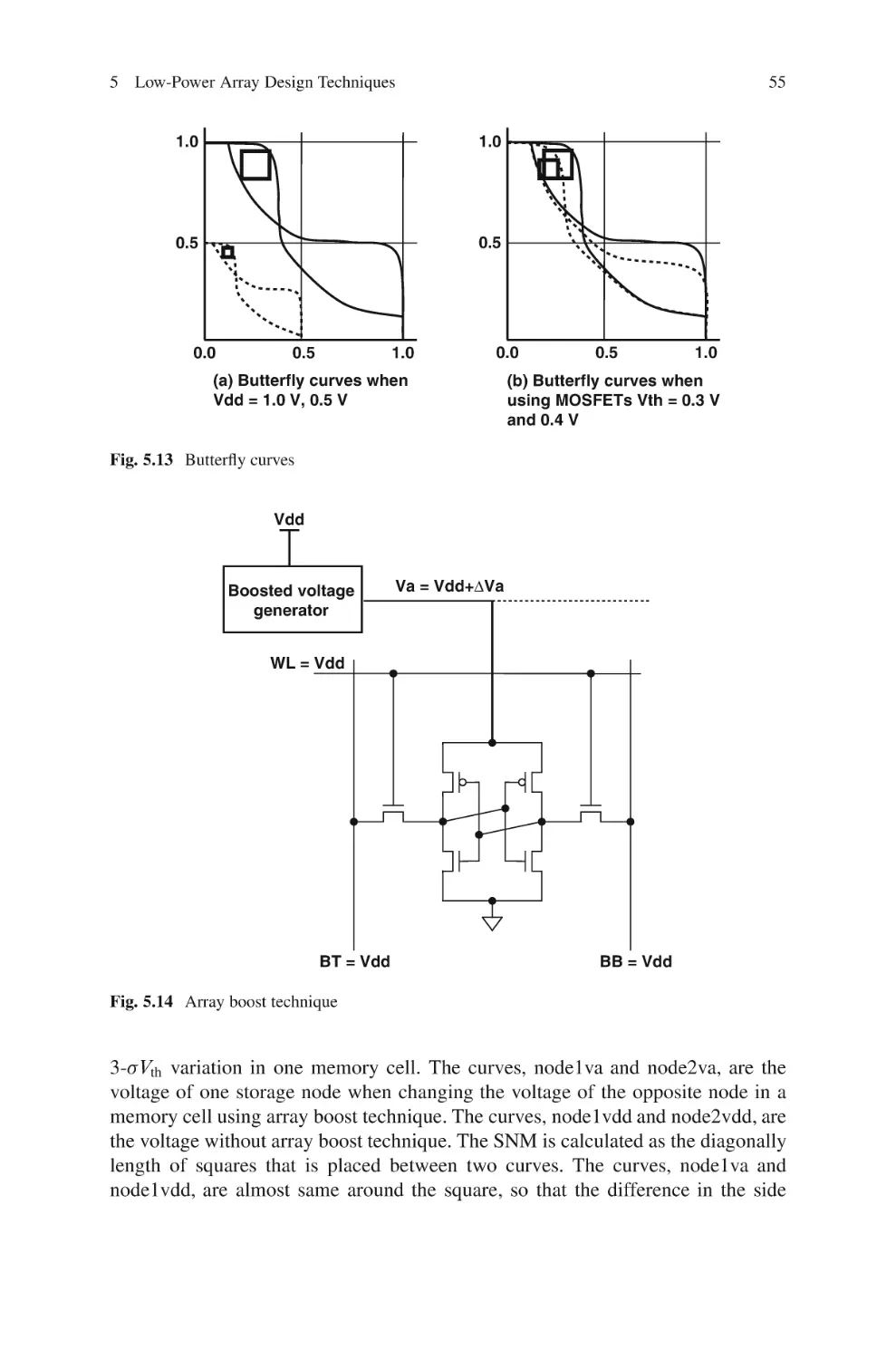
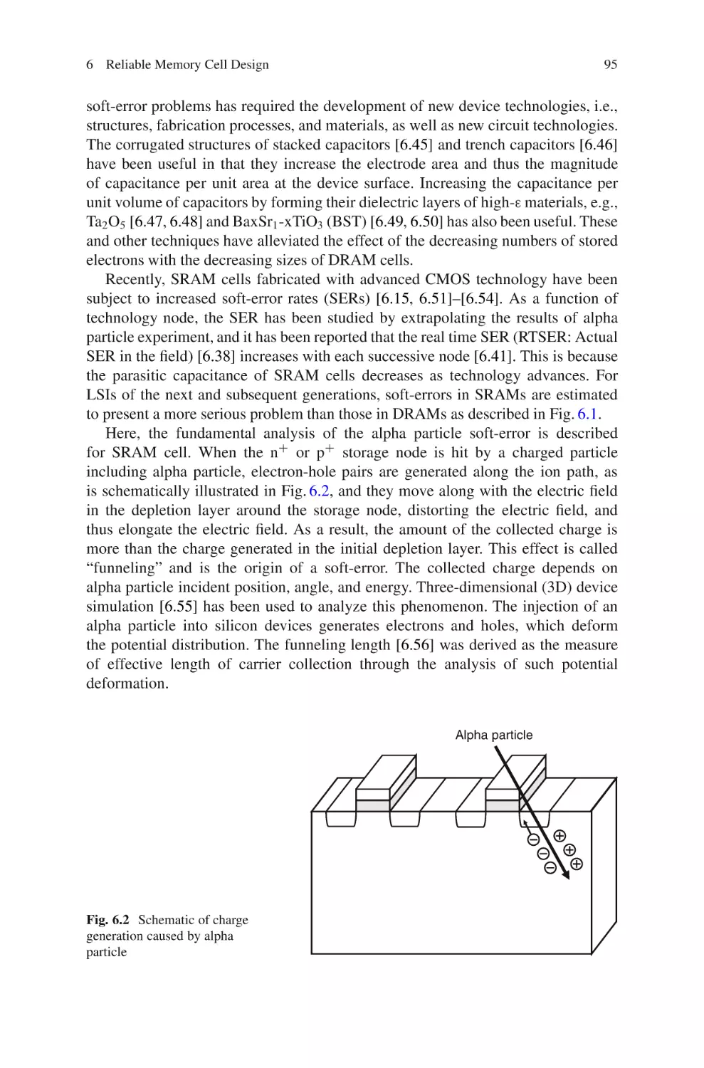
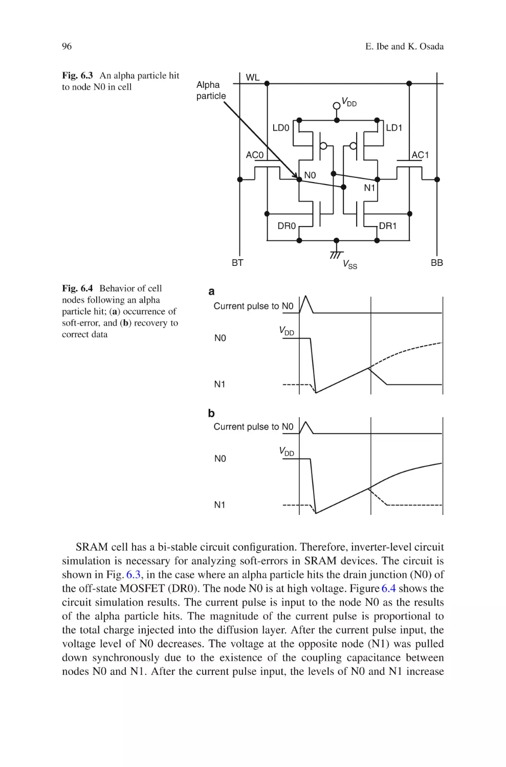
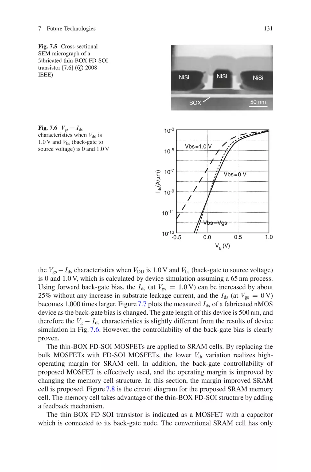
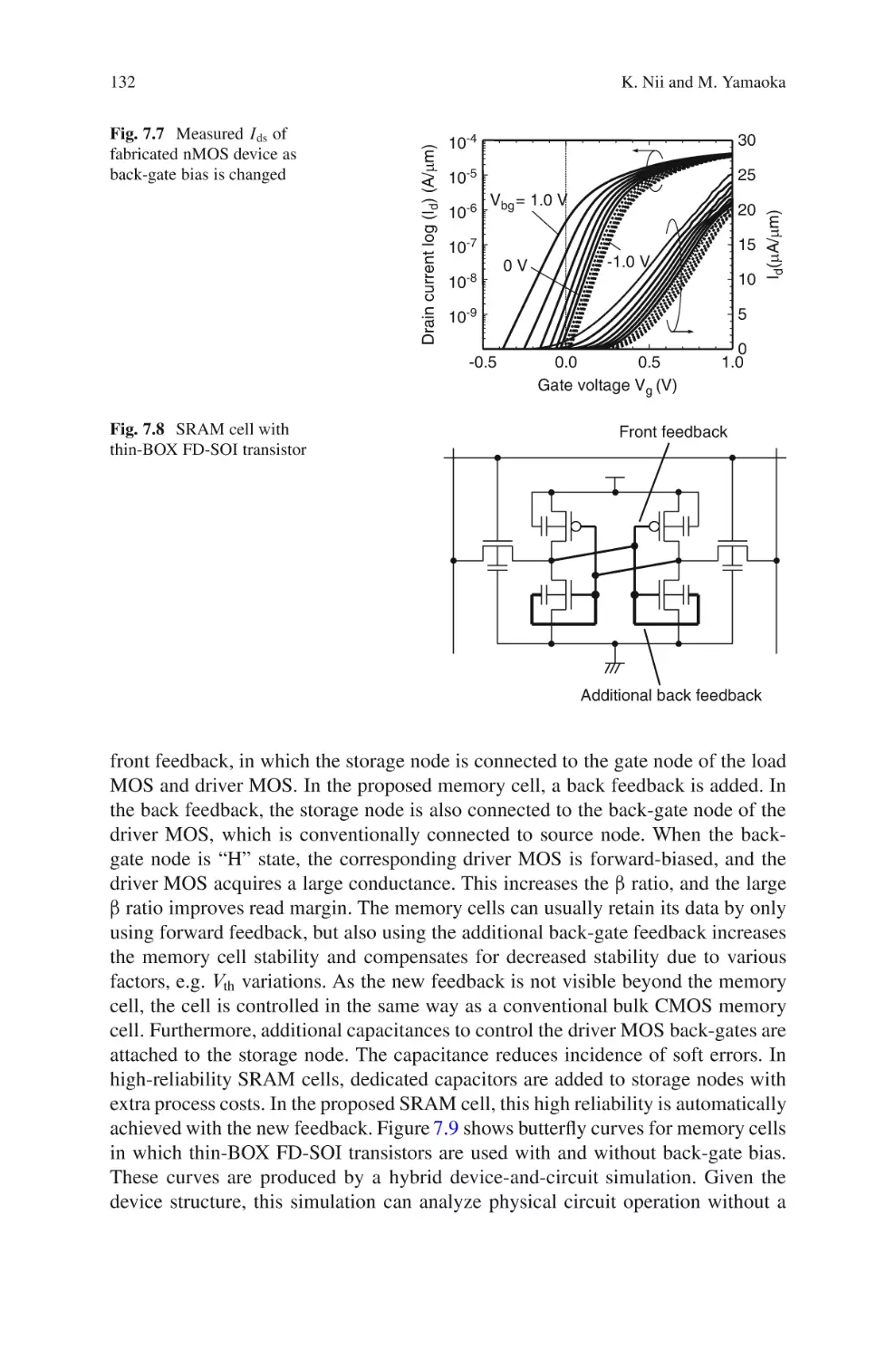
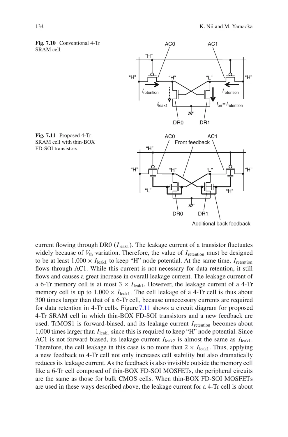
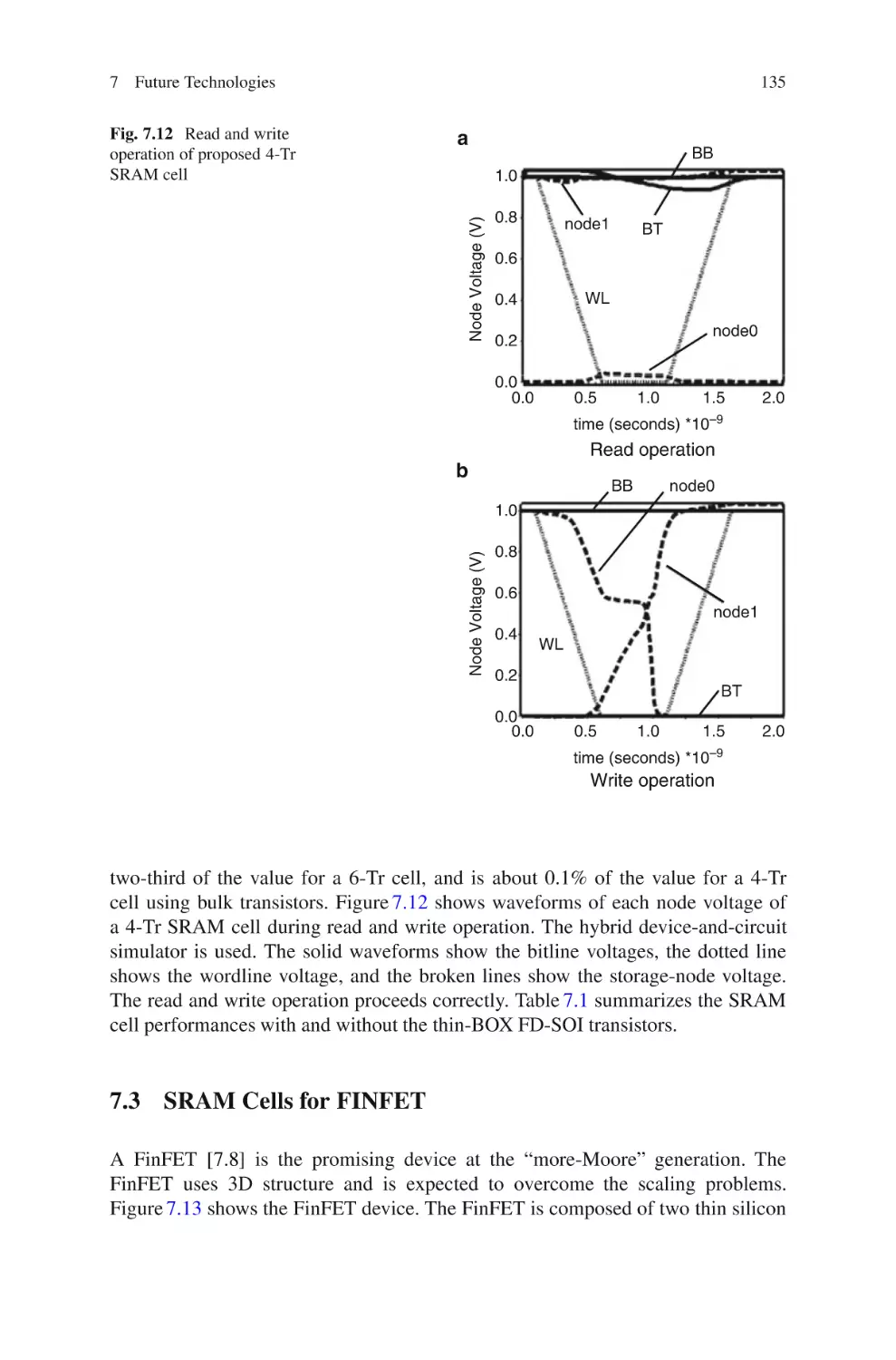
/


Текст
Springer Series in
ADVANCED MICROELECTRONICS
31
Springer Series in
ADVANCED MICROELECTRONICS
Series Editors: K. Itoh
T. Lee
T. Sakurai
W.M.C. Sansen
D. Schmitt-Landsiedel
The Springer Series in Advanced Microelectronics provides systematic information on all the
topics relevant for the design, processing, and manufacturing of microelectronic devices. The
books, each prepared by leading researchers or engineers in their fields, cover the basic
and advanced aspects of topics such as wafer processing, materials, device design, device
technologies, circuit design, VLSI implementation, and subsystem technology. The series
forms a bridge between physics and engineering and the volumes will appeal to practicing
engineers as well as research scientists.
Please view available titles in Springer Series in Advanced Microelectronics
on series homepage http://www.springer.com/series/4076
Koichiro Ishibashi
Kenichi Osada
Editors
Low Power and Reliable
SRAM Memory Cell
and Array Design
With 141 Figures
123
Editors
Prof. Koichiro Ishibashi
The University of Electro-Communications
1-5-1 Chofugaoka, Chofu, Tokyo, 182-8585 Japan
ishibashi@ee.uec.ac.jp
Dr. Kenichi Osada
Hitachi Ltd.
Higashi-koigakubo 1-280, 185-8601 Kokubunji-shi, Tokyo, Japan
kenichi.osada.aj@hitachi.com
Series Editors:
Dr. Kiyoo Itoh
Hitachi Ltd., Central Research Laboratory, 1-280 Higashi-Koigakubo
Kokubunji-shi, Tokyo 185-8601, Japan
Professor Thomas Lee
Stanford University, Department of Electrical Engineering, 420 Via Palou Mall, CIS-205
Stanford, CA 94305-4070, USA
Professor Takayasu Sakurai
Center for Collaborative Research, University of Tokyo, 7-22-1 Roppongi
Minato-ku, Tokyo 106-8558, Japan
Professor Willy M. C. Sansen
Katholieke Universiteit Leuven, ESAT-MICAS, Kasteelpark Arenberg 10
3001 Leuven, Belgium
Professor Doris Schmitt-Landsiedel
Technische Universität München, Lehrstuhl für Technische Elektronik
Theresienstrasse 90, Gebäude N3, 80290 München, Germany
Springer Series in Advanced Microelectronics ISSN 1437-0387
ISBN 978-3-642-19567-9
e-ISBN 978-3-642-19568-6
DOI 10.1007/978-3-642-19568-6
Springer Heidelberg Dordrecht London New York
Library of Congress Control Number: 2011935344
c Springer-Verlag Berlin Heidelberg 2011
This work is subject to copyright. All rights are reserved, whether the whole or part of the material is
concerned, specifically the rights of translation, reprinting, reuse of illustrations, recitation, broadcasting,
reproduction on microfilm or in any other way, and storage in data banks. Duplication of this publication
or parts thereof is permitted only under the provisions of the German Copyright Law of September 9,
1965, in its current version, and permission for use must always be obtained from Springer. Violations
are liable to prosecution under the German Copyright Law.
The use of general descriptive names, registered names, trademarks, etc. in this publication does not
imply, even in the absence of a specific statement, that such names are exempt from the relevant protective
laws and regulations and therefore free for general use.
Cover design: eStudio Calamar Steinen
Printed on acid-free paper
Springer is part of Springer Science+Business Media (www.springer.com)
Preface
As LSI industry has been growing, there appear such kinds of CMOS LSI as
Microprocessor, MCU, gate array, ASIC, FPGA, and SOC. There is no CMOS LSI
that does not use the SRAM memory cell arrays. The best reason is that the SRAM
can be fabricated by the same process as logic process, and it does not need extra
cost to fabricate. Also, SRAM cell array operates fast and consumes low power in
LSI. Despite the SRAM cell size is larger than the other RAM cell such as DRAM
cell and Flash, SRAM cell continue to be used in CMOS LSI, thanks to the natures
of the cell.
Before 90 nm technology, we can design SRAM cell for CMOS LSI without
paying attention to electrical stability, so that we could get operable SRAM bit
cell only when we connect the six transistors of the cell. However, after 90 nm
technology, we must design SRAM bit cell more carefully, because variability and
leakage of transistors in SRAM cell have become large. Also, we must pay attention
to such reliability issues as soft errors, and NBTI at low supply voltages.
This book is focusing on the design of CMOS memory cell and memory cell
array, taking low voltage operation and reliability into consideration. The authors
are specialists who have engaged in these issues for tens of years in Hitachi Ltd, and
Renesas Technology Corporation that is currently Renesas Electronics Corporation.
I believe this book can help readers understand fundamentals of CMOS SRAM
memory cell and cell array design, design methods of memory cell, and cell array
taking variability of transistors into considerations, thereby obtaining low power
and reliable SRAM arrays. This book also introduces new memory cell design
techniques those we can apply to future LSI technologies such as SOI devices.
Acknowledgments
The editors and authors express special thanks to Dr. Kiyoo Itoh of Hitachi Ltd.
for encouragement in editing this book. We also appreciate Dr. Toshiaki Masuhara,
Dr. Osamu Minato, Mr. Toshio Sasaki, and Dr. Toshifumi Shinohara for leading
v
vi
Preface
the authors in various SRAM and SOC development projects. We would like to
appreciate many colleagues, who have been working on the various projects with us.
Tokyo, April 2011
Koichiro Ishibashi
Kenichi Osada
Contents
1
Introduction . . . . . . . . . . . . . . . . . . . . . . . . . . . . . . . . . . . . . . . . . . . . . .. . . . . . . . . . . . . . . . . . . .
Koichiro Ishibashi
1.1 History and Trend of SRAM Memory Cell . . . . . . . .. . . . . . . . . . . . . . . . . . . .
1.2 Memory Cell Design Techniques and Array Design Techniques .. . . .
References . . . . . . . . . . . . . . . . . . . . . . . . . . . . . . . . . . . . . . . . . . . . . . . . .. . . . . . . . . . . . . . . . . . . .
2 Fundamentals of SRAM Memory Cell . . . . . . . . . . . . . . . .. . . . . . . . . . . . . . . . . . . .
Kenichi Osada
2.1 SRAM Cell . . . . . . . . . . . . . . . . . . . . . . . . . . . . . . . . . . . . . . . . . .. . . . . . . . . . . . . . . . . . . .
2.2 Basic Operation of SRAM Cell . . . . . . . . . . . . . . . . . . . .. . . . . . . . . . . . . . . . . . . .
2.3 Electrical Stability at Read Operation:
Static Noise Margin and ˇ Ratio . . . . . . . . . . . . . . . . . . .. . . . . . . . . . . . . . . . . . . .
Reference . . . . . . . . . . . . . . . . . . . . . . . . . . . . . . . . . . . . . . . . . . . . . . . . . .. . . . . . . . . . . . . . . . . . . .
1
1
3
4
5
5
5
9
10
3 Electrical Stability (Read and Write Operations) .. . .. . . . . . . . . . . . . . . . . . . .
Masanao Yamaoka and Yasumasa Tsukamoto
3.1 Fundamentals of Electrical Stability
on Read and Write Operations . . . . . . . . . . . . . . . . . . . . .. . . . . . . . . . . . . . . . . . . .
3.2 Vth Window Curve . . . . . . . . . . . . . . . . . . . . . . . . . . . . . . . . . .. . . . . . . . . . . . . . . . . . . .
3.3 Sensitivity Analysis .. . . . . . . . . . . . . . . . . . . . . . . . . . . . . . . .. . . . . . . . . . . . . . . . . . . .
References . . . . . . . . . . . . . . . . . . . . . . . . . . . . . . . . . . . . . . . . . . . . . . . . .. . . . . . . . . . . . . . . . . . . .
11
4 Low Power Memory Cell Design Technique . . . . . . . . . .. . . . . . . . . . . . . . . . . . . .
Kenichi Osada and Masanao Yamaoka
4.1 Fundamentals of Leakage of SRAM Array .. . . . . . .. . . . . . . . . . . . . . . . . . . .
4.1.1 Leakage Currents in an SRAM of Conventional Design.. . . . .
4.1.2 Gate-Tunnel Leakage and GIDL Currents .. . . . . . . . . . . . . . . . . . . .
4.2 Source Line Voltage Control Technique . . . . . . . . . . .. . . . . . . . . . . . . . . . . . . .
4.2.1 EFR Scheme for Low Power SRAM . . . . . .. . . . . . . . . . . . . . . . . . . .
4.2.2 Chip Architecture .. . . . . . . . . . . . . . . . . . . . . . . . . .. . . . . . . . . . . . . . . . . . . .
4.2.3 Results . . . . . . . . . . . . . . . . . . . . . . . . . . . . . . . . . . . . . . .. . . . . . . . . . . . . . . . . . . .
25
11
16
19
24
25
26
26
29
29
29
31
vii
viii
Contents
4.2.4 Source Line Voltage Control Technique
for SRAM Embedded in the Application Processor . . . . . . . . . .
4.3 LS-Cell Design for Low-Voltage Operation . . . . . . .. . . . . . . . . . . . . . . . . . . .
4.3.1 Lithographically Symmetrical Memory Cell . . . . . . . . . . . . . . . . . .
References . . . . . . . . . . . . . . . . . . . . . . . . . . . . . . . . . . . . . . . . . . . . . . . . .. . . . . . . . . . . . . . . . . . . .
5 Low-Power Array Design Techniques . . . . . . . . . . . . . . . . .. . . . . . . . . . . . . . . . . . . .
Koji Nii, Masanao Yamaoka, and Kenichi Osada
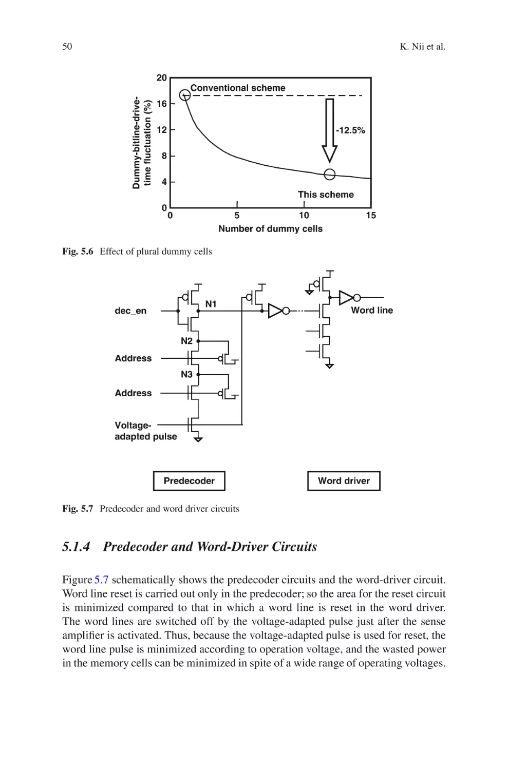
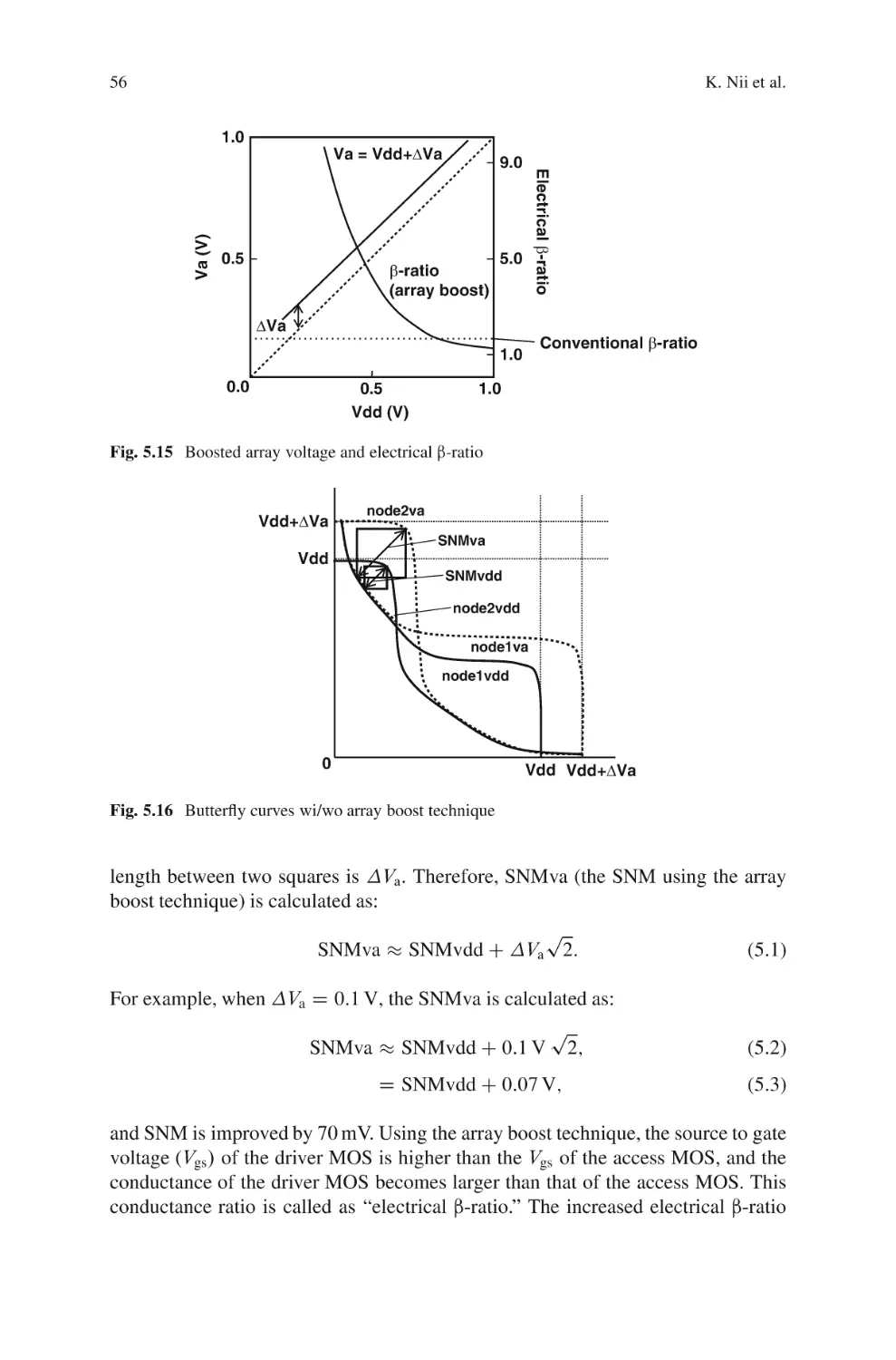
5.1 Dummy Cell Design . . . . . . . . . . . . . . . . . . . . . . . . . . . . . . . .. . . . . . . . . . . . . . . . . . . .
5.1.1 Problem with Wide-Voltage Operation . . . .. . . . . . . . . . . . . . . . . . . .
5.1.2 Block Diagram and Operation of Voltage-Adapted
Timing-Generation Scheme . . . . . . . . . . . . . . . .. . . . . . . . . . . . . . . . . . . .
5.1.3 Timing Diagram and Effect of Voltage-Adapted
Timing-Generation Scheme . . . . . . . . . . . . . . . .. . . . . . . . . . . . . . . . . . . .
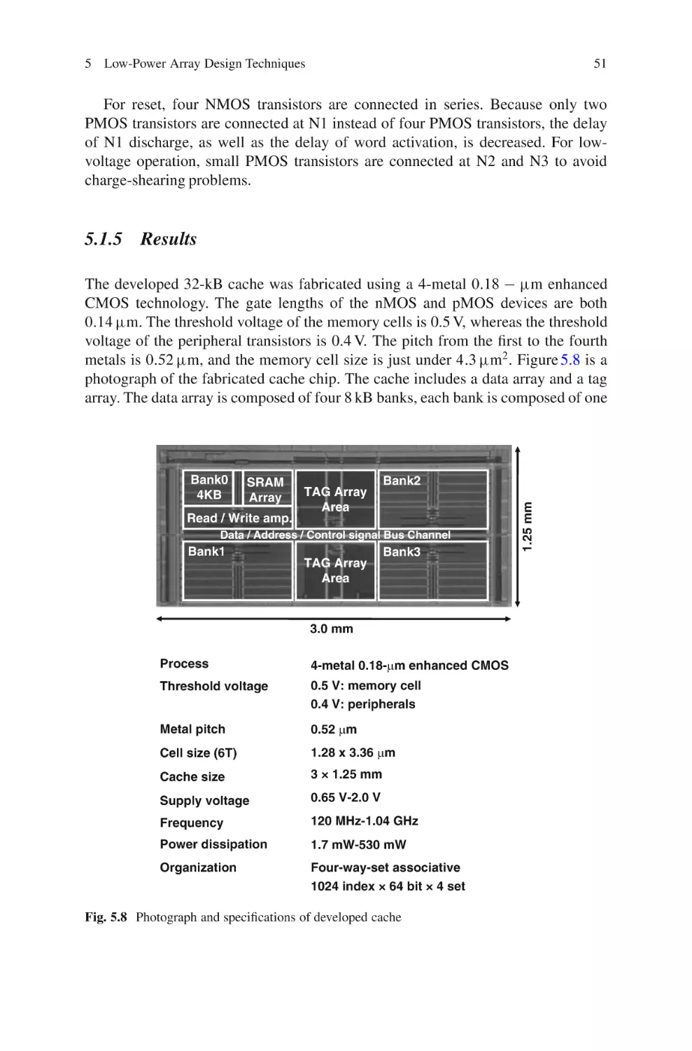
5.1.4 Predecoder and Word-Driver Circuits . . . . .. . . . . . . . . . . . . . . . . . . .
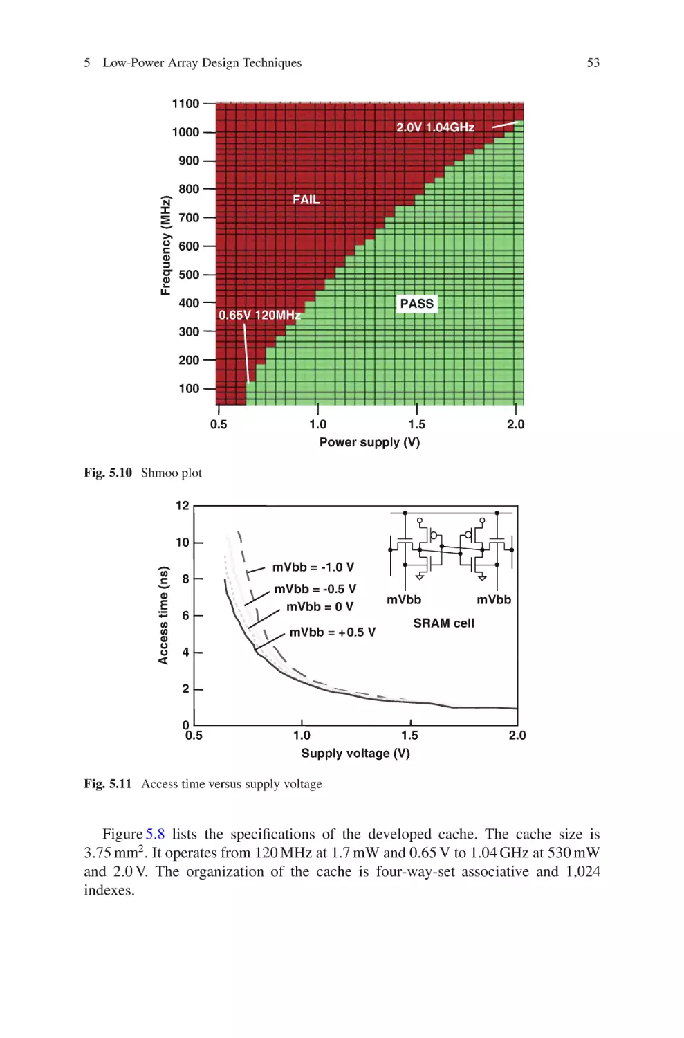
5.1.5 Results . . . . . . . . . . . . . . . . . . . . . . . . . . . . . . . . . . . . . . .. . . . . . . . . . . . . . . . . . . .
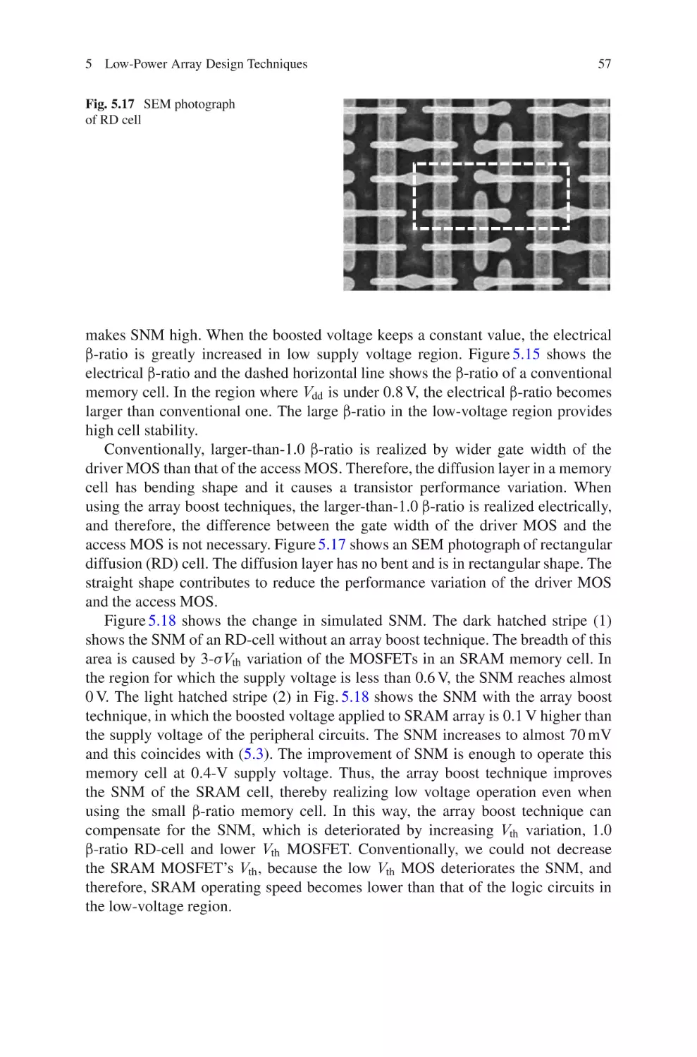
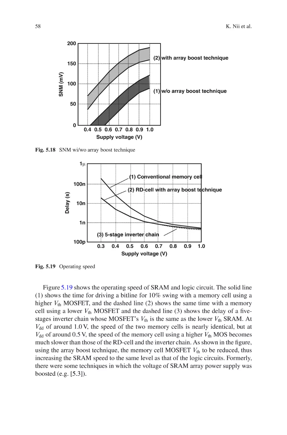
5.2 Array Boost Technique . . . . . . . . . . . . . . . . . . . . . . . . . . . . .. . . . . . . . . . . . . . . . . . . .
5.3 Read and Write Stability Assisting Circuits . . . . . . .. . . . . . . . . . . . . . . . . . . .
5.3.1 Concept of Improving Read Stability . . . . . .. . . . . . . . . . . . . . . . . . . .
5.3.2 Variation Tolerant Read Assist Circuits . . .. . . . . . . . . . . . . . . . . . . .
5.3.3 Variation Tolerant Write Assist Circuits . . .. . . . . . . . . . . . . . . . . . . .
5.3.4 Simulation Result . . . . . . . . . . . . . . . . . . . . . . . . . . .. . . . . . . . . . . . . . . . . . . .
5.3.5 Fabrications and Evaluations in 45-nm Technology . . . . . . . . . .
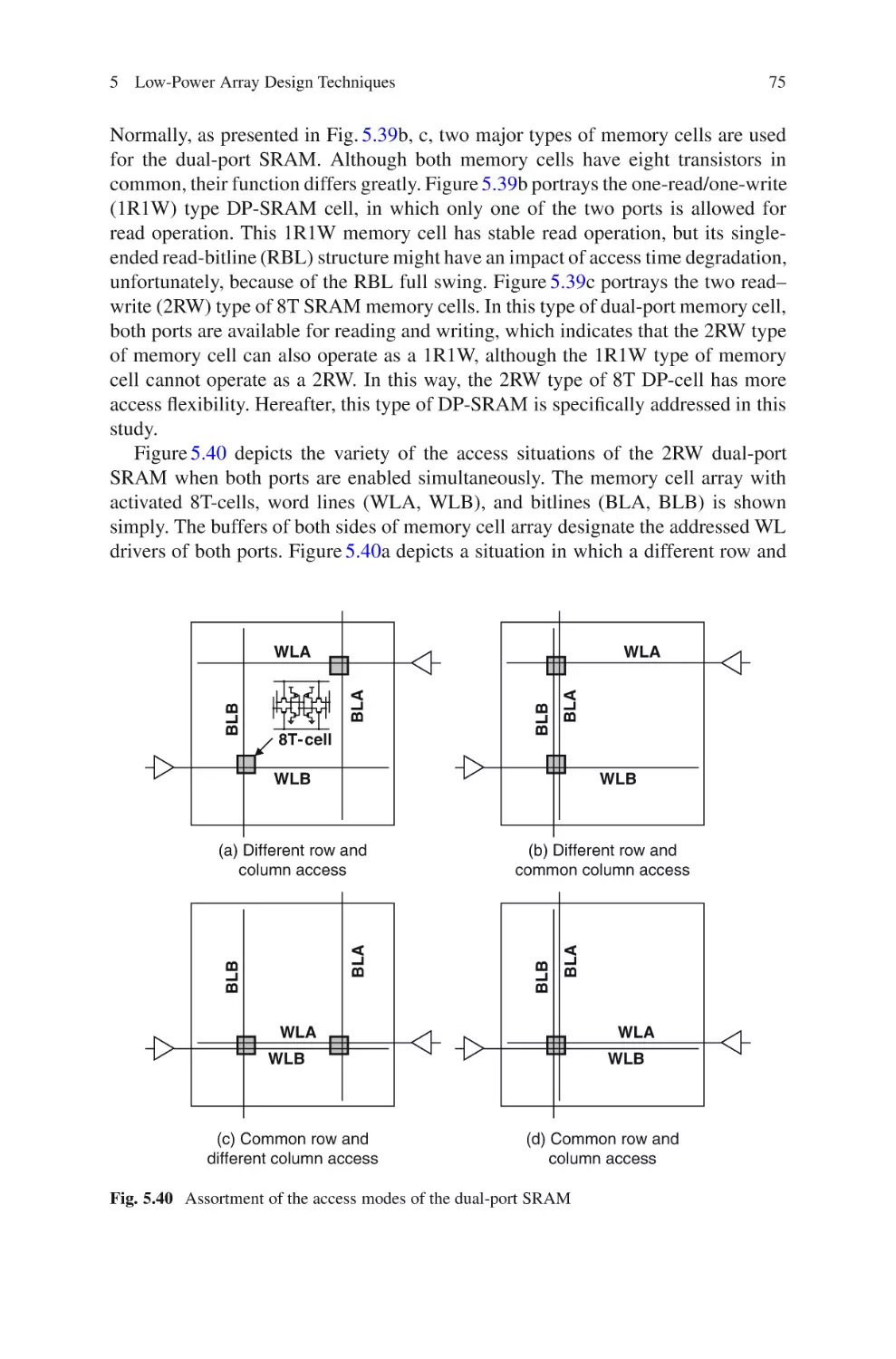
5.4 Dual-Port Array Design Techniques . . . . . . . . . . . . . . .. . . . . . . . . . . . . . . . . . . .
5.4.1 Access Conflict Issue of Dual-Port SRAM . . . . . . . . . . . . . . . . . . . .
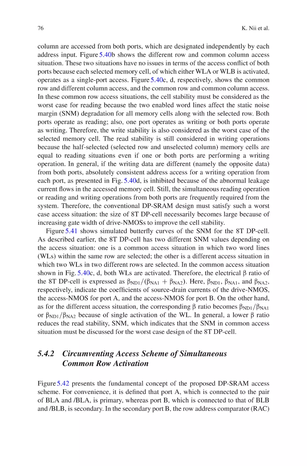
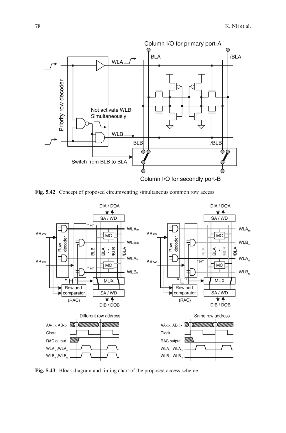
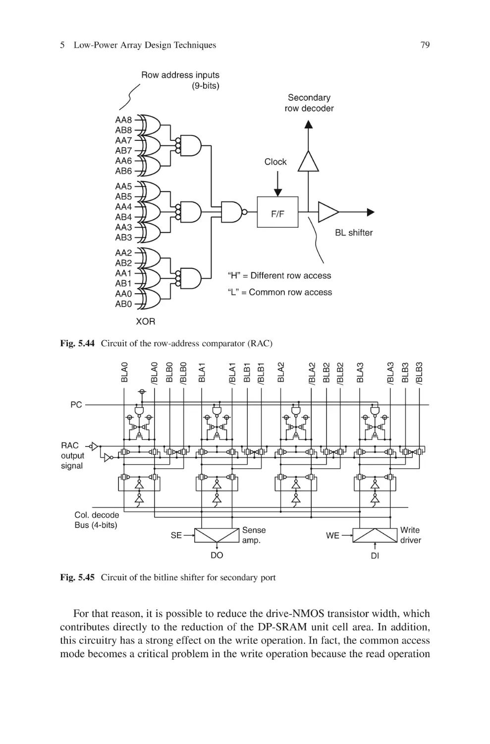
5.4.2 Circumventing Access Scheme of Simultaneous
Common Row Activation . . . . . . . . . . . . . . . . . .. . . . . . . . . . . . . . . . . . . .
5.4.3 8T Dual-Port Cell Design . . . . . . . . . . . . . . . . . .. . . . . . . . . . . . . . . . . . . .
5.4.4 Simulated Butterfly Curves for SNM . . . . . .. . . . . . . . . . . . . . . . . . . .
5.4.5 Cell Stability Analysis .. . . . . . . . . . . . . . . . . . . . .. . . . . . . . . . . . . . . . . . . .
5.4.6 Standby Leakage .. . . . . . . . . . . . . . . . . . . . . . . . . . .. . . . . . . . . . . . . . . . . . . .
5.4.7 Design and Fabrication of Test Chip . . . . . . .. . . . . . . . . . . . . . . . . . . .
5.4.8 Measurement Result . . . . . . . . . . . . . . . . . . . . . . . .. . . . . . . . . . . . . . . . . . . .
References . . . . . . . . . . . . . . . . . . . . . . . . . . . . . . . . . . . . . . . . . . . . . . . . .. . . . . . . . . . . . . . . . . . . .
32
36
37
40
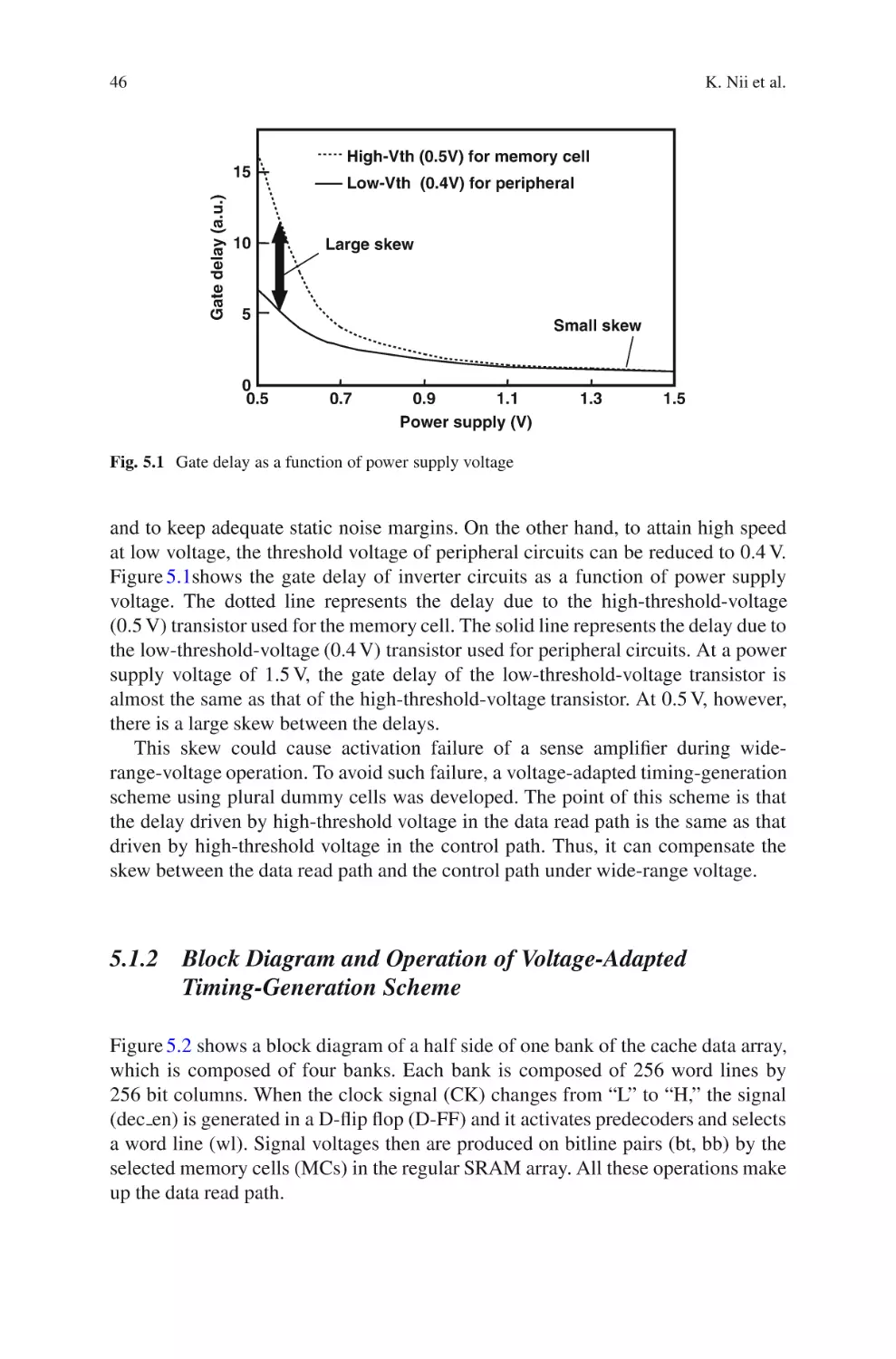
43
45
45
46
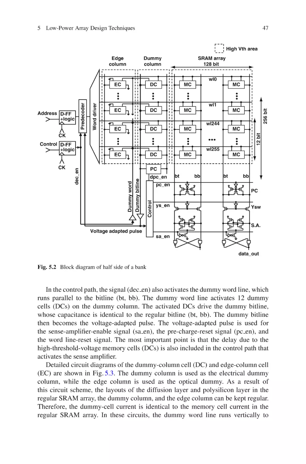
48
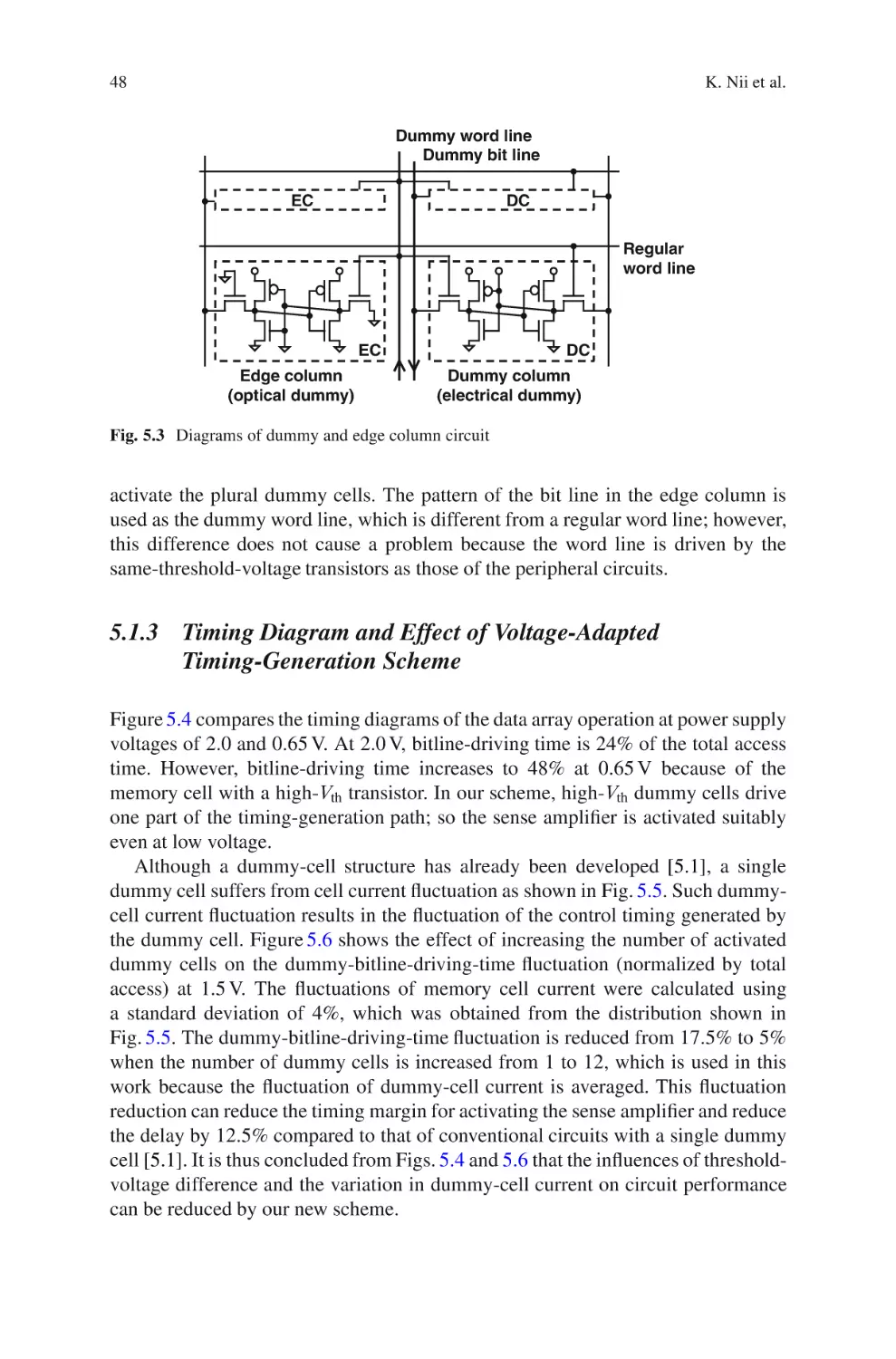
50
51
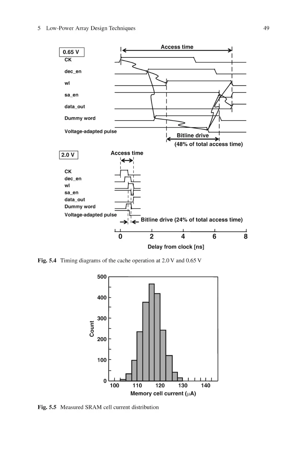
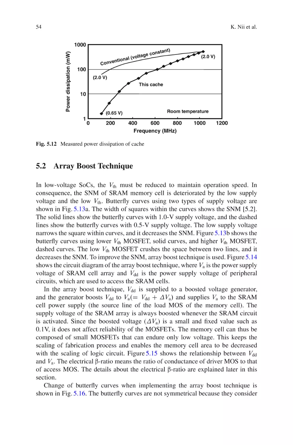
54
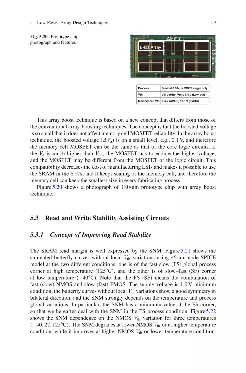
59
59
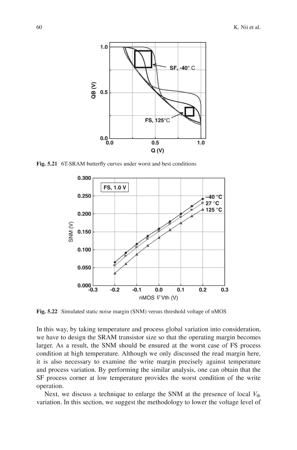
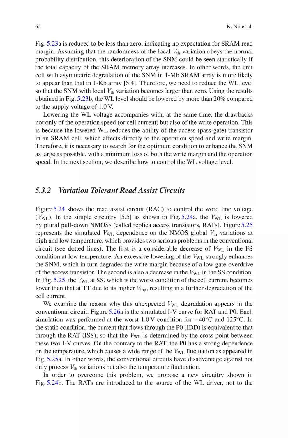
62
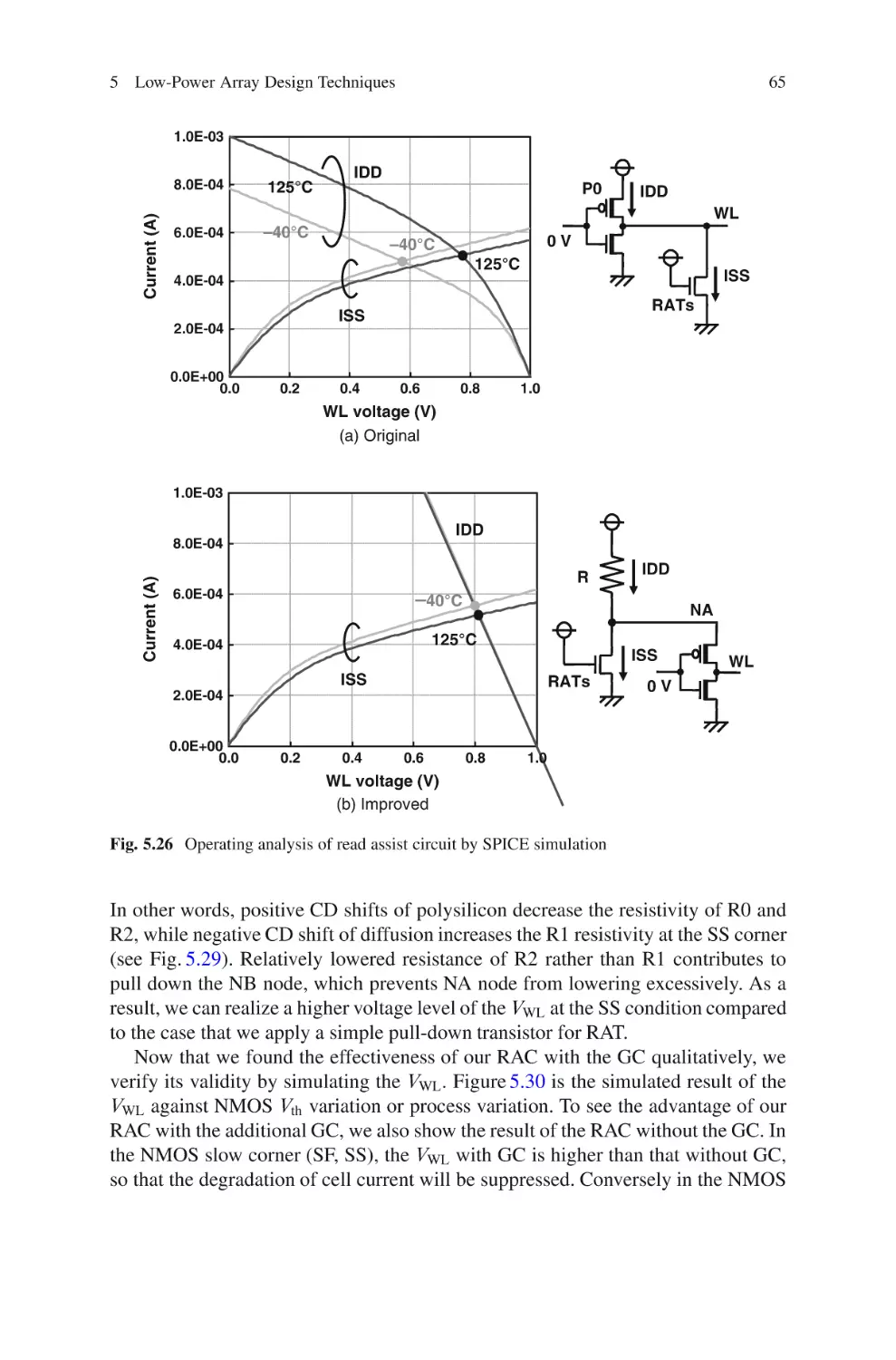
67
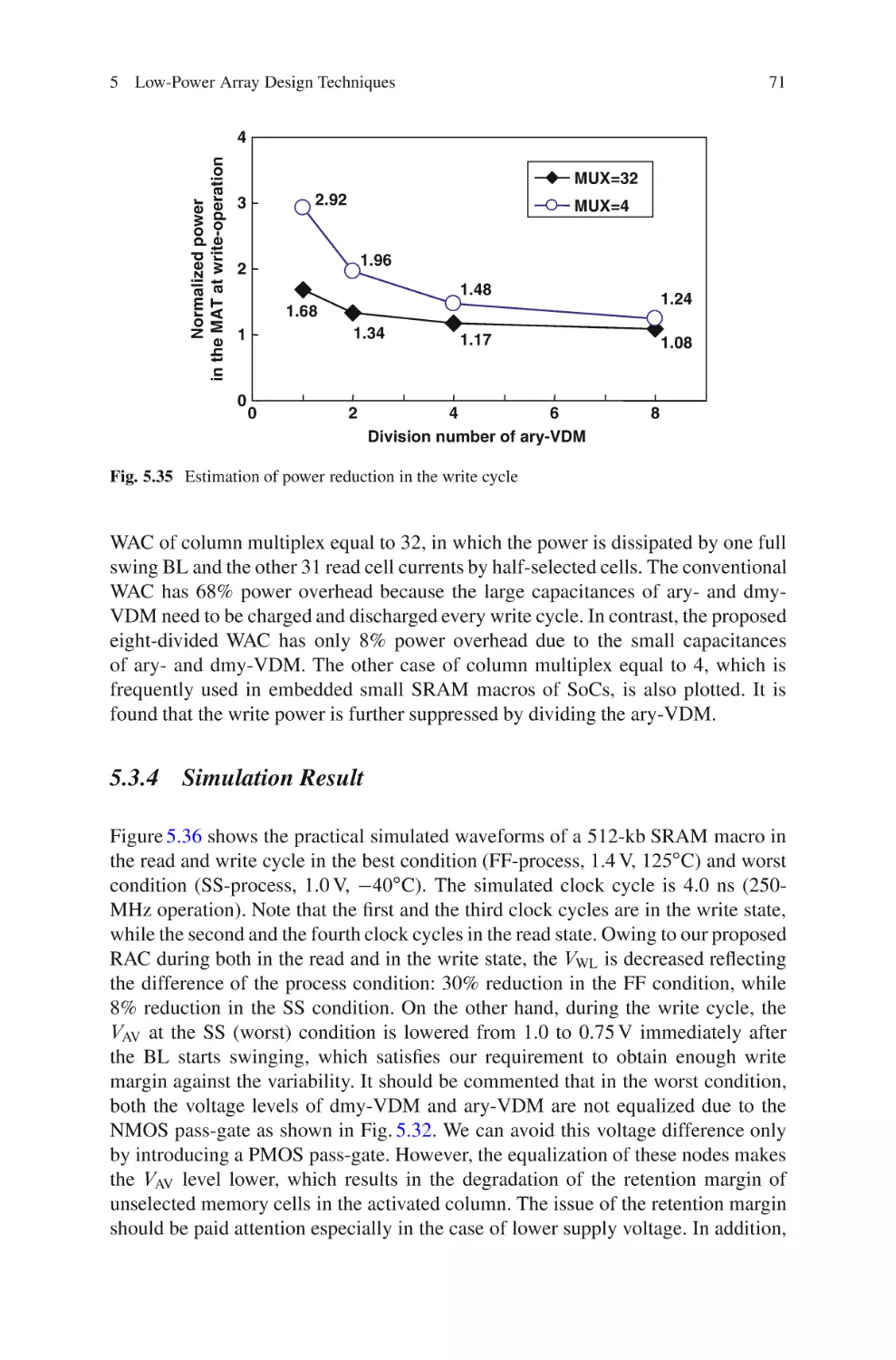
71
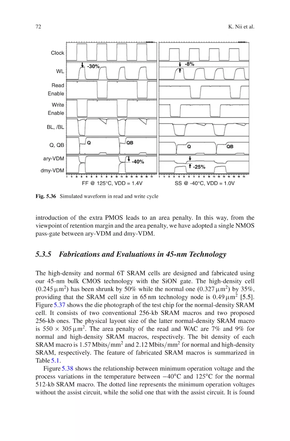
72
74
74
76
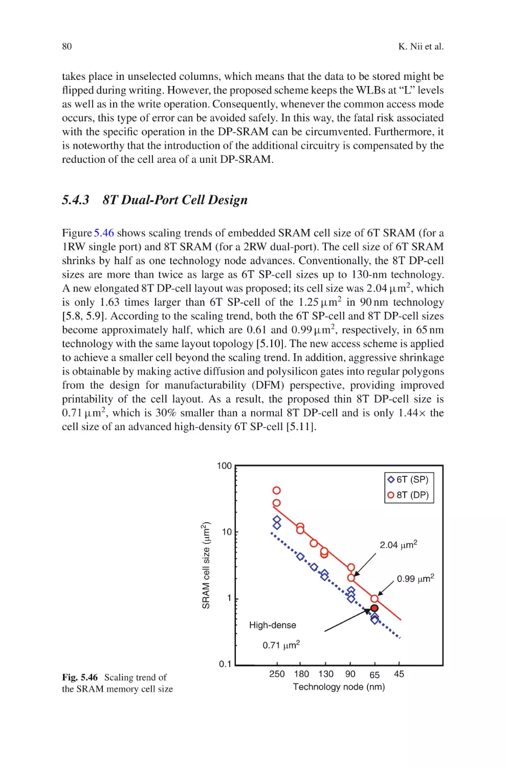
80
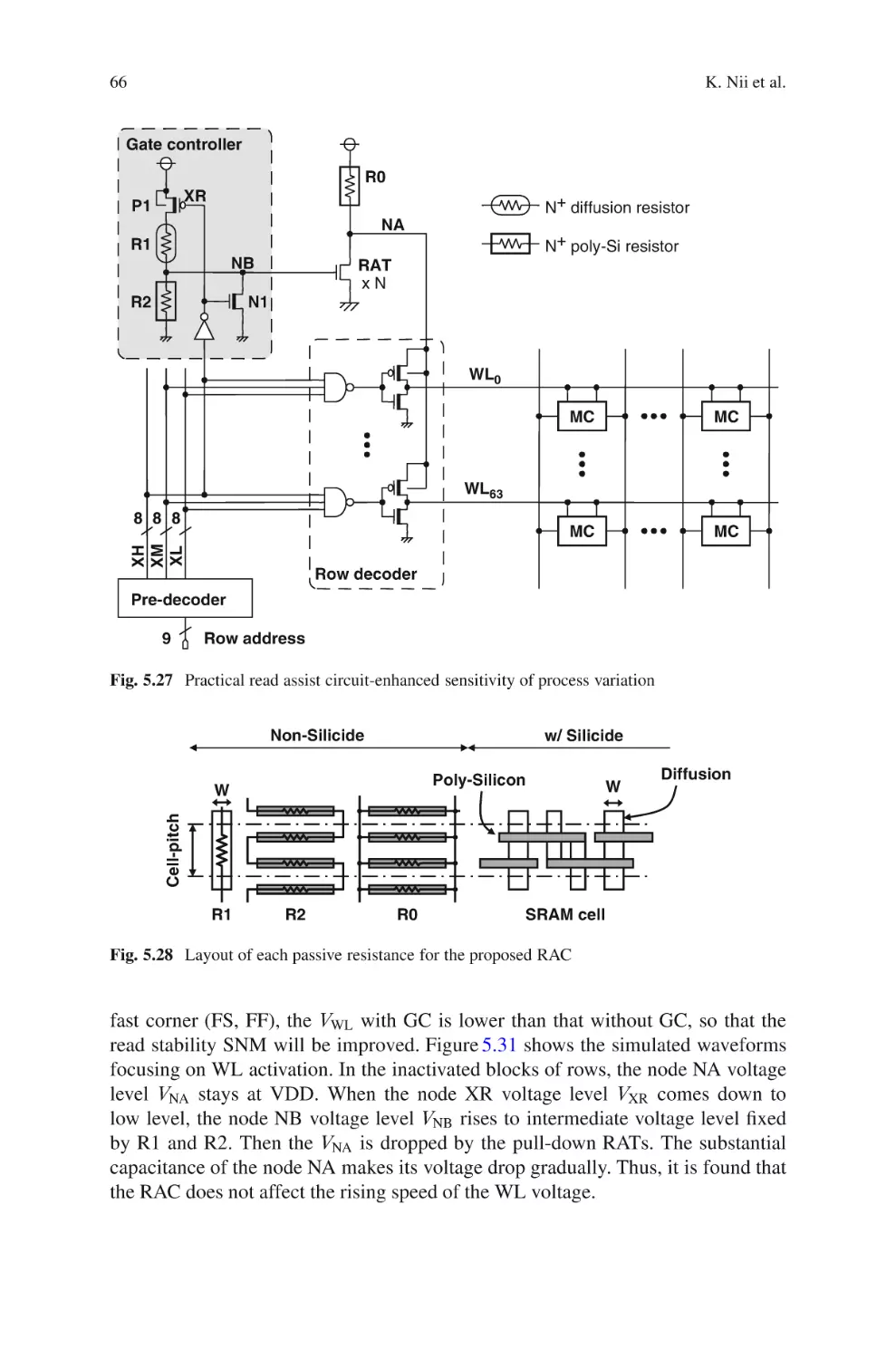
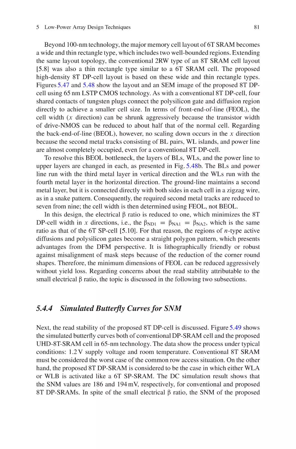
81
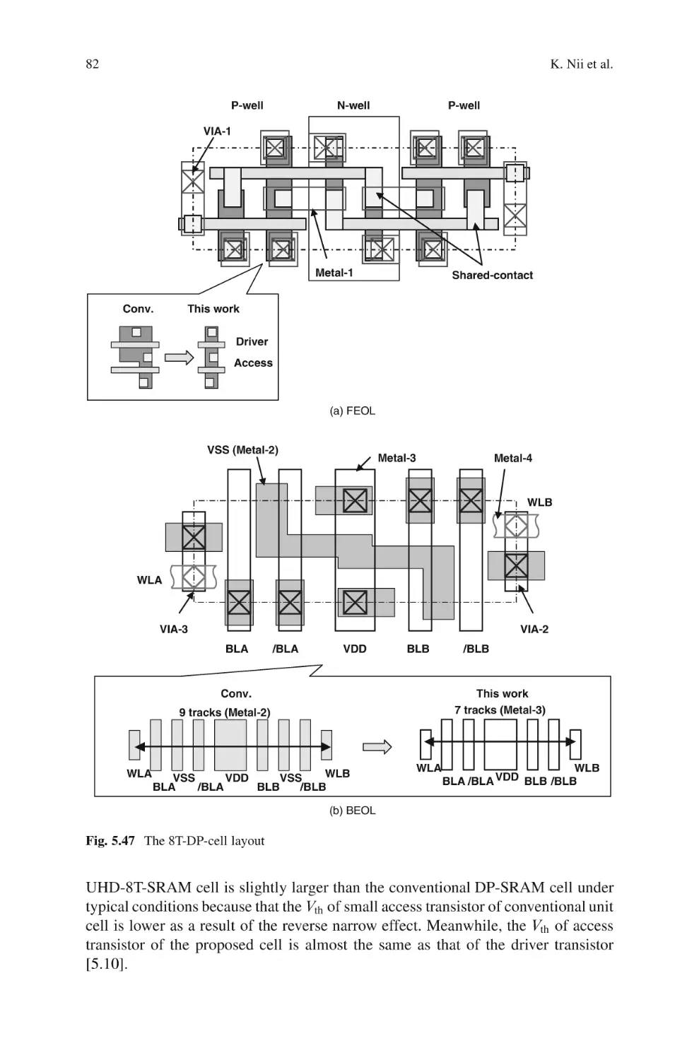
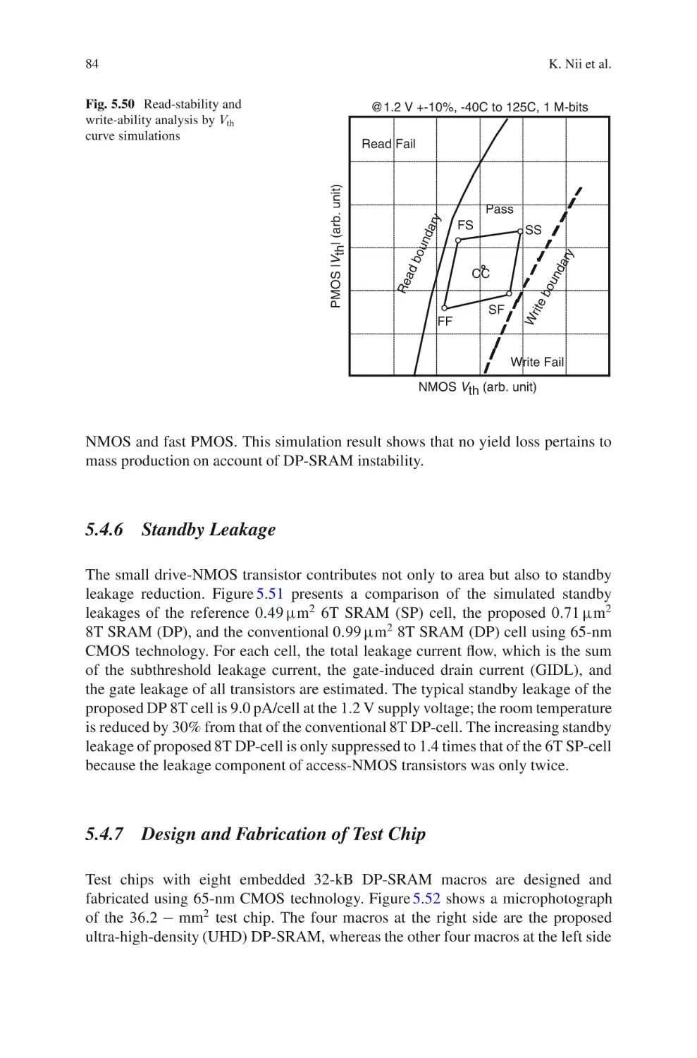
83
84
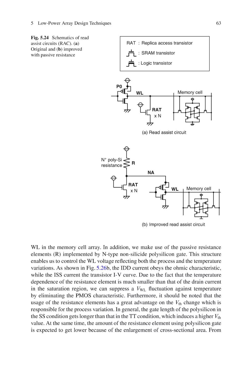
84
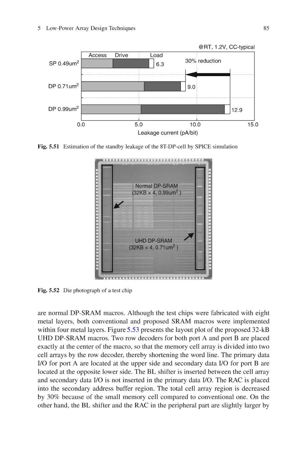
86
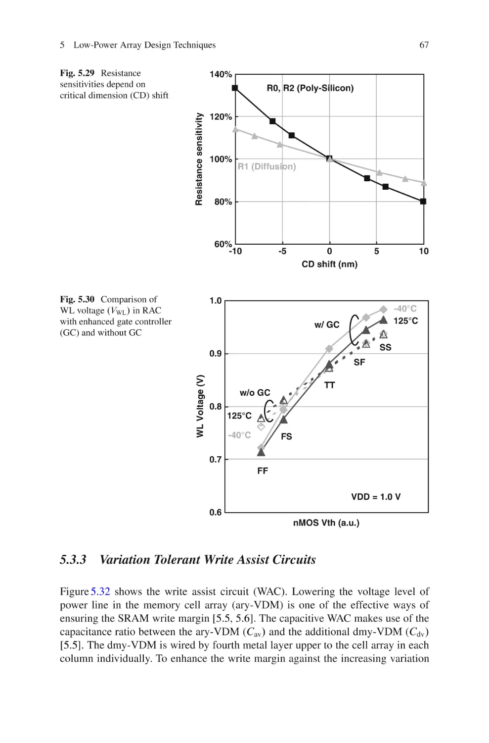
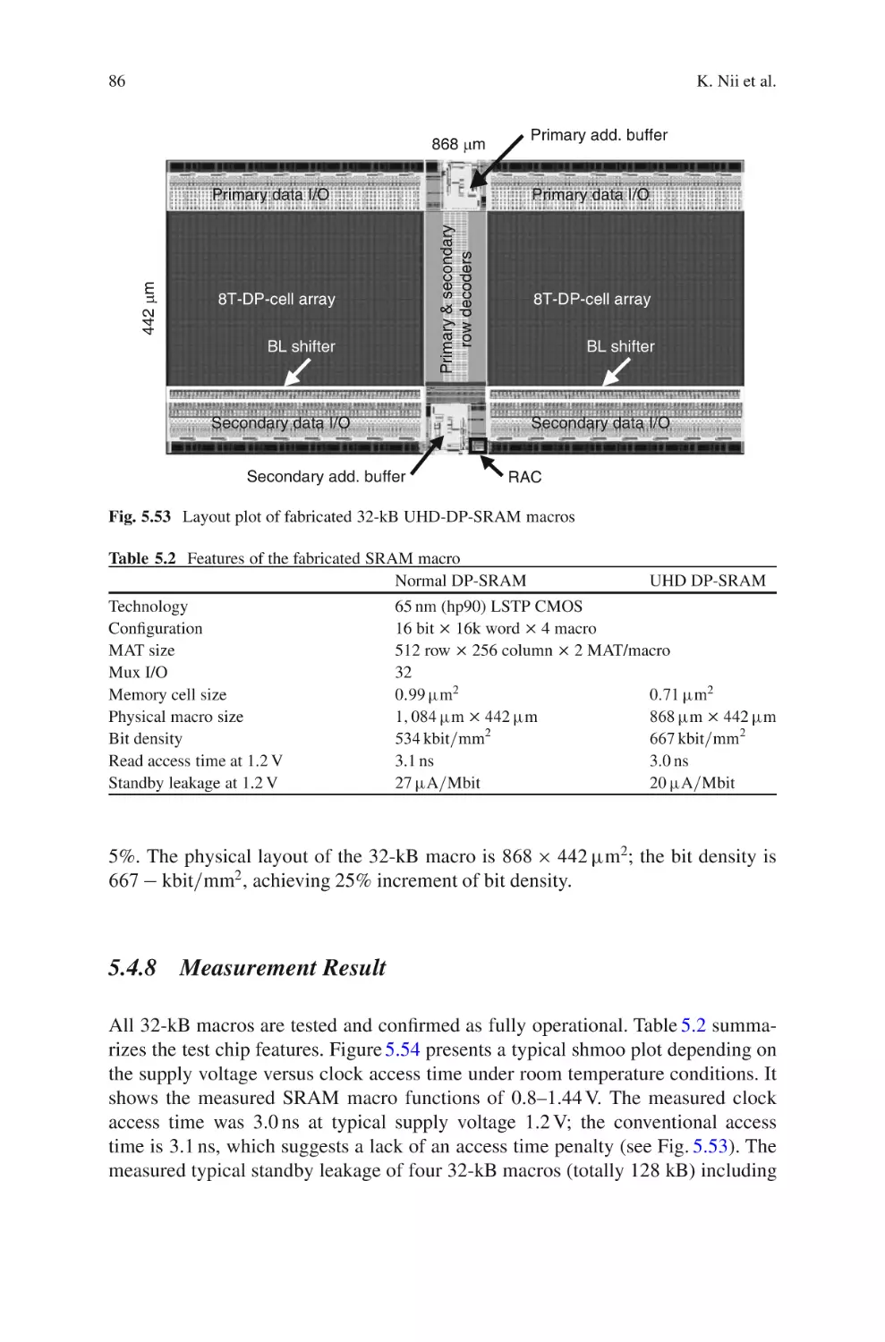
87
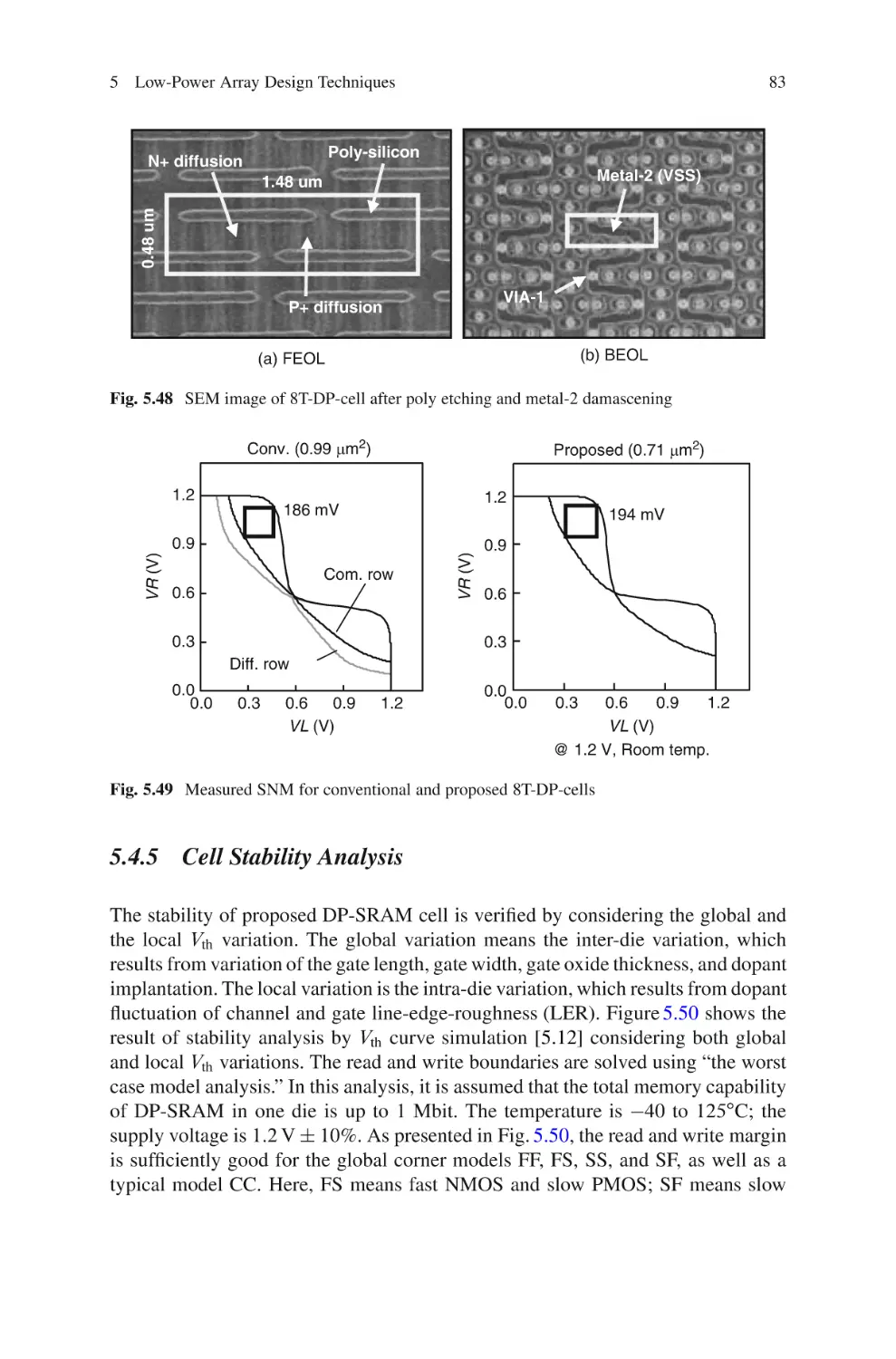
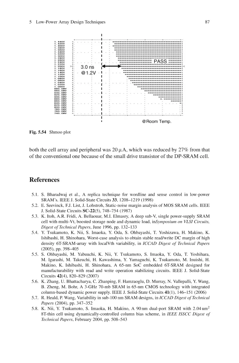
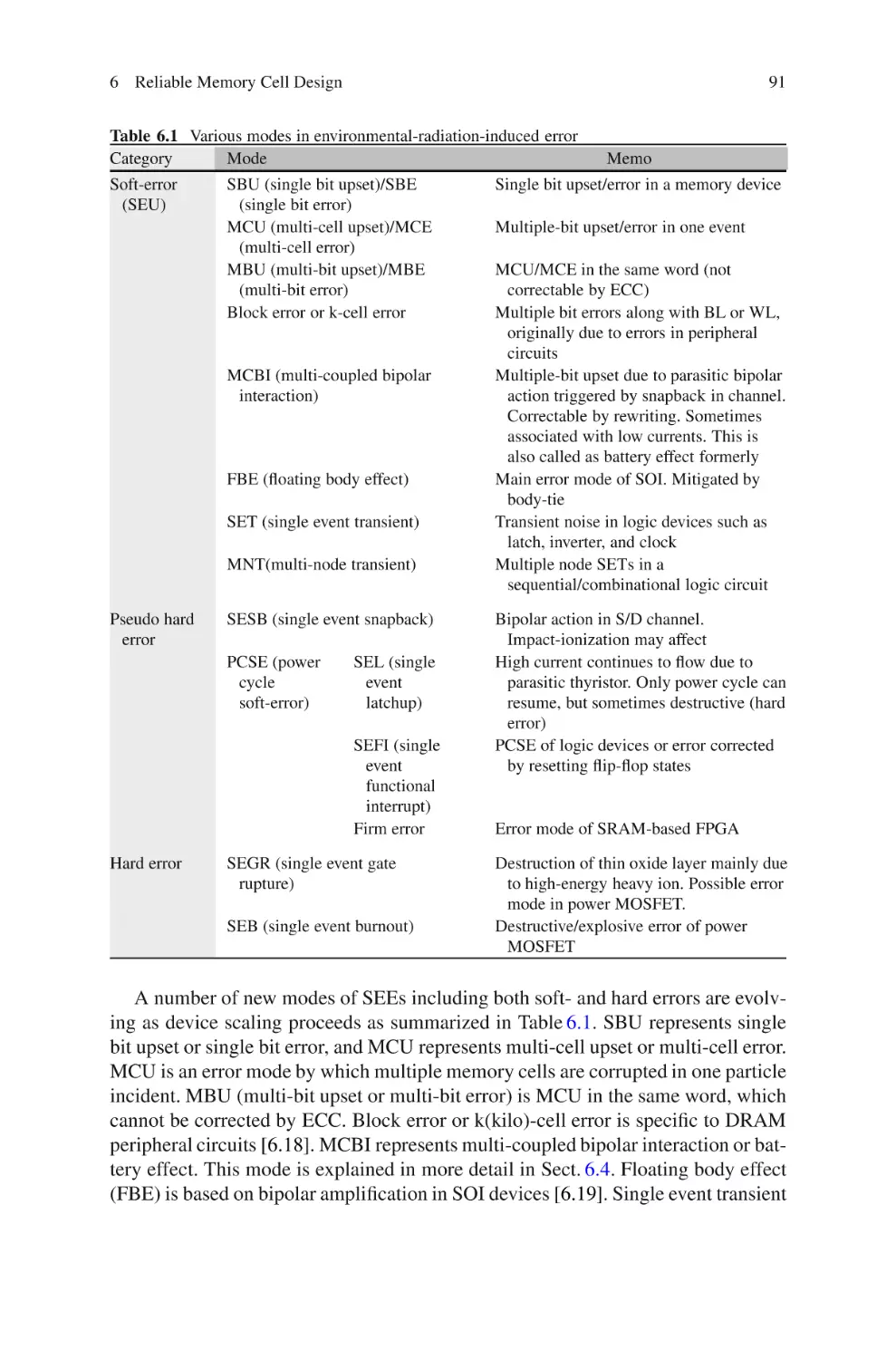
6 Reliable Memory Cell Design for Environmental
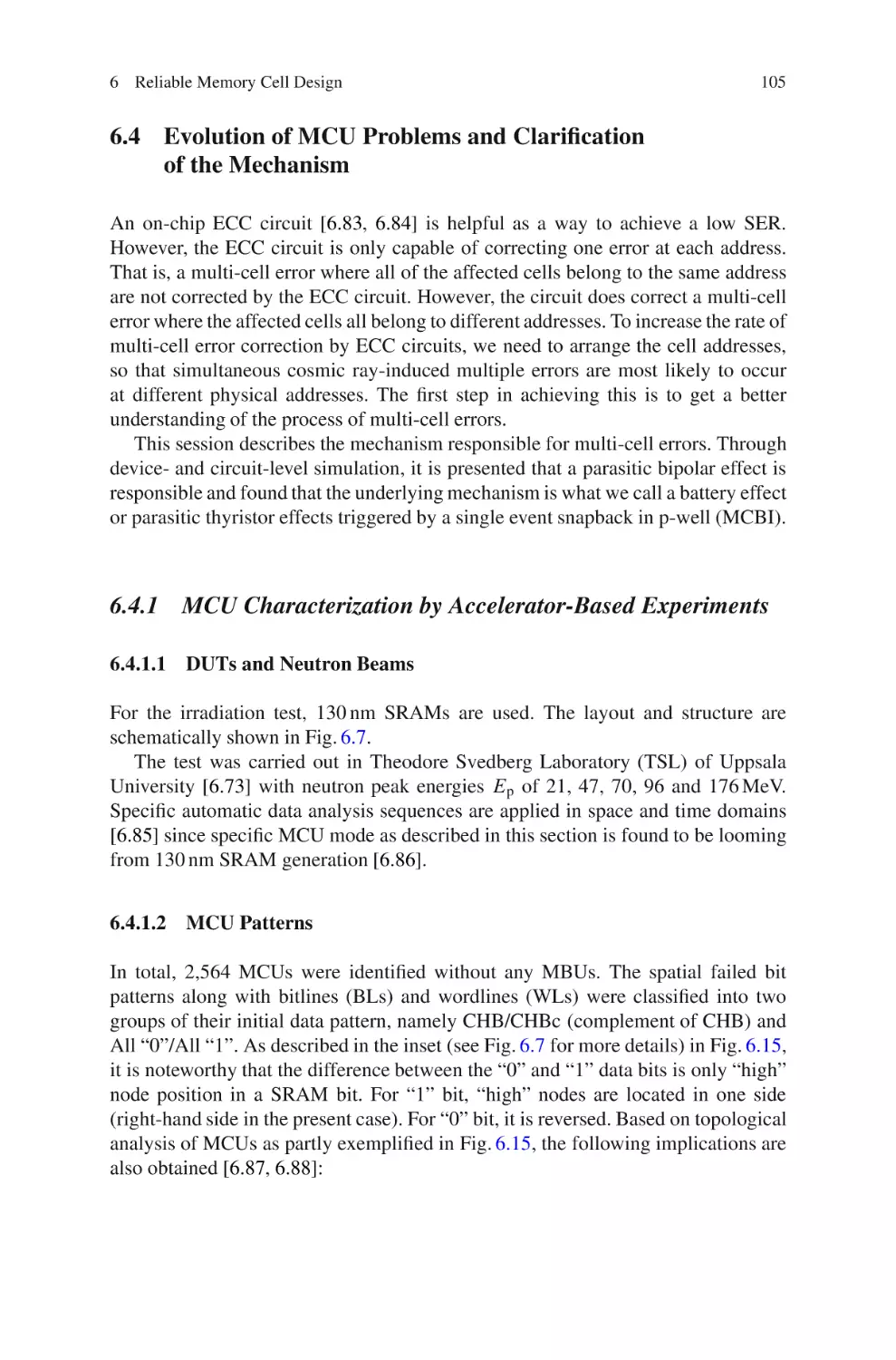
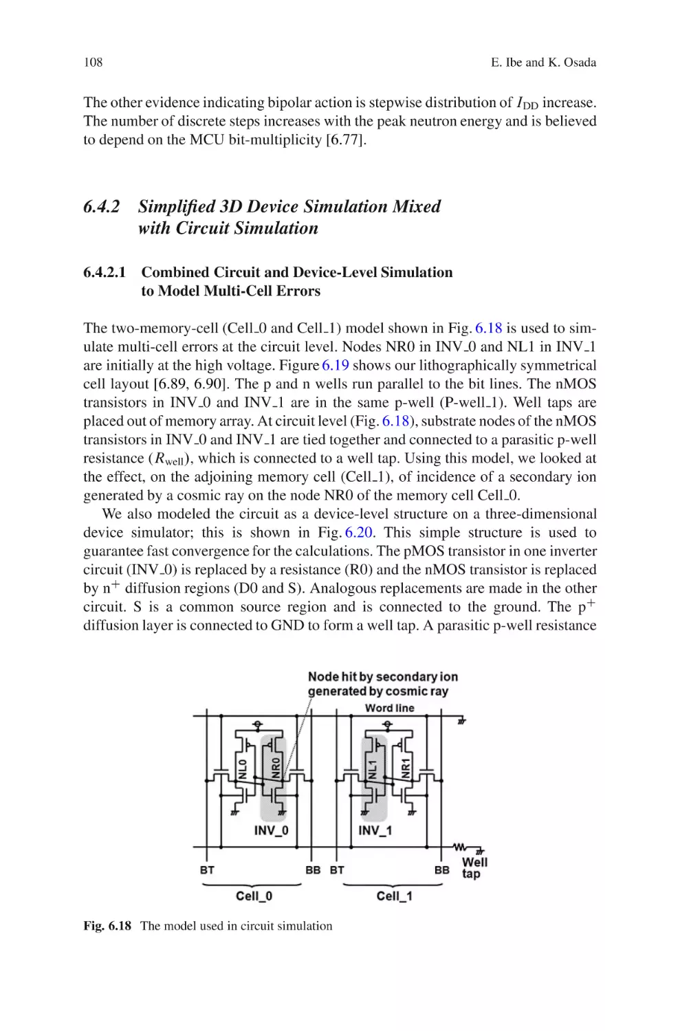
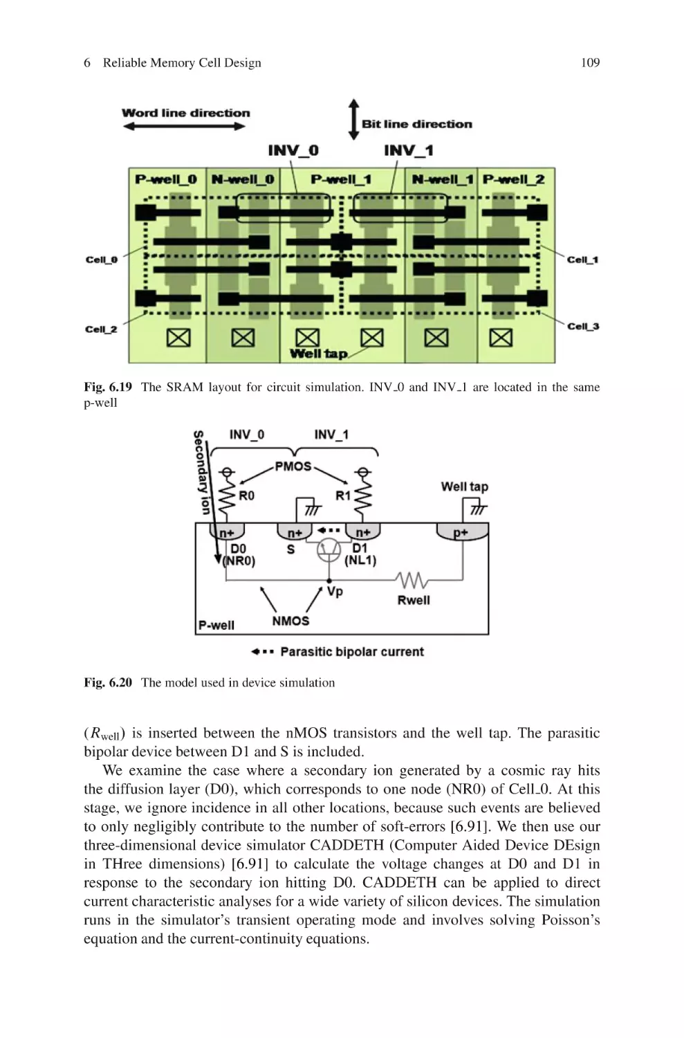
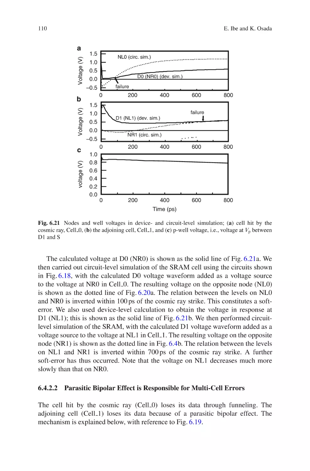
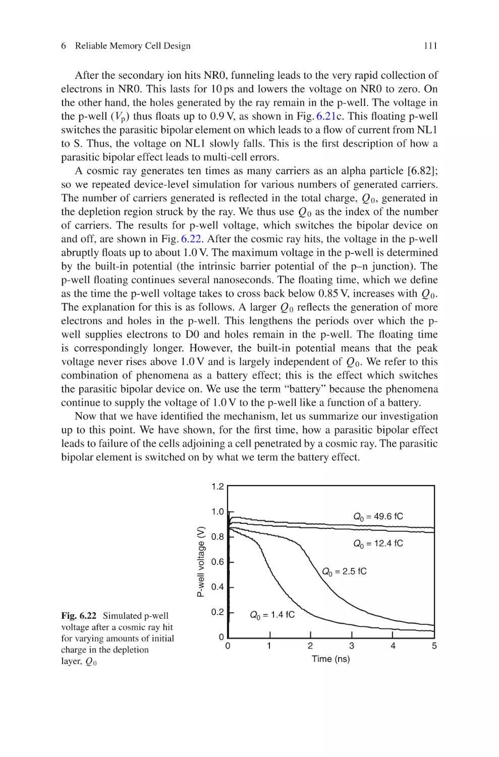
Radiation-Induced Failures in SRAM . . . . . . . . . . . . . . . . .. . . . . . . . . . . . . . . . . . . . 89
Eishi Ibe and Kenichi Osada
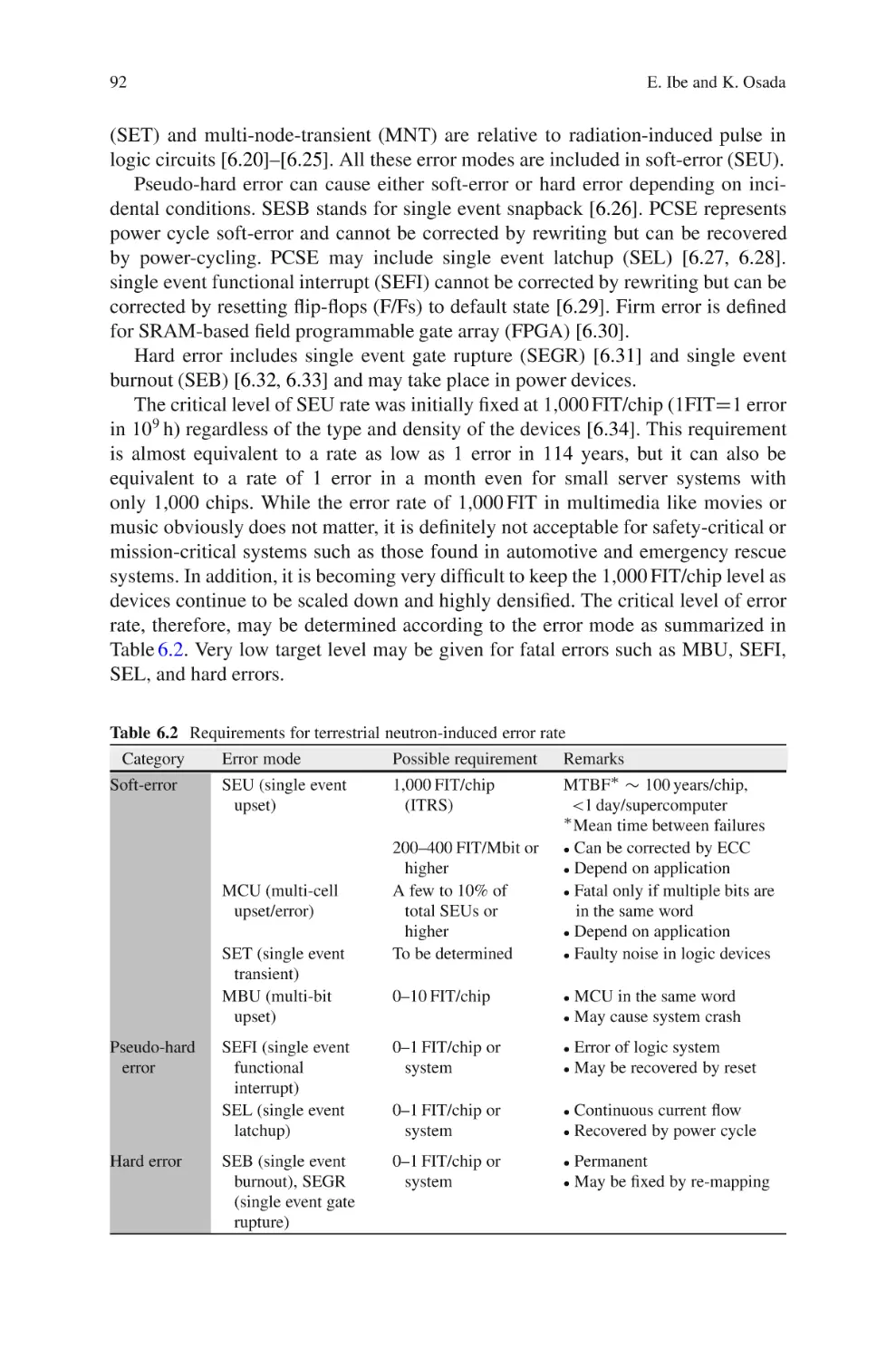
6.1 Fundamentals of SER in SRAM Cell . . . . . . . . . . . . . .. . . . . . . . . . . . . . . . . . . . 90
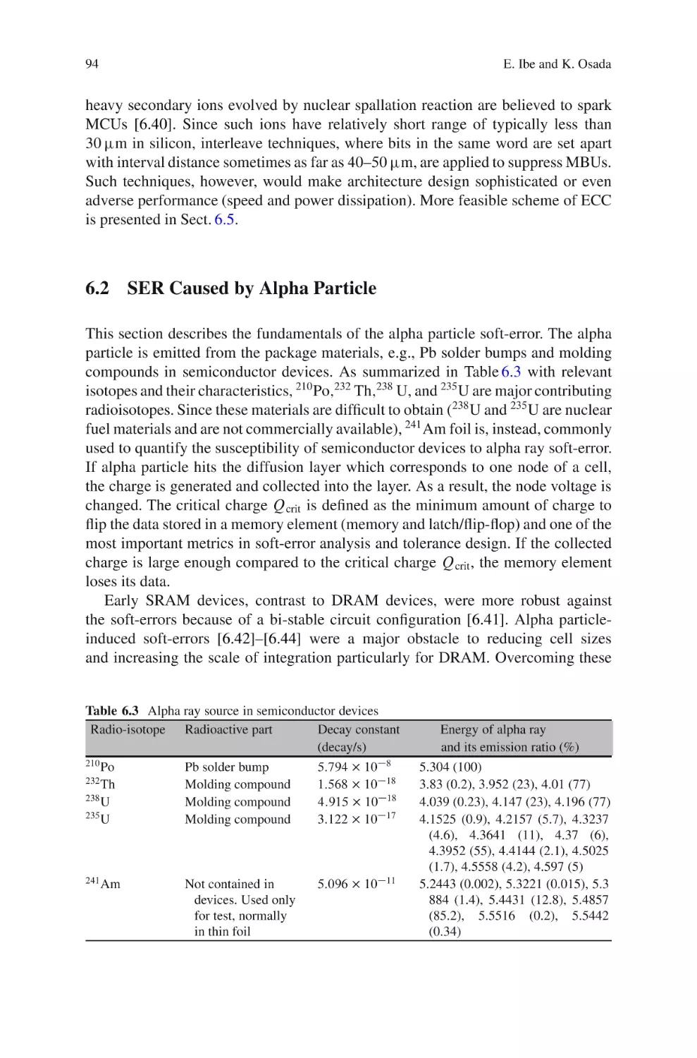
6.2 SER Caused by Alpha Particle . . . . . . . . . . . . . . . . . . . . .. . . . . . . . . . . . . . . . . . . . 94
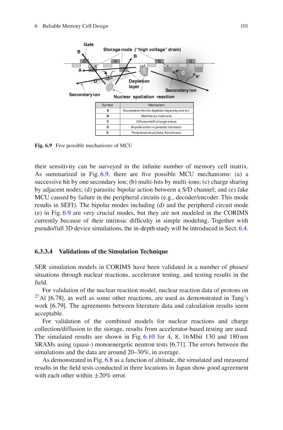
6.3 SER Caused by Neutrons and Its Quantification . .. . . . . . . . . . . . . . . . . . . . 97
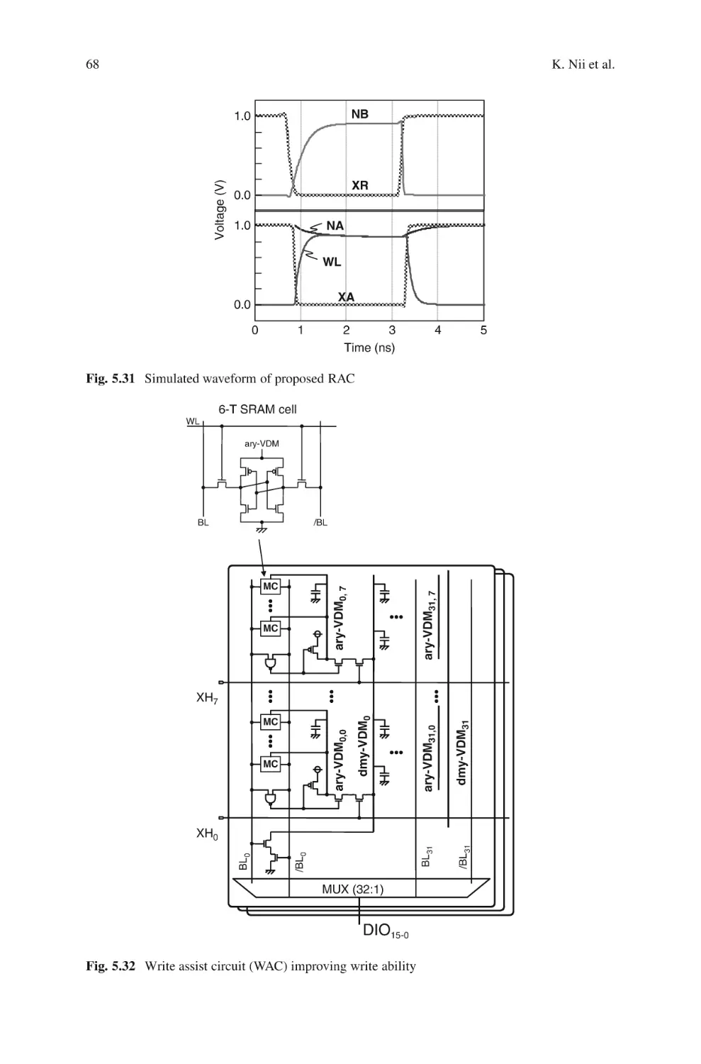
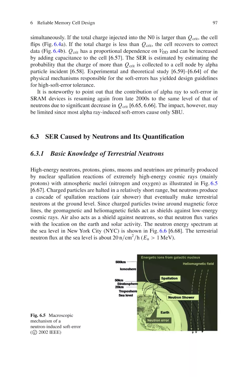
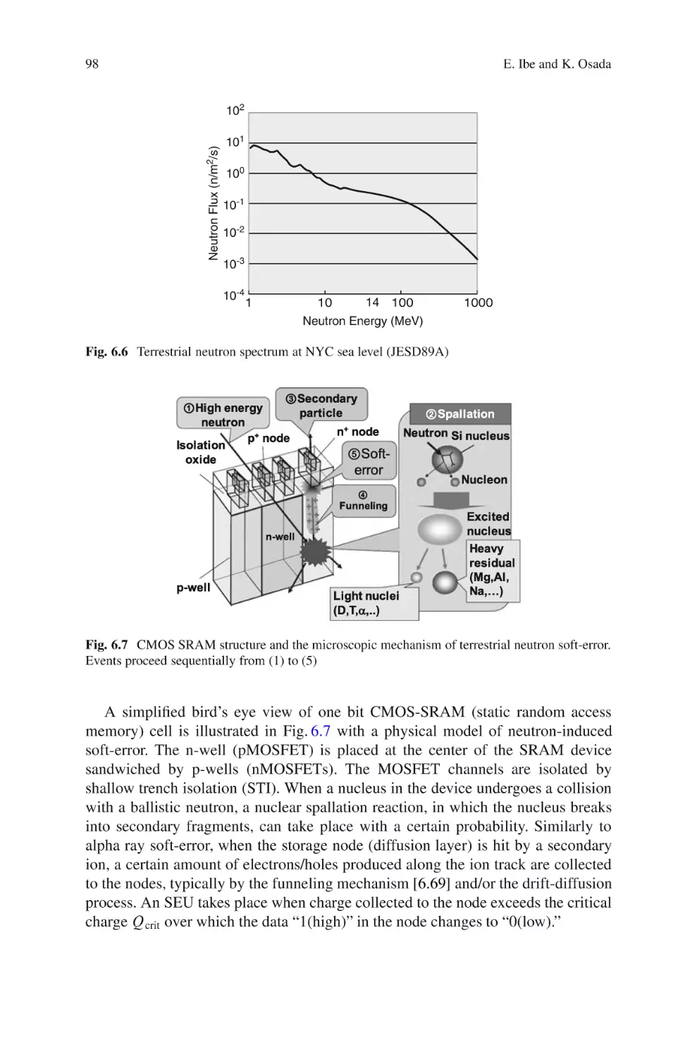
6.3.1 Basic Knowledge of Terrestrial Neutrons .. . . . . . . . . . . . . . . . . . . . 97
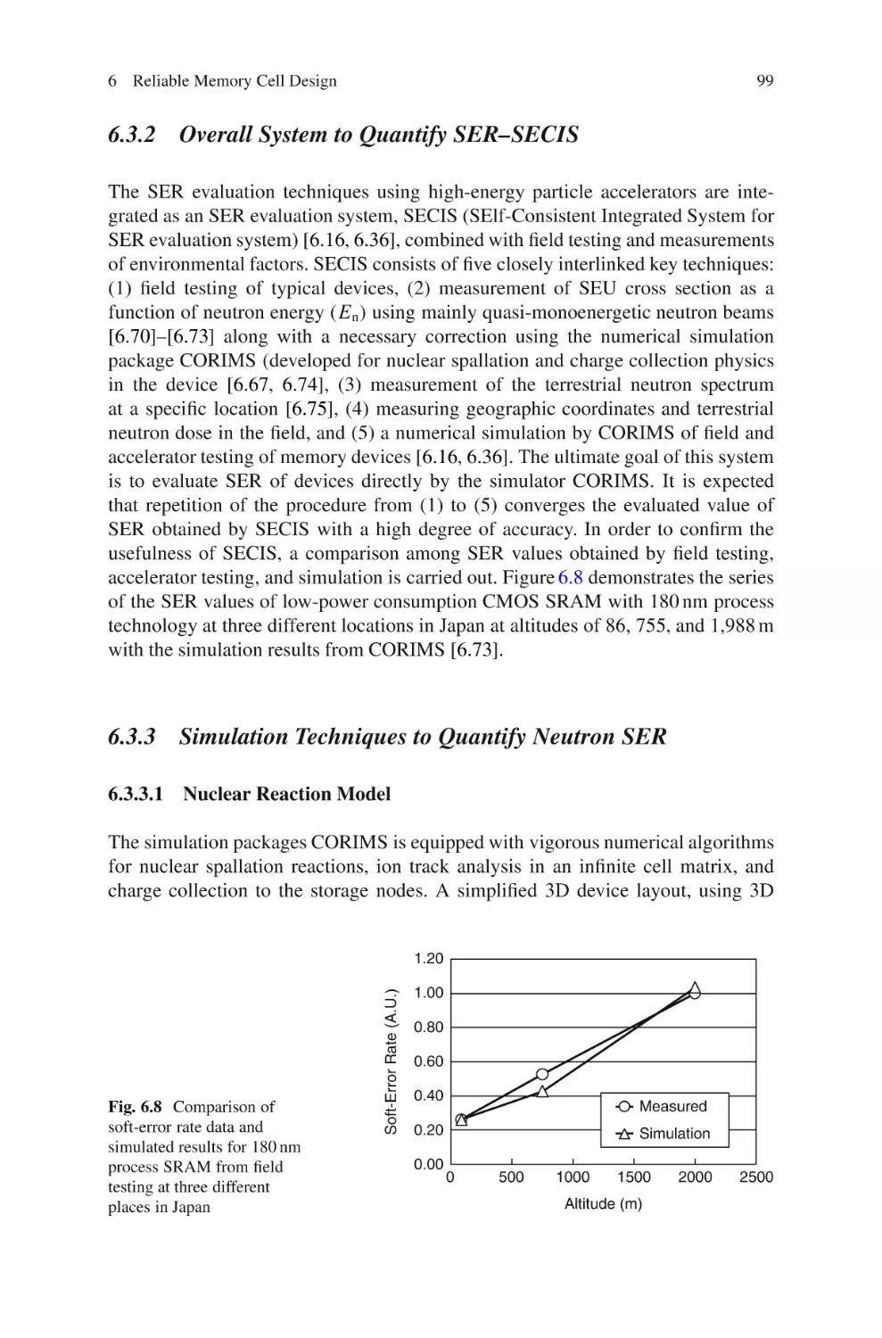
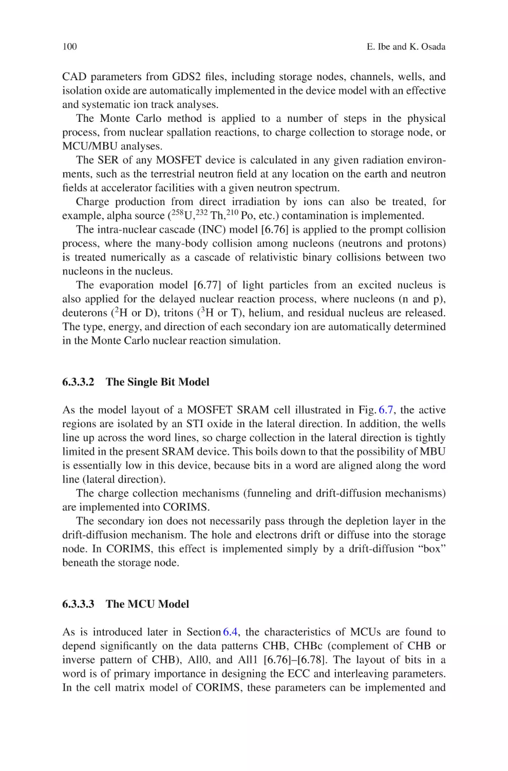
6.3.2 Overall System to Quantify SER–SECIS. .. . . . . . . . . . . . . . . . . . . . 99
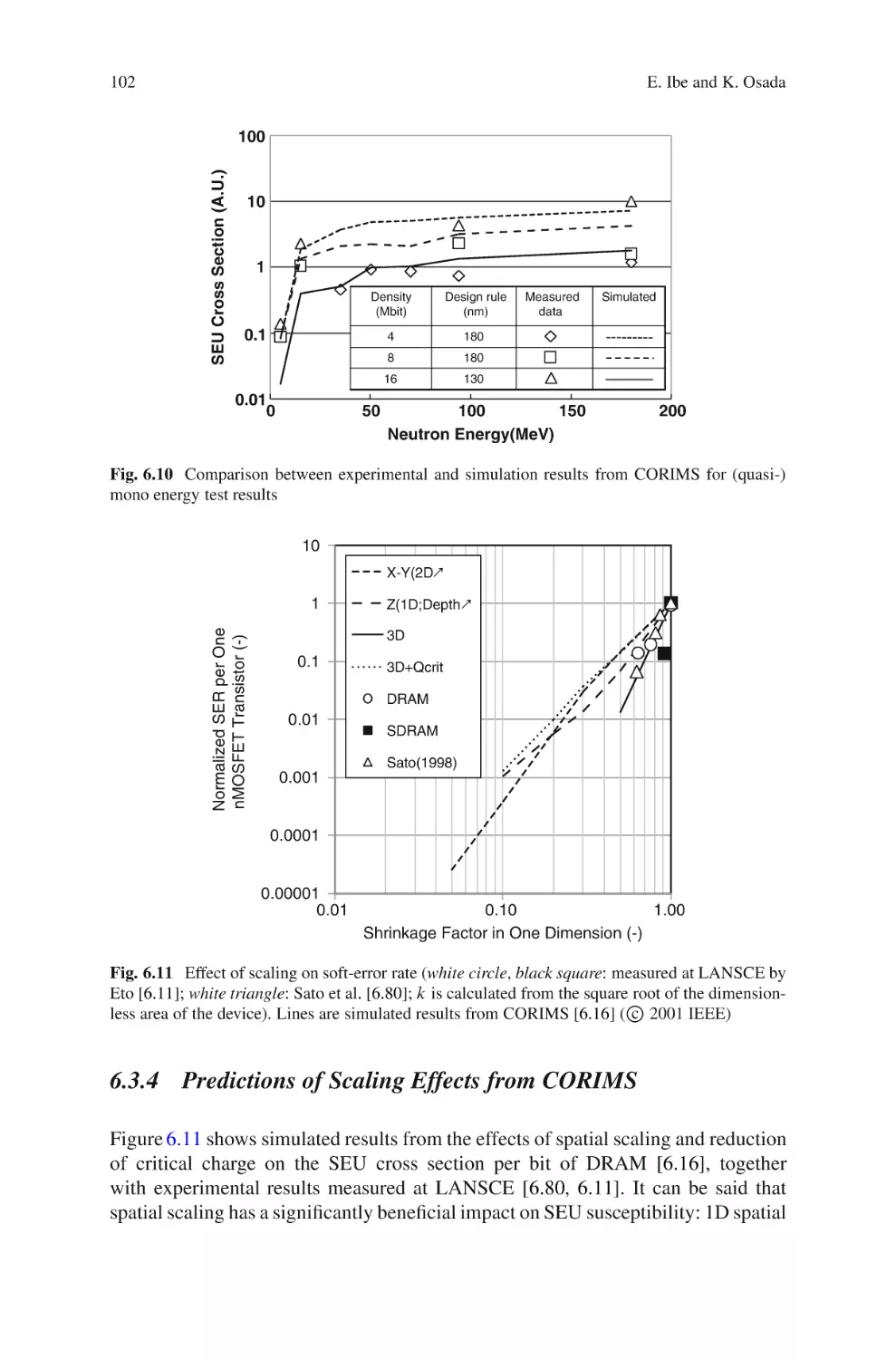
6.3.3 Simulation Techniques to Quantify Neutron SER . . . . . . . . . . . . 99
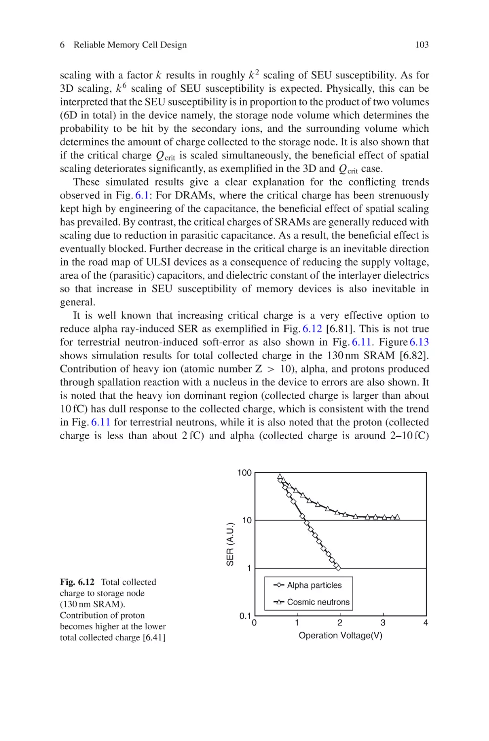
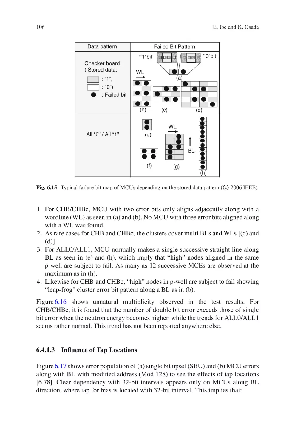
6.3.4 Predictions of Scaling Effects from CORIMS . . . . . . . . . . . . . . . . 102
Contents
ix
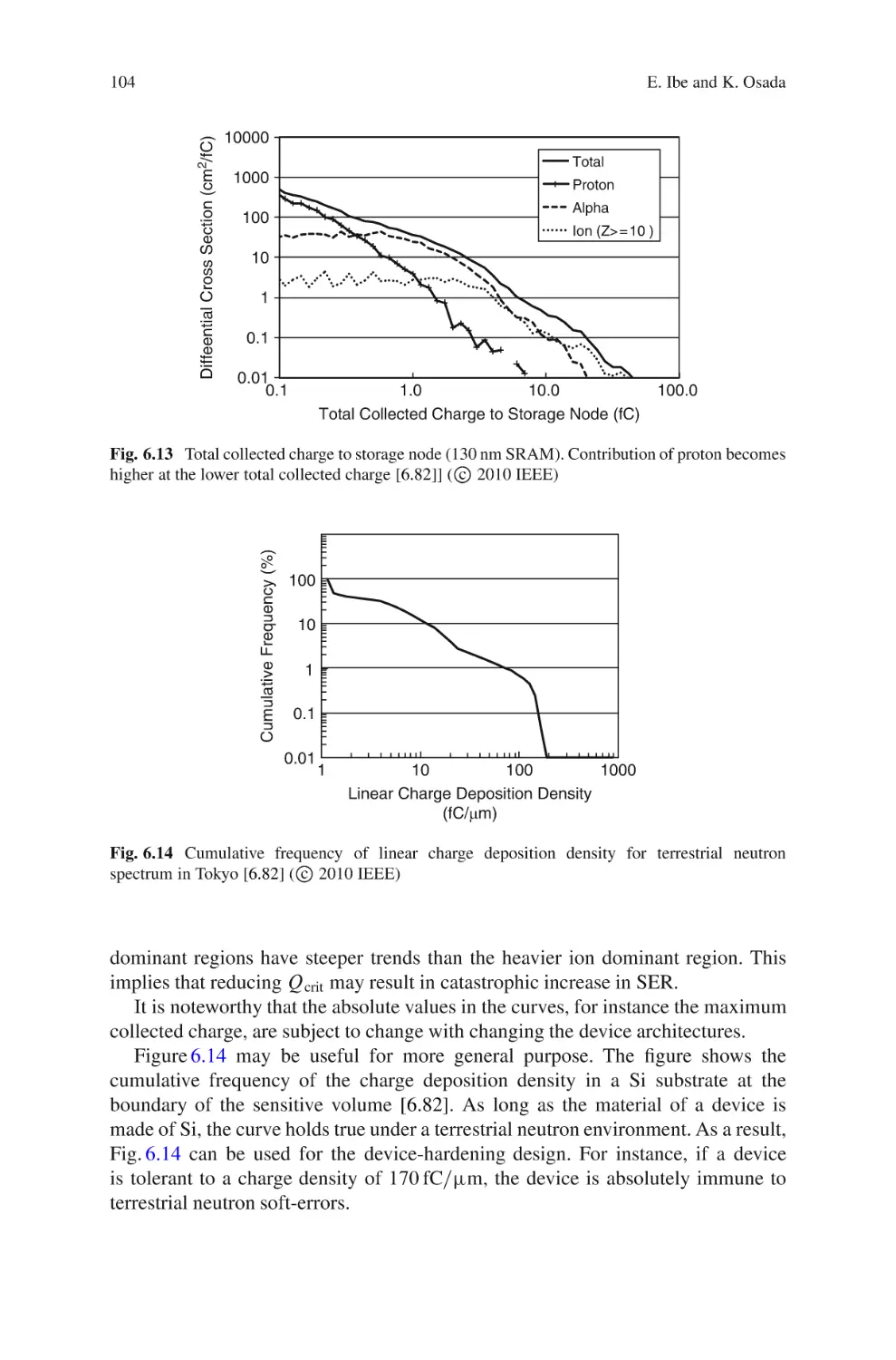
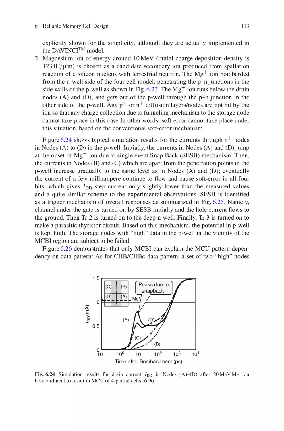
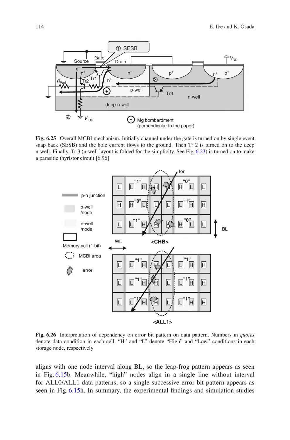
6.4 Evolution of MCU Problems and Clarification of the Mechanism . . .
6.4.1 MCU Characterization by Accelerator-Based
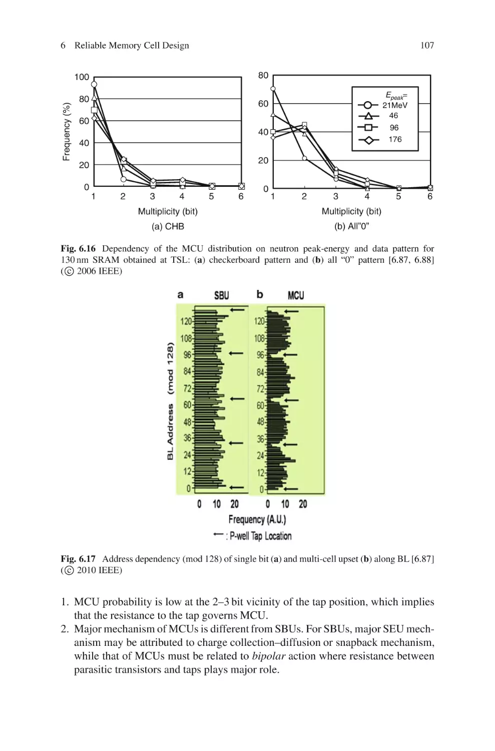
Experiments .. . . . . . . . . . . . . . . . . . . . . . . . . . . . . . . .. . . . . . . . . . . . . . . . . . . .
6.4.2 Simplified 3D Device Simulation Mixed
with Circuit Simulation .. . . . . . . . . . . . . . . . . . . .. . . . . . . . . . . . . . . . . . . .
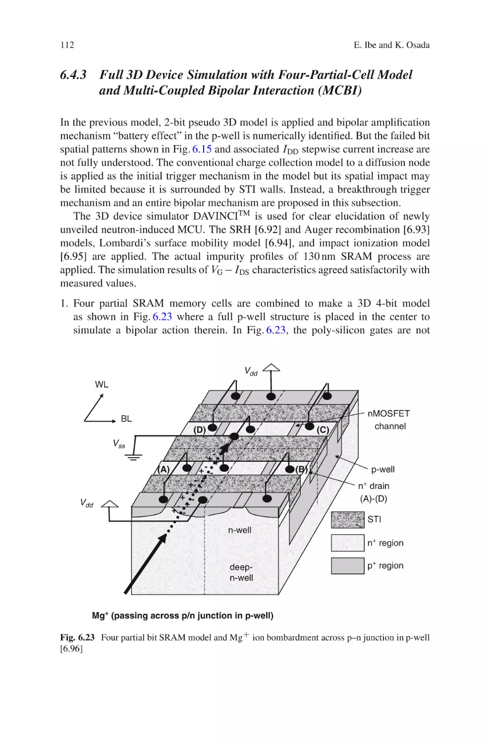
6.4.3 Full 3D Device Simulation with Four-Partial-Cell
Model and Multi-Coupled Bipolar Interaction (MCBI) . . . . . .
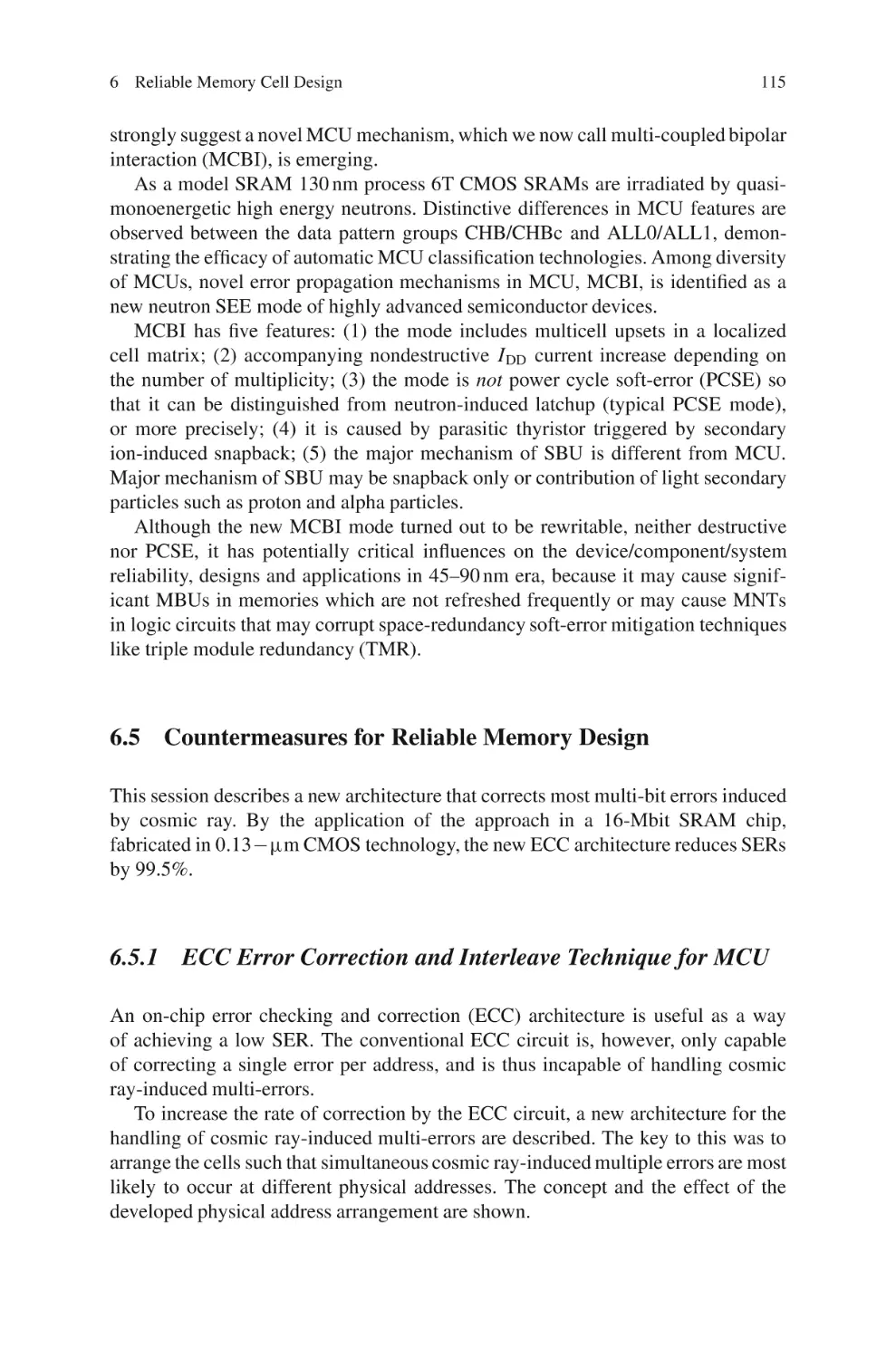
6.5 Countermeasures for Reliable Memory Design . . .. . . . . . . . . . . . . . . . . . . .
6.5.1 ECC Error Correction and Interleave Technique
for MCU. . . . . . . . . . . . . . . . . . . . . . . . . . . . . . . . . . . . .. . . . . . . . . . . . . . . . . . . .
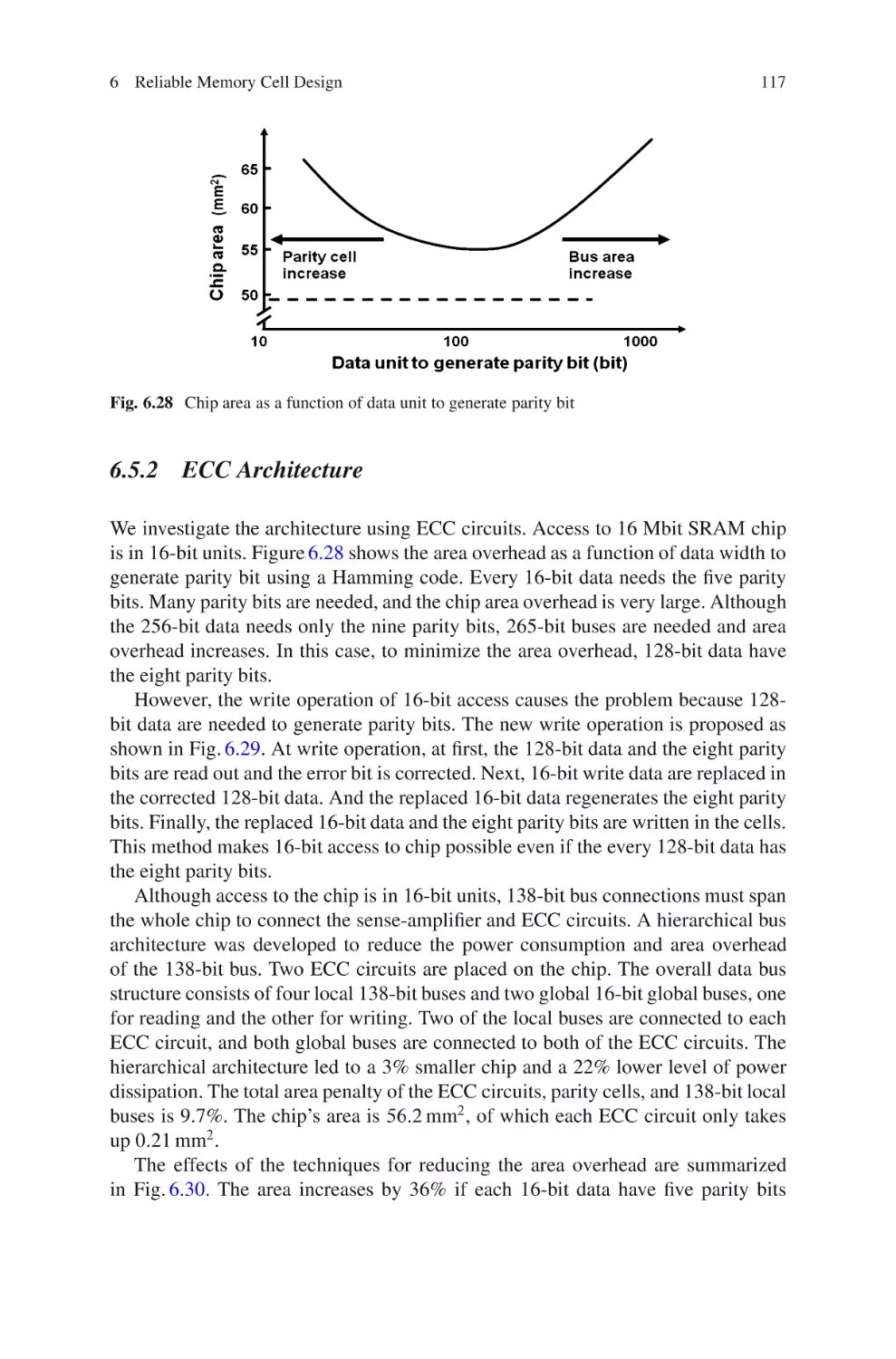
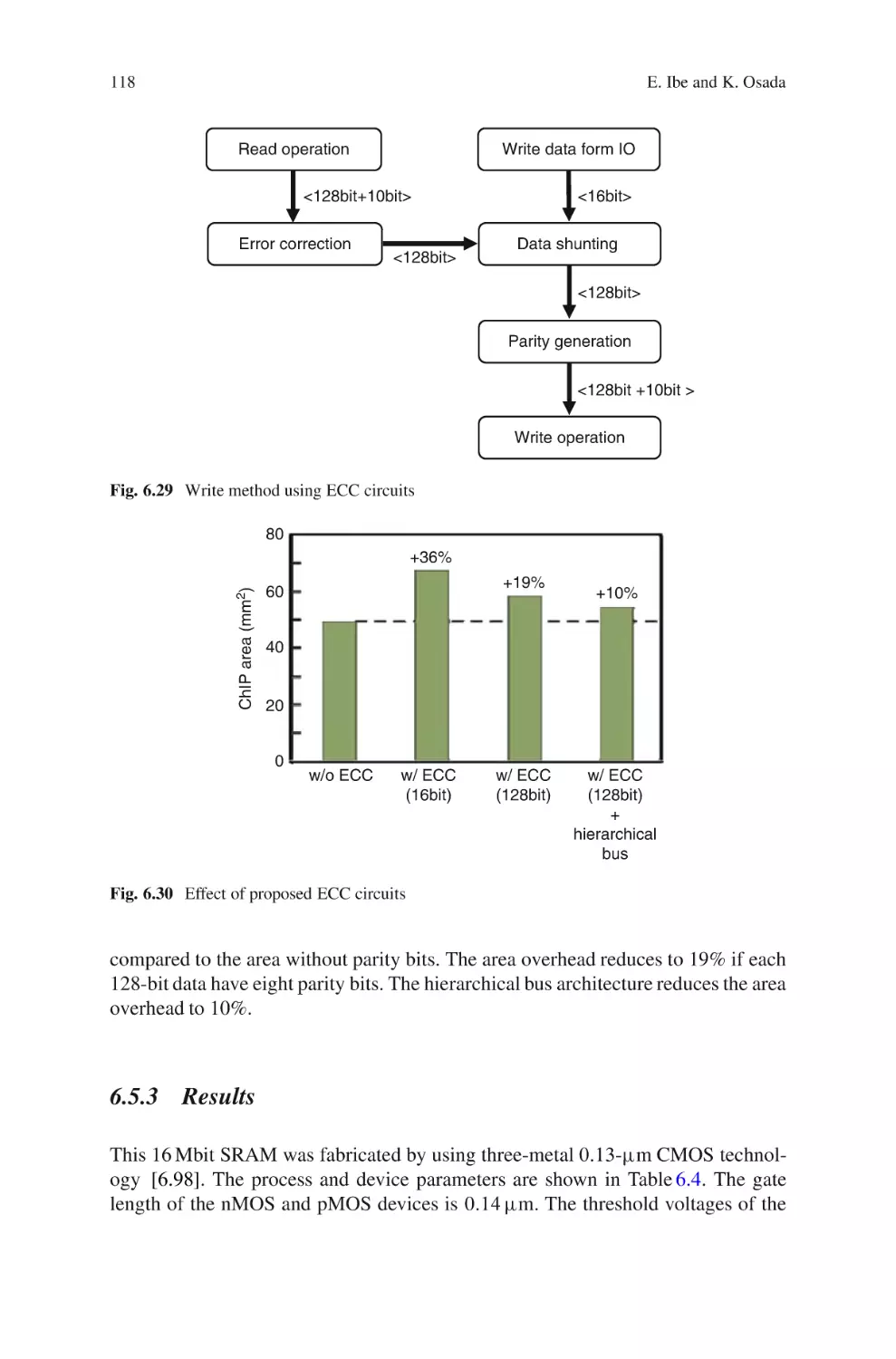
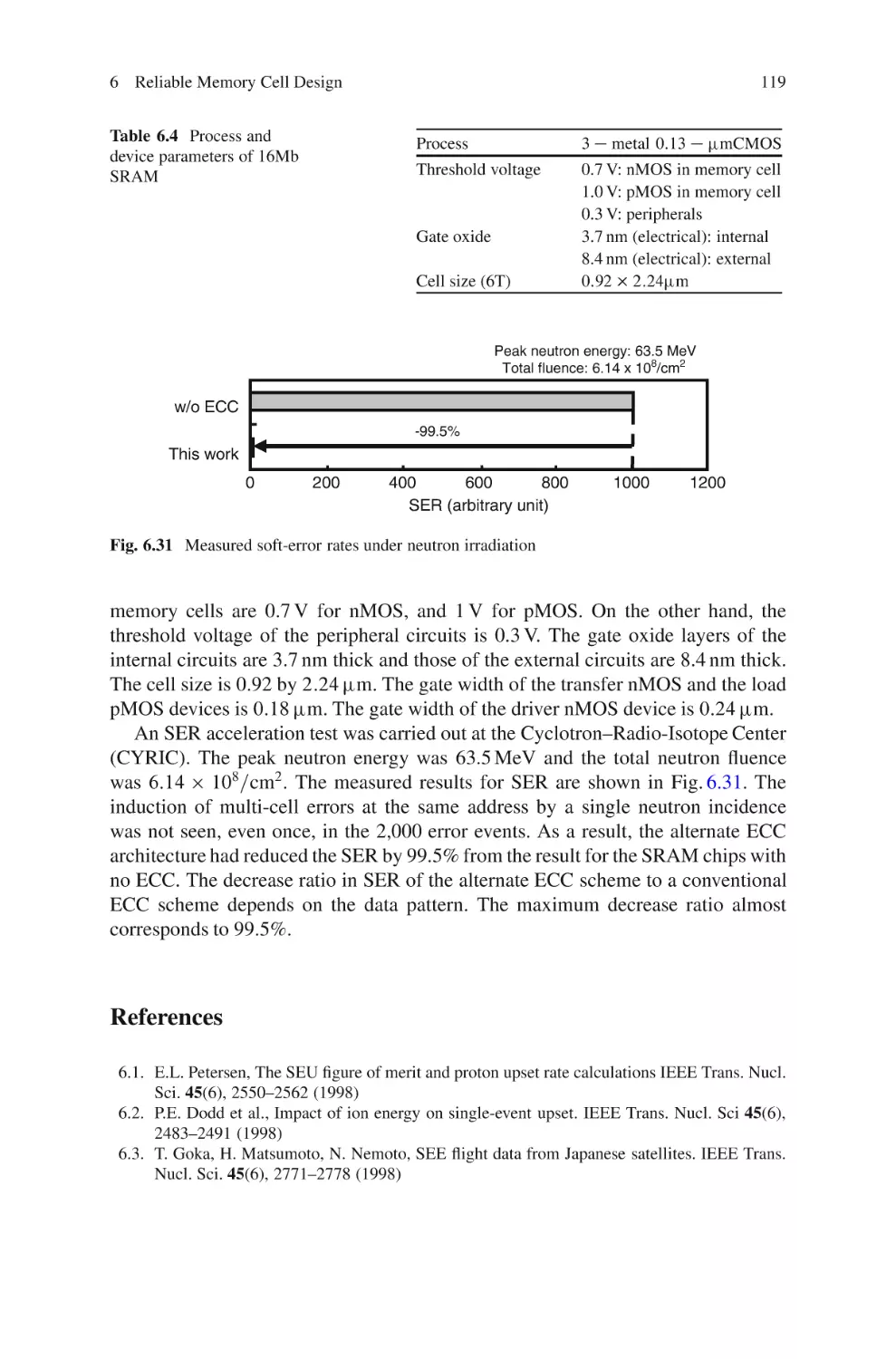
6.5.2 ECC Architecture .. . . . . . . . . . . . . . . . . . . . . . . . . .. . . . . . . . . . . . . . . . . . . .
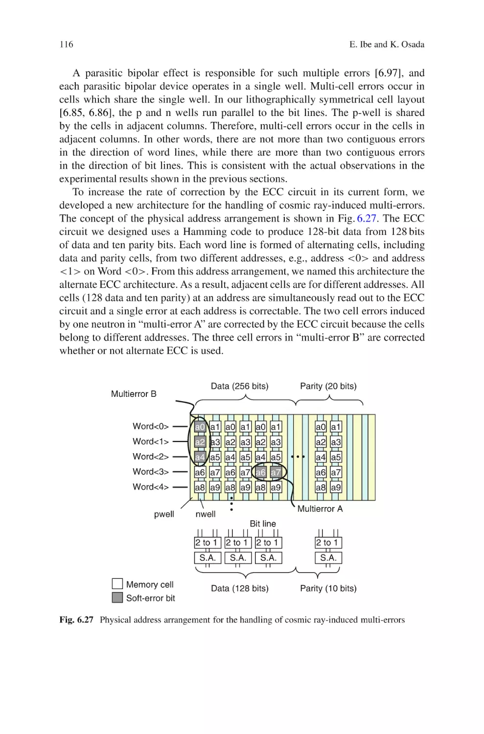
6.5.3 Results . . . . . . . . . . . . . . . . . . . . . . . . . . . . . . . . . . . . . . .. . . . . . . . . . . . . . . . . . . .
References . . . . . . . . . . . . . . . . . . . . . . . . . . . . . . . . . . . . . . . . . . . . . . . . .. . . . . . . . . . . . . . . . . . . .
105
7 Future Technologies . . . . . . . . . . . . . . . . . . . . . . . . . . . . . . . . . . . . .. . . . . . . . . . . . . . . . . . . .
Koji Nii and Masanao Yamaoka
7.1 7T, 8T, 10T SRAM Cell . . . . . . . . . . . . . . . . . . . . . . . . . . . .. . . . . . . . . . . . . . . . . . . .
7.2 Thin-Box FD-SOI SRAM . . . . . . . . . . . . . . . . . . . . . . . . . .. . . . . . . . . . . . . . . . . . . .
7.3 SRAM Cells for FINFET . . . . . . . . . . . . . . . . . . . . . . . . . . .. . . . . . . . . . . . . . . . . . . .
References . . . . . . . . . . . . . . . . . . . . . . . . . . . . . . . . . . . . . . . . . . . . . . . . .. . . . . . . . . . . . . . . . . . . .
125
105
108
112
115
115
117
118
119
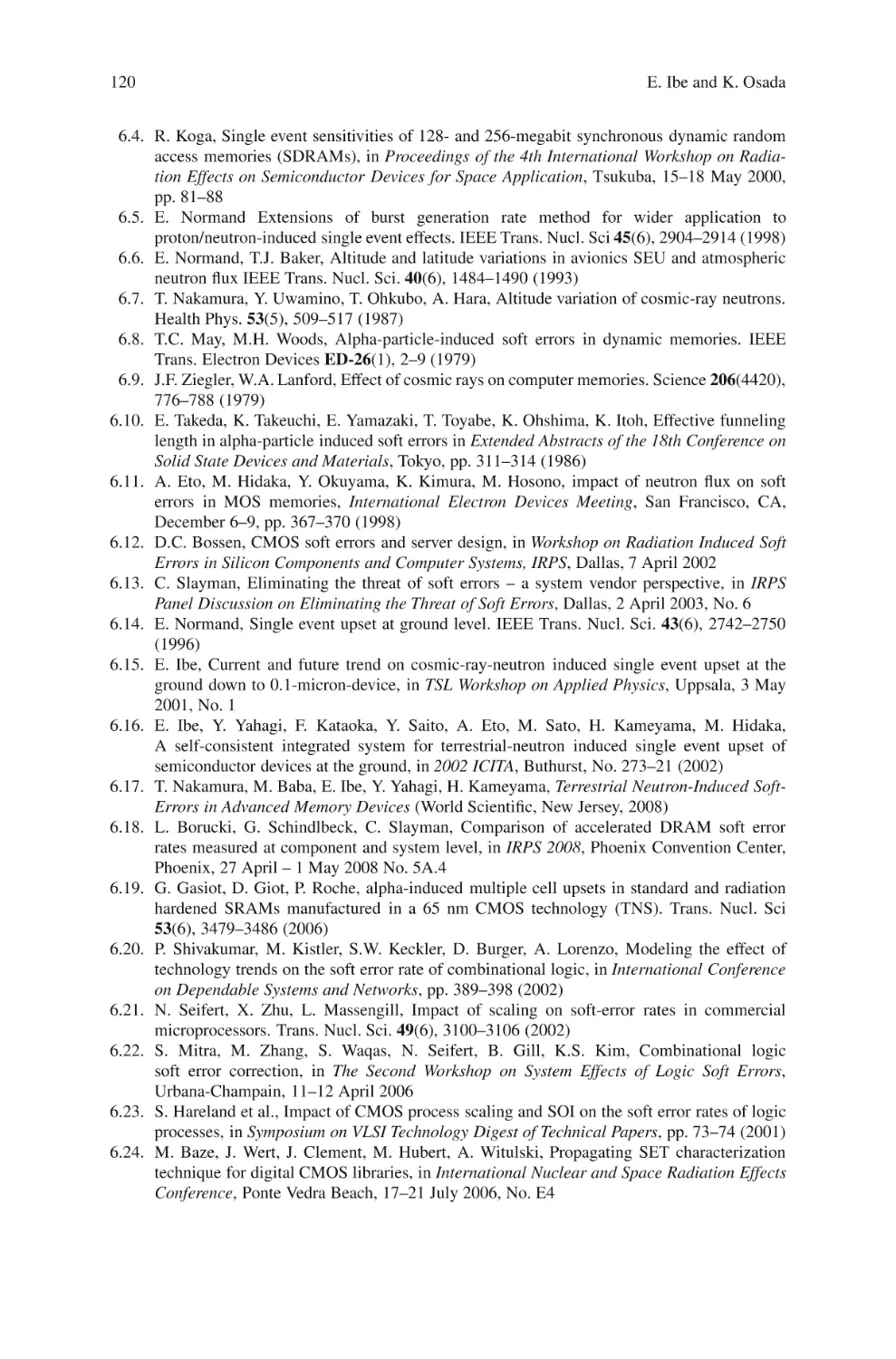
125
128
135
137
Index . . . . . . . .. . . . . . . . . . . . . . . . . . . . . . . . . . . . . . . . . . . . . . . . . . . . . . . . . .. . . . . . . . . . . . . . . . . . . . 139
•
Contributors
Eishi Ibe, Production Engineering Research Laboratory, Hitachi, Ltd., 292
Yoshida, Totsuka, Yokohama, Kanagawa 244-0817, Japan,
hidefumi.ibe.hf@hitachi.com
Koichiro Ishibashi, The University of Electro-Communications, 1-5-1 Chofugaoka, Chofu, Tokyo, 182-8585 Japan, ishibashi@ee.uec.ac.jp
Koji Nii, Renesas Electronics Corporation, 5-20-1, Josuihon-cho, Kodaira, Tokyo
187-8588, Japan, koji.nii.uj@renesas.com
Kenichi Osada, Measurement Systems Research Department, Central Research
Laboratory, Hitachi, Ltd., 1-280, Higashi-koigakubo, Kokubunji-shi, Tokyo
180-8601, Japan, kenichi.osada.aj@hitachi.com
Yasumasa Tsukamoto, Renesas Electronics Corporation, 5-20-1, Josuihon-cho,
Kodaira, Tokyo 187-8588, Japan, yasumasa.tsukamoto.gx@renesas.com
Masanao Yamaoka, 1101 Kitchawan Road, Yorktown Heights, NY 10598, USA,
masanao.yamaoka@hal.hitachi.com
xi
Chapter 1
Introduction
Koichiro Ishibashi
1.1 History and Trend of SRAM Memory Cell
Static random access memory (SRAM) has been widely used as the representative
memory for logic LSIs. This is because SRAM array operates fast as logic circuits
operate, and consumes a little power at standby mode. Another advantage of SRAM
cell is that it is fabricated by same process as logic, so that it does not need extra process cost. These features of SRAM cannot be attained by the other memories such as
DRAM and Flash memories. SRAM memory cell array normally occupies around
40% of logic LSI nowadays, so that the nature of logic LSI such as operating speed,
power, supply voltage, and chip size is limited by the characteristics of SRAM
memory array. Therefore, the good design of SRAM cell and SRAM cell array is
inevitable to obtain high performance, low power, low cost, and reliable logic LSI.
Various kinds of SRAM memory cell has been historically proposed, developed,
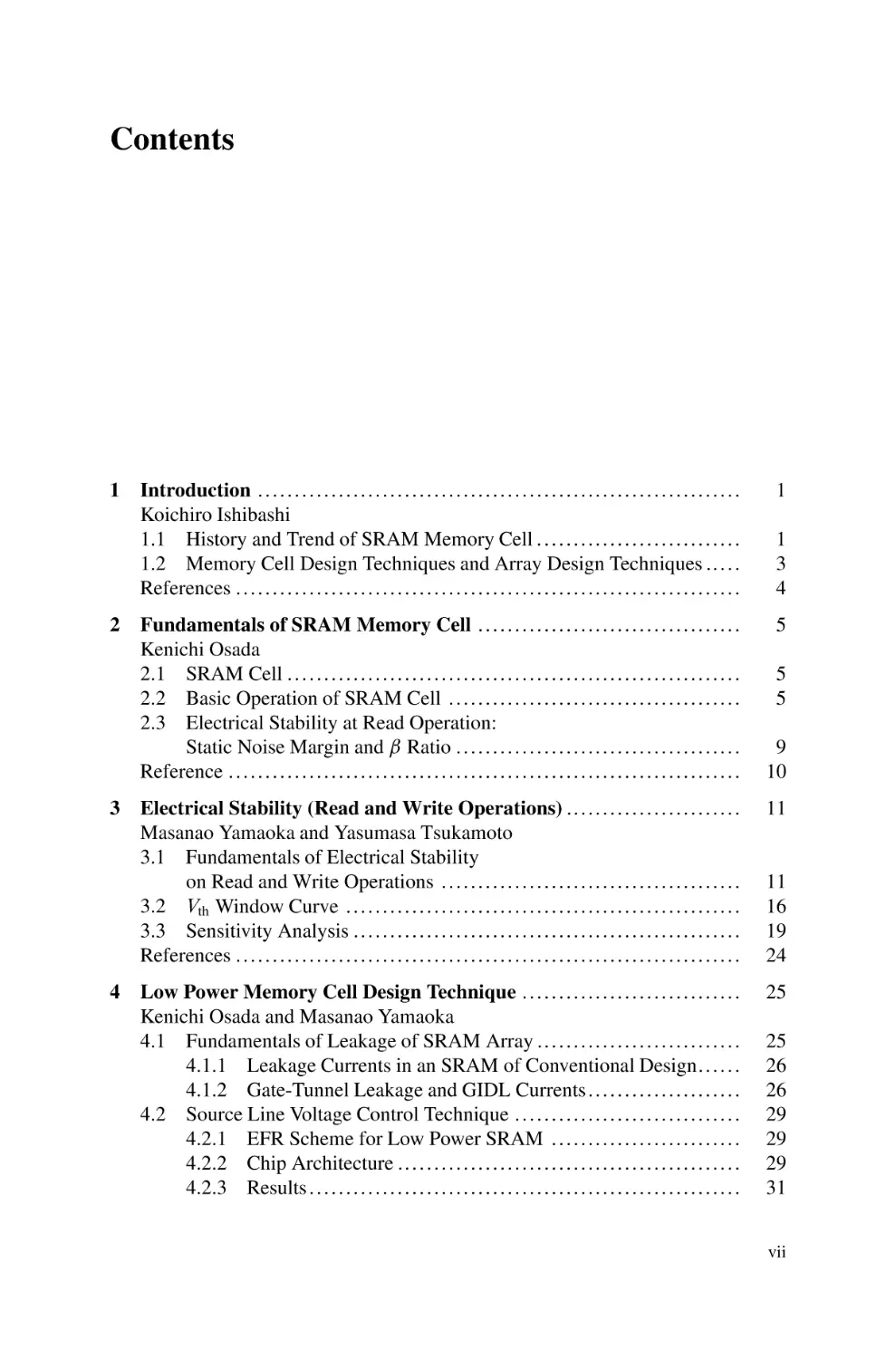
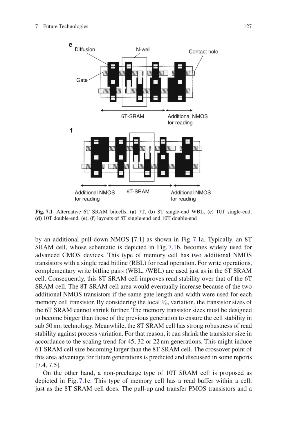
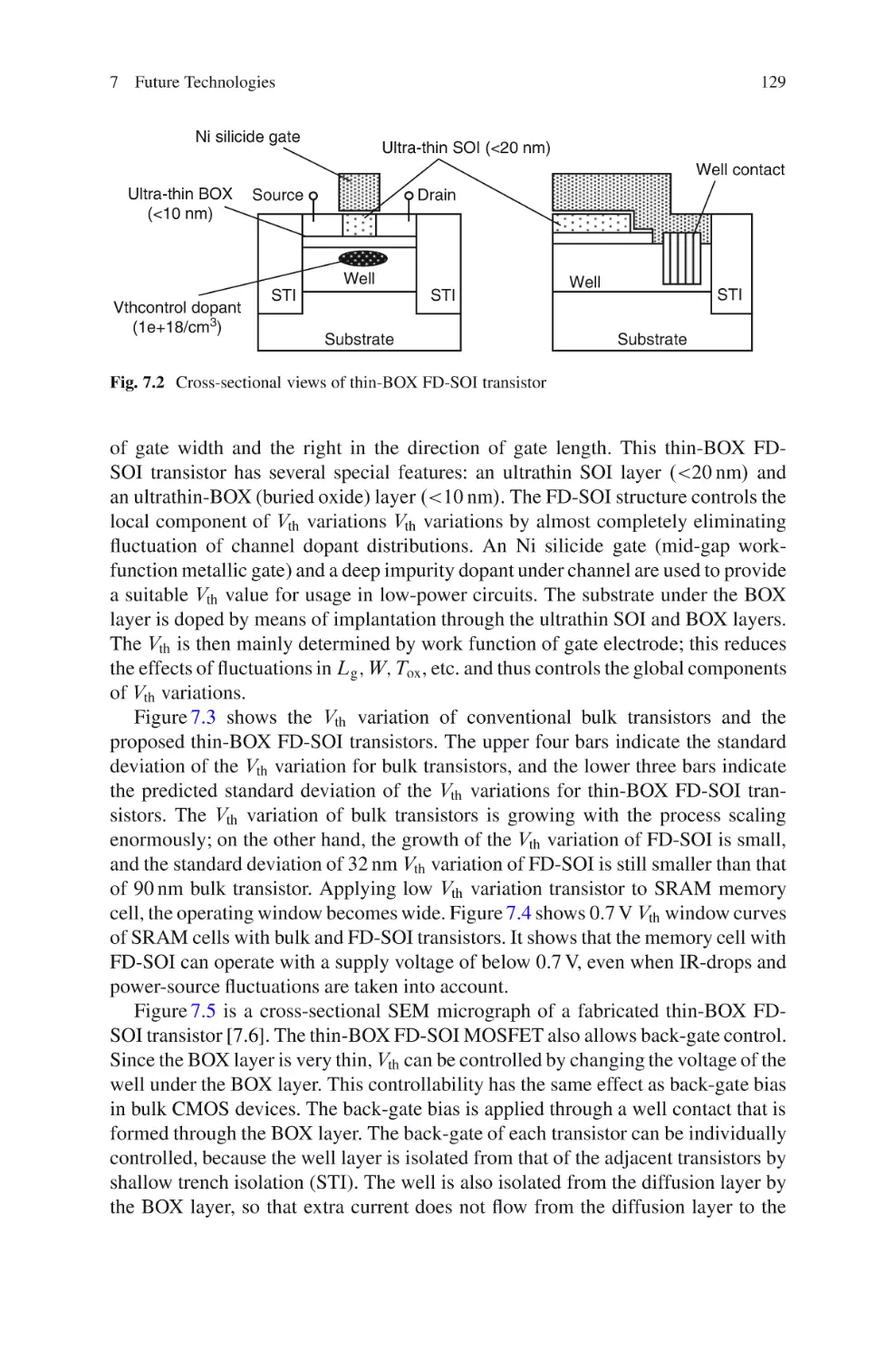
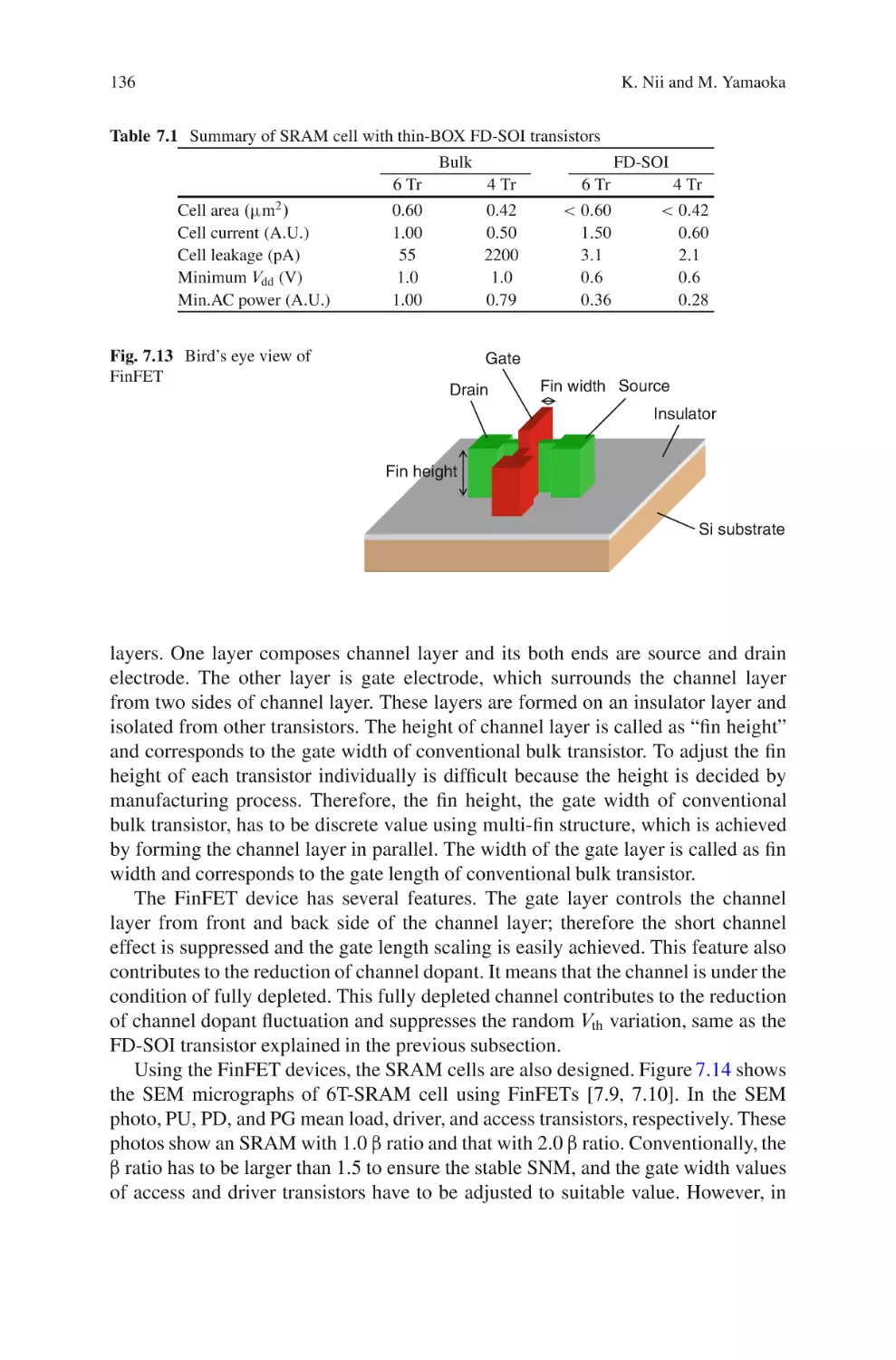
and used. Representative memory cell circuits are shown in Fig. 1.1.
High-R cell was first proposed as low power 4 K SRAM [1.1]. In the High-R cell,
high-resistivity poly-silicon layer is used as load of inverter in the SRAM cell. The
High-R cell does not need bulk PMOS, so that the memory cell size was smaller than
6-Tr. SRAM. As the resistivity of the poly-silicon layer is around 1012 , the standby
current of the memory cell was dramatically decreased to 1012 per cell. The high-R
cell was widely used for high density and low power SRAM memory LSI from 4 K
to 4 M bit [1.2, 1.3]. The disadvantage of the high-R cell is low voltage operation.
At low supply voltages less than 1.5 V, the cell node voltage should be charged to
supply voltage level during write operation. Since the resistivity of the load polysilicon is high, the time required to charge up the high node to supply voltage level
is quit large, high-R cell cannot operate at supply voltages less than 1.5 V.
K. Ishibashi
The University of Electro-Communications, 1-5-1 Chofugaoka, Chofu, Tokyo, 182-8585 Japan
e-mail: ishibashi@ee.uec.ac.jp
K. Ishibashi and K. Osada (eds.), Low Power and Reliable SRAM Memory Cell
and Array Design, Springer Series in Advanced Microelectronics 31,
DOI 10.1007/978-3-642-19568-6 1, © Springer-Verlag Berlin Heidelberg 2011
1
2
K. Ishibashi
High R Cell
6T Cell (Chap. 2 ~ 6)
8T Cell (Chap. 7)
6T Cell for SOI (Chap. 7)
4T Cell for SOI (Chap. 7)
Fig. 1.1 Representative SRAM memory cell circuits
Six-transistor cell (6T cell), which is sometimes called as full CMOS cell, has
been widely used as memories for logic LSIs instead of high-R cell. Most parts of
this book deals with this type of memory cell. Although the 6T cell uses PMOS
transistors and cell area becomes larger than high-R cell, the cell does not need
extra process to logic process. Hence, it has been widely used for memories for
logic LSIs even during high-R cell was popular for standalone SRAM. In addition,
the PMOS transistors in the cell pull up the cell nodes voltages fast, so that 6T cell
operates at lower supply voltages than high-R cell. Therefore, recent supply voltage
reduction at advanced technologies has made the 6T cell inevitable for logic LSI.
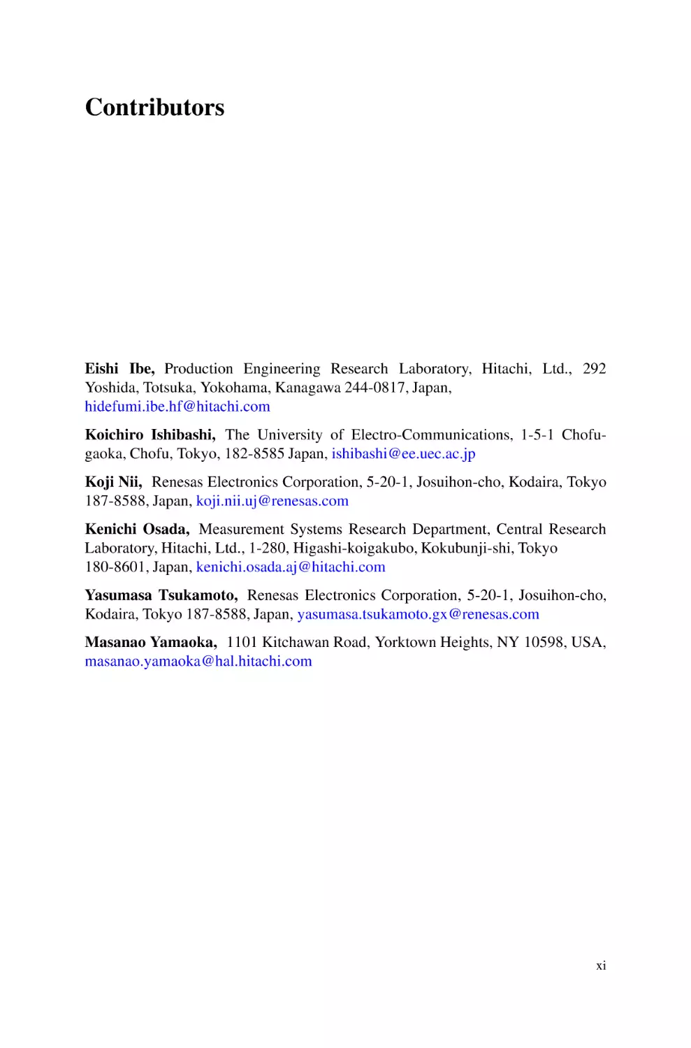
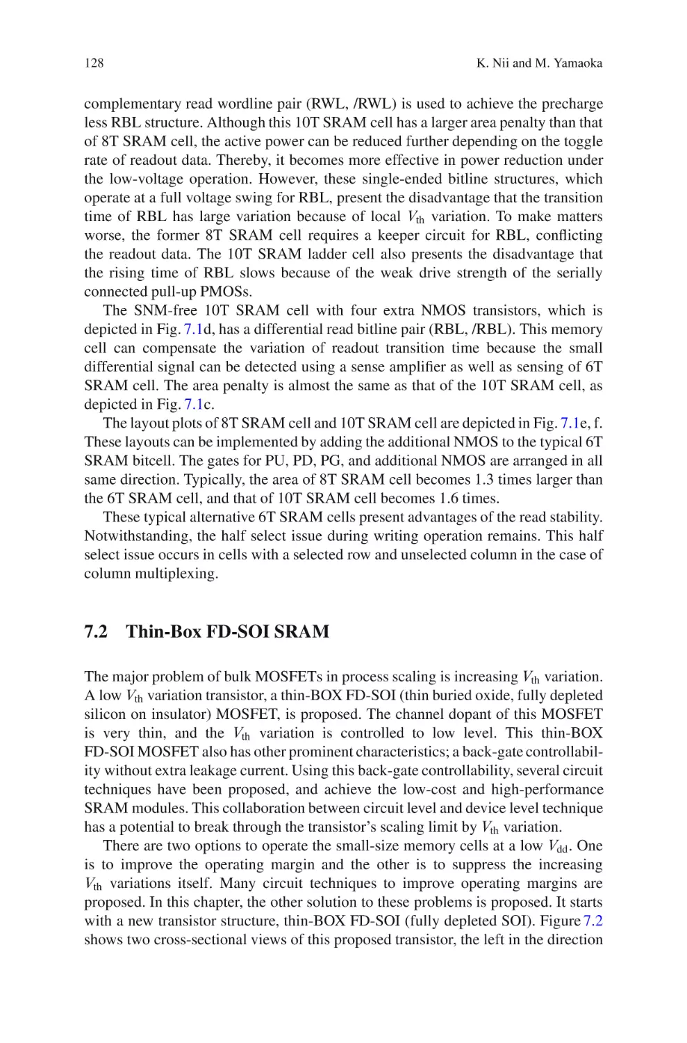
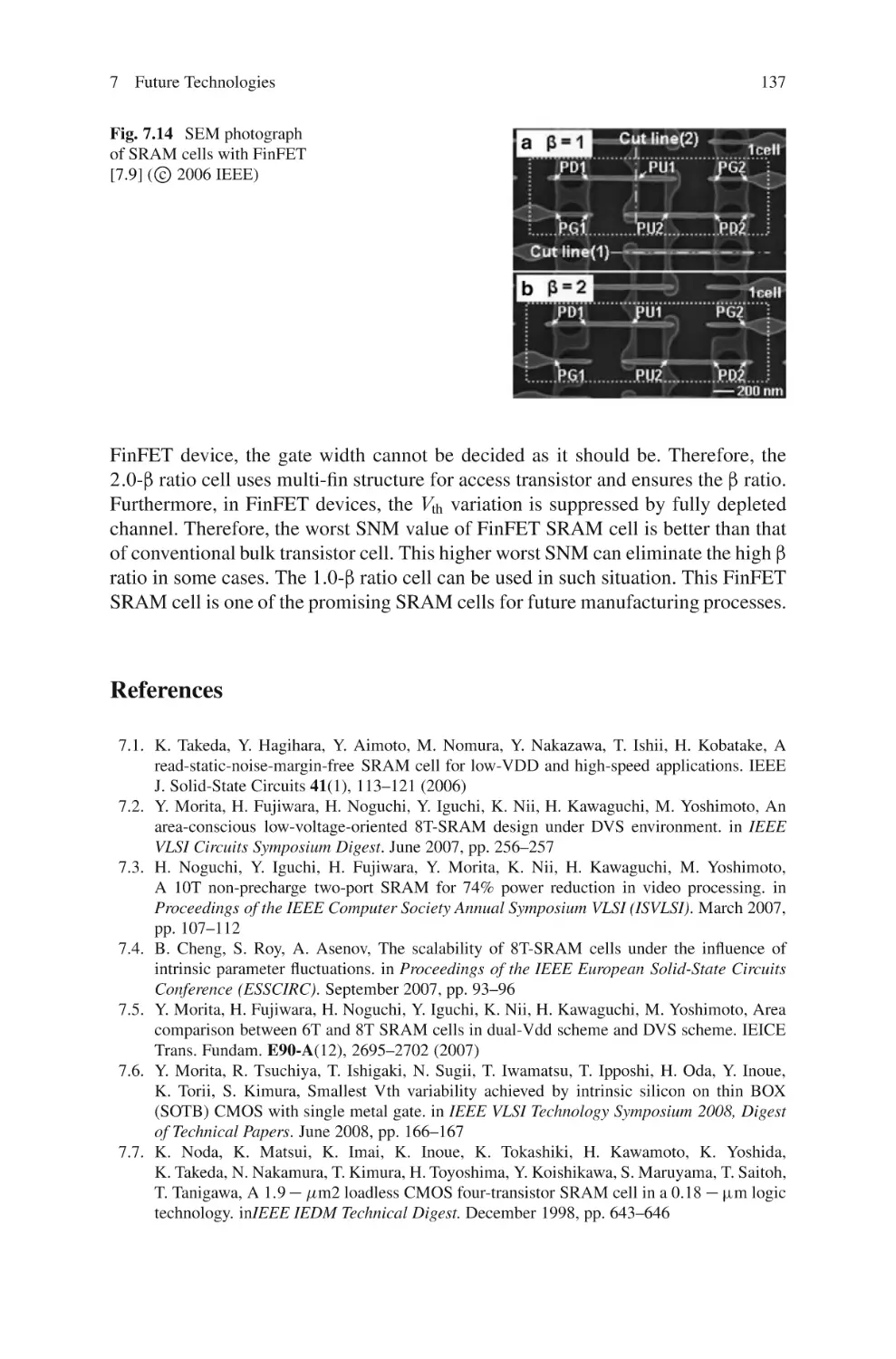
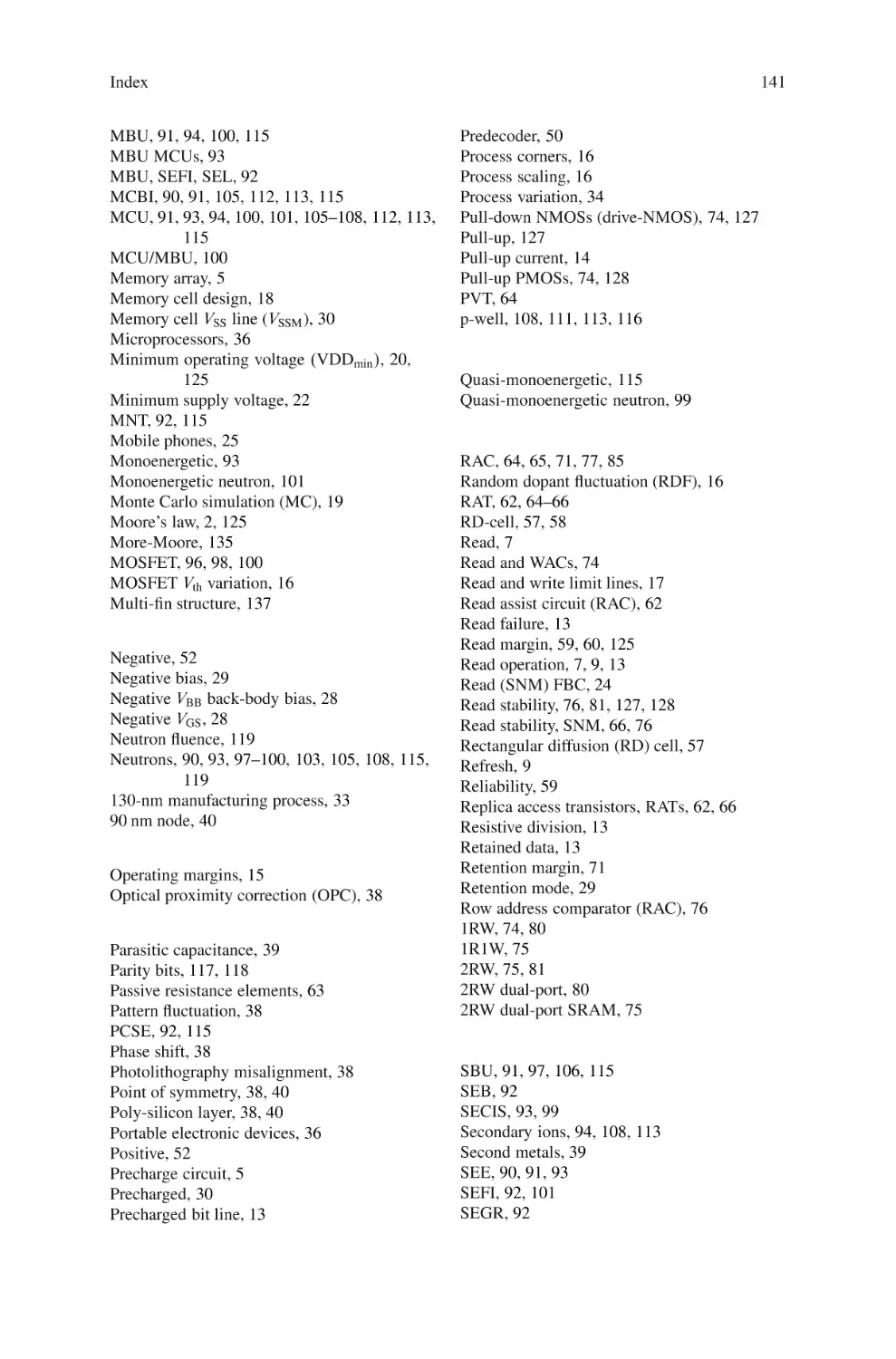
Figure 1.2 shows the size of 6T cell in recent VLSI symposia and International
Electron Devices Meeting (IEDM). The cell size has been decreasing by half every
2 years, and it corresponds to density enhancement by Moore’s law. Therefore,
6T cell is main-stream memory cell for past, nowadays, and future logic LSIs. Even
though structure of transistor will be changed to SOI or FINFET, the 6T cell could
be used as the main memory cell for logic LSI.
For further needs to extremely low supply voltage and fast operation, eighttransistor cell (8T cell) has been proposed. Moreover, such special four-transistor
1 Introduction
3
Fig. 1.2 6T cell size trend in
VLSI and IEDM
Cell Size (um2)
3.0
1.0
0.3
0.1
‘00
‘02
‘04
‘06
‘08
‘10
Year
cell (4T cell) has been proposed using FINFET transistor structure. These kinds of
new SRAM memories are treated in Chap. 7 as future technologies of SRAM cell.
1.2 Memory Cell Design Techniques and Array Design
Techniques
There are a lot of issues to obtain low power, reliable, and small cell size 6T
memory cell. Since the 6T SRAM cell size is scaled by Moore’s law, the feature
size of transistors in 6T cell is also reduced by Moore’s law. Supply voltage of
6T cell is also reduced as the feature size is reduced. Variation in the transistors’
threshold voltage has increased and leakage of transistors has also increased by
the scaling. Supply voltage of memory cell array has been reduced by the scaling.
Recent low power circuit techniques such as Dynamic Voltage Frequency Scaling
(DVFS) alsoneed further low voltage operation of memory cell arrays.
The 6T SRAM cell must be designed so that it must be electrically stable at the
low supply voltages despite the large variation of transistors. The memory cell size
must be as small as possible to obtain small chip size LSIs. The leakage of 6T SRAM
cell array must be small despite large leakage in transistors in the cell. In addition,
immunity to soft errors due to alpha particles or neutrons must be minimized to
obtain reliable LSIs.
This book is focusing on design techniques of SRAM memory cell and array,
and covers issues on variability, low power and low voltage operation, reliability,
and future technologies.
This book first explains electrical stability issue as fundamentals of electrical
operation of 6T cells in Chap. 2. Precise analysis techniques of electrical stability,
Vth window analysis, and sensitivity analysis will be introduced in Chap. 3. Using
4
K. Ishibashi
the analysis techniques, suitable Vth for PMOS and NMOS transistors in 6T cell
are determined, so that electrically stable 6T cell at low supply voltages under large
variability circumstances is obtained.
The SRAM cell array must operate at low voltage operation to reduce operating
power. It must retain data with low leakage at standby mode. Many low power
techniques for obtaining low power SRAM have been proposed. This book covers
important low power memory cell array design techniques as well as memory cell
design techniques.
Two important memory cell design techniques will be introduced in Chap. 4.
Lithographically Symmetric Cell (LS cell) is symmetric memory cell layout, so
that balance of characteristics in the paired MOS transistors in 6T cell, and good
electrical stability can be obtained with advanced super-resolution photolithography.
Source voltage control technique, which can reduce not only subthreshold leakage
but also gate-induced drain leakage (GIDL), will also be shown to reduce data
retention current in standby mode.
SRAM cell array design plays also an important role in reducing power
consumption. Dummy cell design technique to adjust activation timing of sense
amplifier will be shown in Chap. 5, so that stable SRAM operation is achieved with
PVT variation circumstances. Assisting circuits at read operation as well as write
operation will be proposed to attain low voltage operation of memory cell arrays.
Array boost technique is also shown to obtain the lowest operation voltage of 0.3 V.
Reliability issue is another inevitable issue for SRAM memory cell and cell array
design. Among various reliability issues, soft errors caused by alpha particles and
neutron particles are serious issue. This book first shows the phenomena of the soft
error on SRAM memory cell array and explains mechanisms of the soft errors in
Chap. 6. Then memory cell array designtechniques drastically reduce the soft errors.
Chapter 7 is the final chapter of this book. This chapter introduces future design
techniques of SRAM memory cell and array. Such SRAM cell with such larger
number of transistors as 8T cell will be shown to obtain SRAM array with lower
supply voltages. Then SRAM memory cell using SOI and FINFET technology will
be discussed for future design techniques.
References
1.1. T. Masuhara et al., A high speed, low-power Hi-CMOS 4 K static RAM, in IEEE International
Solid-State Circuits Conference, Digest 1978, pp. 110–111
1.2. O. Minato et al., A 42 ns 1 Mb CMOS SRAM, in IEEE International Solid-State Circuits
Conference, Digest 1987, pp. 260–261
1.3. K. Sasaki et al., A 23 nm 4 Mb CMOS SRAM, in IEEE International Solid-State Circuits
Conference, Digest 1990, pp. 130–131
Chapter 2
Fundamentals of SRAM Memory Cell
Kenichi Osada
Abstract This chapter introduces fundamentals of SRAM memory cell. The basic
SRAM cell design and the operation are also described in this chapter. In Sect.2.1,
the most common SRAM cell, the full CMOS 6-T memory cell, is explained. In
Sect.2.2, read and write basic operations are introduced. In Sect.2.3, the basic of
electrical stability at read operation (static noise margin, SNM) is described.
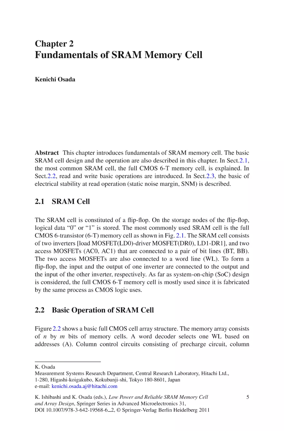
2.1 SRAM Cell
The SRAM cell is constituted of a flip-flop. On the storage nodes of the flip-flop,
logical data “0” or “1” is stored. The most commonly used SRAM cell is the full
CMOS 6-transistor (6-T) memory cell as shown in Fig. 2.1. The SRAM cell consists
of two inverters [load MOSFET(LD0)-driver MOSFET(DR0), LD1-DR1], and two
access MOSFETs (AC0, AC1) that are connected to a pair of bit lines (BT, BB).
The two access MOSFETs are also connected to a word line (WL). To form a
flip-flop, the input and the output of one inverter are connected to the output and
the input of the other inverter, respectively. As far as system-on-chip (SoC) design
is considered, the full CMOS 6-T memory cell is mostly used since it is fabricated
by the same process as CMOS logic uses.
2.2 Basic Operation of SRAM Cell
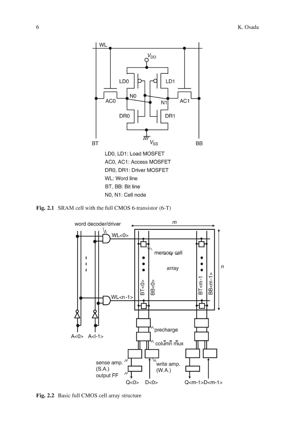
Figure 2.2 shows a basic full CMOS cell array structure. The memory array consists
of n by m bits of memory cells. A word decoder selects one WL based on
addresses (A). Column control circuits consisting of precharge circuit, column
K. Osada
Measurement Systems Research Department, Central Research Laboratory, Hitachi Ltd.,
1-280, Higashi-koigakubo, Kokubunji-shi, Tokyo 180-8601, Japan
e-mail: kenichi.osada.aj@hitachi.com
K. Ishibashi and K. Osada (eds.), Low Power and Reliable SRAM Memory Cell
and Array Design, Springer Series in Advanced Microelectronics 31,
DOI 10.1007/978-3-642-19568-6 2, © Springer-Verlag Berlin Heidelberg 2011
5
6
K. Osada
WL
VDD
LD0
LD1
N0
AC0
AC1
N1
DR0
DR1
VSS
BT
BB
LD0, LD1: Load MOSFET
AC0, AC1: Access MOSFET
DR0, DR1: Driver MOSFET
WL: Word line
BT, BB: Bit line
N0, N1: Cell node
Fig. 2.1 SRAM cell with the full CMOS 6-transistor (6-T)
m
word decoder/driver
WL<0>
memory cell
n
BB<m -1>
BT<m -1
BB<0>
WL<n -1>
BT<0>
array
precharge
A<0> A<l-1>
column mux
sense amp.
(S.A.)
output FF
write amp.
(W.A.)
Q<0>
Fig. 2.2 Basic full CMOS cell array structure
D<0>
Q<m-1>D<m-1>
2 Fundamentals of SRAM Memory Cell
7
WL
BT
memory cell
BB
PE
Precharge
Column
YSW
mux
YSR
SPE
ST
SB
W.A.
SE
S.A.
Output FF
Dout
Din
Fig. 2.3 Column control circuits consisting of precharge circuit, column multiplexer (mux), sense
amplifier (SA), output FF, and write amplifier (WA)
multiplexer (mux), sense amplifier (SA), output FF, and write amplifier (WA) are
shown in Fig. 2.3. The basic voltage waveform in read and write operation is shown
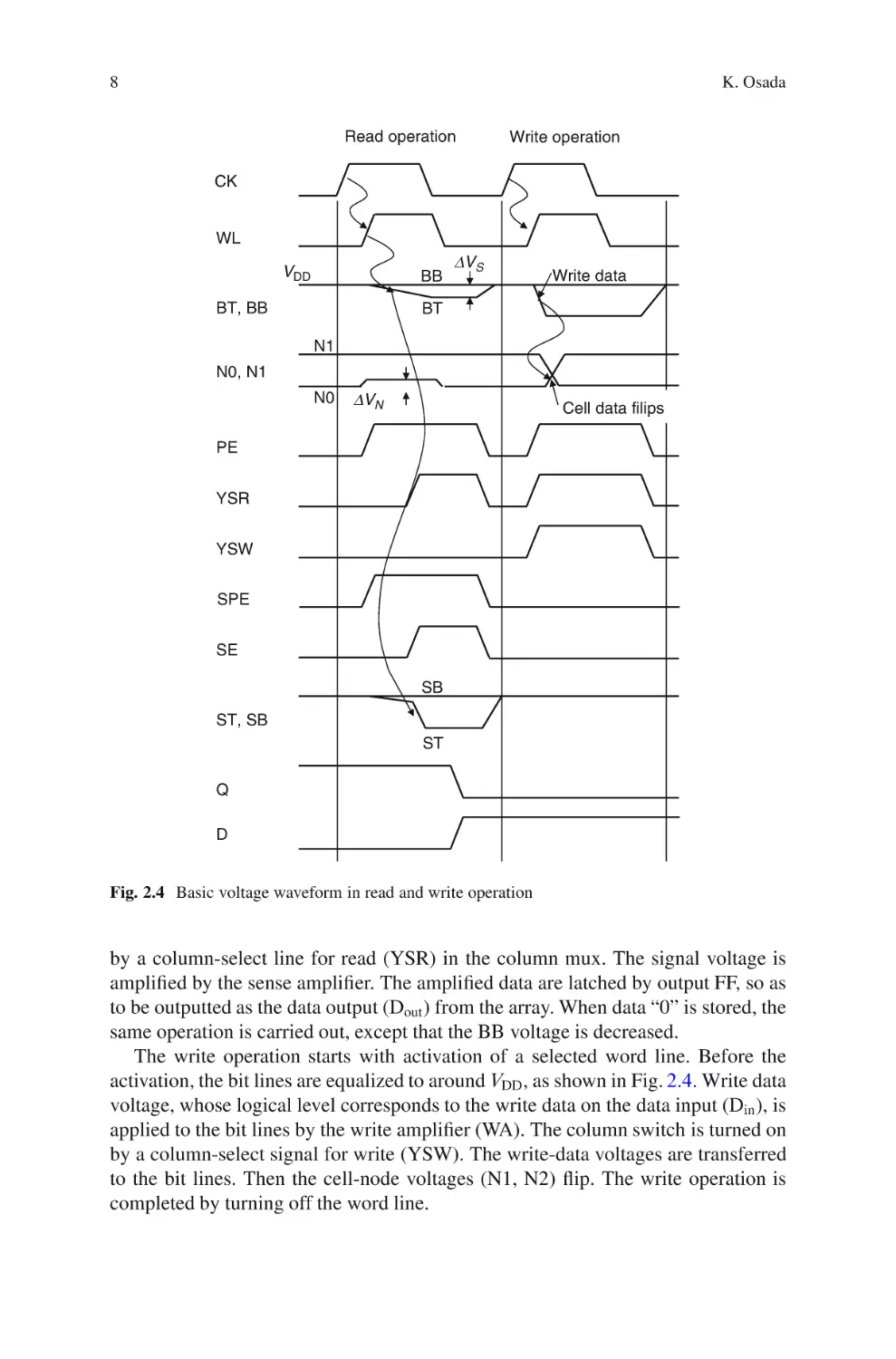
in Fig. 2.4. The read operation starts with activation of word line selection. Before
the activation, the precharge circuit equalizes and raised the bit-line voltages to
VDD level. Each cell generates a small signal voltage, VS , on one of the bit lines,
depending on the stored cell data. If stored data is “1,” where cell node N0 is at
a low voltage and cell node N1 is at a high voltage, the BT voltage is decreased
by VS . The other bit line (BB) remains at the equalized voltage because access
transistor (DR1) is not turned on. The differential signals are transferred to a pair
of sense-amplifier-input signals (ST/SB) by turning on the column switch selected
8
K. Osada
Read operation
Write operation
CK
WL
VDD
BB
BT, BB
DVS
Write data
BT
N1
N0, N1
N0
DVN
Cell data filips
PE
YSR
YSW
SPE
SE
SB
ST, SB
ST
Q
D
Fig. 2.4 Basic voltage waveform in read and write operation
by a column-select line for read (YSR) in the column mux. The signal voltage is
amplified by the sense amplifier. The amplified data are latched by output FF, so as
to be outputted as the data output (Dout ) from the array. When data “0” is stored, the
same operation is carried out, except that the BB voltage is decreased.
The write operation starts with activation of a selected word line. Before the
activation, the bit lines are equalized to around VDD , as shown in Fig. 2.4. Write data
voltage, whose logical level corresponds to the write data on the data input (Din ), is
applied to the bit lines by the write amplifier (WA). The column switch is turned on
by a column-select signal for write (YSW). The write-data voltages are transferred
to the bit lines. Then the cell-node voltages (N1, N2) flip. The write operation is
completed by turning off the word line.
2 Fundamentals of SRAM Memory Cell
9
2.3 Electrical Stability at Read Operation:
Static Noise Margin and ˇ Ratio
At normal read operation, when a word line is activated in the case that cell node N0
is at a low voltage and cell node N1 is at a high voltage, the read current flows from
BT to N0. Then, the N0 voltage rises by VN (Fig. 2.4). At abnormal operation, VN
is larger than the DR1 threshold voltage (Vth ), DR1 turns on, and the N1 voltage
decreases. As a result, the N0 voltage increases and the cell data flip. Therefore, we
need to design SRAM cell so as to avoid abnormal operation. One important index
to evaluate an electrical stability is static noise margin (SNM) [2.1]. This index
represents the margin voltage in which data upset occurs during read operation. To
estimate the SNM, the word line and a pair of bit lines are connected to VDD shown
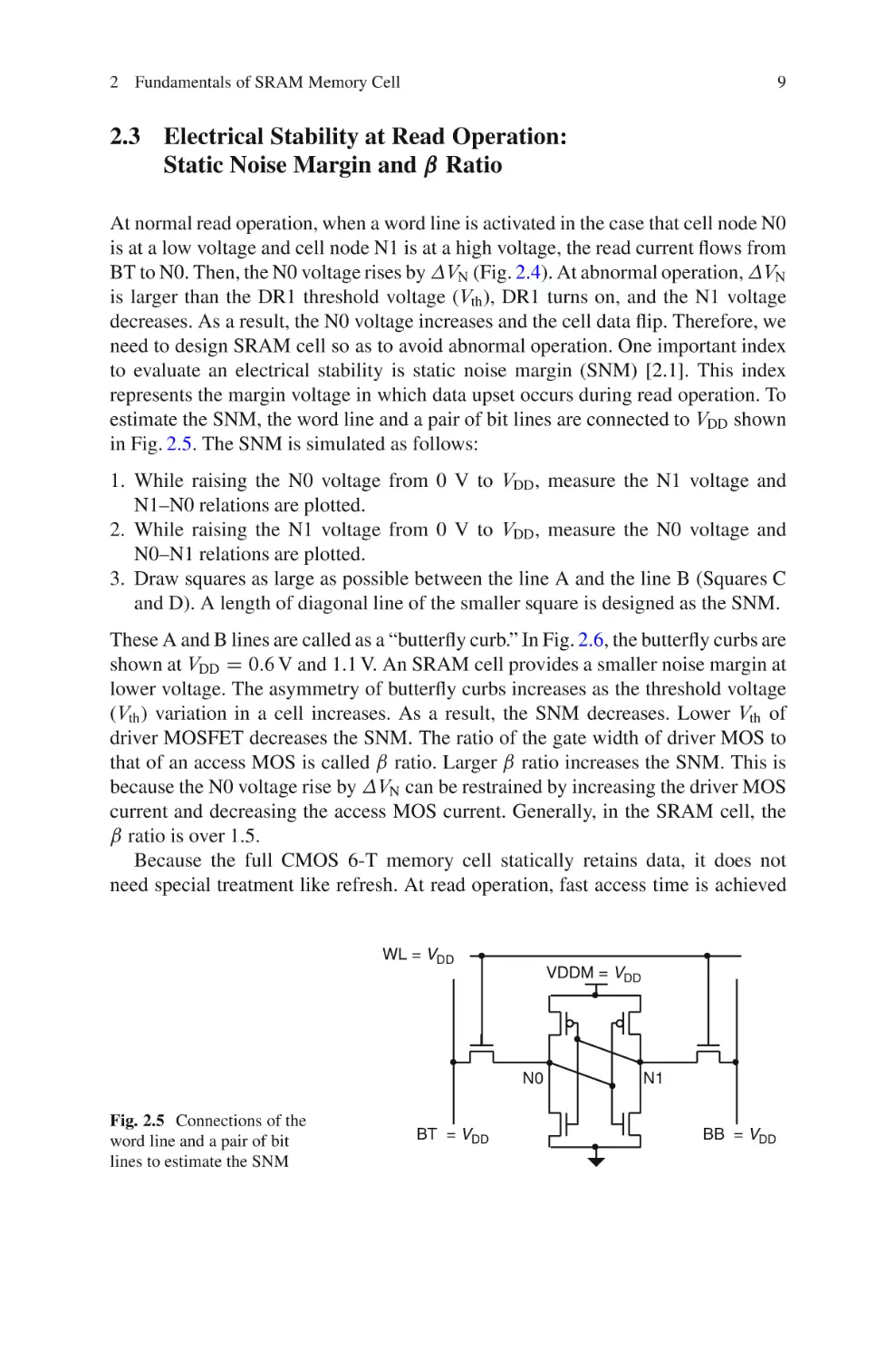
in Fig. 2.5. The SNM is simulated as follows:
1. While raising the N0 voltage from 0 V to VDD , measure the N1 voltage and
N1–N0 relations are plotted.
2. While raising the N1 voltage from 0 V to VDD , measure the N0 voltage and
N0–N1 relations are plotted.
3. Draw squares as large as possible between the line A and the line B (Squares C
and D). A length of diagonal line of the smaller square is designed as the SNM.
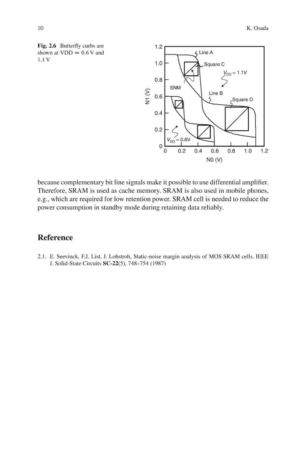
These A and B lines are called as a “butterfly curb.” In Fig. 2.6, the butterfly curbs are
shown at VDD D 0:6 V and 1.1 V. An SRAM cell provides a smaller noise margin at
lower voltage. The asymmetry of butterfly curbs increases as the threshold voltage
(Vth ) variation in a cell increases. As a result, the SNM decreases. Lower Vth of
driver MOSFET decreases the SNM. The ratio of the gate width of driver MOS to
that of an access MOS is called ˇ ratio. Larger ˇ ratio increases the SNM. This is
because the N0 voltage rise by VN can be restrained by increasing the driver MOS
current and decreasing the access MOS current. Generally, in the SRAM cell, the
ˇ ratio is over 1.5.
Because the full CMOS 6-T memory cell statically retains data, it does not
need special treatment like refresh. At read operation, fast access time is achieved
WL = VDD
VDDM = VDD
N0
Fig. 2.5 Connections of the
word line and a pair of bit
lines to estimate the SNM
BT = VDD
N1
BB = VDD
10
K. Osada
Fig. 2.6 Butterfly curbs are
shown at VDD D 0:6 V and
1.1 V
1.2
Line A
1.0
Square C
VDD = 1.1V
N1 (V)
0.8
SNM
Line B
0.6
Square D
0.4
0.2
VDD = 0.6V
0
0
0.2
0.4
0.6
0.8
1.0
1.2
N0 (V)
because complementary bit line signals make it possible to use differential amplifier.
Therefore, SRAM is used as cache memory. SRAM is also used in mobile phones,
e.g., which are required for low retention power. SRAM cell is needed to reduce the
power consumption in standby mode during retaining data reliably.
Reference
2.1. E. Seevinck, F.J. List, J. Lohstroh, Static-noise margin analysis of MOS SRAM cells. IEEE
J. Solid-State Circuits SC-22(5), 748–754 (1987)
Chapter 3
Electrical Stability (Read and Write Operations)
Masanao Yamaoka and Yasumasa Tsukamoto
Abstract In SRAM, read and write are fundamental operations. To ensure the
correct operations, the stability analysis is indispensable. In this chapter, electrical
stability analysis is explained. In Sect. 3.1, the SRAM operations, read and write,
are explained. In this section, the read stability, static-noise margin SNM, and the
write stability are described. In SRAM design, Vth variation of transistors has critical
influence on SRAM operation. In Sect. 3.2, the Vth variation of MOSFETs and its
effect to SRAM are described. The Vth variations can be divided into local and
global components. In this section, the effect of Vth variation is made visible using
Vth window curve analysis. In Sect. 3.3, by means of the conventional SNM and
write margin analysis on the SRAM cell characteristics, expanded mathematical
analysis to obtain the Vth curve is described. The analysis is instructive to see stable
Vth conditions visually to achieve high-yield SRAM. Furthermore, the proposed
analysis referred to as the worst-vector method allows to derive the minimum
operation voltage of the SRAM Macros (Vddmin /.
3.1 Fundamentals of Electrical Stability on Read and Write
Operations
A circuit diagram of a CMOS 6-transistor SRAM memory cell is shown in Fig. 3.1.
The fundamental waveform of SRAM operation is indicated in Fig. 3.2. When data
“0” is written to the cell (W0 in Fig. 3.2), the bit lines are driven to “H” and “L”
M. Yamaoka ()
Hitachi America Ltd., Research and Development Division, 1101 Kitchawan Road, Yorktown
Heights, NY 10598, USA
e-mail: masanao.yamaoka@hal.hitachi.com
Y. Tsukamoto
Renesas Electronics Corporation, 5-20-1, Josuihon-cho, Kodaira, Tokyo 187-8588, Japan
e-mail: yasumasa.tsukamoto.gx@renesas.com
K. Ishibashi and K. Osada (eds.), Low Power and Reliable SRAM Memory Cell
and Array Design, Springer Series in Advanced Microelectronics 31,
DOI 10.1007/978-3-642-19568-6 3, © Springer-Verlag Berlin Heidelberg 2011
11
12
M. Yamaoka and Y. Tsukamoto
WL
V
DD
LD0
LD1
AC0
AC1
N0
N1
DR0
DR1
VSS
BT
BB
Fig. 3.1 SRAM memory cell
W”0”
R”0”
W”1”
R”1”
WL
Time
Normal Operation
BT/BB BT
BB
Data flips
N0/N1
Data“0” is read
Data flips
Data“1”is read
N1
N0
Read stability failure case
Data flips during read operation
N0/N1
N1
N0
Write failure case
Data does not flip in“1”write operation
Wrong data“0”is read
N1
N0/N1
N0
Fig. 3.2 Fundamental waveform of SRAM operation
3 Electrical Stability (Read and Write Operations)
Fig. 3.3 SRAM cell
condition during data
retention
13
"L"
"L"
"H"
"H"
"H"
according to the input data and the word line (WL) is activated. The input data
is written to the data storage node, and the voltages of the data storage nodes are
flipped. When data “0” is read from the cell (R0 in Fig. 3.2), both bit lines are
precharged to “H,” and then the WL is activated. The retained data is appeared to
bit lines and voltage difference on the bit lines is generated. The voltage difference
is amplified at sense amplifier and the retained data is read out. When data “1” is
written to the cell and write failure is occurred (W1 write failure case in Fig. 3.2),
the voltages of the storage nodes (N0/N1) are not flipped, and the correct data is not
written into the cell. At the next read cycle, incorrect data “0” is read out. When
data “1” is read out from the cell and read failure is occurred (R1 read failure case
in Fig. 3.2), the voltage of data storage nodes (N0/N1) is flipped and the retained
data is destroyed. Therefore, the read failure is occurred.
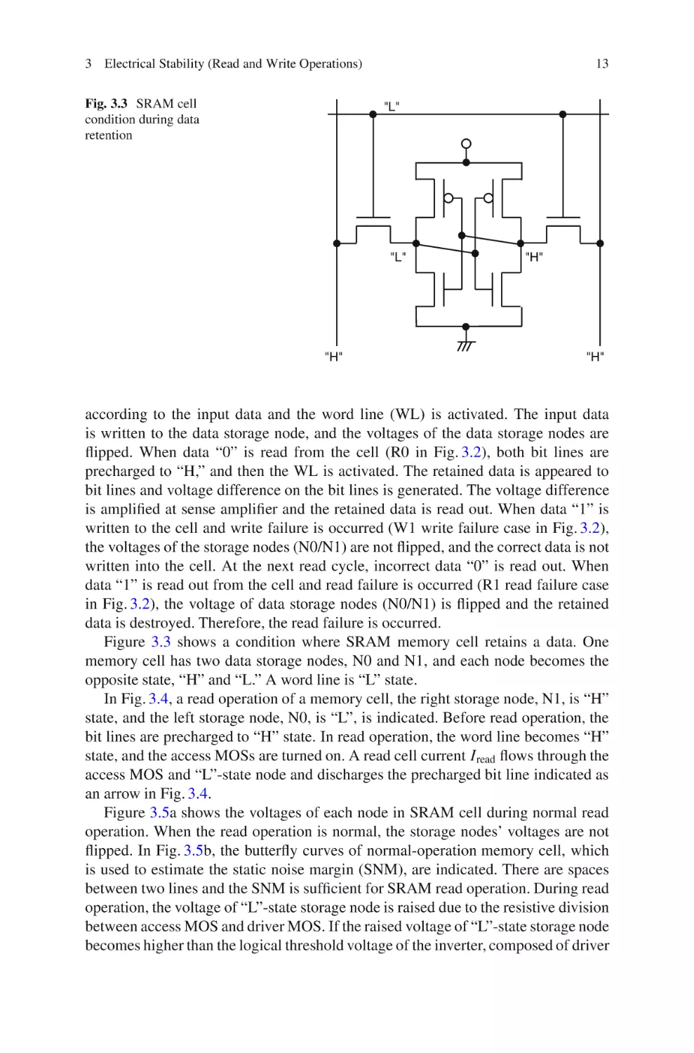
Figure 3.3 shows a condition where SRAM memory cell retains a data. One
memory cell has two data storage nodes, N0 and N1, and each node becomes the
opposite state, “H” and “L.” A word line is “L” state.
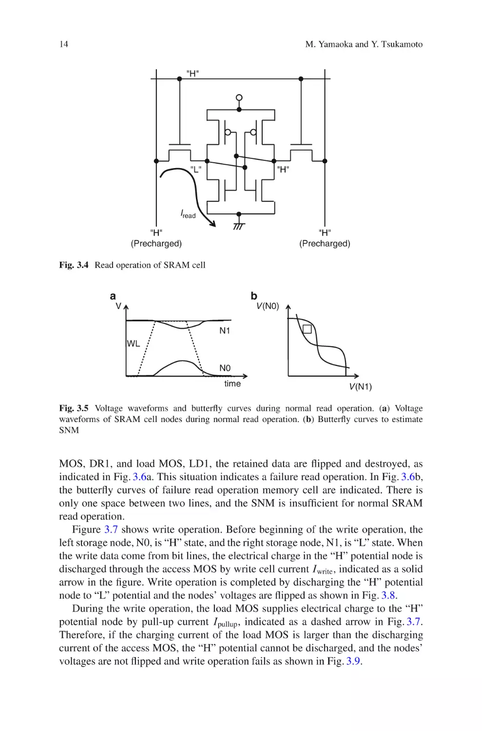
In Fig. 3.4, a read operation of a memory cell, the right storage node, N1, is “H”
state, and the left storage node, N0, is “L”, is indicated. Before read operation, the
bit lines are precharged to “H” state. In read operation, the word line becomes “H”
state, and the access MOSs are turned on. A read cell current Iread flows through the
access MOS and “L”-state node and discharges the precharged bit line indicated as
an arrow in Fig. 3.4.
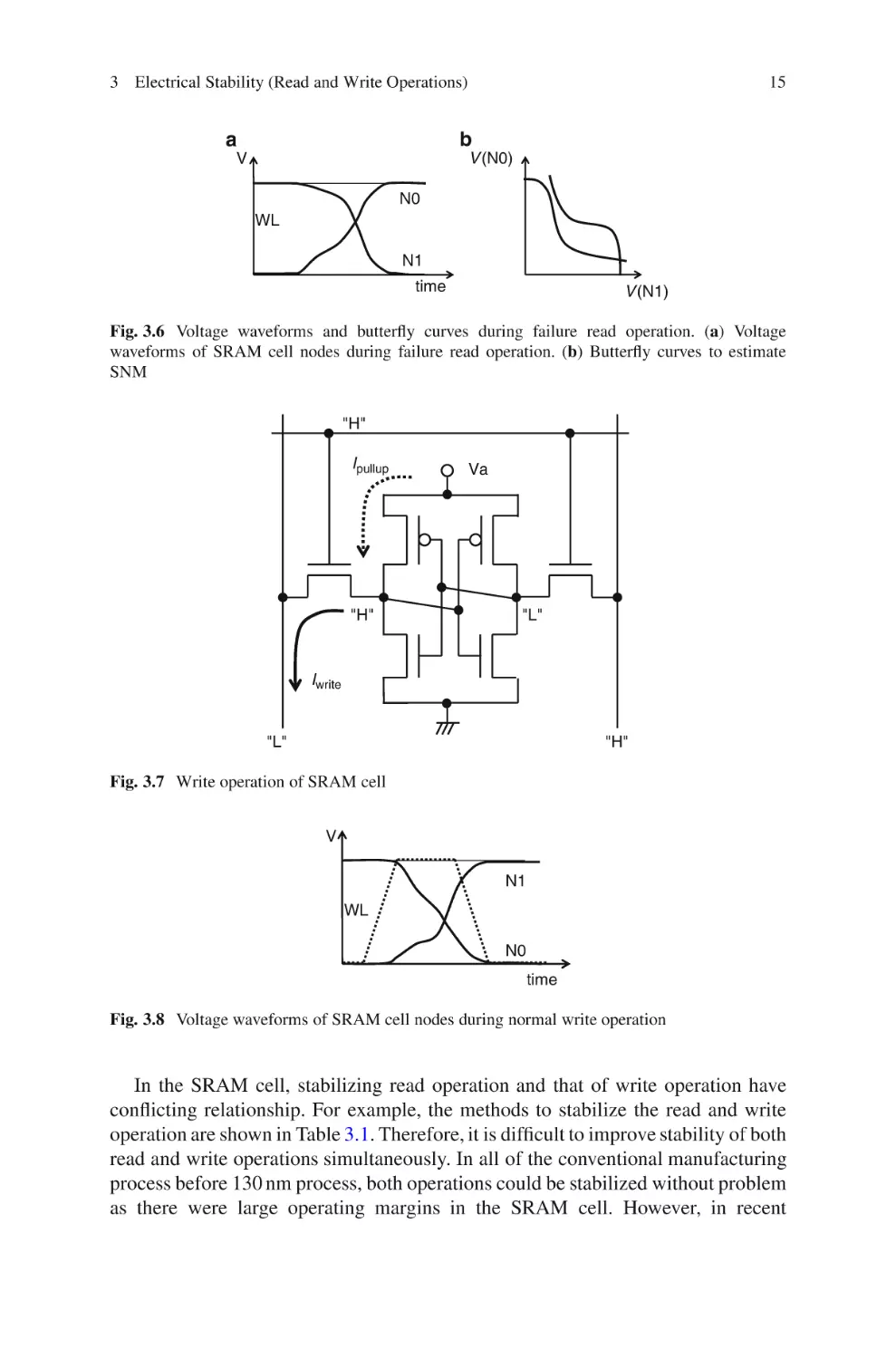
Figure 3.5a shows the voltages of each node in SRAM cell during normal read
operation. When the read operation is normal, the storage nodes’ voltages are not
flipped. In Fig. 3.5b, the butterfly curves of normal-operation memory cell, which
is used to estimate the static noise margin (SNM), are indicated. There are spaces
between two lines and the SNM is sufficient for SRAM read operation. During read
operation, the voltage of “L”-state storage node is raised due to the resistive division
between access MOS and driver MOS. If the raised voltage of “L”-state storage node
becomes higher than the logical threshold voltage of the inverter, composed of driver
14
M. Yamaoka and Y. Tsukamoto
"H"
"L"
"H"
Iread
"H"
(Precharged)
"H"
(Precharged)
Fig. 3.4 Read operation of SRAM cell
a
b
V(N0)
V
N1
WL
N0
time
V(N1)
Fig. 3.5 Voltage waveforms and butterfly curves during normal read operation. (a) Voltage
waveforms of SRAM cell nodes during normal read operation. (b) Butterfly curves to estimate
SNM
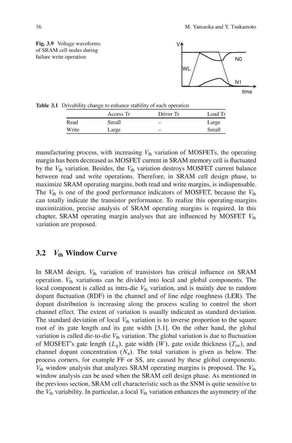
MOS, DR1, and load MOS, LD1, the retained data are flipped and destroyed, as
indicated in Fig. 3.6a. This situation indicates a failure read operation. In Fig. 3.6b,
the butterfly curves of failure read operation memory cell are indicated. There is
only one space between two lines, and the SNM is insufficient for normal SRAM
read operation.
Figure 3.7 shows write operation. Before beginning of the write operation, the
left storage node, N0, is “H” state, and the right storage node, N1, is “L” state. When
the write data come from bit lines, the electrical charge in the “H” potential node is
discharged through the access MOS by write cell current Iwrite , indicated as a solid
arrow in the figure. Write operation is completed by discharging the “H” potential
node to “L” potential and the nodes’ voltages are flipped as shown in Fig. 3.8.
During the write operation, the load MOS supplies electrical charge to the “H”
potential node by pull-up current Ipullup , indicated as a dashed arrow in Fig. 3.7.
Therefore, if the charging current of the load MOS is larger than the discharging
current of the access MOS, the “H” potential cannot be discharged, and the nodes’
voltages are not flipped and write operation fails as shown in Fig. 3.9.
3 Electrical Stability (Read and Write Operations)
15
b
a
V(N0)
V
N0
WL
N1
time
V (N1)
Fig. 3.6 Voltage waveforms and butterfly curves during failure read operation. (a) Voltage
waveforms of SRAM cell nodes during failure read operation. (b) Butterfly curves to estimate
SNM
"H"
Ipullup
"H"
Va
"L"
Iwrite
"L"
"H"
Fig. 3.7 Write operation of SRAM cell
V
N1
WL
N0
time
Fig. 3.8 Voltage waveforms of SRAM cell nodes during normal write operation
In the SRAM cell, stabilizing read operation and that of write operation have
conflicting relationship. For example, the methods to stabilize the read and write
operation are shown in Table 3.1. Therefore, it is difficult to improve stability of both
read and write operations simultaneously. In all of the conventional manufacturing
process before 130 nm process, both operations could be stabilized without problem
as there were large operating margins in the SRAM cell. However, in recent
16
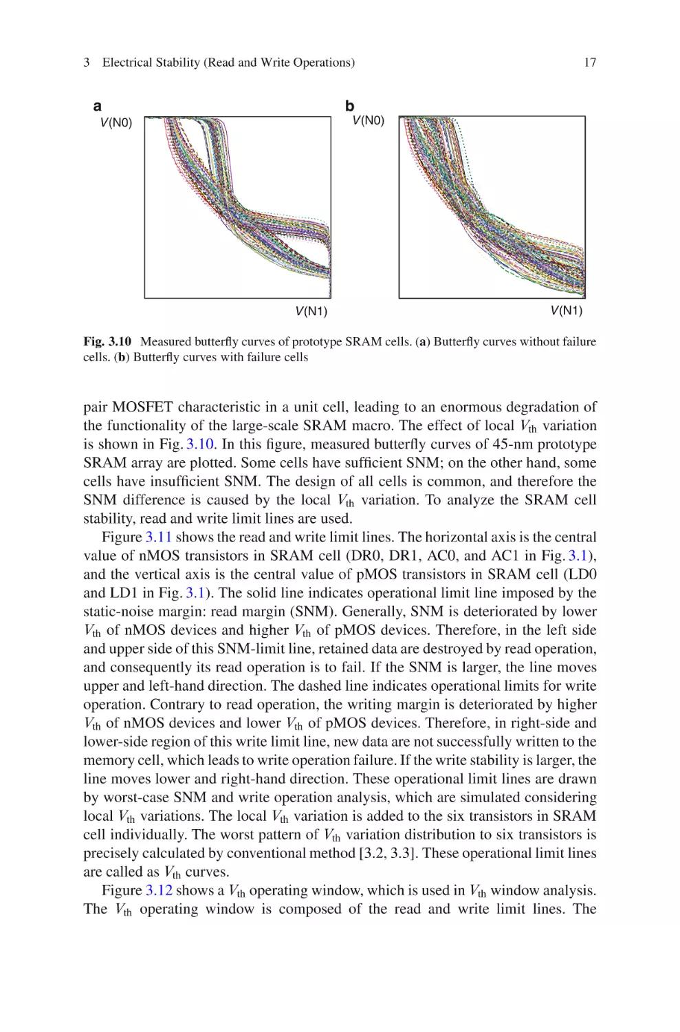
M. Yamaoka and Y. Tsukamoto
Fig. 3.9 Voltage waveforms
of SRAM cell nodes during
failure write operation
V
N0
WL
N1
time
Table 3.1 Drivability change to enhance stability of each operation
Read
Write
Access Tr
Small
Large
Driver Tr
–
–
Load Tr
Large
Small
manufacturing process, with increasing Vth variation of MOSFETs, the operating
margin has been decreased as MOSFET current in SRAM memory cell is fluctuated
by the Vth variation. Besides, the Vth variation destroys MOSFET current balance
between read and write operations. Therefore, in SRAM cell design phase, to
maximize SRAM operating margins, both read and write margins, is indispensable.
The Vth is one of the good performance indicators of MOSFET, because the Vth
can totally indicate the transistor performance. To realize this operating-margins
maximization, precise analysis of SRAM operating margins is required. In this
chapter, SRAM operating margin analyses that are influenced by MOSFET Vth
variation are proposed.
3.2 Vth Window Curve
In SRAM design, Vth variation of transistors has critical influence on SRAM
operation. Vth variations can be divided into local and global components. The
local component is called as intra-die Vth variation, and is mainly due to random
dopant fluctuation (RDF) in the channel and of line edge roughness (LER). The
dopant distribution is increasing along the process scaling to control the short
channel effect. The extent of variation is usually indicated as standard deviation.
The standard deviation of local Vth variation is to inverse proportion to the square
root of its gate length and its gate width [3.1]. On the other hand, the global
variation is called die-to-die Vth variation. The global variation is due to fluctuation
of MOSFET’s gate length .Lg /, gate width .W /, gate oxide thickness .Tox /, and
channel dopant concentration .Na /. The total variation is given as below. The
process corners, for example FF or SS, are caused by these global components.
Vth window analysis that analyzes SRAM operating margins is proposed. The Vth
window analysis can be used when the SRAM cell design phase. As mentioned in
the previous section, SRAM cell characteristic such as the SNM is quite sensitive to
the Vth variability. In particular, a local Vth variation enhances the asymmetry of the
3 Electrical Stability (Read and Write Operations)
a
17
b
V(N0)
V(N0)
V(N1)
V (N1)
Fig. 3.10 Measured butterfly curves of prototype SRAM cells. (a) Butterfly curves without failure
cells. (b) Butterfly curves with failure cells
pair MOSFET characteristic in a unit cell, leading to an enormous degradation of
the functionality of the large-scale SRAM macro. The effect of local Vth variation
is shown in Fig. 3.10. In this figure, measured butterfly curves of 45-nm prototype
SRAM array are plotted. Some cells have sufficient SNM; on the other hand, some
cells have insufficient SNM. The design of all cells is common, and therefore the
SNM difference is caused by the local Vth variation. To analyze the SRAM cell
stability, read and write limit lines are used.
Figure 3.11 shows the read and write limit lines. The horizontal axis is the central
value of nMOS transistors in SRAM cell (DR0, DR1, AC0, and AC1 in Fig. 3.1),
and the vertical axis is the central value of pMOS transistors in SRAM cell (LD0
and LD1 in Fig. 3.1). The solid line indicates operational limit line imposed by the
static-noise margin: read margin (SNM). Generally, SNM is deteriorated by lower
Vth of nMOS devices and higher Vth of pMOS devices. Therefore, in the left side
and upper side of this SNM-limit line, retained data are destroyed by read operation,
and consequently its read operation is to fail. If the SNM is larger, the line moves
upper and left-hand direction. The dashed line indicates operational limits for write
operation. Contrary to read operation, the writing margin is deteriorated by higher
Vth of nMOS devices and lower Vth of pMOS devices. Therefore, in right-side and
lower-side region of this write limit line, new data are not successfully written to the
memory cell, which leads to write operation failure. If the write stability is larger, the
line moves lower and right-hand direction. These operational limit lines are drawn
by worst-case SNM and write operation analysis, which are simulated considering
local Vth variations. The local Vth variation is added to the six transistors in SRAM
cell individually. The worst pattern of Vth variation distribution to six transistors is
precisely calculated by conventional method [3.2, 3.3]. These operational limit lines
are called as Vth curves.
Figure 3.12 shows a Vth operating window, which is used in Vth window analysis.
The Vth operating window is composed of the read and write limit lines. The
18
M. Yamaoka and Y. Tsukamoto
Fig. 3.11 Read and write
limit lines (Vth curves)
Read limit line
SNM larger
pMOS ΔVth (V)
SNM
smaller
Write limit line
Write stability
larger
Write stability
smaller
nMOS ΔVth (V)
Fig. 3.12 Vth operating
window
0.2
Read limit line
SS
pMOS ΔVth (V)
0.1
FS
0
SF
-0.1
FF
Write limit line
-0.2
-0.2
-0.1
0
0.1
0.2
nMOS ΔVth (V)
horizontal axis is the central value of nMOS transistors in SRAM cell, and the
vertical axis is the central value of pMOS transistors in SRAM cell. These Vth
values contain the global Vth variation. The diamond shape in Fig. 3.12 indicates
the process corners. The FS point, for example, means nMOS fast and pMOS slow
device.
When the Vth of manufactured SRAM transistors is in the window between each
Vth curves (hatched region in Fig. 3.12), SRAM memory cell can operate correctly.
Therefore, the diamond shape, which indicates the Vth distribution of manufactured
devices, has to be within the area to guarantee SRAM correct operation in all process
corners. This Vth window analysis is used in memory cell design, and the central Vth
value (TT device) is adjusted so that Vth corners are within the operating window.
An example of this Vth window analysis is described as below. The description
supposes that an SoC is manufactured on the point of a read-limit line, and average
value of nMOS Vth is 0:06 V, and that of pMOS Vth is 0.1 V. These values are
3 Electrical Stability (Read and Write Operations)
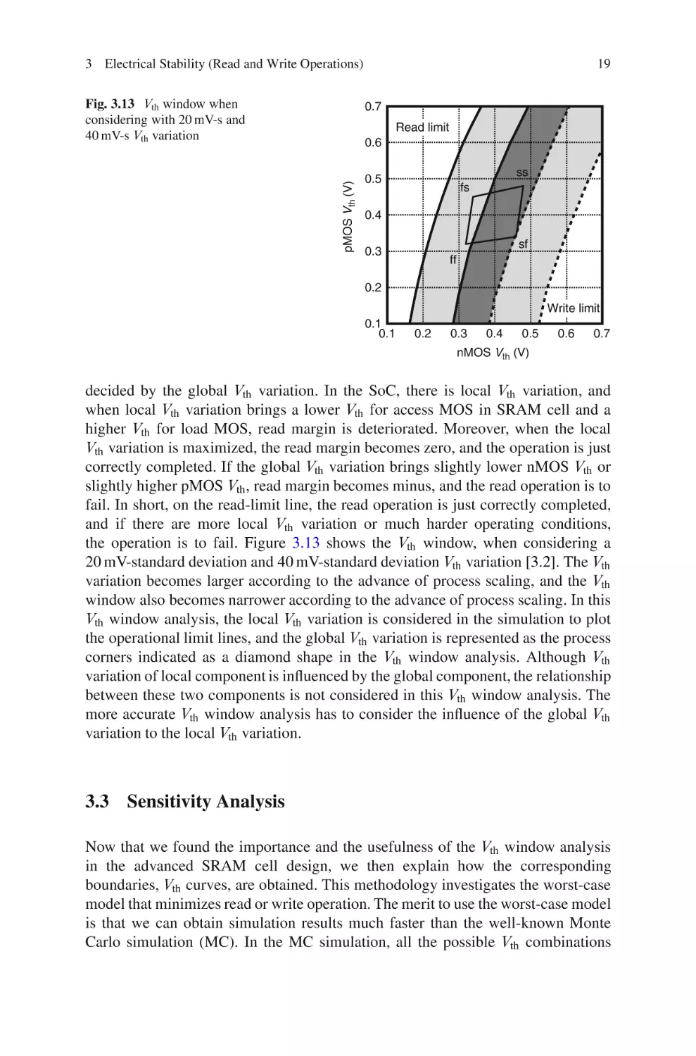
Fig. 3.13 Vth window when
considering with 20 mV-s and
40 mV-s Vth variation
19
0.7
Read limit
pMOS Vth (V)
0.6
ss
0.5
fs
0.4
sf
0.3
ff
0.2
Write limit
0.1
0.1
0.2
0.3
0.4
0.5
0.6
0.7
nMOS Vth (V)
decided by the global Vth variation. In the SoC, there is local Vth variation, and
when local Vth variation brings a lower Vth for access MOS in SRAM cell and a
higher Vth for load MOS, read margin is deteriorated. Moreover, when the local
Vth variation is maximized, the read margin becomes zero, and the operation is just
correctly completed. If the global Vth variation brings slightly lower nMOS Vth or
slightly higher pMOS Vth , read margin becomes minus, and the read operation is to
fail. In short, on the read-limit line, the read operation is just correctly completed,
and if there are more local Vth variation or much harder operating conditions,
the operation is to fail. Figure 3.13 shows the Vth window, when considering a
20 mV-standard deviation and 40 mV-standard deviation Vth variation [3.2]. The Vth
variation becomes larger according to the advance of process scaling, and the Vth
window also becomes narrower according to the advance of process scaling. In this
Vth window analysis, the local Vth variation is considered in the simulation to plot
the operational limit lines, and the global Vth variation is represented as the process
corners indicated as a diamond shape in the Vth window analysis. Although Vth
variation of local component is influenced by the global component, the relationship
between these two components is not considered in this Vth window analysis. The
more accurate Vth window analysis has to consider the influence of the global Vth
variation to the local Vth variation.
3.3 Sensitivity Analysis
Now that we found the importance and the usefulness of the Vth window analysis
in the advanced SRAM cell design, we then explain how the corresponding
boundaries, Vth curves, are obtained. This methodology investigates the worst-case
model that minimizes read or write operation. The merit to use the worst-case model
is that we can obtain simulation results much faster than the well-known Monte
Carlo simulation (MC). In the MC simulation, all the possible Vth combinations
20
M. Yamaoka and Y. Tsukamoto
within a unit SRAM cell are generated, and the corresponding margins are all
calculated. In particular for the Vth window analysis, we need to take the large
number of SRAM cell array (e.g., 1 Mbits or larger) into consideration depending
on the capacity of the actual SRAM products. This means that more than 106
simulation times would be needed to identify single point of Vth curves. In contrast,
our method requires about 50-time simulations for each point because this method
is based on the sensitivity analysis and searches for the worst Vth combination that
minimizes read or write margin: excessive simulations that do not contribute to the
estimate of the boundary are not calculated. Furthermore, a slight modification of
the simulation flow allows us to estimate the minimum operating voltage of the
SRAM cell array .Vddmin /, which is also important in characterizing macroscopic
feature of a large-scale SRAM array. The validity of using the worst-case model is
verified by comparing with the measurement result.
We start our discussion by expanding SRAM DC margin. Hereafter, we only
focus on the read margin or the SNM, which can be also extended to the write
margin. Although various factors such as supply voltage and body bias effects affect
the SNM drastically, we simply assume that the SNM is a function of 6 transistor’s
Vth s’ in a unit memory cell [3.4]. Furthermore, the sensitivity analysis shown in
Fig. 3.14 indicates that 2 transistors in a memory cell have no contribution to the
SNM, which allows us to denote the SNM function as:
SNML .Vt.AC1/ ; Vt.DR0/ ; Vt.DR1/ ; Vt.LD0/ /:
(3.1)
Since our task is to derive the situation of SNM D 0 due to the Vth variation, it is
instructive to divide each Vt.X / into several components.
Vt.X / D Vt.X
typ/
C Vt.X / C xVt.X / ;
AC1
DR1
LD1
Normalized SNM
AC0
DR0
LD0
(3.2)
Fig. 3.14 Sensitivity analysis
-6.0
-3.0
0.0
3.0
Local Vth Variation (Units of s )
6.0
3 Electrical Stability (Read and Write Operations)
21
where Vt.X typ/ is the typical Vth value of transistor X; Vt.X / the deviation from
the typical Vth which is equivalent to the global variation, and Vt.X / the standard
deviation of local Vth variation. As mentioned in the previous subsection, Vt.X / can
be calculated if we define the transistor dimension L/W as well as a proportionality
coefficient, Avt [3.1, 3.5]. In addition, the parameter x indicates the probability of
appearance, which plays an important role in our later discussion in determining the
worst-case model for SNM.
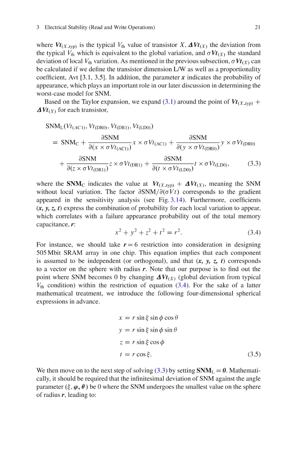
Based on the Taylor expansion, we expand (3.1) around the point of Vt.X typ/ C
Vt.X / for each transistor,
SNML .Vt.AC 1/ ; Vt.DR0/ ; Vt.DR1/ ; Vt.LD0/ /
D SNMC C
C
@SNM
@SNM
x Vt.AC1/ C
y Vt.DR0/
@.x Vt.AC1/ /
@.y Vt.DR0/ /
@SNM
@SNM
z Vt.DR1/ C
t Vt.LD0/ ;
@.z Vt.DR1/ /
@.t Vt.LD0/ /
(3.3)
where the SNMC indicates the value at Vt.X typ/ C Vt.X / , meaning the SNM
without local variation. The factor @SNM=@.¢V t/ corresponds to the gradient
appeared in the sensitivity analysis (see Fig. 3.14). Furthermore, coefficients
(x, y, z, t) express the combination of probability for each local variation to appear,
which correlates with a failure appearance probability out of the total memory
capacitance, r:
x 2 C y 2 C z2 C t 2 D r 2 :
(3.4)
For instance, we should take r D 6 restriction into consideration in designing
505 Mbit SRAM array in one chip. This equation implies that each component
is assumed to be independent (or orthogonal), and that (x, y, z, t) corresponds
to a vector on the sphere with radius r. Note that our purpose is to find out the
point where SNM becomes 0 by changing Vt.X / (global deviation from typical
Vth condition) within the restriction of equation (3.4). For the sake of a latter
mathematical treatment, we introduce the following four-dimensional spherical
expressions in advance.
x D r sin sin cos
y D r sin sin sin
z D r sin cos
t D r cos :
(3.5)
We then move on to the next step of solving (3.3) by setting SNML D 0. Mathematically, it should be required that the infinitesimal deviation of SNM against the angle
parameter .; '; / be 0 where the SNM undergoes the smallest value on the sphere
of radius r, leading to:
22
M. Yamaoka and Y. Tsukamoto
@SNM
@SNM
@SNM
D
D
D 0:
@
@
@
(3.6)
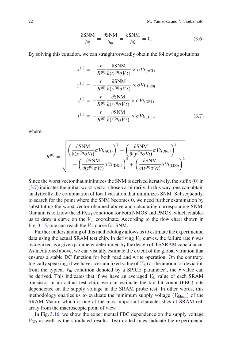
By solving this equation, we can straightforwardly obtain the following solutions:
x .1/ D
r
@SNM
Vt.AC1/
.0/
R @.x .0/ V t/
y .1/ D
@SNM
r
Vt.DR0/
R.0/ @.y .0/ V t/
z.1/ D
@SNM
r
Vt.DR1/
.0/
R @.z.0/ V t/
t .1/ D
@SNM
r
Vt.LD0/ ;
.0/
R @.t .0/ V t/
(3.7)
where,
R.0/
v
u
2
2
u
@SNM
@SNM
u
Vt
Vt
C
.AC1/
.DR0/
u @.x .0/ Vt/
@.y .0/ Vt/
Du
2
2 :
u
@SNM
@SNM
t
Vt.DR1/ C
Vt.LD0/
C
@.z.0/ Vt/
@.t .0/ Vt/
Since the worst vector that minimizes the SNM is derived iteratively, the suffix (0) in
(3.7) indicates the initial worst vector chosen arbitrarily. In this way, one can obtain
analytically the combination of local variation that minimizes SNM. Subsequently,
to search for the point where the SNM becomes 0, we need further examination by
substituting the worst vector obtained above and calculating corresponding SNM.
Our aim is to know the Vt.X / condition for both NMOS and PMOS, which enables
us to draw a curve on the Vth coordinate. According to the flow chart shown in
Fig. 3.15, one can reach the Vth curve for SNM.
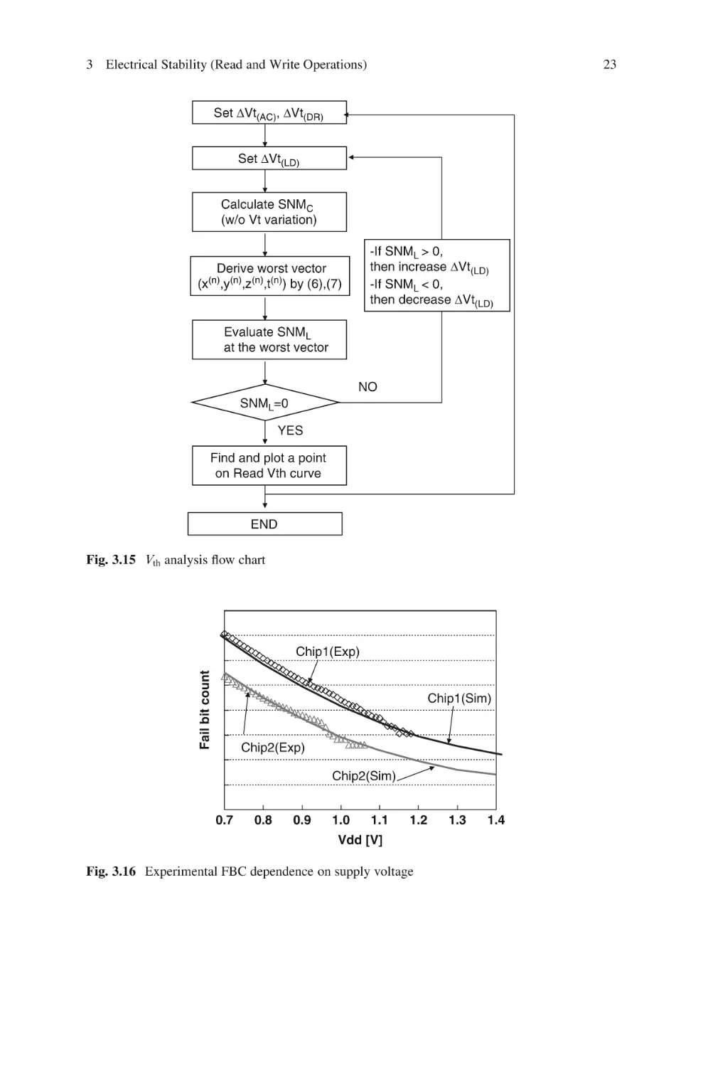
Further understanding of this methodology allows us to estimate the experimental
data using the actual SRAM test chip. In deriving Vth curves, the failure rate r was
recognized as a given parameter determined by the design of the SRAM capacitance.
As mentioned above, we can visually estimate the extent of the global variation that
ensures a stable DC function for both read and write operation. On the contrary,
logically speaking, if we have a certain fixed value of Vth (or the amount of deviation
from the typical Vth condition denoted by a SPICE parameter), the r value can
be derived. This indicates that if we have an averaged Vth value of each SRAM
transistor in an actual test chip, we can estimate the fail bit count (FBC) rate
dependence on the supply voltage in the SRAM probe test. In other words, this
methodology enables us to evaluate the minimum supply voltage .Vddmin / of the
SRAM Macro, which is one of the most important characteristics of SRAM cell
array from the macroscopic point of view.
In Fig. 3.16, we show the experimental FBC dependence on the supply voltage
VDD as well as the simulated results. Two dotted lines indicate the experimental
3 Electrical Stability (Read and Write Operations)
23
Set ΔVt(AC), ΔVt(DR)
Set ΔVt(LD)
Calculate SNMC
(w/o Vt variation)
-If SNML > 0,
then increase ΔVt(LD)
-If SNML < 0,
then decrease ΔVt(LD)
Derive worst vector
(x(n),y(n),z(n),t(n)) by (6),(7)
Evaluate SNML
at the worst vector
NO
SNML=0
YES
Find and plot a point
on Read Vth curve
END
Fig. 3.15 Vth analysis flow chart
Fail bit count
Chip1(Exp)
Chip1(Sim)
Chip2(Exp)
Chip2(Sim)
0.7
0.8
0.9
1.0
1.1
1.2
Vdd [V]
Fig. 3.16 Experimental FBC dependence on supply voltage
1.3
1.4
24
M. Yamaoka and Y. Tsukamoto
results evaluated from the different chips on different wafers. The SRAM cell
.0:499 m2 [3.6]) was fabricated on our original process of 65 nm bulk CMOS
technology. For these two chips we examined, the PMOS Vth s were realized
much higher than our target, so that the read (SNM) FBC has a relatively lower
dependence on the VDD change. To compare the experiments with the simulation
results based on our methodology, we evaluated Vth and the corresponding local
variation of each SRAM transistor using the other test circuitry. It is obvious that
the simulated results are in good accordance with the experiment, exemplifying the
validity of our methodology.
References
3.1. M.J. Pelgrom, A.C.J. Duinmaijar, Matching properties of MOS transistors. IEEE. J. SolidState Circuits 24(5), 1433–1440 (1989)
3.2. M. Yamaoka et. al., Low power SRAM menu for SOC application using Yin-Yang-feedback
memory cell, in Proceedings of 2004 Symposium on VLSI Circuits, pp. 288–291
3.3. Y. Tsukamoto, K. Nii, S. Imaoka, Y. Oda, S. Ohbayashi, T. Yoshizawa, H. Makino,
K. Ishibashi, H. Shinohara, Worst-case analysis to obtain stable read/write DC margin of
high density 6T-SRAM-array with local Vth variability, in Proceedings of ICCAD, Nov. 2005,
pp. 394–405
3.4. F. Tachibana, T. Hiramoto, Re-examination of impact of intrinsic dopant fluctuations for ultrasmall bulk and SOI CMOS, IEEE Trans. Electron Devices 48(9), 1995–2001 (2001)
3.5. P.A. Stolk, F.P. Widdershoven, D.B.M. Klaassen, Modeling statistical dopant fluctuations in
mos transistors IEEE Trans. Electron Devices 45(9), 960–1971 (1998)
3.6. S. Ohbayashi et al., A 65 nm SoC embedded 6T-SRAM design for manufacturing with read
and write cell stabilizing circuits, in Proceedings of 2006 Symposium on VLSI Circuits, 2006,
pp. 17-18
Chapter 4
Low Power Memory Cell Design Technique
Kenichi Osada and Masanao Yamaoka
Abstract This chapter describes the low power memory cell design technique.
Section 4.1 introduces fundamentals of leakage of SRAM array. In Sect. 4.2, source
line voltage control techniques are explained as new designs to reduce standby
power dissipation. Using the techniques for a 16-Mbit SRAM chip fabricated
in 0:13-m CMOS technology, the cell-standby current is 16.7 fA at 25ı C and
101.7 fA at 90ı C. By applying the techniques to 1-Mbit 130-nm embedded SRAM,
the leakage current is reduced by about 90% from 230 to 25 A. In Sect. 4.3, a
new SRAM cell layout design developed for low-voltage operation is described. A
lithographically symmetrical cell for lower-voltage operation was developed. The
measured butterfly curves indicate that the memory cell has a large enough noise
margin even at 0.3 V.
4.1 Fundamentals of Leakage of SRAM Array
DRAM cell has low standby power dissipation [4.1]. But it needs refresh treatment.
On the other hand, SRAM cell does not need special treatment like refresh because
the full CMOS 6-T memory cell statically retains data. Hence, it is easy to control
SRAM chip, which is used in mobile phones. Moreover, SRAM is also used as
the embedded memory in the application processor in mobile cellular phones since
it is fabricated by the same process as CMOS logic uses. Advances in MOS
technology are accompanied by increases in the gate-oxide tunnel leakage and
K. Osada ()
Measurement Systems Research Department, Central Research Laboratory, Hitachi Ltd.,
1-280, Higashi-koigakubo, Kokubunji-shi, Tokyo 180-8601, Japan
e-mail: kenichi.osada.aj@hitachi.com
M. Yamaoka
1101 Kitchawan Road, Yorktown Heights, NY 10598, USA
e-mail: masanao.yamaoka@hal.hitachi.com
K. Ishibashi and K. Osada (eds.), Low Power and Reliable SRAM Memory Cell
and Array Design, Springer Series in Advanced Microelectronics 31,
DOI 10.1007/978-3-642-19568-6 4, © Springer-Verlag Berlin Heidelberg 2011
25
26
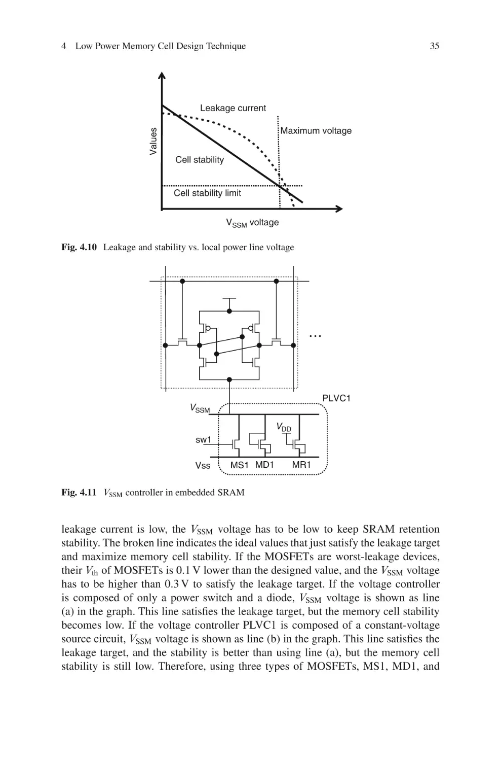
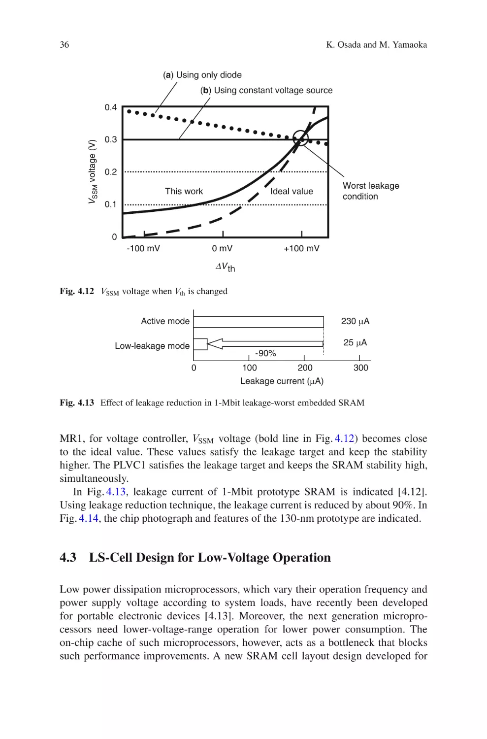
K. Osada and M. Yamaoka
gate-induced drain leakage (GIDL) currents, which are added to the subthreshold
leakage current as the main components of leakage [4.2–4.4]. The increased leakage
currents increases leakage current of SRAM cell. In this section, the fundamentals
of leakage power of SRAM array will be mentioned.
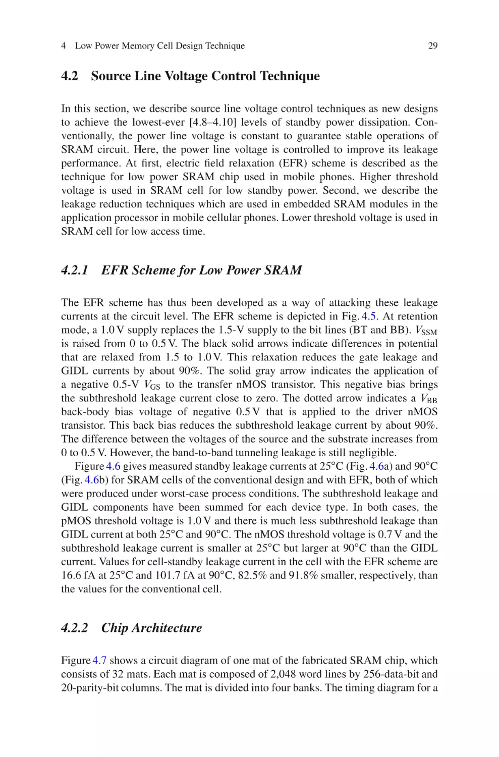
4.1.1 Leakage Currents in an SRAM of Conventional Design
The problem of leakage current increases as technology advances. The four
significant leakage currents in a technologically advanced nMOS transistor are
shown in Fig. 4.1. These are the gate-oxide tunnel leakage, the GIDL, the junction
tunnel leakage, and the subthreshold leakage currents. Subthreshold leakage is a
channel leakage current that flows from drain to source while the gate is off, since
this state sets up a weak inversion layer in the channel region.
The significant leakage currents in an advanced technology SRAM cell of
conventional design are shown in Fig. 4.2. In the conventional SRAM, 1.5 V is
applied to the bit lines (BT and BB) and power line (VDDI ), and 0 V is applied to the
word line and the VSS line (VSSM ). In the cell as a whole, two gate-tunnel leakage
currents, five GIDL currents, and three subthreshold leakage currents constitute the
main leakage currents. The use of high threshold voltages provides a straightforward
way to reduce the subthreshold leakage currents although the cell current for read
operation decreases. However, it is not easy to reduce the tunnel leakage and GIDL
currents by simply improving the device structure.
4.1.2 Gate-Tunnel Leakage and GIDL Currents
In this subsection, we describe the gate-tunnel leakage and GIDL currents. Measured plots of gate-tunnel leakage current as a function of gate voltage with the
thickness of the gate oxide (TOX ) varied as a parameter are given in Fig. 4.3. With a
2-Å decrease in TOX , there is a tenfold increase in gate-tunnel leakage current. As
Gate-oxide tunnel leakage
Gate
GIDL
Source
Fig. 4.1 Leakage currents in
a technologically advanced
nMOS device
Drain
Subthreshold
leakage
GIDL: Gate-induced drain leakage
Junction tunnel
4 Low Power Memory Cell Design Technique
27
Word 0 V
VDDI1.5 V
0V
1.5 V
VSSM
0V
BT
1.5 V
BB
1.5 V
Gate-tunnel leakage
GIDL
Subthreshold leakage
Fig. 4.2 Standby leakage currents in an advanced technology SRAM cell of conventional design
10-8
NMOS
Gate current (A/µm2)
10-9
T OX =
10-10
3.12
T OX =
nm
3.34
10-11
T OX =
10-12
T OX =
nm
3.52
3.76
nm
nm
10-13
10-14
0.5
1.0
1.5
2.0
Gate voltage
(V)
Fig. 4.3 Gate-tunnel leakage current as a function of gate voltage with the thickness of the gate
oxide (Tox ) varied as a parameter
28
K. Osada and M. Yamaoka
Fig. 4.4 GIDL and
subthreshold leakage currents
101
NMOS
VG
10-1
VGD
VD = 1.0 V
VD = 1.5 V
Drain current (A)
10-3
10-5
VS= 0 V
GIDL
VD
10-7
10-9
10-11
Subthreshold
GIDL
10-13
Ioff@VGD = 1.5 V
10-15
Ioff@VGD = 1.0 V
10-17
-0.5
0
0.5
1.0
1.5
Gate voltage VG (V)
technology advances, this current becomes the main form of leakage. On the other
hand, the gate current decreases with the gate voltage. Reducing the voltage by
0.5 V (from 1.5 to 1.0 V) reduces this leakage component by 95%. This is because
the tunnel leakage current simply decreases with the electric field strength in the
gate oxide [4.2–4.6].
Figure 4.4 shows measured curves of drain current as a function of the gate
voltage (VG ). The solid line is the drain current when the drain voltage (VD ) is
1.0 V, and the dotted line is the drain current when VD is 1.5 V. The subthreshold
leakage currents are dominant in the region where VG is greater than 0 V, while
the GIDL currents are dominant in the region where VG is less than 0 V. Since a
raised threshold voltage is in use, the subthreshold leakage currents at VG D 0 V are
negligibly weak in comparison with the GIDL currents. The standby current is thus
almost equivalent to the GIDL current. The GIDL current (IGIDL ) is very sensitive
to the electric field F and is given by [4.4, 4.7]:
IGIDL D AF 5=2 exp.B=F /;
(4.1)
where A and B depend on the bandgap EG and constants. This expression indicates
that the logarithm of the GIDL current is in inverse linear proportion to the gate
voltage, which is mainly responsible for the electric field directly beneath the gate
oxide. That is, the amount of GIDL current is determined by the difference between
the voltages at the gate and drain (VGD /. If VGD is reduced from 1.5 to 1.0 V, the
electric field strength is relaxed and the GIDL current in our device is reduced by
about 90%. If the threshold voltage is low, the main part of the leakage currents is
the subthreshold leakage current. The subthreshold leakage current is reduced by
the applications of a negative VGS or a negative VBB back-body bias voltage.
4 Low Power Memory Cell Design Technique
29
4.2 Source Line Voltage Control Technique
In this section, we describe source line voltage control techniques as new designs
to achieve the lowest-ever [4.8–4.10] levels of standby power dissipation. Conventionally, the power line voltage is constant to guarantee stable operations of
SRAM circuit. Here, the power line voltage is controlled to improve its leakage
performance. At first, electric field relaxation (EFR) scheme is described as the
technique for low power SRAM chip used in mobile phones. Higher threshold
voltage is used in SRAM cell for low standby power. Second, we describe the
leakage reduction techniques which are used in embedded SRAM modules in the
application processor in mobile cellular phones. Lower threshold voltage is used in
SRAM cell for low access time.
4.2.1 EFR Scheme for Low Power SRAM
The EFR scheme has thus been developed as a way of attacking these leakage
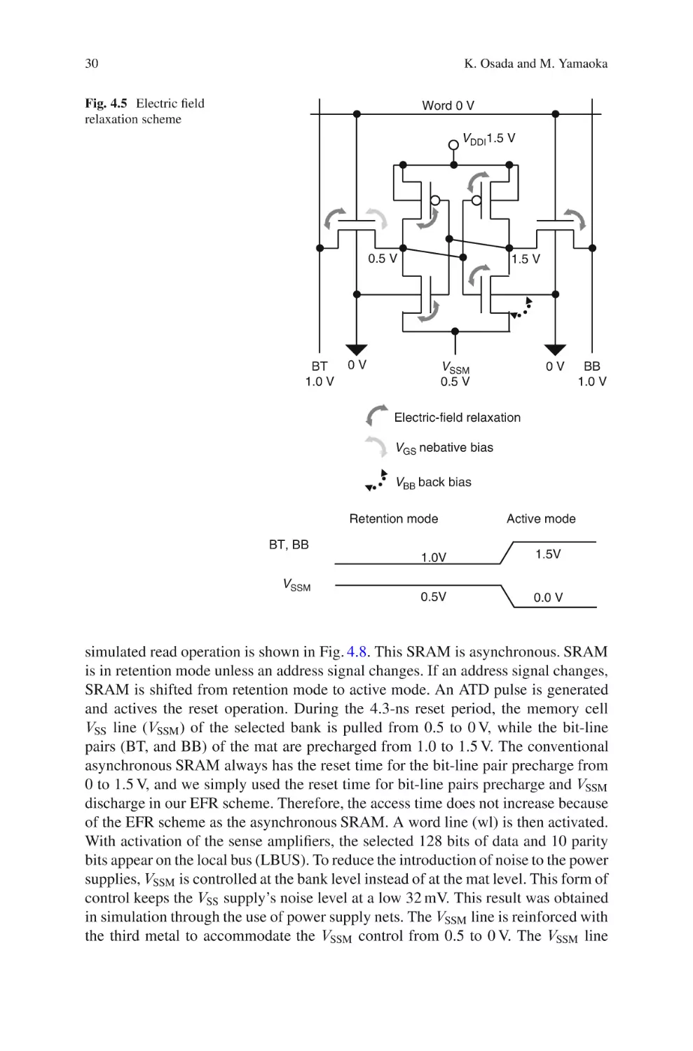
currents at the circuit level. The EFR scheme is depicted in Fig. 4.5. At retention
mode, a 1.0 V supply replaces the 1.5-V supply to the bit lines (BT and BB). VSSM
is raised from 0 to 0.5 V. The black solid arrows indicate differences in potential
that are relaxed from 1.5 to 1.0 V. This relaxation reduces the gate leakage and
GIDL currents by about 90%. The solid gray arrow indicates the application of
a negative 0.5-V VGS to the transfer nMOS transistor. This negative bias brings
the subthreshold leakage current close to zero. The dotted arrow indicates a VBB
back-body bias voltage of negative 0.5 V that is applied to the driver nMOS
transistor. This back bias reduces the subthreshold leakage current by about 90%.
The difference between the voltages of the source and the substrate increases from
0 to 0.5 V. However, the band-to-band tunneling leakage is still negligible.
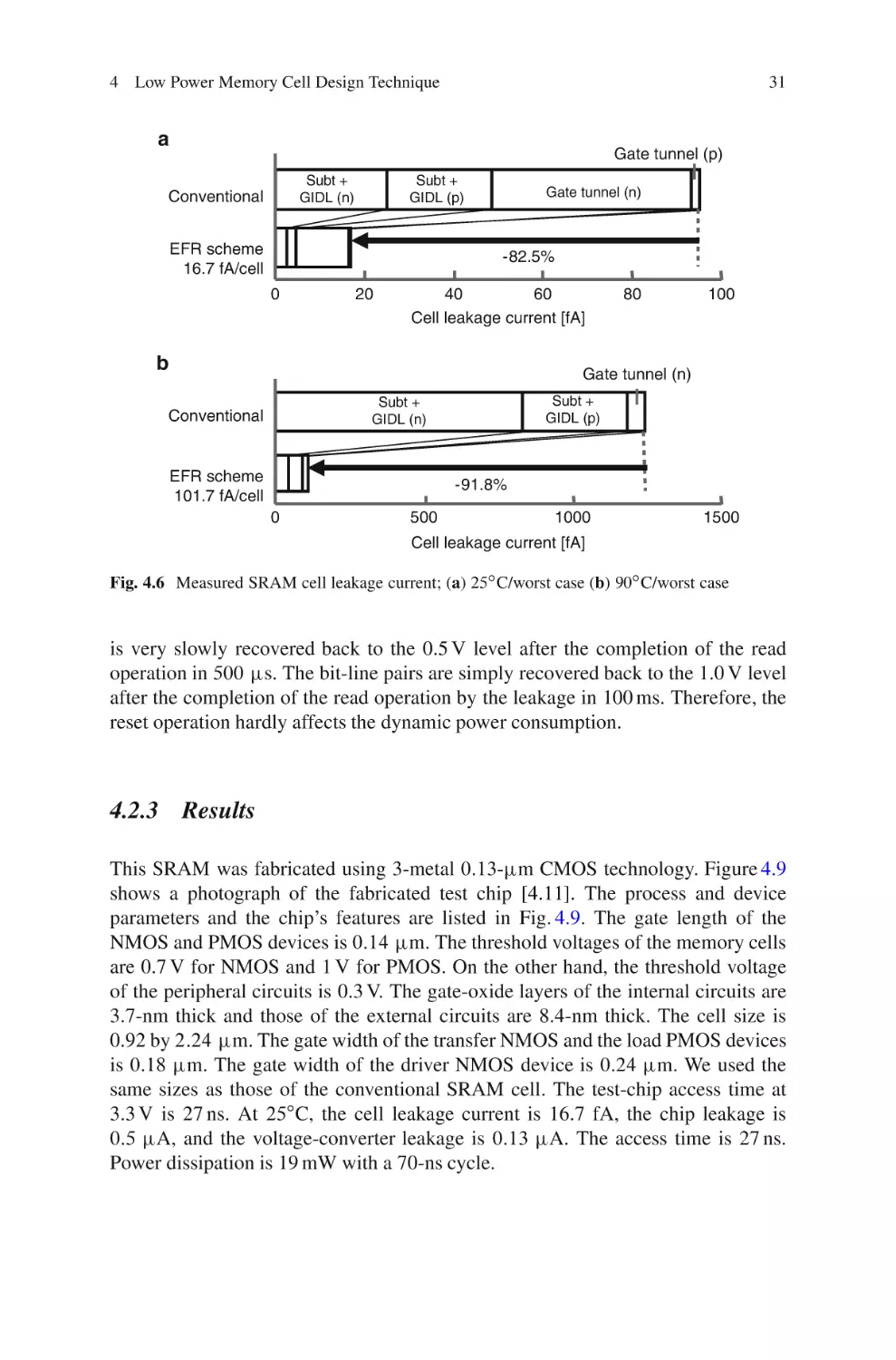
Figure 4.6 gives measured standby leakage currents at 25ı C (Fig. 4.6a) and 90ı C
(Fig. 4.6b) for SRAM cells of the conventional design and with EFR, both of which
were produced under worst-case process conditions. The subthreshold leakage and
GIDL components have been summed for each device type. In both cases, the
pMOS threshold voltage is 1.0 V and there is much less subthreshold leakage than
GIDL current at both 25ı C and 90ı C. The nMOS threshold voltage is 0.7 V and the
subthreshold leakage current is smaller at 25ı C but larger at 90ı C than the GIDL
current. Values for cell-standby leakage current in the cell with the EFR scheme are
16.6 fA at 25ı C and 101.7 fA at 90ı C, 82.5% and 91.8% smaller, respectively, than
the values for the conventional cell.
4.2.2 Chip Architecture
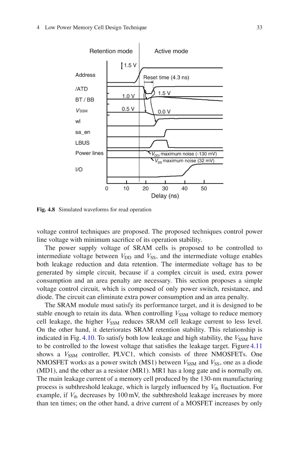
Figure 4.7 shows a circuit diagram of one mat of the fabricated SRAM chip, which
consists of 32 mats. Each mat is composed of 2,048 word lines by 256-data-bit and
20-parity-bit columns. The mat is divided into four banks. The timing diagram for a
30
K. Osada and M. Yamaoka
Fig. 4.5 Electric field
relaxation scheme
Word 0 V
VDDI1.5 V
0.5 V
BT
1.0 V
1.5 V
VSSM
0.5 V
0V
0V
BB
1.0 V
Electric-field relaxation
VGS nebative bias
VBB back bias
Retention mode
BT, BB
VSSM
Active mode
1.0V
1.5V
0.5V
0.0 V
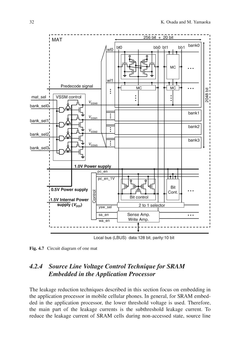
simulated read operation is shown in Fig. 4.8. This SRAM is asynchronous. SRAM
is in retention mode unless an address signal changes. If an address signal changes,
SRAM is shifted from retention mode to active mode. An ATD pulse is generated
and actives the reset operation. During the 4.3-ns reset period, the memory cell
VSS line (VSSM ) of the selected bank is pulled from 0.5 to 0 V, while the bit-line
pairs (BT, and BB) of the mat are precharged from 1.0 to 1.5 V. The conventional
asynchronous SRAM always has the reset time for the bit-line pair precharge from
0 to 1.5 V, and we simply used the reset time for bit-line pairs precharge and VSSM
discharge in our EFR scheme. Therefore, the access time does not increase because
of the EFR scheme as the asynchronous SRAM. A word line (wl) is then activated.
With activation of the sense amplifiers, the selected 128 bits of data and 10 parity
bits appear on the local bus (LBUS). To reduce the introduction of noise to the power
supplies, VSSM is controlled at the bank level instead of at the mat level. This form of
control keeps the VSS supply’s noise level at a low 32 mV. This result was obtained
in simulation through the use of power supply nets. The VSSM line is reinforced with
the third metal to accommodate the VSSM control from 0.5 to 0 V. The VSSM line
4 Low Power Memory Cell Design Technique
31
a
Gate tunnel (p)
Subt +
GIDL (n)
Conventional
Subt +
GIDL (p)
EFR scheme
16.7 fA/cell
Gate tunnel (n)
-82.5%
0
20
40
60
Cell leakage current [fA]
b
80
100
Gate tunnel (n)
Subt +
GIDL (p)
Subt +
GIDL (n)
Conventional
EFR scheme
101.7 fA/cell
-91.8%
0
500
1000
1500
Cell leakage current [fA]
Fig. 4.6 Measured SRAM cell leakage current; (a) 25ı C/worst case (b) 90ı C/worst case
is very slowly recovered back to the 0.5 V level after the completion of the read
operation in 500 s. The bit-line pairs are simply recovered back to the 1.0 V level
after the completion of the read operation by the leakage in 100 ms. Therefore, the
reset operation hardly affects the dynamic power consumption.
4.2.3 Results
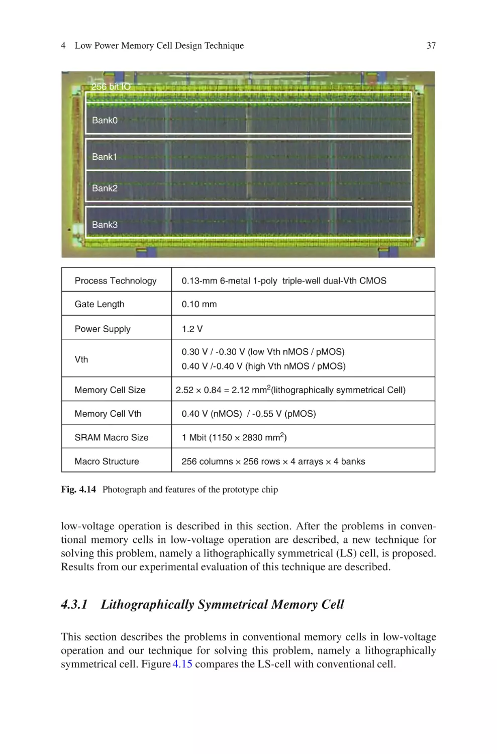
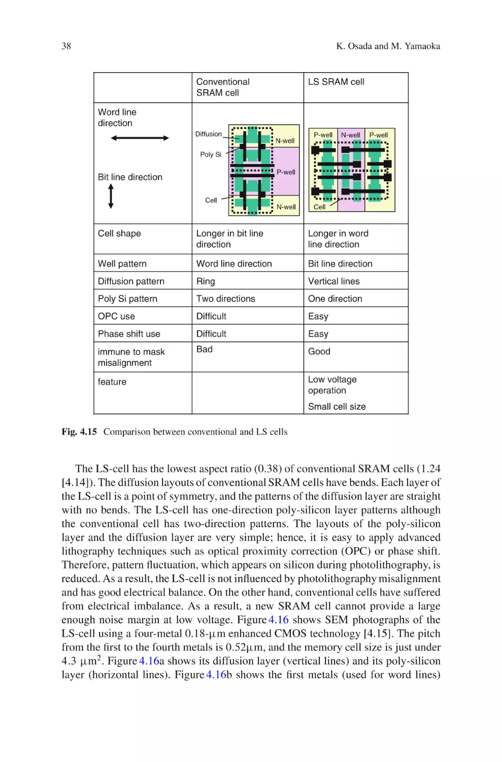
This SRAM was fabricated using 3-metal 0:13-m CMOS technology. Figure 4.9
shows a photograph of the fabricated test chip [4.11]. The process and device
parameters and the chip’s features are listed in Fig. 4.9. The gate length of the
NMOS and PMOS devices is 0:14 m. The threshold voltages of the memory cells
are 0.7 V for NMOS and 1 V for PMOS. On the other hand, the threshold voltage
of the peripheral circuits is 0.3 V. The gate-oxide layers of the internal circuits are
3.7-nm thick and those of the external circuits are 8.4-nm thick. The cell size is
0.92 by 2:24 m. The gate width of the transfer NMOS and the load PMOS devices
is 0:18 m. The gate width of the driver NMOS device is 0:24 m. We used the
same sizes as those of the conventional SRAM cell. The test-chip access time at
3.3 V is 27 ns. At 25ı C, the cell leakage current is 16.7 fA, the chip leakage is
0:5 A, and the voltage-converter leakage is 0:13 A. The access time is 27 ns.
Power dissipation is 19 mW with a 70-ns cycle.
32
K. Osada and M. Yamaoka
256 bit + 20 bit
MAT
wl0
bt0
bb1 bank0
bb0 bt1
MC
wl1
mat_sel
MC
MC
2048 bit
Predecode signal
VSSM control
VSSM0
bank_sel0
bank1
VSSM1
bank_sel1
bank2
VSSM2
bank_sel2
bank3
VSSM3
bank_sel3
1.0V Power supply
pc_en
pc_en_1V
1.5V Internal Power
supply (VDDI)
Bit
Cont.
Control
0.5V Power supply
Bit control
ysw_sel
sa_en
wa_en
2 to 1 selector
Sense Amp.
Write Amp.
Local bus (LBUS) data:128 bit, parity:10 bit
Fig. 4.7 Circuit diagram of one mat
4.2.4 Source Line Voltage Control Technique for SRAM
Embedded in the Application Processor
The leakage reduction techniques described in this section focus on embedding in
the application processor in mobile cellular phones. In general, for SRAM embedded in the application processor, the lower threshold voltage is used. Therefore,
the main part of the leakage currents is the subthreshold leakage current. To
reduce the leakage current of SRAM cells during non-accessed state, source line
4 Low Power Memory Cell Design Technique
33
Retention mode
Active mode
1.5 V
Address
Reset time (4.3 ns)
/ATD
1.5 V
1.0 V
BT / BB
0.5 V
V SSM
0.0 V
wl
sa_en
LBUS
VDDI maximum noise (-130 mV)
VSS maximum noise (32 mV)
Power lines
I/O
0
10
20
30
40
50
Delay (ns)
Fig. 4.8 Simulated waveforms for read operation
voltage control techniques are proposed. The proposed techniques control power
line voltage with minimum sacrifice of its operation stability.
The power supply voltage of SRAM cells is proposed to be controlled to
intermediate voltage between VDD and VSS , and the intermediate voltage enables
both leakage reduction and data retention. The intermediate voltage has to be
generated by simple circuit, because if a complex circuit is used, extra power
consumption and an area penalty are necessary. This section proposes a simple
voltage control circuit, which is composed of only power switch, resistance, and
diode. The circuit can eliminate extra power consumption and an area penalty.
The SRAM module must satisfy its performance target, and it is designed to be
stable enough to retain its data. When controlling VSSM voltage to reduce memory
cell leakage, the higher VSSM reduces SRAM cell leakage current to less level.
On the other hand, it deteriorates SRAM retention stability. This relationship is
indicated in Fig. 4.10. To satisfy both low leakage and high stability, the VSSM have
to be controlled to the lowest voltage that satisfies the leakage target. Figure 4.11
shows a VSSM controller, PLVC1, which consists of three NMOSFETs. One
NMOSFET works as a power switch (MS1) between VSSM and VSS , one as a diode
(MD1), and the other as a resistor (MR1). MR1 has a long gate and is normally on.
The main leakage current of a memory cell produced by the 130-nm manufacturing
process is subthreshold leakage, which is largely influenced by Vth fluctuation. For
example, if Vth decreases by 100 mV, the subthreshold leakage increases by more
than ten times; on the other hand, a drive current of a MOSFET increases by only
34
K. Osada and M. Yamaoka
MAT1
2048 bit
256+20 bit
ECC
ECC
Read global bus
(RGBUS) 16 bit
MAT4
MAT5
Local bus
Local bus
Voltage down
converter
6.42 mm
Write global bus
(WGBUS) 16 bit
Local bus
Local bus
(128+10 bit)
MAT0
MAT6
MAT7
8.76 mm
Process
Threshold voltage
Gate oxide
Cell size (6T)
Density
Chip size
Cell leakage
Chip leakage
Converter leakage
Supply voltage
Access time
Power dissipation
3-metal 0.13-µm CMOS
0.7 V: nMOS in memory cell
1.0 V: pMOS in memory cell
0.3 V: peripherals
3.7 nm (electrical): internal
8.4 nm (electrical): external
0.92 × 2.24 µm
16 Mbit
56.2 mm2
16.7 fA @25°C
0.5 µA @25°C
0.13 µA @25°C
1.5 V: internal (VDDI)
3.3 V: external (VDD)
27 ns
19 mW (70-ns cycle)
Fig. 4.9 Photograph and features of the chip
about 10%. When the Vth of manufactured MOSFET is fluctuated as high value, the
memory cell leakage largely decreases. On the other hand, the current through MR1
slightly decreases, because MR1 is in on state. If the MR1 current is greater than
the memory cell leakage, the VSSM voltage becomes low. On the other hand, when
Vth is fluctuated to lower value, the VSSM voltage is high, but MD1 restricts a rise
in the VSSM voltage. This keeps the voltage low enough to retain the stored data.
Figure 4.12 shows Vth of manufactured MOSFET vs. VSSM voltage. The horizontal
axis shows the Vth difference between designed value and actual manufactured
value, which varies by process variation. When Vth of manufactured transistor is
low and the leakage current is high, the VSSM voltage has to be high to significantly
reduce the leakage current. When Vth of manufactured transistor is high and the
4 Low Power Memory Cell Design Technique
35
Leakage current
Values
Maximum voltage
Cell stability
Cell stability limit
VSSM voltage
Fig. 4.10 Leakage and stability vs. local power line voltage
PLVC1
VSSM
VDD
sw1
Vss
MS1 MD1
MR1
Fig. 4.11 VSSM controller in embedded SRAM
leakage current is low, the VSSM voltage has to be low to keep SRAM retention
stability. The broken line indicates the ideal values that just satisfy the leakage target
and maximize memory cell stability. If the MOSFETs are worst-leakage devices,
their Vth of MOSFETs is 0.1 V lower than the designed value, and the VSSM voltage
has to be higher than 0.3 V to satisfy the leakage target. If the voltage controller
is composed of only a power switch and a diode, VSSM voltage is shown as line
(a) in the graph. This line satisfies the leakage target, but the memory cell stability
becomes low. If the voltage controller PLVC1 is composed of a constant-voltage
source circuit, VSSM voltage is shown as line (b) in the graph. This line satisfies the
leakage target, and the stability is better than using line (a), but the memory cell
stability is still low. Therefore, using three types of MOSFETs, MS1, MD1, and
36
K. Osada and M. Yamaoka
(a) Using only diode
(b) Using constant voltage source
VSSM voltage (V)
0.4
0.3
0.2
This work
Ideal value
0.1
Worst leakage
condition
0
-100 mV
0 mV
+100 mV
DV th
Fig. 4.12 VSSM voltage when Vth is changed
230 µA
Active mode
25 µA
Low-leakage mode
-90%
0
100
200
Leakage current (µA)
300
Fig. 4.13 Effect of leakage reduction in 1-Mbit leakage-worst embedded SRAM
MR1, for voltage controller, VSSM voltage (bold line in Fig. 4.12) becomes close
to the ideal value. These values satisfy the leakage target and keep the stability
higher. The PLVC1 satisfies the leakage target and keeps the SRAM stability high,
simultaneously.
In Fig. 4.13, leakage current of 1-Mbit prototype SRAM is indicated [4.12].
Using leakage reduction technique, the leakage current is reduced by about 90%. In
Fig. 4.14, the chip photograph and features of the 130-nm prototype are indicated.
4.3 LS-Cell Design for Low-Voltage Operation
Low power dissipation microprocessors, which vary their operation frequency and
power supply voltage according to system loads, have recently been developed
for portable electronic devices [4.13]. Moreover, the next generation microprocessors need lower-voltage-range operation for lower power consumption. The
on-chip cache of such microprocessors, however, acts as a bottleneck that blocks
such performance improvements. A new SRAM cell layout design developed for
4 Low Power Memory Cell Design Technique
37
256 bit IO
Bank0
Bank1
Bank2
Bank3
Process Technology
0.13-mm 6-metal 1-poly triple-well dual-Vth CMOS
Gate Length
0.10 mm
Power Supply
1.2 V
Vth
Memory Cell Size
0.30 V / -0.30 V (low Vth nMOS / pMOS)
0.40 V /-0.40 V (high Vth nMOS / pMOS)
2.52 × 0.84 = 2.12 mm2(lithographically symmetrical Cell)
Memory Cell Vth
0.40 V (nMOS) / -0.55 V (pMOS)
SRAM Macro Size
1 Mbit (1150 × 2830 mm2)
Macro Structure
256 columns × 256 rows × 4 arrays × 4 banks
Fig. 4.14 Photograph and features of the prototype chip
low-voltage operation is described in this section. After the problems in conventional memory cells in low-voltage operation are described, a new technique for
solving this problem, namely a lithographically symmetrical (LS) cell, is proposed.
Results from our experimental evaluation of this technique are described.
4.3.1 Lithographically Symmetrical Memory Cell
This section describes the problems in conventional memory cells in low-voltage
operation and our technique for solving this problem, namely a lithographically
symmetrical cell. Figure 4.15 compares the LS-cell with conventional cell.
38
K. Osada and M. Yamaoka
Conventional
SRAM cell
LS SRAM cell
Word line
direction
Diffusion
N-well
P-well
N-well
P-well
Poly Si
P-well
Bit line direction
Cell
N-well
Cell
Cell shape
Longer in bit line
direction
Longer in word
line direction
Well pattern
Word line direction
Bit line direction
Diffusion pattern
Ring
Vertical lines
Poly Si pattern
Two directions
One direction
OPC use
Difficult
Easy
Phase shift use
Difficult
Easy
immune to mask
misalignment
Bad
Good
feature
Low voltage
operation
Small cell size
Fig. 4.15 Comparison between conventional and LS cells
The LS-cell has the lowest aspect ratio (0.38) of conventional SRAM cells (1.24
[4.14]). The diffusion layouts of conventional SRAM cells have bends. Each layer of
the LS-cell is a point of symmetry, and the patterns of the diffusion layer are straight
with no bends. The LS-cell has one-direction poly-silicon layer patterns although
the conventional cell has two-direction patterns. The layouts of the poly-silicon
layer and the diffusion layer are very simple; hence, it is easy to apply advanced
lithography techniques such as optical proximity correction (OPC) or phase shift.
Therefore, pattern fluctuation, which appears on silicon during photolithography, is
reduced. As a result, the LS-cell is not influenced by photolithography misalignment
and has good electrical balance. On the other hand, conventional cells have suffered
from electrical imbalance. As a result, a new SRAM cell cannot provide a large
enough noise margin at low voltage. Figure 4.16 shows SEM photographs of the
LS-cell using a four-metal 0.18-m enhanced CMOS technology [4.15]. The pitch
from the first to the fourth metals is 0:52m, and the memory cell size is just under
4:3 m2 . Figure 4.16a shows its diffusion layer (vertical lines) and its poly-silicon
layer (horizontal lines). Figure 4.16b shows the first metals (used for word lines)
4 Low Power Memory Cell Design Technique
a
Poly Si
SRAM CELL
1.28 µm
Fig. 4.16 SEM photograph
of a lithographically
symmetrical cell (LS-cell).
Cell size is 4.30 m2 ; (a)
diffusion and poly-Si layers,
(b) first and second metals
39
Diffusion
(bright region)
3.36 µm
b
SRAM CELL
VSS
BT
Word lines (M1)
VDD BB
VSS
Short and shielded bit lines (M2)
Fig. 4.17 Measured butterfly
curves (typical)
1.5
VN2
1.0
0.5
0
0
0.5
1.0
1.5
VN1
and the second metals (used for bit lines and power supply). Figure 4.17 shows the
measured butterfly curves of a typical LS-cell: even at 0.3 V, the memory cell has a
large enough noise margin. The threshold voltage of the memory cells is 0.5 V.
There are many other advantages of the LS-cell. Its bit lines are shorter because
of the low-aspect ratio; hence, parasitic capacitance of bit lines is reduced and
read and write access is faster. Crosstalk between bit lines is drastically reduced
because bit lines are shielded by VDD lines and VSS lines, and noises on the VDD
40
Fig. 4.18 SEM photograph
of diffusion and poly-Si
layers of 45 nm SRAM cell.
(a) Cell size 0.327 m2 ; (b)
cell size 0.245 m2
K. Osada and M. Yamaoka
a
P2
N3
N1
P1
N2
N4
b
lines and VSS lines are reduced because these lines run on orthogonal word lines
and every memory cell’s read current flows on each VDD line and each VSS line.
However, its disadvantage is that the memory cell’s word line becomes longer than
that of a conventional SRAM cell. Even if this disadvantage is considered, the
above-mentioned advantages lead to a reduction in the delay in total access time by
13%, compared to that of a conventional SRAM cell at 1.5 V. By these reasons, the
LS-cell has been the common cell for the advanced CMOS processes since 90 nm
node.
Figure 4.18 shows SEM photographs of SRAM cells using a 45-nm CMOS
technology [4.16]. The cell sizes are (a) 0:327 m2 and (b) 0:245 m2 . Each layer
of the SRAM cell is a point of symmetry, and the patterns of the diffusion layer are
straight with no bends. The SRAM cell has one-direction poly-silicon layer patterns.
The layouts of the poly-silicon layer and the diffusion layer are very simple.
References
4.1. K.C. Chum, et al., A sub-0.9V logic-compatible embedded DRAM with boosted 3T gain
cell, regulated bit-line write scheme and PVT-tracking read reference bias, in Symposium on
VLSI Technology Digest, June 2009, pp. 134–135
4.2. S.-H. Lo, D.A. Buchanan, Y. Taur, W. Wang, Quantum-mechanical modeling of electron
tunneling current from the inversion layer of ultra-thin-oxide nMOSFET’s. IEEE Electron
Device Lett. 18(5), 209–211 (1997)
4 Low Power Memory Cell Design Technique
41
4.3. D.J. Frank, Device scaling, leakage currents, and joint technology and system optimization,
in 2002 VLSI Circuits Symposium Short Course, June 2002
4.4. M. Rosar, B. Leroy, G. Schweeger, A new model for the description of gate voltage and
temperature dependence of gate-induced drain leakage (GIDL) in the low electric field
region. IEEE Trans. Electron Dev. 47(1), 154–159 (2000)
4.5. J. Maserjian, Tunneling in thin MOS structures. J. Vac. Sci. Technol. 11(6), 996–1003 (1974)
4.6. J. Sune, P. Olivo, B. Ricco, Quantum-mechanical modeling of accumulation layers in MOS
structure. IEEE Trans. Electron Dev. 39(7), 1732–1739 (1992)
4.7. G.A.M. Hurkx, D.B.M. Klaassen, M.P.G. Knuvers, A new recombination model for device
simulation including tunneling. IEEE Trans. Electron Dev. 39(2), 331–338 (1992)
4.8. K. Nii, H. Makino, Y. Tujihashi, C. Morishima, Y. Hayakawa, H. Nunogami, T. Arakawa,
H. Hamano, A low-power SRAM using auto-backgate-controlled MT-CMOS, in Proceedings of the International Symposium on Low Power Electronics and Devices, August 1998,
pp. 293–298
4.9. H. Yamauchi, T. Iwata, H. Akamatsu, A. Matsuzawa, A 0.5 V single power supply operated
high-speed boosted and offset-grounded data storage (BOGS) SRAM cell architecture. IEEE
Trans. VLSI Syst. 5(4), 377–387 (1997)
4.10. D.H. Kim, S.J. Kim, B.J. Hwang, S.H. Seo, J.H. Choi, H.S. Lee, W.S. Yang, M.S.
Kim, K.H. Kwak, J.Y. Lee, J.Y. Joo, J.H. Kim, K. Koh, S.H. Park, J.I. Hong, Highly
manufacturable 32Mb ULP-SRAM technology by using dual gate process for 1.5V Vcc
operation, in Symposium on VLSI Technology Digest, June 2002, pp. 118–119
4.11. K. Osada, Y. Saitoh, E. Ibe, K. Ishibashi, 16.7-fA/cell tunnel-leakage-suppressed 16-Mbit
SRAM for handling cosmic-ray-induced multi-errors. IEEE J. Solid-State Circuits 38(11),
1952–1957 (2003)
4.12. M. Yamaoka, Y. Shinozaki, N. Maeda, Y. Shimazaki, K. Kato, S. Shimada, K. Yanagisawa,
K. Osada, A 300-MHz 25 A=Mb-leakage on-chip SRAM module featuring processvariation immunity and low-leakage-active mode for mobile-phone application processor.
IEEE J. Solid-State Circuits 40(1), 186–194 (2005)
4.13. T.D. Burd, et al., A dynamic voltage scaled microprocessor system. IEEE J. Solid-State
Circuits 35, 1571–1580 (2000)
4.14. T. Uetake, et al., A 1.0ns access 770MHz 36Kb SRAM macro, in Symposium on VLSI
Circuits Digest, June 1999, pp. 109–110
4.15. K. Osada, J.L. Shin, M. Khan, Y. Liou, K. Wang, K. Shoji, K. Kuroda, S. Ikeda, K. Ishibashi,
Universal-Vdd 0.65–2.0-V 32-kB cache using voltage-adapted timing-generation scheme
and a lithographical-symmetric cell. IEEE J. Solid-State Circuits 36(11), 1738–1744 (2001)
4.16. K. Nii, M. Yabuuchi, Y. Tsukamoto, S. Ohbayashi, S. Imaoka, H. Makino, Y. Yamagami,
S. Ishikura, T. Terano, T. Oashi, K. Hashimoto, A. Sebe, G. Okazaki, K. Satomi, H.
Akamatsu, H. Shinohara, A 45-nm bulk CMOS embedded SRAM with improved immunity
against process and temperature variations. IEEE J. Solid-State Circuits 42(1), 180–191
(2008)
Chapter 5
Low-Power Array Design Techniques
Koji Nii, Masanao Yamaoka, and Kenichi Osada
Abstract Thischapter introduces circuit technologies that enhance electric stability
of the cell, the latesttechnologies that provide moderate timing generation, as well as
larger cell stability. In Sect. 5.1, the voltage-adapted timing-generation scheme with
plural dummy cells for the wider-voltage-range operation is introduced. The effect
of increasing the number of activated dummy cells on the dummy-bitline-drivingtime fluctuation is described. Detailed circuit diagrams of the dummy-column cell
and edge-column cell are shown. The cache was fabricated using 0:18 m
enhanced CMOS technology. The cache chip can continuously operate from 0.65
to 2.0 V; its operating frequency and power are from 120 MHz at 1.7 mW and0.65 V
to 1.04 GHz at 530 mW and 2.0 V.
In the next section, read and write stability assisting circuits are discussed.
Local variation of transistors is one of the serious issues in sub 100 nm era. This
section describes SRAM assist circuits that enhance stability of the cell despite the
local variation. Source bias circuit is introduced to enhance the stability in write
operation, while word line lowering enhances SNM in read operation. These circuit
techniques do not need any additional supply voltages. A test chip is designed and
fabricated using 45-nm CMOS technology. It is achieved over 100 mV improvement
for the SNM and 35 mV for the write margin. Compared to the conventional
K. Nii ()
Renesas Electronics Corporation, 5-20-1, Josuihon-cho, Kodaira, Tokyo 187-8588, Japan
e-mail: koji.nii.uj@renesas.com
M. Yamaoka
1101 Kitchawan Road, Yorktown Heights, NY 10598, USA
e-mail: masanao.yamaoka@hal.hitachi.com
K. Osada
Measurement Systems Research Department, Central Research Laboratory, Hitachi, Ltd.,
1-280, Higashi-koigakubo, Kokubunji-shi, Tokyo 180-8601, Japan
e-mail: kenichi.osada.aj@hitachi.com
K. Ishibashi and K. Osada (eds.), Low Power and Reliable SRAM Memory Cell
and Array Design, Springer Series in Advanced Microelectronics 31,
DOI 10.1007/978-3-642-19568-6 5, © Springer-Verlag Berlin Heidelberg 2011
43
44
K. Nii et al.
assist circuit, the cell current at the worst case condition was improved by 83%.
A more stable functionality of 512-kb SRAM macros with 0.245 and 0:327 m2
is observed. The minimum operating voltage in the process- and temperature-worst
case condition is improved by 170 mV, and its variation to 60 mV, confirming a
high immunity against process and temperature variations with less than 10% area
overhead.
In Sect. 5.3, an array boost technique is demonstrated for low-voltage operation.
The technique enhances stability of SRAM memory cells.
Section 5.4 introduces design techniques of dual-port SRAM cell array, which
is often used in recent SOC as data memory for graphics engines. The electrical
stability of the dual-port SRAM must be considered more seriously than the single
port memory. Thereby, a new array design technique for a synchronous DP-SRAM
was demonstrated. Using 65-nm CMOS technology, 32-kB DP-SRAM macros were
designed and subsequently fabricated. This process yielded the smallest 8T DP-cell
and the highest bit density ever reported in the 65-nm era. Test results show that the
speed penalty was negligible; standby leakage was reduced by 27% because of the
small cell size.
Acronyms
BOX
CAD
CADDETH
CHB
CHBc
CMOS
CORIMS
DC
DRAM
ECC
EFR
FD-SOI
FF
FinFET
FPGA
GIDL
INC
LER
MBU
MCBI
MCU
Buried OXide
Computer Aided Design
Computer Aided Device DEsign in THree dimensions
CHecker Board
CHecker Board complement
Complementary Metal Oxide Semiconductor
COsmic Radiation IMpact Simulation
Direct Current
Dynamic Random Access Memory
Error Checking and Correction
Electric-Field-Relaxation
Fully Depleted Silicon On Insulator
Flip Flop
Fin Filed Effect Transistow
Field Programmable Gate Array
Gate-Induced Drain Leakage
Intra-Nuclear Cascade
Line Edge Roughness
Multi-Bit Upset
Multi-Coupled Bipolar Interaction
Multi-Cell Upset
5 Low-Power Array Design Techniques
MNT
MOSFET
NMOS
OPC
PCSE
PMOS
RDF
RBL
RWL
S.A.
SBU
SoC
SRAM
SEB
SECIS
SEE
SEFI
SEGR
SEL
SER
SET
SEU
SESB
SNM
SOI
STI
TMR
ULSI
Vth
W.A.
WL
45
Multi Node Transient
Metal Oxide Silicon Field Effect Transistor
Negative channel Metal Oxide Silicon
Optical Proximity Correction
Power Cycle Soft-Error
Positive channel Metal Oxide Silicon
Random Dopant Fluctuation
Read Bit Line
Read Word Line
Sense Amplifier
Single Bit Upset
System-on-Chip
Static Random Access Memory
Single Event Burnou
SElf-Consistent Integrated System for neutron-induced
soft-error
Single Event Effect
Single Event Functional Interruption
Single Event Gate Rupture
Single Event Latchup
Soft-Error Rate
Single Event Transient
Single Event Upset
Single Event Snap-Back
Static Noise Margin
Silicon on Insulator
Shallow Trench Isolation
Triple Module Redundancy
Ultra-Large Scale Integration
Threshold Voltage
Write Amplifier
Word Line
5.1 Dummy Cell Design
5.1.1 Problem with Wide-Voltage Operation
As power supply voltage is reduced, the threshold voltage of a MOS transistor
should also be reduced for high-speed operation. However, the threshold voltage
of memory cells must be kept at a minimum of 0.5 V to reduce the leakage current
46
K. Nii et al.
Gate delay (a.u.)
15
10
High-Vth (0.5V) for memory cell
Low-Vth (0.4V) for peripheral
Large skew
5
0
0.5
Small skew
0.7
0.9
1.1
Power supply (V)
1.3
1.5
Fig. 5.1 Gate delay as a function of power supply voltage
and to keep adequate static noise margins. On the other hand, to attain high speed
at low voltage, the threshold voltage of peripheral circuits can be reduced to 0.4 V.
Figure 5.1shows the gate delay of inverter circuits as a function of power supply
voltage. The dotted line represents the delay due to the high-threshold-voltage
(0.5 V) transistor used for the memory cell. The solid line represents the delay due to
the low-threshold-voltage (0.4 V) transistor used for peripheral circuits. At a power
supply voltage of 1.5 V, the gate delay of the low-threshold-voltage transistor is
almost the same as that of the high-threshold-voltage transistor. At 0.5 V, however,
there is a large skew between the delays.
This skew could cause activation failure of a sense amplifier during widerange-voltage operation. To avoid such failure, a voltage-adapted timing-generation
scheme using plural dummy cells was developed. The point of this scheme is that
the delay driven by high-threshold voltage in the data read path is the same as that
driven by high-threshold voltage in the control path. Thus, it can compensate the
skew between the data read path and the control path under wide-range voltage.
5.1.2 Block Diagram and Operation of Voltage-Adapted
Timing-Generation Scheme
Figure 5.2 shows a block diagram of a half side of one bank of the cache data array,
which is composed of four banks. Each bank is composed of 256 word lines by
256 bit columns. When the clock signal (CK) changes from “L” to “H,” the signal
(dec en) is generated in a D-flip flop (D-FF) and it activates predecoders and selects
a word line (wl). Signal voltages then are produced on bitline pairs (bt, bb) by the
selected memory cells (MCs) in the regular SRAM array. All these operations make
up the data read path.
5 Low-Power Array Design Techniques
47
Dummy
column
SRAM array
128 bit
EC
DC
MC
EC
DC
MC
EC
DC
MC
EC
DC
MC
wl0
MC
wl1
MC
wl244
256 bit
Word
Word driver
driver
Address D-FF
+logic
Predecoder
Predecoder
High Vth area
Edge
column
MC
PC
dpc_en
bt
wl255
bb
MC
bt
bb
pc_en
PC
Control
Control
Dummy word
Dummy bitline
CK
dec_en
Control D-FF
+logic
12 bit
CK
ys_en
Ysw
S.A.
Voltage adapted pulse
sa_en
data_out
Fig. 5.2 Block diagram of half side of a bank
In the control path, the signal (dec en) also activates the dummy word line, which
runs parallel to the bitline (bt, bb). The dummy word line activates 12 dummy
cells (DCs) on the dummy column. The activated DCs drive the dummy bitline,
whose capacitance is identical to the regular bitline (bt, bb). The dummy bitline
then becomes the voltage-adapted pulse. The voltage-adapted pulse is used for
the sense-amplifier-enable signal (sa en), the pre-charge-reset signal (pc en), and
the word line-reset signal. The most important point is that the delay due to the
high-threshold-voltage memory cells (DCs) is also included in the control path that
activates the sense amplifier.
Detailed circuit diagrams of the dummy-column cell (DC) and edge-column cell
(EC) are shown in Fig. 5.3. The dummy column is used as the electrical dummy
column, while the edge column is used as the optical dummy. As a result of
this circuit scheme, the layouts of the diffusion layer and polysilicon layer in the
regular SRAM array, the dummy column, and the edge column can be kept regular.
Therefore, the dummy-cell current is identical to the memory cell current in the
regular SRAM array. In these circuits, the dummy word line runs vertically to
48
K. Nii et al.
Dummy word line
Dummy bit line
EC
DC
Regular
word line
EC
Edge column
(optical dummy)
DC
Dummy column
(electrical dummy)
Fig. 5.3 Diagrams of dummy and edge column circuit
activate the plural dummy cells. The pattern of the bit line in the edge column is
used as the dummy word line, which is different from a regular word line; however,
this difference does not cause a problem because the word line is driven by the
same-threshold-voltage transistors as those of the peripheral circuits.
5.1.3 Timing Diagram and Effect of Voltage-Adapted
Timing-Generation Scheme
Figure 5.4 compares the timing diagrams of the data array operation at power supply
voltages of 2.0 and 0.65 V. At 2.0 V, bitline-driving time is 24% of the total access
time. However, bitline-driving time increases to 48% at 0.65 V because of the
memory cell with a high-Vth transistor. In our scheme, high-Vth dummy cells drive
one part of the timing-generation path; so the sense amplifier is activated suitably
even at low voltage.
Although a dummy-cell structure has already been developed [5.1], a single
dummy cell suffers from cell current fluctuation as shown in Fig. 5.5. Such dummycell current fluctuation results in the fluctuation of the control timing generated by
the dummy cell. Figure 5.6 shows the effect of increasing the number of activated
dummy cells on the dummy-bitline-driving-time fluctuation (normalized by total
access) at 1.5 V. The fluctuations of memory cell current were calculated using
a standard deviation of 4%, which was obtained from the distribution shown in
Fig. 5.5. The dummy-bitline-driving-time fluctuation is reduced from 17.5% to 5%
when the number of dummy cells is increased from 1 to 12, which is used in this
work because the fluctuation of dummy-cell current is averaged. This fluctuation
reduction can reduce the timing margin for activating the sense amplifier and reduce
the delay by 12.5% compared to that of conventional circuits with a single dummy
cell [5.1]. It is thus concluded from Figs. 5.4 and 5.6 that the influences of thresholdvoltage difference and the variation in dummy-cell current on circuit performance
can be reduced by our new scheme.
5 Low-Power Array Design Techniques
49
Access time
0.65 V
CK
dec_en
wl
sa_en
data_out
Dummy word
Voltage-adapted pulse
Bitline drive
(48% of total access time)
Access time
2.0 V
CK
dec_en
wl
sa_en
data_out
Dummy word
Voltage-adapted pulse
Bitline drive (24% of total access time)
0
2
4
Delay from clock [ns]
Fig. 5.4 Timing diagrams of the cache operation at 2.0 V and 0.65 V
500
Count
400
300
200
100
0
100
110
120
130
140
Memory cell current (μA)
Fig. 5.5 Measured SRAM cell current distribution
6
8
50
K. Nii et al.
Dummy-bitline-drivetime fluctuation (%)
20
Conventional scheme
16
12
-12.5%
8
4
This scheme
0
0
5
10
Number of dummy cells
15
Fig. 5.6 Effect of plural dummy cells
N1
dec_en
Word line
N2
Address
N3
Address
Voltageadapted pulse
Predecoder
Word driver
Fig. 5.7 Predecoder and word driver circuits
5.1.4 Predecoder and Word-Driver Circuits
Figure 5.7 schematically shows the predecoder circuits and the word-driver circuit.
Word line reset is carried out only in the predecoder; so the area for the reset circuit
is minimized compared to that in which a word line is reset in the word driver.
The word lines are switched off by the voltage-adapted pulse just after the sense
amplifier is activated. Thus, because the voltage-adapted pulse is used for reset, the
word line pulse is minimized according to operation voltage, and the wasted power
in the memory cells can be minimized in spite of a wide range of operating voltages.
5 Low-Power Array Design Techniques
51
For reset, four NMOS transistors are connected in series. Because only two
PMOS transistors are connected at N1 instead of four PMOS transistors, the delay
of N1 discharge, as well as the delay of word activation, is decreased. For lowvoltage operation, small PMOS transistors are connected at N2 and N3 to avoid
charge-shearing problems.
5.1.5 Results
The developed 32-kB cache was fabricated using a 4-metal 0:18 m enhanced
CMOS technology. The gate lengths of the nMOS and pMOS devices are both
0:14 m. The threshold voltage of the memory cells is 0.5 V, whereas the threshold
voltage of the peripheral transistors is 0.4 V. The pitch from the first to the fourth
metals is 0:52 m, and the memory cell size is just under 4:3 m2 . Figure 5.8 is a
photograph of the fabricated cache chip. The cache includes a data array and a tag
array. The data array is composed of four 8 kB banks, each bank is composed of one
SRAM
Array
Read / Write amp.
TAG Array
Area
Bank2
Data / Address / Control signal Bus Channel
Bank1
TAG Array
Area
Bank3
3.0 mm
Process
4-metal 0.18-μm enhanced CMOS
Threshold voltage
0.5 V: memory cell
0.4 V: peripherals
Metal pitch
0.52 μm
Cell size (6T)
1.28 x 3.36 μm
Cache size
3 × 1.25 mm
Supply voltage
0.65 V-2.0 V
Frequency
120 MHz-1.04 GHz
Power dissipation
1.7 mW-530 mW
Organization
Four-way-set associative
1024 index × 64 bit × 4 set
Fig. 5.8 Photograph and specifications of developed cache
1.25 mm
Bank0
4KB
52
K. Nii et al.
Room Temperature
1.5 V
clock
1.25 ns cycle
word
data_out
0.96 ns access
Fig. 5.9 Waveforms of read operation
double word, the bank is composed of 256 word lines by 256 bit columns, the cache
area is 3 1:25 mm, and well taps are placed every 64 rows in each memory array.
The data array has an architecture that minimizes power consumption. Only
one bank is decoded by the two index address bits that are available before the
cache access, and the other three banks are disabled. This approach saves power
consumption by about 30% over the conventional approach, which decodes all the
banks. The main power saving is gained from disabling array-control signals and
the bit-line swings of unselected banks.
Read-operation waveforms of the cache data array are shown in Fig. 5.9. The
waveforms were measured using a pico-probe. Read access from the clock to the
output of a sense amplifier (data out) is 960 ps at 800 MHz and 1.5 V. An on-chip
PLL was used to obtain the shmoo plot of the data array (Fig. 5.10). The cache chip
operates from 120 MHz at 0.65 V to 1.04 GHz at 2.0 V. Figure 5.11 shows the data
array access time as a function of supply voltage under varying substrate voltage
(mVbb) of the NMOS transistor in the memory cell. When mVbb is negative, the
threshold voltage increases and memory cell current is reduced; as a result, access
time is increased. When mVbb is positive, the threshold voltage decreases and
memory cell current is increased; as a result, access time is decreased. This figure
shows that our voltage-adapted timing-generation scheme successfully generates the
control timing according to memory cell current.
Figure 5.12 shows the measured power dissipation of the data array without bus
drive at the minimum voltage for each frequency. Moreover, conventional power
dissipation was simulated at a constant voltage of 2.0 V for each frequency. Clearly,
measured power dissipation at 120 MHz and 0.65 V is 1.7 mW and that at 1.04 GHz
and 2.0 V is 530 mW. At 120 MHz frequency, measured power dissipation is reduced
by 97% compared with conventional power dissipation.
5 Low-Power Array Design Techniques
53
1100
2.0V 1.04GHz
1000
Frequency (MHz)
900
800
FAIL
700
600
500
400
PASS
0.65V 120MHz
300
200
100
0.5
1.0
1.5
Power supply (V)
2.0
Fig. 5.10 Shmoo plot
12
Access time (ns)
10
8
6
mVbb = -1.0 V
mVbb = -0.5 V
mVbb = 0 V
mVbb = +0.5 V
mVbb
mVbb
SRAM cell
4
2
0
0.5
1.0
1.5
Supply voltage (V)
2.0
Fig. 5.11 Access time versus supply voltage
Figure 5.8 lists the specifications of the developed cache. The cache size is
3:75 mm2 . It operates from 120 MHz at 1.7 mW and 0.65 V to 1.04 GHz at 530 mW
and 2.0 V. The organization of the cache is four-way-set associative and 1,024
indexes.
54
K. Nii et al.
Power dissipation (mW)
1000
oltage
al (v
ention
Conv
100
nt)
consta
(2.0 V)
(2.0 V)
This cache
10
1
Room temperature
(0.65 V)
0
200
400
600
800
Frequency (MHz)
1000
1200
Fig. 5.12 Measured power dissipation of cache
5.2 Array Boost Technique
In low-voltage SoCs, the Vth must be reduced to maintain operation speed. In
consequence, the SNM of SRAM memory cell is deteriorated by the low supply
voltage and the low Vth . Butterfly curves using two types of supply voltage are
shown in Fig. 5.13a. The width of squares within the curves shows the SNM [5.2].
The solid lines show the butterfly curves with 1.0-V supply voltage, and the dashed
lines show the butterfly curves with 0.5-V supply voltage. The low supply voltage
narrows the square within curves, and it decreases the SNM. Figure 5.13b shows the
butterfly curves using lower Vth MOSFET, solid curves, and higher Vth MOSFET,
dashed curves. The low Vth MOSFET crushes the space between two lines, and it
decreases the SNM. To improve the SNM, array boost technique is used. Figure 5.14
shows the circuit diagram of the array boost technique, where Va is the power supply
voltage of SRAM cell array and Vdd is the power supply voltage of peripheral
circuits, which are used to access the SRAM cells.
In the array boost technique, Vdd is supplied to a boosted voltage generator,
and the generator boosts Vdd to Va .D Vdd C Va / and supplies Va to the SRAM
cell power supply (the source line of the load MOS of the memory cell). The
supply voltage of the SRAM array is always boosted whenever the SRAM circuit
is activated. Since the boosted voltage (Va ) is a small and fixed value such as
0.1V, it does not affect reliability of the MOSFETs. The memory cell can thus be
composed of small MOSFETs that can endure only low voltage. This keeps the
scaling of fabrication process and enables the memory cell area to be decreased
with the scaling of logic circuit. Figure 5.15 shows the relationship between Vdd
and Va . The electrical “-ratio means the ratio of conductance of driver MOS to that
of access MOS. The details about the electrical “-ratio are explained later in this
section.
Change of butterfly curves when implementing the array boost technique is
shown in Fig. 5.16. The butterfly curves are not symmetrical because they consider
5 Low-Power Array Design Techniques
55
1.0
1.0
0.5
0.5
0.0
0.5
1.0
0.0
(a) Butterfly curves when
Vdd = 1.0 V, 0.5 V
0.5
1.0
(b) Butterfly curves when
using MOSFETs Vth = 0.3 V
and 0.4 V
Fig. 5.13 Butterfly curves
Vdd
Boosted voltage
generator
Va = Vdd+ΔVa
WL = Vdd
BT = Vdd
BB = Vdd
Fig. 5.14 Array boost technique
3-Vth variation in one memory cell. The curves, node1va and node2va, are the
voltage of one storage node when changing the voltage of the opposite node in a
memory cell using array boost technique. The curves, node1vdd and node2vdd, are
the voltage without array boost technique. The SNM is calculated as the diagonally
length of squares that is placed between two curves. The curves, node1va and
node1vdd, are almost same around the square, so that the difference in the side
56
K. Nii et al.
Va = Vdd+ΔVa
0.5
9.0
β-ratio
(array boost)
Electrical β-ratio
Va (V)
1.0
5.0
ΔVa
Conventional β-ratio
1.0
0.0
0.5
Vdd (V)
1.0
Fig. 5.15 Boosted array voltage and electrical “-ratio
Vdd+ΔVa
Vdd
node2va
SNMva
SNMvdd
node2vdd
node1va
node1vdd
0
Vdd Vdd+ΔVa
Fig. 5.16 Butterfly curves wi/wo array boost technique
length between two squares is Va . Therefore, SNMva (the SNM using the array
boost technique) is calculated as:
p
SNMva SNMvdd C Va 2:
(5.1)
For example, when Va D 0:1 V, the SNMva is calculated as:
SNMva SNMvdd C 0:1 V
p
2;
D SNMvdd C 0:07 V;
(5.2)
(5.3)
and SNM is improved by 70 mV. Using the array boost technique, the source to gate
voltage (Vgs / of the driver MOS is higher than the Vgs of the access MOS, and the
conductance of the driver MOS becomes larger than that of the access MOS. This
conductance ratio is called as “electrical “-ratio.” The increased electrical “-ratio
5 Low-Power Array Design Techniques
57
Fig. 5.17 SEM photograph
of RD cell
makes SNM high. When the boosted voltage keeps a constant value, the electrical
“-ratio is greatly increased in low supply voltage region. Figure 5.15 shows the
electrical “-ratio and the dashed horizontal line shows the “-ratio of a conventional
memory cell. In the region where Vdd is under 0.8 V, the electrical “-ratio becomes
larger than conventional one. The large “-ratio in the low-voltage region provides
high cell stability.
Conventionally, larger-than-1.0 “-ratio is realized by wider gate width of the
driver MOS than that of the access MOS. Therefore, the diffusion layer in a memory
cell has bending shape and it causes a transistor performance variation. When
using the array boost techniques, the larger-than-1.0 “-ratio is realized electrically,
and therefore, the difference between the gate width of the driver MOS and the
access MOS is not necessary. Figure 5.17 shows an SEM photograph of rectangular
diffusion (RD) cell. The diffusion layer has no bent and is in rectangular shape. The
straight shape contributes to reduce the performance variation of the driver MOS
and the access MOS.
Figure 5.18 shows the change in simulated SNM. The dark hatched stripe (1)
shows the SNM of an RD-cell without an array boost technique. The breadth of this
area is caused by 3-Vth variation of the MOSFETs in an SRAM memory cell. In
the region for which the supply voltage is less than 0.6 V, the SNM reaches almost
0 V. The light hatched stripe (2) in Fig. 5.18 shows the SNM with the array boost
technique, in which the boosted voltage applied to SRAM array is 0.1 V higher than
the supply voltage of the peripheral circuits. The SNM increases to almost 70 mV
and this coincides with (5.3). The improvement of SNM is enough to operate this
memory cell at 0.4-V supply voltage. Thus, the array boost technique improves
the SNM of the SRAM cell, thereby realizing low voltage operation even when
using the small “-ratio memory cell. In this way, the array boost technique can
compensate for the SNM, which is deteriorated by increasing Vth variation, 1.0
“-ratio RD-cell and lower Vth MOSFET. Conventionally, we could not decrease
the SRAM MOSFET’s Vth , because the low Vth MOS deteriorates the SNM, and
therefore, SRAM operating speed becomes lower than that of the logic circuits in
the low-voltage region.
58
K. Nii et al.
200
(2) with array boost technique
SNM (mV)
150
100
(1) w/o array boost technique
50
0
0.4 0.5 0.6 0.7 0.8 0.9 1.0
Supply voltage (V)
Fig. 5.18 SNM wi/wo array boost technique
1μ
(1) Conventional memory cell
Delay (s)
100n
(2) RD-cell with array boost technique
10n
1n
(3) 5-stage inverter chain
100p
0.3
0.4
0.5 0.6 0.7 0.8
Supply voltage (V)
0.9
1.0
Fig. 5.19 Operating speed
Figure 5.19 shows the operating speed of SRAM and logic circuit. The solid line
(1) shows the time for driving a bitline for 10% swing with a memory cell using a
higher Vth MOSFET, and the dashed line (2) shows the same time with a memory
cell using a lower Vth MOSFET and the dashed line (3) shows the delay of a fivestages inverter chain whose MOSFET’s Vth is the same as the lower Vth SRAM. At
Vdd of around 1.0 V, the speed of the two memory cells is nearly identical, but at
Vdd of around 0.5 V, the speed of the memory cell using a higher Vth MOS becomes
much slower than those of the RD-cell and the inverter chain. As shown in the figure,
using the array boost technique, the memory cell MOSFET Vth to be reduced, thus
increasing the SRAM speed to the same level as that of the logic circuits. Formerly,
there were some techniques in which the voltage of SRAM array power supply was
boosted (e.g. [5.3]).
5 Low-Power Array Design Techniques
59
Fig. 5.20 Prototype chip
photograph and features
2.9 mm
1.3 mm
8-kB Array
Process
6-metal 0.18-mm CMOS single poly
Vth
0.5 V (High Vth) / 0.4 V (Low Vth)
Memory cell Vth 0.4 V (nMOS) / 0.5 V (pMOS)
This array boost technique is based on a new concept that differs from those of
the conventional array-boosting techniques. The concept is that the boosted voltage
is so small that it does not affect memory cell MOSFET reliability. In the array boost
technique, the boosted voltage (Va / is on a small level, e.g., 0.1 V, and therefore
the memory cell MOSFET can be the same as that of the core logic circuits. If
the Va is much higher than Vdd , the MOSFET has to endure the higher voltage,
and the MOSFET may be different from the MOSFET of the logic circuit. This
compatibility decreases the cost of manufacturing LSIs and makes it possible to use
the SRAM in the SoCs, and it keeps scaling of the memory cell, and therefore the
memory cell can keep the smallest size in every fabricating process.
Figure 5.20 shows a photograph of 180-nm prototype chip with array boost
technique.
5.3 Read and Write Stability Assisting Circuits
5.3.1 Concept of Improving Read Stability
The SRAM read margin is well expressed by the SNM. Figure 5.21 shows the
simulated butterfly curves without local Vth variations using 45-nm node SPICE
model at the two different conditions: one is of the fast-slow (FS) global process
corner at high temperature (125ıC), and the other is of slow–fast (SF) corner
at low temperature (40ı C). Note that the FS (SF) means the combination of
fast (slow) NMOS and slow (fast) PMOS. The supply voltage is 1.0 V minimum
condition, the butterfly curves without local Vth variations show a good symmetry in
bilateral direction, and the SNM strongly depends on the temperature and process
global variations. In particular, the SNM has a minimum value at the FS corner,
so that we hereafter deal with the SNM in the FS process condition. Figure 5.22
shows the SNM dependence on the NMOS Vth variation for three temperatures
.40; 27; 125ıC/. The SNM degrades at lower NMOS Vth or at higher temperature
condition, while it improves at higher NMOS Vth or lower temperature condition.
60
K. Nii et al.
1.0
QB (V)
SF, -40° C
0.5
FS, 125°C
0.0
0.0
0.5
Q (V)
1.0
Fig. 5.21 6T-SRAM butterfly curves under worst and best conditions
0.300
FS, 1.0 V
0.250
–40 °C
27 °C
125 °C
SNM (V)
0.200
0.150
0.100
0.050
0.000
-0.3
-0.2
-0.1
0.0
0.1
nMOS — Vth (V)
0.2
0.3
Fig. 5.22 Simulated static noise margin (SNM) versus threshold voltage of nMOS
In this way, by taking temperature and process global variation into consideration,
we have to design the SRAM transistor size so that the operating margin becomes
larger. As a result, the SNM should be ensured at the worst case of FS process
condition at high temperature. Although we only discussed the read margin here,
it is also necessary to examine the write margin precisely against temperature
and process variation. By performing the similar analysis, one can obtain that the
SF process corner at low temperature provides the worst condition of the write
operation.
Next, we discuss a technique to enlarge the SNM at the presence of local Vth
variation. In this section, we suggest the methodology to lower the voltage level of
5 Low-Power Array Design Techniques
61
Fig. 5.23 SNM improvement
by lowering word line voltage
.VWL / in case of with/without
local Vth variations
1.0
VWL = 1.0 V
QB (V)
VWL = 0.9 V (-10%)
0.5
VWL = 0.8 V (-20%)
VWL = 0.7 V (-30%)
0.0
0.0
0.5
Q (V)
1.0
(a) w/o local Vth variations
1.0
VWL = 1.0 V
QB (V)
VWL = 0.9 V (-10%)
0.5
VWL = 0.8 V (-20%)
VWL = 0.7 V (-30%)
0.0
0.0
0.5
Q (V)
1.0
(b) w/ local Vth variations
the WL compared to that of the power line of flip-flop in an SRAM cell. Figure 5.23a
shows SNMs without local Vth variations at the worst condition (discussed above),
where we introduced the lowered voltage level to the WL. As is shown in this
graph, it is confirmed that the SNM is improved by lowering the WL level with
keeping the symmetric margin. In contrast, Fig. 5.23b indicates the result in the
same simulated condition, but the local Vth variation is additionally introduced
to each SRAM transistor. Because randomness of the local Vth variation destroys
the symmetry of the butterfly curve, the SNM without lowering the WL level in
62
K. Nii et al.
Fig. 5.23a is reduced to be less than zero, indicating no expectation for SRAM read
margin. Assuming that the randomness of the local Vth variation obeys the normal
probability distribution, this deterioration of the SNM could be seen statistically if
the total capacity of the SRAM memory array increases. In other words, the unit
cell with asymmetric degradation of the SNM in 1-Mb SRAM array is more likely
to appear than that in 1-Kb array [5.4]. Therefore, we need to reduce the WL level
so that the SNM with local Vth variation becomes larger than zero. Using the results
obtained in Fig. 5.23b, the WL level should be lowered by more than 20% compared
to the supply voltage of 1.0 V.
Lowering the WL voltage accompanies with, at the same time, the drawbacks
not only of the operation speed (or cell current) but also of the write operation. This
is because the lowered WL reduces the ability of the access (pass-gate) transistor
in an SRAM cell, which affects directly to the operation speed and write margin.
Therefore, it is necessary to search for the optimum condition to enhance the SNM
as large as possible, with a minimum loss of both the write margin and the operation
speed. In the next section, we describe how to control the WL voltage level.
5.3.2 Variation Tolerant Read Assist Circuits
Figure 5.24 shows the read assist circuit (RAC) to control the word line voltage
(VWL ). In the simple circuitry [5.5] as shown in Fig. 5.24a, the VWL is lowered
by plural pull-down NMOSs (called replica access transistors, RATs). Figure 5.25
represents the simulated VWL dependence on the NMOS global Vth variations at
high and low temperature, which provides two serious problems in the conventional
circuit (see dotted lines). The first is a considerable decrease of VWL in the FS
condition at low temperature. An excessive lowering of the VWL strongly enhances
the SNM, which in turn degrades the write margin because of a low gate-overdrive
of the access transistor. The second is also a decrease in the VWL in the SS condition.
In Fig. 5.25, the VWL at SS, which is the worst condition of the cell current, becomes
lower than that at TT due to its higher Vthp , resulting in a further degradation of the
cell current.
We examine the reason why this unexpected VWL degradation appears in the
conventional circuit. Figure 5.26a is the simulated I-V curve for RAT and P0. Each
simulation was performed at the worst 1.0 V condition for 40ı C and 125ıC. In
the static condition, the current that flows through the P0 (IDD) is equivalent to that
through the RAT (ISS), so that the VWL is determined by the cross point between
these two I-V curves. On the contrary to the RAT, the P0 has a strong dependence
on the temperature, which causes a wide range of the VWL fluctuation as appeared in
Fig. 5.25a. In other words, the conventional circuits have disadvantage against not
only process Vth variations but also the temperature fluctuation.
In order to overcome this problem, we propose a new circuitry shown in
Fig. 5.24b. The RATs are introduced to the source of the WL driver, not to the
5 Low-Power Array Design Techniques
63
Fig. 5.24 Schematics of read
assist circuits (RAC). (a)
Original and (b) improved
with passive resistance
RAT : Replica access transistor
: SRAM transistor
: Logic transistor
P0
WL
Memory cell
RAT
xN
(a) Read assist circuit
N+ poly-Si
resistance
R
NA
RAT
xN
WL
Memory cell
(b) Improved read assist circuit
WL in the memory cell array. In addition, we make use of the passive resistance
elements (R) implemented by N-type non-silicide polysilicon gate. This structure
enables us to control the WL voltage reflecting both the process and the temperature
variations. As shown in Fig. 5.26b, the IDD current obeys the ohmic characteristic,
while the ISS current the transistor I-V curve. Due to the fact that the temperature
dependence of the resistance element is much smaller than that of the drain current
in the saturation region, we can suppress a VWL fluctuation against temperature
by eliminating the PMOS characteristic. Furthermore, it should be noted that the
usage of the resistance elements has a great advantage on the Vth change which is
responsible for the process variation. In general, the gate length of the polysilicon in
the SS condition gets longer than that in the TT condition, which induces a higher Vth
value. At the same time, the amount of the resistance element using polysilicon gate
is expected to get lower because of the enlargement of cross-sectional area. From
64
K. Nii et al.
Fig. 5.25 Simulation result
of WL voltage .VWL /
depending on nMOS Vth
SS
1.0
TT
FF
SF
FS
Improved
circuitry
WL voltage (V)
0.8
0.6
Basic circuitry
0.4
125°C
0.2
-40°C
0.0
nMOS Vth (a.u.)
Fig. 5.26b, it is easily obtained that a lower resistivity of R and a higher NMOS
Vth (smaller ISS) at the SS corner lead to a higher VWL , while a higher resistivity
of R and a lower NMOS Vth at the FF corner lead to a lower VWL . Combining
these facts, we can conclude that the Vth of RATs dominates the VWL value with a
little temperature dependence. We have verified the validity of these VWL behaviors
through our simulation as shown in the Fig. 5.25 (see solid lines).
Figure 5.27 shows the overall architecture that implemented the proposed RAC.
Additional circuitry denoted as gate controller (GC) has been introduced, which
consists of serial resistors (R1 and R2) and the switching transistors (P1 and N1).
By applying this circuitry, one can realize highly tolerant RAC against the PVT
variations rather than a simple pull-down transistor.
Before explaining the functionality of the GC, we have to mention the layout
of these critical resistors. Figure 5.28 represents the schematic layout view of our
resistance elements. In order to reflect the process variation of the gate length L and
width W of the access transistor in the SRAM memory cell, the line width of nonsilicide polysilicon (R0, R2) and the non-silicide diffusion elements (R1) have the
same size as L and W, respectively. In addition, the poly-Si pitch of R0 and R2 is
equal to that of the SRAM memory cell, leading to the same resistance sensitivity
in conjunction with the access transistor of the SRAM cell. Figure 5.29 indicates
the resistance sensitivities of R0, R1, and R2 to the critical dimension (CD) shift of
the gate and the diffusion sizes. The CD shift, which is caused by manufacturing
variations in the lithography or etching process steps, influences the global Vth
variations. For simplicity, we focus on the SS corner to explain the behavior of the
additional GC. The SS corner means a high Vth and a low Ids condition, implying
that the line width of the polysilicon gets larger and that of the diffusion gets smaller.
5 Low-Power Array Design Techniques
65
Current (A)
1.0E-03
8.0E-04
125°C
6.0E-04
–40°C
IDD
P0
WL
0V
–40°C
125°C
4.0E-04
ISS
RATs
ISS
2.0E-04
0.0E+00
0.0
IDD
0.2
0.4
0.6
0.8
1.0
WL voltage (V)
(a) Original
1.0E-03
IDD
Current (A)
8.0E-04
R
6.0E-04
–40°C
NA
125°C
4.0E-04
ISS
ISS
2.0E-04
0.0E+00
0.0
IDD
0.2
0.4
RATs
0.6
0.8
WL
0V
1.0
WL voltage (V)
(b) Improved
Fig. 5.26 Operating analysis of read assist circuit by SPICE simulation
In other words, positive CD shifts of polysilicon decrease the resistivity of R0 and
R2, while negative CD shift of diffusion increases the R1 resistivity at the SS corner
(see Fig. 5.29). Relatively lowered resistance of R2 rather than R1 contributes to
pull down the NB node, which prevents NA node from lowering excessively. As a
result, we can realize a higher voltage level of the VWL at the SS condition compared
to the case that we apply a simple pull-down transistor for RAT.
Now that we found the effectiveness of our RAC with the GC qualitatively, we
verify its validity by simulating the VWL . Figure 5.30 is the simulated result of the
VWL against NMOS Vth variation or process variation. To see the advantage of our
RAC with the additional GC, we also show the result of the RAC without the GC. In
the NMOS slow corner (SF, SS), the VWL with GC is higher than that without GC,
so that the degradation of cell current will be suppressed. Conversely in the NMOS
66
K. Nii et al.
Gate controller
R0
XR
P1
N+ diffusion resistor
NA
N+ poly-Si resistor
R1
NB
R2
RAT
xN
N1
WL0
MC
MC
MC
MC
WL63
XH
XM
XL
8 8 8
Row decoder
Pre-decoder
9
Row address
Fig. 5.27 Practical read assist circuit-enhanced sensitivity of process variation
Non-Silicide
w/ Silicide
Poly-Silicon
W
Diffusion
Cell-pitch
W
R1
R2
R0
SRAM cell
Fig. 5.28 Layout of each passive resistance for the proposed RAC
fast corner (FS, FF), the VWL with GC is lower than that without GC, so that the
read stability SNM will be improved. Figure 5.31 shows the simulated waveforms
focusing on WL activation. In the inactivated blocks of rows, the node NA voltage
level VNA stays at VDD. When the node XR voltage level VXR comes down to
low level, the node NB voltage level VNB rises to intermediate voltage level fixed
by R1 and R2. Then the VNA is dropped by the pull-down RATs. The substantial
capacitance of the node NA makes its voltage drop gradually. Thus, it is found that
the RAC does not affect the rising speed of the WL voltage.
5 Low-Power Array Design Techniques
67
140%
Fig. 5.29 Resistance
sensitivities depend on
critical dimension (CD) shift
Resistance sensitivity
R0, R2 (Poly-Silicon)
120%
100%
R1 (Diffusion)
80%
60%
-10
-5
0
CD shift (nm)
5
10
1.0
Fig. 5.30 Comparison of
WL voltage .VWL / in RAC
with enhanced gate controller
(GC) and without GC
-40°C
125°C
w/ GC
SS
WL Voltage (V)
0.9
SF
TT
w/o GC
0.8
125°C
-40°C
FS
0.7
FF
VDD = 1.0 V
0.6
nMOS Vth (a.u.)
5.3.3 Variation Tolerant Write Assist Circuits
Figure 5.32 shows the write assist circuit (WAC). Lowering the voltage level of
power line in the memory cell array (ary-VDM) is one of the effective ways of
ensuring the SRAM write margin [5.5, 5.6]. The capacitive WAC makes use of the
capacitance ratio between the ary-VDM (Cav / and the additional dmy-VDM (Cdv /
[5.5]. The dmy-VDM is wired by fourth metal layer upper to the cell array in each
column individually. To enhance the write margin against the increasing variation
68
K. Nii et al.
NB
Voltage (V)
1.0
XR
0.0
NA
1.0
WL
XA
0.0
0
1
2
3
Time (ns)
4
5
Fig. 5.31 Simulated waveform of proposed RAC
6-T SRAM cell
WL
ary-VDM
BL
/BL
MC
ary-VDM31, 7
ary-VDM0, 7
MC
dmy-VDM31
MC
ary-VDM31,0
ary-VDM0,0
MC
dmy-VDM0
XH7
MUX (32:1)
DIO15-0
Fig. 5.32 Write assist circuit (WAC) improving write ability
/BL31
BL31
/BL0
BL0
XH0
5 Low-Power Array Design Techniques
69
accompanied by the scaling, it is necessary to lower the voltage of ary-VDM
immediately, which requires a small Cav =Cdv . If the Cdv is enlarged, it degrades the
speed and power of the writing operation. In Fig. 5.32, the signals of XH0 and XH7
indicate the most significant predecode signal of the row decoder to select one of the
segment arrays. Each two-input NAND gate is connected to the bitline (BL) pair in
each column of the segment arrays. In the NOP states where all BL pairs are highly
pre-charged, all ary-VDM lines are connected to the power source line through the
pull-up PMOS transistors, and all dmy-VDM lines are connected to the ground line
through the stacked pull-down NMOS transistors. In the read state, although one of
the BL pairs is slightly lowering in each column by flowing the cell current into the
activated memory cell, the voltage levels of the BLs are almost high level, so that
all ary-VDM and dmy-VDM keep the high level and low level, respectively. In the
write state, as one of the BL pair is forced to low, both ary-VDM and dmy-VDM
lines are put into a floating state. Consecutively, when the corresponding XH signal
is activated, the corresponding ary-VDM line falls to the intermediate voltage level
determined by Cav =Cdv . In Fig. 5.32, the number of column multiplex, data I/O,
and divided segment are 32-column, 16-bit, and 8-segment, respectively, and the
number of memory cells in each column in the segment is 64-cell as demonstrated
in the following section.
Figure 5.33 shows the simulated waveform of the ary-VDM lowering in several
cases of the segment division number (#div D 1,2,4,8). In this simulation, it is
assumed that the Cdv is a constant value determined by the wire length of fourth
metal of the 512 memory cells (#row D 512). The simulation condition is under the
room temperature (RT) and 1.2 V typical supply voltage. In the case of #div being
equal to 1, the voltage level of ary-VDM becomes 1.13 V from 1.2 V (0.07 V),
while it becomes lower 0.68 V (0.52 V) in the case of #div being equal to 8 due
@R.T., Typical-process, #row = 512
Voltage of ary-VDM, dmy-VDM (V)
1.4
ary-VDM
1.2
#div = 1
#div = 2
#div = 4
1.0
0.8
#div = 8
0.6
dmy-VDM
0.4
0.2
0.0
-0.2
0.0
10.0
20.0
30.0
40.0
Time (ns)
Fig. 5.33 Simulated waveform of the ary-VDM and dmy-VDM in the write status
70
K. Nii et al.
w/o WAC
1.0
#div=1 (Conv.)
#div=2
#div=4
0.8
#div=8 (Proposed)
QB (V)
0.6
0.4
Write-trip-point
+0.2 V
0.2
0.0
0.0
0.2
0.4
0.6
BL, Q (V)
0.8
1.0
Fig. 5.34 Comparison of the write ability by DC simulation result of the write-trip-point
to the small Cav =Cdv . According to Vth curve simulation [5.4], to ensure the write
margin in our 45-nm CMOS technology, the voltage level of ary-VDM should be
0.7 V at VDD D 1.0 V operation of the worst case, so that we divided the ary-VDM
into eight as shown in Fig. 5.32.
Figure 5.34 shows the dc simulation result of improvement of write ability
defined by write-trip-point [5.7]. The voltage levels in cases of #div D 1,2,4, and
8 of internal nodes Q and QB of a memory cell (as shown in Fig. 5.21) are plotted
when one of the input of the BL pair (BL) is changed from 1.0 to 0.0 V and the other
BLB is forced to 1.0 V of the pre-charge level, constantly. The initial condition is
set Q equal to low level and QB equal to high level. As the voltage levels of BL and
node Q become lower, the voltage level of node QB is flipped, and the cross point
of the input BL (Q) and output QB is defined as the write-trip-point. The higher the
voltage level of the write-trip-point, the higher the write ability; hence that means it
is easy to flip the data. After the data flip, the voltage levels of QB in each case of
#div becomes corresponding to lowered voltage level of the ary-VDM determined
by Cav =Cdv as mentioned before. It is found that the write-trip-point of proposed
#div D 8 is 0.41 V at the worst condition, which is improved by 0.2 V compared to
the conventional WAC (#div D 1).
The proposed divided WAC contributes to the suppression of the power overhead
in the write operation compared to the conventional WAC [5.5]. Figure 5.35 shows
the estimated power reduction in a write cycle at the memory cell array (MAT)
depending on the number of the segment division. The referenced power is without
5 Low-Power Array Design Techniques
71
Normalized power
in the MAT at write-operation
4
MUX=32
2.92
3
MUX=4
1.96
2
1.48
1.24
1.68
1.34
1
0
0
2
1.17
4
6
Division number of ary-VDM
1.08
8
Fig. 5.35 Estimation of power reduction in the write cycle
WAC of column multiplex equal to 32, in which the power is dissipated by one full
swing BL and the other 31 read cell currents by half-selected cells. The conventional
WAC has 68% power overhead because the large capacitances of ary- and dmyVDM need to be charged and discharged every write cycle. In contrast, the proposed
eight-divided WAC has only 8% power overhead due to the small capacitances
of ary- and dmy-VDM. The other case of column multiplex equal to 4, which is
frequently used in embedded small SRAM macros of SoCs, is also plotted. It is
found that the write power is further suppressed by dividing the ary-VDM.
5.3.4 Simulation Result
Figure 5.36 shows the practical simulated waveforms of a 512-kb SRAM macro in
the read and write cycle in the best condition (FF-process, 1.4 V, 125ı C) and worst
condition (SS-process, 1.0 V, 40ı C). The simulated clock cycle is 4.0 ns (250MHz operation). Note that the first and the third clock cycles are in the write state,
while the second and the fourth clock cycles in the read state. Owing to our proposed
RAC during both in the read and in the write state, the VWL is decreased reflecting
the difference of the process condition: 30% reduction in the FF condition, while
8% reduction in the SS condition. On the other hand, during the write cycle, the
VAV at the SS (worst) condition is lowered from 1.0 to 0.75 V immediately after
the BL starts swinging, which satisfies our requirement to obtain enough write
margin against the variability. It should be commented that in the worst condition,
both the voltage levels of dmy-VDM and ary-VDM are not equalized due to the
NMOS pass-gate as shown in Fig. 5.32. We can avoid this voltage difference only
by introducing a PMOS pass-gate. However, the equalization of these nodes makes
the VAV level lower, which results in the degradation of the retention margin of
unselected memory cells in the activated column. The issue of the retention margin
should be paid attention especially in the case of lower supply voltage. In addition,
72
K. Nii et al.
Clock
-8%
-30%
WL
Read
Enable
Write
Enable
BL, /BL
Q, QB
ary-VDM
Q
QB
-40%
dmy-VDM
FF @ 125°C, VDD = 1.4V
Q
QB
-25%
SS @ -40°C, VDD = 1.0V
Fig. 5.36 Simulated waveform in read and write cycle
introduction of the extra PMOS leads to an area penalty. In this way, from the
viewpoint of retention margin and the area penalty, we have adopted a single NMOS
pass-gate between ary-VDM and dmy-VDM.
5.3.5 Fabrications and Evaluations in 45-nm Technology
The high-density and normal 6T SRAM cells are designed and fabricated using
our 45-nm bulk CMOS technology with the SiON gate. The high-density cell
.0:245 m2/ has been shrunk by 50% while the normal one .0:327 m2/ by 35%,
providing that the SRAM cell size in 65 nm technology node is 0:49 m2 [5.5].
Figure 5.37 shows the die photograph of the test chip for the normal-density SRAM
cell. It consists of two conventional 256-kb SRAM macros and two proposed
256-kb ones. The physical layout size of the latter normal-density SRAM macro
is 550 305 m2. The area penalty of the read and WAC are 7% and 9% for
normal and high-density SRAM macros, respectively. The bit density of each
SRAM macro is 1:57 Mbits=mm2 and 2:12 Mbits=mm2 for normal and high-density
SRAM, respectively. The feature of fabricated SRAM macros is summarized in
Table 5.1.
Figure 5.38 shows the relationship between minimum operation voltage and the
process variations in the temperature between 40ı C and 125ıC for the normal
512-kb SRAM macro. The dotted line represents the minimum operation voltages
without the assist circuit, while the solid one that with the assist circuit. It is found
5 Low-Power Array Design Techniques
73
Conventional
256 Kb
Conventional
256 Kb
with RAC & WAC
256 Kb
with RAC & WAC
256 Kb
Fig. 5.37 Die photograph of a test chip
Table 5.1 Feature of the fabricated SRAM macro
Technology
45-nm (hp65) LSTP bulk CMOS
Macro configurations
16 bits 16-k words .MUX D 32/
Memory cell arrays
512 rows 256 columns 2 MATs
6T SRAM cell size
0:327 m2
0:245 m2
2
Bit density
1:57 Mbit=mm
2:12 Mbit=mm2
Area overhead of assists
7%
9%
Access time at RT, 256 Kb
2.2 ns at 1.2 V
2.5 ns at 1.2 V
Standby leakage at RT
15 pA/cell at 0.7 V
26 pA/cell at 0.7 V
Worst temperature between -40°C and 125°C
1.2
1.13V
1.1
VDDmin (V)
154mV
- 0.17V
1.0 w/o AC
0.96 V
0.9
60mV
w/ AC
0.8
0.7
0.6
AC: Read-and Write-Assist Circuit
VDDmin: minimum operating voltage
FF
FS
TT
SF
Process variation
SS
Fig. 5.38 Measured minimum operating voltage .VDDmin / of 512-kb SRAM at worst temperature
74
K. Nii et al.
that the VDDmin in each process conditions (FF, FS, TT, SF, SS) is improved by
read and WACs. The VDDmin is lowered from 1.13 to 0.96 V, achieving 170 mV
improvement at worst process and temperature condition. Moreover, it should be
also noted that the distribution of VDDmin in accordance with the process variations
is suppressed from 154 to 60 mV by applying the assist circuit. These results indicate
that the SRAM with the assist circuit has improved immunity against process and
temperature variations.
5.4 Dual-Port Array Design Techniques
5.4.1 Access Conflict Issue of Dual-Port SRAM
Figure 5.39 shows memory cell circuits for single-port and dual-port SRAM. The
standard single-port SRAM cell presented in Fig. 5.39a comprises six transistors:
two pull-up PMOSs (load-PMOS), two pull-down NMOSs (drive-NMOS), and
two transfer NMOSs (access-NMOS). The single-port SRAM realizes either read
operation or write operation, so that its operation is often denoted as “1RW.”
RWL
WWL
WL
BL
/BL
RBL
WBL
(a) 6T-SRAM cell (1RW)
/WBL
(b) 8T-SRAM cell (1R1W)
WLA
BLA
BLB
/BLA
/BLB
WLB
(c) 8T-SRAM cell (2RW)
Fig. 5.39 SRAM memory cell circuits
5 Low-Power Array Design Techniques
75
Normally, as presented in Fig. 5.39b, c, two major types of memory cells are used
for the dual-port SRAM. Although both memory cells have eight transistors in
common, their function differs greatly. Figure 5.39b portrays the one-read/one-write
(1R1W) type DP-SRAM cell, in which only one of the two ports is allowed for
read operation. This 1R1W memory cell has stable read operation, but its singleended read-bitline (RBL) structure might have an impact of access time degradation,
unfortunately, because of the RBL full swing. Figure 5.39c portrays the two read–
write (2RW) type of 8T SRAM memory cells. In this type of dual-port memory cell,
both ports are available for reading and writing, which indicates that the 2RW type
of memory cell can also operate as a 1R1W, although the 1R1W type of memory
cell cannot operate as a 2RW. In this way, the 2RW type of 8T DP-cell has more
access flexibility. Hereafter, this type of DP-SRAM is specifically addressed in this
study.
Figure 5.40 depicts the variety of the access situations of the 2RW dual-port
SRAM when both ports are enabled simultaneously. The memory cell array with
activated 8T-cells, word lines (WLA, WLB), and bitlines (BLA, BLB) is shown
simply. The buffers of both sides of memory cell array designate the addressed WL
drivers of both ports. Figure 5.40a depicts a situation in which a different row and
8T- cell
BLA
BLB
WLA
BLA
BLB
WLA
WLB
WLB
BLA
(b) Different row and
common column access
BLB
BLB
BLA
(a) Different row and
column access
WLA
WLA
WLB
(c) Common row and
different column access
WLB
(d) Common row and
column access
Fig. 5.40 Assortment of the access modes of the dual-port SRAM
76
K. Nii et al.
column are accessed from both ports, which are designated independently by each
address input. Figure 5.40b shows the different row and common column access
situation. These two situations have no issues in terms of the access conflict of both
ports because each selected memory cell, of which either WLA or WLB is activated,
operates as a single-port access. Figure 5.40c, d, respectively, shows the common
row and different column access, and the common row and common column access.
In these common row access situations, the cell stability must be considered as the
worst case for reading because the two enabled word lines affect the static noise
margin (SNM) degradation for all memory cells along with the selected row. Both
ports operate as reading; also, one port operates as writing or both ports operate
as writing. Therefore, the write stability is also considered as the worst case of the
selected memory cell. The read stability is still considered in writing operations
because the half-selected (selected row and unselected column) memory cells are
equal to reading situations even if one or both ports are performing a writing
operation. In general, if the writing data are different (namely the opposite data)
from both ports, absolutely consistent address access for a writing operation from
each port, as presented in Fig. 5.40d, is inhibited because of the abnormal leakage
current flows in the accessed memory cell. Still, the simultaneous reading operation
or reading and writing operations from both ports are frequently required from the
system. Therefore, the conventional DP-SRAM design must satisfy such a worst
case access situation: the size of 8T DP-cell necessarily becomes large because of
increasing gate width of drive-NMOSs to improve the cell stability.
Figure 5.41 shows simulated butterfly curves of the SNM for the 8T DP-cell.
As described earlier, the 8T DP-cell has two different SNM values depending on
the access situation: one is a common access situation in which two word lines
(WLs) within the same row are selected; the other is a different access situation in
which two WLs in two different rows are selected. In the common access situation
shown in Fig. 5.40c, d, both WLs are activated. Therefore, the electrical “ ratio of
the 8T DP-cell is expressed as “ND1 =.“NA1 C “NA2 /. Here, “ND1 , “NA1 , and “NA2 ,
respectively, indicate the coefficients of source-drain currents of the drive-NMOS,
the access-NMOS for port A, and the access-NMOS for port B. On the other hand,
as for the different access situation, the corresponding “ ratio becomes “ND1 =“NA1
or “ND1 =“NA2 because of single activation of the WL. In general, a lower “ ratio
reduces the read stability, SNM, which indicates that the SNM in common access
situation must be discussed for the worst case design of the 8T DP-cell.
5.4.2 Circumventing Access Scheme of Simultaneous
Common Row Activation
Figure 5.42 presents the fundamental concept of the proposed DP-SRAM access
scheme. For convenience, it is defined that port A, which is connected to the pair
of BLA and /BLA, is primary, whereas port B, which is connected to that of BLB
and /BLB, is secondary. In the secondary port B, the row address comparator (RAC)
5 Low-Power Array Design Techniques
77
VL (V)
Different row access
(WLA = “H”,WLB = “L”)
SNMdiff > SNMcom
SNMdiff
SNMcom
Common row access
(WLA=WLB=“H”)
VR (V)
ON
ON
VL
ON
VR
OFF
VL
OFF
Different row access
(WLA= “H”, WLB = “L”)
ON
VR
ON
ON
Common row access
(WLA = WLB= “H”)
Fig. 5.41 Butterfly curves and static noise margin of the DP-8T-cell for both common row access
and different row access
and the bitline shifting circuitry (BSC) are introduced. Figure 5.43 expresses more
detailed operations depending on the access mode.
The implemented circuitry in a test chip design is portrayed in Figs. 5.44 and
5.45. Figure 5.43a shows that the address input signal AA <> activates WLA
in the m-th row (WLAm), whereas the AB <> activates WLB in the n-th row
(WLBn), which means they have different access modes. In this condition, the RAC
is designed to the output “H” level so that the DP-SRAM as a whole is expected to
realize a standard read or write operation. Once the AA <> and the AB <> select
the WLs in a common row, as presented in Fig. 5.43b, the row decoder for port
B is disenabled because of the RAC. Consequently, only the WLAn is accessible
to the memory cell. Simultaneously, the “L” level generated by the RAC (see also
Fig. 5.44) modifies the connection of secondary port B from the pair of BLB to that
of BLA, making it possible to read data stably without SNM degradation. In other
words, this scheme circumvents the common access mode.
78
K. Nii et al.
Column I/O for primary port-A
BLA
/BLA
Priority row decoder
WLA
Not activate WLB
Simultaneously
WLB
BLB
/BLB
Switch from BLB to BLA
Column I/O for secondly port-B
Fig. 5.42 Concept of proposed circumventing simultaneous common row access
DIA / DOA
DIA / DOA
SA / WD
SA / WD
“ H”
“ H”
“ H”
AB<>
“ H”
/BLA
...
/BLB
BLA
WLAn
MC
WLBn
WLBn
“ L”
MUX
Row add.
comparator
WLBm
BLB
/BLA
...
/BLB
BLA
BLB
WLAn
MC
MC
Row
decoder
AA<>
WLBm
AB<>
WLAm
WLAm
MC
Row
decoder
AA<>
MUX
Row add.
comparator
SA / WD
SA / WD
(RAC)
(RAC)
DIB / DOB
DIB / DOB
Different row address
Same row address
AA<>, AB<>
AA<>, AB<>
Clock
Clock
RAC output
RAC output
WLAn ,WLAm
WLAn ,WLAm
WLBn ,WLBm
WLBn ,WLBm
Fig. 5.43 Block diagram and timing chart of the proposed access scheme
5 Low-Power Array Design Techniques
79
Row address inputs
(9-bits)
Secondary
row decoder
AA8
AB8
AA7
AB7
AA6
AB6
Clock
AA5
AB5
AA4
AB4
AA3
AB3
F/F
AA2
AB2
AA1
AB1
AA0
AB0
“H” = Different row access
BL shifter
“L” = Common row access
XOR
BLB3
/BLB3
/BLA3
BLA3
BLB2
/BLB2
/BLA2
BLA2
BLB1
/BLB1
/BLA1
BLA1
BLB0
/BLB0
/BLA0
BLA0
Fig. 5.44 Circuit of the row-address comparator (RAC)
PC
RAC
output
signal
Col. decode
Bus (4-bits)
Sense
amp.
SE
DO
Write
driver
WE
DI
Fig. 5.45 Circuit of the bitline shifter for secondary port
For that reason, it is possible to reduce the drive-NMOS transistor width, which
contributes directly to the reduction of the DP-SRAM unit cell area. In addition,
this circuitry has a strong effect on the write operation. In fact, the common access
mode becomes a critical problem in the write operation because the read operation
80
K. Nii et al.
takes place in unselected columns, which means that the data to be stored might be
flipped during writing. However, the proposed scheme keeps the WLBs at “L” levels
as well as in the write operation. Consequently, whenever the common access mode
occurs, this type of error can be avoided safely. In this way, the fatal risk associated
with the specific operation in the DP-SRAM can be circumvented. Furthermore, it
is noteworthy that the introduction of the additional circuitry is compensated by the
reduction of the cell area of a unit DP-SRAM.
5.4.3 8T Dual-Port Cell Design
Figure 5.46 shows scaling trends of embedded SRAM cell size of 6T SRAM (for a
1RW single port) and 8T SRAM (for a 2RW dual-port). The cell size of 6T SRAM
shrinks by half as one technology node advances. Conventionally, the 8T DP-cell
sizes are more than twice as large as 6T SP-cell sizes up to 130-nm technology.
A new elongated 8T DP-cell layout was proposed; its cell size was 2:04 m2 , which
is only 1.63 times larger than 6T SP-cell of the 1:25 m2 in 90 nm technology
[5.8, 5.9]. According to the scaling trend, both the 6T SP-cell and 8T DP-cell sizes
become approximately half, which are 0.61 and 0:99 m2, respectively, in 65 nm
technology with the same layout topology [5.10]. The new access scheme is applied
to achieve a smaller cell beyond the scaling trend. In addition, aggressive shrinkage
is obtainable by making active diffusion and polysilicon gates into regular polygons
from the design for manufacturability (DFM) perspective, providing improved
printability of the cell layout. As a result, the proposed thin 8T DP-cell size is
0:71 m2, which is 30% smaller than a normal 8T DP-cell and is only 1:44 the
cell size of an advanced high-density 6T SP-cell [5.11].
100
SRAM cell size (μm2)
6T
6 (SP)
8T
8 (DP)
10
2.04 μm2
. 0.99 μm2
1
High-dense
0.71 μm2
0.1
Fig. 5.46 Scaling trend of
the SRAM memory cell size
250 180 130 90
45
65
Technology node (nm)
5 Low-Power Array Design Techniques
81
Beyond 100-nm technology, the major memory cell layout of 6T SRAM becomes
a wide and thin rectangle type, which includes two well-bounded regions. Extending
the same layout topology, the conventional 2RW type of an 8T SRAM cell layout
[5.8] was also a thin rectangle type similar to a 6T SRAM cell. The proposed
high-density 8T DP-cell layout is based on these wide and thin rectangle types.
Figures 5.47 and 5.48 show the layout and an SEM image of the proposed 8T DPcell using 65 nm LSTP CMOS technology. As with a conventional 8T DP-cell, four
shared contacts of tungsten plugs connect the polysilicon gate and diffusion region
directly to achieve a smaller cell size. In terms of front-end-of-line (FEOL), the
cell width (x direction) can be shrunk aggressively because the transistor width
of drive-NMOS can be reduced to about half that of the normal cell. Regarding
the back-end-of-line (BEOL), however, no scaling down occurs in the x direction
because the second metal tracks consisting of BL pairs, WL islands, and power line
are almost completely occupied, even for a conventional 8T DP-cell.
To resolve this BEOL bottleneck, the layers of BLs, WLs, and the power line to
upper layers are changed in each, as presented in Fig. 5.48b. The BLs and power
line run with the third metal layer in vertical direction and the WLs run with the
fourth metal layer in the horizontal direction. The ground-line maintains a second
metal layer, but it is connected directly with both sides in each cell in a zigzag wire,
as in a snake pattern. Consequently, the required second metal tracks are reduced to
seven from nine; the cell width is then determined using FEOL, not BEOL.
In this design, the electrical “ ratio is reduced to one, which minimizes the 8T
DP-cell width in x directions, i.e., the “ND1 D “NA1 D “NA2 , which is the same
ratio as that of the 6T SP-cell [5.10]. For that reason, the regions of n-type active
diffusions and polysilicon gates become a straight polygon pattern, which presents
advantages from the DFM perspective. It is lithographically friendly or robust
against misalignment of mask steps because of the reduction of the corner round
shapes. Therefore, the minimum dimensions of FEOL can be reduced aggressively
without yield loss. Regarding concerns about the read stability attributable to the
small electrical “ ratio, the topic is discussed in the following two subsections.
5.4.4 Simulated Butterfly Curves for SNM
Next, the read stability of the proposed 8T DP-cell is discussed. Figure 5.49 shows
the simulated butterfly curves both of conventional DP-SRAM cell and the proposed
UHD-8T-SRAM cell in 65-nm technology. The data show the process under typical
conditions: 1.2 V supply voltage and room temperature. Conventional 8T SRAM
must be considered the worst case of the common row access situation. On the other
hand, the proposed 8T DP-SRAM is considered to be the case in which either WLA
or WLB is activated like a 6T SP-SRAM. The DC simulation result shows that
the SNM values are 186 and 194 mV, respectively, for conventional and proposed
8T DP-SRAMs. In spite of the small electrical “ ratio, the SNM of the proposed
82
K. Nii et al.
P-well
N-well
P-well
VIA-1
Metal-1
Conv.
Shared-contact
This work
Driver
Access
(a) FEOL
VSS (Metal-2)
Metal-3
Metal-4
WLB
WLA
VIA-3
VIA-2
BLA
/BLA
VDD
BLB
Conv.
This work
7 tracks (Metal-3)
9 tracks (Metal-2)
WLA
/BLB
WLB
VSS
VDD
VSS
BLA
/BLA
BLB
/BLB
WLA
WLB
BLA /BLA VDD BLB /BLB
(b) BEOL
Fig. 5.47 The 8T-DP-cell layout
UHD-8T-SRAM cell is slightly larger than the conventional DP-SRAM cell under
typical conditions because that the Vth of small access transistor of conventional unit
cell is lower as a result of the reverse narrow effect. Meanwhile, the Vth of access
transistor of the proposed cell is almost the same as that of the driver transistor
[5.10].
5 Low-Power Array Design Techniques
83
Poly-silicon
N+ diffusion
Metal-2 (VSS)
0.48 um
1.48 um
VIA-1
P+ diffusion
(b) BEOL
(a) FEOL
Fig. 5.48 SEM image of 8T-DP-cell after poly etching and metal-2 damascening
Conv. (0.99 μm2)
Proposed (0.71 μm2)
1.2
1.2
186 mV
194 mV
Com. row
0.6
0.3
VR (V)
VR (V)
0.9
0.9
0.6
0.3
Diff. row
0.0
0.0
0.3
0.6
0.9
VL (V)
1.2
0.0
0.0
0.3
0.6
0.9
1.2
VL (V)
@ 1.2 V, Room temp.
Fig. 5.49 Measured SNM for conventional and proposed 8T-DP-cells
5.4.5 Cell Stability Analysis
The stability of proposed DP-SRAM cell is verified by considering the global and
the local Vth variation. The global variation means the inter-die variation, which
results from variation of the gate length, gate width, gate oxide thickness, and dopant
implantation. The local variation is the intra-die variation, which results from dopant
fluctuation of channel and gate line-edge-roughness (LER). Figure 5.50 shows the
result of stability analysis by Vth curve simulation [5.12] considering both global
and local Vth variations. The read and write boundaries are solved using “the worst
case model analysis.” In this analysis, it is assumed that the total memory capability
of DP-SRAM in one die is up to 1 Mbit. The temperature is 40 to 125ıC; the
supply voltage is 1:2 V ˙ 10%. As presented in Fig. 5.50, the read and write margin
is sufficiently good for the global corner models FF, FS, SS, and SF, as well as a
typical model CC. Here, FS means fast NMOS and slow PMOS; SF means slow
84
K. Nii et al.
Fig. 5.50 Read-stability and
write-ability analysis by Vth
curve simulations
@1.2 V +-10%, -40C to 125C, 1 M-bits
nda
ry
Pass
FS
SS
da
ry
bou
Re
ad
SF
FF
ite
bo
un
CC
Wr
PMOS |Vth| (arb. unit)
Read Fail
Write Fail
NMOS Vth (arb. unit)
NMOS and fast PMOS. This simulation result shows that no yield loss pertains to
mass production on account of DP-SRAM instability.
5.4.6 Standby Leakage
The small drive-NMOS transistor contributes not only to area but also to standby
leakage reduction. Figure 5.51 presents a comparison of the simulated standby
leakages of the reference 0:49 m2 6T SRAM (SP) cell, the proposed 0:71 m2
8T SRAM (DP), and the conventional 0:99 m2 8T SRAM (DP) cell using 65-nm
CMOS technology. For each cell, the total leakage current flow, which is the sum
of the subthreshold leakage current, the gate-induced drain current (GIDL), and
the gate leakage of all transistors are estimated. The typical standby leakage of the
proposed DP 8T cell is 9.0 pA/cell at the 1.2 V supply voltage; the room temperature
is reduced by 30% from that of the conventional 8T DP-cell. The increasing standby
leakage of proposed 8T DP-cell is only suppressed to 1.4 times that of the 6T SP-cell
because the leakage component of access-NMOS transistors was only twice.
5.4.7 Design and Fabrication of Test Chip
Test chips with eight embedded 32-kB DP-SRAM macros are designed and
fabricated using 65-nm CMOS technology. Figure 5.52 shows a microphotograph
of the 36:2 mm2 test chip. The four macros at the right side are the proposed
ultra-high-density (UHD) DP-SRAM, whereas the other four macros at the left side
5 Low-Power Array Design Techniques
85
@RT, 1.2V, CC-typical
Access
Drive
Load
SP 0.49um2
6.3
DP 0.71um2
30% reduction
9.0
DP 0.99um2
12.9
0.0
5.0
10.0
Leakage current (pA/bit)
15.0
Fig. 5.51 Estimation of the standby leakage of the 8T-DP-cell by SPICE simulation
Normal DP-SRAM
(32KB × 4, 0.99um2 )
UHD DP-SRAM
(32KB × 4, 0.71um2 )
Fig. 5.52 Die photograph of a test chip
are normal DP-SRAM macros. Although the test chips were fabricated with eight
metal layers, both conventional and proposed SRAM macros were implemented
within four metal layers. Figure 5.53 presents the layout plot of the proposed 32-kB
UHD DP-SRAM macros. Two row decoders for both port A and port B are placed
exactly at the center of the macro, so that the memory cell array is divided into two
cell arrays by the row decoder, thereby shortening the word line. The primary data
I/O for port A are located at the upper side and secondary data I/O for port B are
located at the opposite lower side. The BL shifter is inserted between the cell array
and secondary data I/O is not inserted in the primary data I/O. The RAC is placed
into the secondary address buffer region. The total cell array region is decreased
by 30% because of the small memory cell compared to conventional one. On the
other hand, the BL shifter and the RAC in the peripheral part are slightly larger by
86
K. Nii et al.
Primary add. buffer
868 μm
Primary data I/O
Primary & secondary
row decoders
442 μm
Primary data I/O
8T-DP-cell array
BL shifter
8T-DP-cell array
BL shifter
Secondary data I/O
Secondary data I/O
Secondary add. buffer
RAC
Fig. 5.53 Layout plot of fabricated 32-kB UHD-DP-SRAM macros
Table 5.2 Features of the fabricated SRAM macro
Normal DP-SRAM
Technology
Configuration
MAT size
Mux I/O
Memory cell size
Physical macro size
Bit density
Read access time at 1.2 V
Standby leakage at 1.2 V
UHD DP-SRAM
65 nm (hp90) LSTP CMOS
16 bit 16k word 4 macro
512 row 256 column 2 MAT/macro
32
0:99 m2
0:71 m2
1; 084 m 442 m
868 m 442 m
534 kbit=mm2
667 kbit=mm2
3.1 ns
3.0 ns
27 A=Mbit
20 A=Mbit
5%. The physical layout of the 32-kB macro is 868 442 m2; the bit density is
667 kbit=mm2 , achieving 25% increment of bit density.
5.4.8 Measurement Result
All 32-kB macros are tested and confirmed as fully operational. Table 5.2 summarizes the test chip features. Figure 5.54 presents a typical shmoo plot depending on
the supply voltage versus clock access time under room temperature conditions. It
shows the measured SRAM macro functions of 0.8–1.44 V. The measured clock
access time was 3.0 ns at typical supply voltage 1.2 V; the conventional access
time is 3.1 ns, which suggests a lack of an access time penalty (see Fig. 5.53). The
measured typical standby leakage of four 32-kB macros (totally 128 kB) including
5 Low-Power Array Design Techniques
87
PASS
3.0 ns
@1.2V
@Room Temp.
Fig. 5.54 Shmoo plot
both the cell array and peripheral was 20 A, which was reduced by 27% from that
of the conventional one because of the small drive transistor of the DP-SRAM cell.
References
5.1. S. Bharadwaj et al., A replica technique for wordline and sense control in low-power
SRAM’s. IEEE J. Solid-State Circuits 33, 1208–1219 (1998)
5.2. E. Seevinck, F.J. List, J. Lohstroh, Static-noise margin analysis of MOS SRAM cells. IEEE
J. Solid-State Circuits SC-22(5), 748–754 (1987)
5.3. K. Itoh, A.R. Fridi, A. Bellaouar, M.I. Elmasry, A deep sub-V, single power-supply SRAM
cell with multi-Vt, boosted storage node and dynamic load, inSymposium on VLSI Circuits,
Digest of Technical Papers, June 1996, pp. 132–133
5.4. Y. Tsukamoto, K. Nii, S. Imaoka, Y. Oda, S. Ohbayashi, T. Yoshizawa, H. Makino, K.
Ishibashi, H. Shinohara, Worst-case analysis to obtain stable read/write DC margin of high
density 6T-SRAM-array with localVth variability, in ICCAD Digest of Technical Papers
(2005), pp. 398–405
5.5. S. Ohbayashi, M. Yabuuchi, K. Nii, Y. Tsukamoto, S. Imaoka, Y. Oda, T. Yoshihara,
M. Igarashi, M. Takeuchi, H. Kawashima, Y. Yamaguchi, K. Tsukamoto, M. Inuishi, H.
Makino, K. Ishibashi, H. Shinohara, A 65-nm SoC embedded 6T-SRAM designed for
manufacturability with read and write operation stabilizing circuits. IEEE J. Solid-State
Circuits 42(4), 820–829 (2007)
5.6. K. Zhang, U. Bhattacharya, C. Zhanping, F. Hamzaoglu, D. Murray, N. Vallepalli, Y. Wang,
B. Zheng, M. Bohr, A 3-GHz 70-mb SRAM in 65-nm CMOS technology with integrated
column-based dynamic power supply. IEEE J. Solid-State Circuits 41(1), 146–151 (2006)
5.7. R. Heald, P. Wang, Variability in sub-100 nm SRAM designs, in ICCAD Digest of Technical
Papers (2004), pp. 347–352
5.8. K. Nii, Y. Tsukamoto, S. Imaoka, H. Makino, A 90 nm dual-port SRAM with 2:04 um2
8T-thin cell using dynamically-controlled column bias scheme, in IEEE ISSCC Digest of
Technical Papers, February 2004, pp. 508–543
88
K. Nii et al.
5.9. K. Nii, Y. Tsukamoto, T. Yoshizawa, S. Imaoka, Y. Yamagami, T. Suzuki, A. Shibayama,
H. Makino, S. Iwade, A 90-nm low-power 32-kB embedded SRAM with gate leakage
suppression circuit for mobile applications. IEEE J. Solid-State Circuits 39(4), 684–693
(2004)
5.10. S. Ohbayashi, M. Yabuuchi, K. Nii, Y. Tsukamoto, S. Imaoka, Y. Oda, T. Yoshihara,
M. Igarashi, M. Takeuchi, H. Kawashima, Y. Yamaguchi, K. Tsukamoto, M. Inuishi, H.
Makino, K. Ishibashi, H. Shinohara, A 65-nm SoC embedded 6T-SRAM designed for
manufacturability with read and write operation stabilizing circuits. IEEE J. Solid-State
Circuits 42(4), 820–829 (2007)
5.11. K. Nii, Y. Masuda, M. Yabuuchi, Y. Tsukamoto, S. Ohbayashi, S. Imaoka, M. Igarashi,
K. Tomita, N. Tsuboi, H. Makino, K. Ishibashi, H. Shinohara, A 65 nm ultra-high-density
dual-port SRAM with 0:71 m2 8T-cell for SoC, in Symposium on VLSI Circuits Digest of
Technical Papers, June 2006, pp. 162–163
5.12. Y. Tsukamoto, K. Nii, S. Imaoka, Y. Oda, S. Ohbayashi, T. Yoshizawa, H. Makino, K.
Ishibashi, H. Shinohara, “Worst-case analysis to obtain stable read/write DC margin of high
density 6T-SRAM-array with local Vth variability,” in ICCAD Digest of Technical Papers,
(2005), pp. 398–405.
Chapter 6
Reliable Memory Cell Design for Environmental
Radiation-Induced Failures in SRAM
Eishi Ibe and Kenichi Osada
Acronyms
CHB
CHBc
CORIMS
DRAM
FPGA
MBU
MCBI
MCU
MNT
PCSE
SBU
SEB
SEFI
SEGR
SEL
SER
SESB
CHecker Board
CHecker Board complement
COsmic Radiation IMpact Simulator
Dynamic random access memory
Field programmable gate array
Multi-bit upset
Multi-coupled bipolar interaction
Multi-cell upset
Multi-node transient
Power cycle soft-error
Single bit upset
Single event burnout
Single event functional interruption
Single event gate rupture
Single event latchup
Soft-error rate
Single event snapback
E. Ibe ()
Production Engineering Research Laboratory, Hitachi, Ltd., 292 Yoshida, Totsuka, Yokohama,
Kanagawa 244-0817, Japan
e-mail: hidefumi.ibe.hf@hitachi.com
K. Osada
Measurement Systems Research Department, Central Research Laboratory, Hitachi Ltd., 1-280,
Higashi-koigakubo, Kokubunji-shi, Tokyo 180-8601, Japan
e-mail: kenichi.osada.aj@hitachi.com
K. Ishibashi and K. Osada (eds.), Low Power and Reliable SRAM Memory Cell
and Array Design, Springer Series in Advanced Microelectronics 31,
DOI 10.1007/978-3-642-19568-6 6, © Springer-Verlag Berlin Heidelberg 2011
89
90
SET
SEU
SRAM
E. Ibe and K. Osada
Single event transient
Single event upset
Static random access memory
Abstract In this chapter, current status of environmental radiation-induced failures
in SRAM is introduced. Alpha ray-induced soft-error has been a major concern
for soft-errors in memories until late 1980s. Threat from environmental neutroninduced soft-error is growing with a rapid pace from early 1990s as device scaling
proceeds. General features in charge collection mode soft-errors are reviewed and
analyzed based on simulation results from the Monte Carlo soft-error simulator
CORIMS. Combining with conventional charge collection mechanisms causing
soft-error in SRAMs, new bipolar error mechanisms are confirmed under highenergy neutron-accelerated tests. The error mode is initially referred as “battery
effect” and then referred as multi-coupled bipolar interaction (MCBI), based on
theoretical/simulation studies with 2- or 4-bit 3D SRAM models. Countermeasure
combining error correction code (ECC) and interleave turned out to be robust against
this novel error mode.
6.1 Fundamentals of SER in SRAM Cell
When an energetic ionizing particle penetrates into a semiconductor device and pass
through a depletion layer under a storage node (or diffusion layer), a single event
effect (SEE) may take place.
As electronic devices are exposed to the harsh radiation environment from
galactic cosmic rays or solar flares, a wide variety of SEEs in semiconductor devices
caused by protons or heavy ions have been investigated for space applications over
many years [6.1]–[6.5]. SEEs due to terrestrial neutron have been also investigated
in avionics application [6.6, 6.7]. Although SEEs at the ground due to both alpha
ray and terrestrial neutron were pointed out in the late 1970s [6.8, 6.9], major
researches and countermeasures have focused almost solely on alpha ray-induced
single event upset (SEU; soft-error) in memory devices until 1980s [6.10]. Details
of the fundamentals of alpha ray-induced SEU are introduced in Sect. 6.2.
Terrestrial neutrons have been recognized as looming source of SEUs since
early 1990s and concerns are now growing to wider and deeper extent than ever
overwhelming alpha ray soft-error concerns [6.11]–[6.16].
As device scaling proceeds, the charge collected to a storage node due to alpha
particle decreases because, in addition to shrinkage of charge collection volume,
the charge density along an alpha particle path is only about 5–10 fC=m, whereas
the charge density created by heavier secondary ions (C,N,O, : : : ,Ta,W) produced
from nuclear spallation reaction between a high-energy neutron and a nucleus in the
device is as high as 100–200 fC=m [6.17]. This is why neutron-induced SEUs are
getting dominant as the device size shrinks, compared to the contribution of alpha
particles.
6 Reliable Memory Cell Design
91
Table 6.1 Various modes in environmental-radiation-induced error
Category
Mode
Soft-error
(SEU)
SBU (single bit upset)/SBE
(single bit error)
MCU (multi-cell upset)/MCE
(multi-cell error)
MBU (multi-bit upset)/MBE
(multi-bit error)
Block error or k-cell error
MCBI (multi-coupled bipolar
interaction)
FBE (floating body effect)
SET (single event transient)
MNT(multi-node transient)
Pseudo hard
error
SESB (single event snapback)
PCSE (power
cycle
soft-error)
SEL (single
event
latchup)
SEFI (single
event
functional
interrupt)
Firm error
Hard error
SEGR (single event gate
rupture)
SEB (single event burnout)
Memo
Single bit upset/error in a memory device
Multiple-bit upset/error in one event
MCU/MCE in the same word (not
correctable by ECC)
Multiple bit errors along with BL or WL,
originally due to errors in peripheral
circuits
Multiple-bit upset due to parasitic bipolar
action triggered by snapback in channel.
Correctable by rewriting. Sometimes
associated with low currents. This is
also called as battery effect formerly
Main error mode of SOI. Mitigated by
body-tie
Transient noise in logic devices such as
latch, inverter, and clock
Multiple node SETs in a
sequential/combinational logic circuit
Bipolar action in S/D channel.
Impact-ionization may affect
High current continues to flow due to
parasitic thyristor. Only power cycle can
resume, but sometimes destructive (hard
error)
PCSE of logic devices or error corrected
by resetting flip-flop states
Error mode of SRAM-based FPGA
Destruction of thin oxide layer mainly due
to high-energy heavy ion. Possible error
mode in power MOSFET.
Destructive/explosive error of power
MOSFET
A number of new modes of SEEs including both soft- and hard errors are evolving as device scaling proceeds as summarized in Table 6.1. SBU represents single
bit upset or single bit error, and MCU represents multi-cell upset or multi-cell error.
MCU is an error mode by which multiple memory cells are corrupted in one particle
incident. MBU (multi-bit upset or multi-bit error) is MCU in the same word, which
cannot be corrected by ECC. Block error or k(kilo)-cell error is specific to DRAM
peripheral circuits [6.18]. MCBI represents multi-coupled bipolar interaction or battery effect. This mode is explained in more detail in Sect. 6.4. Floating body effect
(FBE) is based on bipolar amplification in SOI devices [6.19]. Single event transient
92
E. Ibe and K. Osada
(SET) and multi-node-transient (MNT) are relative to radiation-induced pulse in
logic circuits [6.20]–[6.25]. All these error modes are included in soft-error (SEU).
Pseudo-hard error can cause either soft-error or hard error depending on incidental conditions. SESB stands for single event snapback [6.26]. PCSE represents
power cycle soft-error and cannot be corrected by rewriting but can be recovered
by power-cycling. PCSE may include single event latchup (SEL) [6.27, 6.28].
single event functional interrupt (SEFI) cannot be corrected by rewriting but can be
corrected by resetting flip-flops (F/Fs) to default state [6.29]. Firm error is defined
for SRAM-based field programmable gate array (FPGA) [6.30].
Hard error includes single event gate rupture (SEGR) [6.31] and single event
burnout (SEB) [6.32, 6.33] and may take place in power devices.
The critical level of SEU rate was initially fixed at 1,000 FIT/chip (1FITD1 error
in 109 h) regardless of the type and density of the devices [6.34]. This requirement
is almost equivalent to a rate as low as 1 error in 114 years, but it can also be
equivalent to a rate of 1 error in a month even for small server systems with
only 1,000 chips. While the error rate of 1,000 FIT in multimedia like movies or
music obviously does not matter, it is definitely not acceptable for safety-critical or
mission-critical systems such as those found in automotive and emergency rescue
systems. In addition, it is becoming very difficult to keep the 1,000 FIT/chip level as
devices continue to be scaled down and highly densified. The critical level of error
rate, therefore, may be determined according to the error mode as summarized in
Table 6.2. Very low target level may be given for fatal errors such as MBU, SEFI,
SEL, and hard errors.
Table 6.2 Requirements for terrestrial neutron-induced error rate
Category
Soft-error
Error mode
Possible requirement
Remarks
SEU (single event
upset)
1,000 FIT/chip
(ITRS)
MCU (multi-cell
upset/error)
200–400 FIT/Mbit or
higher
A few to 10% of
total SEUs or
higher
To be determined
MTBF 100 years/chip,
<1 day/supercomputer
Mean time between failures
Can be corrected by ECC
Depend on application
Fatal only if multiple bits are
in the same word
Depend on application
Faulty noise in logic devices
0–10 FIT/chip
SET (single event
transient)
MBU (multi-bit
upset)
Pseudo-hard
error
Hard error
SEFI (single event
functional
interrupt)
SEL (single event
latchup)
0–1 FIT/chip or
system
0–1 FIT/chip or
system
SEB (single event
burnout), SEGR
(single event gate
rupture)
0–1 FIT/chip or
system
MCU in the same word
May cause system crash
Error of logic system
May be recovered by reset
Continuous current flow
Recovered by power cycle
Permanent
May be fixed by re-mapping
6 Reliable Memory Cell Design
93
Since even the target rate 1000 FIT is extremely low as mentioned before, it is
very difficult to quantify the susceptibility of a particular device with any simple
methods. Accelerated test methods and numerical simulation techniques, therefore,
are indispensable for classifying and clarifying mechanisms, and quantification of
current and future trends in SEEs. As for neutron-induced SEU, reliable solutions
with (quasi-) monoenergetic and spallation neutron tests [6.17] and numerical
simulation package cosmic ray impact simulator (CORIMS) have been developed
within the framework of SECIS (SElf-Consistent Integrated System for neutroninduced soft-error) [6.16, 6.35]–[6.37]. The details of experimental methods are
summarized elsewhere with relevant testing standards [6.38].
Particular attention has been paid on terrestrial neutron-induced SEUs in SRAM
devices since SRAMs are being recognized as the most vulnerable device as device
scaling proceeds.
The typical trends for SRAM and DRAM in literature data are summarized in
Fig. 6.1 [6.15]. Trends in SEU cross section [D number of errors/particle fluence
(n=cm2 )] of SRAM and DRAM are totally different: SRAM is getting worse as
the memory density increases, while DRAM is getting better. The origin of these
conflicting trends and further scaling trend will be elucidated in Sect. 6.3 with the
help of CORIMS. New type of MCUs is evolving from around 130 nm SRAMs.
The MCU mode is widely investigated and identified as a bipolar amplification
effects in p-well by accelerated neutron irradiation methods and device/circuit
simulations as described in Sect. 6.4. MBU (MCUs in the same word) is much
more crucial than SBU for practical applications since MBU cannot be corrected
by the standard error correction code (ECC) and thus cause occasionally costly
unexpected shutdown of large-scale server systems [6.39]. Unlike alpha particles,
SEU Cross Section (cm2/device)
Design rule
(nm)
10–5
500
10–6
250
180
90
65
SRAM
DRAM
10–7
10–8
10–9
Acceptable Level
10–10
0.1
1
10
100
1000
Memory Density (Mbit)
Fig. 6.1 Trends of soft-error susceptibility in SRAM and DRAM as a function of memory size.
SEU cross section is defined as the number of errors divided by fluence (nucleons= cm2 /
94
E. Ibe and K. Osada
heavy secondary ions evolved by nuclear spallation reaction are believed to spark
MCUs [6.40]. Since such ions have relatively short range of typically less than
30 m in silicon, interleave techniques, where bits in the same word are set apart
with interval distance sometimes as far as 40–50 m, are applied to suppress MBUs.
Such techniques, however, would make architecture design sophisticated or even
adverse performance (speed and power dissipation). More feasible scheme of ECC
is presented in Sect. 6.5.
6.2 SER Caused by Alpha Particle
This section describes the fundamentals of the alpha particle soft-error. The alpha
particle is emitted from the package materials, e.g., Pb solder bumps and molding
compounds in semiconductor devices. As summarized in Table 6.3 with relevant
isotopes and their characteristics, 210 Po;232 Th;238 U, and 235 U are major contributing
radioisotopes. Since these materials are difficult to obtain (238 U and 235 U are nuclear
fuel materials and are not commercially available), 241 Am foil is, instead, commonly
used to quantify the susceptibility of semiconductor devices to alpha ray soft-error.
If alpha particle hits the diffusion layer which corresponds to one node of a cell,
the charge is generated and collected into the layer. As a result, the node voltage is
changed. The critical charge Qcrit is defined as the minimum amount of charge to
flip the data stored in a memory element (memory and latch/flip-flop) and one of the
most important metrics in soft-error analysis and tolerance design. If the collected
charge is large enough compared to the critical charge Qcrit , the memory element
loses its data.
Early SRAM devices, contrast to DRAM devices, were more robust against
the soft-errors because of a bi-stable circuit configuration [6.41]. Alpha particleinduced soft-errors [6.42]–[6.44] were a major obstacle to reducing cell sizes
and increasing the scale of integration particularly for DRAM. Overcoming these
Table 6.3 Alpha ray source in semiconductor devices
Radio-isotope Radioactive part
Decay constant
(decay/s)
210
Po
Pb solder bump
5:794 108
232
Th
Molding compound
1:568 1018
238
U
Molding compound
4:915 1018
235
U
Molding compound
3:122 1017
241
Am
Not contained in
devices. Used only
for test, normally
in thin foil
5:096 1011
Energy of alpha ray
and its emission ratio (%)
5.304 (100)
3.83 (0.2), 3.952 (23), 4.01 (77)
4.039 (0.23), 4.147 (23), 4.196 (77)
4.1525 (0.9), 4.2157 (5.7), 4.3237
(4.6), 4.3641 (11), 4.37 (6),
4.3952 (55), 4.4144 (2.1), 4.5025
(1.7), 4.5558 (4.2), 4.597 (5)
5.2443 (0.002), 5.3221 (0.015), 5.3
884 (1.4), 5.4431 (12.8), 5.4857
(85.2), 5.5516 (0.2), 5.5442
(0.34)
6 Reliable Memory Cell Design
95
soft-error problems has required the development of new device technologies, i.e.,
structures, fabrication processes, and materials, as well as new circuit technologies.
The corrugated structures of stacked capacitors [6.45] and trench capacitors [6.46]
have been useful in that they increase the electrode area and thus the magnitude
of capacitance per unit area at the device surface. Increasing the capacitance per
unit volume of capacitors by forming their dielectric layers of high-© materials, e.g.,
Ta2 O5 [6.47, 6.48] and BaxSr1 -xTiO3 (BST) [6.49, 6.50] has also been useful. These
and other techniques have alleviated the effect of the decreasing numbers of stored
electrons with the decreasing sizes of DRAM cells.
Recently, SRAM cells fabricated with advanced CMOS technology have been
subject to increased soft-error rates (SERs) [6.15, 6.51]–[6.54]. As a function of
technology node, the SER has been studied by extrapolating the results of alpha
particle experiment, and it has been reported that the real time SER (RTSER: Actual
SER in the field) [6.38] increases with each successive node [6.41]. This is because
the parasitic capacitance of SRAM cells decreases as technology advances. For
LSIs of the next and subsequent generations, soft-errors in SRAMs are estimated
to present a more serious problem than those in DRAMs as described in Fig. 6.1.
Here, the fundamental analysis of the alpha particle soft-error is described
for SRAM cell. When the nC or pC storage node is hit by a charged particle
including alpha particle, electron-hole pairs are generated along the ion path, as
is schematically illustrated in Fig. 6.2, and they move along with the electric field
in the depletion layer around the storage node, distorting the electric field, and
thus elongate the electric field. As a result, the amount of the collected charge is
more than the charge generated in the initial depletion layer. This effect is called
“funneling” and is the origin of a soft-error. The collected charge depends on
alpha particle incident position, angle, and energy. Three-dimensional (3D) device
simulation [6.55] has been used to analyze this phenomenon. The injection of an
alpha particle into silicon devices generates electrons and holes, which deform
the potential distribution. The funneling length [6.56] was derived as the measure
of effective length of carrier collection through the analysis of such potential
deformation.
Alpha particle
Fig. 6.2 Schematic of charge
generation caused by alpha
particle
96
Fig. 6.3 An alpha particle hit
to node N0 in cell
E. Ibe and K. Osada
WL
Alpha
particle
VDD
LD0
LD1
AC0
AC1
N0
N1
DR0
VSS
BT
Fig. 6.4 Behavior of cell
nodes following an alpha
particle hit; (a) occurrence of
soft-error, and (b) recovery to
correct data
DR1
BB
a
Current pulse to N0
N0
VDD
N1
b
Current pulse to N0
N0
VDD
N1
SRAM cell has a bi-stable circuit configuration. Therefore, inverter-level circuit
simulation is necessary for analyzing soft-errors in SRAM devices. The circuit is
shown in Fig. 6.3, in the case where an alpha particle hits the drain junction (N0) of
the off-state MOSFET (DR0). The node N0 is at high voltage. Figure 6.4 shows the
circuit simulation results. The current pulse is input to the node N0 as the results
of the alpha particle hits. The magnitude of the current pulse is proportional to
the total charge injected into the diffusion layer. After the current pulse input, the
voltage level of N0 decreases. The voltage at the opposite node (N1) was pulled
down synchronously due to the existence of the coupling capacitance between
nodes N0 and N1. After the current pulse input, the levels of N0 and N1 increase
6 Reliable Memory Cell Design
97
simultaneously. If the total charge injected into the N0 is larger than Qcrit , the cell
flips (Fig. 6.4a). If the total charge is less than Qcrit , the cell recovers to correct
data (Fig. 6.4b). Qcrit has a proportional dependence on VDD and can be increased
by adding capacitance to the cell [6.57]. The SER is estimated by estimating the
probability that the charge of more than Qcrit is collected to a cell node by alpha
particle incident [6.58]. Experimental and theoretical study [6.59]–[6.64] of the
physical mechanisms responsible for the soft-errors has yielded design guidelines
for high-soft-error tolerance.
It is noteworthy to point out that the contribution of alpha ray to soft-error in
SRAM devices is resuming again from late 2000s to the same level of that of
neutrons due to significant decrease in Qcrit [6.65, 6.66]. The impact, however, may
be limited since most alpha ray-induced soft-errors cause only SBU.
6.3 SER Caused by Neutrons and Its Quantification
6.3.1 Basic Knowledge of Terrestrial Neutrons
High-energy neutrons, protons, pions, muons and neutrinos are primarily produced
by nuclear spallation reactions of extremely high-energy cosmic rays (mainly
protons) with atmospheric nuclei (nitrogen and oxygen) as illustrated in Fig. 6.5
[6.67]. Charged particles are halted in a relatively short range, but neutrons produce
a cascade of spallation reactions (air shower) that eventually make terrestrial
neutrons at the ground level. Since charged particles twine around magnetic force
lines, the geomagnetic and heliomagnetic fields act as shields against low-energy
cosmic rays. Air also acts as a shield against neutrons, so that neutron flux varies
with the location on the earth and solar activity. The neutron energy spectrum at
the sea level in New York City (NYC) is shown in Fig. 6.6 [6.68]. The terrestrial
neutron flux at the sea level is about 20 n=cm2 =h (En > 1 MeV).
Fig. 6.5 Macroscopic
mechanism of a
neutron-induced soft-error
c 2002 IEEE)
(
98
E. Ibe and K. Osada
Neutron Flux (n/m2/s)
102
101
100
10-1
10-2
10-3
10-4
1
10
14 100
1000
Neutron Energy (MeV)
Fig. 6.6 Terrestrial neutron spectrum at NYC sea level (JESD89A)
Fig. 6.7 CMOS SRAM structure and the microscopic mechanism of terrestrial neutron soft-error.
Events proceed sequentially from (1) to (5)
A simplified bird’s eye view of one bit CMOS-SRAM (static random access
memory) cell is illustrated in Fig. 6.7 with a physical model of neutron-induced
soft-error. The n-well (pMOSFET) is placed at the center of the SRAM device
sandwiched by p-wells (nMOSFETs). The MOSFET channels are isolated by
shallow trench isolation (STI). When a nucleus in the device undergoes a collision
with a ballistic neutron, a nuclear spallation reaction, in which the nucleus breaks
into secondary fragments, can take place with a certain probability. Similarly to
alpha ray soft-error, when the storage node (diffusion layer) is hit by a secondary
ion, a certain amount of electrons/holes produced along the ion track are collected
to the nodes, typically by the funneling mechanism [6.69] and/or the drift-diffusion
process. An SEU takes place when charge collected to the node exceeds the critical
charge Qcrit over which the data “1(high)” in the node changes to “0(low).”
6 Reliable Memory Cell Design
99
6.3.2 Overall System to Quantify SER–SECIS
The SER evaluation techniques using high-energy particle accelerators are integrated as an SER evaluation system, SECIS (SElf-Consistent Integrated System for
SER evaluation system) [6.16, 6.36], combined with field testing and measurements
of environmental factors. SECIS consists of five closely interlinked key techniques:
(1) field testing of typical devices, (2) measurement of SEU cross section as a
function of neutron energy (En ) using mainly quasi-monoenergetic neutron beams
[6.70]–[6.73] along with a necessary correction using the numerical simulation
package CORIMS (developed for nuclear spallation and charge collection physics
in the device [6.67, 6.74], (3) measurement of the terrestrial neutron spectrum
at a specific location [6.75], (4) measuring geographic coordinates and terrestrial
neutron dose in the field, and (5) a numerical simulation by CORIMS of field and
accelerator testing of memory devices [6.16, 6.36]. The ultimate goal of this system
is to evaluate SER of devices directly by the simulator CORIMS. It is expected
that repetition of the procedure from (1) to (5) converges the evaluated value of
SER obtained by SECIS with a high degree of accuracy. In order to confirm the
usefulness of SECIS, a comparison among SER values obtained by field testing,
accelerator testing, and simulation is carried out. Figure 6.8 demonstrates the series
of the SER values of low-power consumption CMOS SRAM with 180 nm process
technology at three different locations in Japan at altitudes of 86, 755, and 1,988 m
with the simulation results from CORIMS [6.73].
6.3.3 Simulation Techniques to Quantify Neutron SER
6.3.3.1 Nuclear Reaction Model
The simulation packages CORIMS is equipped with vigorous numerical algorithms
for nuclear spallation reactions, ion track analysis in an infinite cell matrix, and
charge collection to the storage nodes. A simplified 3D device layout, using 3D
Fig. 6.8 Comparison of
soft-error rate data and
simulated results for 180 nm
process SRAM from field
testing at three different
places in Japan
Soft-Error Rate (A.U.)
1.20
1.00
0.80
0.60
0.40
Measured
0.20
0.00
Simulation
0
500
1000
1500
Altitude (m)
2000
2500
100
E. Ibe and K. Osada
CAD parameters from GDS2 files, including storage nodes, channels, wells, and
isolation oxide are automatically implemented in the device model with an effective
and systematic ion track analyses.
The Monte Carlo method is applied to a number of steps in the physical
process, from nuclear spallation reactions, to charge collection to storage node, or
MCU/MBU analyses.
The SER of any MOSFET device is calculated in any given radiation environments, such as the terrestrial neutron field at any location on the earth and neutron
fields at accelerator facilities with a given neutron spectrum.
Charge production from direct irradiation by ions can also be treated, for
example, alpha source (258 U;232 Th;210 Po, etc.) contamination is implemented.
The intra-nuclear cascade (INC) model [6.76] is applied to the prompt collision
process, where the many-body collision among nucleons (neutrons and protons)
is treated numerically as a cascade of relativistic binary collisions between two
nucleons in the nucleus.
The evaporation model [6.77] of light particles from an excited nucleus is
also applied for the delayed nuclear reaction process, where nucleons (n and p),
deuterons (2 H or D), tritons (3 H or T), helium, and residual nucleus are released.
The type, energy, and direction of each secondary ion are automatically determined
in the Monte Carlo nuclear reaction simulation.
6.3.3.2 The Single Bit Model
As the model layout of a MOSFET SRAM cell illustrated in Fig. 6.7, the active
regions are isolated by an STI oxide in the lateral direction. In addition, the wells
line up across the word lines, so charge collection in the lateral direction is tightly
limited in the present SRAM device. This boils down to that the possibility of MBU
is essentially low in this device, because bits in a word are aligned along the word
line (lateral direction).
The charge collection mechanisms (funneling and drift-diffusion mechanisms)
are implemented into CORIMS.
The secondary ion does not necessarily pass through the depletion layer in the
drift-diffusion mechanism. The hole and electrons drift or diffuse into the storage
node. In CORIMS, this effect is implemented simply by a drift-diffusion “box”
beneath the storage node.
6.3.3.3 The MCU Model
As is introduced later in Section 6.4, the characteristics of MCUs are found to
depend significantly on the data patterns CHB, CHBc (complement of CHB or
inverse pattern of CHB), All0, and All1 [6.76]–[6.78]. The layout of bits in a
word is of primary importance in designing the ECC and interleaving parameters.
In the cell matrix model of CORIMS, these parameters can be implemented and
6 Reliable Memory Cell Design
Gate
101
Storage node (“high voltage” drain)
B
B
G
G
G
G
e-
A
C
Depletion
layer
D
e-
Secondary ion
Nuclear spallation reaction
Secondary ion
Symbol
Mechanism
A
Successive hits into depletion layers by one ion
B
Muli hits by multi-ions
C
Diffusion/drift (charge share)
D
Bi-polar action in parasitic transistor
E
Peripheral circuit (fake. Not shown)
Fig. 6.9 Five possible mechanisms of MCU
their sensitivity can be surveyed in the infinite number of memory cell matrix.
As summarized in Fig. 6.9, there are five possible MCU mechanisms: (a) a
successive hit by one secondary ion; (b) multi-hits by multi-ions; (c) charge sharing
by adjacent nodes; (d) parasitic bipolar action between a S/D channel; and (e) fake
MCU caused by failure in the peripheral circuits (e.g., decoder/encoder. This mode
results in SEFI). The bipolar modes including (d) and the peripheral circuit mode
(e) in Fig. 6.9 are very crucial modes, but they are not modeled in the CORIMS
currently because of their intrinsic difficulty in simple modeling. Together with
pseudo/full 3D device simulations, the in-depth study will be introduced in Sect. 6.4.
6.3.3.4 Validations of the Simulation Technique
SER simulation models in CORIMS have been validated in a number of phases/
situations through nuclear reactions, accelerator testing, and testing results in the
field.
For validation of the nuclear reaction model, nuclear reaction data of protons on
27
Al [6.78], as well as some other reactions, are used as demonstrated in Tang’s
work [6.79]. The agreements between literature data and calculation results seem
acceptable.
For validation of the combined models for nuclear reactions and charge
collection/diffusion to the storage, results from accelerator-based testing are used.
The simulated results are shown in Fig. 6.10 for 4, 8, 16 Mbit 130 and 180 nm
SRAMs using (quasi-) monoenergetic neutron tests [6.71]. The errors between the
simulations and the data are around 20–30%, in average.
As demonstrated in Fig. 6.8 as a function of altitude, the simulated and measured
results in the field tests conducted in three locations in Japan show good agreement
with each other within ˙20% error.
102
E. Ibe and K. Osada
SEU Cross Section (A.U.)
100
10
1
Density
(Mbit)
Design rule
(nm)
4
180
8
180
16
130
0.1
0.01
0
50
Measured
data
Simulated
100
150
Neutron Energy(MeV)
200
Fig. 6.10 Comparison between experimental and simulation results from CORIMS for (quasi-)
mono energy test results
10
X-Y(2D
Normalized SER per One
nMOSFET Transistor (-)
1
Z(1D;Depth
3D
0.1
3D+Qcrit
DRAM
0.01
SDRAM
Sato(1998)
0.001
0.0001
0.00001
0.01
0.10
1.00
Shrinkage Factor in One Dimension (-)
Fig. 6.11 Effect of scaling on soft-error rate (white circle, black square: measured at LANSCE by
Eto [6.11]; white triangle: Sato et al. [6.80]; k is calculated from the square root of the dimensionc 2001 IEEE)
less area of the device). Lines are simulated results from CORIMS [6.16] (
6.3.4 Predictions of Scaling Effects from CORIMS
Figure 6.11 shows simulated results from the effects of spatial scaling and reduction
of critical charge on the SEU cross section per bit of DRAM [6.16], together
with experimental results measured at LANSCE [6.80, 6.11]. It can be said that
spatial scaling has a significantly beneficial impact on SEU susceptibility: 1D spatial
6 Reliable Memory Cell Design
103
scaling with a factor k results in roughly k 2 scaling of SEU susceptibility. As for
3D scaling, k 6 scaling of SEU susceptibility is expected. Physically, this can be
interpreted that the SEU susceptibility is in proportion to the product of two volumes
(6D in total) in the device namely, the storage node volume which determines the
probability to be hit by the secondary ions, and the surrounding volume which
determines the amount of charge collected to the storage node. It is also shown that
if the critical charge Qcrit is scaled simultaneously, the beneficial effect of spatial
scaling deteriorates significantly, as exemplified in the 3D and Qcrit case.
These simulated results give a clear explanation for the conflicting trends
observed in Fig. 6.1: For DRAMs, where the critical charge has been strenuously
kept high by engineering of the capacitance, the beneficial effect of spatial scaling
has prevailed. By contrast, the critical charges of SRAMs are generally reduced with
scaling due to reduction in parasitic capacitance. As a result, the beneficial effect is
eventually blocked. Further decrease in the critical charge is an inevitable direction
in the road map of ULSI devices as a consequence of reducing the supply voltage,
area of the (parasitic) capacitors, and dielectric constant of the interlayer dielectrics
so that increase in SEU susceptibility of memory devices is also inevitable in
general.
It is well known that increasing critical charge is a very effective option to
reduce alpha ray-induced SER as exemplified in Fig. 6.12 [6.81]. This is not true
for terrestrial neutron-induced soft-error as also shown in Fig. 6.11. Figure 6.13
shows simulation results for total collected charge in the 130 nm SRAM [6.82].
Contribution of heavy ion (atomic number Z > 10), alpha, and protons produced
through spallation reaction with a nucleus in the device to errors are also shown. It
is noted that the heavy ion dominant region (collected charge is larger than about
10 fC) has dull response to the collected charge, which is consistent with the trend
in Fig. 6.11 for terrestrial neutrons, while it is also noted that the proton (collected
charge is less than about 2 fC) and alpha (collected charge is around 2–10 fC)
SER (A.U.)
100
Fig. 6.12 Total collected
charge to storage node
(130 nm SRAM).
Contribution of proton
becomes higher at the lower
total collected charge [6.41]
10
1
Alpha particles
Cosmic neutrons
0.1
0
1
2
3
Operation Voltage(V)
4
E. Ibe and K. Osada
Diffeential Cross Section (cm2/fC)
104
10000
Total
1000
Proton
Alpha
100
Ion (Z> = 10 )
10
1
0.1
0.01
0.1
1.0
10.0
Total Collected Charge to Storage Node (fC)
100.0
Cumulative Frequency (%)
Fig. 6.13 Total collected charge to storage node (130 nm SRAM). Contribution of proton becomes
c 2010 IEEE)
higher at the lower total collected charge [6.82]] (
100
10
1
0.1
0.01
1
10
100
1000
Linear Charge Deposition Density
(fC/µm)
Fig. 6.14 Cumulative frequency of linear charge deposition density for terrestrial neutron
c 2010 IEEE)
spectrum in Tokyo [6.82] (
dominant regions have steeper trends than the heavier ion dominant region. This
implies that reducing Qcrit may result in catastrophic increase in SER.
It is noteworthy that the absolute values in the curves, for instance the maximum
collected charge, are subject to change with changing the device architectures.
Figure 6.14 may be useful for more general purpose. The figure shows the
cumulative frequency of the charge deposition density in a Si substrate at the
boundary of the sensitive volume [6.82]. As long as the material of a device is
made of Si, the curve holds true under a terrestrial neutron environment. As a result,
Fig. 6.14 can be used for the device-hardening design. For instance, if a device
is tolerant to a charge density of 170 fC=m, the device is absolutely immune to
terrestrial neutron soft-errors.
6 Reliable Memory Cell Design
105
6.4 Evolution of MCU Problems and Clarification
of the Mechanism
An on-chip ECC circuit [6.83, 6.84] is helpful as a way to achieve a low SER.
However, the ECC circuit is only capable of correcting one error at each address.
That is, a multi-cell error where all of the affected cells belong to the same address
are not corrected by the ECC circuit. However, the circuit does correct a multi-cell
error where the affected cells all belong to different addresses. To increase the rate of
multi-cell error correction by ECC circuits, we need to arrange the cell addresses,
so that simultaneous cosmic ray-induced multiple errors are most likely to occur
at different physical addresses. The first step in achieving this is to get a better
understanding of the process of multi-cell errors.
This session describes the mechanism responsible for multi-cell errors. Through
device- and circuit-level simulation, it is presented that a parasitic bipolar effect is
responsible and found that the underlying mechanism is what we call a battery effect
or parasitic thyristor effects triggered by a single event snapback in p-well (MCBI).
6.4.1 MCU Characterization by Accelerator-Based Experiments
6.4.1.1 DUTs and Neutron Beams
For the irradiation test, 130 nm SRAMs are used. The layout and structure are
schematically shown in Fig. 6.7.
The test was carried out in Theodore Svedberg Laboratory (TSL) of Uppsala
University [6.73] with neutron peak energies Ep of 21, 47, 70, 96 and 176 MeV.
Specific automatic data analysis sequences are applied in space and time domains
[6.85] since specific MCU mode as described in this section is found to be looming
from 130 nm SRAM generation [6.86].
6.4.1.2 MCU Patterns
In total, 2,564 MCUs were identified without any MBUs. The spatial failed bit
patterns along with bitlines (BLs) and wordlines (WLs) were classified into two
groups of their initial data pattern, namely CHB/CHBc (complement of CHB) and
All “0”/All “1”. As described in the inset (see Fig. 6.7 for more details) in Fig. 6.15,
it is noteworthy that the difference between the “0” and “1” data bits is only “high”
node position in a SRAM bit. For “1” bit, “high” nodes are located in one side
(right-hand side in the present case). For “0” bit, it is reversed. Based on topological
analysis of MCUs as partly exemplified in Fig. 6.15, the following implications are
also obtained [6.87, 6.88]:
106
E. Ibe and K. Osada
Data pattern
Failed Bit Pattern
“1”bit
Checker board
( Stored data:
L
L H
H
H
H L
“0”bit
L
WL
(a)
: “1”,
: “0”)
: Failed bit
(b)
(c)
(d)
WL
All “0” / All “1”
(e)
BL
(f)
(g)
(h)
c 2006 IEEE)
Fig. 6.15 Typical failure bit map of MCUs depending on the stored data pattern (
1. For CHB/CHBc, MCU with two error bits only aligns adjacently along with a
wordline (WL) as seen in (a) and (b). No MCU with three error bits aligned along
with a WL was found.
2. As rare cases for CHB and CHBc, the clusters cover multi BLs and WLs [(c) and
(d)]
3. For ALL0/ALL1, MCU normally makes a single successive straight line along
BL as seen in (e) and (h), which imply that “high” nodes aligned in the same
p-well are subject to fail. As many as 12 successive MCEs are observed at the
maximum as in (h).
4. Likewise for CHB and CHBc, “high” nodes in p-well are subject to fail showing
“leap-frog” cluster error bit pattern along a BL as in (b).
Figure 6.16 shows unnatural multiplicity observed in the test results. For
CHB/CHBc, it is found that the number of double bit error exceeds those of single
bit error when the neutron energy becomes higher, while the trends for ALL0/ALL1
seems rather normal. This trend has not been reported anywhere else.
6.4.1.3 Influence of Tap Locations
Figure 6.17 shows error population of (a) single bit upset (SBU) and (b) MCU errors
along with BL with modified address (Mod 128) to see the effects of tap locations
[6.78]. Clear dependency with 32-bit intervals appears only on MCUs along BL
direction, where tap for bias is located with 32-bit interval. This implies that:
6 Reliable Memory Cell Design
107
80
Frequency (%)
100
80
60
Epeak=
21MeV
46
40
96
176
60
40
20
20
0
1
2
3
4
5
6
0
1
2
3
4
Multiplicity (bit)
Multiplicity (bit)
(a) CHB
(b) All”0”
5
6
Fig. 6.16 Dependency of the MCU distribution on neutron peak-energy and data pattern for
130 nm SRAM obtained at TSL: (a) checkerboard pattern and (b) all “0” pattern [6.87, 6.88]
c 2006 IEEE)
(
Fig. 6.17 Address dependency (mod 128) of single bit (a) and multi-cell upset (b) along BL [6.87]
c 2010 IEEE)
(
1. MCU probability is low at the 2–3 bit vicinity of the tap position, which implies
that the resistance to the tap governs MCU.
2. Major mechanism of MCUs is different from SBUs. For SBUs, major SEU mechanism may be attributed to charge collection–diffusion or snapback mechanism,
while that of MCUs must be related to bipolar action where resistance between
parasitic transistors and taps plays major role.
108
E. Ibe and K. Osada
The other evidence indicating bipolar action is stepwise distribution of IDD increase.
The number of discrete steps increases with the peak neutron energy and is believed
to depend on the MCU bit-multiplicity [6.77].
6.4.2 Simplified 3D Device Simulation Mixed
with Circuit Simulation
6.4.2.1 Combined Circuit and Device-Level Simulation
to Model Multi-Cell Errors
The two-memory-cell (Cell 0 and Cell 1) model shown in Fig. 6.18 is used to simulate multi-cell errors at the circuit level. Nodes NR0 in INV 0 and NL1 in INV 1
are initially at the high voltage. Figure 6.19 shows our lithographically symmetrical
cell layout [6.89, 6.90]. The p and n wells run parallel to the bit lines. The nMOS
transistors in INV 0 and INV 1 are in the same p-well (P-well 1). Well taps are
placed out of memory array. At circuit level (Fig. 6.18), substrate nodes of the nMOS
transistors in INV 0 and INV 1 are tied together and connected to a parasitic p-well
resistance (Rwell /, which is connected to a well tap. Using this model, we looked at
the effect, on the adjoining memory cell (Cell 1), of incidence of a secondary ion
generated by a cosmic ray on the node NR0 of the memory cell Cell 0.
We also modeled the circuit as a device-level structure on a three-dimensional
device simulator; this is shown in Fig. 6.20. This simple structure is used to
guarantee fast convergence for the calculations. The pMOS transistor in one inverter
circuit (INV 0) is replaced by a resistance (R0) and the nMOS transistor is replaced
by nC diffusion regions (D0 and S). Analogous replacements are made in the other
circuit. S is a common source region and is connected to the ground. The pC
diffusion layer is connected to GND to form a well tap. A parasitic p-well resistance
Fig. 6.18 The model used in circuit simulation
6 Reliable Memory Cell Design
109
Fig. 6.19 The SRAM layout for circuit simulation. INV 0 and INV 1 are located in the same
p-well
Fig. 6.20 The model used in device simulation
(Rwell / is inserted between the nMOS transistors and the well tap. The parasitic
bipolar device between D1 and S is included.
We examine the case where a secondary ion generated by a cosmic ray hits
the diffusion layer (D0), which corresponds to one node (NR0) of Cell 0. At this
stage, we ignore incidence in all other locations, because such events are believed
to only negligibly contribute to the number of soft-errors [6.91]. We then use our
three-dimensional device simulator CADDETH (Computer Aided Device DEsign
in THree dimensions) [6.91] to calculate the voltage changes at D0 and D1 in
response to the secondary ion hitting D0. CADDETH can be applied to direct
current characteristic analyses for a wide variety of silicon devices. The simulation
runs in the simulator’s transient operating mode and involves solving Poisson’s
equation and the current-continuity equations.
110
E. Ibe and K. Osada
Voltage (V)
a
1.5
NL0 (circ. sim.)
1.0
0.5
0.0
D0 (NR0) (dev. sim.)
failure
–0.5
0
Voltage (V)
b
1.5
1.0
0.5
0.0
voltage (V)
400
600
800
failure
D1 (NL1) (dev. sim.)
NR1 (circ. sim.)
–0.5
c
200
0
200
0
200
400
600
800
400
600
800
1.0
0.8
0.6
0.4
0.2
0.0
Time (ps)
Fig. 6.21 Nodes and well voltages in device- and circuit-level simulation; (a) cell hit by the
cosmic ray, Cell 0, (b) the adjoining cell, Cell 1, and (c) p-well voltage, i.e., voltage at Vp between
D1 and S
The calculated voltage at D0 (NR0) is shown as the solid line of Fig. 6.21a. We
then carried out circuit-level simulation of the SRAM cell using the circuits shown
in Fig. 6.18, with the calculated D0 voltage waveform added as a voltage source
to the voltage at NR0 in Cell 0. The resulting voltage on the opposite node (NL0)
is shown as the dotted line of Fig. 6.20a. The relation between the levels on NL0
and NR0 is inverted within 100 ps of the cosmic ray strike. This constitutes a softerror. We also used device-level calculation to obtain the voltage in response at
D1 (NL1); this is shown as the solid line of Fig. 6.21b. We then performed circuitlevel simulation of the SRAM, with the calculated D1 voltage waveform added as a
voltage source to the voltage at NL1 in Cell 1. The resulting voltage on the opposite
node (NR1) is shown as the dotted line in Fig. 6.4b. The relation between the levels
on NL1 and NR1 is inverted within 700 ps of the cosmic ray strike. A further
soft-error has thus occurred. Note that the voltage on NL1 decreases much more
slowly than that on NR0.
6.4.2.2 Parasitic Bipolar Effect is Responsible for Multi-Cell Errors
The cell hit by the cosmic ray (Cell 0) loses its data through funneling. The
adjoining cell (Cell 1) loses its data because of a parasitic bipolar effect. The
mechanism is explained below, with reference to Fig. 6.19.
6 Reliable Memory Cell Design
111
After the secondary ion hits NR0, funneling leads to the very rapid collection of
electrons in NR0. This lasts for 10 ps and lowers the voltage on NR0 to zero. On
the other hand, the holes generated by the ray remain in the p-well. The voltage in
the p-well (Vp / thus floats up to 0.9 V, as shown in Fig. 6.21c. This floating p-well
switches the parasitic bipolar element on which leads to a flow of current from NL1
to S. Thus, the voltage on NL1 slowly falls. This is the first description of how a
parasitic bipolar effect leads to multi-cell errors.
A cosmic ray generates ten times as many carriers as an alpha particle [6.82];
so we repeated device-level simulation for various numbers of generated carriers.
The number of carriers generated is reflected in the total charge, Q0 , generated in
the depletion region struck by the ray. We thus use Q0 as the index of the number
of carriers. The results for p-well voltage, which switches the bipolar device on
and off, are shown in Fig. 6.22. After the cosmic ray hits, the voltage in the p-well
abruptly floats up to about 1.0 V. The maximum voltage in the p-well is determined
by the built-in potential (the intrinsic barrier potential of the p–n junction). The
p-well floating continues several nanoseconds. The floating time, which we define
as the time the p-well voltage takes to cross back below 0.85 V, increases with Q0 .
The explanation for this is as follows. A larger Q0 reflects the generation of more
electrons and holes in the p-well. This lengthens the periods over which the pwell supplies electrons to D0 and holes remain in the p-well. The floating time
is correspondingly longer. However, the built-in potential means that the peak
voltage never rises above 1.0 V and is largely independent of Q0 . We refer to this
combination of phenomena as a battery effect; this is the effect which switches
the parasitic bipolar device on. We use the term “battery” because the phenomena
continue to supply the voltage of 1.0 V to the p-well like a function of a battery.
Now that we have identified the mechanism, let us summarize our investigation
up to this point. We have shown, for the first time, how a parasitic bipolar effect
leads to failure of the cells adjoining a cell penetrated by a cosmic ray. The parasitic
bipolar element is switched on by what we term the battery effect.
P-well voltage (V)
1.2
Fig. 6.22 Simulated p-well
voltage after a cosmic ray hit
for varying amounts of initial
charge in the depletion
layer, Q0
1.0
Q0 = 49.6 fC
0.8
Q0 = 12.4 fC
0.6
Q0 = 2.5 fC
0.4
0.2
Q0 = 1.4 fC
0
0
1
2
3
Time (ns)
4
5
112
E. Ibe and K. Osada
6.4.3 Full 3D Device Simulation with Four-Partial-Cell Model
and Multi-Coupled Bipolar Interaction (MCBI)
In the previous model, 2-bit pseudo 3D model is applied and bipolar amplification
mechanism “battery effect” in the p-well is numerically identified. But the failed bit
spatial patterns shown in Fig. 6.15 and associated IDD stepwise current increase are
not fully understood. The conventional charge collection model to a diffusion node
is applied as the initial trigger mechanism in the model but its spatial impact may
be limited because it is surrounded by STI walls. Instead, a breakthrough trigger
mechanism and an entire bipolar mechanism are proposed in this subsection.
The 3D device simulator DAVINCITM is used for clear elucidation of newly
unveiled neutron-induced MCU. The SRH [6.92] and Auger recombination [6.93]
models, Lombardi’s surface mobility model [6.94], and impact ionization model
[6.95] are applied. The actual impurity profiles of 130 nm SRAM process are
applied. The simulation results of VG IDS characteristics agreed satisfactorily with
measured values.
1. Four partial SRAM memory cells are combined to make a 3D 4-bit model
as shown in Fig. 6.23 where a full p-well structure is placed in the center to
simulate a bipolar action therein. In Fig. 6.23, the poly-silicon gates are not
Vdd
WL
nMOSFET
channel
BL
(D)
Vss
Vdd
(C)
+
+ -+(A)
+- +
+ +
+- +
+- -
(B)
p-well
n+
drain
(A)-(D)
STI
n-well
n+ region
deepn-well
p+ region
Mg+ (passing across p/n junction in p-well)
Fig. 6.23 Four partial bit SRAM model and MgC ion bombardment across p–n junction in p-well
[6.96]
6 Reliable Memory Cell Design
113
explicitly shown for the simplicity, although they are actually implemented in
the DAVINCITM model.
2. Magnesium ion of energy around 10 MeV (initial charge deposition density is
123 fC=m) is chosen as a candidate secondary ion produced from spallation
reaction of a silicon nucleus with terrestrial neutron. The MgC ion bombarded
from the n-well side of the four cell model, penetrating the p–n junctions in the
side walls of the p-well as shown in Fig. 6.23. The MgC ion runs below the drain
nodes (A) and (D), and gets out of the p-well through the p–n junction in the
other side of the p-well. Any pC or nC diffusion layers/nodes are not hit by the
ion so that any charge collection due to funneling mechanism to the storage node
cannot take place in this case In other words, soft-error cannot take place under
this situation, based on the conventional soft-error mechanism.
Figure 6.24 shows typical simulation results for the currents through nC nodes
in Nodes (A) to (D) in the p-well. Initially, the currents in Nodes (A) and (D) jump
at the onset of MgC ion due to single event Snap Back (SESB) mechanism. Then,
the currents in Nodes (B) and (C) which are apart from the penetration points in the
p-well increase gradually to the same level as in Nodes (A) and (D); eventually
the current of a few milliampere continue to flow and cause soft-error in all four
bits, which gives IDD step current only slightly lower than the measured values
and a quite similar scheme to the experimental observations. SESB is identified
as a trigger mechanism of overall responses as summarized in Fig. 6.25. Namely,
channel under the gate is turned on by SESB initially and the hole current flows to
the ground. Then Tr 2 is turned on to the deep n-well. Finally, Tr 3 is turned on to
make a parasitic thyristor circuit. Based on this mechanism, the potential in p-well
is kept high. The storage nodes with “high” data in the p-well in the vicinity of the
MCBI region are subject to be failed.
Figure 6.26 demonstrates that only MCBI can explain the MCU pattern dependency on data pattern: As for CHB/CHBc data pattern, a set of two “high” nodes
I DD(mA)
1.5
(C)
(B)
(D)
(A)
1.0
Peaks due to
snapback
Mg+
(A)
(D)
0.5
(C)
(B)
0 -1
10
100
101
102
103
Time after Bombardment (ps)
104
Fig. 6.24 Simulation results for drain current IDD in Nodes (A)–(D) after 20 MeV Mg ion
bombardment to result in MCU of 4-partial cells [6.96]
114
E. Ibe and K. Osada
1 SESB
Gate
Source
VDD
Drain
-
e
RWell
n+
Tr2
n+
Tr1
p+
+
h+
p+
3
h
p-well
+
Tr3
n-well
deep-n-well
2
V DD
+
Mg bombardment
(perpendicular to the paper)
Fig. 6.25 Overall MCBI mechanism. Initially channel under the gate is turned on by single event
snap back (SESB) and the hole current flows to the ground. Then Tr 2 is turned on to the deep
n-well. Finally, Tr 3 (n-well layout is folded for the simplicity. See Fig. 6.23) is turned on to make
a parasitic thyristor circuit [6.96]
Ion
“0”
“1”
L
L
p-well
/node
H
H
n-well
/node
L
L
H
H
H
H
L
L
L
L
H
H
H
H
L
L
p-n junction
Memory cell (1 bit)
“0”
“1”
“1”
H
“0”
L
H
L
BL
<CHB>
WL
MCBI area
“1”
“1”
L
L
L
L
L
L
H
H
L
L
H
H
L
L
H
H
L
L
H
H
error
“1”
“1”
“1”
H
“1”
H
H
H
<ALL1>
Fig. 6.26 Interpretation of dependency on error bit pattern on data pattern. Numbers in quotes
denote data condition in each cell. “H” and “L” denote “High” and “Low” conditions in each
storage node, respectively
aligns with one node interval along BL, so the leap-frog pattern appears as seen
in Fig. 6.15b. Meanwhile, “high” nodes align in a single line without interval
for ALL0/ALL1 data patterns; so a single successive error bit pattern appears as
seen in Fig. 6.15h. In summary, the experimental findings and simulation studies
6 Reliable Memory Cell Design
115
strongly suggest a novel MCU mechanism, which we now call multi-coupled bipolar
interaction (MCBI), is emerging.
As a model SRAM 130 nm process 6T CMOS SRAMs are irradiated by quasimonoenergetic high energy neutrons. Distinctive differences in MCU features are
observed between the data pattern groups CHB/CHBc and ALL0/ALL1, demonstrating the efficacy of automatic MCU classification technologies. Among diversity
of MCUs, novel error propagation mechanisms in MCU, MCBI, is identified as a
new neutron SEE mode of highly advanced semiconductor devices.
MCBI has five features: (1) the mode includes multicell upsets in a localized
cell matrix; (2) accompanying nondestructive IDD current increase depending on
the number of multiplicity; (3) the mode is not power cycle soft-error (PCSE) so
that it can be distinguished from neutron-induced latchup (typical PCSE mode),
or more precisely; (4) it is caused by parasitic thyristor triggered by secondary
ion-induced snapback; (5) the major mechanism of SBU is different from MCU.
Major mechanism of SBU may be snapback only or contribution of light secondary
particles such as proton and alpha particles.
Although the new MCBI mode turned out to be rewritable, neither destructive
nor PCSE, it has potentially critical influences on the device/component/system
reliability, designs and applications in 45–90 nm era, because it may cause significant MBUs in memories which are not refreshed frequently or may cause MNTs
in logic circuits that may corrupt space-redundancy soft-error mitigation techniques
like triple module redundancy (TMR).
6.5 Countermeasures for Reliable Memory Design
This session describes a new architecture that corrects most multi-bit errors induced
by cosmic ray. By the application of the approach in a 16-Mbit SRAM chip,
fabricated in 0:13m CMOS technology, the new ECC architecture reduces SERs
by 99.5%.
6.5.1 ECC Error Correction and Interleave Technique for MCU
An on-chip error checking and correction (ECC) architecture is useful as a way
of achieving a low SER. The conventional ECC circuit is, however, only capable
of correcting a single error per address, and is thus incapable of handling cosmic
ray-induced multi-errors.
To increase the rate of correction by the ECC circuit, a new architecture for the
handling of cosmic ray-induced multi-errors are described. The key to this was to
arrange the cells such that simultaneous cosmic ray-induced multiple errors are most
likely to occur at different physical addresses. The concept and the effect of the
developed physical address arrangement are shown.
116
E. Ibe and K. Osada
A parasitic bipolar effect is responsible for such multiple errors [6.97], and
each parasitic bipolar device operates in a single well. Multi-cell errors occur in
cells which share the single well. In our lithographically symmetrical cell layout
[6.85, 6.86], the p and n wells run parallel to the bit lines. The p-well is shared
by the cells in adjacent columns. Therefore, multi-cell errors occur in the cells in
adjacent columns. In other words, there are not more than two contiguous errors
in the direction of word lines, while there are more than two contiguous errors
in the direction of bit lines. This is consistent with the actual observations in the
experimental results shown in the previous sections.
To increase the rate of correction by the ECC circuit in its current form, we
developed a new architecture for the handling of cosmic ray-induced multi-errors.
The concept of the physical address arrangement is shown in Fig. 6.27. The ECC
circuit we designed uses a Hamming code to produce 128-bit data from 128 bits
of data and ten parity bits. Each word line is formed of alternating cells, including
data and parity cells, from two different addresses, e.g., address <0> and address
<1> on Word <0>. From this address arrangement, we named this architecture the
alternate ECC architecture. As a result, adjacent cells are for different addresses. All
cells (128 data and ten parity) at an address are simultaneously read out to the ECC
circuit and a single error at each address is correctable. The two cell errors induced
by one neutron in “multi-error A” are corrected by the ECC circuit because the cells
belong to different addresses. The three cell errors in “multi-error B” are corrected
whether or not alternate ECC is used.
Data (256 bits)
Parity (20 bits)
Word<0>
a0 a1 a0 a1 a0 a1
a0 a1
Word<1>
a2 a3 a2 a3 a2 a3
a2 a3
Word<2>
a4 a5 a4 a5 a4 a5
a4 a5
Word<3>
a6 a7 a6 a7 a6 a7
a6 a7
Word<4>
a8 a9 a8 a9 a8 a9
a8 a9
Multierror B
pwell
Multierror A
nwell
Bit line
2 to 1 2 to 1 2 to 1
S.A.
Memory cell
S.A.
S.A.
Data (128 bits)
2 to 1
S.A.
Parity (10 bits)
Soft-error bit
Fig. 6.27 Physical address arrangement for the handling of cosmic ray-induced multi-errors
6 Reliable Memory Cell Design
117
Fig. 6.28 Chip area as a function of data unit to generate parity bit
6.5.2 ECC Architecture
We investigate the architecture using ECC circuits. Access to 16 Mbit SRAM chip
is in 16-bit units. Figure 6.28 shows the area overhead as a function of data width to
generate parity bit using a Hamming code. Every 16-bit data needs the five parity
bits. Many parity bits are needed, and the chip area overhead is very large. Although
the 256-bit data needs only the nine parity bits, 265-bit buses are needed and area
overhead increases. In this case, to minimize the area overhead, 128-bit data have
the eight parity bits.
However, the write operation of 16-bit access causes the problem because 128bit data are needed to generate parity bits. The new write operation is proposed as
shown in Fig. 6.29. At write operation, at first, the 128-bit data and the eight parity
bits are read out and the error bit is corrected. Next, 16-bit write data are replaced in
the corrected 128-bit data. And the replaced 16-bit data regenerates the eight parity
bits. Finally, the replaced 16-bit data and the eight parity bits are written in the cells.
This method makes 16-bit access to chip possible even if the every 128-bit data has
the eight parity bits.
Although access to the chip is in 16-bit units, 138-bit bus connections must span
the whole chip to connect the sense-amplifier and ECC circuits. A hierarchical bus
architecture was developed to reduce the power consumption and area overhead
of the 138-bit bus. Two ECC circuits are placed on the chip. The overall data bus
structure consists of four local 138-bit buses and two global 16-bit global buses, one
for reading and the other for writing. Two of the local buses are connected to each
ECC circuit, and both global buses are connected to both of the ECC circuits. The
hierarchical architecture led to a 3% smaller chip and a 22% lower level of power
dissipation. The total area penalty of the ECC circuits, parity cells, and 138-bit local
buses is 9.7%. The chip’s area is 56:2 mm2 , of which each ECC circuit only takes
up 0:21 mm2 .
The effects of the techniques for reducing the area overhead are summarized
in Fig. 6.30. The area increases by 36% if each 16-bit data have five parity bits
118
E. Ibe and K. Osada
Read operation
Write data form IO
<128bit+10bit>
Error correction
<128bit>
<16bit>
Data shunting
<128bit>
Parity generation
<128bit +10bit >
Write operation
Fig. 6.29 Write method using ECC circuits
80
ChIP area (mm2)
+36%
+19%
60
+10%
40
20
0
w/o ECC
w/ ECC
(16bit)
w/ ECC
(128bit)
w/ ECC
(128bit)
+
hierarchical
bus
Fig. 6.30 Effect of proposed ECC circuits
compared to the area without parity bits. The area overhead reduces to 19% if each
128-bit data have eight parity bits. The hierarchical bus architecture reduces the area
overhead to 10%.
6.5.3 Results
This 16 Mbit SRAM was fabricated by using three-metal 0:13-m CMOS technology [6.98]. The process and device parameters are shown in Table 6.4. The gate
length of the nMOS and pMOS devices is 0:14 m. The threshold voltages of the
6 Reliable Memory Cell Design
Table 6.4 Process and
device parameters of 16Mb
SRAM
119
Process
3 metal 0:13 mCMOS
Threshold voltage
0.7 V: nMOS in memory cell
1.0 V: pMOS in memory cell
0.3 V: peripherals
3.7 nm (electrical): internal
8.4 nm (electrical): external
0:92 2:24m
Gate oxide
Cell size (6T)
Peak neutron energy: 63.5 MeV
Total fluence: 6.14 x 10⁸/cm2
w/o ECC
-99.5%
This work
0
200
400
600
800
SER (arbitrary unit)
1000
1200
Fig. 6.31 Measured soft-error rates under neutron irradiation
memory cells are 0.7 V for nMOS, and 1 V for pMOS. On the other hand, the
threshold voltage of the peripheral circuits is 0.3 V. The gate oxide layers of the
internal circuits are 3.7 nm thick and those of the external circuits are 8.4 nm thick.
The cell size is 0.92 by 2:24 m. The gate width of the transfer nMOS and the load
pMOS devices is 0:18 m. The gate width of the driver nMOS device is 0:24 m.
An SER acceleration test was carried out at the Cyclotron–Radio-Isotope Center
(CYRIC). The peak neutron energy was 63.5 MeV and the total neutron fluence
was 6:14 108 =cm2 . The measured results for SER are shown in Fig. 6.31. The
induction of multi-cell errors at the same address by a single neutron incidence
was not seen, even once, in the 2,000 error events. As a result, the alternate ECC
architecture had reduced the SER by 99.5% from the result for the SRAM chips with
no ECC. The decrease ratio in SER of the alternate ECC scheme to a conventional
ECC scheme depends on the data pattern. The maximum decrease ratio almost
corresponds to 99.5%.
References
6.1. E.L. Petersen, The SEU figure of merit and proton upset rate calculations IEEE Trans. Nucl.
Sci. 45(6), 2550–2562 (1998)
6.2. P.E. Dodd et al., Impact of ion energy on single-event upset. IEEE Trans. Nucl. Sci 45(6),
2483–2491 (1998)
6.3. T. Goka, H. Matsumoto, N. Nemoto, SEE flight data from Japanese satellites. IEEE Trans.
Nucl. Sci. 45(6), 2771–2778 (1998)
120
E. Ibe and K. Osada
6.4. R. Koga, Single event sensitivities of 128- and 256-megabit synchronous dynamic random
access memories (SDRAMs), in Proceedings of the 4th International Workshop on Radiation Effects on Semiconductor Devices for Space Application, Tsukuba, 15–18 May 2000,
pp. 81–88
6.5. E. Normand Extensions of burst generation rate method for wider application to
proton/neutron-induced single event effects. IEEE Trans. Nucl. Sci 45(6), 2904–2914 (1998)
6.6. E. Normand, T.J. Baker, Altitude and latitude variations in avionics SEU and atmospheric
neutron flux IEEE Trans. Nucl. Sci. 40(6), 1484–1490 (1993)
6.7. T. Nakamura, Y. Uwamino, T. Ohkubo, A. Hara, Altitude variation of cosmic-ray neutrons.
Health Phys. 53(5), 509–517 (1987)
6.8. T.C. May, M.H. Woods, Alpha-particle-induced soft errors in dynamic memories. IEEE
Trans. Electron Devices ED-26(1), 2–9 (1979)
6.9. J.F. Ziegler, W.A. Lanford, Effect of cosmic rays on computer memories. Science 206(4420),
776–788 (1979)
6.10. E. Takeda, K. Takeuchi, E. Yamazaki, T. Toyabe, K. Ohshima, K. Itoh, Effective funneling
length in alpha-particle induced soft errors in Extended Abstracts of the 18th Conference on
Solid State Devices and Materials, Tokyo, pp. 311–314 (1986)
6.11. A. Eto, M. Hidaka, Y. Okuyama, K. Kimura, M. Hosono, impact of neutron flux on soft
errors in MOS memories, International Electron Devices Meeting, San Francisco, CA,
December 6–9, pp. 367–370 (1998)
6.12. D.C. Bossen, CMOS soft errors and server design, in Workshop on Radiation Induced Soft
Errors in Silicon Components and Computer Systems, IRPS, Dallas, 7 April 2002
6.13. C. Slayman, Eliminating the threat of soft errors – a system vendor perspective, in IRPS
Panel Discussion on Eliminating the Threat of Soft Errors, Dallas, 2 April 2003, No. 6
6.14. E. Normand, Single event upset at ground level. IEEE Trans. Nucl. Sci. 43(6), 2742–2750
(1996)
6.15. E. Ibe, Current and future trend on cosmic-ray-neutron induced single event upset at the
ground down to 0.1-micron-device, in TSL Workshop on Applied Physics, Uppsala, 3 May
2001, No. 1
6.16. E. Ibe, Y. Yahagi, F. Kataoka, Y. Saito, A. Eto, M. Sato, H. Kameyama, M. Hidaka,
A self-consistent integrated system for terrestrial-neutron induced single event upset of
semiconductor devices at the ground, in 2002 ICITA, Buthurst, No. 273–21 (2002)
6.17. T. Nakamura, M. Baba, E. Ibe, Y. Yahagi, H. Kameyama, Terrestrial Neutron-Induced SoftErrors in Advanced Memory Devices (World Scientific, New Jersey, 2008)
6.18. L. Borucki, G. Schindlbeck, C. Slayman, Comparison of accelerated DRAM soft error
rates measured at component and system level, in IRPS 2008, Phoenix Convention Center,
Phoenix, 27 April – 1 May 2008 No. 5A.4
6.19. G. Gasiot, D. Giot, P. Roche, alpha-induced multiple cell upsets in standard and radiation
hardened SRAMs manufactured in a 65 nm CMOS technology (TNS). Trans. Nucl. Sci
53(6), 3479–3486 (2006)
6.20. P. Shivakumar, M. Kistler, S.W. Keckler, D. Burger, A. Lorenzo, Modeling the effect of
technology trends on the soft error rate of combinational logic, in International Conference
on Dependable Systems and Networks, pp. 389–398 (2002)
6.21. N. Seifert, X. Zhu, L. Massengill, Impact of scaling on soft-error rates in commercial
microprocessors. Trans. Nucl. Sci. 49(6), 3100–3106 (2002)
6.22. S. Mitra, M. Zhang, S. Waqas, N. Seifert, B. Gill, K.S. Kim, Combinational logic
soft error correction, in The Second Workshop on System Effects of Logic Soft Errors,
Urbana-Champain, 11–12 April 2006
6.23. S. Hareland et al., Impact of CMOS process scaling and SOI on the soft error rates of logic
processes, in Symposium on VLSI Technology Digest of Technical Papers, pp. 73–74 (2001)
6.24. M. Baze, J. Wert, J. Clement, M. Hubert, A. Witulski, Propagating SET characterization
technique for digital CMOS libraries, in International Nuclear and Space Radiation Effects
Conference, Ponte Vedra Beach, 17–21 July 2006, No. E4
6 Reliable Memory Cell Design
121
6.25. N. Seifert, B. Gill, M. Zhang, V. Zia, V. Ambrose, On the scalability of redundancy based
SER mitigation schemes, in ICICDT2007, Austin, 18–20 May 2007, No. G2, pp. 197–205
6.26. P.E. Dodd, M.R. Shaneyfelt, D.S. Walsh, J.R. Schwank, G.L. Hash, R.A. Loemker, B.L.
Draper P.S. Winokur, Single-event upset and snapback in silicon-on-insulator devices and
integrated circuits. Trans. Nucl. Sci. 47(6), 2165–2174 (2000)
6.27. Schwank, J.R., Dodd, P.E., Felix, J.A., Sexton, F.W., Hash, G.L., M.R. Shaneyfelt, J.
Baggio, V. Ferlet-Cavrois, P. Paillet, E. Blackmore, Effects of particle energy on proton and
neutron-induced single-event latchup, in 2005 IEEE Nuclear and Space Radiation Effects
Conference, Seattle, 11–15 July 2005, No. I-4
6.28. P.E. Dodd, M.R. Shaneyfelt, J.R. Schwank, G.L. Hash, Neutron-induced softerrors, latchup,
and comparison of SER test methods for SRAM technologies, in IEDM, No. 13.2 (2002)
6.29. R. Koga, S. Penzin, K. Crawford, W. Crain, Single event functional interrupt (SEFI)
sensitivity in microcircuits in Proceedings of RADECS 1997, pp. 311–318 (1997)
6.30. Actel, Understanding soft and firm errors in semiconductor devices (2003), www.actel.com
6.31. S Huang, G.A.J. Amaratunga, Analysis of SEB and SEGR in super-junction MOSFETs.
Trans. Nucl. Sci. 47(6) 2640–2647 (2000)
6.32. S. Kuboyama, K. Sugimoto, S. Shugyo, S. Matsuda, T. Hirao, Single-event burnout of
epitaxial bipolar transistors. Trans. Nucl. Sci 45(6), 2527–2533 (1998)
6.33. E. Normand, J.L. Wert, D.L. Oberg, P.P. Majewski, P. Voss, SA Wender, Neutron-induced
single event burnout in high voltage electronics. Trans. Nucl. Sci 44, 2358–2368 (1997)
6.34. Semiconductor Industry Association, Technology Node Challenges, International Technology Roadmap for Semiconductors, 1999 Edition (1999)
6.35. Y. Yahagi, E. Ibe, S. Yamamoto, Y. Yoshino, M. Sato, Y. Takahashi, H. Kameyama, A.
Saito, M. Hidaka, Versatility of SEU function and its derivation from the irradiation tests
with well-defined white neutron beams. Trans. Nucl. Sci 52(5), 1562–1567 (2005)
6.36. Y. Yahagi, E. Ibe, Y. Saito, A. Eto, M. Sato, “Self-Consistent Integrated System for
Susceptibility to Terrestrial-Neutron Induced Soft-error of Sub-quarter Micron Memory
Devices, 2002 IRW (Stanford Sierra Camp, South Lake Tahoe, 2002), pp. 143–146
6.37. Y. Yahagi, E. Ibe, Y. Takahashi, Y. Saito, A. Eto, M. Sato, H. Kameyama, M. Hidaka,
K. Terunuma, T. Nunomiya, T. Nakamura, Threshold energy of neutron-induced single
event upset as a critical factor, in 2004 IEEE International Reliability Physics Symposium,
Phoenix, 25–29 April 2004, pp. 669–670
6.38. JESD89A, Measurement and reporting of alpha particles and terrestrial cosmic ray-induced
soft errors in semiconductor devices, Revision of JEDEC Standard No. 89, October 2006
6.39. J. Maiz, S. Hareland, K. Zhang, P. Armstrong, Characterization of multi-bit soft error events
in advanced SRAMs, in Technical Digest of IEEE International Electron Device Meeting
(IEDM) 2003, Washington, 7–10 December 2003, No. 21.4
6.40. D. Giot, G. Gasiot, P. Roche, Multiple bit upset analysis in 90 nm SRAMs, in 9th European
Workshop on Radiation Effects on Components and Systems, Athens, 27–29 September
2006, No.A-7, pp. 26–29
6.41. R. Baumann, The impact of technology scaling on soft error rate performance and limits to
the efficacy of error correction, in Inter. Electron Devices Meeting (IEDM) Tech. Digest, San
Francisco, 8–11 December 2002, pp. 329–332
6.42. T.C. May, M.H. Woods, A new physical mechanism for soft errors in dynamic memories,
in 16th Annual Proceedings of 1978 International Reliability Symposium, 18–20 April, San
Diego, 1979, pp. 33–40
6.43. T.C. May, M.H. Woods, Alpha-particle-induced soft errors in dynamic memories. IEEE
Trans. Electron Devices ED-26(1), 2–9 (1979)
6.44. D.S. Yaney, J.T. Nelson, L.L. Vanskike, Alpha-particle tracks in silicon and their effect on
dynamic MOS RAM reliability. IEEE Trans. Electron Devices ED-26(1), 10–16 (1979)
6.45. M. Koyanagi, H. Sunami, N. Hashimoto, M. Ishikawa, Novel high density, stacked capacitor
MOS RAM, in Inter. Electron Devices Meeting (IEDM) Tech. Digest, Washington, 4–6
December 1978, pp. 348–351
122
E. Ibe and K. Osada
6.46. H. Sunami, T. Kume, N. Hashimoto, K. Ito, T. Toyabe, S. Asai, A corrugated capacitor cell
(CCC) for megabit dynamic MOS memories, in Inter. Electron Devices Meeting (IEDM)
Tech. Digest, San Francisco, 13–15 December 1982, pp. 806–809
6.47. H. Shinnriki, T. Kisu, S. Kimura, Y. Nishioka, Y. Kawamoto, K. Mukai, Promising storage
capacitor structures with thin Ta2O5 film low-power high-density DRAM’s. IEEE Trans.
Electron Devices 37(9), 1939–1947 (1990)
6.48. Y. Nishioka, H. Shinriki, K. Mukai, Influence of SiO2 at the Ta2O5/Si interface on dielectric
characteristics of Ta2O5 capacitors. J. Appl. Phys. 61(6), 2335–2338 (1987)
6.49. S. Takehiro, S. Yamauchi, M. Yoshimaru, H. Onoda, The simple stacked BST capacitor for
the future DRAMs using a novel low temperature growth enhanced crystallization, in Digest
of 1997 Symposium on VLSI Technology, Kyoto, June 10–12, pp. 153–154 (1997)
6.50. Y. Kohyama, T. Ozaki, S. Yoshida, Y. Ishibashi, H. Nitta, S. Inoue, K. Nakamura, T. Aoyama,
K. Imai, H. Hayasaka, A fully printable, self-aligned and planarized stacked capacitor
DRAM cell technology for 1 Gbit DRAM and beyond, in Digest. of 1997 Symposium on
VLSI Technology, Kyoto, June 10–12, pp. 17–18, (1997)
6.51. Y. Tosaka, K. Suzuki, S. Satoh, T. Sugii, Theoretical study of alpha-particle-induced soft
errors in submicron SOI SRAM. IEICE Trans. Electron. E79-C(6), 767–771 (1996)
6.52. Y. Tosaka, S. Satoh, T. Itakura, K. Suzuki, T. Sugii, H. Ehara, G.A. Woffinden, Cosmic ray
neutron-induced soft errors in sub-half micron CMOS circuits. IEEE Electron Device Lett.
18(3), 99–101 (1997)
6.53. Y. Tosaka, S. Satoh, T. Itakura, H. Ehara, T. Ueda, G.A. Woffinden, S.A. Wender,
Measurement and analysis of neutron-induced soft errors in sub-half micron CMOS circuits.
IEEE Trans. Electron Devices 45(7), 1453–1458 (1998)
6.54. Y. Hirano, T. Iwamura, K. Shiga, K. Nii, K. Sonoda, T. Matsumoto, S. Maeda, Y. Yamaguchi,
T. Ipposhi, S. Maegawa, Y. Inoue, High soft-error tolerance body-tied SOI technology
with partial trench isolation (PTI) for next generation devices, in 2002 Symposium on
VLSI Technology: Digest of Technical Papers, 11–13 June, Honolulu, IEEE CAT. No.
01CH37303, JSAP CAT. No. AP021201, pp. 48–49, (2002)
6.55. H. Masuda, T. Toyabe, H. Shukuri, K. Ohshima, K. Itoh, A full three-dimensional simulation
on alpha-particle induced DRAM soft errors, in Technical Digest – International Electron
Devices Meeting, pp. 496–499 (1985)
6.56. C.M. Hsieh, P.C. Murley, R.R. O’Brien, A field-funneling effect on the collection of alphaparticle-generated carriers in silicon devices. IEEE Electron Device Lett. EDL-2(4), 103–
105 (1981)
6.57. P.M. Carter, B.R. Wilkins, Influences on soft error rates in static RAM’s. IEEE J. Solid-State
Circuits SC-22(3), 430–436 (1987)
6.58. S. Satoh, R. Sudo, H. Tashiro, N. Higaki, N. Nakayama, CMOS-SRAM soft-error simulation
system, in 1994 IEEE/IPRS, p. 339
6.59. K. Takeuchi, K. Shimohigashi, E. Takeda, E. Yamasaki, T. Toyabe, K. Itoh, Alpha-particleinduced charge collection measurements for megabit DRAM cells. IEEE Trans. Electron
Devices ED-36(9), 1644–1650 (1989)
6.60. K. Takeuchi, K. Shimohigashi, H. Kozuka, T. Toyabe, K. Itoh, H. Kurosawa, Origin and
characteristics of alpha-particle-induced permanent junction leakage. IEEE Trans. Electron
Devices ED-37(3), 730–736 (1990)
6.61. E. Takeda, K. Takeuchi, E. Yamasaki, T. Toyabe, K. Ohshima, K. Itoh, The scaling law of
alpha-particle induced soft errors for VLSI’s, in IEDM ‘86, pp. 542–545 (1986)
6.62. H. Shin, Modeling of alpha-particle-induced soft error rate in DRAM. IEEE Trans. Electron
Devices 46(9), 1850–1857 (1999)
6.63. M. Minami, Y. Wakui, H. Matsuki, T. Nagano, A new soft-error-immune static memory cell
having a vertical diver MOSFET with a buried source for ground potential. IEEE Trans.
Electron Devices 36(9), 1657–1662 (1989)
6.64. K. Yamaguchi, Y. Takemura, K. Osada, K. Ishibashi, Y. Saito, Three-dimensional device
modeling for SRAM soft-error immunity and tolerance analysis. IEEE Trans. Electron
Devices 51(3), 378–388 (2004)
6 Reliable Memory Cell Design
123
6.65. D. Leroy, R. Gaillard, E. Schaefer, C. Beltrando, S.-J. Wen, R. Wong, Variation of alpha
induced soft error rate with technology node, in IOLTS 2008, Greece, 6–9 July 2008,
No.11.2, pp. 253–260
6.66. E.P. Rech, S. Gerardin, A. Paccagnella, P. Bernardi, M. Grosso, M. Sonza Reorda, D.
Appello, Evaluating alpha-induced soft errors in embedded microprocessors, in IOLTS2009,
Sesimbra-Lisbon, 24–26 June 2009, No. 4.1, pp. 69–74
6.67. E. Ibe, Y. Yahagi, H. Kameyama, Y. Takahashi, Single event effects of semiconductor
devices at the ground. Ionizing Radiation 30(7), 263–281, (2004)
6.68. M.S. Gordon, P. Goldhagen, K.P. Rodbell, T.H. Zabel, H.H.K. Tang, J.M. Clem, P. Bailey,
Measurement of the flux and energy spectrum of cosmic-ray induced neutrons on the ground.
IEEE Trans. Nucl. Sci. 51, 3427–3434 (2004)
6.69. C. Hu, Alpha-particle-induced field and enhanced collection of carriers. IEEE Electron
Device Lett EDL-3(2), 31–34 (1982)
6.70. M. Baba, M. Takada, T. Iwasaki, S. Matsuyama, T. Nakamura et al, Development of
monoenergetic neutron calibration fields between 8 keV and 15 MeV. Nucl. Instrum.
Methods Phys. Res. A 376, 115–123 (1996)
6.71. M. Baba, H. Okamura, M. Hagiwara, T. Itoga, S. Kamada, Y. Yahagi, E. Ibe, Installation
and application of an intense 7 Li.p; n/ neutron source for 20–90 MeV region. Radiat. Prot.
Dosimetry 126(1–4), 13–17 (2007)
6.72. M. Baba, Installation and application of an intense 7 Li.p; n/ neutron source for 20–90 MeV
region, in NEUDOS-10, Uppsala, 12–16 June 2006, No. A1–3
6.73. A.V. Prokofiev, O. Bystrom, C. Ekstrom, D. Reistad, D. Wessman, S. Pomp, J. Blomgren,
M. Osterlund, U. Tippawan, V. Ziemann, A new neutron beam facility for SEE testing, in
2005 RADECS, Sep.19–23, Palais des Congres, Cap d’Agde, 2005, No.W-14
6.74. E. Ibe, Y. Yahagi, H. Yamaguchi, H. Kameyama, SEALER: novel Monte-Carlo simulator
for single event effects of composite-materials semiconductor devices, in 2005 RADECS,
Sep. 19–23, Palais des Congres, Cap d’Agde, 2005, No. E-4
6.75. T. Nakamura, T. Ninomiya, N. Hirabayashi, H. Suzuki, Y. Sato, Sequential measurements
of energy spectrum and intensity for cosmic ray neutrons, in Proceedings of the 7th
International Symposium on Natural Radiation Environment (NRE-VII), Rhodes, 20–24
May 2002
6.76. H.W. Bertini, A.H. Culkowski, O.W. Hermann, N.B. Gove, M.P. Guthrie, High energy(E 5
100 GeV) intranuclear cascade model for nucleons and pions incident on nuclei and
comparisons with experimental data. Phys. Rev. C 17(4) 1382–1394 (1978)
6.77. I. Dostrovsky, Z. Fraenkel, G. Friedlander, Monte Carlo calculations of nuclear evaporation
process. III. Applications to low-energy reactions. Phys. Rev. 116(3), 683–702 (1959)
6.78. F. Bertland, R. Peele, Complete hydrogen and helium particle spectra from 30- to 60-MeV
proton bombardment of nuclei with A D 12 t o 209 and comparison with the intranuclear
cascade model. Phys. Rev. C Nucl. Phys. 8(3), 1045–1064 (1973)
6.79. H.H.K. Tang, G.R. Srinivasan, N. Azziz, Cascade statistical model for nucleon-induced
reactions on light nuclei in the energy range 50-MeV-1 GeV. Phys. Rev. C 42(4), 1598–1622
(1990)
6.80. S. Satoh, Y. Tosaka, T. Itakura, Scaling law for secondary cosmic-ray neutron-induced soft
errors in DRAMs, in Extended Abstracts of the 1998 ISDM, Hiroshima, pp. 40–41 (1998)
6.81. R.C. Baumann, E.B. Smith, Neutron-induced boron fission as a major source of soft errors
in deep submicron SRAM devices, in 2000 IRPS, San Jose, 10–13 April 2000, pp. 152–157
6.82. E. Ibe, H. Taniguchi, Y. Yahagi, K. Shimbo, T. Toba, Impact of scaling on neutron-induced
soft error in SRAMs from a 250 nm to a 22 nm design rule. Trans. Electron Device 57(7),
1527–1538, (2010)
6.83. J. Yamada, Selector-line merged built-in ECC technique for DRAM’s. IEEE J. Solid-State
Circuits 22(5), 868–873 (1987)
6.84. K. Furutani, K. Arimoto, H. Miyamoto, T. Kobayashi, K. Yasuda, K. Mashiko, A built-in
hamming code ECC circuit for DRAM’s. IEEE J. Solid-State Circuits 24(1), 50–56 (1989)
6.85. E. Ibe, S. Chung, S. Wen, Y. Yahagi, H. Kameyama, S. Yamamoto, T. Akioka, H.
Yamaguchi, Valid and prompt track-down algorithms for multiple error mechanisms in
124
6.86.
6.87.
6.88.
6.89.
6.90.
6.91.
6.92.
6.93.
6.94.
6.95.
6.96.
6.97.
6.98.
E. Ibe and K. Osada
neutron-induced single event effects of memory devices, in RADECS, Athens, 27–29
September 2006, No. D-2
E. Ibe, H. Kameyama, Y. Yahagi, K. Nishimoto, Y. Takahashi, Distinctive asymmetry in
neutron-induced multiple error patterns of 0:13 m process SRAM, in The 6th International
Workshop on Radiation Effects on Semiconductor Devices for Space Application, Tsukuba,
6–8 October 2004, pp. 19–23
E. Ibe, S. Chung, S. Wen, H. Yamaguchi, Y. Yahagi, H. Kameyama, S. Yamamoto, T.
Akioka, Spreading diversity in multi-cell neutron-induced upsets with device scaling, in
2006 CICC, San Jose, 10–13 September 2006, pp. 437–444
E. Ibe, S.S. Chung, S.J. Wen, H. Yamaguchi, Y. Yahagi, H. Kameyama, S. Yamamoto, Multierror propagation mechanisms clarified in CMOSFET SRAM devices under quasi-mono
energetic neutron irradiation, in NSREC2006, Ponte Vedra Beach, No. PC-6 (2006)
K. Osada, J.L. Shin, M. Khan, Y. Liou, K. Wang, K. Shoji, K. Kuroda, S. Ikeda, K. Ishibashi,
Universal-Vdd 0.65–2.0 V 32 kB cache using voltage-adapted timing-generation scheme
and a lithographical-symmetric cell, in Proceedings of the IEEE International Solid-State
Circuits Conference, February 2001, pp. 168–169
K. Osada, J.L. Shin, M. Khan, Y. Liou, K. Wang, K. Shoji, K. Kuroda, S. Ikeda, K. Ishibashi,
Universal-Vdd 0.65–2.0-V 32-kB cache using voltage-adapted timing-generation scheme
and a lithographical-symmetric cell. IEEE J. Solid-State Circuits 36(11), 1738–1744 (2001)
T. Toyabe, H. Masuda, Y. Aoki, H. Shukuri, T. Hagiwara, Three-dimensional device
simulator CADDETH with highly convergent matrix solution algorithms. IEEE Trans.
Electron Device 32(10), 2038–2044 (1985)
S.M. Sze, KK. Ng, Physics of Semiconductor Devices, 3rd edn. (Wiley Interscience, San
Jose, 2006), pp. 7–133
S.M. Sze, KK. Ng, Physics of Semiconductor Devices, 3rd edn. (Wiley Interscience, San
Jose, 2006), pp. 249–250
C. Lombardi, S. Manzini, A. Saporito, M. Vanzi, A physically based mobility model for
numerical simulation of nonplanar devices. IEEE Trans. CAD 7, 1164–1171 (1988)
M. Valdinoci, D. Ventura, M.C. Vecchi, M. Rudan, G. Baccarani, F. Illien, A. Stricker,
L. Zullino, Impact-ionization in silicon at large operating temperature, in International
Conference on Simulation of Semiconductor Processes and Devices, September 1999
H. Yamaguchi, E. Ibe, Y. Yahagi, S. Yamamoto, T. Akioka, H. Kameyama, Novel
mechanism of neutron-induced multi-cell error in CMOS devices tracked down from 3D
device simulation, in Proceedings of the 2006 International Conference on Simulaton
of Semiconductor Process and Devices (SISPAD), Monterey, 6–8 September 2006, pp.
184–187
K. Osada, K Yamaguchi, Y. Saitoh, T. Kawahara, Cosmic-ray multi-error immunity for
SRAM, based on analysis of the parasitic bipolar effect, in Symposium on VLSI Circuits
Digest, June 2003, pp. 255–256
K. Osada, Y. Saitoh, E. Ibe, K. Ishibashi, 16.7-fA/cell tunnel-leakage-suppressed 16-Mbit
SRAM for handling cosmic-ray-induced multi-errors IEEE J. Solid-State Circuits 38(11),
1952–1957 (2003)
Chapter 7
Future Technologies
Koji Nii and Masanao Yamaoka
The design solution described in Chap. 5 will help the minimum operating voltage
.VDDmin / ofa general 6T single-port SRAM. However, it will eventually face the
limitation of the SRAM VDDmin because of the degradation of the SRAM stability
due to an increase in the localVth variation. In this chapter, first some alternative 6T
single-port SRAM cells to enhance the SRAM stability are introduced in Sect. 7.1.
By the end of Moore’s low, 3D channel transistors are researched and developed,
and will be the main stream. The SRAM cells using 3D transistors are described. In
Sect. 7.2, a low Vth variation transistor, thin-BOX FD-SOI transistor, is proposed.
The six- and four-transistor memory cells composed of the thin-BOX FD-SOI
transistor can achieve the low-cost and high-performance SRAM modules. In
Sect. 7.3, SRAM cell using FinFET is described. The FinFET has 3D channel and
break through the short channel problem.
7.1 7T, 8T, 10T SRAM Cell
Alternative 6T single-port SRAM cell designs, which use 7T or 8T read margin-free
cell or several types of 10T read margin-free cells, are reported recently [7.1, 7.2,
7.3]. Figure 7.1 depicts the typical types of schematics for an alternative 6T SRAM
cell.
To improve the read margin of an SRAM, which is the static noise margin
(SNM), additional transistors areused so as not to disturb the storage node during
the read operation. A 7T SRAM cell was proposed to improve the read margin
K. Nii ()
Renesas Electronics Corporation, 5-20-1, Josuihon-cho, Kodaira, Tokyo 187-8588, Japan
e-mail: koji.nii.uj@renesas.com
M. Yamaoka
1101 Kitchawan Road, Yorktown Heights, NY 10598, USA
e-mail: masanao.yamaoka@hal.hitachi.com
K. Ishibashi and K. Osada (eds.), Low Power and Reliable SRAM Memory Cell
and Array Design, Springer Series in Advanced Microelectronics 31,
DOI 10.1007/978-3-642-19568-6 7, © Springer-Verlag Berlin Heidelberg 2011
125
126
K. Nii and M. Yamaoka
WL
WWL
BL
WBL
a
/WL
c
/WBL
RBL
RWL
WWL
WBL
b
RBL
/WBL
WBL
/RWL
WWL
RWL
Fig. 7.1 (continued)
RBL
/WBL
WBL
RWL
WWL
/RBL
d
7 Future Technologies
e
Diffusion
127
N-well
Contact hole
Gate
6T-SRAM
Additional NMOS
for reading
f
Additional NMOS
for reading
6T-SRAM
Additional NMOS
for reading
Fig. 7.1 Alternative 6T SRAM bitcells, (a) 7T, (b) 8T single-end WBL, (c) 10T single-end,
(d) 10T double-end, (e), (f) layouts of 8T single-end and 10T double-end
by an additional pull-down NMOS [7.1] as shown in Fig. 7.1a. Typically, an 8T
SRAM cell, whose schematic is depicted in Fig. 7.1b, becomes widely used for
advanced CMOS devices. This type of memory cell has two additional NMOS
transistors with a single read bitline (RBL) for read operation. For write operations,
complementary write bitline pairs (WBL, /WBL) are used just as in the 6T SRAM
cell. Consequently, this 8T SRAM cell improves read stability over that of the 6T
SRAM cell. The 8T SRAM cell area would eventually increase because of the two
additional NMOS transistors if the same gate length and width were used for each
memory cell transistor. By considering the local Vth variation, the transistor sizes of
the 6T SRAM cannot shrink further. The memory transistor sizes must be designed
to become bigger than those of the previous generation to ensure the cell stability in
sub 50 nm technology. Meanwhile, the 8T SRAM cell has strong robustness of read
stability against process variation. For that reason, it can shrink the transistor size in
accordance to the scaling trend for 45, 32 or 22 nm generations. This might induce
6T SRAM cell size becoming larger than the 8T SRAM cell. The crossover point of
this area advantage for future generations is predicted and discussed in some reports
[7.4, 7.5].
On the other hand, a non-precharge type of 10T SRAM cell is proposed as
depicted in Fig. 7.1c. This type of memory cell has a read buffer within a cell,
just as the 8T SRAM cell does. The pull-up and transfer PMOS transistors and a
128
K. Nii and M. Yamaoka
complementary read wordline pair (RWL, /RWL) is used to achieve the precharge
less RBL structure. Although this 10T SRAM cell has a larger area penalty than that
of 8T SRAM cell, the active power can be reduced further depending on the toggle
rate of readout data. Thereby, it becomes more effective in power reduction under
the low-voltage operation. However, these single-ended bitline structures, which
operate at a full voltage swing for RBL, present the disadvantage that the transition
time of RBL has large variation because of local Vth variation. To make matters
worse, the former 8T SRAM cell requires a keeper circuit for RBL, conflicting
the readout data. The 10T SRAM ladder cell also presents the disadvantage that
the rising time of RBL slows because of the weak drive strength of the serially
connected pull-up PMOSs.
The SNM-free 10T SRAM cell with four extra NMOS transistors, which is
depicted in Fig. 7.1d, has a differential read bitline pair (RBL, /RBL). This memory
cell can compensate the variation of readout transition time because the small
differential signal can be detected using a sense amplifier as well as sensing of 6T
SRAM cell. The area penalty is almost the same as that of the 10T SRAM cell, as
depicted in Fig. 7.1c.
The layout plots of 8T SRAM cell and 10T SRAM cell are depicted in Fig. 7.1e, f.
These layouts can be implemented by adding the additional NMOS to the typical 6T
SRAM bitcell. The gates for PU, PD, PG, and additional NMOS are arranged in all
same direction. Typically, the area of 8T SRAM cell becomes 1.3 times larger than
the 6T SRAM cell, and that of 10T SRAM cell becomes 1.6 times.
These typical alternative 6T SRAM cells present advantages of the read stability.
Notwithstanding, the half select issue during writing operation remains. This half
select issue occurs in cells with a selected row and unselected column in the case of
column multiplexing.
7.2 Thin-Box FD-SOI SRAM
The major problem of bulk MOSFETs in process scaling is increasing Vth variation.
A low Vth variation transistor, a thin-BOX FD-SOI (thin buried oxide, fully depleted
silicon on insulator) MOSFET, is proposed. The channel dopant of this MOSFET
is very thin, and the Vth variation is controlled to low level. This thin-BOX
FD-SOI MOSFET also has other prominent characteristics; a back-gate controllability without extra leakage current. Using this back-gate controllability, several circuit
techniques have been proposed, and achieve the low-cost and high-performance
SRAM modules. This collaboration between circuit level and device level technique
has a potential to break through the transistor’s scaling limit by Vth variation.
There are two options to operate the small-size memory cells at a low Vdd . One
is to improve the operating margin and the other is to suppress the increasing
Vth variations itself. Many circuit techniques to improve operating margins are
proposed. In this chapter, the other solution to these problems is proposed. It starts
with a new transistor structure, thin-BOX FD-SOI (fully depleted SOI). Figure 7.2
shows two cross-sectional views of this proposed transistor, the left in the direction
7 Future Technologies
129
Ni silicide gate
Ultra-thin SOI (<20 nm)
Well contact
Ultra-thin BOX
(<10 nm)
Source
Drain
Well
Vthcontrol dopant
(1e+18/cm3)
STI
STI
Substrate
Well
STI
Substrate
Fig. 7.2 Cross-sectional views of thin-BOX FD-SOI transistor
of gate width and the right in the direction of gate length. This thin-BOX FDSOI transistor has several special features: an ultrathin SOI layer .<20 nm/ and
an ultrathin-BOX (buried oxide) layer .<10 nm/. The FD-SOI structure controls the
local component of Vth variations Vth variations by almost completely eliminating
fluctuation of channel dopant distributions. An Ni silicide gate (mid-gap workfunction metallic gate) and a deep impurity dopant under channel are used to provide
a suitable Vth value for usage in low-power circuits. The substrate under the BOX
layer is doped by means of implantation through the ultrathin SOI and BOX layers.
The Vth is then mainly determined by work function of gate electrode; this reduces
the effects of fluctuations in Lg ; W; Tox , etc. and thus controls the global components
of Vth variations.
Figure 7.3 shows the Vth variation of conventional bulk transistors and the
proposed thin-BOX FD-SOI transistors. The upper four bars indicate the standard
deviation of the Vth variation for bulk transistors, and the lower three bars indicate
the predicted standard deviation of the Vth variations for thin-BOX FD-SOI transistors. The Vth variation of bulk transistors is growing with the process scaling
enormously; on the other hand, the growth of the Vth variation of FD-SOI is small,
and the standard deviation of 32 nm Vth variation of FD-SOI is still smaller than that
of 90 nm bulk transistor. Applying low Vth variation transistor to SRAM memory
cell, the operating window becomes wide. Figure 7.4 shows 0.7 V Vth window curves
of SRAM cells with bulk and FD-SOI transistors. It shows that the memory cell with
FD-SOI can operate with a supply voltage of below 0.7 V, even when IR-drops and
power-source fluctuations are taken into account.
Figure 7.5 is a cross-sectional SEM micrograph of a fabricated thin-BOX FDSOI transistor [7.6]. The thin-BOX FD-SOI MOSFET also allows back-gate control.
Since the BOX layer is very thin, Vth can be controlled by changing the voltage of the
well under the BOX layer. This controllability has the same effect as back-gate bias
in bulk CMOS devices. The back-gate bias is applied through a well contact that is
formed through the BOX layer. The back-gate of each transistor can be individually
controlled, because the well layer is isolated from that of the adjacent transistors by
shallow trench isolation (STI). The well is also isolated from the diffusion layer by
the BOX layer, so that extra current does not flow from the diffusion layer to the
130
K. Nii and M. Yamaoka
σlocal
σglobal
σtotal
Bulk LP 90 nm
Bulk LP 65 nm
Bulk LP 45 nm
Bulk LP 32 nm
FD-SOI 65 nm
FD- SOI 45 nm
FD- SOI 32 nm
σ Vth
(arb. unit)
Fig. 7.3 Vth variation of conventional bulk transistors and thin-BOX FD-SOI transistors
FD-SOI
Bulk
0.7
read limit
pMOS V th (V)
0.6
write limit
0.5
0.4
0.3
0.2
0.1
0.1
0.2
0.3 0.4 0.5
nMOS Vth (V)
0.6
0.7
Fig. 7.4 Vth window of SRAM cell of 0.7-V VDD
well, even when forward bias is applied. Conventionally, extra leakage current is
flown from diffusion layer to substrate (substrate leakage current), and the current
prevents the usage of back-gate bias in bulk transistors. This structure solves the
problem that various extra currents flow when using back-gate bias in bulk CMOS,
and the back-gate bias technique can be easily used in this structure. Figure 7.6 plots
7 Future Technologies
131
Fig. 7.5 Cross-sectional
SEM micrograph of a
fabricated thin-BOX FD-SOI
c 2008
transistor [7.6] (
IEEE)
NiSi
NiSi
NiSi
50 nm
BOX
Fig. 7.6 Vgs Ids
characteristics when Vdd is
1.0 V and Vbs (back-gate to
source voltage) is 0 and 1.0 V
10-3
Ids(A/μm)
10-5
Vbs=1.0 V
10-7
Vbs=0 V
10-9
10-11
Vbs=Vgs
10-13
-0.5
0.5
0.0
1.0
Vg (V)
the Vgs Ids characteristics when VDD is 1.0 V and Vbs (back-gate to source voltage)
is 0 and 1.0 V, which is calculated by device simulation assuming a 65 nm process.
Using forward back-gate bias, the Ids (at Vgs D 1:0 V) can be increased by about
25% without any increase in substrate leakage current, and the Ids (at Vgs D 0 V)
becomes 1,000 times larger. Figure 7.7 plots the measured Ids of a fabricated nMOS
device as the back-gate bias is changed. The gate length of this device is 500 nm, and
therefore the Vg Ids characteristics is slightly different from the results of device
simulation in Fig. 7.6. However, the controllability of the back-gate bias is clearly
proven.
The thin-BOX FD-SOI MOSFETs are applied to SRAM cells. By replacing the
bulk MOSFETs with FD-SOI MOSFETs, the lower Vth variation realizes highoperating margin for SRAM cell. In addition, the back-gate controllability of
proposed MOSFET is effectively used, and the operating margin is improved by
changing the memory cell structure. In this section, the margin improved SRAM
cell is proposed. Figure 7.8 is the circuit diagram for the proposed SRAM memory
cell. The memory cell takes advantage of the thin-BOX FD-SOI structure by adding
a feedback mechanism.
The thin-BOX FD-SOI transistor is indicated as a MOSFET with a capacitor
which is connected to its back-gate node. The conventional SRAM cell has only
10-4
30
10-5
10-6
25
Vbg = 1.0 V
10-7
10-8
15
0V
-1.0 V
10
5
10-9
-0.5
Fig. 7.8 SRAM cell with
thin-BOX FD-SOI transistor
20
Id(μA/μm)
Fig. 7.7 Measured Ids of
fabricated nMOS device as
back-gate bias is changed
K. Nii and M. Yamaoka
Drain current log (Id) (A/μm)
132
0.0
0.5
Gate voltage Vg (V)
0
1.0
Front feedback
Additional back feedback
front feedback, in which the storage node is connected to the gate node of the load
MOS and driver MOS. In the proposed memory cell, a back feedback is added. In
the back feedback, the storage node is also connected to the back-gate node of the
driver MOS, which is conventionally connected to source node. When the backgate node is “H” state, the corresponding driver MOS is forward-biased, and the
driver MOS acquires a large conductance. This increases the “ ratio, and the large
“ ratio improves read margin. The memory cells can usually retain its data by only
using forward feedback, but also using the additional back-gate feedback increases
the memory cell stability and compensates for decreased stability due to various
factors, e.g. Vth variations. As the new feedback is not visible beyond the memory
cell, the cell is controlled in the same way as a conventional bulk CMOS memory
cell. Furthermore, additional capacitances to control the driver MOS back-gates are
attached to the storage node. The capacitance reduces incidence of soft errors. In
high-reliability SRAM cells, dedicated capacitors are added to storage nodes with
extra process costs. In the proposed SRAM cell, this high reliability is automatically
achieved with the new feedback. Figure 7.9 shows butterfly curves for memory cells
in which thin-BOX FD-SOI transistors are used with and without back-gate bias.
These curves are produced by a hybrid device-and-circuit simulation. Given the
device structure, this simulation can analyze physical circuit operation without a
7 Future Technologies
133
Fig. 7.9 Butterfly curves of
SRAM cell with thin-BOX
FD-SOI transistors
with back feedback
w/o back feedback
1.0
V(N0)
0.8
0.6
0.4
0.2
0.0
0.0
0.2
0.4
0.6
0.8
1.0
V(N1)
device model produced by measuring actual devices. The curves show how the use
of back-gate bias (the new feedback) improves the SNM. Thus, by applying the
thin-BOX FD-SOI to SRAM memory cells, the Vth variation is reduced and the
operating window becomes wider than that of the window shown in Fig. 7.3 with
20 mV of vth . This means that this SRAM cell can operate below a 0.7 V powersupply voltage, because as the back-gate of the driver MOS is controlled and the
“ ratio increases, the SNM is improved. There is another option when using this thinBOX FD-SOI transistor. Since read and write operations are achieved by current
flowing through the access MOS, a wider access MOS gate leads to higher operating
speeds. A wider gate also leads to large access MOS conductance, which enables
stable write operation. The conductance of a driver MOS is increased by selectively
forward-biasing to back-gate. Therefore, even if the gate width of the access MOS
is increased, the SNM can be kept as large as necessary for stable operation. If an
RD-cell is used, it might be possible to make the gate width of the access MOS
equal to that of the driver MOS without having to increase the memory cell area.
Up to here, an SRAM memory cell composed of six transistors was proposed.
Many memory cells are embedded in an SoC, and the memory cell area occupies
large area of an SoC. If memory cell area can be reduced, the total SoC area
can be greatly reduced. As a method to reduce SRAM cell area, a four-transistor
(4-Tr) SRAM memory cell is proposed [7.7]. The cell area is reduced to two-thirds;
however, the power consumption of memory cell increases. In this section, a lowpower four-transistor memory cell is proposed. Figure 7.10 is a circuit diagram of
a conventional 4-Tr SRAM cell, and the figure also shows leakage currents, which
are flowing during data retention. AC0 and AC1 work as transfer MOS during cell
access and also work as load MOS during data retention. The leakage current for
this cell is the total of leakage currents for DR0 and AC1. During data retention,
the leakage current of AC0 .Iretention / keeps “H” node potential against the leakage
134
K. Nii and M. Yamaoka
Fig. 7.10 Conventional 4-Tr
SRAM cell
AC0
AC1
“H”
“H”
“H”
“H”
“L”
Iretention
Iretention
Ileak1
Ion =Iretention
DR0
Fig. 7.11 Proposed 4-Tr
SRAM cell with thin-BOX
FD-SOI transistors
DR1
AC0
AC1
Front feedback
“H”
“H”
“H”
“H”
“L”
“L”
“H”
DR0
DR1
Additional back feedback
current flowing through DR0 .Ileak1 /. The leakage current of a transistor fluctuates
widely because of Vth variation. Therefore, the value of Iretention must be designed
to be at least 1;000 Ileak1 to keep “H” node potential. At the same time, Iretention
flows through AC1. While this current is not necessary for data retention, it still
flows and causes a great increase in overall leakage current. The leakage current of
a 6-Tr memory cell is at most 3 Ileak1 . However, the leakage current of a 4-Tr
memory cell is up to 1;000 Ileak1 . The cell leakage of a 4-Tr cell is thus about
300 times larger than that of a 6-Tr cell, because unnecessary currents are required
for data retention in 4-Tr cells. Figure 7.11 shows a circuit diagram for proposed
4-Tr SRAM cell in which thin-BOX FD-SOI transistors and a new feedback are
used. TrMOS1 is forward-biased, and its leakage current Iretention becomes about
1,000 times larger than Ileak1 since this is required to keep “H” node potential. Since
AC1 is not forward-biased, its leakage current Ileak2 is almost the same as Ileak1 .
Therefore, the cell leakage in this case is no more than 2 Ileak1 . Thus, applying
a new feedback to 4-Tr cell not only increases cell stability but also dramatically
reduces its leakage current. As the feedback is also invisible outside the memory cell
like a 6-Tr cell composed of thin-BOX FD-SOI MOSFETs, the peripheral circuits
are the same as those for bulk CMOS cells. When thin-BOX FD-SOI MOSFETs
are used in these ways described above, the leakage current for a 4-Tr cell is about
7 Future Technologies
a
BB
1.0
Node Voltage (V)
Fig. 7.12 Read and write
operation of proposed 4-Tr
SRAM cell
135
0.8
node1
BT
0.6
WL
0.4
node0
0.2
0.0
0.0
0.5
1.0
1.5
2.0
time (seconds) *10–9
Read operation
b
BB
node0
Node Voltage (V)
1.0
0.8
0.6
node1
0.4
WL
0.2
BT
0.0
0.0
0.5
1.0
1.5
2.0
time (seconds) *10–9
Write operation
two-third of the value for a 6-Tr cell, and is about 0.1% of the value for a 4-Tr
cell using bulk transistors. Figure 7.12 shows waveforms of each node voltage of
a 4-Tr SRAM cell during read and write operation. The hybrid device-and-circuit
simulator is used. The solid waveforms show the bitline voltages, the dotted line
shows the wordline voltage, and the broken lines show the storage-node voltage.
The read and write operation proceeds correctly. Table 7.1 summarizes the SRAM
cell performances with and without the thin-BOX FD-SOI transistors.
7.3 SRAM Cells for FINFET
A FinFET [7.8] is the promising device at the “more-Moore” generation. The
FinFET uses 3D structure and is expected to overcome the scaling problems.
Figure 7.13 shows the FinFET device. The FinFET is composed of two thin silicon
136
K. Nii and M. Yamaoka
Table 7.1 Summary of SRAM cell with thin-BOX FD-SOI transistors
Bulk
Cell area .m2 /
Cell current (A.U.)
Cell leakage (pA)
Minimum Vdd (V)
Min.AC power (A.U.)
Fig. 7.13 Bird’s eye view of
FinFET
6 Tr
0.60
1.00
55
1.0
1.00
FD-SOI
4 Tr
0.42
0.50
2200
1.0
0.79
6 Tr
< 0:60
1:50
3:1
0:6
0:36
4 Tr
< 0:42
0:60
2:1
0:6
0:28
Gate
Drain
Fin width Source
Insulator
Fin height
Si substrate
layers. One layer composes channel layer and its both ends are source and drain
electrode. The other layer is gate electrode, which surrounds the channel layer
from two sides of channel layer. These layers are formed on an insulator layer and
isolated from other transistors. The height of channel layer is called as “fin height”
and corresponds to the gate width of conventional bulk transistor. To adjust the fin
height of each transistor individually is difficult because the height is decided by
manufacturing process. Therefore, the fin height, the gate width of conventional
bulk transistor, has to be discrete value using multi-fin structure, which is achieved
by forming the channel layer in parallel. The width of the gate layer is called as fin
width and corresponds to the gate length of conventional bulk transistor.
The FinFET device has several features. The gate layer controls the channel
layer from front and back side of the channel layer; therefore the short channel
effect is suppressed and the gate length scaling is easily achieved. This feature also
contributes to the reduction of channel dopant. It means that the channel is under the
condition of fully depleted. This fully depleted channel contributes to the reduction
of channel dopant fluctuation and suppresses the random Vth variation, same as the
FD-SOI transistor explained in the previous subsection.
Using the FinFET devices, the SRAM cells are also designed. Figure 7.14 shows
the SEM micrographs of 6T-SRAM cell using FinFETs [7.9, 7.10]. In the SEM
photo, PU, PD, and PG mean load, driver, and access transistors, respectively. These
photos show an SRAM with 1.0 “ ratio and that with 2.0 “ ratio. Conventionally, the
“ ratio has to be larger than 1.5 to ensure the stable SNM, and the gate width values
of access and driver transistors have to be adjusted to suitable value. However, in
7 Future Technologies
137
Fig. 7.14 SEM photograph
of SRAM cells with FinFET
c 2006 IEEE)
[7.9] (
FinFET device, the gate width cannot be decided as it should be. Therefore, the
2:0-“ ratio cell uses multi-fin structure for access transistor and ensures the “ ratio.
Furthermore, in FinFET devices, the Vth variation is suppressed by fully depleted
channel. Therefore, the worst SNM value of FinFET SRAM cell is better than that
of conventional bulk transistor cell. This higher worst SNM can eliminate the high “
ratio in some cases. The 1:0-“ ratio cell can be used in such situation. This FinFET
SRAM cell is one of the promising SRAM cells for future manufacturing processes.
References
7.1. K. Takeda, Y. Hagihara, Y. Aimoto, M. Nomura, Y. Nakazawa, T. Ishii, H. Kobatake, A
read-static-noise-margin-free SRAM cell for low-VDD and high-speed applications. IEEE
J. Solid-State Circuits 41(1), 113–121 (2006)
7.2. Y. Morita, H. Fujiwara, H. Noguchi, Y. Iguchi, K. Nii, H. Kawaguchi, M. Yoshimoto, An
area-conscious low-voltage-oriented 8T-SRAM design under DVS environment. in IEEE
VLSI Circuits Symposium Digest. June 2007, pp. 256–257
7.3. H. Noguchi, Y. Iguchi, H. Fujiwara, Y. Morita, K. Nii, H. Kawaguchi, M. Yoshimoto,
A 10T non-precharge two-port SRAM for 74% power reduction in video processing. in
Proceedings of the IEEE Computer Society Annual Symposium VLSI (ISVLSI). March 2007,
pp. 107–112
7.4. B. Cheng, S. Roy, A. Asenov, The scalability of 8T-SRAM cells under the influence of
intrinsic parameter fluctuations. in Proceedings of the IEEE European Solid-State Circuits
Conference (ESSCIRC). September 2007, pp. 93–96
7.5. Y. Morita, H. Fujiwara, H. Noguchi, Y. Iguchi, K. Nii, H. Kawaguchi, M. Yoshimoto, Area
comparison between 6T and 8T SRAM cells in dual-Vdd scheme and DVS scheme. IEICE
Trans. Fundam. E90-A(12), 2695–2702 (2007)
7.6. Y. Morita, R. Tsuchiya, T. Ishigaki, N. Sugii, T. Iwamatsu, T. Ipposhi, H. Oda, Y. Inoue,
K. Torii, S. Kimura, Smallest Vth variability achieved by intrinsic silicon on thin BOX
(SOTB) CMOS with single metal gate. in IEEE VLSI Technology Symposium 2008, Digest
of Technical Papers. June 2008, pp. 166–167
7.7. K. Noda, K. Matsui, K. Imai, K. Inoue, K. Tokashiki, H. Kawamoto, K. Yoshida,
K. Takeda, N. Nakamura, T. Kimura, H. Toyoshima, Y. Koishikawa, S. Maruyama, T. Saitoh,
T. Tanigawa, A 1:9 m2 loadless CMOS four-transistor SRAM cell in a 0:18 m logic
technology. inIEEE IEDM Technical Digest. December 1998, pp. 643–646
138
K. Nii and M. Yamaoka
7.8. D. Hisamoto, W.-C. Lee, J. Kedzierski, H. Takeuchi, K. Asano, C. Kuo, E. Anderson,
T.-J. King, J. Bokor, C. Hu, FinFET–A self-aligned double-gate MOSFET scalable to 20
nm. IEEE Trans. Electron Devices 47, 2320–2325 (2000)
7.9. A. Nackaerts, M. Ercken, S. Demuynck, A. Lauwers, C. Baerts, H. Bender, W. Boulaert,
N. Collaert, B. Degroote, C. Delvaux, J.F. de Marneffe, A. Dixit, K. De Meyer, E. Hendrickx,
N. Heylen, P. Jaenen, D. Laidler, S. Locorotondo, M. Maenhoudt, M. Moelants, I. Pollentier,
K. Ronse, R. Rooyackers, J. Van Aelst, G. Vandenberghe, W. Vandervorst, T. Vandeweyer,
S. Vanhaelemeersch, M. Van Hove, J. Van Olmen, S. Verhaegen, J. Versluijs, C. Vrancken,
V. Wiaux, M. Jurczak, S. Biesemans, A 0:314m2 6T-SRAM cell build with tall triple-gate
devices for 45nm node applications using 0.75NA 193nm lithography. IEDM Tech. Dig.
269–272 (2004)
7.10. H. Kawasaki, K. Okano, A. Kaneko, A. Yagishita, T. Izumida, T. Kanemura, K. Kasai,
T. Ishida, T. Sasaki, Y. Takeyama, N. Aoki, N. Ohtsuka, K. Suguro, K. Eguchi, Y.
Tsunashima, S. Inaba, K. Ishimaru, H. Ishiuchi, Embedded bulk FinFET SRAM cell
technology with planar FET peripheral circuit for hp32 nm node and beyond. in VLSI
Technology, Digest of Technical Papers. 2006 Symposium on 2006, pp. 70–71
Index
Access conflict, 76
Access MOS, 54, 56, 57, 133
Access MOSFETs, 5
Access-NMOS, 76, 84
Access time, 9, 31
Access transistor, 7, 62
Aggressive shrinkage, 80
Alpha particle, 90, 94, 95, 97, 111
Alpha particle soft-error, 94, 95
Alpha ray, 90, 97, 103
Alpha ray soft-error, 94
Angle parameter, 21
Application processor, 32
Area overhead, 118
Array boost technique, 44, 54–59
Array structure, 5
Ary-, 71
Ary-VDM, 67, 69–72
Assist circuits, 43, 72
Asymmetric, 62
Asymmetry, 9
Asynchronous, 30
Asynchronous SRAM, 30
ATD pulse, 30
Auger recombination, 112
Back-body bias, 29
Back-gate, 131–133
Back-gate bias, 131–133
Back-gate control, 129
Back-gate feedback, 132
Bandgap, 28
Battery effect, 90, 105, 111, 112
Bipolar, 90, 101, 105, 107–112, 116
Bit lines, 5, 7, 26
Bitline shifting circuitry (BSC), 77
BL shifter, 85
“ ratio, 9, 51, 57, 76, 81, 132, 133, 136, 137
“-ratio RD-cell, 57
Butterfly curb, 9
Butterfly curves, 13, 39, 54, 59, 61, 76, 132
Cache, 43, 51–53
Cache data array, 46
Cache memory, 10
CADDETH, 109
Capacitive WAC, 67
CD shift, 64, 65
Cell current fluctuation, 48
Cell stability, 57, 76, 127
Channel dopant, 129
Charge collection, 90, 99, 100
Charge deposition density, 113
Charging current, 14
CMOS, 95, 115, 118
CMOS 6-transistor SRAM memory cell, 11
Coefficients, 21
Column control circuits, 5
Column multiplexer, 7
Column-select line, 8
Common, 76
Conflicting relationship, 15
CORIMS, 93, 99–102
Critical charge, 94, 98, 102, 103
Critical dimension (CD) shift, 64
Crosstalk, 39
CYRIC, 119
Data array, 51
Data storage node, 13
Data upset, 9
K. Ishibashi and K. Osada (eds.), Low Power and Reliable SRAM Memory Cell
and Array Design, Springer Series in Advanced Microelectronics 31,
DOI 10.1007/978-3-642-19568-6, © Springer-Verlag Berlin Heidelberg 2011
139
140
DAVINCI, 112, 113
Design for manufacturability (DFM), 80, 81
Deviation, 21
Device scaling, 90
Diagonal line, 9
Die-to-die Vth variation, 16
Different, 75
Diffusion layer, 38
Dmy-VDM, 67, 69, 71, 72
Dopant distribution, 16
DP-SRAM cell, 44, 75–77, 79–85, 87
DP 8T cell, 84
DRAM, 25, 91, 94, 95, 102, 103
Drive-NMOS, 76, 79, 81, 84
Driver MOS, 54, 56, 57, 132, 133
Driver MOS back-gates, 132
Driver MOSFET, 5
Driver transistor, 82, 136
Drive transistor, 87
Dual-port, 75
Dual-port SRAM, 44, 74, 75
Dummy bitline, 47
Dummy cells (DCs), 43, 47, 48
Dummy-cell current fluctuation, 48
Dummy-column cell, 43
Dummy-column cell (DC) and edge-column
cell (EC), 47
Dummy word line, 47, 48
ECC, 90, 91, 93, 94, 100, 105, 115–117, 119
Edge-column cell, 43
Electrical “ ratio, 54, 56, 57, 76, 81
Electrical charge, 14
Electrical imbalance, 38
Electrical stability, 44
Electric field, 28
Electric field relaxation (EFR) scheme, 29
Electric field strength, 28
Electric stability, 43
Embedded, 32
Experimental FBC, 22
Fail bit count, 22
Failure, 90
Failure rate, 22
FD-SOI, 136
FD-SOI MOSFETs, 131
FinFET, 125, 135–137
First metals, 38
Flip-flop, 5
Flipped, 13
Flow chart, 22
Index
Fluence, 93
Four-dimensional spherical expressions, 21
Four-transistor (4-Tr) SRAM memory cell, 133
Full CMOS 6-transistor, 5
Fully depleted, 136, 137
Funneling, 98, 100, 111, 113
Funneling length, 95
Gate controller (GC), 64
Gate-induced drain leakage (GIDL) currents,
26, 84
Gate leakage, 84
Gate-oxide tunnel leakage, 25, 26
Gate-tunnel leakage currents, 26
GIDL currents, 26
Global, 83
Global variations, 16, 59, 83
Gradient, 21
Half-selected, 76
Half select issue, 128
Hamming code, 117
High-R cell, 1
High stability, 33
Impact ionization, 112
INC, 100
Infinitesimal deviation, 21
Inverter, 5
Junction tunnel leakage, 26
LANSCE, 102
Leakage current, 26
Line edge roughness (LER), 16
Lithographically symmetrical (LS) cell, 37
Load MOS, 132, 133
Load MOSFET, 5
Load-PMOS, 74
Local and global components, 16
Local bus, 30
Local variation, 43, 83
Local Vth variation, 59–62, 83, 125, 127, 128
Logical threshold voltage, 13
Lombardi’s surface mobility model, 112
Lower-voltage-range operation, 36
Lowest aspect ratio, 38
Low leakage, 33
Low-voltage operation, 37
Index
MBU, 91, 94, 100, 115
MBU MCUs, 93
MBU, SEFI, SEL, 92
MCBI, 90, 91, 105, 112, 113, 115
MCU, 91, 93, 94, 100, 101, 105–108, 112, 113,
115
MCU/MBU, 100
Memory array, 5
Memory cell design, 18
Memory cell VSS line (VSSM ), 30
Microprocessors, 36
Minimum operating voltage .VDDmin /, 20,
125
Minimum supply voltage, 22
MNT, 92, 115
Mobile phones, 25
Monoenergetic, 93
Monoenergetic neutron, 101
Monte Carlo simulation (MC), 19
Moore’s law, 2, 125
More-Moore, 135
MOSFET, 96, 98, 100
MOSFET Vth variation, 16
Multi-fin structure, 137
Negative, 52
Negative bias, 29
Negative VBB back-body bias, 28
Negative VGS , 28
Neutron fluence, 119
Neutrons, 90, 93, 97–100, 103, 105, 108, 115,
119
130-nm manufacturing process, 33
90 nm node, 40
Operating margins, 15
Optical proximity correction (OPC), 38
Parasitic capacitance, 39
Parity bits, 117, 118
Passive resistance elements, 63
Pattern fluctuation, 38
PCSE, 92, 115
Phase shift, 38
Photolithography misalignment, 38
Point of symmetry, 38, 40
Poly-silicon layer, 38, 40
Portable electronic devices, 36
Positive, 52
Precharge circuit, 5
Precharged, 30
Precharged bit line, 13
141
Predecoder, 50
Process corners, 16
Process scaling, 16
Process variation, 34
Pull-down NMOSs (drive-NMOS), 74, 127
Pull-up, 127
Pull-up current, 14
Pull-up PMOSs, 74, 128
PVT, 64
p-well, 108, 111, 113, 116
Quasi-monoenergetic, 115
Quasi-monoenergetic neutron, 99
RAC, 64, 65, 71, 77, 85
Random dopant fluctuation (RDF), 16
RAT, 62, 64–66
RD-cell, 57, 58
Read, 7
Read and WACs, 74
Read and write limit lines, 17
Read assist circuit (RAC), 62
Read failure, 13
Read margin, 59, 60, 125
Read operation, 7, 9, 13
Read (SNM) FBC, 24
Read stability, 76, 81, 127, 128
Read stability, SNM, 66, 76
Rectangular diffusion (RD) cell, 57
Refresh, 9
Reliability, 59
Replica access transistors, RATs, 62, 66
Resistive division, 13
Retained data, 13
Retention margin, 71
Retention mode, 29
Row address comparator (RAC), 76
1RW, 74, 80
1R1W, 75
2RW, 75, 81
2RW dual-port, 80
2RW dual-port SRAM, 75
SBU, 91, 97, 106, 115
SEB, 92
SECIS, 93, 99
Secondary ions, 94, 108, 113
Second metals, 39
SEE, 90, 91, 93
SEFI, 92, 101
SEGR, 92
142
SEL, 92
Selectively, 133
Sense amplifier, 7, 46
Sensitivity analysis, 20
SER, 95, 97, 99, 101, 105, 115, 119
SER–SECIS, 99
SESB, 92, 113
SET, 92
SEU, 90, 92, 93, 98, 102, 103
SEU cross section, 93, 99
Short channel effect, 16
Single-ended, 75
Single-ended bitline, 128
Single-port, 74
Single-port SRAM, 74
Size of 6T cell, 2
Skew, 46
Snake pattern, 81
SNM, 13, 43, 54–57, 59–62, 76, 77, 81, 133,
136, 137
SNM-limit line, 17
SoC, 18
Soft-errors, 90, 94–98, 103, 109, 110, 113,
115, 132
Source bias circuit, 43
Source line voltage control techniques, 29, 33
Spallation, 90, 94, 97–100, 103, 113
Spallation neutron, 93
SPICE parameter, 22
SRAM capacitance, 22
SRAM cell, 5
SRAM DC margin, 20
SRAM operating margin analyses, 16
SRAM operation, 11
SRAM retention stability, 33
SRH, 112
Stability, 43, 125
Stability assisting circuits, 43
Stable DC function, 22
Standard deviation, 16
Standby leakage, 84
Standby power dissipation, 25, 29
Static noise margin (SNM), 9, 46, 76, 125
Static-noise margin: read margin (SNM), 17
STI, 98, 100, 112
Subthreshold leakage currents, 26, 28
3-Vth , 55
Symmetrical, 54
Synchronous DP-SRAM, 44
System-on-chip, 5
7T, 125
Tag array, 51
Index
Taylor expansion, 21
6T cell, 2
8T-cells, 75
8T DP-cell, 44, 75, 76, 80, 81, 84
8T DP-SRAM, 81
Temperature, 59
Terrestrial neutron, 90, 97, 99, 104, 113
Thin, 129
Thin-BOX FD-SOI, 125, 128, 129,
131–135
Threshold voltages, 26, 45
Transfer MOS, 133
Transfer NMOSs (access-NMOS), 74
Transfer PMOS, 127
4-Tr cells, 134, 135
6-Tr cells, 134, 135
8T read margin-free cell, 125
10T read margin-free cells, 125
4-Tr memory cell, 134
6-Tr memory cell, 134
4-Tr SRAM cell, 133–135
6T single-port SRAM cells, 125
TSL, 105
6T SP-cell, 80, 81, 84
6T SP-SRAM, 81
6T SRAM, 80, 81
8T SRAM, 75, 80, 81
10T SRAM, 128
6T SRAM bitcell, 128
6T SRAM cell, 72, 81, 125, 127, 128, 136
7T SRAM cell, 125
8T SRAM cell, 81, 127, 128
10T SRAM cell, 127, 128
8T SRAM (DP) cell, 84
6T SRAM (SP) cell, 84
Typical Vth value, 21
UHD DP-SRAM, 85
UHD-8T-SRAM cell, 81, 82
Ultra-high-density (UHD) DP-SRAM, 84
VDDmin , 74, 125
Voltage-adapted pulse, 50
Voltage-adapted timing-generation scheme, 43,
46
Voltage generator, 54
Vth combinations, 19
Vth curve, 70, 83
Vth distribution of manufactured devices, 18
Vth operating window, 17
Vth variations, 16, 62, 128, 129, 131–134, 136,
137
Index
Vth window analysis, 16
VWL , 62–66, 71
WAC, 70, 71
Well taps, 52
Wide and thin, 81
Wide-range-voltage operation, 46
WL driver, 62
WL level, 61, 62
WL voltage, 63, 66
WL voltage level, 62
Word decoder, 5
Word driver, 50
Word line, 5, 26
143
Word line lowering, 43
Worst-case model, 19
Worst-case SNM and write operation analysis,
17
Worst vector, 22
Worst Vth combination, 20
Write amplifier, 7, 8
Write assist circuit (WAC), 67
Write failure, 13
Write limit line, 17
Write margin, 60, 67, 70, 71, 83
Write operation, 7, 8
Write stability, 76
Write-trip-point, 70
Writing margin, 17