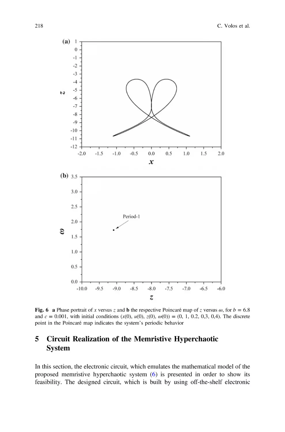
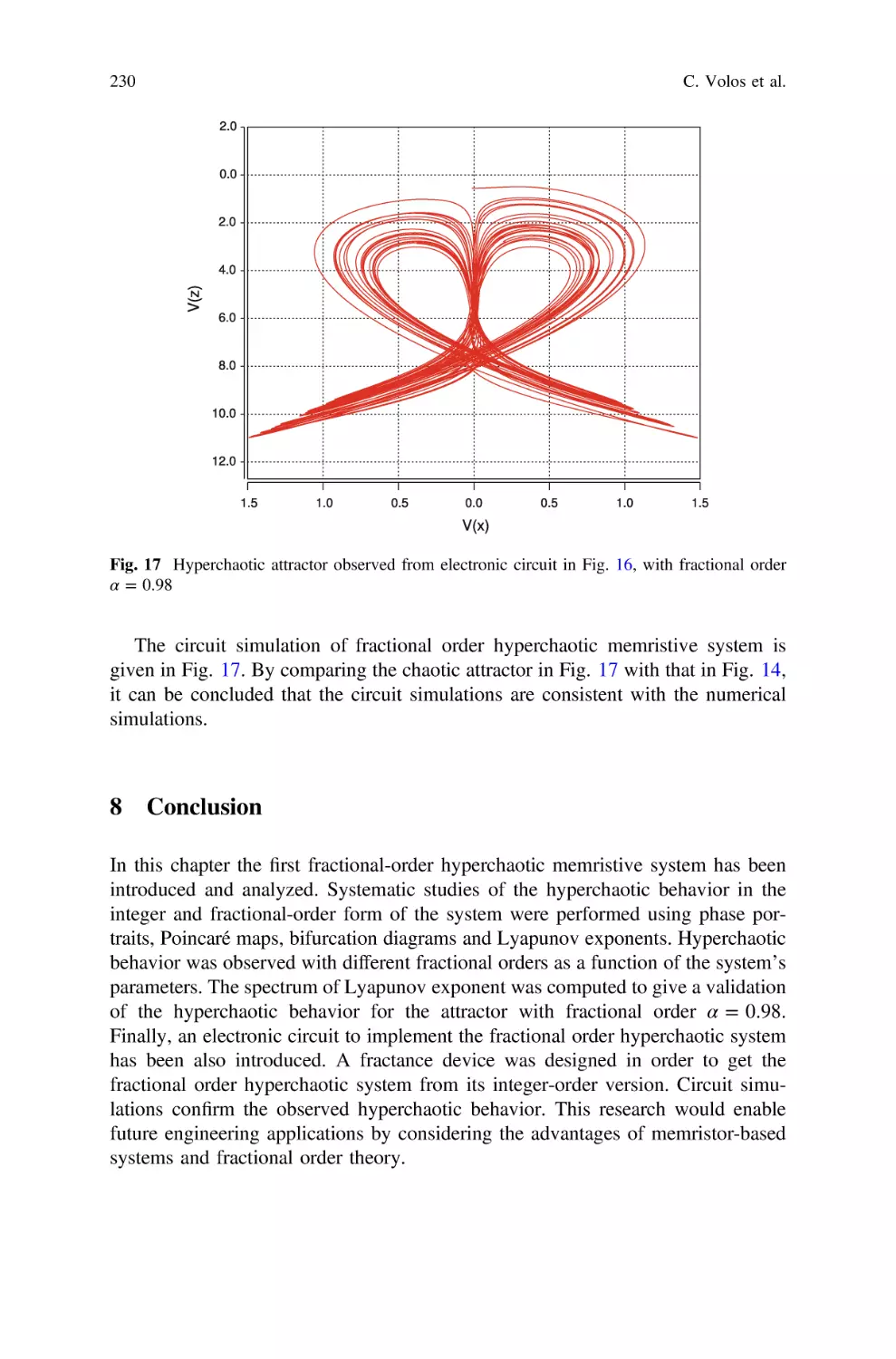
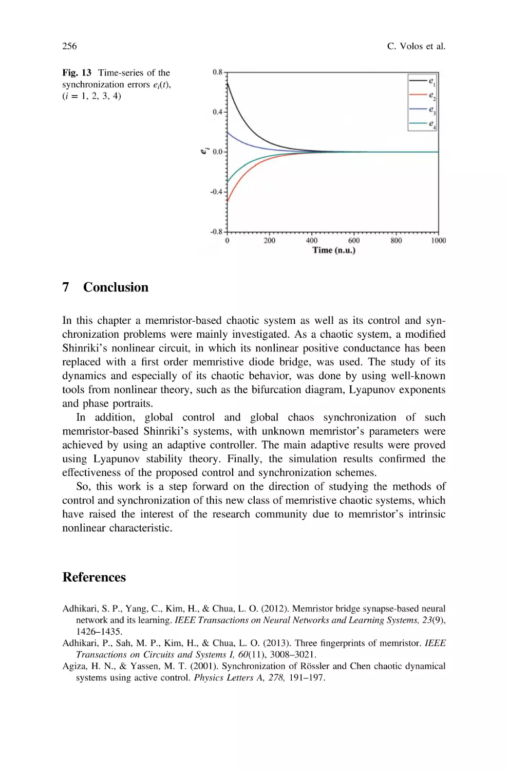
/


Автор: Vaidyanathan S. Volos C.
Теги: computer science information coding memristors
ISBN: 978-3-319-51723-0
Год: 2017
Похожие


Текст
Studies in Computational Intelligence 701
Sundarapandian Vaidyanathan
Christos Volos Editors
Advances in
Memristors,
Memristive
Devices and
Systems
Studies in Computational Intelligence
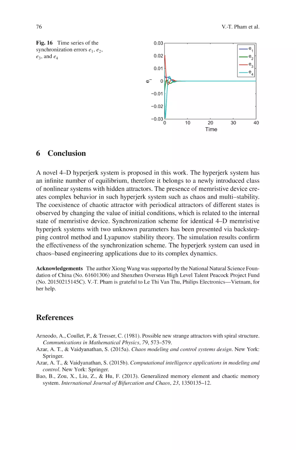
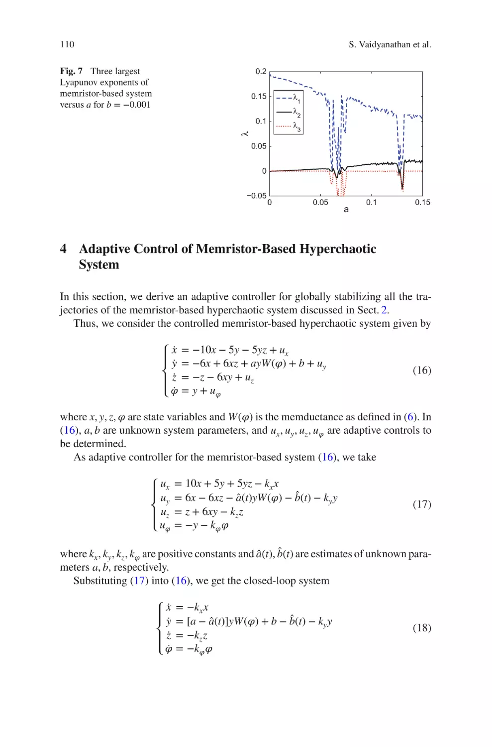
Volume 701
Series editor
Janusz Kacprzyk, Polish Academy of Sciences, Warsaw, Poland
e-mail: kacprzyk@ibspan.waw.pl
About this Series
The series “Studies in Computational Intelligence” (SCI) publishes new developments and advances in the various areas of computational intelligence—quickly and
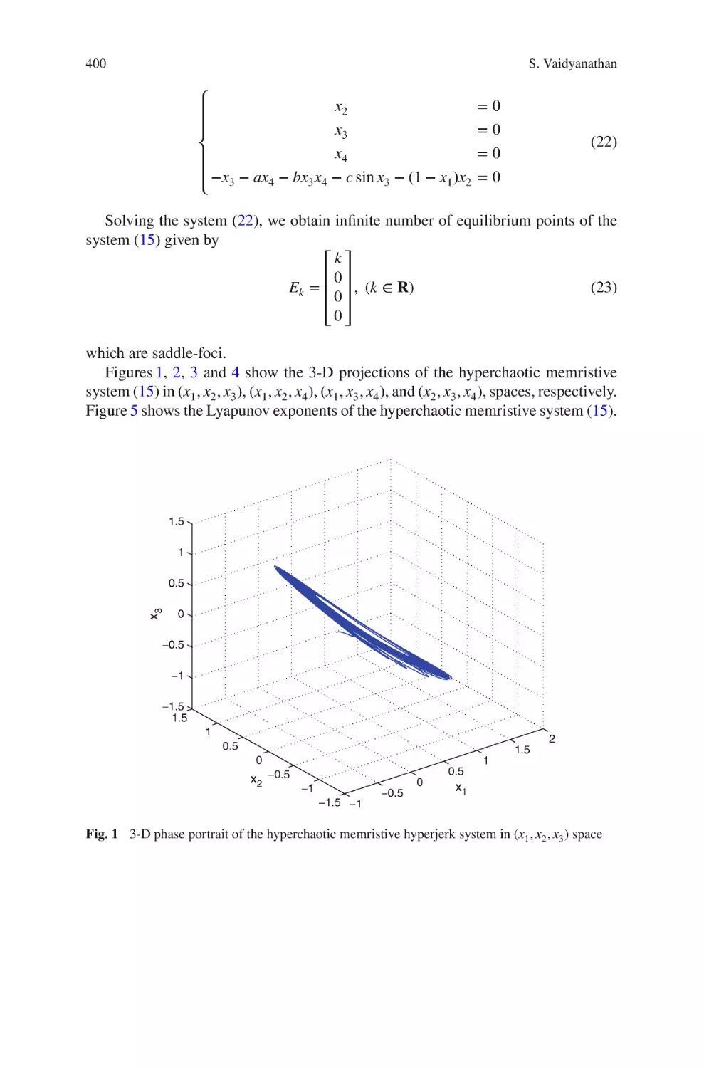
with a high quality. The intent is to cover the theory, applications, and design
methods of computational intelligence, as embedded in the fields of engineering,
computer science, physics and life sciences, as well as the methodologies behind
them. The series contains monographs, lecture notes and edited volumes in
computational intelligence spanning the areas of neural networks, connectionist
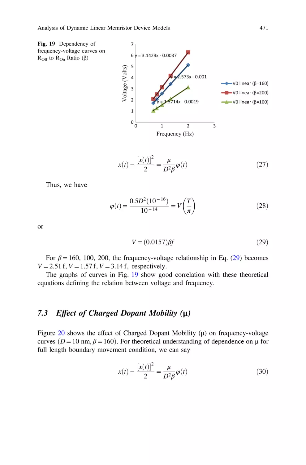
systems, genetic algorithms, evolutionary computation, artificial intelligence,
cellular automata, self-organizing systems, soft computing, fuzzy systems, and
hybrid intelligent systems. Of particular value to both the contributors and the
readership are the short publication timeframe and the worldwide distribution,
which enable both wide and rapid dissemination of research output.
More information about this series at http://www.springer.com/series/7092
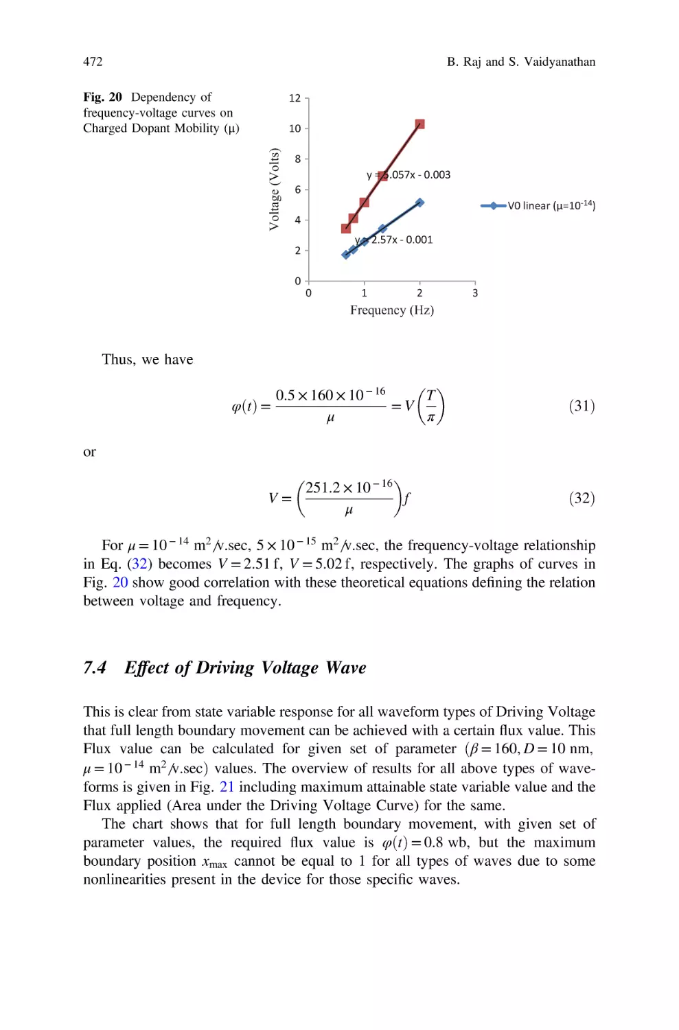
Sundarapandian Vaidyanathan
Christos Volos
Editors
Advances in Memristors,
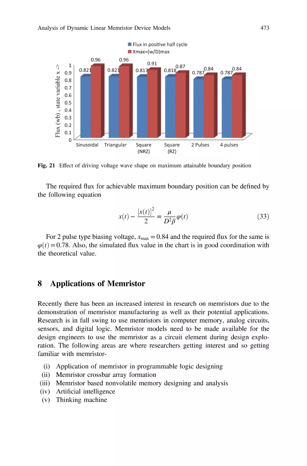
Memristive Devices
and Systems
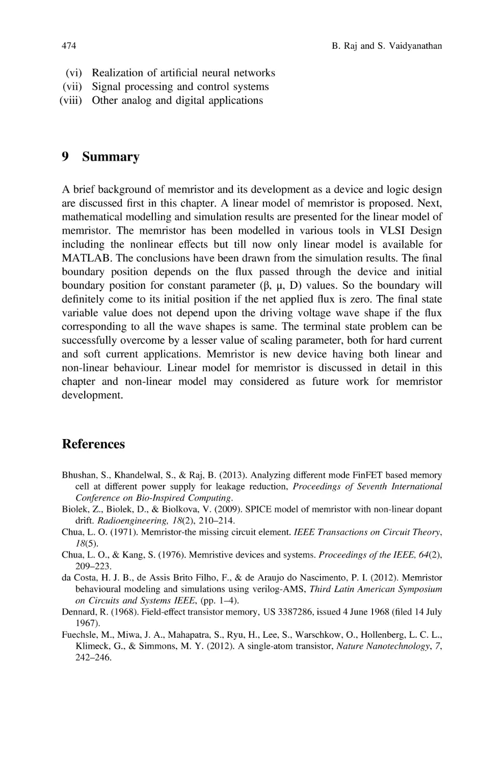
123
Editors
Sundarapandian Vaidyanathan
Research and Development Centre
Vel Tech University
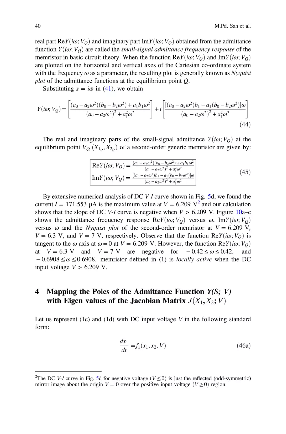
Chennai
India
Christos Volos
Department of Physics
Aristotle University of Thessaloniki
Thessaloniki
Greece
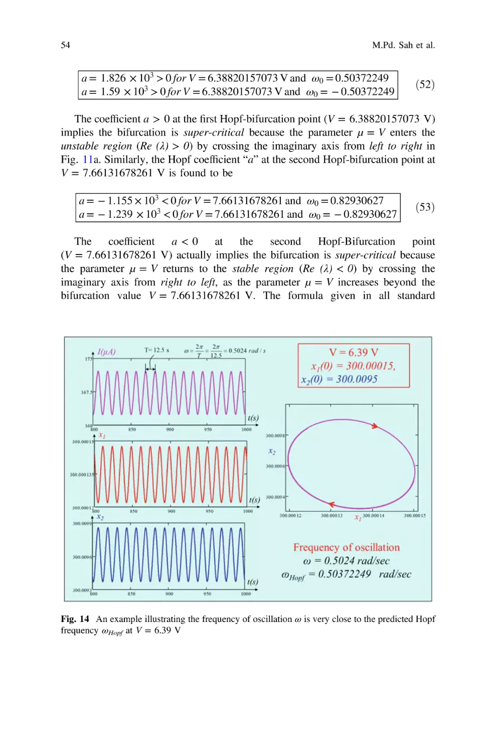
ISSN 1860-949X
ISSN 1860-9503 (electronic)
Studies in Computational Intelligence
ISBN 978-3-319-51723-0
ISBN 978-3-319-51724-7 (eBook)
DOI 10.1007/978-3-319-51724-7
Library of Congress Control Number: 2016961337
© Springer International Publishing AG 2017
This work is subject to copyright. All rights are reserved by the Publisher, whether the whole or part
of the material is concerned, specifically the rights of translation, reprinting, reuse of illustrations,
recitation, broadcasting, reproduction on microfilms or in any other physical way, and transmission
or information storage and retrieval, electronic adaptation, computer software, or by similar or dissimilar
methodology now known or hereafter developed.
The use of general descriptive names, registered names, trademarks, service marks, etc. in this
publication does not imply, even in the absence of a specific statement, that such names are exempt from
the relevant protective laws and regulations and therefore free for general use.
The publisher, the authors and the editors are safe to assume that the advice and information in this
book are believed to be true and accurate at the date of publication. Neither the publisher nor the
authors or the editors give a warranty, express or implied, with respect to the material contained herein or
for any errors or omissions that may have been made. The publisher remains neutral with regard to
jurisdictional claims in published maps and institutional affiliations.
Printed on acid-free paper
This Springer imprint is published by Springer Nature
The registered company is Springer International Publishing AG
The registered company address is: Gewerbestrasse 11, 6330 Cham, Switzerland
Preface
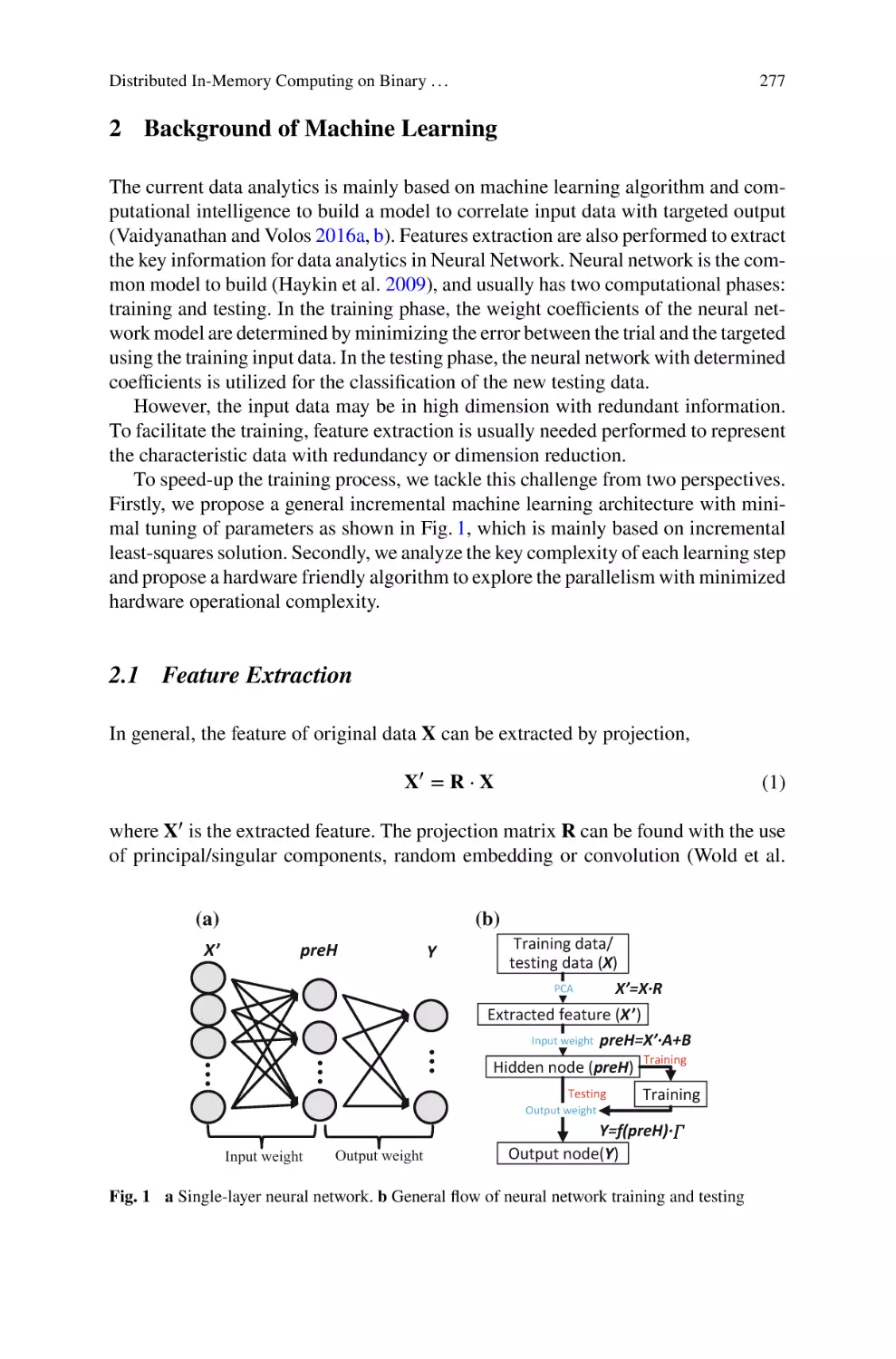
About the Subject
Memristor (concatenation of MEMory ResISTOR), is the fourth fundamental
circuit element ( joining the resistor, the capacitor and the inductor), predicted by
Leon Chua in 1971. This element represents one of today’s latest technological
achievements with a great number of applications. Memristor is a passive
two-terminal electronic device which behavior is described by a nonlinear constitutive relation between the voltage drop at its terminal and the current flowing
through the device. But the reason why the memristor is substantially different from
the other fundamental circuit elements is that, when the applied voltage is turned
off, it still remembers how much voltage was applied before and for how long; thus
presenting memory of its past. However, this innovative device attracted most of
attention worldwide only after 2008 when its practical implementation was
announced by Hewlett-Packard, originating intense research activity ever since.
Memristors have brought a revolution in various scientific fields, as many
phenomena in systems, such as in thermistors, spintronic devices and molecules
could be explained now with the use of the memristor. Also, electronic circuits with
memory elements could simulate processes typical of biological systems, such as
learning and associative memory and the adaptive behavior of unicellular organisms. Furthermore, neuromorphic computing circuits with memristors can potentially solve problems that are cumbersome or outright intractable by digital
computation.
Memristors have been used in cellular neural networks, for performing a number
of applications, such as logical operations, image processing operations, complex
behavior and higher brain functions, or in designing Boolean logic gates for the
AND, OR and NOT operations. In many well-known nonlinear circuits, the nonlinear element has been replaced by memristors and various interesting dynamical
phenomena like chaos and hidden attractors have been observed. Therefore, with
these wide range of applications, engineering aspects of memristor devices,
memristive-based circuits and systems design become significant important.
v
vi
Preface
About the Book
The new Springer book, Advances in Memristors, Memristive Devices and Systems,
consists of 20 contributed chapters by subject experts who are specialized in the
various topics addressed in this book. The special chapters have been brought out in
this book after a rigorous review process in the broad areas of modeling and
applications of memristors, memristive devices and systems. Special importance
was given to chapters offering practical solutions and novel methods for the recent
research problems in the modeling and applications of memristors, memristive
devices and systems.
This book discusses trends and applications of memristors and memristive
devices in engineering.
Objectives of the Book
This volume presents a selected collection of contributions on a focused treatment
of recent advances and applications in memristors, memristive devices and systems.
The book also discusses multidisciplinary applications in electrical engineering,
control engineering, computer science and information technology. These are
among those multidisciplinary applications where computational intelligence has
excellent potentials for use. Both novice and expert readers should find this book a
useful reference in the field of memristors and memristive devices.
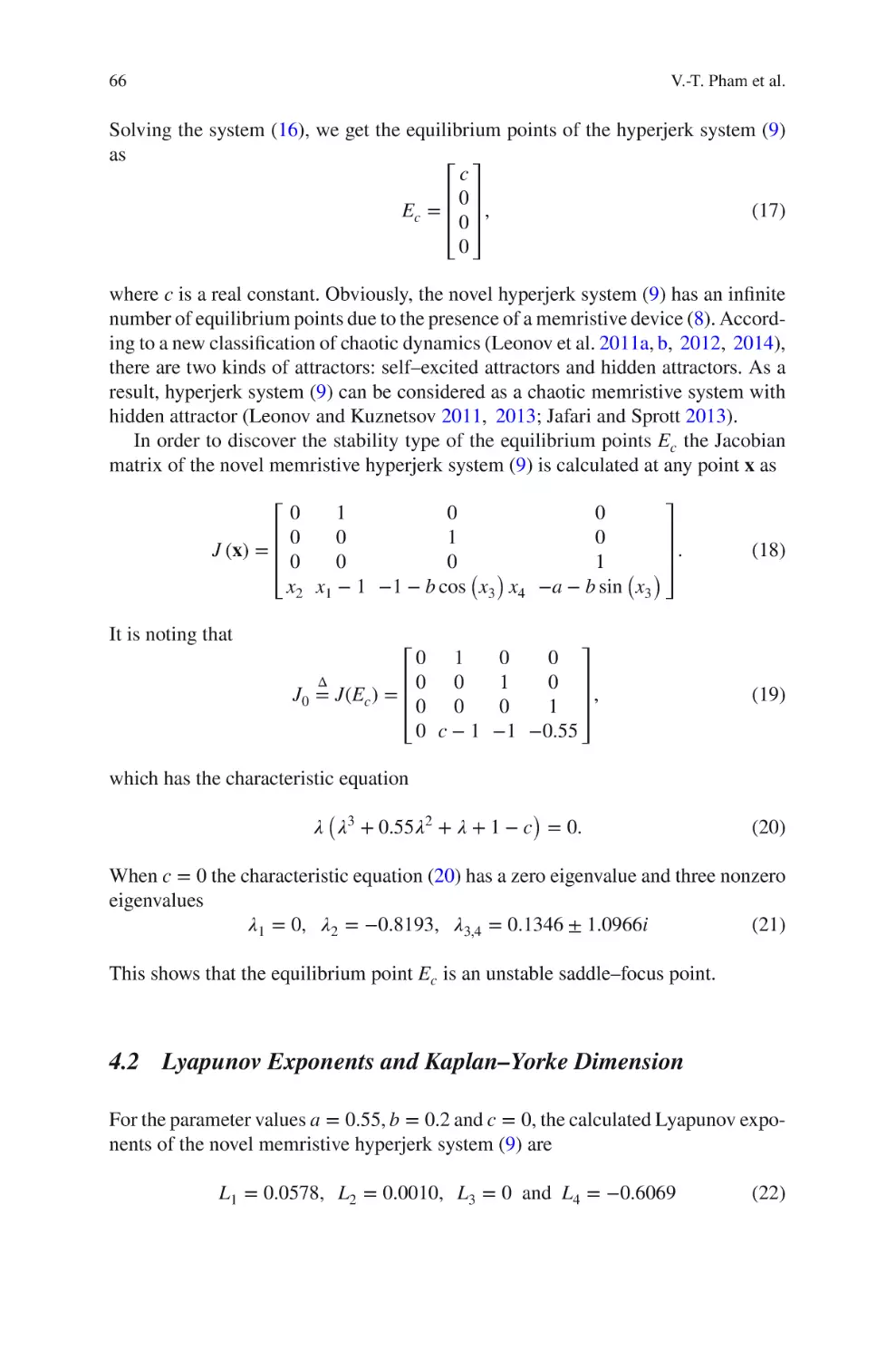
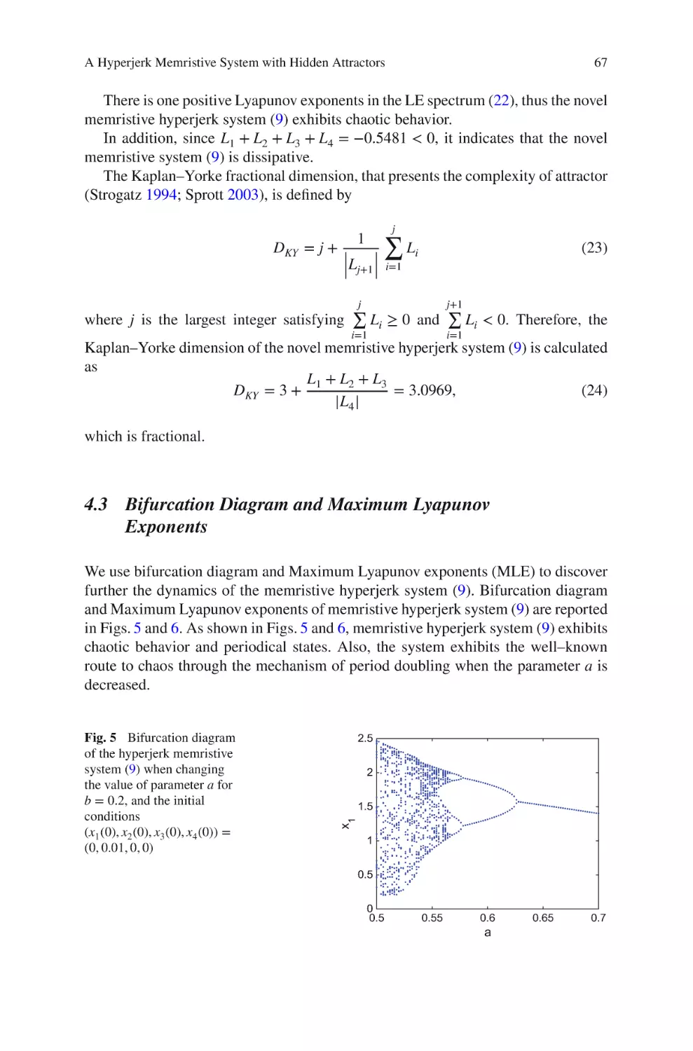
Organization of the Book
This well-structured book consists of 20 full chapters.
Book Features
• The book chapters deal with the recent research problems in the areas of
memristors and memristive devices.
• The book includes chapters by eminent experts and pioneers of memristors—
Leon Chua and R.S. Williams.
• The book chapters contain a good literature survey with a long list of references.
• The book chapters are well-written with a good exposition of the research
problem, methodology, block diagrams and circuits.
• The book chapters are lucidly illustrated with numerical examples and
simulations.
• The book chapters discuss details of engineering applications and future
research areas.
Preface
vii
Audience
The book is primarily meant for researchers from academia and industry, who are
working on memristors and memristive devices in the research areas—electrical
engineering, control engineering, computer science, and information technology.
The book can also be used at the graduate or advanced undergraduate level as a
textbook or major reference for courses such as power systems, control systems,
electrical devices, scientific modeling, computational science and many others.
Chennai, India
Thessaloniki, Greece
Sundarapandian Vaidyanathan
Christos Volos
Acknowledgements
As the editors, we hope that the chapters in this well-structured book will stimulate
further research in memristors, memristive devices and control systems, and utilize
them in real-world applications.
We hope sincerely that this book, covering so many different topics, will be very
useful for all readers.
We thank eminent Prof. Leon Chua for kindly accepting our invitation and
contributing two chapters in this book. We also thank eminent Profs. Alon Ascoli,
Ronald Tetzlaff and R.S. Williams for kindly accepting our invitation and contributing a chapter in this book.
We would like to thank all the reviewers for their diligence in reviewing the
chapters.
Special thanks go to Springer, especially the book Editorial team.
Chennai, India
Thessaloniki, Greece
Sundarapandian Vaidyanathan
Christos Volos
ix
Contents
Memristor Emulators: A Note on Modeling . . . . . . . . . . . . . . . . . . . . . . .
A. Ascoli, R. Tetzlaff, L.O. Chua, W. Yi and R.S. Williams
1
A Simple Oscillator Using Memristor . . . . . . . . . . . . . . . . . . . . . . . . . . . .
Maheshwar Pd. Sah, Vetriveeran Rajamani, Zubaer Ibna Mannan,
Abdullah Eroglu, Hyongsuk Kim and Leon Chua
19
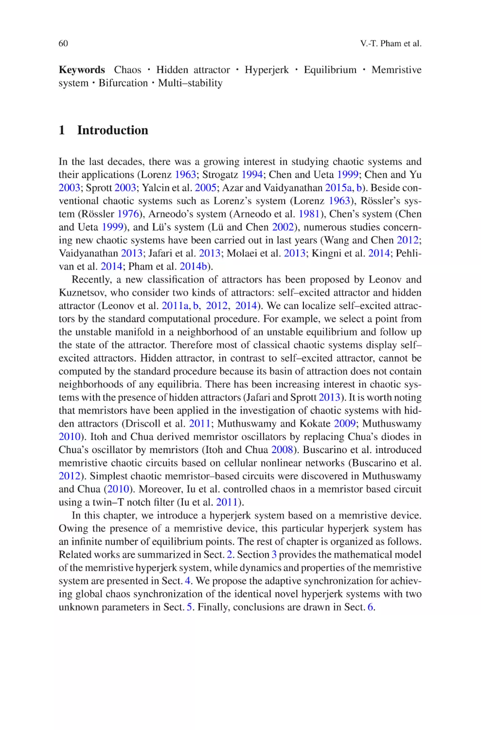
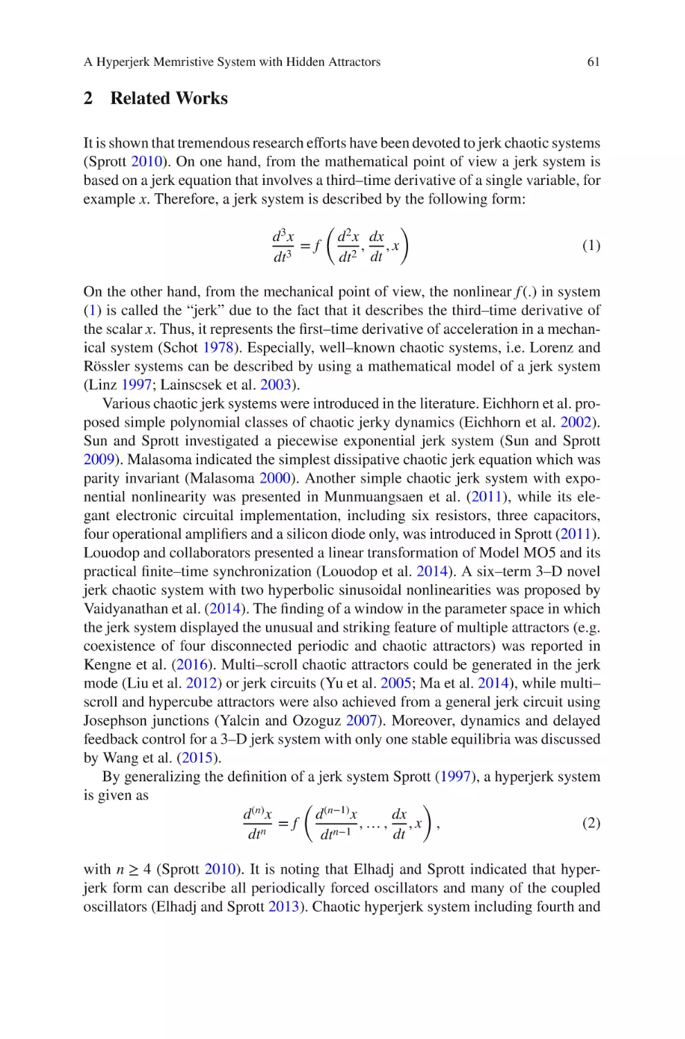
A Hyperjerk Memristive System with Hidden Attractors . . . . . . . . . . . .
Viet-Thanh Pham, Sundarapandian Vaidyanathan, Christos Volos,
Xiong Wang and Duy Vo Hoang
59
A Memristive System with Hidden Attractors
and Its Engineering Application . . . . . . . . . . . . . . . . . . . . . . . . . . . . . . . .
Viet-Thanh Pham, Sundarapandian Vaidyanathan, Christos Volos,
Esteban Tlelo-Cuautle and Fadhil Rahma Tahir
81
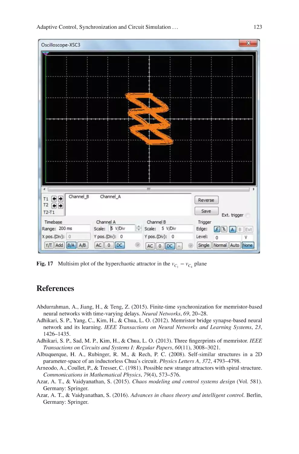
Adaptive Control, Synchronization and Circuit Simulation of a
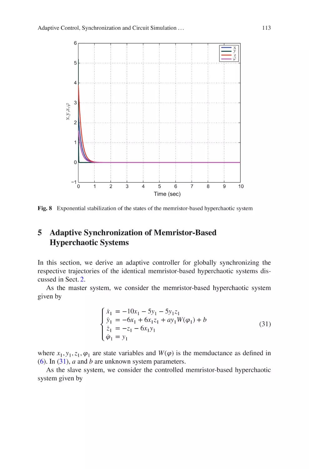
Memristor-Based Hyperchaotic System With Hidden Attractors . . . . . . 101
Sundarapandian Vaidyanathan, Viet-Thanh Pham and Christos Volos
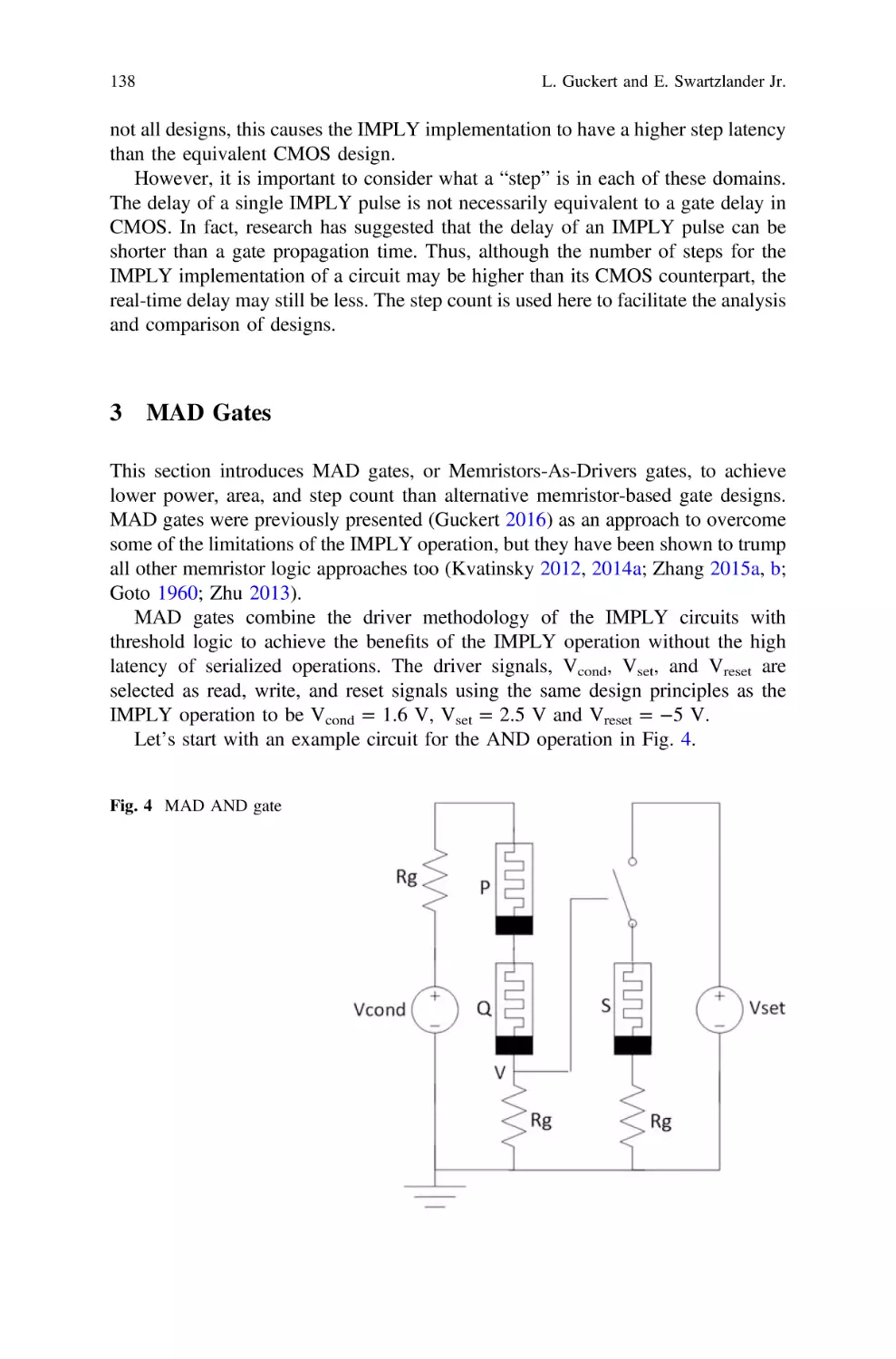
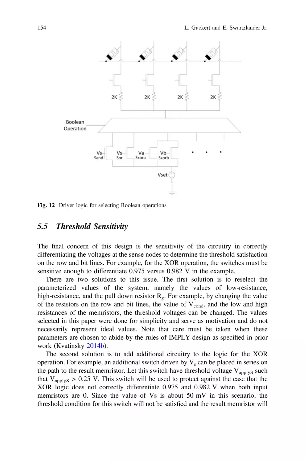
Modern System Design Using Memristors . . . . . . . . . . . . . . . . . . . . . . . . 131
Lauren Guckert and Earl Swartzlander Jr.
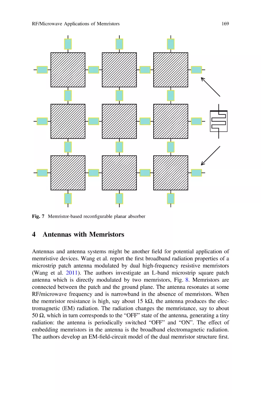
RF/Microwave Applications of Memristors . . . . . . . . . . . . . . . . . . . . . . . . 159
Milka Potrebić, Dejan Tošić and Dalibor Biolek
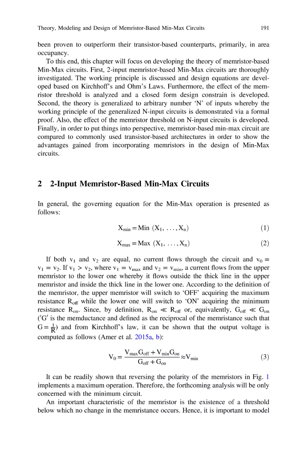
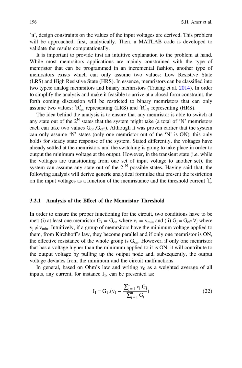
Theory, Modeling and Design of Memristor-Based
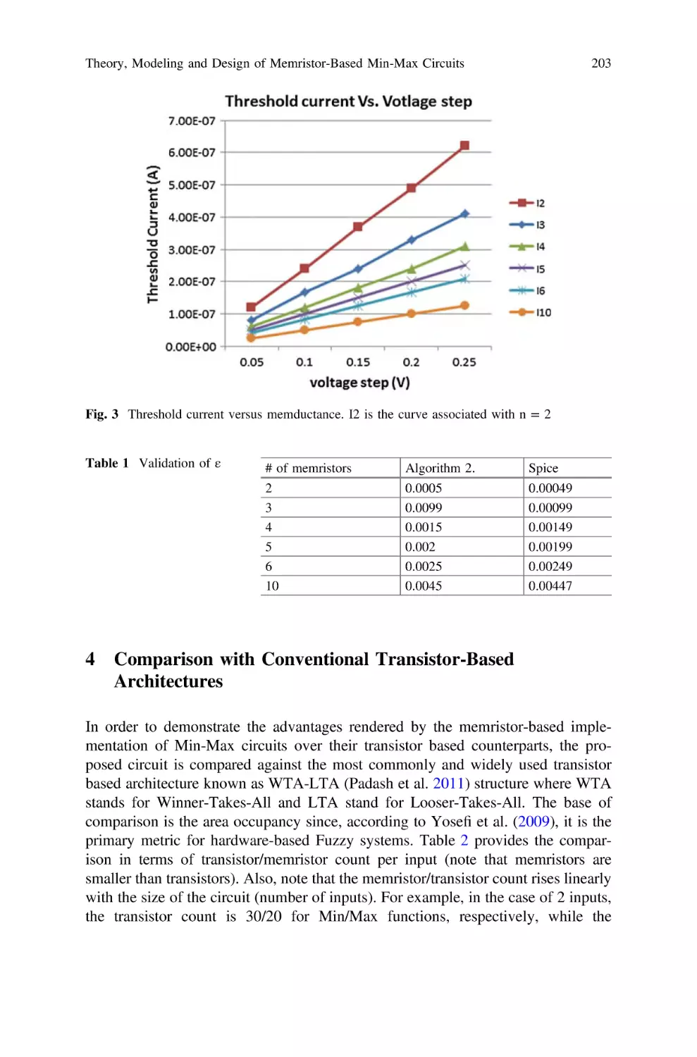
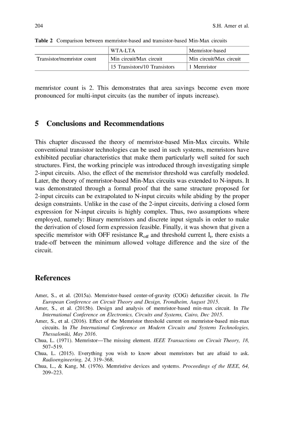
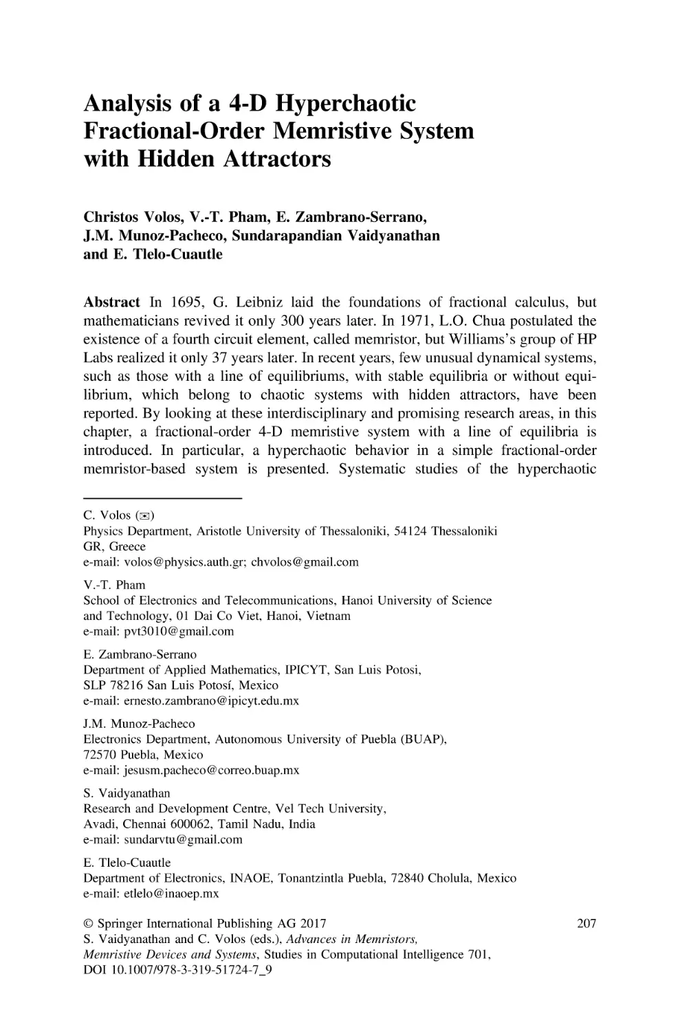
Min-Max Circuits . . . . . . . . . . . . . . . . . . . . . . . . . . . . . . . . . . . . . . . . . . . . 187
S.H. Amer, A.H. Madian, Hany ElSayed, A.S. Emara and H.H. Amer
Analysis of a 4-D Hyperchaotic Fractional-Order
Memristive System with Hidden Attractors . . . . . . . . . . . . . . . . . . . . . . . 207
Christos Volos, V.-T. Pham, E. Zambrano-Serrano, J.M. Munoz-Pacheco,
Sundarapandian Vaidyanathan and E. Tlelo-Cuautle
xi
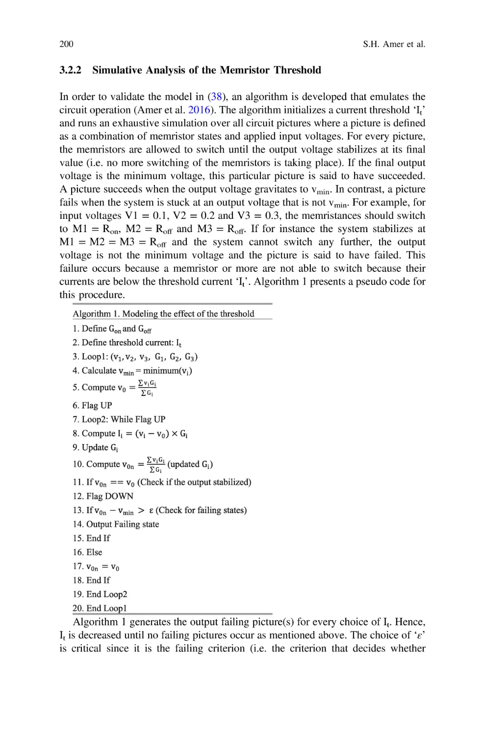
xii
Contents
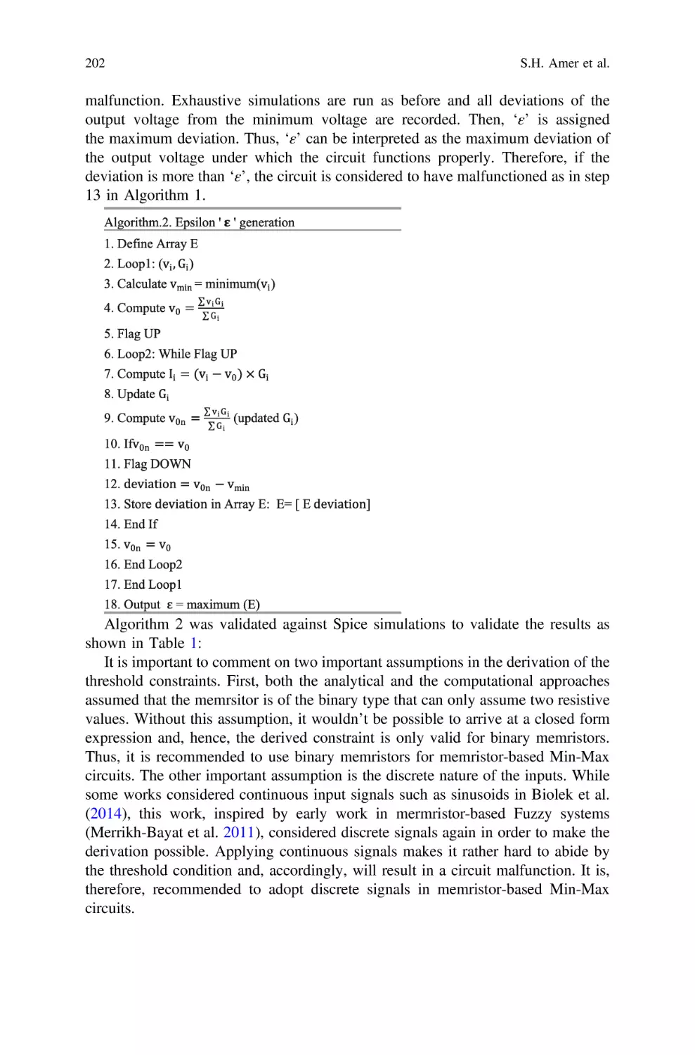
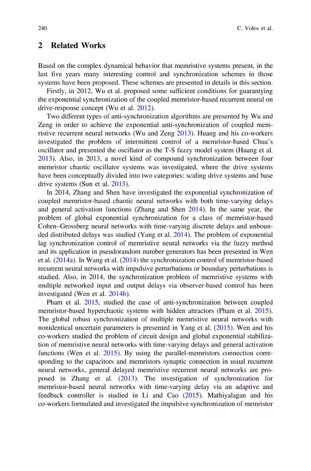
Adaptive Control and Synchronization of a Memristor-Based
Shinriki’s System . . . . . . . . . . . . . . . . . . . . . . . . . . . . . . . . . . . . . . . . . . . . 237
Christos Volos, Sundarapandian Vaidyanathan, V.-T. Pham,
H.E. Nistazakis, I.N. Stouboulos, I.M. Kyprianidis and G.S. Tombras
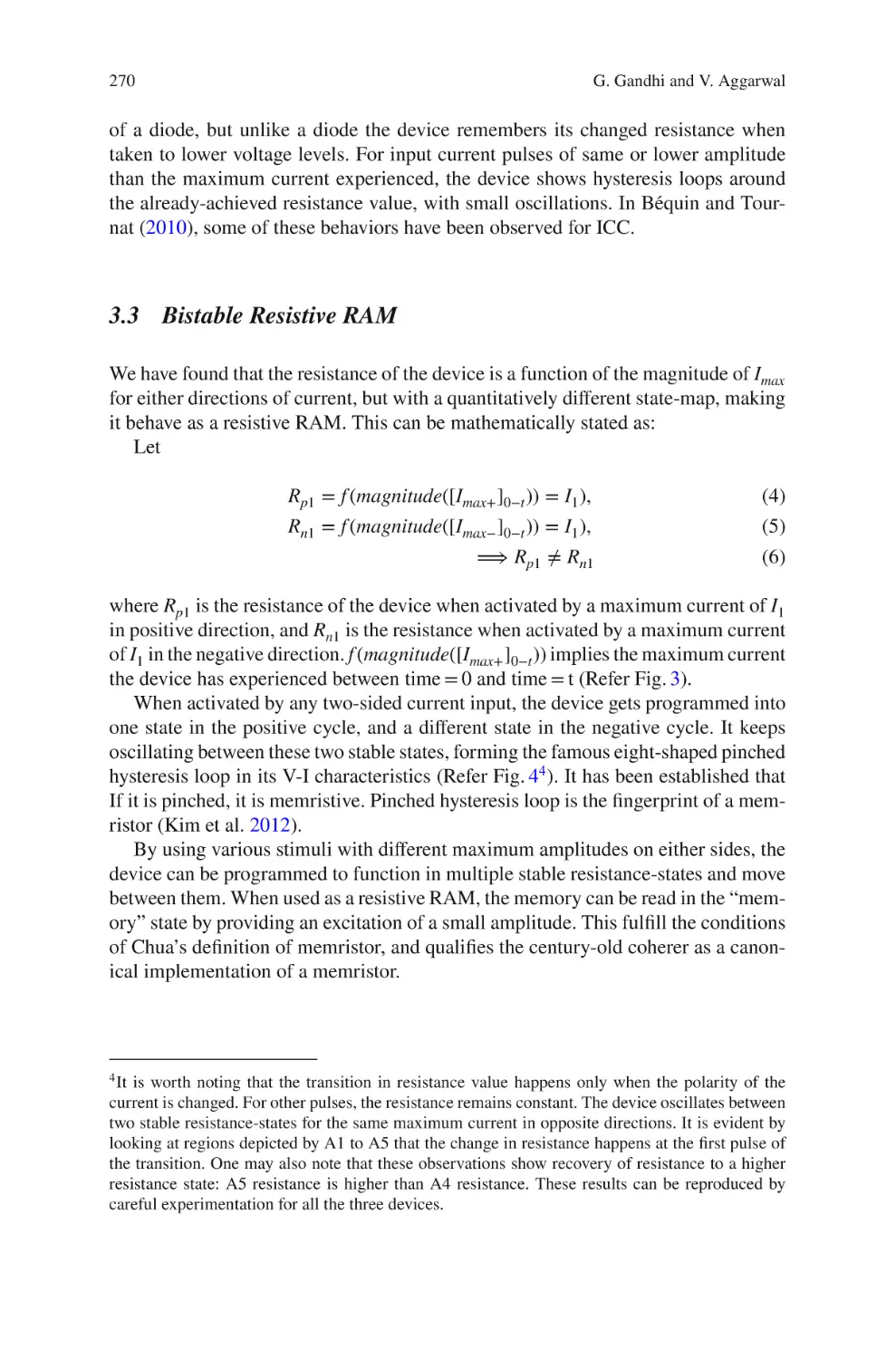
Canonic Memristor: Bipolar Electrical Switching
in Metal-Metal Contacts . . . . . . . . . . . . . . . . . . . . . . . . . . . . . . . . . . . . . . . 263
Gaurav Gandhi and Varun Aggarwal
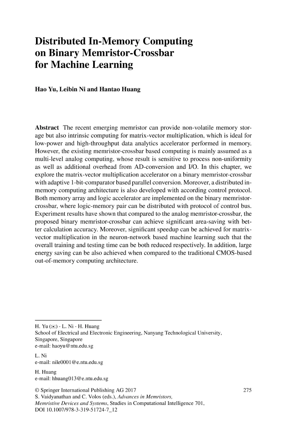
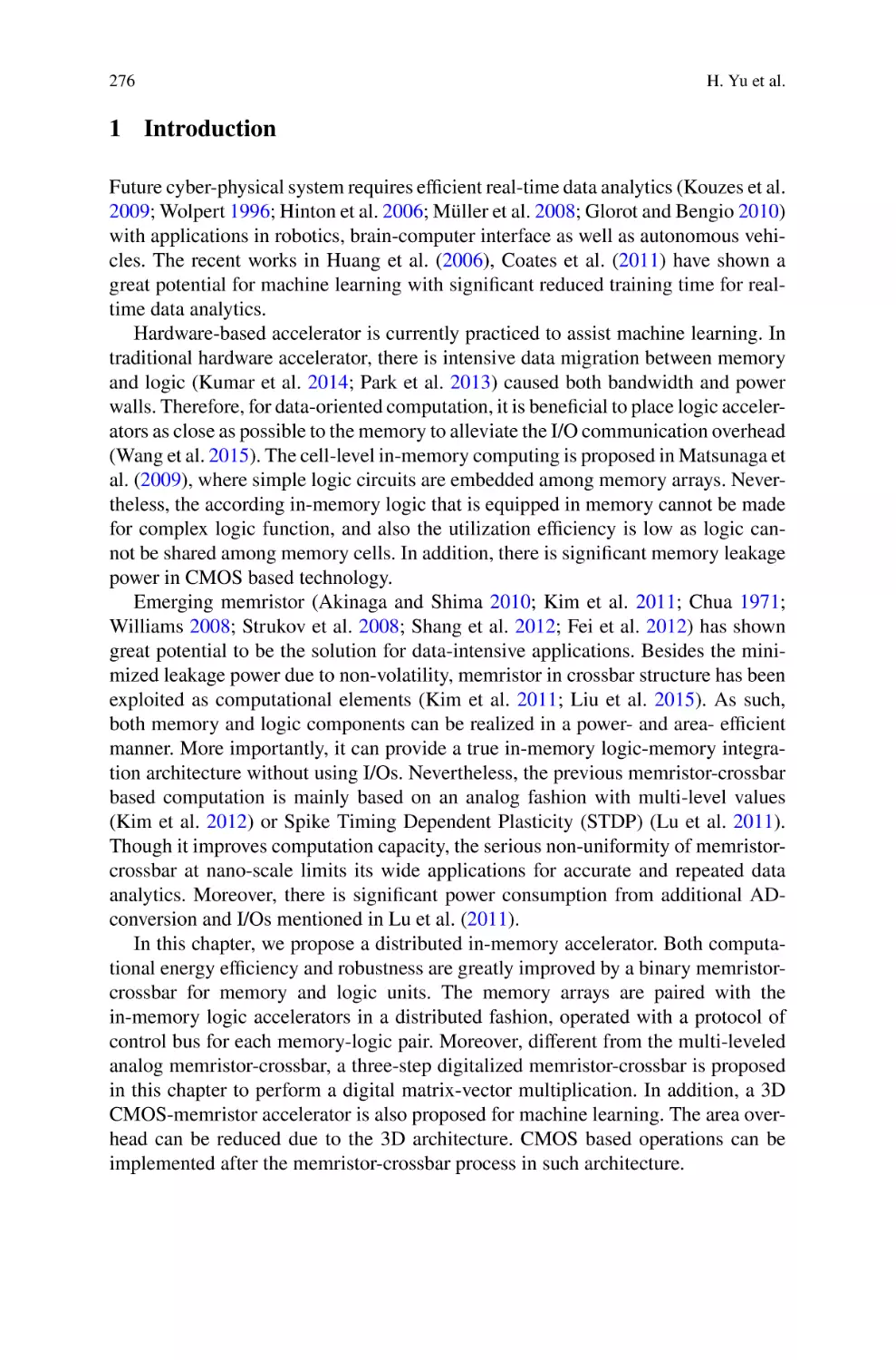
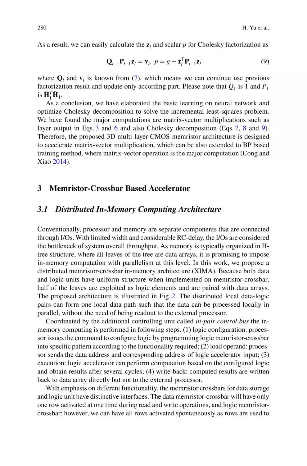
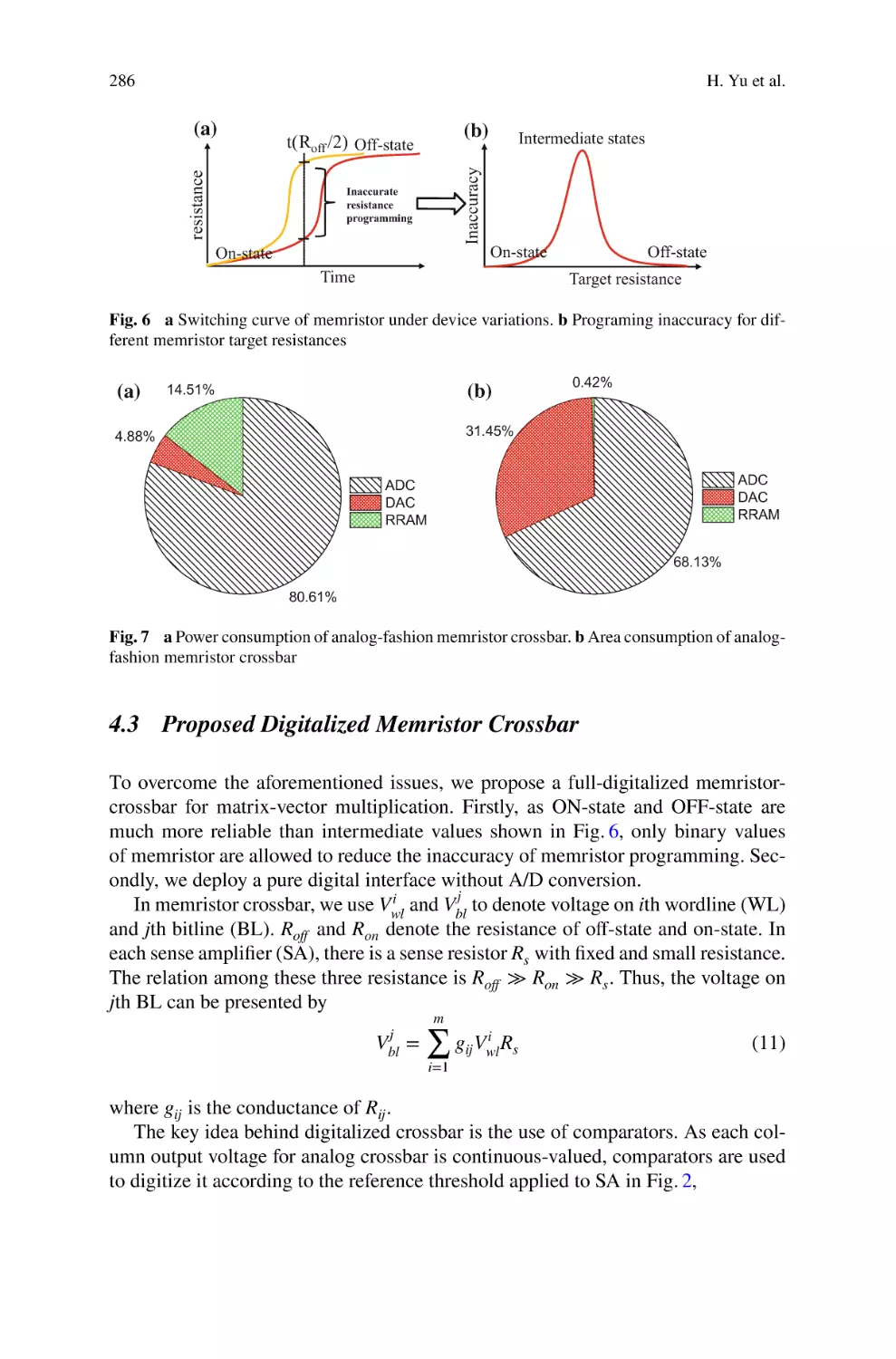
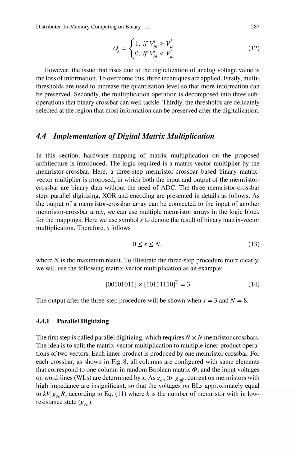
Distributed In-Memory Computing on Binary
Memristor-Crossbar for Machine Learning . . . . . . . . . . . . . . . . . . . . . . . 275
Hao Yu, Leibin Ni and Hantao Huang
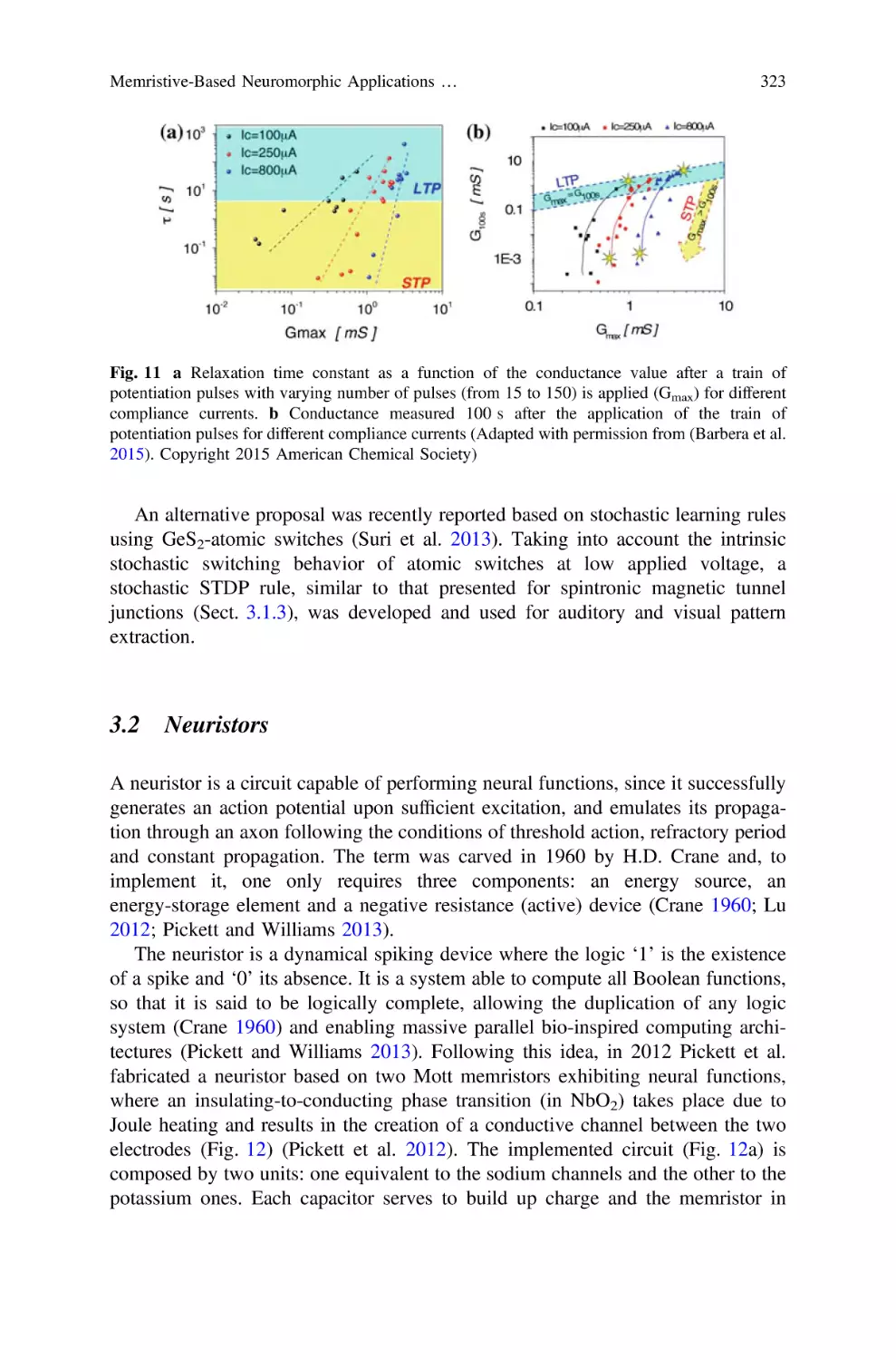
Memristive-Based Neuromorphic Applications
and Associative Memories . . . . . . . . . . . . . . . . . . . . . . . . . . . . . . . . . . . . . 305
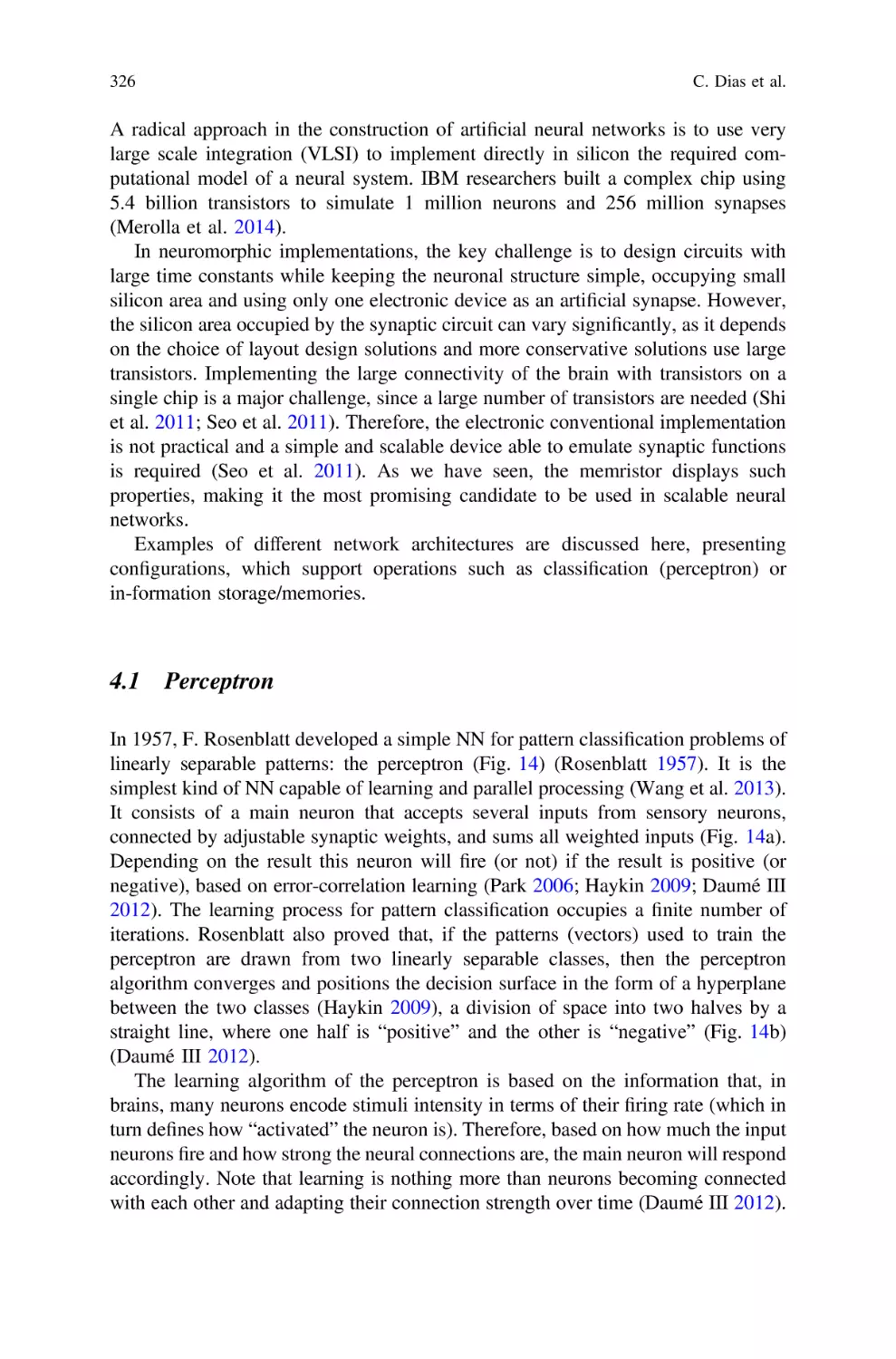
C. Dias, J. Ventura and P. Aguiar
Experimental Analogue Implementation of Memristor
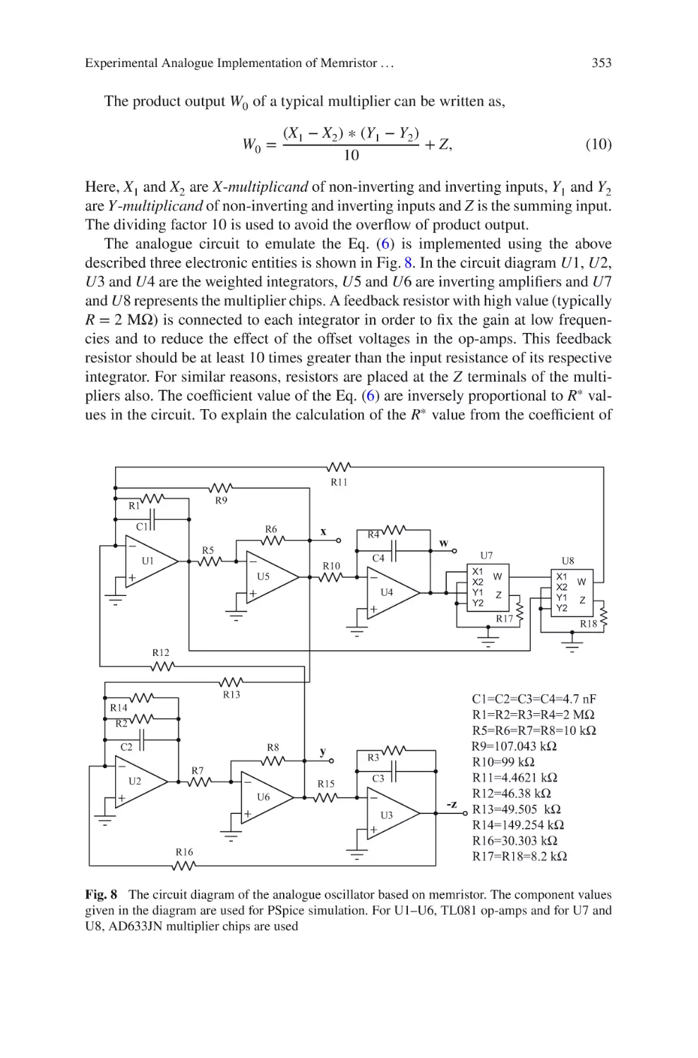
Based Chaotic Oscillators . . . . . . . . . . . . . . . . . . . . . . . . . . . . . . . . . . . . . . 343
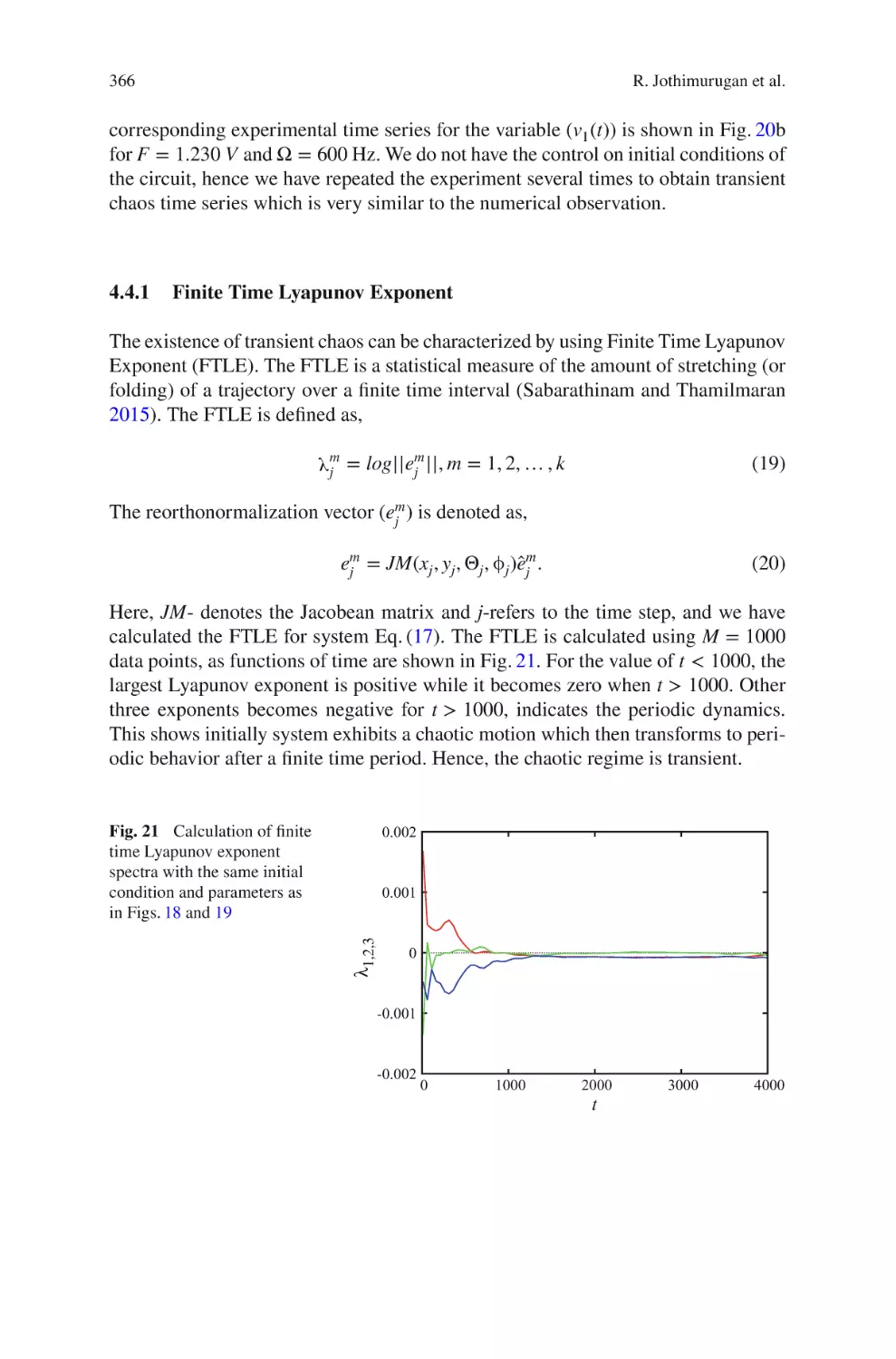
R. Jothimurugan, S. Sabarathinam, K. Suresh and K. Thamilmaran
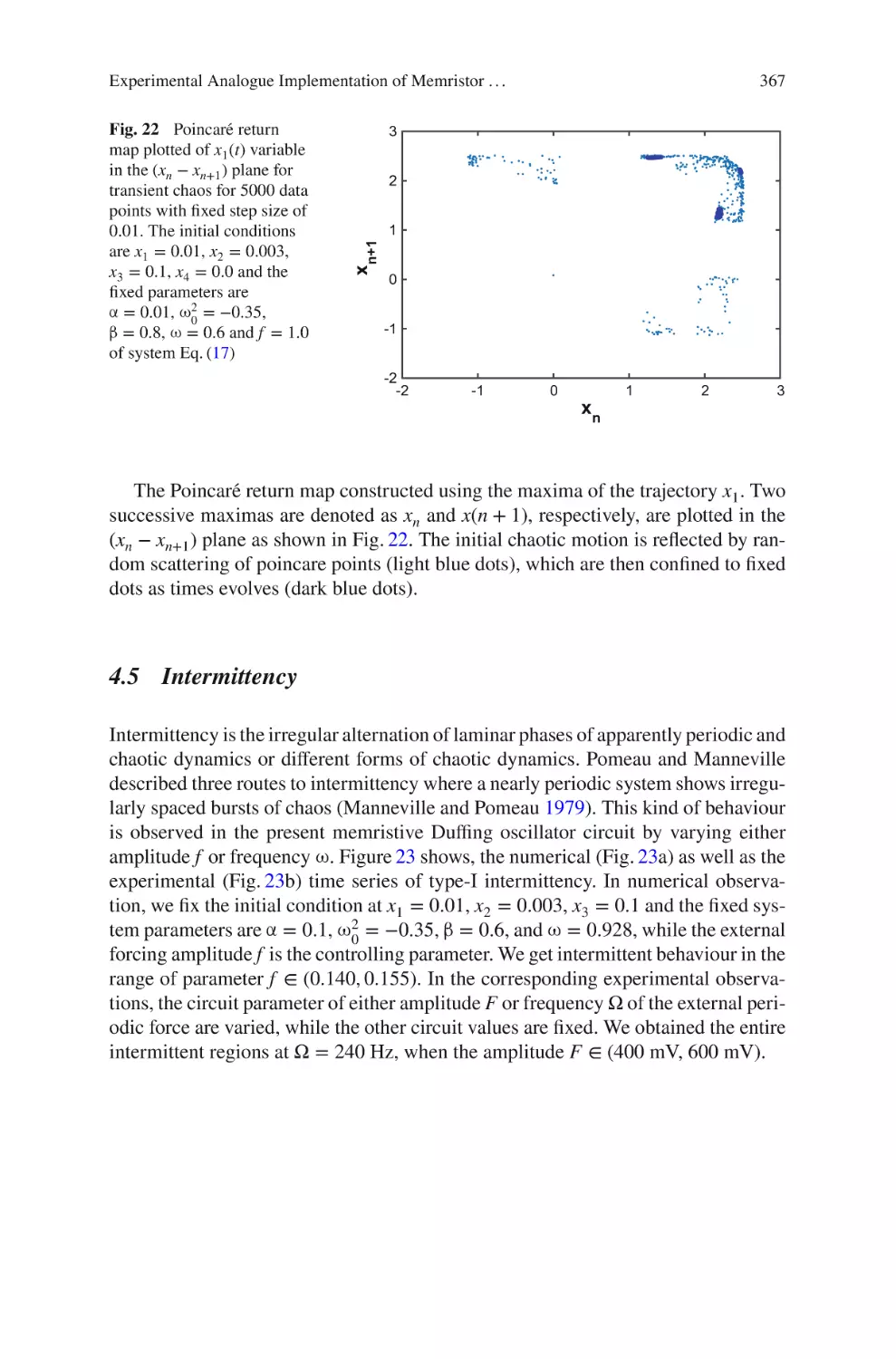
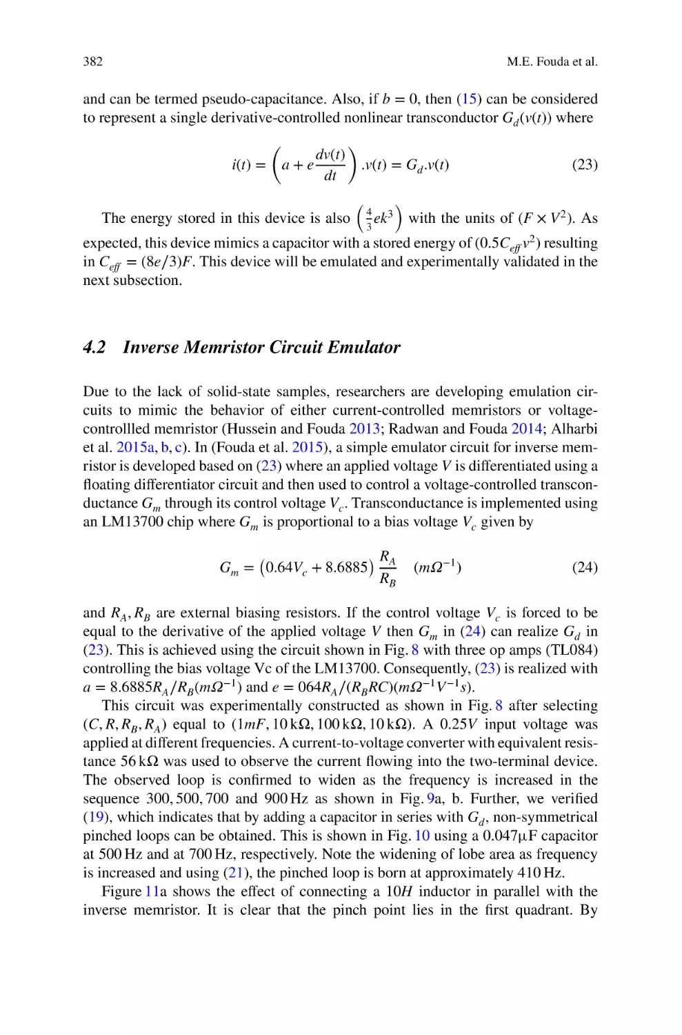
Memristor and Inverse Memristor: Modeling, Implementation
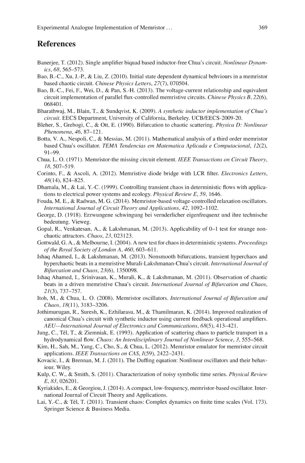
and Experiments . . . . . . . . . . . . . . . . . . . . . . . . . . . . . . . . . . . . . . . . . . . . . 371
Mohammed E. Fouda, Ahmed G. Radwan and Ahmed Elwakil
A Conservative Hyperchaotic Hyperjerk System Based
on Memristive Device . . . . . . . . . . . . . . . . . . . . . . . . . . . . . . . . . . . . . . . . . 393
Sundarapandian Vaidyanathan
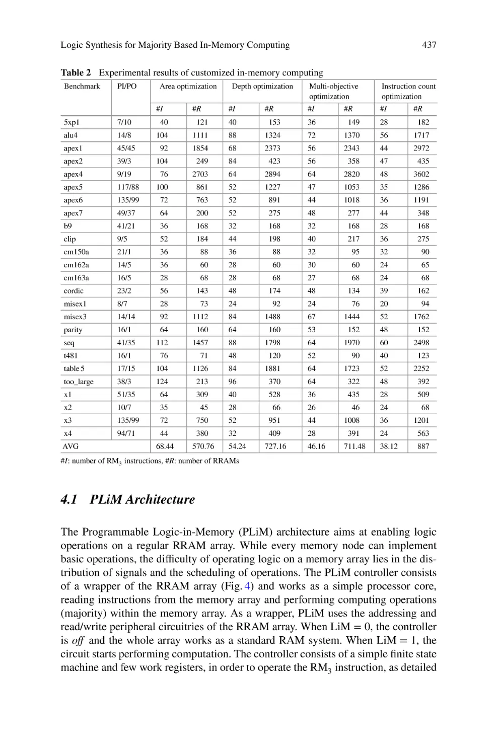
Logic Synthesis for Majority Based In-Memory Computing . . . . . . . . . . 425
Saeideh Shirinzadeh, Mathias Soeken, Pierre-Emmanuel Gaillardon
and Rolf Drechsler
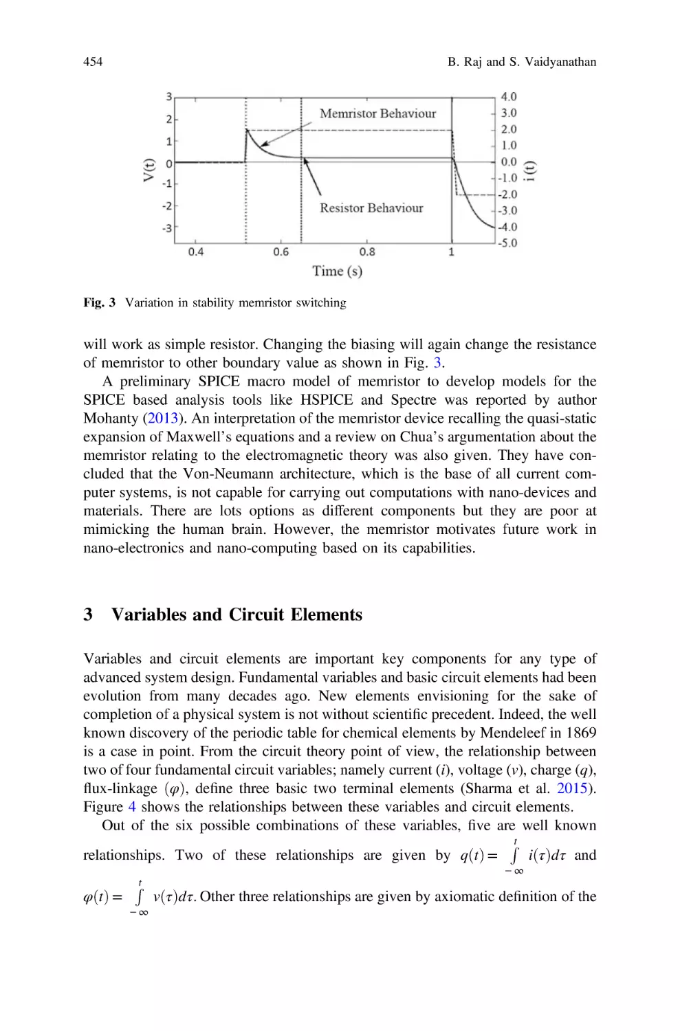
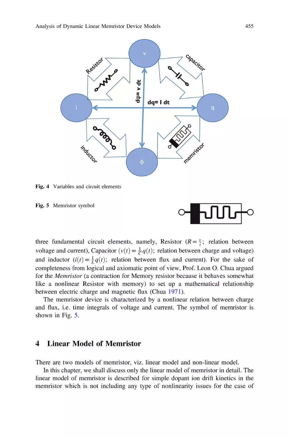
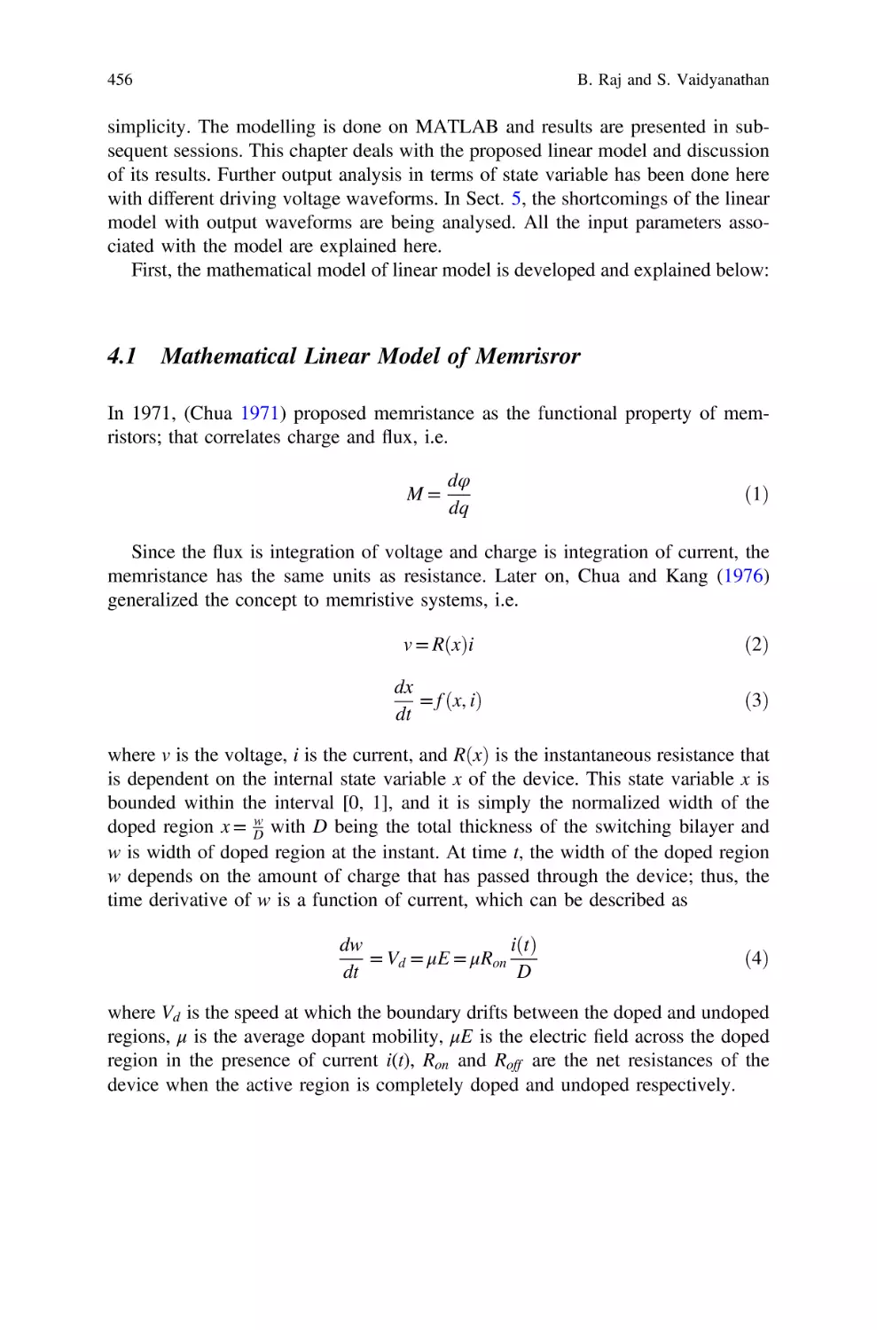
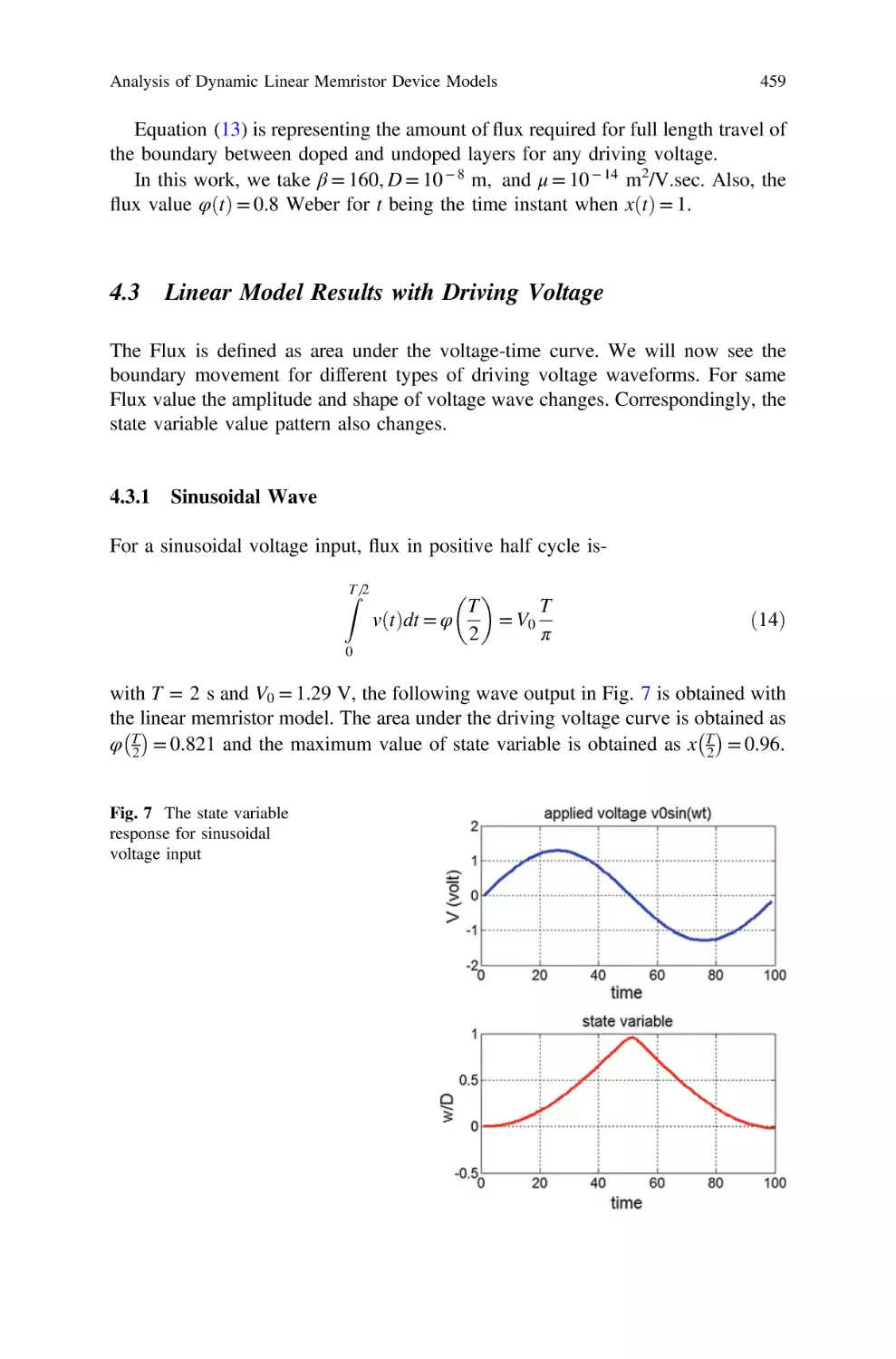
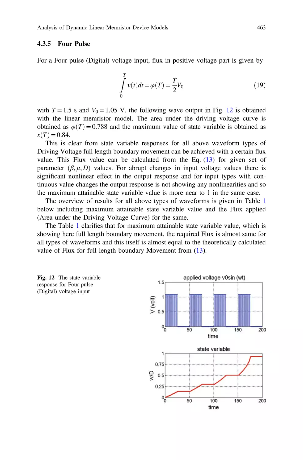
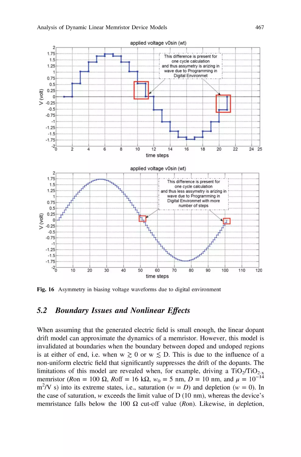
Analysis of Dynamic Linear Memristor Device Models . . . . . . . . . . . . . . 449
Balwinder Raj and Sundarapandian Vaidyanathan
Dynamics of Delayed Memristive Systems in Combination
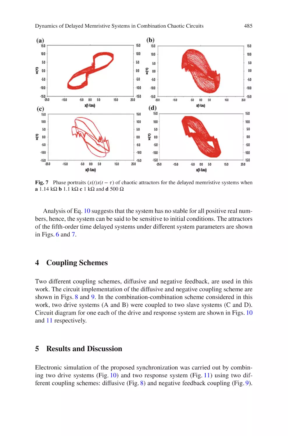
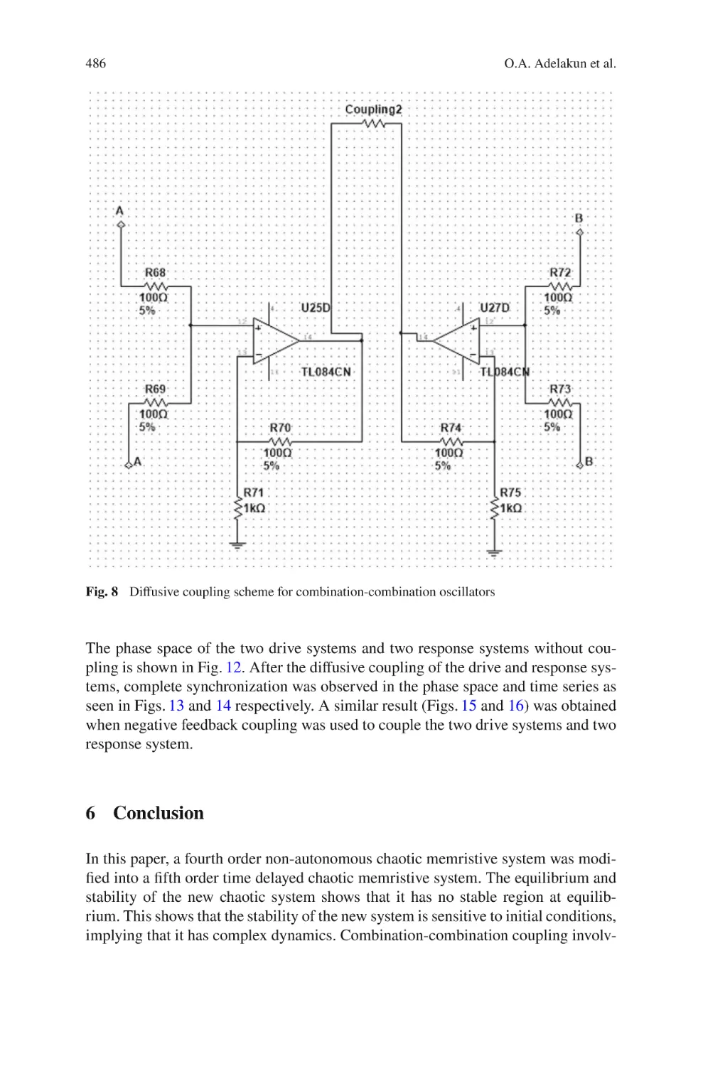
Chaotic Circuits . . . . . . . . . . . . . . . . . . . . . . . . . . . . . . . . . . . . . . . . . . . . . 477
O.A. Adelakun, S.T. Ogunjo and I.A. Fuwape
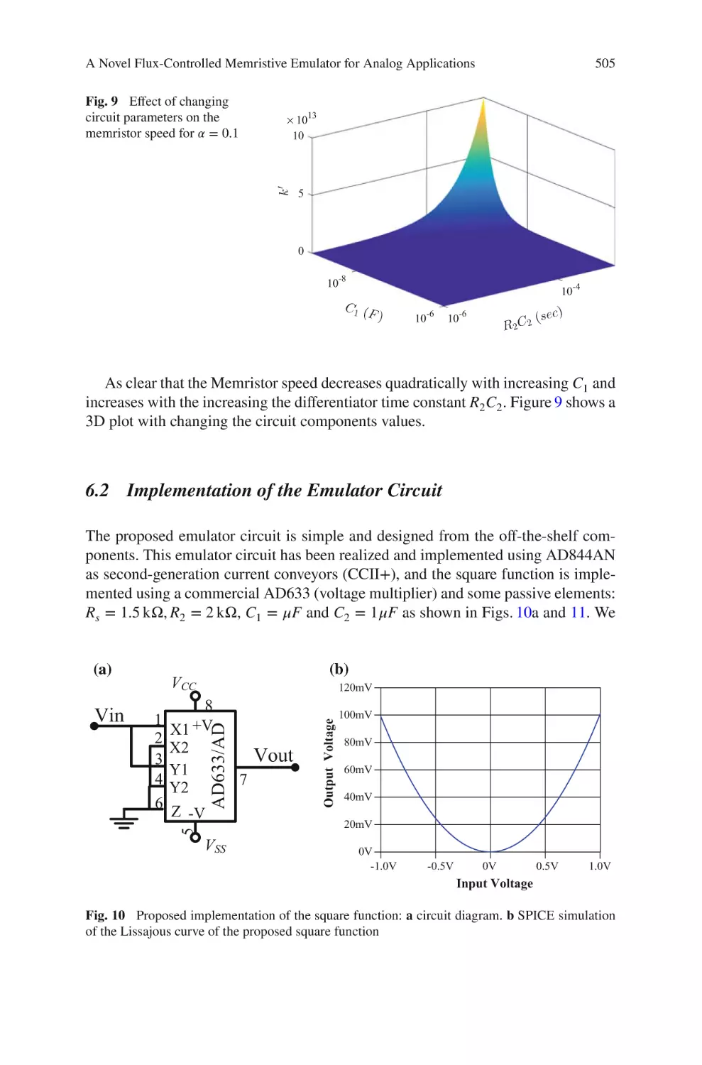
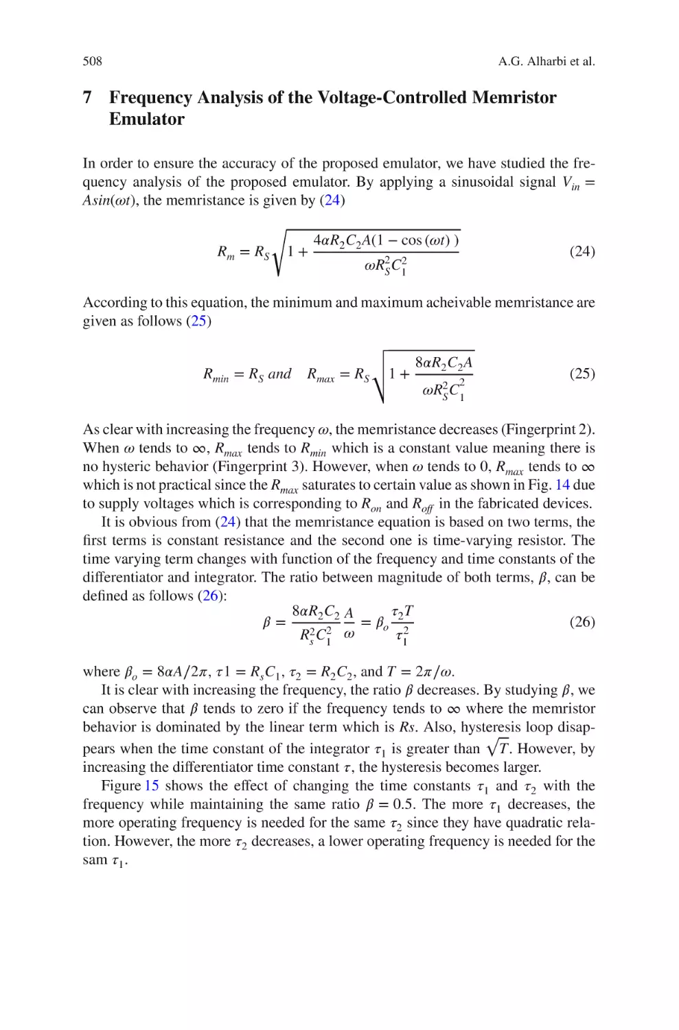
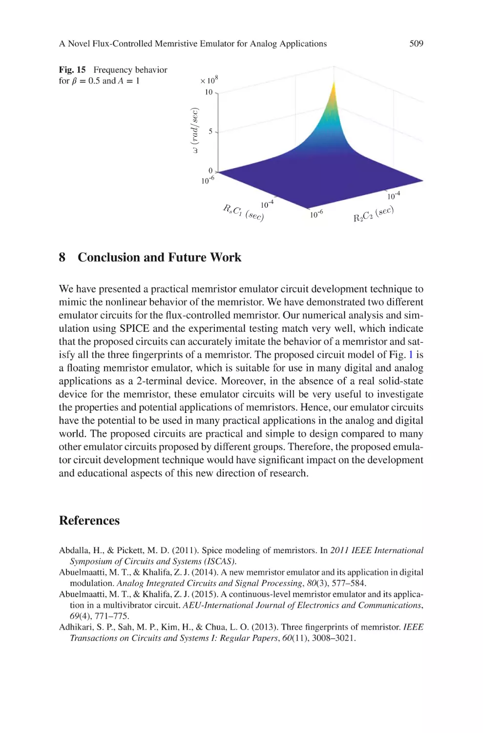
A Novel Flux-Controlled Memristive Emulator for Analog
Applications . . . . . . . . . . . . . . . . . . . . . . . . . . . . . . . . . . . . . . . . . . . . . . . . . 493
Abdullah G. Alharbi, Mohammed E. Fouda and Masud H. Chowdhury
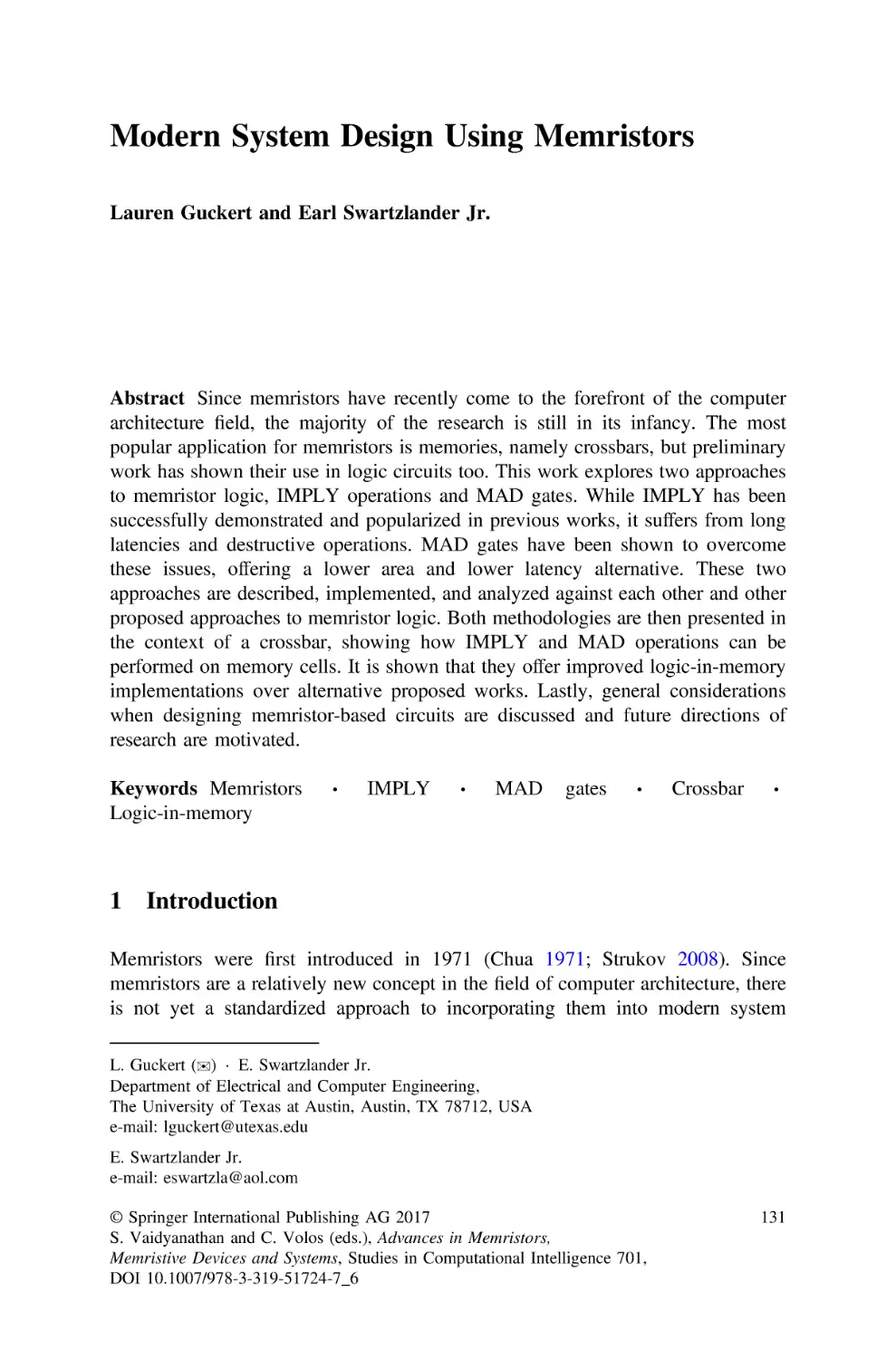
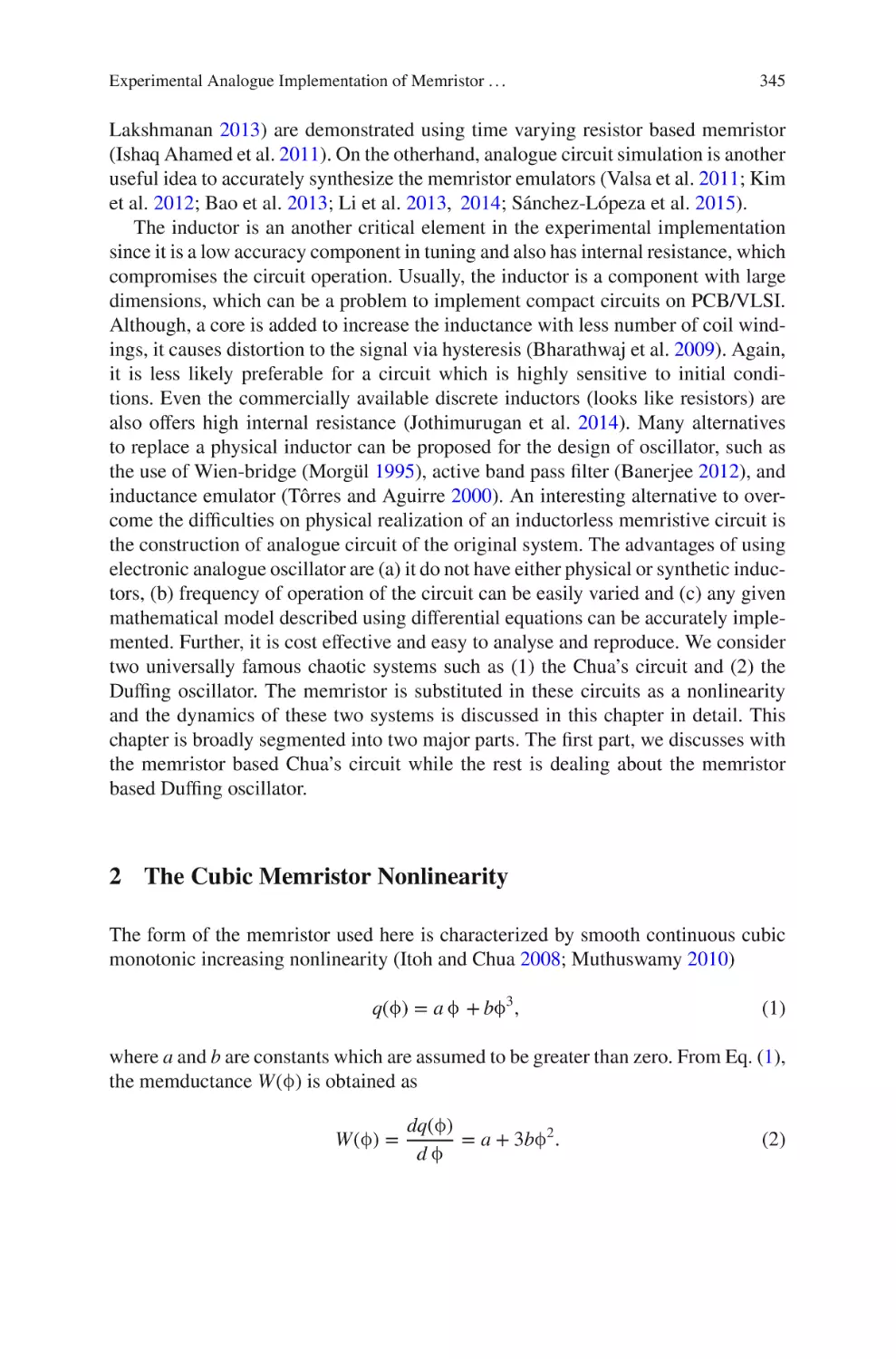
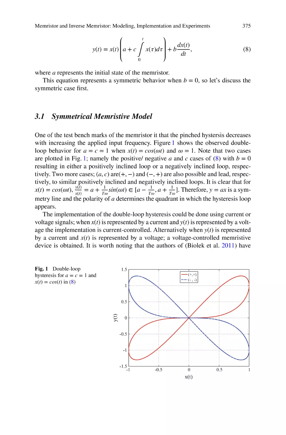
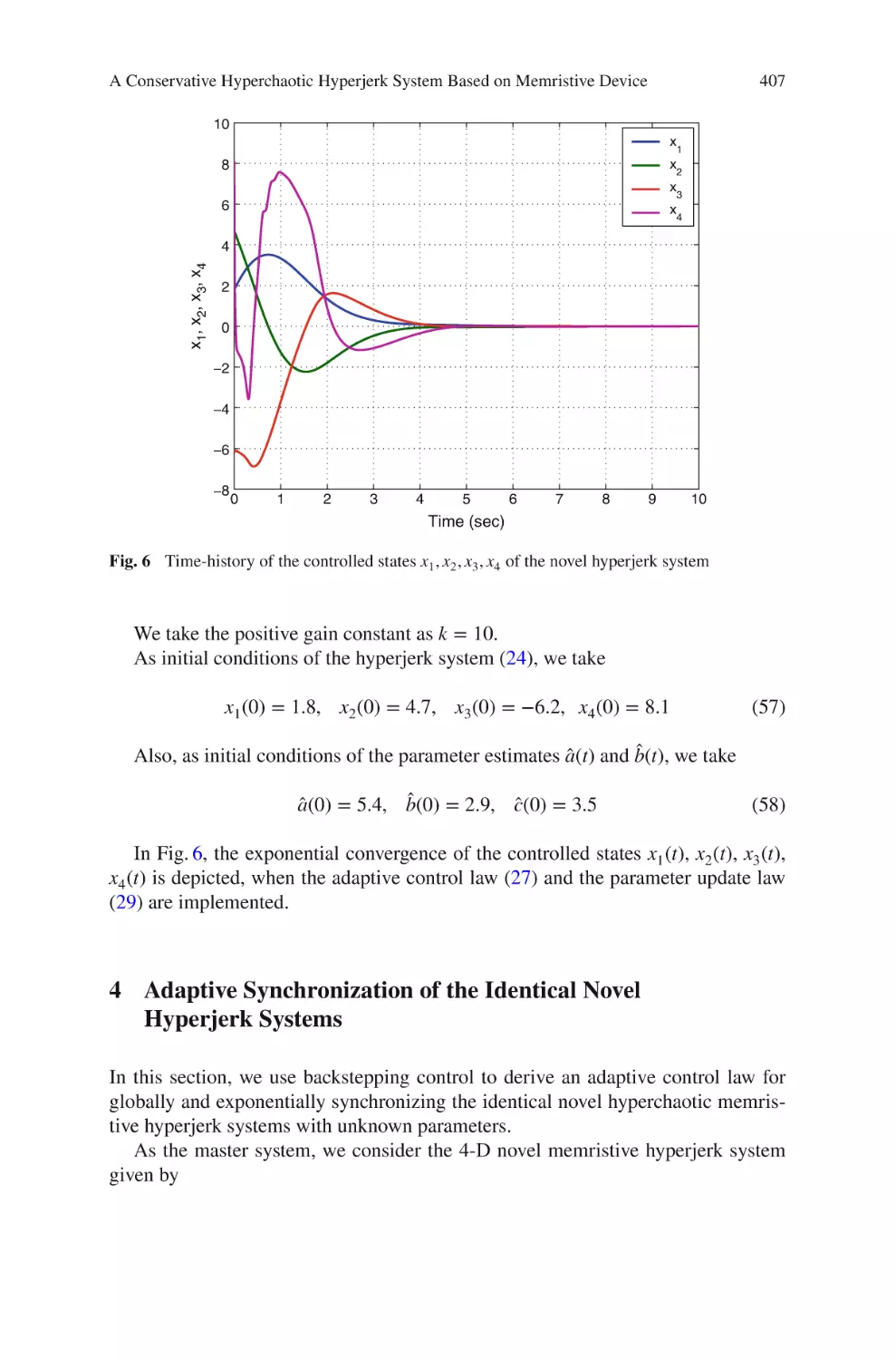
Memristor Emulators: A Note on Modeling
A. Ascoli, R. Tetzlaff, L.O. Chua, W. Yi and R.S. Williams
Abstract In a recent publication (Yi et al. 2011) elucidating a possible scheme to
write information reliably onto a memory crossbar, Hewlett Packard Labs researchers
employed a thyristor-based circuit to emulate the off-to-on switching behaviour of a
titanium oxide memristor. The use of a thyristor device allowed them to test inexpensively and reliably the functionalities of the closed-loop crossbar write circuitry
by using conventional CMOS components. From a device modeling point of view,
however, it is worthy to point out that the aforementioned emulator is not a genuine
memristor. The aim of this paper is to demonstrate with an in-depth mathematical
analysis that the model of the thyristor does not fall into the class of memristors.
The modelling approach adopted in this work may be a source of inspiration for
researchers willing to check whether other devices or circuits may be classified as
memristors.
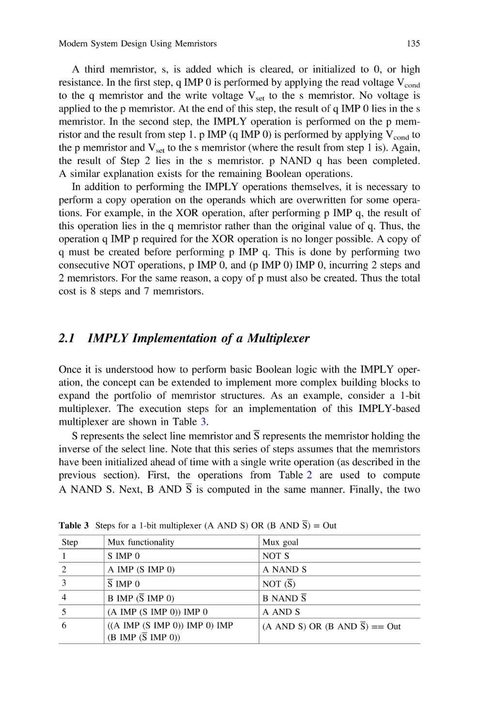
Keywords Circuit theory ⋅ Memristor ⋅ Threshold switching ⋅ Thyristor
A. Ascoli (✉) ⋅ R. Tetzlaff
Faculty of Electrical Circuit Theory and Information Technology,
Department of Fundamentals of Electrical Circuit Theory and Electronics,
Technische Universität Dresden, Dresden, Germany
e-mail: alon.ascoli@tu-dresden.de
R. Tetzlaff
e-mail: ronald.tetzlaff@tu-dresden.de
L.O. Chua
Department of Electrical Engineering and Computer Sciences,
University of California Berkeley, Berkeley, CA 94720, USA
e-mail: chua@eecs.berkeley.edu
W. Yi
HRL Laboratories, LLC, Malibu, CA 90265, USA
e-mail: wyi@hrl.com
R.S. Williams
Hewlett Packard Labs, Palo Alto, CA 94304, USA
e-mail: stan.williams@hpe.com
© Springer International Publishing AG 2017
S. Vaidyanathan and C. Volos (eds.), Advances in Memristors,
Memristive Devices and Systems, Studies in Computational Intelligence 701,
DOI 10.1007/978-3-319-51724-7_1
1
2
A. Ascoli et al.
1 Introduction
A substantial amount of work on memristors (Chua 1971) and memristive systems
(Chua and Kang 1976) focus on their manufacturing process (Pan et al. 2014), which
is engineered so as to shape the electrical characteristics of the devices (Strukov
et al. 2008) to enhance their performance as non-volatile memory elements (Waser
et al. 2009; Jo et al. 2009; Wylezich et al. 2014) or as biological synapse emulators (Zamarreño-Ramos et al. 2011). Only a few number of studies is focused on
the establishment of solid foundations on the theory of memristor devices, circuits,
and systems (Chua 2011, 2014, 2015). However, in our opinion, these theoretical
works (Ascoli et al. 2014; Corinto et al. 2011, 2015, 2016; Larentis et al. 2012) are as
important as the experimental investigation (Nardi et al. 2012), representing a crucial
prerequisite in the ongoing research efforts to explore the full potential of memristors in future electronics (Ascoli et al. 2015c). In fact, gaining a deeper insight into
the key mechanisms at the origin of memristive behaviour (Ascoli et al. 2016c) is
instrumental to identify advantages and limitations of the adoption of memristors for
memory or neuromorphic applications, as well as to understand under which extent
may the nonlinear dynamics of these devices (Ascoli et al. 2016a, b) be exploited
to develop unconventional forms of sensing (Carrara et al. 2012; Tzouvadaki et al.
2016a) and signal processing (Corino et al. 2012; Yang et al. 2013), as well as novel
computing architectures (Talati et al. 2016; Ben-Hur and Kvatinsky 2016). Typically, in our studies, the application of nonlinear circuit theoretic techniques (Chua
et al. 1985) to the device models allows the identification of the key factors underlying the emergence of memristive dynamics. On the basis of this knowledge, it is
then possible to draw a comprehensive picture of the plethora of nonlinear behaviours a memristor may exhibit under any initial condition/input combination (Ascoli
and Corinto 2013). Clearly, the availability of accurate mathematical descriptions is
a fundamental preliminary requirement to conduct these theoretical investigations.
The derivation of accurate memristor models is in fact one of the most challenging activities in this field of research (Ascoli et al. 2013). The aim of the work presented in this chapter is to clarify an important modeling issue which risks to mislead
researchers in the field. In a seminal paper presenting a closed-loop scheme to write
data reliably onto a memory crossbar, Hewlett Packard Labs researchers adopted a
thyristor-based circuit to emulate the high-to-low resistance switching dynamics of
a bipolar titanium dioxide memristor (Yi et al. 2011). This allowed to apply an inexpensive and robust testing and debugging procedure on the proposed data writing
scheme. However, from a device modeling point of view, the aforementioned emulator may not be regarded as a memristor. In order to shed light into this important
aspect, we derive an accurate model of the thyristor adopted for testing purposes at
Hewlett Packard Labs (Yi et al. 2011), proving that it does not fit into the class of
memristors (Chua 2015), because it lacks an Ohm-based law (i.e. an algebraic relation expressing the output in terms of the product between the input and a function
of the state, and, possibly, the input) (Chua 2015), which necessarily constrains the
time evolution of the memristor state, which, otherwise, would be governed solely
Memristor Emulators: A Note on Modeling
3
by the state evolution function. The mathematical analysis presented in this work
may be beneficial in those investigations intended to check whether other devices
or circuits may be regarded as memristors. The manuscript is structured as follows.
Section 2 introduces the thyristor under modeling. Section 3 derives its mathematical model. Section 4 provides the numerical validation for the theoretical results
derived in Sect. 3. Finally conclusions and future research developments are drafted
in Sect. 5.
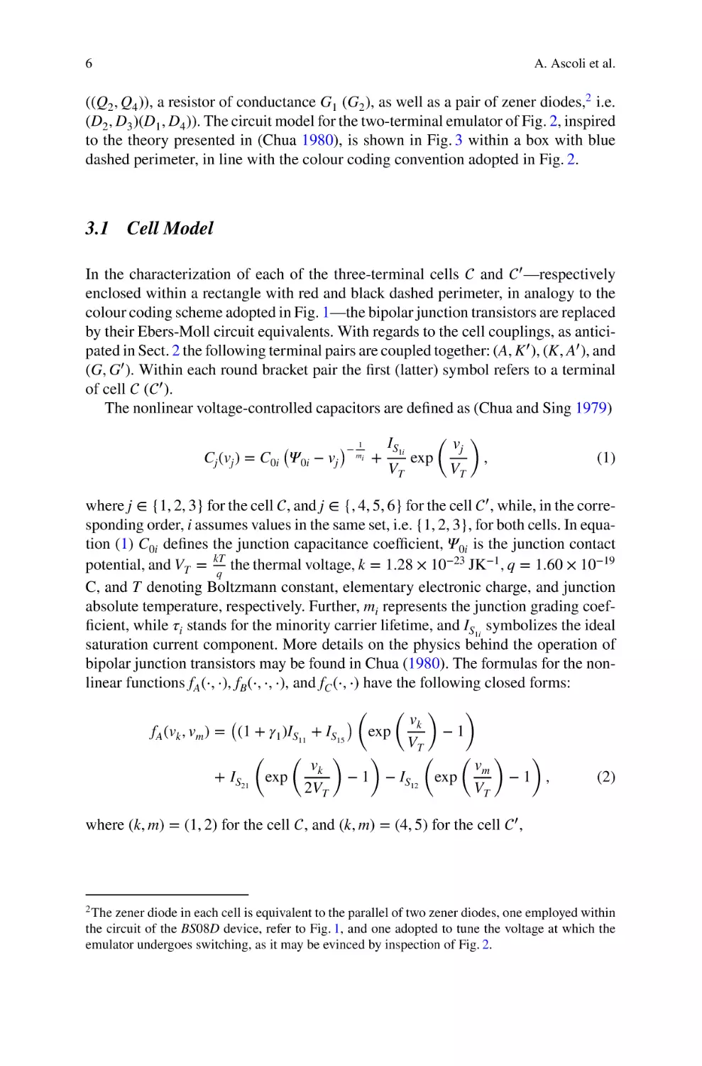
2 Emulator
The particular component adopted at Hewlett Packard Labs to emulate the off-toon switching behaviour of a bipolar titanium oxide memristor (Pickett et al. 2009;
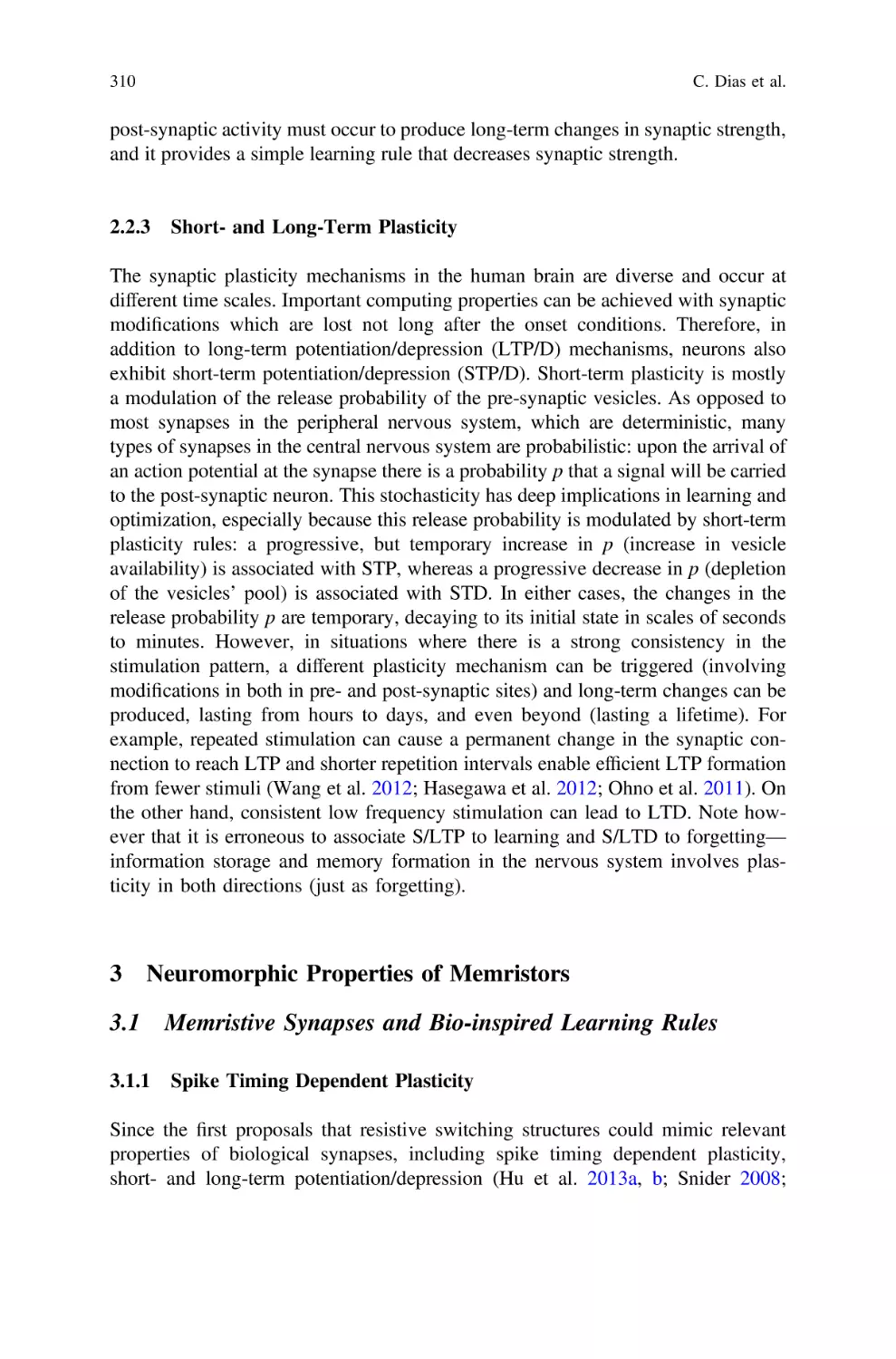
Abdalla and Pickett 2011) in the debugging and testing phase of a closed-loop or
feedback data writing scheme for memory crossbars is the silicon bilateral switch
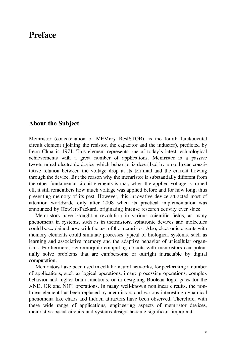
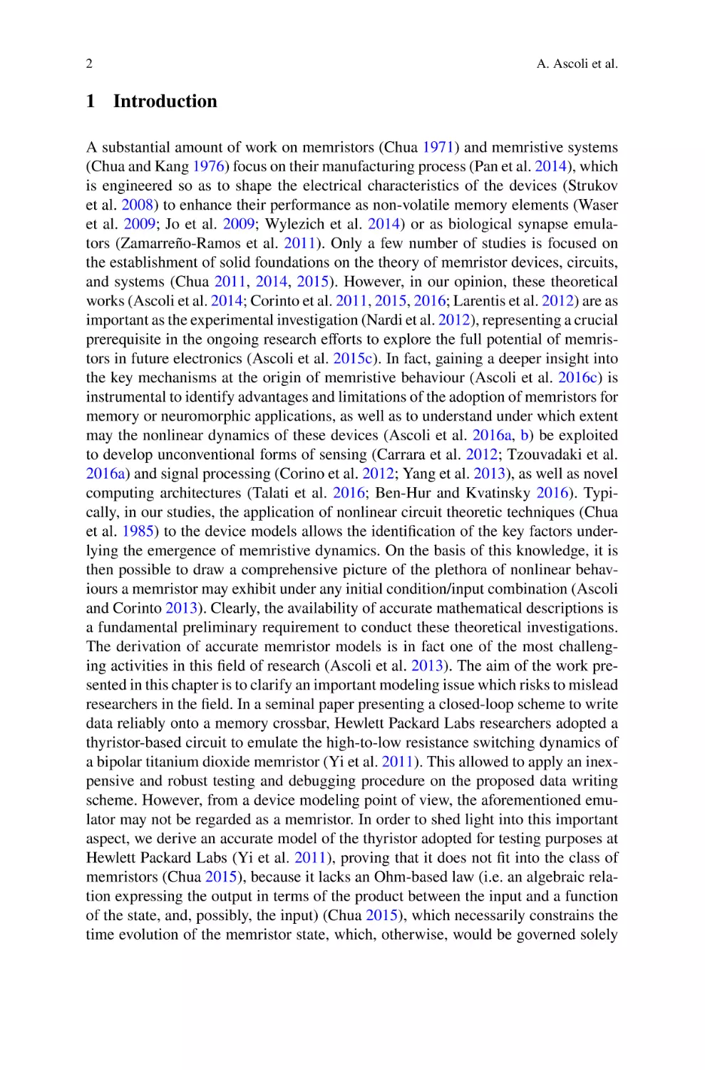
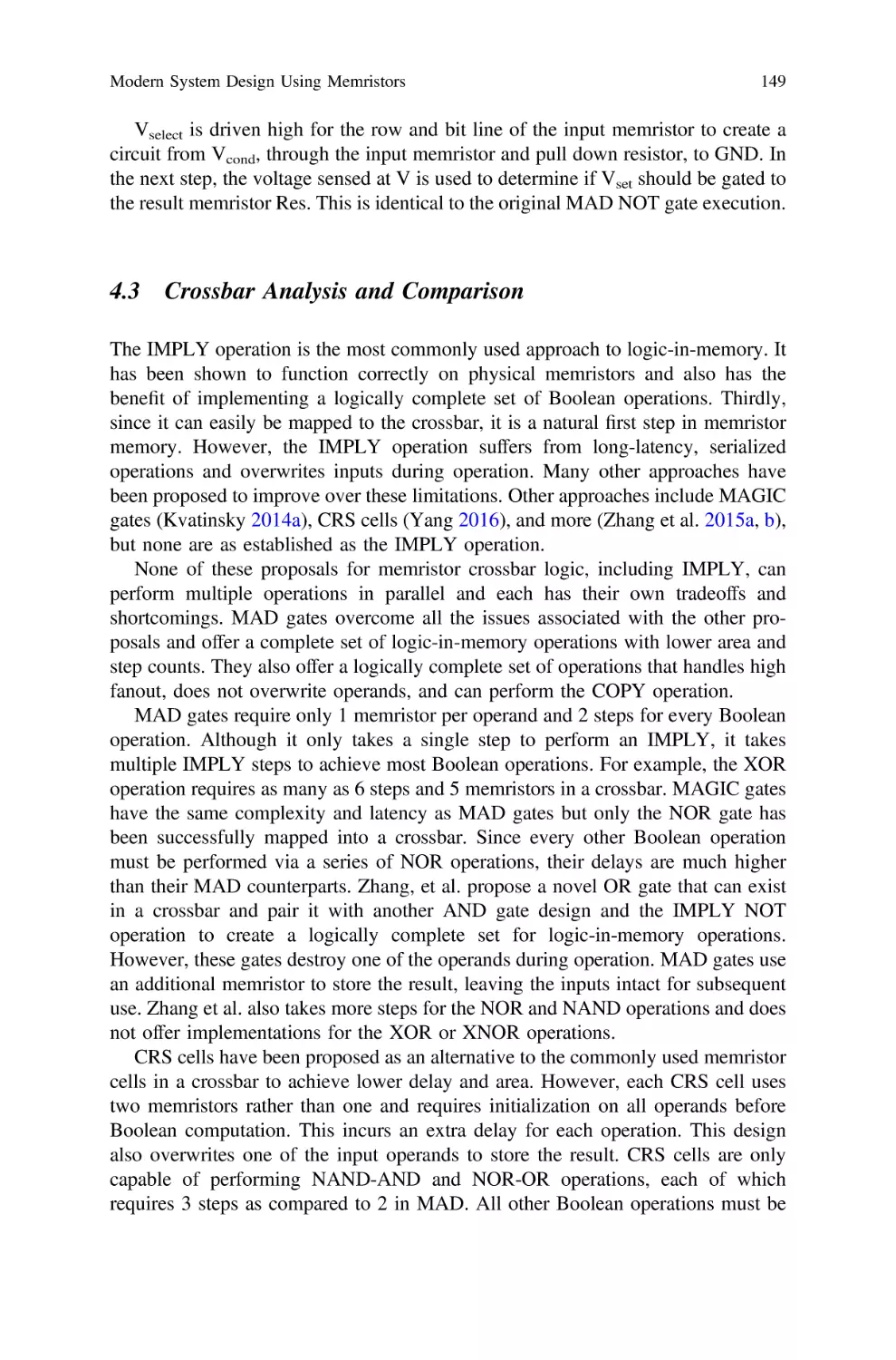
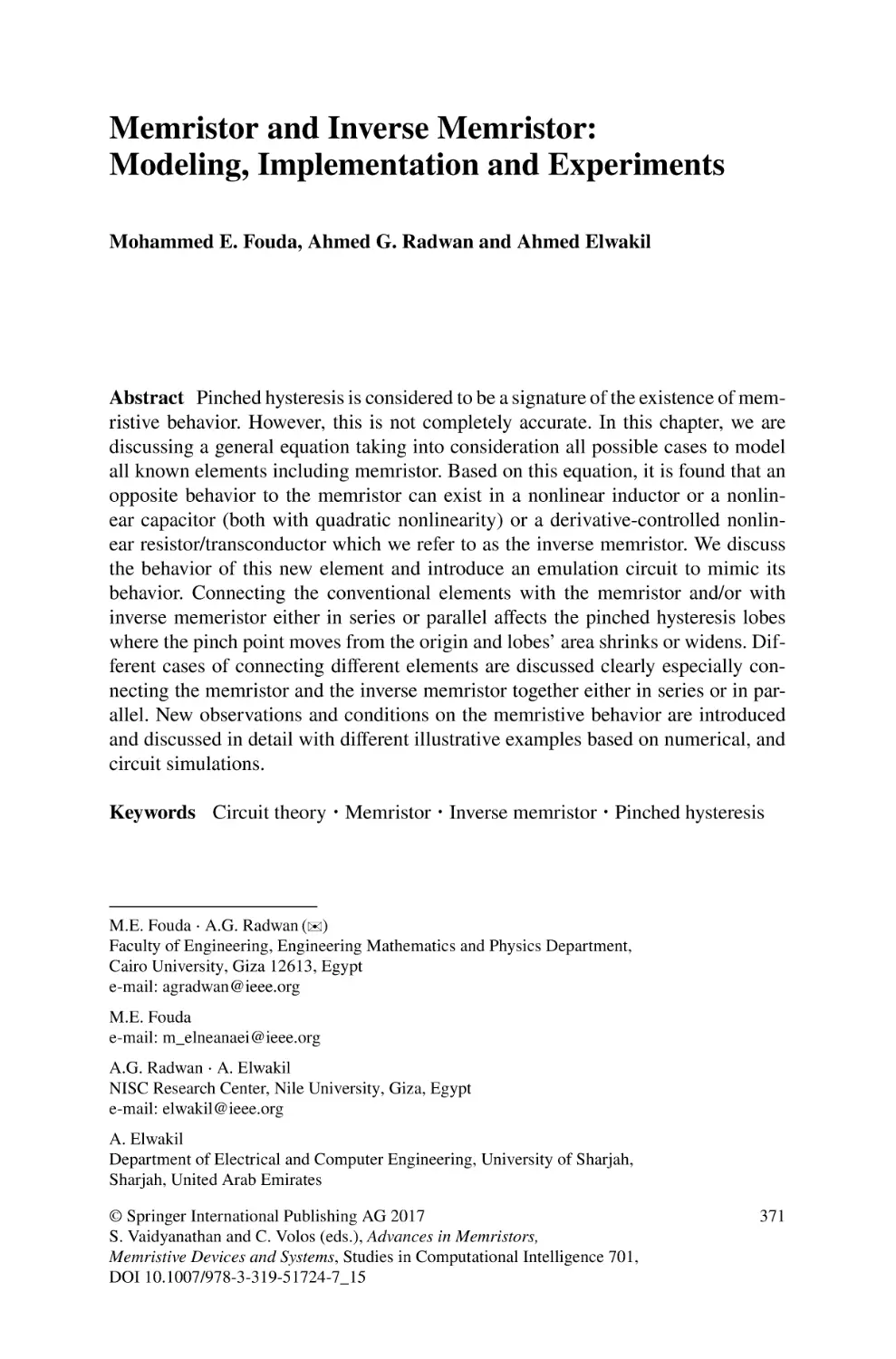
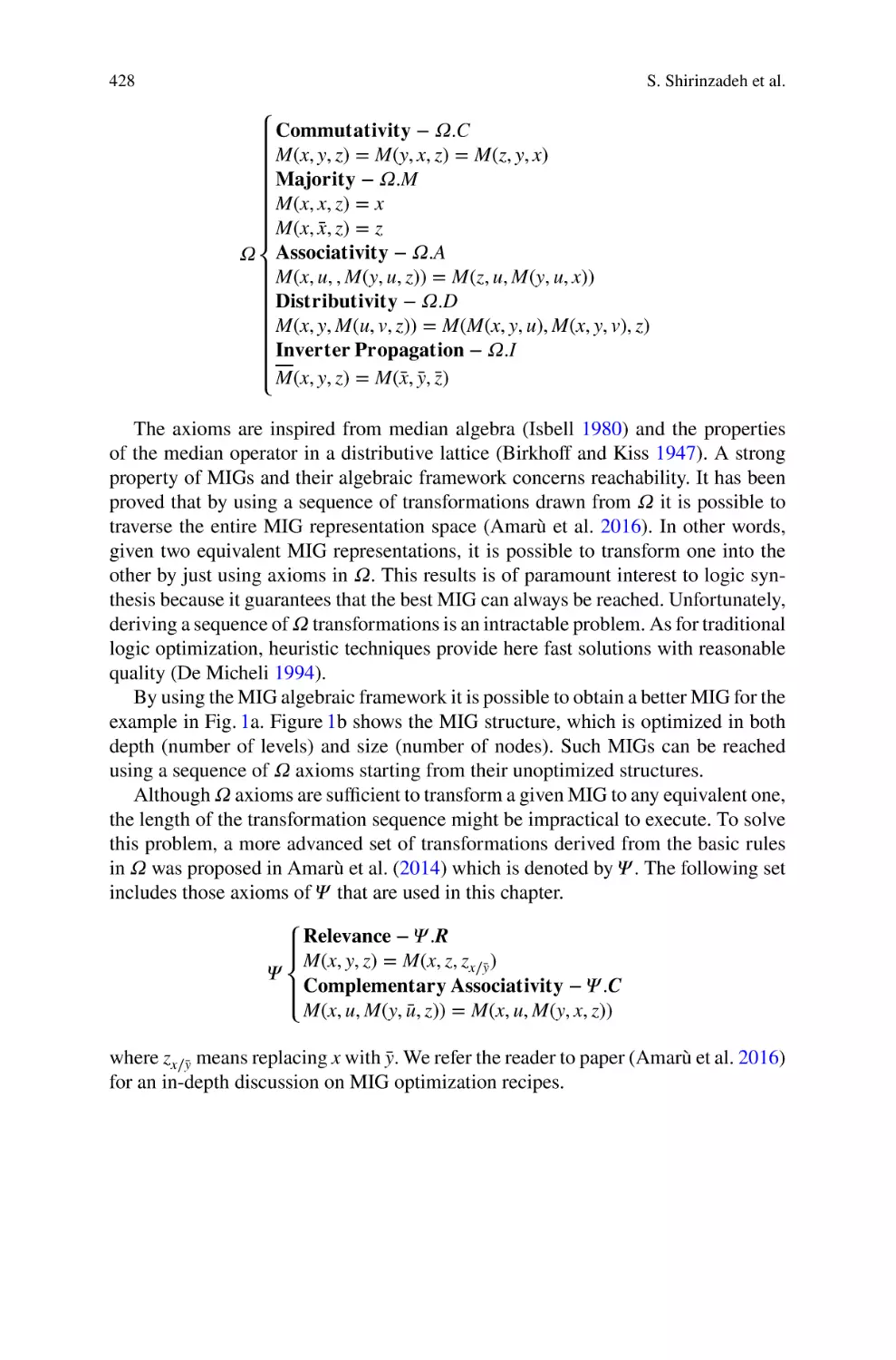
BS08D (Powerex Inc. 2015) manufactured by Powerex Inc., USA. The main building block of the emulator is shown in Fig. 1a, while its circuit symbol is depicted in
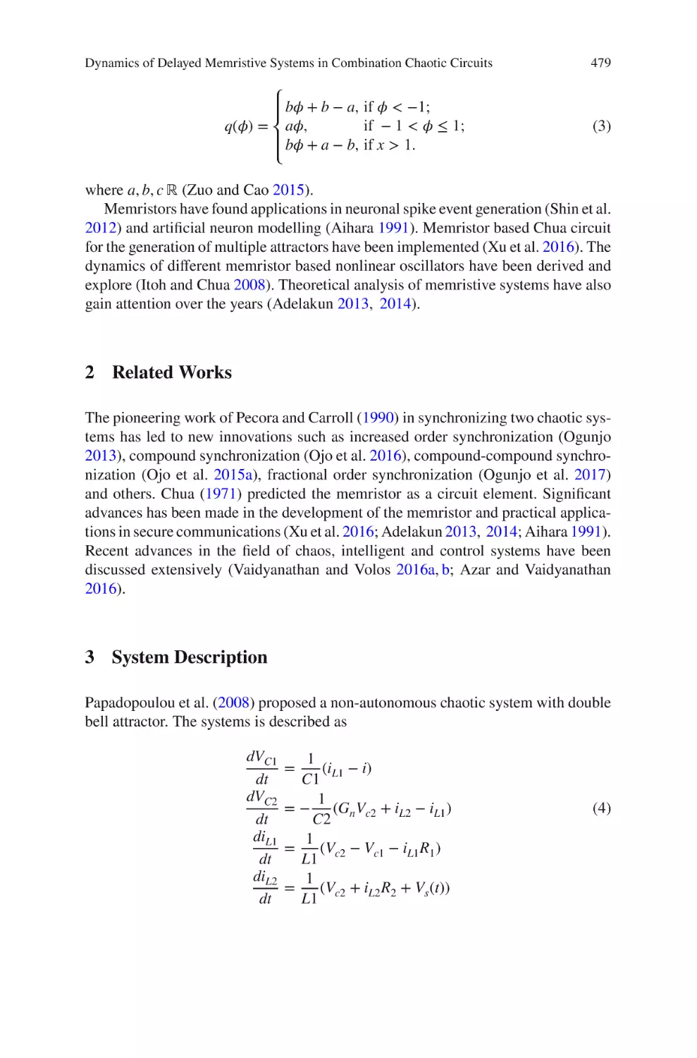
Fig. 1b. It is a bilateral thyristor consisting of four bipolar junction transistors with
substrate node connected to ground—one pair, (Q1 , Q2 ), of pnp type, and the other,
(Q3 , Q4 ), of npn type—as well as of two zener diodes (D1 , D2 ) and of a couple of
resistors (G1 , G2 ). The device has three terminals, i.e. T1 , T2 , and G. Each of the two
devices within a box in Fig. 1a represents a unilateral thyristor. It has three terminals,
known as anode, cathode, and gate. The base of the pnp transistor is chosen as gate
terminal. With such a choice, the unilateral thyristor is also known as programmable
unipolar junction transistor (PUT) (On Semiconductor 2005). There exists another
type of unilateral thyristor, known as silicon controlled rectifier (SCR), in which the
gate terminal coincides with the base of the npn transistor. With reference to Fig. 1a,
coupling the identical left and right PUT devices—let us denote them as cell and
′ , enclosed within a rectangle with red and black dashed perimeter and featuring
terminal triplets (A, G, K) and (A′ , G′ , K ′ ), respectively—through their gates G and
G′ , and connecting the anode A (A′ ) of the first (latter) to the cathode C′ (C) of the
latter (first), results into the circuit topology of a BS08D device. On the other hand,
applying the same coupling strategy to two identical SCR components yields the
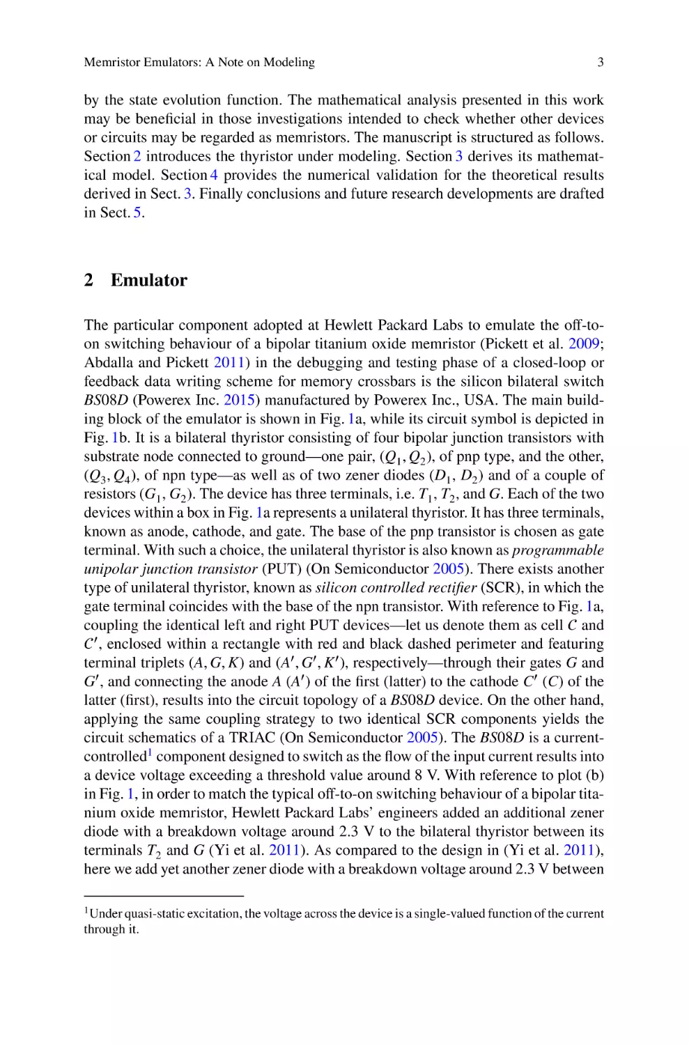
circuit schematics of a TRIAC (On Semiconductor 2005). The BS08D is a currentcontrolled1 component designed to switch as the flow of the input current results into
a device voltage exceeding a threshold value around 8 V. With reference to plot (b)
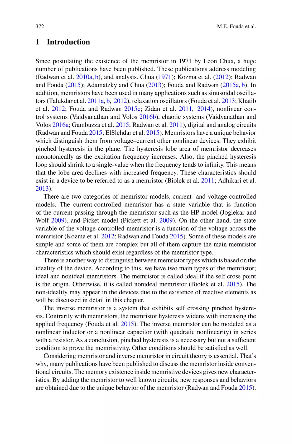
in Fig. 1, in order to match the typical off-to-on switching behaviour of a bipolar titanium oxide memristor, Hewlett Packard Labs’ engineers added an additional zener
diode with a breakdown voltage around 2.3 V to the bilateral thyristor between its
terminals T2 and G (Yi et al. 2011). As compared to the design in (Yi et al. 2011),
here we add yet another zener diode with a breakdown voltage around 2.3 V between
1 Under quasi-static excitation, the voltage across the device is a single-valued function of the current
through it.
4
A. Ascoli et al.
T1 ≡ A ≡ K
(a)
(b)
D2
Q4
T1
.
.
Q1
G2
G ≡ G
G
Q3
G1
cell C
D1
T2 ≡ K ≡ A
Q2
T2
cell C
Fig. 1 a Circuit schematics of the BS08D device, a silicon bilateral thyristor from Powerex, Inc.,
USA. The anode, cathode, and gate terminals of cell ( ′ ) are identified with symbols A, K, and
G (A′ , K ′ , and G′ ). b Circuit symbol of the three-terminal element
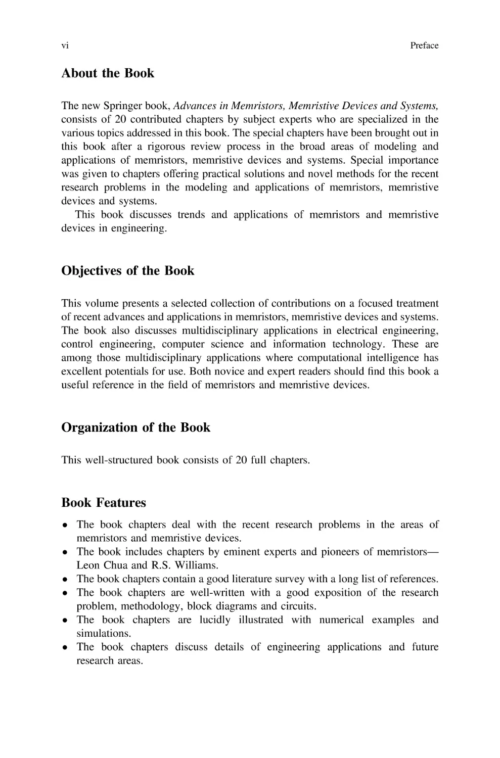
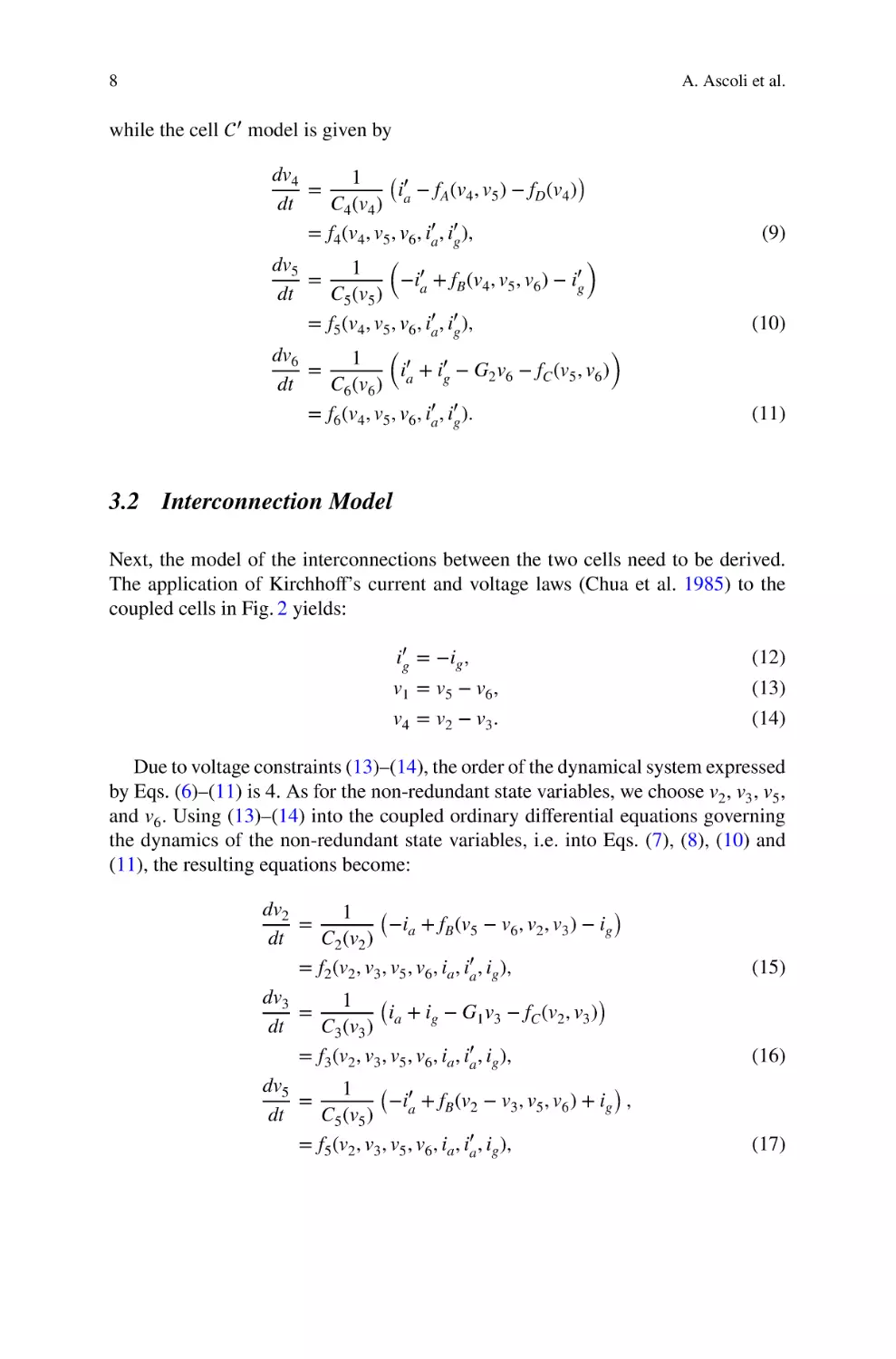
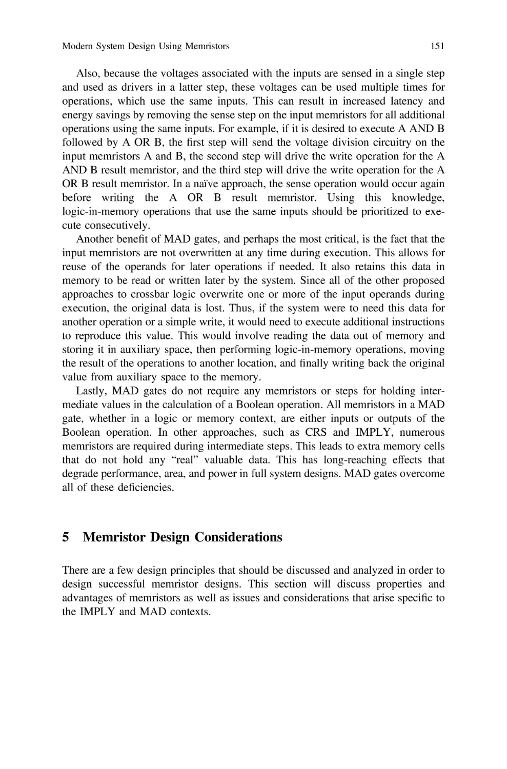
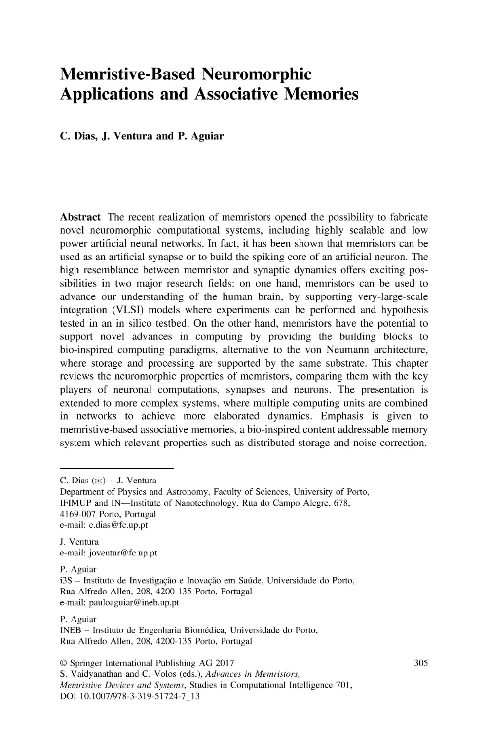
Fig. 2 One-port with
off-to-on switching
dynamics reminiscent of
memristive behaviour under
each polarity of the current
input. In Yi et al. (2011) the
BS08D device was coupled
to zener diode D4 only, and
the resulting two-terminal
element was used to mimic
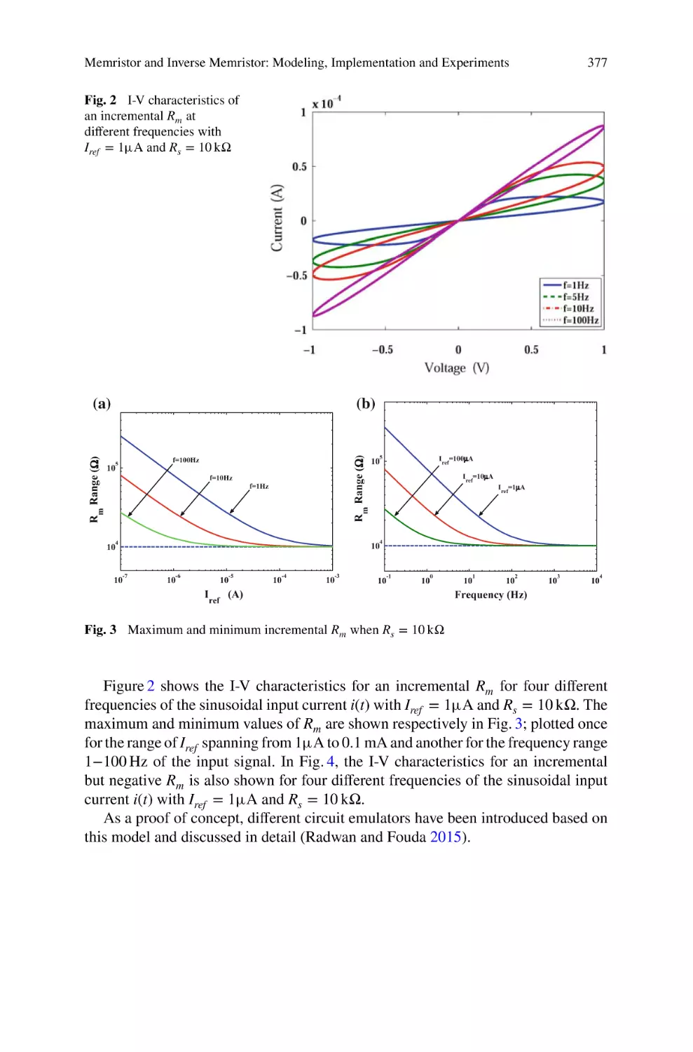
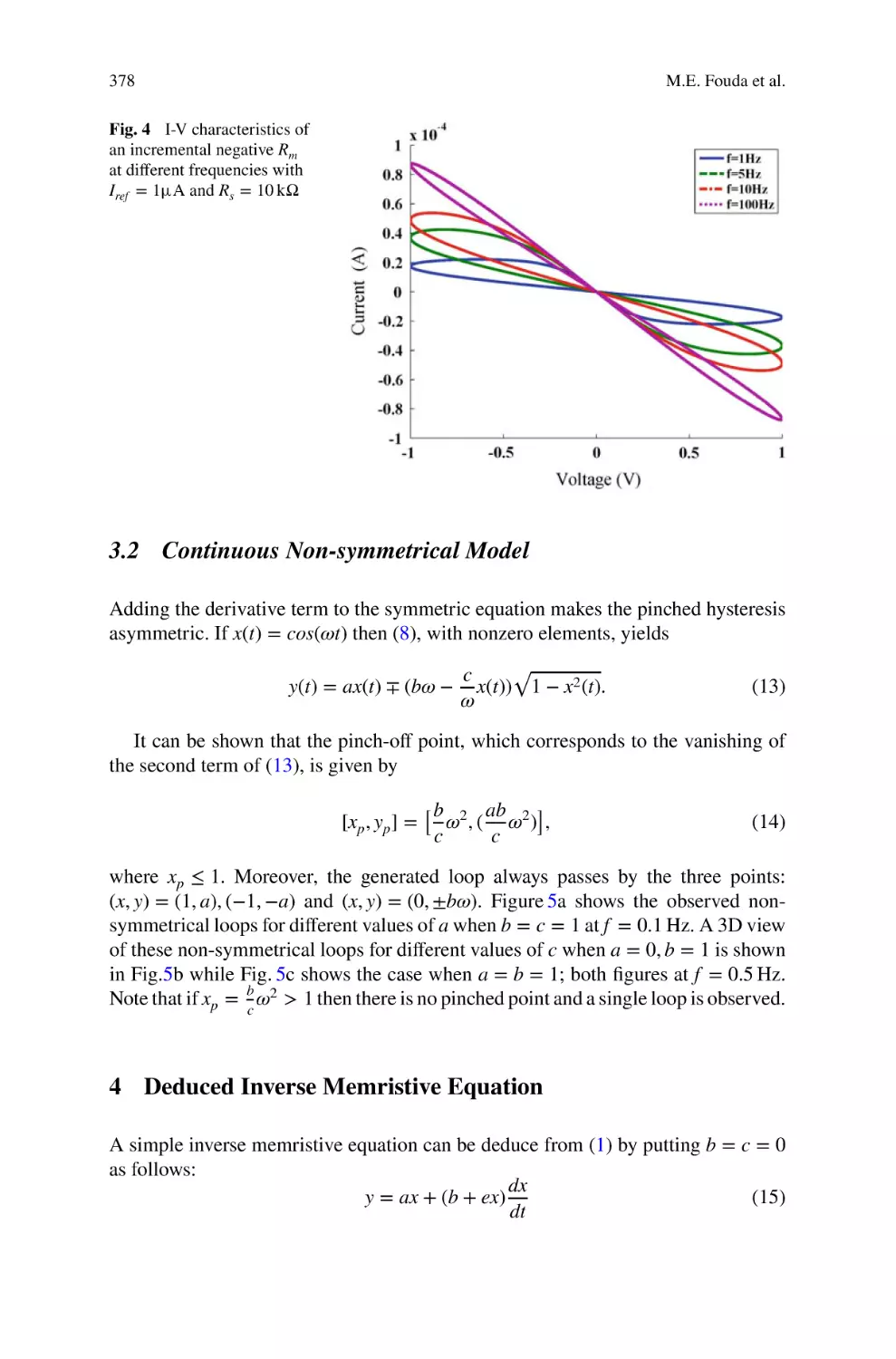
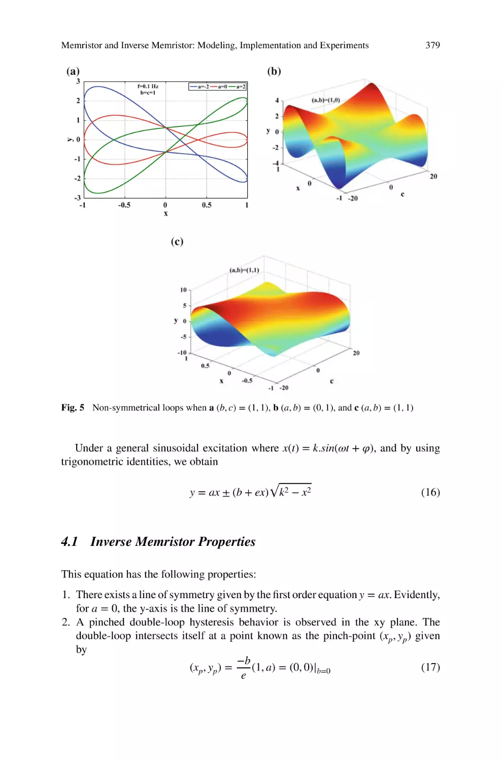
the high-to-low resistance
switching of the titanium
dioxide memristor under
positive stimuli
T1
+
i
D3
v
G ≡ G
D4
−
T2
the terminals T1 and G of the component in Fig. 1b so as to obtain an odd-symmetric
off-to-on switching. The resulting circuit is a one-port with terminals T1 and T2 , as
shown in Fig. 2 within a box with blue dashed perimeter. Let us denote the current
through this bipole and the voltage across it as i and v, respectively.
Memristor Emulators: A Note on Modeling
5
In order to clarify the nature of the two-terminal element in Fig. 2, and avoid
an improper device classification, as well as to gain a better understanding of the
dynamical phenomena emerging in the current-controlled electronic component, in
the next section we shall derive its mathematical model.
3 Model
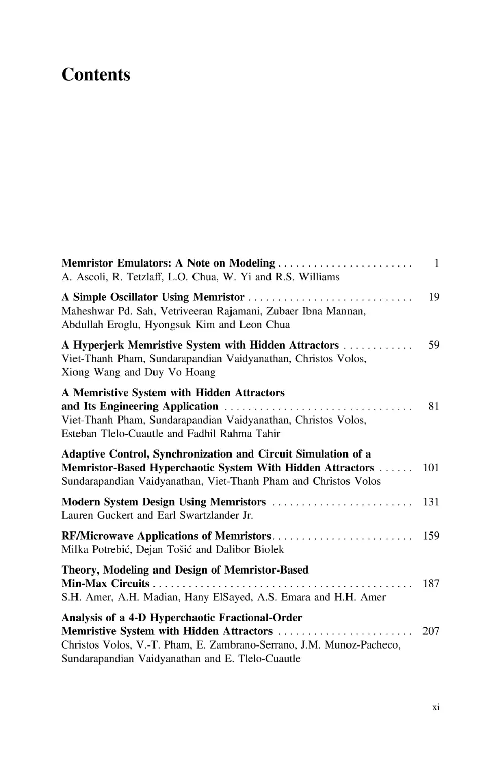
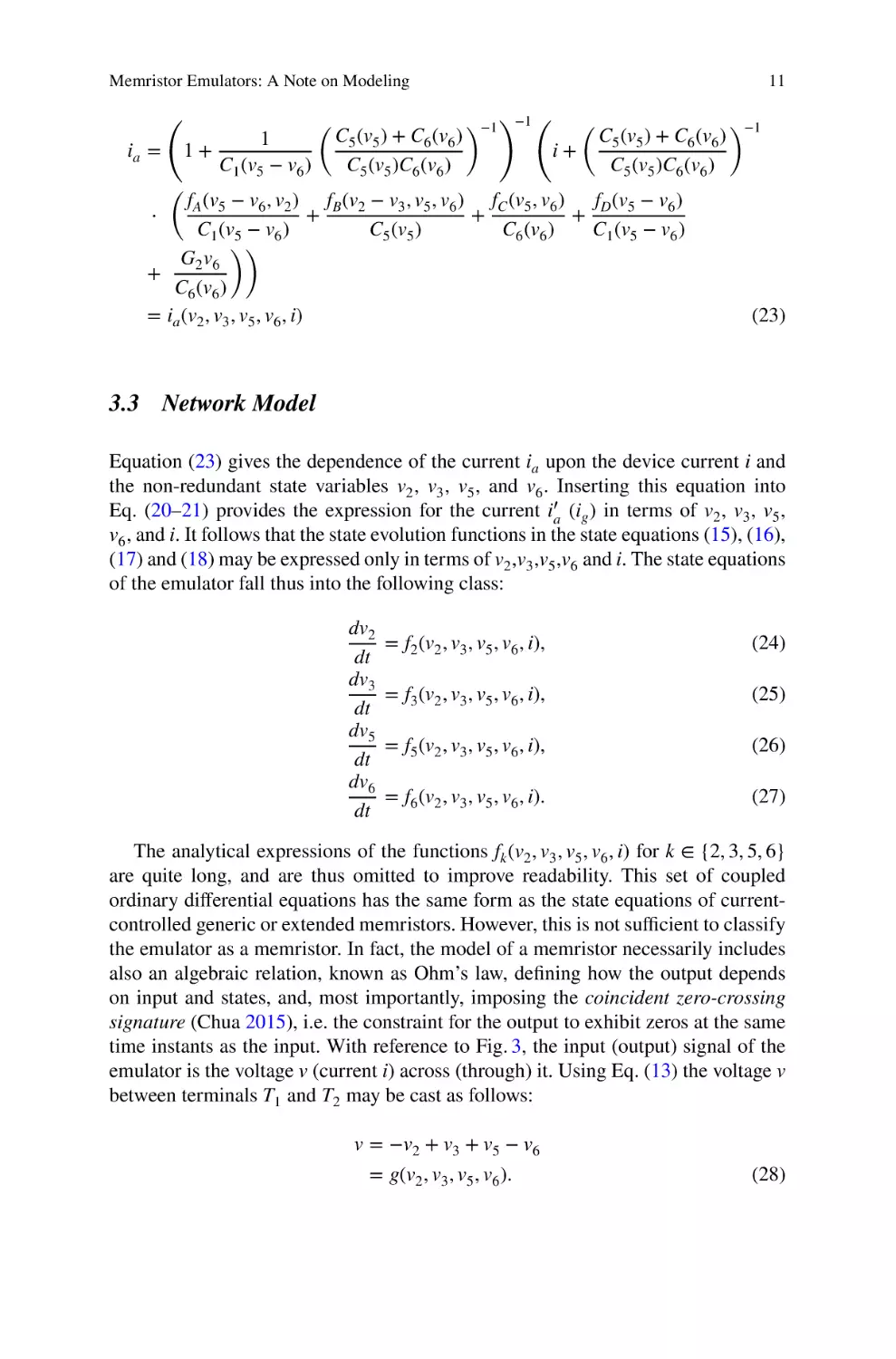
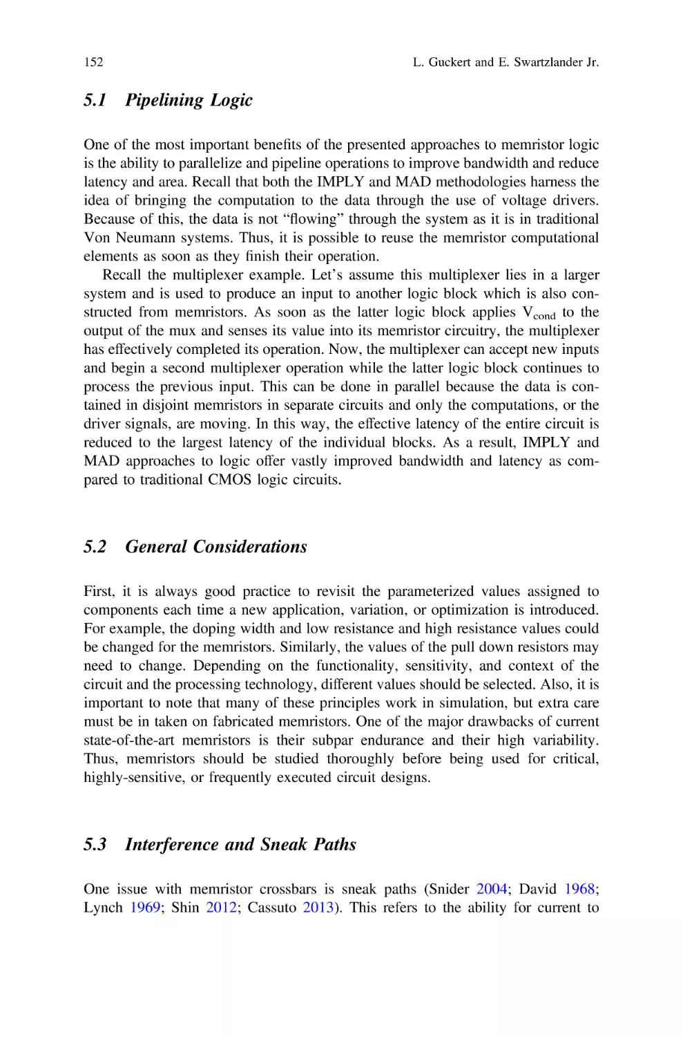
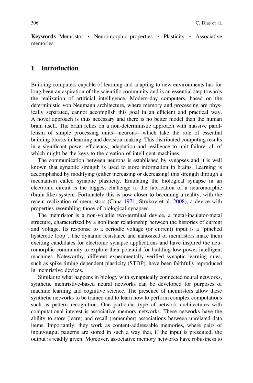
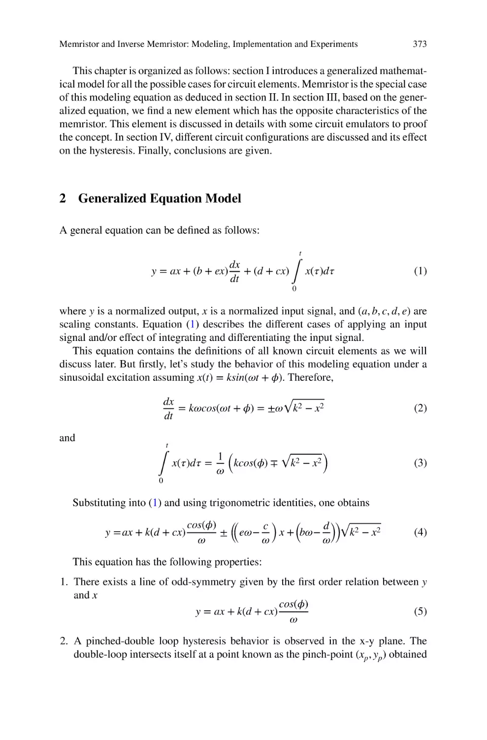
With reference to the circuit schematics in Fig. 1 and to the emulator topology in
Fig. 2, the cell ( ′ ) consists of a complementary transistor pair, namely (Q1 , Q3 )
T1
+
i
ia
fD (v1 )
fA (v1 , v2 )
+
G2
−
C1 (v1 )
ig
v5
−
ik
fB (v4 , v5 , v6 )
C4 (v4 )
−
fD (v4 )
v4
G1
−
fC (v2 , v3 )
cell C
ig
+
v3
C5 (v5 )
−
fB (v1 , v2 , v3 )
C3 (v3 )
C6 (v6 )
+
C2 (v2 )
+
v6
+
G ≡ G
−
v2
fC (v5 , v6 )
−
v1
v
ik
A ≡ K
fA (v4 , v5 )
K ≡ A
ia
+
cell C
emulator
T2
Fig. 3 Equivalent circuit model of the emulator of Fig. 2. The two-terminal device under modeling
is encircled within a rectangle with blue dashed perimeter
6
A. Ascoli et al.
((Q2 , Q4 )), a resistor of conductance G1 (G2 ), as well as a pair of zener diodes,2 i.e.
(D2 , D3 )(D1 , D4 )). The circuit model for the two-terminal emulator of Fig. 2, inspired
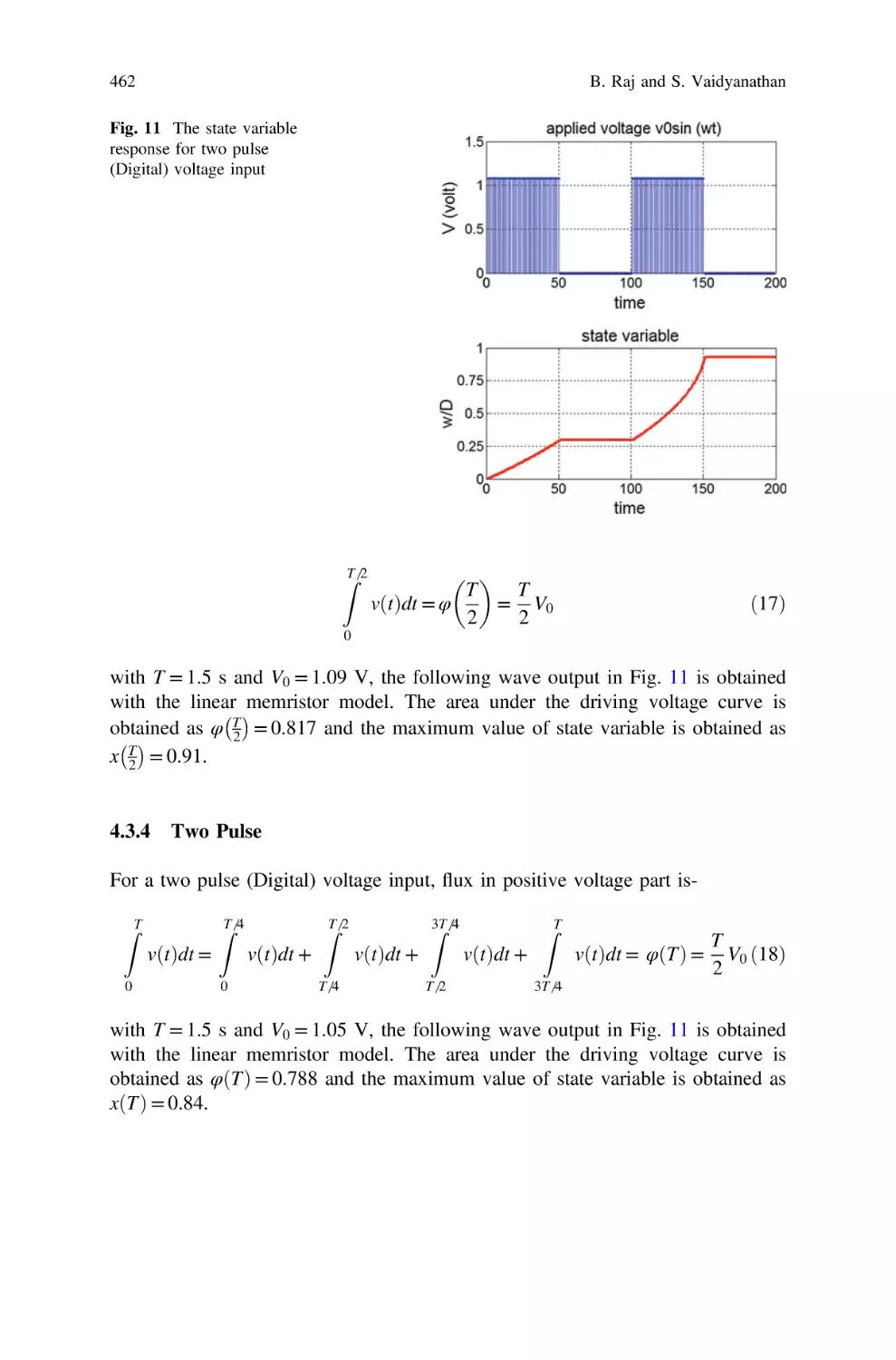
to the theory presented in (Chua 1980), is shown in Fig. 3 within a box with blue
dashed perimeter, in line with the colour coding convention adopted in Fig. 2.
3.1 Cell Model
In the characterization of each of the three-terminal cells and ′ —respectively
enclosed within a rectangle with red and black dashed perimeter, in analogy to the
colour coding scheme adopted in Fig. 1—the bipolar junction transistors are replaced
by their Ebers-Moll circuit equivalents. With regards to the cell couplings, as anticipated in Sect. 2 the following terminal pairs are coupled together: (A, K ′ ), (K, A′ ), and
(G, G′ ). Within each round bracket pair the first (latter) symbol refers to a terminal
of cell ( ′ ).
The nonlinear voltage-controlled capacitors are defined as (Chua and Sing 1979)
IS
(
)− 1
Cj (vj ) = C0i 𝛹0i − vj mi + 1i exp
VT
(
vj
VT
)
,
(1)
where j ∈ {1, 2, 3} for the cell , and j ∈ {, 4, 5, 6} for the cell ′ , while, in the corresponding order, i assumes values in the same set, i.e. {1, 2, 3}, for both cells. In equation (1) C0i defines the junction capacitance coefficient, 𝛹0i is the junction contact
potential, and VT = kTq the thermal voltage, k = 1.28 × 10⁻²³ JK−1 , q = 1.60 × 10⁻¹⁹
C, and T denoting Boltzmann constant, elementary electronic charge, and junction
absolute temperature, respectively. Further, mi represents the junction grading coefficient, while 𝜏i stands for the minority carrier lifetime, and IS1i symbolizes the ideal
saturation current component. More details on the physics behind the operation of
bipolar junction transistors may be found in Chua (1980). The formulas for the nonlinear functions fA (⋅, ⋅), fB (⋅, ⋅, ⋅), and fC (⋅, ⋅) have the following closed forms:
)
(
( )
(
)
vk
−1
fA (vk , vm ) = (1 + 𝛾1 )IS11 + IS15 exp
VT
(
(
)
)
(
( )
)
vk
vm
− 1 − IS12 exp
−1 ,
+ IS21 exp
2VT
VT
(2)
where (k, m) = (1, 2) for the cell , and (k, m) = (4, 5) for the cell ′ ,
2
The zener diode in each cell is equivalent to the parallel of two zener diodes, one employed within
the circuit of the BS08D device, refer to Fig. 1, and one adopted to tune the voltage at which the
emulator undergoes switching, as it may be evinced by inspection of Fig. 2.
Memristor Emulators: A Note on Modeling
(
)
)
(
(
)
)
vk
vm
− 1 − IS22 exp
−1
V
2VT
(
( T)
)
vn
+ IS13 exp
−1
VT
(
( )
)
)
(
vm
−1 ,
− (1 + 𝛾1 )IS12 + (1 + 𝛾2 )IS14 exp
VT
fB (vk , vm , vn ) = IS11
7
(
exp
(3)
where (k, m, n) = (1, 2, 3) for the cell , and (k, m, n) = (4, 5, 6) for the cell ′ , and
(
( )
)
(
(
)
)
vm
vn
− 1 + IS23 exp
−1
fC (vm , vn ) = −IS14 exp
VT
2V
) T
(
( )
(
)
vn
+ (1 + 𝛾2 )IS13 + IS16 exp
−1 ,
VT
(4)
where (m, n) = (2, 3) for the cell , and (m, n) = (5, 6) for the cell ′ . In Eqs. (2)–(4)
IS1j (j ∈ {1, 2, 3, 4, 5, 6}) and IS2j (j ∈ {1, 2, 3}) respectively denote ideal and nonlinear saturation current components, while 𝛾j (j ∈ {1, 2}) are recombination factors for
the current components. Finally, the nonlinear function fD (⋅) is expressed as
)
(
(
(
)
)
vj + Vza
vj
− 1 − Iza exp −
fD (vj ) = ISa exp
na VT
nza VT
)
(
(
(
)
)
vj + Vzb
vj
,
+ ISb exp
− 1 − Izb exp −
nb VT
nzb VT
(5)
where j = 1 for the cell , and j = 4 for the cell ′ . As anticipated earlier, fD (⋅)
takes into account the currents of zener diode pair (D2 , D3 )((D1 , D4 )) for the cell
( ′ ). Particularly, for each cell, on the right hand side of Eq. 5, the first and last
two addends respectively constitute the current of the first and second diode in the
aforementioned pair. Applying basic circuit principles, the equations governing the
evolution of the voltages across the nonlinear capacitors of the cell are expressed as
)
dv1
1 (
ia − fA (v1 , v2 ) − fD (v1 )
=
dt
C1 (v1 )
= f1 (v1 , v2 , v3 , ia , ig ),
)
dv2
1 (
−ia + fB (v1 , v2 , v3 ) − ig
=
dt
C2 (v2 )
= f2 (v1 , v2 , v3 , ia , ig ),
)
dv3
1 (
ia + ig − G1 v3 − fC (v2 , v3 )
=
dt
C3 (v3 )
= f3 (v1 , v2 , v3 , ia , ig ),
(6)
(7)
(8)
8
A. Ascoli et al.
while the cell ′ model is given by
)
dv4
1 (′
ia − fA (v4 , v5 ) − fD (v4 )
=
dt
C4 (v4 )
= f4 (v4 , v5 , v6 , i′a , i′g ),
(
)
dv5
1
−i′a + fB (v4 , v5 , v6 ) − i′g
=
dt
C5 (v5 )
= f5 (v4 , v5 , v6 , i′a , i′g ),
(
)
dv6
1
i′a + i′g − G2 v6 − fC (v5 , v6 )
=
dt
C6 (v6 )
= f6 (v4 , v5 , v6 , i′a , i′g ).
(9)
(10)
(11)
3.2 Interconnection Model
Next, the model of the interconnections between the two cells need to be derived.
The application of Kirchhoff’s current and voltage laws (Chua et al. 1985) to the
coupled cells in Fig. 2 yields:
i′g = −ig ,
v1 = v5 − v6 ,
(12)
(13)
v4 = v2 − v3 .
(14)
Due to voltage constraints (13)–(14), the order of the dynamical system expressed
by Eqs. (6)–(11) is 4. As for the non-redundant state variables, we choose v2 , v3 , v5 ,
and v6 . Using (13)–(14) into the coupled ordinary differential equations governing
the dynamics of the non-redundant state variables, i.e. into Eqs. (7), (8), (10) and
(11), the resulting equations become:
)
dv2
1 (
−ia + fB (v5 − v6 , v2 , v3 ) − ig
=
dt
C2 (v2 )
= f2 (v2 , v3 , v5 , v6 , ia , i′a , ig ),
)
dv3
1 (
ia + ig − G1 v3 − fC (v2 , v3 )
=
dt
C3 (v3 )
= f3 (v2 , v3 , v5 , v6 , ia , i′a , ig ),
)
dv5
1 ( ′
−ia + fB (v2 − v3 , v5 , v6 ) + ig ,
=
dt
C5 (v5 )
= f5 (v2 , v3 , v5 , v6 , ia , i′a , ig ),
(15)
(16)
(17)
Memristor Emulators: A Note on Modeling
)
dv6
1 (′
ia − ig − G2 v6 − fC (v5 , v6 ) ,
=
dt
C6 (v6 )
= f6 (v2 , v3 , v5 , v6 , ia , i′a , ig ),
9
(18)
where we made use of Eq. (12) as well. Next, the variables ia , i′a , and ig need to be
expressed in terms of v2 , v3 , v5 , and v6 as well as of the input current i. Differentiating
(13) with respect to the time, inserting the right hand sides of Eqs. (6), (10) and (11)
into the resulting expression, and casting the two redundant state variables v1 and
v4 in terms of the four non-redundant ones, after some algebraic manipulation, the
current ig is found to be given by
(
)−1 (
ia
f (v − v6 , v2 ) fD (v5 − v6 )
1
1
ig =
+
− A 5
−
C5 (v5 ) C6 (v6 )
C1 (v5 − v6 )
C1 (v5 − v6 )
C1 (v5 − v6 )
)
fC (v5 , v6 )
G2 v6
fB (v2 − v3 , v5 , v6 )
−
−
+ i′a
−
C5 (v5 )
C6 (v6 )
C6 (v6 )
= ig (v2 , v3 , v5 , v6 , ia , i′a ).
(19)
Let us now compute the time derivative of Eq. (14), and then use the right hand
sides of Eqs. (9), (7) and (8) as well as Eq. (19) into the resulting expression. Lengthy
calculations provide the following formula for the current i′a in terms of the current
ia and of the four state variables v2 , v3 , v5 , and v6 :
i′a =
+
+
+
+
⋅
⋅
(
(
) (
C (v ) + C3 (v3 ) −1 fA (v2 − v3 , v5 )
1
1
+ 2 2
+
C4 (v2 − v3 )
C2 (v2 )C3 (v3 )
C4 (v2 − v3 )
C2 (v2 )
)(
)−1
fA (v5 − v6 , v2 ) fB (v5 − v6 , v2 , v3 )
1
1
1
+
+
C3 (v3 )
C5 (v5 ) C6 (v6 )
C1 (v5 − v6 )
C2 (v2 )
)
(
f (v , v )
C
f
(v
)C
(v
)
(v
−
v
,
v
,
v
)
1
1
5 5
6 6
B 2
3 5 6
+
+ C 2 3
C2 (v2 ) C3 (v3 ) C5 (v5 ) + C6 (v6 )
C5 (v5 )
C3 (v3 )
(
)(
)−1
fC (v5 , v6 ) fD (v2 − v3 )
1
1
1
1
+
+
+
C2 (v2 ) C3 (v3 )
C5 (v5 ) C6 (v6 )
C6 (v6 )
C4 (v2 − v3 )
)
(
f
G
G v
C
(v
)C
(v
)
(v
−
v
)
v
1
1
5 5
6 6
D 5
6
+
+ 1 3 + 2 6
C2 (v2 ) C3 (v3 ) C5 (v5 ) + C6 (v6 ) C1 (v5 − v6 ) C3 (v3 ) C6 (v6 )
(
)(
)−1 (
)
1
1
1
1
1
1
−
+
+
+
i
C (v ) C3 (v3 )
C5 (v5 ) C6 (v6 )
C2 (v2 ) C3 (v3 ) a
))
( 2 2
(
)−1
1
1
1
1+
+
+
C1 (v5 − v6 )
C5 (v5 ) C6 (v6 )
= i′a (v2 , v3 , v5 , v6 , ia ).
(20)
10
A. Ascoli et al.
At this point, inserting this expression for i′a into Eq. (19), the current ig is also a
function of v2 , v3 , v5 , v6 , and ia only:
(
((
)
C (v ) + C3 (v3 ) −1 fA (v2 − v3 , v5 )
1
1
+ 2 2
+
C4 (v2 − v3 )
C2 (v2 )C3 (v3 )
C4 (v2 − v3 )
C4 (v2 − v3 )
)
(
)
C2 (v2 ) + C3 (v3 ) −1 C2 (v2 ) + C3 (v3 )
f (v − v6 , v2 )
1
+
−1 A 5
+
C2 (v2 )C3 (v3 )
C2 (v2 )C3 (v3 )
C1 (v5 − v6 )
C2 (v2 )
((
)−1
fB (v5 − v6 , v2 , v3 )
1
1
1
1
+
+
+
+
C3 (v3 ) C4 (v2 − v3 )
C2 (v2 )
C2 (v2 ) C3 (v3 )
)
(
)−1
C2 (v2 ) + C3 (v3 )
fB (v2 − v3 , v5 , v6 )
1
1
+
−1
+
C4 (v2 − v3 )
C2 (v2 )C3 (v3 )
C5 (v5 )
C2 (v2 )
)−1
((
fC (v2 , v3 ) fC (v5 , v6 )
1
1
1
1
+
+
+
+
C3 (v3 ) C4 (v2 − v3 )
C3 (v3 )
C6 (v6 )
C2 (v2 ) C3 (v3 )
) (
)−1 (
)
1
1
1
1
1
+
+
+
−1 +
C4 (v2 − v3 )
C2 (v2 ) C3 (v3 )
C4 (v2 − v3 ) C2 (v2 )
(
)−1
(
C (v ) + C3 (v3 )
fD (v2 − v3 )
1
1
1
+ −1 + 2 2
+
+
C3 (v3 )
C4 (v2 − v3 )
C2 (v2 )C3 (v3 )
C2 (v2 ) C3 (v3 )
(
)−1 )
)
C (v ) + C3 (v3 ) −1
fD (v5 − v6 )
1
1
+
+
+ 2 2
C4 (v2 − v3 )
C1 (v5 − v6 )
C4 (v2 − v3 )
C2 (v2 )C3 (v3 )
((
)−1 (
)
G1 v3
1
1
1
1
1
⋅
+
+
+
+
C3 (v3 )
C4 (v2 − v3 ) C2 (v2 ) C3 (v3 )
C2 (v2 ) C3 (v3 )
(
)−1
) Gv
ia
1
1
1
2 6
−1
ia −
−
+
+
C (v )
C4 (v2 − v3 ) C2 (v2 ) C3 (v3 )
C1 (v5 − v6 )
(( 6 6
)
)−1 (
)
1
1
1
1
1
⋅
+
+
+
−1
C4 (v2 − v3 ) C2 (v2 ) C3 (v3 )
C2 (v2 ) C3 (v3 )
ig =
= ig (v2 , v3 , v5 , v6 , ia ).
(21)
It remains to express the current ia in terms of the non-redundant state variables
as well as of the input current i controlling the emulator operation. Applying the
Kirchhoff’s Current Law at node T1 in Fig. 3, the expression for the current i through
the bilateral device is found to be given by
i = ia − i′a (v2 , v3 , v5 , v6 , ia ) + ig (v2 , v3 , v5 , v6 , ia ).
(22)
Inserting the expressions for i′a and ig , respectively given in Eqs. (20) and (21),
into Eq. (22), the current ia is found to be described by the following mathematical
expression:
Memristor Emulators: A Note on Modeling
11
(
) )−1 ( (
)
C5 (v5 ) + C6 (v6 ) −1
C5 (v5 ) + C6 (v6 ) −1
1
i+
1+
C1 (v5 − v6 )
C5 (v5 )C6 (v6 )
C5 (v5 )C6 (v6 )
(
fA (v5 − v6 , v2 ) fB (v2 − v3 , v5 , v6 ) fC (v5 , v6 ) fD (v5 − v6 )
+
+
+
C1 (v5 − v6 )
C5 (v5 )
C6 (v6 )
C1 (v5 − v6 )
))
G2 v6
C6 (v6 )
ia (v2 , v3 , v5 , v6 , i)
(23)
(
ia =
⋅
+
=
3.3 Network Model
Equation (23) gives the dependence of the current ia upon the device current i and
the non-redundant state variables v2 , v3 , v5 , and v6 . Inserting this equation into
Eq. (20–21) provides the expression for the current i′a (ig ) in terms of v2 , v3 , v5 ,
v6 , and i. It follows that the state evolution functions in the state equations (15), (16),
(17) and (18) may be expressed only in terms of v2 ,v3 ,v5 ,v6 and i. The state equations
of the emulator fall thus into the following class:
dv2
dt
dv3
dt
dv5
dt
dv6
dt
= f2 (v2 , v3 , v5 , v6 , i),
(24)
= f3 (v2 , v3 , v5 , v6 , i),
(25)
= f5 (v2 , v3 , v5 , v6 , i),
(26)
= f6 (v2 , v3 , v5 , v6 , i).
(27)
The analytical expressions of the functions fk (v2 , v3 , v5 , v6 , i) for k ∈ {2, 3, 5, 6}
are quite long, and are thus omitted to improve readability. This set of coupled
ordinary differential equations has the same form as the state equations of currentcontrolled generic or extended memristors. However, this is not sufficient to classify
the emulator as a memristor. In fact, the model of a memristor necessarily includes
also an algebraic relation, known as Ohm’s law, defining how the output depends
on input and states, and, most importantly, imposing the coincident zero-crossing
signature (Chua 2015), i.e. the constraint for the output to exhibit zeros at the same
time instants as the input. With reference to Fig. 3, the input (output) signal of the
emulator is the voltage v (current i) across (through) it. Using Eq. (13) the voltage v
between terminals T1 and T2 may be cast as follows:
v = −v2 + v3 + v5 − v6
= g(v2 , v3 , v5 , v6 ).
(28)
12
A. Ascoli et al.
The input current i has impact on the output voltage v, since it is part of the
state evolution function defined by the right hand sides of Eqs. (24)–(27), and thus
influences the temporal dynamics of the states. However since the right hand side of
equation (28) is independent of i, it may not express the Ohm-based law of a currentcontrolled memristor. In fact the lack of an algebraic relation expressing the device
voltage in terms of the product between its current and a function of its states, and,
possibly, its current, is at the basis of the violation of the coincident zero-crossing
signature3 in the thyristor device under modeling.
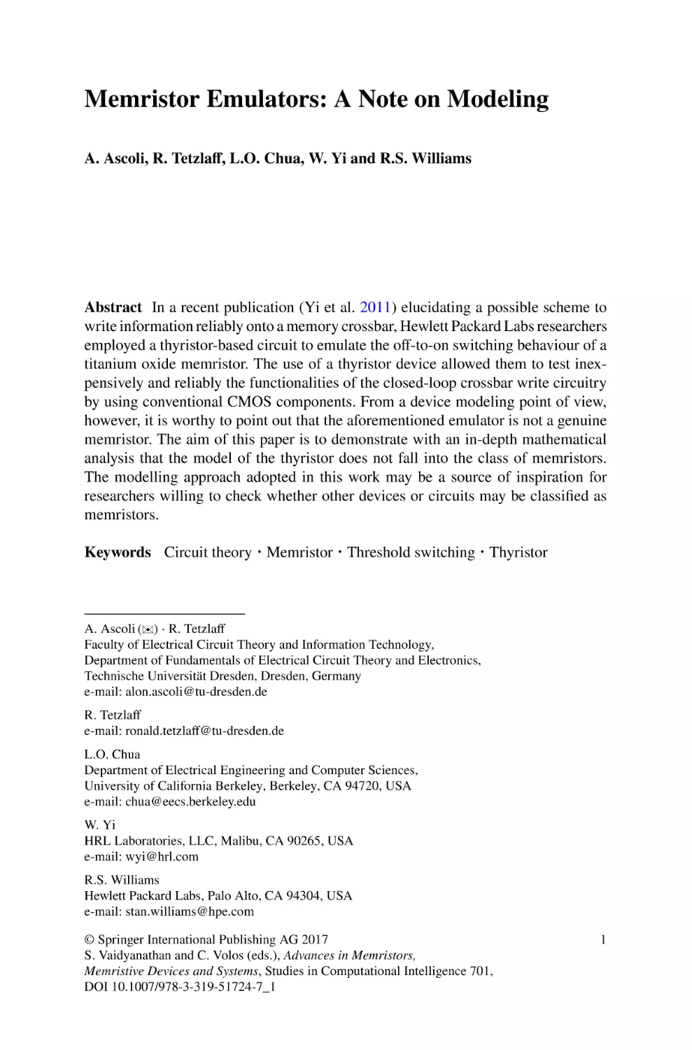
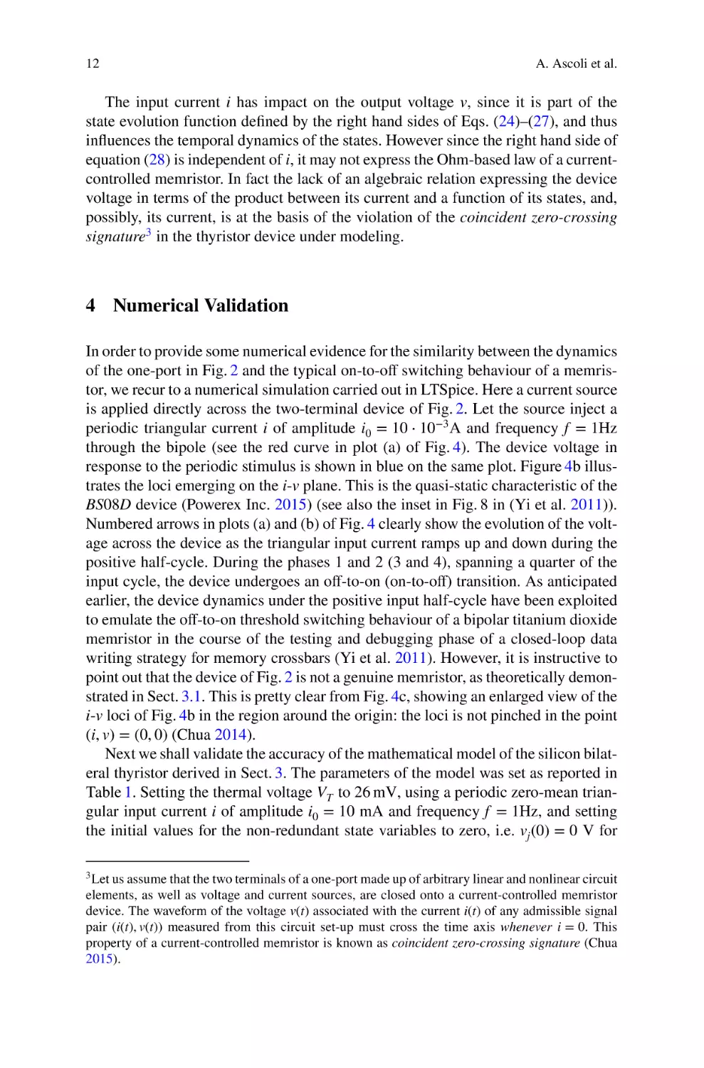
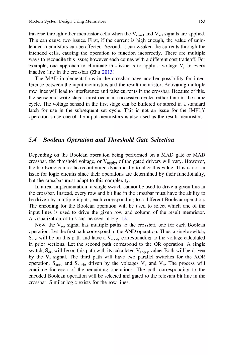
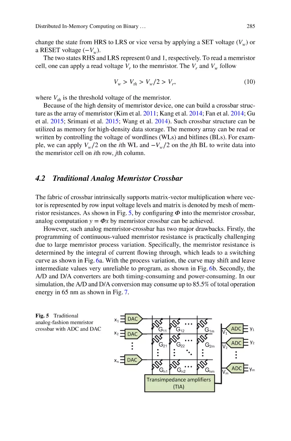
4 Numerical Validation
In order to provide some numerical evidence for the similarity between the dynamics
of the one-port in Fig. 2 and the typical on-to-off switching behaviour of a memristor, we recur to a numerical simulation carried out in LTSpice. Here a current source
is applied directly across the two-terminal device of Fig. 2. Let the source inject a
periodic triangular current i of amplitude i0 = 10 ⋅ 10−3 A and frequency f = 1Hz
through the bipole (see the red curve in plot (a) of Fig. 4). The device voltage in
response to the periodic stimulus is shown in blue on the same plot. Figure 4b illustrates the loci emerging on the i-v plane. This is the quasi-static characteristic of the
BS08D device (Powerex Inc. 2015) (see also the inset in Fig. 8 in (Yi et al. 2011)).
Numbered arrows in plots (a) and (b) of Fig. 4 clearly show the evolution of the voltage across the device as the triangular input current ramps up and down during the
positive half-cycle. During the phases 1 and 2 (3 and 4), spanning a quarter of the
input cycle, the device undergoes an off-to-on (on-to-off) transition. As anticipated
earlier, the device dynamics under the positive input half-cycle have been exploited
to emulate the off-to-on threshold switching behaviour of a bipolar titanium dioxide
memristor in the course of the testing and debugging phase of a closed-loop data
writing strategy for memory crossbars (Yi et al. 2011). However, it is instructive to
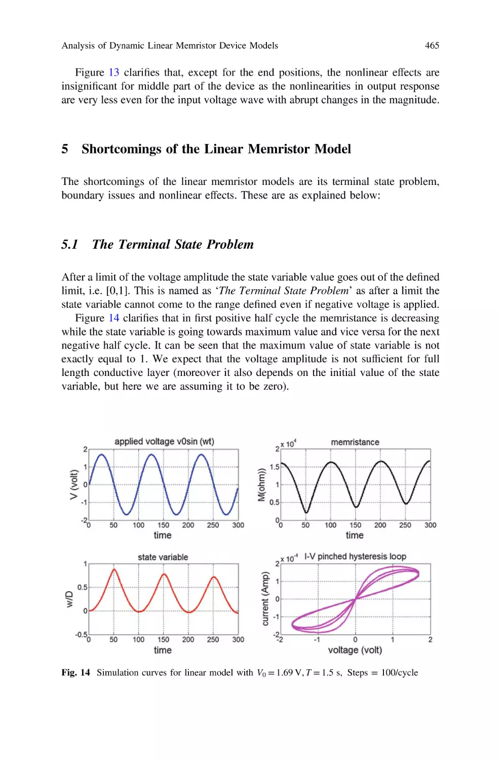
point out that the device of Fig. 2 is not a genuine memristor, as theoretically demonstrated in Sect. 3.1. This is pretty clear from Fig. 4c, showing an enlarged view of the
i-v loci of Fig. 4b in the region around the origin: the loci is not pinched in the point
(i, v) = (0, 0) (Chua 2014).
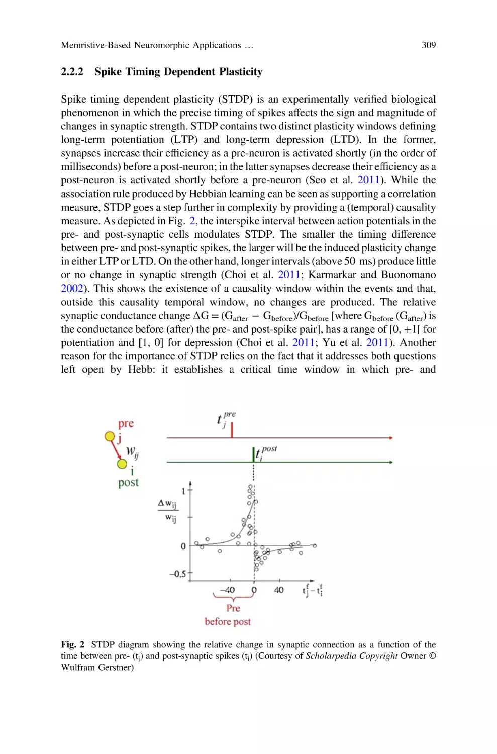
Next we shall validate the accuracy of the mathematical model of the silicon bilateral thyristor derived in Sect. 3. The parameters of the model was set as reported in
Table 1. Setting the thermal voltage VT to 26 mV, using a periodic zero-mean triangular input current i of amplitude i0 = 10 mA and frequency f = 1Hz, and setting
the initial values for the non-redundant state variables to zero, i.e. vj (0) = 0 V for
3 Let us assume that the two terminals of a one-port made up of arbitrary linear and nonlinear circuit
elements, as well as voltage and current sources, are closed onto a current-controlled memristor
device. The waveform of the voltage v(t) associated with the current i(t) of any admissible signal
pair (i(t), v(t)) measured from this circuit set-up must cross the time axis whenever i = 0. This
property of a current-controlled memristor is known as coincident zero-crossing signature (Chua
2015).
Memristor Emulators: A Note on Modeling
4
v/V
0.01
4
1
2
0.005
0
0
2
−2
−4
0
0.5
3
i/A
(a)
13
−0.005
1
1.5
2
2.5
3
3.5
4
−0.01
t/s
i/mA
5
3
(c) 30
2
4
0
i/µA
(b)
1
1-2 on-to-off
3-4 off-to-on
−5
−4
−2
0
2
0
−30
−3
4
0
3
v/V
v/V
Fig. 4 a Time waveforms of the voltage v (in blue) falling across the device of Fig. 2 as a result of
the current i inserted into it. The frequency of the AC stimulus, whose amplitude is i0 = 10 × 10−3 A,
is f = 1 Hz, thus the excitation may be referred to as quasi-static (Ascoli et al. 2016c). b Plot
of i versus v. c Zoom on the region of the i–v plane within the box defined by v ∈ [−3, 3]V and
i ∈ [−30, 30]𝜇A
0.01
2
0.005
0
0
−2
−4
3.5
i/A
v/V
(a) 4
−0.005
4
4.5
5
5.5
6
6.5
7
−0.01
7.5
t/s
(c) 30
5
i/µA
i/mA
(b)
0
−5
−4
−2
0
v/V
2
4
0
−30
−3
0
3
v/V
Fig. 5 a Time waveforms of the current stimulus (red curve) and of the voltage response (blue
curve). b Current-voltage loci of the thyristor. c Enlarged view of the i-v loci in the region around
the point (i, v) = (0, 0)
14
A. Ascoli et al.
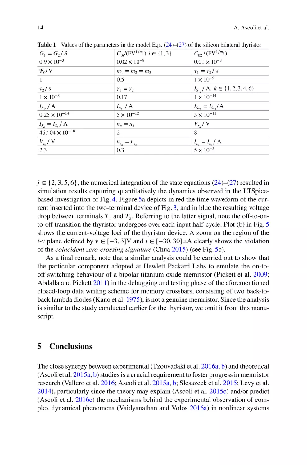
Table 1 Values of the parameters in the model Eqs. (24)–(27) of the silicon bilateral thyristor
G1 = G2 ∕ S
C0i /(FV1∕mi ) i ∈ {1, 3}
C02 / (FV1∕m2 )
0.9 × 10⁻³
0.02 × 10⁻⁸
0.01 × 10⁻⁸
𝛹0 / V
m1 = m2 = m3
𝜏1 = 𝜏3 ∕ s
1
0.5
1 × 10⁻⁹
𝜏2 ∕ s
𝛾1 = 𝛾2
IS1k ∕ A, k ∈ {1, 2, 3, 4, 6}
1 × 10⁻⁸
0.17
1 × 10⁻¹⁴
IS15 ∕ A
IS21 ∕ A
IS22 = IS23 / A
0.25 × 10⁻¹⁴
5 × 10⁻¹²
5 × 10⁻¹¹
ISa = ISb ∕ A
na = nb
Vza ∕ V
−18
467.04 × 10
2
8
Vzb ∕ V
nza = nzb
Iza = Izb ∕ A
2.3
0.3
5 × 10⁻³
j ∈ {2, 3, 5, 6}, the numerical integration of the state equations (24)–(27) resulted in
simulation results capturing quantitatively the dynamics observed in the LTSpicebased investigation of Fig. 4. Figure 5a depicts in red the time waveform of the current inserted into the two-terminal device of Fig. 3, and in blue the resulting voltage
drop between terminals T1 and T2 . Referring to the latter signal, note the off-to-onto-off transition the thyristor undergoes over each input half-cycle. Plot (b) in Fig. 5
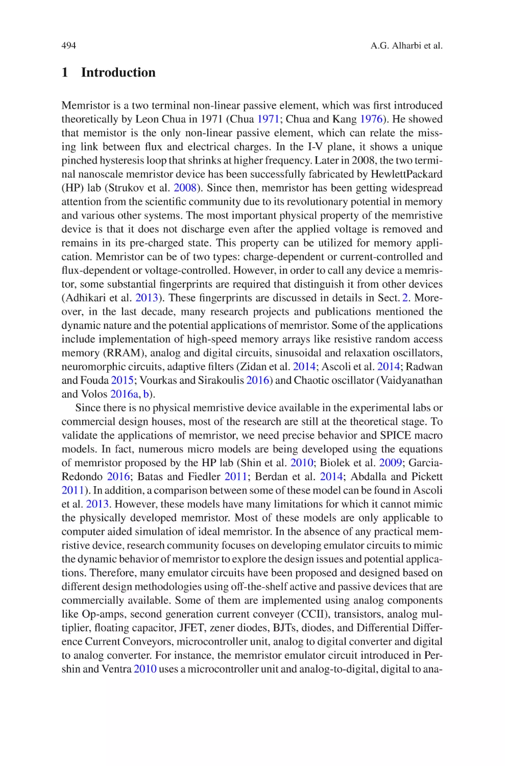
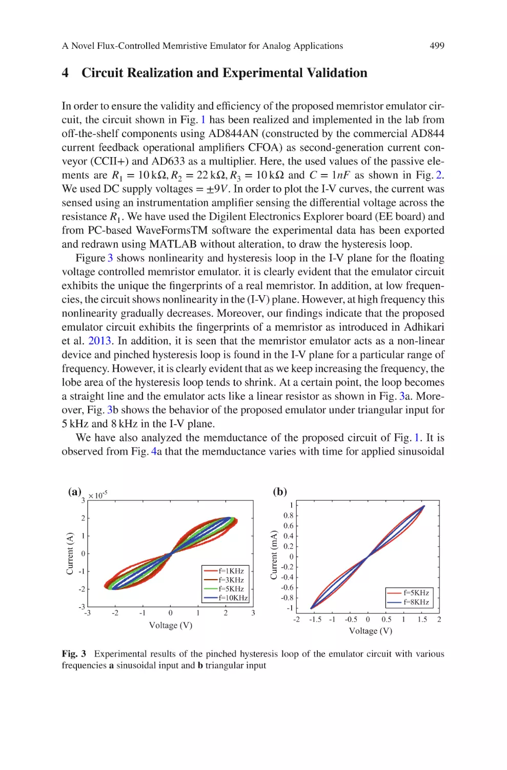
shows the current-voltage loci of the thyristor device. A zoom on the region of the
i-v plane defined by v ∈ [−3, 3]V and i ∈ [−30, 30]µA clearly shows the violation
of the coincident zero-crossing signature (Chua 2015) (see Fig. 5c).
As a final remark, note that a similar analysis could be carried out to show that
the particular component adopted at Hewlett Packard Labs to emulate the on-tooff switching behaviour of a bipolar titanium oxide memristor (Pickett et al. 2009;
Abdalla and Pickett 2011) in the debugging and testing phase of the aforementioned
closed-loop data writing scheme for memory crossbars, consisting of two back-toback lambda diodes (Kano et al. 1975), is not a genuine memristor. Since the analysis
is similar to the study conducted earlier for the thyristor, we omit it from this manuscript.
5 Conclusions
The close synergy between experimental (Tzouvadaki et al. 2016a, b) and theoretical
(Ascoli et al. 2015a, b) studies is a crucial requirement to foster progress in memristor
research (Vallero et al. 2016; Ascoli et al. 2015a, b; Slesazeck et al. 2015; Levy et al.
2014), particularly since the theory may explain (Ascoli et al. 2015c) and/or predict
(Ascoli et al. 2016c) the mechanisms behind the experimental observation of complex dynamical phenomena (Vaidyanathan and Volos 2016a) in nonlinear systems
Memristor Emulators: A Note on Modeling
15
(Vaidyanathan and Voles 2016a, b). This chapter clarifies an important modelling
issue regarding a silicon bilateral thyristor-based circuit used to emulate the off-to-on
switching dynamics of a bipolar titanium dioxide memristor in the testing and debugging phase of a feedback data writing scheme for memory crossbars. Despite the
thyristor exhibits off-to-on dynamics reminiscent of the switching process a memristor undergoes under positive stimuli, thus representing a valid tool for testing and
debugging memristive circuits, from a device modeling point of view it may not be
regarded as a genuine memory resistor (Chua 2015). The present manuscript first
derives the mathematical model of the thyristor-based emulator, adopted in the seminal paper from Hewlett Packard Labs (Yi et al. 2011) to verify the mechanisms
underlying a closed-loop crossbar data writing process, and then proves that it does
not strictly fall into the most general class of memristors (Chua 2015). Numerical
simulation results are then provided to support the conclusions from the theoretical
analysis. All in all, this work is meant to warn the uninitiated against an improper
circuit theoretic classification of the thyristor. The mathematical analysis presented
in the chapter may inspire other studies intended to check whether or not a device or
circuit may be classified as memristor, and fits well in the framework of our activities
aimed at establishing robust foundations on memristor theory.
Acknowledgements The support from EU COST Action IC1401 and Czech Science Foundation
(grant no. 14 − 19865S) are acknowledged. We also thank the Deutsche Forschung Gesellschaft
(DFG) for their financial contribution to the research project “Locally active memristive data
processing (LAMP)” under grant number TE257∕22 − 1. L. Chua’s research is supported by
AFOSR Grant FA 9550-13-1-0136.
References
Abdalla, H., & Pickett, M. (2011). Spice modeling of memristors. In IEEE International Symposium
on Circuits and Systems (ISCAS) (pp. 1832–1835).
Ascoli, A., & Corinto, F. (2013). Memristor models in a chaotic neural circuit. International Journal
of Bifurcation and Chaos (IJBC), 23(1350052), 28.
Ascoli, A., Corinto, F., Senger, V., & Tetzlaff, R. (2013). Memristor model comparison. IEEE Circuits and Systems Magazine, 13, 89–105.
Ascoli, A., Corinto, F., & Tetzlaff, R. (2015a). A class of versatile circuits, made up of standard
electrical components, are memristors. International Journal of Circuit Theory and Applications
(IJCTA), 44, 127–146.
Ascoli, A., Corinto, F., & Tetzlaff, R. (2015b). Generalized boundary condition memristor model.
International Journal of Circuit Theory and Applications (IJCTA), 44, 60–84.
Ascoli, A., Schmidt, T., Corinto, F., & Tetzlaff, R. (2014). Application of the Volterra Series paradigm to memristive systems, Chap. 5 (pp. 163–191). New York: Springer.
Ascoli, A., Slesazeck, S., Mähne, H., Tetzlaff, R., & Mikolaijck, T. (2015c). Nonlinear dynamics
of a locally-active memristor. IEEE Transactions on Circuits and Systems–I (TCAS–I): Regular
Papers, 62, 1165–1174.
Ascoli, A., Tetzlaff, R., & Chua, L. (2016a). The first ever real bistable memristors-part i: Theoretical insights on local fading memory. IEEE Transactions on Circuits and Systems-II (TCAS-II):
Express Briefs.
16
A. Ascoli et al.
Ascoli, A., Tetzlaff, R., & Chua, L. (2016b). The first ever real bistable memristors-part ii: Design
and analysis of a local fading memory system. IEEE Transactions on Circuits and Systems-II
(TCAS-II): Express Briefs.
Ascoli, A., Tetzlaff, R., Chua, L., Strachan, J., & Williams, R. (2016c). History erase effect in a nonvolatile memristor. IEEE Transactions on Circuits and Systems–I (TCAS–I): Regular Papers, 63,
389–400.
Ben-Hur, R., & Kvatinsky, S. (2016). Memristive memory processing unit (mpu) controller for inmemory processing. In Proceedings of International Conference on the Science of Electrical
Engineering (ICSEE).
Carrara, S., Sacchetto, D., Doucey, M.-A., Baj-Rossi, C., Micheli, G. D., & Leblebici, Y. (2012).
Memristive-biosensors: A new detection method by using nanofabricated memristors. Sensors
and Actuators B: Chemical, 171–172, 449–457.
Chua, L. O. (1971). Memristor-The missing circuit element. IEEE Transactions on Circuit Theory,
18, 507–519.
Chua, L. (1980). Device modelling via basic nonlinear circuit elements. IEEE Transactions on
Circuits and Systems–I: Regular Papers, CAS, 27, 1014–1044.
Chua, L. (2011). Resistance switching memories are memristors. Applied Physics A, 102(4), 765–
783.
Chua, L. (2014). If it’s pinched, it’s a memristor. Semiconductor Science and Technology,
29(104001), 42.
Chua, L. (2015). Everything you wish to know about memristors but are afraid to ask. Radioengineering, 24, 319–368.
Chua, L., Desoer, C., & Kuh, E. (1985). Linear and nonlinear circuits. New York, USA: McGrawHill.
Chua, L., & Sing, Y. W. (1979). Nonlinear lumped-circuit model for s.c.r. Electronic Circuits and
Systems, 3, 5–14.
Chua, L. O., & Kang, S. M. (1976). Memristive devices and system. Proceedings of IEEE, 64,
209–223.
Corinto, F., Ascoli, A., & Gilli, M. (2011). Nonlinear dynamics of memristive oscillators. IEEE
Transactions on Circuits Systems I Regular Papers, 58, 1323–1336.
Corinto, F., Ascoli, A., & Gilli, M. (2012). Analysis of current-voltage characteristics for memristive elements in pattern recognition systems. International Journal of Circuit Theory and
Applications (IJCTA), 40, 1277–1320.
Corinto, F., Chua, L., & Civalleri, P. (2015). A theoretical approach to memristor devices. IEEE
Journal on Emerging and Selected Topics in Circuits and Systems (JETCAS), 5, 123–132.
Corinto, F., & Forti, M. (2016). Memristor circuits: Flux-charge analysis method. IEEE Transactions on Circuits and Systems–I (TCAS–I): Regular Papers, 1–13.
Jo, S., Kim, K.-H., & Lu, W. (2009). High-density crossbar arrays based on a si memristive system.
Nanoletters, 9, 870–874.
Kano, G., Iwasa, H., Takagi, H., & Teramoto, I. (1975). The lambda diode: Versatile negativeresistance device. Electronics, 13, 105–109.
Larentis, S., Nardi, F., Balatti, S., Gilmer, D., & Ielmini, D. (2012). Resistive switching by voltagedriven ion migration in bipolar rram-part ii: Modeling. IEEE Transactions on Electron Devices,
59, 2468–2475.
Levy, Y., Bruck, J., Cassuto, Y., Friedman, E., Kolodny, A., Yaacobi, E., et al. (2014). Logic operation in memory using a memristive akers array. Microelectronics Journal, 45, 1429–1437.
Nardi, F., Larentis, S., Balatti, S., Gilmer, D., & Ielmini, D. (2012). Resistive switching by voltagedriven ion migration in bipolar rram-part i: Experimental study. IEEE Transactions on Electron
Devices, 59, 2461–2467.
On Semiconductor, U. (2005). Thyristor theory and design considerations. http://onsemi.com.
Pan, F., Gao, S., Chen, C., Song, C., & Zeng, F. (2014). Recent progress in resistive random access
memories: Materials, switching mechanisms and performance. Materials Science and Engineering R, Elsevier, 83, 1–59.
Memristor Emulators: A Note on Modeling
17
Pickett, M., Strukov, D., Borghetti, J., Yang, J., Snider, G., Stewart, D., et al. (2009). Switching
dynamics in titanium dioxide memristive devices. Journal of Applied Physics, 106, 074508-1–
074508-6.
Powerex Inc, U. (2015). BS08D-T112 silicon bilateral switch. http://www.pwrx.com/Product/
BS08D-T112.
Slesazeck, S., Mähne, H., Wylezich, H., Wachowiak, A., Radhakrishnan, J., & Ascoli, A., et al.
(2015). Physical model of threshold switching in nbo2 based memristors. RSC Advances, Royal
Society of Chemistry.
Strukov, D. B., Snider, G. S., Stewart, D. R., & Williams, R. S. (2008). The missing memristor
found. Nature, 453, 80–83.
Talati, N., Gupta, S., Mane, P., & Kvatinsky, S. (2016). Logic design within memristive memories
using memristor aided logic (magic). IEEE Transactions on Nanotechnology, 15, 635–650.
Tzouvadaki, I., Jolly, P., Lu, X., Ingebrandt, S., de Micheli, G., Estrela, P., & Carrara, S. (2016a).
Label-free ultrasensitive memristive aptasensor. Nanoletters, 16, 4472–4476.
Tzouvadaki, I., Madaboosi, N., Taurino, I., Chu, V., Conde, J., de Micheli, G., & Carrara, S. (2016b).
Study on the bio-functionalization of memristive nanowires for optimum memristive biosensors.
RSC Journal of Materials Chemistry B, 4, 2153–2162.
Vaidyanathan, S., & Volos, C. (2016a). Advances and applications in chaotic systems. Berlin, Germany: Springer.
Vaidyanathan, S., & Volos, C. (2016b). Advances and applications in nonlinear control systems.
Berlin, Germany: Springer.
Vallero, A., Tzouvadaki, I., Puppo, F., Doucey, M. -A., Delaloye, J. -F., Micheli, G. D., & Carrara, S.
(2016). Memristive biosensors integration with microfluidic platform. IEEE Transactions on
Circuits and Systems-I: Regular Papers.
Waser, R., Dittmann, R., Staikov, G., & Szot, K. (2009). Redox-based resistive switching
memories—Nanoionic mechanisms, prospects, and challenges. Advanced Materials, 21, 2632–
2663.
Wylezich, H., Mähne, H., Rensberg, J., Ronning, C., Zahn, P., & Slesazeck, S., et al. (2014). Local
ion irradiation induced resistive threshold and memory switching in nb2 o5 /nbox films. ACS
Applied Materials & Interfaces: American Chemical Society, 1–23.
Yang, J. J., Strukov, D. B., & Stewart, D. R. (2013). Memristive devices for computing. Nature
Nanotechnology, 8, 13–24.
Yi, W., Perner, F., Qureshi, M., Abdalla, H., Pickett, M., Yang, J., et al. (2011). Feedback write
scheme for memristive switching devices. Applied Physics A, 102, 973–982.
Zamarreño-Ramos, C., Camuñas-Mesa, L. A., Pérez-Carrasco, J. A., Masquelier, T., SerranoGotarredona, T., & Linares-Barranco, B. (2011). On spike-timing-dependent-plasticity, memristive devices, and building a self-learning visual cortex. Frontiers in Neuroscience, 5, 1–22.
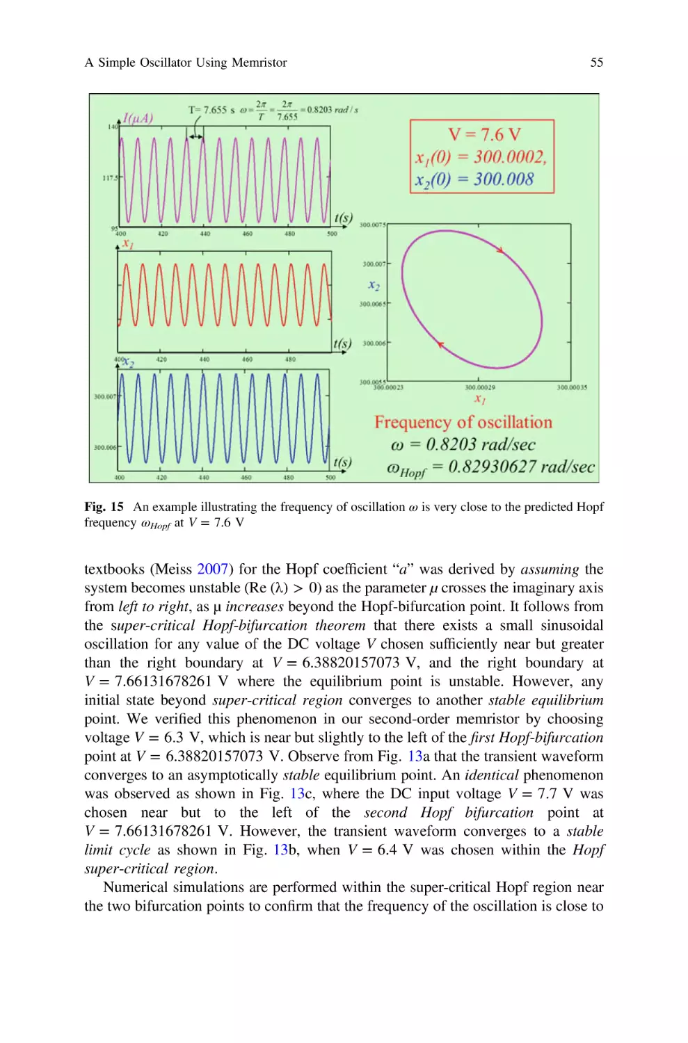
A Simple Oscillator Using Memristor
Maheshwar Pd. Sah, Vetriveeran Rajamani, Zubaer Ibna Mannan,
Abdullah Eroglu, Hyongsuk Kim and Leon Chua
Abstract This paper presents a simple oscillator using a battery and a second order
memristor without the energy storage elements inductor and capacitor. The oscillating mechanism of the proposed circuit has been explained via Hopf bifurcation
theorem, small signal model, local activity principle and edge of chaos theorem.
This paper can be also used as a reference for explaining the intimate relationship
between the super-critical Hopf bifurcation phenomenon and the edge of chaos.
Keywords Memristor
ity
Edge of chaos
⋅
⋅
⋅
⋅
Pinched hysteresis loop
Oscillator
Super-critical Hopf-bifurcation
⋅
Local activ-
M.Pd. Sah ⋅ A. Eroglu
School of Applied Sciences and Engineering Technology, Ivy Tech Community College,
Evansville, IN 47710, USA
e-mail: sahmaheshwar@gmail.com
A. Eroglu
e-mail: eroglua@ipfw.edu
M.Pd. Sah
Department of Electrical and Computer Engineering, Purdue University Fort Wayne,
Fortwayne, IN 46805, USA
M.Pd.Sah ⋅ V. Rajamani ⋅ Z.I. Mannan ⋅ H. Kim (✉)
Division of Electronics and Information Engineering, Chonbuk National University,
Jeonju, Jeonbuk 54896, South Korea
e-mail: hskim@jbnu.ac.kr
V. Rajamani
e-mail: vetriece86@gmail.com
Z.I. Mannan
e-mail: zimannan@gmail.com
L. Chua
Department of Electrical Engineering and Computer Sciences, University of California,
Berkeley, CA 94720, USA
e-mail: chua@berkeley.edu
L. Chua
TUM Fakultat fur Elektrotechnik und Informationstechnik, Technische Universität München,
Arcisstrasse 21, Munich 80333, Germany
© Springer International Publishing AG 2017
S. Vaidyanathan and C. Volos (eds.), Advances in Memristors,
Memristive Devices and Systems, Studies in Computational Intelligence 701,
DOI 10.1007/978-3-319-51724-7_2
19
20
M.Pd. Sah et al.
1 Introduction
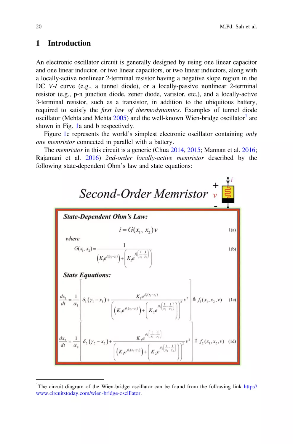
An electronic oscillator circuit is generally designed by using one linear capacitor
and one linear inductor, or two linear capacitors, or two linear inductors, along with
a locally-active nonlinear 2-terminal resistor having a negative slope region in the
DC V-I curve (e.g., a tunnel diode), or a locally-passive nonlinear 2-terminal
resistor (e.g., p-n junction diode, zener diode, varistor, etc.), and a locally-active
3-terminal resistor, such as a transistor, in addition to the ubiquitous battery,
required to satisfy the first law of thermodynamics. Examples of tunnel diode
oscillator (Mehta and Mehta 2005) and the well-known Wien-bridge oscillator1 are
shown in Fig. 1a and b respectively.
Figure 1c represents the world’s simplest electronic oscillator containing only
one memristor connected in parallel with a battery.
The memristor in this circuit is a generic (Chua 2014, 2015; Mannan et al. 2016;
Rajamani et al. 2016) 2nd-order locally-active memristor described by the
following state-dependent Ohm’s law and state equations:
1
The circuit diagram of the Wien-bridge oscillator can be found from the following link http://
www.circuitstoday.com/wien-bridge-oscillator.
A Simple Oscillator Using Memristor
(a)
(b)
R1
DTun
R2
RPar
(c)
Tank circuit
C
VOUT
L
i
C2
+
VBIAS
21
-
R1
C1
+VCC
B
Cx
Rx
C
A
R4
R5
R6
C3
Q1
R2
R3
D
R8
+
R7
C Output
Q2 4
v
R9
-
Battery Voltage E=6.4V
Output
180
I(μA)
170
t(s)
160
150
~
0
t(s)
425
450
475
500
Fig. 1 a Simplest oscillator using a tunnel diode and an LC tank circuit (Mehta 2005).
b Wien-bridge oscillator using resistors, capacitors and transistors (see footnote 1). c World’s
simplest oscillator using only one memristor. The blue near-sinusoidal waveform is obtained by
computer simulation of (1) with the parameters listed in Table 1, and initial states x1(0) = 300.002
and x2 (0) = 300.004
The parameters chosen in this paper are summarized in Table 1. The 3D cross
section of the surface f1(x1, x2, v) and f2(x1, x2, v) are shown in Fig. 2a and b
respectively at V = 6.4 V. Although (1) can be implemented in hardware by several
methods, all results in this paper are obtained by computer simulations to avoid
ambiguities in modeling the physical devices.
2 Pinched Hysteresis Loop and DC V-I Curve
of the Second-Order-Generic Memristor from Fig. 1c
2.1
Pinched Hysteresis Loops Under Bipolar Periodic
Signal
The memristor exhibits a unique fingerprint called a pinched hysteresis loop under
excitation of any bipolar periodic signal with zero average. To illustrate the
Table 1 Parameter values of
the second-order generic
memristor
K1 = 103
β1 = 104
γ 1 = 300
α1 = 0.8
δ1 = 0.8
K2 = 105
β2 = 107
γ 2 = 300
α2 = 0.2
δ2 = 0.1
22
M.Pd. Sah et al.
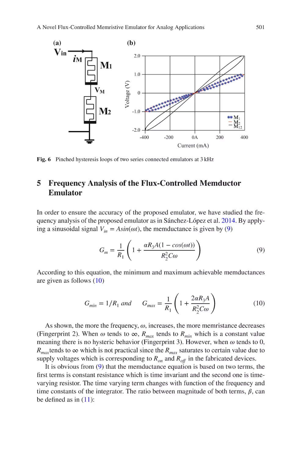
Fig. 2 The cross section of the surfaces a f1(x1, x2, V) and b f2(x1, x2, V) at V = 6.4 V
A Simple Oscillator Using Memristor
23
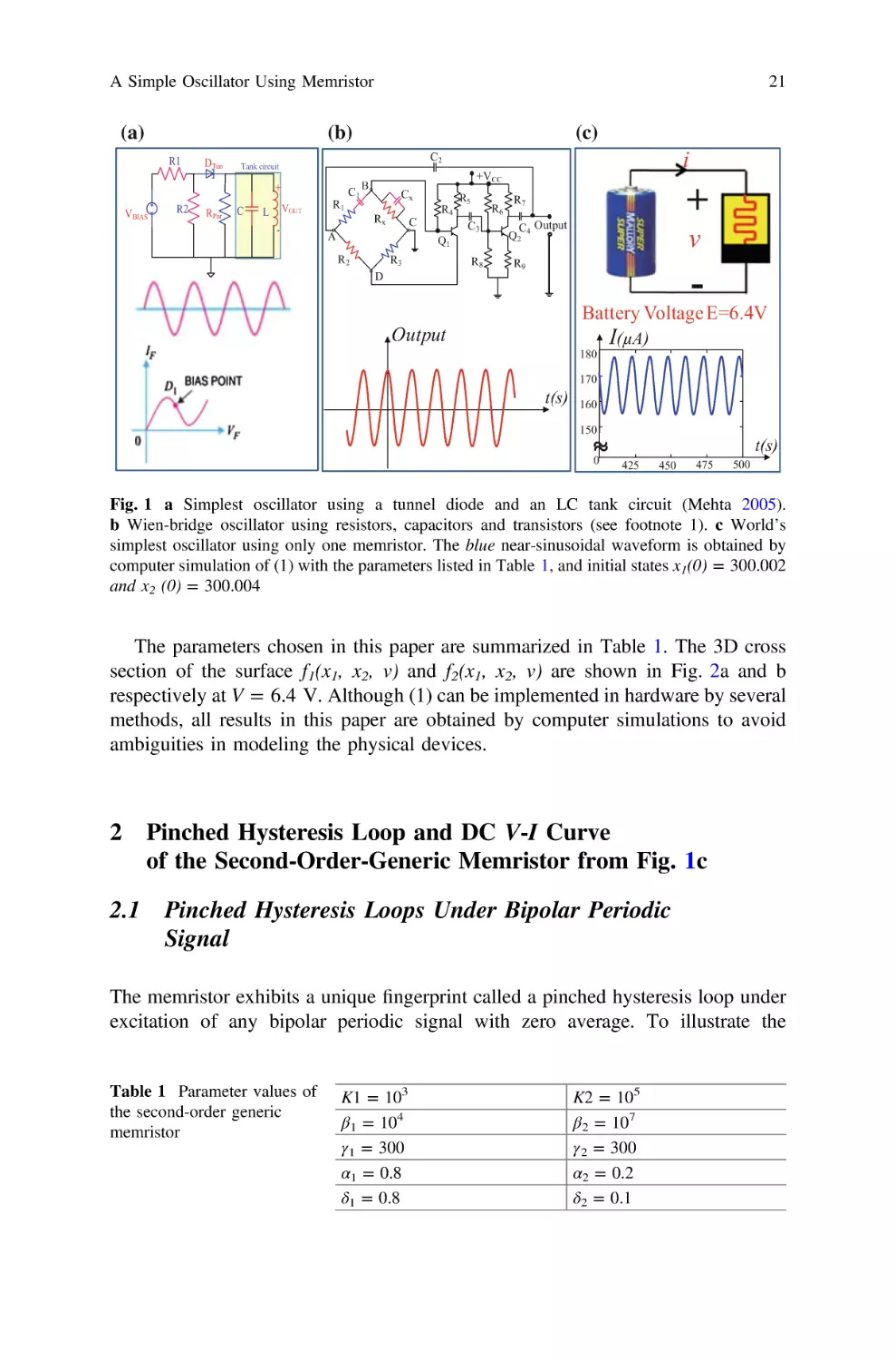
memristor in (1) exhibits this fingerprints, we apply a sinusoidal voltage signal v
(t) = A sin(2πft) with amplitude A = 12 V, and frequency f = 0.1 Hz across this
memristor. Figure 3a shows the output current i(t), the state variables x1(t), x2(t) and
the memductance G(t) with respect to time t, respectively. Observe from Fig. 3a
that i(t) always passes through the origin whenever v(t) is zero at point 1, and 3.
Observe also the memductance G(t) ≥ 0. The upper figure in Fig. 3b is a
double-valued Lissajous figure plotted on the i versus v plane. Such a multi-valued
Lissajous figure of v(t), i(t), which passes through the origin is called a pinched
hysteresis loop (Chua 2003). This unique feature is the characteristic property of a
memristor that distinguishes it from non-memristive devices. The lower figure in
Fig. 3b shows the variation of memductance with respect to applied voltage v(t).
Fig. 3 a Waveforms of the applied sinusoidal voltage v(t) = A sin(2πft), output current i(t), state
variables x1(t), x2(t), and memductance G(t) of the second-order generic memristor. b Pinched
hysteresis loop plotted on the i versus v plane and memductance hysteresis loop plotted on the
G versus v plane, respectively. The simulations were performed at A = 12 V, f = 0.1 Hz,
x1(0) = 300.002 and x2 (0) = 300.004
24
M.Pd. Sah et al.
i(μA)
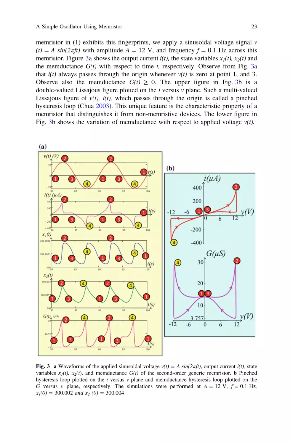
Fig. 4 Pinched hysteresis
loops of the second-order
generic memristor at
frequencies f = 0.1, 0.5 and
5 Hz. The input is a
sinusoidal signal v(t) = A sin
(2πft), with A = 12 V, and
the initial states are
x1(0) = 300.002 and
x2(0) = 300.004
350
175
v(V)
− 12
−6
0
− 175
6
12
f=0.1 Hz
f=0.5 Hz
f=5 Hz
− 350
Another characteristic property of the memristor is the dependence of the pinched hysteresis loop on the frequency of the excitation signal. This property asserts
that the pinched hysteresis loops characterized by a memristor shrinks to a
single-value function through origin as the frequency tends to infinity. We illustrate
this property by applying the sinusoidal signal v(t) = A sin(2πft) with A = 12 V
and f = 0.1, 0.5, and 5 Hz to our memristor. Observe from Fig. 4 that the pinched
hysteresis loops shrink as the frequencies increase and tend to a straight line at 5 Hz
(Adhikari et al. 2013; Mannan et al. 2016; Rajamani et al. 2016). All of these
pinched hysteresis loops exhibit the fingerprints of a memristor.
2.2
DC V-I Curve
The DC V-I curve of a generic memristor is equivalent to a nonlinear resistor at the
DC steady state regime (Chua 2014). The DC V-I curve of the second-order generic
memristor defined in (1a)–(1d) is obtained by equating (1c) and (1d) to zero and
solving for the equilibrium point as a function of applied DC voltage v = V, i.e.
x1 = x̂1 ðVÞ
ð2aÞ
x2 = x̂2 ðVÞ
ð2bÞ
Substituting (2a) and (2b) in (1b), and solving for the DC current i = I from (1a),
we obtain
A Simple Oscillator Using Memristor
25
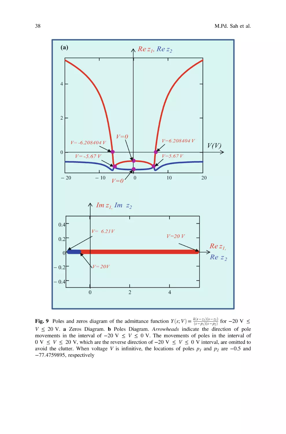
Fig. 5 The DC equilibrium of a state x1, b state x2, and c DC V-I curve in steady state regime, for
−20 V ≤ V ≤ 20 V, d portions of the DC V-I curve which give rise to two distinct super-critical
Hopf bifurcations
I = Gðx1 , x2 Þ V
ð3Þ
Applying (2a), (2b) and (3), for −20 V ≤ V ≤ 20 V, we obtain the red DC
V-I curve of our second-order generic memristor shown in Fig. 5c whereas the state
variables x1 and x2 are shown in Fig. 5a and b, respectively. Note that at steady
state the V-I curve in Fig. 5c is equivalent to the V-I curve of a nonlinear resistor
(Chua 1969). Figure 5d shows the portions of the DC V-I curve which give rise to
two distinct super-critical Hopf bifurcations.
26
M.Pd. Sah et al.
3 Small-Signal Equivalent Circuit
Small-signal equivalent circuit is the linearized circuit used to predict the response
of a memristor to a small-signal input applied at an equilibrium point. Just like
standard electronic circuit theory, the small-signal equivalent circuit is derived
about an equilibrium point (V, I) by using the Taylor series and the Laplace
transform. Let V be the DC voltage at an equilibrium point Q, then the equilibrium
state x1 = X1 and x2 = X2 can be found by solving (1c) and (1d) numerically at the
DC voltage V as follow:
3
2
6
dx1
16
6
= 6 δ 1 ð γ 1 − x1 Þ +
α1 6
dt
4
ðK1 eβ1 ðx1 − γ1 Þ Þ + K2 e
2
6
dx2
16
6
= 6δ2 ðγ 2 − x2 Þ +
α2 6
dt
4
7
7
!!2 V 7 = 0
7
β2 x1 − γ1
5
2
2
K1 eβ1 ðx1 − γ1 Þ
K2 e
β2
27
3
1
x2
− γ1
2
ðK1 eβ1 ðx1 − γ1 Þ Þ + K2 e
ð4aÞ
7
7
27
!!2 V 7 = 0
7
β2 x1 − γ1
5
2
2
ð4bÞ
The memristance Mðx1 , x2 Þ≜ Gðx11, x2 Þ of the 2nd-order memristor defined in (1b) is
composed of the following two decoupled terms involving only x1 and x2,
respectively:
β2
Mðx1 , x2 Þ = K1 eβ1 ðx1 − γ1 Þ + K2 e
1
x2
− γ1
2
!
ð5Þ
We can synthesize the M(x1, x2) by two first-order memristors connected in
series, as shown in Fig. 6. The memristance of the upper and lower memristors in
Fig. 6 are defined by the first and second terms of Eq. (5) respectively, where the
memductance G1(x1) = 1/R1(x1) and G2(x2) = 1/R2(x2) are defined in (6a) and (6b),
respectively:
G1 ðx1 Þ =
1
ðK 1
eβ1 ðx1 − γ1 Þ Þ
1
G2 ðx2 Þ =
K2 e
β2
1
x2
− γ1
2
ð6aÞ
ð6bÞ
A Simple Oscillator Using Memristor
27
Fig. 6 The second-order
memristor defined in (1) can
be realized by connecting two
“uncoupled” first-order
voltage-controlled memristors
in series. The memductance
G1(x1) of the first memristor is
defined by (6a), and the
memductance G2(x2) of the
second memristor is defined
by (6b). The corresponding
state equation is given by (9)
and (10), respectively
Note that i = i1 = i2 and v = v1 + v2 in Fig. 6. Using (6a) and (6b), we have
following relationships:
G1 ðx1 Þv1 = G2 ðx2 Þv2
ð7aÞ
v1 + v 2 = v
ð7bÞ
It follows from (7a) and (7b) that
v=
0
BK 1 e
=@
G1 ðx1 Þ + G2 ðx2 Þ
v1
G2 ðx2 Þ
1
β1 ðx1 − γ 1 Þ
+ K2 e
β2
K1 eβ1 ðx1 − γ1 Þ
1
x2
− γ1
2
C
Av1
ð7cÞ
ð8Þ
From (8) and (1c), we obtain the following state equation of the upper
memristor:
dx1
1
1
2
=
δ 1 ð γ 1 − x1 Þ +
v ≜ f ðx1 , v1 Þ
α1
dt
K1 eβ1 ðx1 − γ1 Þ 1
ð9Þ
28
M.Pd. Sah et al.
A similar derivation with respect to v2 gives the following state equation for the
lower memristor:
3
2
dx2
16
= 4δ2 ðγ 2 − x2 Þ +
α2
dt
1
K2 e
β2
1
x2
− γ1
v22 7
5≜ f ðx2 , v2 Þ
ð10Þ
2
Let us derive small-signal equivalent circuit of the upper and lower memristor in
Fig. 6 at their DC equilibrium point v1 = V1 and v2 = V2 where
V1 + V2 = V. Define,
x1 = X1 + δ x1
ð11aÞ
v1 = V1 + δ v1
ð11bÞ
i1 = I1 + δ i 1
ð11cÞ
where X1 denotes the equilibrium state x1(Q) of the upper memristor at v1 = V1.
We can expand the current i1 due to the memductance G1(x1) in a Taylor series
about the equilibrium point x1 = X1 as follows:
i1 = I1 + δ i1
= a′00 ðQÞ + a′11 ðQÞδ x1 + a′12 ðQÞδ v1 + h.o.t
ð12aÞ
where,
I1 = a′00 ðQÞ = G1 ðX1 ÞV1
ð12bÞ
−1
a′11 ðQÞ = G1̇ ðx1 Þv1 Q = − β1 K1 eβ1 ðX1 − γ1 Þ
V1
ð12cÞ
−1
a′12 ðQÞ = G1 ðx1 ÞjQ = K1 eβ1 ðX1 − γ1 Þ
ð12dÞ
and h.o.t denotes the higher-order terms in δ x1 and δ v1 . Assuming jδ x1 j ≪ 1 and
jδ v1 j ≪ 1, we can neglect the h.o.t term in (12a) to obtain the following linear
equation,
δ i1 = a′11 ðQÞδ x1 + a′12 ðQÞδ v1
ð13Þ
Let us expand state equation f ðx1 , v1 Þ of (9) in Taylor series about the equilibrium point (x1(Q), V1 (Q)):
A Simple Oscillator Using Memristor
29
f ðX1 + δ x1 , V1 + δ v1 Þ = f ðX1 , V1 Þ + b11 ðQÞδ x1 + b12 ðQÞδ v1 + h.o.t
ð14aÞ
where,
b′11 ðQÞ =
− 1
∂f ðx1 , v1 Þ
δ1 β1 V12
β1 ðX1 − γ1 Þ
=
−
+
K
e
1
∂x1 Q
α1
α1
ð14bÞ
−1
2 K1 eβ1 ðX1 − γ1 Þ
∂f ðx1 , v1 Þ
=
V1
∂v1 Q
α1
ð14cÞ
b′12 ðQÞ =
Note that f ðX1 , V1 Þ = 0 since ðX1 , V1 Þ is a point on the DC V1 − I1 curve. Let us
linearize the non-linear state equation ẋ1 = f ðx1 , v1 Þ by neglecting the h.o.t from
(14a) as follows:
dðδ x1 Þ
= b′11 ðQÞδ x1 + b′12 ðQÞδ v1
dt
ð15Þ
Taking the Laplace transform of (13) and (15) (Chua and Kang 1976) we obtain,
ı1̂ ðsÞ = a′11 ðQÞ x̂1 ðsÞ + a′12 ðQÞv̂1 ðsÞ
ð16Þ
sx̂1 ðsÞ = b′11 ðQÞx̂1 ðsÞ + b′12 ðQÞv̂1 ðsÞ
ð17Þ
where the Laplace transform of δ x1 ðtÞ, δ i1 ðtÞ and δ v1 ðtÞ are denoted by x̂1 ðsÞ, ı1̂ ðsÞ
and v̂1 ðsÞ respectively. From (17), we obtain
x̂1 ðsÞ =
b′12 ðQÞv̂1 ðsÞ
s − b′11 ðQÞ
ð18Þ
From (16) and (18), the admittance function Y1 ðs, QÞ of the upper memristor is
Y1 ðs, QÞ≜
ı1̂ ðsÞ a′11 ðQÞb′12 ðQÞ
=
+ a′12 ðQÞ
v̂1 ðsÞ
s − b′11 ðQÞ
ð19Þ
Rearranging (19), we obtain
Y1 ðs, QÞ =
1
1
s a′ ðQÞb
′ ðQÞ
11
12
Let us recast (20) into the form
+
ð − b′11 ðQÞÞ
a′11 ðQÞb′12 ðQÞ
+ a′12 ðQÞ
ð20Þ
30
M.Pd. Sah et al.
Fig. 7 a Small-signal equivalent circuit of the second-order memristor. b Inductances and
resistances in the small-signal equivalent circuit of the second-order memristor calculated at the
DC voltage V
Y1 ðs, QÞ =
1
1
+
sL1 + R1 Ra
ð21Þ
where Y1 ðs, QÞ denotes the small-signal admittance of the upper memristor at Q,
whose circuit as shown in Fig. 7a, where the parameters L1, R1 and Ra are defined
by:
L1 =
1
a′11 ðQÞb′12 ðQÞ
ð22aÞ
R1 =
− b′11 ðQÞ
a′11 ðQÞb′12 ðQÞ
ð22bÞ
1
a′12 ðQÞ
ð22cÞ
Ra =
and state variable x1 at Q can be computed numerically by solving the following
equation:
A Simple Oscillator Using Memristor
31
dx1
1
=
δ1 ðγ 1 − x1 Þ + G1 ðx1 ÞV12 = 0
α1
dt
ð22dÞ
Similarly, the small-signal admittance of the lower memristor is given by
Y2 ðs, QÞ≜
′
ı2̂ ðsÞ c′11 ðQÞd12
ðQÞ
=
+ c′12 ðQÞ
′
v̂2 ðsÞ
s − d11 ðQÞ
ð23Þ
Rearranging (23), we have
Y2 ðs, QÞ =
1
1
s c′ ðQÞd
′ ðQÞ
11
12
+
′ ðQÞÞ
ð − d11
′ ðQÞ
c′11 ðQÞd12
+ c′12 ðQÞ =
1
1
+
sL2 + R2 Rb
ð24Þ
where Y2 ðs, QÞ denotes the small-signal admittance of the lower memristor of the
circuit of Fig. 7a where the parameters L2, R2 and Rb are given by:
L2 =
R2 =
1
′ ðQÞ
c′11 ðQÞd12
c′11
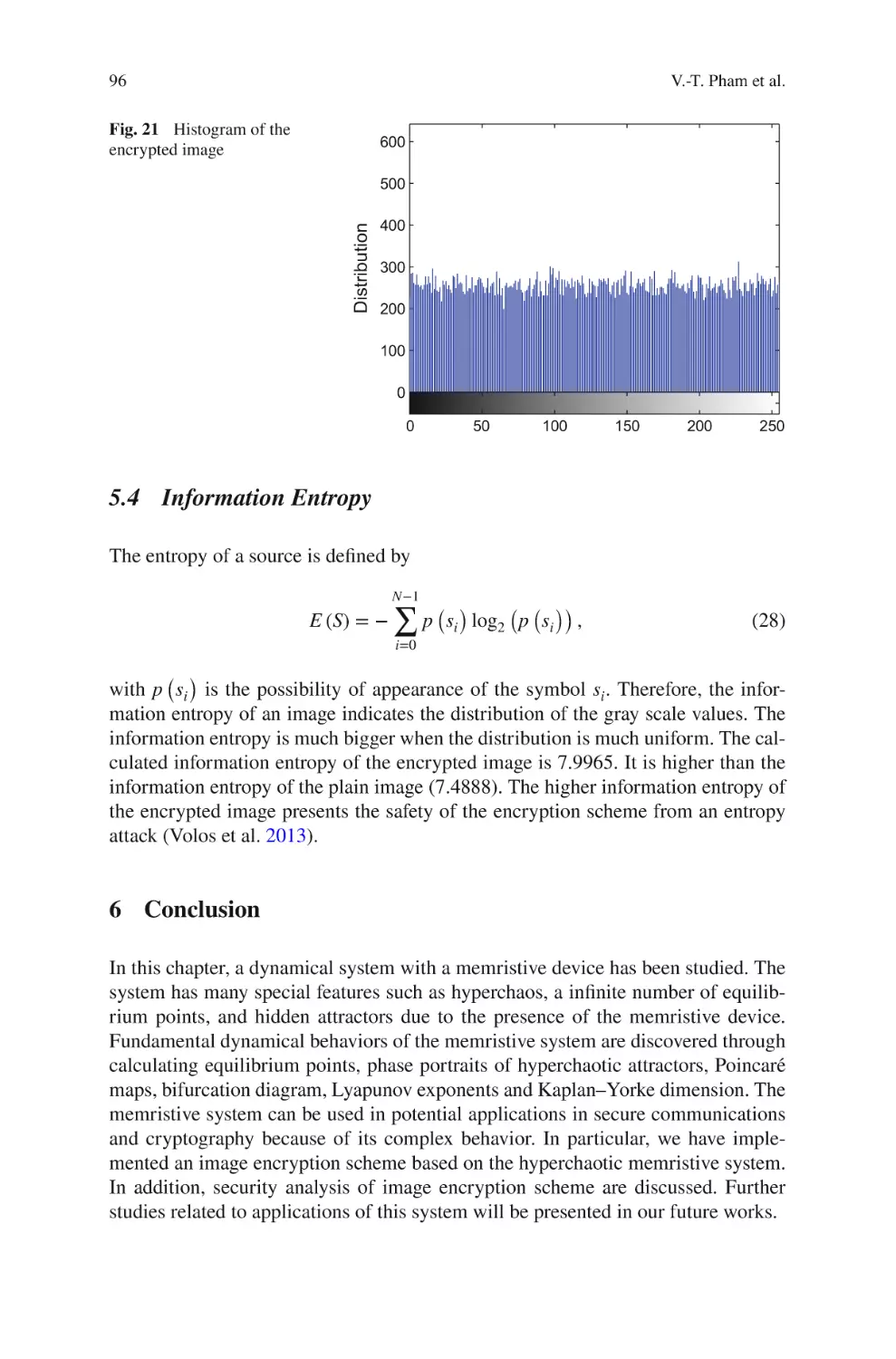
′
− d11
ðQÞ
′ ðQÞ
ðQÞ d12
Rb =
1
c′12 ðQÞ
ð25aÞ
ð25bÞ
ð25cÞ
The state variable x2 at the equilibrium point Q can be computed numerically by
solving the following equation:
dx2
1
=
δ2 ðγ 2 − x2 Þ + G2 ðx2 ÞV22 = 0
α2
dt
ð25dÞ
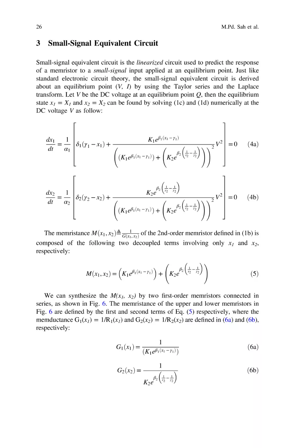
For the convenience of readers, the explicit formulas for computing L1, R1, Ra
and L2, R2, Rb as a function of V1 and V2 are given in Table 2 along with the state
equations f ðx1 , v1 Þ and f ðx2 , v2 Þ, respectively. The corresponding small-signal
equivalent circuit due to L1, R1, Ra and L2, R2, Rb and plots of inductances and
resistances are shown in Fig. 7a and b, respectively, for the memristor. Observe that
the inductance L1 and resistance R1 are always negative for any DC equilibrium
voltage V. The small-signal equivalent circuit of the second-order generic memristor with its inductances and resistances calculated at V = 6.4 V is shown in
Fig. 8.
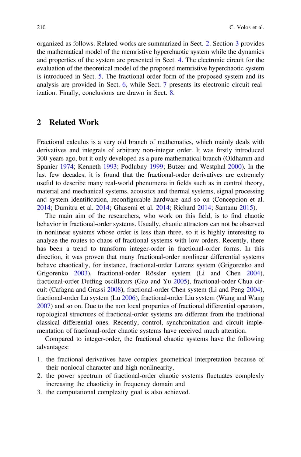
32
M.Pd. Sah et al.
Table 2 Formulas for calculating L1, R1, Ra and L2, R2, Rb of the second-order memristor
A Simple Oscillator Using Memristor
33
Fig. 8 Small-signal
equivalent circuit of the
second-order generic
memristor calculated at
V = 6.4 V
3.1
Admittance and Pole-Zero Diagram of Second-Order
Memristor
Let Q(VQ, IQ) be any point on the DC V-I curve of a second-order generic memristor
and let ðX1Q , X2Q Þ be the corresponding equilibrium state.
Define,
x1 = X1Q + Δ x1
ð26aÞ
x2 = X2Q + Δ x2
ð26bÞ
v = VQ + Δv
ð26cÞ
i = IQ + Δi
ð26dÞ
Let us expand the current i = G(x1, x2) v in (1a) using Taylor series at the
equilibrium point ðX1Q , X2Q , VQ Þ
i = a00 + a11 Δx1 + a12 Δx2 + a13 Δv + h.o.t.
where,
ð27Þ
34
M.Pd. Sah et al.
a00 = GðX1Q , X2Q Þ VQ = IQ
ð28aÞ
∂Gðx1 , x2 Þ
∂x1 Q
ð28bÞ
∂Gðx1 , x2 Þ
a12 = VQ
∂x2 Q
ð28cÞ
a13 = Gðx1 , x2 ÞjQ = GðX1Q , X2Q Þ
ð28dÞ
a11 = VQ
The h.o.t. in (27) denotes the higher-order terms of Δx1, Δx2, and Δv1. Assuming
Δx1 << 1, Δx2 << 1 and Δv1 << 1 then the h.o.t. term can be neglected and (27)
reduces to the following linear equation
Δi = a11 Δx1 + a12 Δx2 + a13 Δv
ð29Þ
Let us expand f1(x1, x2, v) in (1c) using Taylor series at the equilibrium point
ðX1Q , X2Q , VQ Þ
f1 ðX1Q + Δx1 , X2Q + Δx2 , VQ + ΔvÞ = f1 ðX1Q , X2Q , VQ Þ + b11 Δx1 + b12 Δx2 + b13 Δv + h.o.t.
ð30Þ
where,
∂f1 ðx1 , x2 , vÞ
b11 =
∂x1
Q
ð31aÞ
b12 =
∂f1 ðx1 , x2 , vÞ
∂x2
Q
ð31bÞ
b13 =
∂f1 ðx1 , x2 , vÞ
∂v
Q
ð31cÞ
Since ðX1Q , X2Q , VQ Þ specifies a point on the DC V-I curve, the term
f1 ðX1Q , X2Q , VQ Þ = 0. Neglecting the h.o.t. term in (30), we obtain the following
linear equation:
dðΔx1 Þ
dt
= b11 Δx1 + b12 Δx2 + b13 Δv
ð32Þ
Similarly, let us expand f2(x1, x2, v) in (1d) using Taylor series at the equilibrium
point ðX1Q , X2Q , VQ Þ
A Simple Oscillator Using Memristor
35
f2 ðX1Q + Δx1 , X2Q + Δx2 , VQ + ΔvÞ = f2 ðX1Q , X2Q , VQ Þ + c11 Δx1 + c12 Δx2 + c13 Δv + h.o.t.
ð33Þ
where,
∂f2 ðx1 , x2 , vÞ
c11 =
∂x1
Q
ð34aÞ
∂f2 ðx1 , x2 , vÞ
∂x2
Q
ð34bÞ
∂f2 ðx1 , x2 , vÞ
c13 =
∂v
Q
ð34cÞ
c12 =
Since ðX1Q , X2Q , VQ Þ specifies a point on the DC V-I curve, the term
f2 ðX1Q , X2Q , VQ Þ = 0. Neglecting the h.o.t. term in (33), we obtain the following
linear equation:
dðΔx2 Þ
dt
= c11 Δx1 + c12 Δx2 + c13 Δv
ð35Þ
Taking Laplace transform of (29), (32) and (35), we obtain
ı ̂ðsÞ = a11 x̂1 ðsÞ + a12 x̂2 ðsÞ + a13 v̂ðsÞ
ð36Þ
sx̂1 ðsÞ = b11 x̂1 ðsÞ + b12 x̂2 ðsÞ + b13 v̂ðsÞ
ð37Þ
sx̂2 ðsÞ = c11 x̂1 ðsÞ + c12 x̂2 ðsÞ + c13 v̂ðsÞ
ð38Þ
where ı ̂ðsÞ, x̂1 ðsÞ, x̂2 ðsÞ and v̂ðsÞ denote the Laplace transform of Δi, Δx1, Δx2, and
Δv, respectively. Solving (37) and (38) for x̂1 ðsÞ and x̂2 ðsÞ, we obtain
x̂1 ðsÞ =
½b12 c13 + b13 ðs − c12 Þ
v̂ðsÞ
½ðs − b11 Þðs − c12 Þ − b12 c11
ð39aÞ
x̂2 ðsÞ =
½b13 c11 + c13 ðs − b11 Þ
v̂ðsÞ
½ðs − b11 Þðs − c12 Þ − b12 c11
ð39bÞ
The explicit formula for computing the parameters in (39a) and (39b) are given
in Table 3. By substituting x̂1 ðsÞ and x̂2 ðsÞ from (39a, 39b) into (36), we obtain
Yðs; QÞ≜
ı ̂ðsÞ
v̂ðsÞ
ð40Þ
36
M.Pd. Sah et al.
Table 3 Explicit formula for computing the parameters in (40)
a11 =
−V K1 β1e β1 ( X1 −γ 1 )
⎛ 1
1 ⎞
⎡
⎛
β2 ⎜
− ⎟ ⎞⎤
⎢ K1e β1 ( X1 −γ 1 ) + ⎜ K 2 e ⎝ X 2 γ 2 ⎠ ⎟ ⎥
⎜
⎟⎥
⎢
⎝
⎠⎦
⎣
(
a12 =
2
(K e
1
β1 ( X1 − γ 1 )
)
⎛ 1
1 ⎞
− ⎟
⎝ X2 γ2 ⎠
β2 ⎜
⎛ 1
1 ⎞
⎡
⎛
− ⎟ ⎞⎤
β2 ⎜
γ
X 22 ⎢ K1e β1 ( X1 −γ 1 ) + ⎜ K 2 e ⎝ X 2 2 ⎠ ⎟ ⎥
⎜
⎟⎥
⎢
⎝
⎠⎦
⎣
(
)
a13 =
V K2 β2e
2
)
1
⎛ 1
1 ⎞
⎛
− ⎟⎟ ⎞
β 2 ⎜⎜
X
γ
+ ⎜ K2e ⎝ 2 2 ⎠ ⎟
⎜
⎟
⎝
⎠
⎡
⎤
⎢
⎥
⎢
⎥
β1 ( X1 −γ 1 )
2 β1 ( X 1 −γ 1 )
2
−1 ⎢
K1β1e
2 K1 β1e
2
2⎥
−
+
b11 =
V
V
δ
2
3
⎥
⎛ 1
⎛ 1
α1 ⎢ 1 ⎛
1 ⎞
1 ⎞
⎛
⎛
⎛
β2 ⎜
β2 ⎜
− ⎟ ⎞⎞
− ⎟ ⎞⎞
⎢
⎥
⎜ K1e β1 ( X1 −γ 1 ) + ⎜ K 2e ⎝ X 2 γ 2 ⎠ ⎟ ⎟
⎜ K1e β1 ( X1 −γ 1 ) + ⎜ K 2e ⎝ X 2 γ 2 ⎠ ⎟ ⎟
⎢
⎥
⎜
⎜
⎜
⎟⎟
⎜
⎟⎟
⎝
⎠⎠
⎝
⎠⎠
⎝
⎝
⎣⎢
⎦⎥
(
b12 =
2 K1 K 2 β 2 e
(
β1 ( X1 − γ 1 )
e
⎛ 1
1 ⎞
− ⎟⎟
⎝ X2 γ2 ⎠
(
)
− 2 K1 K 2 β1 e β1( X1 −γ1 ) e
⎛ 1
1 ⎞
β 2 ⎜⎜
− ⎟⎟
⎝ X2 γ2 ⎠
⎞⎤
⎟⎥
⎟⎥
⎠⎦
⎛ 1 1 ⎞
− ⎟⎟
⎝ X2 γ2 ⎠
3
V2
b13 =
2 K1e
(
3
V
2
)
c13 =
β1 ( X1 − γ 1 )
⎛ 1
1 ⎞
⎡
⎛
− ⎟⎟ ⎞ ⎤
β 2 ⎜⎜
α1 ⎢ K1e β1 ( X1 −γ1 ) + ⎜ K 2 e ⎝ X 2 γ 2 ⎠ ⎟ ⎥
⎜
⎟⎥
⎢
⎝
⎠⎦
⎣
2
V
)
β 2 ⎜⎜
⎛ 1 1 ⎞ ⎤
⎡
⎛
β 2 ⎜⎜
− ⎟⎟ ⎞
α 2 ⎢ K1e β1( X1 −γ1 ) + ⎜ K 2 e ⎝ X 2 γ 2 ⎠ ⎟ ⎥
⎢
⎜
⎟⎥
⎝
⎠⎦
⎣
(
)
β 2 ⎜⎜
⎡
⎛
α1 X ⎢ K1e β1 ( X1 −γ1 ) + ⎜ K 2 e
⎜
⎢
⎝
⎣
2
2
c11 =
)
2 K 2e
⎛ 1 1 ⎞
− ⎟⎟
⎝ X2 γ2 ⎠
β 2 ⎜⎜
⎛ 1 1 ⎞ ⎤
⎡
⎛
− ⎟⎟ ⎞
β 2 ⎜⎜
α 2 ⎢ K1e β1( X1 −γ1 ) + ⎜ K 2 e ⎝ X 2 γ 2 ⎠ ⎟ ⎥
⎢
⎜
⎟⎥
⎝
⎠⎦
⎣
(
2
V
)
⎡
⎤
⎢
⎥
⎛ 1 1 ⎞
⎛ 1 1 ⎞
β 2 ⎜⎜
2 β 2 ⎜⎜
− ⎟⎟
− ⎟⎟
⎢
⎥
2
⎝ X2 γ2 ⎠
β
K 2 β 2e ⎝ X 2 γ 2 ⎠
2
K
e
−1 ⎢
⎥
2 2
δ2 +
c12 =
V2 −
V2⎥
2
3
⎢
⎛ 1 1 ⎞ ⎤
⎛ 1 1 ⎞ ⎤
α2
⎡
⎡
⎛
⎛
− ⎟⎟ ⎞
− ⎟⎟ ⎞
β 2 ⎜⎜
β 2 ⎜⎜
⎢
⎥
X 22 ⎢ K1e β1( X1 −γ1 ) + ⎜ K 2 e ⎝ X 2 γ 2 ⎠ ⎟ ⎥
X 22 ⎢ K1e β1( X1 −γ1 ) + ⎜ K 2 e ⎝ X 2 γ 2 ⎠ ⎟ ⎥
⎢
⎥
⎢
⎥
⎢
⎥
⎜
⎟
⎜
⎟
⎝
⎠⎦
⎝
⎠⎦
⎣
⎣
⎣⎢
⎦⎥
(
)
(
)
x1 = X1 and x2 = X2 can be computed by solving the following equilibrium equations at V
δ1 ( γ 1 − x1 ) +
K1e
β1 ( x1 − γ 1 )
⎛
⎛
⎜ K e β1 ( x1 − γ 1 ) + ⎜ K 2e
⎜ 1
⎜
⎝
⎝
(
)
⎛ 1
1 ⎞
β 2 ⎜⎜ − ⎟⎟
⎝ x2 γ 2 ⎠
⎞⎞
⎟⎟
⎟⎟
⎠⎠
2
V2 =0
Yðs; QÞ =
δ 2 ( γ 2 − x2 ) +
K2e
⎛ 1 1 ⎞
− ⎟⎟
⎝ x2 γ 2 ⎠
β 2 ⎜⎜
⎛ 1 1 ⎞
⎛
⎛
β2 ⎜ − ⎟ ⎞ ⎞
⎜ K e β1( x1 −γ1 ) + ⎜ K e ⎝⎜ x2 γ 2 ⎠⎟ ⎟ ⎟
⎜ 1
⎜ 2
⎟⎟
⎝
⎠⎠
⎝
(
b2 s 2 + b1 s + b0
a2 s 2 + a1 s + a0
2
V2 =0
)
ð41Þ
A Simple Oscillator Using Memristor
37
The expression Y(s; Q) in (41) is called the small-signal admittance of the
second-order memristor about the equilibrium point Q, where a2, a1, a0, b2, b1 and
b0 are given by
9
a2 = 1
=
ð42aÞ
a1 = − ðb11 + c12 Þ
;
a0 = b11 c12 − b12 c11
9
b2 = a13
=
b1 = a11 b13 + a12 c13 − a13 ðb11 + c12 Þ
;
b0 = a11 ðb12 c13 − b13 c12 Þ + a12 ðb13 c11 − b11 c13 Þ + a13 ðb11 c12 − b12 c11 Þ
ð42bÞ
The pole-zero diagram of the small-signal admittance Y(s; V) is computed by
factorizing the denominator and numerator of (41):
Yðs; VÞ =
kðs − z1 Þðs − z2 Þ
ðs − p1 Þðs − p2 Þ
ð43Þ
where pi and zi denote the poles and zeros of admittance function Y(s; V)
respectively.
The loci of the zeros and poles are shown in the Fig. 9a and b respectively, over
the applied DC voltage −20 V ≤ V ≤ 20 V. In Fig. 9b, the arrowheads indicate
the direction of pole movements in the interval of −20 V ≤ V ≤ 0 V whereas the
direction of pole movements for 0 V ≤ V ≤ 20 V is in reverse direction. Note
that the reverse arrowheads for 0 V ≤ V ≤ 20 V are omitted to avoid the clutter.
Observe from Fig. 9a that Im z1, Im z2 are always zero, and Re z2 is always
negative. The poles diagram in Fig. 9b shows the real part of the poles p1 and p2 are
zero at V = 6.38820157073 V and V = 7.66131678261 V, respectively which are
also called as Hopf-bifurcation points in bifurcation theory. Observe that the real
parts Rep1 and Rep2 of the poles are always positive between the bifurcation points
6.38820157073 V < V < 7.66131678261 V. In the horizontal segment where the
Im p1 and Im p2 are zero, at that point several poles of Rep1 and Rep2 exist due to
different input voltages as shown in Fig. 9b and at V = 0 V, the value of Rep1 and
Rep2 is −0.5 and −1, respectively. As the value of the voltage V increases the value
of the poles of p1 and p2 increases. For V ≤ 6.03481 V and V ≥ 11.1305 V the
Im p1 and Im p2 become zero.
3.2
Frequency Response of Second-Order Generic
Memristor
The frequency response of the second-order generic memristor at an equilibrium
point Q is computed by substituting s = iɷ, for the complex frequency s in (41) at
the equilibrium point Q, where the angular frequency ɷ = 2πf. The corresponding
38
M.Pd. Sah et al.
(a)
Re z1, Re z2
4
2
V=0
V= -6.208404 V
0
V=6.208404 V
V=5.67 V
V= -5.67 V
− 20
− 10
V(V)
0
V=0
10
20
Im z1, Im z2
0.4
V= 6.21V
V=20 V
0.2
Re z1,
0
Re z 2
− 0.2
V= 20V
− 0.4
0
2
4
− z1 Þðs − z2 Þ
Fig. 9 Poles and zeros diagram of the admittance function Yðs; VÞ = kðs
ðs − p1 Þðs − p2 Þ for −20 V ≤
V ≤ 20 V. a Zeros Diagram. b Poles Diagram. Arrowheads indicate the direction of pole
movements in the interval of −20 V ≤ V ≤ 0 V. The movements of poles in the interval of
0 V ≤ V ≤ 20 V, which are the reverse direction of −20 V ≤ V ≤ 0 V interval, are omitted to
avoid the clutter. When voltage V is infinitive, the locations of poles p1 and p2 are −0.5 and
−77.4759895, respectively
A Simple Oscillator Using Memristor
Fig. 9 (continued)
39
40
M.Pd. Sah et al.
real part ReYðiω; VQ Þ and imaginary part ImYðiω; VQ Þ obtained from the admittance
function Yðiω; VQ Þ are called the small-signal admittance frequency response of the
memristor in basic circuit theory. When the function ReYðiω; VQ Þ and ImYðiω; VQ Þ
are plotted on the horizontal and vertical axes of the Cartesian co-ordinate system
with the frequency ω as a parameter, the resulting plot is generally known as Nyquist
plot of the admittance functions at the equilibrium point Q.
Substituting s = iɷ in (41), we obtain
"
Yðiω; VQ Þ =
ða0 − a2 ω2 Þðb0 − b2 ω2 Þ + a1 b1 ω2
ða0 − a2 ω2 Þ2 + a21 ω2
#
"
+i
½ða0 − a2 ω2 Þb1 − a1 ðb0 − b2 ω2 Þω
#
ða0 − a2 ω2 Þ2 + a21 ω2
ð44Þ
The real and imaginary parts of the small-signal admittance Yðiω; VQ Þ at the
equilibrium point VQ ðX1Q , X2Q Þ of a second-order generic memristor are given by:
ReYðiω; VQ Þ =
ImYðiω; VQ Þ =
ða0 − a2 ω2 Þðb0 − b2 ω2 Þ + a1 b1 ω2
ða0 − a2 ω2 Þ2 + a21 ω2
½ða0 − a2 ω2 Þb1 − a1 ðb0 − b2 ω2 Þω
ða0 − a2 ω2 Þ2 + a21 ω2
ð45Þ
By extensive numerical analysis of DC V-I curve shown in Fig. 5d, we found the
current I = 171.553 µA is the maximum value at V = 6.209 V2 and our calculation
shows that the slope of DC V-I curve is negative when V > 6.209 V. Figure 10a–c
shows the admittance frequency response ReYðiω; VQ Þ versus ɷ, ImYðiω; VQ Þ
versus ɷ and the Nyquist plot of the second-order memristor at V = 6.209 V,
V = 6.3 V, and V = 7 V, respectively. Observe that the function ReYðiω; VQ Þ is
tangent to the ω axis at ω = 0 at V = 6.209 V. However, the function ReYðiω; VQ Þ
at V = 6.3 V and V = 7 V are negative for − 0.42 ≤ ω ≤ 0.42, and
− 0.6908 ≤ ω ≤ 0.6908, memristor defined in (1) is locally active when the DC
input voltage V > 6.209 V.
4 Mapping the Poles of the Admittance Function Y(S; V)
with Eigen values of the Jacobian Matrix JðX1 , X2 ; VÞ
Let us represent (1c) and (1d) with DC input voltage V in the following standard
form:
dx1
= f1 ðx1 , x2 , VÞ
dt
ð46aÞ
The DC V-I curve in Fig. 5d for negative voltage ðV ≤ 0Þ is just the reflected (odd-symmetric)
mirror image about the origin V = 0 over the positive input voltage ðV ≥ 0Þ region.
2
A Simple Oscillator Using Memristor
41
Fig. 10 Small-signal admittance frequency response Re Y(iω; VQ), Im Y(iω; VQ) and Nyquist plot
of our second-order memristor at a V = 6.209 V, b V = 6.3 V, and c V = 7 V
42
Fig. 10 (continued)
M.Pd. Sah et al.
A Simple Oscillator Using Memristor
Fig. 10 (continued)
43
44
M.Pd. Sah et al.
dx2
= f2 ðx1 , x2 , VÞ
dt
ð46bÞ
The Eigen values of the second-order memristor are computed from the Jacobian
matrix at the DC equilibrium voltage V obtained by setting the differential
Eqs. (46a) and (46b) to zero. Setting dxdt1 = 0 and dxdt2 = 0, and solving for
x1 = X1 ðVÞ, x2 = X2 ðVÞ at V, we obtain the following Jacobian matrix at (X1(V),
X2(V)):
2
3
∂f1 ðx1 , x2 ; VÞ ∂f1 ðx1 , x2 ; VÞ
6
7
∂x1
∂x2
7
JðX1 , X2 ; VÞ = 6
4 ∂f2 ðx1 , x2 ; VÞ ∂f2 ðx1 , x2 ; VÞ 5
∂x1
∂x2
ðx1 = X1 ðVÞ, x2 = X2 ðVÞÞ
ð47Þ
According to the theory developed by Chua et al. (1987, 2012a, b) the Eigen
values of the Jacobian matrix are identical to the poles3 of the admittance functions
Y(s; V). Table 4 illustrates the Eigen values computed from Jacobian matrix (47)
and the poles computed from the denominator of the admittance function Y(s; V) in
(43). Observe from the Table 4 that the locations of the poles obtained from the
admittance function of the second order memristor in Fig. 1c are identical to the
Eigen values computed from the Jacobian matrix evaluated at V. Similarly, Fig. 11a
and b show plots of the loci of poles of the admittance function Y(s; V), and the loci
of Eigen values of the Jacobian matrix as a function of DC equilibrium voltage V in
the interval of −20 V ≤ V ≤ 20 V whereas to avoid clutter, the arrowheads
indicate the movements of poles and the Eigen values only in the interval of
−20 V ≤ V ≤ 0 V. Our numerical simulations show identical results from these
two independent methods, as expected. In both the plots of Fig. 11a and b, as the
voltage increases the poles of admittance function and the Eigen values also
increases. For V = 0 V, the value of p1 and p2 is −0.5 and −1, respectively, in the
pole diagram of admittance function as well as in the Eigen values of the Jacobian
matrix whereas V ≤ 6.03481 V and V ≥ 11.1305 V the Im p1 and Im p2 become
zero.
3
We would like to caution the readers that the DC current Iext is the input in Chua et al. (2012a, b),
and the two small-signal equivalent circuits of the potassium ion-channel memristor and the
sodium ion-channel memristor in the HH model are connected parallel. Hence, the Eigen values of
1
the Jacobian matrix are identical to the poles of the small-signal impedance Zðs, IÞ≜ VðsÞ
IðsÞ = YðsÞ, or
equivalently, the zeros of the admittance Y(s). In the 2nd-order memristor case, the input is a DC
voltage V and the two small-signal circuit components shown in Fig. 8 are connected in series. It
IðsÞ
follows that the poles of the admittance function Yðs, VÞ≜ VðsÞ
of the second-order memristor in
Fig. 1c are equivalent to the Eigen values of the Jacobian matrix (47).
A Simple Oscillator Using Memristor
45
Table 4 Comparison of the poles of the admittance function Y(s; V) and the Eigen values of the
Jacobian matrix JðX1 , X2 ; VÞ
5 Local Activity and Edge of Chaos
The local activity theorem provides the fundamental concept for predicting whether
the nonlinear system can exhibit complexity or not, whereas a small neighborhood
of the edge of chaos in the parameter space of a dynamical system is where complex
phenomena and information processing will most likely emerge (Chua et al. 1987;
Chua 1998; Dogaru and Chua 1998; Vaidyanathan and Volos 2016a, b). Applying
46
M.Pd. Sah et al.
the above theorem in this paper for the second-order memristor, we found from
Figs. 10a and 5d that the memristor is locally active only when V > 6.209 V, i.e.
ReYðiω; VQ Þ < 0, for V > 6.209V
ð48Þ
Observe from Figs. 9b and 11a that the real part of the poles of Yðs; VQ Þ vanishes at V = 6.38820157073 V, i.e. the poles of the admittance functions Yðs; VÞ
has a pair of complex poles p1 = i0.50372249 and p2 = −i0.50372249 located on
the imaginary axis (Re Pi = 0) at the above applied DC voltage. It follows that the
corresponding equilibrium ðX1 ðVÞ, X2 ðVÞÞ point is no longer asymptotically stable
Fig. 11 a Loci of the Poles from the admittance function Y(s; V). b Loci of the Eigen values from
the Jacobian matrix JðX1 , X2 ; VÞ. Arrowheads indicate the movements of poles and the Eigen
values in the interval of −20 V ≤ V ≤ 0 V
A Simple Oscillator Using Memristor
47
Fig. 11 (continued)
at the above parameter value of V, and becomes unstable thereafter. In other words,
the edge of chaos regime which started at V = 6.209 V (resp. I = 171.553 µA)
exists only over the following the tiny interval (see Fig. 5d):
Edge of chaos domain 1:
6.209 V < V < 6.38820157073 V
171.553 μA > I > 167.5 μA
ð49Þ
48
M.Pd. Sah et al.
Fig. 12 a Illustration of the principle of local activity in the second-order memristor at DC input
voltage V = 6.15 V, V = 6.209 V and V = 6.3 V. b The corresponding Nyquist plot for the input
DC voltage V = 6.15 V, V = 6.209 V and V = 6.3 V. c Edge of chaos domain 1 and edge of
chaos domain 2 on the zoom DC V-I curve of our second-order memristor
A Simple Oscillator Using Memristor
49
Fig. 12 (continued)
The loci of the two complex poles p1 and p2 of Y(s; V) in Fig. 11a reveals the
pole p1 migrated along the red curve in the right-half plane to the left-half plane as
V increases beyond V = 6.38820157073 V and crosses the imaginary axis at
V = 7.66131678261 V (resp. I = 112.582 µA) where the real part of the pole of Y
(s; VQ) vanishes at p1 = −i0.82930627. Any further increase in the voltage
V moves the pole p1 back into the left-half plane. This confirms the existence of a
second edge of chaos regime starting from V = 7.66131678261 V (resp.
112.582 µA), and which extend, over all V > 7.6613 V (see Fig. 5d); namely,
50
M.Pd. Sah et al.
Fig. 13 Numerical Simulations to confirm super-critical Hopf-bifurcation theorem at the first
Hopf-bifurcation V = 6.38820157073 V and at the second Hopf-bifurcation V = 7.66131678261
V. a Transient waveform converging to DC equilibrium point when the DC voltage V = 6.3 V was
chosen near but just to the left of the first Hopf-bifurcation (b). Transient waveform converging to
stable oscillation, when V = 6.4 V was chosen within the Hopf super-critical region. c Transient
waveform converging to DC equilibrium point when the DC voltage V = 7.7 V was chosen near
but just to the left of the second Hopf-bifurcation (see Fig. 11b)
A Simple Oscillator Using Memristor
Fig. 13 (continued)
51
52
M.Pd. Sah et al.
Fig. 13 (continued)
Edge of chaos domain 2:
7.66131678261 V < V < ∞
112.582 μA > I > 0
ð50Þ
To illustrate that local activity in the second-order generic memristor starts from
V = 6.209 V, Fig. 12a and b show the plot of ReYðiω; VQ Þ and the corresponding
Nyquist plot for the DC input voltage V = 6.15 V, V = 6.209 V and V = 6.3 V,
A Simple Oscillator Using Memristor
53
respectively. Observe, the Nyquist plot of the admittance function Yðiω; VQ Þ is
tangent to the ω axis at ω = 0 for V = 6.209 V. Also, observe that for V = 6.15 V,
the real part of the Nyquist plot of the admittance function is positive, i.e.,
ReYðiω; VQ Þ > 0, confirming the memristor is not locally active. However, for
V = 6.3 V, the real part of the Nyquist plot of the admittance function Yðiω; VQ Þ is
negative confirming that the memristor is locally active. The corresponding Nyquist
plots in ImYðiω ; VQ Þ versus ReYðiω ; VQ Þ plane is shown in Fig. 12b. Figure 12c
shows the edge of chaos domain 1 and edge of chaos domain 2 on the zoom DC
V-I curve of our second-order memristor. Observe that in both edge of chaos
domain 1 (49), and domain 2 (50), we have ReYðiω ; VQ Þ < 0, Rep1 < 0, and
Rep2 < 0 (see Figs. 5d and 11a).
6 Hopf Bifurcation
Hopf bifurcation is a local bifurcation generated by non-linear dynamical systems in
which an equilibrium point changes stability at some critical parameter value μ ,
under certain conditions. The bifurcation can be super-critical or sub-critical
resulting in a stable or unstable limit cycle respectively, and is confirmed by the
computation of a Hopf coefficient “a” at the equilibrium point when a pair of eigen
values of the associated Jacobian matrix are purely imaginary. The standard Hopf
coefficient “a” for a second-order ODE is given by:
a=
1
fxxx + fxyy + gxxy + gyyy
16
1
+
fxy fxx + fyy − gxy gxx + gyy − fxx gxx + fyy gyy
16ω0
ð51Þ
The plot of Im(λ) versus Re(λ) shown in Fig. 11b shows, the two
Hopf-bifurcation points occur at V = 6.38820157073 V and V =
7.66131678261 V, respectively where the real parts of the Eigen values of Jacobian
matrix at these two points are zero (pure imaginary Eigen values). The eigen values
within these two bifurcation points lie on the right-half plane (Re(λ) > 0), confirming the second-order memristor could generate oscillation. To confirm that
these two Hopf-bifurcation points are super-critical, let us compute the Hopf
coefficient “a” at V = 6.38820157073 V, where the functions f1 and f2 in (46a) and
(46b) are denoted by f and g, respectively, in (51).
54
M.Pd. Sah et al.
a = 1.826 × 10³ > 0 for V = 6.38820157073 V and ω0 = 0.50372249
a = 1.59 × 10³ > 0 for V = 6.38820157073 V and ω0 = − 0.50372249
ð52Þ
The coefficient a > 0 at the first Hopf-bifurcation point (V = 6.38820157073 V)
implies the bifurcation is super-critical because the parameter µ = V enters the
unstable region (Re (λ) > 0) by crossing the imaginary axis from left to right in
Fig. 11a. Similarly, the Hopf coefficient “a” at the second Hopf-bifurcation point at
V = 7.66131678261 V is found to be
a = − 1.155 × 10³ < 0 for V = 7.66131678261 and ω0 = 0.82930627
a = − 1.239 × 10³ < 0 for V = 7.66131678261 and ω0 = − 0.82930627
ð53Þ
The coefficient
a < 0 at the
second
Hopf-Bifurcation point
(V = 7.66131678261 V) actually implies the bifurcation is super-critical because
the parameter µ = V returns to the stable region (Re (λ) < 0) by crossing the
imaginary axis from right to left, as the parameter µ = V increases beyond the
bifurcation value V = 7.66131678261 V. The formula given in all standard
Fig. 14 An example illustrating the frequency of oscillation ω is very close to the predicted Hopf
frequency ωHopf at V = 6.39 V
A Simple Oscillator Using Memristor
55
Fig. 15 An example illustrating the frequency of oscillation ω is very close to the predicted Hopf
frequency ωHopf at V = 7.6 V
textbooks (Meiss 2007) for the Hopf coefficient “a” was derived by assuming the
system becomes unstable (Re (λ) > 0) as the parameter µ crosses the imaginary axis
from left to right, as µ increases beyond the Hopf-bifurcation point. It follows from
the super-critical Hopf-bifurcation theorem that there exists a small sinusoidal
oscillation for any value of the DC voltage V chosen sufficiently near but greater
than the right boundary at V = 6.38820157073 V, and the right boundary at
V = 7.66131678261 V where the equilibrium point is unstable. However, any
initial state beyond super-critical region converges to another stable equilibrium
point. We verified this phenomenon in our second-order memristor by choosing
voltage V = 6.3 V, which is near but slightly to the left of the first Hopf-bifurcation
point at V = 6.38820157073 V. Observe from Fig. 13a that the transient waveform
converges to an asymptotically stable equilibrium point. An identical phenomenon
was observed as shown in Fig. 13c, where the DC input voltage V = 7.7 V was
chosen near but to the left of the second Hopf bifurcation point at
V = 7.66131678261 V. However, the transient waveform converges to a stable
limit cycle as shown in Fig. 13b, when V = 6.4 V was chosen within the Hopf
super-critical region.
Numerical simulations are performed within the super-critical Hopf region near
the two bifurcation points to confirm that the frequency of the oscillation is close to
56
M.Pd. Sah et al.
the predicted Hopf frequency. Figures 14 and 15 show examples of the waveforms
obtained at V = 6.39 V (near but to the right of the first Hopf-bifurcation point
V = 6.38820157073 V, see Fig. 11b) and at V = 7.6 V (near and to the right of the
second Hopf bifurcation point V = 7.66131678261 V, see Fig. 11b). Observe that
the waveforms corresponding to V = 6.39 V and V = 7.6 V converged to a stable
limit cycle with frequency ω = 0.5024 rad/s, and ω = 0.8203 rad/s, respectively,
which are very close to the predicted Hopf frequency ω = 0.50372249 rad/s, and
ω = 0.82930627 rad/s, respectively.
7 Concluding Remarks
This paper presented a simple electronic oscillator using a second-order memristor
(Chua 2014), and a battery. According to Chua (1969), the simplest mathematical
oscillator circuit must contain a second-order autonomous nonlinear differential
equation. The simulation results of the two differential equations x1(t) and x2(t)
showed almost sinusoidal oscillations and the stability of the oscillation is verified
via phase analysis. Our simulation results showed the edge of chaos regime domain
1 and domain 2 lie between the intervals 6.209 V < V < 6.38820157073 V, and
7.66131678261 V < V < ∞, respectively in DC V-I curve, whereas the Hopf
super-critical regime lie between the interval 6.38820157073 V < V <
7.66131678261 V. Beyond both ends of the super-critical interval, the circuit
tends to a DC equilibrium point on the DC V-I curve. A small-signal equivalent
circuit was derived by choosing a DC equilibrium point Q and are found to consist
of two identical linear resistor-inductor (RL) sub-circuits (with different resistance
and inductance values) connected in series. The poles of the admittance function Y
(s; V) are shown to be identical to the Eigen values of the Jacobian matrix of this
small-signal equivalent circuit describing the memristor-battery circuit. At
V = 6.38820157073 V and at V = 7.66131678261 V, the loci of the Eigen value
as a function of the DC voltage V crosses the imaginary axis. We found, all the
initial conditions decay to a DC operating point, if we increase the battery voltage
V from V = 0 V to the left boundary of the edge of chaos at V = 6.209 V.
A further increase in V causes the pair of complex-conjugate Eigen values to cross
the imaginary axis, while spawning a small sinusoidal oscillation whose amplitude increases rapidly (like the square root of 2) with increasing battery voltage.
This phenomenon of a super-critical Hopf bifurcation (Meiss 2007) serves as a
textbook example, which we had confirmed analytically by showing the Hopf
bifurcation coefficient “a” is positive. On the other hand, the amplitude of the
oscillation begins to decrease, with further increase in battery voltage V, illustrating
the prediction of the Hopf bifurcation theorem no longer exists.
Similarly, when the battery voltage is decreased from far beyond the right
boundary of the edge of chaos domain 2 at V = 7.66131678261 V, we found once
again all initial conditions converge to a DC operating point at the corresponding
battery voltage. Furthermore, when the battery voltage reaches the left boundary of
A Simple Oscillator Using Memristor
57
the edge of chaos domain 2 at V = 7.66131678261 V then the pair of
complex-conjugate Eigen values crosses the imaginary axis from right to left while
spawning another small sinusoidal oscillation, whose amplitude increases rapidly
like before, as we continue to decrease the battery voltage. Soon the sinusoidal
waveform merges seamlessly with the earlier sinusoidal waveform spawned from
the right boundary of the edge of chaos domain1!
Indeed, we have also proved that the second-order memristor oscillator could
generate sinusoidal oscillation via a super-critical Hopf bifurcation. In this paper,
the computation of Hopf bifurcation coefficient “a” gives a < 0 in contrast to the
standard Hopf bifurcation condition which satisfies that a > 0. The reason for the
above difference in the sign of “a” is due to the fact that the calculation of Hopf
bifurcation coefficient “a” described in nonlinear dynamics textbooks (Meiss 2007)
is based on the assumption that the pair of complex-conjugate Eigen values crosses
the imaginary axis from left to right as the bifurcation parameter increases.
Finally, we conclude that the memristor-battery oscillator gives rise to two
sinusoidal oscillations originating from either boundary of the edge of chaos
regime of the memristor via super-critical Hopf bifurcation and it also provides
the textbook example for detail understanding of super-critical Hopf bifurcation
phenomenon.4 In this paper, the second order memristor represents the model of a
physical device called Positive Temperature Coefficient (PTC) and Negative Temperature Coefficient (NTC) thermistor connected in series. So, as a future work, it is
possible to generate oscillations in a real circuit by connecting PTC and NTC
thermistors in series across the battery via super-critical Hopf bifurcation
phenomenon.
Acknowledgements The authors would like to acknowledge financial support from the USA Air
force office of Scientific Research under Grant number FA9550-13-1-0136 and from the European
Commission Marie Curie Fellowship and two National Research Foundation of Korea
(NRF) grants funded by the Korea government (2013R1A2A2A01068683 and
2012R1A1A2044078).
References
Adhikari, S. P., Sah, M. P., Kim, H., & Chua, L. O. (2013). Three fingerprints of memristors. IEEE
Transactions on Circuits and Systems I: Regular Papers, 60, 3008–3021.
Chua, L. O. (1969). Introduction to nonlinear network theory. New York: McGraw-Hill.
Chua, L. O., & Kang, S. M. (1976). Memristive devices and systems. Proceedings of the IEEE, 64,
209–223.
Chua, L. O., Desoer, C. A., & Kuh, E. S. (1987). Linear and nonlinear circuits. New York:
McGraw-Hill.
4
In contrast, the second-order sodium ion-channel memristor oscillator circuit presented in
Fig. 40 of Chua (2014) spawns an unstable sinusoidal oscillation near a boundary of the edge of
chaos of the sodium memristor via a sub-critical Hopf bifurcation, a much more subtle bifurcation phenomenon.
58
M.Pd. Sah et al.
Chua, L. O. (1998). CNN: A paradigm for complexity. Singapore: World Scientific.
Chua, L. O. (2003). Nonlinear circuit foundations for nanodevices—Part I: The four element torus.
Proceedings of the IEEE, 91, 1830–1859.
Chua, L., Sbitnev, V., & Kim, H. (2012a). Hodgkin-Huxley axon is made of memristors.
International Journal of Bifurcation and Chaos, 22, 1230011/1-48.
Chua, L., Sbitnev, V., & Kim, H. (2012b). Neurons are poised near the edge of chaos.
International Journal of Bifurcation and Chaos, 22, 1250098/1-49.
Chua, L. (2014). If it’s pinched it’s a memristor. Semiconductor Science and Technology, 29,
104001/1-42.
Chua, L. (2015). Everything you wish to know about memristors but are afraid to ask. Radio
Engineering, 24, 2/319-368.
Dogaru, R., & Chua, L. O. (1998). Edge of chaos and local activity domain of FitzHugh-Nagumo
equation. International Journal of Bifurcation and Chaos, 8, 211–257.
Mannan, Z. I., Choi, H., & Kim, H. (2016). Chua corsage memristor oscillator via Hopf
bifurcation. International Journal of Bifurcation and Chaos, 26, 1630009/1–28.
Mehta, V. K., & Mehta, R. (2005). Principle of electronics. India: S. Chand and Co., Ltd.
Meiss, J. D. (2007). Differential dynamical systems. USA: Society of Industrial and Applied
Mathematics.
Rajamani, V., Yang, C., Kim, H., & Chua, L. (2016). Design of a low-frequency oscillator with ptc
memristor and an inductor. International Journal of Bifurcation and Chaos, 26, 1630021/1-27.
Vaidyanathan, S., & Volos, C. (2016a). Advances and applications in nonlinear control systems.
Berlin: Springer.
Vaidyanathan, S., & Volos, C. (2016b). Advances and applications in chaotic systems. Berlin:
Springer.
A Hyperjerk Memristive System
with Hidden Attractors
Viet-Thanh Pham, Sundarapandian Vaidyanathan, Christos Volos,
Xiong Wang and Duy Vo Hoang
Abstract After the introduction by Leonov and Kuznetsov of a new classification
of nonlinear dynamics with kinds of attractors (self-excited attractors and hidden
attractors), this subject has received a significant interest. From an engineering point
of view, hidden attractors are important and can lead to unexpected behavior. Various
chaotic systems with the presence of hidden attractors have been discovered recently.
Especially, memristor, the fourth basic circuit element, can be used to construct such
chaotic systems. This chapter presents a new memristive system which can display
hidden chaotic attractor. Interestingly, this memristive system is a hyperjerk system
because it involves time derivatives of a jerk function. The fundamental dynamics
properties of such memristive system are discovered by calculating the number of
equilibrium points, using phase portraits, Poincaré map, bifurcation diagram, maximum Lyapunov exponents, and Kaplan–Yorke fractional dimension. Also, we have
investigated the multi–stability in the memristive system by varying the value of its
initial condition. In addition, adaptive synchronization for the hyperjerk memristive
system is also studied. The proposed memristive system can be applied into chaos–
based engineering applications because of its chaotic behavior.
V.-T. Pham (✉)
School of Electronics and Telecommunications, Hanoi University of Science
and Technology, Hanoi, Vietnam
e-mail: pvt3010@gmail.com
S. Vaidyanathan
Research and Development Centre, Vel Tech University, Chennai, Tamil Nadu, India
e-mail: sundarcontrol@gmail.com
C. Volos
Physics Department, Aristotle University of Thessaloniki, Thessaloniki, Greece
e-mail: volos@physics.auth.gr
X. Wang
Institute for Advanced Study, Shenzhen University, Shenzhen 518060,
Guangdong, People’s Republic of China
e-mail: wangxiong8686@szu.edu.cn
D.V. Hoang
Ton Duc Thang University, Ho Chi Minh, Vietnam
e-mail: vohoangduy@tdt.edu.vn
© Springer International Publishing AG 2017
S. Vaidyanathan and C. Volos (eds.), Advances in Memristors,
Memristive Devices and Systems, Studies in Computational Intelligence 701,
DOI 10.1007/978-3-319-51724-7_3
59
60
Keywords Chaos ⋅ Hidden attractor
system ⋅ Bifurcation ⋅ Multi–stability
V.-T. Pham et al.
⋅
Hyperjerk
⋅
Equilibrium
⋅
Memristive
1 Introduction
In the last decades, there was a growing interest in studying chaotic systems and
their applications (Lorenz 1963; Strogatz 1994; Chen and Ueta 1999; Chen and Yu
2003; Sprott 2003; Yalcin et al. 2005; Azar and Vaidyanathan 2015a, b). Beside conventional chaotic systems such as Lorenz’s system (Lorenz 1963), Rössler’s system (Rössler 1976), Arneodo’s system (Arneodo et al. 1981), Chen’s system (Chen
and Ueta 1999), and Lü’s system (Lü and Chen 2002), numerous studies concerning new chaotic systems have been carried out in last years (Wang and Chen 2012;
Vaidyanathan 2013; Jafari et al. 2013; Molaei et al. 2013; Kingni et al. 2014; Pehlivan et al. 2014; Pham et al. 2014b).
Recently, a new classification of attractors has been proposed by Leonov and
Kuznetsov, who consider two kinds of attractors: self–excited attractor and hidden
attractor (Leonov et al. 2011a, b, 2012, 2014). We can localize self–excited attractors by the standard computational procedure. For example, we select a point from
the unstable manifold in a neighborhood of an unstable equilibrium and follow up
the state of the attractor. Therefore most of classical chaotic systems display self–
excited attractors. Hidden attractor, in contrast to self–excited attractor, cannot be
computed by the standard procedure because its basin of attraction does not contain
neighborhoods of any equilibria. There has been increasing interest in chaotic systems with the presence of hidden attractors (Jafari and Sprott 2013). It is worth noting
that memristors have been applied in the investigation of chaotic systems with hidden attractors (Driscoll et al. 2011; Muthuswamy and Kokate 2009; Muthuswamy
2010). Itoh and Chua derived memristor oscillators by replacing Chua’s diodes in
Chua’s oscillator by memristors (Itoh and Chua 2008). Buscarino et al. introduced
memristive chaotic circuits based on cellular nonlinear networks (Buscarino et al.
2012). Simplest chaotic memristor–based circuits were discovered in Muthuswamy
and Chua (2010). Moreover, Iu et al. controlled chaos in a memristor based circuit
using a twin–T notch filter (Iu et al. 2011).
In this chapter, we introduce a hyperjerk system based on a memristive device.
Owing the presence of a memristive device, this particular hyperjerk system has
an infinite number of equilibrium points. The rest of chapter is organized as follows.
Related works are summarized in Sect. 2. Section 3 provides the mathematical model
of the memristive hyperjerk system, while dynamics and properties of the memristive
system are presented in Sect. 4. We propose the adaptive synchronization for achieving global chaos synchronization of the identical novel hyperjerk systems with two
unknown parameters in Sect. 5. Finally, conclusions are drawn in Sect. 6.
A Hyperjerk Memristive System with Hidden Attractors
61
2 Related Works
It is shown that tremendous research efforts have been devoted to jerk chaotic systems
(Sprott 2010). On one hand, from the mathematical point of view a jerk system is
based on a jerk equation that involves a third–time derivative of a single variable, for
example x. Therefore, a jerk system is described by the following form:
d3 x
=f
dt3
(
d2 x dx
, ,x
dt2 dt
)
(1)
On the other hand, from the mechanical point of view, the nonlinear f (.) in system
(1) is called the “jerk” due to the fact that it describes the third–time derivative of
the scalar x. Thus, it represents the first–time derivative of acceleration in a mechanical system (Schot 1978). Especially, well–known chaotic systems, i.e. Lorenz and
Rössler systems can be described by using a mathematical model of a jerk system
(Linz 1997; Lainscsek et al. 2003).
Various chaotic jerk systems were introduced in the literature. Eichhorn et al. proposed simple polynomial classes of chaotic jerky dynamics (Eichhorn et al. 2002).
Sun and Sprott investigated a piecewise exponential jerk system (Sun and Sprott
2009). Malasoma indicated the simplest dissipative chaotic jerk equation which was
parity invariant (Malasoma 2000). Another simple chaotic jerk system with exponential nonlinearity was presented in Munmuangsaen et al. (2011), while its elegant electronic circuital implementation, including six resistors, three capacitors,
four operational amplifiers and a silicon diode only, was introduced in Sprott (2011).
Louodop and collaborators presented a linear transformation of Model MO5 and its
practical finite–time synchronization (Louodop et al. 2014). A six–term 3–D novel
jerk chaotic system with two hyperbolic sinusoidal nonlinearities was proposed by
Vaidyanathan et al. (2014). The finding of a window in the parameter space in which
the jerk system displayed the unusual and striking feature of multiple attractors (e.g.
coexistence of four disconnected periodic and chaotic attractors) was reported in
Kengne et al. (2016). Multi–scroll chaotic attractors could be generated in the jerk
mode (Liu et al. 2012) or jerk circuits (Yu et al. 2005; Ma et al. 2014), while multi–
scroll and hypercube attractors were also achieved from a general jerk circuit using
Josephson junctions (Yalcin and Ozoguz 2007). Moreover, dynamics and delayed
feedback control for a 3–D jerk system with only one stable equilibria was discussed
by Wang et al. (2015).
By generalizing the definition of a jerk system Sprott (1997), a hyperjerk system
is given as
( (n−1)
)
d
dx
x
d(n) x
=
f
,
…
,
,
x
,
(2)
dtn
dt
dtn−1
with n ≥ 4 (Sprott 2010). It is noting that Elhadj and Sprott indicated that hyperjerk form can describe all periodically forced oscillators and many of the coupled
oscillators (Elhadj and Sprott 2013). Chaotic hyperjerk system including fourth and
62
V.-T. Pham et al.
fifth derivatives was introduced by Chlouverakis and Sprott Chlouverakis and Sprott
(2006). In addition, a 4–D novel hyperchaotic hyperjerk system was proposed by
Sundarapandian (Vaidyanathan et al. 2015).
Interestingly, there are chaotic jerk/hyperjerk systems without equilibria or with
an infinite number of equilibrium points. Wang and Chen proposed a special
autonomous jerk system with no equilibrium point when constructing a chaotic system with any number of equilibria (Wang and Chen 2013). Some simple jerk systems without equilibrium were found by using a systematic searching procedure
(Jafari et al. 2013). A chaotic memory system with infinitely many equilibria was
designed by using the concept of memory element (Bao et al. 2013). Studying such
jerk/hyperjerk systems with special features is still an open research direction.
3 Model of the Memristive System
Memristor was invented by L.O. Chua and was considered as the fourth basic circuit element beside the three conventional circuit elements (the resistor, the inductor
and the capacitor) (Chua 1971). Recently, numerous applications of memristor and
memristive systems have been proposed (Tetzlaff 2014). Memristor–based systems
have been used in different areas such as memristive adaptive filters (Driscoll et al.
2010), memristive model of amoeba learning (Pershin et al. 2009), resistance switching memories (Chua 2011), memristor cellular automata (Itoh and Chua 2009), or
programmable analog integrated circuits (Shin et al. 2011) etc.
It has been known that memristor presents the relationship between two fundamental circuit variables, the charge (q) and the flux (𝜑) (Tetzlaff 2014). Therefore
there are two kinds of memristor: charge–controlled memristor and flux–controlled
memristor (Chua 1971; Tetzlaff 2014). A charge–controlled memristor is described
by
(3)
vM = M (q) iM ,
where vM is the voltage across the memristor and iM is the current through the memristor. Here the memristance (M) is defined by
M (q) =
d𝜑 (q)
,
dq
(4)
while the flux–controlled memristor is given by
iM = W (𝜑) vM ,
(5)
where W (𝜑) is the memductance, which is defined by
W (𝜑) =
dq (𝜑)
.
d𝜑
(6)
A Hyperjerk Memristive System with Hidden Attractors
63
Moreover, by generalizing the original definition of a memristor (Chua and Kang
1976; Tetzlaff 2014), a memristive system is given as:
{
ẋ = F (x, u, t)
y = G (x, u, t) u,
(7)
where u, y, and x denote the input, output and state of the memristive system, respectively. The function F is a continuously differentiable, n–dimensional vector field and
G is a continuous scalar function.
Based on the definition of memristive system (Chua and Kang 1976; Pershin
et al. 2009; Tetzlaff 2014; Bao et al. 2013), a memristive device is introduced in this
section and used in other sections of our chapter. The memristive device is described
in the following form:
{
ẋ 1 =(x2
)
(8)
y = 1 − x1 x2 .
Here x2 , y, and x1 are the input, output and state of the memristive device, respectively.
In this work, a novel 4–D memristive system is constructed by applying the memristive device (8) and using the approach in Bao et al. (2013). The novel memristive
system is described in the following form:
⎧ ẋ 1
⎪ ẋ 2
⎨ ẋ
⎪ 3
⎩ ẋ 4
= x2
= x3
= x4
( )
= −x3 − ax4 − b sin x3 x4 − y,
(9)
)
(
where a, b are two positive parameters and y = 1 − x1 x2 is the output of memristive device (8).
The novel memristive system (9) can be rewritten by
d4 x1
=f
dt4
where
f =−
(
)
d3 x1 d2 x1 dx1
,
,
,x ,
dt3 dt2 dt 1
d2 x1
d3 x1
−
a
− b sin
dt2
dt3
(
d2 x1
dt2
)
) dx1
d3 x1 (
− 1 − x1
.
3
dt
dt
(10)
(11)
Therefore, the memristive system (9) is called a hyperjerk system because it involves
time derivatives of a jerk function (Sprott 1997, 2010). In this chapter, the memristive system (9) is chaotic when the parameters a, and b take the values
a = 0.55, b = 0.2.
(12)
64
V.-T. Pham et al.
3
Fig. 1 2–D projection of the
chaotic hyperjerk memristive
system (9) in (x4 , x1 )–plane
2
x
1
1
0
−1
−2
−3
−2
−1
x4
0
1
2
0
1
2
2
Fig. 2 2–D projection of the
chaotic hyperjerk memristive
system (9) in (x4 , x2 )–plane
1.5
1
x2
0.5
0
−0.5
−1
−1.5
−3
−2
−1
x
4
For the selected parameter values in (12), the Lyapunov exponents of the novel memristive system (9) are obtained as
L1 = 0.0578, L2 = 0.0010, L3 = 0, L4 = −0.6069.
(13)
For numerical simulations, we take the initial conditions of the novel memristive
system (9) as
x1 (0) = 0, x2 (0) = 0.01, x3 (0) = 0, x4 (0) = 0.
(14)
Figures 1, 2 and 3 illustrate the 2–D projections of the new hyperjerk memristive
system (9). In addition, the Poincaré map in Fig. 4 shows the folding properties of
chaos.
A Hyperjerk Memristive System with Hidden Attractors
65
2
Fig. 3 2–D projection of the
chaotic hyperjerk memristive
system (9) in (x4 , x3 )–plane
1.5
1
x3
0.5
0
−0.5
−1
−1.5
−3
−2
−1
x
0
1
2
4
1.2
Fig. 4 Poincaré map the
chaotic hyperjerk memristive
system (9) in (x4 , x1 )–plane
for x3 = 0
1
0.8
x1
0.6
0.4
0.2
0
−0.2
−2
−1
0
x
1
2
4
4 Dynamics and Properties of the Memristive System
4.1 Equilibrium Points
The equilibrium points of the 4–D novel memristive hyperjerk system (9) are
obtained by solving the equations
⎧ f1 (x1 , x2 , x3 , x4 )
⎪ f2 (x1 , x2 , x3 , x4 )
⎨ f (x , x , x , x )
⎪ 3 1 2 3 4
⎩ f4 (x1 , x2 , x3 , x4 )
= x2
= x3
= x4
( )
= −x3 − ax4 − bsin x3 x4 − y
=0
=0
.
=0
=0
(15)
Thus, the equilibrium points of the system (9) are characterized by the equations
y = (1 − x1 )x2 = 0, x2 = 0, x3 = 0, x4 = 0
(16)
66
V.-T. Pham et al.
Solving the system (16), we get the equilibrium points of the hyperjerk system (9)
as
⎡c⎤
⎢0⎥
Ec = ⎢ ⎥ ,
(17)
0
⎢ ⎥
⎣0⎦
where c is a real constant. Obviously, the novel hyperjerk system (9) has an infinite
number of equilibrium points due to the presence of a memristive device (8). According to a new classification of chaotic dynamics (Leonov et al. 2011a, b, 2012, 2014),
there are two kinds of attractors: self–excited attractors and hidden attractors. As a
result, hyperjerk system (9) can be considered as a chaotic memristive system with
hidden attractor (Leonov and Kuznetsov 2011, 2013; Jafari and Sprott 2013).
In order to discover the stability type of the equilibrium points Ec the Jacobian
matrix of the novel memristive hyperjerk system (9) is calculated at any point x as
1
0
0
⎤
⎡0
⎥
⎢0
0
1
0
J (x) = ⎢
.
0
0
0 ( )
1 ( )⎥
⎥
⎢
⎣ x2 x1 − 1 −1 − b cos x3 x4 −a − b sin x3 ⎦
It is noting that
⎡0 1
⎢0 0
J0 = J(Ec ) = ⎢
0 0
⎢
⎣0 c − 1
Δ
0
0 ⎤
1
0 ⎥
,
0
1 ⎥
⎥
−1 −0.55 ⎦
(18)
(19)
which has the characteristic equation
)
(
𝜆 𝜆3 + 0.55𝜆2 + 𝜆 + 1 − c = 0.
(20)
When c = 0 the characteristic equation (20) has a zero eigenvalue and three nonzero
eigenvalues
(21)
𝜆1 = 0, 𝜆2 = −0.8193, 𝜆3,4 = 0.1346 ± 1.0966i
This shows that the equilibrium point Ec is an unstable saddle–focus point.
4.2 Lyapunov Exponents and Kaplan–Yorke Dimension
For the parameter values a = 0.55, b = 0.2 and c = 0, the calculated Lyapunov exponents of the novel memristive hyperjerk system (9) are
L1 = 0.0578, L2 = 0.0010, L3 = 0 and L4 = −0.6069
(22)
A Hyperjerk Memristive System with Hidden Attractors
67
There is one positive Lyapunov exponents in the LE spectrum (22), thus the novel
memristive hyperjerk system (9) exhibits chaotic behavior.
In addition, since L1 + L2 + L3 + L4 = −0.5481 < 0, it indicates that the novel
memristive system (9) is dissipative.
The Kaplan–Yorke fractional dimension, that presents the complexity of attractor
(Strogatz 1994; Sprott 2003), is defined by
DKY = j +
j
∑
1
|
|
|Lj+1 |
|
|
j
∑
where j is the largest integer satisfying
Li
(23)
i=1
Li ≥ 0 and
i=1
∑
j+1
Li < 0. Therefore, the
i=1
Kaplan–Yorke dimension of the novel memristive hyperjerk system (9) is calculated
as
L + L2 + L3
= 3.0969,
(24)
DKY = 3 + 1
|L4 |
which is fractional.
4.3 Bifurcation Diagram and Maximum Lyapunov
Exponents
We use bifurcation diagram and Maximum Lyapunov exponents (MLE) to discover
further the dynamics of the memristive hyperjerk system (9). Bifurcation diagram
and Maximum Lyapunov exponents of memristive hyperjerk system (9) are reported
in Figs. 5 and 6. As shown in Figs. 5 and 6, memristive hyperjerk system (9) exhibits
chaotic behavior and periodical states. Also, the system exhibits the well–known
route to chaos through the mechanism of period doubling when the parameter a is
decreased.
2.5
2
1
1.5
x
Fig. 5 Bifurcation diagram
of the hyperjerk memristive
system (9) when changing
the value of parameter a for
b = 0.2, and the initial
conditions
(x1 (0), x2 (0), x3 (0), x4 (0)) =
(0, 0.01, 0, 0)
1
0.5
0
0.5
0.55
0.6
a
0.65
0.7
68
0.1
0.08
MLE
Fig. 6 Maximum Lyapunov
exponents of the hyperjerk
memristive system (9) when
varying the value of
parameter a for b = 0.2, and
the initial conditions
(x1 (0), x2 (0), x3 (0), x4 (0)) =
(0, 0.01, 0, 0)
V.-T. Pham et al.
0.06
0.04
0.02
0
0.5
0.55
0.6
0.65
0.7
a
3
2
1
1
x
Fig. 7 Chaotic behavior of
the hyperjerk memristive
system (9) in (x4 , x1 )–plane
for a = 0.55, b = 0.2, and
the initial conditions
(x1 (0), x2 (0), x3 (0), x4 (0)) =
(−0.01, 0.01, 0, 0)
0
−1
−2
−3
−2
−1
x4
0
1
2
4.4 Multistability
As seen in Eq. (17), there is an infinite number of equilibrium points in hyperjerk
memristive system (9). Moreover, these equilibrium points depend on the internal
state of the memristive device (x1 ). By changing the initial condition of the internal state x1 , we observed multi–stability of system (9). Chaos coexists with various
periodical states, for example period–4 state, period–2 state, or period–1 state (see
Figs. 7, 8, 9, 10 and 11).
5 Adaptive Synchronization for the Hyperjerk
Memristive System
The possibility of synchronization is one of the most important characteristics
when studying new chaotic systems (Pecora and Carroll 1990; Kapitaniak 1994;
Boccaletti et al. 2002; Fortuna and Frasca 2007). There are numerous research
activities relating to synchronization of nonlinear systems in the literature (Bus-
A Hyperjerk Memristive System with Hidden Attractors
3
2
1
x1
Fig. 8 Chaotic behavior of
the hyperjerk memristive
system (9) in (x4 , x1 )–plane
for a = 0.55, b = 0.2, and
the initial conditions
(x1 (0), x2 (0), x3 (0), x4 (0)) =
(0.005, 0.01, 0, 0)
69
0
−1
−2
−2
−1
0
1
2
1
2
1
2
x4
2
1.5
1
1
x
Fig. 9 Period–4 state of the
hyperjerk memristive system
(9) in (x4 , x1 )–plane for
a = 0.55, b = 0.2, and the
initial conditions
(x1 (0), x2 (0), x3 (0), x4 (0)) =
(0.03, 0.01, 0, 0)
0.5
0
−0.5
−1
−2
−1
0
x
2
1.5
1
x1
Fig. 10 Period–2 state of
the hyperjerk memristive
system (9) in (x4 , x1 )–plane
for a = 0.55, b = 0.2, and
the initial conditions
(x1 (0), x2 (0), x3 (0), x4 (0)) =
(0.05, 0.01, 0, 0)
4
0.5
0
−0.5
−1
−2
−1
0
x
4
70
1.5
1
x1
Fig. 11 Period–1 state of
the hyperjerk memristive
system (9) in (x4 , x1 )–plane
for a = 0.55, b = 0.2, and
the initial conditions
(x1 (0), x2 (0), x3 (0), x4 (0)) =
(0.2, 0.01, 0, 0)
V.-T. Pham et al.
0.5
0
−0.5
−1.5
−1
−0.5
x
0
0.5
1
4
carino et al. 2009; Gamez-Guzman et al. 2009; Srinivasan et al. 2011; Pham et al.
2014a; Karthikeyan and Vaidyanathan 2014; Vaidyanathan 2014). Volos et al. introduced various synchronization phenomena in bidirectionally coupled double scroll
circuits (Volos et al. 2011). Huang et al. implemented shape synchronization control for three–dimensional chaotic systems (Huang et al. 2016). Image encryption process based on chaotic synchronization phenomena was proposed in Volos
et al. (2013). Vaidyanathan reported various synchronization schemes such as anti–
synchronization (Vaidyanathan 2012), adaptive synchronization (Vaidyanathan et al.
2014), or hybrid chaos synchronization (Karthikeyan and Vaidyanathan 2014). Fast
synchronization of non–identical chaotic modulation–based secure systems using
a modified sliding mode controller was investigated in Kajbaf et al. (2016). Rasappan and Vaidyanathan studied global chaos synchronization of WINDMI and
Coullet chaotic systems using adaptive backstepping control design (Rasappan and
Vaidyanathan 2014). As have been known that the backstepping control method is a
recursive approach that connects the choice of a Lyapunov function with the design
of a controller and guarantees global asymptotic stability of strict feedback systems
(Rasappan and Vaidyanathan 2014).
In this section, we study an adaptive backstepping controller to achieve complete chaos synchronization of identical 4–D memristive hyperjerk systems with two
unknown parameters.
The master system is considered as the 4–D novel memristive hyperjerk system
given by
⎧ ẋ 1 = x2
⎪ ẋ 2 = x3
(25)
⎨ ẋ = x
4
( )
⎪ 3
⎩ ẋ 4 = −x3 − ax4 − b sin x3 x4 − x2 + x1 x2
where x1 , x2 , x3 , x4 are the states of the system, and a, b are unknown constant parameters.
A Hyperjerk Memristive System with Hidden Attractors
71
The slave system is considered as the 4–D novel memristive hyperjerk system
given by
⎧ ẏ 1 = y2
⎪ ẏ 2 = y3
(26)
⎨ ẏ = y
4
( )
⎪ 3
⎩ ẏ 4 = −y3 − ay4 − b sin y3 y4 − y2 + y1 y2 + u
where y1 , y2 , y3 , y4 are the states of the system, and u is a backstepping control to be
̂ for a and b, respectively.
determined using estimates â (t) and b(t)
The synchronization errors between the states of the master system (25) and the
slave system (26) are defined as
⎧ e1
⎪ e2
⎨e
⎪ 3
⎩ e4
=
=
=
=
y1 − x1
y2 − x2
y3 − x3
y4 − x4
(27)
Thus, the error dynamics is easily obtained as follows
⎧ ė 1
⎪ ė 2
⎨ ė
⎪ 3
⎩ ė 4
=
=
=
=
e2
e3
e4
( )
( )
−e3 − ae4 − e2 − b(sin y3 y4 − sin x3 x4 ) + y1 y2 − x1 x2 + u
(28)
The parameter estimation errors are defined as:
{
ea (t) = a − â (t)
̂
eb (t) = b − b(t)
(29)
Differentiating (29) with respect to t, we obtain the following equations:
{
ė a (t) = −â̇ (t)
̂̇
ė b (t) = −b(t)
(30)
Next, the main result of this section will be presented and proved.
Theorem 1 The identical 4-D novel memristive hyperjerk systems (25) and (26)
with unknown parameters a and b are globally and exponentially synchronized by
the adaptive control law
{
( ( )
( ) )
̂
u(t) = −5e
( 1 − 9e2 − 8e
) 3 − (4 − â (t))e4 + b(t) sin y3 y4 − sin x3 x4
(31)
− y1 y2 − x1 x2 − kz4
where k > 0 is a gain constant,
72
V.-T. Pham et al.
z4 = 3e1 + 5e2 + 3e3 + e4 ,
(32)
̂ ĉ (t) is given by
and the update law for the parameter estimates â (t), b(t),
{̇
â (t) = −e4 z4
( ( )
( ) )
̂̇ = − sin y3 y4 − sin x3 x4 z4
b(t)
(33)
Proof We prove this result via backstepping control method and Lyapunov stability
theory.
First, we define a quadratic Lyapunov function
V1 (z1 ) =
1 2
z
2 1
(34)
where
z1 = e1
(35)
Differentiating V1 along the error dynamics (28), we get
V̇ 1 = z1 ż 1 = e1 e2 = −z21 + z1 (e1 + e2 )
(36)
z2 = e1 + e2
(37)
Here, we define
Using (37), we can simplify the Eq. (36) as
V̇ 1 = −z21 + z1 z2
(38)
Secondly, we define a quadratic Lyapunov function
V2 (z1 , z2 ) = V1 (z1 ) +
)
1 2 1( 2
z1 + z22
z2 =
2
2
(39)
Differentiating V2 along the error dynamics (28), we get
V̇ 2 = −z21 − z22 + z2 (2e1 + 2e2 + e3 )
(40)
z3 = 2e1 + 2e2 + e3
(41)
Now, we define
Using (41), we can simplify the Eq. (40) as
V̇ 2 = −z21 − z22 + z2 z3
(42)
A Hyperjerk Memristive System with Hidden Attractors
73
Thirdly, we define a quadratic Lyapunov function
V3 (z1 , z2 , x3 ) = V2 (z1 , z2 ) +
)
1 2 1( 2
z1 + z22 + z23
z3 =
2
2
(43)
Differentiating V3 along the error dynamics (28), we get
V̇ 3 = −z21 − z22 − z23 + z3 (3e1 + 5e2 + 3e3 + e4 )
(44)
z4 = 3e1 + 5e2 + 3e3 + e4
(45)
Now, we define
Using (45), we can simplify the equation (44) as
V̇ 3 = −z21 − z22 − z23 + z3 z4
(46)
Finally, we define a quadratic Lyapunov function
1
1
1
V(z1 , z2 , z3 , z4 , ea , eb ) = V3 (z1 , z2 , z3 ) + z24 + e2a + e2b
2
2
2
(47)
which is a positive definite function on R6 .
Differentiating V along the error dynamics (28), we get
V̇ = −z21 − z22 − z23 − z24 + z4 (z4 + z3 + ż 4 ) − ea â̇ − eb b̂̇
(48)
Equation (48) can be written compactly as
V̇ = −z21 − z22 − z23 − z24 + z4 S − ea â̇ − eb b̂̇
(49)
S = z4 + z3 + ż 4 = z4 + z3 + 3ė 1 + 5ė 2 + 3ė 3 + ė 4
(50)
where
A simple calculation gives
( ( )
( ) ) (
)
S = 5e1 + 9e2 + 8e3 + (4 − a)e4 − b sin y3 y4 − sin x3 x4 + y1 y2 − x1 x2 + u
(51)
Substituting the adaptive control law (31) into (51), we obtain
[
]( ( )
( ) )
̂
sin y3 y4 − sin x3 x4 − kz4
S = − [a − â (t)] e4 − b − b(t)
(52)
Using the definitions (30), we can simplify (52) as
( ) )
( ( )
S = −ea e4 − eb sin y3 y4 − sin x3 x4 − kz4
(53)
74
V.-T. Pham et al.
Substituting the value of S from (53) into (49), we obtain
{
V̇ = −z21 [− z22 − z23 − (1 + k)z24 + ea (−e4 z4 − â̇ )]
( ( )
( ) )
+eb − sin y3 y4 − sin x3 x4 z4 − b̂̇
(54)
Substituting the update law (33) into (54), we get
V̇ = −z21 − z22 − z23 − (1 + k)z24 ,
(55)
which is a negative semi–definite function on R6 . Therefore, according to the Lyapunov stability theory (Sastry 1999; Khalil 2002) we obtain e1 (t) → 0, e2 (t) → 0,
e3 (t) → 0, e4 (t) → 0 exponentially when t → 0 that is, synchronization between
master and slave system.
In order to confirm and demonstrate the effectiveness of the proposed synchronization scheme, we consider a numerical example. In the numerical simulations,
the fourth–order Runge–Kutta method is used to solve the systems. The parameters of the memristive hyperjerk systems are selected as a = 0.55, b = 0.2 and the
positive gain constant as k = 4. The initial conditions of the master system (25)
and the slave system (26) have been chosen as x1 (0) = 0, x2 (0) = 0.01, x3 (0) = 0,
x4 (0) = 0 and y1 (0) = 0.005, y2 (0) = 0.001, y3 (0) = 0.02, y4 (0) = 0.01, respectively. We assumed that the initial values of the parameter estimates are â (0) = 0.02
̂
and b(0)
= 0.01.
When adaptive control law (31) and the update law for the parameter estimates
(33) are applied, the master (25) and slave system (26) are synchronized completely
as shown in Figs. 12, 13, 14 and 15. In such figures, time series of master states are
denoted as blue solid lines while corresponding slave states are plotted as red dash–
dot lines. In addition, the time–history of the complete synchronization errors e1 , e2 ,
e3 , and e4 are reported in Fig. 16. The obtained results illustrate the correctness of
the used approach.
Fig. 12 Synchronization of
the states x1 (t) and y1 (t)
3
1
1
x ,y
1
2
0
−1
−2
0
20
40
60
Time
80
100
A Hyperjerk Memristive System with Hidden Attractors
Fig. 13 Synchronization of
the states x2 (t) and y2 (t)
75
2
1.5
1
x2,y2
0.5
0
−0.5
−1
−1.5
0
20
40
60
80
100
60
80
100
80
100
Time
2
Fig. 14 Synchronization of
the states x3 (t) and y3 (t)
1.5
1
x3,y
3
0.5
0
−0.5
−1
−1.5
0
20
40
Time
Fig. 15 Synchronization of
the states x4 (t) and y4 (t)
2
x4,y4
1
0
−1
−2
−3
0
20
40
60
Time
76
V.-T. Pham et al.
0.03
Fig. 16 Time series of the
synchronization errors e1 , e2 ,
e3 , and e4
e1
0.02
e
2
e
3
0.01
e
e
i
4
0
−0.01
−0.02
−0.03
0
10
20
30
40
Time
6 Conclusion
A novel 4–D hyperjerk system is proposed in this work. The hyperjerk system has
an infinite number of equilibrium, therefore it belongs to a newly introduced class
of nonlinear systems with hidden attractors. The presence of memristive device creates complex behavior in such hyperjerk system such as chaos and multi–stability.
The coexistence of chaotic attractor with periodical attractors of different states is
observed by changing the value of initial conditions, which is related to the internal
state of memristive device. Synchronization scheme for identical 4–D memristive
hyperjerk systems with two unknown parameters has been presented via backstepping control method and Lyapunov stability theory. The simulation results confirm
the effectiveness of the synchronization scheme. The hyperjerk system can used in
chaos–based engineering applications due to its complex dynamics.
Acknowledgements The author Xiong Wang was supported by the National Natural Science Foundation of China (No. 61601306) and Shenzhen Overseas High Level Talent Peacock Project Fund
(No. 20150215145C). V.-T. Pham is grateful to Le Thi Van Thu, Philips Electronics—Vietnam, for
her help.
References
Arneodo, A., Coullet, P., & Tresser, C. (1981). Possible new strange attractors with spiral structure.
Communications in Mathematical Physics, 79, 573–579.
Azar, A. T., & Vaidyanathan, S. (2015a). Chaos modeling and control systems design. New York:
Springer.
Azar, A. T., & Vaidyanathan, S. (2015b). Computational intelligence applications in modeling and
control. New York: Springer.
Bao, B., Zou, X., Liu, Z., & Hu, F. (2013). Generalized memory element and chaotic memory
system. International Journal of Bifurcation and Chaos, 23, 1350135–12.
A Hyperjerk Memristive System with Hidden Attractors
77
Boccaletti, S., Kurths, J., Osipov, G., Valladares, D. L., & Zhou, C. S. (2002). The synchronization
of chaotic systems. Physics Reports, 366, 1–101.
Buscarino, A., Fortuna, L., & Frasca, M. (2009). Experimental robust synchronization of hyperchaotic circuits. Physica D, 238, 1917–1922.
Buscarino, A., Fortuna, L., Frasca, M., Gambuzza, L. V., & Sciuto, G. (2012). Memristive chaotic
circuits based on cellular nonlinear networks. International Journal of Bifurcation and Chaos,
22, 1250070-1–13.
Chen, G., & Ueta, T. (1999). Yet another chaotic attractor. International Journal of Bifurcation and
Chaos, 9, 1465–1466.
Chen, G., & Yu, X. (2003). Chaos control: Theory and applications. Berlin: Springer.
Chlouverakis, K. E., & Sprott, J. C. (2006). Chaotic hyperjerk systems. Chaos, Solitons Fractals,
28, 739–746.
Chua, L. O. (1971). Memristor-the missing circuit element. IEEE Transactions on Circuit Theory,
18, 507–519.
Chua, L. O. (2011). Resistance switching memories are memristors. Applied Physics A, 102(4),
765–783.
Chua, L. O., & Kang, S. M. (1976). Memristive devices and system. Proceedings of the IEEE, 64,
209–223.
Driscoll, T., Pershin, Y. V., Basov, D. N., & Ventra, M. D. (2011). Chaotic memristor. Applied
Physics A, 102, 885–889.
Driscoll, T., Quinn, J., Klien, S., Kim, H. T., Kim, B. J., Pershin, Y. V., et al. (2010). Memristive
adaptive filters. Applied Physics Letters, 97, 093502.
Eichhorn, R., Linz, S. J., & Hanggi, P. (2002). Simple polynomial classes of chaotic jerky dynamics.
Chaos Solitons Fractals, 13, 1–15.
Elhadj, Z., & Sprott, J. C. (2013). Transformation of 4-D dynamical systems to hyperjerk form.
Palestine Journal of Mathematics, 2, 38–45.
Fortuna, L., & Frasca, M. (2007). Experimental synchronization of single-transistor-based chaotic
circuits. Chaos, 17, 043118-1–5.
Gamez-Guzman, L., Cruz-Hernandez, C., Lopez-Gutierrez, R., & Garcia-Guerrero, E. E. (2009).
Synchronization of chua’s circuits with multi-scroll attractors: Application to communication.
Communications in Nonlinear Science and Numerical Simulation, 14, 2765–2775.
Huang, Y., Wang, Y., Chen, H., & Zhang, S. (2016). Shape synchronization control for threedimensional chaotic systems. Chaos, Solitons & Fractals, 87, 136–145.
Itoh, M., & Chua, L. O. (2008). Memristor oscillators. International Journal of Bifurcation and
Chaos, 18, 3183–3206.
Itoh, M., & Chua, L. O. (2009). Memristor cellular automata and memristor discrete time cellular
neural networks. International Journal of Bifurcation and Chaos, 19, 3605–3656.
Iu, H. H. C., Yu, D. S., Fitch, A. L., Sreeram, V., & Chen, H. (2011). Controlling chaos in a memristor based circuit using a twin-T notch filter. IEEE Transactions on Circuits and Systems I,
Regular Paper, 58, 1337–1344.
Jafari, S., & Sprott, J. C. (2013). Simple chaotic flows with a line equilibrium. Chaos, Solitons
Fractals, 57, 79–84.
Jafari, S., Sprott, J. C., & Golpayegani, S. M. R. H. (2013). Elementary quadratic flows with no
equilibria. Physics Letters A, 377:699–702.
Kajbaf, A., Akhaee, M. A., & Sheikhan, M. (2016). Fast synchronization of non-identical chaotic
modulation-based secure systems using a modified sliding mode controller. Chaos, Solitons &
Fractals, 84, 49–57.
Kapitaniak, T. (1994). Synchronization of chaos using continuous control. Physical Review E, 50,
1642–1644.
Karthikeyan, R., & Vaidyanathan, S. (2014). Hybrid chaos synchronization of four-scroll systems
via active control. Journal of Electrical Engineering, 65, 97–103.
Kengne, J., Njitacke, Z. T., & Fotsin, H. (2016). Dynamical analysis of a simple autonomous jerk
system with multiple attractors. Nonlinear Dynamics, 83, 751–765.
78
V.-T. Pham et al.
Khalil, H. (2002). Nonlinear systems. New Jersey, USA: Prentice Hall.
Kingni, S. T., Jafari, S., Simo, H., & Woafo, P. (2014). Three-dimensional chaotic autonomous
system with only one stable equilibrium: Analysis, circuit design, parameter estimation, control,
synchronization and its fractional-order form. The European Physical Journal Plus, 129, 76.
Lainscsek, C., Lettellier, C., & Gorodnitsky, I. (2003). Global modeling of the rössler system from
the z-variable. Physics Letters A, 314, 409–427.
Leonov, G. A., & Kuznetsov, N. V. (2011). Algorithms for searching for hidden oscillations in the
Aizerman and Kalman problems. Doklady Mathematics, 84, 475–481.
Leonov, G. A., & Kuznetsov, N. V. (2013). Hidden attractors in dynamical systems: From hidden
oscillation in Hilbert-Kolmogorov, Aizerman and Kalman problems to hidden chaotic attractor
in Chua circuits. International Journal of Bifurcation and Chaos, 23, 1330002.
Leonov, G. A., Kuznetsov, N. V., Kiseleva, M. A., Solovyeva, E. P., & Zaretskiy, A. M. (2014).
Hidden oscillations in mathematical model of drilling system actuated by induction motor with
a wound rotor. Nonlinear Dynamics, 77, 277–288.
Leonov, G. A., Kuznetsov, N. V., Kuznetsova, O. A., Seldedzhi, S. M., & Vagaitsev, V. I. (2011a).
Hidden oscillations in dynamical systems. Transactions on Systems and Control, 6, 54–67.
Leonov, G. A., Kuznetsov, N. V., & Vagaitsev, V. I. (2011b). Localization of hidden Chua’s attractors. Physics Letters A, 375, 2230–2233.
Leonov, G. A., Kuznetsov, N. V., & Vagaitsev, V. I. (2012). Hidden attractor in smooth Chua system.
Physica D, 241, 1482–1486.
Linz, S. J. (1997). Nonlinear dynamical models and jerky motion. American Journal of Physics,
65, 523–526.
Liu, C., Yi, J., Xi, X., An, L., & Fu, Y. (2012). Research on the multi-scroll chaos generation based
on Jerk mode. Procedia Engineering, 29, 957–961.
Lorenz, E. N. (1963). Deterministic non-periodic flow. Journal of the Atmospheric Sciences, 20,
130–141.
Louodop, P., Kountchou, M., Fotsin, H., & Bowong, S. (2014). Practical finite-time synchronization
of jerk systems: Theory and experiment. Nonlinear Dynamics, 78, 597–607.
Lü, J., & Chen, G. (2002). A new chaotic attractor coined. International Journal of Bifurcation and
Chaos, 12, 659–661.
Ma, J., Wu, X., Chu, R., & Zhang, L. (2014). Selection of multi-scroll attractors in Jerk circuits and
their verification using Pspice. Nonlinear Dynamics, 76, 1951–1962.
Malasoma, J. M. (2000). What is the simplest dissipative chaotic jerk equation which is parity
invariant. Physics Letters A, 264, 383–389.
Molaei, M., Jafari, S., Sprott, J. C., & Golpayegani, S. (2013). Simple chaotic flows with one stable
equilibrium. International Journal of Bifurcation and Chaos, 23, 1350188.
Munmuangsaen, B., Srisuchinwong, B., & Sprott, J. C. (2011). Generalization of the simplest
autonomous chaotic system. Physics Letters A, 375, 1445–1450.
Muthuswamy, B. (2010). Implementing memristor based chaotic circuits. International Journal of
Bifurcation and Chaos, 20, 1335–1350.
Muthuswamy, B., & Chua, L. O. (2010). Simplest chaotic circuits. Journal of Bifurcation and
Chaos, 20, 1567–1580.
Muthuswamy, B., & Kokate, P. P. (2009). Memristor-based chaotic circuits. IETE Technical Review,
26, 415–426.
Pecora, L. M., & Carroll, T. L. (1990). Synchronization in chaotic signals. Physical Review A, 64,
821–824.
Pehlivan, I., Moroz, I., & Vaidyanathan, S. (2014). Analysis, synchronization and circuit design of
a novel butterfly attractor. Journal of Sound and Vibration, 333, 5077–5096.
Pershin, Y. V., Fontaine, S. L., & Ventra, M. D. (2009). Memristive model of amoeba learning.
Physical Review E, 80, 021926.
A Hyperjerk Memristive System with Hidden Attractors
79
Pham, V. T., Rahma, F., Frasca, M., & Fortuna, L. (2014a). Dynamics and synchronization of a
novel hyperchaotic system without equilibrium. International Journal of Bifurcation and Chaos,
24, 1450087–11.
Pham, V.-T., Volos, C., Jafari, S., Wang, X., & Vaidyanathan, S. (2014b). Hidden hyperchaotic
attractor in a novel simple memristive neural network. Optoelectronics and Advanced Materials,
Rapid Communications, 8, 1157–1163.
Rasappan, S., & Vaidyanathan, S. (2014). Global chaos synchronization of WINDMI and Coullet
chaotic systems using adaptive backstepping control design. Kyungpook Mathematical Journal,
54, 293–320.
Rössler, O. E. (1976). An equation for continuous chaos. Physics Letters A, 57, 397–398.
Sastry, S. (1999). Nonlinear systems: Analysis, stability, and control. USA: Springer.
Schot, S. (1978). Jerk: The time rate of change of acceleration. American Journal of Physics, 46,
1090–1094.
Shin, S., Kim, K., & Kang, S. M. (2011). Memristor applications for programmable analog ICs.
IEEE Transactions on Nanotechnology, 410, 266–274.
Sprott, J. C. (1997). Some simple chaotic jerk functions. American Journal of Physics, 65, 537–543.
Sprott, J. C. (2003). Chaos and times-series analysis. Oxford: Oxford University Press.
Sprott, J. C. (2010). Elegant chaos: Algebraically simple chaotic flows. Singapore: World Scientific.
Sprott, J. C. (2011). A new chaotic jerk circuit. IEEE Transactions on Circuits and Systems II:
Express Briefs, 58, 240–243.
Srinivasan, K., Senthilkumar, D. V., Murali, K., Lakshmanan, M., & Kurths, J. (2011). Synchronization transitions in coupled time-delay electronic circuits with a threshold nonlinearity. Chaos,
21, 023119.
Strogatz, S. H. (1994). Nonlinear dynamics and chaos: With applications to Physics, Biology,
Chemistry, and Engineering. Massachusetts: Perseus Books.
Sun, K. H., & Sprott, J. C. (2009). A simple jerk system with piecewise exponential nonlinearity.
International Journal of Nonlinear Sciences and Numerical Simulation, 10, 1443–1450.
Tetzlaff, R. (2014). Memristor and memristive systems. New York: Springer.
Vaidyanathan, S. (2012). Anti-synchronization of four-wing chaotic systems via sliding mode control. International Journal of Automation and Computing, 9, 274–279.
Vaidyanathan, S. (2013). A new six-term 3-D chaotic system with an exponential nonlineariry. Far
East Journal of Mathematical Sciences, 79, 135–143.
Vaidyanathan, S. (2014). Analysis and adaptive synchronization of eight-term novel 3-D chaotic
system with three quadratic nonlinearities. European Physical Journal Special Topics, 223,
1519–1529.
Vaidyanathan, S., Volos, C., Pham, V. T., & Madhavan, K. (2015). Analysis, adaptive control and
synchronization of a novel 4-D hyperchaotic hyperjerk system and its SPICE implementation.
Archives of Control Sciences, 25, 135–158.
Vaidyanathan, S., Volos, C., Pham, V. T., Madhavan, K., & Idowo, B. A. (2014). Adaptive backstepping control, synchronization and circuit simualtion of a 3-D novel jerk chaotic system with
two hyperbolic sinusoidal nonlinearities. Archives of Control Sciences, 33, 257–285.
Volos, C. K., Kyprianidis, I. M., & Stouboulos, I. N. (2011). Various synchronization phenomena in bidirectionally coupled double scroll circuits. Communications in Nonlinear Science and
Numerical Simulation, 71, 3356–3366.
Volos, C. K., Kyprianidis, I. M., & Stouboulos, I. N. (2013). Image encryption process based on
chaotic synchronization phenomena. Signal Processing, 93, 1328–1340.
Wang, X., & Chen, G. (2012). A chaotic system with only one stable equilibrium. Communications
in Nonlinear Science and Numerical Simulation, 17, 1264–1272.
Wang, X., & Chen, G. (2013). Constructing a chaotic system with any number of equilibria. Nonlinear Dynamics, 71, 429–436.
Wang, Z., Sun, W., Wei, Z., & Zhang, S. (2015). Dynamical and delayed feedbacl control for a 3D
jerk system with hidden attractor. Nonlinear Dynamics, 82, 577–588.
80
V.-T. Pham et al.
Yalcin, M. E., & Ozoguz, S. (2007). n-scroll chaotic attractors from a first-order time-delay differential equation. Chaos, 17, 033112-1–8.
Yalcin, M. E., Suykens, J. A. K., & Vandewalle, J. (2005). Cellular neural networks, multi-scroll
chaos and synchronization. Singapore: World Scientific.
Yu, S., Lü, J., Leung, H., & Chen, G. (2005). Design and implementation of n-scroll chaotic attractors from a general Jerk circuit. IEEE Transactions on Circuits and Systems I, 52, 1459–1476.
A Memristive System with Hidden Attractors
and Its Engineering Application
Viet-Thanh Pham, Sundarapandian Vaidyanathan, Christos Volos,
Esteban Tlelo-Cuautle and Fadhil Rahma Tahir
Abstract After the successful fabrication of memristor at Hewlett–Packard Laboratories, memristor—based systems and their potential applications have been getting
a great deal of attention in different areas from associative memory, neural networks,
programmable analog ICs to low–power computing and so on. It is well known that
the presence of memristor in a dynamical system may yield novel features because
it is both a nonlinear element and a memory element. In this chapter, we present a
memristive system with an infinite number of equilibrium points. From the computing view of point, such system belongs to a class of systems with hidden attractors
according to a new classification of nonlinear dynamics. This classification has proposed by Leonov and Kuznetsov and played a significant role in engineering applications. In this work, we study the complex dynamics of the introduced memristive
system. It is worth noting that the proposed system can generate hyperchaotic behavior which will be used for image encryption to illustrate its engineering application.
The chaos–based image encryption has many applications in digital image storing,
medical image databases, video conferencing or military transmit systems.
V.-T. Pham (✉)
School of Electronics and Telecommunications, Hanoi University of Science
and Technology, Hanoi, Vietnam
e-mail: pvt3010@gmail.com
S. Vaidyanathan
Research and Development Centre, Vel Tech University, Chennai, Tamil Nadu, India
e-mail: sundarcontrol@gmail.com
C. Volos
Physics Department, Aristotle University of Thessaloniki, Thessaloniki, Greece
e-mail: volos@physics.auth.gr
E. Tlelo-Cuautle
Department of Electronics, INAOE, Tonantzintla Puebla 72840, Mexico
e-mail: etlelo@inaoep.mx
F.R. Tahir
Department of Electrical Engineering, College of Engineering University of Basrah,
Basrah, Iraq
e-mail: fadhilrahma.creative@gmail.com
© Springer International Publishing AG 2017
S. Vaidyanathan and C. Volos (eds.), Advances in Memristors,
Memristive Devices and Systems, Studies in Computational Intelligence 701,
DOI 10.1007/978-3-319-51724-7_4
81
82
V.-T. Pham et al.
Keywords Chaos ⋅ Hyperchaos ⋅ Lyapunov exponents ⋅ Bifurcation
attractor ⋅ Equilibrium ⋅ Memristor ⋅ Encryption ⋅ Security
⋅
Hidden
1 Introduction
In the past few decades, various chaotic systems have been investigated, for example: Lorenz system (Lorenz 1963), Rössler system (Rössler 1976), Arneodo system (Arneodo et al. 1981), Chen system (Chen and Ueta 1999), Lü system (Lü
and Chen 2002), Vaidyanathan system (Vaidyanathan 2013), time–delay systems
(Barnerjee et al. 2012), Tacha system (Tacha et al. 2016), jerk systems (Vaidyanathan
et al. 2014). In addition, hyperchaotic systems have been discovered (Rössler 1979).
Hyperchaotic system is characterized by more than one positive Lyapunov exponent.
Therefore hyperchaotic system can exhibit a higher level of complexity with respect
to chaotic system (Vaidyanathan and Azar 2015). Hyperchaos is better than conventional chaos in a variety of areas, for example, hyperchaos increases the security of
chaotic–based communication systems significantly (Udaltsov et al. 2003; Sadoudi
et al. 2013) or encryption algorithm based on hyperchaos is safer than one based
on chaos (Gao and Chen 2008). Moreover hyperchaos has been applied in different
areas such as cryptosystems (Grassi and Mascolo 1999), neural networks (Huang
and Yang 2006), secure communications (Udaltsov et al. 2003; Sadoudi et al. 2013),
or laser design (Vicente et al. 2005).
The realization of memristor at Hewlett–Packard Labs promotes potential
memristor—based applications (Strukov et al. 2008). Some attractive memristor—
based applications are high–speed low–power processors (Yang et al. 2013), adaptive filter (Driscoll et al. 2010), pattern recognition systems (Corinto et al 2012),
associative memory (Pershin and Ventra 2010), neural networks (Adhikari et al.
2012; Ascoli and Corinto 2013), and programmable analog integrated circuits (Shin
et al. 2011). Especially, the intrinsic nonlinear characteristic of memristor has been
exploited in designing hyperchaotic oscillators (Buscarino et al. 2012a; Fitch et al.
2012). Hyperchaos was generated by combining a memristor with cubic nonlinear characteristics and a modified canonical Chua’s circuit (Fitch et al. 2012). This
memristor—based modified canonical Chua’s circuit is a five–dimensional hyperchaotic oscillator. By extending the HP memristor—based canonical Chua’s oscillator, a six–dimensional hyperchaotic oscillator was designed (Buscarino et al. 2012b).
Authors used a configuration based on two HP memristors in antiparallel (Buscarino et al. 2012a). Four–dimensional hyperchaotic memristive systems were discovered by Li et al. (2014, 2015). A 4D memristive system with a line of equilibrium points was presented in Li et al. (2014) while another memristive system with
an uncountable infinite number of stable and unstable equilibria was reported in Li
et al. (2015). Interestingly, memristor—based hyperchaotic systems without equilibrium were introduced in Pham et al. (2014b; 2015). These memristive systems
belong to a new category of chaotic systems with hidden attractors (Leonov et al.
2011; Leonov and Kuznetsov 2013). Hidden attractor cannot be found by using a
A Memristive System with Hidden Attractors and Its Engineering Application
83
numerical method in which a trajectory started from a point on the unstable manifold in the neighbourhood of an unstable equilibrium (Jafari and Sprott 2013). Thus
hidden attractors play an important role in many fields such as in mechanics, secure
communication and electronics (Kuznetsov et al. 2011; Leonov et al. 2011; Pham
et al. 2014a, c; Sharma et al. 2015).
In this chapter, we study a system based on a memristive device and its application. It is interesting that the memristive system has an infinite number of equilibrium
points and can generate hyperchaos. This chapter is organized as follows. Section 2
presents the description of the memristive system. Dynamics and properties of such
memristive system are investigated in Sect. 3. We implement an image encryption
scheme based on the memeristive system in Sect. 4 and discuss its security in Sect. 5.
Finally, conclusions are drawn in Sect. 6.
2 Description of the Proposed System
According to studies of (Chua 1971; Chua and Kang 1976), a memristive system is
defined by
{
ẇ = f (w, y, t)
(1)
h (w, y) = g (w, y, t) y,
where y, h(w, y), w are the input, output, and internal state of the memristive device.
The functions f and g are a continuous n–dimensional vector function and a continuous scalar function.
Based on the definition of memristive system, recently authors have introduced a
novel memrisitve system (Pham et al. 2014b) in the following form:
⎧ ẋ = −10x − ay − yz
⎪ ẏ = −6x + 1.2xz + 0.1h (w, y) + b
⎨ ż = −z − 1.2xy
⎪
⎩ ẇ = y,
(2)
where a and b are two positive real parameters. Here h(w, y) is the output of the
memristive device described by
{
ẇ = y
(
)
h (w, y) = 1 + 0.24w2 − 0.0016w4 y.
(3)
As have been known system (2) can display hyperchaotic attractors without equilibrium for b ≠ 0 (Pham et al. 2014b). In addition, dynamics of the memristive system without equilibrium have been investigated by using numerical simulations and
circuital implementation (Pham et al. 2014b).
84
V.-T. Pham et al.
When b = 0, the system (2) can be rewritten by
⎧ ẋ = −10x − ay − yz (
)
⎪ ẏ = −6x + 1.2xz + 0.1 1 + 0.24w2 − 0.0016w4 y
⎨ ż = −z − 1.2xy
⎪
⎩ ẇ = y.
(4)
It is easy to get the equilibrium points of system (4) by solving ẋ = 0, ẏ = 0, ż = 0,
and ẇ = 0, that is
− 10x − ay − yz = 0,
(5)
(
)
− 6x + 1.2xz + 0.1 1 + 0.24w2 − 0.0016w4 y = 0,
(6)
− z − 1.2xy = 0,
(7)
y = 0,
(8)
From Eq. (8), we have y = 0. By substituting y = 0 in Eq. (5), it leads to x = 0. As
result, we get z = 0 from Eq. (7). In addition, Eq. (6) insists and does not depend on
w. In other words, system (4) has an infinite number of equilibrium points
E (0, 0, 0, w) .
(9)
Moreover, the equilibrium points are located on a line.
System (4) belongs to a new class of systems with hidden attractor from a computational point of view (Jafari and Sprott 2013). The basin of the system may intersect
the line equilibrium in some sections. But there are uncountable points on the line
that are outside the basin of attraction. Thus the knowledge about equilibrium points
does not help in their localization (Jafari and Sprott 2013).
In the next section, we present complex dynamics of the memristive system with
infinite equilibria (4).
3 Dynamics of the Memristive System
When choosing the parameter a = 5 and the initial condition
(x (0) , y (0) , z (0) , w (0)) = (0, 0.01, 0.01, 0) ,
(10)
the calculated Lyapunov exponents of system (4) are
L1 = 0.1364, L2 = 0.0071, L3 = 0, L4 = −10.8584.
(11)
A Memristive System with Hidden Attractors and Its Engineering Application
85
10
Fig. 1 2–D projection of
the hyperchaotic memristive
system with an infinite
number of equilibrium points
(4) in the (x, y)–plane
y
5
0
−5
−10
−10
−5
0
5
10
5
10
x
Fig. 2 2–D projection of
the hyperchaotic memristive
system with an infinite
number of equilibrium points
(4) in the (x, z)–plane
12
10
z
8
6
4
2
0
−10
−5
0
x
Therefore, system (4) is a four–dimensional hyperchaotic system because there are
two positive Lyapunov exponents, one zero and one negative Lyapunov exponent.
Figures 1, 2, 3 and 4 display 2–D projections of the hyperchaotic attractors with an
infinite number of equilibrium points.
It has been known that the Kaplan–Yorke fractional dimension presenting the
complexity of attractor is given by
DKY = j +
1
|
|
|Lj+1 |
|
|
j
∑
i=1
Li ,
(12)
86
V.-T. Pham et al.
12
Fig. 3 2–D projection of
the hyperchaotic memristive
system with an infinite
number of equilibrium points
(4) in the (y, z)–plane
10
z
8
6
4
2
0
−10
−5
0
5
10
5
10
y
10
Fig. 4 2–D projection of
the hyperchaotic memristive
system with an infinite
number of equilibrium points
(4) in the (x, w)–plane
w
5
0
−5
−10
−10
−5
0
x
∑j
∑j+1
where j is the largest integer satisfying i=1 Li ≥ 0 and i=1 Li < 0. The calculated
Kaplan–Yorke fractional dimension of system (4) for a = 5 is
DKY = 3 +
L1 + L2 + L3
= 3.0132,
|L4 |
| |
(13)
which indicated a strange attractor. Poincaré maps of system (4) are also illustrated
in Figs. 5, 6 and 7. As can be seen from the Poincaré maps, the memristive system
(4) has complex dynamics.
A Memristive System with Hidden Attractors and Its Engineering Application
87
6
Fig. 5 Poincaré map of the
hyperchaotic memristive
system with an infinite
number of equilibrium points
(4) in the (x, y)–plane
4
y
2
0
−2
−4
−6
−4
−2
0
2
4
6
2
4
6
x
8
Fig. 6 Poincaré map of the
hyperchaotic memristive
system with an infinite
number of equilibrium points
(4) in the (x, z)–plane
z
6
4
2
0
−4
−2
0
x
We discover detail dynamics of system (4) by using bifurcation diagram and Lyapunov exponents. The bifurcation diagram of the variable z and the corresponding
Lyapunov exponents are reported in Figs. 8, 9 and 10. The system (4) performs periodic state, chaos, and hyperchaos when varying the parameter a from 1 to 6. The
system displays limit cycle for a ∈ [1, 1.46], [1.5, 1.96], [2.48, 2.88]. For example,
periodical states of system (4) for a = 2.6 are presented in Figs. 11, 12, 13 and 14.
Chaotic behavior can be observed for a ∈ [3.06, 3.34], (4.66, 4.78). The system can
exhibits hyperchaotic behavior for a ∈ [4.08, 4.66], [4.78, 6].
88
V.-T. Pham et al.
Fig. 7 Poincaré map of the
hyperchaotic memristive
system with an infinite
number of equilibrium points
(4) in the (y, z)–plane
8
z
6
4
2
0
−6
−4
−2
0
2
4
6
y
12
Fig. 8 Bifurcation diagram
of the hyperchaotic
memristive system with an
infinite number of
equilibrium points (4) when
changing the parameter a
11
zmax
10
9
8
7
1
2
3
4
5
6
a
4 Application of the Proposed System
Nowadays, digital image information has become popular in the world because of the
rapid development of Internet. In many applications such as military images, online
personal photographs, or fingerprint images of authentication systems, it has to meet
the requirements of safety and security (Volos et al. 2013). Therefore, numerous
encryption techniques, especially chaos–based encryption, have been proposed and
implemented (Liao et al. 2010; Matthews 1989; Seyedzadeh et al. 2012; Tong and
Cui 2009; Wang et al. 2012; Yeung and Pankanti 2000; Zhang et al. 2005).
In this section, we use the encryption scheme suggested by Gao and Chen (Gao
and Chen 2008) to illustrate a possible application of the proposed memristive sys-
A Memristive System with Hidden Attractors and Its Engineering Application
L
1
0.15
L2
0.1
0.05
Li
Fig. 9 Two largest
Lyanpunov exponents of the
hyperchaotic memristive
system with an infinite
number of equilibrium points
(4) when varying the
parameter a
89
0
−0.05
1
2
3
4
5
6
5
5.5
6
4
6
a
Fig. 10 Three largest
Lyanpunov exponents of the
hyperchaotic memristive
system with an infinite
number of equilibrium points
(4) when varying the
parameter a
L
1
L
0.15
2
L
3
Li
0.1
0.05
0
3.5
4
4.5
a
Fig. 11 Limit cycle of the
hyperchaotic memristive
system with an infinite
number of equilibrium points
(4) in the (x, y)–plane for
a = 2.6
6
4
2
y
0
−2
−4
−6
−8
−6
−4
−2
0
x
2
90
V.-T. Pham et al.
Fig. 12 Limit cycle of the
hyperchaotic memristive
system with an infinite
number of equilibrium points
(4) in the (x, z)–plane for
a = 2.6
12
10
z
8
6
4
2
0
−6
−4
−2
0
2
4
6
2
4
6
x
Fig. 13 Limit cycle of the
hyperchaotic memristive
system with an infinite
number of equilibrium points
(4) in the (x, w)–plane for
a = 2.6
−5
−6
w
−7
−8
−9
−10
−11
−6
−4
−2
0
x
tem. We consider a plain–image with the dimension N × M. The position matrix of
pixels, which presents the grey value of the image is denoted as Pi,j (I).
The encryption includes two steps as illustrated in Fig. 15.
Step 1: The main purpose of the step 1 is to shuffle the position of the plain image.
This step is based on a chaotic map (Gao and Chen 2008).
Firstly, we do some iterations based on the Logistic map
(
)
xn+1 = 4xn 1 − xn ,
(14)
to get a new value x0 . Then we calculate a value of h:
)
(
h = mod x0 × 1014 , M ,
in which the function mod(.) returns the remainder after division.
(15)
A Memristive System with Hidden Attractors and Its Engineering Application
91
12
Fig. 14 Limit cycle of the
hyperchaotic memristive
system with an infinite
number of equilibrium points
(4) in the (y, z)–plane for
a = 2.6
10
z
8
6
4
2
0
−10
−5
0
5
10
y
Fig. 15 Block diagram of
the encryption scheme
including two steps. The first
step is based on a chaotic
map while the second step is
based on a hyperchaotic
system
Secondly, {we obtain M different
} data by repeating (15). These obtained data are
reordered in hi , i = 1, 2, … , M where hi ≠ hj if i ≠ j. Then the rows of position
{
}
matrix Pi,j are rearranged by using hi , i = 1, 2, … , M . In other words, we create
a new image position matrix Phi,j based on row transformation. After that we shuffle
the column position of the image for every row of the new position matrix Phi,j with
the same approach.
Thirdly, we do the iteration of Logistic map to calculate the value of l by using:
)
(
l = mod x0 × 1014 , N .
(16)
Fourthly, we repeat the iteration
of Logistic }map and (16) to get N different data.
{
These data are reordered in li , i = 1, 2, … , N where li ≠ lj if i ≠ j. Next the data
{
}
of every column of position matrix Phi,j are rearranged by using li , i = 1, 2, … , N .
In other words, we create a new column transformation of the first row of image
.
position matrix Phl
i,j
Finally, by completing the column transformation for all rows, an image total
is derived.
shuffling matrix Phl
i,j
92
V.-T. Pham et al.
Step 2: The main purpose of the step 2 is to encrypt the shuffled image. This step
is based on a hyperchaotic system (Gao and Chen 2008).
Firstly, we iterate the hyperchaotic memristive system (4) for N0 times by applying
the Runge–Kutta algorithm to eliminate the effect of transient procedure.
Secondly, we iterate the hyperchaotic memristive system (4) to get four state variables x, y, z, and w at the N0 time. Four corresponding decimal fractions x, y, z, w
are generated as
)
(
x = mod (abs (x) − f loor (abs (x))) × 1014 , 256 ,
(17)
(
)
y = mod (abs (y) − f loor (abs (y))) × 1014 , 256 ,
(18)
(
)
z = mod (abs (z) − f loor (abs (z))) × 1014 , 256 ,
(19)
(
)
w = mod (abs (w) − f loor (abs (w))) × 1014 , 256 ,
(20)
where abs(.) is the absolute function while the function floor(.) calculates the nearest
integer.
Thirdly, the new serial numbers X, Y, Z, W are given by
X = mod (x, 4) ,
(21)
Y = mod (y, 4) ,
(22)
Z = mod (z, 4) ,
(23)
W = mod (w, 4) .
(24)
Depending on the values of these new serial numbers, there are corresponding groups
of states (B1 , B2 , B3 ) to perform encryption. For instance, the combination of states
(B1 , B2 , B3 ) are (x, y, z), (x, y, w), (x, z, w), and (y, z, w) for the serial numbers 0, 1, 2,
and 3, respectively. Then we apply the XOR operation between three bytes of the
and three bytes of the selected group of three states
image total shuffling matrix Phl
i,j
as follows
⎧C
= P3×(i−1)+1 ⊕ B1
⎪ 3×(i−1)+1
C
(25)
⎨ 3×(i−1)+2 = P3×(i−1)+2 ⊕ B2
⎪ C3×(i−1)+3 = P3×(i−1)+3 ⊕ B3 ,
⎩
A Memristive System with Hidden Attractors and Its Engineering Application
93
Fig. 16 Presentation of the
plain image
Fig. 17 Presentation of the
encrypted image
in which Pj and Cj , j = 1, 2, … , N × M indicate the pixels of the plain shuffled image
and the ciphered image.
Finally, we continue doing the encryption until the whole image is encrypted.
We have applied the image encryption scheme to the plain–image with the size
256 × 256 (Fig. 16). We assume that the secret key is
)
(
x (0) , y (0) , z (0) , w (0) , N0 = (0, 0.01, 0.01, 0, 3000) .
(26)
The encrypted image is obtained as illustrated in Fig. 17 while the decrypted image
is shown in Fig. 18.
94
V.-T. Pham et al.
Fig. 18 Presentation of the
decrypted image
5 Security Analysis
In this section, we consider the security of the image encryption scheme.
5.1 Key Space Analysis
Secret keys in the encryption scheme are the initial values of chaotic map and the
hyperchaotic memristive system, as well as the systems’ parameter values. In addition, secret keys can include the iteration number N0 . Thus, the key space is enough
large to resist brute–force attacks.
5.2 Key Sensitivity
An intruder, who does not know the secret key, cannot recover the original plain
image. In order to show the sensitivity of the encryption scheme to the secret key,
we take an example where the intruder decrypts the encrypted image in Fig. 17 with
the following secret key:
)
) (
(
x (0) , y (0) , z (0) , w (0) , N0 = 0, 0.01, 0.01, 10−6 , 3000 .
(27)
The failure of recovering the plain image by the intruder is illustrated in Fig. 19.
A Memristive System with Hidden Attractors and Its Engineering Application
95
Fig. 19 The recovered
image by an intruder
Fig. 20 Histogram of the
plain image
800
Distribution
600
400
200
0
0
50
100
150
200
250
5.3 Histogram Analysis
As have been known, two methods preventing the statistical attacks are the diffusion
and confusion Shannon (1949). The histograms of the plain–image and the encrypted
image are presented in Figs. 20, 21. It is easy to see that the histogram of the ciphered
image is different from one of the plain–image. The histogram of the ciphered image
has a uniform distribution which indicates the security of the encryption scheme
from a statistical attack.
96
V.-T. Pham et al.
Fig. 21 Histogram of the
encrypted image
600
Distribution
500
400
300
200
100
0
0
50
100
150
200
250
5.4 Information Entropy
The entropy of a source is defined by
∑ ( )
( ( ))
p si log2 p si ,
N−1
E (S) = −
(28)
i=0
( )
with p si is the possibility of appearance of the symbol si . Therefore, the information entropy of an image indicates the distribution of the gray scale values. The
information entropy is much bigger when the distribution is much uniform. The calculated information entropy of the encrypted image is 7.9965. It is higher than the
information entropy of the plain image (7.4888). The higher information entropy of
the encrypted image presents the safety of the encryption scheme from an entropy
attack (Volos et al. 2013).
6 Conclusion
In this chapter, a dynamical system with a memristive device has been studied. The
system has many special features such as hyperchaos, a infinite number of equilibrium points, and hidden attractors due to the presence of the memristive device.
Fundamental dynamical behaviors of the memristive system are discovered through
calculating equilibrium points, phase portraits of hyperchaotic attractors, Poincaré
maps, bifurcation diagram, Lyapunov exponents and Kaplan–Yorke dimension. The
memristive system can be used in potential applications in secure communications
and cryptography because of its complex behavior. In particular, we have implemented an image encryption scheme based on the hyperchaotic memristive system.
In addition, security analysis of image encryption scheme are discussed. Further
studies related to applications of this system will be presented in our future works.
A Memristive System with Hidden Attractors and Its Engineering Application
97
Acknowledgements Viet–Thanh Pham would like to thank Le Thi Van Thu, Philips Electronics –
Vietnam, for her help.
References
Adhikari, S. P., Yang, C., Kim, H., & Chua, L. O. (2012). Memristor bridge synapse-based neural
network and its learning. IEEE Transactions on Neural Networks and Learning Systems, 23,
1426–1435.
Arneodo, A., Coullet, P., & Tresser, C. (1981). Possible new strange attractors with spiral structure.
Communications in Mathematical Physics, 79, 573–579.
Ascoli, A., & Corinto, F. (2013). Memristor models in a chaotic neural circuit. International Journal
of Bifurcation and Chaos, 23, 1350052.
Barnerjee, T., Biswas, D., & Sarkar, B. C. (2012). Design and analysis of a first order time-delayed
chaotic system. Nonlinear Dynamics, 70, 721–734.
Buscarino, A., Fortuna, L., Frasca, M., & Gambuzza, L. V. (2012a). A chaotic circuit based on
Hewlett–Packard memristor. Chaos, 22, 023136.
Buscarino, A., Fortuna, L., Frasca, M., & Gambuzza, L. V. (2012b). A gallery of chaotic oscillators
based on hp memristor. International Journal of Bifurcation and Chaos, 22, 1330015–14.
Chen, G., & Ueta, T. (1999). Yet another chaotic attractor. International Journal of Bifurcation and
Chaos, 9, 1465–1466.
Chua, L. O. (1971). Memristor-The missing circuit element. IEEE Transactions Circuit Theory, 18,
507–519.
Chua, L. O., & Kang, S. M. (1976). Memristive devices and system. Proceedings of the IEEE, 64,
209–223.
Corinto, F., Ascoli, A., & Gilli, M. (2012). Analysis of current-voltage characteristics for memristive elements in pattern recognition systems. International Journal of Circuit Theory and
Applications, 40, 1277–1320.
Driscoll, T., Quinn, J., Klien, S., Kim, H. T., Kim, B. J., Pershin, Y. V., et al. (2010). Memristive
adaptive filters. Applied Physics Letters, 97, 093502.
Shannon, C. E. (1949). Communication theory of secrecy system. Journal of Bell Systems Technology, 28, 656–715.
Fitch, A. L., Yu, D., Iu, H. H. C., & Sreeram, V. (2012). Hyperchaos in an memristor-based modified
canonical Chua’s circuit. International Journal of Bifurcation and Chaos, 22, 1250133–8.
Gao, T., & Chen, Z. (2008). A new image encryption algorithm based on hyper-chaos. Physics
Letters A, 372, 394–400.
Grassi, G., & Mascolo, S. (1999). A system theory approach for designing cryptosystems based
on hyperchaos. IEEE Transactions on Circuits and Systems I Fundamental Theory and Applications, 46, 1135–1138.
Huang, Y., & Yang, X. (2006). Hyperchaos and bifurcation in a new class of four-dimensional
hopfield neural networks. Neurocomputing, 69, 1787–1795.
Jafari, S., & Sprott, J. C. (2013). Simple chaotic flows with a line equilibrium. Chaos, Solitons and
Fractals, 57, 79–84.
Kuznetsov, N. V., Leonov, G. A., & Seledzhi, S. M. (2011). Hidden oscillations in nonlinear control
systems. IFAC Proceedings, 18, 2506–2510.
Leonov, G. A., & Kuznetsov, N. V. (2013). Hidden attractors in dynamical systems: From hidden
oscillation in Hilbert-Kolmogorov, Aizerman and Kalman problems to hidden chaotic attractor
in chua circuits. International Journal of Bifurcation and Chaos, 23, 1330002.
Leonov, G. A., Kuznetsov, N. V., Kuznetsova, O. A., Seldedzhi, S. M., & Vagaitsev, V. I. (2011).
Hidden oscillations in dynamical systems. Transactions on Systems Control, 6, 54–67.
98
V.-T. Pham et al.
Li, Q., Hu, S., Tang, S., & Zeng, G. (2014). Hyperchaos and horseshoe in a 4D memristive system
with a line of equilibria and its implementation. International Journal of Circuit Theory and
Applications, 42, 1172–1188.
Li, Q., Zeng, H., & Li, J. (2015). Hyperchaos in a 4D memristive circuit with infinitely many stable
equilibria. Nonlinear Dynamics, 79, 2295–2308.
Liao, X., Lai, S., & Zhou, Q. (2010). A novel image encryption algorithm based on self-adaptive
wave transmission. Signal Processing, 90, 2714–2722.
Lorenz, E. N. (1963). Deterministic non-periodic flow. Journal of the Atmospheric Sciences, 20,
130–141.
Lü, J., & Chen, G. (2002). A new chaotic attractor coined. International Journal of Bifurcation and
Chaos, 12, 659–661.
Matthews, R. (1989). One the derivation of a chaotic encryption algorithm. Cryptologia, 8, 29–42.
Pershin, Y. V., & Ventra, M. D. (2010). Experimental demonstration of associative memory with
memristive neural networks. Neural Networks, 23, 881–886.
Pham, V.-T., Jafari, S., Volos, C., Wang, X., & Golpayegani, S. M. R. H. (2014a). Is that really
hidden? The presence of complex fixed-points in chaotic flows with no equilibria. International
Journal of Bifurcation and Chaos, 24, 1450146.
Pham, V.-T., Volos, C., & Gambuzza, L. V. (2014b). A memristive hyperchaotic system withou
equilibrium. The Scientific World Journal, 2014, 368986–9.
Pham, V.-T., Volos, C. K., Jafari, S., Wei, Z., & Wang, X. (2014c). Constructing a novel noequilibrium chaotic system. International Journal of Bifurcation and Chaos, 24, 1450073.
Pham, V. T., Volos, C. K., Vaidyanathan, S., Le, T. P., & Vu, V. Y. (2015). A memristor-based
hyperchaotic system with hidden attractors: Dyamics, sychronization and circuital emulating.
Journal of Engineering Science and Technology Review, 8, 205–214.
Rössler, O. E. (1976). An equation for continuous chaos. Physics Letters A, 57, 397–398.
Rössler, O. E. (1979). An equation for hyperchaos. Physics Letters A, 71, 155–157.
Sadoudi, S., Tanougast, C., Azzaz, M. S., & Dandache, A. (2013). Design and FPGA implementation of a wireless hyperchaotic communication system for secure realtime image transmission.
EURASIP Journal on Image and Video Processing, 943, 1–18.
Seyedzadeh, S. M., Mirzakuchaki, S., & Fast, A. (2012). Color image encryption algorithm based
on coupled two-dimensional piecewise chaotic map. Signal Processing, 92, 1201–1215.
Sharma, P. R., Shrimali, M. D., Prasad, A., Kuznetsov, N. V., & Leonov, G. A. (2015). Control of
multistability in hidden attractors. The European Physical Journal Special Topics, 224, 1485–
1491.
Shin, S., Kim, K., & Kang, S. M. (2011). Memristor applications for programmable analog ICs.
IEEE Transactions on Nanotechnology, 410, 266–274.
Strukov, D. B., Snider, G. S., Stewart, D. R., & Williams, R. S. (2008). The missing memristor
found. Nature, 453, 80–83.
Tacha, O., Volos, C. K., Kyprianidis, I. M., Stouboulos, I. N., Vaidyanathan, S., & Pham, V.-T.
(2016). Analysis, adaptive control and circuit simulation of a novel nonlinear finance system.
Applied Mathematics and Computation, 276, 200–217.
Tong, X., & Cui, M. (2009). Image encryption scheme based on 3d baker with dynamical compound
chaotic sequence cipher generator. Signal Processing, 89, 480–491.
Udaltsov, V. S., Goedgebuer, J. P., Larger, L., Cuenot, J. B., Levy, P., & Rhodes, W. T. (2003).
Communicating with hyperchaos: the dynamics of a DNLF emitter and recovery of transmitted
information. Optics and Spectroscopy, 95, 114–118.
Vaidyanathan, S. (2013). A new six-term 3-D chaotic system with an exponential nonlineariry. Far
East Journal of Mathematical Sciences, 79, 135–143.
Vaidyanathan, S., & Azar, A. T. (2015). Analysis and control of a 4-D novel hyperchaotic system.
In A. T. Azar & S. Vaidyanathan (Eds.), Chaos Modeling and Control Systems Design (Vol. 581,
pp. 19–38). Studies in Computational Intelligence Germany: Springer
A Memristive System with Hidden Attractors and Its Engineering Application
99
Vaidyanathan, S., Volos, C., Pham, V. T., Madhavan, K., & Idowo, B. A. (2014). Adaptive backstepping control, synchronization and circuit simualtion of a 3-D novel jerk chaotic system with
two hyperbolic sinusoidal nonlinearities. Archives of Control Sciences, 33, 257–285.
Vicente, R., Dauden, J., Colet, P., & Toral, R. (2005). Analysis and characterization of the hyperchaos generated by a semiconductor laser subject to a delayed feedback loop. IEEE Journal of
Quantum Electronics, 41, 541–548.
Volos, C. K., Kyprianidis, I. M., & Stouboulos, I. N. (2013). Image encryption process based on
chaotic synchronization phenomena. Signal Processing, 93, 1328–1340.
Wang, X., Teng, L., Qin, X., & Novel, A. (2012). Colour image encryption algorithm based on
chaos. Signal Processing, 92, 1101–1108.
Yang, J. J., Strukov, D. B., & Stewart, D. R. (2013). Memristive devices for computing. Nature
Nanotechnology, 8, 13–24.
Yeung, M. M., & Pankanti, S. (2000). Verification cryptosystems: issues and challenges. Journal
of Electronic Imaging, 9, 468–476.
Zhang, L., Liao, X., & Wang, X. (2005). An image encryption approach based on chaotic map.
Chaos, Solitons and Fractals, 24, 759–756.
Adaptive Control, Synchronization
and Circuit Simulation of a Memristor-Based
Hyperchaotic System With Hidden
Attractors
Sundarapandian Vaidyanathan, Viet-Thanh Pham and Christos Volos
Abstract Memristor-based systems and their potential applications, in which
memristor is both a nonlinear element and a memory element, have been received
significant attention in the control literature. In this work, we study a memristorbased hyperchaotic system with hidden attractors. First, we study the dynamic properties of the memristor-based hyperchaotic system such as equilibria, Lyapunov
exponents, Poincaré map, etc. We obtain the Lyapunov exponents of the memristorbased system as L1 = 0.1244, L2 = 0.0136, L3 = 0 and L4 = −10.8161. Since there
are two positive Lyapunov exponents, the memristor-based system is hyperchaotic.
Also, the Kaplan-Yorke fractional dimension of the memristor-based hyperchaotic
system is obtained as DKY = 3.0128. Next, we design adaptive control and synchronization schemes for the memristor-based hyperchaotic system. The main adaptive
control and synchronization results are established using Lyapunov stability theory. MATLAB simulations are shown to illustrate all the main results of this work.
Finally, an electronic circuit emulating the memristor-based hyperchaotic system has
been designed using off-the-shelf components.
Keywords Memristor ⋅ Hidden attractor ⋅ Chaos ⋅ Hyperchaos ⋅ Adaptive control ⋅
Synchronization ⋅ Circuit
S. Vaidyanathan (✉)
Research and Development Centre, Vel Tech University,
Avadi, Chennai 600062, Tamil Nadu, India
e-mail: sundarcontrol@gmail.com
V.-T. Pham
School of Electronics and Telecommunications, Hanoi University
of Science and Technology, Hanoi, Vietnam
e-mail: pvt3010@gmail.com
C. Volos
Physics Department, Aristotle University of Thessaloniki, Thessaloniki, Greece
e-mail: volos@physics.auth.gr
© Springer International Publishing AG 2017
S. Vaidyanathan and C. Volos (eds.), Advances in Memristors,
Memristive Devices and Systems, Studies in Computational Intelligence 701,
DOI 10.1007/978-3-319-51724-7_5
101
102
S. Vaidyanathan et al.
1 Introduction
Chua’s circuit (Matsumoto 1984), the Cellular Neural Networks (CNNs) (Chua and
Yang 1988a, b) and the memristor (Chua 1971) are three attractive inventions of Prof.
Leon O. Chua and these inventions are widely regarded as the major breakthroughs
in the literature of the nonlinear control systems. Chua’s circuit has been applied
in various areas in engineering (Liu et al. 2004; Fortuna et al. 2009; Chua 1994;
Albuquerque et al. 2008; Tang and Wang 2005). Cellular Neural Networks have been
applied in various areas such as chaos (Vaidyanathan 2016), secure communications
(Wang et al. 2012b), cryptosystem (Cheng and Cheng 2013), etc. The studies on
memristor (Joglekar and Wolf 2009; Shin et al. 2011; Wang et al. 2012a; Shang
et al. 2012; Adhikari et al. 2012, 2013; Yang et al. 2013) have received significant
attention only recently after the realization of a solid-state thin film two-terminal
memristor at Hewlett-Packard Laboratories (Strukov et al. 2008).
Memristor was proposed by L.O. Chua as the fourth basic circuit element besides
the three conventional ones (resistor, inductor and capacitor) (Tetzlaff 2014).
Memristor depicts the relationship between two fundamental circuit variables,
viz. the charge (q) and the flux (𝜑). Hence, there are two kinds of memristors: (1)
charge-controlled memristor, and (2) flux-controlled memristor.
A charge-controlled memristor is described by
vM = M(q)iM
(1)
where vM is the voltage across the memristor and iM is the current through the memristor. Here, the memristance (M) is defined by
d𝜑(q)
dq
(2)
iM = W(𝜑)vM
(3)
M(q) =
A flux-controlled memristor is given by
where W(𝜑) is the memductance, which is defined by
W(q) =
dq(𝜑)
d𝜑
(4)
By generalizing the original definition of a memristor (Chua 1971; Tetzlaff 2014),
a memristive system is defined as
{
ẋ = f (x, u, t)
y = g(x, u, t)u
(5)
Adaptive Control, Synchronization and Circuit Simulation . . .
103
where x is the state, u is the input and y is the output of the system (5). We assume
that the function f is a continuously differentiable, n-dimensional vector field and g
is a continuous scalar function.
The intrinsic nonlinear characteristic of memristor has applications in implementing chaotic systems with complex dynamics as well as special features (Itoh and
Chua 2008; Muthuswamy and Kokate 2009). For example, a simple memristor-based
chaotic system including only three elements (an inductor, a capacitor and a memristor) was introduced in Muthuswamy and Chua (2010). Also, a system containing an
HP memristor model and triangular wave sequence can generate multi-scroll chaotic
attractors (Li et al. 2014). Moreover, a four-dimensional hyperchaotic memristive
system with a line equilibrium was presented by Li et al. (2013).
Chaos theory deals with the qualitative study of chaotic dynamical systems and
their applications in science and engineering. A dynamical system is called chaotic if
it satisfies the three properties: boundedness, infinite recurrence and sensitive dependence on initial conditions (Azar and Vaidyanathan 2015).
Some classical paradigms of 3-D chaotic systems in the literature are Lorenz system (Lorenz 1963), Rössler system (Rössler 1976), ACT system (Arneodo et al.
1981), Sprott systems (Sprott 1994), Chen system (Chen and Ueta 1999), Lü system
(Lü and Chen 2002), Cai system (Cai and Tan 2007), Tigan system (Tigan and Opris
2008), etc.
Many new chaotic systems have been discovered in the recent years such as
Zhou system (Zhou et al. 2008), Zhu system (Zhu et al. 2010), Li system (Li 2008),
Wei-Yang system (Wei and Yang 2010), Sundarapandian systems (Sundarapandian
2013; Sundarapandian and Pehlivan 2012), Vaidyanathan systems (Vaidyanathan
2013a, b, 2014a, b, c, d, 2015b, n; Vaidyanathan and Azar 2015b; Vaidyanathan and
Madhavan 2013; Vaidyanathan and Pakiriswamy 2015; Vaidyanathan et al. 2014c,
2015b, d, f, g; Vaidyanathan and Volos 2015; Vaidyanathan 2015m), Pehlivan system (Pehlivan et al. 2014), Sampath system (Sampath et al. 2015), etc.
Chaos theory has many applications in science and engineering such as chemical systems (Vaidyanathan 2015i, g, s, o, t, c, k, u), biological systems (Vaidyanathan
2015d, e, a, j, p, f, x, q, y, r, z, h, v, l, w), memristors (Pham et al. 2015; Volos et al.
2015; Abdurrahman et al. 2015), etc.
The study of control of a chaotic system investigates feedback control methods
that globally or locally asymptotically stabilize or regulate the outputs of a chaotic
system. Many methods have been designed for control and regulation of chaotic systems such as active control (Sundarapandian 2010, 2011; Vaidyanathan 2011b),
adaptive control (Vaidyanathan et al. 2014a, 2015e, h), backstepping control (Li
et al. 2007; Wang and Ge 2008), sliding mode control (Vaidyanathan 2012c, e), etc.
Synchronization of chaotic systems is a phenomenon that occurs when two or
more chaotic systems are coupled or when a chaotic system drives another chaotic
system. Because of the butterfly effect which causes exponential divergence of the
trajectories of two identical chaotic systems started with nearly the same initial
conditions, the synchronization of chaotic systems is a challenging research problem in the chaos literature (Azar and Vaidyanathan 2015, 2016; Azar et al. 2017;
Vaidyanathan and Volos 2016a, b).
104
S. Vaidyanathan et al.
Pecora and Carroll pioneered the research on synchronization of chaotic systems
with their seminal papers (Carroll and Pecora 1991; Pecora and Carroll 1990). The
active control method (Karthikeyan and Sundarapandian 2014; Sarasu and Sundarapandian 2011a, b; Sundarapandian and Karthikeyan 2012b; Vaidyanathan 2011a,
2012d; Vaidyanathan and Rajagopal 2011a, b; Vaidyanathan and Rasappan 2011)
is typically used when the system parameters are available for measurement. Adaptive control method (Sarasu and Sundarapandian 2012a, b, c; Sundarapandian and
Karthikeyan 2011a, b, 2012a; Vaidyanathan 2013c, 2012b; Vaidyanathan and Azar
2015a; Vaidyanathan and Pakiriswamy 2013; Vaidyanathan and Rajagopal 2011c;
Vaidyanathan et al. 2014b, 2015c) is typically used when some or all the system
parameters are not available for measurement and estimates for the uncertain parameters of the systems.
Sampled-data feedback control method (Gan and Liang 2012; Xiao et al. 2014)
and time-delay feedback control method (Chen et al. 2014; Jiang et al. 2004) are also
used for synchronization of chaotic systems. Backstepping control method (Rasappan and Vaidyanathan 2012a, b, c, 2013, 2014; Suresh and Sundarapandian 2013;
Vaidyanathan and Rasappan 2014; Vaidyanathan et al. 2015a, i) is also applied for
the synchronization of chaotic systems. Backstepping control is a recursive method
for stabilizing the origin of a control system in strict-feedback form (Khalil 2001).
In this research work, we apply backstepping control method for the adaptive control
and synchronization of the novel hyperjerk system.
Sliding mode control method (Sundarapandian and Sivaperumal 2011;
Vaidyanathan 2012a, 2014e; Vaidyanathan and Azar 2015c, d; Vaidyanathan and
Sampath 2011, 2012) is also a popular method for the synchronization of chaotic
systems.
According to a new classification of chaotic dynamics (Kuznetsov and Leonov
2014; Leonov et al. 2011; Dudkowski et al. 2016), there are two kinds of chaotic
attractors: (1) self-cited attractors, and (2) hidden attractors. The classical attractors of Lorenz, Rössler, Chua, Chen, and other widely-known attractors are those
excited from unstable equilibria (Azar and Vaidyanathan 2015, 2016; Azar et al.
2017; Vaidyanathan and Volos 2016a, b). From the computational point of view,
this allows one to use numerical method, in which after transient process a trajectory, started from a point of unstable manifold in the neighborhood of equilibrium,
reaches an attractor and identifies it. However there are attractors of another type:
hidden attractors, a basin of attraction of which does not contain neighborhoods of
equilibria. Hidden attractors cannot be reached by trajectory from neighborhoods of
equilibria.
In this work, we discuss the dynamics and properties of our recent memristorbased hyperchaotic system (Pham et al. 2015). We also derive new results for the
adaptive control and synchronization of this memristor-based hyperchaotic system
with unknown system parameters. The main adaptive control results are derived
using Lyapunov stability theory (Khalil 2001).
This work is organized as follows. Section 2 describes the model of memristorbased system. Section 3 describes the qualitative properties of the memristor-based
hyperchaotic system. Section 4 derives new results for the adaptive control of the
Adaptive Control, Synchronization and Circuit Simulation . . .
105
memristor-based hyperchaotic system. Section 5 discusses new results for the global
hyperchaos synchronization of the memristor-based hyperchaotic systems via adaptive control. In Sect. 6, a circuit implementation of the memristor-based hyperchaotic
system is studied in detail. Finally, Sect. 7 concludes this work with a summary of
the main results.
2 Model of Memristor-Based System
This work describes a flux-controlled memristor. For this construction, we use the
following memductance function (Bao et al. 2010; Fitch et al. 2012; Muthuswamy
2010)
(6)
W(𝜑) = 1 + 6𝜑2
Based on this memristor, a four-dimensional system is introduced as follows:
⎧ ẋ =
⎪ ẏ =
⎨ ż =
⎪
⎩ 𝜑̇ =
−10x − 5y − 5yz
−6x + 6xz + ayW(𝜑) + b
−z − 6xy
y
(7)
where a, b are real parameters and W(𝜑) is the memductance as defined in (6).
When b = 0, the memristor-based system (7) has the line equilibrium
E(0, 0, 0, 𝜑).
Also, when b = 0, the system (7) is hyperchaotic for different values of the parameter a (Li et al. 2013). For example, when a = 0.1, b = 0, and initial conditions are
selected as (x(0), y(0), z(0), 𝜑(0)) = (0, 0.01, 0.01, 0), the system (7) exhibits hyperchaotic behavior. In this case, the memristor-based system (7) is similar to the system
reported in (Li et al. 2013). Hence, we will not discuss the case b = 0 for the rest of
this work.
3 Dynamics of the Memristor-Based System
We consider the memristor-based system (7) when b ≠ 0.
We find the equilibrium points of the system (7) by solving the following system
of equations
− 10x − 5y − 5yz = 0
−6x + 6xz + ay(1 + 6𝜑2 ) + b = 0
(8a)
(8b)
−z − 6xy = 0
y=0
(8c)
(8d)
106
S. Vaidyanathan et al.
Solving (8a), (8c) and (8d), we get
x = 0, y = 0, z = 0
(9)
Thus, Eq. (8b) reduces to b = 0, which is a contradiction.
Hence, there is no equilibrium for the memristor-based system (7).
Next, we take the parameters of the memristor-based system (7) as
a = 0.1, b = −0.001
(10)
We choose the initial conditions of the system (7) as
x(0) = 0, y(0) = 0.01, z(0) = 0.01, 𝜑(0) = 0
(11)
For the parameter values (10) and the initial values (11), the Lyapunov exponents
of the memristor-based system (7) are obtained as
L1 = 0.1244, L2 = 0.0136, L3 = 0, L4 = −10.8161
(12)
Thus, the memristor-based system (7) is a hyperchaotic system because it has
more than one positive Lyapunov exponent (Azar and Vaidyanathan 2016; Azar et al.
2017; Vaidyanathan and Volos 2016a, b).
Since the system (7) has no equilibrium point, it can be classified as a hyperchaotic
system with hidden strange attractor.
We also note that the system (7) has been proposed briefly in Pham et al. (2014),
but the behavior of such a system has not been fully investigated. In this work, we
detail the properties of (7) in detail.
The Kaplan-Yorke fractional dimension describes the complexity of a chaotic
attractor (Frederickson et al. 1983). Suppose that a chaotic system of order n has
n Lyapunov exponents L1 , L2 , … , Ln , which are arranged in decreasing order, i.e.
L1 ≥ L2 ≥ ⋯ ≥ Ln
(13)
Then the Kaplan-Yorke dimension of the chaotic system of order n is defined by
DKY = j +
where j is the largest integer satisfying
1
|Lj+1 |
j
∑
i=1
j
∑
Lj
(14)
i=1
Li ≥ 0 and
∑
j+1
Li < 0.
i=1
The Kaplan-Yorke dimension of the memristor-based hyperchaotic system (7) is
calculated as
L + L2 + L3
= 3.0128
(15)
DKY = 3 + 1
|L4 |
Adaptive Control, Synchronization and Circuit Simulation . . .
107
2
1
ϕ
0
−1
−2
1
2
0
x
1
z
−1 0
Fig. 1 Poincaré map in the (x, z, 𝜑) space when y = 0 for a = 0.1 and b = −0.001
2.5
2
z
1.5
1
0.5
0
1.5
1
0.5
0
−0.5
y
−1
−1.5 −1.5
−1
−0.5
0.5
0
1
1.5
x
Fig. 2 3-D phase portrait of the memristor-based system in (x, y, z) space
which is fractional. Moreover, it can be seen from the Poincaré map Fig. 1 that the
memristor-based hyperchaotic system (7) exhibits a rich dynamical behavior.
Figures 2, 3, 4 and 5 show the 3-D projections of the memristor-based hyperchaotic system in (x, y, z), (x, y, 𝜑), (x, z, 𝜑) and (y, z, 𝜑) spaces, respectively.
108
S. Vaidyanathan et al.
1.5
1
ϕ
0.5
0
−0.5
−1
−1.5
1.5
1
0.5
0
−0.5
−1
y
−1.5 −1.5
−1
−0.5
0.5
0
1
1.5
x
Fig. 3 3-D phase portrait of the memristor-based system in (x, y, 𝜑) space
1.5
1
0.5
ϕ
0
−0.5
−1
−1.5
2.5
2
1.5
1
z
0.5
0
−1.5
−1
−0.5
0
0.5
x
Fig. 4 3-D phase portrait of the memristor-based system in (x, z, 𝜑) space
1
1.5
Adaptive Control, Synchronization and Circuit Simulation . . .
109
1.5
1
ϕ
0.5
0
−0.5
−1
−1.5
2.5
2
1.5
1
z
0.5
0
−1
−1.5
−0.5
0.5
0
1
1.5
y
Fig. 5 3-D phase portrait of the memristor-based system in (y, z, 𝜑) space
Fig. 6 Bifurcation diagram
of zmax with b = −0.001 and
a as varying parameter
2.2
z
2
1.8
1.6
1.4
0
0.05
a
0.1
0.15
In our work, the parameter b is fixed as b = −0.001, while the parameter a indicating the strength of the memristor is varied. The bifurcation diagram is presented
in Fig. 6 by plotting the local maxima of the state variable z(t) when changing the
value of the parameter a. The spectrum of the corresponding Lyapunov exponents is
depicted in Fig. 7.
110
S. Vaidyanathan et al.
0.2
Fig. 7 Three largest
Lyapunov exponents of
memristor-based system
versus a for b = −0.001
0.15
λ
1
λ
2
0.1
λ
λ
3
0.05
0
−0.05
0
0.05
a
0.1
0.15
4 Adaptive Control of Memristor-Based Hyperchaotic
System
In this section, we derive an adaptive controller for globally stabilizing all the trajectories of the memristor-based hyperchaotic system discussed in Sect. 2.
Thus, we consider the controlled memristor-based hyperchaotic system given by
⎧ ẋ
⎪ ẏ
⎨ ż
⎪
⎩ 𝜑̇
= −10x − 5y − 5yz + ux
= −6x + 6xz + ayW(𝜑) + b + uy
= −z − 6xy + uz
= y + u𝜑
(16)
where x, y, z, 𝜑 are state variables and W(𝜑) is the memductance as defined in (6). In
(16), a, b are unknown system parameters, and ux , uy , uz , u𝜑 are adaptive controls to
be determined.
As adaptive controller for the memristor-based system (16), we take
⎧ ux
⎪ uy
⎨u
⎪ z
⎩ u𝜑
= 10x + 5y + 5yz − kx x
̂ − ky y
= 6x − 6xz − â (t)yW(𝜑) − b(t)
= z + 6xy − kz z
= −y − k𝜑 𝜑
(17)
̂ are estimates of unknown parawhere kx , ky , kz , k𝜑 are positive constants and â (t), b(t)
meters a, b, respectively.
Substituting (17) into (16), we get the closed-loop system
⎧ ẋ
⎪ ẏ
⎨ ż
⎪
⎩ 𝜑̇
= −kx x
̂ − ky y
= [a − â (t)]yW(𝜑) + b − b(t)
= −kz z
= −k𝜑 𝜑
(18)
Adaptive Control, Synchronization and Circuit Simulation . . .
111
We define parameter estimation errors as
{
ea (t) = a − â (t)
̂
eb (t) = b − b(t)
(19)
Differentiating the parameter estimation errors, we get
{
ė a (t) = −â̇ (t)
̂̇
ė b (t) = −b(t)
(20)
Using (19), we can simplify the dynamics (18) as
⎧ ẋ
⎪ ẏ
⎨ ż
⎪
⎩ 𝜑̇
= −kx x
= ea yW(𝜑) + eb − ky y
= −kz z
= −k𝜑 𝜑
(21)
Next, we define the quadratic Lyapunov function
V(x, y, z, 𝜑, ea , eb ) =
)
1( 2
x + y2 + z2 + 𝜑2 + e2a + e2b ,
2
(22)
which is positive definite on 𝐑6 .
Differentiating V along the trajectories of (21) and (20), we get
[
]
]
[
V̇ = −kx x2 − ky y2 − kz z2 − k𝜑 𝜑2 + ea y2 W(𝜑) − â̇ + eb y − b̂̇
(23)
In view of (23), we take the parameter update law as follows:
{̇
â = y2 W(𝜑)
b̂̇ = y
(24)
Next, we state the main result of this section.
Theorem 1 The memristor-based hyperchaotic system (16) with unknown system
parameters is globally and exponentially stabilized for all initial values by the adaptive control law (17) and the parameter update law (24), where kx , ky , kz , k𝜑 are positive gain constants.
112
S. Vaidyanathan et al.
Proof This result is proved via Lyapunov stability theory (Khalil 2001).
For this purpose, we consider the quadratic Lyapunov function V defined by (22),
which is positive definite on 𝐑6 .
Substituting the parameter update law (24) into (23), we obtain
V̇ = −kx x2 − ky y2 − kz z2 − k𝜑 𝜑2 ,
(25)
Clearly, V̇ is a negative semi-definite function on 𝐑6 .
Thus, we conclude that the state X(t) = [x(t), y(t), z(t), 𝜑(t)]T and the parameter
estimation error [ea (t), eb (t)]T are globally bounded.
We define k = min{kx , ky , kz , k𝜑 }.
Then it is clear from (25) that
V̇ ≤ −k ⇑ X(t) ⇑2
(26)
k ⇑ X(t) ⇑2 ≤ −V̇
(27)
or
Integrating the inequality (27) from 0 to t, we get
t
k
∫
0
t
2
⇑ X(𝜏) ⇑ d𝜏 ≤ −
∫
V(𝜏)d𝜏 = V(0) − V(t)
(28)
0
From (28), we conclude that X(t) ∈ L2 .
̇
Using (21), we conclude that X(t)
∈ L2 .
Using Barbalat’s lemma (Khalil 2001), it follows that X(t) → 0 exponentially as
■
t → ∞ for all initial conditions X(0) ∈ 𝐑4 . This completes the proof.
For numerical simulations, we take the parameter values of the memristor-based
system (16) as in the hyperchaotic case, i.e. a = 0.1 and b = −0.001.
We take the gain constants as kx = 5, ky = 5, kz = 5 and k𝜑 = 5. Also, we take the
initial conditions of the estimates of the parameters as
̂
â (0) = 7.4 b(0)
= −4.3
(29)
We take the initial conditions of the memristor-based system (16) as
x(0) = 2.4, y(0) = 5.2, z(0) = 3.9, 𝜑(0) = 1.6
Figure 8 shows the exponential stabilization of the states of the system (16).
(30)
Adaptive Control, Synchronization and Circuit Simulation . . .
113
6
x
y
z
ϕ
5
x,y,z,ϕ
4
3
2
1
0
−1
0
1
2
3
4
5
6
7
8
9
10
Time (sec)
Fig. 8 Exponential stabilization of the states of the memristor-based hyperchaotic system
5 Adaptive Synchronization of Memristor-Based
Hyperchaotic Systems
In this section, we derive an adaptive controller for globally synchronizing the
respective trajectories of the identical memristor-based hyperchaotic systems discussed in Sect. 2.
As the master system, we consider the memristor-based hyperchaotic system
given by
⎧ ẋ 1
⎪ ẏ 1
⎨ ż
⎪ 1
⎩ 𝜑̇ 1
=
=
=
=
−10x1 − 5y1 − 5y1 z1
−6x1 + 6x1 z1 + ay1 W(𝜑1 ) + b
−z1 − 6x1 y1
y1
(31)
where x1 , y1 , z1 , 𝜑1 are state variables and W(𝜑) is the memductance as defined in
(6). In (31), a and b are unknown system parameters.
As the slave system, we consider the controlled memristor-based hyperchaotic
system given by
114
S. Vaidyanathan et al.
⎧ ẋ 2
⎪ ẏ 2
⎨ ż
⎪ 2
⎩ 𝜑̇ 2
= −10x2 − 5y2 − 5y2 z2 + ux
= −6x2 + 6x2 z2 + ay2 W(𝜑2 ) + b + uy
= −z2 − 6x2 y2 + uz
= y2 + u𝜑
(32)
where x2 , y2 , z2 , 𝜑2 are state variables and ux , uy , uz , u𝜑 are adaptive controls to be
determined for synchronizing the states of (31) and (32).
The synchronization error is defined as follows:
⎧ ex
⎪ ey
⎨e
⎪ z
⎩ e𝜑
= x2 − x1
= y2 − y1
= z2 − z1
= 𝜑2 − 𝜑1
(33)
The synchronization error dynamics is obtained as follows:
⎧ ė x
⎪ ė y
⎨ ė
⎪ z
⎩ ė 𝜑
=
=
=
=
−10ex − 5ey − 5(y2 z2 − y1 z1 ) + ux
−6ex + 6(x2 z2 − x1 z1 ) + a[y2 W(𝜑2 ) − y1 W(𝜑1 )] + uy
−ez − 6(x2 y2 − x1 y1 ) + uz
ey + u𝜑
(34)
Next, we define the adaptive controller
⎧ ux
⎪ uy
⎨u
⎪ z
⎩ u𝜑
=
=
=
=
10ex + 5ey + 5(y2 z2 − y1 z1 ) − kx ex
6ex − 6(x2 z2 − x1 z1 ) − â (t)[y2 W(𝜑2 ) − y1 W(𝜑1 )] − ky ey
ez + 6(x2 y2 − x1 y1 ) − kz ez
−ey − k𝜑 e𝜑
(35)
where kx , ky , kz , k𝜑 are positive constants and â (t) is an estimate of the unknown parameter a.
Substituting (35) into (34), we get the closed-loop error dynamics
⎧ ė x
⎪ ė y
⎨ ė
⎪ z
⎩ ė 𝜑
= −kx ex
= [a − â (t)][y2 W(𝜑2 ) − y1 W(𝜑1 )] − ky ey
= −kz ez
= −k𝜑 e𝜑
(36)
We define the parameter estimation error as
ea (t) = a − â (t)
(37)
Differentiating the parameter estimation error, we get
ė a (t) = −â̇ (t)
(38)
Adaptive Control, Synchronization and Circuit Simulation . . .
115
Using (37), we can simplify the dynamics (36) as
⎧ ė x
⎪ ė y
⎨ ė
⎪ z
⎩ ė 𝜑
=
=
=
=
−kx ex
ea [y2 W(𝜑2 ) − y1 W(𝜑1 )] − ky ey
−kz ez
−k𝜑 e𝜑
(39)
Next, we define the quadratic Lyapunov function
V(ex , ey , ez , e𝜑 , ea ) =
(
)
1 2
ex + e2y + e2z + e2𝜑 + e2a ,
2
(40)
which is positive definite on 𝐑5 .
Differentiating V along the trajectories of (39) and (38), we get
]
[
V̇ = −kx e2x − ky e2y − kz e2z − k𝜑 e2𝜑 + ea ey [y2 W(𝜑2 ) − y1 W(𝜑1 )] − â̇
(41)
In view of (41), we take the parameter update law as follows:
â̇ = ey [y2 W(𝜑2 ) − y1 W(𝜑1 )]
(42)
Next, we state the main result of this section.
Theorem 2 The memristor-based hyperchaotic systems (31) and (32) with unknown
system parameters are globally and exponentially synchronized for all initial values by the adaptive control law (35) and the parameter update law (42), where
kx , ky , kz , k𝜑 are positive gain constants.
Proof This result is proved via Lyapunov stability theory (Khalil 2001).
For this purpose, we consider the quadratic Lyapunov function V defined by (40),
which is positive definite on 𝐑5 .
Substituting the parameter update law (42) into (41), we obtain
V̇ = −kx e2x − ky e2y − kz e2z − k𝜑 e2𝜑 ,
(43)
Clearly, V̇ is a negative semi-definite function on 𝐑5 .
Thus, we conclude that the error 𝐞(t) = [ex (t), ey (t), ez (t), e𝜑 (t)]T and the parameter estimation error ea (t) are globally bounded. We define k = min{kx , ky , kz , k𝜑 }.
Then it is clear from (43) that
V̇ ≤ −k ⇑ 𝐞(t) ⇑2
(44)
116
S. Vaidyanathan et al.
or
k ⇑ 𝐞(t) ⇑2 ≤ −V̇
(45)
Integrating the inequality (45) from 0 to t, we get
t
k
∫
0
t
2
⇑ 𝐞(𝜏) ⇑ d𝜏 ≤ −
∫
V(𝜏)d𝜏 = V(0) − V(t)
(46)
0
̇ ∈ L2 .
From (46), we conclude that 𝐞(t) ∈ L2 . Using (39), we conclude that 𝐞(t)
Using Barbalat’s lemma (Khalil 2001), it follows that 𝐞(t) → 0 exponentially as
■
t → ∞ for all initial conditions 𝐞(0) ∈ 𝐑4 . This completes the proof.
For numerical simulations, we take the parameter values of the memristor-based
systems (31) and (32) as in the hyperchaotic case, i.e. a = 0.1 and b = −0.001.
We take the gain constants as kx = 5, ky = 5, kz = 5 and k𝜑 = 5. Also, we take the
initial conditions of the parameter estimate as â (0) = 5.4.
We take the initial conditions of the master system (31) as
x1 (0) = 9.1, y1 (0) = −8.5, z1 (0) = 4.7, 𝜑1 (0) = −2.9
(47)
We take the initial conditions of the slave system (32) as
x2 (0) = 7.8, y2 (0) = 6.3, z2 (0) = 2.8, 𝜑2 (0) = 1.4
(48)
Figures 9, 10, 11 and 12 show the complete synchronization of the states of the
memristor-based hyperchaotic systems (31) and (32). Figure 13 shows the exponential convergence of the synchronization errors ex , ey , ez , e𝜑 .
6 Circuit Design of the Memristor-Based Hyperchaotic
System
Using electronic circuits emulating chaotic and hyperchaotic systems is an effective
tool for investigating the dynamics of such systems (Fortuna et al. 2009; Sprott 2011).
From the point of view of practical applications, the realization of chaotic electronic
circuits based on theoretical models is an important topic. Such circuits are main
parts in diverse chaos-based applications such as image encryption scheme, path
planning generator for autonomous mobile robots, random bit generator, etc. (Chen
and Ueda 2002; Volos et al. 2012, 2013; Yalcin et al. 2004).
Adaptive Control, Synchronization and Circuit Simulation . . .
117
15
x
1
x
2
10
1
x , x2
5
0
−5
−10
−15
0
0.5
1
1.5
2
2.5
3
3.5
4
4.5
5
Time (sec)
Fig. 9 Synchronization of the states x1 and x2
25
y
1
20
y
2
15
10
y1, y 2
5
0
−5
−10
−15
−20
−25
0
0.5
1
1.5
2
2.5
Time (sec)
Fig. 10 Synchronization of the states y1 and y2
3
3.5
4
4.5
5
118
S. Vaidyanathan et al.
14
z
1
z
12
2
10
1
z ,z
2
8
6
4
2
0
0
0.5
1
1.5
2
2.5
3
3.5
4
4.5
5
Time (sec)
Fig. 11 Synchronization of the states z1 and z2
1.5
ϕ1
ϕ2
1
0.5
ϕ1 , ϕ2
0
−0.5
−1
−1.5
−2
−2.5
−3
0
0.5
1
1.5
2
2.5
Time (sec)
Fig. 12 Synchronization of the states 𝜑1 and 𝜑2
3
3.5
4
4.5
5
Adaptive Control, Synchronization and Circuit Simulation . . .
119
15
ex
ey
ez
eϕ
10
e x , ey , ez , eϕ
5
0
−5
−10
−15
−20
0
0.5
1
1.5
2
2.5
3
3.5
4
4.5
5
Time (sec)
Fig. 13 Time-history of the synchronization errors ex , ey , ez , e𝜑
In this section, an electronic circuit is designed to implement the memristor-based
hyperchaotic system (7). The circuit in Fig. 14 has been designed following a general
approach based on operational amplifiers (Fortuna et al. 2009).
The variables x, y, z, 𝜑 of the system (7) are the voltages across the capacitor
C1 , C2 , C3 and C4 , respectively. As shown in Fig. 14, the memristor is realized by
common electronic components. Indeed, the sub-circuit of memristor in Fig. 14 only
emulates the memristor because there are not any commercial off-the-shelf memristors in the market yet.
By applying Kirchhoff’s circuit laws, the corresponding circuital equations of the
circuit can be written as follows:
⎧ v̇ C1
⎪
⎪ v̇ C2
⎨
⎪ v̇ C3
⎪ v̇
⎩ C4
= − R 1C vC1 −
1
v − 10R1 C vC2 vC3
R2 C1 C2
3 1
− R 1C vC1 + 10R1 C vC1 vC3 − R 1C Vb + R 1C
4 2
5 2
7 2
6 2
− R 1C vC3 − 10R1 C vC1 vC2
8 3
9 3
1
v
R C C2
1
=
=
=
10
(
1
4
vC2
R11
R12
+
R11
v2
100R13 C4
)
(49)
120
S. Vaidyanathan et al.
Fig. 14 Schematic of the circuit design for the memristor-based system
where
a=
1
1
and b =
V
R6 C2
R7 C2 b
(50)
The operational amplifiers in the electronic circuit are TL084 ones. The power
supplies are ±15 V.
We set the values of the circuit components as follows:
R1 = R3 = 1.8 kΩ, R2 = 3.6 kΩ, R4 = 3 kΩ, R5 = R9 = 1.5 kΩ
(51)
R6 = 180 kΩ, R7 = 90 kΩ, R8 = R10 = R11 = R12 = R = 18 kΩ
(52)
R13 = 0.75 kΩ, C1 = C2 = C3 = C4 = 10 nF, and Vb = 1m VDC
(53)
Adaptive Control, Synchronization and Circuit Simulation . . .
121
Fig. 15 Multisim plot of the hyperchaotic attractor in the vC1 − vC2 plane
The circuit design of Fig. 14 is implemented in the electronic simulation package
Multisim. Figures 15, 16 and 17 show the 2-D plots of the hyperchaotic attractor of
the designed circuit obtained from Multisim package.
7 Conclusions
In this work, a memristor-based hyperchaotic system has been studied. This system
displays rich dynamical behavior as confirmed by qualitative properties, numerical
simulations and circuit implementation. Moreover, the possibility of adaptive control
and synchronization schemes of memristor-based hyperchaotic systems have been
122
S. Vaidyanathan et al.
Fig. 16 Multisim plot of the hyperchaotic attractor in the vC1 − vC3 plane
designed via adaptive control method and Lyapunov stability theory. MATLAB simulations are shown to illustrate the phase portraits, adaptive control and synchronization results for the memristor-based hyperchaotic system. It is worth noting that the
presence of the memristor creates some special and unusual features. For example,
such memristor-based systems can exhibit hyperchaos although it has no equilibrium points. Also, it is well-known that hyperchaotic system, which is characterized
by more than one positive Lyapunov exponent, exhibits a higher level of complexity than a conventional chaotic system. Hence, we can apply this memristor-based
hyperchaotic system in practical applications like encryption, cryptosystems, neural
networks and secure communications.
Adaptive Control, Synchronization and Circuit Simulation . . .
123
Fig. 17 Multisim plot of the hyperchaotic attractor in the vC1 − vC4 plane
References
Abdurrahman, A., Jiang, H., & Teng, Z. (2015). Finite-time synchronization for memristor-based
neural networks with time-varying delays. Neural Networks, 69, 20–28.
Adhikari, S. P., Yang, C., Kim, H., & Chua, L. O. (2012). Memristor bridge synapse-based neural
network and its learning. IEEE Transactions on Neural Networks and Learning Systems, 23,
1426–1435.
Adhikari, S. P., Sad, M. P., Kim, H., & Chua, L. O. (2013). Three fingerprints of memristor. IEEE
Transactions on Circuits and Systems I: Regular Papers, 60(11), 3008–3021.
Albuquerque, H. A., Rubinger, R. M., & Rech, P. C. (2008). Self-similar structures in a 2D
parameter-space of an inductorless Chua’s circuit. Physics Letters A, 372, 4793–4798.
Arneodo, A., Coullet, P., & Tresser, C. (1981). Possible new strange attractors with spiral structure.
Commonications in Mathematical Physics, 79(4), 573–576.
Azar, A. T., & Vaidyanathan, S. (2015). Chaos modeling and control systems design (Vol. 581).
Germany: Springer.
Azar, A. T., & Vaidyanathan, S. (2016). Advances in chaos theory and intelligent control. Berlin,
Germany: Springer.
124
S. Vaidyanathan et al.
Azar, A. T., Vaidyanathan, S., & Ouannas, A. (2017). Fractional order control and synchronization
of chaotic systems. Berlin, Germany: Springer.
Bao, B. C., Liu, Z., & Xu, B. P. (2010). Dynamical analysis of memristor chaotic oscillator. Acta
Physica Sinica, 59(6), 3785–3793.
Cai, G., & Tan, Z. (2007). Chaos synchronization of a new chaotic system via nonlinear control.
Journal of Uncertain Systems, 1(3), 235–240.
Carroll, T. L., & Pecora, L. M. (1991). Synchronizing chaotic circuits. IEEE Transactions on Circuits and Systems, 38(4), 453–456.
Chen, G., & Ueda, T. (2002). Chaos in circuits and systems. Singapore: World Scientific.
Chen, G., & Ueta, T. (1999). Yet another chaotic attractor. International Journal of Bifurcation and
Chaos, 9(7), 1465–1466.
Chen, W. H., Wei, D., & Lu, X. (2014). Global exponential synchronization of nonlinear timedelay Lure systems via delayed impulsive control. Communications in Nonlinear Science and
Numerical Simulation, 19(9), 3298–3312.
Cheng, C. J., & Cheng, C. B. (2013). An asymmetric image cryptosystem based on the adaptive
synchronization of an uncertain unified chaotic system and a cellular neural network. Communications in Nonlinear Science and Numerical Simulation, 18(10), 2825–2837.
Chua, L. O. (1971). Memristor-the missing circuit element. IEEE Transactions on Circuit Theory,
18(5), 507–519.
Chua, L. O. (1994). Chua’s circuit: An overview ten years later. Journal of Circuits, Systems and
Computers, 04, 117–159.
Chua, L. O., & Yang, L. (1988a). Cellular neural networks: Applications. IEEE Transactions on
Circuits and Systems, 35, 1273–1290.
Chua, L. O., & Yang, L. (1988b). Cellular neural networks: Theory. IEEE Transactions on Circuits
and Systems, 35, 1257–1272.
Dudkowski, D., Jafari, S., Kapitaniaka, T., Kuznetsov, N. V., Leonov, G. A., & Prasad, A. (2016).
Hidden attractors in dynamical systems. Physics Reports, 637, 1–50.
Fitch, A. L., Yu, D. S., Iu, H. H. C., & Sreeram, V. (2012). Hyperchaos in a memristor-based modified canonical Chua’s circuit. International Journal of Bifurcation and Chaos, 22(6), 1250133
Fortuna, L., Frasca, M., & Xibilia, M. G. (2009). Chua’s circuit Implementations: Yesterday, today
and tomorrow. Singapore: World Scientific.
Frederickson, P., Kaplan, J. L., Yorke, E. D., & York, J. A. (1983). The Lyapunov dimension of
strange attractors. Journal of Differential Equations, 49, 185–207.
Gan, Q., & Liang, Y. (2012). Synchronization of chaotic neural networks with time delay in the leakage term and parametric uncertainties based on sampled-data control. Journal of the Franklin
Institute, 349(6), 1955–1971.
Itoh, M., & Chua, L. O. (2008). Memristor oscillators. International Journal of Bifurcation and
Chaos, 18(11), 3183–3206.
Jiang, G. P., Zheng, W. X., & Chen, G. (2004). Global chaos synchronization with channel timedelay. Chaos, Solitons & Fractals, 20(2), 267–275.
Joglekar, Y. N., & Wolf, S. J. (2009). The elusive memristor: Properties of basic electrical circuits.
European Journal of Physics, 30(4), 661–675.
Karthikeyan, R., & Sundarapandian, V. (2014). Hybrid chaos synchronization of four-scroll systems
via active control. Journal of Electrical Engineering, 65(2), 97–103.
Khalil, H. K. (2001). Nonlinear systems (3rd ed.). New Jersey, USA: Prentice Hall.
Kuznetsov, N. V., & Leonov, G. A. (2014). Hidden attractors in dynamical systems: systems with
no equilibria, multistability and coexisting attractors. IFAC Proceedings Volumes, 47(3), 5445–
5454.
Leonov, G. A., Kuznetsov, N. V., & Vagaitsev, V. I. (2011). Localization of hidden Chua’s attractors.
Physics Letters A, 375(23), 2230–2233.
Li, D. (2008). A three-scroll chaotic attractor. Physics Letters A, 372(4), 387–393.
Li, G. H., Zhou, S. P., & Yang, K. (2007). Controlling chaos in Colpitts oscillator. Chaos, Solitons
and Fractals, 33, 582–587.
Adaptive Control, Synchronization and Circuit Simulation . . .
125
Li, H., Wang, L., & Duan, S. (2014). A memristor-mased scroll chaotic system—Design, analysis
and circuit implementation. International Journal of Bifurcation and Chaos, 24(07), 1450099
Li, Q., Hu, S., Tang, S., & Zeng, G. (2013). Hyperchaos and horseshoe in a 4D memristive system
with a line of equilibria and its implementation. International Journal of Circuit Theory and
Applications, 42(11), 1172–1188.
Liu, L., Wu, X., & Hu, H. (2004). Estimating system parameters of Chua’s circuit from synchronizing signal. Physics Letters A, 324(1), 36–41.
Lorenz, E. N. (1963). Deterministic periodic flow. Journal of the Atmospheric Sciences, 20(2),
130–141.
Lü, J., & Chen, G. (2002). A new chaotic attractor coined. International Journal of Bifurcation and
Chaos, 12(3), 659–661.
Matsumoto, T. (1984). A chaotic attractor from Chua’s circuit. IEEE Transactions on Circuits and
Systems, 31, 1055–1058.
Muthuswamy, B. (2010). Implementing memristor based chaotic circuits. International Journal of
Bifurcation and Chaos, 20(5), 1335–1350.
Muthuswamy, B., & Chua, L. O. (2010). Simplest chaotic circuit. International Journal of Bifurcation and Chaos, 20(5), 1567–1580.
Muthuswamy, B., & Kokate, P. (2009). Memristor based chaotic circuits. IETE Technical Review,
26(6), 417–429.
Pecora, L. M., & Carroll, T. L. (1990). Synchronization in chaotic systems. Physical Review Letters,
64(8), 821–824.
Pehlivan, I., Moroz, I. M., & Vaidyanathan, S. (2014). Analysis, synchronization and circuit design
of a novel butterfly attractor. Journal of Sound and Vibration, 333(20), 5077–5096.
Pham, V. T., Volos, C., Jafari, S., & Wang, X. (2014). Generating a novel hyperchaotic system out
of equilibrium. Optoelectronics and Advanced Materials-Rapid Communications, 8, 535–539.
Pham, V. T., Volos, C. K., Vaidyanathan, S., Le, T. P., & Vu, V. Y. (2015). A memristor-based
hyperchaotic system with hidden attractors: Dynamics, synchronization and circuital emulating.
Journal of Engineering Science and Technology Review, 8(2), 205–214.
Rasappan, S., & Vaidyanathan, S. (2012a). Global chaos synchronization of WINDMI and Coullet
chaotic systems by backstepping control. Far East Journal of Mathematical Sciences, 67(2),
265–287.
Rasappan, S., & Vaidyanathan, S. (2012b). Hybrid synchronization of n-scroll Chua and Lur’e
chaotic systems via backstepping control with novel feedback. Archives of Control Sciences,
22(3), 343–365.
Rasappan, S., & Vaidyanathan, S. (2012c). Synchronization of hyperchaotic Liu system via backstepping control with recursive feedback. Communications in Computer and Information Science, 305, 212–221.
Rasappan, S., & Vaidyanathan, S. (2013). Hybrid synchronization of n-scroll chaotic Chua circuits using adaptive backstepping control design with recursive feedback. Malaysian Journal of
Mathematical Sciences, 7(2), 219–246.
Rasappan, S., & Vaidyanathan, S. (2014). Global chaos synchronization of WINDMI and Coullet
chaotic systems using adaptive backstepping control design. Kyungpook Mathematical Journal,
54(1), 293–320.
Rössler, O. E. (1976). An equation for continuous chaos. Physics Letters A, 57(5), 397–398.
Sampath, S., Vaidyanathan, S., Volos, C. K., & Pham, V. T. (2015). An eight-term novel four-scroll
chaotic system with cubic nonlinearity and its circuit simulation. Journal of Engineering Science
and Technology Review, 8(2), 1–6.
Sarasu, P., & Sundarapandian, V. (2011a). Active controller design for the generalized projective
synchronization of four-scroll chaotic systems. International Journal of Systems Signal Control
and Engineering Application, 4(2), 26–33.
Sarasu, P., & Sundarapandian, V. (2011b). The generalized projective synchronization of hyperchaotic Lorenz and hyperchaotic Qi systems via active control. International Journal of Soft
Computing, 6(5), 216–223.
126
S. Vaidyanathan et al.
Sarasu, P., & Sundarapandian, V. (2012). Adaptive controller design for the generalized projective synchronization of 4-scroll systems. International Journal of Systems Signal Control and
Engineering Application, 5(2), 21–30.
Sarasu, P., & Sundarapandian, V. (2012b). Generalized projective synchronization of three-scroll
chaotic systems via adaptive control. European Journal of Scientific Research, 72(4), 504–522.
Sarasu, P., & Sundarapandian, V. (2012c). Generalized projective synchronization of two-scroll
systems via adaptive control. International Journal of Soft Computing, 7(4), 146–156.
Shang, Y., Fei, W., & Yu, H. (2012). Analysis and modeling of internal state variables for dynamic
effects of nonvolatile memory devices. IEEE Transactions on Circuits and Systems I: Regular
Papers, 59, 1906–1918.
Shin, S., Kim, K., & Kang, S. M. (2011). Memristor applications for programmable analog ICs.
IEEE Transactions on Nanotechnology, 410, 266–274.
Sprott, J. C. (1994). Some simple chaotic flows. Physical Review E, 50(2), 647–650.
Sprott, J. C. (2011). A proposed standard for the publication of new chaotic systems. International
Journal of Bifurcation and Chaos, 21(9), 2391–2394.
Strukov, D., Snider, G., Stewart, G., & Williams, R. (2008). The missing memristor found. Nature,
453, 80–83.
Sundarapandian, V. (2010). Output regulation of the Lorenz attractor. Far East Journal of Mathematical Sciences, 42(2), 289–299.
Sundarapandian, V. (2011). Output regulation of the Arneodo-Coullet chaotic system. Communications in Computer and Information Science, 133, 98–107.
Sundarapandian, V. (2013). Analysis and anti-synchronization of a novel chaotic system via active
and adaptive controllers. Journal of Engineering Science and Technology Review, 6(4), 45–52.
Sundarapandian, V., & Karthikeyan, R. (2011a). Anti-synchronization of hyperchaotic Lorenz and
hyperchaotic Chen systems by adaptive control. International Journal of Systmes Signal Control
and Engineering Application, 4(2), 18–25.
Sundarapandian, V., & Karthikeyan, R. (2011b). Anti-synchronization of Lü and Pan chaotic systems by adaptive nonlinear control. European Journal of Scientific Research, 64(1), 94–106.
Sundarapandian, V., & Karthikeyan, R. (2012a). Adaptive anti-synchronization of uncertain Tigan
and Li systems. Journal of Engineering and Applied Sciences, 7(1), 45–52.
Sundarapandian, V., & Karthikeyan, R. (2012b). Hybrid synchronization of hyperchaotic Lorenz
and hyperchaotic Chen systems via active control. Journal of Engineering and Applied Sciences,
7(3), 254–264.
Sundarapandian, V., & Pehlivan, I. (2012). Analysis, control, synchronization, and circuit design
of a novel chaotic system. Mathematical and Computer Modelling, 55(7–8), 1904–1915.
Sundarapandian, V., & Sivaperumal, S. (2011). Sliding controller design of hybrid synchronization
of four-wing chaotic systems. International Journal of Soft Computing, 6(5), 224–231.
Suresh, R., & Sundarapandian, V. (2013). Global chaos synchronization of a family of n-scroll
hyperchaotic Chua circuits using backstepping control with recursive feedback. Far East Journal
of Mathematical Sciences, 73(1), 73–95.
Tang, F., & Wang, L. (2005). An adaptive active control for the modified Chua’s circuit. Physics
Letters A, 346, 342–346.
Tetzlaff, R. (2014). Memristors and memristive systems. Berlin, Germany: Springer.
Tigan, G., & Opris, D. (2008). Analysis of a 3D chaotic system. Chaos, Solitons and Fractals, 36,
1315–1319.
Vaidyanathan, S. (2011a). Hybrid chaos synchronization of Liu and Lü systems by active nonlinear
control. Communications in Computer and Information Science, 204, 1–10.
Vaidyanathan, S. (2011b). Output regulation of the unified chaotic system. Communications in
Computer and Information Science, 204, 84–93.
Vaidyanathan, S. (2012a). Analysis and synchronization of the hyperchaotic Yujun systems via
sliding mode control. Advances in Intelligent Systems and Computing, 176, 329–337.
Vaidyanathan, S. (2012b). Anti-synchronization of Sprott-L and Sprott-M chaotic systems via adaptive control. International Journal of Control Theory and Applications, 5(1), 41–59.
Adaptive Control, Synchronization and Circuit Simulation . . .
127
Vaidyanathan, S. (2012c). Global chaos control of hyperchaotic Liu system via sliding control
method. International Journal of Control Theory and Applications, 5(2), 117–123.
Vaidyanathan, S. (2012d). Output regulation of the Liu chaotic system. Applied Mechanics and
Materials, 110–116, 3982–3989.
Vaidyanathan, S. (2012e). Sliding mode control based global chaos control of Liu-Liu-Liu-Su
chaotic system. International Journal of Control Theory and Applications, 5(1), 15–20.
Vaidyanathan, S. (2013a). A new six-term 3-D chaotic system with an exponential nonlinearity.
Far East Journal of Mathematical Sciences, 79(1), 135–143.
Vaidyanathan, S. (2013b). Analysis and adaptive synchronization of two novel chaotic systems
with hyperbolic sinusoidal and cosinusoidal nonlinearity and unknown parameters. Journal of
Engineering Science and Technology Review, 6(4), 53–65.
Vaidyanathan, S. (2013c). Analysis, control and synchronization of hyperchaotic Zhou system via
adaptive control. Advances in Intelligent Systems and Computing, 177, 1–10.
Vaidyanathan, S. (2014a). A new eight-term 3-D polynomial chaotic system with three quadratic
nonlinearities. Far East Journal of Mathematical Sciences, 84(2), 219–226.
Vaidyanathan, S. (2014b). Analysis and adaptive synchronization of eight-term 3-D polynomial
chaotic systems with three quadratic nonlinearities. European Physical Journal: Special Topics,
223(8), 1519–1529.
Vaidyanathan, S. (2014c). Analysis, control and synchronisation of a six-term novel chaotic system with three quadratic nonlinearities. International Journal of Modelling, Identification and
Control, 22(1), 41–53.
Vaidyanathan, S. (2014d). Generalized projective synchronisation of novel 3-D chaotic systems
with an exponential non-linearity via active and adaptive control. International Journal of Modelling, Identification and Control, 22(3), 207–217.
Vaidyanathan, S. (2014e). Global chaos synchronization of identical Li-Wu chaotic systems via sliding mode control. International Journal of Modelling, Identification and Control, 22(2), 170–
177.
Vaidyanathan, S. (2015a). 3-cells Cellular Neural Network (CNN) attractor and its adaptive biological control. International Journal of PharmTech Research, 8(4), 632–640.
Vaidyanathan, S. (2015b). A 3-D novel highly chaotic system with four quadratic nonlinearities,
its adaptive control and anti-synchronization with unknown parameters. Journal of Engineering
Science and Technology Review, 8(2), 106–115.
Vaidyanathan, S. (2015c). A novel chemical chaotic reactor system and its adaptive control. International Journal of ChemTech Research, 8(7), 146–158.
Vaidyanathan, S. (2015d). Adaptive backstepping control of enzymes-substrates system with ferroelectric behaviour in brain waves. International Journal of PharmTech Research, 8(2), 256–261.
Vaidyanathan, S. (2015e). Adaptive biological control of generalized Lotka-Volterra three-species
biological system. International Journal of PharmTech Research, 8(4), 622–631.
Vaidyanathan, S. (2015f). Adaptive chaotic synchronization of enzymes-substrates system with ferroelectric behaviour in brain waves. International Journal of PharmTech Research, 8(5), 964–
973.
Vaidyanathan, S. (2015g). Adaptive control of a chemical chaotic reactor. International Journal of
PharmTech Research, 8(3), 377–382.
Vaidyanathan, S. (2015h). Adaptive control of the FitzHugh-Nagumo chaotic neuron model. International Journal of PharmTech Research, 8(6), 117–127.
Vaidyanathan, S. (2015i). Adaptive synchronization of chemical chaotic reactors. International
Journal of ChemTech Research, 8(2), 612–621.
Vaidyanathan, S. (2015j). Adaptive synchronization of generalized Lotka-Volterra three-species
biological systems. International Journal of PharmTech Research, 8(5), 928–937.
Vaidyanathan, S. (2015k). Adaptive synchronization of novel 3-D chemical chaotic reactor systems.
International Journal of ChemTech Research, 8(7), 159–171.
Vaidyanathan, S. (2015l). Adaptive synchronization of the identical FitzHugh-Nagumo chaotic neuron models. International Journal of PharmTech Research, 8(6), 167–177.
128
S. Vaidyanathan et al.
Vaidyanathan, S. (2015m). Analysis, control and synchronization of a 3-D novel jerk chaotic system
with two quadratic nonlinearities. Kyungpook Mathematical Journal, 55, 563–586.
Vaidyanathan, S. (2015n). Analysis, properties and control of an eight-term 3-D chaotic system
with an exponential nonlinearity. International Journal of Modelling, Identification and Control,
23(2), 164–172.
Vaidyanathan, S. (2015o). Anti-synchronization of brusselator chemical reaction systems via adaptive control. International Journal of ChemTech Research, 8(6), 759–768.
Vaidyanathan, S. (2015p). Chaos in neurons and adaptive control of Birkhoff-Shaw strange chaotic
attractor. International Journal of PharmTech Research, 8(5), 956–963.
Vaidyanathan, S. (2015q). Chaos in neurons and synchronization of Birkhoff-Shaw strange chaotic
attractors via adaptive control. International Journal of PharmTech Research, 8(6), 1–11.
Vaidyanathan, S. (2015r). Coleman-Gomatam logarithmic competitive biology models and their
ecological monitoring. International Journal of PharmTech Research, 8(6), 94–105.
Vaidyanathan, S. (2015s). Dynamics and control of brusselator chemical reaction. International
Journal of ChemTech Research, 8(6), 740–749.
Vaidyanathan, S. (2015t). Dynamics and control of tokamak system with symmetric and magnetically confined plasma. International Journal of ChemTech Research, 8(6), 795–803.
Vaidyanathan, S. (2015u). Global chaos synchronization of chemical chaotic reactors via novel
sliding mode control method. International Journal of ChemTech Research, 8(7), 209–221.
Vaidyanathan, S. (2015v). Global chaos synchronization of the forced Van der Pol chaotic oscillators via adaptive control method. International Journal of PharmTech Research, 8(6), 156–166.
Vaidyanathan, S. (2015w). Global chaos synchronization of the Lotka-Volterra biological systems
with four competitive species via active control. International Journal of PharmTech Research,
8(6), 206–217.
Vaidyanathan, S. (2015x). Lotka-Volterra population biology models with negative feedback and
their ecological monitoring. International Journal of PharmTech Research, 8(5), 974–981.
Vaidyanathan, S. (2015y). Lotka-Volterra two species competitive biology models and their ecological monitoring. International Journal of PharmTech Research, 8(6), 32–44.
Vaidyanathan, S. (2015z). Output regulation of the forced Van der Pol chaotic oscillator via adaptive
control method. International Journal of PharmTech Research, 8(6), 106–116.
Vaidyanathan, S. (2016). Anti-synchronization of 3-cells Cellular Neural Network attractors via
integral sliding mode control. International Journal of PharmTech Research, 9(1), 193–205.
Vaidyanathan, S., & Azar, A. T. (2015a). Analysis and control of a 4-D novel hyperchaotic system.
In A. T. Azar & S. Vaidyanathan (Eds.), Chaos modeling and control systems design. Studies in
computational intelligence (Vol. 581, pp. 19–38). Germany: Springer.
Vaidyanathan, S., & Azar, A. T. (2015b). Analysis, control and synchronization of a nine-term 3D novel chaotic system. In A. T. Azar & S. Vaidyanathan (Eds.), Chaos modelling and control
systems design. Studies in computational intelligence (Vol. 581, pp. 19–38). Germany: Springer.
Vaidyanathan, S., & Azar, A. T. (2015c). Anti-synchronization of identical chaotic systems using
sliding mode control and an application to Vaidhyanathan-Madhavan chaotic systems. Studies
in Computational Intelligence, 576, 527–547.
Vaidyanathan, S., & Azar, A. T. (2015d). Hybrid synchronization of identical chaotic systems using
sliding mode control and an application to Vaidhyanathan chaotic systems. Studies in Computational Intelligence, 576, 549–569.
Vaidyanathan, S., & Madhavan, K. (2013). Analysis, adaptive control and synchronization of a
seven-term novel 3-D chaotic system. International Journal of Control Theory and Applications,
6(2), 121–137.
Vaidyanathan, S., & Pakiriswamy, S. (2013). Generalized projective synchronization of six-term
Sundarapandian chaotic systems by adaptive control. International Journal of Control Theory
and Applications, 6(2), 153–163.
Vaidyanathan, S., & Pakiriswamy, S. (2015). A 3-D novel conservative chaotic system and its generalized projective synchronization via adaptive control. Journal of Engineering Science and
Technology Review, 8(2), 52–60.
Adaptive Control, Synchronization and Circuit Simulation . . .
129
Vaidyanathan, S., & Rajagopal, K. (2011a). Anti-synchronization of Li and T chaotic systems by
active nonlinear control. Communications in Computer and Information Science, 198, 175–184.
Vaidyanathan, S., & Rajagopal, K. (2011b). Global chaos synchronization of hyperchaotic Pang
and Wang systems by active nonlinear control. Communications in Computer and Information
Science, 204, 84–93.
Vaidyanathan, S., & Rajagopal, K. (2011c). Global chaos synchronization of Lü and Pan systems by
adaptive nonlinear control. Communications in Computer and Information Science, 205, 193–
202.
Vaidyanathan, S., & Rasappan, S. (2011). Global chaos synchronization of hyperchaotic Bao and
Xu systems by active nonlinear control. Communications in Computer and Information Science,
198, 10–17.
Vaidyanathan, S., & Pakiriswamy, S. (2015). A 3-D novel conservative chaotic system and its generalized projective synchronization via adaptive control. Journal of Engineering Science and
Technology Review, 8(2), 52–60.
Vaidyanathan, S., & Sampath, S. (2011). Global chaos synchronization of hyperchaotic Lorenz
systems by sliding mode control. Communications in Computer and Information Science, 205,
156–164.
Vaidyanathan, S., & Sampath, S. (2012). Anti-synchronization of four-wing chaotic systems via
sliding mode control. International Journal of Automation and Computing, 9(3), 274–279.
Vaidyanathan, S., & Volos, C. (2015). Analysis and adaptive control of a novel 3-D conservative
no-equilibrium chaotic system. Archives of Control Sciences, 25(3), 333–353.
Vaidyanathan, S., & Volos, C. (2016a). Advances and Applications in Chaotic Systems. Berlin,
Germany: Springer.
Vaidyanathan, S., & Volos, C. (2016b). Advances and applications in nonlinear control systems.
Berlin, Germany: Springer.
Vaidyanathan, S., Volos, C., & Pham, V. T. (2014a). Hyperchaos, adaptive control and synchronization of a novel 5-D hyperchaotic system with three positive Lyapunov exponents and its SPICE
implementation. Archies of Control Sciences, 24(4), 409–446.
Vaidyanathan, S., Volos, C., & Pham, V. T. (2014b). Hyperchaos, adaptive control and synchronization of a novel 5-D hyperchaotic system with three positive Lyapunov exponents and its SPICE
implementation. Archives of Control Sciences, 24(4), 409–446.
Vaidyanathan, S., Volos, C., Pham, V. T., Madhavan, K., & Idowu, B. A. (2014c). Adaptive backstepping control, synchronization and circuit simulation of a 3-D novel jerk chaotic system with
two hyperbolic sinusoidal nonlinearities. Archives of Control Sciences, 24(3), 375–403.
Vaidyanathan, S., Idowu, B. A., & Azar, A. T. (2015a). Backstepping controller design for the
global chaos synchronization of Sprott’s jerk systems. Studies in Computational Intelligence,
581, 39–58.
Vaidyanathan, S., Rajagopal, K., Volos, C. K., Kyprianidis, I. M., & Stouboulos, I. N. (2015b).
Analysis, adaptive control and synchronization of a seven-term novel 3-D chaotic system with
three quadratic nonlinearities and its digital implementation in LabVIEW. Journal of Engineering Science and Technology Review, 8(2), 130–141.
Vaidyanathan, S., Volos, C., Pham, V. T., & Madhavan, K. (2015c). Analysis, adaptive control and
synchronization of a novel 4-D hyperchaotic hyperjerk system and its SPICE implementation.
Archives of Control Sciences, 25(1), 5–28.
Vaidyanathan, S., Volos, C. K., Kyprianidis, I. M., Stouboulos, I. N., & Pham, V. T. (2015d). Analysis, adaptive control and anti-synchronization of a six-term novel jerk chaotic system with two
exponential nonlinearities and its circuit simulation. Journal of Engineering Science and Technology Review, 8(2), 24–36.
Vaidyanathan, S., Volos, C. K., & Madhavan, K. (2015e). Analysis, control, synchronization and
SPICE implementation of a novel 4-D hyperchaotic Rikitake dynamo System without equilibrium. Journal of Engineering Science and Technology Review, 8(2), 232–244.
130
S. Vaidyanathan et al.
Vaidyanathan, S., Volos, C. K., & Pham, V. T. (2015f). Analysis, adaptive control and adaptive
synchronization of a nine-term novel 3-D chaotic system with four quadratic nonlinearities and
its circuit simulation. Journal of Engineering Science and Technology Review, 8(2), 181–191.
Vaidyanathan, S., Volos, C. K., & Pham, V. T. (2015g). Global chaos control of a novel nineterm chaotic system via sliding mode control. In A. T. Azar & Q. Zhu (Eds.), Advances and
applications in sliding mode control systems. Studies in computational intelligence (Vol. 576,
pp. 571–590). Germany: Springer.
Vaidyanathan, S., Volos, C. K., Pham, V. T., & Madhavan, K. (2015h). Analysis, adaptive control
and synchronization of a novel 4-D hyperchaotic hyperjerk system and its SPICE implementation. Archives of Control Sciences, 25(1), 135–158.
Vaidyanathan, S., Volos, C. K., Rajagopal, K., Kyprianidis, I. M., & Stouboulos, I. N. (2015i). Adaptive backstepping controller design for the anti-synchronization of identical WINDMI chaotic
systems with unknown parameters and its SPICE implementation. Journal of Engineering Science and Technology Review, 8(2), 74–82.
Volos, C. K., Kyprianidis, I. M., & Stouboulos, I. N. (2012). A chaotic path planning generator for
autonomous mobile robots. Robotics and Autonomous Systems, 60(4), 651–656.
Volos, C. K., Kyprianidis, I. M., & Stouboulos, I. N. (2013). Image encryption process based on
chaotic synchronization phenomena. Signal Processing, 93(5), 1328–1340.
Volos, C. K., Kyprianidis, I. M., Stouboulos, I. N., Tlelo-Cuautle, E., & Vaidyanathan, S. (2015).
Memristor: A new concept in synchronization of coupled neuromorphic circuits. Journal of
Engineering Science and Technology Review, 8(2), 157–173.
Wang, L., Zhang, C., Chen, L., Lai, J., & Tong, J. (2012a). A novel memristor-based rSRAM structure for multiple-bit upsets immunity. IEICE Electronics Express, 9, 861–867.
Wang, X., & Ge, C. (2008). Controlling and tracking of Newton-Leipnik system via backstepping
design. International Journal of Nonlinear Science, 5(2), 133–139.
Wang, X., Xu, B., & Luo, C. (2012b). An asynchronous communication system based on the hyperchaotic system of 6th-order cellular neural network. Optics Communications, 285(24), 5401–
5405.
Wei, Z., & Yang, Q. (2010). Anti-control of Hopf bifurcation in the new chaotic system with two
stable node-foci. Applied Mathematics and Computation, 217(1), 422–429.
Xiao, X., Zhou, L., & Zhang, Z. (2014). Synchronization of chaotic Lure systems with quantized sampled-data controller. Communications in Nonlinear Science and Numerical Simulation,
19(6), 2039–2047.
Yalcin, M. E., Suykens, J. A. K., & Vandewalle, J. (2004). True random bit generator from a doublescroll attractor. IEEE Transactions on Circuits and Systems I: Regular Papers, 51(7), 1395–1404.
Yang, J. J., Strukov, D. B., & Stewart, D. R. (2013). Memristive devices for computing. Nature
Nanotechnology, 8, 13–24.
Zhou, W., Xu, Y., Lu, H., & Pan, L. (2008). On dynamics analysis of a new chaotic attractor. Physics
Letters A, 372(36), 5773–5777.
Zhu, C., Liu, Y., & Guo, Y. (2010). Theoretic and numerical study of a new chaotic system. Intelligent Information Management, 2, 104–109.
Modern System Design Using Memristors
Lauren Guckert and Earl Swartzlander Jr.
Abstract Since memristors have recently come to the forefront of the computer
architecture field, the majority of the research is still in its infancy. The most
popular application for memristors is memories, namely crossbars, but preliminary
work has shown their use in logic circuits too. This work explores two approaches
to memristor logic, IMPLY operations and MAD gates. While IMPLY has been
successfully demonstrated and popularized in previous works, it suffers from long
latencies and destructive operations. MAD gates have been shown to overcome
these issues, offering a lower area and lower latency alternative. These two
approaches are described, implemented, and analyzed against each other and other
proposed approaches to memristor logic. Both methodologies are then presented in
the context of a crossbar, showing how IMPLY and MAD operations can be
performed on memory cells. It is shown that they offer improved logic-in-memory
implementations over alternative proposed works. Lastly, general considerations
when designing memristor-based circuits are discussed and future directions of
research are motivated.
Keywords Memristors
Logic-in-memory
⋅
IMPLY
⋅
MAD
gates
⋅
Crossbar
⋅
1 Introduction
Memristors were first introduced in 1971 (Chua 1971; Strukov 2008). Since
memristors are a relatively new concept in the field of computer architecture, there
is not yet a standardized approach to incorporating them into modern system
L. Guckert (✉) ⋅ E. Swartzlander Jr.
Department of Electrical and Computer Engineering,
The University of Texas at Austin, Austin, TX 78712, USA
e-mail: lguckert@utexas.edu
E. Swartzlander Jr.
e-mail: eswartzla@aol.com
© Springer International Publishing AG 2017
S. Vaidyanathan and C. Volos (eds.), Advances in Memristors,
Memristive Devices and Systems, Studies in Computational Intelligence 701,
DOI 10.1007/978-3-319-51724-7_6
131
132
L. Guckert and E. Swartzlander Jr.
design. Current research focuses on exploring various ways to harness the characteristics and strengths of memristors to improve future designs in terms of performance, area, and energy. This research falls into 3 broad categories: memristor
design, logic applications for memristors, and memory applications for memristors.
This chapter will focus on the latter two, exploring ways to apply current memristor
models to redesign traditional CMOS circuits for the nanoscale domain.
Even within the bounds of memristor applications, there is a multitude of parallel
and orthogonal research approaches to implement and optimize designs. Much of
the research focuses on memory applications because memristor characteristics lend
themselves particularly well to this domain. Thus, research into logic applications
for memristors is still in its infancy and has great potential to improve. Although
there have been many approaches proposed, it is not clear that a realistic, optimal,
fabricate-able implementation of logic gates with memristors has been discovered.
There is another area of research at the intersection of memory and logic designs
—logic-in-memory memory designs. Logic-in-memory is the idea of moving away
from traditional Von Neumann designs where the data is brought from memory to
the computational circuit and instead the computation is brought from the CPU to
the memory. This avoids the overhead of reading and writing the data to and from
memory, improving performance and power consumption. This prospect has
spurred a subset of memristor research that focuses on how to bridge the gap
between memory applications and logic applications such that a single standardized
approach can be applied to both. The research attempts to find logic designs using
memristors that can also be applied to a crossbar memory context. In this way, both
traditional Von-Neumann and progressive logic-in-memory system designs can be
pursued with memristors.
This chapter covers the current state-of-the-art in memristor-based logic-in-memory
circuit design. First, the most common approach to memristor logic, the IMPLY
operation, is presented. Many works have shown that the IMPLY operation can be
used to implement common logic circuits (Mahajan 2014; Teimoory 2014, 2015;
Rose 2012). Although this approach offers an effective, popular way to perform
Boolean operations, it has shortcomings in terms of high latency, serialized operations (Corinto 2012; Deng 2013; Devolder 2008), and a high number of drivers.
Second, MAD gates, or Memristors-As-Drivers gates, are introduced as a way to
overcome some of the issues with the IMPLY approach (Guckert 2016). Both of the
approaches stray from traditional Von-Neumann paradigm by bringing the drivers
(computation) to the memristors (data). The implementations are analyzed and
compared against other approaches to logic in terms of latency, area, and power.
Then, applications of the IMPLY and MAD gates are shown, both in the realm of
logic and memory. A multiplexer and a 4 × 4 crossbar memory are used as
motivating examples. Descriptions for optimizations, limitations, as well as general
considerations when designing with memristors are also discussed.
Modern System Design Using Memristors
133
2 IMPLY Memristor Logic
IMPLY based Boolean operations are built from the basic IMPLY circuitry shown
in Fig. 1 (Bickerstaff 2010).
The circuitry requires two memristors (one for each operand), a pull-down
resistor, and driver circuitry to apply the appropriate voltages. The operation is
performed by applying a voltage Vcond to memristor P and a voltage Vset to
memristor Q concurrently where Vcond < Vset. It is assumed that the value of P and
Q have been set in the memristors before execution. The corresponding truth table
for the IMPLY operation is given in Table 1.
The value of the pull-down resistor Rg, Vcond, and Vset are determined by the
internal parameters of the memristors themselves. For example, depending on the
threshold voltages or currents and the doping width of the memristors, the correct
value of Rg must be set to ensure that the correct current flows through memristors
P and Q when Vcond and Vset are applied.
Recall that memristors can be written if a high-magnitude current is driven
through the memristor, else it can be read. In the context of an IMPLY operation, the
Q memristor is written with the result while the P memristor remains unchanged.
Thus, the current in the circuit during the IMPLY operation must be controlled such
that the voltage drop across P is not enough to change its value, but the voltage drop
across Q is enough to change its value. This is ensured through the selection of
Vcond, Vset, and Rg. Throughout this chapter Vcond = 1.6 V, Vset = 2.5 V, and
Fig. 1 Circuitry for the
IMPLY operation p → q
Table 1 Truth table for the
IMPLY operation
Case
p
q
p → q
1
2
3
4
0
0
1
1
0
1
0
1
1
1
0
1
134
L. Guckert and E. Swartzlander Jr.
Table 2 IMPLY implementations of Boolean operations (Bickerstaff 2010)
Operation
Implementations
#Steps
#Memristors
P NAND Q
P AND Q
P NOR Q
P OR Q
P XOR Q
NOT P
P IMP (Q IMP 0)
(P IMP (Q IMP 0)) IMP 0
((P IMP 0) IMP Q) IMP 0
(P IMP 0) IMP Q
(P IMP Q) IMP ((Q IMP P) IMP 0)
P IMP 0
2
3
5
4
8
1
3
4
6
5
7
2
Rg = 2 K are used. Also, high resistance and low resistance are selected to be
Rhigh = 100 K and Rlow = 1 K respectively (Kvatinsky 2014b). The VTeam model
(Kvatinsky 2015) is used to represent these values in simulation.
From Table 1, it can be seen that the NOT operation can be computed by setting
the value in memristor P and the value 0 in memristor Q and performing an IMPLY.
Thus, by adding the ability to perform a FALSE operation, essentially a memristor
reset, the IMPLY operation becomes functionally complete. The reset operation can
be performed by applying a Vreset voltage to the memristor where |Vreset| > |Vset|.
For this chapter, assume Vreset = −5 V. In order to implement more complex
operations, the IMPLY circuitry can be extended by introducing more memristors
in parallel and performing consecutive serialized IMPLY operations on pairs at a
time. The resultant Boolean operations and their costs are given in Table 2.
A ‘0’ represents a reset memristor with a high-resistance, or a logical ‘0’ value.
An example circuit of extending the IMPLY circuitry to implement a NAND
operation is shown in Fig. 2.
Fig. 2 Circuitry for the IMPLY NAND operation
Modern System Design Using Memristors
135
A third memristor, s, is added which is cleared, or initialized to 0, or high
resistance. In the first step, q IMP 0 is performed by applying the read voltage Vcond
to the q memristor and the write voltage Vset to the s memristor. No voltage is
applied to the p memristor. At the end of this step, the result of q IMP 0 lies in the s
memristor. In the second step, the IMPLY operation is performed on the p memristor and the result from step 1. p IMP (q IMP 0) is performed by applying Vcond to
the p memristor and Vset to the s memristor (where the result from step 1 is). Again,
the result of Step 2 lies in the s memristor. p NAND q has been completed.
A similar explanation exists for the remaining Boolean operations.
In addition to performing the IMPLY operations themselves, it is necessary to
perform a copy operation on the operands which are overwritten for some operations. For example, in the XOR operation, after performing p IMP q, the result of
this operation lies in the q memristor rather than the original value of q. Thus, the
operation q IMP p required for the XOR operation is no longer possible. A copy of
q must be created before performing p IMP q. This is done by performing two
consecutive NOT operations, p IMP 0, and (p IMP 0) IMP 0, incurring 2 steps and
2 memristors. For the same reason, a copy of p must also be created. Thus the total
cost is 8 steps and 7 memristors.
2.1
IMPLY Implementation of a Multiplexer
Once it is understood how to perform basic Boolean logic with the IMPLY operation, the concept can be extended to implement more complex building blocks to
expand the portfolio of memristor structures. As an example, consider a 1-bit
multiplexer. The execution steps for an implementation of this IMPLY-based
multiplexer are shown in Table 3.
S represents the select line memristor and S represents the memristor holding the
inverse of the select line. Note that this series of steps assumes that the memristors
have been initialized ahead of time with a single write operation (as described in the
previous section). First, the operations from Table 2 are used to compute
A NAND S. Next, B AND S is computed in the same manner. Finally, the two
Table 3 Steps for a 1-bit multiplexer (A AND S) OR (B AND S) = Out
Step
Mux functionality
Mux goal
1
2
3
S IMP 0
A IMP (S IMP 0)
NOT S
A NAND S
4
5
6
S IMP 0
NOT (S)
B IMP (S IMP 0)
(A IMP (S IMP 0)) IMP 0
((A IMP (S IMP 0)) IMP 0) IMP
(B IMP (S IMP 0))
B NAND S
A AND S
(A AND S) OR (B AND S) == Out
136
L. Guckert and E. Swartzlander Jr.
outputs are OR’ed together to produce the output. In total, the multiplexer requires
6 IMPLY steps to produce the result. There are four input memristors for the A, B,
S, and S inputs and a single memristor for the output Out. In addition to these 5
memristors, there are two more memristors required in steps 1 and 5 as initialized,
reset memristors to hold the IMPLY results. The initialized reset memristor used in
Step 3 does not contribute an additional memristor because it is used as the Out
memristor as the execution continues. Thus this implementation requires 6 IMPLY
steps and 7 memristors.
However, in the context of the IMPLY operation, it is often possible to optimize
out many of the steps and thus reduce the number of memristors by rearranging the
Boolean logic. The equation for a multiplexer is optimized for the context of
traditional CMOS Boolean gates and their transistor complexity. However, the
same tradeoffs do not exist in the memristor domain and IMPLY Boolean operations. Thus, the multiplexer equation is rewritten to an equivalent form.
ðA AND SÞORðB AND SÞ = = ðB NAND SÞOR(A NAND SÞ = Out
By interpreting the equation for the multiplexer as such, the number of steps is
reduced. The execution steps for the optimized multiplexer are given in Table 4.
No internal working memristors are necessary, only the input and output
memristors. Thus, the design is maximally optimized in terms of area.
Note that if the multiplexer were extended to wider than a single bit, the select
line will need to be replicated for each bit since the results of the IMPLY operations
overwrite the S and S memristors.
The number of memristors is now just 5 memristors. The equivalent schematic is
shown in Fig. 3. Thus this implementation requires 4 IMPLY steps and 5
memristors.
Optimizations can be performed on this multiplexer once it has contextual
information. For example, consider a circuit where the multiplexer uses outputs
from a separate circuit as its inputs A and B. Rather than having dedicated input
memristors for the A and B inputs, the output memristors from the prior circuit can
be sensed instead. In this way, the A and B memristors can be removed entirely,
reducing the complexity of the multiplexer to just 3 memristors. The delay remains
the same, however now instead of applying the Vcond signal to the A and B
memristors in their respective steps, the Vcond signal is applied to the output
memristors in the other circuit which contain A and B. Note that the memristors in
Table 4 Steps for an optimized 1-bit multiplexer ðB NAND SÞ OR ðA NAND SÞ = Out
Step
1
2
3
4
Mux functionality
Mux goal
A IMP S
B IMP S
A NAND S
(A IMP S) IMP Out
(B IMP S) IMP Out
B NAND S
A AND S
(A AND S) OR (B AND S) = Out
Modern System Design Using Memristors
137
Fig. 3 Optimized multiplexer implemented with memristors using IMPLY logic
the first circuit and the second circuit must be connected in the IMPLY circuit form
in order to properly execute the IMPLY operation.
Similarly, the output memristor can be reused as the input to the circuit which
the multiplexer feeds into. This further reduces the overhead of the design by 1
memristor and maintains the same delay.
Optimizations such as these are common in the context of memristor based
design. Since IMPLY is based on drivers applying voltage signals, it doesn’t matter
where the data lies, only where the drivers are asserted. Thus, many copy or move
operations and duplicate memristors can be removed in favor of memristor reuse
without incurring any delay penalty. This is a key characteristic that enables
IMPLY to be used for logic-in-memory applications. The core of logic-in-memory
is the idea of bringing the computation to the data, just as the IMPLY operation
brings the voltage signals and drivers (computation) to the memristors (data).
2.2
Considerations
Although the IMPLY operation has come to the forefront of memristor logic, it has
limitations in terms of latency optimizations. Strategic Boolean simplification and
expression adjustment can be performed to reduce the number of operations, but
there is still a fundamental limitation in the serialization of IMPLY steps. For
example, to perform an AND operation, 3 IMPLY steps are required as compared to
a single gate delay in traditional CMOS. Other operations, such as the XOR
operation, are more costly, requiring 8 serialized steps as compared to 1. In most if
138
L. Guckert and E. Swartzlander Jr.
not all designs, this causes the IMPLY implementation to have a higher step latency
than the equivalent CMOS design.
However, it is important to consider what a “step” is in each of these domains.
The delay of a single IMPLY pulse is not necessarily equivalent to a gate delay in
CMOS. In fact, research has suggested that the delay of an IMPLY pulse can be
shorter than a gate propagation time. Thus, although the number of steps for the
IMPLY implementation of a circuit may be higher than its CMOS counterpart, the
real-time delay may still be less. The step count is used here to facilitate the analysis
and comparison of designs.
3 MAD Gates
This section introduces MAD gates, or Memristors-As-Drivers gates, to achieve
lower power, area, and step count than alternative memristor-based gate designs.
MAD gates were previously presented (Guckert 2016) as an approach to overcome
some of the limitations of the IMPLY operation, but they have been shown to trump
all other memristor logic approaches too (Kvatinsky 2012, 2014a; Zhang 2015a, b;
Goto 1960; Zhu 2013).
MAD gates combine the driver methodology of the IMPLY circuits with
threshold logic to achieve the benefits of the IMPLY operation without the high
latency of serialized operations. The driver signals, Vcond, Vset, and Vreset are
selected as read, write, and reset signals using the same design principles as the
IMPLY operation to be Vcond = 1.6 V, Vset = 2.5 V and Vreset = −5 V.
Let’s start with an example circuit for the AND operation in Fig. 4.
Fig. 4 MAD AND gate
Modern System Design Using Memristors
139
Similar to the IMPLY circuit, this implementation requires two memristors for
the inputs, P and Q. However, in the MAD gate, these memristors are now connected in series and a third memristor, labeled S, is introduced for the result. For
consistency, this example also assumes that the values of P and Q are preloaded into
the input memristors as described in the IMPLY description. The pull down resistor
Rg is selected as was done for the IMPLY operation. However, now two additional
resistors are required in series with the input memristors and one in series with the
output memristor.
To perform the AND operation, the read voltage Vcond is applied to the input
memristors in series. This is similar to the application of the Vcond voltage in
standard IMPLY operations. The application of the Vset voltage is slightly altered;
the Vset voltage on the output memristor is now gated by the voltage of the input
circuit at node V. In other words, depending on the voltage sensed at node V, the
Vset voltage will or will not be applied to the output memristor. Specifically, if the
voltage at node V is greater than the threshold of the switch on the output memristor, the switch will close and the Vset signal will be applied to the output
memristor. This effectively sets the memristor to a logical ‘1’. If the voltage at node
V is not greater than the threshold of the switch, the gate will remain open and the
output memristor will remain unchanged.
The remaining design parameter is the correct threshold for the switch. Call this
Vapply. To understand how Vapply is computed, consider the example of Fig. 4
where Rg has been assigned 10 K ohms and Vcond remains 1.6 V. Note this is an
exception to the rule that Rg = 2 K ohms throughout this work and is done purely
for example purposes. In this circuit, when both input memristors are logical ‘1’, the
voltage at node V is 16/22 V according to voltage division. If memristors P and Q
are both logical ‘0’, the voltage is 16/220 V and if one of the memristors is ‘1’ and
the other is ‘0’, the voltage of node V is 16/121 V.
For the AND operation, the output memristor should only be set to ‘1’ if both the
inputs P and Q are ‘1’. This only happens if the voltage at node V is greater than the
threshold of the switch, Vapply. Since the voltage at node V is 16/22 V when both
inputs are ‘1’, Vapply must be less than 16/22 V. This will ensure that the Vset signal
is properly applied to the output memristor when both inputs are ‘1’. Similarly,
node V must be less than Vapply for the remaining cases. Since the other possible
values of node V are 16/220 and 16/121 V, Vapply must be greater than 16/121 V.
Thus, Vapply should be selected in the range 16/121 V < Vapply < 16/22 V.
The same circuit can be reused to implement the remaining Boolean operations
by varying the value of Vapply. For example, for the OR operation, Vset is to be
applied to the output memristor when either or both of the input memristors are a
‘1’. Thus, if node V is equal to 16/121 or 16/22 V, the switch should close. If node
V is equal to 16/220 V, the gate should remain open. Thus, for the OR operations,
Vapply should satisfy 16/220 V < Vapply < 16/121 V.
The circuit can also be used to accomplish a COPY operation. The NOT and
COPY operations only require a single input memristor, but take the same form
otherwise. The respective circuits for the OR, XOR, NOT, and COPY operations
are shown in Fig. 5.
140
L. Guckert and E. Swartzlander Jr.
Fig. 5 MAD OR, XOR, NOT, and COPY gates
In this manner, only a single step (one application of the Vcond and Vset signals)
is required for all Boolean operations and the COPY operation. This improves over
not only the latency of IMPLY operations (Kvatinsky 2014b), but all other previous
proposals to memristor logic too—hybrid-CMOS (Kvatinsky 2012), MAGIC gates
(Kvatinsky 2014a), Zhang et al. (2015a, b), threshold gate (Goto 1960; Huisman
1995) implementations and others (Zhu 2013). A full comparison of the step counts
for the various gates is given in Table 5.
The number of steps to complete the operations is not necessarily equivalent to
the delay across the various approaches. For example, a hybrid-CMOS step is a gate
delay whereas an IMPLY, MAGIC, or MAD step is the application of a drive
signal. However, MAD gates offer fast switching times of about 0.4 ns which is 3
times faster than the transition times of 1.25 ns in other works on logic-in-memory.
Taking these considerations into account, MAD gates require fewer steps than all
previous approaches to memristor logic. They also offer a more complete set of
Modern System Design Using Memristors
141
Table 5 Step count comparison for memristor-based gates
Op
IMPLY
Hybrid-CMOS
MAGIC
Zhang et al.
Threshold
MAD
NAND
AND
NOR
OR
XOR
NOT
2
3
5
4
8
1
2
1
2
1
3
1
1
1
1
1
N/A
1
3
1
3
1
N/A
2
2
1
2
1
3
1
1
1
1
1
1
1
Table 6 Area comparisons for memristor-based Boolean gates
Op
IMPLY
Hybrid-CMOS
MAGIC
Zhang et al.
Threshold
MAD
NAND
3 memristors
3 drivers
2 memristors
2 MOSFETs
3 memristors
2 memristors
2 memristors
1 GOTO pair
2 MOSFETs
3 memristors
2 drivers
AND
4 memristors
4 drivers
2 memristors
3 memristors
2 memristors
2 memristors
1 GOTO pair
3 memristors
2 drivers
NOR
6 memristors
6 drivers
2 memristors
2 MOSFETs
3 memristors
2 memristors
2 memristors
1 GOTO pair
2 MOSFETs
3 memristors
2 drivers
OR
6 memristors
6 drivers
2 memristors
3 memristors
2 memristors
2 memristors
1 GOTO pair
3 memristors
2 drivers
XOR
7 memristors
7 drivers
6 memristors
2 MOSFETs
N/A
N/A
5 memristors
3 GOTO pairs
2 MOSFETs
3 memristors
2 drivers
NOT
2 memristors
2 drivers
2 MOSFETs
2 memristors
2 memristors
2 MOSFETs
2 memristors
2 drivers
operations. Although MAGIC gates also offer a single step, operations on the same
inputs cannot be performed in parallel and the XOR operation is not implemented.
MAD gates also reduce the necessary area for memristor logic as compared to
previous proposals. A complete breakdown of the area comparisons for the various
Boolean operations is given in Table 6.
In general, the MAD gates offer improved area for all of the Boolean operations,
especially in comparison to the IMPLY operation (Kvatinsky 2014b). This is
partially due to the fact that no intermediate memristors are required for the MAD
operation. Only memristors for the inputs and outputs are necessary. Also, there is
no need for signal restoration in circuits built from the proposed gate structure as
required in some alternative approaches like hybrid-CMOS. This is because signals
do not propagate through the circuits, but rather serve as sense voltages. For the
gates which MAGIC (Kvatinsky 2014a) and Zhang et al. (2015a, b) have implemented, the proposed MAD gates have slightly higher area. However, the area
measurements for these approaches do not take into consideration the additional
circuitry required for resetting, writing, and reading the memristors such as switches
or comparators. They also do not report on the logic required for concatenating the
gates. Thus, it is likely that MAD gates require the least area.
142
L. Guckert and E. Swartzlander Jr.
Table 7 Energy comparisons (J) for memristor-based Boolean gates
Operation
IMPLY
Hybrid-CMOS
Zhang et al.
MAD
NAND
AND
NOR
OR
XOR
NOT
7.1e-13
1.044e-12
1.044e-12
7.1e-13
3.03e-12
3.4e-13
N/A
1.75e-13
N/A
1.75e-13
N/A
1.75e-13
2.5e-19
2.5e-19
2.5e-19
2.5e-19
2.5e-19
2.5e-19
3e-14
3e-14
3.3e-14
3.3e-14
3.3e-14
3.3e-14
MAD designs offer further area savings when the same inputs are used for
multiple gates by reusing the input circuitry. For example, performing P AND Q
and P OR Q in parallel would require the input memristors P and Q and two output
memristors. Thus, for N gates using the same inputs P and Q, the design only
requires N + 2 memristors rather than 3 N. Additionally, since MAD gate inputs
are not overwritten during operation, the gates can be used repeatedly without
having to reread the inputs or save/copy them.
In terms of power, MAD gates also improve in energy consumption over most
prior work as shown in Table 7.
Energy is reported for all prior works where it was given. For the MAD gates,
the energy was calculated by integrating V * I characteristics across the execution
of the operation. The MAD gates improve energy by an order of magnitude over the
IMPLY approach, mostly because of the large number of steps required for IMPLY
operations. Although the measurements suggest that Zhang et al. requires consumes
less energy than MAD gates, these calculations represent the mean power per bit,
and it is unclear exactly how this value is calculated.
A final benefit of MAD gates over all alternative approaches to memristor logic is
that all MAD gates are constructed from the same uniform standardized cell that can
be configured with a threshold that depends on the gate and application. Additionally,
these designs do not suffer from the concatenation, parallelizability, and fanout
challenges that hybrid-CMOS, logic-in-memory, and MAGIC gates approaches
have. Lastly, the MAD gates are currently able to be fabricated and modeled, rendering them a more practical option than some progressive implementations.
3.1
MAD Implementation of a Multiplexer
To show how MAD memristor concepts can be used beyond individual gates, again
consider the multiplexer example. An optimized implementation for a 1-bit wide
MAD multiplexer is shown in Fig. 6.
The MAD multiplexer is essentially a combination of two singular MAD AND
gates. For the multiplexer equation (A AND S) OR (B AND S) = Out, an AND
gate is needed to compute A AND S and an AND gate is needed to compute B
Modern System Design Using Memristors
143
Fig. 6 MAD multiplexer implementation
AND S. S and S represent the select line of the multiplexer and it’s inverse. Also an
output memristor Out is used to hold the result. As was done for the basic AND
gate, the Vset signal is gated to the output memristor. However, now there are two
switches gating the signal, one for each AND gate. The thresholds of the two
switches are both selected to correspond to an AND gate as described in the
previous section.
The multiplexer executes by applying Vcond to both of the AND gates in parallel,
while applying Vset to the output memristor Out. If either Va or Vb is above the
threshold voltage of a MAD AND operation, its corresponding switch will close
and allow Vset to drive the output memristor, setting it to ‘1’. If neither of the AND
operations corresponds to a ‘1’, both switches will remain open and the output
memristor will remain at ‘0’. In other words if (A AND S) OR (B AND S) is a 1,
the output will be 1. Thus, the multiplexer exhibits correct functionality.
The multiplexer requires one memristor per input and output for a total of 5
memristors. This is equivalent to the fully optimized IMPLY multiplexer. However,
the latency is reduced to just a single step for the entire multiplexer operation as
compared to 4. This directly corresponds to lower energy consumption as well.
4 IMPLY and MAD Implementations in a Crossbar
Since the discovery and exhibition of memristors, their most prevalent application
has been crossbar memories. The low area, high density, and 2-terminal properties
of memristors make them a prime candidate for memory applications. Memristors
can be used to construct a crossbar memory with area 4F2 per bit, where F is the
feature size. This replaces DRAM cells which require 6 transistors (3-terminal
144
L. Guckert and E. Swartzlander Jr.
devices) and exhibit poor density. Also, memristors have the capability to be
stacked to create 3-D memory structures. These characteristics have spurred much
research focusing on leveraging crossbars for efficient memory and logic designs.
Within the context of a crossbar, there have been various proposals for how to
perform reads, writes, and logic on the memristor cells. Each approach has different
tradeoffs in terms of latency, area, and voltage characteristics. Both the IMPLY and
MAD gates are strong candidates for crossbar logic and are discussed in the following sections.
4.1
IMPLY Implementation in a Crossbar
The IMPLY operation introduced at the beginning of this chapter can be directly
implemented in a crossbar (Strukov 2008) as shown in Fig. 7.
Pull down resistors are placed on all rows to allow operations to perform on any
row in the crossbar in a given cycle. The p and q memristors lie on a single row of
the crossbar while the pull down resistor Rg serves as a resistor for the entire row. It
is not necessary for the memristors p and q to lie on consecutive bit cells, but it is
Fig. 7 IMPLY operation in a crossbar
Modern System Design Using Memristors
145
necessary they lie on the same row so that their terminals are connected properly as
per the IMPLY circuit. To perform the IMPLY operation, Vselect drives both bit
lines and the row line of the input memristors high. Vcond is applied to the p
memristor (highlighted in red) while Vset is applied to the q memristor (highlighted
in purple) and the row is connected to GND (highlighted in blue). This directly
matches the traditional IMPLY circuitry. After this step, the result of p IMP q lies in
the q memristor.
4.2
MAD Implementation in a Crossbar
MAD gates can also be transposed into a crossbar structure to allow for
logic-in-memory. However, the traditional MAD gate circuitry must be slightly
altered. First, in the standard MAD Boolean gate, the input memristors are connected in series by connecting their opposite-polarity terminals, i.e. one input
memristor’s p-terminal is connected to the second input memristor’s n-terminal.
This is required in order to be able to maintain the values of the input memristors
when Vcond is applied. Because of memristor fundamentals, if their commonpolarity terminals are connected in series, the values of the input memristors can
change when Vcond is applied. However, in a crossbar structure, the p-terminals of
both input memristors necessarily share a common row line, connecting their
common-polarity. Because of this, the way the MAD input memristors are connected must be slightly altered when translated into a crossbar. This can be seen in
Fig. 8.
The red highlighted path follows the Vcond signal, the purple highlighted path
follows the Vset signal, and the blue highlighted path follows the voltage division
threshold signal. The only change is performed on the input memristors and the
application of Vcond. The other signals remain unchanged. The input memristors are
Fig. 8 Translation of a a MAD AND gate into b a crossbar form
146
L. Guckert and E. Swartzlander Jr.
Fig. 9 MAD AND gate in a crossbar structure
still used in conjunction with the pull down resistors to function as a voltage divider
circuit; however it takes a different form. Instead of connecting the input memristors
in series and applying Vcond and GND to the terminals, Vcond is applied to the
n-terminal of both input memristors and their shared row line is connected to GND
via the pull down memristor. The voltage at V is still sensed, but this node is now
shared by both input resistors. The resistor Rg values are selected to coincide with
the values commonly used in other works in crossbars and to provide simplicity for
calculations. However, Rg can be selected for the given application, staying within
the design parameters specified in this chapter.
Now that the MAD structure has been transformed, it can be inserted into a
crossbar. Figure 9 shows the execution of a MAD AND gate in a crossbar structure
using the new circuitry.
The gate from Fig. 8 has been directly mapped in a one-to-one fashion to the
crossbar. The inputs p and q are two memristors on the same row in the crossbar. To
sense the values of p and q, the row and bit lines of p and q are selected and Vcond is
driven on both bit lines while the row is grounded. The row line now represents the
sensed node voltage, V.
Modern System Design Using Memristors
147
Fig. 10 MAD XNOR gate in a crossbar structure
In the second step, the sensed value at V is used to drive the select lines on the
result memristor’s row and bit lines. If the value of V is greater than the threshold of
the select line gates, then Vset and GND will be driven to the result memristor Res
and it will be set to 1. Otherwise, the row and bit lines will not be selected and Res
will remain at 0. Vapply is calculated using the same methodology as the standard
MAD gates.
For the XOR and XNOR operation, the same crossbar circuit is used but now Va
and Vb are sensed rather than V. Figure 10 shows this for the XNOR operation.
For example purposes, Let Rg = 2 K ohms, low resistance = 1 K, and high
resistance = 100 K. When both input memristors are 0, the voltages at Va and Vb
are 0.975 V. When input memristor p is a 1 and q is a 0, the voltage at Va is 0.6 V
and the voltage at Vb is 0.982 V. If the values of the inputs are swapped the
voltages at Va and Vb swap accordingly. If both inputs are a 1, the voltages at Va
and Vb are 5/7 V. Thus, together, Va and Vb can be used to differentiate the four
input scenarios.
In the original XNOR MAD gate, two separate conditions on two switches must
both be true to gate the Vset signal to the result memristor. This was implemented by
placing two switches in parallel between the Vset signal and the result memristor,
148
L. Guckert and E. Swartzlander Jr.
one gated by Va (with threshold VapplyA) and one gated by Vb (with threshold
VapplyB). To correctly perform an XNOR, VapplyA > 0.6 V and VapplyB > 0.6 V.
The result memristor will only be set to 1 when both of these conditions are true,
which only occurs when both inputs are 0 or both inputs are 1. Thus, a XNOR
operation occurs.
However, this structure is not conducive to the context of a crossbar. In a
crossbar, the same functionality can be achieved by placing one switch on the bit
line gating Vset and one switch on the row line gating GND. One switch will still be
gated by the voltage Va and the other by the voltage Vb. This effectively achieves
the same operation as the original XNOR gate.
For XOR, two switches will be placed in parallel gating Vset such that VapplyA > 0.975 V and V applyB > 0.975 V. If either of these conditions is true, the result
memristor will be set to 1. This corresponds to the cases when one of the inputs is 0
and the other is 1.
Recall that the NOT and COPY operations only require a single input memristor
in the MAD gate design. Since these two gates do not use input memristors in
series, there are no issues with the way the terminals of the memristors are connected in the gate design. Thus, their gate designs do not need to be altered at all to
translate into the crossbar context. This can be seen in Fig. 11.
Fig. 11 MAD NOT gate in a crossbar structure
Modern System Design Using Memristors
149
Vselect is driven high for the row and bit line of the input memristor to create a
circuit from Vcond, through the input memristor and pull down resistor, to GND. In
the next step, the voltage sensed at V is used to determine if Vset should be gated to
the result memristor Res. This is identical to the original MAD NOT gate execution.
4.3
Crossbar Analysis and Comparison
The IMPLY operation is the most commonly used approach to logic-in-memory. It
has been shown to function correctly on physical memristors and also has the
benefit of implementing a logically complete set of Boolean operations. Thirdly,
since it can easily be mapped to the crossbar, it is a natural first step in memristor
memory. However, the IMPLY operation suffers from long-latency, serialized
operations and overwrites inputs during operation. Many other approaches have
been proposed to improve over these limitations. Other approaches include MAGIC
gates (Kvatinsky 2014a), CRS cells (Yang 2016), and more (Zhang et al. 2015a, b),
but none are as established as the IMPLY operation.
None of these proposals for memristor crossbar logic, including IMPLY, can
perform multiple operations in parallel and each has their own tradeoffs and
shortcomings. MAD gates overcome all the issues associated with the other proposals and offer a complete set of logic-in-memory operations with lower area and
step counts. They also offer a logically complete set of operations that handles high
fanout, does not overwrite operands, and can perform the COPY operation.
MAD gates require only 1 memristor per operand and 2 steps for every Boolean
operation. Although it only takes a single step to perform an IMPLY, it takes
multiple IMPLY steps to achieve most Boolean operations. For example, the XOR
operation requires as many as 6 steps and 5 memristors in a crossbar. MAGIC gates
have the same complexity and latency as MAD gates but only the NOR gate has
been successfully mapped into a crossbar. Since every other Boolean operation
must be performed via a series of NOR operations, their delays are much higher
than their MAD counterparts. Zhang, et al. propose a novel OR gate that can exist
in a crossbar and pair it with another AND gate design and the IMPLY NOT
operation to create a logically complete set for logic-in-memory operations.
However, these gates destroy one of the operands during operation. MAD gates use
an additional memristor to store the result, leaving the inputs intact for subsequent
use. Zhang et al. also takes more steps for the NOR and NAND operations and does
not offer implementations for the XOR or XNOR operations.
CRS cells have been proposed as an alternative to the commonly used memristor
cells in a crossbar to achieve lower delay and area. However, each CRS cell uses
two memristors rather than one and requires initialization on all operands before
Boolean computation. This incurs an extra delay for each operation. This design
also overwrites one of the input operands to store the result. CRS cells are only
capable of performing NAND-AND and NOR-OR operations, each of which
requires 3 steps as compared to 2 in MAD. All other Boolean operations must be
150
L. Guckert and E. Swartzlander Jr.
Table 8 Latency
comparisons for the MAD
crossbar and prior crossbar
approaches
Op
IMPLY
MAGIC
CRS
Zhang et al.
MAD
p NAND q
p AND q
p NOR q
p OR q
p XOR q
NOT p
2
3
5
4
8
1
N/A
N/A
1
N/A
N/A
N/A
3
6
3
6
6
3
3
2
3
2
N/A
2
2
2
2
2
2
2
Table 9 Area comparisons
for the MAD crossbar and
prior crossbar approaches
Op
IMPLY
MAGIC
CRS
Zhang et al.
MAD
p NAND q
p AND q
p NOR q
p OR q
p XOR q
NOT p
3
4
6
6
7
2
N/A
N/A
3
N/A
N/A
N/A
6
8
6
8
8
6
2
2
2
2
N/A
2
3
3
3
3
3
2
constructed from a series of these operations, requiring a total of N + 2 steps where
N is the number of NAND and NOR operations required for the Boolean operation.
A full breakdown of the comparison between the proposed MAD crossbar
(Guckert 2016) operations with prior work is given in Tables 8 and 9.
One consequence of the MAD approach is the use of multiple voltages. The
Vcond, Vset, and Vreset are all necessary for execution. Although this is equivalent to
the number of voltage sources used by the IMPLY operation, other proposed
approaches such as MAGIC gates only require a single voltage source. However,
this is likely because this approach is only capable of implementing a single
operation, namely the NOR, in a crossbar. If additional Boolean operations were
tackled, especially the XOR operation, it is likely that the number of voltages
required would increase to match or exceed those required by MAD. The CRS and
Zhang, et al. approaches both require 4 voltage sources, more than MAD and
IMPLY. In Zhang, et al., the first three voltages are similar to those in the IMPLY
and MAD approaches, and the fourth voltage has the same magnitude as Vcond but
opposite polarity.
In addition to low latency and low area, MAD gates also offer increased flexibility over previous approaches. In the IMPLY circuitry, the result memristor
inherently must lie on the same row as the input memristors since one of the inputs
is used for the output. In a MAD operation in a crossbar, the result can lie on any
row line and bit line. This is important for full system designs if logic-in-memory is
going to be harnessed for performance gains. If data is frequently being moved
around in the memory in order to read, write, and execute logic, the advantages of
performing the logic in the memory rather than the CPU is diminished or even
eliminated. Operations in the other proposed approaches suffer from this risk, but
MAD operations in memory do not.
Modern System Design Using Memristors
151
Also, because the voltages associated with the inputs are sensed in a single step
and used as drivers in a latter step, these voltages can be used multiple times for
operations, which use the same inputs. This can result in increased latency and
energy savings by removing the sense step on the input memristors for all additional
operations using the same inputs. For example, if it is desired to execute A AND B
followed by A OR B, the first step will send the voltage division circuitry on the
input memristors A and B, the second step will drive the write operation for the A
AND B result memristor, and the third step will drive the write operation for the A
OR B result memristor. In a naïve approach, the sense operation would occur again
before writing the A OR B result memristor. Using this knowledge,
logic-in-memory operations that use the same inputs should be prioritized to execute consecutively.
Another benefit of MAD gates, and perhaps the most critical, is the fact that the
input memristors are not overwritten at any time during execution. This allows for
reuse of the operands for later operations if needed. It also retains this data in
memory to be read or written later by the system. Since all of the other proposed
approaches to crossbar logic overwrite one or more of the input operands during
execution, the original data is lost. Thus, if the system were to need this data for
another operation or a simple write, it would need to execute additional instructions
to reproduce this value. This would involve reading the data out of memory and
storing it in auxiliary space, then performing logic-in-memory operations, moving
the result of the operations to another location, and finally writing back the original
value from auxiliary space to the memory.
Lastly, MAD gates do not require any memristors or steps for holding intermediate values in the calculation of a Boolean operation. All memristors in a MAD
gate, whether in a logic or memory context, are either inputs or outputs of the
Boolean operation. In other approaches, such as CRS and IMPLY, numerous
memristors are required during intermediate steps. This leads to extra memory cells
that do not hold any “real” valuable data. This has long-reaching effects that
degrade performance, area, and power in full system designs. MAD gates overcome
all of these deficiencies.
5 Memristor Design Considerations
There are a few design principles that should be discussed and analyzed in order to
design successful memristor designs. This section will discuss properties and
advantages of memristors as well as issues and considerations that arise specific to
the IMPLY and MAD contexts.
152
5.1
L. Guckert and E. Swartzlander Jr.
Pipelining Logic
One of the most important benefits of the presented approaches to memristor logic
is the ability to parallelize and pipeline operations to improve bandwidth and reduce
latency and area. Recall that both the IMPLY and MAD methodologies harness the
idea of bringing the computation to the data through the use of voltage drivers.
Because of this, the data is not “flowing” through the system as it is in traditional
Von Neumann systems. Thus, it is possible to reuse the memristor computational
elements as soon as they finish their operation.
Recall the multiplexer example. Let’s assume this multiplexer lies in a larger
system and is used to produce an input to another logic block which is also constructed from memristors. As soon as the latter logic block applies Vcond to the
output of the mux and senses its value into its memristor circuitry, the multiplexer
has effectively completed its operation. Now, the multiplexer can accept new inputs
and begin a second multiplexer operation while the latter logic block continues to
process the previous input. This can be done in parallel because the data is contained in disjoint memristors in separate circuits and only the computations, or the
driver signals, are moving. In this way, the effective latency of the entire circuit is
reduced to the largest latency of the individual blocks. As a result, IMPLY and
MAD approaches to logic offer vastly improved bandwidth and latency as compared to traditional CMOS logic circuits.
5.2
General Considerations
First, it is always good practice to revisit the parameterized values assigned to
components each time a new application, variation, or optimization is introduced.
For example, the doping width and low resistance and high resistance values could
be changed for the memristors. Similarly, the values of the pull down resistors may
need to change. Depending on the functionality, sensitivity, and context of the
circuit and the processing technology, different values should be selected. Also, it is
important to note that many of these principles work in simulation, but extra care
must be in taken on fabricated memristors. One of the major drawbacks of current
state-of-the-art memristors is their subpar endurance and their high variability.
Thus, memristors should be studied thoroughly before being used for critical,
highly-sensitive, or frequently executed circuit designs.
5.3
Interference and Sneak Paths
One issue with memristor crossbars is sneak paths (Snider 2004; David 1968;
Lynch 1969; Shin 2012; Cassuto 2013). This refers to the ability for current to
Modern System Design Using Memristors
153
traverse through other memristor cells when the Vcond and Vset signals are applied.
This can cause two issues. First, if the current is high enough, the value of unintended memristors can be affected. Second, it can weaken the currents through the
intended cells, causing the operation to function incorrectly. There are multiple
ways to reconcile this issue; however each comes with a different cost tradeoff. For
example, one approach to eliminate this issue is to apply a voltage Vp to every
inactive line in the crossbar (Zhu 2013).
The MAD implementations in the crossbar have another possibility for interference between the input memristors and the result memristor. Activating multiple
row lines will lead to interference and false currents in the crossbar. Because of this,
the sense and write stages must occur in successive cycles rather than in the same
cycle. The voltage sensed in the first stage can be buffered or stored in a standard
latch for use in the subsequent set cycle. This is not an issue for the IMPLY
operation since one of the input memristors is also used as the result memristor.
5.4
Boolean Operation and Threshold Gate Selection
Depending on the Boolean operation being performed on a MAD gate or MAD
crossbar, the threshold voltage, or Vapply, of the gated drivers will vary. However,
the hardware cannot be reconfigured dynamically to alter this value. This is not an
issue for logic circuits since their operations are determined by their functionality,
but the crossbar must adapt to this complexity.
In a real implementation, a single switch cannot be used to drive a given line in
the crossbar. Instead, every row and bit line in the crossbar must have the ability to
be driven by multiple inputs, each corresponding to a different Boolean operation.
The encoding for the Boolean operation will be used to select which one of the
input lines is used to drive the given row and column of the result memristor.
A visualization of this can be seen in Fig. 12.
Now, the Vset signal has multiple paths to the crossbar, one for each Boolean
operation. Let the first path correspond to the AND operation. Thus, a single switch,
Sand will lie on this path and have a Vapply corresponding to the voltage calculated
in prior sections. Let the second path correspond to the OR operation. A single
switch, Sor, will lie on this path with its calculated Vapply value. Both will be driven
by the Vs signal. The third path will have two parallel switches for the XOR
operation, Sxora and Sxorb, driven by the voltages Va and Vb. The process will
continue for each of the remaining operations. The path corresponding to the
encoded Boolean operation will be selected and gated to the relevant bit line in the
crossbar. Similar logic exists for the row lines.
154
L. Guckert and E. Swartzlander Jr.
Fig. 12 Driver logic for selecting Boolean operations
5.5
Threshold Sensitivity
The final concern of this design is the sensitivity of the circuitry in correctly
differentiating the voltages at the sense nodes to determine the threshold satisfaction
on the row and bit lines. For example, for the XOR operation, the switches must be
sensitive enough to differentiate 0.975 versus 0.982 V in the example.
There are two solutions to this issue. The first solution is to reselect the
parameterized values of the system, namely the values of low-resistance,
high-resistance, and the pull down resistor Rg. For example, by changing the value
of the resistors on the row and bit lines, the value of Vcond, and the low and high
resistances of the memristors, the threshold voltages can be changed. The values
selected in this paper were done for simplicity and serve as motivation and do not
necessarily represent ideal values. Note that care must be taken when these
parameters are chosen to abide by the rules of IMPLY design as specified in prior
work (Kvatinsky 2014b).
The second solution is to add additional circuitry to the logic for the XOR
operation. For example, an additional switch driven by Vs can be placed in series on
the path to the result memristor. Let this switch have threshold voltage VapplyS such
that VapplyS > 0.25 V. This switch will be used to protect against the case that the
XOR logic does not correctly differentiate 0.975 and 0.982 V when both input
memristors are 0. Since the value of Vs is about 50 mV in this scenario, the
threshold condition for this switch will not be satisfied and the result memristor will
Modern System Design Using Memristors
155
not be set. Thus, even if the initial two switches cannot correctly resolve 0.975
versus 0.982 V, the result will be correct. The consequence of this approach is
additional complexity.
6 Conclusion
This chapter introduced the concept of memristor logic and its applications to
standard logic circuits, crossbars, and non-traditional logic-in-memory. Two
approaches to memristor logic were presented: IMPLY and MAD gates. A multiplexer is used as an example to introduce how logic is performed in each
methodology and compare the costs and benefits of each.
The IMPLY operation is the most popularized approach due to its ability to
implement a logically complete set of Boolean operations and its conformity to a
crossbar structure. However, IMPLY operations suffer from high latencies and a
large number of memristors. Overall, this can lead to poor efficiency.
MAD gates have been shown to offer a low latency, low area alternative to prior
approaches to memristor-based logic. MAD gates require a single cycle regardless
of the Boolean operation, including the XOR, XNOR, and COPY operations. They
also do not overwrite input memristors and only require 1 memristor per operand.
This improves over all previously proposed approaches to memristor logic in terms
of both area and step count. MAD gates can also be transformed into the context of
a crossbar, but the latency of each operation increases to two steps. This is in part to
allow flexibility on the crossbar structure, allowing the result to lie in any row and
allowing the input memristors to be reused. Overall, MAD gates provide an optimally low-area and low-latency implementation for memristor circuit designs in
both the logic and memory settings.
There are many design parameters and practices that should be considered when
designing memristor-based circuits. Depending on the context of the circuit, these
considerations can change. For example, appropriate values of driver voltages,
threshold voltages, and pull down resistors all depend heavily on the approach to
memristor logic, where it’s being used, and the memristor properties themselves. In
addition to these design decisions, memristors can exhibit some complications that
traditional CMOS circuits do not. For example, issues such as sneak paths and
interference can arise and should be handled or addressed to ensure correct functionality. Finally, benefits of memristors can be harnessed, such as their ability to
pipeline execution, improving their latency and resource utilization over CMOS
designs.
Future research in this area can follow many different avenues. There is still a
multitude of exploration to be done in exploring the implementation of more
complex circuits using proposed approaches to memristor logic. Secondly, both
memristor logic circuits and crossbar memories capable of performing
logic-in-memory can be further optimized and demonstrated in real, fabricated
systems. Specifically, exploring how non-Von Neumann systems and pipelined
156
L. Guckert and E. Swartzlander Jr.
logic designs can be constructed from memristors to create modern, low area, low
delay systems will prove very interesting. Lastly, research should explore better
models and simulation tools for the memristor realm are key to enabling this field to
progress.
References
Bickerstaff, K., & Swartzlander, E., Jr. (2010). Memristor-based arithmetic. In Forty-Fourth
Asilomar Conference on Signals, Systems and Computers (pp. 1173–1177).
Cassuto, Y., Kvatinsky, S., & Yaakobi, E. (2013). Sneak-path constraints in memristor crossbar
arrays. In IEEE International Symposium on Information Theory (pp. 156–160).
Chua, L. (1971). Memristor-the missing circuit element. IEEE Transactions on Circuit Theory, 18,
507–519.
Corinto, F., & Ascoli, A. (2012). A boundary condition-based approach to the modeling of
memristor nanostructures. IEEE Transactions on Circuits and Systems I: Regular Papers, 59,
2713–2726.
David, C., & Feldman, B. (1968). High-speed fixed memories using large-scale integrated resistor
matrices. IEEE Transactions on Computers, C-17, 721–728.
Deng, Y., Huang, P., Chen, B., Yang, X., Gao, B., Wang, J., et al. (2013). Rram crossbar array
with cell selection device: A device and circuit interaction study. IEEE Transactions on
Electron Devices, 60, 719–726.
Devolder, T., Hayakawa, J., Ito, K., Takahashi, H., Ikeda, S., Crozat, P., et al. (2008).
Single-shottime-resolved measurements of nanosecond-scale spin-transfer induced switching:
Stochastic versus deterministic aspects. Physical Review Letters, 100, 057206.
Goto, E., Murata, K., Nakazawa, K., Nakagawa, K., Moto-Oka, T., Ishibashi, Y., et al. (1960). Esaki
diode high-speed logical circuits. IRE Transactions on Electronic Computers, EC-9, 25–29.
Guckert, L., & Swartzlander, E., Jr. (2016). MAD gates—memristor logic design using driver
circuitry. IEEE Transactions on Circuits and Systems II: Express Briefs. doi:10.1109/TCSII.
2016.2551554.
Huisman, T., & Vassiliadis, S. (1995). Counters and multipliers with threshold logic.
Kvatinsky, S., Wald, N., Satat, G., Kolodny, A., Weiser, U., & Friedman, E. (2012). MRL—
memristor ratioed logic. In 13th International Workshop on Cellular Nanoscale Networks and
Their Applications (pp. 1–6).
Kvatinsky, S., Satat, G., Wald, N., Friedman, E., Kolodny, A., & Weiser, U. (2014a).
Memristor-based material implication (IMPLY) logic: design principles and methodologies.
IEEE Transactions on Very Large Scale Integration (VLSI) Systems, 22, 2054–2066.
Kvatinsky, S., Belousov, D., Liman, S., Satat, G., Wald, N., Friedman, E., et al. (2014b). MAGIC
memristor aided LoGIC. IEEE Transactions on Circuits and Systems II: Express Briefs, 61, 1–5.
Kvatinsky, S., Ramadan, M., Friedman, E., & Kolodny, A. (2015). VTEAM—a general model for
voltage controlled memristors. IEEE Transactions on Circuits and Systems II: Express Briefs,
62, 786–790.
Lynch, W. (1969). Worst-case analysis of a resistor memory matrix. IEEE Transactions on
Computers, C-18, 940–942.
Mahajan, D., Musaddiq, M., & Swartzlander, E., Jr. (2014). Memristor based adders. In
Forty-Eighth Asilomar Conference on Signals, Systems and Computers (pp. 1256–1260).
Rose, G., & Stan, M. (2007). A programmable majority logic array using molecular scale
electronics. IEEE Transactions on Circuits and Systems I: Regular Papers, 54, 2380–2390.
Rose, G., Rajendran, J., Manem, H., Karri, R., & Pino, R. (2012). Leveraging memristive systems
in the construction of digital logic circuits. Proceedings of the IEEE, 100, 2033–2049.
Modern System Design Using Memristors
157
Shin, S., Kim, K., & Kang, S. (2012). Analysis of passive memristive devices array:
data-dependent statistical model and self-adaptable sense resistance for RRAMs. Proceedings
of the IEEE, 100, 2021–2032.
Snider, G., Kuekes, P., & Williams, R. (2004). CMOS-like logic in defective nanoscale crossbars.
Nanotechnology, 15, 881.
Strukov, D., Snider, G., Stewart, D., & Williams, R. (2008). The missing memristor found. Nature,
453, 80–83.
Teimoory, M., Amirsoleimani, A., Shamsi, J., Ahmadi, A., Alirezaee, S., & Ahmadi, M. (2014).
Optimized implementation of memristor-based full adder by material implication logic. In 21st
IEEE International Conference on Electronics, Circuits and Systems (pp. 562–565).
Teimoory, M., Amirsoleimani, A., Ahmadi, A., Alirezaee, S., Salimpour, S., & Ahmadi, M.
(2015). Memristor-based linear feedback shift register based on material implication logic. In
Proceedings of 22nd European Conference on Circuit Theory and Design (pp. 24–26).
Yang, Y., Mathew, J., Pontarelli, S., Ottavi, M., & Pradhan, D. (2016). Complementary resistive
switch-based arithmetic logic implementations using material implication. IEEE Transactions
on Nanotechnology, 15, 94–108.
Zhang, Y., Shen, Y., Wang, X., & Guo, Y. (2015a). A novel design for memristor-based logic
switch and crossbar circuits. IEEE Transactions on Circuits and Systems I: Regular Papers,
62, 1402–1411.
Zhang, Y., Shen, Y., Wang, X., & Guo, Y. (2015b). A novel design for a memristor-based OR
gate. IEEE Transactions on Circuits and Systems II: Express Briefs, 62, 781–785.
Zhu, X., Yang, X., Wu, C., Xiao, N., Wu, J., & Yi, X. (2013). Performing stateful logic
on memristor memory. IEEE Transactions on Circuits and Systems II: Express Briefs,
60, 682–686.
RF/Microwave Applications of Memristors
Milka Potrebić, Dejan Tošić and Dalibor Biolek
Abstract Memristor-based technology could be utilized, potentially, to enhance
performance of many RF/microwave subsystems. Application of memristors in
RF/microwave circuits, and in a broader context in electromagnetic systems, is
another challenging field for researchers and engineers. In this application frontier,
the research efforts might be divided, for example, into the following important
classes of applications: (1) frequency selective surface, reconfigurable planar
absorber, (2) reconfigurable antenna, direct antenna modulation, (3) RF/microwave
filter, split-ring resonator filter, hairpin-line filter, capacitively coupled resonator
filter, quasi-Gaussian lossy filter, (4) Wilkinson power divider. Memristors could be
exploited as linear resistors with programmable resistance, which can be accurately
adjusted to a desired or specified value. Precise controllability of the memristance
value might be important for tuning microwave circuits and optimizing their performance. In several applications, such as filters, the high-frequency range of the
operation enforces the memristor into the role of a linear resistor whose resistance
can be adjusted electronically. On the other hand, some applications, such as
reconfigurable electromagnetic absorbers, benefit from memristors as electromagnetic switches. Due to the unavailability of commercial memristors, it is necessary to
use accurate circuit-level simulations for experimenting with the memristor-based
RF/microwave circuits and for studying their performance. RF/microwave circuit
simulators, which use the HSPICE engine for the time-domain transient simulation,
M. Potrebić (✉) ⋅ D. Tošić
School of Electrical Engineering, University of Belgrade, Bulevar kralja Aleksandra 73,
PO Box 35-54, 11120 Belgrade, Serbia
e-mail: milka_potrebic@etf.rs
D. Tošić
e-mail: tosic@etf.rs
D. Biolek
Department of Electrical Engineering, University of Defense, Kounicova 65,
662 10 Brno, Czech Republic
e-mail: dalibor.biolek@unob.cz
© Springer International Publishing AG 2017
S. Vaidyanathan and C. Volos (eds.), Advances in Memristors,
Memristive Devices and Systems, Studies in Computational Intelligence 701,
DOI 10.1007/978-3-319-51724-7_7
159
160
M. Potrebić et al.
such as NI AWR Microwave Office, can be used to verify the expected functionality
of the considered memristor-based circuits.
⋅
Keywords Memristor
Reconfigurable planar absorber
antenna
RF/microwave filter
Wilkinson power divider
⋅
⋅
⋅
Reconfigurable
1 Introduction
The memristor is a two-terminal one-port electric circuit element, envisioned,
postulated and conceptualized by Chua, characterized by a constitutive relation
between the time integral of the element’s current and the time integral of the
element’s voltage (Chua 1971). The element is detailed by the inventor in many
recent papers, e.g. (Chua 2011, 2012, 2015). Several scientific books and monographs were dedicated to memristors, e.g. (Adamatzky and Chua 2014; Tetzlaff
2014; Radwan and Fouda 2015; Vaidyanathan and Volos 2016a, b).
Memristor symbol and the constitutive relation are shown in Fig. 1.
Conventionally, q is called the charge and φ is called the flux of the memristor
but these quantities need not have any physical interpretations.
The memristor is said to be charge-controlled if its constitutive relation can be
expressed by
φ = ΦðqÞ
ð1Þ
where Φ(q) is a continuous and piecewise-differentiable function with bounded
slopes. Differentiating (1) with respect to time t, the memristor port equation is
obtained
v=
dφ dΦðqÞ dq
=
= MðqÞ i
dt
dq dt
ð2Þ
where
MðqÞ =
Fig. 1 Memristor symbol
and constitutive relation
dΦðqÞ
dq
ð3Þ
RF/Microwave Applications of Memristors
161
is called the memristance at q. Just as memristor is an acronym for memory resistor,
memristance is an acronym for memory resistance. It should be noted that the
memristance at any time depends on the entire past history of the element’s current.
Equations (2) and (3) define an ideal memristor.
The memristor exhibits a distinctive “fingerprint” characterized by a pinched
hysteresis loop, a double-valued Lissajous figure passing through the origin, confined to the first and the third quadrants of the v-i plane. Consequently, Chua
establishes the following identification of memristors (Chua 2011): “Any
two-terminal device which exhibits a pinched hysteresis loop in the v-i plane when
driven by any bipolar periodic voltage or current waveform, for any initial conditions, is a memristor. The loop shrinks to a straight line whose slope depends on the
excitation waveform, as the excitation frequency tends to infinity”.
An important and salient feature of the memristor is that it exhibits non-volatile
memory (Chua 2012): when a memristor is opened or short-circuited, or when the
excitation is switched off, the memristor holds its charge and the flux and “memorizes” its memristance—it is a resistor with memory.
In addition to the three traditional fundamental passive circuit elements, the
resistor, the capacitor and the inductor, the memristor is the fourth basic ideal (pure)
element of electric circuits characterized by a state-dependent Ohm’s law. In a
broader sense, the memristor begins a subclass of memristive systems introduced by
Chua and Kang (1976).
Extensive analysis of the memristor salient properties and the detailed memristor
fingerprints summary, from the simulation and modeling viewpoint, are presented
in Tetzlaff (2014) along with the generalization to memristive systems and nonelectrical applications.
The successful implementation of memristor is a titanium-dioxide nano device
fabricated at Hewlett-Packard Laboratories (Strukov 2008). The memristive
behavior was observed by the Hewlett Packard researchers during their experimental
work with nanoscale crossbar memory arrays. This pure solid-state implementation
of memristor, without an internal power supply, is sometimes referred to as the HP
memristor. Nanoscale RF memristive switch was reported by Pi et al. (2015).
Recently, some companies (Bio Inspired Technologies 2016, Knowm) have
announced memristor implementations, for example as 44-pin PLCC and 16-pin
DIP packages. Commercial memristors for RF/microwave applications are still not
available as off-the-shelf components, so reliable circuit models are needed to
explore and simulate application circuits which exploit memristor’s potential
(Pickett et al. 2009; Biolek et al. 2013, 2015; Biolek and Biolek 2014; Ascoli et al.
2013a, b, c; Bayat et al. 2015).
The direct physical realization of memristor as the fourth basic circuit element
opens new vistas and research interests in many application fields ranging from
digital memories to analog devices. Moreover, special issues of the eminent IEEE
publications have been dedicated to this emerging technology (IEEE 2012, 2013).
Despite an immense interest among researchers and engineers on the memristor,
commercial memristors are still not available, so various memristor models have
been reported to help simulate application circuits. SPICE (Simulation Program
162
M. Potrebić et al.
with Integrated Circuit Emphasis) is a general-purpose simulation program which
allows the testing of complex circuits before they are actually implemented
experimentally, so it can be useful for simulating memristor-based circuits (Abdalla
and Pickett 2011; Batas and Fiedler 2011; Prodromakis et al. 2011; Corinto and
Ascoli 2012; Eshraghian et al. 2012; Kolka et al. 2012; Ascoli et al. 2013a, b, c;
Kvatinsky et al. 2013a, b; Pershin and Di Ventra 2013; Yakopcic et al. 2013).
Memristors hold promise for use in diverse applications ranging from digital
memories and logic to analog circuits and systems. In analog circuits, the resistance
may require a continuous value, so memristors might be used as configurable
components and the desired resistance could be initialized by a specific procedure,
different from the expected circuit operation (Pershin and Di Ventra 2010;
Kvatinsky et al. 2013a, b; Ascoli et al. 2013a, b, c).
Memristor-based technology could be utilized, potentially, to enhance performance of many RF/microwave subsystems, as well. Application of memristors in
RF/microwave circuits, and in a broader context in electromagnetic systems, is
another challenging field for researchers and engineers. In this application frontier,
the research efforts might be divided into several important classes of applications,
such as frequency selective surfaces, antennas, filters, and other RF/microwave
circuits (Xu et al. 2014a, b; Potrebić and Tošić 2015; Gregory and Werner 2015).
Bray and Werner utilize memristors as electromagnetic switches to implement a
frequency selective surface (Bray and Werner 2009, 2010). Werner and Gregory
analyze a memristor-based electromagnetic absorber (Werner and Gregory 2012).
Wang et al. report the broadband radiation properties of a microstrip patch L-band
antenna directly modulated by dual high-frequency resistive memristors (Wang
et al. 2011). Gregory details on finite-difference time-domain (FDTD) modeling of
memristive devices and some configurable memristor-based electromagnetic devices (Gregory 2013). Sombrin et al. use the ideal memristor as a behavioral model
for passive non-linearity in filters, antennas and connections (Sombrin et al. 2014).
Gregory and Werner analyze a polarization-switchable patch antenna with memristors as microwave switches (Gregory and Werner 2014). Xu et al. analyze a
planar ultra-wideband (UWB) monopole antenna with memristor-based reconfigurable notched band (Xu et al. 2014a, b). Wu et al. explore the feasibility of
fabrication transient photonic memristor at microwave frequencies with metamaterials (Wu et al. 2014). Xu et al. incorporate a memristor in a microstrip transmission line as a load, analyze single memristor-loaded split-ring resonator filter,
and utilize a memristor as a carrier-wave modulator connecting a microstrip patch
antenna to the ground (Xu et al. 2014a, b). Potrebić and Tošić utilize memristors as
configurable linear resistors in a power divider, coupled-resonator bandpass filters,
and a low-reflection quasi-Gaussian lowpass filter with lossy elements, and propose
memristor-based bandpass filters that feature suppression of parasitic frequency
pass bands and widening of the desired rejection band (Potrebić and Tošić 2015).
For RF/microwave applications memristors could be exploited as linear resistors
with programmable resistance, which can be accurately adjusted to a desired or
specified value. Precise controllability of the memristance value might be important
for tuning microwave circuits and optimizing their performance. In several
RF/Microwave Applications of Memristors
163
applications, such as filters, the high-frequency range of the operation enforces the
memristor into the role of a linear resistor whose resistance can be adjusted electronically. On the other hand, some applications, such as reconfigurable electromagnetic absorbers, benefit from memristors as electromagnetic switches.
Due to the unavailability of commercial memristors, it is necessary to use
accurate circuit-level simulations for experimenting with the memristor-based
RF/microwave circuits and for studying their performance. RF/microwave circuit
simulators, which use the HSPICE engine (HSPICE 2016) for the time-domain
transient simulation, such as NI AWR Microwave Office (NI 2016), can be used to
verify the expected functionality of the considered memristor-based circuits.
The rest of the chapter is organized as follows. The next Section provides a brief
description of transient simulations of RF/microwave circuits with memristors.
Section 3 presents memristor-based reconfigurable frequency selective surfaces and
planar absorbers. Antennas with memristors are presented in Sect. 4.
Memristor-based RF/microwave passive circuits are dealt with in Sect. 5. Finally,
Sect. 6 outlines the conclusions of this study and some thoughts for future work.
2 Simulation of RF/Microwave Circuits with Memristors
SPICE (Simulation Program with Integrated Circuit Emphasis) can be used for the
simulation of RF/microwave circuits from DC to microwave frequencies higher
than 100 GHz. Transmission lines are often encountered in these circuits, so a
versatile transmission line model is needed for simulations from a simple lossless
line to complex frequency-dependent lossy coupled lines. In general, transmission
line simulation is challenging and time-consuming since extracting the transmission
line parameters from physical geometry takes a significant effort.
Transient simulation is also important for predicting the time-domain behavior
of RF/microwave circuits, especially when they include memristors. An advanced
SPICE-based simulator is needed to achieve accurate transient simulations of high
frequency circuits containing substrate-specific distributed components, coupled
transmission lines, discontinuities, and components characterized by
frequency-dependent multiport parameters obtained from numerical electromagnetic (EM) analysis. In addition, the skin effect, proximity effect, edge effect,
dielectric and conductor losses, and surface roughness should be taken into account
for realistic models of distributed RF/microwave devices. Furthermore, all models
should preserve the interdependencies of frequency-domain data, the correct
asymptotic behavior of the data at high frequencies, and ensure causality in the
time-domain simulation (Wedge et al. 2005). It should be emphasized that all
models intended for use in transient simulations must be causal (having a response
that does not appear before the stimulus).
NI AWR Microwave Office (MWO) is an example of an environment in which
the model generation is performed automatically for various RF/microwave components. Moreover, the native HSPICE netlist can be incorporated as a model of a
164
M. Potrebić et al.
multiport device, e.g. the memristor. As a result, microwave circuits with memristors
can be simulated in the time domain with HSPICE, which is included in the environment (Wasserman et al. 2005). The W-element and the S-element are the crucial
HSPICE elements for the transient simulation of RF/microwave circuits. Generally,
multiconductor transmission line structures are represented by the W-element and
the frequency dependant N-port parameters are represented by the S-element.
Idealized simple RF/microwave circuits with memristors can be simulated by
LTspice, a free SPICE implementation (Engelhardt 2015), as well (Potrebić and
Tošić 2015). The LTspice model of the ideal memristor, Fig. 2, is based on the
memristorR1 model and subcircuit proposed by Biolek et al. (2013) and Tetzlaff
(2014). The corresponding fingerprint, a pinched hysteresis loop passing through
the origin, is shown in Fig. 3.
.param Ron=100 Roff=10k Rini=5k
.tran 0 10 0 1m
integrator model
Roff
SINE(0 1 1)
q
BGq
Cint
{Roff}
Vin
aux
.options
+ method=gear
+ plotwinsize=0
+ numdgt=7
.param uv=10f D=10n
+ k = uv*Ron/D**2
+ a = (Rini-Ron)/(Roff-Rini)
model of memristive port
plus
1
IC=0
I = I(BEres)
Rpar=100MEG
BEres
V = (Ron-Roff)/(1+a*exp(-4*k*V(q)))*I(BEres)
LTspice IV v4.22s
minus
Fig. 2 LTspice model of the ideal memristor based on the memristor R1 model and subcircuit
proposed by Biolek et al.
I(Beres)
10mA
8mA
6mA
4mA
2mA
0mA
-2mA
-4mA
-6mA
-8mA
-10mA
-1.0V -0.8V -0.6V -0.4V -0.2V 0.0V
0.2V
0.4V
0.6V
0.8V
1.0V
V(plus)
Fig. 3 Fingerprint of the ideal memristor of Fig. 2: Pinched hysteresis loop, a double-valued
Lissajous figure passing through the origin, confined to the first and the third quadrants of the v-i
plane
RF/Microwave Applications of Memristors
MLIN
ID=TL1
W=1.124 mm
L=44.86 mm
165
I_METER
ID=AMP1
1
RES
ID=R1
R=50 Ohm
V_METER
ID=VM1
SUBCKT
ID=S1
NET="memristorR1"
RON=10
ROFF=1e4
RINI=50
2
ACVS
ID=V1
Mag=2 V
Ang=0 Deg
Offset=0 V
DCVal=0 V
MSUB
Er=3.55
H=0.508 mm
T=0.017 mm
Rho=3
Tand=0.0021
ErNom=3.55
Name=RO4003
Fig. 4 RF/microwave circuit with memristor in NI AWR Microwave Office
Transient simulation of an RF/microwave circuit with frequency dependant
parameters is exemplified by the circuit of Fig. 4, in NI AWR Microwave Office
(MWO), and the corresponding response is shown in Fig. 5. The circuit consists of
a microstrip transmission line section terminated by a memristor and driven by a
sinusoidal voltage source: amplitude 2 V, frequency 1 GHz.
The microstrip line is implemented on the standard Rogers RO4003 substrate
(Rogers 2015) characterized by the following physical parameters: relative permittivity 3.55, loss tangent 0.0021, thickness 0.508 mm, copper cladding 17 μm, width
1.124 mm, length 44.86 mm. The characteristic impedance of the line is 50 Ω.
Conductor losses are set via the Rho parameter (the bulk resistivity of conductor
metal normalized to gold) and the empirical value of 3 takes into account the surface
roughness and the skin effect.
Memristor is represented by the two-terminal element SUBCKT NET =
“memristorR1” specified as a native HSPICE netlist containing the ideal memristor
model R1 proposed by Biolek et al. The initial resistance of the memristor is set to 50
Ω. The netlist is an HSPICE subcircuit as follows (Biolek et al. 2013):
166
M. Potrebić et al.
The HSPICE time-domain simulation is performed from 0 to 8 ns with the time
step of 0.005 ns. NI AWR Microwave Office computes the frequency-dependant
parameters of the dispersive lossy microstrip transmission line and generates the
corresponding causal model of the circuit for HSPICE. Next, HSPICE is
p1: Freq = 1 GHz
p2: Freq = 1 GHz
2
Memristor Voltage and Current
20
7.505 ns
0.9905 V
1
10
Vtime(V_METER.VM1,1)[*] (L, V)
SchematicMemristor.HS
0
0
Itime(I_METER.AMP1,1)[*] (R, mA)
SchematicMemristor.HS
p2
-1
-2
0
1
2
3
4
5
Time (ns)
Fig. 5 Time-domain response of the circuit shown in Fig. 4
6
7
8
-10
-20
RF/Microwave Applications of Memristors
167
automatically invoked to carry out the time-domain simulation. The simulation
results are available for presentation, e.g., via the V_METER and I_METER
elements.
Initial RF/microwave circuit design often starts with idealized components.
Therefore, a memristor-based microwave circuit composed of ideal elements is
expected to give a good insight into the circuit operation and performance. This
work considers only circuits with ideal memristors and is meant to be a
proof-of-concept on the potential application of memristors for RF/microwave
circuits. Our model of the memristor is a simplified version of a real operating
threshold-type memristive device.
We can use the ideal memristor as a linear resistor with a programmable
resistance, which can be adjusted with accuracy and reproducibility by auxiliary
programming circuitry. It is assumed that the signal to be processed, e.g. filtered,
should under no circumstance affect the value of the (programmed) memristance.
The resistance value is equal to Rini, shown in Fig. 2, in our modeling.
It is expected that at frequencies higher than 100 MHz, which are typical for
RF/microwave circuit operation, the memristor has behavior similar to that of a
linear resistor. Consequently, it can be assumed that the distortions of the signals
processed by memristor-based microwave circuits should be negligible. We
increase the excitation frequency of Fig. 2 to analyze the memristor dynamics with
regard to the required frequency behavior. For frequencies over 100 kHz the pinched hysteresis loop of Fig. 3 degenerates to straight line implying a limiting
frequency for a linear operation and the FFT analysis shows that the higher harmonics are more that 80 dB below the fundamental.
Precision variable resistors are important for RF/microwave circuits, e.g. in
impedance matching and for tuning the frequency characteristics. Therefore,
memristors might be promising elements for this application field.
3 Reconfigurable Frequency Selective Surfaces
Investigation of potential applications of RF memristive switches to electromagnetic devices is initiated by Bray and Werner (2009). These researchers present a
passive reconfigurable frequency selective surface (FSS) with memristors (Bray and
Werner 2010). FSS can be switched at long standoff distances by changing its
reflectivity via a low frequency control pulse sent through incident electromagnetic
radiation. Since the resistance of the memristor is practically unchanged at high
frequencies, it can function as a variable high frequency resistor which is controlled
by a low frequency charge delivery. Consequently, a memristor can be used as a
passive electromagnetic switch.
The FSS is implemented as a periodic array of square metallic patches located in
the center of a wire grid, Fig. 6. A memristor is placed at the center of each wire on
the grid. The metallic pattern and memristors are placed on top of a dielectric
substrate.
168
M. Potrebić et al.
Fig. 6 Memristor-based reconfigurable bandpass frequency selective surface
When the memristor resistance is very high, say greater than 5000 Ω, the FSS is
reflective at some frequency band. When the memristor resistance is very low, say
less than 100 Ω, the FSS is transmissive. Memristors are electromagnetically
switched by a low frequency control signal, e.g. a positive or negative Gaussian
pulse that is superimposed over the RF signal. The control signal should be able to
deliver enough positive or negative charge to change the resistance of memristors.
No auxiliary electronic circuitry is required on the FSS to control the memristance
of memristors—it is accomplished by electromagnetic waves incident on the FSS. It
should be noted that the reconfigurable FSS is polarization sensitive.
Memristor-based radio frequency devices are further investigated by Werner and
Gregory who present a reconfigurable planar absorber with memristors, Fig. 7
(Werner and Gregory 2012).
Unlike the bandpass frequency selective surface of Fig. 6, this planar absorber
has an electrically conducting backplane (PEC, perfect electric conductor).
Reconfigurability can be achieved by applying a voltage source at the edges of the
structure. No power or signal wires need be routed throughout the structure, as the
memristors form a voltage divider for reconfiguration. The absorber exhibits peak
absorption at some frequency of the incident electromagnetic wave.
The above work is elaborated in the doctoral dissertation (Gregory 2013) and
revisited in the recent paper (Gregory and Werner 2015).
RF/Microwave Applications of Memristors
169
Fig. 7 Memristor-based reconfigurable planar absorber
4 Antennas with Memristors
Antennas and antenna systems might be another field for potential application of
memristive devices. Wang et al. report the first broadband radiation properties of a
microstrip patch antenna modulated by dual high-frequency resistive memristors
(Wang et al. 2011). The authors investigate an L-band microstrip square patch
antenna which is directly modulated by two memristors, Fig. 8. Memristors are
connected between the patch and the ground plane. The antenna resonates at some
RF/microwave frequency and is narrowband in the absence of memristors. When
the memristor resistance is high, say about 15 kΩ, the antenna produces the electromagnetic (EM) radiation. The radiation changes the memristance, say to about
50 Ω, which in turn corresponds to the “OFF” state of the antenna, generating a tiny
radiation: the antenna is periodically switched “OFF” and “ON”. The effect of
embedding memristors in the antenna is the broadband electromagnetic radiation.
The authors develop an EM-field-circuit model of the dual memristor structure first.
170
M. Potrebić et al.
Substrate (dielectric)
Feeding
Patch
Ground plane
Fig. 8 Memristors-modulated L-band microstrip square patch antenna
Next, the model is numerically solved by a hybrid analyzing technique, which
incorporates a finite-difference time-domain (FDTD) and SPICE3 solver.
A polarization-reconfigurable microstrip square patch antenna with the memristor as the switching element is proposed by Gregory and Werner, Fig. 9 (Gregory
and Werner 2014). Four memristors are used as switching elements to connect one
of two transmission lines which feed orthogonal edges of the patch antenna. Two
memristors, M1 and M3, lie flat on the dielectric substrate, and two memristors, M2
and M4, are connected from the top metal layer to the ground plane underneath.
The antenna is designed to operate at some prescribed RF/microwave frequency
with a narrow bandwidth of several percents.
The non-volatility of the memristor as a switch is an attractive property, eliminating any need for a constant voltage or current bias as with PIN diodes and other
RF/microwave switching devices.
The antenna is reconfigured by applying low-frequency signals to the same
transmission line that feeds the antenna. Applying a positive voltage turns on two
Fig. 9 Memristor-based
polarization-reconfigurable
patch antenna (top view)
Ground plane
Substrate (dielectric)
Patch
M1
M2
M4
M3
Probe feed
RF/Microwave Applications of Memristors
171
horizontal memristors M1 and M3 and turns off two vertical memristors M2 and
M4; applying a negative voltage has the opposite effect. The antenna can switch
between two orthogonal linear polarizations.
The authors use a finite difference time-domain (FDTD) simulation tool to
accurately model the devices under switching conditions, including all of the effects
of the accompanying electromagnetic structure, while radio frequency (RF) signals
are applied.
The above work is elaborated in the doctoral dissertation (Gregory 2013) and
revisited in the recent paper (Gregory and Werner 2015).
A band-switching microstrip patch antenna with the memristor as the switching
element is proposed by Gregory and Werner, Fig. 10 (Gregory and Werner 2015).
The central rectangular metallic patch is connected to two metallic rectangular
extensions with six memristors acting as resistive switches. Two additional
inductors are placed between the patch extensions and the ground plane to form a
DC path for controlling the memristors.
Memristors connect patch extensions to the central patch and change (lower) the
resonant frequency of the antenna when the memristances are low. Consequently,
the proposed reconfigurable design achieves switching between two bands of
operation.
A finite difference time-domain (FDTD) software tool is used to simulate the
structure and to obtain the performance of the dual-band patch antenna.
The above work is elaborated in the doctoral dissertation (Gregory 2013).
Direct antenna modulation (DAM) technique using a memristor as a
carrier-wave modulator when connected across the microstrip patch antenna to the
ground is presented by Xu et al. Fig. 11 (Xu et al. 2014a, b). An RF carrier wave
signal is directly modulated by the memristor with bias controlled by a
low-frequency baseband information signal.
A square half-wavelength microstrip patch antenna is designed to have a prescribed resonant frequency. The probe feed point is set along the diagonal of the
Fig. 10 Memristor-based
band-switching patch antenna
(top view)
Ground plane
Substrate (dielectric)
Probe feed
Patch
extension
Patch
Patch
extension
172
Fig. 11 Memristor-based
directly modulated patch
antenna
M. Potrebić et al.
Substrate (dielectric)
Feedpoint
Patch
Memristor
Ground plane
patch plane, where the feed point impedance has a prescribed value, say 50 Ω. The
memristor is placed at the corner of the square patch.
The authors propose two SPICE circuit models of the memristor and utilize a
hybrid circuit-field analysis technique in the finite difference time-domain (FDTD)
simulator (Xu et al. 2014a, b).
5 RF/Microwave Passive Circuits with Memristors
RF/microwave passive circuits might benefit from the memristor specific features.
Some examples according to the recent paper (Potrebić and Tošić 2015) are presented in this section.
The Wilkinson power divider (Pozar 2012) is a passive three-port linear
time-invariant microwave network, matched at all ports, which is used for power
division or power combining. In power division, an input signal is divided into two
output signals of lesser power. The divider is usually implemented in planar
technologies, such as microstrip and stripline. It can be designed with an arbitrary
power division ratio, but we shall consider the equal-split (3 dB) case only.
The Wilkinson power divider 3 dB, Fig. 12, consists of a resistor and two
quarter-wave lossless transmission-line sections. We can replace the resistor with a
memristor, excite the divider with a 2 V amplitude 1 GHz sinusoidal signal, and
observe the response at the two output ports terminated by matched loads. The
reference (nominal) impedances of all ports are 50 Ω.
The scattering parameters of the ideal Wilkinson power divider, at the operating
frequency, are given by
0 1 1
pffiffiffiffiffiffiffiffi
− j
ð4Þ
S = pffiffiffi 1 0 0 , j = − 1.
21 0 0
RF/Microwave Applications of Memristors
173
MLIN
ID=TL2
W=0.604 mm
L=45.96 mm
PORT 1
V_PROBE
ID=VP1
MLIN
ID=TL1
W=1.124 mm
L=44.86 mm
V_PROBE
ID=VP2
1
1
3
2
RES
ID=R2
R=50 Ohm
SUBCKT
ID=S1
NET="memristorR1"
RON=10
ROFF=1e4
RINI=100
MTEE
ID=TL4
W1=0.604 mm
W2=0.604 mm
W3=1.124 mm
RES
ID=R1
R=50 Ohm
ACVS
ID=V1
Mag=2 V
Ang=0 Deg
Offset=0 V
DCVal=0 V
PORT 2
2
V_PROBE
ID=VP3
MSUB
Er=3.55
H=0.508 mm
T=0.017 mm
Rho=3
Tand=0.0021
ErNom=3.55
Name=RO4003
MLIN
ID=TL3
W=0.604 mm
L=45.96 mm
PORT 3
RES
ID=R3
R=50 Ohm
Fig. 12 NI AWR Microwave Office (MWO) circuit model of the microstrip Wilkinson power
divider 3 dB with memristor
The instantaneous voltages at the divider ports are shown in Figs. 13, 14, and 15.
The amplitude at the input port is 1 V and the amplitude at the output ports is about
0.7 V that verifies the equal-split power division. It should be noted that the output
port amplitude is slightly smaller than expected due to the losses in the transmission
line sections.
From the practical viewpoint it is important to assume/provide the following:
(1) signal to be processed by the divider should under no circumstance affect the
value of the programmed memristance,
(2) distortions of the signals processed by memristor-based divider circuits should
be negligible,
(3) input signal power should under no circumstance exceed the memristor power
rating and power-handling capability,
(4) memristor chip packaging should be suitable for the microstrip technology
implementation.
174
M. Potrebić et al.
Input Port 1
p1: Freq = 1 GHz
2
Vtime(V_PROBE.VP1,1)[*] (V)
SchematicWPD.HS
1
p1
0
-1
-2
0
1
2
3
4
5
6
7
8
Time (ns)
Fig. 13 Instantaneous voltage at the input port of the Wilkinson power divider 3 dB shown in
Fig. 12
p1: Freq = 1 GHz
Output Port 2
1
7.747 ns
0.693 V
0.75
0.5
0.25
p1
0
-0.25
Vtime(V_PROBE.VP2,1)[*] (V)
SchematicWPD.HS
-0.5
-0.75
-1
0 0.5 1 1.5 2 2.5 3 3.5 4 4.5 5 5.5 6 6.5 7 7.5 8
Time (ns)
Fig. 14 Instantaneous voltage at the first output port of the Wilkinson power divider 3 dB shown
in Fig. 12
We hope that memristors might be useful in the design of the Wilkinson power
divider because the memristance can be adjusted—programmed—precisely to a
desired value which is not the case with ordinary microwave resistors.
Low-reflection transmission-line quasi-Gaussian lowpass filter with lossy elements is a microwave circuit that might be suitable for the memristor-based design.
Gaussian-like frequency-domain transfer functions are often desirable in digital
signal transmission because they do not yield overshoots and ringing in the time
RF/Microwave Applications of Memristors
p1: Freq = 1 GHz
175
Output Port 3
1
7.746 ns
0.693 V
0.75
0.5
0.25
p1
0
-0.25
Vtime(V_PROBE.VP3,1)[*] (V)
SchematicWPD.HS
-0.5
-0.75
-1
0 0.5 1 1.5 2 2.5 3 3.5 4 4.5 5 5.5 6 6.5 7 7.5 8
Time (ns)
Fig. 15 Instantaneous voltage at the second output port of the Wilkinson power divider 3 dB
shown in Fig. 12
domain, so a special class of low-reflection filters is required. Lossy elements are
introduced in the filter realization in order to achieve a good matching.
NI AWR Microwave Office (MWO) circuit model of the lossy quasi-Gaussian
lowpass filter proposed by Djordjević et al. (2003) is shown in Fig. 16. The voltage
source amplitude is set to 2 V in order to generate the transmission scattering
parameter. The corresponding frequency response is shown in Fig. 17. The phase
characteristic is linear in a wide frequency range. The amplitude characteristic is not
very selective.
Potrebić and Tošić propose a modified lossy filter, Fig. 18, in which the resistors
are replaced by memristors (Potrebić and Tošić 2015). The filter is excited by a sum
of three sinusoidal signals of amplitudes 2.5 V, 0.8 V and 0.5 V, at frequencies
1 GHz, 3 GHz and 5 GHz, respectively. This excitation approximates a bipolar
rectangular pulse train with the period of 1 ns and the amplitude of 2 V. The
nominal impedances of the ports are 50 Ω, i.e. the source and load impedances are
50 Ω, so the signals at the input and output ports swing from –1 to +1 V.
The expected benefit of this approach is easier and precise tunability of the
required resistances due to the inherent tunability feature of the memristor by
programming its memristance. The corresponding response is shown in Fig. 19.
The hairpin-line bandpass filter (Hong 2011) is a coupled-resonator filter realized with a cascade of pairs of parallel-coupled open-circuited transmission lines. It
is suitable for planar implementations, such as the microstrip or stripline technology, as it is easy to fabricate due to the absence of short circuits. Practically, this
filter is obtained by folding the planar half-wavelength resonators into a “U” shape.
For an accurate design of the hairpin-line bandpass filter full-wave electromagnetic
simulations are required.
176
M. Potrebić et al.
PORT 1
PORT 2
V_PROBE
ID=VP1
V_PROBE
ID=VP2
RES
ID=R1
R=50 Ohm
ACVS
ID=V1
Mag=2 V
Ang=0 Deg
Offset=0 V
DCVal=0 V
MLIN
ID=TL1
W=0.211 mm
L=2.386 mm
MLIN
ID=TL2
W=0.211 mm
L=2.261 mm
MLIN
ID=TL3
W=0.211 mm
L=2.261 mm
MLIN
ID=TL4
W=0.211 mm
L=2.386 mm
RES
ID=R3
R=45 Ohm
RES
ID=R4
R=13 Ohm
RES
ID=R5
R=13 Ohm
RES
ID=R6
R=13 Ohm
RES
ID=R7
R=45 Ohm
MLIN
ID=TL5
W=4.128 mm
L=0.952 mm
MLIN
ID=TL6
W=4.128 mm
L=1.658 mm
MLIN
ID=TL7
W=4.128 mm
L=1.77 mm
MLIN
ID=TL8
W=4.128 mm
L=1.658 mm
MLIN
ID=TL9
W=4.128 mm
L=0.952 mm
MOPEN
ID=TL10
W=4.128 mm
MOPEN
ID=TL11
W=4.128 mm
MOPEN
ID=TL12
W=4.128 mm
MOPEN
ID=TL13
W=4.128 mm
MOPEN
ID=TL14
W=4.128 mm
RES
ID=R2
R=50 Ohm
MSUB
Er=3.55
H=0.508 mm
T=0.017 mm
Rho=3
Tand=0.0021
ErNom=3.55
Name=RO1
Fig. 16 NI AWR Microwave Office (MWO) circuit model of the low-reflection transmission-line
quasi-Gaussian lowpass filter with resistors as lossy elements
Output Port 2
0
200
-3
160
-6
120
-9
80
-12
40
-15
0
-18
-40
-21
DB(|Vcomp(V_PROBE.VP2,1)|) (L, dB)
SchematicFilter
-24
Ang(Vcomp(V_PROBE.VP2,1)) (R, Deg)
SchematicFilter
-27
-30
0.2
2.2
4.2
6.2
8.2
-80
-120
-160
-200
10.2
Frequency (GHz)
Fig. 17 Magnitude and phase of the transmission scattering parameter of the lossy lowpass filter.
The phase characteristic (dotted) is very linear in a wide frequency range, thus implying the flat
group delay characteristics
The magnitude of the transmission scattering parameter of a typical hairpin-line
filter is presented in Fig. 20. The filter is designed as a bandpass filter with the center
frequency at 1 GHz and only one pass band is desired. Evidently, undesired pass
bands exist, which is a known side effect of all-transmission-line filter realizations.
RF/Microwave Applications of Memristors
177
PORT 1
PORT 2
V_PROBE
ID=VP1
V_PROBE
ID=VP2
MLIN
ID=TL1
W=0.211 mm
L=2.386 mm
1
SUBCKT
ID=S1
NET="memristorR1"
RON=10
ROFF=1e4
RINI=45
RES
ID=R1
R=50 Ohm
2
1
V_PROBE
ID=VP3
SUBCKT
ID=S6
NET="VSINHS"
MLIN
ID=TL2
W=0.211 mm
L=2.261 mm
1
SUBCKT
ID=S2
NET="memristorR1"
RON=10
ROFF=1e4
RINI=13
MLIN
ID=TL3
W=0.211 mm
L=2.261 mm
1
SUBCKT
ID=S3
NET="memristorR1"
RON=10
ROFF=1e4
RINI=13
2
MLIN
ID=TL4
W=0.211 mm
L=2.386 mm
1
SUBCKT
ID=S4
NET="memristorR1"
RON=10
ROFF=1e4
RINI=13
2
2
1
SUBCKT
ID=S5
NET="memristorR1"
RON=10
ROFF=1e4
RINI=45
RES
ID=R2
R=50 Ohm
2
MLIN
ID=TL5
W=4.128 mm
L=0.952 mm
MLIN
ID=TL6
W=4.128 mm
L=1.658 mm
MLIN
ID=TL7
W=4.128 mm
L=1.77 mm
MLIN
ID=TL8
W=4.128 mm
L=1.658 mm
MLIN
ID=TL9
W=4.128 mm
L=0.952 mm
MOPEN
ID=TL10
W=4.128 mm
MOPEN
ID=TL11
W=4.128 mm
MOPEN
ID=TL12
W=4.128 mm
MOPEN
ID=TL13
W=4.128 mm
MOPEN
ID=TL14
W=4.128 mm
2
MSUB
Er=3.55
H=0.508 mm
T=0.017 mm
Rho=3
Tand=0.0021
ErNom=3.55
Name=RO1
Fig. 18 NI AWR Microwave Office (MWO) circuit model of the low-reflection transmission-line
quasi-Gaussian lowpass filter with memristors
p1: Freq = 1 GHz
p2: Freq = 1 GHz
Generator and Output Voltage
2.5
1.25
2
1
1.5
0.75
1
0.5
0.5
0.25
Vtime(V_PROBE.VP3,1)[*] (L, V)
SchematicFilter.HS
0
p2
Vtime(V_PROBE.VP2,1)[*] (R, V)
SchematicFilter.HS
-0.5
-0.25
-1
-0.5
-1.5
-0.75
p1
-2
-2.5
0
0
0.5
1
1.5
2
2.5
3
3.5
4
4.5
5
-1
-1.25
Time (ns)
Fig. 19 Time-domain response of the lossy lowpass filter with memristors. The output signal is a
very good replica of the generator signal due to the linear phase response, i.e. because of the nearly
constant group delay
The hairpin-line filter is an electrically symmetrical network. Symmetrical passive two-port networks can be conveniently analyzed by using Bartlett’s bisection
theorem, Bartlett and Brune’s theorem, and the even- and odd-mode analysis
(Wanhammar 2009).
178
M. Potrebić et al.
Output Port 2
0
-10
-20
-30
-40
-50
-60
-70
DB(|Vcomp(V_PROBE.VP2,1)|) (dB)
SchematicHairpin
-80
-90
-100
0.5
1
1.5
2
2.5
3
3.5
4
4.5
5
5.5
Frequency (GHz)
Fig. 20 Magnitude of the transmission scattering parameter of a typical hairpin-line filter. The
frequency response has undesired pass bands. The parasitic pass bands occur at the frequencies
which are even multiples of the desired pass-band center frequency
Fig. 21 Physical three-dimensional (3D) model of the bandpass hairpin-line filter with memristor.
The filter can be implemented in a planar microstrip, or stripline technology
Potrebić and Tošić propose insertion of a grounded memristor connected to the
symmetry point of the bandpass hairpin-line filter, as shown in Fig. 21, in order to
suppress some undesired pass bands and to widen the rejection band of the filter
(Potrebić and Tošić 2015). It can be shown that this approach suppresses parasitic
pass bands at the frequencies which are even multiples of the desired pass-band
center frequency.
NI AWR Microwave Office (MWO) circuit model of the stripline bandpass
hairpin-line filter with memristor is shown in Fig. 22. It suppresses some undesirable pass bands and widens the rejection band. The filter is excited by two
sinusoidal RF signals with amplitudes of 2 V. The frequency of the first signal is at
1 GHz, which is the center frequency of the pass band, so the signal passes through
the filter. The second signal at 2 GHz, which is the frequency within the first
undesired pass band of the filter, is suppressed by insertion of the memristor.
RF/Microwave Applications of Memristors
SSUBL
Er1=3.55
Er2=3.55
Tand1=0.0021
Tand2=0.0021
H1=1.524 mm
H2=1.524 mm
T=0.017 mm
Rho=3
Name=SSUBL1
V_PROBE
ID=VP3
RES
ID=R1
R=50 Ohm
V_PROBE
ID=VP1
PORT 1
1
179
S12CLIN
ID=TL1
W1=w0 mm
W2=w1 mm
W3=w1 mm
W4=w1 mm
W5=w1 mm
W6=w1 mm
W7=w1 mm
W8=w1 mm
W9=w1 mm
W10=w1 mm
W11=w1 mm
W12=w0 mm
S1=s0 mm
S2=bend mm
S3=s1 mm
S4=bend mm
S5=s2 mm
S6=bend mm
S7=s2 mm
S8=bend mm
S9=s1 mm
S10=bend mm
S11=s0 mm
L=arm mm
Acc=Acc
w0=0.82
w1=2.58
s0=0.118
s1=0.72
s2=0.85
Len=39.5
bend=4.58
arm=Len-0.5*bend
arm: 37.21
Acc=1
13
W1
1
14
2
SUBCKT
ID=S6
NET="VSINHS"
S1LIN
ID=TL4
W=w1 mm
L=bend mm
Acc=Acc
W2
15
3
W3
2
4
16
W4
S1LIN
ID=TL2
W=w1 mm
L=bend mm
Acc=Acc
17
5
W5
S1LIN
ID=TL5
W=w1 mm
L=bend/2 mm
Acc=Acc
18
6
W6
1
SUBCKT
ID=S1
NET="memristorR1"
RON=10
ROFF=1e4
RINI=100
19
7
W7
20
8
S1LIN
ID=TL3
W=w1 mm
L=bend mm
Acc=Acc
W8
21
9
2
W9
22
10
W10
V_PROBE
ID=VP2
RES
ID=R2
R=50 Ohm
S1LIN
ID=TL7
W=w1 mm
L=bend/2 mm
Acc=Acc
23
11
W11
PORT 2
S1LIN
ID=TL6
W=w1 mm
L=bend mm
Acc=Acc
24
12
W12
Fig. 22 NI AWR MWO model of the bandpass hairpin-line filter with memristor, which
suppresses some undesirable pass bands and widens the rejection band
180
M. Potrebić et al.
4
3.5
3
2.5
2
1.5
1
0.5
0
-0.5
-1
-1.5
-2
-2.5
-3
-3.5
-4
Generator and Output Voltage ZOOM
p1: Freq = 1 GHz
p2: Freq = 1 GHz
32.733 ns
0.7754 V
p2
p1
Vtime(V_PROBE.VP3,1)[*] (V)
SchematicHairpin.HS
Vtime(V_PROBE.VP2,1)[*] (V)
SchematicHairpin.HS
30
30.5
31
31.5
32
32.5
33
33.5
34
34.5
35
Time (ns)
Fig. 23 Time-domain response of the hairpin-line filter with memristors. The output signal is
sinusoidal at 1 GHz
The time-domain response of the memristor-based stripline bandpass
hairpin-line filter is shown in Fig. 23. The output signal is sinusoidal at 1 GHz. It is
slightly attenuated due to the dielectric and conductor losses. The second component of the excitation, the RF signal at 2 GHz, is suppressed.
The above concept can be also applied to the capacitively coupled resonator
filter, which is useful for narrowband applications, usually with bandwidths of less
than 10% of center frequency (Hong 2011). This filter can be implemented in planar
technologies, e.g. as the end-coupled microstrip half-wavelength resonator bandpass filter. The resonators are open-end microstrip resonators that are approximately
a half guided wavelength long at the center frequency of the bandpass filter. The
resonators are capacitively coupled through the gap between the two adjacent open
ends.
Potrebić and Tošić propose insertion of a grounded memristor connected to the
middle of the central resonator of the capacitively coupled resonator filter in order
to suppress some undesired pass bands (at even multiples of the desired pass-band
center frequency) and to widen the rejection band of the filter (Potrebić and Tošić
2015).
The filter is excited by two sinusoidal RF signals. The frequency of the first
signal is at 1 GHz, which is the center frequency of the pass band, so the signal
passes through the filter. The second signal at 2 GHz, which is the frequency within
the first undesired pass band of the filter, is suppressed by insertion of the
memristor.
Memristors might be potentially utilized for the design of reconfigurable
RF/microwave planar filters, as well. Xu et al. design a reconfigurable microstrip
bandpass filter based on a memristor-loaded resonator (Xu et al. 2014a, b).
RF/Microwave Applications of Memristors
Fig. 24 Reconfigurable
microstrip bandpass filter
based on a memristor-loaded
resonator (top view)
181
Ground plane
Substrate (dielectric)
Input
Output
The structure of the conventional single-mode open-loop bandpass filter with
memristor is shown in Fig. 24. The second resonant frequency can be generated or
suppressed depending on the memristance while the fundamental resonant frequency is not affected. When the memristance is high, the second passband is
generated and the filter could become a dual-band bandpass filter, which is the same
as the conventional single-mode open-loop filter without a memristor. As the
memristance decreases, the second passband disappears.
In contrast to the conventional RF/microwave switches, the memristor-based
reconfigurable bandpass filter does not require a continuous power supply and
consumes little energy (Xu et al. 2014a, b).
6 Conclusion
Memory circuit elements are gaining significant attention owing to their ubiquity
and potential use in miscellaneous areas of engineering. In this work we have
presented prospective utilization of memristors in microwave passive circuits.
Memristors are exploited as linear resistors with programmable resistance, which
can be accurately adjusted to a desired or specified value. Precise controllability of
the memristance value might be important for tuning microwave circuits and
optimizing their performance.
The signals processed by microwave circuits are typically sinusoidal with very
high frequencies with respect to the memristor characteristics. Consequently, we
expect that the memristor should keep its memristance at the initial value, which has
been setup by some other control circuitry. Therefore, we may possibly replace
resistors by memristors in the traditional designs of microwave circuits. It should be
noted that the way of modeling the nonlinear behavior of the memristor in this case
is not so much important because at such frequency range the memristor behaves as
a pure linear resistor.
182
M. Potrebić et al.
The Wilkinson power divider has been presented in this work as an example of a
microwave device that inherently comprises a resistor in its realization. The
resistance value is critical for the expected operation, so the memristor might be a
promising solution.
Coupled-resonator half-wavelength bandpass filters, the hairpin-line filter and
the capacitively coupled filter, have been modified in this work by inserting a
memristor at the symmetry plane of the filters. The memristor-based filters have
shown a wider rejection band and suppression of the unwanted pass bands at the
frequencies that are even multiples of the center frequency of the desired pass band.
By fine tuning the memristance value, a compromise between attenuation in the
pass band and the amount of suppression could be achieved.
Lowpass transmission-line quasi-Gaussian filter has been presented in this work
as an example of a microwave filter that inherently comprises lossy resistive elements. The filter design requires optimization of the resistances to achieve the target
performance—linear phase characteristic. Accordingly, the memristor might be
beneficial as a replacement for resistors and the memristance electronic adjustment
might be a solution to the problem.
Due to the unavailability of memristors, it has been necessary to use models that
would allow (1) experimenting with the memristor-based RF/microwave circuits
via simulation programs, LTspice and MWO-HSPICE in this work, and (2) studying the performance of the circuits.
RF/microwave applications of memristors might also include implementations
of switching components for various types of reconfigurable electromagnetic
devices, such as frequency selective surfaces, planar absorbers, band-switching
patch antennas, polarization-switching patch antennas, reconfigurable planar
bandpass filters with memristor-loaded resonators, and directly modulated patch
antennas. A specialized finite-difference time-domain (FDTD) simulation code has
been employed to design reconfigurable electromagnetic devices with embedded
memristors. Hybrid circuit-field analysis techniques in the FDTD simulator software have been found suitable for exploring these devices.
Simulation of the considered memristor-based microwave circuits and devices
have verified the expected functionality and encouraged us to further explore the
memristor deployment in the field of the RF/microwave engineering.
Acknowledgements This work was supported in part by the Ministry of Education, Science and
Technological Development of the Republic of Serbia under Grant TR 32005. The authors would
like to acknowledge the contribution of the EU COST Action IC1401.
References
Abdalla, H., & Pickett, M.D. (2011). SPICE modeling of memristors. In Proceedings of the IEEE
International Symposium on Circuits and Systems (ISCAS), Rio de Janeiro (Brasil), pp. 1832–
1835.
Adamatzky, A., & Chua, L. O. (2014). Memristor networks. New York: Springer.
RF/Microwave Applications of Memristors
183
Ascoli, A., Tetzlaff, R., Corinto, F., Mirchev, M., & Gilli, M. (2013a). Memristor-based filtering
applications. In Proceedings of the 14th Latin American Test Workshop (LATW), Cordoba
(Argentina), 1–6.
Ascoli, A., Corinto, F., Senger, V., & Tetzlaff, R. (2013b). Memristor model comparison. IEEE
Circuits and Systems Magazine, 13(2), 89–105.
Ascoli, A., Tetzlaff, R., Corinto, F., & Gilli, M. (2013c). PSpice switch-based versatile memristor
model. In Proceedings of the IEEE International Symposium on Circuits and Systems (ISCAS),
Beijing (China), pp. 205–208.
Batas, D., & Fiedler, H. (2011). A memristor SPICE implementation and a new approach for
magnetic flux-controlled memristor modeling. IEEE Transactions on Nanotechnology, 10(2),
250–255.
Bayat, F. M., Hoskins, B., & Strukov, D. B. (2015). Phenomenological modeling of memristive
devices. Applied Physics A, 118, 779–786.
Biolek, D., Di Ventra, M., & Pershin, Y. V. (2013). Reliable SPICE simulations of memristors,
memcapacitors and meminductors. Radioengineering, 22(4), 945–968.
Biolek, D., & Biolek, Z. (2014). Fourth fundamental circuit element: SPICE modeling and
simulation. Chapter 4 in R. Tetzlaff (Ed.), Memristors and Memristive Systems. New York:
Springer.
Biolek, D., Biolek, Z., Biolková, V., & Kolka, Z. (2015). Reliable modeling of ideal generic
memristors via state-space transformation. Radioengineering, 24(2), 393–407.
Bio Inspired Technologies, LLC, Boise, Idaho, USA. Retrieved June 2016, from http://www.
bioinspired.net/.
Bray, M.G., & Werner, D.H. (2009). Passive electromagnetic switching with memristors. In
Proceedings of the 2009 IEEE International Symposium on Antennas and Propagation,
Charleston, SC, USA, June 1–5.
Bray, M.G., & Werner, D.H. (2010). Passive switching of electromagnetic devices with
memristors. Applied Physics Letters, 96(7), 073504 1–3.
Chua, L.O. (1971). Memristor—The missing circuit element. IEEE Transactions on Circuit
Theory, CT-18(5), 507–519.
Chua, L. O., & Kang, S. M. (1976). Memristive devices and systems. Proceedings of the IEEE,
64(2), 209–223.
Chua, L. O. (2011). Resistance switching memories are memristors. Applied Physics A, 102,
765–783.
Chua, L. O. (2012). The fourth element. Proceedings of the IEEE, 100(6), 1920–1927.
Chua, L. O. (2015). Everything You wish to know about memristors but are afraid to ask.
Radioengineering, 24(2), 319–368.
Corinto, F., & Ascoli, A. (2012). A boundary condition-based approach to the modeling of
memristor nanostructures. IEEE Transactions on Circuits and Systems I, 59(11), 2713–2726.
Djordjević, A. R., Zajić, A. G., Steković, A. S., Nikolić, M. M., Marićević, Z. A., & Schemmann,
M. F. C. (2003). On a class of low-reflection transmission-line quasi-Gaussian low-pass filters
and their lumped-element approximations. IEEE Transactions on Microwave Theory and
Techniques, 51(7), 1871–1877.
Engelhardt, M. (2015). SPICE differentiation. LT Journal of Analog Innovation, January 10–16.
Eshraghian, K., Kavehei, O., Cho, K.-R., Chappell, J. M., Iqbal, A., Al-Sarawi, S. F., et al. (2012).
Memristive device fundamentals and modeling: Applications to circuits and systems
simulation. Proceedings of the IEEE, 100(6), 1991–2007.
Gregory, M.D. (2013). New methods in ultra-wideband array design and finite-difference
time-domain modeling of memristive devices. Doctoral dissertation, Pennsylvania State
University.
Gregory, M.D., & Werner, D.H. (2014). Reconfigurable electromagnetics devices enabled by a
non-linear dopant drift memristor. In Proceedings of the IEEE Antennas and Propagation
Society International Symposium (APSURSI), Memphis (USA), pp. 563–564.
Gregory, M. D., & Werner, D. H. (2015). Application of the memristor in reconfigurable
electromagnetic devices. IEEE Antennas and Propagation Magazine, 57(1), 239–248.
184
M. Potrebić et al.
HSPICE, Synopsys, Inc., Mountain View, CA 94043, USA. Retrieved June, 2016, from http://
www.synopsys.com/.
Hong, J.-S. (2011). Microstrip filters for RF/microwave applications (2nd ed.). Hoboken: Wiley.
IEEE. (2012). Memristors: Devices, models and applications. Proceedings of the IEEE, 100(6).
IEEE. (2013). Special issue on memristors: theory and applications. IEEE Circuits and Systems
Magazine, 13(2).
Knowm, Inc., PO Box 4698, Santa Fe, NM, 87502-4698, USA. Retrieved June, 2016, from http://
knowm.org/.
Kolka, Z., Biolek, D., & Biolková, V. (2012). Hybrid modelling and emulation of mem-systems.
International Journal of Numerical Modeling: Electronic Networks, Devices and Fields, 25(3),
216–225.
Kvatinsky, S., Friedman, E. G., Kolodny, A., & Weiser, U. C. (2013a). TEAM: ThrEshold
adaptive memristor model. IEEE Transactions on Circuits and Systems I, 60(1), 211–221.
Kvatinsky, S., Friedman, E. G., Kolodny, A., & Weiser, U. C. (2013b). The desired memristor for
circuit designers. IEEE Circuits and Systems Magazine, 13(2), 17–22.
NI AWR Design Environment, National Instruments, Inc., El Segundo, CA 90245, USA.
Retrieved June, 2016, from http://ni.com/awr.
Pershin, Y. V., & Di Ventra, M. (2010). Practical approach to programmable analog circuits with
memristors. IEEE Transaction on Circuits and Systems I, 57(8), 1857–1864.
Pershin, Y. V., & Di Ventra, M. (2013). Spice model of memristive devices with threshold.
Radioengineering, 22(2), 485–489.
Pi, S., Ghadiri-Sadrabadi, M., Bardin, J. C., & Xia, Q. (2015). Nanoscale memristive
radiofrequency switches. Nature Communications, 7519(6), 1–9. doi:10.1038/ncomms8519.
Pickett, M. D., Strukov, D. B., Borghetti, J. L., Yang, J. J., Snider, G. S., Stewart, D. R., et al.
(2009). Switching dynamics in titanium dioxide memristive devices. Journal of Applied
Physics, 106(074508), 1–6.
Potrebić, M., & Tošić, D. (2015). Application of memristors in microwave passive circuits.
Radioengineering, 24(2), 408–419.
Pozar, D. M. (2012). Microwave engineering (4th ed.). Hoboken: Wiley.
Prodromakis, T., Peh, B. P., Papavassiliou, C., & Toumazou, C. (2011). A versatile memristor
model with nonlinear dopant kinetics. IEEE Transactions on Electron Devices, 58(9),
3099–3105.
Radwan, A. G., & Fouda, M. E. (2015). On the mathematical modeling of memristor,
memcapacitor, and meminductor. New York: Springer.
Rogers Corporation, USA. (2015). RO4000 series high frequency circuit materials. Retrieved
June, 2016, from http://www.rogerscorp.com/acs/products/54/ro4003c-laminates.aspx.
Sombrin, J., Michel, P., Soubercaze-Pun, G., & Albert, I. (2014). Memristors as non-linear
behavioral models for passive inter-modulation simulation. In Proceedings of the 9th European
Microwave Integrated Circuit Conference (EuMIC), Rome (Italy), pp. 385–388.
Strukov, D. B., Snider, G. S., Stewart, D. R., & Williams, R. S. (2008). The missing memristor
found. Nature, 453(7191), 80–83.
Tetzlaff, R. (2014). Memristors and memristive systems. New York: Springer.
Vaidyanathan, S., & Volos, C. (2016a). Advances and applications in nonlinear control systems.
Berlin: Springer.
Vaidyanathan, S., & Volos, C. (2016b). Advances and applications in chaotic systems. Berlin:
Springer.
Wang, L., Yuan, M., Xiao, T., Joines, W. T., & Liu, Q. H. (2011). Broadband electromagnetic
radiation modulated by dual memristors. IEEE Antennas and Wireless Propagation Letters, 10,
623–626.
Wanhammar, L. (2009). Analog filters using MATLAB. New York: Springer.
Wasserman, E., Neilson, D., & Mido, T. (2005). Applied wave research’s analog office extends
HSPICE transient simulations to RF frequencies. [online] NI AWR Design Environment,
National Instruments, Inc., El Segundo, CA 90245, USA. Retrieved June, 2016, from http://ni.
com/awr.
RF/Microwave Applications of Memristors
185
Werner, D.H., & Gregory, M.D. (2012). The memristor in reconfigurable radio frequency devices.
In Proceedings of the IEEE Antennas and Propagation Society International Symposium
(APSURSI), Chicago (USA), pp. 1–2.
Wedge, S., Wasserman, E., & Neilson, D. (2005). Transient simulations at RF frequencies.
Microwave Journal 1–4.
Wu, H., Zhou, J., Lan, C., Guo, Y., & Bi, K. (2014). Microwave memristive-like nonlinearity in a
dielectric metamaterial. Scientific Reports, 4(5499), 1–6.
Xu, K., Zhang, Y., Spiegel, R.J., Joines, W.T., & Liu, Q.H. (2014a). Memristor-based UWB
antenna with reconfigurable notched band. In Proceedings of Abstracts of the Progress in
Electromagnetics Research Symposium, Guangzhou (China), p. 1656.
Xu, K. D., Zhang, Y. H., Wang, L., Yuan, M. Q., Fan, Y., Joines, W. T., et al. (2014b). Two
memristor SPICE models and their applications in microwave devices. IEEE Transactions on
Nanotechnology, 13(3), 607–616.
Yakopcic, C., Taha, T. M., Subramanyam, G., & Pino, R. E. (2013). Generalized memristive
device SPICE model and its application in circuit design. IEEE Transactions on
Computer-Aided Design of Integrated Circuits and Systems, 32(8), 1201–1214.
Theory, Modeling and Design
of Memristor-Based Min-Max Circuits
S.H. Amer, A.H. Madian, Hany ElSayed, A.S. Emara and H.H. Amer
Abstract Neuromorphic systems have recently emerged as promising candidates
for future computing paradigms. Min-Max circuits are indispensable building
blocks in Artificial Neural Networks and Fuzzy systems. For instance, the inference
engine in Fuzzy controllers that constitutes the decision-making unit in such systems is a Min-Max circuit. Conventionally, transistor-based architectures were
adopted in the design of Min-Max circuits. Several designs have been reported that
primarily focus on reducing the area consumption (some were voltage mode and
others were current mode). However, the miniaturized features of the memristor and
the peculiar characteristics it exhibits have driven researchers to use it in
state-of-the-art Min-Max circuits. This work addresses the theory, design and
modeling of memristor-based Min-Max circuits. Basics of memristor-based
Min-Max circuits are addressed through an elaborate explanation of 2-input
Min-Max circuits. First, the working principle is explained based on Ohm’s and
Kirchhoff’s Laws. Then, the theory is generalized to an arbitrary number ‘N’ of
inputs (N-ary memristor-based Min-Max circuits) via a formal mathematical proof.
An important feature of the memristor is the existence of a threshold below which
no change in the state variable (no switching in the case of Min-Max circuits)
occurs. Although some existing models overlook the threshold behavior of memristors, most experimental data does confirm the existence of a threshold and,
accordingly, it is essential to incorporate its effect in Min-Max circuits. Furthermore, failure to abide by the threshold restrictions results in a circuit malfunction
not just a parametric failure (i.e. increased power consumption, increased delay….
etc.) which further necessitates a careful and thorough modeling of the effect of the
threshold on the circuit’s behavior. Modeling of the threshold will be approached in
S.H. Amer (✉) ⋅ A.S. Emara ⋅ H.H. Amer
Electronics and Communications Engineering Department, The American University in
Cairo, New Cairo, Cairo, Egypt
e-mail: sherif_amer@aucegypt.edu
A.H. Madian
Radiation Engineering Department, Egyptian Atomic Energy Authority, Cairo, Egypt
H. ElSayed
Electronics and Communications Department, Cairo University, Giza, Egypt
© Springer International Publishing AG 2017
S. Vaidyanathan and C. Volos (eds.), Advances in Memristors,
Memristive Devices and Systems, Studies in Computational Intelligence 701,
DOI 10.1007/978-3-319-51724-7_8
187
188
S.H. Amer et al.
two ways. First, an analytical approach is adopted to derive a closed form
expression for the effect of the threshold on the circuit. Then, an algorithm is
developed (implemented in MATLAB) that emulates the circuit operation. The
algorithm runs exhaustive simulations on memristor states and input voltage vectors
for different circuit sizes (number of inputs) to verify the derived model. The
implications of the derived model are twofold: (1) it provides a closed formula for
designers who wish to design memristor-based Min-Max circuits (2) it demonstrates a clear trade-off between the size and the resolution of the circuit.
⋅
Keywords Memristor
Fuzzy logic
neumann
Computational intelligence
⋅
⋅
Min-Max circuits
⋅
Beyond von
1 Introduction
Complementary Metal Oxide Semiconductor (CMOS) technology has for so long
stood as the cornerstone of all Very Large Scale Integration (VLSI) systems.
However, other technologies such as the memristor (Chua 1971) have been recently
proposed that promise to push the semiconductor industry into new paradigms. The
perpetual down scaling of CMOS technology has provided an ever-enhanced
performance of electronic circuits over the past decades. With each technology
node (a technology node is defined as the channel length of the transistor), average
power consumption has decreased, device speed has been boosted and more integration has become achievable. This enhancement was predicted in 1965 by
Gordon Moore and has ever since been known as “Moore’s Law”.
The sustainability of Moore’s Law, however, cannot last much longer due to two
major challenges which are (1) the CMOS science has reached the fundamental
physical limits (Thompson and Parathasarathy 2006) which prohibits further
miniaturization and (2) process variations have skyrocketed in such Nano-scale
regime.
These issues have instigated significant research trying to provide novel and
innovative solutions to assuage the aforementioned challenges. Several endeavors
have been proposed on both circuit and device levels. On the circuit level, new
structures and circuit architectures have been proposed such as multilayered Integrated Circuits where an extra spatial dimension is exploited to provide a higher
functionality per chip area ratio (i.e. 3D ICs) (Thompson and Parathasarathy 2006).
Also, on the device level, researchers have sought out new devices such as carbon
nanotubes, spintronics and FinFETs. Amongst the new devices tackled by the
research community, a novel device known as “memristor” stands as a powerful
candidate that has the potential to push the microelectronics industry into new
paradigms.
Memristors are newly characterized devices that were first theoretically predicted
by Leon Chua in 1971 but had not been physically realized until 2008 when HP
announced the first manufactured memristor based on the Titanium dioxide TiO2
Theory, Modeling and Design of Memristor-Based Min-Max Circuits
189
process (Sturkov et al. 2008). Ever since that date, a significant research has been
undertaken in the area of memristors and memristor-based systems. Leon Chua
postulated that the memristor constitutes the missing link between the electric
charge and the magnetic flux. He published a paper in 1971 (Chua 1971) in which
he provided a merely theoretical treatment for the memristor element. Later in 1976
(Chua and Kang 1976), he published another paper generalizing the concept of the
memristor from an electrical element to a whole system theory. Recently, in 2015,
Chua published an article summarizing his work on memristors (Chua 2015).
In order for the memristor element to be integrated into commercial CAD tools,
several mathematical models were developed. The published models vary from
simple linear models (Sturkov et al. 2008) to complex nonlinear models (Pickett
et al. 2009). Linear models are simple both analytically and computationally. Yet,
experimental data showed a noticeable deviation from those models. On the other
hand, nonlinear models are accurate but complex (Kvatinsky et al. 2013).
Despite the immaturity of the memristor science that calls for the need for more
theoretical work regarding the memristor element and, accordingly, the continuous
refinement of the models, the peculiar behavior of memristors and their miniaturized size have instigated a surge in memristor-based applications in which those
features are leveraged to deliver new functions such as resistive RAMs (ReRAMs)
and Neuromorphic and Fuzzy circuits, or improve the performance of transistorbased architectures such as in the case of digital and analog circuits.
Memristors have been primarily used in four applications: analog circuits, digital
circuits, memories and Neuromorphic (sometimes referred to as biologicallyinspired systems or beyond Von Neumann architectures) and Fuzzy systems. Also,
several researchers have leveraged memristors and memristive systems in unconventional computing applications such as in chaotic systems (Vaidyanathan and
Volos 2016a, b) and nonlinear control systems (Vaidyanathan and Volos 2016a, b).
The analog programmability of the memristor has inspired many researchers to
utilize it in several applications other than memories and digital design. One
potential application is programmable analog circuits. In Pershin and Di Ventra
(2010), the authors reinvented a number of currently existing and extensively used
analog blocks by employing memristors in the design. Their idea is hinged upon the
threshold behavior of the memristor. The authors utilized this fact by building a
memristor-based analog circuit that operates in two phases. In phase ‘1’, the programming phase, high voltages (voltages higher than the threshold of the memristors), are used to program the memristor to the desired resistive value. In phase
‘2’, the analog operation, low voltages (lower than the threshold of the memristor)
are applied to perform the analog functionality of the circuit. For further details, the
reader is referred to Pershin and Di Ventra (2010).
The non-volatility of memristors and their miniaturized features have instigated
their use in state of the art memories known as Resistive RAMs. Unlike in regular
CMOS designs where the logic is stored as a voltage, logic in Resistive RAMs is
stored as resistive value whereby the information stored is not lost when the power
supply is switched off owing to the peculiar nature of the memristive behavior
190
S.H. Amer et al.
(hence, non-volatile). Also, their miniaturized size has enabled building denser
memory arrays. Three major challenges have been encountered by researchers in
designing resistive RAMs which are: (1) non-destructive reading operation
in which the reading circuitry and the applied read voltages should be designed in
such a way as not to corrupt the data stored in the memory cell as in Elshamy et al.
(2014) (2) process variations and their effect on read/write operations as in Niu et al.
(2010) (3) sneak paths testing in memory arrays as in Kannan et al. (2015).
Another interesting application, in which the compact size of the memrsitor is
leveraged, is digital applications. In essence, there are two types of digital applications: logic in memory and conventional logic. In Kvatinsky et al. (2014),
material implication logic family was presented in which memristors are used as
memory elements as well as perform logic operations. On the other hand, other
logic families such as Memristor Ratioed Logic (MRL) described in Kvatinsky
et al. (2012) uses memristors as computational elements such as in the case of
standard CMOS architectures.
Amongst the very promising emerging computer architectures is the concept of
Neuromorphic computing and Fuzzy systems. While such architectures can be
implemented using transistors, memristors exhibit peculiar characteristics that are
well suited to such systems, which enable the implementation of high density and
power efficient systems (Rose et al. 2012).
Memristors were employed in the design of two major building blocks in Fuzzy
systems, which are: the Fuzzifier and the Defuzzifier. In Merrikh-Bayat et al.
(2011), a memristor-based Fuzzifier was proposed. Memristors were implemented
in the crossbar structure. The values of the fuzzy sets were stored in the memristances and OPAMPs were used to convert the membership degrees of the system
variable(s) in the fuzzy sets into voltage values. The same structure was later
employed in the design of Neuro-Fuzzy systems (Merrikh-Bayat et al. 2013). In
Amer et al. (2015a, b), a memristor-based Center-Of-Gravity Defuzzifier was
proposed. Four approaches were historically adopted for the hardware implementation of COG defuzzifier circuits. First, the fully digital technique was proposed in
Watanabe et al. (1990) in which multiplication/division were performed via iterative addition/subtraction. However, this brings about significant speed limitations
and occupies a relatively large chip area. Second, the voltage follower aggregator
structure was utilized (Hoseini et al. 2010). This structure does not contain divider
circuits, which makes it advantageous. However, it uses several operational
amplifiers which makes it area consuming. Third, a current mode approach was
proposed. It has the advantage of simple addition/subtraction of signals (Farshidi
2008). Yet, the voltage mode approach is often preferred since most sensors and
auxiliary devices communicate with fuzzy systems in voltage mode (Hoseini et al.
2010).
Amongst the major building blocks found in Neuromorphic and Fuzzy systems
are Min-Max circuits. For instance, in Fuzzy controllers, Min-Max circuits are used
in the Fuzzy inference engine. While transistor-based architectures were commonly
adopted in the design of Min-Max circuits, memristor-based Min-Max circuits have
Theory, Modeling and Design of Memristor-Based Min-Max Circuits
191
been proven to outperform their transistor-based counterparts, primarily, in area
occupancy.
To this end, this chapter will focus on developing the theory of memristor-based
Min-Max circuits. First, 2-input memristor-based Min-Max circuits are thoroughly
investigated. The working principle is discussed and design equations are developed based on Kirchhoff’s and Ohm’s Laws. Furthermore, the effect of the memristor threshold is analyzed and a closed form design constrain is developed.
Second, the theory is generalized to arbitrary number ‘N’ of inputs whereby the
working principle of the generalized N-input circuits is demonstrated via a formal
proof. Also, the effect of the memristor threshold on N-input circuits is developed.
Finally, in order to put things into perspective, memristor-based min-max circuit are
compared to commonly used transistor-based architectures in order to show the
advantages gained from incorporating memristors in the design of Min-Max
circuits.
2 2-Input Memristor-Based Min-Max Circuits
In general, the governing equation for the Min-Max operation is presented as
follows:
Xmin = Min ðX1 , . . . , Xn Þ
ð1Þ
Xmax = Max ðX1 , . . . , Xn Þ
ð2Þ
If both v1 and v2 are equal, no current flows through the circuit and v0 =
v1 = v2. If v1 > v2, where v1 = vmax and v2 = vmin, a current flows from the upper
memristor to the lower one whereby it flows outside the thick line in the upper
memristor and inside the thick line in the lower one. According to the definition of
the memristor, the upper memristor will switch to ‘OFF’ acquiring the maximum
resistance Roff while the lower one will switch to ‘ON’ acquiring the minimum
resistance Ron. Since, by definition, Ron ≪ Roff or, equivalently, Goff ≪ Gon
(0 G0 is the memductance and defined as the reciprocal of the memristance such that
1
G= R
) and from Kirchhoff’s law, it can be shown that the output voltage is
computed as follows (Amer et al. 2015a, b):
V0 =
Vmax Goff + Vmin Gon
≈Vmin
Goff + Gon
ð3Þ
It can be readily shown that reversing the polarity of the memristors in Fig. 1
implements a maximum operation. Therefore, the forthcoming analysis will be only
concerned with the minimum circuit.
An important characteristic of the memristor is the existence of a threshold
below which no change in the memristance occurs. Hence, it is important to model
192
S.H. Amer et al.
Fig. 1 2-input minimum
circuits
the effect of the threshold on the operation of Min-Max circuits. Assuming a current
controlled memristor (Kvatinsky et al. 2013), there are two thresholds Ion and Ioff
that correspond to the memristor switching from ‘ON’ to ‘OFF’ or from ‘OFF’ to
‘ON’, respectively. Ion has a negative value corresponding to current flowing to the
left while Ioff is positive corresponding to current flowing to the right in Fig. 1.
Also, in general, Ion and Ioff do not have to be equal. However, for the purpose of
this work, in order to simplify the analysis, Ion and Ioff are assumed equal which is
known as symmetric switching. This can be formalized as follows:
jIon j = jIoff j = jIt j
ð4Þ
From now on, the absolute sign will be dropped and |It| will be expressed as It.
In order to ensure the proper operation for the circuit, both memristors in Fig. 1
must be able to switch under all states. By inspection, since the circuit is a simple
one, it can be shown that the lowest current occurs when both memristors are ‘OFF’
and the voltage difference between both inputs is minimal.
∂V
> It
2Roff
ð5Þ
∂V is the minimum allowable difference between both inputs which reflects the
resolution of the circuit, Roff is the maximum resistance of the memristor and It is
the threshold current of the memristor.
3 N-Ary Memristor-Based Min-Max Circuit
This section will generalize the theory of memristor-based Min-Max circuits to
N-input circuits. The first subsection will provide a proof that, similar to 2-input
structure presented in Fig. 1, an N-input structure does implement Min-Max
operation. The next subsection will derive a closed form expression for the effect of
the threshold on the circuit.
Theory, Modeling and Design of Memristor-Based Min-Max Circuits
3.1
193
Proof of N-Input Memristor-Based Min-Max Circuit
Definitions and Assumptions:
G = 1 ̸R
If Ii is negative (left), then Gi = Gon
If Ii is positive (right), then Gi = Goff
Switching time of the memristors is ignored (i.e., only steady state conditions
are considered)
(e) Gon ≫ Goff irrespective of the number of memristors ‘n’
(f) ðjvi − v0 jÞ.Gi > It .
(a)
(b)
(c)
(d)
(a), (b), and (c) are inherent properties in the memristor device which were
explained in previous sections. In essence, memristors possess a certain switching
time (i.e. time taken to switch from Gon to Goff or vice versa) depending on the
material characteristics. However, only steady state conditions are considered since
the aim is to prove the viability of the structure not its switching dynamics. (e) is
considered valid throughout the development of the proof. However, it will be clear
later in this section that (e) imposes design restrictions on N-ary Min-Max circuits.
Finally, (f) is of a prime importance since it places restrictions on the applied
voltages as a function of the memristor Current threshold. The effect of the
threshold will be ignored in the proof. Yet, its impact will be studied in detail in the
next section.
Suppose vmin ≤ vi ≤ vmax ∀vi and Gi ∈ fGon , Goff g, then from Kirchhoff’s Current
Law (KCL) and Ohm’s Law applied at v0:
v0 =
∑ni= 1 vi .Gi
∑ni= 1 Gi
ð6Þ
Suppose, without loss of generality, that v1 ≤ v2 ≤ ⋯ ≤ vn , where v1 = vmin and
vn = vmax , then:
v1 ≤ v0 ≤ vn
ð7Þ
Suppose initially at the start of the operation that v0 assumes an arbitrary value
between v1 and vn such that:
Then:
v1 . . . vk < vo
ð8Þ
vk + 1 . . . vn > vo
ð9Þ
194
S.H. Amer et al.
G1 = ⋯ = Gk = Gon
ð10Þ
Gk + 1 = ⋯ = Gn = Goff
ð11Þ
Gon ∑ki= 1 vi + Goff ∑ni= k + 1 vi
kGon + ðn − kÞGoff
ð12Þ
Substituting back in (6):
v0N =
where v0N is the new output voltage. From (e), Gon ≫ Goff and (12) is reduced to:
v0N =
∑ki= 1 vi
k
ð13Þ
Hence, v1 < voN < vk and from (8), vk < vo . Therefore:
v0N < vo
ð14Þ
Therefore, it is concluded that the process is recursive since for any arbitrary
output voltage vo , the new output voltage is v0N and is less than vo .
Also, note that when the output voltage changes from a value vo to a new value
v0N , since voN < vk , some memristors (Δ) switch from ON (Gi = Gon ) to OFF
(Gi = Goff ). Therefore the change in the output voltage can be modeled as:
Δv =
Gon ∑ki= 1 vi + Goff ∑ni= k + 1 vi Gon ∑ik=−1Δ vi + Goff ∑ni= k − Δ + 1 vi
−
kGon + ðn − kÞGoff
ðk − ΔÞGon + ðn − k + ΔÞGoff
ð15Þ
Such that Δv = vo − voN . After some mathematical manipulation, (15) reduces to:
Δv =
ðk − ΔÞ ∑ki= k − Δ + 1 vi − Δ ∑ki =−1Δ vi
kðk − ΔÞ
ð16Þ
It was shown in (14) that v0N is always less than v0 . However, it must be shown
that the decrease in the output voltage Δv has a minimal finite value throughout the
operation to ensure that the output voltage will eventually gravitate to vmin in a
finite time. Since finding the minimal Δv might be mathematically tedious, especially, that the variables k and Δ in (16) can only assume integers, it is enough to
show that Δv is always finite for all k and Δ and is always positive since we define
Δv = vo − voN where voN < vo . Since, by definition, v1 ≤ v2 ≤ ⋯ ≤ vn , each vi in
∑ni= k − Δ + 1 vi is, individually, larger than each vi in ∑ki =−1Δ vi . Hence, assuming
vMIN = minimumðvk − Δ + 1 . . . .vn Þ∀vi and vMAX = maximumðv1 . . . .vk − Δ Þ∀vi , then
from (16):
Theory, Modeling and Design of Memristor-Based Min-Max Circuits
Δv ≥
ΔðvMIN − vMAX Þ
k
195
ð17Þ
where vMIN > vMAX . Since, by definition, k and Δ are finite integers between ‘1’ and
‘n’ and k > Δ, then Δv is a finite positive number. Note that vMIN ̸vMAX should not
be confused with vmin ̸vmax which are the global minimum/maximum voltages in
the system. Therefore, it can be shown that since:
• The N-ary minimum circuit has a minimum voltage (boundary) “Vmin”
• The new output voltage is always smaller than the old output voltage “V0N <
Vo” and the process is recursive
• Δv is a finite positive number
It can be concluded that v0 = vmin .
(f) is crucially important for the proper functioning of the circuit. In essence, this
assumption is what allows the cancellation of the Goff term throughout the proof.
However, this cancellation is not always valid but constrained by the values of
applied voltages 0 v0i and the number of memristors ‘n’. These constraints can be
derived from (12) yielding:
n−k
Gon
≪
k
Goff
∑ni= k + 1 vi
∑kj= 1 vj
≪
Gon
Goff
ð18Þ
ð19Þ
To ensure the proper functioning of the system, (18) and (19) have to hold true
under worst case state which is when k = 1, vj = vmin and vi = vmax (largest
possible left hand side in (18) and (19)). Substituting back in (18) and (19):
Gon
Goff
ð20Þ
vmax
Gon
Þ≪
.
vmin
Goff
ð21Þ
n−1≪
ðn − 1Þð
3.2
Effect of the Memristor Threshold
As mentioned earlier in the introduction and the previous section, the threshold
behavior of the memristor poses a crucial challenge in the design of
memristor-based Min-Max circuits. Given a specific Current controlled memrsitor
with threshold current 0 I0t , ON resistance 0 R0on , OFF resistance 0 R0off and arbitrary size
196
S.H. Amer et al.
‘n’, design constraints on the values of the input voltages are derived. This problem
will be approached, first, analytically. Then, a MATLAB code is developed to
validate the results computationally.
It is important to provide first an intuitive explanation to the problem at hand.
While most memrsitors applications are mainly constrained with the type of
memristor that can be programmed in an incremental fashion, another type of
memrsitors exists which can only assume two values: Low Resistive State
(LRS) and High Resistive State (HRS). In essence, memristors can be classified into
two types: analog memrsitors and binary memristors (Truang et al. 2014). In order
to simplify the analysis and make it feasible to arrive at a closed form constraint, the
forth coming discussion will be restricted to binary memristors that can only
assume two values: 0 R0on representing (LRS) and 0 R0off representing (HRS).
The idea behind the analysis is to ensure that any memristor is able to switch at
any state out of the 2N states that the system might take (a total of ‘N’ memristors
each can take two values Gon ̸Goff ). Although it was proven earlier that the system
can only assume ‘N’ states (only one memristor out of the ‘N’ is ON), this only
holds for steady state response of the system. Stated differently, the voltages have
already settled at the memristors and the switching is going to take place in order to
output the minimum voltage at the output. However, in the transient state (i.e. while
the voltages are transitioning from one set of input voltage to another set), the
system can assume any state out of the 2 N possible states. Having said that, the
following analysis will derive generic analytical formulae that present the restriction
on the input voltages as a function of the memristance and the threshold current 0 I0t .
3.2.1
Analysis of the Effect of the Memristor Threshold
In order to ensure the proper functioning for the circuit, two conditions have to be
met: (i) at least one memristor Gi = Gon where vi = vmin and (ii) Gj = Goff ∀j where
vj ≠ vmin . Intuitively, if a group of memrsitors have the minimum voltage applied to
them, from Kirchhoff’s law, they become parallel and if only one memristor is ON,
the effective resistance of the whole group is Gon. However, if only one memristor
that has a voltage higher than the minimum applied to it is ON, it will contribute to
the output voltage by pulling up the output node and, subsequently, the output
voltage deviates from the minimum and the circuit malfunctions.
In general, based on Ohm’s law and writing v0 as a weighted average of all
inputs, any current, for instance I1, can be presented as:
I1 = G1 .ðv1 −
∑nj= 1 vj .Gj
∑nj= 1 Gj
Þ
ð22Þ
Theory, Modeling and Design of Memristor-Based Min-Max Circuits
197
Rearranging the terms in (22):
I1 =
G1
½G2 ðv1 − v2 Þ + ⋯ + Gn ðv1 − vn Þ
G1 + ⋯ + Gn
ð23Þ
Let vi = vmin + mi .∂V = vmax − xi .∂V where mi and xi are integers and
0 ≤ mi , xi ≤ vmax∂−Vvmin such that for a given memrsitor Gi, mi = 0 corresponds to
vi = vmin and mi = vmax∂−Vvmin corresponds to vi = vmax while xi = 0 corresponds to
vi = vmax and xi = vmax∂−Vvmin corresponds to vi = vmin. For example, assume a three
input circuit with input vector V = (0.1, 0.2, 0.3 V). Then, vmin=0.1, ∂V = 0.1,
m2 = 1 and m3 = 2. By the same token, vmax and xi can be deduced accordingly. It
is important to note that vmin/vmax, in this particular analysis, are not necessarily the
global minimum/maximum for the circuit. However, vmin/vmax represent the
minimum/maximum values of the input vector applied to the circuit at a particular
instant in time. For instance, while the global minimum/maximum voltages for the
circuit might be 0/1 V, in this example, vmin/vmax = 0.1/0.3 V.
Assume, without loss of generality, that v1 = vmin and vn = vmax
− G1 ∂V
½G2 m2 + ⋯ + Gn mn
G1 + ⋯ + Gn
ð24Þ
Gn ∂V
½G1 x1 + ⋯ + Gn − 1 xn − 1
G1 + ⋯ + Gn
ð25Þ
I1 =
In =
Note that the negative sign in (24) indicates, for example, that the current is
flowing to the left in the upper most memrsitor in Fig. 1, since, by definition,
v1 = vmin. Therefore, henceforth, the negative sign will be dropped since it indicates no more than the direction of the current. Also, note that m1 = 0 since
v1 = vmin. (25) can be inferred accordingly for the case of vn = vmax based on the
earlier discussion.
Condition (i):
Let an arbitrary number of memristor ‘k’ be ‘ON’ Such that (24) can be rewritten
as:
I1 =
Goff ∂V
½Gon ∑ mi + Goff ∑ mj
kGon + ðn − kÞGoff
k
n−k−1
ð26Þ
Notice that the goal is to minimize (26) in order to find the worst case current
(lowest current that results in circuit malfunctioning) and ensure that it is higher
than the ‘It’. This will ensure that condition (i) is satisfied. There are two ways to
achieve this which are (1) vary ‘k’ and ‘n’ such that the number of ‘ON’ and ‘OFF’
memrsitors change (2) vary the values of mi and mj which, essentially, change the
values of the input voltages. Also, notice that both ways are independent and can be
198
S.H. Amer et al.
treated separately since the combination of ‘ON’ and ‘OFF’ memristors during the
transition state is independent from the steady state voltage values at the inputs.
Case (1): 1 ≤ k ≤ n − 1:
I1 ≈
Goff ∂V
½Gon ∑ mi + Goff ∑ mj
kGon
k
n−k−1
ð27Þ
Notice that, from (i), only one memristor is required to be ON. Hence, if for any
of the ‘k’ memristors that are ‘ON’, mi = 0, (i) will be automatically satisfied and
there would be no need to worry about switching of the memristors. Conversely, the
analysis is concerned with the case were none of the memrsitors for which vi = vmin
is ‘ON’ which means that minimum (∑k mi ) = k (i.e. mi ≥ 1 ∀i ∈ k). Hence, (27)
can be written as:
I1 ≈
Goff ∂V
½kGon ≈Goff ∂V
kGon
ð28Þ
∂V
½Goff ∑ mj
n
n−1
ð29Þ
Case (2): k = 0:
Equation (26) is reduced to:
I1 =
If minimum ∑n − 1 mj = 0, this would mean that all voltages are equal to each
other and equal to vmin, in which case no current flows and
the voltage is transmitted normally to the output. Hence, minimum ∑n − 1 mj = 1 and (29) can be
written as
I1 =
Goff ∂V
n
ð30Þ
Condition (ii):
Using the same argument in (26), (25) can be described as:
In =
Gon ∂V
½Gon ∑ xi + Goff ∑ xj
kGon + ðn − kÞGoff
k−1
n−k
ð31Þ
Case (1): k = 1:
In ≈∂V½Goff ∑ xj
n−1
ð32Þ
Following the same reasoning as before, minimum(∑n − 1 xj ) = 1 and,
accordingly,
Theory, Modeling and Design of Memristor-Based Min-Max Circuits
In ≈ Goff ∂V
199
ð33Þ
Case (2): 1 < k ≤ n − 1:
In =
∂V
½Gon ∑ xi + Goff ∑ xj
k
k−1
n−k
ð34Þ
n order to minimize (34), as mentioned earlier, only one of the two summations can
be zero, not both. Hence, since Gon > Goff , minimum(∑k − 1 xi ) = 0 and minimum
(∑n − k xj ) = 1.
In ≈
Goff ∂V
k
ð35Þ
As mentioned earlier in condition (ii), Gj = Goff ∀j where vj ≠ vmin . While (34)
was only concerned with the memristor with the maximum voltage applied to it,
once this memristor switches to OFF, the memristor with lower voltage than the
maximum becomes the new maximum voltage (i.e. k → k − 1). Since the minimum
value for the current ‘In’ is what is sought in this analysis, (34) can be further
minimized to (largest possible denominator). Formally, Gnoff−∂1V ≤ Ivj ≠ vmin ≤ Goff2∂V.
Hence, minimum (Ivj ≠ vmin ) = Gnoff−∂1V.
In ≈
Goff ∂V
n−1
ð36Þ
In ≈
Gon ∂V
n
ð37Þ
Case (3): k = n:
Hence, the worst case current can be computed as minimum
∂VGon
Goff ∂V
off
(Goff ∂V, Goffn∂V , ∂VG
n − 1 , n Þ which is obviously n and therefore:
∂V
> It
nRoff
ð38Þ
Therefore, given a memristor with OFF resistance ‘Roff’ and threshold current
‘It’, there exists a trade-off between the minimum allowed voltage difference ‘∂V’
and the size of the circuit ‘n’. Also, note that substituting n = 2, we arrive at (5)
which is the case for two input circuits.
200
3.2.2
S.H. Amer et al.
Simulative Analysis of the Memristor Threshold
In order to validate the model in (38), an algorithm is developed that emulates the
circuit operation (Amer et al. 2016). The algorithm initializes a current threshold ‘It’
and runs an exhaustive simulation over all circuit pictures where a picture is defined
as a combination of memristor states and applied input voltages. For every picture,
the memristors are allowed to switch until the output voltage stabilizes at its final
value (i.e. no more switching of the memristors is taking place). If the final output
voltage is the minimum voltage, this particular picture is said to have succeeded.
A picture succeeds when the output voltage gravitates to vmin. In contrast, a picture
fails when the system is stuck at an output voltage that is not vmin. For example, for
input voltages V1 = 0.1, V2 = 0.2 and V3 = 0.3, the memristances should switch
to M1 = Ron, M2 = Roff and M3 = Roff. If for instance the system stabilizes at
M1 = M2 = M3 = Roff and the system cannot switch any further, the output
voltage is not the minimum voltage and the picture is said to have failed. This
failure occurs because a memristor or more are not able to switch because their
currents are below the threshold current ‘It’. Algorithm 1 presents a pseudo code for
this procedure.
Algorithm 1 generates the output failing picture(s) for every choice of It. Hence,
It is decreased until no failing pictures occur as mentioned above. The choice of ‘ε’
is critical since it is the failing criterion (i.e. the criterion that decides whether
Theory, Modeling and Design of Memristor-Based Min-Max Circuits
201
failing pictures exist or not). Moreover, its value is a function in the applied
voltages and the size of the circuit. Therefore, the next section is devoted to finding
the proper ε. Note that although, theoretically speaking, v0 = vmin, this is never
precisely true since the ‘ON’ resistance of the memristor Ron has some finite value.
Yet, the difference is extremely small such that v0 ≈ vmin.
In order to develop a model for the effect of the threshold on the system, two
curves are plotted. Figure 2 plots It against 1/Roff for some specific size of the
min-max circuit (n = 3) and a constant voltage step (∂V = 0.1 V), where the voltage
step is the minimum voltage difference between any two allowed voltage levels.
Figure 3 plots It against ∂V at constant Roff = 200 KΩ (Kvatinsky et al. 2013) and
different sizes for the Min-Max circuit namely: n = 2, 3, 4, 5, 6, 10.
Note that Figs. 2 and 3 depict a strictly linear relation with almost perfect
correlation (R2 = 1 in Fig. 2 and R2 > 0.99 in Fig. 3 due to minor numerical
errors) which is in agreement with (38). It is no surprise, however, that the relation
is perfectly linear. In essence, there is a specific combination of memristor states
and applied voltages that results in the worst case state for all sizes of the circuit.
This combination is when vmin is applied to ‘n−1‘memristors, vmin + ∂V is applied
to the nth memristor and all memristors have the maximum resistance Roff. Intuitively, the worst case picture occurs when the circuit has the maximum resistive
state, all memristors are ‘OFF’, minimum potential difference applied to the circuit,
only one memristor has higher voltage than the rest of the memristors and the
difference is minimal (∂V).
Note that Epsilon ‘ε’ is crucial for it is not only the failing criterion, as mentioned earlier, but also its value changes based on the size of the circuit and the
applied input voltages. Hence, in order to properly model it, another algorithm is
developed that, similar to Algorithm 1, emulates the circuit operation but does not
account for the effect of the threshold. Ignoring the effect of the threshold ensures
the proper switching for all memristors and, accordingly, avoids any circuit
Fig. 2 Threshold current versus memductance
202
S.H. Amer et al.
malfunction. Exhaustive simulations are run as before and all deviations of the
output voltage from the minimum voltage are recorded. Then, ‘ε’ is assigned
the maximum deviation. Thus, ‘ε’ can be interpreted as the maximum deviation of
the output voltage under which the circuit functions properly. Therefore, if the
deviation is more than ‘ε’, the circuit is considered to have malfunctioned as in step
13 in Algorithm 1.
Algorithm 2 was validated against Spice simulations to validate the results as
shown in Table 1:
It is important to comment on two important assumptions in the derivation of the
threshold constraints. First, both the analytical and the computational approaches
assumed that the memrsitor is of the binary type that can only assume two resistive
values. Without this assumption, it wouldn’t be possible to arrive at a closed form
expression and, hence, the derived constraint is only valid for binary memristors.
Thus, it is recommended to use binary memristors for memristor-based Min-Max
circuits. The other important assumption is the discrete nature of the inputs. While
some works considered continuous input signals such as sinusoids in Biolek et al.
(2014), this work, inspired by early work in mermristor-based Fuzzy systems
(Merrikh-Bayat et al. 2011), considered discrete signals again in order to make the
derivation possible. Applying continuous signals makes it rather hard to abide by
the threshold condition and, accordingly, will result in a circuit malfunction. It is,
therefore, recommended to adopt discrete signals in memristor-based Min-Max
circuits.
Theory, Modeling and Design of Memristor-Based Min-Max Circuits
203
Fig. 3 Threshold current versus memductance. I2 is the curve associated with n = 2
Table 1 Validation of ε
# of memristors
Algorithm 2.
Spice
2
3
4
5
6
10
0.0005
0.0099
0.0015
0.002
0.0025
0.0045
0.00049
0.00099
0.00149
0.00199
0.00249
0.00447
4 Comparison with Conventional Transistor-Based
Architectures
In order to demonstrate the advantages rendered by the memristor-based implementation of Min-Max circuits over their transistor based counterparts, the proposed circuit is compared against the most commonly and widely used transistor
based architecture known as WTA-LTA (Padash et al. 2011) structure where WTA
stands for Winner-Takes-All and LTA stand for Looser-Takes-All. The base of
comparison is the area occupancy since, according to Yosefi et al. (2009), it is the
primary metric for hardware-based Fuzzy systems. Table 2 provides the comparison in terms of transistor/memristor count per input (note that memristors are
smaller than transistors). Also, note that the memristor/transistor count rises linearly
with the size of the circuit (number of inputs). For example, in the case of 2 inputs,
the transistor count is 30/20 for Min/Max functions, respectively, while the
204
S.H. Amer et al.
Table 2 Comparison between memristor-based and transistor-based Min-Max circuits
Transistor/memristor count
WTA-LTA
Memristor-based
Min circuit/Max circuit
15 Transistors/10 Transistors
Min circuit/Max circuit
1 Memristor
memristor count is 2. This demonstrates that area savings become even more
pronounced for multi-input circuits (as the number of inputs increase).
5 Conclusions and Recommendations
This chapter discussed the theory of memristor-based Min-Max circuits. While
conventional transistor technologies can be used in such systems, memristors have
exhibited peculiar characteristics that make them particularly well suited for such
structures. First, the working principle was introduced through investigating simple
2-input circuits. Also, the effect of the memristor threshold was carefully modeled.
Later, the theory of memristor-based Min-Max circuits was extended to N-inputs. It
was demonstrated through a formal proof that the same structure proposed for
2-input circuits can be extrapolated to N-input circuits while abiding by the proper
design constraints. Unlike in the case of the 2-input circuits, deriving a closed form
expression for N-input circuits is highly complex. Thus, two assumptions where
employed, namely: Binary memristors and discrete input signals in order to make
the derivation of closed form expression feasible. Finally, it was shown that given a
specific memristor with OFF resistance Roff and threshold current It, there exists a
trade-off between the minimum allowed voltage difference and the size of the
circuit.
References
Amer, S., et al. (2015a). Memristor-based center-of-gravity (COG) defuzzifier circuit. In The
European Conference on Circuit Theory and Design, Trondheim, August 2015.
Amer, S., et al. (2015b). Design and analysis of memristor-based min-max circuit. In The
International Conference on Electronics, Circuits and Systems, Cairo, Dec 2015.
Amer, S., et al. (2016). Effect of the Memristor threshold current on memristor-based min-max
circuits. In The International Conference on Modern Circuits and Systems Technologies,
Thessaloniki, May 2016.
Chua, L. (1971). Memristor—The missing element. IEEE Transactions on Circuit Theory, 18,
507–519.
Chua, L. (2015). Everything you wish to know about memristors but are afraid to ask.
Radioengineering, 24, 319–368.
Chua, L., & Kang, M. (1976). Memristive devices and systems. Proceedings of the IEEE, 64,
209–223.
Theory, Modeling and Design of Memristor-Based Min-Max Circuits
205
Elshamy, M., et al. (2014). A novel nondestructive readout circuit for memristor-based memory
arrays. In The Canadian Conference on Electrical and Computer Engineering, Toronto, May
2014.
Farshidi, E. (2008). A low-power current-mode defuzzifier for fuzzy logic controllers. In The
International Conference on Signals, Circuits and Systems, Hammamet, November 2008.
Hoseini, P., et al. (2010). Circuit design of voltage mode center of gravity defuzzifier in CMOS
process. In The International Conference on Electronic Devices, Systems and Applications,
Kuala Lumpur, April 2010.
Kannan, S., et al. (2015). Modeling, detection, and diagnosis of faults in multilevel memristor
memories. IEEE Transactions on Computer Aided Design of Integrated Circuits and Systems,
34, 822–834.
Kvatinsky, S., et al. (2012). MRL—memristor ratioed logic. In The International Workshop on
Cellular Nanoscale Networks and Their Applications, Turin, August 2012.
Kvatinsky, S., et al. (2013). TEAM: Threshold adaptive memristor model. IEEE Transaction on
circuits and Systems I: Regular Papers, 60, 211–221.
Kvatinsky, S., et al. (2014). Memristor-based implication (IMPLY) logic: Design principles and
methodologies. IEEE Transaction on Very Large Scale Integration Systems, 22, 2065–2066.
Merrikh-Bayat, F., et al. (2011). Memristor crossbar-based hardware implementation of fuzzy
membership functions. In The International Conference of Fuzzy Systems and Knowledge
Discovery, Shanghai, July 2011.
Merrikh-Bayat, F., & Shouraki, S. (2013). Memristive neuro-fuzzy system. IEEE Transactions on
Cybernetics, 43, 269–285.
Niu, D., et al. (2010). Impact of process variations on emerging memristor. In ACM/IEEE Design
Automation Conference, Anaheim, June 2010.
Padash, M., et al. (2011). A high precision high frequency VLSI multi-input min-max circuit based
on WTA-LTA cells. In The International Conference on Electronic Devices, Systems and
Applications, Kuala Lampur, April 2011.
Pershin, Y., & Di Ventra, M. (2010). Practical approach to programmable analog circuits with
memristors. IEEE Transactions on Circuits and Systems I: Regular Papers, 57, 1857–1864.
Pickett, M., et al. (2009). Switching dynamics in titanium dioxide memristive devices. Journal of
Applied Physics, 106, 1–6.
Rose, G., et al. (2012). Leveraging memristive systems in the construction of digital logic circuits.
Proceedings of the IEEE, 100, 2033–2249.
Sturkov, D., et al. (2008). The missing memristor found. Nature, 453, 80–83.
Thompson, S., & Parathasarathy, S. (2006). Moore’s law: the future of Si microelectronics.
Materials Today, 9, 20–25.
Truang, S., et al. (2014). Neuromorphic crossbar circuit with nanoscale filamentary-switching
binary memristors for speech recognition. Nanoscale Research Letters, 9, 629.
Vaidyanathan, S., & Volos, C. (2016a). Advances and applications in nonlinear control systems.
Berlin: Springer.
Vaidyanathan, S., & Volos, C. (2016b). Advances and applications in chaotic systems. Berlin:
Springer.
Watanbe, H., & Dettloff, D. (1990). A VLSI fuzzy logic controller with reconfigurable, cascadable
architecture. IEEE Journal Solid state Circuits, 25, 376–382.
Yosefi, G., et al. (2009). Design of new CMOS current mode min and max circuits for FLC chip
applications. In The European Conference on Circuit Theory and Design, Anatalya, August
2009.
Analysis of a 4-D Hyperchaotic
Fractional-Order Memristive System
with Hidden Attractors
Christos Volos, V.-T. Pham, E. Zambrano-Serrano,
J.M. Munoz-Pacheco, Sundarapandian Vaidyanathan
and E. Tlelo-Cuautle
Abstract In 1695, G. Leibniz laid the foundations of fractional calculus, but
mathematicians revived it only 300 years later. In 1971, L.O. Chua postulated the
existence of a fourth circuit element, called memristor, but Williams’s group of HP
Labs realized it only 37 years later. In recent years, few unusual dynamical systems,
such as those with a line of equilibriums, with stable equilibria or without equilibrium, which belong to chaotic systems with hidden attractors, have been
reported. By looking at these interdisciplinary and promising research areas, in this
chapter, a fractional-order 4-D memristive system with a line of equilibria is
introduced. In particular, a hyperchaotic behavior in a simple fractional-order
memristor-based system is presented. Systematic studies of the hyperchaotic
C. Volos (✉)
Physics Department, Aristotle University of Thessaloniki, 54124 Thessaloniki
GR, Greece
e-mail: volos@physics.auth.gr; chvolos@gmail.com
V.-T. Pham
School of Electronics and Telecommunications, Hanoi University of Science
and Technology, 01 Dai Co Viet, Hanoi, Vietnam
e-mail: pvt3010@gmail.com
E. Zambrano-Serrano
Department of Applied Mathematics, IPICYT, San Luis Potosi,
SLP 78216 San Luis Potosí, Mexico
e-mail: ernesto.zambrano@ipicyt.edu.mx
J.M. Munoz-Pacheco
Electronics Department, Autonomous University of Puebla (BUAP),
72570 Puebla, Mexico
e-mail: jesusm.pacheco@correo.buap.mx
S. Vaidyanathan
Research and Development Centre, Vel Tech University,
Avadi, Chennai 600062, Tamil Nadu, India
e-mail: sundarvtu@gmail.com
E. Tlelo-Cuautle
Department of Electronics, INAOE, Tonantzintla Puebla, 72840 Cholula, Mexico
e-mail: etlelo@inaoep.mx
© Springer International Publishing AG 2017
S. Vaidyanathan and C. Volos (eds.), Advances in Memristors,
Memristive Devices and Systems, Studies in Computational Intelligence 701,
DOI 10.1007/978-3-319-51724-7_9
207
208
C. Volos et al.
behavior in the integer and fractional-order form of the system are performed using
phase portraits, Poincaré maps, bifurcation diagrams and Lyapunov exponents.
Simulation results show that both integer-order and fractional-order system exhibit
hyperchaotic behavior over a wide range of control parameter. Finally, the electronic circuits for the evaluation of the theoretical model of the proposed integer and
fractional-order systems are presented.
Keywords Memristive system
attractors
Nonlinear circuit
⋅
⋅
Hyperchaos
⋅
Fractional order
⋅
Hidden
1 Introduction
The announcement of the realization of a solid-state thin film two terminal memristor at Hewlett-Packard Labs in 2008 (Strukov et al. 2008), brought a revolution in
various scientific fields. Many phenomena in systems, such as in thermistors, which
internal state depends on the temperature (Sapoff and Oppenheim 1963), spintronic
devices which resistance varies according to their spin polarization (Pershin and Di
Ventra 2008) and molecules which resistance changes according to their atomic
configuration (Chen et al. 2003), could be explained now with the use of the
memristor. Also, electronic circuits with memory circuit elements could simulate
processes typical of biological systems, such as the adaptive behavior of unicellular
organisms (Pershin et al. 2009) and the learning and associative memory (Pershin
and Di Ventra 2010).
Also, a considerable number of potential memristor-based applications have
been reported like adaptive filter (Driscoll et al. 2010), high-speed low-power
processors (Yang et al. 2013), pattern recognition systems (Corinto et al. 2012),
neural networks (Adhikari et al. 2012; Ascoli and Corinto 2013), programmable
analog integrated circuits (Shin et al. 2011), and so on (Ascoli et al. 2013; Tetzlaff
2014). Interestingly, the intrinsic nonlinear characteristic of memristor has been
exploited in implementing novel chaotic oscillators with complex dynamics (Itoh
and Chua 2008; Muthuswamy 2010; Bo-Cheng et al. 2011; Driscoll et al. 2011;
Buscarino et al. 2012a, b; Corinto and Ascoli 2012).
It is very interesting to ask naturally whether there exists a memristor-based
system that is hyperchaotic. Some authors have recently answered this question by
introducing some memristor-based hyperchaotic systems, motivated by the complex dynamical behaviors of hyperchaotic systems and the special features of
memristor. Hyperchaos was generated by combining a memristor with cubic nonlinear characteristics and a modified canonical Chua’s circuit (Fitch et al. 2012).
However, this memristor-based modified canonical Chua’s circuit is a
five-dimensional hyperchaotic system. Also, by extending the HP memristor-based
canonical Chua’s oscillator, a six-dimensional hyperchaotic oscillator was designed
(Buscarino et al. 2012c). The authors of this work used a configuration based on
two HP memristors in antiparallel. In other interesting works, four-dimensional
Analysis of a 4-D Hyperchaotic Fractional-Order …
209
hyperchaotic memristive systems were discovered by Li et al. (Li et al. 2014; Li
et al. 2015). The last examples belong to a new category of chaotic systems with
hidden attractors.
According to a new classification of chaotic dynamics (Leonov et al. 2011a;
Leonov et al. 2011b; Jafari and Sprott 2013; Leonov and Kuznetsov 2013), there
are two types of attractors: self-excited attractors and hidden attractors.
A self-excited attractor has a basin of attraction that is excited from unstable
equilibria. In contrast, hidden attractor cannot be found by using a numerical
method in which a trajectory started from a point on the unstable manifold in the
neighborhood of an unstable equilibrium. Furthermore, in contrary to self-excited
attractors, hidden attractors cannot be computed by the standard procedure because
its basin of attraction does not contain neighborhoods of any equilibria.
So, the discovery of dynamical systems with hidden attractors is a great challenge due to their appearance in many research fields such as in mechanics, secure
communication and electronics (Leonov and Kuznetsov 2011c; Kuznetsov et al.
2011; Pham et al. 2014e; Sharma et al. 2015). For example, hidden attractor in
smooth Chua’s system was reported in Leonov et al. (2012). Hidden oscillations in
mathematical model of drilling system (Leonov et al. 2014) and hidden oscillations
in nonlinear control systems (Leonov and Kuznetsov 2011a, b; Vaidyanathan and
Volos 2016a, b) were witnessed. Various examples of hidden attractors were also
summarized in Brezetskyi et al. (2015; Jafari et al. 2015; Shahzad et al. 2015; Sprott
2015). Hidden attractors were observed in a 4-D Rikitake dynamo system (Vaidyanathan et al. 2015a) or 5-D hyperchaotic Rikitake dynamo system (Vaidyanathan et al. 2015b). Hidden attractors in a chaotic system with an exponential
nonlinear term were introduced in Pham et al. (2015a). In addition, algorithms for
searching for hidden oscillations were presented in Leonov and Kuznetsov (2011b),
Leonov et al. (2011c).
In the last five years there has been an increasing interest in chaotic and especially in hyperchaotic systems with the presence of hidden attractors (Jafari and
Sprott 2013; Pham et al. 2014a; Pham et al. 2014b; Wei et al. 2014; Vaidyanathan
et al. 2015b). Also, it is worth noting that memristors have been applied in the
investigation of chaotic and hyperchaotic systems with hidden attractors. Pham
et al. introduced a simple neural network having a memristive synaptic weight,
which can exhibit hyperchaos although it possesses no equilibrium points (Pham
et al. 2014c). A new memristive system, which does not display any equilibria but
exhibits periodic, chaotic, and also hyperchaotic dynamics in a particular range of
the parameters space, was presented in Pham et al. (2014d). Also, a novel 4-D
memristor-based hyperchaotic system with hidden attractor was studied in Pham
et al. (2015b). However, motivated by complex dynamical behaviors, especially of
hyperchaotic systems, noticeable characteristics of memristor, and unknown features of hidden attractors, the study of memristive hyperchaotic systems with
hidden attractors is still an open research subject.
In this chapter, a 4-D hyperchaotic fractional order memristive system with
hidden attractors is introduced. Owing the presence of a memristive device, this
particular hyperchaotic system has no equilibrium points. The rest of the chapter is
210
C. Volos et al.
organized as follows. Related works are summarized in Sect. 2. Section 3 provides
the mathematical model of the memristive hyperchaotic system while the dynamics
and properties of the system are presented in Sect. 4. The electronic circuit for the
evaluation of the theoretical model of the proposed memristive hyperchaotic system
is introduced in Sect. 5. The fractional order form of the proposed system and its
analysis are provided in Sect. 6, while Sect. 7 presents its electronic circuit realization. Finally, conclusions are drawn in Sect. 8.
2 Related Work
Fractional calculus is a very old branch of mathematics, which mainly deals with
derivatives and integrals of arbitrary non-integer order. It was firstly introduced
300 years ago, but it only developed as a pure mathematical branch (Oldhamm and
Spanier 1974; Kenneth 1993; Podlubny 1999; Butzer and Westphal 2000). In the
last few decades, it is found that the fractional-order derivatives are extremely
useful to describe many real-world phenomena in fields such as in control theory,
material and mechanical systems, acoustics and thermal systems, signal processing
and system identification, reconfigurable hardware and so on (Concepcion et al.
2014; Dumitru et al. 2014; Ghasemi et al. 2014; Richard 2014; Santanu 2015).
The main aim of the researchers, who work on this field, is to find chaotic
behavior in fractional-order systems. Usually, chaotic attractors can not be observed
in nonlinear systems whose order is less than three, so it is highly interesting to
analyze the routes to chaos of fractional systems with low orders. Recently, there
has been a trend to transform integer-order in fractional-order forms. In this
direction, it was proven that many fractional-order nonlinear differential systems
behave chaotically, for instance, fractional-order Lorenz system (Grigorenko and
Grigorenko 2003), fractional-order Rössler system (Li and Chen 2004),
fractional-order Duffing oscillators (Gao and Yu 2005), fractional-order Chua circuit (Cafagna and Grassi 2008), fractional-order Chen system (Li and Peng 2004),
fractional-order Lü system (Lu 2006), fractional-order Liu system (Wang and Wang
2007) and so on. Due to the non local properties of fractional differential operators,
topological structures of fractional-order systems are different from the traditional
classical differential ones. Recently, control, synchronization and circuit implementation of fractional-order chaotic systems have received much attention.
Compared to integer-order, the fractional chaotic systems have the following
advantages:
1. the fractional derivatives have complex geometrical interpretation because of
their nonlocal character and high nonlinearity,
2. the power spectrum of fractional-order chaotic systems fluctuates complexly
increasing the chaoticity in frequency domain and
3. the computational complexity goal is also achieved.
Analysis of a 4-D Hyperchaotic Fractional-Order …
211
Therefore, new fractional chaotic systems are crucial to enhance the performance
of several integer-order chaos-based applications.
The last few years the research has been expanded into the design of
fractional-order hyperchaotic systems. Dadras et al. developed a four-wing
fractional-order hyperchaotic attractor generated from a 4-D system with one
equilibrium (Dadras et al. 2012). Wu et al. studied the case of synchronization
between two coupled identical new fractional-order hyperchaotic systems (Wu et al.
2009). Also, Matouk et al. presented the stability conditions, hyperchaos and
control in a novel fractional-order hyperchaotic system. (Matouk 2009). Other
novel fractional-order hyperchaotic systems and the cases of their synchronization
by using various methods, were presented in Yu and Li (2008), Deng et al. (2009),
Ping et al. (2009), Bai et al. (2012).
It is worth noting that all the above mentioned fractional-order chaotic and
hyperchaotic systems are characterized by one or more equilibrium points. However, a very challenging topic is about the study of fractional-order systems without
equilibrium points. In this regard, referring to the presence of chaos or hyperchaos
in fractional-order systems with no equilibria, only very few works have been
published (Li et al. 2011; Cafagna and Grassi 2013; Zhou and Huang 2014;
Cafagna and Grassi 2015). On the other hand, referring to the presence of hyperchaos in fractional-order memristive systems without equilibria, to the best of our
knowledge, no paper has been published in the literature so far.
3 The Memristive Hyperchaotic System Without
Equilibria
In this section a new memristive hyperchaotic system without equilibria is presented in details. Firstly, the model of the memristive device will be analyzed, while
next the mathematical description of the 4-D hyperchaotic system will be
introduced.
3.1
Model of the Memristive Device
In 1976 Chua and Kang introduced a memristive system by generalizing the
original definition of a memristor (Chua and Kang 1976). In general, a memristive
system is described by
ω̇m = F(ωm , um , t)
ym = G(ωm , um , t)um
ð1Þ
212
C. Volos et al.
where um, ym and ωm denote the input, output, and state of the memristive system,
respectively. The function F is a continuous n-dimensional vector function and G is
a continuous scalar function. Based on the definition of memristive system, a
memristive device is proposed by the following form:
ω̇m = um
ym = (1 + 0.24ω2m − 0.0016ω4m )um
ð2Þ
Hence the function G is a fourth degree polynomial function. In order to
investigate the fingerprints of memristive device (2), an external bipolar period
signal is applied across its terminals.
The external sinusoidal stimulus is given by
ð3Þ
um = Asin(2π ft)
where A is the amplitude and f is the frequency. From the first equation of (2), the
state variable of the memristive device is described by
Z
ωm (t) =
t
−∞
Z
um (τ)dτ = ωm (0) +
= ωm (0) +
t
Asin(2π ft)dτ
−∞
A
ð1 − cos(2π ft)Þ
2πf
ð4Þ
Substituting (3) and (4) into (2), it is easy to derive the output of the memristive
device ym. Therefore, the output ym depends on the frequency and amplitude of the
applied input stimulus. Figure 1 shows the hysteresis loop of the memristive device
(2) when it is driven by the periodic signal (3) with different frequencies.
Obviously, the proposed memristive device exhibits a “pinched hysteresis loop”
in the input-output plane (Biolek et al. 2011, 2012). In addition, when the excitation
frequency increases, the hysteresis lobe area decreases monotonically. Moreover,
when the frequency is adequately large, the pinched hysteresis loop shrinks to a
single-valued function. It is worth noting that the hysteresis loop of the memristive
device (2) pinched at different input amplitudes (see Fig. 2). Additionally, the
output ym also depends on the initial state of memristive device, as depicted in
Fig. 3. Thus, according to Adhikari et al. (2013), Biolek et al. (2013) the three main
fingerprints of memristive system have been observed in the proposed memristive
device (2) (Figs. 1–3).
Analysis of a 4-D Hyperchaotic Fractional-Order …
213
Fig. 1 Hysteresis loops of the proposed memristive device (2) driven by a sinusoidal stimulus (3),
when A = 1, ωm(0) = 0 and varying frequency f
Fig. 2 Hysteresis loops of the proposed memristive device (2) driven by a sinusoidal stimulus (3),
when f = 0.1, ωm(0) = 0 and varying amplitude A
214
C. Volos et al.
Fig. 3 Hysteresis loops of the proposed memristive device (2) driven by a sinusoidal stimulus (3),
when A = 1, f = 0.1 and using different initial states ωm(0)
3.2
Model of the Memristive Hyperchaotic System
Based on the introduced memristive device (2), a four-dimensional system, which is
a modification of the system
8
ẋ = − 10x − bu − uz
>
>
<
u̇ = − 6x + 1.2xz + 0.1y − c
ð5Þ
ż
= − z − 1.2xu
>
>
:
ω̇ = u
that has been introduced in Pham et al. (2014d), is proposed as follows:
8
ẋ = − 10x − bu − uz
>
>
<
u̇ = − 6x + 1.2xz + 0.1y − c
ż = − z − 1.2u2
>
>
:
ω̇ = u
ð6Þ
where u = um, y = ym and ω = ωm are the input, output, and state of the memristive
system, while b, c are two parameters. The difference between the two systems is
that the term xu in the third equation of (5) has been changed with u2 in (6).
The equilibrium points of the 4-D system (6) are obtained by solving the
equations
Analysis of a 4-D Hyperchaotic Fractional-Order …
215
− 10x − bu − uz = 0
ð7Þ
− 6x + 1.2xz + 0.1y − c = 0
ð8Þ
− z − 1.2u2 = 0
ð9Þ
u=0
ð10Þ
From Eqs. (7), (9), (10) we have x = u = z = 0. Then, the Eq. (8) becomes
ð11Þ
c=0
Equation (11) is inconsistent, thus there is no equilibrium in system (6).
The divergence of system (6) is defined as:
∇V =
∂ẋ ∂u̇ ∂ż ∂ω̇
+
+
+
= − 10 + 0.24ω2 − 0.0016ω4
∂x ∂u ∂z ∂ω
ð12Þ
So, system (6) is not conservative, and, furthermore, the contraction/expansion
of volumes is not uniform in the four dimensional space.
For the parameter values b = 5 and c = 0.001 and for the initial conditions (x
(0), u(0), z(0), ω(0)) = (0, 1, 0.2, 0,3, 0,4), the calculated Lyapunov exponents
(LEi) of the 4-D memristive system (6) are:
LE1 = 0.14779, LE2 = 0.01571, LE3 = 0, LE4 = − 15.66248
ð13Þ
There is more than one positive Lyapunov exponents in the LE spectrum (13),
thus the 4-D memristive system (6) exhibits hyperchaotic behavior (see its hyperchaotic attractor in Fig. 4).
The Kaplan–Yorke fractional dimension, that presents the complexity of
attractor (Sprott 2003; Strogatz 1994), is defined by
j
1
∑ Li
DKY = j +
Lj + 1 i = 1
ð14Þ
j
j+1
i=1
i=1
where j is the largest integer satisfying ∑ Li ≥ 0 and ∑ Li < 0.Therefore, the
Kaplan–Yorke dimension of the novel memristive hyperjerk system (6) is calculated as: DKY = 3.0104, which is fractional.
216
C. Volos et al.
Fig. 4 Hyperchaotic attractor of system (6), for b = 5, and c = 0.001, in the (x, u, z)-space
4 Dynamics of the Memristive Hyperchaotic System
In this section the system’s dynamical behavior is explored by using well-known
tools of nonlinear theory, such as the bifurcation diagram, the diagram of Lyapunov
exponents, the phase portraits and the Poincaré maps.
The bifurcation diagram provides a useful tool in nonlinear science because it
shows the change of system’s dynamical behavior. We investigate the dynamics of
system (6) further by using this tool for the bifurcation parameter b. In more details,
Fig. 5a presents the bifurcation diagram of the variable x versus the parameters
b. The system’s complexity has also been verified by the corresponding diagram of
Lyapunov exponents (LE) versus the parameter b (see Fig. 5b). For system
dynamical behavior’s better observation, from the diagram of Lyapunov exponents,
only the three of the four Lyapunov exponents are depicted in Fig. 5b.
It is well known that Lyapunov exponents measure the exponential rates of the
divergence and convergence of nearby trajectories in the phase space of the chaotic
system (Strogatz 1994). So, in order to have detailed view of the memristive system
(6), the Lyapunov exponents have been calculated using the algorithm in Wolf et al.
(1985) and are predicted in Fig. 5b. Obviously, Lyapunov spectrum indicates more
clearly than the bifurcation diagram that there are some narrow windows of limit
cycles [b ∈ (5.46, 5.49), b ∈ (5.61, 5.82), b ∈ (6.53, 7.00)] and of chaotic behavior
[b ∈ (4.50, 4.55], b ∈ (5.82, 5.94)], two windows of quasiperiodic behavior
through which the system is driven to chaos [b ∈ (5.55, 5.61], b ∈ (5.94, 6.53)] and
Analysis of a 4-D Hyperchaotic Fractional-Order …
217
Fig. 5 a Bifurcation diagram of z versus the parameter b and b the respective diagram of
Lyapunov exponents versus the parameter b, for c = 0.001, with initial conditions (x(0), u(0), z(0),
ω(0)) = (0, 1, 0.2, 0,3, 0,4)
of hyperchaotic behavior [b ∈ (4.55, 5.46], b ∈ (5.49, 5.55)]. In Figs. 6, 7, 8 and 9
the phase portraits in (x, z)-plane and the corresponding Poincaré maps in (z, ω)plane are displayed, in order to present each one of system’s dynamical behavior
(limit cycle, quasiperiodic, chaotic and hyperchaotic).
218
C. Volos et al.
Fig. 6 a Phase portrait of x versus z and b the respective Poincaré map of z versus ω, for b = 6.8
and c = 0.001, with initial conditions (x(0), u(0), z(0), ω(0)) = (0, 1, 0.2, 0,3, 0,4). The discrete
point in the Poincaré map indicates the system’s periodic behavior
5 Circuit Realization of the Memristive Hyperchaotic
System
In this section, the electronic circuit, which emulates the mathematical model of the
proposed memristive hyperchaotic system (6) is presented in order to show its
feasibility. The designed circuit, which is built by using off-the-shelf electronic
Analysis of a 4-D Hyperchaotic Fractional-Order …
219
Fig. 7 a Phase portrait of x versus z and b the respective Poincaré map of z versus ω, for b = 6.1
and c = 0.001, with initial conditions (x(0), u(0), z(0), ω(0)) = (0, 1, 0.2, 0,3, 0,4). The closed
curve in the Poincaré map indicates the system’s quasiperiodic behavior
components, is an effective way for discovering dynamics of the theoretical model
practically.
Circuital design, especially of hyperchaotic systems plays an important role on
the field of nonlinear science due to its applications in many other fields, such as in
secure communication, signal processing, random bit generator, or path planning
for autonomous mobile robot etc. (Barakat et al. 2013; Gamez-Guzman et al. 2009;
220
C. Volos et al.
Fig. 8 a Phase portrait of x versus z and b the respective Poincaré map of z versus ω, for b = 5.9
and c = 0.001, with initial conditions (x(0), u(0), z(0), ω(0)) = (0, 1, 0.2, 0,3, 0,4). The strange
attractor in the Poincaré map indicates the system’s chaotic behavior
Sadoudi et al. 2013; Volos et al. 2012, 2013; Yalcin et al. 2004). In addition,
circuital implementation of chaotic/hyperchaotic systems is also provide an effective approach for investigating dynamics of such theoretical models (Buscarino
et al. 2009; Sundarapandian and Pehlivan 2012). For example, hyperchaotic
attractors can be observed on the oscilloscope easily or experimental bifurcation
Analysis of a 4-D Hyperchaotic Fractional-Order …
221
Fig. 9 a Phase portrait of x versus z and b the respective Poincaré map of z versus ω, for b = 5
and c = 0.001, with initial conditions (x(0), u(0), z(0), ω(0)) = (0, 1, 0.2, 0,3, 0,4). The strange
attractor in the Poincaré map in combination with the two positive Lyapunov exponents indicates
the system’s hyperchaotic behavior
diagrams can be obtained by varying the values of variable resistors (Bouali et al.
2012; Fortuna et al. 2009).
Figure 10 depicts the schematic of the circuit. The main circuit that realizes the
system (6), has four integrators (U1–U4) and two inverting amplifiers (U5, U6),
222
C. Volos et al.
Fig. 10 Schematic of the circuit, which emulates the memristive hyperchaotic system
which are implemented with the operational amplifier TL084, as well as three
signals multipliers (U8–U10) by using the analog multiplier AD633. Also, the
circuital realization of the memristor’s function y of Eq. (2), is also depicted in
Analysis of a 4-D Hyperchaotic Fractional-Order …
223
Fig. 10. Indeed the sub-circuit of the proposed memristive system only emulates the
memristive function because there is not any commercial off-the-shelf memristive
device in the market yet. So, the memristor’s function is realized by using an
inverting adder amplifier (U7) and three signals multipliers (U11–U13).
By applying Kirchhoff’s circuit laws, the corresponding circuital equations of the
designed circuit can be written as:
8
1
>
ẋ = RC
− RR1 x − RRb u − 10VR⋅ R1 uz
>
>
>
>
<
1
u̇ = RC
− RR2 x + 10VR⋅ R3 xz + RR5 y − Vc
>
1
R
2
>
>
ż
=
−
z
−
u
>
RC
10V ⋅ R3
>
:
1
ω̇ = RC
u
ð15Þ
!
R
R
R
2
4
y=
Vy +
ω −
ω u
10V ⋅ R1
ð10V Þ2 ⋅ R5
ð10V Þ4 ⋅ R6
ð16Þ
where
In system (15), the variables x, u, z and ω correspond to the voltages in the outputs
of the integrators U1–U4. Normalizing the differential equations of system (15), by
using τ = t/RC, we can see that this system is equivalent to the system (6), with
b = R/Rb. The circuit components have been selected as: R = 10 kΩ, R1 = 1 kΩ,
R2 = 2 kΩ, R3 = 0.866 kΩ, R4 = 100 kΩ, R5 = 0.416 kΩ, R6 = 0.625 kΩ,
C = 10 nF, Vc = 1 VDC, Vy = 0.001 VDC, while the power supplies of all active
devices are ±15 VDC. For the chosen set of components the system’s (6) parameter
is c = 0.001, while the value of the parameter b is adjusted via the resistor Rb.
The designed circuit is implemented in the electronic simulation package
MULTISIM and the obtained results are displayed in Figs. 11 and 12. Theoretical
attractors (see Figs. 6a and 9a) are similar with the circuital ones (see Figs. 11 and 12).
6 The Fractional-Order Memristive Hyperchaotic System
Fractional calculus is a generalization of integration and differentiation to
non-integer-order fundamental operator. Different definitions of fractional order
integration and differentiation have emerged during the development of fractional
order theory. Some definitions are the Grünwald-Letnikov definition, the Cauchy
integral formula, the Riemann-Liouville definition and the Caputo definition
(Podlubny 1999).
Let L1 = L1 ½a, b, 0 ≤ a < b < ∞, be a class of Lebesgue integrable function on [a,
b]. Then, the Riemman-Liouville definition of a fractional integral for the function
f ðtÞ ∈ L1 , of order a > 0, and t > 0, is given by
224
C. Volos et al.
Fig. 11 Limit cycle of the designed circuit obtained from MULTISIM in the (x, z)-phase plane,
for b = 6.8, c = 0.001
1
I f (t) =
Γ ðαÞ
α
Zt
0
f (τ)
ðt − τÞ1 − α
dτ
ð17Þ
From the practical point of view the Riemman-Liouville definition requires the
knowledge of the non-integer order derivatives of the function at t = 0. But the
problem does not exist in the Caputo definition of the fractional derivative, which is
called a smooth fractional derivative, and it is described by
Dα = I m − α yðmÞ ð xÞ,
α>0
ð18Þ
where m = ⌈α⌉, y(m) is the general m-order derivative, and Iα is the
Riemman-Liouville integral operator. In general the operator Dα is called α-order
Caputo differential operator, and is widely used in engineering field. The main
advantage of using the Caputo definition is that the initial conditions of the fractional order differential equations are in the same form as the initial conditions of
integer order differential equations, and there are clear interpretations of the initial
conditions for integer orders. Moreover, it has the benefit of possessing a value of
zero when it is applied to a constant.
Analysis of a 4-D Hyperchaotic Fractional-Order …
225
Fig. 12 Hyperchaotic attractor of the designed circuit obtained from MULTISIM in the (x, z)phase plane, for b = 5, c = 0.001
The Laplace transform of the fractional integration operator is
tα − 1
1
I ðsÞ = L
= α
s
ΓðαÞ
α
ð19Þ
the implicit fractional differentiation is defined as the dual operation of the fractional integration. If yðt Þ = I α ðxðt ÞÞ or YðsÞ = s1α X ðsÞ, then x(t) is the αth fractional
order derivative of y(t) defined as:
xðtÞ = Dα ðyðt ÞÞ
or
X ðsÞ = sα YðsÞ
ð20Þ
In this scenario and by taking into account Refs. (Deng and Lu 2007; Petras
2011; Zambrano-Serrano et al. 2016), the fractional order memristive hypechaotic
system of (6) can be described by
8 α
D x = − 10x − bu − uz
>
>
< α
D u = − 6x + 1.2xz + 0.1y − c
> Dα z = − z − 1.2u2
>
: α
D ω=u
ð21Þ
226
C. Volos et al.
Fig. 13 Bifurcation diagram of x with b = 5, c = 0.001 and commensurate order α as varying
parameter
Fig. 14 Hyperchaotic attractor without equilibrium points from the system (21) in the (x, z)-phase
plane, for b = 5, c = 0.001 and α = 0.98
Analysis of a 4-D Hyperchaotic Fractional-Order …
227
where α is the fractional order satisfying 0 < α < 1. By preserving the same values
of system’s parameters for integer case, the chaotic behavior of (21) is observed
when 0.9725 ≤ α < 1 as demonstrated by the bifurcation diagram in Fig. 13. The
resulting hyperchaotic attractor by setting b = 5, c = 0.001 and order α = 0.98 is
given in Fig. 14. We have calculated numerically the spectrum of Lyapunov
exponents in order to show the chaotic behavior of system (21). TISEAN software
has been considered as a tool to obtain the spectrum of Lyapunov exponents
(Hegger et al. 1998), from the numerical time series of the state variable x produced
from system (21). The calculated Lyapunov exponents (LEi) of the 4-D
fractional-order hyperchaotic memristive system (6) are LE1 = 0.2715, LE2 =
0.0171, LE3 = 0, LE4 = −0.2889.
7 Circuit Realization of the Fractional-Order Memristive
Hyperchaotic System
The electronic circuit synthesis of the fractional-order memristive hyperchaotic
system (21) is shown in this section. The basic idea is similar to integer order case.
It means that analog computing approach can be also used to design four integration
channels. The main difference lies on the integration, which must be performed for
fractional orders. As previously reported in Krishna and Reddy (2008), the fractional impedances have been pointed out as a solution to design fractional order
operators. The fractional impedance, or fractance for short, is an electrical element
which exhibits fractional order impedance properties. The impedance of the fractance device in the complex frequency domain is given by
Z(s) = asα ⇒ Z(jω) = aωα ejðπα
̸2Þ
ð22Þ
where ω is the angular frequency, and the parameter α, for the special case of α = 1
this element represents an inductor, for α = −1 represents a capacitor while for
α = 0 represents a resistance. In the range −2 < α < 0 this element generally can
be considered to represent a fractional order capacitor. Alike, in the range
0 < α < 2 this element can be considered to represent a fractional order inductor.
At α = −2 the element represents the frequency-dependent-negative-resistor
(Radwan et al. 2008). A physical fractance device does not yet available in the
form of a single commercial device. So, the fractance device can be emulated via
higher order passive RC or RLC trees, chains or even a net grid type networks
(Krishna and Reddy 2008).
The fractance has many interesting properties. The phase angle is constant
independent of the frequency, its magnitude versus frequency is nonlinear which
can increase or decrease the effect of frequency, which means that it depends only
on the value of fractional order α. Furthermore by using an operational amplifier, a
fractional order integration can be attained. The main issue to design a fractance
228
C. Volos et al.
Fig. 15 Fractional
impedance with n-resistors
and n-capacitors
device is to find the rational approximation of the fractional order operator. This
means, that the design of fractance with order α can be done considering the rational
approximations. A general network to design a fractance for any order is shown in
Fig. 15.
To compute a solution of a fractional order system considering rational
approximations, first the fractional order equations of the system is considered in
the frequency domain, and then Laplace transform of the fractional integral operator
is replaced by its integer order approximation. One of the most common methods to
find a rational approximation of the fractional operators is Charef method (Charef
et al. 1992). Therein, the goal is to find zeros and poles of a transfer function that
has similar amplitude diagram as 1 ̸sα in a given frequency range. The fractional
operator 1 ̸sα has a Bode amplitude diagram characterized by a slope of I
(−20α) dB/decade. Therefore in this method, the slope is approximated by a
number of zigzag straight lines connected together with individuals slopes of
(−20α) and 0 dB/decade. The order of this linear approximation system depends on
the desired bandwidth and accuracy.
By considering α = 0.98, the approximation of 1 ̸s0.98 with error of approximately 0.5 dB and bandwidth of 10−2 – 102 rad/s, and considering the method
presented in Charef et al. (1992) is given by
1
s0.98
≈
s3
1.14s2 + 136.3s + 45.6
+ 134.5s2 + 50.73s + 0.05365
ð23Þ
Then, the high-order rational approximation in (23) is designed by using three
capacitors and three resistors from Fig. 15.
The values of circuit elements are obtained by determining the transfer function
H(s) between n1 and n2 as follows:
H(s) = R1 ajj
1
1
1
jjR2 a +
jjR3 a +
sC1 a
sC2 a
sC3 a
ð24Þ
where C0 is a unit parameter. In this manner, Fig. 16 depicts the schematic of the
electronic circuit of (21) by using commercial devices such as operational amplifiers TL084, analog multipliers AD633, and passive components. Herein, devices
U1, U2, U3, and U4 implement the fractance device to get a fractional order
integrator for α = 0.98. Circuit equations are analogous to integer-order case in
(15) and (16). Then, by using the same values for circuit components as given in
Analysis of a 4-D Hyperchaotic Fractional-Order …
229
1
Sect. 5, and let GðsÞ = HðsÞC0 = s0.98
and C0 = 1μF in (24), the values for fractance
device are: R1a = 849.9 MΩ, R2a = 24.38 MΩ, R3a = 76.55 MΩ, C1a = 8.771
µF, C2a = 1.222 µF and C3a = 1.095 µF.
Fig. 16 Circuit implementation of fractional order hyperchaotic memristive system in (21) with
fractional order α = 0.98
230
C. Volos et al.
Fig. 17 Hyperchaotic attractor observed from electronic circuit in Fig. 16, with fractional order
α = 0.98
The circuit simulation of fractional order hyperchaotic memristive system is
given in Fig. 17. By comparing the chaotic attractor in Fig. 17 with that in Fig. 14,
it can be concluded that the circuit simulations are consistent with the numerical
simulations.
8 Conclusion
In this chapter the first fractional-order hyperchaotic memristive system has been
introduced and analyzed. Systematic studies of the hyperchaotic behavior in the
integer and fractional-order form of the system were performed using phase portraits, Poincaré maps, bifurcation diagrams and Lyapunov exponents. Hyperchaotic
behavior was observed with different fractional orders as a function of the system’s
parameters. The spectrum of Lyapunov exponent was computed to give a validation
of the hyperchaotic behavior for the attractor with fractional order α = 0.98.
Finally, an electronic circuit to implement the fractional order hyperchaotic system
has been also introduced. A fractance device was designed in order to get the
fractional order hyperchaotic system from its integer-order version. Circuit simulations confirm the observed hyperchaotic behavior. This research would enable
future engineering applications by considering the advantages of memristor-based
systems and fractional order theory.
Analysis of a 4-D Hyperchaotic Fractional-Order …
231
References
Adhikari, S. P., Yang, C., Kim, H., & Chua, L. O. (2012). Memristor bridge synapse-based neural
network and its learning. IEEE Transactions on Neural Networks and Learning Systems, 23(9),
1426–1435.
Adhikari, S. P., Sah, M. P., Kim, H., & Chua, L. O. (2013). Three fingerprints of memristor. IEEE
Transactions on Circuits and Systems., 60(11), 3008–3021.
Ascoli, A., & Corinto, F. (2013). Memristor models in a chaotic neural circuit. International
Journal of Bifurcation and Chaos in Applied Sciences and Engineering, 23(3), 1350052.
Ascoli, A., Corinto, F., Senger, V., & Tetzlaff, R. (2013). Memristor model comparison. IEEE
Circuits and Systems Magazine, 13(2), 89–105.
Bai, J., Yu, Y., Wang, S., & Song, Y. (2012). Modified projective synchronization of uncertain
fractional order hyperchaotic systems. Communications in Nonlinear Science and Numerical
Simulation, 17(4), 1921–1928.
Barakat, M., Mansingka, A., Radwan, A. G., & Salama, K. N. (2013). Generalized hardware post
processing technique for chaos–based pseudorandom number generators. ETRI Journal, 35,
448–458.
Biolek, D., Biolek, Z., & Biolková, V. (2011). Pinched hysteretic loops of ideal memristors,
memcapacitors and meminductors must be “self-crossing”. Electronics Letters, 47(25), 1385–
1387.
Biolek, Z., Biolek, D., & Biolková, V. (2012). Computation of the area of memristor pinched
hysteresis loop. IEEE Transactions on Circuits and Systems II: Express Briefs, 59(9), 607–611.
Biolek, Z., Biolek, D., & Biolková, V. (2013). Analytical computation of the area of pinched
hysteresis loops of ideal mem-elements. Radioengineering, 22(1), 132–135.
Bo-Cheng, B., Jian-Ping, X., Guo-Hua, Z., Zheng-Hua, M., & Ling, Z. (2011). Chaotic memristive
circuit: equivalent circuit realization and dynamical analysis. Chinese Physics B, 20(12),
120502.
Bouali, S., Buscarino, A., Fortuna, L., Frasca, M., & Gambuzza, L. V. (2012). Emulating complex
business cycles by using an electronic analogue. Nonlinear Analysis: Real World Applications,
13, 2459–2465.
Brezetskyi, S., Dudkowski, D., & Kapitaniak, T. (2015). Rare and hidden attractors in Van der
Pol-Duffing oscillators. The European Physical Journal Special Topics, 224, 1459–1467.
Buscarino, A., Fortuna, L., & Frasca, M. (2009). Experimental robust synchronization of
hyperchaotic circuits. Physica D: Nonlinear Phenomena, 238, 19171922.
Buscarino, A., Fortuna, L., Frasca, M., Gambuzza, L. V., & Sciuto, G. (2012a). Memristive
chaotic circuits based on cellular nonlinear networks. International Journal of Bifurcation and
Chaos in Applied Sciences and Engineering, 22(03), 1250070.
Buscarino, A., Fortuna, L., Frasca, M., & Gambuzza, L. V. (2012b). A chaotic circuit based on
Hewlett-Packard memristor. Chaos: An Interdisciplinary. Journal of Nonlinear Science, 22(2),
023136.
Buscarino, A., Fortuna, L., Frasca, M., & Gambuzza, L. V. (2012c). A gallery of chaotic
oscillators based on HP memristor. International Journal of Bifurcation and Chaos in Applied
Sciences and Engineering, 22, 1330014–1330015.
Butzer, P., & Westphal, U. (2000). An introduction to fractional calculus. Singapore: World
Scientific.
Cafagna, D., & Grassi, G. (2008). Fractional-order Chua’s circuit: Time-domain analysis,
bifurcation, chaotic behavior and test for chaos. International Journal of Bifurcation and
Chaos in Applied Sciences and Engineering, 18(3), 615–639.
Cafagna, D., & Grassi, G. (2013). Elegant chaos in fractional-order system without equilibria.
Mathematical Problems in Engineering, 2013.
Cafagna, D., & Grassi, G. (2015). Fractional-order systems without equillibria: The first example
of hyperchaos and its application to synchronization. Chinese Physics B, 24(8), 080502.
232
C. Volos et al.
Charef, A., Sun, H. H., Tsao, Y. Y., & Onaral, B. (1992). Fractal system as represented by
singularity function. IEEE Transactions on Automatic Control, 37(9), 1465–1470.
Chen, Y., Jung, G. Y., Ohlberg, D. A. A., Li, X. M., Stewart, D. R., Jeppesen, J. O., et al. (2003).
Nanoscale molecular-switch crossbar circuits. Nanotechology, 14, 462–468.
Chua, L. O., & Kang, S. M. (1976). Memristive devices and systems. Proceedings of the IEEE, 64,
209–223.
Concepcion, A., Chen, Y., Vinagre, B., Xue, D., & Feliu-Batlle, V. (2014). Fractional-order
systems and controls: Fundamentals and applications. London, UK: Springer.
Corinto, F., & Ascoli, A. (2012). Memristor based elements for chaotic circuits. IEICE Nonlinear
Theory and Its Applications, 3(3), 336–356.
Corinto, F., Ascoli, A., & Gilli, M. (2012). Analysis of current-voltage characteristics for
memristive elements in pattern recognition systems. International Journal of Circuit Theory
and Applications, 40(12), 1277–1320.
Dadras, S., Momeni, H. R., Qi, G., & Wang, Z. (2012). Four-wing hyperchaotic attractor generated
from a new 4D system with one equilibrium and its fractional-order form. Nonlinear
Dynamics, 67, 1161–1173.
Deng, H., Li, T., Wang, Q., & Li, H. (2009). A fractional-order hyperchaotic system and its
synchronization. Chaos, Solitons and Fractals, 41(2), 962–969.
Deng, W., & Lu, J. (2007). Generating multi-directional multi-scroll chaotic attractors via a
fractional differential hysteresis system. Physics Letters A, 369(5–6), 438–443.
Driscoll, T., Quinn, J., & Klein, S. (2010). Memristive adaptive filters. Applied Physics Letters, 97
(9), 093502.
Driscoll, T., Pershin, Y. V., Basov, D. N., & Di Ventra, M. (2011). Chaotic memristor. Applied
Physics A, 102(4), 885–889.
Dumitru, B., Guvenc, Z., & Tenreiro Machado, J. (2014). New trends in nanotechnology and
fractional calculus applications. Germany: Springer.
Fitch, A. L., Yu, D., Iu, H. H. C., & Sreeram, V. (2012). Hyperchaos in an memristor-based
modified canonical Chua’s circuit. International Journal of Bifurcation and Chaos in Applied
Sciences and Engineering, 22, 1250133–1250138.
Fortuna, L., Frasca, M., & Xibilia, M. G. (2009). Chua’s circuit implementation: Yesterday, today
and tomorrow. Singapore: World Scientific.
Gamez-Guzman, L., Cruz-Hernandez, C., Lopez-Gutierrez, R., & Garcia-Guerrero, E. E. (2009).
Synchronization of chua’s circuits with multiscroll attractors: Application to communication.
Communications in Nonlinear Science and Numerical Simulation, 14, 2765–2775.
Gao, X., & Yu, J. (2005). Chaos in the fractional order periodically forced complex duffing’s
oscillators. Chaos, Solitons and Fractals, 24(4), 1097–1104.
Ghasemi, S., Tabesh, A., & Askari-Marnani, J. (2014). Application of fractional calculus theory to
robust controller design for wind turbine generators. IEEE Transactions on Energy
Conversion, 29, 780–787.
Grigorenko, I., & Grigorenko, E. (2003). Chaotic dynamics of the fractional Lorenz system.
Physical Review Letters, 91, 34101–34104.
Hegger, R., Kantz, H., & Schereiber, T. (1998). Practical implementation of nonlinear time series
methods: The TISEAN package. Chaos, 9(1999), 1–27.
Itoh, M., & Chua, L. O. (2008). Memristor oscillators. International Journal of Bifurcation and
Chaos in Applied Sciences and Engineering, 18(11), 3183–3206.
Jafari, S., & Sprott, J. C. (2013). Simple chaotic flows with a line equilibrium. Chaos, Solitons and
Fractals, 57, 79–84.
Jafari, S., Sprott, J. C., & Nazarimehr, F. (2015). Recent new examples of hidden attractors. The
European Physical Journal Special Topics, 224, 1469–1476.
Kenneth, S. (1993). An introduction to fractional calculus and fractional differential equations.
USA: Wiley-Interscience.
Krishna, B. T., & Reddy, K. V. V. S. (2008). Active and passive realization of fractance device of
order 1/2. Active and Pasive Electronic Components, 2008(369421), 1–5.
Analysis of a 4-D Hyperchaotic Fractional-Order …
233
Kuznetsov, N. V., Leonov, G. A., & Seledzhi, S. M. (2011). Hidden oscillations in nonlinear
control systems. IFAC Proceedings, 18, 2506–2510.
Leonov, G. A., Kuznetsov, N. V., Kuznetsova, O. A., Seledzhi, S. M., & Vagaitsev, V. I. (2011a).
Hidden oscillations in dynamical systems. WSEAS Transactions on Systems and Control, 6(2),
54–67.
Leonov, G. A., Kuznetsov, N. V., Kuznetsova, O. A., Seldedzhi, S. M., & Vagaitsev, V. I.
(2011b). Hidden oscillations in dynamical systems. Transactions on Systems and Control, 6,
54–67.
Leonov, G. A., & Kuznetsov, N. V. (2011a). Analytical-numerical methods for investigation of
hidden oscillations in nonlinear control systems. IFAC Proceedings, 18, 2494–2505.
Leonov, G. A., & Kuznetsov, N. V. (2011b). Algorithms for searching for hidden oscillations in
the Aizerman and Kalman problems. Doklady Mathematics, 84, 475–481.
Leonov, G. A., Kuznetsov, N. V., & Vagaitsev, V. I. (2011c). Localization of hidden Chua’s
attractors. Physics Letters A, 375, 2230–2233.
Leonov, G. A., Kuznetsov, N. V., & Vagaitsev, V. I. (2012). Hidden attractor in smooth Chua
system. Phys. D, 241, 1482–1486.
Leonov, G. A., & Kuznetsov, N. V. (2013). Hidden attractors in dynamical systems: from hidden
oscillations in Hilbert-Kolmogorov, Aizerman, and Kalman problems to hidden chaotic
attractor in Chua circuits. International Journal of Bifurcation and Chaos in Applied Sciences
and Engineering, 23(1), 1330002.
Leonov, G. A., Kuznetsov, N. V., Kiseleva, M. A., Solovyeva, E. P., & Zaretskiy, A. M. (2014).
Hidden oscillations in mathematical model of drilling system actuated by induction motor with
a wound rotor. Nonlinear Dynamics, 77, 277–288.
Li, C., & Chen, G. (2004). Chaos and hyperchaos in the fractional-order Rössler equations.
Physica A: Statistical Mechanics and its Applications, 341, 55–61.
Li, C., & Peng, G. (2004). Chaos in Chen's system with a fractional order. Chaos, Solitons &
Fractals, 22(2), 443–450.
Li, H., Liao, X., & Luo, M. (2011). A novel non-equilibrium fractional-order chaotic system and
its complete synchronization by circuit implementation. Nonlinear Dynamics, 68(1), 137–149.
Li, Q., Hu, S., Tang, S., & Zeng, G. (2014). Hyperchaos and horseshoe in a 4D memristive system
with a line of equilibria and its implementation. International Journal of Circuit Theory and
Applications, 42, 1172–1188.
Li, Q., Zeng, H., & Li, J. (2015). Hyperchaos in a 4D memristive circuit with infinitely many
stable equilibria. Nonlinear Dynamics, 79, 2295–2308.
Lu, J. (2006). Chaotic dynamics of the fractional-order Lü system and its synchronization. Physics
Letters A, 354(4), 305–311.
Matouk, A. E. (2009). Stability conditions, hyperchaos and control in a novel fractional order
hyperchaotic system. Physics Letters A, 373(25), 2166–2173.
Muthuswamy, B. (2010). Implementing memristor based chaotic circuits. International Journal of
Bifurcation and Chaos in Applied Sciences and Engineering, 20(05), 1335–1350.
Oldhamm, K., & Spanier, J. (1974). The fractional calculus. NewYork, USA: Academic-Press.
Pershin, Y. V., & Di Ventra, M. (2008). Spin memristive systems: Spin memory effects in
semiconductor spintronics. Physics Review B, 78, 113309/1–113309/4.
Pershin, Y. V., La Fontaine, S., & Di Ventra, M. (2009). Memristive model of amoeba learning.
Physics Review E, 80, 021926/1–021926/6.
Pershin, Y. V., & Di Ventra, M. (2010). Experimental demonstration of associative memory with
memristive neural networks. Neural Networks, 23, 881.
Petras, I. (2011). Fractional-order nonlinear system: modeling, analysis and simulation. Berlin
Heidelberg: Springer.
Pham, V. T., Rahma, F., Frasca, M., & Fortuna, L. (2014a). Dynamics and synchronization of a
novel hyperchaotic system without equilibrium. International Journal of Bifurcation and
Chaos in Applied Sciences and Engineering, 24(06), 1450087.
234
C. Volos et al.
Pham, V. T., Volos, C. K., Jafari, S., & Wang, X. (2014b). Generating a novel hyperchaotic
system out of equilibrium. Optoelectronics and Advanced Materials, Rapid Communications, 8
(5–6), 535–539.
Pham, V. T., Volos, C. K., Jafari, S., Wang, X., & Vaidyanathan, S. (2014c). Hidden hyperchaotic
attractor in a novel simple memristive neural network. Optoelectronics and Advanced
Materials, Rapid Communications, 8, 1157–1163.
Pham, V.T., Volos, C.K., and Gambuzza, L.V. (2014d). A memristive hyperchaotic system
without equilibrium. The Scientific World Journal, 2014.
Pham, V.-T., Jafari, S., Volos, C. K., Wang, X., & Golpayegani, S. M. R. H. (2014e). Is that really
hidden? The presence of complex fixed-points in chaotic flows with no equilibria. International
Journal of Bifurcation and Chaos in Applied Sciences and Engineering, 24, 1450146.
Pham, V. T., Vaidyanathan, S., Volos, C. K., & Jafari, S. (2015a). Hidden attractors in a chaotic
system with an exponential nonlinear term. The European Physical Journal Special Topics,
224, 1507–1517.
Pham, V. T., Volos, C. K., Vaidyanathan, S., Le, T. P., & Vu, V. Y. (2015b). A memristor-based
hyperchaotic system with hidden attractors: Dynamics, synchronization and circuital emulating. Journal of Engineering Science and Technology Review, 8(2), 205–214.
Ping, Z., Li-Jia, W., & Xue-Feng, C. (2009). A novel fractional-order hyperchaotic system and its
synchronization. Chinese Physics B, 18(7), 2674.
Podlubny, I. (1999). Fractional differential equations. NewYork, USA: Academic Press.
Radwan, A. G., Soliman, A. S., & Elwakil, A. S. (2008). First-order generalized to the fractional
domain. Journal of Circuits, Systems, and Computers, 17(1), 55–66.
Richard, H. (2014). Fractional calculus: An introduction for physicists. Singapore: World
Scientific Publishing.
Sadoudi, S., Tanougast, C., Azzaz, M. S., & Dandache, A. (2013). Design and FPGA
implementation of a wireless hyperchaotic communication system for secure realtime image
transmission. EURASIP Journal on Image and Video Processing, 943, 1–18.
Santanu, S. (2015). Fractional calculus with applications for nuclear reactor dynamics. London,
UK: Productivity Press.
Sapoff, M., & Oppenheim, R. M. (1963). Theory and application of self-heated thermistors.
Proceedings of the IEEE, 51, 1292–1305.
Shahzad, M., Pham, V. T., Ahmad, M. A., Jafari, S., & Hadaeghi, F. (2015). Synchronization and
circuit design of a chaotic system with coexisting hidden attractors. The European Physical
Journal Special Topics, 224, 1637–1652.
Sharma, P. R., Shrimali, M. D., Prasad, A., Kuznetsov, N. V., & Leonov, G. A. (2015). Control of
multistability in hidden attractors. The European Physical Journal Special Topics, 224, 1485–
1491.
Shin, S., Kim, K., & Kang, S. M. (2011). Memristor applications for programmable analog ICs.
IEEE Transactions on Nanotechnology, 10(2), 266–274.
Sprott, J. C. (2003). Chaos and times-series analysis. Oxford, UK: Oxford University Press.
Sprott, J. C. (2015). Strange attractors with various equilibrium types. The European Physical
Journal Special Topics, 224, 1409–1419.
Strogatz, S. H. (1994). Nonlinear dynamics and chaos: With applications to physics, biology,
chemistry, and engineering. Massachusetts, USA: Perseus Books.
Strukov, D., Snider, G., Stewart, G., & Williams, R. (2008). The missing memristor found. Nature,
453, 80–83.
Sundarapandian, V., & Pehlivan, I. (2012). Analysis, control, synchronization, and circuit design
of a novel chaotic system. Mathematical and Computer Modelling, 55, 1904–1915.
Tetzlaff, R. (2014). Memristors and Memristive Systems. New York, USA: Springer.
Vaidyanathan, S., Volos, C. K., & Pham, V. T. (2015a). Analysis, control, synchronization and
spice implementation of a novel 4-D hyperchaotic Rikitake dynamo system without
equilibrium. Journal of Engineering Science and Technology Review, 8, 232–244.
Analysis of a 4-D Hyperchaotic Fractional-Order …
235
Vaidyanathan, S., Pham, V. T., & Volos, C. K. (2015b). A 5-D hyperchaotic Rikitake dynamo
system with hidden attractors. The European Physical Journal Special Topics, 224(8), 1575–
1592.
Vaidyanathan, S., & Volos, C. K. (2016a). Advances and applications in nonlinear control
systems. Berlin, Germany: Springer.
Vaidyanathan, S., & Volos, C. K. (2016b). Advances and applications in chaotic systems. Berlin,
Germany: Springer.
Volos, C. K., Kyprianidis, I. M., & Stouboulos, I. N. (2012). A chaotic path planning generator for
autonomous mobile robots. Robotics and Autonomous Systems, 60, 651–656.
Volos, C. K., Kyprianidis, I. M., & Stouboulos, I. N. (2013). Image encryption process based on
chaotic synchronization phenomena. Signal Processing, 93, 1328–1340.
Wang, X., & Wang, M. (2007). Dynamic analysis of the fractional-order Liu system and its
synchronization. Chaos, 17(3), 033106.
Wei, Z., Wang, R., & Liu, A. (2014). A new finding of the existence of hidden hyperchaotic
attractors with no equilibria. Mathematics and Computers in Simulation, 100, 13–23.
Wolf, A., Swift, J. B., Swinney, H. L., & Vastano, J. (1985). Determining Lyapunov exponents
from a time series. Physica D: Nonlinear Phenomena, 16(3), 285–317.
Wu, X., Lu, H., & Shen, S. (2009). Synchronization of a new fractional-order hyperchaotic
system. Physics Letters A, 373(27), 2329–2337.
Yalcin, M. E., Suykens, J. A. K., & Vandewalle, J. (2004). True random bit generation from a
double-scroll attractor. IEEE Transactions on Circuits and Systems I: Regular Papers, 51,
1395–1404.
Yang, J. J., Strukov, D. B., & Stewart, D. R. (2013). Memristive devices for computing. Nature
Nanotechnology, 8(1), 13–24.
Yu, Y., & Li, H. X. (2008). The synchronization of fractional-order Rössler hyperchaotic systems.
Physica A: Statistical Mechanics and its Applications, 387(5), 1393–1403.
Zambrano-Serrano, E., Campos-Canton, E., & Munoz-Pacheco, J. M. (2016). Strange attractors
generated by a fractional order switching system and its topological horseshoe. Nonlinear
Dynamics, 83(3), 1629–1641.
Zhou, P., & Huang, K. (2014). A new 4-D non-equilibrium fractional-order chaotic system and its
circuit implementation. Communications in Nonlinear Science and Numerical Simulation, 19
(6), 2005–2011.
Adaptive Control and Synchronization
of a Memristor-Based Shinriki’s System
Christos Volos, Sundarapandian Vaidyanathan, V.-T. Pham,
H.E. Nistazakis, I.N. Stouboulos, I.M. Kyprianidis and G.S. Tombras
Abstract The recent discovery of memristor has aroused great interest in the
scientific community about this new fourth circuit element and its applications in
spintronic devices, ultra-dense information storage, neuromorphic circuits and
programmable electronics. Also, the intrinsic nonlinear characteristic of memristor
has been exploited in implementing novel chaotic oscillators with complex
dynamics, by replacing their nonlinear elements with memristors. However, the
increased systems’ complexity, due to the use of memristor, have been raised
significantly the interest for studying the cases of control of such systems as well as
the synchronization of coupled memristive systems. So, to this direction, this
chapter presents an adaptive controller, which is designed to stabilize a
C. Volos (✉) ⋅ I.N. Stouboulos ⋅ I.M. Kyprianidis
Physics Department, Aristotle University of Thessaloniki, 54124 Thessaloniki
GR, Greece
e-mail: chvolos@gmail.com; volos@physics.auth.gr
I.N. Stouboulos
e-mail: stouboulos@physics.auth.gr
I.M. Kyprianidis
e-mail: imkypr@auth.gr; imkypr@physics.auth.gr
S. Vaidyanathan
Research and Development Centre, Vel Tech University, Avadi, Chennai 600062
Tamil Nadu, India
e-mail: sundarvtu@gmail.com
V.-T. Pham
School of Electronics and Telecommunications, Hanoi University of Science
and Technology, 01 Dai Co Viet, Hanoi, Vietnam
e-mail: pvt3010@gmail.com
H.E. Nistazakis ⋅ G.S. Tombras
Department of Electronics, Computers, Telecommunications and Control Faculty of Physics,
National and Kapodistrian University of Athens, 15784 Athens, GR, Greece
e-mail: enistaz@phys.uoa.gr; henistaz@gmail.com
G.S. Tombras
e-mail: gtombras@phys.uoa.gr
© Springer International Publishing AG 2017
S. Vaidyanathan and C. Volos (eds.), Advances in Memristors,
Memristive Devices and Systems, Studies in Computational Intelligence 701,
DOI 10.1007/978-3-319-51724-7_10
237
238
C. Volos et al.
memristor-based chaotic system with unknown memristor’s parameters. Moreover,
an adaptive controller is designed to achieve global chaos synchronization of the
memristor-based chaotic systems with unknown memristor’s parameters. The
proposed chaotic system is a modified Shinriki nonlinear circuit, in which its
nonlinear positive conductance has been replaced with a first order memristive
diode bridge. All the main adaptive results in this chapter are proved using Lyapunov stability theory. The simulation results confirm the effectiveness of the
proposed control and synchronization schemes.
Keywords Memristor
⋅
Shinriki system
⋅
Chaos
⋅
Control
⋅
Synchronization
1 Introduction
Three attractive inventions of Professor Leon Chua: the Chua’s circuit (Matsumoto
1984), the Cellular Neural/Nonlinear Networks (CNNs) (Chua and Yang 1988a, b),
and the memristor (Chua 1971; Chua and Kang 1976) are considered as the major
breakthroughs in the literature of the nonlinear science. While Chua’s circuit and
CNNs have been studied and applied in various areas, such as secure communications, random generators, signal processing, pattern formation of modelling of
complex systems (Arena 2005; Chua 1994, 1998), studies on memristor have only
received significant attention recently after the realization of a solid-state thin film
two-terminal memristor at Hewlett-Packard Laboratories (Strukov et al. 2008).
After this realization, a considerable number of potential memristor-based
applications have been reported because memristor can be applied in different
potential areas. The more important of them are related with spiking neural network, high-speed computing, synapses of biological systems, flexible circuits,
nonvolatile memory, adaptive filter, pattern recognition systems, artificial intelligence, modeling of complex systems or low power devices and sensing (Adhikari
et al. 2012; Ascoli et al. 2013; Ascoli and Corinto 2013; Corinto et al. 2012;
Driscoll et al. 2010; Joglekar and Wolf 2009; Shin et al. 2011; Tetzlaff 2014).
Interestingly, the intrinsic nonlinear characteristic of memristor has been exploited
in implementing novel chaotic oscillators with complex dynamics (Bo-Cheng et al.
2011; Buscarino et al. 2012a, b; Corinto et al. 2012; Corinto and Ascoli 2012;
Driscoll et al. 2011; Itoh and Chua 2008; Muthuswamy 2010).
Furthermore, the study of control of a chaotic system investigates methods for
designing feedback control laws that globally or locally asymptotically stabilize or
regulate the outputs of a chaotic system. Many methods have been developed for
the control and tracking of chaotic systems such as active control (Chen 1999;
Mahmoud et al. 2007; Nbendjo et al. 2003; Nbendjo and Woafo 2007), adaptive
control (Chen 2011; Zheng 2011; Lin 2008; Luo et al. 2010; Vaidyanathan and
Volos 2016a, b), backstepping control (Laoye et al. 2009; Lin 2010; Yassen 2006)
and sliding mode control (Bartoszewicz and Patton 2007; Edwards and Spurgeon
1998; Utkin 1993, 2004; Utkin et al. 2009; Young et al. 1999).
Adaptive Control and Synchronization …
239
Furthermore, chaos synchronization problem deals with the synchronization of a
couple of systems called the master or drive system and the slave or response
system. To solve this problem, control laws are designed so that the output of the
slave system tracks the output of the master system asymptotically with time. The
study of chaos in the last decades had a tremendous impact on the foundations of
science and engineering and one of the most recent exciting developments is the
discovery of chaos synchronization, which possibility was first reported by Fujisaka
and Yamada and later by Pecora and Carroll (Fujisaka and Yamada 1983; Pecora
and Carroll 1990). Because of the “butterfly” effect, the synchronization of chaotic
systems is a challenging problem in the chaos literature even when the initial
conditions of the master and slave systems are nearly identical because of the
exponential divergence of the outputs of the two systems in the absence of any
control. Different types of synchronization such as complete synchronization
(Landsman and Schwartz 2007; Lin and He 2005; Liu 2002; Mahmoud and
Mahmoud 2010; Pecora and Carroll 1990), antisynchronization (Kim et al. 2003; Li
and Zhou 2007; Wang 2009; Wedekind and Parlitz 2002; Zhang and Sun 2004),
hybrid synchronization (Barajas-Ramírez et al. 2003; Karthikeyan and Sundarapandian 2014; Xie 2002), lag synchronization (Li et al. 2005; Rosenblum et al.
1997; Shahverdiev et al. 2002; Taherion and Lai 1999), phase synchronization
(Pikovsky et al. 1997; Rosenblum et al. 1996, 2001), anti-phase synchronization
(Astakhov et al. 2000; Cao and Lai 1998; Liu et al. 2006), generalized synchronization (Kocarev and Parlitz 1996; Rulkov et al. 1995; Wang and Guan 2006;
Yang and Duan 1998), projective synchronization (Li and Xu 2004; Mainieri and
Rehacek 1999), generalized projective synchronization (Li 2007; Sarasu and
Sundarapandian 2011; Yan and Li 2005), have been studied in the chaos literature.
Since the discovery of chaos synchronization, different approaches have been
proposed to achieve it, such as PC method (Pecora and Carroll 1990), active control
method (Agiza and Yassen 2001; Idowu et al. 2009; Vaidyanathan and Rajagopal
2011; Vincent 2008), adaptive control method (Chen and Lü 2002a, b; Vaidyanathan and Rajagopal 2012), backstepping control method (Huang 2005; Tan 2003;
Yassen 2007) and sliding mode control method (Tavazoei and Haeri 2008; Yau
2004; Zhang and Xu 2010).
In this chapter, adaptive control and synchronization schemes for a
memristor-based chaotic system have been developed. The proposed system is a
modified Shinriki nonlinear circuit, in which its nonlinear positive conductance has
been replaced with a first order memristive diode bridge. All the main adaptive
results in this chapter are proved using Lyapunov stability theory. Simulation results
prove the effectiveness of the proposed control and synchronization schemes.
The rest of this chapter is organized as follows. Related works are summarized in
Sect. 2. Section 3 provides the mathematical model of the memristor-based Shinriki
system, while the dynamics and properties of the system are presented in Sect. 4.
The adaptive control scheme of the memristor-based Shinriki system is introduced
in Sect. 5, while the adaptive synchronization scheme between two coupled
memristor-based Shinriki system is presented in Sect. 6. Finally, conclusions are
drawn in Sect. 7.
240
C. Volos et al.
2 Related Works
Based on the complex dynamical behavior that memristive systems present, in the
last five years many interesting control and synchronization schemes in those
systems have been proposed. These schemes are presented in details in this section.
Firstly, in 2012, Wu et al. proposed some sufficient conditions for guarantying
the exponential synchronization of the coupled memristor-based recurrent neural on
drive-response concept (Wu et al. 2012).
Two different types of anti-synchronization algorithms are presented by Wu and
Zeng in order to achieve the exponential anti-synchronization of coupled memristive recurrent neural networks (Wu and Zeng 2013). Huang and his co-workers
investigated the problem of intermittent control of a memristor-based Chua’s
oscillator and presented the oscillator as the T-S fuzzy model system (Huang et al.
2013). Also, in 2013, a novel kind of compound synchronization between four
memristor chaotic oscillator systems was investigated, where the drive systems
have been conceptually divided into two categories: scaling drive systems and base
drive systems (Sun et al. 2013).
In 2014, Zhang and Shen have investigated the exponential synchronization of
coupled memristor-based chaotic neural networks with both time-varying delays
and general activation functions (Zhang and Shen 2014). In the same year, the
problem of global exponential synchronization for a class of memristor-based
Cohen–Grossberg neural networks with time-varying discrete delays and unbounded distributed delays was studied (Yang et al. 2014). The problem of exponential
lag synchronization control of memristive neural networks via the fuzzy method
and its application in pseudorandom number generators has been presented in Wen
et al. (2014a). In Wang et al. (2014) the synchronization control of memristor-based
recurrent neural networks with impulsive perturbations or boundary perturbations is
studied. Also, in 2014, the synchronization problem of memristive systems with
multiple networked input and output delays via observer-based control has been
investigated (Wen et al. 2014b).
Pham et al. 2015, studied the case of anti-synchronization between coupled
memristor-based hyperchaotic systems with hidden attractors (Pham et al. 2015).
The global robust synchronization of multiple memristive neural networks with
nonidentical uncertain parameters is presented in Yang et al. (2015). Wen and his
co-workers studied the problem of circuit design and global exponential stabilization of memristive neural networks with time-varying delays and general activation
functions (Wen et al. 2015). By using the parallel-memristors connection corresponding to the capacitors and memristors synaptic connection in usual recurrent
neural networks, general delayed memristive recurrent neural networks are proposed in Zhang et al. (2013). The investigation of synchronization for
memristor-based neural networks with time-varying delay via an adaptive and
feedback controller is studied in Li and Cao (2015). Mathiyalagan and his
co-workers formulated and investigated the impulsive synchronization of memristor
Adaptive Control and Synchronization …
241
based bidirectional associative memory neural networks with time varying delays
(Mathiyalagan et al. 2015).
In Mathiyalagan et al. (2016) the mixed H∞ and passivity based synchronization
criteria for memristor-based recurrent neural networks with time-varying delays has
been investigated. The impulsive synchronization of stochastic memristor-based
recurrent neural networks with time delay is studied in Chandrasekar and
Rakkiyappan (2016). Li and Cao presented the lag synchronization problem of
memristor-based coupled neural networks with or without parameter mismatch using
two different algorithms (Li and Cao 2016). A memristor-based complex Lorenz
system and its modified projective synchronization have been introduced in Wang
et al. (2016). Wen and his co-workers presented the sliding-mode control scheme of
uncertain memristive Chua’s circuits via the aforementioned method (Wen et al.
2016). Finally, a new memristor-based hyperchaotic complex Lü system and its
adaptive complex generalized synchronization are presented in Wang et al. (2016).
3 Model of the Memristor-Based Shinriki’s System
In this section, the memristor-based chaotic oscillator obtained by replacing the
nonlinear positive conductance of the Shinriki’s et al. (1981) circuit with a first order
memristive diode bridge is considered, as it proposed by Kengne et al. (2015). The
original Shinriki’s oscillator, which is a modified van der Pol oscillator, has been
introduced by Shinriki and co-workers in 1981 (Fig. 1). It consists of a resonant
circuit and two nonlinear conductances, one negative, which is approximated by
ia (v1 ) = − a1 v1 + a3 v31 , a1 > 0, a3 > 0
ð1Þ
and another positive, which is approximated by
id (v2 − v1 ) = b1 (v2 − v1 ) + b3 (v2 − v1 )3 , b1 > 0, b3 > 0
ð2Þ
These approximations are quite reasonable from the qualitative viewpoint.
The state equation of the Shinriki’s circuit is written as:
8 dv
1
>
= − G1 v1 + a1 v1 − a3 v31 + b1 (v2 − v1 ) + b3 (v2 − v1 )3
C0
>
>
>
dt
>
>
<
dv2
= − iL − G2 v2 − b1 (v2 − v1 ) − b3 (v2 − v1 )3
C
>
dt
>
>
>
>
>
: L diL = v
2
dt
with (v1, v2, iL) ∈ R3.
ð3Þ
242
C. Volos et al.
Fig. 1 The schematic of the original Shinriki’s circuit
Shinriki and his co-workers showed that the circuit of Fig. 1 can generate
oscillations with a random waveform or a periodic waveform depending on the
chosen parameters.
In 1984, the dynamical behavior of the circuit of Fig. 1 has been further
investigated in the work (Freire et al. 1984). The circuit is shown to develop a great
variety of dynamical behaviors (equilibrium points, periodic oscillations, chaotic
motions etc.) and the analysis proceeded to catalog all of them through a bifurcation
study (pitchfork and Hopf bifurcations, flip bifurcations etc.). This study pointed
out the interest devoted to the Shinriki’s system (3).
Furthermore, in 2015 a novel memristor-based oscillator, obtained from Shinriki’s circuit of Fig. 1, by substituting the nonlinear positive conductance with a
first order memristive diode bridge, with a first order parallel RC filter, has been
introduced (Kengne et al. 2015). The schematic diagram of the memristor-based
Shinriki’s circuit, which is an autonomous nonlinear circuit belonging to the
memristive Chua’s circuit family, is depicted in Fig. 2.
The mathematical model of the proposed memristor is given by the following
equations:
im = g(vCm , v)v = 2IS exp( − kvCm )sinh(kvm )
ð4Þ
dvCm
2IS exp( − kvCm )cosh(kvm )
vCm
2IS
= f (vCm , v) =
−
−
Cm
dt
Rm Cm Cm
ð5Þ
where k = 1/2nVT, while IS, n, VT denote the reverse current, the emission coefficient and the thermal voltage of the diode, respectively. Also, vm, im represent the
Adaptive Control and Synchronization …
243
Fig. 2 The schematic of the memristor-based Shinriki’s circuit
input voltage and current of the memristor, and vCm is the voltage of the capacitor
Cm. The proposed memristor has been proved in Bao et al. (2014) that exhibits the
three characteristic fingerprints for identifying a memristor (Adhikari et al. 2013).
By using the aforementioned memristor model, the Shinriki’s system (3) has
became a fourth order dynamical system described by the following set of differential equations:
8
dvC
vC
>
>
C
= − iL −
− 2IS e − kvCm sinh(kvC − kvCo )
>
>
dt
R
5
>
>
>
>
> C dvCo = 1 − 1 v + 2I e − kvCm sinh(kv − kv )
<
0
Co
S
C
Co
R3 R4
dt
ð6Þ
>
diL
>
>
=
v
L
C
>
>
dt
>
>
>
dv
vCm
Cm
>
: Cm
=−
+ 2IS e − kvCm cosh(kvC − kvCo ) − 2IS
dt
Rm
Normalizing the system (6), by using the following change of variable and
parameters:
vC
vCo
ρiL
vCm
t
, x2 =
, x3 =
, x4 =
, τ = pffiffiffiffiffiffi ,
Vref
Vref
Vref
Vref
LC
pffiffiffiffiffiffiffiffi
C
C
,η =
,
Vref = 2ηVT , ρ = L ̸C , η1 =
Co 2 Cm
ρ
ρ
ρ
ρ
2ρiL
α=
,σ=
,β=
,γ=
,δ=
R4
R3
R5
Rm
Vref
x1 =
ð7Þ
244
C. Volos et al.
The dimensionless circuit’s system is defined as:
8
ẋ1 = − x3 − δx1 − γe − x4 sinh(x1 − x2 )
>
>
<
ẋ2 = η1 ½(β − α)x2 + γe − x4 sinh(x1 − x2 )
ẋ = x1
>
>
: 3
ẋ4 = η2 ½ − σx4 + γe − x4 cosh(x1 − x2 ) − γ
ð8Þ
where the over dots denotes differentiation with respect to the dimensionless time τ.
Finally, for simplifying the system (8) further, it can be written as:
8
ẋ1 = − x3 − dx1 − ce − x4 sinh(x1 − x2 )
>
>
<
ẋ2 = (b − a)x2 + pe − x4 sinh(x1 − x2 )
> ẋ3 = x1
>
:
ẋ4 = − lx4 + me − x4 cosh(x1 − x2 ) − m
ð9Þ
where, a = η1α, b = η1β, c = γ, d = δ, p = η1γ, l = η2σ and m = η2γ.
4 Dynamics of the Memristor-based Shinriki’s System
The detailed analysis of the memristor-based Shinriki’s system (8), regarding its
fixed point’s analysis, system’s symmetry and numerical study, can be found in
(Kengne et al. 2015). However, in this section the system’s chaotic behavior will be
explored, in order to study, in the next sections, its chaos control and synchronization schemes.
For this reason the system (9) is solved numerically using the classical
fourth-order Runge-Kutta integration algorithm with time step Δt = 0.005 and the
calculations are performed using variables and constants parameters. Also, the
system is integrated for a sufficiently long time and the transient is cancelled. Two
indicators are substantially exploited to define the type of scenario giving rise to
chaos. The bifurcation diagram stands as the first indicator, while the second
indicator is the graph of the Lyapunov exponents.
Furthermore, the numerical analysis is performed with the following values of
circuit components: L = 225 mH, Co = 10 nF, C = 100 nF, Cm = 940 nF,
R1 = 5.6 kΩ, R2 = 5.6 kΩ, R3 = 10 kΩ, R4 = 50 kΩ, R5 = 20 kΩ, Rm—tuneable,
1N4148 diodes, with η = 1.9, VT = 26 mV and IS = 2.682 nA. With this set of
components values, the system’s dimensionless parameters values are fixed to:
a = 0.3, b = 1.5, c = 8.143724 × 10⁻⁵, d = 0.075, p = 8.143724 × 10⁻⁴, and
m = 8.6635298 × 10⁻⁴, while l is the control parameter. The choice of l as a
control parameter is done, because it is related with the memristor (via Rm). So, it is
preferable as a control parameter, in order to see how a memristor’s parameter
affects system’s behavior.
As it is known, the bifurcation diagram provides a useful tool in nonlinear
science because it shows the change of system’s dynamical behavior. So, the
Adaptive Control and Synchronization …
245
Fig. 3 a Bifurcation diagram of x1 versus the parameter l and b the respective diagram of
Lyapunov exponents versus the parameter l
bifurcation diagram of Fig. 3a has been obtained by plotting the value of variable
x1, when the trajectory intersects the section plane x3 = 0, with ẋ3 > 0, in terms of
the bifurcation parameter l that is increased with step Δl = 0.002 in the range of
0 ≤ l ≤ 2. From the observation of this diagram, the reader can see a period
doubling route to chaos as the bifurcation parameter l is increased. The extended
chaotic region is interrupted by tiny windows of periodic behavior sandwiched in
the chaotic bands.
Also, it is well known, that Lyapunov exponents measure the exponential rates
of the divergence and convergence of nearby trajectories in the phase space of the
246
C. Volos et al.
chaotic system (Strogatz 1994). In order to have detailed view of the
memristor-based Shinriki system (9), the Lyapunov exponents (λi, with i = 1, 2, 3, 4)
have been calculated using the algorithm in Wolf et al. (1985) and are depicted in
Fig. 3b. In fact, Fig. 3b presents only the three largest Lyapunov exponents because
the fourth Lyapunov exponent (λ4) is very low. Briefly recall that for periodic
orbits, the system has λ1 = 0 and λ2, λ3, λ4 ≤ 0, for quasiperiodic orbits
λ1 = λ2 = 0 and λ3, λ4 ≤ 0, while for chaotic attractors λ1 ≥ 0, λ2 = 0, and λ3,
λ4 ≤ 0, and for hyperchaotic attractors λ1 ≥ λ2 ≥ 0, λ3 = 0 and λ4 ≤ 0. It can be
seen that the bifurcation diagram of Fig. 3a well coincide with the spectrum of the
Lyapunov exponents (Fig. 3b). Note that, the system is simply chaotic (and not
hyperchaotic), although it is a fourth order nonlinear system.
Finally, for the aforementioned set of parameters, various numerical phase
portraits in (x2 − x1) planes are depicted (Figs. 4, 5, 6 and 7).
Fig. 4 Phase portrait of x2
versus x1, for l = 0.2
(period-2 state)
Fig. 5 Phase portrait of x2
versus x1, for l = 1 (chaotic
state)
Adaptive Control and Synchronization …
247
Fig. 6 Phase portrait of x2
versus x1 for l = 1.4 (period-6
state)
Fig. 7 Phase portrait of x2
versus x1 for l = 2 (chaotic
state)
5 Adaptive Control of the Memristor-Based Shinriki’s
System
From the results of the aforementioned simulation process, it is obvious that the
nature of the memristor add an extra complexity to system’s dynamical behavior.
So, it is useful to see if the proposed memristor-based Shinriki’s system can be
controlled by using the adaptive control method, in order to derive an adaptive
feedback control law for globally stabilizing the system with memristor’s unknown
parameters.
248
C. Volos et al.
Thus, we consider the memristor-based Shinriki’s system given by
8
ẋ1 = − x3 − dx1 − ce − x4 sinh(x1 − x2 ) + u1
>
>
<
ẋ2 = (b − a)x2 + pe − x4 sinh(x1 − x2 ) + u2
ẋ = x1 + u3
>
>
: 3
ẋ4 = − lx4 + me − x4 cosh(x1 − x2 ) − m + u4
ð10Þ
In (10), xi, (i = 1, …, 4) are the states and ui, (i = 1, …, 4) are the adaptive
̂ m̂ ðtÞ for the unknown
controls to be determined using estimates ĉðtÞ, p̂ðtÞ, lðtÞ,
memristor’s parameters c, p, l, m, respectively.
We consider the adaptive feedback control laws
8
u̇1 = x3 + dx1 + ĉe − x4 sinh(x1 − x2 ) − k1 x1
>
>
<
u̇2 = − (b − a)x2 − p̂e − x4 sinh(x1 − x2 ) − k2 x2
ð11Þ
> u̇3 = − x1 − k3 x3
>
:
u̇4 = lx̂ 4 − m̂ e − x4 cosh(x1 − x2 ) + m̂ − k4 x4
where ki, (i = 1, …, 4) are positive gain constants.
Substituting (11) into (10), we get the closed-loop plant dynamics as:
8
ẋ1 = − (c − ĉ)e − x4 sinh(x1 − x2 ) − k1 x1
>
>
<
ẋ2 = (p − p̂)e − x4 sinh(x1 − x2 ) − k2 x2
ẋ = − k3 x3
>
>
: 3
̂ 4 + (m − m̂ )e − x4 cosh(x1 − x2 ) − (m − m̂ ) − k4 x4
ẋ4 = − (l − l)x
The parameter estimation errors are defined as:
8
ec (t) = c − ĉðtÞ
>
>
<
ep (t) = p − p̂ðtÞ
̂
e (t) = l − lðtÞ
>
>
: l
em (t) = m − m̂ ðtÞ
In view of (13), we can simplify the plant dynamics (12) as:
8
ẋ1 = − ec e − x4 sinh(x1 − x2 ) − k1 x1
>
>
<
ẋ2 = ep e − x4 sinh(x1 − x2 ) − k2 x2
ẋ = − k3 x3
>
>
: 3
ẋ4 = − el x4 + em e − x4 cosh(x1 − x2 ) − em − k4 x4
Differentiating (13) with respect to t, we obtain
8
ėc (t) = − ĉ̇ðtÞ
>
>
< ė (t) = − p̂̇ðtÞ
p
̂̇
>
>
: ėl (t) = − lðtÞ
ėm (t) = − m̂̇ ðtÞ
ð12Þ
ð13Þ
ð14Þ
ð15Þ
Adaptive Control and Synchronization …
249
We use adaptive control theory in order to find an update law for the parameter
estimates. We consider the quadratic candidate Lyapunov function defined by
V(x, ec , ep , el , em Þ =
1 2 2 2 2
1
ðx + x + x + x Þ + ðe2c + e2p + e2l + e2m Þ
2 1 2 3 4
2
ð16Þ
Differentiating V along the trajectories of (14) and (15), we obtain
V ̇ = x1 ẋ1 + x2 ẋ2 + x3 ẋ3 + x4 ẋ4 + ec ėc + ep ėp + el ėl + em ėm
= − k1 x21 − ec x1 e − x4 sinh(x1 − x2 ) − k2 x22 + ep x2 e − x4 sinh(x1 − x2 )
− k3 x23 − k4 x24 − el x24 + em x4 e − x4 cosh(x1 − x2 ) − em x4
̇̂ e m̂̇
− ec ĉ̇ − ep p̂̇ − el l −
m
ð17Þ
or
V ̇ = − k1 x21 − k2 x22 − k3 x23 − k4 x24 + ec ½ − x1 e − x4 sinh(x1 − x2 ) − ĉ̇
h
i
+ ep ½x2 e − x4 sinh(x1 − x2 ) − p̂̇ + el − x24 − l ̂̇
ð18Þ
− em ½x4 e − x4 cosh(x1 − x2 ) − x4 − m̂̇
In view of (18), we take the parameter update law as
8
ĉ̇ = − x1 e − x4 sinh(x1 − x2 )
>
>
< ̇
p̂ = x2 e − x4 sinh(x1 − x2 )
̂̇ − x2
>l=
>
4
: ̇
m̂ = x4 e − x4 cosh(x1 − x2 ) − x4
ð19Þ
Next, we state and prove the main result of this section.
Theorem 1 The states xi, (i = 1, …, 4) of the memristor-based Shinriki’s system
(5) with unknown system parameters are globally and exponentially stabilized for
all initial conditions to the desired constant values c, p, l, m, respectively, by the
adaptive control law (11) and the parameter update law (19), where k1, k2, k3, k4
are positive gain constants.
Proof This result will be proved by applying Lyapunov stability theory (Khalil
2001).
The quadratic Lyapunov function defined by (16), which is clearly a positive
definite function on R8 is considered.
By substituting the parameter update law (19) into (18), the time derivative of
V is obtained as:
250
C. Volos et al.
V ̇ = − k1 x21 − k2 x22 − k3 x23 − k4 x24
ð20Þ
From (20), it is clear that dV/dt is a negative semi-definite function on R8. Thus,
the state vector x(t) and the parameter estimation error can be concluded that are
T
globally bounded, i.e. x1 x2 x3 x4 ec ðtÞep ðtÞel ðtÞem ðtÞ ∈ L∞ .
If k = min{k1, k2, k3, k4}, then it follows from (20) that
V ̇ ≤ − kkxðtÞk2
ð21Þ
kkxðtÞk2 ≤ − V ̇
ð22Þ
Thus
Integrating the inequality (22) from 0 to t, as:
Zt
kxðτÞk2 dτ ≤ V(0) − V(t)
k
ð23Þ
0
From (23), it follows that x ∈ L2 . Using (14), ẋ ∈ L∞ can be concluded.
Also, by using Barbalat’s lemma (Khalil 2001), the x(t) → 0 exponentially as
t → ∞ for all initial conditions xð0Þ ∈ R4 can be concluded. Hence, it follows that
the states xi, (i = 1, …, 4) of the memristor-based Shinriki’s system (5) with
unknown memristor’s parameters c, p, l, m are globally and exponentially stabilized
for all initial conditions, by the adaptive control laws (11) and the parameter update
law (19).
This completes the proof.
■
For the numerical simulations, the classical fourth-order Runge-Kutta method
with step size h = 10−8 is used to solve the systems (10) and (19), when the
adaptive control laws (11) are applied. The parameter values of the memristor-based
Shinriki’s system (9) are taken as in the chaotic case, viz. a = 0.3, b = 1.5,
c = 8.143724 × 10⁻⁵, d = 0.075, p = 8.143724 × 10⁻⁴, m = 8.6635298 × 10⁻⁴
and l = 2. Also, we take the positive gain constants as ki = 5 for i = 1, …, 4.
Furthermore, as initial conditions of the memristor-based Shinriki’s system (5), we
take x1(0) = −0.2, x2(0) = 0.3, x3(0) = −0.3 and x4(0) = 1. Furthermore, as
̂ m̂ ðtÞ, we take
initial conditions of the parameter estimates ĉðtÞ, p̂ðtÞ, lðtÞ,
−5
−4
−
5
̂ = 0.1, m̂ ðtÞ = 8.143724 ⋅ 10 . In Fig. 8, the expoĉðtÞ = 10 , p̂ðtÞ = 10 , lðtÞ
nential convergence of the controlled states of the memristor-based Shinriki’s
system (10) is depicted.
Adaptive Control and Synchronization …
251
Fig. 8 Time-series of the
states xi, (i = 1,…, 4)
6 Adaptive Synchronization of Identical Coupled
Memristor-Based Shinriki’s Systems
In this section, we derive an adaptive control law for globally and exponentially
synchronizing the identical chaotic systems with unknown memristor’s parameters.
Thus, the master system is given by the chaotic memristor-based Shinriki’s system
(9), while the slave system is given by the following system dynamics.
8
ẏ1 = − y3 − dy1 − ce − y4 sinh(y1 − y2 ) + u1
>
>
<
ẏ2 = (b − a)y2 + pe − y4 sinh(y1 − y2 ) + u2
ẏ = y1 + u3
>
>
: 3
ẏ4 = − ly4 + me − y4 cosh(y1 − y2 ) − m + u4
ð24Þ
where yi, (i = 1, …, 4) are the states and ui, (i = 1, …, 4) are the adaptive controls
to be determined. In (9) and (24), the memristor’s parameters c, p, l, m, are
unknown and the design goal is to find adaptive feedback controls ui that uses
̂ m̂ ðtÞ for the parameters c, p, l, m respectively, so as to
estimates ĉðtÞ, p̂ðtÞ, lðtÞ,
render the states of the systems (9) and (24) fully synchronized asymptotically.
The synchronization error between the chaotic systems (9) and (24) is defined as:
8
e1 = y1 − x1
>
>
<
e2 = y2 − x2
e =y −x
>
>
: 3 3 3
e4 = y4 − x4
ð25Þ
252
C. Volos et al.
Thus, the synchronization error dynamics is obtained as:
8
ė1 = − e3 − de1 − ce − y4 sinh(y1 − y2 ) + ce − x4 sinh(x1 − x2 ) + u1
>
>
<
ė2 = (b − a)e2 + pe − y4 sinh(y1 − y2 ) − pe − x4 sinh(x1 − x2 ) + u2
ė = e + u3
>
>
: 3 1
ė4 = − le4 + me − y4 cosh(y1 − y2 ) − me − x4 cosh(x1 − x2 ) + u4
ð26Þ
We take the adaptive control laws defined by
8
u1 = e3 + de1 + ĉe − y4 sinh(y1 − y2 ) − ĉe − x4 sinh(x1 − x2 ) − k1 e1
>
>
<
u2 = − (b − a)e2 + p̂e − y4 sinh(y1 − y2 ) + p̂e − x4 sinh(x1 − x2 ) − k2 e2
> u3 = − e 1 − k 3 e 3
>
:
u4 = lê 4 − m̂ e − y4 cosh(y1 − y2 ) + m̂ e − x4 cosh(x1 − x2 ) − k4 e4
ð27Þ
where ki, (i = 1, …, 4) are positive gain constants.
Substituting (27) into (26), we obtain the closed-loop error dynamics as:
8
ė1 = − (c − ĉ)e − y4 sinh(y1 − y2 ) + (c − ĉ)e − x4 sinh(x1 − x2 ) − k1 e1
>
>
<
ė2 = (p − p̂)e − y4 sinh(y1 − y2 ) − (p − p̂)e − x4 sinh(x1 − x2 ) − k2 e2
ė = − k3 e3
>
>
: 3
̂ 4 + (m − m̂ )e − y4 cosh(y1 − y2 ) − (m − m̂ )e − x4 cosh(x1 − x2 ) − k4 e4
ė4 = − (l − l)e
ð28Þ
The parameter estimation errors are defined as:
8
ec (t) = c − ĉðtÞ
>
>
<
ep (t) = p − p̂ðtÞ
̂
e (t) = l − lðtÞ
>
>
: l
em (t) = m − m̂ ðtÞ
ð29Þ
Differentiating (29) with respect to t, we obtain
8
ėc (t) = − ĉ̇ðtÞ
>
>
< ė (t) = − p̂̇ðtÞ
p
̂̇
>
>
: ėl (t) = − lðtÞ
ėm (t) = − m̂̇ ðtÞ
By using (29), we rewrite the closed-loop system (28) as:
8
ė1 = − ec e − y4 sinh(y1 − y2 ) + ec e − x4 sinh(x1 − x2 ) − k1 e1
>
>
<
ė2 = ep e − y4 sinh(y1 − y2 ) − ep e − x4 sinh(x1 − x2 ) − k2 e2
ė = − k3 e3
>
>
: 3
ė4 = − el e4 + em e − y4 cosh(y1 − y2 ) − em e − x4 cosh(x1 − x2 ) − k4 e4
ð30Þ
ð31Þ
Adaptive Control and Synchronization …
253
We consider the quadratic Lyapunov function given by
Vðe, ec , ep , el , em Þ =
1 2 2
1
ðe + e + e23 + e24 Þ + ðe2c + e2p + e2l + e2m Þ
2 1 2
2
ð32Þ
Differentiating V along the trajectories of the systems (31) and (30), we obtain
the following.
V ̇ = − k1 e21 − k2 e22 − k3 e23 − k4 e24 + ec ½ − e1 e − y4 sinh(y1 − y2 ) + e1 e − x4 sinh(x1 − x2 ) − ĉ̇
h
i
+ ep ½e2 e − y4 sinh(y1 − y2 ) − e2 e − x4 sinh(x1 − x2 ) − p̂̇ + el − e24 − l ̂̇
+ em ½e4 e − y4 cosh(y1 − y2 ) − e4 e − x4 cosh(x1 − x2 ) − m̂̇
ð33Þ
In view of (33), we take the parameter update law as follows.
8
ĉ̇ = − e1 e − y4 sinh(y1 − y2 ) + e1 e − x4 sinh(x1 − x2 )
>
>
< ̇
p̂ = e2 e − y4 sinh(y1 − y2 ) − e2 e − x4 sinh(x1 − x2 )
̂̇ − e2
>
l=
>
4
: ̇
m̂ = e4 e − y4 cosh(y1 − y2 ) − e4 e − x4 cosh(x1 − x2 )
ð34Þ
Next, we establish the main result of this section.
Theorem 2 The memristor-based Shinriki’s systems (9) and (24) with unknown
parameters are globally and exponentially synchronized for all initial conditions by
the adaptive feedback control law (27) and the parameter update law (34), were ki,
(i = 1, …, 4) are positive constants.
Proof We prove this result via Lyapunov stability theory. We consider the quadratic Lyapunov function V defined by (32), which is positive definite on R8. Next,
by substituting the parameter update law (34) into (33), we obtain the time
derivative of V as:
V ̇ = − k1 e21 − k2 e22 − k3 e23 − k4 e24
ð35Þ
Thus, it is clear that V ̇ is a negative semi-definite function on R8.
From (35), it follows that the synchronization error vector e(t) = (e1(t), e2(t),
e3(t), e4(t)) and the parameter estimation error (ec(t), ep(t), el(t), em(t)) are globally
bounded. We define k = min(k1, k2, k3, k4).
Then it follows from (35) that
V ̇ ≤ − kkeðtÞk2
ð36Þ
254
C. Volos et al.
Thus
kkeðtÞk2 ≤ − V ̇
ð37Þ
Integrating the inequality (37) from 0 to t, as:
Zt
keðτÞk2 dτ ≤ Vð0Þ − VðtÞ
k
ð36Þ
0
From (36), it follows that e ∈ L2 , while from (28), it can be deduced that ė ∈ L∞ .
Thus, using Barbalat’s lemma (Khalil 2001), we can conclude that e(t) → 0
exponentially as t → ∞ for all initial conditions.
This completes the proof.
■
For numerical simulations, the classical fourth-order Runge-Kutta method with
step size h = 10−8 is used to solve the system of differential Eqs. (9), (24) and (34),
when the adaptive control laws (27) are applied.
The parameter values of the memristor-based Shinriki’s systems (9) and (24) are
taken as in the chaotic case of the previous section. The gain constants are taken as
ki = 10, for i = 1, 2, 3, 4.
Furthermore, as initial conditions of the master system (9), we take x1(t) = −0.2,
x2(t) = 0.3, x3(t) = −0.3 and x4(t) = 1, while the initial conditions of the slave
system (24), are y1(0) = 0.5, y2(0) = −0.2, y3(0) = −0.1 and y4(0) = 0.7.
Also, as initial conditions of the parameter estimates, we take ĉðtÞ = 10 − 5 ,
̂ = 0.1, m̂ ðtÞ = 8.143724 ⋅ 10 − 5 . In Figs. 9, 10, 11 and 12, the
p̂ðtÞ = 10 − 4 , lðtÞ
synchronization of the states of the master system (9) and slave system (24)
are depicted, when the adaptive control law (27) and parameter update law (34) are
implemented. In Fig. 13, the time-history of the synchronization errors e1(t), e2(t),
e3(t) and e4(t) is depicted.
Fig. 9 Synchronization of
the states x1(t) and y1(t)
Adaptive Control and Synchronization …
Fig. 10 Synchronization of
the states x2(t) and y2(t)
Fig. 11 Synchronization of
the states x3(t) and y3(t)
Fig. 12 Synchronization of
the states x4(t) and y4(t)
255
256
C. Volos et al.
Fig. 13 Time-series of the
synchronization errors ei(t),
(i = 1, 2, 3, 4)
7 Conclusion
In this chapter a memristor-based chaotic system as well as its control and synchronization problems were mainly investigated. As a chaotic system, a modified
Shinriki’s nonlinear circuit, in which its nonlinear positive conductance has been
replaced with a first order memristive diode bridge, was used. The study of its
dynamics and especially of its chaotic behavior, was done by using well-known
tools from nonlinear theory, such as the bifurcation diagram, Lyapunov exponents
and phase portraits.
In addition, global control and global chaos synchronization of such
memristor-based Shinriki’s systems, with unknown memristor’s parameters were
achieved by using an adaptive controller. The main adaptive results were proved
using Lyapunov stability theory. Finally, the simulation results confirmed the
effectiveness of the proposed control and synchronization schemes.
So, this work is a step forward on the direction of studying the methods of
control and synchronization of this new class of memristive chaotic systems, which
have raised the interest of the research community due to memristor’s intrinsic
nonlinear characteristic.
References
Adhikari, S. P., Yang, C., Kim, H., & Chua, L. O. (2012). Memristor bridge synapse-based neural
network and its learning. IEEE Transactions on Neural Networks and Learning Systems, 23(9),
1426–1435.
Adhikari, P., Sah, M. P., Kim, H., & Chua, L. O. (2013). Three fingerprints of memristor. IEEE
Transactions on Circuits and Systems I, 60(11), 3008–3021.
Agiza, H. N., & Yassen, M. T. (2001). Synchronization of Rössler and Chen chaotic dynamical
systems using active control. Physics Letters A, 278, 191–197.
Adaptive Control and Synchronization …
257
Arena, P., Bucolo, M., Fazzino, S., Fortuna, L., & Frasca, M. (2005). The CNN paradigm: Shapes
and complexity. International Journal of Bifurcation and Chaos, 7, 2063–2090.
Ascoli, A., & Corinto, F. (2013). Memristor models in a chaotic neural circuit. International
Journal of Bifurcation and Chaos, 23(3), 1350052.
Ascoli, A., Corinto, F., Senger, V., & Tetzlaff, R. (2013). Memristor model comparison. IEEE
Circuits and Systems Magazine, 13(2), 89–105.
Astakhov, V., Shabunin, A., & Anishchenko, V. (2000). Antiphase synchronization in
symmetrically coupled self-oscillators. International Journal of Bifurcation and Chaos, 10
(04), 849–857.
Bao, B., Yu, J., Hu, F., & Liu, Z. (2014). Generalized memristor consisting of diode bridge with
first order parallel RC filter. International Journal of Bifurcation and Chaos, 24(11), 1450143.
Barajas-Ramírez, J. G., Chen, G., & Shieh, L. S. (2003). Hybrid chaos synchronization.
International Journal of Bifurcation and Chaos, 13(05), 1197–1216.
Bartoszewicz, A., & Patton, R. J. (2007). Sliding mode control. International Journal of Adaptive
Control and Signal Processing, 21(8–9), 635–637.
Bo-Cheng, B., Jian-Ping, X., Guo-Hua, Z., Zheng-Hua, M., & Ling, Z. (2011). Chaotic memristive
circuit: Equivalent circuit realization and dynamical analysis. Chinese Physics B, 20(12),
120502.
Buscarino, A., Fortuna, L., Frasca, M., Gambuzza, L. V., & Sciuto, G. (2012a). Memristive
chaotic circuits based on cellular nonlinear networks. International Journal of Bifurcation and
Chaos, 22(03), 1250070.
Buscarino, A., Fortuna, L., Frasca, M., & Gambuzza, L. V. (2012b). A chaotic circuit based on
Hewlett-Packard memristor. Chaos: An Interdisciplinary Journal of Nonlinear Science, 22(2),
023136.
Cao, L. Y., & Lai, Y. C. (1998). Antiphase synchronism in chaotic systems. Physical Review E, 58
(1), 382–386.
Chandrasekar, A., & Rakkiyappan, R. (2016). Impulsive controller design for exponential
synchronization of delayed stochastic memristor-based recurrent neural networks. Neurocomputing, 173, 1348–1355.
Chen, G. (1999). Controlling chaos and bifurcations in engineering systems. US: CRC Press.
Chen, G. (2011). A simple adaptive feedback control method for chaos and hyper-chaos control.
Applied Mathematics and Computation, 217(17), 7258–7264.
Chen, S., & Lü, J. (2002a). Parameters identification and synchronization of chaotic systems based
upon adaptive control. Physics Letters A, 299(4), 353–358.
Chen, S., & Lü, J. (2002b). Synchronization of an uncertain unified chaotic system via adaptive
control. Chaos, Solitons & Fractals, 14(4), 643–647.
Chua, L. O. (1971). Memristor—the missing circuit element. IEEE Transactions on Circuit
Theory, 18(5), 507–519.
Chua, L. O., & Kang, S. M. (1976). Memristive devices and systems. Proceedings of the IEEE, 64,
209–223.
Chua, L. O., & Yang, L. (1988a). Cellular neural networks: Theory. IEEE Transactions on
Circuits and Systems, 35, 1257–1272.
Chua, L. O., & Yang, L. (1988b). Cellular neural networks: Applications. IEEE Transactions on
Circuits and Systems, 35, 273–1290.
Chua, L. O. (1994). Chua’s circuit: An overview ten years later. Journal of Circuits Systems and
Computers, 4, 117–159.
Chua, L. O. (1998). CNN: A paradigm for complexity. Singapore: World Scientific.
Corinto, F., & Ascoli, A. (2012). Memristor based elements for chaotic circuits. IEICE Nonlinear
Theory and Its Applications, 3(3), 336–356.
Driscoll, T., Quinn, J., & Klein, S. (2010). Memristive adaptive filters. Applied Physics Letters, 97
(9), 093502.
Driscoll, T., Pershin, Y. V., Basov, D. N., & Di Ventra, M. (2011). Chaotic memristor. Applied
Physics A, 102(4), 885–889.
258
C. Volos et al.
Edwards, C., & Spurgeon, S. (1998). Sliding mode control: Theory and applications. US: CRC
Press.
Freire, E., Franquelo, L. G., & Aracil, J. (1984). Periodicity and chaos in an autonomous electrical
system. IEEE Transactions on Circuits and Systems, 31(3), 237–247.
Fujisaka, H., & Yamada, T. (1983). Stability theory of synchronized motion in coupled-oscillator
systems. Progress of Theoretical Physics, 69(1), 32–47.
Huang, L., Wang, M., & Feng, R. (2005). Synchronization of generalized Henon map via
backstepping design. Chaos, Solitons & Fractals, 23(2), 617–620.
Huang, J., Li, C., & He, X. (2013). Stabilization of a memristor-based chaotic system by
intermittent control and fuzzy processing. International Journal of Control, Automation and
Systems, 11(3), 643–647.
Idowu, B. A., Vincent, U. E., & Njah, A. N. (2009). Synchronization of chaos in nonidentical
parametrically excited systems. Chaos, Solitons & Fractals, 39, 2322–2331.
Itoh, M., & Chua, L. O. (2008). Memristor oscillators. International Journal of Bifurcation and
Chaos, 18(11), 3183–3206.
Joglekar, Y. N., & Wolf, S. J. (2009). The elusive memristor: Properties of basic electrical circuits.
European Journal of Physics, 30, 661–675.
Karthikeyan, R., & Sundarapandian, V. (2014). Hybrid Chaos Synchronization of Four-Scroll
Systems via Active Control. Journal of Electrical Engineering, 65(2), 97–103.
Kengne, J., Njitacke Tabekoueng, Z., Kamdum Tamba, V., & Nguomkam Negou, A. (2015).
Periodicity, chaos, and multiple attractors in a memristor-based Shinriki’s circuit. Chaos, 25,
103126.
Khalil, H. K. (2001). Nonlinear systems. New Jersey, USA: Prentice Hall.
Kim, C. M., Rim, S., Kye, W. H., Ryu, J. W., & Park, Y. J. (2003). Anti-synchronization of
chaotic oscillators. Physics Letters A, 320(1), 39–46.
Kocarev, L., & Parlitz, U. (1996). Generalized synchronization, predictability, and equivalence of
unidirectionally coupled dynamical systems. Physical Review Letters, 76(11), 1816–1819.
Landsman, A. S., & Schwartz, I. B. (2007). Complete chaotic synchronization in mutually coupled
time-delay systems. Physical Review E, 75(2), 026201.
Laoye, J., Vincent, U., & Kareem, S. (2009). Chaos control of 4-D chaotic systems using recursive
backstepping nonlinear controller. Chaos, Solitons & Fractals, 39, 356–362.
Li, Z., & Xu, D. (2004). A secure communication scheme using projective chaos synchronization.
Chaos, Solitons & Fractals, 22(2), 477–481.
Li, C., Liao, X., & Wong, K. W. (2005). Lag synchronization of hyperchaos with application to
secure communications. Chaos, Solitons & Fractals, 23(1), 183–193.
Li, G. H. (2007). Generalized projective synchronization between Lorenz system and Chen’s
system. Chaos, Solitons & Fractals, 32(4), 1454–1458.
Li, G. H., & Zhou, S. P. (2007). Anti-synchronization in different chaotic systems. Chaos, Solitons
& Fractals, 32(2), 516–520.
Li, N., & Cao, J. (2015). New synchronization criteria for memristor-based networks: Adaptive
control and feedback control schemes. Neural Networks, 61, 1–9.
Li, N., & Cao, J. (2016). Lag synchronization of memristor-based coupled neural networks
via-measure. IEEE Transactions on Neural Networks and Learning Systems, 27(3), 686–697.
Lin, W., & He, Y. (2005). Complete synchronization of the noise-perturbed Chua’s circuits.
Chaos: An Interdisciplinary Journal of Nonlinear Science, 15(2), 023705.
Lin, W. (2008). Adaptive chaos control and synchronization in only locally Lipschitz systems.
Physics Letters A, 372(18), 3195–3200.
Lin, D., Wang, X., Nian, F., & Zhang, Y. (2010). Dynamic fuzzy neural networks modeling and
adaptive backstepping tracking control of uncertain chaotic systems. Neurocomputing, 73(16),
2873–2881.
Liu, Y., Takiguchi, Y., Davis, P., Aida, T., Saito, S., & Liu, J. M. (2002). Experimental
observation of complete chaos synchronization in semiconductor lasers. Applied Physics
Letters, 80(23), 4306–4308.
Adaptive Control and Synchronization …
259
Liu, W., Xiao, J., Qian, X., & Yang, J. (2006). Antiphase synchronization in coupled chaotic
oscillators. Physical Review E, 73(5), 057203.
Luo, X. S., Zhang, B., & Qin, Y. H. (2010). Controlling chaos in space-clamped FitzHugh–
Nagumo neuron by adaptive passive method. Nonlinear Analysis: Real World Applications, 11
(3), 1752–1759.
Mainieri, R., & Rehacek, J. (1999). Projective synchronization in three-dimensional chaotic
systems. Physical Review Letters, 82(15), 3042–3045.
Mahmoud, G. M., Bountis, T., & Mahmoud, E. E. (2007). Active control and global
synchronization of the complex Chen and Lü systems. International Journal of Bifurcation
and Chaos, 17(12), 4295–4308.
Mahmoud, G. M., & Mahmoud, E. E. (2010). Complete synchronization of chaotic complex
nonlinear systems with uncertain parameters. Nonlinear Dynamics, 62(4), 875–882.
Mathiyalagan, K., Park, J. H., & Sakthivel, R. (2015). Synchronization for delayed memristive
BAM neural networks using impulsive control with random nonlinearities. Applied Mathematics and Computation, 259, 967–979.
Mathiyalagan, K., Anbuvithya, R., Sakthivel, R., Park, J. H., & Prakash, P. (2016). Non-fragile
H∞ synchronization of memristor-based neural networks using passivity theory. Neural
Networks, 74, 85–100.
Matsumoto, T. (1984). A Chaotic attractor from Chua’s circuit. IEEE Transactions on Circuits and
Systems, 31, 1055–1058.
Muthuswamy, B. (2010). Implementing memristor based chaotic circuits. International Journal of
Bifurcation and Chaos, 20(05), 1335–1350.
Nbendjo, B. N., Tchoukuegno, R., & Woafo, P. (2003). Active control with delay of vibration and
chaos in a double-well Duffing oscillator. Chaos, Solitons & Fractals, 18(2), 345–353.
Nbendjo, B. N., & Woafo, P. (2007). Active control with delay of horseshoes chaos using
piezoelectric absorber on a buckled beam under parametric excitation. Chaos, Solitons &
Fractals, 32(1), 73–79.
Pecora, L. M., & Carroll, T. L. (1990). Synchronization in chaotic systems. Physical Review
Letters, 64(8), 821–825.
Pham, V. T., Volos, C. K., Vaidyanathan, S., Le, T. P., & Vu, V. Y. (2015). A memristor-based
hyperchaotic system with hidden attractors: dynamics, synchronization and circuital emulating.
Journal of Engineering Science and Technology Review, 8(2), 205–214.
Pikovsky, A. S., Rosenblum, M. G., Osipov, G. V., & Kurths, J. (1997). Phase synchronization of
chaotic oscillators by external driving. Physica D: Nonlinear Phenomena, 104(3), 219–238.
Rosenblum, M. G., Pikovsky, A. S., & Kurths, J. (1996). Phase synchronization of chaotic
oscillators. Physical Review Letters, 76(11), 1804–1807.
Rosenblum, M. G., Pikovsky, A. S., & Kurths, J. (1997). From phase to lag synchronization in
coupled chaotic oscillators. Physical Review Letters, 78(22), 4193–4196.
Rosenblum, M., Pikovsky, A., Kurths, J., Schäfer, C., & Tass, P. A. (2001). Phase
synchronization: From theory to data analysis. Handbook of Biological Physics, 4, 279–321.
Rulkov, N. F., Sushchik, M. M., Tsimring, L. S., & Abarbanel, H. D. (1995). Generalized
synchronization of chaos in directionally coupled chaotic systems. Physical Review E, 51(2),
980–994.
Sarasu, P., & Sundarapandian, V. (2011). The generalized projective synchronization of
hyperchaotic Lorenz and hyperchaotic Qi systems via active control. International Journal
of Software Computing, 6(5), 216–223.
Shahverdiev, E. M., Sivaprakasam, S., & Shore, K. A. (2002). Lag synchronization in
time-delayed systems. Physics Letters A, 292(6), 320–324.
Shin, S., Kim, K., & Kang, S. M. (2011). Memristor applications for programmable analog ICs.
IEEE Transactions on Nanotechnology, 10(2), 266–274.
Shinriki, M., Yamato, M., & Mori, S. (1981). Multimode oscillations in a modified van der Pol
oscillator containing a positive nonlinear conductance. Proceedings of the IEEE, 69, 394–395.
Strogatz, S. H. (1994). Nonlinear dynamics and chaos: with applications to physics, biology,
chemistry, and engineering. Massachusetts, USA: Perseus Books.
260
C. Volos et al.
Strukov, D., Snider, G., Stewart, G., & Williams, R. (2008). The missing memristor found. Nature,
453, 80–83.
Sun, J., Shen, Y., Yin, Q., & Xu, C. (2013). Compound synchronization of four memristor chaotic
oscillator systems and secure communication. Chaos: An Interdisciplinary Journal of
Nonlinear Science, 23(1), 013140.
Taherion, S., & Lai, Y. C. (1999). Observability of lag synchronization of coupled chaotic
oscillators. Physical Review E, 59(6), R6247.
Tan, X., Zhang, J., & Yang, Y. (2003). Synchronizing chaotic systems using backstepping design.
Chaos, Solitons & Fractals, 16(1), 37–45.
Tavazoei, M. S., & Haeri, M. (2008). Synchronization of chaotic fractional-order systems via
active sliding mode controller. Physica A: Statistical Mechanics and its Applications, 387(1),
57–70.
Tetzlaff, R. (2014). Memristors and memristive systems. New York, USA: Springer.
Utkin, V. I. (1993). Sliding mode control design principles and applications to electric drives.
IEEE Transactions on Industrial Electronics, 40(1), 23–36.
Utkin, V. I. (2004). Sliding mode control. In Variable structure systems: from principles to
implementation, IET control engineering series (Vol. 66, pp. 3–17).
Utkin, V., Guldner, J., & Shi, J. (2009). Sliding mode control in electro-mechanical systems. US:
CRC Press.
Vaidyanathan, S., & Rajagopal, K. (2011). Hybrid synchronization of hyperchaotic Wang-Chen
and hyperchaotic Lorenz systems by active non-linear control. International Journal of Signal
System Control and Engineering Application, 4, 55–61.
Vaidyanathan, S., & Rajagopal, K. (2012). Global chaos synchronization of hyperchaotic Pang
and hyperchaotic Wang systems via adaptive control. International Journal of Software and
Computing, 7, 28–37.
Vaidyanathan, S., & Volos, C. K. (2016a). Advances and applications in nonlinear control
systems. Berlin, Germany: Springer.
Vaidyanathan, S., & Volos, C. K. (2016b). Advances and applications in chaotic systems. Berlin,
Germany: Springer.
Vincent, U. E. (2008). Synchronization of identical and non-identical 4-D chaotic systems using
active control. Chaos, Solitons & Fractals, 37, 1065–1075.
Wang, Y. W., & Guan, Z. H. (2006). Generalized synchronization of continuous chaotic system.
Chaos, Solitons & Fractals, 27(1), 97–101.
Wang, Z. (2009). Anti-synchronization in two non-identical hyperchaotic systems with known or
unknown parameters. Communications in Nonlinear Science and Numerical Simulation, 14(5),
2366–2372.
Wang, W., Li, L., Peng, H., Xiao, J., & Yang, Y. (2014). Synchronization control of
memristor-based recurrent neural networks with perturbations. Neural Networks, 53, 8–14.
Wang, S., Wang, X., & Zhou, Y. (2015). A memristor-based complex Lorenz system and its
modified projective synchronization. Entropy, 17(11), 7628–7644.
Wang, S., Wang, X., Zhou, Y., & Han, B. (2016). A memristor-based hyperchaotic complex Lü
system and its adaptive complex generalized synchronization. Entropy, 18(2), 58.
Wedekind, I., & Parlitz, U. (2002). Synchronization and antisynchronization of chaotic power
drop-outs and jump-ups of coupled semiconductor lasers. Physical Review E, 66(2), 026218.
Wen, S., Zeng, Z., & Huang, T. (2014a). Observer-based synchronization of memristive systems
with multiple networked input and output delays. Nonlinear Dynamics, 78(1), 541–554.
Wen, S., Zeng, Z., Huang, T., & Zhang, Y. (2014b). Exponential adaptive lag synchronization of
memristive neural networks via fuzzy method and applications in pseudorandom number
generators. IEEE Transactions on Fuzzy Systems, 22(6), 1704–1713.
Wen, S., Huang, T., Zeng, Z., Chen, Y., & Li, P. (2015). Circuit design and exponential
stabilization of memristive neural networks. Neural Networks, 63, 48–56.
Wen, S., Huang, T., Yu, X., Chen, M. Z., & Zeng, Z. (2016). Sliding-mode control of memristive
Chua’s systems via the event-based method. IEEE Transactions on Circuits and Systems II:
Express Briefs, 1–5
Adaptive Control and Synchronization …
261
Wolf, A., Swift, J. B., Swinney, H. L., & Wastano, J. A. (1985). Determining Lyapunov exponents
from time series. Physica D: Nonlinear Phenomena, 16, 285–317.
Wu, A., Wen, S., & Zeng, Z. (2012). Synchronization control of a class of memristor-based
recurrent neural networks. Information Sciences, 183(1), 106–116.
Wu, A., & Zeng, Z. (2013). Anti-synchronization control of a class of memristive recurrent neural
networks. Communications in Nonlinear Science and Numerical Simulation, 18(2), 373–385.
Xie, Q., Chen, G., & Bollt, E. M. (2002). Hybrid chaos synchronization and its application in
information processing. Mathematical and Computer Modelling, 35(1), 145–163.
Yan, J., & Li, C. (2005). Generalized projective synchronization of a unified chaotic system.
Chaos, Solitons & Fractals, 26(4), 1119–1124.
Yang, S., & Duan, C. (1998). Generalized synchronization in chaotic systems. Chaos, Solitons &
Fractals, 9(10), 1703–1707.
Yang, X., Cao, J., & Yu, W. (2014). Exponential synchronization of memristive Cohen-Grossberg
neural networks with mixed delays. Cognitive Neurodynamics, 8(3), 239–249.
Yang, S., Guo, Z., & Wang, J. (2015). Robust synchronization of multiple memristive neural
networks with uncertain parameters via nonlinear coupling. IEEE Transactions on Systems,
Man, and Cybernetics: Systems, 45(7), 1077–1086.
Yau, H. T. (2004). Design of adaptive sliding mode controller for chaos synchronization with
uncertainties. Chaos, Solitons & Fractals, 22(2), 341–347.
Yassen, M. T. (2006). Chaos control of chaotic dynamical systems using backstepping design.
Chaos, Solitons & Fractals, 27(2), 537–548.
Yassen, M. T. (2007). Controlling, synchronization and tracking chaotic Liu system using active
backstepping design. Physics Letters A, 360(4), 582–587.
Young, K. D., Utkin, V. I., & Ozguner, U. (1999). A control engineer’s guide to sliding mode
control. IEEE Transactions on Control Systems Technology, 7(3), 328–342.
Zhang, Y., & Sun, J. (2004). Chaotic synchronization and anti-synchronization based on suitable
separation. Physics Letters A, 330(6), 442–447.
Zhang, D., & Xu, J. (2010). Projective synchronization of different chaotic time-delayed neural
networks based on integral sliding mode controller. Applied Mathematics and Computation,
217(1), 164–174.
Zhang, G., Shen, Y., & Wang, L. (2013). Global anti-synchronization of a class of chaotic
memristive neural networks with time-varying delays. Neural Networks, 46, 1–8.
Zhang, G., & Shen, Y. (2014). Exponential synchronization of delayed memristor-based chaotic
neural networks via periodically intermittent control. Neural Networks, 55, 1–10.
Zheng, J. (2011). A simple universal adaptive feedback controller for chaos and hyperchaos
control. Computers & Mathematics with Applications, 61(8), 2000–2004.
Canonic Memristor: Bipolar Electrical
Switching in Metal-Metal Contacts
Gaurav Gandhi and Varun Aggarwal
Abstract In the work, by uncovering hitherto unknown electrical properties of a
set of coherer and autocoherer, we find that extremely simple devices show memristive properties. Coherer and the auto-coherer are electrically-controllable statedependent resistors, the state variable being the maximum current flown through the
device. Bipolar switching in these devices, wherein the device can be programmed
(electrically) to an older higher resistance state has also been observed. This shows
that simple setting such as metallic contacts show memristive properties and constitute the canonic implementation of a memristor.
Keywords Memristor ⋅ Memristive system ⋅ Coherer ⋅ Resistive RAM
1 Introduction
Leon Chua defines a memristor as any two-terminal electronic device that is devoid
of an internal power-source and is capable of switching between two resistance states
upon application of an appropriate voltage or current signal that can be sensed by
applying a relatively much smaller sensing signal (Chua 2011). A pinched hysteresis
loop in the voltage versus current characteristics of the device serves as the fingerprint for memristors. Despite the simplicity of symmetry argument that predicts the
existence of memristor (Chua 2011; Strukov et al. 2008), no simple physical device
behaving as a memristor has been observed so far and thus considered to be nonexistent (Pershin and Ventra 2011). Current memristor implementations use specialized materials such as transition metal oxides, chalcogenides, perovskites, oxides
with valence defects, or a combination of an inert and an electrochemically active
electrode.
G. Gandhi (✉) ⋅ V. Aggarwal
mLabs, New Delhi, India
e-mail: gaurav@mlabs.in
V. Aggarwal
e-mail: varun@mlabs.in
© Springer International Publishing AG 2017
S. Vaidyanathan and C. Volos (eds.), Advances in Memristors,
Memristive Devices and Systems, Studies in Computational Intelligence 701,
DOI 10.1007/978-3-319-51724-7_11
263
264
G. Gandhi and V. Aggarwal
Fig. 1 Bose’s observation of pinched hysteresis in current (vertical axis) and voltage (horizontal
axis) for iron filing coherer. Interestingly, this reference has been missed by almost all the papers
on memristors
On the other hand, coherer, invented by Edouard Branly (Dilhac 2009; Lodge
1897; Falcon and Castaing 2010) in the 19th century, in its many embodiments such
as ball bearings, metallic filings (also referred to as granular media) in a tube or a
point-contact exhibits an initial high-resistance state and coheres to a low-resistance
state on the arrival of radio waves. The device attains its original resistance state
on being tapped mechanically. The first electrically reset-able coherer, comprising
a metal-mercury interface and named as an auto-coherer, (Bondyopadhyay 1998;
Bose 1899a, 1901, 1904; Gandhi et al. 2014) did not require tapping and resets
in the absence of radio waves. Although Bose observed that coherers demonstrate a
pinched hysteresis I-V curve in the first quadrant (arguably the first such observation;
Refer Fig. 1) (Bose 1901) and exhibit multiple stable resistance-states, he could not
establish a systematic way to electrically reverse the diminution of resistance (Bose
1899b).1
Among several competing theories for explaining the coherer behavior, such as
joule heating, molecular rearrangement, Seebeck and Peltier Effect (Béquin and
Tournat 2010; Bose 1901; Eccles 1901, 1912; Lodge 1901), the most popular theory
1 Cat’s whisker was the first metal-semiconductor point contact device patented by JC Bose and was
actively used in early radio research.
Canonic Memristor: Bipolar Electrical Switching in Metal-Metal Contacts
265
was that of current-induced heating resulting in the welding of metal-metal contacts
that led to diminution of resistance. For the auto-coherer, Eccles (1909) postulated
that current leads to the heating of oxide at the interface contacts and the change in
resistance is a function of the temperature of the oxide. His thermistor equation for
the said behavior is, in principle, the same as that prescribed by Chua and Kang for a
thermistor (Chua and Kang 1976), and satisfies the conditions of Chua’s memristive
one-port (Chua 1971). The equation proposed by Eccles is being reproduced here:
d𝜃
= k𝜌c2 − m𝜃
dt
dc
L + (r + 𝜌)c = 𝜖
dt
𝜌 = 𝜌0 (1 + 𝛼𝜃)
(1)
(2)
(3)
where c represents the current, 𝜌 represents the resistance of oxide, 𝜖 represents the
voltage, 𝜃 is the temperature of the oxide and other variables pertain to the setup
mentioned in Eccles (1909). L and r refer to the resistance and inductance in series
with the coherer.
Thus the existence of electrically-controllable multiple resistance-states, and the
possibility of a memristive constitutive relationship was known over a century ago.
Though no one (including Eccles and Bose) observed a pinched hysteresis in both
the quadrant. In works related to coherer in the last decade, its bi-stability has been
reported and its multi-stable behavior has been confirmed (Béquin and Tournat 2010;
Falcon and Castaing 2005). A thermal mechanism, similar to numerous others proposed a century back, has been postulated to explain the resistance change. All these
studies affirm the unidirectionality of the resistance value (which fatigues with time)
and propose no method to electrically recover the older, higher resistance states of
the device. On the other hand, autocoherer has been shown to exhibit diode-like rectifying properties (Groenhaug 2001; Philips 1998). In the present work we have established, by uncovering hitherto unknown electrical properties of a set of coherer and
autocoherer, that extremely simple devices show memristive properties (Fig. 2). We
have found that the coherer and the auto-coherer are electrically-controllable statedependent resistors, the state variable being the maximum current flown through
the device. We have, for the first time observed bipolar switching in these devices,
wherein the device can indeed be programmed (electrically) to an older higher resistance state. The state-map of the resistance of the device versus current is different
for the two directions of the current (Refer Fig. 3d), which allows to write and erase it
as a memory. The programmed resistance of the device can be read by another characteristic signal of small amplitude. Analogous to the phenomena of a wire showing
resistive properties, a coil being inductive, and a set of conducting plates separated
by a dielectric exhibiting capacitance, we show that two convex metallic surfaces in
contact are memristive in nature and work as a fully-functional resistive RAM (Refer
Fig. 4) (Gandhi et al. 2013).
266
G. Gandhi and V. Aggarwal
Fig. 2 Complete set of
canonic discrete
implementations of the four
fundamental circuit elements
Fig. 3 Left Various embodiments of coherer used for experimentation. a Iron Filing Coherer (IFC),
b Iron Chain Coherer (ICC), c Iron Mercury Coherer (IMC). Right d Resistance State Map for
the device. Here horizontal axis refers to maximum current that has flowed through the device
while vertical axis is the resistance of the device. e Current-voltage characteristics of the device
for a current-mode sine wave signal of increasing amplitude. The device shows the famous pinched
hysteresis loops and various possible current-voltage values for the same current
Canonic Memristor: Bipolar Electrical Switching in Metal-Metal Contacts
267
Fig. 4 Device behavior as a state-dependent resistance. a Input current versus time and b currentvoltage plot. After configuring the device in the non-linear high-resistance mode, an input current
pulse with varying amplitude is applied across it. It is observed that the maximum voltage across
the device does not cross a threshold voltage, Vth . Bistable RRAM behavior, c input current versus
time, d voltage across device versus input current. One clearly observes pinched hysteresis loop for
Iron Filing Coherer
It is worth discussing what causes the resistance switching. The cause could be
existence of certain impurities or oxide at the interface or merely by the geometry
of the interface. We note, however, that no Metal-Insulator-Metal system containing
just oxide and iron, or those built in a macro-dimension, has been reported to show
memristive properties. We analytically deduce that the switching in our devices cannot be due to the different mechanisms observed in oxide-based bipolar memristors.
Based on our material setup and experimental observations, our best understanding
is that the resistance switching is caused by electric-field induced polarization at the
interface of the metals (which may or may not contain impurities). This is discussed
in detail in a later section. The paper makes the following contributions:
268
G. Gandhi and V. Aggarwal
(i) Completes the entire set of canonic implementations of all the four known passive elements of circuit theory (Fig. 2),
(ii) Reports for the first time bipolar switching in simple metallic constructions
indicating the ubiquity of the memristive phenomena,
(iii) Argue that thermal mechanism of resistance change in metallic contacts is inadequate and hypothesize a electric-field polarization as its cause,
(iv) Shows that memristor phenomena is not limited to specific materials assembled
at small geometries, but is present in a large class of metals put together as a
point contact and
(v) Provide an inexpensive and simple memristor for widespread experimentation,
hitherto impossible.
This paper is organized as follows: Sect. 2 describes the constructions of three
embodiments of the devices. These include those with a point contact between metals, a granular media assembly and a third comprising of a metal in liquid form.
Section 3 describes in detail the electrical properties of these devices and their behavior under different electrical stimulations. Based on the observed behavior, we postulate an electrical model for the devices and identify the state-variable controlling the
resistance change. In Sect. 4, we discuss the implication of our observations, hypothesize the physical mechanism governing the behavior of the devices and compare it
with other memristor devices.
2 Materials and Methods
The current section discusses the construction of the devices which can be accomplished in any simple undergraduate electrical engineering lab. We replicated three
embodiments of the coherer and autocoherer: an Iron Filing Coherer (IFC), an Iron
Chain Coherer (ICC), and an Iron Mercury Coherer (IMC) (see Fig. 3a–c).2
The first embodiment, namely, Iron Filing Coherer (IFC), consists of a tube containing closely-packed iron filings with electrodes in contact with the metal filings
at the two ends of the tube. In the second embodiment, called Iron Chain Coherer
(ICC), iron filings are replaced by a chain (linear assembly) of iron beads and the
third embodiment is an embodiment of the self-recovering coherer consisting of a
U-tube filled with mercury forming contact with an iron screw on one side. In the
third embodiment, henceforth referred as Iron Mercury Coherer (IMC), one electrode is connected to an iron screw, whereas the other dips into mercury on the other
side of the U-tube. Depending on the packing density (IFC), pressure applied (ICC)
and contact area (IMC), the devices show a continuum of states between a nonlinear
high-resistance state and a more linear low-resistance state. The next section discusses the electrical behavior exhibited by the three devices.
2 The
experiment was repeated with several metals, including aluminum and magnesium flakes and
nickel and zinc-coated ball bearings. Qualitatively similar results as reported herein were observed
in all these experiments.
Canonic Memristor: Bipolar Electrical Switching in Metal-Metal Contacts
269
3 Experimental Results
These devices were activated by different current-mode input signals in their nonlinear mode, and their transient behavior was recorded. We found that the three
devices show similar qualitative behavior and that the mercury-iron system does
not function as a diode, as previously reported (Groenhaug 2001; Philips 1998), but
exhibits state-dependent resistance. All the observed behavior is common to the three
devices. We have found that the devices exhibit three distinct behaviors: Cohering
action, multi-stable memristive behavior, and bistable resistive RAM behavior.
3.1 Cohering Action
For any input current leading to a voltage below a specific threshold voltage, Vth ,
the devices exhibit a high non-linear resistance and may be used for rectification.
Whereas IMC readily shows a moderate non-linear resistance that can be used for
demodulation, IFC and ICC require considerable adjustment to do so. Due to this,
only the IMC has historically been used for demodulation. In this region, the device
remembers the resistance it had earlier, and continues to exhibit the same. We call
this region as the memory state.
At a current higher than Ith , corresponding to a voltage Vth , the resistance of the
device falls sharply (Refer P1 transition in Fig. 4), and the device exhibits lower
conductance. Once the device takes this new state, it maintains the said resistance
on excitation by current values below Ith as well. This is the well-known cohering
behavior used for detecting electromagnetic waves. The device cannot be reset electrically to a resistance less than that shown at A2 (Refer Fig. 4). Contrary to earlier
observations, this behavior is also exhibited by IMC Philips (1998).
3.2 Multistable Memristive Behavior
Once cohered, the device exhibits a state-dependent resistance, the state variable
being the maximum current (Imax ), i.e. Rt = f ([Imax ]0−t ). As the device is exposed to
pulses of subsequently larger peak current (Refer Fig. 43 ), it sets itself to new resistance values. The resistance remains non-linear, nonetheless. The maximum voltage
across the device remains practically constant at Vth . This behavior is akin to that
3 Note
that the resistance changes appreciably only when the maximum current through the device
has changed. This can be seen through color correspondence, where each color shows a new stable
resistance-state and the resistance transitions are marked by the first pulse of higher amplitude: P1,
P2, P3, P4 and P5. In case the maximum current passed through the device does not change, the
resistance feebly oscillates around the same value, as seen in the region of A1, A2, A3, A4 and A5.
Furthermore, one may observe that the resistance remains fixed even when the amplitude of the
pulse is decreased (A6), since the maximum current has not changed.
270
G. Gandhi and V. Aggarwal
of a diode, but unlike a diode the device remembers its changed resistance when
taken to lower voltage levels. For input current pulses of same or lower amplitude
than the maximum current experienced, the device shows hysteresis loops around
the already-achieved resistance value, with small oscillations. In Béquin and Tournat (2010), some of these behaviors have been observed for ICC.
3.3 Bistable Resistive RAM
We have found that the resistance of the device is a function of the magnitude of Imax
for either directions of current, but with a quantitatively different state-map, making
it behave as a resistive RAM. This can be mathematically stated as:
Let
Rp1 = f (magnitude([Imax+ ]0−t )) = I1 ),
(4)
Rn1 = f (magnitude([Imax− ]0−t )) = I1 ),
⟹ Rp1 ≠ Rn1
(5)
(6)
where Rp1 is the resistance of the device when activated by a maximum current of I1
in positive direction, and Rn1 is the resistance when activated by a maximum current
of I1 in the negative direction. f (magnitude([Imax+ ]0−t )) implies the maximum current
the device has experienced between time = 0 and time = t (Refer Fig. 3).
When activated by any two-sided current input, the device gets programmed into
one state in the positive cycle, and a different state in the negative cycle. It keeps
oscillating between these two stable states, forming the famous eight-shaped pinched
hysteresis loop in its V-I characteristics (Refer Fig. 44 ). It has been established that
If it is pinched, it is memristive. Pinched hysteresis loop is the fingerprint of a memristor (Kim et al. 2012).
By using various stimuli with different maximum amplitudes on either sides, the
device can be programmed to function in multiple stable resistance-states and move
between them. When used as a resistive RAM, the memory can be read in the “memory” state by providing an excitation of a small amplitude. This fulfill the conditions
of Chua’s definition of memristor, and qualifies the century-old coherer as a canonical implementation of a memristor.
4 It
is worth noting that the transition in resistance value happens only when the polarity of the
current is changed. For other pulses, the resistance remains constant. The device oscillates between
two stable resistance-states for the same maximum current in opposite directions. It is evident by
looking at regions depicted by A1 to A5 that the change in resistance happens at the first pulse of
the transition. One may also note that these observations show recovery of resistance to a higher
resistance state: A5 resistance is higher than A4 resistance. These results can be reproduced by
careful experimentation for all the three devices.
Canonic Memristor: Bipolar Electrical Switching in Metal-Metal Contacts
271
4 Discussion
We have shown, through these results, that the century old coherer and auto-coherer
function as a multi-state resistance RAM and is thus the canonic implementation
of the elusive memristor. It intrigued the science of that era as much as memristor
is exciting the scientists of the present day (Prodromakis et al. 2012). The present
work shows that one does not require specific material or precise construction to
implement memristors. It is a natural property of metallic point contacts. Note that
there is another component called memistor which is an entirely different component
and must not either be confused with coherer or memristor. It is rather an ill posed 3
terminal device (Kim and Adhikari 2012; Vaidyanathan and Volos 2016; Xia et al.
2011).
There are certain differences between the behavior of coherers and other present
day memristors. Unlike Williams et al. memristor (Strukov et al. 2008), our devices
do not behave as a charge-flux based memristor. Irrespective of the increase or
decrease of flux, their resistance does not change till the maximum current or current
polarity changes. Our device have similarities in behavior (Jo and Lu 2008; Kim et al.
2010) and construction (Kim et al. 2009) to that of some other memristors recently
fabricated at nano-scale. However, none of these recent memristors have reported
observation of multiple resistance states or dependence on Imax .
The question worth discussing is whether the resistive switching mechanism is
due to existence of oxide at the interface of the metals. Our preliminary experiments
with polished gold balls showed the said behavior, which indicates (but does not
rule out) that the observations are not due to presence of oxide. From an analytical
standpoint, the construction and behavior of our device doesn’t fit those observed
in oxide based memristors. The construction and mechanism of operation of oxide
based memristors is discussed in detail in the review by Waser et al. (2009). One
class of oxide based memristors switch unipolarly due to formation and melting of
filaments thermally. This is similar to the explanation provided in coherer literature
(Béquin and Tournat 2010; Falcon and Castaing 2010). Our memristor has bipolar
switching and cannot be explained by a thermal process which is independent of current direction. Only the initial cohering action, akin to electroforming step reported
in literature, may reasonably be explained by a thermal heating process.
Among bipolar oxide-based memristors, one class (Valence Change Mechanism)
uses specific transition metal oxides or those with defects, whereas the other class
has dissimilar electrodes (one active and one counter electrode) on the two sides of
the oxides (or an electrolyte). In the latter case, the difference in the properties of
the two electrodes leads to dependence on current direction. Our memristor has no
explicitly introduced vacancy defects at the interface, doesn’t require transition metal
oxides and works perfectly well with the same metal across all contacts. Thus, its
construction and behavior, put together, do not resemble any oxide based memristor
configuration and behavior.
272
G. Gandhi and V. Aggarwal
On the other hand, ferroelectric RAM containing a perovskite layer and nanoparticle assemblies (Kim et al. 2009) are symmetric, and yet show bipolar resistanceswitching caused by electric field induced polarization. We believe that the behavior
of our device is similar and a result of polarization at the contacts formed between the
metals. It is still open to investigate whether this happens due to the geometry at the
contact or due to impurities. The same requires to be investigated through material
analysis and microscopic studies.
Our results show that bipolar switching can be observed in a large class of metals
by a simple construction in form of a point-contact or granular media. It does not
require complex construction, particular materials or small geometries. The signature of all our devices is an imperfect metal-metal contact and the physical mechanism for the observed behavior needs to be further studied. That the electrical behavior of these simple, naturally-occurring physical constructs can be modeled by a
memristor, but not the other three passive elements, is an indication of its fundamental nature. By providing the canonic physical implementation for memristor, the
present work not only fills an important gap in the study of switching devices, but
also brings them into the realm of immediate practical use and implementation.
Acknowledgements Authors would like to thank Prof. Leon Chua for his continuous mentoring.
References
Béquin, P., & Tournat, V. (2010). Electrical conduction and joule effect in one-dimensional chains
of metallic beads: Hysteresis under cycling dc currents and influence of electromagnetic pulses.
Granular Matter, 12(4), 375–385.
Bondyopadhyay, P. (1998). Sir J C Bose diode detector received Marconi’s first transatlantic wireless signal of december 1901 (the Italian navy coherer scandal revisited). Proceedings of the
IEEE, 86(1), 259–285.
Bose, J. (1899a). On a self-recovering coherer and the study of the cohering action of different
metals. Proceedings of the Royal Society of London, 65(413–422), 166.
Bose, J. (1899b). On electric touch and the molecular changes produced in matter by electric waves.
Proceedings of the Royal Society of London, 66(424–433), 452.
Bose, J. (1901). On the change of conductivity of metallic particles under cyclic electromotive
variation. Originally presented to the British Association at Glasgow, September.
Bose, J. (1904). Patent USA 755,840.
Chua, L. (1971). Memristor-the missing circuit element. IEEE Transactions on Circuit Theory,
18(5), 507–519.
Chua, L. (2011). Resistance switching memories are memristors. Applied Physics A: Materials
Science and Processing, 102(4), 765–783.
Chua, L., & Kang, S. (1976). Memristive devices and systems. Proceedings of the IEEE, 64(2),
209–223.
Dilhac, J. (2009). Edouard Branly, the coherer, and the Branly effect. IEEE Communications Magazine, 47(9), 20–22.
Eccles, W. (1901). On Filing Coherer. PhD thesis, University of London.
Eccles, W. (1909). On coherers. Proceedings of the Physical Society of London, 22, 289.
Eccles, W. (1912). Electrothermal phenomena at the contact of two conductors, with a theory of a
class of radiotelegraph detectors. Proceedings of the Physical Society of London, 25, 273.
Canonic Memristor: Bipolar Electrical Switching in Metal-Metal Contacts
273
Falcon, E., & Castaing, B. (2005). Electrical conductivity in granular media and branly’s coherer:
A simple experiment. American Journal of Physics, 73, 302.
Falcon, E., & Castaing, B. (2010). El Efecto Branly. Investigación y ciencia, 404, 80–86.
Gandhi, G., Aggarwal, V., & Chua, L. (2014). Coherer is the elusive memristor. In 2014 IEEE
International Symposium on Circuits and Systems (ISCAS) (pp. 2245–2248). IEEE.
Gandhi, G., Aggarwal, V., & Chua, L. O. (2013). The first radios were made using memristors!.
IEEE Circuits and Systems Magazine, 13(2), 8–16.
Groenhaug, K. (2001). Experiments with a replica of the bose detector. IEEE GLOBECOM, 1.
http://www.home.online.no/~kgroenha/Marconi.pdf.
Jo, S., & Lu, W. (2008). CMOS compatible nanoscale nonvolatile resistance switching memory.
Nano Letters, 8(2), 392–397.
Kim, H., & Adhikari, S. (2012). Memistor is not memristor [express letters]. IEEE Circuits and
Systems Magazine, 12(1), 75–78.
Kim, H., Sah, M., & Adhikari, S. (2012). Pinched hysteresis loops is the fingerprint of memristive
devices. arXiv preprint arXiv:1202.2437.
Kim, K., Jo, S., Gaba, S., & Lu, W. (2010). Nanoscale resistive memory with intrinsic diode characteristics and long endurance. Applied Physics Letters, 96.
Kim, T., Jang, E., Lee, N., Choi, D., Lee, K., Jang, J., et al. (2009). Nanoparticle assemblies as
memristors. Nano Letters, 9(6), 2229–2233.
Lodge, O. (1897). The history of the coherer principle. The Electrician, 40, 86–91.
Lodge, O. (1901). Patent USA, 674,846.
Pershin, Y., & Ventra, M. (2011). Teaching memory circuit elements via experiment-based learning.
IEEE Circuits and Systems Magazine, 12(1), 64–74.
Philips, V. (1998). The italian navy coherer affair: A turn of the century scandal. Reproduced in
Proceedings of IEEE, 86(1).
Prodromakis, T., Toumazou, C., & Chua, L. (2012). Two centuries of memristors. Nature Materials,
11(6), 478–481.
Strukov, D., Snider, G., Stewart, D., & Williams, R. (2008). The missing memristor found. Nature,
453(7191), 80–83.
Vaidyanathan, S., & Volos, C. (2016). Advances and applications in nonlinear control systems (Vol.
635). Springer.
Waser, R., Dittmann, R., Staikov, G., & Szot, K. (2009). Redox-based resistive switching memoriesnanoionic mechanisms, prospects, and challenges. Advanced Materials, 21(25–26), 2632–2663.
Xia, Q., Pickett, M., Yang, J., Li, X., Wu, W., Medeiros-Ribeiro, G., et al. (2011). Two-and threeterminal resistive switches: Nanometer-scale memristors and memistors. Advanced Functional
Materials, 21(14), 2660–2665.
Distributed In-Memory Computing
on Binary Memristor-Crossbar
for Machine Learning
Hao Yu, Leibin Ni and Hantao Huang
Abstract The recent emerging memristor can provide non-volatile memory storage but also intrinsic computing for matrix-vector multiplication, which is ideal for
low-power and high-throughput data analytics accelerator performed in memory.
However, the existing memristor-crossbar based computing is mainly assumed as a
multi-level analog computing, whose result is sensitive to process non-uniformity
as well as additional overhead from AD-conversion and I/O. In this chapter, we
explore the matrix-vector multiplication accelerator on a binary memristor-crossbar
with adaptive 1-bit-comparator based parallel conversion. Moreover, a distributed inmemory computing architecture is also developed with according control protocol.
Both memory array and logic accelerator are implemented on the binary memristorcrossbar, where logic-memory pair can be distributed with protocol of control bus.
Experiment results have shown that compared to the analog memristor-crossbar, the
proposed binary memristor-crossbar can achieve significant area-saving with better calculation accuracy. Moreover, significant speedup can be achieved for matrixvector multiplication in the neuron-network based machine learning such that the
overall training and testing time can be both reduced respectively. In addition, large
energy saving can be also achieved when compared to the traditional CMOS-based
out-of-memory computing architecture.
H. Yu (✉) ⋅ L. Ni ⋅ H. Huang
School of Electrical and Electronic Engineering, Nanyang Technological University,
Singapore, Singapore
e-mail: haoyu@ntu.edu.sg
L. Ni
e-mail: nile0001@e.ntu.edu.sg
H. Huang
e-mail: hhuang013@e.ntu.edu.sg
© Springer International Publishing AG 2017
S. Vaidyanathan and C. Volos (eds.), Advances in Memristors,
Memristive Devices and Systems, Studies in Computational Intelligence 701,
DOI 10.1007/978-3-319-51724-7_12
275
276
H. Yu et al.
1 Introduction
Future cyber-physical system requires efficient real-time data analytics (Kouzes et al.
2009; Wolpert 1996; Hinton et al. 2006; Müller et al. 2008; Glorot and Bengio 2010)
with applications in robotics, brain-computer interface as well as autonomous vehicles. The recent works in Huang et al. (2006), Coates et al. (2011) have shown a
great potential for machine learning with significant reduced training time for realtime data analytics.
Hardware-based accelerator is currently practiced to assist machine learning. In
traditional hardware accelerator, there is intensive data migration between memory
and logic (Kumar et al. 2014; Park et al. 2013) caused both bandwidth and power
walls. Therefore, for data-oriented computation, it is beneficial to place logic accelerators as close as possible to the memory to alleviate the I/O communication overhead
(Wang et al. 2015). The cell-level in-memory computing is proposed in Matsunaga et
al. (2009), where simple logic circuits are embedded among memory arrays. Nevertheless, the according in-memory logic that is equipped in memory cannot be made
for complex logic function, and also the utilization efficiency is low as logic cannot be shared among memory cells. In addition, there is significant memory leakage
power in CMOS based technology.
Emerging memristor (Akinaga and Shima 2010; Kim et al. 2011; Chua 1971;
Williams 2008; Strukov et al. 2008; Shang et al. 2012; Fei et al. 2012) has shown
great potential to be the solution for data-intensive applications. Besides the minimized leakage power due to non-volatility, memristor in crossbar structure has been
exploited as computational elements (Kim et al. 2011; Liu et al. 2015). As such,
both memory and logic components can be realized in a power- and area- efficient
manner. More importantly, it can provide a true in-memory logic-memory integration architecture without using I/Os. Nevertheless, the previous memristor-crossbar
based computation is mainly based on an analog fashion with multi-level values
(Kim et al. 2012) or Spike Timing Dependent Plasticity (STDP) (Lu et al. 2011).
Though it improves computation capacity, the serious non-uniformity of memristorcrossbar at nano-scale limits its wide applications for accurate and repeated data
analytics. Moreover, there is significant power consumption from additional ADconversion and I/Os mentioned in Lu et al. (2011).
In this chapter, we propose a distributed in-memory accelerator. Both computational energy efficiency and robustness are greatly improved by a binary memristorcrossbar for memory and logic units. The memory arrays are paired with the
in-memory logic accelerators in a distributed fashion, operated with a protocol of
control bus for each memory-logic pair. Moreover, different from the multi-leveled
analog memristor-crossbar, a three-step digitalized memristor-crossbar is proposed
in this chapter to perform a digital matrix-vector multiplication. In addition, a 3D
CMOS-memristor accelerator is also proposed for machine learning. The area overhead can be reduced due to the 3D architecture. CMOS based operations can be
implemented after the memristor-crossbar process in such architecture.
Distributed In-Memory Computing on Binary . . .
277
2 Background of Machine Learning
The current data analytics is mainly based on machine learning algorithm and computational intelligence to build a model to correlate input data with targeted output
(Vaidyanathan and Volos 2016a, b). Features extraction are also performed to extract
the key information for data analytics in Neural Network. Neural network is the common model to build (Haykin et al. 2009), and usually has two computational phases:
training and testing. In the training phase, the weight coefficients of the neural network model are determined by minimizing the error between the trial and the targeted
using the training input data. In the testing phase, the neural network with determined
coefficients is utilized for the classification of the new testing data.
However, the input data may be in high dimension with redundant information.
To facilitate the training, feature extraction is usually needed performed to represent
the characteristic data with redundancy or dimension reduction.
To speed-up the training process, we tackle this challenge from two perspectives.
Firstly, we propose a general incremental machine learning architecture with minimal tuning of parameters as shown in Fig. 1, which is mainly based on incremental
least-squares solution. Secondly, we analyze the key complexity of each learning step
and propose a hardware friendly algorithm to explore the parallelism with minimized
hardware operational complexity.
2.1 Feature Extraction
In general, the feature of original data 𝐗 can be extracted by projection,
𝐗′ = 𝐑 ⋅ 𝐗
(1)
where 𝐗′ is the extracted feature. The projection matrix 𝐑 can be found with the use
of principal/singular components, random embedding or convolution (Wold et al.
(a)
preH
Y
…
…
…
X’
(b)
Training data/
testing data (X)
PCA
X’=X·R
Extracted feature (X ’)
Input weight preH=X’·A+B
Hidden node (preH)
Testing
Training
Training
Output weight
Input weight
Output weight
Y=f(preH)·
Output node(Y)
Fig. 1 a Single-layer neural network. b General flow of neural network training and testing
278
H. Yu et al.
1987). Matrix 𝐑 is computed off-line and used for dimension reductions. We can
treat 𝐑 as a new basis to represent columns of 𝐗; and remove those small values to
minimize the total squared reconstruction error by
||𝐗′ − 𝐑 ⋅ 𝐗||2
(2)
One can observe significant matrix-vector multiplications during the feature
extraction as shown in (1).
2.2 Neural Network Based Learning
After feature extraction, one can perform various machine learning algorithms
(Suykens and Vandewalle 1999; LeCun et al. 2012; Huang et al. 2006) for data analytics. As shown in Fig. 1 for a typical neural network model, one needs to determine
the network weights from training and then practice testing. We use n to represent
the number of features with training input Xf ∈ RN×n . n is the training data size. The
extracted feature will be input to the neural network with following relationship for
the first layer output 𝐩𝐫𝐞𝐇:
𝐩𝐫𝐞𝐇 = 𝐗f 𝐀 + 𝐁, 𝐇 = g(𝐩𝐫𝐞𝐇) =
1
1 + e−𝐩𝐫𝐞𝐇
(3)
where 𝐀 ∈ ℝn×L and 𝐁 ∈ ℝN×L are randomly generated input weight and bias formed
by aij and bij between [−1, 1]; 𝐇 is the hidden-layer output matrix generated from
the Sigmoid function g(⋅) for activation.
The training of neural network is to minimize error with an objective function
below
min ||𝐇𝚪 − 𝐓||22 + 𝜂|||𝜞 ||22
(4)
𝜞
where 𝜂 is the regularized parameter and 𝐓 is the label of training data.
One can solve (4) either by iterative backward propagation method (Werbos 1990)
or direct L2-norm solver method for least-squares problem (Huang et al. 2006). The
̃ − 𝐓||,
̃ and can be solved as
output weight can be obtained as ||𝐇𝜞
̃ −1 𝐇
̃ T 𝐇)
̃ T 𝐓̃ = (𝐇T 𝐇 + 𝜂𝐈)−1 𝐇T 𝐓
𝚪 = (𝐇
(
)
( )
𝐇
𝐓
̃
̃
where 𝐇 = √
, 𝐓=
𝜂𝐈
𝟎
(5)
̃ ∈ ℝ(N+L)×L is formed based on 𝐇 and 𝐈. For matrix 𝚪, it is the solution of a
Here 𝐇
least-square problem, where we adopt Cholesky decomposition to solve it (Higham
2009). We have also analyzed the major computations of Cholesky decomposition
for least-square problem, which will be discussed in Sect. 5.
Distributed In-Memory Computing on Binary . . .
279
As a result, in the testing phase, output node 𝐘 is calculated by already determined
hidden node value and output weight value as
𝐘=𝐇⋅𝚪
(6)
The index of the maximum value in 𝐘 represents the class that the test data
belongs to.
Based on the computation analysis on feature extraction and neural network, we
can observe that matrix-vector multiplication is the dominant operation as shown
in (1), (5) and (6). As such, a hardware accelerator to facilitate the matrix-vector
multiplication is indeed the critical requirement for the efficient machine-learning
based data analytics.
2.3 Incremental Least-Square Solver Based Learning
The objective function (4) is a least-squares problem and can be solved using backwards propagations (BP) or direct solution based on matrix operations. Since our
target is to have incremental learning with latest training samples, iterative gradient
based backwards propagation is slow comparing to pseudo-inverse solutions (Huang
et al. 2006), therefore, BP will not be elaborated in details. In fact, as discussed in
the next sections, our proposed 3D multi-layer CMOS-memristor architecture can
accelerate the matrix-vector multiplications, which will also benefit BP based neural
network training method.
Equation 5 shows how to obtain the output weight 𝜞 . The symmetric positive defĩ is decomposed into 𝐐𝐏𝐐𝐓 . 𝐐 is a lower triangular matrix with diag̃ T𝐇
nite matrix 𝐇
onal elements qii = 1 and 𝐏 is a positive diagonal matrix. Such method can maintain
the same memory space as Cholesky factorization but need not perform square root
extraction, as the square root of 𝐐 is resolved by diagonal matrix 𝐏 (Krishnamoorthy and Menon 2011). Here, we use 𝐇l to represent the matrix decomposition at l
iteration where l ≤ L as below
[
] [
]
̃ T𝐇
̃ l−1 hl T 𝐇
̃l = 𝐇
̃ l−1 hl
𝐇
l
( T
)
̃ 𝐇
̃ l−1 𝐯l
𝐇
l−1
=
𝐯Tl
g
(7)
where (𝐯l , g) is a new column generated from new hidden node output hTl hl ,
̃ . Therefore, we can find
̃T 𝐇
compared to 𝐇
l−1 l−1
𝐐l 𝐏l 𝐐Tl
)
(
)( T
)(
𝐐l−1 𝐳l
𝐐l−1 0
𝐏l−1 0
=
𝐳lT 1
0 p
0 1
(8)
280
H. Yu et al.
As a result, we can easily calculate the 𝐳l and scalar p for Cholesky factorization as
𝐐l−1 𝐏l−1 𝐳l = 𝐯l , p = g − 𝐳lT 𝐏l−1 𝐳l
(9)
where 𝐐l and 𝐯l is known from (7), which means we can continue use previous
factorization result and update only according part. Please note that Q1 is 1 and P1
̃ .
̃ T𝐇
is 𝐇
1 1
As a conclusion, we have elaborated the basic learning on neural network and
optimize Cholesky decomposition to solve the incremental least-squares problem.
We have found the major computations are matrix-vector multiplications such as
layer output in Eqs. 3 and 6 and also Cholesky decomposition (Eqs. 7, 8 and 9).
Therefore, the proposed 3D multi-layer CMOS-memristor architecture is designed
to accelerate matrix-vector multiplication, which can be also extended to BP based
training method, where matrix-vector operation is the major computation (Cong and
Xiao 2014).
3 Memristor-Crossbar Based Accelerator
3.1 Distributed In-Memory Computing Architecture
Conventionally, processor and memory are separate components that are connected
through I/Os. With limited width and considerable RC-delay, the I/Os are considered
the bottleneck of system overall throughput. As memory is typically organized in Htree structure, where all leaves of the tree are data arrays, it is promising to impose
in-memory computation with parallelism at this level. In this work, we propose a
distributed memristor-crossbar in-memory architecture (XIMA). Because both data
and logic units have uniform structure when implemented on memristor-crossbar,
half of the leaves are exploited as logic elements and are paired with data arrays.
The proposed architecture is illustrated in Fig. 2. The distributed local data-logic
pairs can form one local data path such that the data can be processed locally in
parallel, without the need of being readout to the external processor.
Coordinated by the additional controlling unit called in-pair control bus the inmemory computing is performed in following steps. (1) logic configuration: processor issues the command to configure logic by programming logic memristor-crossbar
into specific pattern according to the functionality required; (2) load operand: processor sends the data address and corresponding address of logic accelerator input; (3)
execution: logic accelerator can perform computation based on the configured logic
and obtain results after several cycles; (4) write-back: computed results are written
back to data array directly but not to the external processor.
With emphasis on different functionality, the memristor crossbars for data storage
and logic unit have distinctive interfaces. The data memristor-crossbar will have only
one row activated at one time during read and write operations, and logic memristorcrossbar; however, we can have all rows activated spontaneously as rows are used to
Distributed In-Memory Computing on Binary . . .
281
General processor
Block
decoder
Bit line
Data/address/command IO
BL j
Word line
…
Memory
…
VWL,i
WLi
…
…
…
Rij
…
…
Block
decoder
Data
…
Ij
1- layer
RRAM
crossbar
SA
SA
SA
SA
VBL,j
Control bus
Ij
Block decoder Local data/logic pair
Multiplelayer RRAM
crossbar
In-memory
logic
Rs
Vth,j
VOut,j
Fig. 2 Overview of distributed in-memory computing architecture on memristor-crossbar
take inputs. As such, the input and output interface of logic crossbar requires AD/DA
conversions, which could outweigh the benefits gained. Therefore, in this paper, we
propose a conversion-free digital-interfaced logic memristor crossbar design, which
uses three layers of memristor crossbars to decompose a complex function into several simple operations that digital crossbar can tackle.
The conventional communication protocol between external processor and memory is composed of store and load action identifier, address that routes to different locations of data arrays, and data to be operated. With additional in-memory
computation capacity, the proposed distributed in-memory computing architecture
requires modifications on the current communication protocol. The new communication instructions are proposed in Table 1, which is called in-pair control.
In-pair control bus needs to execute instructions in Table 1. SW (store word)
instruction is to write data into memristors in data array or in-memory logic. If target
Table 1 Protocols between external processor and control bus
Inst.
Op. 1
Op. 2
Action
SW
Addr 1
Addr 2
Addr 1 data to Addr 2
LW
ST
Data
Addr
Block Idx
Addr
–
–
Store data to Addr
Read data from Addr
Switch logic block on
WT
–
–
Wait for logic block response
Function
Store data, configure
logic, in-memory
results write-back
Standard read
Start in-memory
computing
Halt while
performing
in-memory
computing
282
H. Yu et al.
Module
Data array
In-me mory l ogi c
Block decoder
Block index
0
1
Address decoder
0…0
In-layer address
Laye r i nde x
external processor
2. In data array
4
M 11
M 1P
M N1
M NP
1
Logic
Data
Data path to
data array
M N1
2
3
Original
matrix in
this pair
Row/Column
to data array
M 11
M 1P
M NP
m×m
matrix
Instruction
decoder
Instruction
queue
By three-layer RRAM
crossbar logic
Address
decoder
SRAM array
3. In data array
01010001
Row/Column to
in-memory logic
Data path to inmemory logic
l
10110011
…...
M×P
matrix
In-pair CMOS control bus
4. read out for
classification
IO overhead
reduced to
M/N
external
processor
Fig. 3 Detailed structure of control bus and communication protocol
address is in data array, it will be a conventional write or result write-back; otherwise
it will be logic configuration. LW (load word) instruction performs as conventional
read operation. ST (start) instruction means to switch on the logic block for computing after the computation setup has been done. WT (wait) operation is to stop
reading from instruction queue during computing.
Besides communication instructions, memory address format is also different
from that in the conventional architecture. To specify a byte in the proposed architecture, address includes the following identifier segments. Firstly, the data-logic pair
index segment is required, which is taken by block decoders to locate the target datalogic pair. Secondly, one-bit flag is needed to clarify that whether the target address
is in data array or in-memory logic crossbar. Thirdly, if logic accelerator is the target,
additional segment has to specify the layer index. Lastly, rest of address segment are
row and column indexes in each memristor-crossbar. An address example for data
array and in-memory logic is shown in Fig. 3.
To perform logic operation, the following instructions are required to performed.
Firstly, we store the required input data and memristor values with SW operation.
Secondly, an ST instruction will be issued to enable all the columns and rows to
perform the logic computing. The WT instruction is also performed to wait for the
completion of logic computing. At last, LW instruction is performed to load the data
from the output of memristor-crossbar.
Given the new communication protocol between general processor and memory is
introduced, one can design the according control bus as shown in Fig. 3. The control
bus is composed of an instruction queue, an instruction decoder, an address decoder
and a SRAM array. As the operation frequency of memristor-crossbar is slower than
that of external processor, instructions issued by the external processor will be stored
Distributed In-Memory Computing on Binary . . .
283
in the instruction queue first. They are then analyzed by instruction decoder on a
first-come-first-serve (FCFS) basis. The address decoder obtains the row and column
index from the instruction; and SRAM array is used to store temporary data such as
computation results, which are later written back to data array.
3.2 3D CMOS-Memristor Architecture
Recent work (Topaloglu 2015) has shown that the 3D integration supports heterogeneous stacking because different types of components can be fabricated separately,
and layers can be stacked and implemented with different technologies. Therefore,
stacking non-volatile memories on top of microprocessors enables cost-effective heterogeneous integration. Furthermore, works in Chen et al. (2012), Liauw et al. (2012)
have also shown the feasibility to stack memristor on CMOS to achieve smaller area
and lower energy consumption.
The proposed 3D multi-layer CMOS-memristor accelerator with three layers is
shown in Fig. 4a. This accelerator is composed of a two-layer memristor-crossbar
and a one-layer CMOS circuit. As Fig. 4a shows, layer 1 of memristor-crossbar is
implemented as a buffer to temporarily store input data to be processed. Layer 2 of
memristor-crossbar performs logic operations such as matrix-vector multiplication
and also vector addition. The details of implementation will be introduced in Sect. 4.
Note that buffers are designed to separate resistive networks between layer 1 and
layer 2. The last layer of CMOS contains read-out circuits for memristor-crossbar and
(a)
CMOS dividers and nonlinear function
Ij
Rs Vth,j
VOut,j
Integer
divider
Stage 1
(b)
ML Architecture
Design
Key problem
reformulation
SA
…
SA
SA
VBL,j
XOR
Encoding
Word line
…
…
Ij
SA
General processors
Machine-learning
(ML) analysis
…
Rij
…
CMOS logic
(layer 3)
…
VWL,i
WLi
…
RRAM logic
(layer 2)
Parallel digitizing
Bit line
BLj
Input data
buffer
(layer 1)
Matrix-vector
multiplication
RRAM data storage
(layer 1 ) and
accelerator (layer 2)
Vector adder
Integer
divider
Stage 2
Register 1
Post-Normalization
Shift
Register 2
1
0.9
RRAM logic
configuration
Operation
Mapping on
CMOS & RRAM
Pipeline
divider
LUT for
sigmoid
function
CMOS accelerator
0.8
Y = sigmoid (X)
Performance
evaluation
0.7
0.6
0.5
0.4
0.3
0.2
0.1
0
-5
-4
-3
-2
-1
0
X
1
2
3
4
5
Fig. 4 a 3D multi-layer CMOS-memristor accelerator architecture; b Incremental machine
learning algorithm mapping flow on proposed accelerator
284
H. Yu et al.
performs as logic accelerators designed for other operations besides matrix-vector
multiplication, including pipelined divider, look-up table (LUT) designed for division operation and activation function in machine learning.
Moreover, Fig. 4b shows the work flow for incremental machine learning based
on the proposed architecture. Firstly, detailed architecture of machine learning (ML)
(e.g. number of layers and activation function) is determined based on the accuracy
requirements and data characteristics. Secondly, operations of this machine learning
algorithm are analyzed and reformulated so that all the operations can be accelerated
in 3D multi-layer CMOS-memristor architecture as illustrated in Fig. 4a. Furthermore, the bit-width operating on memristor-crossbar is also determined by balancing
the accuracy loss and energy saving. Finally, logic operations on memristor-crossbar
and CMOS are configured based on the reformulated operations, energy saving and
speed-up.
Such a 3D multi-layer CMOS-memristor architecture has advantages in three
manifold. Firstly, by utilizing memristor-crossbar for input data storage, leakage
power of memory is largely removed. In a 3D architecture with TSV interconnection, the bandwidth from this layer to next layer is sufficiently large to perform
parallel computation. Secondly, memristor-crossbar can be configured as computational units for the matrix-vector multiplication with high parallelism and low power.
Lastly, with an additional layer of CMOS-ASIC, more complicated tasks such as
division and non-linear mapping can be performed. As a result, the whole training
process of machine learning can be fully mapped to the proposed 3D multi-layer
CMOS-memristor accelerator architecture towards real-time training and testing.
4 Binary Memristor-Crossbar for Matrix-Vector
Multiplication
In this work, we implement matrix-vector multiplication on binary
memristor-crossbar. It is one always-on operation in various data-analytic applications such as compressive sensing, machine learning. For example, the feature extraction can be achieved by multiplying Bernoulli matrix in Wright et al. (2009).
Matrix multiplication can be denoted as Y = 𝛷X, where X ∈ ℤN×P and 𝛷 ∈
{0, 1}M×N are the multiplicand matrices, and Y ∈ ℤM×P is the result matrix.
4.1 Memristor Device and Crossbar
Memristor is a two-terminal device that can be observed in sub-stoichiometric transition metal oxides (TMOs) sandwiched between metal electrodes. Such a device
can be used as non-volatile memory with state of ion resistance, which results in 2
non-volatile states: high resistance state HRS and low resistance state LRS. One can
Distributed In-Memory Computing on Binary . . .
285
change the state from HRS to LRS or vice versa by applying a SET voltage (Vw ) or
a RESET voltage (−Vw ).
The two states RHS and LRS represent 0 and 1, respectively. To read a memristor
cell, one can apply a read voltage Vr to the memristor. The Vr and Vw follow
Vw > Vth > Vw ∕2 > Vr ,
(10)
where Vth is the threshold voltage of the memristor.
Because of the high density of memristor device, one can build a crossbar structure as the array of memristor (Kim et al. 2011; Kang et al. 2014; Fan et al. 2014; Gu
et al. 2015; Srimani et al. 2015; Wang et al. 2014). Such crossbar structure can be
utilized as memory for high-density data storage. The memory array can be read or
written by controlling the voltage of wordlines (WLs) and bitlines (BLs). For example, we can apply Vw ∕2 on the ith WL and −Vw ∕2 on the jth BL to write data into
the memristor cell on ith row, jth column.
4.2 Traditional Analog Memristor Crossbar
The fabric of crossbar intrinsically supports matrix-vector multiplication where vector is represented by row input voltage levels and matrix is denoted by mesh of memristor resistances. As shown in Fig. 5, by configuring 𝛷 into the memristor crossbar,
analog computation y = 𝛷x by memristor crossbar can be achieved.
However, such analog memristor-crossbar has two major drawbacks. Firstly, the
programming of continuous-valued memristor resistance is practically challenging
due to large memristor process variation. Specifically, the memristor resistance is
determined by the integral of current flowing through, which leads to a switching
curve as shown in Fig. 6a. With the process variation, the curve may shift and leave
intermediate values very unreliable to program, as shown in Fig. 6b. Secondly, the
A/D and D/A converters are both timing-consuming and power-consuming. In our
simulation, the A/D and D/A conversion may consume up to 85.5% of total operation
energy in 65 nm as shown in Fig. 7.
Fig. 5 Traditional
analog-fashion memristor
crossbar with ADC and DAC
x1
x2
xn
G11
G12
G1m
V1
G21
...
...
G
22
G2m
V2
Gn1
Gn2
Gnm
Vm
DAC
DAC
DAC
...
Transimpedance amplifiers
(TIA)
ADC
y1
ADC
y2
ADC
ym
286
H. Yu et al.
(b)
Inaccuracy
t(Roff /2) Off-state
resistance
(a)
Inaccurate
resistance
programming
On-state
Intermediate states
On-state
Time
Off-state
Target resistance
Fig. 6 a Switching curve of memristor under device variations. b Programing inaccuracy for different memristor target resistances
(a)
14.51%
(b)
0.42%
31.45%
4.88%
ADC
DAC
RRAM
ADC
DAC
RRAM
68.13%
80.61%
Fig. 7 a Power consumption of analog-fashion memristor crossbar. b Area consumption of analogfashion memristor crossbar
4.3 Proposed Digitalized Memristor Crossbar
To overcome the aforementioned issues, we propose a full-digitalized memristorcrossbar for matrix-vector multiplication. Firstly, as ON-state and OFF-state are
much more reliable than intermediate values shown in Fig. 6, only binary values
of memristor are allowed to reduce the inaccuracy of memristor programming. Secondly, we deploy a pure digital interface without A/D conversion.
j
i
and Vbl to denote voltage on ith wordline (WL)
In memristor crossbar, we use Vwl
and jth bitline (BL). Roff and Ron denote the resistance of off-state and on-state. In
each sense amplifier (SA), there is a sense resistor Rs with fixed and small resistance.
The relation among these three resistance is Roff ≫ Ron ≫ Rs . Thus, the voltage on
jth BL can be presented by
m
∑
j
i
gij Vwl
Rs
(11)
Vbl =
i=1
where gij is the conductance of Rij .
The key idea behind digitalized crossbar is the use of comparators. As each column output voltage for analog crossbar is continuous-valued, comparators are used
to digitize it according to the reference threshold applied to SA in Fig. 2,
Distributed In-Memory Computing on Binary . . .
{
j
j
1, if Vbl ≥ Vth
Oj =
j
j
0, if Vbl < Vth
287
(12)
However, the issue that rises due to the digitalization of analog voltage value is
the loss of information. To overcome this, three techniques are applied. Firstly, multithresholds are used to increase the quantization level so that more information can
be preserved. Secondly, the multiplication operation is decomposed into three suboperations that binary crossbar can well tackle. Thirdly, the thresholds are delicately
selected at the region that most information can be preserved after the digitalization.
4.4 Implementation of Digital Matrix Multiplication
In this section, hardware mapping of matrix multiplication on the proposed
architecture is introduced. The logic required is a matrix-vector multiplier by the
memristor-crossbar. Here, a three-step memristor-crossbar based binary matrixvector multiplier is proposed, in which both the input and output of the memristorcrossbar are binary data without the need of ADC. The three memristor-crossbar
step: parallel digitizing, XOR and encoding are presented in details as follows. As
the output of a memristor-crossbar array can be connected to the input of another
memristor-crossbar array, we can use multiple memristor arrays in the logic block
for the mappings. Here we use symbol s to denote the result of binary matrix-vector
multiplication. Therefore, s follows
0 ≤ s ≤ N,
(13)
where N is the maximum result. To illustrate the three-step procedure more clearly,
we will use the following matrix-vector multiplication as an example:
[00101011] × [10111110]T = 3
(14)
The output after the three-step procedure will be shown when s = 3 and N = 8.
4.4.1
Parallel Digitizing
The first step is called parallel digitizing, which requires N × N memristor crossbars.
The idea is to split the matrix-vector multiplication to multiple inner-product operations of two vectors. Each inner-product is produced by one memristor crossbar. For
each crossbar, as shown in Fig. 8, all columns are configured with same elements
that correspond to one column in random Boolean matrix 𝛷, and the input voltages
on word-lines (WLs) are determined by x. As gon ≫ goff , current on memristors with
high impedance are insignificant, so that the voltages on BLs approximately equal
to kVr gon Rs according to Eq. (11) where k is the number of memristor with in lowresistance state (gon ).
288
H. Yu et al.
Fig. 8 Parallel digitizing
step of memristor crossbar in
matrix multiplication
It is obvious that voltages on bit-lines (BLs) are all identical. Therefore, the key
to obtain the inner-product is to set ladder-type sensing threshold voltages for each
column,
(2j + 1)Vr gon Rs
Vth,j =
,
(15)
2
where Vth,j is the threshold voltage for the jth column. The Oi,j is used to denote
the output of column j in memristor crossbar step i after sensing. Therefore, for the
output we have
{
1, j ≤ s
O1,j =
(16)
0, j > s,
where s is the inner-product result. In other words, the first (N − s) output bits
are 0 and the rest s bits are 1 (s <= N). In our example, xi = [00101011] and
𝜙i = [10111110], and the corresponding output O1 = [11100000].
4.4.2
XOR
The inner-product output of parallel digitizing step is determined by the position
where O1, j changes from 0 to 1. The XOR takes the output of the first step,
and performs XOR operation for every two adjacent bits in O1, j , which gives the
result index. For the same example of s = 3, we need to convert the first-step output O1 = [11100000] to O2 = [001000000]. The XOR operation based on memristor crossbar is shown in Fig. 9. According to parallel digitizing step, O1, j must
be 1 if O1, j+1 is 1. Therefore, XOR operation is equivalent to the AND operation
O1, j ⊕ O1, j+1 = O1,j O1, j+1 , and therefore we have
Distributed In-Memory Computing on Binary . . .
289
O1,0
1
0
0
O1,1
1
0
0
O1,1
0
1
0
O1,2
0
1
0
Truth table of adjacent
two bits A
B
A
0
1
1
0
B
0
1
0
1
Invalid case
from step 1
C
0
0
1
1
C=A+B
Ij
Vth,j
R fixed
O1,N-1
0
0
VOut,j
1
Comparator
O2,N-1 connection to obtain C
O2,0 O2,1
Fig. 9 XOR step of memristor crossbar in matrix multiplication
O2,j
{
O1,j + O1,j+1 ,
=
O1,j ,
j<N−1
j = N − 1.
(17)
In addition, the threshold voltages for the columns have to follow
Vth,j =
Vr gon Rs
2
(18)
Eqs. (17) and (18) show that only output of sth column is 1 on the second step, where
s is the inner product result. Each crossbar in XOR step has the size of N × (2N − 1).
4.4.3
Encoding
The third step takes the output of XOR step and produces s in binary format as an
encoder. Therefore, O3 should be in the binary format of s. In our example, O3 =
[00000011] when s = 3. In the output of XOR step, as only one input will be 1 and
others are 0, according binary information is stored in corresponding row, as shown
in Fig. 10. Encoding step needs N × n memristors, where n = ⌈log2 N⌉ is the number
of bits in order to represent N in binary format. The thresholds for the encoding step
are set following Eq. 18 as well.
For activation function in (3), the exponentiation and division operations can be
implemented by look-up table (LUT). The output of XOR layer is the index of 𝐩𝐫𝐞𝐇.
Therefore, the encoding layer performs as a LUT mapping process from 𝐩𝐫𝐞𝐇 to 𝐇.
For example, if we want to map 𝐩𝐫𝐞𝐇 = 3 to 𝐇 = 0.953, we can make the memristors
290
H. Yu et al.
O2,0
O2,1
O2,2
O2,N-1
Binary of 1
0
Binary of 2
0
Binary of 3
1
Binary of N
0
MSB
LSB
O3,n Binary of 3
O3,0 O3,1 O3,2
1
1
0
0
Fig. 11 Memristor-based
inner-product operation
Output of memristor
crossbar network
Fig. 10 Encoding step of memristor crossbar in matrix multiplication
Inner product
of the 5th LSB
1bit result
+
Inner product
of the 4th LSB
Inner product result of 16 8-bit numbers
in column 3 as the binary format of 0.953 ([11110100], no-signed, 8-bit fixed point
with 256 scaling factor). As a result, the mapping process can be included in the
encoding step.
4.4.4
Adding and Shifting for Inner-Product Result
The output of encoding step is in binary format, but some processes are needed to
obtain the final inner-product result. Adder and shifter are designed to complete this
process as shown in Fig. 11. We suppose the original data is 8-bit and data dimension is 512, the workload of adder is 512 without any acceleration. With three-step
memristor-crossbar accelerator as pre-processing, the workload of adder can be significantly reduced to 9 (log2 512). Detailed comparison results will be shown in
Sect. 5.
Distributed In-Memory Computing on Binary . . .
291
5 Performance Evaluation
5.1 Experiment Settings
The hardware evaluation platform is implemented on a computer server with 4.0 GHz
core and 16.0 GB memory. Feature extraction is implemented by general processor,
CMOS-based ASIC, non-distributed and distributed in-memory computing based
on digitalized memristor crossbar respectively. For the memristor-crossbar design
evaluation, the resistance of memristor is set as 1 kΩ and 1 MΩ as on-state and
off-state resistance respectively according to Lee et al. (2008).
The general processor solution is performed by Matlab on a 4.0 GHz desktop.
For CMOS-ASIC implementation, we implement it by Verilog and synthesize with
CMOS 65 nm low power PDK. For memristor-crossbar based solution, we verify
the function in circuit level with SPICE tool NVMSPICE (Yu and Wang 2014). By
analyzing the machine learning algorithm, we obtain the basic operations and the
number of memristor-crossbar logic units required.
The working frequency of general processor implementation is 4.0 GHz while
the CMOS ASIC feature extraction design frequency is 1.0 GHz. For in-memory
computing based on the proposed memristor crossbar, write voltage Vw is set as 0.8
V and read voltage Vr is set as 0.1 V as well as duration time of 5 ns. In addition,
the analog computation on memristor-crossbar is performed for comparison based
on design in Singh et al. (2007).
In the followings, we will show the performance of matrix-vector multiplication
on memristor-crossbar first. A scalability study is introduced to show the area, energy
and computation delay with different matrix sizes. Afterwards, the evaluation of face
recognition on in-memory architecture is presented. Finally, we will illustrate the
object classification on 3D CMOS-memristor architecture. Performance of different
bid-width configurations will also be shown. In addition, the 3D CMOS-memristor
solution will be compared with CMOS-ASIC as well as GPU implementation.
5.2 Performance Comparison of Multiplication
To evaluate the performance of binary memristor-crossbar for matrix-vector multiplication, we use the proposed architecture to accelerate dimension reduction of
fingerprint images. 1,000 fingerprint images selected from Tan and Sun (2010) are
stored in memory with 328 × 356 resolution, with 8 bits in each pixel. To agree with
patch size, random Bernoulli N × M matrix is with fixed N and M of 356 and 64,
respectively. The original images can be seen as X ∈ ℤN×P in matrix-vector multiplication. The detailed comparison is shown in Table 2 with numerical results including
energy consumption and delay obtained for one image on average of 1,000 images.
For the digitized XIMA implementation, we need to compute the area of memristor
cell, adding and shifting as well as the control bus. For analog XIMA, the majority
of area is consumed by ADC/DACs and area of memristor cell can be neglected.
292
H. Yu et al.
Table 2 Matrix-vector multiplication performance comparison under among software and hardware implementation
Implementation
General purpose
processor
(MatLab)
CMOS
ASIC
Non-distributed
digitalized
XIMA
Distributed
digitalized
XIMA
Distributed
analog XIMA
Area
177 mm2
5 mm2
3.28 mm2 (800
MBit memristors) + 0.088
mm2 + 128 µ m2
0.05 mm2
(12 MBit
memristors) +
0.088 mm2 +
8192 µ m2
8.32 mm2
200 MHz
Frequency
4 GHz
1 GHz
200 MHz
200 MHz
Cycles
–
69,632
Computing: 984
Computing: 984
Computing: 328
Pre-computing:
262,144
Pre-computing:
4,096
Pre-computing:
4,096
Computing:
4,920 ns
Computing:
4,920 ns
Computing:
1,640 ns
Pre-computing:
1.311 ms
Pre-computing:
20.48 µs
Pre-computing:
20.48 µs
Memristor:
4.71 W
Memristor:
4.71 W
Memristor:
1.28 W
Control-bus:
100 µW
Control-bus:
6.4 mW
Control-bus: 6.4
mW
Memristor:
23.17 µJ
Memristor:
23.17 µJ
Memristor:
2.1 µJ
Control-bus:
0.131 µJ
Control-bus:
0.131 µJ
Memristor:
0.131 µJ
Time
Dynamic power
Energy
1.78 ms
84 W
0.1424 J
69.632 µs
34.938 W
2.4457 mJ
Among hardware implementations, in-memory computing based on the proposed
XIMA achieves better energy-efficiency than CMOS-based ASIC. Non-distributed
XIMA (only one data and logic block inside memory) needs fewer CMOS control
bus but large data communication overhead on a single-layer crossbar compared to
distributed memristor crossbar. Although distributed analog memristor crossbar can
achieve the best in energy perspective but has larger area compared to the digitalized one. Shown in Table 2, memristor crossbar in analog fashion only consumes 2.1
µJ for one vector multiplication while the proposed architecture requires 23.17 µJ
because most of power consumption comes from memristor in computing instead
of ADCs. However, ADCs need more area so that memristor crossbar with analog
fashion is 8.32 mm2 while the proposed one is only 0.15 mm2 because of the high
density of memristor crossbar.
Calculation error of analog and digitalized memristor crossbar are compared in
Fig. 12, where M and N are both set as 256. Calculation error is very low when
memristor error rate is smaller than 0.004 for both analog and digitalized fashion
memristor. However, when memristor error rate reaches 0.01, calculation error rate
of analog memristor crossbar goes to 0.25, much higher than the other one with
only 0.07. As such, computational error can be reduced in the proposed architecture
compared to analog fashion memristor crossbar.
Distributed In-Memory Computing on Binary . . .
0.25
Calculation error rate
Fig. 12 Calculation error
comparison between
multi-leveled and binary
memristor
293
0.2
0.15
0.1
0.05
0
0
Analog RRAM
Digitalized RRAM
0.002
0.004
0.006
0.008
0.01
RRAM error rate
5.3 Scalability Study
Hardware performance comparison among CMOS-based ASIC, non-distributed and
distributed XIMA with varying M is shown in Fig. 13. From area consumption perspective shown in Fig. 13a, distributed memristor-crossbar is much better than the
other implementations. With increasing M from 64 to 208, its total area is from
0.057 to 0.185 mm2 , approximately 100x smaller than the other two approaches.
Non-distributed memristor crossbar becomes the worst one when M > 96. From
delay perspective shown in Fig. 13b, non-distributed memristor crossbar is the worst
because it has only one control bus and takes too much time on preparing of computing. Delay of non-distributed memristor crossbar grows rapidly while distributed
memristor crossbar and CMOS-based ASIC implementation maintains on approximately 21 µs and 70µs respectively as the parallel design. For energy-efficiency side
shown in Fig. 13c, both non-distributed and distributed memristor crossbar do better
as logic accelerator is off at most of time. The proposed architecture also performs
the best in energy-delay product (EDP) shown in Fig. 13d. Distributed XIMA performs the best among all implementation under different specifications. The EDP is
from 0.3 to 2 × 10⁻⁹ sJ, which is 60× better than non-distributed memristor crossbar
and 100× better than CMOS-based ASIC.
What is more, hardware performance comparison with varying N is shown in
Fig. 14. Area and energy consumption trend is similar to Fig. 13. But for computational delay, the proposed architecture cannot maintain constantly as Fig. 13b
because it needs much time to configure the input, but still the best among the three.
Distributed XIMA still achieves better performance than the other two (Fig. 15).
294
H. Yu et al.
(b)
(a)
1000
CMOS-based ASIC
Non-distributed RRAM crossbar
Distributed RRAM crossbar
1
Delay (us)
Area (mm2)
10
CMOS-based ASIC
Non-distributed RRAM crossbar
Distributed RRAM crossbar
100
0.1
60
80
10
100 120 140 160 180 200 220
60
80
100 120 140 160 180 200 220
M
M
(d)
(c)
CMOS-based ASIC
Non-distributed RRAM crossbar
Distributed RRAM crossbar
100
EDP (10-9s·J)
Energy (uJ)
100
1000
CMOS-based ASIC implementation
Non-distributed RRAM crossbar
Distributed RRAM crossbar
10
1
0.1
10
60
80
100 120 140 160 180 200 220
60
80
M
100 120 140 160 180 200 220
M
Fig. 13 Hardware performance scalability under different reduced dimension for a area; b delay;
c energy; d EDP
5.4 Performance of In-Memory Architecture
In this work, we implement the face recognition application on the in-memory architecture. We will analyze the computation complexity of face recognition first, and
then evaluate the performance.
In the experiment, 200 face images of 13 people are selected from Huang et al.
(2007), with scaled image size 262 of each image 𝐗. In PCA, feature size of image
is further reduced to 128 by multiplying the matrix 𝐑. The number of hidden node L
and classes m are 160 and 13, respectively. Based on the experimental settings, computation complexity is analyzed with results shown in Fig. 16. 82% of computations
are multiplication in output weight calculation, which is the most time-consuming
procedure in neural network. Time-consumption of each process in neural network
is introduced in Fig. 16b. Since processes except activation function involve matrixvector multiplication, we extracted this operation in the whole algorithm and found
that 64.62% of time is consumed in matrix-vector multiplication, shown in Fig. 16c.
We implement the face recognition in the distributed in-memory architecture.
In Table 3, general performance comparisons among MatLab, CMOS-ASIC and
memristor-crossbar accelerator are introduced, and the acceleration of each procedure as the formula described in Sect. 2 is also addressed. Among three
Distributed In-Memory Computing on Binary . . .
295
(b)
(a)
10
Delay (us)
Area (mm 2 )
1000
CMOS-based ASIC
Non-distributed RRAM crossbar
Distributed RRAM crossbar
1
CMOS-based ASIC
Non-distributed RRAM crossbar
Distributed RRAM crossbar
100
0.1
300
400
500
600
700
800
10
300
900
400
500
N
(d)
800
900
1000
100
EDP (10-9s·J)
1000
Energy (uJ)
700
N
(c)
CMOS-based ASIC
Non-distributed RRAM crossbar
Distributed RRAM crossbar
100
10
300
600
400
500
600
700
800
10
1
0.01
300
900
CMOS-based ASIC implementation
Non-distributed RRAM crossbar
Distributed RRAM crossbar
0.1
400
500
N
600
700
800
900
N
Fig. 14 Hardware performance scalability under different original dimension for a area; b delay;
c energy; d EDP
Class 1
Class 2
Class 3
Class 4
Test
cases/
classes
Test case 1 (Y)
Test case 2 (Y)
Test case 3 (Y)
Class 1
1.518062
-0.79108
-0.58029
Class 2
-0.29803
-0.87155
-0.24397
Class 3
-0.95114
0.793256
-0.35867
Class 4
-0.65597
-0.44714
-0.70879
Class 5
-0.65955
0.262689
0.872497
Class 5
Fig. 15 Training samples and prediction value 𝐘 (6) for face recognitions
implementations, memristor-crossbar architecture performs the best in area, energy
and speed. Compared to MatLab implementation, it achieves 32.84× speed-up,
210.69× energy-saving and almost four-magnitude area-saving. We also design a
CMOS-ASIC implementation with similar structure as memristor-crossbar with better performance compared to MatLab. memristor-crossbar architecture is 4.34×
296
(a)
H. Yu et al.
(b)
(c)
Fig. 16 a Time consumption breakdown for output weight calculation. b Neural network training
computation effort analysis. c Multiplication analysis for neural network training (N = 200, n =
128, L = 160 and m = 13)
speed-up, 13.08× energy-saving and 51.3× area-saving compared to CMOS-ASIC.
The performance comparison is quite different from Table 2, because we applied
different designs (memristor-crossbar size) is this two experiments according to the
dimension of matrices.
The result of face recognition is shown in Fig. 15. Five training classes are provided as an example with three test cases. Each test face will be recognized as the
class with the largest score (prediction result as the index of Max(𝐘), marked in red
color). In this example, case 1 is identified as class 1, while case 2 and 3 are classified
into class 3 and 5, respectively.
5.5 Performance of 3D CMOS-memristor Architecture
We implement the object classification in the 3D CMOS-memristor Architecture.
Table 4 shows the testing accuracy under different datasets (Lichman 2013; Krizhevsky
and Hinton 2009) and configurations for machine learning of support vector machine
(SVM) and single layer feed-forward neuron network (SLFN). It shows that accuracy
of classification is not very sensitive to the memristor configuration bits. For example, the accuracy of Iris dataset is working with negligible accuracy at 5 memristor
bit-width. When the memristor bit-width increased to 6, it performs the same as 32
bit-width configurations. Similar observation is found in Chen et al. (2015) by truncating algorithms with limited precision for better energy efficiency. Please note that
training data and weight related parameters are quantized to perform matrix-vector
multiplication on memristor crossbar accelerator.
Figure 17 shows the energy comparisons under different bit-width configurations
for CMOS and memristor under the same accuracy requirements. An average of 4.5×
energy saving can be achieved for the same number of bit-width configurations. The
energy consumption is normalized by the CMOS 4 bit-width configuration. Furthermore, we can observe that not always smaller number of bits achieves better energy
saving. Fewer number of bit-width may require much larger neuron network to perform required classification accuracy. As a result, its energy consumption increases.
844
PCA
–
1.56 ms
131
–
–
Computation
Cycles
Time
Energy (mJ)
Speed-up
Energy-saving
Area (mm2 )
Power (W)
4.0 GHz
177
Frequency
82
0.98 ms
–
Input layer
7,770
92.5 ms
–
L2-norm
General purpose processor (MatLab)
Implementation
8.4
0.1 ms
–
Output layer
121.9 µs
483.2
12.26 ms
12,256,400
L2-norm
16.11 × (7991.4 mJ : 496.17 mJ)
7.56 × (95140 µs : 12589.3 µs)
4.80
195 µs
7.68
121,900
Input layer
195,000
PCA
39.4144
5.64
1.0 GHz
CMOS-ASIC
0.49
12.4 µs
12,440
Output layer
Table 3 Face recognition performance comparison under among software and hardware implementation
Input layer
0.3
24 µs
4,800
L2-norm
37.1
2, 832 µs
566,400
210.69 × (7991.4 mJ : 37.93 mJ)
32.84 × (95140 µs : 2896.8 µs)
0.5
38.4 µs
7,680
PCA
13.1
0.11
200 MHz
0.03
2.4 µs
486
Output layer
Distributed in-memory memristor-crossbar
architecture
Distributed In-Memory Computing on Binary . . .
297
214
150
210
179
20,000
60,000
Glass
Iris
Seeds
Arrhythmia
Letter
CIFAR-10
9
4
7
13
16
1600†
Feat.
6
3
3
3
7
10
Cl.
100.07
98.44
97.98
96.77
97.26
98.75
100.00
94.12
82.59
97.67
53.28
95.71
4 bit Acc.(%)
SVM‡
&SLFN
93.88
100.00
99.00
99.18
98.29
99.31
99.30
94.18
91.05
98.83
89.73
97.06
5 bit Acc.(%)
SVM‡
&SLFN
†1600 features extracted from 60,000 32 × 32 color images with 10 classes. ‡Least-square SVM is used for comparison
Size
Datasets
Table 4 Testing accuracy of ML techniques under different dataset and configurations (normalized to all 32 bits)
99.82
100.00
99.00
99.24
99.55
99.31
99.30
100.00
98.51
100.00
96.13
99.33
6 bit Acc.(%)
SVM‡
&SLFN
298
H. Yu et al.
Distributed In-Memory Computing on Binary . . .
299
Normalized energy consumption
1000
CMOS (4 bits)
RRAM (4 bits)
CMOS (5 bits)
RRAM (5 bits)
CMOS (6 bits)
RRAM (6 bits)
100
10
1
0.1
0.01
glassR
Iris
Seeds
Arhthmia
Letter
Dataset
Fig. 17 Energy-saving comparison under different bit-width of CMOS and memristor with the
same accuracy requirement
Test
cases/
Classes
Class 1
Class 2
Class 3
Class 4
Class 5
Test case 1 Test case 2 Test case 3
-3.3363
-3.1661
-3.5008
-3.4521
-3.0085
-0.0037
0.6737
0.0613
-0.0527
-0.1861
Class 1
ship
Class 2
dog
2.2211
1.2081
1.4670
1.5498
1.0764
Class 3
airplane
Class 4
bird
Class 5
cat
Fig. 18 On-line machine-learning for image recognition on the proposed 3D multi-layer CMOSmemristor accelerator using benchmark CIFAR-10
5.6 Performance of Machine Learning Based Face
Recognition
Figure 18 shows the classification values in (6) on image data (Krizhevsky and Hinton 2009) with an example of 5 classes. As mentioned in the Sect. 3, the index with
maximum values (highlighted in red) is selected to indicate the class of test case. A
few sample images are selected. Please note that 50,000 and 10,000 images are used
for training and testing with 10 classes.
–
Energy-saving
95.76
736.6
94.87
729.79
38.26
294.34
97.54
1667.95 750.3
216.83
3.84
97.43
Mul.
3.80
96.53
–
0.015
43.29
Div.
36.12 × (734.78 KJ : 20.34 KJ)
7.30 × (5651.88 s : 773.77 s)
0.078
216.65
Sort
8.69
220.62
Mul.
3.91
99.25
–
OL∗
0.293
22.43
Mul.
0.291
22.22
–
𝓁2 norm
0.015
43.29
Div.
447.17× (734.78 KJ : 1.643 KJ)
14.94 × (5651.88 s : 378.22 s)
0.078
216.65
Sort
Feature extraction IL‡
13.1
0.67
50.79
Mul.
1.46 mm2 (65 nm memristor and CMOS)
200 MHz
3D CMOS-memristor architecture †
†6 bit-width configuration is implemented for both CMOS and memristor. IL‡ is for input layer and OL∗ is for output layer
–
Speed-up
1473.2
–
191.52
Div.
Mul.
Energy (KJ)
–
Time (s)
Mul.
Sort
Operation
Feature extraction IL‡
𝓁2 norm
Feature extraction IL‡
Computation
OL∗
130
Power (W)
𝓁2 norm
1.86 mm2 (65 nm global foundry)
240 mm2 (Intel Xeon X5690)
Area
39.41
1.0 GHz
3.46 GHz
Frequency
3D-CMOS-ASIC †
General purpose processor (Matlab)
Implementation
Table 5 Performance comparison under different software and hardware implementations
OL∗
0.30
22.85
–
300
H. Yu et al.
Distributed In-Memory Computing on Binary . . .
301
In Table 5, performance comparisons among Matlab, 3D-CMOS-ASIC and 3D
multi-layer CMOS-memristor accelerator are presented, and the acceleration of each
procedure based on the formula described in Sect. 2 is also addressed. Among the
three implementations, 3D multi-layer CMOS-memristor accelerator performs the
best in area, energy and speed. Compared to Matlab implementation, it achieves
14.94× speed-up, 447.17× energy-saving and 164.38× area-saving. We also design
a 3D-CMOS-ASIC implementation with similar structure as 3D multi-layer CMOSmemristor accelerator with better performance compared to Matlab. The proposed
3D multi-layer CMOS-memristor 3D accelerator is 2.05× speed-up, 12.38× energysaving and 1.28× area-saving compared to 3D-CMOS-ASIC. To compare the performance with GPU, we also implemented the same code using Matlab GPU parallel
toolbox. It takes 1163.42 s for training benchmark CIFAR-10, which is 4.858× faster
than CPU. Comparing to our proposed 3D multi-layer CMOS-memristor architecture, our work is 3.07× speed-up and 162.86× energy saving (267.59 KJ :1.643 KJ).
Detailed comparisons of each step is not shown due to the limited space of table.
6 Conclusion
In this chapter, we have presented the distributed in-memory matrix-vector multiplication accelerator using binary RRAM-crossbar for machine learning. The design
of three-step digital matrix multiplier on the binary RRAM-crossbar is presented. In
addition, the distributed in-memory computing architecture is introduced with the
according control protocol of the digital memory-logic pair. The performance of the
mapped machine learning can be boosted by the proposed accelerator with significant improvement in speed and energy efficiency.
Experiment results have shown that as for the matrix-vector multiplication, 72%
smaller error can be observed when compared to the analog RRAM-crossbar. Moreover, 2.86× speedup and 105.6× power saving can be achieved when compared to
the CMOS-ASIC. What is more, as for the machine learning based face recognition,
4.34× speedup and 13.08× power saving can be also achieved when compared to the
CMOS-ASIC.
References
Akinaga, H., & Shima, H. (2010). Resistive random access memory (reram) based on metal oxides.
Proceedings of the IEEE, 98(12), 2237–2251.
Chen, P. Y., et al. (2015). Technology-design co-optimization of resistive cross-point array for accelerating learning algorithms on chip. In IEEE date.
Chen, Y.-C., Wang, W., Li H., & Zhang, W. (2012). Non-volatile 3d stacking rram-based fpga. In
22nd International conference on field programmable logic and applications (FPL) (pp. 367–
372). IEEE.
302
H. Yu et al.
Chua, L. O. (1971). Memristor-the missing circuit element. IEEE Transactions on Circuit Theory,
18(5), 507–519.
Coates, A., Ng, A. Y., & Lee, H. (2011). An analysis of single-layer networks in unsupervised
feature learning. In International conference on artificial intelligence and statistics (pp. 215–
223).
Cong, J., & Xiao, B. (2014). Minimizing computation in convolutional neural networks. In International conference on artificial neural networks (pp. 281–290). Springer.
Fan, D., Sharad, M., & Roy, K., (2014). Design and synthesis of ultralow energy spin-memristor
threshold logic. IEEE Transactions on Nanotechnology, 13(3), 574–583.
Fei, W., Yu, H., Zhang, W., & Yeo, K. S. (2012). Design exploration of hybrid cmos and memristor
circuit by new modified nodal analysis. IEEE Transactions on Very Large Scale Integration
(VLSI) Systems, 20(6), 1012–1025.
Glorot, X., & Bengio, Y. (2010). Understanding the difficulty of training deep feedforward neural
networks. In International conference on artificial intelligence and statistics (pp. 249–256).
Gu, P., Li, B., Tang, T., Yu, S., Cao, Y., Wang, Y., & Yang, H. (2015). Technological exploration of
rram crossbar array for matrix-vector multiplication. In 2015 20th Asia and South Pacific design
automation conference (ASP-DAC) (pp. 106–111). IEEE.
Haykin, S. S., Haykin, S. S., & Haykin, S. S. (2009). Neural networks and learning machines
(Vol. 3). Pearson Education Upper Saddle River.
Higham, N. J. (2009). Cholesky factorization. Wiley Interdisciplinary Reviews: Computational Statistics, 1(2), 251–254. doi:10.1002/wics.18.
Hinton, G. E., Osindero, S., & Teh, Y. -W. (2006). A fast learning algorithm for deep belief nets.
Neural Computation, 18(7), 1527–1554.
Huang, G.-B., Zhu, Q.-Y., & Siew, C.-K. (2006). Extreme learning machine: Theory and applications. Neurocomputing, 70(1), 489–501.
Huang, G. B., Ramesh, M., Berg, T., Learned-Miller, E. (2007). Labeled faces in the wild: A database for studying face recognition in unconstrained environments. Technical Report 07-49, University of Massachusetts, Amherst.
Kang, J., Gao, B., Chen, B., Huang, P.-Y., Zhang, F., & Deng, Y. et al. (2014). 3d rram: Design and
optimization. In 2014 12th IEEE international conference on solid-state and integrated circuit
technology (ICSICT) (pp. 1–4). IEEE.
Kim, K. -H., Gaba, S., Wheeler, D., Cruz-Albrecht, J. M., Hussain, T., & Srinivasa, N., et al. (2011).
A functional hybrid memristor crossbar-array/cmos system for data storage and neuromorphic
applications. Nano Letters, 12(1), 389–395.
Kim, Y., Zhang, Y., & Li, P. (2012). A digital neuromorphic vlsi architecture with memristor crossbar synaptic array for machine learning. In 2012 IEEE international SOC conference (SOCC)
(pp. 328–333). IEEE.
Kouzes, R. T., Anderson, G. A., Elbert, S. T., Gorton, I., & Gracio, D. K. (2009). The changing
paradigm of data-intensive computing. Computer, 1, 26–34.
Krishnamoorthy, A., & Menon, D. (2011). Matrix inversion using cholesky decomposition. arXiv
preprint arXiv:11114144.
Krizhevsky, A., & Hinton, G. (2009). Learning multiple layers of features from tiny images.
Kumar, V., Sharma, R., Uzunlar, E., Zheng, L., Bashirullah, R., & Kohl, P., et al. (2014). Airgap
interconnects: Modeling, optimization, and benchmarking for backplane, pcb, and interposer
applications. IEEE Transactions on Components, Packaging and Manufacturing Technology,
4(8), 1335–1346.
LeCun, Y. A., Bottou, L., Orr, G. B., & Müller, K. -R. (2012). Efficient backprop. In Neural networks: Tricks of the Trade (pp. 9–48). Springer.
Lee, H., Che, P., Wu, T., Che, Y., Wan, C., & Tzen, P., et al. (2008). Low power and high speed bipolar switching with a thin reactive ti buffer layer in robust hfo2 based rram. In IEEE international
electron devices meeting, IEDM 2008 (pp. 1–4). IEEE.
Distributed In-Memory Computing on Binary . . .
303
Liauw, Y. Y., Zhang, Z., Kim, W., El Gamal, A., Wong, S. S. (2012). Nonvolatile 3d-fpga with
monolithically stacked rram-based configuration memory. In 2012 IEEE international solidstate circuits conference (pp. 406–408). IEEE.
Lichman, M. (2013). UCI machine learning repository. http://archive.ics.uci.edu/ml.
Liu, X., Mao, M., Liu, B., Li, H., Chen, Y., & Li, B., et al. (2015). Reno: A high-efficient reconfigurable neuromorphic computing accelerator design. In 2015 52nd ACM/EDAC/IEEE design
automation conference (DAC) (pp. 1–6). IEEE.
Lu, W., Kim, K. -H., Chang, T., & Gaba, S. (2011). Two-terminal resistive switches (memristors)
for memory and logic applications. In Design automation conference (ASP-DAC).
Matsunaga, S., Hayakawa, J., Ikeda, S., Miura, K., Endoh, T., & Ohno, H., et al. (2009). Mtj-based
nonvolatile logic-in-memory circuit, future prospects and issues. In Proceedings of the Conference on Design European Design and Automation Association: Automation and Test in Europe
(pp. 433–435).
Müller, K.-R., Tangermann, M., Dornhege, G., Krauledat, M., Curio, G., & Blankertz, B. (2008).
Machine learning for real-time single-trial eeg-analysis: From brain-computer interfacing to
mental state monitoring. Journal of neuroscience methods, 167(1), 82–90.
Park, S., Qazi, M., Peh, L. -S., & Chandrakasan, A. P. (2013). 40.4 fj/bit/mm low-swing on-chip
signaling with self-resetting logic repeaters embedded within a mesh noc in 45nm soi cmos. In
Proceedings of the Conference on Design, Automation and Test in Europe, EDA Consortium
(pp. 1637–1642).
Shang, Y., Fei, W., & Yu, H., (2012). Analysis and modeling of internal state variables for dynamic
effects of nonvolatile memory devices. IEEE Transactions on Circuits and Systems I: Regular
Papers, 59(9), 1906–1918.
Singh, P. N., Kumar, A., Debnath, C., Malik, R. (2007). 20mw, 125 msps, 10 bit pipelined adc in
65nm standard digital cmos process. In Custom integrated circuits conference, CICC’07 (pp.
189–192). IEEE.
Srimani, T., Manna, B., Mukhopadhyay, A. K., Roy, K., Sharad, M. (2015). Energy efficient and
high performance current-mode neural network circuit using memristors and digitally assisted
analog cmos neurons. arXiv preprint arXiv:151109085.
Strukov, D. B., Snider, G. S., Stewart, D. R., & Williams, R. S. (2008). The missing memristor
found. Nature, 453(7191), 80–83.
Suykens, J. A., & Vandewalle, J. (1999). Least squares support vector machine classifiers. Neural
processing letters, 9(3), 293–300.
Tan, T., & Sun, Z. (2010). CASIA-FingerprintV5. http://biometrics.idealtest.org/.
Topaloglu, R. O. (2015). More than moore technologies for next generation computer design.
Springer.
Vaidyanathan, S., & Volos, C. (2016a). Advances and applications in chaotic systems (Vol. 636).
Springer.
Vaidyanathan, S., Volos, C. (2016b). Advances and applications in nonlinear control systems (Vol.
635). Springer.
Wang, Y., Yu, H., & Zhang, W. (2014). Nonvolatile cbram-crossbar-based 3-d-integrated hybrid
memory for data retention. IEEE Transactions on Very Large Scale Integration (VLSI) Systems,
22(5), 957–970.
Wang, Y., Yu, H., Ni, L., Huang, G. -B., Yan, M., & Weng, C., et al.(2015). An energy-efficient
nonvolatile in-memory computing architecture for extreme learning machine by domain-wall
nanowire devices. IEEE Transactions on Nanotechnology, 14(6), 998–1012.
Werbos, P. J. (1990). Backpropagation through time: What it does and how to do it. Proceedings of
the IEEE, 78(10), 1550–1560.
Williams, S. R. (2008). How we found the missing memristor. Spectrum, IEEE, 45(12), 28–35.
Wold, S., Esbensen, K., & Geladi, P. (1987). Principal component analysis. Chemometrics and
Intelligent Laboratory Systems, 2(1–3), 37–52.
Wolpert, D. H. (1996). The lack of a priori distinctions between learning algorithms. Neural Computation, 8(7), 1341–1390.
304
H. Yu et al.
Wright, J., Yang, A. Y., Ganesh, A., Sastry, S. S., & Ma, Y., (2009). Robust face recognition via
sparse representation. IEEE Transactions on Pattern Analysis and Machine Intelligence, 31(2),
210–227.
Yu, H., & Wang, Y. (2014). Design exploration of emerging nano-scale non-volatile memory.
Springer.
Memristive-Based Neuromorphic
Applications and Associative Memories
C. Dias, J. Ventura and P. Aguiar
Abstract The recent realization of memristors opened the possibility to fabricate
novel neuromorphic computational systems, including highly scalable and low
power artificial neural networks. In fact, it has been shown that memristors can be
used as an artificial synapse or to build the spiking core of an artificial neuron. The
high resemblance between memristor and synaptic dynamics offers exciting possibilities in two major research fields: on one hand, memristors can be used to
advance our understanding of the human brain, by supporting very-large-scale
integration (VLSI) models where experiments can be performed and hypothesis
tested in an in silico testbed. On the other hand, memristors have the potential to
support novel advances in computing by providing the building blocks to
bio-inspired computing paradigms, alternative to the von Neumann architecture,
where storage and processing are supported by the same substrate. This chapter
reviews the neuromorphic properties of memristors, comparing them with the key
players of neuronal computations, synapses and neurons. The presentation is
extended to more complex systems, where multiple computing units are combined
in networks to achieve more elaborated dynamics. Emphasis is given to
memristive-based associative memories, a bio-inspired content addressable memory
system which relevant properties such as distributed storage and noise correction.
C. Dias (✉) ⋅ J. Ventura
Department of Physics and Astronomy, Faculty of Sciences, University of Porto,
IFIMUP and IN—Institute of Nanotechnology, Rua do Campo Alegre, 678,
4169-007 Porto, Portugal
e-mail: c.dias@fc.up.pt
J. Ventura
e-mail: joventur@fc.up.pt
P. Aguiar
i3S – Instituto de Investigação e Inovação em Saúde, Universidade do Porto,
Rua Alfredo Allen, 208, 4200-135 Porto, Portugal
e-mail: pauloaguiar@ineb.up.pt
P. Aguiar
INEB – Instituto de Engenharia Biomédica, Universidade do Porto,
Rua Alfredo Allen, 208, 4200-135 Porto, Portugal
© Springer International Publishing AG 2017
S. Vaidyanathan and C. Volos (eds.), Advances in Memristors,
Memristive Devices and Systems, Studies in Computational Intelligence 701,
DOI 10.1007/978-3-319-51724-7_13
305
306
Keywords Memristor
memories
C. Dias et al.
⋅
Neuromorphic properties
⋅
Plasticity
⋅
Associative
1 Introduction
Building computers capable of learning and adapting to new environments has for
long been an aspiration of the scientific community and is an essential step towards
the realization of artificial intelligence. Modern-day computers, based on the
deterministic von Neumann architecture, where memory and processing are physically separated, cannot accomplish this goal in an efficient and practical way.
A novel approach is thus necessary and there is no better model than the human
brain itself. The brain relies on a non-deterministic approach with massive parallelism of simple processing units—neurons—which take the role of essential
building blocks in learning and decision-making. This distributed computing results
in a significant power efficiency, adaptation and resilience to unit failure, all of
which might be the keys to the creation of intelligent machines.
The communication between neurons is established by synapses and it is well
known that synaptic strength is used to store information in brains. Learning is
accomplished by modifying (either increasing or decreasing) this strength through a
mechanism called synaptic plasticity. Emulating the biological synapse in an
electronic circuit is the biggest challenge to the fabrication of a neuromorphic
(brain-like) system. Fortunately this is now closer to becoming a reality, with the
recent realization of memristors (Chua 1971; Strukov et al. 2008), a device with
properties resembling those of biological synapses.
The memristor is a non-volatile two-terminal device, a metal-insulator-metal
structure, characterized by a nonlinear relationship between the histories of current
and voltage. Its response to a periodic voltage (or current) input is a “pinched
hysteretic loop”. The dynamic resistance and nanosized of memristors make them
exciting candidates for electronic synapse applications and have inspired the neuromorphic community to explore their potential for building low-power intelligent
machines. Noteworthy, different experimentally verified synaptic learning rules,
such as spike timing dependent plasticity (STDP), have been faithfully reproduced
in memristive devices.
Similar to what happens in biology with synaptically connected neural networks,
synthetic memristive-based neural networks can be developed for purposes of
machine learning and cognitive science. The presence of memristors allow these
synthetic networks to be trained and to learn how to perform complex computations
such as pattern recognition. One particular type of network architectures with
computational interest is associative memory networks. These networks have the
ability to store (learn) and recall (remember) associations between unrelated data
items. Importantly, they work as content-addressable memories, where pairs of
input/output patterns are stored in such a way that, if the input is presented, the
output is readily given. Moreover, associative memory networks have robustness to
Memristive-Based Neuromorphic Applications …
307
noise: the system is able to recall the correct output pattern even if the presented
input is a partial/noisy version of the original pattern (learnt during storage phase).
The memristor fast speed, adaptive properties and small size meet the necessary
specifications for these type of applications. Thereupon, memristor technology has
the potential to revolutionize computing and scientific research in the coming
decades.
The rest of the chapter is organized as follows. The next Sect. 2 provides a brief
introduction to the key neurobiological mechanisms supporting information processing and information storage. Section 3 discusses the neuromorphic properties
of memristors and their ability to mimic fundamental computational properties from
single neurons and synapses. Then, Sect. 4 extends the discussion to the network
level, where more complex computational capabilities can be achieved by combining a large number of memristive-based units. Section 5 is dedicated to a particularly relevant network architecture, the content-addressable associative
memories. Finally, Sect. 6 outlines the conclusions of this chapter and discusses
some of the open challenges for memristive-based neuromorphic computations.
2 Neural Computation
2.1
Brain Architecture and Operation
Two fundamental units of the human brain, the neuron and the synapse (Fig. 1),
play essential roles in learning and memory formation. Neurons are electrically
excitable cells which are able to respond to stimuli, to conduct impulses, and to
communicate with each other. Synapses are specialized junctions between neurons
that allow the rapid transmission of electrical and chemical signals so that neurons
can communicate with each other (Shi et al. 2011). When an action potential
generated by a neuron reaches a pre-synaptic terminal, a cascade of events leads to
the release of neurotransmitters that give rise to a flow of ionic currents into or out
of the post-synaptic neuron. The magnitude of these currents are subject to modulation—driven by synaptic plasticity mechanisms—allowing learning in the neuronal circuits. The amplitude or strength of a synapse is usually described as
synaptic weight.
Figure 1 illustrates the basic structure of neurons and of their connection by
synapses. The pre-synaptic neuron sends an action potential through one of its
axons to the synaptic junction producing a response in the post-synaptic neuron.
Action potentials, commonly named spikes, are fast (stereotyped) depolarizations in
the neuron’s membrane electrical potential which propagate, without attenuation,
through axons. At rest, the membrane potential is close to −70 mV (and the
membrane is said to be polarized; the reference is the extracellular space), and
during a spike the membrane potential may be close to +30 mV (giving an
amplitude of roughly 100 mV).
308
C. Dias et al.
Fig. 1 Structure of a neuron
showing the cell body,
dendrites and synapses
2.2
Learning and Memory
Learning and memory are the capabilities to gain new information and store it in a
recallable way. Although alternative mechanisms to store information have been
studied (Conde-Sousa and Aguiar 2013), the current dogma in neuroscience is that
information in the human brain is mostly stored in the synaptic strength (weight),
with learning being accomplished by modifying (either increasing or decreasing)
this strength. Synaptic plasticity makes it then possible to store information and to
react to inputs based on past knowledge (Kandel et al. 2003).
2.2.1
Hebbian Learning
Conditions which are consistently experienced together tend to become associated.
As a consequence, future exposure to one of the conditions automatically activates
the response to the second condition (Kandel et al. 2003). One of the most famous
experiments related to associative memory is Pavlov’s experiment on classical
conditioning. In this experiment, salivation of a dog is first set by the sight of food.
Then, if the sight of food is accompanied by a sound (bell) over a certain period of
time, the dog learns to associate the sound to the food, and salivation can start to be
triggered by the sound alone (Kozma et al. 2012). In 1949, D. Hebb addressed this
learning postulate at the neural level: “neurons that fire together, wire together” (Shi
et al. 2011). Thus, when two connected neurons are active at the same time, the
weight of the connecting synapse increases to reinforce that correlation. This
learning rule, however, is incomplete since it provides a rule for increasing synaptic
weight but not for decreasing it; also it does not specify the effective time window
between pre- and post-synaptic activity that will result in potentiation.
Memristive-Based Neuromorphic Applications …
2.2.2
309
Spike Timing Dependent Plasticity
Spike timing dependent plasticity (STDP) is an experimentally verified biological
phenomenon in which the precise timing of spikes affects the sign and magnitude of
changes in synaptic strength. STDP contains two distinct plasticity windows defining
long-term potentiation (LTP) and long-term depression (LTD). In the former,
synapses increase their efficiency as a pre-neuron is activated shortly (in the order of
milliseconds) before a post-neuron; in the latter synapses decrease their efficiency as a
post-neuron is activated shortly before a pre-neuron (Seo et al. 2011). While the
association rule produced by Hebbian learning can be seen as supporting a correlation
measure, STDP goes a step further in complexity by providing a (temporal) causality
measure. As depicted in Fig. 2, the interspike interval between action potentials in the
pre- and post-synaptic cells modulates STDP. The smaller the timing difference
between pre- and post-synaptic spikes, the larger will be the induced plasticity change
in either LTP or LTD. On the other hand, longer intervals (above 50 ms) produce little
or no change in synaptic strength (Choi et al. 2011; Karmarkar and Buonomano
2002). This shows the existence of a causality window within the events and that,
outside this causality temporal window, no changes are produced. The relative
synaptic conductance change ΔG = (Gafter − Gbefore)/Gbefore [where Gbefore (Gafter) is
the conductance before (after) the pre- and post-spike pair], has a range of [0, +1[ for
potentiation and [1, 0] for depression (Choi et al. 2011; Yu et al. 2011). Another
reason for the importance of STDP relies on the fact that it addresses both questions
left open by Hebb: it establishes a critical time window in which pre- and
Fig. 2 STDP diagram showing the relative change in synaptic connection as a function of the
time between pre- (tj) and post-synaptic spikes (ti) (Courtesy of Scholarpedia Copyright Owner ©
Wulfram Gerstner)
310
C. Dias et al.
post-synaptic activity must occur to produce long-term changes in synaptic strength,
and it provides a simple learning rule that decreases synaptic strength.
2.2.3
Short- and Long-Term Plasticity
The synaptic plasticity mechanisms in the human brain are diverse and occur at
different time scales. Important computing properties can be achieved with synaptic
modifications which are lost not long after the onset conditions. Therefore, in
addition to long-term potentiation/depression (LTP/D) mechanisms, neurons also
exhibit short-term potentiation/depression (STP/D). Short-term plasticity is mostly
a modulation of the release probability of the pre-synaptic vesicles. As opposed to
most synapses in the peripheral nervous system, which are deterministic, many
types of synapses in the central nervous system are probabilistic: upon the arrival of
an action potential at the synapse there is a probability p that a signal will be carried
to the post-synaptic neuron. This stochasticity has deep implications in learning and
optimization, especially because this release probability is modulated by short-term
plasticity rules: a progressive, but temporary increase in p (increase in vesicle
availability) is associated with STP, whereas a progressive decrease in p (depletion
of the vesicles’ pool) is associated with STD. In either cases, the changes in the
release probability p are temporary, decaying to its initial state in scales of seconds
to minutes. However, in situations where there is a strong consistency in the
stimulation pattern, a different plasticity mechanism can be triggered (involving
modifications in both in pre- and post-synaptic sites) and long-term changes can be
produced, lasting from hours to days, and even beyond (lasting a lifetime). For
example, repeated stimulation can cause a permanent change in the synaptic connection to reach LTP and shorter repetition intervals enable efficient LTP formation
from fewer stimuli (Wang et al. 2012; Hasegawa et al. 2012; Ohno et al. 2011). On
the other hand, consistent low frequency stimulation can lead to LTD. Note however that it is erroneous to associate S/LTP to learning and S/LTD to forgetting—
information storage and memory formation in the nervous system involves plasticity in both directions (just as forgetting).
3 Neuromorphic Properties of Memristors
3.1
3.1.1
Memristive Synapses and Bio-inspired Learning Rules
Spike Timing Dependent Plasticity
Since the first proposals that resistive switching structures could mimic relevant
properties of biological synapses, including spike timing dependent plasticity,
short- and long-term potentiation/depression (Hu et al. 2013a, b; Snider 2008;
Memristive-Based Neuromorphic Applications …
311
Kim et al. 2012a, b) and their integration in hybrid memristor-CMOS neuromorphic
circuits (Indiveri et al. 2013), there has been a tremendous effort in experimentally
demonstrating learning rules in these novel devices. To relate memristance to traditional biological spike timing dependent plasticity, one requires a voltage/flux
controlled bipolar memristor with voltage threshold (below which no variation of
the resistance is observed) and an exponential behavior beyond threshold (above
which a continuous increment/decrement of the resistance takes place). It was also
found that the strength of STDP learning in memristors (i.e. the induced conductance change) can be modulated by the amplitude or shape of the electric spikes.
This means that the conductivity can be tuned depending on the precise timing
between the pre- and post-synaptic spikes and the learning window by changing the
shape of the pulses (Zamarreño-Ramos et al. 2011). Different STDP learning rules
can also be obtained depending on the physical origin of resistance switching
(Serrano-Gotarredona et al. 2013). For filamentary switching, where the memristor’s conductance varies due to the formation and rupture of metallic filaments
within the oxide, one expects a quadratic STDP learning rule, in which the synaptic
strength update is proportional to the square of the synaptic strength. On the other
hand, in interfacial or domain wall switching, related with uniform variations in the
conductance of the oxide, the synaptic strength update is independent of the
memristor’s conductance (additive STDP update rule). Recently, a SPICE model
able to account for STDP and synaptic dynamics in memristors was also implemented (Li et al. 2015).
Jo et al. were the first to demonstrate STDP in nanoscale memristors (Jo et al.
2010). Their crossbar memristive structure consisted in bottom tungsten and top
chrome/platinum nanowire electrodes and a co-sputtered Ag and Si active layer in
which the Ag/Si ratio varied along the depth (Fig. 3a). The authors then showed
that the sample’s conductance continuously increased (decreased) during the positive (negative) voltage sweeps, and that the current-voltage (I-V) slope of each
subsequent sweep picks up where the last sweep left of (Fig. 3b). Instead of the
usual abrupt, two level switching, in the co-sputtered memristor, the applied bias
led to analog switching in which there is a continuous motion of the conduction
front (Ag ions moving from the Ag-rich region to the Ag-poor region or
vice-verse). This allowed the first demonstration of STDP in a memresistive
structure. Figure 3c shows the change in the conductance (synaptic weight) of the
memristor synapse as a function of the timing difference (Δt) between spikes arising
from pre-synaptic and post-synaptic CMOS integrate-and-fire neurons. When the
pre-synaptic neuron spikes before the post-synaptic neuron, the memristor conductance increases (potentiation behavior). The opposite (depressing behavior) is
observed when the post-synaptic neuron spikes before the pre-synaptic neuron.
Furthermore, the smaller the timing difference between the pulses, the larger is the
change in the memristor conductance. Both these characteristics follow extremely
well the STDP function of biological synapses, as can be seen in Fig. 2.
Since then, synaptic behavior was observed in several memristive structures,
including in TiO2−x/TiOy bilayer systems showing multilevel conductance due to
the movement of oxygen between the TiO2−x and TiOy layers (Seo et al. 2011),
312
C. Dias et al.
Fig. 3 a Schematics of the structure of the fabricated memristor with a gradient of Ag
concentration. b Measured (blue) and calculated (orange) I-V characteristics and c corresponding
memristor synaptic weight as a function of the relative timing of the neuron spikes. Inset SEM
image of the crossbar array (scale: 300 nm; Reprinted with permission from (Jo et al. 2010).
Copyright 2010 American Chemical Society)
PrCaMnO3-based memristors, in which the fabrication of a 1 kbit synaptic array
allowed to confirm the possibility to build a neuromorphic system for pattern
recognition (Park et al. 2012), asymmetric memristors showing single-sided hysteresis (Williamson et al. 2013), Ag/conducting polymer/Ta memristive systems (Li
et al. 2013), volatile and nonvolatile rectification in WO3-x-based nanoionic devices
(Yang et al. 2012), Ni-doped graphene oxide (Pinto et al. 2012), nanoparticle
organic memory field-effect transistors (Alibart et al. 2012) or exploring multilevel
switching in metal oxide memories (Yu et al. 2011).
Choi et al. fabricated Pt/Cu2O/W metal-insulator-metal (MIM) structures and
experimentally demonstrated the successful storing of biological synaptic weight
variations (Choi et al. 2011). They also showed the reliability of plasticity by
varying the amplitude and pulse-width of the input voltage signal, matching their
results with biological plasticity. A practical issue before the industrial implementation of memristors in actual large-scale neural networks is the dependence of
the change of the memristive synaptic weight on its initial conductance. Nevertheless, experiments carried out with Pt/Al2O3/TiO2−x/Ti/Pt memristors in a
Memristive-Based Neuromorphic Applications …
313
12 × 12 crossbar array, were able to demonstrate STDP behavior with
self-adaptation of the average memristor conductance, making plasticity insensitive
to the initial conductance state of the devices (Prezioso et al. 2016).
The implementation of STDP was also achieved in a second-order memristor
(Kim et al. 2015). Kim et al. showed that the dynamics of Pd/Ta2O5−x/TaOy/Pd
structures could be well explained considering two sets of state-variables. The
first-order state-variable is related with the size of the conduction filament region
(w) due to the diffusion of oxygen vacancies that sets the memristor conductance,
while the second-order state-variable is the local temperature of the device that
changes the dynamics of the diffusion process (Fig. 4a). The characteristic short
times of temperature dynamics give rise to an internal timing mechanism and the
possibility to affect w by providing close enough pulsed stimuli that device
Fig. 4 a Operation principles of a second-order memristor in which the modulation of the
2nd-order state-variable (temperature) can trigger changes in the 1st-order state-variable (electrical
conductance). b The obtained tSet versus tinterval operating window for gradual/abrupt resistive
switching. c Observation of spike-timing dependent plasticity in a second-order memristor
(measurements—symbols and simulation—solid lines). d Simulations on the evolution of the
internal temperature of a second-order memristor when stimulated by two consecutive spikes
(Reprinted with permission from (Kim et al. 2015). Copyright 2015 American Chemical Society)
314
C. Dias et al.
temperature is still above its steady state value when the second pulse is triggered.
This is closer to the case of biological than the first-order memristor, as in biological
synapses the weight is also not directly modulated by the spikes, but rather by
secondary state-variable(s) such as the postsynaptic calcium ion (Ca2+) concentration. By providing a set of pulses to the fabricated structures, the authors
determined the conditions (Set pulse duration tSet and time interval between pulses,
tinterval) for which the conductance showed a gradual variation which enables
plasticity (Fig. 4b). Long pulses (>800 ns) always led to abrupt switching because
of the large amount of generated heat. The same was observed for sets of short Set
pulses at low tinterval due to the accumulation of heat that fastens filament growth
and thus leads to abrupt switching. However, for sufficiently large tinterval and small
tSet, the heat generated by each pulse is dissipated before the next one arrives and
intermediate states can be obtained (gradual switching occurs). This allowed the
observation of frequency-dependent weight changes and STDP using
non-overlapping input spikes with a biorealistic implementation (Fig. 4c). The
input consisted in a long, low voltage heating pulse which resulted in a significant
temperature increase, but no change in conductance and a short, high voltage
programming pulse. Although each pulse could not change the memristor conductance by itself, the rise in temperature caused by the first pulse enhanced the
effect of the second (Fig. 4d), so that STDP could be obtained.
Another second-order memristor implementation considered as state variables
the area of the conducting filament between the two electrodes and the mobility of
oxygen vacancies that was found to increase when a stimulation pulse was applied
(Du et al. 2015). This allowed the observation of different synaptic behaviors such
as spike timing dependent plasticity, paired-pulse facilitation or experience
dependent plasticity.
STDP was also replicated in a purely electronic Ti/ZnO/Pt memristor (Pan et al.
2016). In this case, regulation of the current compliance during Set and maximum
applied voltage during Reset allowed tuning the carrier trapping/detrapping level and
thus the sample’s conductance. Resistive switching based on homogeneous barrier
modulation induced by oxygen ion migration was also shown to lead to neuromorphic properties (Wang et al. 2015). In fact, it was found that the resistance of
Ta/TaOx/TiO2/Ti structures could be modulated by the migration of O-2 towards the
TaOx layer under negative bias (Reset) and towards the Ta/TaOx interface under
positive bias (Set). This allowed measuring and modelling spike timing dependent
plasticity related with non-filamentary O-2 evolution during potentiation and
depression. Paired-pulse facilitation (PPF), a form of biological short-term synaptic
plasticity in which synaptic weight changes are correlated with the time interval
between two consecutive potentiating pulses (Fig. 5a) was also observed in these
Ta/TaOx/TiO2/Ti structures. The paired-pulse facilitation ratio was calculated using:
PPF =
ðG2 − G1 Þ
= C1 e − t
G1
̸τ1
+ C2 e − t ̸τ2 ,
ð1Þ
Memristive-Based Neuromorphic Applications …
315
Fig. 5 Paired-pulse facilitation of a a biological synapse (top) and a NiOx-based memristor
(bottom). Dependence of the paired-pulse facilitation [Eq. (2)] of the memristor on b the pulse
interval (for a pulse magnitude and width of 1.8 V and 5 ms), c pulse magnitude (for a pulse width
and interval of 5 ms and 100 ms), and d pulse width (for a pulse magnitude and interval of 2.0 V
and 100 ms; Reprinted from (Hu et al. 2013a, b), with the permission of AIP Publishing)
where G1 and G2 are the sample’s conductance after the first and second pulses,
respectively and C1, C2, τ1 and τ2 are fitting constants. The values obtained for the
fast (τ1 = 45 ms) and slow (τ2 = 800 ms) time constants are in good agreement
with those found in biological synapses. The emulation of biological PPF was also
achieved in NiOx-based memristors (Hu et al. 2013a, b). As in biological synapses,
the change in the memristor’s conductance induced by the second pulse is enhanced
when compared with that of the first one (Fig. 5a). Again, the PPF magnitude
decreases as the interval between the two pulses increases (Fig. 5b), going from
105.4% for 5 ms to 18.3% for 2000 ms. PPF also depended on the magnitude and
width of the pulse pair (Fig. 5c, d). With both increasing pulse magnitude (from 1
to 3 V) and width (from 5 to 1000 ms) the average PPF value was also found to
increase. These results were explained by the formation of conductive filaments of
metallic Ni phases whose number or size increased with the application of the
second pulse. However, the effect of the first pulse somehow fades away gradually,
as the conductance change induced by the second pulse decreases with the pulse
interval. Higher pulse voltages or longer pulses could also lead to the formation of
more filaments or the growth of existing ones.
316
3.1.2
C. Dias et al.
Short- and Long-Term Memory
Short-term memory (STM) and long-term memory (LTM), and the transition from
STM to LTM through repetitions (rehearsal), have also been recreated in memristive devices. While STM can only be sustained by constantly rehearsing the same
stimulus, LTM, despite the presence of natural forgetting, can be maintained for a
longer period without follow-up stimuli (Fig. 6a). The terms short-term plasticity
(STP) and long-term plasticity (LTP) are used in neuroscience, whereas STM and
LTM are used to describe psychological phenomena (Ohno et al. 2011); plasticity is
typically used in the context of localized changes (e.g. a synapse) and memory
typically refers to system level changes (e.g. a neuronal population).
Depending on the input voltage pulses, different memorization behaviors were
observed in memristive devices (Chang et al. 2011). Using memristors based on
WOx thin-films whose low resistance state showed a spontaneous loss of retention
due to the random motion of oxygen vacancies following a stretched-exponential
Fig. 6 a Schematic of the multi-store memory model, b WOx-based memristor retention curve
and c forgetting curve of human memory (Reprinted with permission from (Chang et al. 2011).
Copyright 2011 American Chemical Society). d Three memory stages observed in NiOx
memristors upon application of consecutive voltage pulses (0.5 V in height, 0.1 s in width;
Reprinted with permission from (Liu et al. 2011). Copyright 2011 American Chemical Society)
Memristive-Based Neuromorphic Applications …
317
function law (Fig. 6b), Chang et al. demonstrated artificial properties close to those
of memory loss in biological structures (Fig. 6c). However, if repeated stimulus are
given, both the overall conductance and the retention time of the device are
enhanced with increasing number of stimulus and stimulation rate, showing similarities with paired-pulse facilitation and post-tetanic potentiation. The transition
between short-term and long-term memory was then suggested based on the
existence of two memory regimes with short and long retention times.
As shown in Fig. 6d, three memory stages (unmemorized, STM and LTM) were
also observed in a Ni-rich nickel oxide device by Liu et al. (2011). Memorization
from STM to LTM is obtained by increasing the number of pulses. Behaviors such
as STM, LTM, STDP and spike-rate dependent plasticity were also observed in
Ta/PEDOT:PSS/Ag (Li et al. 2013). Tsuruoka et al. found LTM in an Ag/Ta2O5/Pt
cell under voltage bias for a high repetition rate of input pulses, which is analogous
to the behavior of biological synapses (Tsuruoka et al. 2012) and Wan et al.
mimicked STM and LTM in nanogranular phosphorus-doped SiO2 films by tuning
the pulse gate voltage amplitude (Wan et al. 2013). The compliance current during
electroforming was also shown to have an impact on the retention and analog
properties of FeOx based memristors (Wang et al. 2016).
Wang et al. reported a spontaneous decay of the synaptic weight in an amorphous InGaZnO memristor (Wang et al. 2012). The decay is very fast in the initial
stage and then gradually slows down, which is consistent with the human “forgetting curve”. Their results also indicate that in synaptic devices with
“learning-experience”, re-learning is easily achieved (Fig. 7). Also, with increasing
Fig. 7 a InGaZnO memristor conductance (synaptic weight) increase with the number of applied
pulses. b Spontaneous relaxation of the conductivity (forgetting curve) upon removal of the
stimulus and corresponding fit to an exponential function. c Re-stimulation upon voltage decay,
showing now the need for only four pulses to reach the high conductance state. Bottom inset shows
the proposed oxygen ion migration model (From (Wang et al. 2012), Advanced Functional
Materials, Copyright © 2012 by [John Wiley & Sons, Inc.]. Reprinted by permission of [John
Wiley & Sons, Inc.])
318
C. Dias et al.
number of stimulation pulses, the relaxation time increases from several seconds to
tens of seconds and tends to saturate beyond 100 stimulations, indicating a
decreasing forgetting rate (Wang et al. 2012).
Using TiO2 bipolar memristors, R. Berdan et al. demonstrated short-term plasticity with protocols similar to those used for biological synapses (Berdan et al.
2016). Figure 8a shows that the application of voltage pulses initially leads to
volatile switching, in which the memristors conductance decays back to its low
value. However, the successive application of voltage pulses eventually leads to
non-volatile switching to the high conductance state. Two cases of short-term
facilitation were emulated by providing three consecutive voltage pulses: in the first
(Fig. 8b), the memristor’s conductance is increased by each of the applied pulses
(classical short-term facilitation; STP-F); however, in some particular situations, the
conductance after the second and third pulses decreased with respect to that
obtained after the first voltage spike (Fig. 8c); saturation short-term facilitation
STP-S]. The latter effect was explained in terms of a mobility saturation of oxygen
vacancies near a partially formed filament. Spatio-temporal computation was also
achieved using these memristive synapses and an exponential integrate-and-fire
neuron. The built circuit was able to differentiate two spatio-temporal patterns each
consisting of three −4 V, 10 μs pulses separated by 250 ms applied first to a static
resistance and then to the memristive synapse (AB) or vice-versa (BA). A discrimination success rate of 67.5% with 15% false positives was obtained.
3.1.3
Spintronic Memristors
Memristive behavior has also been found in spintronic devices, particularly
MgO-based magnetic tunnel junctions (MTJs). These are two-terminal devices
constituted by two ferromagnetic (FM) layers separated by an MgO thin insulator
(Parkin et al. 2004; Yuasa et al. 2004; Ikeda et al. 2010; Teixeira et al. 2011). While
the magnetization of one of the ferromagnetic layers is pinned by an antiferromagnet, the other is free to reverse under a small external magnetic field. This
allows obtaining two different resistance states associated with the parallel (when
the magnetization of the two FM layers point in the same direction) and anti-parallel
(when they are opposite) configurations by simply applying an external magnetic
field. Furthermore, the discovery of the Spin Transfer Torque (STT) effect opened
the possibility to switch the magnetization of the MTJ by passing a sufficiently high
spin polarized current through the stack or to induce persistent magnetization
precession in the GHz range (Spin Torque Nano Oscillators; STNOs) (Locatelli
et al. 2014; Kiselev et al. 2003; Kubota et al. 2008). However, besides magnetic
switching, these structures also display resistance variations of non-magnetic origin
arising from ionic migration within the ultra-thin insulating barrier: resistive
switching (Krzysteczko et al. 2009a, b, 2012; Teixeira et al. 2009; Ventura et al.
2007; Yoshida et al. 2008).
Memristive-Based Neuromorphic Applications …
319
Fig. 8 a Metastable and stable conductance states in TiO2-based memristors as function of
voltage stimulus. Short-term plasticity and of a memristor acting as a b facilitating (STP-F) and
c saturated (STP-S) synapse and corresponding fitting (Reprinted from Berdan et al. 2016; used in
accordance with the Creative Commons Attribution (CC BY) license)
Krzysteczko et al. were the first to demonstrate that MTJs possess the characteristics of both of synapses (arising from non-magnetic resistive switching) and
neurons (driven by STT effects; see below) (Krzysteczko et al. 2012). Figure 9a
shows their observation of STDP in magnetic tunnel junctions given a proper
choice of the amplitudes of the voltage function. When the time interval between
the pulses (Δt) is high, the joint effect of the two spikes does not exceed the
threshold voltage for switching, so that no variation of the conductance is seen. On
the other hand, for low Δt, the applied voltage goes above the threshold and
increasingly larger conductance variations are seen with decreasing pulse interval.
The same work also reported that, by applying an electrical current large enough to
320
C. Dias et al.
Fig. 9 a Spike Timing Dependent Plasticity of an MgO-based magnetic tunnel junction and
b Spin Transfer Torque driven stochastic switching between two magnetic configurations. The
inset shows the spiking behavior of a pyramidal neuron (From Krzysteczko et al. 2012, Advanced
Materials, Copyright © 2012 by [John Wiley & Sons, Inc.]. Reprinted by permission of
[John Wiley & Sons, Inc.])
induce STT effects, the magnetization of the free layer switched back-and-forward
between an intermediate and the antiparallel state (back-hopping; Fig. 9b). Such
stochastic current spikes showed a large similitude to the spiking of biological
neurons and were proposed to emulate inter-neuronal communication.
Fully magnetic spintronic memristors were proposed in 2009 based on the spin
transfer torque effect that offers a path for energy efficient, high-speed magnetization switching in nanoscale MTJs (Dimitrov 2009). These included magnetic
tunnel junctions with perpendicular anisotropy under spin-torque excitations or
STT-driven domain wall motion of the free layer of a spin valve or MTJ. A four
terminal device based on spin-orbit torque by joining a heavy metal and a magnetic
tunnel junction displaying spike-timing dependent plasticity was also recently
proposed (Sengupta et al. 2015). An alternative proposal for spin based synapses is
to use the inherent stochastic nature of the binary switching (parallel/antiparallel
resistance states) of magnetic tunnel junctions that depends on the voltage amplitude and duration of the STT pulse (Vincent et al. 2015; Kavehei and Skafidas
2014). Following such proposal, it was possible to implement a simplified STDP
rule, in which STDP occurs only when an output neuron spikes and the
STT-switching of the MTJ conductance is stochastic rather than deterministic.
System level simulations of a crossbar array of MTJs following the developed
model demonstrated the possibility to train the network to learn to detect vehicle in
a video. The impact of device-to-device variations of the parallel/antiparallel conductances and tunnel magnetoresistance on the detection rate of the vehicle counter
was also studied and found to be robust for relative standard deviation (one-sigma)
up to 17%.
Memristive-Based Neuromorphic Applications …
3.1.4
321
Atomic Switches
In atomic switches, sometimes also called electrochemical metallization cells, or
conductive-bridge random-access memories, resistive switching is related with the
migration of metallic cations (M) from the active electrode (usually Cu or Ag)
through an ionic conductor and the formation/annihilation of a conductive filament
(Hasegawa et al. 2012; Jana et al. 2015; Goux and Valov 2016; Valov et al. 2011).
Under the action of a positive bias (with the inert electrode grounded), ions from the
active electrode (anode) are oxidized and diffuse towards the inert cathode where
they are reduced. This ultimately results in the formation of a metallic filament and
thus the high conductance state. The application of a reverse voltage results in the
oxidation of the metallic ions from the filament and their reduction at the active
electrode, resulting in the dissociation of the metallic filament and thus the low
conductance state.
The first observation of learning abilities in atomic switches was achieved in
silver rich Ag2S-based structures (Hasegawa et al. 2010). In this case, an Ag
protrusion grows between the Ag2S and Pt electrodes across a vacuum gap by the
action of an applied voltage, ultimately bridging the two, with learning/unlearning
occurring with the widening/thinning of the Ag atomic bridge. With the same type
of structure, Ohno et al. were able to emulate both STP and LTP depending on the
stimulation rate (Fig. 10) (Ohno et al. 2011). When stimulated with a low repetition
rate (at 20 s intervals), the conductance of the atomic switch increases to a high
conductance state but spontaneously decreases to the low conductance state after
each pulse is removed rate (Fig. 10a). This was related with the formation of an
incomplete metallic bridge that dissolves when the applied bias voltage is removed
and can be associated with short-term plasticity of biological synapses. On the other
hand, the application of high repetition rates (2 s intervals) results in the formation
of a robust atomic bridge between the electrodes (persistent high conductance state)
and thus to a transition to LTP (Fig. 10b). The authors also showed the possibility
to implement the so called multistore model: sensory information is initially stored
as a sensory memory and then selected information is transferred from a temporary
short-term state to a permanent long-term state through rehearsal, depending on the
amplitude and width of the voltage stimulus (Ohno et al. 2011). For this, two
images were stored in a 7 × 7 array of Ag2S atomic switches (Fig. 10c). While the
image of the number ‘2’ was stored using well separated voltages pulses (20 s;
corresponding to the STP case), that of number ‘1’ was stored using closer pulses
(2 s; which led to LTP). Initially both numerals were present, but ‘2’ started to
disappear as soon as the voltage pulses were removed due to the prompt decay of
the conductance associated with the STP state and only the ‘1’ image was transferred to the LTM mode and remained after stimulus stopped. The short-term
dynamics of Ag2S atomic switches was also used to encode input spike patterns
(Ma et al. 2015).
322
C. Dias et al.
Fig. 10 Conductance variation of an Ag2S atomic switch for a low and b high repetition rates (for
80 mV pulses) showing STP and LTP, respectively. c Storage of the numerals ‘1’ (in the LTM
mode) and ‘2’ (in the STM) in a 7 × 7 array and the decay of the ‘2’ memory 20 s after short-term
memorization (Reprinted by permission from Macmillan Publishers Ltd: Nature Materials (Ohno
et al. 2011), copyright 2011)
Furthermore, Barbera et al. showed that the STP/LTP transition could be tuned
by both the used current compliance during SET (Ic; switching from the low to the
high conductance states) and the number of excitatory pulses that can be independently changed (Fig. 11) (Barbera et al. 2015). It was shown that higher current
compliances led to larger ON state conductance due to an increased density or
width of the formed (dendritic) filaments. By measuring the relaxation time (τ) of
the ON state conductance after the device was exposed to a train of potentiation
pulses with varying number of pulses (from 15 to 150), it was possible to observe
that samples with higher conductance before relaxation (Gmax; obtained using either
higher number of pulses or compliance current) had shorter relaxation time constants (Fig. 11a). As Gmax increased, so did the stability of the filaments which then
lead to higher τ-values and to a transition from STP to LTP. The same overall result
can be seen in (Fig. 11b), where G100s stands for the conductance value 100 s after
the train of potentiation pulses was applied and G100s ≈ Gmax indicates that no
relaxation of the conductance took place, i.e. long-term plasticity.
Memristive-Based Neuromorphic Applications …
323
Fig. 11 a Relaxation time constant as a function of the conductance value after a train of
potentiation pulses with varying number of pulses (from 15 to 150) is applied (Gmax) for different
compliance currents. b Conductance measured 100 s after the application of the train of
potentiation pulses for different compliance currents (Adapted with permission from (Barbera et al.
2015). Copyright 2015 American Chemical Society)
An alternative proposal was recently reported based on stochastic learning rules
using GeS2-atomic switches (Suri et al. 2013). Taking into account the intrinsic
stochastic switching behavior of atomic switches at low applied voltage, a
stochastic STDP rule, similar to that presented for spintronic magnetic tunnel
junctions (Sect. 3.1.3), was developed and used for auditory and visual pattern
extraction.
3.2
Neuristors
A neuristor is a circuit capable of performing neural functions, since it successfully
generates an action potential upon sufficient excitation, and emulates its propagation through an axon following the conditions of threshold action, refractory period
and constant propagation. The term was carved in 1960 by H.D. Crane and, to
implement it, one only requires three components: an energy source, an
energy-storage element and a negative resistance (active) device (Crane 1960; Lu
2012; Pickett and Williams 2013).
The neuristor is a dynamical spiking device where the logic ‘1’ is the existence
of a spike and ‘0’ its absence. It is a system able to compute all Boolean functions,
so that it is said to be logically complete, allowing the duplication of any logic
system (Crane 1960) and enabling massive parallel bio-inspired computing architectures (Pickett and Williams 2013). Following this idea, in 2012 Pickett et al.
fabricated a neuristor based on two Mott memristors exhibiting neural functions,
where an insulating-to-conducting phase transition (in NbO2) takes place due to
Joule heating and results in the creation of a conductive channel between the two
electrodes (Fig. 12) (Pickett et al. 2012). The implemented circuit (Fig. 12a) is
composed by two units: one equivalent to the sodium channels and the other to the
potassium ones. Each capacitor serves to build up charge and the memristor in
324
C. Dias et al.
Fig. 12 a Neuristor diagram and b Mott memristors characteristics, c experimental and simulated
spikes for different inter-spike interval (ISI) and spike width (Δt) (Reprinted by permission from
Macmillan Publishers Ltd: Nature Materials (Pickett et al. 2012), copyright 2012)
parallel to release it suddenly. When a voltage threshold is exceeded, the Mott
insulators change into the metallic phase (Fig. 12b), discharging the capacitors and
spikes of activity that emulate an axon action potential are produced (Fig. 12c).
Changing the components values, a variety of spiking behaviors were achieved,
both experimentally and in simulations. Mott memristors turning ON and OFF can
therefore be seen as electronic and inorganic analogues of the biological neuronal
ion channels opening and closing. These neuristors can be downscaled and either be
integrated with existing circuits or implemented in transistorless designs. With this
scalable implementation, there is no need for a comparator and a logic element in
the artificial neuron design (Chabi et al. 2014; Zhou and Ramanathan 2015).
Furthermore, these schemes should allow a deep study of the nervous system
(Pickett et al. 2012).
Mehonic et al. also implemented a simplified circuit model to emulate the neuron
electrical activity using a SiOx memristor (Mehonic and Kenyon 2016). They
observed voltage spiking and a dynamic voltage output when applying a constant or
Memristive-Based Neuromorphic Applications …
325
pulsed current input. Gale et al. studied non-ideal memristive networks and concluded that the richness and dynamics complexity of spiking circuits increases for
three memristors in anti-series and/or anti-parallel, when compared to systems with
only two memristors (Gale et al. 2014). However, if the three memristors have the
same polarity, the circuit is stable and does not spike. They further simulated eight
circuit compositions of up to three memristors both in series and in parallel. Notice
that, in all these cases, memristive devices are used to assume the functions of a
neuron, a complement to the synapse behavior to be used in neuromorphic systems.
4 Synthetic Neural Networks
As in conventional electronics, significant processing power and complexity is
achieved in the human brain by combining multiple simpler computational units
(i.e. synapses and neurons) into large network systems with well-defined architectures. There has been, therefore, several attempts to mimic the biological
learning rules in artificial synapses and to construct artificial neural networks
(ANNs) capable of performing complex functions. A network is based on the
transmission of events from one source node (neuron) to multiple nodes by edges
(synapses; see examples in Fig. 13). In most ANN models, synapses are dynamical
two-terminal entities that connect a pre- (source) to a post-synaptic neuron (sink).
The source emits a signal that is modified by a synaptic transfer function and
delivered to the sink. To facilitate the communication between neurons, the action
potential is propagated as a digital pulse (Schemmel and Grubl 2006). The output of
a neural network node is a function of the sum of all input signals (Ha and
Ramanathan 2011). The sink has a state variable that partially depends upon the
history of incoming signals received from synapses that drive it. This variable along
with the source signal determine the evolution of the synaptic state variable.
Fig. 13 a Graph and b crossbar network architectures (Reprinted by permission from Macmillan
Publishers Ltd: Nature Nanotechnology (Yang et al. 2013), copyright 2013)
326
C. Dias et al.
A radical approach in the construction of artificial neural networks is to use very
large scale integration (VLSI) to implement directly in silicon the required computational model of a neural system. IBM researchers built a complex chip using
5.4 billion transistors to simulate 1 million neurons and 256 million synapses
(Merolla et al. 2014).
In neuromorphic implementations, the key challenge is to design circuits with
large time constants while keeping the neuronal structure simple, occupying small
silicon area and using only one electronic device as an artificial synapse. However,
the silicon area occupied by the synaptic circuit can vary significantly, as it depends
on the choice of layout design solutions and more conservative solutions use large
transistors. Implementing the large connectivity of the brain with transistors on a
single chip is a major challenge, since a large number of transistors are needed (Shi
et al. 2011; Seo et al. 2011). Therefore, the electronic conventional implementation
is not practical and a simple and scalable device able to emulate synaptic functions
is required (Seo et al. 2011). As we have seen, the memristor displays such
properties, making it the most promising candidate to be used in scalable neural
networks.
Examples of different network architectures are discussed here, presenting
configurations, which support operations such as classification (perceptron) or
in-formation storage/memories.
4.1
Perceptron
In 1957, F. Rosenblatt developed a simple NN for pattern classification problems of
linearly separable patterns: the perceptron (Fig. 14) (Rosenblatt 1957). It is the
simplest kind of NN capable of learning and parallel processing (Wang et al. 2013).
It consists of a main neuron that accepts several inputs from sensory neurons,
connected by adjustable synaptic weights, and sums all weighted inputs (Fig. 14a).
Depending on the result this neuron will fire (or not) if the result is positive (or
negative), based on error-correlation learning (Park 2006; Haykin 2009; Daumé III
2012). The learning process for pattern classification occupies a finite number of
iterations. Rosenblatt also proved that, if the patterns (vectors) used to train the
perceptron are drawn from two linearly separable classes, then the perceptron
algorithm converges and positions the decision surface in the form of a hyperplane
between the two classes (Haykin 2009), a division of space into two halves by a
straight line, where one half is “positive” and the other is “negative” (Fig. 14b)
(Daumé III 2012).
The learning algorithm of the perceptron is based on the information that, in
brains, many neurons encode stimuli intensity in terms of their firing rate (which in
turn defines how “activated” the neuron is). Therefore, based on how much the input
neurons fire and how strong the neural connections are, the main neuron will respond
accordingly. Note that learning is nothing more than neurons becoming connected
with each other and adapting their connection strength over time (Daumé III 2012).
Memristive-Based Neuromorphic Applications …
327
Fig. 14 a Single layer perceptron and b illustration of the hyperplane for a two-dimensional
classification problem
Mathematically, the perceptron can be modulated as an input vector x = x1, x2, …, xn
arriving from n neurons, with n stored weights, w1, w2, …, wn, at the main neuron
that computes a sum, a. Also, it is often convenient to have a non-zero threshold,
which is achieved introducing a single scalar bias term into the neuron, so that
activation is always increased by some fixed value b. The overall sum a, parameterized by n weights, and a bias value b is given by (Daumé III 2012):
n
a = ∑ wi xi + b.
ð2Þ
i=1
The weights are easy to interpret: if one input has a zero weight, then the
activation is the same regardless of its value. Furthermore, positive (negative)
weights are indicative of positive (negative) examples because they cause the
activation to increase (decrease). This is the first learning algorithm in which the
abilities of learning and pattern classification were achieved by Artificial Intelligence (Park 2006) and one of those algorithms that is incredibly simple and yet
works amazingly well for some types of problems (Daumé III 2012).
As a classifier, perceptron applications include pattern recognition (fingerprint
and iris) (Wang et al. 2013; Ashidi et al. 2011; Gatet et al. 2009), classification of
medical images (Wang et al. 2013) (cancer classification for example Rosenblatt
1957) or gene array analysis (Bo et al. 2006), surface classification, object detection, distance measurement (Gatet et al. 2009), and forecast ozone and nitrogen
dioxide levels measurement in real-time (Agirre-Basurko et al. 2006). The perceptron can thus be determinant in many fields such as obstacle detection for
autonomous robots or vehicles, identification, surveillance, security systems,
medical applications, industrial processes and navigation (Wang et al. 2013; Gatet
et al. 2009). As an example, imagine for the medical case that you have databases
from previous diagnosed patients for different disease indicators, each with a certain
328
C. Dias et al.
influence on the diagnosis. You can then train your perceptron to learn to identify
the given disease and even make it more probable to give false positives than false
negatives or vice-versa.
As we have seen, memristors are highly attractive for this purpose due to its
reconfigurable and analogue resistance, nanoscale size, automatic information
storage and non-volatility (Wang et al. 2013). Alibart et al. achieved pattern classification using a single-layer perceptron network implemented with a TiO2
memrisitive crossbar circuit (Alibart et al. 2013). This shows the possibility of
fabricating new, dense and high performance information processing systems.
4.2
Memristive Artificial Neural Network
The recent progress in the experimental realization of memristive devices has
renewed the interest in artificial neural networks (Thomas 2013) and many different
learning laws have been proposed for edges (Snider 2007). Adjustable edge weights
are the defining characteristic of neural networks and are the origin of their broad
adaptive functionality (Ha and Ramanathan 2011). An edge’s conductance changes
as a function of the voltage drop across the edge induced by forward spikes from
the source node and back spikes from the sink node. Using memristive nanodevices
to implement edges, conventional analog and digital electronics to implement
nodes, and pairs of bipolar pulses (spikes), to implement communication, it is
possible to develop fully electronic neural networks (Snider 2007). For a very large
number of synapses, a practical implementation of an artificial network using
memristors allows the weights to be updated in parallel due to the high interconnectivity. For this, the logic value of the input (‘1’ and ‘0’) is multiplied by the
memristance value (Ha and Ramanathan 2011; Strukov and Kohlstedt 2012; Rose
et al. 2011). It should be noted that, for ANNs, the density of the memristive
devices is the most important property. Also, ANNs are resilient to variations in
synapses and neurons (Strukov and Kohlstedt 2012). For example, instead of a
single pulse, the average effect of hundreds of parallel synapse inputs into one
neuron determines whether the neuron will fire or not (Yu et al. 2011).
One of the possible applications of memristor-based ANNs is to carry out
position detection. This was simulated in Ref. (Ebong and Mazumder 2012), using
ANNs that combine winner-take-all and STDP learning rules. Random networks of
polymer coated Ag and oxide passivated Ni nanowires (Fig. 15), where their
placement is not important and differences in properties are averaged out, also
presented I-V memristive-like behavior (Nirmalraj et al. 2012). Atomic switch
networks of Ag/Ag2S/Ag with random topology nanowires similar to Turing’s
B-Type unorganized machine were also fabricated using SU-8 photoresist and
Ag2S nanowires where filaments formation takes place at the atomic level
(Fig. 16a, b; see Sect. 3.1.4) (Stieg et al. 2012; Stieg and Avizienis 2014). After an
electroforming step, the electrical characterization of the whole network of highly
interconnected atomic switches using macroscopic electrodes reproducibility
Memristive-Based Neuromorphic Applications …
329
Fig. 15 a Topography of a random network of Ag nanowires. A metal coated atomic force
microscope tip was used to locally activate sites in the network by applying a voltage pulse. The
current maps shown in b–f are the result of applying the voltage pulses at selected regions (marked
1–5 on the topographic map; Reprinted with permission from (Nirmalraj et al. 2012). Copyright
2012 American Chemical Society)
showed pinched hysteresis loops similar to those of single devices (Fig. 16c).
Furthermore, infra-red imaging confirmed the presence of distributed power dissipation throughout the network (Fig. 16d) and thus the formation of a functional
network. Finally, emergent behavior, i.e. a behavior that is not found or associated
with a single unit of the network, similar to that of neuron assemblies was also
inferred from the observation of a large number of metastable conductance states
resulting from discrete configurations of the network (Fig. 16e, f).
4.2.1
Crossbar Memory Arrays
A possible architecture for brain-based nanoelectronic computation is the crossbar
array. Passive crossbar memory arrays are simple matrices consisting only of preand post-neuron connecting lines and a resistive switch at each junction acting as a
synapse (Kügeler et al. 2011; Linn et al. 2012). In a crossbar structure, a
two-terminal memristor synapse is formed at each crosspoint connecting pre- and
post-synaptic neurons (Jo et al. 2010; Linn et al. 2012). Every neuron in the
pre-neuron layer of the crossbar configuration is directly connected to every neuron
330
C. Dias et al.
Fig. 16 a Zoomed and b enlarged view of an Ag/Ag2S/Ag network of random nanowires.
c Pinched hysteresis loops associated with the electrical behavior of the whole network. d Infra-red
imaging of the network under an applied voltage displaying distributed power dissipation.
e, f Switching between metastable conductance states as the network’s response to voltage pulses
(From (Stieg et al. 2012). Advanced Materials, Copyright © 2012 by [John Wiley & Sons, Inc.].
Reprinted by permission of [John Wiley & Sons, Inc.])
in the post-neuron layer (Jo et al. 2010; Kügeler et al. 2011). This 2D ANN can be
seen in a generic manner as mapping sets of input patterns into specific output
patterns fully connected through adaptive synapses. The information can be stored
changing the value at the edges through an applied voltage between the nodes that
they link and can have the meaning of a memory representation (data storage) or of
a function representation (computation). Furthermore, higher memory density can
be achieved in crossbar architectures than in CMOS architectures and, with 3D
stacking, the memory density can be further increased (Chen 2011).
As shown in Fig. 17a, Prezioso et al. used Al2O3/TiO2-x to fabricate a highly
dense 12 × 12 (200 nm × 200 nm) memristors crossbar (free of transistors)
(Prezioso et al. 2015). They used it to implement a stable single layer perceptron 10
(inputs) × 3 (outputs) that successfully performed pattern classification of
3 × 3-pixel images corresponding to three classes of letters, by in situ learning of
23 iterations on average. The operation is based on the self-tuning of the memristor
conductance that is assured by its STDP behavior (Prezioso et al. 2016). A critical
step was the optimization of the current-voltage nonlinearity through the aluminum
oxide thickness to achieve devices with very low variability (Fig. 17b).
Memristive-Based Neuromorphic Applications …
331
Fig. 17 a Memristors crossbar and b I-V curve of a single memristor (Reprinted by permission
from Macmillan Publishers Ltd: Nature (Prezioso et al. 2015). copyright 2015)
Mostafa et al. also implemented a 8 × 8 (60 μm × 60 μm) hybrid
CMOS-memristor perceptron based on an extended STDP rule connecting each two
silicon neurons by a TiO2-x memristor (Mostafa et al. 2015). Their rule has the
advantage of not involving a post-synaptic spike timing, but instead a correlation
between pre-synaptic spikes and signals from the post-synaptic neuron (membrane
potential). This means that there is no need to generate temporally long waveforms
on both synaptic sides. In both cases, each memristor was electrically prepared
before being used as an artificial synapse by an individual electroforming process.
5 Associative Memories
In biological systems, neuronal circuits are deeply involved in the transmission,
processing and storage of information. Importantly, and as previously mentioned,
these three operations are supported by the same wetware substrate. While the
mechanisms supporting efficient and reliable information transmission in neurons
are known already since the early 50 s (Hodgkin and Huxley 1952) only more
recently were the first steps given on understanding how information may be stored
in neuronal populations (Willshaw et al. 1969; Hopfield 1982) The simplest models
for information storage in neuronal populations assume that each unit (neuron) can
be in one of two states: active or inactive. The information content of a neuronal
population can then be seen as the spatiotemporal patterns of activity of its neurons:
given a population of neurons, which neurons are active (spatial coding) at a
specific time (temporal coding) encodes the information being handled in the
network. This section focuses on memory systems relying of spatial coding only, in
other words, static neuronal activation patterns in which a particular memory state
is represented by a specific constellation of active neurons (no temporal dynamics
332
C. Dias et al.
included). In a population of N
neurons,
and assuming each memory is represented
N
by M active neurons, a total of
different patterns can be considered (number
M
of M-combinations from a population with N elements). Assuming a 5% activation
in a population with 1000 neurons, there are on the order of 1085 different (spatial)
activation patterns.
With information being encoded in the spatial patterns of activity, a simple
associative memory system consists of associating particular activity patterns in an
input population of neurons to other particular activity patterns in an output population of neurons. A list of associations may be stored, linking input activity
patterns to output activity patterns, and the information is stored in the connections
between neurons. In this feedforward connection architecture, the system is called
an hetero-associative memory as it involves two distinct neurons populations
(Willshaw et al. 1969). The alternative is when a single population, with recurrent
connectivity, acts both as input and output, in which case the system take the name
of auto-associative memory (Hopfield 1982).
The storage of information and memory formation in the nervous system has
multiple properties which are very interesting from the engineering point of view.
In particular, and as opposed to the standard man-made storage systems, neuronal
based memory systems are distributed, meaning that elements of information are
encoded across groups of units. These memory systems are therefore capable of
graceful degradation: the progressive loss of individual storage units (neurons) does
not lead to an abrupt failure of the memory system. Another important feature is
that neuronal memory systems are content-addressable memories—information
retrieval is achieved not with the presentation of a reference/memory address, but
instead it is triggered by the presentation of part of the stored information (cue).
Standard man-made memory systems are reference addressable instead. In the case
of a hard drive, this implies the existence of a file allocation table (FAT, or a
modern form of it) associating file contents to disk cluster addresses—simply
damaging/eliminating the allocation table impairs information retrieval (a strategy
which was commonly used by computer viruses). Neuronal based memory systems
are also intrinsically robust to noise and capable of auto-completion; that is, a
modified version of the original input pattern can be used to trigger the recall of the
originally associated output pattern. This important property links associative networks to the problem of pattern recognition. All together, these properties (summarized in Table 1) make biology inspired associative networks extremely
attractive from the engineering point of view.
Memristors are in a unique favorable position to support the fabrication of
efficient and reliable associative memories mimicking the key features of their
biological counterparts. Memristors have been shown to be adequate for the
implementation of both hetero-associative (Dias et al. 2015) and auto-associative
(Hu et al. 2015a, b; Duan et al. 2016; Guo et al. 2015) memories.
Memristive-Based Neuromorphic Applications …
333
Table 1 Comparison between neuronal and standard man-made memory systems
Neuronal associative memory
systems
Standard man-made memory
systems
Access
Content-addressable
Reference-addressable
Storage
Distributed
Local
Intrinsic robustness to
Yes
No
noise
Intrinsic
Yes
No
auto-completion
Low power
Yes
Yes, in some implementations
Response to units loss
Graceful degradation
Potential memory corruption
High
Storage capacity
Lowa
a
Current experimental/theoretical evidence points to a storage capacity (as a function of the
number of storage units or number of connections) which is lower than standard man-made
memory systems (Treves and Rolls 1991) (but see also Alme et al. 2014)
5.1
Principles of Operation
In both types of associative memory architectures, full connectivity is typically
assumed between the input and output populations: this means that each neuron in
the output population receives one connection from each neuron in the input
population (in the case of the auto-associative memory all neurons are connected
with all neurons except with themselves). In the simplest associative networks, not
only the neuronal state is binary (silent or active) but also the connection strength
(weak or strong). Analogously with the read/write modes in man-made systems,
current models for associative memories also assume two operation modes: storage
and recall (or retrieval). A proper separation, in terms of mechanism, between these
operations is necessary to avoid information corruption. Memory storage and
retrieval is governed by the neuronal units’ dynamics as well as by synaptic
modification (learning) rule. The common (and the original) choice for the neuronal
dynamics in the discrete associative memory is the McCullock-Pitts model
(McCulloch and Pitts 1943) in which the output state of the neuron is 1 (active)
only if the weighted sum of its inputs is equal or above a predefined threshold value
T; otherwise the output state is 0 (silent) (Fig. 18). As for the learning rule applied
in the storage phase, the typical choice is the Hebb rule. It should be noted,
nonetheless, that in general this is not an optimal learning rule in terms of storage
capacity – higher memory storage capacities can be achieved using slightly modified learning rules (see for example Refs. Dayan and Willshaw (1991); Storkey
(1997)). The Hebb rule has however the advantage of being easily recreated with
simple memristor dynamics.
In memristive-based implementations of associative memories, memristors are
used to establish the network connections while controlled voltage sources (Dias
et al. 2015) or operational amplifiers (Hu et al. 2015a, b) are used to represent the
state of input neuron units. A simple memristive-based hetero-associative memory
334
C. Dias et al.
Fig. 18 Diagram of the
McCulloch-Pitts neuron.
Input signals x are weighted
by the corresponding synaptic
strengths w and a non-linear
transfer function f (e.g. a
threshold function) is used to
set the output signal y
Fig. 19 Hetero-associative
memory architecture. Squares
represent neuron units and
circles represent memristors
(low conductance state, empty
circles; and high conductance
states, shaded circles). Two
associations were stored in
this network: {β1,
β2} → {α1, α2} and {β2,
β3} → {α2, α3} (Reprinted
from (Dias et al. 2015). with
the permission of AIP
Publishing)
is show in Fig. 19. Squares represent neuron units from two populations (input β
and output α) while circles represent memristors (empty circles represent low
conductance state and shaded circles represent high conductance state). In this
representation, the following associations are intended: {β1, β2} → {α1, α2} and
{β2, β3} → {α2, α3}. During storage, memristors conductances are modified
according to the learning rule. In the case of Hebb learning and binary synapses, the
memristor state is changed from low to high conductance state only when both
input and output units are active. During retrieval, the activation of a stored input
pattern leads (with the appropriate threshold T settings) to the recall of the associated output pattern. Naturally, with the increasing number of stored associations
comes interference between patterns. With random, sparse activity patterns, the
N N
capacity of this memory system scales with Mαα Mββ , where N is the total number of
units in each population, and M is the number of active units in each patterns
Memristive-Based Neuromorphic Applications …
335
(Willshaw et al. 1969). Intuitively, maximum capacity is achieved when half of the
memristors where modified to the high conductance state. After this stage, storage
of additional association leads to a fast memory performance degradation.
5.2
Coping with Faulty Memristors
Presently, memristor fabrication is still far from a 100% yield (Strukov and
Likharev 2007) and some variability is expected between units. Implementations of
associative memories based on memristor technology cannot rely on the assumption
that all memristor units perform equally well. A source of inspiration and insights
on how to cope with faulty memristors comes from the associative memories
literature addressing the issues of partial connectivity and different threshold setting
strategies (Buckingham and Willshaw 1993; Graham and Willshaw 1996).
In the context of memristors emulating connections with binary weights, a
common defect resulting from lithography processes is the inability to switch
between resistive states. This leaves the memristors device permanently (“stuck at”)
on the high, or in the low, resistive state. The situation of stuck at high resistance is
comparable to the absence of connections. Given the intrinsic resilience of associative memories (distributed information, soft degradation, noise robustness) it has
been shown (Dias et al. 2015) that under appropriate operation strategies, the
presence of a significant fraction of faulty units (5%) does not necessarily imply
catastrophic failure of the memory system. Moreover, knowing a priori the expected
percentage of faulty units after the fabrication process, it is possible to devise
threshold setting strategies (different thresholds for each output unit) (Buckingham
and Willshaw 1993) which mitigate the reduction in memory capacity.
5.3
Unlearning and Palimpsest Memories
The information retrieval performance in conventional associative memory systems
collapses after the storage capacity has been exceeded. Statistically speaking, if R is
the memory system capacity, the number of correctly recalled patterns approaches
R as storage/recall cycles progress, and then abruptly falls to very low values. If one
wants to produce effective memristor-based associative memories, one needs to
surpass this problem. In the field of neuronal networks, several approaches have
been proposed to address this, introducing different forms of erasing, unlearning or
“forgetting” old and no more used associations. In the case of a memristive device
with filamentary switching, unlearning can be seen for example as the thinning of
the filament by applying an opposite bias polarity (Hasegawa et al. 2010). In
general, one interesting approach to address the memory collapse problem introduces the concept of palimpsest memories (Sandberg et al. 2000; Sterratt and
Willshaw 2008). A palimpsest was a medieval manuscript that was repeatedly
336
C. Dias et al.
reused over time by inscribing text over the previous existing, being only the most
recent writing visible. The analogy with new memories replacing older ones can be
done (Henson 1993). There is not a catastrophic forgetting, but instead these forgetful learning rules select the older memories to forget in order to store the new
ones (Storkey 2015).
There are three main strategies using palimpsest considering forgetting
approaches in the Willshaw network. The first is random resetting, where random
switches are turned off with a (small) random probability. The second is weight
ageing, in which switches are turned off with a probability that depends on the age
of the switch which in turn is the time since it was last triggered. The last one is
generalized learning, the only that is not random but dependent on the patterns
presented at a given time (Henson 1993).
While memristors can in principle support the construction of palimpsest associative memory systems, this subject has not yet been appropriately addressed.
6 Conclusions and Outlook
Memristors exhibit noteworthy properties which make them excellent building
blocks to construct neuromorphic systems. They are low power devices, nanosized,
have good scalability properties and above all they mimic core aspects of the
dynamics of ion channels present at synapses and neuron membranes. As a result,
they are able to reproduce, in silico, many of the mechanisms associated with neural
computation, such as classification, decision-making, learning and memory. The
human brain is the result of more than 4.5 billion years of evolution and optimization, and is therefore Nature’s solution to fast and efficient information processing and information storage. By copying features of the human brain uncovered
by recent advances in neuroscience, one hopes to produce innovations in computing
technology and memory storage devices. Current computing paradigms face major
scalability problems, one of them being electric power demand. It is forecasted that,
by 2040, computing electric power demand will surpass the amount generated
(ITRS 2015). The human brain, capable of pattern recognition, precise motor
control, and other complex information processing tasks, has a remarkably low
power consumption (Sengupta and Stemmler 2014), in the range of 25 watts
(Kandel et al. 2003). Memristors have the potential to enable novel bio-inspired
computing paradigms.
Since the memristor hypothesis by Leon Chua, the realization of a physical
model by HP’s researchers, and through the many recent exciting results regarding
theory and fabrication, the field has made tremendous progress and the time is ripe
to explore the possibilities opened by memristors. Simulating or even discriminating actual neural activity (Gupta et al. n.d.) of the human brain, and getting
inspiration of it to produce novel computing systems is certainly one of the most
promising applications. But there are still many open challenges in
memristive-based neuromorphic systems: mathematical models of memristors’
Memristive-Based Neuromorphic Applications …
337
dynamics need to be consolidated and validated, the physical implementation of
small memristive-based circuits needs to become more consistent and reliable,
circuits to drive learning processes (as well and information storage/retrieval) in
memristive systems need to be improved, efficient coding/decoding mechanisms for
memristor memory systems need to be explored, just to name a few. As in all other
fields in science, challenges are also opportunities, and memristive-based neuromorphic systems offers many exciting possibilities to the research groups willing to
tackle them.
Acknowledgements This work was supported in part by projects PTDC/CTM-NAN/122868/
2010, PTDC/CTM-NAN/3146/2014 and POCI-01-0145-FEDER-016623. This work was also
partially supported by FEDER (Fundo Europeu de Desenvolvimento Regional) funds through the
COMPETE 2020 Operational Programme for Competitiveness and Internationalisation (POCI),
Portugal 2020 and by Portuguese funds through FCT (Fundação para a Ciência e a Tecnologia)
and Ministério da Ciência, Tecnologia e Inovação in the framework of the project “Institute for
Research and Innovation in Health Sciences” (POCI-010145 FEDER-007274) and through the
Associated Laboratory—Institute of Nanoscience and Nanotechnology. J. V. acknowledges
financial support through FSE/POPH. C. Dias is thankful to FCT for grant SFRH/BD/
101661/2014.
References
Agirre-Basurko, E., Ibarra-Berastegi, G., & Madariaga, I. (2006). Regression and multilayer
perceptron-based models to forecast hourly O3 and NO2 levels in the Bilbao area.
Environmental Modelling & Software, 21(4), 430–446.
Alibart, F., et al. (2012). A memristive nanoparticle/organic hybrid synapstor for neuroinspired
computing. Adv. Funct. Mater., 22(3), 609–616.
Alibart, F., Zamanidoost, E., & Strukov, D. B. (2013). Pattern classification by memristive
crossbar circuits using ex situ and in situ training. Nature Communications, 4 (2072).
Alme, C. B., et al. (2014). Place cells in the hippocampus: Eleven maps for eleven rooms.
Proceedings of the National Academy of Sciences of the USA, 111(52), 18428–18435.
Ashidi, N., et al. (2011). Clustered-hybrid multilayer perceptron network for pattern recognition
application. Applied Soft Computing, 11(1), 1457–1466.
Barbera, S. La, Vuillaume, D., & Alibart, F. (2015). Filamentary switching: Synaptic plasticity
through device volatility. ACS Nano, 9, 941–949.
Berdan, R., et al. (2016). Emulating short-term synaptic dynamics with memristive devices.
Scientific Reports, 6, 18639 (November 2015).
Bo, L., Wang, L. & Jiao, L. (2006). Multi-layer Perceptrons with embedded feature selection with
application in Cancer Classification. Chinese Journal of Electronics.
Buckingham, J., & Willshaw, D. (1993). On setting unit thresholds in an incompletely connected
associative net. Network, 4, 441–459.
Chabi, D., et al. (2014). Robust learning approach for neuro-inspired nanoscale crossbar
architecture. ACM Journal on Emerging Technologies in Computing Systems, 10(1), 1–20.
Chang, T., Jo, S., & Lu, W. (2011). Short-term memory to long-term memory transition in a
nanoscale memristor. ACS Nano, 5(9), 7669–7676.
Chen, A. (2011). Ionic memory technology. In Solid state electrochemistry II: Electrodes,
interfaces and ceramic membranes (pp. 1–18).
Choi, S. J., et al. (2011). Synaptic behaviors of a single metal-oxide-metal resistive device. Applied
Physics A, 102(4), 1019–1025.
338
C. Dias et al.
Chua, L. (1971). Memristor-the missing circuit element. IEEE Transactions on Circuit Theory, 18
(5), 507–519.
Conde-Sousa, E., & Aguiar, P. (2013). A working memory model for serial order that stores
information in the intrinsic excitability properties of neurons. Journal of Computational
Neuroscience, 35(2), 187–199.
Crane, H. D. (1960). The Neuristor. IRE Transactions On Electronic Computers, 9, 370–371.
Daumé III, H. (2012). The perceptron. In A course in machine learning (pp. 37–50).
Dayan, P., & Willshaw, D. J. (1991). Optimising synaptic learning rules in linear associative
memories. Biological cybernetics, 65(4), 253–265.
Dias, C., et al. (2015). Memristor-based Willshaw network: Capacity and robustness to noise in the
presence of defects. Applied Physics Letters, 106(22), 223505.
Dimitrov, D. (2009). Spintronic memristor through spin-torque-induced magnetization motion.
IEEE Electron Device Letters, 30(3), 294–297.
Du, C., et al. (2015). Biorealistic implementation of synaptic functions with oxide memristors
through internal ionic dynamics. Advanced Functional Materials, 25(27), 4290–4299.
Duan, S., et al. (2016). Small-world Hopfield neural networks with weight salience priority and
memristor synapses for digit recognition. Neural Computing and Applications, 27(4), 837–844.
Ebong, I. E., & Mazumder, P. (2012). CMOS and memristor-based neural network design for
position detection. Proceedings of the IEEE, 100(6), 2050–2060.
Gale, E., Costello, B. D. L., & Adamatzky, A. (2014). Emergent spiking in non-ideal memristor
networks. Microelectronics Journal, 45(11), 1401–1415.
Gatet, L., Tap-Béteille, H., & Bony, F. (2009). Comparison between analog and digital neural
network implementations for range-finding applications. IEEE Transactions on Neural
Networks, 20(3), 460–470.
Goux, L., & Valov, I. (2016). Electrochemical processes and device improvement in conductive
bridge RAM cells. Physica Status Solidi (A) Applications and Materials Science, 213(2),
pp. 274–288.
Graham, B., & Willshaw, D. (1996). Information efficiency of the associative net at arbitrary
coding rates. In Artificial neural networks—ICANN 96 (pp. 35–40).
Guo, X., et al. (2015). Modeling and experimental demonstration of a hopfield network
analog-to-digital converter with hybrid CMOS/memristor circuits. Frontiers in Neuroscience,
9, 1–8(Dec).
Gupta, I., et al. (n.d.) Memristive integrative sensors for neuronal activity. arXiv:1507.06832.
Ha, S. D., & Ramanathan, S. (2011). Adaptive oxide electronics: A review. Journal of Applied
Physics, 110(7), 071101.
Hasegawa, T., et al. (2012). Atomic switch: Atom/ion movement controlled devices for beyond
von-neumann computers. Advanced materials (Deerfield Beach, Fla.), 24(2), 252–67.
Hasegawa, T., Ohno, T., Terabe, K., Tsuruoka, T., Nakayama, T., Cimzewski, J. K., et al. (2010).
Learning abilities achieved by a single solid-state atomic switch. Advanced Materials, 22(16),
1831–1834.
Haykin, S. (2009). Rosenblatt’s perceptron. In Neural networks and learning machines (pp. 47–
67). Pearson.
Henson, R. (1993). Short-term associative memories.
Hodgkin, A. L., & Huxley, A. F. (1952). A quantitative description of membrane current and its
application to conduction and excitation in nerves. Journal of Physiology, 117, 500–544.
Hopfield, J. J. (1982). Neural networks and physical systems with emergent collective
computational abilities. Proceedings of the National Academy of Sciences of the USA, 79(8),
2554–2558.
Hu, S. G., et al. (2013a). Design of an electronic synapse with spike time dependent plasticity
based on resistive memory device. Journal of Applied Physics, 113(11).
Hu, S. G., et al. (2013b). Emulating the paired-pulse facilitation of a biological synapse with a
NiOx-based memristor. Applied Physics Letters, 102(18).
Hu, S. G., et al. (2015a). A memristive Hopfield network for associative memory. Nature
Communications, 6, 7522.
Memristive-Based Neuromorphic Applications …
339
Hu, S. G., et al. (2015b). Associative memory realized by a reconfigurable memristive Hopfield
neural network. Nature Communications, 6(May), 7522.
Ikeda, S., et al. (2010). A perpendicular-anisotropy CoFeB–MgO magnetic tunnel junction. Nature
Materials, 9(9), 721–724.
Indiveri, G., et al. (2013). Integration of nanoscale memristor synapses in neuromorphic
computing architectures. Nanotechnology, 24(38), 384010.
ITRS. (2015). International technology roadmap for semiconductors 2.0.
Jana, D., et al. (2015). Conductive-bridging random access memory: Challenges and opportunity
for 3D architecture. Nanoscale Research Letters, 10(1), 188.
Jo, S. H., et al. (2010). Nanoscale memristor device as synapse in neuromorphic systems. Nano
Letters, 10(4), 1297–1301.
Kandel, E. R., Schwartz, J. H., & Jessell, T. M. (2003). Principles of neural science. Manole.
Karmarkar, U. R., & Buonomano, D. V. (2002). A model of spike-timing dependent plasticity:
One or two coincidence detectors? Journal of Neurophysiology, 88(1), 507–513.
Kavehei, O., & Skafidas, E. (2014). Highly scalable neuromorphic hardware with 1-bit stochastic
nano-synapses. In Proceedings—IEEE International Symposium on Circuits and Systems,
pp. 1648–1651.
Kim, H., Sah, M. P., et al. (2012a). Memristor bridge synapses. Proceedings of the IEEE, 100(6),
2061–2070.
Kim, H., Sah, M. P., et al. (2012b). Neural synaptic weighting with a pulse-based memristor
circuit. IEEE Transactions on Circuits and Systems, 59(1), 148–158.
Kim, S., et al. (2015). Experimental demonstration of a second-order memristor and its ability to
biorealistically implement synaptic plasticity. Nano Letters, 15(3), 2203–2211.
Kiselev, S. I., et al. (2003). Microwave oscillations of a nanomagnet driven by a spin-polarized
current. Nature, 425(6956), 380–383.
Kozma, R., Pino, R. E., & Pazienza, G. E. (2012). Advances in neuromorphic memristor science
and applications, Springer Publishing Company, Incorporated.
Krzysteczko, P., Kou, X., et al. (2009a). Current induced resistance change of magnetic tunnel
junctions with ultra-thin MgO tunnel barriers. Journal of Magnetism and Magnetic Materials,
321(3), 144–147.
Krzysteczko, P., Reiss, G., & Thomas, A. (2009b). Memristive switching of MgO based magnetic
tunnel junctions. Applied Physics Letters, 95(11), 112508.
Krzysteczko, P., et al. (2012). The memristive magnetic tunnel junction as a nanoscopic
synapse-neuron system. Advanced Materials (Deerfield Beach, Fla.), 24(6), 762–766.
Kubota, H., et al. (2008). Quantitative measurement of voltage dependence of spin-transfer torque
in MgO-based magnetic tunnel junctions. Nature Physics, 4(1), 37–41.
Kügeler, C., et al. (2011). Materials, technologies, and circuit concepts for nanocrossbar-based
bipolar RRAM. Applied Physics A, 102(4), 791–809.
Li, Q., et al. (2015). A memristor SPICE model accounting for synaptic activity dependence. PLoS
ONE, 10(3), e0120506.
Li, S., et al. (2013). Synaptic plasticity and learning behaviours mimicked through Ag interface
movement in an Ag/conducting polymer/Ta memristive system. Journal of Materials
Chemistry C, 1(34), 5292.
Linn, E., et al. (2012). Beyond von Neumann–logic operations in passive crossbar arrays alongside
memory operations. Nanotechnology, 23(30), 305205.
Liu, Y., et al. (2011). Self-learning ability realized with a resistive switching device based on a
Ni-rich nickel oxide thin film. Applied Physics A, 105(4), 855–860.
Locatelli, N., Cros, V., & Grollier, J. (2014). Spin-torque building blocks. Nature Materials, 13(1),
11–20.
Lu, W. (2012). Memristors: Going active. Nature Materials, 12(2), 93–94.
Ma, W., et al. (2015). Temporal information encoding in dynamic memristive devices. Applied
Physics Letters, 107(19), 193101.
McCulloch, W. S., & Pitts, W. (1943). A logical calculus of the ideas immanent in nervous
activity. The Bulletin of Mathematical Biophysics, 5(4), 115–133.
340
C. Dias et al.
Mehonic, A., & Kenyon, A. J. (2016). Emulating the electrical activity of the neuron using a
silicon oxide RRAM cell. Frontiers in Neuroscience, 10, article 57.
Merolla, P. A., et al. (2014). A million spiking-neuron integrated circuit with a scalable
communication network and interface. Science, 345(6197), 668–673.
Mostafa, H., et al. (2015). Implementation of a spike-based perceptron learning rule using TiO2−x
memristors. Frontiers in Neuroscience, 9, 357.
Nirmalraj, P. N., et al. (2012). Manipulating connectivity and electrical conductivity in metallic
nanowire networks. Nano Letters, 12(11), 5966–5971.
Ohno, T., Hasegawa, T., Nayak, A., et al. (2011a). Sensory and short-term memory formations
observed in a Ag2S gap-type atomic switch. Applied Physics Letters, 99(20), 203108.
Ohno, T., Hasegawa, T., Tsuruoka, T., et al. (2011b). Short-term plasticity and long-term
potentiation mimicked in single inorganic synapses. Nature Materials, 10(8), 591–595.
Pan, R., et al. (2016). Synaptic devices based on purely electronic memristors. Applied Physics
Letters, 108(1), 013504.
Park, H. (2006). Multilayer perceptron and natural gradient learning. In New generation computing
(pp. 79–95).
Park, S., et al. (2012). RRAM-based synapse for neuromorphic system with pattern recognition
function. In 2012 international electron devices meeting (pp. 10.2.1–10.2.4). IEEE.
Parkin, S. S. P., et al. (2004). Giant tunnelling magnetoresistance at room temperature with MgO
(100) tunnel barriers. Nature Materials, 3(12), 862–867.
Pickett, M. D., Medeiros-Ribeiro, G., & Williams, R. S. (2012). A scalable neuristor built with
Mott memristors. Nature Materials, 12(2), 114–117.
Pickett, M. D., & Williams, R. S. (2013). Phase transitions enable computational universality in
neuristor-based cellular automata. Nanotechnology, 24(38), 384002.
Pinto, S., et al. (2012). Resistive switching and activity-dependent modifications in Ni-doped
graphene oxide thin films. Applied Physics Letters, 101(6), 063104.
Prezioso, M., et al. (2016). Self-adaptive spike-time-dependent plasticity of metal-oxide
memristors. Scientific Reports, 6(February), 21331.
Prezioso, M., et al. (2015). Training and operation of an integrated neuromorphic network based
on metal-oxide memristors. Nature, 521(7550), 61–64.
Rose, G. S., Pino, R., & Wu, Q. (2011). A low-power memristive neuromorphic circuit utilizing a
global/local training mechanism. In The 2011 international joint conference on neural
networks (pp. 2080–2086). IEEE.
Rosenblatt, F. (1957). The perceptron, a perceiving and recognizing automation.
Sandberg, A., et al. (2000). A palimpsest memory based on an incremental Bayesian learning rule.
Neurocomputing, 32–33, 987–994.
Schemmel, J., & Grubl, A. (2006). Implementing synaptic plasticity in a VLSI spiking neural
network model. In International joint conference on neural networks (pp. 1–6).
Sengupta, A., et al. (2015). Spin-orbit torque induced spike-timing dependent plasticity. Applied
Physics Letters, 106(9), 093704.
Sengupta, B., & Stemmler, M. B. (2014). Power consumption during neuronal computation.
Proceedings of the IEEE, 102(5), 738–750.
Seo, K., et al. (2011). Analog memory and spike-timing-dependent plasticity characteristics of a
nanoscale titanium oxide bilayer resistive switching device. Nanotechnology, 22(25), 254023.
Serrano-Gotarredona, T., et al. (2013). STDP and sTDP variations with memristors for spiking
neuromorphic learning systems. Frontiers in Neuroscience, 7(7 Feb), 1–15.
Shi, L. P., et al. (2011). Artificial cognitive memory-changing from density driven to functionality
driven. Applied Physics A, 102(4), 865–875.
Snider, G. (2008). Spike-timing-dependent learning in memristive nanodevices. In Nanoscale
architectures, 2008. NANOARCH 2008 (pp. 85–92).
Snider, G. S. (2007). Self-organized computation with unreliable, memristive nanodevices.
Nanotechnology, 18(36), 365202.
Sterratt, D. C., & Willshaw, D. (2008). Inhomogeneities in heteroassociative memories with linear
learning rules. Neural Computation, 20(2), 311–344.
Memristive-Based Neuromorphic Applications …
341
Stieg, A., & Avizienis, A. (2014). Self-organized atomic switch networks. Japanese Journal of
Applied Physics, 53, 01AA02.
Stieg, A. Z., et al. (2012). Emergent criticality in complex turing B-Type atomic switch networks.
Advanced Materials, 24(2), 286–293.
Storkey, A. (1997). Increasing the capacity of a Hopfield network without sacrificing functionality.
Artificial Neural Networks – ICANN’97 (pp. 451–456).
Storkey, A., 2015. Palimpsest memories: A new high-capacity forgetful learning rule for Hopfield
networks. Electrical Engineering (July), 1–14.
Strukov, D. B., et al. (2008). The missing memristor found. Nature, 453(7191), 80–83.
Strukov, D. B., & Kohlstedt, H. (2012). Resistive switching phenomena in thin films: Materials,
devices, and applications. MRS Bulletin, 37(02), 108–114.
Strukov, D. B., & Likharev, K. K. (2007). Defect-tolerant architectures for nanoelectronic crossbar
memories. Journal of Nanoscience and Nanotechnology, 7, 151–167.
Suri, M., et al. (2013). Bio-inspired stochastic computing using binary CBRAM synapses. IEEE
Transactions on Electron Devices, 60(7), 2402–2409.
Teixeira, J. M., et al. (2009). Electroforming, magnetic and resistive switching in MgO-based
tunnel junctions. Journal of Physics. D. Applied Physics, 42(10), 105407.
Teixeira, J. M., et al. (2011). Resonant tunneling through electronic trapping states in thin MgO
Magnetic junctions. Physical Review Letters, 106(19), 196601.
Thomas, A. (2013). Memristor-based neural networks. Journal of Physics. D. Applied Physics, 46,
093001.
Treves, A., & Rolls, E. (1991). What determines the capacity of autoassociative memories in the
brain? Network: Computation in Neural Systems, 2(4), 371–397.
Tsuruoka, T., et al. (2012). Conductance quantization and synaptic behavior in a Ta2O5-based
atomic switch. Nanotechnology, 23(43), 435705.
Valov, I., et al. (2011). Electrochemical metallization memories-fundamentals, applications,
prospects. Nanotechnology, 22(28), 289502.
Ventura, J., et al. (2007). Three-state memory combining resistive and magnetic switching using
tunnel junctions. Journal of Physics D Applied Physics, 40(19), 5819–5823.
Vincent, A. F., et al. (2015). Spin-transfer torque magnetic memory as a stochastic memristive
synapse for neuromorphic systems. IEEE Transactions on Biomedical Circuits and Systems, 9
(2), 166–174.
Wan, C. J., et al. (2013). Memory and learning behaviors mimicked in nanogranular SiO2-based
proton conductor gated oxide-based synaptic transistors. Nanoscale, 5(21), 10194–10199.
Wang, C., et al. (2016). Investigation and manipulation of different analog behaviors of memristor
as electronic synapse for neuromorphic applications. Scientific Reports, 6(November 2015),
p. 22970.
Wang, L., Duan, M., & Duan, S. (2013). Memristive perceptron for combinational logic
classification. Mathematical Problems in Engineering, 2013(1), 1–7.
Wang, Y.-F., et al. (2015). Characterization and modeling of nonfilamentary Ta/TaOx/TiO2/Ti
analog synaptic device. Scientific Reports, 5, 10150.
Wang, Z. Q., et al. (2012). Synaptic learning and memory functions achieved using oxygen ion
migration/diffusion in an amorphous InGaZnO memristor. Advanced Functional Materials, 22
(13), 2759–2765.
Williamson, A., et al. (2013). Synaptic behavior and STDP of asymmetric nanoscale memristors in
biohybrid systems. Nanoscale, 5(16), 7297–7303.
Willshaw, D. J., Buneman, O. P., & Longuet-Higgins, H. C. (1969). Non-holographic associative
memory. Nature, 222(5197), 960–962.
Yang, J. J., Strukov, D. B., & Stewart, D. R. (2013). Memristive devices for computing. Nature
Nanotechnology, 8(1), 13–24.
Yang, R., et al. (2012). On-demand nanodevice with electrical and neuromorphic multifunction
realized by local ion migration (SI). ACS Nano, 6(11), 9515–9521.
Yoshida, C., Kurasawa, M., & Lee, Y. (2008). Unipolar resistive switching in CoFeB/
MgO/CoFeB magnetic tunnel junction. Applied Physics Letters, 92, 113508.
342
C. Dias et al.
Yu, S., Wu, Y., & Jeyasingh, R. (2011). An electronic synapse device based on metal oxide
resistive switching memory for neuromorphic computation. IEEE Transactions on Electron
Devices, 58(8), 2729–2737.
Yuasa, S., et al. (2004). Giant room-temperature magnetoresistance in single-crystal Fe/MgO/Fe
magnetic tunnel junctions. Nature Materials, 3(12), 868–871.
Zamarreño-Ramos, C., et al. (2011). On spike-timing-dependent-plasticity, memristive devices,
and building a self-learning visual cortex. Frontiers in neuroscience, 5, 26.
Zhou, Y., & Ramanathan, S. (2015). Mott memory and neuromorphic devices. Proceedings of the
IEEE, 103(8), 1289–1310.
Experimental Analogue Implementation
of Memristor Based Chaotic Oscillators
R. Jothimurugan, S. Sabarathinam, K. Suresh and K. Thamilmaran
Abstract The theory of memristor was postulated in the year of 1971 by Leon O.
Chua. The intensive interest on memristive systems is given by the researchers since
after the physical realization of the hysteresis behavior in a nanoscale TiO2 memristor in 2008 by a group of researchers at HP Labs lead by Stanley Williams. Research
on memristive systems has been carried out on various capacities such as understanding the mathematics of memristor, finding new materials which have memristive
properties, studying the underlying dynamics of memristive systems and revisiting
the existing concepts with memristor as a nonlinear element. As a result, memristors
have potential applications in various domains. It ranges from neural networks, memory devices, artificial intelligence, high speed computing, nano batteries and human
skin modeling, etc. In the recent times, much attention is given to explore the nonlinear dynamics of memristor based circuits. In this chapter, we consider a smooth
continuous cubic memristor as nonlinear element. It is applied to (a) an autonomous
and (b) a non-autonomous dynamical systems namely, the Chua’s circuit and Duffing Oscillator, to study the associated dynamics of these systems. The numerical
simulation of the circuit systems as well as its hardware experimental studies are
R. Jothimurugan
Department of Science and Humanities, Karpagam University, Coimbatore 641 021,
Tamilnadu, India
e-mail: jothi.nld@gmail.com
S. Sabarathinam ⋅ K. Thamilmaran (✉)
Centre for Nonlinear Dynamics, School of Physics, Bharathidasan University,
Tiruchirappalli 624 024, Tamilnadu, India
e-mail: maran.cnld@gmail.com
S. Sabarathinam
e-mail: sabacnld@gmail.com
K. Suresh
Department of Physics, Anjalai Ammal Mahalingam Engineering College,
Kovilvenni 614 403, Tamil Nadu, India
e-mail: sureshscience@gmail.com
© Springer International Publishing AG 2017
S. Vaidyanathan and C. Volos (eds.), Advances in Memristors,
Memristive Devices and Systems, Studies in Computational Intelligence 701,
DOI 10.1007/978-3-319-51724-7_14
343
344
R. Jothimurugan et al.
performed in the laboratory. An inductor free realization and volume expanded
period doubling scenario in a memristive Chua’s circuit is studied. The complex
behaviors, like, bifurcations and chaos, three-tori, transient chaos and intermittency
in a memristive Duffing oscillator are described. In addition, “0–1 test” for the experimental time series data characterizing the regular and chaotic dynamics of the proposed circuits are also discussed.
Keywords Chua’s circuit ⋅ Duffing Osillator ⋅ Chaos ⋅ Transient chaos ⋅
Intermittency ⋅ 0–1 test ⋅ Memristor ⋅ Electronic analogy ⋅ Analogue circuit ⋅ PSpice
simulation
1 Introduction
Memristor was postulated by Leon O. Chua in the year of 1971 based on the symmetry arguments. It is hypothesized that the memristor would be the fourth fundamental passive circuit element. The resistor, capacitor and inductor are the other
three fundamental circuit elements (Chua 1971). Theory of memristors is recognised
by the scientific community since after the physical realization of nanoscale memristor by Stanley William’s group from HP labs in 2008 (Strukov et al. 2008). By
definition, memristor is a passive two-terminal electronic element described by a
nonlinear constitutive relation which takes either one of the following two forms of
the voltage-current relationship, (i) v = M(q)i and (ii) i = W(φ)v, where M(q) and
W(φ) are nonlinear functions regarded as memristance and memductance respectively. These relations are defined by M(q) = d φ(q)∕dq and W(φ) = dq(φ)∕d φ (Itoh
and Chua 2008). The memristor has potential applications in almost all branches
of science such as physics, mathematics, engineering, biology, and various other
fields. Recent researches explicitly demonstrate the potentiality of the memristor
such as mathematical modeling and analysis (Botta et al. 2011; Bao et al. 2010;
Teng et al. 2014; Slipko et al. 2013; Corinto and Ascoli 2012; Secco et al. 2015),
application of memristor theory to the nano-battery (Valov et al. 2013), synthesis
of memristive devices (Strukov et al. 2008; Yang and Pickett 2008; Fouda and Radwan 2014; Kyriakides and Georgiou 2014; Zidan et al. 2014), memory effects on
light emitting diodes (Zakhidov 2010), memristive behavior of electrical properties
of the human skin (Martinsen et al. 2010), and synaptic connections among brain
cells of the human (Thomas 2013). The analysis of nonlinear systems using experimental circuits is always an active area of research that provides a better understanding of the theoretical concepts. The direct experimental implementation of the
memristor element has various challenges. Hence, the emulators and equivalent circuits of the memristor has been used to replace memristor element in experimental circuit implementations. The Chua’s circuit was first investigated with analogue
integrator based smooth memristor (Muthuswamy 2010). The occurrence of chaotic
beats in a driven Chua’s circuit and the nonsmooth bifurcations, transient hyperchaos
and hyperchaotic beats in a Murali-Lakshmanan-Chua circuit (Ishaq Ahamed and
Experimental Analogue Implementation of Memristor . . .
345
Lakshmanan 2013) are demonstrated using time varying resistor based memristor
(Ishaq Ahamed et al. 2011). On the otherhand, analogue circuit simulation is another
useful idea to accurately synthesize the memristor emulators (Valsa et al. 2011; Kim
et al. 2012; Bao et al. 2013; Li et al. 2013, 2014; Sánchez-Lópeza et al. 2015).
The inductor is an another critical element in the experimental implementation
since it is a low accuracy component in tuning and also has internal resistance, which
compromises the circuit operation. Usually, the inductor is a component with large
dimensions, which can be a problem to implement compact circuits on PCB/VLSI.
Although, a core is added to increase the inductance with less number of coil windings, it causes distortion to the signal via hysteresis (Bharathwaj et al. 2009). Again,
it is less likely preferable for a circuit which is highly sensitive to initial conditions. Even the commercially available discrete inductors (looks like resistors) are
also offers high internal resistance (Jothimurugan et al. 2014). Many alternatives
to replace a physical inductor can be proposed for the design of oscillator, such as
the use of Wien-bridge (Morgül 1995), active band pass filter (Banerjee 2012), and
inductance emulator (Tôrres and Aguirre 2000). An interesting alternative to overcome the difficulties on physical realization of an inductorless memristive circuit is
the construction of analogue circuit of the original system. The advantages of using
electronic analogue oscillator are (a) it do not have either physical or synthetic inductors, (b) frequency of operation of the circuit can be easily varied and (c) any given
mathematical model described using differential equations can be accurately implemented. Further, it is cost effective and easy to analyse and reproduce. We consider
two universally famous chaotic systems such as (1) the Chua’s circuit and (2) the
Duffing oscillator. The memristor is substituted in these circuits as a nonlinearity
and the dynamics of these two systems is discussed in this chapter in detail. This
chapter is broadly segmented into two major parts. The first part, we discusses with
the memristor based Chua’s circuit while the rest is dealing about the memristor
based Duffing oscillator.
2 The Cubic Memristor Nonlinearity
The form of the memristor used here is characterized by smooth continuous cubic
monotonic increasing nonlinearity (Itoh and Chua 2008; Muthuswamy 2010)
q(φ) = a φ + bφ3 ,
(1)
where a and b are constants which are assumed to be greater than zero. From Eq. (1),
the memductance W(φ) is obtained as
W(φ) =
dq(φ)
= a + 3bφ2 .
dφ
(2)
346
R. Jothimurugan et al.
(a)
100Ω
AD633
Input
C3
1V 500Hz
−
+
AD633
R6
X1
X1
X2 W
X2 W
X3
X4
X3
X4
Z
Output
Z
(b)
i
v
Fig. 1 Pspice analysis: a Schematic of the memristor nonlinearity with AC sweep analysis (1 V,
500 Hz) and b (v − i) characteristic curve of memristor
The schematic of the memristor emulator and its characteristic curve are shown in
the Fig. 1. The pinched hysteresis loop of Fig. 1b is obtained from PSpice simulation.
3 The Memristor Based Chua’s Oscillator
The memristor oscillator derived from the famous Chua’s circuit is shown in Fig. 2.
Here, NR is an active nonlinear element which is the parallel combination of negative
conductance (−G) and two terminal passive flux controlled memristor. The state
equations for the memristor based Chua’s circuit is written using Kirchhoff’s laws as
follows (Itoh and Chua 2008),
dv1
1
(v − v1 + GRv1 − RW(φ)v1 ),
=
dt
RC1 2
dv2
1
(v − v2 + RiL ),
=
dt
RC2 1
(3a)
(3b)
Experimental Analogue Implementation of Memristor . . .
Fig. 2 The memristor based
Chua’s circuit
iL
iC2
v2
347
iC1
R
+
L
C2
i
+
v1
NR
+
v
C1
-G
Flux controlled
memristor
diL
1
= − v2 ,
dt
L
dφ
= v1 ,
dt
(3c)
(3d)
where, v1 , v2 , iL and φ are voltage across the capacitors C1 , C2 , current flowing
through the inductor L and the flux developed in the memristor, respectively. Substituting the functional form W(φ) into Eq. (3a) yields,
dv1
1
(v − v1 + GRv1 − R(a + 3bφ2 )v1 ).
=
dt
RC1 2
(3e)
A linear transformation is applied to Eq. (3). The transformations are x1 = v1 , x2 =
v2 , x3 = iL , x4 = φ, α = 1∕C1 , β = 1∕L, = G, C2 = 1 and R = 1. Now the circuit
Eq. (3) becomes,
dx1
dt
dx2
dt
dx3
dt
dx4
dt
= α(x2 − x1 + x1 − (a + 3bx42 )x1 ),
(4a)
= x1 − x2 + x3 ,
(4b)
= − β x2 ,
(4c)
= x1 .
(4d)
The dynamics of Eq. (4) is studied through numerical simulation. We used RungeKutta fourth order algorithm to numerically solving the equations. For the following
specific choice of system parameters in the Eq. (4), α = 9.8, β = 100∕7, = 9∕7,
a = 1∕7, b = 2∕7 and initial conditions {x1 , x2 , x3 , x4 } = {0, 0, 0.1, 0}, the double
band chaotic attractor is obtained.
348
R. Jothimurugan et al.
Scaling of System Variables
The maximum amplitude of oscillation of variables x1 , x2 , x3 and x4 of Eq. (4) are
measured from the simulated chaotic time series after terminating a long initial transients. They are |x1 | = 1.3965 V, |x2 | = 0.4772 V, |x3 | = 2.3797 A and |x4 | = 0.9441
Wb. The direct implementation of memristor oscillator for the Eq. (4) is not possible due to two reasons. (a) The quantity flux can not directly implemented; at the
same time (b) value of the current iL or x3 is 2.3 A, which is well above the current
rating of the usual electronic circuit design. Hence analogue circuit simulation of
Eq. (4) is preferred whereby all the variables are converted into voltages. Since the
maximum amplitudes of the state variables x2 and x4 are less than 1, the signals of
these variables are more prone to affected by the inherent noise while implementing the circuit. To avoid this limitation, we uniformly upscale the maximum value
of all the variables to ±5 V. This scaling of variables neither increase the complexity nor alter the original dynamics of the system, rather it produces the oscillation
with higher magnitude than original system. It is useful in the circuit design. This
range is adequate to avoid noise and saturation effects over the op-amps considering
a power supply of ±9 V. Further, it is convenient to visualize the time waveform in
the oscilloscope traces as well as to capture the data through data acquisition systems. Applying the amplitude scaling to the Eq. (4), the new variables are defined as
x = 3.3x1 , y = 10x2 , z = 2x3 and w = 5x4 . Rewriting the Eq. (4) to the new variables
yields the following upscaled system,
dx
dt
dy
dt
dz
dt
dw
dt
= α(0.33y − x + x − ax + 0.12bw2 x),
(5a)
= 3.03x − y + 5z,
(5b)
= −0.2 β y,
(5c)
= 1.5152x.
(5d)
Considering a probability of any intermediate signal to surpass the saturation
voltage limits of the op-amps, the entire equation system is divided by the largest
parameter. In the present case, the largest parameter is β = 100∕7 = 14.28, we divide
the entire system by the factor 15 on both sides of the Eq. (5). Although this procedure alters the operational frequency of the circuit, it does not change the dynamics
of the system. Hence, the rescaled final set of equations is given by,
w2
dx
= 0.2156y + 0.09342x − 2.24109
x,
dt
100
dy
= 0.202x − 0.067y + 0.33z,
dt
dz
= −0.0133 β y
dt
(6a)
(6b)
(6c)
Experimental Analogue Implementation of Memristor . . .
349
dw
= 0.10101x.
dt
(6d)
During this rescaling, the parameter values used for numerical simulation of Eq.
(4) is applied for all the parameters except β, which is used as the control parameter
for the analysis.
3.1 Numerical Results
The Eq. (6) is numerically simulated. The phase portraits of double band chaotic
oscillations in different projections for β = 100∕7 are shown in Fig. 3. The phase
portraits for different values of β during the period doubling transitions to chaos
are shown in Fig. 4. Further, the local maxima of oscillations in the variable ‘w’ is
calculated to plot the one parameter bifurcation plot in the (β −w) plane. The nature
of the system is quantified by calculating the Lyapunov exponent spectrum. The
one parameter bifurcation diagram and largest three Lyapunov exponents (λi for i =
1, 2, 3) are plotted in Fig. 5 for 12 < β < 20. The presence of one positive exponent
confirms the chaotic nature of the system. All these numerical investigations are
carried out using a particular initial conditions ({x, y, z, w} = {0, 0.1, 0, 0}). The role
of initial conditions on the dynamics of the system is also investigated, since present
state of the memristor is depends on its previous state. Figure 6 shows the bifurcation
plots for (a) (x(0) − x) and (b) (w(0) − w) planes for a wide range of initial conditions.
(a)
(b)
(c)
(d)
(e)
(f)
Fig. 3 Different projections of numerical phase portraits of Eq. (4) in the a (x − y), b (x − z), c
(x − w), d (y − z), e (y − w) and f (z − w) planes. The parameters of the system are fixed as α = 9.8,
β = 100∕7, 𝛾 = 9∕7, a = 1∕7 and b = 2∕7. The initial conditions are {x, y, z, w} = {0, 0, 1.0, 0}
350
R. Jothimurugan et al.
(a)
(d)
(g)
(b)
(e)
(h)
(c)
(f)
(i)
Fig. 4 The period doubling bifurcation sequence obtained using numerical simulation of phase
portraits of Eq. (6) in the (x − y) plane for various values of β. a period-1 limit cycle (β = 20),
b period-2 limit cycle (β = 17.7), c period-4 limit cycle (β = 17.3), d period-8 limit cycle (β =
17.268), e one band chaos (β = 17), f period-3 window (β = 16.9), g double band chaos (β =
15.93), h double band chaos (β = 14.4) and i boundary limit cycle (β = 12). Rest of the parameters
are same used for plotting Fig. 3
3.2 Experimental Realization of Memristor Based Chua’s
Oscillator
In the analogue computation, a first order differential equation can be solved primarily using an weighted integrator. The dynamics of the memristor based Chua’s
oscillator is described by a set of four first order coupled nonlinear differential equations as given in Eq. (6). Hence, the analogue implementation of memristor oscillator will have four weighted integrators. Unit gain inverting amplifiers are used to
change the sign of the variables. To incorporate the nonlinear function present in
the Eq. (6a), the analogue multipliers are used. Figure 7 shows three fundamental
units of the analogue memristor oscillator namely, (a) the weighted inverting integrator, (b) scale changer (unit gain inverting amplifier) and (c) the multiplier chip.
The transfer function of the weighted integrator is given by
vo = −
1
v dt + vc (0),
Rin C ∫ in
(7)
Experimental Analogue Implementation of Memristor . . .
351
(a)
(b)
Fig. 5 a One parameter bifurcation diagram in the (β −w) plane, (A clear depiction of period
doubling sequence is shown in inset) and b corresponding Lyapunov exponents spectrum for first
three exponents (λi for i = 1, 2 and 3 with ‘red’, ‘blue’ and ‘green’ colours, respectively) are plotted
in the (β − λi ) plane. The fourth exponent is skipped to view the rest conveniently. The positive
values in the λ1 indicates the chaotic nature of the system obtained
(a)
(b)
Fig. 6 The bifurcation plots for a (x(0) − x), {y, z, w} = {0.1, 0, 0} and b (w(0) − w), {x, y, z} =
{0, 0.1, 0} planes of the Eq. (6). ({⋯} = {⋯}) represents the initial conditions of other three variables
352
R. Jothimurugan et al.
(a)
Rin
Vin
C
−
+
OA
(c)
Vo
X1
X2
+
OA
−
−
+
OA
W0
1/10
Rf
(b)
Rin
Vin
Y1
Y2
−
+
OA
+
OA
−
Z
Vo
Fig. 7 The fundamental units of the analogue computation. Namely, a the integrator, b the inverting amplifier and c schematic of an analog multiplier
where vin and v0 are the input and output voltages of the integrator, respectively. vc (0)
is the initial charge in the capacitor. We assume vc (0) = 0 for the present study. Rin
is divided in to two parts as R and R∗ . The R∗ refers a real positive number and R is
denoted as base resistance.The value of any resistor in the circuit can be represented
as the product of R∗ and R. For example, assume the value of a resistor is 47 kΩ. It
can be represented as 4.7 × 10 kΩ. This conversion is useful to determine the value
of the resistor when an analogue circuit is designed for a given set of differential
equations. The value of R∗ is simply the reciprocal of corresponding coefficient in the
equation. The values of the base resistance R and the capacitance C will determine
the frequency of operation of the analogue circuit. It does not change the dynamics
of the system rather it can slower or faster the oscillations. Thus we rewrite the Eq. 7
as,
vin
1
dt,
(8)
vo = −
RC ∫ R∗
Inverting amplifier with unit gain is used to change the sign of any state variable in
the differential equations. The transfer function of the inverting amplifier at unit gain
is,
when Rin = Rf ,
(9)
vo = −vin ,
where Rin and Rf are the input and feedback resistors of an amplifier unit. These Rin
and Rf are generally fixed as equal to the base resistance R in the analogue circuit
design. The analog multiplier is useful component to multiply two analog signals.
We use this component to get the nonlinear part present in the Eq. 6(a).
Experimental Analogue Implementation of Memristor . . .
353
The product output W0 of a typical multiplier can be written as,
W0 =
(X1 − X2 ) ∗ (Y1 − Y2 )
+ Z,
10
(10)
Here, X1 and X2 are X-multiplicand of non-inverting and inverting inputs, Y1 and Y2
are Y-multiplicand of non-inverting and inverting inputs and Z is the summing input.
The dividing factor 10 is used to avoid the overflow of product output.
The analogue circuit to emulate the Eq. (6) is implemented using the above
described three electronic entities is shown in Fig. 8. In the circuit diagram U1, U2,
U3 and U4 are the weighted integrators, U5 and U6 are inverting amplifiers and U7
and U8 represents the multiplier chips. A feedback resistor with high value (typically
R = 2 MΩ) is connected to each integrator in order to fix the gain at low frequencies and to reduce the effect of the offset voltages in the op-amps. This feedback
resistor should be at least 10 times greater than the input resistance of its respective
integrator. For similar reasons, resistors are placed at the Z terminals of the multipliers also. The coefficient value of the Eq. (6) are inversely proportional to R∗ values in the circuit. To explain the calculation of the R∗ value from the coefficient of
R11
R9
R1
C1
R6
−
R5
U1
−
+
U5
x
R10
+
R4
w
C4
U7
X1
X2
Y1
Y2
−
U4
+
U8
W
Z
R17
X1
X2
Y1
Y2
W
Z
R18
R12
R13
R14
R2
C2
−
U2
R8
R7
+
−
R15
U6
+
R16
y
R3
C3
−
+
U3
-z
C1=C2=C3=C4=4.7 nF
R1=R2=R3=R4=2 MΩ
R5=R6=R7=R8=10 kΩ
R9=107.043 kΩ
R10=99 kΩ
R11=4.4621 kΩ
R12=46.38 kΩ
R13=49.505 kΩ
R14=149.254 kΩ
R16=30.303 kΩ
R17=R18=8.2 kΩ
Fig. 8 The circuit diagram of the analogue oscillator based on memristor. The component values
given in the diagram are used for PSpice simulation. For U1–U6, TL081 op-amps and for U7 and
U8, AD633JN multiplier chips are used
354
R. Jothimurugan et al.
Eq. (6), we consider Eq. 6(d). The variable x in the right hand side has the coefficient value 0.10101. The corresponding R∗ value to the input resistance of the W
cell is 1∕0.10101 = 9.9. The value of corresponding resistor in the circuit is then
directly calculated as (R∗ × R) 9.9 × 10 kΩ = 99 kΩ. In the similar way, values of
the resistance corresponding to all other coefficients in Eq. (6) are determined.
3.3 Experimental Results
Initially the experimental implementation of the memristor oscillator is done using
PSpice simulation. A double band chaotic attractor is obtained in PSpice simulation for R15 = 53.5 kΩ. In order to design the hardware circuit, the resistor values
used for PSpice simulation are modified to its nearest “off-the-shelf” components
values. The values of the components are chosen as C1 = C2 = C3 = C4 = 4.7 nF,
R1 = R2 = R3 = R4 = 2 MΩ, R5 = R6 = R7 = R8 = 10 kΩ, R9 = 106.8 kΩ, (R9A
= 100 kΩ + R9B = 6.8 kΩ), R10 = 100 kΩ, R11 = 4.46 kΩ, R12 = 47 kΩ, R13 =
49.2 kΩ, (R13A = 47 kΩ + R13B = 2.2 kΩ), R14 = 150 kΩ, R16 = 30 kΩ, (R16A =
10 kΩ + R16B = 10 kΩ + R16C = 10 kΩ) and R17 = R18 = 6.8 kΩ. The capacitors
and resistors have maximum of tolerance about 10% and 1%, respectively. To get the
accurate reproduction of numerical results on experiment, the resistors R9, R13, and
R16 are split into parts whereby the sum of the resistance will yield the closest possible value towards the numerical parameters. The variable resistor “R15” is used as
the control parameter which is corresponding to the parameter β in numerical analysis. The polyester type capacitors, TL081 op-amps and AD633JN multiplier chips
biased with ±9 V dual power supply, are used for this implementation. The values
Fig. 9 Different projections of phase portraits for double band chaos obtained from experiment in
the a (x − y), b (x − z), c (x − w), d (y − z), e (y − w) and f (z − w) planes. Scale Horizontal axis =
1.36 V/div, Vertical axis = 1.52 V/div
Experimental Analogue Implementation of Memristor . . .
355
X, Y, Z and W are the four variables in the circuit. The unit of these variables are in
‘volts’.
By varying the value of R15, different dynamical states of the circuit are captured
on ‘Agilent DSO-6014A’ oscilloscope. For instance, when R15 = 54.6 kΩ, the circuit generates the double band chaotic attractor in the phase plane as shown is Fig. 9
on different projections which are in good agreement with numerical results presented in Fig. 3. The corresponding time waveforms are plotted in Fig. 10. It clearly
shows that all the variables are oscillating in the range of ±5 V as defined in the circuit design. The dynamics of the circuit for different values of the control parameter
R15 in the range of 60–50 kΩ are given in Fig. 11. It is observed that this circuit
exhibits the familiar period-doubling bifurcation route to chaos. Most of the plots
shown in Fig. 11 are also captured on numerical simulations as shown in Fig. 4.
Fig. 10 Experimental time
waveform of the variables
x(t), y(t), z(t) and w(t)
operating in the chaotic
regime. Scale Horizontal
axis = 5 ms/div, Vertical axis
= a 2.5 V/div, b 3.0 V/div,
c 4.0 V/div and d 2.5 V/div
356
R. Jothimurugan et al.
Fig. 11 Period doubling
scenario of experimental
phase portraits in the (x − y)
plane for the variation of
R15. a period-1 limit cycle,
(R15 = 59.3 kΩ); b period-2
limit cycle, (R15 = 57.2
kΩ); c period-4 limit cycle,
(R15 = 55.9 kΩ); d Single
band chaos, (R15 = 55.1
kΩ); e double band chaos,
(R15 = 54.6 kΩ); and f
saturated limit cycle,
(R15 = 53.1 kΩ)
3.4 Characterization of Experimental Time Series Using
‘0–1’ Test
Recently, G. A. Gottwald and I. Melbourne has developed a new kind of test which
they named as “0–1 test” to distinguish the periodic and chaotic dynamics of any
deterministic dynamical system (Gottwald and Melbourne 2004). This test is distinct
in a way that it does not require either equations of the system or the large data. It
also not requires the phase space reconstruction as well. The dimension of the system
is also irrelevant. Its applicability is tested for periodic, quasi-periodic, chaotic and
strange nonchaotic motions (Gopal et al. 2013). The ‘0–1 test’ returns a single scalar
value either ‘0’ for periodic or ‘1’ for chaotic motion for a set of time series data
(n). The test applies to the data originated from any form of system governed by
differential or partial differential equations, difference equations etc. Consider a set
of discrete one dimensional data Φ(n) where n = 1, 2, 3, … , N. Define the translation
components p(n) and s(n) as
p(n) =
n
∑
Φ( j)cos(𝜃( j)),
n = 1, 2, 3, … , N
(11)
Φ( j)sin(𝜃( j)),
n = 1, 2, 3, … , N
(12)
j=1
s(n) =
n
∑
j=1
Experimental Analogue Implementation of Memristor . . .
where
𝜃( j) = jc +
j
∑
Φ(i),
j = 1, 2, 3, … , n.
357
(13)
i=1
where, the value c is constant and it can be chosen arbitrarily. The translation components (p, s) shows bounded dynamics in the (p − s) plane for periodic motion, while
it shows Brownian like random dynamics for chaotic dynamics of the given data set.
The plots in the (p − s) plane itself gives an visual confirmation to the type of the
motion. Further, mean square displacement M(n) is defined on the basis of p(n), and
s(n), which is given below
N
1 ∑
[p( j + n) − p( j)]2 + [q( j + n) − q( j)]2 .
N→∞ N
j=1
M(n) = lim
(14)
Here, it is noted that n ≪ N. For the bounded dynamics of p(n), the M(n) is also
bounded whereas for the Brownian like dynamics of p(n), the M(n) linearly grows
with time. From this the asymptotic growth rate K is defined by
K = lim
N→∞
log M(n)
.
log n
(15)
For a given data set, K yields ‘0’ for periodic and ‘1’ for chaos. To characterize
the other dynamical states of a system one can follow the procedure elaborated in
reference (Gopal et al. 2013).
In general, experimental time series data would contain a small amount of noise
arises due to inherent thermal fluctuations present within the circuit. It is proven
that “0–1 test” is suitable for the time series data with low noise (Kulp and Smith
2011). We perform the “0–1 test” for the experimental data collected for the periodic and chaotic motion of the circuit. The set of ‘n’-data points of the time series ‘w’
after the initial transients vanished, is collected using ‘Agilent-U2531A’ data acquisition module with the sampling rate of 500 kSa/s. The value of the constant ‘c’
is randomly varied between (0 − 𝜋). The computed translation components (p, s),
the mean square displacement M(n) and the asymptotic growth rate K for regular
(period-1 limit cycle at R15 = 59.3 kΩ) and chaotic time series (double band chaotic
attractor at R15 = 54.6 kΩ) are plotted in Fig. 12. These plots clearly differentiates
the regular and chaotic motion of the circuit.
4 The Memristor Based Duffing Oscillator
One way of solving the differential equation is through their analogue simulation
of electronic circuits is very important in nonlinear science. Analogue electronic
simulation studies provide for a quick scan of the entire parameter space in real
358
R. Jothimurugan et al.
0.2
1000
a(i)
500
s(n)
s(n)
0.1
0
−500
−0.1
−0.2
−0.3
0
−0.2
−0.1
0
0.1
b(i)
−1000
−500 −250
0
750
15k
a(ii)
10k
M(n)
M(n)
500
p(n)
p(n)
0.06
250
0.03
0
0
20
40
n
60
80
a(iii)
0.5
0
0
0
0
100
50
100
n
150
200
b(ii)
20
40
n
60
1
K
K
1
5k
0.5
0
0
b(iii)
50
100
n
150
200
Fig. 12 Application of the 0–1 test to the experimental time series for a regular (R15 = 59.3 kΩ)
and b chaotic motion (R15 = 54.6 kΩ): (i) translation dynamics of (p(n), s(n)), (ii) mean square
displacement M(n) and (iii) asymptotic growth rate K
time, using simple instruments that are available even in an undergraduate laboratory and off the shelf electronic circuit components. Further, as they are purely RC
based circuits the drawbacks of LC networks are done away with. Their simplicity
and ease of implementation have led do not only validation of past theoretical predictions but also discoveries of many new phenomena. In this section, we present
the investigations on the memristor based Duffing oscillator. To design the memristor based non-autonomous chaotic circuit, we consider Duffing oscillator system
(George 1918; Kovacic and Brennan 2011) by replacing the cubic nonlinearity with
a flux-controlled memristor characteristic nonlinear equation (1). The state equation
for the memristor based Duffing oscillator is
ẍ + α ẋ + W(φ)x = fsin(ω t),
(16)
Experimental Analogue Implementation of Memristor . . .
359
For convenience, the Eq. (16) is rewritten as a system of coupled first order equations
ẋ1 = x2
ẋ2 = x3
ẋ3 = − α x3 − W(φ)x2 + fsin(x4 )
ẋ4 = ω .
(17)
where, W(φ) = ω20 +3 β x12 is the memristance function. Thus by replacing the cubic
nonlinearity in the classical Duffing oscillator, a new memristor based oscillator is
defined, upon which its dynamical behaviour is investigated in detail. The electronic
implementation of analogue circuit model of the memristive Duffing oscillator is
shown in Fig. 13. In this figure, the memristor part is boxed in ‘red colour’. The
dynamical equations for the proposed memristor based Duffing oscillator are
(a)
R1
C1
R8
−
R4
C2
R2
−
+
−
R3
+
+
f(t)
R7
R5
AD633
R6
AD633
X1
W
Z
X2
X3
X4
W
Z
X1
X2
X3
X4
C3
−
+
(b)
Fig. 13 a Schematic of the memristor based Duffing oscillator with external forcing f (t) =
f sin(ω t) (red box indicates the realization of the memristor nonlinearity) and b Photograph of
the experimental circuit realization
360
R. Jothimurugan et al.
obtained by using Kirchhoff’s law at voltages (v1 , v2 , v3 ) across the capacitors (C1 , C2 , C3 )
respectively
2
dv3
d3 v3
1 d v3
1
= −
+
3
2
R1 C1 dt
R2 R3 C1 C2 dt
dt
2
0.01v3 dv3
1
F sin(Ωt).
−
+
R2 R7 C1 C2 dt
R2 R3 R8 C1 C2 C3
(18)
The normalization parameters are defined as d2 v3 ∕dt2 = x3 , dv3 ∕dt = x2 , v3 (τ) as x1 ,
τ = R2 C1 t, Ω = ω R2 C1 , α = R2 ∕R1 , ω20 = R2 ∕R5 and β = 0.01R2 ∕R6 . The memristive Duffing circuit used for this investigation is shown in Fig. 13b. In order to
study the dynamics experimentally, the values of the circuit components are fixed
as, R1 = 1 MΩ, R2 = R3 = R4 = R7 = R8 = 10 kΩ, R5 = 28.57 kΩ, R6 = 125 Ω
(α = 0.001, ω20 = −0.35, β = 0.8), C1 , C2 , C3 = 10 nF, provided ±1% of tolerance
is permitted in all the elements.
4.1 Numerical and Experimental Investigations
The dynamics of the memristor based Duffing oscillator represented by normalized system Eq. (17) is sketched using the fourth-order Runge-Kutta algorithm. An
approximate global dynamics of the system is constructed in a two parameter phase
diagram in the (f − ω) plane in Eq. (17), as shown in Fig. 14 for the parameters
α = 0.1, ω20 = −0.35, and β = 0.8. The forcing amplitude f is varied in the range
(0.01 ≥ f ≥ 2.5) and frequency ω in the range (0.01 ≥ ω ≥ 2.5). Different dynamical behaviour of the system is described using different colours. Specifically, some
of the interesting phenomena such as chaotic attractor, three tori, transient chaos,
intermittency and various periodic states are sketched. In the following sub sections,
few of such phenomena are subjected to appropriate statistical analysis.
4.2 Chaotic Attractor
By fixing the value of the parameters of system Eq. (17) as α = 0.0001, ω20 =
−0.35, β = 0.8 and ω = 1.0, with the initial conditions (x1 , x2 , x3 , x4 ) = (0.01, 0.03,
0.003, 0.0), the system shows chaotic behaviour for red. Figure 15, shows the numerical observation of (a) phase portraits and its corresponding (b) time series of (x2 (t)
and x3 (t)), (c) Poincaré cross section in the (x2 − x3 ) plane and (d) power spectrum
of the chaotic dynamics of the system. Calculation of the Lyapunov exponent values,
λ1,2,3,4 = (0.1335, 0.0, −0.1327, 0.0) which confirms the chaotic behaviour quantitatively by means of one positive exponent.
Experimental Analogue Implementation of Memristor . . .
361
Fig. 14 Numerically computed two phase diagram in the (f − ω) plane with the initial conditions
x1 = 0.0001; x2 = 0.0006; x3 = 0.01; x4 = 0.0 and fixed parameters of α = 0.1, ω20 = −0.35, β =
0.8 of system Eq. (17). The different color indicates various dynamical behaviors of the system,
such as Period-1 (green), Period-2 (blue), Period-3 (light green), Period-4 (yellow), Period-5 (sky
blue), Period-6 (Pink), Period-8 (black) and chaotic attractor (red)
2
(a)
x2
2
x3
0
0
-2
-2
x3
-4
0
-4
-6
-2
0
2
b(i)
b(ii)
1600
1650
5
(c)
Power
x3
2
0
-2
-2
0
x2
1700
1750
time
x2
2
(d)
0
-5
10
40
70
100
Frequency
Fig. 15 Numerical observation of chaos: a phase portrait and its corresponding c Poincaré cross
section in the (x2 − x3 ) plane, b time evolution of (i) x2 (t), (ii) x3 (t), and d Power spectrum of the
chaotic time series, obtained with the initial conditions x1 = −0.01, x2 = 0.03, x3 = 0.003, x4 = 0.0
and fixed parameters of α = 0.0001, ω20 = −0.35, β = 0.8, ω = 1.0 and f = 0.8 of Eq. (17)
362
R. Jothimurugan et al.
Fig. 16 Experimental observation of chaos: a phase portrait and its corresponding, c Poincaré
cross section in the (v2 − v3 ) plane, b time evolution of voltages of (v2 (t)) [yellow], (v3 (t)) [green],
and d Power spectrum of the chaotic time series, the dashed red line crossing which indicating
the external forcing frequency, (i, e) 780 Hz. The observation made by fixing F = 1.120 V and
Ω = 784 Hz
For the experimental demonstration of chaotic behaviour of the circuit the parameters, amplitude F and frequency Ω are varied. The circuit shows chaotic dynamics for F = 1.120 V and Ω = 784 Hz as shown in Fig. 16. The phase portraits and its
corresponding Poincare cross section, time series plots and the power spectrum indicates the chaotic motion which is similar to the numerical observations (Fig. 16). The
robustness of the chaotic dynamics of the circuit is tested with externally supplied
noise signal. The Signal to Noise Ratio (SNR) is calculated for the various intensity
of noise (zero mean Gaussian white noise is applied for this test), the stability of the
behaviour is calculated. The SNR value of 20.06 dB is measured for chaotic signal.
4.2.1
0–1 Test for Chaos
The ‘0–1 test’ is also applied to the time series of both numerical and experimental data to detect the chaotic dynamics of the system. The dynamics of translational
components p(n), q(n), mean square displacement (m(n)) and asymptotic growth rate
(K) are plotted in Fig. 17. The value of K = 0.9696 for numerical data shown in
Fig. 17a(iii), and K = 0.9780 for experimental data as shown in Fig. 17b(iii) indicates tested time series has the chaotic flow over the time.
Experimental Analogue Implementation of Memristor . . .
363
80
M(n)
5
-5
40
q(n)
a(ii)
0
1
K
-15
a(i)
-25
-10
10
0.5
a(iii)
0
30
0
50
p(n)
100
150
200
n
80
q(n)
M(n)
0
40
b(ii)
-10
0
1
K
-20
0.5
b(i)
-30
b(iii)
0
0
20
40
p(n)
60
0
50
100
150
200
n
Fig. 17 0−1 test for chaos: a numerical and b experimental time series of (i) dynamics of translation components (p(n), q(n)), (ii) mean square displacement (M(n)) and (iii) asymptotic growth
rate (K) of the chaotic time series data
4.3 Three Tori
Torus is a phenomenon which in general occurs in a system where there exists a two
incommensurate frequencies. Three tori is a phenomena rarely encountered even in
a coupled dynamical systems. We observe three tori in a single system of memristor
based Duffing oscillator. Under the absence of external forcing, i.e. for f = 0 and
ω = 0 dynamics of the system asymptotically approaches a stable fixed point. An
external periodic force applied to the circuit modulates the environment in which
the intrinsic mode of oscillations lives. As a result of this modulation, the nonlinearity and dissipation will again tend to change the intrinsic mode of oscillation.
In the interval of 0.01 ≥ f ≥ 0.2, three tori is identified. The presence of 3-tori has
characterized by Lyapunov exponents, by which three of them must be zero. In the
present case, the calculated Lyapunov exponents values are λ1 = 0.0001, λ2 = 0.0,
λ3 = −0.0005 and λ4 = 0.0 for f = 0.06 and ω = 0.2009 with the initial conditions
x1 = 0.0001; x2 = 0.0006; x3 = 0.01; x4 = 0.0. The other parameters for the numerical simulation are α = 0.000119, ω20 = 0.35, and β = 0.51. Figure 18 shows, numerical observation of the phase portraits (Fig. 18a), the Poincaré cross section (Fig. 18b)
364
R. Jothimurugan et al.
0.2
0.1
c(i)
x2
x3
(a)
0
-0.1
-0.2
x2
0
0.2
0
-0.2
5790
5810
5830
t
5850
5870
0.1
c(ii)
x3
x3
(b)
0
5890
0
-0.1
-0.1
0
x2
0.1
-0.1
5790
5810
5830
t
5850
5870
5890
Fig. 18 Numerical observation of a Phase portrait, b Poincaré cross section in the (x2 − x3 ) plane
and its corresponding c time series plot of state variable (i) x2 (t) and (ii) x3 (t) explores the presence
of three tori attractor observed with the initial conditions x1 = 0.0001; x2 = 0.0006; x3 = 0.01;
x4 = 0.0 and fixed parameters of α = 0.000119, ω20 = 0.35, β = 0.51, f = 0.06 and ω = 0.2009 of
system Eq. (17)
Fig. 19 Experimental observation of a Phase portrait, b Poincaré cross section in the (v2 − v3 )
plane and its corresponding c time series plot of state variable (i) v2 (t) and (ii) v3 (t) explores the
presence of three tori
in the (x2 − x3 ) plane and (c) time series of (x2 (t), x3 (t)) of typical three tori attractor.
The corresponding experimental plots obtained for F = 1.907 V and Ω = 540 Hz
are shown in Fig. 19.
Experimental Analogue Implementation of Memristor . . .
365
4.4 Transient Chaos
The transient chaos termed as the trajectories starting from random initial conditions
have chaotic behaviour for a finite time length, and then quite abruptly switches
to an attractor which is usually dynamically nonchaotic (Lai and Tél 2011). This
arises due to the presence of nonattracting chaotic saddles in phase space. It is
known that chaotic saddles and transient chaos are responsible for important physical phenomena such as chaotic scattering (Bleher et al. 1990), and particle transport in open hydrodynamical flows (Jung et al. 1993). They are believed to be
the culprit for catastrophic phenomena such as voltage collapse in electrical power
systems (Dhamala and Lai 1999) and species extinction in ecology. An extensive
study of chaotic transients in spatially extended systems was studied by Tél and
Lai (2008). It has also been reported in a memristive Chua’s oscillator by Bao
et al. (2010). We have found both numerically and experimentally the behaviour
of transient chaos in the memristive Duffing oscillator. To observe this, we fixed
parameters of α = 0.01, ω20 = −0.35, β = 0.8, ω = 0.6 and f = 1.0, while the initial
conditions of system Eq. (17) are chosen as x1 = 0.01, x2 = 0.03, x3 = 0.003, x4 =
0.0. The numerical time series of (x1 (t)) variable is shown in the Fig. 20a and the
(a)
4
x1
2
0
-2
-4
1000
1500
2000
2500
3000
3500
t
(b)
Fig. 20 Transient chaos regime: a Numerical observation of time series of x1 (t) with initial conditions x1 = 0.01; x2 = 0.03; x3 = 0.003; x4 = 0.0 and fixed parameters of α = 0.01, ω20 = −0.35,
β = 0.8, ω = 0.6 and f = 1.0 of system Eq. (17). b Experimentally observed time series of v1 (t)
with F = 1.230 V, and Ω = 600 Hz
366
R. Jothimurugan et al.
corresponding experimental time series for the variable (v1 (t)) is shown in Fig. 20b
for F = 1.230 V and Ω = 600 Hz. We do not have the control on initial conditions of
the circuit, hence we have repeated the experiment several times to obtain transient
chaos time series which is very similar to the numerical observation.
4.4.1
Finite Time Lyapunov Exponent
The existence of transient chaos can be characterized by using Finite Time Lyapunov
Exponent (FTLE). The FTLE is a statistical measure of the amount of stretching (or
folding) of a trajectory over a finite time interval (Sabarathinam and Thamilmaran
2015). The FTLE is defined as,
= log||em
||, m = 1, 2, … , k
λm
j
j
(19)
) is denoted as,
The reorthonormalization vector (em
j
em
= JM(xj , yj , Θj , φj )̂em
.
j
j
(20)
Here, JM- denotes the Jacobean matrix and j-refers to the time step, and we have
calculated the FTLE for system Eq. (17). The FTLE is calculated using M = 1000
data points, as functions of time are shown in Fig. 21. For the value of t < 1000, the
largest Lyapunov exponent is positive while it becomes zero when t > 1000. Other
three exponents becomes negative for t > 1000, indicates the periodic dynamics.
This shows initially system exhibits a chaotic motion which then transforms to periodic behavior after a finite time period. Hence, the chaotic regime is transient.
0.002
Fig. 21 Calculation of finite
time Lyapunov exponent
spectra with the same initial
condition and parameters as
in Figs. 18 and 19
λ1,2,3
0.001
0
-0.001
-0.002
0
1000
2000
t
3000
4000
Experimental Analogue Implementation of Memristor . . .
3
2
1
xn+1
Fig. 22 Poincaré return
map plotted of x1 (t) variable
in the (xn − xn+1 ) plane for
transient chaos for 5000 data
points with fixed step size of
0.01. The initial conditions
are x1 = 0.01, x2 = 0.003,
x3 = 0.1, x4 = 0.0 and the
fixed parameters are
α = 0.01, ω20 = −0.35,
β = 0.8, ω = 0.6 and f = 1.0
of system Eq. (17)
367
0
-1
-2
-2
-1
0
xn
1
2
3
The Poincaré return map constructed using the maxima of the trajectory x1 . Two
successive maximas are denoted as xn and x(n + 1), respectively, are plotted in the
(xn − xn+1 ) plane as shown in Fig. 22. The initial chaotic motion is reflected by random scattering of poincare points (light blue dots), which are then confined to fixed
dots as times evolves (dark blue dots).
4.5 Intermittency
Intermittency is the irregular alternation of laminar phases of apparently periodic and
chaotic dynamics or different forms of chaotic dynamics. Pomeau and Manneville
described three routes to intermittency where a nearly periodic system shows irregularly spaced bursts of chaos (Manneville and Pomeau 1979). This kind of behaviour
is observed in the present memristive Duffing oscillator circuit by varying either
amplitude f or frequency ω. Figure 23 shows, the numerical (Fig. 23a) as well as the
experimental (Fig. 23b) time series of type-I intermittency. In numerical observation, we fix the initial condition at x1 = 0.01, x2 = 0.003, x3 = 0.1 and the fixed system parameters are α = 0.1, ω20 = −0.35, β = 0.6, and ω = 0.928, while the external
forcing amplitude f is the controlling parameter. We get intermittent behaviour in the
range of parameter f ∈ (0.140, 0.155). In the corresponding experimental observations, the circuit parameter of either amplitude F or frequency Ω of the external periodic force are varied, while the other circuit values are fixed. We obtained the entire
intermittent regions at Ω = 240 Hz, when the amplitude F ∈ (400 mV, 600 mV).
368
R. Jothimurugan et al.
2
x1
1
0
-1
-2
400
a(i)
600
800
1000
1200
1400
1200
1400
1200
1400
1200
1400
1600
b(i)
t
2
x1
1
0
-1
-2
400
a(ii)
600
800
1000
1600
b(ii)
t
2
x1
1
0
-1
-2
400
a(iii)
600
800
1000
1600
b(iii)
t
2
x1
1
0
-1
-2
400
a(iv)
600
800
1000
1600
b(iv)
t
Fig. 23 Intermittency regime: a Numerical observation of time series in the x1 (t) with the initial
conditions x1 = 0.01; x2 = 0.003; x3 = 0.1; x4 = 0.0 and the fixed parameters of α = 0.1, ω20 =
−0.35, β = 0.6, and ω = 0.928 of system Eq. (17). a(i) laminar ( f = 0.1400), a(ii) burst-1 ( f =
0.1480), a(iii) burst-3 ( f = 0.1495), a(iv) chaos ( f = 0.1550), b The corresponding experimental
observation of the equivalent time series is produced with F = 400–600 mV and Ω = 240 Hz
5 Summary
In summary, two chaotic oscillators such as an autonomous Chua’s oscillator and a
non-autonomous Duffing oscillator are investigated in detail using cubic memristor
as nonlinear functional part. Both numerical and experimental investigations are performed. Period doubling scenario in Chua’s circuit is demonstrated. Different types
of dynamical behaviours such as chaos, transient chaos, three tori and intermittency
are studied in Duffing oscillator. The applicability of ‘0–1 test’ is examined in both
the oscillators which clearly characterise the chaotic dynamics from periodic one.
All the experimental results are corroborated with numerical simulation results.
Acknowledgements R.J and S.S knowledges the financial support of University Grants Commission, India through UGC (BSR)-RFSMS scheme. K.S is thankful to the financial support of the
Department of Science and Technology (DST), India through PURSE scheme. K.T is grateful to
DST, India for the financial support in form of major research project.
Experimental Analogue Implementation of Memristor . . .
369
References
Banerjee, T. (2012). Single amplifier biquad based inductor-free Chua’s circuit. Nonlinear Dynamics, 68, 565–573.
Bao, B.-C., Xu, J.-P., & Liu, Z. (2010). Initial state dependent dynamical behviours in a memristor
based chaotic circuit. Chinese Physics Letters, 27(7), 070504.
Bao, B.-C., Fei, F., Wei, D., & Pan, S.-H. (2013). The voltage-current relationship and equivalent
circuit implementation of parallel flux-controlled memristive circuits. Chinese Physics B, 22(6),
068401.
Bharathwaj, M., Blain, T., & Sundqvist, K. (2009). A synthetic inductor implementation of Chua’s
circuit. EECS Department, University of California, Berkeley. UCB/EECS-2009-20.
Bleher, S., Grebogi, C., & Ott, E. (1990). Bifurcation to chaotic scattering. Physica D: Nonlinear
Phenomena, 46, 87–121.
Botta, V. A., Nespoli, C., & Messias, M. (2011). Mathematical analysis of a third order memristor
based Chua’s oscillator. TEMA Tendencias em Matematica Aplicada e Computacional, 12(2),
91–99.
Chua, L. O. (1971). Memristor-the missing circuit element. IEEE Transactions on Circuit Theory,
18, 507–519.
Corinto, F., & Ascoli, A. (2012). Memristive diode bridge with LCR filter. Electronics Letters,
48(14), 824–825.
Dhamala, M., & Lai, Y.-C. (1999). Controlling transient chaos in deterministic flows with applications to electrical power systems and ecology. Physical Review E, 59, 1646.
Fouda, M. E., & Radwan, M. G. (2014). Memristor-based voltage-controlled relaxation oscillators.
International Journal of Circuit Theory and Applications, 42, 1092–1102.
George, D. (1918). Erzwungene schwingung bei vernderlicher eigenfrequenz und ihre technische
bedeutung. Vieweg.
Gopal, R., Venkatesan, A., & Lakshmanan, M. (2013). Applicability of 0–1 test for strange nonchaotic attractors. Chaos, 23, 023123.
Gottwald, G. A., & Melbourne, I. (2004). A new test for chaos in deterministic systems. Proceedings
of the Royal Society of London A, 460, 603–611.
Ishaq Ahamed, I., & Lakshmanan, M. (2013). Nonsmooth bifurcations, transient hyperchaos and
hyperchaotic beats in a memristive Murali-Lakshmanan-Chua’s circuit. International Journal of
Bifurcation and Chaos, 23(6), 1350098.
Ishaq Ahamed, I., Srinivasan, K., Murali, K., & Lakshmanan, M. (2011). Observation of chaotic
beats in a driven memristive Chua’s circuit. International Journal of Bifurcation and Chaos,
21(3), 737–757.
Itoh, M., & Chua, L. O. (2008). Memristor oscillators. International Journal of Bifurcation and
Chaos, 18(11), 3183–3206.
Jothimurugan, R., Suresh, K., Ezhilarasu, M., & Thamilmaran, K. (2014). Improved realization of
canonical Chua’s circuit with synthetic inductor using current feedback operational amplifiers.
AEU—International Journal of Electronics and Communications, 68(5), 413–421.
Jung, C., Tél, T., & Ziemniak, E. (1993). Application of scattering chaos to particle transport in a
hydrodynamical flow. Chaos: An Interdisciplinary Journal of Nonlinear Science, 3, 555–568.
Kim, H., Sah, M., Yang, C., Cho, S., & Chua, L. (2012). Memristor emulator for memristor circuit
applications. IEEE Transactions on CAS, I(59), 2422–2431.
Kovacic, I., & Brennan, M. J. (2011). The Duffing equation: Nonlinear oscillators and their behaviour. Wiley.
Kulp, C. W., & Smith, S. (2011). Characterization of noisy symbolic time series. Physical Review
E, 83, 026201.
Kyriakides, E., & Georgiou, J. (2014). A compact, low-frequency, memristor-based oscillator. International Journal of Circuit Theory and Applications.
Lai, Y.-C., & Tél, T. (2011). Transient chaos: Complex dynamics on finite time scales (Vol. 173).
Springer Science & Business Media.
370
R. Jothimurugan et al.
Li, Y., Huang, X., & Guo, M. (2013). The generation, analysis, and circuit implementation of a new
memristor based chaotic system. Mathematical Problems in Engineering, 398306.
Li, H., Wang, L., & Duan, S. (2014). A memristor-based scroll chaotic system—design, analysis
and circuit implementation. International Journal of Bifurcation and Chaos, 24, 1450099.
Manneville, P., & Pomeau, Y. (1979). Intermittency and the Lorenz model. Physics Letters A, 75,
1–2.
Martinsen, O. G., Grimnes, S., Lütken, C. A., & Johnsen, G. K. (2010). Memristance in human
skin. Journal of Physics: Conference Series, 224, 012071.
Morgül, Ö. (1995). Inductorless realization of Chua’s oscillator. Electronics Letters, 31, 1424–1430.
Muthuswamy, B. (2010). Implementing memristor based Chaotic circuits. International Journal of
Bifurcation and Chaos, 20(5), 1335–1350.
Sabarathinam, S., & Thamilmaran, K. (2015). Transient chaos in a globally coupled system of
nearly conservative Hamiltonian duffing oscillators. Chaos, Solitons & Fractals, 73, 129–140.
Sánchez-Lópeza, C., Carrasco-Aguilara, M., & Muñiz-Montero, C. (2015). A 16 Hz-160 kHz memristor emulator circuit. International Journal of Electronics and Communications (AEU), 69,
1208–1219.
Secco, J., Biey, M., Corinto, F., Ascoli, A., & Tetzlaff, R. (2015). Complex behavior in memristor
circuits based on static nonlinear two-ports and dynamic bipole. IEEE—European Conference
on Circuit Theory and Design (ECCTD), 1–4.
Slipko, V. A., Pershin, Y. V., & Di Ventra, M. (2013). Changing the state of a memristive system
with white noise. Physical Review E, 87, 042103.
Strukov, D. B., Snider, G. S., Stewart, D. R., & Stanley Williams, R. (2008). The missing memristor
found. Nature, 453, 80–83.
Tél, T., & Lai, Y.-C. (2008). Chaotic transients in spatially extended systems. Physics Reports, 460,
245–275.
Teng, L., Iu, H. H. C., Wang, X., & Wang, X. (2014). Chaotic behavior in fractionalorder memristorbased simplest chaotic circuit using fourth degree polynomial. Nonlinear Dynamics, 77,
231–241.
Thomas, A. (2013). Memristor-based neural networks. Journal of Physics D: Applied Physics, 46,
093001.
Tôrres, L., & Aguirre, L. (2000). Inductorless Chua’s circuit. Electronics Letters, 36, 1915–1916.
Valov, I., Linn, E., Tappertzhofen, S., Schmelzer, S., van den Hurk, J., Lentz, F., et al. (2013).
Nanobatteries in redox-based resistive switches require extension of memristor theory. Nature
Communications, 4, 1771.
Valsa, J., Biolek, D., & Biolek, Z. (2011). An analogue model of the memristor. International
Journal of Numerical Modelling, 24, 400–408.
Yang, J. J., Pickett, M. D., Li, X., Ohlberg, D. A. A., Stewart, D. R., & Stanley Williams, R. (2008).
Memristive switching mechanism for metal/oxide/metal nanodevices. Nature Nanotechnology,
3, 429–433.
Zakhidov, A. A., Jung, B., Slinker, J. D., Abruña, H. D., & Malliaras, G. G. (2010). A light-emitting
memristor. Organic Electronics, 11, 150–153.
Zidan, M. A., Omran, H., Smith, C., Syed, A., Radwan, A. G., & Salama, K. N. (2014). A family of memristorbased reactance-less oscillators. International Journal of Circuit Theory and
Applications, 42, 1103–1122.
Memristor and Inverse Memristor:
Modeling, Implementation and Experiments
Mohammed E. Fouda, Ahmed G. Radwan and Ahmed Elwakil
Abstract Pinched hysteresis is considered to be a signature of the existence of memristive behavior. However, this is not completely accurate. In this chapter, we are
discussing a general equation taking into consideration all possible cases to model
all known elements including memristor. Based on this equation, it is found that an
opposite behavior to the memristor can exist in a nonlinear inductor or a nonlinear capacitor (both with quadratic nonlinearity) or a derivative-controlled nonlinear resistor/transconductor which we refer to as the inverse memristor. We discuss
the behavior of this new element and introduce an emulation circuit to mimic its
behavior. Connecting the conventional elements with the memristor and/or with
inverse memeristor either in series or parallel affects the pinched hysteresis lobes
where the pinch point moves from the origin and lobes’ area shrinks or widens. Different cases of connecting different elements are discussed clearly especially connecting the memristor and the inverse memristor together either in series or in parallel. New observations and conditions on the memristive behavior are introduced
and discussed in detail with different illustrative examples based on numerical, and
circuit simulations.
Keywords Circuit theory ⋅ Memristor ⋅ Inverse memristor ⋅ Pinched hysteresis
M.E. Fouda ⋅ A.G. Radwan (✉)
Faculty of Engineering, Engineering Mathematics and Physics Department,
Cairo University, Giza 12613, Egypt
e-mail: agradwan@ieee.org
M.E. Fouda
e-mail: m_elneanaei@ieee.org
A.G. Radwan ⋅ A. Elwakil
NISC Research Center, Nile University, Giza, Egypt
e-mail: elwakil@ieee.org
A. Elwakil
Department of Electrical and Computer Engineering, University of Sharjah,
Sharjah, United Arab Emirates
© Springer International Publishing AG 2017
S. Vaidyanathan and C. Volos (eds.), Advances in Memristors,
Memristive Devices and Systems, Studies in Computational Intelligence 701,
DOI 10.1007/978-3-319-51724-7_15
371
372
M.E. Fouda et al.
1 Introduction
Since postulating the existence of the memristor in 1971 by Leon Chua, a huge
number of publications have been published. These publications address modeling
(Radwan et al. 2010a, b), and analysis. Chua (1971); Kozma et al. (2012); Radwan
and Fouda (2015); Adamatzky and Chua (2013); Fouda and Radwan (2015a, b). In
addition, memristors have been used in many applications such as sinusoidal oscillators (Talukdar et al. 2011a, b, 2012), relaxation oscillators (Fouda et al. 2013; Khatib
et al. 2012; Fouda and Radwan 2015c; Zidan et al. 2011, 2014), nonlinear control systems (Vaidyanathan and Volos 2016b), chaotic systems (Vaidyanathan and
Volos 2016a; Gambuzza et al. 2015; Radwan et al. 2011), digital and analog circuits
(Radwan and Fouda 2015; ElSlehdar et al. 2015). Memristors have a unique behavior
which distinguish them from voltage–current other nonlinear devices. They exhibit
pinched hysteresis in the plane. The hysteresis lobe area of memristor decreases
monotonically as the excitation frequency increases. Also, the pinched hysteresis
loop should shrink to a single-value when the frequency tends to infinity. This means
that the lobe area declines with increased frequency. These characteristics should
exist in a device to be referred to as a memristor (Biolek et al. 2011; Adhikari et al.
2013).
There are two categories of memristor models, current- and voltage-controlled
models. The current-controlled memristor has a state variable that is function
of the current passing through the memristor such as the HP model (Joglekar and
Wolf 2009), and Picket model (Pickett et al. 2009). On the other hand, the state
variable of the voltage-controlled memristor is a function of the voltage across the
memristor (Kozma et al. 2012; Radwan and Fouda 2015). Some of these models are
simple and some of them are complex but all of them capture the main memristor
characteristics which should exist regardless of the memristor type.
There is another way to distinguish between memristor types which is based on the
ideality of the device. According to this, we have two main types of the memristor;
ideal and nonideal memristors. The memristor is called ideal if the self cross point
is the origin. Otherwise, it is called nonideal memristor (Biolek et al. 2015). The
non-ideality may appear in the devices due to the existence of reactive elements as
will be discussed in detail in this chapter.
The inverse memristor is a system that exhibits self crossing pinched hysteresis. Contrarily with memristors, the memristor hysteresis widens with increasing the
applied frequency (Fouda et al. 2015). The inverse memristor can be modeled as a
nonlinear inductor or a nonlinear capacitor (with quadratic nonlinearity) in series
with a resistor. As a conclusion, pinched hysteresis is a necessary but not a sufficient
condition to prove the memristivity. Other conditions should be satisfied as well.
Considering memristor and inverse memristor in circuit theory is essential. That’s
why, many publications have been published to discuss the memristor inside conventional circuits. The memory existence inside memristive devices gives new characteristics. By adding the memristor to well known circuits, new responses and behaviors
are obtained due to the unique behavior of the memristor (Radwan and Fouda 2015).
Memristor and Inverse Memristor: Modeling, Implementation and Experiments
373
This chapter is organized as follows: section I introduces a generalized mathematical model for all the possible cases for circuit elements. Memristor is the special case
of this modeling equation as deduced in section II. In section III, based on the generalized equation, we find a new element which has the opposite characteristics of the
memristor. This element is discussed in details with some circuit emulators to proof
the concept. In section IV, different circuit configurations are discussed and its effect
on the hysteresis. Finally, conclusions are given.
2 Generalized Equation Model
A general equation can be defined as follows:
t
dx
y = ax + (b + ex) + (d + cx) x(𝜏)d𝜏
∫
dt
(1)
0
where y is a normalized output, x is a normalized input signal, and (a, b, c, d, e) are
scaling constants. Equation (1) describes the different cases of applying an input
signal and/or effect of integrating and differentiating the input signal.
This equation contains the definitions of all known circuit elements as we will
discuss later. But firstly, let’s study the behavior of this modeling equation under a
sinusoidal excitation assuming x(t) = ksin(𝜔t + 𝜙). Therefore,
√
dx
= k𝜔cos(𝜔t + 𝜙) = ±𝜔 k2 − x2
dt
and
t
∫
x(𝜏)d𝜏 =
0
(
)
√
1
kcos(𝜙) ∓ k2 − x2
𝜔
(2)
(3)
Substituting into (1) and using trigonometric identities, one obtains
y = ax + k(d + cx)
)
(
))
cos(𝜙) ((
d √ 2
c
x + b𝜔−
k − x2
± e𝜔−
𝜔
𝜔
𝜔
(4)
This equation has the following properties:
1. There exists a line of odd-symmetry given by the first order relation between y
and x
cos(𝜙)
y = ax + k(d + cx)
(5)
𝜔
2. A pinched-double loop hysteresis behavior is observed in the x-y plane. The
double-loop intersects itself at a point known as the pinch-point (xp , yp ) obtained
374
M.E. Fouda et al.
by equating
√
k2 − x2 to zero; yielding
cos(𝜙)
b𝜔2 − d
, yp = axp + k(d + cxp )
(6)
2
𝜔
c − e𝜔
)
(
−ab
while at low frequency
,
At high frequency, this pinched point reduces to −b
e
e
(
)
it reduces to −d
, 0 . It is obvious that some scaling coefficient are amplified
c
with increasing the frequency; namely b and e while other coefficients vanish
with increasing the applied frequency like c and d. Changing the frequency does
not affect the coefficient a.
3. Generally, (4) will pass by the four boundary points:
xp =
(
(
(
))
) )
cos(𝜙)(d ∓ ck)
dkcos(𝜙) (
d
k and ±k, k ∓a +
0,
± b𝜔 −
.
𝜔
𝜔
𝜔
(7)
The basic circuit elements can be obtain easily from this equation as follows:
∙ Resistor: Resistance can be obtained by putting all the coefficients equal to zero
except a. Either x or y represents the current or the voltage. Then we have a linear
relation between current and voltage representing the resistor.
∙ Capacitor: Capacitance is the linear relation between voltage and charge. So, by
putting x(t) = i(t) and y(t) = v(t), the capacitance is 1∕d where the other coefficients are zero.
∙ Inductor: Inductance can be given by putting x(t) = i(t) and y(t) = v(t), then inductance is b when the other coefficients are zero.
Based on (1), we can generate other elements such as memristor with symmetric and asymmetric behavior. Also we can anticipate new behaviors such as inverse
memristor.
3 Deduced Memristive Equation
The self-crossing (pinched) hysteresis loop was shown to be a necessary characteristic of all memristive devices. However, (Adhikari et al. 2013) added two more
conditions on memristive devices which are (i) starting from some critical frequency,
the hysteresis lobe area should decrease monotonically as the excitation frequency
increases and (ii) the pinched hysteresis loop should shrink to a single-valued function when the frequency tends to infinity. This means that the lobe area declines with
increased frequency. So, any memristor should have these characteristics.
As a special case of (1), a simple equation for the symmetrical and asymmetric
double-loop hysteresis behavior can be developed which was introduced in (Elwakil
et al. 2013; Radwan and Fouda 2015). This equation has the basic memristor characteristics and is given as follows:
Memristor and Inverse Memristor: Modeling, Implementation and Experiments
375
t
⎛
⎞
dx(t)
⎜
y(t) = x(t) a + c x(𝜏)d𝜏 ⎟ + b
,
∫
⎜
⎟
dt
⎝
⎠
0
(8)
where a represents the initial state of the memristor.
This equation represents a symmetric behavior when b = 0, so let’s discuss the
symmetric case first.
3.1 Symmetrical Memristive Model
One of the test bench marks of the memristor it that the pinched hystersis decreases
with increasing the applied input frequency. Figure 1 shows the observed doubleloop behavior for a = c = 1 when x(t) = cos(𝜔t) and 𝜔 = 1. Note that two cases
are plotted in Fig. 1; namely the positive/ negative a and c cases of (8) with b = 0
resulting in either a positively inclined loop or a negatively inclined loop, respectively. Two more cases; (a, c) are(+, −) and (−, +) are also possible and lead, respectively, to similar positively inclined and negatively inclined loops. It is clear that for
y(t)
1
1
1
= a + T𝜔
sin(𝜔t) ∈ [a − T𝜔
, a + T𝜔
]. Therefore, y = ax is a symx(t) = cos(𝜔t), x(t)
metry line and the polarity of a determines the quadrant in which the hysteresis loop
appears.
The implementation of the double-loop hysteresis could be done using current or
voltage signals; when x(t) is represented by a current and y(t) is represented by a voltage the implementation is current-controlled. Alternatively when y(t) is represented
by a current and x(t) is represented by a voltage; a voltage-controlled memristive
device is obtained. It is worth noting that the authors of (Biolek et al. 2011) have
1.5
Fig. 1 Double-loop
hysteresis for a = c = 1 and
x(t) = cos(t) in (8)
(+,+)
(- , -)
1
y(t)
0.5
0
-0.5
-1
-1.5
-1
-0.5
0
x(t)
0.5
1
376
M.E. Fouda et al.
recently proposed conditions for symmetric pinched hysteresis. The model above
satisfies these conditions and is simpler than the one in (Biolek et al. 2011).
3.1.1
Current-Controlled Memristor
Setting x(t) =
i(t)
,
Iref
y(t) =
v(t)
,
Iref Rs
where Iref is an arbitrary reference current and Rs is
an arbitrary resistance, and substituting into (8), the current-controlled memristor
equation is given by
t
i(t)Rs
i(t)Rs
v(t) = ±i(t)Rs ±
i(𝜏)d𝜏 = ±i(t)Rs ±
q(t),
TIref ∫
TIref
(9)
0
and hence the memristance Rm = v(t)∕i(t) is given by
Rm = ±Rs ±
Rs
q(t).
TIref
(10)
It is seen here that Rm is a function of the accumulated current which is essentially the charge q(t); similar to HP modeling equation (Elwakil et al. 2013). In
terms of the four different possibilities for Rm , which (a, c) are (+, +), (+, −), (−, +)
and (−, −) they respectively represent incremental/decremental Rm and incremental/decremental negative Rm ; as demonstrated below.
3.1.2
Voltage-Controlled Memristor
Setting x(t) =
v(t)
, y(t)
Vref
=
i(t)
, where Vref
Vref Gs
is an arbitrary reference voltage and Gs is
an arbitrary transconductance, and substituting into (8), the voltage-controlled memristor equation is given by
t
v(t)
v(t)
i(t) = ±v(t)Gs ± Gs
v(𝜏)d𝜏 = ±v(t)Gs ± Gs
𝜑(t),
∫
TVref
TVref
(11)
0
and hence the trans-memristance Gm is
Gm = ±Gs ±
Gs
𝜑(t),
TVref
(12)
where 𝜑(t) is the accumulated flux. Similarly, there are four different possibilities representing incremental/decremental Gm and incremental/decremental negative
Gm , respectively.
Memristor and Inverse Memristor: Modeling, Implementation and Experiments
377
Fig. 2 I-V characteristics of
an incremental Rm at
different frequencies with
Iref = 1µA and Rs = 10 kΩ
R Range (Ω)
(b)
f=100Hz
5
10
f=10Hz
5
Iref=100μA
10
Iref=10μA
Iref=1μA
m
f=1Hz
m
R Range ( Ω)
(a)
4
10
10
10
-7
-6
10
10
I
ref
-5
-4
10
-3
10
4
-1
10
0
10
(A)
10
1
10
2
10
3
4
10
Frequency (Hz)
Fig. 3 Maximum and minimum incremental Rm when Rs = 10 kΩ
Figure 2 shows the I-V characteristics for an incremental Rm for four different
frequencies of the sinusoidal input current i(t) with Iref = 1µA and Rs = 10 kΩ. The
maximum and minimum values of Rm are shown respectively in Fig. 3; plotted once
for the range of Iref spanning from 1µA to 0.1 mA and another for the frequency range
1−100 Hz of the input signal. In Fig. 4, the I-V characteristics for an incremental
but negative Rm is also shown for four different frequencies of the sinusoidal input
current i(t) with Iref = 1µA and Rs = 10 kΩ.
As a proof of concept, different circuit emulators have been introduced based on
this model and discussed in detail (Radwan and Fouda 2015).
378
M.E. Fouda et al.
Fig. 4 I-V characteristics of
an incremental negative Rm
at different frequencies with
Iref = 1µA and Rs = 10 kΩ
3.2 Continuous Non-symmetrical Model
Adding the derivative term to the symmetric equation makes the pinched hysteresis
asymmetric. If x(t) = cos(𝜔t) then (8), with nonzero elements, yields
y(t) = ax(t) ∓ (b𝜔 −
√
c
x(t)) 1 − x2 (t).
𝜔
(13)
It can be shown that the pinch-off point, which corresponds to the vanishing of
the second term of (13), is given by
[xp , yp ] =
[ b 2 ab 2 ]
𝜔 ,( 𝜔 ) ,
c
c
(14)
where xp ≤ 1. Moreover, the generated loop always passes by the three points:
(x, y) = (1, a), (−1, −a) and (x, y) = (0, ±b𝜔). Figure 5a shows the observed nonsymmetrical loops for different values of a when b = c = 1 at f = 0.1 Hz. A 3D view
of these non-symmetrical loops for different values of c when a = 0, b = 1 is shown
in Fig.5b while Fig. 5c shows the case when a = b = 1; both figures at f = 0.5 Hz.
Note that if xp = bc 𝜔2 > 1 then there is no pinched point and a single loop is observed.
4 Deduced Inverse Memristive Equation
A simple inverse memristive equation can be deduce from (1) by putting b = c = 0
as follows:
dx
y = ax + (b + ex)
(15)
dt
Memristor and Inverse Memristor: Modeling, Implementation and Experiments
(a)
379
(b)
3
f=0.1 Hz
b=c=1
a=-2
a=0
a=2
2
y
1
0
-1
-2
-3
-1
-0.5
0
0.5
x
1
(c)
Fig. 5 Non-symmetrical loops when a (b, c) = (1, 1), b (a, b) = (0, 1), and c (a, b) = (1, 1)
Under a general sinusoidal excitation where x(t) = k.sin(𝜔t + 𝜑), and by using
trigonometric identities, we obtain
√
y = ax ± (b + ex) k2 − x2
(16)
4.1 Inverse Memristor Properties
This equation has the following properties:
1. There exists a line of symmetry given by the first order equation y = ax. Evidently,
for a = 0, the y-axis is the line of symmetry.
2. A pinched double-loop hysteresis behavior is observed in the xy plane. The
double-loop intersects itself at a point known as the pinch-point (xp , yp ) given
by
−b
(17)
(1, a) = (0, 0)|b=0
(xp , yp ) =
e
380
M.E. Fouda et al.
Fig. 6 Pinched hysteresis
from (15) when b = 0
5
y
a=3, e=2
0
-5
-1
0
x
1
which is independent of 𝜔. Figure 6 is a plot of the pinched loop for (a, b, e) =
(3, 0, 2).
3. The double-loop will always pass by the boundary points: 𝜔(0, ±bk) and
k(±1, ∓a). For b = 0, the first two points coincide with the pinch point (xp , yp ) =
(0, 0).
4. The area inside the two lobes of the pinched hysteresis is given by
k
A=4
∫0
(
)
(
)
√
2
𝜔(b + ex) k2 − x2 dx = 2k2 𝜋b + ek
3
(18)
Hence, it is clear that A is directly proportional to 𝜔 ; i.e. maximizing the hysteresis loop area requires increasing 𝜔. This represents inverse-memristor frequency characteristics since the condition in (Adhikari et al. 2013) implies that
for a memristor the lobe area should decrease monotonically as the excitation frequency increases; shrinking to a single valued function when the frequency tends
to infinity.
A non-symmetrical-loop may be obtained using (15) and also by adding an integral term in the form. For example, if b = 0, then
t
y = ax + ex
dx
x(𝜏)d𝜏
+d
∫0
dt
(19)
for which the line of symmetry and pinch-point are, respectively, given by
y = ax + kd
cos(𝜑)
𝜔
and
(xp , yp ) =
(
(
𝜑 ))
d
ad
,
+
kd
𝜔
e𝜔2 e𝜔2
(20)
both of which are frequency dependent. Since |xp | < k, then |d∕e𝜔2 | < k and therefore the frequency
√
|d∕e|
(21)
𝜔c =
k
Memristor and Inverse Memristor: Modeling, Implementation and Experiments
381
1.5
Fig. 7 Pinched hysteresis of
an inverse memristor widens
as frequency is increased
Voltage (V)
1
0.5
ω=10
0
ω=5
-0.5
ω=1
-1
-1.5
-1
-0.5
0
0.5
1
Current (mA)
is the critical frequency at which the non-symmetrical double loop is born. The area
of the this double-loop increases for 𝜔 > 𝜔c . This will be demonstrated further in
the experimental results section.
From an electrical circuit point of view, Eq. (15) can represent different types
of circuits based on the nature of x and y. Restricting ourselves to the v(t) − i(t)
plane, the possible choices of x(t) and y(t) are either a voltage v(t) or a current i(t).
When x(t) = i(t) and y(t) = v(t) then (15) can be translated into series connected
components. Alternatively, if x(t) = v(t) and y(t) = i(t) then (15) can be translated
into parallel connected components as mentioned previously.
It is important to note that in case of x(t) = i(t) and y(t) = v(t), a nonlinear inductor with quadratic current dependence can be obtained where ∫ v(i)dt = e∕2i2 (t)
where e has the units of Henry/Ampere and can be termed pseudo-inductance. Note
that if b = 0, then (15) can be considered to collectively represent single derivativecontrolled nonlinear resistor Rd (i(t)) where
v(t) =
(
)
di(t)
a+e
.i(t) = Rd .i(t)
dt
(22)
Figure 7 shows the observed pinched hysteresis loop in this special case for three
different frequencies with a = 1kΩ, e = 100H∕mA, b = 0 and k = 1mA. The values
of a, e and k were chosen to obtain a current in mA and a voltage in Volts. Note the
widening of the loop as 𝜔 is increased since according to (18), Ab=0 = 43 ek3 𝜔̇ ≈
𝜔∕562.5. In( a conventional
memristor, the loop area declines as 𝜔 is increased.
)
Recall that 43 ek3 represents the energy stored in the device and has the units of
(𝜇H × A2 ). If we compare this to the expression of the energy stored in an effective
inductor (EL = 0.5Leff i2 ), we can calculate the effective inductance Leff = 267µH.
In case of x(t) = v(t) and y(t) = i(t), a nonlinear capacitor with quadratic voltage
dependence is obtained, where ∫ i(t)dt = e∕2v2 (t) and e has the units of Farad/Volt
382
M.E. Fouda et al.
and can be termed pseudo-capacitance. Also, if b = 0, then (15) can be considered
to represent a single derivative-controlled nonlinear transconductor Gd (v(t)) where
(
i(t) =
dv(t)
a+e
dt
)
.v(t) = Gd .v(t)
(
The energy stored in this device is also
4 3
ek
3
)
(23)
with the units of (F × V 2 ). As
expected, this device mimics a capacitor with a stored energy of (0.5Ceff v2 ) resulting
in Ceff = (8e∕3)F. This device will be emulated and experimentally validated in the
next subsection.
4.2 Inverse Memristor Circuit Emulator
Due to the lack of solid-state samples, researchers are developing emulation circuits to mimic the behavior of either current-controlled memristors or voltagecontrollled memristor (Hussein and Fouda 2013; Radwan and Fouda 2014; Alharbi
et al. 2015a, b, c). In (Fouda et al. 2015), a simple emulator circuit for inverse memristor is developed based on (23) where an applied voltage V is differentiated using a
floating differentiator circuit and then used to control a voltage-controlled transconductance Gm through its control voltage Vc . Transconductance is implemented using
an LM13700 chip where Gm is proportional to a bias voltage Vc given by
(
)R
Gm = 0.64Vc + 8.6885 A
RB
(m𝛺−1 )
(24)
and RA , RB are external biasing resistors. If the control voltage Vc is forced to be
equal to the derivative of the applied voltage V then Gm in (24) can realize Gd in
(23). This is achieved using the circuit shown in Fig. 8 with three op amps (TL084)
controlling the bias voltage Vc of the LM13700. Consequently, (23) is realized with
a = 8.6885RA ∕RB (m𝛺−1 ) and e = 064RA ∕(RB RC)(m𝛺−1 V −1 s).
This circuit was experimentally constructed as shown in Fig. 8 after selecting
(C, R, RB , RA ) equal to (1mF, 10 kΩ, 100 kΩ, 10 kΩ). A 0.25V input voltage was
applied at different frequencies. A current-to-voltage converter with equivalent resistance 56 kΩ was used to observe the current flowing into the two-terminal device.
The observed loop is confirmed to widen as the frequency is increased in the
sequence 300, 500, 700 and 900 Hz as shown in Fig. 9a, b. Further, we verified
(19), which indicates that by adding a capacitor in series with Gd , non-symmetrical
pinched loops can be obtained. This is shown in Fig. 10 using a 0.047µF capacitor
at 500 Hz and at 700 Hz, respectively. Note the widening of lobe area as frequency
is increased and using (21), the pinched loop is born at approximately 410 Hz.
Figure 11a shows the effect of connecting a 10H inductor in parallel with the
inverse memristor. It is clear that the pinch point lies in the first quadrant. By
Memristor and Inverse Memristor: Modeling, Implementation and Experiments
383
Vss
10KΩ
6
VDD
5
4
2 3
1
TL084
Vss
7
8
C1
R
Vss
14 13 12 11 10 9
8
7
6
5
4
2 3
1
LM13700
VDD
16 15 14 13 12 11 10 9
15KΩ
C1
R
R1
10KΩ
R1
RA
Fig. 8 Emulation circuit of voltage-controlled inverse memristor (Fouda et al. 2015)
increasing the value of the inductance, the pinched point moves up until the loop
becomes elliptic without any intersection which means that the inductance dominates the behavior of the circuit. Unlike Fig. 11b where the pinched point lies in
the third quadrant, by increasing the capacitance value, the pinch point moves down
until it gets out of the boundaries and the loop becomes inclined elliptic where the
capacitance behavior dominates the inverse memristor behavior.
5 Circuit Identification
Briefly, from a circuit point of view, (1) can represent two different types of circuits; based on the nature of x and y. When x(t) = i(t) and y(t) = v(t) then (1) can
be translated into five series connected impedances, as shown in Fig. 12a. Alternatively, if x(t) = v(t) and y(t) = i(t) then (1) can be translated into five parallel connected admittances, as also shown in Fig. 12b. In Fig. 12a, the five impedances are
identified respectively as
∙ a linear resistance R corresponding to the linear proportional coefficient a in (1)
(R = a).
384
M.E. Fouda et al.
Fig. 9 Experimental verification of the circuit in Fig. 8 at 300, 500, 700 and 900 Hz. X-axis is v(t)
and Y-axis is i(t) × 56 kΩ
∙ a linear inductance L corresponding to the linear derivative coefficient b in (1)
(L = b).
∙ a linear capacitance C corresponding to the linear integration coefficient d in (1)
(C = 1∕d).
∙ a memristor M corresponding to the nonlinear integral term with coefficient c in
(1). From (1), M(q) = c ∫ i(𝜏)d𝜏. Under sinusoidally exciting i(t), the charge q(t)
Memristor and Inverse Memristor: Modeling, Implementation and Experiments
385
Fig. 10 Experimental results showing non-symmetrical loops at 500 and 700 Hz
(a)
(b)
400uA
300uA
200uA
200uA
100uA
Current
Current
0A
-0uA
-100uA
-200uA
-200uA
-400uA
-1.0V
-0.5V
0V
Voltage
0.5V
1.0V
-300uA
-1.0V
-0.5V
0V
0.5V
1.0V
Voltage
Fig. 11 SPICE simulation of parallel inverse memristor with a 10H inductor and b 50 nF capacitor
is inversely proportional to the frequency 𝜔 and hence the memristance decays
with increasing frequency (Adhikari et al. 2013).
∙ a new element, which we term the inverse memristance M, corresponding to the
nonlinear derivative term with coefficient e in (1). From (1), M(q) = edi(t)∕dt.
Under sinusoidal i(t), M increases proportional to 𝜔.
All series-connected cases are summarized in Table 1. Similarly, the same five
impedances can be transformed into their admittance equivalents in Fig. 12b.
386
M.E. Fouda et al.
i
i
v
v
Fig. 12 Series and parallel connections of the five impedances (R, L, C, M, M)
Table 1 A summary of some special cases of the proposed Eq. (1)
Case
(xp , yp )
Boundary points
b=d=e=0
(0, 0)
b=c=d=0
(0, 0)
b=d=0
(0, 0)
d=e=0
xp =
(0, 0)
(±k, ±k(a + ck cos(𝜙)
))
𝜔
b𝜔2
c
yp = axp +
b=c=0
xp =
d
e𝜔2
yp = axp +
(0, 0)
(±k, ±ak)
(0, 0)
(±k, ±k(a + ck cos(𝜙)
))
𝜔
kdcos(𝜙)
𝜔
kdcos(𝜙)
𝜔
(0, ±kb𝜔)
(±k, ±k(a + ck cos(𝜙)
))
𝜔
(0,
kd
(cos(𝜙)
𝜔
± 1))
(±k, ±k(a + ck cos(𝜙)
))
𝜔
Double-loop
𝛥( xy )max =
ck
𝜔
𝛥( xy )max = ek𝜔
𝛥( xy )max = k(e𝜔 − 𝜔c )
Non-symmetrical
)x
y ≈ (a + ckcos(𝜙)
𝜔
Non-symmetrical
y ≈ ax + kdcos(𝜙)
𝜔
5.1 Impedance Analysis
Referring to the first row in Table 1 where a ≠ 0 and c ≠ 0, while b = d = e = 0, (1)
then represents a current-controlled memristor M with initial memristance equals
cq(0) in series with a resistor a. This connection represents a memristor with memristance Rm = Ri + cq(t) and Ri representing the initial memristance and equals
a − cq(0). The pinched hysteresis of this memristor shrinks with increasing frequency and eventually disappears since it can be shown that △(y∕x)max = ck∕𝜔.
Therefore, maximizing the hysteresis behavior requires minimizing 𝜔.
The second row in Table 1, where a ≠ 0, e ≠ 0 and b = c = d = 0 corresponds
to the inverse memristor M. A symmetric pinched hysteresis loop is also observed
and is stimulated with increasing the frequency and vanishes as 𝜔 → 0 since it can
be shown that △(y∕x)max = ek𝜔. Hence, maximizing the hysteresis loop requires
increasing 𝜔.
Row 3 in Table 1 shows the case of a memristor and inverse memristor connected
in series; in which case only b = d = 0 and △(y∕x)max = k(e𝜔 − 𝜔c ). Note the exis√
tence of a critical frequency 𝜔o = c∕e at which the hysteresis loop disappears
and reduces to a straight line. Higher or lower than this critical frequency, the area
of the hysteresis loop increases. This is illustrated in Figs. 13a, b respectively for
Memristor and Inverse Memristor: Modeling, Implementation and Experiments
(a)
(b)
1.5
ω =10
0
ω =ωo=1
-0.5
0.5
-0.5
0
0.5
ω =0.1
0
ω =ωo=1
-0.5
-1
-1
-1.5
-1
ω =0.2
1
Voltage (V)
Voltage (V)
0.5
1.5
ω =5
1
387
1
-1.5
-1
-0.5
0
0.5
1
Current (mA)
Current (mA)
Fig. 13 Behaviour of an M − M series connection a increasing 𝜔 above 𝜔o and b reducing 𝜔 below
𝜔o
Fig. 14 Maximum and
minimum resistances for a
series M − M connection
10
Rmax
8
R
min
× 103
6
4
2
0
10
-2
10
-1
0
10
1
10
10
2
ω (Rad/sec)
a = 103 , c = e = 105 , k = 10−3 and 𝜙 = 𝜋∕2; which yields 𝜔o = 1. The maximum
and minimum resistance (Rmax , Rmin ) with this series M − M connection is shown in
Fig. 14.
Adding a reactive element (capacitor or inductor) in series with M or M makes the
hysteresis loops asymmetric. Figure 5 shows the effect of varying a when b = c = 1
and 𝜔 = 0.2𝜋 on the case represented in row 4 of Table 1. This case corresponds to
an inductor in series with a memristor (series L − M). Note that all loops in Fig. 15
are asymmetric but with the same pinch point. Finally, the case in row 5 of Table 1
is that of a capacitor in series with a memristor (series C − M). Table 2 represents a
summary of the complex impedances that can be obtained from (1) along with their
circuit representations.
388
M.E. Fouda et al.
5
Fig. 15 Asymmetric
double-loop hysteresis
corresponding to row 4 of
Table 1 (an inductor in series
with a memristor) for
variable a
ω =0.5
b=c=1
y
0
-5
-1
Table 2 Impedances from (1)
Non-zero
Element(s)
a
R
b
L
d
C
a, b
RL
a, d
RC
a, b d
RLC
a, c
M
a, e
M
a, b, c
ML
a, c, d
MC
a, b, c, d
MLC
a, b, e
ML
a, b, d, e
MLC
a, b, , c, d, e
MMLC
a=1
a=2
a=4
-0.5
0
x
Circuit Model
0.5
1
Memristor and Inverse Memristor: Modeling, Implementation and Experiments
(a)
389
(b)
400uA
400uA
300uA
300uA
200uA
200uA
Current
Current
100uA
100uA
0uA
0uA
-100uA
-100uA
-200uA
-1.0V
-0.5V
0V
0.5V
-200uA
-1.0V
1.0V
-0.5V
0V
(c)
1.0V
0.5V
1.0V
(d)
400uA
400uA
300uA
300uA
200uA
200uA
Current
Current
0.5V
Voltage
Voltage
100uA
100uA
0uA
0uA
-100uA
-100uA
-200uA
-200uA
-1.0V
-0.5V
0.5V
0V
1.0V
-1.0V
-0.5V
0V
Voltage
Voltage
Fig. 16 SPICE simulation of parallel inverse memristor with parallel LC
5.2 Admittance Analysis
By setting y = i(t) and x = v(t), (1) reads as
t
t
dv
dv
i(t) = [a + c v(𝜏)d𝜏 + e ]v(t) + b + d v(𝜏)d𝜏
∫
∫
dt
dt
0
(25)
0
where the coefficient a has transconductance unit (℧), b has capacitance unit (F),
d has inverse inductance unit (H −1 ), c has unit (sec ⋅ V ⋅ 𝛺)−1 , and e has the unit
of (sec∕V ⋅ 𝛺). Similar to the impedance formation, different complex admittance
can be obtained. For example, when a ≠ 0, c ≠ 0 and b = d = e = 0, the previous
equation represents a voltage-controlled memristor with initial memductance equal
to a − c𝜙(0). While when a ≠ 0, e ≠ 0 and b = c = d = 0, it represents a voltagecontrolled inverse memristor. It is straightforward to build a table similar to Table 2
for all cases.
390
M.E. Fouda et al.
In case of connecting parallel MLC circuit, the hysteresis loop can be either
pinched or not depending on the values of b and d. The hysteresis would be pinched
with double loops if |xp | < A where A is the input voltage amplitude and single loop
for |xp | > A. The pinch point can be in the first or the third quadrant depending on
√
the values of b and d where for 𝜔 < db , the pinch point lies in the first quadrant
and vice versa. Figure 16 is plotted by applying v(t) = sin(400𝜋t) where Fig. 16a, b
showing the effect of changing the parallel capacitance 50 nF and 100 nF at L = 10 H.
However, Fig. 16c, d show the effect of changing the parallel
inductance from 10 H
√
and 5 H at C = 50 nF. At the parallel resonance 𝜔o =
pinch point is (0,
1
)
L𝜔
1
,
LC
the coordinates of the
at 𝜔 = 400𝜋, L = 10 H and C = 63.357 nF.
6 Conclusion
In this chapter, A mathematical model to represent all the linear elements has been
discussed. Different special cases have been introduced and verified using numerical,
and circuit simulations. As we discussed, the statement “if it is pinched, it is memristor” is not valid anymore since we proved that inverse memristor has pinched hysteresis but it has the opposite behavior. Also the inverse memristor can be obtained by a
nonlinear capacitor or nonlinear inductor. Connecting any reactive element to ideal
symmetric pinched device gives asymmetric behavior. Thus, the asymmetric pinched
devices can be modeled as symmetric devices with a reactive element. Moreover,
according to the discussion, the series and parallel connection of the conventional
elements in addition to the memristor and inverse memristor especially memristorinverse memristor connection give new properties. These properties are new to the
circuit theory.
References
Adamatzky, A., & Chua, L. (2013). Memristor Networks. Springer Science & Business Media.
Adhikari, S. P., Sah, M. P., Kim, H., & Chua, L. O. (2013). Three fingerprints of memristor. IEEE
Transactions on Circuits and Systems I: Regular Papers, 60(11), 3008–3021.
Alharbi, A. G., Fouda, M. E., & Chowdhury, M. H. (2015a). Memristor emulator based on practical
current controlled model. In 2015 IEEE 58th International Midwest Symposium on Circuits and
Systems (MWSCAS) (pp. 1–4). IEEE.
Alharbi, A. G., Fouda, M. E., & Chowdhury, M. H. (2015b). A novel memristor emulator based only
on an exponential amplifier and ccii+. In 2015 IEEE International Conference on Electronics,
Circuits, and Systems (ICECS) (pp. 376–379). IEEE.
Alharbi, A. G., Khalifa, Z. J., Fouda, M. E., & Chowdhury, M. H. (2015c). Memristor emulator based on single ccii. In 2015 27th International Conference on Microelectronics (ICM)
(pp. 174–177). IEEE.
Memristor and Inverse Memristor: Modeling, Implementation and Experiments
391
Biolek, D., Biolek, Z., & Biolkova, V. (2011). Pinched hysteretic loops of ideal memristors, memcapacitors and meminductors must be ‘self-crossing’. Electronics Letters, 47(25), 1385–1387.
Biolek, Z., Biolek, D., & Biolková, V. (2015). Specification of one classical fingerprint of ideal
memristor. Microelectronics Journal, 46(4), 298–300.
Chua, L. (1971). Memristor-the missing circuit element. IEEE Transactions on Circuit Theory,
18(5), 507–519.
ElSlehdar, A., Fouad, A., & Radwan, A. (2015). Memristor based n-bits redundant binary adder.
Microelectronics Journal, 46, 207–213.
Elwakil, A. S., Fouda, M. E., & Radwan, A. G. (2013). A simple model of double-loop hysteresis
behavior in memristive elements. IEEE Transactions on Circuits and Systems, 60(8), 487–491.
Fouda, M., Elwakil, A., & Radwan, A. (2015). Pinched hysteresis with inverse-memristor frequency
characteristics in some nonlinear circuit elements. Microelectronics Journal, 46(9), 834–838.
Fouda, M. E., Khatib, M. A., Mosad, A. G., & Radwan, A. G. (2013). Generalized analysis of
symmetric and asymmetric memristive two-gate relaxation oscillators. IEEE Transactions on
Circuits and Systems I: Regular Papers, 60(10), 2701–2708.
Fouda, M. E., & Radwan, A. G. (2015a). Power dissipation of memristor-based relaxation oscillators. Radioengineering.
Fouda, M. E., & Radwan, A. G. (2015b). Fractional-order memristor response under dc and periodic
signals. Circuits, Systems, and Signal Processing, 34(3), 961–970.
Fouda, M. E., & Radwan, A. G. (2015c). Resistive-less memcapacitor-based relaxation oscillator.
International Journal of Circuit Theory and Applications, 43(7), 959–965.
Gambuzza, L. V., Fortuna, L., Frasca, M., & Gale, E. (2015). Experimental evidence of chaos from
memristors. International Journal of Bifurcation and Chaos, 25(08), 1550101.
Hussein, A. I. & Fouda, M. E. (2013). A simple mos realization of current controlled memristor
emulator. In 2013 25th International Conference on Microelectronics (ICM) (pp. 1–4). IEEE.
Joglekar, Y. N., & Wolf, S. J. (2009). The elusive memristor: properties of basic electrical circuits.
European Journal of Physics, 30(4), 661.
Khatib, M. A., Fouda, M. E., Mosad, A. G., Salama, K. N., & Radwan, A. (2012). Memristor-based
relaxation oscillators using digital gates. In 2012 Seventh International Conference on Computer
Engineering & Systems (ICCES) (pp. 98–102). IEEE.
Kozma, R., Pino, R. E., & Pazienza, G. E. (2012). Advances in neuromorphic memristor science
and applications (Vol. 4). Springer Science & Business Media.
Pickett, M. D., Strukov, D. B., Borghetti, J. L., Yang, J. J., Snider, G. S., Stewart, D. R., et al. (2009).
Switching dynamics in titanium dioxide memristive devices. Journal of Applied Physics, 106(7),
074508.
Radwan, A., & Fouda, M. (2014). Simple floating voltage-controlled memductor emulator for analog applications. Radioengineering.
Radwan, A. G. & Fouda, M. E. (2015). On the mathematical modeling of memristor, memcapacitor,
and meminductor (Vol. 26). Springer.
Radwan, A. G., Moaddy, K., & Momani, S. (2011). Stability and nonstandard finite difference
method of the generalized chua’s circuit. Computers and Mathematics with Applications, 62,
961–970.
Radwan, A. G., Zidan, M., & Salama, K. N. (2010a). Hp memristor mathematical model for periodic signals and dc. In 53rd IEEE International Midwest Symposium on Circuits and Systems
(MWSCAS) (pp. 861–864).
Radwan, A. G., Zidan, M., & Salama K. N. (2010b). On the mathematical modeling of memristors.
In 22nd IEEE International Conference on Microelectronics (ICM) (pp. 284–287).
Semiconductor, N. (2000). Lm13700 dual operational transconductance amplifiers with linearizing
diodes and buffers.
Talukdar, A., Radwan, A., & Salama, K. N. (2011a). Generalized model for memristor-based wienfamily oscillators. Microelectronics Journal, 1032–1038.
Talukdar, A., Radwan, A., & Salama, K. N. (2011b). Memristor-based third order oscillator: beyond
oscillation. Applied Nanoscience, 1, 143–145.
392
M.E. Fouda et al.
Talukdar, A., Radwan, A., & Salama, K. N. (2012). Nonlinear dynamics of memristor based 3rd
order oscillatory system. Microelectronics Journal, 169–175.
Vaidyanathan, S., & Volos, C. (2016a). Advances and applications in chaotic systems (Vol. 636).
Springer.
Vaidyanathan, S., & Volos, C. (2016b). Advances and applications in nonlinear control systems
(Vol. 635). Springer.
Zidan, M., Omran, H., Radwan, A. G., & Salama, K. N. (2011). Memristor-based reactance-less
oscillator. Electronics Letters, 47(22), 1220–1221.
Zidan, M., Omran, H., Smith, C., Syed, A., Radwan, A. G., & Salama, K. N. (2014). A family of
memristor-based reactance-less oscillators. International Journal Circuit Theory and Applications, 42(22), 1103–1122.
A Conservative Hyperchaotic Hyperjerk
System Based on Memristive Device
Sundarapandian Vaidyanathan
Abstract Memristor-based systems and their potential applications, in which memristor is both a nonlinear element and a memory element, have been received significant attention in the control literature. In this work, we propose a conservative
memristor-based hyperchaotic hyperjerk system with infinite number of equilibrium
points. In classical mechanics, the third-order time-derivative of displacement is
called jerk, while the fourth-order time-derivative of displacement is called snap.
As a result, a dynamical system which is represented by an nth order ordinary differential equation with n > 3 is considered as a hyperjerk system. Hyperjerk systems have received significant attention in the control literature. In this research
work, a conservative memristor-based hyperjerk system has been designed which
displays rich, hyperchaotic behavior. Interestingly, this hyperjerk system displays
an infinite number of equilibrium points because of the presence of a memristive
device. In this work, we obtain the Lyapunov exponents of the memristor-based system as L1 = 0.2098, L2 = 0.2035, L3 = 0 and L4 = −0.4133. Since there are two
positive Lyapunov exponents, the memristor-based system is hyperchaotic. Also, the
Kaplan-Yorke dimension of the memristor-based hyperchaotic system is obtained
as DKY = 4. Next, we design adaptive control and synchronization schemes for the
memristor-based hyperjerk system with unknown parameters via backstepping control method. The main adaptive control and synchronization results are established
using Lyapunov stability theory. MATLAB simulations are shown to illustrate all
the main results of this work.
Keywords Memristor ⋅ Hyperjerk system ⋅ Conservative system ⋅ Chaos
Hyperchaos ⋅ Adaptive control ⋅ Synchronization ⋅ Backstepping control
⋅
S. Vaidyanathan (✉)
Research and Development Centre, Vel Tech University,
Avadi, Chennai 600062, Tamil Nadu, India
e-mail: sundarcontrol@gmail.com
© Springer International Publishing AG 2017
S. Vaidyanathan and C. Volos (eds.), Advances in Memristors,
Memristive Devices and Systems, Studies in Computational Intelligence 701,
DOI 10.1007/978-3-319-51724-7_16
393
394
S. Vaidyanathan
1 Introduction
Chua’s circuit (Matsumoto 1984), the Cellular Neural Networks (CNNs) (Chua and
Yang 1988a, b) and the memristor (Chua 1971) are three attractive inventions of Prof.
Leon O. Chua and these inventions are widely regarded as the major breakthroughs
in the literature of the nonlinear control systems. Chua’s circuit has been applied
in various areas in engineering (Liu et al. 2004; Fortuna et al. 2009; Chua 1994;
Albuquerque et al. 2008; Tang and Wang 2005). Cellular Neural Networks have been
applied in various areas such as chaos (Vaidyanathan 2016e), secure communications
(Wang et al. 2012b), cryptosystem (Cheng and Cheng 2013), etc. The studies on
memristor (Joglekar and Wolf 2009; Shin et al. 2011; Wang et al. 2012a; Shang
et al. 2012; Adhikari et al. 2012, 2013; Yang et al. 2013) have received significant
attention only recently after the realization of a solid-state thin film two-terminal
memristor at Hewlett-Packard Laboratories (Strukov et al. 2008).
Memristor was proposed by L.O. Chua as the fourth basic circuit element besides
the three conventional ones (resistor, inductor and capacitor) (Tetzlaff 2014).
Memristor depicts the relationship between two fundamental circuit variables,
viz. the charge (q) and the flux (𝜑). Hence, there are two kinds of memristors: (1)
charge-controlled memristor, and (2) flux-controlled memristor.
A charge-controlled memristor is described by
vM = M(q)iM
(1)
where vM is the voltage across the memristor and iM is the current through the memristor. Here, the memristance (M) is defined by
d𝜑(q)
dq
(2)
iM = W(𝜑)vM
(3)
M(q) =
A flux-controlled memristor is given by
where W(𝜑) is the memductance, which is defined by
W(q) =
dq(𝜑)
d𝜑
(4)
By generalizing the original definition of a memristor (Chua 1971; Tetzlaff 2014),
a memristive system is defined as
{
ẋ = f (x, u, t)
y = g(x, u, t)u
(5)
A Conservative Hyperchaotic Hyperjerk System Based on Memristive Device
395
where x is the state, u is the input and y is the output of the system (5). We assume
that the function f is a continuously differentiable, n-dimensional vector field and g
is a continuous scalar function.
Based on the definition of memristive system (Bao et al. 2013; Pershin et al. 2009;
Tetzlaff 2014), a memristive device is introduced in this section and used in our
whole chapter.
The memristive device is described by the following form:
{
ẋ 1 = x2
ẋ 2 = W(x1 , x2 ) = (1 − x1 )x2
(6)
Here x2 , y and x1 are the input, output and state of the memristive device,
respectively.
The intrinsic nonlinear characteristic of memristor has applications in implementing chaotic systems with complex dynamics as well as special features (Itoh and
Chua 2008; Muthuswamy and Kokate 2009). For example, a simple memristor-based
chaotic system including only three elements (an inductor, a capacitor and a memristor) was introduced in Muthuswamy and Chua (2010). Also, a system containing an
HP memristor model and triangular wave sequence can generate multi-scroll chaotic
attractors (Li et al. 2014). Moreover, a four-dimensional hyperchaotic memristive
system with a line equilibrium was presented by Li et al. (2013).
Chaos theory deals with the qualitative study of chaotic dynamical systems and
their applications in science and engineering. A dynamical system is called chaotic if
it satisfies the three properties: boundedness, infinite recurrence and sensitive dependence on initial conditions (Azar and Vaidyanathan 2015).
Some classical paradigms of 3-D chaotic systems in the literature are Lorenz
system (1963), Rössler system (1976), ACT system (Arneodo et al. 1981), Sprott
systems (1994), Chen system (1999), Lü system (2002), Cai system (2007), Tigan
system (2008), etc.
Many new chaotic systems have been discovered in the recent years such as Zhou
system (2008), Zhu system (2010), Li system (2008), Wei-Yang system (2010), Sundarapandian systems (2012; 2013), Vaidyanathan systems (2013a, b, 2014a, b, c, d,
2015b, g, m, n, 2013, 2015b, 2015, 2014c, 2015b, d, f, 2015, 2016, 2016a, c, j, 2016),
Pehlivan system (2014), Sampath system (2015), Pham system (2014), etc.
Chaos theory has many applications in science and engineering such as chemical systems (Vaidyanathan 2015i, g, s, o, t, c, k, u), biological systems (Vaidyanathan
2015d, e, a, j, p, f, x, q, y, r, z, h, v, l, w), memristors (Pham et al. 2015; Volos et al.
2015; Abdurrahman et al. 2015), etc.
The study of control of a chaotic system investigates feedback control methods that globally or locally asymptotically stabilize or regulate the outputs of a
chaotic system. Many methods have been designed for control and regulation of
chaotic systems such as active control (Sundarapandian 2010, 2011; Vaidyanathan
2011b), adaptive control (Vaidyanathan et al. 2014a, 2015e, h), backstepping control
(Li et al. 2007; Wang and Ge 2008), sliding mode control (Vaidyanathan 2012c, e,
2016k, f, i, h), etc.
396
S. Vaidyanathan
Synchronization of chaotic systems is a phenomenon that occurs when two or
more chaotic systems are coupled or when a chaotic system drives another chaotic
system. Because of the butterfly effect which causes exponential divergence of the
trajectories of two identical chaotic systems started with nearly the same initial
conditions, the synchronization of chaotic systems is a challenging research problem in the chaos literature (Azar and Vaidyanathan 2015, 2016; Azar et al. 2017;
Vaidyanathan and Volos 2016a, b).
Pecora and Carroll pioneered the research on synchronization of chaotic systems
with their seminal papers (Carroll and Pecora 1991; Pecora and Carroll 1990). The
active control method (Karthikeyan and Sundarapandian 2014; Sarasu and Sundarapandian 2011a, b; Sundarapandian and Karthikeyan 2012b; Vaidyanathan 2011a,
2012d; Vaidyanathan and Rajagopal 2011a, b; Vaidyanathan and Rasappan 2011)
is typically used when the system parameters are available for measurement. Adaptive control method (Sarasu and Sundarapandian 2012a, b, c; Sundarapandian and
Karthikeyan 2011a, b, 2012a; Vaidyanathan 2012b, 2013c; Vaidyanathan and Azar
2015a; Vaidyanathan and Pakiriswamy 2013; Vaidyanathan and Rajagopal 2011c,
2012; Vaidyanathan et al. 2014b, 2015c) is typically used when some or all the system parameters are not available for measurement and estimates for the uncertain
parameters of the systems.
Sampled-data feedback control method (Gan and Liang 2012; Xiao et al. 2014)
and time-delay feedback control method (Chen et al. 2014; Jiang et al. 2004) are
also used for synchronization of chaotic systems. Backstepping control method
(Rasappan and Vaidyanathan 2012a, b, c, 2013, 2014; Suresh and Sundarapandian
2013; Vaidyanathan and Rasappan 2014; Vaidyanathan et al. 2015a, i; Vaidyanathan
2016g; Vaidyanathan et al. 2016) is also applied for the synchronization of chaotic
systems. Backstepping control is a recursive method for stabilizing the origin of
a control system in strict-feedback form Khalil (2001). In this research work, we
apply backstepping control method for the adaptive control and synchronization of
the novel hyperjerk system.
Sliding mode control method (Sundarapandian and Sivaperumal 2011;
Vaidyanathan 2012a, 2014e; Vaidyanathan and Azar 2015c, d; Vaidyanathan and
Sampath 2011, 2012; Sampath and Vaidyanathan 2016) is also a popular method
for the synchronization of chaotic systems.
In the control literature, there is significant interest in investigating novel jerk
chaotic systems (Azar and Vaidyanathan 2015, 2016; Azar et al. 2017; Vaidyanathan
and Volos 2016a, b). It is well-known that a jerk system is represented by an explicit
third-order differential equation which describes the time evolution of a single scalar
variable. Thus, a jerk system can be described as
d3 x
=f
dt3
(
d2 x dx
, ,x
dt2 dt
)
(7)
In classical mechanics, the differential equation (7) is called a jerk system, because
the successive derivatives of the displacement in a mechanical system are velocity,
acceleration and jerk.
A Conservative Hyperchaotic Hyperjerk System Based on Memristive Device
397
A generalization of the jerk dynamics is given by the dynamics
d(n) x
=f
dtn
(
)
d(n−1) x
dx
, … , , x , (n ≥ 4)
dt
dtn−1
(8)
An ordinary differential equation of the form (8) is called a hyperjerk system since
it involves time derivatives of a jerk function (Vaidyanathan 2016b).
In Chlouverakis and Sprott (2006), Chlouverakis and Sprott discovered a simple
hyperchaotic hyperjerk system given by the dynamics
d2 x dx
d4 x d3 x 4
+ 3x +A 2 +
+x=0
4
dt
dt
dt
dt
(9)
In system form, the differential equation (9) can be expressed as
⎧ ẋ 1
⎪
⎪ ẋ 2
⎨ ẋ
⎪ 3
⎪ ẋ 4
⎩
= x2
= x3
= x4
= −x1 − x2 − Ax3 − x14 x4
(10)
When A = 3.6, the hyperjerk system (10) exhibits hyperchaos with the Lyapunov
exponents
(11)
L1 = 0.132, L2 = 0.035, L3 = 0, L4 = −1.25
Thus, the maximum Lyapunov exponent (MLE) of the Chlouverakis-Sprott hyperchaotic hyperjerk system (10) is L1 = 0.132 and the Kaplan-Yorke dimension of this
hyperjerk system is easily calculated a DKY = 3.13.
In Vaidyanathan (2016d), Vaidyanathan derived a novel hyperjerk system by
adding a hyperbolic sinusoidal nonlinearity to the Chlouverakis-Sprott hyperjerk
system (4) and with a different set of values for the system parameters.
Vaidyanathan hyperjerk system is given in system form as
⎧ ẋ 1
⎪
⎪ ẋ 2
⎨ ẋ
⎪ 3
⎪ ẋ 4
⎩
= x2
= x3
= x4
= −x1 − x2 − ax3 − b sinh(x2 ) − x14 x4
(12)
where the parameter values are taken as
a = 3.7, b = 0.05, c = 1.3
(13)
398
S. Vaidyanathan
For the parameter values in (13), the Lyapunov exponents of the Vaidyanathan hyperjerk system (12) are obtained as
L1 = 0.14219, L2 = 0.04605, L3 = 0, L4 = −1.39267
(14)
Thus, the maximal Lyapunov exponent (MLE) of the Vaidyanathan hyperjerk system (12) is seen as L1 = 0.14219, and the Kaplan-Yorke dimension of the
Vaidyanathan hyperjerk system (12) is derived as DKY = 3.1348.
Conservative chaotic systems are characterized by the property that they are volume preserving. Classical examples of conservative chaotic systems are HénonHeiles system (1964), Nosé-Hoover system (1995), Sprott system (1997), etc.
Recently, many conservative chaotic systems have been reported such as
Vaidyanathan-Volos system (2015), Vaidyanathan-Pakiriswamy systems
(2015; 2016), etc.
In this work, we propose a conservative memristor-based hyperchaotic hyperjerk
system with infinite number of equilibrium points.
In this work, we obtain the Lyapunov exponents of the memristor-based system
as L1 = 0.2098, L2 = 0.2035, L3 = 0 and L4 = −0.4133. Since there are two positive Lyapunov exponents, the memristor-based system is hyperchaotic. Also, the
Kaplan-Yorke dimension of the memristor-based hyperchaotic system is obtained as
DKY = 4.
Next, we design adaptive control and synchronization schemes for the memristorbased hyperjerk system with unknown parameters via backstepping control method.
The main adaptive control and synchronization results are established using Lyapunov stability theory. MATLAB simulations are shown to illustrate all the main
results of this work.
2 A 4-D Novel Conservative Hyperchaotic Memristive
Hyperjerk System
In this chapter, a novel 4-D conservative hyperchaotic memristive hyperjerk system
is proposed by using the memristive device (6) and the reported approach in Bao
et al. (2013).
The 4-D novel memristive system is given in system form as follows:
⎧ ẋ
⎪ 1
⎪ ẋ 2
⎨
⎪ ẋ 3
⎪ ẋ 4
⎩
= x2
= x3
= x4
= −x3 − ax4 − bx3 x4 − c sin x3 − y
(15)
where a, b, c are positive parameters and y = W(x1 , x2 ) = (1 − x1 )x2 is the output of
the memristive device (6).
A Conservative Hyperchaotic Hyperjerk System Based on Memristive Device
399
Next, we take the parameters of the memristor-based system (15) as
a = 0.5, b = 0.4, c = 0.1
(16)
We choose the initial conditions of the system (15) as
x1 (0) = 0.1, x2 (0) = 0.1, x3 (0) = 0, x4 (0) = 0
(17)
For the parameter values (16) and the initial values (17), the Lyapunov exponents
of the memristor-based system (15) are obtained as
L1 = 0.2098, L2 = 0.2035, L3 = 0, L4 = −0.4133
(18)
Thus, the memristor-based system (15) is a hyperchaotic system because it has
two positive Lyapunov exponents (Azar and Vaidyanathan 2016; Azar et al. 2017;
Vaidyanathan and Volos 2016a, b).
Since the sum of the Lyapunov exponents in (18), it follows that the hyperchaotic
memristive hyperjerk system (15) is conservative.
The Kaplan-Yorke dimension describes the complexity of a chaotic attractor
(Frederickson et al. 1983). Suppose that a chaotic system of order n has n Lyapunov
exponents L1 , L2 , … , Ln , which are arranged in decreasing order, i.e.
L1 ≥ L2 ≥ ⋯ ≥ Ln
(19)
Then the Kaplan-Yorke dimension of the chaotic system of order n is defined by
DKY = j +
where j is the largest integer satisfying
1
|Lj+1 |
j
∑
i=1
j
∑
Lj
(20)
i=1
Li ≥ 0 and
∑
j+1
Li < 0.
i=1
The Kaplan-Yorke dimension of the hyperchaotic memristive system (15) is calculated as
L + L2 + L3
DKY = 3 + 1
=4
(21)
|L4 |
The high value of the Kaplan-Yorke dimension of the hyperchaotic memristive
system (15) shows the high complexity of the system.
The equilibrium points of the hyperchaotic memristive system (15) are obtained
by solving the system of equations
400
S. Vaidyanathan
⎧
x2
⎪
x3
⎪
⎨
x4
⎪
⎪ −x3 − ax4 − bx3 x4 − c sin x3 − (1 − x1 )x2
⎩
=0
=0
=0
=0
(22)
Solving the system (22), we obtain infinite number of equilibrium points of the
system (15) given by
⎡k⎤
⎢0⎥
Ek = ⎢ ⎥ , (k ∈ 𝐑)
(23)
0
⎢ ⎥
⎣0⎦
which are saddle-foci.
Figures 1, 2, 3 and 4 show the 3-D projections of the hyperchaotic memristive
system (15) in (x1 , x2 , x3 ), (x1 , x2 , x4 ), (x1 , x3 , x4 ), and (x2 , x3 , x4 ), spaces, respectively.
Figure 5 shows the Lyapunov exponents of the hyperchaotic memristive system (15).
1.5
1
x3
0.5
0
−0.5
−1
−1.5
1.5
1
2
0.5
1.5
0
x2 −0.5
1
0.5
0
−1
−1.5 −1
−0.5
x1
Fig. 1 3-D phase portrait of the hyperchaotic memristive hyperjerk system in (x1 , x2 , x3 ) space
A Conservative Hyperchaotic Hyperjerk System Based on Memristive Device
401
1.5
1
x4
0.5
0
−0.5
−1
−1.5
1.5
1
0.5
0
x2 −0.5
−1
−1.5 −1
−0.5
0
0.5
1
1.5
2
x1
Fig. 2 3-D phase portrait of the hyperchaotic memristive hyperjerk system in (x1 , x2 , x4 ) space
1.5
1
x4
0.5
0
−0.5
−1
−1.5
1.5
1
2
0.5
1.5
0
x3 −0.5
1
0.5
0
−1
−1.5 −1
−0.5
x1
Fig. 3 3-D phase portrait of the hyperchaotic memristive hyperjerk system in (x1 , x3 , x4 ) space
402
S. Vaidyanathan
1.5
1
x4
0.5
0
−0.5
−1
−1.5
1.5
1
1.5
0.5
1
0
x3 −0.5
0.5
0
−0.5
−1
−1.5 −1.5
−1
x2
Fig. 4 3-D phase portrait of the hyperchaotic memristive hyperjerk system in (x2 , x3 , x4 ) space
0.5
0.4
Lyapunov exponents
0.3
L1 = 0.2098
0.2
L2 = 0.2035
0.1
0
L3 = 0
−0.1
−0.2
−0.3
−0.4
L4 = −0.4133
−0.5
0
1000 2000 3000 4000 5000 6000 7000 8000 9000 10000
Time (sec)
Fig. 5 Lyapunov exponents of the hyperchaotic memristive hyperjerk system
A Conservative Hyperchaotic Hyperjerk System Based on Memristive Device
403
3 Adaptive Control of the Novel Hyperchaotic Memristive
Hyperjerk System
In this section, we use backstepping control method to derive an adaptive feedback
control law for globally stabilizing the 4-D novel hyperchaotic memristive hyperjerk
system with unknown parameters.
Thus, we consider the 4-D novel hyperjerk system given by
⎧ ẋ 1
⎪
⎪ ẋ 2
⎨ ẋ
⎪ 3
⎪ ẋ 4
⎩
= x2
= x3
= x4
= −x3 − ax4 − bx3 x4 − c sin x3 − y + u
(24)
where a, b, c are unknown constant parameters, y = (1 − x1 )x2 is the output of the
memristive device, and u is a backstepping control law to be determined using estî and ĉ (t) for a, b and c, respectively.
mates â (t), b(t)
The parameter estimation errors are defined as:
⎧ ea (t) = a − â (t)
⎪
̂
⎨ eb (t) = b − b(t)
⎪ e (t) = c − ĉ (t)
⎩ c
(25)
Differentiating (25) with respect to t, we obtain the following equations:
⎧ ė a (t) = −â̇ (t)
⎪
̂̇
⎨ ė b (t) = −b(t)
⎪ ė (t) = −ĉ̇ (t)
⎩ c
(26)
Next, we shall state and prove the main result of this section.
Theorem 1 The 4-D novel hyperchaotic memristive hyperjerk system (24), with
unknown parameters a, b and c, is globally and exponentially stabilized by the adaptive feedback control law,
̂
̂ (t) sin x3 − kz4 (27)
u(t) = −5x1 − 9x2 − 8x3 − [4 − â (t)]x4 − x1 x2 + b(t)x
3 x4 + c
where k > 0 is a gain constant,
z4 = 3x1 + 5x2 + 3x3 + x4
(28)
404
S. Vaidyanathan
̂ ĉ (t) is given by
and the update law for the parameter estimates â (t), b(t),
⎧ â̇ (t) = −z4 x4
⎪ ̂̇
⎨ b(t) = −z4 x3 x4
⎪ ĉ̇ (t) = −z sin x
4
3
⎩
(29)
Proof We prove this result via Lyapunov stability theory (Khalil 2001).
First, we define a quadratic Lyapunov function
V1 (z1 ) =
1 2
z
2 1
(30)
where
z1 = x1
(31)
Differentiating V1 along the dynamics (24), we get
V̇ 1 = z1 ż 1 = x1 x2 = −z21 + z1 (x1 + x2 )
(32)
z2 = x1 + x2
(33)
Now, we define
Using (33), we can simplify the Eq. (32) as
V̇ 1 = −z21 + z1 z2
(34)
Secondly, we define a quadratic Lyapunov function
V2 (z1 , z2 ) = V1 (z1 ) +
)
1 2 1( 2
z1 + z22
z2 =
2
2
(35)
Differentiating V2 along the dynamics (24), we get
V̇ 2 = −z21 − z22 + z2 (2x1 + 2x2 + x3 )
(36)
z3 = 2x1 + 2x2 + x3
(37)
Now, we define
Using (37), we can simplify the Eq. (36) as
V̇ 2 = −z21 − z22 + z2 z3
(38)
A Conservative Hyperchaotic Hyperjerk System Based on Memristive Device
405
Thirdly, we define a quadratic Lyapunov function
V3 (z1 , z2 , x3 ) = V2 (z1 , z2 ) +
)
1 2 1( 2
z1 + z22 + z23
z3 =
2
2
(39)
Differentiating V3 along the dynamics (24), we get
V̇ 3 = −z21 − z22 − z23 + z3 (3x1 + 5x2 + 3x3 + x4 )
(40)
z4 = 3x1 + 5x2 + 3x3 + x4
(41)
Now, we define
Using (41), we can simplify the Eq. (40) as
V̇ 2 = −z21 − z22 − z23 + z3 z4
(42)
Finally, we define a quadratic Lyapunov function
1
1
1
1
V(z1 , z2 , z3 , z4 , ea , eb , ec ) = V3 (z1 , z2 , z3 ) + z24 + e2a + e2b + e2c
2
2
2
2
(43)
which is a positive definite function on 𝐑7 .
Differentiating V along the dynamics (24), we get
V̇ = −z21 − z22 − z23 − z24 + z4 (z4 + z3 + ż 4 ) − ea â̇ − eb b̂̇ − ec ĉ̇
(44)
Equation (44) can be written compactly as
V̇ = −z21 − z22 − z23 − z24 + z4 S − ea â̇ − eb b̂̇ − ec ĉ̇
(45)
S = z4 + z3 + ż 4 = z4 + z3 + 3ẋ 1 + 5ẋ 2 + 3ẋ 3 + ẋ 4
(46)
where
A simple calculation gives
S = 5x1 + 9x2 + 8x3 + (4 − a)x4 + x1 x2 − bx3 x4 − c sin x3 + u
(47)
Substituting the adaptive control law (27) into (47), we obtain
[
]
̂
x3 x4 − [c − ĉ (t)] sin x3 − kz4
S = − [a − â (t)] x4 − b − b(t)
(48)
Using the definitions (26), we can simplify (48) as
S = −ea x1 − eb x3 − ec x4 − kz4
(49)
406
S. Vaidyanathan
Substituting the value of S from (49) into (45), we obtain
]
[
V̇ = −z21 − z22 − z23 − (1 + k)z24 + ea −z4 x4 − â̇
[
]
]
[
+eb −z4 x3 x4 − b̂̇ + ec −z4 sin x3 − ĉ̇
(50)
Substituting the update law (29) into (50), we get
V̇ = −z21 − z22 − z23 − (1 + k)z24 ,
(51)
which is a negative semi-definite function on 𝐑7 .
From (51), it follows that the vector 𝐳(t) = (z1 (t), z2 (t), z3 (t), z4 (t)) and the parameter estimation error (ea (t), eb (t), ec (t)) are globally bounded, i.e.
[
]
z1 (t) z2 (t) z3 (t) z4 (t) ea (t) eb (t) ec (t) ∈ 𝐋∞
(52)
Also, it follows from (51) that
V̇ ≤ −z21 − z22 − z23 − z24 = −𝓀𝐳𝓀2
(53)
𝓀𝐳𝓀2 ≤ −V̇
(54)
That is,
Integrating the inequality (54) from 0 to t, we get
t
∫
𝒿𝐳(𝜏)𝒿 2 d𝜏 ≤ V(0) − V(t)
(55)
0
From (55), it follows that 𝐳(t) ∈ 𝐋2 .
̇ ∈ 𝐋∞ .
From Eq. (24), it can be deduced that 𝐳(t)
Thus, using Barbalat’s lemma (Khalil 2001), we conclude that 𝐳(t) → 𝟎 exponentially as t → ∞ for all initial conditions 𝐳(0) ∈ 𝐑4 .
Hence, it is immediate that 𝐱(t) → 𝟎 exponentially as t → ∞ for all initial conditions 𝐱(0) ∈ 𝐑4 .
This completes the proof.
■
For the numerical simulations, the classical fourth-order Runge-Kutta method
with step size h = 10−8 is used to solve the system of differential equations (24)
and (29), when the adaptive control law (27) and the parameter update law (29) are
applied.
The parameter values of the novel hyperjerk system (24) are taken as in the hyperchaotic case (16), i.e.
a = 0.5, b = 0.4, c = 0.1
(56)
A Conservative Hyperchaotic Hyperjerk System Based on Memristive Device
407
10
x1
x2
8
x3
6
x4
x1, x2, x3, x4
4
2
0
−2
−4
−6
−8
0
1
2
3
4
5
6
7
8
9
10
Time (sec)
Fig. 6 Time-history of the controlled states x1 , x2 , x3 , x4 of the novel hyperjerk system
We take the positive gain constant as k = 10.
As initial conditions of the hyperjerk system (24), we take
x1 (0) = 1.8, x2 (0) = 4.7, x3 (0) = −6.2, x4 (0) = 8.1
(57)
̂
Also, as initial conditions of the parameter estimates â (t) and b(t),
we take
̂
â (0) = 5.4, b(0)
= 2.9, ĉ (0) = 3.5
(58)
In Fig. 6, the exponential convergence of the controlled states x1 (t), x2 (t), x3 (t),
x4 (t) is depicted, when the adaptive control law (27) and the parameter update law
(29) are implemented.
4 Adaptive Synchronization of the Identical Novel
Hyperjerk Systems
In this section, we use backstepping control to derive an adaptive control law for
globally and exponentially synchronizing the identical novel hyperchaotic memristive hyperjerk systems with unknown parameters.
As the master system, we consider the 4-D novel memristive hyperjerk system
given by
408
S. Vaidyanathan
⎧ ẋ 1
⎪
⎪ ẋ 2
⎨ ẋ
⎪ 3
⎪ ẋ 4
⎩
= x2
= x3
= x4
= −x3 − ax4 − bx3 x4 − c sin x3 − 𝜑
(59)
where a, b, c are unknown constant parameters and 𝜑 = (1 − x1 )x2 is the output of
the memristive device.
As the slave system, we consider the 4-D novel hyperjerk system given by
⎧ ẏ 1
⎪
⎪ ẏ 2
⎨ ẏ
⎪ 3
⎪ ẏ 4
⎩
= y2
= y3
= y4
= −y3 − ay4 − by3 y4 − c sin y3 − 𝜑̂ + u
(60)
where 𝜑̂ = (1 − y1 )y2 is the output of the memristive device and u is a backstepping
̂ and ĉ (t) for a, b and c, respectively.
control to be determined using estimates â (t), b(t)
We define the synchronization errors between the states of the master system (59)
and the slave system (60) as
ei = yi − xi , (i = 1, 2, 3, 4)
(61)
Then the error dynamics is easily obtained as
⎧ ė 1
⎪ ė
⎪ 2
⎨ ė 3
⎪
⎪ ė 4
⎩
=
=
=
=
e2
e3
e4
−e2 − e3 − ae4 − b(y3 y4 − x3 x4 ) − c(sin y3 − sin x3 )
+y1 y2 − x1 x2 + u
(62)
The parameter estimation errors are defined as:
⎧ ea (t) = a − â (t)
⎪
̂
⎨ eb (t) = b − b(t)
⎪ ec (t) = c − ĉ (t)
⎩
(63)
Differentiating (63) with respect to t, we obtain the following equations:
⎧ ė a (t) = −â̇ (t)
⎪
̂̇
⎨ ė b (t) = −b(t)
⎪ ė (t) = −ĉ̇ (t)
⎩ c
(64)
A Conservative Hyperchaotic Hyperjerk System Based on Memristive Device
409
Next, we shall state and prove the main result of this section.
Theorem 2 The identical 4-D hyperjerk systems (59) and (60) with unknown parameters a, b and c are globally and exponentially synchronized by the adaptive control
law
̂
u = −5e1 − 9e2 − 8e3 − [4 − â (t)]e4 + b(t)(y
3 y4 − x3 x4 )
(65)
+̂c(t)(sin y3 − sin x3 ) − y1 y2 + x1 x2 − kz4
where k > 0 is a gain constant,
z4 = 3e1 + 5e2 + 3e3 + e4 ,
(66)
̂ ĉ (t) is given by
and the update law for the parameter estimates â (t), b(t),
⎧ â̇ (t) = −z4 e4
⎪ ̂̇
⎨ b(t) = −z4 (y3 y4 − x3 x4 )
⎪ ĉ̇ (t) = −z (sin y − sin x )
4
3
3
⎩
(67)
Proof We prove this result via backstepping control method and Lyapunov stability
theory (Khalil 2001).
First, we define a quadratic Lyapunov function
V1 (z1 ) =
1 2
z
2 1
(68)
where
z1 = e1
(69)
Differentiating V1 along the error dynamics (62), we get
V̇ 1 = z1 ż 1 = e1 e2 = −z21 + z1 (e1 + e2 )
(70)
z2 = e1 + e2
(71)
Now, we define
Using (71), we can simplify the Eq. (70) as
V̇ 1 = −z21 + z1 z2
(72)
Secondly, we define a quadratic Lyapunov function
V2 (z1 , z2 ) = V1 (z1 ) +
)
1 2 1( 2
z1 + z22
z2 =
2
2
(73)
410
S. Vaidyanathan
Differentiating V2 along the error dynamics (62), we get
V̇ 2 = −z21 − z22 + z2 (2e1 + 2e2 + e3 )
(74)
z3 = 2e1 + 2e2 + e3
(75)
Now, we define
Using (75), we can simplify the Eq. (74) as
V̇ 2 = −z21 − z22 + z2 z3
(76)
Thirdly, we define a quadratic Lyapunov function
V3 (z1 , z2 , x3 ) = V2 (z1 , z2 ) +
)
1 2 1( 2
z1 + z22 + z23
z3 =
2
2
(77)
Differentiating V3 along the error dynamics (62), we get
V̇ 3 = −z21 − z22 − z23 + z3 (3e1 + 5e2 + 3e3 + e4 )
(78)
z4 = 3e1 + 5e2 + 3e3 + e4
(79)
Now, we define
Using (79), we can simplify the Eq. (78) as
V̇ 2 = −z21 − z22 − z23 + z3 z4
(80)
Finally, we define a quadratic Lyapunov function
1
1
1
1
V(z1 , z2 , z3 , z4 , ea , eb , ec ) = V3 (z1 , z2 , z3 ) + z24 + e2a + e2b + e2c
2
2
2
2
(81)
Differentiating V along the error dynamics (62), we get
V̇ = −z21 − z22 − z23 − z24 + z4 (z4 + z3 + ż 4 ) − ea â̇ − eb b̂̇ − ec ĉ̇
(82)
Equation (82) can be written compactly as
V̇ = −z21 − z22 − z23 − z24 + z4 S − ea â̇ − eb b̂̇ − ec ĉ̇
(83)
S = z4 + z3 + ż 4 = z4 + z3 + 3ė 1 + 5ė 2 + 3ė 3 + ė 4
(84)
where
A Conservative Hyperchaotic Hyperjerk System Based on Memristive Device
411
A simple calculation gives
S = 5e1 + 9e2 + 8e3 + (4 − a)e4 − b(y3 y4 − x3 x4 ) − c(sin y3 − sin x3 )
+y1 y2 − x1 x2 + u
(85)
Substituting the adaptive control law (65) into (85), we obtain
̂
̂ (t)](sin y3 − sin x3 ) − kz4 (86)
S = −[a − â (t)]e4 − [b − b(t)](y
3 y4 − x3 x4 ) − [c − c
Using the definitions (64), we can simplify (86) as
S = −ea e4 − eb (y3 y4 − x3 x4 ) − ec (sin y3 − sin x3 ) − kz4
(87)
Substituting the value of S from (87) into (83), we obtain
⎧ V̇ = −z2 − z2 − z2 − (1 + k)z2 + e [−z e − â̇ ]
1
3
4
⎪
[ 2
] a [4 4
]
̇
⎨
+eb −z4 (y3 y4 − x3 x4 ) − b̂ + ec −z4 (sin y3 − sin x3 ) − ĉ̇
⎪
⎩
(88)
Substituting the update law (67) into (88), we get
V̇ = −z21 − z22 − z23 − (1 + k)z24 ,
(89)
which is a negative semi-definite function on 𝐑7 .
From (89), it follows that the vector 𝐳(t) = (z1 (t), z2 (t), z3 (t), z4 (t)) and the parameter estimation error (ea (t), eb (t), ec (t)) are globally bounded, i.e.
[
]
z1 (t) z2 (t) z3 (t) z4 (t) ea (t) eb (t) ec (t) ∈ 𝐋i nfty
(90)
Also, it follows from (89) that
V̇ ≤ −z21 − z22 − z23 − z24 = −𝓀𝐳𝓀2
(91)
𝓀𝐳𝓀2 ≤ −V̇
(92)
That is,
Integrating the inequality (92) from 0 to t, we get
t
∫
𝒿𝐳(𝜏)𝒿 2 d𝜏 ≤ V(0) − V(t)
0
From (93), it follows that 𝐳(t) ∈ 𝐋2 .
(93)
412
S. Vaidyanathan
̇ ∈ 𝐋∞ .
From Eq. (62), it can be deduced that 𝐳(t)
Thus, using Barbalat’s lemma (Khalil 2001), we conclude that 𝐳(t) → 𝟎 exponentially as t → ∞ for all initial conditions 𝐳(0) ∈ 𝐑4 .
Hence, it is immediate that 𝐞(t) → 𝟎 exponentially as t → ∞ for all initial conditions 𝐞(0) ∈ 𝐑4 .
This completes the proof.
■
For the numerical simulations, the classical fourth-order Runge-Kutta method
with step size h = 10−8 is used to solve the system of differential equations
(59) and (60).
The parameter values of the novel hyperjerk system are taken as in the hyperchaotic case (16), viz.
a = 0.5, b = 0.4, c = 0.1
(94)
Also, as initial conditions of the master system (59), we take
x1 (0) = 1.7, x2 (0) = −1.5, x3 (0) = −0.2, x4 (0) = 1.9
(95)
As initial conditions of the slave system (60), we take
y1 (0) = −0.3, y2 (0) = 2.4, y3 (0) = 3.1, y4 (0) = −1.2
(96)
̂ and ĉ (t),
Furthermore, as initial conditions of the parameter estimates â (t), b(t)
we take
̂
â (0) = 2.1, b(0)
= 4.9, ĉ (0) = 7.5
(97)
2
x1
y1
1.5
x1, y1
1
0.5
0
−0.5
0
1
2
3
4
5
6
7
8
Time (sec)
Fig. 7 Synchronization of the states x1 and y1 of the novel hyperjerk systems
9
10
A Conservative Hyperchaotic Hyperjerk System Based on Memristive Device
413
3
x2
2.5
y2
2
1.5
x2 , y2
1
0.5
0
−0.5
−1
−1.5
−2
0
1
2
3
4
5
6
7
8
9
10
Time (sec)
Fig. 8 Synchronization of the states x2 and y2 of the novel hyperjerk systems
4
x3
y3
3
2
x3, y3
1
0
−1
−2
−3
−4
0
1
2
3
4
5
6
7
8
9
10
Time (sec)
Fig. 9 Synchronization of the states x3 and y3 of the novel hyperjerk systems
Figures 7, 8, 9 and 10 depict the complete synchronization of the identical 4-D
hyperjerk systems (59) and (60).
Figure 11 shows the time-history of the complete synchronization errors.
414
S. Vaidyanathan
15
x4
10
y4
5
0
x4, y4
−5
−10
−15
−20
−25
−30
−35
0
1
2
3
4
5
6
7
8
9
10
Time (sec)
Fig. 10 Synchronization of the states x4 and y4 of the novel hyperjerk systems
30
e1
e2
20
e3
e4
e1, e2, e3, e4
10
0
−10
−20
−30
−40
0
1
2
3
4
5
6
7
8
9
Time (sec)
Fig. 11 Time-history of the synchronization errors of the novel hyperjerk systems
10
A Conservative Hyperchaotic Hyperjerk System Based on Memristive Device
415
5 Conclusions
In this work, we have proposed a conservative memristor-based hyperchaotic hyperjerk system with infinite number of equilibrium points. There is great interest in the
chaos literature in finding novel hyperchaotic hyperjerk systems. In this chapter, we
derived a conservative hyperchaotic hyperjerk system with the help of a memristive device. In this work, we derived the Lyapunov exponents of the novel memristive hyperjerk system as L1 = 0.2098, L2 = 0.2035, L3 = 0 and L4 = −0.4133. Since
there are two positive Lyapunov exponents, the memristor-based hyperjerk system
is hyperchaotic. Also, the Kaplan-Yorke dimension of the memristor-based hyperchaotic system has been found as DKY = 4. Next, we designed adaptive control and
synchronization schemes for the memristor-based hyperjerk system with unknown
parameters via backstepping control method. The main adaptive control and synchronization results were established using Lyapunov stability theory. MATLAB simulations have been shown to illustrate all the main results of this work. Also, it is
well-known that hyperchaotic system, which is characterized by more than one positive Lyapunov exponent, exhibits a higher level of complexity than a conventional
chaotic system. Hence, we can apply this memristor-based hyperchaotic system in
practical applications like encryption, cryptosystems, neural networks and secure
communications.
References
Abdurrahman, A., Jiang, H., & Teng, Z. (2015). Finite-time synchronization for memristor-based
neural networks with time-varying delays. Neural Networks, 69, 20–28.
Adhikari, S. P., Yang, C., Kim, H., & Chua, L. O. (2012). Memristor bridge synapse-based neural
network and its learning. IEEE Transactions on Neural Networks and Learning Systems, 23,
1426–1435.
Adhikari, S. P., Sad, M. P., Kim, H., & Chua, L. O. (2013). Three fingerprints of memristor. IEEE
Transactions on Circuits and Systems I: Regular Papers, 60(11), 3008–3021.
Albuquerque, H. A., Rubinger, R. M., & Rech, P. C. (2008). Self-similar structures in a 2D
parameter-space of an inductorless Chua’s circuit. Physics Letters A, 372, 4793–4798.
Arneodo, A., Coullet, P., & Tresser, C. (1981). Possible new strange attractors with spiral structure.
Commonications in Mathematical Physics, 79(4), 573–576.
Azar, A. T., & Vaidyanathan, S. (2015). Chaos Modeling and Control Systems Design (Vol. 581).
Germany: Springer.
Azar, A. T., & Vaidyanathan, S. (2016). Advances in Chaos Theory and Intelligent Control. Berlin,
Germany: Springer.
Azar, A. T., Vaidyanathan, S., & Ouannas, A. (2017). Fractional Order Control and Synchronization of Chaotic Systems. Berlin, Germany: Springer.
Bao, B., Zou, X., Liu, Z., & Hu, F. (2013). Generalized memory element and chaotic memory
system. International Journal of Bifurcation and Chaos, 23(1350), 135.
Cai, G., & Tan, Z. (2007). Chaos synchronization of a new chaotic system via nonlinear control.
Journal of Uncertain Systems, 1(3), 235–240.
Carroll, T. L., & Pecora, L. M. (1991). Synchronizing chaotic circuits. IEEE Transactions on Circuits and Systems, 38(4), 453–456.
416
S. Vaidyanathan
Chen, G., & Ueta, T. (1999). Yet another chaotic attractor. International Journal of Bifurcation and
Chaos, 9(7), 1465–1466.
Chen, W. H., Wei, D., & Lu, X. (2014). Global exponential synchronization of nonlinear timedelay Lur’e systems via delayed impulsive control. Communications in Nonlinear Science and
Numerical Simulation, 19(9), 3298–3312.
Cheng, C. J., & Cheng, C. B. (2013). An asymmetric image cryptosystem based on the adaptive
synchronization of an uncertain unified chaotic system and a cellular neural network. Communications in Nonlinear Science and Numerical Simulation, 18(10), 2825–2837.
Chlouverakis, K. E., & Sprott, J. C. (2006). Chaotic hyperjerk systems. Chaos, Solitons and Fractals, 28, 739–746.
Chua, L. O. (1971). Memristor-the missing circuit element. IEEE Transactions on Circuit Theory,
18(5), 507–519.
Chua, L. O. (1994). Chua’s circuit: An overview ten years later. Journal of Circuits, Systems and
Computers, 04, 117–159.
Chua, L. O., & Yang, L. (1988a). Cellular neural networks: Applications. IEEE Transactions on
Circuits and Systems, 35, 1273–1290.
Chua, L. O., & Yang, L. (1988b). Cellular neural networks: Theory. IEEE Transactions on Circuits
and Systems, 35, 1257–1272.
Fortuna, L., Frasca, M., & Xibilia, M. G. (2009). Chua’s circuit implementations: yesterday, today
and tomorrow. Singapore: World Scientific.
Frederickson, P., Kaplan, J. L., Yorke, E. D., & York, J. A. (1983). The Lyapunov dimension of
strange attractors. Journal of Differential Equations, 49, 185–207.
Gan, Q., & Liang, Y. (2012). Synchronization of chaotic neural networks with time delay in the leakage term and parametric uncertainties based on sampled-data control. Journal of the Franklin
Institute, 349(6), 1955–1971.
Hénon, M., & Heiles, C. (1964). The applicability of the third integral of motion: Some numerical
experiments. Astrophysical Journal, 69, 73–79.
Hoover, W. G. (1995). Remark on ‘Some simple chaotic flows’. Physical Review E, 51, 759–760.
Itoh, M., & Chua, L. O. (2008). Memristor oscillators. International Journal of Bifurcation and
Chaos, 18(11), 3183–3206.
Jiang, G. P., Zheng, W. X., & Chen, G. (2004). Global chaos synchronization with channel timedelay. Chaos, Solitons & Fractals, 20(2), 267–275.
Joglekar, Y. N., & Wolf, S. J. (2009). The elusive memristor: Properties of basic electrical circuits.
European Journal of Physics, 30(4), 661–675.
Karthikeyan, R., & Sundarapandian, V. (2014). Hybrid chaos synchronization of four-scroll systems
via active control. Journal of Electrical Engineering, 65(2), 97–103.
Khalil, H. K. (2001). Nonlinear systems (3rd ed.). New Jersey: Prentice Hall.
Li, D. (2008). A three-scroll chaotic attractor. Physics Letters A, 372(4), 387–393.
Li, G. H., Zhou, S. P., & Yang, K. (2007). Controlling chaos in Colpitts oscillator. Chaos, Solitons
and Fractals, 33, 582–587.
Li, H., Wang, L., Duan, S. (2014). A memristor-mased scroll chaotic system—design, analysis and
circuit implementation. International Journal of Bifurcation and Chaos, 24(07),1450,099
Li, Q., Hu, S., Tang, S., & Zeng, G. (2013). Hyperchaos and horseshoe in a 4D memristive system
with a line of equilibria and its implementation. International Journal of Circuit Theory and
Applications, 42(11), 1172–1188.
Liu, L., Wu, X., & Hu, H. (2004). Estimating system parameters of Chua’s circuit from synchronizing signal. Physics Letters A, 324(1), 36–41.
Lorenz, E. N. (1963). Deterministic periodic flow. Journal of the Atmospheric Sciences, 20(2),
130–141.
Lü, J., & Chen, G. (2002). A new chaotic attractor coined. International Journal of Bifurcation and
Chaos, 12(3), 659–661.
Matsumoto, T. (1984). A chaotic attractor from Chua’s circuit. IEEE Transactions on Circuits and
Systems, 31, 1055–1058.
A Conservative Hyperchaotic Hyperjerk System Based on Memristive Device
417
Muthuswamy, B., & Chua, L. O. (2010). Simplest chaotic circuit. International Journal of Bifurcation and Chaos, 20(5), 1567–1580.
Muthuswamy, B., & Kokate, P. (2009). Memristor based chaotic circuits. IETE Technical Review,
26(6), 417–429.
Pecora, L. M., & Carroll, T. L. (1990). Synchronization in chaotic systems. Physical Review Letters,
64(8), 821–824.
Pehlivan, I., Moroz, I. M., & Vaidyanathan, S. (2014). Analysis, synchronization and circuit design
of a novel butterfly attractor. Journal of Sound and Vibration, 333(20), 5077–5096.
Pershin, Y. V., Fontaine, S. L., & Ventra, M. D. (2009). Memristive model of amoeba learning.
Physical Review E, 80(021), 926.
Pham, V. T., Volos, C., Jafari, S., & Wang, X. (2014). Generating a novel hyperchaotic system out
of equilibrium. Optoelectronics and Advanced Materials-Rapid Communications, 8, 535–539.
Pham, V. T., Volos, C. K., Vaidyanathan, S., Le, T. P., & Vu, V. Y. (2015). A memristor-based
hyperchaotic system with hidden attractors: Dynamics, synchronization and circuital emulating.
Journal of Engineering Science and Technology Review, 8(2), 205–214.
Rasappan, S., & Vaidyanathan, S. (2012a). Global chaos synchronization of WINDMI and Coullet
chaotic systems by backstepping control. Far East Journal of Mathematical Sciences, 67(2),
265–287.
Rasappan, S., & Vaidyanathan, S. (2012b). Hybrid synchronization of n-scroll Chua and Lur’e
chaotic systems via backstepping control with novel feedback. Archives of Control Sciences,
22(3), 343–365.
Rasappan, S., & Vaidyanathan, S. (2012c). Synchronization of hyperchaotic Liu system via backstepping control with recursive feedback. Communications in Computer and Information Science, 305, 212–221.
Rasappan, S., & Vaidyanathan, S. (2013). Hybrid synchronization of n-scroll chaotic Chua circuits using adaptive backstepping control design with recursive feedback. Malaysian Journal of
Mathematical Sciences, 7(2), 219–246.
Rasappan, S., & Vaidyanathan, S. (2014). Global chaos synchronization of WINDMI and Coullet
chaotic systems using adaptive backstepping control design. Kyungpook Mathematical Journal,
54(1), 293–320.
Rössler, O. E. (1976). An equation for continuous chaos. Physics Letters A, 57(5), 397–398.
Sampath, S., & Vaidyanathan, S. (2016). Hybrid synchronization of identical chaotic systems via
novel sliding control method with application to Sampath four-scroll chaotic system. International Journal of Control Theory and Applications, 9(1), 221–235.
Sampath, S., Vaidyanathan, S., Volos, C. K., & Pham, V. T. (2015). An eight-term novel four-scroll
chaotic System with cubic nonlinearity and its circuit simulation. Journal of Engineering Science
and Technology Review, 8(2), 1–6.
Sarasu, P., & Sundarapandian, V. (2011a). Active controller design for the generalized projective
synchronization of four-scroll chaotic systems. International Journal of Systems Signal Control
and Engineering Application, 4(2), 26–33.
Sarasu, P., & Sundarapandian, V. (2011b). The generalized projective synchronization of hyperchaotic Lorenz and hyperchaotic Qi systems via active control. International Journal of Soft
Computing, 6(5), 216–223.
Sarasu, P., & Sundarapandian, V. (2012a). Adaptive controller design for the generalized projective synchronization of 4-scroll systems. International Journal of Systems Signal Control and
Engineering Application, 5(2), 21–30.
Sarasu, P., & Sundarapandian, V. (2012b). Generalized projective synchronization of three-scroll
chaotic systems via adaptive control. European Journal of Scientific Research, 72(4), 504–522.
Sarasu, P., & Sundarapandian, V. (2012c). Generalized projective synchronization of two-scroll
systems via adaptive control. International Journal of Soft Computing, 7(4), 146–156.
Shang, Y., Fei, W., & Yu, H. (2012). Analysis and modeling of internal state variables for dynamic
effects of nonvolatile memory devices. IEEE Transactions on Circuits and Systems I: Regular
Papers, 59, 1906–1918.
418
S. Vaidyanathan
Shin, S., Kim, K., & Kang, S. M. (2011). Memristor applications for programmable analog ICs.
IEEE Transactions on Nanotechnology, 410, 266–274.
Sprott, J. C. (1994). Some simple chaotic flows. Physical Review E, 50(2), 647–650.
Sprott, J. C. (1997). Some simple chaotic jerk functions. American Journal of Physics, 65, 537–543.
Strukov, D., Snider, G., Stewart, G., & Williams, R. (2008). The missing memristor found. Nature,
453, 80–83.
Sundarapandian, V. (2010). Output regulation of the Lorenz attractor. Far East Journal of Mathematical Sciences, 42(2), 289–299.
Sundarapandian, V. (2011). Output regulation of the Arneodo-Coullet chaotic system. Communications in Computer and Information Science, 133, 98–107.
Sundarapandian, V. (2013). Analysis and anti-synchronization of a novel chaotic system via active
and adaptive controllers. Journal of Engineering Science and Technology Review, 6(4), 45–52.
Sundarapandian, V., & Karthikeyan, R. (2011a). Anti-synchronization of hyperchaotic Lorenz and
hyperchaotic Chen systems by adaptive control. International Journal of Systmes Signal Control
and Engineering Application, 4(2), 18–25.
Sundarapandian, V., & Karthikeyan, R. (2011b). Anti-synchronization of Lü and Pan chaotic systems by adaptive nonlinear control. European Journal of Scientific Research, 64(1), 94–106.
Sundarapandian, V., & Karthikeyan, R. (2012a). Adaptive anti-synchronization of uncertain Tigan
and Li systems. Journal of Engineering and Applied Sciences, 7(1), 45–52.
Sundarapandian, V., & Karthikeyan, R. (2012b). Hybrid synchronization of hyperchaotic Lorenz
and hyperchaotic Chen systems via active control. Journal of Engineering and Applied Sciences,
7(3), 254–264.
Sundarapandian, V., & Pehlivan, I. (2012). Analysis, control, synchronization and circuit design of
a novel chaotic system. Mathematical and Computer Modelling, 55(7–8), 1904–1915.
Sundarapandian, V., & Sivaperumal, S. (2011). Sliding controller design of hybrid synchronization
of four-wing chaotic systems. International Journal of Soft Computing, 6(5), 224–231.
Suresh, R., & Sundarapandian, V. (2013). Global chaos synchronization of a family of n-scroll
hyperchaotic Chua circuits using backstepping control with recursive feedback. Far East Journal
of Mathematical Sciences, 73(1), 73–95.
Tang, F., & Wang, L. (2005). An adaptive active control for the modified Chua’s circuit. Physics
Letters A, 346, 342–346.
Tetzlaff, R. (2014). Memristors and memristive systems. Berlin: Springer.
Tigan, G., & Opris, D. (2008). Analysis of a 3D chaotic system. Chaos, Solitons and Fractals, 36,
1315–1319.
Vaidyanathan, S. (2011a). Hybrid chaos synchronization of Liu and Lü systems by active nonlinear
control. Communications in Computer and Information Science, 204, 1–10.
Vaidyanathan, S. (2011b). Output regulation of the unified chaotic system. Communications in
Computer and Information Science, 204, 84–93.
Vaidyanathan, S. (2012a). Analysis and synchronization of the hyperchaotic Yujun systems via
sliding mode control. Advances in Intelligent Systems and Computing, 176, 329–337.
Vaidyanathan, S. (2012b). Anti-synchronization of Sprott-L and Sprott-M chaotic systems via adaptive control. International Journal of Control Theory and Applications, 5(1), 41–59.
Vaidyanathan, S. (2012c). Global chaos control of hyperchaotic Liu system via sliding control
method. International Journal of Control Theory and Applications, 5(2), 117–123.
Vaidyanathan, S. (2012d). Output regulation of the Liu chaotic system. Applied Mechanics and
Materials, 110–116, 3982–3989.
Vaidyanathan, S. (2012e). Sliding mode control based global chaos control of Liu-Liu-Liu-Su
chaotic system. International Journal of Control Theory and Applications, 5(1), 15–20.
Vaidyanathan, S. (2013a). A new six-term 3-D chaotic system with an exponential nonlinearity.
Far East Journal of Mathematical Sciences, 79(1), 135–143.
Vaidyanathan, S. (2013b). Analysis and adaptive synchronization of two novel chaotic systems
with hyperbolic sinusoidal and cosinusoidal nonlinearity and unknown parameters. Journal of
Engineering Science and Technology Review, 6(4), 53–65.
A Conservative Hyperchaotic Hyperjerk System Based on Memristive Device
419
Vaidyanathan, S. (2013c). Analysis, control and synchronization of hyperchaotic Zhou system via
adaptive control. Advances in Intelligent Systems and Computing, 177, 1–10.
Vaidyanathan, S. (2014a). A new eight-term 3-D polynomial chaotic system with three quadratic
nonlinearities. Far East Journal of Mathematical Sciences, 84(2), 219–226.
Vaidyanathan, S. (2014b). Analysis and adaptive synchronization of eight-term 3-D polynomial
chaotic systems with three quadratic nonlinearities. European Physical Journal: Special Topics,
223(8), 1519–1529.
Vaidyanathan, S. (2014c). Analysis, control and synchronisation of a six-term novel chaotic system with three quadratic nonlinearities. International Journal of Modelling, Identification and
Control, 22(1), 41–53.
Vaidyanathan, S. (2014d). Generalized projective synchronisation of novel 3-D chaotic systems
with an exponential non-linearity via active and adaptive control. International Journal of Modelling, Identification and Control, 22(3), 207–217.
Vaidyanathan, S. (2014e). Global chaos synchronization of identical Li-Wu chaotic systems via sliding mode control. International Journal of Modelling, Identification and Control, 22(2), 170–
177.
Vaidyanathan, S. (2015a). 3-cells Cellular Neural Network (CNN) attractor and its adaptive biological control. International Journal of PharmTech Research, 8(4), 632–640.
Vaidyanathan, S. (2015b). A 3-D novel highly chaotic system with four quadratic nonlinearities,
its adaptive control and anti-synchronization with unknown parameters. Journal of Engineering
Science and Technology Review, 8(2), 106–115.
Vaidyanathan, S. (2015c). A novel chemical chaotic reactor system and its adaptive control. International Journal of ChemTech Research, 8(7), 146–158.
Vaidyanathan, S. (2015d). Adaptive backstepping control of enzymes-substrates system with ferroelectric behaviour in brain waves. International Journal of PharmTech Research, 8(2), 256–261.
Vaidyanathan, S. (2015e). Adaptive biological control of generalized Lotka-Volterra three-species
biological system. International Journal of PharmTech Research, 8(4), 622–631.
Vaidyanathan, S. (2015f). Adaptive chaotic synchronization of enzymes-substrates system with ferroelectric behaviour in brain waves. International Journal of PharmTech Research, 8(5), 964–
973.
Vaidyanathan, S. (2015g). Adaptive control of a chemical chaotic reactor. International Journal of
PharmTech Research, 8(3), 377–382.
Vaidyanathan, S. (2015h). Adaptive control of the FitzHugh-Nagumo chaotic neuron model. International Journal of PharmTech Research, 8(6), 117–127.
Vaidyanathan, S. (2015i). Adaptive synchronization of chemical chaotic reactors. International
Journal of ChemTech Research, 8(2), 612–621.
Vaidyanathan, S. (2015j). Adaptive synchronization of generalized Lotka-Volterra three-species
biological systems. International Journal of PharmTech Research, 8(5), 928–937.
Vaidyanathan, S. (2015k). Adaptive synchronization of novel 3-D chemical chaotic reactor systems.
International Journal of ChemTech Research, 8(7), 159–171.
Vaidyanathan, S. (2015l). Adaptive synchronization of the identical FitzHugh-Nagumo chaotic neuron models. International Journal of PharmTech Research, 8(6), 167–177.
Vaidyanathan, S. (2015m). Analysis, control and synchronization of a 3-D novel jerk chaotic system
with two quadratic nonlinearities. Kyungpook Mathematical Journal, 55, 563–586.
Vaidyanathan, S. (2015n). Analysis, properties and control of an eight-term 3-D chaotic system
with an exponential nonlinearity. International Journal of Modelling, Identification and Control,
23(2), 164–172.
Vaidyanathan, S. (2015o). Anti-synchronization of brusselator chemical reaction systems via adaptive control. International Journal of ChemTech Research, 8(6), 759–768.
Vaidyanathan, S. (2015p). Chaos in neurons and adaptive control of Birkhoff-Shaw strange chaotic
attractor. International Journal of PharmTech Research, 8(5), 956–963.
Vaidyanathan, S. (2015q). Chaos in neurons and synchronization of Birkhoff-Shaw strange chaotic
attractors via adaptive control. International Journal of PharmTech Research, 8(6), 1–11.
420
S. Vaidyanathan
Vaidyanathan, S. (2015r). Coleman-Gomatam logarithmic competitive biology models and their
ecological monitoring. International Journal of PharmTech Research, 8(6), 94–105.
Vaidyanathan, S. (2015s). Dynamics and control of brusselator chemical reaction. International
Journal of ChemTech Research, 8(6), 740–749.
Vaidyanathan, S. (2015t). Dynamics and control of tokamak system with symmetric and magnetically confined plasma. International Journal of ChemTech Research, 8(6), 795–803.
Vaidyanathan, S. (2015u). Global chaos synchronization of chemical chaotic reactors via novel
sliding mode control method. International Journal of ChemTech Research, 8(7), 209–221.
Vaidyanathan, S. (2015v). Global chaos synchronization of the forced Van der Pol chaotic oscillators via adaptive control method. International Journal of PharmTech Research, 8(6), 156–166.
Vaidyanathan, S. (2015w). Global chaos synchronization of the Lotka-Volterra biological systems
with four competitive species via active control. International Journal of PharmTech Research,
8(6), 206–217.
Vaidyanathan, S. (2015x). Lotka-Volterra population biology models with negative feedback and
their ecological monitoring. International Journal of PharmTech Research, 8(5), 974–981.
Vaidyanathan, S. (2015y). Lotka-Volterra two species competitive biology models and their ecological monitoring. International Journal of PharmTech Research, 8(6), 32–44.
Vaidyanathan, S. (2015z). Output regulation of the forced Van der Pol chaotic oscillator via adaptive
control method. International Journal of PharmTech Research, 8(6), 106–116.
Vaidyanathan, S. (2016a). A novel 3-D conservative chaotic system with a sinusoidal nonlinearity
and its adaptive control. International Journal of Control Theory and Applications, 9(1), 115–
132.
Vaidyanathan, S. (2016b). A novel hyperchaotic hyperjerk system with two nonlinearities, its analysis, adaptive control and synchronization via backstepping control method. International Journal
of Control Theory and Applications, 9(1), 257–278.
Vaidyanathan, S. (2016c). An eleven-term novel 4-D hyperchaotic system with three quadratic
nonlinearities, analysis, control and synchronization via adaptive control method. International
Journal of Control Theory and Applications, 9(1), 21–43.
Vaidyanathan, S. (2016d). Analysis, adaptive control and synchronization of a novel 4-D hyperchaotic hyperjerk system via backstepping control method. Archives of Control Sciences, 26(3),
311–338.
Vaidyanathan, S. (2016e). Anti-synchronization of 3-cells Cellular Neural Network attractors via
integral sliding mode control. International Journal of PharmTech Research, 9(1), 193–205.
Vaidyanathan, S. (2016f). Anti-synchronization of Duffing double-well chaotic oscillators via integral sliding mode control. International Journal of ChemTech Research, 9(2), 297–304.
Vaidyanathan, S. (2016g). Anti-synchronization of enzymes-substrates biological systems via adaptive backstepping control. International Journal of PharmTech Research, 9(2), 193–205.
Vaidyanathan, S. (2016h). Global chaos control of the FitzHugh-Nagumo chaotic neuron model via
integral sliding mode control. International Journal of PharmTech Research, 9(4), 413–425.
Vaidyanathan, S. (2016i). Global chaos control of the generalized Lotka-Volterra three-species system via integral sliding mode control. International Journal of PharmTech Research, 9(4), 399–
412.
Vaidyanathan, S. (2016j). Mathematical analysis, adaptive control and synchronization of a tenterm novel three-scroll chaotic system with four quadratic nonlinearities. International Journal
of Control Theory and Applications, 9(1), 1–20.
Vaidyanathan, S. (2016k). Sliding mode controller design for the global stabilization of chaotic
systems and its application to Vaidyanathan jerk system. Studies in Computational Intelligence,
636, 537–552.
Vaidyanathan, S., & Azar, A. T. (2015a). Analysis and control of a 4-D novel hyperchaotic system.
In A. T. Azar & S. Vaidyanathan (Eds.), Chaos modeling and control systems design, Studies in
Computational Intelligence, (Vol. 581, pp. 19–38). Germany: Springer.
A Conservative Hyperchaotic Hyperjerk System Based on Memristive Device
421
Vaidyanathan, S., & Azar, A. T. (2015b). Analysis, control and synchronization of a nine-term 3-D
novel chaotic system. In A. T. Azar & S. Vaidyanathan (Eds.), Chaos modelling and control systems design, Studies in Computational Intelligence, (Vol. 581, pp. 19–38). Germany: Springer.
Vaidyanathan, S., & Azar, A. T. (2015c). Anti-synchronization of identical chaotic systems using
sliding mode control and an application to Vaidhyanathan-Madhavan chaotic systems. Studies
in Computational Intelligence, 576, 527–547.
Vaidyanathan, S., & Azar, A. T. (2015d). Hybrid synchronization of identical chaotic systems using
sliding mode control and an application to Vaidhyanathan chaotic systems. Studies in Computational Intelligence, 576, 549–569.
Vaidyanathan, S., & Boulkroune, A. (2016). A novel hyperchaotic system with two quadratic nonlinearities, its analysis and synchronization via integral sliding mode control. International Journal of Control Theory and Applications, 9(1), 321–337.
Vaidyanathan, S., & Madhavan, K. (2013). Analysis, adaptive control and synchronization of a
seven-term novel 3-D chaotic system. International Journal of Control Theory and Applications,
6(2), 121–137.
Vaidyanathan, S., & Pakiriswamy, S. (2013). Generalized projective synchronization of six-term
Sundarapandian chaotic systems by adaptive control. International Journal of Control Theory
and Applications, 6(2), 153–163.
Vaidyanathan, S., & Pakiriswamy, S. (2015). A 3-D novel conservative chaotic System and its
generalized projective synchronization via adaptive control. Journal of Engineering Science and
Technology Review, 8(2), 52–60.
Vaidyanathan, S., & Pakiriswamy, S. (2016). A five-term 3-D novel conservative chaotic system and
its generalized projective synchronization via adaptive control method. International Journal of
Control Theory and Applications, 9(1), 61–78.
Vaidyanathan, S., & Rajagopal, K. (2011a). Anti-synchronization of Li and T chaotic systems by
active nonlinear control. Communications in Computer and Information Science, 198, 175–184.
Vaidyanathan, S., & Rajagopal, K. (2011b). Global chaos synchronization of hyperchaotic Pang
and Wang systems by active nonlinear control. Communications in Computer and Information
Science, 204, 84–93.
Vaidyanathan, S., & Rajagopal, K. (2011c). Global chaos synchronization of Lü and Pan systems by
adaptive nonlinear control. Communications in Computer and Information Science, 205, 193–
202.
Vaidyanathan, S., & Rajagopal, K. (2012). Global chaos synchronization of hyperchaotic Pang and
hyperchaotic Wang systems via adaptive control. International Journal of Soft Computing, 7(1),
28–37.
Vaidyanathan, S., & Rajagopal, K. (2016). Analysis, control, synchronization and LabVIEW implementation of a seven-term novel chaotic system. International Journal of Control Theory and
Applications, 9(1), 151–174.
Vaidyanathan, S., & Rasappan, S. (2011). Global chaos synchronization of hyperchaotic Bao and
Xu systems by active nonlinear control. Communications in Computer and Information Science,
198, 10–17.
Vaidyanathan, S., & Rasappan, S. (2014). Global chaos synchronization of n-scroll Chua circuit
and Lur’e system using backstepping control design with recursive feedback. Arabian Journal
for Science and Engineering, 39(4), 3351–3364.
Vaidyanathan, S., & Sampath, S. (2011). Global chaos synchronization of hyperchaotic Lorenz
systems by sliding mode control. Communications in Computer and Information Science, 205,
156–164.
Vaidyanathan, S., & Sampath, S. (2012). Anti-synchronization of four-wing chaotic systems via
sliding mode control. International Journal of Automation and Computing, 9(3), 274–279.
Vaidyanathan, S., & Volos, C. (2015). Analysis and adaptive control of a novel 3-D conservative
no-equilibrium chaotic system. Archives of Control Sciences, 25(3), 333–353.
Vaidyanathan, S., & Volos, C. (2016a). Advances and applications in chaotic systems. Berlin:
Springer.
422
S. Vaidyanathan
Vaidyanathan, S., & Volos, C. (2016b). Advances and applications in nonlinear control systems.
Berlin: Springer.
Vaidyanathan, S., Volos, C., & Pham, V. T. (2014a). Hyperchaos, adaptive control and synchronization of a novel 5-D hyperchaotic system with three positive Lyapunov exponents and its SPICE
implementation. Archies of Control Sciences, 24(4), 409–446.
Vaidyanathan, S., Volos, C., & Pham, V. T. (2014b). Hyperchaos, adaptive control and synchronization of a novel 5-D hyperchaotic system with three positive Lyapunov exponents and its SPICE
implementation. Archives of Control Sciences, 24(4), 409–446.
Vaidyanathan, S., Volos, C., Pham, V. T., Madhavan, K., & Idowu, B. A. (2014c). Adaptive backstepping control, synchronization and circuit simulation of a 3-D novel jerk chaotic system with
two hyperbolic sinusoidal nonlinearities. Archives of Control Sciences, 24(3), 375–403.
Vaidyanathan, S., Idowu, B. A., & Azar, A. T. (2015a). Backstepping controller design for the
global chaos synchronization of Sprott’s jerk systems. Studies in Computational Intelligence,
581, 39–58.
Vaidyanathan, S., Rajagopal, K., Volos, C. K., Kyprianidis, I. M., & Stouboulos, I. N. (2015b).
Analysis, adaptive control and synchronization of a seven-term novel 3-D chaotic system with
three quadratic nonlinearities and its digital implementation in LabVIEW. Journal of Engineering Science and Technology Review, 8(2), 130–141.
Vaidyanathan, S., Volos, C., Pham, V. T., & Madhavan, K. (2015c). Analysis, adaptive control and
synchronization of a novel 4-D hyperchaotic hyperjerk system and its SPICE implementation.
Archives of Control Sciences, 25(1), 5–28.
Vaidyanathan, S., Volos, C. K., Kyprianidis, I. M., Stouboulos, I. N., & Pham, V. T. (2015d). Analysis, adaptive control and anti-synchronization of a six-term novel jerk chaotic system with two
exponential nonlinearities and its circuit simulation. Journal of Engineering Science and Technology Review, 8(2), 24–36.
Vaidyanathan, S., Volos, C. K., & Madhavan, K. (2015e). Analysis, control, synchronization and
SPICE implementation of a novel 4-D hyperchaotic Rikitake dynamo System without equilibrium. Journal of Engineering Science and Technology Review, 8(2), 232–244.
Vaidyanathan, S., Volos, C. K., & Pham, V. T. (2015f). Analysis, adaptive control and adaptive
synchronization of a nine-term novel 3-D chaotic system with four quadratic nonlinearities and
its circuit simulation. Journal of Engineering Science and Technology Review, 8(2), 181–191.
Vaidyanathan, S., Volos, C. K., & Pham, V. T. (2015g). Global chaos control of a novel nineterm chaotic system via sliding mode control. In A. T. Azar & Q. Zhu (Eds.), Advances and
applications in sliding mode control systems, Studies in Computational Intelligence, (Vol. 576,
pp. 571–590). Germany: Springer.
Vaidyanathan, S., Volos, C. K., Pham, V. T., & Madhavan, K. (2015h). Analysis, adaptive control
and synchronization of a novel 4-D hyperchaotic hyperjerk system and its SPICE implementation. Archives of Control Sciences, 25(1), 135–158.
Vaidyanathan, S., Volos, C. K., Rajagopal, K., Kyprianidis, I. M., & Stouboulos, I. N. (2015i). Adaptive backstepping controller design for the anti-synchronization of identical WINDMI chaotic
systems with unknown parameters and its SPICE implementation. Journal of Engineering Science and Technology Review, 8(2), 74–82.
Vaidyanathan, S., Madhavan, K., & Idowu, B. A. (2016). Backstepping control design for the adaptive stabilization and synchronization of the Pandey jerk chaotic system with unknown parameters. International Journal of Control Theory and Applications, 9(1), 299–319.
Volos, C. K., Kyprianidis, I. M., Stouboulos, I. N., Tlelo-Cuautle, E., & Vaidyanathan, S. (2015).
Memristor: A new concept in synchronization of coupled neuromorphic circuits. Journal of
Engineering Science and Technology Review, 8(2), 157–173.
Wang, L., Zhang, C., Chen, L., Lai, J., & Tong, J. (2012a). A novel memristor-based rSRAM structure for multiple-bit upsets immunity. IEICE Electronics Express, 9, 861–867.
Wang, X., & Ge, C. (2008). Controlling and tracking of Newton-Leipnik system via backstepping
design. International Journal of Nonlinear Science, 5(2), 133–139.
A Conservative Hyperchaotic Hyperjerk System Based on Memristive Device
423
Wang, X., Xu, B., & Luo, C. (2012b). An asynchronous communication system based on the hyperchaotic system of 6th-order cellular neural network. Optics Communications, 285(24), 5401–
5405.
Wei, Z., & Yang, Q. (2010). Anti-control of Hopf bifurcation in the new chaotic system with two
stable node-foci. Applied Mathematics and Computation, 217(1), 422–429.
Xiao, X., Zhou, L., & Zhang, Z. (2014). Synchronization of chaotic Lur’e systems with quantized sampled-data controller. Communications in Nonlinear Science and Numerical Simulation,
19(6), 2039–2047.
Yang, J. J., Strukov, D. B., & Stewart, D. R. (2013). Memristive devices for computing. Nature
Nanotechnology, 8, 13–24.
Zhou, W., Xu, Y., Lu, H., & Pan, L. (2008). On dynamics analysis of a new chaotic attractor. Physics
Letters A, 372(36), 5773–5777.
Zhu, C., Liu, Y., & Guo, Y. (2010). Theoretic and numerical study of a new chaotic system. Intelligent Information Management, 2, 104–109.
Logic Synthesis for Majority Based
In-Memory Computing
Saeideh Shirinzadeh, Mathias Soeken, Pierre-Emmanuel Gaillardon
and Rolf Drechsler
Abstract The resistive switching property exhibited by many emerging memory
technologies enables the execution of logic operations directly with memory arrays.
This opens new horizons to a modern era of computer architectures beyond the traditional Von Neumann architectures which have separated memory and computing
units. In this chapter, the memristive behavior of RRAM is abstracted as a majority
based logic operation for efficient synthesis of logic-in-memory circuits and systems.
A majority based Programmable Logic-in-Memory (PLiM) architecture is also introduced and compiled addressing the latency and area issues.
Keywords Majority-inverter graph
PLiM architecture
⋅ In-memory computing ⋅ Logic synthesis ⋅
1 Introduction
Resistive Random Access Memories (RRAMs) have gained high research attention to
the design and synthesis of in-memory computing circuits and systems. The majority
of approaches proposed so far with this respect, exploit Material Implication (IMP)
operated by RRAMs to synthesize Boolean functions. However, the high number of
S. Shirinzadeh (✉) ⋅ R. Drechsler
Group of Computer Architecture, University of Bremen, Bremen, Germany
e-mail: s.shirinzadeh@cs.uni-bremen.de
M. Soeken
Integrated Systems Laboratory, EPFL, Lausanne, Switzerland
e-mail: mathias.soeken@epfl.ch
P.-E. Gaillardon
Electrical and Computer Engineering Department, University of Utah,
Salt Lake City, UT, USA
e-mail: pierre-emmanuel.gaillardon@utah.edu
R. Drechsler
Cyber-Physical Systems, DFKI GmbH, Bremen, Germany
e-mail: drechsler@uni-bremen.de
© Springer International Publishing AG 2017
S. Vaidyanathan and C. Volos (eds.), Advances in Memristors,
Memristive Devices and Systems, Studies in Computational Intelligence 701,
DOI 10.1007/978-3-319-51724-7_17
425
426
S. Shirinzadeh et al.
instructions that is required to implement a complete system is a serious drawback of
implication logic. Using data structures such as Binary Decision Diagrams (BDDs)
(Chakraborti et al. 2014), and And-Inverter Graphs (AIGs) (Bürger et al. 2013) has
been previously proposed for optimization of memristive in-memory computing circuits. Nevertheless, both approaches still require a high number of instructions.
A Majority-Inverter Graph (MIG) is a logic representation, proposed in
Amarù et al. (2014), which has a high flexibility in depth optimization and therefore enables design of high speed logic circuits and FPGA implementations (Amarù
et al. 2015a). In comparison with the well-known data structures BDDs and AIGs,
MIGs have experimentally shown better results in logic optimization, especially in
propagation delay (Amarù et al. 2014). In Gaillardon et al. (2016), it was shown that
MIGs are highly qualified for logic synthesis of RRAM-based circuits since they
can efficiently execute the intrinsic resistive majority operation in RRAMs indicated
by RM3 . This enables more efficient in-memory computing exploiting a majority
oriented paradigm.
Logic synthesis for majority based in-memory computing also can vary with
respect to differently specified MIG implementation methodologies. An MIG can be
mapped to a netlist of RRAM devices in a fully customized manner such that a set of
MIG features determines the requirements of the final implementation. Obviously,
such a customized synthesis approach results in customized cost metrics, which need
specifically designed optimization schemes. On the other hand, in-memory computing can be also performed in an instruction based manner. This way, a given MIG is
translated instruction by instruction, which can be easily implemented upon a standard resistive crossbar.
An instruction based architecture based on memristive arrays called
Programmable Logic-in-Memory (PLiM) was proposed in Gaillardon et al. (2016).
For programs executed on this architecture, the number of instructions and the
required number of RRAMs are important cost metrics to measure the quality. The
instruction set for the PLiM architecture is based on the RM3 operation, which
computes the majority-of-three operands when one input is inverted. This corresponds directly to the physical implementation of the RRAM proposed in Linn et
al. (2012). Consequently, MIGs are the natural abstraction to derive PLiM programs,
i.e., sequences of RM3 instructions.
An arbitrary function can be represented by several structurally different but functionally equivalent MIGs, which leads to PLiM programs of different quality. Further, even for the same MIG representation, there exists several ways to translate a
graph into PLiM programs that vary in the number of RRAM devices and instructions. Hence, the PLiM architecture can highly benefit from MIG optimization and
efficient node translation schemes.
This chapter presents logic synthesis for majority based in-memory computing
exploiting the memristive behavior of RRAMs. In Sect. 2, MIGs are introduced
and their Boolean algebra is explained. The section also provides an overview of
majority-based in-memory computing, and the state-of-the-art. In Sect. 3, a customized MIG-based approach is presented for synthesis of logic-in-memory circuits.
Section 4 studies instruction based in-memory computing for the PLiM
Logic Synthesis for Majority Based In-Memory Computing
427
architecture and also presents an efficient and fully automated compilation procedure
for it. Experimental evaluations for the customized and instruction based approaches
are given in the corresponding sections presenting them. The concluding remarks of
the chapter are presented in Sect. 5.
2 Background
2.1 Majority-Inverter Graphs
An MIG is a data structure for Boolean function representation and optimization.
An MIG is defined as a logic network that consists of 3-input majority nodes and
regular/complemented edges (Amarù et al. 2014, 2015b, 2016).
MIGs can efficiently represent Boolean functions thanks to the expressive power
of the majority operator (MAJ) M(a, b, c) = a ⋅ b + a ⋅ c + b ⋅ c = (a + b) ⋅ (a + c) ⋅
(b + c). Indeed, a majority operator can be configured to behave as a traditional conjunction (AND) or disjunction (OR) operator. In the case of 3-input majority operator, fixing one input to 0 realizes an AND while fixing one input to 1 realizes an OR.
As a consequence of the AND/OR inclusion by MAJ, traditional And-Or-Inverter
Graphs (AOIGs) are a special case of MIGs and MIGs can be easily derived from
AOIGs. An example MIG representation derived from its optimal AOIG is depicted
in Fig. 1a. AND/OR operators are replaced node-wise by MAJ operators with a constant input, and the inverters are shown by black dots on the branches.
Intuitively, MIGs are at least as compact as AOIGs. However, even smaller MIG
representation arise when fully exploiting the majority functionality, i.e., with nonconstant inputs (Amarù et al. 2016). We are interested in compact MIG representations because they translate into smaller and faster physical implementations. In
order to manipulate MIGs and reach advantageous MIG representations, a dedicated
Boolean algebra was introduced in Amarù et al. (2014). The axiomatic system for
the MIG Boolean algebra, referred to as 𝛺, is defined by the five following primitive
axioms.
Fig. 1 Example MIG
representation a derived by
transposing its optimal
AOIG representation, and b
after optimization
∨
∧
z
z
∨
∧
y
0
∧
z0
∧
x
y
(a)
0z
0
x
y0 x 0y
z xy z xy
(b)
428
S. Shirinzadeh et al.
⎧ 𝐂𝐨𝐦𝐦𝐮𝐭𝐚𝐭𝐢𝐯𝐢𝐭𝐲 − 𝛺.C
⎪ M(x, y, z) = M(y, x, z) = M(z, y, x)
⎪
⎪ 𝐌𝐚𝐣𝐨𝐫𝐢𝐭𝐲 − 𝛺.M
⎪ M(x, x, z) = x
⎪ M(x, x̄ , z) = z
⎪
𝛺 ⎨ 𝐀𝐬𝐬𝐨𝐜𝐢𝐚𝐭𝐢𝐯𝐢𝐭𝐲 − 𝛺.A
⎪ M(x, u, , M(y, u, z)) = M(z, u, M(y, u, x))
⎪ 𝐃𝐢𝐬𝐭𝐫𝐢𝐛𝐮𝐭𝐢𝐯𝐢𝐭𝐲 − 𝛺.D
⎪
⎪ M(x, y, M(u, v, z)) = M(M(x, y, u), M(x, y, v), z)
⎪ 𝐈𝐧𝐯𝐞𝐫𝐭𝐞𝐫 𝐏𝐫𝐨𝐩𝐚𝐠𝐚𝐭𝐢𝐨𝐧 − 𝛺.I
⎪ M(x, y, z) = M(̄x, ȳ , z̄ )
⎩
The axioms are inspired from median algebra (Isbell 1980) and the properties
of the median operator in a distributive lattice (Birkhoff and Kiss 1947). A strong
property of MIGs and their algebraic framework concerns reachability. It has been
proved that by using a sequence of transformations drawn from 𝛺 it is possible to
traverse the entire MIG representation space (Amarù et al. 2016). In other words,
given two equivalent MIG representations, it is possible to transform one into the
other by just using axioms in 𝛺. This results is of paramount interest to logic synthesis because it guarantees that the best MIG can always be reached. Unfortunately,
deriving a sequence of 𝛺 transformations is an intractable problem. As for traditional
logic optimization, heuristic techniques provide here fast solutions with reasonable
quality (De Micheli 1994).
By using the MIG algebraic framework it is possible to obtain a better MIG for the
example in Fig. 1a. Figure 1b shows the MIG structure, which is optimized in both
depth (number of levels) and size (number of nodes). Such MIGs can be reached
using a sequence of 𝛺 axioms starting from their unoptimized structures.
Although 𝛺 axioms are sufficient to transform a given MIG to any equivalent one,
the length of the transformation sequence might be impractical to execute. To solve
this problem, a more advanced set of transformations derived from the basic rules
in 𝛺 was proposed in Amarù et al. (2014) which is denoted by 𝛹 . The following set
includes those axioms of 𝛹 that are used in this chapter.
⎧ 𝐑𝐞𝐥𝐞𝐯𝐚𝐧𝐜𝐞 − 𝛹 .R
⎪ M(x, y, z) = M(x, z, zx∕̄y )
𝛹⎨
𝐂𝐨𝐦𝐩𝐥𝐞𝐦𝐞𝐧𝐭𝐚𝐫𝐲 𝐀𝐬𝐬𝐨𝐜𝐢𝐚𝐭𝐢𝐯𝐢𝐭𝐲 − 𝛹 .C
⎪
⎩ M(x, u, M(y, ū , z)) = M(x, u, M(y, x, z))
where zx∕̄y means replacing x with ȳ . We refer the reader to paper (Amarù et al. 2016)
for an in-depth discussion on MIG optimization recipes.
Logic Synthesis for Majority Based In-Memory Computing
429
Fig. 2 The intrinsic
majority operation within an
RRAM
2.2 Majority for Logic-in-Memory
RRAMs are two-terminal devices which internal resistance R can be switched
between two logic states 0 and 1 designating high and low resistance values, respectively. Denoting the top and bottom terminals by P and Q, the memory can be
switched with a negative or positive voltage VPQ based on the device polarity. The
truth tables in Fig. 2 show how the next state (R′ ) of the switch is resulted from P,
Q, and the current state (R). The built-in majority operation described in Fig. 2 can
be formally expressed as the following (Gaillardon et al. 2016):
R′ = RM3 (P, Q, R) = (P ⋅ Q) ⋅ R + (P + Q) ⋅ R
=P⋅R+Q⋅R+P⋅Q⋅R
=P⋅R+Q⋅R+P⋅Q⋅R+P⋅Q⋅R
=P⋅R+Q⋅R+P⋅Q
= M(P, Q, R)
The operation above is referred to 3-input resistive majority RM3 (x, y, z), with
RM3 (x, y, z) = M(x, ȳ , z) (Gaillardon et al. 2016). According to RM3 , the next state
of a resistive switch is equal to a result of a built-in majority gate when one of the
three variables x, y, and z is already preloaded and the variable corresponding to the
logic state of the bottom electrode is inverted.
2.3 State-of-the-Art of In-Memory Computing
So far, few synthesis approaches using logic representations have been proposed for
logic synthesis of in-memory computing circuits. Most of the existing approaches in
this area exploit material implication for realization of the nodes of their employed
graph based data structures.
In Chattopadhyay and Rakosi (2011), material implication was used to synthesize combinational logic circuits with resistive memories using Or-Inverter Graphs
(OIGs). The approach applies an extension of the delay minimization algorithm proposed in Beatty (1972) to the OIGs and also uses an area minimization to lower the
costs of the equivalent circuits constructed with resistive memories.
430
S. Shirinzadeh et al.
Another approach presented in Bürger et al. (2013) exploits AIGs for synthesis of
in-memory computing logic circuits. The approach maps an arbitrary Boolean function to an AIG and optimizes it. An optimized AIG representing a given function is
then mapped to an equivalent network of implication gates. The approach executes a
given Boolean function with N + 2 RRAMs, where N is the number of input RRAM
devices, which keep their initial values until the target function is executed, and 2
is the number of work RRAMs, which internal states are changed during the operations. Nevertheless, some extra RRAMs are also considered to maintain values of
the implication gates possessing more than one fanout.
A BDD-based approach has been proposed in Chakraborti et al. (2014) for synthesis of Boolean functions with resistive switches. Two implication based realizations
are proposed for a 2-to-1 multiplexer (MUX) one for a minimum number of resistive
switches and the other for a minimum number of operations when lower latency is
of higher importance than area. It has not been referred to any BDD optimization
method in Chakraborti et al. (2014) to lower either the number of RRAM devices
or operations. For a given Boolean function, the approach maps the nodes of the
corresponding BDD representation to a netlist of RRAM devices using one of the
aforementioned implication based MUX realizations. Two methods for serial and
parallel evaluation of BDDs are proposed in Chakraborti et al. (2014) which lead
to different cost metrics. In the serial method, the BDD is traversed in depth-firstmanner and each node corresponding to a MUX realization is computed in order.
This method decreases the number of required RRAM devices but as a consequence
the length of computational operations increases significantly with respect to the size
of Boolean function which might not be of interest for many applications. The parallel method evaluates all of BDD nodes in a level at the same time but still requires
more RRAMs regarding the number of complemented edges and fanouts.
3 Customized In-Memory Computing
This section presents a full custom approach for MIG-based synthesis of logic-inmemory computing circuits. The presented customized approach is based on a realization proposed for the majority gate with RRAM devices and its corresponding
MIG mapping methodology. Then, several MIG optimization algorithms are presented with respect to area and depth, i.e., the number of RRAMs and instructions,
respectively (Shirinzadeh et al. 2016).
3.1 Realization of Majority Gate with RRAMs
Exploiting RM3 (Gaillardon et al. 2016), the majority gate can be realized using four
RRAMs within only three instructions:
Logic Synthesis for Majority Based In-Memory Computing
431
𝟎𝟏 ∶ X = x, Y = y, Z = z, A = 0
𝟎𝟐 ∶ PA = 1, QA = y, RA = 0 → R′A = ȳ
𝟎𝟑 ∶ PZ = x, QZ = ȳ , RZ = z → R′Z = M(x, y, z)
In the first step, the initial values of input variables as well as an additional RRAM
are loaded by applying appropriate voltage levels to the top and bottom electrodes
of RRAM devices. Step 2 executes the required NOT operation in RRAM device A.
In the last step, the majority function is executed by use of RM3 at RRAM device Z.
3.2 Design Methodology
Although the realization imposes sequential circuit implementation, it allows a
reduction in area by reusing RRAMs released from previous computations. The
presented synthesis approach considers one MIG level at each time, such that the
employed RRAMs to evaluate the level can be used for other levels. Starting from
the input of the graph, the RRAMs in a level are released when all the required
instructions are executed. Then, the RRAMs are reused for the upper level and this
procedure is continued until the target function is evaluated. Such an implementation requires as many majority gates as the maximum number of nodes in any
level of the MIG. Hence, depending on the use of IMP or MAJ in the realization,
the corresponding number of RRAMs and steps for synthesizing the MIG is four
times the number of required majority gates and three times the number of levels,
respectively. However, still some additional RRAMs are needed in the presence of
complemented edges. Table 1 shows the number of RRAMs and instructions of the
resulting in-memory computing circuits.
For every complemented edge in the graph a NOT gate is required. The negation
can be executed by an RM3 operation with 0 as one input, as shown in second step
of the realization. This will require one extra RRAM to be loaded by 0 that can be
done in parallel with the data loading step and an additional instruction. For a correct
evaluation, the ingoing complemented edges of any level should be first inverted. It
is obvious that the required instructions for all complemented edges in a level can
be executed simultaneously. In other words, the additional steps required for complemented edges are equal to the number of MIG levels with ingoing complemented
edges. Similarly, the total number of RRAMs required for the synthesis of the whole
graph is equal to the maximum of four times the number of nodes in the level plus
the number of ingoing complemented edges over all MIG levels.
3.3 MIG Rewriting for Customized In-Memory Computing
Having the cost metrics shown in Table 1, an MIG representing a given Boolean
function can be optimized by applying a set of valid transformations to find an
432
S. Shirinzadeh et al.
Table 1 The cost metrics of MIG implementation using RRAMs
Symbol
Definition
Value
Ni
Ci
D
L
R
No. of nodes in the ith level of the MIG
No. of ingoing complemented edges in the ith level of the
MIG
The depth of the MIG
No. of MIG levels with ingoing complemented edges
No. of RRAMs
Given
Given
Given
Given
max (4Ni + Ci )
I
No. of instructions
3D + L
0≤i≤D
equivalent but more efficient MIG. MIG optimization in terms of delay and area aims
at finding the smallest depth, i.e., the number of levels, or the size of the graph, i.e.,
the number of nodes. Using RRAMs for implementation, the metrics determining
area and delay depend on a combination of MIG features that some of them are not
intended in conventional area and depth optimization. However, a reduction in area
and especially depth might lower costs of an RRAM-based implementation. Thus,
specific optimization techniques are required to find an optimum MIG with respect
to the number of RRAMs and computational steps.
Two MIG rewriting algorithms for logic synthesis of in-memory computing circuits are presented in this section. The first algorithm optimizes MIGs with respect to
both objectives simultaneously, while the other one aims at reducing the number of
instructions, which is often regarded to be more important compared to the number
of RRAM devices. For a better understanding of the MIG optimization algorithms
tailored for in-memory computing, conventional area and depth optimization algorithms for standard implementation of MIGs proposed in Amarù et al. (2014) are
introduced first.
1 for (cycles = 0; cycles < effort; cycles++) do
2
𝛺.M; 𝛺.DR→L ; }
3
𝛺.A; 𝛹 .C;
eliminate
4
𝛺.M; 𝛺.DR→L ;
5 end
Algorithm 1: Conventional MIG area optimization (based on (Amarù et al. 2014))
The framework for area optimization given in Algorithm 1 is based on conventional MIG area optimization algorithm proposed in Amarù et al. (2014). Using
eliminate (𝛺.M; 𝛺.DR→L ) some of the MIG nodes can be removed by repeatedly
applying majority rule (𝛺.M) and distributivity from right to left (𝛺.DR→L ) to
the entire MIG. Assuming x, y, z, u, and v as input variables 𝛺.DR→L transforms
M(M(x, y, u), M(x, y, v), z) to M(x, y, M(u, v, z)) which means the total number of
nodes has decreased from three to two. In order to enable further reduction in the
number of nodes, the MIG is reshaped by use of associativity axioms 𝛺.A, 𝛹 .C,
Logic Synthesis for Majority Based In-Memory Computing
433
which allow to move the variables between adjacent levels. Then, eliminate is applied
again to optimize the size of the newly arranged MIG. The area optimization algorithm can be iterated for a maximum number of cycles called effort. From the point
of area in an RRAM-based circuit, although Algorithm 1 can reduce the number of
physical RRAMs by removing unnecessary nodes, it does not address the issue of
complemented edges that are important in both aforementioned cost metrics.
1 for (cycles = 0; cycles < effort; cycles++) do
2
𝛺.M; 𝛺.DL→R ; 𝛺.A; 𝛹 .C; }
3
𝛹 .R;
push-up
4
𝛺.M; 𝛺.DL→R ; 𝛺.A; 𝛹 .C;
5 end
Algorithm 2: Conventional MIG depth optimization (based on (Amarù et al.
2014))
Algorithm 2 is structurally similar to the MIG depth optimization procedure proposed in Amarù et al. (2014) with slightly shorter iterations. In general, the depth
of the graph is of high importance in MIG optimization to lower the latency of the
resulting circuits. The depth of the MIG can be reduced by pushing the critical variable with the longest arrival time to upper levels. This can be possible by the process
push-up shown in Algorithm 2. Push-up includes majority, distributivity, and associativity axioms. It is obvious that the majority rule may reduce depth by removing
unnecessary nodes. Applying distributivity from left to right (𝛺.DL→R ) such that
M(x, y, M(u, v, z)) is transformed to M(M(x, y, u), M(x, y, v), z) may also result in an
MIG with smaller depth. If either x or y is the critical variable with the latest arrival,
distributivity cannot reduce the depth of M(x, y, M(u, v, z)). However, if z is the critical variable, applying 𝛺.DL→R will reduce the depth of MIG by pushing z one level
up. In the cases that the associativity rules (𝛺.A, 𝛹 .C) are applicable, the depth can
be reduced by one if the axioms move the critical variable to the upper level. After
performing push-up, the relevance axiom (𝛹 .R) is applied to replace the reconvergent variables that might provide further possibility of depth reduction for another
push-up.
Although Algorithm 2 decreases the number of instructions in an in-memory
computing circuit, it does not consider the issue of complemented edges. Moreover,
the depth reduction by Algorithm 2 is only possible at a cost in area, since 𝛺.DL→R
adds one extra node to the graph. This may increase the area of the resulting circuit
if the size of the critical level, i.e., the level with the maximum number of required
RRAMs, is increased. 𝛺.A and 𝛹 .C can also have a similar effect on the maximum
level size by moving one node to the critical level. A simple example for this is applying 𝛺.A to M(x, u, M(y, u, M(p, q, r))) that has a depth of three and one node in each
level. The transformation results in M(M(p, q, r), u, M(y, u, x)) of depth two and two
nodes in the lower level. Although the late arrival variable (M(p, q, r)) is pushed up,
the number of nodes in one level, that might be the critical level, has increased from
one to two. This effect is not of interest for implementation of MIGs with resistive
arrays, however using 𝛹 .C might be with a positive spin in this case because of the
possibility of reducing the number of complemented edges.
434
S. Shirinzadeh et al.
1 for (cycles = 0; cycles < effort; cycles++) do
2
𝛺.ML→R ; 𝛺.DL→R ; 𝛺.A; 𝛹 .C; }
3
𝛺.IR→L(1−3) ;
push-up
𝛺.ML→R ; 𝛺.DL→R ; 𝛺.A; 𝛹 .C;
𝛺.A; 𝛺.DR→L ;
6 end
Algorithm 3: Multi-objective optimization for in-memory computing costs
4
5
None of the algorithms explained above suggest a solution for the issue of complemented edges that contain an important part of both cost metrics of in-memory computing circuits. Moreover, a single-objective MIG optimization algorithm considers
either area or delay that leads to circuits worsened with respect to the other objective.
Hence, a multi-objective MIG optimization algorithm is presented to obtain efficient
RRAM-based logic circuits with a good trade-off between both cost metrics. The
algorithm includes a combination of conventional area and depth rewritings besides
techniques tackling complemented edges from both aspects of area and delay.
As shown in Algorithm 3, the presented MIG rewriting for in-memory computing
costs starts with applying push-up to obtain a smaller depth. Then, the complemented
edges are aimed by applying an extension of inverter propagation axiom from right
to left (𝛺.IR→L ) for the condition that the considered node has at least two outgoing
complemented edges. The three cases satisfying this condition and their equivalent
majority gates are shown below and discussed in the following considering their
effect on both cost metrics.
M(̄x, ȳ , z̄ ) = M(x, y, z)
(1)
M(̄x, ȳ , z) = M(x, y, z̄ )
(2)
M(̄x, ȳ , z) = M(x, y, z̄ )
(3)
In the first case, the ingoing complemented edges of the gate are decreased from
three to zero, while one complement attribute is moved to the upper level, i.e., the
level including the output of the gate. Assuming that the current level, i.e., the
level including the ingoing edges, is the critical level with the maximum number
of required RRAMs, this case is favorable for area optimization. However, if the
upper level is the critical level, the number of required RRAMs will increase by only
one. Similar scenarios exist for the two other cases, although the last case might be
less interesting because the number of complemented edges in both levels is changed
equally by one. That means a penalty of one is possible as the cost for a reduction of
one, while transformations (1) and (2) may result in RRAM reductions of three and
two, respectively.
To reduce the number of instructions, the number of levels possessing complemented edges should be reduced. Depending on the presence of complemented
edges by other gates in both levels, the two first transformations given above might
reduce or increase the number of instructions or even leave it unchanged. Case (1) is
Logic Synthesis for Majority Based In-Memory Computing
435
f
f
Ω.IR→L(2)
M
u
M
x
M
y
z
v
w
M
u
M
x
M
y
z
v
w
Fig. 3 Applying an extension of 𝛺.IR→L to reduce the extra RRAMs and steps caused by complemented edges
beneficial if the upper level already has complement edges and also the transformation removes all the complemented edges from the current level. It might be also
neutral if none of the levels are going to be improved to a complement-free level. The
worst case occurs when moving the complement attribute to the upper level which
increments the number of levels with complement edges. Similar arguments can be
made for the remaining cases. However, case (2) is more favorable because it never
adds a level with complemented edges and case (3) can not be advantageous because
it can never release a level from complemented edges.
Figure 3 shows a simple MIG that is applicable to transformation (2) (𝛺.IR→L(2) ).
The transformation has released one level of the MIG from the complement attribute
(indicated by a black dot on the edge), which results in a smaller number of instructions. Furthermore, as a result of removing one complemented edge from the critical
level, the required number of RRAMs is decreased by one.
After applying inverter propagation for the aforementioned conditions
(𝛺.IR→L(1−3) ), the MIG is also reshaped and more chances for reducing the depth
might be created. Thus, push-up is applied to the entire MIG again to reduce the
number of instructions as much as possible. In the last step, the number of RRAMs
are reduced to make a trade-off between both cost metrics. Applying 𝛺.A, some
of changes by push-up that have increased the maximum level size can be undone.
Finally, distributivity from right to left (𝛺.DR→L ) is applied to the graph to reduce
the number of nodes in levels.
1 for (cycles = 0; cycles < effort; cycles++) do
2
𝛺.ML→R ; 𝛺.DL→R ; 𝛺.A; 𝛹 .C; ⎫
3
𝛺.IR→L
⎪
⎬ push-up
4
𝛺.IR→L(1−3)
⎪
𝛺.ML→R ; 𝛺.DL→R ; 𝛺.A; 𝛹 .C; ⎭
6 end
Algorithm 4: Instruction count optimization
5
Due to the importance of latency in logic synthesis, and the issue of sequential implementation, another MIG optimization algorithm is also presented in this
chapter to reduce the number of instructions of logic-in-memory computing circuits.
In the presented instruction count optimization algorithm, two axioms of inverter
436
S. Shirinzadeh et al.
propagation are applied to the MIG after push-up. First, only the axiom presented
by case (1), i.e., the base rule of inverter propagation from right to left (𝛺.IR→L ), is
applied to the entire MIG to lower the number of levels with complemented edges.
Since the transformation moves one complement attribute to the upper level, it might
create new inverter propagation candidates for the all three discussed cases if the
upper level already has one or two ingoing complemented edges. Hence, 𝛺.IR→L(1−3)
is applied again to ensure maximum coverage of complemented edges. Although
case (3) can not reduce the number of instructions, it is not excluded from 𝛺.IR→L(1−3)
due to its effect on balancing the levels’ sizes. Finally, push-up is applied to the MIG
to reduce the depth more if new opportunities are generated. It should be noted that
the number of instructions is mainly determined by the MIG depth. In fact, in the
worst case caused by complemented edges, the total number of instructions would
be equal to four times the number of levels, i.e., the MIG depth.
3.4 Experimental Evaluation of Customized In-Memory
Computing
To assess the performance of the presented customized logic-in-memory computing
approach, experiments are carried out over a benchmark set including 25 Boolean
functions from LGsynth91 (Yang 1991) with a number of input variables from 7 to
135. The number of cycles (effort) is set to 4 in all experiments.
The comparison of results obtained by the conventional MIG area and depth
rewritings and the presented rewritings for the customized in-memory computing
approach are shown in Table 2. The instruction count optimization algorithm has
resulted in MIGs with the smallest number of instructions that is reduced by 29.71%
on average in comparison with the conventional depth optimization algorithm. This
shows that the employed techniques to reduce the complemented edges have been
effective. The results in Table 2 also show a trade-off between both cost metrics
obtained by the presented multi-objective algorithm. It achieves an average reduction of 32.55% in the number of instructions at a fair cost of 19.77% increase in the
number of RRAMs compared to the conventional area optimization algorithm.
4 Instruction Based In-Memory Computing
This section studies PLiM architecture (Gaillardon et al. 2016) and presents an optimization procedure for it, including MIG rewriting and compilation, to reduce the
the length of instructions and the number of required RRAM devices (Soeken et al.
2016).
Logic Synthesis for Majority Based In-Memory Computing
437
Table 2 Experimental results of customized in-memory computing
Benchmark
PI/PO
Area optimization
5xp1
7/10
40
121
40
153
36
149
28
182
alu4
14/8
104
1111
88
1324
72
1370
56
1717
apex1
45/45
92
1854
68
2373
56
2343
44
2972
apex2
39/3
104
249
84
423
56
358
47
435
apex4
9/19
76
2703
64
2894
64
2820
48
3602
apex5
117/88
100
861
52
1227
47
1053
35
1286
apex6
135/99
72
763
52
891
44
1018
36
1191
#I
#R
Depth optimization
#I
#R
Multi-objective
optimization
Instruction count
optimization
#I
#I
#R
#R
apex7
49/37
64
200
52
275
48
277
44
348
b9
41/21
36
168
32
168
32
168
28
168
clip
9/5
52
184
44
198
40
217
36
275
cm150a
21/1
36
88
36
88
32
95
32
90
cm162a
14/5
36
60
28
60
30
60
24
65
cm163a
16/5
28
68
28
68
27
68
24
68
cordic
23/2
56
143
48
174
48
134
39
162
misex1
8/7
28
73
24
92
24
76
20
94
misex3
14/14
92
1112
84
1488
67
1444
52
1762
parity
16/1
64
160
64
160
53
152
48
152
seq
41/35
112
1457
88
1798
64
1970
60
2498
t481
16/1
76
71
48
120
52
90
40
123
table 5
17/15
104
1126
84
1881
64
1723
52
2252
too_large
38/3
124
213
96
370
64
322
48
392
x1
51/35
64
309
40
528
36
435
28
509
x2
10/7
35
45
28
66
26
46
24
68
x3
135/99
72
750
52
951
44
1008
36
1201
x4
94/71
44
380
32
409
28
391
24
563
68.44
570.76
38.12
887
AVG
54.24
727.16
46.16
711.48
#I: number of RM3 instructions, #R: number of RRAMs
4.1 PLiM Architecture
The Programmable Logic-in-Memory (PLiM) architecture aims at enabling logic
operations on a regular RRAM array. While every memory node can implement
basic operations, the difficulty of operating logic on a memory array lies in the distribution of signals and the scheduling of operations. The PLiM controller consists
of a wrapper of the RRAM array (Fig. 4) and works as a simple processor core,
reading instructions from the memory array and performing computing operations
(majority) within the memory array. As a wrapper, PLiM uses the addressing and
read/write peripheral circuitries of the RRAM array. When LiM = 0, the controller
is off and the whole array works as a standard RAM system. When LiM = 1, the
circuit starts performing computation. The controller consists of a simple finite state
machine and few work registers, in order to operate the RM3 instruction, as detailed
438
S. Shirinzadeh et al.
Fig. 4 The PLiM architecture: the PLiM controller operates as a wrapper over the RRAM array
and schedules the RM3 operations (Gaillardon et al. 2016)
in Gaillardon et al. (2016). The instruction format consists of the first operand A, the
second operand B, and the destination address Z of the results. Single-bit operands
A and B are then read from constants or from the memory array, and logic operation
is performed during the write operation to the memory location Z by setting P to
A and Q to B. The new value stored in the node Z is then Z ← ⟨ABZ⟩. When the
write operation is completed, a program counter is incremented, and a new cycle of
operation is triggered.
4.2 Motivation
The main idea of a compilation procedure for PLiM computer is leveraging MIGs in
order to derive RM3 instruction sequences, which can run as programs on the PLiM
architecture. In its current form, the PLiM architecture can only handle serial operations (Gaillardon et al. 2016). Therefore, only one MIG node might be computed
each time and the total number of instructions is equal to the sum of instructions
required to compute each MIG node. Accordingly, reducing the size of the MIG is
considered to have a significant impact on the PLiM program with respect to the
number of instructions. However, still further MIG optimization is possible to lower
the costs caused by complemented edges. While the presence of a single complemented edge in an MIG node is of interest for benefiting from the intrinsic majority
operation inside an RRAM, a second or third complemented edge imposes extra
costs in both number of instructions and required RRAMs. Hence, MIG area rewriting, besides reducing number of nodes with multiple complemented edges, can be
highly effective for optimizing the number of instructions, while the latter can also
lower the number of required RRAMs.
As an example, consider the two equivalent MIGs in Fig. 5a, before optimization
on the left and after optimization on the right. Translating them into RM3 instructions
yields:
Logic Synthesis for Majority Based In-Memory Computing
Fig. 5 Reducing the
number of instructions and
RRAMs, after a MIG
rewriting and b node
selection and translation
439
6
2
2
i2 i4 1
i2 i4 1
i1 i2 i3
4
i3 1
1
01: 0, 1, @X1
02: 1, i3 , @X1
03: i1 , i2 , @X1
04: 0, 1, @X2
05: 1, @X1 , @X2
06: i2 , i4 , @X2
X1
X1
X1
X2
X2
X2
←0
← ̄i3
← N1
←0
← N1
← N2
2
3
0 i1i2 i2 1 i3 i1 i2 i3
i1 i2 i3
(a)
Before MIG optimization
5
(b)
After MIG optimization
01: 0, 1, @X1
02: i3 , 0, @X1
03: i2 , i1 , @X1
04: i4 , i2 , @X1
X1
X1
X1
X1
←0
← i3
← N1
← N2
Here @Xi refers to the address of RRAM Xi and Nj refers to the result of the MIG
node j. Program addresses are bold in front of the RM3 instruction A, B, C, and the
second and fourth column comment the action of the instruction.
It can be seen that after optimization both the number of instructions and RRAMs
are decreased, from 6 to 4 and from 2 to 1, respectively. The effect of multiple complement edge elimination is much larger when translating a large MIG.
Not only the MIG structure has an effect on the PLiM program, but also the
order in which nodes are translated and which of the node’s children are selected
as operands A, B, and destination Z in the RM3 instruction. As example, consider
the MIG in Fig. 5b. Translating it in a naïve way, i.e., in order of their node indexes
and selecting the RM3 operands and destination in order of their children (from left
to right), will result in the following program:
01: 0, 1, @X1
02: 1, i1 , @X1
03: 0, 1, @X2
04: i2 , 0, @X2
05: 0, @X1 , @X2
06: 0, 1, @X3
07: i3 , 0, @X3
08: 1, i2 , @X3
09: 0, 1, @X4
10: 1, i2 , @X4
X1 ← 0
X1 ← ̄i1
X2 ← 0
X2 ← i2
X2 ← N1
X3 ← 0
X3 ← i3
X3 ← N2
X4 ← 0
X4 ← ̄i2
11: 0, 1, @X5
12: i3 , 0, @X5
13: i1 , @X4 , @X5
14: 0, 1, @X6
15: 1, i3 , @X6
16: 1, 0, @X7
17: @X2 , @X6 , @X7
18: @X2 , @X3 , @X5
19: @X7 , @X5 , @X2
X5
X5
X5
X6
X6
X7
X7
X5
X2
←0
← i3
← N3
←0
← ̄i3
←1
← N4
← N5
← N6
By changing the order in which the nodes are translated and also the order in
which children are selected as operands and destination for the RM3 instructions, a
shorter program can be found (for the same MIG representation):
01: 0, 1, @X1
02: i2 , 0, @X1
03: i1 , 1, @X1
04: 1, 0, @X2
05: i3 , i2 , @X2
06: 0, 1, @X3
07: 1, i2 , @X3
08: 0, 1, @X4
X1
X1
X2
X2
X2
X3
X3
X4
←0
← i2
← N1
←1
← N2
←0
← ̄i2
←0
09: i3 , 0, @X4
10: i1 , @X3 , @X4
11: @X1 , @X2 , @X4
12: 0, 1, @X2
13: i3 , 0, @X2
14: @X1 , 0, @X2
15: @X1 , @X4 , @X2
X5
X4
X4
X2
X2
X2
X2
← i3
← N3
← N5
←0
← i3
← N4
← N6
440
S. Shirinzadeh et al.
It can be seen that by translating the nodes with a different order, the number of
instructions is reduced from 19 to 15, and the number of RRAMs is reduced from
7 to 5. Based on this observations, the next part of this section describes algorithms
for automatically finding a good MIG representation and for translating an MIG representation in an effective way to get a small PLiM program.
4.3 MIG Rewriting for Instruction Based In-Memory
Computing
As discussed before, the first requirement for an efficient compilation process is a
dedicated MIG rewriting algorithm such that optimizes MIG structures to be more
convenient for compiling into RM3 instructions. It was already shown that both the
size of an MIG and the distribution of complemented edges have an effect on the
PLiM program in number of instructions and number of RRAMs. Hence, we are
interested in an MIG rewriting algorithm that (i) reduces the size of the MIG, and
(ii) reduces the number of MIG nodes with multiple complemented edges.
1 for (cycles = 0; cycles < effort; cycles++) do
2
𝛺.M; 𝛺.DR→L ;
3
𝛺.A; 𝛹 .C;
4
𝛺.M; 𝛺.DR→L ;
5
𝛺.IR→L(1−3) ;
6
𝛺.IR→L ;
7 end
Algorithm 5: MIG rewriting for PLiM architecture
The MIG rewriting approach required for PLiM is given in Algorithm 5 and follows the rewriting idea of Amarù et al. (2014). It can be iterated for a certain number
of times, controlled by effort. The first three lines of Algorithm 5 are based on the
conventional MIG area rewriting approach proposed in Amarù et al. (2014). These
node elimination techniques are repeated after reshaping the MIG by applying 𝛺.A;
𝛺.C, which may provide further size reduction opportunities. To reduce the number of nodes with multiple inverted edges, the extended inverter propagation axioms
𝛺.IR→L(1−3) shown before are applied to the MIG.
At the end, since the MIG might have been changed after the three aforementioned
transformations, 𝛺.IR→L is applied again to ensure the most costly case is eliminated.
In general, applying the last two lines of Algorithm 5 over the entire MIG repetitively
can lead to much fewer instructions and RRAM cost.
Logic Synthesis for Majority Based In-Memory Computing
441
4.4 The PLiM Compiler
After applying the rewriting algorithm, the optimized MIG is compiled into a PLiM
program. Algorithm 6 gives an overview of the compilation procedure. The algorithm keeps track of a map COMP[v] that stores for each MIG node v whether it has
been computed or not. Initially, all leafs, i.e., primary inputs and the constants, are
set to be computed. A priority queue Q keeps track of all vertices that can possibly be
translated, called candidates. A vertex is a candidate if all its children are computed.
1
2
3
4
5
6
7
8
9
10
11
12
13
14
15
16
17
18
Input : MIG M
Output : PLiM program P = {I1 , I2 , … , Ik }
foreach leaf in M do
set COMP[v] ← ⊤;
end
foreach MIG node in M do
if all children of v are computed then
Q.enqueue(v);
end
end
while Q is not empty do
set c ← Q.pop();
set P ← P ∪ translate(c);
set COMP[c] ← ⊤;
foreach parent of c do
if all children of v are computed then
Q.enqueue(v);
end
end
end
Algorithm 6: Outline of compilation algorithm
The main loop of the algorithm starts by popping the best candidate c from the
priority queue and translating it into a sequence of PLiM instructions. Afterwards,
for each parent, it is checked whether it is computable, and if this is the case, it is
inserted into Q.
The remaining of this section describes the details of the sorting criteria for Q,
and the node translation process are in order.
4.4.1
Candidate Selection
The candidate selection strategy for the PLiM compiler is based on two principles:
(i) releasing the RRAMs in-use as early as possible, and (ii) allocating RRAMs at
the right time such that they are blocked as short as possible. Two example MIGs
are shown to clarify the principles. Figure 6a shows an MIG with two candidates
u and v, for which all of their children nodes are already computed. Candidate u
442
S. Shirinzadeh et al.
(a)
(b)
Fig. 6 Reducing the number of RRAMs by selecting the candidate with a more releasing children
and b smaller fanout level index
has two releasing children, i.e., children who have single fan-out, while v has only
one releasing child. In the case that u is selected for computation first, the RRAMs
keeping its releasing children can be freed and reused for the next candidate.
Figure 6b shows a small MIG with two candidates u and v to illustrate the second
principle. The output of u is only required when v is already computed. In other
words, the number of RRAMs in use can increase if u is computed before v since the
RRAM keeping u cannot be released before computing the root node of the MIG.
This way, v is computed when an RRAM has been already allocated to retain the
value of u. The number of additional RRAMs required in such condition can be
considerable for large number of nodes.
In order to sort nodes in the priority queue in Algorithm 6, two nodes u and v are
compared. Node u is preferred over v if (i) its number of releasing children is greater,
or (ii) if u’s parent with the largest level (ordered from PIs to POs) is on a lower level
than v’s parent with the smallest level. If no criteria is fulfilled, u and v are compared
according to their node index.
4.4.2
Node Translation
To translate a node of the MIG into RM3 instructions, three operands A and B, and
destination Z should be selected in a way that the number of RRAMs and instructions
are as low as possible. The operands A and B can be RRAMs or constants and the
̄
destination Z is a RRAM. Recall that the instruction computes Z ← ⟨ABZ⟩.
In the
ideal case each MIG node can be translated into exactly one RM3 instruction and
can reuse one of its children’s RRAMs as destination. In other cases additional RM3
instructions and/or additional RRAMs are required.
Select Operand B
We first select which of the node’s children should serve as operand B, i.e., the second
operand of the RM3 instruction. In total, four cases with subcases are checked in the
Logic Synthesis for Majority Based In-Memory Computing
(a)
(b)
443
(c)
(d)
(g)
(h)
(e)
(f)
Fig. 7 Selecting operand B
given order which are illustrated in Fig. 7. Only the last two subcases require two
additional instructions and one additional RRAM.
(a) There is exactly one complemented child: B is the RRAM storing this complemented child.
(b) There is more than one complemented child, but also a constant child: The nonconstant complemented child is selected for B, since constants allow for more flexibility when selecting the remaining operands.
(c) There is no complemented child, but there is a constant child: B is assigned the
inverse of the constant. Since we consider MIGs that only have the constant 0 child,
B is assigned 1.
(d) There is more than one complemented child, but at least one with multiple fanout: We select the RRAM of the child with multiple fan-out, as this excludes its use
as destination.
(e) There is more than one complemented child, none with multiple fan-out: The
RRAM of the first child is selected.
(f) There is no complemented child, but for one child there exists a RRAM with its
complemented value: Each node is associated with an RRAM which holds or has
held its computed result. In addition, if its inverted value is computed once and stored
in an additional RRAM Xi , it is remembered for future use. In this case B can be
assigned Xi .
(g) There is no complemented child, but one child has multiple fan-out: The child
with multiple fan-out is selected with the same argumentation as above. Since it is
444
S. Shirinzadeh et al.
(a)
(c)
(b)
(d)
(e)
Fig. 8 Selecting destination Z
not inverted, an additional RRAM Xi needs to be allocated, loaded with 0, and then
set to the complement of Xn . As described above, Xi is associated to the child for
future use.
(h) There is no inverted child and none has multiple fan-out: The fist child is selected
and an additional RRAM Xi is allocated to store the complement of Xn .
Select Destination Z
After the inverter selection, the destination RRAM, i.e., the third argument of the
RM3 instruction is selected. The aim is to reuse one of the children’s RRAMs as
work RRAM instead of creating a new one. In total, four cases (with subcases) are
checked which are illustrated in Fig. 8. Only the first case allows to reuse an RRAM
of the children for the destination, all the other cases require one or two additional
instructions and one additional RRAM. Note that one of the children has already
been selected as operand B and that this is implicitly considered in the following
descriptions.
(a) There is a complemented child with one fan-out, and there exists an RRAM with
its complemented value: The existing RRAM Xi for the complemented value can be
used and it is safe to override it, since the child does not fan out to other parents.
Logic Synthesis for Majority Based In-Memory Computing
445
(b) There is a noncomplemented child with one fan-out: The RRAM of this child
can be used as destination and it is safe to override it. Note that case (a) is preferable
compared to this one to avoid complemented children for operand A.
(c) There is a constant child: If there is a constant child (with or without multiple
fan-out) a new RRAM is allocated and initialized to the constant value (considering
complemented edges into account).
(d) There is a complemented child: If there is an inverted child Xd (with or without
multiple fan-out), a new RRAM Xt is allocated and initialized to the complement of
Xd using two RM3 instructions.
(e) There is a noncomplemented child with multiple fan-out: The first child Xd is
selected and it’s value is copied into a new allocated RRAM Xt using two RM3
instructions.
Select Operand A
The child that is selected as operand A is uniquely determined at this point since
operand B and destination Z have been selected. Consequently, there is no case distinction w.r.t. to preference. However, there are still different actions to be taken
depending on the child node.
(a) The child node is constant: A is set to the constant taking the complement edge
into account.
(b) The child node is noncomplemented: A is set to the RRAM of the child node.
(c) The child node is complemented, and there exists an RRAM with its complemented
value: A is set to the computed RRAM of the complemented value.
(d) The child node is complemented, but there does not exist an RRAM with its complemented value: A new RRAM Xi is allocated and assigned to the inverted value of
the node. A is set to Xi .
At least one instruction is required and no additional RRAM needs to be allocated
in order to translate one node. In the worst case, six additional instructions and three
additional RRAMs are required, e.g., cases (h), (e), and (d) for selecting operand B,
destination Z, and operand A, respectively.
We are interested in finding programs with a small number of instructions and
a small number of RRAMs, i.e., optimized w.r.t. time and space. The presented
MIG rewriting algorithm and the node translation scheme address and affect both
optimization criteria whereas the candidate selection mainly targets the number of
RRAMs.
In order to further reduce the number of RRAMs, an RRAM allocation approach
is also employed. It implements an interface with two operations: (i) request, which
returns an RRAM that is ready to use, and (ii) release, which releases an RRAM
that is not required anymore. This interface is implemented by using a free list that is
populated with released RRAMs. Whenever an RRAM is requested, first it is checked
whether a free released RRAM exists that can be re-used, or a new fresh RRAM is
allocated. RRAMs are requested whenever more than one instruction is required to
446
S. Shirinzadeh et al.
translate a node (e.g., cases (g) and (h) for selecting operand B). RRAMs are released
whenever all parents of a child have been computed.
4.5 Experimental Evaluation of Instruction Based
In-Memory Computing
Table 3 evaluates the efficiency obtained by the presented PLiM compiler for the
EPFL benchmarks.1 The second column includes results for a naïve translation,
where only the candidate selection scheme is disabled, based on the initial nonoptimized MIGs. The third and the forth columns represent results after MIG rewriting
and both rewriting and compilation, respectively. The number of MIG nodes indicated by N is also provided to give a better understanding of the MIG before and after
rewriting. It is clear that N also shows the number of MIG nodes for the compiled
PLiM, since the same MIG after rewriting has been used.
As expected, the number of MIG nodes have been reduced or remained unchanged
for a few cases after MIG rewriting. Although, the number of nodes after MIG rewriting does not show a significant reduction, the average of the number of instructions
is reduced up to 20.09% compared to the naïve translation. This besides the 14.83%
reduction achieved in the total number of RRAMs imply the effectiveness of the
employed techniques for removing multiple inverted edges.
Performing both MIG rewriting and compilation, the number of required instructions and RRAMs reduces notably. The number of instructions and RRAM for the
compiled PLiM are reduced on average by up to 19.95% and 61.4%, respectively in
comparison with the corresponding values obtained for the naïve PLiM. This represents a significant reduction in both the latency and especially storage space metrics.
5 Conclusion
In this chapter, majority based in-memory computing was fully studied for two customized and instruction based approaches exploiting the memristive behavior of
RRAMs. Both approaches benefit from the intrinsic majority operation of RRAMs.
The customized synthesis approach utilizes MIG optimization algorithms to reduce
the number of RRAMs and instructions, and maps the optimized MIGs to memristive arrays according to a level based implementation methodology. The instruction
based approach presents PLiM computer architecture and its automatic compiler for
translation of large Boolean functions into programs for the in-memory computing.
It was observed that both the MIG representation and the way in which an MIG is
compiled has a large impact on the resulting PLiM programs—in terms of required
instructions as well as number of RRAMs.
1 http://lsi.epfl.ch/benchmarks.
60/30
1001/1
router
voter
9468.4
13758
257
978
46836
260
1342
304
174
693
18484
24618
5416
27062
2865
32060
57247
3336
1020
24346.2
38002
503
2461
113244
648
3314
822
499
1919
54704
60691
12479
76156
6731
78885
146617
8136
2844
910.4
1749
117
315
8127
99
545
257
66
262
3272
375
438
2798
1021
1597
687
523
512
9022.4
12992
257
977
46519
257
1311
304
156
691
18085
22351
5344
26951
2845
31419
50841
3240
1020
#N
5895
2037
19452.96
25009
407
2126
85785
432
2119
783
258
1146
33625
47454
10300
56428
5092
60402
147026
#I
MIG rewriting
#R
#N
#I
Naïve
20.09
34.19
19.09
13.61
24.25
33.33
36.05
4.74
48.29
40.28
38.53
21.81
17.09
25.91
24.35
23.43
–0.03
27.54
28.38
impr. (%)
775.32
1544
112
241
6708
83
487
257
55
236
3247
433
426
1672
867
1487
771
371
386
#R
14.83
11.72
4.27
23.49
17.46
16.16
10.64
0.00
16.66
9.92
0.76
–15.46
2.73
40.24
15.08
6.89
–12.22
29.06
24.61
impr. (%)
#N: number of MIG nodes, #I: number of RM3 instructions, #R: number of RRAMS, improvement is calculated compared to naïve
AVG
1204/1231
128/8
priority
11/7
int2float
mem_ctrl
147/142
i2c
128/64
sqrt
8/256
24/25
sin
7/26
128/128
multiplier
dec
512/130
max
ctrl
32/32
log2
64/128
128/128
div
10/11
135/128
bar
cavlc
256/129
adder
square
PI/PO
Benchmark
Table 3 Experimental results of PLiM architecture
19488.56
24990
401
2147
84963
428
2028
777
263
1124
33369
49782
10223
56009
4996
60184
147608
6011
1911
19.95
34.24
20.28
12.76
24.97
33.95
38.81
5.47
47.29
41.43
39.00
17.97
18.08
26.45
25.78
23.71
–0.68
26.12
32.81
impr.(%)
351.4
1063
64
149
2223
41
234
258
39
102
452
323
402
419
579
1256
590
332
259
#R
Rewriting and compilation
#I
61.40
39.22
45.30
52.70
72.65
58.59
57.06
–0.39
40.91
61.07
86.19
13.87
8.22
85.03
43.29
21.35
14.12
36.52
49.41
impr. (%)
Logic Synthesis for Majority Based In-Memory Computing
447
448
S. Shirinzadeh et al.
Experimental results of the customized approach show that higher efficiency can
be obtained with respect to the cost metrics of in-memory computing by specifically
defined MIG optimization algorithms rather than conventional ones. Experiments for
the instruction based approach show that compared to a naïve translation approach
the number of instructions can be reduced and RRAMs can be reduced by up considerably. The presented compiler unlocks the potential of the PLiM architecture to
process large scale computer programs using in-memory computing. This makes this
promising emerging technology immediately available for nontrivial applications.
Acknowledgements This research work was partly supported by H2020-ERC-2014-ADG 669354
CyberCare, by the University of Bremen’s graduate school SyDe, funded by the German Excellence
Initiative, and by the Swiss National Science Foundation project number 200021 146600.
References
Amarù, L. G., Gaillardon, P.-E., & De Micheli, G. (2014). Majority-inverter graph: A novel datastructure and algorithms for efficient logic optimization. In DAC (pp. 194:1–194:6).
Amarù, L., Petkovska, A., Gaillardon, P.-E., Bruna, D. N., Ienne, P., & De Micheli, G. (2015a).
Majority-inverter graph for FPGA synthesis. In SASIMI.
Amarù, L. G., Gaillardon, P.-E., & De Micheli, G. (2015b). Boolean logic optimization in majorityinverter graphs. In DAC.
Amarù, L. G., Gaillardon, P.-E., & De Micheli, G. (2016). Majority-inverter graph: A new paradigm
for logic optimization. IEEE Transactions on Computer-Aided Design of Integrated Circuits and
Systems, 35(5), 806–819.
Beatty, J. C. (1972). An axiomatic approach to code optimization for expressions. Journal of the
ACM, 19(4), 613–640.
Birkhoff, G., & Kiss, S. A. (1947). A ternary operation in distributive lattices. Bulletin of the American Mathematical Society, 53(8), 749–752.
Bürger, J., Teuscher, C., & Perkowski, M. (2013). Digital logic synthesis for memristors. In ReedMuller 2013.
Chakraborti, S., Chowdhary, P., Datta, K., & Sengupta, I. (2014). BDD based synthesis of Boolean
functions using memristors. In IDT (pp. 136–141).
Chattopadhyay, A., & Rakosi, Z. (2011). Combinational logic synthesis for material implication.
In VLSI-SoC (pp. 200–203).
De Micheli, G. (1994). Synthesis and optimization of digital circuits. McGraw-Hill Higher Education.
Gaillardon, P.-E., Amarú, L., Siemon, A., Linn, E., Waser, R., & Chattopadhyay, A., et al. (2016).
The programmable logic-in-memory (PLiM) computer. In DATE (pp. 427–432).
Isbell, J. R. (1980). Median algebra. Transactions of the American Mathematical Society, 260(2),
319–362.
Linn, E., Rosezin, R., Tappertzhofen, S., Böttger, U., & Waser, R. (2012). Beyond von Neumannlogic operations in passive crossbar arrays alongside memory operations. Nanotechnology,
23(305205).
Shirinzadeh, S., Soeken, M., Gaillardon, P.-E., & Drechsler, R. (2016). Fast logic synthesis for
RRAM-based in-memory computing using majority-inverter graphs. In DATE (pp. 948–953).
Soeken, M., Shirinzadeh, S., Gaillardon, P.-E., Amarú, L. G., Drechsler, R., & De Micheli, G.
(2016). An MIG-based compiler for programmable logic-in-memory architectures. In DAC (pp.
117:1–117:6).
Yang, S. (1991). Logic synthesis and optimization benchmarks user guide: Version 3.0. MCNC.
Analysis of Dynamic Linear Memristor
Device Models
Balwinder Raj and Sundarapandian Vaidyanathan
Abstract The aim of this book chapter is to provide a comprehensive review report
on the Memristor device. Development of linear model for memristor and analysis
of memristor are the prime focus as its current requirement for high speed and low
power circuits design. Detailed discussion about memristor device physics, structure, operation, mathematical modeling and TCAD simulations have been carried
out for better understand of memristor. Moore’s law, the semiconductor industry’s
obsession with the shrinking of transistors with the commensurate steady doubling
on chip about every two years, has been a source of about 50 year technical and
economic revolution. Numerous innovations by a large number of scientists and
engineers have helped significantly to sustain Moore’s law since the beginning of
the Integrated Circuit (IC) era. As the cost of computer power to the consumer reduces, the cost of production for producers to sustain Moore’s law follows
an opposite trend, i.e. Research, Development, Manufacturing, and Test costs are
increasing continuously with each new generation of chips. This had led to the
reason for existence of Moore’s second law, also called Rock’s law, which is that
the capital cost of a semiconductor fabrication also increases exponentially over
time. The formation of memristor is a great achievement in semiconductor industry
considering Moore’s second law because of its very easy and less steps of fabrication which is the reason for memristor being so cheap, while its nano scale size is
new direction to attain Moore’s first law. Therefore, the modelling and simulation
of memristor is essential to analyze more advanced features of memristor without
spending a lot of money on fabrication and testing.
⋅
Keywords Memristor
Memristive device
Modeling
Simulation
⋅
⋅
Logic design
⋅
Linear model
⋅
B. Raj
Department of Electronics and Communication, National Institute of Technology,
Jalandhar 144011, Punjab, India
e-mail: balwinderraj@gmail.com
S. Vaidyanathan (✉)
R & D Centre, Vel Tech University, #42, Avadi, Chennai 600062, Tamil Nadu, India
e-mail: sundarcontrol@gmail.com
© Springer International Publishing AG 2017
S. Vaidyanathan and C. Volos (eds.), Advances in Memristors,
Memristive Devices and Systems, Studies in Computational Intelligence 701,
DOI 10.1007/978-3-319-51724-7_18
449
450
B. Raj and S. Vaidyanathan
1 Introduction
Today, most electronic devices in technology inventions and all other applications
use semiconductor components. The study of semiconductor devices is known as a
branch of solid-state physics, whereas the designing and construction of the circuits to solve practical problems is included in electronics engineering (Raj et al.
2009; Sharma et al. 2014; Chua 1971). Moore’s law, the semiconductor industry’s
obsession with the shrinking of transistors with the commensurate steady doubling
on chip about every two years, has been a source of about 50 year technical and
economic revolution. Whether this scaling paradigm will last for 10 or 15 years
more, it will finally come to an end. The emphasis in electronic design will have to
shift to devices that are not just increasingly infinitesimal but increasingly capable.
Numerous innovations by a large number of scientists and engineers have helped
significantly to sustain Moore’s law since the beginning of the Integrated Circuit
(IC) era (Raj et al. 2013; Pattanaik et al. 2012; Raj 2014; Gergel-Hackett et al.
2009; Bhushan et al. 2013).
Innovations listed below are examples of breakthroughs that have played a
critical role in the advancement of integrated circuit technology by more than seven
orders of magnitude in less than five decades:
i. The invention of the Integrated Circuit itself is the foremost contribution and
the reason for existence of Moore’s law, credited equally to Jack Kilby at
Texas Instruments and Robert Noyce at Fairchild Semiconductor (Noyce
1961; Prodromakis and Papavassiliou 2011).
ii. The invention of the Complementary Metal–Oxide–Semiconductor
(CMOS) in 1963 enabled extremely dense and high performance ICs (Wanlass 1967; Johnson 2010).
iii. Invention of the Dynamic Random Access Memory (DRAM) technology in
1967 made fabrication of single-transistor memory cells possible (Dennard
1968; Raj et al. 2009; Larrieu and Han 2013).
iv. The invention of deep UV excimer laser photolithography decreased the
smallest features in ICs from 500 nm in 1990 to 32 nm in 2012. The trend is
expected to reach smallest feature below 10 nm in next decades (Jain et al.
1982; Biolek et al. 2009).
Some of the new directions in research that may allow Moore’s law to continue
are:
i. Using deep-ultraviolet excimer laser photolithography- IBM researchers
claimed to develop a technique to print circuitry only 29.9 nm wide using
193 nm Argon Fluoride excimer laser lithography (La Fontaine 2010; Raj
et al. 2008; Joglekar and Wolf 2009).
ii. In April 2008, researchers at HP Labs successfully created a working memristor, whose existence had previously only been theorized. The memristor’s
unique properties permit the creation of smaller and better-performing electronic devices (Strukov et al. 2008; Raj et al. 2011).
Analysis of Dynamic Linear Memristor Device Models
451
iii. In February 2010 a breakthrough in transistors with the design and fabrication
of the world’s first Junctionless Transistor was announced. The researchers
claim that the Junctionless transistors can be produced at 10 nm scale using
existing fabrication techniques (Raj et al. 2008; Vishvakarma et al. 2007;
Mohsin 2010).
iv. In April 2011, development of Single-Electron Transistor (SET) was
announced, which was 1.5 nm in diameter and made out of oxide based
materials (Fuechsle et al. 2012; Raj et al. 2011; Volos et al. 2015).
v. In February 2013, the development of the first working transistor consisting of
a single atom placed precisely in a silicon crystal (not just picked from a large
sample of random transistors) announced (Larrieu and Han 2013).
2 Background Study: Memristor Review
The analysis of Memristor fabricated on polymer sheet by simple techniques is
done by Gergel-Hackett et al. (2009). The fabricated memristor was with ratio of
ON/OFF resistance (Ron/Roff = 10000:1), life = ∼14 days, and was able to show
good characteristics even with >4000 flexes and requires V < 10 V for stability
with thermal effects. The device was providing following advantagesi.
ii.
iii.
iv.
Both soft switching and hard switching compatible
Behavior is not ambient dependent
Suitable for flexible memory component
Portable physically flexible device
Varghese and Gandhi (2009) have proposed a design for a low area differential
pair which substantially reduces cubic distortion, provide better Total Harmonic
Distortion and hence wide linear range with the help of memristor using in place of
nonlinear resistor to provide better nonlinearity. The advantage of exploiting the
nonlinearity was evident due to the reason that the memristor is 106 times more
nonlinear at nanoscale as compared to micro scale. The possibilities of logic design
using memristors are discussed in literature (Raja and Mourad 2010). Memristor as
state element is analysed, also basic logic operation on two memristor with both
inverting and non-inverting configuration is observed. Logic implementation on
multiple memristor (wired AND) and memristor crossbar logic design for implementation of NAND gate is shown (Raja and Mourad 2010).
Figure 1 shows an example of Crossbar Array, where all possible combinations
for state of a switch is shown and also the case if no switch is present. One switch is
realized here with one memristor working as a memory cell. As a memristor does
not consume area more than required for two perpendicular wires and power to save
its state in standby mode, memristor is a best option for a switch based memory cell
in Crossbar Architectures. Selection of a memory cell (memristor) is done by
452
B. Raj and S. Vaidyanathan
Fig. 1 Memristor crossbar
array
No Memristor at
junction
Memristor closed
Memristor open
Memristor unknown
applying voltage on those selected wire/lines. Wired AND, NAND, XOR, SOP
implementation using memristor crossbar is given in Fig. 2a and future work
includesi. Multiple output implementation
ii. Multi crossbar architecture
iii. Implication logic
Equivalent circuit for a NAND gate works in following three stages:
i. Latch input operation- In this stage, the input data from the three input terminals A, B, C is stored in the memristors M1–M3. Here, we have to apply a
writing voltage (Vw) at the input terminal IN. Assuming that the inputs A, B, C
are outputs of other memristors; the logic state of signals A, B, C is latched
into M1–M3 respectively.
ii. Copy inputs & close AND- Here we are copying data from M1–M3 to M4–
M6 and closing M7 by applying V = 0 at IN, K and Vw at AND. M7 will be
used in next stage as this is inverting stage configuration.
(a)
(b)
Fig. 2 Memristor crossbar with a 3-input NAND gate. a The crossbar with a 4 × 3 tile. b The
equivalent circuit of NAND gate
Analysis of Dynamic Linear Memristor Device Models
453
iii. Evaluate and Capture- Here we have to apply read voltage (Vr) at IN and Vw
at OUT.
In order to read the output of the memristor M8, we need to disable the memristor M7 by applying a large negative voltage on AND to open memristors M4–M7
first and then the memristor M8 can be read out by applying a voltage V = 0 at
OUT and using the output terminal as an input to a subsequent crossbar logic gate.
Figure 2b is showing Evaluate and Capture stage of 3-input NAND gate implementation. Memristor can have many resistance levels, we can use some discrete
value as different logic levels and thus can use in multi value logic system as
reported by Mohsin (2010). The memristor is basically a resistor whose resistance
increases when current flows from one direction and decreases when current flows
from opposite direction, So small pulses of current can be applied to change its
resistance level to up or down depending on duration, direction and strength of
current pulse. Both Hard switching and Soft Switching can be done on the device
for binary or multilevel storage respectively. After storing values there is no need of
refreshing as data is in resistance value form, therefore no external power source is
required to save data for very large time duration.
Liu et al. (2010) propose a behavioral modeling method by constructing two
different workable memristor models. The models proposed are based on experimental measured data of Au/Ti2O5/Au and Pt/TiO2/Al memristor, fabricated in their
lab. Curve fitting in MATLAB is also used. The proposed modeling method can be
used efficiently to choose different memristor materials or fabrication technique,
and the usefulness of which will be amplified by pursuing system-level analyzing
and large scale design of memristor arrays. Compact models for current controlled
and voltage controlled memristor implementable in SPICE, verilog-A and Spectre,
which are suitable for frequency dependent memristive hysteresis behavior reported
by Shin et al. (2010). This shows unique boundary assurance to simulate memristors whether they behave memristive or resistively. Parameter extraction, simulation results with macro model shown. Discussion given on- dependency of model
on type of excitation signal and nonlinear dopant drift effect.
da Costa et al. (2012) were implemented the model in verilog- AMS and simulated in mentor graphics with AMS support. Switching between memristive and
resistive states occurs when the potential barrier that separates the doped and
undoped regions moves totally to one of sides and return only when the stimulus is
inverted. The model can be used for mixed-signal or multi-domain simulation in
circuit designs using memristor.
Figure 3 shows voltage and current output response for memristor model with
input voltage frequency f0 = 1 Hz, input voltage amplitude V0 = 1 V, dopant ion
mobility μv = 10−10 cm2s −1V−1, device length D = 10 nm and off to on resistance
ratio Roff/Ron = 160. It is clear from the Fig. 3 that if the input biasing is applied for
a time period more than required for full length boundary movement, then the
resistance of memristor will be saturated to one of its boundary value (either Roff or
Ron depending upon biasing polarity) and will remain at it until the input bias
polarity is reversed. The memristor will not show any nonlinearity in the case and
454
B. Raj and S. Vaidyanathan
Fig. 3 Variation in stability memristor switching
will work as simple resistor. Changing the biasing will again change the resistance
of memristor to other boundary value as shown in Fig. 3.
A preliminary SPICE macro model of memristor to develop models for the
SPICE based analysis tools like HSPICE and Spectre was reported by author
Mohanty (2013). An interpretation of the memristor device recalling the quasi-static
expansion of Maxwell’s equations and a review on Chua’s argumentation about the
memristor relating to the electromagnetic theory was also given. They have concluded that the Von-Neumann architecture, which is the base of all current computer systems, is not capable for carrying out computations with nano-devices and
materials. There are lots options as different components but they are poor at
mimicking the human brain. However, the memristor motivates future work in
nano-electronics and nano-computing based on its capabilities.
3 Variables and Circuit Elements
Variables and circuit elements are important key components for any type of
advanced system design. Fundamental variables and basic circuit elements had been
evolution from many decades ago. New elements envisioning for the sake of
completion of a physical system is not without scientific precedent. Indeed, the well
known discovery of the periodic table for chemical elements by Mendeleef in 1869
is a case in point. From the circuit theory point of view, the relationship between
two of four fundamental circuit variables; namely current (i), voltage (v), charge (q),
flux-linkage ðφÞ, define three basic two terminal elements (Sharma et al. 2015).
Figure 4 shows the relationships between these variables and circuit elements.
Out of the six possible combinations of these variables, five are well known
Rt
relationships. Two of these relationships are given by qðtÞ =
iðτÞdτ and
φðtÞ =
Rt
−∞
−∞
vðτÞdτ. Other three relationships are given by axiomatic definition of the
Analysis of Dynamic Linear Memristor Device Models
455
v
q
i
φ
Fig. 4 Variables and circuit elements
Fig. 5 Memristor symbol
three fundamental circuit elements, namely, Resistor (R = vi ; relation between
voltage and current), Capacitor ðvðtÞ = C1 qðtÞ; relation between charge and voltage)
and inductor (iðtÞ = L1 qðtÞ; relation between flux and current). For the sake of
completeness from logical and axiomatic point of view, Prof. Leon O. Chua argued
for the Memristor (a contraction for Memory resistor because it behaves somewhat
like a nonlinear Resistor with memory) to set up a mathematical relationship
between electric charge and magnetic flux (Chua 1971).
The memristor device is characterized by a nonlinear relation between charge
and flux, i.e. time integrals of voltage and current. The symbol of memristor is
shown in Fig. 5.
4 Linear Model of Memristor
There are two models of memristor, viz. linear model and non-linear model.
In this chapter, we shall discuss only the linear model of memristor in detail. The
linear model of memristor is described for simple dopant ion drift kinetics in the
memristor which is not including any type of nonlinearity issues for the case of
456
B. Raj and S. Vaidyanathan
simplicity. The modelling is done on MATLAB and results are presented in subsequent sessions. This chapter deals with the proposed linear model and discussion
of its results. Further output analysis in terms of state variable has been done here
with different driving voltage waveforms. In Sect. 5, the shortcomings of the linear
model with output waveforms are being analysed. All the input parameters associated with the model are explained here.
First, the mathematical model of linear model is developed and explained below:
4.1
Mathematical Linear Model of Memrisror
In 1971, (Chua 1971) proposed memristance as the functional property of memristors; that correlates charge and flux, i.e.
M=
dφ
dq
ð1Þ
Since the flux is integration of voltage and charge is integration of current, the
memristance has the same units as resistance. Later on, Chua and Kang (1976)
generalized the concept to memristive systems, i.e.
v = RðxÞi
ð2Þ
dx
= f ðx, iÞ
dt
ð3Þ
where v is the voltage, i is the current, and RðxÞ is the instantaneous resistance that
is dependent on the internal state variable x of the device. This state variable x is
bounded within the interval [0, 1], and it is simply the normalized width of the
doped region x = Dw with D being the total thickness of the switching bilayer and
w is width of doped region at the instant. At time t, the width of the doped region
w depends on the amount of charge that has passed through the device; thus, the
time derivative of w is a function of current, which can be described as
dw
iðtÞ
= Vd = μE = μRon
dt
D
ð4Þ
where Vd is the speed at which the boundary drifts between the doped and undoped
regions, μ is the average dopant mobility, μE is the electric field across the doped
region in the presence of current i(t), Ron and Roff are the net resistances of the
device when the active region is completely doped and undoped respectively.
Analysis of Dynamic Linear Memristor Device Models
457
The definition of memristance can be generalized as follows:
vðtÞ = MðtÞiðtÞ
ð5Þ
MðtÞ = Ron xðtÞ + Roff ð1 − ðxðtÞÞ
ð6Þ
vðtÞ = Ron xðtÞ + Roff ð1 − ðxðtÞÞ iðtÞ
ð7Þ
dx
Ron
= μ 2 iðtÞ
dt
D
ð8Þ
It is clear from above Eq. (8) that memristive effect is considerable in nanoscale
devices due to the D2 factor in denominator, which shows that memristive effect is
106 times better in nanoscale devices as compared to micro scale devices.
The MATLAB model simulation results, based on this mathematical model, are
shown in Fig. 6 for sinusoidal Driving Voltage waveform.
The time axis is showing here the step number, as the time period T = 1.5 s is
divided in 1000 steps due to the reason that MATLAB is a Digital Environment
Programming Language and all the operations like integration and differentiation
are performed here with difference equations and hence steps are required for the
same. The driving voltage for this linear model is vðtÞ = Vo sinð2πftÞ with
V0 = 1.5 V. As the signature characteristics of memristor (Chua 1971) is its
pinched hysteresis loops in current-voltage characteristics, the output waveforms
(I–V curves) in Fig. 6 are enough for validation of model by showing a pinched
Fig. 6 Simulation
curves
for
linear
model
D = 10 nm, μ = 10 − 14 m2 ̸V.Sec, Ron = 100 Ω, Roff = 16 KΩ
with
V0 = 1.5 V, T = 1.5 s,
458
B. Raj and S. Vaidyanathan
hysteresis loop. The model is showing resistance switching between the predefined
range, viz. ½Ron , Roff . Here the state variable x is having its maximum value ∼ 0.65
and corresponding to this value the memristance of the device is ∼ 550 Ω.
4.2
Boundary Movement Condition
The maximum value of state variable is not equal to 1. That is, the voltage
amplitude is not sufficient for full length conductive layer, as it can be seen in
Fig. 6. However, it also depends on the initial value of the state variable. We are
assuming the initial value of the state to be zero, i.e. xð0Þ = 0.
Therefore, increasing the voltage amplitude increases the maximum value that
can be obtained by the state variable keeping the time period of the driving voltage
wave constant.
From the Eqs. (7) and (8), we have
dx
Ron
vðtÞ
=μ 2
dt
D Ron xðtÞ + Roff ð1 − xðtÞÞ
ð9Þ
We know that Roff ≫ Ron and 0 < xðtÞ < 1.
Thus, we can assume that Ron xðtÞ + Roff ≈ Roff .
With this assumption, we can simplify Eq. (9) as follows:
dx
Ron
vðtÞ
=μ 2
dt
D Roff ½1 − xðtÞ
We define k = μ DR2 Ronoff and β =
Roff
Ron
ð10Þ
.
Then we can write Eq. (10) as follows:
½1 − xðtÞ dxðtÞ = kvðtÞ dt
ð11Þ
We integrate Eq. (11) with the initial condition xð0Þ = 0. Thus, we get
xðtÞ −
½xðtÞ2
= kφðtÞ
2
ð12Þ
For the full length travel of boundary between doped and undoped layers, we can
take the final condition for the state variable as xðTÞ = 1.
From Eq. (12), it is clear that for maximum value of state variable xðtÞ = 1,
flux φðtÞ =
1
βD2
=
2k
2μ
ð13Þ
Analysis of Dynamic Linear Memristor Device Models
459
Equation (13) is representing the amount of flux required for full length travel of
the boundary between doped and undoped layers for any driving voltage.
In this work, we take β = 160, D = 10 − 8 m, and μ = 10 − 14 m2/V.sec. Also, the
flux value φðtÞ = 0.8 Weber for t being the time instant when xðtÞ = 1.
4.3
Linear Model Results with Driving Voltage
The Flux is defined as area under the voltage-time curve. We will now see the
boundary movement for different types of driving voltage waveforms. For same
Flux value the amplitude and shape of voltage wave changes. Correspondingly, the
state variable value pattern also changes.
4.3.1
Sinusoidal Wave
For a sinusoidal voltage input, flux in positive half cycle isZT
̸2
vðtÞdt = φ
0
T
T
= V0
2
π
ð14Þ
with T = 2 s and V0 = 1.29 V, the following wave output in Fig. 7 is obtained with
the
memristor model. The area under the driving voltage curve is obtained
as
linear
φ T2 = 0.821 and the maximum value of state variable is obtained as x T2 = 0.96.
Fig. 7 The state variable
response for sinusoidal
voltage input
460
4.3.2
B. Raj and S. Vaidyanathan
Triangular Wave
For a triangular voltage input, flux in positive half cycle is obtained as
ZT
0
̸2
T
T
vðtÞdt = φ
= V0
2
π
ð15Þ
with T = 1.5 s and V0 = 2.19 V, the following wave output in Fig. 8 is obtained with
the
memristor model. The area under the driving voltage curve is obtained
as
linear
φ T2 = 0.821 and the maximum value of state variable is obtained as x T2 = 0.96.
It is clear from Figs. 7 and 8 that the output response for both the triangular
wave and sinusoidal wave input type is almost of same shape and so the maximum
attainable value of state variable for the same flux (area under the curve) is also
same. The case will be different for the input waves with abrupt changes (Fig. 9).
4.3.3
Square Pulse
• Returning Zero type- For a square pulse (RZ) voltage input, flux in positive
half cycle is obtained as
ZT
̸2
ZT ̸4
ZT ̸2
T
T
vðtÞdt = φ
vðtÞdt +
vðtÞdt = V0
=
2
4
0
Fig. 8 The state variable
response for triangular
voltage input
0
T ̸4
ð16Þ
Analysis of Dynamic Linear Memristor Device Models
461
Fig. 9 The state variable
response for square pulse
(RZ) voltage input
Fig. 10 The state variable
response for square pulse
(NRZ) voltage input
with T = 1.5 s and V0 = 2.183 V, the following wave output in Fig. 10 is obtained
with the linear
memristor model. The area under the driving voltage curve is
obtained as φ T2 = 0.818 and the maximum value of state variable is obtained as
x T2 = 0.87.
Non-Returning Zero Type- For a square pulse (NRZ) voltage input, flux in
positive half cycle is-
462
B. Raj and S. Vaidyanathan
Fig. 11 The state variable
response for two pulse
(Digital) voltage input
ZT
̸2
vðtÞdt = φ
T
T
= V0
2
2
ð17Þ
0
with T = 1.5 s and V0 = 1.09 V, the following wave output in Fig. 11 is obtained
with the linear
memristor model. The area under the driving voltage curve is
obtained as φ T2 = 0.817 and the maximum value of state variable is obtained as
x T2 = 0.91.
4.3.4
Two Pulse
For a two pulse (Digital) voltage input, flux in positive voltage part isZT
ZT
vðtÞdt =
0
ZT
̸4
vðtÞdt +
0
Z3T
̸2
vðtÞdt +
T ̸4
ZT
̸4
vðtÞdt = φðTÞ =
vðtÞdt +
T ̸2
3T ̸4
T
V0 ð18Þ
2
with T = 1.5 s and V0 = 1.05 V, the following wave output in Fig. 11 is obtained
with the linear memristor model. The area under the driving voltage curve is
obtained as φðTÞ = 0.788 and the maximum value of state variable is obtained as
xðTÞ = 0.84.
Analysis of Dynamic Linear Memristor Device Models
4.3.5
463
Four Pulse
For a Four pulse (Digital) voltage input, flux in positive voltage part is given by
ZT
T
vðtÞdt = φðTÞ = V0
2
ð19Þ
0
with T = 1.5 s and V0 = 1.05 V, the following wave output in Fig. 12 is obtained
with the linear memristor model. The area under the driving voltage curve is
obtained as φðTÞ = 0.788 and the maximum value of state variable is obtained as
xðTÞ = 0.84.
This is clear from state variable responses for all above waveform types of
Driving Voltage full length boundary movement can be achieved with a certain flux
value. This Flux value can be calculated from the Eq. (13) for given set of
parameter ðβ, μ, DÞ values. For abrupt changes in input voltage values there is
significant nonlinear effect in the output response and for input types with continuous value changes the output response is not showing any nonlinearities and so
the maximum attainable state variable value is more near to 1 in the same case.
The overview of results for all above types of waveforms is given in Table 1
below including maximum attainable state variable value and the Flux applied
(Area under the Driving Voltage Curve) for the same.
The Table 1 clarifies that for maximum attainable state variable value, which is
showing here full length boundary movement, the required Flux is almost same for
all types of waveforms and this itself is almost equal to the theoretically calculated
value of Flux for full length boundary Movement from (13).
Fig. 12 The state variable
response for Four pulse
(Digital) voltage input
464
B. Raj and S. Vaidyanathan
Table 1 Flux requirement for maximum attainable state variable value for different waveforms
Waveform
shape
Area of positive
cycle
Time
period
T (s)
Amplitude
V0 (V)
Flux in positive
cycle
Xmax = (w/D)max
Sinusoidal
Triangular
Square
NRZ
Square RZ
2 Pulse
4 Pulse
(1/π)V0.T
(¼)V0.T
(½)V0.T
2
1.5
1.5
1.29
2.19
1.09
0.821
0.821
0.817
0.96
0.96
0.91
(¼)V0.T
(½)V0.T
(½)V0.T
1.5
1.5
1.5
2.183
1.05
1.05
0.818
0.787
0.787
0.87
0.84
0.84
The same calculation procedure can be applied for any certain value of state
variable value. The only difference will be the value of xðtÞ in (12) for which we are
analyzing the model. We analyze the linear memristor model for the same set of
parameter values, i.e. β = 160, D = 10 nm, μ = 10 − 14 m2/V.Sec with the final state
variable value xðtÞ = 0.27. The corresponding flux value is obtained as
"
#
"
#
1
xðtÞ2
ð0.27Þ2
xðtÞ −
φðtÞ =
= 1.6 0.27 −
= 0.374
k
2
2
ð20Þ
the driving voltage wave we are considering here is square pulse (RZ) with V0 = 1
V and
T = 1.5. For these values, the area under the curve is obtained as
V T4 = 0.375, which is again equal to the theoretically calculated required flux
value given in (20). The state variable response is shown in Fig. 13.
Fig. 13 The state variable
response for square pulse
(RZ) voltage input
Analysis of Dynamic Linear Memristor Device Models
465
Figure 13 clarifies that, except for the end positions, the nonlinear effects are
insignificant for middle part of the device as the nonlinearities in output response
are very less even for the input voltage wave with abrupt changes in the magnitude.
5 Shortcomings of the Linear Memristor Model
The shortcomings of the linear memristor models are its terminal state problem,
boundary issues and nonlinear effects. These are as explained below:
5.1
The Terminal State Problem
After a limit of the voltage amplitude the state variable value goes out of the defined
limit, i.e. [0,1]. This is named as ‘The Terminal State Problem’ as after a limit the
state variable cannot come to the range defined even if negative voltage is applied.
Figure 14 clarifies that in first positive half cycle the memristance is decreasing
while the state variable is going towards maximum value and vice versa for the next
negative half cycle. It can be seen that the maximum value of state variable is not
exactly equal to 1. We expect that the voltage amplitude is not sufficient for full
length conductive layer (moreover it also depends on the initial value of the state
variable, but here we are assuming it to be zero).
Fig. 14 Simulation curves for linear model with V0 = 1.69 V, T = 1.5 s, Steps = 100/cycle
466
Table 2 First maximum and
minimum value of state
variable with increasing
voltage amplitude
B. Raj and S. Vaidyanathan
V0
X
1.69
1.7
1.71
1.72
1.725
1.73
0.86
0.9
0.93
0.953
0.99
2
max.1
X
min1
0
0
–0.02
–0.02
–0.025
1.2
X
min2
–0.03
–0.04
–0.04
–0.05
–0.055
1.2
Increasing the voltage amplitude increases the maximum value that can be
obtained by the state variable, but up to an extent only and after that terminal state
problem arises.
Table 2 shows the corresponding maximum values of state variable. We can see
from Table 2 that voltage amplitude value 1.73 is showing terminal state problem
as the minimum value of state variable is also 1.2, which is not in the predefined
range [0, 1]. Figure 15 clarifies the terminal state problem more clearly.
There are also other problems observed in Table 2 such as the negative minimum values of state variable. This is due to the programming in Digital Environment. Here application of sinusoidal driving voltage on memristor is done with 100
time steps and these steps are taking the value of V0 sinðωtÞ for total step period
which is at the starting instant of the step. So there is arising some asymmetry in
wave in positive and negative half cycle.
Figure 16 depicts this phenomena with number of steps equal to 20 and 100.
Fig. 15 Simulation curves for linear model showing The Terminal State Problem, with
V0 = 1.73 V, T = 1.5 s, Steps = 100/cycle
Analysis of Dynamic Linear Memristor Device Models
467
Fig. 16 Asymmetry in biasing voltage waveforms due to digital environment
5.2
Boundary Issues and Nonlinear Effects
When assuming that the generated electric field is small enough, the linear dopant
drift model can approximate the dynamics of a memristor. However, this model is
invalidated at boundaries when the boundary between doped and undoped regions
is at either of end, i.e. when w ≳ 0 or w ≲ D. This is due to the influence of a
non-uniform electric field that significantly suppresses the drift of the dopants. The
limitations of this model are revealed when, for example, driving a TiO2/TiO2-x
memristor (Ron = 100 Ω, Roff = 16 kΩ, w0 = 5 nm, D = 10 nm, and μ = 10−14
m2/V s) into its extreme states, i.e., saturation (w = D) and depletion (w = 0). In
the case of saturation, w exceeds the limit value of D (10 nm), whereas the device’s
memristance falls below the 100 Ω cut-off value (Ron). Likewise, in depletion,
468
B. Raj and S. Vaidyanathan
w can take negative values with the memristance exceeding the upper limit of
16 kΩ (Roff), which is clearly erroneous. At the edges of device some fringing
fields also exists and over the length of the device also some nonlinearities exists.
Applying a nonlinear drift over dopants at the edges of device to get rid of boundary
issues is called Non-linear dopant drift model.
6 Frequency-Voltage Relationship
The Linear Memristor model analysis shows that the increase in the frequency of
Driving Voltage decreases the Flux in one cycle with the same magnitude of voltage. As we have discussed in Table 1, the flux required for movement of boundary
up to a certain position or more clearly flux required for a certain state variable
value is constant if the parameters are taken not varying their value. So for applying
same Flux with higher Driving Voltage frequency we have to increase the peak
value of the Driving Voltage wave. The relation between this peak voltage value
and frequency is linear and given by
xðtÞ −
½xðtÞ2
= kφðtÞ,
2
k=μ
Ron
Roff
, β=
D2 Roff
Ron
ð21Þ
We take two different cases with xðtÞ = 1 and xðtÞ = 0.5 both with xð0Þ = 0. The
flux values for these boundary positions are 0.8 Wb and 0.6 Wb respectively.
Figures 17a, b show the frequency voltage curves for these two cases with sinusoidal biasing inputs for both linear and nonlinear memristor models. The flux in
positive half cycle for a sinusoidal input is obtained as
φ
T
T
= V = 0.8
2
π
ð22Þ
Thus, the relation between frequency and voltage for full length boundary
movement can be expressed as
V=
0.8π
or V = 2.512f
T
ð23Þ
The relation (23) between V and f is linear. Thus, the curve V = mf is expected to
be linear with slope m = 2.512. The nonlinear model is less compatible with the
theoretical model but is showing more nearby values with practically measured
data, as we will see later. The initial boundary value for these cases in nonlinear
models is xð0Þ = 0.01. Similarly, the second case of xðtÞ = 0.5 is giving Frequency
Voltage relationship V = 1.884 f, which is linear again as expected.
It is clear from Fig. 17 that the nonlinear model is showing less correlation with
the theoretical model as compared to the linear model. While Fig. 17b shows that
Analysis of Dynamic Linear Memristor Device Models
7
(a)
6
5
voltage (volts)
Fig. 17 Frequency voltage
relationship for linear and
nonlinear models for state
variable value a xðtÞ = 1 and
b xðtÞ = 0.5 with β = 160,
μ = 10 − 14 m2/v.sec
469
V0 linear
4
y = 2.57x - 0.001
3
V0
nonlinear
y = 2.88x - 0.012
2
y = 2.51x
V0
Theori cle
1
0
0
1
2
3
Frequency (Hz)
(b)
5
4.5
Voltage (Volts)
4
3.5
V0 linear
3
y = 1.851x - 0.002
2.5
2
y = 2.2141x + 0.0036
1.5
y = 1.884x - 2E-14
1
y = 1.903x - 0.0043
V0 nonlinear
(p=5, j=1)
V0 Theori cle
0.5
0
0
1
2
3
V0 nonlinear
(p=50,j=1)
Frequency (Hz)
with higher values of p, the correlation nonlinear model response and theoretical
model can be increased. The equation of linear curves are (shown in graphs above)
more clearly showing the correctness of the model.
7 Effect of Parameters on F-V Curves
The reason behind the linear relationship between frequency and voltage is the
dependence of flux only on the initial and final boundary position. The flux in fact
depends upon the parameter values also i.e. the total device length ðDÞ, the off to on
resistance ratio ðβÞ and the mobility of charged dopant ions ðμÞ. To observe the
effect of these parameters on the flux or more clearly on frequency-voltage relationship, here one parameter is changing, keeping others constant.
470
B. Raj and S. Vaidyanathan
Fig. 18 Dependency of
frequency-voltage curves on
device length D
Voltage (Volts)
1000
y = 257.89x - 0.1482
100
V0 linear (D=10nm)
y = 64.472x - 0.037
10
y = 2.5789x - 0.0015
1
V0 linear (D=50nm)
V0 linear (D=100nm)
0
1
2
3
Frequency (Hz)
7.1
Effect of Device Length (D)
Figure 18 shows the effect of device length on frequency-voltage curves (with
β = 160, μ = 10 − 14 m2/v.sec).
For theoretical understanding of dependence on D for full length boundary
movement condition, we can say
xðtÞ −
½xðtÞ2
μ
= 2 φðtÞ
D β
2
ð24Þ
Thus, we have
0.5D2 ð160Þ
T
φðtÞ =
=V
10 − 14
π
ð25Þ
V = ð251.2ÞD2 f × 1014
ð26Þ
or
For D = 10 nm, 50 nm, 100 nm, the frequency-voltage relationship in Eq. (26)
becomes V = 2.51 f, V = 62.75 f, V = 251 f, respectively.
The graphs of curves in Fig. 18 show good correlation with these theoretical
equations defining the relation between voltage and frequency.
7.2
Effect of ROff to ROn Ratio (β)
Figure 19 shows the effect of ROff to ROn Ratio on frequency-voltage curves
(D = 10 nm, μ = 10−14 m2/v.sec). For theoretical understanding of dependence on
β for full length boundary movement condition, we can say
Analysis of Dynamic Linear Memristor Device Models
Fig. 19 Dependency of
frequency-voltage curves on
ROff to ROn Ratio (β)
471
7
Voltage (Volts)
6 y = 3.1429x - 0.0037
5
y = 2.573x - 0.001
4
V0 linear (β=160)
3
V0 linear (β=200)
2
y = 1.5714x - 0.0019
V0 linear (β=100)
1
0
0
1
2
3
Frequency (Hz)
xðtÞ −
½xðtÞ2
μ
= 2 φðtÞ
D β
2
ð27Þ
Thus, we have
0.5D2 ð10 − 16 Þ
T
φðtÞ =
=V
−
14
10
π
ð28Þ
V = ð0.0157Þβf
ð29Þ
or
For β = 160, 100, 200, the frequency-voltage relationship in Eq. (29) becomes
V = 2.51 f, V = 1.57 f, V = 3.14 f, respectively.
The graphs of curves in Fig. 19 show good correlation with these theoretical
equations defining the relation between voltage and frequency.
7.3
Effect of Charged Dopant Mobility (μ)
Figure 20 shows the effect of Charged Dopant Mobility (μ) on frequency-voltage
curves ðD = 10 nm, β = 160Þ. For theoretical understanding of dependence on μ for
full length boundary movement condition, we can say
xðtÞ −
½xðtÞ2
μ
= 2 φðtÞ
D β
2
ð30Þ
472
B. Raj and S. Vaidyanathan
Fig. 20 Dependency of
frequency-voltage curves on
Charged Dopant Mobility (μ)
12
Voltage (Volts)
10
8
y = 5.057x - 0.003
6
V0 linear (μ=10-14)
4
y = 2.57x - 0.001
2
0
0
1
2
3
Frequency (Hz)
Thus, we have
0.5 × 160 × 10 − 16
T
=V
φðtÞ =
π
μ
ð31Þ
251.2 × 10 − 16
V=
f
μ
ð32Þ
or
For μ = 10 − 14 m2 ̸v.sec, 5 × 10 − 15 m2 ̸v.sec, the frequency-voltage relationship
in Eq. (32) becomes V = 2.51 f, V = 5.02 f, respectively. The graphs of curves in
Fig. 20 show good correlation with these theoretical equations defining the relation
between voltage and frequency.
7.4
Effect of Driving Voltage Wave
This is clear from state variable response for all waveform types of Driving Voltage
that full length boundary movement can be achieved with a certain flux value. This
Flux value can be calculated for given set of parameter ðβ = 160, D = 10 nm,
μ = 10 − 14 m2 ̸v.secÞ values. The overview of results for all above types of waveforms is given in Fig. 21 including maximum attainable state variable value and the
Flux applied (Area under the Driving Voltage Curve) for the same.
The chart shows that for full length boundary movement, with given set of
parameter values, the required flux value is φðtÞ = 0.8 wb, but the maximum
boundary position xmax cannot be equal to 1 for all types of waves due to some
nonlinearities present in the device for those specific waves.
Analysis of Dynamic Linear Memristor Device Models
473
Flux in posi ve half cycle
Xmax=(w/D)max
Flux (wb) , state variable x ->
0.96
1
0.9
0.8
0.7
0.6
0.5
0.4
0.3
0.2
0.1
0
0.821
Sinusoidal
0.96
0.821
Triangular
0.91
0.817
0.87
0.818
0.84
0.787
0.84
0.787
Square
(NRZ)
Square
(RZ)
2 Pulses
4 pulses
Fig. 21 Effect of driving voltage wave shape on maximum attainable boundary position
The required flux for achievable maximum boundary position can be defined by
the following equation
xðtÞ −
½xðtÞ2
μ
= 2 φðtÞ
D β
2
ð33Þ
For 2 pulse type biasing voltage, xmax = 0.84 and the required flux for the same is
φðtÞ = 0.78. Also, the simulated flux value in the chart is in good coordination with
the theoretical value.
8 Applications of Memristor
Recently there has been an increased interest in research on memristors due to the
demonstration of memristor manufacturing as well as their potential applications.
Research is in full swing to use memristors in computer memory, analog circuits,
sensors, and digital logic. Memristor models need to be made available for the
design engineers to use the memristor as a circuit element during design exploration. The following areas are where researchers getting interest and so getting
familiar with memristor(i)
(ii)
(iii)
(iv)
(v)
Application of memristor in programmable logic designing
Memristor crossbar array formation
Memristor based nonvolatile memory designing and analysis
Artificial intelligence
Thinking machine
474
B. Raj and S. Vaidyanathan
(vi) Realization of artificial neural networks
(vii) Signal processing and control systems
(viii) Other analog and digital applications
9 Summary
A brief background of memristor and its development as a device and logic design
are discussed first in this chapter. A linear model of memristor is proposed. Next,
mathematical modelling and simulation results are presented for the linear model of
memristor. The memristor has been modelled in various tools in VLSI Design
including the nonlinear effects but till now only linear model is available for
MATLAB. The conclusions have been drawn from the simulation results. The final
boundary position depends on the flux passed through the device and initial
boundary position for constant parameter (β, μ, D) values. So the boundary will
definitely come to its initial position if the net applied flux is zero. The final state
variable value does not depend upon the driving voltage wave shape if the flux
corresponding to all the wave shapes is same. The terminal state problem can be
successfully overcome by a lesser value of scaling parameter, both for hard current
and soft current applications. Memristor is new device having both linear and
non-linear behaviour. Linear model for memristor is discussed in detail in this
chapter and non-linear model may considered as future work for memristor
development.
References
Bhushan, S., Khandelwal, S., & Raj, B. (2013). Analyzing different mode FinFET based memory
cell at different power supply for leakage reduction, Proceedings of Seventh International
Conference on Bio-Inspired Computing.
Biolek, Z., Biolek, D., & Biolkova, V. (2009). SPICE model of memristor with non-linear dopant
drift. Radioengineering, 18(2), 210–214.
Chua, L. O. (1971). Memristor-the missing circuit element. IEEE Transactions on Circuit Theory,
18(5).
Chua, L. O., & Kang, S. (1976). Memristive devices and systems. Proceedings of the IEEE, 64(2),
209–223.
da Costa, H. J. B., de Assis Brito Filho, F., & de Araujo do Nascimento, P. I. (2012). Memristor
behavioural modeling and simulations using verilog-AMS, Third Latin American Symposium
on Circuits and Systems IEEE, (pp. 1–4).
Dennard, R. (1968). Field-effect transistor memory, US 3387286, issued 4 June 1968 (filed 14 July
1967).
Fuechsle, M., Miwa, J. A., Mahapatra, S., Ryu, H., Lee, S., Warschkow, O., Hollenberg, L. C. L.,
Klimeck, G., & Simmons, M. Y. (2012). A single-atom transistor, Nature Nanotechnology, 7,
242–246.
Analysis of Dynamic Linear Memristor Device Models
475
Gergel-Hackett, N., Hamadani, B., Dunlap, B., Suehle, J., Richter, C., Hacker, C., et al. (2009).
A flexible solution-processed memristor. IEEE Electron Device Letters, 30(7), 706–708.
Jain et al. K. (1982). Ultrafast deep-UV lithography with excimer lasers, IEEE Electron Device
Letter, EDL-3(53).
Joglekar, Y. N., & Wolf, S. J. (2009). The elusive memristor: Properties of basic electrical circuits.
European Journal of Physics, 30(4), 661–675.
Johnson, D. (2010). Junctionless transistor fabricated from nanowires. IEEE Spectrum. Retrieved
04-20-2010.
La Fontaine, B. (2010). Lasers and Moore’s Law, SPIE Professional, p. 20, Oct. 2010.
Liu, G., Fang, L., Li, N., Sui, B., & Duan, Z. (2010). New behavioral modeling method for
crossbar-based memristor, Asia Pacific Conference on Postgraduate Research in Microelectronics and Electronics, (pp. 356–359).
Larrieu, G., & Han, X. L. (2013). Vertical nanowire array-based field effect transistors for ultimate
scaling. Nanoscale, 5(6), 2437–2441.
Mohanty, S. P. (2013). Memristor: from basics to deployment. IEEE Potentials, 32(3), 34–39.
Mohsin, F. (2010). A Multivalued Storage System Using Memristor, Proceedings of 13th
International Conference on Computer and Information Technology, (pp. 343–346).
Noyce, R. (1961). Semiconductor device-and-lead structure, US 2981877, issued 25 April 1961
(filed 30 July 1959).
Pattanaik, M., Raj, B., Sharma, S., & Kumar, A. (2012). Diode based trimode multi-threshold
CMOS technique for ground bounce noise reduction in static CMOS adders. Advanced
Materials Research, 548, 885–889.
Prodromakis, T., & Papavassiliou, C. (2011). A Versatile Memristor Model With nonlinear
Dopant Kinetics. IEEE Transactions on Electron Devices, 58(9), 3099–3105.
Raj, B. (2014). Quantum mechanical potential modeling of FinFET. Towards Quantum FinFET,
(Vol. 17, pp 81–97). Springer. (ISBN 978-3-319-02021-1).
Raj, B., Saxena, A. K., & Dasgupta, S. (2008). A compact drain current and threshold voltage
quantum mechanical analytical modeling for FinFETs. Journal of Nanoelectronics and
Optoelectronics (JNO) USA, 3(2), 163–170.
Raj, B., Saxena, A. K., & Dasgupta, S. (2009). Analytical modeling for the estimation of leakage
current and subthreshold swing factor of nanoscale double gate finfet device. Microelectronics
International, UK, 26, 53–63.
Raj, B., Saxena, A. K., & Dasgupta, S. (2011a). Nanoscale FinFET Based SRAM Cell Design:
Analysis of Performance metric, Process variation, Underlapped FinFET and Temperature
effect. IEEE Circuits and System Magazine, 11(2), 38–50.
Raj, B., Mitra, J., Bihani, D. K., Rangharajan, V, Saxena, A. K., & Dasgupta, S. (2011). Process
variation tolerant FinFET based robust low power sram cell design at 32 nm technology.
Journal of Low Power Electronics (JOLPE), Academy Publisher, FINLAND, 7(2), 163–171.
Raj, B., Saxena, A. K., & Dasgupta, S. (2011c). High performance double gate FinFET SRAM cell
design for low power application. International Journal of VLSI and Signal Processing
Applications., 1(1), 12–20.
Raj, B., Saxena, A. K., & Dasgupta, S. (2013). Quantum mechanical analytical modeling of
nanoscale DG FinFET: evaluation of potential, threshold voltage and source/drain resistance.
Elsevier’s Journal of Material Science in Semiconductor Processing, Elsevier, 16(4),
1131–1137.
Raja, T., & Mourad, S. (2010). Digital logic implementation in memristor-based crossbars—a
tutorial, Proceedings. Fifth IEEE International Symposium on Electronic Design, Test &
Applications, (pp. 303–309).
Sharma, V. K., Pattanaik, M., & Raj, B. (2014). PVT variations aware low leakage INDEP
approach for nanoscale CMOS circuits. Microelectronics Reliability, 54(1), 90–99.
Sharma, V. K., Pattanaik, M., & Raj, B. (2015). INDEP approach for leakage reduction in
nanoscale CMOS circuits. International Journal of Electronics, 102(2), 200–215.
476
B. Raj and S. Vaidyanathan
Shin, S., Kim, K., & Kang, S. M. (2010). Compact models for memristors based on charge–flux
constitutive relationships. IEEE Transactions on Computer-Aided Design of Integrated
Circuits and Systems, 29(4).
Strukov, D. B., Snider, G. S., Stewart, D. R., & Williams, R. S. (2008). The missing memristor
found. Nature, 453, 80–83.
Varghese, D., & Gandhi, G. (2009). Memristor based high linear range differential pair,
International Conference on Communications, Circuits and Systems, (pp. 935–938).
Vishvakarma, S. K., Agrawal, V., Raj, B., Dasgupta, S., & Saxena, A. K. (2007). Two dimensional
analytical potential modeling of Nanoscale Symmetric Double Gate (SDG) MOSFET with
Ultra Thin Body (UTB). Journal of Computational and Theoretical Nanoscience, 4(6),
1144–1148.
Volos, Ch. K., & Kyprianidis, I. M., Stouboulos1, I. N., Tlelo-Cuautle2, E., Vaidyanathan, S.
(2015). Memristor: a new concept in synchronization of coupled neuromorphic circuits,
Journal of Engineering Science and Technology Review, 8(2), 157–173.
Wanlass, F. (1967). Low stand-by power complementary field effect circuitry”, US 3356858,
issued 5 December 1967 (filed 18 June 1963).
Dynamics of Delayed Memristive Systems
in Combination Chaotic Circuits
O.A. Adelakun, S.T. Ogunjo and I.A. Fuwape
Abstract The use of memristor in the realization of chaotic circuits has gained
popularity in recent times. This can be attributed to its simplicity over the traditional Chua’s diode. The memristor as a nanometer-scale passive circuit element which can be described as a resistor with memory and possesses nonlinear
characteristics. In this chapter, the numerical and experimental dynamics of nonautonomous time delay memristive oscillator which consists of negative conductance and smooth-cubic memristor are reported. Diffusive and negative feed back
coupling of combination-combination arrays of the electronic circuits are also presented. The viability of both numerical and electronic simulation are also presented.
1 Introduction
The discovery of a chaotic attractor by Lorenz (1963) brought attention to the study
of chaos and chaotic systems. Several chaotic attractors such as Duffing oscillators,
Rossler Chaotic attractors, (Pehlivan and Uyaroglu 2010) etc. have proposed for the
study of chao s by researchers. Over the years, the study chaos has been extended to
the study of time series data. Many natural and physical systems such as population
of beetles (2013), BZ chemical reaction, economic data (Fuwape and Ogunjo 2013,
2015), atmospheric data (Fuwape et al. 2016) have been found to be chaotic. The
pioneering work of Pecora and Carroll (1990) on synchronization showed that two
similar or different systems following different trajectories can be made to track one
another.
O.A. Adelakun ⋅ S.T. Ogunjo (✉) ⋅ I.A. Fuwape
Federal University of Technology, Akure, Ondo State, Nigeria
e-mail: stogunjo@futa.edu.ng
O.A. Adelakun
e-mail: aoadelakun@futa.edu.ng
I.A. Fuwape
e-mail: iafuwape@futa.edu.ng
© Springer International Publishing AG 2017
S. Vaidyanathan and C. Volos (eds.), Advances in Memristors,
Memristive Devices and Systems, Studies in Computational Intelligence 701,
DOI 10.1007/978-3-319-51724-7_19
477
478
O.A. Adelakun et al.
Synchronization is a process wherein two (or many) chaotic systems (either equivalent or nonequivalent) adjust a given property of their motion to a common behavior due to a coupling or to a forcing (periodical or noisy) (Boccaletti et al. 2002).
Chaos synchronization has practical applications in secure communication (Ojo and
Ogunjo 2012; Adelakun et al. 2014b), neuronal dynamics (Wang et al. 2011), chemical reactions, etc. Different synchronization schemes have been proposed and implemented for synchronization between chaotic systems, these include: active control,
adaptive control, active backstepping, feedback control. Performance of different
synchronization schemes have been investigated for integer order (Ojo et al. 2013)
and fractional order (Ogunjo et al. 2017). The need for a multiuser communication scheme has led to the development of communication systems with multiple
drives. In combination synchronization, synchronization is achieved between three
similar or dissimilar chaotic systems (Ojo et al. 2016) and combination-combination
synchronization between multiple drives and multiple slaves (Ojo et al. 2015a, b).
Increased or reduced order synchronization is the synchronization of two or more
systems with different order. Different order synchronization has been achieved
between two systems (Ogunjo 2013) and multiple systems (Ojo et al. 2014a, b).
The prospect of practical application of chaos theory in secure communication has
led to circuit implementation of chaotic circuits. Practical chaos based communication scheme has been achieved using fibre optics (Argyris et al. 2005) and semiconductor lasers (Mengue and Essimbi 2012). Synchronization of systems for secure
communication has been implemented for discrete systems (Nagaraj and Vaidya
2009), integer order systems (Wang et al. 2012) and fractional order systems (ElSayed et al. 2016). Rigorous testing and breaking of chaos based secure communication scheme has led to continuous development of more robust chaos based communication schemes (Jinfeng and Jingbo 2008; Li et al. 2012). Elhadj and Sprott (2008)
reported that the attractors by Chua et al. (1986) has more complex dynamics than
the Lorenz type attractors. This could be attributed to the presence of a memristor.
The memory resistor or memristor is a nonlinear device. It was proposed by Chua
(1971) as the fourth circuit element after resistor, capacitor and inductor. The first
practical memristor based on titanium dioxide thin films was developed by Strukov
et al. (2008). A flux controlled memristor is characterized by a memductance (W(𝜙))
that describes the flux dependent rate of change of charge (El-Sayed et al. 2013) as
W(𝜙) =
using the relationship i =
ristor can be written as
dq
dt
and v =
d𝜙
,
dt
dq(𝜙)
d𝜙
(1)
the current through a flux controlled mem-
i(t) = W(𝜙)v(t)
(2)
Various expressions proposed for the flux-dependent rate of change of charge include:
q(𝜙) = a1 𝜙 + a2 𝜙3 (El-Sayed et al. 2013; Adelakun et al. 2014a), q(𝜙) = −a𝜙 +
0.5b𝜙2 sgn(𝜙) (Bo-Cheng et al. 2011), q(𝜙) = 𝜙3 + a𝜙2 + b𝜙 + c (Messias et al.
2010) and
Dynamics of Delayed Memristive Systems in Combination Chaotic Circuits
⎧ b𝜙 + b − a, if 𝜙 < −1;
⎪
if − 1 < 𝜙 ≤ 1;
q(𝜙) = ⎨ a𝜙,
⎪ b𝜙 + a − b, if x > 1.
⎩
479
(3)
where a, b, c ℝ (Zuo and Cao 2015).
Memristors have found applications in neuronal spike event generation (Shin et al.
2012) and artificial neuron modelling (Aihara 1991). Memristor based Chua circuit
for the generation of multiple attractors have been implemented (Xu et al. 2016). The
dynamics of different memristor based nonlinear oscillators have been derived and
explore (Itoh and Chua 2008). Theoretical analysis of memristive systems have also
gain attention over the years (Adelakun 2013, 2014).
2 Related Works
The pioneering work of Pecora and Carroll (1990) in synchronizing two chaotic systems has led to new innovations such as increased order synchronization (Ogunjo
2013), compound synchronization (Ojo et al. 2016), compound-compound synchronization (Ojo et al. 2015a), fractional order synchronization (Ogunjo et al. 2017)
and others. Chua (1971) predicted the memristor as a circuit element. Significant
advances has been made in the development of the memristor and practical applications in secure communications (Xu et al. 2016; Adelakun 2013, 2014; Aihara 1991).
Recent advances in the field of chaos, intelligent and control systems have been
discussed extensively (Vaidyanathan and Volos 2016a, b; Azar and Vaidyanathan
2016).
3 System Description
Papadopoulou et al. (2008) proposed a non-autonomous chaotic system with double
bell attractor. The systems is described as
dVC1
dt
dVC2
dt
diL1
dt
diL2
dt
1
(i − i)
C1 L1
1
= − (Gn Vc2 + iL2 − iL1 )
C2
1
=
(V − Vc1 − iL1 R1 )
L1 c2
1
=
(V + i R + Vs (t))
L1 c2 L2 2
=
(4)
480
O.A. Adelakun et al.
Fig. 1 Fourth order chaotic
system using memristor
(Papadopoulou et al. 2008)
Papadopoulou et al. (2008) used a nonlinear function i of the form described in
Eq. 3. Synchronization of system (4) was reported by Mamat et al. (2012). This work
extends these earlier work done by introducing an extra dimension, computing the
dynamics of the system and combination-combination synchronization of the system
(Fig. 1).
A time delayed memristive system described by Eq. 5 is used in this work.
dVC1
dt
dVC2
C2
dt
diL1
L1
dt
diL2
L2
dt
d𝜙
dt
C1
= iL1 − iM
= −gn Vc2 + iL2 − iL1
(5)
= Vc2 − Vc1 − iL1 r1
= −Vc2 − iL2 r2 + Vs (t)
= Vc1
where the current through the memristor im = W(𝜙)vc1 (t − 𝜏). The memductance
of the form W(𝜙) = dq(𝜙)
= a + 3b𝜙2 is used in this research work. The IV chard𝜙
acteristics of the memristive element is shown in Fig. 5. Negative conductance
g = −0.475. Input sinusoidal signal Vs = vp sin 2𝜋ft with amplitude vp = 1 V, frequency f = 1 kHz, internal resistance R10 = r2 = 1Ω. The circuit realization of the
system described in Eq. 5 is shown in Fig. 2.
The smooth-cubic function Memristor W(𝜙) = a + 3b𝜙2 and Negative conductance (G) were implemented using the circuits in Figs. 3 and 4 respectively. The i − v
characteristics of the smooth cubic function memristor and negative conductance are
shown in Fig. 5.
Dynamics of Delayed Memristive Systems in Combination Chaotic Circuits
481
Fig. 2 Schematic circuit of fifth order non-autonomous Time Delayed Memristor (NTDM)
chaotic system. L3 = L22 = 3.5 mH, L1 = 500 mH, L2 = 300 mH, C1 = 33 nF, C2 = 75 nF, C3 =
47 nF, C4 − C13 = 525 nF, R1 = R3 = R4 = R5 = R7 = R8 = R9 = 2 kΩ, R2 = 1.5 kΩ, R6 =
R7 = R15 = 10 kΩ, R10 = 1Ω, R11 = 2.5 kΩ, R12 = 36 kΩ, R13 = 5 kΩ, R14 = R16 = 1 kΩ,
Multiplier AD633AN, Operational Amplifier TL084CN, RA = 1.1 kΩ, RB = 1 kΩ, RC = 1.14 kΩ,
RD = 500 Ω, AC Voltage source = 1 Vpk (1 kHz), Power supply = V1 = +15 V and V2 = −15 V
3.1 Equilibrium and Stability of the System
The equilibrium points of the system given in Eq. 5 can be found by equating the left
hand side of the equation to zero. One possible equilibrium point for the system is,
where 𝜙 is uncertain but constant (Bo-Cheng et al. 2011)
E = {(vC1 , vC2 , iL1 , iL2 , 𝜙)|(vC1 = vC2 = iL1 = iL2 = 0, 𝜙 = 𝜙0 }
The Jacobian matrix of system (5) was obtained as
(6)
482
Fig. 3 Circuit realization of the smooth cubic function W(𝜙) = a + 3b𝜙2
Fig. 4 Circuit realization of
the negative conductance
1
G = − R4
O.A. Adelakun et al.
Dynamics of Delayed Memristive Systems in Combination Chaotic Circuits
483
Fig. 5 i − v characteristics of a smooth cubic nonlinear memristive element b negative conductance
6bV 𝜙
1
⎡− a − 3b𝜙2 0
0 − C1C1 ⎤
C1
C1
⎥
⎢ C1
g
1
1
0
− C2n − C2
0 ⎥
⎢
C2
r1
1
J=⎢ −1
− L1
0
0 ⎥
L1
L1
⎥
⎢
1
r2
⎢
0
− L2 0 − L2
0 ⎥
⎥
⎢
1
0
0
0
0 ⎦
⎣
(7)
At equilibrium point E, the Jacobian matrix J(E) becomes
2
1
⎡− a − 3b𝜙0 0
0
C1
C1
⎢ C1
gn
1
1
0
−
−
⎢
C2
C2 C2
r1
1
J(E) = ⎢ − 1
− L1
0
⎢
L1
L1
1
r2
⎢
0
− L2 0 − L2
⎢
1
0
0
0
⎣
0⎤
⎥
0⎥
0⎥⎥
0⎥
⎥
0⎦
(8)
The characteristic equation of the system can be written as
𝜆(𝜆4 + a1 𝜆3 + a2 𝜆2 + a3 𝜆 + a4 ) = 0
(9)
where
g
r
1
r2
+ 1 + n +
W(𝜙0 )
L2 L1 C1 C1
)
(
)
( 2
(
)
g
g
r1
r
1
1
r2
1
1
r
1
a2 =
W(𝜙0 )
+ 1 − n + n
+
−
−
+
+
C1
L2 L1 C1
C1 L1 C1 L2
C2 L1 L2
( 2
)
(
(
)
−gn
1
1
1
r
1
1
r1 gn
a3 =
−
W(𝜙0 )𝛤 +
−
−
−
+
C1
C2L1 L2 L2C1
L1 C2 L2C2
C1L1 C2
a1 =
r1 r2
⋅
L1 L2
)
r2
L2
484
O.A. Adelakun et al.
Fig. 6 Phase portraits (x(t), y(t)) of time-delayed unsaturated attractors of memristive systems
when a 1.14 kΩ b 1.1 kΩ c 1 kΩ and d 500 Ω
)
( 2
)
(
−gn r1
−gn
r
r2
r1
1
1
W(𝜙0 )
−
+
+
+
C1
C2L1
C2L1L2 L1C2L2
C1C2 L1L2 L1L2C2
(
)
2
2
g r
g r
1
r1r
1
𝛤 =
− n
− n 1 −
−
C2L2 C2L2 C2L1 L1L2 C2L1
a4 =
The equilibrium point E of the system is an unstable equilibrium when at least
one root of Eq. 9 has real part greater than zero. It can be shown that the coefficients
of the quartic polynomial in Eq. 9 are all non-zero. It can be shown that one or more
roots of this polynomial have positive real parts using system parameters in Fig. 2
and the Routh-Hurwitz criteria. For a quartic polynomial the Routh-Hurwitz criteria
are given as:
a1 > 0
a3 > 0
a4 > 0
a1 a2 a3 > a23 + a21 a4
(10)
Dynamics of Delayed Memristive Systems in Combination Chaotic Circuits
485
Fig. 7 Phase portraits (x(t)x(t − 𝜏) of chaotic attractors for the delayed memristive systems when
a 1.14 kΩ b 1.1 kΩ c 1 kΩ and d 500 Ω
Analysis of Eq. 10 suggests that the system has no stable for all positive real numbers, hence, the system can be said to be sensitive to initial conditions. The attractors
of the fifth-order time delayed systems under different system parameters are shown
in Figs. 6 and 7.
4 Coupling Schemes
Two different coupling schemes, diffusive and negative feedback, are used in this
work. The circuit implementation of the diffusive and negative coupling scheme are
shown in Figs. 8 and 9. In the combination-combination scheme considered in this
work, two drive systems (A and B) were coupled to two slave systems (C and D).
Circuit diagram for one each of the drive and response system are shown in Figs. 10
and 11 respectively.
5 Results and Discussion
Electronic simulation of the proposed synchronization was carried out by combining two drive systems (Fig. 10) and two response system (Fig. 11) using two different coupling schemes: diffusive (Fig. 8) and negative feedback coupling (Fig. 9).
486
O.A. Adelakun et al.
Fig. 8 Diffusive coupling scheme for combination-combination oscillators
The phase space of the two drive systems and two response systems without coupling is shown in Fig. 12. After the diffusive coupling of the drive and response systems, complete synchronization was observed in the phase space and time series as
seen in Figs. 13 and 14 respectively. A similar result (Figs. 15 and 16) was obtained
when negative feedback coupling was used to couple the two drive systems and two
response system.
6 Conclusion
In this paper, a fourth order non-autonomous chaotic memristive system was modified into a fifth order time delayed chaotic memristive system. The equilibrium and
stability of the new chaotic system shows that it has no stable region at equilibrium. This shows that the stability of the new system is sensitive to initial conditions,
implying that it has complex dynamics. Combination-combination coupling involv-
Dynamics of Delayed Memristive Systems in Combination Chaotic Circuits
487
Fig. 9 Negative feedback coupling scheme for combination-combination oscillators
ing two drive systems and two response system of the same system was carried out
using diffusive and negative feedback coupling. Electronic simulation of the coupled
system was carried out and results presented.
Further research based on the success of this current work can be carried out.
Practical implementation and deployment of this system in real-life application is
suggested to test performance under field conditions. It is expedient to examine
the possibility of signal switching between drives during transmission and between
response systems at reception for improved security. The system needs to be subjected to actual known hacking methods such as brute force to determine reliability.
Attempts should be made to test the possibility of different coupling schemes other
than the ones used here. Furthermore, the use of different memductance in the drive
to increase the complexity and security of the communication scheme. Since most
communications systems use digital signals, it will be noteworthy to design the synchronization scheme for digital signal transmission.
488
Fig. 10 One of the drive system
Fig. 11 One of the response system
O.A. Adelakun et al.
Dynamics of Delayed Memristive Systems in Combination Chaotic Circuits
489
Fig. 12 a Combined attractor of the two drive systems when coupling R=1k b Combined attractor
of the two response systems when coupling R = 1 k
Fig. 13 Phase space of the drive and response systems after diffusive coupling
Fig. 14 Time series of the drive and response systems after diffusive coupling
490
O.A. Adelakun et al.
Fig. 15 Phase space of the drive and response systems after diffusive coupling
Fig. 16 Time series of the drive and response systems after diffusive coupling
References
Adelakun, A. O. (2013). Solutions of semistate duffing van der pol and bonhoeffer van der pol
electronic circuits with memristor. Journal of Nigerian Association of Mathematical Physics,
25(2).
Adelakun, A. O. (2014). Purely imaginary eigenvalues (pie) in extended circuits with mem-devices.
Journal of Electrical and Electronics Engineering, 9(3), 1–8.
Adelakun, A. O., Adeiza, O. F., & Oketayo, O. (2014a). Unidirectional synchronization of two identical jerk oscillators with memristor. Journal of Nigerian Association of Mathematical Physics,
28(2), 35–42.
Adelakun, A. O., Egunjobi, I. A., & Oketayo, O. (2014b). Synchronization of new jerk oscillator
and it’s application to secure communication. Journal of Nigerian Association of Mathematical
Physics, 28(2), 27–34.
Aihara, K. (1991). Chaotic dynamics in nerve membranes and its modelling with an artificial neuron. In IEEE international sympoisum on circuits and systems, 1991 (Vol. 3, pp. 1457–1460).
doi:10.1109/ISCAS.1991.176649.
Dynamics of Delayed Memristive Systems in Combination Chaotic Circuits
491
Argyris, A., Syvridis, D., Larger, L., Annovazzi-Lodi, V., Colet, P., Fischer, I., et al. (2005). Chaosbased communications at high bit rates using commercial fibre-optic links. Nature, 438(7066),
343–346. doi:10.1038/nature04275.
Azar, A. T., & Vaidyanathan, S. (2016). Advances in Chaos Theory and Intelligent Control. Berlin,
Germany: Springer.
Bo-Cheng, B., Jian-Ping, X., Guo-Hua, Z., Zheng-Hua, M., & Ling, Z. (2011). Chaotic memristive circuit: Equivalent circuit realization and dynamical analysis. Chinese Physics B, 20(12),
120502.
Boccaletti, S., Kurths, J., Osipov, G., Valladares, D., & Zhou, C. S. (2002). The synchronization of
chaotic systems. Physics Reports, 366, 1–101.
Chua, L. O. (1971). Memristor the missing circuit element. IEEE Transactions on Circuit Theory,
18, 507–519.
Chua, L. O., Komuro, M., & Matsumoto, T. (1986). The double scroll family, part I and II. IEEE
Transaction in Circuit and System, CAS-33, 1073–1118.
El-Sayed, A., Elsaid, A., Nour, H., & Elsonbaty, A. (2013). Dynamical behavior, chaos control and
synchronization of a memristor-based ADVP circuit. Communications in Nonlinear Science and
Numerical Simulation, 18(1), 148–170. doi:10.1016/j.cnsns.2012.06.011.
El-Sayed, A., Nour, H., Elsaid, A., Matouk, A., & Elsonbaty, A. (2016). Dynamical behaviors,
circuit realization, chaos control, and synchronization of a new fractional order hyperchaotic
system. Applied Mathematical Modelling, 40(5), 3516–3534. doi:10.1016/j.apm.2015.10.010.
Elhadj, Z., & Sprott, J. C. (2008). On the robustness of chaos in dynamical systems: Theories and
applications. Frontiers of Physics in China, 3, 195. doi:10.1007/s11467-008-0017-z.
Fuwape, I. A., & Ogunjo, S. T. (2015). Fractal and entropy analysis of nigerian all share index (ASI)
and gross domestic product (GDP). In 2nd international conference and exhibition (OWSDFUTA) (pp. 330–333).
Fuwape, I. A., Ogunjo, S. T., Oluyamo, S. S., & Rabiu, A. B. (2016). Spatial variation of deterministic chaos in mean daily temperature and rainfall over Nigeria. Theoretical and Applied
Climatology. doi:10.1007/s00704-016-1867-x.
Fuwape, I. I. A., & Ogunjo, S. T. (2013). Investigating Chaos in the Nigerian Asset and Resource
Management (ARM) Discovery Fund. CBN Journal of Applied Statistics, 4(2), 129–140.
Itoh, M., & Chua, L. O. (2008). Memristor oscillators. Interntional Journal of Bifurcation and
Chaos, 18(11), 3183–3206.
Jinfeng, H., & Jingbo, G. (2008). Breaking a chaotic secure communication scheme. Chaos,
18(013), 121. doi:10.1063/1.2885388.
Li, S., Álvarez, G., Chen, G., & Mou, X. (2012). Breaking a chaos-noise-based secure communication scheme. Chaos, 15(013), 703. doi:10.1063/1.1856711.
Lorenz, E. N. (1963). Deterministic Nonperiodic Flow. Journal of the Atmospheric Sciences, 20(2),
130–141. doi:10.1175/1520-0469(1963)020<0130:DNF>2.0.CO;2.
Mamat, M., Salleh, Z., Sanjaya, M. W. S., Noor, N. M. M., & Ahmad, M. F. (2012). Numerical simulation of unidirectional chaotic synchronization of non-autonomous circuit and its application
for secure communication. Advanced Studies in Theoretical Physics, 6(10), 497–509.
Mengue, A. D., & Essimbi, B. Z. (2012). Secure communication using chaotic synchronization
in mutually coupled semiconductor lasers. Nonlinear Dynamics, 70, 1241–1253. doi:10.1007/
s11071-012-0528-6.
Messias, M., Nespoli, C., & Botta, V. A. (2010). Hopf bifurcation from lines of equilibria without
parameters in memristor oscillators. Interntional Journal of Bifurcation and Chaos, 20(2), 437–
450.
Nagaraj, N., & Vaidya, P. G. (2009). Multiplexing of discrete chaotic signals in presence of noise.
Chaos, 19(033), 102. doi:10.1063/1.3157183.
Ogunjo, S. T. (2013). Increased and Reduced Order Synchronization of 2D and 3D Dynamical
Systems. International Journal of Nonlinear Science, 16(2), 105–112.
Ogunjo, S. T., Fuwape, I. A., & Olufemi, O. I. (2013). Chaotic Dynamics in a Population of Tribolium. FUTA Journal of Research in Sciences, 9(2), 186–193.
492
O.A. Adelakun et al.
Ogunjo, S. T., Ojo, K. S., & Fuwape, I. A. (2017). Fractional order control and synchronization of
chaotic systems: Studies in computational intelligence. Germany: Springer. chap Comparison of
Three Different Synchronization Scheme for Fractional Chaotic Systems.
Ojo, K. S., & Ogunjo, S. T. (2012). Synchronization of 4D Rabinovich Hyperchaotic System for
Secure Communication. Journal of Nigerian Association of Mathematical Physics, 21, 35–40.
Ojo, K. S., Njah, A., & Ogunjo, S. T. (2013). Comparison of backstepping and modified active
control in projective synchronization of chaos in an extended Bonhoffer van der Pol oscillator.
Pramana, 80(5), 825–835. http://link.springer.com/article/10.1007/s12043-013-0526-3.
Ojo, K., Njah, A., Ogunjo, S., & Olusola, O. (2014a). Reduced order hybrid function projective
combination synchronization of three Josephson junctions. Archives of Control. http://www.
degruyter.com/view/j/acsc.2014.24.issue-1/acsc-2014-0007/acsc-2014-0007.xml.
Ojo, K. S., Njah, A., Ogunjo, S. T., & Olusola, O. I. (2014b). Reduced order function projective
combination synchronization of three Josephson junctions using backstepping technique. Nonlinear Dynamics and System Theory, 14(2), 119.
Ojo, K., Njah, A., & Olusola, O. (2015a). Compound-combination synchronization of chaos in
identical and different orders chaotic systems. Archives of Control Sciences, 25(4), 463–490.
Ojo, K., Njah, A., & Olusola, O. (2015b). Generalized function projective combinationcombination synchronization of chaos in third order chaotic systems. Chinese Journal of Physics,
53(3), l1–16.
Ojo, K., Njah, A., & Olusola, O. (2016). Generalized compound synchronization of chaos in different orders chaotic josephson junctions. International Journal of Dynamics and Control, 4(1),
31–39.
Papadopoulou, M. S., Kyprianidis, I. M., & Stouboulos, I. N. (2008). Complex chaotic dynamics
of the double-bell attractor. WSEAS Transactions on Circuits and Systems, 7(1), 13–21.
Pecora, L. M., & Carroll, T. L. (1990). Synchronization in chaotic systems. Physical Review Letters,
64, 821.
Pehlivan, I., & Uyaroglu, Y. (2010). A new chaotic attractor from general Lorenz system family
and its electronic experimental implementation. Turkish Journal of Electrical Engineering and
Computer Sciences, 18(2), 171–184. doi:10.3906/elk-0906-67.
Shin, S., Sacchetto, D., Leblebici, Y., & Kang, S. M. S. (2012). Neuronal spike event generation
by memristors. In 2012 13th international workshop on cellular nanoscale networks and their
applications (pp. 1–4). doi:10.1109/CNNA.2012.6331427.
Strukov, D., Snider, G., Stewart, D., & Williams, R. (2008). The missing memristor found. Nature,
453, 80–83.
Vaidyanathan, S., Volos, C. (2016a). Advances and Applications in Chaotic Systems. Berlin,
Germany: Springer.
Vaidyanathan S, Volos C (2016b) Advances and Applications in Nonlinear Control Systems. Berlin,
Germany: Springer.
Wang, H., Wang, Q., & Lu, Q. (2011). Bursting oscillations, bifurcation and synchronization neuronal systems. Chaos, Solitons and Fractals, 44, 667–675.
Wang, Z., Cang, S., Ochola, E. O., & Sun, Y. (2012). A hyperchaotic system without equilibrium.
Nonlinear Dynamics, 69(1–2), 531–537. doi:10.1007/s11071-011-0284-z.
Xu, Q., Lin, Y., Bao, B., & Chen, M. (2016). Multiple attractors in a non-ideal active voltagecontrolled memristor based chua’s circuit. Chaos, Solitons and Fractals, 83, 186–200.
Zuo, C., & Cao, H. (2015). One of signatures of a memristor. Communications in Nonlinear Science
and Numerical Simulation, 30, 128–138.
A Novel Flux-Controlled Memristive
Emulator for Analog Applications
Abdullah G. Alharbi, Mohammed E. Fouda and Masud H. Chowdhury
Abstract Emerging memristor technology is drawing widespread attention during
the recent time due to its potential diverse applications in nanoelectronic memories,
logic and neuromorphic computer architectures. Due to the absence of a practical
memristive device, most of the research works in this area are still based on memristor emulator circuits that can be of current-controlled or voltage-controlled type.
In this chapter, we introduce two emulator circuits for flux-controlled memductor
and memristor. These emulator circuits have been built based on second generation
current conveyer (CCII+), one multiplier and a square circuit to mimic the hysteresis
behavior of the memristor. The proposed memristor emulator circuits can not only
emulate memristive and plasticity function but also can be configured for floating
configurations characteristic. Furthermore, we present the mathematical modeling,
SPICE simulation and experimental results of the proposed emulator circuits. The
series and parallel connectivity of these emulator circuits have been also studied, In
addition to frequency analysis of their behavior.
Keywords Memrisitor ⋅ Non-linear Circuit
Floating emulator ⋅ CCII+
⋅ Memristor emulator ⋅ Hysteresis ⋅
A.G. Alharbi (✉) ⋅ M.H. Chowdhury
Computer Science and Electrical Engineering, University of Missouri-Kansas City,
Kansas City, MO 64110, USA
e-mail: a.g.alharbi@ieee.org
M.H. Chowdhury
e-mail: masud@ieee.org
A.G. Alharbi
Electrical Engineering Department, Faculty of Engineering, AlJouf University,
Sakaka 42421, Saudi Arabia
M.E. Fouda
Engineering Mathematics and Physics Department, Faculty of Engineering,
Cairo University, Giza 12613, Egypt
e-mail: m_elneanaei@ieee.org
© Springer International Publishing AG 2017
S. Vaidyanathan and C. Volos (eds.), Advances in Memristors,
Memristive Devices and Systems, Studies in Computational Intelligence 701,
DOI 10.1007/978-3-319-51724-7_20
493
494
A.G. Alharbi et al.
1 Introduction
Memristor is a two terminal non-linear passive element, which was first introduced
theoretically by Leon Chua in 1971 (Chua 1971; Chua and Kang 1976). He showed
that memistor is the only non-linear passive element, which can relate the missing link between flux and electrical charges. In the I-V plane, it shows a unique
pinched hysteresis loop that shrinks at higher frequency. Later in 2008, the two terminal nanoscale memristor device has been successfully fabricated by HewlettPackard
(HP) lab (Strukov et al. 2008). Since then, memristor has been getting widespread
attention from the scientific community due to its revolutionary potential in memory
and various other systems. The most important physical property of the memristive
device is that it does not discharge even after the applied voltage is removed and
remains in its pre-charged state. This property can be utilized for memory application. Memristor can be of two types: charge-dependent or current-controlled and
flux-dependent or voltage-controlled. However, in order to call any device a memristor, some substantial fingerprints are required that distinguish it from other devices
(Adhikari et al. 2013). These fingerprints are discussed in details in Sect. 2. Moreover, in the last decade, many research projects and publications mentioned the
dynamic nature and the potential applications of memristor. Some of the applications
include implementation of high-speed memory arrays like resistive random access
memory (RRAM), analog and digital circuits, sinusoidal and relaxation oscillators,
neuromorphic circuits, adaptive filters (Zidan et al. 2014; Ascoli et al. 2014; Radwan
and Fouda 2015; Vourkas and Sirakoulis 2016) and Chaotic oscillator (Vaidyanathan
and Volos 2016a, b).
Since there is no physical memristive device available in the experimental labs or
commercial design houses, most of the research are still at the theoretical stage. To
validate the applications of memristor, we need precise behavior and SPICE macro
models. In fact, numerous micro models are being developed using the equations
of memristor proposed by the HP lab (Shin et al. 2010; Biolek et al. 2009; GarciaRedondo 2016; Batas and Fiedler 2011; Berdan et al. 2014; Abdalla and Pickett
2011). In addition, a comparison between some of these model can be found in Ascoli
et al. 2013. However, these models have many limitations for which it cannot mimic
the physically developed memristor. Most of these models are only applicable to
computer aided simulation of ideal memristor. In the absence of any practical memristive device, research community focuses on developing emulator circuits to mimic
the dynamic behavior of memristor to explore the design issues and potential applications. Therefore, many emulator circuits have been proposed and designed based on
different design methodologies using off-the-shelf active and passive devices that are
commercially available. Some of them are implemented using analog components
like Op-amps, second generation current conveyer (CCII), transistors, analog multiplier, floating capacitor, JFET, zener diodes, BJTs, diodes, and Differential Difference Current Conveyors, microcontroller unit, analog to digital converter and digital
to analog converter. For instance, the memristor emulator circuit introduced in Pershin and Ventra 2010 uses a microcontroller unit and analog-to-digital, digital to ana-
A Novel Flux-Controlled Memristive Emulator for Analog Applications
495
log converters. This emulator is topologically complex which limits their application
in connecting with active and passive devices. In addition, a memristor emulator circuit based on Operational Transconductance Amplifier has been proposed in Kumngern and Moungnoul 2015. However, the experimental results of this emulator circuit do not satisfy the condition of memristor. A memristor emulator circuit based on
an exponential amplifier and a CCII is presented in Alharbi et al. 2015b. The memristor emulator presented in Sánchez-López et al. 2014 uses five second generation current conveyors (CCII+), analog multiplier, five resistors and one capacitor. In addition, the emulator circuit proposed in Yeşil et al. 2014 requires four resistors, one Differential Difference Current Conveyors (DDCC) blocks, one grounded capacitor and
one analog multiplier. Another memristor emulator introduced in Biolek et al. 2011
uses two current-feedback operational amplifiers (CFOAs) and one voltage-feedback
operational amplifier, a large number of passive elements and a light-dependent resistor (LDR). Moreover, the emulator circuit presented in Abuelmaatti and Khalifa 2014
uses two current-feedback operational amplifiers (CFOAs), one diode, four resistors, two grounded capacitors. Voltage and current controlled mermsitor emulator
is presented in Elwakil et al. 2013. Also, a CMOS based memristor emulator has
been introduced in Hussein and Fouda 2013; Yener and Kuntman 2014. In addition,
the memristor emulator uses two second generation current conveyer (CCIIs), two
diode connected transistors and one resistor is provided in Alharbi et al. 2015d. This
emulator has been improved in Alharbi et al. 2015c. A floating memristor emulator based relaxation oscillator is presented in Yu et al. 2014. Another floating emulator circuit is introduced in Shin et al. 2013. The emulator circuit uses an operational transconductance amplifiers (OTAs) and second generation current conveyors
(CCIIs) is introduced in Sözen and Çam 2016. Simple floating and grounded voltagecontrolled emuator are presented (Fouda and Radwan 2014; Alharbi et al. 2016).
Furthermore, in Kim et al. 2012 an emulator for the memristor has been proposed,
which is comprised of an adder, ten transistors, five OP-AMPs and eight resistors.
Also, Electromechanical Emulator of Memristive Systems is introduced in Asapu
and Pershin 2015. In addition, a cubic flux-controlled memristor is introduced in Liu
et al. 2015 based on the cubic nonlinearity in Zhong 1994. However, most of these
emulators have some drawbacks. Some are very complex and require rigid conditions. Some emulators do not exhibit or satisfy the three characteristic fingerprints
of a memristor as discussed in Adhikari et al. 2013. The emulator circuit can be customized for different memristor models by selecting appropriate circuit elements is
introduced in Alharbi et al. 2015a.
The rest of the chapter is organized as follows. In Sect. 2, a review of the fundamental properties of memristor is presented. In Sect. 3, we present our model and
the emulator circuit development approach. The experimental results are shown in
Sect. 4. Section 5 presents the frequency analysis of the flux-controlled memductor.
In section Sect. 6, flux-controlled memristor circuit is introduced. Section 7 demonstrates the results and the analysis. Finally, Sect. 8 concludes the chapter with a highlight of future work.
496
A.G. Alharbi et al.
2 Memristor Properties
For a device to be considered as a memristor it must have three significant fingerprints (Adhikari et al. 2013). Therefore, any memristor emulator circuit must also
comply with these three fingerprints or defining characteristics. In this section, we
have briefly summarized these fingerprints to establish the intellectual merits of the
proposed emulator circuit.
∙ Memristor Fingerprint 1: Pinched Hysteresis Loop
The first significant signature of the memristor is its unique pinched hysteresis loop
which distinguishes it from any device that is not memristive in the (I-V plane).
(a) In I-V plane, the Lissajous figure of all memristors, having positive memristance
and operated by sinusoidal signal of any amplitude and frequency, have to go
through the origin.
(b) The value of v(t) and i(t) in the Lissajous figure should be same only when it
will pass through origin, however, for rest of the times, V-I should have different
values.
∙ Memristor Fingerprint 2: Hysteresis loop area decreases as frequency increases.
The second vital signature of the memristor is the inversely proportional relationship between the frequency of periodic operating signal and memristors hysteresis
lobe area. It states that with the increment of frequency, the lobe area will decrease.
∙ Memristor Fingerprint 3: No loop at infinite frequency.
As we keep increasing the frequency, at some point, the lobe area will be reduced
so much that there will no longer remain any loop, which means the memristors
will behave as a linear device like resistor. At a very high frequency, memristor
loses its unique non-linearity and the value of V and I remain same for all times
in the I-V plane.
3 Proposed Flux-Contolled Memductor Emulator
The proposed emulator circuit for flux controlled memrductor has been designed
with voltage difference circuit, voltage integrator and analog multiplier as shown in
Fig. 1. In addition, the voltage difference circuit and the integrator are built based on
the second generation current conveyer (CCII+).
3.1 Mathematical Analysis of the Proposed Emulator
The characteristics of an ideal CCII+ can be represented as in (1).
X
iAB
VAB
R2
iin
Y
Z
Z
R3
X
B
x
R1
VZA
Y
VZB
CCII+
Y
CCII+
A
iin
497
CCII+
A Novel Flux-Controlled Memristive Emulator for Analog Applications
Z
C
Fig. 1 The Proposed floating emulator circuit for flux controlled memductor
VY (t) = VX (t) and
iX (t) = iZ (t)
(1)
The input current to the circuit can be written as in (2)
iAB (t) =
vA − vB
R2
(2)
Based on (1), the output voltage of first CCII+, VZA , is given by (3)
VZA = VAB
R3
R2
(3)
and the second CCII+ works as integrator where the current iAB is integrated through
the capacitor. Hence, VZB is given by (4)
t
VZB =
−𝛼
V (𝜏)d𝜏 + VZ
R2 C ∫0 AB
(4)
The voltages VZA and VZB are multiplied, 𝛼 is the multiplier constant, and summed
to VZ of the third CCII which represents VB . Consequently, the voltage of Y terminal
of third CCII is VY = VZA + VZB + VB . The input current, Iin , is given by (5)
iin (t) =
VA −(V ZA VZB +VB )
R1
(5)
498
A.G. Alharbi et al.
6
AD844/AD
U1
-
5
4
2
R3
-9V
10 KΩ
5
R2
VAB
22 KΩ
7
U4
3
+
+9V
-
6
AD844/AD
+
5
U3
7
-9V
7
4
iin
+9V
2
-9V
-9V
6
AD844/AD
3
R1
10 KΩ
N1
N2
2
B
+9V
8
1
X1 +V
2
X2
3
Y1
4
Y2
6
Z -V
N1
N2
+
4
+
+9V
7
AD633/AD
3
N1
N2
A iin
5
U2
C
1nF
Fig. 2 Emulator circuit implementation of the flux controlled memductor model
By rearranging this equation, we obtain (6)
iin (t) =
VAB − VZA VZB
R1
(6)
This current is mirrored to the input terminal VB , so the input current to node A is
the same as the output current of node B. Hence, this emulator represents a floating
memristor emulator. So the current-voltage relation is given as in (7)
iin (t) = VAB (
t
𝛼R
1
+ 2 3
V (𝜏)d𝜏)
R1 R R1 C ∫0 AB
2
(7)
Thus, the input transconductance of the emulator, Gm = iin (t)∕V(t)in = iin ∕VAB representing memductance (memory transconductance) can be given by (8)
Gm =
𝛼R3
1
𝜑 (t)
+
R1 R2 R1 C
2
(8)
It is clear that the memductance GM is a function of the flux 𝜑 (t). So, this model is
referred as flux-controlled memductance
A Novel Flux-Controlled Memristive Emulator for Analog Applications
499
4 Circuit Realization and Experimental Validation
In order to ensure the validity and efficiency of the proposed memristor emulator circuit, the circuit shown in Fig. 1 has been realized and implemented in the lab from
off-the-shelf components using AD844AN (constructed by the commercial AD844
current feedback operational amplifiers CFOA) as second-generation current conveyor (CCII+) and AD633 as a multiplier. Here, the used values of the passive elements are R1 = 10 kΩ, R2 = 22 kΩ, R3 = 10 kΩ and C = 1nF as shown in Fig. 2.
We used DC supply voltages = ±9V. In order to plot the I-V curves, the current was
sensed using an instrumentation amplifier sensing the differential voltage across the
resistance R1 . We have used the Digilent Electronics Explorer board (EE board) and
from PC-based WaveFormsTM software the experimental data has been exported
and redrawn using MATLAB without alteration, to draw the hysteresis loop.
Figure 3 shows nonlinearity and hysteresis loop in the I-V plane for the floating
voltage controlled memristor emulator. it is clearly evident that the emulator circuit
exhibits the unique the fingerprints of a real memristor. In addition, at low frequencies, the circuit shows nonlinearity in the (I-V) plane. However, at high frequency this
nonlinearity gradually decreases. Moreover, our findings indicate that the proposed
emulator circuit exhibits the fingerprints of a memristor as introduced in Adhikari
et al. 2013. In addition, it is seen that the memristor emulator acts as a non-linear
device and pinched hysteresis loop is found in the I-V plane for a particular range of
frequency. However, it is clearly evident that as we keep increasing the frequency, the
lobe area of the hysteresis loop tends to shrink. At a certain point, the loop becomes
a straight line and the emulator acts like a linear resistor as shown in Fig. 3a. Moreover, Fig. 3b shows the behavior of the proposed emulator under triangular input for
5 kHz and 8 kHz in the I-V plane.
We have also analyzed the memductance of the proposed circuit of Fig. 1. It is
observed from Fig. 4a that the memductance varies with time for applied sinusoidal
(a)
3
(b)
× 10-5
Current (mA)
Current (A)
2
1
0
f=1KHz
f=3KHz
f=5KHz
f=10KHz
-1
-2
-3
-3
-2
-1
0
Voltage (V)
1
2
3
1
0.8
0.6
0.4
0.2
0
-0.2
-0.4
-0.6
-0.8
-1
-2
f=5KHz
f=8KHz
-1.5 -1
-0.5
0
0.5
1
1.5
2
Voltage (V)
Fig. 3 Experimental results of the pinched hysteresis loop of the emulator circuit with various
frequencies a sinusoidal input and b triangular input
500
A.G. Alharbi et al.
(b)
1.2
Voltage (V)
Memductance (mS)
1.4
1
0.8
0.6
0.4
0
1
2
3
4
5
3
30
2
20
1
10
0
0
-1
-10
-2
-20
-3
0
1
2
Current (uA)
(a)
-30
3
Time (msec)
Time (msec)
Fig. 4 SPICE transient simulation of proposed emulator signals at 1 kHz a Transient waveforms
of memductance and b waveform of input voltage v(t) (blue) and the input current i(t) (red)
(b)
iM
Vin
M1
M2
Current (mA)
(a)
2.0
1.0
0
-1.0
1
2
12
-2.0
-2.0
-1.0
0
1.0
2.0
Voltage (V)
Fig. 5 Pinched hysteresis loops of two parallel connected emulators at 3 kHz
signal with amplitude 2 V and frequency 1 kHz. Furthermore, we can observe that
the memductance changes from 0.42 mS to 1.23 mS.
As it is well known that the memristor is resistive so there is no phase shift
between the current and the voltage, which is clear in the proposed emulator as
shown in Fig. 4b. Clearly, the current is zero whenever the voltage is zero, which is
the signature of a memristor. If a phase shift exists this means that there is a reactive
element attached to the device. This implies that the proposed memristor emulator
circuit is clearly resistive without any reactive element attached. In addition, in order
to prove the proposed circuit functionality, two of the emulators are connected in parallel/series to make sure that the current/voltage is divided equally. Figure 5 shows
the voltage and current relation (pinched hysteresis) in the I-V plane of the proposed
emulator circuit in parallel connection. It is clearly evident that the current is divided
equally between them. Whereas, Fig. 6 shows the series connection of two emulators
where the input voltage is divided across the two memristors equally.
A Novel Flux-Controlled Memristive Emulator for Analog Applications
(a)
Vin
501
(b)
iM
2.0
M1
VM
M2
Voltage (V)
1.0
0
-1.0
-2.0
-400
1
2
12
-200
0A
200
400
Current (mA)
Fig. 6 Pinched hysteresis loops of two series connected emulators at 3 kHz
5 Frequency Analysis of the Flux-Controlled Memductor
Emulator
In order to ensure the accuracy of the proposed emulator, we have studied the frequency analysis of the proposed emulator as in Sánchez-López et al. 2014. By applying a sinusoidal signal Vin = Asin(𝜔t), the memductance is given by (9)
(
)
𝛼R3 A(1 − cos(𝜔t))
1
Gm =
1+
(9)
R1
R22 C𝜔
According to this equation, the minimum and maximum achievable memductances
are given as follows (10)
Gmin = 1∕R1 and
Gmax
1
=
R1
(
1+
2𝛼R3 A
R22 C𝜔
)
(10)
As shown, the more the frequency, 𝜔, increases, the more memristance decreases
(Fingerprint 2). When 𝜔 tends to ∞, Rmax tends to Rmin which is a constant value
meaning there is no hysteric behavior (Fingerprint 3). However, when 𝜔 tends to 0,
Rmax tends to ∞ which is not practical since the Rmax saturates to certain value due to
supply voltages which is corresponding to Ron and Roff in the fabricated devices.
It is obvious from (9) that the memductance equation is based on two terms, the
first terms is constant resistance which is time invariant and the second one is timevarying resistor. The time varying term changes with function of the frequency and
time constants of the integrator. The ratio between magnitude of both terms, 𝛽, can
be defined as in (11):
502
A.G. Alharbi et al.
Fig. 7 Frequency behavior
for 𝛽 = 0.5 and A = 1
2
× 107
ω (rad/sec)
1.5
1
0.5
0
10-8
10-6
10-4
R2 C (sec)
𝛽=
2𝛼R3 A
R22 C𝜔
= 𝛽o
T
𝜏
(11)
where 𝛽o = 𝛼R3 A∕𝜋R2 , 𝜏 = R2 C and T = 2𝜋∕𝜔.
It is clear with increasing the frequency, the ratio 𝛽 decreases. By studying 𝛽,
we can observe that 𝛽 tends to zero if the frequency tends to ∞ where the memristor
behavior is dominated by the linear term which is R1 . Also, hysteresis loop disappears
when the time constant of the integrator 𝜏 is much greater than T.
Figure 7 shows the effect of changing the time constants 𝜏 with the frequency
while maintaining the same ratio 𝛽 = 0.5. The more 𝜏 decreases, the more operating
frequency is needed for the same 𝛽o .
6 Proposed Flux-Controlled Memristor Emulator Circuit
The proposed emulator circuit is the modification and improved version of the original emulator circuit in Abuelmaatti and Khalifa 2015. The emulator circuit shown
in Fig. 8 consists of a practical integrator, differentiator and square function. The
practical integrator and differentiator are built by using two second-generation current conveyors (CCII+s). Here, the square function is used to achieve the required
non-linearity for memristive behavior.
A Novel Flux-Controlled Memristive Emulator for Analog Applications
503
Vfb
Vin
X
1
Y
Z
RS
CCII+
iin
2
VC
CCII+
Y
X
C1
C2
Z
R2
Fig. 8 Flux-controlled Memristor emulator circuit diagram with square function
6.1 Mathematical Analysis of the Proposed Emulator
The input current, iin , is created by subtracting the feedback voltage, Vfb from the
input voltage, Vin which can be written as in (12)
iin =
Vin − Vfb
Rs
(12)
Then, this current is imposed in the capacitor C1 , so the voltage across the capacitor
is given by (13)
t
VC =
−1
(V in − Vfb )d𝜏
Rs C1 ∫0
(13)
where Vfb represents the feedback voltage (output of second CCII+). This voltage is
squared using squarer circuit, or multiplied by itself using multiplier as done in our
circuit. Then, the output voltage of the multiplier is differentiated using the second
CCII given the feedback voltage (14).
Vfb = 𝛼R2 C2
dVC2
dt
(14)
where 𝛼 is the multiplier gain. By substituting into (13), VC is given as in (15)
t
dVC2
)
−1
1 (
𝛼R2 C2 VC2 − 𝜑in
(V − 𝛼R2 C2
)d𝜏 =
VC =
RS C1 ∫0 in
dt
RS C1
By rearranging the equation,
(15)
504
A.G. Alharbi et al.
𝛼R2 C2 VC2 − RS C1 VC − 𝜑in = 0
(16)
It is second order equation of VC , then the voltage VC can be written as in (17)
VC =
RS C1 ±
√
R2S C12 + 4𝛼RS C2 𝜑in
2𝛼R2 C2
(17)
The feedback voltage is function of dVC2 ∕dt where the derivative of VC is given as in
(18)
dVC
Vin
(18)
= ±√
dt
R2S C12 + 4𝛼R2 C2 𝜑in
by applying the chain rule, the derivative of VC2 is given as follows (19):
dVC2
dt
= 2VC
dVC
Vin
,
= ±2VC √
dt
2 2
RS C1 + 4𝛼R2 C2 𝜑in
(19)
and the feedback voltage is given by (20)
⎞
⎛
RS C1
⎟
⎜
= ⎜1 ± √
Vfb = 𝛼R2 C2
⎟ Vin
dt
⎜
R2S C12 + 4𝛼R2 C2 𝜑in ⎟
⎠
⎝
dV 2C
(20)
By subistuting into (12), and simplifying the expression, the input current can written
as in (21)
C1
iin = √
Vin
R2S C12 + 4𝛼R2 C2 𝜑in
(21)
and the input memristance is given by (22)
√
Rm = RS
1+
4𝛼R2 C2 𝜑in
R2S C12
(22)
As we can see that this equation is the same closed form solution of HP model.
By comparing this equation and HP model solution, the initial memristance is Rs
and the memristor speed term, k′ , is
k′ =
𝛼R2 C2
C12
(23)
A Novel Flux-Controlled Memristive Emulator for Analog Applications
Fig. 9 Effect of changing
circuit parameters on the
memristor speed for 𝛼 = 0.1
505
k
× 1013
10
5
0
10-8
10-4
C1 (F
)
10-6
10-6
R 2C 2
(s e c)
As clear that the Memristor speed decreases quadratically with increasing C1 and
increases with the increasing the differentiator time constant R2 C2 . Figure 9 shows a
3D plot with changing the circuit components values.
6.2 Implementation of the Emulator Circuit
The proposed emulator circuit is simple and designed from the off-the-shelf components. This emulator circuit has been realized and implemented using AD844AN
as second-generation current conveyors (CCII+), and the square function is implemented using a commercial AD633 (voltage multiplier) and some passive elements:
Rs = 1.5 kΩ, R2 = 2 kΩ, C1 = 𝜇F and C2 = 1𝜇F as shown in Figs. 10a and 11. We
AD633/AD
1
2
3
4
6
120mV
8
X1 +V
X2
Y1
Y2
Z -V
5
Vin
(b)
VCC
VSS
Vout
7
Output Voltage
(a)
100mV
80mV
60mV
40mV
20mV
0V
-1.0V
-0.5V
0V
0.5V
1.0V
Input Voltage
Fig. 10 Proposed implementation of the square function: a circuit diagram. b SPICE simulation
of the Lissajous curve of the proposed square function
506
A.G. Alharbi et al.
Vin
-9V
5
C1
1uF
-9V
N1
N2
+
6
AD844/AD
7
U2
7
3
2
C2
1uF
4
U1
+9V
AD633/AD
4
1.5 KΩ
6
AD844/AD
+9V
8
1
X1 +V
2
X2
3
Y1
4
Y2
6
Z -V
5
Rs 2
+
N1
N2
3
+9V
7
-9V
5
U3
2 KΩ
R2
Fig. 11 The schematic diagram of flux controlled emulator circuit of memristor
Fig. 12 Experimental
results of the pinched
hysteresis loop of the
proposed memristor
emulator circuit
have used ±9V as supply voltages. In addition, we have used the Digilent Electronics Explorer Board and WaveFormsTM software to perform the experimentation.
The data has been exported directly to MATLAB without alteration to draw the hysteresis loop. Figure 10b shows the Lissajous curves of the proposed square function
obtained from SPICE simulation conducted on the implemented square function circuit.
Now, if we use the proposed square function circuit of Fig. 10a into the proposed
emulator circuit model of Fig. 8, we achieve a emulator circuit implementation for
flux controlled Memristor as shown in Fig. 11. Furthermore, the hysteresis loops
obtained from the experimental data for the proposed emulator circuit of Fig. 11 are
shown in Fig. 12. It is observed that the emulator has a pinched hysteresis loop in the
I-V plane as expected. Moreover, at low frequencies the circuit shows nonlinear hysteresis in the (I-V) plane. However, with the increase of frequency of the input signal
this nonlinearity gradually shrinks. Beyond 2 kHz, the emulator starts to behave like
a linear resistor, which satisfies Chuas condition in Chua 2014.
A Novel Flux-Controlled Memristive Emulator for Analog Applications
3.5
3
2.5
2
1.5
1
0
50
100
150
200
Voltage
60
Current
1
40
0.5
20
0
0
-0.5
-20
-1
-40
-1.5
0.1
Current (uA)
(b) 1.5
4
Voltage (V)
Memristance (KΩ)
(a)
507
0.15
0.2
0.25
0.3
0.35
-60
0.4
Time (msec)
Time (msec)
Fig. 13 a Transient memristance at 30 Hz b input voltage v(t) (blue) and the input current i(t) (red)
for the proposed memristor at 30 Hz
5
R
Memristance Range (K )
Fig. 14 Maximum and
Minimum achievable
memristance versus the
frequency
R
4
max
min
3
2
1
0
200
400
600
800
1000
Frequency (Hz)
It can be observed from Fig. 13a that the memristance changes with time as we
apply the sinusoidal signal having 30 Hz of frequency and 1 V of amplitude. In addition, it is also significant to notice that the nature of changing the memristance is
also sinusoidal. Furthermore, In addition, Fig. 13b demonstrates the waveform of
the voltage and current of the proposed memristor emulator circuit. Moreover, there
is no phase shift between the current and voltage. It is also seen that no current
exists when the voltage is zero which validates a significant property of the memristor. Hence, we can conclude that our proposed emulator circuit is purely resistive
element. Figure 14 shows the maximum and the minimum achievable memristance,
which changes with the frequency. Here, Rmin is almost constant and it represents
Rs. Rmax decreases gradually with the applied frequency of the sinusoidal input signal
and at one point it coincides with Rmin . This indicates that beyond certain frequency
the emulator circuit starts to behave like a linear resistor.
508
A.G. Alharbi et al.
7 Frequency Analysis of the Voltage-Controlled Memristor
Emulator
In order to ensure the accuracy of the proposed emulator, we have studied the frequency analysis of the proposed emulator. By applying a sinusoidal signal Vin =
Asin(𝜔t), the memristance is given by (24)
√
Rm = RS
1+
4𝛼R2 C2 A(1 − cos (𝜔t) )
𝜔R2S C12
(24)
According to this equation, the minimum and maximum acheivable memristance are
given as follows (25)
Rmin = RS and
Rmax
√
√
8𝛼R2 C2 A
√
= RS √1 +
2
𝜔R2S C1
(25)
As clear with increasing the frequency 𝜔, the memristance decreases (Fingerprint 2).
When 𝜔 tends to ∞, Rmax tends to Rmin which is a constant value meaning there is
no hysteric behavior (Fingerprint 3). However, when 𝜔 tends to 0, Rmax tends to ∞
which is not practical since the Rmax saturates to certain value as shown in Fig. 14 due
to supply voltages which is corresponding to Ron and Roff in the fabricated devices.
It is obvious from (24) that the memristance equation is based on two terms, the
first terms is constant resistance and the second one is time-varying resistor. The
time varying term changes with function of the frequency and time constants of the
differentiator and integrator. The ratio between magnitude of both terms, 𝛽, can be
defined as follows (26):
𝜏T
8𝛼R2 C2 A
(26)
= 𝛽o 2 2
𝛽=
2 𝜔
2
Rs C
𝜏
1
1
where 𝛽o = 8𝛼A∕2𝜋, 𝜏1 = Rs C1 , 𝜏2 = R2 C2 , and T = 2𝜋∕𝜔.
It is clear with increasing the frequency, the ratio 𝛽 decreases. By studying 𝛽, we
can observe that 𝛽 tends to zero if the frequency tends to ∞ where the memristor
behavior is dominated by the linear term which is Rs. Also, hysteresis
loop disap√
pears when the time constant of the integrator 𝜏1 is greater than T. However, by
increasing the differentiator time constant 𝜏, the hysteresis becomes larger.
Figure 15 shows the effect of changing the time constants 𝜏1 and 𝜏2 with the
frequency while maintaining the same ratio 𝛽 = 0.5. The more 𝜏1 decreases, the
more operating frequency is needed for the same 𝜏2 since they have quadratic relation. However, the more 𝜏2 decreases, a lower operating frequency is needed for the
sam 𝜏1 .
A Novel Flux-Controlled Memristive Emulator for Analog Applications
Fig. 15 Frequency behavior
for 𝛽 = 0.5 and A = 1
509
ω (rad/sec)
× 108
10
5
0
10-6
Rs C
1
10-4
(sec)
10-4
10-6
R 2C 2
(sec)
8 Conclusion and Future Work
We have presented a practical memristor emulator circuit development technique to
mimic the nonlinear behavior of the memristor. We have demonstrated two different
emulator circuits for the flux-controlled memristor. Our numerical analysis and simulation using SPICE and the experimental testing match very well, which indicate
that the proposed circuits can accurately imitate the behavior of a memristor and satisfy all the three fingerprints of a memristor. The proposed circuit model of Fig. 1 is
a floating memristor emulator, which is suitable for use in many digital and analog
applications as a 2-terminal device. Moreover, in the absence of a real solid-state
device for the memristor, these emulator circuits will be very useful to investigate
the properties and potential applications of memristors. Hence, our emulator circuits
have the potential to be used in many practical applications in the analog and digital
world. The proposed circuits are practical and simple to design compared to many
other emulator circuits proposed by different groups. Therefore, the proposed emulator circuit development technique would have significant impact on the development
and educational aspects of this new direction of research.
References
Abdalla, H., & Pickett, M. D. (2011). Spice modeling of memristors. In 2011 IEEE International
Symposium of Circuits and Systems (ISCAS).
Abuelmaatti, M. T., & Khalifa, Z. J. (2014). A new memristor emulator and its application in digital
modulation. Analog Integrated Circuits and Signal Processing, 80(3), 577–584.
Abuelmaatti, M. T., & Khalifa, Z. J. (2015). A continuous-level memristor emulator and its application in a multivibrator circuit. AEU-International Journal of Electronics and Communications,
69(4), 771–775.
Adhikari, S. P., Sah, M. P., Kim, H., & Chua, L. O. (2013). Three fingerprints of memristor. IEEE
Transactions on Circuits and Systems I: Regular Papers, 60(11), 3008–3021.
510
A.G. Alharbi et al.
Alharbi, A. G., Fouda, M. E., & Chowdhury, M. H. (2015a). Memristor emulator based on practical
current controlled model. In 2015 IEEE 58th International Midwest Symposium on Circuits and
Systems (MWSCAS) (pp. 1–4). IEEE.
Alharbi, A. G., Fouda, M. E., & Chowdhury, M. H. (2015b). A novel memristor emulator based only
on an exponential amplifier and ccii+. In 2015 IEEE International Conference on Electronics,
Circuits, and Systems (ICECS) (pp. 376–379). IEEE.
Alharbi, A. G., Fouda, M. E., Khalifa, Z. J., & Chowdhury, M. H. (2016). Simple generic memristor
emulator for voltage-controlled models. In 2016 IEEE 59th International Midwest Symposium
on, Circuits and Systems (MWSCAS),Abu Dhabi, UAE (pp. 29–32). IEEE.
Alharbi, A. G., Khalifa, Z. J., Fouda, M. E., & Chowdhury, M. H. (2015c). Memristor emulator
based on single ccii. In 2015 27th International Conference on Microelectronics (ICM) (pp.
174–177). IEEE.
Alharbi, A. G., Khalifa, Z. J., Fouda, M. E., & Chowdhury, M. H. (2015d). A new simple emulator
circuit for current controlled memristor. In 2015 IEEE International Conference on Electronics,
Circuits, and Systems (ICECS) (pp. 288–291). IEEE.
Asapu, S., & Pershin, Y. V. (2015). Electromechanical emulator of memristive systems and devices.
IEEE Transactions on Electron Devices, 62(11), 3678–3684.
Ascoli, A., Corinto, F., Gilli, M., & Tetzlaff, R. (2014). Memristor for neuromorphic applications:
Models and circuit implementations. In Memristors and Memristive Systems (pp. 379–403).
Springer.
Ascoli, A., Corinto, F., Senger, V., & Tetzlaff, R. (2013). Memristor model comparison. IEEE Circuits and Systems Magazine, 13(2), 89–105.
Batas, D., & Fiedler, H. (2011). A memristor spice implementation and a new approach for magnetic
flux-controlled memristor modeling. IEEE Transactions on Nanotechnology, 10(2), 250–255.
Berdan, R., Lim, C., Khiat, A., Papavassiliou, C., & Prodromakis, T. (2014). A memristor spice
model accounting for volatile characteristics of practical reram. IEEE Electron Device Letters,
35(1), 135–137.
Biolek, D., Bajer, J., Biolkova, V., & Kolka, Z. (2011). Mutators for transforming nonlinear resistor
into memristor. In 2011 20th European Conference on Circuit Theory and Design (ECCTD) (pp.
488–491). IEEE.
Biolek, D., Biolkova, V., & Biolek, Z. (2009). Spice model of memristor with nonlinear dopant
drift. Radioengineering.
Chua, L. (1971). Memristor-the missing circuit element. IEEE Transactions on circuit theory, 18(5),
507–519.
Chua, L. (2014). If its pinched itsa memristor. Semiconductor Science and Technology, 29(10),
104001.
Chua, L. O., & Kang, S. M. (1976). Memristive devices and systems. Proceedings of the IEEE,
64(2), 209–223.
Elwakil, A. S., Fouda, M. E., & Radwan, A. G. (2013). A simple model of double-loop hysteresis
behavior in memristive elements. IEEE Transactions on Circuits and Systems, 60(8), 487–491.
Fouda, M., & Radwan, A. (2014). Simple floating voltage-controlled memductor emulator for analog applications. Radioengineering.
Garcia-Redondo, F., Gowers, R., Crespo-Yepes, A., Lopez-Vallejo, M., & Jiang, L. (2016). Spice
compact modeling of bipolar/unipolar memristor switching governed by electrical thresholds.
IEEE Transactions on Circuits and Systems I Regular Papers (pp. 1–10).
Hussein, A. I., & Fouda, M. E. (2013). A simple mos realization of current controlled memristor
emulator. In 2013 25th International Conference on Microelectronics (ICM) (pp. 1–4). IEEE.
Kim, H., Sah, M. P., Yang, C., Cho, S., & Chua, L. O. (2012). Memristor emulator for memristor circuit applications. IEEE Transactions on Circuits and Systems I: Regular Papers, 59(10),
2422–2431.
Kumngern, M., & Moungnoul, P. (2015). A memristor emulator circuit based on operational
transconductance amplifiers. In 2015 12th International Conference on Electrical Engineer-
A Novel Flux-Controlled Memristive Emulator for Analog Applications
511
ing/Electronics, Computer, Telecommunications and Information Technology (ECTI-CON) (pp.
1–5). IEEE.
Liu, W., Wang, F.-Q., & Ma, X.-K. (2015). A unified cubic flux-controlled memristor: Theoretical analysis, simulation and circuit experiment. International Journal of Numerical Modelling:
Electronic Networks, Devices and Fields, 28(3), 335–345.
Pershin, Y. V., & Di Ventra, M. (2010). Practical approach to programmable analog circuits with
memristors. IEEE Transactions on Circuits and Systems I: Regular Papers, 57(8), 1857–1864.
Radwan, A. G., & Fouda, M. E. (2015). Memristor mathematical models and emulators. In On the
Mathematical Modeling of Memristor, Memcapacitor, and Meminductor (pp. 51–84). Springer.
Sánchez-López, C., Mendoza-Lopez, J., Carrasco-Aguilar, M., & Muñiz-Montero, C. (2014). A
floating analog memristor emulator circuit. IEEE Transactions on Circuits and Systems II:
Express Briefs, 61(5), 309–313.
Shin, S., Kim, K., & Kang, S.-M. (2010). Compact models for memristors based on charge-flux
constitutive relationships. IEEE Transactions on Computer-Aided Design of Integrated Circuits
and Systems, 29(4), 590–598.
Shin, S., Zheng, L., Weickhardt, G., Cho, S., & Kang, S.-M. S. (2013). Compact circuit model and
hardware emulation for floating memristor devices. IEEE Circuits and Systems Magazine, 13(2),
42–55.
Sözen, H., & Çam, U. (2016). Electronically tunable memristor emulator circuit. Analog Integrated
Circuits and Signal Processing (pp. 1–9).
Strukov, D., Snider, G., Stewart, D., & Williams, R. (2008). The missing memristor found. Nature,
453(7191), 80–83.
Vaidyanathan, S. & Volos, C. (2016a). Advances and Applications in Chaotic Systems, (Vol. 636).
Springer.
Vaidyanathan, S., & Volos, C. (2016b). Advances and Applications in Nonlinear Control Systems,
(Vol. 635). Springer.
Vourkas, I., & Sirakoulis, G. C. (2016). Memristor-Based Nanoelectronic Computing Circuits and
Architectures. Springer.
Yener, S. C., & Kuntman, H. H. (2014). Fully cmos memristor based chaotic circuit. Radioengineering.
Yeşil, A., Babacan, Y., & Kaçar, F. (2014). A new ddcc based memristor emulator circuit and its
applications. Microelectronics Journal, 45(3), 282–287.
Yu, D., Iu, H. H.-C., Fitch, A. L., & Liang, Y. (2014). A floating memristor emulator based relaxation oscillator. IEEE Transactions on Circuits and Systems I: Regular Papers, 61(10), 2888–
2896.
Zhong, G.-Q. (1994). Implementation of chua’s circuit with a cubic nonlinearity. IEEE Transactions
on Circuits and Systems-Part I-Fundamental Theory and Applications, 41(12), 934–940.
Zidan, M. A., Omran, H., Smith, C., Syed, A., Radwan, A. G., & Salama, K. N. (2014). A family of memristor-based reactance-less oscillators. International Journal of Circuit Theory and
Applications, 42(11), 1103–1122.