/


Текст
V1.10
Page1of49
ICM MP CCQ GRM
M55
Company Confidential © Copyright Siemens AG
01/03
M55
Level 2.5e
Repair Documentation
V 1.00
Version
Date
Department
Notes to change
V 1.00
May 2003 ICM MP CCQ GRM
New document
V1.10
Page2of49
ICM MP CCQ GRM
M55
Company Confidential © Copyright Siemens AG
01/03
Table of Contents:
1 LIST OF AVAILABLE LEVEL 2,5E PARTS M55................................................ 4
2 REQUIRED EQUIPMENT FOR LEVEL 2,5E ...................................................... 5
3 REQUIRED SOFTWARE FOR LEVEL 2,5E M55 ............................................... 5
4 RADIO PART ...................................................................................................... 6
4.1 Power Supply RF-Part .................................................................................... 7
4.2 Frequency generation .................................................................................... 8
4.2.1 Synthesizer: The discrete VCXO (26MHz)...........................................................................8
4.2.2 Synthesizer: LO1 ................................................................................................................10
4.2.3 Synthesizer: LO2 ................................................................................................................12
4.2.4 Synthesizer: PLL ................................................................................................................13
4.3 Antenna switch (electrical/mechanical)...................................................... 14
4.4 Receiver......................................................................................................... 17
4.4.1 Receiver: EGSM900/GSM1800/GSM1900 --Filter to Demodulator ...................................17
4.4.2 IC Overview ........................................................................................................................19
4.5 Transmitter .................................................................................................... 20
4.5.1 Transmitter: Modulator and Up-conversion Loop...............................................................20
4.5.2 Transmitter: Power Amplifier ..............................................................................................21
5 LOGIC / CONTROL........................................................................................... 22
5.1 Overview of Hardware Structure ................................................................. 22
5.1.1 Logic Block Diagram ..........................................................................................................22
5.1.2 Block Diagram M55 Control Part........................................................................................22
5.1.3 EGOLD+ .............................................................................................................................23
5.1.4 SRAM .................................................................................................................................27
5.1.5 FLASH ................................................................................................................................27
5.1.6 SIM .....................................................................................................................................27
5.1.7 Vibration Motor ...................................................................................................................28
6 POWER SUPPLY .............................................................................................. 28
6.1 Power Supply ASIC ...................................................................................... 28
6.1.1 Pinout diagram ...................................................................................................................29
6.1.2 Power Supply Diagram.......................................................................................................30
6.1.3 Power Supply Operating mode: .........................................................................................31
6.1.4 Power Supply Functions:....................................................................................................32
6.2 Battery ........................................................................................................... 34
6.3 Charging Concept......................................................................................... 34
7 INTERFACES.................................................................................................... 38
V1.10
Page3of49
ICM MP CCQ GRM
M55
Company Confidential © Copyright Siemens AG
01/03
7.1 Vibra............................................................................................................... 38
7.2 Earpiece......................................................................................................... 38
7.3 Microphone ................................................................................................... 39
7.4 Battery ........................................................................................................... 39
7.5 IO Connector with ESD protection .............................................................. 40
7.5.1 IO Connector -- New Slim Lumberg ...................................................................................40
7.5.2 ESD Protection with EMI filter ............................................................................................41
7.6 SIM ................................................................................................................. 42
7.7 Display........................................................................................................... 42
8 ACOUSTIC ........................................................................................................ 43
8.1 Microphone ................................................................................................... 43
8.1.1 Mechanical .........................................................................................................................43
8.1.2 Electrical .............................................................................................................................43
8.2 Earpiece/Loudspeaker ................................................................................. 44
8.2.1 Mechanical .........................................................................................................................44
8.2.2 Electrical .............................................................................................................................44
9 DISPLAY AND ILLUMINATION........................................................................ 45
9.1 Display........................................................................................................... 45
9.2 Illumination ................................................................................................... 45
9.3 Light Night..................................................................................................... 46
10 KEYBOARD ................................................................................................... 47
V1.10
Page4of49
ICM MP CCQ GRM
M55
Company Confidential © Copyright Siemens AG
01/03
1 List of available level 2,5e parts M55
ID-No
Type
Name, Location
Part-No.
D171 IC
Egold+
V39197-F5019-F415
D361 IC
ASIC_Salzburg_Light
V30145-J4682-Y47
D800 IC
Transceiver IC
V20820-L6105-D670
D890 VCO
Transmitter_VCO
V20820-L6132-D670
D920 IC
PA_Comperator
V20820-L6133-D670
N282 IC
Volt.Regulator_Light
V20810-C6098-D670
R959 Resistor
Temp_Resistor
V39120-F4223-H
V151 Diode
Diode_KB7
V20840-D5030-D670
V181 Diode
Diode_Battery_Interface
Q62702-A1051
V211 Transistor
Tran._Vibra
V20830-C1097-D670
V212 Transistor
Tran._Light
V20830-C1112-D670
V213 Diode
Diode_SIM_Vibra
V20840-D53-D670
V215 Diode
Diode_IO Connector
V20840-D3084-D670
V361 Transistor
Tran._Charge
V20830-C1110-D670
V501 Transistor
Tran._Light_Night
V20830-C1112-D670
V850 Transistor
Tran._VCO_Switch
V20820-C6047-D670
V920 Diode
Feedback_Diode
V20840-D5049-D670
V921 Transistor
Tran._PA_Switch
V20820-C6047-D670
V950 Transistor
Tran._26MHz_Ampl.
V20840-C4049-D670
V951 Diode
Capa_Diode
V20840-D61-D670
Z171 Quartz
Quarz/Egold
V30145-F102-Y10
Z211 Filter
Logic/IO_Interface
V39197-F5000-F116
Z850 VCO
1LO_VCO
V30145-G100-Y96
Z851 Filter
Filter_BALUN
V30145-K260-Y41
Z880 IC
Ant_Switch_Diplexer
V30145-K280-Y244
Z900 IC
Power_Amplifier
V24851-Z2002-A59
Z950 Quartz
Oszillator_26MHz
V30145-F260-Y17
C914 Capacitor
Buffer Capacitor PA
V39377-F6225-M
C368 Capacitor
Capacitor VREGRF2
V39377-F6225-M
C369 Capacitor
Capacitor VREGRF1
V39377-F6225-M
C370 Capacitor
Capacitor VREG3
V39377-F6225-M
C371 Capacitor
Capacitor VREG2
V39377-F6225-M
C373 Capacitor
Capacitor VREG1
V39377-F6225-M
V1.10
Page5of49
ICM MP CCQ GRM
M55
Company Confidential © Copyright Siemens AG
01/03
2 Required Equipment for Level 2,5e
- GSM-Tester (CMU200 or 4400S incl. Options)
- PC-incl. Monitor, Keyboard and Mouse
- Bootadapter 2000/2002 (L36880-N9241-A200)
- Adapter cable for Bootadapter due to new Lumberg connector
- Troubleshooting Frame M55 (F30032-P208-A1)
- Power Supply
- Spectrum Analyser min. 4GHz
- Active RF-Probe incl. Power Supply
- Oscilloscope incl. Probe
- RF-Connector (N<>SMA(f))
- Power Supply Cables
- Dongle (F30032-P28-A1) if USB-Dongle is used a special driver for NT is required
- BGA Soldering equipment
Reference: Equipment recommendation V1.2
(downloadable from the technical support page)
3 Required Software for Level 2,5e M55
- Windows NT Version4
- Winsui version1.43 or higher
- Software for GSM-Tester ( Cats(Acterna/Wiltek) or CMU-GO(Rohde&Schwarz) )
- Software for reference oscillator adjustment
- Internet unblocking solution
- Dongle driver for USB-Dongle if used with WIN NT4
V1.10
Page6of49
ICM MP CCQ GRM
M55
Company Confidential © Copyright Siemens AG
01/03
4 Radio Part
The radio part is designed for Tripple Band operation, covering EGSM900, GSM1800
as well as GSM 1900 frequencies, and can be divided into 4 Blocks.
-Power supply for RF-Part
-Transmitter
-Receiver
-Synthesizer,
The RF-Part has it´s own power supply realised by a voltage regulator which is
located
inside the ASIC. The voltages for the logic part are generated by the Power-Supply
ASIC too.
The transmitter part converts the I/Q base band signals supplied by the logic
(EGOLD+) into RF-signals with characteristics as defined in the GSM
recommendation (www.etsi.org) After amplification by a power Amplifier the signal is
radiated via the internal or external antenna.
The receiver part converts the received GMSK signal supplied by the antenna into IQ
base band signals which are further processed by the logic (EGOLD+).
The synthesizer generates the required frequencies for the transmitter and receiver. A
26MHz oscillator is acting as a reference frequency.
Restrictions:
The mobile phone can never transmit and receive in both bands simultaneously. Only
the monitor time slot can be selected independently of the frequency band.
Transmitter and receiver can of course never operated simultaneously.
V1.10
Page7of49
ICM MP CCQ GRM
M55
Company Confidential © Copyright Siemens AG
01/03
4.1 Power Supply RF-Part
The voltage regulator for the RF-part is located inside the ASIC D361.(see chapter
5.2).It generates the required 2,8V "RF-Voltages" named VCC2_8 and VCC_SYN .
The voltage regulator is activated as well as deactivated via SLEEPQ (TDMA-Timer H16)
and VCXOEN_UC (Miscellaneous R6) provided by the EGOLD+. The temporary
deactivation is used to extend the stand by time.
Circuit diagram
Between Power Supply ASIC and RF-Part a resistor based interface consisting of
resistor R841 for VCC2_8 and R843 for VCC_SYN is used .
VCC2_8
VCC_SYN
V1.10
Page8of49
ICM MP CCQ GRM
M55
Company Confidential © Copyright Siemens AG
01/03
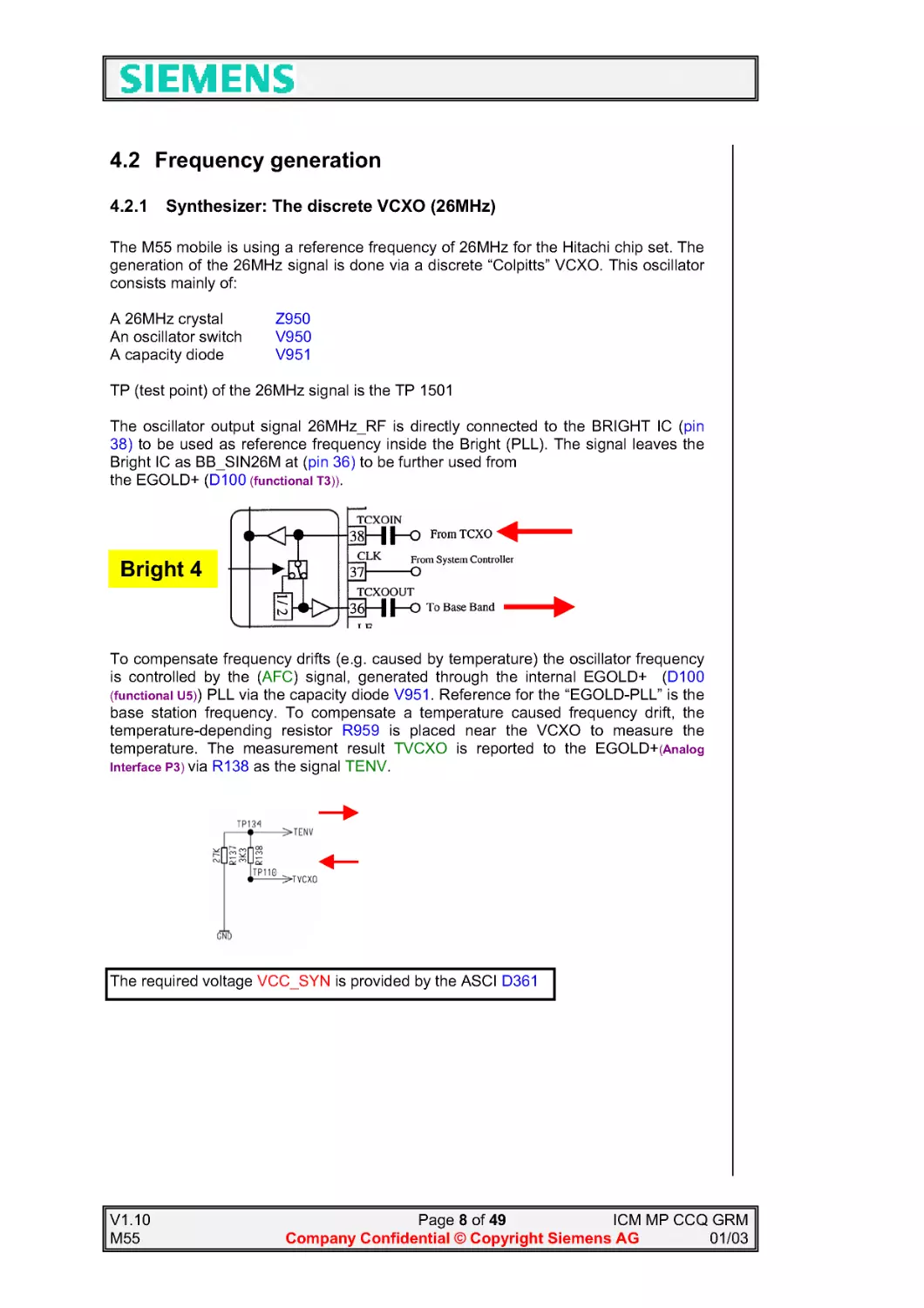
4.2 Frequency generation
4.2.1 Synthesizer: The discrete VCXO (26MHz)
The M55 mobile is using a reference frequency of 26MHz for the Hitachi chip set. The
generation of the 26MHz signal is done via a discrete "Colpitts" VCXO. This oscillator
consists mainly of:
A 26MHz crystal
Z950
An oscillator switch V950
A capacity diode
V951
TP (test point) of the 26MHz signal is the TP 1501
The oscillator output signal 26MHz_RF is directly connected to the BRIGHT IC (pin
38) to be used as reference frequency inside the Bright (PLL). The signal leaves the
Bright IC as BB_SIN26M at (pin 36) to be further used from
the EGOLD+ (D100 (functional T3)).
To compensate frequency drifts (e.g. caused by temperature) the oscillator frequency
is controlled by the (AFC) signal, generated through the internal EGOLD+ (D100
(functional U5)) PLL via the capacity diode V951. Reference for the "EGOLD-PLL" is the
base station frequency. To compensate a temperature caused frequency drift, the
temperature-depending resistor R959 is placed near the VCXO to measure the
temperature. The measurement result TVCXO is reported to the EGOLD+(Analog
Interface P3) via R138 as the signal TENV.
The required voltage VCC_SYN is provided by the ASCI D361
Bright 4
V1.10
Page9of49
ICM MP CCQ GRM
M55
Company Confidential © Copyright Siemens AG
01/03
Circuit diagram
from EGOLD
to Bright IC
V1.10
Page 10 of 49
ICM MP CCQ GRM
M55
Company Confidential © Copyright Siemens AG
01/03
4.2.2 Synthesizer: LO1
The first local oscillator is needed to generate frequencies which enables the
transceiver IC to demodulate the receiver signal and to perform the channel selection
in the TX part. To do so, a control voltage for the LO1 is used. Gained by a
comparator. (located inside the Transceiver (Bright -IC)). This control voltage is a
result of the comparison of the divided LO1 and the 26MHz reference Signal. The
division ratio of the dividers is programmed by the EGOLD+, according to the network
channel requirements.
The first local oscillator (LO1) consists of the PLL inside the Bright (D800), an
external loop filter and the VCO (Z850) module. This LO1 circuit generates
frequencies from
3700-3980 MHz for EGSM900
3580-3760 MHz for GSM1800
3860-3980 MHz for GSM1900
Formula to calculate the TX frequencies:
EGSM900
Channel: 975...1023/76...92 = (Channel freq. + 82MHz) * 4
Channel: 0...75/93...124
= (Channel freq. + 80MHz) * 4
GSM1800
Channel: 512...661
= (Channel freq. + 80MHz) * 2
Channel: 662...885
= (Channel freq. + 82MHz) * 2
GSM1900
Channel: 512...810
= (Channel freq. + 80MHz) * 2
Formula to calculate the RX frequencies:
EGSM900 = Channel freq. * 4
GSM1800 = Channel freq. * 2
GSM1900 = Channel freq. * 2
26MHz
V1.10
Page 11 of 49
ICMMPCCQG M
M55
Company Confidential © Copyright Siemens AG
013
The VCO (Z850) is switched on by the EGOLD+ signal PLLON (TDMA-Timer F16) via
V850 and therefore supplied with VCC2_8. The VCO guarantees by using the control
voltage at pin5 a coverage of the EGSM900, GSM1800 and GSM1900 frequency
band and frequency stability. The Bright gained control voltage passes on the way to
the VCO a discreet loop filter (typical value from 0,5 -- 2,1V).
The channel programming of the PLL happens via the EGOLD+ signals RFDATA;
RFCLK; RFSTR. (RF Control J15, J16, J17). If the Bright IC gets via the same signals a
GSM1800 channel information, the VCO is switched to this frequency by Pin 42 Bright
(Pin 3 VCO).
For GSM900 - RX = "low signal" for channel 975-49
= "high signal" for channel 50-124
- TX = "high signal" for all channels
For GSM1800 - RX = "low signal" for all channels
- TX = "low signal" for all channels
For GSM1900 - RX = "high signal" for all channels
- TX = "high signal" for all channels
The VCO output signal passes the "Balun" transformer (Z851) with insertion losses of
~ 2dB to arrive at the Bright IC.
The required voltage VCC8_8 is provided by the ASIC D361
Circuit diagram
Balun transformer
from EGOLD+
26MHz
Bright 4
V1.10
Page 12 of 49
ICM MP CCQ GRM
M55
Company Confidential © Copyright Siemens AG
01/ 3
VCO
4.2.3 Synthesizer: LO2
The second local oscillator is required for transmitter operations only. It consists of a
PLL and a VCO which are integrated inside the Bright 4, and an external second order
loopfilter (R831; C830; C832). Before the VCO generated 640 or 656MHz signal
arrives at the modulator, it is divided by 8. So the resulting frequency after the IQ
modulator is 80/82MHz (depending on channel and band). Programming of the LO2
PLL is done in the same way as described at the LO1. The tree-wire-bus (EGOLD+
signals RFDATA; RFCLK; RFSTR. (RF Control J15, J16, J17) is used. To ensure the
frequency stability, the 640MHz VCO signal is compared by the phase detector of the
2nd PLL with the 26MHz reference signal. The resulting control signal passes the
external loop filter and is used to control the 640/656MHz VCO.
The required voltage VCC_SYN is provided by the ASIC D361
Circuit diagram
Loop-filter LO2
TOP
View
V1.10
Page 13 of 49
ICM MP CCQ GRM
M55
Company Confidential © Copyright Siemens AG
01/03
4.2.4 Synthesizer: PLL
PLL as a part of the BRIGHT IC
Blockdiagram
V1.10
Page 14 of 49
ICM MP CCQ GRM
M55
Company Confidential © Copyright Siemens AG
01/03
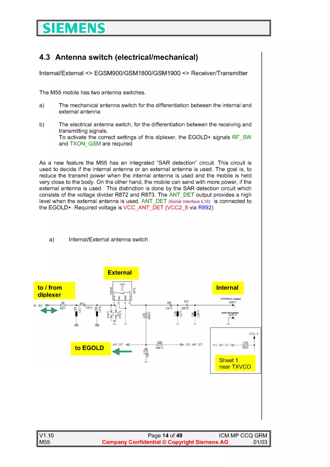
4.3 Antenna switch (electrical/mechanical)
Internal/External <> EGSM900/GSM1800/GSM1900 <> Receiver/Transmitter
The M55 mobile has two antenna switches.
a) The mechanical antenna switch for the differentiation between the internal and
external antenna
b) The electrical antenna switch, for the differentiation between the receiving and
transmitting signals.
To activate the correct settings of this diplexer, the EGOLD+ signals RF_SW
and TXON_GSM are required
As a new feature the M55 has an integrated "SAR detection" circuit. This circuit is
used to decide if the internal antenna or an external antenna is used. The goal is, to
reduce the transmit power when the internal antenna is used and the mobile is held
very close to the body. On the other hand, the mobile can send with more power, if the
external antenna is used. This distinction is done by the SAR detection circuit which
consists of the voltage divider R872 and R873. The ANT_DET output provides a high
level when the external antenna is used. ANT_DET (Serial Interface L16) is connected to
the EGOLD+. Required voltage is VCC_ANT_DET (VCC2_8 via R892)
a) Internal/External antenna switch
to / from
diplexer
Internal
to EGOLD
External
Sheet 1
near TXVCO
V1.10
Page 15 of 49
ICM MP CCQ GRM
M55
Company Confidential © Copyright Siemens AG
01/03
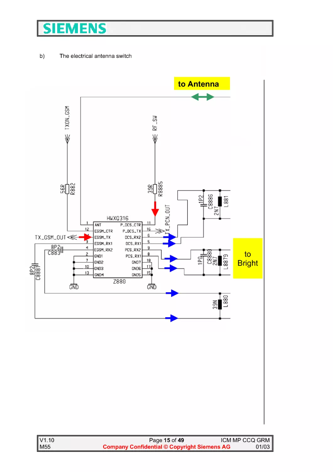
b) The electrical antenna switch
to
Bright
to Antenna
V1.10
Page 16 of 49
ICM MP CCQ GRM
M55
Company Confidential © Copyright Siemens AG
01/03
Z880
Top View
V1.10
Page 17 of 49
ICM MP CCQ GRM
M55
Company Confidential © Copyright Siemens AG
01/03
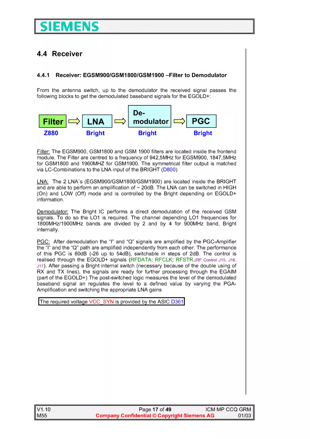
4.4 Receiver
4.4.1 Receiver: EGSM900/GSM1800/GSM1900 --Filter to Demodulator
From the antenna switch, up to the demodulator the received signal passes the
following blocks to get the demodulated baseband signals for the EGOLD+:
Z880
Bright
Bright
Bright
Filter: The EGSM900, GSM1800 and GSM 1900 filters are located inside the frontend
module. The Filter are centred to a frequency of 942,5MHz for EGSM900, 1847,5MHz
for GSM1800 and 1960MHZ for GSM1900. The symmetrical filter output is matched
via LC-Combinations to the LNA input of the BRIGHT (D800)
LNA: The 2 LNA´s (EGSM900/GSM1800/GSM1900) are located inside the BRIGHT
and are able to perform an amplification of ~ 20dB. The LNA can be switched in HIGH
(On) and LOW (Off) mode and is controlled by the Bright depending on EGOLD+
information.
Demodulator: The Bright IC performs a direct demodulation of the received GSM
signals. To do so the LO1 is required. The channel depending LO1 frequencies for
1800MHz/1900MHz bands are divided by 2 and by 4 for 900MHz band, Bright
internally.
PGC: After demodulation the "I" and "Q" signals are amplified by the PGC-Amplifier
the "I" and the "Q" path are amplified independently from each other. The performance
of this PGC is 80dB (-26 up to 54dB), switchable in steps of 2dB. The control is
realised through the EGOLD+ signals (RFDATA; RFCLK; RFSTR.(RF Control J15, J16,
J17). After passing a Bright internal switch (necessary because of the double using of
RX and TX lines), the signals are ready for further processing through the EGAIM
(part of the EGOLD+) The post-switched logic measures the level of the demodulated
baseband signal an regulates the level to a defined value by varying the PGA-
Amplification and switching the appropriate LNA gains
The required voltage VCC_SYN is provided by the ASIC D361
Filter
LNA
PGC
De-
modulator
V1.10
Page 18 of 49
ICM MP CCQ GRM
M55
Company Confidential © Copyright Siemens AG
01/03
Circuit diagram
from LO1
to EGOLD+
progr. signals
from
antenna
V1.10
Page 19 of 49
ICM MP CCQ GRM
M55
Company Confidential © Copyright Siemens AG
01/03
4.4.2 IC Overview
IC Overview
BRIGHT IV
V1.10
Page 20 of 49
ICM MP CCQ GRM
M55
Company Confidential © Copyright Siemens AG
01/03
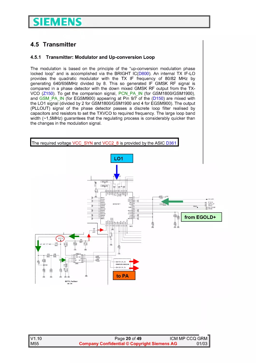
4.5 Transmitter
4.5.1 Transmitter: Modulator and Up-conversion Loop
The modulation is based on the principle of the "up-conversion modulation phase
locked loop" and is accomplished via the BRIGHT IC(D800). An internal TX IF-LO
provides the quadratic modulator with the TX IF frequency of 80/82 MHz by
generating 640/656MHz divided by 8. This so generated IF GMSK RF signal is
compared in a phase detector with the down mixed GMSK RF output from the TX-
VCO (Z150). To get the comparison signal, PCN_PA_IN (for GSM1800/GSM1900),
and GSM_PA_IN (for EGSM900) appearing at Pin 9/7 of the (D150) are mixed with
the LO1 signal (divided by 2 for GSM1800/GSM1900 and 4 for EGSM900). The output
(PLLOUT) signal of the phase detector passes a discrete loop filter realised by
capacitors and resistors to set the TXVCO to required frequency. The large loop band
width (~1,5MHz) guarantees that the regulating process is considerably quicker than
the changes in the modulation signal.
The required voltage VCC_SYN and VCC2_8 is provided by the ASIC D361
to PA
from EGOLD+
LO1
V1.10
Page 21 of 49
ICM MP CCQ GRM
M55
Company Confidential © Copyright Siemens AG
01/03
4.5.2 Transmitter: Power Amplifier
The output signals (PCN_PA_IN , and GSM_PA_IN) from the TX-VCO are led to the
power amplifier (Z900) passing a matching circuit. The PA is a "two in one" PA (one
for EGSM 900 and one for GSM1800 and GSM 1900) and is connected directly to
BATT+. The band selection switching is done via GSM_ON from the Bright IC. After
amplification, a part of the output signals (TX_PCN_OUT and TX_GSM_OUT) is
decoupled via a directional coupler. The other part runs through the antenna switch
(Z880) inside the FEM and the antenna connector (X870) to the antenna. The
decoupled part is equalised by the detector diode (V920) and used from the RF-Power
Regulator IC (D920) to get a PA control voltage, by comparing this voltage with the
PA_RAMP signal provided from the EGOLD+ (analogue interface J2). The (N920) is
activated through the signal TXON1. TXONPA enables with a "high" signal the output
"a" (pin 4).
The required voltage BATT+ is provided by the battery.
The required voltage VCC2 8 is provided by the ASIC D361.
Blockdiagram of LML240 (PA control IC)
Vd
Vd
Vs
Vd
Vd
Vs
Vd
Vs
Comp
Comp
Out
Out
Vs
Vd
BS
PA_ON
Gn
TC
Ra
Vr
Vf
Vho
12345
109876
Top
view
to Ant.
connector
from TX-
VCO
V1.10
Page 22 of 49
ICM MP CCQ GRM
M55
Company Confidential © Copyright Siemens AG
01/03
5 Logic / Control
5.1 Overview of Hardware Structure
5.1.1 Logic Block Diagram
5.1.2 Block Diagram M55 Control Part
RF Control
RF-
Part
V1.10
Page 23 of 49
ICM MP CCQ GRM
M55
Company Confidential © Copyright Siemens AG
01/03
21
24
Bus
Interface
Unit
Shared Memory
Dual Port 512 x 16
Keypad
Interface
GSM
TDMA Timer
TAP Controller
JTAG
Boundary Scan
Cipher Unit
A51/52
SIM card
Interface
High Speed
(F=512, D=8/16)
32 kHz
13/26/52 MHz / 32 kHz
78 MHz
Dual Port RAM
1kx16
OCEM
SRAM
256kx8
DSP Timer2
X-Bus
PD-Bus
PROM
1kx16
Boot
Block
confidential
DSP Serial
Comm. Interface /
DAI
RTC
External
Bus & Port
Controller
AFC Unit
Pulse-Carry Mod.
80
Power
Management
DSP Tim er1
Viterbi
HW
Accelerator
ID Register
SSC
SPI
compatible
ASC0
Autobaud
De tect ASC1
6
2
2
Multicore
Debug Support
SEIB
CAPCOM
2x8bit
16
RF Control
8
16
3
GPT1/GPT2
Watchdog
8
CS(4:0)
Interrupt Controller
Osc.
32.768 kHz
Enable Signals to
X- and PD-Bus Peripherals
MCU
C166S
Clock Generation
Peripheral Enable
Generator
Switch Matrix
Battery & Temperature
Measurement
DAC
R-String
GMSK
Modulator
Voiceband
Filters
RX and TX
ΣΔ
ADC
MUX
Baseband
Filter/
Cordic-
Processor
ΣΔ
ADC
ΣΔ
ADC
16 bit I/O Ports
E-GOLD+ V3.0 Architecture
Single Chip Cellular Baseband Processor
RF Output
Power Control
10 bit DAC
Bandgap
reference
voltage
ΣΔ
DAC
12 bit resolution
DAC
R-String
Package: P-LFBGA-208
READY#
NMI#
HOLD#
HLDA#
CLKOUT
RSTOUT#
6
2
2
2
2
2
2
2
2
3
8
3
4
6
P ROM
60kx16
P RAM
4kx16
Y RAM
2kx16
X RAM
15kx16
X ROM
36kx16
Interp./
Noise
Shaper
Interp./
Noise
Shaper
GPRS
Cipher Unit
OAK78 DSP
Interleaving / De-Interleaving
Speech Coding/Decoding
(FR, HR, EFR, AMR)
Level Measurement
Channel Coding/Decoding
(FR, HR, EFR, AMR)
Equalization
Encryption / Decryption
Voice Mem o/Voice Dialing
GPRS support
I2C
2
LM-Bus
I2S
3
MMCI
V5.4
5
4
Logic
Arranger
(LPA)
OCDS
DPEC
Interrupt Controller
5.1.3 EGOLD+
Block Diagram EGOLD+ V3.1
The EGOLD+ contains a 16-bit micro-controller (μC part), a GSM analog Interface
(EGAIM), a DSP computing core (DSP part) and an interface for application-specific
switch-functions.
The μC part consists of the following:
• Micro-controller
• System interfaces for internal and external peripheries
• On-chip peripheries and memory
The Controller Firmware carries out the following functions:
• Control of the Man Machine Interface (keypad, LCD, sensing element, control of
the illumination,...)
• GSM Layer 1,2,3 /GPRS
• Control of radio part (synthesizer, AGC, AFC, Transmitter, Receiver...),
• Control of base band processing (EGAIM)
• Central operating system functions (general functions, chip select logic, HW driver,
control of mobile phones and accessories...).
V1.10
Page 24 of 49
ICM MP CCQ GRM
M55
Company Confidential © Copyright Siemens AG
01/03
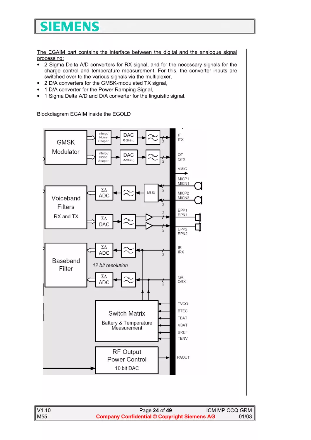
The EGAIM part contains the interface between the digital and the analogue signal
processing:
• 2 Sigma Delta A/D converters for RX signal, and for the necessary signals for the
charge control and temperature measurement. For this, the converter inputs are
switched over to the various signals via the multiplexer.
• 2 D/A converters for the GMSK-modulated TX signal,
• 1 D/A converter for the Power Ramping Signal,
• 1 Sigma Delta A/D and D/A converter for the linguistic signal.
Blockdiagram EGAIM inside the EGOLD
V1.10
Page 25 of 49
ICM MP CCQ GRM
M55
Company Confidential © Copyright Siemens AG
01/03
Measurement of Battery and Ambient Temperature
The battery temperature is measured via the voltage divider R1387, R138 by the
EGOLD+ (Analog Interface P2). For this, the integrated ΣΔ converter of the RX-I base
band branch is used. This ΣΔ converter compares the voltage of TBAT and TENV
internally. Through an analogue multiplexer, either the RX-I base band signal, or the
TBAT signal and the TENV signal is switched to the input of the converter. The signal
MEAS_ON from the EGOLD+(GSM TDMA-TIMER H15) activates the battery voltage
measurement The ambient temperature TENV is measured directly at of the EGOLD+
(Analog Interface P3).
Measurement of the Battery Voltage
The measurement of the battery voltage is done in the Q-branch of the EGOLD+, for
this BATT+ is connected via a voltage divider R143, R146 to the EGOLD+(Analog
Interface P1). An analogue multiplexer does the switching between the baseband signal
processing and the voltage measurement.
V1.10
Page 26 of 49
ICM MP CCQ GRM
M55
Company Confidential © Copyright Siemens AG
01/03
A/D conversion of MIC-Path signals incl. coding
The Microphone signals (MICN2, MIP2, MICP1, MICN1) arrive at the voiceband part
of the EGOLG+. For further operations the signals will be converted into digital
information, filtered, coded and finally formed into the GMSK-Signal by the internal
GMSK-Modulator. This so generated signals (RF_I, RF_IX, RF_Q, RF_QX) are given
to the Bright IC in the transmitter path.
D/A conversion of EP-Path signals incl. decoding
Arriving at the baseband-Part the demodulated signals (RF_I, RF_IX, RF_Q, RF_QX)
will be filtered and A/D converted. In the voiceband part after decoding (with help of
the μC part) and filtering the signals will be D/A converted amplified and given as
(EPP1_FIL, EPN1_FIL) to the Power Supply ASIC.
Generation of the PA Control Signal (PA_RAMP)
The RF output power amplifier needs an analogue ramp up/down control voltage. For
this the system interface on EGOLD+ generates 10 bit digital values which have to be
transferred serially to the power ramping path. After loading into an 10 bit latch the
control value will be converted into the corresponding analogue voltage with a
maximum of ~2V
Key-Value
V1.10
Page 27 of 49
ICM MP CCQ GRM
M55
Company Confidential © Copyright Siemens AG
01/03
The DSP part contains:
• DSP signal processor
• Separate program/data memory
• a hardware block for processing the RX signal,
• a hardware block for "ciphers",
• a hardware block for processing the linguistic signal,
• a hardware block for the "GMSK modulator",
• De-/ interleaving memory,
• Communication memory
• a PLL for processing and reproducing the VCXO pulse signal.
In the DSP Firmware are implemented the following functions:
• scanning of channels, i.e., measurement of the field strengths of neighbouring
base stations
• detection and evaluation of Frequency Correction Bursts
• equalisation of Normal Bursts and Synchronisation Bursts
• channel encoding and soft-decision decoding for fullrate, enhanced-fullrate and
adaptive multirate speech, fullrate and halfrate data and control channels.
• channel encoding for GPRS coding
• fullrate, enhanced fullrate and adaptive multirate speech encoding and decoding
• mandatory sub-functions like
-- discontinuous transmission, DTX
-- voice activity detection
-- background noise calculation
• generation of tone and side tone
• hands-free functions
• support for voice memo
• support for voice dialling
• loop-back to GSM functions
• GSM Transparent Data Services and Transparent Fax
• calculation of the Frame Check Sequence for a RLP frame used for GSM
NonTransparent Data Services
• support of the GSM ciphering algorithm
Real Time Clock (integrated in the EGOLD+):
The real time clock is powered via a separate voltage regulator inside the Power
Supply ASIC. Via a capacitor, data are kept in the internal RAM during a battery
change for at least 30 seconds. An alarm function is also integrated with which it is
possible to switch the phone on and off.
5.1.4 SRAM
Memory for volatile data
Memory Size:
4 Mbit
Data Bus:
16Bit
5.1.5 FLASH
Memory Size:
64Mbit (8 Mbyte)
Data Bus:
16 Bit
5.1.6 SIM
SIM cards with supply voltages of 1.8V and 3V are supported.
V1.10
Page 28 of 49
ICM MP CCQ GRM
M55
Company Confidential © Copyright Siemens AG
01/03
5.1.7 Vibration Motor
The vibration motor is mounted in the lower case. The electrical connection to the
PCB is realised with pressure contacts.
6 Power Supply
6.1 Power Supply ASIC
The power supply ASIC contains the following functions:
• Powerdown-Mode
• Sleep Mode
• Trickle Charge Mode
• Power on Reset
• Digital state machine to control switch on and supervise the μC with a watchdog
• Voltage regulator
• Low power voltage regulator
• Additional output ports
• Voltage supervision
• Temperature supervision with external and internal sensor
• Battery charge control
• TWI interface
• I2C interface
• RC Oscillator
• Audio multiplexer
• Audio amplifier stereo/mono
• 18 bit Sigma/Delta DAC with Clock recovery
• Bandgap reference*
INFO:
* Bandgap reference
The p-n junction of a semiconductor has a bandgap-voltage. This bandgap-voltage is
almost independent of changes in the supply voltage and has a very low temperature
gradient. The bandgap-voltage is used as reference for the voltage regulators.
To reduce the power dissipation of the ASIC and to ensure high efficiency of the
power management concept a DCDC Converter for the Core (EGOLD+V3 Baseband
Chipset), Flash and SRAM supply is used.
The DCDC converter includes the following functions:
• PFM Mode for sleep mode of the Mobile Phone.
• PWM Mode for active mode of the Mobile Phone.
The mode change is controlled by the ASIC with the signal EN_DC_DOWN based on
the EGOLD+ signal VCXO_EN.
V1.10
Page 29 of 49
ICM MP CCQ GRM
M55
Company Confidential © Copyright Siemens AG
01/03
6.1.1 Pinout diagram
V1.10
Page 30 of 49
ICM MP CCQ GRM
M55
Company Confidential © Copyright Siemens AG
01/03
6.1.2 Power Supply Diagram
V1.10
Page 31 of 49
ICM MP CCQ GRM
M55
Company Confidential © Copyright Siemens AG
01/03
6.1.3 Power Supply Operating mode:
- Power Down Mode (mobile is switched off)
In power down mode the current consumption is very low. The inputs for switch on
conditions (ON/OFF PinH2, ON/OFF2 PinJ3, VDD_CHARGE PinC3), the LPREG with
his own voltage reference and POR cells are active. All other blocks are switched off,
so the battery discharging will be kept to a minimum. This is the state when the phone
is switched off.
- Start Up Mode (user switch on, RTC switch on)
"Start Up Mode" can be initiated by ON_OFF (falling edge) or ON_OFF2 (rising edge).
In this mode a sequential start-up, of reference oscillator, voltage supervision and
regulators is controlled by digital part. In case of failure (overvoltage or time out of the
μC reaction), the ASIC shuts down.
-Trickle Charge Mode (to be able to charge the battery)
In case of a rising edge at VDD_CHARGE, the ASIC goes from power down to an
interim state. In this state, the oscillator and the reference are started. If the voltage on
VDD_CHARGE is below the charger detection threshold, the ASIC shuts off. If the
voltage on VDD_CHARGE is high enough the signal EXT_PWR is going to H and the
power up continues. Depending on the voltage of the battery an initial charging of the
battery of the circuit is immediately done. If the Trickle Charge Mode is entered with a
very low battery, the supply for the ASIC itself is generated from the internal VDDREF
regulator. If a failure is detected (overvoltage), the ASIC is switched off.
- Normal Mode (following Start Up Mode or Trickle Charge Mode)
The normal mode is the situation, where the startup has been finished and the ASIC
starts the external μC by changing the signal RESETN from low to high.
Mode: a) Active Mode with full capabilities of all blocks
b) Sleep Mode with reduced capabilities of some blocks and some even not
available at all.
-Active Mode (submode of Normal Mode)
In this mode, the μC controls the charging block and most of the failure cases. The
ASIC can be controlled by the TWI interface, interrupt request can be sent by the
ASIC. Furthermore, the voltages are supervised ( in case of failure the μC will be
informed). In case of watchdog failure, overvoltage or power on request, the ASIC will
be switched off immediately. The mono and the stereo block can be switched on in
active mode.
-Sleep Mode (submode of Normal Mode)
Intention of the mode is to have a limited set of functions available with a reduced
current consumption. A low level at the pin SLEEP1_N will switch from Active Mode to
Sleep Mode. In Sleep Mode all charging functions and supply overvoltage detection
are switched off. LDO undervoltage detection, clock and reference voltages are active.
LDOs are working in low current mode. The battery voltage comparators are available,
the audio block can be switched on.
V1.10
Page 32 of 49
ICM MP CCQ GRM
M55
Company Confidential © Copyright Siemens AG
01/03
6.1.4 Power Supply Functions:
- Power on Reset
To guarantee a defined startup, the ASIC will be reset by a Power on Reset block.
After Power on Reset the ASIC will enter the power done Mode. If the thresholds will
be reached during operating mode the reset will become the device enters the power
down mode. This blocks are always active and will be supplied by VDDREF.
- Switch on and watchdog
There are 3 different possibilities to switch on the phone via external pins:
-VDD_CHARGE with rising edge
-ON/OFF with falling edge
-ON/OFF2 with rising edge
In order to guarantee a defined start-up behavior of the external components, a
sequential power up is used and the correct start up of blocks is supervised. In normal
mode, a continues watchdog signal from the μC is needed to keep the system
running. If this signals fails, the ASIC will switch to power down mode.
It must be guaranteed, that each start up condition does not interfere and block the
other possible start up signals. In case of failure during start up, the device will go
back to power down mode. To guarantee that the connection of the a charging unit
with a very low battery is detected, this detection must work level sensitive at the end
of POR signal.
V1.10
Page 33 of 49
ICM MP CCQ GRM
M55
Company Confidential © Copyright Siemens AG
01/03
- Watchdog monitoring
As soon as the first Watchdog_μC pin rising is detected , the device start the
watchdog monitoring procedure. Standard switch off of the phone is the watchdog.
The first edge of watchdog is rising. If a falling edge is detected ass the first transient
the device will go to power down mode again and the whole phone is switched off.
Rising and falling edges must be detected alternated. With any edge on
Watchdog_μC pin a counter will be loaded. The next -- compared to the previous edge
-- inverted edge must occur between end of TA0,TA1 and end of TB0,TB1. If the
signal occurs before end of TA0, TA1 or is not detected until end of TB0, TB1, the
device will go to power down mode immediately after the violation of the WD criteria
occurs.
TA0, TA1 ~ 0.4 sec
TB0,TB1~3sec
V1.10
Page 34 of 49
ICM MP CCQ GRM
M55
Company Confidential © Copyright Siemens AG
01/03
6.2 Battery
As a standard battery a LiIon battery with a nominal capacity of 3,7 Volt/700mAh is
used.
6.3 Charging Concept
6.3.1.1 Charging Concept
General
The battery is charged in the unit itself. The hardware and software is designed for
LiIon with 4.2V technology.
Charging is started as soon as the phone is connected to an external charger. If the
phone is not switched on, then charging takes place in the background (the customer
can see this via the "Charge" symbol in the display). During normal use the phone is
being charged (restrictions: see below).
Charging is enabled via a PMOS switch in the phone. This PMOS switch closes the
circuit for the external charger to the battery. The EGOLD+ takes over the control of
this switch depending on the charge level of the battery, whereby a disable function in
the POWER SUPPLY ASIC hardware can override/interrupt the charging in the case
of over voltage of the battery (only for Manganese Chemistry Battery types e.g. NEC).
With the new slim Lumberg IO connector we lose the charger recognition via SB line.
Now we measure the charge current inside the POWER SUPPLY ASIC with a current
monitor.
The charging software is able to charge the battery with an input current within the
range of 350-600mA. If the Charge-FET is switched off, then no charging current will
flow into the battery (exception is trickle charging, see below).
For controlling the charging process it is necessary to measure the ambient (phone)
temperature and the battery voltage. The temperature sensor will be an NTC resistor
with a nominal resistance of 22kΩ at 25°C. The determination of the temperature is
achieved via a voltage measurement on a voltage divider in which one component is
the NTC. The NTC for the ambient temperature will be on the PCB (26 MHz part).
Charging current
Charging control signal
V1.10
Page 35 of 49
ICM MP CCQ GRM
M55
Company Confidential © Copyright Siemens AG
01/03
Measurement of Battery, Battery Type and Ambient Temperature
The voltage equivalent of the temperature and battery code on the voltage separator
will be calculated as the difference against a reference voltage of the EGOLD. For
this, the integrated ΣΔ converter in the EGOLD of the RX-I base band branch will be
used. Via an analogue multiplexer, either the RX-I base band signal, the battery code
voltage or the ambient temperature voltage can be switched over to the input of the
converter. The 1-Bit data stream of the converter will be subjected to a data reduction
via the DSP circuit so that the measured voltage (for battery and ambient
temperature) will be available at the end as a 10-bit data word.
Measurement of the Battery Voltage
Analogue to the I-branch either the RX-Q base band signal or the battery voltage can
be measured in the Q-branch. Processing in the DSP circuit will be done analogue to
the I-branch. The EGOLD will be specified internally at voltage measurement input
BATT+ for an input voltage of 3V...4.5V.
V1.10
Page 36 of 49
ICM MP CCQ GRM
M55
Company Confidential © Copyright Siemens AG
01/03
Timing of the Battery Voltage Measurement
Unless the battery is charging, the measurement is made in the TX time slot. During
charging it will be done after the TX time slot. At the same time, either the battery
temperature (in the I-branch) and the battery voltage (in the Q-branch) or the ambient
temperature in the I-branch can be measured (the possibility of measurement in the
Q-branch, the analogue evaluation of the battery coding, is used for HW-Coding).
Other combinations are not possible. For the time of the measurement the multiplexer
in the EGAIM must be programmed to the corresponding measurement.
Recognition of the Battery Type
The battery code is a resistor with a resistance depending on the manufacturer.
Charging Characteristic of Lithium-Ion Cells
LiIon batteries are charged with a U/I characteristic, i.e. the charging current is
regulated in relation to the battery voltage until a minimal charging current has been
achieved. The maximum charging current is approx. 600mA, minimum about 100mA.
The battery voltage may not exceed 4.2V ±50mV average. During the charging pulse
current the voltage may reach 4.3V. The temperature range in which charging of the
phone may be started ranges from 5...40°C, and the temperature at which charging
takes place is from 0...45°C. Outside this range no charging takes place, the battery
only supplies current.
Trickle Charging
The POWER SUPPLY ASIC is able to charge the battery at voltages below 3.2V
without any support from the charge SW. The current will by measured indirectly via
the voltage drop over a shunt resistor and linearly regulated inside the POWER
SUPPLY ASIC. The current level during trickle charge for voltages <2.8V is in a range
of 20-50mA and in a range of 50-100mA for voltages up to 3.75V. To limit the power
dissipation of the dual charge FET the trickle charging is stopped in case the output
voltage of the charger exceeds 10 Volt. The maximum trickle time is limited to 1 hour.
As soon as the battery voltage reaches 3.2 V the POWER SUPPLY ASIC will switch
on the phone automatically and normal charging will be initiated by software (note the
restrictions on this item as stated below).
Normal Charging
For battery voltages above 3.2 Volt and normal ambient temperature between 5 and
40°C the battery can be charged with a charge current up to 1C*. This charging mode
is SW controlled and starts if an accessory (charger) is detected with a supply voltage
above 6.4 Volt by the POWER SUPPLY ASIC. The level of charge current is
limited/controlled by the accessory or charger.
USB Charging
For battery voltages above 3.2 Volt and normal Temperature between 5 and 40°C the
battery can be charged with a charge current up to 1C. This charging mode is SW
controlled and starts if an accessory (charger) with a supply voltage between 3.6 and
5.4 Volt is detected by the POWER SUPPLY ASIC during active mode of the phone.
To enable this charging mode, the mobile phone must be registered (logged on) to a
USB Host. The Charge-Only and Trickle-Charge Mode is not supported because of
USB Spec. restrictions. The charge current is controlled by the POWER SUPPLY
ASIC.
INFO:
* C-rate
The charge and discharge current of a battery is measured in C-rate. Most portable
batteries, are discharge with 1C. A discharge of 1C draws a current equal to the
battery capacity. For example, a battery value of 1000mAh provides 1000mA for one
hour if discharged at 1C. The same battery discharged at 0.5C provides 500mAfor two
hours. At 2C, the same battery delivers 2000mA for 30 minutes. 1C is often referred to
as a one-hour discharge; a 0.5 would be a two-hour, and a 0.1C a 10 hour discharge.
V1.10
Page 37 of 49
ICM MP CCQ GRM
M55
Company Confidential © Copyright Siemens AG
01/03
Restrictions
• A battery which has completely run down can not be re-charged quickly because
the battery voltage is less than 3.0V and the logic which implements the charge
control cannot be operated at this low voltage level. In this case the battery is
recharged via trickle-charging. However, the charging symbol cannot be shown in
the display because at this time logic supply voltages are not operating. The
charging time for this trickle-charging (until the battery can be fast-charged from
then on) is in the range of 1 hour. If, within this time, the battery voltage exceeds
3.2V, then the POWER SUPPLY ASIC switches on the mobile and charging
continues in the Charge-Only Mode. In some circumstances it can happen that
after trickle-charging and the usually initiated switch-on procedure of the mobile,
the supply voltage collapses so much that the mobile phone switches off again. In
this case trickle charging starts again with a now raised threshold voltage of 3.75V
instead of 3.2V, at maximum for 20 minutes. The POWER SUPPLY ASIC will retry
switching on the phone up to 3 times (within 60 minutes overall).
• Charging the battery will not be fully supported in case of using old accessory
(generation '45' or earlier). It is not recommended to use any cables that adapt
"old" to "new" Lumberg connector. Using such adapters with Marlin will have at
least the following impact:
1) half-sine wave chargers (e.g. P35 & home station) can not be used for trickle
charging
2) normal charging might be aborted before the battery is fully charged
3) EMC compliance can not be guaranteed
• A phone with a fully charged LiIon battery will not be charged immediately after
switch-on. Any input current would cause an increase of the battery voltage above
the maximum permissible value. As soon as the battery has been discharged to a
level of about 95% (due to current consumption while use), it will be re-charged in
normal charging mode.
• The phone cannot be operated without a battery.
• The phone will be destroyed if the battery is inserted with reversed polarity:
• ⇒ design-wise it is impossible to wrongly pole the phone. This is prevented by
mechanical means.
• ⇒ electrically, a correctly poled battery is presumed, i.e. correct polarity must be
guaranteed by suitable QA measures at the supplier
• The mobile phone might be destroyed by connecting an unsuitable charger:
• ⇒ a charger voltage >15V can destroy resistances or capacitors
• ⇒ a charger voltage >20V can destroy the switch transistor of the charging circuit
In case the transistor fails the ASIC will be destroyed. In the case of voltages lower
than 15V and an improper current limitation the battery might be permanently
damaged. A protection against grossly negligent use by the customer (e.g. direct
connection of the charge contact to the electricity supply in a motor car) is not
provided. Customer safety will not be affected by this restriction.
V1.10
Page 38 of 49
ICM MP CCQ GRM
M55
Company Confidential © Copyright Siemens AG
01/03
7 Interfaces
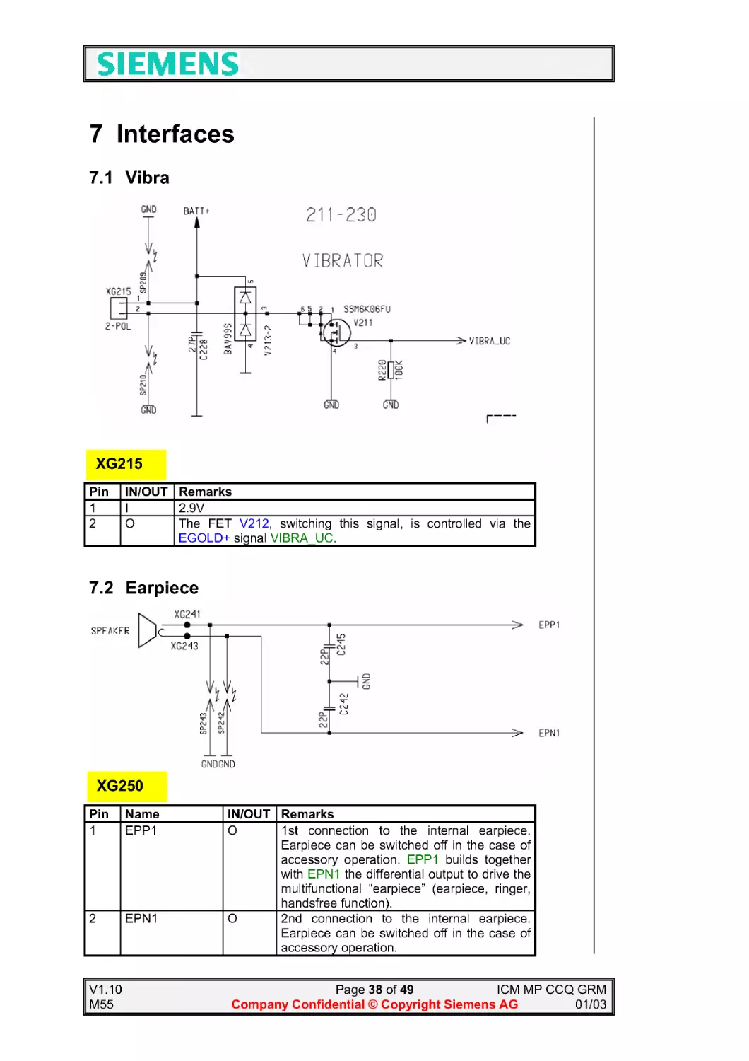
7.1 Vibra
Pin IN/OUT Remarks
1I
2.9V
2O
The FET V212, switching this signal, is controlled via the
EGOLD+ signal VIBRA_UC.
7.2 Earpiece
Pin Name
IN/OUT Remarks
1 EPP1
O
1st connection to the internal earpiece.
Earpiece can be switched off in the case of
accessory operation. EPP1 builds together
with EPN1 the differential output to drive the
multifunctional "earpiece" (earpiece, ringer,
handsfree function).
2 EPN1
O
2nd connection to the internal earpiece.
Earpiece can be switched off in the case of
accessory operation.
XG215
XG250
V1.10
Page 39 of 49
ICM MP CCQ GRM
M55
Company Confidential © Copyright Siemens AG
01/03
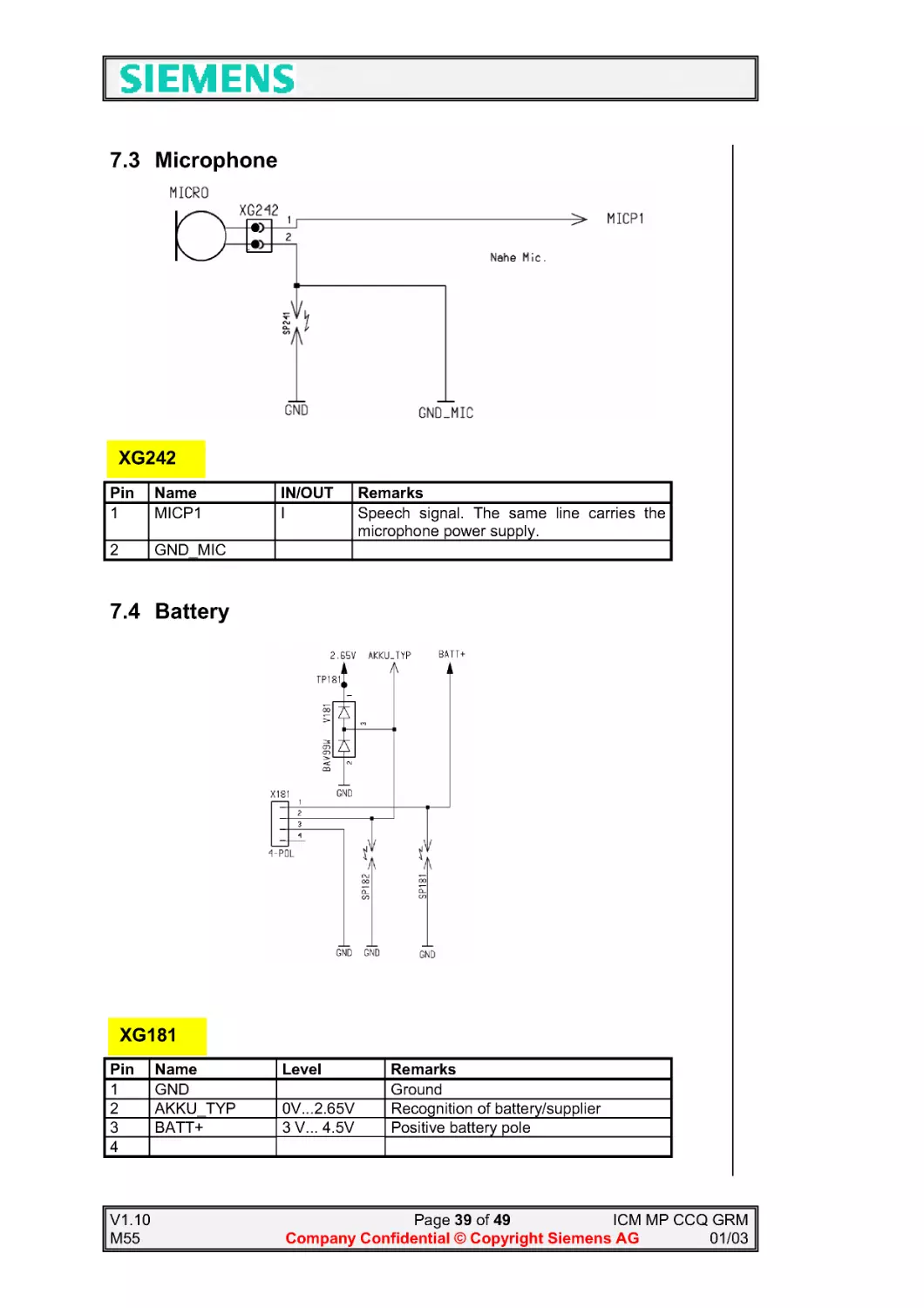
7.3 Microphone
Pin Name
IN/OUT Remarks
1 MICP1
I
Speech signal. The same line carries the
microphone power supply.
2 GND_MIC
7.4 Battery
Pin Name
Level
Remarks
1 GND
Ground
2 AKKU_TYP
0V...2.65V Recognition of battery/supplier
3 BATT+
3 V... 4.5V Positive battery pole
4
XG242
XG181
V1.10
Page 40 of 49
ICM MP CCQ GRM
M55
Company Confidential © Copyright Siemens AG
01/03
7.5 IO Connector with ESD protection
7.5.1 IO Connector -- New Slim Lumberg
Pin Name
IN/OUT Notes
1 POWER I/O POWER is needed for charging batteries and for supplying
the accessories. If accessories are supplied by mobile,
talk-time and standby-time from telephone are reduced.
Therefore it has to be respected on an as low as possible
power consumption in the accessories.
2 GND
3TX
O
Serial interface
4RX
I
serial interface
5 DATA/CTS I/O Data-line for accessory-bus
Use as CTS in data operation.
6 RTS
I/O Use as RTS in data-operation.
7 CLK/DCD I/O Clock-line for accessory-bus.
Use as DTC in data-operation.
8 AUDIO_L Analog
O
driving ext. left speaker
With mono-headset Audio_L and Audio_R differential
mode
910 AUDIO_R Analog
O
driving ext. right speaker With mono-headset Audio_L and
Audio_R differential Signal
11 GND_MIC Analog
I
for ext. microphone
12 MICP2
Analog
I
External microphone
V1.10
Page 41 of 49
ICM MP CCQ GRM
M55
Company Confidential © Copyright Siemens AG
01/03
7.5.2 ESD Protection with EMI filter
The Z211 is a 5-channel filter with over-voltage and ESD Protection array which is
designed to provide filtering of undesired RF signals in the 800-4000MHz frequency
band Additionally the Z211 contains diodes to protect downstream components from
Electrostatic Discharge (ESD) voltages up to 8 kV.
Pin configuration of the Z211
Z211 Circuit Configuration
V1.10
Page 42 of 49
ICM MP CCQ GRM
M55
Company Confidential © Copyright Siemens AG
01/03
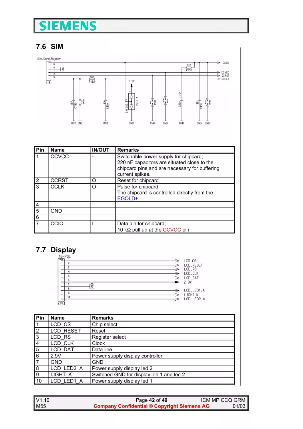
7.6 SIM
Pin Name
IN/OUT Remarks
1 CCVCC
-
Switchable power supply for chipcard;
220 nF capacitors are situated close to the
chipcard pins and are necessary for buffering
current spikes.
2 CCRST
O
Reset for chipcard
3 CCLK
O
Pulse for chipcard.
The chipcard is controlled directly from the
EGOLD+.
45 GND
67 CCIO
I
Data pin for chipcard;
10 kΩ pull up at the CCVCC pin
7.7 Display
Pin Name
Remarks
1 LCD_CS
Chip select
2 LCD_RESET Reset
3 LCD_RS
Register select
4 LCD_CLK
Clock
5 LCD_DAT
Data line
6 2.9V
Power supply display controller
7 GND
GND
8 LCD_LED2_A Power supply display led 2
9 LIGHT_K
Switched GND for display led 1 and led 2
10 LCD_LED1_A Power supply display led 1
V1.10
Page 43 of 49
ICM MP CCQ GRM
M55
Company Confidential © Copyright Siemens AG
01/03
8 Acoustic
The buzzer and the keypad clicks will be realized over the earpiece. At normal buzzer
the signaling will realized with swelling tones. At the same time a maximum sound
pressure level in the coupler of 135 +/- 5dB(A) is fixed.
The standard sounds will be generated by the EGOLD+, the advanced sounds will be
generated via firmware running on the DSP.
8.1 Microphone
8.1.1 Mechanical
The microphone is built in the Mounting Frame Lower Part and is mechanically fixed
with a rubber seal (gasket). The contact on the PCB is realised via spiral springs,
which are integrated in the gasket. Because of usage of Unidirectional Microphone,
the gasket has a front- and a back sound-inlet hole. The front sound-inlet is
acoustically tighten connected with a sound-inlet at the rear-side of the mounting
frame lower part. The back sound-inlet is acoustically tighten connected with a sound-
inlet at the bottom-side of the mounting frame lower part. The gasket of the
microphone has a asymmetrical shape in order to provide non-rotating, guaranteed
covering of the sound-inlets of mounting frame lower part to the corresponding sound-
inlets at microphone gasket.
8.1.2 Electrical
Both Microphones are directly connected to the EGOLD+.(Analog Interface G2, F1-G3, H2)
via the signals MICN1, MICP1 (Internal Microphone )and MICN2, MICP2 (External
Microphone/Headset). Power supply for the Microphone is VMIC (EGOLD+.(Analog
Interface G1))
V1.10
Page 44 of 49
ICM MP CCQ GRM
M55
Company Confidential © Copyright Siemens AG
01/03
8.2 Earpiece/Loudspeaker
8.2.1 Mechanical
The speakermodule is designed to provide optimal performance for mobile handsfree
and sound ringer. Plus independent from mobile leakage sound performance.
Therefore speakermodule is a system that has a closed front volume with sound-
outlets towards the ear of the user. Backvolume of Speakermodule is using the
unused air between the antenna and the PCB. Backvolume is just used for resonance,
there is no sound output from backvolume. The speakermodule is glued to the
lightguide and contacted via two bending springs to the PCB. The lightguide itself is
screwed with six screws via the PCB to the mounting frame lower part. Two of the six
screws are located besides of the connection of speakermodule and lightguide.
Therefore a good and reliable connection between speakermodule and PCB should
be provided.
8.2.2 Electrical
The internal and external Loudspeaker (Earpiece) is connected to the voiceband part
of the EGOLD+ (Analog Interface B1, C1) via audio amplifier inside the ASIC (D361). Input
EPN1_FIL - EPP1_FIL. Output for external loudspeaker AUDIO_L - AUDIO_R, for
internal Loudspeaker EPP! -- EPN1. The ringing tones are generated with the
loudspeaker too. To activate the ringer, the signal RINGIN from the EGOLD+
(Miscellaneous,D16) is used
EGOLD+
from Bright
IC
to ASIC
V1.10
Page 45 of 49
ICM MP CCQ GRM
M55
Company Confidential © Copyright Siemens AG
01/03
9 Display and Illumination
9.1 Display
The display is provided with 2,9V from the ASIC (D361). The communication with the
EGOLD+ by the LCD-Signals, directly connected to the EGOLD+
9.2 Illumination
The light is switched via switches inside the EGOLD+. With the signal LIGHT_UC
(Miscellaneous T17) the illumination for the keyboard and the display backlight is
controlled. With LIGHT_OFF_N. (GSM TDMA-Timer G15) the illumination can be switched
"on" and "off" during the TX timeslot.
Placed on the MMI Board
V1.10
Page 46 of 49
ICM MP CCQ GRM
M55
Company Confidential © Copyright Siemens AG
01/03
9.3 Light Night
The Night light is switched via the signal LIGHT_NIGHT_U (upper LEDs) and
LIGHT_NIGHT_L (lower LEDs). The Dynamic Light illumination is controlled via the
EGOLD+. (LIGHT_NIGHT_U --GSM TDMA-Timer G15 / LIGHT_NIGHT_L --RF -Control K14)
V1.10
Page 47 of 49
ICM MP CCQ GRM
M55
Company Confidential © Copyright Siemens AG
01/03
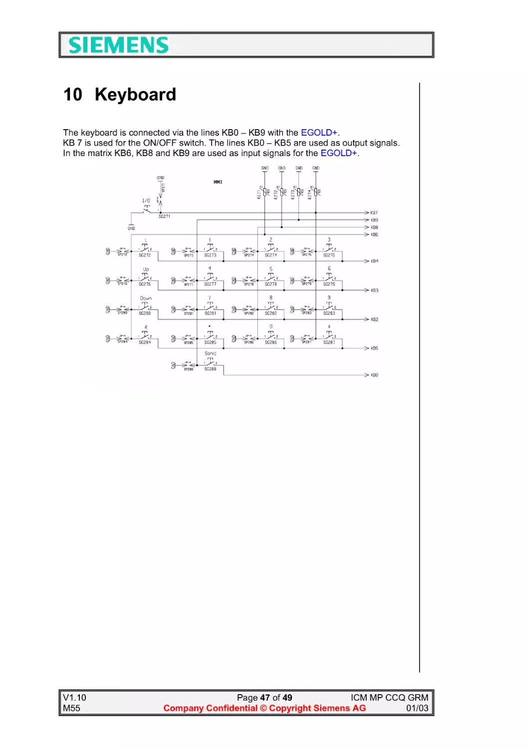
10 Keyboard
The keyboard is connected via the lines KB0 -- KB9 with the EGOLD+.
KB 7 is used for the ON/OFF switch. The lines KB0 -- KB5 are used as output signals.
In the matrix KB6, KB8 and KB9 are used as input signals for the EGOLD+.