/


Теги: service manual electrical engineering electronics manual
Год: 1994


Текст
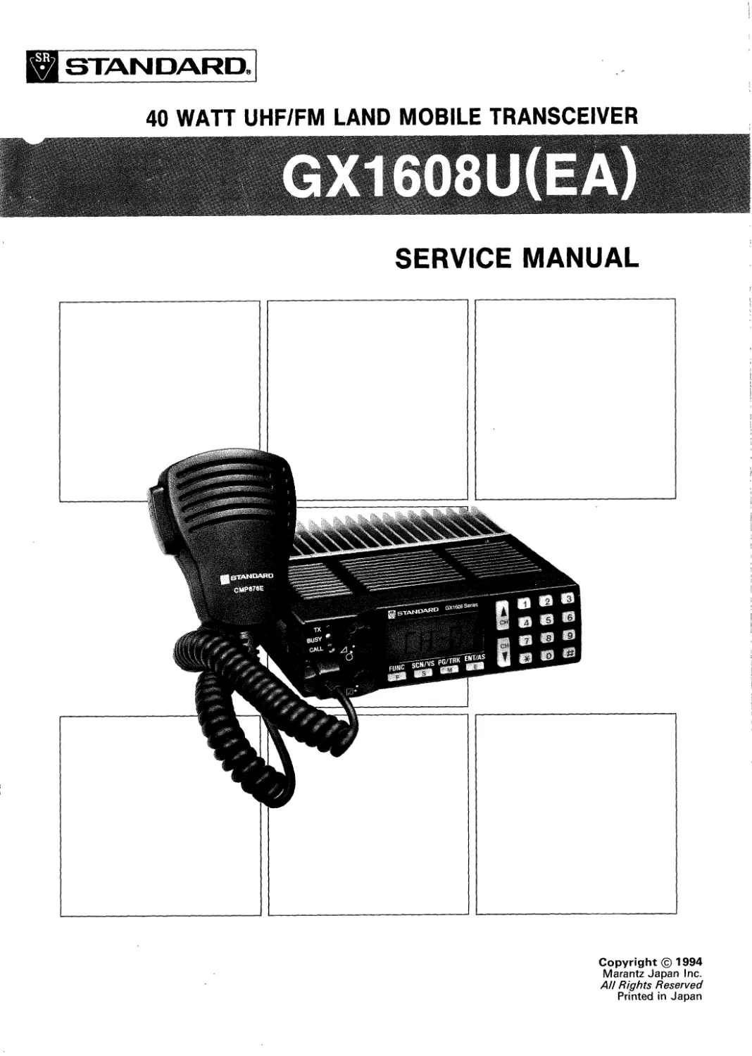
                    STANDARD,
40 WATT UHF/FM LAND MOBILE TRANSCEIVER
SERVICE MANUAL
Copyright © 1994
Marantz Japan Inc.
AH Rights Reserved
Printed in Japan
1. CONTROLS AND CONNECTIONS
•TES.
1.1 Front Panel
Figure 1-1 Front Panel
®CALL INDICATOR
In the paging mode, this indicator lights upon
entering the squelch defeat state. The squelch
defeat state is the state in which DTMF mute is
cancelled and communication is possible.
©TRANSMISSION INDICATOR
Lights when the transceiver is transmitting.
©RECEPTION INDICATOR
Lights when the transceiver is receiving.
©POWER SWITCH/VOLUME CONTROL
Turning all the way in the counterclockwise direc-
tion switches off the power to the transceiver.
Turning in the clockwise direction switches on the
power. When the power is on, turning further in the
clockwise direction increases the volume.
©LCD DISPLAY
©UP ( ▲) KEY
Increases the channel, programming mode, or tun-
ing mode.
©10 KEY
Carries out direct input or programming of the
DTMF code.
©DOWN ( ▼) KEY
Decreases the channel, programming mode, or
tuning mode.
©ENTER (E) KEY
Scans the priority channel.
Pressing for 1.5 seconds or longer allows the
priority channel to be set. Also used to confirm
entered data during programming and alignment.
Pressing this key together with the F key causes the
transceiver to enter the cloning setting mode.
©MONITOR (M) KEY
Pressing this key cancels squelch.
Pressing this key together with the F key causes the
transceiver to enter the paging mode.
©SCAN (S) KEY
Pressing this key causes the scan operation to
begin.
Holding it down allows scan memory to be set on
and off.
Pressing this key together with the F key allows use
of the voice scrambler unit (when the CVS240 is
attached).
©FUNCTION (F) KEY
Pressing together with the E key, M key, or S key
allows use of the special function associated with
these respective keys.
©SQUELCH CONTROL
Turning all the way in the counterclockwise direc-
tion switches squelch off, causing white noise to be
output from the speaker.
Turning in the clockwise direction switches squelch
on, causing white noise to disappear.
©MICROPHONE CONNECTOR
The microphone connector is the connector into
which the 8-pin jack of the provided microphone
(CMP876E) is plugged.
2
1.2 Rear Panel

*
MODEL GX1608U. -•
*3 STANDARO UHF FM LAND MOBILE? RADIO
M
 -j.
J
ht
IIHIUUIIm

Figure 1-2 Rear Panel
© ANTENNA CABLE
©DC POWER CORD
© EXTERNAL SPEAKER CORD
3
1.3 Microphone (CMP876E)
Figure 1-3 Microphone
®PTT SWITCH
When the microphone is attached to the trans-
ceiver, this switch is used to alternate between
transmission and reception.
©8-PIN MODULAR JACK
©MICROPHONE
©MICROPHONE HANGER
When the microphone is mounted in the mounting
bracket, transmission will not be performed even if
the PTT switch is pressed. When performing the
scan operation as well, removing the microphone
from the mounting bracket causes the scan to be
halted.
CAUTION: When using the microphone hanger func-
tion, be sure to connect the microphone
ground to the microphone hanger.
4
2. THEORY OF OPERATION
2.1 PLL Synthesizer
VCO Out Frequency (X501 pin 3)
TX: 440.00 MHz ~ 470.00 MHz
RX: 395.05 MHz ~ 425.05 MHz
Figure 2-1 PLL Block Diagram
5
2.5 Power Supply
2.5.1 Power Supply Circuit
Power supply circuit is comprised of three blocks: a
display block, a control block, and a TX/RX block. The
display block’s power supply circuit is for the backlight
of the display P.C.B. When power switch RS01 is
turned on, the power supply voltage to the transceiver
passes through DC 8 V regulator QD03, and 8 V is
supplied to QD10 through QD22.
The control block utilizes two types of regulator. When
power switch RS01 is turned on, the power supply
voltage supplied to the transceiver is added to 8 V
regulator QL10, and is utilized for D/А converter out-
put. The power supply voltage is also supplied to 5 V
regulator QL08.
The TX/RX block’s power supply circuit is for the
TX/RX P.C.B’s power supply.
Regardless of whether power switch RS01 is in the ON
or OFF position, a DC power supply voltage of 13.6 V is
supplied to Q305, Q601, and Q603. If power switch
RS01 is in the on state, a power supply voltage of 13.6
V, passing through RS01, is supplied to 5 V regulator
Q610.
2.5.2 Voltage Protect Circuit
The voltage protect circuit protects the transceiver in
the event that the voltage supplied to the transceiver
becomes abnormally high.
If power switch RS01 is turned on, the voltage supplied
to the power supply cable passes though power switch
RS01 and is supplied to voltage protect QL05. At that
point, if the voltage supplied to the QL05 exceeds
approximately 17 V, a high level (5 V) is output from pin
2 of QL05. This high output is input to pin 38 of
microprocessor QL01, which in turn ascertains that the
power supply is abnormal.
Subsequently, microprocessor QL01 outputs a low
level from pin 4, and this is input to pin 4 of 9 V
regulator Q601. Based on this low output, Q601’s 9 V
output is interrupted, and the transceiver can no longer
be used. At that point, the transceiver indicates the
abnormality by displaying “DC-CHK” on its LCD dis-
play.
13.6 V DC	Power Switch
Figure 2-2 Power Supply Block Diagram
10
2.6 Display
Data and clock signals are sent from pins 63 and 64 of microprocessor QL01 to LCD driver QD01. In accordance with
these data and clock signals, LCD driver QD01 drives LCD QD04. The display method makes use of 35 segment
terminals and 3 common terminals. The LCD segments are illustrated in the following diagram.
COMMON
SEGMENT
Figure 2-3 Common and segment displays
11
3. DISASSEMBLY OF PARTS
3.1 Disassembly of Parts
3.1.1 Removing the top lid and bottom lid
CAUTION: (1) Turn the transceiver’s power switch off
before removing the screws.
(a) When the eight screws (§) are removed, the top
lid and bottom lid can be removed.
Figure 3-1
3.1.3 Removing the Display P.C.B
(a)	As shown in Figure 3-3, take off the volume and
squelch knobs in the direction of the arrows.
(b)	Using a slotted round screwdriver, remove the
two slotted round nuts © .
(c)	Remove the screw ® , remove the Flexible
P.C.B, and then remove the Display P.C.B.
CAUTION: (1) When removing the Display P.C.B, do not
pull on the Flexible P.C.B, as this may
cause damage to the Flexible P.C.B.
Figure 3-3
3.1.2 Removing the front case
(a) When the four screws (g> are removed, the front
case can be removed.
3.1.4 Removing the Control P.C.B
(a) When the four screws (g) are removed, the Con-
trol P.C.B can be removed.
Figure 3-2
12
3.1.5 Removing the TX/RX P.C.B
CAUTION: (1) Before removing the screws, disconnect
the jack of the external speaker cord from
connector J701.
(2) Next, remove the solder from parts (J)
and (5) as shown in Figure 3-5 below,
and then remove the antenna cable and
power cable.
Figure 3-5
(a) When the two screws (g) are
removed, the
bracket can be removed.
(b) When the two screws © and the four screws
(0) are removed, the TX/RX P.C.B can be re-
moved.
Figure 3-6
13
4. MAINTENANCE
4.1 Alignment Connection Diagram
Make sure all test equipment is properly calibrated.
Allow sufficient time after powering on equipment for it to warm up before performing adjustments.
— Standard Test Conditions —
Power supply voltage ...................13.6	V (DC)
Audio output ...................................2	W
Audio load ....................................4	Q
Transmission output ..........................40	W
Transmission load .............................50	Q
Standard deviation ...........................±3	kHz
Maximum deviation...........................±5	kHz
Frequency modulation.........................1	kHz
Channel spacing ............................25	kHz
Alignment frequencies ................See	Table 4-1
Test method ...............Reception	(ElA RS-204D)
Transmission (EIA RS-152C)
Oscilloscope
VTVM/Distortion Meter
Figure 4-1 Transmission Test Set-up
SSG
(Standard Signal Generator)
Oscilloscope
' —Wr-114 Q Dummy
14
YB00152010
For the antenna connector, used part numbers shown below.
YJ10004000
15
4.2 Alignment Reference Points
TOP VIEW
Figure 4-5 Top View
BOTTOM VIEW
Figure 4-6 Bottom View
16
4.3	Tuning Mode Start-Up Method and
Adjustment Frequency Setting
4.3.1 Tuning Mode Start-Up Method
(a) To start tuning mode, from DIP switch SL01 in
figure 4-7, switch on only No. 4. Switch off all
others.
(b)Turn off the power switch, and then turn it on
again. “CHDATA” is shown on the LCD display,
indicating that the tuning mode has started.
Figure 4-7
— Description of DIP Switch SL01 —
Table 4-1
Switch No.	Function	Description of Operation when Switch is Turned On
1	Test Mode	Program for testing performance and operation during production starts up.
2	Program Mode	All channel, individual channel, and DTMF dealer program modes start up.
3	Not Used	No change in functionality.
4	Tuning Mode	Allows adjustment of frequency, deviation, RF power, and front end.
5	V/S Mode	The voice scrambler starts up. Valid when CVS240 is installed.
6	Not Used	No change in functionality.
4.3.2 Adjustment Frequency Setting
(a)	Check that the tuning mode has started.
(b)	Pressing the A key or ▼ key on the transceiver,
make “CHDATA” appear on the LCD display.
(c)	Press the M key on the transceiver. “CH-01”
appears on the LCD display, and the channel 01
frequency setting mode is entered.
(d)	Press the M key on the transceiver again. The
П])j। indicator lights on the LCD display, and the
reception frequency input mode is entered.
(e)	Input the reception frequency (440.000 MHz) on
the numeric keypad.
Note: Refer to Table 4-2 when setting the alignment
frequency.
(f)	Press the E key on the transceiver to confirm the
input. At that point, the nj)ji indicator disap-
pears from the LCD display, and the transmis-
sion frequency input mode is entered.
(g)	Input the transmission frequency (440.000 MHz)
on the numeric keypad.
(h)	Press the E key on the transceiver again to
confirm the input. At that point, “CH-02” appears
on the LCD display, and the channel 02 fre-
quency setting is entered.
(i)	Repeating operations (d) through (g), perform
frequency setting for channel 02.
(j)	“CH-03” appears on the LCD display, and the
channel 03 frequency setting is entered.
(k)	Repeating operations (d) through (g), perform
frequency setting for channel 03.
(I)	“CH-01” appears on the LCD display, and align-
ment frequency setting is completed.
(m)Press the F key on the transceiver, and the LCD
display returns to “CHDATA.”
Table 4-2 Alignment Frequencies
Fre- quency Range	TX/RX	CH-01	CH-02	CH-03
F3	RX	444.000 MHz	455.000 MHz	470.000 MHz
	TX	440.000 MHz	455.000 MHz	470.000 MHz
17
4.4	Alignment and Confirmation
In performing alignment in the GX1608 series, three
items are adjusted by the transceiver’s internal micro-
processor QL01: TX deviation adjustment, TX power
adjustment, and RX front end adjustment. Adjustment
frequencies are divided into three channels, each of
which can be separately adjusted.
4.4.1 Transmitter
— TX Power Adjustment —
(a)	Connect as shown in Figure 4-1, and turn on the
power switch.
Check that the tuning mode has started.
(b)	Pressing the A key or ▼ key on the transceiver,
make “TX PWCT’’ appear on the LCD display.
(c)	Press the M key on the transceiver. “CH-01”
appears on the LCD display.
(d)	Press the M key on the transceiver again. “HP-
—” appears on the LCD display, and the high
power adjustment mode is entered.
(e)	Turn on the PTT switch, putting the transceiver in
transmit mode.
(f)	Using the A key or ▼ key on the transceiver,
adjust the RF power output level to 43 W ± 1 W.
Note: Refer to Table 4-3 when setting the RF
power.
(g)	Press the E key on the transceiver again to
confirm the input. At that point, “LP—” appears
on the LCD display, and the low power adjust-
ment mode is entered.
(h)	Using the A key or ▼ key on the transceiver,
adjust the RF power output level to 25 W ± 1 W.
(i)	Turn off the PTT switch, putting the transceiver in
receive mode.
(j)	Press the E key on the transceiver to confirm the
RF power adjustment. At that point, “CH-02”
appears on the LCD display.
(k)	Repeating operations (d) through (i), perform RF
power adjustment for channel 02.
(I)	Press the E key on the transceiver to confirm the
RF power adjustment. At that point, “CH-03”
appears on the LCD display.
(m)Repeating operations (d) through (i), perform RF
power adjustment for channel 03.
(n) Press the E key on the transceiver to confirm the
RF power adjustment. At that point, the LCD
display returns to “CH-01.”
Table 4-3 RF Power Adjustment
	CH-01	CH-02	CH-03
High power	43 W ± 1 W	43 W ± 1 W	43 W ± 1 W
Low power	25 W ± 1 W	25 W ± 1 W	25 W ± 1 W
— TX Deviation Adjustment —
(a)	Connect as shown in Figure 4-1, and turn on the
power switch.
Check that the tuning mode has started.
The audio generator (AG) output must be set to
300 Hz at 500 mV rms.
(b)	Pressing the A key or ▼ key on the transceiver,
make “TX DEVI” appear on the LCD display.
(c)	Press the M key on the transceiver. “CH-01”
appears on the LCD display.
(d)	Press the M key on the transceiver again.
“RD—” appears on the LCD display, and the
reference deviation adjustment mode is entered.
(e)	Turn on the PTT switch, putting the transceiver in
transmit mode.
(f)	Using the Akey or ▼ key on the transceiver,
adjust such that the deviation balance is as
shown in figure 4-8.
Figure 4-8
Г Adjust so that
this portion
becomes flat.
(g)	Press the E key on the transceiver to confirm the
reference deviation adjustment. At that point,
“AD—” appears on the LCD display, and the
audio frequency (AF) deviation adjustment mode
is entered.
(h)	Fix the AG output frequency to 1 kHz, and use the
Akey or ▼ key to adjust such that the AF devi-
ation balance is ±4.5 kHz ± 0.1 kHz.
(i)	Turn off the PTT switch, putting the transceiver in
receive mode.
(j)	Press the E key on the transceiver to confirm the
AF deviation adjustment. At that point, “CH-02”
appears on the LCD display.
(k)	Repeating operations (d) through (i), perform
deviation adjustment for channel 02.
(I)	Press the E key on the transceiver to confirm the
AF deviation adjustment. At that point, “CH-03”
appears on the LCD display.
(m)Repeating operations (d) through (i), perform
deviation adjustment for channel 03.
(n) Press the E key on the transceiver to confirm the
AF deviation adjustment. At that point, “CH-01”
appears on the LCD display.
(o) Press the F key on the transceiver, and the LCD
display returns to “TXDEVI.”
— RF Frequency Adjustment —
(a)	Check that the LCD display shows “CH-01.”
(b)	Turn on the PTT switch, putting the transceiver in
transmit mode.
(c)	Use the adjustment rod to adjust X502 such that
the frequency for channel 01 is 440.000 MHz ±
100 Hz.
(d)	Turn off the PTT switch, putting the transceiver in
receive mode.
Press the F key. “TXPWCT” appears on the LCD
display.
18
4.4.2 Receiver
— Front End Initial Adjustment —
(a)	Connect as shown in Figure 4-3, and turn on the
power switch.
Check that the tuning mode has started.
At this point, set the tracking generator and
spectrum analyzer as follows.
Tracking generator
Output level : -20 dBm
Spectrum analyzer
Center frequency : 455.000 MHz (CH-02)
Reference level : 0 dBm
Frequency span : 100 MHz
NOTE: When connecting the tracking generator and
spectrum analyzer together directly, make
sure that the display level of the spectrum
analyzer is approximately -25 dBm.
(b)	Pressing the A key or ▼ key on the transceiver,
make “RXFRNT” appear on the LCD display.
(c)	Press the M key on the transceiver. “CH-01”
appears on the LCD display.
(d)	Pressing the A key or ▼ key on the transceiver,
make “CH-02” appear on the LCD display.
(e)	With the adjustment rod, adjust L101, L102, L103,
L104, and L105 in order such that the display
level of the spectrum analyzer is between -15
dBm and -25 dBm (as shown in Figure 4-9).
Figure 4-9
4.4.3 Voltage Protect Alignment
(a)	Set the power supply voltage to DC 18 V, and turn
on the power switch.
(b)	Adjust RL29 with the adjustment rod, setting the
point at which the transceiver’s power is turned
off.
When “DC-CHK” appears on the LCD display,
this is the point at which the transceiver’s power
is turned off.
4.4.4 CTCSS Deviation Alignment
— Standard Test Conditions —
Power supply voltage .................13.6 V (DC)
Tone adjustment frequency.................179.9	Hz
Adjustment frequency.................. 455.000 MHz
NOTE: (1) If CTN190 is installed, perform “TX Devia-
tion Adjustment” in “4.4.1 Transmitter”
again.
(2)	After TX deviation adjustment, perform
CTCSS deviation adjustment.
(a)	Remove the short P.C.B on JL02 in Figure 4-6.
Then attach tone squelch unit CTN190.
(b)	Connect as shown in Figure 4-4, and turn on the
power switch.
(c)	Set to the CTCSS-specified channel (normal
operating state).
(d)	Turn on the PTT switch, putting the transceiver in
transmit mode.
(e)Turn on the deviation meter’s 3 kHz low-pass
filter.
(f) With the adjustment rod, adjust RA59 such that
the deviation is ±0.7 kHz.
4.5	Cloning Method
Cloning mode includes master mode (data output
mode) and slave mode (data input mode).
4.5.1 Master Mode
(a)	While pressing the F and M keys on the trans-
ceiver at the same time, turn on the power
display.
(b)	“MASTER” appears on the transceiver’s LCD
display.
(c)	Connect the cloning cable to microphone jack
JS01 on the transceiver.
(d)	Prepare the other transceiver (i.e., the trans-
ceiver in the slave mode state) on which to
perform cloning. Connect the cloning cable to
this other transceiver’s microphone connector.
(e)	Press the E key on the transceiver on which
“MASTER” is displayed.
While data is being transmitted, the TX LED
blinks.
(f)	At the point when cloning is definitely completed,
the RX LED lights.
4.5.2 Slave Mode
(a)	While pressing the F and E keys on the trans-
ceiver at the same time, turn on the power
switch.
(b)	When in the state in which data reception is
possible, “SLAVE” appears on the transceiver’s
LCD display.
(c)	Connect the cloning cable to microphone con-
nector JS01 on the transceiver.
At that point, reception of data is possible.
19
4.6	Settings when Shipped from Factory
Table 4-4
Item	Setting Value
Individual Channel	CH-01
F chart	F3
TX Frequency	455.000 MHz
TX Tone	OFF
RX Frequency	455.000 MHz
RX Tone	OFF
RF Power	High
TOT (Time Out Time)	0.0
BLO (Busy Lock Out)	OFF
TLO (Tone Busy Lock Out)	OFF
SCR (Scan Resume)	ON
PSC (PTT Scan Clear)	ON
DWP (Dual Watch)	00
MHG (MIC Hang Control)	OFF
SDI	OFF
DIP Switch (SL01) No.1 — No.6	OFF
20
5.	SPECIFICATIONS
5.1	General
Frequency Range .......................................................(F3)	440.000 MHz to 470.000 MHz
Channels .................................................................................Max. 16 ch.
Input Voltage.........................................................................13.6 V DC ±20%
Current Drain:
Standby..................................................................................... 300	mA
Receive .....................................................................................0.9	A
Transmit.............................................................................11 A (at 40 W)
Dimensions ......................................................  6	inch (H) x 5.5 inch (W) x 7.1 inch (D)
(40 mm x 140 mm x 180 mm)
Weight......................................................................................Approx.	1 kg
5.2	Transmitter
RF Output .........................................................................................40 W
Conducted Spurious Emissions ......................................................................75 dB
Audio Response ..................within +2/-8 of a 6 dB/octave pre-emphasis characteristic at 300 to 3000 Hz
Audio Distortion......................................................................................5%
Modulation.........................................................................................16 F3
Frequency Stability (-30° C to +60° C)..........................................................±5 ppm
FM Hum and Noise Ratio.............................................................................40 dB
5.3	Receiver — Measurements are made in accordance with EIA Standard RS204D —
Sensitivity:
12 dB SINAD ............................................................................................................0.2	/Л/
Acceptable Radio Frequency Displacement ....................................................±3.0 to ±5.5 kHz
Selectivity ..........................................................................70	dB	(2 signal method)
Image Rejection .....................................................................80	dB	(2 signal method)
Intermodulation .....................................................................68	dB	(3 signal method)
Audio Power Output (at 5% Distortion) .................................................................4.5 W
Audio Response.....................within	+2/-8 of a 6 dB/octave de-emphasis characteristic at 300 to 3000 Hz
Frequency Stability (-30° C to +60° C) .............................................................±2.5 kHz
Channel Spacing........................................................................................25 kHz
5.4	Microphone (CMP876E)
Microphone Unit.................................................Omni-directional	electret condenser type
Microphone Impedance ............................................................2.2	kQ ±30% (at 1 kHz)
Weight.......................................................................................... 200	g
• Performance specifications are nominal, unless otherwise indicated, and are subject to change without notice.
21
6.	PARTS LIST
•	Parts List
Information on electrical and mechanical parts is given in the parts list.
Electrical parts are listed first, followed by mechanical parts.
•	Chip Parts
Parts numbers whose first three characters correspond to the following indicate chip parts.
- Capacitors -	- Resistors -	- Semiconductors —	— Inductors —
DD4		Rl		BA		LU
DD5		Nl		HX
DD9		NN		HY
DK4		NY		HZ
DK5
DK9
EY...
•	Ordering Replacement Parts
Please specify the following information when ordering.
Part reference symbol (4 characters)
Description
Part number (10 characters)
Unit model and serial number
22
REF. DESIG.	Q’TY	PART NO.	DESCRIPTION
			P1O1 TX/RX P.C.BOARD
P101	1	WG129B2010	TX/RX P.C.BOARD
C101	1	DK96102300	1000 pF	±10%
C102	1	DD90005300	0.5 pF	± 0.25 pF (CK)
C103	1	DK96102300	1000 pF	± 10 %
C104	1	DD95180300	18 pF	± 5 % (CG)
C105	1	DK96102300	1000 pF	± 10%
СЮ6	1	DD90020300	2 pF	± 0.25 pF (CK)
C107	1	DD95180300	18 pF	± 5 % (CG)
C108	1	DD90020300	2 pF	± 0.25 pF (CK)
C109	1	DD95180300	18 pF	± 5 % (CG)
C110	1	DK96102300	1000 pF	±10%
Cl 11	1	DD90020300	2 pF	± 0.25 pF (CK)
C112	1	DD95180300	18 pF	± 5 % (CG)
C113	1	DD90040300	4 pF	± 0.25 pF (CH)
C114	1	DD91060300	6 pF	± 0.25 pF (CH)
C115	1	DD95120300	12 pF	± 5 % (CG)
C116	1	DD91060300	6 pF	± 0.25 pF (CH)
C117	1	DD90020300	2 pF	± 0.25 pF (CK)
C118	1	DK96102300	1000 pF	± 10 %
C119	1	DK96102300	1000 pF	± 10%
C120	1	DD90020300	2 pF	± 0.25 pF (CK)
C122	1	DK96102300	1000 pF	± 10 %
C124	1	DK96102300	1000 pF	± 10%
C126	1	DK96102300	1000 pF	± 10%
C127	1	DD90040300	4 pF	± 0.25 pF (CH)
C202	1	DD95270300	27 pF	± 5 % (CG)
C203	1	DD95180300	18 pF	± 5 % (CG)
C204	1	DK96102300	1000 pF	± 10%
C205	1	DK96102300	1000 pF	± 10%
C206	1	DD95470300	47 pF	± 5 % (CG)
C207	1	DD95470300	47 pF	± 5 % (CG)
C208	1	DK96103200	0.01 //F	±10%
C209	1	DK96332300	3300 pF	±10%
C210	1	DD95390300	39 pF	± 5 % (CG)
C211	1	DK96102300	1000 pF	± 10%
C212	1	DK96103200	0.01 nF	±10%
C213	1	EY10501610	TANTAL CAP.	1 //F/16V
C216	1	DD90040300	4 pF	± 0.25 pF (CH)
C217	1	DD90040300	4 pF	± 0.25 pF (CH)
C218	1	EY10601030	TANTAL CAP.	10 zzF/10 V
C219	1	DK56104200	0.1 //F	±10%
C220	1	DK56104200	0.1 //F	± 10 %
C221	1	DD95820300	82 pF	± 5 % (CG)
C222	1	DK96103200	0.01 /zF	±10%
C223	1	DK96102300	1000 pF	±10%
C224	1	DK96103200	0.01 /zF	±10%
C225	1	DK96103200	0.01 /zF	± 10%
C226	1	DK96103200	0.01 /zF	±10%
C227	1	EY47501030	TANTAL CAP.	4.7 zzF/10 V
C228	1	EY47501030	TANTAL CAP.	4.7 /zF/10 V
C229	1	DK96102300	1000 pF	± 10 %
C230	1	DK96102300	1000 pF	±10%
C231	1	DK96102300	1000 pF	±10%
REF. DESIG.	Q’TY	PART NO.	DESCRIPTION
			P101 TX/RX P.C.BOARD
C301	1	DK96102300	1000 pF	± 10%
C302	1	DD91060300	6 pF	± 0.25 pF (CH)
C303	1	DD90010300	1 PF	± 0.25 pF (CK)
C304	1	DK96102300	1000 pF	± 10 %
C305	1	DK96471300	470 pF	± 10 %
C306	1	DK96471300	470 pF	± 10 %
C307	1	DD91060300	6 pF	± 0.25 pF (CH)
C308	1	DD91080300	8 pF	± 0.5 pF (CH)
C309	1	DK96102300	1000 pF	± 10 %
C310	1	DK96471300	470 pF	± 10%
C311	1	DK96471300	470 pF	± 10 %
C312	1	DD95150300	15 pF	± 5 % (CG)
C313	1	DD90030300	3 pF	± 0.25 pF (CJ)
C314	1	DD90020300	2 pF	± 0.25 pF (CK)
C315	1	DK96102300	1000 pF	±10%
C316	1	EY10602520	TANTAL CAP.	10 /zF/25 V
C317	1	DK46102300	1000 pF	± 10%
C318	1	EY10602520	TANTAL CAP.	10 /zF/25 V
C319	1	DD95101300	100 pF	± 5 % (CG)
C320	1	DD90005300	0.5 pF	± 0.25 pF (CK)
C321	1	DF95471500	MICA CAP.	470 pF ± 5 %
C322	1	DD90040300	4 pF	± 0.25 pF (CH)
C323	1	DD91060300	6 pF	± 0.25 pF (CH)
C324	1	DF91080500	MICA CAP.	8 pF	± 0.5 pF
C325	1	DF95120500	MICA CAP.	12 pF	±5%
C326	1	DF91080500	MICA CAP.	8 pF	± 0.5 pF
C326	1	DF91080500	MICA CAP.	8 pF	± 0.5 pF
C327	1	DD90020300	2 pF	± 0.25 pF (CK)
C328	1	DD90005300	0.5 pF	± 0.25 pF (CK)
C329	1	DK96471300	470 pF	± 10 %
C330	1	EA10702510	ELECT CAP.	100 /zF/25 V
C331	1	DK96102300	1000 pF	± 10%
C332	1	DD95101300	100 pF	± 5 % (CG)
C333	1	EY68501030	TANTAL CAP.	6.8 /zF/10 V
C334	1	DK96102300	1000 pF	± 10%
C335	1	EY22501630	TANTAL CAP.	2.2 /zF/16 V
C336	1	DD95101300	100 pF	± 5 % (CG)
C337	1	DD95470300	47 pF	± 5 % (CG)
C338	1	DK96102300	1000 pF	± 10 %
C339	1	DK96102300	1000 pF	±10%
C340	1	DD95101300	100 pF	± 5 % (CG)
C341	1	DD95101300	100 pF	± 5 % (CG)
C342	1	DD95101300	100 pF	± 5 % (CG)
C343	1	DK96102300	1000 pF	± 10 %
C344	1	EY22503530	TANTAL CAP.	2.2 /zF/35 V
C348	1	DK96102300	1000 pF	± 10%
C349	1	DK96102300	1000 pF	± 10 %
C501	1	EY10501610	TANTAL CAP.	1 //F/16V
C502	1	EY10501610	TANTAL CAP.	1 //F/16V
C503	1	DK96102300	1000 pF	± 10%
C504	1	DK98104200	0.1 /zF
C508	1	DD90030300	3 pF	± 0.25 pF (CJ)
C509	1	DK96102300	1000 pF	± 10%
C510	1	EY47500630	TANTAL CAP.	4.7 /zF/б.З V
C511	1	DK98104200	0.1 /zF
C512	1	DK96682300	6800 pF	± 10 %
C513	1	DK96102300	1000 pF	±10%
C514	1	DK96103200	0.01 /zF	± 10%
C516	1	EY10503530	TANTAL CAP.	1 /ZF/35V
C517	1	EY10503530	TANTAL CAP.	1 Z/F/35V
C518	1	EY10601030	TANTAL CAP.	10 /zF/10 V
23
REF. DESIG.	Q’TY	PART NO.	DESCRIPTION
			P101 TX/RX P.C.BOARD
C521	1	DD90030300	3 pF	± 0.25 pF (CJ)
C522	1	DK96471300	470 pF	±10%
C523	1	DK96471300	470 pF	±10%
C524	1	DD91070300	7 pF	± 0.5 pF (CH)
C525	1	EY22501630	TANTALCAP.	2.2/zF/16V
C526	1	EY22501630	TANTALCAP.	2.2 дР/ieV
C527	1	EY47501630	TANTALCAP.	4.7 дР/IOV
C528	1	DD95101300	100 pF	±5% (CG)
C529	1	DD95101300	100 pF	±5% (CG)
C530	1	DD95101300	100 pF	±5% (CG)
C531	1	DK98333200	0.033 др
C532	1	DK96102300	1000 pF	± 10 %
C534	1	DK96103200	0.01 цр	± 10 %
C535	1	EY68501030	TANTALCAP.	6.8 дР/IOV
C601	1	EY47403530	TANTALCAP.	0.47//F/35V
C602	1	DK96102300	1000 pF	±10%
своз	1	DK96102300	1000 pF	±10%
C604	1	EY10501610	TANTALCAP.	1 дР/ieV
C605	1	DK96102300	1000 pF	±10%
свое	1	DK96471300	470 pF	±10%
С607	1	DK96102300	1000 pF	±10%
С608	1	DK96102300	1000 pF	±10%
С609	1	EY10501610	TANTALCAP.	1 //F/16V
сею	1	EY10501610	TANTALCAP.	1 //F/16V
С611	1	DK96102300	1000 pF	±10%
С612	1	DD95101300	100 pF	±5% (CG)
С613	1	DD95101300	100 pF	±5% (CG)
С614	1	EY68403530	TANTALCAP.	0.68 //F/35V
С615	1	EY22503530	TANTAL CAP.	2.2 ц F/35 V
Св1в	1	EY10503530	TANTALCAP.	1 //F/35V
С617	1	EY10503530	TANTALCAP.	1 //F/35V
С618	1	EY22403510	TANTAL CAP.	0.22 ц F/35 V
С619	1	EY10601030	TANTALCAP.	10 дР/IOV
С620	1	DK96102300	1000 pF	±10%
С621	1	EY33403510	TANTAL CAP.	0.33 д F/35 V
С622	1	EY33403510	TANTALCAP.	0.33/zF/35V
С623	1	DK96102300	1000 pF	±10%
С624	1	EG10802540	ELECT CAP.	1000 ^F/25V
С625	1	DK96102300	1000 pF	±10%
С626	1	DK96102300	1000 pF	±10%
С627	1	EY68501030	TANTALCAP.	6.8/zF/10V
С701	1	EY22501630	TANTALCAP.	2.2 ^F/16V
С702	1	EY10601030	TANTALCAP.	10 дР/IOV
С703	1	EY47601020	TANTALCAP.	47 дР/IOV
С704	1	EA47702510	ELECT CAP.	470 ^F/25V
С705	1	EA47702510	ELECT CAP.	470 ^F/25V
С706	1	EA10702510	ELECT CAP.	100 ^F/25V
С707	1	DF16154310	FILM CAP.	0.15 цр ±10 % 50 V
С708	1	DD95101300	100 pF	±5% (CG)
С709	1	DD95101300	100 pF	±5% (CG)
С710	1	DK96223200	0.022 цР	± 10 %
Е701	1	QK00577010	SPEAKER VS - 57G0817
FOO1	1	FS11500040	FUSE MF60NM15 250 V/15 A
F201	1	XU744950N3	CRYSTAL FILTER 44.95 MHz
F202	1	XU744950N3	CRYSTAL FILTER 44.95 MHz
F203	1	FG455304E3	CERAMIC FILTER CFUM455E
F204	1	FG455304D2	CERAMIC FILTER CFUM455D
F205	1	FH455302B3	CERAMIC CDBM455C7
REF. DESIG.	Q’TY	PART NO.	DESCRIPTION
			P101 TX/RX P.C.BOARD
J101	1	YJ90000900	COAXIAL SOCKET MM4329- 2700
J102	1	YJ07007670	20 PIN SOCKET
J701	1	YJ06019800	EXTERNAL SPEAKER 3 PIN SOCKET
J702	1	YJ06019790	INTERNAL SPEAKER 2 PIN SOCKET
L101	1	LA70608010	HERICAL FILTER 440-470MHZ 2POLE
L102	1	LA70608010	HERICAL FILTER 440-470MHZ 2POLE
L103	1	LA70608020	HERICAL FILTER 440-470MHZ 3P0LE
L104	1	LA70608020	HERICAL FILTER 440- 470MHZ 3POLE
L105	1	LA70608020	HERICAL FILTER 440-470MHZ 3POLE
L106	1	LU24150010	INDUCTOR 15 nH LQN1A15N
L107	1	LU24090010	INDUCTOR 8.8 nH LQN1A8N8
L108	1	LU24150010	INDUCTOR 15 nH LQN1A15N
L109	1	LU24090010	INDUCTOR 8.8 nH LQN1A8N8
L110	1	LF50060010	ANTENNA COIL U- 5R/33333
L111	1	LF50060010	ANTENNA COIL U- 5R/33333
L112	1	LU24170010	INDUCTOR 17 nH LQN1A17N
L113	1	LU24170010	INDUCTOR 17 nH LQN1A17N
L114	1	LU24330010	INDUCTOR 0.033 дН ± 5 % LQN1A
L201	1	LU15681010	INDUCTOR 0.68 дН
L202	1	LU15102010	INDUCTOR 1.0 дН
L203	1	LU15103010	INDUCTOR NL252018 10 дН
L204	1	LU15102010	INDUCTOR 1.0 дН
L301	1	LU26350010	COIL 33.1 nH36CSL-7
L302	1	LL635003A0	COIL3T
L303	1	LU25220010	COIL 21.6 nH 33CSL-4
L304	1	LL635002A0	COIL2T
L305	1	LU25150010	COIL 15.8 nH33CSL-3
L306	1	LL635007A0	COIL7T
L307	1	LC11510090	CHOKE COIL 10 T
L308	1	ML04010010	COIL 1.5T
L309	1	ML04010010	COIL 1.5T
L310	1	ML04010010	COIL 1.5T
L313	1	LU15103010	INDUCTOR NL252018 10 дН
L314	1	ML03506020	COIL 5 T & F301 (FERRITE CORE)
L501	1	LU15103010	INDUCTOR NL252018 10 дН
L503	1	LU15180010	INDUCTOR 18 nH ±10%
L601	1	LU81125020	INDUCTOR 1.2 MH
L602	1	LU15103010	INDUCTOR NL252018 10 дН
Q101	1	HZ20018050	DIODE 1SS302
Q102	1	HX342261A0	TRANSISTOIR 2SC4226 (R24)
Q103	1	HX342261A0	TRANSISTOIR 2SC4226 (R24)
Q104	1	HE20001010	DIODE HSB88WS
Q105	1	HX342261A0	TRANSISTOIR 2SC4226 (R24)
Q201	1	HX340992B0	TRANSISTOR 2SC4099
Q202	1	HX340992B0	TRANSISTOR 2SC4099
Q204	1	HX346172A0	TRANSISTOR 2SC4617
Q205	1	HX340811C0	TRANSISTOR 2SC4081
Q206	1	HZ20031020	DIODE MA742
Q207	1	HC10020420	IC TK10487M (B)
Q208	1	HC10336050	ICTA75S01F
24
REF. DESIG.	Q’TY	PART NO.	DESCRIPTION
			P101 TX/RX P.C.BOARD
Q301	1	HZ20033020	DIODE MA80WK
Q302	1	HX333571C0	TRANSISTOR 2SC3357
Q303	1	НТ80074Ю0	TRANSISTOR MRF559
Q304	1	HZ20019020	DIODE MA141A
Q305	1	HC10170200	IC M58703H(440- 470MHZ RF MODULE)
Q306	1	HD20001450	DIODE UM9401
Q307	1	HZ20006200	DIODE MI809
Q308	1	HZ20006200	DIODE MI809
Q309	1	HZ20031020	DIODE MA742
Q310	1	HT209452B0	TRANSISTOR SB945
Q311	1	HX409992A0	TRANSISTOR 2SD999
Q312	1	HC10336050	IC TA75S01F(OP- AMP)
Q313	1	HP00004230	VARISTOR PTH487A01BE222
Q501	1	HC10031180	IC MB1504
Q502	1	HZ20029050	DIODE 1SS314
Q504	1	HX115761 CO	TRANSISTOR 2SA1576
Q505	1	HX340811C0	TRANSISTOR 2SC4081
Q506	1	HC10054090	IC MJM062
Q509	1	HX413831 BO	TRANSISTOR 2SD1383 К
Q510	1	HX342261A0	TRANSISTOR 2SC4226 (R24)
Q511	1	BA20057210	DIGITAL TRANSISTOR UMG5
Q512	1	HZ30015050	ZENER DIODE 02CZ6.8Z
Q601	1	HC31909320	IC PQ09RF01
Q602	1	HZ20002000	DIODE 1SS187
Q603	1	HX213021 BO	TRANSISTOR 2SB1302
Q604	1	BA20030210	DIGITAL TRANSISTOR DTC114YU
Q605	1	BA10027210	DIGITAL TRANSISTOR DTA143XU
Q606	1	HX207982A0	TRANSISTOR 2SB798
Q607	1	BA20057210	DIGITAL TRANSISTOR UMG5
Q608	1	HX413831B0	TRANSISTOR 2SD1383 К
Q609	1	HC10018420	IC TK11806M
Q610	1	HC90005090	IC NJM78L05A
Q611	1	HD20007290	DIODE S3V-10
Q701	1	HC10120050	IC TA7252AP
R101	1	NN05273610	27 к Q	±5%	1/16 W
R103	1	NN05470610	47 Q	±5%	1/16 W
R104	1	NN05101610	100 Q	±5%	1/16W
R105	1	NN05273610	27 к Q	±5%	1/16 W
R106	1	NN05470610	47 Q	±5%	1/16 W
R108	1	NN05101610	100 Q	± 5 %	1/16 W
R109	1	NN05271610	270 Q	±5%	1/16 W
R110	1	NN05180610	18 Q	±5%	1/16 W
R111	1	NN05271610	270 Q	±5%	1/16 W
R112	1	NN05101610	100 Q	±5%	1/16 W
R113	1	NN05273610	27 к Q	±5%	1/16 W
R114	1	NN05101610	100 Q	±5%	1/16 W
R116	1	NN05221610	220 Q	±5%	1/16 W
R119	1	NN05102610	IkQ	±5%	1/16 W
R204	1	NN05151610	150 Q	±5%	1/16 W
R205	1	NN05473610	47 к Q	±5%	1/16 W
R206	1	NN05470610	47 Q	±5%	1/16 W
R207	1	NN05681610	680 Q	±5%	1/16 W
R208	1	NN05103610	10 к Q	±5%	1/16 W
R209	1	NN05222610	2.2 к Q	±5%	1/16 W
REF. DESIG.	Q’TY	PART NO.	DESCRIPTION
			P101 TX/RX P.C.BOARD
R211	1	NN05274610	270 к Q	± 5 %	1/16W
R212	1	NN05824610	820 к Q	± 5 %	1/16 w
R213	1	NN05561610	560 Q	± 5 %	1/16 w
R214	1	NN05472610	4.7 kQ	±5%	1/16 w
R215	1	NN05182610	1.8 к Q	± 5 %	1/16 w
R216	1	NN05473610	47 к Q	± 5 %	1/16 w
R219	1	NN05333610	33 к Q	±5%	1/16 w
R220	1	NN05102610	1 kQ	±5%	1/16 w
R221	1	NN05152610	1.5 kQ	± 5 %	1/16 w
R223	1	NN05101610	100 Q	±5%	1/16 w
R224	1	NN05101610	100 Q	±5%	1/16W
R230	1	NN05221610	220 Q	±5%	1/16 w
R231	1	NN05473610	47 к Q	±5%	1/16 w
R232	1	NN05470610	47 Q	± 5 %	1/16 w
R233	1	NN05681610	680 Q	± 5 %	1/16 w
R234	1	NN05221610	220 Q	± 5 %	1/16 w
R301	1	NN05122610	1.2 к Q	±5%	1/16 w
R303	1	NN05153610	15 kQ	± 5 %	1/16W
R304	1	NN05332610	3.3 к Q	± 5 %	1/16 w
R305	1	RI05150140	15 Q	± 5 %	1/4 W
R306	1	RI05470140	47 Q	± 5 %	1/4 W
R307	1	NN05561610	560 Q	±5%	1/16W
R308	1	NN05102610	1 к Q	±5%	1/16 w
R309	1	NN05101610	100 Q	±5%	1/16W
R310	1	NN05561610	560 Q	±5%	1/16 w
R311	1	RI05680010	68 Q	±5%	1 w
R312	1	NN05472610	4.7 kQ	±5%	1/16 w
R313	1	RI05121120	120 Q	± 5 %	1/2 W
R314	1	NN05332610	3.3 к Q	± 5 %	1/16 W
R315	1	RI05561120	560 Q	± 5 %	1/2 W
R316	1	NN05682610	6.8 к Q	± 5 %	1/16 W
R317	1	NI05682110	6.8 к Q	+ -5 %	1/10 W
R318	1	NN05103610	10 к Q	±5%	1/16W
R319	1	NN05101610	100 Q	±5%	1/16W
R320	1	NN05332610	3.3 к Q	±5%	1/16W
R321	1	NN05223610	22 к Q	±5%	1/16 w
R322	1	NN05103610	10 kQ	± 5 %	1/16 w
R323	1	NN05222610	2.2 к Q	±5%	1/16 w
R324	1	N105000110	0 Q	± 5 %	1/10 w
R326	1	GJ05022010	2.2 Q	± 5 %	1 w
R501	1	NN05101610	100 Q	± 5 %	1/16 w
R502	1	NN05471610	470 Q	±5%	1/16 w
R508	1	NN05472610	4.7 к Q	±5%	1/16 w
R509	1	NN05103610	10 к Q	± 5 %	1/16 w
R510	1	NN05332610	3.3 к Q	±5%	1/16W
R511	1	NN05103610	10 к Q	±5%	1/16W
R512	1	NN05682610	6.8 к Q	±5%	1/16 w
R513	1	NN05331610	330 Q	± 5 %	1/16 w
R514	1	NN05273610	27 к Q	± 5 %	1/16 w
R515	1	NN05472610	4.7 к Q	± 5 %	1/16W
R516	1	NN05273610	27 к Q	± 5 %	1/16W
R518	1	NN05332610	3.3 к Q	±5%	1/16 w
R519	1	NN05472610	4.7 к Q	±5%	1/16 w
25
7. EXPLODED PARTS VIEW
7.1 TranSGe|ver
E701
024B_
070B
022B
024B
052B
0H4D
03 OB
03 ZB
05 i В
0343
068B
053B
055B
03 IB
001В
0313
050В
Q305
020В
069В
OHIO
= =4ud
033B
HJ01
019В
012В
006В
OOSB
035В
085В 082В
020В
088В /	!
.063В
083В
054В
066B
PL01
08-5-
087B
W701
.Pl 01
033B
056B
081В
001В
088В
042В
----041В
039В
W301
062B
F001
055В
021В
PL02
019В
021В

01 OB
017B
_____ 077В
005В U"ULJ
015В
FSOI
078B
4B
084В
013В
JD03
QD11
QD04 Г:1
013В
7.2 Microphone (CMP876E)
REF. DESIG.	Q’TY	PART NO.	DESCRIPTION
			MECHANISM
OO1B	1	244X064010	FRONT CASE
002B	1	244X064020	REAR CASE WITH HANGER KNOB
003B	4	51330315U0	F.H.TAP.SCREW F3X15
004B	1	244X270010	PTT BUTTON
005B	1	244X115010	SPRING FOR PTT
006B	1	244X118010	SPACER FOR PTT SWITCH
008B	2	244X008010	WEIGHT FOR REAR CASE
009B	2	51280308A0	B.H.TAP. SCREW B3X8
OO1V	1	244X155010	HANGER BRACKET
002V	2	51380412K0	P.H.TAP.SCREW P4X12
003V	2	51380430K0	P.H.TAP.SCREW P4X30
004V	1	9010510010	POLYETHYLENE BAG
			01 < 0003 >
31
8. PACKING DIAGRAM AND PARTS LIST
005V
011 V
004S
001T
001S
CMP876E
001V
01 1S
005S
013V
008V
004V
007V
003V
002V
009S
01 < 0015
002S
006S
011S
009V
003S
008S
W001
012V
REF. DESIG.	QTY	PART NO.	DESCRIPTION
			PACKING
OO1S	1	129B801010	PACKING CASE
002S	1	129B805010	MASTER CARTON
003S	1	130B809010	CUSHION
004S	1	130B807010	REINFORCING FOR CUSHION
005S	1	146B811010	POLYETHYLENE BAG
006S	1	130B807020	REINFORCING FOR CUSHION
008S	1	9011025010	POLYETHYLENE BAG FOR DC CORD
009S	1	9013025010	POLYETHYLENE BAG
			FOR MOBILE BRACKET
010S	1	159C861020	OUTSIDE F CHART LABEL
011S	2	9524520010	SERIAL NUMBER LABEL
001T	1	130B851210	USER MANUAL
REF. DESIG.	QTY	PART NO.	DESCRIPTION
			PACKING
001V	1	241C861010	CHANNEL LABEL
002V	1	130B160030	MOBILE BRACKET
003V	2	130B010010	SCREW (MOBILE BRACKET + GX1608)
004V	4	52030520A9	H.HEAD BOLT.P5X20
005V	4	53110503E9	HEXAGON NUT M5X3
006V	4	54040502N0	SPRING WASHER M5X2
007V	8	54020501E0	FLAT WASHER, P0.5X1
008V	4	51380515A0	P.H. TAP. SCREW P5X15
009V	1	9011010010	POLYETHYLENE BAG
011V	2	54040502N0	SPRING WASHER M5X2
012V	2	130B118020	SPACER FOR MOBILE BRACKET
013V	1	011C811010	POLYETHYLENE BAG FOR MICROPHONE
W001	1	YC02000660	2 m DC CABLE	Q1 < qO 1 5 >
32
9. BLOCK DIAGRAM
Rsai
AF VOLUME wl Th
POWER SWITCH
34
10. COMPREHENSIVE WIRING DIAGRAM
1|2|3|4|5|6|7|8|9
D
PL01 CONTROL
PD01 DISPLAY
EXT SPEAKER
PL02 SHORT
J6_____2
JL07
15	\
WG129B2020
COMPONENT SIDE)
WZ130B0222
F001
FUSE 15A
DC JACK
P101 TX/RX
(SHOWN FROM COMPONENT SIDE)
PS01 FLEXIBLE
WZ130B0212
(SHOWN FROM SOLDER SIDE)
; RS01
AF VOLUME
। POWER
I SWITCH
I__________
RS02
SQUELCH
VOLUME
(SHOWN FROM COMPONENT SIDE)
JS01
8P MODULER
WE130B0010
ANTENNA CONNECTOR
WG129B2010
P /6\ 01 < 0015 >
E
(SOLDER SIDE PATTERN)
(COMPONENT SIDE PATTERN)
35
11. SCHEMATIC DIAGRAM/COMPONENT OVERLAY DIAGRAM
1|2|3|4|5|6|7|8|9
11.1 TX/RX SCHEMATIC DIAGRAM
3SK2-</
A
TO PL01 (JA01
UNSWED +B
UNSWED +8
SWED +B
9V REG.CONT
GND
UNLOCK
TX POWER CONT
PLL STB
DATA
CLOCK
GND
SQL
TX/RX CONT
AF OUT
TX POWER APC
TCXO MOD
VCO MOD
RX AF IN
1	.REFER TO PARTS LIST FOR COMPONENT VALUES.
2	.UNLESS OTHERWISE NOTED RESISTOR VALUES ARE IN
OHMS (1/1BW) , AND CAPACITOR VALUES ARE IN MICROFARADS.
3	.VOLTAGE NOTATIONS ARE AS FOLLOWS-
NO marking - RX
(	) - TX CH i )
(	I - TXCLo)
«	» - UN LOCK
sA O1<OO15>
E
36
1
2
3
4
5
A
C
D
11.2 TX/RX COMPONENT OVERLAY DIAGRAM
(SOLDER SIDE PATTERN)
(COMPONENT SIDE PATTERN)
37
6
7
8|9
P101 TX/RX
Q208, Q3I2
5	4
I 2	3
R3II
% *R6IO
C308 L302
Q303
C306 C30I
era era
R306
C305
C3I2 «в
C3I3 «в
C3I4 ев
C340«H
C3I5 «в
0511 , 0607
I	2
5	4	3
82 2
a
1-'t a f
го C302
C303 5
R304O
C332
I L503
О5Ю Z____
0506
C5I4
R606
ш C623
C622
Q609
£ 0608
C6I5
C343
F20I
CII4
RIH
C1I5
Tiw
Up
C534GB
C53I


1 C508
0604
C
0302	_
«г» сзо7 R|14 g0® g
^BjC327-^‘ ® ® -®
«ЭС118 R524 «В
|R523
C525
£3H
E
0605
C
E
1Л1|
R309«e
C3I0 «в
R308era
СЗОЭев
О JH,®R112
® lip
0304
* L306
C33I
R3I6
R3I4
C333 R3I7 C304
.Ш
□509
G"-3 +
C538
ИНС620
8
1
СЗЗвХ Всззтй^снз
C339 2g 0^ 0103
esuRioe1
eraCIIO,

*
LI05 ।
§
*
L307
0313
LI04 ;
R5I5_R5I6 Q5|1
C5i8

88
ft
*
’ ' 0306
* I
LI03 [
«»R3I2
о
§
I
_0309 K
h is C322wt>
°- Q
> I;/	;
> *
L309
LL«
Cl 06 ев
*
L308
R2I6
C709
20 C625
.F?02 g
‘ 5
8

I
Q20ll5j
S L202
i @§rTo7
:.g с«|
^8208 Q204
^223IGS
C227
EBt
0202
20
Q207
«BC2I2
«SBR2I3
<ffi»R2l4
«ВС225
11 -©am J
о^сюзГ
® ®»R103’	*	[F205R220
О ।	1	F203	\
I	10
® C2I6 C22I«B
rC226
1-C2II
I-C2O9
Г-С210
LR2I2
® L102
C323
0308 CI0I
_______
ИВС219 1
*
F204
0307	*
LI01
!p xa
8
WG129B201
01 < 0015 >
(SHOWN FROM SOLDER SIDE)
* : MOUNTED ON COMPONENT SIDE
J_______________I_______________1_______________|______________3_______________|______________4_______________|_______________5_______________I	6_______________|_______________7_______________|______________8_______________|______________9
11=3 CONTROL SCHEMATIC uiASRAwi
38
11=4 CONTROL COMPONENT OVERLAY DlAGMIl
* : MOUNTED ON COMPONENT SIDE
(SOLDER SIDE PATTERN)
(COMPONENT SIDE PATTERN)
1|2|3|4|5|6|7|8|9
11.5 DISPLAY SCHEMATIC DIAGRAM
TO PL01 (JL01)
EXT DATA/HANG
GND___________
SPA(DATA)
SCL(CLOCK)
1NT1__________
+5V___________
UP KEY________
DOWN KEY
PTT SW________
TX LED
RX LED
CALL LED
1NT2
VOL CONT
SQL VOL
5WED +B
UN SWEP +B
D
PD01 DISPLAY
SD02
-0*0--- UP
JD01
И
и
CD05
SD03
LCD-DRIVER
QD01- PCF8576T
MinMMMCNNNNNNNNNNi-.-i-T-T-T-i-t-t-i-aiOr'tfUWMC'lv'O.' n
1/)(Л<Л<Л(Л<Л(Л<Л<Л<Л(/)СЛ(Л1Л1Л<Л1/)<Л<Л<Л(Л1Л(Л<Л(/)<Л(ЛСЛ<Л(ЛУ5<Л<Л<Л<Л252

CD01 tL
2.2/35V/T
©
8V REGULATOR
QD03- L78M08T
8.0V
CD02
0.001
CD03
2.2/1 6 V,
CD04J.
0.001т

QD13 QD1 0 QD12
AY1101W	AY1101W	AY1101W
	w- QD1 4 AY1101W					VA	 RD04-330
	QD15 AY1101W	0016 AY1101W
QD1 7 AY1101W	QD1 8 AY1101W	QD1 9 t~J AY1101W	RD05-330
QD20 AY1101W	QD21 AY1101W 	5S3-	QD22^^ AY1101W 		RD06-330 	VA
___RD13~10k___
RD14-4.7k
RD15-1-5k
___RD16-0_____
RD17-4.7k
___RD18-0_____
___RD23-0_____
RD19-220
RD20-10 (1/2W)
___RD21-680___
JD02
I PS01
GND
RD22-82k
-АЛЛ-
jtsx___________
...SQL Y.OL____
SQL VOL REF.
EXT DATA/HANG
PTT SW________
SPA(DATA)
SCL(CLOCK)
MIC IN_________
REG+5 (PA)
1NT2__________
TX LED_________
RX LED________
REG +5V_______
CALL LED
VOL.CONT
+5V____________
SWEP +B_______
UNSWED +B
RD26-68k	|
О
RD01- 27D (1/1OW)
----VA--------
RD24- 270
----VA---------
(1/1OW) X
FLEXIBLE
RS01	RS02
AF VOLUME/ SQL VOLUME
POWER SWITCH
QD11
LCD BACK LIGHT
RD02-27D (1/1 OW)
---------VA-----
RD25-270 (1/1 0W)
---------VA-----
SDA
SCL
GND	JS01
MIC	SPIN MODULER
PTT	CONNECTOR
REG+5V (PA)
EXT DATA/HANG
1NT2
QS01-GL3HY8
TX LED
QS02-BR3432S
RX LED
QSD3-BR3432S
CALL LED
NOTES i
1	.REFER TO PARTS LIST FOR COMPONENT VALUES.
2	.UNLESS OTHERWISE NOTED RESISTOR VALUES ARE IN
OHMS (1/1 6W), AND CAPACITOR VALUES ARE IN MICROFARADS.
S /\oi< 001 5 >
E
40
A
C
J________________|_______________2_________________|_______________3________________|______________4
11.6 DISPLAY COMPONENT OVERLAY DIAGRAM
PD01 DISPLAY
5|6|7 J 8|9
PD01 DISPLAY
* J QO25
0026®* RD"
RDI9«0
RDI3«3
S  R023.
CM
QD32 ~
e»RD09
О fflj RD22
RD26
(SHOWN FROM SOLDER SIDE)
WZ130B021 P 01 <0015>
(SOLDER SIDE PATTERN)
(COMPONENT SIDE PATTERN)
PS01 FLEXIBLE
________________ WE 130B0010
(SHOWN FROM SOLDER SIDE)
E
41
1
2
3
4
D
11.7 СМР876Е SCHEMATIC DIAGRAM/WIRING DIAGRAM
SCHEMATIC DIAGRAM
WIRING DIAGRAM
E
42
Model: GX1608U (EA)
MARANTZ JAPAN, INC.
35-1, 7-chome, Sagamiono, Sagamihara-shi,
Kanagawa, 228 Japan.
GX1608UEA131
Printed in Japan
129B855010
1994/3