/


Текст
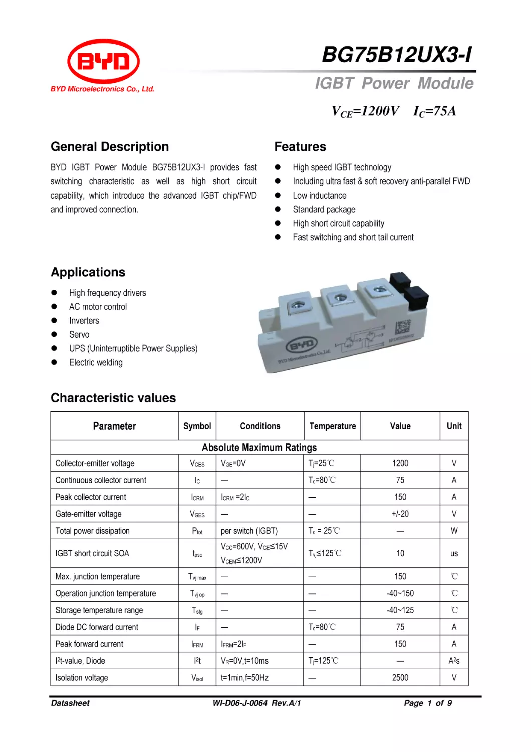
BG75B12UX3-I
IGBT Power Module
BYD Microelectronics Co., Ltd.
VCE=1200V
General Description
Features
BYD IGBT Power Module BG75B12UX3-I provides fast
switching characteristic as well as high short circuit
capability, which introduce the advanced IGBT chip/FWD
and improved connection.
IC=75A
High speed IGBT technology
Including ultra fast & soft recovery anti-parallel FWD
Low inductance
Standard package
High short circuit capability
Fast switching and short tail current
Applications
High frequency drivers
AC motor control
Inverters
Servo
UPS (Uninterruptible Power Supplies)
Electric welding
Characteristic values
Parameter
Symbol
Conditions
Temperature
Value
Unit
Absolute Maximum Ratings
Collector-emitter voltage
Continuous collector current
VCES
IC
VGE=0V
Tj=25℃
1200
V
—
Tc=80℃
75
A
Peak collector current
ICRM
ICRM =2IC
—
150
A
Gate-emitter voltage
VGES
—
—
+/-20
V
Total power dissipation
Ptot
per switch (IGBT)
Tc = 25℃
—
W
IGBT short circuit SOA
tpsc
Tvj≤125℃
10
us
VCC=600V, VGE≤15V
VCEM≤1200V
Max. junction temperature
Tvj max
—
—
150
℃
Operation junction temperature
Tvj op
—
—
-40~150
℃
Storage temperature range
Tstg
—
—
-40~125
℃
Diode DC forward current
IF
—
Tc=80℃
75
A
IFRM=2IF
—
150
A
—
A2s
2500
V
Peak forward current
IFRM
I2t-value, Diode
I2 t
VR=0V,t=10ms
Tj=125℃
Isolation voltage
Visol
t=1min,f=50Hz
—
Datasheet
WI-D06-J-0064 Rev.A/1
Page 1 of 9
BYD Microelectronics Co., Ltd.
Parameter
Symbol
BG75B12UX3-I
Conditions
Temperature
Value
Unit
Characteristics
IGBT
Gate-emitter threshold voltage
VGE(th)
Collector-emitter cut-off current
ICES
VCE=1200V,VGE=0V
Gate-emitter cut-off current
IGES
VCE=0V,VGE=±20V
Collector-emitter
saturation voltage
Integrated gate resistor
Total Gate Charge
VCE(sat)
RGint
Ic=75A,VGE=15V
—
Qg
Gate-Emitter Charge
Qge
Gate-Collector Charge
Qgc
Input capacitance
Cies
Output capacitance
Coes
Reverse transfer capacitance
Cres
Turn-on delay time
td(on)
Rise time
VGE=VCE, IC= 3mA
tr
VCE=600V,IC=75A,
VGE=±15V
VCE=25V,VGE =0V,
f=1MHz
VCC=600V,Ic=75A,
RGon=RGoff=3.3Ω,
VGE=± 15V,
Turn-off delay time
Fall time
td(off)
Lσ=80nH,
Inductive load
tf
VCC=600V, Ic=75A,
Energy dissipation during turn-on
time
Eon
RGon =3.3Ω,
VGE=± 15V, Lσ=80nH,
Inductive load
VCC=600V,Ic=75A,
Energy dissipation during turn-off
time
Eoff
RGoff=3.3Ω,VGE=± 15V
Lσ=80nH,
Inductive load
Datasheet
WI-D06-J-0064 Rev.A/1
min.
typ.
max.
Tvj=25℃
5.0
5.5
6.5
V
Tvj=25℃
—
—
1.0
mA
Tvj=125℃
—
—
1.0
mA
Tvj=25℃
-400
—
400
nA
Tvj=25℃
—
2.84
—
V
Tvj=125℃
—
3.7
—
V
Tvj=25℃
—
—
—
Ω
—
—
tbd
—
uC
—
—
tbd
—
uC
—
—
tbd
—
uC
—
tbd
—
nF
—
tbd
—
nF
—
tbd
—
nF
Tvj=25℃
—
323
—
ns
Tvj=125℃
—
345
—
ns
Tvj=25℃
—
63
—
ns
Tvj=125℃
—
68
—
ns
Tvj=25℃
—
283
—
ns
Tvj=125℃
—
300
—
ns
Tvj=25℃
—
132
—
ns
Tvj=125℃
—
155
—
ns
Tvj=25℃
—
5.06
—
mJ
Tvj=125℃
—
9.8
—
mJ
Tvj=25℃
—
2.87
—
mJ
Tvj=125℃
—
4.81
—
mJ
Tvj=25℃
Page 2 of 9
BYD Microelectronics Co., Ltd.
Parameter
Symbol
BG75B12UX3-I
Conditions
min.
typ.
Max.
min.
typ.
max.
Tvj=25℃
—
2.0
—
V
Tvj=125℃
—
1.7
—
V
Tvj=125℃
—
48
—
A
Diode
Forward voltage
VF
Peak reverse recovery current
IRR
Recovered charge
Qrr
IF=75A,VR=600V,
Tvj=125℃
—
12.2
—
uC
Reverse recovery time
trr
diF/dt=-550A/us
Tvj=125℃
—
380
—
ns
Tvj=125℃
—
5.05
—
mJ
Reverse recovery energy
IF=75A
Unit
Erec
Thermal-Mechanical Specifications
IGBT thermal resistance
junction to case
Diode thermal resistance junction to
case
Thermal resistance case to
heat-sink
Dimensions
Rth(j-c)
per IGBT
—
tbd
—
K/W
Rth(j-c)
per diode
—
tbd
—
K/W
Rth(c-s)
per module
—
0.03
—
K/W
LxWxH
Typical , see outline drawing
according to IEC
Clearance distance in air
da
60664-1 and EN
50124-1
according to IEC
Surface creepage distance
ds
60664-1 and EN
50124-1
Mass
m
—
94× 34× 30.5
mm
Term. to base:
—
—
17
Term. to term:
—
—
9.5
Term. to base:
—
—
17
Term. to term:
—
—
20
—
—
160
—
mm
mm
Thermal and mechanical properties according to IEC 60747 – 15
Specification according to the valid application note.
Datasheet
WI-D06-J-0064 Rev.A/1
Page 3 of 9
g
BYD Microelectronics Co., Ltd.
BG75B12UX3-I
Characterization curves
200
140
V GE=15V
VCE=20V
180
tp=10us
160
120
140
Tvj=25℃
100
IC[A]
IC[A]
120
80
100
Tvj=125℃
60
80
Tvj=125℃
60
Tvj=25℃
40
40
20
20
0
0
0
1
2
3
VCE [V]
4
4.5
5
5.5
6.5
7.5
8.5
9.5
10.5
11.5
VGE[V]
Fig.1 Typ. On-state Characteristics
Fig.2 Typ. Transfer Characteristics
30
150
Tvj=125℃
VGE=17V
Vcc=600V
VGE=15V
Rg=3.3Ω
L=80nH
VGE=13V
120
Tvj=25℃
Tvj=125℃
VGE=15V
20
Eon
E[mJ]
IC[A]
VGE=11V
90
VGE=9V
60
Eoff
10
30
0
0
0
1
2
3
4
5
6
7
8
0
30
VCE[V]
90
120
I C[A]
Fig.3 Typ. Output Characteristics
Datasheet
60
Fig.4 Switching Loss vs. Collector Current
WI-D06-J-0064 Rev.A/1
Page 4 of 9
150
BYD Microelectronics Co., Ltd.
BG75B12UX3-I
16
90
Vcc=600V
Ic=75A
VGE =15V
Tvj=125℃
80
3.3
5.1
70
Eon
12
10
60
Irr
50
E[mJ]
IRR[A]Erec[mJ]Qrr[uC]
Vcc=600V
Ic=75A
VGE=15V
Tvj=125℃
RG=15
8
40
Eoff
30
Erec
20
4
Qrr
Erec
10
0
0
400
500
600
700
800
900
1000
0
5
Rg[Ω] 10
15
di/dt[A/us]
Fig.5 Typ. Reverse Recovery Characteristics vs di/dt
Fig.6 Switching Loss vs. Gate Resistor
700
600
Vcc=600V,VGE=15V
Rg=3.3Ω,Tvj=125℃
Vcc=600V
Ic=75A
VGE=15V
Tvj=125℃
600
500
500
400
tdon
tdon
tdoff
t[ns]
t[ns]
400
300
tdoff
300
200
200
tf
100
tf
tr
100
tr
0
0
0
40
80
120
160
0
IC[A]
Fig.7 Typ. Switching Times vs. IC
Datasheet
2.5
5
7.5
10
Rg[Ω]
12.5
15
Fig.8 Typ. Switching Times vs. Gate resistor RG
WI-D06-J-0064 Rev.A/1
Page 5 of 9
17.5
BYD Microelectronics Co., Ltd.
BG75B12UX3-I
10
150
Vcc=600V
VGE=15V
Rg=3.3Ω
8
Erec[mJ]
120
I F[A]
90
6
Tvj=125℃
Tvj=125℃
4
60
Tvj=25℃
30
2
Tvj=25℃
0
0
0
0.5
1
1.5
VF[V]
2
2.5
3
0
Fig.9 FWD Forward Characteristics.
40
60
80
100
IF[A]
120
140
Fig.10 Typ. Switching Losses Diode-Inverter
100
20
Vcc=600V
VCE=15V
Tvj=125℃
18
5.1
10
16
Tj=125℃
VGE=15V
3.3
150A
RG=15
14
100A
10
IC[A]
75A
12
Qrr[uC]
20
50A
50
8
6
If=20A
4
2
0
0
0
100
200
300
400
500
di/dt[A/us]
600
700
0
40
80
120
TC[℃]
Fig.11 Typ. FRD Recovery charger
Datasheet
800
Fig. 12 Rate Current vs. Temperature(TC)
WI-D06-J-0064 Rev.A/1
Page 6 of 9
160
160
BYD Microelectronics Co., Ltd.
BG75B12UX3-I
175
Ic,Module
Ic,Chip
150
125
Ic[A]
100
75
50
25
0
0
200
400
600
VCE[A]
800
1000
1200
Fig.13 Reverse Bias Safe Operating Area
IGBT-inv(RBSOA)
Datasheet
WI-D06-J-0064 Rev.A/1
Page 7 of 9
BYD Microelectronics Co., Ltd.
BG75B12UX3-I
Circuit Diagram
Package Outlines
Dimensions in mm
Attached (recommended torque):
MS : (to heat sink M6) 3~5 Nm
Datasheet
M t : (to terminals M5) 2.5~4 Nm
WI-D06-J-0064 Rev.A/1
Page 8 of 9
BYD Microelectronics Co., Ltd.
BG75B12UX3-I
Attention
1.
In order to reduce the contact resistance, we suggest add thermal grease between base and heat-sink, which
thickness is about 0.1mm.
2. When installing the module, please wear a electrostatic bracelet to prevent the gate breakdown and the imbalance
power may damage the internal chip, even to damage the module.
3. This is an electrostatic sensitive device, please observe the international standard IEC 60747-1, chap. IX.
RESTRICTIONS ON PRODUCT USE
The information contained herein is subject to change without notice.
BYD Microelectronics Co., Ltd. (short for BME) exerts the greatest possible effort to ensure high quality and
reliability. Nevertheless, semiconductor devices in general can malfunction or fail due to their inherent electrical
sensitivity and vulnerability to physical stress. It is the responsibility of the buyer, when utilizing BME products, to
comply with the standards of safety in making a safe design for the entire system, including redundancy,
fire-prevention measures, and malfunction prevention, to prevent any accidents, fires, or community damage that
may ensue. In developing your designs, please ensure that BME products are used within specified operating
ranges as set forth in the most recent BME products specifications.
The BME products listed in this document are intended for usage in general electronics applications (personal
equipment, measuring equipment, industrial robotics, domestic appliances, etc.). These BME products are neither
intended nor warranted for usage in equipment that requires extraordinarily high quality and/or reliability or a
malfunction or failure of which may cause loss of human life or bodily injury (“Unintended Usage”). Unintended
Usage include atomic energy control instruments, airplane or spaceship instruments, transportation instruments,
traffic signal instruments, combustion control instruments, medical instruments, all types of safety devices, etc..
Unintended Usage of BME products listed in this document shall be made at the customer’s own risk.
Datasheet
WI-D06-J-0064 Rev.A/1
Page 9 of 9