/


Похожие


Текст
SISPAD 2021 Plenary Talk
Memory Technology 2021: Trends & Challenges
Jeongdong Choe
TechInsights, Ottawa, Canada; Email: jchoe@techinsights.com
Abstract- DRAM and NAND Flash memory demands for
server, datacenter, cloud, mobile and AIOT including ML,
autonomous and connected vehicles application have
been increased on and on. In addition, emerging memory
market such as STT-MRAM, ReRAM, PCRAM, FeRAM
and 3D XPoint Memory are expected to reach $36B by
2030. Memory technologies have quite different stories
from Logic devices which is referring to Moore’s Law.
DRAM, NAND Flash and Emerging memory makers are
racing of device scaling, however many of electrical and
physical limits are coming into reality. We overview
current memory technology, and further discuss the
details, trends, and upcoming challenges.
Keywords- Memory, DRAM, NAND, Emerging, MRAM,
ReRAM, FeRAM, XPoint, Trends, Challenges
I.
INTRODUCTION
DRAM cell scaling down to sub-15 nm design rule (D/R) has
already been productized from major DRAM players such as
Samsung, Micron, and SK Hynix. They’ve been developing
n+1 and n+2 generations so called 1b (or 1β) and 1c (or 1γ),
which means DRAM cell D/R might be able to further scale
down to sub-12 nm or beyond with/without EUV adoption
for DRAM cell patterning [1]. The cell scaling is getting
slower due to many challenges such as process integrity, cost,
cell leakage, capacitance, refresh management and sensing
margin. Some innovative technologies such as higher-k
dielectric materials, pillar (or quasi-pillar) capacitor process,
recess channel S/A transistor, and HKMG adoption can be
seen from the advanced DRAM cell design. Further, 3D
DRAM, high bandwidth memory (HBM3), graphic DRAM
(GDDR6X/7) and embedded DRAM (10 nm/7 nm)
technologies will extend the DRAM lifetime and application
[2].
Major NAND manufacturers are racing to increase the
number of vertical 3D NAND gates, they all have introduced
1yyL 3D NAND devices, for example, Samsung V7 V-
NAND, KIOXIA and Western Digital Company (WDC)
BiCS6, Micron 2nd gen. CTF CuA, and SK Hynix 2nd gen. 4D
PUC NAND. Beyond storage density, 3D NAND prototype
is used for ultra-low latency NAND application (classified as
Storage Class Memory), such as Samsung Z-SSD and
KIOXIA XL-FLASH. 3D NAND bit density reached up to
10.8Gb/mm2 (SK Hynix 176L 512Gb TLC) and 12.8Gb/mm2
(Intel 144L 3-deck QLC) [3]. YMTC 128L Xtacking
products are just around the corner.
Intel extends XPoint memory application not only for
conventional SSD but also DCPMM persistent memory. Intel
OptaneTM P5800X SSD products use the 2nd generation
XPoint memory technology with four-stack PCM/OTS cell
structure. Everspin 3rd generation standalone 256 Mb STTMRAM (pMTJ) and 1Gb STT-MRAM, Samsung and
SONY’s new 28 nm eSTT MRAM (pMTJ), Avalanche eSTT
MRAM (pMTJ) with 40nm node, Dialog Semiconductor (old
Adesto Technologies) 2nd generation CBRAM, and Fujitsu
45 nm ReRAM 130nm FeRAM products have been released
on the market in 2020 and 2021 [4, 5].
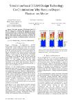
II. DRAM TECHNOLOGY TRENDS &
CHALLENGES
Fig. 1 shows a DRAM roadmap from major and minor
players, including Samsung, Micron, SK Hynix, Nanya,
PSMC, and CXMT. Three major players, Samsung, Micron,
and SK Hynix already revealed D1z and D1a products which
have 15 nm and 14 nm-class cell design rule (D/R) for DDR4,
DDR5 and LPDDR5 application. Samsung adopted EUV
lithography into D1x DDR4 test vehicle (TV) products and
D1z LPDDR5 mass products, while Micron and SK Hynix
keep ArF-i based double patterning technology (DPT)
process for D1z generation. A few more DRAM generation
with further scaled down design such as 1d (or 1δ), 0a (or 0α),
and 0b (or 0β) will be productized by 2030. Another DRAM
maker, CXMT, from China jumped into the race, and is
developing D1x and D1y through this year.
978-1-6654-0685-7/21/$31.00 ©2021 IEEE
LPDDR6 and HBM3 products would be common on the
market.
For 10 nm-class and beyond DRAM cell design, more
innovative process, materials, and circuit technologies should
be added into them, including higher-NA EUV, 4F2, 1T
DRAM, pillar capacitor, ultra-thin higher-k capacitor
dielectrics, and low-k ILD/IMD materials (Fig. 3).
Fig. 1. A DRAM roadmap prepared from TechInsights showing D1z
and D1a DRAM products commercialized on the market in 2020
and 2021. A few more generations such as 1d (or 1δ), 0a (or 0α),
and 0b (or 0β) will be productized by 2030.
Up to date we’ve seen 8F2 and 6F2 DRAM cell design, in
which unit cell comprises of 1T (transistor) plus 1C
(capacitor). The 1T+1C cell design will be used on DRAM
cell design for next decade, however due to the process and
layout limitation, DRAM players have been developing 4F2
cell structure such as 1T DRAM or capacitorless DRAM
prototypes for one of the next candidates to extend DRAM
technology (Fig. 2).
Fig. 3. DRAM Cell design and technology trends from 30 nm-class
through 10 nm-class. More innovative technologies are needed to
meet cell capacitance, scaling and speed improvement.
Fig. 4 shows a DRAM design rule (D/R) trend for major
players. Given that they keep 6F2 DRAM cell design with
1T+1C structure, 10 nm D/R would be the last one for DRAM
in 2027 or 2028. Lots of challenges would be there on DRAM
scaling such as 3D DRAM, row hammer scaling (circuit), low
power design, refresh time scaling and management, low
latency, new work-function materials, HKMG transistor, and
on-die ECC. The most keywords would be ‘speed’ and
‘sensing margin’. Samsung’s HKMG peripheral transistor for
DDR5 is an example to increase BL sensing margin.
Fig. 2. A technology/application roadmap on DRAM devices
showing a 6F2 1T+1C cell design extended to a few more next
DRAM generations, although DRAM players have been developing
4F2 cell structure such as 1T DRAM or capacitorless DRAM
prototypes.
Bulky fin (or saddle fin) with B-RCAT structure for cell
access transistor has been used, however the buried wordline
gate materials already changed from single tungsten layer to
poly-Si/tungsten double layer to control gate leakage
effectively. Further, Micron uses TiN-only gate for D1z cell
integration. A cylinder-type structure was the mainstream for
DRAM cell capacitor integration, but SK Hynix (D1y and
D1z) and Samsung (D1z) adopted a quasi-pillar capacitor
structure in which cell capacitor uses the outer surface of the
cylinder only, which causes smaller cell capacitance than
previous generation. In a couple of years, DDR5, GDDR7,
Fig. 4. DRAM D/R trends showing a limitation of 6F2 cell design.
10 nm D/R would be the last one for 6F2 DRAM in 2027 or 2028.
III. NAND TECHNOLOGY TRENDS &
CHALLENGES
978-1-6654-0685-7/21/$31.00 ©2021 IEEE
Major NAND chip manufacturers are racing to increase the
number of vertical 3D NAND gates. They have already
introduced 1yyL 3D NAND devices up to date. Samsung
176L (V7), KIOXIA/WD 162L (BiCS6), Micron 176L (2nd
CTF), and SK Hynix 176L (V7) are for 1yyL products, and
YMTC 128L Xtacking will be introduced on the market in
2021 (Fig. 5). MXIC also announced their first 3D NAND
prototype with 48L and will mass-produce by late 2021 or
early 2022.
proposed and productized; V-NAND from Samsung, BiCS
from KIOXIA (old Toshiba Memory) and Western Digital,
FG CuA from Intel/Micron, CTF CuA from Micron (128L~),
P-BiCS from SK Hynix (~72/76L), 4D PUC from SK Hynix
(96L~), and Xtacking from YMTC (Fig. 6 and Fig. 7).
Fig. 7. Five representative SEM images showing the concepts of
each 3D NAND cell array architecture. CuA, PUC and Xtacking
prototypes have the CMOS peripheral circuitry under the NAND
cell array.
Fig. 5. A 3D NAND roadmap from TechInsights showing
112L/128L and 162L/176L products released on the market in 2021.
Z-NAND, XL-FLASH, and XPoint are added into the roadmap for
SCM or fast-NAND application.
Some innovative technologies and designs have been adopted
so far, such as triple-deck structure, CuA/COP/PUC
technology, and Xtacking dies with H-bonding. Further, low
latency (high speed) NAND products such as Samsung ZNAND and KIOXIA XL-FLASH have successfully
commercialized with 3D NAND cell architecture and multiplane die design. For more than 500-layer NAND products,
we should consider not only multi-stack or die-stack
integration but also 3D package solution.
Fig. 6. Seven different 3D NAND prototypes have been proposed
and successfully productized: V-NAND, BiCS, FG CuA, CTF CuA,
P-BiCS, 4D PUC, and Xtacking.
Since 2018, most of the worldwide smart phones have used
3D NAND storage components instead of 2D NAND chips.
Up to date, seven different 3D NAND prototypes have been
Especially, Samsung V-NAND (TCAT) 3D NAND products
applied a single VC etching process up to 128L (V6), while
all the other 3D NAND products use multi-deck (three-deck
for Intel 144L, for example) string integration. They all use
20 nm or 19 nm BL half-pitch, which means ArF-i and DPT
based photolithography is the major patterning technology
for 3D NAND.
2D NAND wafers are still needed for some specific
application with higher reliability and low/high temperature
operation. MCU, medical, robots, TVs/toys, game controllers,
wearables, security cameras, smart speakers, IoT, AI, ML,
printers, set-top box, and aerospace need 2D NAND products.
Now, 3D NAND products are very popular for datacenter,
cloud, server, SSD, PCs, mobile, and smart phones. As the
number of gates stacked increases, the vertical NAND string
height is also increased, for example, newly minted 176L
products show a 12 µm height from source plate (Fig. 8). Bit
cost decreased on and on, and bit density increased up to
15Gb/mm2 for QLC die. Total number of gates per NAND
string also increased to 200 gates or more.
Intel 144-tier NAND string consists three decks (upper deck,
middle deck, lower deck and 48L for each) between source
and bitline for the first time and keeps FG CuA structure for
TLC and QLC devices. Each deck can be assigned to any
combination of QLC or SLC blocks to fully benefit from
Intel’s new block-by-deck concept in the storage system.
We cannot yet know all the detailed challenges for future 3D
NAND technology, however some of them are HAR, layer
stress control, wafer warpage, process uniformity, strict
control of ALD/ALE, throughput, deck-to-deck misalign,
yield control, defects, NAND string current, decoder TR
reliability, PGM/ERS speed, retention, e-migration, leakage
978-1-6654-0685-7/21/$31.00 ©2021 IEEE
and interference, 3D package solution, and so on. PLC 3D
NAND products may will be introduced in a couple years.
Samsung and SONY’s 28 nm eSTT MRAM (pMTJ),
Avalanche eSTT MRAM (pMTJ) with 40 nm node, and
Dialog Semiconductor (old Adesto Technologies) 2nd
generation ReRAM (CBRAM) products from the market.
TSMC announced a 22 nm eMRAM-F product roadmap to
replace eFLASH for data/code storage and configuration
memory application. They’re currently developing eMRAMS, and 14 nm/12 nm eMRAM-F/eRRAM as well.
Fig. 8. A comparison of 3D vertical NAND string heights. Newly
minted 176L products show a 12 µm height from source plate.
IV. EMERGING MEMORY TECHNOLOGY
TRENDS & CHALLENGES
For a couple of decades, we’ve considered MRAM (or STTMRAM), PCRAM, ReRAM and FeRAM devices and
technologies as emerging memory prototypes. However,
they’ll be rather a kind of nonvolatile memory devices for
embedded application than a discrete emerging memory
device. Future emerging memory might be referred to novel
magnetic memory devices such as SOT MRAM, FTJ,
unipolar or bipolar filamentary OxRAM, CBRAM,
macromolecular memory, Mott memory or DNA storage.
Here, we still consider the MRAM, XPoint, ReRAM
(CBRAM) and FeRAM for emerging memory devices.
They’re extending application area such as CPU/APU cache
memory (STT-MRAM), AI and in-memory computing
(PCRAM), analog IC (ReRAM, Memristor), external switch
(FeRAM), and high density SCM (XPoint Memory).
Among the emerging memory devices, especially STTMRAM technology has been actively researched and
developed by major players/developers such as Everspin
Technologies, GlobalFoundries, Avalanche Technologies,
Sony, Micron, IMEC, CEA-LETI, Applied Materials,
Samsung, Fujitsu, IBM, TSMC, and Spin Transfer
Technologies (STT). Intel, Micron, and SK Hynix are the
developers more focusing on XPoint memory with
PCM/OTS cell structure. Micron just exited from XPoint
memory in 2021 (Fig. 9).
Up to date we’ve found Everspin 3rd generation standalone
256Mb STT-MRAM (pMTJ) and 1Gb STT-MRAM,
Fig. 9. An Emerging memory roadmap from TechInsights including
STT-MRAM, PCRAM/XPoint, ReRAM/CBRAM, FeRAM and
embedded DRAM/FLASH memory.
Everspin has four different MRAM products released on the
market, including Toggle-mode MRAM (1st generation,
Chandler fab.) and STT-MRAM (2nd ~ 4th generation, GF
fab.). Among the STT-MRAM products, the 2nd generation
STT-MRAM devices use a MgO-based in-plane MTJ
structure, while the 3rd and 4th generation STT-MRAM
devices use a perpendicular MTJ (pMTJ) technology.
Avalanche pMTJ STT-MRAM cell design and structure
show 40 nm p-MTJ layers with 0.032 µm2 cell size, and
MRAM layer placed under M1 source line, between Contact1 and Contact-2. Samsung, together with Sony, revealed 28
nm pMTJ 8Mb embedded STT-MRAM structure for GPS
controller of Huawei GT2 smartwatch, for example. They’re
MgO MTJ-based devices.
Fujitsu 8Mb ReRAM device is the world's largest density as
a stand-alone mass-produced ReRAM product up to date.
Fujitsu adopted a new 45 nm CMOS process with quite
smaller die size and higher memory density compared with
their previous 180 nm 4Mb ReRAM products.
The 1st generation XPoint memory die from Intel and Micron
has 128Gb (16GB) die density and two-layer PCM/OTS
structure. It has been used many of Intel SSD products such
as Optane, 800P, 900P, DC P4800X, H10/H20 and DCPMM.
For the storage elements, many candidates such as phase
change materials, resistive oxide cells, conductive bridge
cells and MRAM cells have been proposed and developed.
978-1-6654-0685-7/21/$31.00 ©2021 IEEE
Among them, the 1st gen. XPoint memory adopted a
chalcogenide phase change material, GST (Ge-Sb-Te) alloy
layer.
A 20 nm double patterning technology (DPT) used for BL
and WL lithography/etching process, effectively 2F2 cell
designed. Recently, Intel released the 2nd generation XPoint
memory, for example, Optane DC P5800X SSD products on
the market. 4-stack PCM/OTS layer structure, effectively 1F2,
is integrated on M4 layer, results in WL/BL/WL/BL/WL
multi-layers. The Ovonic Threshold Switching Selector
(OTS) co-integrated with a PCM layer for the device, which
is the same elements with previous XPoint 1st generation (Fig.
10).
[4] Jeongdong Choe, “Technology & Trend: NAND &
Emerging memory”, Flash Memory Summit 2020, C-9, Nov.
2020
[5] Jeongdong Choe, “Intel’s 2nd Generation XPoint
Memory”,
TechInsights
Blog,
https://www.techinsights.com/
Fig. 10. A PCM/XPoint history showing 2L 1st gen. and 4L 2nd gen.
XPoint memory products from Intel.
Although emerging memory devices have opportunity to
replace eFLASH or SCM due to high performance (high
speed, endurance, and retention) and energy efficiency.
However, one of the most challenges would be how to reduce
the bit cost, in other words, how to increase the array cell
density. So far, all the standalone STT-MRAM dies (256Mb
or 1Gb) and XPoint dies (128Gb or 256Gb) are not
comparable with 3D NAND dies (1Tb or 1.33Tb for QLC
NAND dies). In addition, most of the emerging memory
devices use some new materials such as HfO, HZO, GSTbased chalcogenide compound, and Ir/Ta-based metal
electrodes which causes some difficulties on process
integration including patterning/etching, deposition, and
annealing optimization.
Reference
[1] Jeongdong Choe, “Samsung D1z DRAM with EUV
Lithography”, EETimes Memory DesignLine, Feb. 18, 2021
[2] Jeongdong Choe, “Memory Process, Design, and Cell
Architecture: Current & Future”, Semicon Korea 2021, S3-4,
Feb. 2021
[3] Jeongdong Choe, “Intel 144-Tier Three-deck FG NAND
with 161 Total gates”, Semiconductor Digest, Vol 3 No. 3,
pp. 21-22
978-1-6654-0685-7/21/$31.00 ©2021 IEEE