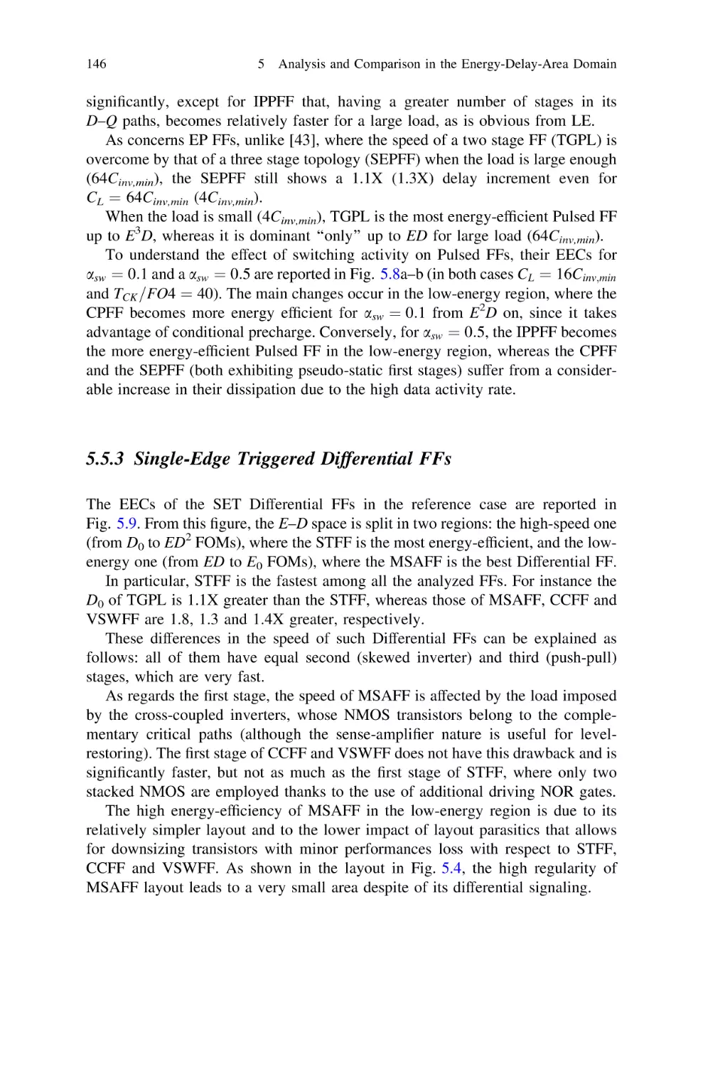
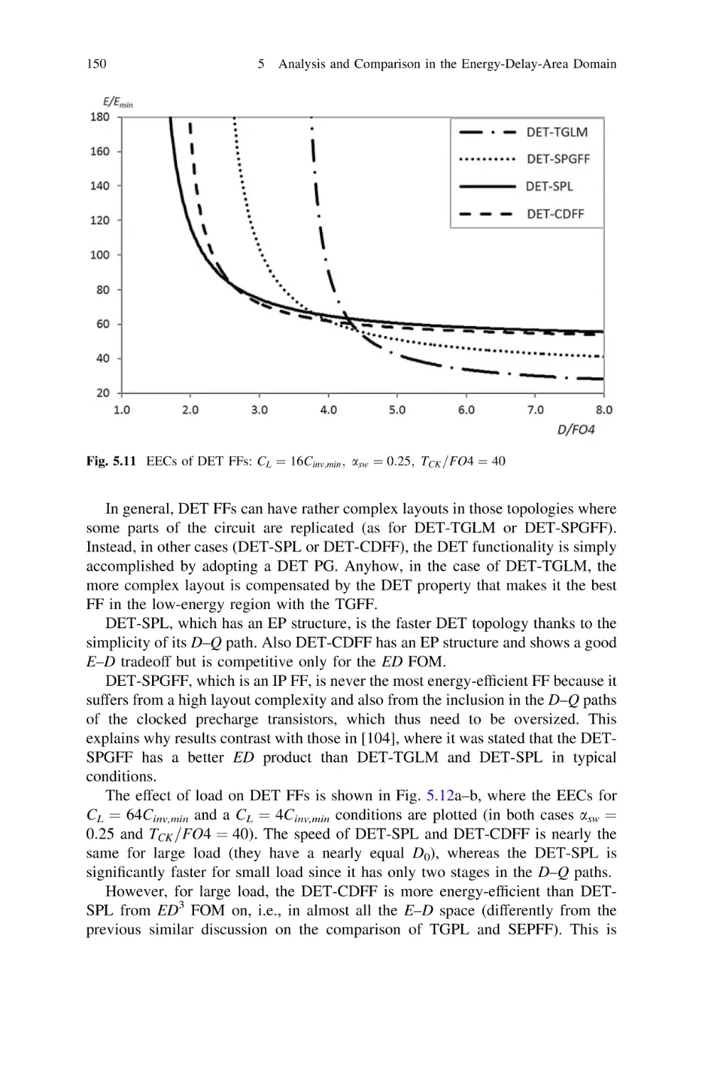
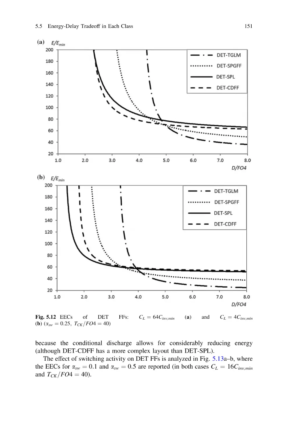
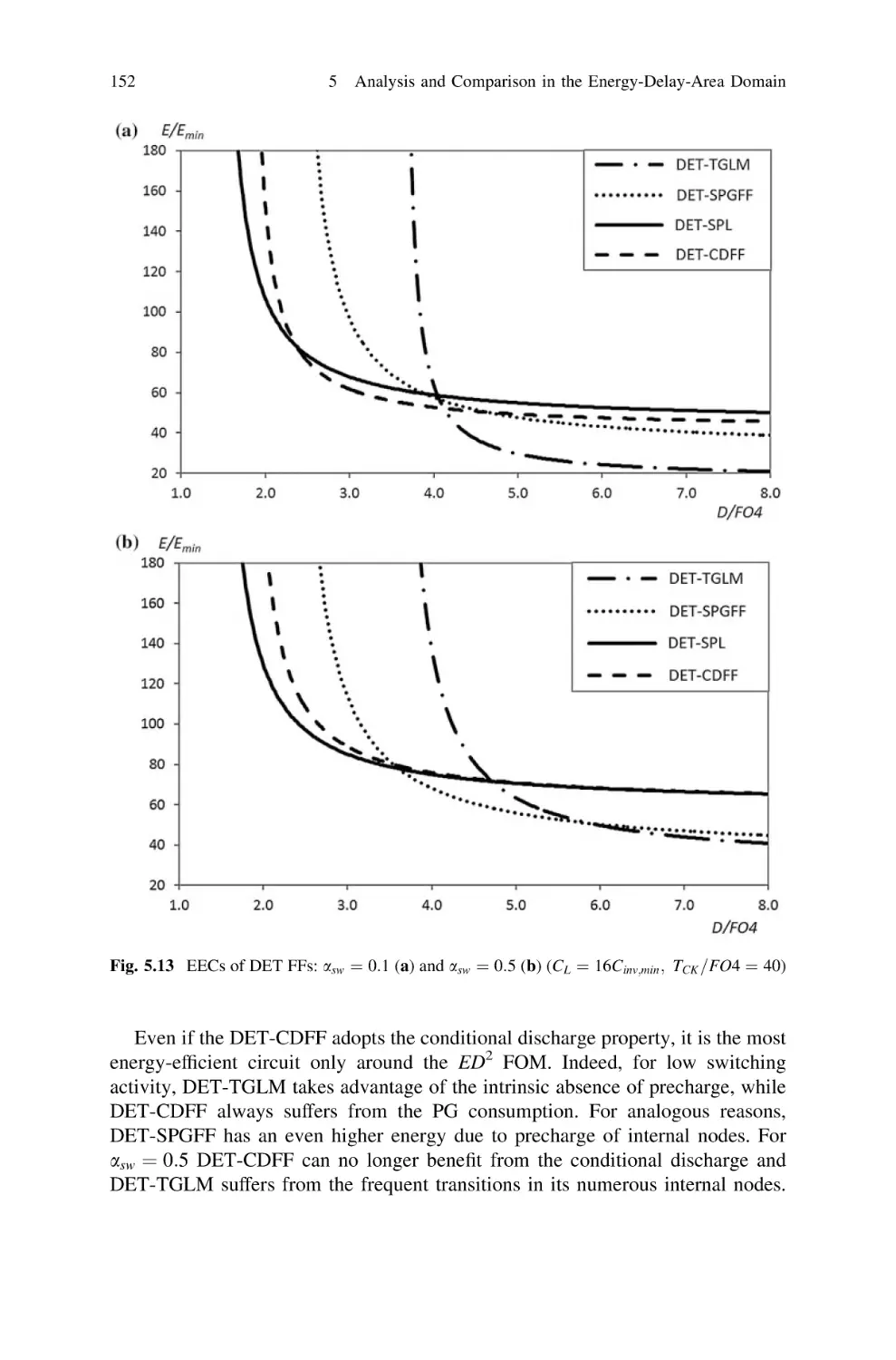
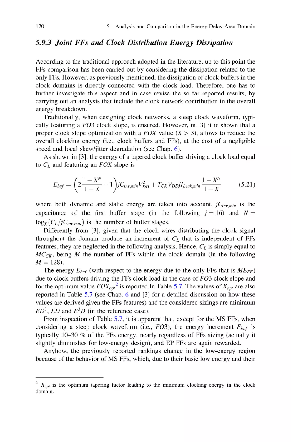
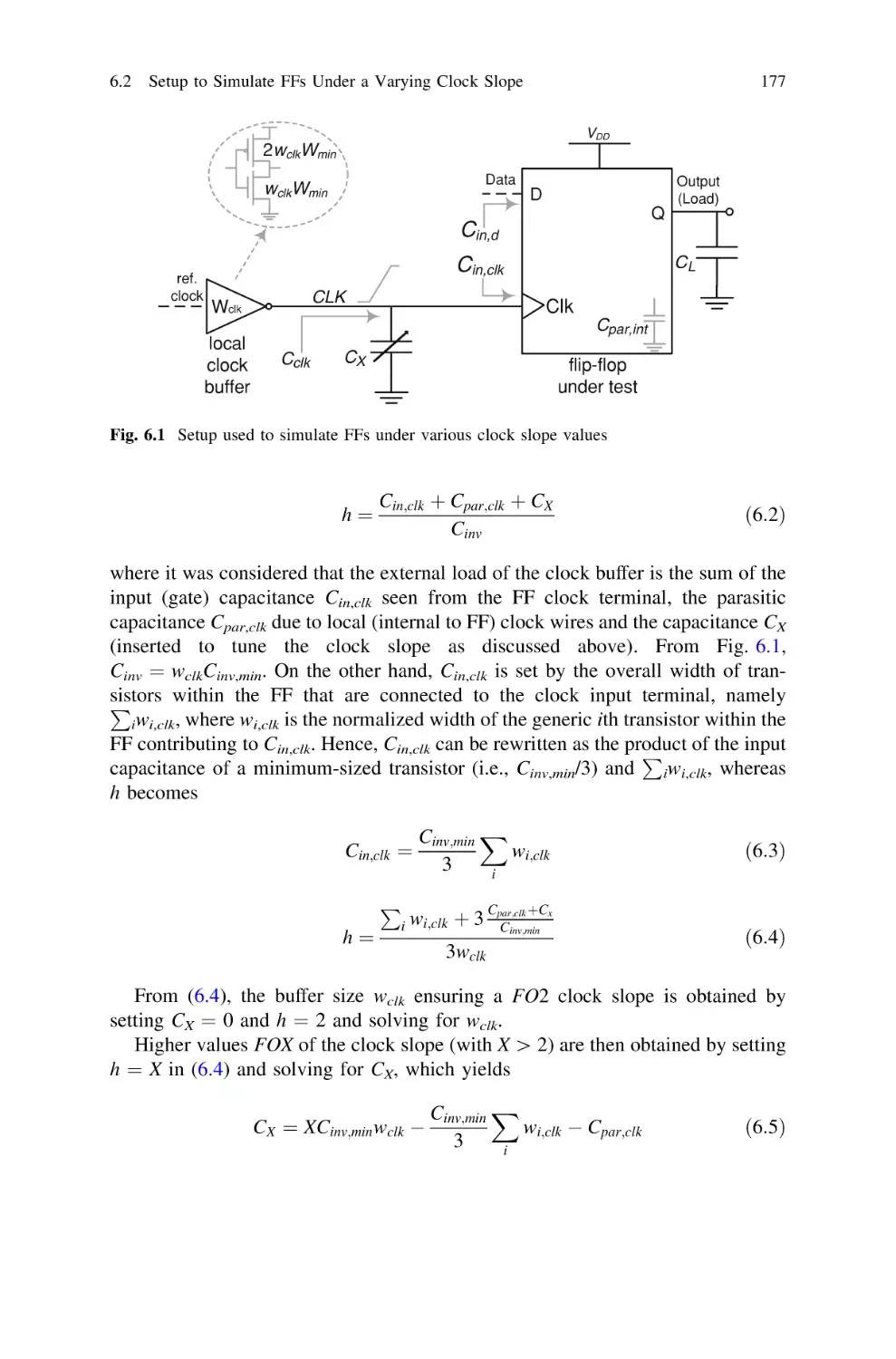
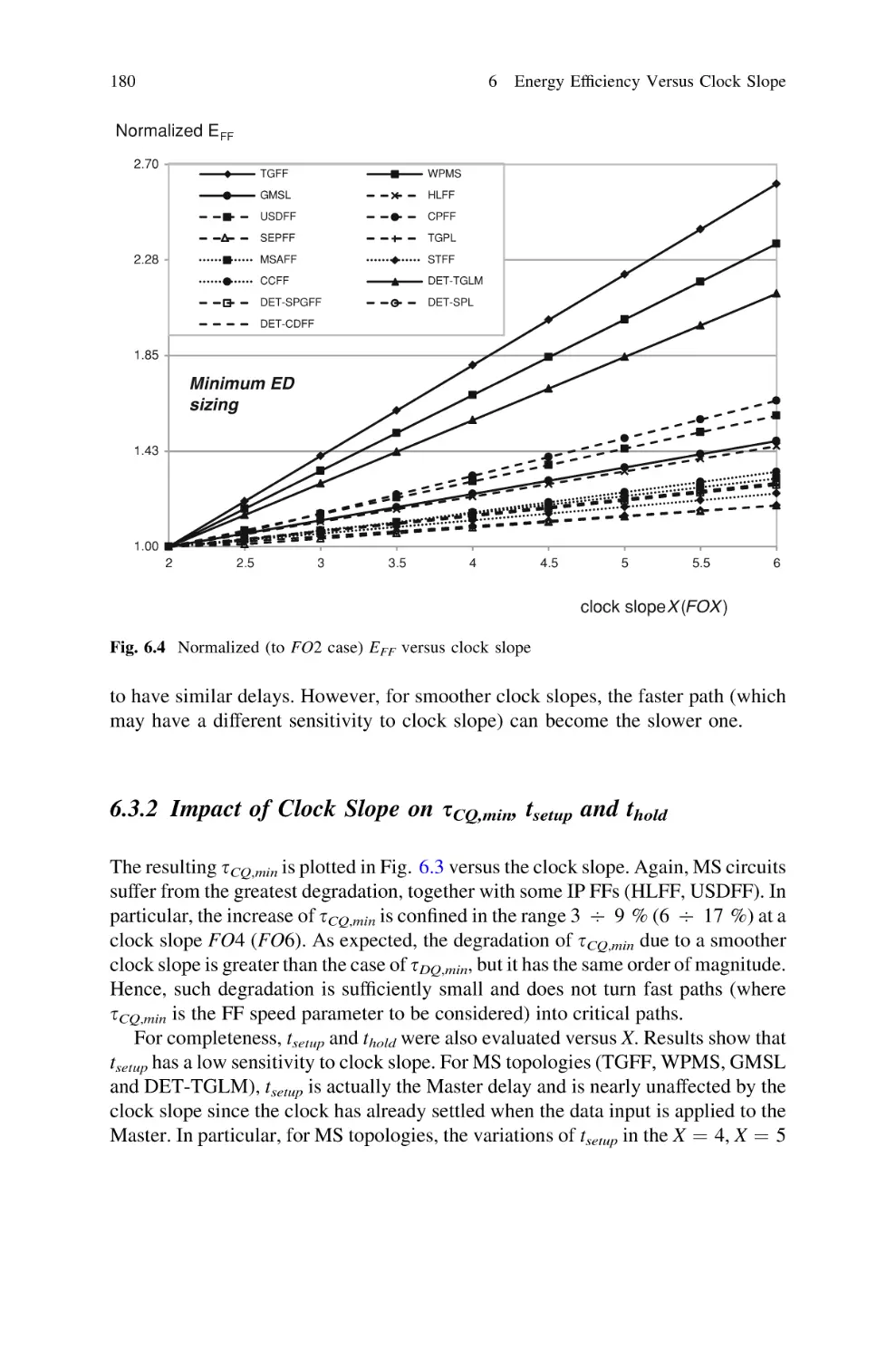
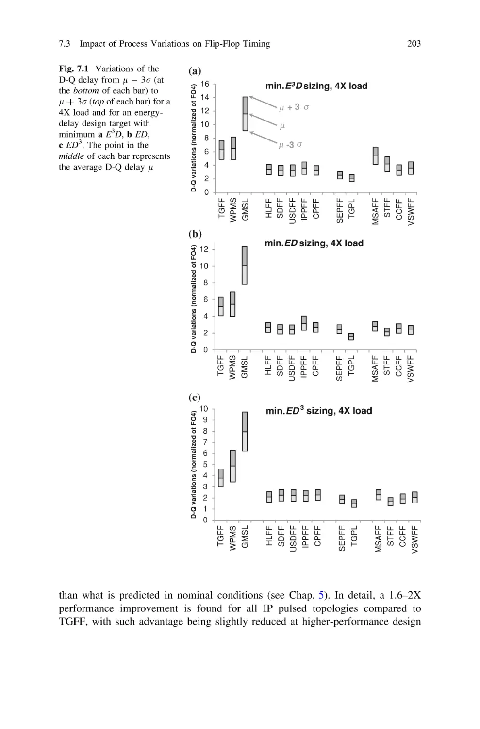
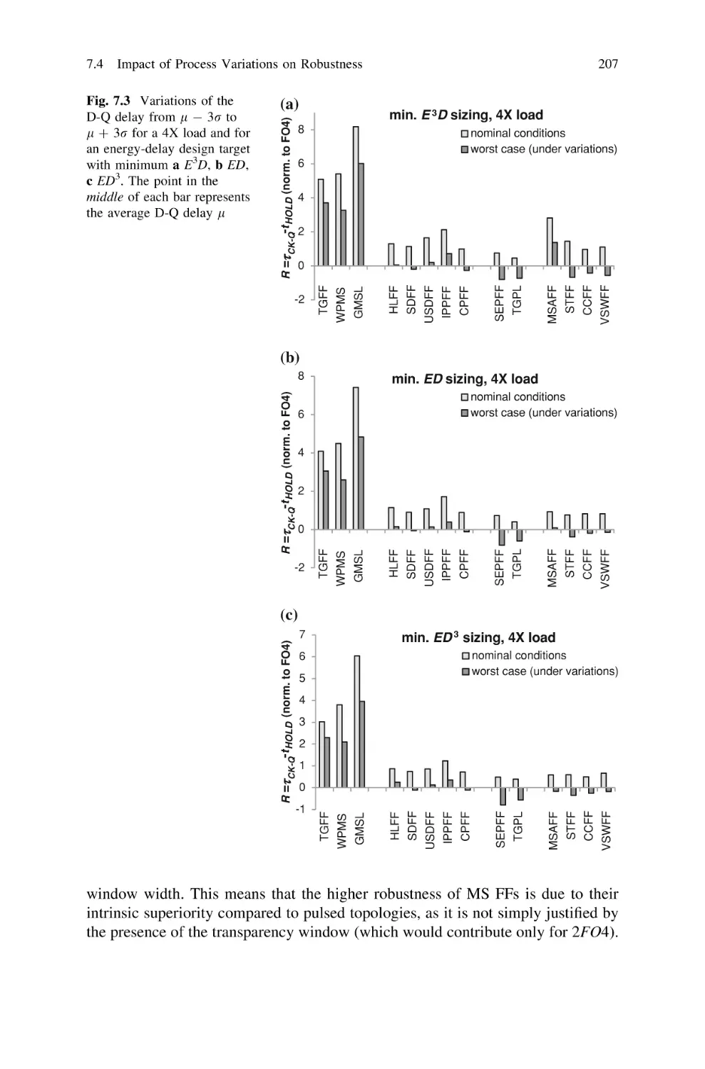
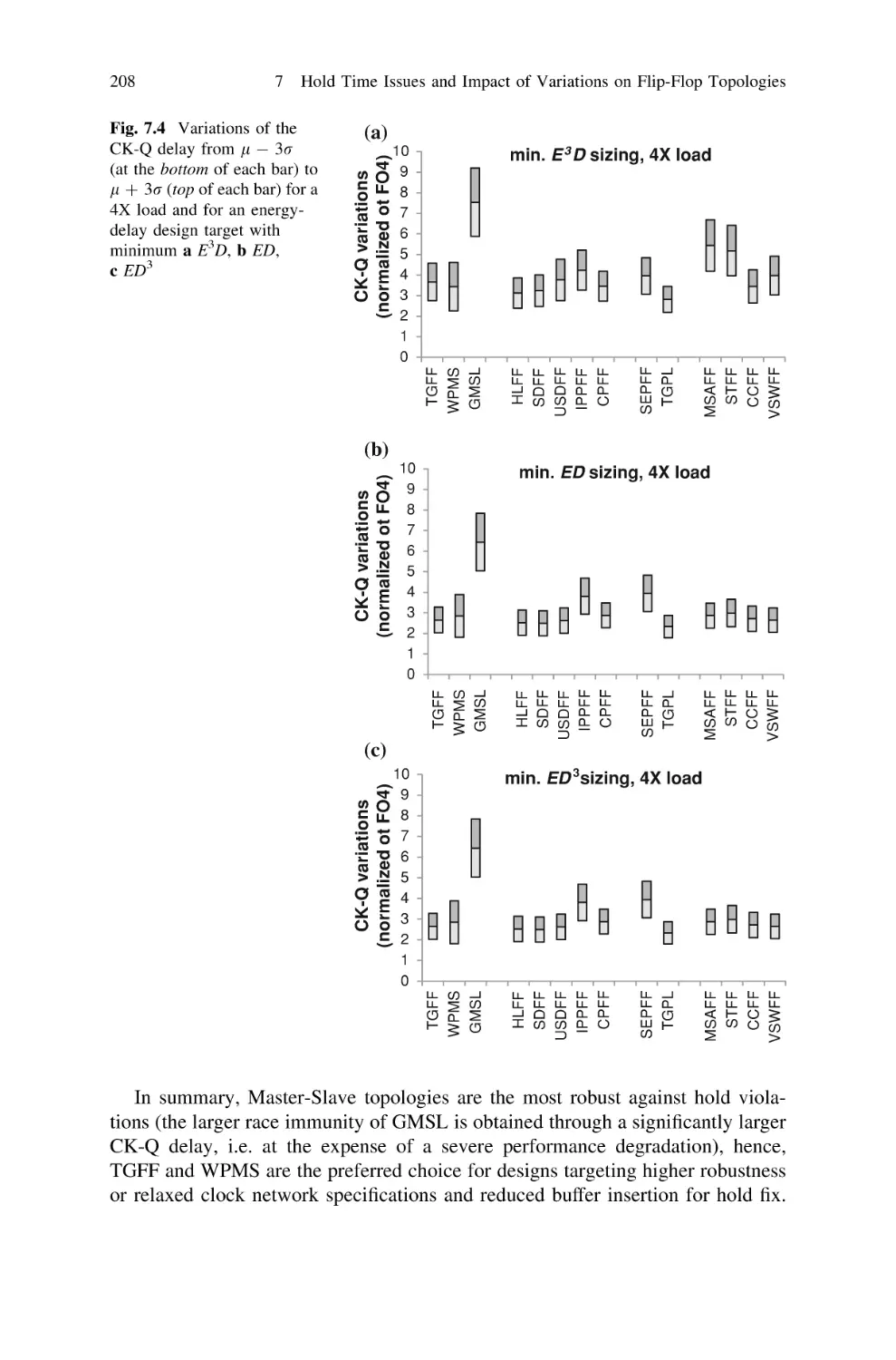
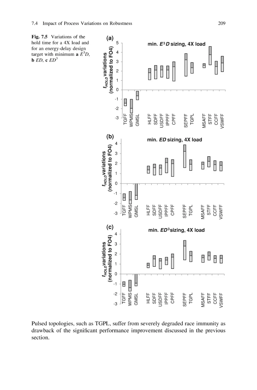
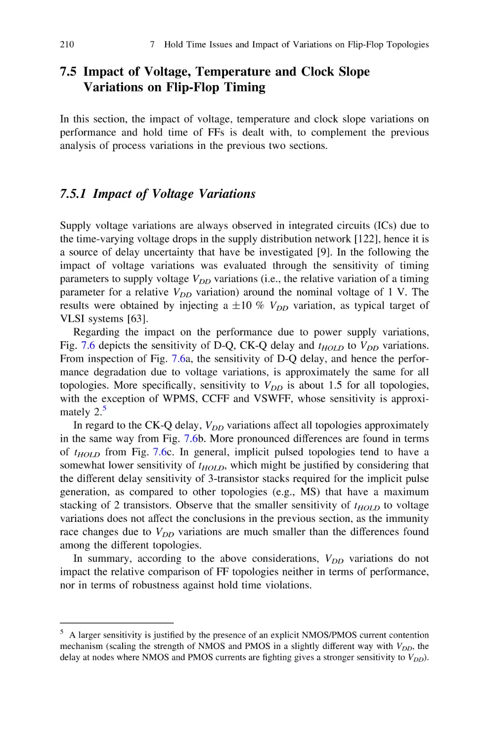
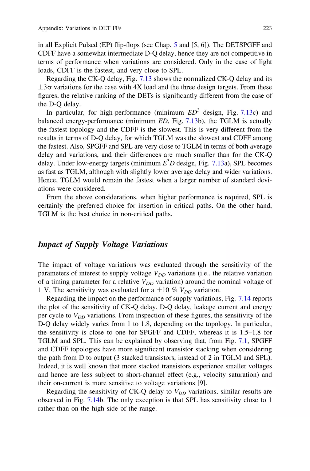
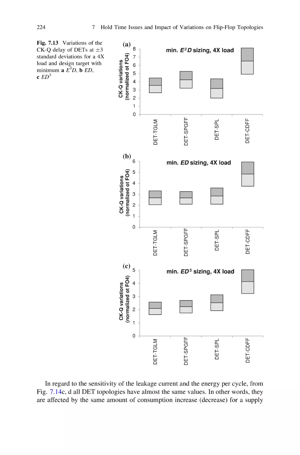
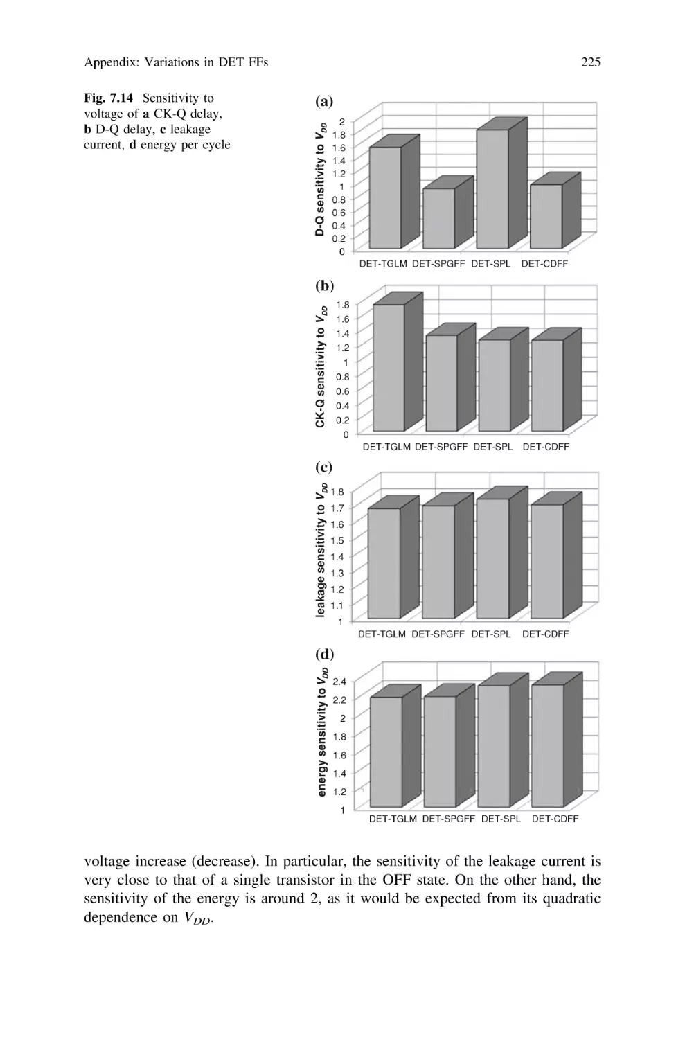
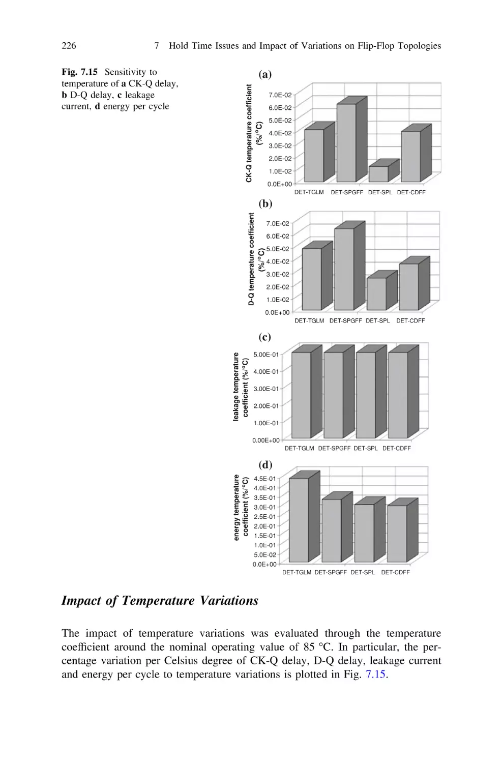
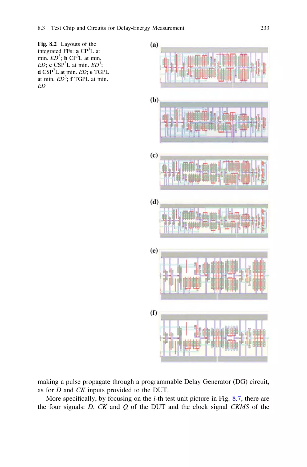
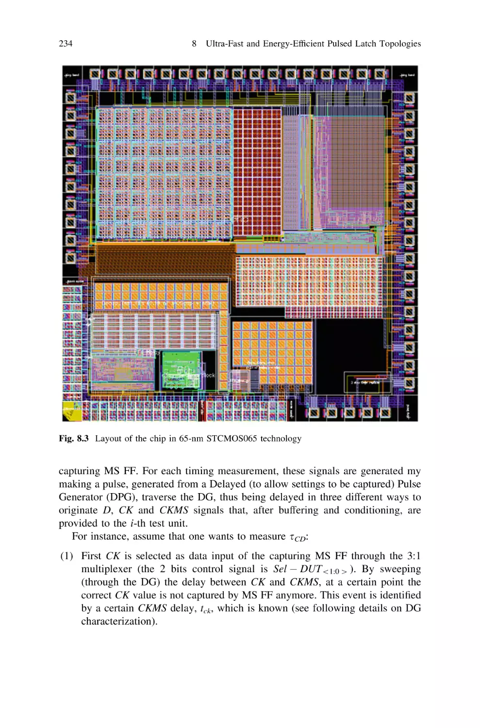
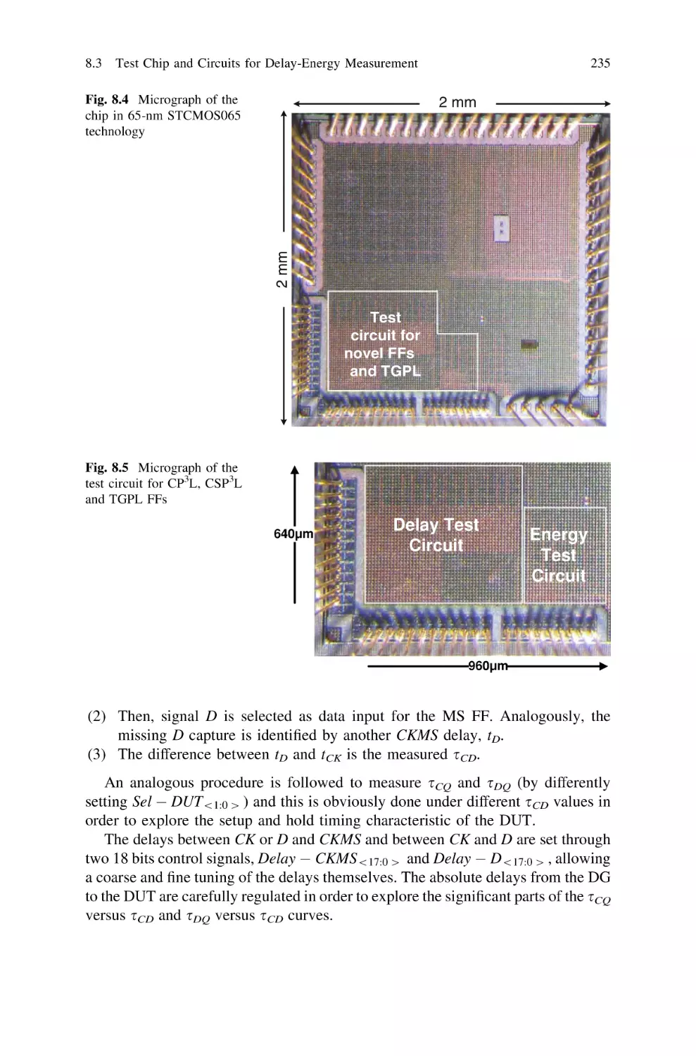
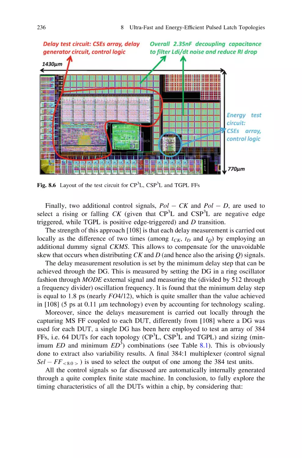
/


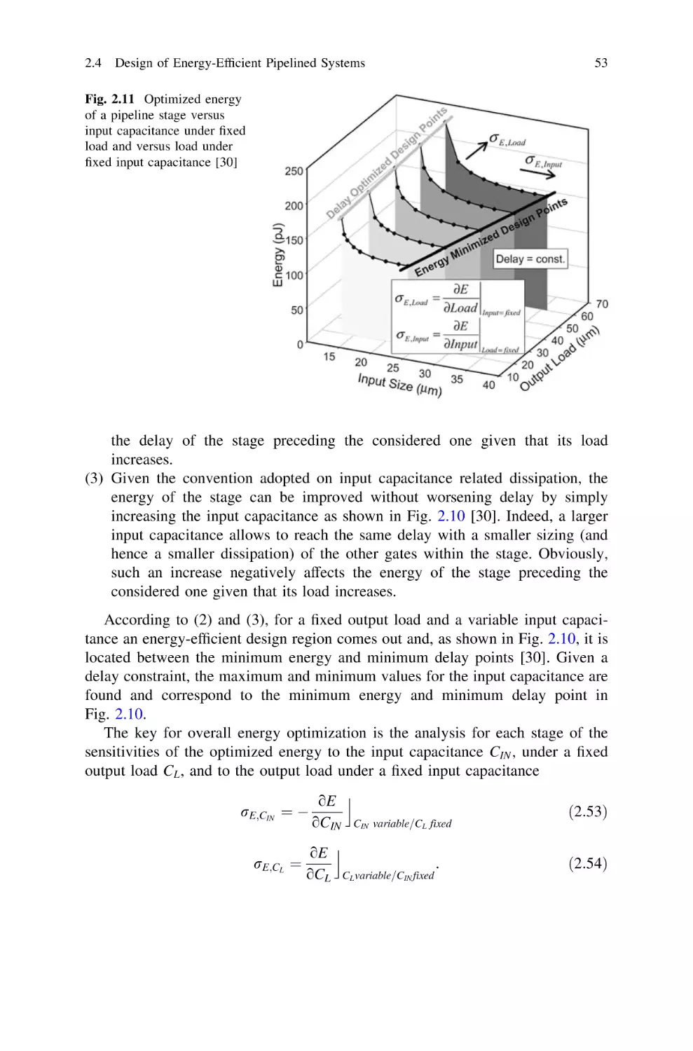


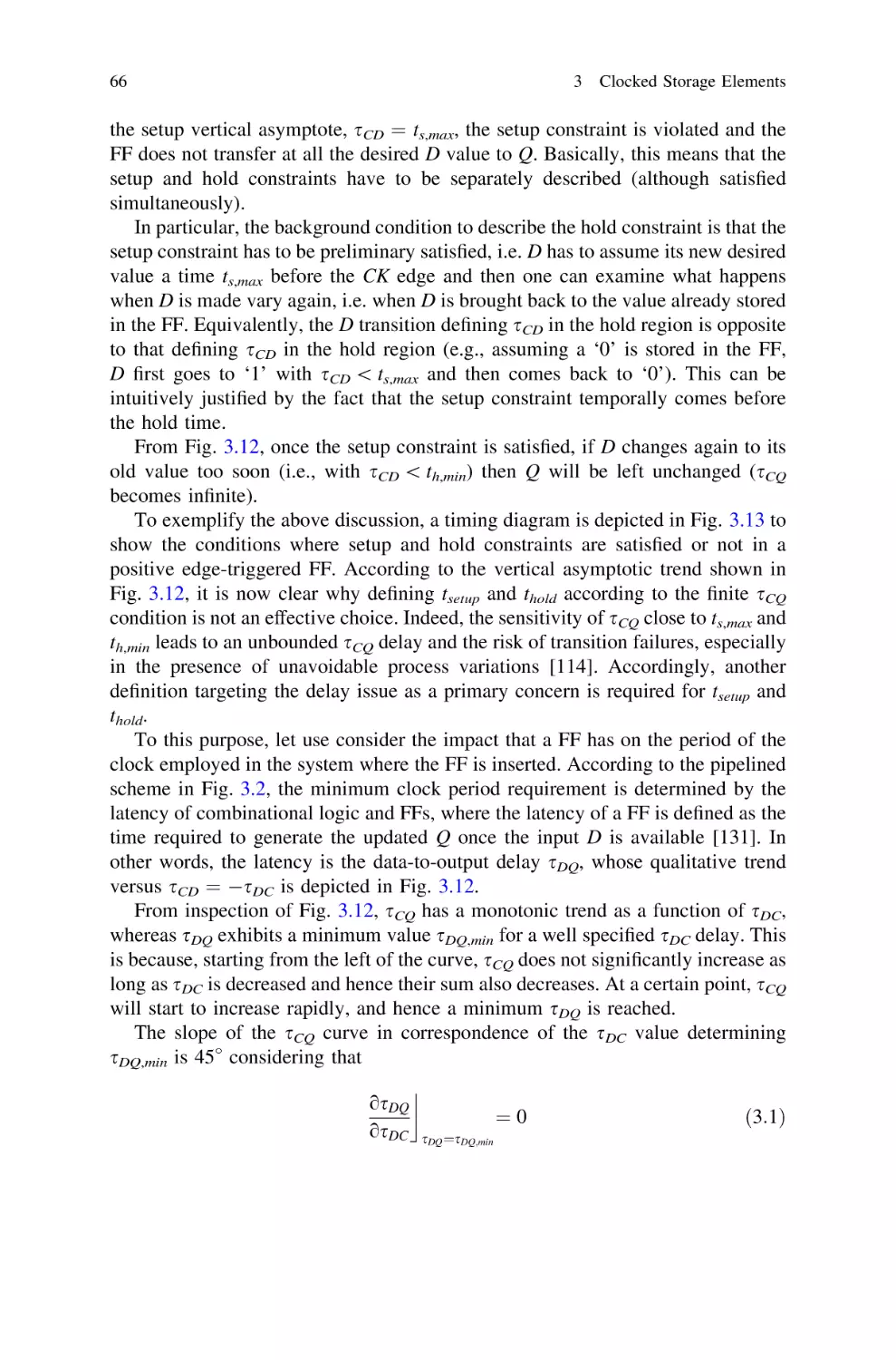


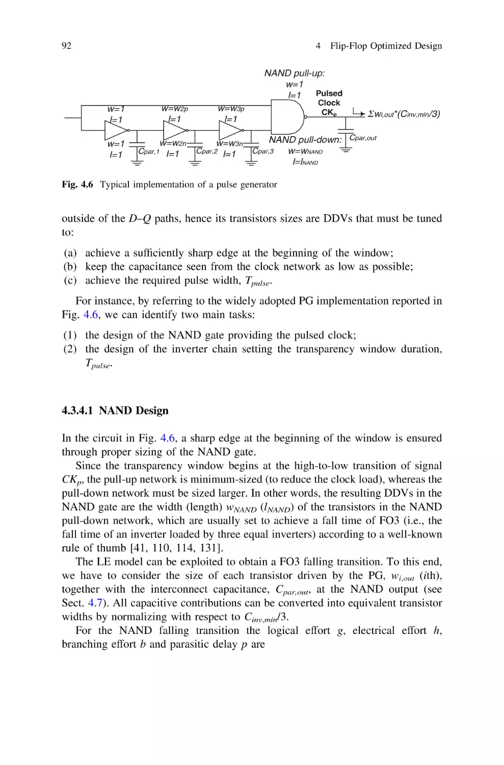


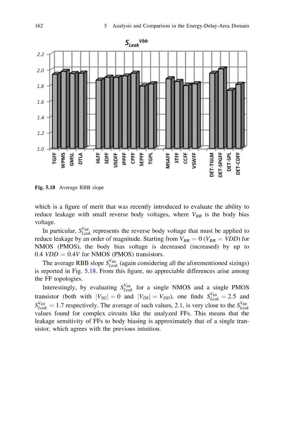


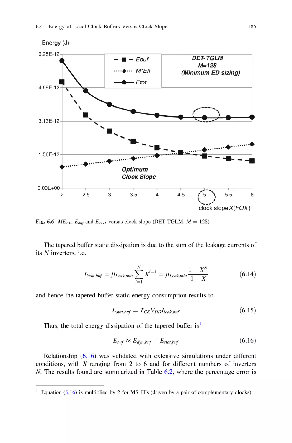

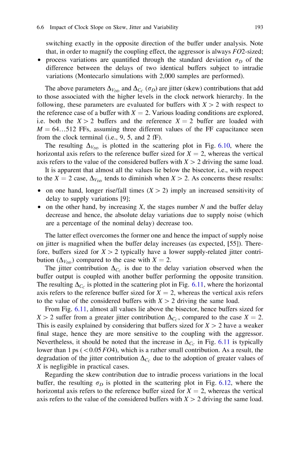
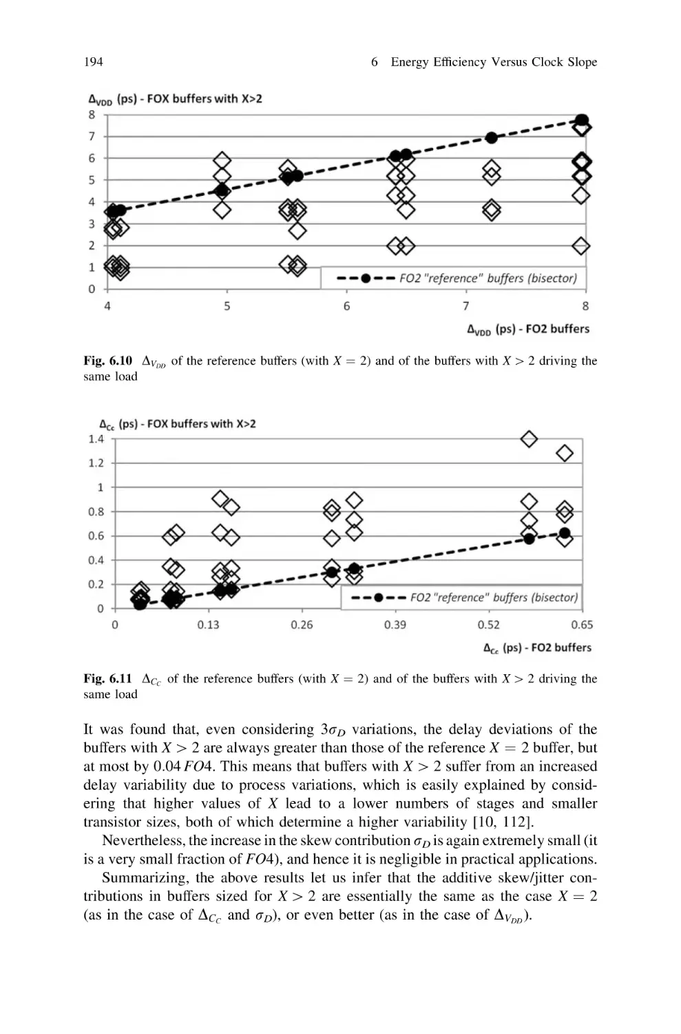


Текст
Massimo Alioto · Elio Consoli
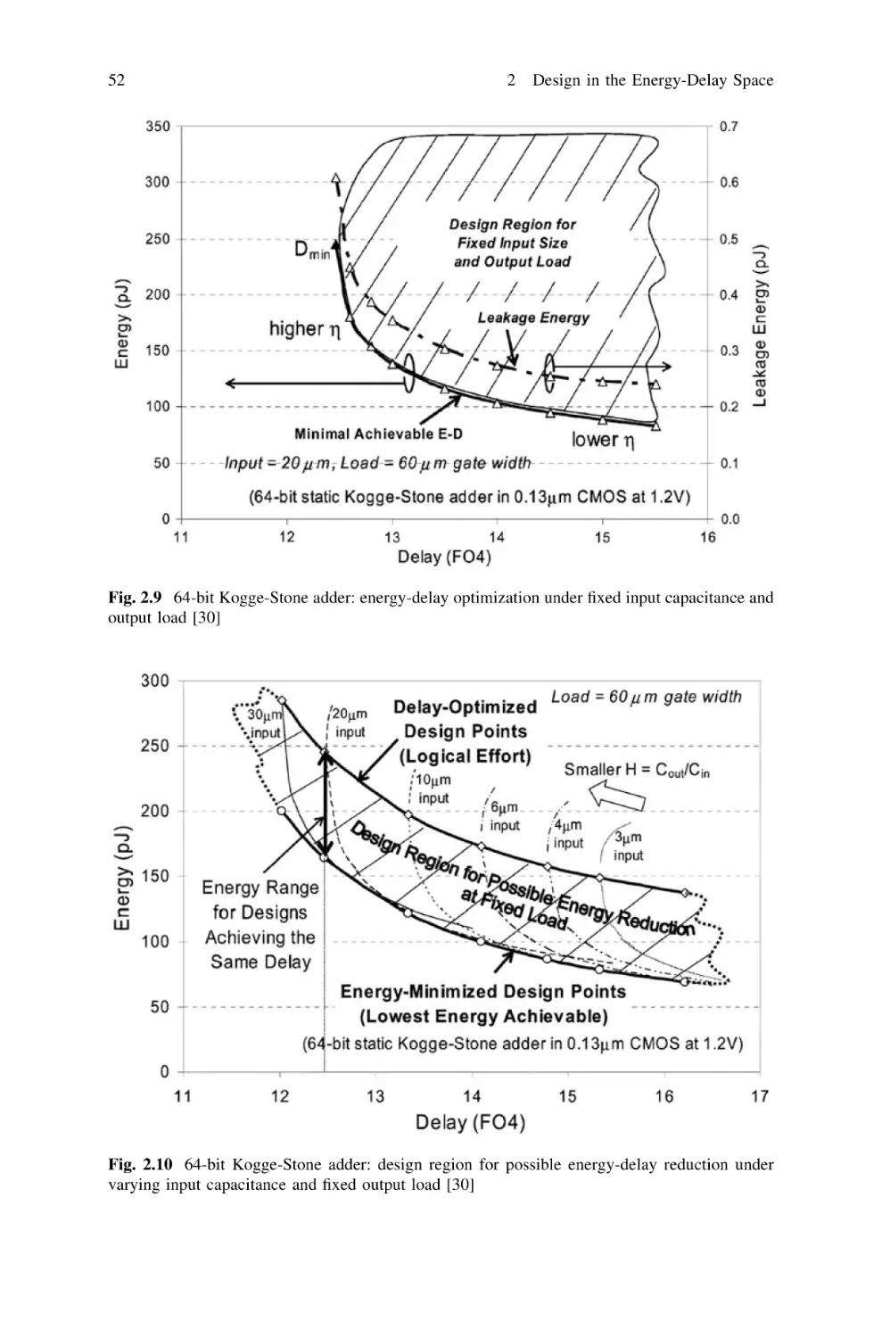
Gaetano Palumbo
Flip-Flop
Design in
Nanometer
CMOS
From High Speed to Low Energy
Flip-Flop Design in Nanometer CMOS
Massimo Alioto Elio Consoli
Gaetano Palumbo
•
Flip-Flop Design
in Nanometer CMOS
From High Speed to Low Energy
123
Massimo Alioto
ECE Department
National University of Singapore (NUS)
Singapore
Singapore
Gaetano Palumbo
University of Catania
Catania
Italy
Elio Consoli
Maxim Integrated Catania Design Center
Catania
Italy
ISBN 978-3-319-01996-3
ISBN 978-3-319-01997-0
DOI 10.1007/978-3-319-01997-0
Springer Cham Heidelberg New York Dordrecht London
(eBook)
Library of Congress Control Number: 2014941307
Ó Springer International Publishing Switzerland 2015
This work is subject to copyright. All rights are reserved by the Publisher, whether the whole or part of
the material is concerned, specifically the rights of translation, reprinting, reuse of illustrations,
recitation, broadcasting, reproduction on microfilms or in any other physical way, and transmission or
information storage and retrieval, electronic adaptation, computer software, or by similar or dissimilar
methodology now known or hereafter developed. Exempted from this legal reservation are brief
excerpts in connection with reviews or scholarly analysis or material supplied specifically for the
purpose of being entered and executed on a computer system, for exclusive use by the purchaser of the
work. Duplication of this publication or parts thereof is permitted only under the provisions of
the Copyright Law of the Publisher’s location, in its current version, and permission for use must
always be obtained from Springer. Permissions for use may be obtained through RightsLink at the
Copyright Clearance Center. Violations are liable to prosecution under the respective Copyright Law.
The use of general descriptive names, registered names, trademarks, service marks, etc. in this
publication does not imply, even in the absence of a specific statement, that such names are exempt
from the relevant protective laws and regulations and therefore free for general use.
While the advice and information in this book are believed to be true and accurate at the date of
publication, neither the authors nor the editors nor the publisher can accept any legal responsibility for
any errors or omissions that may be made. The publisher makes no warranty, express or implied, with
respect to the material contained herein.
Printed on acid-free paper
Springer is part of Springer Science+Business Media (www.springer.com)
To Maria Daniela and Marco, source of deep
inspiration, and Giusi for her encouragement
in perspiration
To my lovely wife Laura,
(mom) Francesca and (dad) Maurizio
To Michela, Francesca and Chiara
Preface
The design of the clocking subsystem represents a crucial aspect in CMOS VLSI
integrated circuits, as it strongly affects not only the chip performance, but also its
overall energy consumption. Independently of the nature of the system (fully
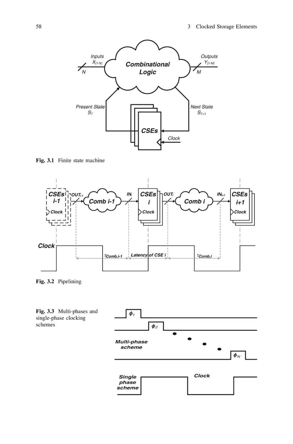
synchronous, globally asynchronous, locally synchronous), any clocking subsystem can be subdivided into three main parts: similar to the structure of a tree, the
root is represented by the clock generation, the branches are represented by the
circuits devoted to clock distribution, and the clocked storage elements (i.e., latches and/or flip-flops) are the final leaves. Flip-flops (or, more in general, clocked
storage elements) are among the most important cells used in digital systems, such
as microprocessors. They separate the various stages that pipelines are made up of,
hold the state, and prevent early transitions that would be otherwise determined by
fast paths. Overall, flip-flops synchronize and regulate the entire flow of data
within a digital system.
In high-performance systems, relatively little combinational logic is contained
by each pipeline stage, hence flip-flops introduce a timing overhead that is a
significant fraction of the clock cycle. On the other hand, due to the high switching
activity of the clock signal, the overall dissipation of the clocking subsystem can
be as high as 30 50 % of the overall chip energy budget. It is crucial to keep
this energy within reasonable bounds, since it reduces the energy available for
computation under a given energy budget, and hence it limits the overall performance in power-limited systems (i.e., the vast majority of practical cases).
The above performance and energy issues, together with the need for adequate
robustness and ability to deal with clock uncertainties, make the flip-flops design
quite tricky. Accordingly, these circuits have been extensively studied in the past,
and significant effort has been devoted to propose new circuit solutions and to
properly select the flip-flop topology depending on the requirements set by the
application. Such a task is further complicated by the issues that are naturally
posed by nanometer technologies, such as the impact of (a) layout parasitics
associated with interconnections, degrading both speed and energy, (b) leakage,
affecting energy both in active and in standby mode, and (c) process and environmental variations, which require considerable design margin that negatively
impact both performance and energy. Unfortunately, the existing body of work on
flip-flop design largely neglects all these effects, and a more thorough analysis is
needed to allow the designer to take the above issues into account.
vii
viii
Preface
The energy-aware design, the comparison, and the selection of the most
appropriate flip-flop topology for a targeted application has been recently investigated by the authors. The main focus of this book is to provide the reader with a
deep understanding of the challenges associated with flip-flop design, and with
clear guidelines to select the most suitable topology when all the above-mentioned
nanometer issues are included. Basic foundations are provided to set the stage for
the comprehension of analyses and results. Unitary and well-grounded simulation
and evaluation methodologies are presented, and many analytical derivations are
included to gain an insight into the main dependencies of important parameters on
circuit properties. Finally, several quantitative results are reported to emphasize
the practical perspective of the book, as a result of an extensive and thorough
simulation analysis.
The book can be used as a reference to practicing engineers working in VLSI
design and also by undergraduate, graduate, and postgraduate students who are
already familiar with basic electronics and digital circuits design.
The outline of the book is as follows. The first three chapters contain all the
theoretical background (including novel modeling approaches), which is then used
in the remainder of the book. Chapter 1 describes the well-known Logical Effort
method, which is extensively adopted throughout the book for both modeling and
design purposes.
Chapter 2 is about the energy consumption of digital circuits and the adopted
framework to evaluate the efficiency of the energy-delay tradeoff. The adoption of
suitable figures of merit and the concept of energy-efficient curve are discussed. A
novel methodology to optimize transistor sizes is introduced to manage the
energy-delay tradeoff. In this chapter, it is also shown that Logical Effort enables
the derivation of practical design constraints, when exploring the energy-delay
space.
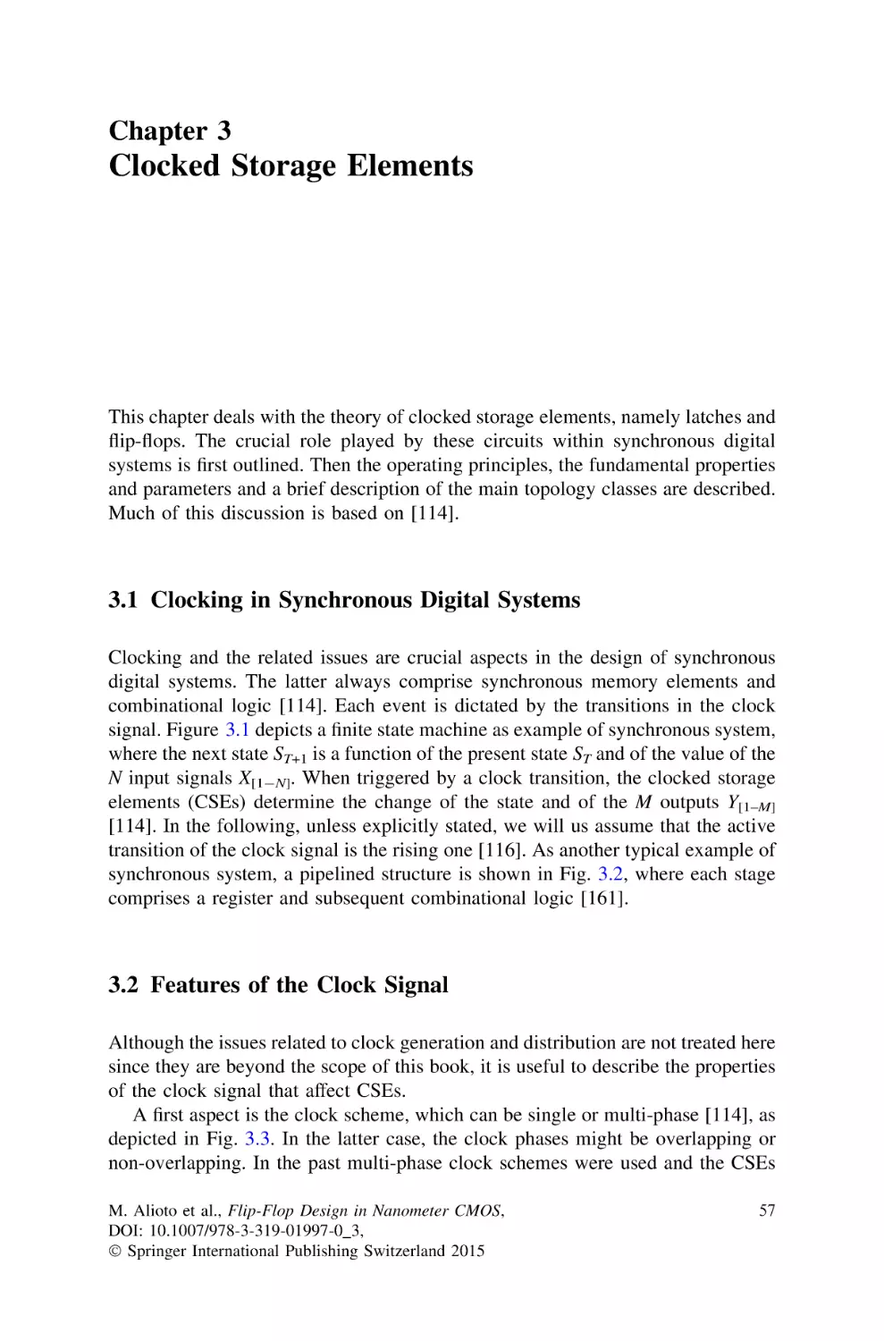
Chapter 3 provides an overview of the clocking subsystem and clocked storage
elements, introducing the main timing and energy parameters. A general classification of clocked storage elements is presented, and their basic properties are
reviewed.
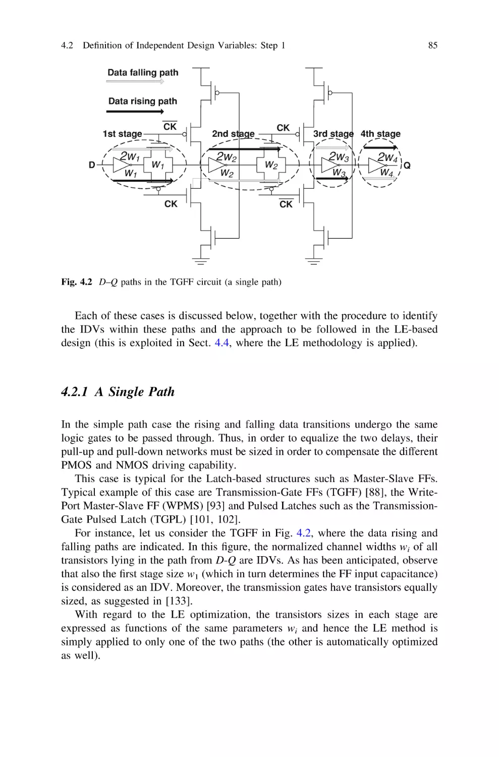
A comprehensive design strategy for nanometer CMOS flip-flops through circuit energy-delay optimization is presented in Chap. 4. The methodology also
accounts for the important contribution of interconnect parasitics, based on the
Logical Effort and energy-efficient design methodologies described in the first two
chapters.
The results of a wide comparison of 19 flip-flop topologies belonging to four
classes (Master–Slave; Pulsed both Implicit and Explicit; Differential and DualEdge-Triggered), and selected among the most representative and best known
topologies, are reported in Chap. 5. The exploration of several tradeoffs, including
energy, delay, leakage, area, and clock load allows for comparing flip-flops in a
very general manner.
Chapter 6 presents results on the optimization of clock buffers, based on the
explicit analysis of their interaction with flip-flops and using the clock slope as a
design parameter.
Preface
ix
The impact of variations on flip-flops is analyzed in Chap. 7. Process/voltage/
temperature (PVT) variations, as well as variations induced by the clock distribution network (i.e., clock slope variations) are thoroughly analyzed and compared
for Single-Edge Triggered flip-flops. As far as Double-Edge Triggered flip-flops
are concerned, results are summarized in the Appendix of the same chapter to
improve the readability.
Finally, in Chap. 8, a novel class of ultrafast and extremely energy-efficient
flip-flop topologies that were recently proposed by the authors is presented,
together with experimental results from an integrated prototype in 65 nm CMOS.
The proposed topologies achieve the best speed and energy efficiency in the
high-speed to minimum ED product region of the design space that have ever been
reported so far.
Contents
1
2
Logical Effort Method . . . . . . . . . . . . . . . . . . . . . . . . . .
An RC Model for the Delay of Logic Gates . . . . . . . . . . .
The Logical Effort Model. . . . . . . . . . . . . . . . . . . . . . . .
Limitations of the Original Logical Effort Model . . . . . . .
Basic Estimation of Logical Effort Parameters . . . . . . . . .
Accurate Estimation of Parameters g and p . . . . . . . . . . .
1.5.1 Estimation of the Capacitance at Internal Nodes . . .
1.5.2 Elmore Delay . . . . . . . . . . . . . . . . . . . . . . . . . . .
1.5.3 Parameter Calibration . . . . . . . . . . . . . . . . . . . . .
1.5.4 Non-step Input . . . . . . . . . . . . . . . . . . . . . . . . . .
1.6 Multistage Logic Networks and Delay Minimization . . . . .
1.6.1 Path Parameters . . . . . . . . . . . . . . . . . . . . . . . . .
1.6.2 Optimized Design . . . . . . . . . . . . . . . . . . . . . . . .
1.7 Optimum Number of Stages . . . . . . . . . . . . . . . . . . . . . .
1.8 Extension of the Model to Non-static Gates . . . . . . . . . . .
1.8.1 Dynamic and Domino Gates with Keeper . . . . . . .
1.8.2 Logic with Transmission Gates and Pass-transistors
1.9 Nonlinearities and Need for Iterative Procedures . . . . . . . .
Appendix: Derivation of Logical Effort with a Transistor
Current Source Model . . . . . . . . . . . . . . . . . . . . . . . . . . . . . .
The
1.1
1.2
1.3
1.4
1.5
Design in the Energy-Delay Space . . . . . . . . . . . . . . . . .
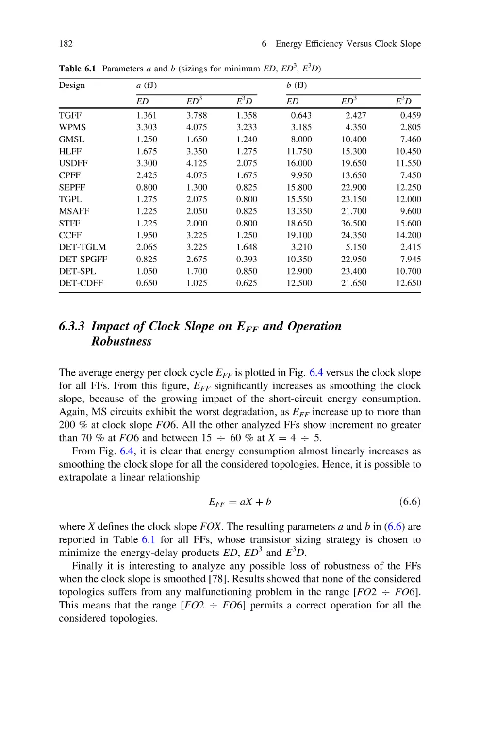
2.1 Energy Modeling. . . . . . . . . . . . . . . . . . . . . . . . . . .
2.2 Energy-Delay Space Analysis and Hardware-Intensity .
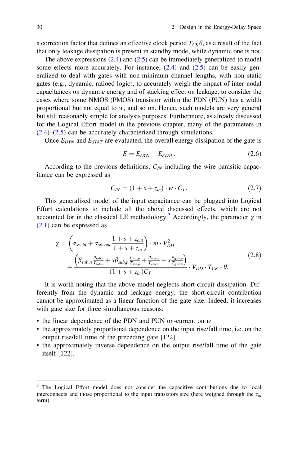
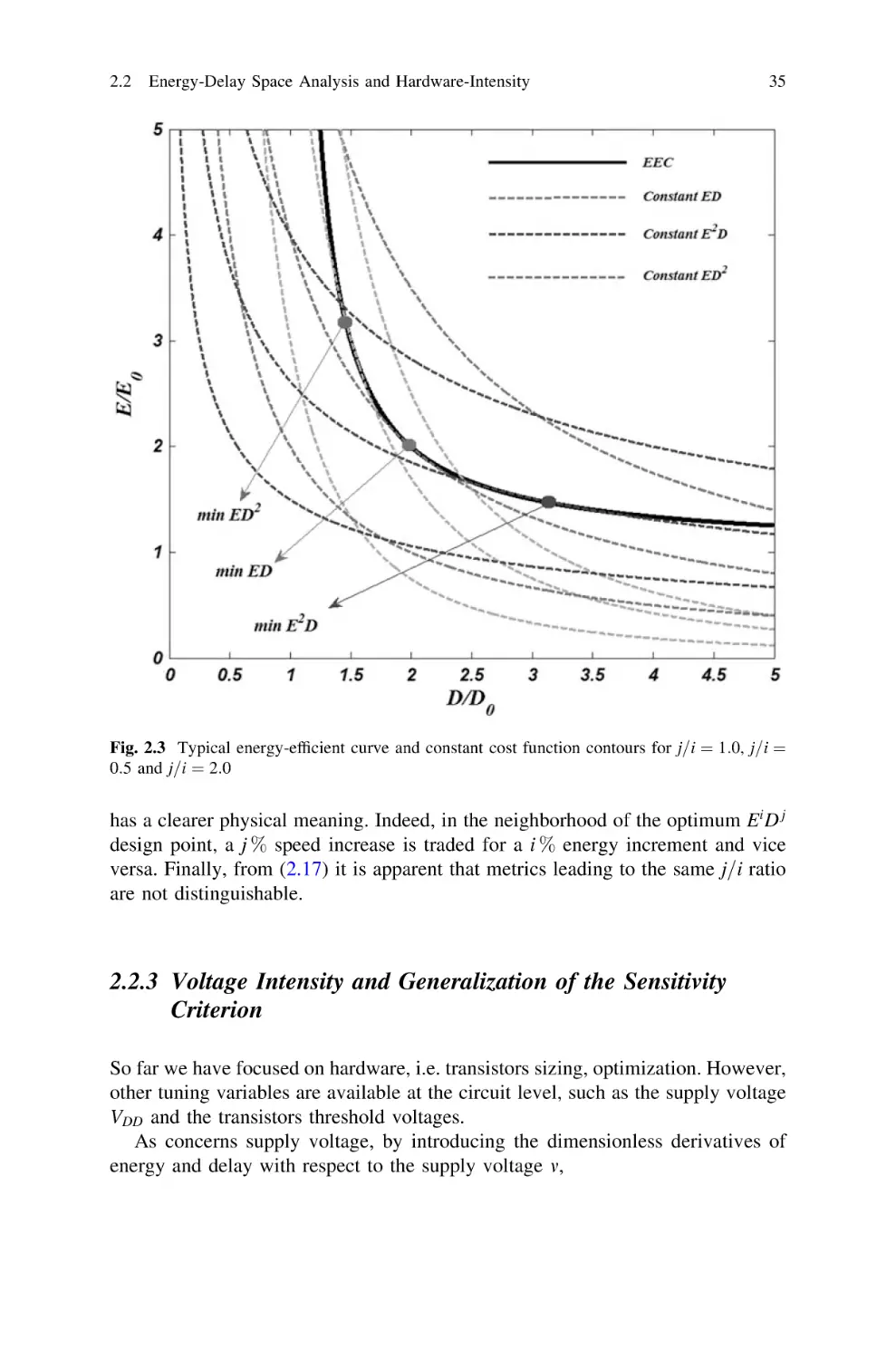
2.2.1 The Energy-Efficient Curve . . . . . . . . . . . . . .
2.2.2 Energy-Delay Metrics and Hardware Intensity .
2.2.3 Voltage Intensity and Generalization
of the Sensitivity Criterion . . . . . . . . . . . . . . .
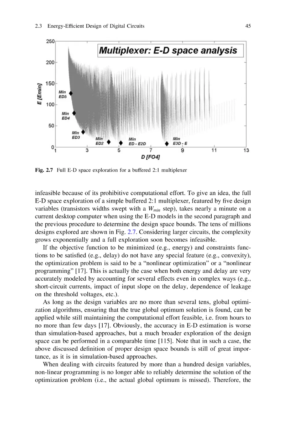
2.3 Energy-Efficient Design of Digital Circuits . . . . . . . .
2.3.1 The Role of the Input Capacitance . . . . . . . . .
2.3.2 Derivation of Design Space Bounds . . . . . . . .
2.3.3 Simulation-Based Optimization
of Small-Sized Circuits . . . . . . . . . . . . . . . . .
.
.
.
.
.
.
.
.
.
.
.
.
.
.
.
.
.
.
.
.
.
.
.
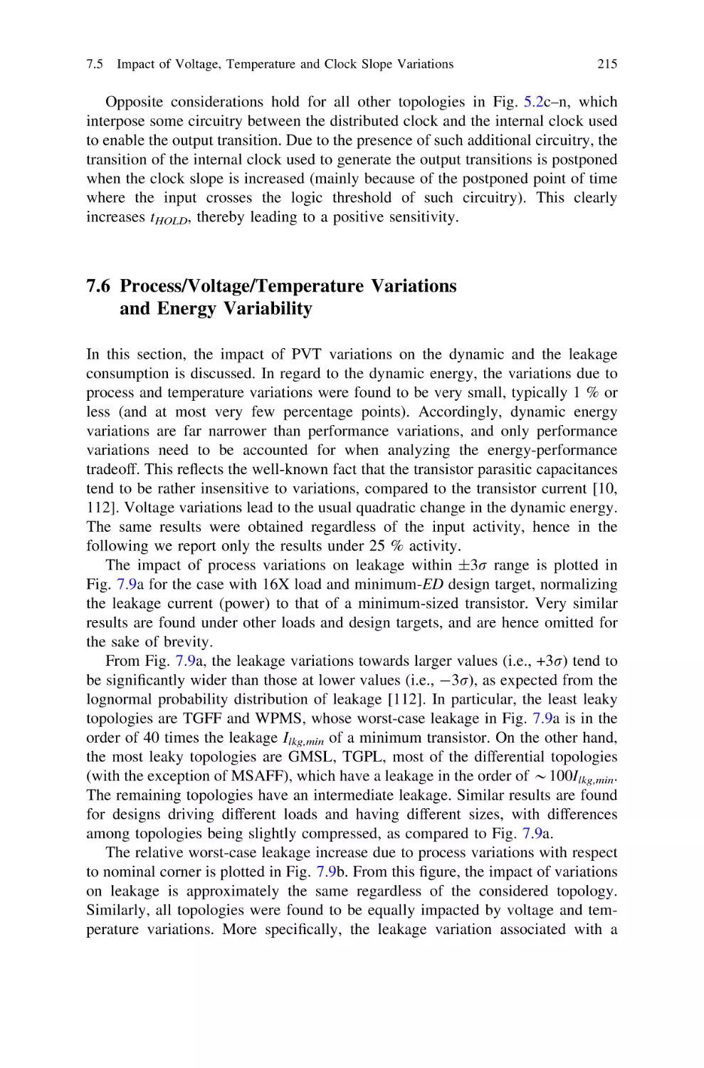
.
.
.
.
.
.
.
.
.
.
.
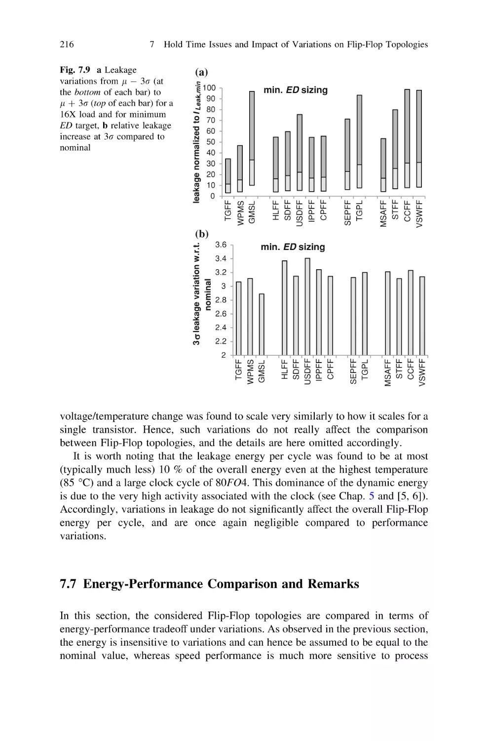
.
.
.
.
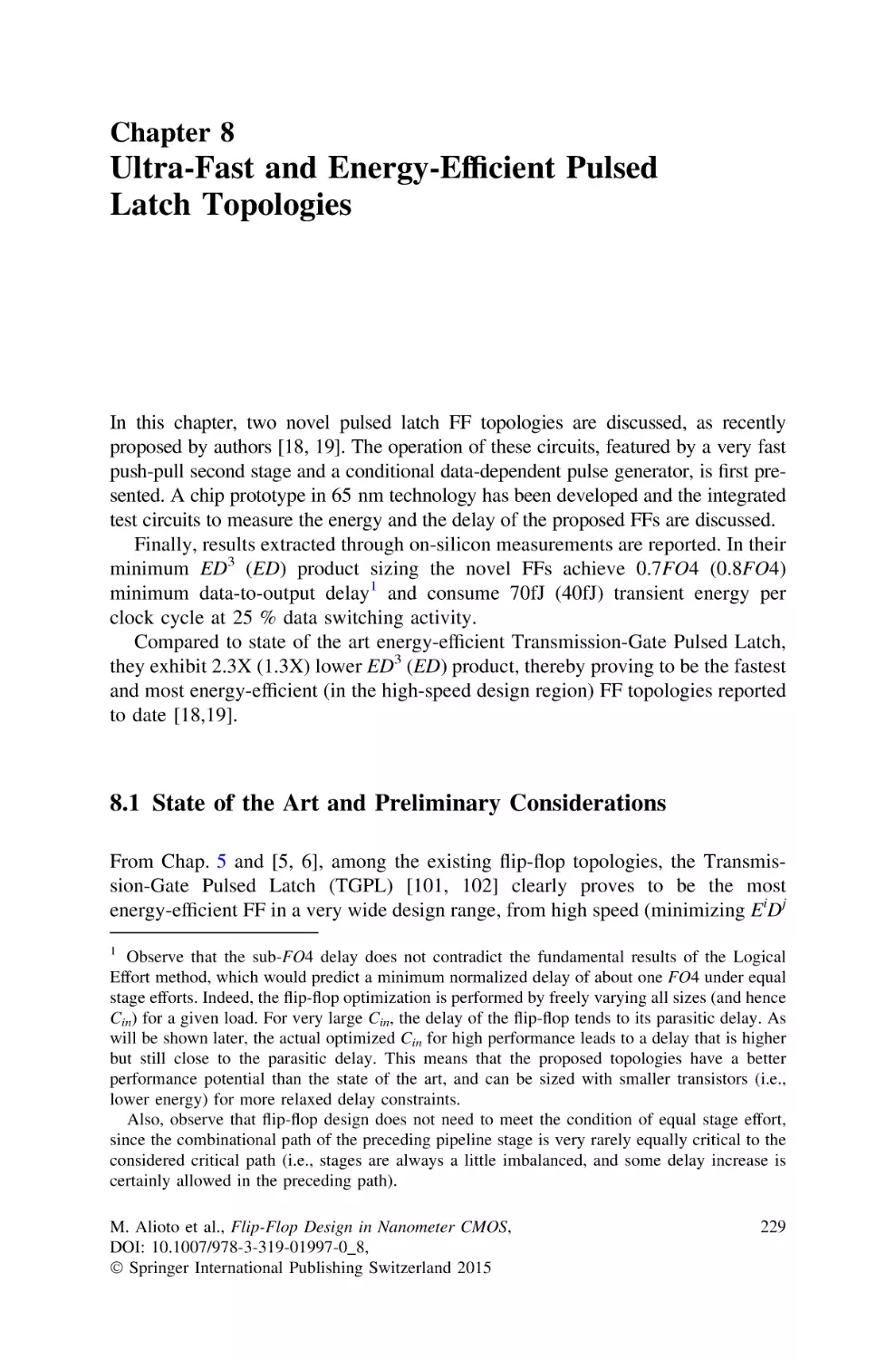
.
.
.
.
.
.
.
.
.
.
.
.
.
.
.
.
.
.
.
.
.
.
.
.
.
.
.
.
.
.
.
.
.
.
1
1
4
5
8
10
11
12
14
15
16
16
17
19
20
21
22
24
....
25
.
.
.
.
.
.
.
.
.
.
.
.
.
.
.
.
.
.
.
.
.
.
.
.
.
.
.
.
.
.
.
.
.
.
.
27
27
31
31
33
.
.
.
.
.
.
.
.
.
.
.
.
.
.
.
.
.
.
.
.
.
.
.
.
.
.
.
.
35
37
37
38
.......
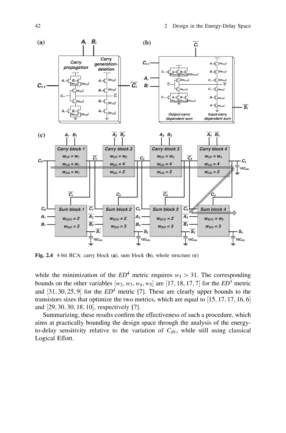
43
xi
xii
Contents
2.3.4
Nonlinear and Convex Optimization of Large
Size Circuits. . . . . . . . . . . . . . . . . . . . . . . . .
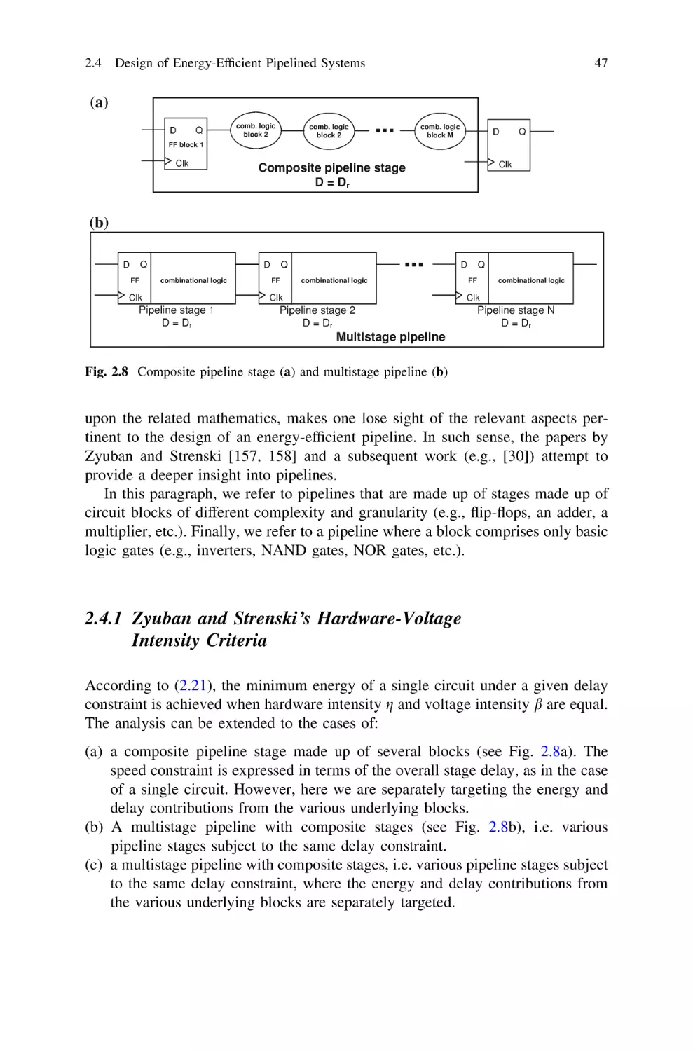
2.4 Design of Energy-Efficient Pipelined Systems . . . . . .
2.4.1 Zyuban and Strenski’s Hardware-Voltage
Intensity Criteria . . . . . . . . . . . . . . . . . . . . . .
2.4.2 Practical Guidelines to Design Energy-Efficient
Pipelines . . . . . . . . . . . . . . . . . . . . . . . . . . .
Appendix: Convex Optimization . . . . . . . . . . . . . . . . . . . .
3
4
.......
.......
44
46
.......
47
.......
.......
51
54
Clocked Storage Elements . . . . . . . . . . . . . . . . . . . . . . . . . .
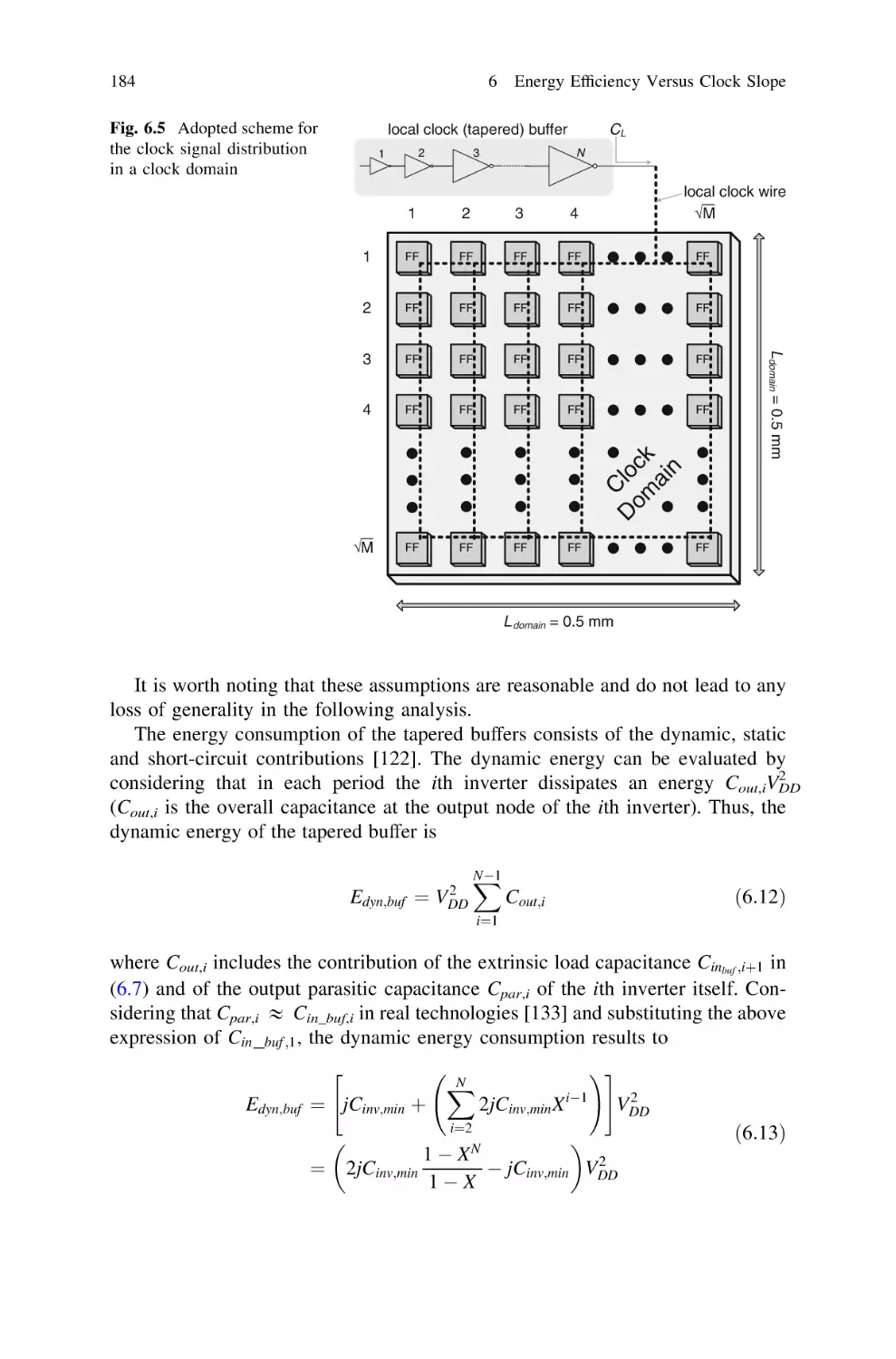
3.1 Clocking in Synchronous Digital Systems . . . . . . . . . . . .
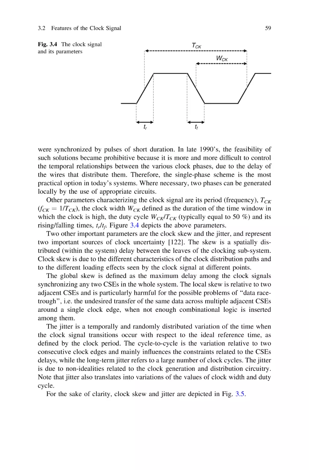
3.2 Features of the Clock Signal . . . . . . . . . . . . . . . . . . . . . .
3.3 Clocked Storage Elements: Latches, Master–Slave
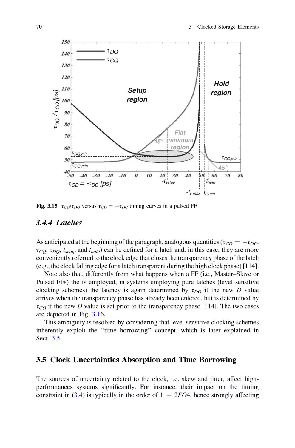
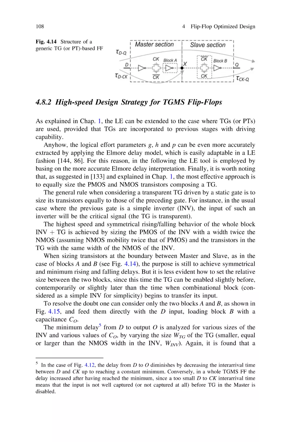
Flip-Flops and Pulsed Topologies . . . . . . . . . . . . . . . . . .
3.4 Timing Parameters of Clocked Storage Elements . . . . . . .
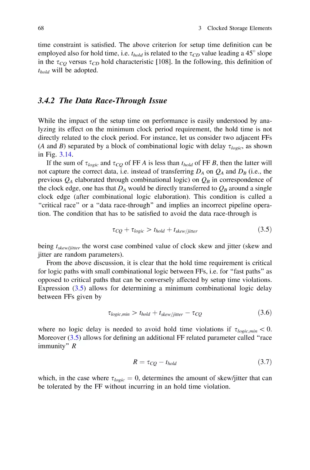
3.4.1 Setup Time and Hold Time . . . . . . . . . . . . . . . . .
3.4.2 The Data Race-Through Issue . . . . . . . . . . . . . . .
3.4.3 Differences Between Master–Slave and Pulsed FFs.
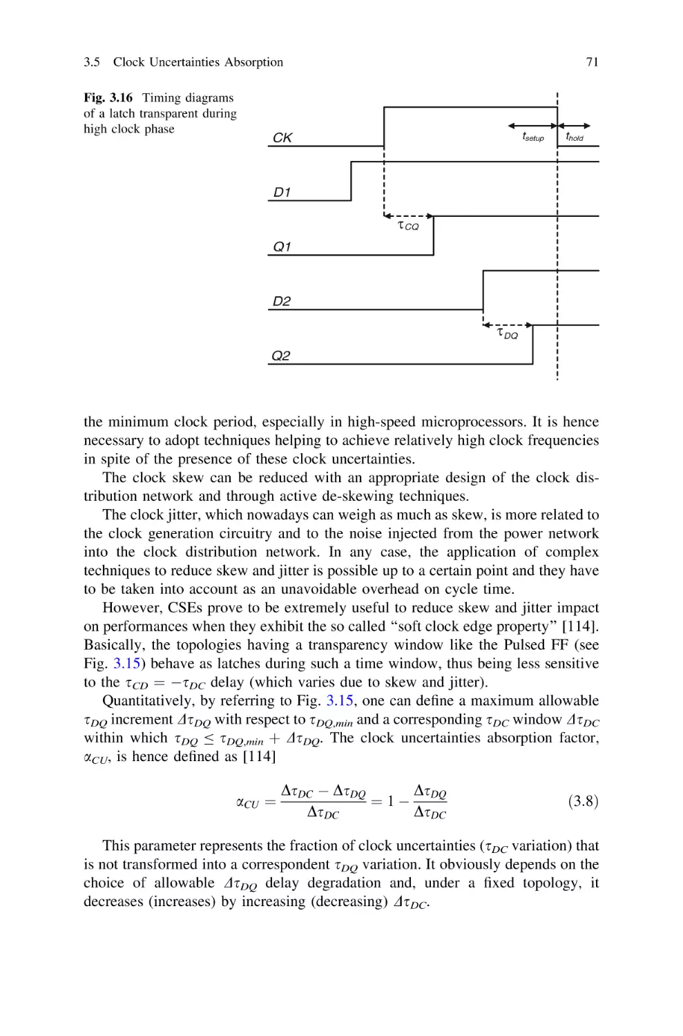
3.4.4 Latches . . . . . . . . . . . . . . . . . . . . . . . . . . . . . . .
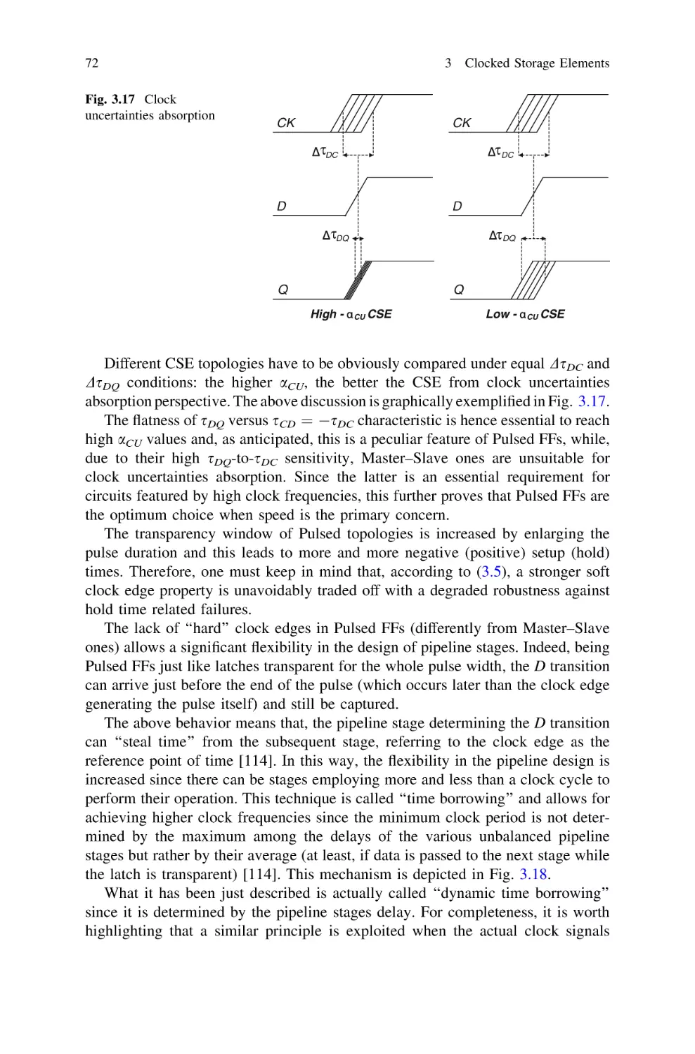
3.5 Clock Uncertainties Absorption and Time Borrowing . . . .
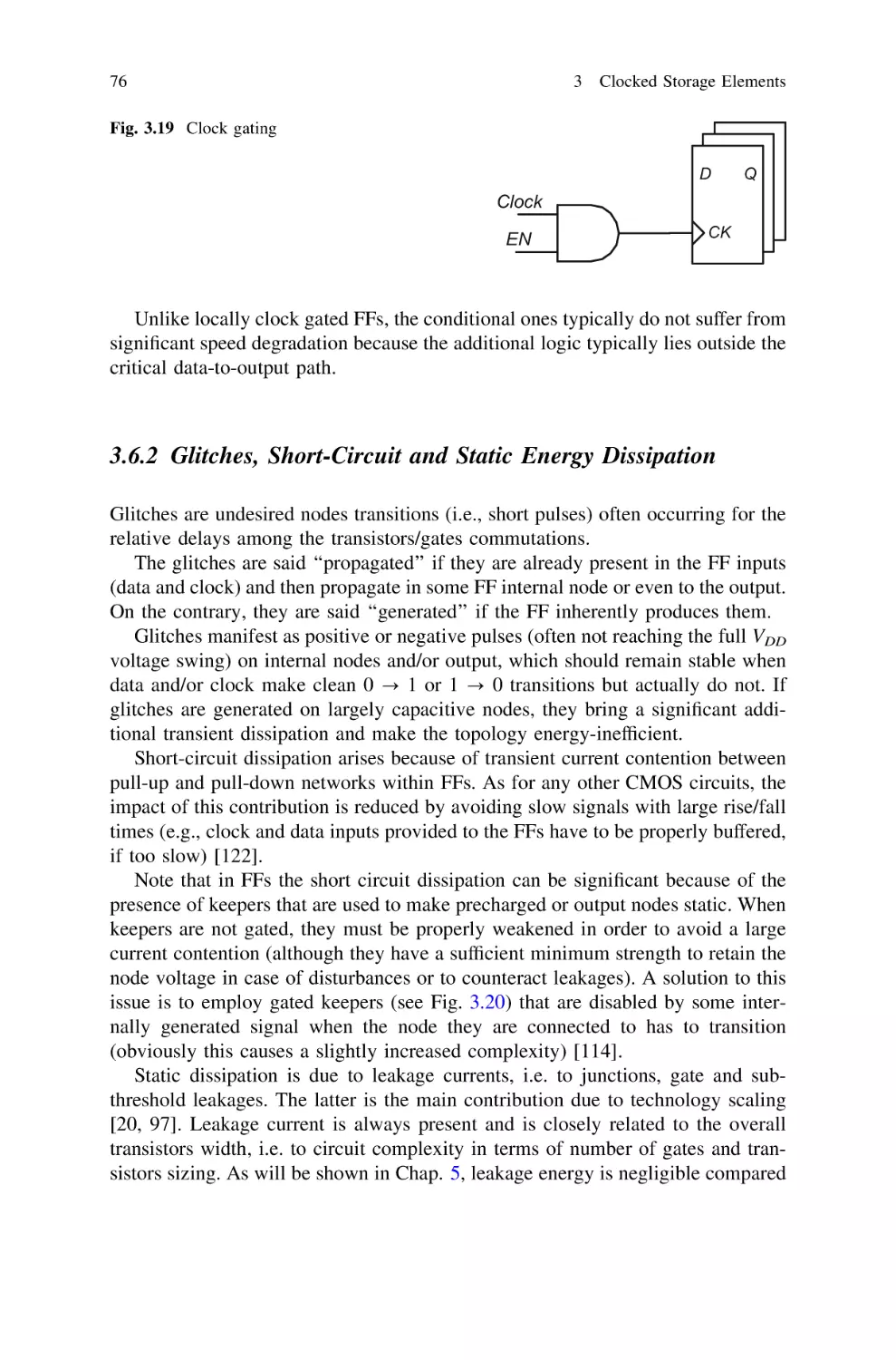
3.6 Energy Consumption in Flip-Flops . . . . . . . . . . . . . . . . .
3.6.1 Dynamic Energy Dissipation and Techniques
for Its Reduction . . . . . . . . . . . . . . . . . . . . . . . . .
3.6.2 Glitches, Short-Circuit and Static
Energy Dissipation . . . . . . . . . . . . . . . . . . . . . . .
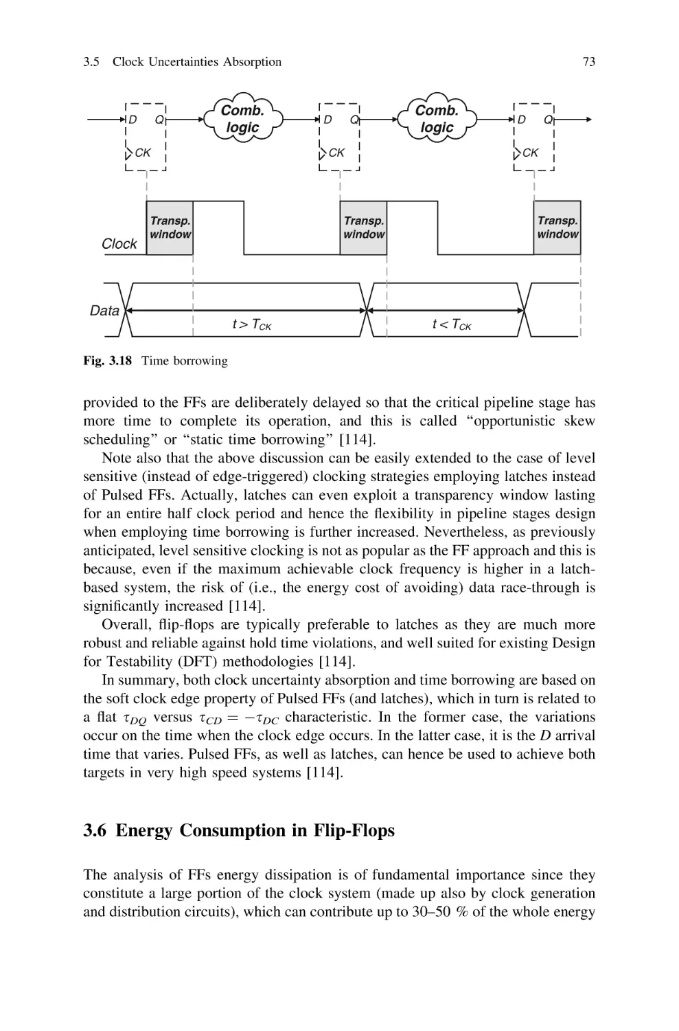
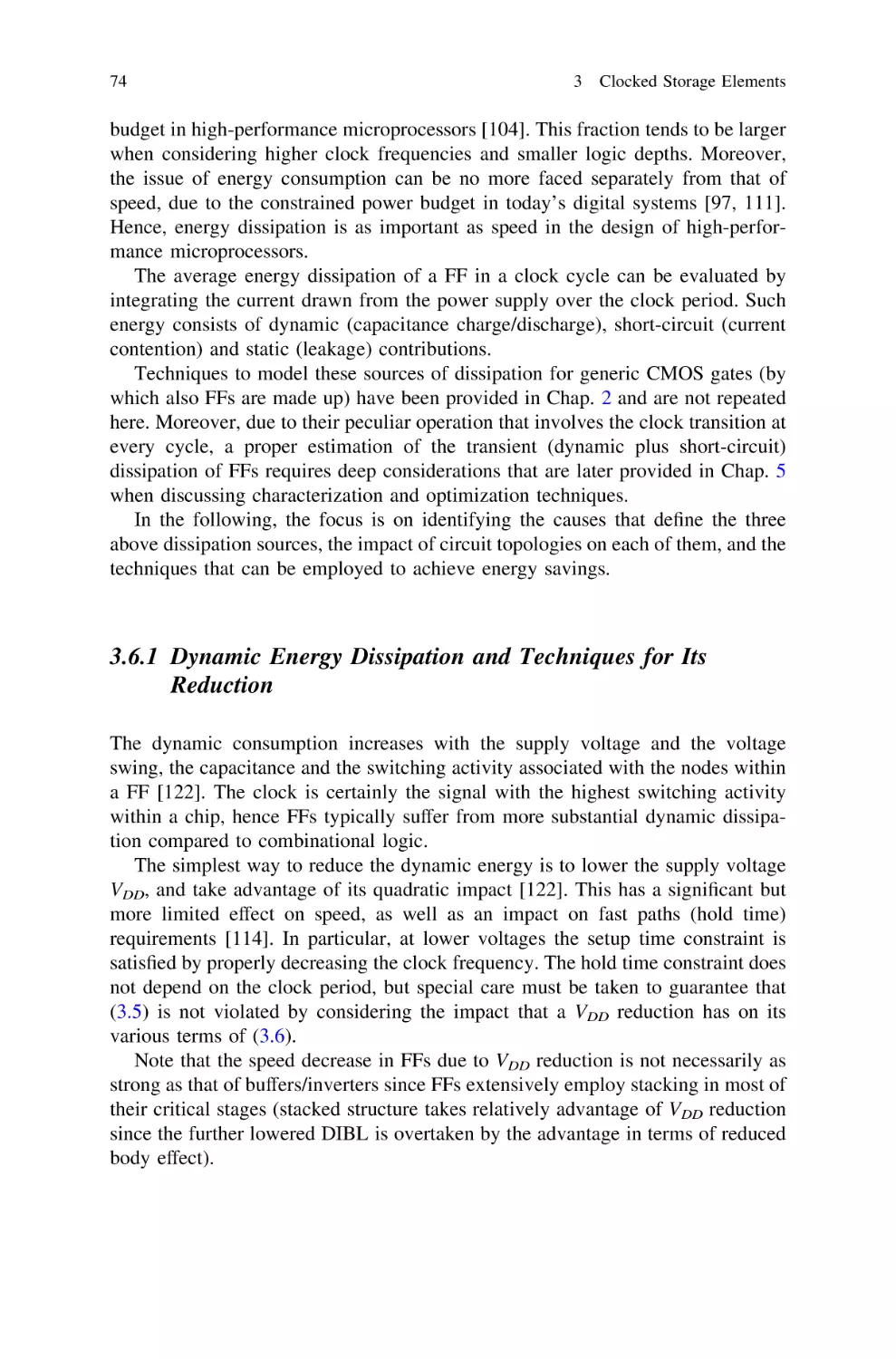
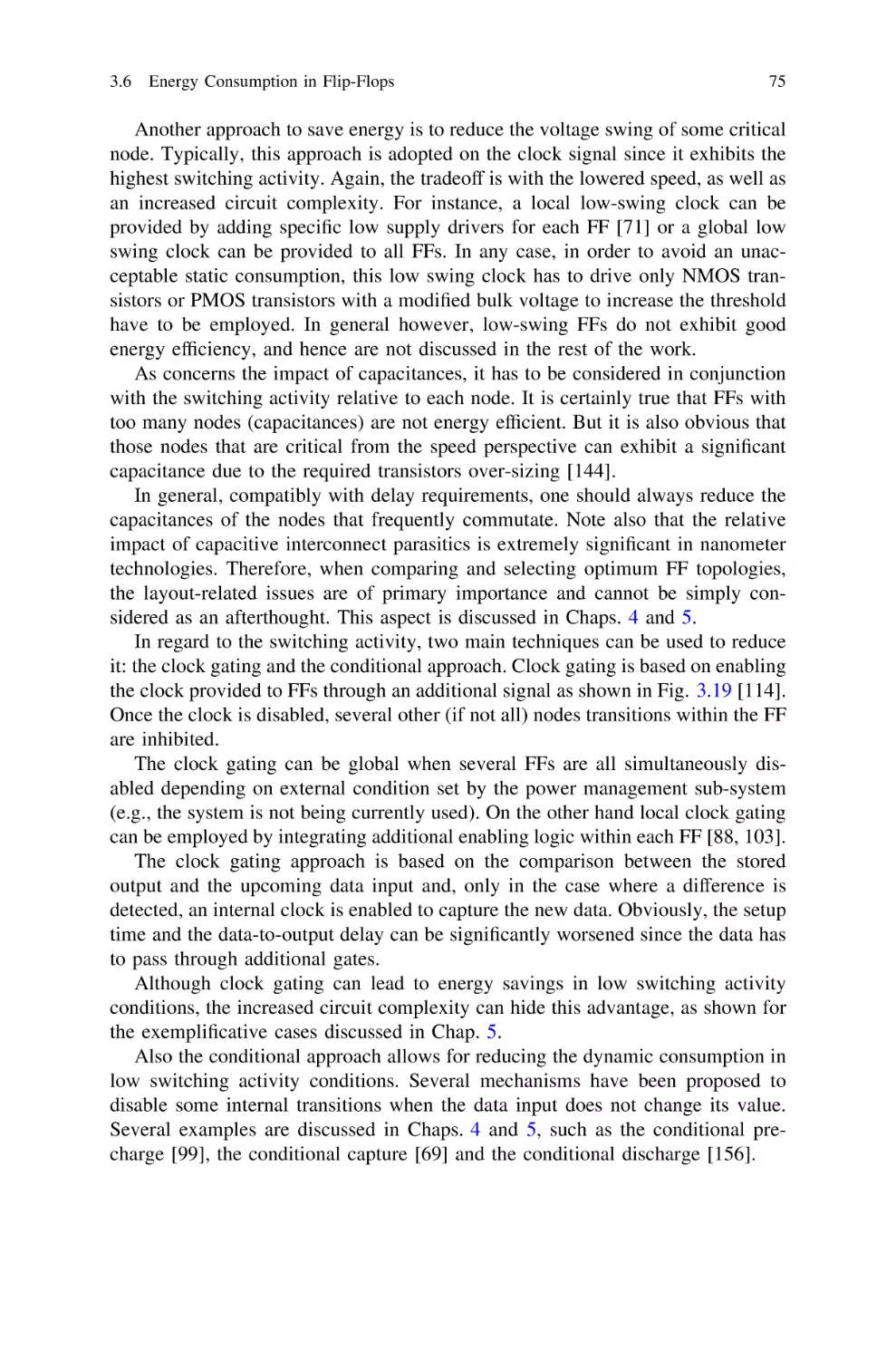
3.7 Differential and Dual Edge-Triggered Topologies . . . . . . .
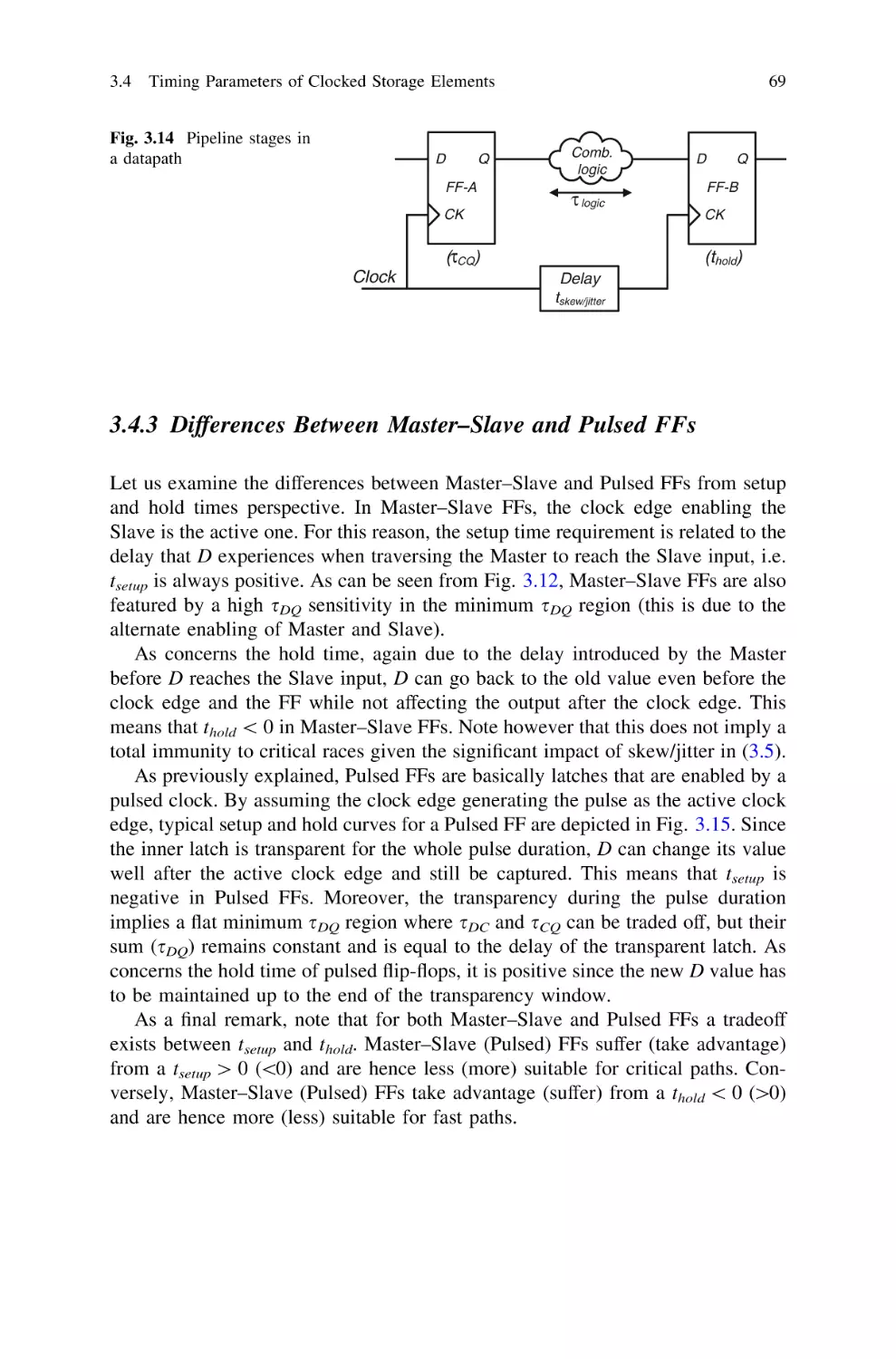
Flip-Flop Optimized Design . . . . . . . . . . . . . . . . . . . . . . . . .
4.1 A Comprehensive Design Approach . . . . . . . . . . . . . . . .
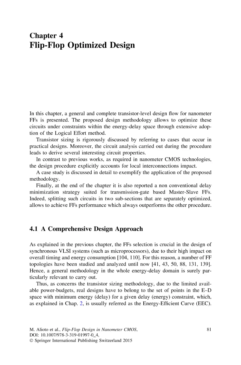
4.2 Definition of Independent Design Variables: Step 1. . . . . .
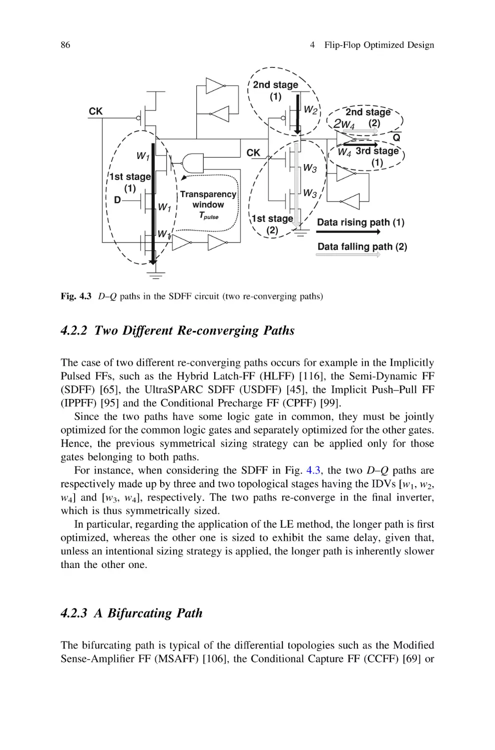
4.2.1 A Single Path . . . . . . . . . . . . . . . . . . . . . . . . . . .
4.2.2 Two Different Re-converging Paths . . . . . . . . . . .
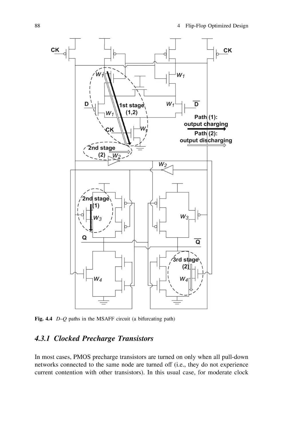
4.2.3 A Bifurcating Path . . . . . . . . . . . . . . . . . . . . . . .
4.2.4 Other Cases . . . . . . . . . . . . . . . . . . . . . . . . . . . .
4.3 Sizing of Dependent Design Variables: Step 2 . . . . . . . . .
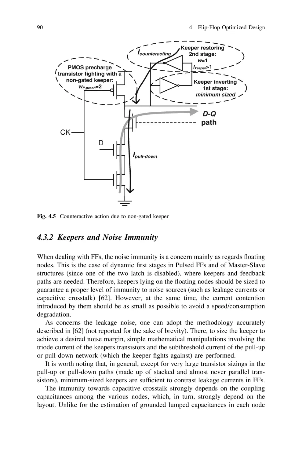
4.3.1 Clocked Precharge Transistors . . . . . . . . . . . . . . .
4.3.2 Keepers and Noise Immunity . . . . . . . . . . . . . . . .
4.3.3 Feedback Paths . . . . . . . . . . . . . . . . . . . . . . . . . .
4.3.4 Pulse Generators . . . . . . . . . . . . . . . . . . . . . . . . .
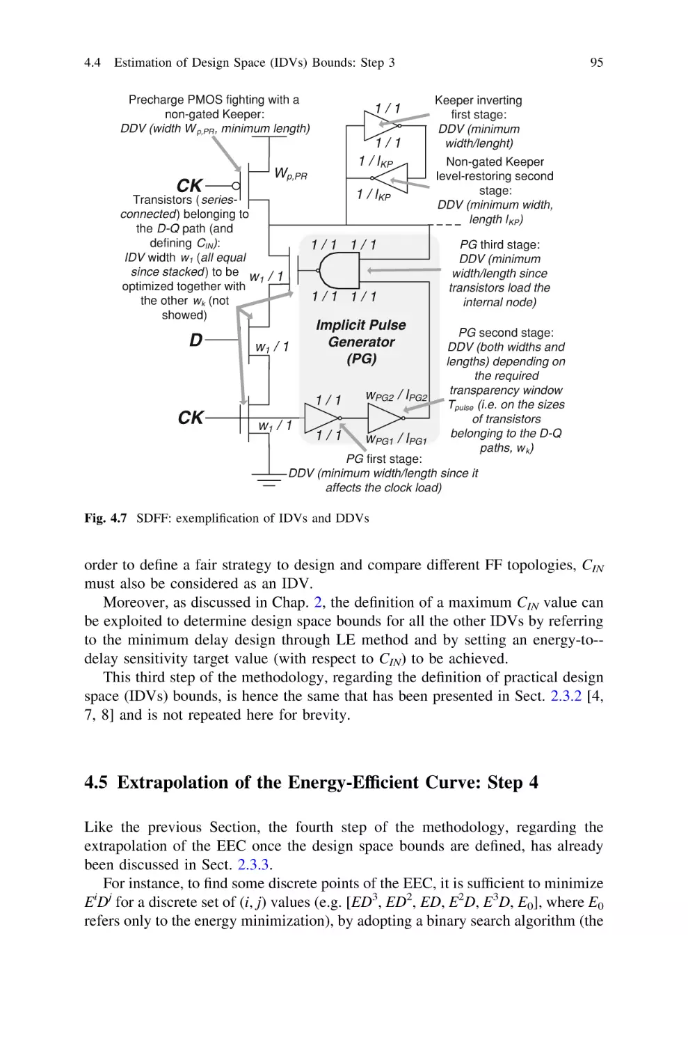
4.3.5 IDVs and DDVs in SDFF First Stage . . . . . . . . . .
4.4 Estimation of Design Space (IDVs) Bounds: Step 3. . . . . .
4.5 Extrapolation of the Energy-Efficient Curve: Step 4 . . . . .
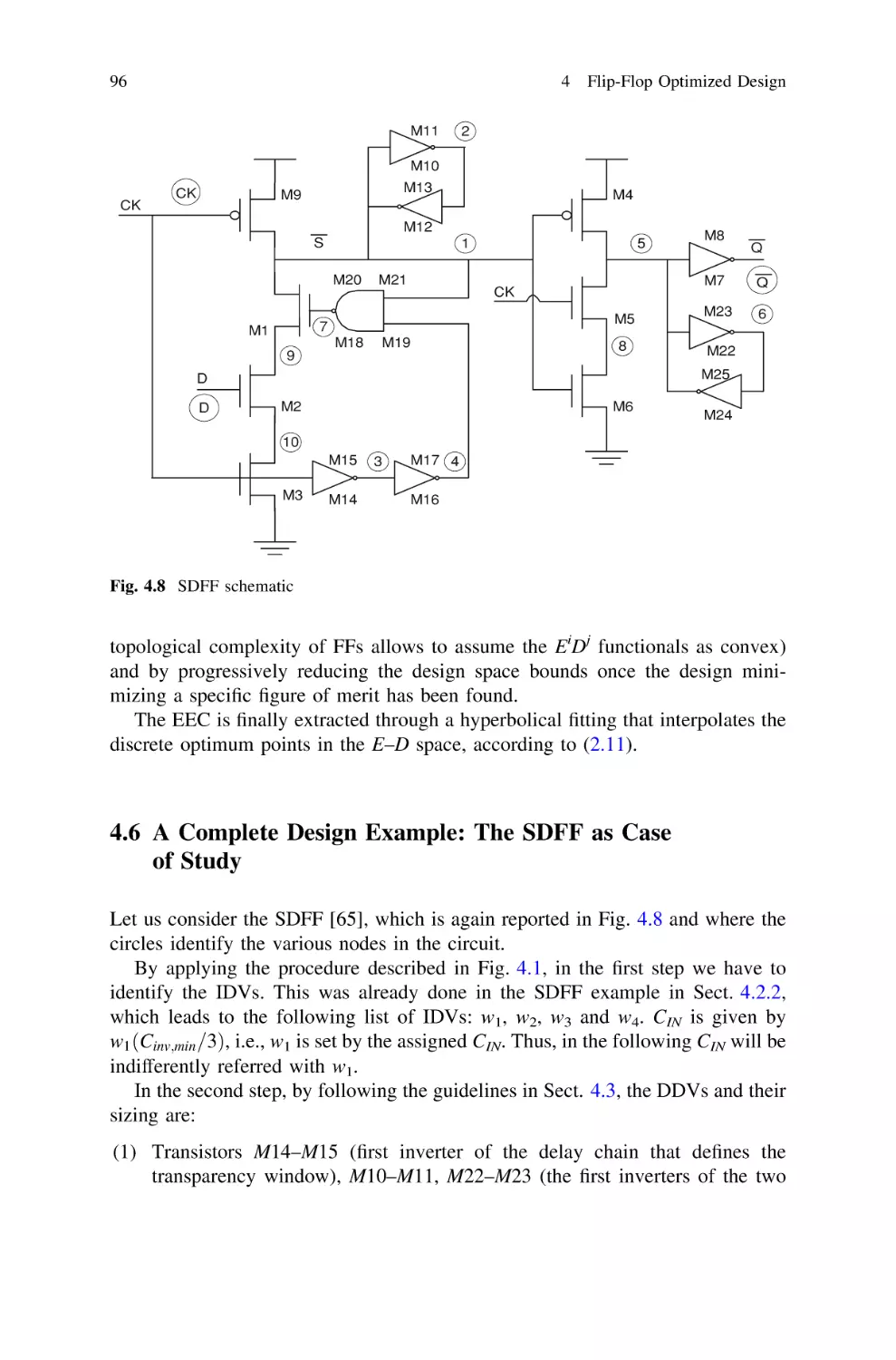
4.6 A Complete Design Example: The SDFF as Case of Study
....
....
....
57
57
57
.
.
.
.
.
.
.
.
.
.
.
.
.
.
.
.
60
64
64
68
69
70
70
73
....
74
....
....
76
77
.
.
.
.
.
.
.
.
.
.
.
.
.
.
.
.
81
81
84
85
86
86
87
87
88
90
91
91
94
94
95
96
.
.
.
.
.
.
.
.
.
.
.
.
.
.
.
.
.
.
.
.
.
.
.
.
.
.
.
.
.
.
.
.
.
.
.
.
.
.
.
.
.
.
.
.
.
.
.
.
.
.
.
.
.
.
.
.
.
.
.
.
.
.
.
.
Contents
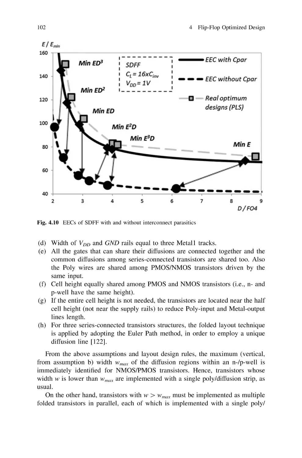
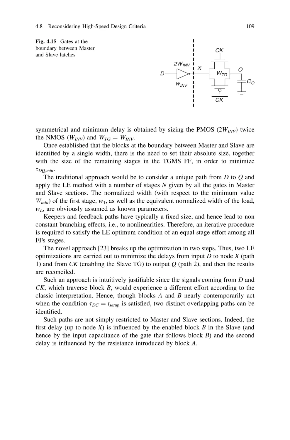
4.7
Estimation of Layout Parasitics in Transistor-Level
Design Iterations . . . . . . . . . . . . . . . . . . . . . . . . . . . . .
4.7.1 Estimation of Layout Parasitics from
Stick Diagrams . . . . . . . . . . . . . . . . . . . . . . . . .
4.7.2 A Detailed Example: Geometrical Width
of Folded Transistors. . . . . . . . . . . . . . . . . . . . .
4.7.3 The SDFF Case of Study . . . . . . . . . . . . . . . . . .
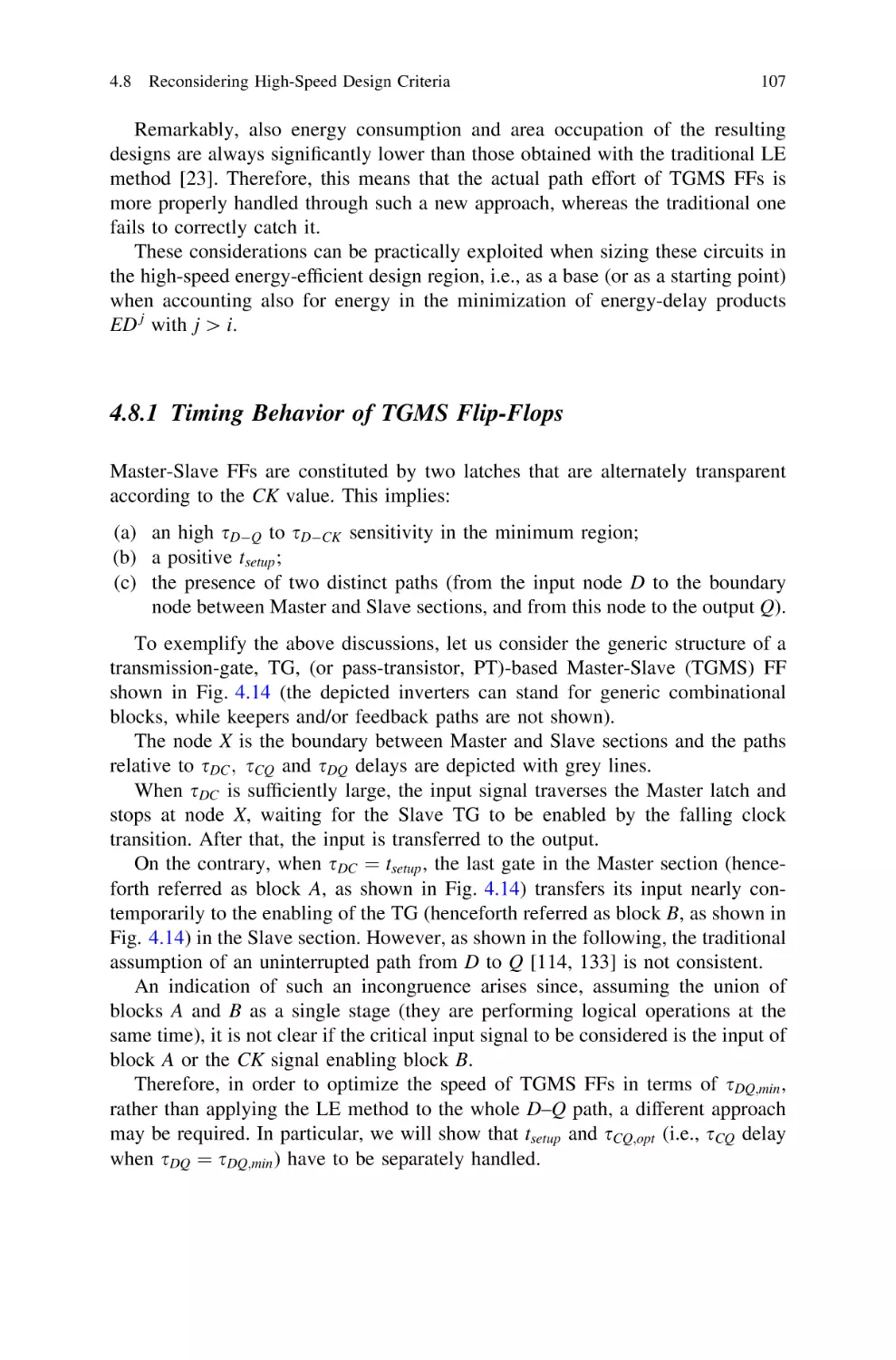
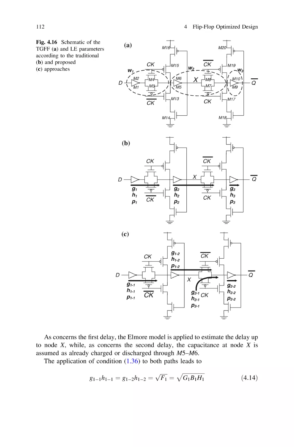
Reconsidering High-Speed Design Criteria
for Transmission-Gate Based Master–Slave FFs . . . . . . .
4.8.1 Timing Behavior of TGMS Flip-Flops. . . . . . . . .
4.8.2 High-speed Design Strategy for TGMS Flip-Flops
4.8.3 Design Example: TGFF . . . . . . . . . . . . . . . . . . .
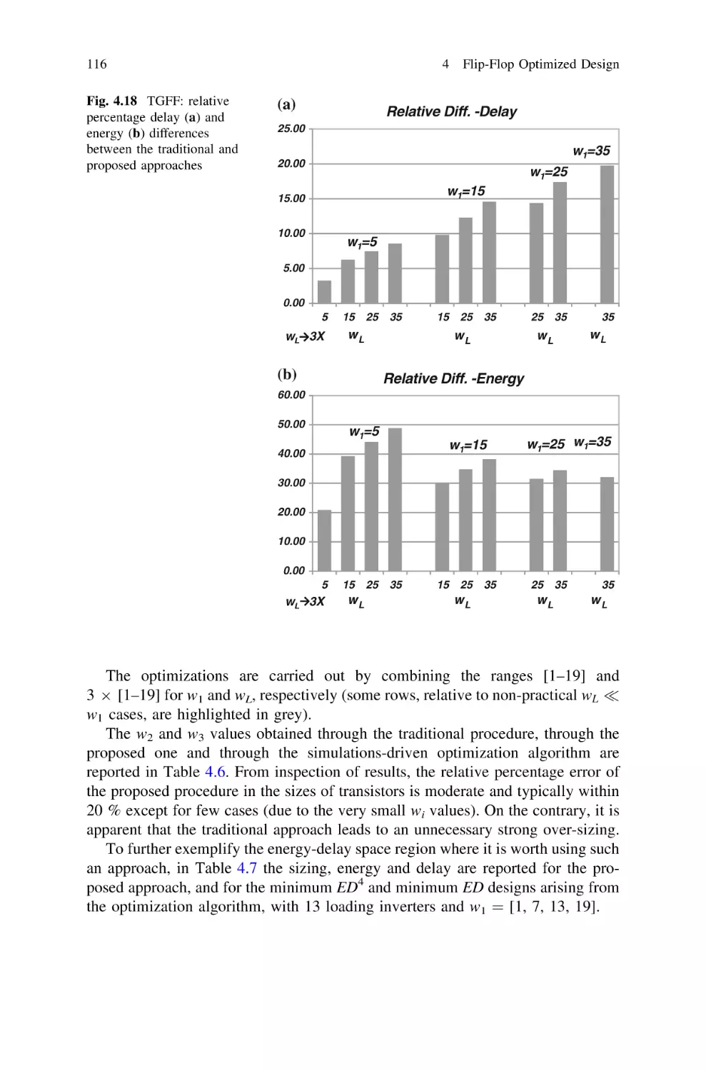
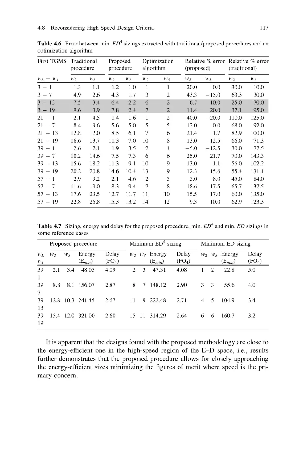
4.8.4 Simulation Results . . . . . . . . . . . . . . . . . . . . . .
.....
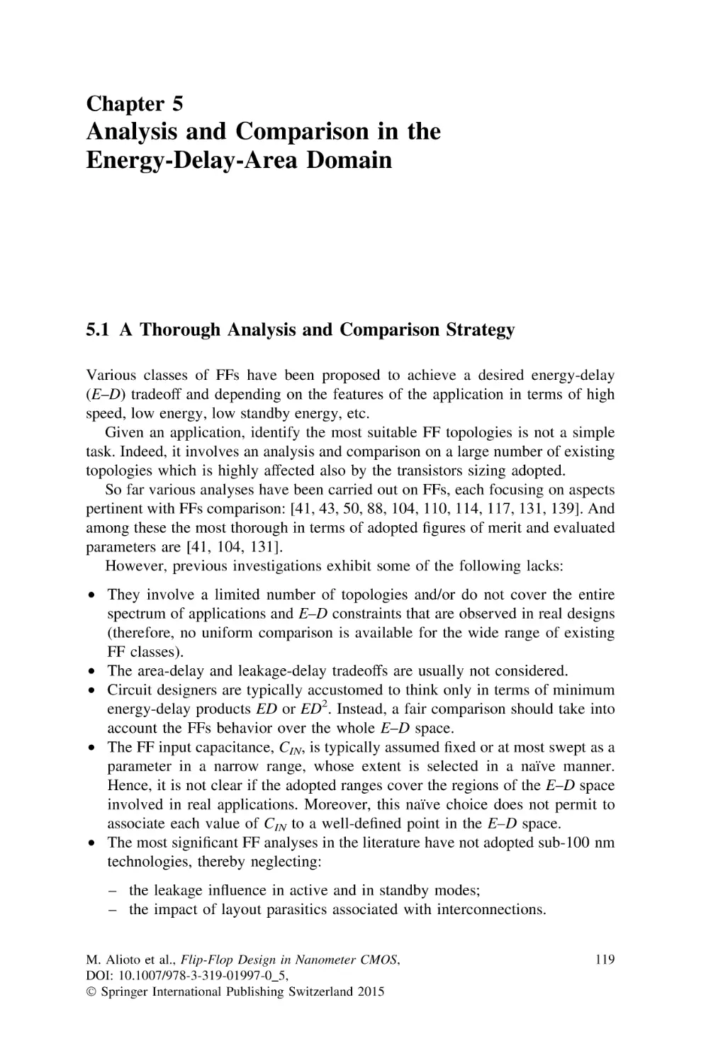
101
.....
101
.....
.....
103
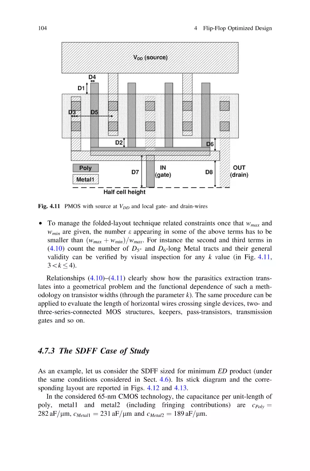
104
.
.
.
.
.
.
.
.
.
.
.
.
.
.
.
.
.
.
.
.
.
.
.
.
.
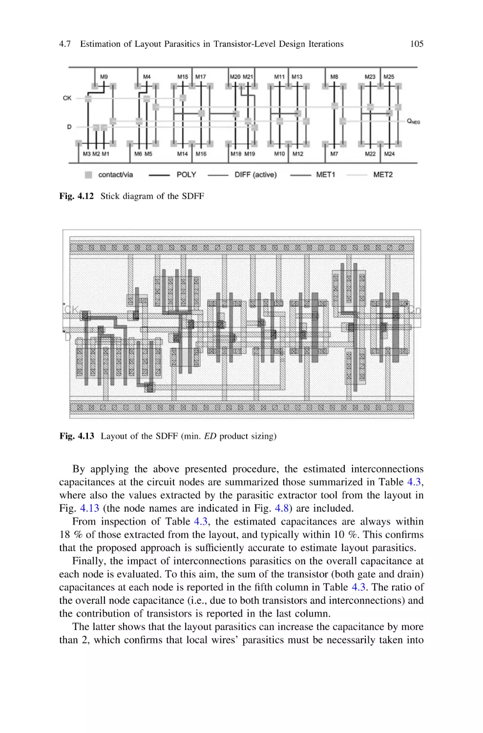
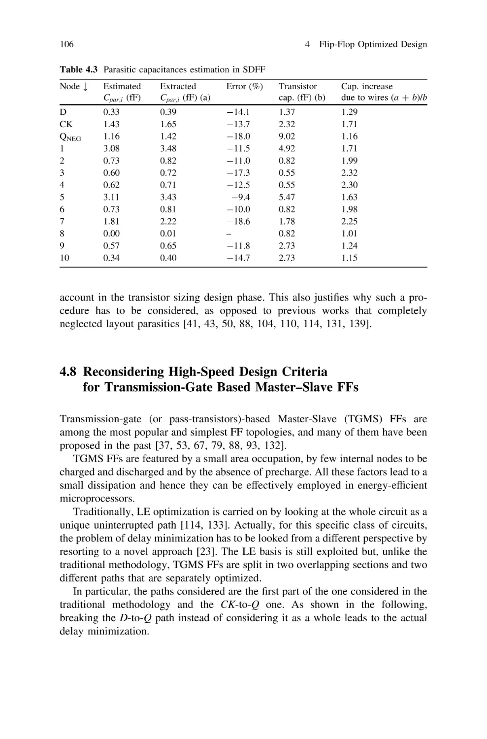
106
107
108
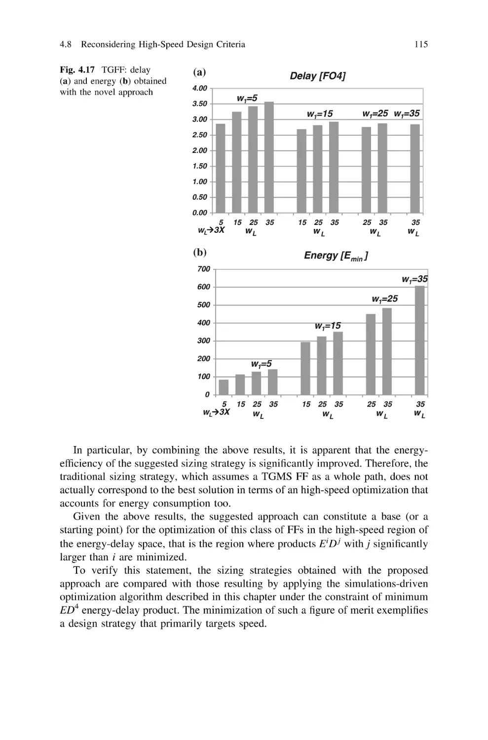
111
114
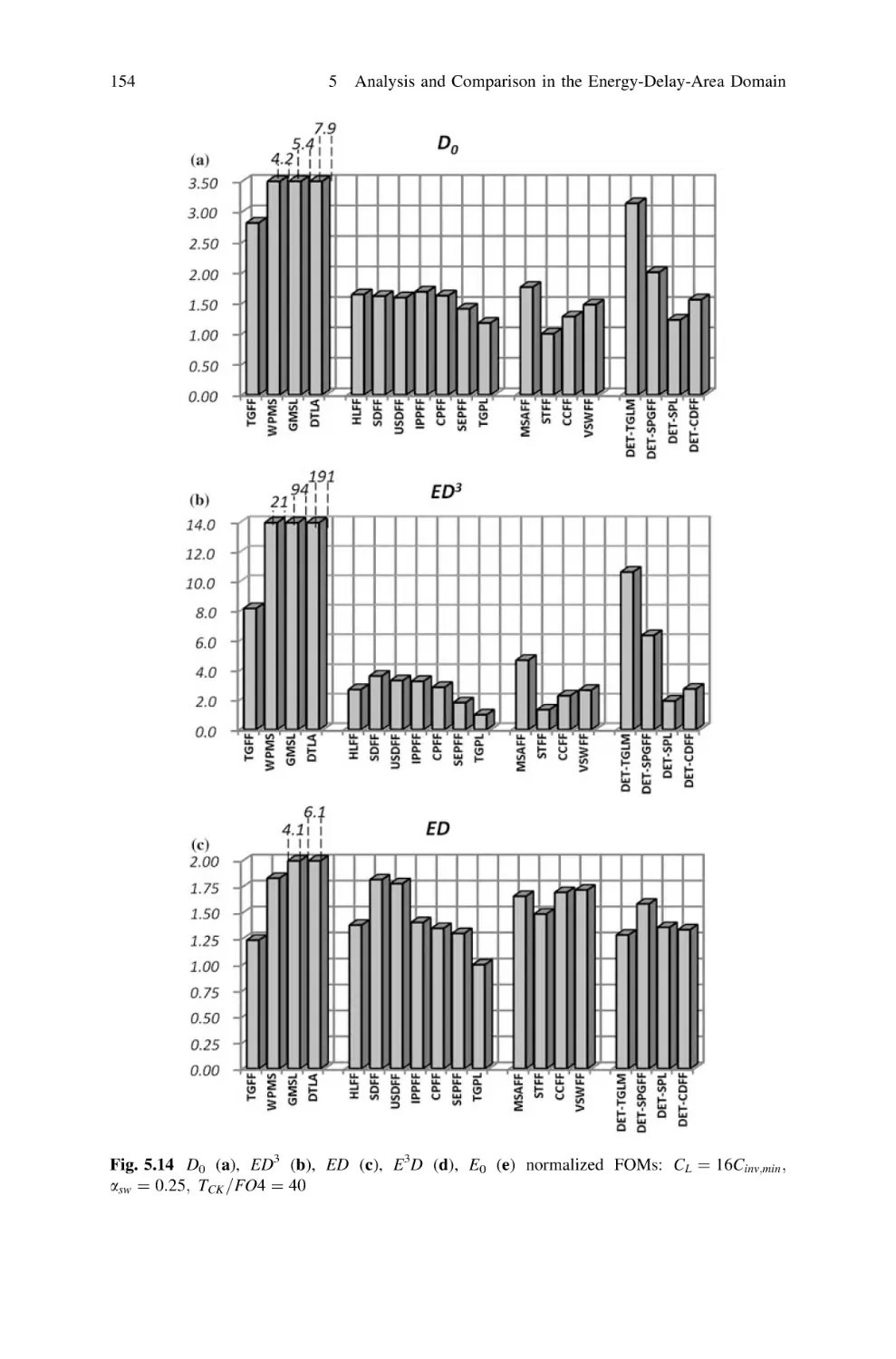
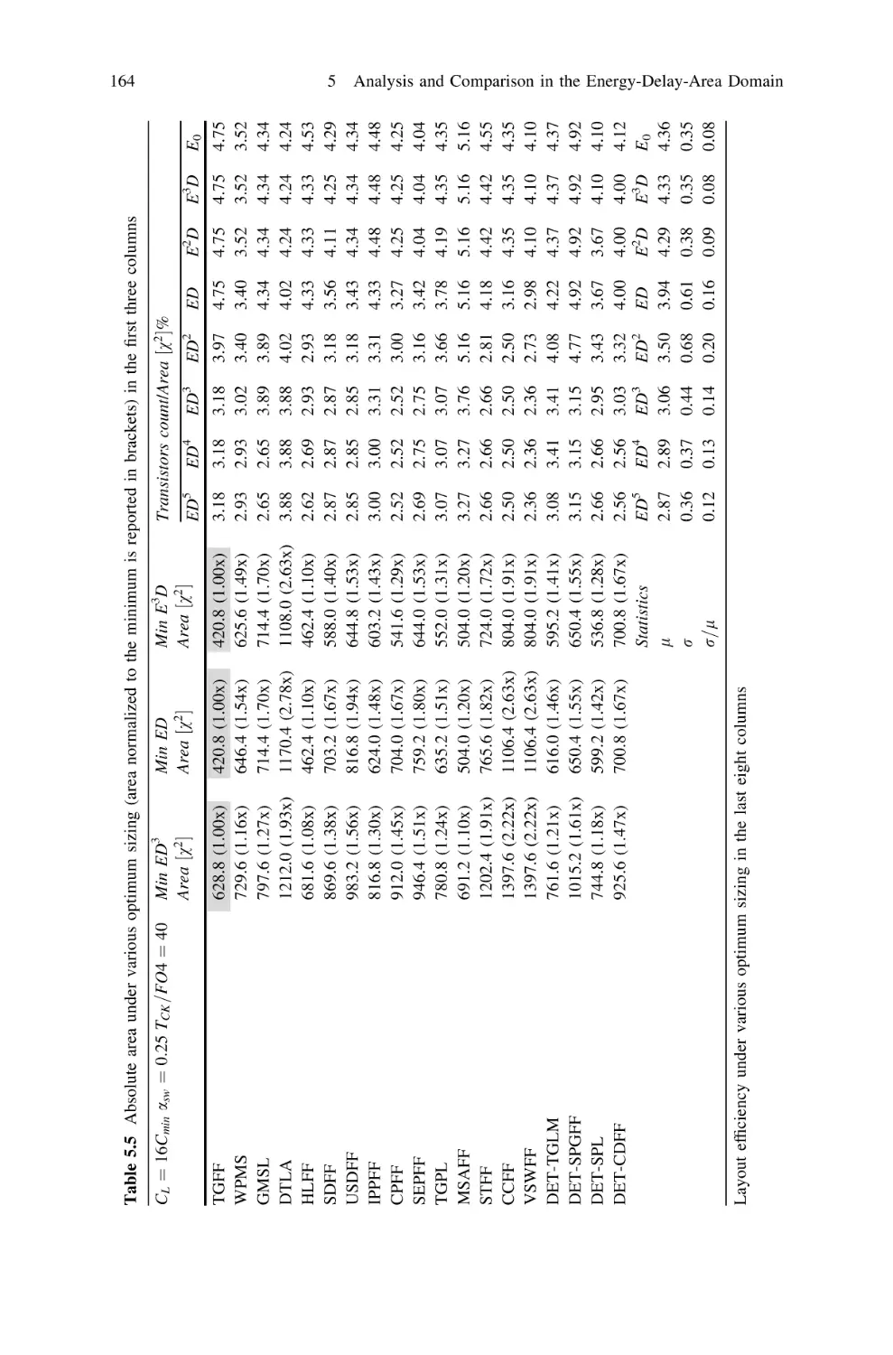
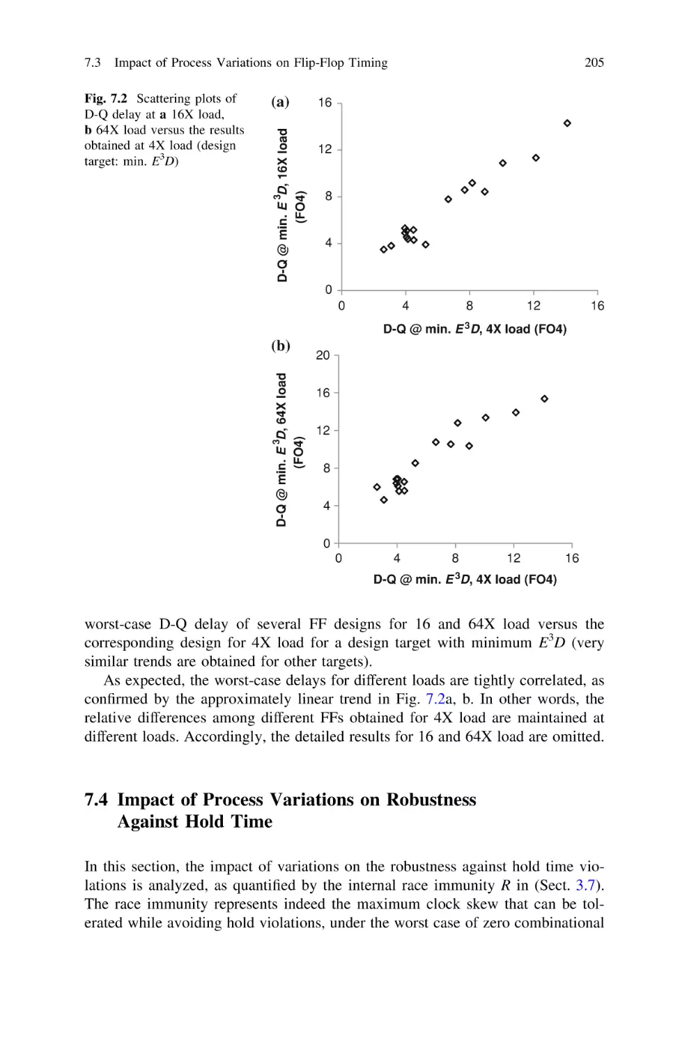
Analysis and Comparison in the Energy-Delay-Area Domain.
5.1 A Thorough Analysis and Comparison Strategy . . . . . . . .
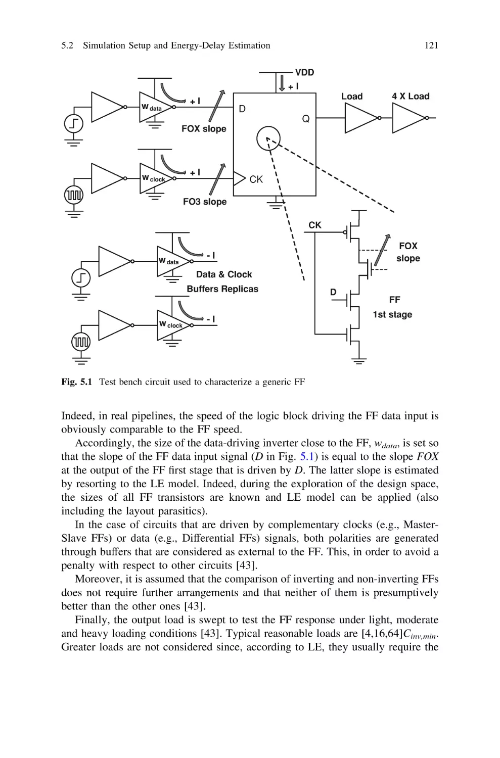
5.2 Simulation Setup and Energy-Delay Estimation . . . . . . . .
5.2.1 Test Bench Circuit . . . . . . . . . . . . . . . . . . . . . . .
5.2.2 Definition of Timing Figure of Merit . . . . . . . . . .
5.2.3 Estimation of Energy Dissipation . . . . . . . . . . . . .
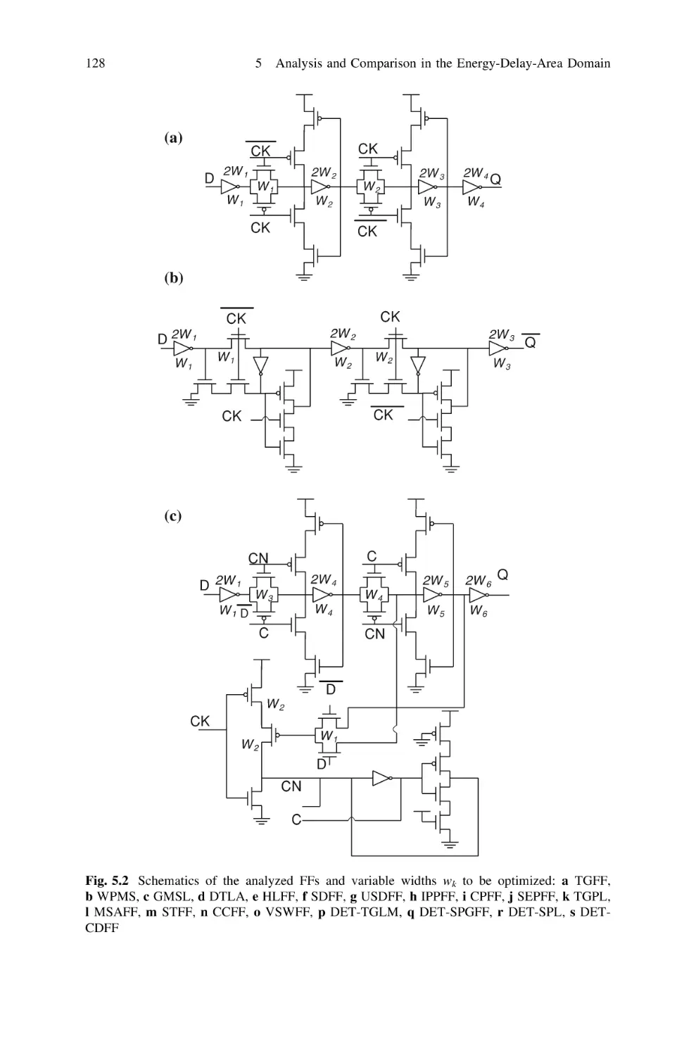
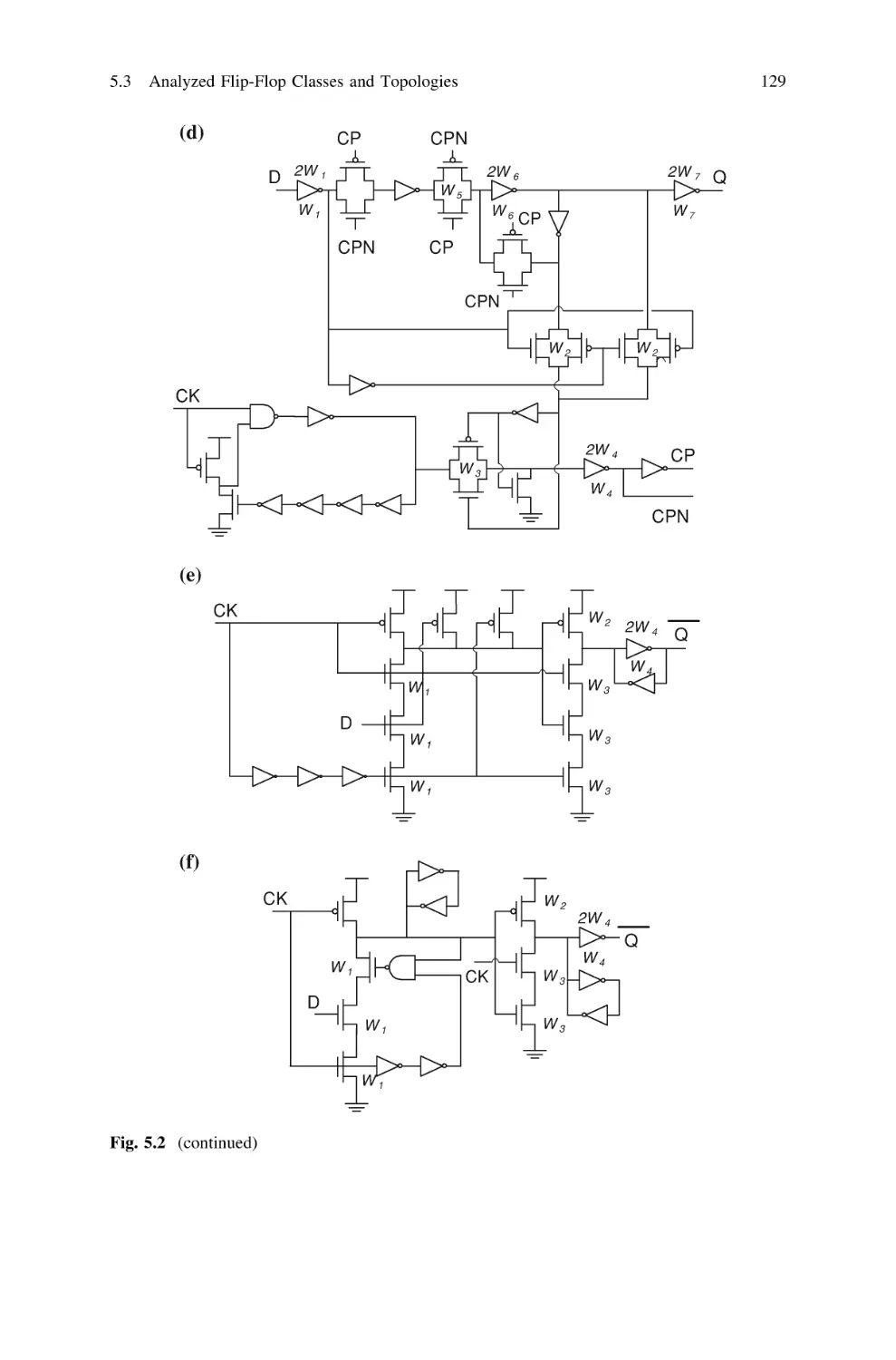
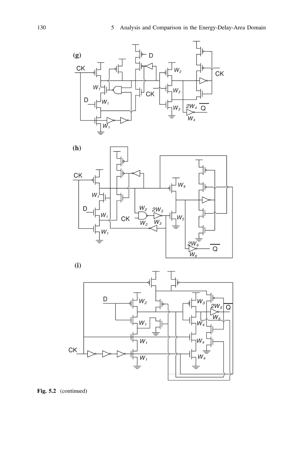
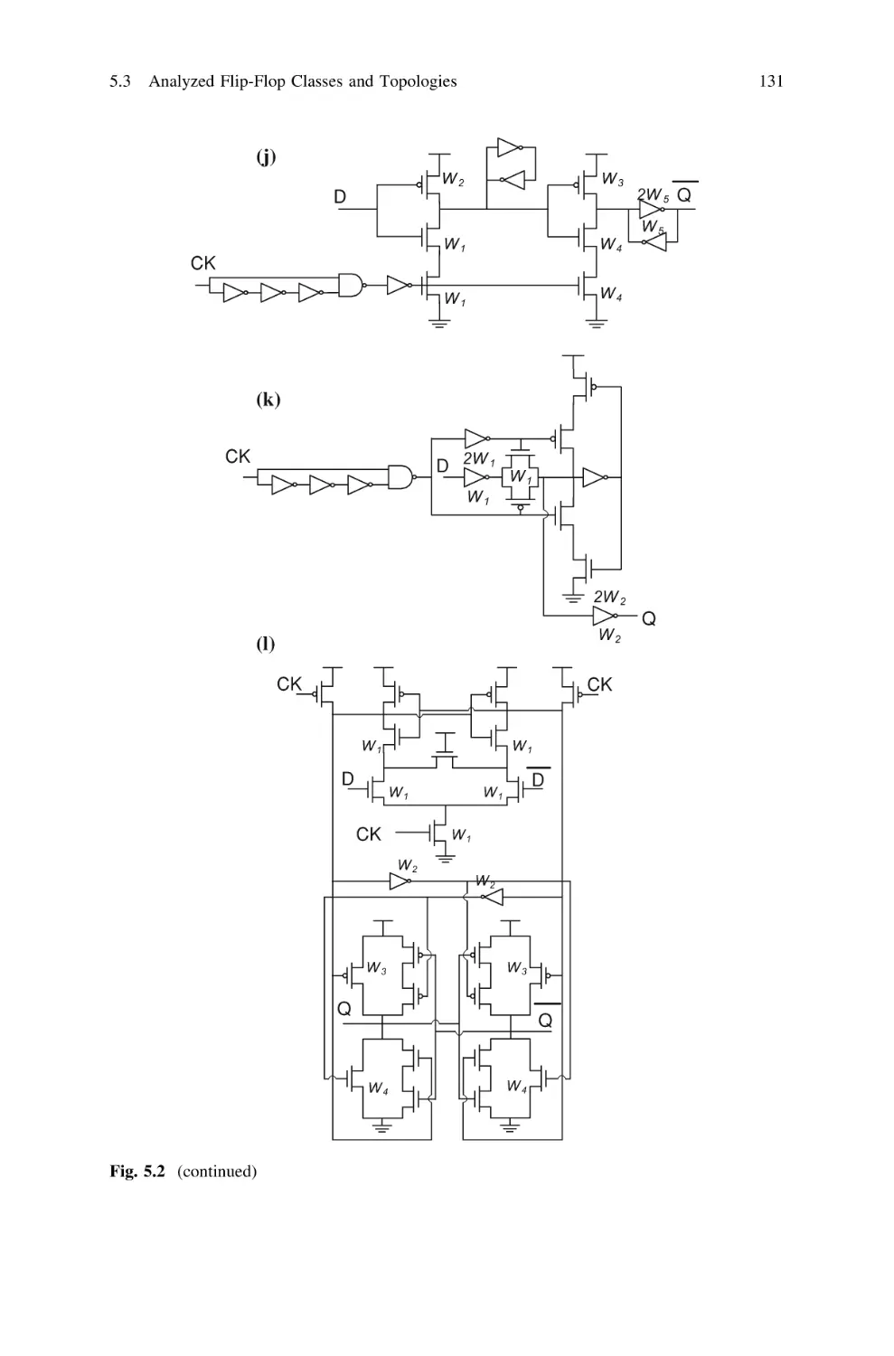
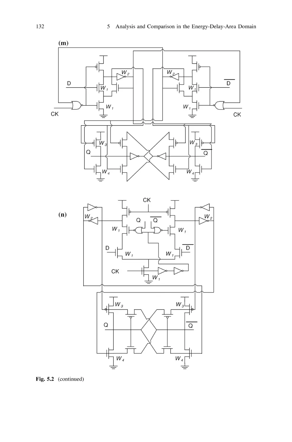
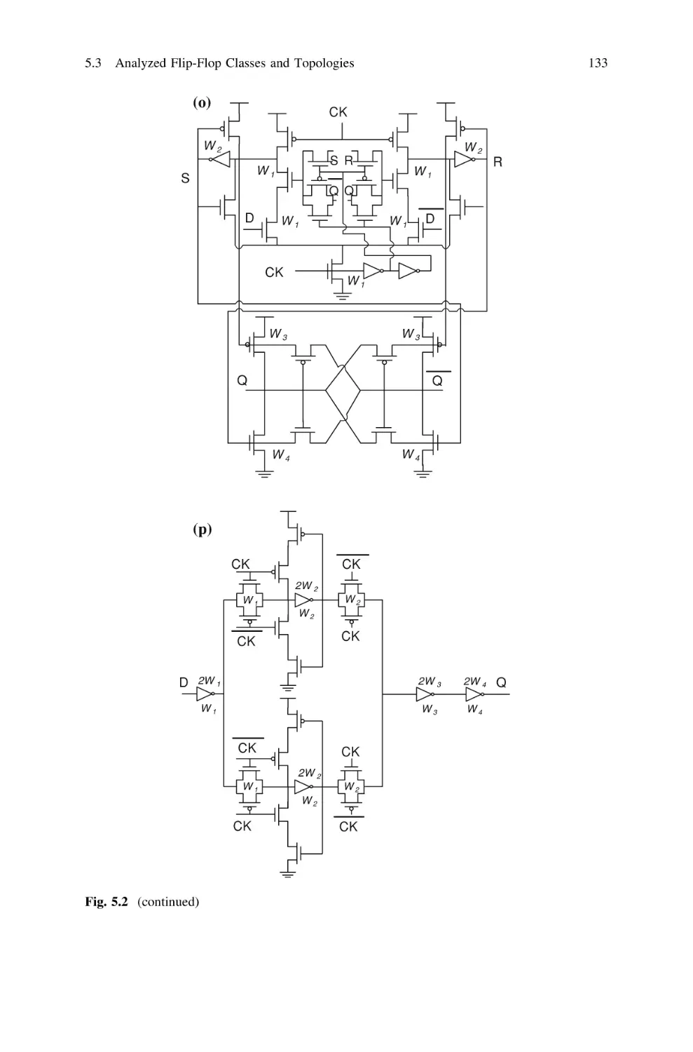
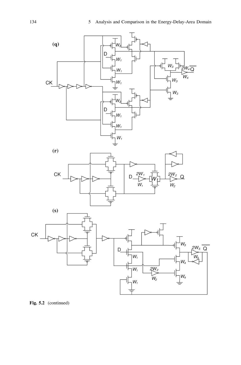
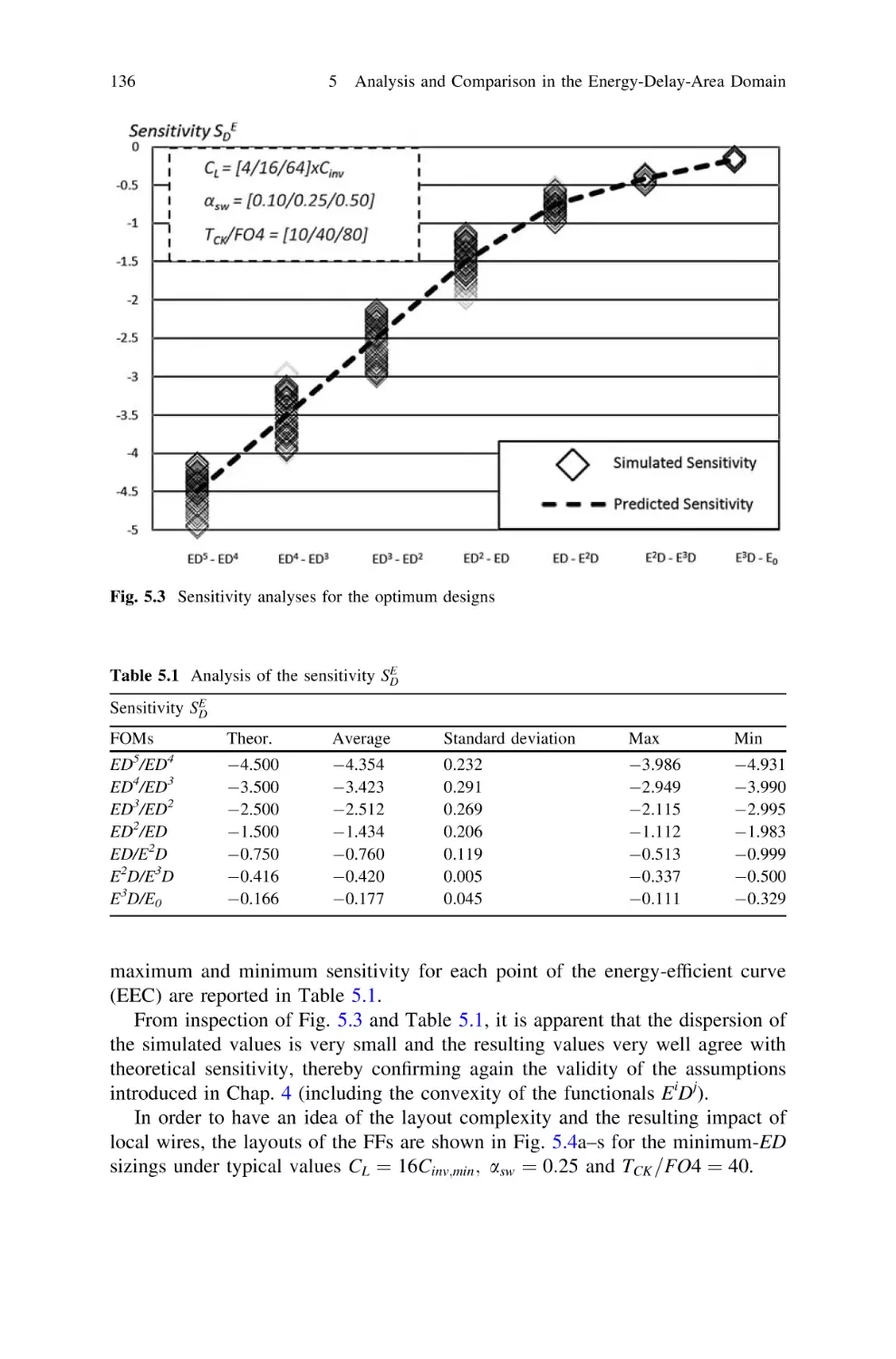
5.3 Analyzed Flip-Flop Classes and Topologies . . . . . . . . . . .
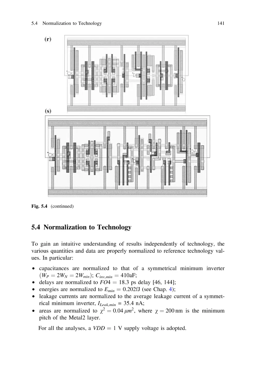
5.4 Normalization to Technology . . . . . . . . . . . . . . . . . . . . .
5.5 Energy-Delay Tradeoff in Each Class . . . . . . . . . . . . . . .
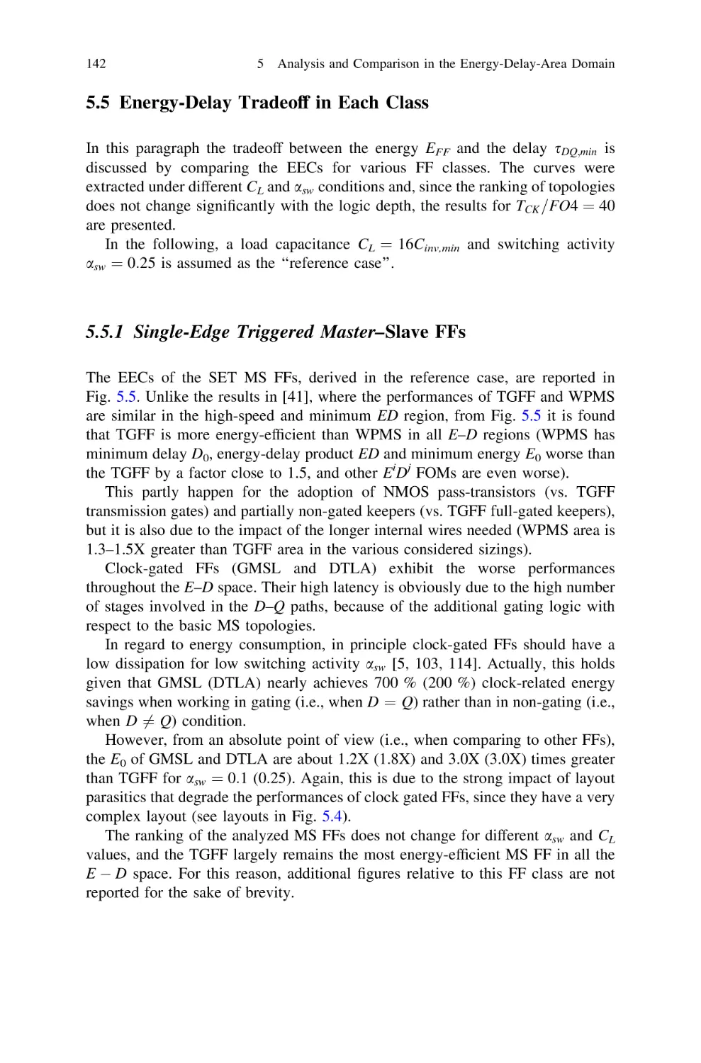
5.5.1 Single-Edge Triggered Master–Slave FFs. . . . . . . .
5.5.2 Single-Edge Triggered Implicitly-Explicitly
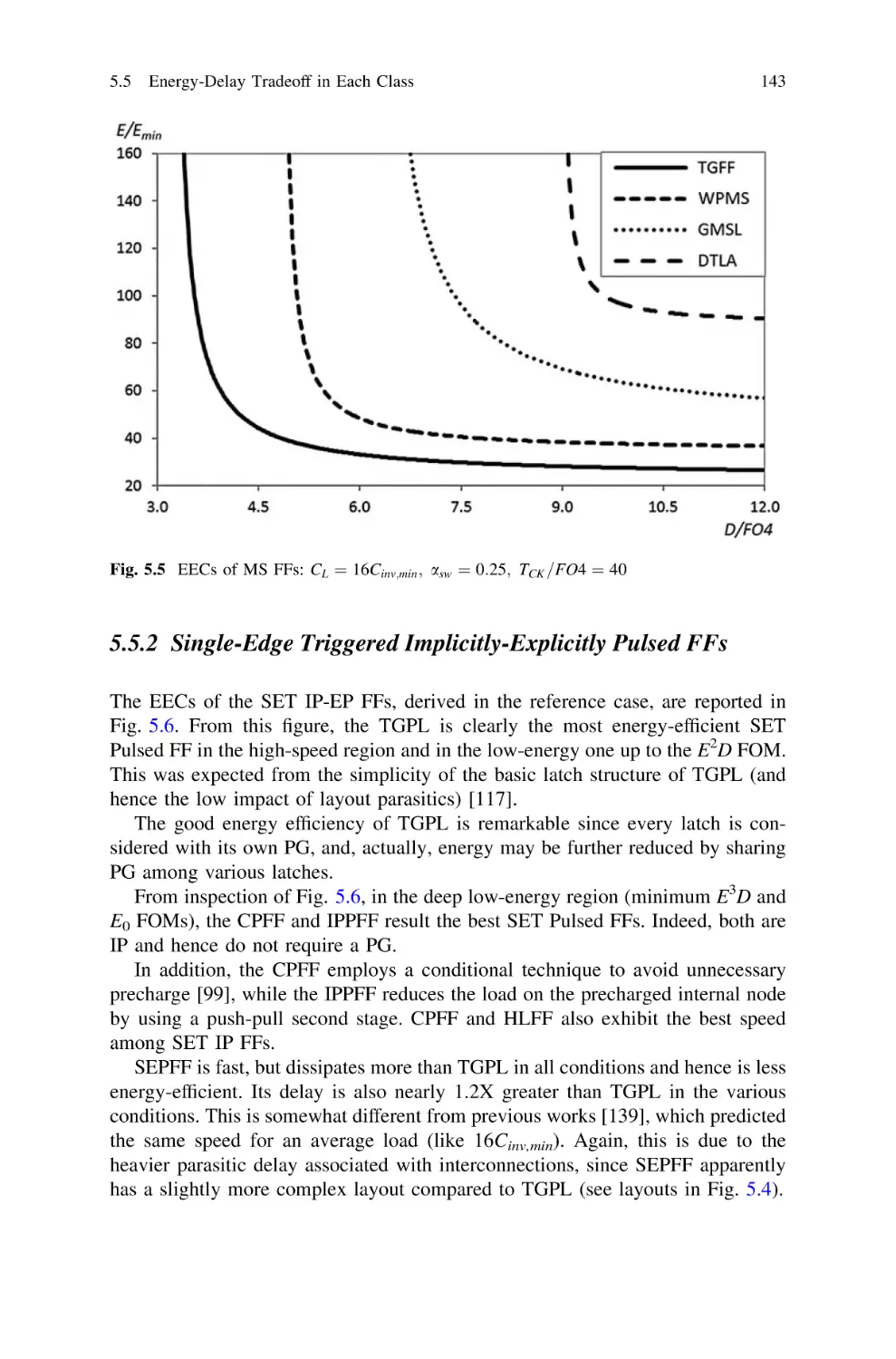
Pulsed FFs . . . . . . . . . . . . . . . . . . . . . . . . . . . . .
5.5.3 Single-Edge Triggered Differential FFs . . . . . . . . .
5.5.4 Dual-Edge Triggered FFs. . . . . . . . . . . . . . . . . . .
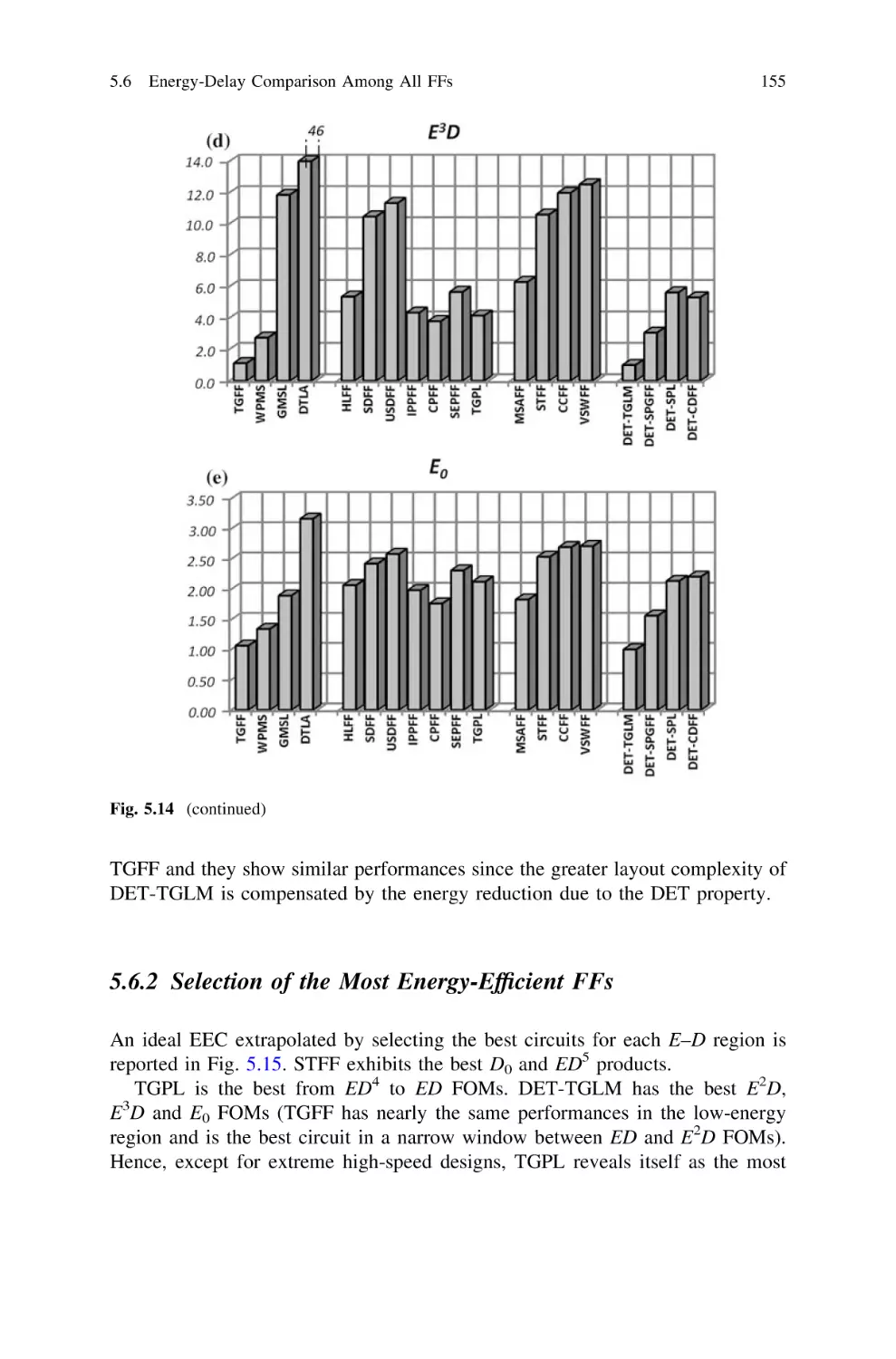
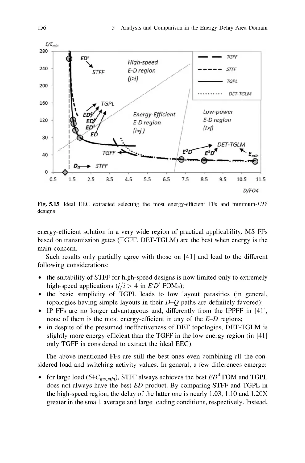
5.6 Energy-Delay Comparison Among All FFs. . . . . . . . . . . .
5.6.1 EiD j Metrics. . . . . . . . . . . . . . . . . . . . . . . . . . . .
5.6.2 Selection of the Most Energy-Efficient FFs . . . . . .
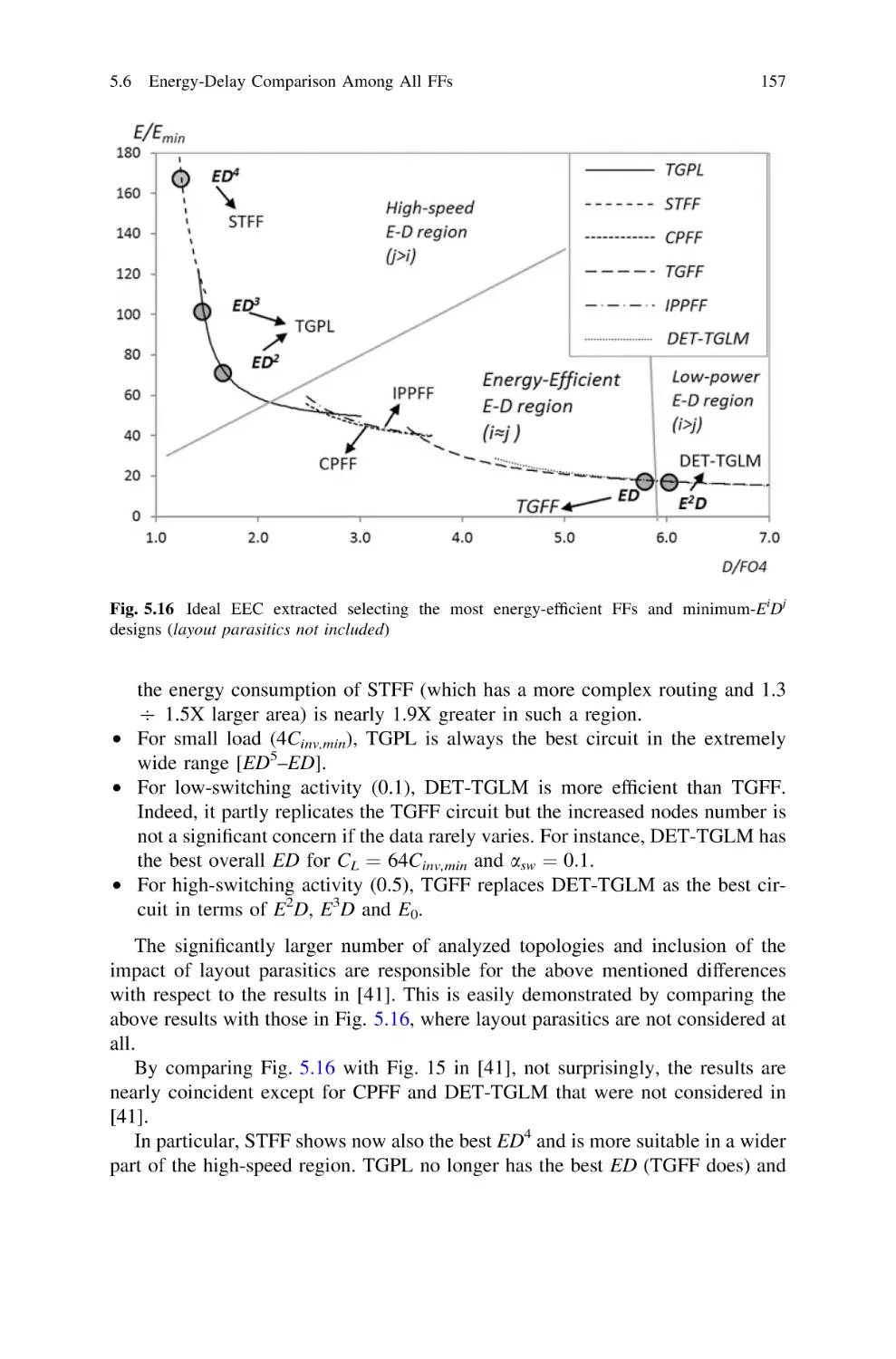
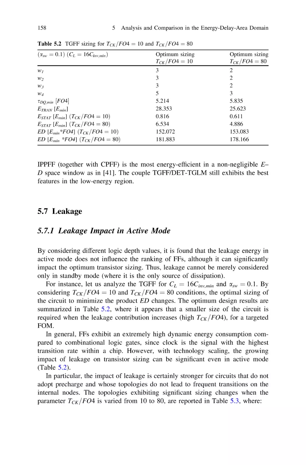
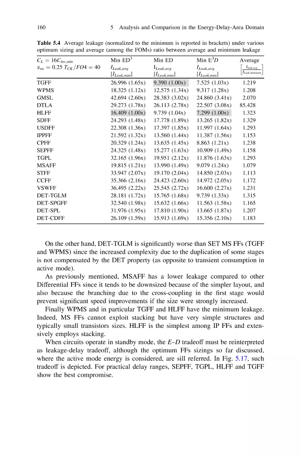
5.7 Leakage . . . . . . . . . . . . . . . . . . . . . . . . . . . . . . . . . . . .
5.7.1 Leakage Impact in Active Mode . . . . . . . . . . . . . .
5.7.2 Leakage Impact in Standby Mode and Tradeoff
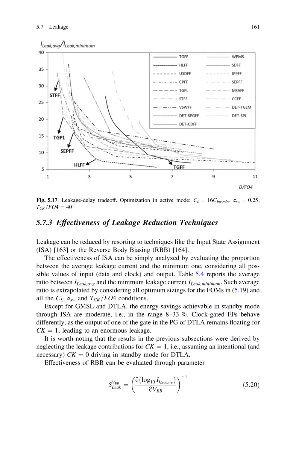
with Delay . . . . . . . . . . . . . . . . . . . . . . . . . . . . .
5.7.3 Effectiveness of Leakage Reduction Techniques . . .
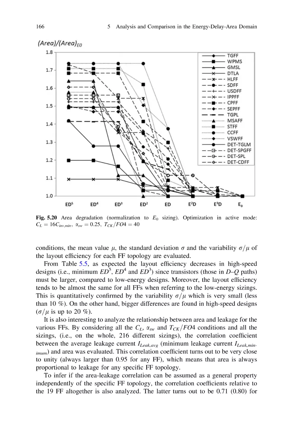
5.8 Silicon Area . . . . . . . . . . . . . . . . . . . . . . . . . . . . . . . . .
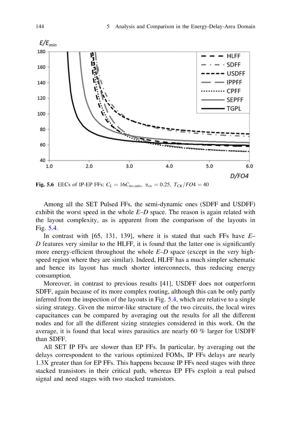
5.8.1 Comparison of FFs Area . . . . . . . . . . . . . . . . . . .
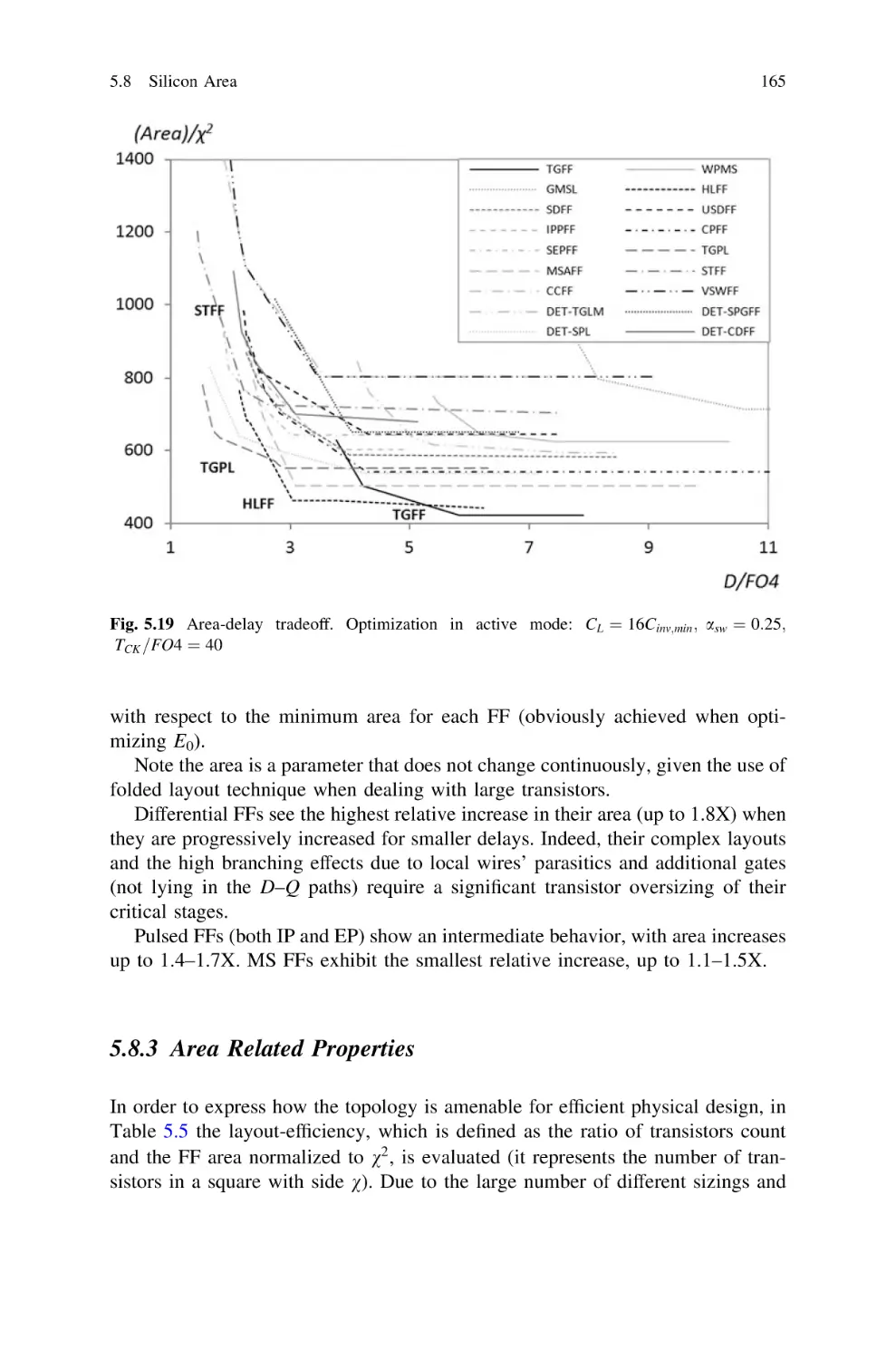
5.8.2 Area-Delay Tradeoff . . . . . . . . . . . . . . . . . . . . . .
5.8.3 Area Related Properties . . . . . . . . . . . . . . . . . . . .
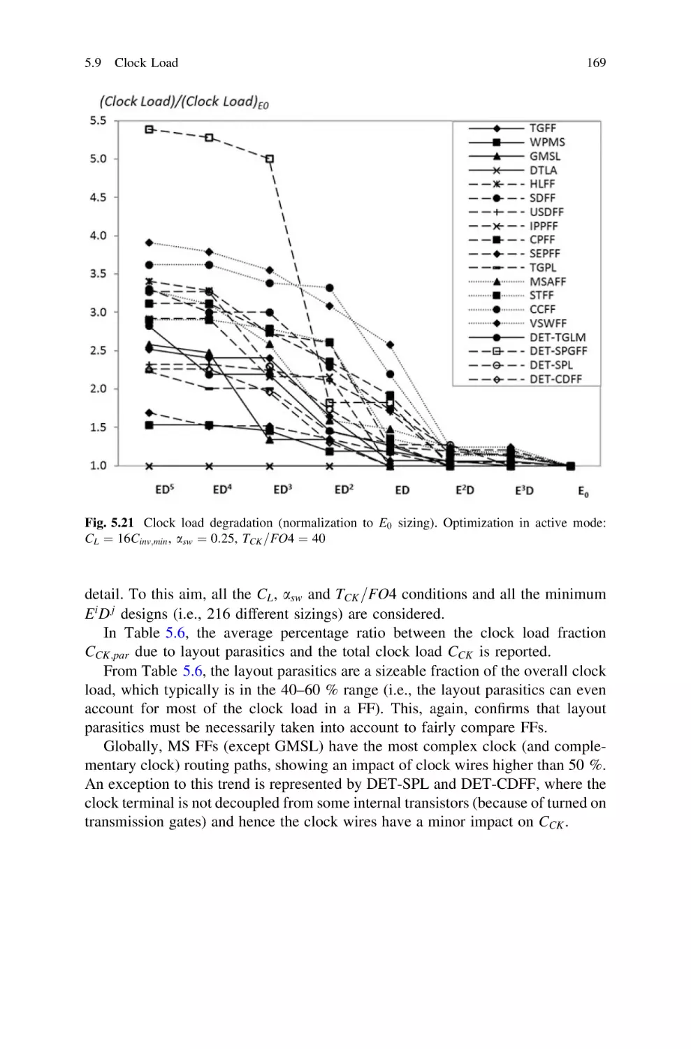
5.9 Clock Load. . . . . . . . . . . . . . . . . . . . . . . . . . . . . . . . . .
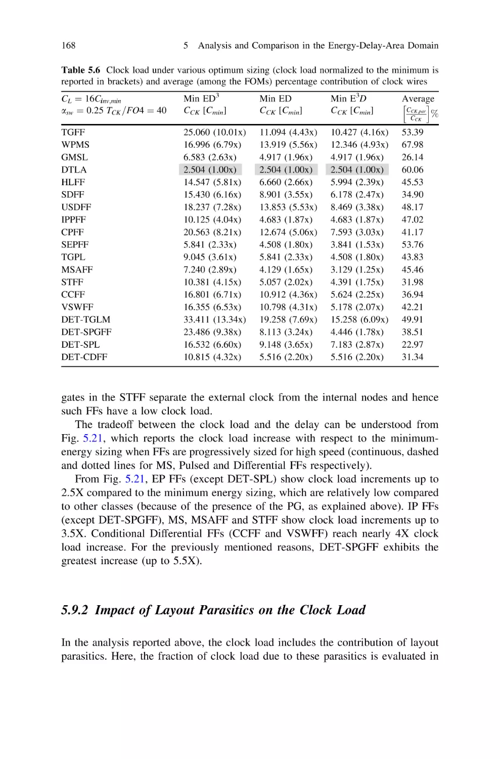
5.9.1 Clock Load Comparison and Tradeoff with Delay .
5.9.2 Impact of Layout Parasitics on the Clock Load . . .
.
.
.
.
.
.
.
.
.
.
.
.
.
.
.
.
.
.
.
.
.
.
.
.
.
.
.
.
.
.
.
.
.
.
.
.
.
.
.
.
119
119
120
120
122
123
127
141
142
142
.
.
.
.
.
.
.
.
.
.
.
.
.
.
.
.
.
.
.
.
.
.
.
.
.
.
.
.
.
.
.
.
143
146
148
153
153
155
158
158
.
.
.
.
.
.
.
.
.
.
.
.
.
.
.
.
.
.
.
.
.
.
.
.
.
.
.
.
.
.
.
.
.
.
.
.
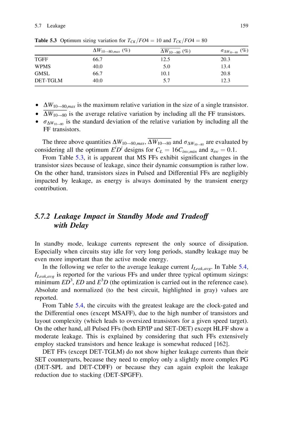
159
161
163
163
163
165
167
167
168
4.8
5
xiii
xiv
Contents
5.9.3
Joint FFs and Clock Distribution
Energy Dissipation . . . . . . . . . . . . . . . . . . . . . . . . . . .
5.10 A Summary . . . . . . . . . . . . . . . . . . . . . . . . . . . . . . . . . . . . .
6
7
Energy Efficiency Versus Clock Slope . . . . . . . . . . . . . . . . . .
6.1 Basic Considerations on the Role of the Clock Slope. . . . .
6.2 Setup to Simulate FFs Under a Varying Clock Slope. . . . .
6.3 FFs Timing and Energy Versus Clock Slope. . . . . . . . . . .
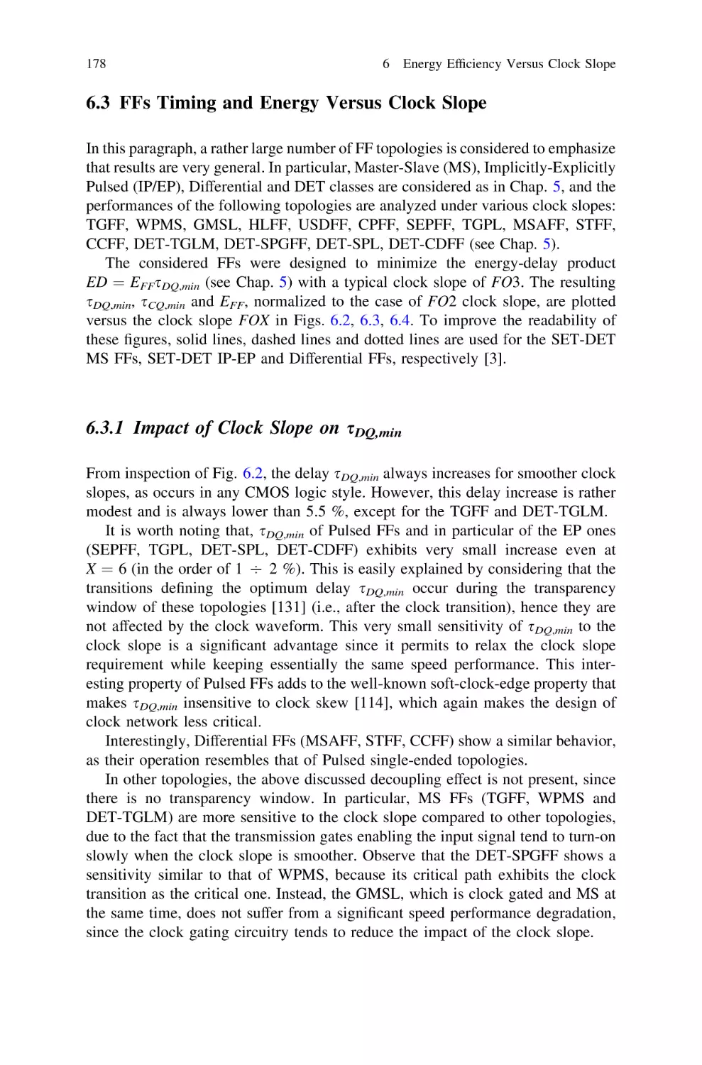
6.3.1 Impact of Clock Slope on sDQ,min . . . . . . . . . . . . .
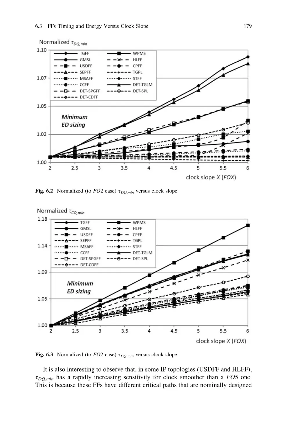
6.3.2 Impact of Clock Slope on sCQ,min, tsetup and thold . .
6.3.3 Impact of Clock Slope on EFF
and Operation Robustness . . . . . . . . . . . . . . . . . .
6.4 Energy of Local Clock Buffers Versus Clock Slope . . . . .
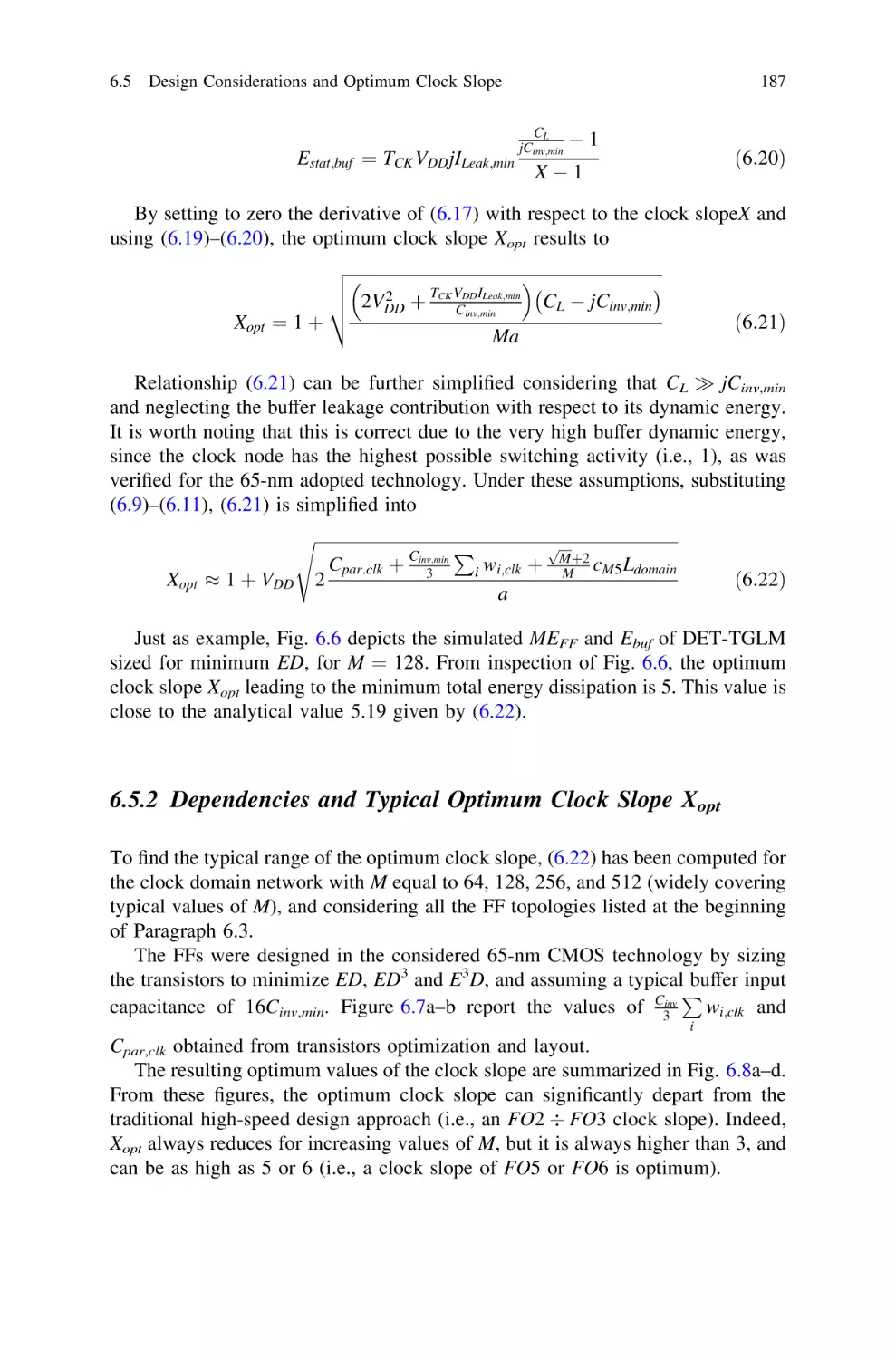
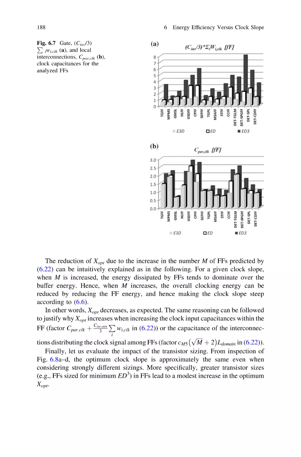
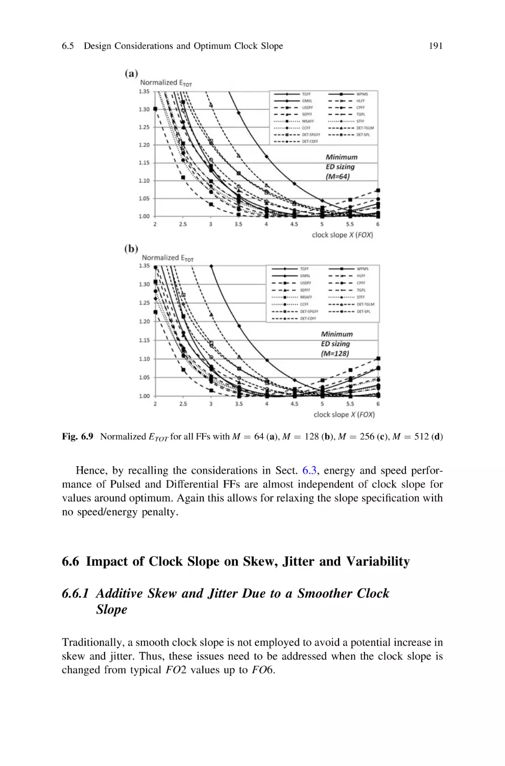
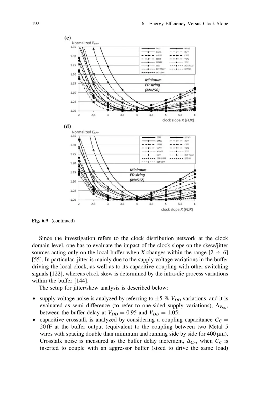
6.5 Design Considerations and Optimum Clock Slope . . . . . . .
6.5.1 Analytical Evaluation of the Optimum Clock Slope
6.5.2 Dependencies and Typical Optimum
Clock Slope Xopt . . . . . . . . . . . . . . . . . . . . . . . . .
6.5.3 Effectiveness of Clock Slope Optimization and
FFs Comparison . . . . . . . . . . . . . . . . . . . . . . . . .
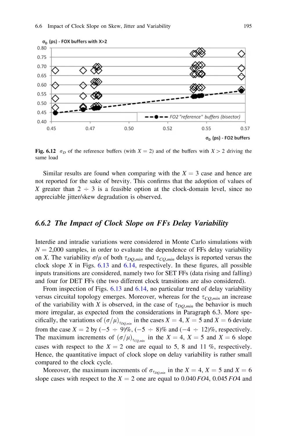
6.6 Impact of Clock Slope on Skew, Jitter and Variability . . . .
6.6.1 Additive Skew and Jitter Due to a Smoother
Clock Slope . . . . . . . . . . . . . . . . . . . . . . . . . . . .
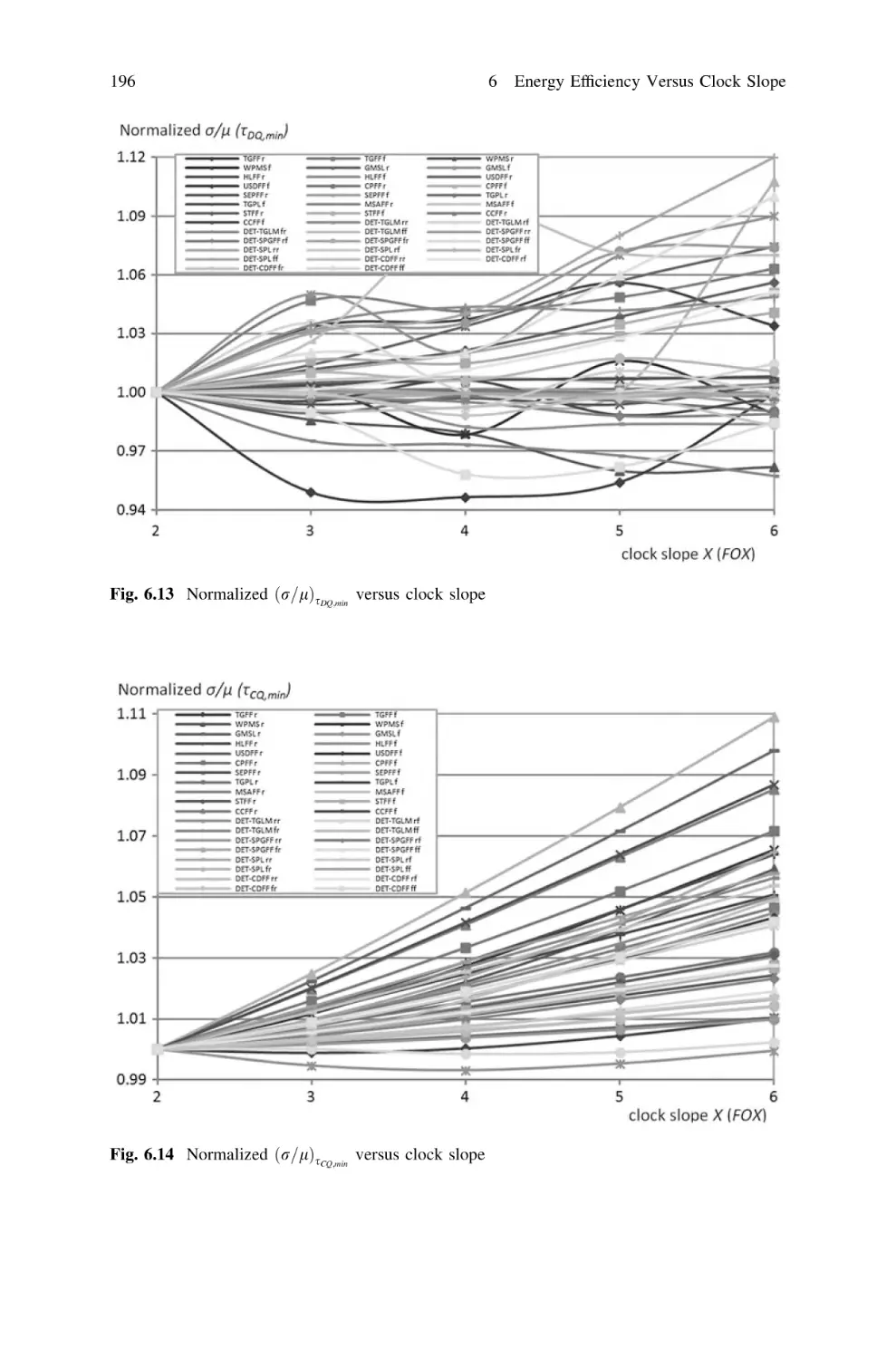
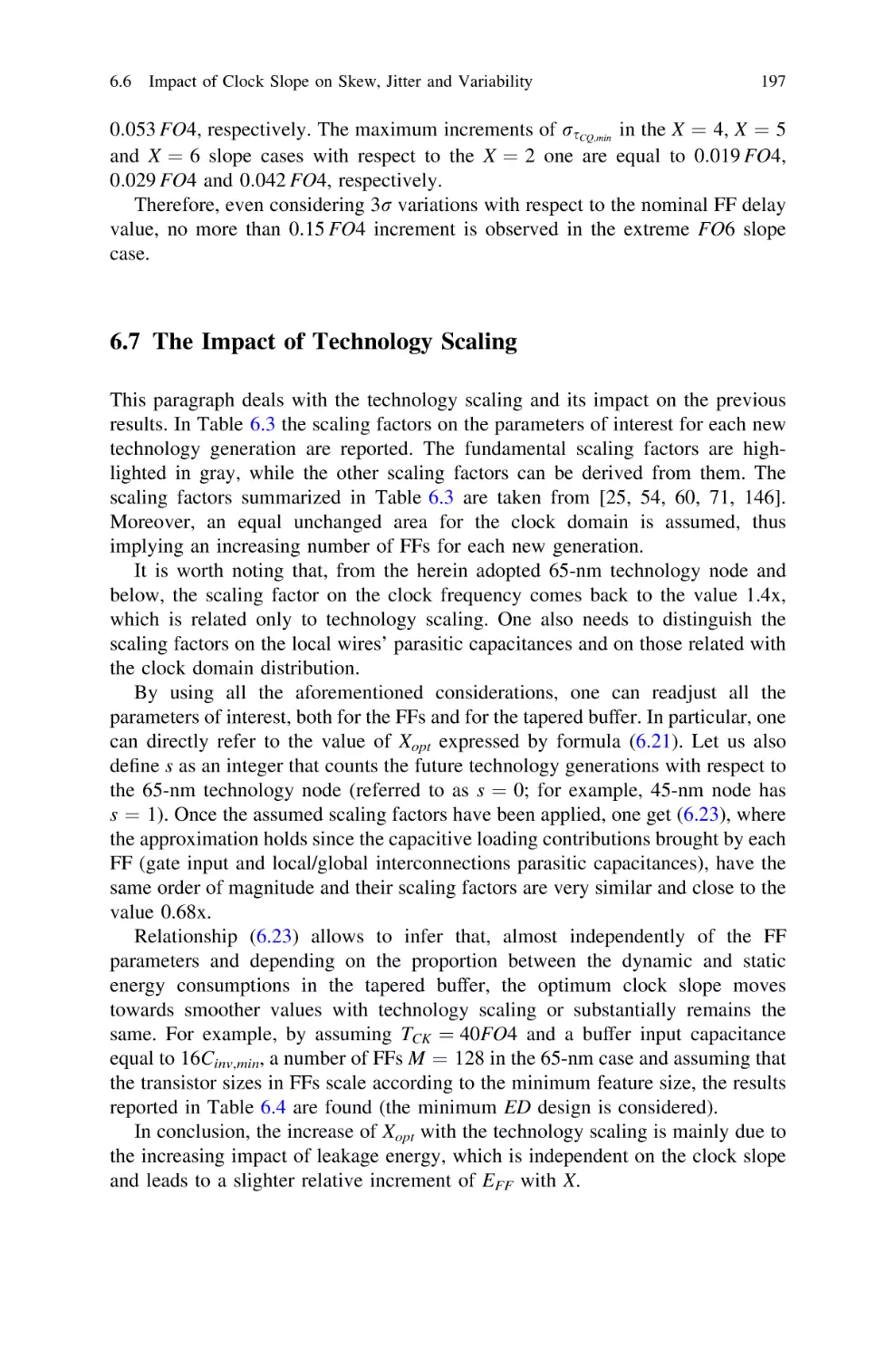
6.6.2 The Impact of Clock Slope on FFs
Delay Variability . . . . . . . . . . . . . . . . . . . . . . . .
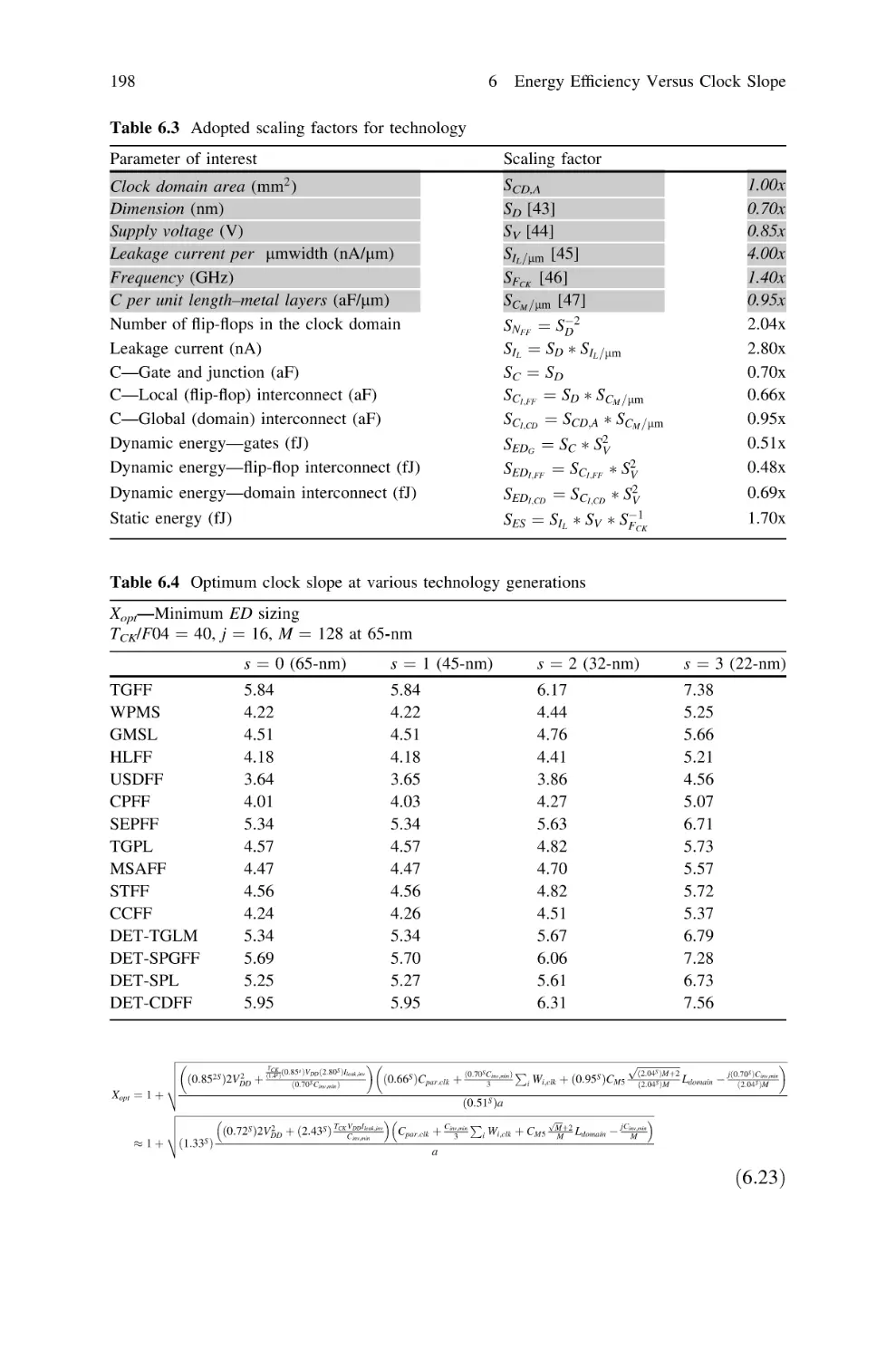
6.7 The Impact of Technology Scaling . . . . . . . . . . . . . . . . .
Hold Time Issues and Impact of Variations
on Flip-Flop Topologies . . . . . . . . . . . . . . . . . . . . . . . .
7.1 State of the Art and Preliminary Considerations . . . .
7.2 Variations, Metrics and Methodology. . . . . . . . . . . .
7.3 Impact of Process Variations on Flip-Flop Timing:
Performance . . . . . . . . . . . . . . . . . . . . . . . . . . . . .
7.4 Impact of Process Variations on Robustness Against
Hold Time . . . . . . . . . . . . . . . . . . . . . . . . . . . . . .
7.5 Impact of Voltage, Temperature and Clock Slope
Variations on Flip-Flop Timing . . . . . . . . . . . . . . . .
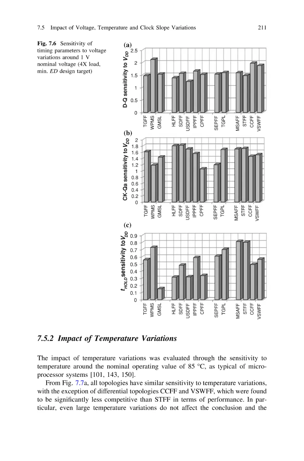
7.5.1 Impact of Voltage Variations . . . . . . . . . . . .
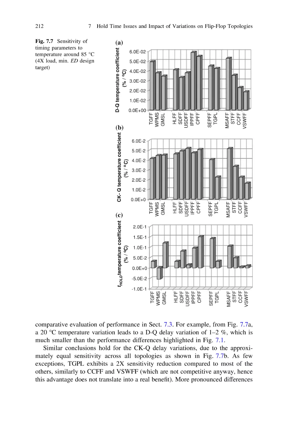
7.5.2 Impact of Temperature Variations . . . . . . . . .
7.5.3 Impact of Clock Slope Variations . . . . . . . . .
7.6 Process/Voltage/Temperature Variations
and Energy Variability . . . . . . . . . . . . . . . . . . . . . .
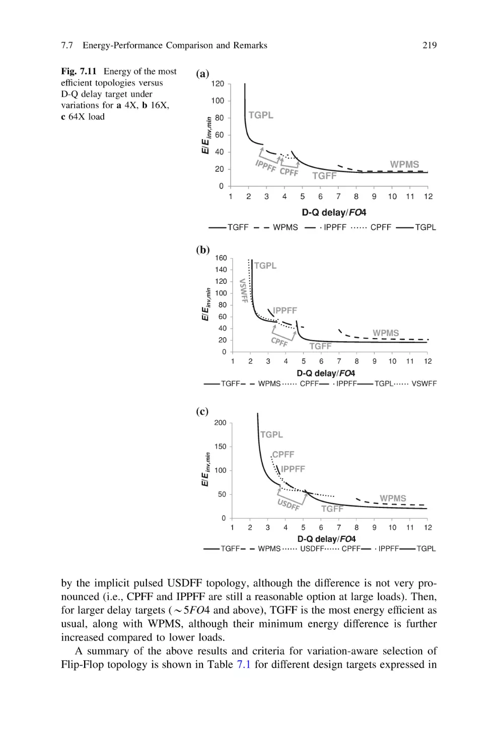
7.7 Energy-Performance Comparison and Remarks . . . . .
170
172
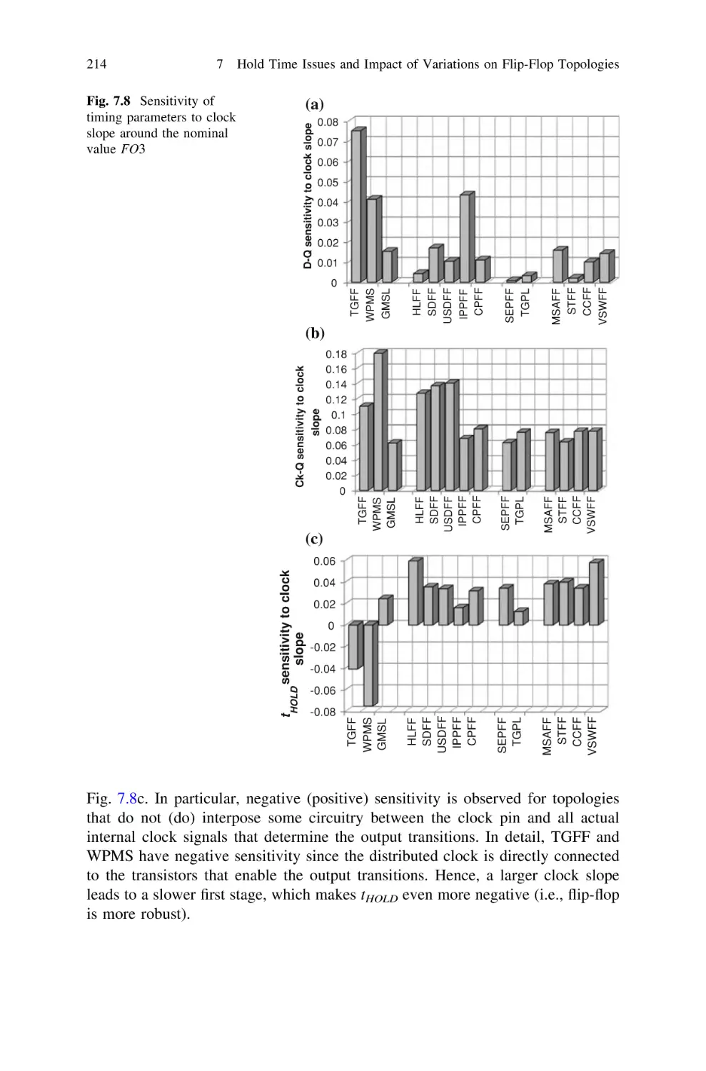
.
.
.
.
.
.
.
.
.
.
.
.
.
.
.
.
.
.
.
.
.
.
.
.
175
175
176
178
178
180
.
.
.
.
.
.
.
.
.
.
.
.
.
.
.
.
182
183
186
186
....
187
....
....
190
191
....
191
....
....
195
197
........
........
........
199
199
200
........
202
........
205
.
.
.
.
.
.
.
.
210
210
211
213
........
........
215
216
.
.
.
.
.
.
.
.
.
.
.
.
.
.
.
.
.
.
.
.
.
.
.
.
Contents
xv
7.8 Summary . . . . . . . . . . . . . . . . . . . . . . . . . . . . . . . . . . . . . . .
Appendix: Variations in DET FFs . . . . . . . . . . . . . . . . . . . . . . . . . .
.
.
.
.
.
.
.
229
229
230
232
239
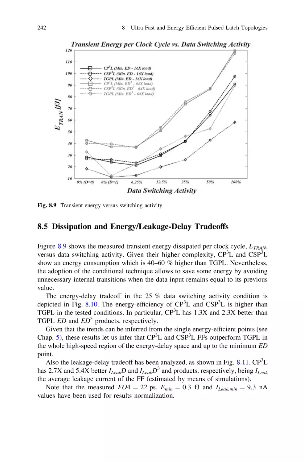
242
246
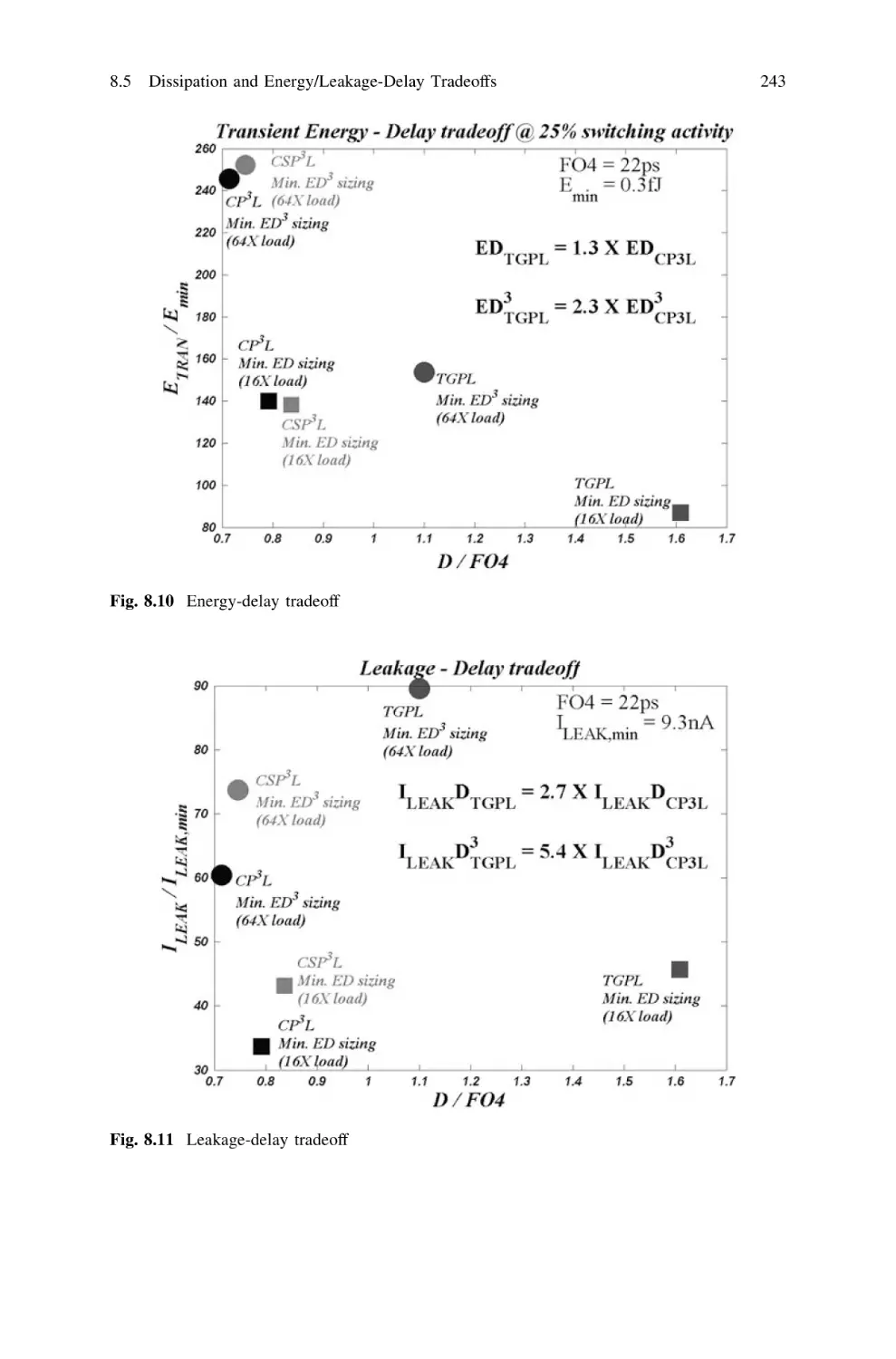
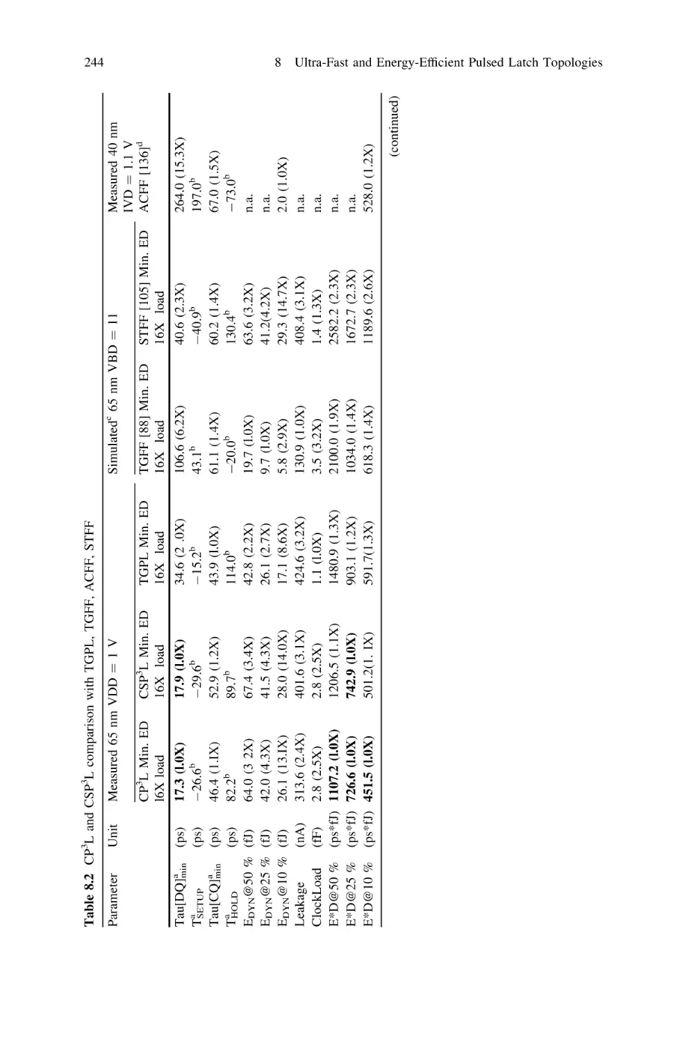
References . . . . . . . . . . . . . . . . . . . . . . . . . . . . . . . . . . . . . . . . . . . .
247
About the Authors. . . . . . . . . . . . . . . . . . . . . . . . . . . . . . . . . . . . . . .
255
Index . . . . . . . . . . . . . . . . . . . . . . . . . . . . . . . . . . . . . . . . . . . . . . . .
259
8
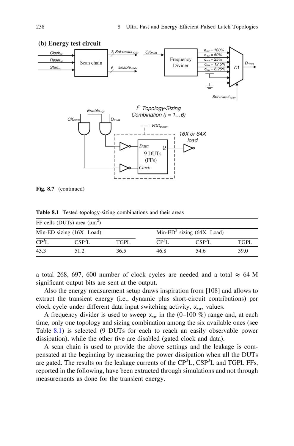
Ultra-Fast and Energy-Efficient Pulsed Latch Topologies.
8.1 State of the Art and Preliminary Considerations . . . . .
8.2 Operation of CP3L and CSP3L . . . . . . . . . . . . . . . . .
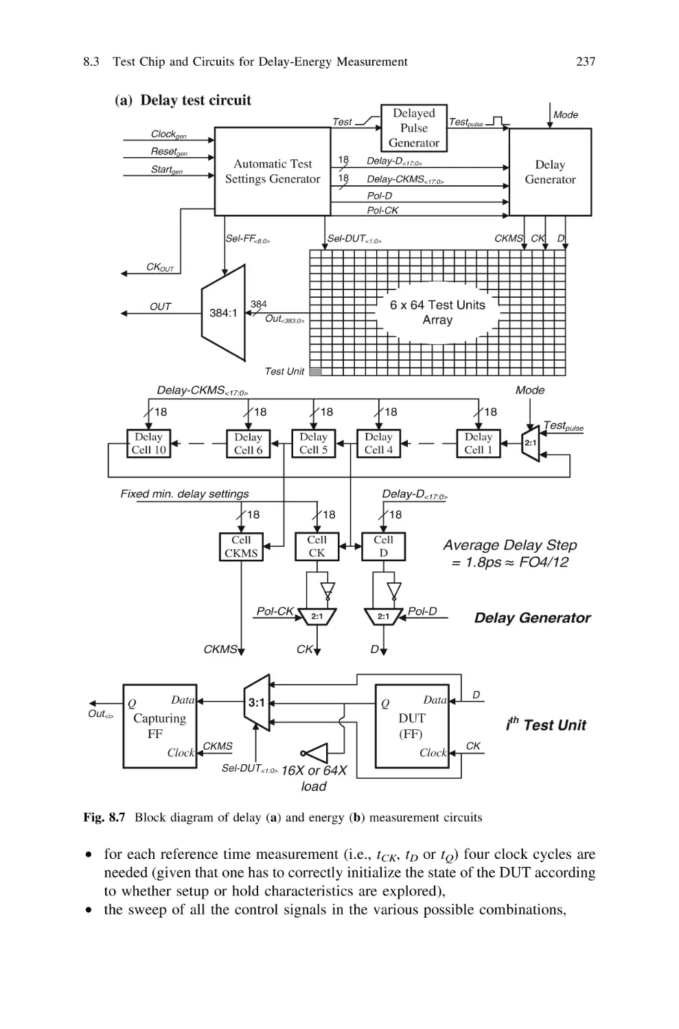
8.3 Test Chip and Circuits for Delay-Energy Measurement
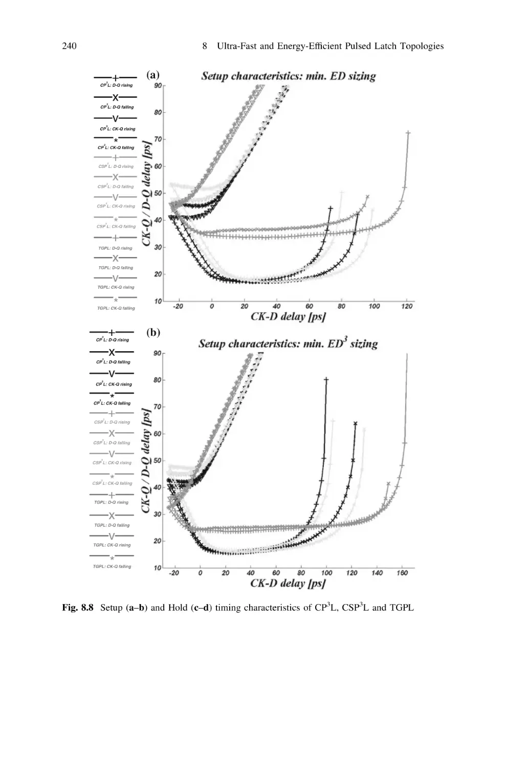
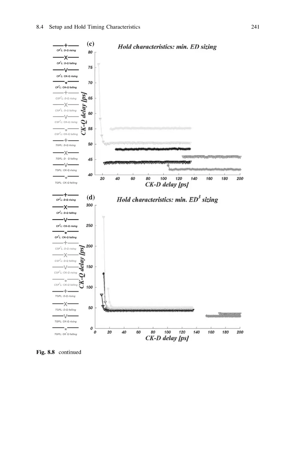
8.4 Setup and Hold Timing Characteristics . . . . . . . . . . .
8.5 Dissipation and Energy/Leakage-Delay Tradeoffs . . . .
8.6 Performance Summary and Comparison . . . . . . . . . . .
.
.
.
.
.
.
.
.
.
.
.
.
.
.
.
.
.
.
.
.
.
.
.
.
.
.
.
.
.
.
.
.
.
.
.
.
.
.
.
.
.
.
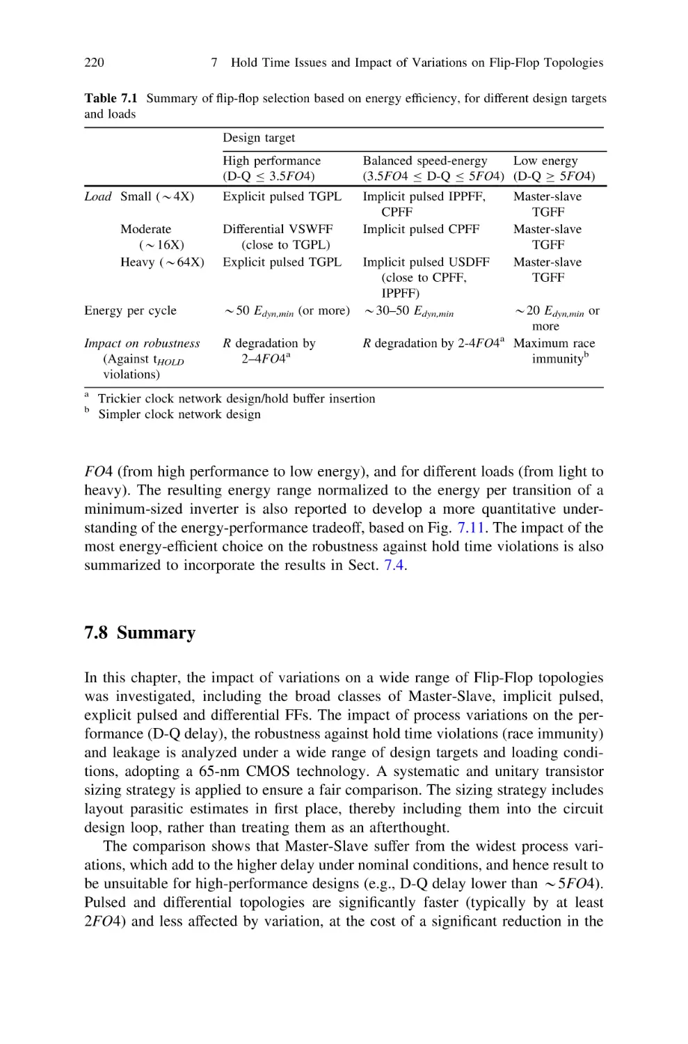
220
221
Chapter 1
The Logical Effort Method
This chapter summarizes the Logical Effort approach [133], which is a widely used
tool to model and optimize CMOS digital circuits from the point of view of speed.
This methodology is extensively used throughout the following chapters, especially when dealing with the transistor size optimization and the search for practical design space bounds.
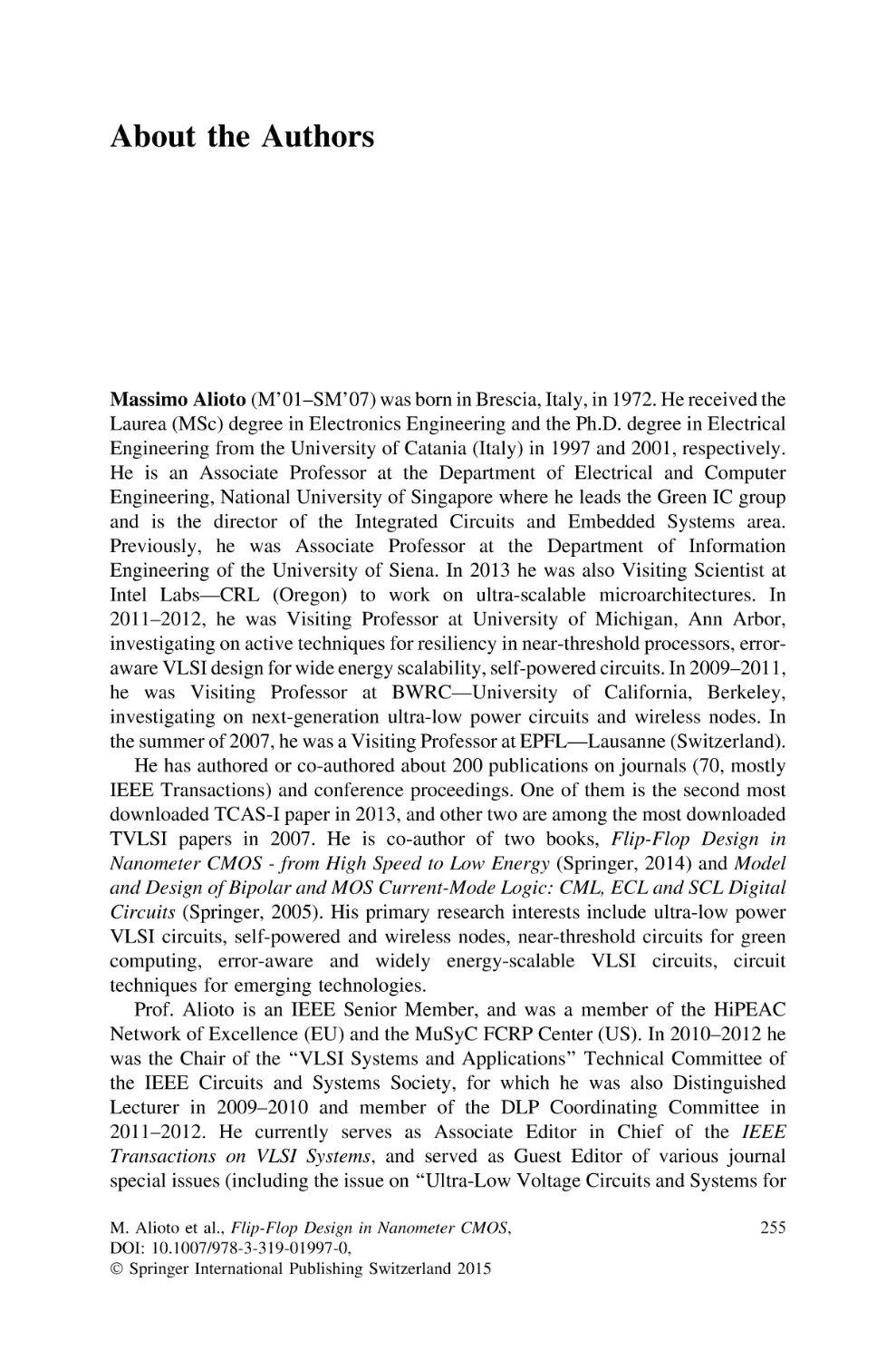
1.1 An RC Model for the Delay of Logic Gates
The development of delay models for CMOS logic gates requires the introduction
of various simplifications, especially if the models are to be used in back-of-theenvelope calculations. From their basic structure, CMOS logic gates can be simply
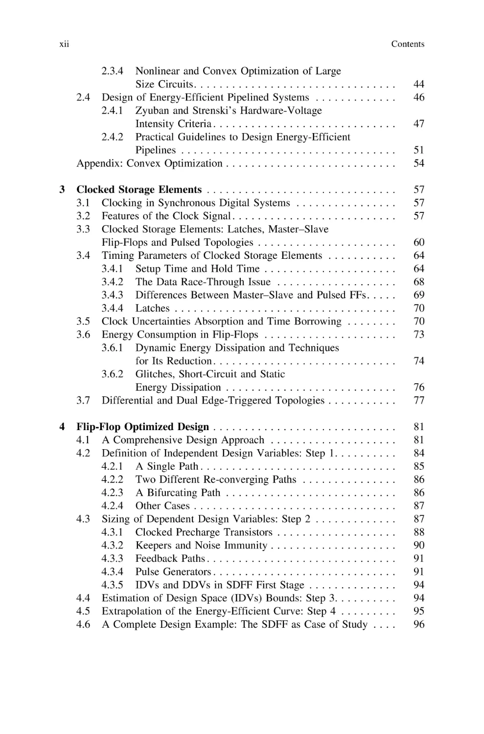
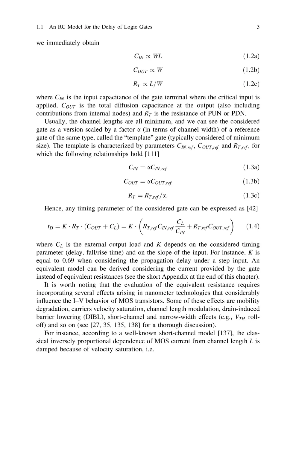
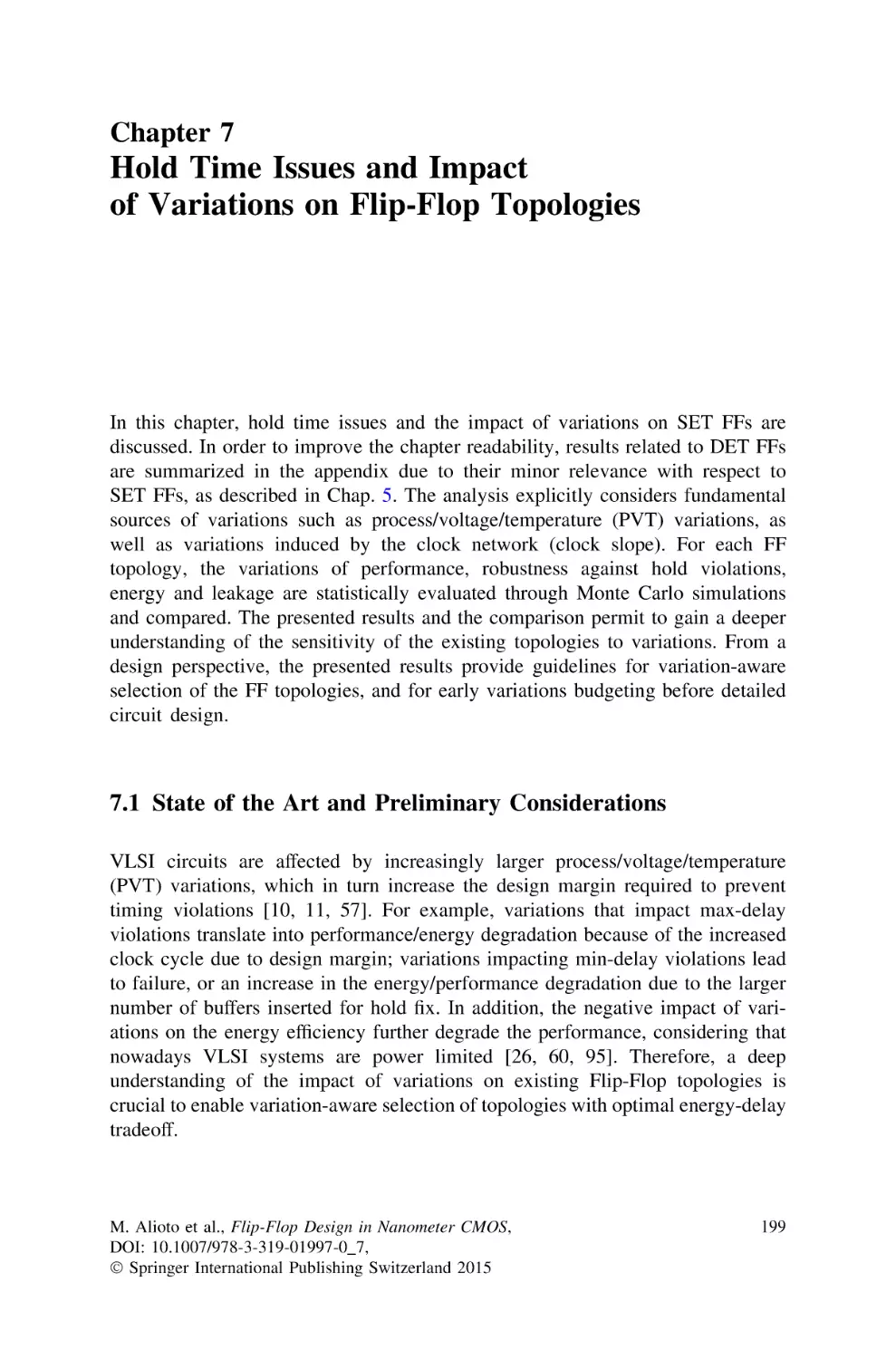
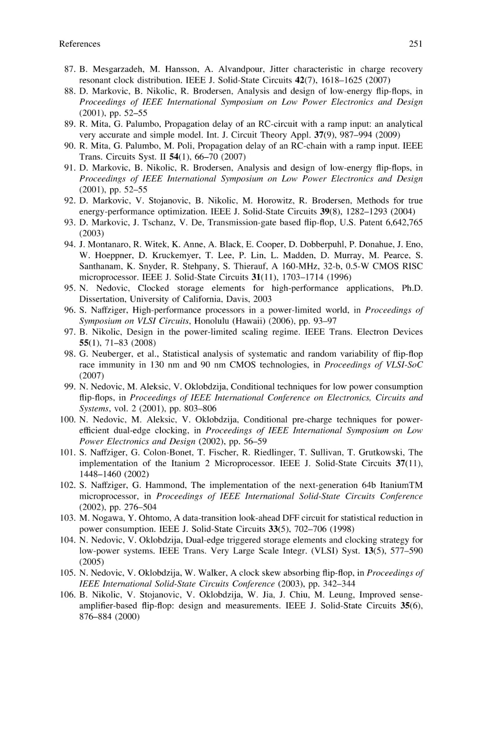
modeled as decoupled RC circuits [42]. As shown in Fig. 1.1, each block consists of
supply(VDD )-to-output and ground-to-output alternately activated resistive paths,
corresponding to pull-up (PUN) and pull-down (PDN) networks respectively. The
output is capacitively self-loaded and externally loaded. Whether the PUN or PDN
is activated depends on the logic value generated at the output of the previous block,
whose external load is the input capacitance of the gate corresponding to the
considered block. Once suitable R and C values are found, an effective model for
the delay estimation of CMOS logic gate can be easily developed.
The equivalent resistance R of a MOS can be evaluated by averaging out the
derivative ðoID =oVDS Þ1 in the voltage range of interest. Anyhow, the most
important consideration is that, independently of its operating region, the resistance of a MOS transistor is inversely proportional to its width W (for simplicity,
by neglecting the impact of normal and reverse narrow width effects [159], which
is certainly correct when sizes are not minimum or so). When considering complex
CMOS gates, the evaluation of the total equivalent resistance of PUN and PDN
can be approximately performed by summing the resistances of stacked blocks of
transistors, and by summing the conductances (which are proportional to W) of
parallel blocks of transistors that are conducting the current at the same time [122].
M. Alioto et al., Flip-Flop Design in Nanometer CMOS,
DOI: 10.1007/978-3-319-01997-0_1,
Ó Springer International Publishing Switzerland 2015
1
2
1 The Logical Effort Method
Fig. 1.1 CMOS logic gates
seen as decoupled RC blocks
VDD
RPUN
VOUT,i-1 = VIN,i
CIN,i
ON
if VIN,i = 0
VOUT,i = VIN,i
COUT,i
ON
if VIN,i = 1
CIN,i+1
RPDN
The equivalent capacitance CG at the input of a MOS transistor can be evaluated by averaging out the sum of CGS (gate-source), CGD (gate-drain) and CGB
(gate-bulk) contributions in the voltage range of interest. The resulting value is
proportional to WL and typically nearly equal to Cox WL (being Cox the gate oxide
capacitance per unit area) [122].
The self-loading capacitance in a CMOS gate is due to the drain-bulk (and
source-bulk in internal nodes for stacked transistors) diffusion capacitances. Such
capacitances can be expressed as1 [111]
CD ¼ CD;A WLd þ CD;P ð2W þ 2Ld Þ
ð1:1Þ
where Ld is the length of drain/source diffusions and CD;A (CD;P ) are the capacitances per unit area (perimeter) of drain-bulk and/or source-bulk junctions, evaluated by averaging out in the voltage range of interest.2 By neglecting the 2Ld CD;P
term, CD can be considered nearly proportional to W.
Summarizing, by considering.
(a) a CMOS gate with all stacked transistors of the same size
(b) only one conductive branch among the existing ones
(c) a constant ratio between the size of PMOS and NMOS
1
Note that sometimes the sidewall capacitance is not counted for the side of diffusion adjacent to
the channel [122]. In this case, the second term of Eq. (1.1) becomes equal to CD;P ðW þ 2Ld Þ.
2
By considering the large signal behavior of reverse-biased junction capacitances, CD;A can be
equaled to Cj0 Kj , being Cj0 the value under zero bias condition, and
"
#
/m
ð/ V1 Þ1m ð/ V2 Þ1m
Kj ¼
V2 V1
1m
1m
where / is the built-in potential across the junction, m is the grading coefficient of the
junction, and V1 and V2 are the minimum and maximum direct voltages across the junction,
respectively [122].
CD;P is equal to CD;A xj , being xj the depth of the diffusion.
1.1 An RC Model for the Delay of Logic Gates
3
we immediately obtain
CIN / WL
ð1:2aÞ
COUT / W
ð1:2bÞ
RT / L=W
ð1:2cÞ
where CIN is the input capacitance of the gate terminal where the critical input is
applied, COUT is the total diffusion capacitance at the output (also including
contributions from internal nodes) and RT is the resistance of PUN or PDN.
Usually, the channel lengths are all minimum, and we can see the considered
gate as a version scaled by a factor a (in terms of channel width) of a reference
gate of the same type, called the “template” gate (typically considered of minimum
size). The template is characterized by parameters CIN;ref , COUT;ref and RT;ref , for
which the following relationships hold [111]
CIN ¼ aCIN;ref
ð1:3aÞ
COUT ¼ aCOUT;ref
ð1:3bÞ
RT ¼ RT;ref =a:
ð1:3cÞ
Hence, any timing parameter of the considered gate can be expressed as [42]
CL
þ RT;ref COUT;ref
tD ¼ K RT ðCOUT þ CL Þ ¼ K RT;ref CIN;ref
ð1:4Þ
CIN
where CL is the external output load and K depends on the considered timing
parameter (delay, fall/rise time) and on the slope of the input. For instance, K is
equal to 0.69 when considering the propagation delay under a step input. An
equivalent model can be derived considering the current provided by the gate
instead of equivalent resistances (see the short Appendix at the end of this chapter).
It is worth noting that the evaluation of the equivalent resistance requires
incorporating several effects arising in nanometer technologies that considerably
influence the I–V behavior of MOS transistors. Some of these effects are mobility
degradation, carriers velocity saturation, channel length modulation, drain-induced
barrier lowering (DIBL), short-channel and narrow-width effects (e.g., VTH rolloff) and so on (see [27, 35, 135, 138] for a thorough discussion).
For instance, according to a well-known short-channel model [137], the classical inversely proportional dependence of MOS current from channel length L is
damped because of velocity saturation, i.e.
4
1 The Logical Effort Method
(
ID /
1
VDS þLEcr
1
ðVGS VTH ÞþLEcr
in triode region
in saturation region
ð1:5Þ
where VTH is the threshold voltage and Ecr is the electrical field for which velocity
saturation is observed. Meanwhile, due to short-channel effects, VTH decreases
when lowering L [149]. Hence, an R / L approximation is not too inaccurate.
In the case of n stacked MOS transistors, which classically exhibit a total
equivalent resistance equal to nR, being R the resistance of a single transistor,
when considering velocity saturation, the total resistance grows more slowly, since
transistors experience less pronounced current saturation thanks to the smaller
voltages they are subject to [128, 129]. Meanwhile, channel length modulation and
DIBL effects have a severe impact and increase the dependence of saturation
current from VDS .
1.2 The Logical Effort Model
The RC model in (1.4) was revisited in [133] to obtain a model normalized to (i.e.,
independent of) technology: the Logical Effort model. Basically, Eq. (1.4) is
divided by RINV CINV , which is the product of the equivalent resistance and input
capacitance of a symmetrical inverter, i.e. an inverter showing symmetric PUN
and PDN driving capabilities (in current technologies, this is typically obtained by
sizing the PMOS nearly twice the size of the NMOS). Note that, even if the
absolute size of this inverter is varied, the product RINV CINV is a constant
depending on technology.
Once normalized, the delay tD of the considered gate becomes
tD ¼ sðgh þ pÞ
ð1:6aÞ
where the various quantities correspond to
s ¼ KRINV CINV
ð1:7Þ
RT;ref CIN;ref
RINV CINV
ð1:8Þ
CL
CIN
ð1:9Þ
RT;ref COUT;ref
RINV CINV
ð1:10Þ
g¼
h¼
p¼
1.2 The Logical Effort Model
5
The parameter s allows for normalizing the absolute delay tD to technology and
it represents the delay of a symmetrical inverter loaded with an identical inverter
and neglecting the self-loading effect due to diffusion capacitances.
The parameter g is called “logical effort” and, except for a few specific cases, is
a feature dependent on the gate’s topology and hence not affected by the “absolute” sizing of the gate but only by its “relative” sizing (by definition, g ¼ 1 for a
symmetrical inverter). The logical effort g describes the driving capability of the
gate topology and has a dual interpretation:
(1) under the assumption of equal CIN , g quantifies the driving capability degradation of the considered gate with respect to a symmetric inverter
(2) under the assumption of equal driving capability, g indicates how much larger
the considered gate has to be (in terms of CIN ) with respect to a symmetric
inverter.
The parameter h is called “electrical effort” and it is equal to the effective
fanout of the gate. It is independent of the topology of the logic gate, and it is
affected only by the absolute gate sizing (i.e., it is defined by a) and affects the
normalized delay d as much as g. Obviously it increases for high CL (heavier load)
and decreases for high CIN (larger driving capability).
The parameter p is called “parasitic delay” and represents the intrinsic and
unavoidable delay contribution due to the self-loading capacitance of the gate.
Similarly to g, with few exceptions that will be reviewed in the next chapters, p is a
feature that is defined by the gate topology and is affected only by the relative
sizing of the gate, not the absolute sizing. Indeed when enlarging the gate size to
improve its driving capability, the capacitance COUT increases proportionally as
well. In the case of an inverter, p is close to 1, since typically CG CD .
Relationship (1.6a) can be rewritten as
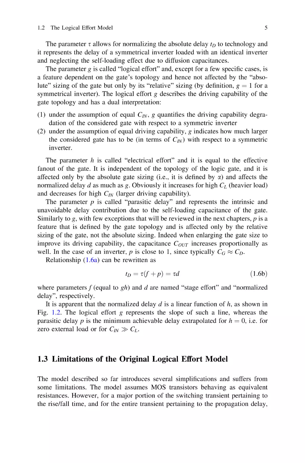
tD ¼ sðf þ pÞ ¼ sd
ð1:6bÞ
where parameters f (equal to gh) and d are named “stage effort” and “normalized
delay”, respectively.
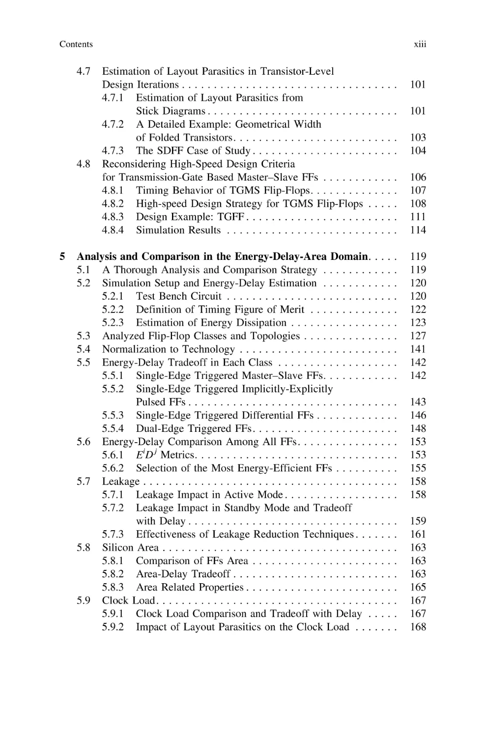
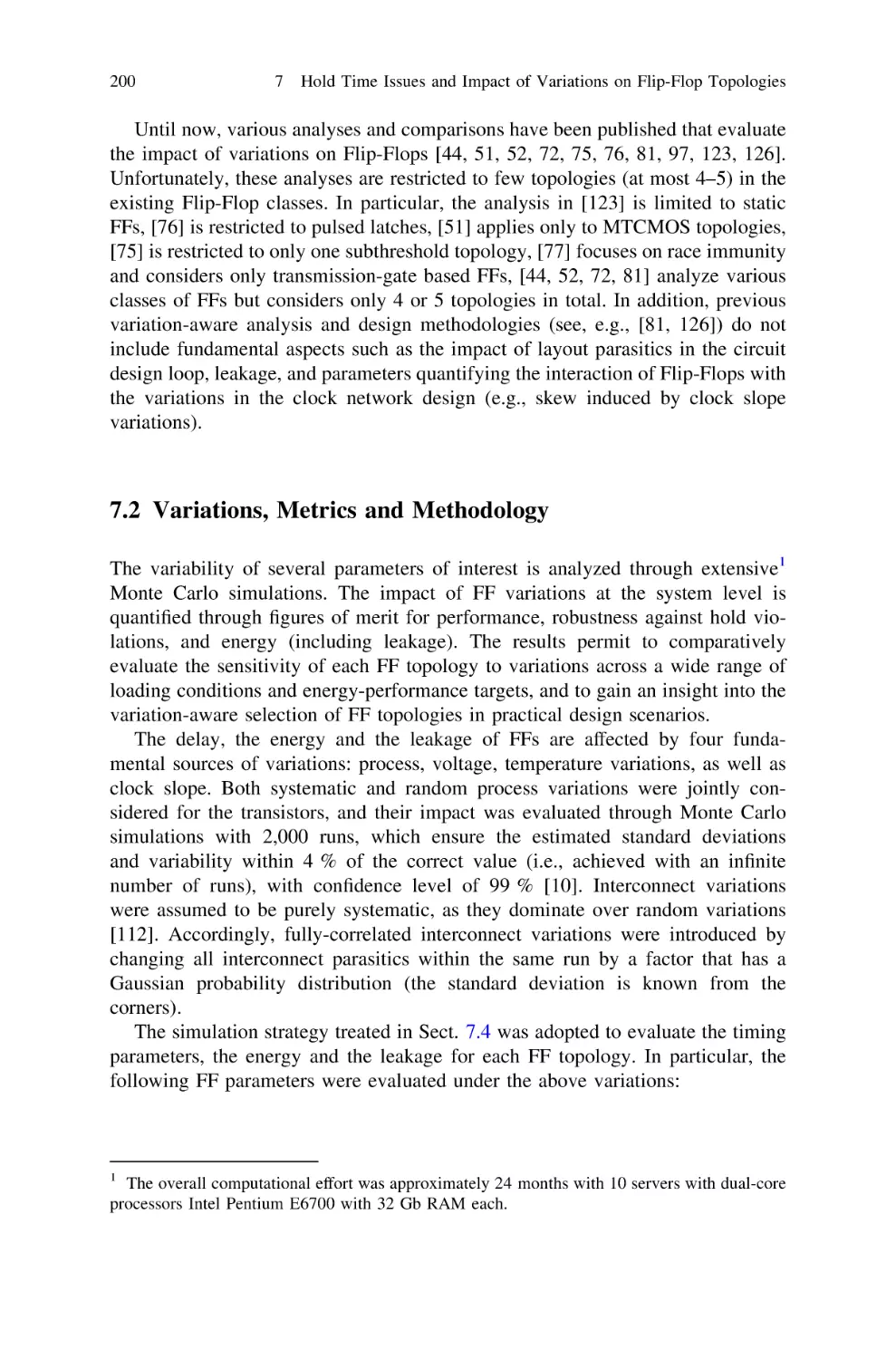
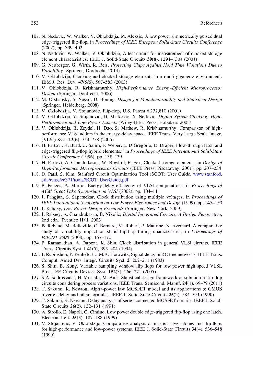
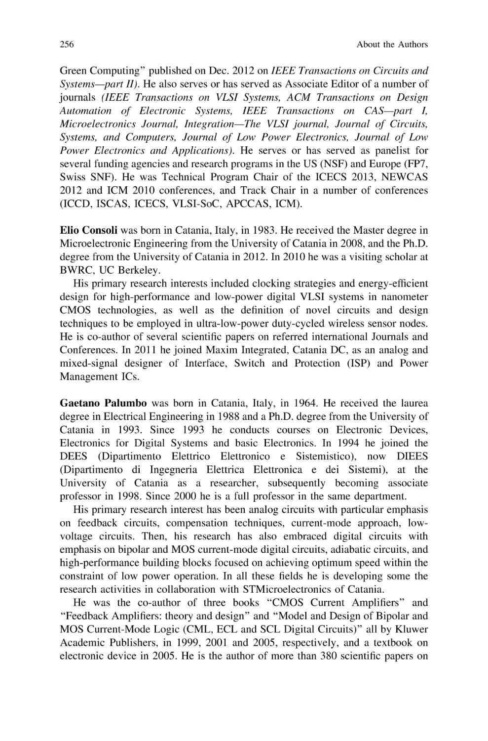
It is apparent that the normalized delay d is a linear function of h, as shown in
Fig. 1.2. The logical effort g represents the slope of such a line, whereas the
parasitic delay p is the minimum achievable delay extrapolated for h ¼ 0, i.e. for
zero external load or for CIN CL .
1.3 Limitations of the Original Logical Effort Model
The model described so far introduces several simplifications and suffers from
some limitations. The model assumes MOS transistors behaving as equivalent
resistances. However, for a major portion of the switching transient pertaining to
the rise/fall time, and for the entire transient pertaining to the propagation delay,
6
Fig. 1.2 Geometrical
interpretation of logical effort
and parasitic delay
1 The Logical Effort Method
d=gh+p
Inverter
2-inputs NAND
3-inputs NAND
pNAND3
pNAND2
pINV
0
1
2
3
4
h
MOS transistors behave as non-ideal current sources. Regardless of the transistor
operating region, the dependence on channel width and length is basically the
same, when considering the current in the saturation region, and the conductance
in the triode region (see the Appendix at the end of the chapter).
Both the self- and external loads vary with the output voltage in a complicated
nonlinear manner. Again, the general trend of actual output waveforms is preserved when adopting averaged constant load capacitances.
The delay and rise/fall times of CMOS gates significantly depend on the input
transition time (or slope) [47], which is neglected in the Logical Effort model. As
concerns the rise/fall time, it always increases in a nonlinear manner at relatively
slow input transitions [28]. Regarding the delay, it can either increase or decrease
in a non-monotonic fashion when considering slow input transitions [29]. Several
attempts have been made to develop Logical Effort extensions in order to capture
the effect of a non-zero input transition time, although they have resulted in quite
complicated and impractical models, or in simpler ones whose applicability is
however restricted only to some cases [49, 74, 145].
Although the accuracy of the pure Logical Effort approach as a delay model is
somewhat impaired by the above approximations, Logical Effort is primarily used
as an optimization method for minimizing delays through the equalization of the
external load-dependent part of the delay d, i.e. gh. This approach leads to
somewhat constant input and output slopes for CMOS gates in a path, in which
case the original Logical Effort model is quite accurate.
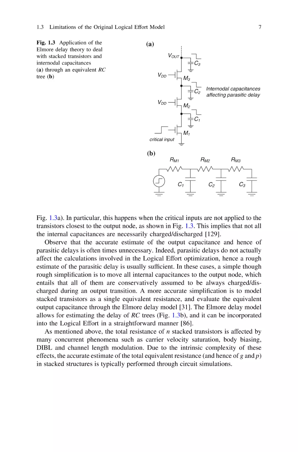
The model in (1.4) and (1.6a) accounts for the self-loading capacitance through
a lumped capacitance COUT that is placed in parallel to the external output load,
and is (dis)charged through the single resistance RT . In other words, only the
capacitances connected to the output node are taken into account. However, in real
PUN and/or PDN made up of stacked (parallel) transistors, the capacitances in
their internal nodes can give a further contribution to the parasitic delay (see
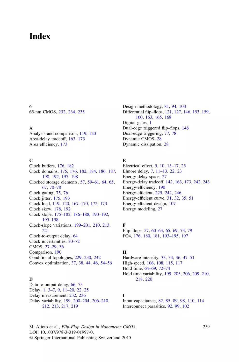
1.3 Limitations of the Original Logical Effort Model
Fig. 1.3 Application of the
Elmore delay theory to deal
with stacked transistors and
internodal capacitances
(a) through an equivalent RC
tree (b)
7
(a)
VOUT
C3
VDD
M3
C2
VDD
Internodal capacitances
affecting parasitic delay
M2
C1
M1
critical input
(b)
RM1
C1
RM2
C2
RM3
C3
Fig. 1.3a). In particular, this happens when the critical inputs are not applied to the
transistors closest to the output node, as shown in Fig. 1.3. This implies that not all
the internal capacitances are necessarily charged/discharged [129].
Observe that the accurate estimate of the output capacitance and hence of
parasitic delays is often times unnecessary. Indeed, parasitic delays do not actually
affect the calculations involved in the Logical Effort optimization, hence a rough
estimate of the parasitic delay is usually sufficient. In these cases, a simple though
rough simplification is to move all internal capacitances to the output node, which
entails that all of them are conservatively assumed to be always charged/discharged during an output transition. A more accurate simplification is to model
stacked transistors as a single equivalent resistance, and evaluate the equivalent
output capacitance through the Elmore delay model [31]. The Elmore delay model
allows for estimating the delay of RC trees (Fig. 1.3b), and it can be incorporated
into the Logical Effort in a straightforward manner [86].
As mentioned above, the total resistance of n stacked transistors is affected by
many concurrent phenomena such as carrier velocity saturation, body biasing,
DIBL and channel length modulation. Due to the intrinsic complexity of these
effects, the accurate estimate of the total equivalent resistance (and hence of g and p)
in stacked structures is typically performed through circuit simulations.
8
1 The Logical Effort Method
1.4 Basic Estimation of Logical Effort Parameters
In the remainder of the book, transistors widths (lengths) are normalized to the
minimum value Wmin (Lmin ) allowed by technology. In particular, such normalized
values are referred to as w ¼ W=Wmin and l ¼ L=Lmin , being W and L the absolute
sizes. Analogously, the absolute capacitances and equivalent resistances, C and R,
will be normalized to the values obtained for W ¼ Wmin and L ¼ Lmin (e.g., gate
capacitances CG will be normalized to Cox Wmin Lmin ) and indicated with c and r,
respectively.
The first step to evaluate Logical Effort parameters (g, h and p) is to determine
rINV and cINV (i.e., the normalized RINV and CINV ). As mentioned above, the
product rINV cINV will remain constant whichever the absolute sizing of the reference inverter is, provided that such inverter is symmetric. In the following, for
simplicity we will assume that the symmetry of an inverter is achieved by sizing
the PMOS transistor 2 times larger than the NMOS transistor. For instance, we will
refer to the minimum symmetrical inverter when wP ¼ 2, lP ¼ 1, wN ¼ 1 and
lN ¼ 1. Hence, such an inverter will have an input capacitance cINV ¼ 3, while its
resistance (equal for PMOS and NMOS by virtue of symmetry) can be assumed as
the reference unitary resistance, i.e. rINV ¼ 1. Thus, rINV cINV results equal to 3,
regardless of the absolute size. Indeed, in a non-minimum inverter with wP and wN
equal to 2w and w, cINV results to 3w and rINV is equal to 1=w, once again leading
to rINV cINV ¼ 3.
When defining g and p in (1.8) and (1.10), we resorted to the products
rT;ref cIN;ref and rT;ref cOUT;ref . As for the symmetrical inverter, for each CMOS
static gate such products (and hence also g and p) remain constant whichever the
absolute size is, provided that the gate maintains its skew S.
The skew of a CMOS static gate is defined as the ratio between the driving
capabilities of PUN and PDN when applying the critical input (i.e., input leading
to an actual output transition). By definition, a symmetric gate has unitary skew,
whereas gates with unbalanced rise/fall transitions will have a skew greater or
smaller than one.
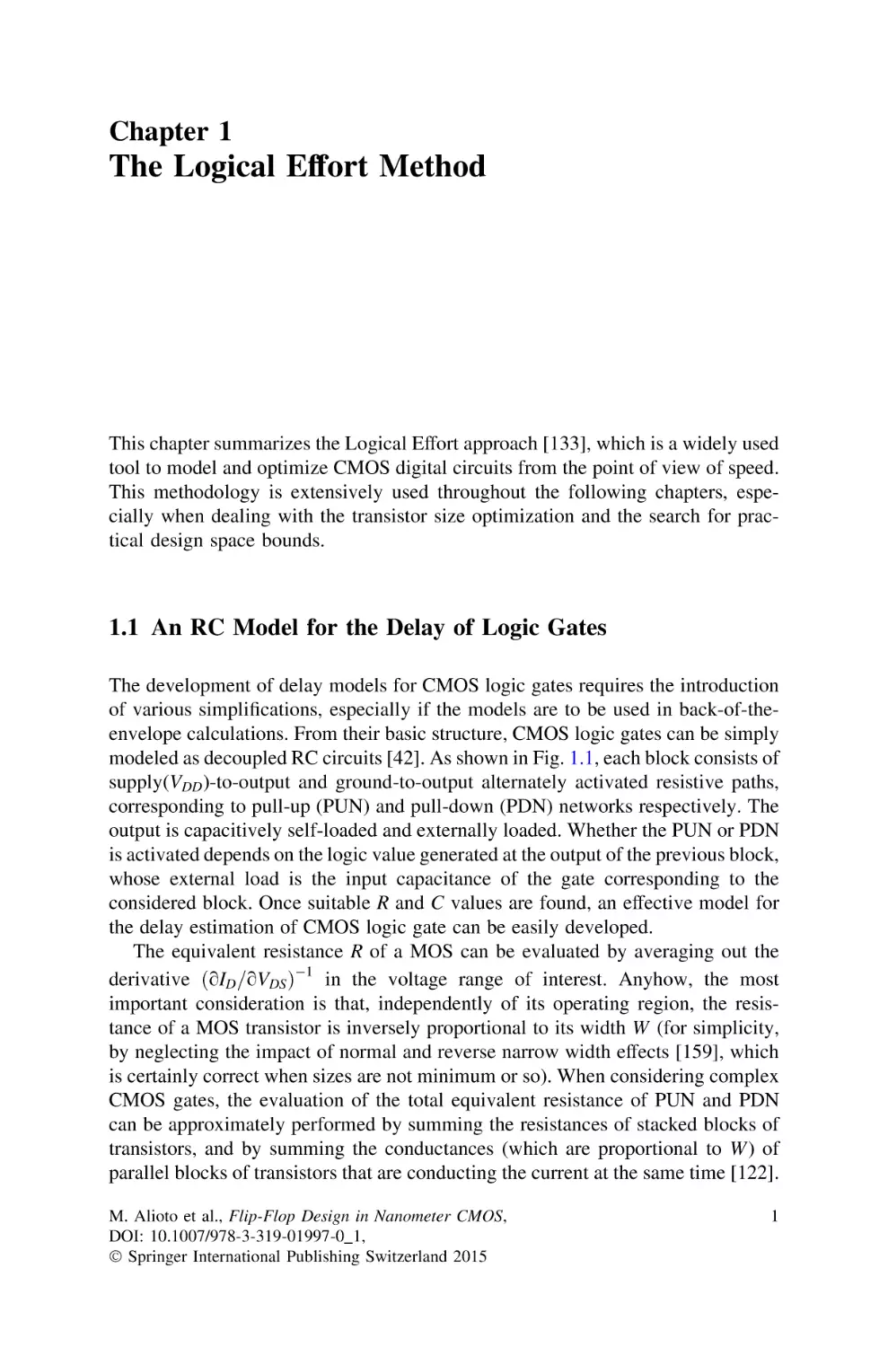
To obtain any desired skew, stacked and/or parallel groups of transistors need to
be properly sized. As an example, if one wants to make a gate symmetrical and
considering the pessimistic case where only one branch conducts current among
each group of parallel ones [122], the PMOS transistors have to be sized k ¼
lðMP=MN Þ times the size of the NMOS, where:
– MN (MP) is the number of stacked transistors in the PDN (PUN), hence the ratio
MP=MN compensate for the different weight of stacking in PUN and PDN;
– l is the above mentioned NMOS/PMOS mobility ratio equal to 2, as dictated by
the different mobilities of electron and holes.
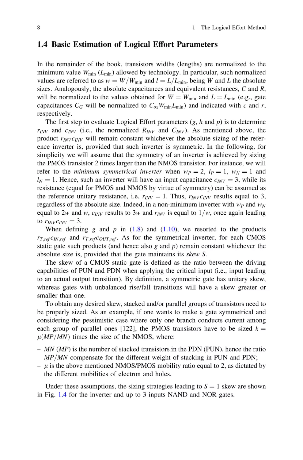
Under these assumptions, the sizing strategies leading to S ¼ 1 skew are shown
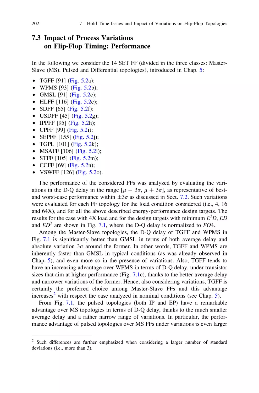
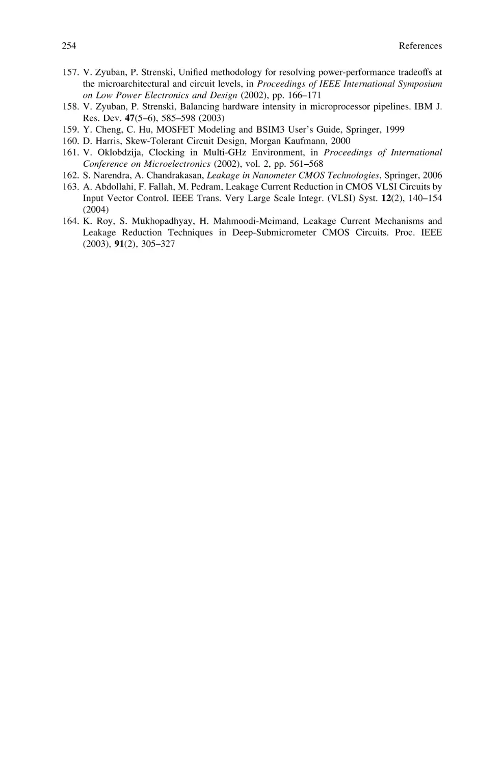
in Fig. 1.4 for the inverter and up to 3 inputs NAND and NOR gates.
1.4 Basic Estimation of Logical Effort Parameters
INVERTER
Wp
Wn
NAND3
NAND2
IN1
IN1
IN2
Wp
Wp
IN
9
IN2
Wp
IN3
Wp
NOR2
Wn
IN2
IN2
Wp
Wn
IN1
IN2
IN2
Wn
Wp
Wp
Wp
IN1
IN1
NOR3
IN1
IN1
Wn
IN2
W
n
IN3
IN3
W
n
Wn
Wp /Wn= (2/1)
gr = 1 gf = 1
pr = 1 pf = 1
Wp /Wn= (1/1)
gr = 4/3 gf = 4/3
pr = 2 pf = 2
Wp /Wn= (2/3)
gr = 5/3 gf = 5/3
pr = 3 pf = 3
Wp /Wn= (4/1)
gr = 5/3 gf = 5/3
pr = 2 pf = 2
IN1
IN2
Wn
Wp
Wp
IN3
Wn
Wn
Wp /Wn= (6/1)
gr = 7/3 gf = 7/3
pr = 3 pf = 3
Fig. 1.4 Sizing of basic gates under unitary skew conditions
Parameters g and p can be simply estimated by visual inspection of the
capacitances (cIN and cOUT ) and resistances (rT ) of the gate for any sizing leading
to a certain skew (recall that g and p remain constant under the same skew). In
particular:
cIN ¼ wN;i lN;i þ wP;i lP;i
X
X
wN;j þ
wP;k
cOUT ¼
j
ð1:11Þ
ð1:12Þ
k
rT;N ¼
MN
X
lN;m
w
m¼1 N;m
ð1:13Þ
rT;P ¼
MP
X
lP;m
w
m¼1 P;m
ð1:14Þ
where
– wN;i (wP;i ) and lN;i (lP;i ) are the width and length of the NMOS (PMOS) transistor driven by the ith input of the gate, which is the one considered in the delay
estimation
– wN;j (wP;j ) are the widths of all NMOS (PMOS) transistors contributing to the
self-loading
– MN (MP) is the number of stacked transistors in the PDN (PUN)
– wN;m (wP;m ) and lN;m (lP;m ) are the width and length of the mth transistor in the
PDN (PUN) stack.
Parallel transistors are neglected in this computation. Only when some of them
are conducting simultaneously, their effect can be included by summing up the
correspondent conductances, i.e. the ratios w=l.
Relationship (1.12) is based on the assumption that the transistor diffusion
drain-bulk capacitance is nearly equal to the gate input capacitance. The validity of
this assumption strongly depends on technology and layout features [144].
Moreover, for the moment we are considering only the capacitances that are
10
1 The Logical Effort Method
Table 1.1 Logical effort and parasitic delay for NAND and NOR gates having M inputs and
S rise/fall skew
M inputs S skew
Inverter
M-inputs NAND
M-inputs NOR
Wp/Wn
gr
gf
pr
pf
2S
2
1
3 1 þ 2S
1
1 þ 2SÞ
3ð
2
1
3 1 þ 2S
1
3 ð1 þ 2SÞ
2S
M
2
M
3 1 þ 2S
1
M þ 2SÞ
3ð
2
M
3 M þ 2S
1
3 ðM þ 2SM Þ
2SM
2
1
3 M þ 2S
1
1 þ 2SM Þ
3ð
2
M
3 M þ 2S
1
3 ðM þ 2SM Þ
physically attached to the output node as in the original Logical Effort model
(more accurate extensions will be given in the following chapters).
Once cIN , cOUT , rT;N and rT;P are computed for the specific input, g and p can be
estimated from (1.8) and (1.10), i.e. dividing cIN rT;N (cIN rT;P ) and cOUT rT;N
(cOUT rT;P ) by rINV cINV ¼ 3. It is evident that, except for the cases of unitary skew
(shown in Fig. 1.4), g and p are different for the falling and rising transitions.
Hence we define gf and pf as the parameters referring to the falling transition and
gr and pr as those referring to the rising transition. The values of g and p for the
rising and falling transitions of the basic gates depicted in Fig. 1.4 are reported in
Table 1.1 for generic inputs number, M, and skew, S.
It is worth noting that, while p is constant for any input of the gate (at least
when considering only the parasitic capacitances attached to the output node), g
can vary according to the considered input because of the possible different input
capacitance seen at each input. This happens when considering gates that employ
combined stacked/parallel group of transistors and where NMOS (PMOS) are not
equally sized3 as shown in Fig. 1.5.
Finally, the electrical effort h is simply estimated by transforming the external
load CL into a normalized equivalent width. This is easily done by visual
inspection when the load is represented by another CMOS gate.
1.5 Accurate Estimation of Parameters g and p
So far we have discussed simple strategies to estimate the logical effort and the
parasitic delay of CMOS logic gates. The following approaches are better suited
for more accurate estimates of Logical Effort parameters in the presence of stacked
transistors.
3
When considering basic gates such as NAND or NOR, the resistance exhibited by pull-up an
pull-down network is nearly the same whichever is the applied critical input. On the contrary, for
more complex gates it is not possible to size the pull-down (pull-up) networks so that they exhibit
the same resistance for all input combinations. Therefore, the usual approach [122] is to consider
a worst-case where it is considered that only one among various parallel groups of transistors is
conducting, as done for the sizing of the gate in Fig. 1.5.
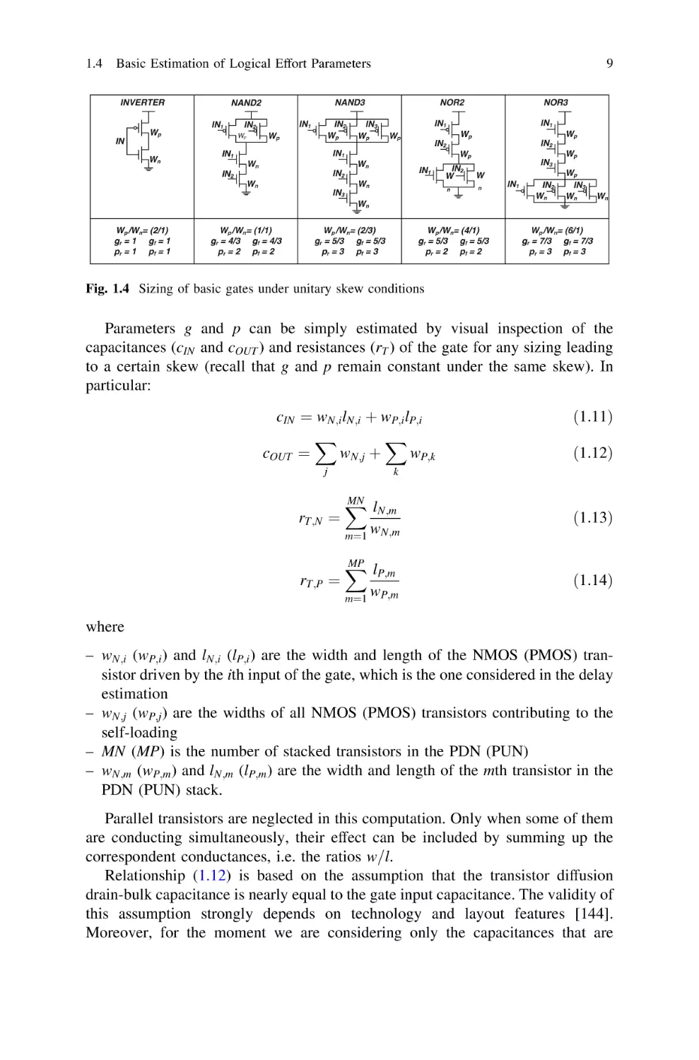
1.5 Accurate Estimation of Parameters g and p
Fig. 1.5 Complex gate sized
to exhibit S ¼ 1 skew and
delay equal to a minimum
inverter: differences in g
values according to the
considered input
A
B
4Wmin
11
C
4Wmin
4Wmin
D
4Wmin
f = (ABC)D
A
3Wmin
D
B
3Wmin
C
3Wmin
Wmin
gr,(ABC) = g f,(ABC) = 7/3
gr,(D) = g f,(D) = 5/3
1.5.1 Estimation of the Capacitance at Internal Nodes
The value of the diffusion capacitances depends on the specific layout. Different
drain-bulk and source-bulk capacitances are associated to shared/unshared and
contacted/non-contacted nodes [144]. For instance, stacked transistors can share their
diffusions and hence reduce the corresponding parasitic capacitances. Similarly, noncontacted diffusions are smaller than contacted ones, and hence have small parasitic
capacitance as well. In addition to the diffusion capacitances, the gate-source and
gate-drain capacitances contribute to the inter-nodal capacitances, at least for the
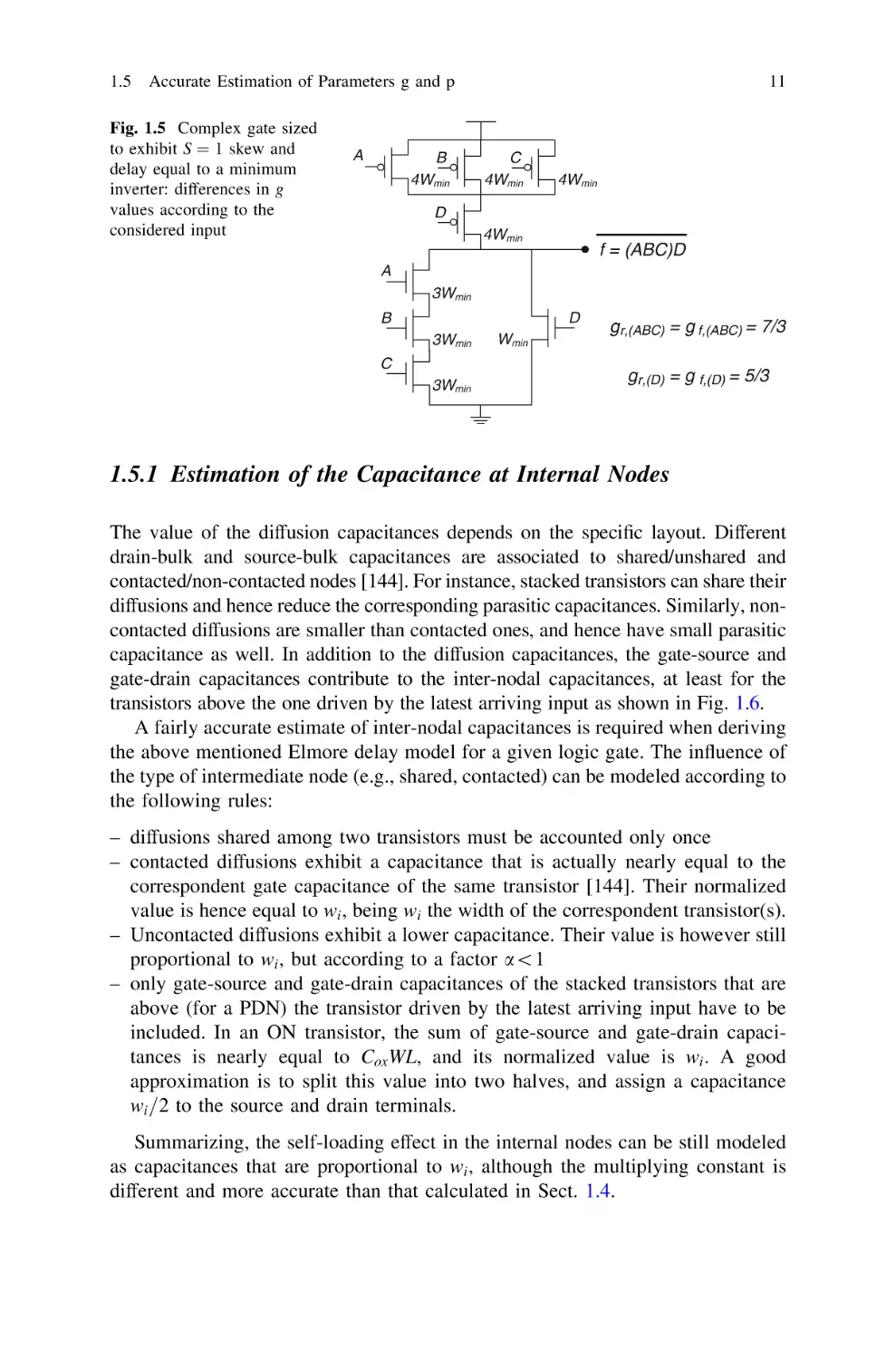
transistors above the one driven by the latest arriving input as shown in Fig. 1.6.
A fairly accurate estimate of inter-nodal capacitances is required when deriving
the above mentioned Elmore delay model for a given logic gate. The influence of
the type of intermediate node (e.g., shared, contacted) can be modeled according to
the following rules:
– diffusions shared among two transistors must be accounted only once
– contacted diffusions exhibit a capacitance that is actually nearly equal to the
correspondent gate capacitance of the same transistor [144]. Their normalized
value is hence equal to wi , being wi the width of the correspondent transistor(s).
– Uncontacted diffusions exhibit a lower capacitance. Their value is however still
proportional to wi , but according to a factor a\1
– only gate-source and gate-drain capacitances of the stacked transistors that are
above (for a PDN) the transistor driven by the latest arriving input have to be
included. In an ON transistor, the sum of gate-source and gate-drain capacitances is nearly equal to Cox WL, and its normalized value is wi . A good
approximation is to split this value into two halves, and assign a capacitance
wi =2 to the source and drain terminals.
Summarizing, the self-loading effect in the internal nodes can be still modeled
as capacitances that are proportional to wi , although the multiplying constant is
different and more accurate than that calculated in Sect. 1.4.
12
1 The Logical Effort Method
(a)
VDD
critical input
wP
M5
wP
M4
CGD4
CDB4
wP
M6
CDB5
CGD5
VOUT
CGD3
CGD6
CDB6
wL
CDB3
wN
M3
CGS3
CGD2
CSB3
CDB2
wN
M2
CGS2
CGD1
CSB2
CDB1
wN
M1
critical input
(b)
VOUT
c3 ≈ (3/2)wN+3wP+wL
Normalized capacitances c:
cDB1+cSB2 ≈ αwN
cDB2+cSB3 ≈ αwN
cDB3 ≈ wN
cGD1+cGS2 ≈ wN
cGD2+cGS3 ≈ wN
cGD3 ≈ wN/2
cDB4+cDB5 ≈ wP
cDB6 ≈ wP
cGD4+cGD5+cGD6 ≈ wP
VDD
M3
c2 ≈ (α+1)wN
VDD
M2
c1 ≈ (α+1)wN
M1
critical input
Fig. 1.6 Internodal capacitances in a NAND3 (a) and accurate estimation of their normalized
values as functions of sizing (b)
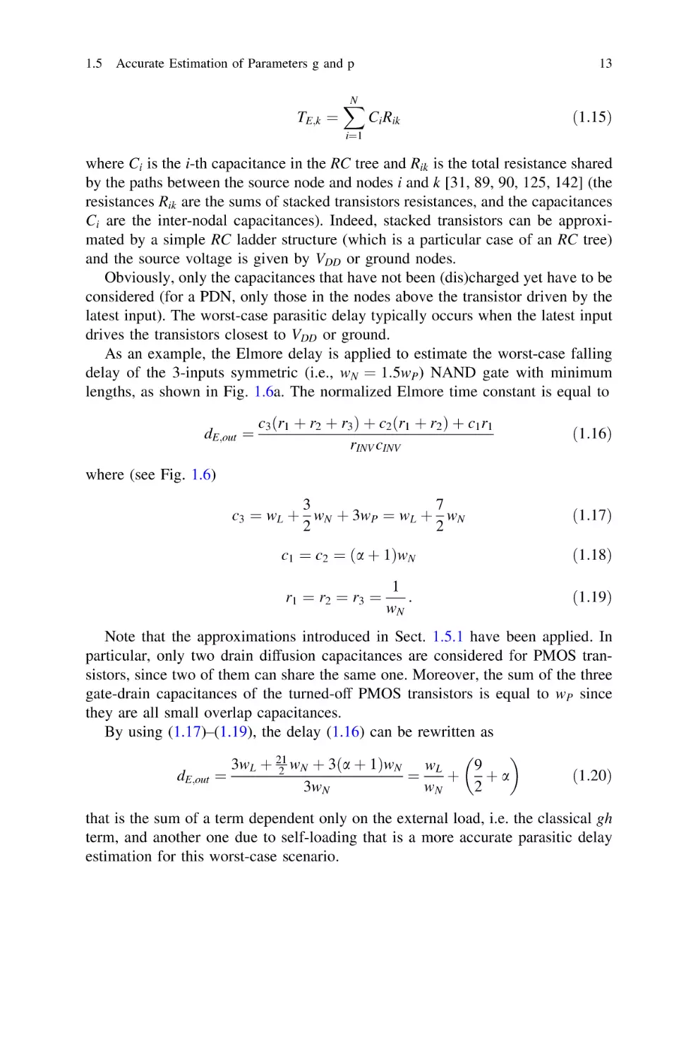
1.5.2 Elmore Delay
As was discussed in Fig. 1.3, the parasitic delay of topologies with stacked transistors can be more accurately expressed through the Elmore delay model [31].
The latter allows for estimating the delay due to an RC tree from a source node
(where the voltage is applied) to a node k. Elmore delay expresses the tree time
constant as
1.5 Accurate Estimation of Parameters g and p
TE;k ¼
N
X
13
Ci Rik
ð1:15Þ
i¼1
where Ci is the i-th capacitance in the RC tree and Rik is the total resistance shared
by the paths between the source node and nodes i and k [31, 89, 90, 125, 142] (the
resistances Rik are the sums of stacked transistors resistances, and the capacitances
Ci are the inter-nodal capacitances). Indeed, stacked transistors can be approximated by a simple RC ladder structure (which is a particular case of an RC tree)
and the source voltage is given by VDD or ground nodes.
Obviously, only the capacitances that have not been (dis)charged yet have to be
considered (for a PDN, only those in the nodes above the transistor driven by the
latest input). The worst-case parasitic delay typically occurs when the latest input
drives the transistors closest to VDD or ground.
As an example, the Elmore delay is applied to estimate the worst-case falling
delay of the 3-inputs symmetric (i.e., wN ¼ 1:5wP ) NAND gate with minimum
lengths, as shown in Fig. 1.6a. The normalized Elmore time constant is equal to
dE;out ¼
c3 ðr1 þ r2 þ r3 Þ þ c2 ðr1 þ r2 Þ þ c1 r1
rINV cINV
ð1:16Þ
where (see Fig. 1.6)
3
7
c3 ¼ wL þ wN þ 3wP ¼ wL þ wN
2
2
ð1:17Þ
c1 ¼ c2 ¼ ða þ 1ÞwN
ð1:18Þ
1
:
wN
ð1:19Þ
r1 ¼ r2 ¼ r3 ¼
Note that the approximations introduced in Sect. 1.5.1 have been applied. In
particular, only two drain diffusion capacitances are considered for PMOS transistors, since two of them can share the same one. Moreover, the sum of the three
gate-drain capacitances of the turned-off PMOS transistors is equal to wP since
they are all small overlap capacitances.
By using (1.17)–(1.19), the delay (1.16) can be rewritten as
3wL þ 21
wL
9
2 wN þ 3ða þ 1ÞwN
þa
ð1:20Þ
dE;out ¼
¼
þ
2
3wN
wN
that is the sum of a term dependent only on the external load, i.e. the classical gh
term, and another one due to self-loading that is a more accurate parasitic delay
estimation for this worst-case scenario.
14
1 The Logical Effort Method
It is worth noting that the resulting parasitic delay is slightly higher than that
resulting with the traditional LE, equal to 3 for the 3-input NAND.
1.5.3 Parameter Calibration
A third issue concerns the accurate evaluation of the overall resistance of stacked
transistors, which influences both g and p. Even if DIBL and channel length
modulation effects somewhat compensate for velocity saturation, the nR approximation is not precise. Anyhow, given the complexity of the problem, no easy
calculations can be carried out and the best way to estimate the actual value of g
and p is through simulations.
Remembering that g is the slope and p is the intercept of the linear relationship
between delay and electrical effort, the procedure to estimate them simply consists
in evaluating the delay of the considered gate for increasing h values and normalizing with respect to the technology parameter s.
Proper precautions have to be taken in order to provide the gate with realistic
input waveforms and load, to avoid an unrealistic amplification of the CGD external
loading capacitances due to Miller effect [133]. The first objective is achieved by
driving the gate under test with the signal provided by two gates of the same type,
while the second is achieved by imposing a sufficiently large load on the loading
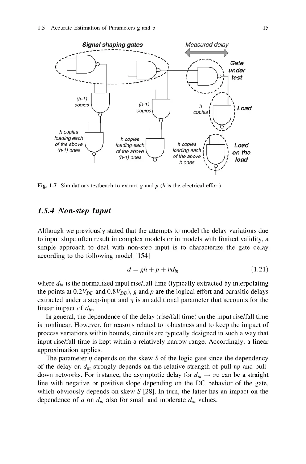
gate. Figure 1.7 illustrates such a testbench to extract parameters g and p through
simulations [144].
By extracting g and p in this way, for instance one finds that, in a 65-nm CMOS
technology the ratio RT;ref =RINV is equal to 1.85, 1.6, 2.7, 2.3 for minimum
symmetrical NAND2, NOR2, NAND3 and NOR3 gates, respectively. This shows
that, although DIBL and channel length modulation effect have a strong impact in
nanometer technologies, the effect of velocity saturation is higher.4
It is worth noting that the above calibration procedure allows for estimating the
values of g and p including the effect of non-zero input rise/fall times, although
under the restriction that the output rise/fall time is equal to the input rise/fall time.
Obviously, in real circuits this is not generally true. But, as anticipated in Sect. 1.3
and shown in the following section, this is a highly reasonable approximation
when using the Logical Effort as a method to minimize delay.
4
In the case of long-channel devices, NAND2/NOR2 and NAND3/NOR3 show a ratio
RT;ref =RINV equal to 2 and 3, respectively. The ratio increases because of DIBL and channel
length modulation, whereas decreases due to velocity saturation.
1.5 Accurate Estimation of Parameters g and p
15
Measured delay
Signal shaping gates
Gate
under
test
(h-1)
copies
h copies
loading each
of the above
(h-1) ones
(h-1)
copies
h copies
loading each
of the above
(h-1) ones
h
copies
h copies
loading each
of the above
h ones
Load
Load
on the
load
Fig. 1.7 Simulations testbench to extract g and p (h is the electrical effort)
1.5.4 Non-step Input
Although we previously stated that the attempts to model the delay variations due
to input slope often result in complex models or in models with limited validity, a
simple approach to deal with non-step input is to characterize the gate delay
according to the following model [154]
d ¼ gh þ p þ gdin
ð1:21Þ
where din is the normalized input rise/fall time (typically extracted by interpolating
the points at 0:2VDD and 0:8VDD ), g and p are the logical effort and parasitic delays
extracted under a step-input and g is an additional parameter that accounts for the
linear impact of din .
In general, the dependence of the delay (rise/fall time) on the input rise/fall time
is nonlinear. However, for reasons related to robustness and to keep the impact of
process variations within bounds, circuits are typically designed in such a way that
input rise/fall time is kept within a relatively narrow range. Accordingly, a linear
approximation applies.
The parameter g depends on the skew S of the logic gate since the dependency
of the delay on din strongly depends on the relative strength of pull-up and pulldown networks. For instance, the asymptotic delay for din ! 1 can be a straight
line with negative or positive slope depending on the DC behavior of the gate,
which obviously depends on skew S [28]. In turn, the latter has an impact on the
dependence of d on din also for small and moderate din values.
16
1 The Logical Effort Method
1.6 Multistage Logic Networks and Delay Minimization
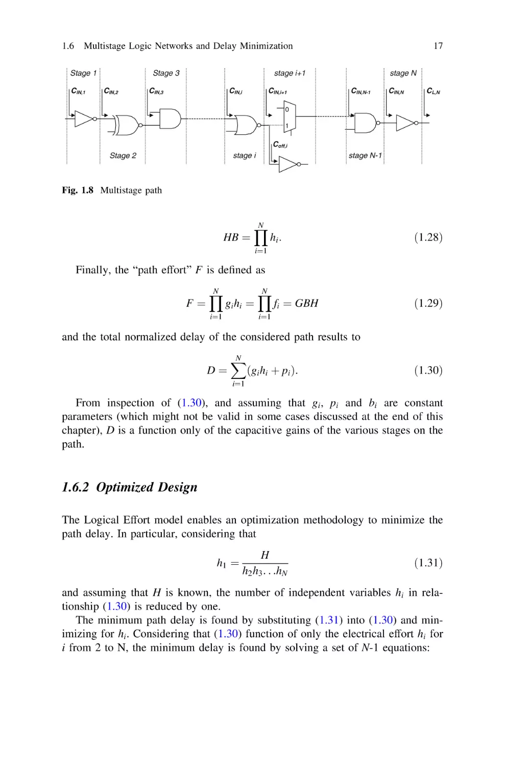
1.6.1 Path Parameters
In the following we consider a multistage network comprising a path made up of N
cascaded logic gates, the ith of which is featured by a logical effort gi , a parasitic
delay pi and an electrical effort equal to
hi ¼
CL;i
CIN;iþ1 þ Coff ;i
¼
CIN;i
CIN;i
ð1:22Þ
where CIN;i and CIN;iþ1 are the input capacitances of the ith and ði þ 1Þth gate in
the considered path, while Coff ;i is the input capacitance of other gates loading the
stage i but not belonging to the path under analysis (see Fig. 1.8).
The Logical Effort (LE) can also be applied to entire paths. To this purpose, the
“path logical effort” G, the “path parasitic delay” P, and the “path electrical effort”
H are defined as
G¼
N
Y
gi
ð1:23Þ
pi
ð1:24Þ
CL;N
CIN;1
ð1:25Þ
i¼1
P¼
N
X
i¼1
H¼
being CL;N and CIN;1 in (1.25) the final load of the path and the input capacitance of
the first stage, respectively.
By defining the “branching effort” bi of the ith stage as the proportion between
the total load of gate i and the fraction lying on the considered path
bi ¼
CIN;iþ1 þ Coff ;i
1;
CIN;iþ1
ð1:26Þ
the “path branching effort” B of the entire path is defined as
B¼
N
Y
bi
ð1:27Þ
i¼1
whose product with the path electrical effort H is readily found to result to the
product of all gate electrical efforts in the path (equal to H only when there are not
branch in path):
1.6 Multistage Logic Networks and Delay Minimization
Stage 1
CIN,1
Stage 3
CIN,2
17
stage i+1
CIN,3
CIN,i
CIN,i+1
stage N
CIN,N-1
CIN,N
CL,N
0
1
Coff,i
stage i
Stage 2
stage N-1
Fig. 1.8 Multistage path
HB ¼
N
Y
hi :
ð1:28Þ
i¼1
Finally, the “path effort” F is defined as
F¼
N
Y
gi hi ¼
i¼1
N
Y
fi ¼ GBH
ð1:29Þ
i¼1
and the total normalized delay of the considered path results to
D¼
N
X
ðgi hi þ pi Þ:
ð1:30Þ
i¼1
From inspection of (1.30), and assuming that gi , pi and bi are constant
parameters (which might not be valid in some cases discussed at the end of this
chapter), D is a function only of the capacitive gains of the various stages on the
path.
1.6.2 Optimized Design
The Logical Effort model enables an optimization methodology to minimize the
path delay. In particular, considering that
h1 ¼
H
h2 h3 . . .hN
ð1:31Þ
and assuming that H is known, the number of independent variables hi in relationship (1.30) is reduced by one.
The minimum path delay is found by substituting (1.31) into (1.30) and minimizing for hi . Considering that (1.30) function of only the electrical effort hi for
i from 2 to N, the minimum delay is found by solving a set of N-1 equations:
18
1 The Logical Effort Method
PN
H
oD o g1 h2 h3 hN þ i¼2 ðgi hi þ pi Þ
g1 H
¼0
¼
¼ gi
ohi
ohi
h1 ðh2 h3 hN Þ
ð1:32Þ
whose solution gives
g1 h1 ¼ gi hi
8i:
ð1:33Þ
From (1.33), the stage effort has to be the same for all stages in the path.
Moreover, according to (1.29), the optimum stage effort gi hi is equal to
pffi
fopt ¼ ½NGBH:
ð1:34Þ
Observe that, from (1.30), parasitic delays do not play any role since they are
constant when optimizing for hi .
Considering that the path load and the input capacitance of the first stage are
preliminarily assigned, hence the minimum achievable delay Dopt of a path with
fixed topology and stages number N is known even before optimizing for hi , as is
immediately found from (1.30) and (1.34):
pffiffiffiffiffiffiffiffiffiffiffi
ð1:35Þ
Dopt ¼ N N GBH þ P
where G, B and H are independent of the absolute sizing of the various stages,
assuming that gi , bi and pi are constant.
The minimum delay in (1.35) is achieved under the conditions (1.32)–(1.34),
which are met by setting
pffi
fi ¼ ½NGHB i ¼ 1 N
ð1:36aÞ
pffi
½NGHB
hi ¼
i ¼ 1N
ð1:36bÞ
gi
gi bi CIN;iþ1
CIN;i ¼ pffi
½NGHB
i ¼ 1 N:
ð1:36cÞ
Relationships (1.36a)–(1.36c) can be applied by starting from the Nth gate
(CL;N is known) and proceeding backward along the path, or starting from the first
gate (CIN;1 is known) and proceeding onward along the path.
It is worth noting that, according to the above considerations and by neglecting
the contribution of parasitic delays, the minimum overall path delay is reached
when all the gates in the path exhibit similar speed, i.e. when the input and output
rise/fall times along the path are similar. Under this condition, the parameters g
and p extracted as shown in Paragraph 1.5 are quite accurate since they account
also for the impact of a highly realistic input slope.
1.7 Optimum Number of Stages
19
1.7 Optimum Number of Stages
So far, we have discussed how to size the logic gates within a path, whose
topologies were assumed to be fixed, in order to minimize its delay. Actually, it is
also possible to consider the number of stage as a further degree of freedom for
delay minimization. Indeed, the path effort F does not change when introducing an
arbitrary number of inverters at the end of the considered path. This is because the
additional inverters are featured by g ¼ b ¼ 1, hence G and B do not change, and
H ¼ CL;N =CIN;1 is unaffected as well.
Starting from an initial number of stages n1 required to perform a targeted the
logic function, we can add n2 inverter so that the total number of stages is now
equal to N ¼ n1 þ n2 .
By applying the delay minimization procedure described in the previous paragraph, the minimum delay of the path will be
Dopt ¼ N
N
X
pffi
½NF þ
pi þ ðN n1 ÞpINV
ð1:37Þ
i¼1
where pINV is the actual parasitic delay of an inverter (so far supposed to be equal
to 1).
The best number of stages Nb can be calculated by setting the derivative of
(1.37) to zero
pffi
pffi
pffi
oDopt
¼ ½NF ln
½NF þ ½NF þ pINV ¼ 0;
oN
which is a non-linear equation with unknown N.
By recalling that the optimal stage effort in (1.34) is
pffi
q ¼ ½Nb F;
ð1:38Þ
ð1:39Þ
Equation (1.38) can be written as
qð1 ln qÞ þ pINV ¼ 0:
ð1:40Þ
The solution of (1.40) can be found numerically, as shown by the numerical
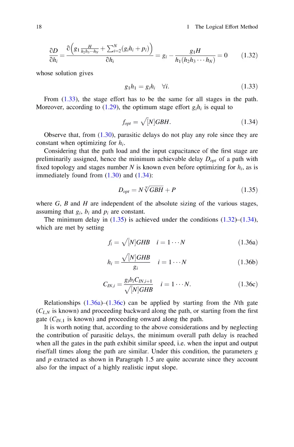
solution plotted in Fig. 1.9 versus pINV . It is apparent that the optimal stage effort
increases with pINV , as is expected from the fact that the delay penalty associated
with the inserted inverters increases when increasing pINV .
In the typical case with pINV 1, the optimal stage effort q results to 3:59,
which is typically approximated to 4 to make calculations easier. This justifies the
widespread adoption of the FO4 inverter delay metric [46]. The FO4 delay is
defined as the delay of an inverter loaded by four inverter with the same size. From
the Logical Effort point of view, the FO4 delay corresponds to a technology
normalized delay equal to 5 (d ¼ h þ 1). It is worth noting that, under the unrealistic assumption of negligible parasitic delays, the Logical Effort theory provides
20
Fig. 1.9 Best stage effort
versus inverter parasitic delay
1 The Logical Effort Method
ρ
5.5
Best stage effort
5.0
4.5
4.0
3.59
3.5
3.0
e
2.5
0.0
0.5
1.0
1.5
2.0
2.5
3.0
pINV
the classical result relative to tapered buffers sizing in [83], since q results to e if
pINV ¼ 0. Thus, in general, we can assume q in the range of 3–4.
From the above results, the number of stages to achieve the minimum delay is
equal to
Nb ¼ logq ðGBH Þ
ð1:41Þ
Obviously, the actual number of stages must be an integer number. By defining
Dopt;b as the optimized best delay achieved through a stage effort equal to q, the
trend of Dopt =Dopt;b versus N=Nb can be analyzed. Such a curve has obviously a
minimum equal to 1 for N=Nb ¼ 1. Anyhow, because of the flatness of the curve
near its minimum, even by choosing a stage number quite different from Nb such
as N ¼ 2Nb (N ¼ 0:5Nb ), the optimized delay increases only by a factor 1:26
(1:51Þ for pINV ¼ 1 compared to the minimum achievable delay Dopt;b [133]. The
flatness of the minimum also justifies the frequently used approximation of q to 4.
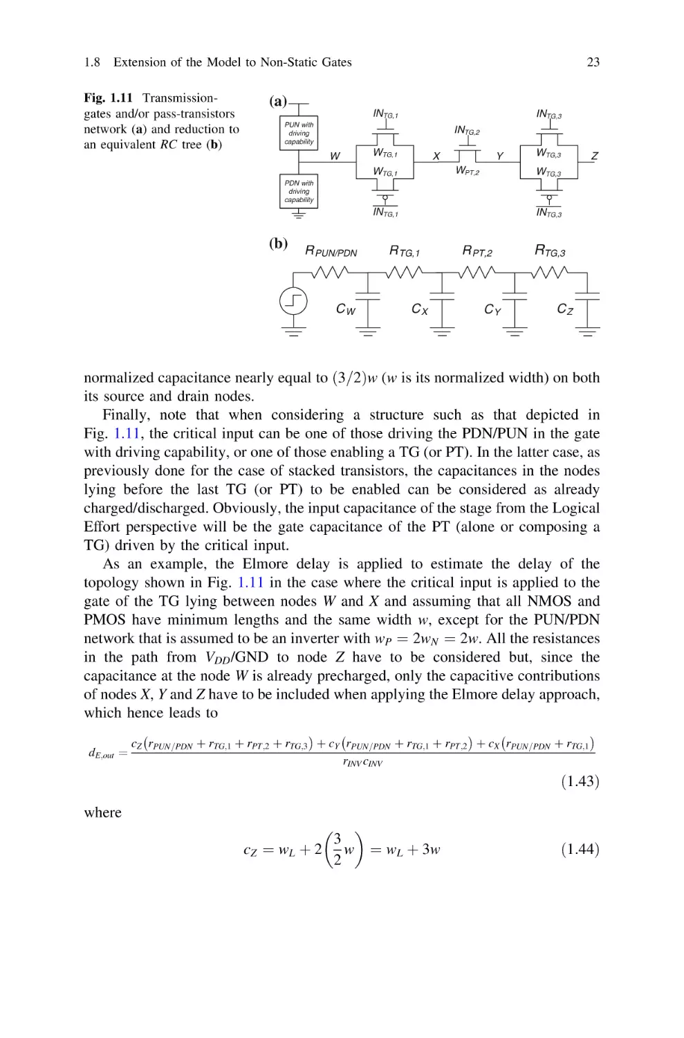
1.8 Extension of the Model to Non-static Gates
The procedures described so far are valid also in the case of non-static gates, such
as the dynamic ones and, under some conditions, those based on pass-transistors
and transmission gates.
1.8 Extension of the Model to Non-Static Gates
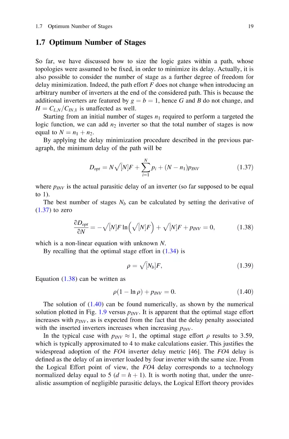
Fig. 1.10 Domino gate
compound of a typically lowskewed dynamic NAND2
(gr [ 1; gf \1), a typically
high-skewed static inverter
(gr \1; gf [ 1) and a PMOS
keeper
CK
21
W p,pre
W kpr
W p,eval
IN 1
W n,eval
IN 2
W n,eval
CK
W n,eval
X
W n,pre
OUT
1.8.1 Dynamic and Domino Gates with Keeper
Let us consider a domino gate [70] consisting of a dynamic NAND2, a cascaded
static inverter and a PMOS keeper (introduced to improve the robustness of the
structure) as shown in Fig. 1.10.
The evaluation of parameters g, h, b and p follows the same strategy described
for static gates. Note that, even when varying the size of the dynamic gate and of
the static inverter around it, the PMOS keeper is usually featured by a nearly fixed
and small size. Indeed, it serves the purpose of avoiding an unintentional discharge5 of the internal node X, while limiting the current contention with NMOS
transistors. Therefore, the loading effects introduced by the keeper on both nodes X
and OUT usually entail a non-constant branching effort due to their fixed size.
To estimate the impact of the current contention between the PMOS keeper and
the evaluation path in the dynamic gate, a factor r [ 1 is introduced to modify and
enlarge both parameters g and p. The value of r is [133]
r¼
1
1 rreval
kpr
ð1:42Þ
where reval is the equivalent resistance of the evaluation PDN path in the dynamic
gate and rkpr is the resistance of the PMOS keeper. Note that, the constraint
reval \rkpr has to be satisfied, otherwise the strength of the keeper would not allow
to discharge the node X.
The example of the domino gate is also representative of a typical case of a
skewed design (i.e., non-symmetric gates). Indeed, there is no point in making the
dynamic gate symmetrical, since the rising/precharge transition can typically last
up to an entire half-clock period. On the contrary the falling/evaluation transition
5
Possibly due to due to charge-sharing effects, leakage currents, cross-talk noise and other
sources of disturbances.
22
1 The Logical Effort Method
belongs to the critical path and has to be fast. Therefore, the dynamic gate is
usually low-skewed, meaning that the relative size between wN;eval and wP;pre is
chosen to guarantee a falling delay smaller than the rising one.
For the same reasons, the cascaded static inverter is usually high-skewed,
meaning that it is sized to speed up its rising transition (which is the one following
the evaluation) thanks to a proper over-sizing of wP;eval with respect to wN;pre .
Moreover, the domino gate exemplifies the situation where different input
signals have a different g because of the different input capacitance (see Fig. 1.5).
Indeed, differently from the inputs IN1 and IN2 , the clock signal CK drives also the
precharge transistor and hence has a larger gf . Also pf is larger when the critical
input is CK and, indeed, in real applications, the design is oriented to make INi the
critical inputs [160].
1.8.2 Logic with Transmission Gates and Pass-transistors
Transmission gates (TGs) and pass-transistors (PTs) can be straightforwardly
introduced in the Logical Effort framework. The only limitation is that (a chain of)
TGs (or PTs) have to be considered in series to an initial gate with driving
capability, i.e. connected to VDD and/or GND, as shown in Fig. 1.11. Indeed, only
in this way the classical simplified RC structure, or the more accurate RC tree
based on the Elmore delay model, can be identified.
As concerns the estimation of the equivalent resistance of a TG, one has to
consider that both its transistors are contemporarily conducting, and hence their
resistances are in parallel. In particular, assuming that an NMOS PT exhibits a
resistance equal to R (when transferring a logic “0”), a TG with equally sized
PMOS and NMOS transistors exhibits a resistance nearly equal to R for both “1”
and “0” inputs. Indeed, when a “0” is passing into the TG the PMOS it can be
assumed with resistance 4R (remember that PMOS switches off when the output
reach a voltage as low as a threshold voltage); while when a logic “1” is passing
transistor TG NMOS and PMOS transistor can be both assumed6 with a resistance
equal to 2R [133].
It is worth noting that there is no point in doubling the size of the PMOS with
respect to the NMOS (as usually done in static/dynamic gates with driving
capability) since the TG resistance would become equal to ð2=3ÞR for both “1” and
“0” at the input but the capacitances at the input and output of the TG would
increase by 50 %. Hence, the usual practice is to equally size PMOS and NMOS
transistors in a TG, as shown in Fig. 1.11.
As concerns the estimation of inter-nodal capacitances in Fig. 1.11, from
Sect. 1.5, it can be assumed that each PT (alone or part of a TG) contributes with a
6
Assuming that the resistance of a pass transistor is doubled when transferring a signal from
source to drain or vice versa, i.e. when the voltage swing is degraded by the threshold voltage.
1.8 Extension of the Model to Non-Static Gates
Fig. 1.11 Transmissiongates and/or pass-transistors
network (a) and reduction to
an equivalent RC tree (b)
23
(a)
INTG,1
INTG,3
PUN with
driving
capability
INTG,2
W
WTG,1
X
Y
WPT,2
WTG,1
WTG,3
Z
WTG,3
PDN with
driving
capability
INTG,1
(b)
R PUN/PDN
CW
INTG,3
R TG,1
CX
R PT,2
CY
RTG,3
CZ
normalized capacitance nearly equal to ð3=2Þw (w is its normalized width) on both
its source and drain nodes.
Finally, note that when considering a structure such as that depicted in
Fig. 1.11, the critical input can be one of those driving the PDN/PUN in the gate
with driving capability, or one of those enabling a TG (or PT). In the latter case, as
previously done for the case of stacked transistors, the capacitances in the nodes
lying before the last TG (or PT) to be enabled can be considered as already
charged/discharged. Obviously, the input capacitance of the stage from the Logical
Effort perspective will be the gate capacitance of the PT (alone or composing a
TG) driven by the critical input.
As an example, the Elmore delay is applied to estimate the delay of the
topology shown in Fig. 1.11 in the case where the critical input is applied to the
gate of the TG lying between nodes W and X and assuming that all NMOS and
PMOS have minimum lengths and the same width w, except for the PUN/PDN
network that is assumed to be an inverter with wP ¼ 2wN ¼ 2w. All the resistances
in the path from VDD /GND to node Z have to be considered but, since the
capacitance at the node W is already precharged, only the capacitive contributions
of nodes X, Y and Z have to be included when applying the Elmore delay approach,
which hence leads to
dE;out ¼
cZ rPUN=PDN þ rTG;1 þ rPT;2 þ rTG;3 þ cY rPUN=PDN þ rTG;1 þ rPT;2 þ cX rPUN=PDN þ rTG;1
rINV cINV
ð1:43Þ
where
3
cZ ¼ wL þ 2 w ¼ wL þ 3w
2
ð1:44Þ
24
1 The Logical Effort Method
3
9
w ¼ w
2
2
ð1:45Þ
3
cW ¼ 2 w þ 3w ¼ 6w
2
ð1:46Þ
cX ¼ cY ¼ 3
rPUN=PDN ¼ rTG;1 ¼ rTG;3 ¼
rPT;2 ¼
1
w
2
:
w
ð1:47Þ
ð1:48Þ
Note that, as previously observed, it was assumed for simplicity that each PT
adds to its source and drain nodes a normalized capacitance nearly equal to
ð3=2Þw, while an average resistance (between the cases of a passing “1” or “0”) of
rPT;2 is considered.
By using (1.44)–(1.48), the delay in (1.43) can be rewritten as
5
dE;out ¼ 3
wL þ 13w 5 wL
¼
þ 13
w
3w
ð1:49Þ
where w alone is found at the denominator because it represents the input
capacitance seen at the NMOS or PMOS gate of TG,1. As for (1.20), (1.49) is also
expressed as the sum of a term depending only on the external load (i.e., the
classical gh term), and another one due to self-loading that is an accurate parasitic
delay estimation for this scenario.
1.9 Nonlinearities and Need for Iterative Procedures
In Sects. 1.5 and 1.6 we have summarized how Logical Effort can be employed as
an optimization method to maximize speed. The related results are based on the
assumption that g, b and p are constant (i.e., independent of the sizing). In practical
cases, this condition cannot be exactly satisfied for several reasons, which are
listed in the following.
– the correction factor for g and p in (1.42), which accounts for current contention
due to keepers, becomes a function of the gate and keeper absolute sizes when
the ratio between their driving capabilities is not maintained constant
– the branching effect in (1.26) experienced by the ith gate in a path because of
gate and/or diffusion capacitances of transistors outside the considered path can
often be a function of the absolute size of the ith gate itself (this happens when a
constant proportion between the absolute values of CIN;iþ1 and Coff ;i is not
maintained);
– the presence of global and local interconnects.
1.9 Nonlinearities and Need for Iterative Procedures
25
In particular, global interconnects can be modeled as equivalent RC ladder
blocks and hence handled as done for stacked transistors and TGs/PTs. However,
their length is typically fixed by layout constraints and hence the resistive and
capacitive contributions that they introduce lead to g and b values that are functions of the absolute size of the gates driving such interconnects.
Local interconnects can be simply modeled through additional parasitic
capacitances. However, as reported in Chap. 4 where we will introduce a methodology to estimate such parasitics within a flip-flop, the overall local interconnect
parasitics include can be split into (a) a capacitance given by the gate driving the
considered node, (b) a contribution given by the gates loading the node (through
both gate and diffusion capacitances), (c) a constant contribution. Thus, from the
perspective of the gate driving the considered node, the first contribution lies on
the parasitic delay, the second contribution modifies the capacitance imposed by
the following gates and hence the electrical effort, while the latter contribution
influences the branching effort in a gate-size dependent way. Note that also the first
two contributions depend on the gates sizes in complex non-linear ways and a
linearization is not always feasible.
It is apparent from the discussion above that in all the considered cases several
nonlinearities emerge and do not allow the optimization described in (1.32–1.35)
to be straightforwardly applied. Therefore, in order to minimize the delay of paths
including complex branching effects and the impact of interconnects, iterative
procedures become necessary, thereby making the Logical Effort method less
suitable for pencil-and-paper calculations.
Appendix: Derivation of Logical Effort with a Transistor
Current Source Model
The Logical Effort model can be also derived by assuming transistors as
equivalent current sources instead of equivalent resistors. This modeling is more
suitable in nanometer technologies in which transistors spend longer time in the
saturation region during the switching of the output of a logic gate. Under this
assumption, any timing parameter (delay, rise/fall time) of the considered gate
can be expressed as
tD ¼ K
ðCOUT þ CL Þ
IT
ð1:50Þ
where IT is the current provided by the PUN or PDN, and can be generally
approximated with the saturation current.
26
1 The Logical Effort Method
The inverse of IT exhibits the same functional dependencies of the resistance RT
in (1.2c), i.e.
ðIT Þ1 / L=W:
ð1:51Þ
Therefore, the Logical Effort parameters can be extracted as in (1.3)–(1.4),
(1.6)–(1.10) as functions of the equivalent current behavior of the gate and results to
IINV CIN;ref
IT;ref CINV
ð1:52Þ
CL
CIN
ð1:53Þ
IINV COUT;ref
IT;ref CINV
ð1:54Þ
g¼
h¼
p¼
where IINV is the equivalent current provided by a symmetric inverter and IT;ref is
the equivalent current provided by the template version of the considered gate.
Both the equivalent currents can be simply approximated with the current given by
PDN or PUN transistors in saturation region.
Chapter 2
Design in the Energy-Delay Space
Scaling trends have driven CMOS technology into a power-limited regime, where
energy has to be managed wisely to make performance truly available within a
given power budget [13]. This chapter deals with the design of energy-efficient
digital circuits, i.e. to the achievement of the desired speed under minimum energy
consumption. Energy-delay models of logic circuits and the theoretical background relative to the analysis of circuits in the energy-delay space are discussed,
in order to identify design criteria to achieve energy efficiency.
2.1 Energy Modeling
This chapter is focused on the joint optimization of speed and consumption in
digital circuits. It is hence necessary to clarify the metrics that will be used to
quantify the consumption at the transistor level of abstraction. In particular, two
metrics are available: power and energy [24, 121].
Both metrics are actually interchangeable and choosing one or another is simply
a matter of convention as long as transient (i.e., dynamic and short-circuit) and
static (i.e., leakage) dissipative contributions are properly weighed [3]. In the
following, energy is chosen as the metric for circuit consumption. This implies that
transient contributions relative to a generic circuit operation have to be simply
summed, whereas static leakage-related power has to be multiplied by the time
between successive operations (e.g., the duration of a clock cycle in a pipelined
system) and summed to the transient (dynamic) contribution to obtain the overall
energy dissipation.
In the following, a model accounting for the above contributions is summarized
[7, 8]. This model aims at the extraction of a factor v featuring a logic gate and
such that the overall gate energy E is simply expressed as linearly related to the
input capacitance CIN , i.e. to the gate size according to (2.1):
E ¼ v CIN :
M. Alioto et al., Flip-Flop Design in Nanometer CMOS,
DOI: 10.1007/978-3-319-01997-0_2,
Ó Springer International Publishing Switzerland 2015
ð2:1Þ
27
28
2 Design in the Energy-Delay Space
Fig. 2.1 Capacitive
contributions determining
dynamic energy in a gate
(αsw,in)
(αsw,in)
sw
sw
a
swCT
swCT
(αsw,out)
swCT
swCT
zinwCT
OUT
(αsw,in)
wCT
wCT
w
(αsw,in)
b
zinwCT
wCT
(αsw,out)
2zoutwCT
(αsw,out)
wCT
w
Such a model intentionally excludes the energy dissipated in charging/discharging the load capacitance CL , but includes the energy dissipated in charging/
discharging CIN and the capacitances at the internal nodes. Again, it is simply a
matter of convention, when summing up all the energy contributions of the logic
gates within the same module.
Let us consider a static CMOS gate such as the 2-inputs NAND in Fig. 2.1,
where the various capacitive contributions determining the dynamic dissipation are
depicted. One can distinguish among capacitances lying in the input nodes and
switching according to the transition probability of the inputs asw;in , and capacitances lying at the output node (or in the internal ones featuring stacked structures)
and switching according to the transition probability of the output (internal) node
asw;out [85].
Each of these capacitances is made up of nearly equal transistor contributions
[144]: gate capacitances for the input nodes, and diffusion capacitances (drainbulk, source-bulk) for the output and/or internal nodes. In particular, let us define
• CT as the gate capacitance of a minimum-sized transistor, which can be defined
as Cinv;min =3, being Cinv;min the input capacitance of a symmetric minimum
inverter (i.e., with WPMOS ¼ 2WNMOS ¼ 2Wmin )
• s as a multiplicative factor that defines the widths of PMOS (again all equal and
with minimum lengths) with respect to NMOS, thus leading to a certain skew in
the speed of PUN and PDN [133].
The average dynamic energy per clock cycle of a CMOS gate is given by
2
EDYN ¼ ð1 þ sÞasw;in þ ð1 þ sÞasw;out w CT m VDD
ð2:2Þ
2.1 Energy Modeling
29
where m is the number of gate inputs (equal to 2 for the NAND in Fig. 2.1), and it
is assumed that each transistor contributes with a single gate and a single parasitic
capacitance.1
In order to include the parasitic capacitances due to local interconnects (within
the logic gate) at the input and the output of the gate, let us introduce parameters
zin and zout that weigh2 parasitic capacitive contributions through the gate size w.
Hence, the overall local wire capacitance Cpar;j at a generic node j can be
expressed as [7, 8]
Cpar;j ¼ zout;i1 wi1 CT þ zin;i wi CT
ð2:3Þ
being j the node at the output and the input of the ði 1)th and the ith stage,
respectively, and the average dynamic energy (2.2) becomes
2
EDYN ¼ ð1 þ s þ zin Þasw;in þ ð1 þ s þ zout Þasw;out w CT m VDD
ð2:4Þ
A similar analysis concerning the static dissipation of a CMOS gate can be
carried out. In particular, let us define
• qsub;n (qsub;p ) as the sub-threshold leakage current of a minimum-sized transistor;
in other words, these parameters express the leakage dependency on the technology and temperature, regardless of the size
• qgate;n and qgate;p are defined similarly, but they refer to gate leakage
• Tsub;n (Tsub;p ) as the PDN (PUN) sub-threshold leakage current at room temperature normalized to a single minimum-sized transistor; in other words, these
parameters model the effect of the PDN (PUN) topology on its average leakage,
averaging out the various currents for each input, and including the effect of
transistor stacking
• Tgate;n and Tgate;p are defined similarly, but they refer to gate leakage
• bsub;n (bsub;p ) as the probability that the leakage of the gate is determined by the
PDN (PUN), which is set by the statistics of input and output nodes of the gate
(i.e., bsub;n þ bsub;p ¼ 1).
Accordingly, the average energy due to sub-threshold and gate leakage in a
clock cycle with period TCK is given by
qsub;p qgate;n
qgate;p
qsub;n
þ sbsub;p
þ
þs
ESTAT ¼ w bsub;n
VDD TCK h: ð2:5Þ
Tsub;n
Tsub;p Tgate;n
Tgate;p
In (2.5), the parameter h accounts for the percentage of time spent in active and
standby mode by the module that the considered gate belongs to. In other words, h is
1
The approximation of considering a single inter-nodal capacitance for each stacked transistor is
reasonably accurate, through the methods discussed in Chap. 1
2
Although the dependence of such parasitics on w is in general nonlinear, linear fitting can be
extracted without seriously compromising the accuracy of lumped local wires capacitances, as
discussed in the following.
30
2 Design in the Energy-Delay Space
a correction factor that defines an effective clock period TCK h, as a result of the fact
that only leakage dissipation is present in standby mode, while dynamic one is not.
The above expressions (2.4) and (2.5) can be immediately generalized to model
some effects more accurately. For instance, (2.4) and (2.5) can be easily generalized to deal with gates with non-minimum channel lengths, with non static
gates (e.g., dynamic, ratioed logic), to accurately weigh the impact of inter-nodal
capacitances on dynamic energy and of stacking effect on leakage, to consider the
cases where some NMOS (PMOS) transistor within the PDN (PUN) has a width
proportional but not equal to w, and so on. Hence, such models are very general
but still reasonably simple for analysis purposes. Furthermore, as already discussed
for the Logical Effort model in the previous chapter, many of the parameters in
(2.4)–(2.5) can be accurately characterized through simulations.
Once EDYN and ESTAT are evaluated, the overall energy dissipation of the gate is
E ¼ EDYN þ ESTAT :
ð2:6Þ
According to the previous definitions, CIN including the wire parasitic capacitance can be expressed as
CIN ¼ ð1 þ s þ zin Þ w CT :
ð2:7Þ
This generalized model of the input capacitance can be plugged into Logical
Effort calculations to include all the above discussed effects, which are not
accounted for in the classical LE methodology.3 Accordingly, the parameter v in
(2.1) can be expressed as
1 þ s þ zout
2
v ¼ asw;in þ asw;out
m VDD
1 þ s þ zin
ð2:8Þ
qsub;p
qgate;p
qgate;n
q
bsub;n Tsub;n
þ
sb
þ
þ
s
sub;p Tsub;p
Tgate;n
Tgate;p
sub;n
þ
VDD TCK h:
ð1 þ s þ zin ÞCT
It is worth noting that the above model neglects short-circuit dissipation. Differently from the dynamic and leakage energy, the short-circuit contribution
cannot be approximated as a linear function of the gate size. Indeed, it increases
with gate size for three simultaneous reasons:
• the linear dependence of the PDN and PUN on-current on w
• the approximately proportional dependence on the input rise/fall time, i.e. on the
output rise/fall time of the preceding gate [122]
• the approximately inverse dependence on the output rise/fall time of the gate
itself [122].
3
The Logical Effort model does not consider the capacitive contributions due to local
interconnects and those proportional to the input transistors size (here weighed through the zin
term).
2.1 Energy Modeling
31
The last two terms can be assumed as nearly linearly dependent on w, by
neglecting the parasitic delays in the computation of input rise/fall times.
Overall, the short-circuit dissipation can be written as
ESC ¼
din
q Tsc;n þ sTsc;p asw;out w
dout sc
ð2:9Þ
where din and dout are input and output rise/fall times according to Logical Effort
model, while parameters Tsc;n and Tsc;p average out the various possible output
transition cases according to PDN and PUN topologies. Finally qsc is a further
parameter accounting for the impact of technology and VDD .
The short-circuit energy tends to be rather small in nanometer technologies, due
to the progressive reduction (although relatively slow, recently) in VDD =VTH [122].
The only and very infrequent case where the short-circuit energy is non negligible
occurs when the input rise/fall times are much larger than the gate delay.
2.2 Energy-Delay Space Analysis and Hardware-Intensity
2.2.1 The Energy-Efficient Curve
For a digital circuit under a fixed supply voltage VDD and whose last stage is
loaded with a capacitance CL , the “energy-efficient curve” (EEC) is made up of the
design points (i.e., sizing of all transistors within the gate) exhibiting the minimum
delay for a fixed energy dissipation or, equivalently, the minimum energy consumption for a given delay [4, 119]. By definition, other design points above the
EEC lead to a needlessly higher energy under the same speed performances and
need to be discarded, as shown in Fig. 2.2.
As previously stated, we consider the input capacitance of (the first stage of) the
circuit CIN as a further design variable to be optimized, and including (excluding)
the energy dissipated in charging/discharging CIN (CL ). This assumption is different from that adopted in [92, 111, 157, 158]. While it was a simple matter of
convention when referring to the modeling of the energy of a circuit, we will show
that it becomes a necessary assumption when the target is the full exploration of
the E-D potential of a flip-flop topology.
In [119] it was predicted that the EEC of any circuit has a hyperbolic trend
ðE E 0 ÞðD D 0 Þ ¼ E 0 D 0
ð2:10Þ
being E0 and D0 the minimum energy and minimum delay asymptotes, as shown in
Fig. 2.2. Actually, substantial deviations from (2.10) are found when analyzing
32
2 Design in the Energy-Delay Space
Fig. 2.2 Energy-efficient
curve and designs optimizing
the metrics E i D j
real circuits and hence a correction factor c (typically 0\c\1) can be introduced
to fit real data [157, 158]
ðE E0 ÞðD D0 Þ ¼ cE0 D0
ð2:11Þ
Despite of the above mentioned differences with respect to [157, 158], the
general character of (2.11) is retained. In particular, looking at the generic EEC
depicted in Fig. 2.2, there is a minimum energy value Emin , which is achievable
with the minimum transistors sizes allowing correct operation, hence the points
between E0 and Emin have not a physical correspondence (see Fig. 2.2).
Regarding the delay, the value D0 can be approached only asymptotically
through transistor sizing, and measures the maximum speed potential of a specific
topology. More specifically, one can indefinitely trade energy for delay by
increasing CIN . On the contrary, if CIN is fixed [92, 111, 157, 158], a minimum
delay for a given load is actually reachable and corresponds to the Logical Effort
sizing. The asymptotic value D0 under an unbounded CIN can be estimated as well
through Logical Effort, and it corresponds to the parasitic delay P since it is simply
the delay under large sizing.
As concerns parameter c in (2.11) and the actual analytical expression of the
EEC under our assumption, analytical calculations can be carried out only for a
single logic gate [7, 8]. Indeed, according to Logical Effort model, one has
D D0 gh g CL
¼
¼
p
p CIN
D0
ð2:12Þ
As concerns the energy, from (2.1) we get
E E0 vCIN vCIN;min CIN CIN;min
¼
¼
E0
vCIN;min
CIN;min
ð2:13Þ
2.2 Energy-Delay Space Analysis and Hardware-Intensity
33
being CIN;min the minimum input capacitance of the gate (i.e., when its transistors
are all minimum sized).
By referring to (2.11) and using (2.12)–(2.13), c is given by
c¼
gCL
D D0 gsvCL D D0
¼
pCIN;min
D0
D0 E0
D0
ð2:14Þ
where s is the delay of an inverter loaded by an inverter of the same size, i.e. the
Logical Effort normalization delay parameter (see Chap. 1).
The above formula indicates that, under the above and more general assumptions, the value of c in (2.11) actually depends on the variable D, i.e. the EEC is
not a pure hyperbole. However, c can be approximated in a sufficiently accurate
way by its first term, gCL =pCIN;min as long as the delay is not much higher than
D0 ¼ ps. In this case, c becomes constant and independent of D, and the EEC is a
pure hyperbole.
Nevertheless, when dealing with circuits made up by more than one gate, no
analytical expression can be determined for c. In such case, c is typically assumed
to be a constant parameter in (2.11) for simplicity.
2.2.2 Energy-Delay Metrics and Hardware Intensity
In the last two decades digital circuit designers have become familiar with the use
of composite energy-delay metrics to effectively translate the more and more
stringent constraints on the speed, while not disregarding the energy dissipation.
The first (and at first glance the most appropriate) composite metric to be
introduced is the simple ED product, which equally weighs the two quantities.
Another popular metric is the ED2 product where speed has priority over energy.
The latter metric is claimed to have useful properties such as a nearly zero sensitivity on the supply voltage [80]. However, although designs optimizing (i.e.,
minimizing) the above metrics are maximally efficient for a given delay (or
energy), it is clear that a generalization is required when exploring and designing a
circuit over the entire spectrum of the delay (energy) values it can achieve.
Hence, the general class of metrics E i D j , or equivalently EDg (being g equal to
j=i) as originally presented in [119], are introduced. By varying the exponents i 0
and j 0 (g 0), any tradeoff between energy and delay can be explored. The
extreme cases are obtained when j=i ¼ 0 (g ¼ 0) and when j=i ¼ 1 (g ¼ 1),
which, once optimized, represent the designs having the minimum possible energy
and delay, respectively.
Interestingly, every design solution minimizing a metric Ei D j (EDg ) lies in the
EEC [119], and the latter curve is hence made up of all points that minimize E i D j
(EDg ) for some i and j (g), as shown in Fig. 2.2. The demonstration of this
assertion is quite simple and intuitive. Indeed, considering a circuit under a fixed
34
2 Design in the Energy-Delay Space
load and supply voltage, both its delay and energy are functions of its sizing W (W
is an array containing the sizes of transistors in all circuit gates). A design minimizing an Ei D j metric for some ði; jÞ has a delay D which is obtained with a
certain size W (i.e., D ¼ DðW Þ). Since the size W minimizes a product E i D j ,
in which the energy is taken into account with i 0, the value E ¼ E ðW Þ of this
design will be the minimum among all the designs exhibiting a delay D ¼ D and
thus it lies on the EEC. More rigorous analytical proofs can be found in [119].
From the above considerations, the indexes i and j (g) define cost functions for
optimizing hardware under a fixed load and supply voltage. According to [153,
157, 158], the value j=i (g) is named “hardware intensity”. Basically, j=i (g)
quantifies the effort to be spent in sizing a circuit to optimize the speed of the
circuit at the expense of its energy consumption. The higher j=i (g), the higher the
effort (i.e., energy) to further improve the speed. The set of points of the EEC
curve where metrics Ei D j is minimized for j [ i (g [ 1) is hence called the highperformance region, whereas the region with minimum E i D j with j\i (g\1) is
called the low energy region. The former is featured by lower and lower delay
gains achieved at the cost of larger and larger increments in energy as long as the
delay diminishes. Dual considerations are valid for the low energy region.
The graphical interpretation of hardware intensity is shown in Fig. 2.3 [153,
158]. The solid line plots a typical EEC for a generic circuit. Dotted curves show
several contours of the cost function E i D j for three values of the hardware
intensity. The point in the E-D space at which the EEC tangents the lowest of the
contours corresponds to the energy-efficient implementation of the circuit for that
specific hardware intensity value [157, 158].
Accordingly, the analytical interpretation of hardware intensity is related to the
energy-to-delay sensitivity evaluated in correspondence of the design points
optimizing the E i D j (EDg ) metrics [7, 8, 157, 158]. Indeed, the design point
minimizing E i D j for a given ði; jÞ leads to a zero derivative of Ei D j with respect to
D and E [7, 8, 119]
oð E i D j Þ
i1 j oE
i j1
þ jE D
¼ iE D
¼0
ð2:15Þ
j
oD Ei Dmin
oD
Ei D j
min
oð E i D j Þ
¼
j
oE Ei Dmin
iE i1 D j þ jE i Dj1
oD
oE
Solving the set of equations (2.15)–(2.16), one finds
oE D
j
E
SD i j ¼
¼
ED
oD E Ei D j
i
min
j
E i Dmin
¼0
ð2:16Þ
ð2:17Þ
min
Equivalently, when carrying out analogous calculations by referring to the EDg
metrics, the results is simply g. Anyhow, the adoption of the two indexes i and j
2.2 Energy-Delay Space Analysis and Hardware-Intensity
35
Fig. 2.3 Typical energy-efficient curve and constant cost function contours for j=i ¼ 1:0, j=i ¼
0:5 and j=i ¼ 2:0
has a clearer physical meaning. Indeed, in the neighborhood of the optimum E i D j
design point, a j % speed increase is traded for a i % energy increment and vice
versa. Finally, from (2.17) it is apparent that metrics leading to the same j=i ratio
are not distinguishable.
2.2.3 Voltage Intensity and Generalization of the Sensitivity
Criterion
So far we have focused on hardware, i.e. transistors sizing, optimization. However,
other tuning variables are available at the circuit level, such as the supply voltage
VDD and the transistors threshold voltages.
As concerns supply voltage, by introducing the dimensionless derivatives of
energy and delay with respect to the supply voltage m,
36
2 Design in the Energy-Delay Space
Em ¼
m oE
E om
Dm ¼
m oD
D om
ð2:18Þ
ð2:19Þ
and taking their ratio, one can define “voltage intensity” b as the energy-to-delay
sensitivity relative to the variation of v at a fixed hardware intensity j=i [157, 158].
Hence, just as j=i represents the negative of the ratio between the energy (delay)
relative gain and the cost of the relative increase in delay (energy) achievable by
sizing transistors under a fixed m, b represents the energy (delay) relative increase
(decrease), achievable by increasing m under a fixed w [157, 158]
oE D k
b¼
:
ð2:20Þ
oD E m variablew fixed
2
The Em and Dm values cannot be simply determined through classical E / VDD
2
and D / 1=ðVDD VTH Þ , given the impact of leakage and short-circuit currents
on energy and the complexity of ID ¼ f ðVGS ; VDS Þ relationship featuring nanometer transistors. Therefore, it is necessary to develop comprehensive models of
energy and delay as functions of the supply voltage [9] (similarly to those relative
to transistors sizing that were discussed in the previous paragraph) or extract Em
and Dm for the various gates in a circuit through simulations. To have an idea of the
main trends [158], the voltage intensity b almost linearly increase with VDD for
typical CMOS circuits.
The most important aspect of this discussion is that hardware and voltage
intensities are related when optimizing a circuit in the E-D space. If we consider a
sub-circuit that has to satisfy a given maximum delay constraint (e.g., a pipeline
stage), this requirement can be achieved at different combinations of the j=i and b
values. However, the energy-efficient implementation, i.e. that with the minimum
energy, is the one featured by
j=i ¼ b:
ð2:21Þ
Indeed, energy and delay are functions of the variables ðw; mÞ, and, by solving
the problem of minimizing Eðw; mÞ under the constraint Dðw; mÞ ¼ D , one finds
[30, 157, 158]
oD oE oD oE
¼
ow om
om ow
ð2:22Þ
which means j=i ¼ b. Hence, to reach an energy-optimal balance between the
supply voltage and the transistors sizing, the relative speed gain achieved at the
cost of a given relative energy increase due to an increment in the supply voltage
must equal the relative speed gain achieved at the cost of a given relative energy
2.2 Energy-Delay Space Analysis and Hardware-Intensity
37
increase due to a larger transistors sizing [158]. This result disproves the common
misconception that the lowest energy can be achieved by designing circuit for the
highest speed and then reducing the power supply up to the lowest value that
satisfies the delay requirement.
Further generalizing the above analysis to any kind of design variable (e.g.,
threshold voltages) [38, 77], and to the sensitivity Sx ðXÞ of energy to delay with
respect to a change in variable x, as in (2.18)–(2.19), the minimum energy under a
given delay constraint is achieved when [92]
oE D k
oE D k
¼ Sy ðYÞ ¼
8x; y
ð2:23Þ
Sx ðXÞ ¼
oD E x variable
oD E y variable
being x and y design variables. In other words, the energy-efficient corresponds to
the design with x ¼ X; y ¼ Y and so on.
2.3 Energy-Efficient Design of Digital Circuits
In this section we discuss practical optimization techniques to achieve the energyefficient design of digital circuits at the circuit level, by considering various levels
of complexity. In particular, we first provide some preliminary remarks concerning
the role played by the input capacitance of the circuit and the definition of design
space bounds, both essential regardless of the actually employed optimization
technique. Then, we consider the case of simple basic blocks whose complexity
allows a simulations-based optimization and finally with large designs that can be
dealt with by resorting to convex optimization and exploiting simple E-D models.
2.3.1 The Role of the Input Capacitance
As shown in [30, 111], the input capacitance CIN of a logic circuit cannot be
simply assumed as fixed, when designing for energy efficiency. Granted that the
adopted CIN value is also related with the architectural-level design strategies [30],
differently from [92, 111, 157, 158], here we consider CIN as an additional design
variable to be fully optimized like any other transistor size. This choice is justified
by considering that CIN strongly affects the E-D tradeoff, as discussed below.
A second assumption, differently to [30, 92, 111, 157, 158], is to include the
energy dissipated in the (dis)charge of CIN and to exclude the energy dissipated in
the (dis)charge of CL . Indeed, the first term is inherently related to the adopted
circuit sizing, whereas the latter term does not depend on the features of the
topology [41, 131].
In general, throughput improvements can be achieved by means of an increase
in the degree of parallelism and/or a more aggressive sizing of all the gates in the
38
2 Design in the Energy-Delay Space
logic paths (e.g., when the sequential part of code running on a microprocessor
system is dominant, hence parallelization is not effective). In the latter case, if CIN
is increased with respect to a reference design, it means that the topology is being
sized up to achieve a higher speed at the cost of higher energy. Even if the circuit
imposes a larger load on the preceding logic stage (e.g. in a pipeline), in highspeed applications the speed penalty of the preceding logic stages could be
exceeded by the speed improvement in the considered topology. This tradeoff
cannot be explored if one does not assume a fully variable CIN . Similar considerations hold in regard to low-energy designs. Obviously, there always exist
practical limits on the adoptable CIN values. Nevertheless, once the full EEC is
extracted, the designer can easily select the portion of interest according to
practical constraints in terms of maximum allowable CIN , so that the interaction
between the delays of adjacent stages through the CIN of the successive one is
captured (as it is typically done by setting a fixed CIN ).
Finally, it is worth highlighting that, when referring to the “first stage”, we
mean the first gate in the path of the circuit whose sizing is assumed as a reference
in terms of timing criticality. Indeed, several input-to-output paths coexist in real
circuits, and the target must obviously be that of equaling these delays. Among the
various paths, it is then possible to identify one (typically the longest) that is
adopted as the reference to identify the CIN of the circuit. Note that, since CIN is
fully varied and the optimization targets the equality of the various concurrent
delays, the input capacitances of the first stages of all the other paths will be
optimized and fully explored as well.
2.3.2 Derivation of Design Space Bounds
Regardless of the methodology employed for EEC extraction, practical design
space bounds need to be identified to limit the space of solutions. As will be shown
successively, this issue is particularly important in the case of simulations-based
procedures and nonlinear optimizations, to keep the computational effort within
reasonable bounds. On the contrary, this issue becomes less relevant when one
adopts simple gate-level E-D models and resorts to convex optimization.
In [30] it is shown that Logical Effort designs lie above the EEC, i.e. they are
not the most efficient possible designs. Even if CIN is assumed as a design variable
unlike [30], the same result still holds.4 Nevertheless, the energy-to-delay sensitivity of Logical Effort designs can be used as an indicator to determine design
4
Indeed, as explained in the previous section, the minimum energy under a given speed
constraint is reached when the sensitivity with respect to “all” the tuning variables is the same.
Logical Effort designs are featured by an infinite energy-to-delay sensitivity with respect to the
sizes of internal transistors (since delay cannot be further reduced given a fixed CIN ), but not with
respect to the size of transistors defining CIN . Hence, the condition in (2.23) is not satisfied for
Logical Effort designs, which thus are not energy-efficient [30]. Only when CIN approaches
2.3 Energy-Efficient Design of Digital Circuits
39
space bounds. More specifically, let us assume that the designer is interested in the
portion of the EEC up to a certain minimum-E i D j design point with j=i ¼ X, i.e.
the portion of the EEC made up by energy-efficient designs that minimize FOMs
with j=i less than or equal to X. In this case, the range of the transistor sizes to be
explored can be defined by upper bounding the energy sensitivity to delay to a
given value X, which translates into the upper bound CIN;max of CIN that satisfies
the following condition [7, 8]
SED
CIN
¼
SECIN
j
¼ ¼ X:
i
SD
CIN
ð2:24Þ
The definition of CIN;max leads also to the definition of the upper bounds for the
other design variables (i.e. transistors sizes) that are clearly defined by the Logical
Effort sizing with CIN ¼ CIN;max .
Equation (2.24) can be analytically evaluated thanks to the properties of Logical Effort designs. In particular, as discussed in Chap. 1, given CIN and CL , the
minimum normalized path delay DTOT of a circuit simply made up by a path of N
cascaded gates is
pffiffiffiffiffiffiffiffiffiffiffi
pffiffiffiffi
ð2:25Þ
DTOT ¼ N N GBH þ P ¼ N N F þ P
which can be rewritten as
DTOT ¼ Pð1 þ kÞ
ð2:26Þ
pffiffiffiffiffiffiffi pffiffiffiffiffiffi
N N GB N CL
pffiffiffiffiffiffiffi
P N CIN
ð2:27Þ
where
k¼
is the relative delay increment with respect to the ideal and practically
unachievable minimum path delay (i.e., the path parasitic delay P). From (2.26)–
(2.27), the sensitivity of the optimized path delay DTOT to CIN is given by
TOT
SD
CIN ¼
oDTOT CIN
1 k
¼
Nkþ1
oCIN DTOT
ð2:28Þ
which is a function of CIN only.
As for the path delay DTOT , it is possible to unambiguously determine the
energy ETOT of a single path circuit sized through Logical Effort for a given CIN
and CL . According to (1.33) and (1.34), the input capacitance CN and the energy
EN of the Nth gate are respectively given by
(Footnote 4 continued)
infinity, the Logical Effort design will be featured by an equal (tending to infinity) energy-todelay sensitivity with respect to all the tuning variables.
40
2 Design in the Energy-Delay Space
pffiffiffiffiffiffiffi
gN bN N CIN
ffiffiffiffiffiffiffiffiffiffiffiffi
CN ¼ p
CL
N
GBCL
ð2:29Þ
EN ¼ vN CN :
ð2:30Þ
By iterating the above reasoning and going backwards through the path, one
finds that the input capacitance and energy of the ith gate under classical Logical
Effort design are
Q
Q
Niþ1
N
N
N
j¼i gj
j¼i bj ðCIN Þ
Ci ¼
CL
ð2:31Þ
Niþ1
ðGBCL Þ N
E i ¼ vi C i
ð2:32Þ
and C1 ¼ CIN .
Therefore, the overall dissipation of the reference path is
2 QN QN
3
Niþ1
N
N
X
j¼i gj
j¼i bj ðCIN Þ
4vi
CL 5
ETOT ¼
Niþ1
ðGBCL Þ N
i¼1
ð2:33Þ
and the sensitivity of the overall energy ETOT to CIN can be again expressed as a
function of the only CIN :
2 Q Q
3
Niþ1
N
N
gj
bj ðCIN Þ N
PN
j¼i
j¼i
Niþ1
4
CL 5
Niþ1
i¼1 vi
N
ðGBCL Þ
SECTOT
¼
IN
PN
i¼1
N
2 Q Q
3
Niþ1
N
N
N
g
b
ð
C
Þ
j
j
IN
j¼i
j¼i
4vi
CL 5
Niþ1
ðGBCL Þ
ð2:34Þ
N
Finally, (2.28) and (2.34) can be combined to evaluate (2.24) and determine
CIN;max .
Unfortunately, formula (2.24) cannot be always applied straightforwardly since
gi , hi , bi and pi are often not available in a closed-form5 as function of CIN . Rather, gi ,
5
There are three main reasons for this issue:
(1) there are various sources of non-linearity, as listed in the Sect. 2.2, which imply the need for
iterative procedures to determine the Logical Effort sizing.
(2) not all the transistor sizes need to be optimized. Actually, only transistors lying in input-tooutput paths should represent variables to be optimized in the E-D space, since they affect
both consumption and speed. On the contrary, there can exist some parts of the circuit whose
size is simply the minimum guaranteeing correct operation, since they affect only energy.
This is the case for instance of keepers, pulse generators, and so on. However, these gates
have a size dependent on the design variables to be optimized (to guarantee the correct
operation) and hence affect the branching effort bi in a non-linear way.
2.3 Energy-Efficient Design of Digital Circuits
41
hi , bi and pi themselves can be found only by numerically solving a set of complex
non-linear equations when applying the Logical Effort method for a given CIN (see
Footnote 5). Furthermore, when the circuit is not simply made up by a single path,
also the energy of the circuit is not simply that in (2.32) (see Footnote 5), and it is not
always possible to find closed form relationships describing the energy of the other
gates as functions of CIN . Nevertheless, one has to keep in mind that the energy still
depends on the only variable CIN , when sizing for maximum speed.
From the above considerations, the following iterative procedure can be adopted
to define the range of CIN for a targeted maximum sensitivity j=i [4, 7, 8]:
(a) under the current CIN (re)apply the Logical Effort method to find the transistor
sizes leading to the minimum delay of all the concurrent paths in the circuit (a
non-linear set of equations must be solved, see Footnote 5)
(b) (re)simulate energy and delay
(c) (re)extrapolate the fitted curve of ETOT versus CIN and the fitted curve of DTOT
versus CIN fitted curves, and (re)compute the sensitivity (2.24) around the
current CIN value
(d) (re)compare such sensitivity with the desired one j=i; if SEDTOT
c \ ji ; CIN
TOT CIN
is increased and another iteration starting from (a) is needed. Otherwise, no
more iteration is needed, hence CIN;max and the upper bound for all transistor
sizes is found.
To exemplify the above procedure, let us consider a 4-bit Ripple-Carry Adder
in a 65-nm technology, whose schematic is shown in Fig. 2.4, under a load equal to
16 minimum inverters and VDD ¼ 1V. In Fig. 2.5 we show the energy-to-delay
sensitivity relative to the variation of CIN . The x-axis corresponds to the value of
the transistor width w1 (normalized to the minimum Wmin ) determining the size of
the first stage of the circuit (i.e., CIN ), while other four transistors normalized
widths w2 w5 are further tuning variables (see Fig. 2.4 and [7] for details).
From inspection of Fig. 2.5, according to the above discussed procedure, one
has that the minimization of the ED3 metric (i.e., j=i ¼ 3) requires w1 [ 15,
(Footnote 5 continued)
(3) The possible presence of reconvergent paths or multiple outputs. Indeed, transistors in the
paths that lie nearby to the path assumed as the reference one will affect speed too, since they
must be sized so that all concurrent paths exhibit the same delay. When formulating the
Logical Effort equations, besides satisfying (1.35) for stages in the reference path, additional
equations relate the delays of the various concurrent paths. This makes the problem of finding
the minimum delay design even more complex and nonlinear.
42
2 Design in the Energy-Delay Space
Ai Bi
(a)
Carry
generationdeletion
Carry
propagation
Ai
(wCD)
(wCP)
Bi
(wCD)
(wCP)
Bi
(wCG)
Bi
(wCP) (wCP)
Ai
Ci-1
(b)
Ci-1
Ai
(c)
C0
Ai
Ci-1
Bi
Ai
(2wSCO)(2wSCO)(2wSCO)
Ai
Ci
(2wSCI)
Bi
(2wSCI)
(2wSCO)
Ci-1
(2wSCI)
(wSCO)
Ci-1
(wSCI)
Bi
(wSCI)
Ai
(wSCI)
Si
Ci
Bi
Ci-1
(wCG)
Ai
Bi
Ai
(wSCO) (wSCO)(wSCO)
Output-carry
dependent sum
A2 B2
A3 B3
A4 B4
Carry block 1
Carry block 2
Carry block 3
Carry block 4
wCP = w1
wCP = w2
wCP = w3
C1
wCD = w1
C2
wCD = 4
wCG = 2
C1
C3
wCD = 4
C2
wCP = w4
wCD = 4
wCG = 2
wCG = 2
C3
Si
Input-carry
dependent sum
A1 B1
wCG = w1
C0
Ci-1
Ci
Bi
(wCP) (wCP)
Ci
C4
16CINV
C4
Sum block 1
C1
Sum block 2 C2
Sum block 3
C3
Sum block 4
A1
wSCO = 2
A2
wSCO = 2
A3
wSCO = 2
A4
wSCO = w5
B1
wSCI = 3
B2
wSCI = 3
B3
wSCI = 3
B4
wSCI = 3
S1
S2
S3
S4
16CINV
16CINV
16CINV
16CINV
Fig. 2.4 4-bit RCA: carry block (a), sum block (b), whole structure (c)
while the minimization of the ED4 metric requires w1 [ 31. The corresponding
bounds on the other variables ½w2 ; w3 ; w4 ; w5 are ½17; 18; 17; 7 for the ED3 metric
and ½31; 30; 25; 9 for the ED4 metric [7]. These are clearly upper bounds to the
transistors sizes that optimize the two metrics, which are equal to ½15; 17; 17; 16; 6
and ½29; 30; 30; 18; 10, respectively [7].
Summarizing, these results confirm the effectiveness of such a procedure, which
aims at practically bounding the design space through the analysis of the energyto-delay sensitivity relative to the variation of CIN , while still using classical
Logical Effort.
2.3 Energy-Efficient Design of Digital Circuits
43
Fig. 2.5 4-bit RCA: energy-to-delay sensitivity of Logical Effort designs as a function of the first
stage size
2.3.3 Simulation-Based Optimization of Small-Sized Circuits
When dealing with small circuits featured by few design variables (i.e., simple
basic circuit blocks), the energy-delay optimization can be carried out by
employing a simulation-based procedure [4–8].
From the properties of the Ei D j metrics discussed in the previous section, from
a practical perspective the EEC of a circuit can be extracted by simply minimizing
E i D j for a limited number of pairs ði; jÞ and interpolating such optimum points. In
particular, a binary search can be employed to identify minimum-Ei D j designs
because E i D j functionals are nearly convex in the design space [4]. Moreover, the
transistor size space to be explored can be progressively reduced through an
iterative procedure described in the following. Indeed, assuming j1 =i1 \j2 =i2 , a
design optimizing Ei1 Dj1 will always lead to sizes that are smaller than optimizing
E i2 Dj2 . Therefore, one can start from the metric with the highest j=i ratio. Then,
0
once it is optimized with a sizing W , the optimization of the successive metric
(with decreased j=i value) will be constrained by bounding the design space with
0
the sizing W , and so on [4].
To exemplify the above search algorithm, we report the results relative to the
simulations-based extraction of the EEC for the 4-bit adder previously mentioned.
In Fig. 2.6 the design points explored in the search space are depicted with small
circles, while the energy-efficient ones minimizing some E i D j metrics are highlighted. It is apparent that the explored designs crowd near the EEC, thus highlighting the search algorithm effectiveness.
44
2 Design in the Energy-Delay Space
Fig. 2.6 Energy-delay space exploration for the 4-bit RCA ðCL ¼ 16CINV ; VDD ¼ 1VÞ
Table 2.1 4-bit RCA:
minimum E i D j designs
Sizing ↓
Min
Min
Min
Min
Min
Min
Min
4
ED
ED3
ED2
ED
E2 D
E3 D
E
D [FO4]
E [Emin]
SED
−j/i
6.79
7.62
7.99
10.32
16.11
16.11
34.59
490.89
345.12
310.12
238.00
188.62
188.62
173.43
−4.24
−2.78
−1.85
−0.92
−0.37
−0.37
−0.08
−4.00
−3.00
−2.00
−1.00
−0.50
−0.33
−0.00
As a further validation, we also evaluate the energy-to-delay sensitivity in the
minimum E i D j points and compare with the theoretically expected j=i value, as
shown in Table. 2.1. Results confirm again that the described search algorithm
allows for identifying the minimum Ei D j points with adequate accuracy for design
purposes.
2.3.4 Nonlinear and Convex Optimization
of Large Size Circuits
When dealing with circuits of fairly large complexity (e.g., from several tens to
several thousands of design variables), a simulations-based optimization becomes
2.3 Energy-Efficient Design of Digital Circuits
45
Fig. 2.7 Full E-D space exploration for a buffered 2:1 multiplexer
infeasible because of its prohibitive computational effort. To give an idea, the full
E-D space exploration of a simple buffered 2:1 multiplexer, featured by five design
variables (transistors widths swept with a Wmin step), takes nearly a minute on a
current desktop computer when using the E-D models in the second paragraph and
the previous procedure to determine the design space bounds. The tens of millions
designs explored are shown in Fig. 2.7. Considering larger circuits, the complexity
grows exponentially and a full exploration soon becomes infeasible.
If the objective function to be minimized (e.g., energy) and constraints functions to be satisfied (e.g., delay) do not have any special feature (e.g., convexity),
the optimization problem is said to be a “nonlinear optimization” or a “nonlinear
programming” [17]. This is actually the case when both energy and delay are very
accurately modeled by accounting for several effects even in complex ways (e.g.,
short-circuit currents, impact of input slope on the delay, dependence of leakage
on the threshold voltages, etc.).
As long as the design variables are no more than several tens, global optimization algorithms, ensuring that the true global optimum solution is found, can be
applied while still maintaining the computational effort feasible, i.e. from hours to
no more than few days [17]. Obviously, the accuracy in E-D estimation is worse
than simulation-based approaches, but a much broader exploration of the design
space can be performed in a comparable time [115]. Note that in such a case, the
above discussed definition of proper design space bounds is still of great importance, as it is in simulation-based approaches.
When dealing with circuits featured by more than a hundred design variables,
non-linear programming is no longer able to reliably determine the solution of the
optimization problem (i.e., the actual global optimum is missed). Therefore, the
46
2 Design in the Energy-Delay Space
focus must be on the adoption of the most accurate possible E-D models leading to
optimization problems that can be reliably solved in a feasible time.
A class of problems that can be reliably and fast solved is the convex optimization, where both the objective and constraint functions are convex [17] (see
the Appendix at the end of the chapter). There is in general no analytical formula
for the solution of convex optimization problems, but there are very effective
methods for solving them like interior-point methods [17] or other custom
methods. For instance, the method proposed in [61] is claimed to size circuit with a
million gates in nearly an hour. Furthermore, thanks to the properties of the above
solving methods, the definition of design space bounds and of the initial point
becomes irrelevant.
Hence, it is apparent that the required computational effort is incomparably
lower than that required in the previous cases. The other side of the coin is that the
formulation itself requires a simplification of the E-D models that lowers the
accuracy in their estimation. Nevertheless, this is the only feasible approach when
the circuit size is large enough.
A class of convex optimization problems that really suits the problem of digital
gate sizing for energy efficiency is called “generalized geometric programming
(GGP)”, where the objective and constraint functions take the special form of
“generalized posynomials” (“monomials” for the equality constraints). A brief
overview on convex optimization and GGP is reported in the Appendix of the
chapter, while a detailed and full mathematical treatment can be found in [17] and
[16]. In particular, in [15] a comprehensive list concerning the applicability of
GGPs to the design of digital circuits can be also found, which includes:
• the minimization of energy/power (or area) of logic circuits under speed (e.g.,
delay, clock frequency) constraints, i.e. the energy-efficient design;
• wires sizing in RC tree networks;
• statistical optimization under PVT variations.
As previously discussed, energy and delay have to be modeled with adequate
accuracy to ensure convergence to the actual global optimum. As concerns delay,
RC based models linearly including the impact of input slope (see Sect. 2.2) are
typically adopted [21, 32, 118], while energy is typically modeled as proportional
to gates sizes [see (2.1)].
2.4 Design of Energy-Efficient Pipelined Systems
When dealing with custom datapaths, the design of energy-efficient pipelined
systems is essential to achieve the desired throughput (or clock frequency) while
keeping energy minimum.
Convex optimization methods allow for optimizing any kind of digital circuits
featured by several concurrent constraints, as in the case of pipelined systems.
However, formulating the problem as (for instance) GGP and solving it by relying
2.4 Design of Energy-Efficient Pipelined Systems
47
(a)
D
Q
comb. logic
block 2
comb. logic
block 2
...
comb. logic
block M
D
Q
FF block 1
Clk
Clk
Composite pipeline stage
D = Dr
(b)
Q
D
FF
Clk
Pipeline stage 1
D = Dr
...
Q
D
combinational logic
FF
Q
D
combinational logic
Clk
FF
combinational logic
Clk
Pipeline stage 2
D = Dr
Pipeline stage N
D = Dr
Multistage pipeline
Fig. 2.8 Composite pipeline stage (a) and multistage pipeline (b)
upon the related mathematics, makes one lose sight of the relevant aspects pertinent to the design of an energy-efficient pipeline. In such sense, the papers by
Zyuban and Strenski [157, 158] and a subsequent work (e.g., [30]) attempt to
provide a deeper insight into pipelines.
In this paragraph, we refer to pipelines that are made up of stages made up of
circuit blocks of different complexity and granularity (e.g., flip-flops, an adder, a
multiplier, etc.). Finally, we refer to a pipeline where a block comprises only basic
logic gates (e.g., inverters, NAND gates, NOR gates, etc.).
2.4.1 Zyuban and Strenski’s Hardware-Voltage
Intensity Criteria
According to (2.21), the minimum energy of a single circuit under a given delay
constraint is achieved when hardware intensity g and voltage intensity b are equal.
The analysis can be extended to the cases of:
(a) a composite pipeline stage made up of several blocks (see Fig. 2.8a). The
speed constraint is expressed in terms of the overall stage delay, as in the case
of a single circuit. However, here we are separately targeting the energy and
delay contributions from the various underlying blocks.
(b) A multistage pipeline with composite stages (see Fig. 2.8b), i.e. various
pipeline stages subject to the same delay constraint.
(c) a multistage pipeline with composite stages, i.e. various pipeline stages subject
to the same delay constraint, where the energy and delay contributions from
the various underlying blocks are separately targeted.
48
2 Design in the Energy-Delay Space
(a) A composite pipeline stage
Assuming the pipeline stage is made up of M cascaded sub-blocks, we have to
minimize the overall energy
E ðw1 ; w2 ; . . .; wM ; mÞ ¼
M
X
Ei ðwi ; mÞ
ð2:35Þ
i¼1
being wi the normalized sizes of the various blocks and m the supply voltage, under
the constraint that the overall delay is equal to a given value Dr
Dðw1 ; w2 ; . . .; wM ; mÞ ¼
M
X
Di ðwi ; mÞ ¼ Dr :
ð2:36Þ
i¼1
The solution of the problem can be easily found by using the Lagrange multipliers method [30], and corresponds to the condition
ei
g ¼b
di i
8i ¼ 1. . . M
ð2:37Þ
where ei ¼ Ei =E and di ¼ Di =D are the energy and delay fraction of the ith block
relative to the entire pipeline stage, gi is the hardware intensity of the ith block and
b is the stage voltage intensity, i.e.
oEi Di k
ð2:38Þ
gi ¼
oDi Ei wi variable=ðw1 ;w2 ;...;wi1 ;wiþ1 ;...;wM ;mÞ fixed
b¼
oE D k
:
oD E m variable=ðw1 ;w2 ;...;wM Þ fixed
ð2:39Þ
Thus, in a pipeline stage with multiple cascaded blocks that have been designed
independently, those that have lower energy weight and higher delay weight
should be designed more aggressively than blocks with lower delay weight and
higher energy weight.
The aggregate hardware intensity of the whole pipeline stage cannot be in
general related to the hardware intensities of the underlying blocks, given that one
has [158]
M
X
oE
ei oDi
¼
g
:
E
di i D
i¼1
ð2:40Þ
However, when condition (2.37) is satisfied (i.e., all blocks are jointly optimized), from (2.40) one finds that the aggregate hardware intensity of the whole
pipeline stage is equal to those of the various blocks, i.e.
2.4 Design of Energy-Efficient Pipelined Systems
g¼
49
oE D k
ei
¼ gi ¼ b
oD E ðw1 ;w2 ;...;wM Þ variable=m fixed di
8i ¼ 1. . . M:
ð2:41Þ
(b) A multistage pipeline
Practically, different stages of the pipeline usually have different complexity
and energy-delay tradeoff, hence it would be incorrect to tune all of them for the
same value of the hardware intensity.
Assuming the pipeline is made up of N stages, we have to minimize the overall
energy
EðW1 ; W2 ; . . .; WN ; mÞ ¼
N
X
Ei ðWi ; mÞ
ð2:42Þ
i¼1
being Wi the sizes of the various stages, under the constraint that the delays of the
various stages are all equal to a given value
Di ðWi ; mÞ ¼ Dr
8i ¼ 1. . . N
ð2:43Þ
Note that each ith stage is in turn made up of Mi blocks and hence the sizing Wi
should be more properly expressed as
ð2:44Þ
Wi ¼ wi;1 ; wi;2 ; . . .; wi;Mi
The solution of the problem can be again easily found by using Lagrange
multipliers [30], and corresponds to the conditions
N
X
e i gi ¼ b
8i ¼ 1. . . N:
ð2:45Þ
i¼1
The above relationship can be used to reevaluate the choice of the supply
voltage and the clock cycle target, and possibly the partitioning of the pipeline into
stages.
This time the aggregate hardware intensity of the whole multistage pipeline can
be computed from the hardware intensities of the various stages and corresponds to
the left side of (2.45) equation [158], i.e.
g¼
N
X
oE D k
¼
e i gi :
oD E ðW1 ;W2 ;...;WN Þ variable=m fixed
i¼1
ð2:46Þ
50
2 Design in the Energy-Delay Space
(c) A multistage pipeline with composite stages
Assuming the pipeline is made up of N composite stages and the ith stage is made
up of Mi blocks, we have to minimize the overall energy
E w1;1 ; w1;2 ; . . .; w1;M1 ; w2;1 ; w2;2 ; . . .; w2;M2 ; . . .; wN;1 ; wN;2 ; . . .; wN;MN ; m
(
)
Mi
N
X
X
ð2:47Þ
¼
Ei;j wi;j ; m
i¼1
j¼1
where the subscripts i and j refer to the ith pipeline stage and to the jth block within
it, under the constraint that the overall delays of the various stages are all equal to a
given value
Mi
X
Di wi;1 ; wi;2 ; . . .; wi;Mi ; m ¼
Di;j wi;j ; m ¼ Dr :
ð2:48Þ
j¼1
The solution of the problem, as in the previous cases, can be found by using
Lagrange multipliers and corresponds to the conditions
ei;j
ei;k
g ¼
g
di;j i;j di;k i;k
N
X
ei;j
i¼1
di;j
gi;j ¼ b
8j; k ¼ 1. . . Mi
ð2:49Þ
8j ¼ 1. . . Mi
ð2:50Þ
Again, the aggregate hardware intensity of the whole pipeline stage cannot be
in general related to the hardware intensities of the underlying blocks, given that
one has [158]
(
)
Mi
N
X
X
oE
ei;j
oDi;j
¼
g
:
ð2:51Þ
E
di;j i;j D
i¼1
j¼1
However, when condition (2.49) is satisfied, from (2.51) one finds that the
aggregate hardware intensity of the whole multistage pipeline is equal to
g¼
N
X
ei;j
i¼1
di;j
gi;j
8j ¼ 1. . . Mi
ð2:52Þ
2.4 Design of Energy-Efficient Pipelined Systems
51
2.4.2 Practical Guidelines to Design
Energy-Efficient Pipelines
The optimal criteria given by Zyuban and Strenski have two primary limitations:
their hard-to-use coarse-tuning approach and the restricted assumption of energy
and delay dependency among blocks/stages [30]. Indeed, the optimal criteria are
difficult to apply, and they are more useful for the verification of optimality after
performing the design. If the design is not optimal, the criteria may suggest
modifications to energy, delay, hardware intensity, or supply voltage, but it is not
immediately clear how to change each of these quantities [30].
The other limitation arises since these optimal criteria are derived assuming that
changes in a particular block/stage do not affect the energy and delay of neighboring ones. While this assumption might be reasonable in coarse tuning of separate macro-modules, it is certainly inadequate in cascaded pipeline stages since
the input (output) capacitances of each stage/block affect the performance of the
preceding stage/block (of the stage/block itself). Therefore, the energy and delay
dependencies between adjacent blocks/stages should be added to the previous
derivations. However, due to the non-analytical form of these dependencies, their
inclusion does not lead to an analytical solution [30].
To partially overcome the above issues, a thorough methodology consisting of
several iterative steps has been proposed in [30]. This methodology targets the
minimization of the energy of a multistage pipeline under a given delay constraint
and without neglecting the mutual influence between the design of the various
stages.
The convention adopted in [30] is to exclude the energy dissipation related to
the (dis)charge of the input capacitance of a stage and to include that related with
the (dis)charge of the output load capacitance.
The iterative procedure leading to the optimum designs of all the combined
pipeline stages is based on the optimization of the stages themselves under various
input/output capacitance conditions. Indeed, three different optimizations can be
performed on a single stage:
(1) the stage can be designed to achieve the minimum energy under a given delay
constraint and with a fixed input and load capacitances. This is the problem
discussed in the rest of this chapter and can be dealt with by resorting to
simulation- or model-based optimizations (e.g., with generalized geometric
programming). When exploring different delay constraints, an energy-efficient
curve can be extracted and it reaches a well-defined minimum delay point
corresponding to the Logical Effort design. This case is exemplified in the case
of a 64-bit Kogge-Stone adder in Fig. 2.9 [30].
(2) Given the convention adopted on input capacitance-related dissipation, the
delay of the stage can be improved without worsening the energy by simply
increasing the input capacitance as shown in the case of the 64-bit KoggeStone adder in Fig. 2.10 [30]. Obviously, such an increase negatively affects
52
2 Design in the Energy-Delay Space
Fig. 2.9 64-bit Kogge-Stone adder: energy-delay optimization under fixed input capacitance and
output load [30]
Fig. 2.10 64-bit Kogge-Stone adder: design region for possible energy-delay reduction under
varying input capacitance and fixed output load [30]
2.4 Design of Energy-Efficient Pipelined Systems
53
Fig. 2.11 Optimized energy
of a pipeline stage versus
input capacitance under fixed
load and versus load under
fixed input capacitance [30]
the delay of the stage preceding the considered one given that its load
increases.
(3) Given the convention adopted on input capacitance related dissipation, the
energy of the stage can be improved without worsening delay by simply
increasing the input capacitance as shown in Fig. 2.10 [30]. Indeed, a larger
input capacitance allows to reach the same delay with a smaller sizing (and
hence a smaller dissipation) of the other gates within the stage. Obviously,
such an increase negatively affects the energy of the stage preceding the
considered one given that its load increases.
According to (2) and (3), for a fixed output load and a variable input capacitance an energy-efficient design region comes out and, as shown in Fig. 2.10, it is
located between the minimum energy and minimum delay points [30]. Given a
delay constraint, the maximum and minimum values for the input capacitance are
found and correspond to the minimum energy and minimum delay point in
Fig. 2.10.
The key for overall energy optimization is the analysis for each stage of the
sensitivities of the optimized energy to the input capacitance CIN , under a fixed
output load CL , and to the output load under a fixed input capacitance
oE k
ð2:53Þ
rE;CIN ¼
oCIN CIN variable=CL fixed
rE;CL ¼
oE k
:
oCL CL variable=CIN fixed
ð2:54Þ
54
2 Design in the Energy-Delay Space
Indeed, in this way one can deal with the performance improvement of a stage
when increasing its input capacitance and decreasing its output load, and the
corresponding decrease in the performance of the preceding and succeeding stages.
The general trends are shown in Fig. 2.11, where it is shown that the sensitivity
of the optimized energy of each stage to its CIN under a fixed CL asymptotically
decreases for larger values of CIN itself [30]. The maximum value of CIN leading
to the lowest stage energy corresponds to the minimum energy point in Fig. 2.10
and increases for larger CL . On the contrary, the sensitivity increases when moving
towards the minimum delay point (Logical Effort design) by decreasing the CIN
value. Again, the minimum delay point is achieved with a larger CIN when CL
increases. Moreover, the optimized energy of the stage under a fixed CIN is a
nearly linear increasing function of CL both when considering the minimum
energy and minimum delay points.
It is easy to show that, when considering a multistage pipeline, the overall
minimum energy is reached when the sensitivities of the energy of all stages to
their input capacitances and output loads are all equal [30].
Basing on the above considerations, an iterative procedure to determine the
energy-efficient sizing of a multistage pipeline comes out [30]:
(1) a set of initial values for the capacitances at the boundaries between the
various stages is chosen
(2) the various stages are optimized for minimum energy given the delay constraint under a fixed input capacitance and output load (the capacitances at the
boundary are fixed). This optimization can be performed with any of the
methods discussed in this chapter.
(3) The sensitivities in (2.53)–(2.54) are computed for each stage.
(4) If the sensitivities are not equal for all the stages, the values of the capacitances at the boundaries between the various stages are properly updated and
the procedure starts again at step 2. Otherwise the energy-efficient design for
the multistage pipeline is found and the procedure comes to an end.
Appendix: Convex Optimization
When dealing with circuits of large size (e.g., a hundred design variables), nonlinear programming is no longer able to ensure the reachability of the global
optimum. Since non-linear programming and the related solving algorithms were
necessary because of the complexity of quite accurate E-D models, the usage of
the latter ones cannot be afforded anymore. On the contrary, the focus must be on
the adoption of the most accurate possible E-D models leading to optimization
problems that can be reliably solved (i.e., assuring the global optimum is found) in
a feasible time.
Two classes of optimization problems that can be reliably and fast solved are
“least-squares” problems, where there are no constraints and the objective function
Appendix: Convex Optimization
55
is a sum of square terms, and “linear programming”, where both the objective and
constraint functions are linear [17]. Both cases are special subclasses of “convex
optimization“, where both the objective and constraint functions are convex [17]. In
short, by defining the objective function f0 : Rn ! R and the constraint functions
fi : Rn ! R for i ¼ 1. . . m, a convex optimization problem is one of the form [17]
minimize f0 ðxÞ
subject to fi ð xÞ bi i ¼ 1. . . m
where fi ðax þ byÞ afi ð xÞ þ bfi ðyÞ
ð2:55Þ
for all x; y 2 Rn and all a; b 2 R with a þ b ¼ 1 and a; b 0.
There is in general no analytical formula for the solution of convex optimization problems. However, similarly to linear programming, there are very
effective numerical methods for solving them, such as interior-point methods [17]
or other custom methods [61]. These methods allow for easily solving problems
with hundreds of variables and thousands of constraints on a current desktop
computer, in a few tens of seconds or less. For instance, the method proposed in
[61] is claimed to size circuit with a million gates in nearly 1 h. Furthermore,
thanks to the properties of the above solving methods, the definition of practical
design space bounds as well as that of the initial point from which to start the
optimization, become irrelevant. Hence, it is apparent that as long as the optimization problem can be formulated in a convex form, the required computational
effort is incomparably lower than that required in the previous cases. The other
side of the coin is that the formulation itself requires a simplification of the E-D
models that lowers the accuracy in their estimation. Nevertheless, this is the only
feasible approach when the circuit size is large enough.
A class of optimization problems that really well suits the problem of digital
gate sizing (e.g., to determine the energy-efficient designs as in our case) is that
called geometric programming [15].
Given a vector x ¼ ðx1 ; x2 ; . . .; xn Þ of positive optimization variables (e.g.,
transistors sizes), a function g of the form
gðxÞ ¼ cxa11 xa22 . . .xann
ð2:56Þ
where c [ 0 and ai 2 R, is called a “monomial” [16]. Monomials are closed under
product, division, positive scaling, power, inverse. A sum of monomials, i.e.
f ðxÞ ¼
t
X
ck xa11k xa22k . . .xannk
ð2:57Þ
k¼1
where ck [ 0 and aik 2 R, is called a “posynomial” [16]. Obviously, a monomial is
also a posynomial. Posynomials are closed under sum, product, positive scaling,
product and division by monomial and positive integer power. A “generalized
posynomial” can also be introduced as a function that can be obtained also by
taking the positive fractional power of posynomials or the maximum of some
56
2 Design in the Energy-Delay Space
posynomials [16]. Generalized posynomials are hence closed under sum, product,
positive scaling, product and division by monomial, positive power and maximum.
A “(generalized) geometric programming”, (G) GP is an optimization problem
with the form [16]
minimize
f0 ðxÞ
subject to fi ð xÞ 1 i ¼ 1. . . m
gi ð xÞ ¼ 1 i ¼ 1. . . p
ð2:58Þ
where fi are (generalized) posynomials and gi are monomials. Several extensions,
such as f ð xÞ \ gðxÞ; f ð xÞ \ a or g1 ð xÞ ¼ g2 ðxÞ constraints, can be readily handled. It is also possible to maximize a nonzero monomial objective function, by
minimizing its inverse (which is also a monomial).
GPs are not convex optimization problems. However, they can be converted
into non-linear but convex optimization problems basing on a logarithmic change
of variables and a logarithmic transformation of the objective and constraint
functions [16, 17]. Variables xi are substituted by yi ¼ logðxi Þ and the log of
posynomials and monomials is taken leading to the following optimization
problem
minimize log½f0 ðeyi ; ey2 ; . . .; eyn Þ
subject to log½fi ðeyi ; ey2 ; . . .; eyn Þ 0
log½gi ðeyi ; ey2 ; . . .; eyn Þ ¼ 0
i ¼ 1. . . m
ð2:59Þ
i ¼ 1. . . p
where the objective and inequality constraints are now smooth convex functions
and the equality constraint are now affine functions, i.e. linear plus a constant.
Chapter 3
Clocked Storage Elements
This chapter deals with the theory of clocked storage elements, namely latches and
flip-flops. The crucial role played by these circuits within synchronous digital
systems is first outlined. Then the operating principles, the fundamental properties
and parameters and a brief description of the main topology classes are described.
Much of this discussion is based on [114].
3.1 Clocking in Synchronous Digital Systems
Clocking and the related issues are crucial aspects in the design of synchronous
digital systems. The latter always comprise synchronous memory elements and
combinational logic [114]. Each event is dictated by the transitions in the clock
signal. Figure 3.1 depicts a finite state machine as example of synchronous system,
where the next state ST+1 is a function of the present state ST and of the value of the
N input signals X[1-N]. When triggered by a clock transition, the clocked storage
elements (CSEs) determine the change of the state and of the M outputs Y[1–M]
[114]. In the following, unless explicitly stated, we will us assume that the active
transition of the clock signal is the rising one [116]. As another typical example of
synchronous system, a pipelined structure is shown in Fig. 3.2, where each stage
comprises a register and subsequent combinational logic [161].
3.2 Features of the Clock Signal
Although the issues related to clock generation and distribution are not treated here
since they are beyond the scope of this book, it is useful to describe the properties
of the clock signal that affect CSEs.
A first aspect is the clock scheme, which can be single or multi-phase [114], as
depicted in Fig. 3.3. In the latter case, the clock phases might be overlapping or
non-overlapping. In the past multi-phase clock schemes were used and the CSEs
M. Alioto et al., Flip-Flop Design in Nanometer CMOS,
DOI: 10.1007/978-3-319-01997-0_3,
Ó Springer International Publishing Switzerland 2015
57
58
3 Clocked Storage Elements
Inputs
X[1-N]
Combinational
Logic
N
Present State
ST
Outputs
Y[1-M]
M
Next State
ST+1
CSEs
Clock
Fig. 3.1 Finite state machine
CSEs
i-1
CSEs
i
INi
OUTi-1
Comb i-1
Clock
OUTi
INi+1
Comb i
Clock
CSEs
i+1
Clock
Clock
Comb,i-1
Latency of CSE i
Comb,i
Fig. 3.2 Pipelining
Fig. 3.3 Multi-phases and
single-phase clocking
schemes
1
2
Multi-phase
scheme
N
Single
phase
scheme
Clock
3.2 Features of the Clock Signal
59
Fig. 3.4 The clock signal
and its parameters
TCK
WCK
tr
tf
were synchronized by pulses of short duration. In late 1990’s, the feasibility of
such solutions became prohibitive because it is more and more difficult to control
the temporal relationships between the various clock phases, due to the delay of
the wires that distribute them. Therefore, the single-phase scheme is the most
practical option in today’s systems. Where necessary, two phases can be generated
locally by the use of appropriate circuits.
Other parameters characterizing the clock signal are its period (frequency), TCK
(fCK = 1/TCK), the clock width WCK defined as the duration of the time window in
which the clock is high, the duty cycle WCK/TCK (typically equal to 50 %) and its
rising/falling times, tr/tf. Figure 3.4 depicts the above parameters.
Two other important parameters are the clock skew and the jitter, and represent
two important sources of clock uncertainty [122]. The skew is a spatially distributed (within the system) delay between the leaves of the clocking sub-system.
Clock skew is due to the different characteristics of the clock distribution paths and
to the different loading effects seen by the clock signal at different points.
The global skew is defined as the maximum delay among the clock signals
synchronizing any two CSEs in the whole system. The local skew is relative to two
adjacent CSEs and is particularly harmful for the possible problems of ‘‘data racetrough’’, i.e. the undesired transfer of the same data across multiple adjacent CSEs
around a single clock edge, when not enough combinational logic is inserted
among them.
The jitter is a temporally and randomly distributed variation of the time when
the clock signal transitions occur with respect to the ideal reference time, as
defined by the clock period. The cycle-to-cycle is the variation relative to two
consecutive clock edges and mainly influences the constraints related to the CSEs
delays, while the long-term jitter refers to a large number of clock cycles. The jitter
is due to non-idealities related to the clock generation and distribution circuitry.
Note that jitter also translates into variations of the values of clock width and duty
cycle.
For the sake of clarity, clock skew and jitter are depicted in Fig. 3.5.
60
Fig. 3.5 Clock skew and
clock jitter
3 Clocked Storage Elements
Reference Clock
Local Clock
tskew
tjitter
3.3 Clocked Storage Elements: Latches, Master–Slave
Flip-Flops and Pulsed Topologies
The simplest memory element is made up by two back-to-back inverters. The
positive feedback allows for preserving the stored bit as shown in Fig. 3.6a [122].
The only way to change the stored bit is to ‘‘force’’ a change in the logic level on
one of the two nodes for long enough, until the extinction of the current contention
that is temporarily created.
To avoid the energy consumption and the robustness issues related to current
contention, it is preferable to introduce additional nodes that help to change the
stored logic state and this can be simply done by replacing the inverters with
NAND or NOR gates, thus realizing a so called ‘‘Set–Reset’’ memory element, as
shown in Fig. 3.6b. The Boolean equations that relate the next output value, Qn+1,
to the present output, Qn, and to the inputs S and R can be straightforwardly
derived.
By focusing on the NAND implementation in Fig. 3.6b, note that the stored bit
can be changed by setting the inputs to complementary values, while setting both
of them to ‘1’ the bits are maintained. The [0, 0] configuration is forbidden. An
inverter between inputs R and S (as shown with a dashed line in Fig. 3.6b) ensures
that these inputs are always complementary, to avoid the forbidden configuration.
The Set–Reset memory element changes the value of its output according to the
sole inputs values and hence, in order to translate this structure in one compatible
with a synchronous design, it is necessary to introduce additional logic that allows
to change the output only during a specific clock phase or edge.
A clocked delay memory element, named ‘‘D latch’’, is shown in Fig. 3.7a and
requires the addition of two NAND gates driven by the complementary inputs and
by the clock signal. Basically, this circuit is transparent to the input D-value
(meaning that this value is transferred to the output Q) only when the clock is
equal to ‘1’. The transparency during an entire active clock phase is the essence of
a latch. Another implementation of a D latch, shown in Fig. 3.7b, is based on the
3.3 Clocked Storage Elements
Fig. 3.6 a Cross-coupled
inverters, and b NAND-based
Set–Reset memory element
61
(a)
D
Q
(b)
R
S
D
Q
Fig. 3.7 Clocked D latches:
NAND- (a) and transmissiongate (b) based
(a)
Set-Reset
Memory Element
D
Q
CK
Q
(b)
CK
Q
D
CK
employment of a clocked transmission gate and a keeper to maintain the stored
data when the latch is opaque.
Although it is possible to build synchronous systems by using only latches
[160], the typical approach to employ CSEs is to capture the input data (ideally) on
the occurrence of a single instant. Such an instant can coincide with the rising or
falling clock edge and the arising temporization strategy is hence called ‘‘Positive
or Negative Edge-Triggered’’ [117]. CSEs that are (ideally) transparent only
during a clock edge are named Flip-Flops (FFs) and can be divided into two main
classes: the Master–Slave FFs, and Pulsed FFs (note that despite all FFs are edgetriggered, in some textbooks the name Edge-Triggered FFs is used to only refer to
pulsed FFs).
A Master–Slave FF, shown in Fig. 3.8, is made up of two latches that are
alternately enabled by two complementary clock signals. For instance the first
latch (called the Master) is transparent during the low clock phase (CK = ‘0’),
62
3 Clocked Storage Elements
Fig. 3.8 Master–Slave FF
Master Latch
D
Slave Latch
Q
D
CK
Q
D
Q
CK
CK
while the second latch (called the Slave) is transparent during the high clock phase
(CK = ‘1’). In this way the input D is transferred to the Master output as long as
CK = ‘0’ while the Slave is opaque and maintains its output (which is the global
FF output, Q). At the rising clock edge, the Master becomes opaque and the Slave
captures the Master output, which is ideally equal to the D value in correspondence
of the rising clock edge.
Summarizing, the whole Master–Slave circuit is transparent to the input D only
during an instant, the rising clock edge, i.e. it is a Positive Edge-Triggered FF. The
sensitivity of the Master to the D-value during an entire clock phase (the Master is
a latch) can cause energy dissipation if D makes several transitions, but does not
invalidate the correct operation as long as (ideally) the desired D value is stable
just before the rising clock edge. Actually, it is the Master output that has to be
stable during the rising clock edge and, as subsequently shown, this translates in a
so called setup time requirement for the input D.
As concerns the requirement of two clock phases, actually a single clock phase
CK is normally distributed and its complementary version CK is generated locally
as shown in Fig. 3.8. In order to ensure a proper operation, CK and CK must not be
significantly overlapped in order to avoid a direct bit transfer from D to Q in points
of time different from the clock edge.
One of the first Master–Slave circuit to be ever proposed, shown in Fig. 3.9, is
the C2MOS FF [132], which is however outperformed by the classic TransmissionGate FF (TGFF) reported in [37, 88]. A classification of several Master–Slave FFs
can be found in [66, 67].
A few different Master–Slave topologies with good energy efficiency are analyzed in Chaps. 4 and 5. In general, Master–Slave topologies do not exhibit a high
speed but are featured by low energy consumption, thanks to the absence of nodes
(e.g., precharged) that transition independently of the input.
A Master–Slave scheme that does not need two complementary clock phases
can be realized using dynamic logic. In particular, by alternating dynamic gates
with evaluation pull-up and pull-down paths, only a single clock phase is needed.
For this reason this approach is called ‘‘True-Single-Phase-Clock (TSPC)’’
[12, 151, 152]. Despite of the advantage of working with a single clock phase (e.g.,
the designer does not need to worry about the disoverlap and the timing relationship between different phases), TSPC flip-flops exhibit significantly worse
3.3 Clocked Storage Elements
63
Fig. 3.9 C2MOS
Master–Slave FF
CK
CK
CK
CK
Q
D
CK
CK
CK
CK
performance with respect to other Master–Slave topologies and hence are not
considered in the rest of the work.
Pulsed flip-flops are a conceptually simpler circuit approach, compared to
Master–Slave FFs. Pulsed flip-flops can be classified into ‘‘Explicitly Pulsed’’ (EP)
and ‘‘Implicitly Pulsed’’ (IP) flip-flops. As shown in Fig. 3.10, Explicitly Pulsed
FFs are made up of a latch controlled by a pulsed clock, i.e. a clock signal featured
by a small clock width (and duty cycle), and, hence, they are also defined ‘‘pulsed
latches’’. The Pulse Generator circuit generates a clock pulse at the desired clock
edge, thus making the latch transparent only in a narrow and controlled time
window [64].
Since the Pulse Generator can be responsible for significant area and energy
overheads, it can be shared among several latches. The Pulse Generator is shared
only locally, among multiple latches (e.g., 8–16) that are placed close to each
other, since it is difficult to distribute a pulsed clock for a large silicon area without
incurring in synchronization issues (e.g., clock skew).
The Explicitly Pulsed approach is simpler than Master–Slave and allows for
reaching higher speed thanks to the small latch delay. However, the criticality of
the design is moved to the Pulse Generator, since the transparency window must
be large enough to ensure the capture of the correct D-values but this comes at the
cost of an increased risk of data race-through. Dealing with this tradeoff is particularly difficult because of the impact of process variations.
An Implicitly Pulsed FF (Fig. 3.11) is conceptually constituted by a first stage
that generates a pulse, which is a function of D and is triggered by CK transitions,
and this pulse is then captured by a latch or by a non-clocked (asynchronous)
memory element. IP flip-flops behave like Pulsed Latches since they are transparent during a time window. Differently from EP flip-flops, they integrate the
Pulse Generator within the memory element, and accordingly they are sometimes
referred to as ‘‘Hybrid Latches’’ (or Hybrid Flip-Flops) [116].
There are several different Implicitly Pulsed FF topologies, but all share the
same above described data capturing mechanism. Compared with the Explicitly
Pulsed solution, Implicitly Pulsed FFs have typically slightly more complex
topologies.
64
3 Clocked Storage Elements
Fig. 3.10 Explicitly pulsed
FF (pulsed latch)
Latch
Q
D
CK
Fig. 3.11 Implicitly pulsed
FFs
D
Pulse
Generator
Q
CK
S
D
CK
Q
Latch or
non-clocked
memory
element
Pulse
Generating
1st stage
R
A classification of several Explicitly and Implicitly Pulsed FFs can be found in
[139] and [155], and in Chaps. 4 and 5 the most representative pulsed topologies are
analyzed in detail. In general, Pulsed FFs are faster than Master–Slave FFs but at the
expense of higher energy consumption, due to the presence of precharged nodes and
pulse generators that always transition independently of the input data switching.
3.4 Timing Parameters of Clocked Storage Elements
Both latches and Master–Slave/Pulsed FFs are CSEs, and are characterized by
conceptually analogous timing parameters. This section will mainly deal with
Master–Slave/Pulsed FFs. Although the definition of latch timing parameters is
slightly different, the extension to latches is straightforward and summarized
briefly at the end of this Section.
For a Master–Slave or Pulsed FFs, henceforth simply referred as FFs, the clockto-output delay sCQ is the time measured from the clock edge enabling the
acquisition of input data D and the transition of the output Q. sCQ is measured by
considering the points of time when the clock CK and the output Q reach 50 % of
their swing (typically VDD/2, being VDD the power supply).
3.4.1 Setup Time and Hold Time
The Q transition (sCQ) occurs in a bounded and predictable time (has a finite value)
as long as certain timing constraints are satisfied concerning the timing relationship between CK and D, i.e. according to the clock-to-data delay sCD (the latter is
3.4 Timing Parameters of Clocked Storage Elements
65
τDQ / τCQ [ps]
τ DQ
τ CQ
τ DQ,min
Hold
region
Setup
region
τCQ,min
τ CQ,min
45°
45°
τ CD
= - τDC
[ps]
-tsetup
t hold
-t s,max t h,min
Fig. 3.12 sCQ/sDQ versus sCD = -sDC timing curves in a Master–Slave FF
often considered in its negative version, i.e. by referring to data-to-clock delay,
sDC). These timing constraints are defined by setup time tsetup and hold time thold
requirements [114]. In detail, D has to remain stable to the new value that has to be
captured at least for a time tsetup (thold) before (after) the CK edge, to ensure a
correct transfer of D to Q with a finite and predictable sCQ [122]. From the point of
view of the timing characterization of FFs, this is an ambiguous definition for tsetup
and thold. Indeed, let us consider the trend of sCQ versus sCD = -sDC for a Master–
Slave FF in Fig. 3.12.
From Fig. 3.12, sCQ has two (equal) horizontal asymptotes defining its minimum value sCQ,min when D is setup to the desired value early enough compared to
the clock edge, and it is held to this value for long enough after the CK edge [114].
When D gets closer to the CK edge (from both directions, i.e. both from setup and
hold viewpoint), sCQ slowly increases at the beginning until a critical timing
region is reached where sCQ is much more sensitive to sCD [114]. A so called metastable region is entered where sCQ approaches infinity, in which the FF is no longer
able to correctly capture D (at least deterministically) [114].
From the setup time perspective, increasing sCD beyond the metastable region
(i.e., sCD [-tS,max) does not cause sCQ to be brought back to finite values as could
be wrongly inferred from Fig. 3.12. Indeed, if D assumes the desired values after
66
3 Clocked Storage Elements
the setup vertical asymptote, sCD = ts,max, the setup constraint is violated and the
FF does not transfer at all the desired D value to Q. Basically, this means that the
setup and hold constraints have to be separately described (although satisfied
simultaneously).
In particular, the background condition to describe the hold constraint is that the
setup constraint has to be preliminary satisfied, i.e. D has to assume its new desired
value a time ts,max before the CK edge and then one can examine what happens
when D is made vary again, i.e. when D is brought back to the value already stored
in the FF. Equivalently, the D transition defining sCD in the hold region is opposite
to that defining sCD in the hold region (e.g., assuming a ‘0’ is stored in the FF,
D first goes to ‘1’ with sCD \ ts,max and then comes back to ‘0’). This can be
intuitively justified by the fact that the setup constraint temporally comes before
the hold time.
From Fig. 3.12, once the setup constraint is satisfied, if D changes again to its
old value too soon (i.e., with sCD \ th,min) then Q will be left unchanged (sCQ
becomes infinite).
To exemplify the above discussion, a timing diagram is depicted in Fig. 3.13 to
show the conditions where setup and hold constraints are satisfied or not in a
positive edge-triggered FF. According to the vertical asymptotic trend shown in
Fig. 3.12, it is now clear why defining tsetup and thold according to the finite sCQ
condition is not an effective choice. Indeed, the sensitivity of sCQ close to ts,max and
th,min leads to an unbounded sCQ delay and the risk of transition failures, especially
in the presence of unavoidable process variations [114]. Accordingly, another
definition targeting the delay issue as a primary concern is required for tsetup and
thold.
To this purpose, let use consider the impact that a FF has on the period of the
clock employed in the system where the FF is inserted. According to the pipelined
scheme in Fig. 3.2, the minimum clock period requirement is determined by the
latency of combinational logic and FFs, where the latency of a FF is defined as the
time required to generate the updated Q once the input D is available [131]. In
other words, the latency is the data-to-output delay sDQ, whose qualitative trend
versus sCD = -sDC is depicted in Fig. 3.12.
From inspection of Fig. 3.12, sCQ has a monotonic trend as a function of sDC,
whereas sDQ exhibits a minimum value sDQ,min for a well specified sDC delay. This
is because, starting from the left of the curve, sCQ does not significantly increase as
long as sDC is decreased and hence their sum also decreases. At a certain point, sCQ
will start to increase rapidly, and hence a minimum sDQ is reached.
The slope of the sCQ curve in correspondence of the sDC value determining
sDQ,min is 45 considering that
osDQ
osDC
¼0
sDQ ¼sDQ;min
ð3:1Þ
3.4 Timing Parameters of Clocked Storage Elements
67
D
τ DC > ts,max τCD > th,min
τ DC < ts,max τ CD > th,min
τ DC > ts,max τ CD < th,min
Hold violation
Setup violation
CK
ts,max th,min
ts,max th,min
τCQ
τ DQ
Setup violation
ts,max th,min
Hold violation
Q
Fig. 3.13 Timing diagram and setup/hold times violations in a positive edge-triggered FF
and remembering that sDQ = sDC + sCQ
osDQ
osDC
oðsDC þ sCQ Þ
osCQ
¼
¼1þ
osDC
osDC sDQ ¼sDQ;min
sDQ ¼sDQ;min
sDQ ¼sDQ;min
ð3:2Þ
we get
osCQ
osDC
¼ 1:
ð3:3Þ
sDQ ¼sDQ;min
To the right of this minimum point, sDQ rapidly increases due to the sCQ
increase, and tends to infinity for sDC = -sCD tending to ts,max.
Since the FF latency from clock period perspective is determined by sDQ, it is
reasonable to define tsetup as the sDC value leading to sDQ,min [131]. This definition
is the most suitable one when designing high-performance circuits since condition
(3.3) leads to the maximum possible clock frequency. More specifically, by considering a pipeline made up of combinational logic blocks separated by FFs, the
minimum TCK is given by
TCK [ slogic;max þ sDQ;min þ tskew=jitter
ð3:4Þ
being slogic,max the maximum among the delays of the various combinational logic
blocks and tskew/jitter the worst case (skew and jitter are random parameters)
combined value of clock skew and jitter.
Provided that relationship (3.4) is satisfied, each pipeline stage succeeds to
perform the required computation within a clock cycle, or equivalently the setup
68
3 Clocked Storage Elements
time constraint is satisfied. The above criterion for setup time definition can be
employed also for hold time, i.e. thold is related to the sCD value leading a 45 slope
in the sCQ versus sCD hold characteristic [108]. In the following, this definition of
thold will be adopted.
3.4.2 The Data Race-Through Issue
While the impact of the setup time on performance is easily understood by analyzing its effect on the minimum clock period requirement, the hold time is not
directly related to the clock period. For instance, let us consider two adjacent FFs
(A and B) separated by a block of combinational logic with delay slogic, as shown
in Fig. 3.14.
If the sum of slogic and sCQ of FF A is less than thold of FF B, then the latter will
not capture the correct data, i.e. instead of transferring DA on QA and DB (i.e., the
previous QA elaborated through combinational logic) on QB in correspondence of
the clock edge, one has that DA would be directly transferred to QB around a single
clock edge (after combinational logic elaboration). This condition is called a
‘‘critical race’’ or a ‘‘data race-through’’ and implies an incorrect pipeline operation. The condition that has to be satisfied to avoid the data race-through is
sCQ þ slogic [ thold þ tskew=jitter
ð3:5Þ
being tskew/jitter the worst case combined value of clock skew and jitter (skew and
jitter are random parameters).
From the above discussion, it is clear that the hold time requirement is critical
for logic paths with small combinational logic between FFs, i.e. for ‘‘fast paths’’ as
opposed to critical paths that can be conversely affected by setup time violations.
Expression (3.5) allows for determining a minimum combinational logic delay
between FFs given by
slogic;min [ thold þ tskew=jitter sCQ
ð3:6Þ
where no logic delay is needed to avoid hold time violations if slogic,min \ 0.
Moreover (3.5) allows for defining an additional FF related parameter called ‘‘race
immunity’’ R
R ¼ sCQ thold
ð3:7Þ
which, in the case where slogic = 0, determines the amount of skew/jitter that can
be tolerated by the FF without incurring in an hold time violation.
3.4 Timing Parameters of Clocked Storage Elements
Fig. 3.14 Pipeline stages in
a datapath
D
Q
FF-A
CK
69
Comb.
logic
D
τ logic
(τCQ)
Clock
Q
FF-B
CK
(thold)
Delay
tskew/jitter
3.4.3 Differences Between Master–Slave and Pulsed FFs
Let us examine the differences between Master–Slave and Pulsed FFs from setup
and hold times perspective. In Master–Slave FFs, the clock edge enabling the
Slave is the active one. For this reason, the setup time requirement is related to the
delay that D experiences when traversing the Master to reach the Slave input, i.e.
tsetup is always positive. As can be seen from Fig. 3.12, Master–Slave FFs are also
featured by a high sDQ sensitivity in the minimum sDQ region (this is due to the
alternate enabling of Master and Slave).
As concerns the hold time, again due to the delay introduced by the Master
before D reaches the Slave input, D can go back to the old value even before the
clock edge and the FF while not affecting the output after the clock edge. This
means that thold \ 0 in Master–Slave FFs. Note however that this does not imply a
total immunity to critical races given the significant impact of skew/jitter in (3.5).
As previously explained, Pulsed FFs are basically latches that are enabled by a
pulsed clock. By assuming the clock edge generating the pulse as the active clock
edge, typical setup and hold curves for a Pulsed FF are depicted in Fig. 3.15. Since
the inner latch is transparent for the whole pulse duration, D can change its value
well after the active clock edge and still be captured. This means that tsetup is
negative in Pulsed FFs. Moreover, the transparency during the pulse duration
implies a flat minimum sDQ region where sDC and sCQ can be traded off, but their
sum (sDQ) remains constant and is equal to the delay of the transparent latch. As
concerns the hold time of pulsed flip-flops, it is positive since the new D value has
to be maintained up to the end of the transparency window.
As a final remark, note that for both Master–Slave and Pulsed FFs a tradeoff
exists between tsetup and thold. Master–Slave (Pulsed) FFs suffer (take advantage)
from a tsetup [ 0 (\0) and are hence less (more) suitable for critical paths. Conversely, Master–Slave (Pulsed) FFs take advantage (suffer) from a thold \ 0 ([0)
and are hence more (less) suitable for fast paths.
70
3 Clocked Storage Elements
τ DQ
τ CQ
Hold
region
τ DQ / τ CQ [ps]
Setup
region
τDQ,min
Flat
45° minimum
region
τCQ,min
τCQ,min
τ CD = - τDC [ps]
45°
-tsetup
thold
-ts,max th,min
Fig. 3.15 sCQ/sDQ versus sCD = -sDC timing curves in a pulsed FF
3.4.4 Latches
As anticipated at the beginning of the paragraph, analogous quantities (sCD = -sDC,
sCQ, sDQ, tsetup and thold) can be defined for a latch and, in this case, they are more
conveniently referred to the clock edge that closes the transparency phase of the latch
(e.g., the clock falling edge for a latch transparent during the high clock phase) [114].
Note also that, differently from what happens when a FF (i.e., Master–Slave or
Pulsed FFs) the is employed, in systems employing pure latches (level sensitive
clocking schemes) the latency is again determined by sDQ if the new D value
arrives when the transparency phase has already been entered, but is determined by
sCQ if the new D value is set prior to the transparency phase [114]. The two cases
are depicted in Fig. 3.16.
This ambiguity is resolved by considering that level sensitive clocking schemes
inherently exploit the ‘‘time borrowing’’ concept, which is later explained in
Sect. 3.5.
3.5 Clock Uncertainties Absorption and Time Borrowing
The sources of uncertainty related to the clock, i.e. skew and jitter, affect highperformances systems significantly. For instance, their impact on the timing
constraint in (3.4) is typically in the order of 1 7 2FO4, hence strongly affecting
3.5 Clock Uncertainties Absorption
Fig. 3.16 Timing diagrams
of a latch transparent during
high clock phase
71
tsetup
CK
thold
D1
τ CQ
Q1
D2
τ DQ
Q2
the minimum clock period, especially in high-speed microprocessors. It is hence
necessary to adopt techniques helping to achieve relatively high clock frequencies
in spite of the presence of these clock uncertainties.
The clock skew can be reduced with an appropriate design of the clock distribution network and through active de-skewing techniques.
The clock jitter, which nowadays can weigh as much as skew, is more related to
the clock generation circuitry and to the noise injected from the power network
into the clock distribution network. In any case, the application of complex
techniques to reduce skew and jitter is possible up to a certain point and they have
to be taken into account as an unavoidable overhead on cycle time.
However, CSEs prove to be extremely useful to reduce skew and jitter impact
on performances when they exhibit the so called ‘‘soft clock edge property’’ [114].
Basically, the topologies having a transparency window like the Pulsed FF (see
Fig. 3.15) behave as latches during such a time window, thus being less sensitive
to the sCD = -sDC delay (which varies due to skew and jitter).
Quantitatively, by referring to Fig. 3.15, one can define a maximum allowable
sDQ increment DsDQ with respect to sDQ,min and a corresponding sDC window DsDC
within which sDQ B sDQ,min + DsDQ. The clock uncertainties absorption factor,
aCU, is hence defined as [114]
aCU ¼
DsDC DsDQ
DsDQ
¼1
DsDC
DsDC
ð3:8Þ
This parameter represents the fraction of clock uncertainties (sDC variation) that
is not transformed into a correspondent sDQ variation. It obviously depends on the
choice of allowable DsDQ delay degradation and, under a fixed topology, it
decreases (increases) by increasing (decreasing) DsDC.
72
Fig. 3.17 Clock
uncertainties absorption
3 Clocked Storage Elements
CK
CK
τDC
τDC
D
D
τDQ
τDQ
Q
Q
High -
CU CSE
Low -
CU CSE
Different CSE topologies have to be obviously compared under equal DsDC and
DsDQ conditions: the higher aCU, the better the CSE from clock uncertainties
absorption perspective. The above discussion is graphically exemplified in Fig. 3.17.
The flatness of sDQ versus sCD = -sDC characteristic is hence essential to reach
high aCU values and, as anticipated, this is a peculiar feature of Pulsed FFs, while,
due to their high sDQ-to-sDC sensitivity, Master–Slave ones are unsuitable for
clock uncertainties absorption. Since the latter is an essential requirement for
circuits featured by high clock frequencies, this further proves that Pulsed FFs are
the optimum choice when speed is the primary concern.
The transparency window of Pulsed topologies is increased by enlarging the
pulse duration and this leads to more and more negative (positive) setup (hold)
times. Therefore, one must keep in mind that, according to (3.5), a stronger soft
clock edge property is unavoidably traded off with a degraded robustness against
hold time related failures.
The lack of ‘‘hard’’ clock edges in Pulsed FFs (differently from Master–Slave
ones) allows a significant flexibility in the design of pipeline stages. Indeed, being
Pulsed FFs just like latches transparent for the whole pulse width, the D transition
can arrive just before the end of the pulse (which occurs later than the clock edge
generating the pulse itself) and still be captured.
The above behavior means that, the pipeline stage determining the D transition
can ‘‘steal time’’ from the subsequent stage, referring to the clock edge as the
reference point of time [114]. In this way, the flexibility in the pipeline design is
increased since there can be stages employing more and less than a clock cycle to
perform their operation. This technique is called ‘‘time borrowing’’ and allows for
achieving higher clock frequencies since the minimum clock period is not determined by the maximum among the delays of the various unbalanced pipeline
stages but rather by their average (at least, if data is passed to the next stage while
the latch is transparent) [114]. This mechanism is depicted in Fig. 3.18.
What it has been just described is actually called ‘‘dynamic time borrowing’’
since it is determined by the pipeline stages delay. For completeness, it is worth
highlighting that a similar principle is exploited when the actual clock signals
3.5 Clock Uncertainties Absorption
D
Q
Comb.
logic
CK
Clock
73
D
Q
Comb.
logic
CK
Transp.
window
D
Q
CK
Transp.
window
Transp.
window
Data
t > TCK
t < TCK
Fig. 3.18 Time borrowing
provided to the FFs are deliberately delayed so that the critical pipeline stage has
more time to complete its operation, and this is called ‘‘opportunistic skew
scheduling’’ or ‘‘static time borrowing’’ [114].
Note also that the above discussion can be easily extended to the case of level
sensitive (instead of edge-triggered) clocking strategies employing latches instead
of Pulsed FFs. Actually, latches can even exploit a transparency window lasting
for an entire half clock period and hence the flexibility in pipeline stages design
when employing time borrowing is further increased. Nevertheless, as previously
anticipated, level sensitive clocking is not as popular as the FF approach and this is
because, even if the maximum achievable clock frequency is higher in a latchbased system, the risk of (i.e., the energy cost of avoiding) data race-through is
significantly increased [114].
Overall, flip-flops are typically preferable to latches as they are much more
robust and reliable against hold time violations, and well suited for existing Design
for Testability (DFT) methodologies [114].
In summary, both clock uncertainty absorption and time borrowing are based on
the soft clock edge property of Pulsed FFs (and latches), which in turn is related to
a flat sDQ versus sCD = -sDC characteristic. In the former case, the variations
occur on the time when the clock edge occurs. In the latter case, it is the D arrival
time that varies. Pulsed FFs, as well as latches, can hence be used to achieve both
targets in very high speed systems [114].
3.6 Energy Consumption in Flip-Flops
The analysis of FFs energy dissipation is of fundamental importance since they
constitute a large portion of the clock system (made up also by clock generation
and distribution circuits), which can contribute up to 30–50 % of the whole energy
74
3 Clocked Storage Elements
budget in high-performance microprocessors [104]. This fraction tends to be larger
when considering higher clock frequencies and smaller logic depths. Moreover,
the issue of energy consumption can be no more faced separately from that of
speed, due to the constrained power budget in today’s digital systems [97, 111].
Hence, energy dissipation is as important as speed in the design of high-performance microprocessors.
The average energy dissipation of a FF in a clock cycle can be evaluated by
integrating the current drawn from the power supply over the clock period. Such
energy consists of dynamic (capacitance charge/discharge), short-circuit (current
contention) and static (leakage) contributions.
Techniques to model these sources of dissipation for generic CMOS gates (by
which also FFs are made up) have been provided in Chap. 2 and are not repeated
here. Moreover, due to their peculiar operation that involves the clock transition at
every cycle, a proper estimation of the transient (dynamic plus short-circuit)
dissipation of FFs requires deep considerations that are later provided in Chap. 5
when discussing characterization and optimization techniques.
In the following, the focus is on identifying the causes that define the three
above dissipation sources, the impact of circuit topologies on each of them, and the
techniques that can be employed to achieve energy savings.
3.6.1 Dynamic Energy Dissipation and Techniques for Its
Reduction
The dynamic consumption increases with the supply voltage and the voltage
swing, the capacitance and the switching activity associated with the nodes within
a FF [122]. The clock is certainly the signal with the highest switching activity
within a chip, hence FFs typically suffer from more substantial dynamic dissipation compared to combinational logic.
The simplest way to reduce the dynamic energy is to lower the supply voltage
VDD, and take advantage of its quadratic impact [122]. This has a significant but
more limited effect on speed, as well as an impact on fast paths (hold time)
requirements [114]. In particular, at lower voltages the setup time constraint is
satisfied by properly decreasing the clock frequency. The hold time constraint does
not depend on the clock period, but special care must be taken to guarantee that
(3.5) is not violated by considering the impact that a VDD reduction has on its
various terms of (3.6).
Note that the speed decrease in FFs due to VDD reduction is not necessarily as
strong as that of buffers/inverters since FFs extensively employ stacking in most of
their critical stages (stacked structure takes relatively advantage of VDD reduction
since the further lowered DIBL is overtaken by the advantage in terms of reduced
body effect).
3.6 Energy Consumption in Flip-Flops
75
Another approach to save energy is to reduce the voltage swing of some critical
node. Typically, this approach is adopted on the clock signal since it exhibits the
highest switching activity. Again, the tradeoff is with the lowered speed, as well as
an increased circuit complexity. For instance, a local low-swing clock can be
provided by adding specific low supply drivers for each FF [71] or a global low
swing clock can be provided to all FFs. In any case, in order to avoid an unacceptable static consumption, this low swing clock has to drive only NMOS transistors or PMOS transistors with a modified bulk voltage to increase the threshold
have to be employed. In general however, low-swing FFs do not exhibit good
energy efficiency, and hence are not discussed in the rest of the work.
As concerns the impact of capacitances, it has to be considered in conjunction
with the switching activity relative to each node. It is certainly true that FFs with
too many nodes (capacitances) are not energy efficient. But it is also obvious that
those nodes that are critical from the speed perspective can exhibit a significant
capacitance due to the required transistors over-sizing [144].
In general, compatibly with delay requirements, one should always reduce the
capacitances of the nodes that frequently commutate. Note also that the relative
impact of capacitive interconnect parasitics is extremely significant in nanometer
technologies. Therefore, when comparing and selecting optimum FF topologies,
the layout-related issues are of primary importance and cannot be simply considered as an afterthought. This aspect is discussed in Chaps. 4 and 5.
In regard to the switching activity, two main techniques can be used to reduce
it: the clock gating and the conditional approach. Clock gating is based on enabling
the clock provided to FFs through an additional signal as shown in Fig. 3.19 [114].
Once the clock is disabled, several other (if not all) nodes transitions within the FF
are inhibited.
The clock gating can be global when several FFs are all simultaneously disabled depending on external condition set by the power management sub-system
(e.g., the system is not being currently used). On the other hand local clock gating
can be employed by integrating additional enabling logic within each FF [88, 103].
The clock gating approach is based on the comparison between the stored
output and the upcoming data input and, only in the case where a difference is
detected, an internal clock is enabled to capture the new data. Obviously, the setup
time and the data-to-output delay can be significantly worsened since the data has
to pass through additional gates.
Although clock gating can lead to energy savings in low switching activity
conditions, the increased circuit complexity can hide this advantage, as shown for
the exemplificative cases discussed in Chap. 5.
Also the conditional approach allows for reducing the dynamic consumption in
low switching activity conditions. Several mechanisms have been proposed to
disable some internal transitions when the data input does not change its value.
Several examples are discussed in Chaps. 4 and 5, such as the conditional precharge [99], the conditional capture [69] and the conditional discharge [156].
76
3 Clocked Storage Elements
Fig. 3.19 Clock gating
D
Q
Clock
EN
CK
Unlike locally clock gated FFs, the conditional ones typically do not suffer from
significant speed degradation because the additional logic typically lies outside the
critical data-to-output path.
3.6.2 Glitches, Short-Circuit and Static Energy Dissipation
Glitches are undesired nodes transitions (i.e., short pulses) often occurring for the
relative delays among the transistors/gates commutations.
The glitches are said ‘‘propagated’’ if they are already present in the FF inputs
(data and clock) and then propagate in some FF internal node or even to the output.
On the contrary, they are said ‘‘generated’’ if the FF inherently produces them.
Glitches manifest as positive or negative pulses (often not reaching the full VDD
voltage swing) on internal nodes and/or output, which should remain stable when
data and/or clock make clean 0 ? 1 or 1 ? 0 transitions but actually do not. If
glitches are generated on largely capacitive nodes, they bring a significant additional transient dissipation and make the topology energy-inefficient.
Short-circuit dissipation arises because of transient current contention between
pull-up and pull-down networks within FFs. As for any other CMOS circuits, the
impact of this contribution is reduced by avoiding slow signals with large rise/fall
times (e.g., clock and data inputs provided to the FFs have to be properly buffered,
if too slow) [122].
Note that in FFs the short circuit dissipation can be significant because of the
presence of keepers that are used to make precharged or output nodes static. When
keepers are not gated, they must be properly weakened in order to avoid a large
current contention (although they have a sufficient minimum strength to retain the
node voltage in case of disturbances or to counteract leakages). A solution to this
issue is to employ gated keepers (see Fig. 3.20) that are disabled by some internally generated signal when the node they are connected to has to transition
(obviously this causes a slightly increased complexity) [114].
Static dissipation is due to leakage currents, i.e. to junctions, gate and subthreshold leakages. The latter is the main contribution due to technology scaling
[20, 97]. Leakage current is always present and is closely related to the overall
transistors width, i.e. to circuit complexity in terms of number of gates and transistors sizing. As will be shown in Chap. 5, leakage energy is negligible compared
3.6 Energy Consumption in Flip-Flops
Fig. 3.20 Non-gated (a) and
gated (b) keepers
77
(a)
X
(b)
EN
X
EN
to the dynamic energy when the clock FF is active. However, it must be considered
that systems (or portions of them) are often put in standby/idle modes where the
clock is gated for long period of times and hence the relative weight of leakage
energy (which is the only one to be present in standby) becomes significant also for
FFs. The techniques employed to reduce sub-threshold leakage are the same that
are used for any other kind of digital circuits, such as the usage of multi-thresholds
and sleep transistors [68].
3.7 Differential and Dual Edge-Triggered Topologies
The two main FF topological classes (Master–Slave and Pulsed) have been discussed in the previous sections by referring to single output, Single Edge (positive
or negative) Triggered (SET) FFs.
In real systems it is often necessary to generate the negative version of the
output signal Q. Although this could be done through the addition of an inverter,
unbalanced delays would inherently arise. Fully differential FFs that exhibit
symmetrical D-to-Q and D-to-Q paths are often employed. Typically, these differential FFs exploit regenerative feedback between the outputs of the first stage
(see Fig. 3.21), and their operation resembles that of sense amplifiers. Several
versions of the so called Sense Amplifier FF (SAFF) have been proposed in the
past [34, 82, 94, 113], being the Modified SAFF (MSAFF) in [106] the most
energy-efficient one (this FF is extensively discussed in Chaps. 4 and 5).
It is worth highlighting that differential sense amplifier FFs can be used to
achieve low-to-high level shifting within the FF (when data input is driven by
gates with a VDD lower than that powering the FF) given the regenerative property
of their input stages [56, 59].
78
3 Clocked Storage Elements
Fig. 3.21 Sense-amplifying
input stage in a differential
CSE
R
S
D
D
CK
Fig. 3.22 Master–Slave (a),
explicitly pulsed (b) and
implicitly pulsed (c) dual
edge-triggered FFs
(a)
D
D
CK
Q
0S
CK
D
Q
Q
1
CK
(b)
Latch
D
CK
D
Pulse
Generator
Q
Q
CK
(c)
D
CK
S
Pulse
Generating
1st stage
Latch or
non-clocked
memory
element
Q
R
A possible technique to reduce power dissipation is to employ Dual EdgeTriggered (DET) FFs. A DET FF captures the D value in correspondence of both
(rising and falling) clock edges and is obtained by properly modifying the topology
of a corresponding SET FF [36, 58, 73, 100, 104, 130, 140].
3.7 Differential and Dual Edge-Triggered Topologies
79
The great potential benefit with DET FFs is that the same system throughput
can be maintained while halving clock frequency. This implies power savings
relative to the FF dissipation induced by clock commutations. However, DET FF
are inherently more complex than their SET counterparts and this can lead to a
degradation in both delay and energy.
As for SET FFs, also DET flip-flops belong to three main classes that are
depicted in Fig. 3.22:
(1) Latch-MUX DET FFs, where two latches are connected in parallel, and are
respectively transparent in opposite clock phases. At each clock phase, a final
clocked multiplexer selects the output of the latch that is non transparent at
that moment. Basically, the operation is analogous to that of Master–Slave
FFs and the difference is that there are two Masters that operate in parallel
and the final clocked multiplexer that acts as the Slave. The main disadvantage of such a solution is that the area is almost doubled with respect to
the SET counterpart.
(2) Explicitly Pulsed DET FFs are analogous to the SET case except for the pulse
generator, which produces a synchronizing pulse at both clock edges rather
than one. The increase in area and complexity is limited to the pulse generator, which however has to be properly designed to achieve a robust and as
much symmetrical as possible operation.
(3) Implicitly Pulsed DET FFs, where, analogously to the SET case, a first stage
generates a pulse that is function of D and and is triggered by both clock
edges. A second stage (a clocked latch or an asynchronous memory element)
captures the transition. In general, Implicitly Pulsed FFs are significantly
more complex than Latch-MUX or Explicitly Pulsed DET and hence exhibit
a lower energy efficiency.
Four energy-efficient DET FFs, belonging to the above three classes, are analyzed in Chaps. 4 and 5.
Chapter 4
Flip-Flop Optimized Design
In this chapter, a general and complete transistor-level design flow for nanometer
FFs is presented. The proposed design methodology allows to optimize these
circuits under constraints within the energy-delay space through extensive adoption of the Logical Effort method.
Transistor sizing is rigorously discussed by referring to cases that occur in
practical designs. Moreover, the circuit analysis carried out during the procedure
leads to derive several interesting circuit properties.
In contrast to previous works, as required in nanometer CMOS technologies,
the design procedure explicitly accounts for local interconnections impact.
A case study is discussed in detail to exemplify the application of the proposed
methodology.
Finally, at the end of the chapter it is also reported a non conventional delay
minimization strategy suited for transmission-gate based Master-Slave FFs.
Indeed, splitting such circuits in two sub-sections that are separately optimized,
allows to achieve FFs performance which always outperforms the other procedure.
4.1 A Comprehensive Design Approach
As explained in the previous chapter, the FFs selection is crucial in the design of
synchronous VLSI systems (such as microprocessors), due to their high impact on
overall timing and energy consumption [104, 110]. For this reason, a number of FF
topologies have been studied and analyzed until now [41, 43, 50, 88, 131, 139].
Hence, a general methodology in the whole energy-delay domain is surely particularly relevant to carry out.
Thus, as concerns the transistor sizing methodology, due to the limited available power-budgets, real designs have to belong to the set of points in the E–D
space with minimum energy (delay) for a given delay (energy) constraint, which,
as explained in Chap. 2, is usually referred as the Energy-Efficient Curve (EEC).
M. Alioto et al., Flip-Flop Design in Nanometer CMOS,
DOI: 10.1007/978-3-319-01997-0_4,
Springer International Publishing Switzerland 2015
81
82
4 Flip-Flop Optimized Design
Up to now, typical approaches were based on extensive simulations to identify
the FF design that meets the delay requirement and belongs to the EEC [41].
However, this approach is computationally inefficient and forces the designer to
arbitrarily discard potentially good design solutions.
On the other hand, a better methodology should exploit the properties of the
EEC in order to preliminarily discard inefficient designs, and search only among
the best and promising design points, according to the approach discussed below
[4].
The general and complete FF design methodology proposed in [4] is summarized in Fig. 4.1 and consists of four steps.
In the first step, independent design variables, which are transistor sizes, are
identified. Indeed, not all the transistors dimensions are independent variables,
since not all of them affect the FF speed performance.1
In particular, as further detailed in Sects. 4.2 and 4.3, follow the below strategy:
• assume as Independent Design Variables (IDVs) only the transistors aspect
ratios lying in the input-to-output paths (first step in Fig. 4.1);
• assume the remaining Dependent Design Variables (DDVs) either equal to the
minimum size, which guarantees the correct circuital functionality, or functions
of the size of the IDVs (their expression is set in the second step in Fig. 4.1).
After the two above steps, the IDVs have been identified to reduce the size of
the design space, thereby reducing the computational effort of the optimization
algorithm.
In the third step discussed in Sect. 4.4, the computational effort involved in the
optimization is further reduced by appropriately bounding the region where the
optimum designs are searched. Indeed, as it has been explained in Chap. 2 these
bounds can be evaluated by estimating the transistor sizes needed to achieve the
maximum speed (i.e., applying the LE method) under a varying and increasing
input capacitance CIN.
In particular, according to the iterative procedure in Chap. 2, all IDVs (i.e.,
transistor sizes) are related to CIN through the LE design approach.
Hence, CIN is progressively increased until the required condition on the
energy-to-delay sensitivity with respect to input capacitance is achieved [7, 8].
Once the bounds for the IDVs are found, in the fourth step (see Sect. 4.5) a
search algorithm is applied to find the optimum value of the IDVs that minimize a
few EiDj metrics. This is repeated for various values of the pair (i, j) to find various
points of the EEC, according to the discussion in Chap. 2. The complete EEC is
then found by interpolating these points, which permits to evaluate the energy
efficiency of a FF topology under various speed constraint, as well as to compare
different topologies.
It is worth noting that, in contrast to previous works where local interconnections parasitic are considered only at the end of the design process [54, 144], since
1
Remember, however, that all transistor sizes affect the energy consumption.
4.1 A Comprehensive Design Approach
Fig. 4.1 Summary of the
proposed design procedure
83
STEP 1: definition of IDVs
Definition of the independent
design variables in the inputoutput path (IDVs)
(see Paragraph 4.2)
STEP 2: expression of DDVs
Sizing (minimum if possible)
of dependent design
variables (DDVs) as
functions of IDVs to ensure
functionality
(Local wires’ parasitic
capacitances included)
(see Paragraph 4.3)
STEP 3: estimation of bounds of IDVs
Design for maximum speed (Logical Effort) under various input
capacitance and definition of bounds for IDV
(Local wires’ parasitic
capacitances included)
(see Paragraph 4.4)
Condition on
E-to-D
sensitivity
fulfilled ?
Fixed Cin and Cout:
LE design
methodology and
delay evaluation
No :
Cin increment
LE re-usage
Yes :
Stop cycle
Ranges of
variation are
defined
STEP 4: extrapolation of the EEC
Search algorithm to minimize
various E iD j metrics: EEC
extrapolation
(Local wires’ parasitic
capacitances included)
(see Paragraph 4.5)
local interconnect parasitics in systems and circuits designed with a nanometer
technology have to be necessarily introduced within the transistor-level design
loop, the proposed design procedure takes them into account from the beginning.
84
4 Flip-Flop Optimized Design
In principle, the exploration of the design space accounting for local wires’
parasitics would require one layout for each design point (i.e., transistor sizing)
considered in the optimization, hence an impractically very large number of layouts (typically thousands or more) should be drawn.
To overcome the huge number of layout required, a simple but reasonably
accurate method to estimate the layout parasitics under an arbitrary transistor
sizing is proposed and adopted during the design steps from the second to the
fourth in Fig. 4.1. A detailed description of this method is reported in Sect. 4.7.
4.2 Definition of Independent Design Variables: Step 1
In practical FFs, due to the large number of transistors (and hence of design
variables), automated transistors size optimization is computationally feasible only
if proper circuit simplifications are introduced to reduce the design space size.
To reduce the number of design variables, it should be firstly observed that the
sizes of some groups of transistors can be unified into a single variable, as in the
case of the series-connected transistors.
Secondly, it is well known that the transistors that do not affect the FF speed
performance can be sized to a constant value ensuring correct functionality, or to a
value that is a function of the size of some other transistor that impacts the FF
speed. Therefore, the sizes of these transistors are dependent design variables
(DDVs), as opposed to the sizes which are independent design variables (IDVs).
In the following, criteria to identify IDVs are discussed for the various cases
that occur in practical FF topologies.
The IDVs are the sizes of transistors affecting the delay of input-to-output
paths. And, as usual, the delay D of FFs is defined as the minimum data-to-output
delay sDQ;min , [110, 114].
In order to reduce the computational effort required for the various design tasks,
we assume that:
• the series-connected transistors are equally sized [144];
• all transistors in the data-to-output (D–Q) paths have minimum sized channel
lengths.
Thus, the IDVs are simply channel widths of transistors lying in the D–Q path,
which in the following will be normalized to the minimum value Wmin, imposed by
the technology, and will be referred to as wi (i.e., wi is the width of the ith
transistor normalized to Wmin).
In general, with regard to the possible D–Q paths, three different cases may
occur depending on the FF topology:
(1) a single path;
(2) two different paths, which at a certain point re-converge;
(3) a first common path and a following bifurcation.
4.2 Definition of Independent Design Variables: Step 1
85
Data falling path
Data rising path
1st stage
D
CK
2w1
w1
w1
2nd stage
2w2
w2
CK
CK
3rd stage 4th stage
2w3
w3
w2
2w4
w4
Q
CK
Fig. 4.2 D–Q paths in the TGFF circuit (a single path)
Each of these cases is discussed below, together with the procedure to identify
the IDVs within these paths and the approach to be followed in the LE-based
design (this is exploited in Sect. 4.4, where the LE methodology is applied).
4.2.1 A Single Path
In the simple path case the rising and falling data transitions undergo the same
logic gates to be passed through. Thus, in order to equalize the two delays, their
pull-up and pull-down networks must be sized in order to compensate the different
PMOS and NMOS driving capability.
This case is typical for the Latch-based structures such as Master-Slave FFs.
Typical example of this case are Transmission-Gate FFs (TGFF) [88], the WritePort Master-Slave FF (WPMS) [93] and Pulsed Latches such as the TransmissionGate Pulsed Latch (TGPL) [101, 102].
For instance, let us consider the TGFF in Fig. 4.2, where the data rising and
falling paths are indicated. In this figure, the normalized channel widths wi of all
transistors lying in the path from D-Q are IDVs. As has been anticipated, observe
that also the first stage size w1 (which in turn determines the FF input capacitance)
is considered as an IDV. Moreover, the transmission gates have transistors equally
sized, as suggested in [133].
With regard to the LE optimization, the transistors sizes in each stage are
expressed as functions of the same parameters wi and hence the LE method is
simply applied to only one of the two paths (the other is automatically optimized
as well).
86
4 Flip-Flop Optimized Design
2nd stage
(1)
w2
CK
2nd stage
(2)
2w4
w1
1st stage
(1)
D
w4
CK
w3
w1
Transparency
window
Tpulse
w1
Q
3rd stage
(1)
w3
1st stage
(2)
Data rising path (1)
Data falling path (2)
Fig. 4.3 D–Q paths in the SDFF circuit (two re-converging paths)
4.2.2 Two Different Re-converging Paths
The case of two different re-converging paths occurs for example in the Implicitly
Pulsed FFs, such as the Hybrid Latch-FF (HLFF) [116], the Semi-Dynamic FF
(SDFF) [65], the UltraSPARC SDFF (USDFF) [45], the Implicit Push–Pull FF
(IPPFF) [95] and the Conditional Precharge FF (CPFF) [99].
Since the two paths have some logic gate in common, they must be jointly
optimized for the common logic gates and separately optimized for the other gates.
Hence, the previous symmetrical sizing strategy can be applied only for those
gates belonging to both paths.
For instance, when considering the SDFF in Fig. 4.3, the two D–Q paths are
respectively made up by three and two topological stages having the IDVs [w1, w2,
w4] and [w3, w4], respectively. The two paths re-converge in the final inverter,
which is thus symmetrically sized.
In particular, regarding the application of the LE method, the longer path is first
optimized, whereas the other one is sized to exhibit the same delay, given that,
unless an intentional sizing strategy is applied, the longer path is inherently slower
than the other one.
4.2.3 A Bifurcating Path
The bifurcating path is typical of the differential topologies such as the Modified
Sense-Amplifier FF (MSAFF) [106], the Conditional Capture FF (CCFF) [69] or
4.2 Definition of Independent Design Variables: Step 1
87
the Skew-Tolerant FF (STFF) [105], and has not the two paths related with different (rising and falling) inputs transitions, but to the different output nodes.
Even if this case is different from the previous one, the same approach can be
followed. Indeed, during the LE optimization, the delay of the output charging and
discharging paths must be equalized just like the data rising and falling paths
previously discussed.
An example is shown in Fig. 4.4 for the MSAFF. Note that only the pull-up
networks of the inverters define an IDV (skewed inverters), since only their output
rising transition is critical.
4.2.4 Other Cases
Other possible topologies, such as clock-gated and Dual Edge-Triggered (DET)
FFs, can be included in the previous cases. In particular, for the clock-gated FFs
such as the Data-Transition Look-Ahead FF (DTLA) [103] or the Gated MasterSlave FF (GMSL) [88], the parts of the additional gating logic belonging to the
D–Q paths are considered as additional IDVs.
With regard to DET structures, they exhibit four different D–Q paths. However,
in some topologies the four paths are equal in pairs, since have common sections
and the other sections are replicated [79]. In other cases the topology is that of a
Single-Edge Triggered FF and it is simply driven by a DET Pulse Generator (PG)
[156].
4.3 Sizing of Dependent Design Variables: Step 2
Once the IDVs have been identified, the remaining transistors sizes are dependent
variables (i.e., DDVs) and must be set according to a proper strategy linking them
to the IDVs.
Since the DDVs do not influence the FF speed, but only its energy consumption,
in general their sizes must be kept as low as possible (i.e., to the minimum value
that guarantees correct FF functionality). However, in some of the cases discussed
below a slightly more complex design strategy is required.
As done for IDVs, in the following we refer to transistors channel widths
w normalized to the minimum size Wmin. Moreover, we adopt also normalized
channel lengths, l, with respect the minimum technology channel length Lmin. And
for the sake of simplicity, we consider only integer values of w, and l 2.
The DDVs expressions are found in the following for the cases that can occur in
practical designs.
88
4 Flip-Flop Optimized Design
CK
CK
w1
D
w1
1st stage
(1,2)
w1
CK
w1
Path (1):
output charging
w1
2nd stage
(2) w2
D
Path (2):
output discharging
w2
2nd stage
(1)
w3
w3
Q
Q
3rd stage
(2)
w4
w4
Fig. 4.4 D–Q paths in the MSAFF circuit (a bifurcating path)
4.3.1 Clocked Precharge Transistors
In most cases, PMOS precharge transistors are turned on only when all pull-down
networks connected to the same node are turned off (i.e., they do not experience
current contention with other transistors). In this usual case, for moderate clock
4.3 Sizing of Dependent Design Variables: Step 2
89
frequencies and/or load values on the nodes to be precharged, precharge transistors
are minimum-sized, (i.e., wP,prech = 1).
On the contrary, if the clock frequency requirement is very pressing and/or if
the load on the precharged nodes is very high, there can be the need for larger
precharge transistors sizing.
Moreover, a sizing larger than minimum can be required also if there is some
NMOS transistor in non-gated keeper that is simultaneously turned on during
precharge. In this case, the PMOS precharge transistor must have a sufficient
strength to counteract the non-gated keeper. Since NMOS transistors in non-gated
keepers have (as discussed later on) minimum width and l [ 1, wP,prech of the
PMOS precharge transistor cannot be lower than 2 (see Fig. 4.5).
According to the LE model, a FO4 delay corresponds to a normalized delay
equal to five [133]. Hence, by normalizing the clock half-period to the FO4 delay,
we get
ðTCK =2Þnorm ¼ 5
ðTCK =2Þ
FO4
ð4:1Þ
where TCK =2 and FO4 are not normalized.
In general, the normalized delay of the precharge PMOS, which has a wP,prech
size, is given by
dP;prech
1 wP;prech þ
¼
3
P
i
wgate;i þ
P
C
j
par;int
wdrain;j þ 3 Cinv;min
wP;prech
1
1 lkeeper w1 P;prech
ð4:2Þ
where wgate,i and wdrain,j are the widths of transistors whose gate and drain,
respectively, are connected to the precharged node, Cpar,int is the parasitic lumped
capacitance due to local wires related with the precharged node and Cinv,min is
the input capacitance of a symmetrical minimum inverter (i.e., with WPMOS ¼
2WNMOS ¼ 2Wmin ).
It is worth noting that the rightmost factor has the form 1/(1 - r), where r is the
ratio between the driving capabilities of a possible non-gated keeper connected to
the precharged node and of the precharge PMOS (see Chap. 1).
A duration slightly smaller (e.g. by a 0.9 factor) than the half-period of the
clock can be chosen to conservatively satisfy the clock period requirement. Thus,
by assuming that rise time is roughly twice the delay, one can set wP,prech to the
minimum value guaranteeing that
2dP;prech \0:9ðTCK =2Þnorm
ð4:3Þ
90
4 Flip-Flop Optimized Design
Icounteracting
PMOS precharge
transistor fighting with a
non-gated keeper:
wP,prech=2
Keeper restoring
2nd stage:
w=1
lkeeper>1
Keeper inverting
1st stage:
minimum sized
D-Q
path
CK
D
Ipull-down
Fig. 4.5 Counteractive action due to non-gated keeper
4.3.2 Keepers and Noise Immunity
When dealing with FFs, the noise immunity is a concern mainly as regards floating
nodes. This is the case of dynamic first stages in Pulsed FFs and of Master-Slave
structures (since one of the two latch is disabled), where keepers and feedback
paths are needed. Therefore, keepers lying on the floating nodes should be sized to
guarantee a proper level of immunity to noise sources (such as leakage currents or
capacitive crosstalk) [62]. However, at the same time, the current contention
introduced by them should be as small as possible to avoid a speed/consumption
degradation.
As concerns the leakage noise, one can adopt the methodology accurately
described in [62] (not reported for the sake of brevity). There, to size the keeper to
achieve a desired noise margin, simple mathematical manipulations involving the
triode current of the keepers transistors and the subthreshold current of the pull-up
or pull-down network (which the keeper fights against) are performed.
It is worth noting that, in general, except for very large transistor sizings in the
pull-up or pull-down paths (made up of stacked and almost never parallel transistors), minimum-sized keepers are sufficient to contrast leakage currents in FFs.
The immunity towards capacitive crosstalk strongly depends on the coupling
capacitances among the various nodes, which, in turn, strongly depend on the
layout. Unlike for the estimation of grounded lumped capacitances in each node
4.3 Sizing of Dependent Design Variables: Step 2
91
(which can be carried out through straight though enough accurate geometrical
manipulations as shown in Paragraph 4.7), the estimation of the coupling capacitances is a task that needs the realization of the actual layout.
Again, a minimum-sized keeper is typically sufficient to avoid the corruption of
the stored data. Anyhow, a check has to be carried out after post-layout simulations
and, in the case of hazardous capacitive couplings, the keeper has to be slightly
oversized.
When one can assume that leakage and crosstalk are not a significant concern
(i.e., when minimum keepers are sufficiently strong), keepers transistors are sized
in this way:
(a) when the inverters that form the first stages of keepers do not belong to the
D–Q paths (see Fig. 4.5), they are always minimum sized to reduce the load
on the FF internal nodes;
(b) keepers second stages, which restore the logic state at their output node, have
always minimum transistors widths, while their lengths, lkeeper, is in the order
of a few units (e.g. 1 or 2), according to the desired driving strength.2
Instead, in order to guarantee a correct precharge or evaluation of the internal
nodes (even when the transistors in D–Q paths are very small), the restoring stages
of non-gated keepers have lkeeper [ 1 (see Fig. 4.5).
4.3.3 Feedback Paths
Transistors involved in feedback paths (typically coming from the output) are used
to disable/enable the transition of some internal node. If such feedback paths
define the duration of the FF ‘‘transparency window’’3 (e.g. in the CCFF [69]), the
sizing of the transistors is carried out like for the pulse generator, treated in the
next case. For other feedback paths cases transistors have minimum size (e.g. in
the CPFF [99]).
4.3.4 Pulse Generators
Implicitly and Explicitly Pulsed FFs [114] always contain a pulse generator (PG)
circuit that generates a pulse that defines the transparency window. The PG lies
2
Usually, gated keepers have lkeeper = 1, since they are disabled during the charge/discharge of
the internal nodes and hence do not determine current contention with other transistors.
3
In Implicit-Explicit Pulsed FFs, the transparency window is the time period when the FF is
transparent to the data input [114] (see Chap. 3).
92
4 Flip-Flop Optimized Design
NAND pull-up:
w=1
Pulsed
l=1
w=1
l=1
w=1
l=1
w=w2p
l=1
w=w2n
Cpar,1 l=1
Clock
CKp
w=w3p
l=1
w=w3n
Cpar,2 l=1
Σ wi,out*(Cinv,min/3)
NAND pull-down: Cpar,out
w=wNAND
l=lNAND
Cpar,3
Fig. 4.6 Typical implementation of a pulse generator
outside of the D–Q paths, hence its transistors sizes are DDVs that must be tuned
to:
(a) achieve a sufficiently sharp edge at the beginning of the window;
(b) keep the capacitance seen from the clock network as low as possible;
(c) achieve the required pulse width, Tpulse.
For instance, by referring to the widely adopted PG implementation reported in
Fig. 4.6, we can identify two main tasks:
(1) the design of the NAND gate providing the pulsed clock;
(2) the design of the inverter chain setting the transparency window duration,
Tpulse.
4.3.4.1 NAND Design
In the circuit in Fig. 4.6, a sharp edge at the beginning of the window is ensured
through proper sizing of the NAND gate.
Since the transparency window begins at the high-to-low transition of signal
CKp, the pull-up network is minimum-sized (to reduce the clock load), whereas the
pull-down network must be sized larger. In other words, the resulting DDVs in the
NAND gate are the width (length) wNAND (lNAND) of the transistors in the NAND
pull-down network, which are usually set to achieve a fall time of FO3 (i.e., the
fall time of an inverter loaded by three equal inverters) according to a well-known
rule of thumb [41, 110, 114, 131].
The LE model can be exploited to obtain a FO3 falling transition. To this end,
we have to consider the size of each transistor driven by the PG, wi,out (ith),
together with the interconnect capacitance, Cpar,out, at the NAND output (see
Sect. 4.7). All capacitive contributions can be converted into equivalent transistor
widths by normalizing with respect to Cinv,min/3.
For the NAND falling transition the logical effort g, electrical effort h,
branching effort b and parasitic delay p are
4.3 Sizing of Dependent Design Variables: Step 2
gf ;NAND ¼
wNAND lNAND þ 1
3
0P
hf ;NAND ¼ @
93
2lNAND
wNAND
C 00
par;out
i wi;out þ 3 Cinv;min
wNAND lNAND þ 1
ð4:4aÞ
1
A
bf ;NAND ¼ 1
ð4:4cÞ
0
pf ;NAND
1
0
Cpar;out
wNAND þ 2 þ 3 Cinv;min
2lNAND
@
A
¼
3
wNAND
ð4:4bÞ
ð4:4dÞ
0
is the fraction of Cpar;out depending on the size of the NAND gate
where Cpar;out
00
itself (i.e., on wNAND and lNAND), thus affecting parasitic delay, whereas Cpar;out
depends on the sizes of the other FF gates, thus affecting electrical effort.
By setting the falling transition time at the NAND output equal to FO3 (i.e., a
normalized delay equal to four [133]) we get
df ;NAND ¼ gf ;NAND hf ;NAND bf ;NAND þ pf ;NAND ¼ 4
ð4:5Þ
thus finding wNAND and lNAND (both have discrete range of values and hence
iterative cycles are sufficient to find them).
4.3.4.2 Inverters Chain Design
The pulse width (transparency window), Tpulse, determines the setup time and the
hold time [122] in Pulsed FFs. Therefore, Tpulse is tuned according to the timeborrowing requirement [114] and/or to the necessity to avoid races in fast paths
[114].
The desired Tpulse, is achieved by properly sizing the chain made up by the three
inverters in Fig. 4.6.
Once the NAND gate is sized, the clock load is minimized by adopting minimum
size in the first inverter. Only the widths of the remaining two inverters are varied
(i.e., they have minimum lengths) since four different widths (w2p, w2n, w3p, w3n)
represent a sufficient number of degrees of freedom to achieve any practical Tpulse
value.
Through calculations similar to (4.4)–(4.5), one gets
94
4 Flip-Flop Optimized Design
C
Tpulse ¼
par;1
w2p þ w2n þ 2 þ 3 Cinv;min
3
Cpar;2
2 w3p þ w3n þ w2p þ w2n þ 3 Cinv;min
þ
3
w2p
C
þ
par;3
wNAND lNAND þ 1 þ w3p þ w3n þ 3 Cinv;min
3w3n
ð4:6Þ
þ dr;NAND df ;NAND
where dr, NAND is the rising NAND delay, evaluated as in (4.4)–(4.5) and Cpar;123
are the local wires’ parasitic capacitances at inverters output nodes (see Sect. 4.7).
The optimal solution in terms of w2p, w2n, w3p and w3n (see Fig. 4.6) is found by
simple iterative cycles (the searched widths are integer numbers). Obviously, in
order to reduce the energy consumption, these optimum widths should be searched
within small-values ranges (i.e., a few units).
4.3.4.3 Different Pulse Generator Topologies
A similar reasoning can be followed for other PG topologies, as in the case of the
simple inverter chain usually employed in the Implicitly Pulsed FFs (e.g. in the
HLFF [116]).
It is worth noting that, in some cases where the last stage of the delay chain is
not an inverter (such as the CCFF [69] or the SDFF [65]), such last stage is
minimum sized to reduce the load on FF internal nodes and thus the FF energy. In
this case, in order to set Tpulse, only the size of the second inverter is varied by
exploiting also its channel lengths, so that a sufficient number of degrees of
freedom is maintained.
4.3.5 IDVs and DDVs in SDFF First Stage
Since SDFF is chosen in Sect. 4.6 as a case of study to validate the design
methodology effectiveness, in Fig. 4.7 some IDVs and DDVs are shown in the
case of the SDFF first stage (see Fig. 4.3) for exemplification.
4.4 Estimation of Design Space (IDVs) Bounds: Step 3
The design strategies presented in the literature are generally discussed in papers
that compare FF topologies and assume a fixed input size or at most a narrow set of
CIN values [41, 43, 50, 88, 104, 114, 131, 139].
However, as thoroughly explained in Chap. 2, this does not allow to extensively
explore and compare the FF potentials in terms of both energy and delay. Thus, in
4.4 Estimation of Design Space (IDVs) Bounds: Step 3
Precharge PMOS fighting with a
non-gated Keeper:
DDV (width W p,PR , minimum length)
CK
CK
1/1
1 / l KP
Wp,PR
1 / l KP
Transistors ( seriesconnected) belonging to
the D-Q path (and
defining CIN):
IDV width w1 (all equal
since stacked ) to be w / 1
1
optimized together with
the other wk (not
showed)
D
1/1
1/1 1/1
1/1 1/1
w1 / 1
w1 / 1
Implicit Pulse
Generator
(PG)
1/1
wPG2 / lPG2
1/1
wPG1 / lPG1
95
Keeper inverting
first stage:
DDV (minimum
width/lenght)
Non-gated Keeper
level-restoring second
stage:
DDV (minimum width,
length l KP)
PG third stage:
DDV (minimum
width/length since
transistors load the
internal node)
PG second stage:
DDV (both widths and
lengths) depending on
the required
transparency window
Tpulse (i.e. on the sizes
of transistors
belonging to the D-Q
paths, w k)
PG first stage:
DDV (minimum width/length since it
affects the clock load)
Fig. 4.7 SDFF: exemplification of IDVs and DDVs
order to define a fair strategy to design and compare different FF topologies, CIN
must also be considered as an IDV.
Moreover, as discussed in Chap. 2, the definition of a maximum CIN value can
be exploited to determine design space bounds for all the other IDVs by referring
to the minimum delay design through LE method and by setting an energy-to-delay sensitivity target value (with respect to CIN) to be achieved.
This third step of the methodology, regarding the definition of practical design
space (IDVs) bounds, is hence the same that has been presented in Sect. 2.3.2 [4,
7, 8] and is not repeated here for brevity.
4.5 Extrapolation of the Energy-Efficient Curve: Step 4
Like the previous Section, the fourth step of the methodology, regarding the
extrapolation of the EEC once the design space bounds are defined, has already
been discussed in Sect. 2.3.3.
For instance, to find some discrete points of the EEC, it is sufficient to minimize
EiDj for a discrete set of (i, j) values (e.g. [ED3, ED2, ED, E2D, E3D, E0], where E0
refers only to the energy minimization), by adopting a binary search algorithm (the
96
4 Flip-Flop Optimized Design
M11
2
M10
CK
CK
M13
M9
M4
M12
S
1
M20
M21
CK
M5
7
M1
5
M18
M19
9
8
Q
M7
Q
M23
6
M22
M25
D
D
M8
M2
M6
M24
10
M15
M3
M14
3
M17 4
M16
Fig. 4.8 SDFF schematic
topological complexity of FFs allows to assume the EiDj functionals as convex)
and by progressively reducing the design space bounds once the design minimizing a specific figure of merit has been found.
The EEC is finally extracted through a hyperbolical fitting that interpolates the
discrete optimum points in the E–D space, according to (2.11).
4.6 A Complete Design Example: The SDFF as Case
of Study
Let us consider the SDFF [65], which is again reported in Fig. 4.8 and where the
circles identify the various nodes in the circuit.
By applying the procedure described in Fig. 4.1, in the first step we have to
identify the IDVs. This was already done in the SDFF example in Sect. 4.2.2,
which leads to the following list of IDVs: w1, w2, w3 and w4. CIN is given by
w1 ðCinv;min =3Þ, i.e., w1 is set by the assigned CIN. Thus, in the following CIN will be
indifferently referred with w1.
In the second step, by following the guidelines in Sect. 4.3, the DDVs and their
sizing are:
(1) Transistors M14–M15 (first inverter of the delay chain that defines the
transparency window), M10–M11, M22–M23 (the first inverters of the two
4.6 A Complete Design Example: The SDFF as Case of Study
97
non-gated keepers) and M18–M21 (the NAND gate that is the last stage of the
time-window delay chain) are all minimum sized.
(2) Transistors M12–M13 and M24–M25 (second inverters of the keepers) have
minimum widths and normalized channel lengths l = 2.
(3) Precharge PMOS M9, in order to win the current conflict with M12, has
w9 = 2.
(4) Transistors M16–M17, which have to guarantee a transparency window
duration Tpulse (together with the inverter M14–M15 and the NAND gate), are
sized once the IDVs are known (i.e., for each wi set of values) according to
the principles similar to those suggested in Sect. 4.3.4.4
In the third step, the upper bounds of IDVs must be found through the iterative
LE-based procedure in Sect. 2.3.2. As was explained in the SDFF example in
Sect. 4.2.2, firstly one needs to optimize the rising path r that is made up by three
stages. Then, the falling path f to have the same delay as the r path is sized.
Since w1 is fixed for each cycle step (it is imposed by each CIN value), only w2,
w3 and w4 evaluation with the LE method is needed. This requires the knowledge
of the LE parameters of each cascaded gate (logical effort g, electrical effort h,
branching effort b and parasitic delay p) as a function of transistors widths.
The results obtained are reported in Table 4.1, where the external load, CL, is
expressed in terms of equivalent normalized width wL (i.e., wL ¼ ð3CL Þ=Cinv;min ).
In regard to the parasitic interconnect capacitance at the generic ith, they are
0
00
split into two contributes Cpar;i and Cpar;i . The former are due to wire lengths
depending on the size of the gate itself (discussed in detail in Sect. 4.7), whereas
00
Cpar;i depends on the other gates sizes. In Table 4.1, both capacitive contributions
are converted into equivalent transistor widths by normalizing with respect to
Cinv;min /3 (as for CL).
Now, one can apply the LE method to find the optimum IDVs w2, w3 and w4 as
a function of w1. Through a straightforward employment of LE and adopting the
usual definitions (G ¼ g1r g2r g3r ; H ¼ wL =w1 ; B ¼ b1r b2r b3r and the optimum
pffiffiffiffiffiffiffiffiffiffi
stage effort fOPT ¼ 3 GHB, [133]), we get
C 00
w4 ¼
ð4:7Þ
3fOPT
C
w2 þ w3 ¼
par;Q
wL þ 3 Cinv;min
00
par;5
3w4 þ 4 þ 3 Cinv;min
fOPT
4w2
3ð2w2 2Þ
ð4:8Þ
4
The choice is that of setting the transparency window equal to the whole D–Q delay, which can
be analytically estimated as a function of the IDVs by using the LE method for each set of IDVs
values.
98
4 Flip-Flop Optimized Design
Table 4.1 SDFF LE parameters: stage S = [1, 2, 3], path P = [r, f]
g
b
S=1P=r
4w1
4w1 3
w2 þ8þw3 þ3C par;1
S=2P=r
4w2
3ð2w2 2Þ
C 00
3w4 þ4þ3C par;5
inv;min
S=1P=f
4w3
3ð2w3 1Þ
3w4 þ4þ3C par;5
C 00
inv;min
w2 þw3
3w4
C 00
inv;min
3w4
1
C 00
wL þ3C par;Q
inv;min
h
p
S=1P=r
w2 þw3
w1
w1 þ3C par;1
S=2P=r
3w4
w2 þw3
4w1 3
C0
w2 þw3 þ3C par;5
inv;min 4w2
S=1P=f
3w4
w2 þw3
w3 þw2 þ3C par;5
S = 2, 3 P = r, f
wL
3w4
S = 2, 3 P = r, f
wL
C0
inv;min
4w1
w1
2w2 2
3w2
C0
inv;min
3w3
4w3
2w3 1
C0
3w4 þ3C par;Q
inv;min
3w4
A third equation is then found by equalizing the r and f paths delays, which
results to
g1r h1r b1r þ p1r þ g2r h2r b2r þ p2r ¼ g1f h1f b1f þ p1f
ð4:9Þ
The set of Eqs. (4.7)–(4.9) must be iteratively solved to find the optimum value
of w2, w3 and w4 according to the values of w1 and wL (sub-step a in the iterative
procedure in Sect. 2.3.2).
Once the IDVs are known, also the variable DDVs (sizes of M16–M17) are
determined (sub-step a). After each simulation (sub-step b), the energy-to-delay
sensitivity (with respect to CIN) on (2.24) is evaluated on the ETOT versus CIN and
DTOT versus CIN fitted curves (sub-step c).
The SDFF has been optimized under a 16Cinv;min load and a VDD = 1 V supply
voltage in the 65-nm STCMOS065 technology with Wmin = 120 nm,
Lmin = 60 nm and Cinv;min ¼ 410 aF.
The upper bounds of IDVs are found by first evaluating the maximum value of
CIN (or equivalently w1) leading to an energy-to-delay sensitivity value equal to j/i = -3. Such a condition is fulfilled when w1 = 30 (sub-step d in the iterative
procedure in Sect. 2.3.2).
By employing the LE method for such a value of first stage size (i.e., input
capacitance CIN), one finds w2 = 20, w3 = 10 and w4 = 10. Such a design is
featured by a 2.12FO4 sDQ;min delay (from simulations, FO4 = 18.3 ps) and a
162Emin average energy per clock cycle (from simulations, Emin = 0.202 fJ is the
4.6 A Complete Design Example: The SDFF as Case of Study
99
Fig. 4.9 E–D space exploration for the SDFF
transient energy dissipated in a 0 ? 1 ? 0 output transition by an unloaded
minimum symmetrical inverter).
With regard to step 4 in Fig. 4.1, the resulting points in the search space
explored by the algorithm are depicted as small circles in Fig. 4.9. To develop an
intuitive understanding regardless of the technology, in Fig. 4.9 the delay is normalized to FO4 and the energy is normalized to Emin.
Note that the searched design points crowd around the EEC, as a proof of the
effectiveness of the design space bounds determination and search algorithm
employed strategies.
As expected, the asymptote D0, which results to 30:2ps 1:65FO4, agrees well
with the parasitic delay P (equal to the sum of parasitic delays in the D–Q path
stages), which is equal to 27:3ps 1:5FO4. This confirms the agreement of the
theoretical results based on the LE optimization and that performed in the E–
D space.
In order to evaluate the impact of the local interconnections, the optimized
designs with and without the interconnect parasitics (see Sect. 4.7) are compared
under the same conditions. The resulting optimum IDVs that minimize the metrics
EiDj are summarized in Table 4.2, while the EECs and the location of the minimum EiDj points in the E–D space are plotted in Fig. 4.10 (both the curves with
the parasitics extracted as showed in Sect. 4.7 and through post-layout simulations
on actual layouts are reported).
From inspection of Table 4.2 and Fig. 4.10, the optimum circuit sizes considerably change when the parasitics are taken into account or not. Indeed, as shown
100
4 Flip-Flop Optimized Design
Table 4.2 Properties of the minimum EiDj designs for the SDFF in presence and in absence of
local wires’ parasitics inclusion
No Cpar
With Cpar
Min
Min
Min
Min
Min
Min
Min
Min
Min
Min
Min
Min
ED3
ED2
ED
E2D
E3D
E
ED3
ED2
ED
E2D
E3D
E
w1
w2
w3
w4
E [Emin]
D [FO4]
SED
ji
17
10
5
4
3
1
24
16
10
5
4
1
16
12
8
6
3
2
20
17
15
10
9
2
4
3
2
2
1
1
5
4
3
2
2
1
7
6
5
3
2
1
9
7
6
4
3
1
96.91
71.07
55.83
51.23
47.50
44.58
145.30
117.63
99.08
79.38
78.02
68.43
2.05
2.34
2.84
3.21
3.83
6.13
2.26
2.46
2.87
3.82
3.98
8.45
-3.09
-1.82
-0.94
-0.53
-0.34
-0.13
-2.89
-1.87
-0.95
-0.44
-0.30
-0.10
-3.0
-2.0
-1.0
-0.5
-0.3
-0.0
-3.0
-2.0
-1.0
-0.5
-0.3
-0.0
in the next Sect. 4.7, the layout parasitics can increase the capacitances in the
circuit nodes by more than a factor two.
In particular, as expected the optimization leads to larger transistors sizes (up to
29) when parasitics are accounted for, in order to compensate the resulting speed
degradation. As a result, the energy increases both for the additional interconnections capacitances themselves and for the larger transistors sizes achieved
considering parasitics.
From Table 4.2, the energy and delay without parasitics are underestimated by
a factor of up to 1.8 and 1.4, respectively, compared to the evaluation with
parasitics.
It is worth noting that the energy/delay estimation when extracting the layout
parasitics with the method presented in Sect. 4.7 is highly accurate (see Fig. 4.10).
Quantitatively, the average relative error on energy and delay with respect to the
actual post-layout simulations is equal to -4.4 and -5.1 %, respectively.
The above considerations confirm that interconnections parasitics must be
necessarily considered from the beginning in the transistor-level optimization, as
opposed to the approach generally adopted and considered in several papers that
consider parasitics only at the end of the design (or even do not consider them at
all).
Finally, to further validate the effectiveness of the whole design methodology,
the energy-to-delay sensitivity is also reported in Table 4.2. From this table, the
assumptions adopted allow to find sensitivity values in good agreement with the
theoretically predicted ratios j=i. This again confirms the efficacy of the LEbased procedure used to bound the design space (Sects. 2.3.2 and 4.4) and of the
optimization algorithm in the E–D space (Sects. 2.3.3 and 4.5).
4.7 Estimation of Layout Parasitics in Transistor-Level Design Iterations
101
4.7 Estimation of Layout Parasitics in Transistor-Level
Design Iterations
A simple though accurate methodology allowing for fast extraction of local wires’
parasitic capacitances, which does not need the detailed layout drawing, is highly
desirable to efficiently explore the space of design solutions [4].
A primary and necessary step is the definition of the layout style which one
refers to. In the following let us consider standard cell FFs layouts, given that
standard cells approach allows to simplify the physical design of complex ICs and
easily automate the place and route [22, 83].
As it is shown below, the use of stick diagrams [122] relative to standard cell FF
layouts permits to fulfill the targeted parasitics extraction.
To improve the readability of this paragraph, it is split into three subsections.
The first one describes the basic principles and the main assumptions adopted in
the use of stick diagrams related to the standard cells. The second one contains a
detailed example of typical formulations which one arrives to. The third one
provides results relative to the SDFF practical example to validate the accuracy of
the method and its relevancy (already discussed at the end of Sect. 4.6).
4.7.1 Estimation of Layout Parasitics from Stick Diagrams
A generic interconnection within a standard cell consists of several vertical and
horizontal segments. Since the associated parasitic capacitance is proportional to
the interconnection length (via the capacitance per unit length), its estimation is
equivalent to evaluating the length of the vertical and horizontal segments (i.e., it
becomes a geometrical problem).
To avoid drawing a complete layout for each transistor sizing during the
optimization, one can resort to stick diagrams [122], which geometrically describe
the relative position of each transistor to be connected with respect to the others. In
particular, the length of horizontal tracts depends on the geometrical horizontal
width of transistors structures which the interconnections runs over or in parallel.
The effective (for parasitics extraction) length of vertical tracts is obtained
subtracting the channel width of driven (by the specific interconnection) transistors
to the whole vertical extension.
To simplify the geometrical analysis, let us refer to standard cell layouts with
the following usual features:
(a) Metal1 and Metal2 are used as interconnect layers within the cells (‘‘over-thecell’’ routing).
(b) Vertical Poly lines and horizontal diffusion lines (having a greater density
compared to Weinberger approach [122]).
(c) Height of the cell layout equal to 16 Metal2 tracks [22].
102
4 Flip-Flop Optimized Design
Fig. 4.10 EECs of SDFF with and without interconnect parasitics
(d) Width of VDD and GND rails equal to three Metal1 tracks.
(e) All the gates that can share their diffusions are connected together and the
common diffusions among series-connected transistors are shared too. Also
the Poly wires are shared among PMOS/NMOS transistors driven by the
same input.
(f) Cell height equally shared among PMOS and NMOS transistors (i.e., n- and
p-well have the same height).
(g) If the entire cell height is not needed, the transistors are located near the half
cell height (not near the supply rails) to reduce Poly-input and Metal-output
lines length.
(h) For three series-connected transistors structures, the folded layout technique
is applied by adopting the Euler Path method, in order to employ a unique
diffusion line [122].
From the above assumptions and layout design rules, the maximum (vertical,
from assumption b) width wmax of the diffusion regions within an n-/p-well is
immediately identified for NMOS/PMOS transistors. Hence, transistors whose
width w is lower than wmax are implemented with a single poly/diffusion strip, as
usual.
On the other hand, transistors with w [ wmax must be implemented as multiple
folded transistors in parallel, each of which is implemented with a single poly/
4.7 Estimation of Layout Parasitics in Transistor-Level Design Iterations
103
diffusion strip and has w = wmax. The number k of these parallel folded transistors
is k = w/wmax.
According to these observations, the geometrical height of a generic transistor
is w if w \ wmax, and equal to wmax if w [ wmax. On the other hand, the geometrical width is obviously proportional to the number k of parallel folded transistors, since they are placed by abutment. A detailed example is reported in the
next subsection.
Finally, the capacitances per unit length should be extracted from the design kit
information by including the fringing contribution due to coupled lines between
stacked buses, which is usually reported as the worst-case interconnect capacitance
(as opposed to the best-case value obtained for an isolated interconnect above a
ground plane).
Inclusion of the fringing contribution is very important to correctly estimate
layout parasitics, as the worst-case value can be typically three times the best-case
value [4].
4.7.2 A Detailed Example: Geometrical Width of Folded
Transistors
To better understand how to evaluate the geometrical width of transistors, let us
consider an exemplifying case depicted in Fig. 4.11, where a folded layout of a
single PMOS with the source tied to VDD is shown. From inspection of Fig. 4.11,
assuming minimum-width wires and neglecting the small segments crossing the
active regions, the overall length of the Poly (gate) and Metal1 (drain) wires result
to:
LPoly ¼ ½kþ ðD1 þ D2 Þ þ 2D4 þ ½kþ 1 D5 þ D7
LMetal1
kþ1
e
¼ 2D3 þ 2
2
D5 þ
kþ1
e
2
þ1 D6 þ D8
ð4:10Þ
ð4:11Þ
In particular:
[x]- is the closest integer smaller than x (floor).
[x]+ is the closest integer larger than x (ceil).
D1–D4 are technology-dependent layout design rules.
D5–D8 derive from the combination of the above design rules; in particular,
D7–D8 depend on the minimum distance between the active region and the
half-cell height (see Fig. 4.11), which is dictated by the space around the halfcell height that is reserved for horizontal Metal wires to connect transistors.
• The Poly length over the diffusion, which defines the transistor gate capacitance, is not included in the computation since this contribution is already
managed by the simulator even without the local wires’ parasitics inclusion.
•
•
•
•
104
4 Flip-Flop Optimized Design
VDD (source)
D4
D1
D3
D5
D2
Poly
D6
D7
Metal1
IN
(gate)
D8
OUT
(drain)
Half cell height
Fig. 4.11 PMOS with source at VDD and local gate- and drain-wires
• To manage the folded-layout technique related constraints once that wmax and
wmin are given, the number e appearing in some of the above terms has to be
smaller than ðwmax þ wmin Þ=wmax . For instance the second and third terms in
(4.10) count the number of D5- and D6-long Metal tracts and their general
validity can be verified by visual inspection for any k value (in Fig. 4.11,
3\k 4).
Relationships (4.10)–(4.11) clearly show how the parasitics extraction translates into a geometrical problem and the functional dependence of such a methodology on transistor widths (through the parameter k). The same procedure can be
applied to evaluate the length of horizontal wires crossing single devices, two- and
three-series-connected MOS structures, keepers, pass-transistors, transmission
gates and so on.
4.7.3 The SDFF Case of Study
As an example, let us consider the SDFF sized for minimum ED product (under
the same conditions considered in Sect. 4.6). Its stick diagram and the corresponding layout are reported in Figs. 4.12 and 4.13.
In the considered 65-nm CMOS technology, the capacitance per unit-length of
poly, metal1 and metal2 (including fringing contributions) are cPoly ¼
282 aF=lm, cMetal1 ¼ 231 aF=lm and cMetal2 ¼ 189 aF=lm.
4.7 Estimation of Layout Parasitics in Transistor-Level Design Iterations
105
Fig. 4.12 Stick diagram of the SDFF
Fig. 4.13 Layout of the SDFF (min. ED product sizing)
By applying the above presented procedure, the estimated interconnections
capacitances at the circuit nodes are summarized those summarized in Table 4.3,
where also the values extracted by the parasitic extractor tool from the layout in
Fig. 4.13 (the node names are indicated in Fig. 4.8) are included.
From inspection of Table 4.3, the estimated capacitances are always within
18 % of those extracted from the layout, and typically within 10 %. This confirms
that the proposed approach is sufficiently accurate to estimate layout parasitics.
Finally, the impact of interconnections parasitics on the overall capacitance at
each node is evaluated. To this aim, the sum of the transistor (both gate and drain)
capacitances at each node is reported in the fifth column in Table 4.3. The ratio of
the overall node capacitance (i.e., due to both transistors and interconnections) and
the contribution of transistors is reported in the last column.
The latter shows that the layout parasitics can increase the capacitance by more
than 2, which confirms that local wires’ parasitics must be necessarily taken into
106
4 Flip-Flop Optimized Design
Table 4.3 Parasitic capacitances estimation in SDFF
Node ;
Estimated
Cpar;i (fF)
Extracted
Cpar;i (fF) (a)
Error (%)
Transistor
cap. (fF) (b)
Cap. increase
due to wires (a + b)/b
D
CK
QNEG
1
2
3
4
5
6
7
8
9
10
0.33
1.43
1.16
3.08
0.73
0.60
0.62
3.11
0.73
1.81
0.00
0.57
0.34
0.39
1.65
1.42
3.48
0.82
0.72
0.71
3.43
0.81
2.22
0.01
0.65
0.40
-14.1
-13.7
-18.0
-11.5
-11.0
-17.3
-12.5
-9.4
-10.0
-18.6
–
-11.8
-14.7
1.37
2.32
9.02
4.92
0.82
0.55
0.55
5.47
0.82
1.78
0.82
2.73
2.73
1.29
1.71
1.16
1.71
1.99
2.32
2.30
1.63
1.98
2.25
1.01
1.24
1.15
account in the transistor sizing design phase. This also justifies why such a procedure has to be considered, as opposed to previous works that completely
neglected layout parasitics [41, 43, 50, 88, 104, 110, 114, 131, 139].
4.8 Reconsidering High-Speed Design Criteria
for Transmission-Gate Based Master–Slave FFs
Transmission-gate (or pass-transistors)-based Master-Slave (TGMS) FFs are
among the most popular and simplest FF topologies, and many of them have been
proposed in the past [37, 53, 67, 79, 88, 93, 132].
TGMS FFs are featured by a small area occupation, by few internal nodes to be
charged and discharged and by the absence of precharge. All these factors lead to a
small dissipation and hence they can be effectively employed in energy-efficient
microprocessors.
Traditionally, LE optimization is carried on by looking at the whole circuit as a
unique uninterrupted path [114, 133]. Actually, for this specific class of circuits,
the problem of delay minimization has to be looked from a different perspective by
resorting to a novel approach [23]. The LE basis is still exploited but, unlike the
traditional methodology, TGMS FFs are split in two overlapping sections and two
different paths that are separately optimized.
In particular, the paths considered are the first part of the one considered in the
traditional methodology and the CK-to-Q one. As shown in the following,
breaking the D-to-Q path instead of considering it as a whole leads to the actual
delay minimization.
4.8 Reconsidering High-Speed Design Criteria
107
Remarkably, also energy consumption and area occupation of the resulting
designs are always significantly lower than those obtained with the traditional LE
method [23]. Therefore, this means that the actual path effort of TGMS FFs is
more properly handled through such a new approach, whereas the traditional one
fails to correctly catch it.
These considerations can be practically exploited when sizing these circuits in
the high-speed energy-efficient design region, i.e., as a base (or as a starting point)
when accounting also for energy in the minimization of energy-delay products
ED j with j [ i.
4.8.1 Timing Behavior of TGMS Flip-Flops
Master-Slave FFs are constituted by two latches that are alternately transparent
according to the CK value. This implies:
(a) an high sDQ to sDCK sensitivity in the minimum region;
(b) a positive tsetup ;
(c) the presence of two distinct paths (from the input node D to the boundary
node between Master and Slave sections, and from this node to the output Q).
To exemplify the above discussions, let us consider the generic structure of a
transmission-gate, TG, (or pass-transistor, PT)-based Master-Slave (TGMS) FF
shown in Fig. 4.14 (the depicted inverters can stand for generic combinational
blocks, while keepers and/or feedback paths are not shown).
The node X is the boundary between Master and Slave sections and the paths
relative to sDC ; sCQ and sDQ delays are depicted with grey lines.
When sDC is sufficiently large, the input signal traverses the Master latch and
stops at node X, waiting for the Slave TG to be enabled by the falling clock
transition. After that, the input is transferred to the output.
On the contrary, when sDC ¼ tsetup , the last gate in the Master section (henceforth referred as block A, as shown in Fig. 4.14) transfers its input nearly contemporarily to the enabling of the TG (henceforth referred as block B, as shown in
Fig. 4.14) in the Slave section. However, as shown in the following, the traditional
assumption of an uninterrupted path from D to Q [114, 133] is not consistent.
An indication of such an incongruence arises since, assuming the union of
blocks A and B as a single stage (they are performing logical operations at the
same time), it is not clear if the critical input signal to be considered is the input of
block A or the CK signal enabling block B.
Therefore, in order to optimize the speed of TGMS FFs in terms of sDQ;min ,
rather than applying the LE method to the whole D–Q path, a different approach
may be required. In particular, we will show that tsetup and sCQ;opt (i.e., sCQ delay
when sDQ ¼ sDQ;min ) have to be separately handled.
108
4 Flip-Flop Optimized Design
Fig. 4.14 Structure of a
generic TG (or PT)-based FF
4.8.2 High-speed Design Strategy for TGMS Flip-Flops
As explained in Chap. 1, the LE can be extended to the case where TGs (or PTs)
are used, provided that TGs are incorporated to previous stages with driving
capability.
Anyhow, the logical effort parameters g, h and p can be even more accurately
extracted by applying the Elmore delay model, which is easily adaptable in a LE
fashion [144, 86]. For this reason, in the following the LE tool is employed by
basing on the more accurate Elmore delay interpretation. Finally, it is worth noting
that, as suggested in [133] and explained in Chap. 1, the most effective approach is
to equally size the PMOS and NMOS transistors composing a TG.
The general rule when considering a transparent TG driven by a static gate is to
size its transistors equally to those of the preceding gate. For instance, in the usual
case where the previous gate is a simple inverter (INV), the input of such an
inverter will be the critical signal (the TG is transparent).
The highest speed and symmetrical rising/falling behavior of the whole block
INV + TG is achieved by sizing the PMOS of the INV with a width twice the
NMOS (assuming NMOS mobility twice that of PMOS) and the transistors in the
TG with the same width of the NMOS of the INV.
When sizing transistors at the boundary between Master and Slave, as in the
case of blocks A and B (see Fig. 4.14), the purpose is still to achieve symmetrical
and minimum rising and falling delays. But it is less evident how to set the relative
size between the two blocks, since this time the TG can be enabled slightly before,
contemporarily or slightly later than the time when combinational block (considered as a simple INV for simplicity) begins to transfer its input.
To resolve the doubt one can consider only the two blocks A and B, as shown in
Fig. 4.15, and feed them directly with the D input, loading block B with a
capacitance CO.
The minimum delay5 from D to output O is analyzed for various sizes of the
INV and various values of CO, by varying the size WTG of the TG (smaller, equal
or larger than the NMOS width in the INV, WINV). Again, it is found that a
5
In the case of Fig. 4.12, the delay from D to O diminishes by decreasing the interarrival time
between D and CK up to reaching a constant minimum. Conversely, in a whole TGMS FF the
delay increased after having reached the minimum, since a too small D to CK interarrival time
means that the input is not well captured (or not captured at all) before TG in the Master is
disabled.
4.8 Reconsidering High-Speed Design Criteria
109
Fig. 4.15 Gates at the
boundary between Master
and Slave latches
CK
2W INV
X
WTG
D
O
CO
W INV
CK
symmetrical and minimum delay is obtained by sizing the PMOS (2WINV) twice
the NMOS (WINV) and WTG = WINV.
Once established that the blocks at the boundary between Master and Slave are
identified by a single width, there is the need to set their absolute size, together
with the size of the remaining stages in the TGMS FF, in order to minimize
sDQ;min .
The traditional approach would be to consider a unique path from D to Q and
apply the LE method with a number of stages N given by all the gates in Master
and Slave sections. The normalized width (with respect to the minimum value
Wmin) of the first stage, w1, as well as the equivalent normalized width of the load,
wL, are obviously assumed as known parameters.
Keepers and feedback paths have typically a fixed size, and hence lead to non
constant branching effects, i.e., to nonlinearities. Therefore, an iterative procedure
is required to satisfy the LE optimum condition of an equal stage effort among all
FFs stages.
The novel approach [23] breaks up the optimization in two steps. Thus, two LE
optimizations are carried out to minimize the delays from input D to node X (path
1) and from CK (enabling the Slave TG) to output Q (path 2), and then the results
are reconciled.
Such an approach is intuitively justifiable since the signals coming from D and
CK, which traverse block B, would experience a different effort according to the
classic interpretation. Hence, though blocks A and B nearly contemporarily act
when the condition sDC ¼ tsetup is satisfied, two distinct overlapping paths can be
identified.
Such paths are not simply restricted to Master and Slave sections. Indeed, the
first delay (up to node X) is influenced by the enabled block B in the Slave (and
hence by the input capacitance of the gate that follows block B) and the second
delay is influenced by the resistance introduced by block A.
110
4 Flip-Flop Optimized Design
According to the above point of view, the overall path effort is hence more
appropriately broken into two separate contributions and, rather than according to
opt tsetup þ sCQ;opt
ð4:12Þ
the minimum sDQ; min is actually found according to
opt tsetup þ opt sCQ;opt
ð4:13Þ
where the notation opt(T) means that the delay T is optimized by applying the LE
method.
According to (4.13), two sets of LE parameters have to be derived for the paths
1 and 2 and condition (1.36) is applied to both paths. Note that the input capacitance of the gate following block B is considered as the final load for path 1, while
blocks A-B represent the first stage for path 2.
Further arrangements are necessary to properly define the LE equations
according to the FF topology (the examples in the next paragraph clarify many
practical aspects). Nevertheless, it is worth anticipating that, by separately optimizing path 1 and path 2 and then reconciling the results, a unique possible size for
blocks A–B (and hence also for all the other gates) comes out, just like in the
traditional LE approach.
Moreover, another aspect strengthening the above point of view concerns the
role played by variability when TGMS FFs are employed in the critical paths of
pipelined schemes. Indeed, due to their high sDQ to sDC sensitivity in the minimum
region, TGMS FFs have to be actually operated with a sDC slightly larger than tsetup
(which leads to the very sDQ;min delay) in order to guarantee a sufficient margin to
absorb the impact of process-environmental variations and external clock skewjitter.
Yet, when employed in critical paths, TGMS FFs still obviously work under the
condition where there is a certain overlap between the operations of the blocks
A and B, i.e., under the condition where the figure of merit for speed is still the sDQ
delay and not only the sCQ one (as in fast paths). Hence, a LE based optimization
targeting the DQ path is still consistent to minimize the impact of TGMS FFs
timing on the clock period.
Given all of the above, right due to the margin that has to be provided on sDC ,
the assumption of splitting the D–Q path in two sections becomes even more
consistent and justifiable with respect to the traditional one.6
6
When increasing sDC with respect to tsetup , one is getting closer to (but not really reaching)
the condition in which block A fully completes its operation before block B is enabled. This
reinforces the intuition according to which the paths up to and after node X have to be
separately handled.
4.8 Reconsidering High-Speed Design Criteria
111
4.8.3 Design Example: TGFF
To exemplify the novel approach, one can choose the typical TGFF [88], already
considered in Sect. 4.2.1. It is a modified version of the well-known FF employed
in the PowerPC 603 low power processor [37]. In particular, an inverter is added to
isolate the D input and provide better noise immunity. The input is transferred to
and simple gated keepers are employed.
the output with inverted polarity, Q,
The normalized widths (with respect to the minimum value Wmin) of the various
stages are highlighted in Fig. 4.16a (the keepers are minimum sized). In particular,
the first INV + TG block (M1–M4) in the Master has the width w1 determining the
FF CIN. Blocks A–B correspond to M5–M8 and are identified by a width w2, while
INV M9–M10 is identified by a width w3.7
Considering the traditional LE approach, the LE parameters relative to the
various stages are those in Table 4.4 (wL is the equivalent load width). The stages
corresponding to the LE parameters in Table 4.4 are shown in Fig. 4.16 for
exemplification. In this case the LE method has to be applied by assuming a
number of stages N = 3 (nonlinear equations arise due to branching and hence the
solution has to be found iteratively).
As anticipated, the Elmore delay model is applied to determine the expressions
of delays of blocks M1–M4 and M5–M8 (from which LE parameters are then
extracted). Note that, in Table 4.4, capacitive terms are between parentheses and
are multiplied by the resistances from each node to VDD =GND. Diffusion capacitance introduced by each transistor is equaled to its gate capacitance under the
same width [133] (it has been verified that they are nearly equal).
Moreover, the resistance reduction exhibited by stacked transistors due to
velocity saturation is neglected, since, in the adopted 65-nm technology, it is
nearly compensated by strong channel length modulation and DIBL effects.
Regarding the parameters of the second stage, they are derived by averaging out
two different cases:
(a) the case where input of INV M5–M6 is the critical signal;
(b) the case where CK enabling TG M7-M8 is the critical signal.
It is verified that such an assumption leads to the best results for the traditional
N = 3 LE procedure with respect to the case of simply assuming the input of INV
M5–M6 as the critical signal, and hence it is the fairest choice to point out any
possible merit of the novel approach.
Considering the proposed approach, two sets of LE parameters are derived for
the N = 2 paths 1 and 2 (referred through the first subscript) and are reported in
Table 4.5. The stages corresponding to the LE parameters in Table 4.5 are shown
in Fig. 4.16c for exemplification. Note that, obviously, the first and last rows of
Tables 4.4 and 4.5 are equal.
7
PMOS M2, M6, M10 actually have widths 2w1, 2w2 and 2w3, respectively.
112
4 Flip-Flop Optimized Design
Fig. 4.16 Schematic of the
TGFF (a) and LE parameters
according to the traditional
(b) and proposed
(c) approaches
(a)
M16
CK
M20
M15
w1
D
M2
M4
M6
M1
M3
M5
w2
CK
X
M13
M19
M8
M7
M9
Q
M17
CK
CK
w3
M10
M18
M14
(b)
CK
CK
X
D
g1
h1
p1
CK
g2
h2
p2
Q
CK
g3
h3
p3
(c)
CK
D
g1-1
h1-1
p1-1
g1-2
h1-2
p1-2
CK
Q
X
CK
g2-1
CK
h2-1
p2-1
g2-2
h2-2
p2-2
As concerns the first delay, the Elmore model is applied to estimate the delay up
to node X, while, as concerns the second delay, the capacitance at node X is
assumed as already charged or discharged through M5–M6.
The application of condition (1.36) to both paths leads to
g11 h11 ¼ g12 h12 ¼
pffiffiffiffiffi pffiffiffiffiffiffiffiffiffiffiffiffiffiffiffiffi
F1 ¼ G1 B1 H1
ð4:14Þ
4.8 Reconsidering High-Speed Design Criteria
113
with N = 3
Table 4.4 LE parameters for the TGFF considered as a whole path (from D to Q)
stages
St. Normalized (in LE fashion)
Elmore delay d
1
ð5w1 Þ w11 þ ð2w1 þ 2 þ 3w2 Þ w21
2
3
"
ð5w2 þ 2Þ w12 þ ð2w2 þ 2 þ 3w3 Þ w22
Logical
effort g
Electrical effort h
2
2 þ 3w2
3
3w1
3 þ 3w3 2 þ 3w3
3 þ 43 =2
=2
þ
3w2
w2
2 þ 23 =2
3
þ
3
ð2w2 þ 2 þ 3w3 Þ w22
3
Parasitic
delay p
#
=2
ð3w3 þ 2 þ wL Þ w13
2 þ wL
3w3
1
3
1
Table 4.5 LE parameters for the TGFF considered as the union of two paths each with N = 2
stages
Pathstage
Normalized (in LE fashion)
Elmore delay d
1-1
ð5w1 Þ w11 þ ð2w1 þ 2 þ 3w2 Þ w21
1-2
3
ð5w2 þ 2Þ w12 þ ð2w2 þ 2 þ 3w3 Þ w12
2-1
3
ð2w2 þ 2 þ 3w3 Þ w22
2-2
ð3w3 þ2þwL Þw1
3
3
Logical effort Electrical effort Parasitic delay
g
h
p
2
þ
3w
3
2
2
3w1
7
4 þ 3w3
1
3
3w2
4
2
2 þ 3w3
3
3
w2
2þwL
1
1
3w
3
3
g21 h21 ¼ g22 h22 ¼
pffiffiffiffiffi pffiffiffiffiffiffiffiffiffiffiffiffiffiffiffiffi
F2 ¼ G2 B2 H2
ð4:15Þ
G1 ¼ g11 g12 =G2 ¼ g21 g22
ð4:16Þ
B1 H1 ¼ h11 h12 =B2 H2 ¼ h21 h22
ð4:17Þ
where gi - j (h1 - j) is the logical (electrical) effort of the jth stage in the ith path.
According to Table 4.5, (4.14)–(4.17) are solved by setting
pffiffiffiffiffiffiffiffiffiffiffiffiffiffiffiffiffiffiffiffiffiffiffiffiffiffiffiffiffiffiffiffiffiffiffiffiffiffiffiffiffiffiffiffiffiffiffi
36 þ 18ð4 þ 3w3 Þð3w1 Þ
w2 ¼
18
pffiffiffiffiffiffiffiffiffiffiffiffiffiffiffiffiffiffiffiffiffiffiffiffiffiffiffiffiffiffiffiffiffiffiffiffiffiffiffiffiffiffi
6 þ 36 þ 54ð2 þ wL Þðw2 Þ
w3 ¼
18
6 þ
ð4:18Þ
ð4:19Þ
114
4 Flip-Flop Optimized Design
The Eqs. (4.18)–(4.19) have to be satisfied to contemporarily minimize tsetup
and sCQ;opt according to (4.13). Practically, by substituting (4.19) into (4.18) (or
vice versa), a single variable equation comes out and w2 and w3 can be easily
identified (w1 and wL are given and a simple iterative cycle is sufficient to solve the
arising nonlinear equation).
4.8.4 Simulation Results
Starting from the LE parameters in Tables 4.4 and 4.5, the TGFF is sized
according to the traditional and suggested approaches and the actual energy and
delay are extracted by means of simulations.
Various loading and input capacitance conditions are explored and, in particular, w1 is varied in the range [5–35], whereas wL in the range 3 9 [5–35] (i.e., a
load equal to [5–35] minimum symmetrical inverters with WP ¼ 2WN ¼ 2Wmin ).
For practical reasons, only the realistic cases where wL [ w1 are considered.
The average delay (normalized to FO4 = 18.3 ps) and the energy dissipation
under a 0.25 data input switching activity (normalized to Emin ¼ 0:202fJ) are
shown in Fig. 4.17a–b, respectively, for the TGFF optimized according to the
proposed procedure. The relative differences on delay and energy between the
proposed sizing strategy and the traditional one are shown in Fig. 4.18a–b,
respectively.8
From inspection of results in the figures, the suggested procedure always outperforms the traditional one in terms of speed performance, with quantitative
improvements ranging from 1 to 23 % and increasing with wL. Even more interestingly, the dissipation (and area) of the suggested approach is significantly lower
than that of the traditional one, which reduces from 6 to 57 % (increasing for
larger wL).
Indeed, as concerns the sizing, the w2 and w3 values found with the proposed
methodology are always lower than the ones found with the traditional approach
(nearly by 30 and 50 % factors). For instance, when considering the case with load
equal to 16 minimum symmetrical inverters and w1 = 4, the traditional approach
would lead to ½w2 ; w3 ¼ ½7:5=13:8, while the proposed one to ½w2 =w3 ¼
½5:4=6:8.
Despite the smaller sizing, the proposed approach leads to 6 and 40 % better
delay and energy, respectively. The above results imply that, when optimizing
sDQ;min , the assumption of two split paths is more consistent than that of a single
path, which unnecessarily overestimates the actual path effort in the case of
Master-Slave topologies.
8
The relative differences are obtained as ðPA PB Þ=½ðPA þ PB Þ=2, being PA the parameter
(delay or energy) relative to the traditional sizing strategy and PB the parameter relative to the
proposed sizing strategy.
4.8 Reconsidering High-Speed Design Criteria
Fig. 4.17 TGFF: delay
(a) and energy (b) obtained
with the novel approach
115
(a)
Delay [FO4]
4.00
w1=5
3.50
w1=25 w1=35
w1=15
3.00
2.50
2.00
1.50
1.00
0.50
0.00
5
15
wL 3X
25
35
15
wL
25
35
25
wL
(b)
35
35
wL
wL
Energy [E min ]
700
w1=35
600
w1=25
500
400
w1=15
300
200
w1=5
100
0
5
wL 3X
15
25
wL
35
15
25
wL
35
25
35
wL
35
wL
In particular, by combining the above results, it is apparent that the energyefficiency of the suggested sizing strategy is significantly improved. Therefore, the
traditional sizing strategy, which assumes a TGMS FF as a whole path, does not
actually correspond to the best solution in terms of an high-speed optimization that
accounts for energy consumption too.
Given the above results, the suggested approach can constitute a base (or a
starting point) for the optimization of this class of FFs in the high-speed region of
the energy-delay space, that is the region where products Ei D j with j significantly
larger than i are minimized.
To verify this statement, the sizing strategies obtained with the proposed
approach are compared with those resulting by applying the simulations-driven
optimization algorithm described in this chapter under the constraint of minimum
ED4 energy-delay product. The minimization of such a figure of merit exemplifies
a design strategy that primarily targets speed.
116
Fig. 4.18 TGFF: relative
percentage delay (a) and
energy (b) differences
between the traditional and
proposed approaches
4 Flip-Flop Optimized Design
(a)
Relative Diff. -Delay
25.00
w1=35
20.00
w1=25
w1=15
15.00
10.00
w1=5
5.00
0.00
5
wL 3X
15
25
35
15
wL
25
35
wL
(b)
25
35
35
wL
wL
Relative Diff. -Energy
60.00
50.00
w1=5
w1=15
40.00
w1=25 w1=35
30.00
20.00
10.00
0.00
5
wL 3X
15
wL
25
35
15
25
wL
35
25
wL
35
35
wL
The optimizations are carried out by combining the ranges [1–19] and
3 9 [1–19] for w1 and wL, respectively (some rows, relative to non-practical wL
w1 cases, are highlighted in grey).
The w2 and w3 values obtained through the traditional procedure, through the
proposed one and through the simulations-driven optimization algorithm are
reported in Table 4.6. From inspection of results, the relative percentage error of
the proposed procedure in the sizes of transistors is moderate and typically within
20 % except for few cases (due to the very small wi values). On the contrary, it is
apparent that the traditional approach leads to an unnecessary strong over-sizing.
To further exemplify the energy-delay space region where it is worth using such
an approach, in Table 4.7 the sizing, energy and delay are reported for the proposed approach, and for the minimum ED4 and minimum ED designs arising from
the optimization algorithm, with 13 loading inverters and w1 = [1, 7, 13, 19].
4.8 Reconsidering High-Speed Design Criteria
117
Table 4.6 Error between min. ED4 sizings extracted with traditional/proposed procedures and an
optimization algorithm
First TGMS Traditional
procedure
Proposed
procedure
Optimization
algorithm
Relative % error Relative % error
(proposed)
(traditional)
wL - w1
w2
w3
w2
w3
w2
w3
w2
w3
w2
w3
3-1
3-7
3 - 13
3 - 19
21 - 1
21 - 7
21 - 13
21 - 19
39 - 1
39 - 7
39 - 13
39 - 19
57 - 1
57 - 7
57 - 13
57 - 19
1.3
4.9
7.5
9.6
2.1
8.4
12.8
16.6
2.6
10.2
15.6
20.2
2.9
11.6
17.6
22.8
1.1
2.6
3.4
3.9
4.5
9.6
12.0
13.7
7.1
14.6
18.2
20.8
9.2
19.0
23.5
26.8
1.2
4.3
6.4
7.8
1.4
5.6
8.5
11.3
1.9
7.5
11.3
14.6
2.1
8.3
12.7
15.3
1.0
1.7
2.2
2.4
1.6
5.0
6.1
7.0
3.5
7.3
9.1
10.4
4.6
9.4
11.7
13.2
1
3
6
7
1
5
7
10
2
6
10
13
2
7
11
14
1
2
2
2
2
5
6
8
4
6
9
9
5
8
10
12
20.0
43.3
6.7
11.4
40.0
12.0
21.4
13.0
-5.0
25.0
13.0
12.3
5.0
18.6
15.5
9.3
0.0
-15.0
10.0
20.0
-20.0
0.0
1.7
-12.5
-12.5
21.7
1.1
15.6
-8.0
17.5
17.0
10.0
30.0
63.3
25.0
37.1
110.0
68.0
82.9
66.0
30.0
70.0
56.0
55.4
45.0
65.7
60.0
62.9
10.0
30.0
70.0
95.0
125.0
92.0
100.0
71.3
77.5
143.3
102.2
131.1
84.0
137.5
135.0
123.3
Table 4.7 Sizing, energy and delay for the proposed procedure, min. ED4 and min. ED sizings in
some reference cases
Proposed procedure
wL
w1
39
1
39
7
39
13
39
19
w2
w3
Energy
(Emin)
Delay
(FO4)
Minimum ED4 sizing
Minimum ED sizing
w2 w3 Energy
(Emin)
Delay
(FO4)
w2 w3 Energy
(Emin)
Delay
(FO4)
2.1
3.4
48.05
4.09
2
3
47.31
4.08
1
2
22.8
5.0
8.8
8.1 156.07
2.87
8
7 148.12
2.90
3
3
55.6
4.0
12.8 10.3 241.45
2.67
11
9 222.48
2.71
4
5
104.9
3.4
15.4 12.0 321.00
2.60
15 11 314.29
2.64
6
6
160.7
3.2
It is apparent that the designs found with the proposed methodology are close to
the energy-efficient one in the high-speed region of the E–D space, i.e., results
further demonstrates that the proposed procedure allows for closely approaching
the energy-efficient sizes minimizing the figures of merit where speed is the primary concern.
Chapter 5
Analysis and Comparison in the
Energy-Delay-Area Domain
5.1 A Thorough Analysis and Comparison Strategy
Various classes of FFs have been proposed to achieve a desired energy-delay
(E–D) tradeoff and depending on the features of the application in terms of high
speed, low energy, low standby energy, etc.
Given an application, identify the most suitable FF topologies is not a simple
task. Indeed, it involves an analysis and comparison on a large number of existing
topologies which is highly affected also by the transistors sizing adopted.
So far various analyses have been carried out on FFs, each focusing on aspects
pertinent with FFs comparison: [41, 43, 50, 88, 104, 110, 114, 117, 131, 139]. And
among these the most thorough in terms of adopted figures of merit and evaluated
parameters are [41, 104, 131].
However, previous investigations exhibit some of the following lacks:
• They involve a limited number of topologies and/or do not cover the entire
spectrum of applications and E–D constraints that are observed in real designs
(therefore, no uniform comparison is available for the wide range of existing
FF classes).
• The area-delay and leakage-delay tradeoffs are usually not considered.
• Circuit designers are typically accustomed to think only in terms of minimum
energy-delay products ED or ED2. Instead, a fair comparison should take into
account the FFs behavior over the whole E–D space.
• The FF input capacitance, CIN, is typically assumed fixed or at most swept as a
parameter in a narrow range, whose extent is selected in a naïve manner.
Hence, it is not clear if the adopted ranges cover the regions of the E–D space
involved in real applications. Moreover, this naïve choice does not permit to
associate each value of CIN to a well-defined point in the E–D space.
• The most significant FF analyses in the literature have not adopted sub-100 nm
technologies, thereby neglecting:
– the leakage influence in active and in standby modes;
– the impact of layout parasitics associated with interconnections.
M. Alioto et al., Flip-Flop Design in Nanometer CMOS,
DOI: 10.1007/978-3-319-01997-0_5,
Springer International Publishing Switzerland 2015
119
120
5 Analysis and Comparison in the Energy-Delay-Area Domain
In [5, 6] a novel analysis and comparison strategy is proposed, which suitably
accounts for all the above-mentioned aspects to achieve fair and meaningful
results. Such strategy is applied to compare four FF classes which includes 19
different topologies designed in a 65 nm CMOS technology.
In particular:
(a) The FFs are designed optimizing their transistors sizes by following the
strategy presented in the previous Chap. 4.
(b) The E–D space is explored by considering the points where EiDj products are
minimized (i and j are widely varied to cover this space). Accordingly, every
design is associated with a point in the E–D space that has a clear meaning,
which links results to the hardware intensity concept in [157]. This allows for
gaining a deeper insight into the E–D tradeoff.
(c) According to the motivations in Chaps. 2 and 4, CIN is a design variable
allowing for further exploring the potentials of each topology in the minimization of different figures of merit, differently from [41], where separate
energy-efficient curves (EECs) were extracted under very few (three) different CIN parametrical values.
(d) The comparison is carried out by including local wires parasitics within the
transistors.
(e) Leakage is separately evaluated and its impact is analyzed in both active and
standby mode.
(f) In addition to the thorough investigation of the E–D tradeoff, the interdependence of several other circuit parameters are considered, including leakage,
silicon area and clock load. And to this aim, appropriate figures of merit to rank
the considered FF classes and topologies are introduced.
5.2 Simulation Setup and Energy-Delay Estimation
5.2.1 Test Bench Circuit
Figure 5.1 shows the setup used to test a generic FF, which is similar to that
proposed in [114] but with some differences.
The clock signal fed to the FF comes from a two-stage buffer, sized to attain a
typical FO3 slope at the clock input node of the FF. Hence, the size wclock of the
clock-driving inverter close to the FF is set to get an electrical effort equal to 3 [133].
When evaluating the FF input capacitance seen from the clock terminal, both the
transistors and local (i.e., internal to the FF) interconnections capacitances are taken
into account.
As concerns the FF data input signal, a different approach is followed with
respect to [114], where another constant slope policy was adopted for simplicity.
5.2 Simulation Setup and Energy-Delay Estimation
121
VDD
+I
Load
+I
w data
4 X Load
D
Q
FOX slope
w clock
+I
CK
FO3 slope
CK
w data
FOX
slope
-I
Data & Clock
Buffers Replicas
w clock
-I
D
FF
1st stage
Fig. 5.1 Test bench circuit used to characterize a generic FF
Indeed, in real pipelines, the speed of the logic block driving the FF data input is
obviously comparable to the FF speed.
Accordingly, the size of the data-driving inverter close to the FF, wdata, is set so
that the slope of the FF data input signal (D in Fig. 5.1) is equal to the slope FOX
at the output of the FF first stage that is driven by D. The latter slope is estimated
by resorting to the LE model. Indeed, during the exploration of the design space,
the sizes of all FF transistors are known and LE model can be applied (also
including the layout parasitics).
In the case of circuits that are driven by complementary clocks (e.g., MasterSlave FFs) or data (e.g., Differential FFs) signals, both polarities are generated
through buffers that are considered as external to the FF. This, in order to avoid a
penalty with respect to other circuits [43].
Moreover, it is assumed that the comparison of inverting and non-inverting FFs
does not require further arrangements and that neither of them is presumptively
better than the other ones [43].
Finally, the output load is swept to test the FF response under light, moderate
and heavy loading conditions [43]. Typical reasonable loads are [4,16,64]Cinv,min.
Greater loads are not considered since, according to LE, they usually require the
122
5 Analysis and Comparison in the Energy-Delay-Area Domain
insertion of a buffer at the FF output, which alters the intrinsic energy-delay FF
features [43].
It is worth noting that the first loading inverter in Fig. 5.1 that loads the FF
output is in turn loaded by another inverter, which is 4 times wider to avoid an
unrealistically strong Miller effect in the gate-drain capacitances at the FF output.
5.2.2 Definition of Timing Figure of Merit
The timing parameters characterizing a FF has been accurately described in
Chap. 3. They are:
(1) the minimum data-to-output delay, sDQ;min , which is obtained by selecting the
optimum data-to-clock delay, sDC ¼ tsetup ;
(2) the setup time, tsetup, which is the optimum sDC delay that leads to
sDQ ¼ sDQ;min ;
(3) the minimum clock-to-output delay, sCQ;min , occurring when the data input
transition occurs well before the clock transition;
(4) the hold time, thold, which is the clock-to-data delay that leads to a -1 slope
in the curve sCQ ve.sus sDC .
In the analysis of the FF behavior within the E–D space, according to [41], the
speed is quantified through the minimum achievable data-to-output delay, i.e.,
D ¼ sDQ;min . Indeed, sDQ;min represents the FF timing contribution to the cycle time
when the FF is placed into a critical path [131]. Moreover, every delay is evaluated
by considering the greatest among all the possible data-to-output (D–Q) paths
(namely two for the Single-Edge-Triggered FFs and four paths for the Dual EdgeTriggered FFs).
On the other hand, FFs lying in fast paths do not affect system speed. Anyhow,
data races must be avoided and the race immunity R ¼ sCQ;min thold is the
parameter that defines the FF sensitivity to races [114].
As regards tsetup and thold, FFs can be subdivided into two main categories:
(a) FFs where tsetup and thold have positive and negative values, respectively, such
as the Master-Slave FFs. They always have R \ 0 and, hence, are not prone
to data race problems, although they do not allow time-borrowing because of
their positive tsetup [114, 131].
(b) FFs where tsetup and thold have negative and positive values, respectively, such
as the Pulsed FFs. They are featured by an inherent tradeoff related to the
duration of their transparency window. Indeed, by enlarging the width of the
clock pulse, their soft-clock-edge and time-borrowing properties are
improved thanks to an increasingly negative tsetup [131], but their race
immunity diminishes because thold increases [114].
5.2 Simulation Setup and Energy-Delay Estimation
123
In the first case, tsetup and thold are inherently related to the sDQ;min value. Hence,
the only independent figure of merit concerning FF timing is sDQ;min .
In the second case, tsetup and thold can be arranged regardless of the sDQ;min
value. However, this tradeoff depends only on the specific requirements at the
micro-architectural level and can be freely regulated through the pulse width.
Hence, also in this case, the only real figure of merit concerning FF timing is
sDQ;min .
5.2.3 Estimation of Energy Dissipation
The FF energy dissipation is made up of transient (i.e., dynamic and short-circuit)
and static (i.e., leakage) contributions.
In deep submicron technologies, the impact of leakage has to be considered not
only in standby mode but also in active mode, as it is a sizeable fraction of the chip
consumption [162]. For this reason, it is separately evaluated from the transient
contribution, as discussed in the following.
An average leakage current, ILeak, avg, is estimated by averaging out the eight
possible values for the total FF leakage current according to the different steady
states of the FF terminals. The generic current is defined Ixyz where subscript x,
y and z stand for the clock, data and output static values (0 or 1).
In order to correctly account for the gate leakage, one also needs to:
• add the leakage contribution at the data and clock inputs when they are at the
high logical level (because this current is drawn by the FF under analysis)
• subtract leakage currents that flow from the output when it is logically high
(because they are drawn by the load).
Thus, the average static dissipation in a clock cycle is
P
ELKG ¼
x;y;zf0;1g Ixyz
8
VDD TCK ¼ ILeak; avg VDD TCK
ð5:1Þ
from which it is apparent that the value of the clock period TCK has to be explicitly
set to consistently add and compare the leakage and the transient energy.
Equivalently, the impact of leakage in active mode depends on the choices made
at the micro-architectural level, which set TCK for a given technology. Actually, to
express the impact of micro-architecture regardless of the adopted technology, it is
more convenient to refer to the logic depth TCK =FO4 instead of the absolute clock
cycle (i.e., the equivalent number of cascaded stages with optimum stage effort
equal to 4 [133]). Typical values of TCK =FO4 are respectively equal to 10, 40 and
80 for high-performance, energy-efficient and low-energy microprocessors,
respectively [48, 111].
124
5 Analysis and Comparison in the Energy-Delay-Area Domain
To fairly compare DET and SET FFs, they are analyzed by assuming the same
throughput, i.e., by assuming that the clock cycle of the former is half that of the
latter ones.
In regard to the temperature, the analyses are carried out by setting the temperature to realistic values encountered in real applications (i.e., in the order of
70 C) instead of the room temperature [122, 144]. This setting affects the speed of
the circuits and the strongly temperature-dependent leakage currents in a realistic
way.
Transient energy depends on the data input switching activity asw [50], which is
set to the typical values 0.10, 0.25 and 0.5. The evaluation of transient dissipation
has been discussed in detail in [114]. However, some modifications are required to
more properly evaluate this contribution [5]. Details about the estimation methodology, where the average transient energy ETRAN in a clock cycle is evaluated as
a function of asw , are reported below (Appendix of [5]).
(a) Evaluation of the transient energy consumption
The proper evaluation of the energy dissipation related with the input, internal
and output nodes transitions is a somewhat complicated task. In [114, 131] some
significant guidelines were outlined. For instance, the evaluation of the energy
consumption must not include the energy dissipated in the charging/discharging of
the external output load, since it is a value solely depending on the load dimension
and not on the FF features.
However, one should not simply subtract the magnitude of the current flowing
from and towards the load, otherwise, the effect of some undesired output transitions would not be taken into account. To be more specific, some topologies (e.g.
some semi-dynamic FFs) can suffer from glitches both on the internal and output
nodes. In this case, the energy dissipation due to output glitches must be included,
since it is a shortcoming that worsens the FF features right dependently on the load
value.
The energy spent to charge the data and clock inputs has to be included in the
computation [114, 131], because it is a feature dependent on the FF characteristics.
The replicas of the data- and clock-driving buffers are inserted in the simulation
setup (see Fig. 5.1), to subtract the energy due to the parasitic load of the same
driving inverters [114, 131].
Summarizing, defining IFF, Iclk, Idata, Iclk,re and Idata,re as the currents drawn
from the power supply by the FF, by the data- and clock-driving inverters close to
the FF and by their unloaded replicas, the generic contribution to the transient
energy (including at the moment the energy on the load) is
ZTB
VDD
IFF þ Iclk þ Idata Iclk;re Idata;re dt
ð5:2Þ
TA
where the definition of the integration limits, TA and TB, has to be properly done.
5.2 Simulation Setup and Energy-Delay Estimation
125
In [114], the authors deal with the energy breakdown by referring to four energy
contributions: E0!0 ; E1!1 ; E1!0 and E0!1 . They are evaluated by considering a
single clock period during which a single event on data occurs (0 ? 0, 1 ? 1,
1 ? 0 or 0 ? 1). The authors state that it is possible to infer clocking, precharge
and internal nodes energy contributions by simply combining the four terms
according to transition probabilities and subtracting the energy spent on load.
However, the simple approach shown in [114] does not allow to accurately
separate and localize the various sources of energy consumption (clock, precharge,
etc.), because the energy dissipation related with the transition of one signal is
influenced by the values of the other signals. For instance, according to the FF
functionality, the transition of the data input can cause simply the charging of the
input gate capacitance or the transition of internal nodes according to the state of
the clock (e.g. in Master-Slave FFs).
If, after the transition, the data always remained stable waiting for being
transferred through the FF, the argument made in [114] would be completely
correct and exhaustive. But, actually, the data can change during the opaque phase
of the FF and, in order to have the most general information about the transient
energy, account for all the possible transition scenarios is needed.
Moreover, the integration of the supply current over the entire clock period
includes the static energy due to leakage, whereas it should be separately evaluated
and weighted according to the chosen logic depth TCK =FO4.
For these reasons it is suggested to consider all the possible 12 transitions that
arise according to all possible inputs combinations [5], and the following notation
is adopted:
• the first subscript refers to the input signal (clock or data) that is varying and to
the specific transition (1 ? 0 or 0 ? 1);
• the second subscript refers to the value of the other stable input signal (= 0
or = 1);
• the third subscript is related with the output behavior, which can remain stable
(= 0 or = 1) or can vary (1 ? 0 or 0 ? 1).
In the following, without loss of generality, we will refer to a non-inverting
Positive SET FF. The first four contributions are those related with the clock
transitions when the input and output are stable
E1 ¼ ECK 1!0; D¼0; Q¼0
ð5:3Þ
E2 ¼ ECK 0!1; D¼0; Q¼0
ð5:4Þ
E3 ¼ ECK 1!0; D¼1; Q¼1
ð5:5Þ
E4 ¼ ECK 0!1; D¼1; Q¼1
ð5:6Þ
The second four contributions are related with the clock transitions when the
input and output are different. In the case of a Positive SET FF, this does (not) lead
126
5 Analysis and Comparison in the Energy-Delay-Area Domain
to an output change for the clock 0 ? 1 (1 ? 0) transition (the situation is
reversed for a Negative SET FF):
E5 ¼ ECK 1!0; D¼0; Q¼1
ð5:7Þ
E6 ¼ ECK 1!0; D¼1; Q¼0
ð5:8Þ
E7 ¼ ECK 0!1; D¼0; Q1!0
ð5:9Þ
E8 ¼ ECK 0!1; D¼1; Q0!1
ð5:10Þ
Finally, come the data input transitions, which can occur during the high or low
clock phase
E9 ¼ ED 1!0; CK¼0; Q¼1
ð5:11Þ
E10 ¼ ED 1!0; CK¼1; Q¼1
ð5:12Þ
E11 ¼ ED 0!1; CK¼0; Q¼0
ð5:13Þ
E12 ¼ ED 0!1; CK¼1; Q¼0
ð5:14Þ
These 12 contributions are evaluated by integrating the supply current
according to (5.2), assuming TA to be the point of time where the input experiences
a transition, and TB to be the point of time where the slowest node within the FF
reaches 99 % of its steady value.1 In this way, the time window [TA, TB] is
sufficiently wide to fully capture the dynamic and short-circuit energy contributions, whereas it is sufficiently narrow to neglect and the impact of leakage.
To determine the average transient energy in a clock cycle, the switching
activity asw needs to be used. If at most one data transition occurs for each clock
period (i.e., asw 1), the average transient energy can be written as
ETRAN ¼
ð1 asw Þ
asw
ð E1 þ E2 þ E3 þ E 4 Þ þ
ð E 5 þ E6 þ E7 þ E8 Þ
2
2
asw
asw
2
CL VDD
þ
ðE9 þ E10 þ E11 þ E12 Þ
4
2
ð5:15Þ
2
in (5.15) is the energy required by the load capacitance,
The quantity a2sw CL VDD
and, hence, it is subtracted because depends on only the adopted load (i.e., it is not
a feature of the considered FF).
1
Sometimes, the nodes voltages can take long times to reach the 99 % of the steady value.
Anyhow, when not employing simple pass-transistors that cause a threshold drop and when all
transistors are properly sized according to the architectural TCK/FO4 specification [4], the 99 %
value can be closely approached in practically acceptable times. Nevertheless, a good estimation
of transient energy comes out also considering slightly smaller values than 99 % (e.g. 90 %), and
hence it is simply a matter of convention when characterizing a FF.
5.2 Simulation Setup and Energy-Delay Estimation
127
Some further arrangements are required when dealing with DET FFs. In this
case (5.7) and (5.8) change into
E5 ¼ ECK1!0; D¼0; Q1!0
ð5:16Þ
E6 ¼ ECK1!0; D¼1; Q0!1
ð5:17Þ
because both the clock transitions enable the data-transfer through the FF.
To fairly compare SET and DET FFs, the same throughput must be assumed,
which translates into an halved clock frequency for DET with respect to SET FFs.
Therefore, in order to consistently readjust the average transient energy evaluation,
one has to refer to the transitions occurring in a half-cycle and hence (5.15) is
changed into
ETRAN ¼
ð1 asw Þ
asw
ð E1 þ E2 þ E3 þ E 4 Þ þ
ð E 5 þ E6 þ E7 þ E8 Þ
4
4
asw
asw
2
CL VDD
þ
ðE9 þ E10 þ E11 þ E12 Þ
4
2
ð5:18Þ
It is worth noting that the proposed methodology also allows for straightforwardly taking data glitches into account. This was not possible in [114], since
contributions in (5.11)–(5.14) were not explicitly evaluated.
Finally, the average FF energy dissipation in one clock cycle, EFF, is the sum of
ETRAN and ELKG and thus depends on the input data statistics and micro-architectural choices through switching activity asw and logic depth TCK =FO4.
5.3 Analyzed Flip-Flop Classes and Topologies
To cover the wide spectrum of adopted FF topologies, in the following analysis the
main four FF classes are considered: Master-Slave (MS), Implicit and Explicit
Pulsed (IP and EP), Differential and DET topologies. And among the possible
FF topologies, the 19 FF circuits depicted in Fig. 5.2, which represent the most
significant and best known ones, are chosen for the four classes.
In particular, the considered MS topologies are (the latter two ones are also
clock-gated structures):
•
•
•
•
Transmission Gate FF (TGFF) [88] (Fig. 5.2a);
Write-Port Master-Slave FF (WPMS) [93] (Fig. 5.2b);
Gated Master-Slave FF (GMSL) [88] (Fig. 5.2c);
Data Transition Look-Ahead FF (DTLA) [103] (Fig. 5.2d).
128
5 Analysis and Comparison in the Energy-Delay-Area Domain
(a)
CK
CK
D
2W 1
2W 2
W1
2W 3
2W 4
W3
W4
W2
W1
W2
CK
Q
CK
(b)
CK
CK
2W 2
D 2W 1
W1
W1
W2
2W 3
W2
Q
W3
CK
CK
(c)
C
CN
D 2W 1
2W 4
W3
2W 5
2W 6 Q
W5
W6
W4
W4
W1 D
C
CN
D
W2
CK
W1
W2
D
CN
C
Fig. 5.2 Schematics of the analyzed FFs and variable widths wk to be optimized: a TGFF,
b WPMS, c GMSL, d DTLA, e HLFF, f SDFF, g USDFF, h IPPFF, i CPFF, j SEPFF, k TGPL,
l MSAFF, m STFF, n CCFF, o VSWFF, p DET-TGLM, q DET-SPGFF, r DET-SPL, s DETCDFF
5.3 Analyzed Flip-Flop Classes and Topologies
(d)
129
CPN
CP
D 2W 1
2W 6
2W 7 Q
W6
W7
W5
W1
CPN
CP
CP
CPN
W2
W2
CK
2W 4
CP
W3
W4
CPN
(e)
CK
W2
2W 4
W4
W1
W3
W1
W3
W1
W3
D
(f)
CK
W2
2W 4
Q
W4
W1
CK
W3
D
W1
W1
Fig. 5.2 (continued)
W3
Q
130
5 Analysis and Comparison in the Energy-Delay-Area Domain
(g)
D
CK
W2
W1
CK
D
CK
W3
W1
W3
2W 4 Q
W4
W1
(h)
CK
W4
W1
W 2 2W 3
D
W1
CK
W2
W3
W5
W1
2W 6
Q
W6
(i)
D
W2
W3
W1
W4
W1
W4
W1
W4
W5
CK
Fig. 5.2 (continued)
2W 5 Q
5.3 Analyzed Flip-Flop Classes and Topologies
131
(j)
W2
W3
W1
W4
W1
W4
D
2W 5 Q
W5
CK
(k)
D 2W 1
CK
W1
W1
2W 2
W2
(l)
CK
CK
W1
D
W1
W1
W1
CK
W2
W3
D
W1
W2
W3
Q
Q
W4
Fig. 5.2 (continued)
W4
Q
132
5 Analysis and Comparison in the Energy-Delay-Area Domain
(m)
W2
W2
D
D
W1
W1
W1
W1
CK
CK
W3
W3
Q
Q
W4
W4
CK
(n)
W2
Q
W2
Q
W1
W1
D
D
W1
W1
CK
W1
W3
W3
Q
Q
W4
Fig. 5.2 (continued)
W4
5.3 Analyzed Flip-Flop Classes and Topologies
(o)
133
CK
W2
W2
S R
W1
S
R
W1
Q Q
D
W1
D
W1
CK
W1
W3
W3
Q
Q
W4
W4
(p)
CK
CK
2W 2
W2
W1
W2
CK
CK
D
2W 1
2W 3
2W 4
W1
W3
W4
CK
CK
2W 2
W1
W2
W2
CK
Fig. 5.2 (continued)
CK
Q
134
5 Analysis and Comparison in the Energy-Delay-Area Domain
(q)
W2
D
W1
W3
W1
W3
W1
CK
2W4 Q
W4
W3
W2
D
W1
W1
W1
(r)
CK
D
2W 1
W1
W1
2W 2
Q
W2
(s)
CK
W3
D
W1
W5
W4
W1
W1
Fig. 5.2 (continued)
2W 5 Q
2W 2
W2
W4
5.3 Analyzed Flip-Flop Classes and Topologies
135
The analyzed Pulsed topologies are seven (the first five ones are IP, whereas the
remaining two are EP):
•
•
•
•
•
•
•
Hybrid Latch FF (HLFF) [116] (Fig. 5.2e);
Semi-Dynamic FF (SDFF) [65] (Fig. 5.2f);
UltraSPARC Semi-Dynamic FF (USDFF) [45] (Fig. 5.2g);
Implicitly Push-Pull FF (IPPFF) [95] (Fig. 5.2h);
Conditional Precharge FF (CPFF) [99] (Fig. 5.2i);
Static Explicit Pulsed FF (SEPFF) [155] (Fig. 5.2j);
Transmission Gate Pulsed Latch (TGPL) [101] (Fig. 5.2k).
The four Differential FFs investigated are:
•
•
•
•
Modified Sense-Amplifier FF (MSAFF) [106] (Fig. 5.2l);
Skew-Tolerant FF (STFF) [105] (Fig. 5.2m);
Conditional Capture FF (CCFF) [69] (Fig. 5.2n);
Variable Sampling Window FF (VSWFF) [126] (Fig. 5.2o).
Finally, the four DET topologies are (the first is a MS, the second is IP and the
other ones are EP):
•
•
•
•
Transmission Gate Latch-Mux (DET-TGLM) [80] (Fig. 5.2p);
Symmetric Pulse Generator FF (DET-SPGFF) [107] (Fig. 5.2q);
Static Pulsed Latch (DET-SPL) [139] (Fig. 5.2r);
Conditional Discharge FF (DET-CDFF) [156] (Fig. 5.2s).
In Fig. 5.2a–s together the schematics of each FF, the location of the independent design variables wk lying in the D–Q paths (optimized as explained in
Chap. 4) are also indicated.
Note that, in the analysis of EP FFs, one pulse generator (PG) for each latch is
considered. Obviously, this is a somewhat conservative choice in the estimation of
the energy consumption of such FFs, since, by sharing the PG among a few
different latches [101, 139, 155, 144], the fraction of PG dissipation imputable to
each latch slightly diminishes. This must be taken into account when comparing
EP FFs with other topologies.
As concerns the optimized figures of merit (FOMs) in the E–D space, the
following products are chosen (E0 is the energy of the minimum sizing leading to a
correct operation)
5
ED =ED4 =ED3 =ED2 =ED=E2 D=E3 D=E0
ð5:19Þ
The energy-efficient transistor level design methodologies in Chap. 4 (as done
in the example in Sect. 4.6) has been extensively applied, and the consistency of
the methodology assumptions has been verified by comparing the energy-to-delay
sensitivity in the minimum EiDj points with the theoretical values j=i.
The simulated and theoretical sensitivities are plotted in Fig. 5.3 for all the
optimum designs found within this analysis under various conditions and for all
the considered FFs. Detailed numerical values of the mean, standard deviation,
136
5 Analysis and Comparison in the Energy-Delay-Area Domain
Fig. 5.3 Sensitivity analyses for the optimum designs
Table 5.1 Analysis of the sensitivity SED
Sensitivity SED
FOMs
Theor.
Average
Standard deviation
Max
Min
ED5/ED4
ED4/ED3
ED3/ED2
ED2/ED
ED/E2D
E2D/E3D
E3D/E0
-4.500
-3.500
-2.500
-1.500
-0.750
-0.416
-0.166
-4.354
-3.423
-2.512
-1.434
-0.760
-0.420
-0.177
0.232
0.291
0.269
0.206
0.119
0.005
0.045
-3.986
-2.949
-2.115
-1.112
-0.513
-0.337
-0.111
-4.931
-3.990
-2.995
-1.983
-0.999
-0.500
-0.329
maximum and minimum sensitivity for each point of the energy-efficient curve
(EEC) are reported in Table 5.1.
From inspection of Fig. 5.3 and Table 5.1, it is apparent that the dispersion of
the simulated values is very small and the resulting values very well agree with
theoretical sensitivity, thereby confirming again the validity of the assumptions
introduced in Chap. 4 (including the convexity of the functionals EiDj).
In order to have an idea of the layout complexity and the resulting impact of
local wires, the layouts of the FFs are shown in Fig. 5.4a–s for the minimum-ED
sizings under typical values CL ¼ 16Cinv;min ; asw ¼ 0:25 and TCK =FO4 ¼ 40.
5.3 Analyzed Flip-Flop Classes and Topologies
137
Fig. 5.4 Layouts of the analyzed FFs (min. ED sizing): a TGFF, b WPMS, c GMSL, d DTLA,
e HLFF, f SDFF, g USDFF, h IPPFF, i CPFF, j SEPFF, k TGPL, l MSAFF, m STFF, n CCFF,
o VSWFF, p DET-TGLM, q DET-SPGFF, r DET-SPL, s DET-CDFF
138
Fig. 5.4 (continued)
5 Analysis and Comparison in the Energy-Delay-Area Domain
5.3 Analyzed Flip-Flop Classes and Topologies
Fig. 5.4 (continued)
139
140
Fig. 5.4 (continued)
5 Analysis and Comparison in the Energy-Delay-Area Domain
5.4 Normalization to Technology
141
Fig. 5.4 (continued)
5.4 Normalization to Technology
To gain an intuitive understanding of results independently of technology, the
various quantities and data are properly normalized to reference technology values. In particular:
• capacitances are normalized to that of a symmetrical minimum inverter
ðWP ¼ 2WN ¼ 2Wmin Þ; Cinv,min = 410aF;
• delays are normalized to FO4 = 18.3 ps delay [46, 144];
• energies are normalized to Emin = 0.202fJ (see Chap. 4);
• leakage currents are normalized to the average leakage current of a symmetrical minimum inverter, ILeak,min = 35.4 nA;
• areas are normalized to v2 ¼ 0:04 lm2 , where v ¼ 200 nm is the minimum
pitch of the Metal2 layer.
For all the analyses, a VDD = 1 V supply voltage is adopted.
142
5 Analysis and Comparison in the Energy-Delay-Area Domain
5.5 Energy-Delay Tradeoff in Each Class
In this paragraph the tradeoff between the energy EFF and the delay sDQ;min is
discussed by comparing the EECs for various FF classes. The curves were
extracted under different CL and asw conditions and, since the ranking of topologies
does not change significantly with the logic depth, the results for TCK =FO4 ¼ 40
are presented.
In the following, a load capacitance CL = 16Cinv,min and switching activity
asw ¼ 0:25 is assumed as the ‘‘reference case’’.
5.5.1 Single-Edge Triggered Master–Slave FFs
The EECs of the SET MS FFs, derived in the reference case, are reported in
Fig. 5.5. Unlike the results in [41], where the performances of TGFF and WPMS
are similar in the high-speed and minimum ED region, from Fig. 5.5 it is found
that TGFF is more energy-efficient than WPMS in all E–D regions (WPMS has
minimum delay D0, energy-delay product ED and minimum energy E0 worse than
the TGFF by a factor close to 1.5, and other EiDj FOMs are even worse).
This partly happen for the adoption of NMOS pass-transistors (vs. TGFF
transmission gates) and partially non-gated keepers (vs. TGFF full-gated keepers),
but it is also due to the impact of the longer internal wires needed (WPMS area is
1.3–1.5X greater than TGFF area in the various considered sizings).
Clock-gated FFs (GMSL and DTLA) exhibit the worse performances
throughout the E–D space. Their high latency is obviously due to the high number
of stages involved in the D–Q paths, because of the additional gating logic with
respect to the basic MS topologies.
In regard to energy consumption, in principle clock-gated FFs should have a
low dissipation for low switching activity asw [5, 103, 114]. Actually, this holds
given that GMSL (DTLA) nearly achieves 700 % (200 %) clock-related energy
savings when working in gating (i.e., when D = Q) rather than in non-gating (i.e.,
when D 6¼ Q) condition.
However, from an absolute point of view (i.e., when comparing to other FFs),
the E0 of GMSL and DTLA are about 1.2X (1.8X) and 3.0X (3.0X) times greater
than TGFF for asw ¼ 0:1 (0.25). Again, this is due to the strong impact of layout
parasitics that degrade the performances of clock gated FFs, since they have a very
complex layout (see layouts in Fig. 5.4).
The ranking of the analyzed MS FFs does not change for different asw and CL
values, and the TGFF largely remains the most energy-efficient MS FF in all the
E D space. For this reason, additional figures relative to this FF class are not
reported for the sake of brevity.
5.5 Energy-Delay Tradeoff in Each Class
143
Fig. 5.5 EECs of MS FFs: CL ¼ 16Cinv;min ; asw ¼ 0:25; TCK =FO4 ¼ 40
5.5.2 Single-Edge Triggered Implicitly-Explicitly Pulsed FFs
The EECs of the SET IP-EP FFs, derived in the reference case, are reported in
Fig. 5.6. From this figure, the TGPL is clearly the most energy-efficient SET
Pulsed FF in the high-speed region and in the low-energy one up to the E2D FOM.
This was expected from the simplicity of the basic latch structure of TGPL (and
hence the low impact of layout parasitics) [117].
The good energy efficiency of TGPL is remarkable since every latch is considered with its own PG, and, actually, energy may be further reduced by sharing
PG among various latches.
From inspection of Fig. 5.6, in the deep low-energy region (minimum E3D and
E0 FOMs), the CPFF and IPPFF result the best SET Pulsed FFs. Indeed, both are
IP and hence do not require a PG.
In addition, the CPFF employs a conditional technique to avoid unnecessary
precharge [99], while the IPPFF reduces the load on the precharged internal node
by using a push-pull second stage. CPFF and HLFF also exhibit the best speed
among SET IP FFs.
SEPFF is fast, but dissipates more than TGPL in all conditions and hence is less
energy-efficient. Its delay is also nearly 1.2X greater than TGPL in the various
conditions. This is somewhat different from previous works [139], which predicted
the same speed for an average load (like 16Cinv,min). Again, this is due to the
heavier parasitic delay associated with interconnections, since SEPFF apparently
has a slightly more complex layout compared to TGPL (see layouts in Fig. 5.4).
144
5 Analysis and Comparison in the Energy-Delay-Area Domain
Fig. 5.6 EECs of IP-EP FFs: CL ¼ 16Cinv;min ; asw ¼ 0:25; TCK =FO4 ¼ 40
Among all the SET Pulsed FFs, the semi-dynamic ones (SDFF and USDFF)
exhibit the worst speed in the whole E–D space. The reason is again related with
the layout complexity, as is apparent from the comparison of the layouts in
Fig. 5.4.
In contrast with [65, 131, 139], where it is stated that such FFs have E–
D features very similar to the HLFF, it is found that the latter one is significantly
more energy-efficient throughout the whole E–D space (except in the very highspeed region where they are similar). Indeed, HLFF has a much simpler schematic
and hence its layout has much shorter interconnects, thus reducing energy
consumption.
Moreover, in contrast to previous results [41], USDFF does not outperform
SDFF, again because of its more complex routing, although this can be only partly
inferred from the inspection of the layouts in Fig. 5.4, which are relative to a single
sizing strategy. Given the mirror-like structure of the two circuits, the local wires
capacitances can be compared by averaging out the results for all the different
nodes and for all the different sizing strategies considered in this work. On the
average, it is found that local wires parasitics are nearly 60 % larger for USDFF
than SDFF.
All SET IP FFs are slower than EP FFs. In particular, by averaging out the
delays correspondent to the various optimized FOMs, IP FFs delays are nearly
1.3X greater than for EP FFs. This happens because IP FFs need stages with three
stacked transistors in their critical path, whereas EP FFs exploit a real pulsed
signal and need stages with two stacked transistors.
5.5 Energy-Delay Tradeoff in Each Class
145
Fig. 5.7 EECs of IP-EP FFs: CL = 64Cinv,min (a) and CL = 4Cinv,min (b) (asw ¼ 0:25;
TCK =FO4 ¼ 40)
In particular, IPPFF has the worst minimum delay D0 among IP FFs, since it
exhibits three and four stages paths for the rising and falling data transitions and
this effect overcomes the advantages given by the push-pull stage [41].
To understand the dependence of the above results on the load, the EECs of
Pulsed FFs for CL = 64Cinv,min and CL = 4Cinv,min are reported in Fig. 5.7a–b (in
both cases asw ¼ 0:25 and TCK =FO4 ¼ 40). The ranking of IP FFs does not change
146
5 Analysis and Comparison in the Energy-Delay-Area Domain
significantly, except for IPPFF that, having a greater number of stages in its
D–Q paths, becomes relatively faster for a large load, as is obvious from LE.
As concerns EP FFs, unlike [43], where the speed of a two stage FF (TGPL) is
overcome by that of a three stage topology (SEPFF) when the load is large enough
(64Cinv,min), the SEPFF still shows a 1.1X (1.3X) delay increment even for
CL = 64Cinv,min (4Cinv,min).
When the load is small (4Cinv,min), TGPL is the most energy-efficient Pulsed FF
up to E3D, whereas it is dominant ‘‘only’’ up to ED for large load (64Cinv,min).
To understand the effect of switching activity on Pulsed FFs, their EECs for
asw ¼ 0:1 and a asw ¼ 0:5 are reported in Fig. 5.8a–b (in both cases CL ¼ 16Cinv;min
and TCK =FO4 ¼ 40). The main changes occur in the low-energy region, where the
CPFF becomes more energy efficient for asw ¼ 0:1 from E2D on, since it takes
advantage of conditional precharge. Conversely, for asw ¼ 0:5, the IPPFF becomes
the more energy-efficient Pulsed FF in the low-energy region, whereas the CPFF
and the SEPFF (both exhibiting pseudo-static first stages) suffer from a considerable increase in their dissipation due to the high data activity rate.
5.5.3 Single-Edge Triggered Differential FFs
The EECs of the SET Differential FFs in the reference case are reported in
Fig. 5.9. From this figure, the E–D space is split in two regions: the high-speed one
(from D0 to ED2 FOMs), where the STFF is the most energy-efficient, and the lowenergy one (from ED to E0 FOMs), where the MSAFF is the best Differential FF.
In particular, STFF is the fastest among all the analyzed FFs. For instance the
D0 of TGPL is 1.1X greater than the STFF, whereas those of MSAFF, CCFF and
VSWFF are 1.8, 1.3 and 1.4X greater, respectively.
These differences in the speed of such Differential FFs can be explained as
follows: all of them have equal second (skewed inverter) and third (push-pull)
stages, which are very fast.
As regards the first stage, the speed of MSAFF is affected by the load imposed
by the cross-coupled inverters, whose NMOS transistors belong to the complementary critical paths (although the sense-amplifier nature is useful for levelrestoring). The first stage of CCFF and VSWFF does not have this drawback and is
significantly faster, but not as much as the first stage of STFF, where only two
stacked NMOS are employed thanks to the use of additional driving NOR gates.
The high energy-efficiency of MSAFF in the low-energy region is due to its
relatively simpler layout and to the lower impact of layout parasitics that allows
for downsizing transistors with minor performances loss with respect to STFF,
CCFF and VSWFF. As shown in the layout in Fig. 5.4, the high regularity of
MSAFF layout leads to a very small area despite of its differential signaling.
5.5 Energy-Delay Tradeoff in Each Class
147
Fig. 5.8 EECs of IP-EP FFs: asw ¼ 0:1 (a) and asw ¼ 0:5 (b) (CL ¼ 16Cinv;min ; TCK =FO4 ¼ 40)
For analogous reasons, CCFF and VSWFF, which have extremely complex
layout and local wires (see the layouts in Fig. 5.4), are never the most energyefficient.
The above considerations are in contrast to what is claimed in many papers
(especially as concerns CCFF) [69, 99, 114, 126], where the conditional capture
property is praised as a very efficient technique to reduce energy at a negligible
148
5 Analysis and Comparison in the Energy-Delay-Area Domain
Fig. 5.9 EECs of Differential FFs: CL ¼ 16Cinv;min ; asw ¼ 0:25; TCK =FO4 ¼ 40
speed penalty. Indeed, this is no longer true in nanometer technologies where the
impact of local wires is considerable (in order to maintain good speed, CCFF and
VSWFF need to be strongly oversized for a targeted speed).
Given the very similar topology of the considered Differential FFs, the same
ranking is obtained regardless of the load CL. Instead, switching activity has a
significant impact on the comparison, as is shown in Fig. 5.10a–b where the EECs
derived for asw ¼ 0:1 and a asw ¼ 0:5 are plotted (in both cases CL = 16Cinv,min
and TCK =FO4 ¼ 40).
In detail, for asw ¼ 0:1, CCFF and VSWFF become the most energy-efficient
from ED2 to E2D FOMs (thus including also the product ED). For asw ¼ 0:5 their
EECs move far away from the MSAFF and STFF ones, in contrast to [69], where it
is stated that conditional capture FFs have a reasonable energy consumption even
for such a data transition rate.
5.5.4 Dual-Edge Triggered FFs
It is decided to put the selected DET topologies in a single class even if they have
quite different basic operations and features. The EECs of the DET FFs, derived in
the reference case, are reported in Fig. 5.11. As for the Differential class, two
topologies emerge as the most energy-efficient ones: DET-SPL in the high-speed
region (from D0 to ED2 FOMs) and the DET-TGLM in the low-energy one (from
ED to E0 FOMs).
5.5 Energy-Delay Tradeoff in Each Class
149
Fig. 5.10 EECs of Differential FFs: asw ¼ 0:1 (a) and asw ¼ 0:5 (b) (CL ¼ 16Cinv;min ;
TCK =FO4 ¼ 40)
In particular, DET-TGLM (which has a MS structure) dissipates less energy
among all the analyzed FFs. On average, DET-SPGFF, DET-SPL and DET-CDFF
dissipate 1.7, 2.4 and 2.1X more energy than the DET-TGLM. This is due to the
combination of the DET and MS features, which both contribute to reduce energy
consumption.
150
5 Analysis and Comparison in the Energy-Delay-Area Domain
Fig. 5.11 EECs of DET FFs: CL ¼ 16Cinv;min ; asw ¼ 0:25; TCK =FO4 ¼ 40
In general, DET FFs can have rather complex layouts in those topologies where
some parts of the circuit are replicated (as for DET-TGLM or DET-SPGFF).
Instead, in other cases (DET-SPL or DET-CDFF), the DET functionality is simply
accomplished by adopting a DET PG. Anyhow, in the case of DET-TGLM, the
more complex layout is compensated by the DET property that makes it the best
FF in the low-energy region with the TGFF.
DET-SPL, which has an EP structure, is the faster DET topology thanks to the
simplicity of its D–Q path. Also DET-CDFF has an EP structure and shows a good
E–D tradeoff but is competitive only for the ED FOM.
DET-SPGFF, which is an IP FF, is never the most energy-efficient FF because it
suffers from a high layout complexity and also from the inclusion in the D–Q paths
of the clocked precharge transistors, which thus need to be oversized. This
explains why results contrast with those in [104], where it was stated that the DETSPGFF has a better ED product than DET-TGLM and DET-SPL in typical
conditions.
The effect of load on DET FFs is shown in Fig. 5.12a–b, where the EECs for
CL = 64Cinv,min and a CL = 4Cinv,min conditions are plotted (in both cases asw ¼
0:25 and TCK =FO4 ¼ 40). The speed of DET-SPL and DET-CDFF is nearly the
same for large load (they have a nearly equal D0), whereas the DET-SPL is
significantly faster for small load since it has only two stages in the D–Q paths.
However, for large load, the DET-CDFF is more energy-efficient than DETSPL from ED3 FOM on, i.e., in almost all the E–D space (differently from the
previous similar discussion on the comparison of TGPL and SEPFF). This is
5.5 Energy-Delay Tradeoff in Each Class
Fig. 5.12 EECs
of
DET
(b) (asw ¼ 0:25; TCK =FO4 ¼ 40)
FFs:
151
CL = 64Cinv,min
(a)
and
CL = 4Cinv,min
because the conditional discharge allows for considerably reducing energy
(although DET-CDFF has a more complex layout than DET-SPL).
The effect of switching activity on DET FFs is analyzed in Fig. 5.13a–b, where
the EECs for asw ¼ 0:1 and asw ¼ 0:5 are reported (in both cases CL = 16Cinv,min
and TCK =FO4 ¼ 40).
152
5 Analysis and Comparison in the Energy-Delay-Area Domain
Fig. 5.13 EECs of DET FFs: asw ¼ 0:1 (a) and asw ¼ 0:5 (b) (CL ¼ 16Cinv;min ; TCK =FO4 ¼ 40)
Even if the DET-CDFF adopts the conditional discharge property, it is the most
energy-efficient circuit only around the ED2 FOM. Indeed, for low switching
activity, DET-TGLM takes advantage of the intrinsic absence of precharge, while
DET-CDFF always suffers from the PG consumption. For analogous reasons,
DET-SPGFF has an even higher energy due to precharge of internal nodes. For
asw ¼ 0:5 DET-CDFF can no longer benefit from the conditional discharge and
DET-TGLM suffers from the frequent transitions in its numerous internal nodes.
5.5 Energy-Delay Tradeoff in Each Class
153
On the other hand, DET-SPL is the most energy efficient in the region from D0 to
ED FOMs, and DET-SPGFF is the best at ED and E2D FOMs. DET-TGLM is still
the best circuit in the deep low-energy region.
5.6 Energy-Delay Comparison Among All FFs
5.6.1 EiDj Metrics
In Fig. 5.14a–e, the FOMs D0, ED3, ED, E3D and E0 of all FFs, normalized to the
best topology, are reported (again in the reference case). This permits to draw
general conclusions on the comparison of the analyzed classes.
From inspection of the figure, it is apparent that Pulsed FFs are the most energyefficient in the high-speed region (D0 and ED3 FOMs) and the EP FFs in particular
result more energy-efficient than the IP FFs in such a region. Since Pulsed FFs are
employed in real high-speed applications, EP topologies can be considered the best
choice in such a case.
The superiority of EP over IP FFs is explained by considering that, in nanometer technologies, IP FFs suffer from a complex routing between the stages
involved in the D–Q paths, which thus need to be oversized to avoid a speed
penalty. In particular, TGPL is the best circuit even in terms of ED product.
Observe that, in high-speed applications, Pulsed FFs can benefit from an even
greater energy reduction when the PG is shared among various FFs. The advantage
of EP over IP FFs no longer exists in the low-energy region (E3D and E0 FOMs).
As expected, also Differential FFs exhibit very good features in the high-speed
region. Indeed their basic structures closely resemble those of Pulsed FFs (STFF is
the fastest topology among all those considered). Obviously the energy dissipation
of Differential FFs is high since they have to provide both polarities of the output.
Some of them have a single-ended counterpart, like the STFF [105] and the CCFF
[69].
However, such single-ended versions (which are IP FFs) are quite complex and
it is found that their energy-efficiency is always worse than other analogous singleended topologies (for this reason they are not included in the analysis). In the lowenergy region, MSAFF is quite efficient since it achieves acceptable speed at the
cost of a relatively low consumption.
MS FFs are clearly the most energy-efficient ones in the low-energy region,
whereas their speed is limited. Together with TGPL, TGFF and DET-TGLM offer
also the best compromise in terms of ED product.
Clock-gated FFs are by far the worst circuits and have a degraded speed and
energy compared to any other topology. Accordingly, Clock-gated FFs are
unsuitable for nanometer technologies.
Among DET FFs, the DET-TGLM represents the most energy-efficient solution
in the deep low-energy region, together with TGFF. It is the DET counterpart of
154
5 Analysis and Comparison in the Energy-Delay-Area Domain
Fig. 5.14 D0 (a), ED3 (b), ED (c), E3D (d), E0 (e) normalized FOMs: CL ¼ 16Cinv;min ;
asw ¼ 0:25; TCK =FO4 ¼ 40
5.6 Energy-Delay Comparison Among All FFs
155
Fig. 5.14 (continued)
TGFF and they show similar performances since the greater layout complexity of
DET-TGLM is compensated by the energy reduction due to the DET property.
5.6.2 Selection of the Most Energy-Efficient FFs
An ideal EEC extrapolated by selecting the best circuits for each E–D region is
reported in Fig. 5.15. STFF exhibits the best D0 and ED5 products.
TGPL is the best from ED4 to ED FOMs. DET-TGLM has the best E2D,
3
E D and E0 FOMs (TGFF has nearly the same performances in the low-energy
region and is the best circuit in a narrow window between ED and E2D FOMs).
Hence, except for extreme high-speed designs, TGPL reveals itself as the most
156
5 Analysis and Comparison in the Energy-Delay-Area Domain
Fig. 5.15 Ideal EEC extracted selecting the most energy-efficient FFs and minimum-EiDj
designs
energy-efficient solution in a very wide region of practical applicability. MS FFs
based on transmission gates (TGFF, DET-TGLM) are the best when energy is the
main concern.
Such results only partially agree with those on [41] and lead to the different
following considerations:
• the suitability of STFF for high-speed designs is now limited only to extremely
high-speed applications (j=i [ 4 in EiDj FOMs);
• the basic simplicity of TGPL leads to low layout parasitics (in general,
topologies having simple layouts in their D–Q paths are definitely favored);
• IP FFs are no longer advantageous and, differently from the IPPFF in [41],
none of them is the most energy-efficient in any of the E–D regions;
• in despite of the presumed ineffectiveness of DET topologies, DET-TGLM is
slightly more energy-efficient than the TGFF in the low-energy region (in [41]
only TGFF is considered to extract the ideal EEC).
The above-mentioned FFs are still the best ones even combining all the considered load and switching activity values. In general, a few differences emerge:
• for large load (64Cinv,min), STFF always achieves the best ED4 FOM and TGPL
does not always have the best ED product. By comparing STFF and TGPL in
the high-speed region, the delay of the latter one is nearly 1.03, 1.10 and 1.20X
greater in the small, average and large loading conditions, respectively. Instead,
5.6 Energy-Delay Comparison Among All FFs
157
Fig. 5.16 Ideal EEC extracted selecting the most energy-efficient FFs and minimum-EiDj
designs (layout parasitics not included)
the energy consumption of STFF (which has a more complex routing and 1.3
7 1.5X larger area) is nearly 1.9X greater in such a region.
• For small load (4Cinv,min), TGPL is always the best circuit in the extremely
wide range [ED5–ED].
• For low-switching activity (0.1), DET-TGLM is more efficient than TGFF.
Indeed, it partly replicates the TGFF circuit but the increased nodes number is
not a significant concern if the data rarely varies. For instance, DET-TGLM has
the best overall ED for CL = 64Cinv,min and asw ¼ 0:1.
• For high-switching activity (0.5), TGFF replaces DET-TGLM as the best circuit in terms of E2D, E3D and E0.
The significantly larger number of analyzed topologies and inclusion of the
impact of layout parasitics are responsible for the above mentioned differences
with respect to the results in [41]. This is easily demonstrated by comparing the
above results with those in Fig. 5.16, where layout parasitics are not considered at
all.
By comparing Fig. 5.16 with Fig. 15 in [41], not surprisingly, the results are
nearly coincident except for CPFF and DET-TGLM that were not considered in
[41].
In particular, STFF shows now also the best ED4 and is more suitable in a wider
part of the high-speed region. TGPL no longer has the best ED (TGFF does) and
158
5 Analysis and Comparison in the Energy-Delay-Area Domain
Table 5.2 TGFF sizing for TCK =FO4 ¼ 10 and TCK =FO4 ¼ 80
ðasw ¼ 0:1Þ ðCL ¼ 16Cinv;min Þ
Optimum sizing
TCK =FO4 ¼ 10
Optimum sizing
TCK =FO4 ¼ 80
w1
w2
w3
w4
sDQ;min ½FO4
ETRAN [Emin]
ESTAT [Emin] ðTCK =FO4 ¼ 10Þ
ESTAT [Emin] ðTCK =FO4 ¼ 80Þ
ED [Emin*FO4] ðTCK =FO4 ¼ 10Þ
ED [Emin *FO4] ðTCK =FO4 ¼ 80Þ
3
3
3
5
5.214
28.353
0.816
6.534
152.072
181.883
2
2
2
3
5.835
25.623
0.611
4.886
153.083
178.166
IPPFF (together with CPFF) is the most energy-efficient in a non-negligible E–
D space window as in [41]. The couple TGFF/DET-TGLM still exhibits the best
features in the low-energy region.
5.7 Leakage
5.7.1 Leakage Impact in Active Mode
By considering different logic depth values, it is found that the leakage energy in
active mode does not influence the ranking of FFs, although it can significantly
impact the optimum transistor sizing. Thus, leakage cannot be merely considered
only in standby mode (where it is the only source of dissipation).
For instance, let us analyze the TGFF for CL = 16Cinv,min and asw ¼ 0:1. By
considering TCK =FO4 ¼ 10 and TCK =FO4 ¼ 80 conditions, the optimal sizing of
the circuit to minimize the product ED changes. The optimum design results are
summarized in Table 5.2, where it appears that a smaller size of the circuit is
required when the leakage contribution increases (high TCK =FO4), for a targeted
FOM.
In general, FFs exhibit an extremely high dynamic energy consumption compared to combinational logic gates, since clock is the signal with the highest
transition rate within a chip. However, with technology scaling, the growing
impact of leakage on transistor sizing can be significant even in active mode
(Table 5.2).
In particular, the impact of leakage is certainly stronger for circuits that do not
adopt precharge and whose topologies do not lead to frequent transitions on the
internal nodes. The topologies exhibiting significant sizing changes when the
parameter TCK =FO4 is varied from 10 to 80, are reported in Table 5.3, where:
5.7 Leakage
159
Table 5.3 Optimum sizing variation for TCK =FO4 ¼ 10 and TCK =FO4 ¼ 80
TGFF
WPMS
GMSL
DET-TGLM
DW10!80;max (%)
DW10!80 (%)
rDW10!80 (%)
66.7
40.0
66.7
40.0
12.5
5.0
10.1
5.7
20.3
13.4
20.8
12.3
• DW10!80;max is the maximum relative variation in the size of a single transistor.
• DW10!80 is the average relative variation by including all the FF transistors.
• rDW10!80 is the standard deviation of the relative variation by including all the
FF transistors.
The three above quantities DW10!80;max , DW10!80 and rDW10!80 are evaluated by
considering all the optimum EiDj designs for CL = 16Cinv,min and asw ¼ 0:1.
From Table 5.3, it is apparent that MS FFs exhibit significant changes in the
transistor sizes because of leakage, since their dynamic consumption is rather low.
On the other hand, transistors sizes in Pulsed and Differential FFs are negligibly
impacted by leakage, as energy is always dominated by the transient energy
contribution.
5.7.2 Leakage Impact in Standby Mode and Tradeoff
with Delay
In standby mode, leakage currents represent the only source of dissipation.
Especially when circuits stay idle for very long periods, standby leakage may be
even more important than the active mode energy.
In the following we refer to the average leakage current ILeak,avg. In Table 5.4,
ILeak,avg is reported for the various FFs and under three typical optimum sizings:
minimum ED3, ED and E3D (the optimization is carried out in the reference case).
Absolute and normalized (to the best circuit, highlighted in gray) values are
reported.
From Table 5.4, the circuits with the greatest leakage are the clock-gated and
the Differential ones (except MSAFF), due to the high number of transistors and
layout complexity (which leads to oversized transistors for a given speed target).
On the other hand, all Pulsed FFs (both EP/IP and SET-DET) except HLFF show a
moderate leakage. This is explained by considering that such FFs extensively
employ stacked transistors and hence leakage is somewhat reduced [162].
DET FFs (except DET-TGLM) do not show higher leakage currents than their
SET counterparts, because they need to employ only a slightly more complex PG
(DET-SPL and DET-CDFF) or because they can again exploit the leakage
reduction due to stacking (DET-SPGFF).
160
5 Analysis and Comparison in the Energy-Delay-Area Domain
Table 5.4 Average leakage (normalized to the minimum is reported in brackets) under various
optimum sizing and average (among the FOMs) ratio between average and minimum leakage
CL ¼ 16Cinv;min
asw ¼ 0:25 TCK =FO4 ¼ 40
Min ED3
ILeak,avg
[ILeak,min]
Min ED
ILeak,avg
[ILeak,min]
Min E3D
ILeak,avg
[ILeak,min]
Average
h
i
TGFF
WPMS
GMSL
DTLA
HLFF
SDFF
USDFF
IPPFF
CPFF
SEPFF
TGPL
MSAFF
STFF
CCFF
VSWFF
DET-TGLM
DET-SPGFF
DET-SPL
DET-CDFF
26.996
18.325
42.694
29.273
16.409
24.293
22.308
21.592
20.329
24.325
32.165
19.815
33.947
35.366
36.495
28.181
32.540
31.976
26.109
9.390 (1.00x)
12.575 (1.34x)
28.383 (3.02x)
26.113 (2.78x)
9.739 (1.04x)
17.778 (1.89x)
17.397 (1.85x)
13.560 (1.44x)
13.635 (1.45x)
15.277 (1.63x)
19.951 (2.12x)
13.990 (1.49x)
19.170 (2.04x)
24.423 (2.60x)
25.545 (2.72x)
15.765 (1.68x)
15.632 (1.66x)
17.810 (1.90x)
15.913 (1.69x)
7.525 (1.03x)
9.317 (1.28x)
24.860 (3.41x)
22.507 (3.08x)
7.299 (1.00x)
13.265 (1.82x)
11.997 (1.64x)
11.387 (1.56x)
8.863 (1.21x)
10.909 (1.49x)
11.876 (1.63x)
9.079 (1.24x)
14.850 (2.03x)
14.972 (2.05x)
16.600 (2.27x)
9.739 (1.33x)
11.563 (1.58x)
13.665 (1.87x)
15.356 (2.10x)
1.219
1.208
2.070
85.428
1.323
1.329
1.293
1.153
1.238
1.158
1.293
1.079
1.113
1.172
1.231
1.315
1.165
1.207
1.183
(1.65x)
(1.12x)
(2.60x)
(1.78x)
(1.00x)
(1.48x)
(1.36x)
(1.32x)
(1.24x)
(1.48x)
(1.96x)
(1.21x)
(2.07x)
(2.16x)
(2.22x)
(1.72x)
(1.98x)
(1.95x)
(1.59x)
Ileak;avg
ILeak;minimum
On the other hand, DET-TGLM is significantly worse than SET MS FFs (TGFF
and WPMS) since the increased complexity due to the duplication of some stages
is not compensated by the DET property (as opposite to transient consumption in
active mode).
As previously mentioned, MSAFF has a lower leakage compared to other
Differential FFs since it tends to be downsized because of the simpler layout, and
also because the branching due to the cross-coupling in the first stage would
prevent significant speed improvements if the size were strongly increased.
Finally WPMS and in particular TGFF and HLFF have the minimum leakage.
Indeed, MS FFs cannot exploit stacking but have very simple structures and
typically small transistors sizes. HLFF is the simplest among IP FFs and extensively employs stacking.
When circuits operate in standby mode, the E–D tradeoff must be reinterpreted
as leakage-delay tradeoff, although the optimum FFs sizings so far discussed,
where the active mode energy is considered, are sill referred. In Fig. 5.17, such
tradeoff is depicted. For practical delay ranges, SEPFF, TGPL, HLFF and TGFF
show the best compromise.
5.7 Leakage
161
Fig. 5.17 Leakage-delay tradeoff. Optimization in active mode: CL ¼ 16Cinv;min ; asw ¼ 0:25;
TCK =FO4 ¼ 40
5.7.3 Effectiveness of Leakage Reduction Techniques
Leakage can be reduced by resorting to techniques like the Input State Assignment
(ISA) [163] or the Reverse Body Biasing (RBB) [164].
The effectiveness of ISA can be simply analyzed by evaluating the proportion
between the average leakage current and the minimum one, considering all possible values of input (data and clock) and output. Table 5.4 reports the average
ratio between ILeak,avg and the minimum leakage current ILeak,minimum. Such average
ratio is extrapolated by considering all optimum sizings for the FOMs in (5.19) and
all the CL, asw and TCK =FO4 conditions.
Except for GMSL and DTLA, the energy savings achievable in standby mode
through ISA are moderate, i.e., in the range 8–33 %. Clock-gated FFs behave
differently, as the output of one of the gate in the PG of DTLA remains floating for
CK = 1, leading to an enormous leakage.
It is worth noting that the results in the previous subsections were derived by
neglecting the leakage contributions for CK = 1, i.e., assuming an intentional (and
necessary) CK = 0 driving in standby mode for DTLA.
Effectiveness of RBB can be evaluated through parameter
BB
SVLeak
1
o log10 IILeak;avg
¼
oVBB
ð5:20Þ
162
5 Analysis and Comparison in the Energy-Delay-Area Domain
Fig. 5.18 Average RBB slope
which is a figure of merit that was recently introduced to evaluate the ability to
reduce leakage with small reverse body voltages, where VBB is the body bias
voltage.
BB
represents the reverse body voltage that must be applied to
In particular, SVLeak
reduce leakage by an order of magnitude. Starting from VBB = 0 (VBB = VDD) for
NMOS (PMOS), the body bias voltage is decreased (increased) by up to
0.4 VDD = 0.4V for NMOS (PMOS) transistors.
BB
(again considering all the aforementioned sizings)
The average RBB slope SVLeak
is reported in Fig. 5.18. From this figure, no appreciable differences arise among
the FF topologies.
BB
Interestingly, by evaluating SVLeak
for a single NMOS and a single PMOS
BB
¼ 2:5 and
transistor (both with jVSG j ¼ 0 and jVDS j ¼ VDD ), one finds SVLeak
VBB
BB
SLeak ¼ 1:7 respectively. The average of such values, 2.1, is very close to the SVLeak
values found for complex circuits like the analyzed FFs. This means that the
leakage sensitivity of FFs to body biasing is approximately that of a single transistor, which agrees with the previous intuition.
5.8 Silicon Area
163
5.8 Silicon Area
5.8.1 Comparison of FFs Area
The silicon area occupied by FFs can be accurately estimated by using the same
procedure used to evaluate the interconnect length, as discussed in Sect. 4.7. Thus,
thanks to this procedure it is allowed for the first time to extensively compare FFs
in terms of silicon area (previous works did not analyze this aspect).
Table 5.5 reports the area of the various FFs under three typical optimum
sizings, i.e., minimum ED3, ED and E3D (the optimization is carried out in the
reference case). Absolute and normalized values (with respect to the best circuit,
highlighted in gray) are reported.
Area is mostly dictated by the topological complexity. From inspection of
Table 5.5, one can draw the following main conclusions, which roughly hold for
all the considered sizings:
• DTLA and the conditional Differential FFs (CCFF and VSWFF) have the
greatest area (for minimum ED-E3D, the major complexity of DTLA is the
dominant factor);
• TGFF, HLFF and MSAFF have the smallest areas. Indeed, as explained when
dealing with leakage, MSAFF requires a very low area (despite its Differential
nature) thanks to its regularity, while TGFF and HLFF have the simplest
structures among the considered MS and Pulsed FFs.
As concerns EP FFs, the values in Table 5.5 are somewhat pessimistic. Indeed,
when sharing the PG among an increasing number of latches, the area increase of
the PG is very low. Thus, the actual area evaluation is affected by the number of
latches sharing the same PG.
5.8.2 Area-Delay Tradeoff
The area-delay tradeoff is illustrated for the reference case in Fig. 5.19. From this
figure, the area-delay tradeoff closely resembles the energy-delay tradeoff discussed in Sects. 5.5 and 5.6. The reason is that (differently from the leakage-delay
tradeoff) the overall energy dissipation is strongly related with the area and the size
of the circuits.
The main differences with the composite EEC in Fig. 5.15 are the very good
tradeoff offered by the HLFF in the delay range [3–5] FO4 and the better features
of TGFF with respect to DET-TGLM in the low-energy (i.e., high delay) region.
The area degradation versus sizing (i.e., when optimizing FOMs where more
emphasis is given to the speed) is also analyzed. The results in Fig. 5.20 (where
MS, Pulsed and Differential FFs are depicted with continuous, dashed and dotted
lines, respectively) refer to the usual optimization conditions and are normalized
628.8 (1.00x)
729.6 (1.16x)
797.6 (1.27x)
1212.0 (1.93x)
681.6 (1.08x)
869.6 (1.38x)
983.2 (1.56x)
816.8 (1.30x)
912.0 (1.45x)
946.4 (1.51x)
780.8 (1.24x)
691.2 (1.10x)
1202.4 (1.91x)
1397.6 (2.22x)
1397.6 (2.22x)
761.6 (1.21x)
1015.2 (1.61x)
744.8 (1.18x)
925.6 (1.47x)
TGFF
WPMS
GMSL
DTLA
HLFF
SDFF
USDFF
IPPFF
CPFF
SEPFF
TGPL
MSAFF
STFF
CCFF
VSWFF
DET-TGLM
DET-SPGFF
DET-SPL
DET-CDFF
420.8 (1.00x)
646.4 (1.54x)
714.4 (1.70x)
1170.4 (2.78x)
462.4 (1.10x)
703.2 (1.67x)
816.8 (1.94x)
624.0 (1.48x)
704.0 (1.67x)
759.2 (1.80x)
635.2 (1.51x)
504.0 (1.20x)
765.6 (1.82x)
1106.4 (2.63x)
1106.4 (2.63x)
616.0 (1.46x)
650.4 (1.55x)
599.2 (1.42x)
700.8 (1.67x)
Min ED
Area ½v2
Layout efficiency under various optimum sizing in the last eight columns
Min ED3
Area ½v2
CL ¼ 16Cmin asw ¼ 0:25 TCK =FO4 ¼ 40
420.8 (1.00x)
625.6 (1.49x)
714.4 (1.70x)
1108.0 (2.63x)
462.4 (1.10x)
588.0 (1.40x)
644.8 (1.53x)
603.2 (1.43x)
541.6 (1.29x)
644.0 (1.53x)
552.0 (1.31x)
504.0 (1.20x)
724.0 (1.72x)
804.0 (1.91x)
804.0 (1.91x)
595.2 (1.41x)
650.4 (1.55x)
536.8 (1.28x)
700.8 (1.67x)
Statistics
l
r
r=l
Min E3D
Area ½v2
3.18
2.93
2.65
3.88
2.62
2.87
2.85
3.00
2.52
2.69
3.07
3.27
2.66
2.50
2.36
3.08
3.15
2.66
2.56
ED5
2.87
0.36
0.12
ED5
3.18
2.93
2.65
3.88
2.69
2.87
2.85
3.00
2.52
2.75
3.07
3.27
2.66
2.50
2.36
3.41
3.15
2.66
2.56
ED4
2.89
0.37
0.13
ED4
3.18
3.02
3.89
3.88
2.93
2.87
2.85
3.31
2.52
2.75
3.07
3.76
2.66
2.50
2.36
3.41
3.15
2.95
3.03
ED3
3.06
0.44
0.14
ED3
3.97
3.40
3.89
4.02
2.93
3.18
3.18
3.31
3.00
3.16
3.66
5.16
2.81
2.50
2.73
4.08
4.77
3.43
3.32
ED2
3.50
0.68
0.20
ED2
Transistors count/Area ½v2 %
4.75
3.40
4.34
4.02
4.33
3.56
3.43
4.33
3.27
3.42
3.78
5.16
4.18
3.16
2.98
4.22
4.92
3.67
4.00
ED
3.94
0.61
0.16
ED
4.75
3.52
4.34
4.24
4.33
4.11
4.34
4.48
4.25
4.04
4.19
5.16
4.42
4.35
4.10
4.37
4.92
3.67
4.00
E2D
4.29
0.38
0.09
E2D
Table 5.5 Absolute area under various optimum sizing (area normalized to the minimum is reported in brackets) in the first three columns
4.75
3.52
4.34
4.24
4.33
4.25
4.34
4.48
4.25
4.04
4.35
5.16
4.42
4.35
4.10
4.37
4.92
4.10
4.00
E3D
4.33
0.35
0.08
E3D
E0
4.75
3.52
4.34
4.24
4.53
4.29
4.34
4.48
4.25
4.04
4.35
5.16
4.55
4.35
4.10
4.37
4.92
4.10
4.12
E0
4.36
0.35
0.08
164
5 Analysis and Comparison in the Energy-Delay-Area Domain
5.8 Silicon Area
165
Fig. 5.19 Area-delay tradeoff. Optimization in active mode: CL ¼ 16Cinv;min ; asw ¼ 0:25;
TCK =FO4 ¼ 40
with respect to the minimum area for each FF (obviously achieved when optimizing E0).
Note the area is a parameter that does not change continuously, given the use of
folded layout technique when dealing with large transistors.
Differential FFs see the highest relative increase in their area (up to 1.8X) when
they are progressively increased for smaller delays. Indeed, their complex layouts
and the high branching effects due to local wires’ parasitics and additional gates
(not lying in the D–Q paths) require a significant transistor oversizing of their
critical stages.
Pulsed FFs (both IP and EP) show an intermediate behavior, with area increases
up to 1.4–1.7X. MS FFs exhibit the smallest relative increase, up to 1.1–1.5X.
5.8.3 Area Related Properties
In order to express how the topology is amenable for efficient physical design, in
Table 5.5 the layout-efficiency, which is defined as the ratio of transistors count
and the FF area normalized to v2 , is evaluated (it represents the number of transistors in a square with side v). Due to the large number of different sizings and
166
5 Analysis and Comparison in the Energy-Delay-Area Domain
Fig. 5.20 Area degradation (normalization to E0 sizing). Optimization in active mode:
CL ¼ 16Cinv;min ; asw ¼ 0:25; TCK =FO4 ¼ 40
conditions, the mean value l, the standard deviation r and the variability r=l of
the layout efficiency for each FF topology are evaluated.
From Table 5.5, as expected the layout efficiency decreases in high-speed
designs (i.e., minimum ED5, ED4 and ED3) since transistors (those in D–Q paths)
must be larger, compared to low-energy designs. Moreover, the layout efficiency
tends to be almost the same for all FFs when referring to the low-energy sizings.
This is quantitatively confirmed by the variability r=l which is very small (less
than 10 %). On the other hand, bigger differences are found in high-speed designs
(r=l is up to 20 %).
It is also interesting to analyze the relationship between area and leakage for the
various FFs. By considering all the CL, asw and TCK =FO4 conditions and all the
sizings, (i.e., on the whole, 216 different sizings), the correlation coefficient
between the average leakage current ILeak,avg (minimum leakage current ILeak,minimum) and area was evaluated. This correlation coefficient turns out to be very close
to unity (always larger than 0.95 for any FF), which means that area is always
proportional to leakage for any specific FF topology.
To infer if the area-leakage correlation can be assumed as a general property
independently of the specific FF topology, the correlation coefficients relative to
the 19 FF altogether is also analyzed. The latter turns out to be 0.71 (0.80) for
5.8 Silicon Area
167
ILeak,avg (ILeak,minimum), which are still rather close to unity. Hence, area can be still
considered to be almost linearly related to leakage despite of the FF topology.
In other words, the silicon area of FFs can be inferred immediately from the
analysis of leakage (i.e., it does not require a separate analysis). Quantitatively, by
again considering the 19 FFs altogether, the linear proportionality coefficient
between ILeak,avg (ILeak,minimum) and area results to 30.8 nA/lm2 (24.0 nA/lm2),
which is a very useful information to roughly estimate leakage once the area is
given (and vice versa).
5.9 Clock Load
5.9.1 Clock Load Comparison and Tradeoff with Delay
The clock load CCK of a FF is defined as the capacitance seen from the FF clock
terminal, and is an important feature since it is closely related with the design of
the clock network, which is responsible for a large fraction (up to 30–50 % [104])
of the whole energy budget in high-performance microprocessors [3, 14, 33].
Indeed, the higher the clock load, the larger the clock buffers that locally
distribute the clock signal to FFs throughout the various clock domains [144, 3].
Therefore, in addition to the evaluation of the energy spent to charge/discharge the
clock input capacitance (see Sect. 5.5), the clock load is a further figure of merit
since its value is inherently related to the consumption of the clock network.
In Table 5.6 the clock load of the various FFs under three typical optimum
sizings, i.e., minimum ED3, ED and E3D, is reported (the optimization is carried
out in the reference case). Absolute and normalized (with respect to the best
circuit, highlighted in gray) values are reported.
FFs have obviously a decreasing clock load when going towards low-energy
designs, except DTLA, which has the minimum and constant clock load for all
sizings (its PG sees a small internal load and hence is always minimum-sized).
MS FFs exhibit the highest clock load in almost all conditions (the loads seen
by the true and complementary versions of clock signals are added), since, independently from their sizing, they have a quite high number of clocked transistor
and clock interconnections.
DET-SPGFF shows wide clock load variations when sized for high-speed or
low-energy. Indeed, as previously mentioned, clocked precharge transistors lie in
two of its four D–Q paths and hence need to be strongly oversized. This is not the
case when sizing for low-energy.
EP FFs exhibit a very small clock load thanks to the ‘‘decoupling’’ effect
accomplished through the use of a PG. Since the PG dissipation is already fully
accounted for, EP FFs reveal another significant advantage, given that they do not
bring a great load to clock distribution network.
DET-SPL is slightly worse because of the features of its PG, which does not
guarantee a full decoupling. Also the clock gating logic (GMSL) and the NOR
168
5 Analysis and Comparison in the Energy-Delay-Area Domain
Table 5.6 Clock load under various optimum sizing (clock load normalized to the minimum is
reported in brackets) and average (among the FOMs) percentage contribution of clock wires
CL ¼ 16Cinv;min
asw ¼ 0:25 TCK =FO4 ¼ 40
Min ED3
CCK [Cmin]
Min ED
CCK [Cmin]
Min E3D
CCK [Cmin]
hAverage
i
CCK;par
CCK %
TGFF
WPMS
GMSL
DTLA
HLFF
SDFF
USDFF
IPPFF
CPFF
SEPFF
TGPL
MSAFF
STFF
CCFF
VSWFF
DET-TGLM
DET-SPGFF
DET-SPL
DET-CDFF
25.060 (10.01x)
16.996 (6.79x)
6.583 (2.63x)
2.504 (1.00x)
14.547 (5.81x)
15.430 (6.16x)
18.237 (7.28x)
10.125 (4.04x)
20.563 (8.21x)
5.841 (2.33x)
9.045 (3.61x)
7.240 (2.89x)
10.381 (4.15x)
16.801 (6.71x)
16.355 (6.53x)
33.411 (13.34x)
23.486 (9.38x)
16.532 (6.60x)
10.815 (4.32x)
11.094 (4.43x)
13.919 (5.56x)
4.917 (1.96x)
2.504 (1.00x)
6.660 (2.66x)
8.901 (3.55x)
13.853 (5.53x)
4.683 (1.87x)
12.674 (5.06x)
4.508 (1.80x)
5.841 (2.33x)
4.129 (1.65x)
5.057 (2.02x)
10.912 (4.36x)
10.798 (4.31x)
19.258 (7.69x)
8.113 (3.24x)
9.148 (3.65x)
5.516 (2.20x)
10.427 (4.16x)
12.346 (4.93x)
4.917 (1.96x)
2.504 (1.00x)
5.994 (2.39x)
6.178 (2.47x)
8.469 (3.38x)
4.683 (1.87x)
7.593 (3.03x)
3.841 (1.53x)
4.508 (1.80x)
3.129 (1.25x)
4.391 (1.75x)
5.624 (2.25x)
5.178 (2.07x)
15.258 (6.09x)
4.446 (1.78x)
7.183 (2.87x)
5.516 (2.20x)
53.39
67.98
26.14
60.06
45.53
34.90
48.17
47.02
41.17
53.76
43.83
45.46
31.98
36.94
42.21
49.91
38.51
22.97
31.34
gates in the STFF separate the external clock from the internal nodes and hence
such FFs have a low clock load.
The tradeoff between the clock load and the delay can be understood from
Fig. 5.21, which reports the clock load increase with respect to the minimumenergy sizing when FFs are progressively sized for high speed (continuous, dashed
and dotted lines for MS, Pulsed and Differential FFs respectively).
From Fig. 5.21, EP FFs (except DET-SPL) show clock load increments up to
2.5X compared to the minimum energy sizing, which are relatively low compared
to other classes (because of the presence of the PG, as explained above). IP FFs
(except DET-SPGFF), MS, MSAFF and STFF show clock load increments up to
3.5X. Conditional Differential FFs (CCFF and VSWFF) reach nearly 4X clock
load increase. For the previously mentioned reasons, DET-SPGFF exhibits the
greatest increase (up to 5.5X).
5.9.2 Impact of Layout Parasitics on the Clock Load
In the analysis reported above, the clock load includes the contribution of layout
parasitics. Here, the fraction of clock load due to these parasitics is evaluated in
5.9 Clock Load
169
Fig. 5.21 Clock load degradation (normalization to E0 sizing). Optimization in active mode:
CL ¼ 16Cinv;min , asw ¼ 0:25, TCK =FO4 ¼ 40
detail. To this aim, all the CL , asw and TCK =FO4 conditions and all the minimum
Ei D j designs (i.e., 216 different sizings) are considered.
In Table 5.6, the average percentage ratio between the clock load fraction
CCK;par due to layout parasitics and the total clock load CCK is reported.
From Table 5.6, the layout parasitics are a sizeable fraction of the overall clock
load, which typically is in the 40–60 % range (i.e., the layout parasitics can even
account for most of the clock load in a FF). This, again, confirms that layout
parasitics must be necessarily taken into account to fairly compare FFs.
Globally, MS FFs (except GMSL) have the most complex clock (and complementary clock) routing paths, showing an impact of clock wires higher than 50 %.
An exception to this trend is represented by DET-SPL and DET-CDFF, where the
clock terminal is not decoupled from some internal transistors (because of turned on
transmission gates) and hence the clock wires have a minor impact on CCK .
170
5 Analysis and Comparison in the Energy-Delay-Area Domain
5.9.3 Joint FFs and Clock Distribution Energy Dissipation
According to the traditional approach adopted in the literature, up to this point the
FFs comparison has been carried out by considering the dissipation related to the
only FFs. However, as previously mentioned, the dissipation of clock buffers in the
clock domains is directly connected with the clock load. Therefore, one has to
further investigate this aspect and in case revise the so far reported results, by
carrying out an analysis that include the clock network contribution in the overall
energy breakdown.
Traditionally, when designing clock networks, a steep clock waveform, typically featuring a FO3 clock slope, is ensured. However, in [3] it is shown that a
proper clock slope optimization with a FOX value (X [ 3), allows to reduce the
overall clocking energy (i.e., clock buffers and FFs), at the cost of a negligible
speed and local skew/jitter degradation (see Chap. 6).
As shown in [3], the energy of a tapered clock buffer driving a clock load equal
to CL and featuring an FOX slope is
Ebuf
1 XN
1 XN
2
1 jCinv;min VDD
¼ 2
þ TCK VDD jILeak;min
1X
1X
ð5:21Þ
where both dynamic and static energy are taken into account, jCinv;min is the
capacitance of the first buffer stage (in the following j ¼ 16) and N ¼
logX CL =jCinv;min is the number of buffer stages.
Differently from [3], given that the clock wires distributing the clock signal
throughout the domain produce an increment of CL that is independent of FFs
features, they are neglected in the following analysis. Hence, CL is simply equal to
MCCK , being M the number of FFs within the clock domain (in the following
M ¼ 128).
The energy Ebuf (with respect to the energy due to the only FFs that is MEFF )
due to clock buffers driving the FFs clock load in the case of FO3 clock slope and
for the optimum value FOXopt 2 is reported In Table 5.7. The values of Xopt are also
reported in Table 5.7 (see Chap. 6 and [3] for a detailed discussion on how these
values are derived given the FFs features) and the considered sizings are minimum
ED3 , ED and E3 D (in the reference case).
From inspection of Table 5.7, it is apparent that, except for the MS FFs, when
considering a steep clock waveform (i.e., FO3), the energy increment Ebuf is
typically 10–30 % of the FFs energy, nearly regardless of FFs sizing (actually it
slightly diminishes for low-energy design), and EP FFs are again rewarded.
Anyhow, the previously reported rankings change in the low-energy region
because of the behavior of MS FFs, which, due to their basic low energy and their
2
Xopt is the optimum tapering factor leading to the minimum clocking energy in the clock
domain.
TGFF
73.66
WPMS
58.49
GMSL
16.68
DTLA
4.59
HLFF
28.21
SDFF
21.88
USDFF
26.91
IPPFF
18.84
CPFF
38.75
SEPFF
9.02
TGPL
14.29
MSAFF
11.13
STFF
10.34
CCFF
21.88
VSWFF
22.01
DET113.91
TGLM
DET34.50
SPGFF
DET-SPL
24.92
DET-CDFF 18.31
69.82
62.56
17.23
5.14
18.96
15.92
22.26
16.09
28.29
10.78
13.94
10.58
9.93
13.30
11.89
109.36
19.67
23.41
16.40
68.47
61.57
16.07
4.91
18.83
18.29
25.63
14.85
34.68
10.05
13.65
10.08
9.61
18.87
18.45
106.51
26.77
24.73
16.28
11.0
7.3
17.2
30.0
29.1
10.0
2.8
20.9
16.3
20.0
13.8
28.3
4.7
8.8
6.8
6.5
13.2
13.2
37.2
10.7
5.5
10.0
16.7
30.2
7.8
2.5
11.1
10.4
19.1
8.0
19.8
4.5
6.9
5.1
5.0
11.6
11.3
27.9
Min ED Ebuf
[%MEFF]
FOXopt clock slope
Min E3
DEbuf
[%MEFF]
Min ED3
Ebuf
[%MEFF]
Min ED Ebuf
[%MEFF]
FO3 clock slope
Min ED3
Ebuf
[%MEFF]
8.7
5.6
6.7
16.5
29.7
8.3
2.2
9.3
9.3
13.0
7.3
13.0
4.7
6.0
4.4
4.4
6.7
6.0
28.1
Min E3
DEbuf
[%MEFF]
5
5.5
4.5
4.5
4
4
4
3.5
3.5
3.5
3.5
3.5
4.5
4
4
4
4
4
5
Min ED3
Xopt
Table 5.7 Percentage energy increment due to a clock tapered buffer driving M ¼ 128 FFs (normalized to FFs energy, MEFF )
5
6
5.5
6
4
4.5
4.5
4
4
3.5
4
4
5
4.5
4.5
4.5
4
4
5.5
Min ED
Xopt
5.5
6
6
6
4
4.5
5
4.5
4
4
4.5
4.5
5
5
5
5
4.5
4.5
5.5
Min ED3
Xopt
5.9 Clock Load
171
172
5 Analysis and Comparison in the Energy-Delay-Area Domain
high clock load, see a very high energy increment (up to 100 % for the DETTGLM) due to Ebuf .
In the case the optimum clock slope is used to minimize the overall clocking
energy, it can be easily seen that the energy increments become much more similar
for all the FFs topologies, and they become equal to 30–35 % for MS FFs.
Moreover, the energy increments significantly diminish for low-energy sizings.
Hence, by also considering that FFs speed is not practically degraded by assuming
a smoother slope up to FO5 FO6 (see Chap. 6 and [3]), the previously reported
rankings in the energy-delay space do not change significantly when adopting the
optimum clock slope.
Nevertheless, one should emphasize that, although they remain the most suitable circuits for very low-energy applications, the inclusion of Ebuf worsen the
performances of MS FFs (e.g., for minimum ED).
5.10 A Summary
In this chapter, results relative to an exhaustive comparison of a large number of
FFs (19 topologies belonging to four different classes) in nanometer (65 nm)
CMOS technology have been reported [5, 6], differently from the other most
relevant analyses in the literature that have so far adopted technologies up to
0:13 lm. The comparison has been performed in the whole energy-delay-area
design space. The impact of layout parasitics has been included in the transistorlevel design phase. The contribution of leakage has been considered in both
standby and active mode, weighting it according to the logic depth in the active
case. Wide loading and switching activity conditions have been explored, and
other properties (e.g., the clock load) have been analyzed in detail.
Through the adoption of the general framework for FFs design, presented in
Chap. 4, which allow an in depth analysis and comparison, several results have
been derived and discussed.
As opposite to previous available results, figures of merit that designers are
familiar with have been considered. And this leads to gain an insight into the
considered tradeoffs in a wide range of applications.
Analysis showed that the results are different from previous papers because,
layout parasitics, explicitly included from the beginning of the optimized design
strategy, cannot be now neglected.
According to the presented results, the fastest topology is the STFF, the best
low-energy FFs are the DET-TGLM and TGFF, whereas the most energy-efficient
throughout a wide region of the energy-delay design space is the TGPL. Moreover,
the best topologies within each of the main FF classes have been identified as well.
As a further contribution, the resulting trends have been justified through detailed
circuit analyses.
5.10
A Summary
173
The layout efficiency of FFs has been analyzed. In particular, HLFF, MSAFF
and TGFF exhibit a very efficient area-delay tradeoff. Moreover, it has been shown
that area is almost proportional to leakage regardless of the FF topology and the
transistor sizing. Hence the leakage of FFs can be inferred immediately from the
analysis of silicon area and vice versa.
The differences between the leakage-delay and the more general energy-delay
tradeoff have been pointed out. It has also been shown that leakage has a significant impact on the optimum transistor sizing, especially for MS FFs.
The clock load seen from the clock terminal of a FF and the related dissipation
of the clock distribution network, has also been analyzed. Results showed that the
clock load is severely impacted by layout parasitics, and that EP FFs have a small
clock load thanks to the decoupling effect brought by the PG.
It is also shown that, by including the impact of local clock distribution buffers,
whose dissipation is directly related with FFs clock load, the rankings of FFs in the
E-D space do not change significantly, unless for the MS class that is somewhat
penalized.
As a general remark, simpler basic structures are rewarded in nanometer
technologies because of the strong impact of layout parasitics. In particular, EP
topologies, and specifically the TGPL, have been recognized as the most efficient
FF topologies in a very wide range of applications from many points of view.
Indeed, the presence of the PG ensures the possibility to achieve time-borrowing by properly adjusting the transparency window, a greater speed with
respect to IP FFs because of the reduced transistors stacking and a small clock
load. Area and leakage are moderate, whereas the energy consumption, which
entirely includes the PG contribution, is obviously somewhat high. Hence, the
previous considerations are further reinforced by considering that the energy and
area contribution of PG can be further reduced if it is shared among different
latches.
Chapter 6
Energy Efficiency Versus Clock Slope
In this chapter, the influence of the clock slope on the speed of various FF classes
and on the overall energy dissipation of both FFs and clock domain buffers is
analyzed. The analysis shows that an optimum clock slope exists, which minimizes
the energy spent in a clock domain [3]. Results show that the clock slope
requirement can be relaxed with respect to traditional assumptions, leading up to
30 7 40 % energy savings and at a very small speed performance penalty. The
effectiveness of the clock slope optimization is discussed in detail for the existing
classes of FFs. The impact of such an optimization in terms of additive skew and
jitter contributions is discussed, together to the analysis of the impact of technology scaling [3].
6.1 Basic Considerations on the Role of the Clock Slope
In the design of the clock network, the most important requirements are the
maximum skew and jitter, along with the clock slope (i.e., the rise/fall time of
clock edges) [14, 33, 124].
In general, the clock slope impacts the speed performances of FFs, but also their
energy consumption and their robustness [117]. Indeed, by adopting a smooth
clock slope (i.e., a long rise/fall time clock waveform), the FFs energy consumption increases due to the stronger effect of the short-circuit currents and the
current contentions between pull-up and pull-down networks [40, 120]. Robustness problems are related to the risk of data-races (e.g., because of the contemporaneous transparency of Master and Slave latches) that can lead to the corruption
of the information stored in FFs [160].
The paper that most closely approaches the clock slope related issues is [78],
but it is mainly focused on showing the robustness problems coming from ‘‘very’’
smooth clock edges. Moreover, when dealing with the overall clock distribution
network and in order to satisfy the skew/jitter requirement, the clock slope has to
be properly set [84, 141].
M. Alioto et al., Flip-Flop Design in Nanometer CMOS,
DOI: 10.1007/978-3-319-01997-0_6,
Springer International Publishing Switzerland 2015
175
176
6
Energy Efficiency Versus Clock Slope
As a general rule of thumb, in high-speed designs the clock waveform is
conservatively steep (i.e., short rise/fall time clock waveform) and the slope is
preliminarily chosen regardless of the number of FFs and their topology. Commonly adopted values of the clock slope range from FO2 to FO3 [41, 87, 110,
114], being FOX the slope of the output waveform of an inverter loaded by
X inverters with the same size.
In [78] it is stated that, in order to guarantee significant safety margins, the
clock slope should be set to FO2 7 FO4. But, it is also stated that, with low
supply voltages (approaching the value VTH,n + |VTH,p|), the clock slope related
robustness issues become much less problematic. Indeed, basing on a 65-nm
technology where the ratio VTH/VDD is significantly high, one does not encounter
any malfunctioning problem in the wide slope range [FO2 7 FO6].
Anyhow, unless for authors’ paper [3], there are no previous works dealing with
the clock slope optimization which account for the joint energy dissipation of
clock buffers and FFs at the clock domain level (given that an inherent energy
tradeoff arises among the two contributions).
6.2 Setup to Simulate FFs Under a Varying Clock Slope
Figure 6.1 shows the simulation setup used to test a generic FF under different
clock slope conditions. The local clock, CLK, is generated by the clock buffer (i.e.,
an inverter gate) that is symmetrically sized (i.e., with the NMOS and PMOS
channel width equal to wclkWmin and 2wclkWmin, respectively, being wclk the NMOS
width normalized to the minimum size Wmin).
In the scheme in Fig. 6.1, the required clock slope is tuned by setting the buffer
size wclk to obtain a clock slope equal to FO2, which is surely the minimum value
that is typically adopted in real designs. Smoother clock slopes, FOX (with X [ 2),
are obtained by inserting and tuning the capacitance CX, which slows down the
signal CLK.
The considered clock slope range is FO2 to FO6 with a step of 0.5, which is a
wide range compared to typical values [41, 87, 110, 114]. The strategy to estimate
FFs energy and delay and to account for interconnect parasitics have been already
discussed in Chaps. 4 and 5.
The slope of the clock buffer output waveform (i.e., rise/fall time) can be
represented by using the LE model, as shown in (6.1)
d ¼ ghb þ p ¼ h þ 1
ð6:1Þ
where being parameters g, b and p those of an inverter, they are equal to 1.
Accordingly, a given slope FOX, is achieved by simply setting h = X. From
Fig. 6.1, h results to
6.2 Setup to Simulate FFs Under a Varying Clock Slope
177
VDD
2wclkWmin
Data
wclkWmin
Output
(Load)
D
Q
Cin,d
ref.
clock
CL
Cin,clk
CLK
Wclk
local
clock
buffer
Clk
Cpar,int
Cclk
CX
flip-flop
under test
Fig. 6.1 Setup used to simulate FFs under various clock slope values
h¼
Cin;clk þ Cpar;clk þ CX
Cinv
ð6:2Þ
where it was considered that the external load of the clock buffer is the sum of the
input (gate) capacitance Cin,clk seen from the FF clock terminal, the parasitic
capacitance Cpar,clk due to local (internal to FF) clock wires and the capacitance CX
(inserted to tune the clock slope as discussed above). From Fig. 6.1,
Cinv = wclkCinv,min. On the other hand, Cin,clk is set by the overall width of transistors
within the FF that are connected to the clock input terminal, namely
P
w
i i,clk, where wi,clk is the normalized width of the generic ith transistor within the
FF contributing to Cin,clk. Hence, Cin,clk can be rewritten as the product
P of the input
capacitance of a minimum-sized transistor (i.e., Cinv,min/3) and iwi,clk, whereas
h becomes
Cin;clk ¼
P
h¼
i
Cinv;min X
wi;clk
3
i
wi;clk þ 3
Cpar;clk þCx
Cinv;min
3wclk
ð6:3Þ
ð6:4Þ
From (6.4), the buffer size wclk ensuring a FO2 clock slope is obtained by
setting CX = 0 and h = 2 and solving for wclk.
Higher values FOX of the clock slope (with X [ 2) are then obtained by setting
h = X in (6.4) and solving for CX, which yields
CX ¼ XCinv;min wclk
Cinv;min X
wi;clk Cpar;clk
3
i
ð6:5Þ
178
6
Energy Efficiency Versus Clock Slope
6.3 FFs Timing and Energy Versus Clock Slope
In this paragraph, a rather large number of FF topologies is considered to emphasize
that results are very general. In particular, Master-Slave (MS), Implicitly-Explicitly
Pulsed (IP/EP), Differential and DET classes are considered as in Chap. 5, and the
performances of the following topologies are analyzed under various clock slopes:
TGFF, WPMS, GMSL, HLFF, USDFF, CPFF, SEPFF, TGPL, MSAFF, STFF,
CCFF, DET-TGLM, DET-SPGFF, DET-SPL, DET-CDFF (see Chap. 5).
The considered FFs were designed to minimize the energy-delay product
ED = EFFsDQ,min (see Chap. 5) with a typical clock slope of FO3. The resulting
sDQ,min, sCQ,min and EFF, normalized to the case of FO2 clock slope, are plotted
versus the clock slope FOX in Figs. 6.2, 6.3, 6.4. To improve the readability of
these figures, solid lines, dashed lines and dotted lines are used for the SET-DET
MS FFs, SET-DET IP-EP and Differential FFs, respectively [3].
6.3.1 Impact of Clock Slope on sDQ,min
From inspection of Fig. 6.2, the delay sDQ,min always increases for smoother clock
slopes, as occurs in any CMOS logic style. However, this delay increase is rather
modest and is always lower than 5.5 %, except for the TGFF and DET-TGLM.
It is worth noting that, sDQ,min of Pulsed FFs and in particular of the EP ones
(SEPFF, TGPL, DET-SPL, DET-CDFF) exhibits very small increase even at
X = 6 (in the order of 1 7 2 %). This is easily explained by considering that the
transitions defining the optimum delay sDQ,min occur during the transparency
window of these topologies [131] (i.e., after the clock transition), hence they are
not affected by the clock waveform. This very small sensitivity of sDQ,min to the
clock slope is a significant advantage since it permits to relax the clock slope
requirement while keeping essentially the same speed performance. This interesting property of Pulsed FFs adds to the well-known soft-clock-edge property that
makes sDQ,min insensitive to clock skew [114], which again makes the design of
clock network less critical.
Interestingly, Differential FFs (MSAFF, STFF, CCFF) show a similar behavior,
as their operation resembles that of Pulsed single-ended topologies.
In other topologies, the above discussed decoupling effect is not present, since
there is no transparency window. In particular, MS FFs (TGFF, WPMS and
DET-TGLM) are more sensitive to the clock slope compared to other topologies,
due to the fact that the transmission gates enabling the input signal tend to turn-on
slowly when the clock slope is smoother. Observe that the DET-SPGFF shows a
sensitivity similar to that of WPMS, because its critical path exhibits the clock
transition as the critical one. Instead, the GMSL, which is clock gated and MS at
the same time, does not suffer from a significant speed performance degradation,
since the clock gating circuitry tends to reduce the impact of the clock slope.
6.3 FFs Timing and Energy Versus Clock Slope
179
Fig. 6.2 Normalized (to FO2 case) sDQ,min versus clock slope
Fig. 6.3 Normalized (to FO2 case) sCQ,min versus clock slope
It is also interesting to observe that, in some IP topologies (USDFF and HLFF),
sDQ,min has a rapidly increasing sensitivity for clock smoother than a FO5 one.
This is because these FFs have different critical paths that are nominally designed
180
6
Energy Efficiency Versus Clock Slope
Normalized E FF
2.70
2.28
TGFF
WPMS
GMSL
HLFF
USDFF
CPFF
SEPFF
TGPL
MSAFF
STFF
CCFF
DET-TGLM
DET-SPGFF
DET-SPL
DET-CDFF
1.85
Minimum ED
sizing
1.43
1.00
2
2.5
3
3.5
4
4.5
5
5.5
6
clock slope X (FOX )
Fig. 6.4 Normalized (to FO2 case) EFF versus clock slope
to have similar delays. However, for smoother clock slopes, the faster path (which
may have a different sensitivity to clock slope) can become the slower one.
6.3.2 Impact of Clock Slope on sCQ,min, tsetup and thold
The resulting sCQ,min is plotted in Fig. 6.3 versus the clock slope. Again, MS circuits
suffer from the greatest degradation, together with some IP FFs (HLFF, USDFF). In
particular, the increase of sCQ,min is confined in the range 3 7 9 % (6 7 17 %) at a
clock slope FO4 (FO6). As expected, the degradation of sCQ,min due to a smoother
clock slope is greater than the case of sDQ,min, but it has the same order of magnitude.
Hence, such degradation is sufficiently small and does not turn fast paths (where
sCQ,min is the FF speed parameter to be considered) into critical paths.
For completeness, tsetup and thold were also evaluated versus X. Results show that
tsetup has a low sensitivity to clock slope. For MS topologies (TGFF, WPMS, GMSL
and DET-TGLM), tsetup is actually the Master delay and is nearly unaffected by the
clock slope since the clock has already settled when the data input is applied to the
Master. In particular, for MS topologies, the variations of tsetup in the X = 4, X = 5
6.3 FFs Timing and Energy Versus Clock Slope
181
and X = 6 slope cases with respect to the X = 2 one are equal to (-0.15 7 0.09)
FO4, (-0.12 7 0.13)FO4 and (-0.20 7 0.25)FO4, respectively.
Pulsed and Differential FFs, which basically have a negative tsetup, experience
even more negative tsetup values when increasing the clock slope. This can be
easily understood by observing that, when the clock slope is smoother, the
transparency window closes later in paths with the soft-clock-edge property
(because the falling edge of the pulsed clock is less steep). Hence the data can be
further delayed while still keeping a correct operation. For Pulsed and Differential
FFs, the variations of tsetup in the cases with X = 4, X = 5 and X = 6 with respect
to the X = 2 one are equal to (-0.02 7 -0.28)FO4, (-0.09 7 -0.44)FO4 and
(-0.06 7 -0.52)FO4, respectively, i.e. they are slightly negative.
Whereas the decrease of tsetup with X can be even advantageous in terms of
possible time-borrowing, the dependence of thold on X needs a special attention
since higher values of thold are critical for the system operation because of the
possibility of races in fast-paths [114, 122].
MS FFs (TGFF, WPMS and DET-TGLM) have a negative thold and, hence, are
not critical from this point of view. Moreover, their thold further decreases with
X and its variations in the X = 4, X = 5 and X = 6 slope cases with respect to the
X = 2 one are (-0.04 7 -0.20)FO4, (-0.01 7 -0.34)FO4 and (-0.04 7 0.48)FO4, respectively.
Regarding GMSL, it has a positive thold (because of the gating logic) and,
hence, must be analyzed together with Pulsed and Differential FFs, all of which
exhibit a positive thold. For all these FFs, the variations of thold in the X = 4, X = 5
and X = 6 slope cases with respect to the X = 2 one are equal to
(0.05 7 0.21)FO4, (0.06 7 0.27)FO4 and (0.08 7 0.35)FO4, respectively.
Therefore, even in the extreme FO6 slope case, the thold increase is no more than
one third of the FO4 delay.
Nevertheless, the correct parameter that evaluates the immunity against races in
fast paths is the well-known race immunityR = sCQ - thold [114]. When R is
positive, there is no race risk, whereas, when R is negative, it determines the
minimum delay of logic to be inserted in fast paths. Hence, the dependence of R on
X has also been analyzed.
For all the considered FFs except CPFF, TGPL, DET-SPL and DET-CDFF,
parameter R increases with respect to the X = 2 case, thus leading to an even
greater immunity towards races. The variations of R in the X = 4, X = 5 and
X = 6 slope cases with respect to the X = 2 one are equal to (0.01 7 0.50) FO4,
(0.02 7 0.80)FO4 and (0.02 7 1.09)FO4, respectively. For the remaining four
FFs, the variations of R in the X = 4, X = 5 and X = 6 slope cases with respect to
the X = 2 one are equal to (-0.04 7 0.03)FO4, (-0.06 7 0.07)FO4 and
(-0.10 7 0.10)FO4, respectively. Therefore, it is apparent that the race immunity
loss is negligible (it is no greater than 0:1FO4).
182
6
Energy Efficiency Versus Clock Slope
Table 6.1 Parameters a and b (sizings for minimum ED, ED3, E3D)
Design
TGFF
WPMS
GMSL
HLFF
USDFF
CPFF
SEPFF
TGPL
MSAFF
STFF
CCFF
DET-TGLM
DET-SPGFF
DET-SPL
DET-CDFF
a (fJ)
b (fJ)
ED
ED3
E3D
ED
ED3
E3D
1.361
3.303
1.250
1.675
3.300
2.425
0.800
1.275
1.225
1.225
1.950
2.065
0.825
1.050
0.650
3.788
4.075
1.650
3.350
4.125
4.075
1.300
2.075
2.050
2.000
3.225
3.225
2.675
1.700
1.025
1.358
3.233
1.240
1.275
2.075
1.675
0.825
0.800
0.825
0.800
1.250
1.648
0.393
0.850
0.625
0.643
3.185
8.000
11.750
16.000
9.950
15.800
15.550
13.350
18.650
19.100
3.210
10.350
12.900
12.500
2.427
4.350
10.400
15.300
19.650
13.650
22.900
23.150
21.700
36.500
24.350
5.150
22.950
23.400
21.650
0.459
2.805
7.460
10.450
11.550
7.450
12.250
12.000
9.600
15.600
14.200
2.415
7.945
10.700
12.650
6.3.3 Impact of Clock Slope on EFF and Operation
Robustness
The average energy per clock cycle EFF is plotted in Fig. 6.4 versus the clock slope
for all FFs. From this figure, EFF significantly increases as smoothing the clock
slope, because of the growing impact of the short-circuit energy consumption.
Again, MS circuits exhibit the worst degradation, as EFF increase up to more than
200 % at clock slope FO6. All the other analyzed FFs show increment no greater
than 70 % at FO6 and between 15 7 60 % at X = 4 7 5.
From Fig. 6.4, it is clear that energy consumption almost linearly increases as
smoothing the clock slope for all the considered topologies. Hence, it is possible to
extrapolate a linear relationship
EFF ¼ aX þ b
ð6:6Þ
where X defines the clock slope FOX. The resulting parameters a and b in (6.6) are
reported in Table 6.1 for all FFs, whose transistor sizing strategy is chosen to
minimize the energy-delay products ED, ED3 and E3D.
Finally it is interesting to analyze any possible loss of robustness of the FFs
when the clock slope is smoothed [78]. Results showed that none of the considered
topologies suffers from any malfunctioning problem in the range [FO2 7 FO6].
This means that the range [FO2 7 FO6] permits a correct operation for all the
considered topologies.
6.4 Energy of Local Clock Buffers Versus Clock Slope
183
6.4 Energy of Local Clock Buffers Versus Clock Slope
Let us consider a generic clock domain consisting of a local clock buffer driving a
number M of FFs. As usual, the clock buffer is a tapered buffer preliminarily
assigned during the global clock network design. Since the clock buffer must
provide a specified clock slope of FOX, each inverter must have an electrical effort
h = X, i.e. the size of each inverter is greater than the previous one by a factor
X. Hence, the input capacitance of the ith inverter within the buffer, Cin_buf,i, is
made up of N inverter stages, as shown in Fig. 6.5 [122]. Let Cin buf ;1 be the first
stage’s input capacitance, Cin buf ;1 ¼ jCinv;min , which is
Cin
buf ;i
¼ X i1 Cin
buf ;1
¼ X i1 jCinv;min
ði ¼ 2. . .NÞ
ð6:7Þ
and the last inverter drives a load capacitance C[L] given by
C½L ¼ X N Cin
buf ;1
¼ X N jCinv;min
ð6:8Þ
In general, CL consists of the contribution CM,FF associated with the input
capacitances of the M driven FFs and the contribution Cpar,domain due to the
interconnections that distribute the clock signal throughout the clock domain
CL ¼ CM;FF þ Cpar;domain
ð6:9Þ
The FF input capacitance accounts for the transistor capacitance in (6.3) and the
interconnect capacitance Cpar,clk connected to CLK within each FF, hence one gets
CM;FF
!
Cinv;min X
¼ M Cpar;clk þ
wi;clk :
3
i
ð6:10Þ
On the other hand, Cpar,domain depends on the placement of FFs during synthesis. In the following, let us consider the realistic case of a square clock domain
whose side length is Ldomain ¼ 0:5 mm [144], and assume that FFs are uniformly
distributed, as in Fig. 6.5. Moreover, let us assume that the wires distributing the
clock signal among the FFs have the shape indicated by the dashed lines and are
pffiffiffiffiffi
realized in Metal5 [144]. Since there are M FFs for each side of the square clock
domain, the parasitic lumped capacitance results
Cpar;domain ¼ cM5
pffiffiffiffiffi
M þ 2 Ldomain
ð6:11Þ
being cM5 the capacitance for unit length of the Metal5 layer (equal to 100 aF=lm
for the considered 65 nm CMOS technology) and the addendum 2 takes into
account the horizontal edges in Fig. 6.6.
184
6
Fig. 6.5 Adopted scheme for
the clock signal distribution
in a clock domain
Energy Efficiency Versus Clock Slope
local clock (tapered) buffer
2
1
3
CL
N
local clock wire
√M
3
4
1
FF
FF
FF
FF
FF
2
FF
FF
FF
FF
FF
3
FF
FF
FF
FF
FF
4
FF
FF
FF
FF
FF
√M
FF
FF
FF
FF
D
C
l
om ock
ai
n
2
Ldomain = 0.5 mm
1
FF
L domain = 0.5 mm
It is worth noting that these assumptions are reasonable and do not lead to any
loss of generality in the following analysis.
The energy consumption of the tapered buffers consists of the dynamic, static
and short-circuit contributions [122]. The dynamic energy can be evaluated by
considering that in each period the ith inverter dissipates an energy Cout,iV2DD
(Cout,i is the overall capacitance at the output node of the ith inverter). Thus, the
dynamic energy of the tapered buffer is
2
Edyn;buf ¼ VDD
N 1
X
ð6:12Þ
Cout;i
i¼1
where Cout,i includes the contribution of the extrinsic load capacitance Cinbuf ;iþ1 in
(6.7) and of the output parasitic capacitance Cpar,i of the ith inverter itself. Considering that Cpar,i & Cin_buf,i in real technologies [133] and substituting the above
expression of Cin buf ;1 , the dynamic energy consumption results to
"
Edyn;buf ¼ jCinv;min þ
N
X
!#
2jCinv;min X i1
i¼2
N
2
VDD
1X
2
jCinv;min VDD
¼ 2jCinv;min
1X
ð6:13Þ
6.4 Energy of Local Clock Buffers Versus Clock Slope
185
Energy (J)
6.25E-12
DET- TGLM
M=128
(Minimum ED sizing)
Ebuf
M*Eff
Etot
4.69E-12
3.13E-12
1.56E-12
Optimum
Clock Slope
0.00E+00
2
2.5
3
3.5
4
4.5
5
5.5
6
clock slope X(FOX )
Fig. 6.6 MEFF, Ebuf and ETOT versus clock slope (DET-TGLM, M = 128)
The tapered buffer static dissipation is due to the sum of the leakage currents of
its N inverters, i.e.
Ileak;buf ¼ jILeak;min
N
X
X i1 ¼ jILeak;min
i¼1
1 XN
1X
ð6:14Þ
and hence the tapered buffer static energy consumption results to
Estat;buf ¼ TCK VDD Ileak;buf
ð6:15Þ
Thus, the total energy dissipation of the tapered buffer is1
Ebuf Edyn;buf þ Estat;buf
ð6:16Þ
Relationship (6.16) was validated with extensive simulations under different
conditions, with X ranging from 2 to 6 and for different numbers of inverters
N. The results found are summarized in Table 6.2, where the percentage error is
1
Equation (6.16) is multiplied by 2 for MS FFs (driven by a pair of complementary clocks).
186
6
Table 6.2 Predicted and
simulated energy of a tapered
buffer
X, N (j = 16)
X
X
X
X
X
=
=
=
=
=
Energy Efficiency Versus Clock Slope
Range of N
2
3
4
5
6
N
N
N
N
N
=
=
=
=
=
1
1
1
1
1
7
7
7
7
7
10
6
5
4
4
Average percentage
error (%)
-5.75
-7.28
-9.38
-11.18
-13.26
shown to be always lower than 14 %, and typically lower than 8 %. It is apparent
that the error increases with X, since the buffers short-circuit currents are
neglected. However, such increase is small (only a 7 % factor from FO2 to FO6)
and, hence, the assumption does not affect the results on the clock slope optimization carried out in the following.
6.5 Design Considerations and Optimum Clock Slope
In Sects. 6.3 and 6.4 it has been shown that the FF (local clock buffer) energy
within a clock domain tends to increase (decrease) when smoothing the clock
slope. Hence, the overall energy spent in clocking a clock domain (i.e., their sum)
can be minimized by properly choosing the clock slope. This optimization is
discussed in the following.
6.5.1 Analytical Evaluation of the Optimum Clock Slope
The energy consumption of the considered clock domain network can be computed
from (6.6) and (6.16)
ETOT ¼ Edyn;buf þ Estat;buf þ MEFF
ð6:17Þ
where, since from (6.8)
N ¼ logX
CL
jCinv;min
ð6:18Þ
one can rewrite (6.13) and (6.15) as
Edyn;buf ¼
2
CL jCinv;min
2
jCinv;min VDD
X1
ð6:19Þ
6.5 Design Considerations and Optimum Clock Slope
Estat;buf ¼ TCK VDD jILeak;min
187
CL
jCinv;min
1
ð6:20Þ
X1
By setting to zero the derivative of (6.17) with respect to the clock slopeX and
using (6.19)–(6.20), the optimum clock slope Xopt results to
Xopt ¼ 1 þ
ffiffiffiffiffiffiffiffiffiffiffiffiffiffiffiffiffiffiffiffiffiffiffiffiffiffiffiffiffiffiffiffiffiffiffiffiffiffiffiffiffiffiffiffiffiffiffiffiffiffiffiffiffiffiffiffiffiffiffiffiffiffiffiffiffiffiffiffiffiffiffiffiffiffi
v
u
u 2V 2 þ TCK VDD ILeak;min C jC
L
inv;min
t
DD
Cinv;min
ð6:21Þ
Ma
Relationship (6.21) can be further simplified considering that CL jCinv,min
and neglecting the buffer leakage contribution with respect to its dynamic energy.
It is worth noting that this is correct due to the very high buffer dynamic energy,
since the clock node has the highest possible switching activity (i.e., 1), as was
verified for the 65-nm adopted technology. Under these assumptions, substituting
(6.9)–(6.11), (6.21) is simplified into
Xopt
sffiffiffiffiffiffiffiffiffiffiffiffiffiffiffiffiffiffiffiffiffiffiffiffiffiffiffiffiffiffiffiffiffiffiffiffiffiffiffiffiffiffiffiffiffiffiffiffiffiffiffiffiffiffiffiffiffiffiffiffiffiffiffiffiffiffiffiffiffiffiffiffiffiffiffiffiffiffiffiffiffiffiffiffiffiffi
pffiffiffi
P
C
M þ2
Cpar:clk þ inv;min
i wi;clk þ M cM5 Ldomain
3
1 þ VDD 2
a
ð6:22Þ
Just as example, Fig. 6.6 depicts the simulated MEFF and Ebuf of DET-TGLM
sized for minimum ED, for M = 128. From inspection of Fig. 6.6, the optimum
clock slope Xopt leading to the minimum total energy dissipation is 5. This value is
close to the analytical value 5.19 given by (6.22).
6.5.2 Dependencies and Typical Optimum Clock Slope Xopt
To find the typical range of the optimum clock slope, (6.22) has been computed for
the clock domain network with M equal to 64, 128, 256, and 512 (widely covering
typical values of M), and considering all the FF topologies listed at the beginning
of Paragraph 6.3.
The FFs were designed in the considered 65-nm CMOS technology by sizing
the transistors to minimize ED, ED3 and E3D, and assuming a typical buffer input
P
capacitance of 16Cinv,min. Figure 6.7a–b report the values of C3inv wi;clk and
i
Cpar,clk obtained from transistors optimization and layout.
The resulting optimum values of the clock slope are summarized in Fig. 6.8a–d.
From these figures, the optimum clock slope can significantly depart from the
traditional high-speed design approach (i.e., an FO2 FO3 clock slope). Indeed,
Xopt always reduces for increasing values of M, but it is always higher than 3, and
can be as high as 5 or 6 (i.e., a clock slope of FO5 or FO6 is optimum).
188
6
Energy Efficiency Versus Clock Slope
Fig.
P 6.7 Gate, (Cinv/3)
iwi,clk (a), and local
interconnections, Cpar,clk (b),
clock capacitances for the
analyzed FFs
The reduction of Xopt due to the increase in the number M of FFs predicted by
(6.22) can be intuitively explained as in the following. For a given clock slope,
when M is increased, the energy dissipated by FFs tends to dominate over the
buffer energy. Hence, when M increases, the overall clocking energy can be
reduced by reducing the FF energy, and hence making the clock slope steep
according to (6.6).
In other words, Xopt decreases, as expected. The same reasoning can be followed
to justify why Xopt increases when increasing the clock input capacitances within the
P
C
wi;clk in (6.22)) or the capacitance of the interconnecFF (factor Cpar:clk þ inv;min
3
i
pffiffiffiffiffi
tions distributing the clock signal among FFs (factor cM5 M þ 2 Ldomain in (6.22)).
Finally, let us evaluate the impact of the transistor sizing. From inspection of
Fig. 6.8a–d, the optimum clock slope is approximately the same even when
considering strongly different sizings. More specifically, greater transistor sizes
(e.g., FFs sized for minimum ED3) in FFs lead to a modest increase in the optimum
Xopt.
6.5 Design Considerations and Optimum Clock Slope
Fig. 6.8 Optimum clock
slope Xopt under various Mvalues (64, 128, 256 and 512)
(a–d) and sizings (minimum
ED3, ED and E3D)
189
190
6
Energy Efficiency Versus Clock Slope
6.5.3 Effectiveness of Clock Slope Optimization
and FFs Comparison
To comparatively evaluate the considered FF topologies, let us consider the results
in Fig. 6.8a–d relative to the minimum-ED sizing. Interestingly, within each FF
class, the optimum clock slope tends to be roughly the same for all topologies. In
particular, the MS class (i.e., TGFF, WPMS, GMSL) shows an optimum
Xopt 2 [4.5 7 6] (Xopt 2 [3.5 7 4.5]) for M 2 [64 7 128] (M 2 [256 7 512]).
Similar results are obtained for the EP FFs (i.e., SEPFF, TGPL) and the Differential topologies (MSAFF, STFF, CCFF). Instead, the IP FFs (HLFF, USDFF,
CPFF) have a somewhat steeper optimum clock slope (i.e. closer to the usually
adopted values). On the other hand, DET FFs exhibit a smoother optimum clock
slope (typically, Xopt 2 [5.5 7 6] (Xopt 2 [4.5 7 5]) for M 2 [64 7 128]
(M 2 [256 7 512]). By resuming, the optimum clock slope of MS, EP and Differential FFs is significantly smoother than usual values, and even more in the case
of DET FFs. This means that, except for IP FFs, the overall clocking energy can be
reduced by properly relaxing the clock slope requirement.
To evaluate the energy s avings obtained by optimizing the clock slope, the
overall clocking energy of a clock domain with 64, 128, 256 and 512 FFs is plotted
versus the clock slope in Fig. 6.9a–d, respectively. In these plots, the energy is
normalized to the minimum value obtained for the optimum clock slope Xopt, with
transistors sized to minimize ED.
From Fig. 6.9a–d, the adoption of the optimum clock slope permits an energy
saving in the range 12 7 235 % (2 7 40 %), compared to the case with clock
slope FO2 (FO3), when considering MS, DET and EP FFs. On the other hand,
lower energy savings are achieved in IP and Differential FFs, which are in the
range 12 7 41 % (1 7 9 %) compared to the case with clock slope FO2 (FO3).
This confirms that the clock slope optimization is worthwhile from the point of
view of energy efficiency, at the cost of a minor speed performance degradation as
was discussed in Sect. 6.3.
In regard to the energy sensitivity to the clock slope, in general, from Fig. 6.9a–d,
it is apparent that it is high in the low-X region (which is far from the optimum Xopt),
while there is a low sensitivity in the high-X for all topologies. In particular, DET
FFs have the highest sensitivity in the low-X region: this is explained by considering
that the contribution of short-circuit energy contribution occurs once per cycle, as
opposite to SET FFs that experience two clock transitions per cycle (i.e., a doubled
contribution due to short circuit current).
On the other hand, in the intermediate region for X & Xopt a different behavior
can be observed in different classes. Indeed, the Pulsed and Differential FFs tend to
be much less sensitive to the clock slope, compared to the other topologies: for
example, a clock slope change from the optimum Xopt to FO6 determines only a
2.5 % energy increase under M = 512. This means that Pulsed and Differential
FFs have essentially the same energy even in the presence of a significant clock
slope degradation compared to the optimum.
6.5 Design Considerations and Optimum Clock Slope
191
Fig. 6.9 Normalized ETOT for all FFs with M = 64 (a), M = 128 (b), M = 256 (c), M = 512 (d)
Hence, by recalling the considerations in Sect. 6.3, energy and speed performance of Pulsed and Differential FFs are almost independent of clock slope for
values around optimum. Again this allows for relaxing the slope specification with
no speed/energy penalty.
6.6 Impact of Clock Slope on Skew, Jitter and Variability
6.6.1 Additive Skew and Jitter Due to a Smoother Clock
Slope
Traditionally, a smooth clock slope is not employed to avoid a potential increase in
skew and jitter. Thus, these issues need to be addressed when the clock slope is
changed from typical FO2 values up to FO6.
192
6
Energy Efficiency Versus Clock Slope
Fig. 6.9 (continued)
Since the investigation refers to the clock distribution network at the clock
domain level, one has to evaluate the impact of the clock slope on the skew/jitter
sources acting only on the local buffer when X changes within the range [2 7 6]
[55]. In particular, jitter is mainly due to the supply voltage variations in the buffer
driving the local clock, as well as to its capacitive coupling with other switching
signals [122], whereas clock skew is determined by the intra-die process variations
within the buffer [144].
The setup for jitter/skew analysis is described below:
• supply voltage noise is analyzed by referring to ±5 % VDD variations, and it is
evaluated as semi difference (to refer to one-sided supply variations), DVDD ,
between the buffer delay at VDD = 0.95 and VDD = 1.05;
• capacitive crosstalk is analyzed by considering a coupling capacitance CC ¼
20 fF at the buffer output (equivalent to the coupling between two Metal 5
wires with spacing double than minimum and running side by side for 400 lm).
Crosstalk noise is measured as the buffer delay increment, DCC , when CC is
inserted to couple with an aggressor buffer (sized to drive the same load)
6.6 Impact of Clock Slope on Skew, Jitter and Variability
193
switching exactly in the opposite direction of the buffer under analysis. Note
that, in order to magnify the coupling effect, the aggressor is always FO2-sized;
• process variations are quantified through the standard deviation rD of the
difference between the delays of two identical buffers subject to intradie
variations (Montecarlo simulations with 2,000 samples are performed).
The above parameters DVDD and DCC (rD) are jitter (skew) contributions that add
to those associated with the higher levels in the clock network hierarchy. In the
following, these parameters are evaluated for buffers with X [ 2 with respect to
the reference case of a buffer with X = 2. Various loading conditions are explored,
i.e. both the X [ 2 buffers and the reference X = 2 buffer are loaded with
M = 64…512 FFs, assuming three different values of the FF capacitance seen
from the clock terminal (i.e., 9, 5, and 2 fF).
The resulting DVDD is plotted in the scattering plot in Fig. 6.10, where the
horizontal axis refers to the reference buffer sized for X = 2, whereas the vertical
axis refers to the value of the considered buffers with X [ 2 driving the same load.
It is apparent that almost all the values lie below the bisector, i.e., with respect
to the X = 2 case, DVDD tends to diminish when X [ 2. As concerns these results:
• on one hand, longer rise/fall times (X [ 2) imply an increased sensitivity of
delay to supply variations [9];
• on the other hand, by increasing X, the stages number N and the buffer delay
decrease and hence, the absolute delay variations due to supply noise (which
are a percentage of the nominal delay) decrease too.
The latter effect overcomes the former one and hence the impact of supply noise
on jitter is magnified when the buffer delay increases (as expected, [55]). Therefore, buffers sized for X [ 2 typically have a lower supply-related jitter contribution (DVDD ) compared to the case with X = 2.
The jitter contribution DCC is due to the delay variation observed when the
buffer output is coupled with another buffer performing the opposite transition.
The resulting DCC is plotted in the scattering plot in Fig. 6.11, where the horizontal
axis refers to the reference buffer sized for X = 2, whereas the vertical axis refers
to the value of the considered buffers with X [ 2 driving the same load.
From Fig. 6.11, almost all values lie above the bisector, hence buffers sized for
X [ 2 suffer from a greater jitter contribution DCC , compared to the case X = 2.
This is easily explained by considering that buffers sized for X [ 2 have a weaker
final stage, hence they are more sensitive to the coupling with the aggressor.
Nevertheless, it should be noted that the increase in DCC in Fig. 6.11 is typically
lower than 1 ps (\0:05 FO4), which is a rather small contribution. As a result, the
degradation of the jitter contribution DCC due to the adoption of greater values of
X is negligible in practical cases.
Regarding the skew contribution due to intradie process variations in the local
buffer, the resulting rD is plotted in the scattering plot in Fig. 6.12, where the
horizontal axis refers to the reference buffer sized for X = 2, whereas the vertical
axis refers to the value of the considered buffers with X [ 2 driving the same load.
194
6
Energy Efficiency Versus Clock Slope
Fig. 6.10 DVDD of the reference buffers (with X = 2) and of the buffers with X [ 2 driving the
same load
Fig. 6.11 DCC of the reference buffers (with X = 2) and of the buffers with X [ 2 driving the
same load
It was found that, even considering 3rD variations, the delay deviations of the
buffers with X [ 2 are always greater than those of the reference X = 2 buffer, but
at most by 0:04 FO4. This means that buffers with X [ 2 suffer from an increased
delay variability due to process variations, which is easily explained by considering that higher values of X lead to a lower numbers of stages and smaller
transistor sizes, both of which determine a higher variability [10, 112].
Nevertheless, the increase in the skew contribution rD is again extremely small (it
is a very small fraction of FO4), and hence it is negligible in practical applications.
Summarizing, the above results let us infer that the additive skew/jitter contributions in buffers sized for X [ 2 are essentially the same as the case X = 2
(as in the case of DCC and rD), or even better (as in the case of DVDD ).
6.6 Impact of Clock Slope on Skew, Jitter and Variability
195
Fig. 6.12 rD of the reference buffers (with X = 2) and of the buffers with X [ 2 driving the
same load
Similar results are found when comparing with the X = 3 case and hence are
not reported for the sake of brevity. This confirms that the adoption of values of
X greater than 2 7 3 is a feasible option at the clock-domain level, since no
appreciable jitter/skew degradation is observed.
6.6.2 The Impact of Clock Slope on FFs Delay Variability
Interdie and intradie variations were considered in Monte Carlo simulations with
N = 2,000 samples, in order to evaluate the dependence of FFs delay variability
on X. The variability r/l of both sDQ,min and sCQ,min delays is reported versus the
clock slope X in Figs. 6.13 and 6.14, respectively. In these figures, all possible
inputs transitions are considered, namely two for SET FFs (data rising and falling)
and four for DET FFs (the two different clock transitions are also considered).
From inspection of Figs. 6.13 and 6.14, no particular trend of delay variability
versus circuital topology emerges. Moreover, whereas for the sCQ,min an increase
of the variability with X is observed, in the case of sDQ,min the behavior is much
more irregular, as expected from the considerations in Paragraph 6.3. More specifically, the variations of ðr=lÞsDQ;min in the cases X = 4, X = 5 and X = 6 deviate
from the case X = 2 by (-5 7 9)%, (-5 7 8)% and (-4 7 12)%, respectively.
The maximum increments of ðr=lÞsCQ;min in the X = 4, X = 5 and X = 6 slope
cases with respect to the X = 2 one are equal to 5, 8 and 11 %, respectively.
Hence, the quantitative impact of clock slope on delay variability is rather small
compared to the clock cycle.
Moreover, the maximum increments of rsDQ;min in the X = 4, X = 5 and X = 6
slope cases with respect to the X = 2 one are equal to 0:040 FO4, 0:045 FO4 and
196
Fig. 6.13 Normalized ðr=lÞsDQ;min versus clock slope
Fig. 6.14 Normalized ðr=lÞsCQ;min versus clock slope
6
Energy Efficiency Versus Clock Slope
6.6 Impact of Clock Slope on Skew, Jitter and Variability
197
0:053 FO4, respectively. The maximum increments of rsCQ;min in the X = 4, X = 5
and X = 6 slope cases with respect to the X = 2 one are equal to 0:019 FO4,
0:029 FO4 and 0:042 FO4, respectively.
Therefore, even considering 3r variations with respect to the nominal FF delay
value, no more than 0:15 FO4 increment is observed in the extreme FO6 slope
case.
6.7 The Impact of Technology Scaling
This paragraph deals with the technology scaling and its impact on the previous
results. In Table 6.3 the scaling factors on the parameters of interest for each new
technology generation are reported. The fundamental scaling factors are highlighted in gray, while the other scaling factors can be derived from them. The
scaling factors summarized in Table 6.3 are taken from [25, 54, 60, 71, 146].
Moreover, an equal unchanged area for the clock domain is assumed, thus
implying an increasing number of FFs for each new generation.
It is worth noting that, from the herein adopted 65-nm technology node and
below, the scaling factor on the clock frequency comes back to the value 1.4x,
which is related only to technology scaling. One also needs to distinguish the
scaling factors on the local wires’ parasitic capacitances and on those related with
the clock domain distribution.
By using all the aforementioned considerations, one can readjust all the
parameters of interest, both for the FFs and for the tapered buffer. In particular, one
can directly refer to the value of Xopt expressed by formula (6.21). Let us also
define s as an integer that counts the future technology generations with respect to
the 65-nm technology node (referred to as s = 0; for example, 45-nm node has
s = 1). Once the assumed scaling factors have been applied, one get (6.23), where
the approximation holds since the capacitive loading contributions brought by each
FF (gate input and local/global interconnections parasitic capacitances), have the
same order of magnitude and their scaling factors are very similar and close to the
value 0.68x.
Relationship (6.23) allows to infer that, almost independently of the FF
parameters and depending on the proportion between the dynamic and static
energy consumptions in the tapered buffer, the optimum clock slope moves
towards smoother values with technology scaling or substantially remains the
same. For example, by assuming TCK ¼ 40FO4 and a buffer input capacitance
equal to 16Cinv,min, a number of FFs M = 128 in the 65-nm case and assuming that
the transistor sizes in FFs scale according to the minimum feature size, the results
reported in Table 6.4 are found (the minimum ED design is considered).
In conclusion, the increase of Xopt with the technology scaling is mainly due to
the increasing impact of leakage energy, which is independent on the clock slope
and leads to a slighter relative increment of EFF with X.
198
6
Energy Efficiency Versus Clock Slope
Table 6.3 Adopted scaling factors for technology
Parameter of interest
Scaling factor
Clock domain area (mm2 )
Dimension (nm)
Supply voltage (V)
Leakage current per lmwidth (nA/lm)
Frequency (GHz)
C per unit length–metal layers (aF/lm)
Number of flip-flops in the clock domain
Leakage current (nA)
C—Gate and junction (aF)
C—Local (flip-flop) interconnect (aF)
C—Global (domain) interconnect (aF)
Dynamic energy—gates (fJ)
Dynamic energy—flip-flop interconnect (fJ)
Dynamic energy—domain interconnect (fJ)
Static energy (fJ)
SCD,A
SD [43]
SV [44]
SIL =lm [45]
SFCK [46]
SCM =lm [47]
SNFF ¼ S2
D
SIL ¼ SD SIL =lm
SC = SD
SCI;FF ¼ SD SCM =lm
SCI;CD ¼ SCD;A SCM =lm
SEDG ¼ SC S2V
SEDI;FF ¼ SCI;FF S2V
SEDI;CD ¼ SCI;CD S2V
SES ¼ SIL SV S1
FCK
1.00x
0.70x
0.85x
4.00x
1.40x
0.95x
2.04x
2.80x
0.70x
0.66x
0.95x
0.51x
0.48x
0.69x
1.70x
Table 6.4 Optimum clock slope at various technology generations
Xopt—Minimum ED sizing
TCK/F04 = 40, j = 16, M = 128 at 65-nm
TGFF
WPMS
GMSL
HLFF
USDFF
CPFF
SEPFF
TGPL
MSAFF
STFF
CCFF
DET-TGLM
DET-SPGFF
DET-SPL
DET-CDFF
Xopt
s = 0 (65-nm)
s = 1 (45-nm)
s = 2 (32-nm)
s = 3 (22-nm)
5.84
4.22
4.51
4.18
3.64
4.01
5.34
4.57
4.47
4.56
4.24
5.34
5.69
5.25
5.95
5.84
4.22
4.51
4.18
3.65
4.03
5.34
4.57
4.47
4.56
4.26
5.34
5.70
5.27
5.95
6.17
4.44
4.76
4.41
3.86
4.27
5.63
4.82
4.70
4.82
4.51
5.67
6.06
5.61
6.31
7.38
5.25
5.66
5.21
4.56
5.07
6.71
5.73
5.57
5.72
5.37
6.79
7.28
6.73
7.56
v
ffiffiffiffiffiffiffiffiffiffiffiffiffiffiffiffiffiffiffiffiffiffiffiffiffiffiffiffiffiffiffiffiffiffiffiffiffiffiffiffiffiffiffiffiffiffiffiffiffiffiffiffiffiffiffiffiffiffiffiffiffiffiffiffiffiffiffiffiffiffiffiffiffiffiffiffiffiffiffiffiffiffiffiffiffiffiffiffiffiffiffiffiffiffiffiffiffiffiffiffiffiffiffiffiffiffiffiffiffiffiffiffiffiffiffiffiffiffiffiffiffiffiffiffiffiffiffiffiffiffiffiffiffiffiffiffiffiffiffiffiffiffiffiffiffiffiffiffiffiffiffiffiffiffiffiffiffiffiffiffiffiffiffiffiffiffiffiffiffiffiffiffiffiffiffiffiffiffiffiffiffiffiffiffiffiffiffiffiffiffiffiffiffiffiffiffiffiffiffiffiffiffiffiffiffiffiffiffiffiffiffiffiffiffiffiffiffiffiffiffiffiffiffiffiffiffiffiffiffiffiffiffiffiffiffiffiffiffiffiffiffiffiffiffiffiffiffi
ffi
pffiffiffiffiffiffiffiffiffiffiffiffiffiffiffiffiffi
ffi
u
TCK
ð0:85s ÞVDD ð2:80S ÞIleak;inv
ð2:04S ÞMþ2
u
ð0:70S Cinv;min Þ P
jð0:70S ÞCinv;min
2 þ ð1:4s Þ
S
Ldomain ð2:04S ÞM
ð0:66S ÞCpar:clk þ
u ð0:852S Þ2VDD
i Wi;clk þ ð0:95 ÞCM5
3
ð0:70S Cinv;min Þ
ð2:04S ÞM
t
¼1þ
ð0:51S Þa
vffiffiffiffiffiffiffiffiffiffiffiffiffiffiffiffiffiffiffiffiffiffiffiffiffiffiffiffiffiffiffiffiffiffiffiffiffiffiffiffiffiffiffiffiffiffiffiffiffiffiffiffiffiffiffiffiffiffiffiffiffiffiffiffiffiffiffiffiffiffiffiffiffiffiffiffiffiffiffiffiffiffiffiffiffiffiffiffiffiffiffiffiffiffiffiffiffiffiffiffiffiffiffiffiffiffiffiffiffiffiffiffiffiffiffiffiffiffiffiffiffiffiffiffiffiffiffiffiffiffiffiffiffiffiffiffiffiffiffiffiffiffiffiffiffiffiffiffiffiffiffiffiffiffiffiffiffiffiffiffiffiffiffiffiffiffiffiffiffiffiffiffiffiffiffiffiffiffiffiffiffiffiffiffiffiffiffiffiffiffiffiffiffi
ffi
u
pffiffiffi
TCK VDD Ileak;inv
Cinv;min P
jCinv;min
u
M þ2
2
S
S
ð0:72 Þ2VDD þ ð2:43 Þ Cinv;min
Cpar:clk þ 3
t
i Wi;clk þ CM5 M Ldomain M
1 þ ð1:33S Þ
a
ð6:23Þ
Chapter 7
Hold Time Issues and Impact
of Variations on Flip-Flop Topologies
In this chapter, hold time issues and the impact of variations on SET FFs are
discussed. In order to improve the chapter readability, results related to DET FFs
are summarized in the appendix due to their minor relevance with respect to
SET FFs, as described in Chap. 5. The analysis explicitly considers fundamental
sources of variations such as process/voltage/temperature (PVT) variations, as
well as variations induced by the clock network (clock slope). For each FF
topology, the variations of performance, robustness against hold violations,
energy and leakage are statistically evaluated through Monte Carlo simulations
and compared. The presented results and the comparison permit to gain a deeper
understanding of the sensitivity of the existing topologies to variations. From a
design perspective, the presented results provide guidelines for variation-aware
selection of the FF topologies, and for early variations budgeting before detailed
circuit design.
7.1 State of the Art and Preliminary Considerations
VLSI circuits are affected by increasingly larger process/voltage/temperature
(PVT) variations, which in turn increase the design margin required to prevent
timing violations [10, 11, 57]. For example, variations that impact max-delay
violations translate into performance/energy degradation because of the increased
clock cycle due to design margin; variations impacting min-delay violations lead
to failure, or an increase in the energy/performance degradation due to the larger
number of buffers inserted for hold fix. In addition, the negative impact of variations on the energy efficiency further degrade the performance, considering that
nowadays VLSI systems are power limited [26, 60, 95]. Therefore, a deep
understanding of the impact of variations on existing Flip-Flop topologies is
crucial to enable variation-aware selection of topologies with optimal energy-delay
tradeoff.
M. Alioto et al., Flip-Flop Design in Nanometer CMOS,
DOI: 10.1007/978-3-319-01997-0_7,
Springer International Publishing Switzerland 2015
199
200
7 Hold Time Issues and Impact of Variations on Flip-Flop Topologies
Until now, various analyses and comparisons have been published that evaluate
the impact of variations on Flip-Flops [44, 51, 52, 72, 75, 76, 81, 97, 123, 126].
Unfortunately, these analyses are restricted to few topologies (at most 4–5) in the
existing Flip-Flop classes. In particular, the analysis in [123] is limited to static
FFs, [76] is restricted to pulsed latches, [51] applies only to MTCMOS topologies,
[75] is restricted to only one subthreshold topology, [77] focuses on race immunity
and considers only transmission-gate based FFs, [44, 52, 72, 81] analyze various
classes of FFs but considers only 4 or 5 topologies in total. In addition, previous
variation-aware analysis and design methodologies (see, e.g., [81, 126]) do not
include fundamental aspects such as the impact of layout parasitics in the circuit
design loop, leakage, and parameters quantifying the interaction of Flip-Flops with
the variations in the clock network design (e.g., skew induced by clock slope
variations).
7.2 Variations, Metrics and Methodology
The variability of several parameters of interest is analyzed through extensive1
Monte Carlo simulations. The impact of FF variations at the system level is
quantified through figures of merit for performance, robustness against hold violations, and energy (including leakage). The results permit to comparatively
evaluate the sensitivity of each FF topology to variations across a wide range of
loading conditions and energy-performance targets, and to gain an insight into the
variation-aware selection of FF topologies in practical design scenarios.
The delay, the energy and the leakage of FFs are affected by four fundamental sources of variations: process, voltage, temperature variations, as well as
clock slope. Both systematic and random process variations were jointly considered for the transistors, and their impact was evaluated through Monte Carlo
simulations with 2,000 runs, which ensure the estimated standard deviations
and variability within 4 % of the correct value (i.e., achieved with an infinite
number of runs), with confidence level of 99 % [10]. Interconnect variations
were assumed to be purely systematic, as they dominate over random variations
[112]. Accordingly, fully-correlated interconnect variations were introduced by
changing all interconnect parasitics within the same run by a factor that has a
Gaussian probability distribution (the standard deviation is known from the
corners).
The simulation strategy treated in Sect. 7.4 was adopted to evaluate the timing
parameters, the energy and the leakage for each FF topology. In particular, the
following FF parameters were evaluated under the above variations:
1
The overall computational effort was approximately 24 months with 10 servers with dual-core
processors Intel Pentium E6700 with 32 Gb RAM each.
7.2 Variations, Metrics and Methodology
•
•
•
•
201
Minimum clock-to-output (CK-Q) delay [114, 131, 148] (see Chap. 3).
Hold time thold [131] (see Chap. 3).
Energy per cycle E (see Chap. 2).
Leakage current Ilkg (see Chap. 2).
To relate the above FF specifications to the system level, the following
parameters were also evaluated:
• Minimum data-to-output (D-Q) delay, as representative of the impact on the
system performance (see Chap. 3).
• Internal race immunity R in (Sect. 3.7) (i.e., R ¼ sCKQ tHOLD ), as representative of the robustness against hold violations.
• D-Q sensitivity to clock slope, defined as relative variation of sDQ;min due to a
given relative variation in the clock slope, as representative of timing sensitivity to variations in the clock network.
The data activity was set to different values representative of low (10 %),
moderately high (25 %), extremely high (50 %) activity. The load of each FF was
set to 4, 16 and 64X, as was previously done in Chap. 5. To explore a wide range
of design targets, transistors were sized to minimize the energy-delay (E-D) figure
of merit EiDj, with i = 1, 2 and 3 and j = 1, as well as i = 1, j = 1, 2 and 3. The
transistor sizes were optimized according to the strategy in Chap. 4, with layout
parasitics estimated and included in the transistor-level optimization.
To gain a better sense of the quantitative results regardless of the adopted
technology, all parameters were normalized as follows:
• Delays were normalized to FO4.
• Energies were normalized to the dynamic energy per transition Einv,min of a
minimum-sized symmetric inverter.
• Leakage currents were normalized to the leakage current Ileak,min of a minimum-sized symmetric inverter.
The evaluation of all timing parameters was performed by varying the D-CK
delay by a step of 2 ps, which ensures a maximum discretization error of 0.11FO4.
In pulsed latches, the transparency window width was sized so that all of them
had the same tolerance to clock and combinational delay uncertainty (i.e., transparency window width minus tsetup ). The latter was set to 2FO4, as reasonable
value that enables some tolerance to skew/jitter/variations without paying for
excessive penalty for hold fix. Observe that assuming different values does not
impact the performance comparison (i.e., D-Q delay), as the choice of the transparency window width translates into a tradeoff between setup and hold time,
rather than D-Q delay [131, 148].
The variability of each parameter is reported for variations at three standard
deviations around the mean value, as typically done in comparative evaluation of
variations, [51, 52, 76, 81, 127, NKR07]. Extension to different number of standard deviations is straightforward and hence omitted.
202
7 Hold Time Issues and Impact of Variations on Flip-Flop Topologies
7.3 Impact of Process Variations
on Flip-Flop Timing: Performance
In the following we consider the 14 SET FF (divided in the three classes: MasterSlave (MS), Pulsed and Differential topologies), introduced in Chap. 5:
•
•
•
•
•
•
•
•
•
•
•
•
•
•
TGFF [91] (Fig. 5.2a);
WPMS [93] (Fig. 5.2b);
GMSL [91] (Fig. 5.2c);
HLFF [116] (Fig. 5.2e);
SDFF [65] (Fig. 5.2f);
USDFF [45] (Fig. 5.2g);
IPPFF [95] (Fig. 5.2h);
CPFF [99] (Fig. 5.2i);
SEPFF [155] (Fig. 5.2j);
TGPL [101] (Fig. 5.2k);
MSAFF [106] (Fig. 5.2l);
STFF [105] (Fig. 5.2m);
CCFF [69] (Fig. 5.2n);
VSWFF [126] (Fig. 5.2o).
The performance of the considered FFs was analyzed by evaluating the variations in the D-Q delay in the range [l - 3r, l + 3r], as representative of bestand worst-case performance within ±3r as discussed in Sect. 7.2. Such variations
were evaluated for each FF topology for the load condition considered (i.e., 4, 16
and 64X), and for all the above described energy-performance design targets. The
results for the case with 4X load and for the design targets with minimum E3D, ED
and ED3 are shown in Fig. 7.1, where the D-Q delay is normalized to FO4.
Among the Master-Slave topologies, the D-Q delay of TGFF and WPMS in
Fig. 7.1 is significantly better than GMSL in terms of both average delay and
absolute variation 3r around the former. In other words, TGFF and WPMS are
inherently faster than GMSL in typical conditions (as was already observed in
Chap. 5), and even more so in the presence of variations. Also, TGFF tends to
have an increasing advantage over WPMS in terms of D-Q delay, under transistor
sizes that aim at higher performance (Fig. 7.1c), thanks to the better average delay
and narrower variations of the former. Hence, also considering variations, TGFF is
certainly the preferred choice among Master-Slave FFs and this advantage
increases2 with respect the case analyzed in nominal conditions (see Chap. 5).
From Fig. 7.1, the pulsed topologies (both IP and EP) have a remarkable
advantage over MS topologies in terms of D-Q delay, thanks to the much smaller
average delay and a rather narrow range of variations. In particular, the performance advantage of pulsed topologies over MS FFs under variations is even larger
2
Such differences are further emphasized when considering a larger number of standard
deviations (i.e., more than 3).
7.3 Impact of Process Variations on Flip-Flop Timing
(a)
16
min. E 3 D sizing, 4X load
14
12
μ +3 σ
10
μ
8
μ -3 σ
6
4
2
MSAFF
STFF
CCFF
VSWFF
TGPL
SEPFF
USDFF
IPPFF
CPFF
min.ED sizing, 4X load
12
10
8
6
4
2
STFF
CCFF
VSWFF
MSAFF
TGPL
SEPFF
HLFF
SDFF
USDFF
IPPFF
CPFF
TGFF
0
WPMS
GMSL
D-Q variations (normalized ot FO4)
(b)
HLFF
SDFF
0
TGFF
WPMS
GMSL
D-Q variations (normalized ot FO4)
Fig. 7.1 Variations of the
D-Q delay from l - 3r (at
the bottom of each bar) to
l + 3r (top of each bar) for a
4X load and for an energydelay design target with
minimum a E3D, b ED,
c ED3. The point in the
middle of each bar represents
the average D-Q delay l
203
MSAFF
STFF
CCFF
VSWFF
SEPFF
TGPL
SDFF
USDFF
IPPFF
CPFF
GMSL
HLFF
min. ED 3 sizing, 4X load
10
9
8
7
6
5
4
3
2
1
0
TGFF
WPMS
D-Q variations (normalized ot FO4)
(c)
than what is predicted in nominal conditions (see Chap. 5). In detail, a 1.6–2X
performance improvement is found for all IP pulsed topologies compared to
TGFF, with such advantage being slightly reduced at higher-performance design
204
7 Hold Time Issues and Impact of Variations on Flip-Flop Topologies
targets. And among this class of FF, the TGPL topology has the largest performance advantage, as the worst-case D-Q delay is 2.5X smaller than the TGFF.3
It is worth noting that these results obtained from Monte Carlo simulations
match measurements very well, when compared to the testchip discussed in
Chap. 8 [18, 19]. For example, the variability r/l of the D-Q delay of TGPL in
Fig. 7.1 results to 8.3 % from Monte Carlo simulations, whereas the value measured in the testchips in Chap. 8 is 8.6 % [18], and this difference is within the 4 %
accuracy that is expected from the number of performed simulations/
measurements.
In the analysis ignoring the variations (Chap. 5), CPFF and IPPFF were found
to be equivalent in terms of energy/delay under typical conditions for
energy-efficient targets (i.e., topologies sized for minimum ED). Actually, CPFF is
preferable to IPPFF when variations are accounted for, thanks to the narrower
variations in the former. Hence, IPPFF has to be discarded from the group of
topologies that are competitive for minimum ED target.
Moreover, as expected, also including variation EP FF are more advantageous
with respect IP FF with the TGPL topology the best among all the analyzed
topologies (Fig. 7.1).
Among the differential topologies, STFF tends to be the fastest under highperformance design targets from Fig. 7.1c, which is the typical design scenario in
which differential topologies are used, as reported previously. In particular, STFF
has almost the same performance as TGPL both in terms of mean delay and
variations around it. Hence, STFF is certainly the preferred among differential FF
topologies.
Comparing the above FF classes, TGPL and STFF are the fastest, but TGPL is
slightly faster and has a considerably better energy efficiency (see also Chap. 5).
However, the adoption of these topologies imposes some additional effort in the
design and verification, since a pulse generation is needed in an EP FF, or for the
need of differential signaling in differential FFs.
On the other hand, despite the adoption of the TGFF (i.e., the fastest MasterSlave topology) leads to a performance degradation of 2.3–3X with respect the
fastest topologies, for design simplicity and robustness (as shown in the next
section) this more traditional topology should be used in moderate-performance
applications. Further considerations on TGFF and CPFF will be introduced in the
next sections, when energy efficiency is also considered.
For all topologies, the variations are observed to monotonically decrease when
moving towards higher-performance design targets, due to the resulting increase in
the transistor sizes, which in turn reduce the amount of variations experienced by
each transistor [10, 112]. Very similar results were obtained for all other loading
conditions, with relative differences in the order of a few percentage points. For
example, this is shown in the scattering plots in Fig. 7.2a, b, which report the
3
The remarkable advantage of TGPL is further emphasized when considering a larger number of
standard deviations.
7.3 Impact of Process Variations on Flip-Flop Timing
(a)
3
D-Q @ min. E D, 16X load
(FO4)
Fig. 7.2 Scattering plots of
D-Q delay at a 16X load,
b 64X load versus the results
obtained at 4X load (design
target: min. E3D)
205
16
12
8
4
0
0
4
D-Q @ min.
D-Q @ min. E 3D, 64X load
(FO4)
(b)
8
E 3D,
12
16
4X load (FO4)
20
16
12
8
4
0
0
4
8
12
16
3
D-Q @ min. E D, 4X load (FO4)
worst-case D-Q delay of several FF designs for 16 and 64X load versus the
corresponding design for 4X load for a design target with minimum E3D (very
similar trends are obtained for other targets).
As expected, the worst-case delays for different loads are tightly correlated, as
confirmed by the approximately linear trend in Fig. 7.2a, b. In other words, the
relative differences among different FFs obtained for 4X load are maintained at
different loads. Accordingly, the detailed results for 16 and 64X load are omitted.
7.4 Impact of Process Variations on Robustness
Against Hold Time
In this section, the impact of variations on the robustness against hold time violations is analyzed, as quantified by the internal race immunity R in (Sect. 3.7).
The race immunity represents indeed the maximum clock skew that can be tolerated while avoiding hold violations, under the worst case of zero combinational
206
7 Hold Time Issues and Impact of Variations on Flip-Flop Topologies
path delay [109, 131]. For a given combinational delay, larger values of R translate
into stronger robustness against clock skew, and hence variations in the clock
network. Equivalently, for a given clock network, larger values of R reduce the
minimum tolerable combinational delay that does not lead to hold violation, and
hence the number of buffers that need to be inserted in short paths [131].
Figure 7.3a–c plot the race immunity of the considered FFs for a 4X load and
for the design targets with minimum E3D, ED, ED3. From these figures, MasterSlave topologies have the largest robustness against hold violations, as well know
from previous analyses under nominal conditions [91]. Under nominal conditions,
both IP and EP FF topologies have a significantly (2–4X) smaller race immunity,
and the same holds for the differential topologies.
From Fig. 7.3a–c, variations significantly reduce the race immunity in all cases.
The resulting worst-case R at -3r of MS topologies is still positive and in the
order of 2FO4 for fast designs (Fig. 7.4c) and 4FO4 for low-energy designs
(Fig. 7.3a). Hence, MS topologies are not particularly sensitive to hold violations
under variations. On the other hand, variations in pulsed and differential topologies
make the race immunity virtually zero or even negative. Such significantly
degraded race immunity requires a tighter control of the skew and hence trickier
design of the clock network, and the insertion of a larger number of buffers to fix
the hold violations. In both cases, a higher indirect energy cost is paid for, due to
the degraded race immunity.
To gain an insight into the causes that lead to such large difference in race
immunity, in Figs. 7.4 and 7.5 both the CK-Q delay and hold time variations in
(Sect. 3.7) are plotted. From Fig. 7.4, unless for GMSL FF,4 the differences
between the MS and the IP and EP pulsed topologies in terms of CK-Q delay are
relatively modest, both in terms of average and worst-case value, regardless of the
design target. Differential topologies tend to have a larger CK-Q delay, both in
nominal conditions and under variations, especially for lower-energy design
targets.
From the above considerations, it is evident that the differences in R shown by
Fig. 7.3 are not due to CK-Q delay variations, hence from (Sect. 3.7) the main
differentiator between the immunity race of the considered topologies is the hold
time. This is clearly shown in Fig. 7.5a–c, which plot tHOLD variations for a 4X
load and for minimum E3D, ED and ED3 design target.
From inspection of these figures, which are similar for the other load conditions, the differences in terms of tHOLD are more pronounced and tend to drastically
favor MS topologies (it is well known the tHOLD negative value in nominal conditions [131]), thereby making their race immunity significantly better than other
topologies. Interestingly, the race immunity advantage of MS topologies over the
others is in the order of 3–4 FO4 delays, which is greater than the transparency
4
The much larger CK-Q delay of GMSL reflects its intrinsically low performance, already
highlighted on the D-Q delay analysis in Fig. 7.1.
7.4 Impact of Process Variations on Robustness
(norm. to FO4)
(a)
min. E 3D sizing, 4X load
8
nominal conditions
worst case (under variations)
-t
CK-Q HOLD
6
R=
4
2
VSWFF
STFF
CCFF
MSAFF
TGPL
SEPFF
CPFF
IPPFF
USDFF
HLFF
SDFF
GMSL
-2
TGFF
0
WPMS
Fig. 7.3 Variations of the
D-Q delay from l - 3r to
l + 3r for a 4X load and for
an energy-delay design target
with minimum a E3D, b ED,
c ED3. The point in the
middle of each bar represents
the average D-Q delay l
207
(b)
(norm. to FO4)
8
min. ED sizing, 4X load
nominal conditions
worst case (under variations)
6
2
VSWFF
CCFF
STFF
MSAFF
TGPL
SEPFF
CPFF
IPPFF
USDFF
HLFF
SDFF
GMSL
TGFF
-2
WPMS
0
R=
-t
CK-Q HOLD
4
(c)
(norm. to FO4)
7
nominal conditions
worst case (under variations)
5
4
-t
CK-Q HOLD
3
2
1
VSWFF
CCFF
STFF
MSAFF
TGPL
SEPFF
CPFF
IPPFF
USDFF
HLFF
SDFF
GMSL
TGFF
0
-1
WPMS
R=
min. ED 3 sizing, 4X load
6
window width. This means that the higher robustness of MS FFs is due to their
intrinsic superiority compared to pulsed topologies, as it is not simply justified by
the presence of the transparency window (which would contribute only for 2FO4).
7 Hold Time Issues and Impact of Variations on Flip-Flop Topologies
(a)
10
9
8
7
6
5
4
3
2
1
0
MSAFF
STFF
CCFF
VSWFF
SEPFF
TGPL
HLFF
SDFF
USDFF
IPPFF
CPFF
min. E 3 D sizing, 4X load
TGFF
WPMS
GMSL
Fig. 7.4 Variations of the
CK-Q delay from l - 3r
(at the bottom of each bar) to
l + 3r (top of each bar) for a
4X load and for an energydelay design target with
minimum a E3D, b ED,
c ED3
CK-Q variations
(normalized ot FO4)
208
10
9
8
7
6
5
4
3
2
1
0
MSAFF
STFF
CCFF
VSWFF
SEPFF
TGPL
HLFF
SDFF
USDFF
IPPFF
CPFF
min. ED sizing, 4X load
TGFF
WPMS
GMSL
CK-Q variations
(normalized ot FO4)
(b)
10
9
8
7
6
5
4
3
2
1
0
MSAFF
STFF
CCFF
VSWFF
SEPFF
TGPL
HLFF
SDFF
USDFF
IPPFF
CPFF
min. ED 3 sizing, 4X load
TGFF
WPMS
GMSL
CK-Q variations
(normalized ot FO4)
(c)
In summary, Master-Slave topologies are the most robust against hold violations (the larger race immunity of GMSL is obtained through a significantly larger
CK-Q delay, i.e. at the expense of a severe performance degradation), hence,
TGFF and WPMS are the preferred choice for designs targeting higher robustness
or relaxed clock network specifications and reduced buffer insertion for hold fix.
7.4 Impact of Process Variations on Robustness
(a)
5
tHOLD variations
(normalized to FO4)
Fig. 7.5 Variations of the
hold time for a 4X load and
for an energy-delay design
target with minimum a E3D,
b ED, c ED3
209
min. E 3 D sizing, 4X load
4
3
2
1
0
-1
(b)
MSAFF
STFF
CCFF
VSWFF
SEPFF
TGPL
min. ED sizing, 4X load
4
tHOLD variations
(normalized to FO4)
HLFF
SDFF
USDFF
IPPFF
CPFF
-3
TGFF
WPMS
GMSL
-2
3
2
1
0
tHOLD variations
(normalized to FO4)
(c)
MSAFF
STFF
CCFF
VSWFF
SEPFF
TGPL
-3
HLFF
SDFF
USDFF
IPPFF
CPFF
-2
TGFF
WPMS
GMSL
-1
min. ED 3 sizing, 4X load
4
3
2
1
0
MSAFF
STFF
CCFF
VSWFF
SEPFF
TGPL
-3
HLFF
SDFF
USDFF
IPPFF
CPFF
-2
TGFF
WPMS
GMSL
-1
Pulsed topologies, such as TGPL, suffer from severely degraded race immunity as
drawback of the significant performance improvement discussed in the previous
section.
210
7 Hold Time Issues and Impact of Variations on Flip-Flop Topologies
7.5 Impact of Voltage, Temperature and Clock Slope
Variations on Flip-Flop Timing
In this section, the impact of voltage, temperature and clock slope variations on
performance and hold time of FFs is dealt with, to complement the previous
analysis of process variations in the previous two sections.
7.5.1 Impact of Voltage Variations
Supply voltage variations are always observed in integrated circuits (ICs) due to
the time-varying voltage drops in the supply distribution network [122], hence it is
a source of delay uncertainty that have be investigated [9]. In the following the
impact of voltage variations was evaluated through the sensitivity of timing
parameters to supply voltage VDD variations (i.e., the relative variation of a timing
parameter for a relative VDD variation) around the nominal voltage of 1 V. The
results were obtained by injecting a ±10 % VDD variation, as typical target of
VLSI systems [63].
Regarding the impact on the performance due to power supply variations,
Fig. 7.6 depicts the sensitivity of D-Q, CK-Q delay and tHOLD to VDD variations.
From inspection of Fig. 7.6a, the sensitivity of D-Q delay, and hence the performance degradation due to voltage variations, is approximately the same for all
topologies. More specifically, sensitivity to VDD is about 1.5 for all topologies,
with the exception of WPMS, CCFF and VSWFF, whose sensitivity is approximately 2.5
In regard to the CK-Q delay, VDD variations affect all topologies approximately
in the same way from Fig. 7.6b. More pronounced differences are found in terms
of tHOLD from Fig. 7.6c. In general, implicit pulsed topologies tend to have a
somewhat lower sensitivity of tHOLD, which might be justified by considering that
the different delay sensitivity of 3-transistor stacks required for the implicit pulse
generation, as compared to other topologies (e.g., MS) that have a maximum
stacking of 2 transistors. Observe that the smaller sensitivity of tHOLD to voltage
variations does not affect the conclusions in the previous section, as the immunity
race changes due to VDD variations are much smaller than the differences found
among the different topologies.
In summary, according to the above considerations, VDD variations do not
impact the relative comparison of FF topologies neither in terms of performance,
nor in terms of robustness against hold time violations.
5
A larger sensitivity is justified by the presence of an explicit NMOS/PMOS current contention
mechanism (scaling the strength of NMOS and PMOS in a slightly different way with VDD, the
delay at nodes where NMOS and PMOS currents are fighting gives a stronger sensitivity to VDD).
7.5 Impact of Voltage, Temperature and Clock Slope Variations
(a)
2.5
2
1.5
1
MSAFF
MSAFF
VSWFF
TGPL
TGPL
TGPL
VSWFF
SEPFF
SEPFF
SEPFF
STFF
CPFF
CPFF
CPFF
CCFF
IPPFF
IPPFF
IPPFF
CCFF
USDFF
USDFF
USDFF
TGFF
WPMS
GMSL
TGFF
2
1.8
1.6
1.4
1.2
1
0.8
0.6
0.4
0.2
0
WPMS
CK-Qa sensitivity to VDD
(b)
STFF
HLFF
SDFF
HLFF
SDFF
HLFF
SDFF
GMSL
0
TGFF
0.5
WPMS
D-Q sensitivity to V DD
Fig. 7.6 Sensitivity of
timing parameters to voltage
variations around 1 V
nominal voltage (4X load,
min. ED design target)
211
VSWFF
CCFF
STFF
MSAFF
0.9
0.8
0.7
0.6
0.5
0.4
0.3
0.2
0.1
0
GMSL
t HOLD sensitivity toVDD
(c)
7.5.2 Impact of Temperature Variations
The impact of temperature variations was evaluated through the sensitivity to
temperature around the nominal operating value of 85 C, as typical of microprocessor systems [101, 143, 150].
From Fig. 7.7a, all topologies have similar sensitivity to temperature variations,
with the exception of differential topologies CCFF and VSWFF, which were found
to be significantly less competitive than STFF in terms of performance. In particular, even large temperature variations do not affect the conclusion and the
7 Hold Time Issues and Impact of Variations on Flip-Flop Topologies
(a)
6.0E-02
5.0E-02
4.0E-02
3.0E-02
2.0E-02
HLFF
SDFF
USDFF
IPPFF
CPFF
SEPFF
TGPL
MSAFF
STFF
CCFF
VSWFF
HLFF
SDFF
USDFF
IPPFF
CPFF
SEPFF
TGPL
MSAFF
STFF
CCFF
VSWFF
SEPFF
TGPL
MSAFF
STFF
CCFF
VSWFF
6.0E-2
5.0E-2
4.0E-2
3.0E-2
2.0E-2
1.0E-2
0.0E+0
(c)
tHOLD temperature coefficient
(% / oC)
HLFF
SDFF
USDFF
IPPFF
CPFF
CK- Q temperature coefficient
(% / o C)
(b)
TGFF
WPMS
GMSL
0.0E+00
TGFF
WPMS
GMSL
1.0E-02
TGFF
WPMS
GMSL
Fig. 7.7 Sensitivity of
timing parameters to
temperature around 85 C
(4X load, min. ED design
target)
D-Q temperature coefficient
(% / oC)
212
2.0E-1
1.5E-1
1.0E-1
5.0E-2
0.0E+0
-5.0E-2
-1.0E-1
comparative evaluation of performance in Sect. 7.3. For example, from Fig. 7.7a,
a 20 C temperature variation leads to a D-Q delay variation of 1–2 %, which is
much smaller than the performance differences highlighted in Fig. 7.1.
Similar conclusions hold for the CK-Q delay variations, due to the approximately equal sensitivity across all topologies as shown in Fig. 7.7b. As few
exceptions, TGPL exhibits a 2X sensitivity reduction compared to most of the
others, similarly to CCFF and VSWFF (which are not competitive anyway, hence
this advantage does not translate into a real benefit). More pronounced differences
7.5 Impact of Voltage, Temperature and Clock Slope Variations
213
are found for tHOLD variations due to temperature, from Fig. 7.7c. In particular, the
smallest sensitivity to temperature variations was observed in TGFF among
Master-Slave topologies, in USDFF among IP pulsed FFs, TGPL among EP pulsed
FFs, and CCFF among differential topologies. This confirms the superiority of
TGFF in terms of race immunity even in the presence of temperature variations
compared to other topologies,6 including pulsed and differential. Indeed, the difference in terms of CK-Q delay and tHOLD variations due to temperature changes
are negligible compared to the considerable differences that were found in
Sect. 7.4.
7.5.3 Impact of Clock Slope Variations
The impact of variations in the clock slopes arising from PVT variations occurring
in the clock distribution network was analyzed by evaluating the sensitivity of the
FF timing parameters on the clock slope. The nominal clock slope in this analysis
was set to FO3, as typical value adopted in microprocessor systems [3, 114] (see
Chap. 6).
Regarding the performance, from Fig. 7.8a EP pulsed topologies are the least
sensitive to clock slope variations . This is justified by the fact that a delay element
(the three inverters cascade in Fig. 5.2i–k) is interposed between the distributed
clock signal and the internal clock of explicit pulsed FFs, in order to define the
transparency window. The presence of this delay element effectively filters out the
clock slope variations, thanks to its propagation through the inverters, and to the
well-known reduction in output slope variations of CMOS logic gates compared to
the input slope variations [144]. Accordingly, not only EP pulsed topologies
exhibit the best performance in the presence of variations, but they also relax the
design of the clock network in terms of clock slope. In other words, the clock
network can be designed with a larger (i.e., slower) nominal clock slope and wider
variations, for a targeted slope of the internal clock.
On the other hand, Master-Slave topologies are the most sensitive to clock slope
variations, which hence impose a tighter control of variations in the clock network.
As a numerical example to quantify the impact of clock slope variations on TGFF,
from Fig. 7.8a, a 30 % variation in the clock slope (approximately a 3r variation
in this technology) leads to 3 % increase in the D-Q delay. Despite process
variations within the FFs are certainly more critical, this result shows that the clock
slope variations are a non-negligible source of variations for FFs.
Figure 7.8b shows that differences in terms of CK-Q delay sensitivity to clock
slope variations are much less pronounced, with the WPMS topology being the
most sensitive. Regarding the sensitivity of tHOLD, it is interesting to observe that
the sign of the sensitivity depends on the considered topology, as shown in
6
Excluding GMSL, which is not competitive anyway due to its much worse performance.
7 Hold Time Issues and Impact of Variations on Flip-Flop Topologies
Fig. 7.8 Sensitivity of
timing parameters to clock
slope around the nominal
value FO3
0.08
0.07
0.06
0.05
0.04
0.03
0.02
MSAFF
STFF
CCFF
VSWFF
0
SEPFF
TGPL
0.01
HLFF
SDFF
USDFF
IPPFF
CPFF
D-Q sensitivity to clock slope
(a)
TGFF
WPMS
GMSL
214
SEPFF
TGPL
MSAFF
STFF
CCFF
VSWFF
SEPFF
TGPL
MSAFF
STFF
CCFF
VSWFF
HLFF
SDFF
USDFF
IPPFF
CPFF
0.18
0.16
0.14
0.12
0.1
0.08
0.06
0.04
0.02
0
TGFF
WPMS
GMSL
Ck-Q sensitivity to clock
slope
(b)
(c)
0.04
0.02
0
-0.02
-0.04
-0.08
HLFF
SDFF
USDFF
IPPFF
CPFF
-0.06
TGFF
WPMS
GMSL
t
HOLD
sensitivity to clock
slope
0.06
Fig. 7.8c. In particular, negative (positive) sensitivity is observed for topologies
that do not (do) interpose some circuitry between the clock pin and all actual
internal clock signals that determine the output transitions. In detail, TGFF and
WPMS have negative sensitivity since the distributed clock is directly connected
to the transistors that enable the output transitions. Hence, a larger clock slope
leads to a slower first stage, which makes tHOLD even more negative (i.e., flip-flop
is more robust).
7.5 Impact of Voltage, Temperature and Clock Slope Variations
215
Opposite considerations hold for all other topologies in Fig. 5.2c–n, which
interpose some circuitry between the distributed clock and the internal clock used
to enable the output transition. Due to the presence of such additional circuitry, the
transition of the internal clock used to generate the output transitions is postponed
when the clock slope is increased (mainly because of the postponed point of time
where the input crosses the logic threshold of such circuitry). This clearly
increases tHOLD, thereby leading to a positive sensitivity.
7.6 Process/Voltage/Temperature Variations
and Energy Variability
In this section, the impact of PVT variations on the dynamic and the leakage
consumption is discussed. In regard to the dynamic energy, the variations due to
process and temperature variations were found to be very small, typically 1 % or
less (and at most very few percentage points). Accordingly, dynamic energy
variations are far narrower than performance variations, and only performance
variations need to be accounted for when analyzing the energy-performance
tradeoff. This reflects the well-known fact that the transistor parasitic capacitances
tend to be rather insensitive to variations, compared to the transistor current [10,
112]. Voltage variations lead to the usual quadratic change in the dynamic energy.
The same results were obtained regardless of the input activity, hence in the
following we report only the results under 25 % activity.
The impact of process variations on leakage within ±3r range is plotted in
Fig. 7.9a for the case with 16X load and minimum-ED design target, normalizing
the leakage current (power) to that of a minimum-sized transistor. Very similar
results are found under other loads and design targets, and are hence omitted for
the sake of brevity.
From Fig. 7.9a, the leakage variations towards larger values (i.e., +3r) tend to
be significantly wider than those at lower values (i.e., -3r), as expected from the
lognormal probability distribution of leakage [112]. In particular, the least leaky
topologies are TGFF and WPMS, whose worst-case leakage in Fig. 7.9a is in the
order of 40 times the leakage Ilkg,min of a minimum transistor. On the other hand,
the most leaky topologies are GMSL, TGPL, most of the differential topologies
(with the exception of MSAFF), which have a leakage in the order of *100Ilkg,min.
The remaining topologies have an intermediate leakage. Similar results are found
for designs driving different loads and having different sizes, with differences
among topologies being slightly compressed, as compared to Fig. 7.9a.
The relative worst-case leakage increase due to process variations with respect
to nominal corner is plotted in Fig. 7.9b. From this figure, the impact of variations
on leakage is approximately the same regardless of the considered topology.
Similarly, all topologies were found to be equally impacted by voltage and temperature variations. More specifically, the leakage variation associated with a
7 Hold Time Issues and Impact of Variations on Flip-Flop Topologies
(a)
CCFF
VSWFF
MSAFF
STFF
SEPFF
TGPL
IPPFF
CPFF
HLFF
SDFF
USDFF
min. ED sizing
TGFF
100
90
80
70
60
50
40
30
20
10
0
WPMS
GMSL
Fig. 7.9 a Leakage
variations from l - 3r (at
the bottom of each bar) to
l + 3r (top of each bar) for a
16X load and for minimum
ED target, b relative leakage
increase at 3r compared to
nominal
leakage normalized to I Leak,min
216
3.6
min. ED sizing
3.4
3.2
3
2.8
2.6
2.4
MSAFF
STFF
CCFF
VSWFF
SEPFF
TGPL
2
HLFF
SDFF
USDFF
IPPFF
CPFF
2.2
TGFF
WPMS
GMSL
3 leakage variation w.r.t.
nominal
(b)
voltage/temperature change was found to scale very similarly to how it scales for a
single transistor. Hence, such variations do not really affect the comparison
between Flip-Flop topologies, and the details are here omitted accordingly.
It is worth noting that the leakage energy per cycle was found to be at most
(typically much less) 10 % of the overall energy even at the highest temperature
(85 C) and a large clock cycle of 80FO4. This dominance of the dynamic energy
is due to the very high activity associated with the clock (see Chap. 5 and [5, 6]).
Accordingly, variations in leakage do not significantly affect the overall Flip-Flop
energy per cycle, and are once again negligible compared to performance
variations.
7.7 Energy-Performance Comparison and Remarks
In this section, the considered Flip-Flop topologies are compared in terms of
energy-performance tradeoff under variations. As observed in the previous section,
the energy is insensitive to variations and can hence be assumed to be equal to the
nominal value, whereas speed performance is much more sensitive to process
7.7 Energy-Performance Comparison and Remarks
(a)
160
140
120
E/E inv,min
Fig. 7.10 Energy versus
D-Q delay under variations
for a Master-slave, b IP and
EP pulsed, c differential
topologies (4X load)
217
100
80
60
40
20
0
3
4
5
6
7
8
9
10
11
12
D-Q delay/FO4
TGFF
WPMS
GMSL
E/E
inv,min
(b)
160
140
120
100
80
60
40
20
0
1
2
3
4
5
6
D-Q delay/FO4
HLFF
CPFF
SDFF
SEPFF
USDFF
TGPL
IPPFF
E/E inv,min
(c)
160
140
120
100
80
60
40
20
0
1
2
3
4
5
6
D-Q delay/FO4
MSAFF
STFF
CCFF
VSWFF
variations. For these reason, the FF topologies ranking found for different target is
close to the one reported in Chap. 5, but it differ for intermediate delay targets
where, as detailed in the following, IP FF topologies appear more suitable.
The energy-performance tradeoff was widely explored for the loading conditions and design targets previously discussed. As an example, Fig. 7.10 shows the
energy per cycle versus the D-Q delay under 4X load for the Master-Slave, pulsed
and differential topologies. As discussed above, the energy is evaluated at the
nominal corner and the D-Q delay as the 3-r worst-case value, at nominal voltage
218
7 Hold Time Issues and Impact of Variations on Flip-Flop Topologies
and room temperature. From Fig. 7.10a, TGFF is the most energy efficient MS
topology across all possible D-Q delay targets. However, WPMS is equally energy
efficient for low-energy design targets. GMSL always has a larger energy for any
delay target, hence it is never a preferable option in real designs.
From Fig. 7.10b, among IP and EP pulsed topologies, TGPL is the most energy
efficient for fast design targets (i.e., for D-Q delay lower than 2.8FO4). On the
other hand, IPPFF is slightly more energy efficient for intermediate D-Q delay
targets (from 2.8FO4 to 3.8FO4 in Fig. 7.10b), and CPFF is more efficient at
slower delay targets (from 3.8FO4 on).
Among the differential topologies, from Fig. 7.10c STFF and VSWFF have the
highest potential for high performance, while there are no significant differences in
terms of energy at slower delay targets, as they tend to have approximately the
same minimum energy. Also, the latter is significantly higher than the minimum
energy of MS topologies in Fig. 7.10a, hence differential topologies are competitive only in light of their high performance, rather than for slow design targets.
Similar results were found for most of the topologies when considering different
loading conditions, although the comparison in terms of energy efficiency across a
wide range of D-Q delay is affected by the load in some cases. The results are
summarized in Fig. 7.11 for a load of 4, 16 and 64X, respectively. In these figures,
only the portion of each energy-delay curve that has the lowest energy across the
considered topologies is plotted. From Fig. 7.11a, at low loads the most energy
efficient topology at low delay targets (*3FO4 and below) is the explicit pulsed
TGPL. For intermediate delay targets, the implicit pulsed IPPFF and CPFF become
more energy efficient. For large delay targets (4.5FO4 and above), the Master-Slave
TGFF topology is the most energy efficient. The Master-Slave WPMS is equally
energy efficient for large delay targets, as was expected from Fig. 7.10a. As previously discussed, the observed performance advantage of pulsed topologies comes at
the expense of a degraded robustness against hold time violations, which translates
into more tighter clock network design and larger number of buffers for hold fix.
The selection of the most energy-efficient topologies at intermediate loads is
similar, although not identical, as depicted in Fig. 7.11b. In detail, for high-performance targets the differential VSWFF topology becomes slightly more energy
efficient than TGPL for very high performance targets (*3.5FO4 and below).
Such high performance is obtained at the cost of generating differential signals for
the VSWFF, and the degradation in the robustness against hold time violations, as
discussed above.
For intermediate delay targets, CPFF becomes more energy efficient than IPPFF,
hence the latter is no longer an option in practical designs. Since the two topologies
have similar energy, the superiority of CPFF is mostly due to the stronger impact of
variations on the delay of IPPFF compared to CPFF, as was observed in Fig. 7.1b.
For larger delay targets (*5FO4 and above), TGFF continues to be the most energy
efficient, with the WPMS having similar energy (although the energy difference with
respect to TGFF tends to increase at larger loads).
At large loads (64X in Fig. 7.11c), TGPL is the most energy efficient for high
performance (i.e., D-Q delay of *4FO4 and below). CPFF and IPPFF are replaced
7.7 Energy-Performance Comparison and Remarks
(a)
120
100
E/E inv,min
Fig. 7.11 Energy of the most
efficient topologies versus
D-Q delay target under
variations for a 4X, b 16X,
c 64X load
219
TGPL
80
60
40
WPMS
20
TGFF
0
1
2
3
4
5
6
7
8
9
10
11
12
D-Q delay/FO4
TGFF
(b)
WPMS
IPPFF
CPFF
TGPL
160
TGPL
140
E/Einv,min
120
100
80
IPPFF
60
40
WPMS
20
TGFF
0
1
2
3
4
5
6
7
8
9
10
11
12
D-Q delay/FO4
TGFF
WPMS
CPFF
IPPFF
TGPL
VSWFF
(c)
200
TGPL
E/E inv,min
150
CPFF
IPPFF
100
50
WPMS
TGFF
0
1
2
3
4
5
6
7
8
9
10
11
12
D-Q delay/FO4
TGFF
WPMS
USDFF
CPFF
IPPFF
TGPL
by the implicit pulsed USDFF topology, although the difference is not very pronounced (i.e., CPFF and IPPFF are still a reasonable option at large loads). Then,
for larger delay targets (*5FO4 and above), TGFF is the most energy efficient as
usual, along with WPMS, although their minimum energy difference is further
increased compared to lower loads.
A summary of the above results and criteria for variation-aware selection of
Flip-Flop topology is shown in Table 7.1 for different design targets expressed in
220
7 Hold Time Issues and Impact of Variations on Flip-Flop Topologies
Table 7.1 Summary of flip-flop selection based on energy efficiency, for different design targets
and loads
Design target
Load Small (*4X)
Moderate
(*16X)
Heavy (*64X)
High performance
(D-Q B 3.5FO4)
Balanced speed-energy
Low energy
(3.5FO4 B D-Q B 5FO4) (D-Q C 5FO4)
Explicit pulsed TGPL
Implicit pulsed IPPFF,
CPFF
Implicit pulsed CPFF
Differential VSWFF
(close to TGPL)
Explicit pulsed TGPL
Implicit pulsed USDFF
(close to CPFF,
IPPFF)
(or more) *30–50 Edyn,min
Energy per cycle
*50 Edyn,min
Impact on robustness
(Against tHOLD
violations)
R degradation by
2–4FO4a
a
b
R degradation by 2-4FO4a
Master-slave
TGFF
Master-slave
TGFF
Master-slave
TGFF
*20 Edyn,min or
more
Maximum race
immunityb
Trickier clock network design/hold buffer insertion
Simpler clock network design
FO4 (from high performance to low energy), and for different loads (from light to
heavy). The resulting energy range normalized to the energy per transition of a
minimum-sized inverter is also reported to develop a more quantitative understanding of the energy-performance tradeoff, based on Fig. 7.11. The impact of the
most energy-efficient choice on the robustness against hold time violations is also
summarized to incorporate the results in Sect. 7.4.
7.8 Summary
In this chapter, the impact of variations on a wide range of Flip-Flop topologies
was investigated, including the broad classes of Master-Slave, implicit pulsed,
explicit pulsed and differential FFs. The impact of process variations on the performance (D-Q delay), the robustness against hold time violations (race immunity)
and leakage is analyzed under a wide range of design targets and loading conditions, adopting a 65-nm CMOS technology. A systematic and unitary transistor
sizing strategy is applied to ensure a fair comparison. The sizing strategy includes
layout parasitic estimates in first place, thereby including them into the circuit
design loop, rather than treating them as an afterthought.
The comparison shows that Master-Slave suffer from the widest process variations, which add to the higher delay under nominal conditions, and hence result to
be unsuitable for high-performance designs (e.g., D-Q delay lower than *5FO4).
Pulsed and differential topologies are significantly faster (typically by at least
2FO4) and less affected by variation, at the cost of a significant reduction in the
7.8 Summary
221
race immunity in the order of 2-4FO4. Hence, pulsed and differential FFs require
more careful clock network design with tighter control of the clock skew. On the
other hand, the sensitivity of pulsed FFs to clock slope variations is significantly
lower than other topologies (especially compared to Master-Slave), which permits
to actually relax the clock slope specification and the related variations in the clock
network.
Regarding voltage variations, no significant difference among the different
topologies were found in terms of their impact on D-Q and CK-Q delay. More
pronounced differences were found in terms of hold time, mainly due to the
different amount of transistor stacking in each topology. Similar conclusions were
drawn regarding temperature variations.
In regard to leakage, process variations were found to magnify the differences
between different topologies, compared to the nominal corner analysis. On the
other hand, no significant differences were found in terms of sensitivity to voltage
variations. However, considering the total contribution of leakage and dynamic
energy, variations in energy were found to be very small and hence negligible.
Finally, the energy-performance tradeoff was analyzed in the presence of
variations. As a result, simple guidelines to select the most appropriate (energyefficient) topology for a given design target and load were derived. The results are
a useful tool to select the Flip-Flop topology under practical design scenarios.
Appendix: Variations in DET FFs
In this appendix a variation-aware comparison is carried out for the four most
representative DET FFs analyzed in Chap. 5 and reported below:
•
•
•
•
TGLM [79] (Fig. 5.2p);
SPGFF [107] (Fig. 5.2q);
SPL [139] (Fig. 5.2r);
CDFF [156] (Fig. 5.2s).
Impact of Process Variations
As shown in Fig. 7.12, among the considered DET topologies, the D-Q delay of
TGLM is significantly worse than the other three in terms of both average delay
and absolute variation 3r around the former. On the other hand, the SPL exhibits
the lowest average delay and the minimum D-Q delay variation.7 Such advantage
of the SPL FF is mainly due to the simplicity of its data-to-output path, as occurs
7
The minimum-size case (i.e. E3D sizing) is an exception, as the D-Q delay variation of DETSPL is slightly wider than the CDFF.
7 Hold Time Issues and Impact of Variations on Flip-Flop Topologies
8
min. E 3 D sizing, 4X load
7
6
μ+3σ
μ
5
4
3
0
DET-CDFF
μ- 3 σ
DET-SPL
1
DET-SPGFF
2
DET-TGLM
D-Q variations (normalized ot FO4)
(a)
(b)
8
min. ED sizing, 4X load
7
6
5
4
3
2
DET-CDFF
DET-SPL
0
DET-SPGFF
1
DET-TGLM
D-Q variations (normalized ot FO4)
(c)
5
min. ED 3 sizing, 4X load
4
3
2
DET-CDFF
DET-SPL
0
DET-SPGFF
1
DET-TGLM
Fig. 7.12 Variations of the
D-Q delay of DETs at ±3
standard deviations r for a
4X load and for an energydelay design target with
minimum. a E3D, b ED,
c ED3. The point in the
middle of each bar is the
average D-Q delay
D-Q variations (normalized ot FO4)
222
Appendix: Variations in DET FFs
223
in all Explicit Pulsed (EP) flip-flops (see Chap. 5 and [5, 6]). The DETSPGFF and
CDFF have a somewhat intermediate D-Q delay, hence they are not competitive in
terms of performance when variations are considered. Only in the case of light
loads, CDFF is the fastest, and very close to SPL.
Regarding the CK-Q delay, Fig. 7.13 shows the normalized CK-Q delay and its
±3r variations for the case with 4X load and the three design targets. From these
figures, the relative ranking of the DETs is significantly different from the case of
the D-Q delay.
In particular, for high-performance (minimum ED3 design, Fig. 7.13c) and
balanced energy-performance (minimum ED, Fig. 7.13b), the TGLM is actually
the fastest topology and the CDFF is the slowest. This is very different from the
results in terms of D-Q delay, for which TGLM was the slowest and CDFF among
the fastest. Also, SPGFF and SPL are very close to TGLM in terms of both average
delay and variations, and their differences are much smaller than for the CK-Q
delay. Under low-energy targets (minimum E3D design, Fig. 7.13a), SPL becomes
as fast as TGLM, although with slightly lower average delay and wider variations.
Hence, TGLM would remain the fastest when a larger number of standard deviations were considered.
From the above considerations, when higher performance is required, SPL is
certainly the preferred choice for insertion in critical paths. On the other hand,
TGLM is the best choice in non-critical paths.
Impact of Supply Voltage Variations
The impact of voltage variations was evaluated through the sensitivity of the
parameters of interest to supply voltage VDD variations (i.e., the relative variation
of a timing parameter for a relative VDD variation) around the nominal voltage of
1 V. The sensitivity was evaluated for a ±10 % VDD variation.
Regarding the impact on the performance of supply variations, Fig. 7.14 reports
the plot of the sensitivity of CK-Q delay, D-Q delay, leakage current and energy
per cycle to VDD variations. From inspection of these figures, the sensitivity of the
D-Q delay widely varies from 1 to 1.8, depending on the topology. In particular,
the sensitivity is close to one for SPGFF and CDFF, whereas it is 1.5–1.8 for
TGLM and SPL. This can be explained by observing that, from Fig. 7.1, SPGFF
and CDFF topologies have more significant transistor stacking when considering
the path from D to output (3 stacked transistors, instead of 2 in TGLM and SPL).
Indeed, it is well known that more stacked transistors experience smaller voltages
and hence are less subject to short-channel effect (e.g., velocity saturation) and
their on-current is more sensitive to voltage variations [9].
Regarding the sensitivity of CK-Q delay to VDD variations, similar results are
observed in Fig. 7.14b. The only exception is that SPL has sensitivity close to 1
rather than on the high side of the range.
7 Hold Time Issues and Impact of Variations on Flip-Flop Topologies
Fig. 7.13 Variations of the
CK-Q delay of DETs at ±3
standard deviations for a 4X
load and design target with
minimum a E3D, b ED,
c ED3
(a)
CK-Q variations
(normalized ot FO4)
224
8
min. E 3 D sizing, 4X load
7
6
5
4
3
2
1
6
3
2
5
DET-CDFF
DET-SPL
DET-SPGFF
1
DET-TGLM
min. ED 3 sizing, 4X load
4
3
2
DET-TGLM
0
DET-CDFF
1
DET-SPL
CK-Q variations
(normalized ot FO4)
DET-CDFF
4
0
(c)
DET-SPL
min. ED sizing, 4X load
5
DET-SPGFF
CK-Q variations
(normalized ot FO4)
(b)
DET-SPGFF
DET-TGLM
0
In regard to the sensitivity of the leakage current and the energy per cycle, from
Fig. 7.14c, d all DET topologies have almost the same values. In other words, they
are affected by the same amount of consumption increase (decrease) for a supply
Appendix: Variations in DET FFs
(a)
D-Q sensitivity to VDD
Fig. 7.14 Sensitivity to
voltage of a CK-Q delay,
b D-Q delay, c leakage
current, d energy per cycle
225
2
1.8
1.6
1.4
1.2
1
0.8
0.6
0.4
0.2
0
DET-TGLM DET-SPGFF DET-SPL
DET-CDFF
DET-TGLM DET-SPGFF DET-SPL
DET-CDFF
DET-TGLM DET-SPGFF DET-SPL
DET-CDFF
(b)
CK-Q sensitivity to VDD
1.8
1.6
1.4
1.2
1
0.8
0.6
0.4
0.2
0
leakage sensitivity to VDD
(c)
1.8
1.7
1.6
1.5
1.4
1.3
1.2
1.1
1
energy sensitivity to VDD
(d)
2.4
2.2
2
1.8
1.6
1.4
1.2
1
DET-TGLM DET-SPGFF DET-SPL
DET-CDFF
voltage increase (decrease). In particular, the sensitivity of the leakage current is
very close to that of a single transistor in the OFF state. On the other hand, the
sensitivity of the energy is around 2, as it would be expected from its quadratic
dependence on VDD.
7 Hold Time Issues and Impact of Variations on Flip-Flop Topologies
(a)
7.0E-02
6.0E-02
5.0E-02
(%/ o C)
Fig. 7.15 Sensitivity to
temperature of a CK-Q delay,
b D-Q delay, c leakage
current, d energy per cycle
CK-Q temperature coefficient
226
4.0E-02
3.0E-02
2.0E-02
1.0E-02
0.0E+00
DET-TGLM
DET-SPGFF DET-SPL DET-CDFF
7.0E-02
6.0E-02
(%/ o C)
D-Q temperature coefficient
(b)
5.0E-02
4.0E-02
3.0E-02
2.0E-02
1.0E-02
0.0E+00
DET-TGLM DET-SPGFF DET-SPL
DET-CDFF
leakage temperature
coefficient (%/ o C)
(c)
5.00E-01
4.00E-01
3.00E-01
2.00E-01
1.00E-01
0.00E+00
DET-TGLM DET-SPGFF DET-SPL DET-CDFF
energy temperature
coefficient (%/ oC)
(d)
4.5E-01
4.0E-01
3.5E-01
3.0E-01
2.5E-01
2.0E-01
1.5E-01
1.0E-01
5.0E-02
0.0E+00
DET-TGLM DET-SPGFF DET-SPL
DET-CDFF
Impact of Temperature Variations
The impact of temperature variations was evaluated through the temperature
coefficient around the nominal operating value of 85 C. In particular, the percentage variation per Celsius degree of CK-Q delay, D-Q delay, leakage current
and energy per cycle to temperature variations is plotted in Fig. 7.15.
Appendix: Variations in DET FFs
227
From inspection of Fig. 7.15, the sensitivity of delay to temperature is much
smaller for the SPL flip-flop, thereby confirming its superiority from the performance viewpoint, both in terms of D-Q and CK-Q delay. In other words, SPL is
the fastest when considering process variations, it has the lowest delay degradation
under VDD variations, and the same holds for temperature variations. On the other
hand, SPGFF suffers from the largest sensitivity to temperature, which makes it
less competitive than what was found by considering process variations only.
Regarding the leakage current sensitivity in Fig. 7.15c, it is almost equal for all
the four topologies, and very close to the value that pertains to the on-current of a
single transistor. In regard to the sensitivity of the energy per cycle to the temperature, from Fig. 7.15d it is almost the same for the DET FFs considered, unless
for the TGLM that is slightly worse than the other three DET FFs.
From the above results, it is apparent that temperature variations do not
appreciably affect performance in any topology. For example the most sensitive
topology (SPGFF) experiences a variation of CK-Q and D-Q delay of about
1.28 % for a wide temperature variation of 20 C.
Chapter 8
Ultra-Fast and Energy-Efficient Pulsed
Latch Topologies
In this chapter, two novel pulsed latch FF topologies are discussed, as recently
proposed by authors [18, 19]. The operation of these circuits, featured by a very fast
push-pull second stage and a conditional data-dependent pulse generator, is first presented. A chip prototype in 65 nm technology has been developed and the integrated
test circuits to measure the energy and the delay of the proposed FFs are discussed.
Finally, results extracted through on-silicon measurements are reported. In their
minimum ED3 (ED) product sizing the novel FFs achieve 0.7FO4 (0.8FO4)
minimum data-to-output delay1 and consume 70fJ (40fJ) transient energy per
clock cycle at 25 % data switching activity.
Compared to state of the art energy-efficient Transmission-Gate Pulsed Latch,
they exhibit 2.3X (1.3X) lower ED3 (ED) product, thereby proving to be the fastest
and most energy-efficient (in the high-speed design region) FF topologies reported
to date [18,19].
8.1 State of the Art and Preliminary Considerations
From Chap. 5 and [5, 6], among the existing flip-flop topologies, the Transmission-Gate Pulsed Latch (TGPL) [101, 102] clearly proves to be the most
energy-efficient FF in a very wide design range, from high speed (minimizing EiDj
1
Observe that the sub-FO4 delay does not contradict the fundamental results of the Logical
Effort method, which would predict a minimum normalized delay of about one FO4 under equal
stage efforts. Indeed, the flip-flop optimization is performed by freely varying all sizes (and hence
Cin) for a given load. For very large Cin, the delay of the flip-flop tends to its parasitic delay. As
will be shown later, the actual optimized Cin for high performance leads to a delay that is higher
but still close to the parasitic delay. This means that the proposed topologies have a better
performance potential than the state of the art, and can be sized with smaller transistors (i.e.,
lower energy) for more relaxed delay constraints.
Also, observe that flip-flop design does not need to meet the condition of equal stage effort,
since the combinational path of the preceding pipeline stage is very rarely equally critical to the
considered critical path (i.e., stages are always a little imbalanced, and some delay increase is
certainly allowed in the preceding path).
M. Alioto et al., Flip-Flop Design in Nanometer CMOS,
DOI: 10.1007/978-3-319-01997-0_8,
Springer International Publishing Switzerland 2015
229
230
8
Ultra-Fast and Energy-Efficient Pulsed Latch Topologies
with j [ i) to minimum ED. On the other hand, transmission-gate based Master-Slave (MS) FFs like Transmission-Gate FF (TGFF) [37, 88] or Adaptive
Coupling FF (ACFF) [136] are the most energy-efficient in the low-energy region.
Overall, TGPL has the lowest sDQ,min, together with Skew-Tolerant FF (STFF)
[105], which however exhibits a much worse energy efficiency.
Here, two novel FFs proposed by authors are introduced, namely the Conditional Push-Pull Pulsed Latch (CP3L) and its version with a Shareable (CSP3L)
Pulse Generator (PG) [18,19]. The adoption of a fast push-pull second stage, which
requires the employment of a conditional data acquisition technique in the PG,
enable 50 % to 100 % delay improvements compared to TGPL and absolute
sDQ,min up to 0.7FO4.
Despite of a certain energy dissipation increment, CP3L and CSP3L exhibit a
superior energy-efficiency compared to TGPL, both in terms of minimum ED3 and
ED products.
8.2 Operation of CP3L and CSP3L
The schematic and the operation of the CP3L and CSP3L FFs are shown in
Fig. 8.1, where to allow a simple comparison also the TGPL FF is reported. By
considering TGPL topology as a reference, in CP3L the data-to-output path is
broken into two parallel ones capturing data rising and falling transitions,
respectively. The output inverter in TGPL is replaced by a push-pull stage, the first
inverter plus the transmission-gate are replaced by two half latches and the gated
keeper is moved to the output.
Since the push-pull stage is more prone to current contention than a simple
inverter, thanks to the usage of a conditional PG, only one among the internal
nodes Sneg and R (equal to ‘1’ and ‘0’ in steady state) has to be enabled in each
clock cycle depending on the previously stored Q value.
Indeed, the pulsed signals CPr (rising) and CPf (falling) are alternately enabled
by employing Pseudo-NOR and Pseudo-NAND, respectively, that are gated by a
delayed version of the output, QD. If QD = ‘1’ (‘0’), CP3L can change its state if
D = ‘0’ (D = ‘1’) or not if D = ‘1’ (D = ‘0’). In any case, the Pseudo-NOR and
(Pseudo-NAND) does not change its output CPr (CPf) and hence also the internal
node Sneg (R) does not make any transition. On the contrary, the Pseudo-NAND
(Pseudo-NOR) is enabled and generates a pulse on CPf (CPr). Anyway, if
D remains equal to ‘1’ (‘0’), also the node R (Sneg) does not change its state.
It is worth noting that QD has to be sufficiently delayed in order to avoid the
undesired enabling of the Pseudo-NOR (Pseudo-NAND) when the previously
stored output is equal to ‘1’ (‘0’). Indeed, if this happened, an undesired transition
on CPr (CPf) would occur, i.e. there would be more energy dissipation. However,
even in such case, this would not affect the correct operation, given that the input
D has anyway to remain stable up to the end of the transparency window to avoid
an hold time violation. Such a discussion on the delay from Q to QD is indeed
8.2 Operation of CP3L and CSP3L
Fig. 8.1 Schematics of CP3L
(a), CSP3L (b) and TGPL
(c) and operation of the novel
(CP3L and CSP3L) topologies
(d)
231
(a)
CK
CKn(III) CK(IV)
CKn(I)
CPf
CKn(III)
CK
CKn(I)
(b)
CK
CPr
R
D
QD
CK(IV)
CKn(I)
QD
CKn(I)
CK(IV)
Sn
Q
QD CP
f
QD
CPr
R
Sn
D
Qn
CKn(III) CK(IV)
R
Sn
CPr,ext
CPf,ext
D
CPf
Sn
Q
Qn,D
CK
CKn(III)
CPr,ext
CPr
QD
(c)
CPf,ext
CK
D
R
Qn,D
QD
Qn
CP
CP
D
Q
(d)
D
CK
CPr
CPf
Sn
R
Q
QD
closely related with the hold time characteristics of the CP3L and CSP3L FFs (and
later resumed in Sect. 8.4).
As concerns setup characteristics, the inverters chain in the PG defines an
adjustable transparency window allowing clock skew absorption and time borrowing as in TGPL [41, 101, 102, 114].
CP3L does not allow the sharing of the entire PG (only the four inverters can be
shared) given that the Pseudo-NOR and the Pseudo-NAND are driven by QD
which is different for each latch. CSP3L solves this issue by employing standard
232
8
Ultra-Fast and Energy-Efficient Pulsed Latch Topologies
NAND and NOR gates and by fully integrating the conditional logic in the latch.
In such a case the whole PG (i.e., including NAND and NOR) can be shared
among several FFs.
To achieve the same operation discussed before for CP3L, two transmission
gates and few small keepers have to be added at the two pulsed nodes of the
CSP3L (also an inverted version of QD is needed). Therefore, the advantage of the
full PG sharing comes at the cost of a slightly increased latch complexity.
The layouts of the integrated sizings (minimum ED3 and ED, see next Section)
for CP3L, CSP3L and TGPL are shown in Fig. 8.2.
8.3 Test Chip and Circuits for Delay-Energy Measurement
Given the expected high performance of the proposed CP3L and CSP3L FFs, a test
circuit has been fabricated in 65-nm STCMOS065 technology (GP option at
VDD = 1 V).2 The layout and chip micrograph are shown in Figs. 8.3 and 8.4,3
respectivey, while the micrograph of the test circuit to characterize the novel FFs
and its layout are shown in Figs. 8.5 and 8.6, respectively.
As shown in Fig. 8.6, the test circuit is basically split into two blocks, one for
delay (and in general timing characteristics) measurement and the other one for
(transient) energy measurement. Apart from FFs arrays and some control logic in
both blocks, it is worth highlighting that an overall 2.35 nF on-chip capacitance
(made up of MIM and MOS capacitors) has been used to filter resistive and
inductive voltage drops due to interconnections and bonding parasitics.
Given that, as previously discussed, TGPL constitutes an essential reference for
comparison and in order to achieve meaningful and fair results CP3L, CSP3L and
TGPL itself have been integrated in their minimum ED3 and ED sizings. Different
loads are chosen for the minimum ED3 and the minimum ED design, which are 64
minimum symmetrical inverters and 16 minimum symmetrical inverters (implying
the need of a larger sizing to achieve high speed).
Figure 8.7 shows a block diagram of delay and energy measurement blocks, as
well as the area occupation of the three FF topologies in their two different
optimum sizing.
The delay measurement setup is basically the same proposed in [108]. In
particular, clock-to-data, sCD, clock-to-output, sCQ, and sDQ delays of each device
under test (DUT) are measured as time differences by using an additional capturing
Master-Slave (MS) FF. The MS FF is clocked by a signal CKMS obtained by
2
This activity has been carried out in collaboration with the Berkeley Wireless Research Center
(BWRC), UC Berkeley.
3
The test circuit is included within a chip containing other circuits to demonstrate the feasibility
of some novel ultra-low power techniques, which however are out of the scope of this work and
hence are not here discussed.
8.3 Test Chip and Circuits for Delay-Energy Measurement
233
Fig. 8.2 Layouts of the
integrated FFs: a CP3L at
min. ED3; b CP3L at min.
ED; c CSP3L at min. ED3;
d CSP3L at min. ED; e TGPL
at min. ED3; f TGPL at min.
ED
making a pulse propagate through a programmable Delay Generator (DG) circuit,
as for D and CK inputs provided to the DUT.
More specifically, by focusing on the i-th test unit picture in Fig. 8.7, there are
the four signals: D, CK and Q of the DUT and the clock signal CKMS of the
234
8
Ultra-Fast and Energy-Efficient Pulsed Latch Topologies
Fig. 8.3 Layout of the chip in 65-nm STCMOS065 technology
capturing MS FF. For each timing measurement, these signals are generated my
making a pulse, generated from a Delayed (to allow settings to be captured) Pulse
Generator (DPG), traverse the DG, thus being delayed in three different ways to
originate D, CK and CKMS signals that, after buffering and conditioning, are
provided to the i-th test unit.
For instance, assume that one wants to measure sCD:
(1) First CK is selected as data input of the capturing MS FF through the 3:1
multiplexer (the 2 bits control signal is Sel DUT\1:0 [ ). By sweeping
(through the DG) the delay between CK and CKMS, at a certain point the
correct CK value is not captured by MS FF anymore. This event is identified
by a certain CKMS delay, tck, which is known (see following details on DG
characterization).
8.3 Test Chip and Circuits for Delay-Energy Measurement
Fig. 8.4 Micrograph of the
chip in 65-nm STCMOS065
technology
235
2 mm
2 mm
Test
circuit for
novel FFs
and TGPL
Fig. 8.5 Micrograph of the
test circuit for CP3L, CSP3L
and TGPL FFs
640µm
Delay Test
Circuit
Energy
Test
Circuit
960µm
(2) Then, signal D is selected as data input for the MS FF. Analogously, the
missing D capture is identified by another CKMS delay, tD.
(3) The difference between tD and tCK is the measured sCD.
An analogous procedure is followed to measure sCQ and sDQ (by differently
setting Sel DUT\1:0 [ ) and this is obviously done under different sCD values in
order to explore the setup and hold timing characteristic of the DUT.
The delays between CK or D and CKMS and between CK and D are set through
two 18 bits control signals, Delay CKMS\17:0 [ and Delay D\17:0 [ , allowing
a coarse and fine tuning of the delays themselves. The absolute delays from the DG
to the DUT are carefully regulated in order to explore the significant parts of the sCQ
versus sCD and sDQ versus sCD curves.
236
8
Ultra-Fast and Energy-Efficient Pulsed Latch Topologies
Fig. 8.6 Layout of the test circuit for CP3L, CSP3L and TGPL FFs
Finally, two additional control signals, Pol - CK and Pol - D, are used to
select a rising or falling CK (given that CP3L and CSP3L are negative edge
triggered, while TGPL is positive edge-triggered) and D transition.
The strength of this approach [108] is that each delay measurement is carried out
locally as the difference of two times (among tCK, tD and tQ) by employing an
additional dummy signal CKMS. This allows to compensate for the unavoidable
skew that occurs when distributing CK and D (and hence also the arising Q) signals.
The delay measurement resolution is set by the minimum delay step that can be
achieved through the DG. This is measured by setting the DG in a ring oscillator
fashion through MODE external signal and measuring the (divided by 512 through
a frequency divider) oscillation frequency. It is found that the minimum delay step
is equal to 1.8 ps (nearly FO4/12), which is quite smaller than the value achieved
in [108] (5 ps at 0.11 lm technology) even by accounting for technology scaling.
Moreover, since the delays measurement is carried out locally through the
capturing MS FF coupled to each DUT, differently from [108] where a DG was
used for each DUT, a single DG has been here employed to test an array of 384
FFs, i.e. 64 DUTs for each topology (CP3L, CSP3L and TGPL) and sizing (minimum ED and minimum ED3) combinations (see Table 8.1). This is obviously
done to extract also variability results. A final 384:1 multiplexer (control signal
Sel FF\8:0 [ ) is used to select the output of one among the 384 test units.
All the control signals so far discussed are automatically internally generated
through a quite complex finite state machine. In conclusion, to fully explore the
timing characteristics of all the DUTs within a chip, by considering that:
8.3 Test Chip and Circuits for Delay-Energy Measurement
237
(a) Delay test circuit
Delayed
Pulse
Generator
Test
Clockgen
Resetgen
Startgen
Automatic Test
Settings Generator
Mode
Testpulse
18
Delay-D<17:0>
18
Delay-CKMS<17:0>
Delay
Generator
Pol-D
Pol-CK
Sel-FF<8:0>
Sel-DUT<1:0>
CKMS CK
D
CKOUT
OUT
6 x 64 Test Units
Array
384
Out<383:0>
384:1
Test Unit
Delay-CKMS<17:0>
18
Mode
18
18
18
18
Testpulse
Delay
Cell 10
Delay
Cell 6
Delay
Cell 5
Delay
Cell 4
Fixed min. delay settings
Delay
Cell 1
2:1
Delay-D<17:0>
18
18
Cell
CK
Cell
CKMS
18
Cell
D
Average Delay Step
= 1.8ps FO4/12
f
Pol-CK
CKMS
Q
Out<i>
Data
2:1
CK
3:1
Pol-D
Delay Generator
D
Q
Capturing
FF
Clock
2:1
Data
D
DUT
(FF)
CKMS
Clock
ith Test Unit
CK
Sel-DUT<1:0> 16X
or 64X
load
Fig. 8.7 Block diagram of delay (a) and energy (b) measurement circuits
• for each reference time measurement (i.e., tCK, tD or tQ) four clock cycles are
needed (given that one has to correctly initialize the state of the DUT according
to whether setup or hold characteristics are explored),
• the sweep of all the control signals in the various possible combinations,
238
8
Ultra-Fast and Energy-Efficient Pulsed Latch Topologies
(b) Energy test circuit
3 Sel-swact<2:0>
Clocksc
= 100%
= 50%
= 25%
sw = 12.5%
sw = 6.25%
sw
CKPWR
sw
Resetsc
Frequency
Divider
Scan chain
Startsc
6
Enable<5:0>
sw
DPWR
7:1
Sel-swact<2:0>
Enable<0>
CKPWR
DPWR
ith Topology-Sizing
Combination (i = 1…6)
VDDpower
16X or 64X
load
Data
Q
9 DUTs
(FFs)
Clock
Fig. 8.7 (continued)
Table 8.1 Tested topology-sizing combinations and their areas
FF cells (DUTs) area (lm2)
Min-ED3 sizing (64X Load)
Min-ED sizing (16X Load)
CP3L
CSP3L
TGPL
CP3L
CSP3L
TGPL
43.3
51.2
36.5
46.8
54.6
39.0
a total 268, 697, 600 number of clock cycles are needed and a total & 64 M
significant output bits are sent at the output.
Also the energy measurement setup draws inspiration from [108] and allows to
extract the transient energy (i.e., dynamic plus short-circuit contributions) per
clock cycle under different data input switching activity, asw, values.
A frequency divider is used to sweep asw in the (0–100 %) range and, at each
time, only one topology and sizing combination among the six available ones (see
Table 8.1) is selected (9 DUTs for each to reach an easily observable power
dissipation), while the other five are disabled (gated clock and data).
A scan chain is used to provide the above settings and the leakage is compensated at the beginning by measuring the power dissipation when all the DUTs
are gated. The results on the leakage currents of the CP3L, CSP3L and TGPL FFs,
reported in the following, have been extracted through simulations and not through
measurements as done for the transient energy.
8.4 Setup and Hold Timing Characteristics
239
8.4 Setup and Hold Timing Characteristics
Figure 8.8 shows setup and hold characteristics4 typically measured of the CP3L,
CSP3L and TGPL FFs. CP3L and CSP3L achieve a sDQ,min close to 15 ps (0.7FO4)
and 17.5 ps (0.8FO4) in their minimum ED (16X load) and ED3 (64X load)
sizings, respectively, while TGPL has a sDQ,min 50 % and 100 % larger in the
minimum ED3 and minimum ED case, respectively.
Note that TGPL is a very fast topology thanks to the small logical effort,
branching effort and parasitic delay of stages in data-to-output path and the small
layout impact leading to lower interconnect parasitics (see Chap. 5 and [6]). The
sDQ,min of the CP3L and CSP3L FFs is further lowered mainly given that Sneg and
R nodes have roughly half the load than TGPL. Hence the Half Latches are very fast
and push-pull stage size can be increased without degrading the energy-efficiency.
Also the branching due to fixed size gates is reduced and, from a delay perspective,
the load due to interconnect parasitics is smaller.
Although the PGs of all FFs were designed to achieve a nearly 4FO4 pulse
width duration, it is apparent that the flat sDQ region is more pronounced in TGPL,
while the CP3L and CSP3L topologies exhibit a flat sDQ region slightly smaller
(nearly 2.5FO4) because of the more complex pulse generation mechanism.
From inspection of setup and hold time characteristics, the CP3L and CSP3L
FFs do not seem to suffer from the normal setup-hold times tradeoff, since when
the previously stored Q value is equal to ‘1’ (‘0’), only a data falling (rising)
transition can be captured in the successive clock cycle. This is true because QD is
enough delayed so that even if a new ‘1’ (‘0’) value is captured at the beginning of
the transparency window (as happens in hold characteristics definition), the
Pseudo-NAND (Pseudo-NOR) gate is not enabled since the transparency window
itself closes before the enabling QD = ‘1’ (QD = ‘0’) value arrives.
The above discussion means that the hold time evaluated in the sCQ versus sCD
curves, called THOLD;rise=fall , reported in Fig. 8.8, is not above the setup time,
TSETUP;rise=fall , as normally happens in other FFs like TGPL. Instead it is well below
and is limited only by the delay from CK to Sneg/R occurring at the beginning of
the transparency window (i.e., D has to remain stable only for the minimum time
allowing its initial capture).
However, it can be noted that the hold time has to be defined also in the case
where the previously stored value has to be maintained. In such case, the setuphold times tradeoff is basically restored also for CP3L and CSP3L, given that the
hold time becomes the last point in the setup characteristic leading to finite sDQ
and sCQ delays, called THOLD;D¼Q¼0=1 in Fig. 8.8.
4
d ðs
Þ
TSETUP;rise=fall ¼ sCD : dðsCQ
¼ 1, i.e. sCD leading to minimum sDQ
CD Þ
d ðsCQ Þ
d ðsCD Þ
THOLD;rise=fall ¼ sCD :
¼ 1, i.e. FF has to change its stored value
THOLD;D¼Q¼0=1 ¼ sCD : FF should maintain stored value but does not.
240
8
+
3
Ultra-Fast and Energy-Efficient Pulsed Latch Topologies
(a)
CP L: D-Q rising
x
3
CP L: D-Q falling
v
3
CP L: CK-Q rising
3
*
+
CP L: CK-Q falling
3
CSP L: D-Q rising
3
x
CSP L: D-Q falling
3
v
CSP L: CK-Q rising
3
*
+
CSP L: CK-Q falling
TGPL: D-Q rising
x
TGPL: D-Q falling
v
TGPL: CK-Q rising
*
TGPL: CK-Q falling
3
+
CP L: D-Q rising
3
(b)
x
CP L: D-Q falling
v
3
CP L: CK-Q rising
3
*
+
CP L: CK-Q falling
3
CSP L: D-Q rising
3
x
CSP L: D-Q falling
3
v
CSP L: CK-Q rising
3
*
+
CSP L: CK-Q falling
TGPL: D-Q rising
x
TGPL: D-Q falling
v
TGPL: CK-Q rising
*
TGPL: CK-Q falling
Fig. 8.8 Setup (a–b) and Hold (c–d) timing characteristics of CP3L, CSP3L and TGPL
8.4 Setup and Hold Timing Characteristics
3
+
(c)
CP L: D-Q rising
3
x
CP L: D-Q falling
v
3
CP L: CK-Q rising
3
*
+
CP L: CK-Q falling
3
CSP L: D-Q rising
3
x
CSP L: D-Q falling
3
v
CSP L: CK-Q rising
3
*
+
CSP L: CK-Q falling
TGPL: D-Q rising
x
TGPL: D- Q falling
v
TGPL: CK-Q rising
*
TGPL: CK-Q falling
3
+
CP L: D-Q rising
3
x
CP L: D-Q falling
v
3
CP L: CK-Q rising
3
*
+
CP L: CK-Q falling
3
CSP L: D-Q rising
3
x
CSP L: D-Q falling
3
v
CSP L: CK-Q rising
3
*
+
CSP L: CK-Q falling
TGPL: D-Q rising
x
TGPL: D-Q falling
v
TGPL: CK-Q rising
*
TGPL: CK Q falling
Fig. 8.8 continued
(d)
241
242
8
Ultra-Fast and Energy-Efficient Pulsed Latch Topologies
Fig. 8.9 Transient energy versus switching activity
8.5 Dissipation and Energy/Leakage-Delay Tradeoffs
Figure 8.9 shows the measured transient energy dissipated per clock cycle, ETRAN,
versus data switching activity. Given their higher complexity, CP3L and CSP3L
show an energy consumption which is 40–60 % higher than TGPL. Nevertheless,
the adoption of the conditional technique allows to save some energy by avoiding
unnecessary internal transitions when the data input remains equal to its previous
value.
The energy-delay tradeoff in the 25 % data switching activity condition is
depicted in Fig. 8.10. The energy-efficiency of CP3L and CSP3L is higher than
TGPL in the tested conditions. In particular, CP3L has 1.3X and 2.3X better than
TGPL ED and ED3 products, respectively.
Given that the trends can be inferred from the single energy-efficient points (see
Chap. 5), these results let us infer that CP3L and CSP3L FFs outperform TGPL in
the whole high-speed region of the energy-delay space and up to the minimum ED
point.
Also the leakage-delay tradeoff has been analyzed, as shown in Fig. 8.11. CP3L
has 2.7X and 5.4X better ILeakD and ILeakD3 and products, respectively, being ILeak
the average leakage current of the FF (estimated by means of simulations).
Note that the measured FO4 = 22 ps, Emin = 0.3 fJ and ILeak,min = 9.3 nA
values have been used for results normalization.
8.5 Dissipation and Energy/Leakage-Delay Tradeoffs
Fig. 8.10 Energy-delay tradeoff
Fig. 8.11 Leakage-delay tradeoff
243
Unit
(ps)
(ps)
(ps)
(ps)
(fJ)
(fJ)
(fJ)
(nA)
(fF)
(ps*fJ)
(ps*fJ)
(ps*fJ)
Parameter
Tau[DQ]amin
TaSETUP
Tau[CQ]amin
TaHOLD
EDYN@50 %
EDYN@25 %
EDYN@10 %
Leakage
ClockLoad
E*D@50 %
E*D@25 %
E*D@10 %
17.3 (l.0X)
-26.6b
46.4 (1.IX)
82.2b
64.0 (3 2X)
42.0 (4.3X)
26.1 (13.IX)
313.6 (2.4X)
2.8 (2.5X)
1107.2 (l.0X)
726.6 (l.0X)
451.5 (l.0X)
17.9 (l.0X)
-29.6b
52.9 (1.2X)
89.7b
67.4 (3.4X)
41.5 (4.3X)
28.0 (14.0X)
401.6 (3.1X)
2.8 (2.5X)
1206.5 (1.1X)
742.9 (l.0X)
501.2(1. IX)
34.6 (2 .0X)
-15.2b
43.9 (l.0X)
114.0b
42.8 (2.2X)
26.1 (2.7X)
17.1 (8.6X)
424.6 (3.2X)
1.1 (l.0X)
1480.9 (1.3X)
903.1 (1.2X)
591.7(1.3X)
106.6 (6.2X)
43.1b
61.1 (1.4X)
-20.0b
19.7 (l.0X)
9.7 (l.0X)
5.8 (2.9X)
130.9 (1.0X)
3.5 (3.2X)
2100.0 (1.9X)
1034.0 (1.4X)
618.3 (1.4X)
40.6 (2.3X)
-40.9b
60.2 (1.4X)
130.4b
63.6 (3.2X)
41.2(4.2X)
29.3 (14.7X)
408.4 (3.1X)
1.4 (1.3X)
2582.2 (2.3X)
1672.7 (2.3X)
1189.6 (2.6X)
STFF [105] Min. ED
16X load
TGFF [88] Min. ED
16X load
TGPL Min. ED
16X load
CP3L Min. ED
l6X load
CSP3L Min. ED
16X load
Simulatedc 65 nm VBD = 11
Measured 65 nm VDD = 1 V
Table 8.2 CP3L and CSP3L comparison with TGPL, TGFF, ACFF, STFF
8
(continued)
264.0 (15.3X)
197.0b
67.0 (1.5X)
-73.0b
n.a.
n.a.
2.0 (1.0X)
n.a.
n.a.
n.a.
n.a.
528.0 (1.2X)
Measured 40 nm
IVD = 1.1 V
ACFF [136]d
244
Ultra-Fast and Energy-Efficient Pulsed Latch Topologies
d
c
b
15.6 (l.0X)
-25.9b
45.0 (1.4X)
111.8b
86.5 (3.3X)
73.7 (5.0X)
44.6(4.3X)
561.7 (2.3X)
3.3 (3.0X)
328.4 (l.0X)
279.8 (l.0X)
169 3 (l.0X)
CP3L Min.
ED3
64X load
16.1 (l.0X)
-29.8b
49.7 (1.5X)
117.8b
87.2 (3.3X)
75.7 (5.1X)
45.2 (4.4X)
685.7 (2.8X)
3.3 (3.0X)
363.9 (1.1X)
315.9 (1.1X)
188.6 (1.1X)
CSP3L Min.
ED3
64X load
24.0 (1.5X)
-12.1b
32.7 (l.0X)
161.9b
52.8 (2.0X)
46.1 (3.1X)
30.7 (3.0X)
832.5 (3.4X)
1.1 (l.0X)
729.9 (2.2X)
637.3 (2.3X)
424.4 (2.5X)
TGPL Min.
ED3
64X load
Average between rise/fall cases
Since they can assume positive and negative values, Setup and Hold times are not normalized
Simulation results match measurements within 10 % in the case of the integrated FFs
The comparison with ACFF [136] is pessimistic because of technology scaling
(ps)
(ps)
(ps)
(ps)
(fJ)
(fJ)
(fJ)
(nA)
(fF)
103*(ps3*fJ)
103*(ps3*fJ)
103*(ps3*fJ)
Tau[DQ]amin
TaSETUP
Tau[CQ]amin
TaHOLD
EDYN@50 %
EDYN@25 %
EDYN@10 %
Leakage
ClockLoad
E*D3@50 %
E*D3@25 %
E*D3@10 %
a
Unit
Parameter
Table 8.2 (continued)
83.4 (5.3X)
30.1b
51.8 (1.6X)
-18.9b
26.6 (l.0X)
14.8 (l.0X)
10.3 (l.0X)
242.2 (1.0X)
4.4 (4 .0X)
15430 (47X)
8585.4 (31X)
5975.0 (35X)
TGFF Min.
ED3
64X load
23.8 (1.5X)
-25.0b
63.5 (1.9X)
126.3b
69.5 (2.6X)
58.6 (4.0X)
50.0 (4.9X)
609.6 (2.5X)
1.4 (1.3X)
936.9 (2.9X)
790.0 (2.8X)
674.1 (4.0X)
STFF Min.
ED3
64X load
8.5 Dissipation and Energy/Leakage-Delay Tradeoffs
245
246
8
Ultra-Fast and Energy-Efficient Pulsed Latch Topologies
8.6 Performance Summary and Comparison
Table 8.2 summarizes the main figures of merit of the integrated FFs and includes
results for TGFF and STFF extracted through simulations and measurements for
ACFF reported in [136]. Simulation results are significant, given that they match
measurements typically within 10 % in the case of the integrated FFs, while the
comparison with ACFF is even pessimistic given that results in [136] are relative
to a 40 nm technology.
Topologies TGFF, ACFF and STFF have not been integrated given the different
applicative target (TGFF and ACFF, see Chap. 5) or the expected worse
energy-efficiency (STFF, see Chap. 5) but represent valuable references for
comparison because of their small ED product (TGFF and ACFF) and sDQ,min
(STFF). Other FFs have not been nor integrated nor included in the simulations for
this comparison given that they are all outperformed by TGPL in terms of speed
and energy-efficiency (see Chap. 5 and [6]).
The improvements introduced with CP3L and CSP3L are highlighted in the
table, where it is shown that TGPL and STFF have sDQ,min always more than 50 %
higher than them. As concerns energy-efficiency, CP3L and CSP3L FFs have
largely the best ED3 product (always more than 120 % reduction) and outperform
TGPL, TGFF and ACFF in terms of ED product (always more than 20 %
reduction), i.e. even at the boundary between high-speed and low-energy design
regions.
Overall, CP3L and CSP3L prove to be the fastest voltage mode FFs so far
proposed and the most energy-efficient in the whole high-speed energy-delay
space region where EiDj products with j C i are optimized.
References
1. M. Alioto, Guest Editorial for the special issue on ultra-low-voltage VLSI circuits and
systems for green computing. IEEE Trans. Circuits Syst. II 59(12), 849–852 (2012)
2. M. Alioto, Ultra-low power VLSI circuit design demystified and explained: a tutorial. IEEE
Trans. Circuits Syst. I (invited) 59(1), 3–29 (2012)
3. M. Alioto, E. Consoli, G. Palumbo, Flip-Flop energy/performance versus clock slope and
impact on the clock network design. IEEE Trans. Circuits Syst. I 57(6), 1273–1286 (2010)
4. M. Alioto, E. Consoli, G. Palumbo, General strategies to design nanometer flip-flops in the
energy-delay space. IEEE Trans. Circuits Syst. I 57(7), 1583–1596 (2010)
5. M. Alioto, E. Consoli, G. Palumbo, Analysis and comparison in the energy-delay-area
domain of nanometer CMOS flip-flops: part I—methodologies and design strategies. IEEE
Trans. Very Large Scale Integr. (VLSI) Syst. 19(5), 725–736 (2011)
6. M. Alioto, E. Consoli, G. Palumbo, Analysis and comparison in the energy-delay-area
domain of nanometer CMOS flip-flops: part II—results and figures of merit. IEEE Trans.
Very Large Scale Integr. (VLSI) Syst. 19(5), 737–750 (2011)
7. M. Alioto, E. Consoli, G. Palumbo, From energy-delay metrics to constraints on the design
of digital circuits. Int. J. Circuit Theory Appl. PCME 40(8), 815–834 (2012)
8. M. Alioto, E. Consoli, G. Palumbo, Design in the energy-delay space, in Advanced Circuits
for Emerging Technologies, ed. by K. Iniewsky (Wiley, Hoboken, 2012), pp. 3–39
9. M. Alioto, G. Palumbo, Impact of supply voltage variations on full adder delay: analysis and
comparison. IEEE Trans. Very Large Scale Integr. (VLSI) Syst. 14(12), 1322–1335 (2006)
10. M. Alioto, G. Palumbo, M. Pennisi, Understanding the effect of process variations on the
delay of static and domino logic. IEEE Trans. Very Large Scale Integr. (VLSI) Syst. 18(5),
697–710 (2010)
11. M. Alioto, G. Palumbo, M. Pennisi, A simple circuit approach to reduce delay variations in
domino logic gates. IEEE Trans. Circuits Syst. I 59(10), 2292–2300 (2012)
12. M. Afghahi, C. Svensson, A unified single-phase clocking scheme for VLSI systems. IEEE
J. Solid-State Circuits 25(1), 225–233 (1990)
13. S. Borkar, Design challenges of technology scaling. IEEE Micro 19(4), 23–29 (1999)
14. D. Bailey, B. Benschneider, Clocking design and analysis for a 600-MHz alpha
microprocessor. IEEE J. Solid-State Circuits 33(11), 1627–1633 (1998)
15. S. Boyd, S. Kim, S. Mohan, Geometric programming and its applications to EDA problems,
in Proceedings of Design, Automation and Test in Europe Conference, Tutorial paper
(2005)
16. S. Boyd, S. Kim, D. Patil, M. Horowitz, Digital circuit optimization via geometric
programming. Oper. Res. 53(6), 899–932 (2005)
17. S. Boyd, L. Vandenberghe, Convex Optimization (Cambridge University Press, New York,
2003)
18. E. Consoli, M. Alioto, G. Palumbo, J. Rabaey, Conditional Push-Pull Pulsed Latches with
726 fJ ps Energy-Delay Product in 65 nm CMOS, ISCCC’12, San Francisco (2012),
pp. 482–483
M. Alioto et al., Flip-Flop Design in Nanometer CMOS,
DOI: 10.1007/978-3-319-01997-0,
Ó Springer International Publishing Switzerland 2015
247
248
References
19. E. Consoli, G. Palumbo, J. Rabaey, M. Alioto, A novel class of energy-efficient very highspeed conditional push-pull pulsed latches, IEEE Trans. VLSI Syst.
20. A. Chandrakasan, W. Bowhill, F. Fox, Design of High-Performance Microprocessor
Circuits (IEEE Press, New York, 2001)
21. A. Conn, I. Elfadel, W. Molzen, P. O’Brien, P. Strenski, C. Visweswariah, C. Whan,
Gradient-based optimization of custom circuits using a static timing formulation, in
Proceedings of Design Automation Conference (1999), pp. 452–459
22. D. Chinnery, K. Keutzer, Closing the Gap between ASIC and Custom: Tools and
Techniques for High-Performance ASIC Design (Kluwer, Boston, 2002)
23. E. Consoli, G. Palumbo, M. Pennisi, Reconsidering high-speed design criteria for
transmission-gate based master-slave flip flops. IEEE Trans. VLSI 20(2), 284–295 (2012)
24. A. Chandrakasan, S. Sheng, R. Brodersen, Low-power CMOS digital design. IEEE J. SolidState Circuits 27(4), 473–484 (1992)
25. B. Chatterjee, M. Sachdev, S. Hsu, R. Krishnamurthy, S. Borkar, Effectiveness and Scaling
Trends of Leakage Control Techniques for Sub-130 nm CMOS Technologies, in
Proceedings of IEEE International Symposium on Low Power Electronics and Design
(2003), pp. 122–127
26. B. Dally, Architectures and Circuits for Energy-Efficient Computing, Plenary Talk atCICC
2012, San Jose (CA) (2012)
27. R. Dennard, F. Gaensslen, V. Rideout, Bassous, A. LeBlanc, Design of ion-implanted
MOSFETs with very small physical dimensions. IEEE J. Solid-State Circuits 9(5), 256–268
(1974)
28. S. Dutta, S. Mahant Shetty, S. Lusky, A comprehensive delay model for CMOS inverters.
IEEE J. Solid-State Circuits 30(8), 864–871 (1995)
29. J. Daga, D. Auvergne, A comprehensice delay macro modeling for submicrometer CMOS
logics. IEEE J. Solid-State Circuits 34(1), 42–55 (1999)
30. H. Dao, B. Zeydel, V. Oklobdzija, Energy optimization of pipelined digital systems using
circuit sizing and supply scaling. IEEE Trans. Very Large Scale Integr. (VLSI) Syst. 14(2),
122–134 (2006)
31. W.C. Elmore, The transient response of damped linear networks with particular regard to
wideband amplifiers. J. Appl. Phys. 19, 55–63 (1948)
32. J. Fishburn, A. Dunlop, TILOS: A polynomial programming approach to transistor sizing, in
Proceedings of IEEE International Conference on CAD (1985), pp. 326–328
33. P. Gronowski, W. Bowhill, R. Preston, M. Gowan, R. Allmon, High-performance
microprocessor design. IEEE J. Solid-State Circuits 33(5), 676–686 (1998)
34. B. Gieseke, R. Conrad, J. Montanaro, D. Dobberpuhl, Push-Pull Cascode Logic. U.S. Patent
5,023,480 (1991)
35. E. Consoli, G. Giustolisi, G. Palumbo, An accurate ultra-compact I–V model for nanometer
MOS transistors with applications on digital circuits. IEEE Trans. Circuits Syst. I 59(1),
159–169 (2012)
36. A. Gago, R. Escano, J. Hidalgo, Reduced implementation of d-type DET flip-flops. IEEE J.
Solid-State Circuits 28(3), 400–402 (1993)
37. G. Gerosa, S. Gary, C. Dietz, D. Pham, K. Hoover, J. Alvarez, H. Sanchez, P. Ippolito, T.
Ngo, S. Litch, J. Eno, J. Golab, N. Vanderschaaf, J. Kahle, A 2.2 W, 80 MHz superscalar
RISC microprocessor. IEEE J. Solid-State Circuits 29(12), 1440–1452 (1994)
38. R. Gonzalez, B. Gordon, M. Horowitz, Supply and threshold voltage scaling for low power
CMOS. IEEE J. Solid-State Circuits 32(8), 1210–1216 (1997)
39. R. Gonzalez, M. Horowitz, Energy dissipation in general purpose microprocessors. IEEE J.
Solid-State Circuits 31(9), 1277–1284 (1996)
40. S. Ganguly, D. Lehther, S. Pullela, Clock distribution methodology for PowerPCTM
microprocessors. J. VLSI Sig. Proc. Syst. 16(2/3), 181–189 (1997)
References
249
41. C. Giacomotto, N. Nedovic, V. Oklobdzija, The effect of the system specification on the
optimal selection of clocked storage elements. IEEE J. Solid-State Circuits 42(6),
1392–1404 (2007)
42. M. Horowitz, Timing Models for MOS Circuits, Ph.D. Thesis, Stanford University, 1984
43. S. Heo, K. Asanovic, Load-sensitive flip-flop characterization, in Proceedings of IEEE
Computer Society Workshop on VLSI (2001), pp. 87–92
44. M. Hansson, A. Alvandpour, Comparative analysis of process variation impact on flip-flop
power-performance, in Proceedings of ISCAS 2007 (2007), pp. 3744–3747
45. R. Heald et al., A third generation SPARC V9 64-b microprocessor. IEEE J. Solid-State
Circuits 35(11), 1526–1538 (2000)
46. D. Harris, R. Ho, G. Wei, M. Horowitz, The Fanout-of-4 Inverter Delay Metric,
Unpublished manuscript (1997), http://odin.ac.hmc.edu/*harris/research/FO4.pdf
47. N. Hedenstierna, K. Jeppson, CMOS circuit speed and buffer optimization. IEEE Trans.
Comput. Aided Des. 6(2), 270–281 (1987)
48. M. Hrishikesh, N. Jouppi, K. Farkas, D. Burger, S. Keckler, P. Shivakumar, The optimal
logic depth per pipeline stage is 6 to 8 FO4 inverter delays, in Proceedings of Annual
International Symposium on Computer Architecture (2002), pp. 14–24
49. M. Hwang, S. Jung, K. Roy, Slope interconnect effort: gate-interconnect interdependent
delay modeling for early CMOS circuit simulation. IEEE Trans. Circuits Syst. I: Regul. Pap.
56(7), 1428–1441 (2009)
50. S. Heo, R. Krashinsky, K. Asanovic, Activity-sensitive flip-flop and latch selection for
reduced energy. IEEE Trans. Very Large Scale Integr. (VLSI) Syst. 15(9), 1060–1064
(2007)
51. E. J. Hwang, W. Kim, Y. H. Kim, Impact of process variation on timing characteristics of
MTCMOS flip-flops for low-power mobile multimedia applications, in Proceedings of ISIC
2009 (2009), pp. 332–335
52. E. J. Hwang, W. Kim, Y. H. Kim, Improving the process variation tolerability of flip-flops
for UDSM circuit design, in Proceedings of ISQED 2010 (2010), pp. 812–817
53. S. Hsu, S. Mathew, M. Anders, B. Bloechel, R. Krishnamurthy, S. Borkar, A 110GOPS/W
16b multiplier and reconfigurable PLA loop in 90 nm CMOS, in Proc. of IEEE
International Solid-State Circuit Conference, vol. 1 (2005), pp. 376–377
54. R. Ho, K. Mai, M.A. Horowitz, The future of wires. Proc. IEEE 89(4), 490–504 (2001)
55. D. Harris, S. Naffziger, Statistical clock skew modeling with data delay variations. IEEE
Trans. Very Large Scale Integr. (VLSI) Syst. 9(6), 888–898 (2001)
56. M. Hamada, M. Takahashi, H. Arakida, A. Chiba, T. Terazawa, T. Ishikawa, M. Kanazawa,
M. Igarashi, K. Usami, T. Kuroda, A top-down low power design technique using clustered
voltage scaling with variable supply-voltage scheme, in Proceedings of IEEE Custom
Integrated Circuits Conference (1998), pp. 495–498
57. F. Hassan, W. Vanderbauwhede, F. Rodríguez-Salazar, Impact of random dopant
fluctuations on the timing characteristics of flip-flops, IEEE Trans. VLSI Syst. (2012)
58. R. Hossain, L. Wronski, A. Albicki, Low power design using double edge triggered flipflops. IEEE Trans. Very Large Scale Integr. (VLSI) Syst. 2(2), 261–265 (1994)
59. F. Ishihara, F. Sheikh, B. Nikolic, Level-conversion for dual-supply systems. IEEE Trans.
Very Large Scale Integration (VLSI) Syst. 12(2), 185–195 (2004)
60. International Technology Roadmap for Semiconductors, http://public.itrs.net/
61. S. Joshi, S. Boyd, An efficient method for large-scale sizing. IEEE Trans. Circuits Syst. I
55(9), 2760–2773 (2008)
62. S. Jung, K. Kim, S. Kang, Noise constrained transistor sizing and power optimization for
dual Vt domino logic. IEEE Trans. Very Large Scale Integr. (VLSI) Syst. 10(5), 532–541
(2002)
63. R. Jakushokas, M. Popovich, A.V. Mezhiba, S. Köse, E.G. Friedman, Power distribution
networks with on-chip decoupling capacitors (Springer, New York, 2011)
250
References
64. S. Kozu et al., A 100 MHz, 0.4 W RISC processor with 200 MHz multiply-adder, using
pulse-register technique, in Proceedings of IEEE International Solid-State Circuit
Conference (1996), pp. 140–141
65. F. Klass, C. Amir, A. Das, K. Aingaran, C. Truong, R. Wang, A. Mehta, R. Heald, G. Yee,
A new family of semidynamic and dynamic flip-flops with embedded logic for highperformance processors. IEEE J. Solid-State Circuits 34(5), 712–716 (1999)
66. U. Ko, P. Balsara, High performance, energy efficient master-slave flip-flop circuits, in
Proceedings of IEEE Symposium on Low Power Electronics (1995), pp. 16–17
67. U. Ko, P. Balsara, High-performance energy-efficient d-flip-flop circuits. IEEE Trans. Very
Large Scale Integr. (VLSI) Syst. 8(1), 94–98 (2000)
68. J. Kao, A. Chandrakasan, MTCMOS sequential circuits, in Proceedings of European SolidState Circuits Conference (2001), pp. 317–320
69. B. Kong, S. Kim, Y. Jun, Conditional-capture flip-flop for statistical power reduction. IEEE
J. Solid-State Circuits 36(8), 1263–1271 (2001)
70. R. Krambeck, C. Lee, H. Law, High-speed compact circuits with CMOS. IEEE J. SolidState Circuits 17(3), 614–619 (1982)
71. T. Kuroda, T. Sakurai, Overview of low-power ULSI circuit techniques. IEICE Trans.
Electron. E78-C(4), 334–344 (1995)
72. M. Lanuzza, R. De Rose, F. Frustaci, S. Perri, P. Corsonello, Impact of process variations on
flip-flops energy and timing characteristics, in Proceedings of Annual Symposium on VLSI
(2010), pp. 458–459
73. S. Lu, M. Ercegovac, A novel CMOS implementation of double-edge-triggered flip-flops.
IEEE J. Solid-State Circuits 25(4), 1008–1010 (1990)
74. B. Lasbouygues, S. Engels, R. Wilson, P. Maurine, N. Azémard, D. Auvergne, Logical
effort model extension to propagation delay representation. IEEE Trans. Comput. Aided
Des. 25(9), 1677–1684 (2006)
75. N. Lotze, M. Ortmanns, Y. Manoli, Variability of flip-flop timing at sub-threshold voltages,
in Proceedings of ISLPED’08, Bangalore (India) (2008), pp. 221–224
76. M. Lanuzza, R. De Rose, F. Frustaci, S. Perri, P. Corsonello, Impact of process variations on
pulsed flip-flops: yield improving circuit-level techniques and comparative analysis, in
Proceedings of PATMOS 2011 (2011), pp. 180–189
77. D. Liu, C. Svensson, Trading speed for low power by choice of supply and threshold
voltage. IEEE J. Solid-State Circuits 28(1), 10–17 (1993)
78. P. Larsson, C. Svensson, Impact of clock slope on true single phase clocked (TSPC) CMOS
circuits. IEEE J. Solid-State Circuits 29(6), 723–726 (1994)
79. R. Llopis, M. Sachdev, Low power, testable dual edge triggered flip-flops, in Proceedings of
IEEE International Symposium on Low Power Electronics and Design (1996), pp. 341–345
80. A. Martin, Towards an energy complexity of computation, Inf. Process. Lett. 77(2–4),
181–187 (2001)
81. H. Mostafa, M. Anis, M. Elmasry, Comparative analysis of timing yield improvement under
process variations of flip-flops circuits, in Proceedings of ISVLSI 2009 (2009)
82. W. Madden, W. Bowhill, High input impedance, strobed CMOS differential sense amplifier,
U.S. Patent 4,910,713 (1990)
83. C. Mead, L. Conway, Introduction to VLSI Systems (Addison Wesley, Reading, 1979)
84. A. Mehta, Y. Chen, N. Menezes, D. Wong, L. Pileggi, Clustering and load balancing for
buffered clock tree synthesis, in Proceedings of IEEE International Conference on
Computer Design (1997), pp. 217–223
85. J. Monteiro, S. Devadas, A. Ghosh, K. Keutzer, J. White, Estimation of average switching
activity in combinational logic circuits using symbolic simulation. IEEE Trans. Comput.
Aided Des. Integr. Circuits Syst. 16(1), 121–127 (1997)
86. A. Morgenshtein, E. Friedman, R. Ginosar, A. Kolodny, Unified logical effort—a method
for delay evaluation and minimization in logic paths with RC interconnect. IEEE Trans.
Very Large Scale Integr. (VLSI) Syst. 18(5), 689–696 (2010)
References
251
87. B. Mesgarzadeh, M. Hansson, A. Alvandpour, Jitter characteristic in charge recovery
resonant clock distribution. IEEE J. Solid-State Circuits 42(7), 1618–1625 (2007)
88. D. Markovic, B. Nikolic, R. Brodersen, Analysis and design of low-energy flip-flops, in
Proceedings of IEEE International Symposium on Low Power Electronics and Design
(2001), pp. 52–55
89. R. Mita, G. Palumbo, Propagation delay of an RC-circuit with a ramp input: an analytical
very accurate and simple model. Int. J. Circuit Theory Appl. 37(9), 987–994 (2009)
90. R. Mita, G. Palumbo, M. Poli, Propagation delay of an RC-chain with a ramp input. IEEE
Trans. Circuits Syst. II 54(1), 66–70 (2007)
91. D. Markovic, B. Nikolic, R. Brodersen, Analysis and design of low-energy flip-flops, in
Proceedings of IEEE International Symposium on Low Power Electronics and Design
(2001), pp. 52–55
92. D. Markovic, V. Stojanovic, B. Nikolic, M. Horowitz, R. Brodersen, Methods for true
energy-performance optimization. IEEE J. Solid-State Circuits 39(8), 1282–1293 (2004)
93. D. Markovic, J. Tschanz, V. De, Transmission-gate based flip-flop, U.S. Patent 6,642,765
(2003)
94. J. Montanaro, R. Witek, K. Anne, A. Black, E. Cooper, D. Dobberpuhl, P. Donahue, J. Eno,
W. Hoeppner, D. Kruckemyer, T. Lee, P. Lin, L. Madden, D. Murray, M. Pearce, S.
Santhanam, K. Snyder, R. Stehpany, S. Thierauf, A 160-MHz, 32-b, 0.5-W CMOS RISC
microprocessor. IEEE J. Solid-State Circuits 31(11), 1703–1714 (1996)
95. N. Nedovic, Clocked storage elements for high-performance applications, Ph.D.
Dissertation, University of California, Davis, 2003
96. S. Naffziger, High-performance processors in a power-limited world, in Proceedings of
Symposium on VLSI Circuits, Honolulu (Hawaii) (2006), pp. 93–97
97. B. Nikolic, Design in the power-limited scaling regime. IEEE Trans. Electron Devices
55(1), 71–83 (2008)
98. G. Neuberger, et al., Statistical analysis of systematic and random variability of flip-flop
race immunity in 130 nm and 90 nm CMOS technologies, in Proceedings of VLSI-SoC
(2007)
99. N. Nedovic, M. Aleksic, V. Oklobdzija, Conditional techniques for low power consumption
flip-flops, in Proceedings of IEEE International Conference on Electronics, Circuits and
Systems, vol. 2 (2001), pp. 803–806
100. N. Nedovic, M. Aleksic, V. Oklobdzija, Conditional pre-charge techniques for powerefficient dual-edge clocking, in Proceedings of IEEE International Symposium on Low
Power Electronics and Design (2002), pp. 56–59
101. S. Naffziger, G. Colon-Bonet, T. Fischer, R. Riedlinger, T. Sullivan, T. Grutkowski, The
implementation of the Itanium 2 Microprocessor. IEEE J. Solid-State Circuits 37(11),
1448–1460 (2002)
102. S. Naffziger, G. Hammond, The implementation of the next-generation 64b ItaniumTM
microprocessor, in Proceedings of IEEE International Solid-State Circuits Conference
(2002), pp. 276–504
103. M. Nogawa, Y. Ohtomo, A data-transition look-ahead DFF circuit for statistical reduction in
power consumption. IEEE J. Solid-State Circuits 33(5), 702–706 (1998)
104. N. Nedovic, V. Oklobdzija, Dual-edge triggered storage elements and clocking strategy for
low-power systems. IEEE Trans. Very Large Scale Integr. (VLSI) Syst. 13(5), 577–590
(2005)
105. N. Nedovic, V. Oklobdzija, W. Walker, A clock skew absorbing flip-flop, in Proceedings of
IEEE International Solid-State Circuits Conference (2003), pp. 342–344
106. B. Nikolic, V. Stojanovic, V. Oklobdzija, W. Jia, J. Chiu, M. Leung, Improved senseamplifier-based flip-flop: design and measurements. IEEE J. Solid-State Circuits 35(6),
876–884 (2000)
252
References
107. N. Nedovic, W. Walker, V. Oklobdzija, M. Aleksic, A low power simmetrically pulsed dual
edge-triggered flip-flop, in Proceedings of IEEE European Solid-State Circuits Conference
(2002), pp. 399–402
108. N. Nedovic, W. Walker, V. Oklobdzija, A test circuit for measurement of clocked storage
element characteristics. IEEE J. Solid-State Circuits 39(8), 1294–1304 (2004)
109. G. Neuberger, G. Wirth, R. Reis, Protecting Chips Against Hold Time Violations Due to
Variability (Springer, Dordrecht, 2014)
110. V. Oklobdzija, Clocking and clocked storage elements in a multi-gigahertz environment.
IBM J. Res. Dev. 47(5/6), 567–583 (2003)
111. V. Oklobdzija, R. Krishnamurthy, High-Performance Energy-Efficient Microprocessor
Design (Springer, Dordrecht, 2006)
112. M. Orshansky, S. Nassif, D. Boning, Design for Manufacturability and Statistical Design
(Springer, Heidelberg, 2008)
113. V. Oklobdzija, V. Stojanovic, Flip-flop, U.S. Patent 6,232,810 (2001)
114. V. Oklobdzija, V. Stojanovic, D. Markovic, N. Nedovic, Digital System Clocking: HighPerformance and Low-Power Aspects (Wiley-IEEE Press, Hoboken, 2003)
115. V. Oklobdzija, B. Zeydel, H. Dao, S. Mathew, R. Krishnamurthy, Comparison of highperformance VLSI adders in the energy-delay space. IEEE Trans. Very Large Scale Integr.
(VLSI) Syst. 13(6), 754–758 (2005)
116. H. Partovi, R. Burd, U. Salim, F. Weber. L. DiGregorio, D. Draper, Flow-through latch and
edge-triggered flip-flop hybrid elements,’’ in Proceedings of IEEE International Solid-State
Circuit Conference (1996), pp. 138–139
117. H. Partovi, A. Chandrakasan, W. Bowhill, F. Fox, Clocked storage elements, in Design of
High-Performance Microprocessor Circuits (IEEE Press, Piscataway, 2001), pp. 207–234
118. D. Patil, S. Kim, Stanford Circuit Optimization Tool (SCOT) User Guide, www.stanford.
edu/class/ee371/tools/SCOT_UserGuide.pdf
119. P. Penzes, A. Martin, Energy-delay efficiency of VLSI computations, in Proceedings of
ACM Great Lake Symposium on VLSI (2002), pp. 104–111
120. J. Pangjun, S. Sapatnekar, Clock distribution using multiple voltages, in Proceedings of
IEEE International Symposium on Low Power Electronics and Design (1999), pp. 145–150
121. J. Rabaey, Low Power Design Essentials (Springer, New York, 2009)
122. J. Rabaey, A. Chandrakasan, B. Nikolic, Digital Integrated Circuits: A Design Perspective,
2nd edn. (Prentice Hall, 2003)
123. B. Rebaud, M. Belleville, C. Bernard, M. Robert, P. Maurine, N. Azemard, A comparative
study of variability impact on static flip-flop timing characteristics, in Proceedings of
ICICDT 2008 (2008), pp. 167–170
124. P. Ramanathan, A. Dupont, K. Shin, Clock distribution in general VLSI circuits. IEEE
Trans. Circuits Syst. I 41(5), 395–404 (1994)
125. J. Rubinstein, P. Penfield Jr., M.A. Horowitz, Signal delay in RC tree networks. IEEE Trans.
Comput. Aided Des. Integr. Circuits Syst. 2, 202–211 (1983)
126. S. Shin, B. Kong, Variable sampling window flip-flops for low-power high-speed VLSI.
Proc. IEE Circuits Devices Syst. 152(3), 266–271 (2005)
127. S.A. Sadrossadat, H. Mostafa, M. Anis, Statistical design framework of submicron flip-flop
circuits considering process variations. IEEE Trans. Semicond. Manuf. 24(1), 69–79 (2011)
128. T. Sakurai, R. Newton, Alpha-power law MOSFET model and its applications to CMOS
inverter delay and other formulas. IEEE J. Solid-State Circuits 25(2), 584–594 (1990)
129. T. Sakurai, R. Newton, Delay analysis of series-connected MOSFET circuits. IEEE J. SolidState Circuits 26(2), 122–131 (1991)
130. A. Strollo, E. Napoli, C. Cimino, Low power double edge-triggered flip-flop using one latch.
Electron. Lett. 35(3), 187–188 (1999)
131. V. Stojanovic, V. Oklobdzija, Comparative analysis of master-slave latches and flip-flops
for high-performance and low-power systems. IEEE J. Solid-State Circuits 34(4), 536–548
(1999)
References
253
132. Y. Suzuki, K. Odagawa, T. Abe, Clocked CMOS calculator circuitry. IEEE J. Solid-State
Circuits 8(6), 462–469 (1973)
133. I. Sutherland, B. Sproull, D. Harris, Logical Effort: Designing Fast CMOS Circuits (Morgan
Kaufmann, San Mateo, 1998)
134. Y. Taur, CMOS design near the limit of scaling. IBM J Res. Dev. 46(2–3), 213–222 (2002)
135. Y. Tsividis, Operation and Modeling of the MOS Transistor, 2nd edn. (Oxford University
Press, New York, 2003)
136. C. Teh, T. Fujita, H. Hara, M. Hamada, A 77 % energy-saving 22-transistor Single-phaseclocking d-flip-flop with adaptive-coupling configuration in 40 nm CMOS, in Proceedings
of IEEE International Solid-State Circuits Conference (2011), pp. 338–340
137. K. Toh, P. Ko, G. Meyer, An engineering model for short-channel MOS devices. IEEE J.
Solid-State Circuits 23(4), 950–958 (1988)
138. Y. Taur, T. Ning, Fundamentals of Modern VLSI Devices, 2nd edn. (Cambridge University
Press, New York, 2009)
139. J. Tschanz, S. Narendra, Z. Chen, S. Borkar, M. Sachdev, V. De, Comparative delay and
energy of single edge-triggered and dual edge-triggered pulsed flip-flops for highperformance microprocessors, in Proceedings of IEEE International Symposium on Low
Power Electronics and Design (2001), pp. 147–152
140. S. Unger, Double-edge-triggered flip-flops. IEEE Trans. Comput. 30(6), 447–451 (1981)
141. A. Vittal, M. Marek-Sadowska, Power optimal buffered clock tree design, in Proceedings of
Design Automation Conference (1995), pp. 497–502
142. J.L. Wyatt, Jr., Signal delay in RC mesh networks. IEEE Trans. Circuits Syst. CAS-32(5),
507–510 (1985)
143. J. Warnock et al., A 5.2 GHz microprocessor chip for the IBM zEnterpriseTM system, in
IEEE ISSCC Dig. Tech. Papers (2011), pp. 70–72
144. N. Weste, D. Harris, CMOS VLSI Design, 4th edn. (Addison-Wesley, Boston, 2011)
145. C. Wang, D. Markovic, Delay estimation and sizing of CMOS logic using logical effort with
slope correction. IEEE Trans. Circuits Syst. II: Express Briefs 56(8), 634–638 (2009)
146. B. Wong, A. Mittal, Y. Cao, G. Starr, Nano-CMOS Circuit and Physical Design (Wiley,
Hoboken, 2005)
147. M. Wieckowski, Y.M. Park, C. Tokunaga, D.W. Kim, Z. Foo, D. Sylvester, D. Blaauw,
Timing yield enhancement through soft edge flip-flop based design, in Proceedings of CICC
2008, San Jose (CA) (2008), pp. 543–546
148. T. Xanthopoulos (ed.), Clocking in Modern VLSI Systems (Springer, New York, 2009)
149. L. Yau, A simple theory to predict the threshold voltage of short channel IGFETs. SolidState Electron. 17(10), 1059–1063 (1974)
150. A. Yeung, H. Partovi, Q. Harvard, R. Homer, J. Ngai, L. Ravezzi, M. Ashcraft, G. Favor, A
3 GHz 64-bit ARMv8 processor in 40 nm bulk CMOS technology, in IEEE ISSCC Dig.
Tech. Papers (2014), pp. 96–97
151. J. Yuan, C. Svensson, High-speed CMOS circuit technique. IEEE J. Solid-State Circuits
24(1), 62–70 (1989)
152. J. Yuan, C. Svensson, New TSPC latches and flipflops minimizing delay and power, in
Proceedings of IEEE Symposium on VLSI Circuits (1996), pp. 160–161
153. V. Zyuban, Optimization of scannable latches for low energy. IEEE Trans. Very Large
Scale Integr. (VLSI) Syst. 11(5), 778–788 (2003)
154. R. Zlatanovici, Power-performance optimization for digital circuits, Ph.D. Dissertation, UC
Berkeley, 2006
155. P. Zhao, T. Darwish, M. Bayoumi, Low power and high speed explicit-pulsed flip-flops, in
Proceedings of IEEE Midwest Symposium on Circuits and Systems (2002), pp. 477–480
156. P. Zhao, T. Darwish, M. Bayoumi, High-performance and low-power conditional discharge
flip-flop. IEEE Trans. Very Large Scale Integr. (VLSI) Syst. 12(5), 477–484 (2004)
254
References
157. V. Zyuban, P. Strenski, Unified methodology for resolving power-performance tradeoffs at
the microarchitectural and circuit levels, in Proceedings of IEEE International Symposium
on Low Power Electronics and Design (2002), pp. 166–171
158. V. Zyuban, P. Strenski, Balancing hardware intensity in microprocessor pipelines. IBM J.
Res. Dev. 47(5–6), 585–598 (2003)
159. Y. Cheng, C. Hu, MOSFET Modeling and BSIM3 User’s Guide, Springer, 1999
160. D. Harris, Skew-Tolerant Circuit Design, Morgan Kaufmann, 2000
161. V. Oklobdzija, Clocking in Multi-GHz Environment, in Proceedings of International
Conference on Microelectronics (2002), vol. 2, pp. 561–568
162. S. Narendra, A. Chandrakasan, Leakage in Nanometer CMOS Technologies, Springer, 2006
163. A. Abdollahi, F. Fallah, M. Pedram, Leakage Current Reduction in CMOS VLSI Circuits by
Input Vector Control. IEEE Trans. Very Large Scale Integr. (VLSI) Syst. 12(2), 140–154
(2004)
164. K. Roy, S. Mukhopadhyay, H. Mahmoodi-Meimand, Leakage Current Mechanisms and
Leakage Reduction Techniques in Deep-Submicrometer CMOS Circuits. Proc. IEEE
(2003), 91(2), 305–327
About the Authors
Massimo Alioto (M’01–SM’07) was born in Brescia, Italy, in 1972. He received the
Laurea (MSc) degree in Electronics Engineering and the Ph.D. degree in Electrical
Engineering from the University of Catania (Italy) in 1997 and 2001, respectively.
He is an Associate Professor at the Department of Electrical and Computer
Engineering, National University of Singapore where he leads the Green IC group
and is the director of the Integrated Circuits and Embedded Systems area.
Previously, he was Associate Professor at the Department of Information
Engineering of the University of Siena. In 2013 he was also Visiting Scientist at
Intel Labs—CRL (Oregon) to work on ultra-scalable microarchitectures. In
2011–2012, he was Visiting Professor at University of Michigan, Ann Arbor,
investigating on active techniques for resiliency in near-threshold processors, erroraware VLSI design for wide energy scalability, self-powered circuits. In 2009–2011,
he was Visiting Professor at BWRC—University of California, Berkeley,
investigating on next-generation ultra-low power circuits and wireless nodes. In
the summer of 2007, he was a Visiting Professor at EPFL—Lausanne (Switzerland).
He has authored or co-authored about 200 publications on journals (70, mostly
IEEE Transactions) and conference proceedings. One of them is the second most
downloaded TCAS-I paper in 2013, and other two are among the most downloaded
TVLSI papers in 2007. He is co-author of two books, Flip-Flop Design in
Nanometer CMOS - from High Speed to Low Energy (Springer, 2014) and Model
and Design of Bipolar and MOS Current-Mode Logic: CML, ECL and SCL Digital
Circuits (Springer, 2005). His primary research interests include ultra-low power
VLSI circuits, self-powered and wireless nodes, near-threshold circuits for green
computing, error-aware and widely energy-scalable VLSI circuits, circuit
techniques for emerging technologies.
Prof. Alioto is an IEEE Senior Member, and was a member of the HiPEAC
Network of Excellence (EU) and the MuSyC FCRP Center (US). In 2010–2012 he
was the Chair of the ‘‘VLSI Systems and Applications’’ Technical Committee of
the IEEE Circuits and Systems Society, for which he was also Distinguished
Lecturer in 2009–2010 and member of the DLP Coordinating Committee in
2011–2012. He currently serves as Associate Editor in Chief of the IEEE
Transactions on VLSI Systems, and served as Guest Editor of various journal
special issues (including the issue on ‘‘Ultra-Low Voltage Circuits and Systems for
M. Alioto et al., Flip-Flop Design in Nanometer CMOS,
DOI: 10.1007/978-3-319-01997-0,
Ó Springer International Publishing Switzerland 2015
255
256
About the Authors
Green Computing’’ published on Dec. 2012 on IEEE Transactions on Circuits and
Systems—part II). He also serves or has served as Associate Editor of a number of
journals (IEEE Transactions on VLSI Systems, ACM Transactions on Design
Automation of Electronic Systems, IEEE Transactions on CAS—part I,
Microelectronics Journal, Integration—The VLSI journal, Journal of Circuits,
Systems, and Computers, Journal of Low Power Electronics, Journal of Low
Power Electronics and Applications). He serves or has served as panelist for
several funding agencies and research programs in the US (NSF) and Europe (FP7,
Swiss SNF). He was Technical Program Chair of the ICECS 2013, NEWCAS
2012 and ICM 2010 conferences, and Track Chair in a number of conferences
(ICCD, ISCAS, ICECS, VLSI-SoC, APCCAS, ICM).
Elio Consoli was born in Catania, Italy, in 1983. He received the Master degree in
Microelectronic Engineering from the University of Catania in 2008, and the Ph.D.
degree from the University of Catania in 2012. In 2010 he was a visiting scholar at
BWRC, UC Berkeley.
His primary research interests included clocking strategies and energy-efficient
design for high-performance and low-power digital VLSI systems in nanometer
CMOS technologies, as well as the definition of novel circuits and design
techniques to be employed in ultra-low-power duty-cycled wireless sensor nodes.
He is co-author of several scientific papers on referred international Journals and
Conferences. In 2011 he joined Maxim Integrated, Catania DC, as an analog and
mixed-signal designer of Interface, Switch and Protection (ISP) and Power
Management ICs.
Gaetano Palumbo was born in Catania, Italy, in 1964. He received the laurea
degree in Electrical Engineering in 1988 and a Ph.D. degree from the University of
Catania in 1993. Since 1993 he conducts courses on Electronic Devices,
Electronics for Digital Systems and basic Electronics. In 1994 he joined the
DEES (Dipartimento Elettrico Elettronico e Sistemistico), now DIEES
(Dipartimento di Ingegneria Elettrica Elettronica e dei Sistemi), at the
University of Catania as a researcher, subsequently becoming associate
professor in 1998. Since 2000 he is a full professor in the same department.
His primary research interest has been analog circuits with particular emphasis
on feedback circuits, compensation techniques, current-mode approach, lowvoltage circuits. Then, his research has also embraced digital circuits with
emphasis on bipolar and MOS current-mode digital circuits, adiabatic circuits, and
high-performance building blocks focused on achieving optimum speed within the
constraint of low power operation. In all these fields he is developing some the
research activities in collaboration with STMicroelectronics of Catania.
He was the co-author of three books ‘‘CMOS Current Amplifiers’’ and
‘‘Feedback Amplifiers: theory and design’’ and ‘‘Model and Design of Bipolar and
MOS Current-Mode Logic (CML, ECL and SCL Digital Circuits)’’ all by Kluwer
Academic Publishers, in 1999, 2001 and 2005, respectively, and a textbook on
electronic device in 2005. He is the author of more than 380 scientific papers on
About the Authors
257
referred international journals (more than 160) and in conferences. Moreover he is
co-author of several patents.
Since June 1999 to the end of 2001 and since 2004 to 2005 he served as an
Associated Editor of the IEEE Transactions on Circuits and Systems part I for the
topic ‘‘Analog Circuits and Filters’’ and ‘‘digital circuits and systems’’,
respectively. Since 2006 to 2007 he served as an Associated Editor of the IEEE
Transactions on Circuits and Systems part II. Since 2008 to 2011 he served as an
Associated Editor of the IEEE Transactions on Circuits and Systems part I.
In 2005 he was one of the 12 panelists in the scientific-disciplinare area
09—industrial and information engineering of the CIVR (Committee for
Evaluation of Italian Research), which has the aim to evaluate the Italian
research in the above area for the period 2001–2003.
In 2003 he received the Darlington Award. In the period 2011–2013 he served
as member of the Board of Governors of the IEEE CAS Society. Prof. Palumbo is
an IEEE Fellow.
Index
6
65-nm CMOS, 232, 234, 235
A
Analysis and comparison, 119, 120
Area-delay tradeoff, 163, 173
Area efficiency, 173
C
Clock buffers, 176, 182
Clock domains, 175, 176, 182, 184, 186, 187,
190, 192, 197, 198
Clocked storage elements, 57, 59–61, 64, 65,
67, 70–78
Clock gating, 75, 76
Clock jitter, 175, 193
Clock load, 119, 120, 167–170, 172, 173
Clock skew, 178, 192
Clock slope, 175–182, 186–188, 190–192,
195–198
Clock-slope variations, 199–201, 210, 213,
221
Clock-to-output delay, 64
Clock uncertainties, 70–72
CMOS, 27–29, 36
Comparison, 190
Conditional topologies, 229, 230, 242
Convex optimization, 37, 38, 44, 46, 54–56
D
Data-to-output delay, 66, 75
Delay, 1, 3–7, 9, 11–20, 22, 25
Delay measurement, 232, 236
Delay variability, 199, 200–204, 206–210,
212, 213, 217, 219
Design methodology, 81, 94, 100
Differential flip–flops, 121, 127, 146, 153, 159,
160, 163, 165, 168
Digital gates, 1
Dual-edge triggered flip–flops, 148
Dual-edge triggering, 77, 78
Dynamic CMOS, 28
Dynamic dissipation, 28
E
Electrical effort, 5, 10, 15–17, 25
Elmore delay, 7, 11–13, 22, 23
Energy-delay space, 27
Energy-delay tradeoff, 142, 163, 173, 242, 243
Energy-efficiency, 190
Energy-efficient, 229, 242, 246
Energy-efficient curve, 31, 32, 35, 51
Energy-efficient design, 107
Energy modeling, 27
F
Flip–flops, 57, 60–63, 65, 69, 73, 79
FO4, 176, 180, 181, 193–195, 197
H
Hardware intensity, 33, 34, 36, 47–51
High-speed, 106, 108, 115, 117
Hold time, 64–69, 72–74
Hold time variability, 199, 205, 206, 209, 210,
218, 220
I
Input capacitance, 82, 85, 89, 98, 110, 114
Interconnect parasitics, 92, 99, 102
M. Alioto et al., Flip-Flop Design in Nanometer CMOS,
DOI: 10.1007/978-3-319-01997-0,
Ó Springer International Publishing Switzerland 2015
259
260
K
Keepers, 90, 91, 104, 107, 109, 111
L
Latches, 57, 60, 61, 63, 64, 69, 70–73, 79
Layout-aware design, 84
Leakage, 119, 120, 123–126, 141, 158–163,
166, 167, 172, 173
Leakage-delay tradeoff, 242, 243
Leakage variability, 199, 200, 215, 216
Logical effort, 1, 4–8, 10, 14–17, 19, 22–25
Low-energy, 87, 107
M
Master–slave flip–flops, 121, 122, 125, 127,
142
Monte carlo, 199, 200, 204
Multistage paths, 16, 17
O
Optimized design, 31, 33, 99, 186
Optimum speed, 18
P
Parasitic delay, 5–7, 10, 12, 13, 15, 16, 18–20,
24, 25
Pipelined systems, 46
Pipelines, 67–69, 72, 73
Power consumption, 27, 31
Process variations, 200, 202, 205, 213, 215,
220, 221
ps resolution, 236
Pulse generators, 87, 91, 94
Pulsed flip–flops, 122, 127, 143–146, 153, 159,
163, 165, 168
Pulsed latches, 135
Push–pull, 229, 230, 239
PVT, 199, 231, 215
Index
R
Race immunity, 181, 200, 205, 206, 213
RC model, 1
Ring oscillator, 236
Robustness, 199, 200, 204, 205, 207, 210, 218,
220
S
Sense amplifiers, 135, 146
Setup time, 62, 64, 65, 68, 69, 74, 75
Short-circuit current, 36, 45
Simulations, 120, 124
Single-edge triggering, 77
Static CMOS, 8
Statistical analysis, 199
Stick diagrams, 101
T
Technology scaling, 175, 197, 198
Temperature variations, 200, 211, 213, 215,
226, 227
Test chip, 232
Testbench, 120, 121
Time borrowing, 70, 72, 73
Timing violations, 67, 68, 73
Transmission-gate based flip-flops, 85
Transmission-gate pulsed latches, 229–232,
235, 238, 239, 242, 246
Transmission gates, 20, 22
Transparency window, 63, 69, 71–73
V
Variability, 191, 194, 195
Very high-speed, 242, 246
Very Large Scale Integration (VLSI), 81, 199,
210
Voltage intensity, 35, 36, 47, 48
Voltage variations, 210, 211, 215, 221, 223