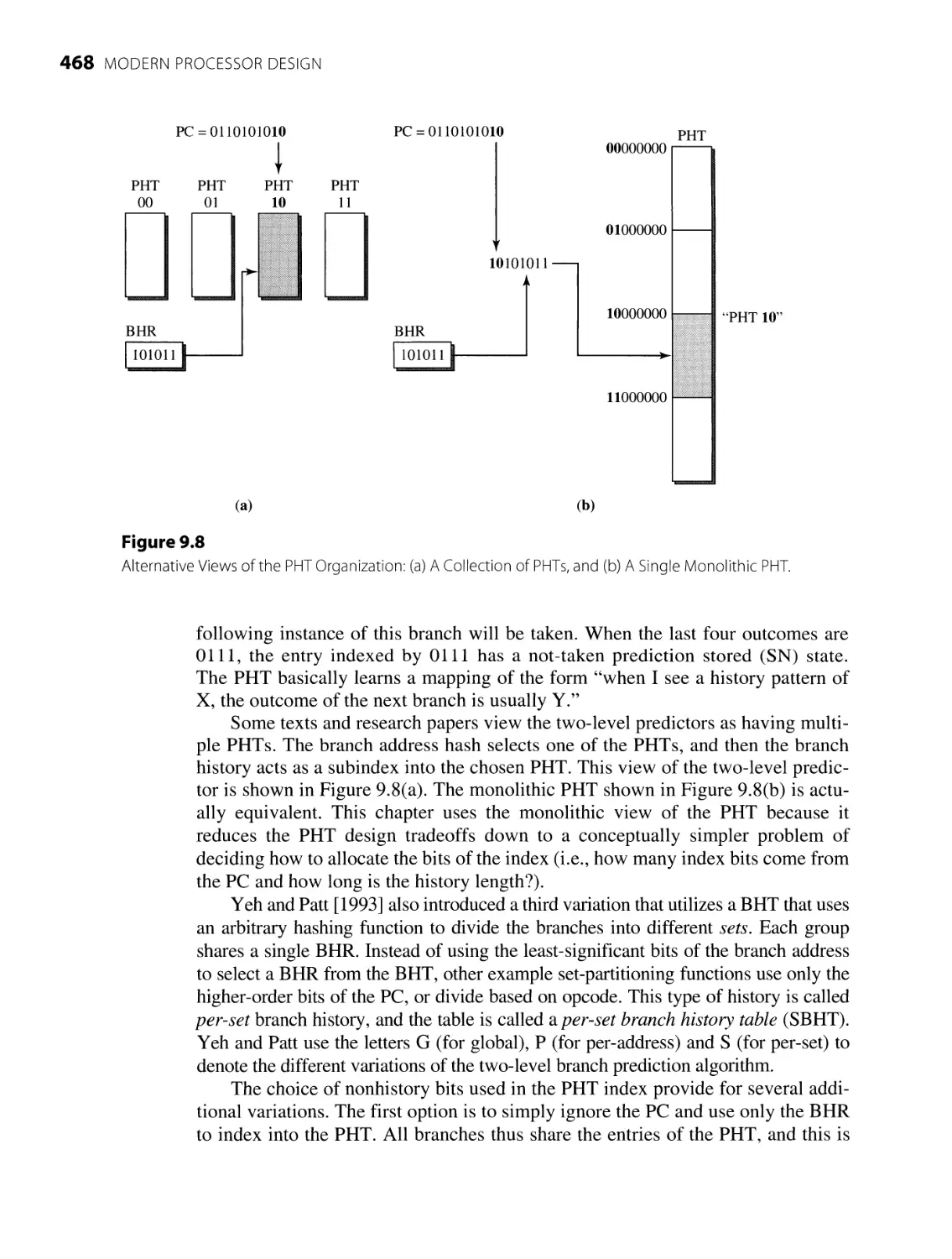
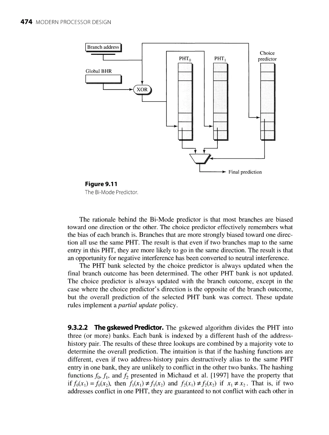
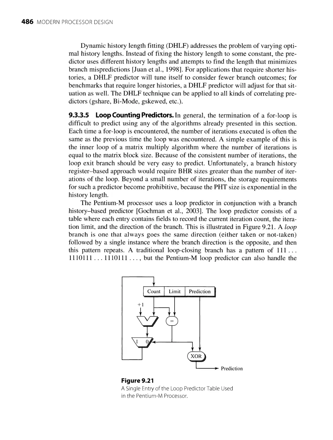
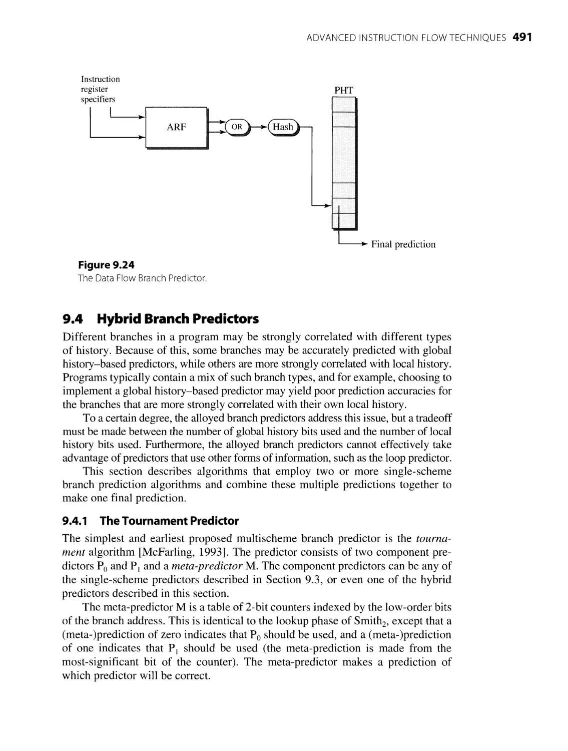
/


Автор: Shen J.P. Lipasti M.H.
Теги: programming languages programming semiconductors waveland press intel corporation microprocers
ISBN: 1-4786-0783-1


Текст
Fundamentals of Superscalar Processors
John Paul Shen
Intel Corporation
Mikko H. Lipasti
University of Wisconsin
WAVELAND
PRESS, INC.
Long Grove, Illinois
To
Our parents:
Paul and Sue Shen
Tarja and Simo Lipasti
Our spouses:
Amy C. Shen
Erica Ann Lipasti
Our children:
Priscilla S. Shen, Rachael S. Shen, and Valentia C. Shen
Emma Kristiina Lipasti and Elias Joel Lipasti
For information about this book, contact:
Waveland Press, Inc.
4180 IL Route 83, Suite 101
Long Grove, IL 60047-9580
(847) 634-0081
info @ waveland.com
www.waveland.com
Copyright © 2005 by John Paul Shen and Mikko H. Lipasti
2013 reissued by Waveland Press, Inc.
10-digit ISBN 1-4786-0783-1
13-digit ISBN 978-1-4786-0783-0
All rights reserved. No part of this book may be reproduced, stored in a retrieval
system, or transmitted in any form or by any means without permission in writing
from the publisher.
Printed in the United States of America
7654321
Table of Contents
Preface
x
1 Processor Design 1
About the Authors ix
1.1 The Evolution of Microprocessors 2
1.2 Instruction Set Processor Design 4
1.2.1 Digital Systems Design 4
Realization
5
1.2.3 Instruction Set Architecture 6
1.2.2 Architecture, Implementation, and
1.2.4 Dynamic-Static Interface 8
1.3 Principles of Processor Performance 10
1.3.1 Processor Performance Equation 10
1.3.2 Processor Performance Optimizations 11
1.3.3 Performance Evaluation Method 13
1.4 Instruction-Level Parallel Processing 16
1.4.1 From Scalar to Superscalar 16
1.5
Summary
32
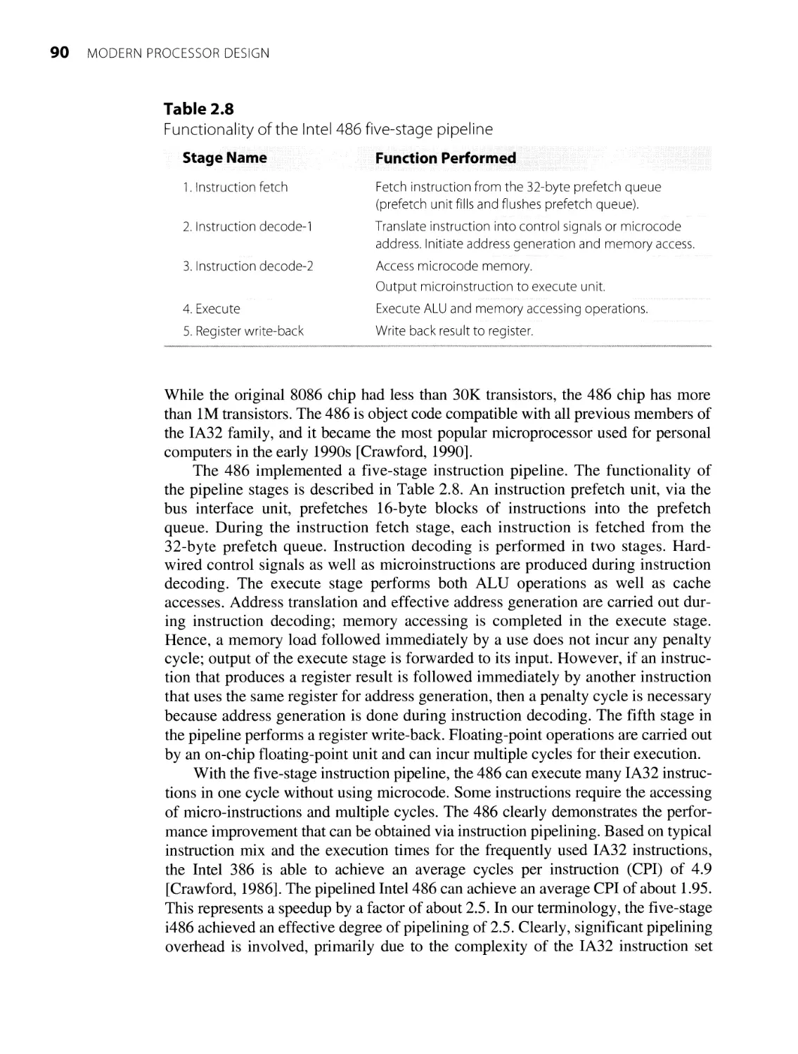
2 Pipelined Processors 39
1.4.2 Limits of Instruction-Level Parallelism 24
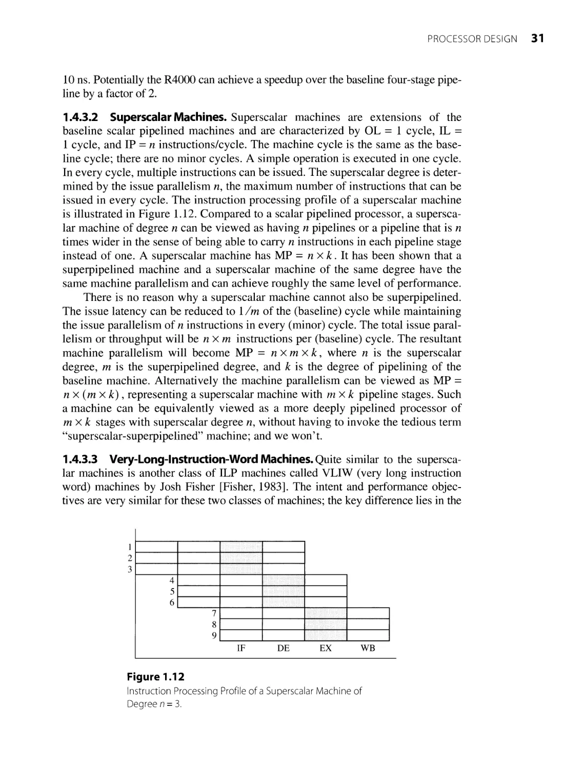
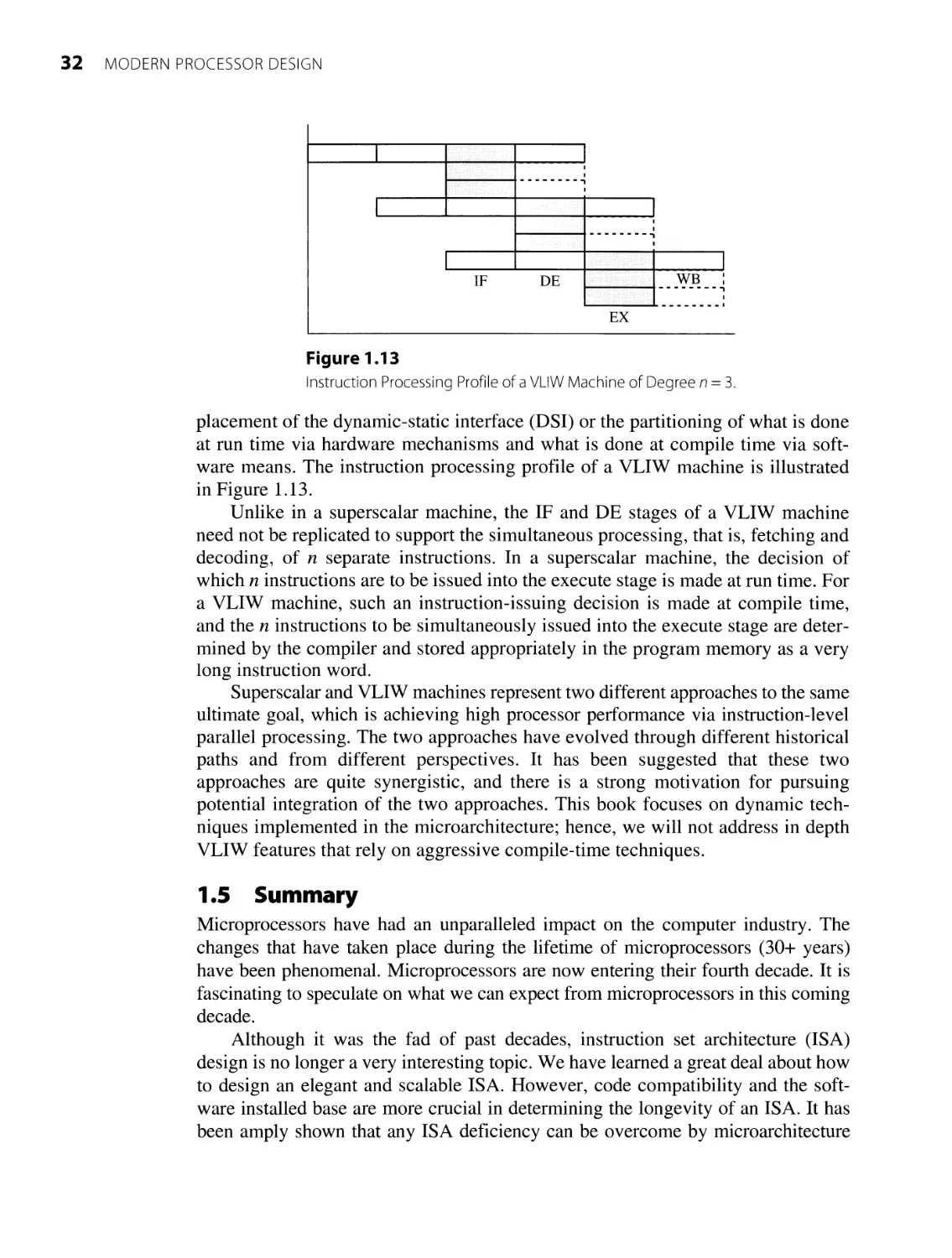
1.4.3 Machines for Instruction-Level Parallelism 27
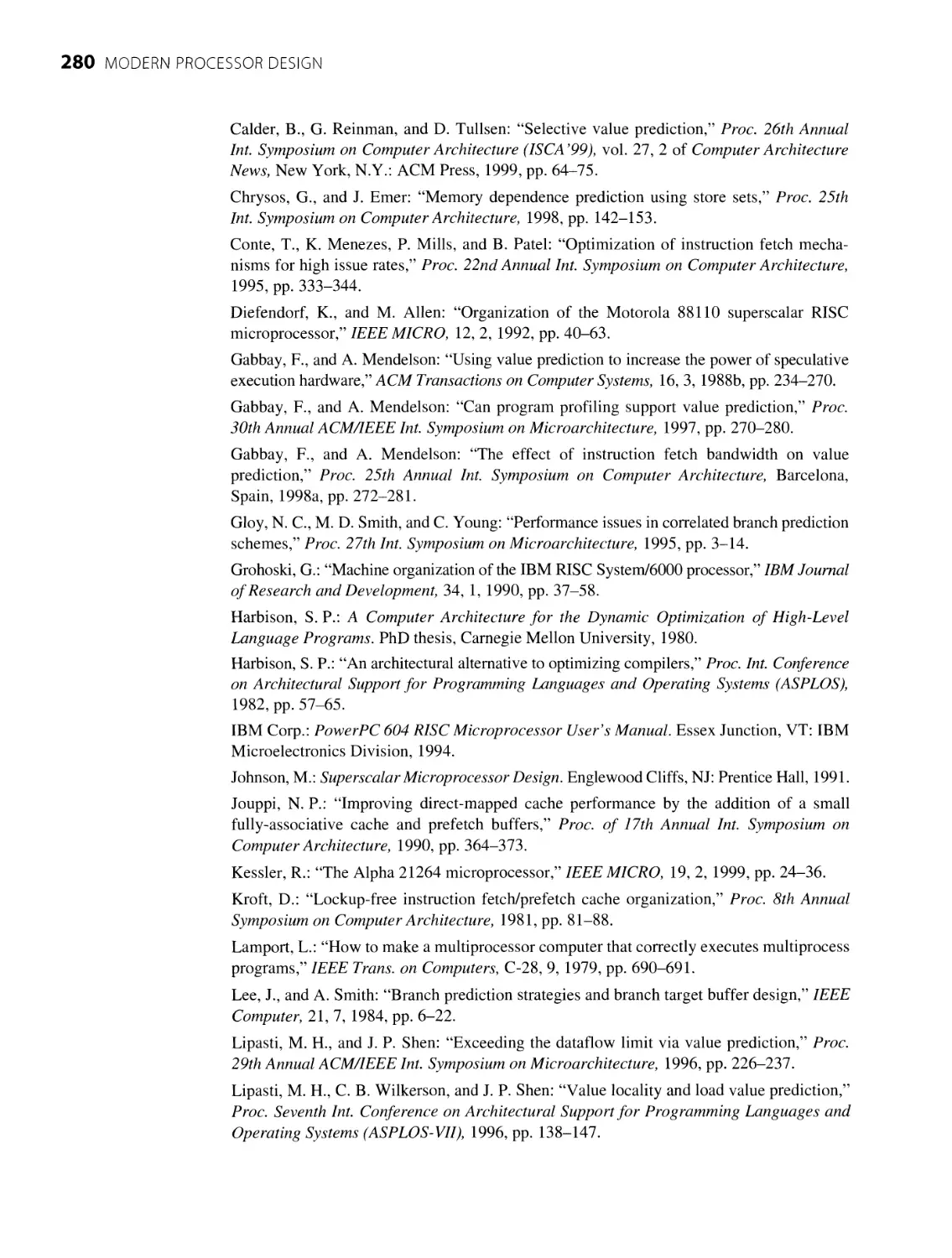
2.12.1.1
Pipelining
Fundamentals
40
Pipelined
Design
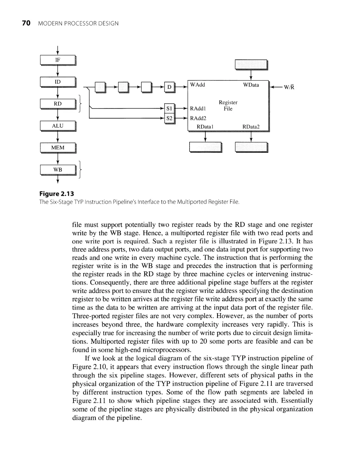
40
2.1.2 Arithmetic Pipeline Example 44
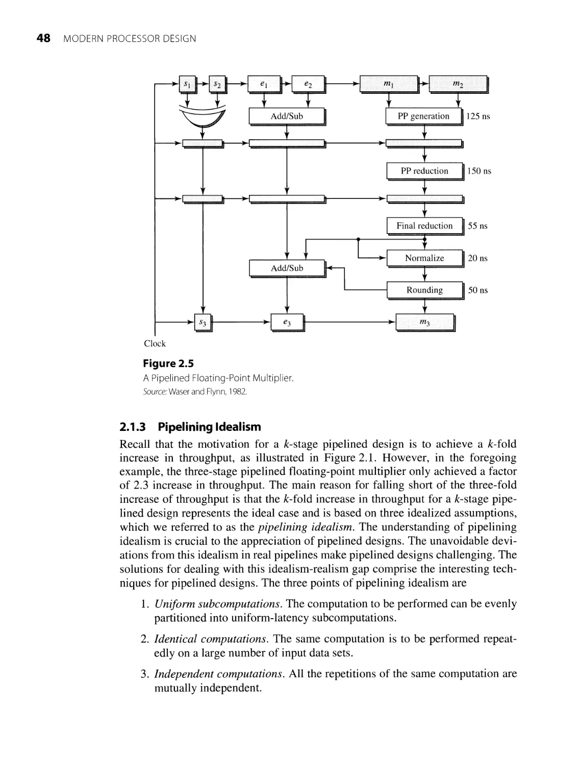
2.1.3
Pipelining Idealism 48
2.1.4 Instruction Pipelining 51
2.2 Pipelined Processor Design 54
2.2.1 Balancing Pipeline Stages 55
2.2.2 Unifying Instruction Types 61
2.2.3 Minimizing Pipeline Stalls 71
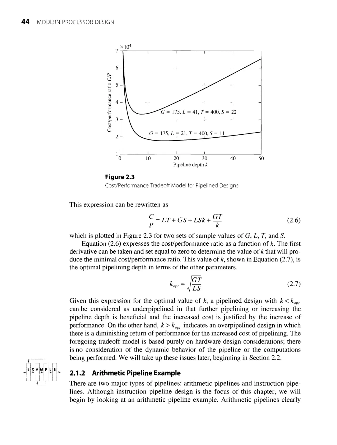
2.4
Summary
97
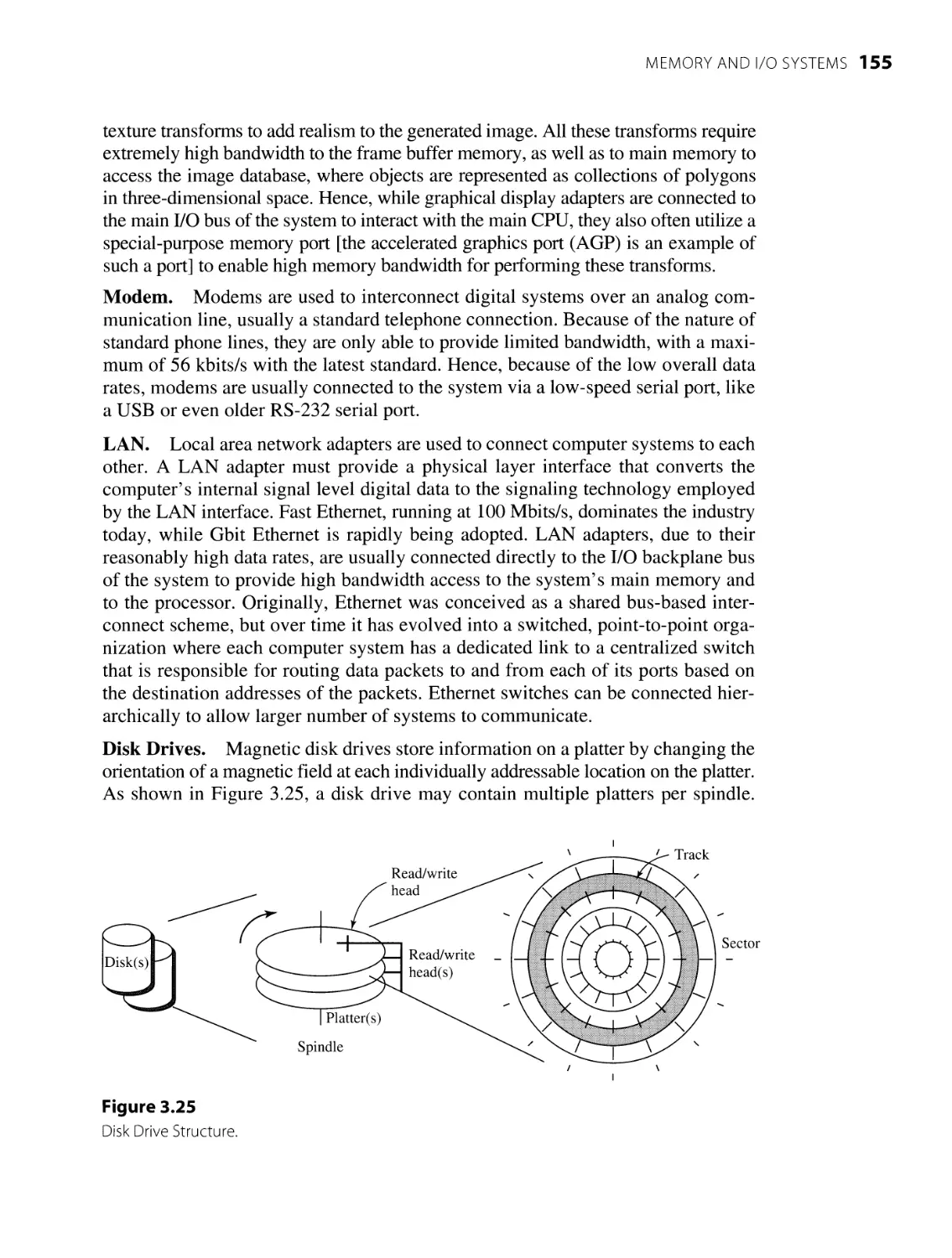
3 Memory and I/O Systems 105
2.2.4 Commercial Pipelined Processors 87
2.3 Deeply Pipelined Processors 94
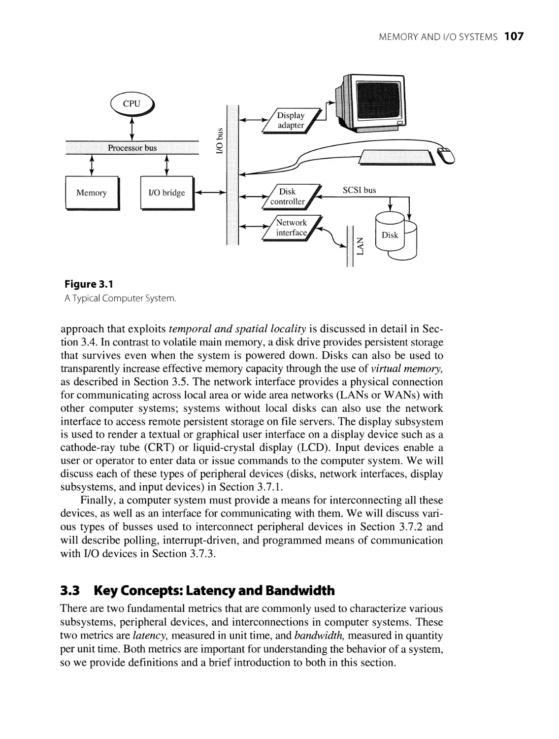
3.1 Introduction 105
3.2 Computer System Overview 106
3.3 Key Concepts: Latency and Bandwidth 107
iv MODERN PROCESSOR DESIGN
3.4 Memory Hierarchy 110
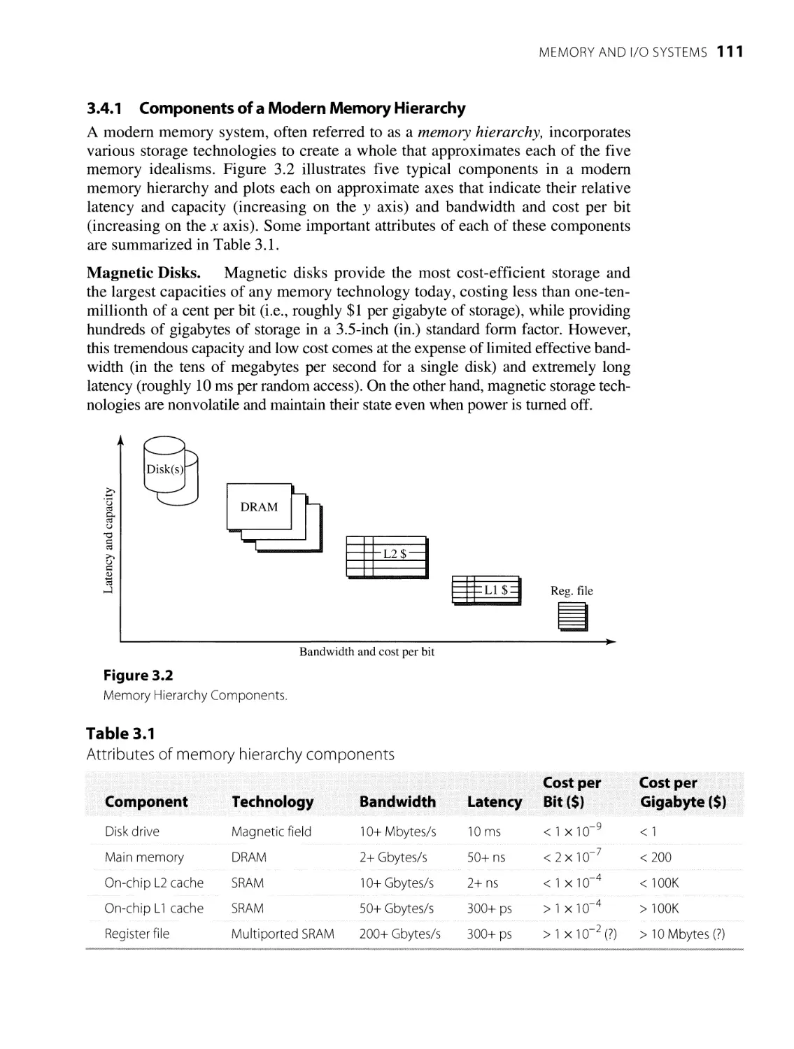
3.4.1 Components of a Modern Memory Hierarchy 111
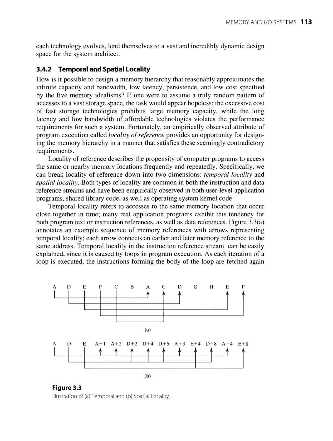
3.4.2 Temporal and Spatial Locality 113
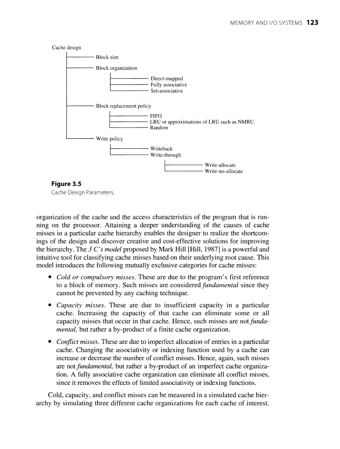
3.4.3 Caching and Cache Memories 115
3.4.4
Main
Memory
127
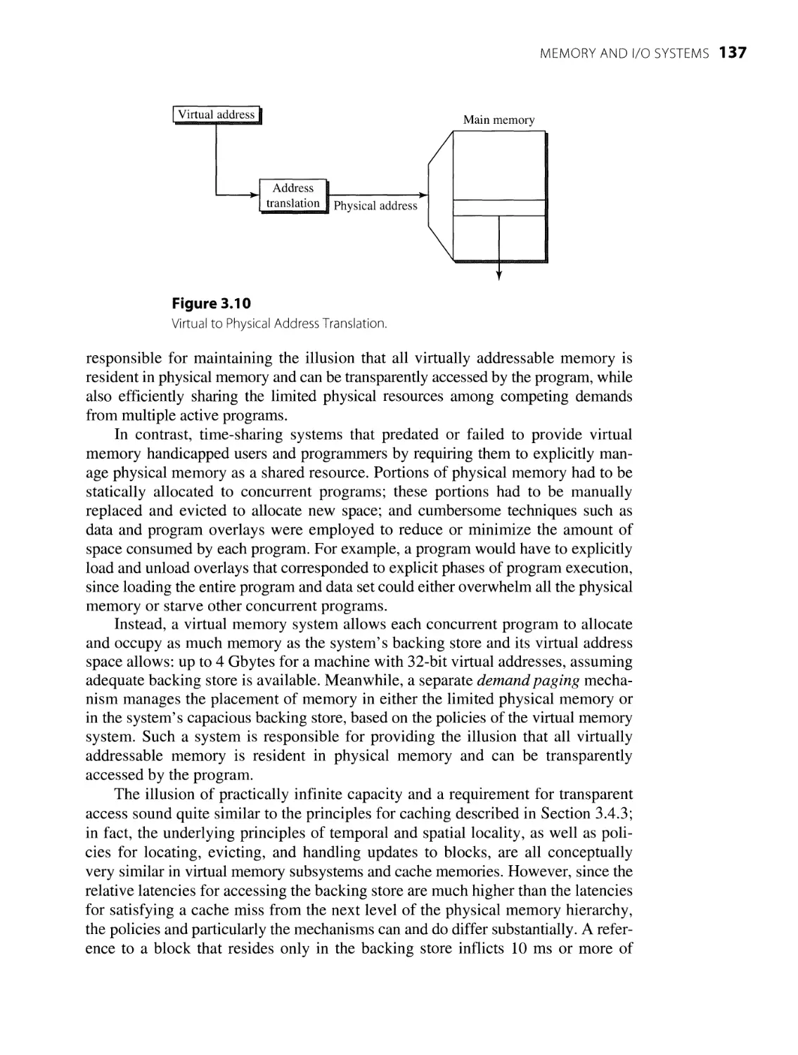
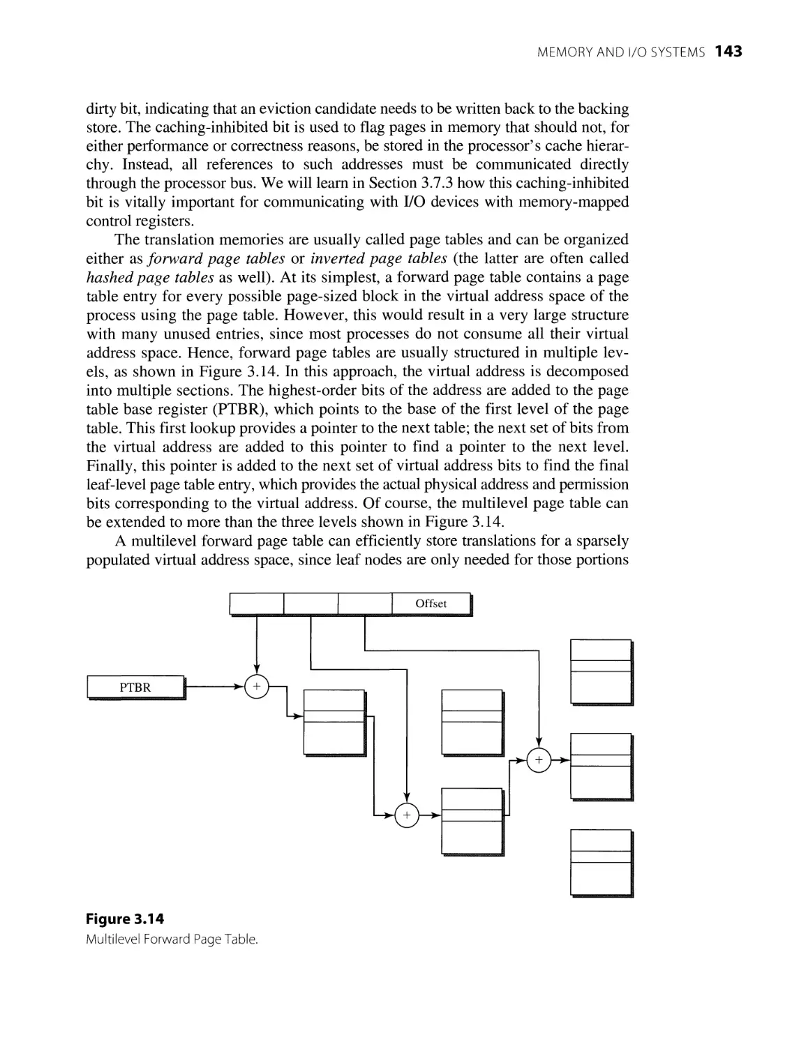
3.5 Virtual Memory Systems 136
3.5.1
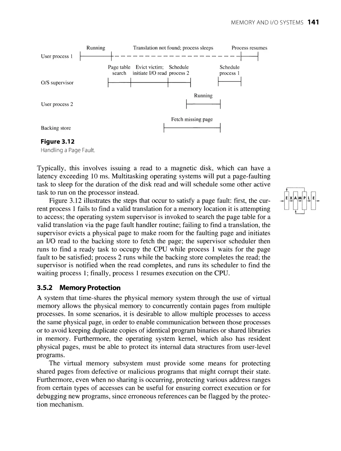
Demand Paging 138
3.5.2 Memory Protection 141
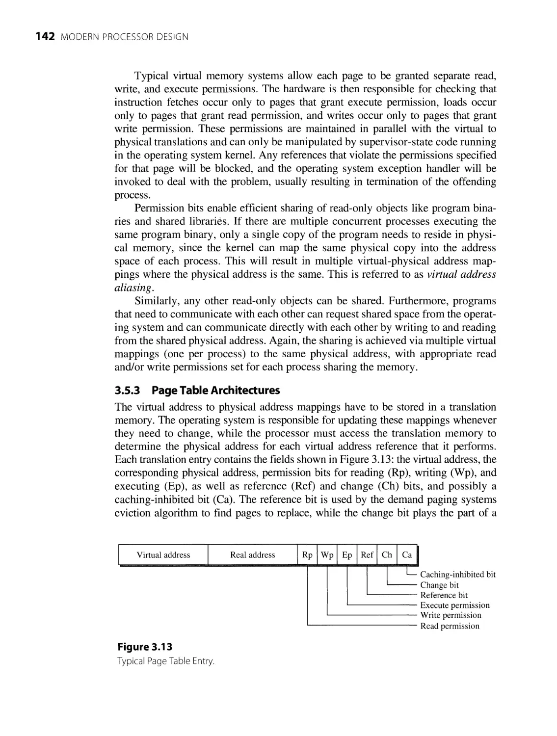
3.5.3 Page Table Architectures 142
3.6 Memory Hierarchy Implementation 145
3.7 Input/Output Systems 153
3.7.1 Types of I/O Devices 154
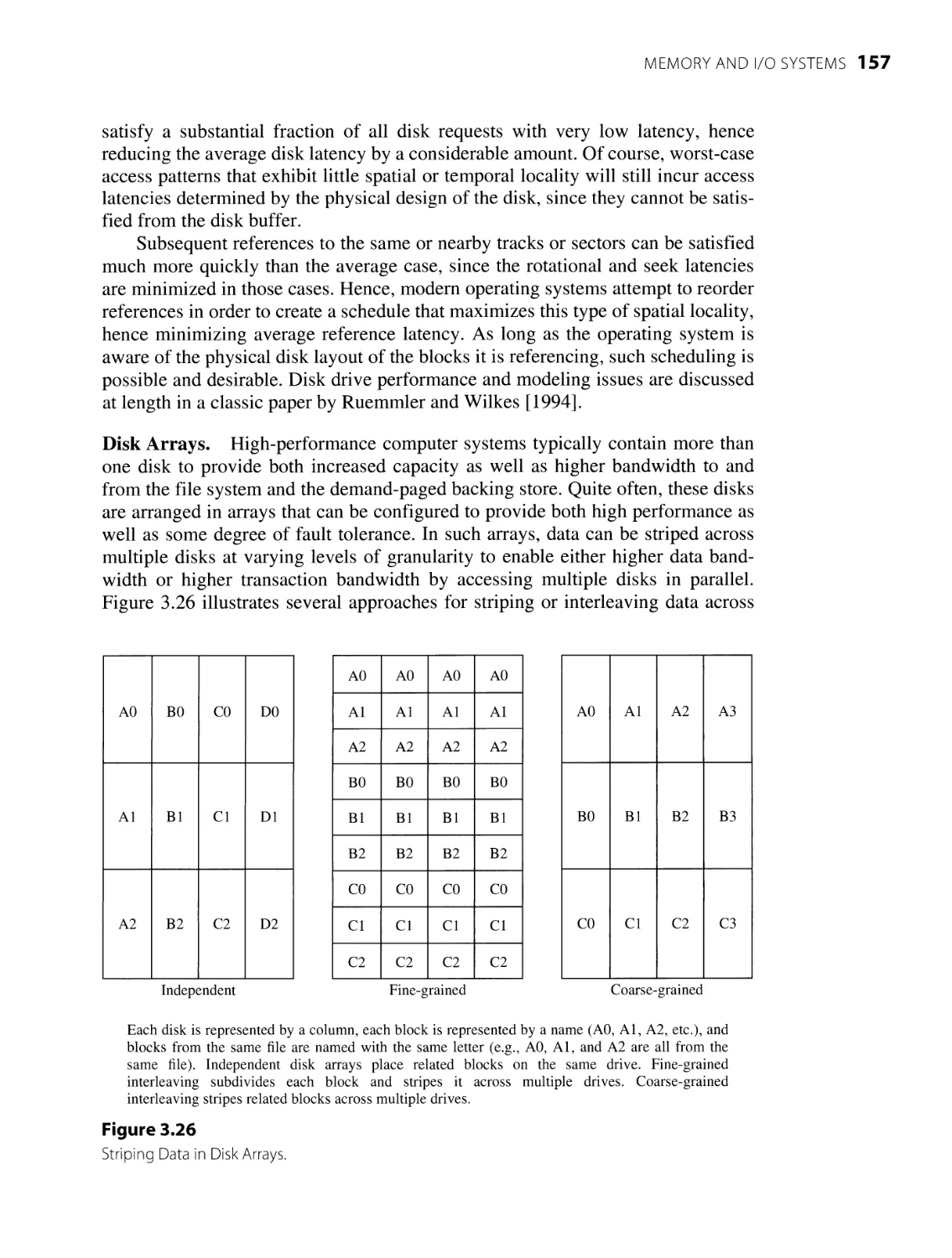
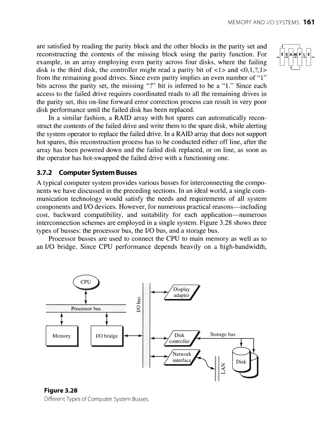
3.7.2 Computer System Busses 161
3.7.3 Communication with I/O Devices 165
3.8 Summary 170
3.7.4 Interaction of I/O Devices and Memory Hierarchy 168
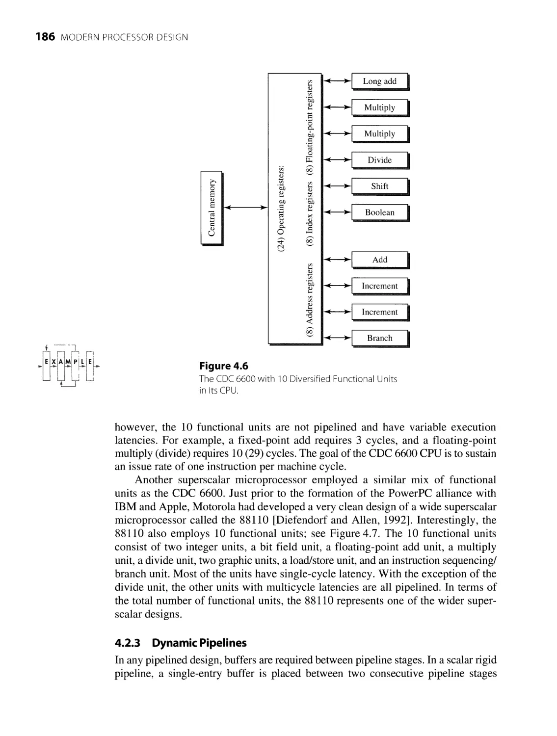
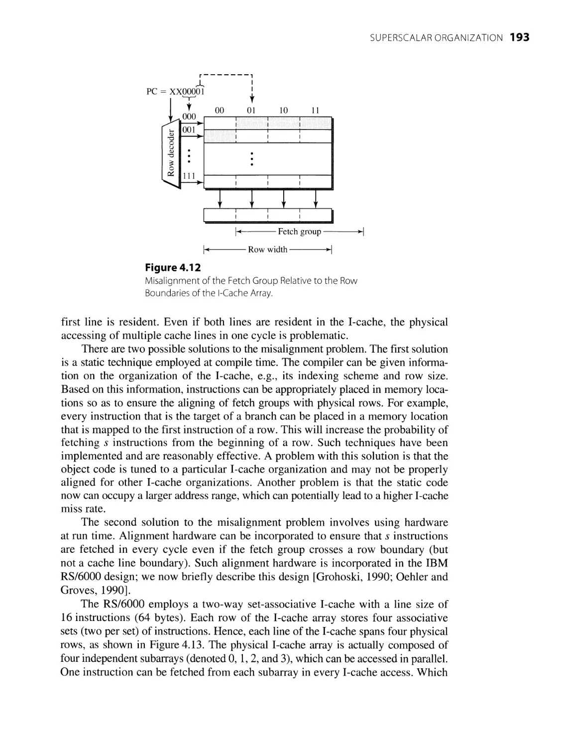
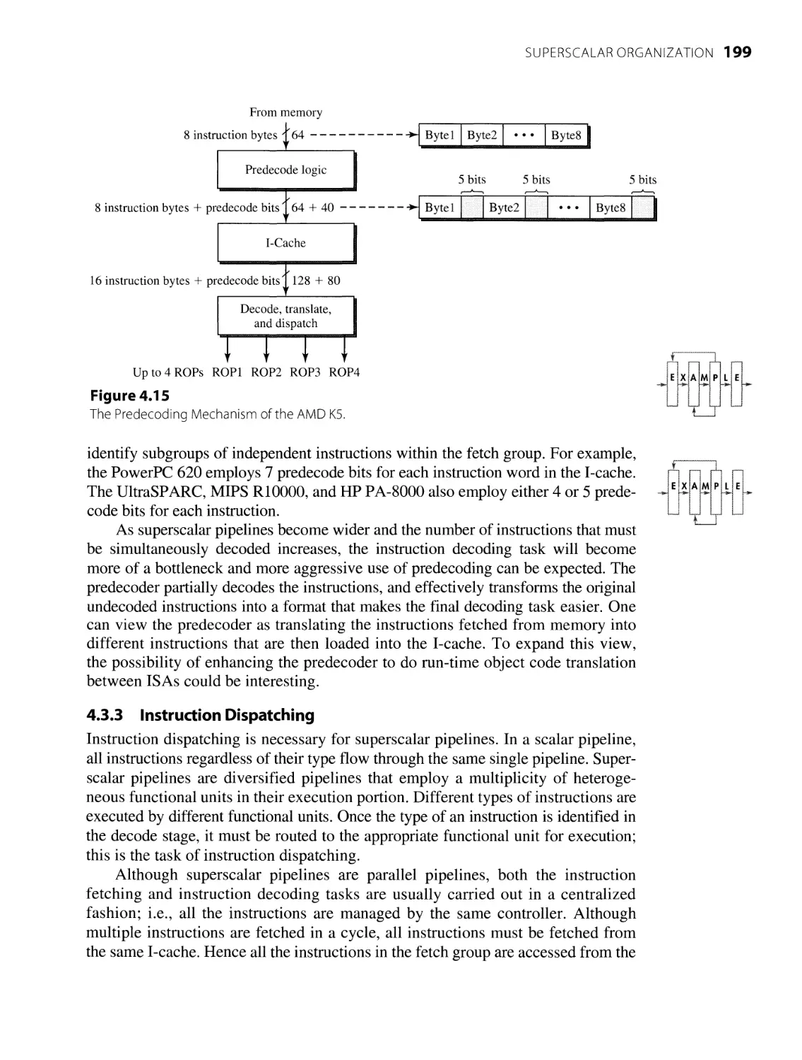
4 Superscalar Organization 177
4.1 Limitations of Scalar Pipelines 178
4.1.1 Upper Bound on Scalar Pipeline Throughput 178
4.1.2 Inefficient Unification into a Single Pipeline 179
4.1.3 Performance Lost Due to a Rigid Pipeline 179
4.2 From Scalar to Superscalar Pipelines 181
4.2.1
Parallel Pipelines 181
4.2.2 Diversified Pipelines 184
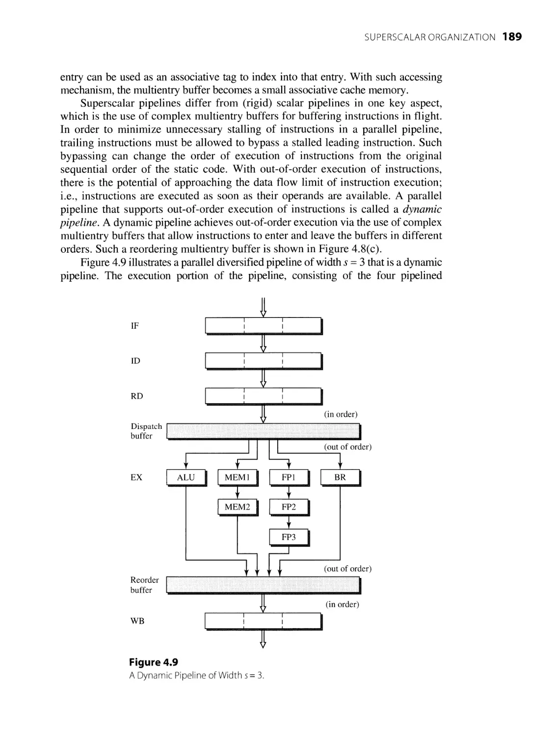
4.2.3 Dynamic Pipelines 186
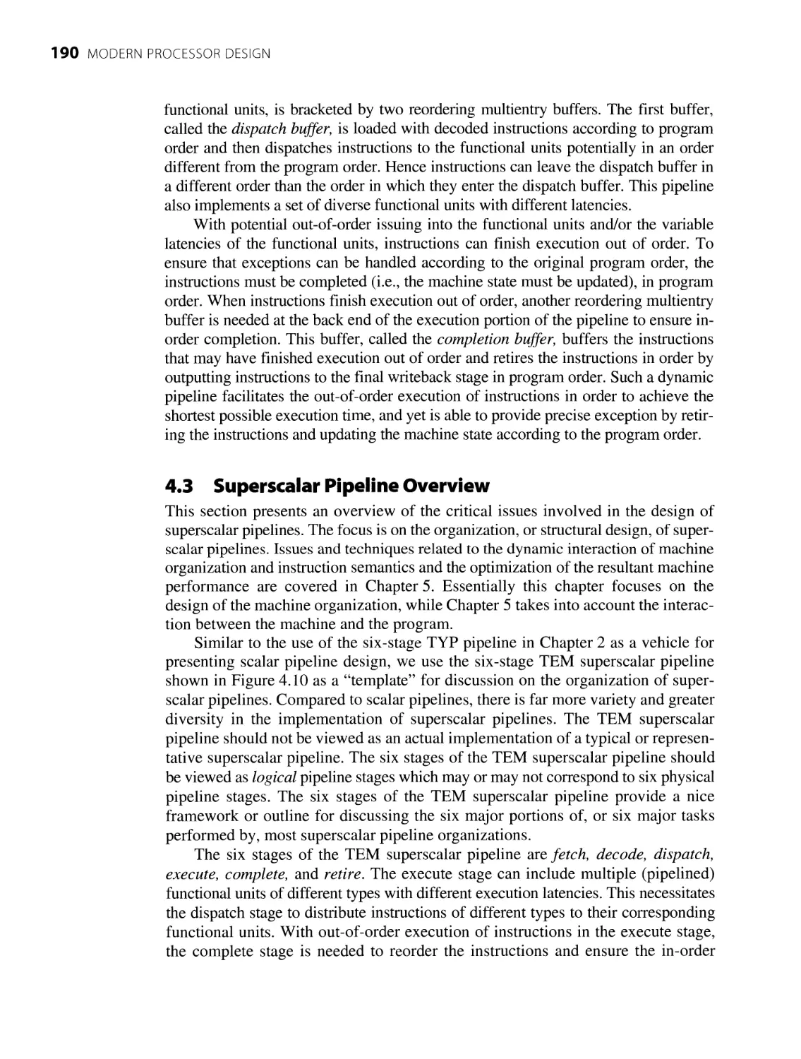
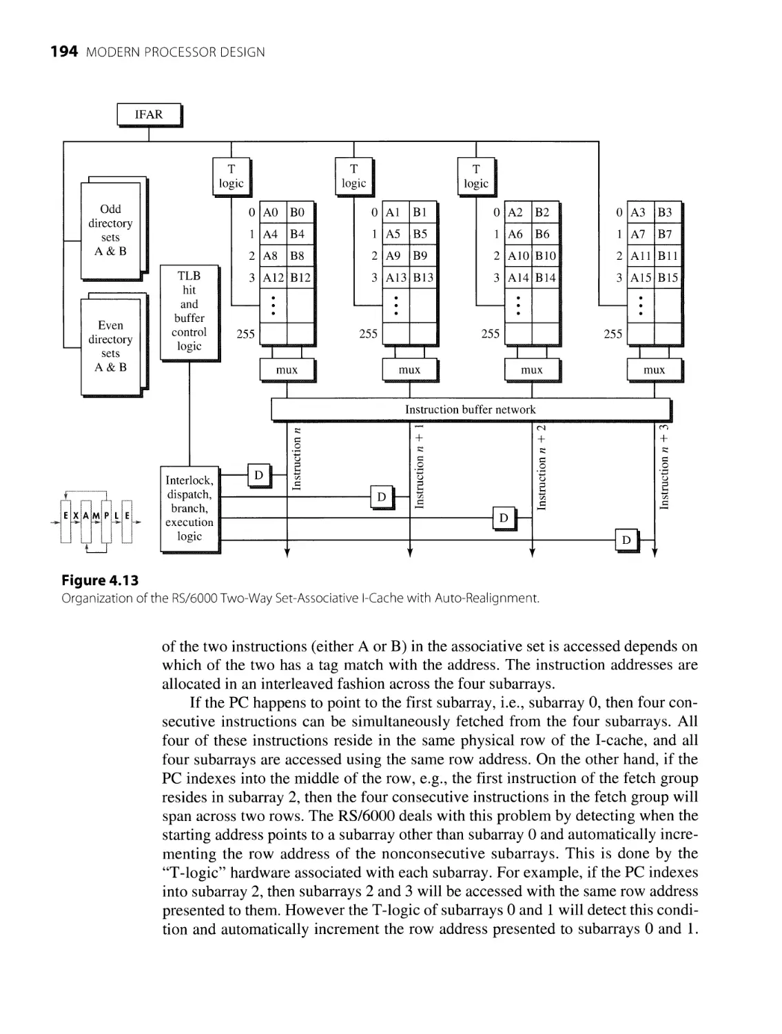
4.3.1 Instruction Fetching 191
4.3.2 Instruction Decoding 195
4.3 Superscalar Pipeline Overview 190
4.3.3
199
4.3.4 Instruction
InstructionDispatching
Execution 203
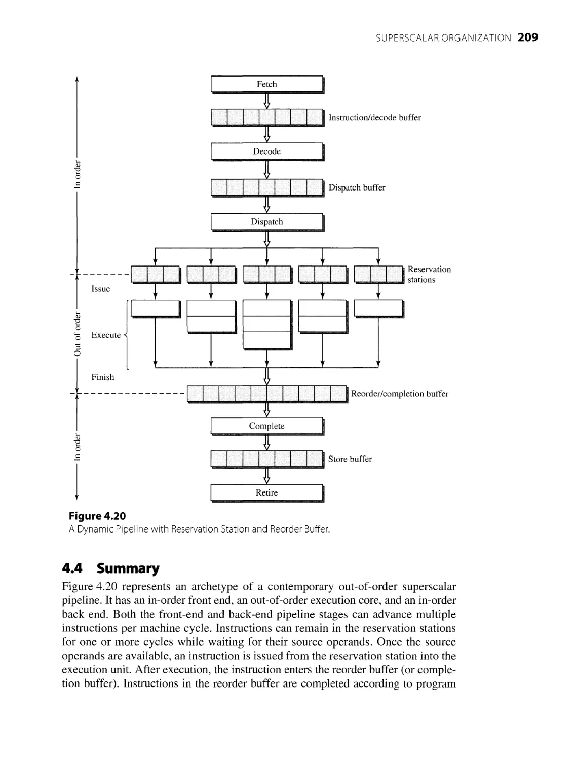
4.4 Summary 209
4.3.5 Instruction Completion and Retiring 206
5 Superscalar Techniques 217
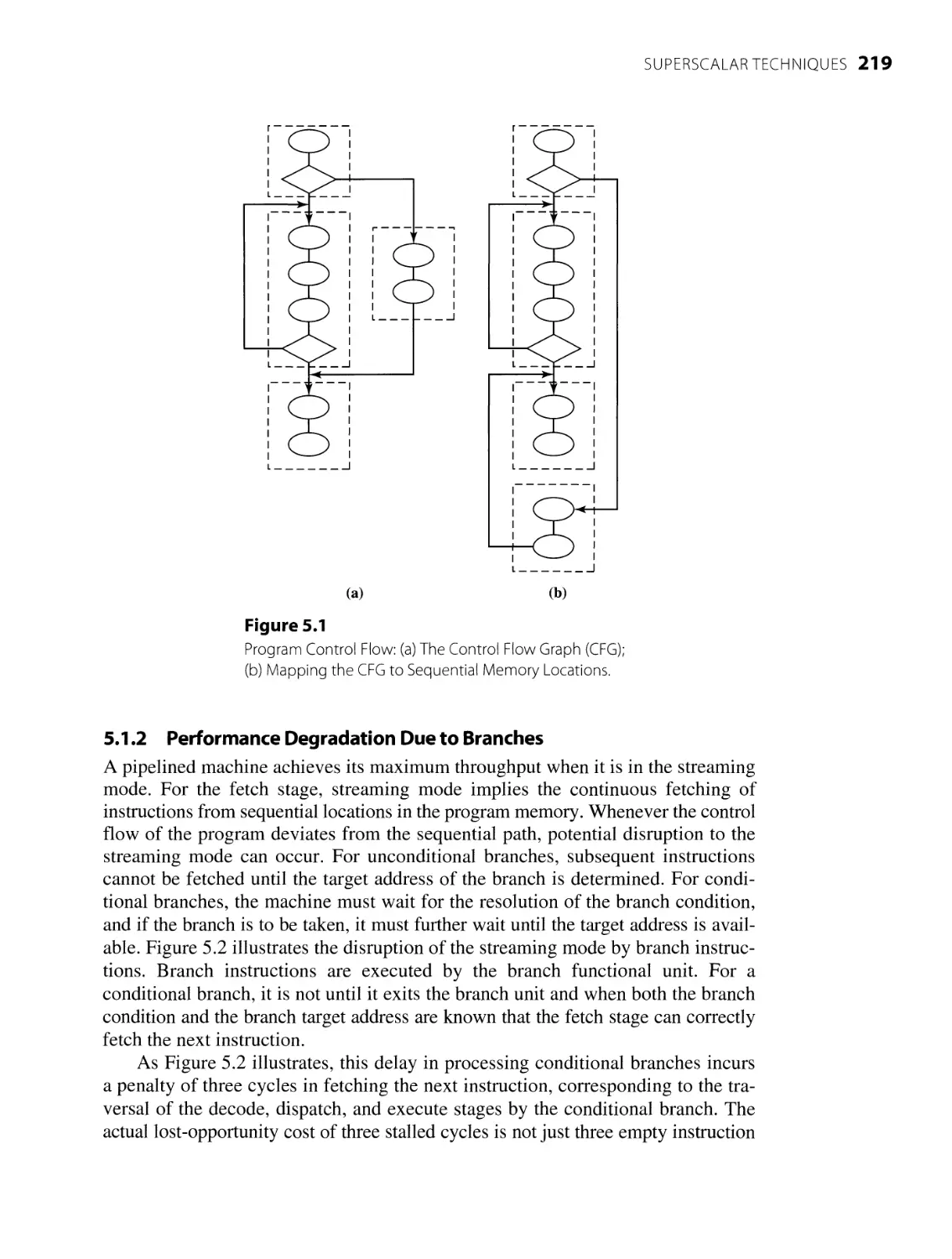
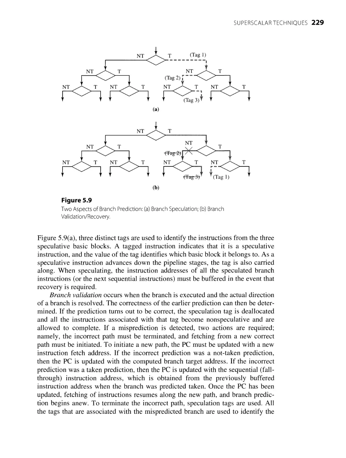
5.1 Instruction Flow Techniques 218
5.1.1 Program Control Flow and Control Dependences 218
5.1.2 Performance Degradation Due to Branches 219
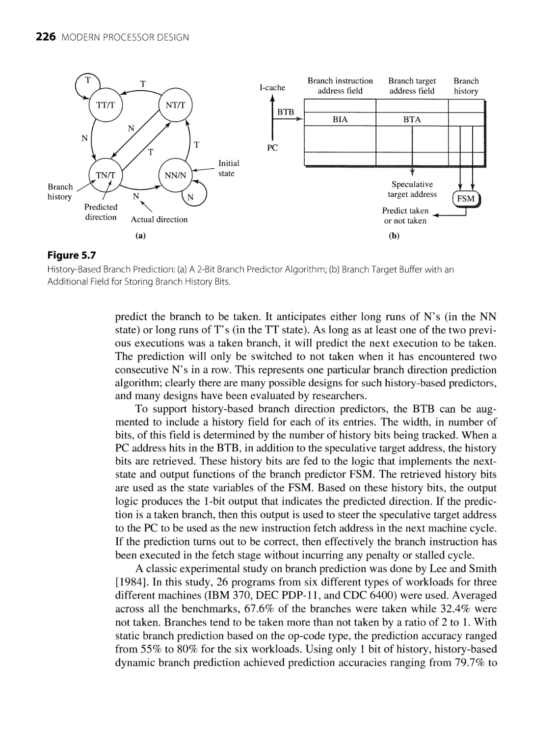
5.1.3 Branch Prediction Techniques 223
5.1.4 Branch Misprediction Recovery 228
5.1.5 Advanced Branch Prediction Techniques 231
5.1.6 Other Instruction Flow Techniques 236
5.2 Register Data Flow Techniques 237
5.2.1 Register Reuse and False Data Dependences 237
5.2.2 Register Renaming Techniques 239
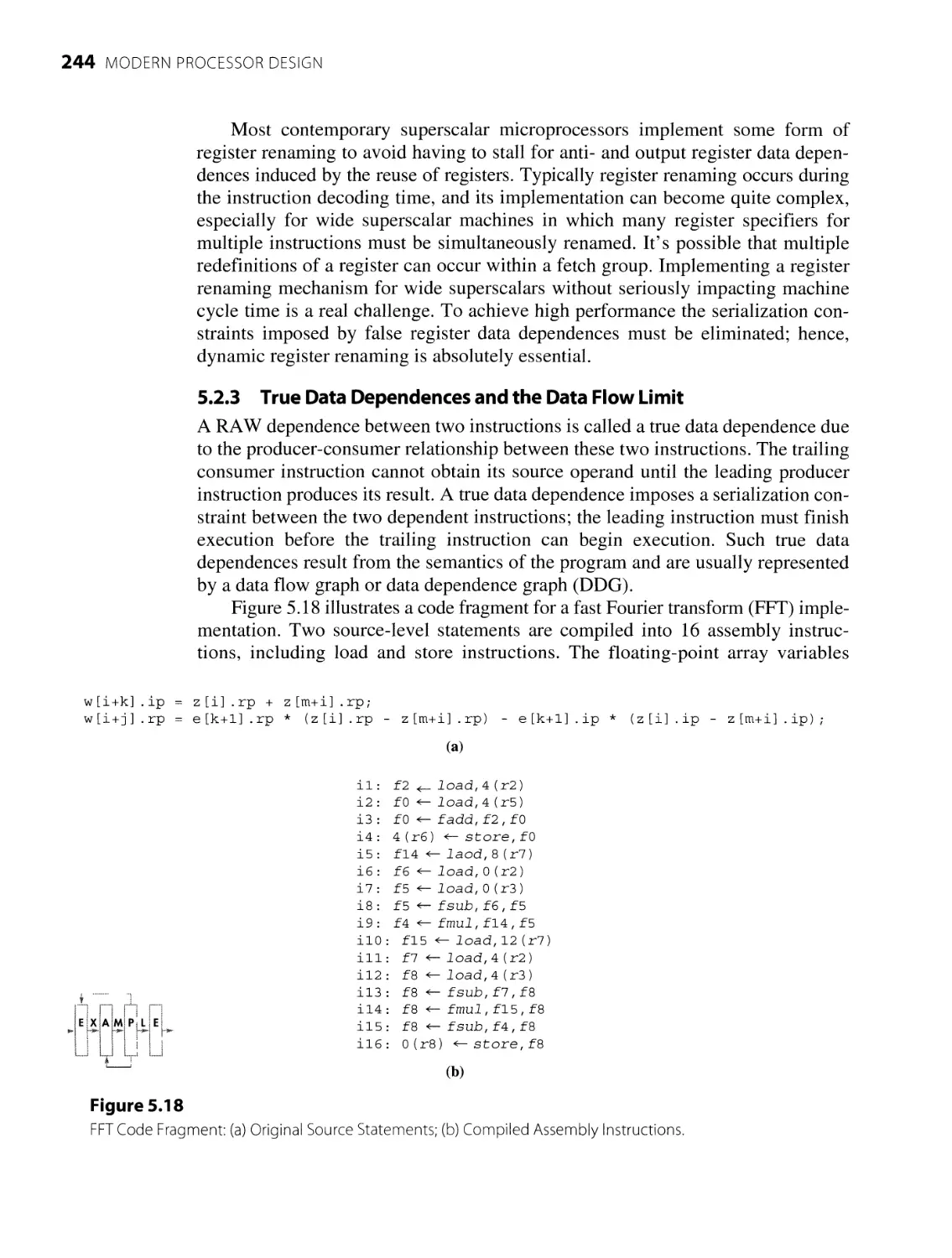
5.2.3 True Data Dependences and the Data Flow Limit 244
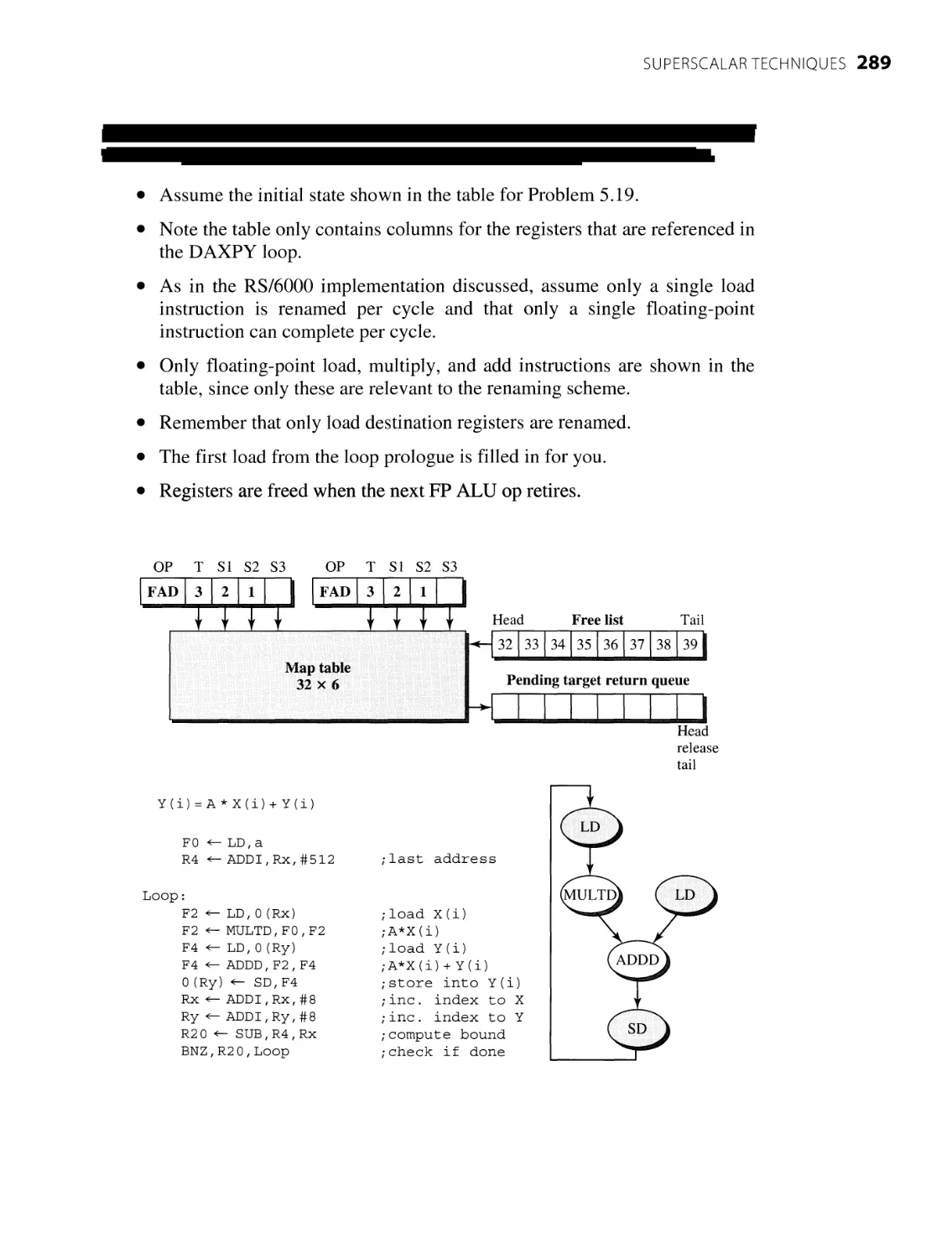
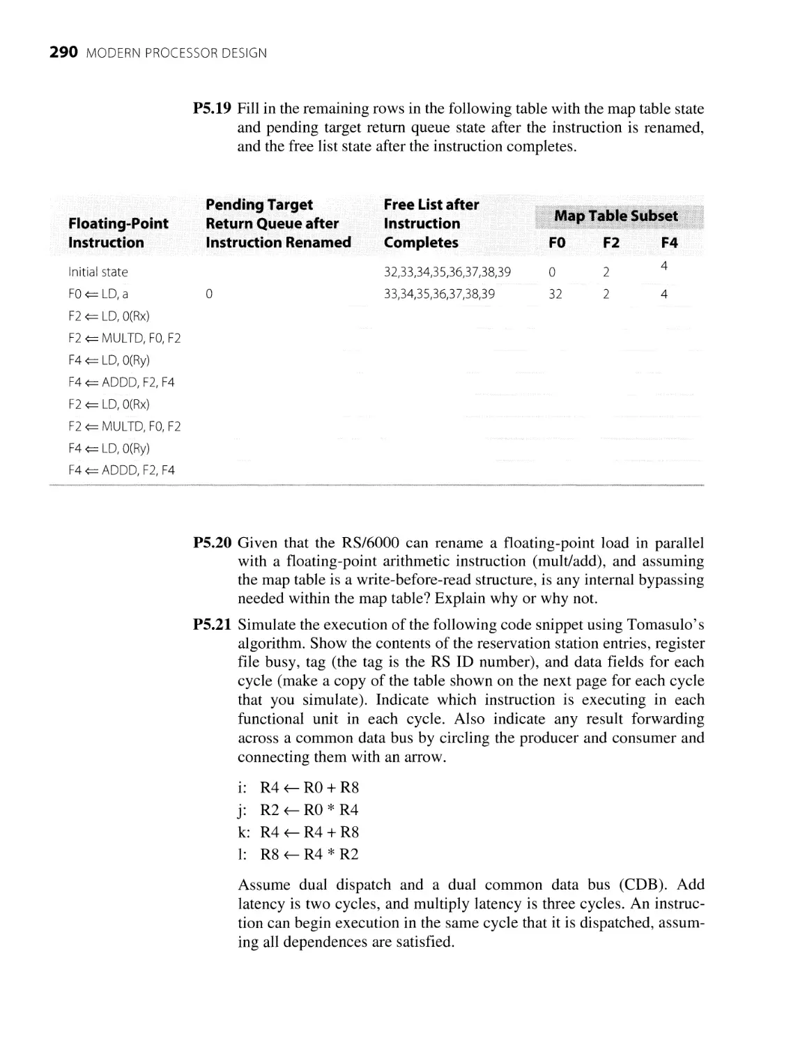
TABLE OF CONTENTS
5.3
5.4
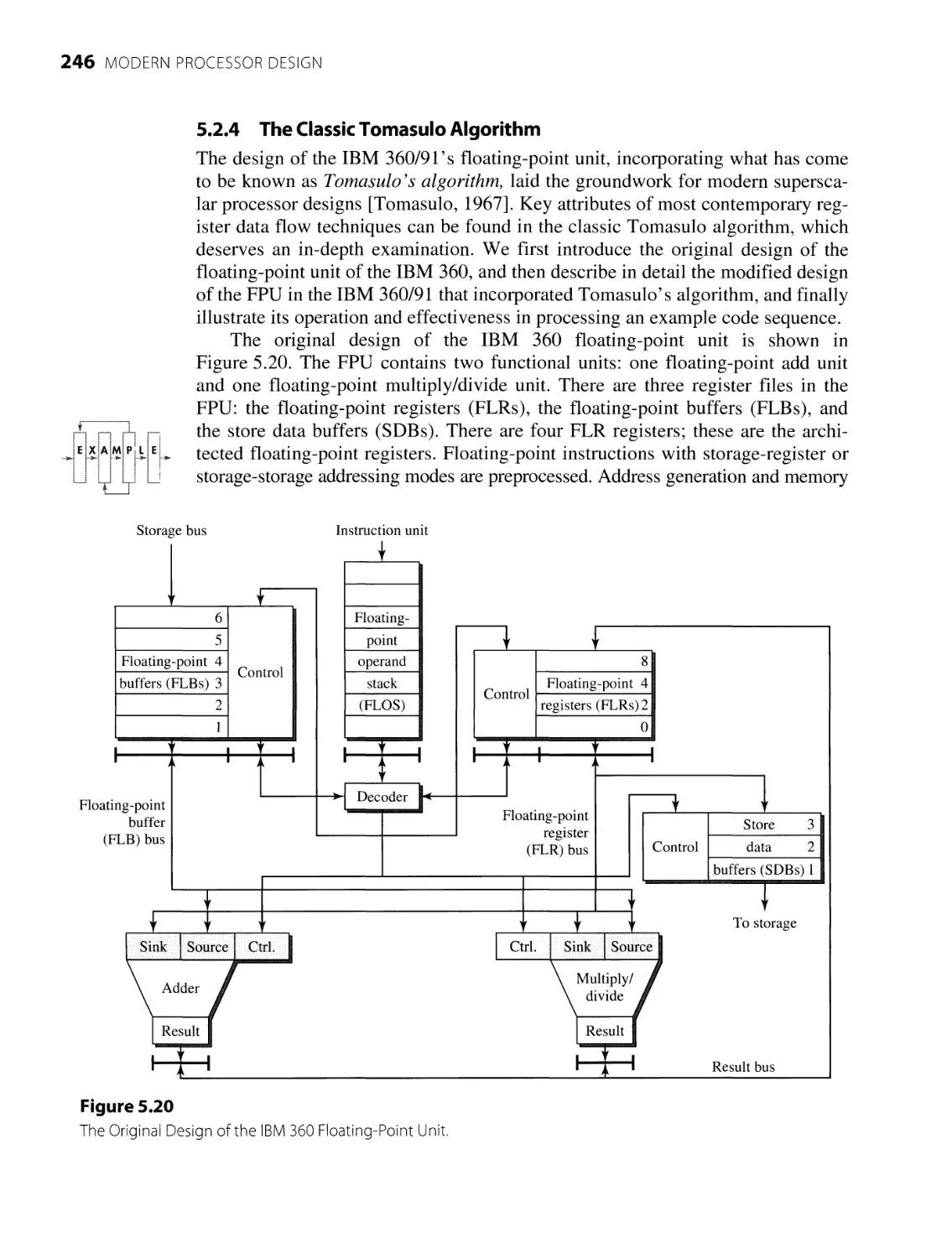
5.2.4 The Classic Tomasulo Algorithm
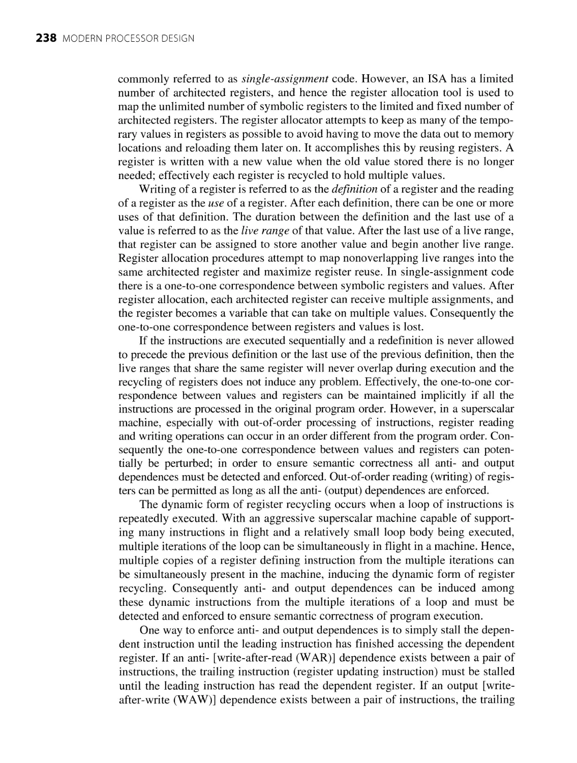
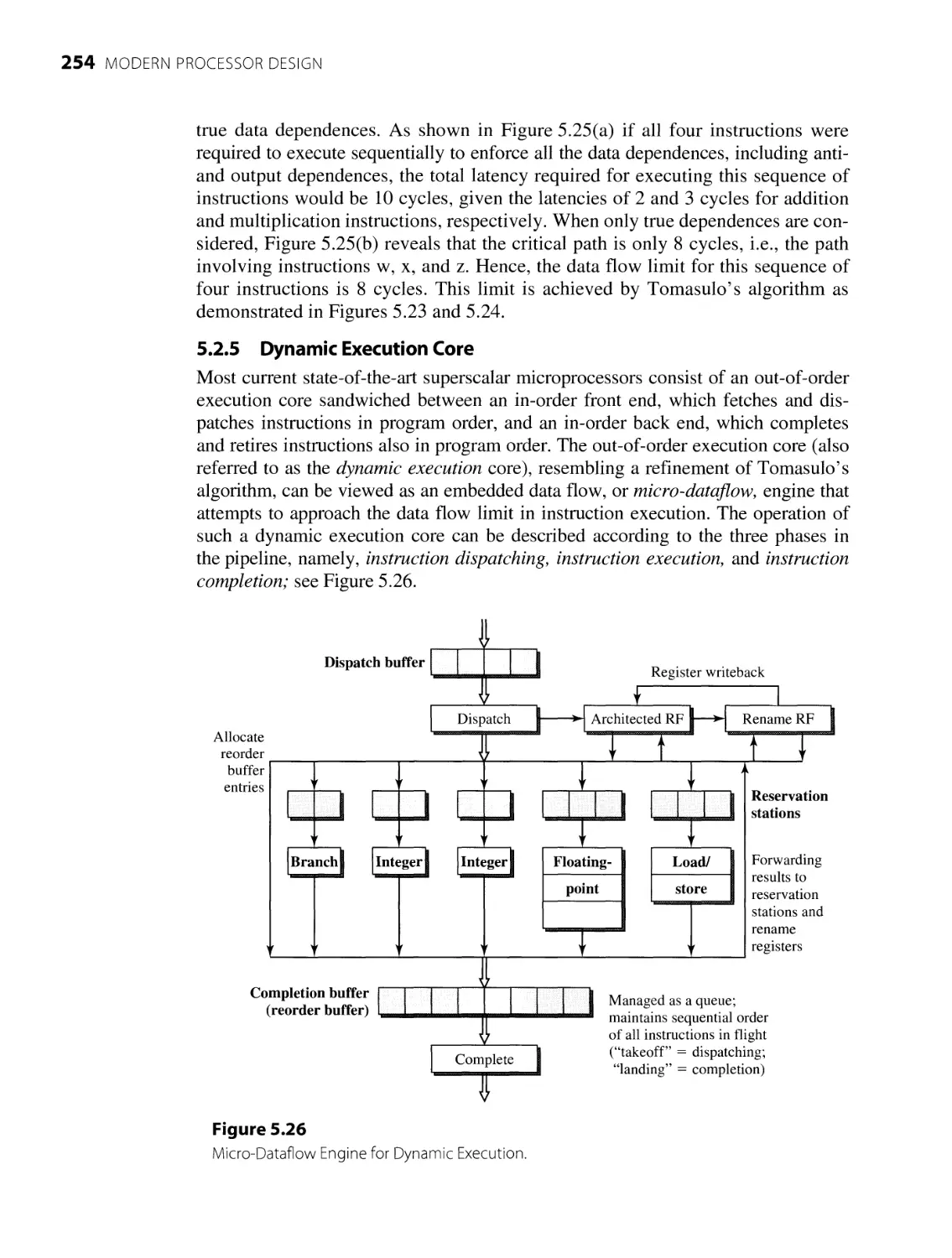
5.2.5 Dynamic Execution Core
5.2.6 Reservation Stations and Reorder Buffer
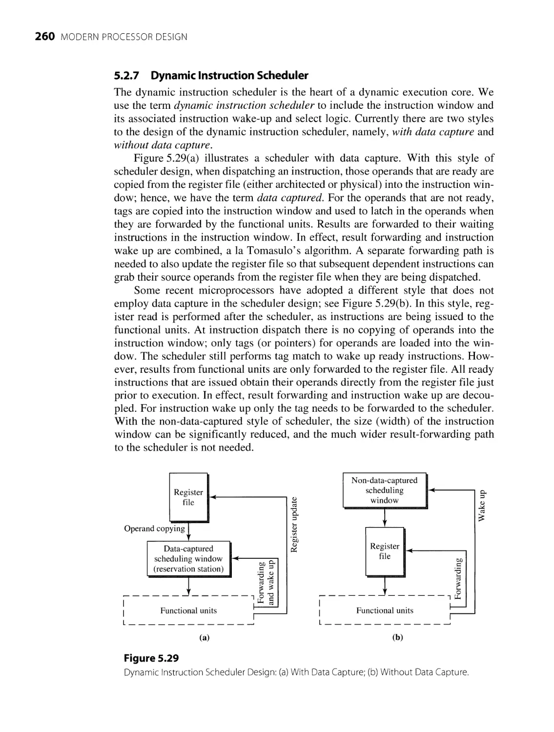
5.2.7 Dynamic Instruction Scheduler
5.2.8 Other Register Data Flow Techniques
Memory Data Flow Techniques
5.3.1 Memory Accessing Instructions
5.3.2 Ordering of Memory Accesses
5.3.3 Load Bypassing and Load Forwarding
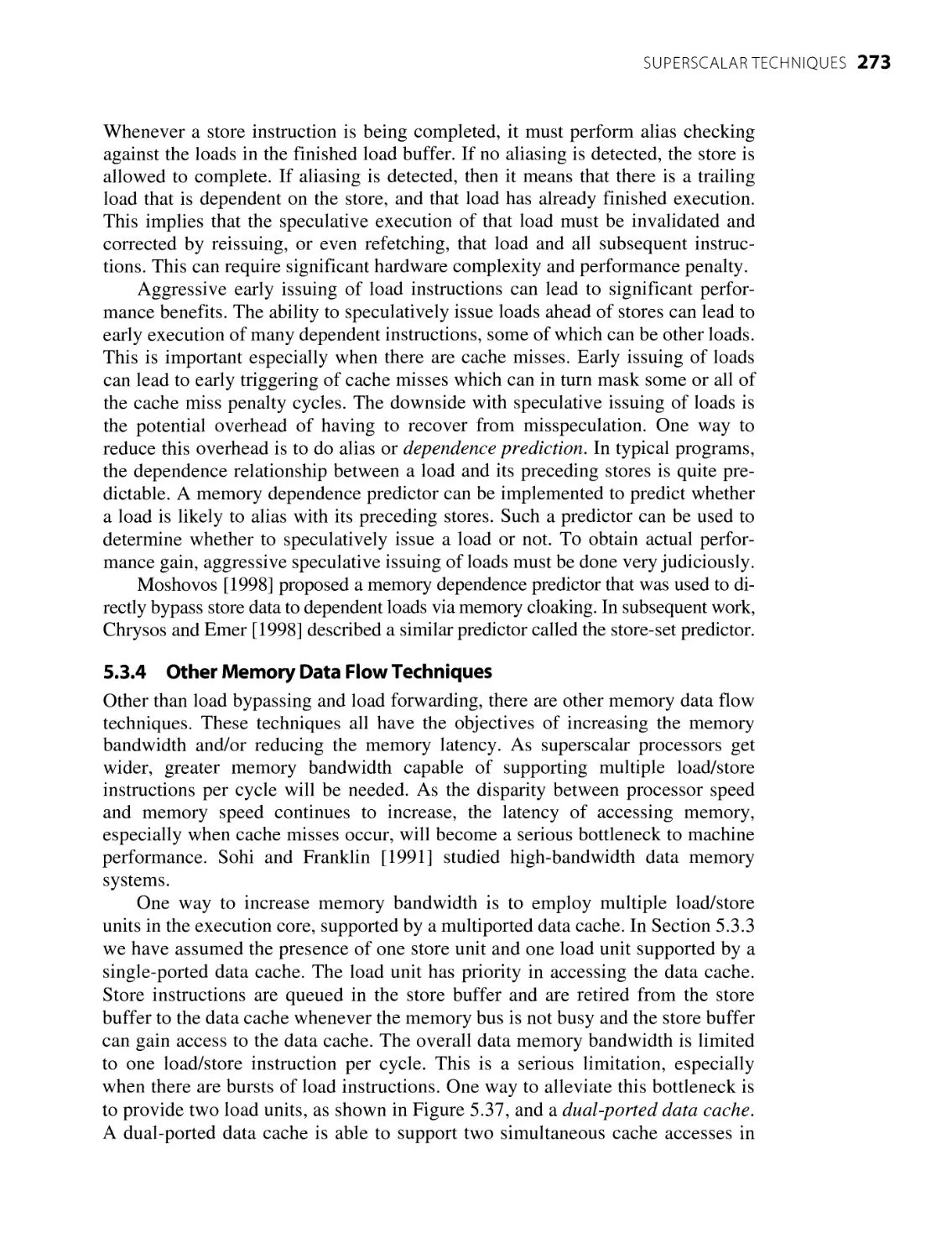
5.3.4 Other Memory Data Flow Techniques
Summary
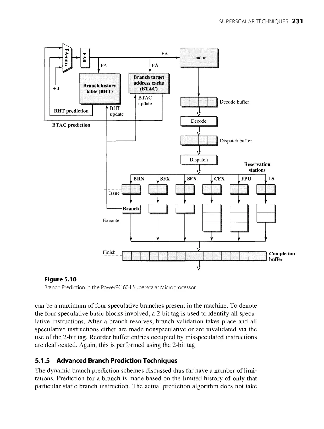
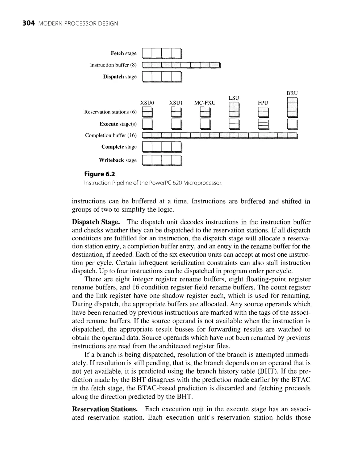
The PowerPC 620
6.1
6.2
6.3
6.4
6.5
6.6
6.7
6.8
6.9
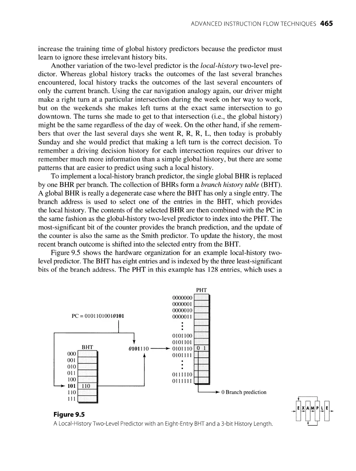
Introduction
Experimental Framework
Instruction Fetching
6.3.1 Branch Prediction
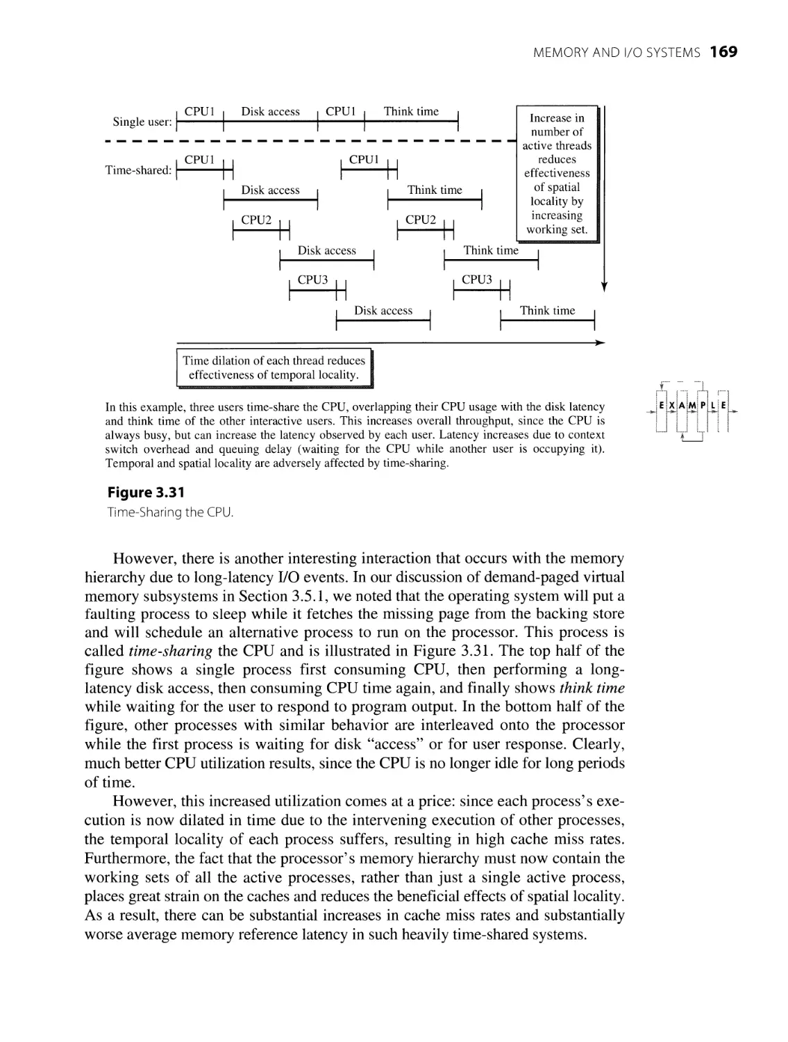
6.3.2 Fetching and Speculation
Instruction Dispatching
6.4.1 Instruction Buffer
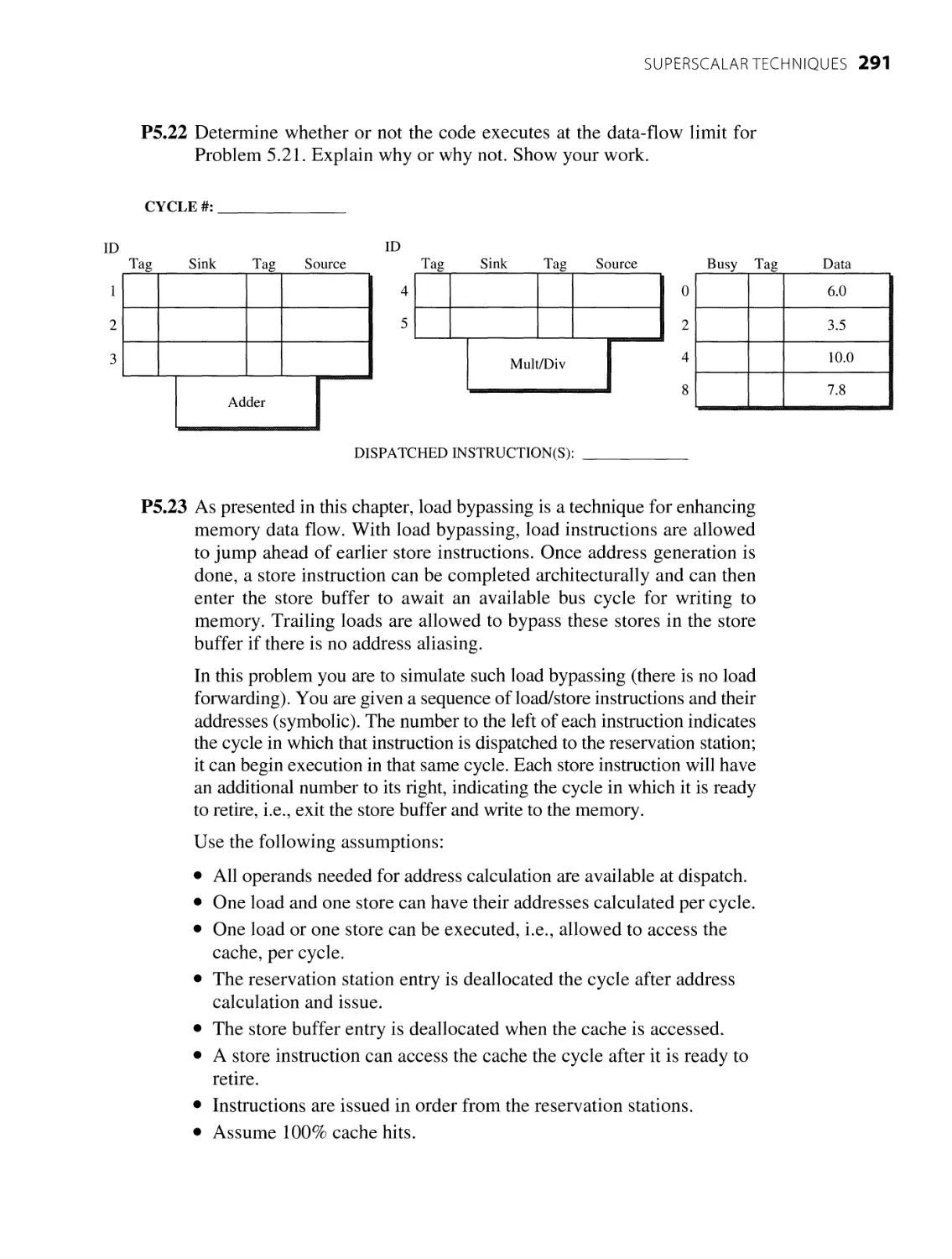
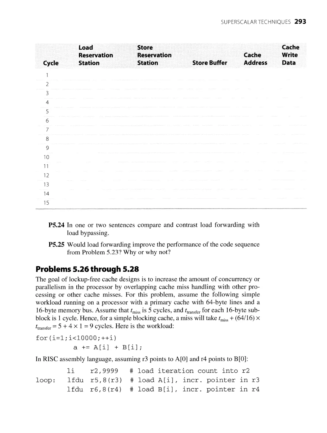
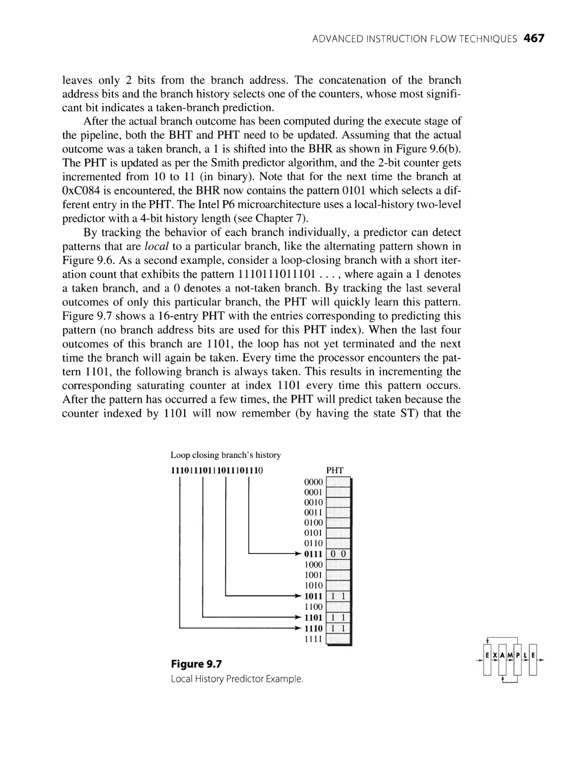
7.2
7.3
262
263
266
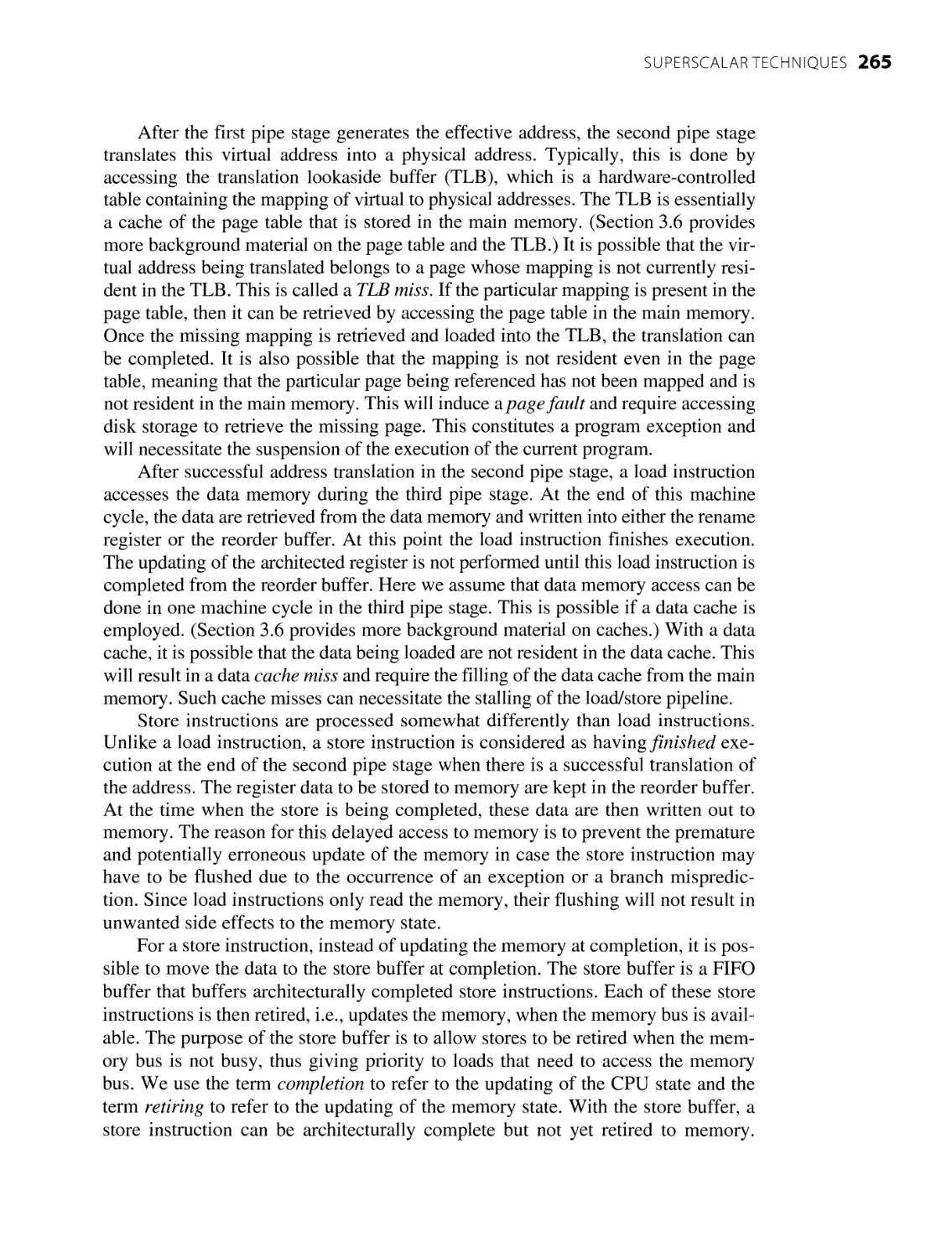
267
273
279
301
302
305
307
307
309
311
6.4.2 Dispatch Stalls
6.4.3 Dispatch Effectiveness
311
311
313
Instruction Execution
316
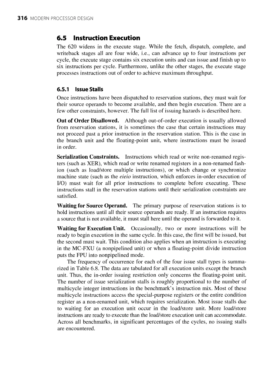
6.5.1 Issue Stalls
316
317
317
6.5.2 Execution Parallelism
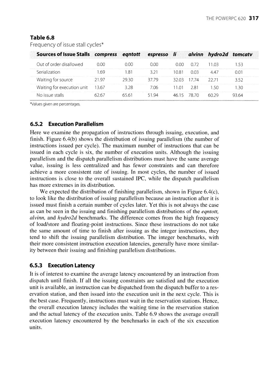
6.5.3 Execution Latency
Instruction Completion
6.6.1 Completion Parallelism
6.6.2 Cache Effects
Conclusions and Observations
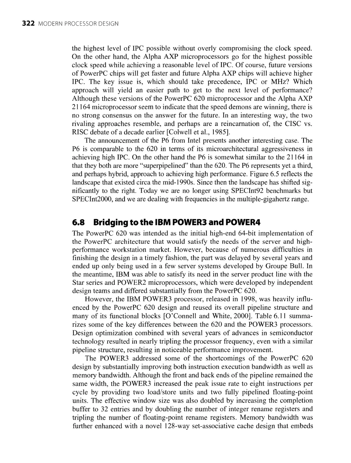
Bridging to the IBM POWER3 and POWER4
Summary
Intel's P6 Microarchitecture
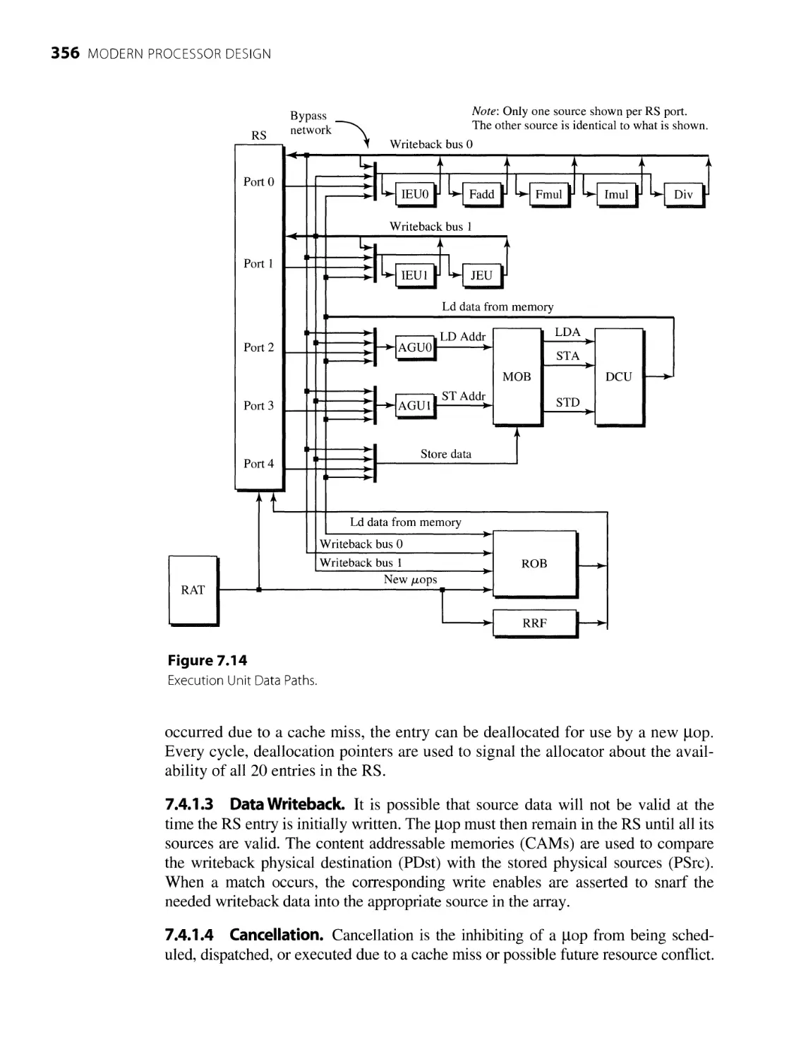
7.1
246
254
256
260
261
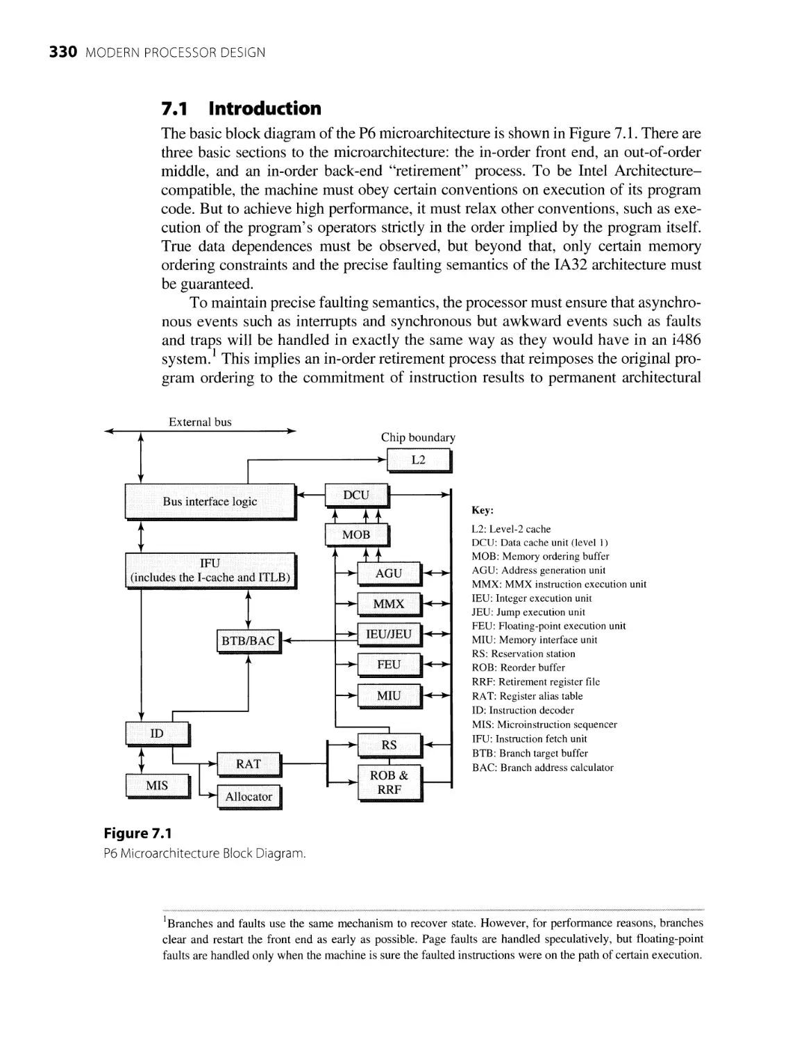
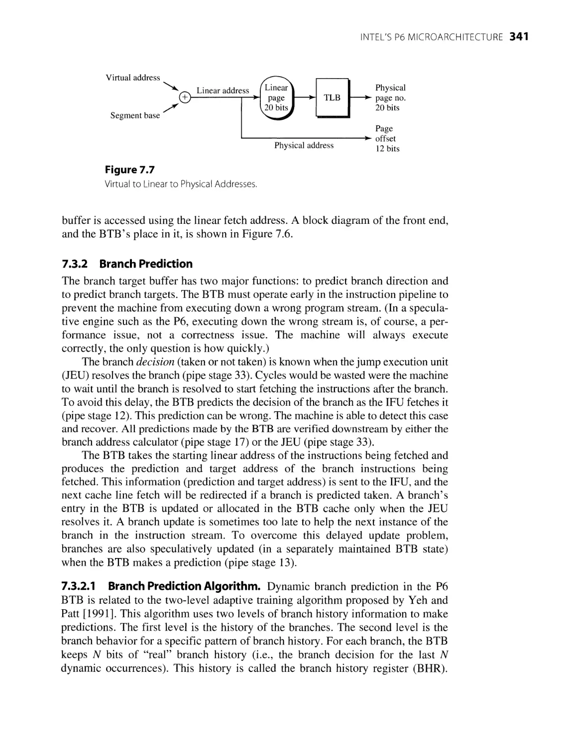
Introduction
7.1.1 Basics of the P6 Microarchitecture
Pipelining
7.2.1 In-Order Front-End Pipeline
7.2.2 Out-of-Order Core Pipeline
7.2.3 Retirement Pipeline
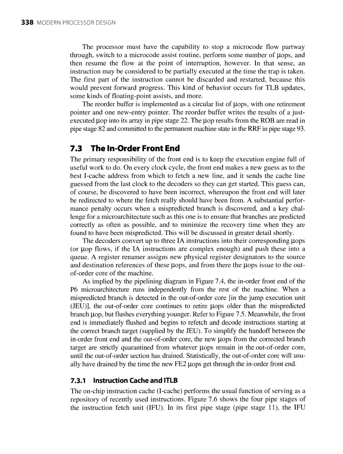
The In-Order Front End
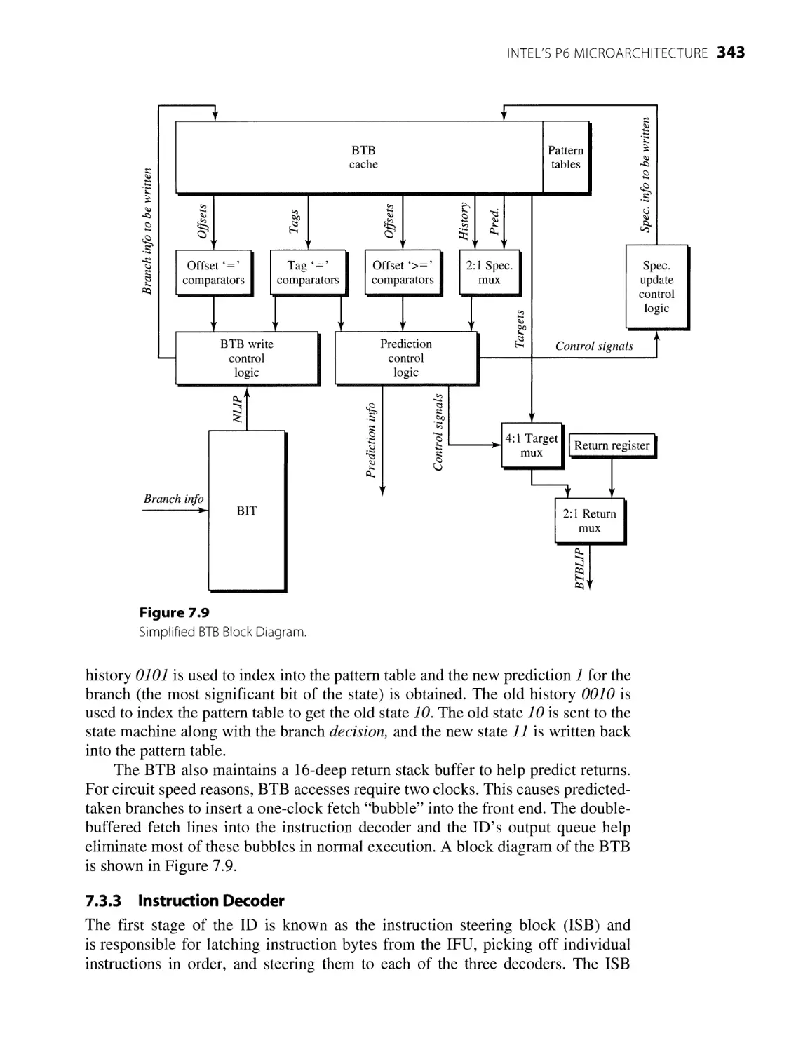
7.3.1 Instruction Cache and ITLB
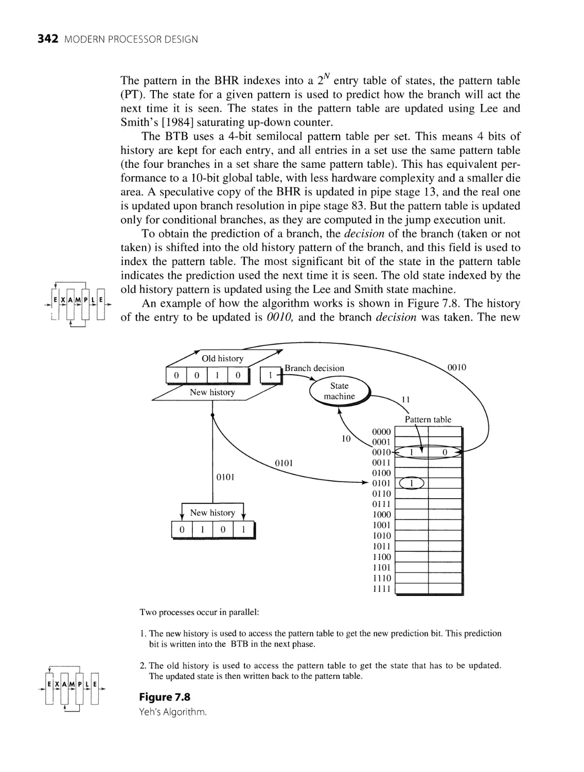
7.3.2 Branch Prediction
7.3.3 Instruction Decoder
7.3.4 Register Alias Table
7.3.5 Allocator
318
318
318
320
322
324
329
330
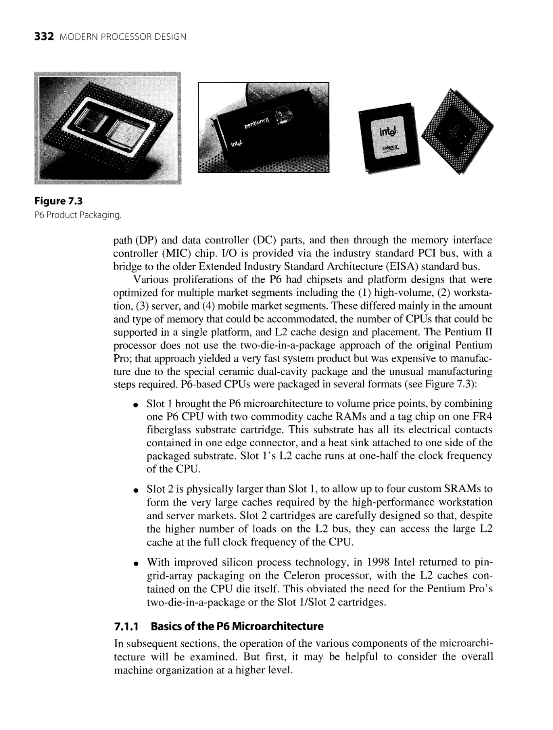
332
334
334
336
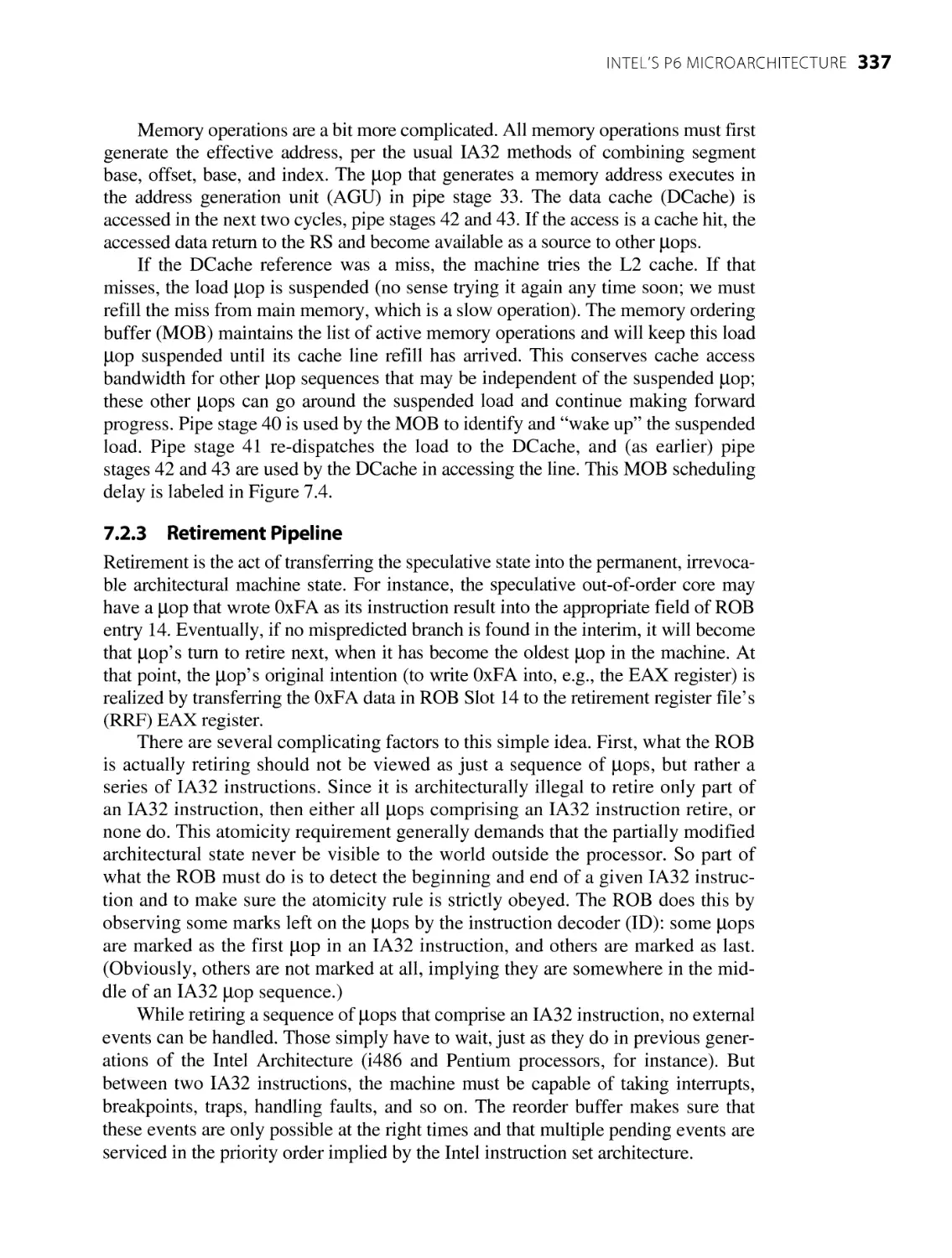
337
338
338
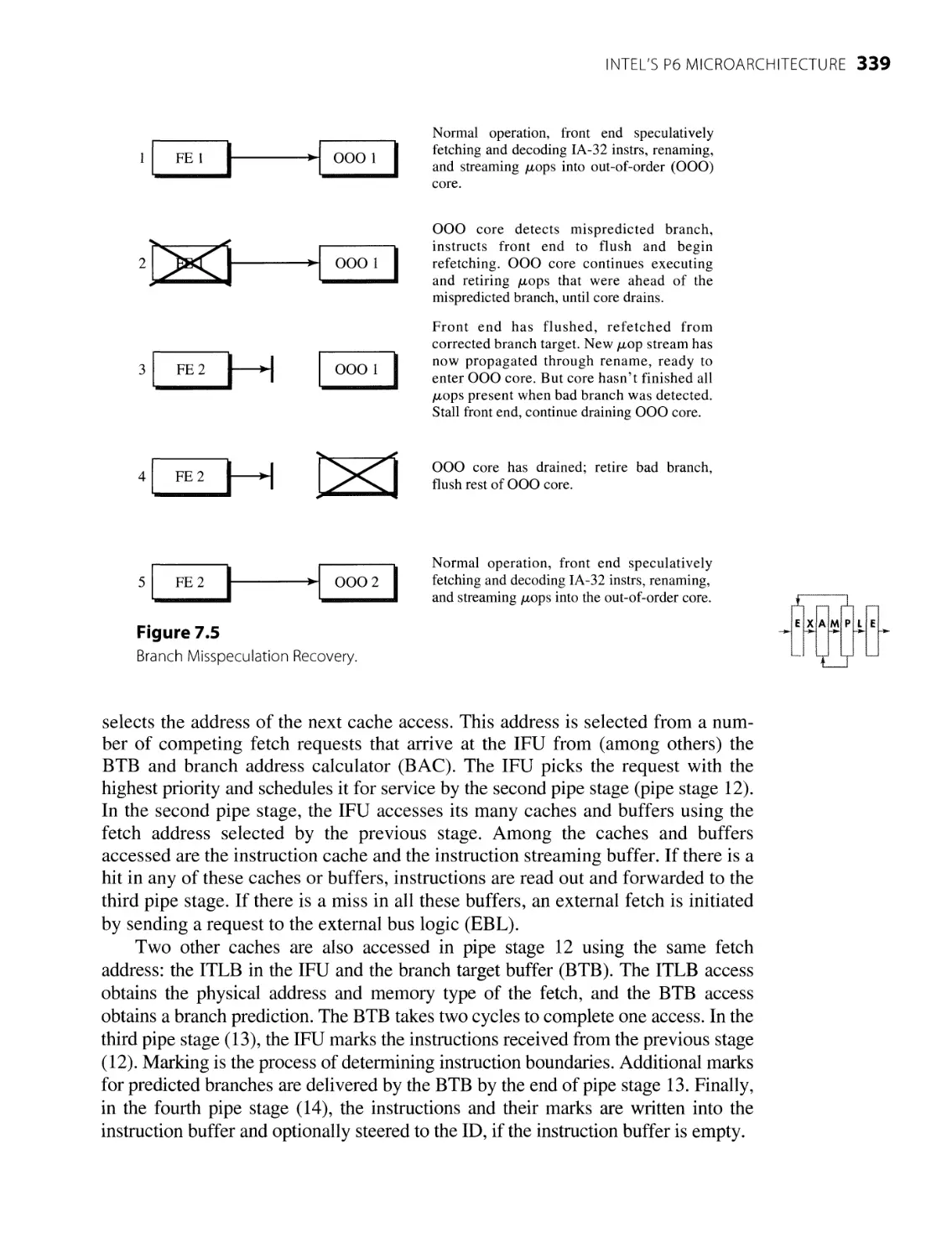
341
343
346
353
V
vi
MODERN PROCESSOR DESIGN
7.4
The Out-of-Order Core
7.4.1
7.5
Retirement
7.5.1
7.6
7.7
7.8
Reservation Station
The Reorder Buffer
7.6.1
7.6.2
7.6.3
7.6.4
7.6.5
362
363
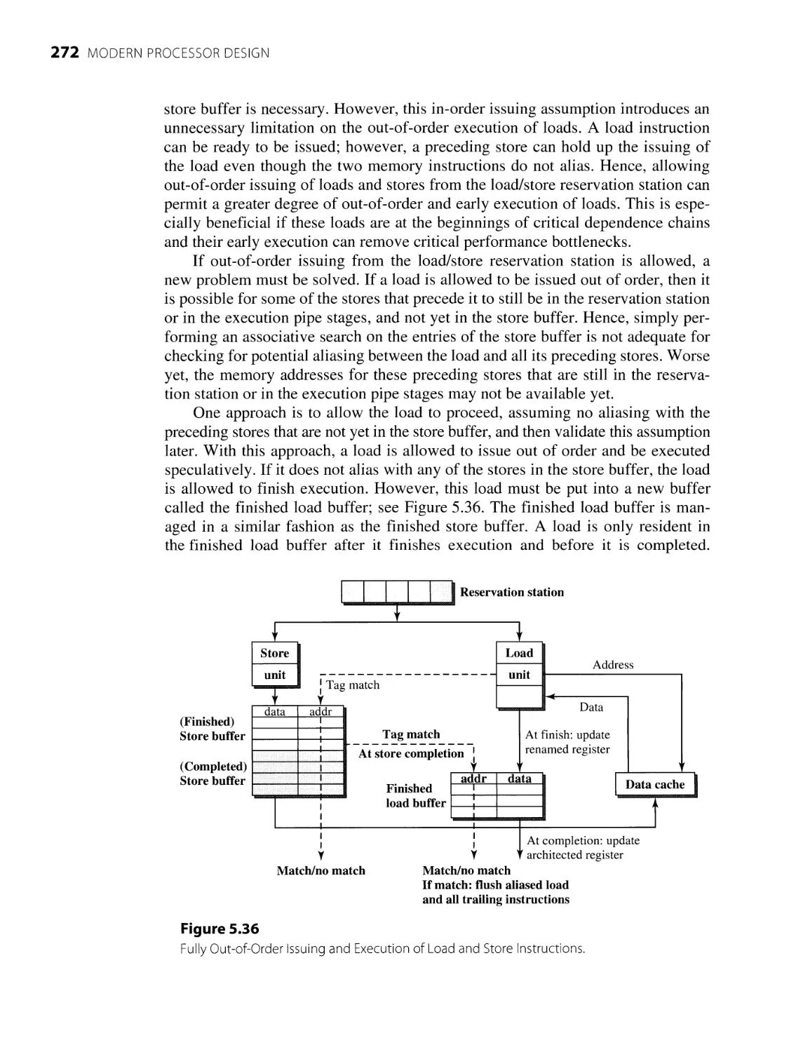
363
363
364
Memory Access Ordering
Load Memory Operations
Basic Store Memory Operations
Deferring Memory Operations
Page Faults
Summary
Acknowledgments
Development of Superscalar Processors
8.1.2
8.1.3
8.1.4
8.1.5
8.1.6
8.1.7
8.1.8
Early Advances in Uniprocessor Parallelism:
The IBM Stretch
First Superscalar Design: The IBM Advanced
Computer System
Instruction-Level Parallelism Studies
By-Products of DAE: The First
Multiple-Decoding Implementations
IBM Cheetah, Panther, and America
Decoupled Microarchitectures
Other Efforts in the 1980s
Wide Acceptance of Superscalar
A Classification of Recent Designs
8.2.1
8.2.2
8.2.3
8.3
357
Memory Subsystem
8.1.1
8.2
355
357
361
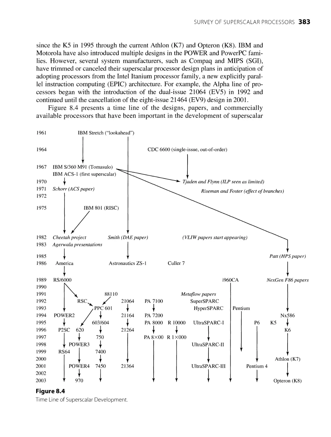
Survey of Superscalar Processors
8.1
355
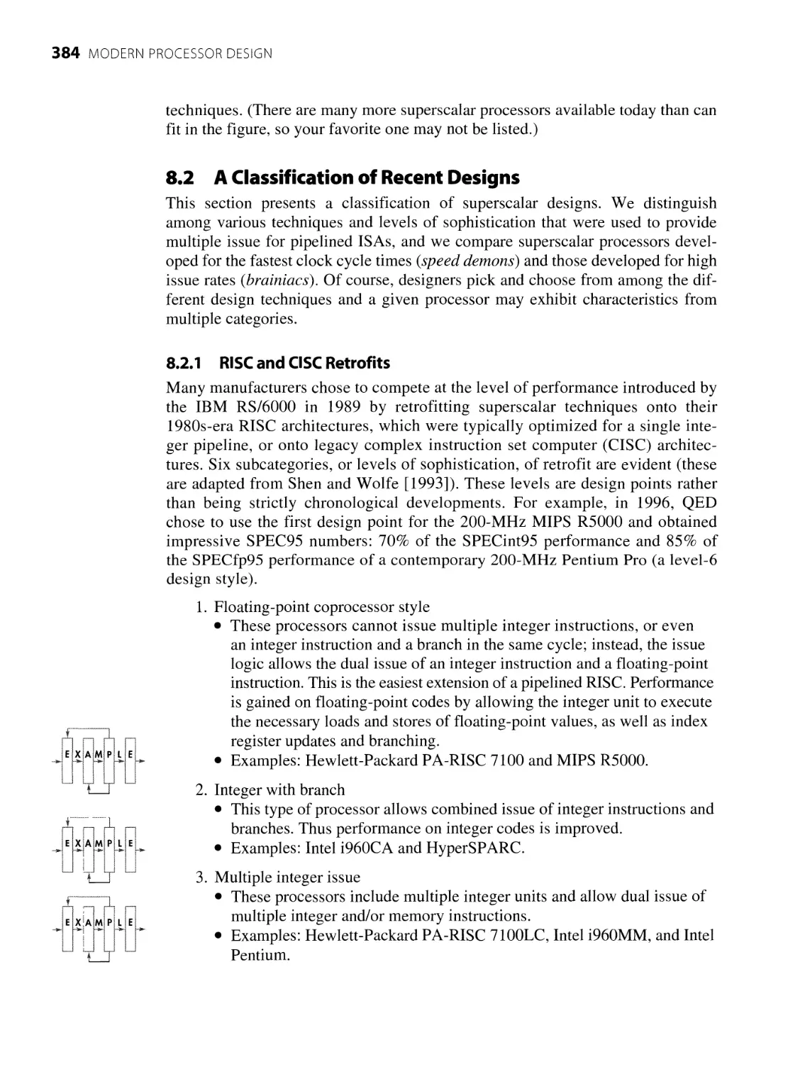
RISC and CISC Retrofits
Speed Demons: Emphasis on Clock Cycle Time
Brainiacs: Emphasis on IPC
364
365
369
369
369
372
377
378
380
380
382
382
384
384
386
386
Processor Descriptions
387
8.3.1
8.3.2
8.3.3
8.3.4
8.3.5
8.3.6
8.3.7
8.3.8
8.3.9
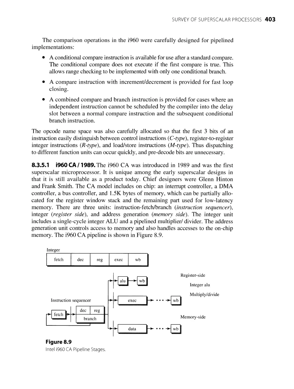
8.3.10
8.3.11
8.3.12
8.3.13
8.3.14
8.3.15
387
392
395
397
402
405
409
417
417
422
424
429
431
432
435
Compaq / DEC Alpha
Hewlett-Packard PA-RISC Version 1.0
Hewlett-Packard PA-RISC Version 2.0
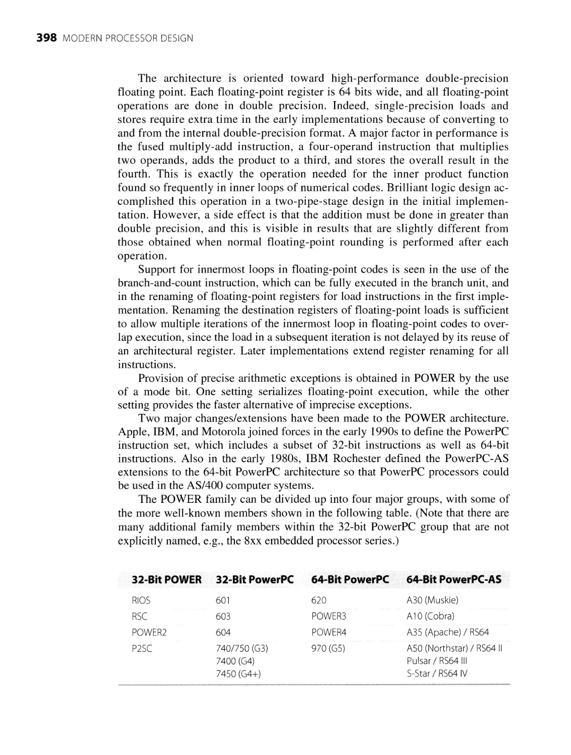
IBM POWER
Intel i960
Intel IA32—Native Approaches
Intel IA32—Decoupled Approaches
x86-64
MIPS
Motorola
PowerPC—32-bit Architecture
PowerPC—64-bit Architecture
PowerPC-AS
SPARC Version 8
SPARC Version 9
TABLE OF CONTENTS vii
8.4 Verification of Superscalar Processors 439
8.5 Acknowledgments 440
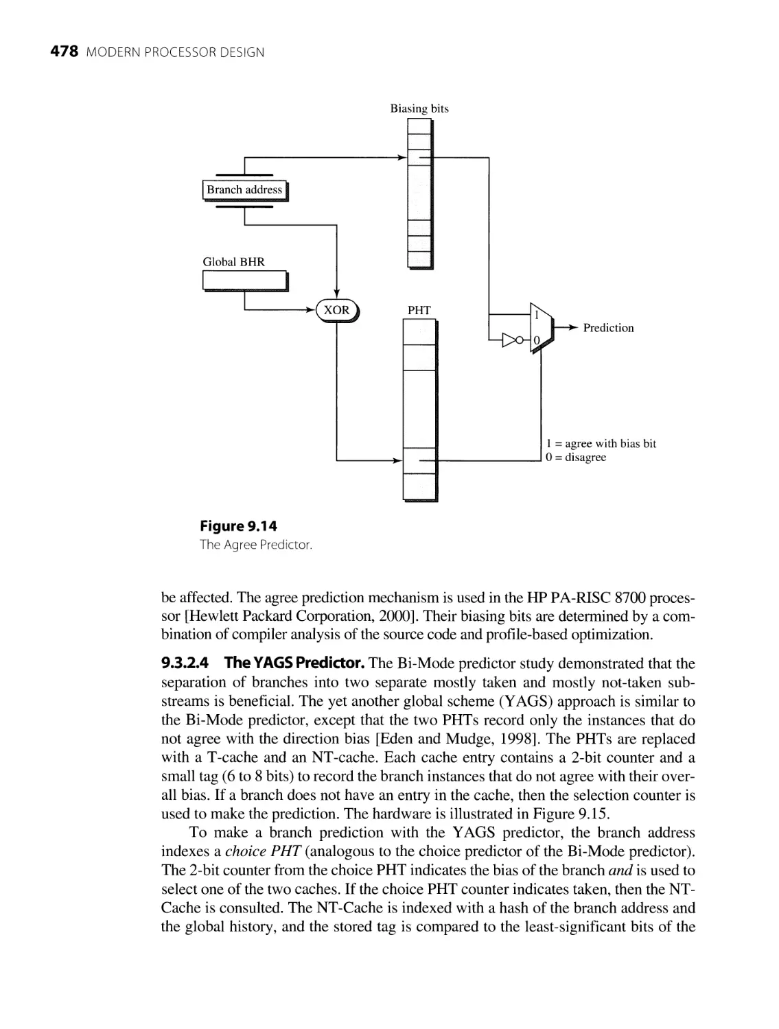
9.1 Introduction 453
9 Advanced Instruction Flow Techniques 453
9.2 Static Branch Prediction Techniques 454
9.2.1 Single-Direction Prediction 455
9.2.2 Backwards Taken/Forwards Not-Taken 456
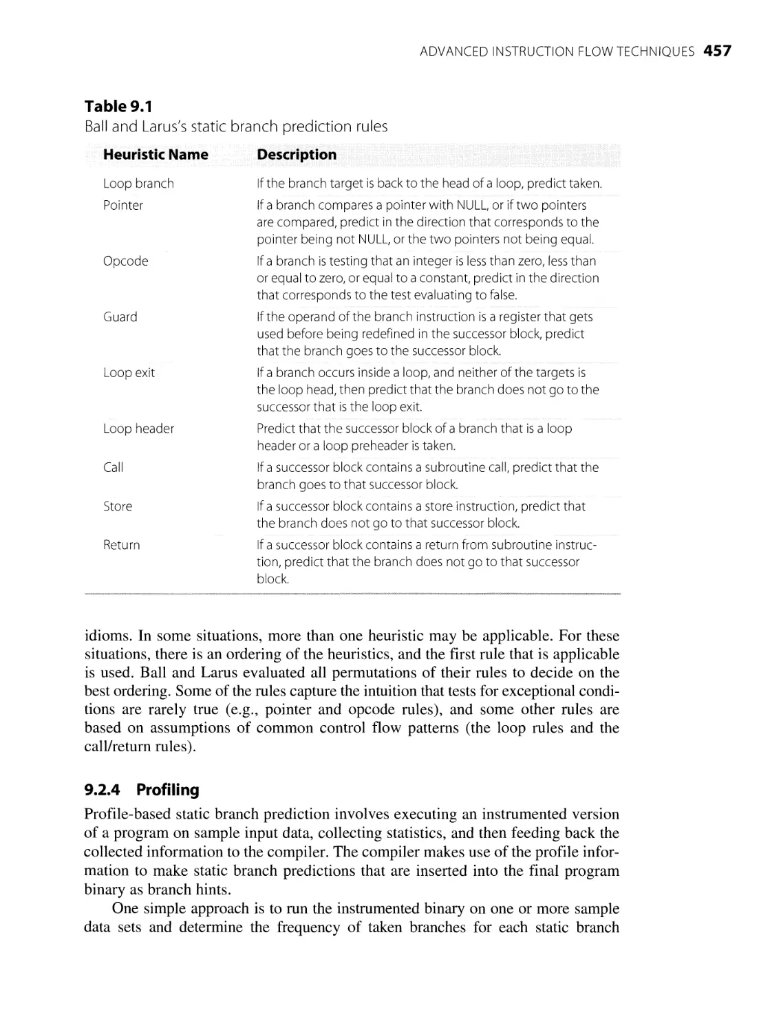
9.2.3 Ball/Larus Heuristics 456
9.2.4
Profiling
457
9.3 Dynamic Branch Prediction Techniques 458
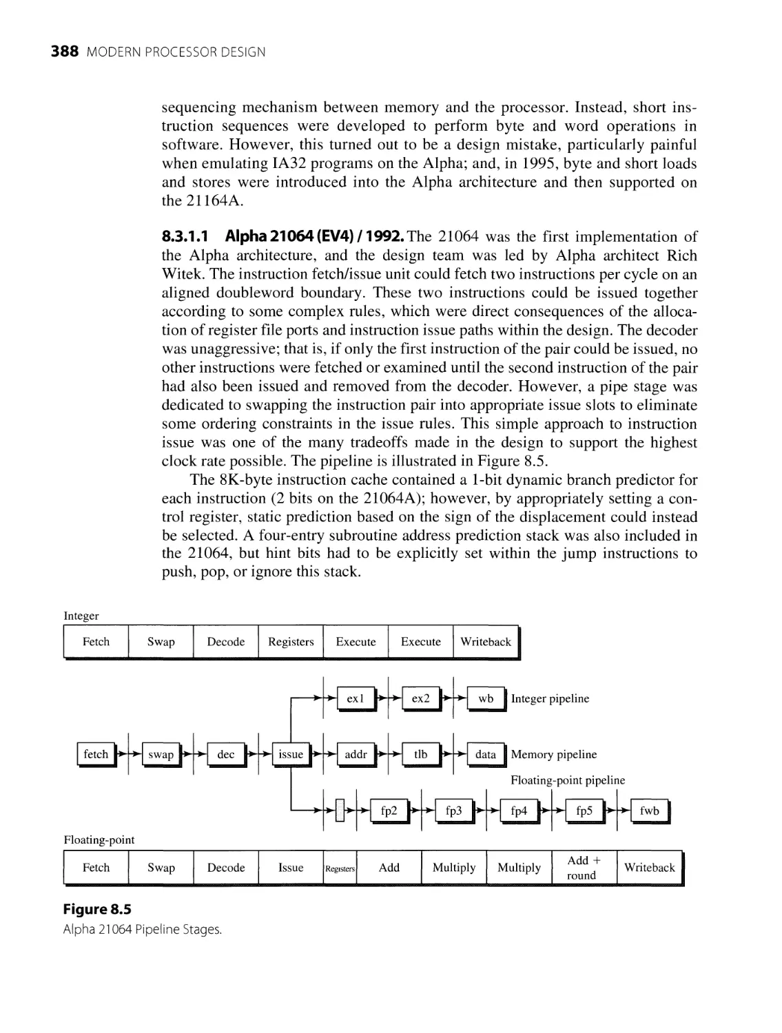
9.3.1 Basic Algorithms 459
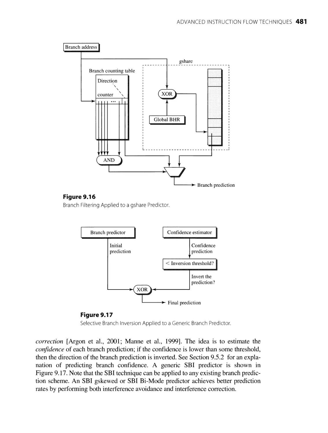
9.3.2 Interference-Reducing Predictors 472
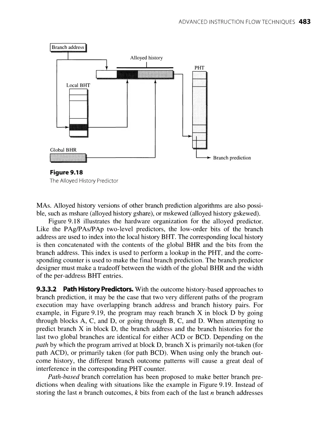
Predicting with Alternative Contexts 482
9.49.3.3
Hybrid
Branch Predictors 491
9.4.1 The Tournament Predictor 491
9.4.2 Static Predictor Selection 493
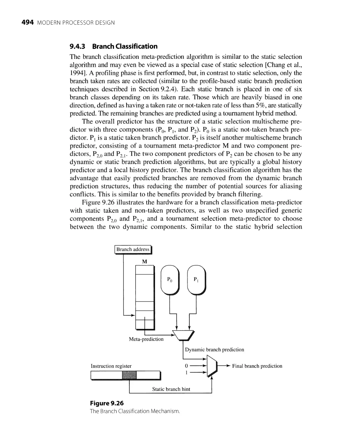
9.4.3 Branch Classification 494
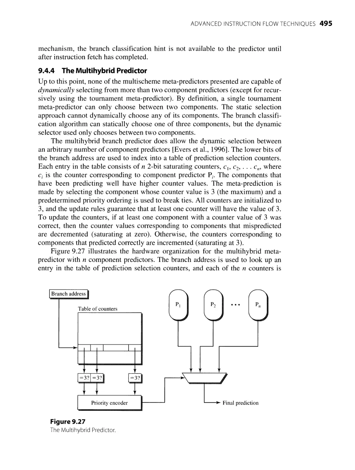
9.4.4
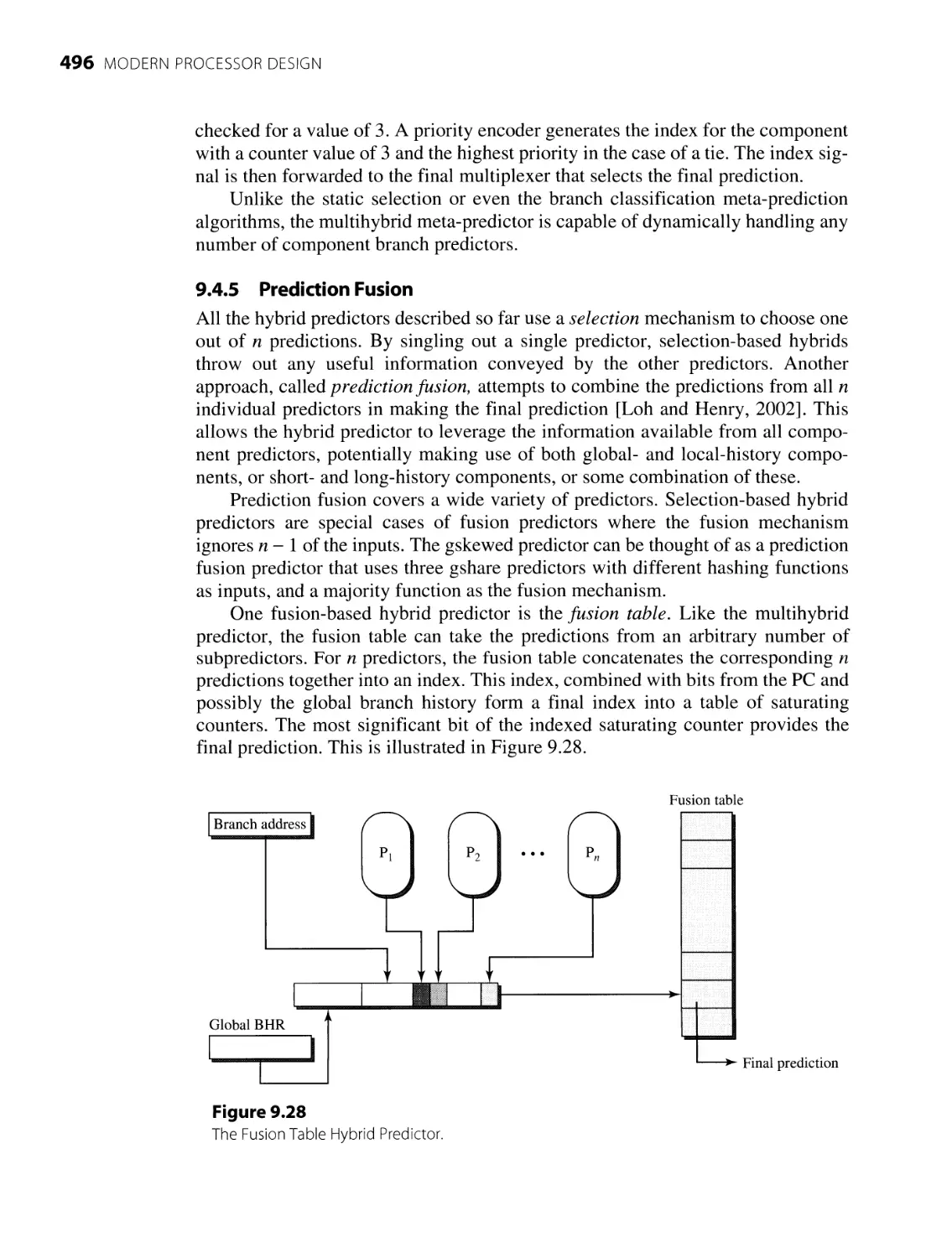
MultihybridFusion
Predictor496
495
9.4.5The
Prediction
9.5 Other Instruction Flow Issues and Techniques 497
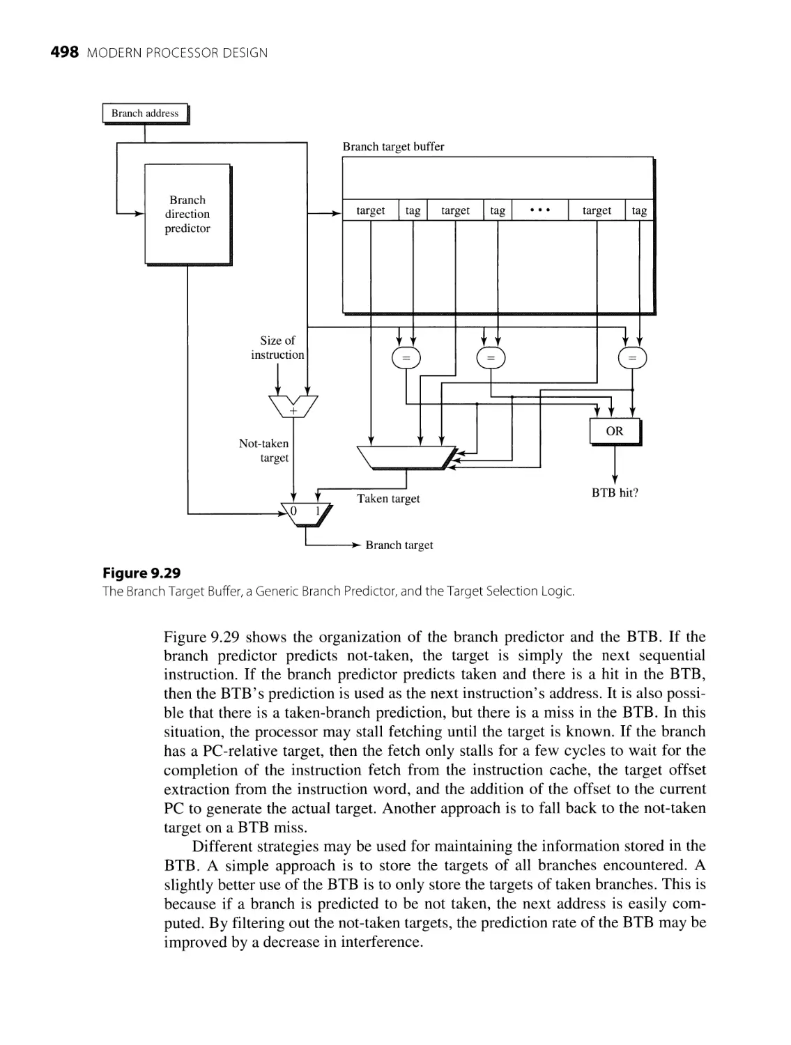
9.5.1 T arget Prediction 497
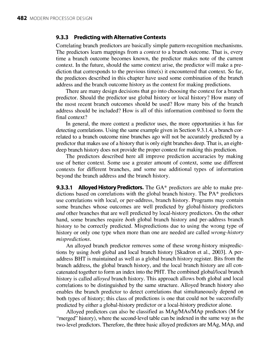
9.5.2 Branch Confidence Prediction 501
9.6 Summary 512
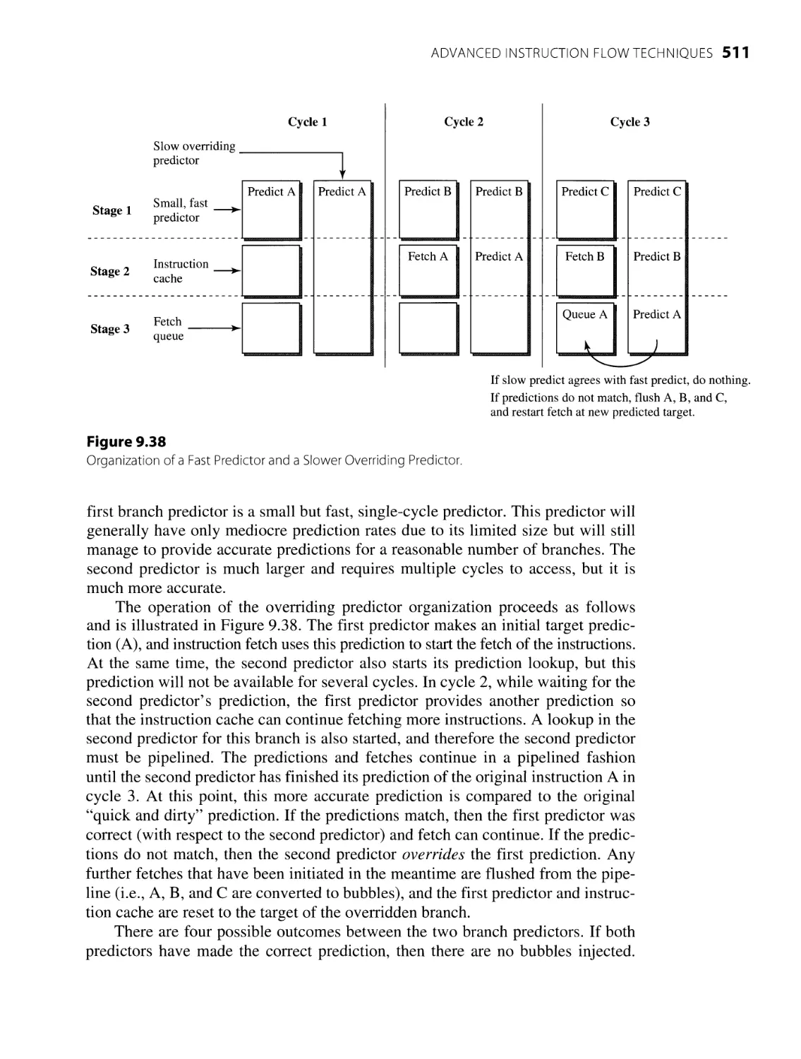
9.5.3 High-Bandwidth Fetch Mechanisms 504
9.5.4 High-Frequency Fetch Mechanisms 509
10.1 Introduction 519
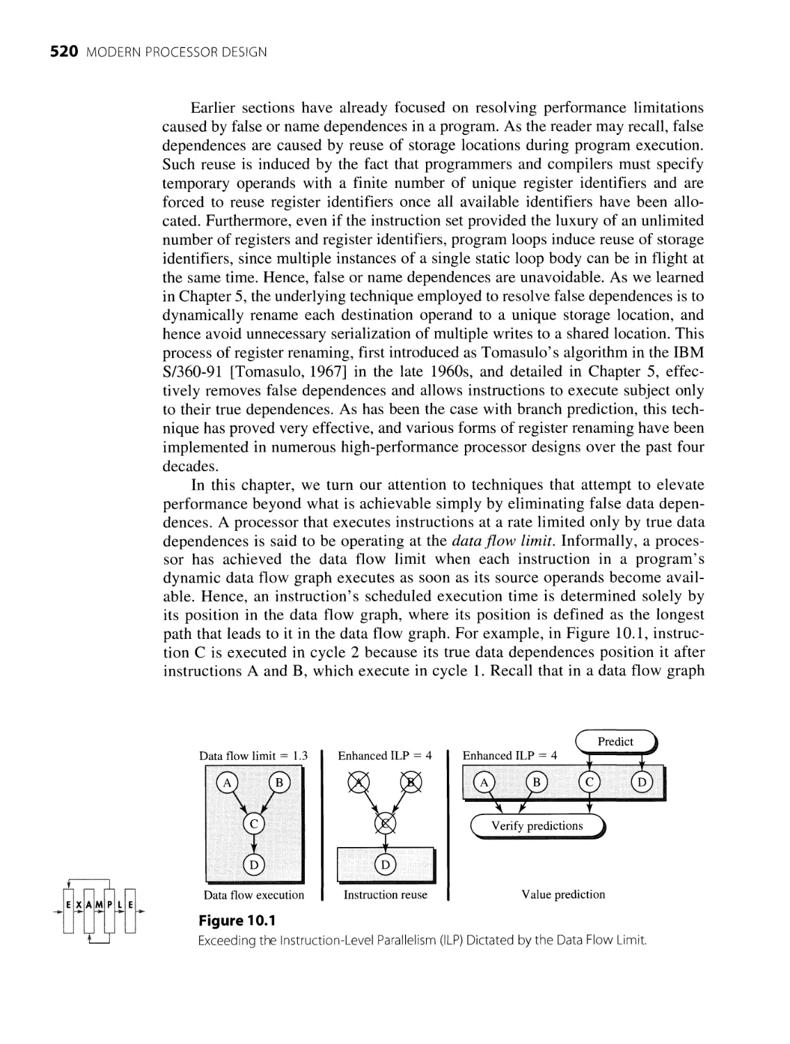
10 Advanced Register Data Flow Techniques 519
10.2 Value Locality and Redundant Execution 523
10.2.1 Causes of Value Locality 523
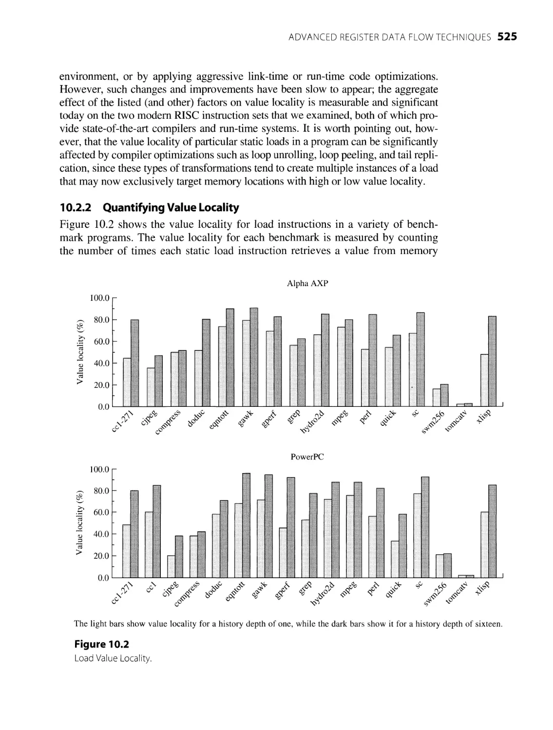
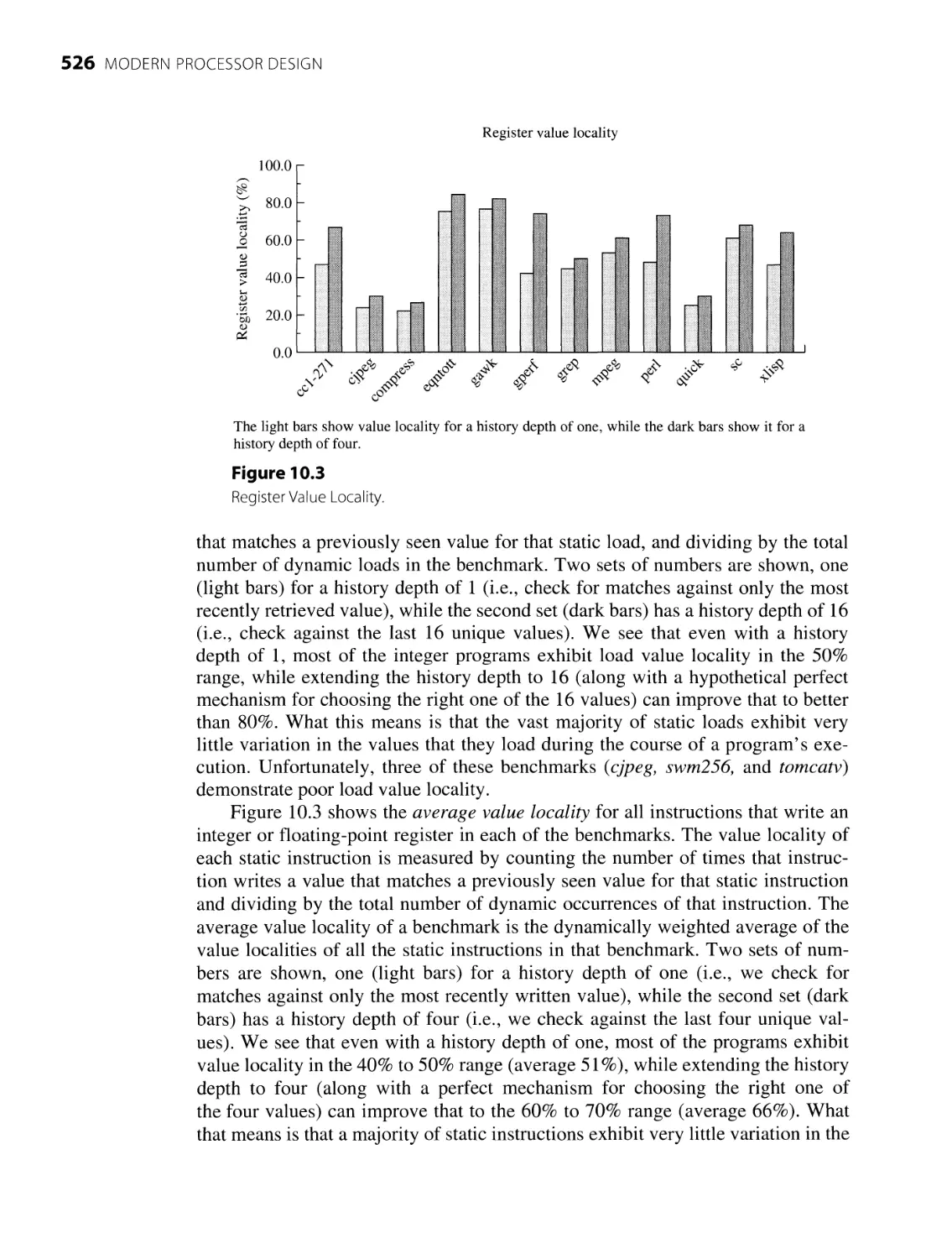
10.2.2 Quantifying Value Locality 525
10.3.1
Memoization 527
10.3.2 Instruction Reuse 529
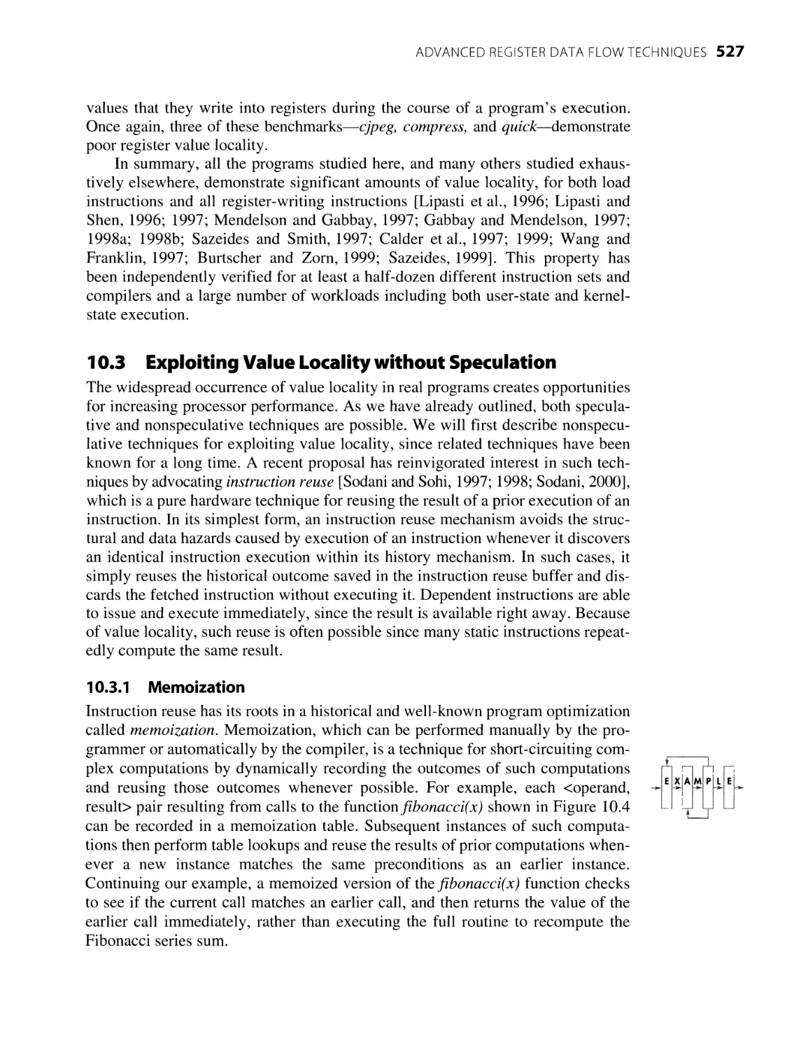
10.3 Exploiting Value Locality without Speculation 527
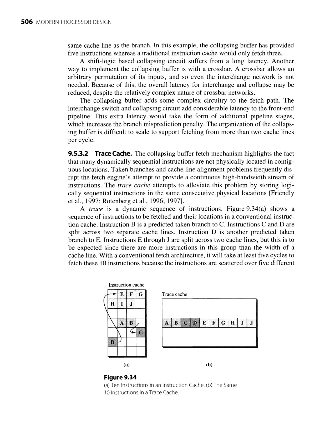
10.3.3 Basic Block and Trace Reuse 533
10.3.4 Data Flow Region Reuse 534
10.3.5 Concluding Remarks 535
10.4 Exploiting Value Locality with Speculation 535
10.4.1 The Weak Dependence Model 535
10.4.2 Value Prediction 536
10.4.3 The Value Prediction Unit 537
10.4.4 Speculative Execution Using Predicted Values 542
10.4.5 Performance of Value Prediction 551
10.4.6Summary
Concluding Remarks
553
10.5
554
VIII
MODERN PROCESSOR DESIGN
Executing Multiple Threads
11.1
11.2
11.3
Introduction
Synchronizing Shared-Memory Threads
Introduction to Multiprocessor Systems
11.3.1
11.3.2
11.3.3
11.3.4
11.3.5
11.3.6
11.3.7
11.3.8
11.4
11.5
11.6
Index
559
562
565
566
567
567
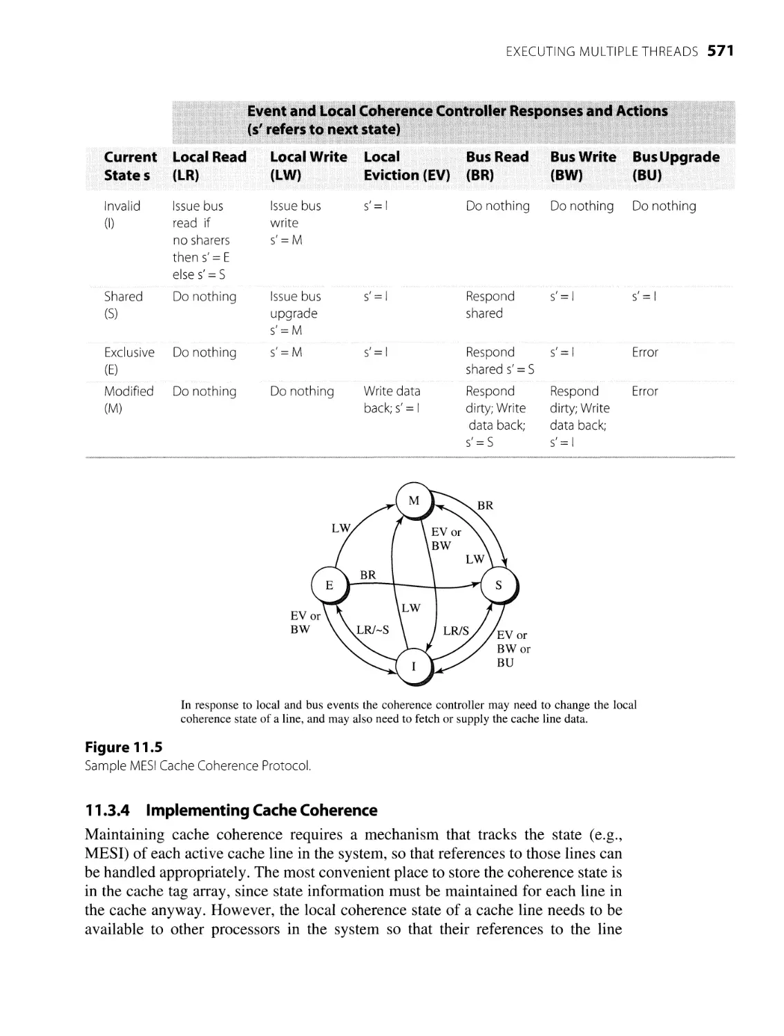
571
574
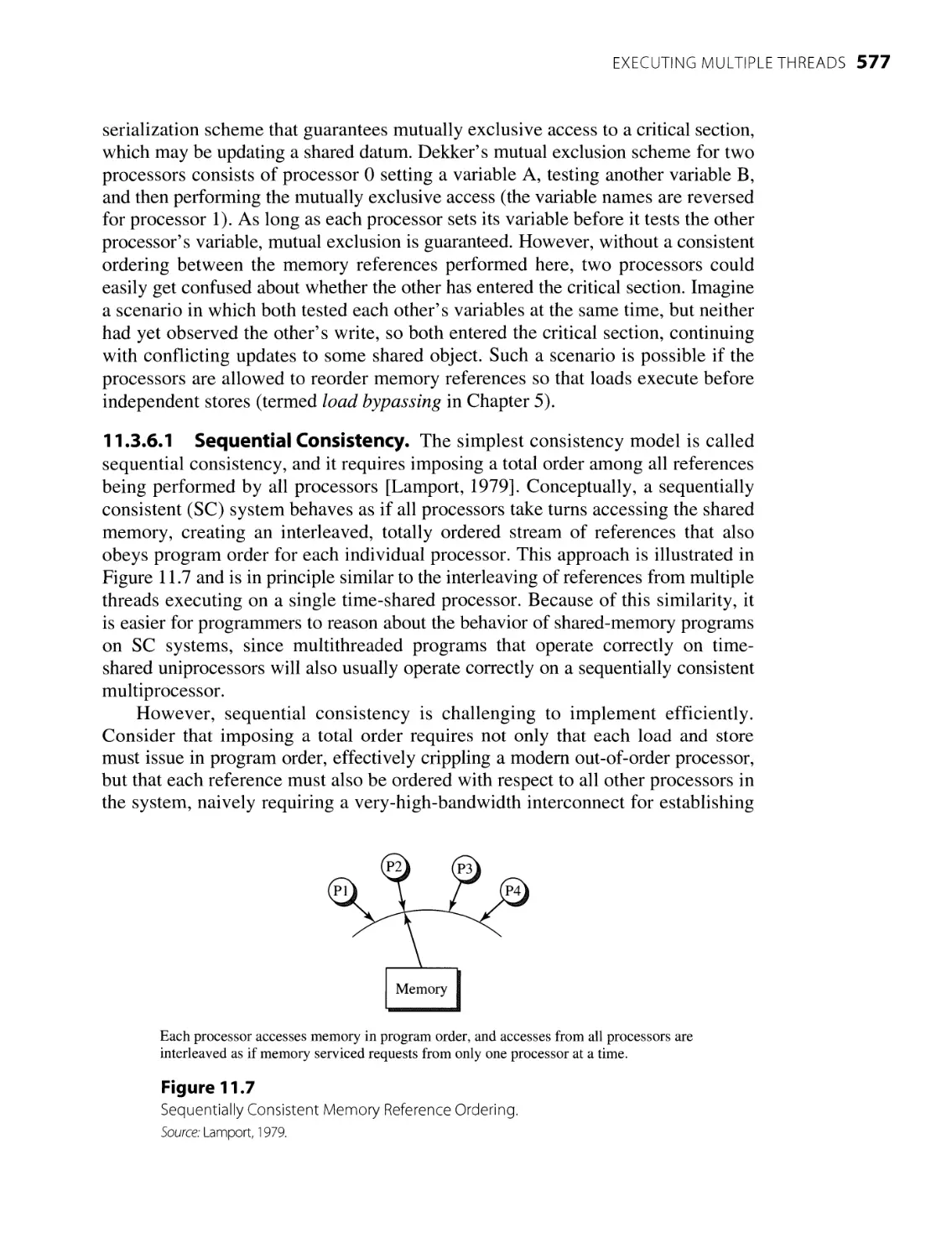
576
581
583
Explicitly Multithreaded Processors
584
11.4.1
11.4.2
11.4.3
11.4.4
584
588
589
592
Chip Multiprocessors
Fine-Grained Multithreading
Coarse-Grained Multithreading
Simultaneous Multithreading
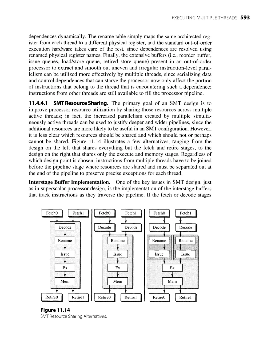
Implicitly Multithreaded Processors
600
11.5.1
11.5.2
11.5.3
11.5.4
601
605
607
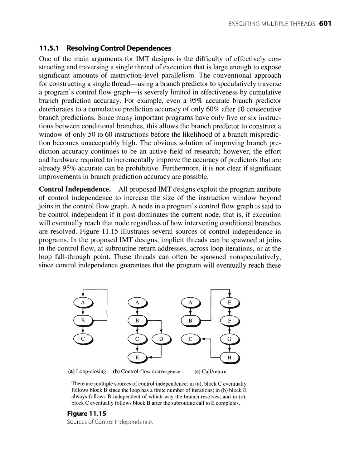
Resolving Control Dependences
Resolving Register Data Dependences
Resolving Memory Data Dependences
Concluding Remarks
Executing the Same Thread
11.6.1
11.6.2
11.6.3
11.6.4
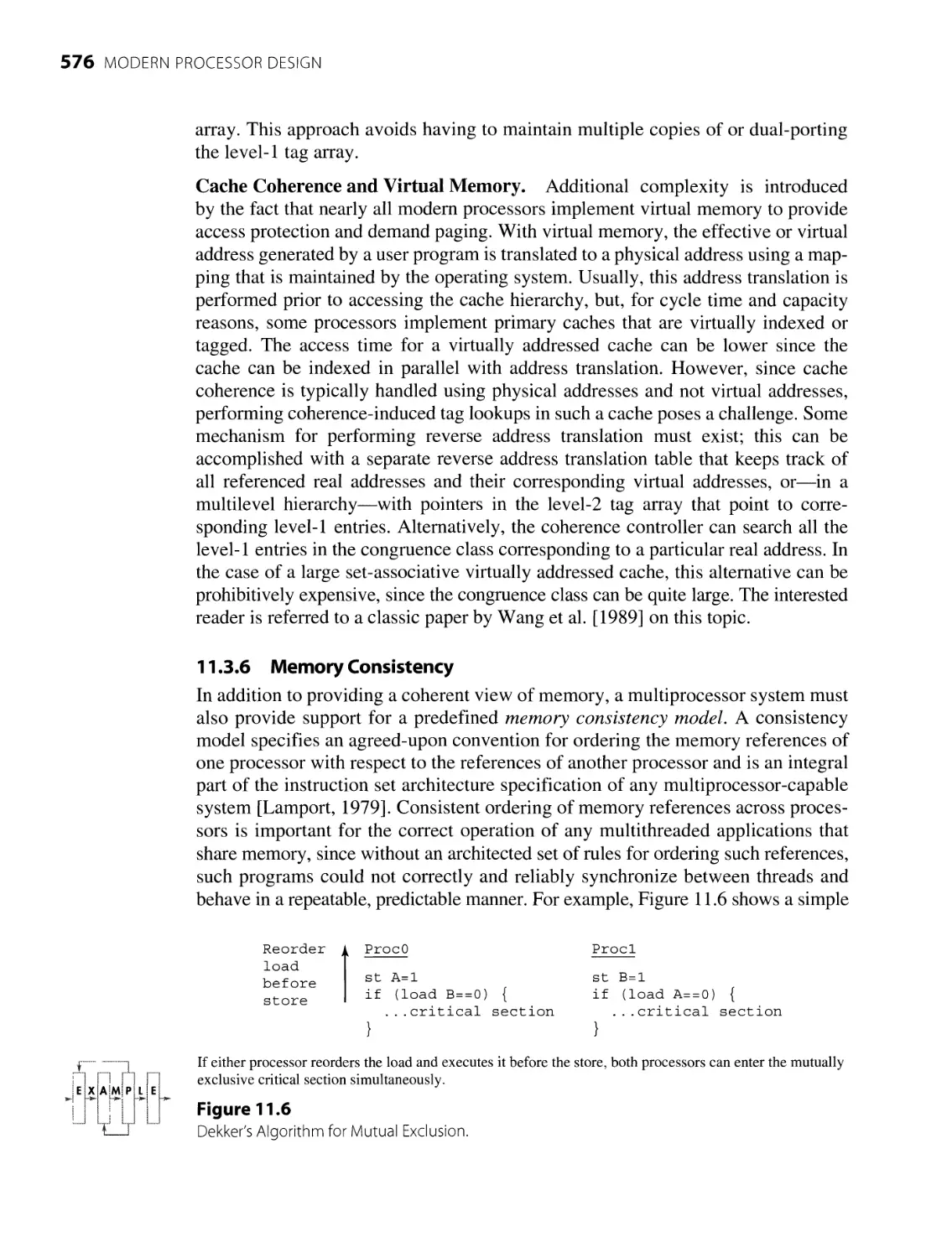
11.7
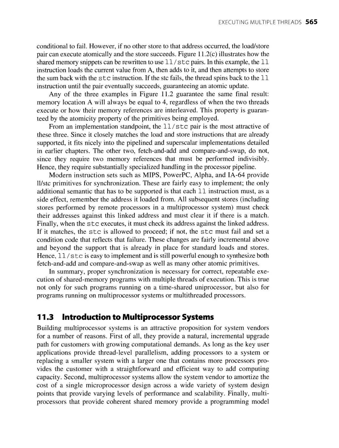
Fully Shared Memory, Unit Latency,
and Lack of Contention
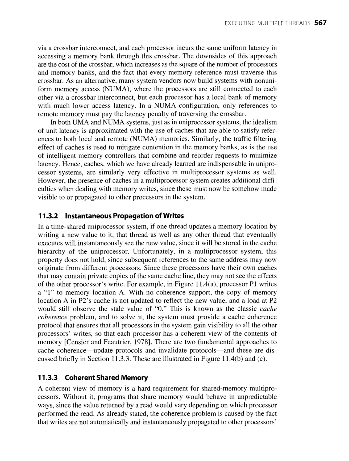
Instantaneous Propagation of Writes
Coherent Shared Memory
Implementing Cache Coherence
Multilevel Caches, Inclusion, and Virtual Memory
Memory Consistency
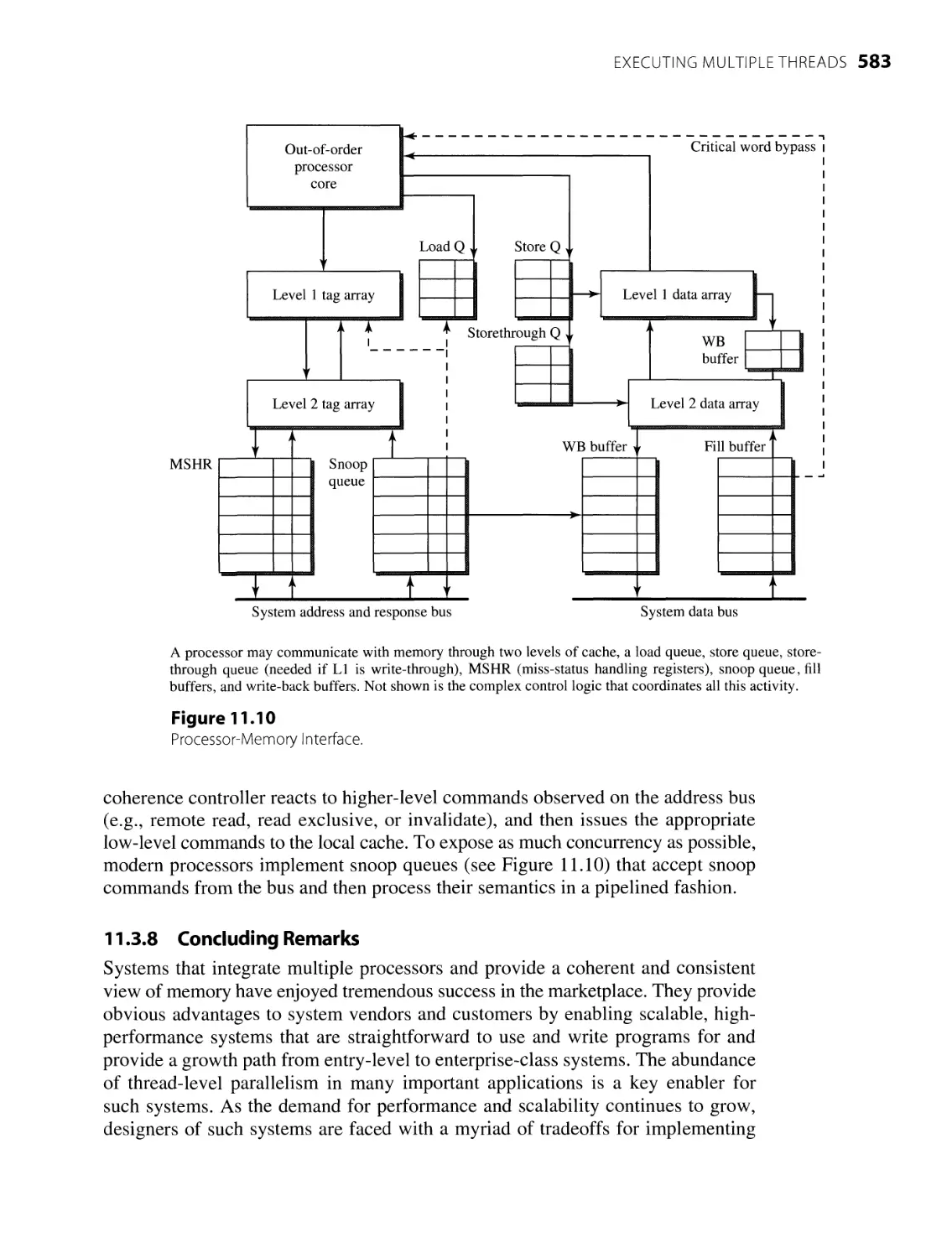
The Coherent Memory Interface
Concluding Remarks
559
Summary
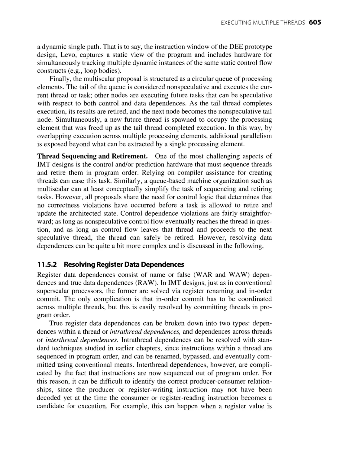
Fault Detection
Prefetching
Branch Resolution
Concluding Remarks
610
610
611
613
614
615
616
623
is the Director of Intel’s Microarchitecture Research
Lab (MRL), providing leadership to about two-dozen
highly skilled researchers located in Santa Clara, CA; Hillsboro, OR; and Austin, TX.
MRL is responsible for developing innovative microarchitecture techniques that can
potentially be used in future microprocessor products from Intel. MRL researchers col¬
laborate closely with microarchitects from product teams in joint advanced-develop¬
ment efforts. MRL frequently hosts visiting faculty and Ph.D. interns and conducts joint
research projects with academic research groups.
Prior to joining Intel in 2000, John was a professor in the electrical and computer
engineering department of Carnegie Mellon University, where he headed up the CMU Microarchitecture
Research Team (CMuART). He has supervised a total of 16 Ph.D. students during his years at CMU.
Seven are currently with Intel, and five have faculty positions in academia. He won multiple teaching
awards at CMU. He was an NSF Presidential Young Investigator. He is an IEEE Fellow and has served
on the program committees of ISC A, MICRO, HPCA, ASPLOS, PACT, ICCD, ITC, and FTCS.
He has published over 100 research papers in diverse areas, including fault-tolerant computing,
built-in self-test, process defect and fault analysis, concurrent error detection, application-specific proces¬
sors, performance evaluation, compilation for instruction-level parallelism, value locality and prediction,
analytical modeling of superscalar processors, systematic microarchitecture test generation, performance
simulator validation, precomputation-based prefetching, database workload analysis, and user-level
helper threads.
John received his M.S. and Ph.D. degrees from the University of Southern California, and his B.S.
degree from the University of Michigan, all in electrical engineering. He attended Kimball High School
in Royal Oak, Michigan. He is happily married and has three daughters. His family enjoys camping, road
trips, and reading The Lord of the Rings.
has been an assistant professor at the University of Wiscon
sin-Madison since 1999, where he is actively pursuing vari¬
ous research topics in the realms of processor, system, and memory architecture. He
has advised a total of 17 graduate students, including two completed Ph.D. theses and
numerous M.S. projects, and has published more than 30 papers in top computer archi¬
tecture conferences and journals. He is most well known for his seminal Ph.D. work in
value prediction. His research program has received in excess of $2 million in support
through multiple grants from the National Science Foundation as well as financial sup¬
port and equipment donations from IBM, Intel, AMD, and Sun Microsystems.
The Eta Kappa Nu Electrical Engineering Honor Society selected Mikko as the country’s Out¬
standing Young Electrical Engineer for 2002. He is also a member of the IEEE and the Tau Beta Pi
engineering honor society. He received his B.S. in computer engineering from Valparaiso University in
1991, and M.S. (1992) and Ph.D. (1997) degrees in electrical and computer engineering from Carnegie
Mellon University. Prior to beginning his academic career, he worked for IBM Corporation in both soft¬
ware and future processor and system performance analysis and design guidance, as well as operating
system kernel implementation. While at IBM he contributed to system and microarchitectural definition
of future IBM server computer systems. He has served on numerous conference and workshop program
committees and is co-organizer of the annual Workshop on Duplicating, Deconstructing, and Debunking
(WDDD). He has filed seven patent applications, six of which are issued U.S. patents; won the Best Paper
Award at MICRO-29; and has received IBM Invention Achievement, Patent Issuance, and Technical
Recognition Awards.
Mikko has been happily married since 1991 and has a nine-year-old daughter and a six-year old
son. In his spare time, he enjoys regular exercise, family bike rides, reading, and volunteering his time
at his local church and on campus as an English-language discussion group leader at the International
Friendship Center.
Preface
This book emerged from the course Superscalar Processor Design, which has been
taught at Carnegie Mellon University since 1995. Superscalar Processor Design is a
mezzanine course targeting seniors and first-year graduate students. Quite a few of
the more aggressive juniors have taken the course in the spring semester of their jun¬
ior year. The prerequisite to this course is the Introduction to Computer Architecture
course. The objectives for the Superscalar Processor Design course include: (1) to
teach modern processor design skills at the microarchitecture level of abstraction;
(2) to cover current microarchitecture techniques for achieving high performance via
the exploitation of instruction-level parallelism (ILP); and (3) to impart insights and
hands-on experience for the effective design of contemporary high-performance
microprocessors for mobile, desktop, and server markets. In addition to covering the
contents of this book, the course contains a project component that involves the
microarchitectural design of a future-generation superscalar microprocessor.
During the decade of the 1990s many microarchitectural techniques for increas¬
ing clock frequency and harvesting more ILP to achieve better processor perfor¬
mance have been proposed and implemented in real machines. This book is an
attempt to codify this large body of knowledge in a systematic way. These techniques
include deep pipelining, aggressive branch prediction, dynamic register renaming,
multiple instruction dispatching and issuing, out-of-order execution, and speculative
load/store processing. Hundreds of research papers have been published since the
early 1990s, and many of the research ideas have become reality in commercial
superscalar microprocessors. In this book, the numerous techniques are organized
and presented within a clear framework that facilitates ease of comprehension. The
foundational principles that underlie the plethora of techniques are highlighted.
While the contents of this book would generally be viewed as graduate-level
material, the book is intentionally written in a way that would be very accessible to
undergraduate students. Significant effort has been spent in making seemingly
complex techniques to appear as quite straightforward through appropriate abstrac¬
tion and hiding of details. The priority is to convey clearly the key concepts and
fundamental principles, giving just enough details to ensure understanding of im¬
plementation issues without massive dumping of information and quantitative data.
The hope is that this body of knowledge can become widely possessed by not just
microarchitects and processor designers but by most B.S. and M.S. students with
interests in computer systems and microprocessor design.
Here is a brief summary of the chapters.
Chapter 1: Processor Design
This chapter introduces the art of processor design, the instruction set architecture
(ISA) as the specification of the processor, and the microarchitecture as the imple¬
mentation of the processor. The dynamic/static interface that separates compile-time
PREFACE Xi
software and run-time hardware is defined and discussed. The goal of this chapter
is not to revisit in depth the traditional issues regarding ISA design, but to erect the
proper framework for understanding modern processor design.
Chapter 2: Pipelined Processors
This chapter focuses on the concept of pipelining, discusses instruction pipeline
design, and presents the performance benefits of pipelining. Pipelining is usually in¬
troduced in the first computer architecture course. Pipelining provides the foundation
for modem superscalar techniques and is presented in this chapter in a fresh and
unique way. We intentionally avoid the massive dumping of bar charts and graphs;
instead, we focus on distilling the foundational principles of instmction pipelining.
Chapter 3: Memory and I/O Systems
This chapter provides a larger context for the remainder of the book by including a
thorough grounding in the principles and mechanisms of modern memory and I/O
systems. Topics covered include memory hierarchies, caching, main memory de¬
sign, virtual memory architecture, common input/output devices, processor-I/O in¬
teraction, and bus design and organization.
Chapter 4: Superscalar Organization
This chapter introduces the main concepts and the overall organization of superscalar
processors. It provides a “big picture” view for the reader that leads smoothly into the
detailed discussions in the next chapters on specific superscalar techniques for achiev¬
ing performance. This chapter highlights only the key features of superscalar processor
organizations. Chapter 7 provides a detailed survey of features found in real machines.
Chapter 5: Superscalar Techniques
This chapter is the heart of this book and presents all the major microarchitecture tech¬
niques for designing contemporary superscalar processors for achieving high perfor¬
mance. It classifies and presents specific techniques for enhancing instruction flow,
register data flow, and memory data flow. This chapter attempts to organize a plethora
of techniques into a systematic framework that facilitates ease of comprehension.
Chapter 6: The PowerPC 620
This chapter presents a detailed analysis of the PowerPC 620 microarchitecture and
uses it as a case study to examine many of the issues and design tradeoffs intro¬
duced in the previous chapters. This chapter contains extensive performance data
of an aggressive out-of-order design.
Chapter 7: Intel's P6 Microarchitecture
This is a case study chapter on probably the most commercially successful contempo¬
rary superscalar microarchitecture. It is written by the Intel P6 design team led by Bob
Colwell and presents in depth the P6 microarchitecture that facilitated the implemen¬
tation of the Pentium Pro, Pentium II, and Pentium III microprocessors. This chapter
offers the readers an opportunity to peek into the mindset of a top-notch design team.
xii
MODERN PROCESSOR DESIGN
Chapter 8: Survey of Superscalar Processors
This chapter, compiled by Prof. Mark Smotherman of Clemson University, pro¬
vides a historical chronicle on the development of superscalar machines and a
survey of existing superscalar microprocessors. The chapter was first completed in
1998 and has been continuously revised and updated since then. It contains fasci¬
nating information that can’t be found elsewhere.
Chapter 9: Advanced Instruction Flow Techniques
This chapter provides a thorough overview of issues related to high-performance
instruction fetching. The topics covered include historical, currently used, and pro¬
posed advanced future techniques for branch prediction, as well as high-bandwidth
and high-frequency fetch architectures like trace caches. Though not all such tech¬
niques have yet been adopted in real machines, future designs are likely to incorpo¬
rate at least some form of them.
Chapter 10: Advanced Register Data Flow Techniques
This chapter highlights emerging microarchitectural techniques for increasing per¬
formance by exploiting the program characteristic of value locality. This program
characteristic was discovered recently, and techniques ranging from software
memoization, instruction reuse, and various forms of value prediction are described
in this chapter. Though such techniques have not yet been adopted in real machines,
future designs are likely to incorporate at least some form of them.
Chapter 11: Executing Multiple Threads
This chapter provides an introduction to thread-level parallelism (TLP), and pro¬
vides a basic introduction to multiprocessing, cache coherence, and high-perfor¬
mance implementations that guarantee either sequential or relaxed memory
ordering across multiple processors. It discusses single-chip techniques like multi¬
threading and on-chip multiprocessing that also exploit thread-level parallelism.
Finally, it visits two emerging technologies—implicit multithreading and
preexecution—that attempt to extract thread-level parallelism automatically from
single-threaded programs.
In summary, Chapters 1 through 5 cover fundamental concepts and foundation¬
al techniques. Chapters 6 through 8 present case studies and an extensive survey of
actual commercial superscalar processors. Chapter 9 provides a thorough overview
of advanced instruction flow techniques, including recent developments in ad¬
vanced branch predictors. Chapters 10 and 11 should be viewed as advanced topics
chapters that highlight some emerging techniques and provide an introduction to
multiprocessor systems.
This is the first edition of the book. An earlier beta edition was published in 2002
with the intent of collecting feedback to help shape and hone the contents and presen¬
tation of this first edition. Through the course of the development of the book, a large
set of homework and exam problems have been created. A subset of these problems
are included at the end of each chapter. Several problems suggest the use of the
PREFACE Xiii
Simplescalar simulation suite available from the Simplescalar website at http://www
.simplescalar.com. A companion website for the book contains additional support mate¬
rial for the instructor, including a complete set of lecture slides (www.mhhe.com/shen).
Acknowledgments
Many people have generously contributed their time, energy, and support toward
the completion of this book. In particular, we are grateful to Bob Colwell, who is
the lead author of Chapter 7, Intel’s P6 Microarchitecture. We also acknowledge
his coauthors, Dave Papworth, Glenn Hinton, Mike Fetterman, and Andy Glew,
who were all key members of the historic P6 team. This chapter helps ground this
textbook in practical, real-world considerations. We are also grateful to Professor
Mark Smotherman of Clemson University, who meticulously compiled and au¬
thored Chapter 8, Survey of Superscalar Processors. This chapter documents the rich
and varied history of superscalar processor design over the last 40 years. The guest
authors of these two chapters added a certain radiance to this textbook that we could
not possibly have produced on our own. The PowerPC 620 case study in Chapter 6
is based on Trung Diep’s Ph.D. thesis at Carnegie Mellon University. Finally, the
thorough survey of advanced instruction flow techniques in Chapter 9 was authored
by Gabriel Loh, largely based on his Ph.D. thesis at Yale University.
In addition, we want to thank the following professors for their detailed, in¬
sightful, and thorough review of the original manuscript. The inputs from these
reviews have significantly improved the first edition of this book.
David Andrews, University of Arkansas
• Walid Najjar, University of California
Angelos Bilas, University of Toronto
Fred H. Carlin, University of California at
Riverside
• Vojin G. Oklabdzija, University of California
at Davis
• Soner Onder, Michigan Technological
Santa Barbara
Yinong Chen, Arizona State University
Lynn Choi, University of California at Irvine
Dan Connors, University of Colorado
Karel Driesen, McGill University
Alan D. George, University of Florida
Arthur Glaser, New Jersey Institute of
Technology
Rajiv Gupta, University of Arizona
Vincent Hayward, McGill University
James Hoe, Carnegie Mellon University
Lizy Kurian John, University of Texas at Austin
Peter M. Kogge, University of Notre Dame
Angkul Kongmunvattana, University of
Nevada at Reno
Israel Koren, University of Massachusetts at
Amherst
Ben Lee, Oregon State University
Francis Leung, Illinois Institute of Technology
University
• Parimal Patel, University of Texas at San
Antonio
• Jih-Kwon Peir, University of Florida
• Gregory D. Peterson, University of
Tennessee
• Amir Roth, University of Pennsylvania
• Kevin Skadron, University of Virginia
• Mark Smotherman, Clemson University
• Miroslav N. Velev, Georgia Institute of
Technology
• Bin Wei, Rutgers University
• Anthony S. Wojcik, Michigan State University
• Ali Zaringhalam, Stevens Institute of
Technology
• Xiaobo Zhou, University of Colorado at
Colorado Springs
PROCESSOR DESIGN
This book grew out of the course Superscalar Processor Design at Carnegie Mellon
University. This course has been taught at CMU since 1995. Many teaching assis¬
tants of this course have left their indelible touch in the contents of this book. They
include Bryan Black, Scott Cape, Yuan Chou, Alex Dean, Trung Diep, John Faistl,
Andrew Huang, Deepak Limaye, Chris Nelson, Chris Newburn, Derek Noonburg,
Kyle Oppenheim, Ryan Rakvic, and Bob Rychlik. Hundreds of students have taken
this course at CMU; many of them provided inputs that also helped shape this book.
Since 2000, Professor James Hoe at CMU has taken this course even further. We
both are indebted to the nurturing we experienced while at CMU, and we hope that
this book will help perpetuate CMU’s historical reputation of producing some of
the best computer architects and processor designers.
A draft version of this textbook has also been used at the University of
Wisconsin since 2000. Some of the problems at the end of each chapter were actu¬
ally contributed by students at the University of Wisconsin. We appreciate their test
driving of this book.
John Paul Shen, Director,
Microarchitecture Research, Intel Labs, Adjunct Professor,
ECE Department, Carnegie Mellon University
Mikko H. Lipasti, Assistant Professor,
ECE Department, University of Wisconsin
June 2004
Soli Deo Gloria
CHAPTER
1
Processor Design
CHAPTER OUTLINE
1.1 The Evolution of Microprocessors
1.2 Instruction Set Processor Design
1.3 Principles of Processor Performance
1.4 Instruction-Level Parallel Processing
1.5 Summary
References
Homework Problems
Welcome to contemporary microprocessor design. In its relatively brief lifetime of
30+ years, the microprocessor has undergone phenomenal advances. Its performance
has improved at the astounding rate of doubling every 18 months. In the past three
decades, microprocessors have been responsible for inspiring and facilitating some
of the major innovations in computer systems. These innovations include embedded
microcontrollers, personal computers, advanced workstations, handheld and mobile
devices, application and file servers, web servers for the Internet, low-cost super¬
computers, and large-scale computing clusters. Currently more than 100 million
microprocessors are sold each year for the mobile, desktop, and server markets.
Including embedded microprocessors and microcontrollers, the total number of
microprocessors shipped each year is well over one billion units.
Microprocessors are instruction set processors (ISPs). An ISP executes in¬
structions from a predefined instruction set. A microprocessor’s functionality is
fully characterized by the instruction set that it is capable of executing. All the pro¬
grams that run on a microprocessor are encoded in that instruction set. This pre¬
defined instruction set is also called the instruction set architecture (ISA). An ISA
serves as an interface between software and hardware, or between programs and
processors. In terms of processor design methodology, an ISA is the specification
1
2 MODERN PROCESSOR DESIGN
of a design while a microprocessor or ISP is the implementation of a design. As
with all forms of engineering design, microprocessor design is inherently a creative
process that involves subtle tradeoffs and requires good intuition and clever
insights.
This book focuses on contemporary superscalar microprocessor design at the
microarchitecture level. It presents existing and proposed microarchitecture tech¬
niques in a systematic way and imparts foundational principles and insights, with
the hope of training new microarchitects who can contribute to the effective design
of future-generation microprocessors.
1.1 The Evolution of Microprocessors
The first microprocessor, the Intel 4004, was introduced in 1971. The 4004 was a
4-bit processor consisting of approximately 2300 transistors with a clock fre¬
quency of just over 100 kilohertz (kHz). Its primary application was for building
calculators. The year 2001 marks the thirtieth anniversary of the birth of micropro¬
cessors. High-end microprocessors, containing up to 100 million transistors with
a clock frequency reaching 2 gigahertz (GHz), are now the building blocks for
supercomputer systems and powerful client and server systems that populate the
Internet. Within a few years microprocessors will be clocked at close to 10 GHz
and each will contain several hundred million transistors.
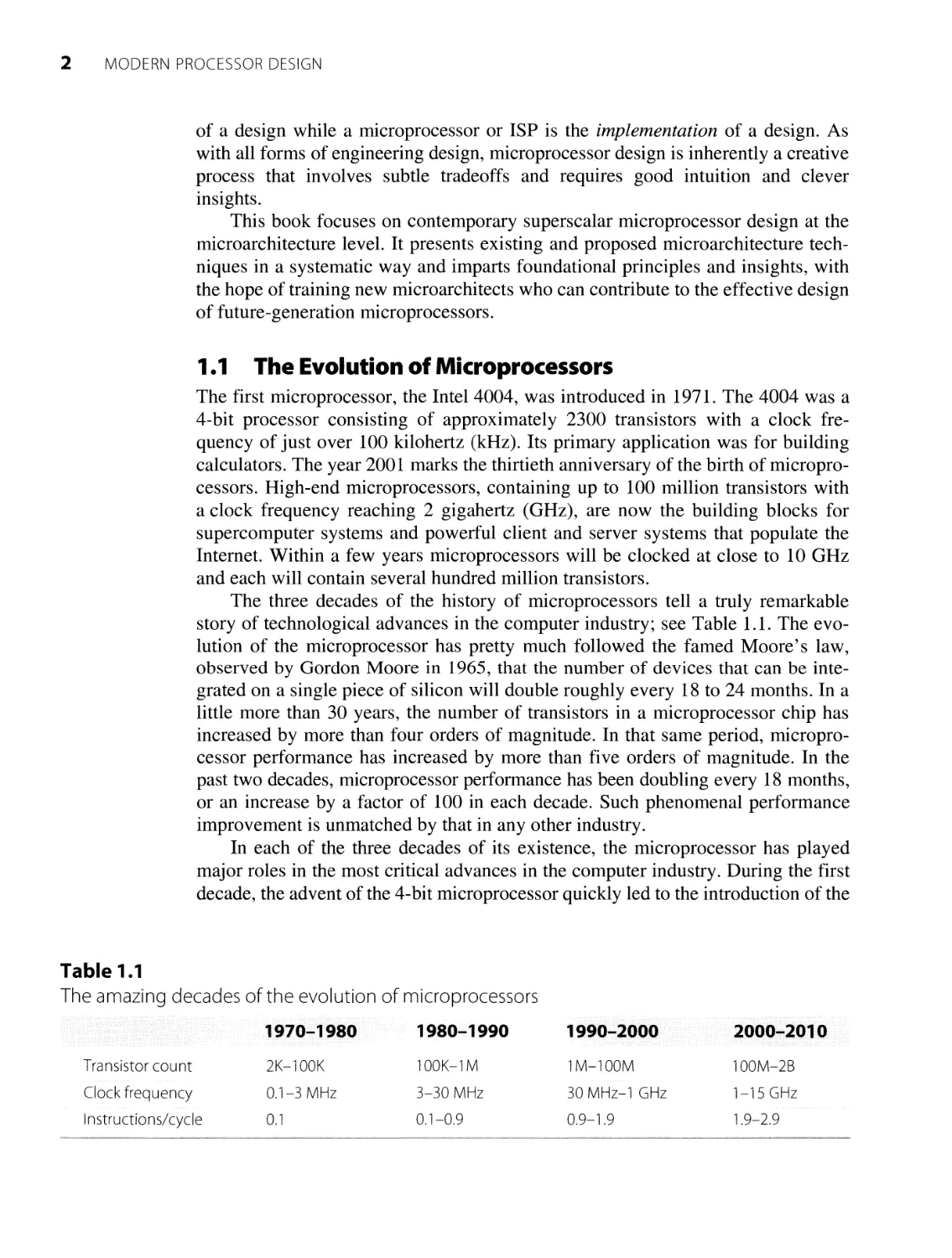
The three decades of the history of microprocessors tell a truly remarkable
story of technological advances in the computer industry; see Table 1.1. The evo¬
lution of the microprocessor has pretty much followed the famed Moore’s law,
observed by Gordon Moore in 1965, that the number of devices that can be inte¬
grated on a single piece of silicon will double roughly every 18 to 24 months. In a
little more than 30 years, the number of transistors in a microprocessor chip has
increased by more than four orders of magnitude. In that same period, micropro¬
cessor performance has increased by more than five orders of magnitude. In the
past two decades, microprocessor performance has been doubling every 18 months,
or an increase by a factor of 100 in each decade. Such phenomenal performance
improvement is unmatched by that in any other industry.
In each of the three decades of its existence, the microprocessor has played
major roles in the most critical advances in the computer industry. During the first
decade, the advent of the 4-bit microprocessor quickly led to the introduction of the
Table 1.1
The amazing decades of the evolution of microprocessors
1970-1980 1980-1990
Transistor count 2K-100K
Clock frequency 0.1-3 MHz
Instructions/cycle 0.1
1990-2000 2000-2010
100K-1M
1M-100M 100M-2B
3-30 MHz
30 MHz-1 GHz 1-15 GHz
0.1-0.9
0.9-1.9 1.9-2.9
PROCESSOR DESIGN 3
8-bit microprocessor. These narrow bit-width microprocessors evolved into self
contained microcontrollers that were produced in huge volumes and deployed in
numerous embedded applications ranging from washing machines, to elevators, to
jet engines. The 8-bit microprocessor also became the heart of a new popular com¬
puting platform called the personal computer (PC) and ushered in the PC era of
computing.
The decade of the 1980s witnessed major advances in the architecture and
microarchitecture of 32-bit microprocessors. Instruction set design issues became
the focus of both academic and industrial researchers. The importance of having
an instruction set architecture that facilitates efficient hardware implementation
and that can leverage compiler optimizations was recognized. Instruction pipelin¬
ing and fast cache memories became standard microarchitecture techniques. Pow¬
erful scientific and engineering workstations based on 32-bit microprocessors
were introduced. These workstations in turn became the workhorses for the design
of subsequent generations of even more powerful microprocessors.
During the decade of the 1990s, microprocessors became the most powerful
and most popular form of computers. The clock frequency of the fastest micropro¬
cessors exceeded that of the fastest supercomputers. Personal computers and work¬
stations became ubiquitous and essential tools for productivity and communication.
Extremely aggressive microarchitecture techniques were devised to achieve un¬
precedented levels of microprocessor performance. Deeply pipelined machines
capable of achieving extremely high clock frequencies and sustaining multiple
instructions executed per cycle became popular. Out-of-order execution of instruc¬
tions and aggressive branch prediction techniques were introduced to avoid or
reduce the number of pipeline stalls. By the end of the third decade of microproces¬
sors, almost all forms of computing platforms ranging from personal handheld
devices to mainstream desktop and server computers to the most powerful parallel
and clustered computers are based on the building blocks of microprocessors.
We are now heading into the fourth decade of microprocessors, and the
momentum shows no sign of abating. Most technologists agree that Moore’s law
will continue to rule for at least 10 to 15 years more. By 2010, we can expect
microprocessors to contain more than 1 billion transistors with clocking frequen¬
cies greater than 10 GHz. We can also expect new innovations in a number of
areas. The current focus on instruction-level parallelism (ILP) will expand to
include thread-level parallelism (TLP) as well as memory-level parallelism
(MLP). Architectural features that historically belong to large systems, for exam¬
ple, multiprocessors and memory hierarchies, will be implemented on a single
chip. Many traditional “macroarchitecture” issues will now become microarchi¬
tecture issues. Power consumption will become a dominant performance impedi¬
ment and will require new solutions at all levels of the design hierarchy, including
fabrication process, circuit design, logic design, microarchitecture design, and
software run-time environment, in order to sustain the same rate of performance
improvements that we have witnessed in the past three decades.
The objective of this book is to introduce the fundamental principles of micro¬
processor design at the microarchitecture level. Major techniques that have been
4 MODERN PROCESSOR DESIGN
developed and deployed in the past three decades are presented in a comprehensive
way. This book attempts to codify a large body of knowledge into a systematic
framework. Concepts and techniques that may appear quite complex and difficult
to decipher are distilled into a format that is intuitive and insightful. A number of
innovative techniques recently proposed by researchers are also highlighted. We
hope this book will play a role in producing a new generation of microprocessor
designers who will help write the history for the fourth decade of microprocessors.
1.2 Instruction Set Processor Design
The focus of this book is on designing instruction set processors. Critical to an
instruction set processor is the instruction set architecture, which specifies the
functionality that must be implemented by the instruction set processor. The ISA
plays several crucial roles in instruction set processor design.
1.2.1 Digital Systems Design
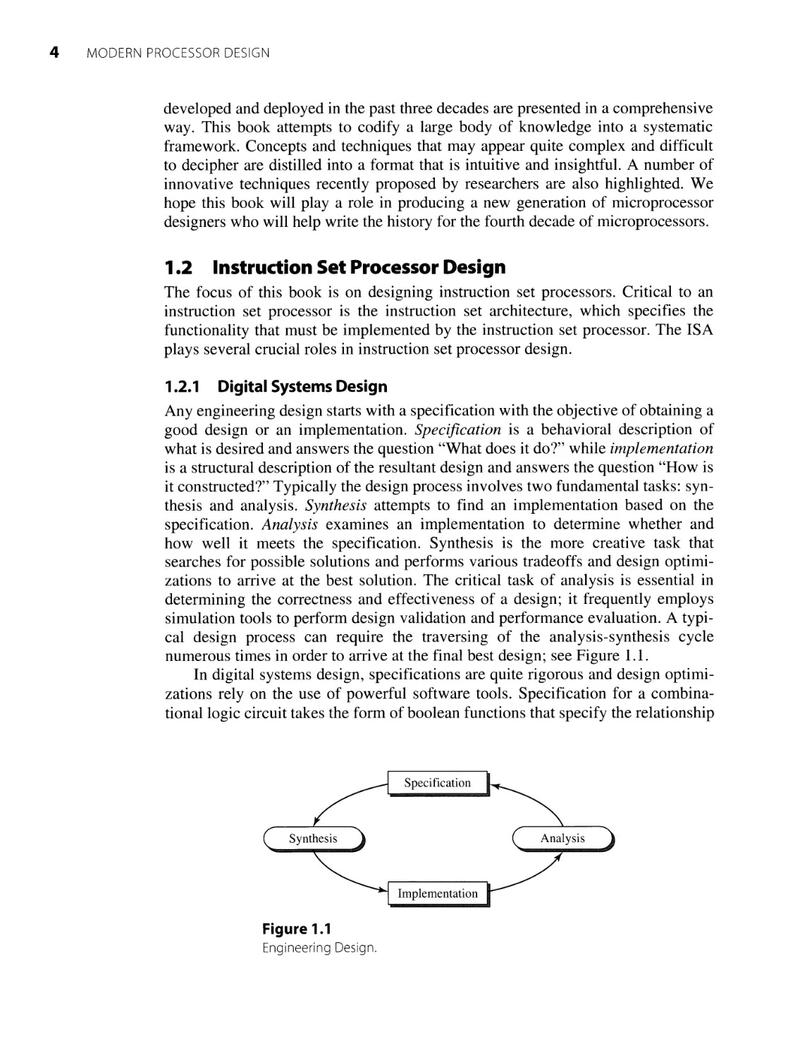
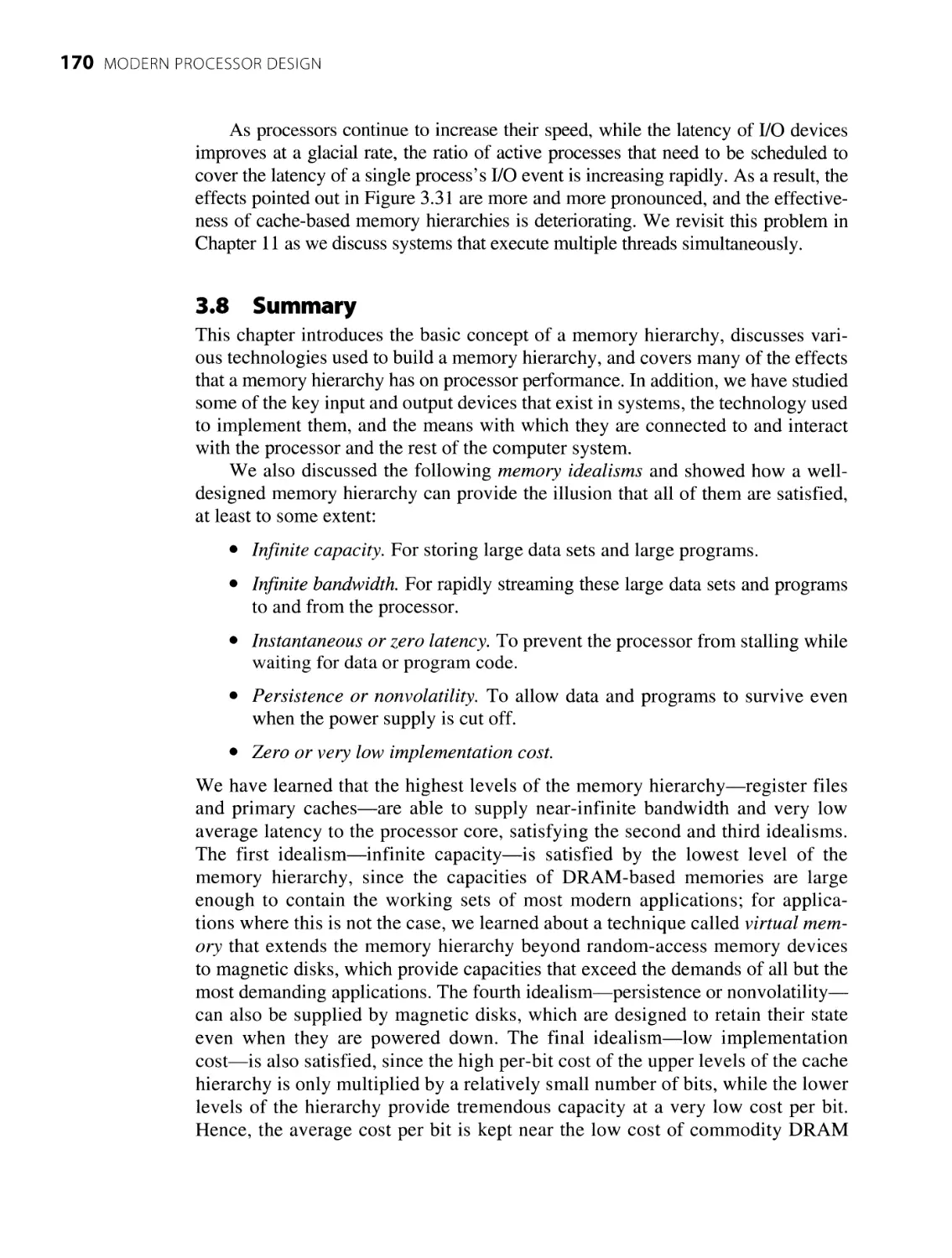
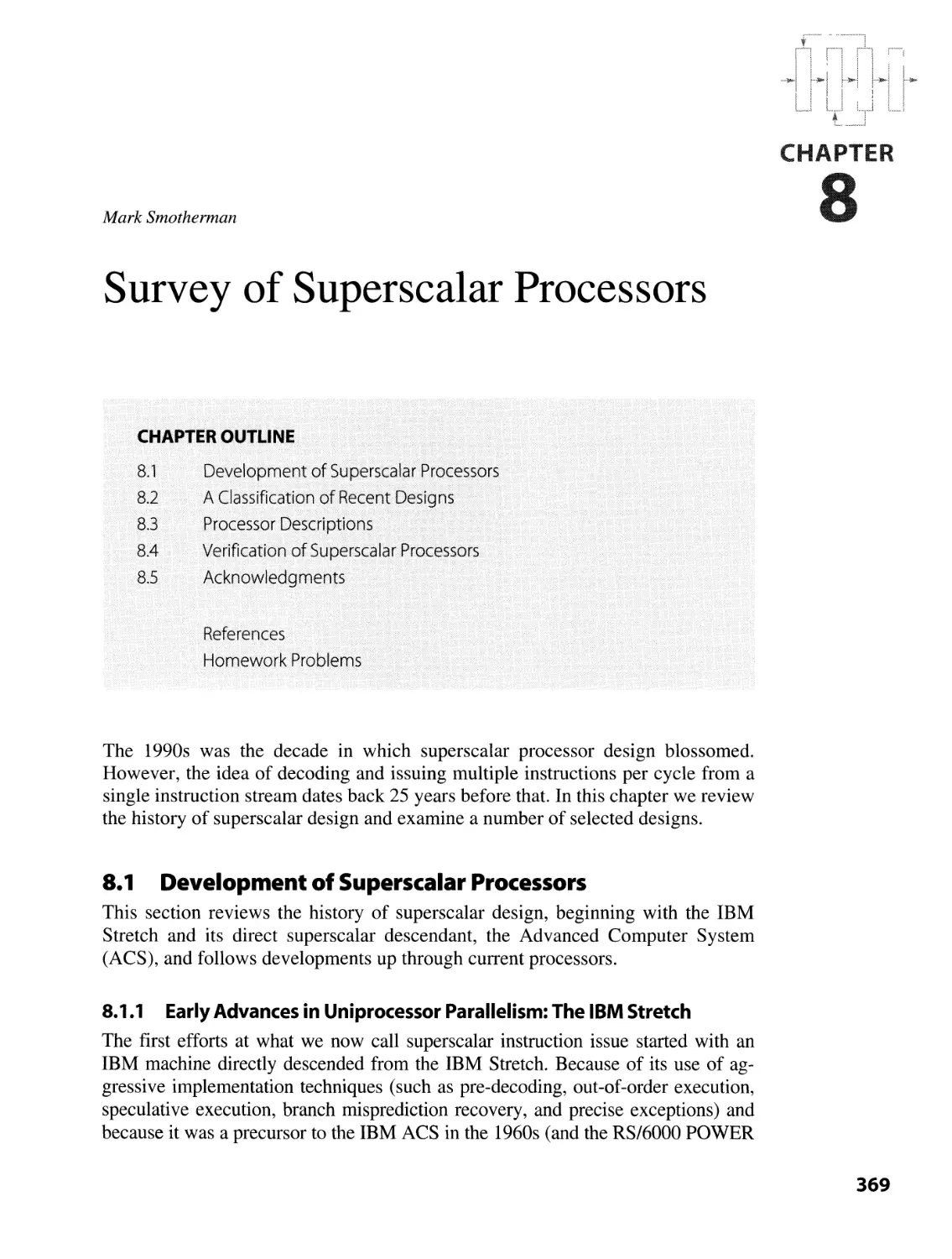
Any engineering design starts with a specification with the objective of obtaining a
good design or an implementation. Specification is a behavioral description of
what is desired and answers the question “What does it do?” while implementation
is a structural description of the resultant design and answers the question “How is
it constructed?” Typically the design process involves two fundamental tasks: syn¬
thesis and analysis. Synthesis attempts to find an implementation based on the
specification. Analysis examines an implementation to determine whether and
how well it meets the specification. Synthesis is the more creative task that
searches for possible solutions and performs various tradeoffs and design optimi¬
zations to arrive at the best solution. The critical task of analysis is essential in
determining the correctness and effectiveness of a design; it frequently employs
simulation tools to perform design validation and performance evaluation. A typi¬
cal design process can require the traversing of the analysis-synthesis cycle
numerous times in order to arrive at the final best design; see Figure 1.1.
In digital systems design, specifications are quite rigorous and design optimi¬
zations rely on the use of powerful software tools. Specification for a combina¬
tional logic circuit takes the form of boolean functions that specify the relationship
Figure 1.1
Engineering Design.
PROCESSOR DESIGN 5
between input and output variables. The implementation is typically an optimized
two-level AND-OR design or a multilevel network of logic gates. The optimiza¬
tion attempts to reduce the number of logic gates and the number of levels of logic
used in the design. For sequential circuit design, the specification is in the form of
state machine descriptions that include the specification of the state variables as
well as the output and next state functions. Optimization objectives include the
reduction of the number of states and the complexity of the associated combina¬
tional logic circuits. Logic minimization and state minimization software tools are
essential. Logic and state machine simulation tools are used to assist the analysis
task. These tools can verify the logic correctness of a design and determine the
critical delay path and hence the maximum clocking rate of the state machine.
The design process for a microprocessor is more complex and less straightfor¬
ward. The specification of a microprocessor design is the instruction set architec¬
ture, which specifies a set of instructions that the microprocessor must be able to
execute. The implementation is the actual hardware design described using a hard¬
ware description language (HDL). The primitives of an HDL can range from logic
gates and flip-flops, to more complex modules, such as decoders and multiplexers,
to entire functional modules, such as adders and multipliers. A design is described
as a schematic, or interconnected organization, of these primitives.
The process of designing a modern high-end microprocessor typically involves
two major steps: microarchitecture design and logic design. Microarchitecture
design involves developing and defining the key techniques for achieving the tar¬
geted performance. Usually a performance model is used as an analysis tool to
assess the effectiveness of these techniques. The performance model accurately
models the behavior of the machine at the clock cycle granularity and is able to
quantify the number of machine cycles required to execute a benchmark program.
The end result of microarchitecture design is a high-level description of the orga¬
nization of the microprocessor. This description typically uses a register transfer
language (RTL) to specify all the major modules in the machine organization and
the interactions between these modules. During the logic design step, the RTL
description is successively refined by the incorporation of implementation details
to eventually yield the HDL description of the actual hardware design. Both the
RTL and the HDL descriptions can potentially use the same description language.
For example, Verilog is one such language. The primary focus of this book is on
microarchitecture design.
1.2.2 Architecture, Implementation, and Realization
In a classic textbook on computer architecture by Blaauw and Brooks [1997] the
authors defined three fundamental and distinct levels of abstraction: architecture,
implementation, and realization. Architecture specifies the functional behavior of a
processor. Implementation is the logical structure or organization that performs the
architecture. Realization is the physical structure that embodies the implementation.
Architecture is also referred to as the instruction set architecture. It specifies
an instruction set that characterizes the functional behavior of an instruction set
processor. All software must be mapped to or encoded in this instruction set in
6 MODERN PROCESSOR DESIGN
x|a Ml P
1
E
i
Lj
i
E
L
order to be executed by the processor. Every program is compiled into a sequence
of instructions in this instruction set. Examples of some well-known architectures
are IBM 360, DEC VAX, Motorola 68K, PowerPC, and Intel IA32. Attributes
associated with an architecture include the assembly language, instruction format,
addressing modes, and programming model. These attributes are all part of the
ISA and exposed to the software as perceived by the compiler or the programmer.
An implementation is a specific design of an architecture, and it is also
E X A M PiL E.
referred to as the microarchitecture. An architecture can have many implementa¬
tions in the lifetime of that ISA. All implementations of an architecture can execute
any program encoded in that ISA. Examples of some well-known implementations
of the above-listed architecture are IBM 360/91, VAX 11/780, Motorola 68040,
PowerPC 604, and Intel P6. Attributes associated with an implementation include
pipeline design, cache memories, and branch predictors. Implementation or
microarchitecture features are generally implemented in hardware and hidden from
the software. To develop these features is the job of the microprocessor designer or
the microarchitect.
A realization of an implementation is a specific physical embodiment of a
design. For a microprocessor, this physical embodiment is usually a chip or a multi¬
chip package. For a given implementation, there can be various realizations of that
implementation. These realizations can vary and differ in terms of the clock fre¬
quency, cache memory capacity, bus interface, fabrication technology, packaging,
etc. Attributes associated with a realization include die size, physical form factor,
power, cooling, and reliability. These attributes are the concerns of the chip
designer and the system designer who uses the chip.
The primary focus of this book is on the implementation of modern micropro¬
cessors. Issues related to architecture and realization are also important. Architecture
serves as the specification for the implementation. Attributes of an architecture
can significantly impact the design complexity and the design effort of an implemen¬
tation. Attributes of a realization, such as die size and power, must be considered
in the design process and used as part of the design objectives.
1.2.3 Instruction Set Architecture
Instruction set architecture plays a very crucial role and has been defined as a con¬
tract between the software and the hardware, or between the program and the
machine. By having the ISA as a contract, programs and machines can be devel¬
oped independently. Programs can be developed that target the ISA without
requiring knowledge of the actual machine implementation. Similarly, machines
can be designed that implement the ISA without concern for what programs will
run on them. Any program written for a particular ISA should be able to run on any
machine implementing that same ISA. The notion of maintaining the same ISA
across multiple implementations of that ISA was first introduced with the IBM
S/360 line of computers [Amdahl et al., 1964].
Having the ISA also ensures software portability. A program written for a par¬
ticular ISA can run on all the implementations of that same ISA. Typically given
an ISA, many implementations will be developed over the lifetime of that ISA, or
PROCESSOR DESIGN 7
multiple implementations that provide different levels of cost and performance can
be simultaneously developed. A program only needs to be developed once for that
ISA, and then it can run on all these implementations. Such program portability
significantly reduces the cost of software development and increases the longevity
of software. Unfortunately this same benefit also makes migration to a new ISA
very difficult. Successful ISAs, or more specifically ISAs with a large software
installed base, tend to stay around for quite a while. Two examples are the IBM
360/370 and the Intel IA32.
Besides serving as a reference targeted by software developers or compilers,
ISA serves as the specification for processor designers. Microprocessor design
starts with the ISA and produces a microarchitecture that meets this specification.
Every new microarchitecture must be validated against the ISA to ensure that it per¬
forms the functional requirements specified by the ISA. This is extremely impor¬
tant to ensure that existing software can run correctly on the new microarchitecture.
Since the advent of computers, a wide variety of ISAs have been developed
and used. They differ in how operations and operands are specified. Typically an
ISA defines a set of instructions called assembly instructions. Each instruction
specifies an operation and one or more operands. Each ISA uniquely defines an
assembly language. An assembly language program constitutes a sequence of
assembly instructions. ISAs have been differentiated according to the number of
operands that can be explicitly specified in each instruction, for example two
address or three-address architectures. Some early ISAs use an accumulator as an
implicit operand. In an accumulator-based architecture, the accumulator is used as
an implicit source operand and the destination. Other early ISAs assume that oper¬
ands are stored in a stack [last in, first out (LIFO)] structure and operations are
performed on the top one or two entries of the stack. Most modern ISAs assume
that operands are stored in a multientry register file, and that all arithmetic and
logical operations are performed on operands stored in the registers. Special
instructions, such as load and store instructions, are devised to move operands
between the register file and the main memory. Some traditional ISAs allow oper¬
ands to come directly from both the register file and the main memory.
ISAs tend to evolve very slowly due to the inertia against recompiling or rede¬
veloping software. Typically a twofold performance increase is needed before
software developers will be willing to pay the overhead to recompile their existing
applications. While new extensions to an existing ISA can occur from time to time
to accommodate new emerging applications, the introduction of a brand new ISA
is a tall order. The development of effective compilers and operating systems for a
new ISA can take on the order of 10+ years. The longer an ISA has been in exist¬
ence and the larger the installed base of software based on that ISA, the more diffi¬
cult it is to replace that ISA. One possible exception might be in certain special
application domains where a specialized new ISA might be able to provide signif¬
icant performance boost, such as on the order of 10-fold.
Unlike the glacial creep of ISA innovations, significantly new microarchitectures
can be and have been developed every 3 to 5 years. During the 1980s, there were
widespread interests in ISA design and passionate debates about what constituted the
8 MODERN PROCESSOR DESIGN
best ISA features. However, since the 1990s the focus has shifted to the implemen¬
tation and to innovative microarchitecture techniques that are applicable to most,
if not all, ISAs. It is quite likely that the few ISAs that have dominated the micro¬
processor landscape in the past decades will continue to do so for the coming
decade. On the other hand, we can expect to see radically different and innovative
microarchitectures for these ISAs in the coming decade.
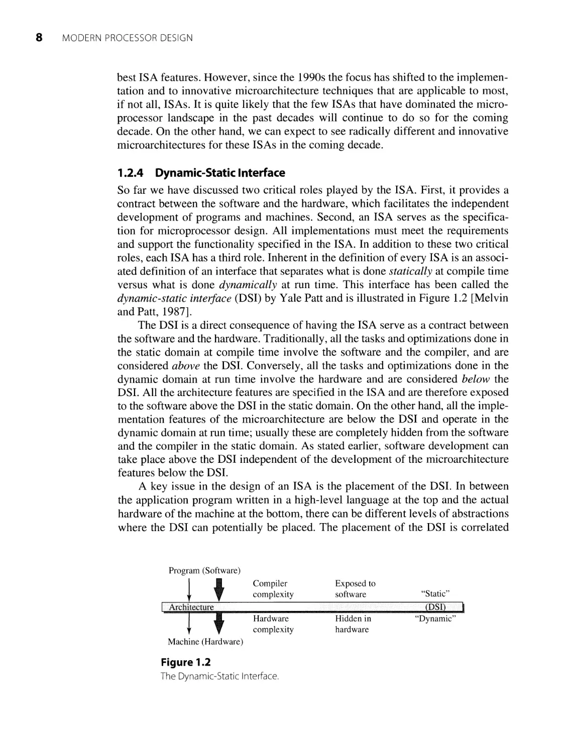
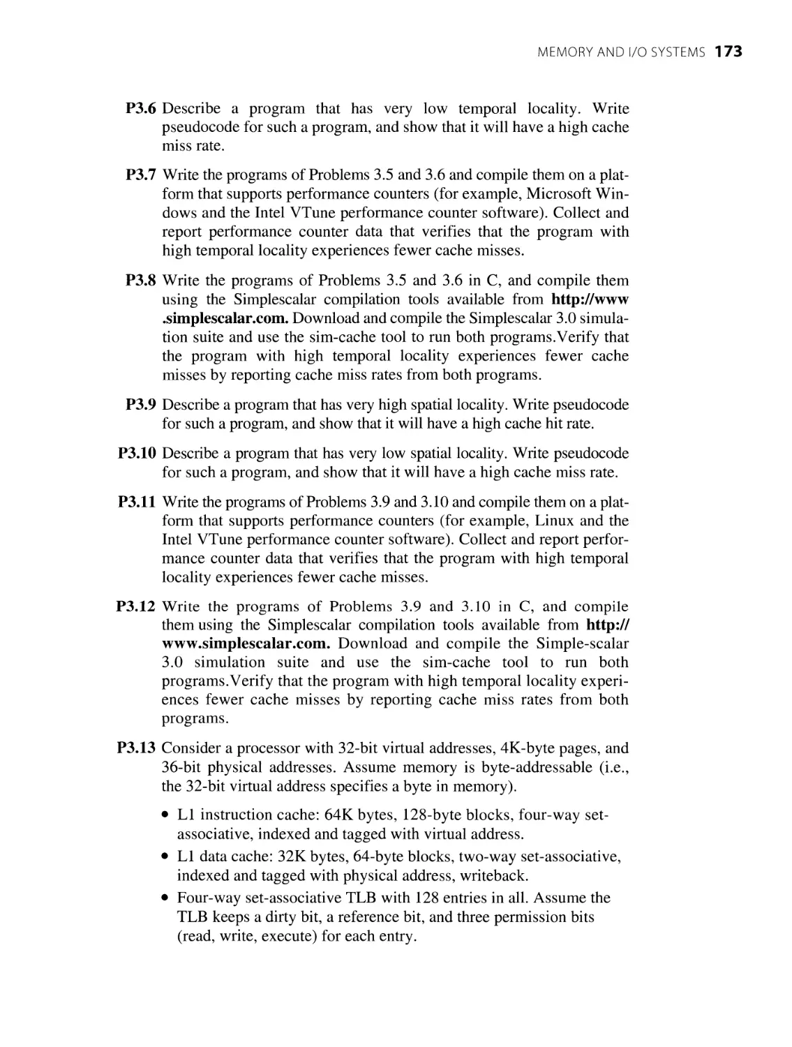
1.2.4 Dynamic-Static Interface
So far we have discussed two critical roles played by the ISA. First, it provides a
contract between the software and the hardware, which facilitates the independent
development of programs and machines. Second, an ISA serves as the specifica¬
tion for microprocessor design. All implementations must meet the requirements
and support the functionality specified in the ISA. In addition to these two critical
roles, each ISA has a third role. Inherent in the definition of every ISA is an associ¬
ated definition of an interface that separates what is done statically at compile time
versus what is done dynamically at run time. This interface has been called the
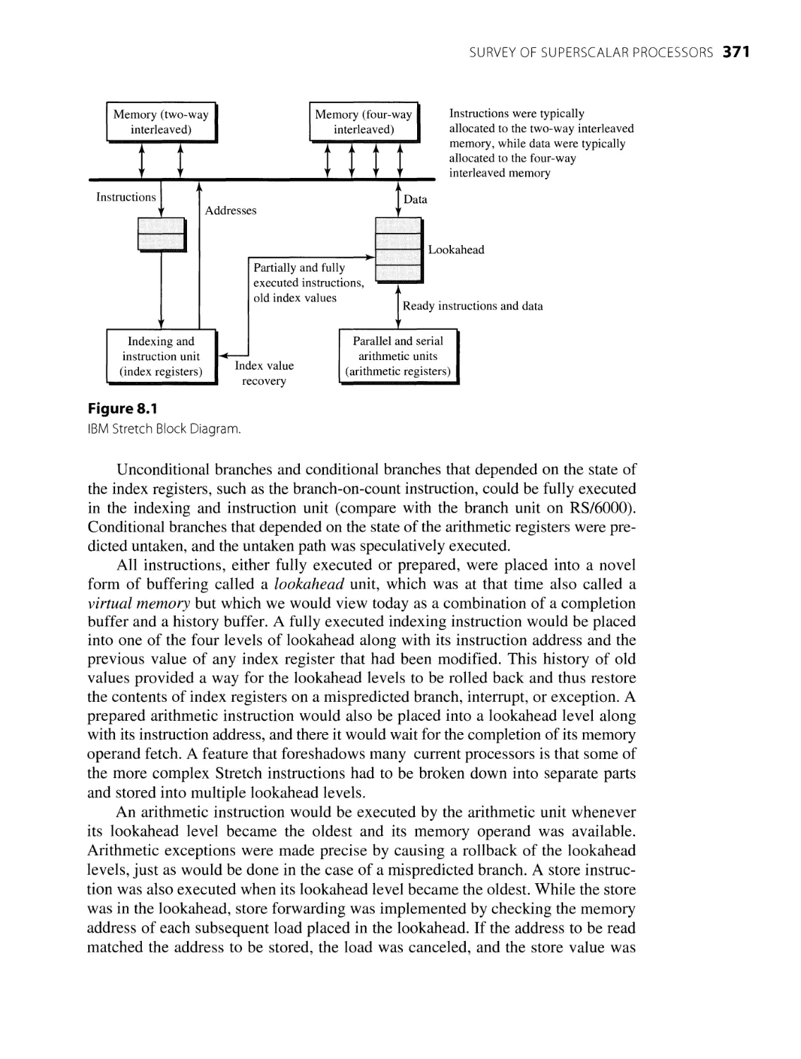
dynamic-static interface (DSI) by Yale Patt and is illustrated in Figure 1.2 [Melvin
andPatt, 1987].
The DSI is a direct consequence of having the ISA serve as a contract between
the software and the hardware. Traditionally, all the tasks and optimizations done in
the static domain at compile time involve the software and the compiler, and are
considered above the DSI. Conversely, all the tasks and optimizations done in the
dynamic domain at run time involve the hardware and are considered below the
DSI. All the architecture features are specified in the ISA and are therefore exposed
to the software above the DSI in the static domain. On the other hand, all the imple¬
mentation features of the microarchitecture are below the DSI and operate in the
dynamic domain at run time; usually these are completely hidden from the software
and the compiler in the static domain. As stated earlier, software development can
take place above the DSI independent of the development of the microarchitecture
features below the DSI.
A key issue in the design of an ISA is the placement of the DSI. In between
the application program written in a high-level language at the top and the actual
hardware of the machine at the bottom, there can be different levels of abstractions
where the DSI can potentially be placed. The placement of the DSI is correlated
Program (Software)
I Architecture
Compiler Exposed to
complexity software
“Static”
Hardware Hidden in
‘Dynamic”
complexity hardware
Machine (Hardware)
Figure 1.2
The Dynamic-Static Interface.
(DSD >
PROCESSOR DESIGN 9
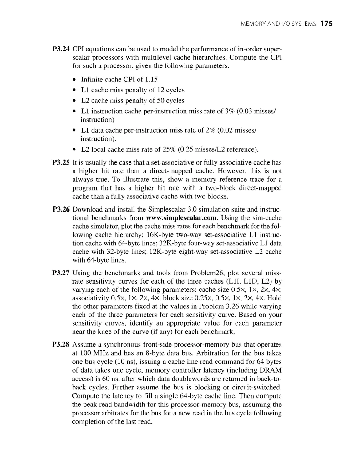
DEL
-CISC
-VLIW
-RISC
■ HLL Program
- DSI-1
I
- DSI-2
I:
- DSI-3
- Hardware
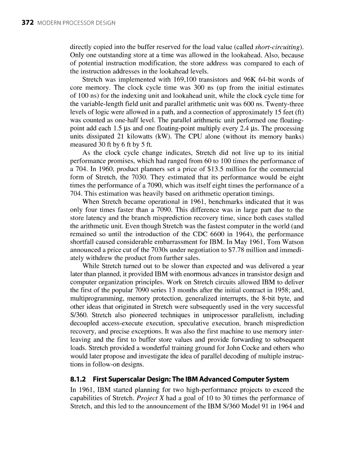
Figure 1.3
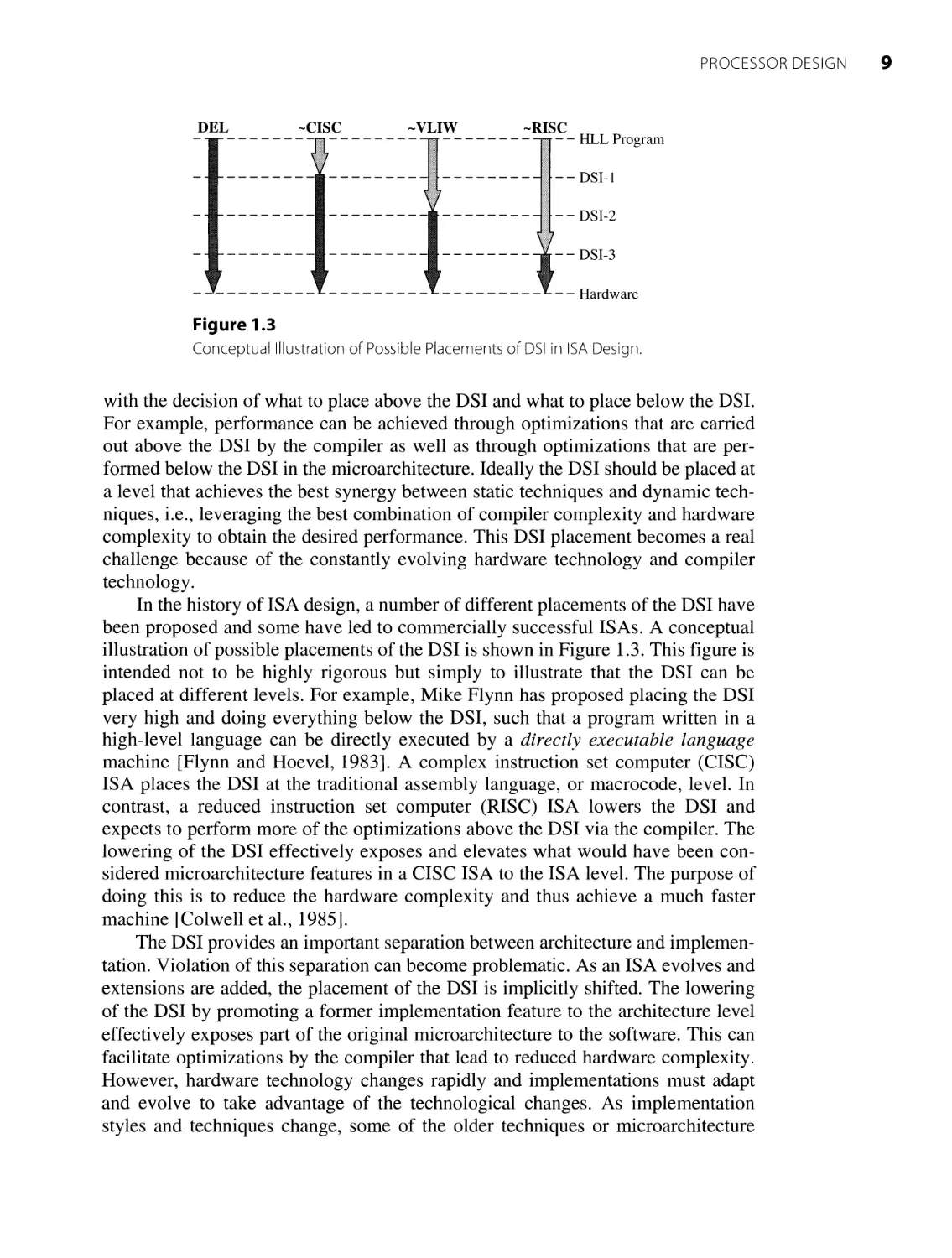
Conceptual Illustration of Possible Placements of DSI in ISA Design.
with the decision of what to place above the DSI and what to place below the DSI.
For example, performance can be achieved through optimizations that are carried
out above the DSI by the compiler as well as through optimizations that are per¬
formed below the DSI in the microarchitecture. Ideally the DSI should be placed at
a level that achieves the best synergy between static techniques and dynamic tech¬
niques, i.e., leveraging the best combination of compiler complexity and hardware
complexity to obtain the desired performance. This DSI placement becomes a real
challenge because of the constantly evolving hardware technology and compiler
technology.
In the history of ISA design, a number of different placements of the DSI have
been proposed and some have led to commercially successful IS As. A conceptual
illustration of possible placements of the DSI is shown in Figure 1.3. This figure is
intended not to be highly rigorous but simply to illustrate that the DSI can be
placed at different levels. For example, Mike Flynn has proposed placing the DSI
very high and doing everything below the DSI, such that a program written in a
high-level language can be directly executed by a directly executable language
machine [Flynn and Hoevel, 1983]. A complex instruction set computer (CISC)
ISA places the DSI at the traditional assembly language, or macrocode, level. In
contrast, a reduced instruction set computer (RISC) ISA lowers the DSI and
expects to perform more of the optimizations above the DSI via the compiler. The
lowering of the DSI effectively exposes and elevates what would have been con¬
sidered microarchitecture features in a CISC ISA to the ISA level. The purpose of
doing this is to reduce the hardware complexity and thus achieve a much faster
machine [Colwell et al., 1985].
The DSI provides an important separation between architecture and implemen¬
tation. Violation of this separation can become problematic. As an ISA evolves and
extensions are added, the placement of the DSI is implicitly shifted. The lowering
of the DSI by promoting a former implementation feature to the architecture level
effectively exposes part of the original microarchitecture to the software. This can
facilitate optimizations by the compiler that lead to reduced hardware complexity.
However, hardware technology changes rapidly and implementations must adapt
and evolve to take advantage of the technological changes. As implementation
styles and techniques change, some of the older techniques or microarchitecture
10
MODERN PROCESSOR DESIGN
features may become ineffective or even undesirable. If some of these older fea¬
tures were promoted to the ISA level, then they become part of the ISA and there
will exist installed software base or legacy code containing these features. Since all
future implementations must support the entire ISA to ensure the portability of all
existing code, the unfortunate consequence is that all future implementations must
continue to support those ISA features that had been promoted earlier, even if they
are now ineffective and even undesirable. Such mistakes have been made with real
ISAs. The lesson learned from these mistakes is that a strict separation of architec¬
ture and microarchitecture must be maintained in a disciplined fashion. Ideally, the
architecture or ISA should only contain features necessary to express the function¬
ality or the semantics of the software algorithm, whereas all the features that are
employed to facilitate better program performance should be relegated to the imple¬
mentation or the microarchitecture domain.
The focus of this book is not on ISA design but on microarchitecture tech¬
niques, with almost exclusive emphasis on performance. ISA features can influ¬
ence the design effort and the design complexity needed to achieve high levels of
performance. However, our view is that in contemporary high-end microprocessor
design, it is the microarchitecture, and not the ISA, that is the dominant determi¬
nant of microprocessor performance. Hence, the focus of this book is on microar¬
chitecture techniques for achieving high performance. There are other important
design objectives, such as power, cost, and reliability. However, historically per¬
formance has received the most attention, and there is a large body of knowledge
on techniques for enhancing performance. It is this body of knowledge that this
book is attempting to codify.
1.3 Principles of Processor Performance
The primary design objective for new leading-edge microprocessors has been
performance. Each new generation of microarchitecture seeks to significantly
improve on the performance of the previous generation. In recent years, reducing
power consumption has emerged as another, potentially equally important design
objective. However, the demand for greater performance will always be there, and
processor performance will continue to be a key design objective.
1.3.1 Processor Performance Equation
During the 1980s several researchers independently discovered or formulated an
equation that clearly defines processor performance and cleanly characterizes the
fundamental factors that contribute to processor performance. This equation has
come to be known as the iron law of processor performance, and it is shown in
Equation (1.1). First, the processor performance equation indicates that a proces¬
sor’s performance is measured in terms of how long it takes to execute a particular
program (time/program). Second, this measure of time/program or execution time
can be formulated as a product of three terms: instructions/program, cycles/
instruction, and time/cycle. The first term indicates the total number of dynamic
instructions that need to be executed for a particular program; this term is also
PROCESSOR DESIGN 11
referred to as the instruction count. The second term indicates on average (averag¬
ing over the entire execution of the program) how many machine cycles are con¬
sumed to execute each instruction; typically this term is denoted as the CPI (cycles
per instruction). The third term indicates the length of time of each machine cycle,
namely, the cycle time of the machine.
1 _ time _ instructions x cycles x time ^ ^
Performance program program instruction cycle
The shorter the program’s execution time, the better the performance. Looking at
Equation 1.1, we can conclude that processor performance can be improved by reduc¬
ing the magnitude of any one of the three terms in this equation. If the instruction
count can be reduced, there will be fewer instructions to execute and the execution
time will be reduced. If CPI is reduced, then on average each instruction will con¬
sume fewer machine cycles. If cycle time can be reduced, then each cycle will
consume less time and the overall execution time is reduced. It might seem from
this equation that improving performance is quite trivial. Unfortunately, it is not that
straightforward. The three terms are not all independent, and there are complex inter¬
actions between them. The reduction of any one term can potentially increase the
magnitude of the other two terms. The relationship between the three terms cannot be
easily characterized. Improving performance becomes a real challenge involving
subtle tradeoffs and delicate balancing acts. It is exactly this challenge that makes
processor design fascinating and at times more of an art than a science. Section 1.3.2
will examine more closely different ways to improve processor performance.
1.3.2 Processor Performance Optimizations
It can be said that all performance optimization techniques boil down to reducing
one or more of the three terms in the processor performance equation. Some tech¬
niques can reduce one term while leaving the other two unchanged. For example,
when a compiler performs optimizations that eliminate redundant and useless
instructions in the object code, the instruction count can be reduced without impact¬
ing the CPI or the cycle time. As another example, when a faster circuit technology
or a more advanced fabrication process is used that reduces signal propagation
delays, the machine cycle time can potentially be reduced without impacting the
instruction count or the CPI. Such types of performance optimization techniques
are always desirable and should be employed if the cost is not prohibitive.
Other techniques that reduce one of the terms can at the same time increase
one or both of the other terms. For these techniques, there is performance gain
only if the reduction in one term is not overwhelmed by the increase in the other
terms. We can examine these techniques by looking at the reduction of each of the
three terms in the processor performance equation.
There are a number of ways to reduce the instruction count. First, the instruc¬
tion set can include more complex instructions that perform more work per
instruction. The total number of instructions executed can decrease significantly.
For example, a program in a RISC ISA can require twice as many instructions as
12
MODERN PROCESSOR DESIGN
one in a CISC ISA. While the instruction count may go down, the complexity of
the execution unit can increase, leading to a potential increase of the cycle time. If
deeper pipelining is used to avoid increasing the cycle time, then a higher branch
misprediction penalty can result in higher CPI. Second, certain compiler optimiza¬
tions can result in fewer instructions being executed. For example, unrolling loops
can reduce the number of loop closing instructions executed. However, this can
lead to an increase in the static code size, which can in turn impact the instruction
cache hit rate, which can in turn increase the CPI. Another similar example is the
in-lining of function calls. By eliminating calls and returns, fewer instructions are
executed, but the code size can significantly expand. Third, more recently
researchers have proposed the dynamic elimination of redundant computations via
microarchitecture techniques. They have observed that during program execution,
there are frequent repeated executions of the same computation with the same data
set. Hence, the result of the earlier computation can be buffered and directly used
without repeating the same computation [Sodani and Sohi, 1997]. Such computa¬
tion reuse techniques can reduce the instruction count, but can potentially increase
the complexity in the hardware implementation which can lead to the increase of
cycle time. We see that decreasing the instruction count can potentially lead to
increasing the CPI and/or cycle time.
The desire to reduce CPI has inspired many architectural and microarchitec
tural techniques. One of the key motivations for RISC was to reduce the complex¬
ity of each instruction in order to reduce the number of machine cycles required to
process each instruction. As we have already mentioned, this comes with the over¬
head of an increased instruction count. Another key technique to reduce CPI is
instruction pipelining. A pipelined processor can overlap the processing of multi¬
ple instructions. Compared to a nonpipelined design and assuming identical cycle
times, a pipelined design can significantly reduce the CPI. A shallower pipeline,
that is, a pipeline with fewer pipe stages, can yield a lower CPI than a deeper pipe¬
line, but at the expense of increased cycle time. The use of cache memory to reduce
the average memory access latency (in terms of number of clock cycles) will also
reduce the CPI. When a conditional branch is taken, stalled cycles can result from
having to fetch the next instruction from a nonsequential location. Branch predic¬
tion techniques can reduce the number of such stalled cycles, leading to a reduction
of CPI. However, adding branch predictors can potentially increase the cycle time
due to the added complexity in the fetch pipe stage, or even increase the CPI if a
deeper pipeline is required to maintain the same cycle time. The emergence of
superscalar processors allows the processor pipeline to simultaneously process
multiple instructions in each pipe stage. By being able to sustain the execution of
multiple instructions in every machine cycle, the CPI can be significantly reduced.
Of course, the complexity of each pipe stage can increase, leading to a potential
increase of cycle time or the pipeline depth, which can in turn increase the CPI.
The key microarchitecture technique for reducing cycle time is pipelining.
Pipelining effectively partitions the task of processing an instruction into multiple
stages. The latency (in terms of signal propagation delay) of each pipe stage deter¬
mines the machine cycle time. By employing deeper pipelines, the latency of each
PROCESSOR DESIGN 13
pipe stage, and hence the cycle time, can be reduced. In recent years, aggressive
pipelining has been the major technique used in achieving phenomenal increases
of clock frequency of high-end microprocessors. As can be seen in Table 1.1, dur¬
ing the most recent decade, most of the performance increase has been due to the
increase of the clock frequency.
There is a downside to increasing the clock frequency through deeper pipelin¬
ing. As a pipeline gets deeper, CPI can go up in three ways. First, as the front end
of the pipeline gets deeper, the number of pipe stages between fetch and execute
increases. This increases the number of penalty cycles incurred when branches are
mispredicted, resulting in the increase of CPI. Second, if the pipeline is so deep
that a primitive arithmetic-logic unit (ALU) operation requires multiple cycles,
then the necessary latency between two dependent instructions, even with result¬
forwarding hardware, will be multiple cycles. Third, as the clock frequency
increases with deeper central processing unit (CPU) pipelines, the latency of mem¬
ory, in terms of number of clock cycles, can significantly increase. This can
increase the average latency of memory operations and thus increase the overall
CPI. Finally, there is hardware and latency overhead in pipelining that can lead to
diminishing returns on performance gains. This technique of getting higher fre¬
quency via deeper pipelining has served us well for more than a decade. It is not
clear how much further we can push it before the requisite complexity and power
consumption become prohibitive.
As can be concluded from this discussion, achieving a performance improve¬
ment is not a straightforward task. It requires interesting tradeoffs involving many
and sometimes very subtle issues. The most talented microarchitects and processor
designers in the industry all seem to possess the intuition and the insights that
enable them to make such tradeoffs better than others. It is the goal, or perhaps the
dream, of this book to impart not only the concepts and techniques of superscalar
processor design but also the intuitions and insights of superb microarchitects.
1.3.3 Performance Evaluation Method
In modem microprocessor design, hardware prototyping is infeasible; most design¬
ers use simulators to do performance projection and ensure functional correctness
during the design process. Typically two types of simulators are used: functional
simulators and performance simulators. Functional simulators model a machine at
the architecture (ISA) level and are used to verify the correct execution of a pro¬
gram. Functional simulators actually interpret or execute the instructions of a
program. Performance simulators model the microarchitecture of a design and are
used to measure the number of machine cycles required to execute a program.
Usually performance simulators are concerned not with the semantic correctness
of instruction execution, but only with the timing of instruction execution.
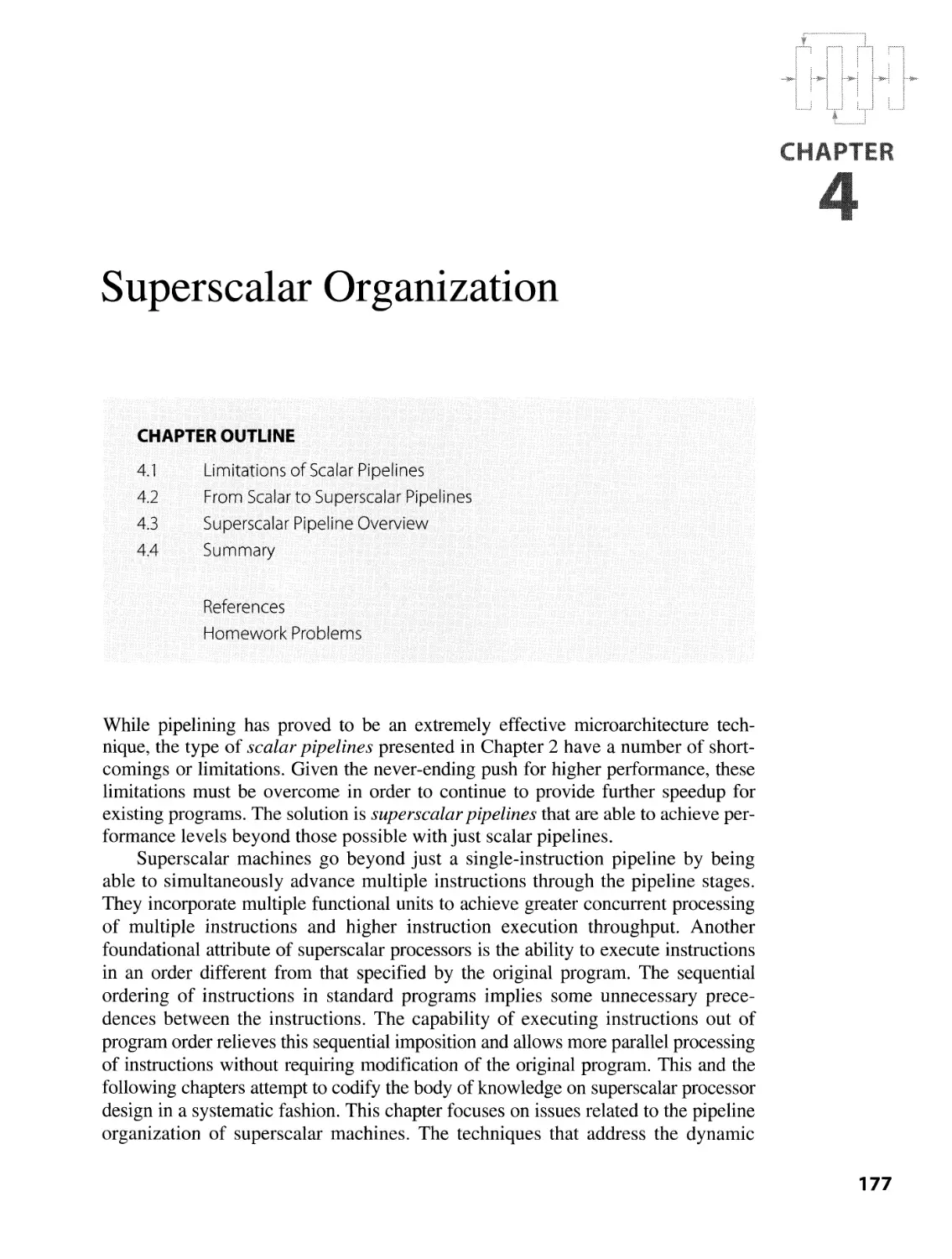
Performance simulators can be either trace-driven or execution-driven; as illus¬
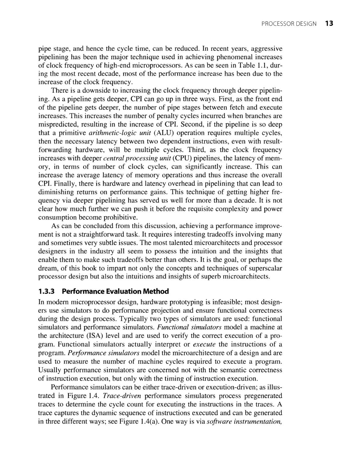
trated in Figure 1.4. Trace-driven performance simulators process pregenerated
traces to determine the cycle count for executing the instructions in the traces. A
trace captures the dynamic sequence of instructions executed and can be generated
in three different ways; see Figure 1.4(a). One way is via software instrumentation,
14
MODERN PROCESSOR DESIGN
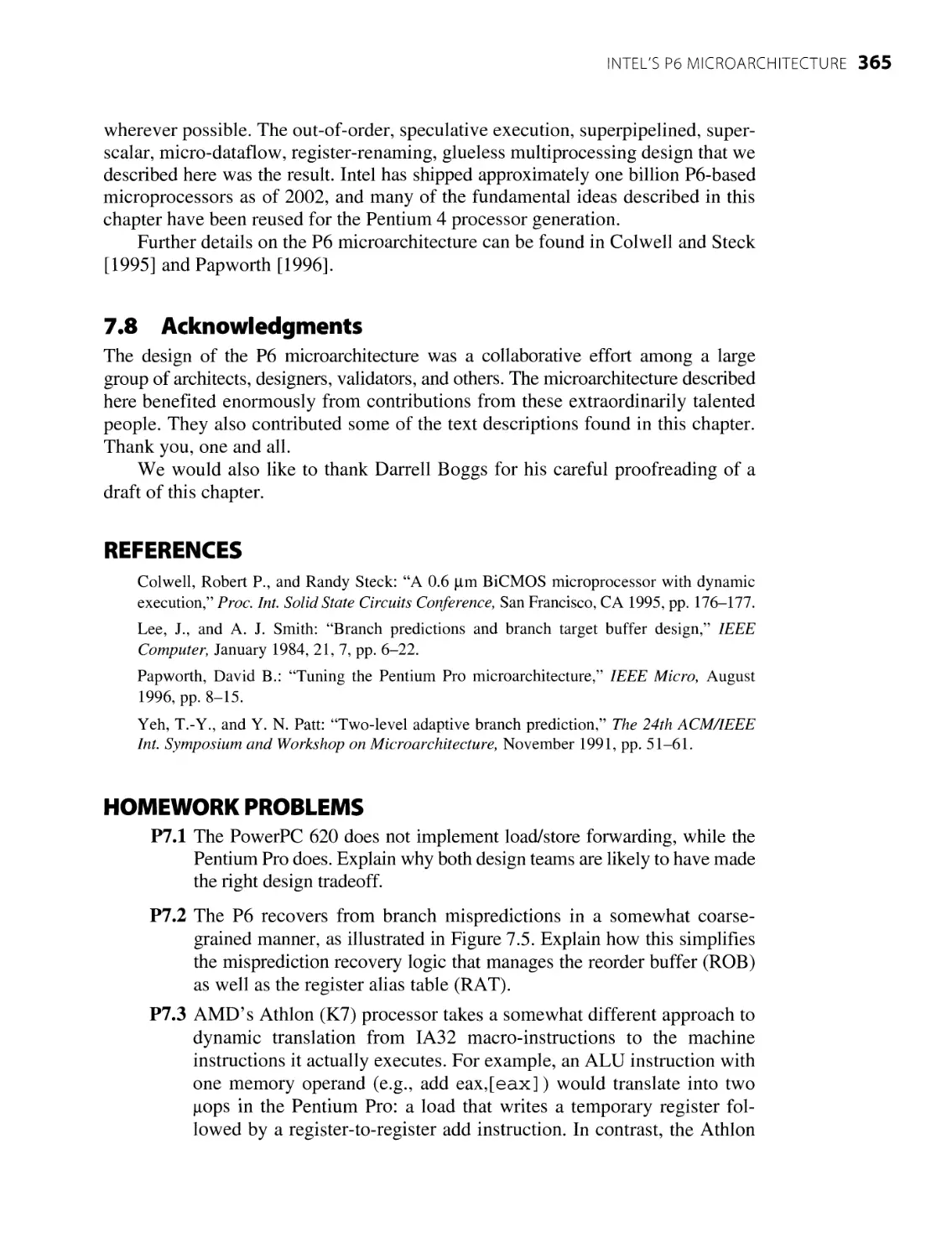
Trace generation
(a)
Functional simulator
(instruction interpretation)
Execution
trace
Checkpoint
Functional simulation and control
Cycle-based
performance
simulator
Execution-driven
timing simulation
(b)
Figure 1.4
Performance Simulation Methods: (a) Trace-Driven Simulation;
(b) Execution-Driven Simulation.
which inserts special instructions into a program prior to run time so that when the
instrumented program is executed on a physical system, the inserted instructions
will produce the dynamic execution trace. Another way is via hardware instrumen¬
tation, which involves putting special hardware probes to monitor the system bus
and to record the actual execution trace when a program is executed on the system.
Software instrumentation can significantly increase the code size and the program
execution time. Hardware instrumentation requires the monitoring hardware and is
seriously limited by the buffering capacity of the monitoring hardware. The third
trace generation method uses a functional simulator to simulate the execution of a
program. During simulation, hooks are embedded in the simulator to record the
dynamic execution trace. For all three methods, once traces are generated, they can
be stored for subsequent repeated use by trace-driven performance simulators.
Execution-driven performance simulators overcome some of the limitations of
trace-driven performance simulators; see Figure 1.4(b). Instead of using pregener¬
ated traces, an execution-driven performance simulator is interfaced to a functional
simulator, and the two simulators work in tandem. During simulation, the functional
simulator executes the instructions and passes information associated with the exe¬
cuted instructions to the performance simulator. The performance simulator then
tracks the timing of these instructions and their movement through the pipeline
stages. It has the ability to issue directives to the functional simulator to checkpoint
the simulation state and to later resume from the checkpointed state. The checkpoint
capability allows the simulation of speculative instructions, such as instructions
PROCESSOR DESIGN 15
following a branch prediction. More specifically, execution-driven simulation can
simulate the mis-speculated instructions, such as the instructions following a
mispredicted branch, going through the pipeline. In trace-driven simulation, the pre¬
generated trace contains only the actual (nonspeculative) instructions executed, and
a trace-driven simulator cannot account for the instructions on a mis-speculated path
and their potential contention for resources with other (nonspeculative) instructions.
Execution-driven simulators also alleviate the need to store long traces. Most mod¬
em performance simulators employ the execution-driven paradigm. The most
advanced execution-driven performance simulators are supported by functional
simulators that are capable of performing full-system simulation, that is, the simula¬
tion of both application and operating system instmctions, the memory hierarchy,
and even input/output devices.
The actual implementation of the microarchitecture model in a performance
simulator can vary widely in terms of the amount and details of machine resources
that are explicitly modeled. Some performance models are merely cycle counters
that assume unlimited resources and simply calculate the total number of cycles
needed for the execution of a trace, taking into account inter-instruction depen¬
dences. Others explicitly model the organization of the machine with all its com¬
ponent modules. These performance models actually simulate the movement of
instructions through the various pipeline stages, including the allocation of limited
machine resources in each machine cycle. While many performance simulators
claim to be “cycle-accurate,” the methods they use to model and track the activi¬
ties in each machine cycle can be quite different.
While there is heavy reliance on performance simulators during the early
design stages of a microprocessor, the validation of the accuracy of performance
simulators is an extremely difficult task. Typically the performance model or sim¬
ulator is implemented in the early phase of the design and is used to do initial
tradeoffs of various microarchitecture features. During this phase there isn’t a refer¬
ence that can be used to validate the performance model. As the design progresses
and an RTL model of the design is developed, the RTL model can be used as a ref¬
erence to validate the accuracy of the performance model. However, simulation
using the RTL model is very slow, and therefore only very short traces can be
used. During the entire design process, discipline is essential to concurrently
evolve the performance model and the RTL model to ensure that the performance
model is tracking all the changes made in the RTL model. It is also important to do
post-silicon validation of the performance model so that it can be used as a good
starting point for the next-generation design. Most performance simulators used in
academic research are never validated. These simulators can be quite complex
and, just like all large pieces of software, can contain many bugs that are difficult
to eliminate. It is quite likely that a large fraction of the performance data pub¬
lished in many research papers using unvalidated performance models is com¬
pletely erroneous. Black argues convincingly for more rigorous validation of
processor simulators [Black and Shen, 1998].
Other than the difficulty of validating their accuracy, another problem associated
with performance simulators is the extremely long simulation times that are often
16
MODERN PROCESSOR DESIGN
required. Most contemporary performance evaluations involve the simulation of
many benchmarks and a total of tens to hundreds of billion instructions. During the
early phase of the design, performance simulators are used extensively to support the
exploration of numerous tradeoffs, which require many simulation runs using differ¬
ent sets of parameters in the simulation model. For execution-driven performance
simulators that have fairly detailed models of a complex machine, a slowdown factor
of four to five orders of magnitude is rather common. In other words, to simulate a
single machine cycle of the target machine, that is the machine being modeled, can
require the execution of 10,000 to 100,000 machine cycles on the host machine. A
large set of simulation runs can sometimes take many days to complete, even using a
large pool of simulation machines.
1.4 Instruction-Level Parallel Processing
Instruction-level parallel processing can be informally defined as the concurrent
processing of multiple instructions. Traditional sequential processors execute one
instruction at a time. A leading instruction is completed before the next instruction is
processed. To a certain extent, pipelined processors achieve a form of instruction
level parallel processing by overlapping the processing of multiple instructions. As
many instructions as there are pipeline stages can be concurrently in flight at any
one time. Traditional sequential (CISC) processors can require an average of about
10 machine cycles for processing each instruction, that is CPI = 10. With pipelined
(RISC) processors, even though each instruction may still require multiple cycles to
complete, by overlapping the processing of multiple instructions in the pipeline, the
effective average CPI can be reduced to close to one if a new instruction can be initi¬
ated every machine cycle.
With scalar pipelined processors, there is still the limitation of fetching and
initiating at most one instruction into the pipeline every machine cycle. With this
limitation, the best possible CPI that can be achieved is one; or inversely, the best
possible throughput of a scalar processor is one instruction per cycle (IPC). A
more aggressive form of instruction-level parallel processing is possible that
involves fetching and initiating multiple instructions into a wider pipelined proces¬
sor every machine cycle. While the decade of the 1980s adopted CPI = 1 as its
design objective for single-chip microprocessors, the goal for the decade of the
1990s was to reduce CPI to below one, or to achieve a throughput of IPC greater
than one. Processors capable of IPC greater than one are termed superscalar pro¬
cessors. This section presents the overview of instruction-level parallel processing
and provides the bridge between scalar pipelined processors and their natural
descendants, the superscalar processors.
1.4.1 From Scalar to Superscalar
Scalar processors are pipelined processors that are designed to fetch and issue at
most one instruction every machine cycle. Superscalar processors are those that
are designed to fetch and issue multiple instructions every machine cycle. This
subsection presents the basis and motivation for evolving from scalar to supersca¬
lar processor implementations.
PROCESSOR DESIGN
1.4.1.1 Processor Performance. In Section 1.3.1 we introduced the iron law of
processor performance, as shown in Equation (1.1). That equation actually repre¬
sents the inverse of performance as a product of instruction count, average CPI, and
the clock cycle time. We can rewrite that equation to directly represent performance
as a product of the inverse of instruction count, average IPC (IPC = 1/CPI), and the
clock frequency, as shown in Equation (1.2). Looking at this equation, we see that
performance can be increased by increasing the IPC, increasing the frequency, or
decreasing the instruction count.
Performance
=
instruction count
xx—
instructions 1 IPC X frequency
cycle cycle time instruction count
(1.2)
Instruction count is determined by three contributing factors: the instruction
set architecture, the compiler, and the operating system. The ISA and the amount
of work encoded into each instruction can strongly influence the total number of
instructions executed for a program. The effectiveness of the compiler can also
strongly influence the number of instructions executed. The operating system
functions that are invoked by the application program effectively increase the total
number of instructions executed in carrying out the execution of the program.
Average IPC (instructions per cycle) reflects the average instruction throughput
achieved by the processor and is a key measure of microarchitecture effectiveness.
Historically, the inverse of IPC, that is, CPI (cycles per instruction), has been used to
indicate the average number of machine cycles needed to process each instruction.
The use of CPI was popular during the days of scalar pipelined processors. The per¬
formance penalties due to various forms of pipeline stalls can be cleanly stated as dif¬
ferent CPI overheads. Back then, the ultimate performance goal for scalar pipelined
processors was to reduce the average CPI to one. As we move into the superscalar
domain, it becomes more convenient to use IPC. The new performance goal for
superscalar processors is to achieve an average IPC greater than one. The bulk of the
microarchitecture techniques presented in this book target the improvement of IPC.
Frequency is strongly affected by the fabrication technology and circuit tech¬
niques. Increasing the number of pipeline stages can also facilitate higher clocking
frequencies by reducing the number of logic gate levels in each pipe stage. Tradi¬
tional pipelines can have up to 20 levels of logic gates in each pipe stage; most
contemporary pipelines have only 10 or fewer levels. To achieve high IPC in
superscalar designs, the pipeline must be made wider to allow simultaneous pro¬
cessing of multiple instructions in each pipe stage. The widening of the pipeline
increases the hardware complexity and the signal propagation delay of each pipe
stage. Hence, with a wider pipeline, in order to maintain the same frequency an
even deeper pipeline may be required. There is a complex tradeoff between mak¬
ing pipelines wider and making them deeper.
1.4.1.2 Parallel Processor Performance. As we consider the parallel process¬
ing of instructions in increasing processor performance, it is insightful to revisit the
classic observation on parallel processing commonly referred to as Amdahl's law
17
18
MODERN PROCESSOR DESIGN
Figure 1.5
Scalar and Vector Processing in a Traditional Supercomputer.
[Amdahl, 1967]. Traditional supercomputers are parallel processors that perform
both scalar and vector computations. During scalar computation only one processor is
used. During vector computation all N processors are used to perform operations on
array data. The computation performed by such a parallel machine can be depicted as
shown in Figure 1.5, where N is the number of processors in the machine and h is
the fraction of time the machine spends in scalar computation. Conversely, 1 - h
is the fraction of the time the machine spends in vector computation.
One formulation of Amdahl’s law states that the efficiency E of the parallel
machine is measured by the overall utilization of the N processors or the fraction
of time the N processors are busy. Efficiency E can be modeled as
NNvN
h + Nx(l-h) _h + N-Nh _ x v L 1
(1-3)
As the number of processors N becomes very large, the efficiency E approaches
1 - h, which is the fraction of time the machine spends in vector computation. As
N becomes large, the amount of time spent in vector computation becomes smaller
and smaller and approaches zero. Hence, as A becomes very large, the efficiency E
approaches zero. This means that almost all the computation time is taken up with
scalar computation, and further increase of N makes very little impact on reducing
the overall execution time.
Another formulation of this same principle is based on the amount of work
that can be done in the vector computation mode, or the vectorizability of the pro¬
gram. As shown in Figure 1.5,/represents the fraction of the program that can be
parallelized to run in vector computation mode. Therefore, 1 - / represents the
fraction of the program that must be executed sequentially. If T is the total time
required to run the program, then the relative speedup S can be represented as
T (1 -f) + (f/N)
where T is the sum of (1 -/), the time required to execute the sequential part, and
f/N, the time required to execute the parallelizable part of the program. As N
becomes very large, the second term of this sum approaches zero, and the total
PROCESSOR DESIGN
execution time is dictated by the amount of time required to execute the sequential
part. This is commonly referred to as the sequential bottleneck; that is, the time spent
in sequential execution or scalar computation becomes a limit to how much overall
performance improvement can be achieved via the exploitation of parallelism. As N
increases or as the machine parallelism increases, the performance will become
more and more sensitive to and dictated by the sequential part of the program.
The efficiency of a parallel processor drops off very quickly as the number of
processors is increased. Furthermore, as the vectorizability, i.e., the fraction of the
program that can be parallelized, of a program drops off slightly from 100%, the
efficiency drop-off rate increases. Similarly the overall speedup drops off very
quickly when /, the vectorizability of the program, drops even just very slightly
from 100%. Hence, the overall performance improvement is very sensitive to the
vectorizability of the program; or to state it another way, the overall speedup due
to parallel processing is strongly dictated by the sequential part of the program as
the machine parallelism increases.
1.4.1.3 Pipelined Processor Performance. Harold Stone proposed that a per¬
formance model similar to that for parallel processors can be developed for pipe¬
lined processors [Stone, 1987]. A typical execution profile of a pipelined processor
is shown in Figure 1.6(a). The machine parallelism parameter N is now the depth
of the pipeline, that is, the number of stages in the pipeline. There are three phases
Oh
<D
T3
-1 - J
(a)
N
I
j
a<
Pu
-1 - g~
(b)
Figure 1.6
Idealized Pipelined Execution Profile: (a) Actual; (b) Modeled.
19
20
MODERN PROCESSOR DESIGN
in this execution profile. The first phase is the pipeline filling phase during which
the first sequence of N instructions enters the pipeline. The second phase is the
pipeline full phase, during which the pipeline is full and represents the steady state
of the pipeline. This is assuming that there is no pipeline disruption, and therefore
represents the perfect pipeline execution profile. The third phase is the pipeline
draining phase, during which no new instruction is entering the pipeline and the
pipeline is finishing the instructions still present in the pipeline stages.
For modeling purposes, we can modify the execution profile of Figure 1.6(a) to
the execution profile of Figure 1.6(b) by moving some of the work done during the
pipeline filling phase to the pipeline draining phase. The total amount of work
remains the same; that is, the areas within the two profiles are equal. The number of
pipeline stages is N, the fraction of the time that all N pipeline stages are utilized is g,
and 1 - g is the fraction of time when only one pipeline stage is utilized. Essentially
1 - g can be viewed as the fraction of time when only one instruction is moving
through the pipeline; that is, there is no overlapping of instructions in the pipeline.
Unlike the idealized pipeline execution profile, the realistic pipeline execu¬
tion profile must account for the stalling cycles. This can be done as shown in
Figure 1.7(a). Instead of remaining in the pipeline full phase for the duration of the
entire execution, this steady state is interrupted by pipeline stalls. Each stall effec¬
tively induces a new pipeline draining phase and a new pipeline filling phase, as
shown in Figure 1.7(a), due to the break in the pipeline full phase. Similar modifica¬
tion can be performed on this execution profile to result in the modified profile of
Pipeline stall
Pipeline stall
N
<D
Oh
£
k Pipeline stall
£a,
r—
N
c
ra>
Oh
£
i
Pipeline stall
r—
1
l_ _l
r
<u
-o
(a)
i
i--1
r
i
1
1
r —1
!
r—
i
(b)
Figure 1.7
Realistic Pipeline Execution Profile: (a) Actual; (b) Modeled.
PROCESSOR DESIGN
Figure 1.7(b) by moving part of the work done in the two pipeline filling phases to
the two pipeline draining phases. Now the modified profile of Figure 1.7(b) resem¬
bles the execution profile of parallel processors as shown in Figure 1.5.
With the similarity of the execution profiles, we can now borrow the perfor¬
mance model of parallel processors and apply it to pipelined processors. Instead of
being the number of processors, N is now the number of pipeline stages, or the
maximum speedup possible. The parameter g now becomes the fraction of time
when the pipeline is filled, and the parameter 1 - g now represents the fraction of
time when the pipeline is stalled. The speedup S that can be obtained is now
S = (1.5)
(l-g) + (g/N)
Note that g, the fraction of time when the pipeline is full, is analogous to/, the vec
torizability of the program in the parallel processor model. Therefore, Amdahl’s
law can be analogously applied to pipelined processors. As g drops off just slightly
from 100%, the speedup or the performance of a pipelined processor can drop off
very quickly. In other words, the actual performance gain that can be obtained
through pipelining can be strongly degraded by just a small fraction of stall cycles.
As the degree of pipelining N increases, the fraction of stall cycles will become
increasingly devastating to the actual speedup that can be achieved by a pipeline
processor. Stall cycles in pipelined processors are now the key adversary and are
analogous to the sequential bottleneck for parallel processors. Essentially, stall
cycles constitute the pipelined processor’s sequential bottleneck.
Equation (1.5) is a simple performance model for pipelined processors based
on Amdahl’s law for parallel processors. It is assumed in this model that whenever
the pipeline is stalled, there is only one instruction in the pipeline, or it effectively
becomes a sequential nonpipelined processor. The implication is that when a pipe¬
line is stalled no overlapping of instructions is allowed; this is effectively equiva¬
lent to stalling the pipeline for N cycles to allow the instruction causing the stall to
completely traverse the pipeline. We know, however, that with clever design of
the pipeline, such as with the use of forwarding paths, to resolve a hazard that
causes a pipeline stall, the number of penalty cycles incurred is not necessarily N
and most likely less than N. Based on this observation, a refinement to the model
of Equation (1.5) is possible.
51 =2 N1 (1.6)
&1 _|_ §2 _|_ +gN
Equation (1.6) is a generalization of Equation (1.5) and provides a refined model
for pipelined processor performance. In this model, gt represents the fraction of
time when there are i instructions in the pipeline. In other words, gt represents the
fraction of time when the pipeline is stalled for (N - i) penalty cycles. Of course,
gN is the fraction of time when the pipeline is full.
This pipelined processor performance model is illustrated by applying it to the
six-stage TYP pipeline in Chapter 2. Note that the TYP pipeline has a load penalty
21
22 MODERN PROCESSOR DESIGN
of one cycle and a branch penalty of four cycles. Based on the statistics from the
IBM study presented in Chapter 2, the typical percentages of load and branch
instructions are 25% and 20%, respectively. Assuming that the TYP pipeline is
designed with a bias for a branch not taken, only 66.6% of the branch instructions,
those that are actually taken, will incur the branch penalty. Therefore, only 13% of
the instructions (branches) will incur the four-cycle penalty and 25% of the
instructions (loads) will incur the one-cycle penalty. The remaining instructions
(62%) will incur no penalty cycles. The performance of the TYP pipeline can be
modeled as shown in Equation (1.7).
0.13 + 0.25 + 0.62 0.13 + 0.25 + 0.62 0.22
(6-4)
(6- 1) 6 2 5 6
The resultant performance of the six-stage TYP pipeline processor is a factor of
4.5 over that of the sequential or nonpipelined processor. Note that the TYP is a
six-stage pipeline with the theoretical speedup potential of 6. The actual speedup
based on our model of Equation (1.6) is 4.5, as shown in Equation (1.7), which can
be viewed as the effective degree of pipelining of the TYP pipeline. Essentially the
six-stage TYP processor behaves as a perfect pipeline with 4.5 pipeline stages.
The difference between 6 and 4.5 reflects the difference between the potential
(peak) pipeline parallelism and the achieved (actual) pipeline parallelism.
1.4.1.4 The Superscalar Proposal. We now restate Amdahl’s law that models
the performance of a parallel processor:
(1 -f) + (flN)
(1.8)
This model gives the performance or speedup of a parallel system over that of a
nonparallel system. The machine parallelism is measured by N, the number of pro¬
cessors in the machine, and reflects the maximum number of tasks that can be
simultaneously performed by the system. The parameter/, however, is the vector
izability of the program which reflects the program parallelism. The formulation
of this model is influenced by traditional supercomputers that contain a scalar unit
and a vector unit. The vector unit, consisting of N processors, executes the vector
izable portion of the program by performing N tasks at a time. The nonvectoriz
able portion of the program is then executed in the scalar unit in a sequential
fashion. We have already observed the oppressive tyranny of the nonvectorizable
portion of the program on the overall performance that can be obtained through
parallel processing.
The assumption that the nonvectorizable portion of the program must be exe¬
cuted sequentially is overly pessimistic and not necessary. If some, even low, level
of parallelism can be achieved for the nonvectorizable portion of the program, the
severe impact of the sequential bottleneck can be significantly moderated. Figure 1.8
illustrates this principle. This figure, taken from an IBM technical report coauthored
PROCESSOR DESIGN
Vectorizability /
Figure 1.8
Easing of the Sequential Bottleneck with Instruction-Level Parallelism
for Nonvectorizable Code.
Source: Agerwala and Cocke, 1987.
by Agerwala and Cocke [1987], plots the speedup as a function of / the vectorizabil
ity of a program, for several values of N, the maximum parallelism of the machine.
Take the example of the case when N = 6. The speedup is
(1.9)
Examining the curve for Equation (1.9) in Figure 1.8, we see that the speedup is
equal to 6 if/is 100%, that is, perfectly vectorizable. As/drops off from 100%, the
speedup drops off very quickly; as/becomes 0%, the speedup is one; that is, no
speedup is obtained. With higher values of N, this speedup drop-off rate gets signifi¬
cantly worse, and as / approaches 0%, all the speedups approach one, regardless of
the value of N. Now assume that the minimum degree of parallelism of 2 can be
achieved for the nonvectorizable portion of the program. The speedup now becomes
(1.10)
Examining the curve for Equation (1.10) in Figure 1.8, we see that it also starts at a
speedup of 6 when/is 100%, but drops off more slowly than the curve for Equa¬
tion (1.9) when/is lowered from 100%. In fact this curve crosses over the curve
for Equation (1.8) with N = 100 when/is approximately 75%. This means that for
cases with/less than 75%, it is more beneficial to have a system with maximum
parallelism of only 6, that is N = 6, but a minimum parallelism of two for the non¬
vectorizable portion, than a system with maximum parallelism of N = 100 with
23
24
MODERN PROCESSOR DESIGN
sequential execution of the nonvectorizable portion. The vectorizability of a pro
gram/is a complex function involving the application algorithm, the programming
language, the compiler, and the architecture. Other than those for scientific applica¬
tions involving mostly numerical computations, most programs for general-purpose
computing tend not to have very high vectorizability. It is safe to say that most
general-purpose programs have/less than 75%, and for many, significantly less.
One primary motivation for designing superscalar processors is to develop
general-purpose processors that can achieve some (perhaps low relative to vector¬
izing) level of parallelism for a wide range of application programs. The goal is to
ensure that some degree of instruction-level parallelism can be achieved for all por¬
tions of the program so as to moderate the severe impact of the sequential bottle¬
neck. Of course, the highly vectorizable programs will continue to achieve good
speedup via parallelism. Note that the curve for Equation (1.10) is always higher
than that for Equation (1.9) even at high values of/, and is higher than other curves
for large values of N at lower values of /. The goal for superscalar processors is to
achieve generalized instruction-level parallelism and the consequent speedup for all
types of application programs, including those that are not necessarily vectorizable.
1.4.2 Limits of Instruction-Level Parallelism
£,1^
E
X A M P
O
L
E
In Equation (1.10), parallelism of degree 6 can be achieved for the/fraction of the
program and parallelism of degree 2 can be achieved for the remaining 1 -/ frac¬
tion of the program. The speedup S can be viewed as the aggregate degree of par¬
allelism that can be achieved for the entire program. For example, if the parameter
/is 50% and the peak parallelism N is 6, then the speedup or the aggregate degree
of parallelism is
S=
(!-/)+/ 05
2 05
6
(1.11)
The implication of Equation (1.11) is that effectively an overall or aggregate
degree of parallelism of 3 is achieved for the entire program. Applying this result
at the instruction level, we see that Equation (1.11) indicates that an average of
three instructions can be simultaneously executed at a time. For traditional vector
computation, the number of operations that can be simultaneously performed is
largely determined by the size of the vectors or arrays, or essentially the data set
size. For general-purpose unstructured programs, the key question is, what aggre¬
gate degree of instruction-level parallelism can potentially be achieved?
Instruction-level parallelism can be informally defined as the aggregate
degree of parallelism (measured by the number of instructions) that can be
achieved by the concurrent execution of multiple instructions. Possible limits of
ILP have been investigated for almost three decades. Numerous experimental
studies have been performed that yield widely varying results on purported limits
of ILP. The following table provides a sample listing of reported limits in order of
increasing degrees of ILP.
PROCESSOR DESIGN
Study
ILP Limit
Weiss and Smith, 1984
1.58
Sohi and Vajapeyam, 1987
1.81
Tjaden and Flynn, 1970
1.86
Tjaden and Flynn, 1973
1.96
Uht and Wedig, 1986
2.0
Smith et al., 1989
2.0
Jouppi and Wall, 1989
2.4
Johnson, 1991
2.5
Acosta et al., 1986
2.79
Wedig, 1982
3.0
Butler et al., 1991
5.8
Melvin and Patt, 1991
6
Wall, 1991
7
Kuck et al., 1972
8
Riseman and Foster, 1972
51
Nicolau and Fisher, 1984
90
This listing is certainly not exhaustive, but clearly illustrates the diversity and
possible inconsistency of the research findings. Most of these are limit studies
making various idealized assumptions. The real challenge is how to achieve these
levels of ILP in realistic designs. The purported limits are also not monotonic with
respect to chronological order. During the decade of the 1990s the debate on the lim¬
its of ILP replaced the RISC vs. CISC debate of the 1980s [Colwell et al., 1985].
This new debate on the limit of ILP is still not settled.
1.4.2.1 Flynn's Bottleneck. One of the earliest studies done at Stanford Univer¬
sity by Tjaden and Flynn in 1970 concluded that the ILP for most programs is less
than 2. This limit has been informally referred to as Flynn's bottleneck. This study
focused on instruction-level parallelism that can be found within basic block
boundaries. Since crossing basic block boundaries involves crossing control depen¬
dences, which can be dependent on run-time data, it is assumed that the basic
blocks must be executed sequentially. Because of the small size of most basic
blocks, typically the degree of parallelism found is less than 2. This result or
Flynn’s bottleneck has since been confirmed by several other studies.
One study in 1972 that confirmed this result was by Riseman and Foster
[1972]. However, they extended their study to examine the degree of ILP that can
be achieved if somehow control dependences can be surmounted. This study
reported various degrees of parallelism that can be achieved if various numbers of
control dependences can be overcome. If the number of control dependences that
can be overcome is unlimited, then the limit of ILP is around 51. This study high¬
lights the strong influence of control dependences on the limits of ILP.
25
26 MODERN PROCESSOR DESIGN
1.4.2.2 Fisher's Optimism. At the other end of the spectrum is a study performed
by Nicolau and Fisher in 1984 at Yale University. This study hints at almost unlim¬
ited amounts of ILP in many programs. The benchmarks used in this study tend to be
more numerical, and some of the parallelisms measured were due to data parallelism
resulting from array-type data sets. An idealized machine model capable of execut¬
ing many instructions simultaneously was assumed. While some idealized assump¬
tions were made in this study, it does present a refreshing optimistic outlook on the
amount of ILP that can be harvested against the pessimism due to Flynn’s bottle¬
neck. We informally refer to this purported limit on ILP as Fisher's optimism.
Initially this optimism was received with a great deal of skepticism. A number
of subsequent events somewhat vindicated this study. First a prototype machine
model called the VLIW (very long instruction word) processor was developed
along with a supporting compiler [Fisher, 1983]. Subsequently, a commercial ven¬
ture (Multiflow, Inc.) was formed to develop a realistic VLIW machine, which
resulted in the Multiflow TRACE computer. The TRACE machines were sup¬
ported by a powerful VLIW compiler that employs trace scheduling (developed by
Josh Fisher et al.) to extract instruction-level parallelism [Fisher, 1981]. Multiflow,
Inc., was reasonably successful and eventually had an installed base of more than
100 machines. More importantly, the short-lived commercial TRACE machines
were the first general-purpose uniprocessors to achieve an average IPC greater
than one. Although the actual levels of ILP achieved by the TRACE machines
were far less than the limits published earlier by Nicolau and Fisher in 1984, they
did substantiate the claims that there are significant amounts of ILP that can be
harvested beyond the previously accepted limit of 2.
1.4.2.3 Contributing Factors. Many of the studies on the limits of ILP employ
different experimental approaches and make different assumptions. Three key fac¬
tors contribute to the wide range of experimental results: benchmarks used,
machine models assumed, and compilation techniques employed. Each study
adopts its own set of benchmarks, and frequently the results are strongly influ¬
enced by the benchmarks chosen. Recently, the Standard Performance Evaluation
Corporation (SPEC) benchmark suites have become widely adopted, and most
manufacturers of processors and computing systems provide SPEC ratings for
their systems. While strict guidelines exist for manufacturers to report the SPEC
ratings on their products (see www.spec.org), there are still quite nonuniform uses
of the SPEC ratings by researchers. There are also strong indications that the
SPEC benchmark suites are only appropriate for workstations running scientific
and engineering applications, and are not relevant for other application domains
such as commercial transaction processing and embedded real-time computing.
The second key factor that contributes to the confusion and controversy on the
limits of ILP is the assumptions made by the various studies about the machine
model. Most of the limit studies assume idealized machine models. For example,
the cache memory is usually not considered or is assumed to have a 100% hit rate
with one-cycle latency. Some models assume infinite-sized machines with infinite
register files. Usually one-cycle latency is assumed for all operation and functional
PROCESSOR DESIGN 27
unit types. Other studies employ more realistic machine models, and these usually
resulted in more pessimistic, and possibly unnecessarily pessimistic, limits. Of
course, there is also a great deal of nonuniformity in the instruction set architectures
used. Some are fictitious architectures, and others use existing architectures. The
architectures used also tend to have a strong influence on the experimental results.
Finally, the assumptions made about the compilation techniques used are
quite diverse. Many of the studies do not include any consideration about the com¬
piler; others assume infinitely powerful compilers. Frequently, these studies are
based on dynamic traces collected on real machines. Simulation results based on
such traces are not only dependent on the benchmarks and architectures chosen,
but also strongly dependent on the compilers used to generate the object code. The
potential contribution of the compilation techniques to the limits of ILP is an
ongoing area of research. There is currently a significant gap between the assumed
capabilities of all-powerful compilers and the capabilities of existing commer¬
cially available compilers. Many anticipate that many more advancements can be
expected in the compilation domain.
Probably the safest conclusion drawn from the studies done so far is that the
real limit of ILP is beyond that being achieved on current machines. There is room
for more and better research. The assumption of any specific limit is likely to be
premature. As more powerful and efficient microarchitectures are designed and
more aggressive compilation techniques are developed, the previously made
assumptions may have to be changed and previously purported limits may have to
be adjusted upward.
1.4.3 Machines for Instruction-Level Parallelism
Instruction-level parallelism is referred to as fine-grained parallelism relative to
other forms of coarse-grained parallelism involving the concurrent processing
of multiple program fragments or computing tasks. Machines designed for exploit¬
ing general ILP are referred to as ILP machines and are typically uniprocessors
with machine resource parallelisms at the functional unit level. A classification of
ILP machines was presented by Norm Jouppi in 1989 [Jouppi and Wall, 1989].
ILP machines are classified according to a number of parameters.
• Operation latency (OL). The number of machine cycles until the result of an
instruction is available for use by a subsequent instruction. The reference
instruction used is a simple instruction that typifies most of the instructions in
the instruction set. The operation latency is the number of machine cycles
required for the execution of such an instruction.
• Machine parallelism (MP). The maximum number of simultaneously execut¬
ing instructions the machine can support. Informally, this is the maximum
number of instructions that can be simultaneously in flight in the pipeline at
any one time.
• Issue latency (IL). The number of machine cycles required between issuing
two consecutive instructions. Again the reference instructions are simple
28 MODERN PROCESSOR DESIGN
instructions. In the present context, issuing means the initiating of a new
instruction into the pipeline.
• Issue parallelism (IP). The maximum number of instructions that can be
issued in every machine cycle.
In Jouppi’s classification, the scalar pipelined processor is used as the baseline
machine. The classification also uses a generic four-stage instruction pipeline for
illustration. These stages are
1. IF (instruction fetch)
2. DE (instruction decode)
3. EX (execute)
4. WB (write back)
The EX stage is used as a reference for the determination of the operation latency.
The scalar pipelined processor, used as the baseline machine, is defined to be a
machine with OL = 1 cycle and IL = 1 cycle. This baseline machine, with its instruc¬
tion processing profile illustrated in Figure 1.9, can issue one new instruction into
the pipeline in every cycle, and a typical instruction requires one machine cycle for
its execution. The corresponding MP is equal to k, the number of stages in the pipe¬
line; in Figure 1.9 MP = 4. The IP is equal to one instruction per cycle. Notice all
four of these parameters are static parameters of the machine and do not take into
account the dynamic behavior that depends on the program being executed.
When we discuss the performance or speedup of ILP machines, this baseline
machine is used as the reference. Earlier in this chapter we referred to the speedup
that can be obtained by a pipelined processor over that of a sequential nonpipe
lined processor that does not overlap the processing of multiple instructions. This
form of speedup is restricted to comparison within the domain of scalar processors
and focuses on the increased throughput that can be obtained by a (scalar) pipelined
processor with respect to a (scalar) nonpipelined processor. Beginning with Chapter 3,
Successive instructions
Time in cycles (of baseline machine)
Figure 1.9
Instruction Processing Profile of the Baseline Scalar Pipelined Machine.
PROCESSOR DESIGN 29
which deals with ILP machines, the form of speedup referred to is the performance
of an ILP machine compared to the scalar pipelined processor, which is used as the
new reference machine.
1.4.3.1 Superpipelined Machines. A superpipelined machine is defined with
respect to the baseline machine and is a machine with higher degrees of pipelining
than the baseline machine. In a superpipelined machine, the machine cycle time is
shorter than that of the baseline machine and is referred to as the minor cycle time.
The cycle time of a superpipelined machine is 1 /m of the baseline cycle time, or
equivalently there are m minor cycles in the baseline cycle. A superpipelined
machine is characterized by OL = 1 cycle = m minor cycles and IL = 1 minor
cycle. In other words, the simple instruction still requires one baseline cycle, equal
to m minor cycles, for execution, but the machine can issue a new instruction in
every minor cycle. Consequently, IP = 1 instruction/minor cycle = m instructions/
cycle, and MP = mxk. The instruction processing profile of a superpipelined
machine is shown in Figure 1.10.
A superpipelined machine is a pipelined machine in which the degree of pipe¬
lining is beyond that dictated by the operation latency of the simple instructions.
Essentially superpipelining involves pipelining of the execution stage into multi¬
ple stages. An “underpipelined” machine cannot issue instructions as fast as they
are executed. On the other hand, a superpipelined machine issues instructions
faster than they are executed. A superpipelined machine of degree m, that is, one
that takes m minor cycles to execute a simple operation, can potentially achieve
better performance than that of the baseline machine by a factor of m. Technically,
traditional pipelined computers that require multiple cycles for executing simple
operations should be classified as superpipelined. For example, the latency for per¬
forming fixed-point addition is three cycles in both the CDC 6600 [Thornton, 1964]
and the CRAY-1 [Russell, 1978], and new instructions can be issued in every cycle.
Hence, these are really superpipelined machines.
In a way, the classification of superpipelined machines is somewhat artifi¬
cial, because it depends on the choice of the baseline cycle and the definition of
a simple operation. The key characteristic of a superpipelined machine is that the
Figure 1.10
Instruction Processing Profile of a Superpipelined Machine of
Degree m = 3.
30 MODERN PROCESSOR DESIGN
result of an instruction is not available to the next m - 1 instructions. Hence, a
superpipelined processor can be viewed simply as a more deeply pipelined pro¬
cessor with some restrictions on the placement of forwarding paths. In a stan¬
dard pipelined processor, the implicit assumption is that the sources and
destinations of forwarding paths can be the outputs and inputs, respectively, of
any of the pipeline stages. If a superpipelined machine is viewed as a deeply
pipelined machine with m x k stages, then the outputs of some of the stages can¬
not be accessed for forwarding and the inputs of some of the stages cannot
receive forwarded data. The reason for this is that some of the operations that
require multiple minor cycles and multiple pipeline stages to complete are prim¬
itive operations, in the sense of being noninterruptible for the purpose of data
forwarding. This is really the key distinction between pipelined and superpipe¬
lined machines. In this book, outside of this section, there is no special treatment
of superpipelined machines as a separate class of processors distinct from pipe¬
lined machines.
The 64-bit MIPS R4000 processor is one of the first processors claimed to be
“superpipelined.” Internally, the R4000 has eight physical stages in its pipeline, as
shown in Figurel.il, with a physical machine cycle time of 10 nanoseconds
(ns) [Bashteen etal., 1991, Mirapuri etal., 1992]. However, the chip requires a 50
MHz clock input and has an on-chip clock doubler. Consequently, the R4000 uses 20
ns as its baseline cycle, and it is considered superpipelined of degree 2 with respect to
a four-stage baseline machine with a 20-ns cycle time. There are two minor cycles to
every baseline cycle. In the case of the R4000, the multicycle primitive operations are
the cache access operations. For example, the first two physical stages (IF and IS) are
required to perform the I-cache access, and similarly the DF and DS physical stages
are required for D-cache access. These are noninterruptible operations; no data for¬
warding can involve the buffers between the IF and IS stages or the buffers between
the DF and DS stages. Cache accesses, here considered “simple” operations, are pipe¬
lined and require an operation latency of two (minor) cycles. The issue latency for the
entire pipeline is one (minor) cycle; that is, one new instruction can be issued every
Figure 1.11
The “Superpipelined” MIPS R4000 8-Stage Pipeline.
PROCESSOR DESIGN
10 ns. Potentially the R4000 can achieve a speedup over the baseline four-stage pipe¬
line by a factor of 2.
1.4.3.2 Superscalar Machines. Superscalar machines are extensions of the
baseline scalar pipelined machines and are characterized by OL = 1 cycle, IL =
1 cycle, and IP -n instructions/cycle. The machine cycle is the same as the base¬
line cycle; there are no minor cycles. A simple operation is executed in one cycle.
In every cycle, multiple instructions can be issued. The superscalar degree is deter¬
mined by the issue parallelism n, the maximum number of instructions that can be
issued in every cycle. The instruction processing profile of a superscalar machine
is illustrated in Figure 1.12. Compared to a scalar pipelined processor, a supersca¬
lar machine of degree n can be viewed as having n pipelines or a pipeline that is n
times wider in the sense of being able to carry n instructions in each pipeline stage
instead of one. A superscalar machine has MP = nxk.lt has been shown that a
superpipelined machine and a superscalar machine of the same degree have the
same machine parallelism and can achieve roughly the same level of performance.
There is no reason why a superscalar machine cannot also be superpipelined.
The issue latency can be reduced to l/m of the (baseline) cycle while maintaining
the issue parallelism of n instructions in every (minor) cycle. The total issue paral¬
lelism or throughput will be nXm instructions per (baseline) cycle. The resultant
machine parallelism will become MP = nXmXk, where n is the superscalar
degree, m is the superpipelined degree, and k is the degree of pipelining of the
baseline machine. Alternatively the machine parallelism can be viewed as MP =
nx(mxk), representing a superscalar machine with m X k pipeline stages. Such
a machine can be equivalently viewed as a more deeply pipelined processor of
m x k stages with superscalar degree n, without having to invoke the tedious term
“superscalar-superpipelined” machine; and we won’t.
1.4.3.3 Very-Long-lnstruction-Word Machines. Quite similar to the supersca¬
lar machines is another class of ILP machines called VLIW (very long instruction
word) machines by Josh Fisher [Fisher, 1983]. The intent and performance objec¬
tives are very similar for these two classes of machines; the key difference lies in the
Figure 1.12
Instruction Processing Profile of a Superscalar Machine of
Degree n = 3.
31
32 MODERN PROCESSOR DESIGN
Figure 1.13
Instruction Processing Profile of a VLIW Machine of Degree n = 3.
placement of the dynamic-static interface (DSI) or the partitioning of what is done
at run time via hardware mechanisms and what is done at compile time via soft¬
ware means. The instruction processing profile of a VLIW machine is illustrated
in Figure 1.13.
Unlike in a superscalar machine, the IF and DE stages of a VLIW machine
need not be replicated to support the simultaneous processing, that is, fetching and
decoding, of n separate instructions. In a superscalar machine, the decision of
which n instructions are to be issued into the execute stage is made at run time. For
a VLIW machine, such an instruction-issuing decision is made at compile time,
and the n instructions to be simultaneously issued into the execute stage are deter¬
mined by the compiler and stored appropriately in the program memory as a very
long instruction word.
Superscalar and VLIW machines represent two different approaches to the same
ultimate goal, which is achieving high processor performance via instruction-level
parallel processing. The two approaches have evolved through different historical
paths and from different perspectives. It has been suggested that these two
approaches are quite synergistic, and there is a strong motivation for pursuing
potential integration of the two approaches. This book focuses on dynamic tech¬
niques implemented in the microarchitecture; hence, we will not address in depth
VLIW features that rely on aggressive compile-time techniques.
1.5 Summary
Microprocessors have had an unparalleled impact on the computer industry. The
changes that have taken place during the lifetime of microprocessors (30+ years)
have been phenomenal. Microprocessors are now entering their fourth decade. It is
fascinating to speculate on what we can expect from microprocessors in this coming
decade.
Although it was the fad of past decades, instruction set architecture (ISA)
design is no longer a very interesting topic. We have learned a great deal about how
to design an elegant and scalable ISA. However, code compatibility and the soft¬
ware installed base are more crucial in determining the longevity of an ISA. It has
been amply shown that any ISA deficiency can be overcome by microarchitecture
PROCESSOR DESIGN 33
techniques. Furthermore, with the emergence of portable bytecodes and dynamic
just-in-time (JIT) compilation, the meaning of ISA and the consequent placement
of the dynamic-static interface (DSI) will become quite blurred.
In the coming decade, microarchitecture will be where the action is. As the chip
integration density approaches 1 billion transistors on a die, many of the traditional
(macro)architecture features, such as the memory subsystem, multiple processors,
and input/output subsystem, will become on-die issues and hence become effec¬
tively microarchitecture issues. Traditional system-level architecture will become
part of chip-level design. We can expect to see the integration of multiple proces¬
sors, the cache memory hierarchy, the main memory controller (and possibly even
the main memory), input/output devices, and network interface devices on one chip.
We can expect to see many new innovative microarchitecture techniques. As
we approach and possibly exceed the 10-GHz clocking speed, we will need to
rethink many of the fundamentals of microarchitecture design. A simple ALU
operation may take multiple cycles. A sophisticated branch predictor can require
up to 10 cycles. Main memory latency will be 1000+ cycles long. It may take tens
of clock cycles to traverse the entire die. What we currently think of as very
aggressive pipelining will be viewed as rather elementary.
Future microprocessors will become single-chip computing systems that will
need to exploit various forms of parallelism. These systems will need to go beyond
instruction-level parallelism to harvest thread-level parallelism (TLP) in the work¬
load. Perhaps the most important will be the pursuit of memory-level parallelism
(MLP) in being able to process many simultaneous memory accesses. As main mem¬
ory latency becomes three orders of magnitude slower than the CPU cycle time, we
will need to find clever ways of trading the memory bandwidth to mitigate the severe
negative impact of long memory latency on overall performance. The main challenge
will become the movement of data, not the operations performed on the data.
REFERENCES
Acosta, R., J. Kilestrup, and H. Torng: “An instruction issuing approach to enhancing per¬
formance in multiple functional unit processors,” IEEE Trans, on Computers, C35, 9, 1986,
pp. 815-828.
Agerwala, T., and J. Cocke: “High performance reduced instruction set processors,” Tech¬
nical report, IBM Computer Science, 1987.
Amdahl, G.: “Validity of the single processor approach to achieving large scale computing
capabilities,” AFIPS Conf. Proc., 1967, pp. 483-485.
Amdahl, G., G. Blaauw, and F. P. Brooks, Jr.: “Architecture of the IBM System/360,” IBM
Journal of Research and Development, 8, 1964, pp. 87-101.
Bashteen, A., I. Lui, and J. Mullan: “A superpipeline approach to the MIPS architecture,”
Proc. COMPCON Spring 91, 1991, pp. 325-333.
Blaauw, G., and F. P. Brooks, Jr.: Computer Architecture: Concepts and Evolution. Read¬
ing, MA: Addison-Wesley, 1997.
Black, B., and J. P. Shen: “Calibration of microprocessor performance models,” Computer,
31,5, 1998, pp. 59-65.
34 MODERN PROCESSOR DESIGN
Butler, M., T.-Y. Yeh, Y. Patt, M. Alsup, H. Scales, and M. Shebanow: “Instruction level
parallelism is greater than two,” Proc. 18th Int. Symposium on Computer Architecture,
1991, pp. 276-286.
Colwell, R., C. Hitchcock, E. Jensen, H. B. Sprunt, and C. Kollar: “Instructions sets and
beyond: computers, complexity, and controversy,” IEEE Computer, 18, 9, 1985, pp. 8-19.
Fisher, J.: “Trace scheduling: A technique for global microcode compaction. IEEE Trans,
on Computers,” C-30, 7, 1981, pp. 478-490.
Fisher, J. A.: “Very long instruction word architectures and the ELI-512,” Technical Report
YLU 253, Yale University, 1983.
Flynn, ML, and L. Hoevel: “Execution architecture: the DELtran experiment,” IEEE Trans,
on Computers, C-32, 2, 1983, pp. 156-175.
Johnson, M.: Superscalar Microprocessor Design. Englewood Cliffs, NJ: Prentice Hall, 1991.
Jouppi, N. P., and D. W. Wall: “Available instruction-level parallelism for superscalar and
superpipelined machines,” Proc. Third Int. Conf. on Architectural Support for Program¬
ming Languages and Operating Systems (ASPLOS-III), 1989, pp. 272-282.
Kuck, D., Y. Muraoka, and S. Chen: “On the number of operations simultaneously execut¬
able in Fortran-like programs and their resulting speedup,” IEEE Trans, on Computers,
C-21, 1972, pp. 1293-1310.
Melvin, S., and Y. Patt: “Exploiting fine-grained parallelism through a combination of
hardware and software techniques,” Proc. 18th Int. Symposium on Computer Architecture,
1991, pp. 287-296.
Melvin, S. W., and Y. Patt: “A clarification of the dynamic/static interface,” Proc. 20th
Annual Hawaii Int. Conf. on System Sciences, 1987, pp. 218-226.
Mirapuri, S., M. Woodacre, and N. Vasseghi: “The MIPS R4000 processor,” IEEE Micro,
12, 2, 1992, pp. 10-22.
Nicolau, A., and J. Fisher: “Measuring the parallelism available for very long instruction
word architectures,” IEEE Transactions on Computers, C-33, 1984, pp. 968-976.
Riseman, E. M., and C. C. Foster: “The inhibition of potential parallelism by conditional
jumps,” IEEE Transactions on Computers, 1972, pp. 1405-1411.
Russell, R. M.: “The Cray-1 Computer System,” Communications of the ACM, 21, 1, 1978,
pp. 63-72.
Smith, M. D., M. Johnson, and M. A. Horowitz: “Limits on multiple instruction issue,”
Proc. Third Int. Conf. on Architectural Support for Programming Languages and Operating
Systems (ASPLOS-III), 1989, pp. 290-302.
Sodani, A., and G. S. Sohi: “Dynamic instruction reuse,” Proc. 24th Annual Int. Sympo¬
sium on Computer Architecture, 1997, pp. 194-205.
Sohi, G., and S. Vajapeyam: “Instruction issue logic for high-performance, interruptible
pipelined processors,” Proc. 14th Annual Int. Symposium on Computer Architecture, 1987,
pp. 27-34.
Stone, H.: High-Performance Computer Architecture. Reading, MA: Addison-Wesley, 1987.
Thornton, J. E.: “Parallel operation in the Control Data 6600,” AF1PS Proc. FJCC, part 2,
26, 1964, pp. 33-40.
Tjaden, G., and M. Flynn: “Representation of concurrency with ordering matrices,” IEEE
Trans, on Computers, C-22, 8, 1973, pp. 752-761.
PROCESSOR DESIGN 35
Tjaden, G. S., and M. J. Flynn: “Detection and parallel execution of independent instruc¬
tions,” IEEE Transactions on Computers, C19, 10, 1970, pp. 889-895.
Uht, A., and R. Wedig: “Hardware extraction of low-level concurrency from a serial
instruction stream,” Proc. Int. Conf. on Parallel Processing, 1986, pp. 729-736.
Wall, D.: “Limits of instruction-level parallelism,” Proc. 4th Int. Conf. on Architectural
Support for Programming Languages and Operating Systems, 1991, pp. 176-188.
Wedig, R.: Detection of Concurrency in Directly Executed Language Instruction Streams.
PhD thesis, Stanford University, 1982.
Weiss, S., and J. Smith: “Instruction issue logic in pipelined supercomputers,” Proc. 11th
Annual Symposium on Computer Architecture, 1984, pp. 110-118.
HOMEWORK PROBLEMS
Pl.l Using the resources of the World Wide Web, list the top five reported
benchmark results for SPECINT2000, SPECFP2000, and TPC-C.
P1.2 Graph SPECINT2000 vs. processor frequency for two different pro¬
cessor families (e.g., AMD Athlon and HP PA-RISC) for as many fre¬
quencies as are posted at www.spec.org. Comment on performance
scaling with frequency, pointing out any anomalies and suggesting
possible explanations for them.
P1.3 Explain the differences between architecture, implementation, and
realization. Explain how each of these relates to processor performance
as expressed in Equation (1.1).
P1.4 As silicon technology evolves, implementation constraints and tradeoffs
change, which can affect the placement and definition of the dynamic
static interface (DSI). Explain why architecting a branch delay slot [as
in the millions of instructions per second (MIPS) architecture] was a
reasonable thing to do when that architecture was introduced, but is
less attractive today.
P1.5 Many times, implementation issues for a particular generation end up
determining tradeoffs in instruction set architecture. Discuss at least
one historical implementation constraint that explains why CISC
instruction sets were a sensible choice in the 1970s.
P1.6 A program’s run time is determined by the product of instructions per
program, cycles per instruction, and clock frequency. Assume the fol¬
lowing instruction mix for a MIPS-like RISC instruction set: 15% stores,
25% loads, 15% branches, and 35% integer arithmetic, 5% integer shift,
and 5% integer multiply. Given that load instructions require two cycles,
stores require one cycle, branches require four cycles, integer ALU
instructions require one cycle, and integer multiplies require ten cycles,
compute the overall CPI.
P1.7 Given the parameters of Problem 6, consider a strength-reducing opti¬
mization that converts multiplies by a compile-time constant into a
36 MODERN PROCESSOR DESIGN
sequence of shifts and adds. For this instruction mix, 50% of the multiplies
can be converted to shift-add sequences with an average length of three
instructions. Assuming a fixed frequency, compute the change in instruc¬
tions per program, cycles per instruction, and overall program speedup.
PI.8 Recent processors like the Pentium 4 processors do not implement single¬
cycle shifts. Given the scenario of Problem 7, assume that s = 50% of
the additional instructions introduced by strength reduction are shifts,
and shifts now take four cycles to execute. Recompute the cycles per
instruction and overall program speedup. Is strength reduction still a
good optimization?
P1.9 Given the assumptions of Problem 8, solve for the break-even ratio s
(percentage of additional instructions that are shifts). That is, find the
value of s (if any) for which program performance is identical to the
baseline case without strength reduction (Problem 6).
PI.10 Given the assumptions of Problem 8, assume you are designing the
shift unit on the Pentium 4 processor. You have concluded there are
two possible implementation options for the shift unit: four-cycle shift
latency at a frequency of 2 GHz, or two-cycle shift latency at 1.9 GHz.
Assume the rest of the pipeline could run at 2 GHz, and hence the two
cycle shifter would set the entire processor’s frequency to 1.9 GHz.
Which option will provide better overall performance?
PI.11 Using Amdahl’s law, compute speedups for a program that is 85% vec
torizable for a system with 4, 8, 16, and 32 processors. What would be
a reasonable number of processors to build into a system for running
such an application?
PI.12 Using Amdahl’s law, compute speedups for a program that is 98% vec
torizable for a system with 16, 64, 256, and 1024 processors. What
would be a reasonable number of processors to build into a system for
running such an application?
PI.13 Replot the graph in Figure 1.8 on page 23 for each of the ILP limits
shown in the list of studies in Section 1.4.2. What conclusions can you
draw from the graphs you created?
PI.14 Compare and contrast these two ILP limit studies by reading the rele¬
vant papers and explaining why the limits are so different: Jouppi and
Wall [1989] vs. Wall [1991].
PI.15 In 1995, the IBM AS/400 line of computers transitioned from a CISC
instruction set to a RISC instruction set. Because of the simpler instruc¬
tion set, the realizable clock frequency for a given technology generation
and the CPI metric improved dramatically. However, for the same rea¬
son, the number of instructions per program also increased noticeably.
Given the following parameters, compute the total performance
PROCESSOR DESIGN 37
improvement that occurred with this transition. Furthermore, compute
the break-even clock frequency, break-even cycles per instruction, and
break-even code expansion ratios for this transition, assuming the other
two factors are held constant.
AS/400
AS/400
RISC
Performance
Factor
CISC (IMPI)
Actual
Ratio
even
(Actual)
(PowerPC)
(Actual)
Relative frequency
50 MHz
125 MHz
2.5
?
Cycles per instruction
7
3
0.43
?
Relative instructions per
program (dynamic
count)
1000
3300
3.3
?
Break¬
P1.16 MIPS (millions of instructions per second) was commonly used to
gauge computer system performance up until the 1980s. Explain why it
can be a very poor measure of a processor’s performance. Are there
any circumstances under which it is a valid measure of performance? If
so, describe those circumstances.
PI.17 MFLOPS (millions of floating-point operations per second) was com¬
monly used to gauge computer system performance up until the 1980s.
Explain why it can be a very poor measure of a processor’s perfor¬
mance. Are there any circumstances under which it is a valid measure
of performance? If so, describe those circumstances.
Terms and Buzzwords
These problems are similar to the “Jeopardy Game” on TV. The answers are shown
and you are to provide the best correct questions. For each answer there may be
more than one appropriate question; you need to provide the best one.
Q: What is ?
Q: What is ?
Q: What is ?
P1.18 A: Instruction-level parallelism within a basic block is typically upper
bounded by 2.
PI.19 A: It will significantly reduce the machine cycle time, but can increase
the branch penalty.
P1.20 A: Describes the speedup achievable when some fraction of the program
execution is not parallelizable.
Ratio
38
MODERN PROCESSOR DESIGN
Q: What is ?
Q: What is ?
Q: What is ?
Q: What is ?
Q: What is ?
Q: What is ?
Q: What is ?
Q: What is ?
Q: What is ?
Q: What is ?
P1.21 A: A widely used solution to Flynn’s bottleneck.
P1.22 A: The best way to describe a computer system’s performance.
P1.23 A: This specifies the number of registers, available addressing modes,
and instruction opcodes.
P1.24 A: This determines a processor’s configuration and number of func¬
tional units.
P1.25 A: This is a type of processor that relies heavily on the compiler to stat¬
ically schedule independent instructions.
P1.26 A: This is a type of processor where results of instructions are not avail¬
able until two or more cycles after the instruction begins execution.
P1.27 A: This is a type of processor that attempts to execute more than one
instruction at the same time.
P1.28 A: This important study showed that instruction-level parallelism was
abundant, if only control dependences could somehow be overcome.
P1.29 A: This is a type of processor that executes high-level languages with¬
out the aid of a compiler.
P1.30 A: This approach to processor simulation requires substantial storage
space.
CHAPTER
2
Pipelined Processors
CHAPTER OUTLINE
2.1 Pipelining Fundamentals
2.2 Pipelined Processor Design
2.3 Deeply Pipelined Processors
2.4 Summary
References
Homework Problems
Pipelining is a powerful implementation technique for enhancing system through¬
put without requiring massive replication of hardware. It was first employed in the
early 1960s in the design of high-end mainframes. Instruction pipelining was first
introduced in the IBM 7030, nicknamed the Stretch computer [Bloch, 1959,
Bucholtz, 1962]. Later the CDC 6600 incorporated both pipelining and the use of
multiple functional units [Thornton, 1964].
During the 1980s, pipelining became the cornerstone of the RISC approach to
processor design. Most of the techniques that constituted the RISC approach are
directly or indirectly related to the objective of efficient pipelining. Since then,
pipelining has been effectively applied to CISC processors as well. The Intel i486
was the first pipelined implementation of the IA32 architecture [Crawford, 1990].
Pipelined versions of Digital’s VAX and Motorola’s M68K architectures were
also quite successful commercially.
Pipelining is a technique that is now widely employed in the design of instruc¬
tion set processors. This chapter focuses on the design of (scalar) pipelined proces¬
sors. Many of the approaches and techniques related to the design of pipelined
processors, such as pipeline interlock mechanisms for hazard detection and resolu¬
tion, are foundational to the design of superscalar processors.
39
40
MODERN PROCESSOR DESIGN
The current trend is toward very deep pipelines. Pipeline depth has increased
from less than 10 to more than 20. Deep pipelines are necessary for achieving very
high clock frequencies. This has been a very effective means of gaining greater
processor performance. There are some indications that this trend will continue.
2.1 Pipelining Fundamentals
This section presents the motivations and the fundamental principles of pipelining.
Historically there are two major types of pipelines: arithmetic pipelines and instruc¬
tion pipelines. While instruction pipelines are the focus of this book, we begin by
examining an arithmetic pipeline example. Arithmetic pipelines more readily illus¬
trate a set of idealized assumptions underlying the principles of pipelined designs.
We term these idealized assumptions the pipelining idealism. It is dealing with the
discrepancy between these idealized assumptions and realistic considerations in
instruction pipelining that makes pipelined processor design so interesting.
2.1.1 Pipelined Design
This subsection introduces the foundational notions of pipelined design. The moti¬
vations and limitations of pipelining are presented. A theoretical model, proposed
by Peter Kogge, of optimal pipelining from the hardware design perspective is
described [Kogge, 1981].
2.1.1.1 Motivations. The primary motivation for pipelining is to increase the
throughput of a system with little increase in hardware. The throughput, or band¬
width, of a system is measured in terms of the number of tasks performed per unit
time, and it characterizes the performance of the system. For a system that oper¬
ates on one task at a time, the throughput P is equal to HD, where D is the latency
of a task or the delay associated with the performance of a task by the system. The
throughput of a system can be increased by pipelining if there are many tasks that
require the use of the same system. The actual latency for each task still remains
the same or may even increase slightly.
Pipelining involves partitioning the system into multiple stages with added
buffering between the stages. These stages and the interstage buffers constitute the
pipeline. The computation carried out by the original system is decomposed into
k subcomputations, carried out in the k stages of the pipeline. A new task can start
into the pipeline as soon as the previous task has traversed the first stage. Hence,
instead of initiating a new task every D units of time, a new task can be initiated
every D/k units of time, where k is the number of stages in the pipeline, and the
processing of k computations is now overlapped in the pipeline. It is assumed that
the original latency of D has been evenly partitioned into k stages and that no addi¬
tional delay is introduced by the added buffers. Given that the total number of
tasks to be processed is very large, the throughput of a pipelined system can poten¬
tially approach k times that of a nonpipelined system. This potential performance
increase by a factor of k by simply adding new buffers in a £-stage pipeline is the
primary attraction of the pipelined design. Figure 2.1 illustrates the potential &-fold
increase of throughput in a £-stage pipelined system.
PIPELINED PROCESSORS 41
Figure 2.1
Potential k-Fold Increase of Throughput in a k-Stage Pipelined System.
Figure 2.2
The Earle Latch and Its Incorporation into Logic Without Incurring Additional Gate Delay: (a) Earle Latch
Following the Combinational Logic; (b) Earle Latch Integrated with the Combinational Logic.
So far we have assumed that the addition of interstage buffers does not introduce
any additional delay. This is not unrealistic. The Earle latch shown in Figure 2.2(a)
was designed and used in the IBM 360/91 for buffering between stages of carry-save
adders in the pipelined multiply unit. In the Earle latch, the output Z follows the
input D when clock C = 1. When the clock goes low, the value at D is latched at Z
through the latching loop, and then the output Z becomes insensitive to further
changes at D. Proper hold time is required on the D input to ensure proper latching.
The middle AND gate ensures glitch-free operation; the product term represented
by this AND gate “covers” a potential hazard. A hazard is a spurious pulse caused
42 MODERN PROCESSOR DESIGN
by a race condition involving simultaneous change of multiple signals. The top and
bottom inputs to the OR gate can potentially change simultaneously in opposite
directions. Under such a condition, if the OR gate does not have the middle (redun¬
dant) input, a spurious pulse (the hazard) can potentially appear at the output of the
OR gate. The Earle latch has this desirable glitch-free operation feature. Further¬
more, the Earle latch can be integrated into the logic function so as not to incur any
additional gate delay. Figure 2.2(b) illustrates how the latching function can be
merged into the last two AND-OR levels of the combinational logic circuit resulting
in no additional gate delay for the addition of the latch. The circuit in Figure 2.2(b)
performs the same logic function as that of Figure 2.2(a) without incurring two
additional gate delays for latching. The increase of gate fan-in by one can slightly
increase the delay through these gates.
2.1.1.2 Limitations. Since the performance gained in a pipelined design is pro¬
portional to the depth, that is, the number of stages, of a pipeline, it might seem
that the best design is always to maximize the number of stages of a pipelined sys¬
tem. However, due to clocking constraints, there are physical limitations to how
finely an original computation can be partitioned into pipeline stages.
Each stage of a pipeline can be viewed as a piece of combinational logic F fol¬
lowed by a set of latches L. Signals must propagate through F and be latched at L. Let
TM be the maximum propagation delay through F, that is, the delay through the long¬
est signal path; let Tm be the minimum propagation delay through F, that is, the delay
through the shortest signal path. Let TL be the additional time needed for proper
clocking. Delay l L can include the necessary setup and hold times to ensure proper
latching, as well as the potential clock skews, that is, the worst-case disparity between
the arrival times of the clock edge at different latches. If the first set of signals X1 is
applied at the inputs to the stage at time 7\, then the outputs of F must be valid at
Tx + Tm. For proper latching at L, the signals at the outputs of F must continue to be
valid until Tx + TM + TL. When the second set of signals X2 is applied at the inputs to
F at time T2, it takes at least until T2 + Tm for the effects to be felt at the latches L. To
ensure that the second set of signals does not overrun the first set, it is required that
T2 + Tm > Tx + Tm+ Tl (2.1)
which means that the earliest possible arrival of X2 at the latches must not be
sooner than the time required for the proper latching of Xx. This inequality can be
rewritten as
T2-Tl>TM-Tm + TL (2.2)
where T2 - Tx is effectively the minimum clocking period T. Therefore, the clock¬
ing period T must be greater than Tm ~ Tm + Tl, and the maximum clocking rate
cannot exceed 1 IT.
Based on the foregoing analysis, two factors limit the clocking rate. One is the
difference between the maximum and minimum propagation delays through the
logic, namely, TM-Tm. The other is the additional time required for proper clocking,
PIPELINED PROCESSORS
namely, TL. The first factor can be eliminated if all signal propagation paths are of the
same length. This can be accomplished by padding the short paths. Hence, TM - Tm is
close to zero. The second factor is dictated by the need to latch the results of the pipe¬
line stages. Proper latching requires the propagation of a signal through a feedback
loop and the stabilizing of that signal value in the loop. Another contribution to TL is
the worst-case clock skew. The clock signal may arrive at different latches at slightly
different times due to the generation and distribution of the clock signals to all the
latches. In a fully synchronous system, this worst-case clock skew must be accounted
for in the clocking period. Ultimately, the limit of how deeply a synchronous system
can be pipelined is determined by the minimum time required for latching and the
uncertainty associated with the delays in the clock distribution network.
2.1.1.3 Tradeoff. Clocking constraints determine the ultimate physical limit to
the depth of pipelining. Aside from this limit, maximum pipeline depth may not be
the optimal design when cost, or pipelining overhead, is considered. In the hard¬
ware design of a pipelined system, the tradeoff between cost and performance
must be considered. A cost/performance tradeoff model for pipelined design has
been proposed by Peter Kogge and is summarized here [Kogge, 1981]. Models for
both cost and performance are proposed. The cost of a nonpipelined design is
denoted as G. This cost can be in terms of gate count, transistor count, or silicon
real estate. The cost C for a k-stage pipelined design is equal to
C = G + k XL (2.3)
where k is the number of stages in the pipeline, L is the cost of adding each latch,
and G is the cost of the original nonpipelined hardware. Based on this cost model,
the pipeline cost C is a linear function of k, the depth of the pipeline. Basically, the
cost of a pipeline goes up linearly with respect to the depth of the pipeline.
Assume that the latency in the nonpipelined system is T. Then the performance
of the nonpipelined design is 1 IT, the computation rate. The performance P of
the pipelined design can be modeled as l/(77£ + S), where T is the latency of the
original nonpipelined design and S is the delay due to the addition of the latch.
Assuming that the original latency T can be evenly divided into k stages, (T/k + S)
is the delay associated with each stage and is thus the clocking period of the pipeline.
Consequently, 1/(77/: + S) is equal to the clocking rate and the throughput of the
pipelined design. Hence, the performance of the pipelined design is
(Tlk + S)
Note that P is a nonlinear function of k.
(2.4)
Given these models for cost and performance, the expression for the cost/
performance ratio is
PI
C_G+kxL
(T/k + S)
43
44 MODERN PROCESSOR DESIGN
xio4
Figure 2.3
Pk
Cost/Performance Tradeoff Model for Pipelined Designs.
This expression can be rewritten as
- =LT+GS + LSk+— (2.6)
which is plotted in Figure 2.3 for two sets of sample values of G, L, T, and S.
Equation (2.6) expresses the cost/performance ratio as a function of k. The first
derivative can be taken and set equal to zero to determine the value of k that will pro¬
duce the minimal cost/performance ratio. This value of k, shown in Equation (2.7), is
the optimal pipelining depth in terms of the other parameters.
k opt
'GT
LS
(2.7)
Given this expression for the optimal value of k, a pipelined design with k < kopt
can be considered as underpipelined in that further pipelining or increasing the
pipeline depth is beneficial and the increased cost is justified by the increase of
performance. On the other hand, k > kopt indicates an overpipelined design in which
there is a diminishing return of performance for the increased cost of pipelining. The
foregoing tradeoff model is based purely on hardware design considerations; there
is no consideration of the dynamic behavior of the pipeline or the computations
being performed. We will take up these issues later, beginning in Section 2.2.
tJr
2.1.2 Arithmetic Pipeline Example
There are two major types of pipelines: arithmetic pipelines and instruction pipe¬
lines. Although instruction pipeline design is the focus of this chapter, we will
begin by looking at an arithmetic pipeline example. Arithmetic pipelines clearly
PIPELINED PROCESSORS
illustrate the effectiveness of pipelining without having to deal with some of the
complex issues involved in instruction pipeline design. These complex issues will
be addressed in subsequent sections of this chapter.
2.1.2.1 Floating-Point Multiplication. The design of a pipelined floating-point
multiplier is used as the example. This “vintage” board-level design is taken from
a classic text by Shlomo Waser and Mike Flynn [Waser and Flynn, 1982]. (Even
though this design assumes 1980 technology, nonetheless it still serves as an effective
vehicle to illustrate arithmetic pipelining.) This design assumes a 64-bit floating¬
point format that uses the excess-128 notation for the exponent e (8 bits) and the
sign-magnitude fraction notation with the hidden bit for the mantissa m (57 bits,
including the hidden bit).
The floating-point multiplication algorithm implemented in this design is as
follows.
1. Check to see if any operand is zero. If it is, the result is immediately set to zero.
2. Add the two characteristics (physical bit patterns of the exponents) and correct
for the excess-128 bias, that is, el + (e2 - 128).
3. Perform fixed-point multiplication of the two mantissas m, and m2.
4. Normalize the product of the mantissas, which involves shifting left by one
bit and decrementing the exponent by 1. (The normalized representation of
the mantissa has no leading zeros.)
5. Round the result by adding 1 to the first guard bit (the bit immediately to
the right of the least-significant bit of the mantissa). This is effectively
rounding up. If the mantissa overflows, then the mantissa must be shifted
right one bit and the exponent incremented by 1 to maintain the normalized
representation for the mantissa.
Figure 2.4 illustrates in the functional block diagram the nonpipelined design of the
floating-point multiplier. The input latches store the two operands to be multiplied.
At the next clock the product of the two operands will be stored in the output latches.
The fixed-point mantissa multiplier represents the most complex module in
this design and consists of three submodules for partial product generation, partial
product reduction, and final reduction. The hardware complexity, in terms of the
number of integrated circuit (IC) chips, and the propagation delay, in nanoseconds,
of each submodule can be obtained.
• Partial product generation. Simultaneous generation of the partial products
can be performed using 8x8 hardware multipliers. To generate all the partial
products, 34 such 8x8 multipliers are needed. The delay involved is 125 ns.
• Partial product reduction. Once all the partial products are generated, they
must be reduced or summed. A summing circuit called the (5, 5, 4) counter
can be used to reduce two columns of 5 bits each into a 4-bit sum. A (5, 5, 4)
counter can be implemented using a 1K x 4 read-only memory (ROM) with
45
46
MODERN PROCESSOR DESIGN
1 1 8 8 56 56
Figure 2.4
A Nonpipelined Floating-Point Multiplier. Waser and Flynn, 1982.
a delay of 50 ns. Three levels of (5, 5, 4) counters are needed to reduce all
the partial products. Hence a total of 72 suchlKx4 ROMs are needed,
incurring a total delay of 150 ns.
• Final reduction. Once all the partial products have been reduced down to
two partial products a final level of reduction can be implemented using
fast carry-lookahead (CLA) adders to produce the final result. Sixteen 4-bit
adder chips with CLA plus five 4-bit CLA units are needed for this final
reduction step. A total of 21 IC chips and a 55-ns delay are required.
Two additional modules are needed for the mantissa section, namely, a shifter for
performing normalization (2 chips, 20-ns delay) and an incrementer for perform¬
ing rounding (15 chips, 50-ns delay). The Add/Sub modules in the exponent sec¬
tion require another 4 chips; their delays are unimportant because they are not in
the critical delay path. An additional 17 and 10 chips are needed for implementing
the input and output latches, respectively. The total chip counts and critical delays
of the modules in the nonpipelined design are summarized in Table 2.1.
Based on the tabulation in Table 2.1, the nonpipelined design of the floating¬
point multiplier requires 175 chips and can be clocked at 2.5 MHz with a clock
period of 400 ns. This implies that the nonpipelined design can achieve a through¬
put of 2.5 MFLOPS (million floating-point operations per second).
2.1.2.2 Pipelined Floating-Point Multiplier. The nonpipelined design of the
floating-point multiplier can be pipelined to increase its throughput. In this example,
we will assume that there is no pipelining within a submodule; that is, the finest
granularity for partitioning into pipeline stages is at the submodule level. We now
examine the delays associated with each of the (sub)modules in the critical delay
path. These delays are shown in the third column of Table 2.1. The partial product
PIPELINED PROCESSORS
Table 2.1
Chip counts and critical delays of the modules in the nonpipelined floating-point
multiplier design.
Module
Chip Count
Delay, ns
Partial product generation
34
125
Partial product reduction
Final reduction
72
150
21
55
Normalization
Rounding
Exponent section
Input latches
Output latches
Total
2
20
15
50
4
17
10
175
400
Source: Waser and Flynn, 1982.
reduction submodule has the longest delay, 150 ns; this delay then determines the
delay of a stage in the pipeline. The five (sub)modules in the critical path can be par¬
titioned into three fairly even stages with delays of 125 ns (partial product genera¬
tion), 150 ns (partial product reduction), and 125 ns (final reduction, normalization,
and rounding). The resultant three-stage pipelined design is shown in Figure 2.5.
In determining the actual clocking rate of the pipelined design, we must con¬
sider clocking requirements. Assuming that edge-triggered registers are used for
buffering between pipeline stages, we must add the clock-edge-to-register-output
delay of 17 ns and the setup time of 5 ns to the stage delay of 150 ns. This results
in the minimum clocking period of 172 ns. Therefore, instead of clocking at the
rate of 2.5 MHz, the new pipelined design can be clocked at the rate of 5.8 MHz.
This represents a factor of 2.3 increase in throughput. Note, however, that
the latency for performing each multiplication has increased slightly, from 400 to
516 ns.
The only additional hardware required for the pipelined design is the edge
triggered register chips for buffering between pipeline stages. On top of the original
175 IC chips, an additional 82 IC chips are required. Using chip count as a measure
of hardware complexity, the total of 257 IC chips represents an increase of 45% in
terms of hardware complexity. This 45% increase in hardware cost resulted in a
130% increase in performance. Clearly, this three-stage pipelined design of the
floating-point multiplier is a win over the original nonpipelined design.
This example assumes board-level implementations using off-the-shelf parts.
Given today’s chip technology, this entire design can be easily implemented as a
small module on a chip. While a board-level implementation of the floating-point
multiplier may be viewed as outdated, the purpose of this example is to succinctly
illustrate the effectiveness of pipelining using a published specific design with
actual latency and hardware cost parameters. In fact, the upper curve in Figure 2.3
reflects the parameters from this example.
47
48
MODERN PROCESSOR DESIGN
Figure 2.5
A Pipelined Floating-Point Multiplier.
Source: Waser and Flynn, 1982.
2.1.3 Pipelining Idealism
Recall that the motivation for a &-stage pipelined design is to achieve a &-fold
increase in throughput, as illustrated in Figure 2.1. However, in the foregoing
example, the three-stage pipelined floating-point multiplier only achieved a factor
of 2.3 increase in throughput. The main reason for falling short of the three-fold
increase of throughput is that the fc-fold increase in throughput for a £-stage pipe¬
lined design represents the ideal case and is based on three idealized assumptions,
which we referred to as the pipelining idealism. The understanding of pipelining
idealism is crucial to the appreciation of pipelined designs. The unavoidable devi¬
ations from this idealism in real pipelines make pipelined designs challenging. The
solutions for dealing with this idealism-realism gap comprise the interesting tech¬
niques for pipelined designs. The three points of pipelining idealism are
1. Uniform subcomputations. The computation to be performed can be evenly
partitioned into uniform-latency subcomputations.
2. Identical computations. The same computation is to be performed repeat¬
edly on a large number of input data sets.
3. Independent computations. All the repetitions of the same computation are
mutually independent.
PIPELINED PROCESSORS
2.1.3.1 Uniform Subcomputations. The first point of pipelining idealism
states that the computation to be pipelined can be evenly partitioned into k uniform
latency subcomputations. This means that the original design can be evenly
partitioned into k balanced (i.e., having the same latency) pipeline stages. If the
latency of the original computation, and hence the clocking period of the nonpipe
lined design, is T, then the clocking period of a &-stage pipelined design is exactly
T/k, which is the latency of each of the k stages. Given this idealized assumption,
the k-fold increase in throughput is achieved due to the &-fold increase of the
clocking rate.
This idealized assumption may not be true in an actual pipelined design. It
may not be possible to partition the computation into perfectly balanced stages.
We see in our floating-point multiplier example that the latency of 400 ns of the
original computation is partitioned into three stages with latencies of 125, 150, and
125 ns, respectively. Clearly the original latency has not been evenly partitioned
into three balanced stages. Since the clocking period of a pipelined design is dic¬
tated by the stage with the longest latency, the stages with shorter latencies in
effect will incur some inefficiency or penalty. In our example, the first and third
stages have an inefficiency of 25 ns each; we called such inefficiency within pipe¬
line stages, the internal fragmentation of pipeline stages. Because of such internal
fragmentation, the total latency required for performing the same computation will
increase from T to 7}, and the clocking period of the pipelined design will be no
longer T/k but Tf/k. In our example the performance of the three subcomputa¬
tions will require 450 ns instead of the original 400 ns, and the clocking period
will be not 133 ns (400/3 ns) but 150 ns.
There is a secondary implicit assumption, namely, that no additional delay is
introduced by the introduction of buffers between pipeline stages and that no addi¬
tional delay is required for ensuring proper clocking of the pipeline stages. Again,
this assumption may not be true in actual designs. In our example, an additional
22 ns is required to ensure proper clocking of the pipeline stages, which resulted in
the cycle time of 172 ns for the three-stage pipelined design. The ideal cycle time
for a three-stage pipelined design would have been 133 ns. The difference between
172 and 133 ns for the clocking period accounts for the shortfall from the idealized
three-fold increase of throughput.
The first point of pipelining idealism basically assumes two things: (1) There is
no inefficiency introduced due to the partitioning of the original computation into
multiple subcomputations; and (2) there is no additional delay caused by the intro¬
duction of the interstage buffers and the clocking requirements. In chip-level design
the additional delay incurred for proper pipeline clocking can be minimized by
employing latches similar to the Earle latch. The partitioning of a computation into
balanced pipeline stages constitutes the first challenge of pipelined design. The goal
is to achieve stages as balanced as possible to minimize internal fragmentation.
Internal fragmentation due to imperfectly balanced pipeline stages is the primary
cause of deviation from the first point of pipelining idealism. This deviation
becomes a form of pipelining overhead and leads to the shortfall from the idealized
fc-fold increase of throughput in a k-stage pipelined design.
49
50
MODERN PROCESSOR DESIGN
2.1.3.2 Identical Computations. The second point of pipelining idealism states
that many repetitions of the same computation are to be performed by the pipeline.
The same computation is repeated on multiple sets of input data; each repetition
requires the same sequence of subcomputations provided by the pipeline stages.
For our floating-point multiplier example, this means that many pairs of floating¬
point numbers are to be multiplied and that each pair of operands is sent through
the same three pipeline stages. Basically this assumption implies that all the pipe¬
line stages are used by every repetition of the computation. This is certainly true
for our example.
This assumption holds for the floating-point multiplier example because this
pipeline performs only one function, that is, floating-point multiplication. If a
pipeline is designed to perform multiple functions, this assumption may not
hold. For example, an arithmetic pipeline can be designed to perform both addi¬
tion and multiplication. In a multiple-function pipeline, not all the pipeline
stages may be required by each of the functions supported by the pipeline. It is
possible that a different subset of pipeline stages is required for performing each
of the functions and that each computation may not require all the pipeline
stages. Since the sequence of data sets traverses the pipeline in a synchronous
manner, some data sets will not require some pipeline stages and effectively will
be idling during those stages. These unused or idling pipeline stages introduce
another form of pipeline inefficiency that can be called external fragmentation
of pipeline stages. Similar to internal fragmentation, external fragmentation is a
form of pipelining overhead and should be minimized in multifunction pipe¬
lines. For the pipelined floating-point multiplier example, there is no external
fragmentation.
The second point of pipelining idealism effectively assumes that all pipeline
stages are always utilized. Aside from the implication of having no external frag¬
mentation, this idealized assumption also implies that there are many sets of data
to be processed. It takes k cycles for the first data set to reach the last stage of the
pipeline; these cycles are referred to as the pipeline//// time. After the last data set
has entered the first pipeline stage, an additional k cycles are needed to drain
the pipeline. During pipeline fill and drain times, not all the stages will be busy.
The main reason for assuming the processing of many sets of input data is that the
pipeline fill and drain times constitute a very small fraction of the total time.
Hence, the pipeline stages can be considered, for all practical purposes, to be
always busy. In fact, the throughput of 5.8 MFLOPS for the pipelined floating¬
point multiplier is based on this assumption.
2.1.3.3 Independent Computations. The third point of pipelining idealism
states that the repetitions of computation, or simply computations, to be pro¬
cessed by the pipeline are independent. This means that all the computations that
are concurrently resident in the pipeline stages are independent, that is, have no
data or control dependences between any pair of the computations. This assumption
permits the pipeline to operate in “streaming” mode, in that a later computation
PIPELINED PROCESSORS 51
need not wait for the completion of an earlier computation due to a dependence
between them. For our pipelined floating-point multiplier this assumption holds. If
there are multiple pairs of operands to be multiplied, the multiplication of a pair of
operands does not depend on the result from another multiplication. These pairs
can be processed by the pipeline in streaming mode.
For some pipelines this point may not hold. A later computation may require
the result of an earlier computation. Both of these computations can be concurrently
resident in the pipeline stages. If the later computation has entered the pipeline
stage that needs the result while the earlier computation has not reached the pipeline
stage that produces the needed result, the later computation must wait in that pipe¬
line stage. This waiting is referred to as a pipeline stall. If a computation is stalled
in a pipeline stage, all subsequent computations may have to be stalled as well.
Pipeline stalls effectively introduce idling pipeline stages, and this is essentially a
dynamic form of external fragmentation and results in the reduction of pipeline
throughput. In designing pipelines that need to process computations that are not
necessarily independent, the goal is to produce a pipeline design that minimizes
the amount of pipeline stalls.
2.1.4 Instruction Pipelining
The three points of pipelining idealism are three idealized assumptions about pipe¬
lined designs. For the most part, in arithmetic pipelines the reality is not far from
these idealized assumptions. However, for instruction pipelining the gap between
realism and idealism is greater. It is the bridging of this gap that makes instruction
pipelining interesting and challenging. In designing pipelined processors, these
three points become the three major challenges. These three challenges are now
briefly introduced and will be addressed in depth in Section 2.2 on pipelined pro¬
cessor design. These three challenges also provide a nice road map for keeping
track of all the pipelined processor design techniques.
2.1.4.1 Instruction Pipeline Design. The three points of pipelining idealism
become the objectives, or desired goals, for designing instruction pipelines. The
processing of an instruction becomes the computation to be pipelined. This com¬
putation must be partitioned into a sequence of fairly uniform subcomputations
that will result in fairly balanced pipeline stages. The latency for processing an
instruction is referred to as the instruction cycle; the latency of each pipeline stage
determines the machine cycle. The instruction cycle can be viewed as a logical
concept that specifies the processing of an instruction. The execution of a program
with many instructions involves the repeated execution of this computation. The
machine cycle is a physical concept that involves the clocking of storage elements
in digital logic circuits, and it is essentially the clocking period of the pipeline
stages.
We can view the earlier floating-point multiplier as an example of a very simple
processor with only one instruction, namely, floating-point multiply. The instruction
52
MODERN PROCESSOR DESIGN
PP generation
PP reduction
Final reduction
normalize
Floating-point
multiply
round
Clock ■
Clock ■
(a)
(b)
Figure 2.6
A Simple Illustration of Instruction Cycle vs. Machine Cycle.
cycle involves the performance of a floating-point multiply; see Figure 2.6(a).
This computation can be naturally partitioned, based on obvious functional unit
boundaries, into the following five subcomputations.
1. Partial product generation (125 ns).
2. Partial product reduction (150 ns).
3. Final reduction (55 ns).
4. Normalization (20 ns).
5. Rounding (50 ns).
For the purpose of pipelining, we had grouped the last three subcomputations into one
subcomputation. This resulted in the three pipeline stages shown in Figure 2.6(b).
The instruction cycle of Figure 2.6(a) has been mapped into the three machine cycles
of Figure 2.6(b), resulting in a three-stage pipelined design. We can refer to the
instruction cycle as an architected (logical) primitive which is specified in the
instruction set architecture, whereas the machine cycle is a machine (physical) prim¬
itive and is specified in the microarchitecture. The pipelined design of Figure 2.6(b)
is an implementation of the architecture specified in Figure 2.6(a).
A main task of instruction pipelining can be stated as the mapping of the logi¬
cal instruction cycle to the physical machine cycles. In other words, the computa¬
tion represented by the instruction cycle must be partitioned into a sequence of
subcomputations to be carried out by the pipeline stages. To perform this mapping or
partitioning effectively, the three points of pipelining idealism must be considered.
PIPELINED PROCESSORS 53
Uniform Subcomputations. The partitioning of the instruction cycle to multi¬
ple machine cycles can be called stage quantization, and it should be performed to
minimize internal fragmentation of the pipeline stages. If care is not taken in stage
quantization, the internal fragmentation introduced can quickly undermine the
efficiency of the pipeline. This first point of pipelining idealism leads to the first
challenge of instruction pipelining, namely, the need to balance the pipeline
stages. The more balanced the pipeline stages are, the less will be the internal
fragmentation.
Identical Computations. Unlike a single-function arithmetic pipeline, an instruc¬
tion pipeline is inherently a multifunction pipeline, in that it must be able to process
different instruction types. Different instruction types will require slightly different
sequences of subcomputations and consequently different hardware resources. The
second challenge of instruction pipelining involves the efficient coalescing or unify¬
ing of the different resource requirements of different instruction types. The pipeline
must be able to support the processing of all instruction types, while minimizing
unused or idling pipeline stages for each instruction type. This essentially is equiva¬
lent to minimizing the external fragmentation.
Independent Computations. Again, unlike an arithmetic pipeline that processes
array data, an instruction pipeline processes instructions that are not necessarily
independent of one another. Hence, the instruction pipeline must have built-in
mechanisms to detect the occurrences of dependences between instructions and to
ensure that such dependences are not violated. The enforcing of interinstruction
dependences may incur penalties in the form of pipeline stalls. Recall that pipeline
stalls are a dynamic form of external fragmentation which reduces the throughput
of the pipeline. Therefore, the third challenge of instruction pipelining is the mini¬
mizing of pipeline stalls.
2.1.4.2 Instruction Set Architecture Impacts. Before we address the three major
challenges of instruction pipelining in earnest, it might be enlightening to briefly con¬
sider the impacts that instruction set architectures (ISAs) can have on instruction
pipelining. Again, the three points of pipelining idealism are considered in turn.
Uniform Subcomputations. The first challenge of balancing the pipeline stages
implies that a set of uniform subcomputations must be identified. Looking at all
the subcomputations that are involved in the processing of an instruction, one must
identify the one critical subcomputation that requires the longest latency and can¬
not be easily further partitioned into multiple finer subcomputations. In pipelined
processor design, one such critical subcomputation is the accessing of main mem¬
ory. Because of the disparity of speed between the processor and main memory,
memory accessing can be the critical subcomputation. To support more efficient
instruction pipelining, addressing modes that involve memory access should be
minimized, and fast cache memories that can keep up with the processor speed
should be employed.
54
MODERN PROCESSOR DESIGN
Identical Computations. The second challenge of unifying the resource require¬
ments of different instruction types is one of the primary motivations for the RISC
architectures. By reducing the complexity and diversity of the different instruction
types, the task of unifying different instruction types is made easier. Complex
addressing modes not only require additional accesses to memory, but also increase
the diversity of resource requirements. To unify all these resource requirements
into one instruction pipeline is extremely difficult, and the resultant pipeline can
become very inefficient for many of the instructions with less complex resource
requirements. These instructions would have to pay the external fragmentation
overhead in that they underutilize the stages in the pipeline. The unifying of
instruction types for a pipelined implementation of a RISC architecture is clean
and results in an efficient instruction pipeline with little external fragmentation.
Independent Computations. The third challenge of minimizing pipeline stalls
due to interinstruction dependences is probably the most fascinating area of pipe¬
lined processor design. For proper operation, an instruction pipeline must detect
and enforce interinstruction dependences. Complex addressing modes, especially
those that involve memory accessing, can make dependence detection very diffi¬
cult due to the memory reference specifiers. In general, register dependences are
easier to check because registers are explicitly specified in the instruction. Clean
and symmetric instruction formats can facilitate the decoding of the instructions
and the detection of dependences. Both the detection and the enforcement of
dependences can be done either statically at compile time or dynamically at run
time. The decision of what to do at compile time vs. run time involves the defini¬
tion of the dynamic-static interface (DSI). The placement of the DSI induces inter¬
esting and subtle tradeoffs. These tradeoffs highlight the intimate relationship
between compilers and (micro)architectures and the importance of considering
both in the design of processors.
2.2 Pipelined Processor Design
In designing instruction pipelines or pipelined processors, the three points of pipe¬
lining idealism manifest as the three primary design challenges. Dealing with these
deviations from the idealized assumptions becomes the primary task in designing
pipelined processors. The three points of pipelining idealism and the corresponding
three primary challenges for pipelined processor design are as follows:
1. Uniform subcomputations =» balancing pipeline stages
2. Identical computations => unifying instruction types
3. Independent computations => minimizing pipeline stalls
These three challenges are addressed in turn in Subsections 2.2.1 to 2.2.3. These
three challenges provide a nice framework for presenting instruction pipelining
techniques. All pipelined processor design techniques can be viewed as efforts in
addressing these three challenges.
PIPELINED PROCESSORS
2.2.1 Balancing Pipeline Stages
In pipelined processor design, the computation to be pipelined is the work to be
done in each instruction cycle. A typical instruction cycle can be functionally par¬
titioned into the following five generic subcomputations.
1. Instruction fetch (IF)
2. Instruction decode (ID)
3. Operand(s) fetch (OF)
4. Instruction execution (EX)
5. Operand store (OS)
A typical instruction cycle begins with the fetching of the next instruction to be
executed, which is followed by the decoding of the instruction to determine the
work to be performed by this instruction. Usually one or more operands are speci¬
fied and need to be fetched. These operands can reside in the registers or in mem¬
ory locations depending on the addressing modes used. Once the necessary
operands are available, the actual operation specified by the instruction is per¬
formed. The instruction cycle ends with the storing of the result produced by the
specified operation. The result can be stored in a register or in a memory location,
again depending on the addressing mode specified. In a sequential processor, this
entire sequence of subcomputations is then repeated for the next instruction. Dur¬
ing these five generic subcomputations some side effects can also occur as part of
the execution of this instruction. Usually these side effects take the form of certain
modifications to the machine state. These changes to the machine state are referred
to as side effects because these effects are not necessarily explicitly specified in the
instruction. The implementation complexity and resultant latency for each of the
five generic subcomputations can vary significantly depending on the actual ISA
specified.
2.2.1.1 Stage Quantization. One natural partitioning of the instruction cycle for
pipelining is based on the five generic subcomputations. Each of the five generic
subcomputations is mapped to a pipeline stage, resulting in a five-stage instruction
pipeline; see Figure 2.7. We called this example pipeline the GENERIC (GNR)
instruction pipeline. In the GNR pipeline, the logical instruction cycle has been
mapped into five physical machine cycles. The machine cycles/instruction cycle
ratio of 5 reflects the degree of pipelining and gives some indication of the granu¬
larity of the pipeline stages.
The objective of stage quantization is to partition the instruction cycle into bal¬
anced pipeline stages so as to minimize internal fragmentation in the pipeline stages.
Stage quantization can begin with the natural functional partition of the instruction
cycle, for example, the five generic subcomputations. Multiple subcomputations
with short latencies can be grouped into one new subcomputation to achieve more
balanced stages. For example, the three subcomputations—final reduction, normal¬
ization, and rounding—of the floating-point multiplication computation are grouped
55
56 MODERN PROCESSOR DESIGN
1. Instruction
fetch
E
2. Instruction
decode
IE
3. Operand
fetch
EH
4. Instruction
execute
E1
5. Operand
store
OS |
Figure 2.7
The Five-Stage GENERIC (GNR)
Instruction Pipeline.
into one subcomputation in the pipelined design of Figure 2.6(b). Similarly, some of
the five generic subcomputations of a typical instruction cycle can be grouped to
achieve more balanced stages. For example, if an instruction set architecture employs
fixed instruction length, simple addressing modes, and orthogonal fields in the
instruction format, then both the IF and ID subcomputations should be quite straight¬
forward and relatively simple compared to the other three subcomputations. These
two subcomputations can potentially be combined into one new subcomputation,
resulting in four subcomputations that are more balanced in terms of their required
latencies. Based on these four subcomputations a four-stage instruction pipeline can
be implemented; see Figure 2.8(a). In fact, the combining of the IF and ID subcompu¬
tations is employed in the MIPS R2000/R3000 pipelined processors [Moussouris
et al., 1986, Kane, 1987]. This approach essentially uses the subcomputation with the
longest latency as a reference and attempts to group other subcomputations with
shorter latencies into a new subcomputation with comparable latency as the reference.
This will result in a coarser-grained machine cycle and a lower degree of pipelining.
Instead of combining subcomputations with short latencies, an opposite
approach can be taken to balance the pipeline stages. A given subcomputation with
extra-long latency can be further partitioned into multiple subcomputations of shorter
latencies. This approach uses the subcomputation with the shortest latency as the ref¬
JTZTX
E
__
X A M p
fT
__
erence and attempts to subdivide long-latency subcomputations into many finer
grained subcomputations with latencies comparable to the reference. This will result
in a finer-grained machine cycle and a higher degree of pipelining. For example, if an
ISA employs complex addressing modes that may involve accessing the memory for
both the OF and OS subcomputations, these two subcomputations can incur long
latencies and can therefore be further subdivided into multiple subcomputations.
PIPELINED PROCESSORS 57
IF1
IF
IF2
ID
ID1
~T
OF1
OF
OF2
-n
OF3
EX1
EX
±
EX2
OS1
OS
OS2
OS3
T
(a)
(b)
Figure 2.8
(a) A Four-Stage Instruction Pipeline Example.
(b) An 11-Stage Instruction Pipeline Example.
Additionally, some operations to be performed in the EX subcomputation may be
quite complex and can be further subdivided into multiple subcomputations as well.
Figure 2.8(b) illustrates such an instruction pipeline with an 11-stage design. Both
the OF and OS subcomputations are mapped into three pipeline stages, while the IF
and EX subcomputations are mapped into two pipeline stages. Essentially, the ID
subcomputation is used as the reference to achieve balanced stages.
The two methods presented for stage quantization are (1) merge multiple sub¬
computations into one and (2) subdivide a subcomputation into multiple subcom¬
putations. A combination of both methods can also be used in the design of
an instruction pipeline. As shown in the previous discussion, the instruction set
architecture can have a significant impact on stage quantization. In all cases, the
goal of stage quantization is to minimize the overall internal fragmentation. For
example, assume that the total latency for the five generic subcomputations is 280 ns
and that the resultant machine cycle times for the 4-stage design of Figure 2.8(a) and
the 11-stage design of Figure 2.8(b) are 80 and 30 ns, respectively. Consequently, the
E
X A M P
T_T
E
58 MODERN PROCESSOR DESIGN
total latency for the 4-stage pipeline is 320 ns (80 ns X 4) and the total latency for
the 11-stage pipeline is 330 ns (30 ns X 11). The difference between the new total
latency and the original total latency of 280 ns represents the internal fragmentation.
Hence, the internal fragmentation for the 4-stage design is 40 ns (320 ns - 280 ns),
and the internal fragmentation for the 11-stage design is 50 ns (330 ns - 280 ns). It
can be concluded that the 4-stage design is more efficient than the 11-stage design
in terms of incurring less overhead due to internal fragmentation. Of course, the
11-stage design yields a throughput that is 9.3 (280 ns/30 ns) times that of a non
pipelined design, while the 4-stage design’s throughput is only 3.5 (280 ns / 80 ns)
times that of a nonpipelined design. As can be seen in both designs, the internal
fragmentation has hindered the attainment of the idealized throughput increase by
factors of 11 and 4 for the 11-stage and the 4-stage pipelines, respectively.
2.2.1.2 Hardware Requirements. In most realistic engineering designs, the goal
is not simply to achieve the best possible performance, but to achieve the best per
formance/cost ratio. Hence, in addition to simply maximizing the throughput
(performance) of an instruction pipeline, hardware requirements (cost) must be con¬
sidered. In general, higher degrees of pipelining will incur greater costs in terms of
hardware requirements. Clearly there is the added cost due to the additional buffer¬
ing between pipeline stages. We have already seen in the model presented in
Section 2.1.1.3 that there is a point beyond which further pipelining yields dimin¬
ishing returns due to the overhead of buffering between pipeline stages. Besides
this buffering overhead, there are other, and more significant, hardware require¬
ments for highly pipelined designs.
In assessing the hardware requirements for an instruction pipeline, the first
thing to keep in mind is that for a k-stage instruction pipeline, in the worst case, or
actually best case in terms of performance, there are k instructions concurrently
present in the pipeline. There will be an instruction resident in each pipeline stage,
with a total of k instructions all in different phases of the instruction cycle. Hence,
the entire pipeline must have enough hardware to support the concurrent processing
of k instructions in the k pipeline stages. The hardware requirements fall into three
categories: (1) the logic required for control and data manipulation in each stage,
(2) register-file ports to support concurrent register accessing by multiple stages, and
(3) memory ports to support concurrent memory accessing by multiple stages.
We first examine the four-stage instruction pipeline of Figure 2.8(a). Assuming
a load/store architecture, a typical register-register instruction will need to read the
two register operands in the first stage and store the result back to a register in the
fourth stage. A load instruction will need to read from memory in the second stage,
while a store instruction will need to write to memory in the fourth stage. Combining
the requirements for all four stages, a register file with two read ports and one write
port will be required, and a data memory interface capable of performing one memory
read and one memory write in every machine cycle will be required. In addition, the
first stage needs to read from the instruction memory in every cycle for instruction
fetch. If a unified (instruction and data) memory is used, then this memory must be
able to support two read accesses and one write access in every machine cycle.
PIPELINED PROCESSORS 59
Similar analysis of hardware requirements can be performed for the 11-stage
instruction pipeline of Figure 2.8(b). To accommodate slow instruction memory,
the IF generic subcomputation is subdivided and mapped to two pipeline stages,
namely, the IF1 and IF2 stages. Instruction fetch is initiated in IF1 and completes
in IF2. Even though instruction fetch takes two machine cycles, it is pipelined; that
is, while the first instruction is completing the fetching in IF2, the second instruction
can begin fetching in IF1. This means that the instruction memory must be able to
support two concurrent accesses, by IF1 and IF2 pipeline stages, in every machine
cycle. Similarly, the mapping of both the OF and OS generic subcomputations to
three pipeline stages each implies that at any one time there could be up to six
instructions in the pipeline, all in the process of accessing the data memory. Hence,
the data memory must be able to support six independent concurrent accesses with¬
out conflict in every machine cycle. This can potentially require a six-ported data
memory. Furthermore, if the instruction memory and the data memory are unified
into one memory unit, an eight-ported memory unit can potentially be required.
Such multiported memory units are extremely expensive to implement. Less
expensive solutions, such as using interleaved memory with multiple banks, that
attempt to simulate true multiported functionality usually cannot guarantee conflict
free concurrent accesses at all times.
As the degree of pipelining, or the pipeline depth, increases, the amount of
hardware resources needed to support such a pipeline increases significantly. The
most significant increases of hardware resources are the additional ports to the register
file(s) and the memory unit(s) needed to support the increased degree of concurrent
accesses to these data storage units. Furthermore, to accommodate long memory
access latency, the memory access subcomputation must be pipelined. However,
the physical pipelining of memory accessing beyond two machine cycles can
become quite complex, and frequently conflict-free concurrent accesses must be
compromised.
2.2.1.3 Example Instruction Pipelines. The stage quantization of two commer¬
cial pipelined processors is presented here to provide illustrations of real instruction
pipelines. The MIPS R2000/R3000 RISC processors employ a five-stage instruc¬
tion pipeline, as shown in Figure 2.9(a). The MIPS architecture is a load/store
architecture. The IF and ID generic subcomputations are merged into the IF stage,
which will require one memory (I-cache) read in every machine cycle. The OF
generic subcomputation is carried out in both the RD and MEM stages. For ALU
instructions that access only register operands, operand fetch is done in the RD
stage and requires the reading of two registers. For load instructions, the operand
fetch also requires accessing the memory (D-cache) and is carried out in the MEM
stage, which is the only stage in the pipeline that can access the D-cache. The OS
generic subcomputation is carried out in the MEM and WB stages. Store instruc¬
tions must access the D-cache and are done in the MEM stage. ALU and load
instructions write their results back to the register file in the WB stage.
MIPS processors normally employ separate instruction and data caches. In every
machine cycle the R2000/R3000 pipeline must support the concurrent accesses of
60
MODERN PROCESSOR DESIGN
MIPS R2000/R3000
AMDAHL 470V/7
IF
ID
IF
1
PC GEN
1
Cache Read
2
OF
RD
2
Cache Read
3
Decode
4
Read REG
5
Add GEN
6
Cache Read
7
Cache Read
8
EX 1
9
EX 2
10
Check Result
11
Write Result
12
IF
EX
ALU
3
MEM
4
ID
OS
OF
WB
5
(a)
EX
OS
(b)
Figure 2.9
Two Commercial Instruction Pipelines: (a) MIPS R2000/R3000
Five-Stage Pipeline; (b) AMDAHL 470V/7 12-Stage Pipeline.
one I-cache read by the IF stage and one D-cache read (for a load instruction) or
write (for a store instruction) by the MEM stage. Note that with the split cache con¬
figuration, both the I-cache and the D-cache need not be multiported. On the other
hand, if both instructions and data are stored in the same cache, the unified cache
will need to be dual-ported to support this pipeline. The register file must provide
adequate ports to support two register reads by the RD stage and one register write
by the WB stage in every machine cycle.
Figure 2.9(b) illustrates the 12-stage instruction pipeline of the AMDAHL
470V/7. The IF generic subcomputation is implemented in the first three stages.
Because of the complex addressing modes that must be supported, the OF generic
subcomputation is mapped into four stages. Both the EX and OS generic subcompu¬
tations are partitioned into two pipeline stages. In stage 1 of this 12-stage pipeline,
the address of the next sequential instruction is computed. Stage 2 initiates cache
access to read the instruction; stage 3 loads the instruction from the cache into the
PIPELINED PROCESSORS
I-unit (instruction unit). Stage 4 decodes the instruction. Two general-purpose regis¬
ters are read during stage 5; these registers are used as address registers. Stage 6
computes the address of an operand in memory. Stage 7 initiates cache access to
read the memory operand; stage 8 loads the operand from the cache into the I-unit
and also reads register operands. Stages 9 and 10 are the two execute stages in the
E-unit (execute unit). In Stage 11 error checking is performed on the computed
result. The final result is stored into the destination register in stage 12.
This 12-stage pipeline must support the concurrent accesses of two register
reads by stage 5 and one register write by stage 12 in every machine cycle, along
with four cache memory reads by stages 2, 3, 7, and 8 in every machine cycle. The
memory subsystem of this pipelined processor is clearly much more complicated
than that of the MIPS R2000/R3000 pipeline.
The current trend in pipelined processor design is toward higher degrees of
pipelining with deeper pipeline depth. This produces finer-grained pipelined stages
that can be clocked at higher rates. While four or five stages are common in first
generation pipelined RISC processors, instruction pipelines with more than ten
stages are becoming commonplace. There is also the trend toward implementing
multiple pipelines with different numbers of stages. This is the subject of superscalar
processor design, which will be addressed in Chapter 4.
2.2.2 Unifying Instruction Types
The second point of pipelining idealism assumes that the same computation is to be
performed repeatedly by the pipeline. For most instruction pipelines, this idealized
assumption of repetition of identical computations does not hold. While the instruc¬
tion pipeline repeatedly processes instructions, there are different types of instruc¬
tions involved. Although the instruction cycle is repeated over and over, repetitions
of the instruction cycle may involve the processing of different instruction types.
Different instruction types have different resource requirements and may not require
the exact same sequence of subcomputations. The instruction pipeline must be able
to support the different requirements and must provide a superset of all the subcom¬
putations needed by all the instruction types. Each instruction type may not require
all the pipeline stages in the instruction pipeline. For each instruction type, the
unnecessary pipeline stages become a form of inefficiency or overhead for that
instruction type; such inefficiency or overhead has been referred to as external frag¬
mentation of the pipeline in Section 2.1.3.2. The goal for unifying instruction types,
the key challenge resulting from the second point of pipelining idealism, is to mini¬
mize the external fragmentations for all the instruction types.
2.2.2.1 Classification of Instruction Types. To perform a computation, a com¬
puter must do three generic tasks:
1. Arithmetic operation
2. Data movement
3. Instruction sequencing
61
62 MODERN PROCESSOR DESIGN
These three generic tasks are carried out by the processing of instructions in the
processor. The arithmetic operation task involves the performing of arithmetic and
logical operations on specified operands. This is the most obvious part of perform¬
ing a computation and has often been equated to computation. A processor can sup¬
port a large variety of arithmetic operations. The data movement task is responsible
for moving the operands and the results between storage locations. Typically there
is a hierarchy of storage locations, and explicit instructions are used to move the data
among these locations. The instruction sequencing task is responsible for the sequenc¬
ing of instructions. Typically a computation is specified in a program consisting of
many instructions. The performance of the computation involves the processing of a
sequence of instructions. This sequencing of instructions, or the program flow, can
be explicitly specified by the instructions themselves.
How these three generic tasks are assigned to the various instructions of an
ISA is a key component of instruction set design. A very complex instruction can
be specified that actually performs all three of these generic tasks. In a typical hori¬
zontally microcoded machine, every microinstruction has fields that are used to
specify all three of these generic tasks. In more traditional instruction set architec¬
tures known as complex instruction set computer (CISC) architectures, many of
the instructions carry out more than one of these three generic tasks.
Influenced by the RISC research of the 1980s, most recent instruction set
architectures all share some common attributes. These recent architectures
include Hewlett-Packard’s Precision architecture, IBM’s Power architecture,
IBM/Motorola’s PowerPC architecture, and Digital’s Alpha architecture. These
modern ISAs tend to have fixed-length instructions, symmetric instruction for¬
mats, load/store architectures, and simple addressing modes. Most of these
attributes are quite compatible with instruction pipelining. For the most part, this
book adopts and assumes such a typical RISC architecture in its examples and
illustrations.
In a typical modern RISC architecture, the instruction set employs a dedicated
instruction type for each of the three generic tasks; each instruction only carries
out one of the three generic tasks. Based on the three generic tasks, instructions
can be classified into three types:
1. ALU instructions. For performing arithmetic and logical operations.
2. Load/store instructions. For moving data between registers and memory
locations.
3. Branch instructions. For controlling instruction sequencing.
ALU instructions perform arithmetic and logical operations strictly on register
operands. Only load and store instructions can access the data memory. Both the
load/store and branch instructions employ fairly simple addressing modes. Typically
only register-indirect with an offset addressing mode is supported. Often PC-relative
addressing mode is also supported for branch instructions. In the following
detailed specification of the three instruction types, the use of an instruction cache
(I-cache) and a data cache (D-cache) is also assumed.
PIPELINED PROCESSORS 63
Table 2.2
Specification of ALU instruction type
ALU Instruction Type
Generic
Subcomputations
IF
Floating-Point
Integer Instruction Instruction
Fetch instruction
(access l-cache).
Fetch instruction
(access l-cache).
ID
Decode instruction.
Decode instruction.
OF
Access register file.
Access FP register file.
EX
Perform ALU operation.
Perform FP operation.
OS
Write back to register file.
Write back to FP register file.
The semantics of each of the three instruction types can be specified based on
the sequence of subcomputations performed by that instruction type. This specifi¬
cation can begin with the five generic subcomputations (Section 2.2.1) with subse¬
quent further refinements. Eventually, these subcomputations specify the sequence
of register transfers used for hardware implementation. For convenience, ALU
instructions are further divided into integer and floating-point instructions. The
semantics of the ALU instructions are specified in Table 2.2.
In a load/store architecture, load and store instructions are the only instruc¬
tions that access the data memory. A load instruction moves data from a memory
location into a register; a store instruction moves data from a register to a memory
location. In the specification of the semantics of load and store instructions in
Table 2.3, it is assumed that the only addressing mode is register-indirect with an
offset. This addressing mode computes an effective address by adding the content
of a register with the offset specified in the immediate field of the instruction.
Comparing the specifications in Tables 2.2 and 2.3, we can observe that the
sequences of subcomputations required for ALU and load/store instruction types
are similar but not exactly the same. ALU instructions need not generate memory
addresses. On the other hand, load/store instructions, other than having to generate
the effective address, do not have to perform explicit arithmetic or logical opera¬
tions. They simply move data between registers and memory locations. Even
between load and store instructions there are subtle differences. For the load
instruction, the OF generic subcomputation expands into three subcomputations
involving accessing the register file for the base address, generating the effective
address, and accessing the memory location. Similarly for the store instruction, the
OS generic subcomputation consists of two subcomputations involving generating
the effective address and storing a register operand into a memory location. This
assumes that the base address and the register operand are both accessed from the
register file during the OF generic subcomputation.
Finally the sequences of subcomputations that specify the unconditional jump
and the conditional branch instructions are presented in Table 2.4. A similar
64
MODERN PROCESSOR DESIGN
Table 2.3
Specification of load/store instruction type
Load/Store Instruction Type
Generic
Subcomputations
IF
Load Instruction
Store Instruction
Fetch instruction
(access l-cache).
Fetch instruction
(access l-cache).
Decode instruction.
ID
Decode instruction.
OF
Access register file (base
address).
Generate effective address
(base + offset).
Access register file
(register operand,
and base address).
Access (read) memory
location (access D-cache).
EX
OS
Write back to register file.
Generate effective address
(base + offset).
Access (write) memory
location (access D-cache).
Table 2.4
Specification of branch instruction type
Generic
Subcomputations
Branch Instruction Type
Conditional Branch
Jump (unconditional)
Instruction
Instruction
Fetch instruction
(access l-cache).
Fetch instruction
(access l-cache).
ID
Decode instruction.
Decode instruction.
OF
Access register file (base
address).
Generate effective address
(base + offset).
Access register file
(base address).
IF
EX
OS
Update program counter
with target address.
Generate effective address
(base + offset).
Evaluate branch condition.
If condition is true,
update program counter
with target address.
addressing mode as that for the load/store instructions is employed for the branch
instructions. A PC-relative addressing mode can also be supported. In this address¬
ing mode, the address of the target of the branch (or jump) instruction is generated
by adding a displacement to the current content of the program counter. Typically
PIPELINED PROCESSORS
this displacement can be either a positive or a negative value, to facilitate both for¬
ward and backward branches.
Examining the specifications of the three major instruction types in Tables 2.2
to 2.4, we see that the initial subcomputations for all three types are quite similar.
However, there are differences in the later subcomputations. For example, ALU
instructions do not access data memory, and hence for them no memory address
generation is needed. On the other hand, load/store and branch instruction types
share the same required subcomputation of effective address generation. Load/
store instructions must access the data memory, while branch instructions must
provide the address of the target instruction. We also see that for a conditional
branch instruction, in addition to generating the effective address, evaluation
of the branch condition must be performed. This can involve simply the check¬
ing of a status bit generated by an earlier instruction, or it can require the perfor¬
mance of an arithmetic operation on a register operand as part of the processing
of the branch instruction, or it can involve checking the value of a specified
register.
Based on the foregoing specifications of the instruction semantics, resource
requirements for the three major instruction types can be determined. While the
three instruction types share some commonality in terms of the fetching and decod¬
ing of the instructions, there are differences between the instruction types. These
differences in the instruction semantics will lead to differences in the resource
requirements.
2.2.2.2 Coalescing of Resource Requirements. The challenge of unifying the
different instruction types involves the efficient coalescing of the different resource
requirements into one instruction pipeline that can accommodate all the instruction
types. The objective is to minimize the total resources required by the pipeline and
at the same time maximize the utilization of all the resources in the pipeline. The
procedure for unifying different instruction types can be informally stated as con¬
sisting of the following three steps.
1. Analyze the sequence of subcomputations of each instruction type, and
determine the corresponding resource requirements.
2. Find commonality between instruction types, and merge common subcom¬
putations to share the same pipeline stage.
3. If there exists flexibility, without violating the instruction semantics, shift
or reorder the subcomputations to facilitate further merging.
This procedure of unifying instruction types can be illustrated by applying it to the
instruction types specified in Tables 2.2 to 2.4. For simplicity and clarity, floating¬
point instructions and unconditional jumps are not considered. Summary specifi¬
cations of the ALU, load, store, and branch instruction types are repeated in
Figure 2.10. The four sequences of subcomputations required by these four instruc¬
tion types are taken from Tables 2.2 to 2.4 and are summarized in the four columns
on the left-hand side of Figure 2.10. We now apply the unifying procedure from the
top down, by examining the four sequences of subcomputations and the associated
65
66 MODERN PROCESSOR DESIGN
ALU
LOAD
STORE
IF:
fetch inst.
update PC
fetch inst.
update PC
fetch inst.
update PC
fetch inst.
update PC
IF
ID:
decode
decode
decode
decode
ID
OF:
read reg.
read reg.
read reg.
read reg.
RD
BRANCH
ALU
addr. gen.
read mem.
EX:
ALU op.
OS:
write reg.
MEM
write reg.
addr. gen.
addr. gen.
write mem.
update PC
WB
Figure 2.10
Unifying of ALU, Load, Store, and Branch Instruction Types into a Six-Stage Instruction Pipeline, Henceforth
Identified as the TYPICAL (TYP) Instruction Pipeline.
hardware resources required to support them. This procedure results in the definition
of the stages of an instruction pipeline.
All four instruction types share the same common subcomputations for IF and
ID. Hence, the first two subcomputations for all four instruction types can be eas¬
ily merged and used to define the first two pipeline stages, labeled IF and ID, for
instruction fetching and instruction decoding.
All four instruction types also read from the register file for the OF generic
subcomputation. ALU instructions access the two register operands. Load and
branch instructions access a register to obtain the base address. Store instructions
access a register to obtain the register operand and another register for the base
address. In all four cases either one or two registers are read. These similar sub¬
computations can be merged into the third stage of the pipeline, called RD, for
reading up to two registers from the register file. The register file must be capable
of supporting two independent and concurrent reads in every machine cycle.
ALU instructions require an ALU functional unit for performing the necessary
arithmetic and logical operations. While load, store, and branch instructions do not
need to perform such operations, they do need to generate an effective address for
accessing memory. It can be observed that the address generation task can be per¬
formed by the ALU functional unit. Hence, these subcomputations can be merged
into the fourth stage of the pipeline, called ALU, which consists primarily of the
ALU functional unit for performing arithmetic/logical operations or effective
address generation.
PIPELINED PROCESSORS
Both the load and store instruction types need to access the data memory.
Hence a pipeline stage must be devoted to this subcomputation. The fifth stage of
the pipeline, labeled MEM, is included for this purpose.
Both the ALU and load instruction types must write a result back to the register
file as their last subcomputation. An ALU instruction writes the result of the opera¬
tion performed on the register operands into a destination register. A load instruction
loads into the destination register the data fetched from memory. No memory access
is required by an ALU instruction; hence, the writing back to the destination register
can theoretically take place immediately after the ALU stage. However, for the pur¬
pose of unifying with the register write-back subcomputation of the load instruction
type, the register write-back subcomputation for ALU instructions is delayed by one
pipeline stage and takes place in the sixth pipeline stage, named WB. This incurs one
idle machine cycle for ALU instructions in the MEM pipeline stage. This is a form
of external fragmentation and introduces some inefficiency in the pipeline.
For conditional branch instructions, the branch condition must be determined
prior to updating the program counter. Since the ALU functional unit is used to
perform effective address generation, it cannot be used to perform the branch con¬
dition evaluation. If the branch condition evaluation involves only the checking of
a register to determine if it is equal to zero, or if it is positive or negative, then only
a simple comparator is needed. This comparator can be added, and the earliest
pipeline stage in which it can be added is the ALU stage, that is, after the reference
register is read in the RD stage. Hence, the earliest pipeline stage in which the pro¬
gram counter can be updated with the branch target address, assuming the condi¬
tional branch is taken, is during the MEM stage, that is, after the target address is
computed and the branch condition is determined in the ALU stage.
The foregoing coalescing of resource requirements for the different instruction
types resulted in the six-stage instruction pipeline shown in the right-hand side of
Figure 2.10. This instruction pipeline is identified as the TYPICAL (TYP) instruction
pipeline and is used in the remainder of this chapter as an illustration vehicle. Other
than the one idling pipeline stage (MEM) for ALU instructions, store and branch
instruction types also incur some external fragmentation. Both store and branch
instructions do not need to write back to a register and are idling during the WB stage.
Overall this six-stage instruction pipeline is quite efficient. Load instructions use all
six stages of the pipeline; the other three instruction types use five of the six stages.
In unifying different instruction types into one instruction pipeline, there are
three optimization objectives. The first is to minimize the total resources required to
support all the instruction types. In a way, the objective is to determine the pipeline
that is analogous to the least common multiple of all the different resource require¬
ments. The second objective is to maximize the utilization of all the pipeline stages
by the different instruction types, in other words, to minimize the idling stages
incurred by each instruction type. Idling stages lead to external fragmentation and
result in inefficiency and throughput penalty. The third objective is to minimize the
overall latency for each of the instruction types. Hence, if an idling stage is unavoid¬
able for a particular instruction type and there is flexibility in terms of the placement
of that idling stage, then it is always better to place it at the end of the pipeline. This
67
68 MODERN PROCESSOR DESIGN
will allow the instruction to effectively complete earlier and reduce the overall
latency for that instruction type.
2.2.23 Instruction Pipeline Implementation. In the six-stage TYP instruction
pipeline (Figure 2.10), there are potentially six different instructions simulta¬
neously present or “in flight” in the pipeline at any one time. Each of the six
instructions is going through one of the pipeline stages. The register file must sup¬
port two reads (by the instruction in the RD stage) and one write (by the instruction
in the WB stage) in every machine cycle. The I-cache must support one read in
every machine cycle. Unless interrupted by a branch instruction, the IF stage con¬
tinually increments the program counter and fetches the next sequential instruction
from the I-cache. The D-cache must support one memory read or memory write in
every machine cycle. Only the MEM stage accesses the D-cache; hence, at any time
only one instruction in the pipeline can be accessing the data memory.
The pipeline diagram in Figure 2.10 is only a logical representation of the six
stage TYP instruction pipeline and illustrates only the ordering of the six pipeline
stages. The actual physical organization of the TYP instruction pipeline is shown in
Figure 2.11, which is the functional block diagram of the TYP pipelined processor
D-cache
I-cache
Data
Addr
IF
Addr
Data
ID
Update
PC
WB
Instruction
decode
Register
file
RD
ALU
Figure 2.11
The Physical Organization of the Six-Stage TYP Instruction Pipeline.
ALU
PIPELINED PROCESSORS
implementation. In this diagram the buffers between the pipeline stages are explic¬
itly identified. The logical buffer between two particular pipeline stages can actually
involve multiple physical buffers distributed in this diagram. The single logical path
that traverses the six pipeline stages in sequence actually involves multiple physical
paths in this diagram. The progression of each instruction through the pipeline must
be traced along these physical paths.
The physical organization of the six-stage TYP instruction pipeline in
Figure 2.11 looks more complex than it really is. To help digest it, we can first
examine the pipeline’s interfaces to the register file and the memory subsystem.
Assuming a split cache organization, that is, separate caches for storing instruc¬
tions and data, two single-ported caches, one I-cache and one D-cache, are needed.
The memory subsystem interface of the TYP pipeline is quite simple and efficient,
and resembles most scalar pipelined processors. The IF stage accesses the I-cache,
and the MEM stage accesses the D-cache, as shown in Figure 2.12. The I-cache can
support the fetch of one instruction in every machine cycle; a miss in the I-cache
will stall the pipeline. In the MEM stage of the pipeline, a load (store) instruction
performs a read (write) from (to) the D-cache. Note that it is assumed here that the
latency for accessing the D-cache, and the I-cache, is within one machine cycle.
As caches become larger and processor logic becomes more deeply pipelined,
maintaining this one machine cycle latency for the caches will become more
difficult.
The interface to the multiported register file is shown in Figure 2.13. Only the
RD and the WB stages access the register file. In every machine cycle, the register
IF
ID
A
d
d
r
I-cache
D
a
t
a
RD
Memory
ALU
MEM
A
d
d
r
D-cache
WB
D
a
t
a
Figure 2.12
The Six-Stage TYP Instruction Pipeline's Interface to the Memory Subsystem.
69
70 MODERN PROCESSOR DESIGN
IF
ID
RD
ALU
D
WAdd
SI
RAddl
S2
RAdd2
WData
W/R
Register
File
RDatal
RData2
MEM
WB
Figure 2.13
The Six-Stage TYP Instruction Pipeline's Interface to the Multiported Register File.
file must support potentially two register reads by the RD stage and one register
write by the WB stage. Hence, a multiported register file with two read ports and
one write port is required. Such a register file is illustrated in Figure 2.13. It has
three address ports, two data output ports, and one data input port for supporting two
reads and one write in every machine cycle. The instruction that is performing the
register write is in the WB stage and precedes the instruction that is performing
the register reads in the RD stage by three machine cycles or intervening instruc¬
tions. Consequently, there are three additional pipeline stage buffers at the register
write address port to ensure that the register write address specifying the destination
register to be written arrives at the register file write address port at exactly the same
time as the data to be written are arriving at the input data port of the register file.
Three-ported register files are not very complex. However, as the number of ports
increases beyond three, the hardware complexity increases very rapidly. This is
especially true for increasing the number of write ports due to circuit design limita¬
tions. Multiported register files with up to 20 some ports are feasible and can be
found in some high-end microprocessors.
If we look at the logical diagram of the six-stage TYP instruction pipeline of
Figure 2.10, it appears that every instruction flows through the single linear path
through the six pipeline stages. However, different sets of physical paths in the
physical organization of the TYP instruction pipeline of Figure 2.11 are traversed
by different instruction types. Some of the flow path segments are labeled in
Figure 2.11 to show which pipeline stages they are associated with. Essentially
some of the pipeline stages are physically distributed in the physical organization
diagram of the pipeline.
PIPELINED PROCESSORS
The six-stage TYP instruction pipeline is quite similar to two other instruction
pipelines, namely, the MIPS R2000/R3000 and the instructional DLX processor
used in the popular textbook by John Hennessy and David Patterson [2003]. Both
are five-stage pipelines. The MIPS pipeline combines the IF and ID stages of the
TYP pipeline into one pipeline stage. The DLX pipeline combines the ID and RD
stages of the TYP pipeline into one pipeline stage. The other four stages are essen¬
tially the same for all three pipelines. The TYP pipeline is used in the remainder of
this chapter as a running example.
2.2.3 Minimizing Pipeline Stalls
The third point of pipelining idealism assumes that the computations that are per¬
formed by the pipeline are mutually independent. In a k-stage pipeline, there can
be k different computations going on at any one time. For an instruction pipeline,
there can be up to k different instructions present or in flight in the pipeline at any
one time. These instructions may not be independent of one another; in fact, usu¬
ally there are dependences between the instructions in flight. Having independent
instructions in the pipeline facilitates the streaming of the pipeline; that is, instruc¬
tions move through the pipeline without encountering any pipeline stalls. When
there are inter-instruction dependences, they must be detected and resolved. The
resolution of these dependences can require the stalling of the pipeline. The chal¬
lenge and design objective is to minimize such pipeline stalls and the resultant
throughput degradation.
2.2.3.1 Program Dependences and Pipeline Hazards. At the ISA abstraction
level, a program is specified as a sequence of assembly language instructions. A
typical instruction can be specified as a function i: T<r- SI op S2, where the
domain of instruction i is D(i) = {51, 52}, the range is R(i) = {T}, and the
mapping from the domain to the range is defined by op, the operation. Given two
instructions i and y, with y following i in the lexical ordering of the two instruc¬
tions, a data dependence can exist between i and j, or j can be data-dependent on z,
denoted /8 y, if one of the following three conditions exists.
R(i)nD(j)*0
(2.8)
R(J) n D(i) * 0
(2.9)
R(i)nR(j)*0
(2.10)
The first condition implies that instruction j requires an operand that is in the range
of instruction /. This is referred to as the read-after-write (RAW) or true data
dependence and is denoted iddj. The implication of a true data dependence is that
instruction j cannot begin execution until instruction i completes. The second con¬
dition indicates that an operand required by i is in the range of y, or that instruction
j will modify the variable which is an operand of i. This is referred to as the write
after-read (WAR) or anti data dependence and is denoted ihaj. The existence of an
anti-dependence requires that instruction y not complete prior to the execution of
71
72
MODERN PROCESSOR DESIGN
instruction /; otherwise, instruction i will get the wrong operand. The third condi¬
tion indicates that both instructions i and j share a common variable in their range,
meaning that both will modify that same variable. This is referred to as the write
after-write (WAW) or output data dependence and is denoted ih0j. The existence
of an output dependence requires that instruction j not complete before the com¬
pletion of instruction /; otherwise, instructions subsequent to j that have the same
variable in their domains will receive the wrong operand. Clearly, the read-after¬
read case involves both instructions i and j accessing the same operand and is
harmless regardless of the relative order of the two accesses.
These three possible ways for the domains and ranges of two instructions to over¬
lap induce the three types of possible data dependences between two instructions,
namely, true (RAW), anti (WAR), and output (WAW) data dependences. Since, in
assembly code, the domains and the ranges of instructions can be variables residing in
either the registers or memory locations, the common variable in a dependence can
involve either a register or a memory location. We refer to them as register depen¬
dences and memory dependences. In this chapter we focus primarily on register depen¬
dences. Figure 2.14 illustrates the RAW, WAR, and WAW register data dependences.
Other than data dependences, a control dependence can exist between two
instructions. Given instructions i and y, with j following ij is control-dependent on
/, denoted /8j, if whether instruction j is executed or not depends on the outcome
of the execution of instruction /. Control dependences are consequences of the
control flow structure of the program. A conditional branch instruction causes
uncertainty on instruction sequencing. Instructions following a conditional branch
can have control dependences on the branch instruction.
An assembly language program consists of a sequence of instructions. The
semantics of this program assume and depend on the sequential execution of the
instructions. The sequential listing of the instructions implies a sequential prece¬
dence between adjacent instructions. If instruction i is followed by instruction i + 1
in the program listing, then it is assumed that first instruction i is executed, and
then instruction i + 1 is executed. If such sequential execution is followed, the
semantic correctness of the program is guaranteed. To be more precise, since an
instruction cycle can involve multiple subcomputations, the implicit assumption
is that all the subcomputations of instruction i are carried out before any of the
♦ True dependence
*3
*5
*1 op
r2
Read-after-write (RAW)
*3 op *4
♦ Anti-dependence
r2
*3
*1 op
*1
*4 op *5
Write-after-read (WAR)
♦ Output dependence
*3
*5
*3
*1 op r2
*3 op R4
*6 op *7
Write-after-write (WAW)
Figure 2.14
Illustration of RAW, WAR, and WAW Data Dependences.
PIPELINED PROCESSORS
subcomputations of instruction i + 1 can begin. We called this the total sequential
execution of the program; that is, all the subcomputations of the sequence of
instructions are carried out sequentially.
Given a pipelined processor with k pipeline stages, the processing of k instruc¬
tions is overlapped in the pipeline. As soon as instruction i finishes its first sub¬
computation and begins its second subcomputation, instruction i + 1 begins its first
subcomputation. The k subcomputations, corresponding to the k pipeline stages, of
a particular instruction are overlapped with subcomputations of other instructions.
Hence, the total sequential execution does not hold. While total sequential execu¬
tion is sufficient to ensure semantic correctness, it is not a necessary requirement
for semantic correctness. The total sequential execution implied by the sequential
listing of instructions is an overspecification of the semantics of a program. The
essential requirement in ensuring that the program semantics are not violated is
that all the inter-instruction dependences not be violated. In other words, if there
exists a dependence between two instructions i and j, with j following i in the pro¬
gram listing, then the reading/writing of the common variable by instructions i and
j must occur in original sequential order. In pipelined processors, if care is not
taken, there is the potential that program dependences can be violated. Such poten¬
tial violations of program dependences are called pipeline hazards. All pipeline
hazards must be detected and resolved for correct program execution.
2.2.3.2 Identification of Pipeline Hazards. Once all the instruction types are
unified into an instruction pipeline and the functionality for all the pipeline stages
is defined, analysis of the instruction pipeline can be performed to identify all the
pipeline hazards that can occur in that pipeline. Pipeline hazards are consequences
of both the organization of the pipeline and inter-instruction dependences. The focus
of this chapter is on scalar instruction pipelines. By definition, a scalar instruction
pipeline is a single pipeline with multiple pipeline stages organized in a linear
sequential order. Instructions enter the pipeline according to the sequential order
specified by the program listing. Except when pipeline stalls occur, instructions
flow through a scalar instruction pipeline in the lockstep fashion; that is, each
instruction advances to the next pipeline stage with every machine cycle. For sca¬
lar instruction pipelines, necessary conditions on the pipeline organization for the
occurrence of pipeline hazards due to data dependences can be determined.
A pipeline hazard is a potential violation of a program dependence. Pipeline
hazards can be classified according to the type of program dependence involved.
A WAW hazard is a potential violation of an output dependence. A WAR hazard
is a potential violation of an anti-dependence. A RAW hazard is a potential viola¬
tion of a true data dependence. A data dependence involves the reading and/or
writing of a common variable by two instructions. For a hazard to occur, there must
exist at least two pipeline stages in the pipeline which can contain two instructions
that can simultaneously access the common variable.
Figure 2.15 illustrates the necessary conditions on the pipeline organization for
the occurrence of WAW, WAR, and RAW hazards. These necessary conditions
apply to hazards caused by both memory and register data dependences (only register
73
74
MODERN PROCESSOR DESIGN
Register write
Register write
Register read
Register write
Register read
Register write
(a) WAW Hazard
(b) WAR Hazard
(c) RAW Hazard
Figure 2.15
Necessary Conditions on the Pipeline Organization for the Occurrence of (a) WAW
Hazards, (b) WAR Hazards, and (c) RAW Hazards.
dependences are illustrated in the figure). In order for a WAW hazard to occur due to
an output dependence ibQj, there must exist at least two pipeline stages that can per¬
form two simultaneous writes to the common variable; see Figure 2.15(a). If only
one stage in the pipeline can write to that variable, then no hazard can occur because
both writes—in fact all writes—to that variable will be performed by that pipeline
stage according to the original sequential order specified by the program listing.
Figure 2.15(b) specifies that in order for a WAR hazard to occur, there must exist at
least two stages in the pipeline, with an earlier stage x and a later stage y, such that
stage v can write to that variable and stage y can read that variable. In order for the
anti-dependence ibaj to be violated, instruction j must perform the write, that is,
reach stage x, prior to instruction i performing the read or reaching stage y. If this
necessary condition does not hold, it is impossible for instruction j, a trailing instruc¬
tion, to perform a write prior to instruction i completing its read. For example, if
there exists only one pipeline stage that can perform both the read and write to that
variable, then all accesses to that variable are done in the original sequential order,
and hence no WAR hazard can occur. In the case where the stage performing the
read is earlier in the pipeline than the stage performing the write, the leading instruc¬
tion / must complete its read before the trailing instruction j can possibly perform the
write in a later stage in the pipeline. Again, no WAR hazard can occur in such a
pipeline. In actuality, the necessary conditions presented in Figure 2.15 are also suf¬
ficient conditions and can be considered as characterizing conditions for the occur¬
rence of WAW, WAR, and RAW pipeline hazards.
Figure 2.15(c) specifies that in order for a RAW hazard to occur due to a true
data dependence ibdj, there must exist two pipeline stages x and y, with x occur¬
ring earlier in the pipeline than y, such that stage x can perform a read and stage y
can perform a write to the common variable. With this pipeline organization, the
dependence ibdj can be violated if the trailing instruction j reaches stage x prior to
the leading instruction i reaching stage y. Arguments similar to that used for WAR
hazards can be applied to show that if this necessary condition does not hold, then
no RAW hazard can occur. For example, if only one pipeline stage performs all
PIPELINED PROCESSORS
the reads and writes, then effectively total sequential execution is carried out and
no hazard can occur. If the stage performing the read is positioned later in the
pipeline than the stage performing the write, then RAW hazards can never occur;
the reason is that all the writes of leading instructions will be completed before the
trailing instructions perform their reads.
Since pipeline hazards are caused by potential violations of program depen¬
dences, a systematic procedure for identifying all the pipeline hazards that can
occur in an instruction pipeline can be formulated by considering each dependence
type in turn. The specific procedure employed in this chapter examines program
dependences in the following order.
1. Memory data dependence
a. Output dependence
b. Anti-dependence
c. True data dependence
2. Register data dependence
a. Output dependence
b. Anti-dependence
c. True data dependence
3. Control dependence
We illustrate this procedure by applying it to the six-stage TYP instruction
pipeline. First, memory data dependences are considered. A memory data depen¬
dence involves a common variable stored in memory that is accessed (either read
or write) by two instructions. Given a load/store architecture, memory data depen¬
dences can only occur between load/store instructions. To determine whether
pipeline hazards can occur due to memory data dependences, the processing of
load/store instructions by the pipeline must be examined. Assuming a split cache
design, in the TYP pipeline, only the MEM stage can access the D-cache. Hence,
all accessing of memory locations by load/store instructions must and can only
occur in the MEM stage; there is only one stage in the pipeline that performs reads
and writes to the data memory. Based on the necessary conditions presented in
Figure 2.15 no pipeline hazards due to memory data dependences can occur in the
TYP pipeline. Essentially, all accesses to the data memory are performed sequen¬
tially, and the processing of all load/store instructions is done in the total sequen¬
tial execution mode. Therefore, for the TYP pipeline, there are no pipeline hazards
due to memory data dependences.
Register data dependences are considered next. To determine pipeline hazards
that can occur due to register data dependences, all pipeline stages that can access
the register file must be identified. In the TYP pipeline, all register reads occur in
the RD stage and all register writes occur in the WB stage. An output (WAW)
dependence, denoted i8aj, indicates that an instruction i and a subsequent instruc¬
tion j both share the same destination register. To enforce the output dependence,
instruction i must write to that register first; then instruction j can write to that
same register. In the TYP pipeline, only the WB stage can perform writes to the
75
76
MODERN PROCESSOR DESIGN
register file. Consequently, all register writes are performed in sequential order by
the WB stage; and according to the necessary condition of Figure 2.15(a), no pipe¬
line hazards due to output dependences can occur in the TYP pipeline.
An anti (WAR) dependence, denoted i8aj, indicates that instruction i is reading
from a register that is the destination register of a subsequent instruction j. It must
be ensured that instruction i reads that register before instruction j writes into that
register. The only way that an anti-dependence can cause a pipeline hazard is if the
trailing instruction j can perform a register write earlier than instruction i can per¬
form its register read. This is an impossibility in the TYP pipeline because all regis¬
ter reads occur in the RD stage, which is earlier in the pipeline than the WB stage,
the only stage in which register writes can occur. Hence, the necessary condition of
Figure 2.15(b) does not exist in the TYP pipeline. Consequently, no pipeline haz¬
ards due to anti-dependences can occur in the TYP pipeline.
The only type of register data dependences that can cause pipeline hazards
in the TYP pipeline are the true data dependences. The necessary condition of
Figure 2.15(c) exists in the TYP pipeline because the pipeline stage RD that performs
register reads is positioned earlier in the pipeline than the WB stage that performs
register writes. A true data dependence, denoted ibdj, involves instruction i writing
into a register and a trailing instruction j reading from that same register. If instruc¬
tion j immediately follows instruction /, then when j reaches the RD stage, instruction
i will still be in the ALU stage. Hence, j cannot read the register operand that is the
result of instruction i until i reaches the WB stage. To enforce this data dependence,
instruction j must be prevented from entering the RD stage until instruction i has
completed the WB stage. RAW pipeline hazards can occur for true data dependences
because a trailing instruction can reach the register read stage in the pipeline prior to
the leading instruction completing the register write stage in the pipeline.
Finally, control dependences are considered. Control dependences involve con¬
trol flow changing instructions, namely, conditional branch instructions. The outcome
of a conditional branch instruction determines whether the next instruction to be
fetched is the next sequential instruction or the target of the conditional branch instruc¬
tion. Essentially there are two candidate instructions that can follow a conditional
branch. In an instruction pipeline, under normal operation, the instruction fetch stage
uses the content of the program counter to fetch the next instruction, and then incre¬
ments the content of the program counter to point to the next sequential instruction.
This task is repeated in every machine cycle by the instruction fetch stage to keep the
pipeline filled. When a conditional branch instruction is fetched, potential disruption
of this sequential flow can occur. If the conditional branch is not taken, then the con¬
tinued fetching by the instruction fetch stage of the next sequential instruction is cor¬
rect. However, if the conditional branch is actually taken, then the fetching of the next
sequential instruction by the instruction fetch stage will be incorrect. The problem is
that this ambiguity cannot be resolved until the condition for branching is known.
A control dependence can be viewed as a form of register data (RAW) depen¬
dence involving the program counter (PC). A conditional branch instruction writes
into the PC, whereas the fetching of the next instruction involves reading of the PC.
The conditional branch instruction updates the PC with the address of the target
PIPELINED PROCESSORS
instruction if the branch is taken; otherwise, the PC is updated with the address of
the next sequential instruction. In the TYP pipeline, the updating of the PC with
the target instruction address is performed in the MEM stage, whereas the IF stage
uses the content of the PC to fetch the next instruction. Hence, the IF stage per¬
forms reads on the PC register, and the MEM stage which occurs later in the pipe¬
line performs writes to the PC register. This ordering of the IF and MEM stages,
according to Figure 2.15(c), satisfies the necessary condition for the occurrence of
RAW hazards involving the PC register. Therefore, a control hazard exists in the
TYP pipeline, and it can be viewed as a form of RAW hazard involving the PC.
2.23.3 Resolution of Pipeline Hazards. Given the organization of the TYP
pipeline, the only type of pipeline hazards due to data dependences that can occur
are the RAW hazards. In addition, pipeline hazards due to control dependences
can occur. All these hazards involve a leading instruction i that writes to a register
(or PC) and a trailing instruction j that reads that register. With the presence of
pipeline hazards, mechanisms must be provided to resolve these hazards, that is,
ensure that the corresponding data dependences are not violated. With regard to
each RAW hazard in the TYP pipeline, it must be ensured that the read occurs
after the write to the common register, or the hazard register.
To resolve a RAW hazard, the trailing instruction j must be prevented from
entering the pipeline stage in which the hazard register is read by j, until the leading
instruction i has traversed the pipeline stage in which the hazard register is written
by i. This is accomplished by stalling the earlier stages of the pipeline, namely all the
stages prior to the stage performing a register read, thus preventing instruction j from
entering the critical register read stage. The number of machine cycles by which
instruction j must be held back is, in the worst case, equal to the distance between the
two critical stages of the pipeline, that is, the stages performing read and write to the
hazard register. In the case of the TYP pipeline, if the leading instruction i is either
an ALU or a load instruction, the critical register write stage is the WB stage and
the critical register read stage for all trailing instruction types is the RD stage. The
distance between these two critical stages is three cycles; hence, the worst-case
penalty is three cycles, as shown in Table 2.5. The worst-case penalty is incurred
Table 2.5
Worst-case penalties due to RAW hazards in the TYP pipeline
ALU
Leading Instruction Type (/)
Load
Branch
Trailing instruction types {j)
ALU, Load/Store, Br.
ALU, Load/Store, Br.
ALU, Load/Store, Br.
Hazard register
Int. register (Ri)
Int. register (Ri)
PC
Register write stage (/)
WB (stage 6)
WB (stage 6)
MEM (stage 5)
Register read stage (y)
RD (stage 3)
RD (stage 3)
IF (stage 1)
RAW distance or penalty
3 cycles
3 cycles
4 cycles
77
78
MODERN PROCESSOR DESIGN
when instruction j immediately follows instruction i in the original program listing;
that is, j is equal to i + 1. In this case, instruction j must be stalled for three cycles in
the ID stage and is allowed to enter the RD stage three cycles later as instruction i
exits the WB stage. If the trailing instruction j does not immediately follow instruc¬
tion /, that is, if there are intervening instructions between i and j, then the penalty
will be less than three cycles. It is assumed that the intervening instructions do not
depend on instruction i. The actual number of penalty cycles incurred is thus equal
to 3 -s, where s is the number of intervening instructions. For example, if there are
three instructions between i and y, then no penalty cycle is incurred. In this case,
instruction j will be entering the RD stage just as instruction i is exiting the WB
stage, and no stalling is required to satisfy the RAW dependence.
For control hazards, the leading instruction i is a branch instruction, which
updates the PC in the MEM stage. The fetching of the trailing instruction j requires
the reading of the PC in the IF stage. The distance between these two stages is four
cycles; hence, the worst-case penalty is four cycles. When a conditional branch
instruction is encountered, all further fetching of instructions is stopped by stalling
the IF stage until the conditional branch instruction completes the MEM stage in
which the PC is updated with the branch target address. This requires stalling the
IF stage for four cycles. Further analysis reveals that this stalling is only necessary
if the conditional branch is actually taken. If it turns out that the conditional branch
is not taken, then the IF stage could have continued its fetching of the next sequen¬
tial instructions. This feature can be included in the pipeline design, so that follow¬
ing a conditional branch instruction, the instruction fetching is not stalled.
Effectively, the pipeline assumes that the branch will not be taken. In the event that
the branch is taken, the PC is updated with the branch target in the MEM stage and
all the instructions residing in earlier pipeline stages are deleted, or flushed, and the
next instruction fetched is the branch target. With such a design, the four-cycle
penalty is incurred only when the conditional branch is actually taken, and there is
no penalty cycle otherwise.
Similar to RAW hazards due to register data dependence, the four-cycle pen¬
alty incurred by a control hazard can be viewed as the worst-case penalty. If
instructions that are not control-dependent on instruction i can be inserted between
instruction i and instruction j, the control-dependent instruction, then the actual
number of penalty cycles incurred can be reduced by the number of instructions
inserted. This is the concept of delayed branches. Essentially these penalty cycles
are filled by useful instructions that must be executed regardless of whether the
conditional branch is taken. The actual number of penalty cycles is 4 - s, where s
is the number of control-independent instructions that can be inserted between
instructions i and j. Delayed branches or the filling of penalty cycles due to
branches makes it difficult to implement the earlier technique of assuming that the
branch is not taken and allowing the IF stage to fetch down the sequential path.
The reason is that mechanisms must be provided to distinguish the filled instruc¬
tions from the actual normal sequential instructions. In the event that the branch is
actually taken, the filled instructions need not be deleted, but the normal sequential
instructions must be deleted because they should not have been executed.
PIPELINED PROCESSORS
2.23.4 Penalty Reduction via Forwarding Paths. So far we have implicitly
assumed that the only mechanism available for dealing with hazard resolution is to
stall the dependent trailing instruction and ensure that the writing and reading of
the hazard register are done in their normal sequential order. More aggressive
techniques are available in the actual implementation of the pipeline that can help
reduce the penalty cycles incurred by pipeline hazards. One such technique
involves the incorporation of forwarding paths in the pipeline.
With respect to pipeline hazards, the leading instruction i is the instruction on
which the trailing instruction j depends. For RAW hazards, instruction j needs the
result of instruction i for its operand. Figure 2.16 illustrates the processing of the
leading instruction i in the case when i is an ALU instruction or a load instruction.
If the leading instruction i is an ALU instruction, the result needed by instruction j
is actually produced by the ALU stage and is available when instruction i com¬
pletes the ALU stage. In other words, the operand needed by instruction j is actu¬
ally available at the output of the ALU stage when instruction i exits the ALU
stage, and j need not wait two more cycles for i to exit the WB stage. If the output
of the ALU stage can be made available to the input side of the ALU stage via a
physical forwarding path, then the trailing instruction j can be allowed to enter the
ALU stage as soon as the leading instruction i leaves the ALU stage. In this case,
instruction j need not access the dependent operand by reading the register file in
the RD stage; instead, it can obtain the dependent operand by accessing the output
of the ALU stage. With the addition of this forwarding path and the associated
control logic, the worst-case penalty incurred is now zero cycles when the leading
instruction is an ALU instruction. Even if the trailing instruction is instruction i + 1,
no stalling is needed because instruction i + 1 can enter the ALU stage as instruc¬
tion i leaves the ALU stage just as a normal pipeline operation.
4 cycles
0 cycle
1 cycle
ALU
Load
Branch
Figure 2.16
Incorporation of Forwarding Paths in the TYP Pipeline
to Reduce ALU and Load Penalties.
79
80 MODERN PROCESSOR DESIGN
In the case that the leading instruction is a load instruction rather than an ALU
instruction, a similar forwarding path can be incorporated to reduce the penalty
cycles incurred due to a leading load instruction and a dependent trailing instruc¬
tion. Examining Figure 2.16 reveals that if the leading instruction is a load instruc¬
tion, the result of this load instruction, that is, the content of the memory location
being loaded into the register, is available at the output of the MEM stage when the
load instruction completes the MEM stage. Again, a forwarding path can be added
from the output of the MEM stage to the input of the ALU stage to support the
requirement of the trailing instruction. The trailing instruction can enter the ALU
stage as soon as the leading load instruction completes the MEM stage. This effec¬
tively reduces the worst-case penalty due to a leading load instruction from three
cycles down to just one cycle. In the worst case, the dependent instruction is
instruction i + 1, i.Q.J = i +1. In normal pipeline processing when instruction i is in
the ALU stage, instruction i + 1 will be in the RD stage. When instruction i
advances to the MEM stage, instruction i + 1 must be held back at the RD stage via
stalling the earlier stages of the pipeline. However, in the next cycle when instruc¬
tion i exits the MEM stage, with the forwarding path from the output of the MEM
stage to the input of the ALU stage, instruction i + 1 can be allowed to enter the
ALU stage. In effect, instruction i + 1 is only stalled for one cycle in the RD stage;
hence the worst-case penalty is one cycle. With the incorporation of the forward¬
ing paths the worst-case penalties for RAW hazards can be reduced as shown in
Table 2.6.
The penalty due to a RAW hazard with an ALU instruction as the leading
instruction is referred to as the ALU penalty. Similarly, the penalty due to a leading
load instruction is referred to as the load penalty. For the TYP pipeline, with for¬
warding paths added, the ALU penalty is zero cycles. In effect, when the leading
instruction is an ALU instruction, no penalty is incurred. Note that the source of the
forwarding path is the output of the ALU stage, this being the earliest point where the
result of instruction i is available. The destination of the forwarding path is the input
to the ALU stage, this being the latest point where the result from instruction i is
Table 2.6
Worst-case penalties due to RAW hazards in the TYP pipeline when forwarding paths are used
ALU
Load I
Trailing instruction types (j)
ALU, Load/Store, Br.
ALU, Load/Store, Br.
ALU, Load/Store, Br.
Hazard register
Int. register (Ri)
Int. register (Ri)
PC
Register write stage (/)
WB (stage 6)
WB (stage 6)
MEM (stage 5)
Register read stage (j)
RD (stage 3)
RD (stage 3)
IF (stage 1)
Forward from outputs of:
ALU, MEM, WB
ALU
MEM
Forward to input of:
ALU
MEM, WB
Penalty w/forwarding paths
0 cycles
1 cycle
Leading Instruction Type (i)
Branch
IF
4 cycles
PIPELINED PROCESSORS
needed by instruction j. A forwarding path from the earliest point a result is available
to the latest point that result is needed by a dependent instruction is termed the criti¬
cal forwarding path, and it represents the best that can be done in terms of reducing
the hazard penalty for that type of leading instruction.
In addition to the critical forwarding path, additional forwarding paths are
needed. For example, forwarding paths are needed that start from the outputs of the
MEM and WB stages and end at the input to the ALU stage. These two additional
forwarding paths are needed because the dependent instruction j could potentially
be instruction i + 2 or instruction / + 3. If / = i + 2, then when instruction j is ready to
enter the ALU stage, instruction i will be exiting the MEM stage. Hence, the result
of instruction /, which still has not been written back to the destination register and
is needed by instruction j, is now available at the output of the MEM stage and must
be forwarded to the input of the ALU stage to allow instruction j to enter that stage
in the next cycle. Similarly, if j = i + 3, the result of instruction i must be forwarded
from the output of the WB stage to the input of the ALU stage. In this case,
although instruction i has completed the write back to the destination register,
instruction j has already traversed the RD stage and is ready to enter the ALU stage.
Of course, in the case that j = i + 4, the RAW dependence is easily satisfied via the
normal reading of the register file by j without requiring the use of any forwarding
path. By the time j reaches the RD stage, i will have completed the WB stage.
If the leading instruction is a load instruction, the earliest point at which the
result of instruction i is available is at the output of the MEM stage, and the latest
point where this result is needed is at the input to the ALU stage. Hence the critical
forwarding path for a leading load instruction is from the output of the MEM stage
to the input of the ALU stage. This represents the best that can be done, and in this
case the incurring of the one cycle penalty is unavoidable. Again, another forward¬
ing path from the output of the WB stage to the input of the ALU stage is needed
in case the dependent trailing instruction is ready to enter the ALU stage when
instruction i is exiting the WB stage.
Table 2.6 indicates that no forwarding path is used to reduce the penalty due to
a branch instruction. If the leading instruction i is a branch instruction and given the
addressing mode assumed for the TYP pipeline, the earliest point where the result
is available is at the output of the MEM stage. For branch instructions, the branch
target address and the branch condition are generated in the ALU stage. It is not
until the MEM stage that the branch condition is checked and that the target address
of the branch is loaded into the PC. Consequently, only after the MEM stage can
the PC be used to fetch the branch target. On the other hand, the PC must be avail¬
able at the beginning of the IF stage to allow the fetching of the next instruction.
Hence the latest point where the result is needed is at the beginning of the IF stage.
As a result the critical forwarding path, or the best that can be done, is the current
penalty path of updating the PC with the branch target in the MEM stage and start¬
ing the fetching of the branch target in the next cycle if the branch is taken. If, how¬
ever, the branch condition can be generated early enough in the ALU stage to allow
updating the PC with the branch target address toward the end of the ALU stage,
then in that case the branch penalty can be reduced from four cycles to three cycles.
81
82
MODERN PROCESSOR DESIGN
2.23.5 Implementation of Pipeline Interlock. The resolving of pipeline haz¬
ards via hardware mechanisms is referred to as pipeline interlock. Pipeline inter¬
lock hardware must detect all pipeline hazards and ensure that all the dependences
are satisfied. Pipeline interlock can involve stalling certain stages of the pipeline
as well as controlling the forwarding of data via the forwarding paths.
With the addition of forwarding paths, the scalar pipeline is no longer a simple
sequence of pipeline stages with data flowing from the first stage to the last stage.
The forwarding paths now provide potential feedback paths from outputs of later
stages to inputs of earlier stages. For example, the three forwarding paths needed
to support a leading ALU instruction involved in a pipeline hazard are illustrated
in Figure 2.17. These are referred to as ALU forwarding paths. As the leading
ALU instruction i traverses down the pipeline stages, there could be multiple trail¬
ing instructions that are data (RAW) dependent on instruction i. The right side of
Figure 2.17 illustrates how multiple dependent trailing instructions are satisfied
during three consecutive machine cycles. During cycle tl, instruction i forwards
its result to dependent instruction i + 1 via forwarding path a. During the next
cycle, t2, instruction i forwards its result to dependent instruction i + 2 via forward¬
ing path b. If instruction i + 2 also requires the result of instruction i + 1, this result
can also be forwarded to i + 2 by / + 1 via forwarding path a during this cycle. Dur¬
ing cycle t3, instruction i can forward its result to instruction i + 3 via forwarding
path c. Again, path a or path b can also be activated during this cycle if instruction
i + 3 also requires the result of i + 2 or i + 1, respectively.
reads R{
Figure 2.17
Forwarding Paths for Supporting Pipeline Hazards Due to an ALU Leading Instruction.
PIPELINED PROCESSORS
Figure 2.18
Implementation of Pipeline Interlock for RAW Hazards Involving a Leading ALU Instruction.
The physical implementation of the logical diagram of Figure 2.17 is shown in
Figure 2.18. Note that RAW hazards are detected using comparators that compare
the register specifiers of consecutive instructions. Four 5-bit (assuming 32 registers)
comparators are shown in Figure 2.18. If the trailing instruction j is currently in the
RD stage, that is, attempting to read its two register operands, then the first two com¬
parators (to the left) are checking for possible RAW dependences between instruc¬
tion j and instruction j - 1, which is now in the ALU stage. These two comparators
are comparing the two source register specifiers of j with the destination register
specifier of j - 1. At the same time the other two comparators (to the right) are
checking for possible RAW dependences between j and j - 2, which is now in the
MEM stage. These two comparators are comparing the two source register specifiers
of j with the destination register specifier of j - 2. The outputs of these four compar¬
ators are used as control signals in the next cycle for activating the appropriate for¬
warding paths if dependences are detected.
83
84
MODERN PROCESSOR DESIGN
Forwarding path a is activated by the first pair of comparators if any RAW
dependences are detected between instructions j and j - 1. Similarly, forwarding
path b is activated by the outputs of the second pair of comparators for satisfying
any dependences between instructions j and j - 2. Both paths can be simulta¬
neously activated if j depends on both j - l and j - 2.
Forwarding path c of Figure 2.17 is not shown in Figure 2.18; the reason is that
this forwarding path may not be necessary if appropriate care is taken in the design of
the multiported register file. If the physical design of the three-ported (two reads and
one write) register file performs first the write and then the two reads in each cycle,
then the third forwarding path is not necessary. Essentially instruction j will read the
new, and correct, value of the dependent register when it traverses the RD stage. In
other words, the forwarding is performed internally in the register file. There is no
need to wait for one more cycle to read the dependent register or to forward it from
the output of the WB stage to the input of the ALU stage. This is a reasonable design
choice, which can reduce either the penalty cycle by one or the number of forwarding
paths by one, and it is actually implemented in the MIPS R2000/R3000 pipeline.
To reduce the penalty due to pipeline hazards that involve leading load instruc¬
tions, another set of forwarding paths is needed. Figure 2.19 illustrates the two for¬
warding paths needed when the leading instruction involved in a pipeline hazard is a
load instruction. These are referred to as load forwarding paths. Forwarding path d
forwards the output of the MEM stage to the input of the ALU stage, whereas path e
forwards the output of the WB stage to the input of the ALU stage. When the leading
via path d before i + 2
reads R{
Figure 2.19
Forwarding Paths for Supporting Pipeline Eiazards Due to a Leading Load Instruction.
PIPELINED PROCESSORS 85
instruction i reaches the ALU stage, if instruction i + 1 is dependent on instruction /,
it must be stalled in the RD stage for one cycle. In the next cycle, when instruction i
is exiting the MEM stage, its result can be forwarded to the ALU stage via path d to
allow instruction / + 1 to enter the ALU stage. In case instruction / + 2 also depends
on instruction /, the same result is forwarded in the next cycle via path e from the
WB stage to the ALU stage to allow instruction i + 2 to proceed into the ALU stage
without incurring another stall cycle. Again, if the multiported register file performs
first the write and then the read, then forwarding path e will not be necessary. For
example, instruction i + 2 will read the result of instruction i in the RD stage while
instruction i is simultaneously performing a register write in the WB stage.
The physical implementation of all the forwarding paths for supporting pipeline
hazards due to both ALU and load leading instructions is shown in Figure 2.20. For¬
warding path e is not shown, assuming that the register file is designed to perform first
the write and then the read in each cycle. Note that while both ALU forwarding path b
Figure 2.20
Implementation of Pipeline Interlock for RAW Hazards Involving ALU and Load Instructions.
86
MODERN PROCESSOR DESIGN
and load forwarding path d are shown in Figure 2.17 and Figure 2.19, respectively, as
going from the output of the MEM stage to the input of the ALU stage, these are actu¬
ally two different physical paths, as shown in Figure 2.20. These two paths feed into
the first pair of multiplexers, and only one of the two can be selected depending on
whether the leading instruction in the MEM stage is an ALU or a load instruction.
Forwarding path b originates from the buffer in the MEM stage that contains the out¬
put of the ALU from the previous machine cycle. Forwarding path d originates from
the buffer in the MEM stage that contains the data accessed from the D-cache.
The same two pairs of comparators are used to detect register dependences
regardless of whether the leading instruction is an ALU or a load instruction. Two
pairs of comparators are required because the interlock hardware must detect pos¬
sible dependences between instructions i and i + 1 as well as between instructions i
and i + 2. When the register file is designed to perform first a write and then a read
in each cycle, a dependence between instructions i and / + 3 is automatically satis¬
fied when they traverse the WB and RD stages, respectively. The output of the
first pair of comparators is used along with a signal from the ID stage indicating
that the leading instruction is a load to produce a control signal for stalling the first
three stages of the pipeline for one cycle if a dependence is detected between
instructions i and i + 1, and that instruction i is a load.
Pipeline interlock hardware for the TYP pipeline must also deal with pipeline
hazards due to control dependences. The implementation of the interlock mecha¬
nism for supporting control hazards involving a leading branch instruction is
shown in Figure 2.21. Normally, in every cycle the IF stage accesses the I-cache to
Condition
ALU
Target address
Invalidate
IF, ID, RD, ALU
Figure 2.21
Implementation of Pipeline Interlock for Hazards Involving a Branch
Instruction.
PIPELINED PROCESSORS 87
fetch the next instruction and at the same time increments the PC in preparation
for fetching the next sequential instruction. When a branch instruction is fetched in
the IF stage and then decoded to be such an instruction in the ID stage, the IF stage
can be stalled until the branch instruction traverses the ALU stage, in which both
the branch condition and the target address are generated. In the next cycle, corre¬
sponding to the MEM stage of the branch instruction, the branch condition is used
to load the branch target address into the PC via the right side of the PC multi¬
plexer if the branch is taken. This results in a four-cycle penalty whenever a
branch instruction is encountered. Alternatively, the branch instruction can be
assumed to be not taken, and the IF stage continues to fetch subsequent instruc¬
tions along the sequential path. In the case when the branch instruction is deter¬
mined to be taken, the PC is updated with the branch target during the MEM stage
of the branch instruction, and the sequential instructions in the IF, ID, RD, and
ALU stages are invalidated and flushed from the pipeline. In this case, the four¬
cycle penalty is incurred only when the branch is actually taken. If the branch
turns out to be not taken, then no penalty cycle is incurred.
2.2.4 Commercial Pipelined Processors
Pipelined processor design has become a mature and widely adopted technology.
The compatibility of the RISC philosophy with instruction pipelining is well known
and well exploited. Pipelining has also been successfully applied to CISC architec¬
tures. This subsection highlights two representative pipelined processors. The
MIPS R2000/R3000 pipeline is presented as representative of RISC pipeline pro¬
cessors [Moussouris et al., 1986; Kane, 1987]. The Intel i486 is presented as repre¬
sentative of CISC pipelined processors [Crawford, 1990]. Experimental data from
an IBM study on RISC pipelined processors done by Tilak Agerwala and John
Cocke in 1987 are presented as representative of the characteristics and the perfor¬
mance capabilities of scalar pipelined processors [Agerwala and Cocke, 1987].
2.2.4.1 RISC Pipelined Processor Example. MIPS is a RISC architecture with
32-bit instructions. There are three different instruction formats as shown in
Figure 2.22.
Figure 2.22
Instruction Formats Used in the MIPS Instruction Set Architecture.
E X.
A M P
j_r
-t
E
88
MODERN PROCESSOR DESIGN
Instructions can be divided into four types.
• Computational instructions perform arithmetic, logical, and shift opera¬
tions on register operands. They can employ the R-type format if all the
operands and the result are registers, or the I-type format if one of the oper¬
ands is specified in the immediate field of the instruction.
• Load/store instructions move data between the memory and registers. They
employ the I-type format. The only addressing mode is the base register
plus the signed offset stored in the immediate field.
• Jump and branch instructions steer the control flow of the program. Jumps
are unconditional and use the J-type format to jump to an absolute address
composed of the 26-bit target and the high-order 4 bits of the PC. Branches
are conditional and use the I-type format to specify the target address as the
PC plus the 16-bit offset in the immediate field.
• Other instructions in the instruction set are used to perform operations in
the coprocessors and other special system functions. Coprocessor 0 (CPO)
is the system control coprocessor. CPO instructions manipulate the memory
management and exception handling facilities. Floating-point instructions
are implemented as coprocessor instructions and are performed by a sepa¬
rate floating-point processor.
The MIPS R2000/R3000 pipeline is a five-stage instruction pipeline quite simi¬
lar to the TYP pipeline. However, each pipeline stage is further divided into two
separate phases, identified as phase one ((|)1) and phase two (((>2). The functions per¬
formed by each of the five stages and their phases are described in Table 2.7.
There are a number of interesting features in this five-stage pipeline. The
I-cache access, which requires an entire cycle, actually takes place during (f)2 of
Table 2.7
Functionality of the MIPS R2000/R3000 five-stage pipeline
Stage Name
1. IF
Phase
Function Performed
Translate virtual instruction address using TLB.
Access l-cache using physical address.
2. RD
Return instructions from l-cache; check tags and parity.
Read register file; if a branch, generate target address.
3. ALU
Start ALU operation; if a branch, check branch condition.
Finish ALU operation; if a load/store, translate virtual
address.
4. MEM
Access D-cache.
Return data from D-cache; check tags and parity.
5.WB
Write register file.
PIPELINED PROCESSORS 89
the IF stage and (|)1 of the RD stage. One translation lookaside buffer (TLB) is used
to do address translation for both the I-cache and the D-cache. The TLB is accessed
during (f) 1 of the IF stage, for supporting I-cache access and is accessed during (|)2 of
the ALU stage, for supporting D-cache access, which takes place during the MEM
cycle. The register file performs first a write (0 1 of WB stage), and then a read ((f)2
of RD stage) in every machine cycle. This pipeline requires a three-ported (two
reads and one write) register file and a single-ported I-cache and a single-ported
D-cache to support the IF and MEM stages, respectively.
With forwarding paths from the outputs of the ALU and the MEM stages back
to the input of the ALU stage, no ALU leading hazards will incur a penalty cycle.
The load penalty, that is, the worst-case penalty incurred by a load leading hazard,
is only one cycle with the forwarding path from the output of the MEM stage to
the input of the ALU stage. The branch penalty is also only one cycle. This is
made possible due to several features of the R2000/R3000 pipeline. First, branch
instructions use only PC-relative addressing mode. Unlike a register which must
be accessed during the RD stage, the PC is available after the IF stage. Hence, the
branch target address can be calculated, albeit using a separate adder, during the
RD stage. The second feature is that no explicit condition code bit is generated
and stored. The branch condition is generated during (f) 1 of the ALU stage by com¬
paring the contents of the referenced register(s). Normally with the branch condi¬
tion being generated in the ALU stage (stage 3) and the instruction fetch being
done in the IF stage (stage 1), the expected penalty would be two cycles. How¬
ever, in this particular pipeline design the I-cache access actually does not start until
(|)2 of the IF stage. With the branch condition being available at the end of 01 of the
ALU stage and since the I-cache access does not begin until 02 of the IF stage,
the branch target address produced at the end of the RD stage can be steered by the
branch condition into the PC prior to the start of I-cache access in the middle of the IF
stage. Consequently only a one-cycle penalty is incurred by branch instructions.
Compared to the six-stage TYP pipeline, the five-stage MIPS R2000/R3000
pipeline is a better design in terms of the penalties incurred due to pipeline haz¬
ards. Both pipelines have the same ALU and load penalties of zero cycles and one
cycle, respectively. However, due to the above stated features in its design, the
MIPS R2000/R3000 pipeline incurs only one cycle, instead of four cycles, for its
branch penalty. Influenced by and having benefited from the RISC research done
at Stanford University, the MIPS R2000/R3000 has a very clean design and is a
highly efficient pipelined processor.
2.2.4.2 CISC Pipelined Processor Example. In 1978 Intel introduced one of the
first 16-bit microprocessors, the Intel 8086. Although preceded by earlier 8-bit
microprocessors from Intel (8080 and 8085), the 8086 began an evolution that would
eventually result in the Intel IA32 family of object code compatible microproces¬
sors. The Intel IA32 is a CISC architecture with variable-length instructions and
complex addressing modes, and it is by far the most dominant architecture today in
terms of sales volume and the accompanying application software base. In 1985, the
Intel 386, the 32-bit version of the IA32 family, was introduced [Crawford, 1986].
The first pipelined version of the IA32 family, the Intel 486, was introduced in 1989.
IT777L
E
X A M P
LE
90 MODERN PROCESSOR DESIGN
Table 2.8
Functionality of the Intel 486 five-stage pipeline
Function Performed
Stage Name
1. Instruction fetch
Fetch instruction from the 32-byte prefetch queue
(prefetch unit fills and flushes prefetch queue).
2. Instruction decode-1
Translate instruction into control signals or microcode
address. Initiate address generation and memory access.
3. Instruction decode-2
Access microcode memory.
Output microinstruction to execute unit.
4. Execute
Execute ALU and memory accessing operations.
5. Register write-back
Write back result to register.
While the original 8086 chip had less than 30K transistors, the 486 chip has more
than 1M transistors. The 486 is object code compatible with all previous members of
the IA32 family, and it became the most popular microprocessor used for personal
computers in the early 1990s [Crawford, 1990].
The 486 implemented a five-stage instruction pipeline. The functionality of
the pipeline stages is described in Table 2.8. An instruction prefetch unit, via the
bus interface unit, prefetches 16-byte blocks of instructions into the prefetch
queue. During the instruction fetch stage, each instruction is fetched from the
32-byte prefetch queue. Instruction decoding is performed in two stages. Hard¬
wired control signals as well as microinstructions are produced during instruction
decoding. The execute stage performs both ALU operations as well as cache
accesses. Address translation and effective address generation are carried out dur¬
ing instruction decoding; memory accessing is completed in the execute stage.
Hence, a memory load followed immediately by a use does not incur any penalty
cycle; output of the execute stage is forwarded to its input. However, if an instruc¬
tion that produces a register result is followed immediately by another instruction
that uses the same register for address generation, then a penalty cycle is necessary
because address generation is done during instruction decoding. The fifth stage in
the pipeline performs a register write-back. Floating-point operations are carried out
by an on-chip floating-point unit and can incur multiple cycles for their execution.
With the five-stage instruction pipeline, the 486 can execute many IA32 instruc¬
tions in one cycle without using microcode. Some instructions require the accessing
of micro-instructions and multiple cycles. The 486 clearly demonstrates the perfor¬
mance improvement that can be obtained via instruction pipelining. Based on typical
instruction mix and the execution times for the frequently used IA32 instructions,
the Intel 386 is able to achieve an average cycles per instruction (CPI) of 4.9
[Crawford, 1986]. The pipelined Intel 486 can achieve an average CPI of about 1.95.
This represents a speedup by a factor of about 2.5. In our terminology, the five-stage
i486 achieved an effective degree of pipelining of 2.5. Clearly, significant pipelining
overhead is involved, primarily due to the complexity of the IA32 instruction set
PIPELINED PROCESSORS 91
architecture and the burden of ensuring object code compatibility. Nonetheless, for a
CISC architecture, the speedup obtained is quite respectable. The 486 clearly dem¬
onstrated the feasibility of pipelining a CISC architecture.
2.2.43 Scalar Pipelined Processor Performance. A report documenting the
IBM experience with pipelined RISC machines by Tilak Agerwala and John
Cocke in 1987 provided an assessment of the performance capability of scalar
pipelined RISC processors [Agerwala and Cocke, 1987]. Some of the key obser¬
vations from that report are presented here. In this study, it is assumed that the
I-cache and D-cache are separate. The I-cache can supply one instruction per cycle
to the processor. Only load/store instructions access the D-cache. In this study, the
hit rates for both caches are assumed to be 100%. The default latency for both
caches is one cycle. The following characteristics and statistics are used in the
study.
1. Dynamic instruction mix
a. ALU: 40% (register-register)
b. Loads: 25%
c. Stores: 15%
d. Branches: 20%
2. Dynamic branch instruction mix
a. Unconditional: 33.3% (always taken)
b. Conditional—taken: 33.3%
c. Conditional—not taken: 33.3%
3. Load scheduling
a. Cannot be scheduled: 25% (no delay slot filled)
b. Can be moved back one or two instructions: 65% (fill two delay slots)
c. Can be moved back one instruction: 10% (fill one delay slot)
4. Branch scheduling
a. Unconditional: 100% schedulable (fill one delay slot)
b. Conditional: 50% schedulable (fill one delay slot)
The performance of a processor can be estimated using the average cycles per
instruction. The idealized goal of a scalar pipeline processor is to achieve a CPI = 1.
This implies that the pipeline is processing or completing, on the average, one
instruction in every cycle. The IBM study attempted to quantify how closely this
idealized goal can be reached. Initially, it is assumed that there is no ALU penalty
and that the load and branch penalties are both two cycles. Given the dynamic
instruction mix, the CPI overheads due to these two penalties can be computed.
• Load penalty overhead: 0.25 x 2 = 0.5 CPI
• Branch penalty overhead: 0.20 X 0.66 x 2 = 0.27 CPI
92 MODERN PROCESSOR DESIGN
Since 25% of the dynamic instructions are loads, if we assume each load
incurs the two-cycle penalty, the CPI overhead is 0.5. If the pipeline assumes that
branch instructions are not taken, or biased for not taken, then only the 66.6%
of the branch instructions that are taken will incur the two-cycle branch penalty.
Taking into account both the load and branch penalties, the expected CPI is 1.77.
This is far from the idealized goal of CPI = 1.
Assuming that a forwarding path can be added to bypass the register file for
load instructions, the load penalty can be reduced from two cycles down to just
one cycle. With the addition of this forwarding path, the CPI can be reduced to
1.0 + 0.25 + 0.27 = 1.52.
In addition, the compiler can be employed to schedule instructions into the
load and branch penalty slots. Assuming the statistics presented in the preceding
text, since 65% of the loads can be moved back by one or two instructions and
10% of the loads can be moved back by one instruction, a total of 75% of the load
instructions can be scheduled, or moved back, so as to eliminate the load penalty
of one cycle. For 33.3% of the branch instructions that are unconditional, they can
all be scheduled to reduce the branch penalty for them from two cycles to one
cycle. Since the pipeline is biased for not taken branches, the 33.3% of the branches
that are conditional and not taken incur no branch penalty. For the remaining 33.3%
of the branches that are conditional and taken, the assumption is that 50% of them
are schedulable, that is, can be moved back one instruction. Hence 50% of the con¬
ditional branches that are taken will incur only a one-cycle penalty, and the other
50% will incur the normal two-cycle penalty. The new CPI overheads and the
resultant CPI are shown here.
• Load penalty overhead: 0.25 x 0.25 x 1 = 0.0625 CPI
• Branch penalty overhead: 0.20 x [0.33 x 1 + 0.33 x 0.5 x 1 + 0.33 x
0.5x2] =0.167 CPI
• Resultant CPI: 1.0 + 0.063 + 0.167 = 1.23 CPI
By scheduling the load and branch penalty slots, the CPI overheads due to
load and branch penalties are significantly reduced. The resultant CPI of 1.23 is
approaching the idealized goal of CPI = 1. The CPI overhead due to the branch
penalty is still significant. One way to reduce this overhead further is to consider
ways to reduce the branch penalty of two cycles. From the IBM study, instead of
using the register-indirect mode of addressing, 90% of the branches can be
coded as PC-relative. Using the PC-relative addressing mode, the branch target
address generation can be done without having to access the register file. A sep¬
arate adder can be included to generate the target address in parallel with the
register read stage. Hence, for the branch instructions that employ PC-relative
addressing, the branch penalty can be reduced by one cycle. For the 33.3% of the
branches that are unconditional, they are 100% schedulable. Hence, the branch
penalty is only one cycle. If 90% of them can be made PC-relative and conse¬
quently eliminate the branch penalty, then only the remaining 10% of the uncon¬
ditional branches will incur the branch penalty of one cycle. The corresponding
PIPELINED PROCESSORS
Table 2.9
Conditional branch penalties considering PC-relative addressing and scheduling
of penalty slot
PC-relative Addressing Schedulable Branch Penalty
Yes (90%) Yes (50%) 0 cycles
Yes (90%) No (50%) 1 cycle
No (10%) Yes (50%) 1 cycle
No (10%) No (50%) 2 cycles * •CPI overhead for unconditional branches is then 0.20x0.33x0.10x 1 =
0.0066 CPI.
With the employment of the PC-relative addressing mode, the fetch stage is
no longer biased for the not taken branches. Hence all conditional branches can be
treated in the same way, regardless of whether they are taken. Depending on
whether a conditional branch can be made PC-relative and whether it can be
scheduled, there are four possible cases. The penalties for these four possible cases
for conditional branches are shown in Table 2.9.
Including both taken and not taken ones, 66.6% of the branches are condi¬
tional. The CPI overhead due to conditional branches is derived by considering the
cases in Table 2.9 and is equal to
0.20 x 0.66 x{ [0.9 x 0.5x1]+ [0.1 x 0.5x1]+ [0.1 x 0.5x2]} = 0.079 CPI
Combining the CPI overheads due to unconditional and conditional branches results
in the total CPI overhead due to branch penalty of 0.0066 + 0.079 = 0.0856 CPI.
Along with the original load penalty, the new overheads and the resultant overall
CPI are shown here.
• Load penalty overhead: 0.0625 CPI
• Branch penalty overhead: 0.0856 CPI
• Resultant CPI: 1.0+ 0.0625+ 0.0856 = 1.149 CPI
Therefore, with a series of refinements, the original CPI of 1.77 is reduced
to 1.15. This is quite close to the idealized goal of CPI = 1. One way to view
this is that CPI = 1 represents the ideal instruction pipeline, in which a new
instruction is entered into the pipeline in every cycle. This is achievable only if
the third point of pipelining idealism is true, that is, all the instructions are inde¬
pendent. In real programs there are inter-instruction dependences. The CPI =
1.15 indicates that only a 15% overhead or inefficiency is incurred in the design
of a realistic instruction pipeline that can deal with inter-instruction depen¬
dences. This is quite impressive and reflects the effectiveness of instruction
pipelining.
93
94
MODERN PROCESSOR DESIGN
2.3 Deeply Pipelined Processors
Pipelining is a very effective means of improving processor performance, and there
are strong motivations for employing deep pipelines. A deeper pipeline increases
the number of pipeline stages and reduces the number of logic gate levels in each
pipeline stage. The primary benefit of deeper pipelines is the ability to reduce the
machine cycle time and hence increase the clocking frequency. During the 1980s
most pipelined microprocessors had four to six pipeline stages. Contemporary
high-end microprocessors have clocking frequencies in the multiple-gigahertz
range, and pipeline depths have increased to more than 20 pipeline stages. Pipelines
have gotten not only deeper, but also wider, such as superscalar processors. As
pipelines get wider, there is increased complexity in each pipeline stage, which
can increase the delay of each pipeline stage. To maintain the same clocking fre¬
quency, a wider pipeline will need to be made even deeper.
There is a downside to deeper pipelines. With a deeper pipeline the penalties
incurred for pipeline hazard resolution can become larger. Figure 2.23 illustrates
what can happen to the ALU, load, and branch penalties when a pipeline becomes
wider and much deeper. Comparing the shallow and the deep pipelines, we see
that the ALU penalty increases from zero cycles to one cycle, the load penalty
increases from one cycle to four cycles, and most importantly, the branch penalty
goes from three cycles to eleven cycles. With increased pipeline penalties, the
average CPI increases. The potential performance gain due to the higher clocking
frequency of a deeper pipeline can be ameliorated by the increase of CPI. To
ensure overall performance improvement with a deeper pipeline, the increase in
clocking frequency must exceed the increase in CPI.
There are two approaches that can be used to mitigate the negative impact of
the increased branch penalty in deep pipelines; see Figure 2.24. Among the three
pipeline penalties, the branch penalty is the most severe because it spans all
the front-end pipeline stages. With a mispredicted branch, all the instructions in the
front-end pipeline stages must be flushed. The first approach to reduce the branch
Branch
penalty
Load
penalty
Figure 2.23
Impact on ALU, Load, and Branch Penalties with Increasing Pipeline Depth.
95
PIPELINED PROCESSORS
_ _ Fetch
Branch
penalty
Front-end
contraction
- Decode -
— Fetch
- - Decode -
Dispatch ■
- ■ Execute -
. Dispatch __
J
Branch
penalty
_'Memory
■ Execute -
I Memory __
r\
Back-end
optimization
Retire ■
- - Retire
- Optimize -
Figure 2.24
Mitigating the Branch Penalty Impact of Deep Pipelines.
penalty is to reduce the number of pipeline stages in the front end. For example, a
CISC architecture with variable instruction length can require very complex instruc¬
tion decoding logic that can require multiple pipeline stages. By using a RISC archi¬
tecture, the decoding complexity is reduced, resulting in fewer front-end pipeline
stages. Another example is the use of pre-decoding logic prior to loading instructions
into the I-cache. Pre-decoded instructions fetched from the I-cache require less
decoding logic and hence fewer decode stages.
The second approach is to move some of the front-end complexity to the back
end of the pipeline, resulting in a shallower front end and hence a smaller branch
penalty. This has been an active area of research. When a sequence of instructions
is repeatedly executed by a pipeline, the front-end pipeline stages repeatedly per¬
form the same work of fetching, decoding, and dispatching on the same instruc¬
tions. Some have suggested that the result of the work done can be cached and
reused without having to repeat the same work. For example, a block of decoded
instructions can be stored in a special cache. Subsequent fetching of these same
instructions can be done by accessing this cache, and the decoding pipeline
stage(s) can be bypassed. Other than just caching these decoded instructions, addi¬
tional optimization can be performed on these instructions, leading to further elim¬
ination of the need for some of the front-end pipeline stages. Both the caching and
the optimization can be implemented in the back end of the pipeline without
impacting the front-end depth and the associated branch penalty. In order for deep
pipelines to harvest the performance benefit of a higher clocking frequency, the
pipeline penalties must be kept under control.
There are different forms of tradeoffs involved in designing deep pipelines.
As indicated in Section 2.1, a &-stage pipeline can potentially achieve an increase
of throughput by a factor of k relative to a nonpipelined design. When cost is taken
into account, there is a tradeoff involving cost and performance. This tradeoff dic¬
tates that the optimal value of k not be arbitrarily large. This is illustrated
in Figure 2.3. This form of tradeoff deals with the hardware cost of implement¬
ing the pipeline, and it indicates that there is a pipeline depth beyond which the
±
E
J
X A M P
4__r
X
E
96
MODERN PROCESSOR DESIGN
additional cost of pipelining cannot be justified by the diminishing return on the
performance gain.
There is another form of tradeoff based on the foregoing analysis of CPI
impact induced by deep pipelines. This tradeoff involves the increase of clocking
frequency versus the increase of CPI. According to the iron law of processor per¬
formance (Sec. 1.3.1, Eq. 1.1), performance is determined by the product of clock¬
ing frequency and the average IPC, or the frequency/CPI ratio. As pipelines get
deeper, frequency increases but so does CPI. Increasing the pipeline depth is prof¬
itable as long as the added pipeline depth brings about a net increase in perfor¬
mance. There is a point beyond which pipelining any deeper will lead to little or
no performance improvement. The interesting question is, How deep can a pipe¬
line go before we reach this point of diminishing returns?
A number of recent studies have focused on determining the optimum pipeline
depth [Hartstein and Puzak, 2002, 2003; Sprangle and Carmean, 2002; Srinivasan
et al., 2002] for a microprocessor. As pipeline depth increases, frequency can be
increased. However the frequency does not increase linearly with respect to
the increase of pipeline depth. The sublinear increase of frequency is due to the
overhead of adding latches. As pipeline depth increases, CPI also increases
due to the increase of branch and load penalties. Combining frequency and
CPI behaviors yields the overall performance. As pipeline depth is increased,
the overall performance tends to increase due to the benefit of the increased
frequency. However when pipeline depth is further increased, there reaches a
point where the CPI overhead overcomes the benefit of the increased frequency;
any further increase of pipeline depth beyond this point can actually bring
about the gradual decrease of overall performance. In a recent study, Hartstein
and Puzak [2003] showed, based on their performance model, this point
of diminishing return, and hence the optimum pipeline depth, occurs around
pipeline depth of ~25 stages. Using more aggressive assumptions, Sprangle and
Carmean [2002] showed that the optimum pipeline depth is actually around
50 stages.
If power consumption is taken into account, the optimum pipeline depth is
significantly less than 25 or 50 pipe stages. The higher frequency of a deeper
pipeline leads to a significant increase of power consumption. Power consump¬
tion can become prohibitive so as to render a deep pipeline infeasible, even if
there is more performance to be harvested. In the same study, Hartstein and
Puzak [2003] developed a new model for optimum pipeline depth by taking into
account power consumption in addition to performance. They use a model based
on the BIPSAA3AV metric, where BIPSAA3 is billions of instructions per second to
the third power, and W is watt. This model essentially favors performance (BIPS)
to power (W) by a ratio of 3 to 1. Given their model, the optimum pipeline depth is
now more in the range of 6-9 pipe stages. Assuming lower latching overhead and
with increasing leakage power, they showed the optimum pipeline depth could
potentially be in the range of 10-15 pipe stages. While in recent years we have
witnessed the relentless push towards ever higher clocking frequencies and ever
PIPELINED PROCESSORS
deeper pipelines, the constraints due to power consumption and heat dissipation
can become serious impediments to this relentless push.
2.4 Summary
Pipelining is a microarchitecture technique that can be applied to any ISA. It is
true that the features of RISC architectures make pipelining easier and produce
more efficient pipeline designs. However, pipelining is equally effective on CISC
architectures. Pipelining has proved to be a very powerful technique in increasing
processor performance, and in terms of pipeline depth there is still plenty of head
room. We can expect much deeper pipelines.
The key impediment to pipelined processor performance is the stalling of the
pipeline due to inter-instruction dependences. A branch penalty due to control
dependences is the biggest culprit. Dynamic branch prediction can alleviate this
problem so as to incur the branch penalty only when a branch misprediction
occurs. When a branch is correctly predicted, there is no stalling of the pipeline;
however, when a branch misprediction is detected, the pipeline must be flushed.
As pipelines get deeper, the branch penalty increases and becomes the key
challenge. One strategy is to reduce the branch penalty by reducing the depth of
the front end of the pipeline, that is, the distance between the instruction fetch
stage and the stage in which branch instructions are resolved. An alternative is to
increase the accuracy of the dynamic branch prediction algorithm so that the fre¬
quency of branch misprediction is reduced; hence, the frequency of incurring the
branch penalty is also reduced. We did not cover dynamic branch prediction in this
chapter. This is a very important topic, and we have chosen to present branch pre¬
diction in the context of superscalar processors. We will get to it in Chapter 5.
Pipelined processor design alters the relevance of the classic view of CPU
design. The classic view partitions the design of a processor into data path design
and control path design. Data path design focuses on the design of the ALU and
other functional units as well as the accessing of registers. Control path design
focuses on the design of the state machines to decode instructions and generate the
sequence of control signals necessary to appropriately manipulate the data path.
This view is no longer relevant. In a pipelined processor this partition is no longer
obvious. Instructions are decoded in the decode stage, and the decoded instruc¬
tions, including the associated control signals, are propagated down the pipeline
and used by various subsequent pipeline stages. Each pipeline stage simply uses
the appropriate fields of the decoded instruction and associated control signals.
Essentially there is no longer the centralized control performed by the control
path. Instead, a form of distributed control via the propagation of the control sig¬
nals through the pipeline stages is used. The traditional sequencing through multi¬
ple control path states to process an instruction is now replaced by the traversal
through the various pipeline stages. Essentially, not only is the data path pipelined,
but also the control path. Furthermore, the traditional data path and the control
path are now integrated into the same pipeline.
97
98 MODERN PROCESSOR DESIGN
REFERENCES
Agerwala, T., and J. Cocke: “High performance reduced instruction set processors,” Tech¬
nical report, IBM Computer Science, 1987.
Bloch, E.: “The engineering design of the STRETCH computer,” Proc. Fall Joint Computer
Conf., 1959, pp. 48-59.
Bucholtz, W.: Planning a Computer System: Project Stretch. New York: McGraw-Hill, 1962.
Crawford, J.: “Architecture of the Intel 80386,” Proc. IEEE Int. Conf. on Computer
Design: VLSI in Computers, 1986, pp. 155-160.
Crawford, J.: “The execution pipeline of the Intel i486 CPU,” Proc. COMP CON Spring ’90,
1990, pp. 254-258.
Hartstein, A., and T. R. Puzak: “Optimum power/performance pipeline depth,” Proc. of the
36th Annual International Symposium on Microarchitecture (MICRO), Dec. 2003.
Hartstein, A., and T. R. Puzak: “The optimum pipeline depth for a microprocessor,” Proc. of
the 29th Annual International Symposium on Computer Architecture (ISCA), June 2002.
Hennessy, J., and D. Patterson: Computer Architecture: A Quantitative Approach, 3rd ed.,
San Mateo, CA: Morgan Kaufmann Publishers, 2003.
Kane, G.: MIPS R2000/R3000 RISC Architecture. Englewood Cliffs, NJ: Prentice Hall, 1987.
Kogge, P.: The Architecture of Pipelined Computers. New York: McGraw-Hill, 1981.
Moussouris, J., L. Crudele, D. Frietas, C. Hansen, E. Hudson, R. March, S. Przybylski, and
T. Riordan: “A CMOS RISC processor with integrated system functions,” Proc.
COMPCON, 1986, pp. 126-131.
Sprangle, E., and D. Carmean: “Increasing processor performance by implementing deeper
pipelines,” Proc. of the 29th Annual International Symposium on Computer Architecture
(ISCA), June 2002.
Srinivasan, V., D. Brooks, M. Gschwind, P. Bose, V. Zyuban, P. N. Strenski, and P. G.
Emma: “Optimizing pipelines for power and performance,” Proc. of the 35th Annual Inter¬
national Symposium on Microarchitecture (MICRO), Dec. 2002.
Thornton, J. E.: “Parallel operation in the Control Data 6600,” AEIPS Proc. FJCC part 2,
vol. 26, 1964, pp. 33-40.
Waser, S., and M. Flynn: Introduction to Arithmetic for Digital Systems Designers. New York:
Holt, Rinehart, and Winston, 1982.
HOMEWORK PROBLEMS
P2.1 Equation (2.4), which relates the performance of an ideal pipeline to
pipeline depth, looks very similar to Amdahl’s law. Describe the relation¬
ship between the terms in these two equations, and develop an intuitive
explanation for why the two equations are so similar.
P2.2 Using Equation (2.7), the cost/performance optimal pipeline depth kopt
can be computed using parameters G, T, L, and S. Compute kopt for the
pipelined floating-point multiplier example in Section 2.1 by using the
chip count as the cost terms (G = 175 chips and L = 82/2 = 41 chips
PIPELINED PROCESSORS
per interstage latch) and the delays shown for T and S (T = 400 ns, S =
22 ns). How different is kopt from the proposed pipelined design?
P2.3 Identify and discuss two reasons why Equation (2.4) is only useful for
naive approximations of potential speedup from pipelining.
P2.4 Consider that you would like to add a load-immediate instruction to the
TYP instruction set and pipeline. This instruction extracts a 16-bit
immediate value from the instruction word, sign-extends the immedi¬
ate value to 32 bits, and stores the result in the destination register
specified in the instruction word. Since the extraction and sign-extension
can be accomplished without the ALU, your colleague suggests that
such instructions be able to write their results into the register in the
decode (ID) stage. Using the hazard detection algorithm described in
Figure 2.15, identify what additional hazards such a change might
introduce.
P2.5 Ignoring pipeline interlock hardware (discussed in Problem 6), what
additional pipeline resources does the change outlined in Problem 4
require? Discuss these resources and their cost.
P2.6 Considering the change outlined in Problem 4, redraw the pipeline
interlock hardware shown in Figure 2.18 to correctly handle the load
immediate instructions.
P2.7 Consider that you would like to add byte-wide ALU instructions to the
TYP instruction set and pipeline. These instructions have semantics that
are otherwise identical to the existing word-width ALU instructions,
except that the source operands are only 1 byte wide and the destination
operand is only 1 byte wide. The byte-wide operands are stored in the
same registers as the word-wide instructions, in the low-order byte, and
the register writes must only affect the low-order byte (i.e., the high
order bytes must remain unchanged). Redraw the RAW pipeline inter¬
lock detection hardware shown in Figure 2.18 to correctly handle these
additional ALU instructions.
P2.8 Consider adding a store instruction with an indexed addressing mode
to the TYP pipeline. This store differs from the existing store with the
register + immediate addressing mode by computing its effective add¬
ress as the sum of two source registers, that is, stx r3,r4,r5 performs
r3^MEM[r4+r5]. Describe the additional pipeline resources needed to
support such an instruction in the TYP pipeline. Discuss the advan¬
tages and disadvantages of such an instruction.
P2.9 Consider adding a load-update instruction with register + immediate
and postupdate addressing mode. In this addressing mode, the effec¬
tive address for the load is computed as register + immediate, and
the resulting address is written back into the base register. That is,
lwu r3,8(r4) performs r3«-MEM[r4+8]; r4^r4+8. Describe the
99
100 MODERN PROCESSOR DESIGN
additional pipeline resources needed to support such an instruction in
the TYP pipeline.
P2.10 Given the change outlined in Problem 9, redraw the pipeline interlock
hardware shown in Figure 2.20 to correctly handle the load-update
instruction.
P2.ll Bypass network design: given the following ID, EX, MEM, and WB
pipeline configuration, draw all necessary MuxO and Muxl bypass
paths to resolve RAW data hazards. Assume that load instructions are
always separated by at least one independent instruction [possibly a
no-operation instruction (NOP)] from any instruction that reads the
loaded register (hence you never stall due to a RAW hazard).
P2.12 Given the forwarding paths in Problem 11, draw a detailed design for
MuxO and Muxl that clearly identifies which bypass paths are
selected under which control conditions. Identify each input to each
PIPELINED PROCESSORS 101
mux by the name of the pipeline latch that it is bypassing from. Spec¬
ify precisely the boolean equations that are used to control MuxO and
Muxl. Possible inputs to the boolean equations are:
• ID.OP, EX.OP, MEM.OP = {‘load’, ‘store’, ‘alu\ ‘other’}
• ID.ReadRegO, ID.ReadRegl = [0..31,32] where 32 means a register
is not read by this instruction
• EX.ReadRegO, etc., as in ID stage
• MEM.ReadRegO, etc., as in ID stage
• ID.WriteReg, EX.WriteReg, MEM.WriteReg = [0..31,33] where 33
means a register is not written by this instruction
• Draw MuxO and Muxl with labeled inputs; you do not need to show
the controls using gates. Simply write out the control equations
using symbolic OP comparisons, etc. [e.g., Ctrll = (ID.op = ‘load’)
& (ID.WriteReg=MEM.ReadRegO)].
P2.13 Given the IBM experience outlined in Section 2.2.4.3, compute the
CPI impact of the addition of a level-zero data cache that is able to sup¬
ply the data operand in a single cycle, but only 75% of the time. The
level-zero and level-one caches are accessed in parallel, so that when
the level-zero cache misses, the level-one cache returns the result in the
next cycle, resulting in one load-delay slot. Assume uniform distribu¬
tion of level-zero hits across load-delay slots that can and cannot be
filled. Show your work.
P2.14 Given the assumptions of Problem 13, compute the CPI impact if the
level-one cache is accessed sequentially, only after the level-zero
cache misses, resulting in two load-delay slots instead of one. Show
your work.
P2.15 The IBM study of pipelined processor performance assumed an
instruction mix based on popular C programs in use in the 1980s.
Since then, object-oriented languages like C++ and Java have become
much more common. One of the effects of these languages is that
object inheritance and polymorphism can be used to replace condi¬
tional branches with virtual function calls. Given the IBM instruction
mix and CPI shown in the following table, perform the following trans¬
formations to reflect the use of C++ and Java, and recompute the over¬
all CPI and speedup or slowdown due to this change: •• Replace 50% of taken conditional branches with a load instruction
followed by a jump register instruction (the load and jump register
implement a virtual function call).
• Replace 25% of not-taken branches with a load instruction followed
by a jump register instruction.
102 MODERN PROCESSOR DESIGN
Instruction Old Mix,
Type
%
Load
25.0 22
0.50 500
1 0.15 150
1 0.30 300
1 0.10 100
3 0.24 240
6.0 22 0.12 120
5.0 22 0.10 100
Store
15.0
Arithmetic
30.0
Logical
10.0
Branch-T
Branch-NT
Jump
Jump register
Total
New Mix,
Latency Old CPI Cycles % Instructions Cycles New CPI
8.0
1.0 3
100.0
0.03
30
1.54
1540
P2.16 In a TYP-based pipeline design with a data cache, load instructions
check the tag array for a cache hit in parallel with accessing the data
array to read the corresponding memory location. Pipelining stores
to such a cache is more difficult, since the processor must check
the tag first, before it overwrites the data array. Otherwise, in the
case of a cache miss, the wrong memory location may be overwritten
by the store. Design a solution to this problem that does not require
sending the store down the pipe twice, or stalling the pipe for every
store instruction, or dual-porting the data cache. Referring to
Figure 2.15, are there any new RAW, WAR, and/or WAW memory
hazards?
P2.17 The MIPS pipeline shown in Table 2.7 employs a two-phase clocking
scheme that makes efficient use of a shared TLB, since instruction fetch
accesses the TLB in phase one and data fetch accesses in phase two.
However, when resolving a conditional branch, both the branch target
address and the branch fall-through address need to be translated during
phase one—in parallel with the branch condition check in phase one of
the ALU stage—to enable instruction fetch from either the target or the
fall-through during phase two. This seems to imply a dual-ported TLB.
Suggest an architected solution to this problem that avoids dual-porting
the TLB.
Problems 18 through 24: Instruction
Pipeline Design
This problem explores pipeline design. As discussed earlier, pipelining involves
balancing the pipe stages. Good pipeline implementations minimize both internal
PIPELINED PROCESSORS 103
and external fragmentation to create simple balanced designs. Below is a nonpipe
lined implementation of a simple microprocessor that executes only ALU instruc¬
tions, with no data hazards:
104 MODERN PROCESSOR DESIGN
P2.18 Generate a pipelined implementation of the simple processor outlined in
the figure that minimizes internal fragmentation. Each subblock in the
diagram is a primitive unit that cannot be further partitioned into smaller
ones. The original functionality must be maintained in the pipelined
implementation. Show the diagram of your pipelined implementation.
Pipeline registers have the following timing requirements:
• 0.5-ns setup time
• 1-ns delay time (from clock to output)
P2.19 Compute the latencies (in nanoseconds) of the instruction cycle of the
nonpipelined and the pipelined implementations.
P2.20 Compute the machine cycle times (in nanoseconds) of the nonpipe¬
lined and the pipelined implementations.
P2.21 Compute the (potential) speedup of the pipelined implementation in
Problems 18-20 over the original nonpipelined implementation.
P2.22 What microarchitectural techniques could be used to further reduce the
machine cycle time of pipelined designs? Explain how the machine
cycle time is reduced.
P2.23 Draw a simplified diagram of the pipeline stages in Problem 18; you
should include all the necessary data forwarding paths. This diagram
should be similar to Figure 2.16.
P2.24 Discuss the impact of the data forwarding paths from Problem 23 on
the pipeline implementation in Problem 18. How will the timing be
affected? Will the pipeline remain balanced once these forwarding
paths are added? What changes to the original pipeline organization of
Problem 18 might be needed?
CHAPTER
3
Memory and I/O Systems
CHAPTER OUTLINE
3.1 Introduction
3.2 Computer System Overview
3.3 Key Concepts: Latency and Bandwidth
3.4 Memory Hierarchy
3.5 Virtual Memory Systems
3.6 Memory Hierarchy Implementation
3.7 Input/Output Systems
3.8 Summary
References
Homework Problems
3.1 Introduction
The primary focus of this book is the design of advanced, high-performance proces¬
sors; this chapter examines the larger context of computer systems that incorporate
such processors. Basic components, such as memory systems, input and output,
and virtual memory, and the ways in which they are interconnected are described
in relative detail to enable a better understanding of the interactions between
high-performance processors and the peripheral devices they are connected to.
Clearly, processors do not exist in a vacuum. Depending on their intended appli¬
cation, processors will interact with other components internal to a computer system,
devices that are external to the system, as well as humans or other external entities.
The speed with which these interactions occur varies with the type of communica¬
tion that is necessary, as do the protocols used to communicate with them. Typically,
interacting with performance-critical entities such as the memory subsystem is
accomplished via proprietary, high-speed interfaces, while communication with
105
106 MODERN PROCESSOR DESIGN
peripheral or external devices is accomplished across industry-standard interfaces
that sacrifice some performance for the sake of compatibility across multiple ven¬
dors. Usually such interfaces are balanced, providing symmetric bandwidth to and
from the device. However, interacting with physical beings (such as humans) often
leads to unbalanced bandwidth requirements. Even the fastest human typist can
generate input rates of only a few kilobytes per second. In contrast, human visual
perception can absorb more than 30 frames per second of image data, where each
image contains several megabytes of pixel data, resulting in an output data rate of
over 100 megabytes per second (Mbytes/s).
Just as the bandwidth requirements of various components can vary dramati¬
cally, the latency characteristics are diverse as well. For example, studies have
shown that while subsecond response times (a response time is defined as the inter¬
val between a user issuing a command via the keyboard and observing the
response on the display) are critical for the productivity of human computer users,
response times much less than a second provide rapidly diminishing returns.
rTTn r-,
l
E
X A M P
T_x
E
Hence, low latency in responding to user input through the keyboard or mouse is not
that critical. In contrast, modern processors operate at frequencies that are much
higher than main memory subsystems. For example, a state-of-the-art personal
computer has a processor that is clocked at 3 GHz today, while the synchronous
main memory is clocked at only 133 MHz. This mismatch in frequency can cause
the processor to starve for instructions and data as it waits for memory to supply
them, hence motivating high-speed processor-to-memory interfaces that are opti¬
mized for low latency.
Section 3.2 presents an overview of modem computer systems. There are
numerous interesting architectural tradeoffs in the design of hardware subsystems,
interfaces, and protocols to satisfy input/output requirements that vary so dramati¬
cally. In Section 3.3, we define the fundamental metrics of bandwidth and latency
and discuss some of the tradeoffs involved in designing interfaces that meet require¬
ments for both metrics. In Section 3.4, we introduce the concept of a memory hierar¬
chy and discuss the components used to build a modem memory hierarchy as well as
the key tradeoffs and metrics used in the design process. Section 3.5 introduces the
notion of virtual memory, which is critically important in modem systems that time
share physical execution resources. Finally, Section 3.7 discusses various input/
output devices, their key characteristics, and the interconnects used in modern
systems to allow them to communicate with each other and with the processor.
3.2 Computer System Overview
As illustrated in Figure 3.1, a typical computer system consists of a processor or
CPU, main memory, and an input/output (I/O) bridge connected to a processor
bus, and peripheral devices such as a network interface, a disk controller driving
one or more disk drives, a display adapter driving a display, and input devices
such as a keyboard or mouse, all connected to the I/O bus. The main memory pro¬
vides volatile storage for programs and data while the computer is powered up.
The design of efficient, high-performance memory systems using a hierarchical
MEMORY AND I/O SYSTEMS 107
Figure 3.1
A Typical Computer System.
approach that exploits temporal and spatial locality is discussed in detail in Sec¬
tion 3.4. In contrast to volatile main memory, a disk drive provides persistent storage
that survives even when the system is powered down. Disks can also be used to
transparently increase effective memory capacity through the use of virtual memory,
as described in Section 3.5. The network interface provides a physical connection
for communicating across local area or wide area networks (LANs or WANs) with
other computer systems; systems without local disks can also use the network
interface to access remote persistent storage on file servers. The display subsystem
is used to render a textual or graphical user interface on a display device such as a
cathode-ray tube (CRT) or liquid-crystal display (LCD). Input devices enable a
user or operator to enter data or issue commands to the computer system. We will
discuss each of these types of peripheral devices (disks, network interfaces, display
subsystems, and input devices) in Section 3.7.1.
Finally, a computer system must provide a means for interconnecting all these
devices, as well as an interface for communicating with them. We will discuss vari¬
ous types of busses used to interconnect peripheral devices in Section 3.7.2 and
will describe polling, interrupt-driven, and programmed means of communication
with I/O devices in Section 3.7.3.
3.3 Key Concepts: Latency and Bandwidth
There are two fundamental metrics that are commonly used to characterize various
subsystems, peripheral devices, and interconnections in computer systems. These
two metrics are latency, measured in unit time, and bandwidth, measured in quantity
per unit time. Both metrics are important for understanding the behavior of a system,
so we provide definitions and a brief introduction to both in this section.
108 MODERN PROCESSOR DESIGN
Latency is defined as the elapsed time between issuing a request or command to
a particular subsystem and receiving a response or reply. It is measured either in
units of time (seconds, microseconds, milliseconds, etc.) or cycles, which can be
trivially translated to time given cycle time or frequency. Latency provides a mea¬
surement of the responsiveness of a particular system and is a critical metric for
any subsystem that satisfies time-critical requests. An example of such a system is
the memory subsystem, which must provide the processor with instructions and
data; latency is critical because processors will usually stall if the memory sub¬
system does not respond rapidly. Latency is also sometimes called response time
and can be decomposed into the inherent delay of a device or subsystem, called the
service time, which forms the lower bound for the time required to satisfy a request,
and the queueing time, which results from waiting for a particular resource to
become available. Queueing time is greater than zero only when there are multiple
concurrent requests competing for access to the same resource, and one or more of
those requests must delay while waiting for another to complete.
Bandwidth is defined as the throughput of a subsystem; that is, the rate at
which it can satisfy requests. Bandwidth is measured in quantity per unit time, where
the quantity measured varies based on the type of request. At its simplest, bandwidth
is expressed as the number of requests per unit time. If each request corresponds to
a fixed number of bytes of data, for example, bandwidth can also be expressed as
the number of bytes per unit time.
Naively, bandwidth can be defined as the inverse of latency. That is, a device
that responds to a single request with latency l will have bandwidth equal to or
less than 1//, since it can accept and respond to one request every l units of time.
However, this naive definition precludes any concurrency in the handling of
requests. A high-performance subsystem will frequently overlap multiple requests
to increase bandwidth without affecting the latency of a particular request. Hence,
bandwidth is more generally defined as the rate at which a subsystem is able to
satisfy requests. If bandwidth is greater than 1//, we can infer that the subsystem
supports multiple concurrent requests and is able to overlap their latencies
with each other. Most high-performance interfaces, including processor-to-memory
interconnects, standard input/output busses like peripheral component interfaces
(PCIs), and device interfaces like small computer systems interface (SCSI),
support multiple concurrent requests and have bandwidth significantly higher
than 1 //.
JL “ 1
E
X A M P
t_r
-i
Quite often, manufacturers will also report raw or peak bandwidth numbers,
which are usually derived directly from the hardware parameters of a particular
interface. For example, a synchronous dynamic random-access memory (DRAM)
interface that is 8 bytes wide and is clocked at 133 MHz may have a reported peak
bandwidth of 1 Gbyte/s. These peak numbers will usually be substantially higher than
sustainable bandwidth, since they do not account for request and response transaction
overheads or other bottlenecks that might limit achievable bandwidth. Sustainable
bandwidth is a more realistic measure that represents bandwidth that the sub¬
system can actually deliver. Nevertheless, even sustainable bandwidth might be
unrealistically optimistic, since it may not account for real-life access patterns and
MEMORY AND I/O SYSTEMS 109
other system components that may cause additional queueing delays, increase
overhead, and reduce delivered bandwidth.
In general, bandwidth is largely driven by product-cost constraints rather than
fundamental limitations of a given technology. For example, a bus can always be
made wider to increase the number of bytes transmitted per cycle, hence increas¬
ing the bandwidth of the interface. This will increase cost, since the chip pin count
and backplane trace count for the bus may double, and while the peak bandwidth
may double, the effective or sustained bandwidth may increase by a much smaller
factor. However, it is generally true that a system that is performance-limited
due to insufficient bandwidth is either poorly engineered or constrained by cost
factors; if cost were no object, it would usually be possible to provide adequate
bandwidth.
Latency is fundamentally more difficult to improve, since it is often dominated
by limitations of a particular technology, or possibly even the laws of physics. For
example, the electrical characteristics of a given signaling technology used in a mul¬
tidrop backplane bus will determine the maximum frequency at which that bus can
operate. It follows that the minimum latency of a transaction across that bus is
bounded by the cycle time corresponding to that maximum frequency. A common
strategy for improving latency, short of transitioning to a newer, faster, technology,
is to decompose the latency into the portions that are due to various subcomponents
and attempt to maximize the concurrency of those components. For example, a
modern multiprocessor system like the IBM pSeries 690 exposes concurrency in
handling processor cache misses by fetching the missing block from DRAM main
memory in parallel with checking other processors’ caches to try and find a newer,
modified copy of the block. A less aggressive approach would first check the other
processors’ caches and then fetch the block from DRAM only if no other processor
has a modified copy. The latter approach serializes the two events, leading to
increased latency whenever a block needs to be fetched from DRAM.
However, there is often a price to be paid for such attempts to maximize concur¬
rency, since they typically require speculative actions that may ultimately prove to
be unnecessary. In the preceding multiprocessor example, if a newer, modified
copy is found in another processor’s cache, the block must be supplied by that
cache. In this case, the concurrent DRAM fetch proves to be unnecessary and con¬
sumes excess memory bandwidth and wastes energy. However, despite such cost,
various forms of speculation are commonly employed in an attempt to reduce the
observed latency of a request. As another example, modern processors incorporate
prefetch engines that look for patterns in the reference stream and issue specula¬
tive memory fetches to bring blocks into their caches in anticipation of demand
references to those blocks. In many cases, these additional speculative requests or
prefetches prove to be unnecessary, and end up consuming additional bandwidth.
However, when they are useful, and a subsequent demand reference occurs to a
speculatively prefetched block, the latency of that reference corresponds to hitting in
the cache and is much lower than if the prefetch had not occurred. Hence, average
latency for all memory references can be lowered at the expense of consuming
additional bandwidth to issue some number of useless prefetches.
x zra ^
—
E
X A M P
L
E
__
110 MODERN PROCESSOR DESIGN
In summary, bandwidth and latency are two fundamental attributes of com¬
puter system components, peripheral devices, and interconnection networks.
Bandwidth can usually be improved by adding cost to the system, but in a well
engineered system that maximizes concurrency, latency is usually much more
difficult to improve without changing the implementation technology or using
various forms of speculation. Speculation can be used to improve the observed
latency for a request, but this usually happens at the expense of additional band¬
width consumption. Hence, in a well-designed computer system, latency and
bandwidth need to be carefully balanced against cost, since all three factors are
interrelated.
3.4 Memory Hierarchy
One of the fundamental needs that a computer system must meet is the need for
storage of data and program code, both while the computer is running, to support
storage of temporary results, as well as while the computer is powered off, to
enable the results of computation as well as the programs used to perform that
computation to survive across power-down cycles. Fundamentally, such storage is
nothing more than a sea of bits that is addressable by the processor. A perfect storage
technology for retaining this sea of bits in a computer system would satisfy the
following memory idealisms:
• Infinite capacity. For storing large data sets and large programs.
• Infinite bandwidth. For rapidly streaming these large data sets and programs
to and from the processor.
• Instantaneous or zero latency. To prevent the processor from stalling while
waiting for data or program code.
• Persistence or nonvolatility. To allow data and programs to survive even
when the power supply is cut off.
• Zero or very low implementation cost.
Naturally, the system and processor designers must strive to approximate these
idealisms as closely as possible so as to satisfy the performance and correctness
expectations of the user. Obviously, the final factor—cost—plays a large role in
how easy it is to reach these goals, but a well-designed memory system can in fact
maintain the illusion of these idealisms quite successfully. This is true despite the
fact that the perceived requirements for the first three—capacity, bandwidth, and
latency—have been increasing rapidly over the past few decades. Capacity
requirements grow because the programs and operating systems that users demand
are increasing in size and complexity, as are the data sets that they operate over.
Bandwidth requirements are increasing for the same reason. Meanwhile, the
latency requirement is becoming increasingly important as processors continue to
become faster and faster and are more easily starved for data or program code if the
perceived memory latency is too long.
MEMORY AND I/O SYSTEMS 111
3.4.1 Components of a Modem Memory Hierarchy
A modem memory system, often referred to as a memory hierarchy, incorporates
various storage technologies to create a whole that approximates each of the five
memory idealisms. Figure 3.2 illustrates five typical components in a modem
memory hierarchy and plots each on approximate axes that indicate their relative
latency and capacity (increasing on the y axis) and bandwidth and cost per bit
(increasing on the x axis). Some important attributes of each of these components
are summarized in Table 3.1.
Magnetic Disks. Magnetic disks provide the most cost-efficient storage and
the largest capacities of any memory technology today, costing less than one-ten
millionth of a cent per bit (i.e., roughly $1 per gigabyte of storage), while providing
hundreds of gigabytes of storage in a 3.5-inch (in.) standard form factor. However,
this tremendous capacity and low cost comes at the expense of limited effective band¬
width (in the tens of megabytes per second for a single disk) and extremely long
latency (roughly 10 ms per random access). On the other hand, magnetic storage tech¬
nologies are nonvolatile and maintain their state even when power is turned off.
Figure 3.2
Memory Hierarchy Components.
Table 3.1
Attributes of memory hierarchy components
Component
Technology
Bandwidth
Latency
Bit ($)
Cost per
Gigabyte ($)
Diskdrive
Magnetic field
10+ Mbytes/s
10ms
< 1 x 10“9
<1
Main memory
DRAM
2+ Gbytes/s
50+ ns
< 2x 10⁻⁷
<200
On-chip L2 cache
SRAM
10+ Gbytes/s
2+ ns
< 1 x 10~4
< 100K
On-chip L1 cache
SRAM
50+ Gbytes/s
300+ ps
>1 x10⁻⁴
> 100K
Register file
Multiported SRAM
200+ Gbytes/s
300+ ps
> 1 x 10⁻² (?)
> 10 Mbytes (?)
Cost per
112 MODERN PROCESSOR DESIGN
Main Memory. Main memory based on standard DRAM technology is much
more expensive at approximately two hundred-thousandths of a cent per bit (i.e.,
roughly $200 per gigabyte of storage) but provides much higher bandwidth (several
gigabytes per second even in a low-cost commodity personal computer) and much
lower latency (averaging less than 100 ns in a modern design). We study various
aspects of main memory design at length in Section 3.4.4.
Cache Memory. On-chip and off-chip cache memories, both secondary (L2)
and primary (LI), utilize static random-access memory (SRAM) technology that
pays a much higher area cost per storage cell than DRAM technology, resulting in
much lower storage density per unit of chip area and driving the cost much higher.
Of course, the latency of SRAM-based storage is much lower—as low as a few
hundred picoseconds for small LI caches or several nanoseconds for larger L2
caches. The bandwidth provided by such caches is tremendous, in some cases
exceeding 100 Gbytes/s. The cost is much harder to estimate, since high-speed
custom cache SRAM is available at commodity prices only when integrated with
high-performance processors. However, ignoring nonrecurring expenses and con¬
sidering only the $50 estimated manufacturing cost of a modern x86 processor
chip like the Pentium 4 that incorporates 512K bytes of cache and ignoring the
cost of the processor core itself, we can arrive at an estimated cost per bit of one
hundredth of a cent per bit (i.e., roughly $100,000 per gigabyte).
Register File. Finally, the fastest, smallest, and most expensive element in a
modern memory hierarchy is the register file. The register file is responsible for
supplying operands to the execution units of a processor at very low latency—usually
jrrrn
E
X A M P
♦T
JL,
E
a few hundred picoseconds, corresponding to a single processor cycle—and at
very high bandwidth, to satisfy multiple execution units in parallel. Register file
bandwidth can approach 200 Gbytes/s in a modern eight-issue processor like
the IBM PowerPC 970, that operates at 2 GHz and needs to read two and write one
8-byte operand for each of the eight issue slots in each cycle. Estimating the cost
per bit in the register file is virtually impossible without detailed knowledge of a
particular design and its yield characteristics; suffice it to say that it is likely several
orders of magnitude higher than our estimate of $100,000 per gigabyte for on-chip
cache memory.
These memory hierarchy components are attached to the processor in a hierar¬
chical fashion to provide an overall storage system that approximates the five
idealisms—infinite capacity, infinite bandwidth, zero latency, persistence, and
zero cost—as closely as possible. Proper design of an effective memory hierarchy
requires careful analysis of the characteristics of the processor, the programs and
operating system running on that processor, and a thorough understanding of the
capabilities and costs of each component in the memory hierarchy. Table 3.1 sum¬
marizes some of the key attributes of these memory hierarchy components and
illustrates that bandwidth can vary by four orders of magnitude, latency can vary
by eight orders of magnitude, while cost per bit can vary by seven orders of mag¬
nitude. These drastic variations, which continue to change at nonuniform rates as
MEMORY AND I/O SYSTEMS 113
each technology evolves, lend themselves to a vast and incredibly dynamic design
space for the system architect.
3.4.2 Temporal and Spatial Locality
How is it possible to design a memory hierarchy that reasonably approximates the
infinite capacity and bandwidth, low latency, persistence, and low cost specified
by the five memory idealisms? If one were to assume a truly random pattern of
accesses to a vast storage space, the task would appear hopeless: the excessive cost
of fast storage technologies prohibits large memory capacity, while the long
latency and low bandwidth of affordable technologies violates the performance
requirements for such a system. Fortunately, an empirically observed attribute of
program execution called locality of reference provides an opportunity for design¬
ing the memory hierarchy in a manner that satisfies these seemingly contradictory
requirements.
Locality of reference describes the propensity of computer programs to access
the same or nearby memory locations frequently and repeatedly. Specifically, we
can break locality of reference down into two dimensions: temporal locality and
spatial locality. Both types of locality are common in both the instruction and data
reference streams and have been empirically observed in both user-level application
programs, shared library code, as well as operating system kernel code.
Temporal locality refers to accesses to the same memory location that occur
close together in time; many real application programs exhibit this tendency for
both program text or instruction references, as well as data references. Figure 3.3(a)
annotates an example sequence of memory references with arrows representing
temporal locality; each arrow connects an earlier and later memory reference to the
same address. Temporal locality in the instruction reference stream can be easily
explained, since it is caused by loops in program execution. As each iteration of a
loop is executed, the instructions forming the body of the loop are fetched again
Figure 3.3
Illustration of (a) Temporal and (b) Spatial Locality.
114 MODERN PROCESSOR DESIGN
and again. Similarly, nested or outer loops cause this repetition to occur on a coarser
scale. Furthermore, even programs that contain very few discernible loop struc¬
tures can still share key subroutines that are called from various locations; each
time the subroutine is called, temporally local instruction references occur.
Within the data reference stream, accesses to widely used program variables
lead to temporal locality, as do accesses to the current stack frame in call-intensive
programs. As call-stack frames are deallocated on procedure returns and reallo¬
cated on a subsequent call, the memory locations corresponding to the top of the
stack are accessed repeatedly to pass parameters, spill registers, and return func¬
tion results. All this activity leads to abundant temporal locality in the data access
stream.
Spatial locality refers to accesses to nearby memory locations that occur close
together in time. Figure 3.3(b) annotates an example sequence of memory refer¬
ences with arrows representing temporal locality; an earlier reference to some
address (for example, A) is followed by references to adjacent or nearby addresses
(A+l, A+2, A+3, and so on). Again, most real application programs exhibit this
tendency for both instruction and data references. In the instruction stream, the
instructions that make up a sequential execution path through the program are laid
out sequentially in program memory. Hence, in the absence of branches or jumps,
instruction fetches sequence through program memory in a linear fashion, where
subsequent accesses in time are also adjacent in the address space, leading to
abundant spatial locality. Even when branches or jumps cause discontinuities in
fetching, the targets of branches and jumps are often nearby, maintaining spatial
locality, though at a slightly coarser level.
Spatial locality within the data reference stream often occurs for algorithmic
reasons. For example, numerical applications that traverse large matrices of data
often access the matrix elements in serial fashion. As long as the matrix elements
are laid out in memory in the same order they are traversed, abundant spatial locality
occurs. Applications that stream through large data files, like audio MP3 decoder
or encoders, also access data in a sequential, linear fashion, leading to many spatially
local references. Furthermore, accesses to automatic variables in call-intensive
environments also exhibit spatial locality, since the automatic variables for a given
function are laid out adjacent to each other in the stack frame corresponding to the
current function.
Of course, it is possible to write programs that exhibit very little temporal or
spatial locality. Such programs do exist, and it is very difficult to design a cost
efficient memory hierarchy that behaves well for such programs. If these programs
or classes of applications are deemed important enough, special-purpose high-cost
systems can be built to execute them. In the past, many supercomputer designs
optimized for applications with limited locality of reference avoided using many
of the techniques introduced in this chapter (cache memories, virtual memory, and
DRAM main memory), since these techniques require locality of reference in
order to be effective. Fortunately, most important applications do exhibit locality
and can benefit from these techniques. Hence, the vast majority of computer sys¬
tems designed today incorporate most or all of these techniques.
MEMORY AND I/O SYSTEMS 115
3.4.3 Caching and Cache Memories
The principle of caching instructions and data is paramount in exploiting both
temporal and spatial locality to create the illusion of a fast yet capacious memory.
Caches were first proposed by Wilkes [1965] and first implemented in the IBM
System 360/85 in 1968 [Liptay, 1968]. Caching is accomplished by placing a
small, fast, and expensive memory between the processor and a slow, large, and
inexpensive main memory, and by placing instructions and data that exhibit tempo¬
ral and spatial reference locality into this cache memory. References to memory loca¬
tions that are cached can be satisfied very quickly, reducing average memory
reference latency, while the low latency of a small cache also naturally provides
high bandwidth. Hence, a cache can effectively approximate the second and third
memory idealisms—infinite bandwidth and zero latency—for those references
that can be satisfied from the cache. Since temporal and spatial locality are so
prevalent in most programs, even small first-level caches can satisfy in excess of
90% of all references in most cases; such references are said to hit in the cache.
Those references that cannot be satisfied from the cache are called misses and
must be satisfied from the slower, larger, memory that is behind the cache.
3.4.3.1 Average Reference Latency. Caching can be extended to multiple levels
by adding caches of increasing capacity and latency in a hierarchical fashion,
using the technologies enumerated in Table 3.1. As long as each level of the cache is
able to capture a reasonable fraction of the references sent to it, the reference
latency perceived by the processor is substantially lower than if all references
were sent directly to the lowest level in the hierarchy. The average memory refer¬
ence latency can be computed using Equation (3.1), which computes the weighted
average based on the distribution of references satisfied at each level in the cache.
The latency to satisfy a reference from each level in the cache hierarchy is defined
as lh while the fraction of all references satisfied by that level is ht.
Latency = ht xlt (3.1)
n
/=o
This equation makes clear that as long as the hit rates ht for the upper levels in the
cache (those with low latency Z;) are relatively high, the average latency observed
by the processor will be very low. For example, a two-level cache hierarchy with
hx = 0.95, lx = 1 ns, h2 = 0.04, l2 = 10 ns, h3 = 0.01, and l3 = 100 ns will deliver an
average latency of 0.95 x 1 ns + 0.04 x 10 ns + 0.01 x 100 ns = 2.35 ns, which is
nearly two orders of magnitude faster than simply sending each reference directly
to the lowest level.
3.4.3.2 Miss Rates and Cycles per Instruction Estimates. Equation (3.1)
assumes that h{ hit rates are specified as global hit rates, which specify the fraction
of all memory references that hit in that level of the memory hierarchy. It is often
useful to also understand local hit rates for caches, which specify the fraction of all
memory references serviced by a particular cache that hit in that cache. For a first
level cache, the global and local hit rates are the same, since the first-level cache
116 MODERN PROCESSOR DESIGN
services all references from a program. A second-level cache, however, only ser¬
vices those references that result in a miss in the first-level cache. Similarly, a
third-level cache only services references that miss in the second-level cache, and
so on. Hence, the local hit rate lht for cache level i is defined in Equation (3.2).
lht =
hi
ni:
(3.2)
1-X h
Returning to our earlier example, we see that the local hit rate of the second-level
cache lht = 0.04/(l - 0.95) = 0.8. This tells us that 0.8 or 80% of the references ser¬
viced by the second-level cache were also satisfied from that cache, while 1 - 0.8 = 0.2
or 20% were sent to the next level. This latter rate is often called a local miss rate,
as it indicates the fraction of references serviced by a particular level in the cache
that missed at that level. Note that for the first-level cache, the local and global hit
rates are equivalent, since the first-level cache services all references. The same is
true for the local and global miss rates of the first-level cache.
Finally, it is often useful to report cache miss rates as per-instruction miss rates.
This metric reports misses normalized to the number of instructions executed, rather
than the number of memory references performed and provides an intuitive basis
for reasoning about or estimating the performance effects of various cache organi¬
zations. Given the per-instruction miss rate mt and a specific execution-time penalty
Pi for a miss in each cache in a system, one can quickly estimate the performance
effect of the cache hierarchy using the memory-time-per-instruction (MTPI) metric,
as defined in Equation (3.3).
MTPI = £ mt xPi (3.3)
/=o
In this equation the p( term is not equivalent to the latency term lt used in
Equation (3.1). Instead, it must reflect the penalty associated with a miss in level i
of the hierarchy, assuming the reference can be satisfied at the next level. The miss
penalties are computed as the difference between the latencies to adjacent levels in
the hierarchy, as shown in Equation (3.4).
Pi = h+1 - h (3.4)
r
E
X A M P
t_x
E
Returning to our earlier example, if hx - 0.95, lx = 1 ns, h2 = 0.04, Z2 = 10 ns, h3 = 0.01,
and Z3 = 100 ns, then px - (l2 - lx) - (10 ns - 1 ns) = 9 ns, which is the difference
between the lx and l2 latencies and reflects the additional penalty of missing the
first level and having to fetch from the second level. Similarly, p2 = (Z3 - Z2) =
(100 ns - 10 ns) = 90 ns, which is the difference between the Z2 and Z3 latencies.
The mt miss rates are also expressed as per-instruction miss rates and need to be
converted from the global miss rates used earlier. To perform this conversion, we
need to know the number of references performed per instruction. If we assume that
MEMORY AND I/O SYSTEMS 117
each instruction is fetched individually and that 40% of instructions are either loads
or stores, we have a total of n = (1 + 0.4) = 1.4 references per instruction. Hence, we
can compute the per-instruction miss rates using Equation (3.5).
1 - Ay misses
m, =
j= i
ref
x n ref
inst
(3.5)
Returning to our example, we would find that ml = (1 - 0.95) X 1.4 = 0.07 misses
per instruction, while m2 = [1 - (0.95 + 0.04)] X 1.4 = 0.014 misses per instruction.
Finally, substituting into Equation (3.3), we can compute the memory-time-per
instruction metric MTPI = (0.07 x 9 ns) + (0.014 X 90 ns) = 0.63 + 1.26 = 1.89 ns
per instruction. This can also be conveniently expressed in terms of cycles per
instruction by normalizing to the cycle time of the processor. For example, assum¬
ing a cycle time of 1 ns, the memory-cycles-per-instruction (MCPI) would be
1.89 cycles per instruction.
Note that our definition of MTPI in Equation (3.3) does not account for the
latency spent servicing hits from the first level of cache, but only time spent for
misses. Such a definition is useful in performance modeling, since it cleanly separates
the time spent in the processor core from the time spent outside the core servicing
misses. For example, an ideal scalar processor pipeline would execute instructions
at a rate of one per cycle, resulting in a core cycles per instruction (CPI) equal to
one. This CPI assumes that all memory references hit in the cache; a core CPI is
also often called a perfect cache CPI, since the cache is perfectly able to satisfy all
references with a fixed hit latency. As shown in Equation (3.6), the core CPI can be
added to the MCPI computed previously to reach the actual CPI of the processor:
CPI = 1.0 + 1.89 = 2.89 cycles per instruction for our recurring example.
CPI = CoreCPI + MCPI
(3.6)
However, one has to be careful using such equations to reason about absolute
performance effects, since they do not account for any overlap or concurrency
between cache misses. In Chapter 5, we will investigate numerous techniques that
exist for the express purpose of maximizing overlap and concurrency, and we will
see that performance approximations like Equation (3.3) are less effective at predict¬
ing the performance of cache hierarchies that incorporate such techniques.
3.43.3 Effective Bandwidth. Cache hierarchies are also useful for satisfying
the second memory idealism of infinite bandwidth. Each higher level in the cache
hierarchy is also inherently able to provide higher bandwidth than lower levels,
due to its lower access latency, so the hierarchy as a whole manages to maintain
the illusion of infinite bandwidth. In our recurring example, the latency of the first
level cache is 1 ns, so a single-ported nonpipelined implementation can provide a
bandwidth of 1 billion references per second. In contrast, the second level, if also
not pipelined, can only satisfy one reference every 10 ns, resulting in a bandwidth of
E
X A M P
T _!t
-k
E
118 MODERN PROCESSOR DESIGN
100 million references per second. Of course, it is possible to increase concurrency
in the lower levels to provide greater effective bandwidth by either multiporting or
banking (see Section 3.4.4.2 for an explanation of banking or interleaving) the
cache or memory, or pipelining it so that it can initiate new requests at a rate
greater than the inverse of the access latency. Goodman [1983] conducted a classic
study of the bandwidth benefits of caches.
3.43.4 Cache Organization and Design. Each level in a cache hierarchy must
be designed in a way that matches the requirements for bandwidth and latency at
that level. Since the upper levels of the hierarchy must operate at speeds comparable
to the processor core, they must be implemented using fast hardware techniques,
necessarily limiting their complexity. Lower in the cache hierarchy, where latency
is not as critical, more sophisticated schemes are attractive, and even software tech¬
niques are widely deployed. However, at all levels, there must be efficient policies
and mechanisms in place for locating a particular piece or block of data, for evicting
existing blocks to make room for newer ones, and for reliably handling updates to
any block that the processor writes. This section presents a brief overview of some
common approaches; additional implementation details are provided in Section 3.6.
Locating a Block. Each level must implement a mechanism that enables low
JL
..1
E
latency lookups to check whether or not a particular block is cache-resident. There
are two attributes that determine the process for locating a block; the first is the
size of the block, and the second is the organization of the blocks within the cache.
Block size (sometimes referred to as line size) describes the granularity at which
the cache operates. Each block is a contiguous series of bytes in memory and begins
_X
A M p
T
L
E
—
on a naturally aligned boundary. For example, in a cache with 16-byte blocks,
each block would contain 16 bytes, and the first byte in each block would be
aligned to 16-byte boundaries in the address space, implying that the low-order
4 bits of the address of the first byte would always be zero (i.e., Ob ••• 0000). The
smallest usable block size is the natural word size of the processor (i.e., 4 bytes for
a 32-bit machine, or 8 bytes for a 64-bit machine), since each access will require
the cache to supply at least that many bytes, and splitting a single access over multi¬
ple blocks would introduce unacceptable overhead into the access path. In practice,
applications with abundant spatial locality will benefit from larger blocks, as a ref¬
erence to any word within a block will place the entire block into the cache.
Hence, spatially local references that fall within the boundaries of that block can
now be satisfied as hits in the block that was installed in the cache in response to
the first reference to that block.
Whenever the block size is greater than 1 byte, the low-order bits of an
address must be used to find the byte or word being accessed within the block. As
stated above, the low-order bits for the first byte in the block must always be zero,
corresponding to a naturally aligned block in memory. However, if a byte other
than the first byte needs to be accessed, the low-order bits must be used as a block
offset to index into the block to find the right byte. The number of bits needed for
the block offset is the log2 of the block size, so that enough bits are available to
MEMORY AND I/O SYSTEMS 119
Figure 3.4
Block Placement Schemes: (a) Direct-Mapped, (b) Fully Associative, (c) Set-Associative.
span all the bytes in the block. For example, if the block size is 64 bytes, log2(64) = 6
low-order bits are used as the block offset. The remaining higher-order bits are
then used to locate the appropriate block in the cache memory.
The second attribute that determines how blocks are located, cache organiza¬
tion, determines how blocks are arranged in a cache that contains multiple blocks.
Figure 3.4 illustrates three fundamental approaches for organizing a cache that
directly affect the complexity of the lookup process: direct-mapped, fully associa¬
tive, and set-associative.
The simplest approach, direct-mapped, forces a many-to-one mapping between
addresses and the available storage locations in the cache. In other words, a particu¬
lar address can reside only in a single location in the cache; that location is usually
determined by extracting n bits from the address and using those n bits as a direct
index into one of 2n possible locations in the cache.
Of course, since there is a many-to-one mapping, each location must also store
a tag that contains the remaining address bits corresponding to the block of data
stored at that location. On each lookup, the hardware must read the tag and com¬
pare it with the address bits of the reference being performed to determine whether
a hit or miss has occurred. We describe this process in greater detail in Section 3.6.
In the degenerate case where a direct-mapped memory contains enough storage
locations for every address block (i.e., the n index bits include all bits of the
address), no tag is needed, as the mapping between addresses and storage locations
is now one-to-one instead of many-to-one. The register file inside the processor is
an example of such a memory; it need not be tagged since all the address bits (all
bits of the register identifier) are used as the index into the register file.
The second approach, fully associative, allows an any-to-any mapping
between addresses and the available storage locations in the cache. In this organi¬
zation, any memory address can reside anywhere in the cache, and all locations
must be searched to find the right one; hence, no index bits are extracted from the
address to determine the storage location. Again, each entry must be tagged with
E
X A M P
E
120 MODERN PROCESSOR DESIGN
the address it is currently holding, and all these tags are compared with the address
of the current reference. Whichever entry matches is then used to supply the data;
if no entry matches, a miss has occurred.
The final approach, set-associative, is a compromise between the other two.
Here a many-to-few mapping exists between addresses and storage locations. On
each lookup, a subset of address bits is used to generate an index, just as in the
direct-mapped case. However, this index now corresponds to a set of entries, usually
two to eight, that are searched in parallel for a matching tag. In practice, this
approach is much more efficient from a hardware implementation perspective,
since it requires fewer address comparators than a fully associative cache, but due
to its flexible mapping policy behaves similarly to a fully associative cache. Hill
and Smith [1989] present a classic evaluation of associativity in caches.
Evicting Blocks. Since each level in the cache has finite capacity, there must be
a policy and mechanism for removing or evicting current occupants to make room
for blocks corresponding to more recent references. The replacement policy of the
cache determines the algorithm used to identify a candidate for eviction. In a
direct-mapped cache, this is a trivial problem, since there is only a single potential
candidate, as only a single entry in the cache can be used to store the new block,
and the current occupant of that entry must be evicted to free up the entry.
In fully associative and set-associative caches, however, there is a choice to
be made, since the new block can be placed in any one of several entries, and the
current occupants of all those entries are candidates for eviction. There are three
common policies that are implemented in modern cache designs: first in, first out
(FIFO), least recently used (LRU), and random.
The FIFO policy simply keeps track of the insertion order of the candidates
and evicts the entry that has resided in the cache for the longest amount of time.
The mechanism that implements this policy is straightforward, since the candidate
eviction set (all blocks in a fully associative cache, or all blocks in a single set in a
set-associative cache) can be managed as a circular queue. The circular queue has
a single pointer to the oldest entry which is used to identify the eviction candidate,
and the pointer is incremented whenever a new entry is placed in the queue. This
results in a single update for every miss in the cache.
However, the FIFO policy does not always match the temporal locality char¬
acteristics inherent in a program’s reference stream, since some memory locations
are accessed continually throughout the execution (e.g., commonly referenced glo¬
bal variables). Such references would experience frequent misses under a FIFO
policy, since the blocks used to satisfy them would be evicted at regular intervals,
as soon as every other block in the candidate eviction set had been evicted.
The LRU policy attempts to mitigate this problem by keeping an ordered list
that tracks the recent references to each of the blocks that form an eviction set.
Every time a block is referenced as a hit or a miss, it is placed on the head of this
ordered list, while the other blocks in the set are pushed down the list. Whenever a
block needs to be evicted, the one on the tail of the list is chosen, since it has been
referenced least recently (hence the name least recently used). Empirically, this policy
MEMORY AND I/O SYSTEMS 121
has been found to work quite well, but is challenging to implement, as it requires
storing an ordered list in hardware and updating that list, not just on every cache
miss, but on every hit as well. Quite often, a practical hardware mechanism will
only implement an approximate LRU policy, rather than an exact LRU policy, due
to such implementation challenges. An instance of an approximate algorithm is
the not-most-recently-used (NMRU) policy, where the history mechanism must
remember which block was referenced most recently and victimize one of the other
blocks, choosing randomly if there is more than one other block to choose from. In
the case of a two-way associative cache, LRU and NMRU are equivalent, but for
higher degrees of associativity, NMRU is less exact but simpler to implement, since
the history list needs only a single element (the most recently referenced block).
The final policy we consider is random replacement. As the name implies,
under this policy a block from the candidate eviction set is chosen at random.
While this may sound risky, empirical studies have shown that random replace¬
ment is only slightly worse than true LRU and still significantly better than FIFO.
Clearly, implementing a true random policy would be very difficult, so practical
mechanisms usually employ some reasonable pseudo-random approximation for
choosing a block for eviction from the candidate set.
Handling Updates to a Block. The presence of a cache in the memory sub¬
system implies the existence of more than one copy of a block of memory in the
system. Even with a single level of cache, a block that is currently cached also has
a copy still stored in the main memory. As long as blocks are only read, and never
written, this is not a problem, since all copies of the block have exactly the same
contents. However, when the processor writes to a block, some mechanism must
exist for updating all copies of the block, in order to guarantee that the effects of
the write persist beyond the time that the block resides in the cache. There are two
approaches for handling this problem: write-through caches and writeback caches.
A write-through cache, as the name implies, simply propagates each write
through the cache and on to the next level. This approach is attractive due to its
simplicity, since correctness is easily maintained and there is never any ambiguity
about which copy of a particular block is the current one. However, its main draw¬
back is the amount of bandwidth required to support it. Typical programs contain
about 15% writes, meaning that about one in six instructions updates a block in
memory. Providing adequate bandwidth to the lowest level of the memory hierarchy
to write through at this rate is practically impossible, given the current and contin¬
ually increasing disparity in frequency between processors and main memories.
Hence, write-through policies are rarely if ever used throughout all levels of a
cache hierarchy.
A write-through cache must also decide whether or not to fetch and allocate
space for a block that has experienced a miss due to a write. A write-allocate policy
implies fetching such a block and installing it in the cache, while a write-no-allocate
policy would avoid the fetch and would fetch and install blocks only on read
misses. The main advantage of a write-no-allocate policy occurs when streaming
writes overwrite most or all of an entire block before any unwritten part of the
122 MODERN PROCESSOR DESIGN
block is read. In this scenario, a useless fetch of data from the next level is avoided
(the fetched data is useless since it is overwritten before it is read).
A writeback cache, in contrast, delays updating the other copies of the block
until it has to in order to maintain correctness. In a writeback cache hierarchy, an
implicit priority order is used to find the most up-to-date copy of a block, and only
that copy is updated. This priority order corresponds to the levels of the cache
hierarchy and the order in which they are searched by the processor when attempt¬
ing to satisfy a reference. In other words, if a block is found in the highest level of
cache, that copy is updated, while copies in lower levels are allowed to become
stale, since the update is not propagated to them. If a block is only found in a lower
level, it is promoted to the top level of cache and is updated there, once again leaving
behind stale copies in lower levels of the hierarchy.
The updated copy in a writeback cache is also marked with a dirty bit or flag
to indicate that it has been updated and that stale copies exist at lower levels of the
hierarchy. Ultimately, when a dirty block is evicted to make room for other blocks,
it is written back to the next level in the hierarchy, to make sure that the update to
the block persists. The copy in the next level now becomes the most up-to-date
copy and must also have its dirty bit set, in order to ensure that the block will get
written back to the next level when it gets evicted.
Writeback caches are almost universally deployed, since they require much
less write bandwidth. Care must be taken to design these caches correctly, so that
no updates are ever dropped due to losing track of a dirty cache line. We revisit
writeback hierarchies in greater depth in Chapter 11 in the context of systems with
multiple processors and multiple cache hierarchies.
However, despite the apparent drawbacks of write-through caches, several
modern processors, including the IBM Power4 [Tendler etal., 2001] and Sun
UltraSPARC III [Lauterbach and Horel, 1999], do use a write-through policy for
the first level of cache. In such schemes, the hierarchy propagates all writes to the
second-level cache, which is also on the processor chip. Since the next level of
cache is on the chip, it is relatively easy to provide adequate bandwidth for the
write-through traffic, while the design of the first-level cache is simplified, since it
no longer needs to serve as the sole repository for the most up-to-date copy of a
cache block and never needs to initiate writebacks when dirty blocks are evicted
from it. However, to avoid excessive off-chip bandwidth consumption due to
write-throughs, the second-level cache maintains dirty bits to implement a writeback
policy.
Figure 3.5 summarizes the main parameters—block size, block organization,
replacement policy, write policy, and write-allocation policy—that can be used to
describe a typical cache design.
3.43.5 Cache Miss Classification. As discussed in Section 3.4.3.1, the average
reference latency delivered by a multilevel cache hierarchy can be computed as the
average of the latencies of each level in the hierarchy, weighted by the global hit rate
of each level. The latencies of each level are determined by the technology used and
the aggressiveness of the physical design, while the miss rates are a function of the
MEMORY AND I/O SYSTEMS 123
Figure 3.5
Cache Design Parameters.
organization of the cache and the access characteristics of the program that is run¬
ning on the processor. Attaining a deeper understanding of the causes of cache
misses in a particular cache hierarchy enables the designer to realize the shortcom¬
ings of the design and discover creative and cost-effective solutions for improving
the hierarchy. The 3 C’s model proposed by Mark Hill [Hill, 1987] is a powerful and
intuitive tool for classifying cache misses based on their underlying root cause. This
model introduces the following mutually exclusive categories for cache misses:
• Cold or compulsory misses. These are due to the program’s first reference
to a block of memory. Such misses are considered fundamental since they
cannot be prevented by any caching technique.
• Capacity misses. These are due to insufficient capacity in a particular
cache. Increasing the capacity of that cache can eliminate some or all
capacity misses that occur in that cache. Hence, such misses are not funda¬
mental, but rather a by-product of a finite cache organization. •• Conflict misses. These are due to imperfect allocation of entries in a particular
cache. Changing the associativity or indexing function used by a cache can
increase or decrease the number of conflict misses. Hence, again, such misses
are not fundamental, but rather a by-product of an imperfect cache organiza¬
tion. A fully associative cache organization can eliminate all conflict misses,
since it removes the effects of limited associativity or indexing functions.
Cold, capacity, and conflict misses can be measured in a simulated cache hier¬
archy by simulating three different cache organizations for each cache of interest.
124 MODERN PROCESSOR DESIGN
The first organization is the actual cache being studied; for notational convenience
let’s assume it experiences ma cache misses. The second organization is a fully
associative cache with the same capacity and block size as the actual cache; it
experiences mf cache misses. The third and final organization is a fully associative
cache with the same block size but infinite capacity; it experiences mc misses. The
number of cold, capacity, and conflict misses can now be computed as
• Cold misses = rac, number of misses in fully associative, infinite cache.
• Capacity misses = rnf- rac, number of additional misses in finite but fully
associative cache over infinite cache.
• Conflict misses -ma- number of additional misses in actual cache over
number of misses in fully associative, finite cache.
Cold misses are fundamental and are determined by the working set of the pro¬
gram in question, rather than by the cache organization. However, varying the
block size directly affects the number of cold misses experienced by a cache.
Intuitively, this becomes obvious by considering two extreme block sizes: a
cache with a block size of one word will experience a cold miss for every unique
word referenced by the program (this forms the upper bound for the number of
cold misses in any cache organization), while a cache with an infinite block size
will experience only a single cold miss. The latter is true because the very first
reference will install all addressable memory into the cache, resulting in no addi¬
tional misses of any type. Of course, practical cache organizations have a finite
block size somewhere between these two endpoints, usually in the range of 16 to
512 bytes.
Capacity misses are not fundamental but are determined by the block size and
capacity of the cache. Clearly, as capacity increases, the number of capacity misses
is reduced, since a larger cache is able to capture a larger share of the program’s
working set. In contrast, as block size increases, the number of unique blocks that
can reside simultaneously in a cache of fixed capacity decreases. Larger blocks tend
to be utilized more poorly, since the probability that the program will access all the
words in a particular block decreases as the block gets bigger, leading to a lower
effective capacity. As a result, with fewer unique blocks and a decreased probability
that all words in each block are useful, a larger block size usually results in an
increased number of capacity misses. However, programs that efficiently utilize all
the contents of large blocks would not experience such an increase.
Conflict misses are also not fundamental and are determined by the block size,
the capacity, and the associativity of the cache. Increased capacity invariably reduces
the number of conflict misses, since the probability of a conflict between two
accessed blocks is reduced as the total number of blocks that can reside in the cache
simultaneously increases. As with capacity misses, a larger number of smaller blocks
reduces the probability of a conflict and improves the effective capacity, resulting in
likely fewer conflict misses. Similarly, increased associativity will almost invariably
reduce the number of conflict misses. (Problem 25 in the homework will ask you to
construct a counterexample to this case.)
MEMORY AND I/O SYSTEMS 125
Table 3.2
Interaction of cache organization and cache misses
Effect on Cache Miss Rate
Cache
Parameter
Cold Misses
Capacity Misses
Conflict Misses
Overall Misses
Reduced capacity
No effect
Increase
Likely increase
Likely increase
Increased capacity
Reduced block size
No effect
Decrease
Likely decrease
Likely decrease
Increase
Likely decrease
Likely decrease
Varies
Increased block size
Decrease
Likely increase
Varies
Likely increase
Likely increase
Reduced associativity
No effect
Likely increase
No effect
Increased associativity
Writeback vs. write
No effect
No effect
No effect
No effect
Likely decrease
No effect
Likely decrease
No effect
Possible decrease
Possible decrease
Possible decrease
Possible decrease
through
Write-no-allocate
Table 3.2 summarizes the effects of cache organizational parameters on each
category of cache misses, as well as overall misses. Note that some parameters can
have unexpected effects, but empirical evidence tells us that for most programs,
the effects are as summarized in Table 3.2. The possible decrease noted for write
no-allocate caches is due to blocks that are only written to and never read; these
blocks are never fetched into the cache, and hence never incur any type of misses.
This directly reduces the number of cold misses and can indirectly reduce capacity
misses, conflict misses, and overall misses.
3.4.3.6 Example Cache Hierarchy. Figure 3.6 illustrates a typical two-level
cache hierarchy, where the CPU or processor contains a register file and is directly
connected to a small, fast level-one instruction cache (LI I-$) and a small, fast
level-one data cache (LI D-$). Since these first-level or primary caches are rela¬
tively small, typically ranging from 8 up to 64K bytes, they can be accessed
quickly, usually in only a single processor cycle, and they can provide enough
bandwidth to keep the processor core busy with enough instructions and data. Of
course, only in rare cases do they provide enough capacity to contain all the work¬
ing set of a program. Inevitably, the program will issue a reference that is not
found in the first-level cache. Such a reference results in a cache miss, or a refer¬
ence that needs to be forwarded to the next level in the memory hierarchy. In the
case of the example in Figure 3.6, this is the level-two cache, which contains both
program text and data and is substantially larger. Modem second-level caches
range from 256K bytes to 16 Mbytes, with access latencies of a few nanoseconds
up to 10 or 15 ns for large, off-chip level-two caches.
Modem processors usually incorporate a second level of cache on chip, while
recent processor designs like the Intel Xeon and Itanium 2 actually add a third level
of cache onboard the processor chip. High-end system designs like IBM xSeries 445
TT
126 MODERN PROCESSOR DESIGN
256 byte-lK-byte capacity
«l-ns latency (typical)
8K-128K-byte capacity
<l-ns latency (typical)
128K-byte-16-Mbyte capacity
~10-ns latency (typical)
128-Mbyte-100+ Gbyte capacity
~100-ns latency (typical)
Figure 3.6
A Typical Memory Hierarchy.
multiprocessors that employ Itanium 2 processors and are intended for extremely
memory-intensive server applications even include a fourth level of cache memory
on the system board.
Finally, the physical memory hierarchy is backed up by DRAM that ranges in
size from 128 Mbytes in entry-level desktop PCs to 100 Gbytes or more in high
end server systems. The latency for a reference that must be satisfied from DRAM
is typically at least 100 ns, though it can be somewhat less in a single-processor
system. Systems with multiple processors that share memory typically pay an
overhead for maintaining cache coherence that increases the latency for main
memory accesses, in some cases up to 1000 ns. Chapter 11 discusses many of the
issues related to efficient support for coherent shared memory.
In light of the example shown in Figure 3.6, let’s revisit the five memory
idealisms introduced earlier in the chapter:
• Infinite capacity. For storing large data sets and large programs.
• Infinite bandwidth. For rapidly streaming these large data sets and programs
to and from the processor.
• Instantaneous or zero latency. To prevent the processor from stalling while
waiting for data or program code.
• Persistence or nonvolatility. To allow data and programs to survive even
when the power supply is cut off.
• Zero or very low implementation cost.
MEMORY AND I/O SYSTEMS 127
We see that the highest levels of the memory hierarchy—register files and primary
caches—are able to supply near-infinite bandwidth and very low average latency
to the processor core, satisfying the second and third idealisms. The first idealism—
infinite capacity—is satisfied by the lowest level of the memory hierarchy, since
the capacities of DRAM-based memories are large enough to contain the working
sets of most modern applications; for applications where this is not the case,
Section 3.5 describes a technique called virtual memory that extends the memory
hierarchy beyond random-access memory devices to magnetic disks, which provide
capacities that exceed the demands of all but the most demanding applications.
The fourth idealism—persistence or nonvolatility—can also be supplied by magnetic
disks, which are designed to retain their state even when they are powered down.
The final idealism—low implementation cost—is also satisfied, since the high
per-bit cost of the upper levels of the cache hierarchy is only multiplied by a rela¬
tively small number of bits, while the lower levels of the hierarchy provide tre¬
mendous capacity at a very low cost per bit. Hence, the average cost per bit is kept
near the low cost of commodity DRAM and magnetic disks, rather than the high
cost of the custom SRAM in the cache memories.
3.4.4 Main Memory
In a typical modem computer system, the main memory is built from standardized
commodity DRAM chips organized in a flexible, expandable manner to provide
substantial capacity and expandability, high bandwidth, and a reasonably low access
latency that should be only slightly higher than the access latency of the DRAM chips
themselves. Since current-generation DRAM chips have a capacity of 256 megabits,
a computer system with 1 Gbyte of memory would require approximately 32
DRAM chips for storage; including overhead for parity or error-correction codes to
detect and tolerate soft errors would typically increase the count to 36 chips. Next
generation DRAM chips, which are just around the comer, will provide 1 gigabit of
capacity each, reducing the chip count by a factor of 4. However, demand for
increased memory capacity in future systems will likely keep the total number of
DRAM chips required to satisfy that capacity relatively constant.
Clearly, there are many possible ways to configure a large number of DRAM
chips to optimize for cost, latency, bandwidth, or expandability. Figure 3.7 illus¬
trates one possible approach for arranging and interconnecting memory chips. In
this configuration, multiple DRAM chips are mounted on a dual inline memory
module (DIMM); multiple DIMMs are connected to a shared port or bank, and one
or more banks are connected to a memory controller. In turn, the memory controller
connects to the system’s processor bus and responds to the processor’s memory
requests by issuing appropriate commands to one or both memory banks. Sec¬
tion 3.4.4.1 introduces the basic principles of DRAM chip organization, and
Section 3.4.4.2 discusses several key issues in memory controller design.
3.4.4.1 DRAM Chip Organization. DRAM chips are a commodity product that
are manufactured by several competing vendors worldwide. DRAM manufacturers
collaborate on standardizing the specification of the capacities and interfaces of
128 MODERN PROCESSOR DESIGN
Display
adapter
Processor bus
rO
o
DIMM(s)
DIMM(s)
Figure 3.7
Typical Main Memory Organization.
each generation of DRAM chips in order to guarantee compatibility and consistent
performance. Conceptually, the function and organization of DRAM chips is quite
straightforward, since they are designed to store as many bits as possible in as
compact an area as possible, while minimizing area and product cost and maximiz¬
ing bandwidth. While all these factors are considered in DRAM design, historically
the primary design constraints have been capacity and cost. DRAM manufacturing
is an extremely competitive business, where even minor increases in product cost,
potentially caused by complex designs that reduce process yields, can drive a vendor
out of business. Hence, DRAM vendors are typically very conservative about
adopting dramatically new or different approaches for building DRAM chips.
As semiconductor process geometries have shrunk, DRAM capacity per chip
has increased at a rate more or less directly proportional to Moore’s law, which
predicts a doubling of devices per chip every two years or so. This has resulted in
exponential growth in the capacity of DRAM chips with a fixed die size, which in
turn has tended to hold product cost roughly constant. Despite the fact that device
switching times improve with reduced process geometries, DRAM chip latency
has not improved dramatically. This is due to the fact that DRAM access latency is
dominated by wire delay, and not device switching times. Since wire delay has not
improved nearly as dramatically as device switching delay, and the overall dimension
of the memory array has remained largely fixed (to accommodate increased capac¬
ity), the end-to-end latency to retrieve a word from a DRAM chip has only
improved at a compound rate of about 10% per year. This provides a stark contrast
MEMORY AND I/O SYSTEMS 129
with the 60% compound rate of frequency growth observed for general-purpose
microprocessors. This divergence in device frequency has led many computer sys¬
tem designers and researchers to search for new techniques that will surmount
what is known as the memory wall [Wulf and McKee, 1995].
The other main contributor to DRAM product cost—packaging, as driven by
per-chip pin count—has also remained relatively stable over the years, resulting in
a dearth of dramatic improvements in bandwidth per chip. The improvements that
have been made for bandwidth have been largely in the realm of enhanced signaling
technology, synchronous interfaces [synchronous DRAM (SDRAM)], higher inter¬
face frequencies (e.g., PC100 which runs at 100 MHz, while PC133 runs at 133 MHz),
and aggressive use of both rising and falling clock edges to transmit twice the
amount of data per clock period [known as double-data rate (DDR)].
Figure 3.8 shows the internal organization of a typical DRAM chip. At its
heart, there is an array of binary storage elements organized in rows and columns.
The storage elements are tiny capacitors, which store a charge to represent a 1, or
store no charge to represent a 0. Each capacitor-based cell is connected by a tran¬
sistor to a vertical bit line that stretches from the top of the array to the bottom.
The transistor is controlled by a horizontal word line which selects a particular row
in the array for either reading or writing. The bit line is used to read the state of the
cell: a charged capacitor will drive the bit line to a higher voltage; this higher volt¬
age will be sensed by a high-gain amplifier at one end of the bit line that converts
the signal to a standard logic level 1, while a discharged capacitor will drain
Bit lines
Figure 3.8
DRAM Chip Organization.
130 MODERN PROCESSOR DESIGN
charge from the bitline, reducing its voltage to a level that is amplified to logic
level 0. The high-gain analog amplifier is called a sense amp and relies on bit-line
precharging, a process that presets the bit-line voltage prior to a read to an interme¬
diate value that can swing high or low very quickly depending on the state of the
accessed cell’s capacitor. The bit line is also used to store a value in the cell by
driving the bit line high to store a charge in the capacitor, or driving it low to drain
the charge from the capacitor. Since the charge stored by a capacitor decays over
time, cells in a DRAM chip must be refreshed periodically to maintain their state.
This dynamic behavior lends itself to the naming of DRAM chips; the acronym
stands for dynamic random-access memory. In contrast, SRAM or static random
access memory, employed in higher levels of the cache hierarchy, does not need to
be refreshed since the storage cells are static complementary metal-on-semiconductor
(CMOS) circuits (a pair of cross-coupled inverters) that can hold their state indefi¬
nitely, as long as power is supplied to them.
DRAM Addressing. The word lines in Figure 3.8 are used to select a row
within the array to either read from that row (i.e., let the capacitors from that row
drive the bit lines) or write to it (i.e., let the bit lines drive or drain the capacitors in
that row). A row address of n bits must be supplied to the DRAM chip, and a
decoder circuit activates one of the 2n word lines that corresponds to the supplied
row address. At each storage cell, the word line controls a pass transistor that
either isolates the capacitor from the bit line or connects it to the bit line, to enable
selective reading or writing of a single row. During a read, the bits in the selected
row are sensed by the sense amps and are stored in a row buffer. In a subsequent
command cycle, a column address of m bits must also be supplied; this is used to
select one of 2m words from within the row.
DRAM Access Latency. The latency to access a random storage location within
a DRAM chip is determined by the inherent latency of the storage array aug¬
mented by the overhead required to communicate with the chip. Since DRAM
chips are very cost-sensitive, and an increased pin count drives cost higher,
DRAM interfaces typically share the same physical pin for several purposes. For
example, a DRAM chip does not provide enough address pins to directly address
any word within the array; instead, the address pins are time-multiplexed to first
provide the row address when the row address strobe (RAS) control line is
asserted, followed by a column address strobe (CAS) while the column address is
provided. As long as there are an equal number of rows and columns, only half the
number of address pins are needed, reducing cost significantly. On the other hand,
two transactions are required across the interface to provide a complete address,
increasing the latency of an access.
The decoupling of the row and column addresses creates an opportunity for
optimizing the access latency for memory references that exhibit spatial locality.
Since the DRAM chip reads the entire row into a row buffer, and then selects a
word out of that row based on the column address, it is possible to provide multiple
column addresses in back-to-back cycles and read bursts of words from the same
row at a very high rate, usually limited only by the interface frequency and data rate.
MEMORY AND I/O SYSTEMS 131
Historically, back-to-back accesses to the same row have been called page-mode
accesses. These same-row accesses complete much faster (up to 3 times faster in
current-generation DRAM) since they do not incur the additional latency of pro¬
viding a row address, decoding the row address, precharging the bit lines, and
reading the row out of the memory cell array into the row buffer. This creates a
performance-enhancing scheduling opportunity for the memory controller, which
we will revisit in Section 3.4.4.2.
DRAM chips also share the pins of the data bus for both reads and writes.
While it is easy to pipeline a stream of reads or a stream of writes across such an
interface, alternating reads with writes requires a bus turnaround. Since the DRAM
chip is driving the data bus during reads, while the memory controller is driving it
during writes, care must be taken to ensure that there is never a time during which
both the memory controller and DRAM chip are attempting to drive the bus, as this
could result in a short-circuit condition between the respective drivers. Hence, the
interface must be carefully designed to allow enough timing margin for the current
bus master (e.g., the DRAM chip on a read) to stop driving the bus before the new
bus master (e.g., the memory controller on a write) starts to drive the bus. This
results in additional delay and reduces the efficiency of the DRAM interface.
Rambus DRAM. In the late 1990s, an alternative standard called Rambus
DRAM (RDRAM) emerged from research in high-speed signaling at Stanford
University. RDRAM employed many of the techniques that more recent standards
for synchronous DRAM (e.g., DDR2) have since adopted, including advanced sig¬
naling, higher interface frequencies, and multiple data words per clock period.
RDRAM chips also provide a row buffer cache which contains several of the most
recently accessed DRAM rows; this increases the probability that a random access
can be satisfied with much lower latency from one of the row buffer entries, avoid¬
ing the row access latency. To improve interface bandwidth, RDRAM carefully
specifies the physical design for board-level traces used to connect RDRAM chips
to the controller, and uses source-synchronous clocking (i.e., the clock signal trav¬
els with the data) to drive clock frequencies several times higher than more con¬
ventional SDRAM approaches. As a result of these optimizations, RDRAM is able
to provide substantially higher bandwidth per pin, albeit at a higher product cost and
increased design time due to the stringent physical design requirements.
High bandwidth per pin is very useful in systems that require lots of band¬
width but relatively little capacity. Examples of such systems that use RDRAM
are the Sony Playstation 2 and Microsoft X-Box game controllers, which provide
only 32 Mbytes of memory in their base configuration while requiring lots of
memory bandwidth to support intensive three-dimensional gaming. A modest
capacity requirement of only 32 Mbytes could be satisfied by a single current
generation 256-Mbit DRAM chip. However, since that DRAM chip only has a
small number of data pins (between 2 and 16, typically 4 or 8), each pin must
provide very high bandwidth to satisfy the system’s overall bandwidth demand.
In contrast, general-purpose computer systems such as personal computers
typically contain at least an order of magnitude more memory, ranging from at
E
X A M P
L
E
t_T “
,
132 MODERN PROCESSOR DESIGN
least 256 Mbit to several gigabytes. In such a system, per-pin bandwidth is less
important, since many DRAM chips are required to provide the requisite capacity
anyway, and these chips can be arranged in parallel to provide a wide interface
that supplies the required bandwidth. Of course, this increases the package cost of
the memory controller chip, since it has to have enough pins to access multiple
DRAM chips in parallel. On the other hand, product cost can be lowered by using
less aggressive and less expensive circuit board technology, since each pin signals
at a lower rate.
Detailed performance evaluation and comparison of various modern DRAM
technologies can be found in two recent studies [Cuppu et al., 1999; Cuppu and
Jacob, 2001].
3.4.4.2 Memory Controller Organization. Memory controllers serve as the
interface between a system’s processor bus, which communicates reads and writes
issued by the processor, and the standard DRAM command interface, which
expects a tightly specified sequence of commands for supplying row addresses,
column addresses, and read or write commands to each DRAM chip. There are
many alternatives for arranging the mapping between the physical addresses pro¬
vided by the processor and the DRAM addresses needed to access the actual storage
locations. Furthermore, there are various optimizations that can be applied within the
memory controller to improve read performance and increase spatial locality in the
DRAM reference stream. The net effect is that the design of the memory controller
can substantially impact sustainable memory bandwidth and the observed latency of
memory references. The following sections discuss some of these issues in detail.
Memory Module Organization. The desired memory capacity for a system
determines the total number of DRAM chips needed to provide that capacity. In prac¬
tice, most systems are designed to support a range of capacities to enable use of sev¬
eral generations of memory chips and to allow for future expansion from an initial
configuration. However, for simplicity we will assume a fixed capacity only, result¬
ing in a fixed number of DRAM chips in the memory subsystem. Figure 3.9 illus¬
trates four possible organizations for four DRAM chips in a system, as determined by
two fundamental attributes: serial vs. parallel and interleaved vs. non-interleaved. In
the top left case, the DRAM chips all share the same address, command, and data
lines, but only a single chip is active at a time when it is selected via its chip select
(CS) control line. In this case, the number of pins required in the controller is mini¬
mized, since all pins except for the CS control lines are shared. However, data band¬
width is limited by the data bus width of each DRAM chip. DRAM chips have 2, 4,
8, or 16 data lines—typically 4 or 8 in current-generation chips—with a price pre¬
mium charged for wider interfaces. In this organization, transaction bandwidth is
restricted to one concurrent command, since the address and command lines are
shared across all chips.
The top right case in Figure 3.9 shows a parallel organization, in which all
chips are active for all commands (hence, no chip selects), and the n-bit data bus¬
ses from each chip are concatenated to form a An-bii interface. This configuration
provides much better data bandwidth, but at a higher memory controller cost due to
MEMORY AND I/O SYSTEMS 133
Figure 3.9
Memory Module Organization.
the private data bus pins for each DRAM chip. It provides no increase in transac¬
tion bandwidth, since the address and command lines are still shared.
The bottom left shows an interleaved (or banked) organization where half the
DRAM chips are connected to one set of chip select, address, command, and data
busses, while the other half is connected to a second set. This organization pro¬
vides twice the data bandwidth, and also twice the transaction bandwidth, since
each interleaved bank can now operate independently, at the cost of twice as many
address and command pins. The final configuration, on the bottom right, combines
the parallel and interleaved organizations, providing twice the transaction band¬
width through interleaving, and four times the data bandwidth through two 2n-b\i
wide data busses. Of course, this final configuration requires the highest cost and
largest number of pins in the memory controller.
There are other possible combinations of these techniques (for example, a
semi-parallel scheme where only half—instead of all—DRAM chips are in parallel,
and chip selects are still used to select which half drives the 2n-b\i wide data bus).
In all these combinations, however, the linear physical address presented by the
processor needs to be translated to an rc-tuple that describes the actual physical
location of the memory location being addressed. Table 3.3 summarizes the con¬
tents of the DRAM address rc-tuple for several approaches for organizing memory
modules. Linear physical addresses are mapped to these rc-tuples by selecting
appropriately sized subsets of bits from the physical address to form each element
134 MODERN PROCESSOR DESIGN
Table 3.3
Translating linear physical address to DRAM address*
DRAM Address
Organization
Example Physical
Address
Breakdown
(Figure 3.9)
16 12 11 2 1 0
Serial non-interleaved,
8-bit data bus
| RAS | CAS | CS |
Parallel non-interleaved,
32-bit data bus
| RAS | CAS | n/a |
Serial interleaved,
8-bit data bus
| RAS | CAS |Ba|CS|
Parallel interleaved,
16-bit data bus
16 12 11 21 0
16 12 11 2 10
16 12 11 2 10
| RAS | CAS | Ba | n/a |
Corresponding
DRAM Address
0x4321
RAS: 0x4, CAS: 0xC8,
CS: 0x1
0x4320
RAS: 0x4, CAS: 0xC8
0x8251
RAS: 0x4, CAS: 0x94,
Bank: 0x0, CS: 0x0
0x8254
RAS: 0x4, CAS: 0x95,
Bank: 0x0
^Examples assume 4 x 256-kbit DRAM with 8-bit data path and 8-kbit row, for a total of 128 kB of addressable memory.
f——-\ of the n-tunle. In general, this selection problem has M possible solutions, where a
ways of choosing the bits for each element in the DRAM address n-tuple.
Regardless of which organization is chosen, the RAS bits should be selected
to maximize the number of row hits; careful study of the access patterns of impor¬
tant applications can reveal which address bits are the best candidates for RAS. Fur¬
thermore, in an interleaved design, the bits used for bank selection need to be
selected carefully to ensure even distribution of references across the memory
banks, since a poor choice of bank bits can direct all references to a single bank,
negating any bandwidth benefit expected from the presence of multiple banks.
Components of a Memory Controller. As shown in Figure 3.7, a memory con¬
troller contains more than just an interface to the processor bus and an interface to
the DRAM chips. It also contains logic for buffering read and write commands
from the processor bus (the ReadQ and WriteQ), a response queue (.RespQ) for
buffering responses heading back to the processor, scheduling logic for issuing
DRAM commands to satisfy the processor’s read and write requests, and buffer
space to assemble wide data responses from multiple narrow DRAM reads. This
reassembly is needed whenever the processor bus issues read commands that are
wider than the DRAM data interface; in such cases multiple DRAM reads have to
be performed to assemble a block that matches the width of the processor’s read
request (which is usually the width of a cache block in the processor’s cache). In a
similar fashion, wide writes from the processor bus need to be decomposed into
multiple narrower writes to the DRAM chips.
Although Figure 3.7 shows the memory controller as a physically separate entity,
recent designs, exemplified by the AMD Opteron [Keltcher et al., 2003], integrate the
memory controller directly on chip to minimize memory latency, simplify the chipset
design, and reduce overall system cost. One of the drawbacks of an on-chip memory
MEMORY AND I/O SYSTEMS 135
controller is that processor designs must now be synchronized with evolving memory
standards. As an example, the Opteron processors must be redesigned to take advan¬
tage of the new DDR2 DRAM standard, since the onboard controller will only work
the older DDR standard. In contrast, an off-chip memory controller {North Bridge in
the Intel/PC terminology) can be more quickly redesigned and replaced to match new
memory standards.
The ReadQ is used to buffer multiple outstanding reads; this decouples comple¬
tion of a read from accepting the next one. Quite often the processor will issue reads
in bursts, as cache misses tend to occur in clusters and accepting multiple reads into
the ReadQ prevents the bus from stalling. Queueing up multiple requests may also
expose more locality that the memory controller can exploit when it schedules
DRAM commands. Similarly, the WriteQ prevents the bus and processor from stall¬
ing by allowing multiple writes to be outstanding at the same time. Furthermore, the
WriteQ enables a latency-enhancing optimization for reads: since writes are usually
not latency-critical, the WriteQ can delay them in favor of outstanding reads, allow¬
ing the reads to be satisfied first from the DRAM. The delayed writes can be retired
whenever there are no pending reads, utilizing idle memory channel cycles.
Memory Reference Scheduling. Of course, reference reordering in the memory
controller is subject to the same correctness requirements as a pipelined processor
for maintaining read-after-write (RAW), write-after-read (WAR), and write-after¬
write (WAW) dependences. In effect, this means that reads cannot be reordered
past pending writes to the same address (RAW), writes cannot be reordered past
pending reads from the same address (WAR), and writes cannot bypass pending
writes to the same address (WAW). If we are only reordering reads with respect to
outstanding writes, only the RAW condition needs to be checked. If a RAW condi¬
tion exists between a pending write and a newer read, the read must either stall and
wait for the write to be performed against the DRAM, or the read can be satisfied
directly from the write queue. Either solution will maintain correctness, while the
latter should improve performance, since the latency of the read from the on-chip
WriteQ will be lower than a read from an external DRAM chip.
However, in Section 3.4.4.1 we showed how DRAM chips can exploit spatial
locality by fetching multiple words from the same row by issuing different column
addresses to the DRAM in back-to-back cycles. These references can be satisfied
much more quickly than references to different rows, which incur the latency for a
row address transfer and row read in the internal DRAM array. In current-generation
DRAMs, rows can be as large as 8 kilobits; an eight-wide parallel organization
(extrapolating from the two-wide parallel scheme shown in Figure 3.9) would result
in an 8-kilobits row in physical memory. Accesses to the same row can be satisfied
much more quickly than references to other rows. Hence, the scheduling logic in
advanced memory controllers will attempt to find references to the same row in the
ReadQ and WriteQ and attempt to schedule them together to increase the number of
row hits. This type of scheduling optimization can substantially reduce average
DRAM read latency and improve sustained memory bandwidth, but can dramati¬
cally complicate the scheduling logic as well as the ReadQ and WriteQ bypass logic.
136 MODERN PROCESSOR DESIGN
Current-generation DRAM chips are also internally interleaved or banked. A
typical chip will contain four independent banks that replicate most of the structures
shown in Figure 3.8, while sharing the external address, data, and control lines.
Internal DRAM banking allows the memory controller to overlap different types of
commands to each bank; for example, bank 0 can begin a bit-line precharge cycle
while bank 1 is performing a row access and bank 2 is performing a column access.
Furthermore, each bank has a separate row buffer, which allows the memory con¬
troller to leave multiple rows open concurrently, increasing the probability that a
future request will hit an open row, reducing the access latency for that request.
Finally, banking or interleaving the DRAM interface increases the transaction
bandwidth for the memory controller, since multiple banks can operate indepen¬
dently and concurrently, as long as the ReadQ and WriteQ contain references to
different banks. High-end memory controllers in multiprocessor server systems
have many independent memory banks; commodity PC systems typically have
one or two.
As a final note, the parallel and interleaved organizations described here for
DRAM systems can also be applied to SRAM caches in higher levels of the memory
hierarchy. In particular, multibanked caches are commonly used to increase transac¬
tion bandwidth to a cache. For example, the Intel Pentium processor incorporates
J LyJ y u
an eight-way interleaved primary data cache to support concurrent memory
accesses from its dual pipelines [Intel Corp., 1993]. Similarly, the IBM Power
four-chip multiprocessor that is described in Chapter 6 has a three-way interleaved
on-chip level-2 cache to support concurrent requests from the two processor cores
that are on the chip [Tendler et al., 2001].
3.5 Virtual Memory Systems
So far, we have only considered levels of the memory hierarchy that employ random
access storage technology. However, in modem high-performance computer systems,
the lowest level of the memory hierarchy is actually implemented using magnetic
disks as a paging device or backing store for the physical memory, comprising a
virtual memory system. The backing store contains blocks of memory that have
been displaced from main memory due to capacity reasons, just the same as blocks
are displaced from caches and placed either in the next level of the cache hierarchy
or in main memory.
Historically, virtual memory predates caches and was first introduced 40 years
ago in time-shared mainframe computers to enable sharing of a precious commodity—
the main memory—among multiple active programs [Kilbum et al., 1962]. Virtual
memory, as the name implies, virtualizes main memory by separating the program¬
mer’s view of memory from the actual physical placement of blocks in memory.
It does so by adding a layer of cooperating hardware and software that manages
the mappings between a program’s virtual address and the physical address that
actually stores the data or program text being referenced. This process of address
translation is illustrated in Figure 3.10. The layer of cooperating hardware and soft¬
ware that enables address translation is called the virtual memory system and is
MEMORY AND I/O SYSTEMS 137
Figure 3.10
Virtual to Physical Address Translation.
responsible for maintaining the illusion that all virtually addressable memory is
resident in physical memory and can be transparently accessed by the program, while
also efficiently sharing the limited physical resources among competing demands
from multiple active programs.
In contrast, time-sharing systems that predated or failed to provide virtual
memory handicapped users and programmers by requiring them to explicitly man¬
age physical memory as a shared resource. Portions of physical memory had to be
statically allocated to concurrent programs; these portions had to be manually
replaced and evicted to allocate new space; and cumbersome techniques such as
data and program overlays were employed to reduce or minimize the amount of
space consumed by each program. For example, a program would have to explicitly
load and unload overlays that corresponded to explicit phases of program execution,
since loading the entire program and data set could either overwhelm all the physical
memory or starve other concurrent programs.
Instead, a virtual memory system allows each concurrent program to allocate
and occupy as much memory as the system’s backing store and its virtual address
space allows: up to 4 Gbytes for a machine with 32-bit virtual addresses, assuming
adequate backing store is available. Meanwhile, a separate demand paging mecha¬
nism manages the placement of memory in either the limited physical memory or
in the system’s capacious backing store, based on the policies of the virtual memory
system. Such a system is responsible for providing the illusion that all virtually
addressable memory is resident in physical memory and can be transparently
accessed by the program.
The illusion of practically infinite capacity and a requirement for transparent
access sound quite similar to the principles for caching described in Section 3.4.3;
in fact, the underlying principles of temporal and spatial locality, as well as poli¬
cies for locating, evicting, and handling updates to blocks, are all conceptually
very similar in virtual memory subsystems and cache memories. However, since the
relative latencies for accessing the backing store are much higher than the latencies
for satisfying a cache miss from the next level of the physical memory hierarchy,
the policies and particularly the mechanisms can and do differ substantially. A refer¬
ence to a block that resides only in the backing store inflicts 10 ms or more of
138 MODERN PROCESSOR DESIGN
latency to read the block from disk. A pure hardware replacement scheme that
stalls the processor while waiting for this amount of time would result in very
poor utilization, since 10 ms corresponds to approximately 10 million instruction
execution opportunities in a processor that executes one instruction per nanosec¬
ond. Hence, virtual memory subsystems are implemented as a hybrid of hardware
and software, where references to blocks that reside in physical memory are satis¬
fied quickly and efficiently by the hardware, while references that miss invoke the
operating system through a page fault exception, which initiates the disk transfer
but is also able to schedule some other, ready task to execute in the window of
time between initiating and completing the disk request. Furthermore, the operat¬
ing system now becomes responsible for implementing a policy for evicting
blocks to allocate space for the new block being fetched from disk. We will study
these issues in further detail in Section 3.5.1.
However, there is an additional complication that arises from the fact that multi¬
ple programs are sharing the same physical memory: they should somehow be pro¬
tected from accessing each others’ memory, either accidentally or due to a malicious
program attempting to spy on or subvert another concurrent program. In a typical
modem system, each program mns in its own virtual address space, which is disjoint
from the address space of any other concurrent program. As long as there is no over¬
lap in address spaces, the operating system need only ensure that no two concurrent
address mappings from different programs ever point to the same physical location,
and protection is ensured. However, this can limit functionality, since two programs
cannot communicate via a shared memory location, and can also reduce perfor¬
mance, since duplicates of the same objects may need to exist in memory to satisfy
the needs of multiple programs. For these two reasons, virtual memory systems typ¬
ically provide mechanisms for protecting the regions of memory that they map into
each program’s address space; these protection mechanisms allow efficient sharing
and communication to occur. We describe them further in Section 3.5.2.
Finally, a virtual memory system must provide an architected means for trans¬
lating a virtual address to a physical address and a structure for storing these
mappings. We outline several schemes for doing so in Section 3.5.3.
3.5.1 Demand Paging
Figure 3.11 shows an example of a single process that consumes virtual address
space in three regions: for program text (to load program binaries and shared
libraries); for the process stack (for activation records and automatic storage); and
for the process heap (for dynamically allocated memory). Not only are these three
regions noncontiguous, leaving unused holes in the virtual address space, but each
of these regions can be accessed relatively sparsely. Practically speaking, only the
regions that are currently being accessed need to reside in physical memory
(shown as shaded in the figure), while the unaccessed or rarely accessed regions
can be stored on the paging device or backing store, enabling the use of a system
with a limited amount of physical memory for programs that consume large frac¬
tions of their address space, or, alternatively, freeing up main memory for other
applications in a time-shared system.
MEMORY AND I/O SYSTEMS 139
Physical memory
Process heap
Process stack
Paging device
Program text
Figure 3.11
Virtual Memory System.
A virtual memory demand paging system must track regions of memory at
some reasonable granularity. Just as caches track memory in blocks, a demand paging
system must choose some page size as the minimum granularity for locating and
evicting blocks in main memory. Typical page sizes in current-generation systems
are 4K or 8K bytes. Some modem systems also support variable-sized pages or multi¬
ple page sizes to more efficiently manage larger regions of memory. However, we
will restrict our discussion to fixed-size pages.
Providing a virtual memory subsystem relieves the programmer from having
to manually and explicitly manage the program’s use of physical memory. Fur¬
thermore, it enables efficient execution of classes of algorithms that use the virtual
address space greedily but sparsely, since it avoids allocating physical memory for
untouched regions of virtual memory. Virtual memory relies on lazy allocation to
achieve this very purpose: instead of eagerly allocating space for a program’s
needs, it defers allocation until the program actually references the memory.
This requires a means for the program to communicate to the virtual memory
subsystem that it needs to reference memory that has previously not been
accessed. In a demand-paged system, this communication occurs through a page
fault exception. Initially, when a new program starts up, none of its virtual address
space may be allocated in physical memory. However, as soon as the program
attempts to fetch an instruction or perform a load or store from a virtual memory
location that is not currently in virtual memory, a page fault occurs. The hardware
registers a page fault whenever it cannot find a valid translation for the current vir¬
tual address. This is conceptually very similar to a cache memory experiencing a
miss whenever it cannot find a matching tag when it performs a cache lookup.
140 MODERN PROCESSOR DESIGN
However, a page fault is not handled implicitly by a hardware mechanism;
rather, it transfers control to the operating system, which then allocates a page for
the virtual address, creates a mapping between the virtual and physical addresses,
installs the contents of the page into physical memory (usually by accessing the
backing store on a magnetic disk), and returns control to the faulting program. The
program is now able to continue execution, since the hardware can satisfy its virtual
address reference from the corresponding physical memory location.
Detecting a Page Fault. To detect a page fault, the hardware must fail to find a
valid mapping for the current virtual address. This requires an architected structure
that the hardware searches for valid mappings before it raises a page fault exception
to the operating system. The operating system’s exception handler code is then
invoked to handle the exception and create a valid mapping. Section 3.5.3 discusses
several schemes for storing such mappings.
Page Allocation. Allocating space for a new virtual memory page is similar to
allocating space for a new block in the cache, and depends on the page organiza¬
tion. Current virtual memory systems all use a fully-associative policy for placing
virtual pages in physical memory, since it leads to efficient use of main memory,
and the overhead of performing an associative search is not significant compared
to the overall latency for handling a page fault. However, there must be a policy
for evicting an active page whenever memory is completely full. Since a least
recently-used (LRU) policy would be too expensive to implement for the thousands
of pages in a reasonably sized physical memory, some current operating systems
use an approximation of LRU called the clock algorithm. In this scheme, each
page in physical memory maintains a reference bit that is set by the hardware
whenever a reference occurs to that page. The operating system intermittently clears
all the reference bits. Subsequent references will set the page reference bits, effec¬
tively marking those pages that have been referenced recently. When the virtual
memory system needs to find a page to evict, it randomly chooses a page from the
set of pages with cleared reference bits. This scheme avoids evicting pages that
have been referenced since the last time the reference bits were cleared, providing
a very coarse approximation of the LRU policy.
Alternatively, the operating system can easily implement a FIFO policy for evict¬
ing pages by maintaining an ordered list of pages that have been fetched into main
memory from the backing store. While not optimal, this scheme can perform reason¬
ably well and is easy to implement since it avoids the overhead of the clock algorithm.
Once a page has been chosen for eviction, the operating system must place it in
the backing store, usually by performing a write of the contents of the page to a mag¬
netic disk. This write can be avoided if the hardware maintains a change bit or dirty
bit for the page, and the dirty bit is not set. This is similar in principle to the dirty bits
in a writeback cache, where only the blocks that have their dirty bit set need to be
written back to the next level of the cache hierarchy when they are evicted.
Accessing the Backing Store. The backing store needs to be accessed to supply
the paged contents of the virtual page that is about to be installed in physical memory.
MEMORY AND I/O SYSTEMS 141
User process 1 | 1 1 1
Running Translation not found; process sleeps Process resumes
Page table Evict victim; Schedule Schedule
search initiate I/O read process 2 process 1
O/S supervisor | 1 1 1 | |
User process 2 | 1
Running
Backing store | 1
Fetch missing page
Figure 3.12
Handling a Page Fault.
Typically, this involves issuing a read to a magnetic disk, which can have a
latency exceeding 10 ms. Multitasking operating systems will put a page-faulting
task to sleep for the duration of the disk read and will schedule some other active
task to run on the processor instead.
Figure 3.12 illustrates the steps that occur to satisfy a page fault: first, the cur¬
rent process 1 fails to find a valid translation for a memory location it is attempting
to access; the operating system supervisor is invoked to search the page table for a
valid translation via the page fault handler routine; failing to find a translation, the
supervisor evicts a physical page to make room for the faulting page and initiates
an I/O read to the backing store to fetch the page; the supervisor scheduler then
runs to find a ready task to occupy the CPU while process 1 waits for the page
fault to be satisfied; process 2 runs while the backing store completes the read; the
supervisor is notified when the read completes, and runs its scheduler to find the
waiting process 1; finally, process 1 resumes execution on the CPU.
3.5.2 Memory Protection
A system that time-shares the physical memory system through the use of virtual
memory allows the physical memory to concurrently contain pages from multiple
processes. In some scenarios, it is desirable to allow multiple processes to access
the same physical page, in order to enable communication between those processes
or to avoid keeping duplicate copies of identical program binaries or shared libraries
in memory. Furthermore, the operating system kernel, which also has resident
physical pages, must be able to protect its internal data structures from user-level
programs.
The virtual memory subsystem must provide some means for protecting
shared pages from defective or malicious programs that might corrupt their state.
Furthermore, even when no sharing is occurring, protecting various address ranges
from certain types of accesses can be useful for ensuring correct execution or for
debugging new programs, since erroneous references can be flagged by the protec¬
tion mechanism.
E X.
A M P
T_J
JL
E
142 MODERN PROCESSOR DESIGN
Typical virtual memory systems allow each page to be granted separate read,
write, and execute permissions. The hardware is then responsible for checking that
instruction fetches occur only to pages that grant execute permission, loads occur
only to pages that grant read permission, and writes occur only to pages that grant
write permission. These permissions are maintained in parallel with the virtual to
physical translations and can only be manipulated by supervisor-state code running
in the operating system kernel. Any references that violate the permissions specified
for that page will be blocked, and the operating system exception handler will be
invoked to deal with the problem, usually resulting in termination of the offending
process.
Permission bits enable efficient sharing of read-only objects like program bina¬
ries and shared libraries. If there are multiple concurrent processes executing the
same program binary, only a single copy of the program needs to reside in physi¬
cal memory, since the kernel can map the same physical copy into the address
space of each process. This will result in multiple virtual-physical address map¬
pings where the physical address is the same. This is referred to as virtual address
aliasing.
Similarly, any other read-only objects can be shared. Furthermore, programs
that need to communicate with each other can request shared space from the operat¬
ing system and can communicate directly with each other by writing to and reading
from the shared physical address. Again, the sharing is achieved via multiple virtual
mappings (one per process) to the same physical address, with appropriate read
and/or write permissions set for each process sharing the memory.
3.5.3 Page Table Architectures
The virtual address to physical address mappings have to be stored in a translation
memory. The operating system is responsible for updating these mappings whenever
they need to change, while the processor must access the translation memory to
determine the physical address for each virtual address reference that it performs.
Each translation entry contains the fields shown in Figure 3.13: the virtual address, the
corresponding physical address, permission bits for reading (Rp), writing (Wp), and
executing (Ep), as well as reference (Ref) and change (Ch) bits, and possibly a
caching-inhibited bit (Ca). The reference bit is used by the demand paging systems
eviction algorithm to find pages to replace, while the change bit plays the part of a
Virtual address
Real address
Rp
Wp
Ep
Ref Ch
Caching-inhibited bit
Change bit
Reference bit
Execute permission
Write permission
Read permission
Figure 3.13
Typical Page Table Entry.
MEMORY AND I/O SYSTEMS 143
dirty bit, indicating that an eviction candidate needs to be written back to the backing
store. The caching-inhibited bit is used to flag pages in memory that should not, for
either performance or correctness reasons, be stored in the processor’s cache hierar¬
chy. Instead, all references to such addresses must be communicated directly
through the processor bus. We will learn in Section 3.7.3 how this caching-inhibited
bit is vitally important for communicating with I/O devices with memory-mapped
control registers.
The translation memories are usually called page tables and can be organized
either as forward page tables or inverted page tables (the latter are often called
hashed page tables as well). At its simplest, a forward page table contains a page
table entry for every possible page-sized block in the virtual address space of the
process using the page table. However, this would result in a very large structure
with many unused entries, since most processes do not consume all their virtual
address space. Hence, forward page tables are usually structured in multiple lev¬
els, as shown in Figure 3.14. In this approach, the virtual address is decomposed
into multiple sections. The highest-order bits of the address are added to the page
table base register (PTBR), which points to the base of the first level of the page
table. This first lookup provides a pointer to the next table; the next set of bits from
the virtual address are added to this pointer to find a pointer to the next level.
Finally, this pointer is added to the next set of virtual address bits to find the final
leaf-level page table entry, which provides the actual physical address and permission
bits corresponding to the virtual address. Of course, the multilevel page table can
be extended to more than the three levels shown in Figure 3.14.
A multilevel forward page table can efficiently store translations for a sparsely
populated virtual address space, since leaf nodes are only needed for those portions
Figure 3.14
Multilevel Forward Page Table.
144 MODERN PROCESSOR DESIGN
of the address space that are actually in use; unused tables in the middle and leaf levels
are lazily allocated only when the operating system actually allocates storage in
those portions of the address space. Furthermore, the page table entries themselves
can be stored in virtual memory, allowing them to be paged out to the backing store.
This can lead to nested page faults, when the initial page fault experiences a second
page fault as it is trying to find the translation information for its virtual address. If
paging of the page table is allowed, the root level of the page table needs to remain
resident in physical memory to avoid an unserviceable page fault.
An alternative page table organization derives from the observation that there
is little motivation to provide translation entries for more pages than can actually
fit in physical memory. In an inverted page table, there are only enough entries to
map all the physical memory, rather than enough entries to map all the virtual
memory. Since an inverted page table has far fewer entries and fits comfortably
into main memory, there is no need to make it pageable. Rather, the operating sys¬
tem can access it directly with physical addressing.
Figure 3.15 illustrates how translation entries are found in an inverted or hashed
page table. The virtual address is hashed, usually by applying an exclusive-OR func¬
tion to nonoverlapping portions of the virtual address, and is added to the page table
base register. The resulting address is used directly as a physical address to find a set
of page table entries (PTEO through PTE3 in Figure 3.15). These page table entries
are then checked sequentially to find a matching entry. Multiple entries need to be
searched and provided, since it is possible for multiple virtual addresses to hash to
the same location. In fact, it is possible for the number of virtual page numbers that
map to the same page table entry group to exceed the capacity of the group;
this results in an overflow condition that induces additional page faults. In effect,
space in physical memory is now allocated in a set-associative manner, rather than a
Figure 3.15
Hashed Page Table.
MEMORY AND I/O SYSTEMS 145
fully-associative manner. Fortunately, these types of conflicts are relatively rare. In
the PowerPC virtual memory architecture, which uses a hashed page table, they are
further mitigated by providing a secondary hashing scheme that differs substantially
from the primary hash. Whenever the primary page table entry group fails to provide
a valid translation, the secondary hash is used to find a second group that is also
searched. The probability of failing to find a valid translation in either of the two
groups is further minimized, though still not completely avoided.
One drawback of an inverted page table is that it only contains mappings for
resident physical pages. Hence, pages that have been evicted from physical memory
to the backing store need their mappings stored elsewhere. This is handled by the
operating system, which maintains a separate software page table for tracking
pages that reside in the backing store. Of course, this software page table main¬
tains mapping from virtual addresses to the corresponding disk blocks, rather than
to physical memory addresses.
As a final alternative, page tables need not be architected to reside in physical
memory in a particular organization. Instead, a structure called the translation
lookaside buffer (TLB, further described in Section 3.6 and illustrated in Figures 3.21
and 3.22) can be defined as part of the supervisor state of the processor. The TLB
contains a small number (typically 64) of entries that look just like the entry illus¬
trated in Figure 3.13, but arranged in a fully-associative fashion. The processor
must provide fast associative lookup hardware for searching this structure to trans¬
late references for every instruction fetch, load, or store. Misses in an architected
TLB result in page faults, which invoke the operating system. The operating sys¬
tem uses its own page table or other mapping structure to find a valid translation or
create a new one and then updates the TLB using supervisor-mode instructions
that can directly replace and update entries in the TLB. In such a scheme, the operat¬
ing system can structure the page table in whatever way it deems best, since the
page table is searched only by the page fault handler software, which can be modi¬
fied to adapt to a variety of page table structures. This approach to handling trans¬
lation misses is called a software TLB miss handler and is specified by the MIPS,
Alpha, and SPARC instruction set architectures.
In contrast, a processor that implements an architecture that specifies the page
table architecture provides a hardware state machine for accessing memory to search
the page table and provide translations for all memory references. In such an archi¬
tecture, the page table structure is fixed, since not just the operating system page
fault handler has to access it, but a hardware state machine must also be able to
search it. Such a system provides a hardware TLB miss handler. The PowerPC and
Intel IA-32 instruction set architectures specify hardware TLB miss handlers.
3.6 Memory Hierarchy Implementation
To conclude our discussion of memory hierarchies, we address several interesting
issues that arise when they are realized in hardware and interfaced to a high
performance processor. Four topics are covered in this section: memory accessing
mechanisms, cache memory implementations, TLB implementations, and interac¬
tion between cache memory and the TLB.
146 MODERN PROCESSOR DESIGN
As discussed in Section 3.4.3.4, there are three fundamental ways to access a
multientry memory: indexing via an address, associative search via a tag, or a com¬
bination of the two. An indexed memory uses an address to index into the memory
to select a particular entry; see Figure 3.4(a). A decoder is used to decode the n-bit
address in order to enable one of the 2n entries for reading or writing. There is a
rigid or direct mapping of an address to the data which requires the data to be
stored in a fixed entry in the memory. Indexed or direct-mapped memory is rigid
in this mapping but less complex to implement. In contrast, an associative memory
uses a key to search through the memory to select a particular entry; see
Figure 3.4(b). Each entry of the memory has a tag field and a comparator that com¬
pares the content of its tag field to the key. When a match occurs, that entry is
selected. Using this form of associative search allows the data to be flexibly stored
in any location of the memory. This flexibility comes at the cost of implementa¬
tion complexity. A compromise between the indexed memory and the associative
memory is the set-associative memory which uses both indexing and associative
search; see Figure 3.4(c). An address is used to index into one of the sets, while the
multiple entries within a set are searched with a key to identify one particular
entry. This compromise provides some flexibility in the placement of data without
incurring the complexity of a fully associative memory.
Main memory is normally implemented as a large indexed memory. However,
a cache memory can be implemented using any one of the three memory accessing
schemes shown in Figure 3.4. When a cache memory is implemented as an indexed
memory, it is referred to as a direct-mapped cache (illustrated in Figure 3.16).
Since the direct-mapped cache is smaller and has fewer entries than the main
memory, it requires fewer address bits and its smaller decoder can only decode a
subset of the main memory address bits. Consequently, many main memory
addresses can be mapped to the same entry in the direct-mapped cache. To ensure
the selected entry contains the correct data, the remaining, i.e., not decoded,
Figure 3.16
Direct-Mapped Caches: (a) Single Word Per Block; (b) Multiword Per Block.
MEMORY AND I/O SYSTEMS 147
address bits must be used to identify the selected entry. Hence in addition to the
data field, each entry has an additional tag field for storing these undecoded bits.
When an entry of the cache is selected, its tag field is accessed and compared with
the undecoded bits of the original address to ensure that the entry contains the data
being addressed.
Figure 3.16(a) illustrates a direct-mapped cache with each entry, or block,
containing one word. In order to take advantage of spatial locality, the block size
of a cache usually contains multiple words as shown in Figure 3.16(b). With a multi¬
word block, some of the bits from the original address are used to select the particu¬
lar word being referenced. Hence, the original address is now partitioned into three
portions: the index bits are used to select a block; the block offset bits are used to
select a word within a selected block, and the tag bits are used to do a tag match
against the tag stored in the tag field of the selected entry.
Cache memory can also be implemented as a fully associative or a set-associative
memory, as shown in Figures 3.17 and 3.18, respectively. Fully associative caches
have the greatest flexibility in terms of the placement of data in the entries of the
cache. Other than the block offset bits, all other address bits are used as a key for
associatively searching all the entries of the cache. This full associativity facilitates
the most efficient use of all the entries of the cache, but incurs the greatest implemen¬
tation complexity. Set-associative caches permit the flexible placement of data among
all the entries of a set. The index bits select a particular set, the tag bits select an entry
within the set, and the block offset bits select the word within the selected entry.
As discussed in Section 3.5, virtual memory requires mapping the virtual
address space to the physical address space. This requires the translation of the virtual
address into the physical address. Instead of directly accessing the main memory
with the address generated by the processor, the virtual address generated by the
processor must first be translated into a physical address. The physical address is
then used to access the physical main memory, as shown in Figure 3.10.
Figure 3.17
Fully Associative Cache.
148 MODERN PROCESSOR DESIGN
Multiplexor
Figure 3.18
Set-Associative Cache.
Virtual address
Main memory
Translatior
memory
Physical address
Figure 3.19
Translation of Virtual Word Address to Physical Word Address Using
a Translation Memory.
As discussed in Section 3.5.3, address translation can be done using a transla¬
tion memory that stores the virtual-to-real mappings; this structure is usually
called a page table. The virtual address is used to index into or search the transla¬
tion memory. The data retrieved from the selected entry in the translation memory
are then used as the physical address to index the main memory. Hence, physical
addresses that correspond to the virtual addresses are stored in the corresponding
entries of the translation memory. Figure 3.19 illustrates the use of a translation
memory to translate word addresses; i.e., it maps a virtual address of a word in the
virtual address space into a physical address of a word in the physical main memory.
There are two weaknesses to the naive translation scheme shown in Figure 3.19.
First, translation of word addresses will require a translation memory with the
MEMORY AND I/O SYSTEMS 149
Virtual address
Page offset
Virtual
page
number
Translation
memory
(page table)
Physical
page
number
Figure 3.20
Translation of Virtual Page Address to Physical Page Address Using a Translation Memory.
same number of entries as the main memory. This can result in doubling the size
of the physical main memory. Translation is usually done at a coarser granularity.
Multiple (usually in powers of 2) words in the main memory can be grouped
together into a page, and only addresses to each page need to be translated. Within
the page, words can be selected using the lower-order bits of the virtual address,
which form the page offset. This is illustrated in Figure 3.20. Within a virtual
memory paging system, the translation memory is called the page table.
The second weakness of the translation memory scheme is the fact that two
memory accesses are required for every main memory reference by an instruction.
First the page table must be accessed to obtain the physical page number, and then
the physical main memory can be accessed using the translated physical page num¬
ber along with the page offset. In actual implementations the page table is typically
stored in the main memory (usually in the portion of main memory allocated to the
operating system); hence, every reference to memory by an instruction requires
two sequential accesses to the physical main memory. This can become a serious
bottleneck to performance. The solution is to cache portions of the page table in a
small, fast memory called a translation lookaside buffer (TLB).
A TLB is essentially a cache memory for the page table. Just like any other
cache memory, the TLB can be implemented using any one of the three memory
accessing schemes of Figure 3.4. A direct-mapped TLB is simply a smaller (and
faster) version of the page table. The virtual page number is partitioned into an
150 MODERN PROCESSOR DESIGN
index for the TLB and a tag; see Figure 3.21. The virtual page number is translated
into the physical page number, which is concatenated with the page offset to form
the physical address.
To ensure more flexible and efficient use of the TLB entries, associativity is
usually added to the TLB implementation. Figure 3.22 illustrates the set-associative
and fully associative TLBs. For the set-associative TLB, the virtual address bits
are partitioned into three fields: index, tag, and page offset. The size of the page
offset field is dictated by the page size which is specified by the architecture and the
operating system. The remaining fields, i.e., index and tag, constitute the virtual
Virtual address
Figure 3.21
Direct-Mapped TLB.
Virtual page no.
Tag |poj
Virtual
page no.
Page
offset
Physical page no.
Physical address
(b)
Figure 3.22
Associative TLBs: (a) Set-Associative TLB; (b) Fully Associative TLB.
MEMORY AND I/O SYSTEMS 151
page number. For the fully associative TLB, the index field is missing, and the tag
field contains the virtual page number.
Caching a portion of the page table into the TLB allows fast address translation;
however, TLB misses can occur. Not all the virtual page to physical page mappings
in the page table can be simultaneously present in the TLB. When accessing the
TLB, a cache miss can occur, in which case the TLB must be filled from the page
table sitting in the main memory. This can incur a number of stall cycles in the
pipeline. It is also possible that a TLB miss can lead to a page fault. A page fault
occurs when the virtual page to physical page mapping does not even exist in the
page table. This means that the particular page being referenced is not resident in
the main memory and must be fetched from secondary storage. To service a page
fault requires invoking the operating system to access the disk storage and can
require potentially tens of thousands of machine cycles. Hence, when a page fault
is triggered by a program, that program is suspended from execution until the page
fault is serviced by the operating system. This process is illustrated in Figure 3.12.
A data cache is used to cache a portion of the main memory; a TLB is used to
cache a portion of the page table. The interaction between the TLB and the data
cache is illustrated in Figure 3.23. The n-bit virtual address shown in Figure 3.23
is the effective address generated by the first pipe stage. This virtual address consists
of a virtual page number (v bits) and a page offset (g bits). If the TLB is a set
associative cache, the v bits of the virtual page number is further split into a k-bit
index and a (v-k)-bit tag. The second pipe stage of the load/store unit corresponds
to the accessing of the TLB using the virtual page number. Assuming there is no
TLB miss, the TLB will output the physical page number (p bits), which is then
1
concatenated with the g-bit page offset to produce the m-bit physical address
where m- p + g and m is not necessarily equal to n. During the third pipe stage the
m-bit physical address is used to access the data cache. The exact interpretation of the
Virtual page no. (VPN)
Virtual
address
(n = v +
Tag i Index
Pageo^et^PO)^J
g bits) 1Yv-k
c
TLB
''P
Physical
address
(m = p +
BO:
c
D-cache
Data
Figure 3.23
Interaction Between the TLB and the Data Cache.
j
block offset
152 MODERN PROCESSOR DESIGN
m-bit physical address depends on the design of the data cache. If the data cache
block contains multiple words, then the lower-order b bits are used as a block off¬
set to select the referenced word from the selected block. The selected block is
determined by the remaining (m - b) bits. If the data cache is a set-associative cache,
then the remaining (m - b) bits are split into a f-bit tag and an /-bit index. The value
of i is determined by the total size of the cache and the set associativity; i.e., there
should be i sets in the set-associative data cache. If there is no cache miss, then at
the end of the third pipe stage (assuming the data cache can be accessed in a single
cycle) the data will be available from the data cache (assuming a load instruction
is being executed).
The organization shown in Figure 3.23 has a disadvantage because the TLB
must be accessed before the data cache can be accessed. Serialization of the TLB
and data cache accesses introduces an overall latency that is the sum of the two
latencies. Hence, one might assume that address translation and memory access are
done in two separate pipe stages. The solution to this problem is to use a virtually
indexed data cache that allows the accessing of the TLB and the data cache to be
performed in parallel. Figure 3.24 illustrates such a scheme.
A straightforward way to implement a virtually indexed data cache is to use
only the page offset bits to access the data cache. Since the page offset bits do not
require translation, they can be used without translation. The g bits of the page offset
can be used as the block offset (b bits) and the index (/ bits) fields in accessing the
data cache. For simplicity, let’s assume that the data cache is a direct-mapped
cache of 2l entries with each entry, or block, containing 2b words. Instead of stor¬
ing the remaining bits of the virtual address, i.e., the virtual page number, as its tag
field, the data cache can store the translated physical page number in its tag field.
This is done at the time when a data cache line is filled. At the same time as the
page offset bits are being used to access the data cache, the remaining bits of the
virtual address, i.e., the virtual page number, are used to access the TLB. Assum¬
ing the TLB and data cache access latencies are comparable, at the time when the
Virtual page no. (VPN)
Virtual page no. (VPN)
Tag i Index
1
Page offset (PO) |
,'v-k ,'k
( TLB ^
>
'g
'P
PPN
1
'P
Figure 3.24
Virtually Indexed Data Cache.
MEMORY AND I/O SYSTEMS 153
physical page number from the TLB becomes available, the tag field (also containing
the physical page number) of the data cache will also be available. The two p-bit
physical page numbers can then be compared to determine whether there is a hit
(matching physical page numbers) in the data cache or not. With a virtually
indexed data cache, address translation and data cache access can be overlapped to
reduce the overall latency. A classic paper by Wang, Baer, and Levy discusses
many of the tradeoffs involved in designing a multilevel virtually addressed cache
hierarchy [Wang et al., 1989].
3.7 Input/Output Systems
Obviously, a processor in isolation is largely useless to an end user and serves no
practical purpose. Of course, virtually everyone has interacted with computers of
various types, either directly, through a keyboard and display device, or indirectly,
through the phone system or some other interface to an embedded computing sys¬
tem. The purpose of such interaction is to either log information into a computer
system and possibly request it to perform certain computations (input) and then
either observe the result or allow the computer to directly interact with external
devices (output). Thus, the computer system as a whole can be thought of as a
black box device with some set of inputs, provided through various interfaces, and
some set of outputs, also provided through a set of interfaces. These interfaces can
interact directly with a human (by capturing keystrokes on a keyboard, movements
of a mouse, or even spoken commands, and by displaying text or graphics or play¬
ing audio that are comprehensible to humans) or can instead interact with other
digital devices at various speeds. This section discusses some of these devices and
their attributes.
Table 3.4 summarizes some attributes of common input/output devices. For
each device type, the table specifies how the device is connected to the system;
whether it is used for input, output, both input and output, or storage; whether it
communicates with a human or some other machine; and approximate data rates
for these devices. The table makes clear that I/O devices are quite diverse in their
characteristics, with data rates varying by seven orders of magnitude.
Table 3.4
Types of input/output devices
How/Where Input/Output/
Data Rate
Mouse, keyboard
Connected Storage
Serial port Input
Partner (kB/s)
Human 0.01
Graphical display
I/O bus and Output
Human 100,000
Device
memory bus
Modem
Serial port Input and output
Machine 2-8
LAN
I/O bus Input and output
Disk
Storage bus Storage
Machine 500-120,000
Machine 10,000+
154 MODERN PROCESSOR DESIGN
3.7.1 Types of I/O Devices
This section briefly discusses the I/O devices enumerated in Table 3.4 (mouse,
keyboard, graphical displays, modems, LANs, and disk drives), and also provides
an overview of high-performance and fault-tolerant disk arrays.
Mouse and Keyboard. A mouse and keyboard are used to provide direct user
input to the system. The keyboard and mouse devices are usually connected to the
system via a low-speed serial port. The universal serial bus (USB) is an example
of a standardized serial port available on many systems today. The data rates for
keyboards and mice are very low, as they are limited by the speed at which
humans can type on a keyboard or operate a mouse. Since the data rates are so low,
keyboard and mouse input are typically communicated to the CPU via external
interrupts. Every key press or movement of the mouse ultimately invokes the oper¬
ating system’s interrupt handler, which then samples the current state of the mouse
or the keyboard to determine which key was pressed or which direction the mouse
moved so it can respond appropriately. Though this may appear to create an exces¬
sive rate of interrupts that might seriously perturb the processor, the low data rates
of these devices generally avoid that problem on a single-user system. However, in
a large-scale time-shared system that services keyboard input from hundreds or
thousands of users, the interrupt rates quickly become prohibitive. In such envi¬
ronments, it is not unusual to provide terminal I/O controllers that handle key¬
board interrupts from users and only communicate with the main processor once a
cluster of keyboard activity has been aggregated at the controller. The modern-day
equivalent of this type of aggregation of interactive I/O activity occurs when users
enter data into a form on their Web browser: all the data entry is captured by the
user’s Web browser client, and the Web server does not get involved until the user
clicks on a submit button that transmits all the Web form data in a single transac¬
tion to the server. In this fashion, load on the server as well as the communication
links between the client and the server is minimized, since only the aggregated
information is communicated, rather than every keystroke.
f
E
JL
X A M p
i_T
Graphical Display. A graphical display conveys video or image data, illustra¬
tions, and formatted documents to the user, and also presents a user interface that
simplifies the user’s interaction with the system. Graphical displays must render a
million or more pixels on the screen using a 24-bit color representation per pixel and
usually update the screen at a rate of 60 or more frames per second. The contents of
the screen are rendered in a frame buffer which contains a pixel-by-pixel representa¬
tion of the contents of the screen. A random access memory digital-to-analog con¬
verter (.RAMDAQ uses a high-speed interface to the frame buffer’s memory and
converts the digitally represented image into an analog image that is displayed on a
CRT (cathode-ray tube) or LCD (liquid-crystal display) monitor. The frame buffer
contents are updated by a graphics processor that typically supports various schemes
for accelerating two-dimensional and three-dimensional graphics transformations.
For example, dedicated hardware in the graphics processor pipeline can perform visi¬
bility checks to see if certain objects are hidden behind others, can correct for per¬
spective in a three-dimensional environment, and can perform lighting, shading, and
MEMORY AND I/O SYSTEMS 155
texture transforms to add realism to the generated image. All these transforms require
extremely high bandwidth to the frame buffer memory, as well as to main memory to
access the image database, where objects are represented as collections of polygons
in three-dimensional space. Hence, while graphical display adapters are connected to
the main I/O bus of the system to interact with the main CPU, they also often utilize a
special-purpose memory port [the accelerated graphics port (AGP) is an example of
such a port] to enable high memory bandwidth for performing these transforms.
Modem. Modems are used to interconnect digital systems over an analog com¬
munication line, usually a standard telephone connection. Because of the nature of
standard phone lines, they are only able to provide limited bandwidth, with a maxi¬
mum of 56 kbits/s with the latest standard. Hence, because of the low overall data
rates, modems are usually connected to the system via a low-speed serial port, like
a USB or even older RS-232 serial port.
LAN. Local area network adapters are used to connect computer systems to each
other. A LAN adapter must provide a physical layer interface that converts the
computer’s internal signal level digital data to the signaling technology employed
by the LAN interface. Fast Ethernet, running at 100 Mbits/s, dominates the industry
today, while Gbit Ethernet is rapidly being adopted. LAN adapters, due to their
reasonably high data rates, are usually connected directly to the I/O backplane bus
of the system to provide high bandwidth access to the system’s main memory and
to the processor. Originally, Ethernet was conceived as a shared bus-based inter¬
connect scheme, but over time it has evolved into a switched, point-to-point orga¬
nization where each computer system has a dedicated link to a centralized switch
that is responsible for routing data packets to and from each of its ports based on
the destination addresses of the packets. Ethernet switches can be connected hier¬
archically to allow larger number of systems to communicate.
Disk Drives. Magnetic disk drives store information on a platter by changing the
orientation of a magnetic field at each individually addressable location on the platter.
As shown in Figure 3.25, a disk drive may contain multiple platters per spindle.
Track
Read/write
head ^
Sector
Disk(s)
Platter(s)
Spindle
Figure 3.25
Disk Drive Structure.
156 MODERN PROCESSOR DESIGN
Usually, data are stored on each side of the platter, with a separate read/write head
for each side of each platter. Each platter has multiple concentric tracks that are
divided into sectors. Read/write heads rest on a cushion of air on top of each spin¬
ning platter and seek to the desired track via a mechanical actuator. The desired
sector is found by waiting for the disk to rotate to the desired position. Typical
disks today rotate from 3000 to 15,000 revolutions per minute (rpm), contain any¬
where from 500 to 2500 tracks with 32 or more sectors per track, and have platters
with diameters ranging in size from 1 to 3.5 in.
Recent drives have moved to placing a variable number of sectors per track,
where outer tracks with greater circumference have more sectors, and inner tracks
with lesser circumference contain fewer tracks. This approach maintains constant
areal bit density on the platter substrate, but complicates the read/write head control
logic, since the linear velocity of the disk under the head varies with the track (with a
higher velocity for outer tracks). Hence, the rate at which bits pass underneath the
head also varies with the track, with a higher bit rate for outer tracks. In contrast, in
older disks with a constant number of sectors and variable bit density, the bit rate
that the head observed remained constant, independent of which track was being
accessed. Some older disk drives, most notably the floppy drives in the original
Apple Macintosh computers, held the bit rate and linear velocity constant by varying
the rotational speed of the disk based on the position of the head, leading to an audi¬
ble variation in the sound the drive generates. This approach substantially compli¬
cates the motor and its control electronics, making it infeasible for high-speed hard
drives spinning at thousands of rpm, and has been abandoned in recent disk designs.
Latency = rotational + seek + transfer + queueing (3.7)
f
E
X A M P
L_r
L
As shown in Equation (3.7), the access latency for a disk drive consists of the
sum of four terms: the rotational latency, the seek latency, the transfer latency,
and queueing delays. Rotational latency is determined by the speed at which the
disk rotates. For example, a 5400-rpm drive completes a single revolution in (60 s)/
(5400 rpm) =11.1 ms. On average, a random access will have to wait half a revolu¬
tion, leading to an average rotational latency of 11.1 ms/2 = 5.5 ms for our 5400-rpm
drive. The seek latency is determined by the number of tracks, the size of the plat¬
ter, and the design of the seek actuator, and varies depending on the distance from
the head’s current position to the target track. Typical average seek latencies range
from 5 to 15 ms. The transfer latency is determined by the read/write head’s data
transfer rate divided by the block size. Data transfer rates vary from 1 to 4 Mbytes/s
or more, while typical blocks are 512 bytes; assuming a 4-Mbyte transfer rate for a
512-b block, a drive would incur 0.12 ms of transfer latency. Finally, queueing
delays in the controller due to multiple outstanding requests can consume 1 ms or
more of latency. The final average latency for our example drive would add up to
5.5 ms (rotational latency) + 5 ms (seek latency) + 0.1 ms (transfer latency) + 1 ms
(queueing latency) = 11.6 ms.
Modern disk drives also provide cache buffers ranging in size from 2 to
8 Mbytes that are used to capture temporal and spatial locality in the disk refer¬
ence stream. These operate very similarly to processor caches and are often able to
MEMORY AND I/O SYSTEMS 157
satisfy a substantial fraction of all disk requests with very low latency, hence
reducing the average disk latency by a considerable amount. Of course, worst-case
access patterns that exhibit little spatial or temporal locality will still incur access
latencies determined by the physical design of the disk, since they cannot be satis¬
fied from the disk buffer.
Subsequent references to the same or nearby tracks or sectors can be satisfied
much more quickly than the average case, since the rotational and seek latencies
are minimized in those cases. Hence, modern operating systems attempt to reorder
references in order to create a schedule that maximizes this type of spatial locality,
hence minimizing average reference latency. As long as the operating system is
aware of the physical disk layout of the blocks it is referencing, such scheduling is
possible and desirable. Disk drive performance and modeling issues are discussed
at length in a classic paper by Ruemmler and Wilkes [1994].
Disk Arrays. High-performance computer systems typically contain more than
one disk to provide both increased capacity as well as higher bandwidth to and
from the file system and the demand-paged backing store. Quite often, these disks
are arranged in arrays that can be configured to provide both high performance as
well as some degree of fault tolerance. In such arrays, data can be striped across
multiple disks at varying levels of granularity to enable either higher data band¬
width or higher transaction bandwidth by accessing multiple disks in parallel.
Figure 3.26 illustrates several approaches for striping or interleaving data across
AO
Al
A2
BO
B1
B2
CO
Cl
C2
DO
D1
D2
AO
AO
AO
AO
Al
Al
Al
Al
A2
A2
A2
A2
BO
BO
BO
BO
B1
B1
B1
B1
B2
B2
B2
B2
CO
CO
CO
CO
Cl
Cl
Cl
Cl
C2
C2
C2
C2
AO
Al
A2
A3
BO
B1
B2
B3
CO
Cl
C2
C3
Independent Fine-grained Coarse-grained
Each disk is represented by a column, each block is represented by a name (AO, Al, A2, etc.), and
blocks from the same file are named with the same letter (e.g., AO, Al, and A2 are all from the
same file). Independent disk arrays place related blocks on the same drive. Fine-grained
interleaving subdivides each block and stripes it across multiple drives. Coarse-grained
interleaving stripes related blocks across multiple drives.
Figure 3.26
Striping Data in Disk Arrays.
158 MODERN PROCESSOR DESIGN
multiple disks at varying levels of granularity. Without interleaving, shown at left
in the figure as Independent, blocks from a single file (e.g. AO, Al, A2) are all
placed consecutively on a single disk (represented by a column in Figure 3.26.
With fine-grained interleaving, shown in the middle of the figure, blocks are sub¬
divided and striped across multiple disks. Finally, in coarse-grained interleaving,
shown at right in the figure, each block is placed on a single disk, but related
blocks are striped across multiple disks.
The redundant arrays of inexpensive disks (RAID) nomenclature, introduced
by Patterson, Gibson, and Katz [1988] and summarized in Table 3.5, provides a
useful framework for describing different approaches for combining disks into
arrays. RAID level 0 provides no degree of fault tolerance, but does provide high
performance by striping data across multiple disks. Because of the striping, greater
aggregate read and write bandwidth is available to the objects stored on the disks.
Table 3.5
Redundant arrays of inexpensive disks (RAID) levels
Explanation
Overhead
Fault
Tolerance
Usage and
Comments
Data striped across disks
Data mirrored
None
None
Widely used; fragile
Each disk duplicated
1 of 2
Widely used; very
Hamming code ECC
protection; data +
ECC bits striped across
many disks
Very high for few
disks; reasonable only
for a large disk array
Single disk
failure
RAID
Level
0
1
high overhead
2
3
4
5
Data striped; single
parity disk per word
Data not striped
(interleaved at block
granularity); single
parity disk
Data not striped
(interleaved at block
granularity); parity
blocks interleaved
Not practical; requires
too many disks to
amortize cost of
ECC bits
Available; high data
striped block
Single disk
failure
Parity disk per
block set
Single disk
failure
Available; poor write
1 of n disk blocks
Single disk
failure
Widespread; writes
require updates to
two disks—one for
data, one for parity
Multiple disk
failure
Available; writes updates
to three disks—one for
data, one for row parity,
one for column parity
Parity disk per
used for parity (e.g.,
5 disks provide data
capacity of 4)
bandwidth, poor
transaction bandwidth
performance due to
parity disk bottleneck
on all disks
6
Data not striped
(interleaved at block
granularity); two
dimensional parity
blocks interleaved
on disks
Source: Patterson et al.; 1988.
2 of n disk blocks
used for parity (e.g.,
6 disks provide data
capacity of 4)
MEMORY AND I/O SYSTEMS 159
Furthermore, since each disk can operate independently, transaction bandwidth is
also increased dramatically. However, a single disk failure will cause the entire
array to fail. RAID level 1, also known as disk mirroring, addresses this by provid¬
ing fault tolerance through mirroring of all data. This approach is simple to imple¬
ment, but has very high overhead and provides no improvement in write bandwidth
(since both copies must be updated), and only a doubling of read and read transac¬
tion bandwidth.
Higher levels of RAID protection use parity or error-correction codes (ECCs)1
to reduce the overhead of fault tolerance to much less than the 100% overhead
required by RAID level 1. In RAID level 2, word-level ECCs based on Hamming
codes are used to identify and correct single errors. Conceptually, an ECC contains
both a parity bit (used to check for a bit error in the coded word), as well as an off¬
set that points to the data bit that is in error. Both the parity bit and offset are
encoded using a Hamming code to minimize storage overhead and are used
together to correct a bit error by flipping the bit at the specified offset whenever
the parity bit indicates an error.
Unfortunately, the inherent overhead of word-level ECCs is high enough that
RAID level 2 is impractical for all but the largest disk arrays, where large words
can be spread across dozens of drives to reduce the ECC overhead. For example,
the ECC SECDED * 2 overhead for a 64-bit word size is a minimum of 7 bits, requir¬
ing a disk array with 71 drives (64 data drives and 7 ECC drives) to achieve a rea¬
sonable 11% overhead. Since the ECC SECDED overhead is much higher for
smaller word sizes, RAID level 2 is rarely employed in arrays with few drives.
RAID level 3 replaces the ECCs with just parity, since failing drives can typically
be detected by the disk array controller without the explicit error-correction-coded
offset that identifies the failing bit (modern disks include diagnostic firmware that
is able to report disk failure and even predict imminent failure to the disk control¬
ler). Using only parity reduces overhead and simplifies RAID implementation.
However, since data are striped at a very fine grain in RAID level 3 (at the bit
level), each transaction requires the coordinated participation of all the drives in the
parity set; hence, transaction bandwidth does not scale well. Instead, RAID level 4
maintains parity at a coarser block level, reducing the transaction overhead and sup¬
plying much better transaction bandwidth scaling. As illustrated in Figure 3.27,
RAID level 4 places all parity blocks on the same drive. This leads to the parity
drive bottleneck, since all writes must access this single drive to update their block
set’s parity. RAID level 5 solves the parity block bottleneck by rotating the parity
blocks across all the drives, as shown at right in Figure 3.27.
RAID level 5 is widely used to provide both high performance and fault toler¬
ance to protect against single disk failure. In RAID level 5, data blocks are indepen¬
dently stored across the disks in the array, while parity blocks covering a group of
Tor background information on error-correcting codes, which are not covered in detail in this book, the
interested reader is referred to Blahut [1983] and Rao and Fujiwara [1989].
2Single-error correct and dual-error detect (SECDED) codes are powerful enough to correct a single bit error
and detect the occurrence of—but not correct—a dual-bit error within a protected word.
JTTzrri
E
x A M P -i
i__r
E
160 MODERN PROCESSOR DESIGN
Figure 3.27
Placement of Parity Blocks in RAID Level 4 (Left) vs. RAID Level 5 (Right).
data blocks are interleaved in the drives as well. In terms of capacity overhead, this
means that 1 of n disks is consumed for storing parity, in exchange for tolerance of
single drive failures. Read performance is still very good, since each logical read
requires only a single physical read of the actual data block. Write performance
suffers slightly compared to RAID level 0, since the parity block must be updated in
addition to writing the new data block. However, RAID level 5 provides a powerful
combination of fault tolerance, reasonable overhead, and high performance, and is
widely deployed in real systems.
Finally, RAID level 6 extends level 5 by maintaining two dimensions of parity
for each block, requiring double the storage and write overhead of level 5 but
providing tolerance of multiple disk failures. RAID level 6 is typically employed only
in environments where data integrity is extremely important. The interested reader
is referred to the original work by Patterson et al. [1988] for a more in-depth treat¬
ment of the advantages and disadvantages of the various RAID levels.
“1
E
X
r
AM
p
TT
E
RAID controllers can be implemented either completely in hardware, with
limited or no operating system involvement, or in the operating system’s device
driver (also known as software RAID). For example, the open-source Linux kernel
supports software RAID levels 0, 1, and 5 over arrays of inexpensive, commodity
integrated drive electronics (IDE) drives, and even across drives on separate LAN
connected machines that are configured as network block devices (nbd). This
makes it possible to implement fault-tolerant RAID arrays using very inexpensive,
commodity PC hardware.
Hardware RAID controllers, typically used in higher-end server systems,
implement RAID functionality in the controller’s firmware. High-end RAID
controllers often also support hot-swappable drives, where a failed or failing drive
can be replaced on the fly, while the RAID array remains on-line. Alternatively, a
RAID array can be configured to contain hot spare drives, and the controller can
automatically switch in a hot spare drive for a drive that is about to fail or has
already failed (this is called automated failover). During the period of time that a
failed disk is still part of the array, all accesses to blocks stored on the failed disk
MEMORY AND I/O SYSTEMS 161
are satisfied by reading the parity block and the other blocks in the parity set and
reconstructing the contents of the missing block using the parity function. For
example, in an array employing even parity across four disks, where the failing
disk is the third disk, the controller might read a parity bit of <1> and <0,1,?, 1>
from the remaining good drives. Since even parity implies an even number of “1”
bits across the parity set, the missing “?” bit is inferred to be a “1.” Since each
access to the failed drive requires coordinated reads to all the remaining drives in
the parity set, this on-line forward error correction process can result in very poor
disk performance until the failed disk has been replaced.
In a similar fashion, a RAID array with hot spares can automatically recon¬
struct the contents of the failed drive and write them to the spare disk, while alerting
the system operator to replace the failed drive. In a RAID array that does not support
hot spares, this reconstruction process has to be conducted either off line, after the
array has been powered down and the failed disk replaced, or on line, as soon as
the operator has hot-swapped the failed drive with a functioning one.
3.7.2 Computer System Busses
A typical computer system provides various busses for interconnecting the compo¬
nents we have discussed in the preceding sections. In an ideal world, a single com¬
munication technology would satisfy the needs and requirements of all system
components and I/O devices. However, for numerous practical reasons—including
cost, backward compatibility, and suitability for each application—numerous
interconnection schemes are employed in a single system. Figure 3.28 shows three
types of busses: the processor bus, the I/O bus, and a storage bus.
Processor busses are used to connect the CPU to main memory as well as to
an I/O bridge. Since CPU performance depends heavily on a high-bandwidth,
Figure 3.28
Different Types of Computer System Busses.
162 MODERN PROCESSOR DESIGN
low-latency connection to main memory, processor busses employ leading-edge sig¬
naling technology running at very high frequencies. Processor busses are also fre¬
quently updated and improved, usually with every processor generation. Hence,
all the devices that connect to the processor bus (typically the CPU, the memory
controller, and the I/O bridge; often referred to as the chip set) need to be updated
at regular intervals. Because of this de facto update requirement, there is little or
no pressure on processor busses to maintain backward compatibility beyond more
than one processor generation. Hence, not only does the signaling technology
evolve quickly, but also the protocols used to communicate across the bus adapt
quickly to take advantage of new opportunities for improving performance. Sec¬
tion 11.3.7 provides some additional discussion on the design of processor busses
and the coherent memory interface that a modern CPU needs to provide to com¬
municate with a processor bus. Processor busses are also designed with electrical
characteristics that match very short physical distances, since the components
attached to this bus are usually in very close proximity inside the physical com¬
puter package. This enables very high speed signaling technologies that would be
impossible or very expensive for longer physical distances.
In contrast to the processor bus, a typical I/O bus evolves much more
slowly, since backward compatibility with legacy I/O adapters is a primary
design constraint. In fact, systems will frequently support multiple generations
r
E
X A M P
y
L
E
of I/O busses to enable use of legacy adapters as well as modem ones. For example,
many PC systems support both the peripheral component interface (PCI) I/O bus
and the industry standard architecture (ISA) bus, where the ISA bus standard
stretches back 15 years into the past. Also, for cost and physical design reasons,
I/O busses usually employ less aggressive signaling technology, run at much
lower clock frequencies, and employ less complex communication protocols than
processor busses. For example, a modern PC system might have a 533-MHz pro¬
cessor bus with an 8-byte datapath, while the PCI I/O bus would run at 33 MHz
with a 4-byte datapath. Since most peripheral I/O devices cannot support higher
data rates anyway, for cost reasons the I/O busses are less aggressive in their
design. The only standard peripheral that requires much higher bandwidth is a
modern graphics processing unit (or display adapter); modern PCs provide a
dedicated accelerated graphics port (AGP) to supply this bandwidth to main
memory, while control and other communication with the display adapter still
occurs through the PCI I/O bus.
I/O busses typically need to span physical distances that are limited by the
computer system enclosure; these distances are substantially longer than what
the processor bus needs to span, but are still limited to less than 12 in. (30 cm) in
most cases.
Finally, storage busses, used primarily to connect magnetic disk drives to the
system, suffer even more from legacy issues and backward compatibility. As a
result, they are often hobbled in their ability to adopt new signaling technology in
a clean, straightforward fashion that does not imply less-than-elegant solutions.
For example, most storage busses are limited in their use of newer technology or
signaling by the oldest peer sharing that particular bus. The presence of one old
MEMORY AND I/O SYSTEMS 163
device will hence limit all newer devices to the lowest common denominator of
performance.
Storage busses must also be able to span much greater physical distances,
since the storage devices they are connecting may reside in an external case or
adjacent rack. Hence, the signaling technology and communication protocol must
tolerate long transmission latencies. In the case of Fiber Channel, optical fiber
links are used and can span several hundred meters, enabling storage devices to
reside in separate buildings.
Simple busses support only a single concurrent transaction. Following an arbi¬
tration cycle, the device that wins the arbitration is allowed to place a command on
the bus. The requester then proceeds to hold or occupy the bus until the command
completes, which usually involves waiting for a response from some other entity
that is connected to the same bus. Of course, if providing a response entails some
long-latency event like performing a read from a disk drive, the bus is occupied for
a very long time for each transaction. While such a bus is relatively easy to design,
it suffers from very poor utilization due to these long wait times, during which the
bus is effectively idle. In fact, virtually all modern bus designs support split trans¬
actions, which enable multiple concurrent requests on a single bus. On a split
transaction bus, a requester first arbitrates for the bus, but then occupies the bus
only long enough to issue the request, and surrenders the bus to the next user with¬
out waiting for the response. Some period of time later, the responder now arbi¬
trates for the bus and then transmits the response as a separate bus event. In this
fashion, transactions on the bus are split into two—and sometimes more than
two—separate events. This interleaving of multiple concurrent requests leads to
much better efficiency, since the bus can now be utilized to transfer independent
requests and responses while a long-latency request is pending. Naturally, the
design complexity of such a bus is much higher, since all devices connected to the
bus must now be able to track outstanding requests and identify which bus transac¬
tions correspond to those requests. However, the far higher effective bandwidth
that results justifies the additional complexity.
Figure 3.29 summarizes the key design parameters that describe computer
system busses. First of all, the bus topology must be set as either point-to-point,
which enables much higher frequency, or multidrop, which limits frequency due
to the added capacitance of each electrical connection on the shared bus, but pro¬
vides more flexible connectivity. Second, a particular signaling technology must
be chosen to determine voltage levels, frequency, receiver/transmitter design,
use of differential signals, etc. Then, several parameters related to actual data
transfer must be set: the width of the data bus; whether or not the data bus lines
are shared or multiplexed with the control lines; and either a single-word data
transfer granularity, or support for multiword transfers, possibly including sup¬
port for burst-mode operation that can saturate the data bus with back-to-back
transfers. Also, a bidirectional bus that supports multiple signal drivers per data
wire must provide a mechanism for turning the bus around to switch from one
driver to another; this usually leads to dead cycles on the bus and reduces sus¬
tainable bandwidth (a unidirectional bus avoids this problem). Next, a clocking
164 MODERN PROCESSOR DESIGN
Bus design
Topology
Point to point
Multidrop (broadcast)
Signaling technology (voltage levels, frequency, etc.)
Data transfer
Data bus width
Data bus wires
Shared/multiplexed with address lines
Dedicated data lines
Transfer granularity
Single word
Multiple words (burst mode)
Directionality
Unidirectional (single driver per data wire)
Bidirectional (multiple drivers, bus turnarounds required)
Clocking strategy
Asynchronous (handshaking required)
Synchronous (single shared clock)
Source synchronous (clock travels with address and/or data)
1 Bus arbitration
Single bus master (no arbitration necessary)
Multiple bus masters
Arbitration mechanism
Daisy chain
Centralized
Distributed
Switching strategy
Blocking (circuit-switched or pended)
Nonblocking (packet-switched or split transaction)
Figure 3.29
Bus Design Parameters.
strategy must also be set: the simplest option is to avoid bus clocks, instead
employing handshaking sequences using request and valid lines to signal the
presence of valid commands or data on the bus. As an alternative, a single shared
clock can be used on a synchronous bus to avoid handshaking and improve bus
utilization. Finally, an aggressive source-synchronous clocking approach can be
used, where the clock travels with the data and commands, enabling the highest
operating frequency and wave pipelining with multiple packets in flight at the
same time. Finally, for bus designs that allow multiple bus masters to control the
MEMORY AND I/O SYSTEMS 165
bus, an arbitration and switching policy must be specified. Possible arbitration
mechanisms include daisy-chained arbiters, centralized arbiters, or distributed
arbiters; while switching policies are either circuit-switched (also known as
blocking), where a single transaction holds the bus until it completes, or packet
switched (also known as nonblocking, pipelined, or split transaction buses),
where bus transactions are split into two or more packets and each packet occu¬
pies a separate slot on the bus, allowing for interleaving of packets from multiple
distinct requests.
Modern high-performance bus designs are trending toward the following
characteristics to maximize signaling frequency, bandwidth, and utilization: point
to-point connections with relatively few data lines to minimize crosstalk, source
synchronous clocking with support for burst mode transfers, distributed arbitration
schemes, and support for split transactions. One interesting alternative bus design
that has emerged recently is the simultaneous bidirectional bus: in this scheme, the
bus wires have multiple pipelined source-synchronous transfers in flight at the
same time, with the additional twist of signaling simultaneously in both directions
across the same set of wires. Such advanced bus designs conceptually treat the
digital signal as an analog waveform traveling over a well-behaved waveguide (i.e.,
a copper wire), and require very careful driver and receiver design that borrows con¬
cepts and techniques from the signal processing and advanced communications
transceiver design communities.
3.7.3 Communication with I/O Devices
Clearly, the processor needs to communicate with I/O devices in the system using
some mechanism. In practice, there are two types of communication that need to
occur: control flow, which communicates commands and responses to and from
the I/O device; and data flow, which actually transfers data to and from the I/O
device. Control flow can further be broken down into commands which flow from
the processor to the I/O device (outbound control flow), and responses signaling
completion of the commands or other status information back to the processor
(inbound control flow). Figure 3.30 summarizes the main attributes of I/O device
communication that will be discussed in this section.
Outbound Control Flow. There are two basic approaches for communicating
commands (outbound control flow) from the processor to the I/O device. The first
of these is through programmed I/O: certain instruction set architectures provide
specific instructions for communicating with I/O devices; for example, the Intel
IA-32 instruction set provides such primitives. These programmed I/O instructions
are directly connected to control registers in the I/O devices, and the I/O devices
react accordingly to changes written to these control registers. The main shortcom¬
ing of this approach is that the ISA provides only a finite set of I/O port interfaces
to the processor, and in the presence of multiple I/O devices, they need to be
shared or virtualized in a manner that complicates operating system device driver
software. Furthermore, these special-purpose instructions do not map cleanly to
ri
E
X A M
E
p|k
T_T
i
166 MODERN PROCESSOR DESIGN
I/O device communication
Control flow granularity
Fine-grained (shallow adapters)
' Coarse-grained (deep adapters, e.g., channels)
Mechanics of control flow
Outbound control flow
Programmed I/O
' Memory-mapped control registers
Inbound control flow
Polling
' Interrupt-driven
Mechanics of data flow
Programmed I/O
Direct memory access (DMA)
Software cache coherence
' Hardware cache coherence
Figure 3.30
Communication with I/O Devices.
the pipelined and out-of-order designs described in this book, but require complex
specialized handling within the processor core.
A more general approach for outbound control flow is to use memory
mapped I/O. In this approach, the device-specific control registers are mapped
into the memory address space of the system. Hence, they can be accessed with
conventional load and store instructions, with no special support in the ISA.
However, care must be taken in cache-based systems to ensure that the effects of
loads and stores to and from these memory-mapped I/O registers are actually
visible to the I/O device, rather than being masked by the cache as references
that hit in the cache hierarchy. Hence, virtual memory pages corresponding to
memory-mapped control registers are usually marked as caching inhibited or
uncacheable in the virtual memory page table (refer to Section 3.5.3 for more
information on page table design). References to uncacheable pages must be
routed off the processor chip and to the I/O bridge interface, which then satisfies
them from the control registers of the I/O device that is mapped to the address in
question.
Inbound Control Flow. For inbound control flow, i.e., responses or status infor¬
mation returned from the I/O devices back to the processor, there are two funda¬
mental approaches: polling or interrupts. In a polling system, the operating system
will intermittently check either a programmed I/O or memory-mapped control
register to determine the status of the I/O device. While straightforward to implement,
both in hardware and software, polling systems suffer from inefficiency, since the
MEMORY AND I/O SYSTEMS 167
processor can spend a significant amount of time polling for completion of a long
latency event. Furthermore, since the polling activity requires communication
across the processor and I/O busses of the system, these busses can become over¬
whelmed and begin to suffer from excessive queueing delays. Hence, a much
cleaner and scalable approach involves utilizing the processor’s support for external
interrupts. Here, the processor is not responsible for polling the I/O device for
completion. Rather, the I/O device instead is responsible for asserting the external
interrupt line of the processor when it completes its activity, which then initiates
the operating system’s interrupt handler and conveys to the processor that the I/O is
complete. The interrupt signal is routed from the I/O device, through the I/O
bridge, to the processor’s external interrupt controller.
Control Flow Granularity. Command and response control flow can also vary
in granularity. In typical PC-based systems, most I/O devices expose a very simple
interface through their control registers. They can perform fairly simple activities
to support straightforward requests like reading or writing a simple block of memory
to or from a peripheral device. Such devices have very fine-grained control flow,
since the processor (or the operating system device driver running on the processor)
has to control such devices in a very fine-grained manner, issuing many simple
commands to complete a more complex transaction with the peripheral I/O device.
In contrast, in the mainframe and minicomputer world, I/O devices will often
expose a much more powerful and complex interface to the processor, allowing
the processor to control those devices in a very coarse-grained fashion. For example,
I/O channel controllers in IBM S/390-compatible mainframe systems can actually
execute separate programs that contain internal control flow structures like loops
and conditional branches. This richer functionality can be used to off-load such
fine-grained control from the main CPU, freeing it to focus on other tasks. Modern
three-dimensional graphics adapters in today’s desktop PC systems are another
example of I/O devices with coarse-grained control flow. The command set avail¬
able to the operating system device drivers for these adapters is semantically rich
and very powerful, and most of the graphics-related processing is effectively off¬
loaded from the main processor to the graphics adapter.
Data Flow. Data flow between the processor and I/O devices can occur in two
fundamental ways. The first of these relies on instruction set support for pro¬
grammed I/O. Again, the ISA must specify primitives for communicating with I/O
devices, and these primitives are used not just to initiate requests and poll for com¬
pletion, but also for data transfer. Hence, the processor actually needs to individu¬
ally read or write each word that is transferred to or from the I/O device through an
internal processor register, and move it from there to the operating system’s in¬
memory buffer. Of course, this is extremely inefficient, as it can occupy the pro¬
cessor for thousands of cycles whenever large blocks of data are being transferred.
These data transfers will also unnecessarily pollute and cause contention in the
processor’s cache hierarchy.
E X > m[p
»^E
E_J
±
r1
E X /< M P L E
LJ
168 MODERN PROCESSOR DESIGN
Instead, modem systems enable direct memory access (DMA) for peripheral I/O
devices. In effect, these devices can issue reads and writes directly to the main
memory controller, just as the processor can. In this fashion, an I/O device can
update an operating system’s in-memory receive buffer directly, with no interven¬
tion from the processor, and then signal the processor with an interrupt once the
transfer is complete. Conversely, transmit buffers can be read directly from main
memory, and a transmission completion interrupt is sent to the processor once the
transmission completes.
Of course, just as with memory-mapped control registers, DMA can cause
problems in cache-based systems. The operating system must guarantee that any
cache blocks that the I/O device wants to read from are not currently in the proces¬
sor’s caches, because otherwise the I/O device may read from a stale copy of the
cache block in main memory. Similarly, if the I/O device is writing to a memory
location, the processor must ensure that it does not satisfy its next read from the
same location from a cached copy that has now become stale, since the I/O device
only updated the copy in memory. In effect, the caches must be kept coherent with
the latest updates to and from their corresponding memory blocks. This can be
done manually, in the operating system software, by using primitives in the ISA
that enable flushing blocks out of cache. This approach is called software cache
coherence.
Alternatively, the system can provide hardware that maintains coherence; such a
scheme is called hardware cache coherence. To maintain hardware cache coherence,
the I/O devices’ DMA accesses must be made visible to the processor’s cache hier¬
archy. In other words, DMA writes must either directly update matching copies in
the processor’s cache, or those matching copies must be marked invalid to prevent
the processor from reading them in the future. Similarly, DMA reads must be satis¬
fied from the processor’s caches whenever a matching and more up-to-date copy of
a block is found there, rather than being satisfied from the stale copy in main mem¬
ory. Hardware cache coherence is often achieved by requiring the processor’s caches
to snoop all read and write transactions that occur across the processor-memory bus
and to respond appropriately to snooped commands that match cached lines by
either invalidating them (when a bus write is snooped) or supplying the most up-to
date data (when a bus read to a dirty line is snooped). Chapter 11 provides more
details on hardware mechanisms for enforcing cache coherence.
3.7.4 Interaction of I/O Devices and Memory Hierarchy
As discussed in Section 3.7.3, direct memory access (DMA) by I/O devices causes
a cache coherence problem in cache-based systems. Cache coherence is a more
general and pervasive problem in systems that contain multiple processors, since
each processor can now also update copies of blocks of memory locally in their
cache, whereas the effects of those updates should be made visible to other proces¬
sors in the system as well (i.e., their caches should remain coherent). We revisit
this problem at length in Section 11.3 and describe cache coherence protocols that
can be used to elegantly and efficiently solve this problem in systems with a few
or even hundreds of processors.
MEMORY AND I/O SYSTEMS 169
CPU 1 | Disk access i CPU 1 i Think time
Single user:
CPU1 | | | CPU1
Time-shared:
Disk access i i Think time
CPU2 . | | CPU2
Disk access i i Think time
Increase in
number of
active threads
reduces
effectiveness
of spatial
locality by
increasing
working set.
CPU3 | | | CPU3
Disk access i i Think time
Time dilation of each thread reduces
effectiveness of temporal locality.
In this example, three users time-share the CPU, overlapping their CPU usage with the disk latency
and think time of the other interactive users. This increases overall throughput, since the CPU is
always busy, but can increase the latency observed by each user. Latency increases due to context
switch overhead and queuing delay (waiting for the CPU while another user is occupying it).
Temporal and spatial locality are adversely affected by time-sharing.
Figure 3.31
Time-Sharing the CPU.
However, there is another interesting interaction that occurs with the memory
hierarchy due to long-latency I/O events. In our discussion of demand-paged virtual
memory subsystems in Section 3.5.1, we noted that the operating system will put a
faulting process to sleep while it fetches the missing page from the backing store
and will schedule an alternative process to run on the processor. This process is
called timesharing the CPU and is illustrated in Figure 3.31. The top half of the
figure shows a single process first consuming CPU, then performing a long
latency disk access, then consuming CPU time again, and finally shows think time
while waiting for the user to respond to program output. In the bottom half of the
figure, other processes with similar behavior are interleaved onto the processor
while the first process is waiting for disk “access” or for user response. Clearly,
much better CPU utilization results, since the CPU is no longer idle for long periods
of time.
However, this increased utilization comes at a price: since each process’s exe¬
cution is now dilated in time due to the intervening execution of other processes,
the temporal locality of each process suffers, resulting in high cache miss rates.
Furthermore, the fact that the processor’s memory hierarchy must now contain the
working sets of all the active processes, rather than just a single active process,
places great strain on the caches and reduces the beneficial effects of spatial locality.
As a result, there can be substantial increases in cache miss rates and substantially
worse average memory reference latency in such heavily time-shared systems.
170 MODERN PROCESSOR DESIGN
As processors continue to increase their speed, while the latency of I/O devices
improves at a glacial rate, the ratio of active processes that need to be scheduled to
cover the latency of a single process’s I/O event is increasing rapidly. As a result, the
effects pointed out in Figure 3.31 are more and more pronounced, and the effective¬
ness of cache-based memory hierarchies is deteriorating. We revisit this problem in
Chapter 11 as we discuss systems that execute multiple threads simultaneously.
3.8 Summary
This chapter introduces the basic concept of a memory hierarchy, discusses vari¬
ous technologies used to build a memory hierarchy, and covers many of the effects
that a memory hierarchy has on processor performance. In addition, we have studied
some of the key input and output devices that exist in systems, the technology used
to implement them, and the means with which they are connected to and interact
with the processor and the rest of the computer system.
We also discussed the following memory idealisms and showed how a well
designed memory hierarchy can provide the illusion that all of them are satisfied,
at least to some extent:
• Infinite capacity. For storing large data sets and large programs.
• Infinite bandwidth. For rapidly streaming these large data sets and programs
to and from the processor.
• Instantaneous or zero latency. To prevent the processor from stalling while
waiting for data or program code. •• Persistence or nonvolatility. To allow data and programs to survive even
when the power supply is cut off.
• Zero or very low implementation cost.
We have learned that the highest levels of the memory hierarchy—register files
and primary caches—are able to supply near-infinite bandwidth and very low
average latency to the processor core, satisfying the second and third idealisms.
The first idealism—infinite capacity—is satisfied by the lowest level of the
memory hierarchy, since the capacities of DRAM-based memories are large
enough to contain the working sets of most modern applications; for applica¬
tions where this is not the case, we learned about a technique called virtual mem¬
ory that extends the memory hierarchy beyond random-access memory devices
to magnetic disks, which provide capacities that exceed the demands of all but the
most demanding applications. The fourth idealism—persistence or nonvolatility—
can also be supplied by magnetic disks, which are designed to retain their state
even when they are powered down. The final idealism—low implementation
cost—is also satisfied, since the high per-bit cost of the upper levels of the cache
hierarchy is only multiplied by a relatively small number of bits, while the lower
levels of the hierarchy provide tremendous capacity at a very low cost per bit.
Hence, the average cost per bit is kept near the low cost of commodity DRAM
MEMORY AND I/O SYSTEMS 171
and magnetic disks, rather than the high cost of the custom SRAM in the cache
memories and register files.
REFERENCES
Blahut, R. E.: Theory and Practice of Error Control Codes. Reading, MA: Addison-Wesley
Publishing Company, 1983.
Cuppu, V., and B. L. Jacob: “Concurrency, latency, or system overhead: Which has the
largest impact on uniprocesor DRAM-system performance?,” Proc. 28th Int. Symposium
on Computer Architecture, 2001, pp. 62-71.
Cuppu, V., B. L. Jacob, B. Davis, and T. N. Mudge: “A performance comparison of con¬
temporary DRAM architectures,” Proc. 26th Int. Symposium on Computer Architecture,
1999, pp. 222-233.
Goodman, J.: “Using cache memory to reduce processor-memory traffic,” Proc. 10th Int.
Symposium on Computer Architecture, 1983, pp. 124-131.
Hill, M., and A. Smith: “Evaluating associativity in CPU caches,” IEEE Trans, on Computers,
38, 12, 1989, pp. 1612-1630.
Hill, M. D.: Aspects of Cache Memory and Instruction Buffer Performance. PhD thesis,
University of California at Berkeley, Computer Science Division, 1987.
Intel Corp.: Pentium Processor User's Manual, Vol. 3: Architecture and Programming
Manual. Santa Clara, CA: Intel Corp., 1993.
Keltcher, C., K. McGrath, A. Ahmed, and P. Conway: “The AMD Opteron processor for
multiprocessor servers,” IEEE Micro, 23, 2, 2003, pp. 66-76.
Kilburn, T., D. Edwards, M. Lanigan, and F. Sumner: “One-level storage systems,” IRE
Transactions, EC-11, 2, 1962, pp. 223-235.
Lauterbach, G., and T. Horel: “UltraSPARC-Ill: Designing third generation 64-bit perfor¬
mance,” IEEE Micro, 19, 3, 1999, pp. 56-66.
Liptay, J.: “Structural aspects of the system/360 model 85, part ii,” IBM Systems Journal, 7,
1, 1968, pp. 15-21.
Patterson, D., G. Gibson, and R. Katz: “A case for redundant arrays of inexpensive disks
(RAID),” Proc. ACM S1GMOD Conference, 1988, pp. 109-116.
Rao, T. R. N., and E. Fujiwara: Error-Control Coding for Computer Systems. Englewood
Cliffs, NJ: Prentice Hall, 1989.
Ruemmler, C., and J. Wilkes: “An introduction to disk drive modeling,” IEEE Computer,
27, 3, 1994, pp. 5-15.
Tendler, J. M., S. Dodson, S. Fields, and B. Sinharoy: “IBM eServer POWER4 system
microarchitecture,” IBM Whitepaper, 2001.
Wang, W.-H., J.-L. Baer, and H. Levy: “Organization and performance of a two-level
virtual-real cache hierarchy,” Proc. 16th Annual Int. Symposium on Computer Architecture,
1989, pp. 140-148.
Wilkes, M.: “Slave memories and dynamic storage allocation,” IEEE Trans, on Electronic
Computers, EC-14, 2, 1965, pp. 270-271.
Wulf, W. A., and S. A. McKee: “Hitting the memory wall: Implications of the obvious,”
Computer Architecture News, 23, 1, 1995, pp. 20-24.
172 MODERN PROCESSOR DESIGN
HOMEWORK PROBLEMS
P3.1 Given the following benchmark code and assuming a virtually-addressed
fully-associative cache with infinite capacity and 64-byte blocks, com¬
pute the overall miss rate (number of misses divided by number of refer¬
ences). Assume that all variables except array locations reside in registers
and that arrays A, B, and C are placed consecutively in memory. Assume
that the generated code for the loop body first loads from B, then from C,
and finally stores to A.
double A[1024], B[1024], C[1024];
for(int i=0;i<1000;i += 2) {
A[i] = 35.0 * B[i] + C[i + 1] ;
}
P3.2 Given the example code in Problem 3.1 and assuming a virtually
addressed direct-mapped cache of capacity 8K-byte and 64-byte blocks,
compute the overall miss rate (number of misses divided by number of
references). Assume that all variables except array locations reside in
registers and that arrays A, B, and C are placed consecutively in memory.
P3.3 Given the example code in Problem 3.1 and assuming a virtually
addressed two-way set-associative cache of capacity 8K-byte and 64
byte blocks, compute the overall miss rate (number of misses divided by
number of references). Assume that all variables except array locations
reside in registers and that arrays A, B, and C are placed consecutively in
memory.
P3.4 Consider a cache with 256 bytes. The word size is 4 bytes, and the
block size is 16 bytes. Show the values in the cache and tag bits after
each of the following memory access operations for the following two
cache organizations: direct mapped and two-way associative. Also
indicate whether the access was a hit or a miss. Justify. The addresses
are in hexadecimal representation. Use LRU (least recently used)
replacement algorithm wherever needed.
1. Read 0010
2. Read 001C
3. Read 0018
4. Write 0010
5. Read 0484
6. Read 051C
7. Read 001C
8. Read 0210
9. Read 051C
P3.5 Describe a program that has very high temporal locality. Write
pseudocode for such a program, and show that it will have a high cache
hit rate.
MEMORY AND I/O SYSTEMS 173
P3.6 Describe a program that has very low temporal locality. Write
pseudocode for such a program, and show that it will have a high cache
miss rate.
P3.7 Write the programs of Problems 3.5 and 3.6 and compile them on a plat¬
form that supports performance counters (for example, Microsoft Win¬
dows and the Intel VTune performance counter software). Collect and
report performance counter data that verifies that the program with
high temporal locality experiences fewer cache misses.
P3.8 Write the programs of Problems 3.5 and 3.6 in C, and compile them
using the Simplescalar compilation tools available from http://www
.simplescalar.com. Download and compile the Simplescalar 3.0 simula¬
tion suite and use the sim-cache tool to run both programs.Verify that
the program with high temporal locality experiences fewer cache
misses by reporting cache miss rates from both programs.
P3.9 Describe a program that has very high spatial locality. Write pseudocode
for such a program, and show that it will have a high cache hit rate.
P3.10 Describe a program that has very low spatial locality. Write pseudocode
for such a program, and show that it will have a high cache miss rate.
P3.ll Write the programs of Problems 3.9 and 3.10 and compile them on a plat¬
form that supports performance counters (for example, Linux and the
Intel VTune performance counter software). Collect and report perfor¬
mance counter data that verifies that the program with high temporal
locality experiences fewer cache misses.
P3.12 Write the programs of Problems 3.9 and 3.10 in C, and compile
them using the Simplescalar compilation tools available from http://
www.simplescalar.com. Download and compile the Simple-scalar
3.0 simulation suite and use the sim-cache tool to run both
programs.Verify that the program with high temporal locality experi¬
ences fewer cache misses by reporting cache miss rates from both
programs.
P3.13 Consider a processor with 32-bit virtual addresses, 4K-byte pages, and
36-bit physical addresses. Assume memory is byte-addressable (i.e.,
the 32-bit virtual address specifies a byte in memory). •• LI instruction cache: 64K bytes, 128-byte blocks, four-way set
associative, indexed and tagged with virtual address.
• LI data cache: 32K bytes, 64-byte blocks, two-way set-associative,
indexed and tagged with physical address, writeback.
• Four-way set-associative TLB with 128 entries in all. Assume the
TLB keeps a dirty bit, a reference bit, and three permission bits
(read, write, execute) for each entry.
174 MODERN PROCESSOR DESIGN
Specify the number of offset, index, and tag bits for each of these
structures in the following table. Also, compute the total size in num¬
ber of bit cells for each of the tag and data arrays.
Offset Index Tag Size of Tag Size of Data
Structure Bits Bits Bits Array Array
l-cache
D-cache
TLB
P3.14 Given the cache organization in Problem 3.13, explain why accesses to
the data cache would take longer than accesses to the instruction cache.
Suggest a lower-latency data cache design with the same capacity and
describe how the organization of the cache would have to change to
achieve the lower latency.
P3.15 Given the cache organization in Problem 3.13, assume the architecture
requires writes that modify the instruction text (i.e., self-modifying
code) to be reflected immediately if the modified instructions are
fetched and executed. Explain why it may be difficult to support this
requirement with this instruction cache organization.
P3.16 Assume a two-level cache hierarchy with a private level-1 instruction
cache (L1I), a private level-1 data cache (LID), and a shared level-two
data cache (L2). Given local miss rates for the 4% for L1I, 7.5% for
LID, and 35% for L2, compute the global miss rate for the L2 cache.
P3.17 Assuming 1 L1I access per instruction and 0.4 data accesses per
instruction, compute the misses per instruction for the LI I, LID, and
L2 caches of Problem 3.16.
P3.18 Given the miss rates of Problem 3.16 and assuming that accesses to the
L1I and LID caches take 1 cycle, accesses to the L2 take 12 cycles,
accesses to main memory take 75 cycles, and a clock rate of 1 GHz,
compute the average memory reference latency for this cache hierarchy.
P3.19 Assuming a perfect cache CPI (cycles per instruction) for a pipelined pro¬
cessor equal to 1.15 CPI, compute the MCPI and overall CPI for a pipe¬
lined processor with the memory hierarchy described in Problem 3.18
and the miss rates and access rates specified in Problems 3.16 and 3.17.
P3.20 Repeat Problem 3.16 assuming an L1I local miss rate of 7%, an LID
local miss rate of 3.5%, and an L2 local miss rate of 75%.
P3.21 Repeat Problem 3.17 given the miss rates of Problem 3.20.
P3.22 Repeat Problem 3.18 given the miss rates of Problem 3.20.
P3.23 Repeat Problem 3.19 given the miss rates of Problem 3.20.
MEMORY AND I/O SYSTEMS 175
P3.24 CPI equations can be used to model the performance of in-order super¬
scalar processors with multilevel cache hierarchies. Compute the CPI
for such a processor, given the following parameters:
• Infinite cache CPI of 1.15
• LI cache miss penalty of 12 cycles
• L2 cache miss penalty of 50 cycles
• LI instruction cache per-instruction miss rate of 3% (0.03 misses/
instruction)
• LI data cache per-instruction miss rate of 2% (0.02 misses/
instruction).
• L2 local cache miss rate of 25% (0.25 misses/L2 reference).
P3.25 It is usually the case that a set-associative or fully associative cache has
a higher hit rate than a direct-mapped cache. However, this is not
always true. To illustrate this, show a memory reference trace for a
program that has a higher hit rate with a two-block direct-mapped
cache than a fully associative cache with two blocks.
P3.26 Download and install the Simplescalar 3.0 simulation suite and instruc¬
tional benchmarks from www.simplescalar.com. Using the sim-cache
cache simulator, plot the cache miss rates for each benchmark for the fol¬
lowing cache hierarchy: 16K-byte two-way set-associative LI instruc¬
tion cache with 64-byte lines; 32K-byte four-way set-associative LI data
cache with 32-byte lines; 12K-byte eight-way set-associative L2 cache
with 64-byte lines.
P3.27 Using the benchmarks and tools from Problem26, plot several miss
rate sensitivity curves for each of the three caches (LII, LID, L2) by
varying each of the following parameters: cache size 0.5x, lx, 2x, 4x;
associativity 0.5x, lx, 2x, 4x; block size 0.25x, 0.5x, lx, 2x, 4x. Hold
the other parameters fixed at the values in Problem 3.26 while varying
each of the three parameters for each sensitivity curve. Based on your
sensitivity curves, identify an appropriate value for each parameter
near the knee of the curve (if any) for each benchmark.
P3.28 Assume a synchronous front-side processor-memory bus that operates
at 100 MHz and has an 8-byte data bus. Arbitration for the bus takes
one bus cycle (10 ns), issuing a cache line read command for 64 bytes
of data takes one cycle, memory controller latency (including DRAM
access) is 60 ns, after which data doublewords are returned in back-to
back cycles. Further assume the bus is blocking or circuit-switched.
Compute the latency to fill a single 64-byte cache line. Then compute
the peak read bandwidth for this processor-memory bus, assuming the
processor arbitrates for the bus for a new read in the bus cycle following
completion of the last read.
176 MODERN PROCESSOR DESIGN
P3.29 Given the assumptions of Problem 3.28, assume a nonblocking (split
transaction) bus that overlaps arbitration with commands and data
transfers, but multiplexes data and address lines. Assume that a read
command requires a single bus cycle, and further assume that the memory
controller has infinite DRAM bandwidth. Compute the peak data band¬
width for this front side bus.
P3.30 Building on the assumptions of Problem 3.29, assume the bus now has
dedicated data lines and a separate arbitration mechanism for addresses/
commands and data. Compute the peak data bandwidth for this front
side bus.
P3.31 Consider finite DRAM bandwidth at a memory controller, as follows.
Assume double-data-rate DRAM operating at 100 MHz in a parallel
non-interleaved organization, with an 8-byte interface to the DRAM
chips. Further assume that each cache line read results in a DRAM row
miss, requiring a precharge and RAS cycle, followed by row-hit CAS
cycles for each of the doublewords in the cache line. Assuming mem¬
ory controller overhead of one cycle (10 ns) to initiate a read operation,
and one cycle latency to transfer data from the DRAM data bus to the
processor-memory bus, compute the latency for reading one 64-byte
cache block. Now compute the peak data bandwidth for the memory
interface, ignoring DRAM refresh cycles.
P3.32 Two page-table architectures are in common use today: multilevel
forward page tables and hashed page tables. Write out a pseudocode
function matching the following function declaration that searches a
three-level forward page table and returns 1 on a hit and 0 on a miss,
and assigns *realaddress on a hit.
int fptsearch(void *pagetablebase/ void*
virtualaddress, void** realaddress);
P3.33 As in Problem 3.32, write out a pseudocode function matching the fol¬
lowing function declaration that searches a hashed page table and
returns 1 on a hit and 0 on a miss, and assigns ^realaddress on a
hit:
int hptsearch(void *pagetablebase/ void*
virtualaddress, void** realaddress);
P3.34 Assume a single-platter disk drive with an average seek time of 4.5 ms,
rotation speed of 7200 rpm, data transfer rate of 10 Mbytes/s per head,
and controller overhead and queueing of 1 ms. What is the average
access latency for a 4096-byte read?
P3.35 Recompute the average access latency for Problem34 assuming a rota¬
tion speed of 15K rpm, two platters, and an average seek time of 4.0 ms.
CHAPTER
4
Superscalar Organization
CHAPTER OUTLINE
4.1 Limitations of Scalar Pipelines
4.2 From Scalar to Superscalar Pipelines
4.3 Superscalar Pipeline Overview
4.4 Summary
References
Homework Problems
While pipelining has proved to be an extremely effective microarchitecture tech¬
nique, the type of scalar pipelines presented in Chapter 2 have a number of short¬
comings or limitations. Given the never-ending push for higher performance, these
limitations must be overcome in order to continue to provide further speedup for
existing programs. The solution is superscalar pipelines that are able to achieve per¬
formance levels beyond those possible with just scalar pipelines.
Superscalar machines go beyond just a single-instruction pipeline by being
able to simultaneously advance multiple instructions through the pipeline stages.
They incorporate multiple functional units to achieve greater concurrent processing
of multiple instructions and higher instruction execution throughput. Another
foundational attribute of superscalar processors is the ability to execute instructions
in an order different from that specified by the original program. The sequential
ordering of instructions in standard programs implies some unnecessary prece¬
dences between the instructions. The capability of executing instructions out of
program order relieves this sequential imposition and allows more parallel processing
of instructions without requiring modification of the original program. This and the
following chapters attempt to codify the body of knowledge on superscalar processor
design in a systematic fashion. This chapter focuses on issues related to the pipeline
organization of superscalar machines. The techniques that address the dynamic
177
178 MODERN PROCESSOR DESIGN
interaction between the superscalar machine and the instructions being processed
are presented in Chapter 5. Case studies of two commercial superscalar processors
are presented in Chapters 6 and 7, while Chapter 8 provides a broad survey of his¬
torical and current designs.
4.1 Limitations of Scalar Pipelines
Scalar pipelines are characterized by a single-instruction pipeline of k stages. All
instructions, regardless of type, traverse through the same set of pipeline stages. At
most, one instruction can be resident in each pipeline stage at any one time, and the
instructions advance through the pipeline stages in a lockstep fashion. Except for the
pipeline stages that are stalled, each instruction stays in each pipeline stage for
exactly one cycle and advances to the next stage in the next cycle. Such rigid scalar
pipelines have three fundamental limitations:
1. The maximum throughput for a scalar pipeline is bounded by one instruction
per cycle.
2. The unification of all instruction types into one pipeline can yield an ineffi¬
cient design.
3. The stalling of a lockstep or rigid scalar pipeline induces unnecessary pipe¬
line bubbles.
We elaborate on these limitations in Sections 4.1.1 to 4.1.3.
4.1.1 Upper Bound on Scalar Pipeline Throughput
As stated in Chapter 1 and as shown in Equation (4.1), processor performance can
be increased either by increasing instructions per cycle (IPC) and/or frequency or
by decreasing the total instruction count.
Performance = l- X inStr-UCtionS X 1 = IPC x frequency
instruction count cycle cycle time instruction count
(4.1)
Frequency can be increased by employing a deeper pipeline. A deeper pipeline has
fewer logic gate levels in each pipeline stage, which leads to a shorter cycle time
and a higher frequency. However, there is a point of diminishing return due to the
hardware overhead of pipelining. Furthermore, a deeper pipeline can potentially
incur higher penalties, in terms of the number of penalty cycles, for dealing with
inter-instruction dependences. The additional average cycles per instruction (CPI)
overhead due to this higher penalty can possibly eradicate the benefit due to the
reduction of cycle time.
Regardless of the pipeline depth, a scalar pipeline can only initiate the process¬
ing of at most one instruction in every machine cycle. Essentially, the average IPC
for a scalar pipeline is fundamentally bounded by one. To get more instruction
throughput, especially when deeper pipelining is no longer the most cost-effective
SUPERSCALAR ORGANIZATION 179
way to get performance, the ability to initiate more than one instruction in every
machine cycle is necessary. To achieve an IPC greater than one, a pipelined
processor must be able to initiate the processing of more than one instruction in
every machine cycle. This will require increasing the width of the pipeline to facilitate
having more than one instruction resident in each pipeline stage at any one time.
We identify such pipelines as parallel pipelines.
4.1.2 Inefficient Unification into a Single Pipeline
Recall that the second idealized assumption of pipelining is that all the repeated
computations to be processed by the pipeline are identical. For instruction pipelines,
this is clearly not the case. There are different instruction types that require different
sets of subcomputations. In unifying these different requirements into one pipeline,
difficulties and/or inefficiencies can result. Looking at the unification of different
instruction types into the TYP pipeline in Chapter 2, we can observe that in the
earlier pipeline stages (such as IF, ID, and RD stages) there is significant uniformity.
However, in the execution stages (such as ALU and MEM stages) there is sub¬
stantial diversity. In fact, in the TYP example, we have ignored floating-point instruc¬
tions on purpose due to the difficulty of unifying them with the other instruction types.
It is for this reason that at one point in time during the “RISC revolution,” floating¬
point instructions were categorized as inherently CISC and considered to be violating
RISC principles.
Certain instruction types make their unification into a single pipeline quite
difficult. These include floating-point instructions and certain fixed-point instruc¬
tions (such as multiply and divide instructions) that require multiple execution
cycles. Instructions that require long and possibly variable latencies are difficult to
unify with simple instructions that require only a single cycle latency. As the disparity
between CPU and memory speeds continues to widen, the latency (in terms of
number of machine cycles) of memory instructions will continue to increase. Other
than latency differences, the hardware resources required to support the execution of
these different instruction types are also quite different. With the continued push for
faster hardware, more specialized execution units customized for specific instruction
types will be required. This will also contribute to the need for greater diversity in
the execution stages of the instruction pipeline.
Consequently, the forced unification of all the instruction types into a single pipe¬
line becomes either impossible or extremely inefficient for future high-performance
processors. For parallel pipelines there is a strong motivation not to unify all the
execution hardware into one pipeline, but instead to implement multiple different
execution units or subpipelines in the execution portion of parallel pipelines. We
call such parallel pipelines diversified pipelines.
4.1.3 Performance Lost due to a Rigid Pipeline
Scalar pipelines are rigid in the sense that instructions advance through the pipeline
stages in a lockstep fashion. Instructions enter a scalar pipeline according to program
order, i.e., in order. When there are no stalls in the pipeline, all the instructions in the
pipeline stages advance synchronously and the program order of instructions is
180 MODERN PROCESSOR DESIGN
maintained. When an instruction is stalled in a pipeline stage due to its dependence
on a leading instruction, that instruction is held in the stalled pipeline stage while all
leading instructions are allowed to proceed down the pipeline stages. Because of
the rigid nature of a scalar pipeline, if a dependent instruction is stalled in pipeline
stage /, then all earlier stages, i.e., stages 1, 2,...,/- 1, containing trailing instruc¬
tions are also stalled. All i stages of the pipeline are stalled until the instruction in
stage i is forwarded its dependent operand. After the inter-instruction dependence is
satisfied, then all i stalled instructions can again advance synchronously down the
pipeline. For a rigid scalar pipeline, a stalled stage in the middle of the pipeline
affects all earlier stages of the pipeline; essentially the stalling of stage i is propa¬
gated backward through all the preceding stages of the pipeline.
The backward propagation of stalling from a stalled stage in a scalar pipeline
induces unnecessary pipeline bubbles or idling pipeline stages. While an instruc¬
tion is stalled in stage i due to its dependence on a leading instruction, there may
be another instruction trailing the stalled instruction which does not have a depen¬
dence on any leading instruction that would require its stalling. For example, this
independent trailing instruction could be in stage i - 1 and would be unnecessarily
stalled due to the stalling of the instruction in stage i. According to program
semantics, it is not necessary for this instruction to wait in stage i - 1. If this
instruction is allowed to bypass the stalled instruction and continue down the pipe¬
line stages, an idling cycle of the pipeline can be eliminated, which effectively
reduces the penalty due to the stalled instruction by one cycle; see Figure 4.1. If
multiple instructions are able and allowed to bypass the stalled instruction, then
multiple penalty cycles can be eliminated or “covered” in the sense that idling
pipeline stages are given useful instructions to process. Potentially all the penalty
cycles due to the stalled instruction can be covered. Allowing the bypassing of a
stalled leading instruction by trailing instructions is referred to as an out-of-order
execution of instructions. A rigid scalar pipeline does not allow out-of-order exe¬
cution and hence can incur unnecessary penalty cycles in enforcing inter-instruction
dependences. Parallel pipelines that support out-of-order execution are called
dynamic pipelines.
A
Backward
propagation
of stalling
Figure 4.1
Unnecessary Stall Cycles Induced by Backward
Propagation of Stalling in a Rigid Pipeline.
SUPERSCALAR ORGANIZATION 181
4.2 From Scalar to Superscalar Pipelines
Superscalar pipelines can be viewed as natural descendants of the scalar pipelines
and involve extensions to alleviate the three limitations (see Section 4.1) with scalar
pipelines. Superscalar pipelines are parallel pipelines, instead of scalar pipelines, in
that they are able to initiate the processing of multiple instructions in every machine
cycle. In addition, superscalar pipelines are diversified pipelines in employing
multiple and heterogeneous functional units in their execution stage(s). Finally,
superscalar pipelines can be implemented as dynamic pipelines in order to achieve
the best possible performance without requiring reordering of instructions by the
compiler. These three characterizing attributes of superscalar pipelines will be further
elaborated in this section.
4.2.1 Parallel Pipelines
The degree of parallelism of a machine can be measured by the maximum number of
instructions that can be concurrently in progress at any one time. A stage scalar pipe¬
line can have k instructions concurrently resident in the machine and can potentially
achieve a factor-of-A: speedup over a nonpipelined machine. Alternatively, the same
speedup can be achieved by employing k copies of the nonpipelined machine to pro¬
cess k instructions in parallel. These two forms of machine parallelism are illustrated in
Figure 4.2(b) and (c), and they can be denoted temporal machine parallelism and spa¬
tial machine parallelism, respectively. Temporal and spatial parallelism of the same
degree can yield about the same factor of potential speedup. Clearly, temporal parallel¬
ism via pipelining requires less hardware than spatial parallelism, which requires repli¬
cation of the entire processing unit. Parallel pipelines can be viewed as employing both
temporal and spatial machine parallelism, as illustrated in Figure 4.2(d), to achieve
higher instruction processing throughput in an efficient manner.
The speedup of a scalar pipeline is measured with respect to a nonpipelined
design and is primarily determined by the depth of the scalar pipeline. For parallel
pipelines, or superscalar pipelines, the speedup now is usually measured with re¬
spect to a scalar pipeline and is primarily determined by the width of the parallel
pipeline. A parallel pipeline with width s can concurrently process up to s instruc¬
tions in each of its pipeline stages, which can lead to a potential speedup of s over
a scalar pipeline. Figure 4.3 illustrates a parallel pipeline of width s = 3.
Significant additional hardware resources are required for implementing parallel
pipelines. Each pipeline stage can potentially process and advance up to s instruc¬
tions in every machine cycle. Hence, the logic complexity of each pipeline stage
can increase by a factor of s. In the worst case, the circuitry for interstage intercon¬
nection can increase by a factor of s2 if an s x s crossbar is used to connect all s
instruction buffers from one stage to all s instruction buffers of the next stage. In
order to support concurrent register file accesses by s instructions, the number of
read and write ports of the register file must be increased by a factor of s. Similarly,
additional I-cache and D-cache access ports must be provided.
As shown in Chapter 2, the Intel i486 is a five-stage scalar pipeline
[Crawford, 1990]. The sequel to the i486 was the Pentium microprocessor from
182 MODERN PROCESSOR DESIGN
(a) No parallelism (b) Temporal parallelism
JL
(c) Spatial parallelism
(d) Parallel pipeline
Figure 4.2
Machine Parallelism: (a) No Parallelism (Nonpipelined); (b) Temporal
Parallelism (Pipelined); (c) Spatial Parallelism (Multiple Units);
(d) Combined Temporal and Spatial Parallelism.
Intel [Intel Corp., 1993]. The Pentium microprocessor is a superscalar machine
implementing a parallel pipeline of width s = 2. It essentially implements two i486
pipelines; see Figure 4.4. Multiple instructions can be fetched and decoded by the
first two stages of the parallel pipeline in every machine cycle. In each cycle,
potentially two instructions can be issued into the two execution pipelines, i.e., the
U pipe and the V pipe. The goal is to maximize the number of dual-issue cycles.
The superscalar Pentium microprocessor can achieve a peak execution rate of two
instructions per machine cycle.
As compared to the scalar pipeline of i486, the Pentium parallel pipeline
requires significant additional hardware resources. First, the five pipeline stages
SUPERSCALAR ORGANIZATION 183
Figure 4.3
A Parallel Pipeline of Width 5= 3.
1
IF
IF
IF
D1
D1
D1 1
E)2 |
D2
D2
EX |
EX
EX
WB |
“T
WB
T
U pipe
V pipe
(a)
WB
(b)
Figure 4.4
(a) The Five-Stage i486 Scalar Pipeline;
(b) The Five-Stage Pentium Parallel Pipeline
of Width s= 2.
E
X A M P
*__r
E
184 MODERN PROCESSOR DESIGN
have doubled in width. The two execution pipes can accommodate up to two
instructions in each of the last three stages of the pipeline. The execute stage can
perform an ALU operation or access the D-cache. Hence, additional ports to the
register file must be provided to support the concurrent execution of two ALU
operations in every cycle. If the two instructions in the execute stage are both
load/store instructions, then the D-cache must provide dual access. A true dual
ported D-cache is expensive to implement. Instead, the Pentium D-cache is imple¬
mented as a single-ported D-cache with eight-way interleaving. Simultaneous
accesses to two different banks by the two load/store instructions in the U and V
pipes can be supported. If there is a bank conflict, i.e., both load/store instructions
must access the same bank, then the two D-cache accesses are serialized.
4.2.2 Diversified Pipelines
The hardware resources required to support the execution of different instruction
types can vary significantly. For a scalar pipeline, all the diverse requirements for
the execution of all instruction types must be unified into a single pipeline. The
resultant pipeline can be highly inefficient. Each instruction type only requires a
subset of the execution stages, but it must traverse all the execution stages. Every
instruction is idling as it traverses the unnecessary stages and incurs significant
dynamic external fragmentation. The execution latency for all instruction types is
equal to the total number of execution stages. This can result in unnecessary stalling
of trailing instructions and/or require additional forwarding paths.
This inefficiency due to unification into one single pipeline is naturally
addressed in parallel pipelines by employing multiple different functional units
in the execution stage(s). Instead of implementing s identical pipes in an s-wide
parallel pipeline, in the execution portion of the parallel pipeline, diversified
execution pipes can be implemented; see Figure 4.5. In this example, four exe¬
cution pipes, or functional units, of differing pipe depths are implemented. The
RD stage dispatches instructions to the four execution pipes based on the
instruction types.
There are a number of advantages in implementing diversified execution
pipes. Each pipe can be customized for a particular instruction type, resulting in
efficient hardware design. Each instruction type incurs only the necessary latency
and makes use of all the stages of an execution pipe. This is certainly more effi¬
cient than implementing s identical copies of a universal execution pipe each of
which can execute all instruction types. If all inter-instruction dependences
between different instruction types are resolved prior to dispatching, then once
instructions are issued into the individual execution pipes, no further stalling can
occur due to instructions in other pipes. This allows the distributed and indepen¬
dent control of each execution pipe.
The design of a diversified parallel pipeline does require special considerations.
One important consideration is the number and mix of functional units. Ideally the
number of functional units should match the available instruction-level parallelism
of the program, and the mix of functional units should match the dynamic mix
of instruction types of the program. Most first-generation superscalar processors
SUPERSCALAR ORGANIZATION 185
Figure 4.5
A Diversified Parallel Pipeline with Four
Execution Pipes.
simply integrated a second execution pipe for processing floating-point instruc¬
tions with the existing scalar pipe for processing non-floating-point instructions. As
superscalar designs evolved from two-issue machines to four-issue machines, typi¬
cally four functional units are implemented for executing integer, floating-point,
load/store, and branch instructions. Some recent designs incorporate multiple integer
units, some of which are dedicated to long-latency integer operations such as multiply
and divide, and others are dedicated to the processing of special operations for
image, graphics, and signal processing applications.
Similar to pipelining, the employment of a multiplicity of diversified functional
units in the design of a high-performance CPU is not a recent invention. The CDC
6600 incorporates both pipelining and the use of multiple functional units
[Thornton, 1964]. The CPU of the CDC 6600 employs 10 diversified functional
units, as shown in Figure 4.6. The 10 functional units operate on data stored in 24
operating registers, which consist of 8 address registers (18 bits), 8 index registers
(18 bits), and 8 floating-point registers (60 bits). The 10 functional units operate
independently and consist of a fixed-point adder (18 bits), a floating-point adder
(60 bits), two multiply units (60 bits), a divide unit (60 bits), a shift unit (60 bits), a
boolean unit (60 bits), two increment units, and a branch unit. The CDC 6600 CPU
is a pipelined processor with two decoding stages preceding the execution portion;
186 MODERN PROCESSOR DESIGN
Figure 4.6
The CDC 6600 with 10 Diversified Functional Units
in Its CPU.
however, the 10 functional units are not pipelined and have variable execution
latencies. For example, a fixed-point add requires 3 cycles, and a floating-point
multiply (divide) requires 10 (29) cycles. The goal of the CDC 6600 CPU is to sustain
an issue rate of one instruction per machine cycle.
Another superscalar microprocessor employed a similar mix of functional
units as the CDC 6600. Just prior to the formation of the PowerPC alliance with
IBM and Apple, Motorola had developed a very clean design of a wide superscalar
microprocessor called the 88110 [Diefendorf and Allen, 1992]. Interestingly, the
88110 also employs 10 functional units; see Figure 4.7. The 10 functional units
consist of two integer units, a bit field unit, a floating-point add unit, a multiply
unit, a divide unit, two graphic units, a load/store unit, and an instruction sequencing/
branch unit. Most of the units have single-cycle latency. With the exception of the
divide unit, the other units with multicycle latencies are all pipelined. In terms of
the total number of functional units, the 88110 represents one of the wider super¬
scalar designs.
4.2.3 Dynamic Pipelines
In any pipelined design, buffers are required between pipeline stages. In a scalar rigid
pipeline, a single-entry buffer is placed between two consecutive pipeline stages
SUPERSCALAR ORGANIZATION 187
History
buffer
General
register
file
Integer
unit
Integer
unit
Instruction
sequencer
and branch unit
Floating-point
register file
Bit field
unit
Bus
interface
unit
Instruction
cache
Target instruction
cache
Multiplier
unit
Floating-point
add unit
Divider
unit
Data
cache
Graphics
add unit
Graphics
pack unit
Load/
store unit
Writeback busses
Figure 4.7
The Motorola 88110 Superscalar Microprocessor.
Source: Diefendorf and Allen, 1992.
(stages i and i + 1), as shown in Figure 4.8(a). The buffer holds all essential control
and data bits for the instruction that has just traversed stage i of the pipeline and is
ready to traverse stage i + 1 in the next machine cycle. Single-entry buffers are quite
easy to control. In every machine cycle, the buffer’s current content is used as input
to stage i +1; and at the end of the cycle, the buffer latches in the result produced by
stage i. Essentially the buffer is clocked in every machine cycle. The exception
occurs when the instruction in the buffer must be held back and prevented from tra¬
versing stage / +1. In that case, the clocking of the buffer is disabled, and the instruc¬
tion is stalled in the buffer. Clearly if this buffer is stalled in a scalar rigid pipeline, all
stages preceding stage i must also be stalled. Hence, in a scalar rigid pipeline, if there
is no stalling, then every instruction remains in each buffer for exactly one machine
cycle and then advances to the next buffer. All the instructions enter and leave each
buffer in exactly the same order as specified in the original sequential code.
In a parallel pipeline, multientry buffers are needed between two consecutive
pipeline stages as shown in Figure 4.8(b). Multientry buffers can be viewed as sim¬
ple extensions of the single-entry buffers. Multiple instructions can be latched into
each multientry buffer in every machine cycle. In the next cycle, these instructions
can then traverse the next pipeline stage. If all the instructions in a multientry buffer
are required to advance simultaneously in a lockstep fashion, then the control of the
L_J
188 MODERN PROCESSOR DESIGN
11 l• 1• • If
i1
,1 v•••, iuI
I Stage i
Stage i
11
'1
jL n (in order)
| Buffer (n)
Buffer (1)
1v1i
'1
jL n (in order)
| Stage i + 1
Stage i + 1
T
T
(b)
(a)
Stage i
zz ...
.1
, (in order)
Buffer (25 n)
I
I
FT H
f I (out of order)
Stage i + 1
i
i
(C)
Figure 4.8
Interpipeline-Stage Buffers: (a) Single-Entry Buffer; (b) Multientry
Buffer; (c) Multientry Buffer with Reordering.
multientry buffer is similar to that of the single-entry buffer. The entire multientry
buffer is either clocked or stalled in each machine cycle. However, such operation of
the parallel pipeline may induce unnecessary stalling of some of the instructions in a
multientry buffer. For more efficient operation of a parallel pipeline, much more
sophisticated multientry buffers are needed.
Each entry of the simple multientry buffer of Figure 4.8(b) is hardwired to one
write port and one read port, and there is no interaction between the multiple entries.
One enhancement to this simple buffer is to add connectivity between the entries to
facilitate movement of data between entries. For example, the entries can be con¬
nected into a linear chain like a shift register and function as a FIFO queue. Another
enhancement is to provide a mechanism for independent accessing of each entry in
the buffer. This will require the ability to explicitly address each individual entry in
the buffer and independently control the reading and writing of each entry. If each
input/output port of the buffer is given the ability to access any entry in the buffer,
then such a multientry buffer will effectively resemble a small multiported RAM.
With such a buffer an instruction can remain in an entry of the buffer for many
machine cycles and can be updated or modified while resident in that buffer. A further
enhancement can incorporate associative accessing of the entries in the buffer. Instead
of using conventional addressing to index into an entry in the buffer, the content of an
SUPERSCALAR ORGANIZATION 189
entry can be used as an associative tag to index into that entry. With such accessing
mechanism, the multientry buffer becomes a small associative cache memory.
Superscalar pipelines differ from (rigid) scalar pipelines in one key aspect,
which is the use of complex multientry buffers for buffering instructions in flight.
In order to minimize unnecessary stalling of instructions in a parallel pipeline,
trailing instructions must be allowed to bypass a stalled leading instruction. Such
bypassing can change the order of execution of instructions from the original
sequential order of the static code. With out-of-order execution of instructions,
there is the potential of approaching the data flow limit of instruction execution;
i.e., instructions are executed as soon as their operands are available. A parallel
pipeline that supports out-of-order execution of instructions is called a dynamic
pipeline. A dynamic pipeline achieves out-of-order execution via the use of complex
multientry buffers that allow instructions to enter and leave the buffers in different
orders. Such a reordering multientry buffer is shown in Figure 4.8(c).
Figure 4.9 illustrates a parallel diversified pipeline of width s = 3 that is a dynamic
pipeline. The execution portion of the pipeline, consisting of the four pipelined
Figure 4.9
A Dynamic Pipeline of Width s= 3.
190 MODERN PROCESSOR DESIGN
functional units, is bracketed by two reordering multientry buffers. The first buffer,
called the dispatch buffer, is loaded with decoded instructions according to program
order and then dispatches instructions to the functional units potentially in an order
different from the program order. Hence instructions can leave the dispatch buffer in
a different order than the order in which they enter the dispatch buffer. This pipeline
also implements a set of diverse functional units with different latencies.
With potential out-of-order issuing into the functional units and/or the variable
latencies of the functional units, instructions can finish execution out of order. To
ensure that exceptions can be handled according to the original program order, the
instructions must be completed (i.e., the machine state must be updated), in program
order. When instructions finish execution out of order, another reordering multientry
buffer is needed at the back end of the execution portion of the pipeline to ensure in
order completion. This buffer, called the completion buffer, buffers the instructions
that may have finished execution out of order and retires the instructions in order by
outputting instructions to the final writeback stage in program order. Such a dynamic
pipeline facilitates the out-of-order execution of instructions in order to achieve the
shortest possible execution time, and yet is able to provide precise exception by retir¬
ing the instructions and updating the machine state according to the program order.
4.3 Superscalar Pipeline Overview
This section presents an overview of the critical issues involved in the design of
superscalar pipelines. The focus is on the organization, or structural design, of super¬
scalar pipelines. Issues and techniques related to the dynamic interaction of machine
organization and instruction semantics and the optimization of the resultant machine
performance are covered in Chapter 5. Essentially this chapter focuses on the
design of the machine organization, while Chapter 5 takes into account the interac¬
tion between the machine and the program.
Similar to the use of the six-stage TYP pipeline in Chapter 2 as a vehicle for
presenting scalar pipeline design, we use the six-stage TEM superscalar pipeline
shown in Figure 4.10 as a “template” for discussion on the organization of super¬
scalar pipelines. Compared to scalar pipelines, there is far more variety and greater
diversity in the implementation of superscalar pipelines. The TEM superscalar
pipeline should not be viewed as an actual implementation of a typical or represen¬
tative superscalar pipeline. The six stages of the TEM superscalar pipeline should
be viewed as logical pipeline stages which may or may not correspond to six physical
pipeline stages. The six stages of the TEM superscalar pipeline provide a nice
framework or outline for discussing the six major portions of, or six major tasks
performed by, most superscalar pipeline organizations.
The six stages of the TEM superscalar pipeline are fetch, decode, dispatch,
execute, complete, and retire. The execute stage can include multiple (pipelined)
functional units of different types with different execution latencies. This necessitates
the dispatch stage to distribute instructions of different types to their corresponding
functional units. With out-of-order execution of instructions in the execute stage,
the complete stage is needed to reorder the instructions and ensure the in-order
SUPERSCALAR ORGANIZATION 191
Instruction buffer
Dispatch buffer
Issuing buffer
Completion buffer
Store buffer
Figure 4.10
The Six-Stage Template (TEM) Superscalar
Pipeline.
updating of the machine state. Note also that there are multientry buffers separating
these six stages. The complexity of these buffers can vary depending on their func¬
tionality and location in the superscalar pipeline. These six stages and design
issues related to them are now addressed in turn.
4.3.1 Instruction Fetching
Unlike a scalar pipeline, a superscalar pipeline, being a parallel pipeline, is capable of
fetching more than one instruction from the I-cache in every machine cycle. Given a
superscalar pipeline of width s, its fetch stage should be able to fetch s instructions
from the I-cache in every machine cycle. This implies that the physical organization
of the I-cache must be wide enough that each row of the I-cache array can store
192 MODERN PROCESSOR DESIGN
u
Address
Tag
Tag
•
73
£
o
&
Tag
Tag
1ii ii1ii 1
ii ii ii
(a)
,11
Address
Cache
}c
J 1line
A
Tag
•
73
£
Tag
111 111 111
1
1 11I
1
1
1
1
111
Cache
line
(b)
Figure 4.11
Organization of a Wide 1-Cache: (a) One Cache Line is Equal to One Physical Row; (b) One Cache Line is
Equal to Two Physical Rows.
5 instructions and that an entire row can be accessed at one time. In our current discus¬
sion, we assume that the access latency of the I-cache is one cycle and that the fetch
width is equal to the row width. Typically in such a wide cache organization, a cache
line corresponds to a physical row in the cache array; it is also possible that a cache
line can span several physical rows of the cache array, as illustrated in Figure 4.11.
The primary objective of the fetch stage is to maximize the instruction-fetching
bandwidth. The sustained throughput achieved by the fetch stage will impact the
overall throughput of the superscalar pipeline, because the throughput of all subse¬
quent stages depends on and cannot possibly exceed the throughput of the fetch
stage. Two primary impediments to achieving the maximum throughput of
5 instructions fetched per cycle are (1) the misalignment of the 5 instructions being
fetched, called tht fetch group, with respect to the row organization of the I-cache
array; and (2) the presence of control-flow changing instructions in the fetch group.
In every machine cycle, the fetch stage uses the program counter (PC) to
index into the I-cache to fetch the instruction pointed to by the PC along with the
next 5-1 instructions, i.e., the 5 instructions of the fetch group. If the entire fetch
group is stored in the same row of the cache array, then all 5 instructions can be
fetched. On the other hand, if the fetch group crosses a row boundary, then not
all s instructions can be fetched in that cycle (assuming that only one row of the
I-cache can be accessed in each cycle). Hence, only those instructions in the first
row can be fetched; the remaining instructions will require another cycle for their
fetching. The fetch bandwidth is effectively reduced by one-half, for it now
requires two cycles to fetch 5 instructions. This is due to the misalignment of the
fetch group with respect to the row boundaries of the I-cache array, as illustrated in
Figure 4.12. Such misalignments reduce the effective fetch bandwidth. In the case
where each cache line corresponds to a physical row, as shown in Figure 4.11(a),
then the crossing of a row boundary also corresponds to the crossing of a cache line
boundary, which can incur additional problems. If a fetch group spans two cache
lines, then it can induce an I-cache miss involving the second line even though the
SUPERSCALAR ORGANIZATION 193
X
PC = XX00001
t
,000
t
00
01
10
11
001
111
Fetch group
- Row width ►!
Figure 4.12
Misalignment of the Fetch Group Relative to the Row
Boundaries of the 1-Cache Array.
first line is resident. Even if both lines are resident in the I-cache, the physical
accessing of multiple cache lines in one cycle is problematic.
There are two possible solutions to the misalignment problem. The first solution
is a static technique employed at compile time. The compiler can be given informa¬
tion on the organization of the I-cache, e.g., its indexing scheme and row size.
Based on this information, instructions can be appropriately placed in memory loca¬
tions so as to ensure the aligning of fetch groups with physical rows. For example,
every instruction that is the target of a branch can be placed in a memory location
that is mapped to the first instruction of a row. This will increase the probability of
fetching s instructions from the beginning of a row. Such techniques have been
implemented and are reasonably effective. A problem with this solution is that the
object code is tuned to a particular I-cache organization and may not be properly
aligned for other I-cache organizations. Another problem is that the static code
now can occupy a larger address range, which can potentially lead to a higher I-cache
miss rate.
The second solution to the misalignment problem involves using hardware
at run time. Alignment hardware can be incorporated to ensure that s instructions
are fetched in every cycle even if the fetch group crosses a row boundary (but
not a cache line boundary). Such alignment hardware is incorporated in the IBM
RS/6000 design; we now briefly describe this design [Grohoski, 1990; Oehler and
Groves, 1990].
The RS/6000 employs a two-way set-associative I-cache with a line size of
16 instructions (64 bytes). Each row of the I-cache array stores four associative
sets (two per set) of instructions. Hence, each line of the I-cache spans four physical
rows, as shown in Figure 4.13. The physical I-cache array is actually composed of
four independent subarrays (denoted 0,1,2, and 3), which can be accessed in parallel.
One instruction can be fetched from each subarray in every I-cache access. Which
194 MODERN PROCESSOR DESIGN
Odd
directory
sets
A&B
Even
directory
sets
TLB
hit
and
buffer
control
logic
A&B
Instruction buffer network
Interlock,
dispatch,
branch,
execution
logic
Figure 4.13
Organization of the RS/6000 Two-Way Set-Associative 1-Cache with Auto-Realignment.
of the two instructions (either A or B) in the associative set is accessed depends on
which of the two has a tag match with the address. The instruction addresses are
allocated in an interleaved fashion across the four subarrays.
If the PC happens to point to the first subarray, i.e., subarray 0, then four con¬
secutive instructions can be simultaneously fetched from the four subarrays. All
four of these instructions reside in the same physical row of the I-cache, and all
four subarrays are accessed using the same row address. On the other hand, if the
PC indexes into the middle of the row, e.g., the first instruction of the fetch group
resides in subarray 2, then the four consecutive instructions in the fetch group will
span across two rows. The RS/6000 deals with this problem by detecting when the
starting address points to a subarray other than subarray 0 and automatically incre¬
menting the row address of the nonconsecutive subarrays. This is done by the
“T-logic” hardware associated with each subarray. For example, if the PC indexes
into subarray 2, then subarrays 2 and 3 will be accessed with the same row address
presented to them. However the T-logic of subarrays 0 and 1 will detect this condi¬
tion and automatically increment the row address presented to subarrays 0 and 1.
SUPERSCALAR ORGANIZATION 195
Consequently the two instructions fetched from subarrays 0 and 1 will actually be
from the next physical row of the I-cache.
Therefore, regardless of the starting address and where that address points in
an I-cache row, four consecutive instructions can always be fetched in every cycle
as long as the fetch group does not cross a cache line boundary. When a fetch
group crosses a cache line boundary, only instructions in the first cache line can
be fetched in that cycle. Given the fact that the cache line of the RS/6000 consists
of 16 instructions, and that there are 16 possible starting addresses of a word in
a cache line, on the average the fetch bandwidth of this I-cache organization is
(13/16) x 4 + (1/16) x 3 + (1/16) x 2 + (1/16) x 1 = 3.625 instructions per cycle.
Although the fetch group can begin in any one of the four subarrays, only
subarrays 0, 1, and 2 require the T-logic hardware. The row address of subarray 3
never needs to be incremented regardless of the starting subarray of a fetch group.
The instruction buffer network in the RS/6000 contains a rotating network which
can rotate the four fetched instructions so as to present the four instructions, at its
output, in original program order. This design of the I-cache is quite sophisticated
and can ensure high fetch bandwidth even if the fetch group is misaligned
with respect to the row organization of the I-cache. However, it is quite hardware
intensive and was made feasible because the RS/6000 was implemented on
multiple chips.
Other than the misalignment problem, the second impediment to sustaining
the maximum fetch bandwidth of s instructions per cycle is the presence of control
flow changing instructions within the fetch group. If one of the instructions in the
middle of the fetch group is a conditional branch, then the subsequent instructions
in the fetch group will be discarded if the branch is taken. Consequently, when this
happens, the fetch bandwidth is effectively reduced. This problem is fundamen¬
tally due to the presence of control dependences between instructions and is
related to the handling of conditional branches. This topic, viewed as more related
to the dynamic interaction between the machine and the program, is addressed in
greater detail in Chapter 5, which covers techniques for dealing with control
dependences and branch instructions.
4.3.2 Instruction Decoding
Instruction decoding involves the identification of the individual instructions,
determination of the instruction types, and detection of inter-instruction depen¬
dences among the group of instructions that have been fetched but not yet dis¬
patched. The complexity of the instruction decoding task is strongly influenced by
two factors, namely, the ISA and the width of the parallel pipeline. For a typical
RISC instruction set with fixed-length instructions and simple instruction formats,
the decoding task is quite straightforward. No explicit effort is needed to determine
the beginning and ending of each instruction. The relatively few different instruc¬
tion formats and addressing modes make the distinguishing of instruction types
reasonably easy. By simply decoding a small portion, e.g., one op code byte, of an
instruction, the instruction type and the format used can be determined and the
196 MODERN PROCESSOR DESIGN
remaining fields of the instruction and their interpretation can be quickly deter¬
mined. A RISC instruction set simplifies the instruction decoding task.
For a RISC scalar pipeline, instruction decoding is quite trivial. Frequently the
decode stage is used for accessing the register operands and is merged with the
register read stage. However, for a RISC parallel pipeline with multiple instruc¬
tions being simultaneously decoded, the decode stage must identify dependences
between these instructions and determine the independent instructions that can be
dispatched in parallel. Furthermore, to support efficient instruction fetching, the
decode stage must quickly identify control-flow changing branch instructions
among the instructions being decoded in order to provide quick feedback to the
fetch stage. These two tasks in conjunction with accessing many register operands
can make the logic for the decode stage of a RISC parallel pipeline somewhat
complex. A large number of comparators are needed for determining register
dependences between instructions. The register files must be multiported and able
to support many simultaneous accesses. Multiple busses are also needed to route
the accessed operands to their appropriate destination buffers. It is possible that
the decode stage can become the critical stage in the overall superscalar pipeline.
For a CISC parallel pipeline, the instruction decoding task can become even
more complex and usually requires multiple pipeline stages. For such a parallel
pipeline, the identification of individual instructions and their types is no longer
trivial. Both the Intel Pentium and the AMD K5 employ two pipeline stages for
decoding IA32 instructions. On the more deeply pipelined Intel Pentium Pro, a
total of five machine cycles are required to access the I-cache and decode the IA32
instructions. The use of variable instruction lengths imposes an undesirable
sequentiality to the instruction decoding task; the leading instruction must be
decoded and have its length determined before the beginning of the next instruction
can be identified. Consequently, the simultaneous parallel decoding of multiple
instructions can become quite challenging. In the worst case, it must be assumed
that a new instruction can begin anywhere within the fetch group, and a large
number of decoders are used to simultaneously and “speculatively” decode instruc¬
tions, starting at every byte boundary. This is extremely complex and can be quite
inefficient.
There is an additional burden on the instruction decoder of a CISC parallel
pipeline. The decoder must translate the architected instructions into internal low
level operations that can be directly executed by the hardware. Such a translation
process was first described by Patt, Hwu, and Shebanow in their seminal paper on
the high-performance substrate (HPS), which decomposed complex VAX CISC
instructions into RISC-like primitives [Patt et al., 1985]. These internal operations
resemble RISC instructions and can be viewed as vertical micro-instructions. In
the AMD K5 these operations are called RISC operations or ROPs (pronounced
“ar-ops”). In the Intel P6 these internal operations are identified as micro-operations
or [lops (pronounced “you-ops”). Each IA32 instruction is translated into one or
more ROPs or flops. According to Intel, on average, one IA32 instruction is trans¬
lated into 1.5 to 2.0 flops. In these CISC parallel pipelines, between the instruction
decoding and instruction completion stages, all instructions in flight within the
SUPERSCALAR ORGANIZATION 197
Macro-instruction bytes from IFU
Figure 4.14
The Fetch/Decode Unit of the Intel P6 Superscalar Pipeline.
machine are these internal operations. In this book, for convenience we will adopt
the Intel terminology and refer to these internal operations as pops.
The instruction decoder for the Intel Pentium Pro is presented as an illustrative
example of instruction decoding for a CISC parallel pipeline. A diagram of the
fetch/decode unit of the P6 is shown in Figure 4.14. In each machine cycle, the
I-cache can deliver 16 aligned bytes to the instruction queue. Three parallel decod¬
ers simultaneously decode instruction bytes from the instruction queue. The first
decoder at the front of the queue is capable of decoding all IA32 instructions,
while the other two decoders have more limited capability and can only decode
simple IA32 instructions such as register-to-register instructions.
The decoders translate IA32 instructions into the internal three-address pops.
The pops employ the load/store model. Each IA32 instruction with complex
addressing modes is translated into multiple pops. The first (generalized) decoder
can generate up to four pops per cycle in response to the decoding of an I A3 2
instruction. Each of the other two (restricted) decoders can generate only one pop
per cycle in response to the decoding of a simple IA32 instruction. In each
machine cycle at least one IA32 instruction is decoded by the generalized decoder,
leading to the generation of one or more pops. The goal is to go beyond this and
have the other two restricted decoders also decode two simple IA32 instructions
that trail the leading IA32 instruction in the same machine cycle. In the most ideal
case the three parallel decoders can generate a total of six pops in one machine
cycle. For those complex IA32 instructions that require more than four pops to
translate, when they reach the front of the instruction queue, the generalized
decoder will invoke a pops sequencer to emit microcode, which is simply a pre¬
programmed sequence of normal pops. These pops will require two or more
machine cycles to generate. All the pops generated by the three parallel decoders
are loaded into the reorder buffer (ROB), which has 40 entries to hold up to
40 pops, to await dispatching to the functional units.
198 MODERN PROCESSOR DESIGN
For many superscalar processors, especially those that implement wide and/or
CISC parallel pipelines, the instruction decoding hardware can be extremely com¬
plex and require partitioning into multiple pipeline stages. When the number of
decoding stages is increased, the branch penalty, in terms of number of machine
cycles, is also increased. Hence, it is not desirable to just keep increasing the depth
of the decoding portion of the parallel pipeline. To help alleviate this complexity,
a technique called predecoding has been proposed and implemented.
Predecoding moves a part of the decoding task to the other side, i.e., the input
side, of the I-cache. When an I-cache miss occurs and a new cache line is being
brought in from the memory, the instructions in that cache line are partially
decoded by decoding hardware placed between the memory and the I-cache. The
instructions and some additional decoded information are then stored in the I-cache.
The decoded information, in the form of predecode bits, simplifies the instruction
decoding task when the instructions are fetched from the I-cache. Hence, part of
the decoding is performed only once when instructions are loaded into the I-cache,
instead of every time when these instructions are fetched from the I-cache. With
some of the decoding hardware having been moved to the input side of the I-cache,
the instruction decoding complexity of the parallel pipeline can be simplified.
The AMD K5 is an example of a CISC superscalar pipeline that employs
aggressive predecoding of IA32 instructions as they are fetched from memory and
prior to their being loaded into the I-cache. In a single bus transaction a total of
eight instruction bytes are fetched from memory. These bytes are predecoded, and
five additional bits are generated by the predecoder for each of the instruction
bytes. These five predecode bits contain information about the location of the start
and end of an I A3 2 instruction, the number of qops (or ROPs) needed to translate
that IA32 instruction, and the location of op codes and prefixes. These additional
predecode bits are stored in the I-cache along with the original instruction’s bytes.
Consequently, the original I-cache line size of 128 bits (16 bytes) is increased by
an additional 80 bits; see Figure 4.15. In each I-cache access, the 16 instruction
bytes are fetched along with the 80 predecode bits. The predecode bits significantly
simplify instruction decoding and allow the simultaneous decoding of multiple
IA32 instructions by four identical decoders/translators that can generate up to
four |lops in each cycle.
There are two forms of overhead associated with predecoding. The I-cache miss
penalty can be increased due to the necessity of predecoding the instruction bytes
fetched from memory. This is not a serious problem if the I-cache miss rate is very
low. The other overhead involves the storing of the predecode bits in the I-cache
and the consequent increase of the I-cache size. For the K5 the size of the I-cache is
increased by about 50%. There is clearly a tradeoff between the aggressiveness of
predecoding and the I-cache size increase.
Predecoding is not just limited to alleviating the sequential bottleneck in parallel
decoding of multiple CISC instructions in a CISC parallel pipeline. It can also be
used to support RISC parallel pipelines. RISC instructions can be predecoded when
they are being loaded into the I-cache. The predecode bits can be used to identify
control-flow changing branch instructions within the fetch group and to explicitly
SUPERSCALAR ORGANIZATION 199
From memory
8 instruction bytes \ 64 —
Bytel
Byte2
Byte8j
5 bits 5 bits
Bytel
Byte2
5 bits
...
Byte8
1
Up to 4 ROPs ROP1 ROP2 ROP3 ROP4
Figure 4.15
The Predecoding Mechanism of the AMD K5.
identify subgroups of independent instructions within the fetch group. For example,
the PowerPC 620 employs 7 predecode bits for each instruction word in the I-cache.
The UltraSPARC, MIPS R10000, and HP PA-8000 also employ either 4 or 5 prede¬
code bits for each instruction.
As superscalar pipelines become wider and the number of instructions that must
be simultaneously decoded increases, the instruction decoding task will become
more of a bottleneck and more aggressive use of predecoding can be expected. The
predecoder partially decodes the instructions, and effectively transforms the original
undecoded instructions into a format that makes the final decoding task easier. One
can view the predecoder as translating the instructions fetched from memory into
different instructions that are then loaded into the I-cache. To expand this view,
the possibility of enhancing the predecoder to do run-time object code translation
between ISAs could be interesting.
4.3.3 Instruction Dispatching
Instruction dispatching is necessary for superscalar pipelines. In a scalar pipeline,
all instructions regardless of their type flow through the same single pipeline. Super¬
scalar pipelines are diversified pipelines that employ a multiplicity of heteroge¬
neous functional units in their execution portion. Different types of instructions are
executed by different functional units. Once the type of an instruction is identified in
the decode stage, it must be routed to the appropriate functional unit for execution;
this is the task of instruction dispatching.
Although superscalar pipelines are parallel pipelines, both the instruction
fetching and instruction decoding tasks are usually carried out in a centralized
fashion; i.e., all the instructions are managed by the same controller. Although
multiple instructions are fetched in a cycle, all instructions must be fetched from
the same I-cache. Hence all the instructions in the fetch group are accessed from the
E
£
A M P
T_r
E
200 MODERN PROCESSOR DESIGN
I-cache at the same time, and they are all deposited into the same buffer. Instruction
decoding is done in a centralized fashion because in the case of CISC instructions,
all the bytes in the fetch group must be decoded collectively by a centralized
decoder in order to identify the individual instructions. Even with RISC instruc¬
tions, the decoder must identify inter-instruction dependences, which also requires
centralized instruction decoding.
On the other hand, in a diversified pipeline all the functional units can operate
independently in a distributed fashion in executing their own types of instructions
once the inter-instruction dependences are resolved. Consequently, going from
instruction decoding to instruction execution, there is a change from centralized
processing of instructions to distributed processing of instructions. This change is
carried out by, and is the reason for, the instruction dispatching stage in a superscalar
pipeline. This is illustrated in Figure 4.16.
Another mechanism that is necessary between instruction decoding and instruc¬
tion execution is the temporary buffering of instructions. Prior to its execution, an
instruction must have all its operands. During decoding, register operands are
fetched from the register files. In a superscalar pipeline it is possible that some of
these operands are not yet ready because earlier instructions that update these regis¬
ters have not finished their execution. When this situation occurs, an obvious solution
is to stall the decoding stage until all register operands are ready. This solution seri¬
ously restricts the decoding throughput and is not desirable. A better solution is to
fetch those register operands that are ready and go ahead and advance these
FU1 I
~T~J
FU 2
1
“IT
FU3 1
FUn
Instruction execution
Figure 4.16
The Necessity of Instruction Dispatching in a Superscalar Pipeline.
SUPERSCALAR ORGANIZATION 201
Dispatch
(issue)
i
1
station (dispatch
buffer)
I Centralized
reservation
]a
Execute «
]
1
J Completion
buffer
Figure 4.17
Centralized Reservation Station.
instructions into a separate buffer to await those register operands that are not ready.
When all register operands are ready, those instructions can then exit this buffer and
be issued into the functional units for execution. Borrowing the term used in the
Tomasulo’s algorithm employed in the IBM 360/91 [Tomasulo, 1967], we denote
such a temporary instruction buffer as a reservation station. The use of a reservation
station decouples instruction decoding and instruction execution and provides a
buffer to take up the slack between decoding and execution stages due to the temporal
variation of throughput rates in the two stages. This eliminates unnecessary stalling
of the decoding stage and prevents unnecessary starvation of the execution stage.
Based on the placement of the reservation station relative to instruction dis¬
patching, two types of reservation station implementations are possible. If a single
buffer is used at the source side of dispatching, we identify this as a centralized
reservation station. On the other hand, if multiple buffers are placed at the destina¬
tion side of dispatching, they are identified as distributed reservation stations.
Figures 4.17 and 4.18 illustrate the two ways of implementing reservation stations.
The Intel Pentium Pro implements a centralized reservation station. In such an
implementation, one reservation station with many entries feeds all the functional
units. Instructions are dispatched from this centralized reservation station directly
to all the functional units to begin execution. On the other hand, the PowerPC 620
employs distributed reservation stations. In this implementation, each functional
unit has its own reservation station on the input side of the unit. Instructions are
dispatched to the individual reservation stations based on instruction type. These
instructions remain in these reservation stations until they are ready to be issued
into the functional units for execution. Of course, these two implementations of
202 MODERN PROCESSOR DESIGN
i
Dispatch
T
n
Issue
J Dispatch
n
n
\„ 1„
n
buffer
n
Distributed
reservation
stations
i
|
i
Execute <
]
Finish
Complete
t
J Completion
buffer
Figure 4.18
Distributed Reservation Stations.
iTDTDl
E
X A M P
L_
E
reservation stations represent only the two extreme alternatives. Hybrids of these
two approaches are also possible. For example, the MIPS R10000 employs one
such hybrid implementation. We identified such hybrid implementations as clus¬
tered reservation stations. With clustered reservation stations, instructions are dis¬
patched to multiple reservation stations, and each reservation station can feed or be
shared by more than one functional unit. Typically the reservation stations and
functional units are clustered based on instruction or data types.
Reservation station design involves certain tradeoffs. A centralized reserva¬
tion station allows all instruction types to share the same reservation station and
will likely achieve the best overall utilization of all the reservation station entries.
However, a centralized implementation can incur the greatest complexity in its hard¬
ware design. It requires centralized control and a buffer that is highly multiported
to allow multiple concurrent accesses. Distributed reservation stations can be single
ported buffers, each with only a small number of entries. However, each reservation
station’s idling entries cannot be used by instructions destined for execution in
other functional units. The overall utilization of all the reservation station entries
will be lower. It is also likely that one reservation station can saturate when all its
entries are occupied and hence induce stalls in instruction dispatching.
With the different alternatives for implementing reservation stations, we need to
clarify our use of certain terms. In this book the term dispatching implies the asso¬
ciating of instruction types with functional unit types after instructions have been
decoded. On the other hand, the term issuing always means the initiation of execution
in functional units. In a distributed reservation station design, these two events occur
SUPERSCALAR ORGANIZATION 203
separately. Instructions are dispatched from the centralized decode/dispatch buffer
to the individual reservation stations first, and when all their operands are available,
then they are issued into the individual functional units for execution. With a cen¬
tralized reservation station, the dispatching of instructions from the centralized
reservation station does not occur until all their operands are ready. All instructions,
regardless of type, are held in the centralized reservation station until they are ready
to execute, at which time instructions are dispatched directly into the individual
functional units to begin execution. Hence, in a machine with a centralized reserva¬
tion station, the associating of instructions to individual functional units occurs at the
same time as their execution is initiated. Therefore, with a centralized reservation
station, instruction dispatching and instruction issuing occur at the same time, and
these two terms become interchangeable. This is illustrated in Figure 4.17.
4.3.4 Instruction Execution
The instruction execution stage is the heart of a superscalar machine. The current
trend in superscalar pipeline design is toward more parallel and more diversified
pipelines. This translates into having more functional units and having these func¬
tional units be more specialized. By specializing them for executing specific
instruction types, these functional units can be more performance efficient. Early
scalar pipelined processors have essentially one functional unit. All instruction
types (excluding floating-point instructions that are executed by a separate floating¬
point coprocessor chip) are executed by the same functional unit. In the TYP pipe¬
line example, this functional unit is a two-stage pipelined unit consisting of the
ALU and MEM stages of the TYP pipeline. Most first-generation superscalar pro¬
cessors are parallel pipelines with two diversified functional units, one executing
integer instructions and the other executing floating-point instructions. These early
superscalar processors simply integrated floating-point execution in the same
instruction pipeline instead of employing a separate coprocessor unit.
Current superscalar processors can employ multiple integer units, and some
have multiple floating-point units. These are the two most fundamental functional
unit types. Some of these units are becoming quite sophisticated and are capable
of executing more than one operation involving more than two source operands
in each cycle. Figure 4.19(a) illustrates the integer execution unit of the TI
SuperSPARC which contains a cascaded ALU configuration [Blanck and
Krueger, 1992]. Three ALUs are included in this two-stage pipelined unit, and up
to two integer operations can be issued into this unit in one cycle. If they are inde¬
pendent, then both operations are executed in the first stage using ALUO and
ALU2. If the second operation depends on the first, then the first one is executed
in ALU2 during the first stage with the second one executed in ALUC in the sec¬
ond stage. Implementing such a functional unit allows more cycles in which two
instructions are simultaneously issued.
The floating-point unit in the IBM RS/6000 is implemented as a two-stage pipe¬
lined multiply-add-fused (MAF) unit that takes three inputs (A, B, C) and performs
(A x B) + C. This is illustrated in Figure 4.19(b). The MAF unit is motivated by
the most common use of floating-point multiplication to carry out the dot-product
operation D = (A x B) + C. If the compiler is able to merge many multiply-add
204 MODERN PROCESSOR DESIGN
J
AXB
(A X B) + Cl
Round/Normalize
Jl J,
t_f
(b)
Figure 4.19
(a) Integer Functional Unit in the Tl SuperSPARC; (b) Floating-Point Unit in the
IBM RS/6000.
pairs of instructions into single MAF instructions, and the MAF unit can sustain the
issuing of one MAF instruction in every cycle, then an effective throughput of two
floating-point instructions per cycle can be achieved using only one MAF unit. The
normal floating-point multiply instruction is actually executed by the MAF unit as
x B) + 0, while the floating-point add instruction is performed by the MAF unit as
(A X 1) + C. Since the MAF unit is pipelined, even without executing MAF instruc¬
tions, it can still sustain an execution rate of one floating-point instruction per cycle.
In addition to executing integer ALU instructions, an integer unit can be used
T_f
for generating memory addresses and executing branch and load/store instruc¬
tions. However, in most recent designs separate branch and load/store units have
been incorporated. The branch unit is responsible for updating the PC, while the
load/store unit is directly connected to the D-cache. Other specialized functional
units have emerged for supporting graphics and image processing applications.
For example, in the Motorola 88110 there is a dedicated functional unit for bit
manipulation and two functional units for supporting pixel processing. For many
of the signal processing and multimedia applications, the common data type is a
byte. Frequently 4 bytes are packed into a 32-bit word for simultaneous processing
by specialized 32-bit functional units for increased throughput. In the TriMedia
VLIW processor intended for such applications, such functional units are employed
[Slavenburg et al., 1996]. For example, the TriMedia-1 processor can execute the
quadavg instruction in one cycle. The quadavg instruction sums four rounded
averages and is quite useful in MPEG decoding for decompressing compressed
2222
video images; it carries out the following computation.
quadavg =
(a + e+1) (b+f+1) (c + g+1) (d + h + 1)
(4.2)
SUPERSCALAR ORGANIZATION 205
The eight variables denote 8-byte operands with a, b, c, and d stored as one 32-bit
quantity and e,f, g, and h stored as another 32-bit quantity. The functional unit
takes as input these two 32-bit operands and produces the quadavg result in one
cycle. This single-cycle operation replaces numerous add and divide instructions
that would have been required if the eight single-byte operands were manipu¬
lated individually. With the widespread deployment of multimedia applications,
such specialized functional units that operate on special data types have
emerged.
What is the best mix of functional units for a superscalar pipeline is an inter¬
esting question. The answer is dependent on the application domain. If we use the
statistics from Chapter 2 of typical programs having 40% ALU instructions, 20%
branches, and 40% load/store instructions, then we can have a 4-2-4 rule of thumb.
For every four ALU units, we should have two branch units and four load/store
units. Many of the current leading superscalar processors have four or more ALU
type functional units (including both integer and floating-point units). Most of
them have only one branch unit but are able to speculate beyond one conditional
branch instruction. However, most of these processors have only one load/store
unit; some are able to process two load/store instructions in every cycle with some
constraints. Clearly there seems be an imbalance in having too few load/store
units. The reason is that implementing multiple load/store units that operate in par¬
allel in accessing the same D-cache is a difficult task. It requires the D-cache to be
multiported. Multiported memory modules involve very complex circuit design
and can significantly slow down the memory speed.
In many designs multiple memory banks are used to simulate a truly multiported
memory. A memory is partitioned into multiple banks. Each bank can perform a
read/write operation in a machine cycle. If the effective addresses of two load/
store instructions happen to reside on different banks, then both instructions can be
carried out by the two different banks at the same time. However, if there is a bank
conflict, then the two instructions must be serialized. Multibanked D-caches have
been used to simulate multiported D-caches. For example, the Intel Pentium pro¬
cessor uses an eight-banked D-cache to simulate a two-ported D-cache [Intel
Corp., 1993]. A truly multiported memory can guarantee conflict-free simulta¬
neous accesses. Typically, more read ports than write ports are needed. Multiple
read ports can be implemented by having multiple copies of the memory. All
memory writes are broadcast to all the copies, with all the copies having identical
content. Each copy can provide a small number of read ports with the total number
of read ports being the sum of all the read ports on all the copies. For example, a
memory with four read ports and two write ports can be implemented as two copies
of simpler memory modules, each with only two write ports and two read ports.
Implementing multiple, especially more than two, load/store units to operate in
parallel can be a challenge in designing wide superscalar pipelines.
The amount of resource parallelism in the instruction execution portion is
determined by the combination of spatial and temporal parallelism. Having multi¬
ple functional units is a form of spatial parallelism. Alternatively, parallelism can
be obtained via pipelining of these functional units, which is a form of temporal
E
X A M P
L
E
206 MODERN PROCESSOR DESIGN
parallelism. For example, instead of implementing a dual-ported D-cache, in some
current designs D-cache access is pipelined into two pipeline stages so that two
load/store instructions can be concurrently serviced by the D-cache. Currently,
there is a general trend toward implementing deeper pipelines in order to reduce
the cycle time and increase the clock speed. Spatial parallelism also tends to
require greater hardware complexity and silicon real estate. Temporal parallelism
makes more efficient use of hardware but does increase the overall instruction pro¬
cessing latency and potentially pipeline stall penalties due to inter-instruction
dependences.
In real superscalar pipeline designs, we often see that the total number of
functional units exceeds the actual width of the parallel pipeline. Typically the
width of a superscalar pipeline is determined by the number of instructions that
can be fetched, decoded, or completed in every machine cycle. However, because
of the dynamic variation of instruction mix and the resultant nonuniform distribu¬
tion of instruction mix during program execution on a cycle-by-cycle basis, there
is a potential dynamic mismatch of instruction mix and functional unit mix. The
former varies in time and the latter stays fixed. Because of the specialization and
heterogeneity of the functional units the total number of functional units must
exceed the width of the superscalar pipeline to avoid having the instruction execu¬
tion portion become the bottleneck due to excessive structural dependences related
to the unavailability of certain functional unit types. Some of the aggressive com¬
piler back ends actually try to smooth out this dynamic variation of instruction mix
to ensure a better sustained match with the functional unit mix. Of course, differ¬
ent application programs can exhibit a different inherent overall mix of instruction
types. The compiler can only make localized adjustments to achieve some perfor¬
mance gain. Studies have been done in assessing the best number and mix of func¬
tional units based on SPEC benchmarks [Jourdan et al., 1995].
With a large number of functional units, there is additional hardware complexity
other than the functional units themselves. Results from the outputs of functional
units need to be forwarded to inputs of the functional units. A multiplicity of busses
are required, and potentially logic for bus control and arbitration is needed. Usually a
full crossbar interconnection network is too costly and not absolutely necessary. The
mechanism for routing operands between functional units introduces another form of
structural dependence. The interconnect mechanism also contributes to the latency of
the execution stage(s) of the pipeline. In order to support data forwarding the reserva¬
tion station(s) must monitor the busses for tag matches, indicating the availability of
needed operands, and latch in the operands when they are broadcasted on the busses.
Potentially the complexity of the instruction execution stage can grow at the rate of
n2, where n is the total number of functional units.
4.3.5 Instruction Completion and Retiring
An instruction is considered completed when it finishes execution and updates the
machine state. An instruction finishes execution when it exits the functional unit
and enters the completion buffer. Subsequently it exits the completion buffer and
becomes completed. When an instruction finishes execution, its result may only
SUPERSCALAR ORGANIZATION 207
reside in nonarchitected buffers. However, when it is completed, its result is written
into an architecture register. With instructions that actually update memory loca¬
tions, there can be a time period between when they are architecturally completed
and when the memory locations are updated. For example, a store instruction can be
architecturally completed when it exits the completion buffer and enters the store
buffer to wait for the availability of a bus cycle in order to write to the D-cache. This
store instruction is considered retired when it exits the store buffer and updates the
D-cache. Hence, in this book instruction completion involves the updating of the
machine state, whereas instruction retiring involves the updating of the memory
state. For instructions that do not update the memory, retiring occurs at the same
time as completion. So, in a distributed reservation station machine, an instruction
can go through the following phases: fetch, decode, dispatch, issue, execute, finish,
complete, and retire. Issuing and finishing simply refer to starting execution and
ending execution, respectively. Some of the superscalar processor vendors use
these terms in slightly different ways. Frequently, dispatching and issuing are used
almost interchangeably, similar to completion and retiring. Sometimes completion is
used to mean finishing execution, and retiring is used to mean updating the machine’s
architectural state. There is yet no standardization on the use of these terms.
During the execution of a program, interrupts and exceptions can occur that
will disrupt the execution flow of a program. Superscalar processors employing
dynamic pipelines that facilitate out-of-order execution must be able to deal with
such disruptions of program execution. Interrupts are usually induced by the
external environment such as I/O devices or the operating system. These occur in
an asynchronous fashion with respect to the program execution. When an interrupt
occurs, the program execution must be suspended to allow the operating system to
service the interrupt. One way to do this is to stop fetching new instructions and
allow the instructions that are already in the pipeline to finish execution, at which
time the state of the machine can be saved. Once the interrupt has been serviced
by the operating system, the saved machine state can be restored and the original
program can resume execution.
Exceptions are induced by the execution of the instructions of the program.
An instruction can induce an exception due to arithmetic operations, such as divid¬
ing by zero and floating-point overflow or underflow. When such exceptions
occur, the results of the computation may no longer be valid and the operating sys¬
tem may need to intervene to log such exceptions. Exceptions can also occur due
to the occurrence of page faults in a paging-based virtual memory system. Such
exceptions can occur when instructions reference the memory. When such excep¬
tions occur, a new page must be brought in from secondary storage, which can
require on the order of thousands of machine cycles. Consequently, the execution
of the program that induced the page fault is usually suspended, and the execution
of a new program is initiated in the multiprogramming environment. After the
page fault has been serviced, the original program can then resume execution.
It is important that the architectural state of the machine present at the time the
excepting instruction is executed be saved so that the program can resume execu¬
tion after the exception is serviced. Machines that are capable of supporting this
208 MODERN PROCESSOR DESIGN
suspension and resumption of execution of a program at the granularity of each
individual instruction are said to have precise exception. Precise exception
involves being able to checkpoint the state of the machine just prior to the execu¬
tion of the excepting instruction and then resume execution by restoring the check
pointed state and restarting execution at the excepting instruction. In order to
support precise exception, the superscalar processor must maintain its architec¬
tural state and evolve this machine state in such a way as if the instructions in the
program are executed one at a time according to the original program order. The
reason is that when an exception occurs, the state the machine is in at that time
must reflect the condition that all instructions preceding the excepting instruction
have completed while no instructions following the excepting instruction have
completed. For a dynamic pipeline to have precise exception, this sequential
evolving of the architectural state must be maintained even though instructions are
actually executed out of program order.
In a dynamic pipeline, instructions are fetched and decoded in program order
but are executed out of program order. Essentially, instructions can enter the res¬
ervation station(s) in order but exit the reservation station(s) out of order. They
also finish execution out of order. To support precise exception, instruction com¬
pletion must occur in program order so as to update the architectural state of the
machine in program order. In order to accommodate out-of-order finishing of exe¬
cution and in-order completion of instructions, a reorder buffer is needed in the
instruction completion stage of the parallel pipeline. As instructions finish execu¬
tion, they enter the reorder buffer out of order, but they exit the reorder buffer
in program order. As they exit the reorder buffer, they are considered architec¬
turally completed. This is illustrated in Figure 4.20 with the reservation station
and the reorder buffer bounding the out-of-order region of the pipeline or essen¬
tially the instruction execution portion of the pipeline. The terms adopted in this
book, referring to the various phases of instruction processing, are illustrated in
Figure 4.20.
Precise exception is handled by the instruction completion stage using the
reorder buffer. When an exception occurs, the excepting instruction is tagged in
the reorder buffer. The completion stage checks each instruction before that
instruction is completed. When a tagged instruction is detected, it is not allowed to
be completed. All the instructions prior to the tagged instructions are allowed to be
completed. The machine state is then checkpointed or saved. The machine state
includes all the architected registers and the program counter. The remaining
instructions in the pipeline, some of which may have already finished execution,
are discarded. After the exception has been serviced, the checkpointed machine
state is restored and execution resumes with the fetching of the instruction that
triggered the original exception.
Early work on support for providing precise exceptions in a processor that
supports out-of-order execution was conducted by Acosta et al. [1986], Sohi and
Vajapeyam [1987], and Smith and Pleszkun [1988]. An early proposal describing
the Metaflow processor, which was never completed, also provides interesting
insights for the curious reader [Popescu et al., 1991].
SUPERSCALAR ORGANIZATION 209
Figure 4.20
A Dynamic Pipeline with Reservation Station and Reorder Buffer.
4.4 Summary
Figure 4.20 represents an archetype of a contemporary out-of-order superscalar
pipeline. It has an in-order front end, an out-of-order execution core, and an in-order
back end. Both the front-end and back-end pipeline stages can advance multiple
instructions per machine cycle. Instructions can remain in the reservation stations
for one or more cycles while waiting for their source operands. Once the source
operands are available, an instruction is issued from the reservation station into the
execution unit. After execution, the instruction enters the reorder buffer (or comple¬
tion buffer). Instructions in the reorder buffer are completed according to program
210 MODERN PROCESSOR DESIGN
order. In fact the reorder buffer is managed as a circular queue with instructions
arranged according to the program order.
This chapter focuses on the superscalar pipeline organization and highlights
the issues associated with the various pipeline stages. So far, we have addressed
mostly the static structures of superscalar pipelines. Chapter 5 will get into the
dynamic behavior of superscalar processors. We have chosen to present superscalar
pipeline organization at a fairly high level, avoiding the implementation details.
The main purpose of this chapter is to provide a bridge from scalar to superscalar
pipelines and to convey a high-level framework for superscalar pipelines that will
be a useful navigational aid when we get into the plethora of superscalar processor
techniques in Chapter 5.
REFERENCES
Acosta, R., J. Kilestrup, and H. Torng: “An instruction issuing approach to enhancing per¬
formance in multiple functional unit processors,” IEEE Trans, on Computers, C35, 9, 1986,
pp. 815-828.
Blanck, G., and S. Krueger: “The SuperS PARC microprocessor,” Proc. IEEE COMP CON,
1992, pp. 136-141.
Crawford, J.: “The execution pipeline of the Intel i486 CPU,” Proc. COMP CON Spring’90,
1990, pp. 254-258.
Diefendorf, K., and M. Allen: “Organization of the Motorola 88110 superscalar RISC
microprocessor,” IEEE MICRO, 12, 2, 1992, pp. 40-63.
Grohoski, G.: “Machine organization of the IBM RISC System/6000 processor,” IBM
Journal of Research and Development, 34, 1, 1990, pp. 37-58.
Intel Corp.: Pentium Processor User’s Manual, Vol. 3: Architecture and Programming
Manual. Santa Clara, CA: Intel Corp., 1993.
Jourdan, S., P. Sainrat, and D. Litaize: “Exploring configurations of functional units in an
out-of-order superscalar processor,” Proc. 22nd Annual Int. Symposium on Computer
Architecture, 1995, pp. 117-125.
Oehler, R. R., and R. D. Groves: “IBM RISC System/6000 processor architecture,” IBM
Journal of Research and Development, 34, 1, 1990, pp. 23-36.
Patt, Y., W. Hwu, and M. Shebanow: “HPS, a new microarchitecture: Introduction and
rationale,” Proc. 18th Annual Workshop on Microprogramming (MICRO-18), 1985,
pp. 103-108.
Popescu, V., M. Schulz, J. Spracklen, G. Gibson, B. Lightner, and D. Isaman: “The Meta¬
flow architecture,” IEEE Micro., June 1991, pp. 10-13, 63-73.
Slavenburg, G., S. Rathnam, and H. Dijkstra: “The TriMedia TM-1 PCI VLIW media pro¬
cessor,” Proc. Hot Chips 8, 1996, pp. 171-178.
Smith, J., and A. Pleszkun: “Implementing precise interrupts in pipelined processors,”
IEEE Trans, on Computers, 37, 5, 1988, pp. 562-573.
Sohi, G., and S. Vajapeyam: “Instruction issue logic for high-performance, interruptible
pipelined processors,” Proc. 14th Annual Int. Symposium on Computer Architecture, 1987,
pp. 27-34.
SUPERSCALAR ORGANIZATION 211
Thornton, J. E.: “Parallel operation in the Control Data 6600,” AFIPS Proc. FJCC part 2,
vol. 26, 1964, pp. 33-40.
Tomasulo, R.: “An efficient algorithm for exploiting multiple arithmetic units,” IBM Journal
of Research and Development, 11, 1967, pp. 25-33.
HOMEWORK PROBLEMS
P4.1 Is it reasonable to build a scalar pipeline that supports out-of-order exe¬
cution? If so, describe a code execution scenario where such a pipeline
would perform better than a conventional in-order scalar pipeline.
P4.2 Superscalar pipelines require replication of pipeline resources across
each parallel pipeline, naively including the replication of cache ports.
In practice, however, a two-wide superscalar pipeline may have two
data cache ports but only a single instruction cache port. Explain why
this is possible, but also discuss why a single instruction cache port can
perform worse than two (replicated) instruction cache ports.
P4.3 Section 4.3.1 suggests that a compiler can generate object code where
branch targets are aligned at the beginning of physical cache lines to
increase the likelihood of fetching multiple instructions from the
branch target in a single cycle. However, given a fixed number of
instructions between taken branches, this approach may simply shift
the unused fetch slots from before the branch target to after the branch
that terminates sequential fetch at the target. For example, moving the
code at label 0 so it aligns with a physical cache line will not improve
fetch efficiency, since the wasted fetch slot shifts from the beginning
of the physical line to the end.
v
Original code: Physical cache line
be cond, labelO
be
labelO:
• • • add
Wasted
slot
add rl, r2, r3
emp cond, rl, r5
be cond, labell
be
emp
Optimized code: Physical cache line
be
...
add emp be | j
Lie
^—1—
Wasted
slot
Discuss the relationship between fetch block size and the dynamic
distance between taken branches. Describe how one affects the other,
describe how important is branch target alignment for small vs. large
fetch blocks and short vs. long dynamic distance, and describe how
well static compiler-based target alignment might work in all cases.
212 MODERN PROCESSOR DESIGN
P4.4 The auto-realigning instruction fetch hardware shown in Figure 4.13
still fails to achieve full-width fetch bandwidth (i.e., four instructions
per cycle). Describe a more aggressive organization that is always able
to fetch four instructions per cycle. Comment on the additional hard¬
ware such an organization implies.
P4.5 One idea to eliminate the branch misprediction penalty is to build a
machine that executes both paths of a branch. In a two to three paragraph
essay, explain why this may or may not be a good idea.
P4.6 Section 4.3.2 discusses adding predecode bits to the instruction cache
to simplify the task of decoding instructions after they have been
fetched. A logical extension of predecode bits is to simply store the
instructions in decoded form in a decoded instruction cache; this is par¬
ticularly attractive for processors like the Pentium Pro that dynamically
translate fetched instructions into a sequence of simpler RISC-like
instructions for the core to execute. Identify and describe at least one
factor that complicates the building of decoded instruction caches for
processors that translate from a complex instruction set to a simpler
RISC-like instruction set.
P4.7 What is the most important advantage of a centralized reservation station
over distributed reservation stations?
P4.8 In an in-order pipelined processor, pipeline latches are used to hold
result operands from the time an execution unit computes them until
they are written back to the register file during the writeback stage. In
an out-of-order processor, rename registers are used for the same pur¬
pose. Given a four-wide out-of-order processor TYP pipeline, compute
the minimum number of rename registers needed to prevent rename
register starvation from limiting concurrency. What happens to this
number if frequency demands force a designer to add five extra pipeline
stages between dispatch and execute, and five more stages between
execute and retire/writeback?
P4.9 A banked or interleaved cache can be an effective approach for allowing
multiple loads or stores to be performed in one cycle. Sketch out the
data flow for a two-way interleaved data cache attached to two load/
store units. Now sketch the data flow for an eight-way interleaved data
cache attached to four load/store units. Comment on how well inter¬
leaving scales or does not scale.
P4.10 The Pentium 4 processor operates its integer arithmetic units at double
the nominal clock frequency of the rest of the processor. This is
accomplished by pipelining the integer adder into two stages, comput¬
ing the low-order 16 bits in the first cycle and the high-order 16 bits in
the second cycle. Naively, this appears to increase ALU latency from
one cycle to two cycles. However, assuming that two dependent
SUPERSCALAR ORGANIZATION 213
instructions are both arithmetic instructions, it is possible to issue the
second instruction in the cycle immediately following issue of the first
instruction, since the low-order bits of the second instruction are
dependent only on the low-order bits of the first instruction. Sketch out
a pipeline diagram of such an ALU along with the additional bypass
paths needed to handle this optimized case.
P4.ll Given the ALU configuration described in Problem 4.10, specify how
many cycles a trailing dependent instruction of each of the following
types must delay, following the issue of a leading arithmetic instruction:
arithmetic, logical (and/or/xor), shift left, shift right.
P4.12 Explain why the kind of bit-slice pipelining described in Problem 4.10
cannot be usefully employed to pipeline dependent floating-point arith¬
metic instructions.
P4.13 Assume a four-wide superscalar processor that attempts to retire four
instructions per cycle from the reorder buffer. Explain which data
dependences need to be checked at this time, and sketch the dependence¬
checking hardware.
P4.14 Four-wide superscalar processors rarely sustain throughput much
greater than one instruction per cycle (IPC). Despite this fact, explain
why four-wide retirement is still useful in such a processor.
P4.15 Most general-purpose instruction sets have recently added multimedia
extensions to support vector-like operations over arrays of small data
types. For example, Intel IA32 has added the MMX and SSE instruction
set extensions for this purpose. A single multimedia instruction will load,
say, eight 8-bit operands into a 64-bit register in parallel, while arithmetic
instructions will perform the same operation on all eight operands in
single-instruction, multiple data (SIMD) fashion. Describe the changes
you would have to make to the fetch, decode, dispatch, issue, execute,
and retire logic of a typical superscalar processor to accommodate these
instructions.
P4.16 The PowerPC instruction set provides support for a fused floating¬
point multiply-add operation that multiplies two of its input registers
and adds the product to the third input register. Explain how the addition
of such an instruction complicates the decode, dispatch, issue, and exe¬
cute stages of a typical superscalar processor. What effect do you think
these changes will have on the processor’s cycle time?
P4.17 The semantics of the fused multiply-add instruction described in
Problem 4.16 can be mimicked by issuing a separate floating-point add
and floating-point multiply whenever such an instruction is decoded.
In fact, the MIPS R10000 does just that; rather than supporting this
instruction (which also exists in the MIPS instruction set) directly, the
214 MODERN PROCESSOR DESIGN
decoder simply inserts the add/multiply instruction pair into the execution
window. Identify and discuss at least two reasons why this approach
could reduce performance as measured in instructions per cycle.
P4.18 Does the ALU mix for the Motorola 88110 processor shown in Figure 4.7
agree with the IBM instruction mix provided in Section 2.2.4.37 If not,
how would you change the ALU mix?
Terms and Buzzwords
These problems are similar to the “Jeopardy Game” on TV. The “answers” are
given and you are to provide the best correct “questions.” For each “answer” there
may be more than one appropriate “question”; you need to provide the best one.
Q: What is ?
Q: What is ?
P4.19 A: A mechanism that tracks out-of-order execution and maintains specu¬
lative machine state.
P4.20 A: It will significantly reduce the machine cycle time, but can increase
the branch penalty.
Q: What are ?
P4.21 A: Additional I-cache bits generated at cache refill time to ease the
decoding/dispatching task.
Q: What is ?
Q: What is ?
Q: What is ?
Q: What is ?
Q: What is ?
P4.22 A: A program attribute that causes inefficiencies in a superscalar fetch
unit.
P4.23 A: The internal RISC-like instruction executed by the Pentium Pro (P6)
microarchitecture.
P4.24 A: The logical pipeline stage that assigns an instruction to the appropri¬
ate execution unit.
P4.25 A: An early processor design that incorporated 10 diverse functional
units.
P4.26 A: A new instruction that allows a scalar pipeline to achieve more than
one floating-point operation per cycle.
SUPERSCALAR ORGANIZATION 215
Q: What is ?
Q: What is ?
P4.27 A: An effective technique for allowing more than one memory operation
to be performed per cycle.
P4.28 A: A useful architectural property that simplifies the task of writing
low-level operating system code.
P4.29 A: The first research paper to describe run-time, hardware translation
of one instruction set to another, simpler one.
Q: What was ?
Q: What was ?
Q: What was ?
P4.30 A: The first real processor to implement run-time, hardware translation
of one instruction set to another, simpler one.
P4.31 A: This attribute of most RISC instruction sets substantially simplifies
the task of decoding multiple instructions in parallel.
4
CHAPTER
5
Superscalar Techniques
CHAPTER OUTLINE
5.1 Instruction Flow Techniques
5.2 Register Data Flow Techniques
5.3 Memory Data Flow Techniques
5.4 Summary
References
Flomework Problems
In Chapter 4 we focused on the structural, or organizational, design of the super¬
scalar pipeline and dealt with issues that were somewhat independent of the specific
types of instructions being processed. In this chapter we focus more on the
dynamic behavior of a superscalar processor and consider techniques that deal
with specific types of instructions. The ultimate performance goal of a superscalar
pipeline is to achieve maximum throughput of instruction processing. It is convenient
to view instruction processing as involving three component flows of instructions
and/or data, namely, instruction flow, register data flow, and memory data flow.
This partitioning into three flow paths is similar to that used in Mike Johnson’s
1991 textbook entitled Superscalar Microprocessor Design [Johnson, 1991]. The
overall performance objective is to maximize the volumes in all three of these flow
paths. Of course, what makes this task interesting is that the three flow paths are
not independent and their interactions are quite complex. This chapter classifies
and presents superscalar microarchitecture techniques based on their association
with the three flow paths.
The three flow paths correspond roughly to the processing of the three major
types of instructions, namely, branch, ALU, and load/store instructions. Conse¬
quently, maximizing the throughput of the three flow paths corresponds to the
minimizing of the branch, ALU, and load penalties.
217
218 MODERN PROCESSOR DESIGN
1. Instruction flow. Branch instruction processing.
2. Register data flow. ALU instruction processing.
3. Memory dataflow. Load/store instruction processing.
This chapter uses these three flow paths as a convenient framework for presenting
the plethora of microarchitecture techniques for optimizing the performance of
modern superscalar processors.
5.1 Instruction Flow Techniques
We present instruction flow techniques first because these deal with the early
stages, e.g., the fetch and decode stages, of a superscalar pipeline. The throughput
of the early pipeline stages will impose an upper bound on the throughput of all
subsequent stages. For contemporary pipelined processors, the traditional partition¬
ing of a processor into control path and data path is no longer clear or effective.
Nevertheless, the early pipeline stages along with the branch execution unit can be
viewed as corresponding to the traditional control path whose primary function is to
enforce the control flow semantics of a program. The primary goal for all instruc¬
tion flow techniques is to maximize the supply of instructions to the superscalar
pipeline subject to the requirements of the control flow semantics of a program.
5.1.1 Program Control Flow and Control Dependences
The control flow semantics of a program are specified in the form of the control
flow graph (CFG), in which the nodes represent basic blocks and the edges repre¬
sent the transfer of control flow between basic blocks. Figure 5.1(a) illustrates a
CFG with four basic blocks (dashed-line rectangles), each containing a number of
instructions (ovals). The directed edges represent control flows between basic
blocks. These edges are induced by conditional branch instructions (diamonds).
The run-time execution of a program entails the dynamic traversal of the nodes
and edges of its CFG. The actual path of traversal is dictated by the branch instruc¬
tions and their branch conditions which can be dependent on run-time data.
The basic blocks, and their constituent instructions, of a CFG must be stored
in sequential locations in the program memory. Hence the partial ordered basic
blocks in a CFG must be arranged in a total order in the program memory. In map¬
ping a CFG to linear consecutive memory locations, additional unconditional
branch instructions must be added, as illustrated in Figure 5.1(b). The mapping of
the CFG to a linear program memory facilitates an implied sequential flow of control
along the sequential memory locations during program execution. However, the
encounter of both conditional and unconditional branches at run time induces
deviations from this implied sequential control flow and the consequent disrup¬
tions to the sequential fetching of instructions. Such disruptions cause stalls in the
instruction fetch stage of the pipeline and reduce the overall instruction fetching
bandwidth. Subroutine jump and return instructions also induce similar disrup¬
tions to the sequential fetching of instructions.
SUPERSCALARTECHNIQUES 219
Figure 5.1
Program Control Flow: (a) The Control Flow Graph (CFG);
(b) Mapping the CFG to Seguential Memory Focations.
5.1.2 Performance Degradation Due to Branches
A pipelined machine achieves its maximum throughput when it is in the streaming
mode. For the fetch stage, streaming mode implies the continuous fetching of
instructions from sequential locations in the program memory. Whenever the control
flow of the program deviates from the sequential path, potential disruption to the
streaming mode can occur. For unconditional branches, subsequent instructions
cannot be fetched until the target address of the branch is determined. For condi¬
tional branches, the machine must wait for the resolution of the branch condition,
and if the branch is to be taken, it must further wait until the target address is avail¬
able. Figure 5.2 illustrates the disruption of the streaming mode by branch instruc¬
tions. Branch instructions are executed by the branch functional unit. For a
conditional branch, it is not until it exits the branch unit and when both the branch
condition and the branch target address are known that the fetch stage can correctly
fetch the next instruction.
As Figure 5.2 illustrates, this delay in processing conditional branches incurs
a penalty of three cycles in fetching the next instruction, corresponding to the tra¬
versal of the decode, dispatch, and execute stages by the conditional branch. The
actual lost-opportunity cost of three stalled cycles is not just three empty instruction
220 MODERN PROCESSOR DESIGN
Reservation
stations
buffer
Figure 5.2
Disruption of Sequential Control Flow by Branch Instructions.
slots as in the scalar pipeline, but the number of empty instruction slots must be
multiplied by the width of the machine. For example, for a four-wide machine the
total penalty is 12 instruction “bubbles” in the superscalar pipeline. Also recall
from Chapter 1, that such pipeline stall cycles effectively correspond to the
sequential bottleneck of Amdahl’s law and rapidly and significantly reduce the
actual performance from the potential peak performance.
For conditional branches, the actual number of stalled or penalty cycles can be
dictated by either target address generation or condition resolution. Figure 5.3 illus¬
trates the potential cycles that can be incurred by target address generation. The
SUPERSCALARTECHNIQUES 221
Fetch
PC
relative
Decode buffer
Register
indirect
Decode
Register
indirect
Dispatch buffer
with
offset
Dispatch
Reservation
stations
Branch
Execute
Finish
Completion buffer
Complete
Store buffer
Retire
Figure 5.3
Branch Target Address Generation Penalties.
actual number of penalty cycles is determined by the addressing modes of the
branch instructions. For the PC-relative addressing mode, the branch target address
can be generated during the fetch stage, resulting in a penalty of one cycle. If the
register indirect addressing mode is used, the branch instruction must traverse the
decode stage to access the register. In this case a two-cycle penalty is incurred. For
register indirect with an offset addressing mode, the offset must be added after register
access and a total three-cycle penalty can result. For unconditional branches, only
the penalty due to target address generation is of concern. For conditional branches,
branch condition resolution latency must also be considered.
222 MODERN PROCESSOR DESIGN
Figure 5.4
Branch Condition Resolution Penalties.
Different methods for performing condition resolution can also lead to different
penalties. Figure 5.4 illustrates two possible penalties. If condition code registers
are used, and assuming that the relevant condition code register is accessed during
the dispatch stage, then a penalty of two cycles will result. If the ISA permits the
comparison of two general-purpose registers to generate the branch condition,
then one more cycle is needed to perform an ALU operation on the contents of the
two registers. This will result in a penalty of three cycles. For a conditional branch,
depending on the addressing mode and condition resolution method used, either
one of the penalties may be the critical one. For example, even if the PC-relative
SUPERSCALAR TECHNIQUES 223
addressing mode is used, a conditional branch that must access a condition code
register will still incur a two-cycle penalty instead of the one-cycle penalty for target
address generation.
Maximizing the volume of the instruction flow path is equivalent to maximiz¬
ing the sustained instruction fetch bandwidth. To do this, the number of stall
cycles in the fetch stage must be minimized. Recall that the total lost-opportunity
cost is equal to the product of the number of penalty cycles and the width of a
machine. For an n-wide machine each stalled cycle is equal to fetching n no-op
instructions. The primary aim of instruction flow techniques is to minimize the
number of such fetch stall cycles and/or to make use of these cycles to do poten¬
tially useful work. The current dominant approach to accomplishing this is via
branch prediction which is the subject of Section 5.1.3.
5.1.3 Branch Prediction Techniques
Experimental studies have shown that the behavior of branch instructions is highly
predictable. A key approach to minimizing branch penalty and maximizing
instruction flow throughput is to speculate on both branch target addresses and
branch conditions of branch instructions. As a static branch instruction is repeatedly
executed at run time, its dynamic behavior can be tracked. Based on its past behavior,
its future behavior can be effectively predicted. Two fundamental components of
branch prediction are branch target speculation and branch condition speculation.
With any speculative technique, there must be mechanisms to validate the predic¬
tion and to safely recover from any mispredictions. Branch misprediction recovery
will be covered in Section 5.1.4.
Branch target speculation involves the use of a branch target buffer (BTB) to
store previous branch target addresses. BTB is a small cache memory accessed
during the instruction fetch stage using the instruction fetch address (PC). Each
entry of the BTB contains two fields: the branch instruction address (BIA) and the
branch target address (BTA). When a static branch instruction is executed for the
first time, an entry in the BTB is allocated for it. Its instruction address is stored in
the BIA field, and its target address is stored in the BTA field. Assuming the BTB
is a fully associative cache, the BIA field is used for the associative access of the
BTB. The BTB is accessed concurrently with the accessing of the I-cache. When
the current PC matches the BIA of an entry in the BTB, a hit in the BTB results.
This implies that the current instruction being fetched from the I-cache has been
executed before and is a branch instruction. When a hit in the BTB occurs, the
BTA field of the hit entry is accessed and can be used as the next instruction fetch
address if that particular branch instruction is predicted to be taken; see Figure 5.5.
By accessing the BTB using the branch instruction address and retrieving the
branch target address from the BTB all during the fetch stage, the speculative
branch target address will be ready to be used in the next machine cycle as the new
instruction fetch address if the branch instruction is predicted to be taken. If the
branch instruction is predicted to be taken and this prediction turns out to be cor¬
rect, then the branch instruction is effectively executed in the fetch stage, incurring
no branch penalty. The nonspeculative execution of the branch instruction is still
224 MODERN PROCESSOR DESIGN
Branch target buffer (BTB)
Access
I-cache
Branch instruction Branch target
address (BIA) field address (BTA) field
'k Access
—►
BTB
BIA
PC
(instruction
fetch address)
4
I
BTA
>
f
- - target address
Speculative
(Used as the new PC if branch is predicted taken)
Figure 5.5
Branch Target Speculation Using a Branch Target Buffer.
performed for the purpose of validating the speculative execution. The branch
instruction is still fetched from the I-cache and executed. The resultant target
address and branch condition are compared with the speculative version. If they
agree, then correct prediction was made; otherwise, misprediction has occurred
and recovery must be initiated. The result from the nonspeculative execution is
1
:1,
E
also used to update the content, i.e., the BTA field, of the BTB.
There are a number of ways to do branch condition speculation. The simplest
form is to design the fetch hardware to be biased for not taken, i.e., to always pre¬
dict not taken. When a branch instruction is encountered, prior to its resolution, the
fetch stage continues fetching down the fall-through path without stalling. This
form of minimal branch prediction is easy to implement but is not very effective.
X A M P
T
L
-S*.
For example, many branches are used as loop closing instructions, which are
mostly taken during execution except when exiting loops. Another form of predic¬
tion employs software support and can require ISA changes. For example, an extra
bit can be allocated in the branch instruction format that is set by the compiler.
This bit is used as a hint to the hardware to perform either predict not taken or pre¬
dict taken depending on the value of this bit. The compiler can use branch instruc¬
tion type and profiling information to determine the most appropriate value for this
bit. This allows each static branch instruction to have its own specified prediction.
However, this prediction is static in the sense that the same prediction is used for
all dynamic executions of the branch. Such static software prediction technique is
used in the Motorola 88110 [Diefendorf and Allen, 1992]. A more aggressive and
dynamic form of prediction makes prediction based on the branch target address
offset. This form of prediction first determines the relative offset between the
address of the branch instruction and the address of the target instruction. A posi¬
tive offset will trigger the hardware to predict not taken, whereas a negative offset,
most likely indicating a loop closing branch, will trigger the hardware to predict
taken. This branch offset-based technique is used in the original IBM RS/6000
design and has been adopted by other machines as well [Grohoski, 1990; Oehler
and Groves, 1990]. The most common branch condition speculation technique
SUPERSCALAR TECHNIQUES 225
Actual direction
of resolved branch
Predicted direction
of fetched branch
Figure 5.6
FSM Model for History-Based Branch Direction Predictors.
employed in contemporary superscalar machines is based on the history of previ¬
ous branch executions.
History-based branch prediction makes a prediction of the branch direction,
whether taken (T) or not taken (N), based on previously observed branch direc¬
tions. This approach was first proposed by Jim Smith, who patented the technique
on behalf of his employer, Control Data, and later published an important early
study [Smith, 1981]. The assumption is that historical information on the direction
that a static branch takes in previous executions can give helpful hints on the
direction that it is likely to take in future executions. Design decisions for such
type of branch prediction include how much history should be tracked and for
each observed history pattern what prediction should be made. The specific algo¬
rithm for history-based branch direction prediction can be characterized by a finite
state machine (FSM); see Figure 5.6. The n state variables encode the directions
taken by the last n executions of that branch. Hence each state represents a partic¬
ular history pattern in terms of a sequence of takens and not takens. The output
logic generates a prediction based on the current state of the FSM. Essentially, a
prediction is made based on the outcome of the previous n executions of that
branch. When a predicted branch is finally executed, the actual outcome is used as
an input to the FSM to trigger a state transition. The next state logic is trivial; it
simply involves chaining the state variables into a shift register, which records the
branch directions of the previous n executions of that branch instruction.
Figure 5.7(a) illustrates the FSM diagram of a typical 2-bit branch predictor
that employs two history bits to track the outcome of two previous executions of
the branch. The two history bits constitute the state variables of the FSM. The pre¬
dictor can be in one of four states: NN, NT, TT, or TN, representing the directions
taken in the previous two executions of the branch. The NN state can be desig¬
nated as the initial state. An output value of either T or N is associated with each of
the four states representing the prediction that would be made when a predictor is
in that state. When a branch is executed, the actual direction taken is used as an
input to the FSM, and a state transition occurs to update the branch history which
will be used to do the next prediction.
The particular algorithm implemented in the predictor of Figure 5.7(a) is
biased toward predicting branches to be taken; note that three of the four states
226 MODERN PROCESSOR DESIGN
I-cache
BTB
Branch instruction Branch target
address field
Branch
address field history
BIA
BTA
PC
Initial
state
Branch
history
f
Specuilative >
Predict taken
or not taken
(b)
Figure 5.7
History-Based Branch Prediction: (a) A 2-Bit Branch Predictor Algorithm; (b) Branch Target Buffer with an
Additional Field for Storing Branch History Bits.
predict the branch to be taken. It anticipates either long runs of N’s (in the NN
state) or long runs of T’s (in the TT state). As long as at least one of the two previ¬
ous executions was a taken branch, it will predict the next execution to be taken.
The prediction will only be switched to not taken when it has encountered two
consecutive N’s in a row. This represents one particular branch direction prediction
algorithm; clearly there are many possible designs for such history-based predictors,
and many designs have been evaluated by researchers.
To support history-based branch direction predictors, the BTB can be aug¬
mented to include a history field for each of its entries. The width, in number of
bits, of this field is determined by the number of history bits being tracked. When a
PC address hits in the BTB, in addition to the speculative target address, the history
bits are retrieved. These history bits are fed to the logic that implements the next
state and output functions of the branch predictor FSM. The retrieved history bits
are used as the state variables of the FSM. Based on these history bits, the output
logic produces the 1-bit output that indicates the predicted direction. If the predic¬
tion is a taken branch, then this output is used to steer the speculative target address
to the PC to be used as the new instruction fetch address in the next machine cycle.
If the prediction turns out to be correct, then effectively the branch instruction has
been executed in the fetch stage without incurring any penalty or stalled cycle.
A classic experimental study on branch prediction was done by Lee and Smith
[1984]. In this study, 26 programs from six different types of workloads for three
different machines (IBM 370, DEC PDP-11, and CDC 6400) were used. Averaged
across all the benchmarks, 67.6% of the branches were taken while 32.4% were
not taken. Branches tend to be taken more than not taken by a ratio of 2 to 1. With
static branch prediction based on the op-code type, the prediction accuracy ranged
from 55% to 80% for the six workloads. Using only 1 bit of history, history-based
dynamic branch prediction achieved prediction accuracies ranging from 79.7% to
SUPERSCALARTECHNIQUES 227
96.5%. With 2 history bits, the accuracies for the six workloads ranged from
83.4% to 97.5%. Continued increase of the number of history bits brought addi¬
tional incremental accuracy. However, beyond four history bits there is a very
minimal increase in the prediction accuracy. They implemented a four-way set
associative BTB that had 128 sets. The averaged BTB hit rate was 86.5%. Com¬
bining prediction accuracy with the BTB hit rate, the resultant average prediction
effectiveness was approximately 80%.
Another experimental study was done in 1992 at IBM by Ravi Nair using the
RS/6000 architecture and Systems Performance Evaluation Cooperative (SPEC)
benchmarks [Nair, 1992]. This was a very comprehensive study of possible branch
prediction algorithms. The goal for branch prediction is to overlap the execution of
branch instructions with that of other instructions so as to achieve zero-cycle
branches or accomplish branch folding; i.e., branches are folded out of the critical
latency path of instruction execution. This study performed an exhaustive search
for optimal 2-bit predictors. There are 220 possible FSMs of 2-bit predictors. Nair
determined that many of these machines are uninteresting and pruned the entire
design space down to 5248 machines. Extensive simulations are performed to
determine the optimal (achieves the best prediction accuracy) 2-bit predictor for
each of the benchmarks. The list of SPEC benchmarks, their best prediction accu¬
racies, and the associated optimal predictors are shown in Figure 5.8.
In Figure 5.8, the states denoted with bold circles represent states in which the
branch is predicted taken; the nonbold circles represent states that predict not
taken. Similarly the bold edges represent state transitions when the branch is actu¬
ally taken; the nonbold edges represent transitions corresponding to the branch
Benchmark
Optimal
“Counter’
spice2g6
97.2
97.0
doduc
94.3
94.3
gcc
89.1
89.1
espresso
89.1
89.1
li
87.1
86.8
eqntott
87.9
87.2
Initial state (^) Predict NT Predict T
Figure 5.8
Optimal 2-Bit Branch Predictors for Six SPEC Benchmarks from the Nair Study.
228 MODERN PROCESSOR DESIGN
actually not taken. The state denoted with an asterisk indicates the initial state. The
prediction accuracies for the optimal predictors of these six benchmarks range from
87.1% to 97.2%. Notice that the optimal predictors for doduc, gcc, and espresso are
identical (disregarding the different initial state of the gcc predictor) and exhibit the
behavior of a 2-bit up/down saturating counter. We can label the four states from
left to right as 0, 1, 2, and 3, representing the four count values of a 2-bit counter.
Whenever a branch is resolved taken, the count is incremented; and it is decre¬
mented otherwise. The two lower-count states predict a branch to be not taken,
while the two higher-count states predict a branch to be taken. Figure 5.8 also pro¬
vides the prediction accuracies for the six benchmarks if the 2-bit saturating counter
predictor is used for all six benchmarks. The prediction accuracies for spice2g6, li,
and eqntott only decrease minimally from their optimal values, indicating that the
2-bit saturating counter is a good candidate for general use on all benchmarks. In
fact, the 2-bit saturating counter, originally invented by Jim Smith, has become a
popular prediction algorithm in real and experimental designs.
The same study by Nair also investigated the effectiveness of counter-based
predictors. With a 1-bit counter as the predictor, i.e., remembering the direction
taken last time and predicting the same direction for the next time, the prediction
accuracies ranged from 82.5% to 96.2%. As we have seen in Figure 5.8, a 2-bit
counter yields an accuracy range of 86.8% to 97.0%. If a 3-bit counter is used, the
increase in accuracy is minimal; accuracies range from 88.3% to 97.0%. Based
on this study, the 2-bit saturating counter appears to be a very good choice for a
history-based predictor. Direct-mapped branch history tables are assumed in this
study. While some programs, such as gcc, have more than 7000 conditional
branches, for most programs, the branch penalty due to aliasing in finite-sized
branch history tables levels out at about 1024 entries for the table size.
5.1.4 Branch Misprediction Recovery
Branch prediction is a speculative technique. Any speculative technique requires
mechanisms for validating the speculation. Dynamic branch prediction can be
viewed as consisting of two interacting engines. The leading engine performs
speculation in the front-end stages of the pipeline, while a trailing engine performs
validation in the later stages of the pipeline. In the case of misprediction the trailing
engine also performs recovery. These two aspects of branch prediction are illus¬
trated in Figure 5.9.
Branch speculation involves predicting the direction of a branch and then pro¬
ceeding to fetch along the predicted path of control flow. While fetching from the
predicted path, additional branch instructions may be encountered. Prediction of
these additional branches can be similarly performed, potentially resulting in spec¬
ulating past multiple conditional branches before the first speculated branch is
resolved. Figure 5.9(a) illustrates speculating past three branches with the first
and the third branches being predicted taken and the second one predicted not
taken. When this occurs, instructions from three speculative basic blocks are now
resident in the machine and must be appropriately identified. Instructions from
each speculative basic block are given the same identifying tag. In the example of
SUPERSCALARTECHNIQUES 229
(a)
Figure 5.9
Two Aspects of Branch Prediction: (a) Branch Speculation; (b) Branch
Validation/Recovery.
Figure 5.9(a), three distinct tags are used to identify the instructions from the three
speculative basic blocks. A tagged instruction indicates that it is a speculative
instruction, and the value of the tag identifies which basic block it belongs to. As a
speculative instruction advances down the pipeline stages, the tag is also carried
along. When speculating, the instruction addresses of all the speculated branch
instructions (or the next sequential instructions) must be buffered in the event that
recovery is required.
Branch validation occurs when the branch is executed and the actual direction
of a branch is resolved. The correctness of the earlier prediction can then be deter¬
mined. If the prediction turns out to be correct, the speculation tag is deallocated
and all the instructions associated with that tag become nonspeculative and are
allowed to complete. If a misprediction is detected, two actions are required;
namely, the incorrect path must be terminated, and fetching from a new correct
path must be initiated. To initiate a new path, the PC must be updated with a new
instruction fetch address. If the incorrect prediction was a not-taken prediction,
then the PC is updated with the computed branch target address. If the incorrect
prediction was a taken prediction, then the PC is updated with the sequential (fall
through) instruction address, which is obtained from the previously buffered
instruction address when the branch was predicted taken. Once the PC has been
updated, fetching of instructions resumes along the new path, and branch predic¬
tion begins anew. To terminate the incorrect path, speculation tags are used. All
the tags that are associated with the mispredicted branch are used to identify the
230 MODERN PROCESSOR DESIGN
instructions that must be eliminated. All such instructions that are still in the
decode and dispatch buffers as well as those in reservation station entries are
invalidated. Reorder buffer entries occupied by these instructions are deallocated.
Figure 5.9(b) illustrates this validation/recovery task when the second of the three
predictions is incorrect. The first branch is correctly predicted, and therefore
instructions with Tag 1 become nonspeculative and are allowed to complete. The
second prediction is incorrect, and all the instructions with Tag 2 and Tag 3 must
be invalidated and their reorder buffer entries must be deallocated. After fetching
down the correct path, branch prediction can begin once again, and Tag 1 is used
again to denote the instructions in the first speculative basic block. During branch
validation, the associated BTB entry is also updated.
We now use the PowerPC 604 superscalar microprocessor to illustrate the
implementation of dynamic branch prediction in a real superscalar processor. The
PowerPC 604 is a four-wide superscalar capable of fetching, decoding, and dispatch¬
ing up to four instructions in every machine cycle [IBM Corp., 1994]. Instead of a
single unified BTB, the PowerPC 604 employs two separate buffers to support
branch prediction, namely, the branch target address cache (BTAC) and the branch
history table (BHT); see Figure 5.10. The BTAC is a 64-entry fully associative
cache that stores the branch target addresses, while the BHT, a 512-entry direct
mapped table, stores the history bits of branches. The reason for this separation
will become clear shortly.
Both the BTAC and the BHT are accessed during the fetch stage using the
current instruction fetch address in the PC. The BTAC responds in one cycle;
however, the BHT requires two cycles to complete its access. If a hit occurs in the
BTAC, indicating the presence of a branch instruction in the current fetch group, a
predict taken occurs and the branch target address retrieved from the BTAC is
used in the next fetch cycle. Since the PowerPC 604 fetches four instructions in a
fetch cycle, there can be multiple branches in the fetch group. Hence, the BTAC
entry indexed by the fetch address contains the branch target address of the first
branch instruction in the fetch group that is predicted to be taken. In the second
cycle, or during the decode stage, the history bits retrieved from the BHT are used
to generate a history-based prediction on the same branch. If this prediction agrees
with the taken prediction made by the BTAC, the earlier prediction is allowed to
stand. On the other hand, if the BHT prediction disagrees with the BTAC prediction,
the BTAC prediction is annulled and fetching from the fall-through path, corre¬
sponding to predict not taken, is initiated. In essence, the BHT prediction can over¬
rule the BTAC prediction. As expected, in most cases the two predictions agree. In
some cases, the BHT corrects the wrong prediction made by the BTAC. It is possi¬
ble, however, for the BHT to erroneously change the correct prediction of the BTAC;
this occurs very infrequently. When a branch is resolved, the BHT is updated; and
based on its updated content the BHT in turn updates the BTAC by either leaving an
entry in the BTAC if it is to be predicted taken the next time, or deleting an entry
from the BTAC if that branch is to be predicted not taken the next time.
The PowerPC 604 has four entries in the reservation station that feeds the
branch execution unit. Hence, it can speculate past up to four branches; i.e., there
SUPERSCALARTECHNIQUES 231
Figure 5.10
Branch Prediction in the PowerPC 604 Superscalar Microprocessor.
can be a maximum of four speculative branches present in the machine. To denote
the four speculative basic blocks involved, a 2-bit tag is used to identify all specu¬
lative instructions. After a branch resolves, branch validation takes place and all
speculative instructions either are made nonspeculative or are invalidated via the
use of the 2-bit tag. Reorder buffer entries occupied by misspeculated instructions
are deallocated. Again, this is performed using the 2-bit tag.
5.1.5 Advanced Branch Prediction Techniques
The dynamic branch prediction schemes discussed thus far have a number of limi¬
tations. Prediction for a branch is made based on the limited history of only that
particular static branch instruction. The actual prediction algorithm does not take
232 MODERN PROCESSOR DESIGN
into account the dynamic context within which the branch is being executed. For
example, it does not make use of any information on the particular control flow
path taken in arriving at that branch. Furthermore the same fixed algorithm is used
to make the prediction regardless of the dynamic context. It has been observed
experimentally that the behavior of certain branches is strongly correlated with the
behavior of other branches that precede them during execution. Consequently
more accurate branch prediction can be achieved with algorithms that take into
account the branch history of other correlated branches and that can adapt the pre¬
diction algorithm to the dynamic branching context.
In 1991, Yeh and Patt proposed a two-level adaptive branch prediction technique
that can potentially achieve better than 95% prediction accuracy by having a highly
flexible prediction algorithm that can adapt to changing dynamic contexts [Yeh and
Patt, 1991]. In previous schemes, a single branch history table is used and indexed by
the branch address. For each branch address there is only one relevant entry in the
branch history table. In the two-level adaptive scheme, a set of history tables is used.
These are identified as the pattern history table (PHT); see Figure 5.11. Each branch
address indexes to a set of relevant entries; one of these entries is then selected based
on the dynamic branching context. The context is determined by a specific pattern of
recently executed branches stored in a branch history shift register (BHSR); see
Figure 5.11. The content of the BHSR is used to index into the PHT to select one of
the relevant entries. The content of this entry is then used as the state for the predic¬
tion algorithm FSM to produce a prediction. When a branch is resolved, the branch
result is used to update both the BHSR and the selected entry in the PHT.
The two-level adaptive branch prediction technique actually specifies a frame¬
work within which many possible designs can be implemented. There are two options
Pattern history table (PHT)
Figure 5.11
Two-Level Adaptive Branch Prediction of Yeh and Patt.
Source: Yeh and Patt, 1991.
SUPERSCALARTECHNIQUES 233
to implementing the BHSR: global (G) and individual (P). The global implemen¬
tation employs a single BHSR of k bits that tracks the branch directions of the last
k dynamic branch instructions in program execution. These can involve any number
(1 to k) of static branch instructions. The individual (called per-branch by Yeh and
Patt) implementation employs a set of k-bii BHSRs as illustrated in Figure 5.11,
one of which is selected based on the branch address. Essentially the global BHSR
is shared by all static branches, whereas with individual BHSRs each BHSR is
dedicated to each static branch or a subset of static branches if there is address
aliasing when indexing into the set of BHSRs using the branch address. There are
three options to implementing the PHT: global (g), individual (p), or shared (s).
The global PHT uses a single table to support the prediction of all static branches.
Alternatively, individual PHTs can be used in which each PHT is dedicated to
each static branch (p) or a small subset of static branches (s) if there is address
aliasing when indexing into the set of PHTs using the branch address. A third
dimension to this design space involves the implementation of the actual predic¬
tion algorithm. When a history-based FSM is used to implement the prediction
algorithm, Yeh and Patt identified such schemes as adaptive (A).
All possible implementations of the two-level adaptive branch prediction can
be classified based on these three dimensions of design parameters. A given imple¬
mentation can then be denoted using a three-letter notation; e.g., GAs represents a
design that employs a single global BHSR, an adaptive prediction algorithm, and a
set of PHTs with each being shared by a number of static branches. Yeh and Patt
presented three specific implementations that are able to achieve a prediction
accuracy of 97% for their given set of benchmarks:
• GAg: (1) BHSR of size 18 bits; (1) PHT of size 218 x 2 bits.
• PAg: (512 x 4) BHSRs of size 12 bits; (1) PHT of size 212 x 2 bits.
• PAs: (512 x 4) BHSRs of size 6 bits; (512) PHTs of size 26 x 2 bits.
All three implementations use an adaptive (A) predictor that is a 2-bit FSM. The
first implementation employs a global BHSR (G) of 18 bits and a global PHT (g)
with 218 entries indexed by the BHSR bits. The second implementation employs
512 sets (four-way set-associative) of 12-bit BHSRs (P) and a global PHT (g) with
212 entries. The third implementation also employs 512 sets of four-way set
associative BHSRs (P), but each is only 6 bits wide. It also uses 512 PHTs (s), each
having 26 entries indexed by the BHSR bits. Both the 512 sets of BHSRs and the
512 PHTs are indexed using 9 bits of the branch address. Additional branch address
bits are used for the set-associative access of the BHSRs. The 512 PHTs are direct
mapped, and there can be aliasing, i.e., multiple branch addresses sharing the same
PHT. From experimental data, such aliasing had minimal impact on degrading the
prediction accuracy. Achieving greater than 95% prediction accuracy by the two
level adaptive branch prediction schemes is quite impressive; the best traditional
prediction techniques can only achieve about 90% prediction accuracy. The two
level adaptive branch prediction approach has been adopted by a number of real
designs, including the Intel Pentium Pro and the AMD/NexGen Nx686.
234 MODERN PROCESSOR DESIGN
Branch address
Figure 5.12
Correlated Branch Predictor with Global BHSR and Shared PHTs (GAs).
Following the original Yeh and Patt proposal, other studies by McFarling [1993],
Young and Smith [1994], and Gloy et al. [1995] have gained further insights into two
level adaptive, or more recently called correlated, branch predictors. Figure 5.12
illustrates a correlated branch predictor with a global BHSR (G) and a shared PHT (s).
The 2-bit saturating counter is used as the predictor FSM. The global BHSR tracks the
directions of the last k dynamic branches and captures the dynamic control flow con¬
text. The PHT can be viewed as a single table containing a two-dimensional array,
with 27 columns and 2k rows, of 2-bit predictors. If the branch address has n bits, a
subset of j bits is used to index into the PHT to select one of the 2J columns. Since j is
less than n, some aliasing can occur where two different branch addresses can index
into the same column of the PHT. Hence the designation of shared PHT. The k bits
from the BHSR are used to select one of the 2k entries in the selected column. The
2 history bits in the selected entry are used to make a history-based prediction. The
traditional branch history table is equivalent to having only one row of the PHT that is
indexed only by the j bits of the branch address, as illustrated in Figure 5.12 by the
dashed rectangular block of 2-bit predictors in the first row of the PHT.
Figure 5.13 illustrates a correlated branch predictor with individual, or per
branch, BHSRs (P) and the same shared PHT (s). Similar to the GAs scheme, the
PAs scheme also uses j bits of the branch address to select one of the 2J columns of
the PHT. However, i bits of the branch address, which can overlap with the j bits
used to access the PHT, are used to index into a set of BHSRs. Depending on the
branch address, one of the 2l BHSRs is selected. Hence, each BHSR is associated
with one particular branch address, or a set of branch addresses if there is aliasing.
Essentially, instead of using a single BHSR to provide the dynamic control flow
context for all static branches, multiple BHSRs are used to provide distinct
dynamic control flow contexts for different subsets of static branches. This adds
SUPERSCALARTECHNIQUES 235
Branch address
Figure 5.13
Correlated Branch Predictor with Individual BHSRs and Shared PHTs (PAs).
Figure 5.14
The gshare Correlated Branch Predictor of McFarling.
Source: McFarling, 1993.
flexibility in tracking and exploiting correlations between different branch instruc¬
tions. Each BHSR tracks the directions of the last k dynamic branches belonging
to the same subset of static branches. Both the GAs and the PAs schemes require a
PHT of size 2k x 2J x 2 bits. The GAs scheme has only one k-bit BHSR whereas
the PAs scheme requires 2l k-bit BHSRs.
A fairly efficient correlated branch predictor called gshare was proposed by
Scott McFarling [1993]. In this scheme, j bits from the branch address are “hashed”
(via bitwise XOR function) with the k bits from a global BHSR; see Figure 5.14. The
resultant max{k, j} bits are used to index into a PHT of size 2max* x 2 bits to
236 MODERN PROCESSOR DESIGN
select one of the 2max^J* 2-bit branch predictors. The gshare scheme requires
only one k-bit BHSR and a much smaller PHT, yet achieves comparable predic¬
tion accuracy to other correlated branch predictors. This scheme is used in the
DEC Alpha 21264 4-way superscalar microprocessor [Keller, 1996].
5.1.6 Other Instruction Flow Techniques
The primary objective for instruction flow techniques is to supply as many useful
instructions as possible to the execution core of the processor in every machine
cycle. The two major challenges deal with conditional branches and taken branches.
For a wide superscalar processor, to provide adequate conditional branch through¬
put, the processor must very accurately predict the outcomes and targets of multi¬
ple conditional branches in every machine cycle. For example, in a fetch group of
four instructions, it is possible that all four instructions are conditional branches.
Ideally one would like to use the addresses of all four instructions to index into a
four-ported BTB to retrieve the history bits and target addresses of all four
branches. A complex predictor can then make an overall prediction based on all
the history bits. Speculative fetching can then proceed based on this prediction.
Techniques for predicting multiple branches in every cycle have been proposed by
Conte et al. [1995] as well as Rotenberg et al. [1996]. It is also important to ensure
high accuracy in such predictions. Global branch history can be used in conjunc¬
tion with per-branch history to achieve very accurate predictions. For those
branches or sequences of branches that do not exhibit strongly biased branching
behavior and therefore are not predictable, dynamic eager execution (DEE) has
been proposed by Gus Uht [Uht and Sindagi, 1995]. DEE employs multiple PCs to
simultaneously fetch from multiple addresses. Essentially the fetch stage pursues
down multiple control flow paths until some branches are resolved, at which time
some of the wrong paths are dynamically pruned by invalidating the instructions
on those paths.
Taken branches are the second major obstacle to supplying enough useful
instructions to the execution core. In a wide machine the fetch unit must be able to
correctly process more than one taken branch per cycle, which involves predicting
each branch’s direction and target, and fetching, aligning, and merging instruc¬
tions from multiple branch targets. An effective approach in alleviating this problem
involves the use of a trace cache that was initially proposed by Eric Rotenberg
[Rotenberg et al., 1996]. Since then, a form of trace caching has been implemented
in Intel’s most recent Pentium 4 superscalar microprocessor. Trace cache is a
history-based fetch mechanism that stores dynamic instruction traces in a cache
indexed by the fetch address and branch outcomes. These traces are assembled
dynamically based on the dynamic branching behavior and can contain multiple
nonconsecutive basic blocks. Whenever the fetch address hits in the trace cache,
instructions are fetched from the trace cache rather than the instruction cache.
Since a dynamic sequence of instructions in the trace cache can contain multiple
taken branches but is stored sequentially, there is no need to fetch from multiple
targets and no need for a multiported instruction cache or complex merging and
aligning logic in the fetch stage. The trace cache can be viewed as doing dynamic
SUPERSCALARTECHNIQUES 237
basic block reordering according to the dominant execution paths taken by a program.
The merging and aligning can be done at completion time, when nonconsecutive
basic blocks on a dominant path are first executed, to assemble a trace, which is
then stored in one line of the trace cache. The goal is that once the trace cache is
warmed up, most of the fetching will come from the trace cache instead of the
instruction cache. Since the reordered basic blocks in the trace cache better match
the dynamic execution order, there will be fewer fetches from nonconsecutive
locations in the trace cache, and there will be an effective increase in the overall
throughput of taken branches.
5.2 Register Data Flow Techniques
Register data flow techniques concern the effective execution of ALU (or register
register) type instructions in the execution core of the processor. ALU instructions
can be viewed as performing the “real” work specified by the program, with control
flow and load/store instructions playing the supportive roles of providing the neces¬
sary instructions and the required data, respectively. In the most ideal machine,
branch and load/store instructions, being “overhead” instructions, should take no
time to execute and the computation latency should be strictly determined by the
processing of ALU instructions. The effective processing of these instructions is
foundational to achieving high performance.
Assuming a load/store architecture, ALU instructions specify operations to be
performed on source operands stored in registers. Typically an ALU instruction
specifies a binary operation, two source registers where operands are to be re¬
trieved, and a destination register where the result is to be placed. <— Fn(Rj,Rk)
specifies a typical ALU instruction, the execution of which requires the availability
of (1) Fn, the functional unit; (2) Rj and Rh the two source operand registers; and
(3) Rh the destination register. If the functional unit Fn is not available, then a struc¬
tural dependence exists that can result in a structural hazard. If one or both of the
source operands in Rj and Rk are not available, then a hazard due to true data depen¬
dence can occur. If the destination register is not available, then a hazard due to
anti- and output dependences can occur.
5.2.1 Register Reuse and False Data Dependences
The occurrence of anti- and output dependences, or false data dependences, is due
to the reuse of registers. If registers are never reused to store operands, then such
false data dependences will not occur. The reuse of registers is commonly referred
to as register recycling. Register recycling occurs in two different forms, one static
and the other dynamic. The static form is due to optimization performed by the
compiler and is presented first. In a typical compiler, toward the back end of the
compilation process two tasks are performed: code generation and register alloca¬
tion. The code generation task is responsible for the actual emitting of machine
instructions. Typically the code generator assumes the availability of an unlimited
number of symbolic registers in which it stores all the temporary data. Each sym¬
bolic register is used to store one value and is only written once, producing what is
238 MODERN PROCESSOR DESIGN
commonly referred to as single-assignment code. However, an ISA has a limited
number of architected registers, and hence the register allocation tool is used to
map the unlimited number of symbolic registers to the limited and fixed number of
architected registers. The register allocator attempts to keep as many of the tempo¬
rary values in registers as possible to avoid having to move the data out to memory
locations and reloading them later on. It accomplishes this by reusing registers. A
register is written with a new value when the old value stored there is no longer
needed; effectively each register is recycled to hold multiple values.
Writing of a register is referred to as the definition of a register and the reading
of a register as the use of a register. After each definition, there can be one or more
uses of that definition. The duration between the definition and the last use of a
value is referred to as the live range of that value. After the last use of a live range,
that register can be assigned to store another value and begin another live range.
Register allocation procedures attempt to map nonoverlapping live ranges into the
same architected register and maximize register reuse. In single-assignment code
there is a one-to-one correspondence between symbolic registers and values. After
register allocation, each architected register can receive multiple assignments, and
the register becomes a variable that can take on multiple values. Consequently the
one-to-one correspondence between registers and values is lost.
If the instructions are executed sequentially and a redefinition is never allowed
to precede the previous definition or the last use of the previous definition, then the
live ranges that share the same register will never overlap during execution and the
recycling of registers does not induce any problem. Effectively, the one-to-one cor¬
respondence between values and registers can be maintained implicitly if all the
instructions are processed in the original program order. However, in a superscalar
machine, especially with out-of-order processing of instructions, register reading
and writing operations can occur in an order different from the program order. Con¬
sequently the one-to-one correspondence between values and registers can poten¬
tially be perturbed; in order to ensure semantic correctness all anti- and output
dependences must be detected and enforced. Out-of-order reading (writing) of regis¬
ters can be permitted as long as all the anti- (output) dependences are enforced.
The dynamic form of register recycling occurs when a loop of instructions is
repeatedly executed. With an aggressive superscalar machine capable of support¬
ing many instructions in flight and a relatively small loop body being executed,
multiple iterations of the loop can be simultaneously in flight in a machine. Hence,
multiple copies of a register defining instruction from the multiple iterations can
be simultaneously present in the machine, inducing the dynamic form of register
recycling. Consequently anti- and output dependences can be induced among
these dynamic instructions from the multiple iterations of a loop and must be
detected and enforced to ensure semantic correctness of program execution.
One way to enforce anti- and output dependences is to simply stall the depen¬
dent instruction until the leading instruction has finished accessing the dependent
register. If an anti- [write-after-read (WAR)] dependence exists between a pair of
instructions, the trailing instruction (register updating instruction) must be stalled
until the leading instruction has read the dependent register. If an output [write
after-write (WAW)] dependence exists between a pair of instructions, the trailing
SUPERSCALARTECHNIQUES 239
instruction (register updating instruction) must be stalled until the leading instruc¬
tion has first updated the register. Such stalling of anti- and output dependent
instructions can lead to significant performance loss and is not necessary. Recall
that such false data dependences are induced by the recycling of the architected
registers and are not intrinsic to the program semantics.
5.2.2 Register Renaming Techniques
A more aggressive way to deal with false data dependences is to dynamically
assign different names to the multiple definitions of an architected register and, as
a result, eliminate the presence of such false dependences. This is called register
renaming and requires the use of hardware mechanisms at run time to undo the
effects of register recycling by reproducing the one-to-one correspondence
between registers and values for all the instructions that might be simultaneously
in flight. By performing register renaming, single assignment is effectively recov¬
ered for the instructions that are in flight, and no anti- and output dependences can
exist among these instructions. This will allow the instructions that originally had
false dependences between them to be executed in parallel.
A common way to implement register renaming is to use a separate rename
register file (RRF) in addition to the architected register file (ARF). A straightfor¬
ward way to implement the RRF is to simply duplicate the ARF and use the RRF
as a shadow version of the ARF. This will allow each architected register to be
renamed once. However, this is not a very efficient way to use the registers in the
RRF. Many existing designs implement an RRF with fewer entries than the ARF
and allow each of the registers in the RRF to be flexibly used to rename any one of
the architected registers. This facilitates the efficient use of the rename registers,
but does require a mapping table to store the pointers to the entries in the RRF.
The use of a separate RRF in conjunction with a mapping table to perform renam¬
ing of the ARF is illustrated in Figure 5.15.
When a separate RRF is used for register renaming, there are implementation
choices in terms of where to place the RRF. One option is to implement a separate
stand-alone structure similar to the ARF and perhaps adjacent to the ARF. This is
shown in Figure 5.15(a). An alternative is to incorporate the RRF as part of the
reorder buffer, as shown in Figure 5.15(b). In both options a busy field is added to
the ARF along with a mapping table. If the busy bit of a selected entry of the ARF
is set, indicating the architected register has been renamed, the corresponding
entry of the map table is accessed to obtain the tag or the pointer to an RRF entry.
In the former option, the tag specifies a rename register and is used to index into
the RRF; whereas in the latter option, the tag specifies a reorder buffer entry and is
used to index into the reorder buffer.
Based on the diagrams in Figure 5.15, the difference between the two options
may seem artificial; however, there are important subtle differences. If the RRF is
incorporated as part of the reorder buffer, every entry of the reorder buffer con¬
tains an additional field that functions as a rename register, and hence there is a
rename register allocated for every instruction in flight. This is a design based on
worst-case scenario and may be wasteful since not every instruction defines a regis¬
ter. For example, branch instructions do not update any architected register. On the
240 MODERN PROCESSOR DESIGN
ARF Map table
Register
specifier
Oh
O
Register
specifier
Figure 5.15
Rename Register File (RRF) Implementations: (a) Stand-Alone; (b) Attached to the Reorder Buffer.
other hand, a reorder buffer already contains ports to receive data from the func¬
tional units and to update the ARF at instruction completion time. When a separate
stand-alone RRF is used, it introduces an additional structure that requires ports
for receiving data from the functional units and for updating the ARF. The choice
of which of the two options to implement involves design tradeoffs, and both
options have been employed in real designs. We now focus on the stand-alone
option to get a better feel of how register renaming actually works.
Register renaming involves three tasks: (1) source read, (2) destination allocate,
and (3) register update. The first task of source read typically occurs during the
decode (or possibly dispatch) stage and is for the purpose of fetching the register
operands. When an instruction is decoded, its source register specifiers are used to
index into a multiported ARF in order to fetch the register operands. Three possi¬
bilities can occur for each register operand fetch. First, if the busy bit is not set,
indicating there is no pending write to the specified register and that the archi¬
tected register contains the specified operand, the operand is fetched from the
ARF. If the busy bit is set, indicating there is a pending write to that register and
that the content of the architected register is stale, the corresponding entry of the
map table is accessed to retrieve the rename tag. This rename tag specifies a
SUPERSCALARTECHNIQUES 241
Register
specifier
Figure 5.16
Register Renaming Tasks: Source Read, Destination Allocate, and Register Update.
rename register and is used to index into the RRF. Two possibilities can occur
when indexing into the RRF. If the valid bit of the indexed entry is set, it indicates
that the register-updating instruction has already finished execution, although it is
still waiting to be completed. In this case, the source operand is available in the
rename register and is retrieved from the indexed RRF entry. If the valid bit is not
set, it indicates that the register-updating instruction still has not been executed
and that the rename register has a pending update. In this case the tag, or the
rename register specifier, from the map table is forwarded to the reservation sta¬
tion instead of to the source operand. This tag will be used later by the reservation
station to obtain the operand when it becomes available. These three possibilities
for source read are shown in Figure 5.16.
The task of destination allocate also occurs during the decode (or possibly dis¬
patch) stage and has three subtasks, namely, set busy bit, assign tag, and update
map table. When an instruction is decoded, its destination register specifier is used
to index into the ARF. The selected architected register now has a pending write,
and its busy bit must be set. The specified destination register must be mapped to a
rename register. A particular unused (indicated by the busy bit) rename register
must be selected. The busy bit of the selected RRF entry must be set, and the index
of the selected RRF entry is used as a tag. This tag must then be written into the
corresponding entry in the map table, to be used by subsequent dependent instruc¬
tions for fetching their source operands.
While the task of register update takes place in the back end of the machine and is
not part of the actual renaming activity of the decode/dispatch stage, it does have a
direct impact on the operation of the RRF. Register update can occur in two separate
steps; see Figure 5.16. When a register-updating instruction finishes execution, its
result is written into the entry of the RRF indicated by the tag. Later on when this
242 MODERN PROCESSOR DESIGN
instruction is completed, its result is then copied from the RRF into the ARF. Hence,
register update involves updating first an entry in the RRF and then an entry in the
ARF. These two steps can occur in back-to-back cycles if the register-updating
instruction is at the head of the reorder buffer, or they can be separated by many
cycles if there are other unfinished instructions in the reorder buffer ahead of this
instruction. Once a rename register is copied to its corresponding architected register,
its busy bit is reset and it can be used again to rename another architected register.
So far we have assumed that register renaming implementation requires the use
of two separate physical register files, namely the ARF and the RRF. However,
this assumption is not necessary. The architected registers and the rename registers
can be pooled together and implemented as a single physical register file with its
number of entries equal to the sum of the ARF and RRF entry counts. Such a pooled
register file does not rigidly designate some of the registers as architected registers
and others as rename registers. Each physical register can be flexibly assigned to
be an architected register or a rename register. Unlike a separate ARF and RRF
implementation which must physically copy a result from the RRF to the ARF at
instruction completion, the pooled register file only needs to change the designation
of a register from being a rename register to an architected register. This will save
the data transfer interconnect between the RRF and the ARF. The key disadvantage
of the pooled register file is its hardware complexity. A secondary disadvantage is
that at context swap time, when the machine state must be saved, the subset of regis¬
ters constituting the architected state of the machine must be explicitly identified
before state saving can begin.
The pooled register file approach is used in the floating-point unit of the original
IBM RS/6000 design and is illustrated in Figure 5.17 [Grohoski, 1990; Oehler and
Groves, 1990]. In this design, 40 physical registers are implemented for supporting
an ISA that specifies 32 architected registers. A mapping table is implemented, based
on whose content any subset of 32 of the 40 physical registers can be designated as
the architected registers. The mapping table contains 32 entries indexed by the 5-bit
architected register specifier. Each entry when indexed returns a 6-bit specifier indi¬
cating the physical register to which the architected register has been mapped.
j
1111
OP
T
SI S2 S3
FAD
3
2
1
OP
T
SI S2 S3
FAD
3
2
1
1
1
1
ui Head Freelist Tail
32 33 34 35 36 37 38 39
Pending target return queue
Head
release
tail
Figure 5.17
Floating-Point Unit (FPU) Register Renaming in the IBM RS/6000.
SUPERSCALARTECHNIQUES 243
The floating-point unit (FPU) of the RS/6000 is a pipelined functional unit with
the rename pipe stage preceding the decode pipe stage. The rename pipe stage con¬
tains the map table, two circular queues, and the associated control logic. The first
queue is called the free list (FL) and contains physical registers that are available for
new renaming. The second queue is called the pending target return queue (PTRQ)
and contains those physical registers that have been used to rename architected regis¬
ters that have been subsequently re-renamed in the map table. Physical registers in the
PTRQ can be returned to the FL once the last use of that register has occurred. Two
instructions can traverse the rename stage in every machine cycle. Because of the pos¬
sibility of fused multiply-add (FMA) instructions that have three sources and one des¬
tination, each of the two instructions can contain up to four register specifiers. Hence,
the map table must be eight-ported to support the simultaneous translation of the eight
architected register specifiers. The map table is initialized with the identity mapping;
i.e., architected register i is mapped to physical register i for i = 0, 1, . . . , 31. At ini¬
tialization, physical registers 32 to 39 are placed in the FL and the PTRQ is empty.
When an instruction traverses the rename stage, its architected register specifi¬
ers are used to index into the map table to obtain their translated physical register
specifiers. The eight-ported map table has 32 entries, indexed by the 5-bit archi¬
tected register specifier, with each entry containing 6 bits indicating the physical reg¬
ister to which the architected register is mapped. The content of the map table
represents the latest mapping of architected registers to physical registers and speci¬
fies the subset of physical registers that currently represents the architected registers.
In the FPU of the RS/6000, by design only load instructions can trigger a new
renaming. Such register renaming prevents the FPU from stalling while waiting
for loads to execute in order to enforce anti- and output dependences. When a load
instruction traverses the rename stage, its destination register specifier is used to
index into the map table. The current content of that entry of the map table is
pushed out to the PTRQ, and the next physical register in the FL is loaded into the
map table. This effectively renames the redefinition of that destination register to a
different physical register. All subsequent instructions that specify this architected
register as a source operand will receive the new physical register specifier as the
source register. Beyond the rename stage, i.e., in the decode and execute stages,
the FPU uses only physical register specifiers, and all true register dependences
are enforced using the physical register specifiers.
The map table approach represents the most aggressive and versatile implemen¬
tation of register renaming. Every physical register can be used to represent any
redefinition of any architected register. There is significant hardware complexity
required to implement the multiported map table and the logic to control the two
circular queues. The return of a register in the PTRQ to the FL is especially trouble¬
some due to the difficulty in identifying the last-use instruction of a register. How¬
ever, unlike approaches based on the use of separate rename registers, at instruction
completion time no copying of the content of the rename registers to the architected
registers is necessary. On the other hand, when interrupts occur and as part of con¬
text swap, the subset of physical registers that constitute the current architected
machine state must be explicitly determined based on the map table contents.
244 MODERN PROCESSOR DESIGN
Most contemporary superscalar microprocessors implement some form of
register renaming to avoid having to stall for anti- and output register data depen¬
dences induced by the reuse of registers. Typically register renaming occurs during
the instruction decoding time, and its implementation can become quite complex,
especially for wide superscalar machines in which many register specifiers for
multiple instructions must be simultaneously renamed. It’s possible that multiple
redefinitions of a register can occur within a fetch group. Implementing a register
renaming mechanism for wide superscalars without seriously impacting machine
cycle time is a real challenge. To achieve high performance the serialization con¬
straints imposed by false register data dependences must be eliminated; hence,
dynamic register renaming is absolutely essential.
5.2.3 True Data Dependences and the Data Flow Limit
A RAW dependence between two instructions is called a true data dependence due
to the producer-consumer relationship between these two instructions. The trailing
consumer instruction cannot obtain its source operand until the leading producer
instruction produces its result. A true data dependence imposes a serialization con¬
straint between the two dependent instructions; the leading instruction must finish
execution before the trailing instruction can begin execution. Such true data
dependences result from the semantics of the program and are usually represented
by a data flow graph or data dependence graph (DDG).
Figure 5.18 illustrates a code fragment for a fast Fourier transform (FFT) imple¬
mentation. Two source-level statements are compiled into 16 assembly instruc¬
tions, including load and store instructions. The floating-point array variables
w[i+k] .ip = z [i] . rp + z [m+i] . rp;
w [i+j ] . rp = e [k+1] . rp * (z [i] . rp - z [m+i] . rp) - e [k+1] . ip * (z [i] . ip - z [m+i] .ip) ;
(a)
il: f2 load, 4 (r2)
i2: fO <— load,4(r5)
13 : fO <— fadd, f2 , fO
14 : 4(r6) <— store, fO
i5: f14 <— laod, 8(r7)
16: f6 <— load, 0 (r2)
±7: f5 <— load,0(r3)
i8: fS <— fsub,f6,f5
i9 : f4 <— fmul, fl4 , f5
ilO: fl5 +- load,12 (r7)
ill: fl load,4(r2)
112: f8 <— load,4(r3)
£
E
—
—
X A M P
£
E
Tj
il3 : fQ <r- fsub,fl,f8
il4: fQ <— fmul,fl5,f8
il5 : f8 <— fsub,f4,f8
116: 0(r8) <— store,f8
(b)
Figure 5.18
FFT Code Fragment: (a) Original Source Statements; (b) Compiled Assembly Instructions.
SUPERSCALARTECHNIQUES 245
Figure 5.19
Data Flow Graph of the Code Fragment in Figure 5.18(b).
are stored in memory and must be first loaded before operations can be per¬
formed. After the computation, the results are stored back out to memory. Integer
registers (n) are used to hold addresses of arrays. Floating-point registers (fj)
are used to hold temporary data. The DFG induced by the writing and reading of
floating-point registers by the 16 instructions of Figure 5.18(b) is shown in
Figure 5.19.
Each node in Figure 5.19 represents an instruction in Figure 5.18(b). A directed
edge exists between two instructions if there exists a true data dependence between
the two instructions. A dependent register can be identified for each of the depen¬
dence edges in the DFG. A latency can also be associated with each dependence
edge. In Figure 5.19, each edge is labeled with the execution latency of the producer
instruction. In this example, load, store, addition, and subtraction instructions are
assumed to have two-cycle execution latency, while multiplication instructions
require four cycles.
The latencies associated with dependence edges are cumulative. The longest
dependence chain, measured in terms of total cumulative latency, is identified as
the critical path of a DFG. Even assuming unlimited machine resources, a code
fragment cannot be executed any faster than the length of its critical path. This is
commonly referred to as the data flow limit to program execution and represents
the best performance that can possibly be achieved. For the code fragment of
Figure 5.19 the data flow limit is 12 cycles. The data flow limit is dictated by the
true data dependences in the program. Traditionally, the data flow execution
model stipulates that every instruction in a program begin execution immedi¬
ately in the cycle following when all its operands become available. In effect,
all existing register data flow techniques are attempts to approach the data
flow limit.
246 MODERN PROCESSOR DESIGN
5.2.4 The Classic Tomasulo Algorithm
The design of the IBM 360/9l’s floating-point unit, incorporating what has come
to be known as Tomasulo’s algorithm, laid the groundwork for modern supersca¬
lar processor designs [Tomasulo, 1967]. Key attributes of most contemporary reg¬
ister data flow techniques can be found in the classic Tomasulo algorithm, which
deserves an in-depth examination. We first introduce the original design of the
floating-point unit of the IBM 360, and then describe in detail the modified design
of the FPU in the IBM 360/91 that incorporated Tomasulo’s algorithm, and finally
illustrate its operation and effectiveness in processing an example code sequence.
The original design of the IBM 360 floating-point unit is shown in
Figure 5.20. The FPU contains two functional units: one floating-point add unit
and one floating-point multiply/divide unit. There are three register files in the
FPU: the floating-point registers (FLRs), the floating-point buffers (FLBs), and
the store data buffers (SDBs). There are four FLR registers; these are the archi¬
tected floating-point registers. Floating-point instructions with storage-register or
storage-storage addressing modes are preprocessed. Address generation and memory
Storage bus Instruction unit
Figure 5.20
The Original Design of the IBM 360 Floating-Point Unit.
SUPERSCALARTECHNIQUES 247
accessing are performed outside of the FPU. When the data are retrieved from the
memory, they are loaded into one of the six FLB registers. Similarly if the destina¬
tion of an instruction is a memory location, the result to be stored is placed in one
of the three SDB registers and a separate unit accesses the SDBs to complete the
storing of the result to a memory location. Using these two additional register
files, the FLBs, and the SDBs, to support storage-register and storage-storage
instructions, the FPU effectively functions as a register-register machine.
In the IBM 360/91, the instruction unit (IU) decodes all the instructions and
passes all floating-point instructions (in order) to the floating-point operation stack
(FLOS). In the FPU, floating-point instructions are then further decoded and
issued in order from the FLOS to the two functional units. The two functional units
are not pipelined and incur multiple-cycle latencies. The adder incurs 2 cycles for
add instructions, while the multiply/divide unit incurs 3 cycles and 12 cycles for
performing multiply and divide instructions, respectively.
In the mid-1960s, IBM began developing what eventually became Model 91
of the Systems 360 family. One of the goals was to achieve concurrent execution
of multiple floating-point instructions and to sustain a throughput of one instruc¬
tion per cycle in the instruction pipeline. This is quite aggressive considering the
complex addressing modes of the 360 ISA and the multicycle latencies of the exe¬
cution units. The end result is a modified FPU in the 360/91 that incorporated
Tomasulo’s algorithm; see Figure 5.21.
Tomasulo’s algorithm consists of adding three new mechanisms to the original
FPU design, namely, reservation stations, the common data bus, and register tags.
In the original design, each functional unit has a single buffer on its input side to
hold the instruction currently being executed. If a functional unit is busy, issuing
of instructions by FLOS will stall whenever the next instruction to be issued
requires the same functional unit. To alleviate this structural bottleneck, multiple
buffers, called reservation stations, are attached to the input side of each func¬
tional unit. The adder unit has three reservation stations, while the multiply/divide
unit has two. These reservation stations are viewed as virtual functional units; as
long as there is a free reservation station, the FLOS can issue an instruction to that
functional unit even if it is currently busy executing another instruction. Since the
FLOS issues instructions in order, this will prevent unnecessary stalling due to
unfortunate ordering of different floating-point instruction types.
With the availability of reservation stations, instructions can also be issued to
the functional units by the FLOS even though not all their operands are yet avail¬
able. These instructions can wait in the reservation station for their operands and
only begin execution when they become available. The common data bus (CDB)
connects the outputs of the two functional units to the reservation stations as well
as the FLRs and SDB registers. Results produced by the functional units are
broadcast into the CDB. Those instructions in the reservation stations needing the
results as their operands will latch in the data from the CDB. Those registers in the
FLR and SDB that are the destinations of these results also latch in the same data
from the CDB. The CDB facilitates the forwarding of results directly from pro¬
ducer instructions to consumer instructions waiting in the reservation stations
248 MODERN PROCESSOR DESIGN
Storage bus Instruction unit
Figure 5.21
The Modified Design of the IBM 360/91 Floating-Point Unit with Tomasulo's Algorithm.
without having to go through the registers. Destination registers are updated
simultaneously with the forwarding of results to dependent instructions. If an
operand is coming from a memory location, it will be loaded into a FLB register
once memory accessing is performed. Hence, the FLB can also output onto the
CDB, allowing a waiting instruction in a reservation station to latch in its operand.
Consequently, the two functional units and the FLBs can drive data onto the CDB,
and the reservation station’s FLRs and SDBs can latch in data from the CDB.
When the FLOS is dispatching an instruction to a functional unit, it allocates a
reservation station and checks to see if the needed operands are available. If an
operand is available in the FLRs, then the content of that register in the FLRs is
copied to the reservation station; otherwise a tag is copied to the reservation sta¬
tion instead. The tag indicates where the pending operand is going to come from.
SUPERSCALAR TECHNIQUES 249
The pending operand can come from a producer instruction currently resident in
one of the five reservation stations, or it can come from one of the six FLB regis¬
ters. To uniquely identify one of these 11 possible sources for a pending operand,
a 4-bit tag is required. If one of the two operand fields of a reservation station con¬
tains a tag instead of the actual operand, it indicates that this instruction is waiting
for a pending operand. When that pending operand becomes available, the pro¬
ducer of that operand drives the tag along with the actual operand onto the CDB.
A waiting instruction in a reservation station uses its tag to monitor the CDB.
When it detects a tag match on the CDB, it then latches in the associated operand.
Essentially the producer of an operand broadcasts the tag and the operand on the
CDB; all consumers of that operand monitor the CDB for that tag, and when the
broadcasted tag matches their tag, they then latch in the associated operand from
the CDB. Hence, all possible destinations of pending operands must carry a tag
field and must monitor the CDB for a tag match. Each reservation station contains
two operand fields, each of which must carry a tag field since each of the two
operands can be pending. The four FLRs and the three registers in the SDB must
also carry tag fields. This is a total of 17 tag fields representing 17 places that can
monitor and receive operands; see Figure 5.22. The tag field at each potential con¬
sumer site is used in an associative fashion to monitor for possible matching of its
content with the tag value being broadcasted on the CDB. When a tag match
occurs, the consumer latches in the broadcasted operand.
The IBM 360 floating-point instructions use a two-address instruction format.
Two source operands can be specified. The first operand specifier is called the sink
because it also doubles as the destination specifier. The second operand specifier
is called the source. Each reservation station has two operand fields, one for the
sink and the other for the source. Each operand field is accompanied by a tag field.
If an operand field contains real data, then its tag field is set to zero. Otherwise, its
tag field identifies the source where the pending operand will be coming from, and
is used to monitor the CDB for the availability of the pending operand. Whenever
Reservation
station
FLR
SDB
register
(c)
Figure 5.22
The Use ofTag Fields in (a) A Reservation Station, (b) A FLR, and
(c) A SDB Register.
250 MODERN PROCESSOR DESIGN
an instruction is dispatched by the FLOS to a reservation station, the data in the
FLR corresponding to the sink operand are retrieved and copied to the reservation
station. At the same time, the “busy” bit associated with this FLR is set, indicating
that there is a pending update of that register, and the tag value that identifies the
particular reservation station to which the instruction is being dispatched is written
into the tag field of the same FLR. This clearly identifies which of the reservation
stations will eventually produce the updated data for this FLR. Subsequently if a
trailing instruction specifies this register as one of its source operands, when it is
dispatched to a reservation station, only the tag field (called the pseudo-operand)
will be copied to the corresponding tag field in the reservation station and not the
actual data. When the busy bit is set, it indicates that the data in the FLR are stale
and the tag represents the source from which the real data will come. Other than
reservation stations and FLRs, SDB registers can also be destinations of pending
operands and hence a tag field is required for each of the three SDB registers.
We now use an example sequence of instructions to illustrate the operation of
Tomasulo’s algorithm. We deviate from the actual IBM 360/91 design in several
ways to help clarify the example. First, instead of the two-address format of the
IBM 360 instructions, we will use three-address instructions to avoid potential
confusion. The example sequence contains only register-register instructions. To
reduce the number of machine cycles we have to trace, we will allow the FLOS to
dispatch (in program order) up to two instructions in every cycle. We also assume
that an instruction can begin execution in the same cycle that it is dispatched to a
reservation station. We keep the same latencies of two and three cycles for add and
multiply instructions, respectively. However, we allow an instruction to forward
its result to dependent instructions during its last execution cycle, and a dependent
instruction can begin execution in the next cycle. The tag values of 1, 2, and 3 are
used to identify the three reservation stations of the adder functional unit, while 4
and 5 are used to identify the two reservation stations of the multiply/divide func¬
tional unit. These tag values are called the IDs of the reservation stations. The
example sequence consists of the following four register-register instructions.
w: R4 <— R0 + R8
x: R2 R0 * R4
y: R4 <- R4 + R8
z: R8 R4 * R2
Figure 5.23 illustrates the first three cycles of execution. In cycle 1, instructions
w and x are dispatched (in order) to reservation stations 1 and 4. The destination
registers of instructions w and x are R4 and R2 (i.e., FLRs 4 and 2), respectively.
The busy bits of these two registers are set. Since instruction w is dispatched to
reservation station 1, the tag value of 1 is entered into the tag field of R4, indicating
that the instruction in reservation station 1 will produce the result for updating R4.
Similarly the tag value of 4 is entered into the tag field of R2. Both source operands
of instruction w are available, so it begins execution immediately. Instruction x
SUPERSCALARTECHNIQUES 251
CYCLE 1 Dispatched instruction(s): w, x (in order)
RS
w1
Tag Sink Tag Source
0
6.0
0
7.8
2
RS.
Tag Sink Tag Source
x4
0
6.0
Busy Tag Data
0
2 Yes
4 Yes
1
5
3
FLR_
Mult/Div
6.0
4
1
Adder
3.5
10.0
7.8
CYCLE 2 Dispatched instruction(s): y, z (in order)
RS
w1
s
Tag Sink Tag Source
0
y2
3
6.0
w
RS
7.8 1
0
0
Tag Sink Tag Source
0
2
7.8 !
6.0
FLR
Busy Tag Data
0
2 Yes
4 Yes
8 Yes
Adder
4
2
5
6.0
3.5
10.0
7.8
CYCLE 3 Dispatched instruction(s):
RS
Tag Sink Tag Source
1
y2
3
0
13.8
0
7.8 E
__J
Adder
RS
x4
z5
Tag Sink Tag Source
0
2
6.0
____
0
4
Mult/Div
rj
13.8 8
FLR
Busy Tag Data
0
2
4
8
6.0
Yes
Yes
Yes
4
2
5
3.5
10.0
7.8
X
Figure 5.23
E
X A M P
Illustration of Tomasulo's Algorithm on an Example Instruction Sequence (Part 1).
TLT
requires the result (R4) of instruction w for its second (source) operand. Hence
when instruction x is dispatched to reservation station 4, the tag field of the second
operand is written the tag value of 1, indicating that the instruction in reservation
station 1 will produce the needed operand.
During cycle 2, instructions y and z are dispatched (in order) to reservation
stations 2 and 5, respectively. Because it needs the result of instruction w for its
first operand, instruction y, when it is dispatched to reservation station 2, receives
the tag value of 1 in the tag field of the first operand. Similarly instruction z, dis¬
patched to reservation station 5, receives the tag values of 2 and 4 in its two tag
fields, indicating that reservation stations 2 and 4 will eventually produce the two
operands it needs. Since R4 is the destination of instruction y, the tag field of R4 is
updated with the new tag value of 2, indicating reservation station 2 (i.e., instruc¬
tion y) is now responsible for the pending update of R4. The busy bit of R4
remains set. The busy bit of R8 is set when instruction z is dispatched to reservation
station 5, and the tag field of R8 is set to 5. At the end of cycle 2, instruction w
finishes execution and broadcasts its ID (reservation station 1) and its result onto
the CDB. All the tag fields containing the tag value of 1 will trigger a tag match
and latch in the broadcasted result. The first tag field of reservation station 2 (holding
instruction y) and the second tag field of reservation station 4 (holding instruction x)
i
E
252 MODERN PROCESSOR DESIGN
CYCLE 4 Dispatched instruction(s):
RS
Tag Sink Tag Source
RS.
Tag Sink Tag Source
RS
RS
Tag Sink Tag Source
Tag Sink Tag Source
0
0
1
2
6.0
21.6
0
FLR
FLR
Busy Tag Data
Busy Tag Data
13.8
4
Yes
4
Yes
5
x Mult/Div
3
Adder |
6.0
3.5
21.6
7.8
CYCLE 6 Dispatched instruction(s):
RS
Tag Sink Tag Source
RS.
Tag
Sink
FLR
4
z5
0
0
21.6
0
82.8 1
Mult/Div
Adder |
Busy Tag Data
Tag Source
2
4
8
Yes
5
6.0
82.8
21.6
7.8
Figure 5.24
Illustration of Tomasulo's Algorithm on an Example Instruction Sequence (Part 2).
f
E
—
.....
X A M P
4
-S
LE
L
have such tag matches. Hence the result of instruction w is forwarded to dependent
instructions x and y.
In cycle 3, instruction y begins execution in the adder unit, and instruction x
begins execution in the multiply/divide unit. Instruction y finishes execution in
cycle 4 (see Figure 5.24) and broadcasts its result on the CDB along with the tag
value of 2 (its reservation station ID). The first tag field in reservation station 5
(holding instruction z) and the tag field of R4 have tag matches and pull in the
result of instruction y. Instruction x finishes execution in cycle 5 and broadcasts its
result on the CDB along with the tag value of 4. The second tag field in reservation
station 5 (holding instruction z) and the tag field of R2 have tag matches and pull
in the result of instruction x. In cycle 6, instruction z begins execution and finishes
in cycle 8.
Figure 5.25(a) illustrates the data flow graph of this example sequence of four
instructions. The four solid arcs represent the four true data dependences, while
the other three arcs represent the anti- and output dependences. Instructions are
dispatched in program order. Anti-dependences are resolved by copying an operand
at dispatch time to the reservation station. Hence, it is not possible for a trailing
instruction to overwrite a register before an earlier instruction has a chance to read
that register. If the operand is still pending, the dispatched instruction will receive
SUPERSCALARTECHNIQUES 253
Figure 5.25
iTTTTI _
E
Data Flow Graphs of the Example Instruction Sequence: (a) All Data
Dependences; (b) True Data Dependences.
the tag for that operand. When that operand becomes available, the instruction will
receive that operand via a tag match in its reservation station.
As an instruction is dispatched, the tag field of its destination register is written
with the reservation station ID of that instruction. When a subsequent instruction with
the same destination register is dispatched, the same tag field will be updated with the
reservation station ID of this new instruction. The tag field of a register always con¬
tains the reservation station ID of the latest updating instruction. If there are multiple
instructions in flight that have the same destination register, only the latest instruction
will be able to update that register. Output dependences are implicitly resolved by
making it impossible for an earlier instruction to update a register after a later instruc¬
tion has updated the same register. This does introduce the problem of not being able
to support precise exception since the register file does not necessarily evolve through
all its sequential states; i.e., a register can potentially miss an intermediate update. For
example, in Figure 5.23, at the end of cycle 2, instruction w should have updated its
destination register R4. However, instruction y has the same destination register, and
when it was dispatched earlier in that cycle, the tag field of R4 was changed from 1 to
2 anticipating the update of R4 by instruction y. At the end of cycle 2 when instruc¬
tion w broadcasts its tag value of 1, the tag field of R4 fails to trigger a tag match and
does not pull in the result of instruction w. Eventually R4 will be updated by instruc¬
tion y. However, if an exception is triggered by instruction x, precise exception will
be impossible since the register file does not evolve through all its sequential states.
Tomasulo’s algorithm resolves anti- and output dependences via a form of regis¬
ter renaming. Each definition of an FLR triggers the renaming of that register to a
register tag. This tag is taken from the ID of the reservation station containing the
instruction that redefines that register. This effectively removes false dependences
from causing pipeline stalls. Hence, the data flow limit is strictly determined by the
true data dependences. Figure 5.25(b) depicts the data flow graph involving only
X A M P
t_T
E
254 MODERN PROCESSOR DESIGN
true data dependences. As shown in Figure 5.25(a) if all four instructions were
required to execute sequentially to enforce all the data dependences, including anti
and output dependences, the total latency required for executing this sequence of
instructions would be 10 cycles, given the latencies of 2 and 3 cycles for addition
and multiplication instructions, respectively. When only true dependences are con¬
sidered, Figure 5.25(b) reveals that the critical path is only 8 cycles, i.e., the path
involving instructions w, x, and z. Hence, the data flow limit for this sequence of
four instructions is 8 cycles. This limit is achieved by Tomasulo’s algorithm as
demonstrated in Figures 5.23 and 5.24.
5.2.5 Dynamic Execution Core
Most current state-of-the-art superscalar microprocessors consist of an out-of-order
execution core sandwiched between an in-order front end, which fetches and dis¬
patches instructions in program order, and an in-order back end, which completes
and retires instructions also in program order. The out-of-order execution core (also
referred to as the dynamic execution core), resembling a refinement of Tomasulo’s
algorithm, can be viewed as an embedded data flow, or micro-dataflow, engine that
attempts to approach the data flow limit in instruction execution. The operation of
such a dynamic execution core can be described according to the three phases in
the pipeline, namely, instruction dispatching, instruction execution, and instruction
completion; see Figure 5.26.
i
Dispatch buffer
]
Register writeback
J—,
Dispatch I
Allocate
reorder
buffer
entries
r
s
7
Integer! Integer
Completion buffer
(reorder buffer)
Architected RF
{
1
T
Complete
Figure 5.26
Micro-Dataflow Engine for Dynamic Execution.
H
Reservation
stations
Floating¬
Load/
point
store
n
Rename RF
Forwarding
results to
reservation
stations and
rename
registers
Managed as a queue;
maintains sequential order
of all instructions in flight
(“takeoff” = dispatching;
“landing” = completion)
SUPERSCALARTECHNIQUES 255
The instruction dispatching phase consists of renaming of destination registers,
allocating of reservation station and reorder buffer entries, and advancing instruc¬
tions from the dispatch buffer to the reservation stations. For ease of presentation,
we assume here that register renaming is performed in the dispatch stage. All
redefinitions of architected registers are renamed to rename registers. Trailing uses
of these redefinitions are assigned the corresponding rename register specifiers.
This ensures that all producer-consumer relationships are properly identified and
all false register dependences are removed.
Instructions in the dispatch buffer are then dispatched to the appropriate reser¬
vation stations based on instruction type. Here we assume the use of distributed
reservation stations, and we use reservation station to refer to the (multientry)
instruction buffer attached to each functional unit and reservation station entry to
refer to one of the entries of this buffer. Simultaneous with the allocation of reser¬
vation station entries for the dispatched instructions is the allocation of entries in
the reorder buffer for the same instructions. Reorder buffer entries are allocated
according to program order.
Typically, for an instruction to be dispatched there must be the availability of
a rename register, a reservation station entry, and a reorder buffer entry. If any one of
these three is not available, instruction dispatching is stalled. The actual dispatching
of instructions from the dispatch buffer entries to the reservation station entries is
via a complex routing network. If the connectivity of this routing network is less
than that of a full crossbar (this is frequently the case in real designs), then stalling
can also occur due to resource contention in the routing network.
The instruction execution phase consists of issuing of ready instructions, execut¬
ing the issued instructions, and forwarding of results. Each reservation station is
responsible for identifying instructions that are ready to execute and for scheduling
their execution. When an instruction is first dispatched to a reservation station, it
may not have all its source operands and therefore must wait in the reservation sta¬
tion. Waiting instructions continually monitor the busses for tag matches. When a
tag match is triggered, indicating the availability of the pending operand, the result
being broadcasted is latched into the reservation station entry. When an instruction
in a reservation station entry has all its operands, it becomes ready for execution
and can be issued into the functional unit. In a given machine cycle if multiple
instructions in a reservation station are ready, a scheduling algorithm is used
(typically oldest first) to pick one of them for issuing into the functional unit to
begin execution. If there is only one functional unit connected to a reservation
station (as is the case for distributed reservation stations), then that reservation
station can only issue one instruction per cycle.
Once issued into a functional unit, an instruction is executed. Functional units
can vary in terms of their latency. Some have single-cycle latencies, others have fixed
multiple-cycle latencies. Certain functional units can require a variable number of
cycles, depending on the values of the operands and the operation being performed.
Typically, even with function units that require multiple-cycle latencies, once an
instruction begins execution in a pipelined functional unit, there is no further stalling
of that instruction in the middle of the execution pipeline since all data dependences
have been resolved prior to issuing and there shouldn’t be any resource contention.
256 MODERN PROCESSOR DESIGN
When an instruction finishes execution, it asserts its destination tag (i.e., the
specifier of the rename register assigned for its destination) and the actual result
onto a forwarding bus. All dependent instructions waiting in the reservation stations
will trigger a tag match and latch in the broadcasted result. This is how an instruction
forwards its result to other dependent instructions without requiring the intermediate
steps of updating and then reading of the dependent register. Concurrent with
result forwarding, the RRF uses the broadcasted tag as an index and loads the
broadcasted result into the selected entry of the RRF.
Typically a reservation station entry is deallocated when its instruction is
issued in order to allow another trailing instruction to be dispatched into it. Reser¬
vation station saturation can cause instruction dispatch to stall. Certain instructions
whose execution can induce an exceptional condition may require rescheduling for
execution in a future cycle. Frequently, for these instructions, their reservation
station entries are not deallocated until they finish execution without triggering
any exceptions. For example, a load instruction can potentially trigger a D-cache
miss that may require many cycles to service. Instead of stalling the functional
unit, such an excepting load can be reissued from the reservation station after the
miss has been serviced.
In a dynamic execution core as described previously, a producer-consumer
relationship is satisfied without having to wait for the writing and then the reading
of the dependent register. The dependent operand is directly forwarded from the
producer instruction to the consumer instruction to minimize the latency incurred
due to the true data dependence. Assuming that an instruction can be issued in the
same cycle that it receives its last pending operand via a forwarding bus, if there is
no other instruction contending for the same functional unit, then this instruction
should be able to begin execution in the cycle immediately following the availabil¬
ity of all its operands. Hence, if there are adequate resources such that no stalling
due to structural dependences occurs, then the dynamic execution core should be
able to approach the data flow limit.
5.2.6 Reservation Stations and Reorder Buffer
Other than the functional units, the critical components of the dynamic execution
core are the reservation stations and the reorder buffer. The operations of these
components dictate the function of the dynamic execution core. Here we present
the issues associated with the implementation of the reservation station and the
reorder buffer. We present their organization and behavior with special focus on
loading and unloading of an entry of a reservation station and the reorder buffer.
There are three tasks associated with the operation of a reservation station:
dispatching, waiting, and issuing. A typical reservation station is shown in
Figure 5.27(b), and the various fields in an entry of a reservation station are illus¬
trated in Figure 5.27(a). Each entry has a busy bit, indicating that the entry has
been allocated, and a ready bit, indicating that the instruction in that entry has all
its source operands. Dispatching involves loading an instruction from the dispatch
buffer into an entry of the reservation station. Typically the dispatching of an
instruction requires the following three steps: select a free, i.e., not busy, reservation
SUPERSCALARTECHNIQUES 257
Dispatch Forwarding
Dispatch Forwarding
' 1 1 ->
| ••• H ••• I
slots busses
slots busses
X ••• X X ••• X
Busy
Operand 1
T
Valid
Operand 2
Tag
match
Valid
ReadyJ
Tag
match
Tag busses
Tag busses
(a)
Entry
to be
issued
(b)
Figure 5.27
Reservation Station Mechanisms: (a) A Reservation Station Entry;
(b) Dispatching into and Issuing from a Reservation Station.
station entry; load operands and/or tags into the selected entry; and set the busy bit
of that entry. The selection of a free entry is based on the busy bits and is per¬
formed by the allocate unit. The allocate unit examines all the busy bits and selects
one of the nonbusy entries to be the allocated entry. This can be implemented
using a priority encoder. Once an entry is allocated, the operands and/or tags of the
instruction are loaded into the entry. Each entry has two operand fields, each of
which has an associated valid bit. If the operand field contains the actual operand,
then the valid bit is set. If the field contains a tag, indicating a pending operand,
then its valid bit is reset and it must wait for the operand to be forwarded. Once an
entry is allocated, its busy bit must be set.
An instruction with a pending operand must wait in the reservation station.
When a reservation station entry is waiting for a pending operand, it must continu¬
ously monitor the tag busses. When a tag match occurs, the operand field latches
in the forwarded result and sets its valid bit. When both operand fields are valid,
the ready bit is set, indicating that the instruction has all its source operands and is
ready to be issued. This is usually referred to as instruction wake up.
258 MODERN PROCESSOR DESIGN
The issuing step is responsible for selecting a ready instruction in the reserva¬
tion station and issues it into the functional unit. This is usually referred to as
instruction select. All the ready instructions are identified by their ready bits being
set. The selecting of a ready instruction is performed by the issuing unit based on a
scheduling heuristic; see Figure 5.27(b). The heuristic can be based on program
order or how long each ready instruction has been waiting in the reservation
station. Typically when an instruction is issued into the functional unit, its reserva¬
tion station entry is deallocated by resetting the busy bit.
A large reservation station can be quite complex to implement. On its input
side, it must support many possible sources, including all the dispatch slots and
forwarding busses; see Figure 5.27(a). The data routing network on its input side
can be quite complex. During the waiting step, all operand fields of a reservation
station with pending operands must continuously compare their tags against poten¬
tially multiple tag busses. This is comparable to doing an associative search across
all the reservation station entries involving multiple keys (tag busses). If the num¬
ber of entries is small, this is quite feasible. However, as the number of entries
increases, the increase in complexity is quite significant. This portion of the hard¬
ware is commonly referred to as the wake-up logic. When the entry count increases,
it also complicates the issuing unit and the scheduling heuristic in selecting the
best ready instruction to issue. This portion of the hardware is commonly referred
to as the select logic. In any given machine cycle, there can be multiple ready
instructions. The select logic must determine the best one to issue. For a superscalar
machine, a reservation station can potentially support multiple instruction issues
per cycle, in which case the select logic must pick the best subset of instructions to
issue among all the ready instructions.
The reorder buffer contains all the instructions that are in flight, i.e., all the
instructions that have been dispatched but not yet completed architecturally.
These include all the instructions waiting in the reservation stations and execut¬
ing in the functional units and those that have finished execution but are waiting
to be completed in program order. The status of each instruction in the reorder
buffer can be tracked using several bits in each entry of the reorder buffer. Each
instruction can be in one of several states, i.e., waiting execution, in execution,
and finished execution. These status bits are updated as an instruction traverses
from one state to the next. An additional bit can also be used to indicate whether
an instruction is speculative (in the predicted path) or not. If speculation can cross
multiple branches, additional bits can be employed to identify which speculative
basic block an instruction belongs to. When a branch is resolved, a speculative
instruction can become nonspeculative (if the prediction is correct) or invalid
(if the prediction is incorrect). Only finished and nonspeculative instructions can be
completed. An instruction marked invalid is not architecturally completed when
exiting the reorder buffer. Figure 5.28(a) illustrates the fields typically found in a
reorder buffer entry; in this figure the rename register field is also included.
The reorder buffer is managed as a circular queue using a head pointer and a
tail pointer; see Figure 5.28(b). The tail pointer is advanced when reorder buffer
entries are allocated at instruction dispatch. The number of entries that can be
SUPERSCALARTECHNIQUES 259
Finished
Issued
Busy
Instruction
address
Rename
register
Speculative
Valid
(a)
Next entry to Next instruction
be allocated to complete
(tail pointer) (head pointer)
I
B
I
0
0
0
0
0
1
1
1
1
1
1
1
F
IA
RR
S
V
Reorder buffer
(b)
Figure 5.28
(a) Reorder Buffer Entry; (b) Reorder Buffer Organization.
allocated per cycle is limited by the dispatch bandwidth. Instructions are completed
from the head of the queue. From the head of the queue as many instructions that
have finished execution can be completed as the completion bandwidth allows. The
completion bandwidth is determined by the capacity of another routing network
and the ports available for register writeback. One of the critical issues is the num¬
ber of write ports to the architected register file that are needed to support the trans¬
ferring of data from the rename registers (or the reorder buffer entries if they are
used as rename registers) to the architected registers. When an instruction is com¬
pleted, its rename register and its reorder buffer entry are deallocated. The head
pointer to the reorder buffer is also appropriately updated. In a way the reorder
buffer can be viewed as the heart or the central control of the dynamic execution
core because the status of all in-flight instructions is tracked by the reorder buffer.
It is possible to combine the reservation stations and the reorder buffer into
one single structure, called the instruction window, that manages all the instruc¬
tions in flight. Since at dispatch an entry in the reservation station and an entry in
the reorder buffer must be allocated for each instruction, they can be combined as
one entry in the instruction window. Hence, instructions are dispatched into the
instruction window, entries of the instruction window monitor the tag busses for
pending operands, results are forwarded into the instruction window, instructions
are issued from the instruction window when ready, and instructions are completed
from the instruction window. The size of the instruction window determines the
maximum number of instructions that can be simultaneously in flight within the
machine and consequently the degree of instruction-level parallelism that can be
achieved by the machine.
260 MODERN PROCESSOR DESIGN
5.2.7 Dynamic Instruction Scheduler
The dynamic instruction scheduler is the heart of a dynamic execution core. We
use the term dynamic instruction scheduler to include the instruction window and
its associated instruction wake-up and select logic. Currently there are two styles
to the design of the dynamic instruction scheduler, namely, with data capture and
without data capture.
Figure 5.29(a) illustrates a scheduler with data capture. With this style of
scheduler design, when dispatching an instruction, those operands that are ready are
copied from the register file (either architected or physical) into the instruction win¬
dow; hence, we have the term data captured. For the operands that are not ready,
tags are copied into the instruction window and used to latch in the operands when
they are forwarded by the functional units. Results are forwarded to their waiting
instructions in the instruction window. In effect, result forwarding and instruction
wake up are combined, a la Tomasulo’s algorithm. A separate forwarding path is
needed to also update the register file so that subsequent dependent instructions can
grab their source operands from the register file when they are being dispatched.
Some recent microprocessors have adopted a different style that does not
employ data capture in the scheduler design; see Figure 5.29(b). In this style, reg¬
ister read is performed after the scheduler, as instructions are being issued to the
functional units. At instruction dispatch there is no copying of operands into the
instruction window; only tags (or pointers) for operands are loaded into the win¬
dow. The scheduler still performs tag match to wake up ready instructions. How¬
ever, results from functional units are only forwarded to the register file. All ready
instructions that are issued obtain their operands directly from the register file just
prior to execution. In effect, result forwarding and instruction wake up are decou¬
pled. For instruction wake up only the tag needs to be forwarded to the scheduler.
With the non-data-captured style of scheduler, the size (width) of the instruction
window can be significantly reduced, and the much wider result-forwarding path
to the scheduler is not needed.
Non-data-captured
scheduling
window
Operand copying
Data-captured
scheduling window
(reservation station)
I
04
a <5
££
o^
Functional units
(a)
(b)
Figure 5.29
Dynamic Instruction Scheduler Design: (a) With Data Capture; (b) Without Data Capture.
SUPERSCALARTECHNIQUES 261
There is a close relationship between register renaming and instruction schedul¬
ing. As stated earlier, one purpose for doing dynamic register renaming is to elimi¬
nate the false dependences induced by register recycling. Another purpose is to
establish the producer-consumer relationship between two dependent instructions.
A true data dependence is determined by the common rename register specifier in
the producer and consumer instructions. The rename register specifier can func¬
tion as the tag for result forwarding. In the non-data-captured scheduler of
Figure 5.29(b) the register specifiers are used to access the register file for retrieving
source operands; the (destination) register specifiers are used as tags for waking up
dependent instructions in the scheduler. For the data-captured type of scheduler of
Figure 5.29(a), the tags used for result forwarding and instruction wake up do not
have to be actual register specifiers. The tags are mainly used to identify producer
consumer relationships between dependent instructions and can be assigned arbi¬
trarily. For example, Tomasulo’s algorithm uses reservation station IDs as the tags
for forwarding results to dependent instructions as well as for updating architected
registers. There is no explicit register renaming involving physical rename registers.
5.2.8 Other Register Data Flow Techniques
For many years the data flow limit has been assumed to be an absolute theoretical
limit and the ultimate performance goal. Extensive research efforts on data flow archi¬
tectures and data flow machines have been going on for over three decades. The data
flow limit assumes that true data dependences are absolute and cannot possibly be
overcome. Interestingly, in the late 1960s and the early 1970s a similar assumption
was made concerning control dependences. It was generally thought that control
dependences are absolute and that when encountering a conditional branch instruction
there is no choice but to wait for that conditional branch to be executed before pro¬
ceeding to the next instruction due to the uncertainty of the actual control flow. Since
then, we have witnessed tremendous strides made in the area of branch prediction
techniques. Conditional branches and associated control dependences are no longer
absolute barriers and can frequently be overcome by speculating on the direction and
the target address of the branch. What made such speculation possible is that fre¬
quently the outcome of a branch instruction is quite predictable. It wasn’t until 1995
that researchers began to also question the absoluteness of true data dependences.
In 1996 several research papers appeared that proposed the concept of value
prediction. The first paper by Lipasti, Wilkerson, and Shen focused on predicting
load values based on the observation that frequently the values being loaded by a
particular static load instruction are quite predictable [Lipasti et al., 1996]. Their sec¬
ond paper generalized the same basic idea for predicting the result of ALU instruc¬
tions [Lipasti and Shen, 1996]. Experimental data based on real input data sets
indicate that the results produced by many instructions are actually quite predictable.
The notion of value locality indicates that certain instructions tend to repeatedly pro¬
duce the same small set (sometimes one) of result values. By tracking the results
produced by these instructions, future values can become predictable based on the
historical values. Since these seminal papers, numerous papers have been published in
recent years proposing various designs of value predictors [Mendelson and Gabbay,
1997; Sazeides and Smith, 1997; Calder et al., 1997; Gabbay and Mendelson, 1997;
262 MODERN PROCESSOR DESIGN
1998a; 1998b; Calder etal., 1999]. In a recent study, it was shown that a hybrid
value predictor can achieve prediction rates of up to 80% and a realistic design
incorporating value prediction can achieve IPC improvements in the range of 8.6%
to 23% for the SPEC benchmarks [Wang and Franklin, 1997].
When the result of an instruction is correctly predicted via value prediction,
typically performed during the fetch stage, a subsequent dependent instruction can
begin execution using this speculative result without having to wait for the actual
decoding and execution of the leading instruction. This effectively removes the
serialization constraint imposed by the true data dependence between these two
instructions. In a way this particular dependence edge in the data flow graph is
effectively removed when correct value prediction is performed. Hence, value pre¬
diction provides the potential to exceed the classical data flow limit. Of course, vali¬
dation is still required to ensure that the prediction is correct and becomes the new
limit on instruction execution throughput. Value prediction becomes effective in
increasing machine performance if misprediction rarely occurs and the mispredic¬
tion penalty is small (e.g., zero or one cycle) and if the validation latency is less
than the average instruction execution latency. Clearly, efficient implementation of
value prediction is crucial in ensuring its efficacy in improving performance.
Another recently proposed idea is called dynamic instruction reuse [Sodani and
Sohi, 1997]. Similar to the concept of value locality, it has been observed through
experiments with real programs that frequently the same sequence of instructions is
repeatedly executed using the same set of input data. This results in redundant com¬
putation being performed by the machine. Dynamic instruction reuse techniques
attempt to track such redundant computations, and when they are detected, the pre¬
vious results are used without performing the redundant computations. These tech¬
niques are nonspeculative; hence, no validation is required. While value prediction
can be viewed as the elimination of certain dependence edges in the data flow
graph, dynamic instruction reuse techniques attempt to remove both nodes and
edges of a subgraph from the data flow graph. A much earlier research effort had
shown that such elimination of redundant computations can yield significant per¬
formance gains for programs written in functional languages [Harbison, 1980;
1982]. A more recent study also yields similar data on the presence of redundant
computations in real programs [Richardson, 1992]. This is an area that is currently
being actively researched, and new insightful results can be expected.
We will revisit these advanced register data flow techniques in Chapter 10 in
greater detail.
5.3 Memory Data Flow Techniques
Memory instructions are responsible for moving data between the main memory
and the register file, and they are essential for supporting the execution of ALU
instructions. Register operands needed by ALU instructions must first be loaded
from memory. With a limited number of registers, during the execution of a pro¬
gram not all the operands can be kept in the register file. The compiler generates
spill code to temporarily place certain operands out to the main memory and to
SUPERSCALARTECHNIQUES 263
reload them when they are needed. Such spill code is implemented using store and
load instructions. Typically, the compiler only allocates scalar variables into registers.
Complex data structures, such as arrays and linked lists, that far exceed the size of
the register file are usually kept in the main memory. To perform operations on
such data structures, load and store instructions are required. The effective pro¬
cessing of load/store instructions can minimize the overhead of moving data
between the main memory and the register file.
The processing of load/store instructions and the resultant memory data flow
can become a bottleneck to overall machine performance due to the potential long
latency for executing memory instructions. The long latency of load/store instruc¬
tions results from the need to compute a memory address and the need to access a
memory location. To support virtual memory, the computed memory address
(called the virtual address) also needs to be translated into a physical address
before the physical memory can be accessed. Cache memories are very effective
in reducing the effective latency for accessing the main memory. Furthermore,
various techniques have been developed to reduce the overall latency and increase
the overall throughput for processing load/store instructions.
5.3.1 Memory Accessing instructions
The execution of memory data flow instructions occurs in three steps: memory
address generation, memory address translation, and data memory accessing. We
first state the basis for these three steps and then describe the processing of load/
store instructions in a superscalar pipeline.
The register file and the main memory are defined by the instruction set
architecture for data storage. The main memory as defined in an instruction set
architecture is a collection of 2n memory locations with random access capability;
i.e., every memory location is identified by an n-bit address and can be directly
accessed with the same latency. Just like the architected register file, the main
memory is an architected entity and is visible to the software instructions. How¬
ever, unlike the register file, the address that identifies a particular memory loca¬
tion is usually not explicitly stored as part of the instruction format. Instead, a
memory address is usually generated based on a register and an offset specified in
the instruction. Hence, address generation is required and involves the accessing
of the specified register and the adding of the offset value.
In addition to address generation, address translation is required when virtual
memory is implemented in a system. The architected main memory constitutes the
virtual address space of the program and is viewed by each program as its private
address space. The physical memory that is implemented in a machine constitutes the
physical address space, which may be smaller than the virtual address space and may
even be shared by multiple programs. Virtual memory is a mechanism that maps the
virtual address space of a program to the physical address space of the machine. With
such address mapping, virtual memory is able to support the execution of a program
with a virtual address space that is larger than the physical address space, and the
multiprogramming paradigm by mapping multiple virtual address spaces to the same
physical address space. This mapping mechanism involves the translation of the
264 MODERN PROCESSOR DESIGN
computed effective address, i.e., the virtual address, into a physical address that can
be used to access the physical memory. This mechanism is usually implemented
using a mapping table, and address translation is performed via a table lookup.
The third step in processing a load/store instruction is memory accessing. For
load instructions data are read from a memory location and stored into a register,
while for store instructions a register value is stored into a memory location. While
the first two steps of address generation and address translation are performed in
identical fashion for both loads and stores, the third step is performed differently
for loads and stores by a superscalar pipeline.
In Figure 5.30, we illustrate these three steps as occurring in three pipeline
stages. The first pipe stage performs effective address generation. We assume the
typical addressing mode of register indirect with an offset for both load and store
instructions. For a load instruction, as soon as the address register operand is avail¬
able, it is issued into the pipelined functional unit and the effective address is gener¬
ated by the first pipe stage. A store instruction must wait for the availability of both
the address register and the data register operands before it is issued.
Figure 5.30
Processing of Load/Store Instructions.
SUPERSCALARTECHNIQUES 265
After the first pipe stage generates the effective address, the second pipe stage
translates this virtual address into a physical address. Typically, this is done by
accessing the translation lookaside buffer (TLB), which is a hardware-controlled
table containing the mapping of virtual to physical addresses. The TLB is essentially
a cache of the page table that is stored in the main memory. (Section 3.6 provides
more background material on the page table and the TLB.) It is possible that the vir¬
tual address being translated belongs to a page whose mapping is not currently resi¬
dent in the TLB. This is called a TLB miss. If the particular mapping is present in the
page table, then it can be retrieved by accessing the page table in the main memory.
Once the missing mapping is retrieved and loaded into the TLB, the translation can
be completed. It is also possible that the mapping is not resident even in the page
table, meaning that the particular page being referenced has not been mapped and is
not resident in the main memory. This will induce a page fault and require accessing
disk storage to retrieve the missing page. This constitutes a program exception and
will necessitate the suspension of the execution of the current program.
After successful address translation in the second pipe stage, a load instruction
accesses the data memory during the third pipe stage. At the end of this machine
cycle, the data are retrieved from the data memory and written into either the rename
register or the reorder buffer. At this point the load instruction finishes execution.
The updating of the architected register is not performed until this load instruction is
completed from the reorder buffer. Here we assume that data memory access can be
done in one machine cycle in the third pipe stage. This is possible if a data cache is
employed. (Section 3.6 provides more background material on caches.) With a data
cache, it is possible that the data being loaded are not resident in the data cache. This
will result in a data cache miss and require the filling of the data cache from the main
memory. Such cache misses can necessitate the stalling of the load/store pipeline.
Store instructions are processed somewhat differently than load instructions.
Unlike a load instruction, a store instruction is considered as having finished exe¬
cution at the end of the second pipe stage when there is a successful translation of
the address. The register data to be stored to memory are kept in the reorder buffer.
At the time when the store is being completed, these data are then written out to
memory. The reason for this delayed access to memory is to prevent the premature
and potentially erroneous update of the memory in case the store instruction may
have to be flushed due to the occurrence of an exception or a branch mispredic¬
tion. Since load instructions only read the memory, their flushing will not result in
unwanted side effects to the memory state.
For a store instruction, instead of updating the memory at completion, it is pos¬
sible to move the data to the store buffer at completion. The store buffer is a FIFO
buffer that buffers architecturally completed store instructions. Each of these store
instructions is then retired, i.e., updates the memory, when the memory bus is avail¬
able. The purpose of the store buffer is to allow stores to be retired when the mem¬
ory bus is not busy, thus giving priority to loads that need to access the memory
bus. We use the term completion to refer to the updating of the CPU state and the
term retiring to refer to the updating of the memory state. With the store buffer, a
store instruction can be architecturally complete but not yet retired to memory.
266 MODERN PROCESSOR DESIGN
When a program exception occurs, the instructions that follow the excepting
instruction and that may have finished out of order, must be flushed from the reor¬
der buffer; however, the store buffer must be drained, i.e., the store instructions in
the store buffer must be retired, before the excepting program can be suspended.
We have assumed here that both address translation and memory accessing
can be done in one machine cycle. Of course, this is only the case when both the
TLB and the first level of the memory hierarchy return hits. An in-depth treatment
of memory hierarchies that maximize the occurrence of cache hits by exploiting
temporal and spatial locality and using various forms of caching is provided in
Chapter 3. In Section 5.3.2, we will focus specifically on the additional complica¬
tions that result from out-of-order execution of memory references and on some of
the mechanisms used by modern problems to address these complications.
5.3.2 Ordering of Memory Accesses
A memory data dependence exists between two load/store instructions if they both
reference the same memory location, i.e., there exists an aliasing, or collision, of the
two memory addresses. A load instruction performs a read from a memory location,
while a store instruction performs a write to a memory location. Similar to register
data dependences, read-after-write (RAW), write-after-read (WAR), and write-after¬
write (WAW) dependences can exist between load and store instructions. A store
(load) instruction followed by a load (store) instruction involving the same memory
location will induce a RAW (WAR) memory data dependence. Two stores to the
same memory location will induce a WAW dependence. These memory data depen¬
dences must be enforced in order to preserve the correct semantics of the program.
One way to enforce memory data dependences is to execute all load/store
instructions in program order. Such total ordering of memory instructions is sufficient
for enforcing memory data dependences but not necessary. It is conservative and
can impose an unnecessary limitation on the performance of a program. We use
the example in Figure 5.31 to illustrate this point. DAXPY is the name of a piece
Y(i) = A* X (i) + Y ( i)
FO <— LD, a
R4 ADDI,Rx,#512
Loop :
F2 <- LD, 0 (Rx)
F2 <- MULTD,FO,F2
F4 <- ADDD,F2,F4
0 (Ry) <- SD, F4
;A*X(i) + Y(i)
R20 SUB,R4,Rx
X A M P
TT
;A*X(i)
;load Y(i)
Ry <- ADDI,Ry,# 8
E
;load X(i)
F4 LD, 0 (Ry)
Rx ADDI,Rx,#8
..FTTH
;last address
BNZ,R20,Loop
E
Figure 5.31
The DAXPY Example.
;store into Y(i)
;inc. index to X
;inc. index to Y
,-compute bound
;check if done
SUPERSCALAR TECHNIQUES 267
of code that multiplies an array by a coefficient and then adds the resultant array to
another array. DAXPY (derived from “double precision A times X plus Y”) is a
kernel in the LINPAC routines and is commonly found in many numerical pro¬
grams. Notice that all the iterations of this loop are data-independent and can be
executed in parallel. However, if we impose the constraint that all load/store
instructions be executed in total order, then the first load instruction of the second
iteration cannot begin until the store instruction of the first iteration is performed.
This constraint will effectively serialize the execution of all the iterations of this loop.
By allowing load/store instructions to execute out of order, without violating
memory data dependences, performance gain can be achieved. Take the example of
the DAXPY loop. The graph in Figure 5.31 represents the true data dependences
involving the core instructions of the loop body. These dependences exist among the
instructions of the same iteration of the loop. There are no data dependences
between multiple iterations of the loop. The loop closing branch instruction is highly
predictable; hence, the fetching of subsequent iterations can be done very quickly.
The same architected registers specified by instructions from subsequent iterations
are dynamically renamed by register renaming mechanisms; hence, there are no reg¬
ister dependences between the iterations due to the dynamic reuse of the same archi¬
tected registers. Consequently if load/store instructions are allowed to execute out of
order, the load instructions from a trailing iteration can begin before the execution of
the store instruction from an earlier iteration. By overlapping the execution of multi¬
ple iterations of the loop, performance gain is achieved for the execution of this loop.
Memory models impose certain limitations on the out-of-order execution of load/
store instructions by a processor. First, to facilitate recovery from exceptions, the
sequential state of the memory must be preserved. In other words, the memory state
must evolve according to the sequential execution of load/store instructions. Second,
many shared-memory multiprocessor systems assume the sequential consistency
memory model, which requires that the accessing of the shared memory by each
processor be done according to program order [Lamport, 1979, Adve and
Gharachorloo, 1996].1 Both of these reasons effectively require that store instruc¬
tions be executed in program order, or at least the memory must be updated as if
stores are performed in program order. If stores are required to execute in program
order, WAW and WAR memory data dependences are implicitly enforced and are
not an issue. Hence, only RAW memory data dependences must be enforced.
5.3.3 Load Bypassing and Load Forwarding
Out-of-order execution of load instructions is the primary source for potential
performance gain. As can be seen in the DAXPY example, load instructions are
frequently at the beginning of dependence chains, and their early execution can
facilitate the early execution of other dependent instructions. While relative to
memory data dependences, load instructions are viewed as performing read opera¬
tions on the memory locations, they are actually performing write operations to
their destination registers. With loads being register-defining (DEF) instructions, they
Consistency models are discussed in greater detail in Chapter 11.
268 MODERN PROCESSOR DESIGN
Dynamic instruction sequence: Dynamic instruction sequence:
Execute load
ahead of the 1
Store
X
Store
X
Store
Y
Store
Y
^ Load
Z
Load
X
(a) (b)
two stores \
Forward the
store data
directly to
the load
Figure 5.32
Early Execution of Load Instructions: (a) Load Bypassing;
(b) Load Forwarding.
are typically followed immediately by other dependent register use (USE) instruc¬
tions. The goal is to allow load instructions to begin execution as early as possible,
possibly jumping ahead of other preceding store instructions, as long as RAW
memory data dependences are not violated and that memory is updated according
to the sequential memory consistency model.
Two specific techniques for early out-of-order execution of loads are load
bypassing and load forwarding. As shown in Figure 5.32(a), load bypassing allows a
trailing load to be executed earlier than preceding stores if the load address does
not alias with the preceding stores; i.e., there is no memory data dependence
between the stores and the load. On the other hand, if a trailing load aliases with a
preceding store, i.e., there is a RAW dependence from the store to the load, load
forwarding allows the load to receive its data directly from the store without having
to access the data memory; see Figure 5.32(b). In both of these cases, earlier execu¬
tion of a load instruction is achieved.
Before we discuss the issues that must be addressed in order to implement
load bypassing and load forwarding, first we present the organization of the por¬
tion of the execution core responsible for processing load/store instructions. This
organization, shown in Figure 5.33, is used as the vehicle for our discussion on
load bypassing and load forwarding. There is one store unit (two pipe stages) and
one load unit (three pipe stages); both are fed by a common reservation station. For
now we assume that load and store instructions are issued from this shared reserva¬
tion station in program order. The store unit is supported by a store buffer. The
load unit and the store buffer can access the data cache.
Given the organization of Figure 5.33, a store instruction can be in one of sev¬
eral states while it is in flight. When a store instruction is dispatched to the reserva¬
tion station, an entry in the reorder buffer is allocated for it. It remains in the
reservation station until all its source operands become available and it is issued into
the pipelined execution unit. Once the memory address is generated and successfully
translated, it is considered to have finished execution and is placed into the finished
portion of the store buffer (the reorder buffer is also updated). The store buffer oper¬
ates as a queue and has two portions, finished and completed. The finished portion
contains those stores that have finished execution but are not yet architecturally
SUPERSCALAR TECHNIQUES 269
Address generation
Address translation
(Finished)
Store buffer
(Completed)
Store buffer
Figure 5.33
Mechanisms for Load/Store Processing: Separate Load and Store Units with
In-Order Issuing from a Common Reservation Station.
completed. The completed portion of the store buffer contains those stores that are
completed architecturally but waiting to update the memory. The identification of
the two portions of the store buffer can be done via a pointer to the store buffer or a
status bit in the store buffer entries. A store in the finished portion of the store buffer
can potentially be speculative, and when a misspeculation is detected, it will need to
be flushed from the store buffer. When a finished store is completed by the reorder
buffer, it changes from the finished state to the completed state. This can be done by
updating the store buffer pointer or flipping the status bit. When a completed store
finally exits the store buffer and updates the memory, it is considered retired.
Viewed from the perspective of the memory state, a store does not really finish its
execution until it is retired. When an exception occurs, the stores in the completed
portion of the store buffer must be drained in order to appropriately update the
memory. So between being dispatched and retired, a store instruction can be in one
of three states: issued (in the execution unit), finished (in the finished portion of the
store buffer), or completed (in the completed portion of the store buffer).
One key issue in implementing load bypassing is the need to check for possible
aliasing with preceding stores, i.e., those stores being bypassed. A load is considered
to bypass a preceding store if the load reads from the memory before the store writes
to the memory. Hence, before such a load is allowed to execute or read from the
memory, it must be determined that it does not alias with all the preceding stores that
are still in flight, i.e., those that have been issued but not retired. Assuming in-order
issuing of load/store instructions from the load/store reservation station, all such
stores should be sitting in the store buffer, including both the finished and the com¬
pleted portions. The alias checking for possible dependence between the load and
the preceding store can be done using the store buffer. A tag field containing the
memory address of the store is incorporated with each entry of the store buffer. Once
270 MODERN PROCESSOR DESIGN
(Finished)
Store buffer
(Completed)
Store buffer
t
Match/no match
Figure 5.34
Illustration of Load Bypassing.
the memory address of the load is available, this address can be used to perform an
associative search on the tag field of the store buffer entries. If a match occurs, then
aliasing exists and the load is not allowed to execute out of order. Otherwise, the
load is independent of the preceding stores in the store buffer and can be executed
ahead of them. This associative search can be performed in the third pipe stage of the
load unit concurrent with the accessing of the data cache; see Figure 5.34. If no
aliasing is detected, the load is allowed to finish and the corresponding renamed
destination register is updated with the data returned from the data cache. If alias¬
ing is detected, the data returned by the data cache are discarded and the load is
held back in the reservation station for future reissue.
Most of the complexity in implementing load bypassing lies in the store buffer
and the associated associative search mechanism. To reduce the complexity, the
tag field used for associative search can be reduced to contain only a subset of
the address bits. Using only a subset of the address bits can reduce the width of the
comparators needed for associative search. However, the result can be pessimistic.
Potentially, an alias can be indicated by the narrower comparator when it really
doesn’t exist if the full-length address bits were used. Some of the load bypassing
opportunities can be lost due to this compromise in the implementation. In general,
the degradation of performance is minimal if enough address bits are used.
The load forwarding technique further enhances and complements the load
bypassing technique. When a load is allowed to jump ahead of preceding stores, if
it is determined that the load does alias with a preceding store, there is the potential
to satisfy that load by forwarding the data directly from the aliased store. Essen¬
tially a memory RAW dependence exists between the leading store and the trailing
load. The same associative search of the store buffer is needed. When aliasing is
detected, instead of holding the load back for future reissue, the data from the
aliased entry of the store buffer are forwarded to the renamed destination register
SUPERSCALARTECHNIQUES 271
(Finished)
Store buffer
(Completed)
Store buffer
Match/no match
Figure 5.35
Illustration of Load Forwarding.
of the load instruction. This technique not only allows the load to be executed
early, but also eliminates the need for the load to access the data cache. This can
reduce the bandwidth pressure on the bus to the data cache.
To support load forwarding, added complexity to the store buffer is required;
see Figure 5.35. First, the full-length address bits must be used for performing the
associative search. When a subset of the address bits is used for supporting load
bypassing, the only negative consequence is lost opportunity. For load forwarding
the alias detection must be exact before forwarding of data can be performed; other¬
wise, it will lead to semantic incorrectness. Second, there can be multiple preceding
stores in the store buffer that alias with the load. When such multiple matches
occur during the associative search, there must be logic added to determine which
of the aliased stores is the most recent. This will require additional priority encoding
logic to identify the latest store on which the load is dependent before forwarding
is performed. Third, an additional read port may be required for the store buffer.
Prior to the incorporation of load forwarding, the store buffer has one write port
that interfaces with the store unit and one read port that interfaces with the data
cache. A new read port is now required that interfaces with the load unit; other¬
wise, port contention can occur between load forwarding and data cache update.
Significant performance improvement can be obtained with load bypassing
and load forwarding. According to Mike Johnson, typically load bypassing can
yield 11% to 19% performance gain, and load forwarding can yield another 1% to
4% of additional performance improvement [Johnson, 1991].
So far we have assumed that loads and stores share a common reservation sta¬
tion with instructions being issued from the reservation station to the store and the
load units in program order. This in-order issuing assumption ensures that all the
preceding stores to a load will be in the store buffer when the load is executed.
This simplifies memory dependence checking; only an associative search of the
t
E
1
£A M P
T J
L
E
272 MODERN PROCESSOR DESIGN
store buffer is necessary. However, this in-order issuing assumption introduces an
unnecessary limitation on the out-of-order execution of loads. A load instruction
can be ready to be issued; however, a preceding store can hold up the issuing of
the load even though the two memory instructions do not alias. Hence, allowing
out-of-order issuing of loads and stores from the load/store reservation station can
permit a greater degree of out-of-order and early execution of loads. This is espe¬
cially beneficial if these loads are at the beginnings of critical dependence chains
and their early execution can remove critical performance bottlenecks.
If out-of-order issuing from the load/store reservation station is allowed, a
new problem must be solved. If a load is allowed to be issued out of order, then it
is possible for some of the stores that precede it to still be in the reservation station
or in the execution pipe stages, and not yet in the store buffer. Hence, simply per¬
forming an associative search on the entries of the store buffer is not adequate for
checking for potential aliasing between the load and all its preceding stores. Worse
yet, the memory addresses for these preceding stores that are still in the reserva¬
tion station or in the execution pipe stages may not be available yet.
One approach is to allow the load to proceed, assuming no aliasing with the
preceding stores that are not yet in the store buffer, and then validate this assumption
later. With this approach, a load is allowed to issue out of order and be executed
speculatively. If it does not alias with any of the stores in the store buffer, the load
is allowed to finish execution. However, this load must be put into a new buffer
called the finished load buffer; see Figure 5.36. The finished load buffer is man¬
aged in a similar fashion as the finished store buffer. A load is only resident in
the finished load buffer after it finishes execution and before it is completed.
(Finished)
Store buffer
(Completed)
Store buffer
Match/no match Match/no match
If match: flush aliased load
and all trailing instructions
Figure 5.36
Fully Out-of-Order Issuing and Execution of Load and Store Instructions.
SUPERSCALARTECHNIQUES 273
Whenever a store instruction is being completed, it must perform alias checking
against the loads in the finished load buffer. If no aliasing is detected, the store is
allowed to complete. If aliasing is detected, then it means that there is a trailing
load that is dependent on the store, and that load has already finished execution.
This implies that the speculative execution of that load must be invalidated and
corrected by reissuing, or even refetching, that load and all subsequent instruc¬
tions. This can require significant hardware complexity and performance penalty.
Aggressive early issuing of load instructions can lead to significant perfor¬
mance benefits. The ability to speculatively issue loads ahead of stores can lead to
early execution of many dependent instructions, some of which can be other loads.
This is important especially when there are cache misses. Early issuing of loads
can lead to early triggering of cache misses which can in turn mask some or all of
the cache miss penalty cycles. The downside with speculative issuing of loads is
the potential overhead of having to recover from misspeculation. One way to
reduce this overhead is to do alias or dependence prediction. In typical programs,
the dependence relationship between a load and its preceding stores is quite pre¬
dictable. A memory dependence predictor can be implemented to predict whether
a load is likely to alias with its preceding stores. Such a predictor can be used to
determine whether to speculatively issue a load or not. To obtain actual perfor¬
mance gain, aggressive speculative issuing of loads must be done very judiciously.
Moshovos [1998] proposed a memory dependence predictor that was used to di¬
rectly bypass store data to dependent loads via memory cloaking. In subsequent work,
Chrysos and Emer [1998] described a similar predictor called the store-set predictor.
5.3.4 Other Memory Data Flow Techniques
Other than load bypassing and load forwarding, there are other memory data flow
techniques. These techniques all have the objectives of increasing the memory
bandwidth and/or reducing the memory latency. As superscalar processors get
wider, greater memory bandwidth capable of supporting multiple load/store
instructions per cycle will be needed. As the disparity between processor speed
and memory speed continues to increase, the latency of accessing memory,
especially when cache misses occur, will become a serious bottleneck to machine
performance. Sohi and Franklin [1991] studied high-bandwidth data memory
systems.
One way to increase memory bandwidth is to employ multiple load/store
units in the execution core, supported by a multiported data cache. In Section 5.3.3
we have assumed the presence of one store unit and one load unit supported by a
single-ported data cache. The load unit has priority in accessing the data cache.
Store instructions are queued in the store buffer and are retired from the store
buffer to the data cache whenever the memory bus is not busy and the store buffer
can gain access to the data cache. The overall data memory bandwidth is limited
to one load/store instruction per cycle. This is a serious limitation, especially
when there are bursts of load instructions. One way to alleviate this bottleneck is
to provide two load units, as shown in Figure 5.37, and a dual-ported data cache.
A dual-ported data cache is able to support two simultaneous cache accesses in
274 MODERN PROCESSOR DESIGN
(Finished)
Store buffer
(Completed)
Store buffer
Figure 5.37
Dual-Ported and Nonblocking Data Cache.
every cycle. This will double the potential memory bandwidth. However, it
comes with the cost of hardware complexity; a dual-ported cache can require
doubling of the cache hardware. One way to alleviate this hardware cost is to
implement interleaved data cache banks. With the data cache being implemented
as multiple banks of memory, two simultaneous accesses to different banks can
be supported in one cycle. If two accesses need to access the same bank, a bank
conflict occurs and the two accesses must be serialized. From practical experi¬
ence, a cache with eight banks can keep the frequency of bank conflicts down to
acceptable levels.
The most common way to reduce memory latency is through the use of a cache.
Caches are now widely employed. As the gap between processor speed and memory
speed widens, multiple levels of caches are required. Most high-performance
superscalar processors incorporate at least two levels of caches. The first level
(LI) cache can usually keep up with the processor speed with access latency of
one or very few cycles. Typically there are separate LI caches for storing instruc¬
tions and data. The second level (L2) cache typically supports the storing of both
instructions and data, can be either on-chip or off-chip, and can be accessed in
series (in case of a miss in the LI) or in parallel with the LI cache. In some of the
emerging designs a third level (L3) cache is used. It is likely that in future high
end designs a very large on-chip L3 cache will become commonplace. Other than
the use of a cache or a hierarchy of caches, there are two other techniques for
reducing the effective memory latency, namely, nonblocking cache and prefetch¬
ing cache.
A nonblocking cache, first proposed by Kroft [1981], can reduce the effective
memory latency by reducing the performance penalty due to cache misses. Tradi¬
tionally, when a load instruction encounters a cache miss, it will stall the load unit
pipeline and any further issuing of load instructions until the cache miss is serviced.
SUPERSCALARTECHNIQUES 275
Such stalling is overly conservative and prevents subsequent and independent
loads that may hit in the data cache from being issued. A nonblocking data cache
alleviates this unnecessary penalty by putting aside a load that has missed in the
cache into a missed load queue and allowing subsequent load instructions to issue;
see Figure 5.37. A missed load sits in the missed load queue while the cache miss
is serviced. When the missing block is fetched from the main memory, the missed
load exits the missed load queue and finishes execution.
Essentially the cache miss penalty cycles are overlapped with, and masked by,
the processing of subsequent independent instructions. Of course, if a subsequent
instruction depends on the missed load, the issuing of that instruction is stalled.
The number of penalty cycles that can be masked depends on the number of inde¬
pendent instructions following the missed load. A missed load queue can contain
multiple entries, allowing multiple missed loads to be serviced concurrently.
Potentially the cache penalty cycles of multiple missed loads can be overlapped to
result in fewer total penalty cycles.
A number of issues must be considered when implementing nonblocking
caches. Load misses can occur in bursts. The ability to support multiple misses
and overlap their servicing is important. The interface to main memory, or a lower
level cache, must be able to support the overlapping or pipelining of multiple
accesses. The filling of the cache triggered by the missed load may need to contend
with the store buffer for the write port to the cache. There is one complication that
can emerge with nonblocking caches. If the missed load is on a speculative path,
i.e., the predicted path, there is the possibility that the speculation, i.e., branch
prediction, will turn out to be incorrect. If a missed load is on a mispredicted path,
the question is whether the cache miss should be serviced. In a machine with very
aggressive branch prediction, the number of loads on the mispredicted path can be
significant; servicing their misses speculatively can require significant memory
bandwidth. Studies have shown that a nonblocking cache can reduce the amount
of load miss penalty by about 15%.
Another way to reduce or mask the cache miss penalty is through the use of a
prefetching cache. A prefetching cache anticipates future misses and triggers these
misses early so as to overlap the miss penalty with the processing of instructions
preceding the missing load. Figure 5.38 illustrates a prefetching data cache. Two
structures are needed to implement a prefetching cache, namely, a memory reference
prediction table and a prefetch queue. The memory reference prediction table
stores information about previously executed loads in three different fields. The
first field contains the instruction address of the load and is used as a tag field for
selecting an entry of the table. The second field contains the previous data address
of the load, while the third field contains a stride value that indicates the difference
between the previous two data addresses used by that load. The memory reference
prediction table is accessed via associative search using the fetch address produced
by the branch predictor and the first field of the table. When there is a tag match,
indicating a hit in the memory reference prediction table, the previous address is
added to the stride value to produce a predicted memory address. This predicted
address is then loaded into the prefetch queue. Entries in the prefetch queue are
276 MODERN PROCESSOR DESIGN
Figure 5.38
Prefetching Data Cache.
retrieved to speculatively access the data cache, and if a cache miss is triggered,
the main memory or the next-level cache is accessed. The access to the data cache
is in reality a cache touch operation; i.e., access to the cache is attempted in order
to trigger a potential cache miss and not necessarily to actually retrieve the data
from the cache. Early work on prefetching was done by Baer and Chen [1991] and
Jouppi [1990].
The goal of a prefetching cache is to try to anticipate forthcoming cache
misses and to trigger those misses early so as to hide the cache miss penalty by
overlapping cache refill time with the processing of instructions preceding the
missing load. When the anticipated missing load is executed, the data will be resi¬
dent in the cache; hence, no cache miss is triggered, and no cache miss penalty is
incurred. The actual effectiveness of prefetching depends on a number of factors.
The prefetching distance, i.e., how far in advance the prefetching is being trig¬
gered, must be large enough to fully mask the miss penalty. This is the reason that
SUPERSCALARTECHNIQUES 277
the predicted instruction fetch address is used to access the memory reference pre¬
diction table, with the hope that the data prefetch will occur far enough in advance
of the load. However, this makes prefetching effectiveness subject to the effective¬
ness of branch prediction. Furthermore, there is the potential of polluting the data
cache with prefetches that are on the mispredicted path. Status or confidence bits
can be added to each entry of the memory reference prediction table to modulate
the aggressiveness of prefetching. Another problem can occur when the prefetch¬
ing is performed too early so as to evict a useful block from the cache and induce
an unnecessary miss. One more factor is the actual memory reference prediction
algorithm used. Load address prediction based on stride is quite effective for loads
that are stepping through an array. For other loads that are traversing linked list
data structures, the stride prediction will not work very well. Prefetching for such
memory references will require much more sophisticated prediction algorithms.
To enhance memory data flow, load instructions must be executed early and
fast. Store instructions are less important because experimental data indicate that
they occur less frequently than load instructions and they usually are not on the
performance critical path. To speed up the execution of loads we must reduce the
latency for processing load instructions. The overall latency for processing a load
instruction includes four components: (1) pipeline front-end latency for fetching,
decoding, and dispatching the load instruction; (2) reservation station latency of
waiting for register data dependence to resolve; (3) execution pipeline latency for
address generation and translation; and (4) the cache/memory access latency for
retrieving the data from memory. Both nonblocking and prefetching caches
address only the fourth component, which is a crucial component due to the slow
memory speed. To achieve higher clocking rates, superscalar pipelines are quickly
becoming deeper and deeper. Consequently the latencies, in terms of number of
machine cycles, of the first three components are also becoming quite significant.
A number of speculative techniques have been proposed to address the reduction
of these latencies; they include load address prediction, load value prediction, and
memory dependence prediction.
Recently load address prediction techniques have been proposed to address
the latencies associated with the first three components [Austin and Sohi, 1995].
To deal with the latency associated with the first component, a load prediction
table, similar to the memory reference prediction table, is proposed. This table is
indexed with the predicted instruction fetch address, and a hit in this table indi¬
cates the presence of a load instruction in the upcoming fetch group. Hence, the
prediction of the presence of a load instruction in the upcoming fetch group is per¬
formed during the fetch stage and without requiring the decode and dispatch
stages. Each entry of this table contains the predicted effective address which is
retrieved during the fetch stage, in effect eliminating the need for waiting in the
reservation station for the availability of the base register value and the address
generation stage of the execution pipeline. Consequently, data cache access can
begin in the next cycle, and potentially data can be retrieved from the cache at the
end of the decode stage. Such a form of load address prediction can effectively
collapse the latencies of the first three components down to just two cycles, i.e.,
278 MODERN PROCESSOR DESIGN
fetch and decode stages, if the address prediction is correct and there is a hit in the
data cache.
While the hardware structures needed to support load address prediction are
quite similar to those needed for memory prefetching, the two mechanisms have
significant differences. Load address prediction is actually executing, though spec¬
ulatively, the load instruction early, whereas memory prefetching is mainly trying
to prefetch the needed data into the cache without actually executing the load
instruction. With load address prediction, instructions that depend on the load can
also execute early because their dependent data are available early. Since load
address prediction is a speculative technique, it must be validated, and if mispre¬
diction is detected, recovery must be performed. The validation is performed by
allowing the actual load instruction to be fetched from the instruction cache and
executed in a normal fashion. The result from the speculative version is compared
with that of the normal version. If the results concur, then the speculative result
becomes nonspeculative and all the dependent instructions that were executed
speculatively are also declared as nonspeculative. If the results do not agree, then
the nonspeculative result is used and all dependent instructions must be reexe¬
cuted. If the load address prediction mechanism is quite accurate, mispredictions
occur only infrequently, the misprediction penalty is minimal, and overall net per¬
formance gain can be achieved.
Even more aggressive than load address prediction is the technique of load
value prediction [Lipasti et al., 1996]. Unlike load address prediction which
attempts to predict the effective address of a load instruction, load value prediction
actually attempts to predict the value of the data to be retrieved from memory.
This is accomplished by extending the load prediction table to contain not just the
predicted address, but also the predicted value for the destination register. Experi¬
mental studies have shown that many load instructions’ destination values are
quite predictable. For example, many loads actually load the same value as last
time. Hence, by storing the last value loaded by a static load instruction in the load
prediction table, this value can be used as the predicted value when the same static
load is encountered again. As a result, the load prediction table can be accessed
during the fetch stage, and at the end of that cycle, the actual destination value of a
predicted load instruction can be available and used in the next cycle by a depen¬
dent instruction. This significantly reduces the latency required for processing a
load instruction if the load value prediction is correct. Again, validation is
required, and at times a misprediction penalty must be paid.
Other than load address prediction and load value prediction, a third spec¬
ulative technique has been proposed called memory dependence prediction
[Moshovos, 1998]. Recall from Section 5.3.3 that to perform load bypassing and
load forwarding, memory dependence checking is required. For load bypassing, it
must be determined that the load does not alias with any of the stores being
bypassed. For load forwarding, the most recent aliased store must be identified.
Memory dependence checking can become quite complex if a larger number of
load/store instructions are involved and can potentially require an entire pipe
stage. It would be nice to eliminate this latency. Experimental data have shown
SUPERSCALARTECHNIQUES 279
that the memory dependence relationship is quite predictable. It is possible to track
the memory dependence relationship when load/store instructions are executed
and use this information to make memory dependence prediction when the same
load/store instructions are encountered again. Such memory dependence predic¬
tion can facilitate earlier execution of load bypassing and load forwarding. As with
all speculative techniques, validation is needed and a recovery mechanism for
misprediction must be provided.
5.4 Summary
In this chapter we attempt to cover all the fundamental microarchitecture techniques
used in modern superscalar microprocessor design in a systematic and easy-to
digest way. We intentionally avoid inundating readers with lots of quantitative
data and bar charts. We also focus on generic techniques instead of features of
specific commercial products. In Chapters 6 and 7 we present detailed case studies
of two actual products. Chapter 6 introduces the IBM/Motorola PowerPC 620 in
great detail along with quantitative performance data. While not a successful com¬
mercial product, the PowerPC 620 represents one of the earlier and most aggressive
out-of-order designs. Chapter 7 presents the Intel P6 microarchitecture, the first
out-of-order implementation of the IA32 architecture. The Intel P6 is likely the
most commercially successful microarchitecture. The fact that the P6 microarchi¬
tecture core provided the foundation for multiple generations of products, including
the Pentium Pro, the Pentium II, the Pentium III, and the Pentium M, is a clear testi¬
mony to the effectiveness and elegance of its original design.
Superscalar microprocessor design is a rapidly evolving art which has been
simultaneously harnessing the creative ideas of researchers and the insights and
skills of architects and designers. Chapter 8 is a historical chronicle of the practice
of this art form. Interesting and valuable lessons can be gleaned from this historical
chronicle. The body of knowledge on superscalar microarchitecture techniques is
constantly expanding. New innovative ideas from the research community as well
as ideas from the traditional “macroarchitecture” domain are likely to find their
way into future superscalar microprocessor designs. Chapters 9, 10, and 11 document
some of these ideas.
REFERENCES
Adve, S. V., and K. Gharachorloo: “Shared memory consistency models: A tutorial,” IEEE
Computer, 29, 12, 1996, pp. 66-76.
Austin, T. M., and G. S. Sohi: “Zero-cycle loads: Microarchitecture support for reducing
load latency,” Proc. 28th Annual ACM/IEEE Int. Symposium on Microarchitecture, 1995,
pp. 82-92.
Baer, J., and T. Chen: “An effective on-chip preloading scheme to reduce data access
penalty,” Proc. Supercomputing ’91, 1991, pp. 176-186.
Calder, B., P. Feller, and A. Eustace: “Value profiling,” Proc. 30th Annual ACM/IEEE Int.
Symposium on Microarchitecture, 1997, pp. 259-269.
280 MODERN PROCESSOR DESIGN
Calder, B., G. Reinman, and D. Tullsen: “Selective value prediction,” Proc. 26th Annual
Int. Symposium on Computer Architecture (ISCA’99), vol. 27, 2 of Computer Architecture
News, New York, N.Y.: ACM Press, 1999, pp. 64-75.
Chrysos, G., and J. Emer: “Memory dependence prediction using store sets,” Proc. 25th
Int. Symposium on Computer Architecture, 1998, pp. 142-153.
Conte, T., K. Menezes, P. Mills, and B. Patel: “Optimization of instruction fetch mecha¬
nisms for high issue rates,” Proc. 22nd Annual Int. Symposium on Computer Architecture,
1995, pp. 333-344.
Diefendorf, K., and M. Allen: “Organization of the Motorola 88110 superscalar RISC
microprocessor,” IEEE MICRO, 12, 2, 1992, pp. 40-63.
Gabbay, F., and A. Mendelson: “Using value prediction to increase the power of speculative
execution hardware,” ACM Transactions on Computer Systems, 16, 3, 1988b, pp. 234-270.
Gabbay, F., and A. Mendelson: “Can program profiling support value prediction,” Proc.
30th Annual ACM/IEEE Int. Symposium on Microarchitecture, 1997, pp. 270-280.
Gabbay, F., and A. Mendelson: “The effect of instruction fetch bandwidth on value
prediction,” Proc. 25th Annual Int. Symposium on Computer Architecture, Barcelona,
Spain, 1998a, pp. 272-281.
Gloy, N. C., M. D. Smith, and C. Young: “Performance issues in correlated branch prediction
schemes,” Proc. 27th Int. Symposium on Microarchitecture, 1995, pp. 3-14.
Grohoski, G.: “Machine organization of the IBM RISC System/6000 processor,” IBM Journal
of Research and Development, 34, 1, 1990, pp. 37-58.
Harbison, S. P.: A Computer Architecture for the Dynamic Optimization of High-Level
Language Programs. PhD thesis, Carnegie Mellon University, 1980.
Harbison, S. P.: “An architectural alternative to optimizing compilers,” Proc. Int. Conference
on Architectural Support for Programming Languages and Operating Systems (ASPLOS),
1982, pp. 57-65.
IBM Corp.: PowerPC 604 RISC Microprocessor User's Manual. Essex Junction, VT: IBM
Microelectronics Division, 1994.
Johnson, M.: Superscalar Microprocessor Design. Englewood Cliffs, NJ: Prentice Hall, 1991.
Jouppi, N. P.: “Improving direct-mapped cache performance by the addition of a small
fully-associative cache and prefetch buffers,” Proc. of 17th Annual Int. Symposium on
Computer Architecture, 1990, pp. 364-373.
Kessler, R.: “The Alpha 21264 microprocessor,” IEEE MICRO, 19, 2, 1999, pp. 24-36.
Kroft, D.: “Lockup-free instruction fetch/prefetch cache organization,” Proc. 8th Annual
Symposium on Computer Architecture, 1981, pp. 81-88.
Lamport, L.: “How to make a multiprocessor computer that correctly executes multiprocess
programs,” IEEE Trans, on Computers, C-28, 9, 1979, pp. 690-691.
Lee, J., and A. Smith: “Branch prediction strategies and branch target buffer design,” IEEE
Computer, 21,1, 1984, pp. 6-22.
Lipasti, M. H., and J. P. Shen: “Exceeding the dataflow limit via value prediction,” Proc.
29th Annual ACM/IEEE Int. Symposium on Microarchitecture, 1996, pp. 226-237.
Lipasti, M. H., C. B. Wilkerson, and J. P. Shen: “Value locality and load value prediction,”
Proc. Seventh Int. Conference on Architectural Support for Programming Languages and
Operating Systems (ASPLOS-VII), 1996, pp. 138-147.
SUPERSCALARTECHNIQUES 281
McFarling, S.: “Combining branch predictors,” Technical Report TN-36, Digital Equipment
Corp. (http ://research.compaq.com/wrl/techreports/abstracts/TN-36.html), 1993.
Mendelson, A., and F. Gabbay: “Speculative execution based on value prediction,” Technical
report, Technion (http://www-ee.technion.ac.il/%7efredg), 1997.
Moshovos, A.: “Memory Dependence Prediction,” PhD thesis, University of Wisconsin, 1998.
Nair, R.: “Branch behavior on the IBM RS/6000,” Technical report, IBM Computer
Science, 1992.
Oehler, R. R., and R. D. Groves: “IBM RISC System/6000 processor architecture,” IBM
Journal of Research and Development, 34, 1, 1990, pp. 23-36.
Richardson, S. E.: “Caching function results: Faster arithmetic by avoiding unnecessary
computation,” Technical report, Sun Microsystems Laboratories, 1992.
Rotenberg, E., S. Bennett, and J. Smith: “Trace cache: a low latency approach to high band¬
width instruction fetching,” Proc. 29th Annual ACM/IEEE Int. Symposium on Microarchi¬
tecture, 1996, pp. 24-35.
Sazeides, Y., and J. E. Smith: “The predictability of data values,” Proc. 30th Annual ACM/
IEEE Int. Symposium on Microarchitecture, 1997, pp. 248-258.
Smith, J. E.: “A study of branch prediction techniques,” Proc. 8th Annual Symposium on
Computer Architecture, 1981, pp. 135-147.
Sodani, A., and G. S. Sohi: “Dynamic instruction reuse,” Proc. 24th Annual Int. Sympo¬
sium on Computer Architecture, 1997, pp 194-205.
Sohi, G., and M. Franklin: “High-bandwidth data memory systems for superscalar proces¬
sors,” Proc. 4th Int. Conference on Architectural Support for Programming Languages and
Operating Systems, 1991, pp. 53-62.
Tomasulo, R.: “An efficient algorithm for exploiting multiple arithmetic units,” IBM Journal
of Research and Development, 11, 1967, pp. 25-33.
Uht, A. K., and V. Sindagi: “Disjoint eager execution: An optimal form of speculative
execution,” Proc. 28th Annual ACM/IEEE Int. Symposium on Microarchitecture, 1995,
pp. 313-325.
Wang, K., and M. Franklin: “Highly accurate data value prediction using hybrid predictors,”
Proc. 30th Annual ACM/IEEE Int. Symposium on Microarchitecture, 1997, pp. 281-290.
Yeh, T. Y., and Y. N. Patt: “Two-level adaptive training branch prediction,” Proc. 24th
Annual Int. Symposium on Microarchitecture, 1991, pp. 51-61.
Young, C., and M. D. Smith: “Improving the accuracy of static branch prediction using
branch correlation,” Proc. 6th Int. Conference on Architectural Support for Programming
Languages and Operating Systems (ASPLOS-VI), 1994, pp. 232-241.
HOMEWORK PROBLEMS
Problems 5.1 through 5.6
The displayed code that follows steps through the elements of two arrays (A[]
and B[]) concurrently, and for each element, it puts the larger of the two values
into the corresponding element of a third array (C[]). The three arrays are of
length N.
282 MODERN PROCESSOR DESIGN
The instruction set used for Problems 5.1 through 5.6 is as follows:
lw
rd, rs, rt
rd, rs, imm
rd, offset(base)
sw
rs, offset(base) MEM[offset+base] <— rs
add
addi
rd <— rs + rt
rd <— rs + imm
rd <— MEM [of f set+base]
(offset = imm, base = reg)
bge
bit
rs, rt, address
rs, rt, address
(offset = imm, base = reg)
if (rs >= rt) PC <— address
if (rs < rt) PC <— address
b
address
PC <— address
Note: rO is hardwired to 0.
The benchmark code is as follows:
Static Inst#
Label
main:
Assembly _Instruction
4
addi
addi
addi
addi
5
6
add
bge
1
2
3
loop:
7
lw
lw
r2,
r3,
r4,
r5,
rlO,
rlO,
rO,
rO,
rO,
rO,
rO,
r2 0,
0 (r2)
r5,
bge
10
11
b
T2
sw
r20, 0 (r4)
addi
addi
addi
addi
rlO,
r2,
r3,
r4,
rlO,
Tl:
12
T2 :
13
14
15
16
17
bit
end:
B
C
N
rO
end
r21, 0 (r3)
r20, r21, Tl
r21, 0 (r4)
8
9
sw
A
rlO,
r2,
r3,
r4,
r5,
1
4
4
4
loop
P5.1 Identify the basic blocks of this benchmark code by listing the static
instructions belonging to each basic block in the following table.
Number the basic blocks based on the lexical ordering of the code.
Note: There may be more boxes than there are basic blocks.
SUPERSCALARTECHNIQUES 283
123456789
Basic Block No.
Instr. nos.
P5.2 Draw the control flow graph for this benchmark.
P5.3 Now generate the instruction execution trace (i.e., the sequence of
basic blocks executed). Use the following arrays as input to the pro¬
gram, and trace the code execution by recording the number of each
basic block that is executed.
N = 5;
A[] - (8, 3, 2, 5, 9};
B[] = (4, 9, 8, 5, 1};
P5.4 Fill in Tables 5.1 and 5.2 based on the data you generated in Problem 5.3.
Table 5.1
Instruction mix
Static
Instr. Class
Number %
Dynamic
Number %
ALU
Load/store
Branch
Table 5.2
Basic block/branch data*
Static Dynamic
Average basic block size (no. of instr.)
Number of taken branches
Number of not-taken branches
*Count unconditional branches as taken branches.
P5.5 Given the branch profile information you collected in Problem 5.4,
rearrange the basic blocks and reverse the sense of the branches in the
program snippet to minimize the number of taken branches and to pack
284 MODERN PROCESSOR DESIGN
the code so that the frequently executed paths are placed together.
Show the new program.
P5.6 Given the new program you wrote in Problem 5.5, recompute the
branch statistics in the last two rows of Table 5.2.
Problems 5.7 through 5.13
Consider the following code segment within a loop body for Problems 5.7
through 5.13:
if (x is even) then ^(branch bl)
increment a e-(bl taken)
if (x is a multiple of 10) then e-(branch b2)
increment b ^(b2 taken)
Assume that the following list of nine values of r is to be processed by nine itera¬
tions of this loop.
8, 9, 10, 11, 12, 20, 29, 30,31
Note: Assume that predictor entries are updated by each dynamic branch before
the next dynamic branch accesses the predictor (i.e., there is no update delay).
Branch history table
bl GHZ
b2
0 = NT
1=T
P5.7 Assume that a 1-bit (history bit) state machine (see above) is used as
the prediction algorithm for predicting the execution of the two
branches in this loop. Indicate the predicted and actual branch direc¬
tions of the bl and b2 branch instructions for each iteration of this
loop. Assume an initial state of 0, i.e., NT, for the predictor.
8 9 10 11 12 20 29 30 31
bl predicted
bl actual
b2 predicted
b2 actual
P5.8 What are the prediction accuracies for bl and b2?
SUPERSCALAR TECHNIQUES 285
P5.9 What is the overall prediction accuracy?
P5.10 Assume a two-level branch prediction scheme is used. In addition to
the 1-bit predictor, a 1-bit global register (g) is used. Register g stores
the direction of the last branch executed (which may not be the same
branch as the branch currently being predicted) and is used to index
into two separate 1-bit branch history tables (BHTs) as shown in the
following figure.
bl
b2
Depending on the value of g, one of the two BHTs is selected and used
to do the normal 1-bit prediction. Again, fill in the predicted and actual
branch directions of bl and b2 for nine iterations of the loop. Assume
the initial value of g = 0, i.e., NT. For each prediction, depending on the
current value of g, only one of the two BHTs is accessed and updated.
Hence, some of the entries in the following table should be empty.
Note: Assume that predictor entries are updated by each dynamic
branch before the next dynamic branch accesses the predictor (i.e.,
there is no update delay).
8 9 10 11 12 20 29 30 31
Forg = 0:
b1 predicted
b1 actual
b2 predicted
b2 actual
For g = 1:
bl predicted
bl actual
b2 predicted
b2 actual
P5.ll What are the prediction accuracies for bl and b2?
P5.12 What is the overall prediction accuracy?
P5.13 What is the prediction accuracy of b2 when g = 0? Explain why.
286 MODERN PROCESSOR DESIGN
P5.14 The figure shows the control flow graph of a simple program. The
CFG is annotated with three different execution trace paths. For each
execution trace, circle which branch predictor (bimodal, local, or gse
lect) will best predict the branching behavior of the given trace. More
Circle one:
Bimodal
Local
Gselect
Circle one:
Bimodal
Local
Gselect
Circle one:
Bimodal
Local
Gselect
SUPERSCALARTECHNIQUES 287
than one predictor may perform equally well on a particular trace.
However, you are to use each of the three predictors exactly once in
choosing the best predictors for the three traces. Circle your choice
for each of the three traces and add. (Assume each trace is executed
many times and every node in the CFG is a conditional branch. The
branch history register for the local, global, and gselect predictors is
limited to 4 bits.)
Problems 5.15 and 5.16: Combining Branch Prediction
Given a combining branch predictor with a two-entry direct-mapped bimodal
branch direction predictor, a gshare predictor with a 1-bit BHR and two PHT
entries, and a two-entry selector table, simulate a sequence of taken and not-taken
branches as shown in the rows of the table in Problem 5.15, record the prediction
made by the predictor before the branch is resolved as well as any change to the
predictor entries after the branch resolves.
Use the following assumptions:
• Instructions are a fixed 4 bytes long; hence, the two low-order bits of the
branch address should be shifted out when indexing into the predictor. Use
the next lowest-order bit to index into the predictor.
• Each predictor and selector entry is a saturating up-down 2-bit Smith
counter with the initial states shown. •• A taken branch (T) increments the predictor entry; a not-taken branch (N)
decrements the predictor entry.
• A predictor entry less than 2 (0 or 1) results in a not-taken (N) prediction.
• A predictor entry greater than or equal to 2 (2 or 3) results in a taken (T)
prediction.
288 MODERN PROCESSOR DESIGN
• A selector value of 0 or 1 selects the bimodal predictor, while a selector
value of 2 or 3 selects the gshare predictor.
• None of the predictors are tagged with the branch address.
• Avoid destructive interference by not updating the “wrong” predictor when¬
ever the other predictor is right.
P5.15 Fill in the following table with the prediction outcomes, and the predictor
state following resolution of each branch.
Predictor State after Branch is Resolved
Branch
Address
Initial
Branch
Outcome
(TNT)
N/A
0x654
N
0x780
T
0x78C
T
0x990
T
0xA04
N
0x78 C
N
Predicted Outcome (T/N) Selector
Bimodal Gshare Combined PHTO PHT1
N/A N/A N/A 2 0
Bimodal
Predictor
02
PHTO PHT1
Gshare Predictor
021
BHR PHTO PHT1
P5.16 Compute the overall branch prediction rates (number of correctly pre¬
dicted branches / total number of predicted branches) for the bimodal,
gshare, and final (combined) predictors.
P5.17 Branch predictions are resolved when a branch instruction executes.
Early out-of-order processors like the PowerPC 604 simplified branch
resolution by forcing branches to execute strictly in program order.
Discuss why this simplifies branch redirect logic, and explain in detail
how the microarchitecture must change to accommodate out-of-order
branch resolution.
P5.18 Describe a scenario in which out-of-order branch resolution would be
important for performance. State your hypothesis and describe a set of
experiments to validate your hypothesis. Optionally, modify a timing
simulator and conduct these experiments.
Problems 5.19 and 5.20: Register Renaming
SUPERSCALARTECHNIQUES 289
• Assume the initial state shown in the table for Problem 5.19.
• Note the table only contains columns for the registers that are referenced in
the DAXPY loop.
• As in the RS/6000 implementation discussed, assume only a single load
instruction is renamed per cycle and that only a single floating-point
instruction can complete per cycle.
• Only floating-point load, multiply, and add instructions are shown in the
table, since only these are relevant to the renaming scheme.
• Remember that only load destination registers are renamed.
• The first load from the loop prologue is filled in for you.
• Registers are freed when the next FP ALU op retires.
OP T SI S2 S3
OP T SI S2 S3
u u]
FAD
3
2
1
FAD
3
2
1
Head
Free list
Tail
32 33 34 35 36 37 38 39
Map table
32 x 6
Pending target return queue
Head
release
tail
y (i) = a * x(i) + y(i)
FO <— LD, a
R4 <- ADDI,Rx,#512
Loop :
F2 LD, 0 (Rx)
F2 MULTD,FO,F2
,-last address
/load X(i)
/ A*X(i)
F4 <— LD, 0 (Ry)
/load Y(i)
F4 <- ADDD,F2,F4
0 (Ry) <- SD, F4
/A*X(i ) + Y(i)
Rx ADDI,Rx,#8
Ry ADDI,Ry,#8
R2 0 SUB,R4,Rx
BNZ,R2 0,Loop
/store into Y(i)
/inc. index to X
/inc. index to Y
/compute bound
/check if done
290 MODERN PROCESSOR DESIGN
P5.19 Fill in the remaining rows in the following table with the map table state
and pending target return queue state after the instruction is renamed,
and the free list state after the instruction completes.
Floating-Point
Instruction
Pending Target
Return Queue after
Instruction Renamed
Initial state
FO <= LD, a
0
Free List after
Instruction
Completes
FO
32,33,34,35,36,37,38,39
0
33,34,35,36,37,38,39
32
Map Table Subset
F2 F4
22 44
F2 <= LD, 0(Rx)
F2 <= MU LTD, FO, F2
F4 <= LD, 0(Ry)
F4 <= ADDD, F2, F4
F2 <^= LD, 0(Rx)
E2 <:= MU LTD, FO, F2
F4 <^= LD, 0(Ry)
F4 <= ADDD, F2, F4
P5.20 Given that the RS/6000 can rename a floating-point load in parallel
with a floating-point arithmetic instruction (mult/add), and assuming
the map table is a write-before-read structure, is any internal bypassing
needed within the map table? Explain why or why not.
P5.21 Simulate the execution of the following code snippet using Tomasulo’s
algorithm. Show the contents of the reservation station entries, register
file busy, tag (the tag is the RS ID number), and data fields for each
cycle (make a copy of the table shown on the next page for each cycle
that you simulate). Indicate which instruction is executing in each
functional unit in each cycle. Also indicate any result forwarding
across a common data bus by circling the producer and consumer and
connecting them with an arrow.
i: R4 <— RO + R8
j: R2^-R0*R4
k: R4 <— R4 + R8
1: R8f-R4*R2
Assume dual dispatch and a dual common data bus (CDB). Add
latency is two cycles, and multiply latency is three cycles. An instruc¬
tion can begin execution in the same cycle that it is dispatched, assum¬
ing all dependences are satisfied.
SUPERSCALARTECHNIQUES 291
P5.22 Determine whether or not the code executes at the data-flow limit for
Problem 5.21. Explain why or why not. Show your work.
ID ID
CYCLE #:
Tag Sink Tag Source Tag Sink Tag Source Busy Tag Data
DISPATCHED INSTRUCTION(S):
P5.23 As presented in this chapter, load bypassing is a technique for enhancing
memory data flow. With load bypassing, load instructions are allowed
to jump ahead of earlier store instructions. Once address generation is
done, a store instruction can be completed architecturally and can then
enter the store buffer to await an available bus cycle for writing to
memory. Trailing loads are allowed to bypass these stores in the store
buffer if there is no address aliasing.
In this problem you are to simulate such load bypassing (there is no load
forwarding). You are given a sequence of load/store instructions and their
addresses (symbolic). The number to the left of each instruction indicates
the cycle in which that instruction is dispatched to the reservation station;
it can begin execution in that same cycle. Each store instruction will have
an additional number to its right, indicating the cycle in which it is ready
to retire, i.e., exit the store buffer and write to the memory.
Use the following assumptions:
• All operands needed for address calculation are available at dispatch.
• One load and one store can have their addresses calculated per cycle.
• One load or one store can be executed, i.e., allowed to access the
cache, per cycle.
• The reservation station entry is deallocated the cycle after address
calculation and issue.
• The store buffer entry is deallocated when the cache is accessed.
• A store instruction can access the cache the cycle after it is ready to
retire.
• Instructions are issued in order from the reservation stations.
• Assume 100% cache hits.
292 MODERN PROCESSOR DESIGN
Load/store unit
Example:
Dispatch cycle Instruction Retire cycle
1 Load A
1 Load B
1 Store C 5
Reservation
Station
Store
Reservation
Station
1
Ld A Ld B
StC
2
Ld B
Load
Cycle
Store Buffer
Cache
Address
StC
Ld A
Ld B
3
StC
4
StC
5
StC
StC
6
Load/store unit
Code:
Dispatch cycle Instruction Retire cycle
1
2
3
4
4
4
5
Store A
Load B
Load A
Store D
Load E
Load A
Load D
Cache address Cache write data
Cache
Write
Data
data
SUPERSCALAR TECHNIQUES 293
Load
Reservation
Cycle Station
Store
Reservation
Station
Store Buffer
Cache
Address
1
2
3
4
5
6
7
8
9
10
11
12
13
14
15
P5.24 In one or two sentences compare and contrast load forwarding with
load bypassing.
P5.25 Would load forwarding improve the performance of the code sequence
from Problem 5.23? Why or why not?
Problems 5.26 through 5.28
The goal of lockup-free cache designs is to increase the amount of concurrency or
parallelism in the processor by overlapping cache miss handling with other pro¬
cessing or other cache misses. For this problem, assume the following simple
workload running on a processor with a primary cache with 64-byte lines and a
16-byte memory bus. Assume that tm[ss is 5 cycles, and rtransfer for each 16-byte sub¬
block is 1 cycle. Hence, for a simple blocking cache, a miss will take tm[ss + (64/16) x
transfer =5+4xl=9 cycles. Here is the workload:
for(i=l;i<10000;++i)
a += A[i] + B[i];
In RISC assembly language, assuming r3 points to A[0] and r4 points to B[0]:
li r2,9999 # load iteration count into r2
loop: lfdu r5,8(r3) # load A[i] f incr. pointer in r3
lfdu r6,8(r4) # load B[i], incr. pointer in r4
Cache
Write
Data
294 MODERN PROCESSOR DESIGN
add r7,r7,r5 # add A[i] to a
add r7,r7,r6 # add B[i] to a
bdnz r2,loop # decrement r2, branch if not zero
Here is a timing diagram for the loop body assuming neither array hits in the cache
and the cache is a simple blocking design (m = miss latency, t = transfer latency,
A = load from A, B = load from B, a = add, and b = branch):
Cycle 1 2
0123456789 0123456789 0123456789
Array A m m m m m t t t t
Array
Bmmm
tttt
Execution
A mBmaabABaabAB
For Problems 5.26 through 5.28 assume that each instruction takes a single
cycle to execute and that all subsequent instructions are stalled on a cache miss
until the requested data are returned by the cache (as shown in the timing dia¬
gram). Furthermore, assume that no portion of either array (A or B) is in the cache
initially, but must be fetched on demand misses. Also, assume there are enough
loop iterations to fill all the table entries provided.
P5.26 Assume a blocking cache design with critical word forwarding (i.e., the
requested word is forwarded as soon as it has been transferred), but
support for only a single outstanding miss. Fill in the timing diagram
and explain your work.
012345678901234567890123456789
Array A m m m m m
Array B
Execution A
Array A
Array B
Execution
SUPERSCALARTECHNIQUES 295
P5.27 Now fill in the timing diagram for a lockup-free cache that supports
multiple outstanding misses, and explain your work.
01 23456789 01 234 5 6 789 01 23456789
mmmmm
Array A
Array B
Execution
A
0123456789 0123456789 0123456789
Array A
Array B
Execution
P5.28 Instead of a 64-byte cache line, assume a 32-byte line size for the cache,
and fill in the timing diagram as in Problem 5.27. Explain your work
0123456789 0123456789 0123456789
Array A m m m m m
Array B
Execution A
0123456789 0123456789 0123456789
Array A
Array B
Execution
Problems 5.29 through 5.30
The goal of prefetching and nonblocking cache designs is to increase the amount
of concurrency or parallelism in the processor by overlapping cache miss handling
with other processing or other cache misses. For this problem, assume the same
simple workload from Problem 5.26 running on a processor with a primary cache
with 16-byte lines and an 4-byte memory bus. Assume that tmiss is 2 cycles and
296 MODERN PROCESSOR DESIGN
^transfer f°r each 4-byte subblock is 1 cycle. Hence, a miss will take tmiss + (16/4) x
/transfer = 2 + 4 X 1 = 6 Cycles.
For Problems 5.29 and 5.30, assume that each instruction takes a single cycle
to execute and that all subsequent instructions are stalled on a cache miss until the
requested data are returned by the cache (as shown in the table in Problem 5.29).
Furthermore, assume that no portion of either array (A or B) is in the cache ini¬
tially, but must be fetched on demand misses. Also, assume there are enough loop
iterations to fill all the table entries provided.
Further assume a stride-based hardware prefetch mechanism that can track up to
two independent strided address streams, and issues a stride prefetch the cycle after it
has observed the same stride twice, from observing three strided misses (e.g., misses
to A, A + 32, A + 64 triggers a prefetch for A + 96). The prefetcher will issue its next
strided prefetch in the cycle following a demand reference to its previous prefetch,
but no sooner (to avoid overwhelming the memory subsystem). Assume that a
demand reference will always get priority over a prefetch for any shared resource.
P5.29 Fill in the following table to indicate miss (m) and transfer (t) cycles
for both demand misses and prefetch requests for the assumed work¬
load. Annotate each prefetch with a symbolic address (e.g., A + 64).
The first 30 cycles are filled in for you.
Cycle 1 2
0123456789 0123456789 0123456789
Array
mmtttt
ArrayABmmtttt
mmtttt
mmtttt
Prefetch 1
Execution A B aabABaabA B aa
Prefetch 2
012345678901234567890123456789
Array A
Array B
Prefetch 1
Prefetch 2
Execution
0123456789 0123456789 0123456789
Array A
Array B
Prefetch 1
Prefetch 2
Execution
SUPERSCALARTECHNIQUES 297
P5.30 Report the overall miss rate for the portion of execution shown in
Problem 5.29, as well as the coverage of the prefetches generated
(coverage is defined as: (number of misses eliminated by prefetching)/
(number of misses without prefetching).
P5.31 A victim cache is used to augment a direct-mapped cache to reduce
conflict misses. For additional background on this problem, read
Jouppi’s paper on victim caches [Jouppi, 1990]. Please fill in the follow¬
ing table to reflect the state of each cache line in a four-entry direct
mapped cache and a two-entry fully associative victim cache following
each memory reference shown. Also, record whether the reference was
a cache hit or a cache miss. The reference addresses are shown in hexa¬
decimal format. Assume the direct-mapped cache is indexed with the
low-order bits above the 16-byte line offset (e.g., address 40 maps to set
0, address 50 maps to set 1). Use a dash (—) to indicate an invalid line
and the address of the line to indicate a valid line. Assume LRU policy
for the victim cache and mark the LRU line as such in the table.
Victim Cache
Direct-Mapped Cache
Reference Address
[init state]
Hit/Miss
LineO
Line 1 Line 2
110 —
Line 3
Line 0
Line 1
FF0
1F0
210/LRU
80
A0
200
80
B0
E0
20 0
80
200
P5.32 Given your results from Problem 5.31, and excluding the data provided
to the processor to supply the requested instruction words, compute the
total number of bytes that were transferred into and out of the direct
mapped cache array. Assume this is a read-only instruction cache;
hence, there are no writebacks of dirty lines. Show your work.
P5.33 Fill in the details for the block diagram of the read-only victim I-cache
design shown in the following figure (based on the victim cache out¬
lined in Problem 5.31). For additional background on this problem,
read Jouppi’s paper on victim caches [Jouppi, 1990]. Show data and
address paths, identify which address bits are used for indexing and tag
comparison, and show the logic for generating a hit/miss signal as well
as control logic for any multiplexers that are included in your design.
Don’t forget the data paths for “swapping” cache lines between the
298 MODERN PROCESSOR DESIGN
victim cache and the DM cache. Assume that the arrays are read in the
first half of each clock cycle and written in the second half of each
clock cycle. Do not include LRU update or control or data paths for
handling misses.
Tag Index Offset
Fetch address: /
J (<= fill in how many bits each)
LRU Info: □
L
Write Port
Write Port
Write Port
DM Tag Array
Victim TagO
Victim Tagl
Read Port
Read Port
Read Port
T
i
1
Row ID
©
©
l_
1
©
1
Write Port
Write Port
Write Port
DM Data Array
Victim DataO
Victim Datal
Read Port
Read Port
Row ID
Read Port
!
Data out: V
>
|
Hit/Miss: □
Problems 5.34 through 5.36: Simplescalar Simulation
Problems 5.34 through 5.36 require you to use and modify the Simplescalar 3.0 simu¬
lator suite, available from http://www.simplescalar.com. Use the Simplescalar
simulators to execute the four benchmarks in the instructional benchmark suite
from http://www.simplescalar.com.
P5.34 First use the sim-outorder simulator with the default machine parame¬
ters to simulate an out-of-order processor that performs both right-path
and wrong-path speculative references against the instruction cache,
data cache, and unified level 2 cache. Report the instruction cache, data
cache, and 12 cache miss rates (misses per reference) as well as the
total number of references and the total number of misses for each of
the caches.
P5.35 Now simulate the exact same memory hierarchy as in Problem 5.34 but
using the sim-cache simulator. Note that you will have to determine the
SUPERSCALAR TECHNIQUES 299
parameters to use when you invoke sim-cache. Report the same statis¬
tics as in Problem 5.34, and compute the increase (or decrease) in each
statistic.
P5.36 Now modify sim-outorder.c to inhibit cache misses caused by wrong
path references. This is very easy to do for instruction fetches in sim
outorder, since the global variable “spec_mode” is set whenever the
processor begins to execute instructions from an incorrect branch path.
You can use this global flag to inhibit instruction cache misses from
wrong path instruction fetches. For data cache misses, you can check
the “spec_mode” flag within each RUU entry and inhibit data cache
misses for any such instruction. “Inhibiting misses” means don’t even
bother to check the cache hierarchy; simply treat these references as if
they hit the cache. You can find the places where the cache is accessed by
searching for calls to the function “cache_access” within sim-outorder.c.
Now recollect the statistics from Problem 5.34 in your modified simula¬
tor and compare your results to Problem 5.35. If your results still differ
from Problem 5.35, explain why that might be the case.
CHAPTER
Trung A. Diep
6
The PowerPC 620
CHAPTER OUTLINE
6.1 Introduction
6.2 Experimental Framework
6.3 Instruction Fetching
6.4 Instruction Dispatching
6.5 Instruction Execution
6.6 Instruction Completion
6.7 Conclusions and Observations
6.8 Bridging to the IBM POWER3 and POWER4
6.9 Summary
References
Flomework Problems
The PowerPC family of microprocessors includes the 64-bit PowerPC 620 micro¬
processor. The 620 was the first 64-bit superscalar processor to employ true out-of
order execution, aggressive branch prediction, distributed multientry reservation
stations, dynamic renaming for all register files, six pipelined execution units, and a
completion buffer to ensure precise exceptions. Most of these features had not been
previously implemented in a single-chip microprocessor. Their actual effectiveness
is of great interest to both academic researchers as well as industry designers. This
chapter presents an instruction-level, or machine-cycle level, performance evalua¬
tion of the 620 microarchitecture using a VMW-generated performance simulator
of the 620 (VMW is the Visualization-based Microarchitecture Workbench from
Carnegie Mellon University) [Levitan et al., 1995; Diep et al., 1995].
We also describe the IBM POWER3 and POWER4 designs, and we highlight
how they differ from the predecessor PowerPC 620. While they are fundamentally
301
302 MODERN PROCESSOR DESIGN
similar in that they aggressively extract instruction-level parallelism from sequen¬
tial code, the differences between the 620, the POWER3, and the POWER4 designs
help to highlight recent trends in processor implementation: increased memory
bandwidth through aggressive cache hierarchies, better branch prediction, more
execution resources, and deeper pipelining.
6.1 Introduction
The PowerPC Architecture is the result of the PowerPC alliance among IBM,
Motorola, and Apple [May et al., 1994]. It is based on the Performance Optimized
with Enhanced RISC (POWER) Architecture, designed to facilitate parallel instruc¬
tion execution and to scale well with advancing technology. The PowerPC alliance
has released and announced a number of chips. The first, which provided a
transition from the POWER Architecture to the PowerPC Architecture, was the
PowerPC 601 microprocessor [IBM Corp., 1993]. The second, a low-power chip,
was the PowerPC 603 microprocessor [Motorola, Inc., 2002]. Subsequently, a more
advanced chip for desktop systems, the PowerPC 604 microprocessor, has been
shipped [IBM Corp., 1994]. The fourth chip was the 64-bit 620 [Levitan et al., 1995;
Diep et al., 1995].
More recently, Motorola and IBM have pursued independent development of
general-purpose PowerPC-compatible parts. Motorola has focused on 32-bit desk¬
top chips for Apple, while IBM has concentrated on server parts for its Unix (AIX)
and business (OS/400) systems. Recent 32-bit Motorola designs, not detailed here,
are the PowerPC G3 and G4 designs [Motorola, Inc., 2001; 2003]. These are 32-bit
parts derived from the PowerPC 603, with short pipelines, limited execution
resources, but very low cost. IBM’s server parts have included the in-order multi¬
threaded Star series (Northstar, Pulsar, S-Star [Storino et al., 1998]), as well as the
out-of-order POWER3 [O’Connell and White, 2000] and POWER4 [Tendler
et al., 2001]. In addition, both Motorola and IBM have developed various PowerPC
cores for the embedded marketplace. Our focus in this chapter is on the PowerPC
620 and its heirs at the high-performance end of the marketplace, the POWER3
and the POWER4.
The PowerPC Architecture has 32 general-purpose registers (GPRs) and 32
floating-point registers (FPRs). It also has a condition register which can be addressed
as one 32-bit register (CR), as a register file of 8 four-bit fields (CRFs), or as 32
single-bit fields. The architecture has a count register (CTR) and a link register
(LR), both primarily used for branch instructions, and an integer exception register
(XER) and a floating-point status and control register (FPSCR), which are used to
record the exception status of the appropriate instruction types. The PowerPC
instructions are typical RISC instructions, with the addition of floating-point fused
multiply-add (FMA) instructions, load/store instructions with addressing modes
that update the effective address, and instructions to set, manipulate, and branch
off of the condition register bits.
The 620 is a four-wide superscalar machine. It uses aggressive branch prediction
to fetch instructions as early as possible and a dispatch policy to distribute those
THE POWERPC 620 303
Figure 6.1
Block Diagram of the PowerPC 620 Microprocessor.
instructions to the execution units. The 620 uses six parallel execution units: two
simple (single-cycle) integer units, one complex (multicycle) integer unit, one
floating-point unit (three stages), one load/store unit (two stages), and a branch
unit. The 620 uses distributed reservation stations and register renaming to imple¬
ment out-of-order execution. The block diagram of the 620 is shown in Figure 6.1.
The 620 processes instructions in five major stages, namely the fetch, dispatch,
execute, complete, and writeback stages. Some of these stages are separated by buffers
to take up slack in the dynamic variation of available parallelism. These buffers are the
instruction buffer, the reservation stations, and the completion buffer. The pipeline
stages and their buffers are shown in Figure 6.2. Some of the units in the execute stage
are actually multistage pipelines.
Fetch Stage. The fetch unit accesses the instruction cache to fetch up to four
instructions per cycle into the instruction buffer. The end of a cache line or a taken
branch can prevent the fetch unit from fetching four useful instructions in a cycle.
A mispredicted branch can waste cycles while fetching from the wrong path. Dur¬
ing the fetch stage, a preliminary branch prediction is made using the branch target
address cache (BTAC) to obtain the target address for fetching in the next cycle.
Instruction Buffer. The instruction buffer holds instructions between the fetch
and dispatch stages. If the dispatch unit cannot keep up with the fetch unit, instruc¬
tions are buffered until the dispatch unit can process them. A maximum of eight
304 MODERN PROCESSOR DESIGN
Fetch stage
Instruction buffer (8)
Dispatch stage 1
xsuo
a aa
XSU1
MC-FXU
LSU
a
3
BRU
FPU
3
□
Completion buffer (16) I I 1 I I I 1 II I I I II \ 1 I
Reservation stations (6) | |
Execute stage(s) | |
Complete stage |
Writeback stage |
Figure 6.2
Instruction Pipeline of the PowerPC 620 Microprocessor.
instructions can be buffered at a time. Instructions are buffered and shifted in
groups of two to simplify the logic.
Dispatch Stage. The dispatch unit decodes instructions in the instruction buffer
and checks whether they can be dispatched to the reservation stations. If all dispatch
conditions are fulfilled for an instruction, the dispatch stage will allocate a reserva¬
tion station entry, a completion buffer entry, and an entry in the rename buffer for the
destination, if needed. Each of the six execution units can accept at most one instruc¬
tion per cycle. Certain infrequent serialization constraints can also stall instruction
dispatch. Up to four instructions can be dispatched in program order per cycle.
There are eight integer register rename buffers, eight floating-point register
rename buffers, and 16 condition register field rename buffers. The count register
and the link register have one shadow register each, which is used for renaming.
During dispatch, the appropriate buffers are allocated. Any source operands which
have been renamed by previous instructions are marked with the tags of the associ¬
ated rename buffers. If the source operand is not available when the instruction is
dispatched, the appropriate result busses for forwarding results are watched to
obtain the operand data. Source operands which have not been renamed by previous
instructions are read from the architected register files.
If a branch is being dispatched, resolution of the branch is attempted immedi¬
ately. If resolution is still pending, that is, the branch depends on an operand that is
not yet available, it is predicted using the branch history table (BHT). If the pre¬
diction made by the BHT disagrees with the prediction made earlier by the BTAC
in the fetch stage, the BTAC-based prediction is discarded and fetching proceeds
along the direction predicted by the BHT.
Reservation Stations. Each execution unit in the execute stage has an associ¬
ated reservation station. Each execution unit’s reservation station holds those
THE POWERPC 620 305
instructions waiting to execute there. A reservation station can hold two to four
instruction entries, depending on the execution unit. Each dispatched instruction waits
in a reservation station until all its source operands have been read or forwarded and
the execution unit is available. Instructions can leave reservation stations and be
issued into the execution units out of order [except for FPU and branch unit (BRU)].
Execute Stage. This major stage can require multiple cycles to produce its results,
depending on the type of instruction being executed. The load/store unit is a two-stage
pipeline, and the floating-point unit is a three-stage pipeline. At the end of execution,
the instruction results are sent to the destination rename buffers and forwarded to
any waiting instructions.
Completion Buffer. The 16-entry completion buffer records the state of the in¬
flight instructions until they are architecturally complete. An entry is allocated for
each instruction during the dispatch stage. The execute stage then marks an
instruction as finished when the unit is done executing the instruction. Once an
instruction is finished, it is eligible for completion.
Complete Stage. During the completion stage, finished instructions are removed
from the completion buffer in order, up to four at a time, and passed to the write¬
back stage. Fewer instructions will complete in a cycle if there are an insufficient
number of write ports to the architected register files. By holding instructions in the
completion buffer until writeback, the 620 guarantees that the architected registers
hold the correct state up to the most recently completed instruction. Hence, precise
exception is maintained even with aggressive out-of-order execution.
Writeback Stage. During this stage, the writeback logic retires those instruc¬
tions completed in the previous cycle by committing their results from the rename
buffers to the architected register files.
6.2 Experimental Framework
The performance simulator for the 620 was implemented using the VMW frame¬
work developed at Carnegie Mellon University. The five machine specification
files for the 620 were generated based on design documents provided and periodi¬
cally updated by the 620 design team. Correct interpretation of the design docu¬
ments was checked by a member of the design team through a series of refinement
cycles as the 620 design was finalized.
Instruction and data traces are generated on an existing PowerPC 601 micro¬
processor via software instrumentation. Traces for several SPEC 92 benchmarks,
four integer and three floating-point, are generated. The benchmarks and their
dynamic instruction mixes are shown in Table 6.1. Most integer benchmarks have
similar instruction mixes; li contains more multicycle instructions than the rest.
Most of these instructions move values to and from special-purpose registers.
There is greater diversity among the floating-point benchmarks. Hydro2d uses
more nonpipelined floating-point instructions. These instructions are all floating¬
point divides, which require 18 cycles on the 620.
306 MODERN PROCESSOR DESIGN
Table 6.1
Dynamic instruction mix of the benchmark set*
Integer Benchmarks Floating-Point Benchmarks
(SPECInt92) (SPECfp92)
Instruction
Mix
compress
eqntott
espresso
//
alvinn hydro2d
tomcatv
Integer
Arithmetic
42.73
48.79
48.30
29.54
37.50
26.25
19.93
0.89
1.26
1.25
5.14
0.29
1.19
0.05
Load
25.39
23.21
24.34
28.48
0.25
0.46
0.31
Store
16.49
6.26
8.29
18.60
0.20
0.19
0.29
0.00
0.00
0.00
0.00
12.27
26.99
37.82
0.00
0.00
0.00
0.00
0.08
1.87
0.70
Load
0.00
0.00
0.00
0.01
26.85
22.53
27.84
Store
0.00
0.00
0.00
0.01
12.02
7.74
9.09
1.90
1.87
1.52
3.26
0.15
0.10
0.01
Conditional
12.15
17.43
15.26
12.01
10.37
12.50
3.92
Conditional
0.00
0.44
0.10
0.39
0.00
0.16
0.05
4.44
0.74
0.94
2.55
0.03
0.01
0.00
(single cycle)
Arithmetic
(multicycle)
Floating-point
Arithmetic
(pipelined)
Arithmetic
(nonpipelined)
Branch
Unconditional
to count
register
Conditional
to link
register
*Values given are percentages.
Trace-driven performance simulation is used. With trace-driven simulation,
instructions with variable latency such as integer multiply/divide and floating¬
point divide cannot be simulated accurately. For these instructions, we assume the
minimum latency. The frequency of these operations and the amount of variance
in the latencies are both quite low. Furthermore, the traces only contain those
instructions that are actually executed. No speculative instructions that are later
discarded due to misprediction are included in the simulation runs. Both I-cache
and D-cache activities are included in the simulation. The caches are 32K bytes
and 8-way set-associative. The D-cache is two-way interleaved. Cache miss latency
of eight cycles and a perfect unified L2 cache are also assumed.
THE POWERPC 620 307
Table 6.2
Summary of benchmark performance
Benchmarks
Dynamic Instructions
Execution Cycles
IPC
compress
6,884,247
6,062,494
1.14
eqntott
3,147,233
2,188,331
1.44
espresso
4,615,085
3,412,653
1.35
li
3,376,415
3,399,293
0.99
olvinn
4,861,138
2,744,098
1.77
hydro2d
tomcatv
4,114,602
4,293,230
0.96
6,858,619
6,494,912
1.06
Table 6.2 presents the total number of instructions simulated for each bench¬
mark and the total number of 620 machine cycles required. The sustained average
number of instructions per cycle (IPC) achieved by the 620 for each benchmark is
also shown. The IPC rating reflects the overall degree of instruction-level parallelism
achieved by the 620 microarchitecture, the detailed analysis of which is presented
in Sections 6.3 to 6.6.
6.3 Instruction Fetching
Provided that the instruction buffer is not saturated, the 620’s fetch unit is capable
of fetching four instructions in every cycle. If the fetch unit were to wait for
branch resolution before continuing to fetch nonspeculatively, or if it were to bias
naively for branch-not-taken, machine execution would be drastically slowed by
the bottleneck in fetching down taken branches. Hence, accurate branch prediction
is crucial in keeping a wide superscalar processor busy.
6.3.1 Branch Prediction
Branch prediction in the 620 takes place in two phases. The first prediction, done in
the fetch stage, uses the BTAC to provide a preliminary guess of the target address
when a branch is encountered during instruction fetch. The second, and more
accurate, prediction is done in the dispatch stage using the BHT, which contains
branch history and makes predictions based on the two history bits.
During the dispatch stage, the 620 attempts to resolve immediately a branch
based on available information. If the branch is unconditional, or if the condition
register has the appropriate bits ready, then no branch prediction is necessary. The
branch is executed immediately. On the other hand, if the source condition register
bits are unavailable because the instruction generating them is not finished, then
branch prediction is made using the BHT. The BHT contains two history bits per
entry that are accessed during the dispatch stage to predict whether the branch will
be taken or not taken. Upon resolution of the predicted branch, the actual direction
of the branch is updated to the BHT. The 2048-entry BHT is a direct-mapped
table, unlike the BTAC, which is an associative cache. There is no concept of a
308 MODERN PROCESSOR DESIGN
hit or a miss. If two branches that update the BHT are an exact multiple of
2048 instructions apart, i.e., aliased, they will affect each other’s predictions.
The 620 can resolve or predict a branch at the dispatch stage, but even that can
incur one cycle delay until the new target of the branch can be fetched. For this
reason, the 620 makes a preliminary prediction during the fetch stage, based solely
on the address of the instruction that it is currently fetching. If one of these
addresses hits in the BTAC, the target address stored in the BTAC is used as the
fetch address in the next cycle. The BTAC, which is smaller than the BHT, has
256 entries and is two-way set-associative. It holds only the targets of those
branches that are predicted taken. Branches that are predicted not taken (fall
through) are not stored in the BTAC. Only unconditional and PC-relative condi¬
tional branches use the BTAC. Branches to the count register or the link register
have unpredictable target addresses and are never stored in the BTAC. Effectively,
these branches are always predicted not taken by the BTAC in the fetch stage. A
link register stack, which stores the addresses of subroutine returns, is used for
predicting conditional return instructions. The link register stack is not modeled in
the simulator.
There are four possible cases in the BTAC prediction: a BTAC miss for which
the branch is not taken (correct prediction), a BTAC miss for which the branch is
taken (incorrect prediction), a BTAC hit for a taken branch (correct prediction),
and a BTAC hit for a not-taken branch (incorrect prediction). The BTAC can
never hit on a taken branch and get the wrong target address; only PC-relative
branches can hit in the BTAC and therefore must always use the same target
address. Two predictions are made for each branch, once by the BTAC in the fetch
stage, and another by the BHT in the dispatch stage. If the BHT prediction dis¬
agrees with the BTAC prediction, the BHT prediction is used, while the BTAC
prediction is discarded. If the predictions agree and are correct, all instructions that
are speculatively fetched are used and no penalty is incurred.
In combining the possible predictions and resolutions of the BHT and BTAC,
there are six possible outcomes. In general, the predictions made by the BTAC and
BHT are strongly correlated. There is a small fraction of the time that the wrong
prediction made by the BTAC is corrected by the right prediction of the BHT.
There is the unusual possibility of the correct prediction made by the BTAC being
undone by the incorrect prediction of the BHT. However, such cases are quite rare;
see Table 6.3. The BTAC makes an early prediction without using branch history.
A hit in the BTAC effectively implies that the branch is predicted taken. A miss in
the BTAC implicitly means a not-taken prediction. The BHT prediction is based
on branch history and is more accurate but can potentially incur a one-cycle pen¬
alty if its prediction differs from that made by the BTAC. The BHT tracks the
branch history and updates the entries in the BTAC. This is the reason for the
strong correlation between the two predictions.
Table 6.3 summarizes the branch prediction statistics for the benchmarks. The
BTAC prediction accuracy for the integer benchmarks ranges from 75% to 84%.
For the floating-point benchmarks it ranges from 88% to 94%. For these correct
predictions by the BTAC, no branch penalty is incurred if they are likewise predicted
THE POWERPC 620 309
Table 6.3
Branch prediction data*
Branch
compress eqntott
Processing
Branch resolution
Not taken
espresso
//
alvinn
hydro2d
tomcatv
40.35
31.84
40.05
33.09
6.38
17.51
6.12
59.65
68.16
59.95
66.91
93.62
82.49
93.88
Correct
84.10
82.64
81.99
74.70
94.49
88.31
93.31
Incorrect
15.90
17.36
18.01
25.30
5.51
11.69
6.69
Taken
BTAC preaiction
BHT prediction
Resolved
19.71
18.30
17.09
28.83
17.49
26.18
45.39
Correct
68.86
72.16
72.27
62.45
81.58
68.00
52.56
Incorrect
11.43
9.54
10.64
8.72
0.92
5.82
2.05
BTAC incorrect and
BHT correct
0.01
0.79
1.13
7.78
0.07
0.19
0.00
BTAC correct and
BHT incorrect
0.00
0.12
0.37
0.26
0.00
0.08
0.00
88.57
90.46
89.36
91.28
99.07
94.18
97.95
Overall branch
prediction accuracy
*Values given are percentages.
correctly by the BHT. The overall branch prediction accuracy is determined by the
BHT. For the integer benchmarks, about 17% to 29% of the branches are resolved
by the time they reach the dispatch stage. For the floating-point benchmarks, this
range is 17% to 45%. The overall misprediction rate for the integer benchmarks
ranges from 8.7% to 11.4%; whereas for the floating-point benchmarks it ranges
from 0.9% to 5.8%. The existing branch prediction mechanisms work quite well
for the floating-point benchmarks. There is still room for improvement in the integer
benchmarks.
6.3.2 Fetching and Speculation
The main purpose for branch prediction is to sustain a high instruction fetch band¬
width, which in turn keeps the rest of the superscalar machine busy. Misprediction
translates into wasted fetch cycles and reduces the effective instruction fetch band¬
width. Another source of fetch bandwidth loss is due to I-cache misses. The effects
of these two impediments on fetch bandwidth for the benchmarks are shown in
Table 6.4. Again, for the integer benchmarks, significant percentages (6.7% to
11.8%) of the fetch cycles are lost due to misprediction. For all the benchmarks,
the I-cache misses resulted in the loss of less than 1% of the fetch cycles.
310 MODERN PROCESSOR DESIGN
Table 6.4
Zero bandwidth fetch cycles*
Benchmarks
Misprediction
l-Cache Miss
compress
6.65
0.01
eqntott
11.78
0.08
espresso
10.84
0.52
li
8.92
0.09
alvinn
0.39
0.02
hydro2d
tomcatv
5.24
0.12
0.68
0.01
*Values given are percentages.
Table 6.5
Distribution and average number of branches bypassed*
Benchmarks
Number of Bypassed Branches
4
2
3
0
1
compress
66.42
27.38
0.78
0.02
eqntott
48.96
28.27
20.93
1.82
0.02
0.76
espresso
53.39
29.98
11.97
4.63
0.03
0.68
li
63.48
25.67
7.75
2.66
0.45
0.51
olvinn
83.92
15.95
0.13
0.00
0.00
0.16
hydro2d
tomcatv
68.79
16.90
10.32
3.32
0.67
0.50
92.07
2.30
3.68
1.95
0.00
0.16
5.40
Average
0.41
*Columns 0-4 show percentage of cycles.
Branch prediction is a form of speculation. When speculation is done effec¬
tively, it can increase the performance of the machine by alleviating the con¬
straints imposed by control dependences. The 620 can speculate past up to four
predicted branches before stalling the fifth branch at the dispatch stage. Specula¬
tive instructions are allowed to move down the pipeline stages until the branches
are resolved, at which time if the speculation proves to be incorrect, the speculated
instructions are canceled. Speculative instructions can potentially finish execution
and reach the completion stage prior to branch resolution. However, they are not
allowed to complete until the resolution of the branch.
Table 6.5 displays the frequency of bypassing specific numbers of branches,
which reflects the degree of speculation sustained. The average number of branches
bypassed is determined by obtaining the number of correctly predicted branches that
THE POWERPC 620 311
are bypassed in each cycle. Once a branch is determined to be mispredicted, spec¬
ulation of instructions beyond that branch is not simulated. For the integer bench¬
marks, in 34% to 51% of the cycles, the 620 is speculatively executing beyond one
or more branches. For floating-point benchmarks, the degree of speculation is
lower. The frequency of misprediction, shown in Table 6.4, is related to the com¬
bination of the average number of branches bypassed, provided in Table 6.5, and
the prediction accuracy, provided in Table 6.3.
6.4 Instruction Dispatching
The primary objective of the dispatch stage is to advance instructions from the ins¬
truction buffer to the reservation stations. The 620 uses an in-order dispatch policy.
6.4.1 Instruction Buffer
The eight-entry instruction buffer sits between the fetch stage and the dispatch stage.
The fetch stage is responsible for filling the instruction buffer. The dispatch stage
examines the first four entries of the instruction buffer and attempts to dispatch them
to the reservation stations. As instructions are dispatched, the remaining instructions
in the instruction buffer are shifted in groups of two to fill the vacated entries.
Figure 6.3(a) shows the utilization of the instruction buffer by profiling the fre¬
quencies of having specific numbers of instructions in the instruction buffer. The
instruction buffer decouples the fetch stage and the dispatch stage and moderates
the temporal variations of and differences between the fetching and dispatching par¬
allelisms. The frequency of having zero instructions in the instruction buffer is sig¬
nificantly lower in the floating-point benchmarks than in the integer benchmarks.
This frequency is directly related to the misprediction frequency shown in Table 6.4.
At the other end of the spectrum, instruction buffer saturation can cause fetch stalls.
6.4.2 Dispatch Stalls
The 620 dispatches instructions by checking in parallel for all conditions that can
cause dispatch to stall. This list of conditions is described in the following in
greater detail. During simulation, the conditions in the list are checked one at a
time and in the order listed. Once a condition that causes the dispatch of an
instruction to stall is identified, checking of the rest of the conditions is aborted,
and only that condition is identified as the source of the stall.
Serialization Constraints. Certain instructions cause single-instruction serializa¬
tion. All previously dispatched instructions must complete before the serializing
instruction can begin execution, and all subsequent instructions must wait until the
serializing instruction is finished before they can dispatch. This condition, though
extremely disruptive to performance, is quite rare.
Branch Wait for mtspr. Some forms of branch instructions access the count
register during the dispatch stage. A move to special-purpose register (mtspr)
instruction that writes to the count register will cause subsequent dependent branch
instructions to delay dispatching until it is finished. This condition is also rare.
312 MODERN PROCESSOR DESIGN
Figure 6.3
Profiles of the (a) Instruction Buffer and (b) Completion
Buffer Utilizations.
Register Read Port Saturation. There are seven read ports for the general
purpose register file and four read ports for the floating-point register file. Occa¬
sionally, saturation of the read ports occurs when a read port is needed but none is
available. There are enough condition register field read ports (three) that satura¬
tion cannot occur.
THE POWERPC 620 313
Reservation Station Saturation. As an instruction is dispatched, the instruction
is placed into the reservation station of the instruction’s associated execution unit.
The instruction remains in the reservation station until it is issued. There is one
reservation station per execution unit, and each reservation station has multiple
entries, depending on the execution unit. Reservation station saturation occurs
when an instruction can be dispatched to a reservation station but that reservation
station has no more empty entries.
Rename Buffer Saturation. As each instruction is dispatched, its destination
register is renamed into the appropriate rename buffer files. There are three
rename buffer files, for general-purpose registers, floating-point registers, and
condition register fields. Both the general-purpose register file and the floating¬
point register file have eight rename buffers. The condition register field file has
16 rename buffers.
Completion Buffer Saturation. Completion buffer entries are also allocated
during the dispatch stage. They are kept until the instruction has completed. The
620 has 16 completion buffer entries; no more than 16 instructions can be in flight
at the same time. Attempted dispatch beyond 16 in-flight instructions will cause a
stall. Figure 6.3(b) illustrates the utilization profiles of the completion buffer for
the benchmarks.
Another Dispatched to Same Unit. Although a reservation station has multi¬
ple entries, each reservation station can receive at most one instruction per cycle
even when there are multiple available entries in a reservation station. Essentially,
this constraint is due to the fact that each of the reservation stations has only one
write port.
6.4.3 Dispatch Effectiveness
The average utilization of all the buffers is provided in Table 6.6. Utilization of the
load/store unit’s three reservation station entries averages 1.36 to 1.73 entries for
integer benchmarks and 0.98 to 2.26 entries for floating-point benchmarks. Unlike
the other execution units, the load/store unit does not deallocate a reservation sta¬
tion entry as soon as an instruction is issued. The reservation station entry is held
until the instruction is finished, usually two cycles after the instruction is issued.
This is due to the potential miss in the D-cache or the TLB. The reservation station
entries in the floating-point unit are more utilized than those in the integer units.
The in-order issue constraint of the floating-point unit and the nonpipelining of
some floating-point instructions prevent some ready instructions from issuing. The
average utilization of the completion buffer ranges from 9 to 14 for the bench¬
marks and corresponds with the average number of instructions that are in flight.
Sources of dispatch stalls are summarized in Table 6.7 for all benchmarks.
The data in the table are percentages of all the cycles executed by each of the
benchmarks. For example, in 24.35% of the compress execution cycles, no dispatch
stalls occurred; i.e., all instructions in the dispatch buffer (first four entries of the
instruction buffer) are dispatched. A common and significant source of bottleneck
314 MODERN PROCESSOR DESIGN
Table 6.6
Summary of average number of buffers used
compress
Buffer Usage
eqntott
espresso
//
alvinn
hydro2d
tomcatv
Instruction buffers (8)
5.41
4.43
4.72
4.65
5.13
5.44
6.42
Dispatch buffers (4)
3.21
2.75
2.89
2.85
3.40
3.10
3.53
XSUO RS entries (2)
0.37
0.66
0.68
0.36
0.48
0.23
0.11
XSU1 RS entries (2)
0.42
0.51
0.65
0.32
0.24
0.17
0.10
MC-FXU RS entries (2)
0.04
0.07
0.09
0.28
0.01
0.10
0.00
FPU RS entries (2)
0.00
0.00
0.00
0.00
0.70
1.04
0.89
LSU RS entries (3)
1.69
1.36
1.60
1.73
2.26
0.98
1.23
BRU RS entries (4)
0.45
0.84
0.75
0.59
0.19
0.54
0.17
GPR rename buffers (8)
2.73
3.70
3.25
2.77
3.79
1.83
1.97
FPR rename buffers (8)
0.00
0.00
0.00
0.00
5.03
2.85
3.23
CR rename buffers (16)
1.25
1.32
1.19
0.98
1.27
1.20
0.42
Completion buffers (16)
10.75
8.83
8.75
9.87
13.91
10.10
11.16
eqntott
espresso
Table 6.7
Frequency of dispatch stall cycles*
Sources of
Dispatch Stalls
compress
li
alvinn
hydro2d
tomcatv
Serialization
0.00
0.00
0.00
0.00
0.00
0.00
0.00
Move to special
register constraint
0.00
4.49
0.94
3.44
0.00
0.95
0.08
0.26
0.00
0.02
0.00
0.32
2.23
6.73
36.07
22.36
31.50
34.40
22.81
42.70
36.51
24.06
7.60
13.93
17.26
1.36
16.98
34.13
Completion buffer
saturation
5.54
3.64
2.02
4.27
21.12
7.80
9.03
Another to same
unit
9.72
20.51
18.31
10.57
24.30
12.01
7.17
No dispatch stalls
24.35
41.40
33.28
30.06
30.09
17.33
6.35
Read port saturation
Reservation station
saturation
Rename buffer
saturation
*Values given are percentages.
for all the benchmarks is the saturation of reservation stations, especially in the
load/store unit. For the other sources of dispatch stalls, the degrees of various
bottlenecks vary among the different benchmarks. Saturation of the rename buffers
is significant for compress and tomcatv, even though on average their rename
THE POWERPC 620 315
buffers are less than one-half utilized. Completion buffer saturation is highest in
alvinn, which has the highest frequency of having all 16 entries utilized; see
Figure 6.3(b). Contention for the single write port to each reservation station is
also a serious bottleneck for many benchmarks.
Figure 6.4(a) displays the distribution of dispatching parallelism (the number
of instructions dispatched per cycle). The number of instructions dispatched in
each cycle can range from 0 to 4. The distribution indicates the frequency (averaged
across the entire trace) of dispatching n instructions in a cycle, where n = 0, 1, 2, 3, 4.
In all benchmarks, at least one instruction is dispatched per cycle for over one-half
of the execution cycles.
(a) Dispatching
(b) Issuing
(c) Finishing
(d) Completion
Figure 6.4
Distribution of the Instruction (a) Dispatching, (b) Issuing, (c) Finishing, and (d) Completion Parallelisms.
316 MODERN PROCESSOR DESIGN
6.5 Instruction Execution
The 620 widens in the execute stage. While the fetch, dispatch, complete, and
writeback stages all are four wide, i.e., can advance up to four instructions per
cycle, the execute stage contains six execution units and can issue and finish up to
six instructions per cycle. Furthermore, unlike the other stages, the execute stage
processes instructions out of order to achieve maximum throughput.
6.5.1 Issue Stalls
Once instructions have been dispatched to reservation stations, they must wait for
their source operands to become available, and then begin execution. There are a
few other constraints, however. The full list of issuing hazards is described here.
Out of Order Disallowed. Although out-of-order execution is usually allowed
from reservation stations, it is sometimes the case that certain instructions may
not proceed past a prior instruction in the reservation station. This is the case in
the branch unit and the floating-point unit, where instructions must be issued
in order.
Serialization Constraints. Instructions which read or write non-renamed regis¬
ters (such as XER), which read or write renamed registers in a non-renamed fash¬
ion (such as load/store multiple instructions), or which change or synchronize
machine state (such as the eieio instruction, which enforces in-order execution of
I/O) must wait for all prior instructions to complete before executing. These
instructions stall in the reservation stations until their serialization constraints are
satisfied.
Waiting for Source Operand. The primary purpose of reservation stations is to
hold instructions until all their source operands are ready. If an instruction requires
a source that is not available, it must stall here until the operand is forwarded to it.
Waiting for Execution Unit. Occasionally, two or more instructions will be
ready to begin execution in the same cycle. In this case, the first will be issued, but
the second must wait. This condition also applies when an instruction is executing
in the MC-FXU (a nonpipelined unit) or when a floating-point divide instruction
puts the FPU into nonpipelined mode.
The frequency of occurrence for each of the four issue stall types is summa¬
rized in Table 6.8. The data are tabulated for all execution units except the branch
unit. Thus, the in-order issuing restriction only concerns the floating-point unit.
The number of issue serialization stalls is roughly proportional to the number of
multicycle integer instructions in the benchmark’s instruction mix. Most of these
multicycle instructions access the special-purpose registers or the entire condition
register as a non-renamed unit, which requires serialization. Most issue stalls due
to waiting for an execution unit occur in the load/store unit. More load/store
instructions are ready to execute than the load/store execution unit can accommodate.
Across all benchmarks, in significant percentages of the cycles, no issuing stalls
are encountered.
THE POWERPC 620 317
Table 6.8
Frequency of issue stall cycles*
Sources of Issue Stalls compress
Out of order disallowed
0.00
Serialization
eqntott
0.00
espresso //
0.00
0.00
alvinn hydro2d tomcatv
0.72
11.03
1.53
1.69
1.81
3.21
10.81
0.03
4.47
0.01
Waiting for source
21.97
29.30
37.79
32.03
17.74
22.71
3.52
Waiting for execution unit
No issue stalls
13.67
3.28
7.06
11.01
2.81
1.50
1.30
62.67
65.61
51.94
46.15
78.70
60.29
93.64
*Values given are percentages.
6.5.2 Execution Parallelism
Here we examine the propagation of instructions through issuing, execution, and
finish. Figure 6.4(b) shows the distribution of issuing parallelism (the number of
instructions issued per cycle). The maximum number of instructions that can be
issued in each cycle is six, the number of execution units. Although the issuing
parallelism and the dispatch parallelism distributions must have the same average
value, issuing is less centralized and has fewer constraints and can therefore
achieve a more consistent rate of issuing. In most cycles, the number of issued
instructions is close to the overall sustained IPC, while the dispatch parallelism
has more extremes in its distribution.
We expected the distribution of finishing parallelism, shown in Figure 6.4(c),
to look like the distribution of issuing parallelism because an instruction after it is
issued must finish a certain number of cycles later. Yet this is not always the case
as can be seen in the issuing and finishing parallelism distributions of the eqntott,
alvinn, and hydro2d benchmarks. The difference comes from the high frequency
of load/store and floating-point instructions. Since these instructions do not take
the same amount of time to finish after issuing as the integer instructions, they
tend to shift the issuing parallelism distribution. The integer benchmarks, with
their more consistent instruction execution latencies, generally have more similar¬
ity between their issuing and finishing parallelism distributions.
6.5.3 Execution Latency
It is of interest to examine the average latency encountered by an instruction from
dispatch until finish. If all the issuing constraints are satisfied and the execution
unit is available, an instruction can be dispatched from the dispatch buffer to a res¬
ervation station, and then issued into the execution unit in the next cycle. This is
the best case. Frequently, instructions must wait in the reservation stations. Hence,
the overall execution latency includes the waiting time in the reservation station
and the actual latency of the execution units. Table 6.9 shows the average overall
execution latency encountered by the benchmarks in each of the six execution
units.
318 MODERN PROCESSOR DESIGN
Table 6.9
Average execution latency (in cycles) in each of the six execution units for the benchmarks
Execution Units compress eqntott espresso //
alvinn hydro2d tomcatv
1.53
XSUO (1 stage)
1.62
1.89
2.28
1.05
1.48
1.01
XSU1 (1 stage)
1.72
1.73
2.23
2.39
1.13
1.78
1.03
MC-FXU (>1 stage)
4.35
4.82
—*
6.18
5.64
3.48
9.61
1.64
5.29
6.74
4.45
LSU (2 stages)
3.56
2.35
2.87
3.22
2.39
2.92
2.75
BRU (>1 stage)
2.71
2.86
3.11
3.28
1.04
4.42
4.14
FPU (3 stages)
*
*
*
*Very few instructions are executed in this unit for these benchmarks.
6.6 Instruction Completion
Once instructions finish execution, they enter the completion buffer for in-order
completion and writeback. The completion buffer functions as a reorder buffer to
reorder the out-of-order execution in the execute stage back to the sequential order
for in-order retiring of instructions.
6.6.1 Completion Parallelism
The distributions of completion parallelism for all the benchmarks are shown in
Figure 6.4(d). Again, similar to dispatching, up to four instructions can be com¬
pleted per cycle. An average value can be computed for each of the parallelism
distributions. In fact, for each benchmark, the average completion parallelism
should be exactly equal to the average dispatching, issuing, and finishing parallel¬
isms, which are all equal to the sustained IPC for the benchmark. In the case of
instruction completion, while instructions are allowed to finish out of order, they
can only complete in order. This means that occasionally the completion buffer
will have to wait for one slow instruction to finish, but then will be able to retire its
maximum of four instructions at once. On some occasions, the completion buffer
can saturate and cause the stalling at the dispatch stage; see Figure 6.3(b).
The integer benchmarks with their more consistent execution latencies usually
have one instruction completed per cycle. Hydro 2d completes zero instructions in
a large percentage of cycles because it must wait for floating-point divide instruc¬
tions to finish. Usually, instructions cannot complete because they, or instructions
preceding them, are not finished yet. However, occasionally there are other reasons.
The 620 has four integer and two floating-point writeback ports. It is rare to run
out of integer register file write ports. However, floating-point write port saturation
occurs occasionally.
6.6.2 Cache Effects
The D-cache behavior has a direct impact on the CPU performance. Cache misses
can cause additional stall cycles in the execute and complete stages. The D-cache
in the 620 is interleaved in two banks, each with an address port. A load or store
THE POWERPC 620 319
instruction can use either port. The cache can service at most one load and one
store at the same time. A load instruction and a store instruction can access the
cache in the same cycle if the accesses are made to different banks. The cache is
nonblocking, only for the port with a load access. When a load cache miss is
encountered and while a cache line is being filled, a subsequent load instruction
can proceed to access the cache. If this access results in a cache hit, the instruc¬
tion can proceed without being blocked by the earlier miss. Otherwise, the
instruction is returned to the reservation station. The multiple entries in the load/
store reservation station and the out-of-order issuing of instructions allow the
servicing of a load with a cache hit past up to three outstanding load cache
misses.
The sequential consistency model for main memory imposes the constraint
that all memory instructions must appear to execute in order. However, if all memory
instructions are to execute in sequential order, a significant amount of perfor¬
mance can be lost. The 620 executes all store instructions, which access the cache
after the complete stage (using the physical address), in order; however, it allows
load instructions, which access the cache in the execute stage (using the virtual
address), to bypass store instructions. Such relaxation is possible due to the weak
memory consistency model specified by the PowerPC ISA [May etal., 1994].
When a store is being completed, aliasing of its address with that of loads that
have bypassed and finished is checked. If aliasing is detected, the machine is
flushed when the next load instruction is examined for completion, and refetching
of that load instruction is carried out. No forwarding of data is made from a pend¬
ing store instruction to a dependent load instruction. The weak ordering of mem¬
ory accesses can eliminate some unnecessary stall cycles. Most load instructions
are at the beginning of dependence chains, and their earliest possible execution
can make available other instructions for earlier execution.
Table 6.10 summarizes the nonblocking cache effect and the weak ordering of
load/store instructions. The first line in the table gives the D-cache hit rate for all
the benchmarks. The hit rate ranges from 94.2% to 99.9%. Because of the non
blocking feature of the cache, a load can bypass another load if the trailing load is
a cache hit at the time that the leading load is being serviced for a cache miss. The
percentage (as percentage of all load instructions) of all such trailing loads that
actually bypass a missed load is given in the second line of Table 6.10. When a
store is completed, it enters the complete store queue, waits there until the store
writes to the cache, and then exits the queue. During the time that a pending
store is in the queue, a load can potentially access the cache and bypass the store.
The third line of Table 6.10 gives the percentage of all loads that, at the time of the
load cache access, bypass at least one pending store. Some of these loads have
addresses that alias with the addresses of the pending stores. The percentage of all
loads that bypass a pending store and alias with any of the pending store addresses
is given in the fourth line of the table. Most of the benchmarks have an insignifi¬
cant number of aliasing occurrences. The fifth line of the table gives the average
number of pending stores, or the number of stores in the store complete queue, in
each cycle.
320 MODERN PROCESSOR DESIGN
Table 6.10
Cache effect data*
Cache Effects
compress
eqntott
espresso
li
alvinn
hydro2d tomcatv
Loads/stores
with cache hit
94.17
99.57
99.92
99.74
99.99
94.58
96.24
Loads that bypass
a missed load
8.45
0.53
0.11
0.14
0.01
4.82
5.45
Loads that bypass
a pending store
Load that aliased
with a pending
store
58.85
21.05
27.17
48.49
98.33
58.26
43.23
0.00
0.31
0.77
2.59
0.27
0.21
0.29
Average number
of pending stores
1.96
0.83
0.97
2.11
1.30
1.01
1.38
per cycle
^Values given are percentages, except for the average number of pending stores per cycle.
6.7 Conclusions and Observations
The most interesting parts of the 620 microarchitecture are the branch prediction
mechanisms, the out-of-order execution engine, and the weak ordering of memory
accesses. The 620 does reasonably well on branch prediction. For the floating-point
benchmarks, about 94% to 99% of the branches are resolved or correctly predicted,
incurring little or no penalty cycles. Integer benchmarks yield another story. The
range drops down to 89% to 91%. More sophisticated prediction algorithms, for
example, those using more history information, can increase prediction accuracy.
It is also clear that floating-point and integer benchmarks exhibit significantly
different branching behaviors. Perhaps separate and different branch prediction
schemes can be employed for dealing with the two types of benchmarks.
Even with having to support precise exceptions, the out-of-order execution
engine in the 620 is still able to achieve a reasonable degree of instruction-level
parallelism, with sustained IPC ranging from 0.99 to 1.44 for integer benchmarks
and from 0.96 to 1.77 for floating-point benchmarks. One hot spot is the load/store
unit. The number of load/store reservation station entries and/or the number of
load/store units needs to be increased. Although the difficulties of designing a
system with multiple load/store units are myriad, the load/store bottleneck in the
620 is evident. Having only one floating-point unit for three integer units is also a
source of bottleneck. The integer benchmarks rarely stall on the integer units, but
the floating-point benchmarks do stall while waiting for floating-point resources.
The single dispatch to each reservation station in a cycle is also a source of dis¬
patch stalls, which can reduce the number of instructions available for out-of-order
execution. One interesting tradeoff involves the choice of implementing distributed
reservation stations, as in the 620, versus one centralized reservation station, as in
the Intel P6. The former approach permits simpler hardware since there are only
THE POWERPC 620 321
single-ported reservation stations. However, the latter can share the multiple ports
and the reservation station entries among different instruction types.
Allowing weak-ordering memory accesses is essential in achieving high per¬
formance in modem wide superscalar processors. The 620 allows loads to bypass
stores and other loads; however, it does not provide forwarding from pending
stores to dependent loads. The 620 allows loads to bypass stores but does not
check for aliasing until completing the store. This store-centric approach makes
forwarding difficult and requires that the machine be flushed from the point of the
dependent load when aliasing occurs. The 620 does implement the D-cache as two
interleaved banks, and permits the concurrent processing of one load and one store
in the same cycle if there is no bank conflict. Using the standard mle of thumb for
dynamic instmction mix, there is a clear imbalance with the processing of load/
store instmctions in current superscalar processors. Increasing the throughput of
load/store instmctions is currently the most critical challenge. As future superscalar
processors get wider and their clock speeds increase, the memory bottleneck prob¬
lem will be further exacerbated. Furthermore, commercial applications such as
transaction processing (not characterized by the SPEC benchmarks) put even
greater pressure on the memory and chip I/O bottleneck.
It is interesting to examine superscalar introductions contemporaneous to the
620 by different companies, and how different microprocessor families have
evolved; see Figure 6.5. The PowerPC microprocessors and the Alpha AXP
microprocessors represent two different approaches to achieving high performance
in superscalar machines. The two approaches have been respectively dubbed
“brainiacs vs. speed demons.” The PowerPC microprocessors attempt to achieve
Figure 6.5
Evolution of Superscalar Families.
322 MODERN PROCESSOR DESIGN
the highest level of IPC possible without overly compromising the clock speed.
On the other hand, the Alpha AXP microprocessors go for the highest possible
clock speed while achieving a reasonable level of IPC. Of course, future versions
of PowerPC chips will get faster and future Alpha AXP chips will achieve higher
IPC. The key issue is, which should take precedence, IPC or MHz? Which
approach will yield an easier path to get to the next level of performance?
Although these versions of the PowerPC 620 microprocessor and the Alpha AXP
21164 microprocessor seem to indicate that the speed demons are winning, there is
no strong consensus on the answer for the future. In an interesting way, the two
rivaling approaches resemble, and perhaps are a reincarnation of, the CISC vs.
RISC debate of a decade earlier [Colwell et al., 1985].
The announcement of the P6 from Intel presents another interesting case. The
P6 is comparable to the 620 in terms of its microarchitectural aggressiveness in
achieving high IPC. On the other hand the P6 is somewhat similar to the 21164 in
that they both are more “superpipelined” than the 620. The P6 represents yet a third,
and perhaps hybrid, approach to achieving high performance. Figure 6.5 reflects the
landscape that existed circa the mid-1990s. Since then the landscape has shifted sig¬
nificantly to the right. Today we are no longer using SPECInt92 benchmarks but
SPECInt2000, and we are dealing with frequencies in the multiple-gigahertz range.
6.8 Bridging to the IBM POWER3 and POWER4
The PowerPC 620 was intended as the initial high-end 64-bit implementation of
the PowerPC architecture that would satisfy the needs of the server and high
performance workstation market. However, because of numerous difficulties in
finishing the design in a timely fashion, the part was delayed by several years and
ended up only being used in a few server systems developed by Groupe Bull. In
the meantime, IBM was able to satisfy its need in the server product line with the
Star series and POWER2 microprocessors, which were developed by independent
design teams and differed substantially from the PowerPC 620.
However, the IBM POWER3 processor, released in 1998, was heavily influ¬
enced by the PowerPC 620 design and reused its overall pipeline structure and
many of its functional blocks [O’Connell and White, 2000]. Table 6.11 summa¬
rizes some of the key differences between the 620 and the POWER3 processors.
Design optimization combined with several years of advances in semiconductor
technology resulted in nearly tripling the processor frequency, even with a similar
pipeline structure, resulting in noticeable performance improvement.
The POWER3 addressed some of the shortcomings of the PowerPC 620
design by substantially improving both instruction execution bandwidth as well as
memory bandwidth. Although the front and back ends of the pipeline remained the
same width, the POWER3 increased the peak issue rate to eight instructions per
cycle by providing two load/store units and two fully pipelined floating-point
units. The effective window size was also doubled by increasing the completion
buffer to 32 entries and by doubling the number of integer rename registers and
tripling the number of floating-point rename registers. Memory bandwidth was
further enhanced with a novel 128-way set-associative cache design that embeds
THE POWERPC 620 323
Table 6.11
PowerPC 620 versus IBM POWER3 and POWER4
Attribute 620
POWER3
POWER4
Frequency
172 MHz
450 MHz
1.3 GHz
Pipeline length
5+
5+
15+
Bimodal BHT/BTAC
Same as 620
4/8/4
3 x 16K combining
4/8/5
Branch prediction
Fetch/issue/completion width
Rename/physical registers
In-flight instructions
Floating-point units
Load/store units
4/6/4
16
1
8 Int, 8 FP
1
16 Int, 24 FP
80 Int, 72 FP
32
Up to 200
2
2
2
2
Instruction cache
32K 8-way SA
32K 128-way SA
64K DM
Data cache
32K 8-way SA
64K 128-way SA
32K 2-way SA
L2/L3 size
4 Mbytes
16 Mbytes
~1.5 Mbytes/32 Mbytes
L2 bandwidth
1 Gbytes/s
6.4 Gbytes/s
100+ Gbytes/s
Store queue entries
6x8 bytes
16x8 bytes
12 x 64 bytes
MSHRs
l:1/D:1
l:2/D:4
l:2/D:8
Hardware prefetch
None
4 streams
8 streams
SA—set-associative DM—direct mapped
tag match hardware directly into the tag arrays of both LI caches, significantly
reducing the miss rates, and by doubling the overall size of the data cache. The L2
cache size also increased substantially, as did available bandwidth to the off-chip
L2 cache. Memory latency was also effectively decreased by incorporating an
aggressive hardware prefetch engine that can detect up to four independent refer¬
ence streams and prefetch them from memory. This prefetching scheme works
extremely well for floating-point workloads with regular, predictable access patterns.
Finally, support for multiple outstanding cache misses was added by providing
two miss-status handling registers (MSHRs) for the instruction cache and four
MSHRs for the data cache.
The next new high-performance processor in the PowerPC family was the
POWER4 processor, introduced in 2001 [Tendler et al., 2001]. Key attributes of
this entirely new core design are summarized in Table 6.11. IBM achieved yet
another tripling of processor frequency, this time by employing a substantially
deeper pipeline in conjunction with major advances in process technology (i.e.,
reduced feature sizes, copper interconnects, and silicon-on-insulator technology).
The POWER4 pipeline is illustrated in Figure 6.6 and extends to 15 stages for the
best case of single-cycle integer ALU instructions. To keep this pipeline fed with
useful instructions, the POWER4 employs an advanced combining branch predictor
that uses a 16K entry selector table to choose between a 16K entry bimodal predictor
and a 16K entry gshare predictor. Each entry in each of the three tables is only 1 bit,
324 MODERN PROCESSOR DESIGN
Figure 6.6
POWER4 Pipeline Structure.
Source: Tendler et at, 2001.
rather than a 2-bit up-down counter, since studies showed that 16K 1-bit entries per¬
formed better than 8K 2-bit entries. This indicates that for the server workloads the
POWER4 is optimized for, branch predictor capacity misses are more important
than the hysteresis provided by 2-bit counters.
The POWER4 matches the POWER3 in execution bandwidth, but provides
substantially more rename registers (now in the form of a single physical register
file) and supports up to 200 in-flight instructions in its pipeline. As in the POWER3,
memory bandwidth and latency were important considerations, and multiple load/
store units, support for up to eight outstanding cache misses, a very-high-bandwidth
interface to the on-chip L2, and support for a massive off-chip L3 cache, all play an
integral role in improving overall performance. The POWER4 also packs two com¬
plete processor cores sharing an L2 cache on a single chip in a chip multiprocessor
configuration. More details on this arrangement are discussed in Chapter 11.
6.9 Summary
The PowerPC 620 is an interesting first-generation out-of-order superscalar pro¬
cessor design that exemplifies the short pipelines, aggressive support for extracting
instruction-level parallelism, and support for weak ordering of memory references
that are typical for other processors of a similar vintage (for example, the HP PA
8000 [Gwennap, 1994] and the MIPS R10000 [Yeager, 1996]). Its evolution into
the IBM POWER3 part illustrates the natural extension of execution resources to
extract even greater parallelism while also tackling the memory bandwidth and
latency bottlenecks. Finally, the recent POWER4 design highlights the seemingly
heroic efforts of microprocessors today to tolerate memory bandwidth and
latency with aggressive on- and off-chip cache hierarchies, stream-based hardware
THE POWERPC 620 325
prefetching, and very large instruction windows. At the same time, the POWER4
illustrates the trend toward higher and higher clock frequency through extremely
deep pipelining, which can only be sustained as a result of increasingly accurate
branch predictors that keep such pipelines filled with useful instructions.
REFERENCES
Colwell, R., C. Hitchcock, E. Jensen, H. B. Sprunt, and C. Kollar: “Instructions sets and
beyond: Computers, complexity, and controversy,” IEEE Computer, 18, 9, 1985, pp. 8-19.
Diep, T. A., C. Nelson, and J. P. Shen: “Performance evaluation of the PowerPC 620
microarchitecture,” Proc. 22nd Int. Symposium on Computer Architecture, Santa Margherita
Ligure, Italy, 1995.
Gwennap, L.: “PA-8000 combines complexity and speed,” Microprocessor Report, 8, 15,
1994, pp. 6-9.
IBM Corp.: PowerPC 601 RISC Microprocessor User’s Manual. IBM Microelectronics
Division, 1993.
IBM Corp.: PowerPC 604 RISC Microprocessor User’s Manual. IBM Microelectronics
Division, 1994.
Levitan, D., T. Thomas, and P. Tu: “The PowerPC 620 microprocessor: A high perfor¬
mance superscalar RISC processor,” Proc. ofCOMPCON95, 1995, pp. 285-291.
May, C., E. Silha, R. Simpson, and H. Warren: The PowerPC Architecture: A Specification
for a New Family of RISC Processors, 2nd ed. San Francisco, CA, Morgan Kauffman, 1994.
Motorola, Inc.: MPC750 RISC Microprocessor Family User’s Manual. Motorola, Inc., 2001.
Motorola, Inc.: MPC603e RISC Microprocessor User’s Manual. Motorola, Inc., 2002.
Motorola, Inc.: MPC7450 RISC Microprocessor Family User’s Manual. Motorola, Inc., 2003.
O’Connell, F., and S. White: “POWER3: the next generation of PowerPC processors,” IBM
Journal of Research and Development, 44, 6, 2000, pp. 873-884.
Storino, S., A. Aipperspach, J. Borkenhagen, R. Eickemeyer, S. Kunkel, S. Levenstein, and
G. Uhlmann: “A commercial multi-threaded RISC processor,” Int. Solid-State Circuits Con¬
ference, 1998.
Tendler, J. M., S. Dodson, S. Fields, and B. Sinharoy: “IBM eserver POWER4 system
microarchitecture,” IBM Whitepaper, 2001.
Yeager, K.: “The MIPS R10000 superscalar microprocessor,” IEEE Micro, 16, 2, 1996,
pp. 28-40.
HOMEWORK PROBLEMS
P6.1 Assume the IBM instruction mix from Chapter 2, and consider whether
or not the PowerPC 620 completion buffer versus integer rename
buffer design is reasonably balanced. Assume that load and ALU
instructions need an integer rename buffer, while other instructions do
not. If the 620 design is not balanced, how many rename buffers should
there be?
326 MODERN PROCESSOR DESIGN
P6.2 Assuming instruction mixes in Table 6.2, which benchmarks are likely
to be rename buffer constrained? That is, which ones run out of rename
buffers before they run out of completion buffers and vice versa?
P6.3 Given the dispatch and retirement bandwidth specified, how many
integer architected register file (ARF) read and write ports are needed
to sustain peak throughput? Given instruction mixes in Table 6.2, also
compute average ports needed for each benchmark. Explain why you
would not just build for the average case. Given the actual number of
read and write ports specified, how likely is it that dispatch will be
port-limited? How likely is it that retirement will be port-limited?
P6.4 Given the dispatch and retirement bandwidth specified, how many
integer rename buffer read and write ports are needed? Given instruction
mixes in Table 6.2, also compute average ports needed for each bench¬
mark. Explain why you would not just build for the average case.
P6.5 Compare the PowerPC 620 BTAC design to the next-line/next-set predic¬
tor in the Alpha 21264 as described in the Alpha 21264 Microproces¬
sor Hardware Reference Manual (available from www.compaq.com).
What are the key differences and similarities between the two techniques?
P6.6 How would you expect the results in Table 6.5 to change for a more
recent design with a deeper pipeline (e.g., 20 stages, like the Pentium 4)?
P6.7 Judging from Table 6.7, the PowerPC 620 appears reservation station
starved. If you were to double the number of reservation stations, how
much performance improvement would you expect for each of the
benchmarks? Justify your answer.
P6.8 One of the most obvious bottlenecks of the 620 design is the single
load/store unit. The IBM POWER3, a subsequent design based
heavily on the 620 microarchitecture, added a second load/store unit
along with a second floating-point multiply/add unit. Compare the
SPECInt2000 and SPECFP2000 score of the IBM POWER3 (as
reported on www.spec.org) with another modern processor, the Alpha
AXP 21264. Normalized to frequency, which processor scores higher?
Why is it not fair to normalize to frequency?
P6.9 The data in Table 6.10 seems to support the 620 designers’ decision to
not implement load/store forwarding in the 620 processor. Discuss
how this tradeoff changes as pipeline depth increases and relative
memory latency (as measured in processor cycles) increases.
P6.10 Given the data in Table 6.9, present a hypothesis for why XSU1 appears
to have consistently longer execution latency than XSUO. Describe an
experiment you might conduct to verify your hypothesis.
THE POWERPC 620 327
P6.ll The IBM POWER3 can detect up to four regular access streams and
issue prefetches for future references. Construct an address reference
trace that will utilize all four streams.
P6.12 The IBM POWER4 can detect up to eight regular access streams and
issue prefetches for future references. Construct an address reference
trace that will utilize all eight streams.
P6.13 The stream prefetching of the POWER3 and POWER4 processors is
done outside the processor core, using the physical addresses of cache
lines that miss the LI cache. Explain why large virtual memory page
sizes can improve the efficiency of such a prefetch scheme.
P6.14 Assume that a program is streaming sequentially through a 1-Gbyte array
by reading each aligned 8-byte floating-point double in the 1-Gbyte array.
Further assume that the prefetch engine will start prefetching after it
has seen three consecutive cache line references that miss the LI cache
(i.e., the fourth cache line in a sequential stream will be prefetched).
Assuming 4K page sizes and given the cache line sizes for the
POWER3 and POWER4, compute the overall miss rate for this program
for each of the following three assumptions: no prefetching, physical
address prefetching, and virtual-address prefetching. Report the miss
rate per LI D-cache reference, assuming that there is a single reference
to every 8-byte word.
P6.15 Download and install the sim-outorder simulator from the Simplescalar
simulator suite (available from www.simplescalar.com). Configure the
simulator to match (as closely as possible) the microarchitecture of the
PowerPC 620. Now collect branch prediction and cache hit data using
the instructional benchmarks available from the Simplescalar website.
Compare your results to Tables 6.3 and 6.10 and provide some reasons
for differences you might observe.
Robert P. Colwell
Dave B. Papworth
Glenn J. Hinton
Mike A. Fetterman
Andy F. Glew
CHAPTER
Intel’s P6 Microarchitecture
CHAPTER OUTLINE
7.1 Introduction
7.2 Pipelining
7.3 The In-Order Front End
7.4 The Out-of-Order Core
7.5 Retirement
7.6 Memory Subsystem
7.7 Summary
7.8 Acknowledgments
References
Homework Problems
In 1990, Intel began development of a new 32-bit Intel Architecture (IA32)
microarchitecture core known as the P6. Introduced as a product in 1995 [Colwell
and Steck, 1995], it was named the Pentium Pro processor and became very popu¬
lar in workstation and server systems. A desktop proliferation of the P6 core, the
Pentium II processor, was launched in May 1997, which added the MMX instruc¬
tions to the basic P6 engine. The P6-based Pentium III processor followed in 1998,
which included MMX and SSE instructions. This chapter refers to the core as the
P6 and to the products by their respective product names.
The P6 microarchitecture is a 32-bit Intel Architecture-compatible, high
performance, superpipelined dynamic execution engine. It is order-3 superscalar and
uses out-of-order and speculative execution techniques around a micro-dataflow
execution core. P6 includes nonblocking caches and a transactions-based snooping
bus. This chapter describes the various components of the design and how they
combine to deliver extraordinary performance on an economical die size.
329
330 MODERN PROCESSOR DESIGN
7.1 Introduction
The basic block diagram of the P6 microarchitecture is shown in Figure 7.1. There are
three basic sections to the microarchitecture: the in-order front end, an out-of-order
middle, and an in-order back-end “retirement” process. To be Intel Architecture
compatible, the machine must obey certain conventions on execution of its program
code. But to achieve high performance, it must relax other conventions, such as exe¬
cution of the program’s operators strictly in the order implied by the program itself.
True data dependences must be observed, but beyond that, only certain memory
ordering constraints and the precise faulting semantics of the IA32 architecture must
be guaranteed.
To maintain precise faulting semantics, the processor must ensure that asynchro¬
nous events such as interrupts and synchronous but awkward events such as faults
and traps will be handled in exactly the same way as they would have in an i486
system.1 This implies an in-order retirement process that reimposes the original pro¬
gram ordering to the commitment of instruction results to permanent architectural
External bus
Key:
L2: Level-2 cache
DCU: Data cache unit (level 1)
MOB: Memory ordering buffer
AGU: Address generation unit
MMX: MMX instruction execution unit
IEU: Integer execution unit
JEU: Jump execution unit
FEU: Floating-point execution unit
MIU: Memory interface unit
RS: Reservation station
ROB: Reorder buffer
RRF: Retirement register file
RAT: Register alias table
ID: Instruction decoder
MIS: Microinstruction sequencer
IFU: Instruction fetch unit
BTB: Branch target buffer
BAC: Branch address calculator
Figure 7.1
P6 Microarchitecture Block Diagram.
branches and faults use the same mechanism to recover state. However, for performance reasons, branches
clear and restart the front end as early as possible. Page faults are handled speculatively, but floating-point
faults are handled only when the machine is sure the faulted instructions were on the path of certain execution.
INTEL'S P6 MICROARCHITECTURE 331
machine state. With these in-order mechanisms at both ends of the execution pipe¬
line, the actual execution of the instructions can proceed unconstrained by any arti¬
facts other than true data dependences and machine resources. We will explore the
details of all three sections of the machine in the remainder of this chapter.
There are many novel aspects to this microarchitecture. For instance, it is almost
universal that processors have a central controller unit somewhere that monitors and
controls the overall pipeline. This controller “understands” the state of the instructions
flowing through the pipeline, and it governs and coordinates the changes of state that
constitute the computation process. The P6 microarchitecture purposely avoids having
such a centralized resource. To simplify the hardware in the rest of the machine, this
microarchitecture translates the Intel Architecture instructions into simple, stylized
atomic units of computation called micro-operations (micro-ops or pops). All that the
microarchitecture knows about the state of a program’s execution, and the only way it
can change its machine state, is through the manipulation of these pops.
The P6 microarchitecture is very deeply pipelined, relative to competitive
designs of its era. This deep pipeline is implemented as several short pipe seg¬
ments connected by queues. This approach affords a much higher clock rate, and
the negative effects of deep pipelining are ameliorated by an advanced branch pre¬
dictor, very fast high-bandwidth access to the L2 cache, and a much higher clock
rate (for a given semiconductor process technology).
This microarchitecture is a speculative, out-of-order engine. Any engine that
speculates can also misspeculate and must provide means to detect and recover
from that condition. To ensure that this fundamental microarchitecture feature
would be implemented as error-free as humanly possible, we designed the recov¬
ery mechanism to be extremely simple. Taking advantage of that simplicity, and
the fact that this mechanism would be very heavily validated, we mapped the
machine’s event-handling events (faults, traps, interrupts, breakpoints) onto the
same set of protocols and mechanisms.
The front-side bus is a change from Intel’s Pentium processor family. It is
transaction-oriented and designed for high-performance multiprocessing systems.
Figure 7.2 shows how up to four Pentium Pro processors can be connected to a
single shared bus. The chipset provides for main memory, through the data
Figure 7.2
P6 Pentium Pro System Block Diagram.
332 MODERN PROCESSOR DESIGN
Figure 7.3
P6 Product Packaging.
path (DP) and data controller (DC) parts, and then through the memory interface
controller (MIC) chip. I/O is provided via the industry standard PCI bus, with a
bridge to the older Extended Industry Standard Architecture (EISA) standard bus.
Various proliferations of the P6 had chipsets and platform designs that were
optimized for multiple market segments including the (1) high-volume, (2) worksta¬
tion, (3) server, and (4) mobile market segments. These differed mainly in the amount
and type of memory that could be accommodated, the number of CPUs that could be
supported in a single platform, and L2 cache design and placement. The Pentium II
processor does not use the two-die-in-a-package approach of the original Pentium
Pro; that approach yielded a very fast system product but was expensive to manufac¬
ture due to the special ceramic dual-cavity package and the unusual manufacturing
steps required. P6-based CPUs were packaged in several formats (see Figure 7.3):
• Slot 1 brought the P6 microarchitecture to volume price points, by combining
one P6 CPU with two commodity cache RAMs and a tag chip on one FR4
fiberglass substrate cartridge. This substrate has all its electrical contacts
contained in one edge connector, and a heat sink attached to one side of the
packaged substrate. Slot l’s L2 cache runs at one-half the clock frequency
of the CPU.
• Slot 2 is physically larger than Slot 1, to allow up to four custom SRAMs to
form the very large caches required by the high-performance workstation
and server markets. Slot 2 cartridges are carefully designed so that, despite
the higher number of loads on the L2 bus, they can access the large L2
cache at the full clock frequency of the CPU.
• With improved silicon process technology, in 1998 Intel returned to pin
grid-array packaging on the Celeron processor, with the L2 caches con¬
tained on the CPU die itself. This obviated the need for the Pentium Pro’s
two-die-in-a-package or the Slot 1/Slot 2 cartridges.
7.1.1 Basics of the P6 Microarchitecture
In subsequent sections, the operation of the various components of the microarchi¬
tecture will be examined. But first, it may be helpful to consider the overall
machine organization at a higher level.
INTEL'S P6 MICROARCHITECTURE 333
A useful way to view the P6 microarchitecture is as a dataflow engine, fed by
an aggressive front end, constrained by implementation and code compatibility. It
is not difficult to design microarchitectures that are capable of expressing instruction
level parallelism; adding multiple execution units is trivial. Keeping those execu¬
tion units gainfully employed is what is hard.
The P6 solution to this problem is to
• Extract useful work via deep speculation on the front end (instruction cache,
decoder, and register renaming).
• Provide enough temporary storage that a lot of work can be “kept in the air.”
• Allow instructions that are ready to execute to pass others that are not (in the
out-of-order middle section).
• Include enough memory bandwidth to keep up with all the work in progress.
When speculation is proceeding down the right path, the (lops generated in the
front end flow smoothly into the reservation station (RS), execute when all their
data operands have become available (often in an order other than that implied by
the source program), take their place in the retirement line in the reorder buffer
(ROB), and retire when it is their turn.
Micro-ops carry along with them all the information required for their sched¬
uling, dispatch, execution, and retirement. Micro-ops have two source references,
one destination, and an operation-type field. These logical references are renamed
in the register alias table (RAT) to physical registers residing in the ROB.
When the inevitable misprediction occurs,2 a very simple protocol is exercised
within the out-of-order core. This protocol ensures that the out-of-order core flushes
the speculative state that is now known to be bogus, while keeping any other work
that is not yet known to be good or bogus. This same protocol directs the front end to
drop what it was doing and start over at the mispredicted target’s correct address.
Memory operations are a special category of |Llop. Because the IA323 instruc¬
tion set architecture has so few registers, IA32 programs must access memory fre¬
quently. This means that the dependency chains that characterize a program
generally start with a memory load, and this in turn means that it is important that
loads be speculative. (If they were not, all the rest of the speculative engine would be
starved while waiting for loads to go in order.) But not all loads can be speculative;
consider a load in a memory-mapped I/O system where the load has a nonrecoverable
side effect. Section 7.6 will cover some of these special cases. Stores are never
speculative, there being no way to “put back the old data” if a misspeculated store
were later found to have been in error. However, for performance reasons, store
data can be forwarded from the store buffer (SB), before the data have actually
2For instance, on the first encounter with a branch, the branch predictor does not “know” there is a branch at
all, much less which way the branch might go.
3This chapter uses IA32 to refer to the standard 32-bit Intel Architecture, as embodied in processors such as
the Intel 486, or the Pentium, Pentium II, Pentium III, and Pentium 4 processors.
334 MODERN PROCESSOR DESIGN
appeared in any caches or memory, to allow dependent loads (and their progeny) to
proceed. This is closely analogous to a writeback cache, where data can be loaded
from a cache that has not yet written its data to main memory.
Because of IA32 coding semantics, it is important to carefully control the trans¬
fer of information from the out-of-order, speculative engine to the permanent
machine state that is saved and restored in program context switches. We call this
“retirement.” Essentially, all the machine’s activity up until this point can be
undone. Retirement is the act of irrevocably committing changes to a program’s
state. The P6 microarchitecture can retire up to three pops per clock cycle, and
therefore can retire as many as three IA32 instructions’ worth of changes to the per¬
manent state. (If more than three ops are needed to express a given IA32 instruction,
the retirement process makes sure the necessary all-or-none atomicity is obeyed.)
7.2 Pipelining
We will examine the individual elements of the P6 micro-architecture in this chap¬
ter, but before we look at the pieces, it may help to see how they all fit together.
The pipeline diagram of Figure 7.4 may help put the pieces into perspective. The
first thing to note about the figure is that it appears to show many separate pipe¬
lines, rather than one single pipeline. This is intentional; it reflects both the philos¬
ophy and the design of the microarchitecture.
The pipeline segments are in three clusters. First is the in-order front end, sec¬
ond is the out-of-order core, and third is the retirement. For reasons that should
become clear, it is essential that these pipeline segments be separable operation¬
ally. For example, when recovering from a mispredicted branch, the front end of
the machine will immediately flush the bogus information it had been processing
from the mispredicted target address and will refetch the corrected stream from the
corrected branch target, and all the while the out-of-order core continues working
on previously fetched instructions (up until the mispredicted branch).
It is also important to separate the overall pipeline into independent segments
so that when the various queues happen to fill up, and thus require their suppliers
to stall until the tables have drained, only as little of the overall machine as neces¬
sary stalls, not the entire machine.
7.2.1 In-Order Front-End Pipeline
The first stage (pipe stage ll4) of the in-order front-end pipeline is used by the
branch target buffer (BTB) to generate a pointer for the instruction cache (I-cache)
to use, in accessing what we hope will be the right set of instruction bytes.
Remember that the machine is always speculating, and this guess can be wrong; if
it is, the error will be recognized at one of several places in the machine and a
misprediction recovery sequence will be initiated at that time.
The second pipe stage in the in-order pipe (stage 12) initiates an I-cache fetch at
the address that the BTB generated in pipe stage 11. The third pipe stage (stage 13)
4Why is the first stage numbered 11 instead of 1? We don’t remember. We think it was arbitrary.
INTEL'S P6 MICROARCHITECTURE 335
Pipelined
multicycle /mop
81: Mem/FP writeback
82: Integer writeback
83: Writeback data
&
Nonblocking memory
pipeline
Blocking memory access
pipeline
Ret ptr wr Retirement in-order boundary
91
Figure 7.4
P6 Pipelining.
continues the I-cache access. The fourth pipe stage (stage 14) completes the I-cache
fetch and transfers the newly fetched cache line to the instruction decoder (ID) so
it can commence decoding.
Pipe stages 15 and 16 are used by the ID to align the instruction bytes, identify
the ends of up to three IA32 instructions, and break these instructions down into
sequences of their constituent pops.
Pipe stage 17 is the stage where part of the ID can detect branches in the
instructions it has just decoded. Under certain conditions (e.g., an unpredicted but
unconditional branch), the ID can notice that a branch went unpredicted by the
BTB (probably because the BTB had never seen that particular branch before) and
can flush the in-order pipe and refetch from the branch target, without having to
wait until the branch actually tries to retire many cycles in the future.
Ret ROB rd
92 93
336 MODERN PROCESSOR DESIGN
Pipe stage 17 is synonymous with pipe stage 21,5 which is the rename stage.
Here the register alias table (RAT) renames pop destination/source linkages to a
large set of physical registers in the reorder buffer. In pipe stage 22, the RAT
transfers the pops (three at a time, since the P6 microarchitecture is an order-3
superscalar) to the out-of-order core. Pipe stage 22 marks the transition from the
in-order section to the out-of-order section of the machine. The pops making this
transition are written into both the reservation station (where they will wait until
they can execute in the appropriate execution unit) and the reorder buffer (where
they “take a place in line,” so that eventually they can commit their changes to the
permanent machine state in the order implied by the original user program).
7.2.2 Out-of-Order Core Pipeline
Once the in-order front end has written a new set of (up to) three pops into the reser¬
vation station, these pops become possible candidates for execution. The RS takes
several factors into account when deciding which pops are ready for execution: The
pop must have all its operands available; the execution unit (EU) needed by that pop
must be available; a writeback bus must be ready in the cycle in which the EU will
complete that pop’s execution; and the RS must not have other pops that it thinks
(for whatever reason) are more important to overall performance than the pop under
discussion. Remember that this is the out-of-order core of the machine. The RS does
not know, and does not care about, the original program order. It only observes data
dependences and tries to maximize overall performance while doing so.
One implication of this is that any given pop can wait from zero to dozens or even
hundreds of clock cycles after having been written into the RS. That is the point of the
RS scheduling delay label on Figure 7.4. The scheduling delay can be as low as zero, if
the machine is recovering from a mispredicted branch, and these are the first “known
good” pops from the new instruction stream. (There would be no point to writing the
pops into the RS, only to have the RS “discover” that they are data-ready two cycles
later. The first pop to issue from the in-order section is guaranteed to be dependent on
no speculative state, because there is no more speculative state at that point!)
Normally, however, the pops do get written into the RS, and there they stay
until the RS notices that they are data-ready (and the other constraints previously
listed are satisfied). It takes the RS two cycles to notice, and then dispatch, pops to
the execution units. These are pipe stages 31 and 32.
Simple, single-cycle-execution pops such as logical operators or simple arith¬
metic operations execute in pipe stage 33. More complex operations, such as integer
multiply, or floating-point operations, take as many cycles as needed.
One-cycle operators provide their results to the writeback bus at the end of
pipe stage 33. The writeback busses are a shared resource, managed by the RS, so
the RS must ensure that there will be a writeback bus available in some future
cycle for a given pop at the time the pop is dispatched. Writeback bus scheduling
occurs in pipe stage 82, with the writeback itself in the execution cycle, 83 (which
is synonymous with pipe stage 33).
5Why do some pipe stages have more than one name? Because the pipe segments are independent. Sometimes
part of one pipe segment lines up with one stage of a different pipe segment, and sometimes with another.
INTEL'S P6 MICROARCHITECTURE 337
Memory operations are a bit more complicated. All memory operations must first
generate the effective address, per the usual IA32 methods of combining segment
base, offset, base, and index. The pop that generates a memory address executes in
the address generation unit (AGU) in pipe stage 33. The data cache (DCache) is
accessed in the next two cycles, pipe stages 42 and 43. If the access is a cache hit, the
accessed data return to the RS and become available as a source to other pops.
If the DCache reference was a miss, the machine tries the L2 cache. If that
misses, the load pop is suspended (no sense trying it again any time soon; we must
refill the miss from main memory, which is a slow operation). The memory ordering
buffer (MOB) maintains the list of active memory operations and will keep this load
pop suspended until its cache line refill has arrived. This conserves cache access
bandwidth for other pop sequences that may be independent of the suspended pop;
these other pops can go around the suspended load and continue making forward
progress. Pipe stage 40 is used by the MOB to identify and “wake up” the suspended
load. Pipe stage 41 re-dispatches the load to the DCache, and (as earlier) pipe
stages 42 and 43 are used by the DCache in accessing the line. This MOB scheduling
delay is labeled in Figure 7.4.
7.2.3 Retirement Pipeline
Retirement is the act of transferring the speculative state into the permanent, irrevoca¬
ble architectural machine state. For instance, the speculative out-of-order core may
have a pop that wrote OxFA as its instruction result into the appropriate field of ROB
entry 14. Eventually, if no mispredicted branch is found in the interim, it will become
that pop’s turn to retire next, when it has become the oldest pop in the machine. At
that point, the pop’s original intention (to write OxFA into, e.g., the EAX register) is
realized by transferring the OxFA data in ROB Slot 14 to the retirement register file’s
(RRF) EAX register.
There are several complicating factors to this simple idea. First, what the ROB
is actually retiring should not be viewed as just a sequence of pops, but rather a
series of IA32 instructions. Since it is architecturally illegal to retire only part of
an IA32 instruction, then either all pops comprising an IA32 instruction retire, or
none do. This atomicity requirement generally demands that the partially modified
architectural state never be visible to the world outside the processor. So part of
what the ROB must do is to detect the beginning and end of a given IA32 instruc¬
tion and to make sure the atomicity rule is strictly obeyed. The ROB does this by
observing some marks left on the pops by the instruction decoder (ID): some pops
are marked as the first pop in an I A3 2 instruction, and others are marked as last.
(Obviously, others are not marked at all, implying they are somewhere in the mid¬
dle of an IA32 pop sequence.)
While retiring a sequence of pops that comprise an IA32 instruction, no external
events can be handled. Those simply have to wait, just as they do in previous gener¬
ations of the Intel Architecture (i486 and Pentium processors, for instance). But
between two IA32 instructions, the machine must be capable of taking interrupts,
breakpoints, traps, handling faults, and so on. The reorder buffer makes sure that
these events are only possible at the right times and that multiple pending events are
serviced in the priority order implied by the Intel instruction set architecture.
338 MODERN PROCESSOR DESIGN
The processor must have the capability to stop a microcode flow partway
through, switch to a microcode assist routine, perform some number of pops, and
then resume the flow at the point of interruption, however. In that sense, an
instruction may be considered to be partially executed at the time the trap is taken.
The first part of the instruction cannot be discarded and restarted, because this
would prevent forward progress. This kind of behavior occurs for TLB updates,
some kinds of floating-point assists, and more.
The reorder buffer is implemented as a circular list of pops, with one retirement
pointer and one new-entry pointer. The reorder buffer writes the results of a just
executed pop into its array in pipe stage 22. The pop results from the ROB are read in
pipe stage 82 and committed to the permanent machine state in the RRF in pipe stage 93.
7.3 The In-Order Front End
The primary responsibility of the front end is to keep the execution engine full of
useful work to do. On every clock cycle, the front end makes a new guess as to the
best I-cache address from which to fetch a new line, and it sends the cache line
guessed from the last clock to the decoders so they can get started. This guess can,
of course, be discovered to have been incorrect, whereupon the front end will later
be redirected to where the fetch really should have been from. A substantial perfor¬
mance penalty occurs when a mispredicted branch is discovered, and a key chal¬
lenge for a microarchitecture such as this one is to ensure that branches are predicted
correctly as often as possible, and to minimize the recovery time when they are
found to have been mispredicted. This will be discussed in greater detail shortly.
The decoders convert up to three IA instructions into their corresponding pops
(or pop flows, if the IA instructions are complex enough) and push these into a
queue. A register renamer assigns new physical register designators to the source
and destination references of these pops, and from there the pops issue to the out
of-order core of the machine.
As implied by the pipelining diagram in Figure 7.4, the in-order front end of the
P6 microarchitecture runs independently from the rest of the machine. When a
mispredicted branch is detected in the out-of-order core [in the jump execution unit
(JEU)], the out-of-order core continues to retire pops older than the mispredicted
branch pop, but flushes everything younger. Refer to Figure 7.5. Meanwhile, the front
end is immediately flushed and begins to refetch and decode instructions starting at
the correct branch target (supplied by the JEU). To simplify the handoff between the
in-order front end and the out-of-order core, the new pops from the corrected branch
target are strictly quarantined from whatever pops remain in the out-of-order core,
until the out-of-order section has drained. Statistically, the out-of-order core will usu¬
ally have drained by the time the new FE2 pops get through the in-order front end.
7.3.1 Instruction Cache and ITLB
The on-chip instruction cache (I-cache) performs the usual function of serving as a
repository of recently used instructions. Figure 7.6 shows the four pipe stages of
the instruction fetch unit (IFU). In its first pipe stage (pipe stage 11), the IFU
INTEL'S P6 MICROARCHITECTURE 339
ru, i | ^
Normal operation, front end speculatively
OOO 1 |
fetching and decoding IA-32 instrs, renaming,
and streaming pcops into out-of-order (OOO)
core.
XI—
OOO core detects mispredicted branch,
OOO 1 I
instructs front end to flush and begin
refetching. OOO core continues executing
and retiring /tops that were ahead of the
mispredicted branch, until core drains.
Front end has flushed, refetched from
corrected branch target. New /top stream has
FE2 1 *-|
OOO 1 I
now propagated through rename, ready to
enter OOO core. But core hasn’t finished all
/tops present when bad branch was detected.
Stall front end, continue draining OOO core.
FE 2 1 »-|
FE 2 | ►
XI
OOO core has drained; retire bad branch,
flush rest of OOO core.
Normal operation, front end speculatively
000 2 |
fetching and decoding IA-32 instrs, renaming,
and streaming /tops into the out-of-order core.
Figure 7.5
Branch Misspeculation Recovery.
selects the address of the next cache access. This address is selected from a num¬
ber of competing fetch requests that arrive at the IFU from (among others) the
BTB and branch address calculator (BAC). The IFU picks the request with the
highest priority and schedules it for service by the second pipe stage (pipe stage 12).
In the second pipe stage, the IFU accesses its many caches and buffers using the
fetch address selected by the previous stage. Among the caches and buffers
accessed are the instruction cache and the instruction streaming buffer. If there is a
hit in any of these caches or buffers, instructions are read out and forwarded to the
third pipe stage. If there is a miss in all these buffers, an external fetch is initiated
by sending a request to the external bus logic (EBL).
Two other caches are also accessed in pipe stage 12 using the same fetch
address: the ITLB in the IFU and the branch target buffer (BTB). The ITLB access
obtains the physical address and memory type of the fetch, and the BTB access
obtains a branch prediction. The BTB takes two cycles to complete one access. In the
third pipe stage (13), the IFU marks the instructions received from the previous stage
(12). Marking is the process of determining instruction boundaries. Additional marks
for predicted branches are delivered by the BTB by the end of pipe stage 13. Finally,
in the fourth pipe stage (14), the instructions and their marks are written into the
instruction buffer and optionally steered to the ID, if the instruction buffer is empty.
r
E
X A M P
TT
E
340 MODERN PROCESSOR DESIGN
Other fetch
requests
Data
Fetch
from L2 address
cache to EBL
Next IP
mux
Instruction
buffer
Instruction
streaming
buffer
Instruction
length
decoder
Instruction
cache
Instruction
rotator
Instruction
victim
cache
Physical address
Bytes consumed
by ID
Instruction
TLB
Branch target buffer
Figure 7.6
Front-End Pipe Staging.
The fetch address selected by pipe stage 11 for service in pipe stage 12 is a linear
address, not a virtual or physical address. In fact, the IFU is oblivious to virtual
addresses and indeed all segmentation. This allows the IFU to ignore segment
boundaries while delaying the checking of segmentation-related violations to units
downstream from the IFU in the P6 pipeline. The IFU does, however, deal
with paging. When paging is turned off, the linear fetch address selected by pipe
stage 11 is identical to the physical address and is directly used to search all caches
and buffers in pipe stage 12. However, when paging is turned on, the linear address
must be translated by the ITLB into a physical address. The virtual to linear to
physical sequence is shown in Figure 7.7.
The IFU caches and buffers that require a physical address (actually, untrans¬
lated bits, with a match on physical address) for access are the instruction cache,
the instruction streaming buffer, and the instruction victim cache. The branch target
INTEL'S P6 MICROARCHITECTURE 341
Physical
page no.
20 bits
Page
offset
12 bits
Figure 7.7
Virtual to Linear to Physical Addresses.
buffer is accessed using the linear fetch address. A block diagram of the front end,
and the BTB’s place in it, is shown in Figure 7.6.
7.3.2 Branch Prediction
The branch target buffer has two major functions: to predict branch direction and
to predict branch targets. The BTB must operate early in the instruction pipeline to
prevent the machine from executing down a wrong program stream. (In a specula¬
tive engine such as the P6, executing down the wrong stream is, of course, a per¬
formance issue, not a correctness issue. The machine will always execute
correctly, the only question is how quickly.)
The branch decision (taken or not taken) is known when the jump execution unit
(JEU) resolves the branch (pipe stage 33). Cycles would be wasted were the machine
to wait until the branch is resolved to start fetching the instructions after the branch.
To avoid this delay, the BTB predicts the decision of the branch as the IFU fetches it
(pipe stage 12). This prediction can be wrong. The machine is able to detect this case
and recover. All predictions made by the BTB are verified downstream by either the
branch address calculator (pipe stage 17) or the JEU (pipe stage 33).
The BTB takes the starting linear address of the instructions being fetched and
produces the prediction and target address of the branch instructions being
fetched. This information (prediction and target address) is sent to the IFU, and the
next cache line fetch will be redirected if a branch is predicted taken. A branch’s
entry in the BTB is updated or allocated in the BTB cache only when the JEU
resolves it. A branch update is sometimes too late to help the next instance of the
branch in the instruction stream. To overcome this delayed update problem,
branches are also speculatively updated (in a separately maintained BTB state)
when the BTB makes a prediction (pipe stage 13).
7.3.2.1 Branch Prediction Algorithm. Dynamic branch prediction in the P6
BTB is related to the two-level adaptive training algorithm proposed by Yeh and
Patt [1991]. This algorithm uses two levels of branch history information to make
predictions. The first level is the history of the branches. The second level is the
branch behavior for a specific pattern of branch history. For each branch, the BTB
keeps N bits of “real” branch history (i.e., the branch decision for the last N
dynamic occurrences). This history is called the branch history register (BHR).
342 MODERN PROCESSOR DESIGN
The pattern in the BHR indexes into a 2N entry table of states, the pattern table
(PT). The state for a given pattern is used to predict how the branch will act the
next time it is seen. The states in the pattern table are updated using Lee and
Smith’s [1984] saturating up-down counter.
The BTB uses a 4-bit semilocal pattern table per set. This means 4 bits of
history are kept for each entry, and all entries in a set use the same pattern table
(the four branches in a set share the same pattern table). This has equivalent per¬
formance to a 10-bit global table, with less hardware complexity and a smaller die
area. A speculative copy of the BHR is updated in pipe stage 13, and the real one
is updated upon branch resolution in pipe stage 83. But the pattern table is updated
only for conditional branches, as they are computed in the jump execution unit.
To obtain the prediction of a branch, the decision of the branch (taken or not
taken) is shifted into the old history pattern of the branch, and this field is used to
index the pattern table. The most significant bit of the state in the pattern table
indicates the prediction used the next time it is seen. The old state indexed by the
old history pattern is updated using the Lee and Smith state machine.
An example of how the algorithm works is shown in Figure 7.8. The history
of the entry to be updated is 0010, and the branch decision was taken. The new
Two processes occur in parallel:
1. The new history is used to access the pattern table to get the new prediction bit. This prediction
bit is written into the BTB in the next phase.
E X,
A M P
i_r
i
2. The old history is used to access the pattern table to get the state that has to be updated.
The updated state is then written back to the pattern table.
E
Figure 7.8
Yeh's Algorithm.
INTEL'S P6 MICROARCHITECTURE 343
Figure 7.9
Simplified BTB Block Diagram.
history 0101 is used to index into the pattern table and the new prediction 1 for the
branch (the most significant bit of the state) is obtained. The old history 0010 is
used to index the pattern table to get the old state 10. The old state 10 is sent to the
state machine along with the branch decision, and the new state 11 is written back
into the pattern table.
The BTB also maintains a 16-deep return stack buffer to help predict returns.
For circuit speed reasons, BTB accesses require two clocks. This causes predicted
taken branches to insert a one-clock fetch “bubble” into the front end. The double
buffered fetch lines into the instruction decoder and the ID’s output queue help
eliminate most of these bubbles in normal execution. A block diagram of the BTB
is shown in Figure 7.9.
7.3.3 Instruction Decoder
The first stage of the ID is known as the instruction steering block (ISB) and
is responsible for latching instruction bytes from the IFU, picking off individual
instructions in order, and steering them to each of the three decoders. The ISB
344 MODERN PROCESSOR DESIGN
Macro-instruction bytes from IFU
Up to 3 /Hops issued to RAT/ALL
Figure 7.10
ID Block Diagram.
quickly detects how many instructions are decoded each clock to make a fast deter¬
mination of whether or not the instruction buffer is empty. If empty, it enables the
latch to receive more instruction bytes from the IFU (refer to Figure 7.10).
There are other miscellaneous functions performed by this logic as the “front end”
of the ID. It detects and generates the correct sequencing of predicted branches. In
addition, the ID front end generates the valid bits for the pups produced by the
decode PL As and detects stall conditions in the ID.
Next, the instruction buffer loads 16 bytes at a time from the IFU. These data are
aligned such that the first byte in the buffer is guaranteed to be the first byte of a com¬
plete instruction. The average instruction length is 2.7 to 3.1 bytes. This means that on
average five to six complete instructions will be loaded into the buffer. Loading a new
batch of instruction bytes is enabled under any of the following conditions:
• A processor front-end reset occurs due to branch misprediction.
• All complete instructions currently in the buffer are successfully decoded.
• A BTB predicted-taken branch is successfully decoded in any of the three
decoders.
INTEL'S P6 MICROARCHITECTURE 345
Steering three properly aligned macro-instructions to three decoders in one clock
is complicated due to the variable length of IA32 instructions. Even determining
the length of one instruction itself is not straightforward, as the first bytes of an
instruction must be decoded in order to interpret the bytes that follow. Since the
process of steering three variable-length instructions is inherently serial, it is help¬
ful to know beforehand the location of each macro-instruction’s boundaries. The
instruction length decoder (ILD), which resides in the IFU, performs this pre-decode
function. It scans the bytes of the macro-instruction stream locating instruction
boundaries and marking the first opcode and end-bytes of each. In addition, the IFU
marks the bytes to indicate BTB branch predictions and code breakpoints.
There may be from 1 to 16 instructions loaded into the instruction buffer during
each load. Each of the first three instructions is steered to one of three decoders. If
the instruction buffer does not contain three complete instructions, then as many as
possible are steered to the decoders. The steering logic uses the first opcode mark¬
ers to align and steer the instructions in parallel.
Since there may be up to 16 instructions in the instruction buffer, it may take
several clocks to decode all of them. The starting byte location of the three instruc¬
tions steered in a given clock may lie anywhere in the buffer. Hardware aligns
three instructions and steers them to the three decoders.
Even though three instructions may be steered to the decoders in one cycle, all
three may not get successfully decoded. When an instruction is not successfully
decoded, then that specific decoder is flushed and all (lops resulting from that
decode attempt will be invalidated. It can take multiple cycles to consume
(decode) all the instructions in the buffer. The following situations result in the
invalidation of (lops and the resteering of their corresponding macro-instructions
to another decoder during a subsequent cycle:
• If a complex macro-instruction is detected on decoder 0, requiring assis¬
tance from the microcode sequencer (MS) microcode read-only memory
(UROM), then the (Hops from all subsequent decoders are invalidated.
When the MS has completed sequencing the rest of the flow,6 subsequent
macro-instructions are decoded.
• If a macro-instruction is steered to a limited-functionality decoder (which is
not able to decode it), then the macro-instructions and all subsequent macro¬
instructions are resteered to other decoders in the next cycle. All (lops pro¬
duced by this and subsequent decoders are invalidated.
• If a branch is encountered, then all pops produced by subsequent decoders
are invalidated. Only one branch can be decoded per cycle.
Note that the number of macro-instructions that can be decoded simultaneously
does not directly relate to the number of pops that the ID can issue because the
decoder queue can store pops and issue them later.
6Flow refers to a sequence of pops emitted by the microcode ROM. Such sequences are commonly used by
the microcode to express IA32 instructions, or microarchitectural housekeeping.
346 MODERN PROCESSOR DESIGN
7.3.3.1 Complex Instructions. Complex instructions are those requiring the
MS to sequence pops from the UROM. Only decoder 0 can handle these instruc¬
tions. There are two ways in which the MS microcode will be invoked:
• Long flows where decoder 0 generates up to the first four pops of the flow
and the MS sequences the remaining pops.
• Low-performance instructions where decoder 0 issues no pops but transfers
control to the MS to sequence from the UROM.
Decoders 1 and 2 cannot decode complex instructions, a design tradeoff that
reflects both the silicon expense of implementation as well as the statistics of
dynamic IA32 code execution. Complex instructions will be resteered to the next
lower available decoder during subsequent clocks until they reach decoder 0. The
MS receives a UROM entry point vector from decoder 0 and begins sequencing
pops until the end of the microcode flow is encountered.
7.3.3.2 Decoder Branch Prediction. When the macro-instruction buffer is loaded
from the IFU, the ID looks at the prediction byte marks to see if there are any
predicted-taken branches (predicted dynamically by the BTB) in the set of complete
instructions in the buffer. A proper prediction will be found on the byte correspond¬
ing to the last byte of a branch instruction. If a predicted-taken branch is found any¬
where in the buffer, the ID indicates to the IFU that the ID has “grabbed” the
predicted branch. The IFU can now let the 16-byte block, fetched at the target
address of the branch, enter the buffer at the input of its rotator. The rotator then
aligns the instruction at the branch target so that it will be the next instruction loaded
into the ID’s instruction buffer. The ID may decode the predicted branch immedi¬
ately, or it may take several cycles (due to decoding all the instructions ahead of it).
After the branch is finally decoded, the ID will latch the instructions at the branch
target in the next clock cycle.
Static branch prediction (prediction made without reference to run-time history)
is made by the branch address calculator (BAC). If the BAC decides to take a
branch, it gives the IFU a target IP where the IFU should start fetching instruc¬
tions. The ID must not, of course, issue any pops of instructions after the branch,
until it decodes the branch target instruction. The BAC will make a static branch
prediction under two conditions: It sees an absolute branch that the BTB did not
make a prediction on, or it sees a conditional branch with a target address whose
direction is “backward” (which suggests it is the return edge of a loop).
7.3.4 Register Alias Table
The register alias table (RAT) provides register renaming of integer and floating¬
point registers and flags to make available a larger register set than is explicitly
provided in the Intel Architecture. As pops are presented to the RAT, their logical
sources and destination are mapped to the corresponding physical ROB addresses
where the data are found. The mapping arrays are then updated with new physical
destination addresses granted by the allocator for each new pop.
INTEL'S P6 MICROARCHITECTURE 347
0
Reorder buffer
Figure 7.11
Basic RAT Register Renaming.
^cops from
decoder
Physical ROB
pointers from
allocator
Figure 7.12
RAT Block Diagram.
Refer to Figures 7.11 and 7.12. In each clock cycle, the RAT must look up the
physical ROB locations corresponding to the logical source references of each
(Top. These physical designators become part of the jLlop’s overall state and travel
with the |Liop from this point on. Any machine state that will be modified by the
(Top (its “destination” reference) is also renamed, via information provided by the
allocator. This physical destination reference becomes part of the (Top’s overall
state and is written into the RAT for use by subsequent (Tops whose sources refer
to the same logical destination. Because the physical destination value is unique to
each (Top, it is used as an identifier for the (Top throughout the out-of-order section.
All checks and references to a (Top are performed by using this physical destina¬
tion (PDst) as its name.
348 MODERN PROCESSOR DESIGN
Since the P6 is a superscalar design, multiple pops must be renamed in a given
clock cycle. If there is a true dependency chain through these three pops, say,
popO: ADD EAX, EBX; src 1 = EBX, src 2 = EAX, dst = EAX
popl: ADD EAX, ECX;
pop2: ADD EAX, EDX;
then the RAT must supply the renamed source locations “on the fly,” via logic,
rather than just looking up the destination, as it does for dependences tracked
across clock cycles. Bypass logic will directly supply popl’s source register, src 2,
EAX, to avoid having to wait for popO’s EAX destination to be written into the
RAT and then read as popl’s src.
The state in the RAT is speculative, because the RAT is constantly updating
its array entries per the pop destinations flowing by. When the inevitable branch
misprediction occurs, the RAT must flush the bogus state it has collected and
revert to logical-to-physical mappings that will work with the next set of pops. The
P6’s branch misprediction recovery scheme guarantees that the RAT will have to
do no new renamings until the out-of-order core has flushed all its bogus misspec
ulated state. That is useful, because it means that register references will now
reside in the retirement register file until new speculative pops begin to appear.
Therefore, to recover from a branch misprediction, all the RAT needs to do is to
revert all its integer pointers to point directly to their counterparts in the RRF.
7.3.4.1 RAT Implementation Details. The IA32 architecture allows partial
width reads and writes to the general-purpose integer registers (i.e., EAX, AX,
AH, AL), which presents a problem for register renaming. The problem occurs
when a partial-width write is followed by a larger-width read. In this case, the data
required by the larger-width read must be an assimilation of multiple previous
jTTTTL _
E
X A M P
i
E
writes to different pieces of the register.
The P6 solution to the problem requires that the RAT remember the width of
each integer array entry. This is done by maintaining a 2-bit size field for each entry
in the integer low and high banks. The 2-bit encoding will distinguish between the
three register write sizes of 32, 16, and 8 bits. The RAT uses the register size infor¬
mation to determine if a larger register value is needed than has previously been
written. In this case, the RAT must generate a partial-write stall.
Another case, common in 16-bit code, is the independent use of the 8-bit regis¬
ters. If only one alias were maintained for all three sizes of an integer register access,
then independent use of the 8-bit subsets of the registers would cause a tremendous
number of false dependences. Take, for example, the following series of pops:
(lopO : MOV AL,#DATA1
(lopl:
MOV
AH,#DATA2
|J,op2 : ADD AL,#DATA3
(Xop3 : ADD AH,#DATA4
INTEL'S P6 MICROARCHITECTURE 349
Micro-ops 0 and 1 move independent data into AL and AH. Micro-ops 3 and 4 source
AL and AH for the addition. If only one alias were available for the “A” register, then
pop 1 ’ s pointer to AH would overwrite popO’s pointer to AL. Then when pop2 tried to
read AL, the RAT would not know the correct pointer and would have to stall until
popl retired. Then pop3’s AH source would again be lost due to pop2’s write to AL.
The CPU would essentially be serialized, and performance would be diminished.
To prevent this, two integer register banks are maintained in the RAT. For 32-bit
and 16-bit RAT accesses, data are read only from the low bank, but data are written
into both banks simultaneously. For 8-bit RAT accesses, however, only the appro¬
priate high or low bank is read or written, according to whether it was a high byte
or low byte access. Thus, the high and low byte registers use different rename
entries, and both can be renamed independently. Note that the high bank only has
four array entries because four of the integer registers (namely, EBP, ESP, EDI,
ESI) cannot have 8-bit accesses, per the Intel Architecture specification.
The RAT physical source (PSrc) designators point to locations in the ROB array
where data may currently be found. Data do not actually appear in the ROB until
after the pop generating the data has executed and written back on one of the write¬
back busses. Until execution writeback of a PSrc, the ROB entry contains junk.
Each RAT entry has an RRF bit to select one of two address spaces, the RRF
or the ROB. If the RRF bit is set, then the data are found in the real register file;
the physical address bits are set to the appropriate entry of the RRF. If the RRF bit
is clear, then the data are found in the ROB, and the physical address points to the
correct position in the ROB. The 6-bit physical address field can access any of the
ROB entries. If the RRF bit is set, the entry points to the real register file; its physical
address field contains the pointer to the appropriate RRF register. The busses are
arranged such that the RRF can source data in the same way that the ROB can.
7.3.4.2 Basic RAT Operation. To rename logical sources (LSrc’s), the six
sources from the three ID-issued pops are used as the indices into the RAT’s inte¬
ger array. Each entry in the array has six read ports to allow all six LSrc’s to each
read any logical entry in the array.
After the read phase has been completed, the array must be updated with new
physical destinations (PDst’s) from the allocator associated with the destinations
of the current pops being processed. Because of possible intracycle destination
dependences, a priority write scheme is employed to guarantee that the correct
PDst is written to each array destination.
The priority write mechanism gives priority in the following manner:
Highest: Current pop2’s physical destination
Current popl’s physical destination
Current popO’s physical destination
Lowest: Any of the retiring pops physical destinations
Retirement is the act of removing a completed pop from the ROB and committing
its state to the appropriate permanent architectural state in the machine. The ROB
informs the RAT that the retiring pop’s destination can no longer be found in the
350 MODERN PROCESSOR DESIGN
reorder buffer but must (from now on) be taken from the real register file (RRF). If
the retiring PDst is found in the array, the matching entry (or entries) is reset to
point to the RRF.
The retirement mechanism requires the RAT to do three associative matches
of each array PSrc against all three retirement pointers that are valid in the current
cycle. For all matches found, the corresponding array entries are reset to point to
the RRF. Retirement has lowest priority in the priority writeback mechanism; log¬
ically, retirement should happen before any new flops write back. Therefore, if any
|Llops want to write back concurrently with a retirement reset, then the PDst write¬
back would happen last.
Resetting the floating-point register rename apparatus is more complicated,
due to the Intel Architecture FP register stack organization. Special hardware is
provided to remove the top-of-stack (TOS) offset from FP register references. In
addition, a retirement FP RAT (RfRAT) table is maintained, which contains non
speculative alias information for the floating-point stack registers. It is updated only
upon |Hop retirement. Each RfRAT entry is 4 bits wide: a 1-bit retired stack valid
and a 3-bit RRF pointer. In addition, the RfRAT maintains its own nonspeculative
TOS pointer. The reason for the RfRAT’s existence is to be able to recover from
mispredicted branches and other events in the presence of the FXCH instruction.
The FXCH macro-op swaps the floating-point TOS register entry with any stack
entry (including itself, oddly enough). FXCH could have been implemented as three
MOV flops, using a temporary register. But the Pentium processor-optimized
floating-point code uses FXCH extensively to arrange data for its dual execution
units. Using three |Llops for the FXCH would be a heavy performance hit for the P6
processors on Pentium processor-optimized FP code, hence the motivation to imple¬
ment FXCH as a single flop.
P6 processors handle the FXCH operation by having the FP part of the RAT
(fRAT) merely swap its array pointers for the two source registers. This requires
extra write ports in the fRAT but obviates having to swap 80+ bits of data between
any two stack registers in the RRF. In addition, since the pointer swap operation
would not require the resources of an execution unit, the FXCH is marked as
“completed” in the ROB as soon as the ROB receives it from the RAT. So the
FXCH effectively takes no RS resources and executes in zero cycles.
Because of any number of previous FXCH operations, the fRAT may specula¬
tively swap any number of its entries before a mispredicted branch occurs. At this
point, all instructions issued down this branch are stopped. Sometime later, a sig¬
nal will be asserted by the ROB indicating that all flops up to and including the
branching flop have retired. This means that all arrays in the CPU have been reset,
and macroarchitectural state must be restored to the machine state existing at the
time of the mispredicted branch. The trick is to be able to correctly undo the
effects of the speculative FXCHs. The fRAT entries cannot simply be reset to con¬
stant RRF values, as integer rename references are, because any number of retired
FXCHs may have occurred, and the fRAT must forevermore remember the retired
FXCH mappings. This is the purpose of the retirement fRAT: to “know” what to
reset the FP entries to when the front end must be flushed.
INTEL'S P6 MICROARCHITECTURE 351
7.3.43 Integer Retirement Overrides. When a retiring pop’s PDst is still
being referenced in the RAT, then at retirement that RAT entry reverts to pointing
into the retirement register file. This implies that the retirement of (lops must take
precedence over the table read. This operation is performed as a bypass after the
table read in hardware. This way, the data read from the table will be overridden by
the most current pop retirement information.
The integer retirement override mechanism requires doing an associative
match of the integer arrays’ PSrc entries against all retirement pointers that are
valid in the current cycle. For all matches found, the corresponding array entries
are reset to point to the RRF.
Retirement overrides must occur, because retiring PSrc’s read from the RAT
will no longer point to the correct data. The ROB array entries that are retiring dur¬
ing the current cycle cannot be referenced by any current (lop (because the data
will now be found in the RRF).
73.4.4 New PDst Overrides. Micro-op logical source references are used as
indices into the RAT’s multiported integer array, and physical sources are output
by the array. These sources are then subject to retirement overrides. At this time,
the RAT also receives newly allocated physical destinations (PDst’s) from the
allocator. Priority comparisons of logical sources and destinations from the ID are
used to gate out either PSrc’s from the integer array or PDst’s from the allocator as
the actual renamed (lop physical sources. Notice that source 0 is never overridden
because it has no previous pop in the cycle on which to be dependent. A block dia¬
gram of the RAT’s override hardware is shown in Figure 7.13.
LSrcs
Array
PSrcs
Temp
PSrcs
Read
overrides
Renamed /*,op
PSrcs
LSrc & LDsts
t/2
i>
<D
VG
<L>
<D
RAT
array
1
1
ft
<D
>
O
c
<D
u>
6
<D
P4
LDsts
Figure 7.13
RAT New PDst Overrides.
PDsts
Note: Only one source
renaming shown here.
There are actually two
source ports (Src 1 and Src 2).
352 MODERN PROCESSOR DESIGN
Suppose that the following pops are being processed:
popO: rl + r3 —> r3
popl: r3 + r2 —» r3
pop2: r3 + r4 —> r5
Notice that a popl source relies on the destination reference of popO. This
means that the data required by popl are not found in the register pointed to by the
RAT, but rather are found at the new location provided by the allocator. The PSrc
information in the RAT is made stale by the allocator PDst of popO and must be
overridden before the renamed pop physical sources are output to the RS and to
the ROB. Also notice that a pop2 source uses the same register as was written by
both popO and popl. The new PDst override control must indicate that the PDst of
popl (not popO) is the appropriate pointer to use as the override for pop2’s source.
Note that the pop groups can be a mixture of both integer and floating-point
operations. Although there are two separate control blocks to perform integer and
FP overrides, comparison of the logical register names sufficiently isolates the two
classes of pops. It is naturally the case that only like types of sources and destina¬
tions can override each other. (For example, an FP destination cannot override an
integer source.) Therefore, differences in the floating-point overrides can be han¬
dled independently of the integer mechanism.
The need for floating-point overrides is the same as for the integer overrides.
Retirement and concurrent issue of pops prevent the array from being updated
with the newest information before those concurrent pops read the array. There¬
fore, PSrc information read from the RAT arrays must be overridden by both
retirement overrides and new PDst overrides.
Floating-point retirement overrides are identical to integer retirement over¬
rides except that the value to which a PSrc is overridden is not determined by the
logical register source name as in the integer case. Rather, the retiring logical reg¬
ister destination reads the RfRAT for the reset value. Depending on which retire¬
ment pop content addressable memory (CAM) matched with this array read, the
retirement override control must choose between one of the three RfRAT reset
values. These reset values must have been modified by any concurrent retiring
FXCHs as well.
7.3.4.S RAT Stalls. The RAT can stall in two ways, internally and externally.
The RAT generates an internal stall if it is unable to completely process the cur¬
rent set of pops, due to a partial register write, a flag mismatch, or other microar
chitectural conditions. The allocator may also be unable to process all pops due to
an RS or ROB table overflow; this is an external stall to the RAT.
Partial Write Stalls. When a partial-width write (e.g., AX, AL, AH) is followed
by a larger-width read (e.g., EAX), the RAT must stall until the last partial-width
write of the desired register has retired. At this point, all portions of the register
have been reassembled in the RRF, and a single PSrc can be specified for the
required data.
INTEL'S P6 MICROARCHITECTURE 353
The RAT performs this function by maintaining the size information (8, 16, or
32 bits) for each register alias. To handle the independent use of 8-bit registers,
two entries and aliases (H and L) are maintained in the integer array for each of the
registers EAX, EBX, ECX, and EDX. (The other macroregisters cannot be par¬
tially written, as per the Intel Architecture specification.) When 16- or 32-bit
writes occur, both entries are updated. When 8-bit writes occur, only the corre¬
sponding entry (H or L, not both) is updated.
Thus when an entry is targeted by a logical source, the size information read
from the array is compared to the requested size information specified by the pop.
If the size needed is greater than the size available (read from array), then the RAT
stalls both the instruction decoder and the allocator. In addition, the RAT clears
the “valid bits” on the pop causing the stall (and any pops younger than it is) until
the partial write retires; this is the in-order pipe, and subsequent pops cannot be
allowed to pass the stalling pop here.
Mismatch Stalls. Since reading and writing the flags are common occurrences
and are therefore performance-critical, they are renamed just as the registers are.
There are two alias entries for flags, one for arithmetic flags and one for floating¬
point condition code flags, that are maintained in much the same fashion as the
other integer array entries. When a pop is known to write the flags, the PDst
granted for the pop is written into the corresponding flag entry (as well as the des¬
tination register entry). When subsequent pops use the flags as a source, the appro¬
priate flag entry is read to find the PDst where the flags live.
In addition to the general renaming scheme, each pop emitted by the ID has
associated flag information, in the form of masks, that tell the RAT which flags
the pop touches and which flags the pop needs as input. In the event a previous but
not yet retired pop did not touch all the flags that a current pop needs as input, the
RAT stalls the in-order machine. This informs the ID and allocator that no new
pops can be driven to the RAT because one or more of the current pops cannot be
issued until a previous flag write retires.
7.3.5 Allocator
For each clock cycle, the allocator assumes that it will have to allocate three reor¬
der buffer, reservation station, and load buffer entries and two store buffer entries.
The allocator generates pointers to these entries and decodes the pops coming
from the ID unit to determine how many entries of each resource are really needed
and which RS dispatch port they will be dispatched on.
Based on the pop decoding and valid bits, the allocator will determine whether or
not resource needs have been met. If not, then a stall is asserted and pop issue is fro¬
zen until sufficient resources become available through retirement of previous pops.
The first step in allocation is the decoding of the pops that are delivered by the
ID. Some pops need an LB or SB entry; all pops need an ROB entry.
7.3.5.1 ROB Allocation. The ROB entry addresses are the physical destinations
or PDst’s which were assigned by the allocator. The PDst’s are used to directly
354 MODERN PROCESSOR DESIGN
address the ROB. This means if the ROB is full, the allocator must assert a stall
signal early enough to prevent overwriting valid ROB data.
The ROB buffer is treated as a circular buffer by the allocator. In other words,
entry addresses are assigned sequentially from 0 until the highest address, and then
wraparound back to 0. A three-or-none allocation policy is used: every cycle, at
least three ROB entries must be available or the allocator will stall. This means
ROB allocation is independent of the type of pop and does not even depend on the
(lop’s validity. The three-or-none policy simplifies allocation.
At the end of the cycle, the address of the last ROB entry allocated is pre¬
served and becomes the new allocation starting point. Note that this does depend
on the real number of valid (lops. The ROB also uses the number of valid (lops to
determine where to stop retiring.
7.3.5.2 MOB Allocation. All pops have a load buffer ID and a store buffer ID
(together known as a MOB ID, or MB ID) stored with them. Load (Liops will have a
newly allocated LB address and the last SB address that was allocated. Nonload
(lops (store or any other (Hop) have MB ID with LB ID = 0 and the SBID (or store
color) of the last store allocated.
The LB and SB are treated as circular buffers, as is the ROB. However, the
allocation policy is slightly different. Since every pop does not need an LB or SB
entry, it would be a big performance hit to use a three-or-none policy (or two-or
none for SB) and stall whenever the LB or SB has less than three free entries.
Instead we use an all-or-none policy. This means that stalling will occur only
when not all the valid MOB pops can be allocated.
Another important part of MOB allocation is the handling of entries containing
senior stores. These are stores that have been committed or retired by the CPU but
are still actually awaiting completion of execution to memory. These store buffer
entries cannot be deallocated until the store is actually performed to memory.
7.3.5.3 RS Allocation. The allocator also generates write enable bits which are
used by the RS directly for its entry enables. If the RS is full, a stall indication
must be given early in order to prevent the overwrite of valid RS data. In fact if the
RS is full, the enable bits will all be cleared and thus no entry will be enabled for
writing. If the RS is not full but a stall occurs due to some other resource conflict,
the RS invalidates data written to any RS entry in that cycle (i.e., data get written
but are marked as invalid).
The RS allocation works differently from the ROB or MOB circular buffer
model. Since the RS dispatches pops out of order (as they become data-ready), its
free entries are typically interspersed with used or allocated entries, and so a circu¬
lar buffer model does not work. Instead, a bitmap scheme is used where each RS
entry maps to a bit of the RS allocation pool. In this way, entries may be drawn or
replaced from the pool in any order. The RS searches for free entries by scanning
from location 0 until the first three free entries are found.
Some pops can dispatch to more than one port, and the act of committing a
given pop to a given port is called binding. The binding of pops to the RS functional
unit interfaces is done at allocation. The allocator has a load-balancing algorithm
INTEL'S P6 MICROARCHITECTURE 355
that knows how many (Hops in the RS are waiting to be executed on a given inter¬
face. This algorithm is only used for pops that can execute on more than one EU.
This is referred to as a static binding with load balancing of ready pops to an exe¬
cution interface.
7.4 The Out-of-Order Core
7.4.1 Reservation Station
The reservation station (RS) is basically a place for pops to wait until their oper¬
ands have all become ready and the appropriate execution unit has become avail¬
able. In each cycle, the RS determines execution unit availability and source data
validity, performs out-of-order scheduling, dispatches pops to execution units, and
controls data bypassing to RS array and execution units. All entries of the RS are
identical and can hold any kind of pops.
The RS has 20 entries. The control portion of an entry (pop, entry valid, etc.)
can be written from one of three ports (there are three ports because the P6
microarchitecture is of superscalar order 3.). This information comes from the
allocator and RAT. The data portion of an entry can be written from one of six
ports (three ROB and three execution unit writebacks). CAMs control the snarfing
of valid writeback data into pop Src fields and data bypassing at the execution unit
(EU) interfaces. The CAMs, EU arbitration, and control information are used to
determine data validity and EU availability for each entry (ready bit generation).
The scheduler logic uses this ready information to schedule up to five pops. The
entries that have been scheduled for dispatch are then read out of the array and
driven to the execution unit.
During pipe stage 31, the RS determines which entries are, or will be, ready for
dispatch in stage 32. To do this, it is necessary to know the availability of data and
execution resources (EU/AGU units). This ready information is sent to the scheduler.
7.4.1.1 Scheduling. The basic function of the scheduler is to enable the dis¬
patching of up to five pops per clock from the RS. The RS has five schedulers, one
for each execution unit interface. Figure 7.14 shows the mapping of the functional
units to their RS ports.
The RS uses a priority pointer to specify where the scheduler should begin its
scan of the 20 entries. The priority pointer will change according to a pseudo
FIFO algorithm. This is used to reduce stale entry effects and increase perfor¬
mance in the RS.
7.4.1.2 Dispatch. The RS can dispatch up to five pops per clock. There are two
EU and two AGU interfaces and one store data (STD) interface. Figure 7.14
shows the connections of the execution units to the RS ports. Before instruction
dispatch time, the RS determines whether or not all the resources needed for a par¬
ticular pop to execute are available, and then the ready entries are scheduled. The
RS then dispatches all the necessary pop information to the scheduled functional
unit. Once a pop has been dispatched to a functional unit and no cancellation has
356 MODERN PROCESSOR DESIGN
Figure 7.14
Execution Unit Data Paths.
occurred due to a cache miss, the entry can be deallocated for use by a new (Hop.
Every cycle, deallocation pointers are used to signal the allocator about the avail¬
ability of all 20 entries in the RS.
7.4.1.3 Data Writeback. It is possible that source data will not be valid at the
time the RS entry is initially written. The pop must then remain in the RS until all its
sources are valid. The content addressable memories (CAMs) are used to compare
the writeback physical destination (PDst) with the stored physical sources (PSrc).
When a match occurs, the corresponding write enables are asserted to snarf the
needed writeback data into the appropriate source in the array.
7.4.1.4 Cancellation. Cancellation is the inhibiting of a pop from being sched¬
uled, dispatched, or executed due to a cache miss or possible future resource conflict.
INTEL'S P6 MICROARCHITECTURE 357
All canceled pops will be rescheduled at a later time unless the out-of-order
machine is reset.
There are times when writeback data are invalid, e.g., when the memory unit
detects a cache miss. In this case, dispatching (lops that are dependent on the
writeback data need to be canceled and rescheduled at a later time. This can hap¬
pen because the RS pipeline assumes cache accesses will be hits, and schedules
dependent (lops based on that assumption.
7.5 Retirement
7.5.1 The Reorder Buffer
The reorder buffer (ROB) participates in three fundamental aspects of the P6
microarchitecture: speculative execution, register renaming, and out-of-order exe¬
cution. In some ways, the ROB is similar to the register file in an in-order
machine, but with additional functionality to support retirement of speculative
operations and register renaming.
The ROB supports speculative execution by buffering the results of the exe¬
cution units (EUs) before committing them to architecturally visible state. This
allows most of the microengine to fetch and execute instructions at a maximum
rate by assuming that branches are properly predicted and that no exceptions
occur. If a branch is mispredicted or if an exception occurs in executing an instruc¬
tion, the microengine can recover simply by discarding the speculative results
stored in the ROB. The microengine can also restart at the proper instruction by
examining the committed architectural state in the ROB. A key function of the
ROB is to control retirement or completion of (Tops.
The buffer storage for EU results is also used to support register renaming.
The EUs write result data only into the renamed register in the ROB. The retire¬
ment logic in the ROB updates the architectural registers based upon the contents
of each renamed instance of the architectural registers. Micro-ops which source an
architectural register obtain either the contents of the actual architectural register
or the contents of the renamed register. Since the P6 microarchitecture is supersca¬
lar, different (lops in the same clock which use the same architectural register may
in fact access different physical registers.
The ROB supports out-of-order execution by allowing EUs to complete their
(Hops and write back the results without regard to other pops which are executing
simultaneously. Therefore, as far as the execution units are concerned, pops com¬
plete out of order. The ROB retirement logic reorders the completed pops into the
original sequence issued by the instruction decoder as it updates the architectural
state during retirement.
The ROB is active in three separate parts of the processor pipeline (refer to
Figure 7.4): the rename and register read stages, the execute/writeback stage, and
the retirement stages.
The placement of the ROB relative to other units in the P6 is shown in the block
diagram in Figure 7.1. The ROB is closely tied to the allocator (ALL) and register
358 MODERN PROCESSOR DESIGN
alias table (RAT) units. The allocator manages ROB physical registers to support
speculative operations and register renaming. The actual renaming of architectural
registers in the ROB is managed by the RAT. Both the allocator and the RAT func¬
tion within the in-order part of the P6 pipeline. Thus, the rename and register read
(or ROB read) functions are performed in the same sequence as in the program flow.
The ROB interface with the reservation station (RS) and the EUs in the out-of
order part of the machine is loosely coupled in nature. The data read from the ROB
during the register read pipe stage consist of operand sources for the pop. These
operands are stored in the RS until the pop is dispatched to an execution unit. The
EUs write back pop results to the ROB through the five writeback ports (three full
writeback ports, two partial writebacks for STD and STA). The result writeback is
out of order with respect to pops issued by the instruction decoder. Because the
results from the EUs are speculative, any exceptions that were detected by the EUs
may or may not be “real.” Such exceptions are written into a special field of the
pop. If it turns out that the pop was misspeculated, then the exception was not
“real” and will be flushed along with the rest of the pop. Otherwise, the ROB will
notice the exceptional condition during retirement of the pop and will cause the
appropriate exception-handling action to be invoked then, before making the deci¬
sion to commit that pop’s result to architectural state.
The ROB retirement logic has important interfaces to the micro-instruction
sequencer (MS) and the memory ordering buffer (MOB). The ROB/MS interface
allows the ROB to signal an exception to the MS, forcing the micro-instruction
sequencer to jump to a particular exception handler microcode routine. Again, the
ROB must force the control flow change because the EUs report events out of order
with respect to program flow. The ROB/MOB interface allows the MOB to commit
memory state from stores when the store pop is committed to the machine state.
7.5.1.1 ROB Stages in the Pipeline. The ROB is active in both the in-order and
out-of-order sections of the P6 pipeline. The ROB is used in the in-order pipe in
pipe stages 21 and 22. Entries in the reorder buffer which will hold the results of the
speculative pops are allocated in pipe stage 21. The reorder buffer is managed by
the allocator and the retirement logic as a circular buffer. If there are unused entries
in the reorder buffer, the allocator will use them for the pops being issued in the
clock. The entries used are signaled to the RAT, allowing it to update its renaming
or alias tables. The addresses of the entries used (PDst’s) are also written into the
RS for each pop. The PDst is the key token used by the out-of-order section of the
machine to identify pops in execution; it is the actual slot number in the ROB. As
the entries in the ROB are allocated, certain fields in them are written with data
from fields in the pops. This information can be written either at allocation time or
with the results written back by the EUs. To reduce the width of the RS entries as
well as to reduce the amount of information which must be circulated to the EUs or
memory subsystem, any pop information required to retire a pop which is deter¬
mined strictly at decode time is written into the ROB at allocation time.
In pipe stage 22, immediately following entry allocation, the sources for the
pops are read from the ROB. The physical source addresses, PSrc’s, are delivered
INTEL'S P6 MICROARCHITECTURE 359
by the RAT based upon the alias table update performed in pipe stage 21. A source
may reside in one of three places: in the committed architectural state (retirement
register file), in the reorder buffer, or from a writeback bus. (The RRF contains
both architectural state and microcode visible state. Subsequent references to RRF
state will call them macrocode and microcode visible state). Source operands read
from the RRF are always valid, ready for execution unit use. Sources read from
the ROB may or may not be valid, depending on the timing of the source read with
respect to writebacks of previous pops which updated the entries read. If the
source operand delivered by the ROB is invalid, the RS will wait until an EU
writes back to a PDst which matches the physical source address for a source
operand in order to capture (or bypass at the EU) the valid source operand for a
given pop.
An EU writes back destination data into the entry allocated for the pop, along
with any event information, in pipe stage 83. (Event refers to exceptions, inter¬
rupts, microcode assists, and so on.) The writeback pipe stage is decoupled from
the rename and register read pipe stages because the pops are issued out of order
from the RS. Arbitration for use of writeback busses is determined by the EUs
along with the RS. The ROB is simply the terminus for each of the writeback
busses and stores whatever data are on the busses into the writeback PDst’s
signaled by the EUs.
The ROB retirement logic commits macrocode and microcode visible state
in pipe stages 92 and 93. The retirement pipe stages are decoupled from the
writeback pipe stage because the writebacks are out of order with respect to the
program or microcode order. Retirement effectively reorders the out-of-order
completion of pops by the EUs into an in-order completion of pops by the machine
as a whole. Retirement is a two-clock operation, but the retirement stages are pipe¬
lined. If there are allocated entries in the reorder buffer, the retirement logic will
attempt to deallocate or retire them. Retirement treats the reorder buffer as FIFO in
deallocating the entries, since the pops were originally allocated in a sequential
FIFO order earlier in the pipeline. This ensures that retirement follows the original
program source order, in terms of allowing the architectural state to be modified.
The ROB contains all the P6 macrocode and microcode state which may be
modified without serialization of the machine. (Serialization limits to one the
number of pops which may flow through the out-of-order section of the machine,
effectively making them execute in order.) Much of this state is updated directly
from the speculative state in the reorder buffer. The extended instruction pointer
(EIP) is the one architectural register which is an exception to this norm. The EIP
requires a significant amount of hardware in the ROB for each update. The reason
is the number of pops which may retire in a clock varies from zero to three.
The ROB is implemented as a multiported register file with separate ports for
allocation time writes of pop fields needed at retirement, EU writebacks, ROB
reads of sources for the RS, and retirement logic reads of speculative result data.
The ROB has 40 entries. Each entry is 157 bits wide. The allocator and retire¬
ment logic manage the register file as FIFO. Both source read and destination
writeback functions treat the reorder buffer as a register file.
360 MODERN PROCESSOR DESIGN
Table 7,1
Registers in the RRF
Register Name(s)
Size (bits)
Description
8
i486 general registers
32
EAX, ECX, EDX, EBX, EBP, ESP,
8
i486 FP stack registers
General microcode
86
FST(0-7)
86
For storing both integer
and FP values
Integer microcode
temp, registers
32
For storing integer values
EFLAGS
32
The i486 system flags register
Qty.
ESI, EDI
12
temp, registers
4
1
1
ArithFlags
8
2
FCC
4
1
EIP
32
1
FIP
32
1
EventUIP
12
The micro-instruction reporting
an event
2
FSW
16
The FP status word
The i486 flags which are renamed
The FP condition codes
The architectural instruction
pointer
The architectural FP instruction
pointer
The RRF contains both the macrocode and microcode visible state. Not all
such processor state is located in the RRF, but any state which may be renamed is
there. Table 7.1 gives a listing of the registers in the RRF.
Retirement logic generates the addresses for the retirement reads performed in
each clock. The retirement logic also computes the retirement valid signals indi¬
cating which entries with valid writeback data may be retired.
The IP calculation block produces the architectural instruction pointer as well
as several other macro- and micro-instruction pointers. The macro-instruction
pointer is generated based on the lengths of all the macro-instructions which may
retire, as well as any branch target addresses which may be delivered by the jump
execution unit.
When the ROB has determined that the processor has started to execute
operations down the wrong path of a branch, any operations in that path must not
be allowed to retire. The ROB accomplishes this by asserting a “clear” signal at
the point just before the first of these operations would have retired. All speculative
operations are then flushed from the machine. When the ROB retires an operation
that faults, it clears both the in-order and out-of-order sections of the machine in
pipe stages 93 and 94.
7.5.1.2 Event Detection. Events include faults, traps, assists, and interrupts.
Every entry in the reorder buffer has an event information field. The execution
INTEL'S P6 MICROARCHITECTURE 361
units write back into this field. During retirement the retirement logic looks at this
field for the three entries that are candidates for retirement. The event information
field tells the retirement logic whether there is an exception and whether it is a
fault or a trap or an assist. Interrupts are signaled directly by the interrupt unit. The
jump unit marks the event information field in case of taken or mispredicted
branches.
If an event is detected, the ROB clears the machine of all |Ltops and forces the
MS to jump to a microcode event handler. Event records are saved to allow the
microcode handler to properly repair the result or invoke the correct macrocode
handler. Macro- and micro-instruction pointers are also saved to allow program
resumption upon termination of the event handler.
7.6 Memory Subsystem
The memory ordering buffer (MOB) is a part of the memory subsystem of the P6.
The MOB interfaces the processor’s out-of-order engine to the memory sub¬
system. The MOB contains two main buffers, the load buffer (LB) and the store
address buffer (SAB). Both of these buffers are circular queues with each entry
within the buffer representing either a load or a store micro-operation, respec¬
tively. The SAB works in unison with the memory interface unit’s (MIU) store
data buffer (SDB) and the DCache’s physical address buffer (PAB) to effectively
manage a processor store operation. The SAB, SDB, and PAB can be viewed as
one buffer, the store buffer (SB).
The LB contains 16 buffer entries, holding up to 16 loads. The LB queues up
load operations that were unable to complete when originally dispatched by the
reservation station (RS). The queued operations are redispatched when the conflict
has been removed. The LB maintains processor ordering for loads by snooping
external writes against completed loads. A second processor’s write to a specula¬
tively read memory location forces the out-of-order engine to clear and restart the
load operation (as well as any younger pops).
The SB contains 12 entries, holding up to 12 store operations. The SB is used
to queue up all store operations before they dispatch to memory. These stores are
then dispatched in original program order, when the OOO engine signals that their
state is no longer speculative. The SAB also checks all loads for store address con¬
flicts. This checking keeps loads consistent with previously executed stores still
in the SB.
The MOB resources are allocated by the allocator when a load or store opera¬
tion is issued into the reservation station. A load operation decodes into one pop
and a store operation is decoded into two pops: store data (STD) and store address
(STA). At allocation time, the operation is tagged with its eventual location in the
LB or SB, collectively referred to as the MOB ID (MBID). Splitting stores into
two distinct pops allows any possible concurrency between generation of the
address and data to be stored to be expressed.
The MOB receives speculative LD and STA operations from the reservation
station. The RS provides the opcode, while the address generation unit (AGU)
362 MODERN PROCESSOR DESIGN
calculates and provides the linear address for the access. The DCache either executes
these operations immediately, or they are dispatched later by the MOB. In either case
they are written into one of the MOB arrays. During memory operations, the data
translation lookaside buffer (DTLB) converts the linear address to a physical address
or signals a page miss to the page miss handler (PMH). The MOB will also perform
numerous checks on the linear address and data size to determine if the operation can
continue or if it must block.
In the case of a load, the data cache unit is expected to return the data to the
core. In parallel, the MOB writes address and status bits into the LB, to signal the
operation’s completion. In the case of a STA, the MOB completes the operation by
writing a valid bit (AddressDone) into the SAB array and to the reorder buffer.
This indicates that the address portion of the store has completed. The data portion
of the store is executed by the SDB. The SDB will signal the ROB and SAB when
the data have been received and written into the buffer. The MOB will retain the
store information until the ROB indicates that the store operation is retired and
committed to the processor state. It will then dispatch from the MOB to the data
cache unit to commit the store to the system state. Once completed, the MOB sig¬
nals deallocation of SAB resources for reuse by the allocator. Stores are executed
by the memory subsystem in program order.
7.6.1 Memory Access Ordering
Micro-op register operand dependences are tracked explicitly, based on the regis¬
ter references in the original program instructions. Unfortunately, memory opera¬
tions have implicit dependences, with load operations having a dependency on any
previous store that has address overlap with the load. These operations are often
speculative inside the MOB, both the stores and loads, so that system memory
access may return stale data and produce incorrect results.
To maintain self-consistency between loads and stores, the P6 employs a con¬
cept termed store coloring. Each load operation is tagged with the store buffer ID
(SBID) of the store previous to it. This ID represents the relative location of the
load compared to all stores in the execution sequence. When the load executes in
the memory subsystem, the MOB will use this SBID as a beginning point for ana¬
lyzing the load against all older stores in the buffer, while also allowing the MOB
to ignore younger stores.
Store coloring is used to maintain ordering consistency between loads and
stores of the same processor. A similar problem occurs between processors of a
multiprocessing system. If loads execute out of order, they can effectively make
another processor’s store operations appear out of order. This results from a
younger load passing an older load that has not been performed yet. This younger
load reads old data, while the older load, once performed, has the chance of read¬
ing new data written by another processor. If allowed to commit to state, these
loads would violate processor ordering. To prevent this violation, the LB watches
(snoops) all data writes on the bus. If another processor writes a location that was
speculatively read, the speculatively completed load and subsequent operations
will be cleared and re-executed to get the correct data.
INTEL'S P6 MICROARCHITECTURE 363
7.6.2 Load Memory Operations
Load operations issue to the RS from the allocator and register allocation table
(RAT). The allocator assigns a new load buffer ID (LBID) to each load that issues
into the RS. The allocator also assigns a store color to the load, which is the SBID
of the last store previously allocated. The load waits in the RS for its data operands
to become available. Once available, the RS dispatches the load on port 2 to the
AGU and LB. Assuming no other dispatches are waiting for this port, the LB
bypasses this operation for immediate execution by the memory subsystem. The
AGU generates the linear address to be used by the DTLB, MOB, and DCU. As
the DTLB does its translation to the physical address, the DCU does an initial data
lookup using the lower-order 12 bits. Likewise, the SAB uses the lower-order 12 bits
along with the store color SBID to check potential conflicting addresses of previ¬
ous stores (previous in program order, not time order). Assuming a DTLB page hit
and no SAB conflicts, the DCU uses the physical address to do a final tag match
and return the correct data (assuming no miss or block). This completes the load
operation, and the RS, ROB, and MOB write their completion status.
If the SAB noticed an address match, the SAB would cause the SDB to forward
SDB data, ignoring the DCU data. If a SAB conflict existed but the addresses did
not match (a false conflict detection), then the load would be blocked and written
into the LB. The load will wait until the conflicting store has left the store buffer.
7.6.3 Basic Store Memory Operations
Store operations are split into two micro-ops, store data (STD) followed by a store
address (STA). Since a store is represented by the combination of these operations,
the allocator allocates a store buffer entry only when the STD is issued into the
RS. The allocation of a store buffer entry reserves the same location in the SAB,
the SDB, and the PAB. When the store’s source data become available, the RS
dispatches the STD on port 4 to the MOB for writing into the SDB. As the STA
address source data become available, the RS dispatches the STA on port 3 to the
AGU and SAB. The AGU generates the linear address for translation by the
DTLB and for writing into the SAB. Assuming a DTLB page hit, the physical
address is written into the PAB. This completes the STA operation, and the MOB
and ROB update their completion status.
Assuming no faults or mispredicted branches, the ROB retires both the STD
and STA. Monitoring this retirement, the SAB marks the store (STD/STA pair) as
the committed, or senior, processor state. Once senior, the MOB dispatches these
operations by sending the opcode, SBID, and lower 12 address bits to the DCU.
The DCU and MIU use the SBID to access the physical address in the PAB and
store data in the SDB, respectively, to complete the final store operation.
7.6.4 Deferring Memory Operations
In general, most memory operations are expected to complete three cycles after
dispatch from the RS (which is only two clocks longer than an ALU operation).
However, memory operations are not totally predictable as to their translation and
availability from the LI cache. In cases such as these, the operations require other
364 MODERN PROCESSOR DESIGN
resources, e.g., DCU fill buffers on a pending cache miss, that may not be avail¬
able. Thus, the operations must be deferred until the resource becomes available.
The MOB load buffer employs a general mechanism of blocking load memory
operation until a later wakeup is received. The blocking information associated
with each entry of the load buffer contains two fields: a blocking code or type and a
blocking identifier. The block code identifies the source of the block (e.g., address
block, PMH resource block). The block identifier refers to a specific ID of a
resource associated with the block code. When a wakeup signal is received, all
deferred memory operations that match the blocking code and identifier are marked
“ready for dispatch.” The load buffer then schedules and dispatches one of these
ready operations in a manner that is very similar to RS dispatching.
The MOB store buffer uses a restricted mechanism for blocking STA memory
operations. The operations remain blocked until the ROB retirement pointers indi¬
cate that STA pop is the oldest nonretired operation in the machine. This operation
will then dispatch at retirement with the write to the DCU occurring simulta¬
neously with the dispatch of the STA. This simplified mechanism for stores was
used because ST As are rarely blocked.
7.6.5 Page Faults
The DTLB translates the linear addresses to physical addresses for all memory load
and store address pops. The DTLB does the address translation by performing a
lookup in a cache array for the physical address of the page being accessed. The
DTLB also caches page attributes with the physical address. The DTLB uses this
information to check for page protection faults and other paging-related exceptions.
The DTLB stores physical addresses for only a subset of all possible memory
pages. If an address lookup fails, the DTLB signals a miss to the PMH. The PMH
executes a page walk to fetch the physical address from the page tables located in
physical memory. The PMH then looks up the effective memory type for the physical
address from its on-chip memory type range registers and supplies both the physical
address and the effective memory type to the DTLB to store in its cache array.
(These memory type range registers are usually configured at processor boot time.)
Finally, the DTLB performs the fault detection and writeback for various
types of faults including page faults, assists, and machine check architecture errors
for the DCU. This is true for data and instruction pages. The DTLB also checks for
I/O and data breakpoint traps, and either writes back (for store address pops) or
passes (for loads and I/O pops) the results to the DCU which is responsible for
supplying the data for the ROB writeback.
7.7 Summary
The design described in this chapter began as the brainchild of the authors of this
chapter, but also reflects the myriad contributions of hundreds of designers, micro¬
coders, validators, and performance analysts. Subject only to the economics that
rule Intel’s approach to business, we tried at all times to obey the prime directive:
Make choices that maximize delivered performance, and quantify those choices
INTEL'S P6 MICROARCHITECTURE 365
wherever possible. The out-of-order, speculative execution, superpipelined, super¬
scalar, micro-dataflow, register-renaming, glueless multiprocessing design that we
described here was the result. Intel has shipped approximately one billion P6-based
microprocessors as of 2002, and many of the fundamental ideas described in this
chapter have been reused for the Pentium 4 processor generation.
Further details on the P6 microarchitecture can be found in Colwell and Steck
[1995] and Papworth [1996].
7.8 Acknowledgments
The design of the P6 microarchitecture was a collaborative effort among a large
group of architects, designers, validators, and others. The microarchitecture described
here benefited enormously from contributions from these extraordinarily talented
people. They also contributed some of the text descriptions found in this chapter.
Thank you, one and all.
We would also like to thank Darrell Boggs for his careful proofreading of a
draft of this chapter.
REFERENCES
Colwell, Robert P., and Randy Steck: “A 0.6 pm BiCMOS microprocessor with dynamic
execution,” Proc. Int. Solid State Circuits Conference, San Francisco, CA 1995, pp. 176-177.
Lee, J., and A. J. Smith: “Branch predictions and branch target buffer design,” IEEE
Computer, January 1984, 21,7, pp. 6-22.
Papworth, David B.: “Tuning the Pentium Pro microarchitecture,” IEEE Micro, August
1996, pp. 8-15.
Yeh, T.-Y., and Y. N. Patt: “Two-level adaptive branch prediction,” The 24th ACM/IEEE
Int. Symposium and Workshop on Microarchitecture, November 1991, pp. 51-61.
HOMEWORK PROBLEMS
P7.1 The PowerPC 620 does not implement load/store forwarding, while the
Pentium Pro does. Explain why both design teams are likely to have made
the right design tradeoff.
P7.2 The P6 recovers from branch mispredictions in a somewhat coarse¬
grained manner, as illustrated in Figure 7.5. Explain how this simplifies
the misprediction recovery logic that manages the reorder buffer (ROB)
as well as the register alias table (RAT).
P7.3 AMD’s Athlon (K7) processor takes a somewhat different approach to
dynamic translation from IA32 macro-instructions to the machine
instructions it actually executes. For example, an ALU instruction with
one memory operand (e.g., add eax,[eax]) would translate into two
pops in the Pentium Pro: a load that writes a temporary register fol¬
lowed by a register-to-register add instruction. In contrast, the Athlon
366 MODERN PROCESSOR DESIGN
would simply dispatch the original instruction into the issue queue as a
macro-op, but it would issue from the queue twice: once as a load and
again as an ALU operation. Identify and discuss at least two microar
chitectural benefits that accrue from this “macro-op” approach to
instruction-set translation.
P7.4 The P6 two-level branch predictor has a speculative and nonspecula
tive branch history register stored at each entry. Describe when and
how each branch history register is updated, and provide some reason¬
ing that justifies this design decision.
P7.5 The P6 dynamic branch predictor is backed up by a static predictor that
is able to predict branch instructions that for some reason were not pre¬
dicted by the dynamic predictor. The static prediction occurs in pipe
stage 17 (refer to Figure 7.4). One scenario in which the static predic¬
tion is used occurs when the BTB reports a tag mismatch, reflecting the
fact that it has no branch history information for this particular branch.
Assume the static branch prediction turns out to be correct. One possi¬
ble optimization would be to avoid installing such a branch (one that is
statically predictable) in the BTB, since it might displace another
branch that needs dynamic prediction. Discuss at least one reason why
this might be a bad idea.
P7.6 Early in the P6 development, the design had two different ROBs, one
for integers and another for floating-point. To save die size, these
were combined into one during the Pentium Pro development. Explain
the advantages and disadvantages of the separate integer ROB and
floating-point ROB versus the unified ROB.
P7.7 From the timing diagrams you can see that the P6 retirement process
takes three clock cycles. Suppose you knew a way to implement the
ROB so that retirement only took two clock cycles. Would you expect
a substantial performance boost? Explain.
P7.8 Section 7.3.4.5 describes a mismatch stall that occurs when condition
flags are only partially written by an in-flight pop. Suggest a solution that
would prevent the mismatch stall from occurring in the renaming process.
P7.9 Section 13.53 describes the RS allocation policy of the Pentium Pro.
Based on this description, would you call the P6 a centralized RS
design or a distributed RS design? Justify your answer.
P7.10 If the P6 microarchitecture had to support an instruction set that in¬
cluded predication, what effect would that have on the register renaming
process?
P7.ll As described in the text, the P6 microarchitecture splits store opera¬
tions into a STA and STD pair for handling address generation and
data movement. Explain why this makes sense from a microarchitec
tural implementation perspective.
INTEL'S P6 MICROARCHITECTURE 367
P7.12 Following up on Problem 7.11, would there be a performance benefit
(measured in instructions per cycle) if stores were not split? Explain
why or why not?
P7.13 What changes would one have to make to the P6 microarchitecture to
accommodate stores that are not split into separate ST A and STD oper¬
ations? What would be the likely effect on cycle time?
P7.14 AMD has recently announced the x86-64 extensions to the Intel
IA32 architecture that add support for 64-bit registers and addressing.
Investigate these extensions (more information is available from
www.amd.com) and outline the changes you would need to make to
the P6 architecture to accommodate these additional instructions.
CHAPTER
Mark Smotherman
8
Survey of Superscalar Processors
CHAPTER OUTLINE
8.1 Development of Superscalar Processors
8.2 A Classification of Recent Designs
8.3 Processor Descriptions
8.4 Verification of Superscalar Processors
8.5 Acknowledgments
References
Homework Problems
The 1990s was the decade in which superscalar processor design blossomed.
However, the idea of decoding and issuing multiple instructions per cycle from a
single instruction stream dates back 25 years before that. In this chapter we review
the history of superscalar design and examine a number of selected designs.
8.1 Development of Superscalar Processors
This section reviews the history of superscalar design, beginning with the IBM
Stretch and its direct superscalar descendant, the Advanced Computer System
(ACS), and follows developments up through current processors.
8.1.1 Early Advances in Uniprocessor Parallelism: The IBM Stretch
The first efforts at what we now call superscalar instruction issue started with an
IBM machine directly descended from the IBM Stretch. Because of its use of ag¬
gressive implementation techniques (such as pre-decoding, out-of-order execution,
speculative execution, branch misprediction recovery, and precise exceptions) and
because it was a precursor to the IBM ACS in the 1960s (and the RS/6000 POWER
369
370 MODERN PROCESSOR DESIGN
architecture in the 1990s), it is appropriate to review the Stretch, also known as the
IBM 7030 [Buchholz, 1962].
The Stretch design started in 1955 when IBM lost a bid on a high-performance
decimal computer system for the University of California Radiation Laboratory
(Livermore Lab). Univac, IBM’s competitor and the dominant computer manufac¬
turer at the time, won the contract to build the Livermore Automatic Research
Computer (LARC) by promising delivery of the requested machine in 29 months
[Bashe et al., 1986]. IBM had been more aggressive, and its bid was based on a
renegotiation clause for a machine that was four to five times faster than requested
and cost $3.5 million rather than the requested $2.5 million.
In the following year, IBM bid a binary computer of “speed at least 100 times
greater than that of existing machines” to the Los Alamos Scientific Laboratory
and won a contract for what would become the Stretch. Delivery was slated for
1960. Stephen Dunwell was chosen to head the project, and among those he
recruited for the design effort were Gerrit Blaauw, Fred Brooks, John Cocke, and
Harwood Kolsky. While Blaauw and Brooks investigated instruction set design
ideas, which would later serve them as they worked on the IBM S/360, Cocke and
Kolsky constructed a crucial simulator that would help the team explore organization
options. Erich Bloch, later to become chief scientist at IBM, was named engineer¬
ing manager in 1958 and led the implementation efforts on prototype units in that
year and on an engineering model in 1959.
Five test programs were selected for the simulation to help determine machine
parameters: a hydrodynamics mesh problem, a Monte Carlo neutron-diffusion code,
the inner loop of a second neutron diffusion code, a polynomial evaluation routine,
and the inner loop of a matrix inversion routine. Several Stretch instructions intended
for scientific computation of this kind, such as a branch-on-count and multiply-and
add (called cumulative multiply in Stretch and later known as fused multiply and add),
would become important to RS/6000 performance some 30 years later.
Instructions in Stretch flowed through two processing elements: an indexing
and instruction unit that fetched, pre-decoded, and partially executed the instruc¬
tion stream, and an arithmetic unit that executed the remainder of the instructions.
Stretch also partitioned its registers according to this organization; a set of sixteen
64-bit index registers was associated with the indexing and instruction unit, and a
set of 64-bit accumulators and other registers was associated with the arithmetic
unit. Partitioned register sets also appear on the ACS and the RS/6000.
The indexing and instruction unit (see Figure 8.1) of Stretch fetched 64-bit
memory words into a two-word instruction buffer. Instructions could be either 32
or 64 bits in length, so up to four instructions could be buffered. The indexing and
instruction unit directly executed indexing instructions and prepared arithmetic
instructions by calculating effective addresses (i.e., adding index register contents
to address fields) and starting memory operand fetches. The unit was itself pipe¬
lined and decoded instructions in parallel with execution. One interesting feature of
the instruction fetch logic was the addition of pre-decoding bits to all instructions;
this was done one word at a time, so two half-word instructions could be pre¬
decoded in parallel.
SURVEY OF SUPERSCALAR PROCESSORS 371
Figure 8.1
IBM Stretch Block Diagram.
Unconditional branches and conditional branches that depended on the state of
the index registers, such as the branch-on-count instruction, could be fully executed
in the indexing and instruction unit (compare with the branch unit on RS/6000).
Conditional branches that depended on the state of the arithmetic registers were pre¬
dicted untaken, and the untaken path was speculatively executed.
All instructions, either fully executed or prepared, were placed into a novel
form of buffering called a lookahead unit, which was at that time also called a
virtual memory but which we would view today as a combination of a completion
buffer and a history buffer. A fully executed indexing instruction would be placed
into one of the four levels of lookahead along with its instruction address and the
previous value of any index register that had been modified. This history of old
values provided a way for the lookahead levels to be rolled back and thus restore
the contents of index registers on a mispredicted branch, interrupt, or exception. A
prepared arithmetic instruction would also be placed into a lookahead level along
with its instruction address, and there it would wait for the completion of its memory
operand fetch. A feature that foreshadows many current processors is that some of
the more complex Stretch instructions had to be broken down into separate parts
and stored into multiple lookahead levels.
An arithmetic instruction would be executed by the arithmetic unit whenever
its lookahead level became the oldest and its memory operand was available.
Arithmetic exceptions were made precise by causing a rollback of the lookahead
levels, just as would be done in the case of a mispredicted branch. A store instruc¬
tion was also executed when its lookahead level became the oldest. While the store
was in the lookahead, store forwarding was implemented by checking the memory
address of each subsequent load placed in the lookahead. If the address to be read
matched the address to be stored, the load was canceled, and the store value was
372 MODERN PROCESSOR DESIGN
directly copied into the buffer reserved for the load value (called short-circuiting).
Only one outstanding store at a time was allowed in the lookahead. Also, because
of potential instruction modification, the store address was compared to each of
the instruction addresses in the lookahead levels.
Stretch was implemented with 169,100 transistors and 96K 64-bit words of
core memory. The clock cycle time was 300 ns (up from the initial estimates
of 100 ns) for the indexing unit and lookahead unit, while the clock cycle time for
the variable-length field unit and parallel arithmetic unit was 600 ns. Twenty-three
levels of logic were allowed in a path, and a connection of approximately 15 feet (ft)
was counted as one-half level. The parallel arithmetic unit performed one floating¬
point add each 1.5 (Is and one floating-point multiply every 2.4 (is. The processing
units dissipated 21 kilowatts (kW). The CPU alone (without its memory banks)
measured 30 ft by 6 ft by 5 ft.
As the clock cycle change indicates, Stretch did not live up to its initial
performance promises, which had ranged from 60 to 100 times the performance of
a 704. In 1960, product planners set a price of $13.5 million for the commercial
form of Stretch, the 7030. They estimated that its performance would be eight
times the performance of a 7090, which was itself eight times the performance of a
704. This estimation was heavily based on arithmetic operation timings.
When Stretch became operational in 1961, benchmarks indicated that it was
only four times faster than a 7090. This difference was in large part due to the
store latency and the branch misprediction recovery time, since both cases stalled
the arithmetic unit. Even though Stretch was the fastest computer in the world (and
remained so until the introduction of the CDC 6600 in 1964), the performance
shortfall caused considerable embarrassment for IBM. In May 1961, Tom Watson
announced a price cut of the 7030s under negotiation to $7.78 million and immedi¬
ately withdrew the product from further sales.
While Stretch turned out to be slower than expected and was delivered a year
later than planned, it provided IBM with enormous advances in transistor design and
computer organization principles. Work on Stretch circuits allowed IBM to deliver
the first of the popular 7090 series 13 months after the initial contract in 1958; and,
multiprogramming, memory protection, generalized interrupts, the 8-bit byte, and
other ideas that originated in Stretch were subsequently used in the very successful
S/360. Stretch also pioneered techniques in uniprocessor parallelism, including
decoupled access-execute execution, speculative execution, branch misprediction
recovery, and precise exceptions. It was also the first machine to use memory inter¬
leaving and the first to buffer store values and provide forwarding to subsequent
loads. Stretch provided a wonderful training ground for John Cocke and others who
would later propose and investigate the idea of parallel decoding of multiple instruc¬
tions in follow-on designs.
8.1.2 First Superscalar Design: The IBM Advanced Computer System
In 1961, IBM started planning for two high-performance projects to exceed the
capabilities of Stretch. Project X had a goal of 10 to 30 times the performance of
Stretch, and this led to the announcement of the IBM S/360 Model 91 in 1964 and
SURVEY OF SUPERSCALAR PROCESSORS 373
its delivery in 1967. The Model 91’s floating-point unit is famous for executing
instructions out-of-order, according to an algorithm devised by Robert Tomasulo.
The initial cycle time goal for Project X was 50 ns, and the Model 91 shipped at a
60-ns cycle time. Mike Flynn was the project manager for the IBM S/360 Model 91
up until he left IBM in 1966.
The second project, named Project Yy had a goal of building a machine that was
100 times faster than Stretch. Project Y started in 1961 at IBM Watson Research
Center. However, because of Watson’s overly critical assessment of Stretch,
Project Y languished until the 1963 announcement of the CDC 6600 (which com¬
bined scalar instruction issue with out-of-order instruction execution among its 10
execution units and ran with a 100-ns cycle time; see Figure 4.6). Project Y was then
assigned to Jack Bertram’s experimental computers and programming group; and
John Cocke, Brian Randell, and Herb Schorr began playing major roles in defining
the circuit technology, instruction set, and compiler technology.
In late 1964, sales of the CDC 6600 and the announcement of a 25-ns cycle time
6800 (later redesigned and renamed the 7600) added urgency to the Project Y effort.
Watson decided to “go for broke on a very advanced machine” (memo dated May 17,
1965 [Pugh, 1991]), and in May 1965, a supercomputer laboratory was established in
Menlo Park, California, under the direction of Max Paley and Jack Bertram. The
architecture team was led by Herb Schorr, the circuits team by Bob Domenico, the
compiler team by Fran Allen, and the engineering team by Russ Robelen. John Cocke
arrived in California to work on the compilers in 1966. The design became known as
the Advanced Computer System 1 (ACS-1) [Sussenguth, 1990].
The initial clock cycle time goal for ACS-1 was 10 ns, and a more aggressive
goal was embraced of 1000 times the performance of a 7090. To reach the cycle
time goal, the ACS-1 pipeline was designed with a target of five gate levels of
logic per stage. The overall plan was ambitious and included an optimizing com¬
piler as well as a new operating system, streamlined I/O channels, and multi¬
headed disks as integral parts of the system. Delivery was at first anticipated for
1968 to expected customers such as Livermore and Los Alamos. However, in late
1965, the target introduction date was moved back to the 1970 time frame.
Like the CDC 6600 and modem RISC architectures, most ACS-1 instmctions
were defined with three register specifiers. There were thirty-one 24-bit index
registers and thirty-one 48-bit arithmetic registers. Because it was targeted to number¬
crunching at the national labs, the single-precision floating-point data used a 48-bit
format and double-precision data used 96 bits. The ACS-1 also used 31 backup regis¬
ters, each one being paired with a corresponding arithmetic register. This provided a
form of register renaming, so that a load or writeback could occur to the backup regis¬
ter whenever a dependency on the previous register value was still outstanding.
Parallel decoding of multiple instructions and dispatch to two reservation
stations, one of which provided out-of-order issue, were proposed for the proces¬
sor (see Figure 8.2). Schorr wrote in his 1971 paper on the ACS-1 that “multiple
decoding was a new function examined by this project.” Cocke in a 1994 inter¬
view stated that he arrived at the idea of multiple instruction decoding for ACS-1
in response to an IBM internal report written by Gene Amdahl in the early 1960s
374 MODERN PROCESSOR DESIGN
Figure 8.2
IBM ACS Block Diagram.
in which Amdahl postulated one instruction decode per cycle as one of the funda¬
mental limits on obtainable performance. Cocke wanted to test each supposed fun¬
damental limitation and decided that multiple decoding was feasible. (See also
Flynn [1966] for a discussion of this limit and the difficulty of multiple decoding.)
Although Cocke had made some early proposals for methods of multiple
instruction issue, in late 1965 Lynn Conway made the contribution of the general¬
ized scheme for dynamic instruction scheduling that was used in the design. She
described a contender stack that scheduled instructions in terms of source and des¬
tination scheduling matrices and a busy vector. Instruction decoding and filling of
the matrices would stop on the appearance of a conditional branch and resume
only when that branch was resolved. The matrices were also scanned in reverse
order to give priority to the issue of the conditional branch.
The resulting ACS-1 processor design had six function units for index opera¬
tions: compare, shift, add, branch address calculation, and two effective address
adders. It had seven function units for arithmetic operations: compare, shift, logic,
add, divide/integer multiply, floating-point add, and floating-point multiply. Up to
seven instructions could be issued per cycle: three index operations (two of which
could be load/stores), three arithmetic operations, and one branch. The eight-entry
load/store/index instruction buffer could issue up to three instructions in order. The
eight-entry arithmetic instruction buffer would search for up to three ready instruc¬
tions and could issue these instructions out of order. (See U.S. Patent 3,718,912.)
Loads were sent to both instruction buffers to maintain instruction ordering.
Recognizing that they could lose half or more of the design’s performance
on branching, the designers adopted several aggressive techniques to reduce the
number of branches and to speed up the processing of those branches and other
transfers of control that remained: •• Ed Sussenguth and Herb Schorr divided the actions of a conditional branch
into three separate categories: branch target address calculation, taken/
untaken determination, and PC update. The ACS-1 combined the first two
SURVEY OF SUPERSCALAR PROCESSORS 375
actions in a prepare-to-branch instruction and used an exit instruction to
perform the last action. This allowed a variable number of branch delay
slots to be filled (called anticipating a branch); but, more importantly, it
provided for multiway branch specification. That is, multiple prepare-to
branch instructions could be executed and thereby set up an internal table
of multiple branch conditions and associated target addresses, only one of
which (the first one that evaluated to true) would be used by the exit
instruction. Thus only one redirection of the instruction fetch stream would
be required. (See U.S. Patent 3,577,189.)
• A set of 24 condition code registers allowed precalculation of branch con¬
ditions and also allowed a single prepare-to-branch instruction to specify a
logical expression involving any two of the condition codes. This is similar
in concept to the eight independent condition codes in the RS/6000.
• To handle the case of a forward conditional branch with small displace¬
ment, a conditional bit was added to each instruction format (i.e., a form of
predication). A special form of the prepare-to-branch instruction was used
as a conditional skip. At the point of condition resolution, if the condition
in the skip instruction was true, any instructions marked as conditional were
removed from the instruction queues. If the condition was resolved to be
false, then the marked instructions were unmarked and allowed to execute.
(See U.S. Patent 3,577,190.)
• Dynamic branch prediction with 1-bit histories provided for instruction
prefetch into the decoder, but speculative execution was ruled out because
of the previous performance problems with Stretch. A 12-entry target
instruction cache with eight instructions per entry was also proposed by Ed
Sussenguth to provide the initial target instructions and thus eliminate the
four-cycle penalty for taken branches. (See U.S. Patent 3,559,183.)
• Up to 50 instructions could be in some stage of execution at any given time,
so interrupts and exceptions could be costly. Most external interrupts were
converted by the hardware into specially marked branches to the appropriate
interrupt handler routines and then inserted into the instruction stream to
allow the previously issued instructions to complete. (These were called soft
interrupts.) Arithmetic exceptions were handled by having two modes: one
for multiple issue with imprecise interrupts and one for serialized issue. This
approach was used for the S/360 Model 91 and for the RS/6000.
Main memory was 16-way interleaved, and a store buffer provided for load
bypassing, as done in Stretch. Cache memory was introduced within IBM in
1965, leading to the announcement of the S/360 Model 85 in 1968. The ACS-1
adopted the cache memory approach and proposed a 64K-word unified instruc¬
tion and data cache. The ACS-1 cache was to be two-way set-associative with a
line size of 32 words and last-recently-used (LRU) replacement; a block of up to
eight 24-bit instructions could be fetched each cycle. A cache hit would require
376 MODERN PROCESSOR DESIGN
five cycles, and a cache miss would require 40 cycles. I/O was to be performed
to and from the cache.
The ACS-1 processor design called for 240,000 circuits: 50% of these were
for floating-point, 24% were for indexing, and the remaining 26% were for
instruction sequencing. Up to 40 circuits were to be included on an integrated
circuit die. At approximately 30 mW per circuit, the total power dissipation of the
processor was greater than 7 kW.
An optimizing compiler with instruction scheduling, register allocation, and
global code motion was developed in parallel with the machine design by Fran
Allen and John Cocke [Allen, 1981]. Simulation demonstrated that the compiler
could produce better code than careful hand optimization in several instances. In
her article, Fran Allen credits the ACS-1 work as providing the foundations for
program analysis and machine independent/dependent optimization.
Special emphasis was given to six benchmark kernels by both the instruction
set design and compiler groups. One of these was double-precision floating-point
inner product. Cocke estimated that the machine could reach five to six instruc¬
tions per cycle on linear algebra codes of this type [1998]. Schorr [1971] and
Sussenguth [1990] contain performance comparisons between the IBM 7090,
CDC 6600, S/360 Model 91, and ACS-1 for a simple loop [Lagrangian hydrody¬
namics calculation (LHC)] and a very complex loop [Newtonian diffusion (ND)],
and these comparisons are given in Table 8.1.
An analysis of several machines was also performed that normalized relative
performance with respect to the number of circuits and the circuit speed of each
machine. The result was called a relative architectural factor, although average
memory access time (affected by the presence or absence of cache memory)
affected the results. Based on this analysis, and using the 7090 for normalization,
Stretch had a factor of 1.2; both the CDC 6600 and the Model 91 had factors of 1.1;
and the Model 195 (with cache) had a factor of 1.7. The ACS-1 had a factor of 5.2.
The ACS-1 was in competition with other projects within IBM, and by
the late 1960s, a design that was incompatible with the S/360 architecture was
losing support within the company. Gene Amdahl, having become an IBM Fellow
Table 8.1
ACS-1 performance comparison
Relative performance
7090
CDC 6600
S/360 M91
ACS-1
1
50
110
2500
1
21
72
1608
on LHC
Relative performance
on ND
Sustained IPC on ND
Performance limiter
on ND
0.26
Sequential nature
of the machine
0.27
Inst, fetch
0.4
Branches
1.8
Arithmetic
SURVEY OF SUPERSCALAR PROCESSORS 377
in 1965 and having come to California as a consultant to Paley, began working
with John Earle on a proposal to redesign the ACS to provide S/360 compatibil¬
ity. In early 1968, persuaded by increased sales forecasts, IBM management
accepted the Amdahl-Earle plan. However, the overall project was thrown into
a state of disarray by this decision, and approximately one-half of the design
team left.
Because of the constraint of architectural compatibility, the ACS-360 had to
discard the innovative branching and predication schemes, and it also had to pro¬
vide a strongly ordered memory model as well as precise interrupts. Compatibility
also meant that an extra gate level of logic was required in the execution stage,
with consequent loss of clock frequency. One ACS-360 instruction set innovation
that later made it into the S/370 was start I/O fast release (SIOF), so that the pro¬
cessor would not be unduly slowed by the initiation of I/O channels.
Unfortunately, with the design no longer targeted to number-crunching, the
ACS-360 had to compete with other IBM S/360 projects on the basis of bench¬
marks that included commercial data processing. The result was that the IPC of the
ACS-360 was less than one. In 1968, a second instruction counter and a second set
of registers were added to the simulator to make the ACS-360 the first simulta¬
neous multithreaded design. Instructions were tagged with an additional red/blue
bit to designate the instruction stream and register set; and, as project members
had expected, the utilization of the function units increased.
However, it was too late. By 1969, emitter coupled logic (ECL) circuit design
problems, coupled with the performance achievements of the cache-based S/360
Model 85, a slowdown in the national economy, and East Coast/West Coast ten¬
sions within the company, led to the cancellation of the ACS-360 [Pugh et al.,
1991]. Amdahl left shortly thereafter to start his own company. Further work was
done at IBM on superscalar S/370s up through the 1990s. However, IBM never
produced a superscalar mainframe, with the notable exception of a processor
announced 25 years later, the ES/9000 Model 520 [Liptay, 1992].
8.1.3 Instruction-Level Parallelism Studies
In the early 1970s two important studies on multiple instruction decoding and
issue were published: one by Gary Tjaden and Mike Flynn [1970] and one by
Ed Riseman and Caxton Foster [1972]. Flynn remembers being skeptical of the
idea of multiple decoding, but later, with his student Tjaden, he examined some
of the inherent problems of interlocking and control in the context of a multiple
issue 7094. Flynn also published what appears to be the first open-literature
reference to multiple decoding as part of his classic SISD/SIMD/MIMD paper
[Flynn, 1966].
While Tjaden and Flynn concentrated on the decoding logic for a multiple
issue IBM 7094, Riseman and Foster examined the effect of branches in CDC
3600 programs. Both groups reported small amounts of available parallelism in
the benchmarks they studied (1.86 and 1.72 instructions per cycle, respectively);
however, Riseman and Foster found increasing levels of parallelism as the number
of branches were eliminated by knowing which paths were executed.
378 MODERN PROCESSOR DESIGN
The results of these papers were taken as quite negative and dampened general
enthusiasm for fine-grain, single-program parallelism (see Section 1.4.2). It would
be the early 1980s before Josh Fisher and Bob Rau’s VLIW efforts [Fisher, 1983;
Rau et al., 1982] and Tilak Agerwala and John Cocke’s superscalar efforts (see the
following) would convince designers of the feasibility of multiple instruction issue
and thus inspire numerous design efforts.
8.1.4 By-Products of DAE: The First Multiple-Decoding Implementations
In the early 1980s, work by Jim Smith appeared on decoupled access-execute
(DAE) architectures [Smith, 1982; 1984; Smith and Kaminski, 1982; Smith
et al., 1986]. Smith was a veteran of Control Data Corporation (CDC) design efforts
and was now teaching at the University of Wisconsin. In his 1982 International
Symposium on Computer Architecture (ISCA) paper he gives credit to the IBM
Stretch as the first machine to decouple access and execution, thereby allowing
memory loads to start as early as possible. Smith’s design efforts included archi¬
tecturally visible queues on which the loads and stores operated. Computational
instructions referenced either registers or loaded-data queues. His ideas led to the
design and development of the dual-issue Astronautics ZS-1 in the mid-1980s
[Smith et al., 1987].
As shown in Figure 8.3, the ZS-1 fetched 64-bit words from memory into an
instruction splitter. Instructions could be either 32 or 64 bits in length, so the
splitter could fetch up to two instructions per cycle. Branches were 64 bits and
were fully executed in the splitter and removed from the instruction stream;
Figure 8.3
Astronautics ZS-1 Block Diagram.
SURVEY OF SUPERSCALAR PROCESSORS 379
unresolved conditional branches stalled the splitter. Access (A) instructions were
placed in a four-entry A instruction queue, and execute (X) instructions were placed
in a 24-entry X instruction queue. In-order issue occurs from these instruction
queues; issue requires that there be no dependences or conflicts, and operands are
fetched at that time from registers and/or load queues, as specified in the instruction.
The access processor included three execution units: integer ALU, shift, and integer
multiply/divide; and the execute processor included four execution units: logical,
floating-point adder, floating-point multiplier, and reciprocal approximation unit. In
this manner, up to two instructions could be issued per cycle.
In the 1982 ISC A paper, Smith also cites the CSPI MAP 200 array processor
as an example of decoupling access and execution [Cohler and Storer, 1981]. The
MAP 200 had separate access and execute processors coupled by FIFO buffers,
but each processor had its own program memory. It was up to the programmer to
ensure correct coordination of the processors.
In 1986 Glen Culler announced a dual-issue DAE machine, the Culler-7, a
multiprocessor with an M68010-based kernel processor and up to four user pro¬
cessors [Lichtenstein, 1986]. Each user processor was a combination of an A
machine, used to control program sequencing and data memory addressing and
access, and a microcoded X machine, used for floating-point computations and
which could run in parallel with the A machine. The A and X machines were
coupled by a four-entry input FIFO buffer and a single-entry output buffer. A
program memory contained sequences of X instructions, sometimes paired with
and then trailed by some number of A instructions.
The X instructions were lookups into a control store of microcode routines;
these routines were sequences of horizontal micro-instructions that specified
operations for a floating-point adder and multiplier, two 4K-entry scratch pad
memories, and various registers and busses. Single-precision floating-point
operations were single-cycle, while double-precision operations took two cycles.
User-microcoded routines could also be placed in the control store.
X and A instruction pairs were fetched, decoded, and executed together when
available. A common sequence was a single X instruction, which would start a
microcoded routine, followed by a series of A instructions to provide the neces¬
sary memory accesses. The first pair would be fetched and executed together, and
the remaining A instructions would be fetched and executed in an overlapping
manner with the multicycle X instruction. The input and output buffers between
the X and A machines were interlocked, but the programmer/compiler was respon¬
sible for deadlock avoidance (e.g., omission of a required A instruction before the
next X instruction).
The ZS-1 and Culler-7, developed without knowledge of each other, represent
the first commercially sold processors in which multiple instructions from a single
instruction stream were fetched, decoded, and issued in parallel. This dual issue of
access and execute instructions will appear several times in later designs (albeit
without the FIFO buffers) in which an integer unit will have responsibility for both
integer instructions and memory loads and stores and can issue these in parallel
with floating-point computation instructions on a floating-point unit.
380 MODERN PROCESSOR DESIGN
8.1.5 IBM Cheetah, Panther, and America
Tilak Agerwala at IBM Research started a dual-issue project, code-named Cheetah, in
the early 1980s with the urging and support of John Cocke. This design incorporated
ACS ideas, such as backup registers, as well as ideas from the IBM 801 RISC experi¬
mental machine, another John Cocke project (circa 1974 to 1978). The three logical
unit types seen in the RS/6000, i.e., branch, fixed-point (integer), and floating-point,
were first proposed in Cheetah. A member of the Cheetah group, Pradip Bose,
published a compiler research paper at the 1986 Fall Joint Computer Conference
describing dual-issue machines such as the Astronautics ZS-1 and the IBM design.
In invited talks at several universities during 1983 to 1984, Agerwala first pub¬
licly used the term he had coined for ACS and Cheetah-like machines: superscalar.
This name helped describe the potential performance of multiple-decoding machines,
especially as compared to vector processors. These talks, some of which were avail¬
able on videotape, and a related IBM technical report were influential in rekindling
interest in multiple-decoding designs. By the time Jouppi and Wall presented their
paper on available instruction-level parallelism at ASPLOS-III [1989] and Smith,
Johnson, and Horowitz presented their paper on the limits on multiple instmction
issue [1989], also at ASPLOS-III, superscalar and VLIW processors were hot topics.
Further development of the Cheetah/Panther design occurred in 1985 to 1986 and
led to a four-way issue design called America [Special issue, IBM Journal of Research
and Development, 1990]. The design team was led by Greg Grohoski and included
Marc Auslander, A1 Chang, Marty Hopkins, Peter Markstein, Vicky Markstein, Mark
Mergen, Bob Montoye, and Dan Prener. In this design, a generalized register renam¬
ing facility for floating-point loads replaced the use of backup registers, and a more
aggressive branch-folding approach replaced the Cheetah’s delayed branching
scheme. In 1986 the IBM Austin development lab adopted the America design and
began refining it into the RS/6000 architecture (also known as RIOS and POWER).
8.1.6 Decoupled Microarchitectures
In the middle 1980s, Yale Patt and his students at the University of California,
Berkeley, including Wen-Mei Hwu, Steve Melvin, and Mike Shebanow, proposed a
generalization of the Tomasulo floating-point unit of the IBM S/360 Model 91,
which they called restricted dataflow. The key idea was that a sequential instruction
stream could be dynamically converted into a partial data flow graph and executed
in a data flow manner. The results of decoding the instruction stream would be
stored in a decoded instruction cache (DIC), and this buffer area decouples the
instruction decoding engine from the execution engine.
8.1.6.1 Instruction Fission. In their work on the high-performance substrate
(HPS), Patt and his students determined that regardless of the complexity of the tar¬
get instruction set, the nodes of the partial dataflow graph stored in the DIC could be
RISC-like micro-instructions. They applied this idea to the VAX ISA and found that
an average of four HPS micro-instructions were needed per VAX instruction and
that a restricted dataflow implementation could reduce the CPI of a VAX instruction
stream from the then-current 6 to 2 [Patt et al., 1986; Wilson et ah, 1987].
SURVEY OF SUPERSCALAR PROCESSORS 381
The translation of CISC instruction streams into dynamically scheduled,
RISC-like micro-instruction streams was the basis of a number of IA32 proces¬
sors, including the NexGen Nx586, the AMD K5, and the Intel Pentium Pro. The
recent Pentium 4 caches the translated micro-instruction stream in its trace cache,
similar to the decoded instruction cache of HPS. This fission-like approach
is also used by some nominally reduced instruction set computer processors.
One example is the recent POWER4, which cracks some of the more complex
PowerPC instructions into multiple internal operations.
8.1.6.2 Instruction Fusion. Another approach to a decoupled microarchitecture
is to fetch instructions and then allow the decoding logic to fuse compatible
instructions together, rather than break each apart into smaller micro-operations.
The resulting instruction group traverses the execution engine as a unit, in almost
the same manner as a VLIW instruction.
One early effort along this line was undertaken at AT&T Bell Labs in the
middle 1980s to design a decoupled scalar pipeline as part of the C Machine
Project. The result was the CRISP microprocessor, described in 1987 [Ditzel and
McLellan, 1987; Ditzel et al., 1987]. CRISP translated variable-length instructions
into fixed-length formats, including next-address fields, during traversal of a
three-stage decode pipeline. The resulting decoded instructions were placed into a
32-entry DIC, and a three-stage execution pipeline fetched and executed these
decoded entries. By collapsing computation instructions and branches in this
manner, CRISP could run simple instruction sequences at a rate of greater than
one instruction per cycle. The Motorola 68060 draws heavily from this design.
Another effort at fusing instructions was the National Semiconductor Sword¬
fish. The design, led by Don Alpert, began in Israel in the late 1980s and featured
dual integer pipelines (A and B) and a multiple-unit floating-point coprocessor. A
decoded instruction cache was organized into instruction pair entries. An instruc¬
tion cache miss started a fetch and pre-decode process, called instruction loading.
This process examined the instructions, precalculated branch target addresses, and
checked opcodes and register dependences for dual issue. If dual issue was possi¬
ble, a special bit in the cache entry was set. Regardless of dual issue, the first
instruction in a cache entry was always sent to pipeline A, and the second instruc¬
tion was supplied to both pipeline B and the floating-point pipeline. Program¬
sequencing instructions could only be executed by pipeline B. Loads could be
performed on either pipeline, and thus they could issue on A in parallel with
branches or floating-point operations on B. Pipeline B operated in lockstep with
the floating-point pipeline; and in cases where a floating-point operation could
trap, pipeline B cycled twice in its memory stage so that it and the floating-point
pipeline would enter their writeback stages simultaneously. This provided in-order
completion and thus made floating-point exceptions precise.
Other designs using instruction fusion include the Transputer T9000, intro¬
duced in 1991 and the TI SuperSPARC, introduced in 1992. Within the T9000, up
to four instructions could be fetched per cycle, but an instruction grouper could
build groups of up to eight instructions that would flow through the five-stage
JT
E
X A M P
T_r
L
E
382 MODERN PROCESSOR DESIGN
pipeline together [May et al., 1991]. The SuperSPARC had a similar grouping
stage that combined up to three instructions.
Some recent processors use the idea of grouping instructions into larger units as
a way to gain efficiency for reservation station slot allocation, reorder buffer alloca¬
tion, and retirement actions, e.g., the Alpha 21264, AMD Athlon, Intel Pentium 4,
and IBM POWER4. However, in these cases the instructions or micro-operations are
not truly fused together but are independently executed within the execution engine.
8.1.7 Other Efforts in the 1980s
There were several efforts at multiple-instruction issue undertaken in the 1980s.
H. C. Tomg at Cornell University examined multiple-instruction issue for Cray-like
machines and developed an out-of-order multiple-issue mechanism called the
dispatch stack [Acosta et al., 1986]. Introduced in 1986 was the Stellar GS-1000
graphics supercomputer workstation [Sporer et al., 1988]. The GS-1000 used a four¬
way multithreaded, 12-stage pipelined processor in which two adjacent instructions
in an instruction stream could be packetized and executed in a single cycle.
The Apollo DN10000 and the Intel i860 were dual-issue processors introduced
in the late 1980s, but in each case the compile-time marking of dual issue makes
these machines better understood as long-instruction-word architectures rather than
as superscalars. In particular, the Apollo design used a bit in the integer instruction
format to indicate whether a companion floating-point instruction (immediately fol¬
lowing the integer instruction, with the pair being double-word aligned) should be
dual-issued. The i860 used a bit in the floating-point instruction format to indicate
dual operation mode in which aligned pairs of integer and floating-point instructions
would be fetched and executed together. Because of pipelining, the effect of the bit
in the i860 governed dual issue of the next pair of instructions.
8.1.8 Wide Acceptance of Superscalar
In 1989 Intel announced the first single-chip superscalar, the i960CA, which was a
triple-issue implementation of the i960 embedded processor architecture [Hinton,
1989]. Also 1989 saw the announcement of the IBM RS/6000 as the first superscalar
workstation; a special session with three RS/6000 papers was presented at the Inter¬
national Conference on Computer Design that October. Appearing in 1990 was the
aggressively microcoded Tandom Cyclone, which executed special dual-instruction
execution microprograms whenever possible [Horst et al., 1990], and Motorola
introduced the dual-issue 88110 in 1991. Mainframe manufacturers were also exper¬
imenting with superscalar designs; Univac announced the A19 in 1991, and in the
following year Liptay [1992] described the IBM ES/9000 Model 520. A flurry of
announcements occurred in the early 1990s, including the dual-issue Intel Pentium
and the triple-issue PowerPC 601 for personal computers. And 1995 saw the intro¬
duction of five major processor cores that, with various tweaks, have powered
computer systems for the past several years: HP 8000, Intel P6 (basis for Pentium
Pro/II/III) MIPS R10000, HaL SPARC64, and UltraSPARC-1. Intel recently intro¬
duced the Pentium 4 with a redesigned core, and Sun has introduced the redesigned
UltraSPARC-Ill. AMD has been actively involved in multiple superscalar designs
SURVEY OF SUPERSCALAR PROCESSORS 383
since the K5 in 1995 through the current Athlon (K7) and Opteron (K8). IBM and
Motorola have also introduced multiple designs in the POWER and PowerPC fami¬
lies. However, several system manufacturers, such as Compaq and MIPS (SGI),
have trimmed or canceled their superscalar processor design plans in anticipation of
adopting processors from the Intel Itanium processor family, a new explicitly paral¬
lel instruction computing (EPIC) architecture. For example, the Alpha line of pro¬
cessors began with the introduction of the dual-issue 21064 (EV5) in 1992 and
continued until the cancellation of the eight-issue 21464 (EV9) design in 2001.
Figure 8.4 presents a time line of the designs, papers, and commercially
available processors that have been important in the development of superscalar
1961
IBM Stretch (“lookahead”)
1964
1967
CDC 6600 (single-issue, out-of-order)
IBM S/360 M91 (Tomasulo) .
IBM ACS-1 (first superscalar)
1970
1971
Tjaden and Flynn (ILP seen as limited)
Schorr (ACS paper)
Riseman and Foster (effect of branches)
1972
1975
1982
1983
IBM 801 (RISC)
Cheetah project
Agerwala presentations
Smith (DAE paper)
(VLIWpapers start appearing)
1985
1986
1989
1990
1991
1992
1993
1994
1995
1996
Patt (HPS paper)
America
Astronautics ZS-1
RS/6000
i960CA
88110
1998
SuperSPARC
PPC 601
POWER2
603/604
NexGen F86 papers
Metaflow papers
PA 7100
RSC
HyperSPARC
PA 7200
PA 8000
Pentium
Nx586
R10000
UltraSPARC-1
P6
P2SC
K5
K6
PA 8X00 R 1X000
1997
1999
2000
Culler 7
POWER3
RS64
UltraSPARC-II
POWER4
UltraSPARC-Ill
2001
2002
2003
Athlon (K7)
Figure 8.4
Time Line of Superscalar Development.
Pentium 4
Opteron (K8)
384 MODERN PROCESSOR DESIGN
techniques. (There are many more superscalar processors available today than can
fit in the figure, so your favorite one may not be listed.)
8.2 A Classification of Recent Designs
This section presents a classification of superscalar designs. We distinguish
among various techniques and levels of sophistication that were used to provide
multiple issue for pipelined ISAs, and we compare superscalar processors devel¬
oped for the fastest clock cycle times {speed demons) and those developed for high
issue rates {brainiacs). Of course, designers pick and choose from among the dif¬
ferent design techniques and a given processor may exhibit characteristics from
multiple categories.
8.2.1 RISC and CISC Retrofits
Many manufacturers chose to compete at the level of performance introduced by
the IBM RS/6000 in 1989 by retrofitting superscalar techniques onto their
1980s-era RISC architectures, which were typically optimized for a single inte¬
ger pipeline, or onto legacy complex instruction set computer (CISC) architec¬
tures. Six subcategories, or levels of sophistication, of retrofit are evident (these
are adapted from Shen and Wolfe [1993]). These levels are design points rather
than being strictly chronological developments. For example, in 1996, QED
chose to use the first design point for the 200-MHz MIPS R5000 and obtained
impressive SPEC95 numbers: 70% of the SPECint95 performance and 85% of
the SPECfp95 performance of a contemporary 200-MHz Pentium Pro (a level-6
design style).
JL
E
X A M p
A
E
i__r
2. Integer with branch
r
E X /yM i5iE
[J U
!
±_
L
E X /yM i
r
Floating-point coprocessor style
• These processors cannot issue multiple integer instructions, or even
an integer instruction and a branch in the same cycle; instead, the issue
logic allows the dual issue of an integer instruction and a floating-point
instruction. This is the easiest extension of a pipelined RISC. Performance
is gained on floating-point codes by allowing the integer unit to execute
the necessary loads and stores of floating-point values, as well as index
register updates and branching.
• Examples: Hewlett-Packard PA-RISC 7100 and MIPS R5000.
E
• This type of processor allows combined issue of integer instructions and
branches. Thus performance on integer codes is improved.
• Examples: Intel i960CA and HyperSPARC.
Multiple integer issue
• These processors include multiple integer units and allow dual issue of
multiple integer and/or memory instructions.
• Examples: Hewlett-Packard PA-RISC 7100LC, Intel i960MM, and Intel
Pentium.
SURVEY OF SUPERSCALAR PROCESSORS 385
4. Dependent integer issue
• This type of processor uses cascaded or three-input ALUs to allow
multiple issue of dependent integer instructions. A related technique is
to double-pump the ALU each clock cycle.
• Examples: SuperSPARC and Motorola 68060.
5. Multiple function units with precise exceptions
• This type of processor emphasizes a precise exception model with sophis¬
ticated recovery mechanisms and includes a large number of function units
with few, if any, issue restrictions. Restricted forms of out-of-order execu¬
tion using distributed reservation stations are possible (i.e., interunit slip).
• Example: Motorola 88110.
6. Extensive out-of-order issue
• This type of processor provides complete out-of-order issue for all
instructions. In addition to the normal pipeline stages, there is an identifi¬
able dispatch stage, in which instructions are placed into a centralized
reservation station or a set of distributed reservation stations, and an
identifiable retirement stage, at which point the instructions are allowed
to change the architectural register state and stores are allowed to change
the state of the data cache.
• Examples: Pentium Pro and HaL SPARC64.
Table 8.2 illustrates the variety of buffering choices found in level-5 and -6 designs.
Table 8.2
Out-of-order organization
Reservation
Station Structure
Processor
(Number of Entries)
Operand
Copies
Entries in
Reorder
Buffer
Result
Copies
No
20 x 4 insts. each
No
Alpha 21264
Queues (15, 20)
HP PA 8000
Queues (28, 28)
No
Combined w/RS
No
AMD K5
Decentralized (1,2, 2, 2, 2, 2)
Yes
16
Yes
AMD K7
Schedulers (6 x 3,12 x 3)
Yes, no
24 x 3 macroOps each
Yes, no
Pentium Pro
Centralized (20)
Yes
40
Yes
128
No
Pentium 4
Queues and schedulers
No
MIPS R10000
Queues (16,16,16)
No
32 (active list)
No
PPC 604
Decentralized (2, 2, 2, 2, 2, 2)
Yes
16
No
PPC 750
Decentralized (1,1,1,1,2, 2)
Yes
6
No
PPC 620
Decentralized (2, 2, 2, 2, 3,4)
Yes
16
No
POWER3
Queues (3,4,6,6,8)
No
32
No
POWER4
Queues (10,10,10,12,18,18)
No
20 x 5 lOPs each
No
SPARC64
Decentralized (8,8, 8,12)
Yes
64 (A-ring)
No
386 MODERN PROCESSOR DESIGN
8.2.2 Speed Demons: Emphasis on Clock Cycle Time
High clock rate is the primary goal for a speed demon design. Such designs are
characterized by deep pipelines, and designers will typically trade off lower issue
rates and longer load-use and branch misprediction penalties for clock rate. Sec¬
tion 2.3 discusses these tradeoffs in more detail.
The initial DEC Alpha implementation, the 21064, illustrates the speed demon
approach. The 21064 combined superpipelining and two-way superscalar issue
and used seven stages in its integer pipeline, whereas most contemporary designs
in 1992 used five or at most six stages. However, the tradeoff is that the 21064
would be classified only at level 1 of the retrofit categories given earlier. This is
because only one integer instruction could be issued per cycle and could not be
paired with an integer branch.
An alternative view of a speed demon processor is to consider it without the
superpipelining exposed, that is, to look at what is accomplished in every two
clock cycles. This is again illustrated by the 21064 since its clock rate was typi¬
cally two or more times the clock rates of other contemporary chips. With this
view, the 21064 is a four-way issue design with dependent instructions allowed
with only a mild ordering constraint (i.e., the dependent instructions cannot be in
the same doubleword); thus it is at level 4 of the retrofit categories.
A high clock rate often dictates a full custom logic design. Bailey gives a
brief overview of the clocking, latching, and choices between static and dynamic
logic used in the first three Alpha designs [1998]; he claims that full custom
design is neither as difficult nor as time-consuming as is generally thought.
Grundmann et al. [1997] also discusses the full-custom philosophy used in the
Alpha designs.
8.2.3 Brainiacs: Emphasis on IPC
A separate design philosophy, the brainiac approach, is based on getting the most
work done per clock cycle. This can involve instruction set design decisions as
well as implementation decisions. Designers from this school of thought will trade
off large reservation stations, complex dynamic scheduling logic, and lower clock
cycle times for higher IPC. Other characteristics of this approach include emphasis
on low load-use penalties and special support for dependent instruction execution.
The brainiac approach to architecture and implementation is illustrated by the
IBM POWER (performance optimized with enhanced RISC). Enhanced instruc¬
tions, such as fused multiply-add, load-multiple/store-multiple, string operations,
and automatic index register updates for load/stores, were included in order to
reduce the number of instructions that needed to be fetched and executed. The
instruction cache was specially designed to avoid alignment constraints for full
width fetches, and the instruction distribution crossbar and front ends of the execu¬
tion pipelines were designed to accept as many instructions as possible so that
branches could be fetched and handled as quickly as possible. IBM also empha¬
sized time to market and, for many components, used a standard-cell design approach
that left the circuit design relatively unoptimized. This was especially true for
SURVEY OF SUPERSCALAR PROCESSORS 387
the POWER2. Thus, for example, in 1996, the fastest clock rates on POWER
and POWER2 implementations were 62.5 and 71.5 MHz, respectively, while the
Alpha 21064A and 21264A ran at 300 and 500 MHz, respectively. Smith and
Weiss [1994] offer an interesting comparison of the DEC and IBM design philoso¬
phies. (See also Section 6.7 and Figure 6.5.)
The brainiac approach to implementation can be seen in levels 4 and 6 of the
retrofit categories.
8.3 Processor Descriptions
This section presents brief descriptions of several superscalar processors. The
descriptions are ordered alphabetically according to manufacturer and/or architec¬
ture family (e.g., AMD and Cyrix are described with the Intel IA32 processors).
The descriptions are not intended to be complete but rather to give brief overviews
and highlight interesting or unusual design choices. More information on each
design can be obtained from the references cited. Microprocessor Reports is also
an excellent source of descriptive articles on the microarchitectural features of
processors; these descriptions are often derived from manufacturer presentations
at the annual Microprocessor Forum. The annual IEEE International Solid-State
Circuits Conference typically holds one or more sessions with short papers on the
circuit design techniques used in the newest processors.
8.3.1 Compaq / DEC Alpha
The DEC Alpha was designed as a 64-bit replacement for the 32-bit VAX archi¬
tecture. Alpha architects Richard Sites and Rich Witek paid special attention to
multiprocessor support, operating system independence, and multiple issue [Sites,
1993]. They explicitly rejected what they saw as scalar RISC implementation arti¬
facts found in contemporary instruction sets, such as delayed branches and single¬
copy resources like multiplier-quotient and string registers. They also spurned
mode bits, condition codes, and strict memory ordering.
In contrast to most other recent superscalar designs, the Alpha architects
chose to allow imprecise arithmetic exceptions and, furthermore, not to provide
a mode bit to change to a precise-exception mode. Instead, they defined a trap
barrier instruction (TRAPB, and the almost identical EXCB) that will serialize
any implementation so that pending exceptions will be forced to occur. Precise
floating-point exceptions can then be provided in a naive way by inserting a
TRAPB after each floating-point operation. A more efficient approach is to
ensure that the compiler’s register allocation will not allow instructions to over¬
write source registers within a basic block or smaller region (e.g., the code block
corresponding to a single high-level language statement); this constraint allows
precise exceptions to be provided with one TRAPB per basic block (or smaller
region) since the exception handler can then completely determine the correct
values for all destination registers.
The Alpha architects also rejected byte and 16-bit word load/store opera¬
tions, since they require a shift and mask network and a read-modify-write
388 MODERN PROCESSOR DESIGN
sequencing mechanism between memory and the processor. Instead, short ins¬
truction sequences were developed to perform byte and word operations in
software. However, this turned out to be a design mistake, particularly painful
when emulating IA32 programs on the Alpha; and, in 1995, byte and short loads
and stores were introduced into the Alpha architecture and then supported on
the 21164A.
8.3.1.1 Alpha 21064 (EV4) /1992 • The 21064 was the first implementation of
the Alpha architecture, and the design team was led by Alpha architect Rich
Witek. The instruction fetch/issue unit could fetch two instructions per cycle on an
aligned doubleword boundary. These two instructions could be issued together
according to some complex rules, which were direct consequences of the alloca¬
tion of register file ports and instruction issue paths within the design. The decoder
was unaggressive; that is, if only the first instruction of the pair could be issued, no
other instructions were fetched or examined until the second instruction of the pair
had also been issued and removed from the decoder. However, a pipe stage was
dedicated to swapping the instruction pair into appropriate issue slots to eliminate
some ordering constraints in the issue rules. This simple approach to instruction
issue was one of the many tradeoffs made in the design to support the highest
clock rate possible. The pipeline is illustrated in Figure 8.5.
The 8K-byte instruction cache contained a 1-bit dynamic branch predictor for
each instruction (2 bits on the 21064A); however, by appropriately setting a con¬
trol register, static prediction based on the sign of the displacement could instead
be selected. A four-entry subroutine address prediction stack was also included in
the 21064, but hint bits had to be explicitly set within the jump instructions to
push, pop, or ignore this stack.
Integer
Fetch
Swap
Decode
Registers
Execute
Execute
Writeback
wb I Integer pipeline
Floating-point
Fetch
Swap
Decode
Figure 8.5
Alpha 21064 Pipeline Stages.
Issue
Registers
Add
Multiply
Multiply
Add +
round
Writeback
SURVEY OF SUPERSCALAR PROCESSORS 389
The 21064 had three function units: integer, load/store, and floating-point. The
integer unit was pipelined in two stages for longer-executing instructions such as
shifts; however, adds and subtracts finished in the first stage. The load/store unit
interfaced to an 8K-byte data cache and a four-entry write buffer. Each entry was
cache-line sized even though the cache was writethrough; this sizing provided for
write merging. Load bypass was provided, and up to three outstanding data cache
misses were supported.
For more information, see the special issue of Digital Technical Journal
[1992], Montanaro [1992], Sites [1993], and McLellan [1993].
8.3.1.2 Alpha 21164 (EV5)/1995. The Alpha 21164 was an aggressive second
implementation of the Alpha architecture. John Edmondson was the lead architect
during design, and Jim Keller was lead architect during advanced development.
Pete Bannon was a contributor and also led the design of a follow-on chip, the
21164PC. The 21164 integrated four function units, three separate caches, and an
L3 cache controller on chip. The function units were integer unit 0, which also per¬
formed integer shift and load and store; integer unit 1, which also performed integer
multiply, integer branch, and load (but not store); floating-point unit 0, which per¬
formed floating-point add, subtract, compare, and branch and which controlled a
floating-point divider; and floating-point unit 1, which performed floating-point
multiply.
The designers cranked up the clock speed for the 21164 and also reduced the
shift, integer multiply, and floating-point multiply and divide cycle count laten¬
cies, as compared to the 21064. However, the simple approach of a fast but unag
gressive decoder was retained, with multiple issue having to occur in order from a
quadword-aligned instruction quartet; the decoder advanced only after everything
in the current quartet had been issued.
The correct instruction mix for a four-issue cycle was two independent inte¬
ger instructions, a floating-point multiply instruction, and an independent non
multiply floating-point instruction. However, these four instructions did not have
ordering constraints within the quartet, since a slotting stage was included in
the pipeline to route instructions from a two-quartet instruction-fetch buffer into
the decoder. The two integer instructions could both be loads, and each load
could be for either integer or floating-point values. To allow the compiler greater
flexibility in branch target alignment and generating a correct instruction mix in
each quartet, three flavors of nops were provided: integer unit, floating-point unit,
and vanishing nops. Special provision was made for dual issue of a compare or
logic instruction and a dependent conditional move or branch. Branches into the
middle of a quartet were supported by having a valid bit on each instruction in
the decoder. Exceptions on the 21164 were handled in the same manner as in the
21064: issue from the decoder stalled whenever a trap or exception barrier
instruction was encountered.
In this second Alpha design, the branch prediction bits were removed from the
instruction cache and instead were packaged in a 2048-entry BHT. The return
address stack was also increased to 12 entries. A correctly predicted taken branch
390 MODERN PROCESSOR DESIGN
could result in a one-cycle bubble, but this bubble was often squashed by stalls of
previous instructions within the issue stage.
A novel, but now common, approach to pipeline stall control was adopted in
the 21164. The control logic checked for stall conditions in the early pipeline
stages, but late-developing hazards such as cache miss and write buffer overflow
were caught at the point of execution and the offending instruction and its succes¬
sors were then replayed. This approach eliminated several critical paths in the
design, and the handling of a load miss was specially designed so that no addi¬
tional performance was lost due to the replay.
The on-chip cache memory consisted of an LI instruction cache (8K bytes), a
dual-ported LI data cache (8K bytes), and a unified L2 cache (96K bytes). The split
LI caches provided the necessary bandwidth to the pipelines, but the size of the LI
data cache was limited because of the dual-port design. The LI data cache provided
two-cycle latency for loads and could accept two loads or one store per cycle; L2
access time was eight cycles. There was a six-entry miss address file (MAF) that sat
between the LI and L2 caches to provide nonblocking access to the LI cache. The
MAF merged nonsequential loads from the same L2 cache line, much the same way
as large store buffers can merge stores to the same cache line; up to four destination
registers could be remembered per missed address. There was also a two-entry bus
address file (B AF) that sat between the L2 cache and the off-chip memory to provide
nonblocking access for line-length refills of the L2 cache.
See Edmondson [1994], Edmondson et al. [1995a, b], and Bannon and Keller
[1995] for details of the 21164 design. Circuit design is discussed by Benschneider
et al. [1995] and Bowhill et al. [1995]. The Alpha 21164A is described by Gronowski
et al. [1996].
8.3.1.3 Alpha 21264 (EV6)/1997. The 21264 was the first out-of-order imple¬
mentation of the Alpha architecture. However, the in-order parts of the pipeline
retain the efficiency of dealing with aligned instruction quartets, and instructions
are preslotted into one of two sets of execution pipelines. Thus, it could be said
that this design approach marries the efficiency of VLIW-like constraints on
instruction alignment and slotting to the flexibility of an out-of-order superscalar.
Jim Keller was the lead architect of the 21264.
A hybrid (or tournament) branch predictor is used in which a two-level adaptive
local predictor is paired with a two-level adaptive global predictor. The local predic¬
tor contains 1024 ten-bit local history entries that index into a 1024-entry pattern his¬
tory table, while the global predictor uses a 12-bit global history register that indexes
into a separate 4096-entry pattern history table. A 4096-entry choice predictor is
driven by the global history register and chooses between the local and global pre¬
dictors. The instruction fetch is designed to speculate up through 20 branches.
Four instructions can be renamed per cycle, and these are then dispatched to
either a 20-entry integer instruction queue or a 15-entry floating-point instruction
queue. There are 80 physical integer registers (32 architectural, 8 privileged archi¬
tecture library (PAL) shadow registers, and 40 renaming registers) and 72 physical
floating-point registers (32 architectural and 40 renaming registers). The instruction
SURVEY OF SUPERSCALAR PROCESSORS 391
quartets are retained in a 20-entry reorder buffer/active list, so that up to 80 instruc¬
tions along with their renaming status can be tracked. A mispredicted branch
requires one cycle to recover to the appropriate instruction quartet. Instructions can
retire at the rate of two quartets per cycle, but the 21264 is unusual in that it can
retire instructions whenever they and all previous instructions are past the point of
possible exception and/or misprediction. This can allow retirement of instructions
even before the execution results are calculated.
The integer instruction queue can issue up to four instructions per cycle, one
to each of four integer function units. Each integer unit can execute add, subtract,
and logic instructions. Additionally, one unit can execute branch, shift, and multi
media instructions; one unit can execute branch, shift, and multiply instructions;
and the remaining two can each execute loads and stores. The integer register file
is implemented as two identical copies so that enough register ports can be pro¬
vided. Coherency between the two copies is maintained with a one-cycle latency
between a write into one file and the corresponding update in the other. Gieseke
et al. [1997] estimate that the performance penalty for the split integer clusters is
1%, whereas a unified integer cluster would have required a 22% increase in area,
a 47% increase in data path width, and a 75% increase in operand bus length. A
unified register file approach would also have limited the clock cycle time.
The floating-point instruction queue can issue up to two instructions per cycle,
one to each of two floating-point function units. One floating-point unit can exe¬
cute add, subtract, divide, and take the square root, while the other floating-point
unit is dedicated to multiply. Floating-point add, subtract, and multiply are pipe¬
lined and have a four-cycle latency.
The 21264 instruction and data caches are each 64K bytes in size and are
organized as two-way pseudo-set-associative. The data cache is cycled twice as
fast as the processor clock, so that two loads, or a store and a victim extract, can be
executed during each processor clock cycle. A 32-entry load reorder buffer and a
32-entry store reorder buffer are provided.
For more information on the 21264 microarchitecture, see Leibholz and
Razdan [1997], Kessler et al. [1998], and Kessler [1999]. For some specifics on
the logic design, see Gowan et al. [1998] and Matson et al. [1998].
8.3.1.4 Alpha 21364 (EV7) / 2001. The Alpha 21364 uses a 21264 (EV68) core
and adds an on-chip L2 cache, two memory controllers, and a network interface.
The F2 cache is seven-way set-associative and contains 1.75 Mbytes. The cache
hierarchy also contains 16 victim buffers for LI cast-outs, 16 victim buffers for L2
cast-outs, and 16 LI miss buffers. The memory controllers support directory-based
cache coherency and provide RAM bus interfaces. The network interface supports
out-of-order transactions and adaptive routing over four links per processor, and it
can provide a bandwidth of 6.4 Gbytes/s per link.
8.3.1.5 Alpha 21464 (EV8) / Canceled. The Alpha 21464 was an aggressive
eight-wide superscalar design that included four-way simultaneous multithread¬
ing. The design was oriented toward high single-thread throughput, yet the chip
392 MODERN PROCESSOR DESIGN
area cost of adding simultaneous multithreading (SMT) control and replicated
resources was minimal (reported to be 6%).
With up to two branch predictions performed each cycle, instruction fetch was
designed to return two blocks, possibly noncontiguous, of eight instructions each.
After fetch, the 16 instructions would be collapsed into a group of eight instruc¬
tions, based on the branch predictions. Each group was then renamed and dis¬
patched into a single 128-entry instruction queue. The queue was implemented
with the dispatched instructions assigned age vectors, as opposed to the collapsing
FIFO design of the instruction queues in the 21264.
Each cycle up to eight instructions would be issued to a set of 16 function
units: eight integer ALUs, four floating-point ALUs, two load pipelines, and
two store pipelines. The register file was designed to have 256 architected regis¬
ters (64 each for the four threads) and an additional 256 registers available for
renaming. Eight-way issue required the equivalent of 24 ports, but such a structure
would be difficult to implement. Instead, two banks of 512 registers each were
used, with each register being eight-ported. This structure required significantly
more die area than the 64K-byte LI data cache. Moreover, the integer execution
pipeline, planned as requiring the equivalent of 18 stages, devoted three clock
cycles to register file read. Several eight-entry register caches were included
within the function units to provide forwarding (compare with the UltraSPARC-Ill
working register file).
The chip design also included a system interconnect router for building a
directory-based cache coherent NUMA system with up to 512 processors.
Alpha processor development, including the 21464, was canceled in June 2001
by Compaq in favor of switching to the Intel Itanium processors. Joel Emer gave
an overview of the 21464 design in a keynote talk at PACT 2001, and his slides
are available on the Internet. See also Preston et al. [2002]. Seznec et al. [2002]
describe the branch predictor.
8.3.2 Hewlett-Packard PA-RISC Version 1.0
Hewlett-Packard’s Precision Architecture (PA) was one of the first RISC architec¬
tures; it was designed between 1981 and 1983 by Bill Worley and Michael Mahon,
prior to the introduction of MIPS and SPARC. It is a load/store architecture with
many RISC-like qualities, and there is also a slight VLIW flavor to its instruction
set architecture (ISA). In several cases, multiple operations can be specified in one
instruction. Thus, while superscalar processors in the 32-bit PA line (PA-RISC
version 1.0) were relatively unaggressive in superscalar instruction issue width,
they were all capable of executing multiple operations per cycle. Indeed, the first
dual-issue PA processor, the 7100, could issue up to four operations in a given
cycle: an integer ALU operation, a condition test on the ALU result to determine if
the next instruction would be nullified (i.e., predicated execution), a floating-point
add, and an independent floating-point multiply. Moreover, these four operations
could be issued while a previous floating-point divide was still in execution and
while a cache miss was outstanding.
SURVEY OF SUPERSCALAR PROCESSORS 393
The 32-bit PA processors prior to the 7300LC were characterized by relatively
low numbers of transistors per chip and instead emphasized the use of large off-chip
caches. A simple five-stage pipeline was the starting point for each design, but care¬
ful attention was given to tailoring the pipelines to run as fast as the external cache
SRAMs would allow. While small, specialized on-chip caches were introduced on
the 7100LC and the 7200, the 7300LC featured large on-chip caches. The 64-bit,
out-of-order 8000 reverted back to reliance on large, off-chip caches. Later versions
of the 8x00 series have once again added large, on-chip caches as transistor budgets
have allowed. These design choices resulted from the close attention HP system
designers have paid to commercial workloads (e.g., transaction processing), which
exhibit large working sets and thus poor locality for small on-chip caches.
The implementations listed next follow the HP tradition of team designs. That
is, no one or two lead architects are identified. Perhaps more than other compa¬
nies, HP has attempted to include compiler writers on these teams at an equal level
with the hardware designers.
8.3.2.1 PA 7100/1992. The 7100 was the first superscalar implementation of
the Precision Architecture series. It was a dual-issue design with one integer unit
and three independent floating-point units. One integer unit instruction could be
issued along with one floating-point unit instruction each cycle. The integer unit
handled both integer and floating-point load/stores, while integer multiply was
performed by the floating-point multiplier. Special pre-decode bits in the instruc¬
tion cache were assigned on refill so that instruction issue was simplified. There
were no ordering or alignment requirements for dual issue.
Branches on the 7100 were statically predicted based on the sign of the dis¬
placement. Precise exceptions were provided for a dual-issue instruction pair by
delaying the writeback from the integer unit until the floating-point units had suc¬
cessfully written back.
A load could be issued each cycle, and returned data from a cache hit in two
cycles. Special pairing allowed a dependent floating-point store to be issued in the
same cycle as the result-producing floating-point operation. Loading to R0 pro¬
vided for software-controlled data prefetching.
See Asprey et al. [1993] and DeLano et al. [1992] for more information on the
PA 7100. The 7150 is a 125-MHz implementation of the 7100.
8.3.2.2 PA7100LCand 7300LC/1994 and 1996. The PA 7100LC was a low
cost, low-power extension of the 7100 that was oriented toward graphics and mul¬
timedia workstation use. It was available as a uniprocessor only, but it provided a
second integer unit, a lK-byte on-chip instruction cache, an integrated memory
controller, and new instructions for multimedia support. Figure 8.6 illustrates the
PA 7100 pipeline.
The integer units on the 7100LC were asymmetric, with only one having shift
and bit-field circuitry. Given that there could be only one shift instruction per cycle,
then either two integer instructions, or an integer instruction and a load/store, or an
integer instruction and a floating-point instruction, or a load/store and a floating-point
394 MODERN PROCESSOR DESIGN
Integer unit—ALU or load/store
Floating-point units—pipelined
arithmetic unit, pipelined multiplier,
nonpipelined divide/sqrt
Integer
on
dec
fetch
Floating-point
fetch
dec
fpexecl
fpexec2
wb
Figure 8.6
HP PA 7100 Pipeline Stages.
instruction could be issued in the same cycle. There was also a provision that two
loads or two stores to the two words of a 64-bit aligned doubleword in memory
could also be issued in the same cycle. This is a valuable technique for speeding
up subroutine entry and exit.
Branches, and other integer instructions that can nullify the next sequential
instruction, could be dual issued only with their predecessor instruction and not
with their successor (e.g., a delayed branch cannot be issued with its branch delay
slot). Instruction pairs that crossed cache line boundaries could be issued, except
when the pair was an integer instruction and a load/store. The register scoreboard
on the 7100LC also allowed write-after-write dependences to issue in the same
cycle. However, to reduce control logic, the whole pipeline would stall on any
operation longer in duration than two cycles; this included integer multiply,
double-precision floating-point operations, and floating-point divide.
See Knebel et al. [1993], Undy et al. [1994], and the April 1995 special issue
of the Hewlett-Packard Journal for more information on the PA 7100LC.
The7300LC is a derivative of the 7100LC with dual 64K-byte on-chip caches
[Hollenbeck et al., 1996; Blanchard and Tobin, 1997; Johnson and Undy, 1997].
8.3.2.3 PA 7200 /1994. The PA 7200 added a second integer unit and a 2K-byte
on-chip assist cache for data. The instruction issue logic was similar to that of
the 7100LC, but the pipeline did not stall on multiple-cycle operations. The 7200
SURVEY OF SUPERSCALAR PROCESSORS 395
provided multiple sequential prefetches for its instruction cache and also aggressively
prefetched data. These data prefetches were internally generated according to the
direction and stride of the address-register-update forms of the load/store instructions.
The decoding scheme on the 7200 was similar to that of the National Semi¬
conductor Swordfish. The instruction cache expanded each doubleword with six
pre-decode bits, some of which indicated data dependences between the two
instructions and some of which were used to steer the instructions to the correct
function units. These pre-decode bits were set upon cache refill.
The most interesting design twist to the 7200 was the use of an on-chip, fully
associative assist cache of 64 entries, each being a 32-byte data cache line. All data
cache misses and prefetches were directed to the assist cache, which had a FIFO
replacement into the external data cache. A load/store hint was set in the instruction
to indicate spatial locality only (e.g., block copy), so that the replacement of marked
lines in the assist cache would bypass the external data cache. Thus cache pollution
and unnecessary conflict misses in the direct-mapped external data cache were
reduced.
See Kurpanek et al. [1994] and Chan et al. [1996] for more details on the
PA 7200.
8.3.3 Hewlett-Packard PA-RISC Version 2.0
Michael Mahon and Jerry Hauck led the Hewlett-Packard efforts to extend Preci¬
sion Architecture to 64 bits. PA-RISC 2.0 also includes multimedia extensions,
called MAX [Lee and Huck, 1996]. The major change for superscalar implementa¬
tions is the definition of eight floating-point condition bits rather than the original
one. PA-RISC 2.0 adds a speculative cache line prefetch instruction that avoids
invoking miss actions on a TLB miss, a weakly ordered memory model mode
bit in the processor status word (PSW), hints in procedure calls and returns for
maintaining a return-address prediction stack, and a fused multiply-add instruction.
PA-RISC 2.0 further defines cache hint bits for loads and stores (e.g., for marking
accesses as having spatial locality, as done for the HP PA 7200). PA-RISC 2.0
also uses a unique static branch prediction method: If register numbers are in
ascending order in the compare and branch instruction, then the branch is pre¬
dicted in one way; if they are in descending order, the branch is predicted in the
opposite manner. The designers chose this covert manner of passing the static pre¬
diction information since there were no spare opcode bits available.
8.3.3.1 HP PA 8000/1996. The PA 8000 was the first implementation of the
64-bit PA-RISC 2.0 architecture. This core is still used today in the various
8x00 chips. As shown in Figure 8.7, the PA 8000 has two 28-entry combined reserva¬
tion station/reorder buffers and 10 function units: two integer ALUs, two shift/merge
unit, two divide/square root unit, two multiply/accumulate units, and two load/store
units. ALU instructions are dispatched into the ALU buffer, while memory instruc¬
tions are dispatched into the memory buffer as well as a matching 28-entry address
buffer. Some instructions, such as load-and-modify and branch, are dispatched to
both buffers.
396 MODERN PROCESSOR DESIGN
ALU
buffer 6 ALU pipelines (integer and FP)
fetch
dec
queue
arb
exec
wb
dec
queue
arb
mul
add
Floating-point
fetch
md
wb
Figure 8.7
HP PA 8000 Pipeline Stages.
The combined reservation station/reorder buffers operate in an interesting
divide-and-conquer manner [Gaddis and Lotz, 1996]. Instructions in the even
numbered slots in a buffer are issued to one integer ALU or one load/store unit,
while instructions in the odd-numbered slots are issued to the other integer ALU
or load/store unit. Additionally, arbitration for issue is done by subdividing a
buffer’s even half and odd half into four banks each (with sizes of 4, 4, 4, and 2).
Thus there are four groups of four banks each. Within each group, the first ready
instruction in the bank that contains the oldest instruction wins the issue arbitra¬
tion. Thus, one instruction can be issued per group per cycle, leading to a maxi¬
mum issue rate of two ALU instructions and two memory instructions per cycle.
A large number of comparators is used to check register dependences when
instructions are dispatched into the buffers, and an equally large number of com¬
parators is used to match register updates to waiting instructions. Special propa¬
gate logic within the reservation station/reorder buffers handles carry-borrow
dependences.
Because of the off-chip instruction cache, a taken branch on the 8000 can
have a two-cycle penalty. However, a 32-entry, fully associative BTAC was
used on the 8000 along with a 256-entry BHT. The BHT maintained a three-bit
SURVEY OF SUPERSCALAR PROCESSORS 397
branch history register in each entry, and a prediction was made by majority vote
of the history bits. A hit in the BTAC that leads to a correctly predicted taken
branch has no penalty. Alternatively, prediction can be performed statically using
a register number ordering scheme within the instruction format (see the intro¬
ductory PA-RISC 2.0 paragraphs earlier). Static or dynamic prediction is select¬
able on a page basis. One suggestion made by HP is to profile dynamic library
code, set the static prediction bits accordingly, and select static prediction for
library pages. This preserves a program’s dynamic history in the BHT across
library calls.
See Hunt [1995] and Gaddis and Lotz [1996] for further description of the
PA 8000.
8.3.3.2 PA8200/1997.The PA 8200 is a follow-on chip that includes some
improvements such as quadrupling the number of entries in the BHT to 1024 and
allowing multiple BHT entries to be updated in a single cycle. The TLB entries are
also increased from 96 to 120. See the special issue of the Hewlett-Packard Jour¬
nal [1997] for more information on the PA 8000 and PA 8200.
8.3.3.3 PA 8500/1998. The PA 8500 is a shrink of the PA 8000 core and inte¬
grates 0.5 Mbyte of instruction cache and 1 Mbyte of data cache onto the chip. The
8500 changes the branch prediction method to use a 2-bit saturating agree counter
in each BHT entry; the counter is decremented when a branch follows the static
prediction and incremented when a branch mispredicts. The number of BHT
entries is also increased to 2048. See Lesartre and Hunt [1997] for a brief descrip¬
tion of the PA 8500.
8.3.3.4 Additional PA 8x00 Processors. The PA 8600 was introduced in 2000
and provides for lockstep operation between two chips for fault tolerant designs.
The PA 8700, introduced in 2001, features increased cache sizes: a 1.5-Mbyte data
cache and a 0.75-Mbyte instruction cache. See the Hewlett-Packard technical
report [2000] for more details of the PA 8700.
Hewlett-Packard plans to introduce the PA 8800 and PA 8900 designs before
switching its product line over to processors from the Intel Itanium processor fam¬
ily. The PA 8800 is slated to have dual PA 8700 cores, each with a 0.75-Mbyte
data cache and a 0.75-Mbyte instruction cache, on-chip L2 tags, and a 32-Mbyte
off-chip DRAM L2 cache.
8.3.4 IBM POWER
The design of the POWER architecture was led by Greg Grohoski and Rich
Oehler and was based on the ideas of Cocke and Agerwala. Following the Chee¬
tah and America designs, three separate function units were defined, each with
its own register set. This approach reduced the design complexity for the initial
implementations since instructions for different units do not need complex
dependency checking to identify shared registers.
398 MODERN PROCESSOR DESIGN
The architecture is oriented toward high-performance double-precision
floating point. Each floating-point register is 64 bits wide, and all floating-point
operations are done in double precision. Indeed, single-precision loads and
stores require extra time in the early implementations because of converting to
and from the internal double-precision format. A major factor in performance is
the fused multiply-add instruction, a four-operand instruction that multiplies
two operands, adds the product to a third, and stores the overall result in the
fourth. This is exactly the operation needed for the inner product function
found so frequently in inner loops of numerical codes. Brilliant logic design ac¬
complished this operation in a two-pipe-stage design in the initial implemen¬
tation. However, a side effect is that the addition must be done in greater than
double precision, and this is visible in results that are slightly different from
those obtained when normal floating-point rounding is performed after each
operation.
Support for innermost loops in floating-point codes is seen in the use of the
branch-and-count instruction, which can be fully executed in the branch unit, and
in the renaming of floating-point registers for load instructions in the first imple¬
mentation. Renaming the destination registers of floating-point loads is sufficient
to allow multiple iterations of the innermost loop in floating-point codes to over¬
lap execution, since the load in a subsequent iteration is not delayed by its reuse of
an architectural register. Later implementations extend register renaming for all
instructions.
Provision of precise arithmetic exceptions is obtained in POWER by the use
of a mode bit. One setting serializes floating-point execution, while the other
setting provides the faster alternative of imprecise exceptions.
Two major changes/extensions have been made to the POWER architecture.
Apple, IBM, and Motorola joined forces in the early 1990s to define the PowerPC
instruction set, which includes a subset of 32-bit instructions as well as 64-bit
instructions. Also in the early 1980s, IBM Rochester defined the PowerPC-AS
extensions to the 64-bit PowerPC architecture so that PowerPC processors could
be used in the AS/400 computer systems.
The POWER family can be divided up into four major groups, with some of
the more well-known members shown in the following table. (Note that there are
many additional family members within the 32-bit PowerPC group that are not
explicitly named, e.g., the 8xx embedded processor series.)
32-Bit POWER
32-Bit PowerPC
64-Bit PowerPC
64-Bit PowerPC-AS
RIOS
601
620
A30 (Muskie)
RSC
603
POWER3
A10 (Cobra)
POWER2
604
POWER4
A35 (Apache) / RS64
P2SC
740/750 (G3)
7400 (G4)
7450 (G4+)
970 (G5)
A50 (Northstar) / RS64 II
Pulsar/RS64 III
S-Star / RS64 IV
SURVEY OF SUPERSCALAR PROCESSORS 399
8.3.4.1 RIOS Pipelines/1989.Figure 8.8 depicts the pipelines in the initial
implementation of POWER. These are essentially the same as the ones in the
America processor designed by Greg Grohoski. The instruction cache and branch
unit could fetch four instructions per cycle, even across cache line boundaries.
During sequential execution these four instructions were placed in an eight-entry
sequential instruction buffer. Although a predict-untaken policy was implemented
with conditional issue/dispatch of sequential instructions, the branch logic
inspected the first five entries of this buffer, and if a branch was found then a spec¬
ulative fetch of four instructions at the branch target address was started. A special
buffer held these target instructions. If the branch was not taken, the target buffer
was flushed; however, if the branch was taken, the sequential buffer was flushed,
the target instructions were moved to the sequential buffer, any conditionally dis¬
patched sequential instructions were flushed, and the branch unit registers were
restored from history registers as necessary. Sequential execution would then
begin down the branch-taken path.
Floating-point
I-fetch
Dispatch
Partial decode
Rename
fp-decode
fp-exec-1
fp-exec-2
fp-wb
Predecode
buffer
h*C
Sequential
inst. buffer
Store
data
queue
Decode
buffer
Bypass cache
Integer (‘fixed-point’)
I-fetch
Dispatch
Decode
Figure 8.8
IBM POWER (RIOS) Pipeline Stages.
Execute
Cache
Writeback
400 MODERN PROCESSOR DESIGN
The instruction cache and branch unit dispatched up to four instructions each
cycle. Two instructions could be issued to the branch unit itself, while two floating¬
point and integer (called fixed-point in the POWER) instructions could be dis¬
patched to buffers. These latter two instructions could be both floating-point, both
integer, or one of each. The fused multiply-add counted as one floating-point
instruction. Floating-point loads and stores went to both pipelines, while other
floating-point instructions were discarded by the integer unit and other integer
instructions were discarded by the floating-point unit. If the instruction buffers
were empty, then the first instruction of the appropriate type was allowed to issue
into the unit. This dual dispatch into buffers obviated instruction pairing/ordering
rules. Pre-decode tags were added to instructions on instruction cache refill to
identify the required unit and thus speed up instruction dispatch.
The instruction cache and branch unit executed branches and condition code
logic operations. There are three architected registers: a link register, which holds
return addresses; a count register, which holds loop counts; and a condition regis¬
ter, which has eight separate condition code fields (CRi). CRO is the default con¬
dition code for the integer unit, and CRI is the default condition code for the
floating-point unit. Explicit integer and floating-point compare instructions can
specify any of the eight, but condition code updating as an optional side effect
of execution occurs only to the default condition code. Multiple condition codes
provide for reuse and also allow the compiler to substitute condition code logic
operations in place of some conditional jumps in the evaluation of compound con¬
ditions. However, Hall and O’Brien [1991] indicated that the XL compilers at that
point did not appear to benefit from the multiple condition codes.
The integer unit had four stages: decode, execute, cache access, and writeback.
Rather than a traditional cache bypass for ALU results, the POWER integer unit
passed ALU results directly to the writeback stage, which could write two integer
results per cycle (this approach came from the 801 pipeline). Floating-point stores
performed effective address generation and were then set aside into a store address
queue until the floating-point data arrived later. There were four entries in this
queue. Floating-point load data were sent to the floating-point writeback stage as
well as to the first floating-point execution stage. This latter bypass allowed a
floating-point load and a dependent floating-point instruction to be issued in the
same cycle; the loaded value arrived for execution without a load penalty.
The floating-point unit accepted up to two instructions per cycle from its pre¬
decode buffer. Integer instructions were discarded by the pre-decode stage, and
floating-point loads and stores were identified. The second stage in the unit renamed
floating-point register references at a rate of two instructions per cycle; new physical
registers were assigned as the targets of floating-point load instructions. (Thirty
eight physical registers were provided to map the 32 architected registers.)
At this point loads, stores, and ALU operations were separated; instructions for
the latter two types were sent to their respective buffers. The store buffer thus
allowed loads and ALU operations to bypass. The third pipe stage in the floating¬
point unit decoded one instruction per cycle and would read the necessary operands
from the register file. The final three pipe stages were multiply, add, and writeback.
SURVEY OF SUPERSCALAR PROCESSORS 401
For more information on the POWER architecture and implementations, see
the January 1990 special issue of IBM Journal of Research and Development, the
IBM RISC System/6000 Technology book, Hester [1990], Oehler and Blasgen
[1991], and Weiss and Smith [1994].
8.3.4.2 RSC /1992. In 1992 the RSC was announced as a single-chip implemen¬
tation of the POWER architecture. A restriction to one million transistors meant
that the level of parallelism of the RIOS chip set could not be supported. The RSC
was therefore designed with three function units (branch, integer, and floating¬
point) and the ability to issue/dispatch two instructions per cycle. An 8K-byte uni¬
fied cache was included on chip; it was two-way set-associative, write-through,
and had a line size of 64 bytes split into four sectors.
Up to four instructions (one sector) could be fetched from the cache in a cycle;
these instructions were placed into a seven-entry instruction queue. The first three
entries in the instruction queue were decoded each cycle, and either one of the first
two instruction entries could be issued to the integer unit and the other dispatched to
the floating-point unit. The integer unit was not buffered; it had a three-stage pipe¬
line consisting of decode, execute, and writeback. Cache access could occur in either
the execute or the writeback stage to help tolerate contention for access to the single
cache. The floating-point unit had a two-entry buffer into which instructions were
dispatched; this allowed the dispatch logic to reach subsequent integer and branch
instructions more quickly. The floating-point unit did not rename registers.
The instruction prefetch direction after a branch instruction was encountered
was predicted according to the sign of the displacement; however, an opcode bit
could reverse the direction of this prediction. The branch unit was quite restricted
and could independently handle only those branches that were dependent on the
counter register and that had a target address in the same page as the branch
instruction. All other branches had to be issued to the integer unit. There was no
speculative execution beyond an unresolved branch.
Charles Moore was the lead designer for the RSC; see his paper [Moore et al.,
1989] for a description of the RSC.
8.3.43 POWER2/1994. Greg Grohoski led the effort to extend the four-way
POWER by increasing the instruction cache to 32K bytes and adding a second
integer unit and a second floating-point unit; the result allowed six-way instruction
issue and was called the POWER2. Additional goals were to process two branches
per cycle and allow dependent integer instruction issue.
The POWER ISA was extended in POWER2 by the introduction of load/store
quadword (128 bits), floating-point to integer conversions, and floating-point square
root. The page table entry search and caching rule were also changed to reduce the
expected number of cache misses during TLB miss handling.
Instruction fetch in POWER2 was increased to eight instructions per cycle, with
cache line crossing permitted; and, the number of entries for the sequential and tar¬
get instruction buffers was increased to 16 and 8, respectively. In sequential dispatch
mode, the instruction cache and branch unit attempted to dispatch six instructions
402 MODERN PROCESSOR DESIGN
per cycle, and the branch unit inspected an additional two more instructions to look
ahead for branches. In target dispatch mode, the instruction cache and branch unit
prepared to dispatch up to four integer and floating-point instructions by placing
them on the bus to the integer and floating-point units. This latter mode did not con¬
ditionally dispatch but did reduce the branch penalty for taken branches by up to two
cycles. There were also two independent branch stations that could evaluate branch
conditions and generate the necessary target addresses for the next target fetch. The
major benefit of using two branch units was to calculate and prefetch the target
address of a second branch that follows a resolved-untaken first branch; only the
untaken-path instructions beyond one unresolved branch (either first or second)
could be conditionally dispatched; a second unresolved branch stopped dispatch.
There were two integer units. Each had its own copy of the integer register
file, and the hardware maintained consistency. Each unit could execute simple
integer operations, including loads and stores. Cache control and privileged
instructions were executed on the first unit, while the second unit executed multi¬
plies and divides. The second unit provided integer multiplies in two cycles and
could also execute two dependent add instructions in one cycle.
The integer units also handled load/stores. The data cache, including the direc¬
tory, was fully dual-ported. In fact, the cache ran three times faster than the normal
clock cycle time; each integer unit got a turn, sometimes in reverse order to allow
a read to go first, and then the cache refill got a turn.
There were also two floating-point units, each of which could execute fused
multiply-add in two cycles. A buffer in front of each floating-point ALU allowed
one long-running instruction and one dependent instruction to be assigned to one
of the ALUs, while other independent instructions subsequent to the dependent
pair could be issued out of order to the second ALU. Each ALU had multiple
bypasses to the other; however, only normalized floating-point numbers could be
routed along these bypasses. Numbers that were denormalized or special-valued
(e.g., not a number (NaN), infinity) had to be handled via the register file.
Arithmetic exceptions were imprecise on the POWER2, so the only precise
interrupt-generating instructions were load/stores and integer traps. The floating-point
unit and the integer unit had to be synchronized whenever an interrupt-generating
instruction was issued.
See Barreh et al. [1994], Shippy [1994], Weiss and Smith [1994], and White
[1994] for more information on the POWER2. A single-chip POWER2 implemen¬
tation is called the P2SC.
8.3.5 Intel i960
The i960 architecture was announced by Intel in 1988 as a RISC design for the
embedded systems market. The basic architecture is integer-only and has 32 registers.
The registers are divided into 16 global registers and 16 local registers, the latter
of which are windowed in a nonoverlapping manner on procedure call/retum. A
numerics extension to the architecture provides for single-precision, double¬
precision, and extended-precision floating point; in this case, four 80-bit registers are
added to the programming model. The i960 chief architect was Glen Myers.
SURVEY OF SUPERSCALAR PROCESSORS 403
The comparison operations in the i960 were carefully designed for pipelined
implementations:
• A conditional compare instruction is available for use after a standard compare.
The conditional compare does not execute if the first compare is true. This
allows range checking to be implemented with only one conditional branch.
• A compare instruction with increment/decrement is provided for fast loop
closing.
• A combined compare and branch instruction is provided for cases where an
independent instruction cannot be scheduled by the compiler into the delay
slot between a normal compare instruction and the subsequent conditional
branch instruction.
The opcode name space was also carefully allocated so that the first 3 bits of an
instruction easily distinguish between control instructions (C-type), register-to-register
integer instructions (.R-type), and load/store instructions (M-type). Thus dispatching
to different function units can occur quickly, and pre-decode bits are unnecessary.
8.3.5.1 i960 CA/1989. The i960 CA was introduced in 1989 and was the first
superscalar microprocessor. It is unique among the early superscalar designs in
that it is still available as a product today. Chief designers were Glenn Hinton
and Frank Smith. The CA model includes on chip: an interrupt controller, a DMA
controller, a bus controller, and 1.5K bytes of memory, which can be partially allo¬
cated for the register window stack and the remaining part used for low-latency
memory. There are three units: instruction-fetch/branch (instruction sequencer),
integer (register side), and address generation {memory side). The integer unit
includes a single-cycle integer ALU and a pipelined multiplier/ divider. The address
generation unit controls access to memory and also handles accesses to the on-chip
memory. The i960 CA pipeline is shown in Figure 8.9.
Integer
fetch
dec
reg
Figure 8.9
Intel i960 CA Pipeline Stages.
exec
wb
404 MODERN PROCESSOR DESIGN
The decoder fetches four instructions as quickly as every two cycles and
attempts to issue according to the following rules:
1. The first instruction in the four slots is issued if possible.
2. If the first instruction is a register-side instruction, that is, if it is neither a
memory-side instruction nor a control instruction, then the second in¬
struction is examined. If it is a memory-side instruction, then it is issued if
possible.
3. If either one or two instructions have been issued and neither one was a
control instruction, then all remaining instructions are examined. The first
control instruction that is found is issued.
Thus, after a new instruction quadword has been fetched, there are nine possi¬
bilities for issue.
3-Issue 2-Issue, No R 2-Issue, No M 2-Issue, No C
RMCx MCxx
RMxC MxCx
MxxC
RCxx RMxx
RxCx
RxxC
(Here x represents an instruction that is not issued.)
Notice that in the lower rows of the table the control instruction is executed
early, in an out-of-order manner. However, the instruction sequencer retains the
current instruction quadword until all instructions have been issued. Thus, while
the peak issue rate is three instructions in a given cycle, the maximum sustained
issue rate is two per cycle. The instruction ordering constraint in the issue rules has
been criticized as irregular and has been avoided by most other designers. How¬
ever, the M-type load-effective-address (Ida) instruction is general enough so that
in many cases a pair of integer instructions can be migrated by an instruction
scheduler or peephole optimizer into an equivalent pair of one integer instruction
and one Ida instruction. (See also the MM model, described in Section 8.3.5.2,
which provides hardware-based instruction migration.)
The i960 CA includes a lK-byte, two-way set-associative instruction cache.
The set-associative design allows either one or both banks to be loaded (via a spe¬
cial instruction) with time-critical software routines and locked to prevent instruc¬
tion cache misses. Moreover, a speculative memory fetch is started for each
branch target address in anticipation of an instruction cache miss; this reduces the
instruction cache miss penalty. Recovery from exceptions can be handled either by
software or by use of an exception barrier instruction.
Please see Hinton [1989] and McGeady [1990a, b] for more details of the
i960 CA. U.S. Statutory Invention Registration H1291 also describes the i960 CA.
SURVEY OF SUPERSCALAR PROCESSORS 405
83.5.2 Other Models of the i960. The i960 MM was introduced for military
applications in 1991 and included both a 2K-byte instruction cache and a 2K-byte
data cache on chip [McGeady et al., 1991]. The decoder automatically rewrote
second integer instructions as equivalent Ida instructions where possible. The
MM model also included a floating-point unit to implement the numerics exten¬
sion for the architecture. The CF model was announced in 1992 with a 4K-byte,
two-way set-associative instruction cache and a lK-byte, direct-mapped data
cache.
The i960 Hx series of models provides a 16K-byte four-way set-associative
instruction cache, an 8K-byte four-way set-associative data cache, and 2K-bytes of
on-chip RAM.
8.3.6 Intel IA32—Native Approaches
The Intel IA32 is probably the most widely used architecture to be developed in
the 50+ years of electronic computer history. Although its roots trace back to the
8080 8-bit microprocessor designed by Stanley Mazor, Federico Faggin, and
Masatoshi Shima in 1973, Intel introduced the 32-bit computing model with
the 386 in 1990 (the design was led by John Crawford and Patrick Gelsinger). The
follow-on 486 (designed by John Crawford) integrated the FPU on chip and also
used extensive pipelining to achieve single-cycle execution for many of the
instructions. The next design, the Pentium, was the first superscalar implementa¬
tion of I A3 2 brought to market.
Overall, the I A3 2 design efforts can be classified into whole-instruction
(called native) approaches, like the Pentium, and decoupled microarchitecture
approaches, like the P6 core and Pentium 4. Processors using the native approach
are examined in this section.
8.3.6.1 Intel Pentium/1993.Rather than being called the 586, the Pentium
name was selected for trademark purposes. Actually there were a series of Pen¬
tium implementations, with different feature sizes, power management techniques,
and clock speeds. The last implementation added the MMX multimedia instruc¬
tion set extension [Peleg and Weiser, 1996; Lempel et al., 1997]. The Pentium
chief architect was Don Alpert, who was assisted by Jack Mills, Bob Dreyer, Ed
Grochowski, and Uri Weiser. Weiser led the initial design study in Israel that
framed the P5 as a dual-issue processor, and Mills was instrumental in gaining
final management approval of dual integer pipelines.
The Pentium was designed around two integer pipelines, U and V, that oper¬
ated in lockstep manner. (The exception to this lockstep operation was that a
paired instruction could stall in the execute stage of V without stalling the
instruction in U.) The stages of these pipelines were very similar to the stages of
the 486 pipeline. The first decode stage determined the instruction lengths and
checked for dual issue. The second decode stage calculated the effective mem¬
ory address so that the execute stage could access the data cache; this stage dif¬
fered from its 486 counterpart in its ability to read both an index register and a
406 MODERN PROCESSOR DESIGN
ETcrn
[
: x !■\ M p
L_T
i
E
base register in the same cycle and its ability to handle both a displacement and
an immediate in the same cycle. The execute stage performed arithmetic and
logical operations in one cycle if all operands were in registers, but it required
multiple cycles for more complex instructions. For example, a common type of
complex instruction, add register to memory, required three cycles in the exe¬
cute stage: one to read the memory operand from cache, one to execute the add,
and one to store the result back to cache. However, if two instructions of this
form (read-modify-write) were paired, there were two additional stall cycles.
Some integer instructions, such as shift, rotate, and add with carry, could only be
performed in the U pipeline. Integer multiply was done by the floating-point
pipeline, attached to the U pipeline, and stalled the pipelines for 10 cycles. The
pipeline is illustrated in Figure 8.10.
Single issue down the U pipeline occurred for (1) complex instructions, in¬
cluding floating-point; (2) when the first instruction of a possible dual-issue pair
was a branch; or (3) when the second instruction of a possible pair was dependent
on the first (although WAR dependences were not checked and did not limit dual
issue). Complex instructions generated a sequence of control words from a micro¬
code sequencer in the D1 stage to control the pipelines for several cycles. There
was special handling for pairing a flag-setting instruction with a dependent condi¬
tional branch, for pairing two push or two pop instructions in sequence (helpful for
procedure entry/exit), and for pairing a floating-point stack register exchange
(FXCH) and a floating-point arithmetic instruction.
The data cache on the Pentium was interleaved eight ways on 4-byte bound¬
aries, with true dual porting of the TLB and tags. This allowed the U and V pipe¬
lines to access 32-bit doublewords from the data cache in parallel as long as there
Integer
Fetch
Decode 1
Decode2
Cache/
execute
Writeback
Decode 1
Decode2
Operand
fetch
fp execl
Floating-point
Fetch
Figure 8.10
Intel Pentium Pipeline Stages.
fp exec2
Writeback
Error
report
SURVEY OF SUPERSCALAR PROCESSORS 407
was no bank conflict. The cache did not allocate lines on write misses, and thus
dummy reads were sometimes inserted before a set of sequential writes as a com¬
piler or hand-coded optimization.
The floating-point data paths were 80 bits wide, directly supporting ex¬
tended precision operations, and the delayed exception model of the 486 was
changed to predicting exceptions (called safe instruction recognition). The
single-issue of floating-point instructions on the Pentium was not as restrictive a
constraint as it would be on a RISC architecture, since floating-point instruc¬
tions on the IA32 are allowed to have a memory operand. The cache design also
supported double-precision floating-point loads and stores by using the U and
V pipes in parallel to access the upper 32 bits and the lower 32 bits of the 64-bit
double-precision value.
Branches were predicted in the fetch stage by use of a 256-entry BTB; each
entry held the branch instruction address, target address, and two bits of history.
For more information on the original Pentium, see Alpert and Avnon [1993].
The Pentium MMX design included 57 multimedia instructions, larger caches, and
a better branch prediction scheme (derived from the P6). Instruction-length decod¬
ing was also done in a separate pipeline stage [Eden and Kagan, 1997].
83.6.2 Cyrix 6x86 (Ml) /1994. Mark Bluhm and Ty Garibay led a design
effort at Cyrix to improve on a Pentium-like dual-pipeline design. Their design,
illustrated in Figure 8.11, was called the 6x86, and included register renaming
(32 physical registers), forwarding paths across the dual pipelines (called X and
Y in the 6x86), decoupled pipeline execution, the ability to swap instructions
between the pipelines after the decode stages to support dynamic load balancing and
stall avoidance, the ability to dual issue a larger variety of instruction pairs, the use
of an eight-entry address stack to support branch prediction of return addresses, and
Integer
Floating point is not pipelined
Figure 8.11
Cyrix 6x86 Pipeline Stages.
408 MODERN PROCESSOR DESIGN
speculative execution past any combination of up to four branches and floating¬
point instructions. They also made several design decisions to better support older
16-bit IA32 programs as well as mixed 32-bit/16-bit programs.
The X and Y pipelines of the 6x86 had seven stages, compared with five
stages of the U and V pipelines in the Pentium. The D1 and D2 stages of the Pen¬
tium were split into two stages each in the 6x86: two instruction decode stages and
two address calculation stages. Instructions were obtained by using two 16-byte
aligned fetches; even in the worst case of instruction placement, this provided at
least 9 bytes per cycle for decoding. The first instruction decode stage identified
the boundaries for up to two instructions, and the second decode stage identified
the operands. The second decode stage of the 6x86 was optimized for processing
instruction prefix bytes.
The first address calculation stage renamed the registers and flags and per¬
formed address calculation. To allow the address calculation to start as early as
possible, it was overlapped with register renaming; thus, the address adder had to
access values from a logical register file while the execute stage ALU had to
access values from the renamed physical register file. A register scoreboard was
used to track any pending updates to the logical registers used in address calcula¬
tion and enforced address generation interlocks (AGIs). Coherence between the
logical and physical copies of a register that was updated during address calcula¬
tion, such as the stack pointer, was specially handled by the hardware. With this
support, two pushes or two pops could be executed simultaneously. The segment
registers were not renamed, but a segment register scoreboard was maintained by
this stage and stalled dependent instructions until segment register updates were
complete.
The second address calculation stage performed address translation and
cache access for memory operands (the Pentium did this in the execute stage).
Memory access exceptions were also handled by this stage, so certain instruc¬
tions for which exceptions cannot be easily predicted had to be singly issued and
executed serially from that point in the pipelines. An example of this is the
return instruction in which a target address that is popped off the stack leads to a
segmentation exception. For instructions with results going to memory, the
cache access occurred in the writeback stage (the Pentium wrote memory results
in the execute stage).
The 6x86 handled branches in the X pipeline and, as in the Pentium, special
instruction pairing was provided for a compare and a dependent conditional jump.
Unlike the Pentium, the 6x86 had the ability to dual issue a predicted-untaken
branch in the X pipeline along with its fall-through instruction in the Y pipeline.
The 6x86 also used a checkpoint-repair approach to allow speculative execution
past predicted branches and floating-point instructions. Four levels of checkpoint
storage were provided.
Memory-accessing instructions were typically routed to the Y pipeline, so that
the X pipeline could continue to be used should a cache miss occur. The 6x86 pro¬
vided special support to the repeat and string move instruction combination in
SURVEY OF SUPERSCALAR PROCESSORS 409
which the resources of both pipelines were used to allow the move instruction to
attain a speed of one cycle per iteration. Because of the forwarding paths between
the X and Y pipelines (which were not present between the U and V pipelines on
the Pentium) and because cache access occurred outside the execute stage, depen¬
dent instruction pairs could be dual-issued on the 6x86 when they had the form of
a move memory-to-register instruction paired with an arithmetic instruction using
that register, or the form of an arithmetic operation writing to a register paired with
a move register-to-memory instruction using that register.
Floating-point instructions were handled by the X pipeline and placed into a
four-entry floating-point instruction queue. At the point a floating-point instruc¬
tion was known not to cause a memory-access fault, a checkpoint was made and
instruction issue continued. This allowed the floating-point instruction to execute
out of order. The 6x86 could also dual issue a floating-point instruction along with
an integer instruction. However, in contrast to the Pentium’s support of 80-bit
extended precision floating point, the data path in the 6x86 floating-point unit was
64 bits wide and not pipelined. Also FXCH instructions could not be dual-issued
with other floating-point instructions.
Cyrix chose to use a 256-byte fully associative instruction cache and a
16K-byte unified cache (four-way set-associative). The unified cache was 16-way
interleaved (on 16-bit boundaries to provide better support for 16-bit code) and
provided dual-ported access similar to the Pentium’s data cache. Load bypass
and load forwarding were also supported.
See Burkhardt [1994], Gwennap [1993], and Ryan [1994a] for overviews of
the 6x86, which was then called the Ml. McMahan et al. [1995] provide more
details of the 6x86. A follow-on design, known as the M2 or 6x86MX, was
designed by Doug Beard and Dan Green. It incorporated MMX instruction set
extensions as well as increasing the unified cache to 64K bytes.
Cyrix continued to use the dual-pipeline native approach in several subsequent
chip designs, and small improvements were made. For example, the Cayenne core
allowed FXCH to dual issue in the FP/MMX unit. However, a decoupled design
was started by Ty Garibay and Mike Shebanow in the mid-1990s and came to
be called the Jalapeno core (also known as Mojave). Greg Grohoski took over as
chief architect of this core in 1997. In 1999, Via bought both Cyrix and Centaur
(designers of the WinChip series), and by mid-2000 the Cyrix design efforts were
canceled.
8.3.7 Intel IA32—Decoupled Approaches
Decoupled efforts at building IA32 processors began at least in 1989, when
NexGen publicly described its efforts for the F86 (later called the Nx586
and Nx686, and which became the AMD K6 product line). These efforts were
influenced by the work of Yale Patt and his students on the high-performance
substrate (HPS).
In this section, two outwardly scalar, but internally superscalar efforts are
discussed first, and then the superscalar AMD and Intel designs are presented.
410 MODERN PROCESSOR DESIGN
8.3.7.1 NexGen Nx586 (F86) /1994. The Nx586 appeared on the outside to be
a scalar processor; however, internally it was a decoupled microarchitecture that
operated in a superscalar manner. The Nx586 translated one IA32 instruction per
cycle into one or more RISC86 instructions and then dispatched the RISC-like
instructions to three function units: integer with multiply/divide, integer, and
address generation.
Each function unit on the Nx586 had a 14-entry reservation station, where
RISC86 instructions spent at least one cycle for renaming. Each reservation station
also operated in a FIFO manner, but out-of-order issue of the RISC86 instructions
could occur across function units. The major drawback to this arrangement is that
if the first instruction in a reservation station must stall due to a data dependency,
the complete reservation station is stalled.
The Nx586 required a separate FPU chip for floating-point, but it included
two 16K-byte on-chip caches, dynamic branch prediction using an adaptive
branch predictor, speculative execution, and register renaming using 22 physical
registers. NexGen worked on this basic design for several years; three preliminary
articles were presented at the 1989 Spring COMPCON on what was then called
the F86. Later information can be found in Ryan [1994b]. Mack McFarland was
the first NexGen architect, then Dave Stiles and Greg Favor worked on the Nx586,
and later Korbin Van Dyke oversaw the actual implementation.
83.7.2 WinChip Series /1997 to Present. Glenn Henry has been working on
an outwardly scalar, internally superscalar approach, similar to the NexGen effort,
for the past decade. Although only one IA32 instruction can be decoded per cycle,
dual issue of translated micro-operations is possible. One item of interest in the
WinChip approach is that a load-ALU-store combination is represented as one
micro-operation. See Diefendorff [1998] for a description of the 11-pipe-stage Win¬
Chip 4. Via is currently shipping the C3, which has a 16-pipe-stage core known as
Nehemiah.
83.73 AMD K5/1995. The lead architect of the K5 was Mike Johnson, whose
1989 Stanford Ph.D. dissertation was published as the first superscalar micropro¬
cessor design textbook [Johnson, 1991]. The K5 followed many of the design sug¬
gestions in his book, which was based on a superscalar AMD 29000 design effort.
In the K5, IA32 instructions were fetched from memory and placed into a 16K
byte instruction cache with additional pre-decode bits to assist in locating instruction
fields and boundaries (see Figure 4.15). On each cycle up to 16 bytes were fetched
from the instruction cache, based on the branch prediction scheme detailed in
Johnson’s book, and merged into a byte queue. According to this scheme, there
could only be one branch predicted to be taken per cache line, so the cache lines
were limited to 16 bytes to avoid conflicts among taken branches. Each cache line
was initially marked as fall-through, and the marking was changed on each mispre¬
diction. The effect was about the same as using one history bit per cache line.
As part of filling a line in the instruction cache, each IA32 instruction was
tagged with the number of micro-instructions (R-ops) that would be produced.
SURVEY OF SUPERSCALAR PROCESSORS 411
These tags acted as repetition numbers so that a corresponding number of decoders
could be assigned to decode the instructions. In this manner, an IA32 instruction
could be routed to one or more two-stage decoders without having to wait for con¬
trol logic to propagate instruction alignment information across the decoders. The
tradeoff is the increased instruction cache refill time required by the pre-decoding.
There were four decoders in the K5, and each could produce one R-op per cycle.
An interesting aspect of this process is that, depending on the sequential assign¬
ment of instruction + tag packets to decoders, the R-ops for one instruction might
be split into different decoding cycles. Complex instructions overrode the normal
decoding process and caused a stream of four R-ops per cycle to be fetched from a
control store.
R-ops were renamed and then dispatched to six execution units: two integer
units, two load/store units, a floating-point unit, and a branch unit. Each execution
unit had a two-entry reservation station, with the exception that the floating-point
reservation station had only one entry. Each reservation station could issue one
R-op per cycle. With two entries in the branch reservation station, the K5 could
speculatively execute past two unresolved branches.
R-ops completed and wrote their results into a 16-entry reorder buffer; up to
four results could be retired per cycle. The reservation stations and reorder buffer
entries handled mixed operand sizes (8, 16, and 32 bits) by treating each IA32 reg¬
ister as three separate items (low byte, high byte, and extended bytes). Each item
had separate dependency-checking logic and an individual renaming tag.
The K5 had an 8K-byte dual-ported/four-bank data cache. As in most proces¬
sors, stores were written upon R-op retirement. Unlike other processors, the refill
for a load miss was not started until the load R-op became the oldest R-op in the
reorder buffer. This choice was made to avoid incorrect accesses to memory
mapped I/O device registers. Starting the refills earlier would have required spe¬
cial case logic to handle the device registers.
The K5 was a performance disappointment, allegedly from design decisions
made without proper workload information from Windows 3.x applications. An
agreement with Compaq in 1995 to supply K5 chips fell through, and AMD
bought NexGen (see Section 8.3.7.4). See Gwennap [1994], Halfhill [1994a], and
Christie [1996] for more information on the design.
83.7.4 AMD K6 (NexGen Nx686) /1996. In 1995, AMD acquired NexGen and
announced that the follow-on design to the Nx586 would be marketed as the AMD
K6. That design, called the Nx686 and done by Greg Favor, extended the Nx586
design by integrating a floating-point unit as well as a multimedia operation unit
onto the chip. The caches were enlarged, and the decode rate was doubled.
The K6 had three types of decoders operating in a mutually exclusive manner.
There was a pair of short decoders that decoded one IA32 instruction each. These
could produce one or two RISC86 operations each. There was an alternate long
decoder that could handle a single, more complex IA32 instruction and produce
up to four RISC86 operations. Finally, there was a vector decoder that provided
an initial RISC86 operation group and then began streaming groups of RISC86
412 MODERN PROCESSOR DESIGN
operations from a control store. The result was a maximum rate of four RISC86
operations per cycle from one of the three decoder types. Pre-decode bits assisted
the K6 decoders, similar to the approach in the K5.
The K6 dispatched RISC86 operations into a 24-entry centralized reservation
station, from which up to six RISC86 operations issued per cycle. The eight IA32
registers used in the instructions were renamed using 48 physical registers. Branch
support included an 8192-entry BHT implementing adaptive branch prediction
according to a global/adaptive/set (GAs) scheme. A 9-bit global branch history
shift register and 4 bits from the instruction pointer were used to identify one out
of the 8192 saturating 2-bit counters. There was also a 16-entry target instruction
cache (16 bytes per line) and a 16-entry return address stack.
The data cache on the K6 ran twice per cycle to give the appearance of dual
porting for one load and one store per cycle; this was chosen rather than banking
in order to avoid dealing with bank conflicts.
See Halfhill [1996a] for a description of the K6. Shriver and Smith [1998]
have written a book-length, in-depth case study of the K6-III.
83.7.5 AMD Athlon (K7) /1999. Dirk Meyer and Fred Weber were the chief
architects of the K7, later branded as the Athlon. The Athlon uses some of the
same approaches as the K5 and K6; however, the most striking differences are in
the deeper pipelining, the use of MacroOps, and special handling of floating-point/
multimedia instructions as distinct from integer instructions. Stephan Meier led
the floating-point part of the design.
The front-end, in-order pipeline for the Athlon consists of six stages (through
dispatch). Branch prediction for the front end is handled by a 2048-entry BHT, a
2048-entry BTAC, and a 12-entry return stack. This scheme is simpler than the
two-level adaptive scheme used in the K6. Decoding is performed by three Direct
Path decoders that can produce one MacroOp each, or, for complex instructions,
by a VectorPath decoder that sequences three MacroOps per cycle out of a control
store. As in the K5 and K6, pre-decode bits assist in the decoding.
A MacroOp is a representation of an IA32 instruction of up to moderate com¬
plexity. A MacroOp is fixed length but can contain one or two Ops. For the integer
pipeline, Ops can be of six types: load, store, combined load-store, address gener¬
ation, ALU, and multiply. Thus, register-to-memory as well as memory-to-register
IA32 instructions can be represented by a single MacroOp. For the floating-point
pipeline, Ops can be of three types: multiply, add, or miscellaneous. The advan¬
tage of using MacroOps is the reduced number of buffer entries needed.
During the dispatch stage, MacroOps are placed in a 72-entry reorder buffer
called the instruction control unit (ICU). This buffer is organized into 24 lines of
three slots each, and the rest of the pipelines follow this three-slot organization. The
integer pipelines are organized symmetrically with both an address generation unit
and an integer function unit connected to each slot. Integer multiply is the only asym¬
metric integer instruction; it must be placed in the first slot since the integer multiply
unit is attached to the first integer function unit. Floating-point and multimedia
(MMX/3DNow! and later SSE) instructions have more restrictive slotting constraints.
SURVEY OF SUPERSCALAR PROCESSORS 413
From the ICU, MacroOps are placed either into the integer scheduler (18 entries,
organized as six lines of three slots each) or the floating-point/multimedia scheduler
(36 entries, organized as 12 lines of three slots each). The schedulers can schedule
Ops individually and out of order, so that a MacroOp remains in the scheduler buffer
until all its Ops are completed.
On the integer side, load and store Ops are sent to a 44-entry load/store queue
for processing; the combined load-store Op remains in the load/store queue after
the load is complete until the value to store is forwarded across a result bus; at that
point it is ready to act as a store Op. The integer side also uses a 24-entry integer
future file and register file (IFFRF). Integer operands or tags are read from this
unit during dispatch, and integer results are written into this unit and the ICU upon
completion. The ICU performs the update of the architected integer registers when
the MacroOp retires.
Because of the IA32 floating-point stack model and the width of XMM regis¬
ters, MacroOps sent to the floating-point/multimedia side are handled in a special
manner and require additional pipeline stages. Rather than reading operands or
tags at dispatch, floating-point/multimedia register references are later renamed
using 88 physical registers. This occurs in three steps: first, in stage 7, stack regis¬
ter references are renamed into a linear map; second, in stage 8, these mapped ref¬
erences are renamed onto the physical registers; then, in stage 9, the renamed
MacroOps are stored in the floating-point/multimedia scheduler. Because the
operands are not read at dispatch on this side, an extra stage for reading the physi¬
cal registers is needed. Thus, floating-point/multimedia execution does not start
until stage 12 of the Athlon pipeline.
The Athlon has on-chip 64K-byte LI caches and initially contained a control¬
ler for an off-chip L2 of up to 8 Mbytes with MOESI cache coherence. Later
shrinks allowed for on-chip L2 caches. The LI data cache is multibanked and sup¬
ports two loads or stores per cycle. AMD licensed the Alpha 21264 bus, and the
Athlon contains an on-chip bus controller.
See Diefendorff [1998] for a description of the Athlon.
8.3.7.6 Intel P6 Core (Pentium Pro / Pentium II / Pentium III) /1996. The Intel
P6 is discussed in depth in Chapter 7. The P6 core design team included Bob Colwell
as chief architect, Glenn Hinton and Dave Papworth as senior architects, along with
Michael Fetterman and Andy Glew. Figure 8.12 illustrates the P6 pipeline.
The P6 was Intel’s first use of a decoupled microarchitecture that decomposed
IA32 instructions. Intel calls the translated micro-instructions pops. An eight-stage
fetch and translate pipeline allocates entries for the pops in a 40-entry reorder
buffer and a 20-entry reservation station. Limitations of the IA32 floating-point
stack model are removed by allowing FXCH (exchange) instructions to be inserted
directly into the reorder buffer and tagged as complete after they are processed by
the renaming hardware. These instructions never occupy reservation station slots.
Because of transistor count limitations on the instruction cache and the prob¬
lem of branching to what a pre-decoder has marked as an interior byte of an
instruction, extra pre-decode bits were rejected. Instead, fetch stages mark the
414 MODERN PROCESSOR DESIGN
Instruction
queue
(X86 insts.)
Reservation
Reorder
buffer
(M ops)
Oops)
station
BTB Shortstopbranch
10 units on 4 issue ports
prediction
Figure 8.12
Intel P6 Pipeline Stages.
instruction boundaries for decoding. Up to three IA32 instructions can be decoded
in parallel; but to obtain this maximum decoding effectiveness, the instructions
must be arranged so that only the first one can generate multiple pops (up to four)
while the other two instructions behind it must each generate one pop only.
Instructions with operands in memory require multiple pops and therefore limit
the decoding rate to one IA32 instruction per cycle. Extremely complex IA32
instructions (e.g., PUSHA) require that a long sequence of pops be fetched from a
control store and dispatched into the processor over several cycles. Prefix bytes
and a combination of both an immediate operand and a displacement addressing
mode in the same instruction are also quite disruptive to decoding.
The reservation station is scanned in a FIFO-like manner each cycle in an
attempt to issue up to four pops to five issue ports. Issue ports are a collection of
two read ports and one write port to and from the reservation station. One issue port
supports wide data paths and has six execution units of various types attached: integer,
floating-point add, floating-point multiply, integer divide, floating-point divide, and
integer shift. A second issue port handles pops for a second integer unit and a
branch unit. The third port is dedicated to loads, while the fourth and fifth ports are
dedicated to stores. In scanning of the reservation station, preference is given
to back-to-back pops to increase the amount of operand forwarding among the exe¬
cution units.
Branch handling uses a two-level adaptive branch predictor, and to assist
branching when a branch is not found by a BTB lookup, a decoder shortstop in the
middle of the front-end pipeline predicts the branch based on the sign of the dis¬
placement. A conditional move has been added to the IA32 ISA to help avoid
some conditional branches, and new instructions to move the floating-point condi¬
tion codes to the integer condition codes have also been added.
The Pentium Pro was introduced at 133 MHz, but the almost immediate avail¬
ability of the 200-MHz version caught many in the industry by surprise, since its
performance on the SPEC integer benchmarks exceeded even that of the contem¬
porary 300-MHz DEC Alpha 21164. In the personal computer marketplace, the
SURVEY OF SUPERSCALAR PROCESSORS 415
performance results were less dramatic. The designers traded off some 16-bit code
performance (i.e., virtual 8086) to provide the best 32-bit performance possible;
thus they chose to serialize the machine on such instructions as far calls and other
segment register switches. While small-model 16-bit code runs well, large-model
code (e.g., DOS and Windows programs) runs at only Pentium speed or worse.
See Gwennap [1995] and Halfhill [1995] for additional descriptions of the P6.
Papworth [1996] discusses design tradeoffs made in the microarchitecture.
83.7.7 Intel Pentium 4 / 2001. The Pentium 4 design, led by Glenn Hinton,
takes the same decoupled approach as in the P6 core, but the Pentium 4 looks even
more like Yale Patt’s HPS proposal by including a decoded instruction cache. This
cache, called the trace cache, is organized to hold 2048 lines of six jaops each in
trace order, that is, with branch target (Hops placed immediately next to prediet
taken branch (lops. The fetch bandwidth of the trace cache is three (Hops per cycle.
The Pentium 4 is much more deeply pipelined than the P6 core, resulting in 30
or more pipeline stages. The number and actions of the back-end stages have not yet
been disclosed, but the branch misprediction pipeline has been described. It has
20 stages from starting a trace cache access on a mispredicted path to restarting the
trace cache on the correct path. The equivalent length in the P6 core is 10 stages.
There are two branch predictors in the Pentium 4, one for the front end of
the pipeline and a smaller one for the trace cache itself. The front-end BTB has
4096 entries and reportedly uses a hybrid prediction scheme. If a branch misses
in this structure, the front-end pipe stages will predict it based on the sign of the
displacement, similar to the P6 shortstop.
Because the trace cache eliminates the need to re-decode recently executed
IA32 instructions, the Pentium 4 uses a single decoder in its front end. Thus, com¬
pared to the P6 core, the Pentium 4 might take a few more cycles for decoding the
first visit to a code segment but will be more efficient on subsequent visits. To
maximize the hit rate in the trace cache, the Pentium 4 optimization manual
advises against overuse of FXCH instructions (whereas P6 optimization encour¬
ages their use; see Section 8.3.7.6). Excessive loop unrolling should be avoided for
the same reason.
Another difference between the two Intel designs is that the Pentium 4 does
not store source and result values in the reservation stations and reorder buffer.
Instead, it uses 128 physical registers for renaming the architected integer registers
and a second set of 128 physical registers for renaming the floating-point stack and
XMM registers. A front-end register alias table is used along with a retirement
register alias table to keep track of the lookahead and retirement states.
qops are dispatched into two queues: one for memory operations and one for
other operations. There are four issue ports, two of which handle load/stores and
two of which handle the other operations. These latter two ports have multiple
schedulers examining the (Hop queue and arbitrating for issue permission on the
two ports. Some of these schedulers can issue one (Ltop per cycle, but other fast
schedulers can issue ALU (lops twice per cycle. This double issue is because the
integer ALUs are pipelined to operate in three half-cycles, with two half-cycle
416 MODERN PROCESSOR DESIGN
stages handling 16 bits of the operation each and the third half-cycle stage setting
the flags. The overall effect is that the integer ALUs have one-half cycle effective
latencies. Because of this staggered structure, dependent pops can be issued back
to-back in half cycles.
The Pentium 4 reorder buffer has 128 entries, and 126 (lops can be in flight.
The processor also has a 48-entry load queue and a 24-entry store queue, so that 72
of the 126 pops can be load/stores. The LI data cache provides two-cycle latency
for integer values and six-cycle latency for floating-point values. This cache also
supports one load and one store per cycle. The schedulers speculatively issue (Hops
that are dependent on loads so that the loaded values can be immediately for¬
warded to the dependent pops. However, if a load has a cache miss, the dependent
pops must be replayed.
See Hinton et al. [2000] for more details of the Pentium 4.
83.7.8 Intel Pentium M / 2003. The Pentium M design was led by Simcha
Gochman and is a low-power revision of the P6 core. The Intel team in Israel
started their revision by adding streaming SIMD extensions (SSE2) and the Pen¬
tium 4 branch predictor to the basic P6 microarchitecture. They also extended
branch prediction in two ways. The first is a loop detector that captures and stores
loop counts in a set of hardware counters; this leads to perfect branch prediction of
for-loops. The second extension is an adaptive indirect-branch prediction scheme
that is designed for data-dependent indirect branches, such as are found in a byte¬
code interpreter. Mispredicted indirect branches are allocated new table entries in
locations corresponding to the current global branch history shift register contents.
Thus, the global history can be used to choose one predictor from among many
possible instances of predictors for a data-dependent indirect branch.
The Pentium M team made two other changes to the P6 core. The first is that
the IA32 instruction decoders have been redesigned to produce single, fused (lops
for load-and-operate and store instructions. In the P6 these instruction types can be
decoded only by the complex decoder and result in two pops each. In the Pentium M
they can be handled by any of the three decoders, and each type is now allocated
a single reservation station entry and ROB entry. However, the pop scheduling
logic recognizes and treats a fused-pop entry as two separate pops, so that the
execution pipelines remain virtually the same. The retirement logic also recog¬
nizes a fused-pop entry as requiring two completions before retirement (compare
with AMD Athlon MacroOps). A major benefit of this approach is a 10% reduc¬
tion in the number of pops handled by the front-end and rear-end pipeline stages
and consequent power savings. However, the team also reports a 5% increase in
performance for integer code and 9% increase for floating-point code. This is due
to the increased decoding bandwidth and to less contention for reservation station
and ROB entries.
Another change made in the Pentium M is the addition of register tracking
logic for the hardware stack pointer (ESP). The stack pointer updates that are
required for push, pop, call, and return are done using dedicated logic and a dedi¬
cated adder in the front end, rather than sending a stack pointer adjustment pop
SURVEY OF SUPERSCALAR PROCESSORS 417
through the execution pipelines for each update. Address offsets from the stack
pointer are adjusted as needed for load and store (lops that reference the stack, and
a history buffer records the speculative stack pointer updates in case of a branch
mispredict or exception (compare with the Cyrix 6x86 stack pointer tracking).
See Gochman et al. [2003] for more details.
8.3.8 x86-64
AMD has proposed a 64-bit extension to the x86 (Intel IA32) architecture. Chief
architects of this extension were Kevin McGrath and Dave Christie. In the x86-64,
compatibility with IA32 is paramount. The existing eight IA32 registers are
extended to 64 bits in width, and eight more general registers are added. Also the
SSE and SSE2 register set is doubled from 8 to 16 in size. See McGrath [2000] for
a presentation of the x86-64 architecture.
8.3.8.1 AMD Opteron (K8) / 2003. The first processor supporting the extended
architecture is the AMD Opteron. An initial K8 project was led by Jim Keller but
was canceled. The Opteron processor brought to market is an adaptation of the
Athlon design, and this work was led by Fred Weber.
As compared to the Athlon (see Section 8.3.7.5), the Opteron retains the same
three-slotted pipeline organization. The three regular decoders, now called FastPath,
can handle more of the multimedia instructions without having to resort to the
VectorPath decoder. The Opteron has two more front-end pipe stages than the Athlon
(and fewer pre-decode bits in the instruction cache), so that integer instructions
start execution in stage 10 rather than 8, and floating-point/multimedia instructions
start in stage 14 rather than 12. Branch prediction is enhanced by enlarging the
BHT to 16K entries. The integer scheduler and IFFRF sizes are increased to 24
and 40 entries, respectively, and the number of floating-point/multimedia physical
registers is increased to 120.
The Opteron chip also contains three HyperTransport links for multiprocessor
interconnection and an on-chip controller that integrates many of the normal North
bridge chip functions.
See Keltcher et al. [2003] for more information on the Opteron.
8.3.9 MIPS
The MIPS architecture is the quintessential RISC. It originated in research work
on noninterlocked pipelines by John Hennessy of Stanford University, and the first
design by the MIPS company included a noninterlocked load delay slot. The
MIPS-I and -II architectures were defined in 1986 and 1990, respectively, by
Craig Hansen. Earl Killian was the 64-bit MIPS-III architect in 1991. Peter Hsu
started the MIPS-IV extensions at SGI prior to the SGI/MIPS merger; the R8000
and R10000/12000 implement MIPS-IV. MIPS-V was finalized by Earl Killian in
1995, with input from Bill Huffman and Peter Hsu, and includes the MIPS digital
media extensions (MDMX).
MIPS is known for clean, fast pipeline design, and the R4000 designers (Peter
Davies, Earl Killian, and Tom Riordan) chose to introduce a superpipelined (yet
418 MODERN PROCESSOR DESIGN
single-cycle ALU) processor in 1992 when most other companies were choosing
a superscalar approach. Through simulation, the superpipeline design performed
better on unrecompiled integer codes than a competing in-house superscalar
design. This was because the superscalar required multiple integer units to issue
two integer instructions per cycle but lacked the ability to issue dependent integer
instruction pairs in the same cycle. In contrast, the superpipelined design ran the
clock twice as fast and, by use of a single fast-cycle ALU, could issue the depen¬
dent integer instruction pair in only two of the fast cycles [Mirapuri et al., 1992]. It
is interesting to compare this approach with the issue of dependent instructions
using cascaded ALUs in the SuperSPARC, also a 1992 design. Also, the fast ALU
idea is helpful to the Pentium 4 design.
8.3.9.1 MIPS R8000(TFP)/1994. The MIPS R8000 was superscalar but not
superpipelined; this might seem an anomaly, and indeed, the R8000 was actually
the final name for the tremendous floating-point (TFP) design that was started at
Silicon Graphics by Peter Hsu. The R8000 was a 64-bit machine aimed at floating¬
point computation and seems in some ways a reaction to the IBM POWER. How¬
ever, many of the main ideas in the R8000’s design were inspired by the Cydrome
Cydra-5. Peter Hsu was an alumnus of Cydrome, as were some of his design team:
Ross Towle, John Brennan, and Jim Dehnert. Hsu also hired Paul Rodman and
John Ruttenberg, who were formerly with Multiflow.
The R8000 is unique in separating floating-point data from integer data and
addresses. The latter could be loaded into the on-chip 16K-byte cache, but floating¬
point data could not. This decision was made in an effort to prevent the poor
temporal locality of floating-point data in many programs from rendering the
on-chip cache ineffective. Instead the R8000 provided floating-point memory
bandwidth using a large second-level cache that is two-way interleaved and has a
five-stage access pipeline (two stages of which were included for chip crossings).
Bank conflict was reduced by the help of a one-entry address bellow; this pro¬
vided for reordering of cache accesses to increase the frequency of pairing odd and
even bank requests.
A coherency problem could exist between the external cache and the on-chip
cache when floating-point and integer data were mixed in the same structure or
assigned to the same field (i.e., a union data structure). The on-chip cache pre¬
vented this by maintaining one valid bit per word (the MIPS architecture requires
aligned accesses). Cache refill would set the valid bits, while integer and floating¬
point stores would set and reset the appropriate bits, respectively.
The R8000 issued up to four instructions per cycle to eight execution units:
four integer, two floating-point, and two load/store. The integer pipelines inserted
an empty stage after decode so that the ALU operation was in the same relative
position as the cache access in the load/store pipelines. Thus there were no load/
use delays, but address arithmetic stalled for one cycle when it depended on a
loaded value.
A floating-point queue buffered floating-point instructions until they
were ready to issue. This allowed the integer pipelines to proceed even when a
SURVEY OF SUPERSCALAR PROCESSORS 419
floating-point load, with its five-cycle latency, was dispatched along with a
dependent floating-point instruction. Imprecise exceptions were thus the rule for
floating-point arithmetic, but there was a floating-point serialization mode bit to
help in debugging, as in the IBM POWER.
A combined branch prediction and instruction alignment scheme similar to the
one in the AMD K5 was used. There was a single branch prediction bit for each
block of four instructions in the cache. A source bit mask in the prediction entry
indicated how many valid instructions existed in the branch block, and another bit
mask indicated where the branch target instruction started in the target block.
Compiler support to eliminate the problem of two likely-taken branches being
placed in the same block was helpful.
Hsu [1993, 1994] presents the R8000 in greater detail.
83.9.2 MIPS R10000 (T5) /1996. Whereas the R8000 was a multichip imple¬
mentation, the R10000 (previously code-named the T5, and designed by Chris
Rowen and Ken Yeager) is a single-chip implementation with a peak issue rate of
five instructions per cycle. The sustained rate is limited to four per cycle. Figure 8.13
illustrates the MIPS R10000 pipeline.
Instructions on the R10000 are stored in a 32K-byte instruction cache with
pre-decode bits and are fetched up to four per cycle from anywhere in a cache line.
Decoding can run at a rate of four per cycle, and there is an eight-entry instruction
buffer between the instruction cache and the decoder that allows fetch to continue
even when decoding is stalled.
Figure 8.13
MIPS R10000 Pipeline Stages.
420 MODERN PROCESSOR DESIGN
The decoder also renames registers. While the MIPS ISA defines 33 integer
registers (31 plus two special registers for multiply and divide) and 31 floating¬
point registers, the R10000 has 64 physical registers for integers and 64 physical
registers for floating-point. The current register mapping between logical registers
and physical registers is maintained in two mapping tables, one for integer and one
for floating-point.
Instructions are dispatched from the decoder into one of three instruction
queues: integer, load/store, and floating-point. These queues serve the role of res¬
ervation stations, but they do not contain operand values, only physical register
numbers. Operands are instead read from the physical register files during instruc¬
tion issue out of a queue.
Each queue has 16 entries and supports out-of-order issue. Up to five instruc¬
tions can be issued per cycle: two integer instructions can be issued to the two
integer units, one of which can execute branches while the other contains integer
multiply/divide circuitry; one load/store instruction can be issued to its unit; and
one floating-point add instruction and one floating-point multiply instruction can
be issued in parallel.
The implementation of the combined floating-point multiply-add instruction
is unique in that an instruction of this type must first traverse the first two execu¬
tion stages of the multiply pipeline and is then routed into the add pipeline, where
it finishes normalization and writeback. Results from other floating-point opera¬
tions can also be forwarded after two execution stages.
The processor keeps track of physical register assignments in a 32-entry active
list of decoded instructions. The list is maintained in program order. An entry in
this list is allocated for each instruction upon dispatch, and a done flag in each
entry is initialized to zero. The indices of the active list entries are also used to tag
the dispatched instructions as they are placed in the instruction queues. At comple¬
tion, each instruction writes its result into its assigned physical register and sets its
done flag to 1. In this manner the active list serves as a reorder buffer and supports
in-order retirement (called graduation).
Entries in the active list contain the logical register number named as a desti¬
nation in an instruction as well as the physical register previously assigned. This
arrangement provides a type of history buffer for exception handling. Upon detect¬
ing an exception, instruction dispatching ceases; current instructions are allowed
to complete; and then, the active list is traversed in reverse order, four instructions
per cycle, unmapping physical registers by restoring the previous assignments
to the mapping table. To provide precise exceptions, this process continues until
the excepting instruction is unmapped. At that point, an exception handler can
be called.
To make branch misprediction recovery faster, a checkpoint-repair scheme is
used to make a copy of the register mapping tables and preserve the alternate path
address at each branch. Up to four checkpoints can exist at one time, so the R10000
can speculatively execute past four branches. Recovery requires only one cycle to
repair the mapping tables to the point of the branch and then restart instruction fetch
at the correct address. Speculative instructions on the mispredicted path are flushed
SURVEY OF SUPERSCALAR PROCESSORS 421
from the processor by use of a 4-bit branch mask added to each decoded instruc¬
tion. The mask indicates if an instruction is speculative and on which of the four
predicted branches it depends (multiple bits can be set). As branches are resolved, a
correct prediction causes each instruction in the processor to reset the correspond¬
ing branch mask bit. Conversely, a misprediction causes each instruction with the
corresponding bit set to be flushed.
Integer multiply and divide instructions have multiple destination registers
(HI, LO) and thus disrupt normal instruction flow. The decoder in the R10000
stalls after encountering one of these instructions; also, the decoder will not dis¬
patch a multiply or divide as the fourth instruction in a decode group. The reason
for this is that special handling is required for the multiple destinations: two
entries must be allocated in the active list for each multiply or divide.
Conditional branches are supported on the R10000 by a special condition file,
in which the one bit per physical register is set to 1 whenever a result equal to zero
is written into the physical register file. A conditional branch that compares
against zero can immediately determine taken or not taken by checking the appro¬
priate bit in the condition file, rather than read the value from the physical register
file and check if it is zero. A 512-entry BHT is maintained for branch prediction,
but there is no caching of branch target addresses. This results in a one-cycle pen¬
alty for correctly predicted taken branches.
Another interesting branch support feature of the R10000 is a branch link
quadword, which holds up to four instructions past the most recent subroutine call.
This acts as a return target instruction cache and supports fast returns from leaf
subroutines. During initial design in 1994, a similar cache structure was proposed
for holding up to four instructions on the fall-through path for the four most recent
predicted-taken branches. Upon detecting a misprediction this branch-resume
cache would allow immediate restart, and R10000 descriptions from 1994 and
1995 describe it as a unique feature. However, at best this mechanism only saves a
single cycle over the simpler method of fetching the fall-through path instructions
from the instruction cache, and it was left out of the actual R10000 chip.
To support strong memory consistency, the load/store instruction queue is main¬
tained in program order. Two 16-by-16 matrices for address matching are used to
determine load forwarding and also so that cache set conflicts can be detected and
avoided.
See Halfhill [1994b] for an overview of the R10000. Yeager [1996] presents
an in-depth description of the design, including details of the instruction queues
and the active list. Vasseghi et al. [1996] presents circuit design details of the
R10000.
The follow-on design, the R12000, increases the active list to 48 entries and
the BHT to 2048 entries, and it adds a 32-entry two-way set-associative branch
target cache. The recent R14000 and R16000 are similar to the R12000.
83.9.3 MIPS R5000 and QED RM7000 /1996 and 1997. The R5000 was de
signed by QED, a company started by Earl Killian and Tom Riordan, who also
designed some of the R4x000 family members. The R5000 organization is very
422 MODERN PROCESSOR DESIGN
simple and only provides one integer and one floating-point instruction issued per
cycle (a level-1 design); however, the performance is as impressive as that of com¬
peting designs with extensive out-of-order capabilities. Riordan also extended this
approach in the RM7000, which retains the R5000’s dual-issue structure but inte¬
grates on one chip a 16K-byte four-way set-associative LI instruction cache, a
16K-byte four-way set-associative LI data cache, and a 256K-byte four-way set
associative L2 unified cache.
8.3.10 Motorola
Two Motorola designs have been superscalar, apart from processors in the PowerPC
family.
8.3.10.1 Motorola 88110/1991. The 88110 was a very aggressive design for
its time (1991) and was introduced shortly after the IBM RS/6000 started gaining
popularity. The 88110 was a dual-issue implementation of the Motorola 88K
RISC architecture and extended the 88K architecture by introducing a separate
extended-precision (80-bit) floating-point register file and by adding graphics
instructions and nondelayed branches. The 88110 was notable for its 10 function
units (see Figure 4.7) and its use of a history buffer to provide for precise excep¬
tions and recovery from branch mispredictions. Keith Diefendorff was the chief
architect; Willie Anderson designed the graphics and floating-point extensions;
and Bill Moyer designed the memory system.
The 10 function units were the instruction-fetch/branch unit, load/store unit, bit
field unit, floating-point add unit, multiply unit, divide unit, two integer units, and
two graphics units. Floating-point operations were performed using 80-bit extended
precision. The integer and floating-point register files each had two dedicated history
buffer ports to record the old values of two result registers per cycle. The history
buffer provided 12 entries and could restore up to two registers per cycle.
On each cycle two instructions were fetched, unless the instruction pair crossed
a cache line. The decoder was aggressive and tried to dual issue in each cycle. There
was a one-entry reservation station for branches and a three-entry reservation station
for stores; thus the processor performed in-order issue except for branches and
stores. Instructions speculatively issued past a predicted branch were tagged as con¬
ditional and flushed if the branch was mispredicted; and any registers already written
by mispredicted conditional instructions were restored using the history buffer. Con¬
ditional stores, however, were not allowed to update the data cache but remained in
the reservation station until the branch was resolved.
Branches were statically predicted. A target instruction cache returned the
pair of instructions at the branch’s target address for the 32 most recently taken
branches. The TIC was virtually addressed, and it had to be flushed on each
context switch.
There was no register renaming, but instruction pairs with write-after-read
dependences were allowed to dual issue, and dependent stores were allowed to dual
issue with the result-producing instruction. The load/store unit had a four-entry load
buffer and allowed loads to bypass stores.
SURVEY OF SUPERSCALAR PROCESSORS 423
There were two 80-bit writeback busses shared among the 10 function units.
Because of the different latencies among the function units, instructions arbi¬
trated for the busses. The arbitration priority was unusual in that it gave priority
to lower-cycle-count operations and could thus further delay long-latency opera¬
tions. This was apparently done in response to a customer demand for this type
of priority.
Apple, Next, Data General, Encore, and Harris designed machines for the
88110 (with the latter three delivering 88110-based systems). However, Motorola
had difficulty in manufacturing fully functional chips and canceled revisions and
follow-on designs in favor of supporting the PowerPC. However, several of the
cache, TLB, and bus design techniques for the 88110 were used in the IBM/
Motorola PowerPC processors and in the Motorola 68060.
See Diefendorff and Allen [1992a,b] and Ullah and Holle [1993] for articles
on the 88110.
8.3.10.2 68060/1993. The 68060 was the first superscalar implementation in
the 68000 CISC architecture family to make it to market. Even though many of the
earliest workstations used the 680x0 processors and Apple chose them for the
Macintosh, the 680x0 family has been displaced by the more numerous IA32 and
RISC designs. Indeed, Motorola had chosen in 1991 to target the PowerPC for the
workstation market, and thus the 68060 was designed as a low-cost, low-power
entrant in the embedded systems market. The architect was Joe Circello. The
68060 pipeline is illustrated in Figure 8.14.
The 68060 implementation has a decoupled microarchitecture that translates a
variable-length 68000 instruction into a fixed-length format that completely iden¬
tifies the resources required. The translated instructions are stored in a 16-entry
FIFO buffer. Each entry has room for a 16-bit opcode, 32-bit extension words, and
early decode information. Some of the complex instructions require more than one
entry in the buffer. Moreover, some of the most complex 68040 instruction types
Integer
Fetch
Early
decode
Decode
Address
generate
Secondary pipeline
Figure 8.14
Motorola M68060 Pipeline Stages.
D-cache
read
Execute
D-cache
write acc
Writeback
424 MODERN PROCESSOR DESIGN
are not handled by the 68060 hardware but are instead implemented as traps to
emulation software.
The 68060 contains a 256-entry branch cache with 2-bit predictors. The branch
cache also uses branch folding, in which the branch condition and an address recov¬
ery increment are stored along with the target address in each branch cache entry.
Each entry is tagged with the address of the instruction prior to the branch and thus
allows the branch to be eliminated from the instruction stream sent to the FIFO
buffer whenever the condition code bits satisfy the branch condition.
The issue logic attempts to in-order issue two instructions per cycle from the
FIFO buffer to two four-stage operand-execution pipelines. The primary operand
execution pipeline can execute all instructions, including the initiation of floating¬
point instructions in a separate execution unit. The secondary operand-execution
pipeline executes only integer instructions.
These dual pipelines must be operated in a lockstep manner, similar to the
Pentium, but the design and the control logic are much more sophisticated. Each
operand execution pipeline is composed of two pairs of fetch and execute stages;
Motorola literature describes this as two RISC engines placed back to back. This is
required for instructions with memory operands: the first pair fetches address com¬
ponents and uses an ALU to calculate the effective address (and starts the cache
read), and the second pair fetches register operands and uses an ALU to calculate
the operation result. Taking this further, by generalizing the effective address
ALU, some operations can be executed by the first two stages in the primary pipe¬
line and then have their results forwarded to the second pipeline in a cascaded
manner. While some instructions are always executed in the first two stages, oth¬
ers are dynamically allocated according to the issue pair dependency; thus many
times pairs of dependent instructions can be issued in the same cycle. Register
renaming is also used to remove false dependences between issue pairs.
The data cache is four-way interleaved and allows one load and one nonconflict¬
ing store to execute simultaneously. See Circello and Goodrich [1993], Circello
[1994], and Circello et al. [1995] for more detailed descriptions of the 68060.
8.3.11 PowerPC—32-bit Architecture
The PowerPC architecture is the result of cooperation begun in 1991 between
IBM, Motorola, and Apple. IBM and Motorola set up the joint Somerset Design
Center in Austin, Texas, and the POWER ISA and the 88110 bus interface were
adopted as starting points for the joint effort. Single-precision floating-point,
revised integer multiply and divide, load word and reserve and store word condi¬
tional, and support for both little-endian as well as big-endian were added to the ISA,
along with the definition of a weakly ordered memory model and an I/O barrier
instruction (the humorously named “eieio” instruction). Features removed include
record locking, the multiplier-quotient (MQ) register and its associated instructions,
and several bit-field and string instructions. Cache control instructions were also
changed to provide greater flexibility. The lead architects were Rich Oehler (IBM),
Keith Diefendorff (Motorola), Ron Hochsprung (Apple), and John Sell (Apple).
SURVEY OF SUPERSCALAR PROCESSORS 425
Diefendorff [1994], Diefendorff et al. [1994], and Diefendorff and Silha [1994]
contain more information about the history of the PowerPC cooperation and the
changes from POWER.
8.3.11.1 PowerPC 601 /1993. The 601 was the first implementation of the
PowerPC architecture and was designed by Charles Moore and John Muhich. An
important design goal was time to market, so Moore’s previous RSC design was
used as a starting point. The bus and cache coherency schemes of the Motorola
88110 were also used to leverage Apple’s previous 88110-based system designs.
Compared to the RSC, the 601 unified cache was enlarged to 32K bytes and the
TLB structure followed the 88110 approach of mapping pages and larger blocks.
Each cycle, the bottom four entries of an eight-entry instruction queue were
decoded. Floating-point instructions and branches could be dispatched from any of
the four entries, but integer instructions had to be issued from the bottom entry. A
unique tagging scheme linked the instructions that were issued/dispatched in a
given cycle into an instruction packet. The progress of this packet was monitored
through the integer instruction that served as the anchor of the packet. If an integer
instruction was not available to be issued in a given cycle, a nop was generated so
that it could serve as the anchor for the packet. All instructions in a packet com¬
pleted at the same time.
Following the RSC design, the 601 had a two-entry floating-point instruction
queue into which instructions were dispatched, and it did not rename floating¬
point registers. The RSC floating-point pipeline stage design for multiply and add
was reused. The integer unit also handled loads and stores, but there was a more
sophisticated memory system than that in the RSC. Between the processor and
the cache, the 601 added a two-entry load queue and a three-entry store queue.
Between the cache and memory a five-entry memory queue was added to make the
cache nonblocking. Branch instructions were predicted in the same manner as in
the RSC, and conditional dispatch but not execution could occur past unresolved
branches.
The designers added many multiprocessor capabilities to the 601. For example,
the data cache implemented the MESI protocol, and the tags were double-pumped
each cycle to allow for snooping. The writeback queue entries were also snooped so
that refills could have priority without causing coherency problems.
See Becker et al. [1993], Diefendorff [1993], Moore [1993], Potter et al. [1994],
and Weiss and Smith [1994] for more information on the 601.
8.3.11.2 PowerPC 603/1994. The 603 is a low-power implementation of the
PowerPC that was designed by Brad Burgess, Russ Reininger, and Jim Kahle for
small, single-processor systems, such as laptops. The 603 has separate 8K-byte
instruction and data caches and five independent execution units: branch, integer,
system, load/store, and floating-point. The system unit executes the condition code
logic operations and instructions that move data to and from special system registers.
Two instructions are fetched each cycle from the instruction cache and sent to
both the branch unit and a six-entry instruction queue. The branch unit can delete
426 MODERN PROCESSOR DESIGN
branches in the instruction queue when they do not change branch unit registers;
otherwise, branches pass through the system unit. A decoder looks at the bottom
two entries in the instruction queue and issues/dispatches up to two instructions
per cycle. Dispatch includes reading register operands and assigning a rename
register to destination registers. There are five integer rename registers and four
floating-point rename registers.
There is a reservation station for each execution unit so that dispatch can
occur even with data dependences. Dispatch also requires that an entry for each
issued/dispatched instruction be allocated in the five-entry completion buffer.
Instructions are retired from the completion buffer at a rate of two per cycle; retire¬
ment includes the updating of the register files by transferring the contents of the
assigned rename registers. Because all instructions that change registers retire
from the completion buffer in program order, all exceptions are precise.
Default branch prediction is based on the sign of the displacement, but a bit in
the branch opcode can be used by the compilers to reverse the prediction. Specula¬
tive execution past one conditional branch is provided, with the speculative path
able to follow an unconditional branch or a branch-on-count while conditional
branches wait to be resolved. Branch misprediction is handled by flushing the pre¬
dicted instructions and the completion buffer contents subsequent to the branch.
The load/store unit performs multiple accesses for unaligned operands and
sequences multiple accesses for the load-multiple/store-multiple and string instruc¬
tions. Loads are pipelined with a two-cycle latency; stores are not pipelined.
Denormal floating-point numbers are supported by a special internal format, or a
flush-to-zero mode can be enabled.
There are four power management modes: nap, doze, sleep, and dynamic. The
dynamic mode allows idle execution units to reduce power consumption without
impacting performance.
See Burgess et al. [1994a, 1994b] and the special issue of the Communications
of the ACM on “The Making of the PowerPC” for more information. An excellent
article describing the simulation studies of design tradeoffs for the 603 can be
found in Poursepanj et al. [1994].
The 603e, done by Brad Burgess and Robert Golla, is a later implementation
that doubles the sizes of the on-chip caches and provides the system unit with the
ability to execute integer adds and compares. (Thus the 603e could be described as
having a limited second integer unit.)
8.3.11.3 PowerPC 604/1994. The 604 looks much like the standard processor
design of Mike Johnson’s textbook on superscalar design. As shown in Figure 8.15,
there are six function units, each having a two-entry reservation station, and a
16-entry reorder buffer {completion buffer). Up to four instructions can be fetched
per cycle into a four-entry decode buffer. These instructions are next placed into a
four-entry dispatch buffer, which reads operands and performs register renaming.
From this buffer, up to four instructions are dispatched per cycle to the six func¬
tion units: a branch unit, two integer units, an integer multiply unit, a load/store
unit, and a floating-point unit. Each of the integer units can issue an instruction
SURVEY OF SUPERSCALAR PROCESSORS 427
Integer
Fetch
Decode
Dispatch
Execute
Complete
Writeback
stations buffer
Figure 8.15
IBM/Motorola PowerPC 604 Pipeline Stages.
from either reservation station entry (i.e., out of order), whereas the reservation
stations assigned to other units issue in order for the given instruction type but, of
course, provide for interunit slip. There are two levels of speculative execution
supported. The reorder buffer can retire up to four instructions per cycle.
Renaming is provided by a 12-entry rename buffer for integer registers, an
eight-entry rename buffer for floating-point registers, and an eight-entry rename
buffer for condition codes. Speculative execution is not allowed for stores, and the
604 also disallows speculative execution for logical operations on condition regis¬
ters and integer arithmetic operations that use the carry bit.
Branch prediction on the 604 is supported by a 512-entry BHT, each entry
having a 2-bit predictor, and a 64-entry fully associative BTAC. The decode stage
recognizes and handles prediction for unconditional branches and branches that hit
in the BHT but not in the BTAC. There is also special branch prediction for
branches on the count register, which typically implement innermost loops. The
dispatch logic stops collecting instructions for multiple dispatch when it encoun¬
ters a branch, so only one branch per cycle is processed.
Peter Song was the chief architect of the 604. See Denman [1994] and Song
etal. [1994] for more information on the 604. Denman et al. [1996] discuss a
follow-on chip, the 604e, which is a lower-power, pin-compatible version. The 604e
doubles the cache sizes and provides separate execution units for condition register
operations and branches. Each of these two units has a two-entry reservation station,
but dispatch is limited to one per cycle.
428 MODERN PROCESSOR DESIGN
8.3.11.4 PowerPC 750 (G3)/1997. The chief architect of the 750 is Brad
Burgess. The 750 is designed as a low-power chip with four pipeline stages, and it
has less buffering than the 604. Burgess characterizes the design as “modest issue
width, short pipeline, large caches, and an aggressive branch unit focused on
resolving branches rather than predicting them.” The 750 has six function units:
two integer units, a system register unit, a load/store unit, a floating-point unit, and
the branch unit. Unlike the 604, function units other than the branch unit and the
load/store unit have only one entry each in their reservation stations.
Instructions are pre-decoded into a 36-bit format prior to storing in the
LI instruction cache. Four instructions can be fetched per cycle, and up to two
instructions can be dispatched per cycle from the two bottom entries of a six-entry
instruction buffer. Branches are processed as soon as they are recognized, and
when predicted taken, they are deleted {folded out) from the instruction buffer and
overlaid with instructions from the branch target path. Speculative execution is
provided past one unresolved branch, and speculative fetching continues past two
unresolved branches. An interesting approach to save space in the six-entry com¬
pletion buffer is the “squashing” of nops and untaken branches from the instruc¬
tion buffer prior to dispatch. These two types of instructions will not be allocated
completion buffer entries, but an unresolved, predicted-untaken branch will be
held in the branch unit until resolution so that any misprediction recovery can
be performed.
The 750 includes a 64-entry four-way set-associative BTIC and a 512-entry
BHT. The chip also includes a two-way set-associative level-two cache controller
and the level-two tags; this supports 256K bytes, 512K bytes, or 1 Mbyte of off-chip
SRAM. (The 740 version of the chip does not contain the L2 tags and controller.)
See Kennedy et al. [1997] for more details on the 750.
8.3.11.5 PowerPC 7400 (G4) and 7450 (G4+) /1999 and 2001. The 7400, a
design led by Mike Snyder, is essentially the 750 with AltiVec added. A major
redesign in the 74xx series occurred in 2001 with the seven-stage 7450. In this
design, led by Brad Burgess, the issue and retire rates have been increased to three
per cycle, and 10 function units are provided. The completion queue has been
enlarged to 16 entries, and branch prediction has also been improved by quadru¬
pling the BHT to 2048 entries and doubling the BTIC to 128 entries. A 256K-byte
L2 cache is integrated onto the 7450 chip. See Diefendorff [1999] for a description
of the 7450.
8.3.11.6 PowerPCe500Core/2001. The e500 core implements the 32-bit
embedded processor “Book E” instruction set. The e500 also implements the signal
processing engine (SPE) extensions, which provide two-element vector operands,
and the integer select extension, which provides for partial predication.
The e500 core is a two-way issue, seven-stage-pipeline design similar in some
ways to the 7450. Branch prediction in the e500 core is provided by a single struc¬
ture, a 512-entry BTB. Two instructions can be dispatched from the 12-entry
instruction queue per cycle; and, both of these instructions can be moved into the
SURVEY OF SUPERSCALAR PROCESSORS 429
four-entry general instruction queue, or one can be moved there and the other can
be moved into the two-entry branch instruction queue. A single reservation station
is placed between the branch instruction queue and the branch unit, and a similar
arrangement occurs for each of the other functional units, which are fed instead by the
general instruction queue. These units include two simple integer units, a multiple
cycle integer unit, and a load/store unit. The SPE instructions execute in the sim¬
ple and multiple-cycle integer units along with the rest of the instructions. The
completion queue has 14 entries and can retire up to two instructions per cycle.
8.3.12 PowerPC—64-bit Architecture
When the PowerPC architecture was defined in the early 1990s, a 64-bit mode of
operation was also defined along with an 80-bit virtual address. See Peng et al.
[1995] for a detailed description of the 64-bit PowerPC architecture.
8.3.12.1 PowerPC 620 /1995. The 620 was the first 64-bit implementation of the
PowerPC architecture and is detailed in Chapter 6. Its designers included Don
Waldecker, Chin Ching Kau, and Dave Levitan. The four-way issue organization was
similar to that of the 604 and used the same mix of function units. However, the 620
was more aggressive than the 604 in several ways. For example, the decode stage
was removed from the instruction pipeline and instead replaced by pre-decoding
during instruction cache refills (see Figure 6.2). The load/store unit reservation
station was increased from two entries to three entries with out-of-order issue, and
the branch unit reservation station was increased from two entries to four entries. To
assist in speculating through the four branches, the 620 doubled the number
of condition register fields rename buffers (to 16), and quadrupled the number of
entries in the BTAC and the BHT (to 256 and 2048, respectively). Some implemen¬
tation simplifications were (1) integer instructions that require two source registers
could only be dispatched from the bottom two slots of the eight-entry instruction
queue, (2) integer rename registers were cut from 12 in the 604 to 8 in the 620,
and (3) reorder buffer entries were allocated and released in pairs.
The 620 implementation reportedly had bugs that initially restricted multi¬
processor operation, and very few systems shipped with 620 chips. For more
information on the design of the 620, see Thompson and Ryan [1994] and Levitan
et al. [1995].
8.3.12.2 POWER3 (630) /1998. Chapter 6 notes that the single floating-point
unit in the 620 and the inability to issue more than one load plus one store per
cycle are major bottlenecks in that design. These problems were addressed in the
follow-on design, called at first the 630 but later known as the POWER3. Starting
with the 620 core, the POWER3 doubled the number of floating-point and load/
store units to two each. The data cache supported up to two loads, one store, and
one refill each cycle; it also had four miss handling registers rather than the single
register found in the 620. (See Table 6.11.)
Each of the eight function units in POWER3 could be issued an instruction
each cycle (versus an issue limit of four in the 620). While branch and load/store
430 MODERN PROCESSOR DESIGN
instructions were issued in order from their respective reservation stations, the
other five units could be issued instructions out of order. The completion buffer
was doubled to 32 entries, and the number of rename registers was doubled and
tripled for integer instructions and floating-point instructions, respectively. A four
stream hardware prefetch facility was also added.
A decision was made to not store operands in the reservation station entries;
instead, operands were read from the physical registers in a separate pipe stage just
prior to execution. Also, timing issues led to a separate finish stage prior to the
commit stage. Thus the POWER3 pipeline has two additional stages as compared
to the 620 and was able to reach a clock rate approximately three times faster than
the 620.
See Song [1997b] and O’Connell and White [2000] for more information on
the POWER3.
8.3.12.3 POWER4/2002. The IBM POWER4 is a high-performance multipro¬
cessing system design. Jim Kahle and Chuck Moore were the chief architects.
Each chip contains two processing cores, with each core having its own eight
function units (including two floating-point units and two load/store units) and
LI caches but sharing a single unified L2 cache and L3 cache controller and
directory. A single multichip module can package four chips, so the basic system
building block is an eight-way SMP.
The eight-way issue core is equally as ambitious in design as the surrounding
caches and memory access path logic. The traditional IBM brainiac style was
explicitly discarded in POWER4 in favor of a deeply pipelined speed demon that
even cracks some of the enhanced-RISC PowerPC instructions into separate, sim¬
pler internal operations. Up to 200 instructions can be in-flight.
Instructions are fetched based on a hybrid branch prediction scheme that is
unusual in its use of 1-bit predictors rather than the more typical 2-bit predictors.
A 16K-entry selector chooses between a 16K-entry local predictor and a gshare
like 16K-entry global predictor. Special handling of branch-to-link and branch-on
count instructions is also provided. POWER4 allows hint bits in the branch
instructions to override the dynamic branch prediction.
In a scheme somewhat reminiscent of the PowerPC 601, instruction groups
are formed to track instruction completion; however, in POWER4, the group is
anchored by a branch instruction. Groups of five are formed sequentially, with the
anchoring branch instruction in the fifth slot and nops used to pad out any unfilled
slots. Condition register instructions must be specially handled, and they can only
be assigned to the first or second slot of a group. The groups are tracked by use of
a 20-entry global completion table.
Only one group can be dispatched into the issue queues per cycle, and only
one group can complete per cycle. Instructions that require serialization form their
own single-issue groups, and these groups cannot execute until they have no other
uncompleted groups in front of them. Instructions that are cracked into two inter¬
nal operations, like load-with-update, must have both internal operations in the
same group. More complex instructions, like load-multiple, are cracked into
SURVEY OF SUPERSCALAR PROCESSORS 431
several internal operations (called millicoding), and these operations must be
placed into groups separated from other instructions. Upon an exception, instruc¬
tions within the group from which the exception occurred are redispatched in sep¬
arate, single-instruction groups.
Once in the issue queues, instructions and internal operations can issue out of
order. There are 11 issue queues with a total of 78 entries among them. In a
scheme somewhat reminiscent of the HP 8000, an even-odd distribution of the
group slots to the issue queues and function units is used. An abundance of physi¬
cal registers are provided, including 80 physical registers for the 32 architected
general registers, 72 physical registers for the 32 architected floating-point regis¬
ters, 16 physical registers for the architected link and count registers, and 32 phys¬
ical registers for the eight condition register fields.
The POWER4 pipeline has nine stages prior to instruction issue (see Figure 6.6).
Two of these stages are required for instruction fetch, six are used for instruction
cracking and group formation, and one stage provides for resource mapping and
dispatch. A simple integer instruction requires five stages during executing, includ¬
ing issue, reading operands, executing, transfer, and writing the result. Groups can
complete in a final complete stage, making a 15-stage pipeline for integer instruc¬
tions. Floating-point instructions require an extra five stages.
The on-chip caches include two 64K-byte instruction caches, two 32K-byte
data caches, and a unified L2 cache of approximately 1.5 Mbytes. Each LI data
cache provides up to two reads and one store per cycle. Up to eight prefetch
streams and an off-chip L3 of 32 Mbytes is supported. The L2 cache uses a seven
state, enhanced MESI coherency protocol, while the L3 uses a five-state protocol.
See Section 6.8 and Tendler et al. [2002] for more information on POWER4.
8.3.12.4 PowerPC 970 (G5) / 2003. The PowerPC 970 is a single-core version
of the POWER4, and it includes the AltiVec extensions. The chief architect is
Peter Sandon. An extra pipeline stage was added to the front end for timing pur¬
poses, so the 970 has a 16-stage pipeline for integer instructions. While two SIMD
units have been added to make a total of 10 function units, the instruction group
size remains at five and the issue limit remains at eight instructions per cycle. See
Halfhill [2002] for details.
8.3.13 PowerPC-AS
Following a directive by IBM President Jack Kuehler in 1991, a corporate-wide
effort was made to investigate standardizing on the PowerPC. Engineers from the
AS/400 division in Rochester, Minnesota, had been working on a commercial RISC
design (C-RISC) for the next generation of the single-level store AS/400 machines,
but they were told to instead adapt the 64-bit PowerPC architecture. This extension,
called Amazon and later PowerPC-AS, was designed by Andy Wottreng and Mike
Corrigan at IBM Rochester, under the leadership of Frank Soltis.
Since the 64-bit PowerPC 620 was not ready, Rochester went on to develop
the multichip A30 (Muskie), while Endicott developed the single-chip A10
(Cobra). These designs did not include the 32-bit PowerPC instructions, but the
432 MODERN PROCESSOR DESIGN
next Rochester design, the A35 (Apache), did. Apache was used in the RS/6000
series and called the RS64. See Soltis [2001] for details of the Rochester
efforts.
Currently, PowerPC-AS processors, including the POWER4, implement the
228 64-bit PowerPC instruction set plus more than 150 AS-mode instructions.
8.3.13.1 PowerPC-AS A30 (Muskie) /1995. The A30 was a seven-chip, high
end, SMP-capable implementation. The design was based on a five-stage pipeline:
fetch, dispatch, execute, commit, and writeback. Five function units were
provided, and up to four instructions could be issued per cycle, in order. Hazard
detection was done in the execute stage, rather than the dispatch stage, and floating¬
point registers were renamed to avoid hazards. The commit stage held results until
they could be written back to the register files. Branches were handled using
predict-untaken, but the branch unit could look up to six instructions back in the
16-entry current instruction queue and determine branch target addresses. An
eight-entry branch target queue was used to prefetch taken-path instructions.
Borkenhagen et al. [1994] describes the A30.
8.3.13.2 PowerPC-AS Al 0 (Cobra) and A35 (Apache, RS64) /1995 and 1997.
The A10 was a single-chip, uniprocessor-only implementation with four pipeline
stages and in-order issue of up to three instructions per cycle. No renaming was
done. See Bishop et al. [1996] for more details. The A35 (Apache) was a follow
on design at Rochester that added the full PowerPC instruction set and multipro¬
cessor support to the A10. It was a five-chip implementation and was introduced
in 1997.
8.3.13.3 PowerPC-AS A50 (Star series) /1998-2001. In 1998, Rochester intro¬
duced the first of the multithreaded Star series of PowerPC-AS processors.
This was the A50, also called Northstar and known as the RS64-II when used in
RS/6000 systems. Process changes [specifically, copper interconnect and then silicon
on insulator (SOI)] led to the A50 design being renamed as Pulsar / RS64-III and
then i-Star. See Borkenhagen et al. [2000] for a description of the most recent
member of the Star series, the s-Star or RS64-IV.
8.3.14 SPARC Version 8
The SPARC architecture is a RISC design derived from work by David Patterson
at the University of California at Berkeley. One distinguishing feature of that early
work was the use of register windows for reducing memory traffic on procedure
calls, and this feature was adopted in SPARC by chief architect Robert Garner.
The first SPARC processors implemented what was called version 7 of the archi¬
tecture in 1986. It was highly pipeline oriented and defined a set of integer instruc¬
tions, each of which could be implemented in one cycle of execution (integer
multiply and divide were missing), and delayed branches. The architecture manual
explicitly stated that “an untaken branch takes as much or more time than a taken
branch.” A floating-point queue was also explicitly defined in the architecture
SURVEY OF SUPERSCALAR PROCESSORS 433
manual; it is a reorder buffer that can be directly accessed by exception handler
software.
Although the version 7 architecture manual included suggested subroutines for
integer multiply and divide, version 8 of the architecture in 1990 adopted integer
multiply. The SuperSPARC and HyperSPARC processors implement version 8.
8.3.14.1 Texas Instruments SuperSPARC (Viking) /1992. The SuperSPARC
was designed by Greg Blanck of Sun, with the implementation overseen by Steve
Krueger of TI. The SuperSPARC issued up to three instructions per cycle in pro¬
gram order and was built around a control unit that handled branching, a floating¬
point unit, and a unique integer unit that contained three cascaded ALUs. These
cascaded ALUs permitted the simultaneous issue of a dependent pair of integer
instructions.
The SuperSPARC fetched an aligned group of four instructions each cycle.
The decoder required one and one-half cycles and attempted to issue up to three
instructions in the last half-cycle, in what Texas Instruments called a grouping
stage. While some instructions were single-issue (e.g., register window save and
restore, integer multiply), the grouping logic could combine up to two integer
instructions, one load/store, and/or one floating-point instruction per group. The
actual issue rules were quite complex and involved resource constraints such as
a limit on the number of integer register write ports. An instruction group was
said to be finalized after any control transfer instruction. In general, once issued,
the group proceeded through the pipelines in lockstep manner. However, floating¬
point instructions would be placed into a four-entry instruction buffer to await
floating-point unit availability and thereafter would execute independently. The
SPARC floating-point queue was provided for dealing with any exceptions. As
noted before, a dependent instruction (integer, store, or branch) could be
included in a group with an operand-producing integer instruction due to the
cascaded ALUs. This was not true for an operand-producing load; because of
possible cache misses, any instruction dependent on a load had to be placed in
the next group.
The SuperSPARC contained two four-instruction fetch queues. One was used
for fetching along the sequential path, while the other was used to prefetch instruc¬
tions at branch targets whenever a branch was encountered in the sequential path.
Since a group finalized after a control transfer instruction, a delay slot instruction
was placed in the next group. This group would be speculatively issued. (Thus the
SuperSPARC was actually a predict-untaken design). If the branch was taken, the
instructions in the speculative group, other than the delay slot instruction, would
be squashed, and the prefetched target instructions would then be issued in the
next group. Thus there was no branch penalty for a taken branch; rather there was
a one-issue cycle between the branch group and the target group in which the
delay slot instruction was executed by itself.
See Blanck and Krueger [1992] for an overview of SuperSPARC. The chip
was somewhat of a performance disappointment, allegedly due to problems in the
cache design rather than the core.
434 MODERN PROCESSOR DESIGN
8.3.14.2 Ross HyperSPARC (Pinnacle) /1993. The HyperSPARC came to mar¬
ket a year or two after the SuperSPARC and was a less aggressive design in terms
of multiple issue. However, its success in competing in performance against the
SuperSPARC is another example, like Alpha versus POWER, of a speed demon
versus a brainiac. The HyperSPARC specification was done by Raju Vegesna and
the first simulator by Jim Monaco. A preliminary article on the HyperSPARC was
published by Vegesna [1992].
The HyperSPARC had four execution units: integer, floating-point, load/
store, and branch. Two instructions per cycle could be fetched from an 8K-byte
on-chip instruction cache and placed into the decoder. The two-instruction-wide
decoder was unaggressive and would not accept more instructions until both previ¬
ously fetched instructions had been issued. The decoder also fetched register oper¬
and values.
Three special cases of dependent issue were supported: (1) sethi and depen¬
dent, (2) sethi and dependent load/store, and (3) an integer ALU instruction that
sets the condition code and a dependent branch. Two floating-point instructions
could also be dispatched into a four-entry floating-point prequeue in the same
cycle, if the queue had room. There were several stall conditions, some of which
involved register file port contention since there were only two read ports for the
integer register file. Moreover, there were 53 single-issue instructions, including
call, save, restore, multiply, divide, and floating-point compare.
The integer unit had a total of 136 registers, thus providing eight overlapping
windows of 24 registers each and eight global registers. The integer pipeline, as
well as the load/store and branch pipelines, consisted of four stages beyond the
common fetch and decode: execute, cache read, cache write, and register update.
The integer unit did not use the two cache-related stages, but they were included
so that all non-floating-point pipelines would be of equal length. Integer multiply
and divide were unusually long, 18 and 37 cycles, respectively; moreover, they
stalled further instruction issue until they were completed.
The floating-point unit’s four-entry prequeue and a three-entry postqueue
together implemented the SPARC floating-point queue technique for out-of-order
completions in the floating-point unit. The prequeue allowed the decoder to dis¬
patch floating-point instructions as quickly as possible. Instructions in the floating¬
point prequeue were decoded in order and issued into the postqueue; each postqueue
entry corresponded to an execution stage in the floating-point pipeline (execute-1,
execute-2, round). A floating-point load and a dependent floating-point instruction
could be issued/dispatched in the same cycle; however, the dependent instruction
would spend two cycles in the prequeue before the loaded data were forwarded to
the execute-1 stage. When a floating-point instruction and a dependent floating¬
point store were paired in the decoder, the store waited for at least two cycles in
the decoder before the operation result entered the round stage and from there was
forwarded to the load/store unit in the subsequent cycle.
8.3.14.3 Metaflow Lightning and Thunder / Canceled. The Lightning and
Thunder were out-of-order execution SPARC designs by Bruce Lightner and
SURVEY OF SUPERSCALAR PROCESSORS 435
Val Popescu. These designs used a centralized reservation station approach called
deferred-scheduling register-renaming instruction shelf (DRIS). Thunder was
described at the 1994 Hot Chips and was an improved three-chip version of the
four-chip Lightning, which was designed in 1991. Thunder issued up to four
instructions per cycle to eight execution units: three integer units, two floating¬
point units, two load/store units, and one branch unit. Branch prediction was
dynamic and included return address prediction. See Lightner and Hill [1991] and
Popescu et al. [1991] for articles on Lightning, and see Lightner [1994] for a pre¬
sentation on Thunder. Neither design was delivered, and Hyundai was assigned
the patents.
8.3.15 SPARC Version 9
The 64-bit SPARC instruction set is known as version 9. The revisions were
decided by a large committee with more than 100 meetings. Major contributors
were Dave Ditzel (chairman), Joel Boney, Steve Chessin, Bill Joy, Steve Kleiman,
Steve Kruger, Dave Weaver, Winfried Wilcke, and Robert Yung. The goals of the
version 9 architecture also included avoiding serialization points. Thus, there are
now four separate floating-point condition codes as well as a new type of integer
branch that conditionally branches on the basis of integer register contents, giving
the effect of multiple integer condition codes. Version 9 also added support for
nonfaulting speculative loads, branch prediction bits in the branch instruction for¬
mats, conditional moves, and a memory-barrier instruction for a weakly ordered
memory model.
8.3.15.1 HaL SPARC64 /1995. The SPARC64 was the first of several imple¬
mentations of the SPARC version 9 architecture that were planned by HaL,
including a multiprocessor version with directory-based cache coherence. The
HaL designs use a unique three-level memory management scheme (with regions,
views, and then pages) to reduce the amount of storage required for mapping
tables for its 64-bit address space. The SPARC64 designers were Hisashige Ando,
Winfried Wilcke, and Mike Shebanow.
The windowed register file contained 116 integer registers, 78 of which were
bound at any given time to form four SPARC register windows. This left 38 free
integer registers to be used for renaming. There were also 112 floating-point regis¬
ters, 32 of which were bound at any given time to single-precision and another 32
of which were bound to double-precision. This left 48 free floating-point registers
to be used in renaming. The integer register file had 10 read ports and 4 write
ports, while the floating-point register file had 6 read ports and 3 write ports.
The SPARC64 had four 64K-byte, virtually addressed, four-way set-associative
caches (two were used for instructions, and two were used for data; this allowed
two nonconflicting load/stores per cycle). A real address table was provided for
inverse mapping of the data caches, and nonblocking access to the data caches
(with load merging) was also provided using eight reload buffers. For speeding
up instruction access, a level-0 4K-byte direct-mapped instruction cache was
provided in which SPARC instructions were stored in a partially decoded internal
436 MODERN PROCESSOR DESIGN
format; this format included room for partially calculated branch target addresses.
A 2-bit branch history was also provided for each instruction in the level-0
instruction cache.
Up to four instructions were dispatched per cycle, with some limits according
to instruction type, into four reservation stations. There was an 8-entry reservation
station for four integer units (two integer ALUs, an integer multiply unit, and an
integer divide unit); an 8-entry reservation station for two address generation
units; an 8-entry reservation station for two floating-point units (a floating-point
multiplier-adder unit and a floating-point divider); and a 12-entry reservation sta¬
tion for two load/store units. Register renaming was performed during dispatch. A
load or store instruction was dispatched to both the address generation unit reser¬
vation station and the load/store unit reservation station. The effective address was
sent from the address generation unit to a value cache associated with the load/
store reservation station.
While some designs provide for an equal number of instructions to be dis¬
patched, issued, completed, and retired during a given cycle, the SPARC64 had a
wide variance. In a given cycle, up to four instructions could dispatch, up to seven
instructions could issue, up to ten could execute, up to nine instructions could
complete, up to eight instructions could commit, and up to four instructions could
retire. A maximum of 64 instructions could be active at any point, and the hard¬
ware kept track of these in the A ring via individually assigned 6-bit serial num¬
bers. The A ring operated in a checkpoint-repair manner to provide branch
misprediction recovery, and there was room for 16 checkpoints (at branches or
instructions that modified unrenamed control registers). Four pointers were used
to update the A ring: last issued serial number (ISN), last committed serial number
(CSN), resource recovery pointer (RRP), and noncommitted memory serial num¬
ber pointer (NCSNP), which allowed aggressive scheduling of loads and stores. A
pointer to the last checkpoint was appended to each instruction to allow for a one
cycle recovery to the checkpoint. For trapping instructions that were not aligned
on a checkpoint, the processor could undo four instructions per cycle.
The integer instruction pipeline had seven stages: fetch, dispatch, execute,
write, complete, commit, and retire. A decode stage was missing since the decod¬
ing was primarily accomplished as instructions were loaded into the level-0
instruction cache. The complete stage checked for errors/exceptions; the commit
stage performed the in-order update of results into the architectural state; and the
retire stage deallocated any resources. Two extra execution stages were required
for load/stores. Using the trap definitions in version 9, the SPARC64 could rename
trap levels, and this allowed the processor to speculatively enter traps that were
detected during dispatch.
See Chen et al. [1995], Patkar et al. [1995], Simone et al. [1995], Wilcke
[1995], and Williams et al. [1995] for more details of SPARC64. The Simone
paper details several interesting design tradeoffs, including special priority logic
for issuing condition-code-modifying instructions.
HaL was bought by Fujitsu, which produced various revisions of the basic
design, called the SPARC64-II, -III, GP, and -IV (e.g., increased level-0 instruction
SURVEY OF SUPERSCALAR PROCESSORS 437
cache and BHT sizes). A two-level branch predictor and an additional pipeline
stage for dispatch were introduced in the SPARC64-III [Song, 1997a]. An ambi¬
tious new core, known as the SPARC64 V, was an eight-way issue design using a
trace cache and value prediction. Mike Shebanow, the chief architect, described
this design at the 1999 Microprocessor Forum [Diefendorff, 1999b] and at a semi¬
nar presentation at Stanford University in 1999 [Shebanow, 1999]. Fujitsu can¬
celed this project and instead introduced another revision of the original core
under the name SPARC64-V in 2003 [Krewell, 2002].
8.3.15.2 UltraSPARC !/1995.The UltraSPARC-1 was designed by Les Kohn,
Marc Tremblay, Guillermo Maturana, and Robert Yung. It provided four-way issue
to nine function units (two integer ALUs, load/store, branch, floating-point add,
floating-point multiply, floating-point divide/square root, graphics add, and graphics
multiply). A set of 30 or so graphics instructions was introduced for the UltraSPARC
and is called the visual instruction set (VIS). Block load/store instructions and addi¬
tional register windows were also provided in the UltraSPARC-1. Figure 8.16
illustrates the UltraSPARC-1 pipeline.
The UltraSPARC-1 was not an ambitious out-of-order design as were many
of its contemporaries. The design team extensively simulated many designs,
including various forms of out-of-order processing. They reported that an out-of
order approach would have cost a 20% penalty in clock cycle time and would
have likely increased the time to market by three to six months. Instead, high
performance was sought by including features such as speculative, nonfaulting
loads, which the UltraSPARC compilers can use to perform aggressive global
code motion.
Load/store
Fetch
Decode
Group
addr calc
D-cache
read
Integer pipeline
Figure 8.16
Sun UltraSPARC-1 Pipeline Stages.
Post miss
Wait
Resolve
exceptions
Writeback
438 MODERN PROCESSOR DESIGN
Building on the concepts of grouping and fixed-length pipeline segments as
found in the SuperSPARC and HyperSPARC, the UltraSPARC-1 performed in
order issue of groups of up to four instructions each. The design provided precise
exceptions by discarding the traditional SPARC floating-point queue in favor of
padding out all function unit pipelines to four stages each. Exceptions in longer
running operations (e.g., divide, square root) were predicted.
Speculative issue was provided using a branch prediction mechanism similar to
Johnson’s proposal for an extended instruction cache. An instruction cache line in
UltraSPARC-1 contained eight instructions. Each instruction pair had a 2-bit history,
and each instruction quad had a 12-bit next-cache-line field. The history and next
line field were used to fill the instruction buffer, and this allocation of history bits
was claimed to improve prediction accuracy by removing interference between mul¬
tiple branches that map to the same entry in a traditional BHT. Branches were
resolved after the first execute stage in the integer and floating-point pipelines.
The UltraSPARC-1 was relatively aggressive in its memory interface. The
instruction cache used a set prediction method that provided the access speed of a
direct-mapped cache while retaining the reduced conflict behavior of a two-way
set-associative cache. There was a nine-entry load buffer and an eight-entry store
buffer. Load bypass was provided as well as write merging of the last two store
buffer entries.
See Wayner [1994], Greenley et al. [1995], Lev et al. [1995], and Tremblay
and O’Connor [1996] for descriptions of the UltraSPARC-1 processor. Tremblay
et al. [1995] discusses some of the tradeoff decisions made during the design of
this processor and its memory system. Goldman and Tirumalai [1996] discuss the
UltraSPARC-II, which adds memory system enhancements, such as prefetching,
to the UltraSPARC-1 core.
8.3.15.3 UltraSPARC-Ill / 2000. Gary Lauterbach is the chief designer for the
UltraSPARC-Ill, which retains the in-order issue approach of its predecessor. The
UltraSPARC-Ill pipeline, however, is extended to 14 stages with careful attention
to memory bandwidth. There are two integer units, a memory/special-instruction
unit, a branch unit, and two floating-point units. Instructions are combined into
groups of up to four instructions, and each group proceeds through the pipelines in
lockstep manner. Grouping rules are reminiscent of the SuperSPARC and Ultra¬
SPARC-1. However, as in the Alpha 21164, the UltraSPARC-Ill rejects a global
stall signaling scheme and instead adopts a replay approach.
Branches are predicted using a form of gshare with 16K predictors. Pipeline
timing considerations led to a design with the pattern history table being held in
eight banks. The xor result of 11 bits from the program counter and 11 bits from
the global branch history shift register is used to read out one predictor per bank,
and then an additional three low-order bits from the program counter are used in
the next stage to select among the eight predictors. Simulations indicated that this
approach has similar accuracy to the normal gshare scheme.
A four-entry miss queue for holding fall-through instructions is used
along with a 16-entry instruction queue (although sometimes described as having
SURVEY OF SUPERSCALAR PROCESSORS 439
20 entries) to reduce the branch misprediction penalty for untaken branches.
Conditional moves are available in the instruction set for partial predication, but
the code optimization section of the manual advises that code performance is better
with conditional branches than with conditional moves if the branches are fairly
predictable.
To reduce the number of integer data forwarding paths, a variant of a future
file, called the working register file, is used. Results are written to this structure in
an out-of-order manner and are thus available to dependent instructions as early as
possible. Registers are not renamed or tagged. Instead, age bits are included in the
decoded instruction fields along with destination register IDs and are used to elim¬
inate WAW hazards. WAR hazards are prevented by reading operands in the issue
(“dispatch”) stage. Precise exceptions are supported by not updating the architectural
register file until the last stage, after all possible exceptions have been checked. If
recovery is necessary, the working register file can be reloaded from the architec¬
tural register file in a single cycle.
The UltraSPARC-Ill has a 32K-byte LI instruction cache and 64K-byte LI
data cache. The data cache latency is two cycles, which derives from a sum
addressed memory technique. A 2K-byte write cache allows the data cache to
appear as write-through but defers the actual L2 update until a line has to be
evicted from the write cache itself. Individual byte valid bits allow for storing only
the changed bytes in the write cache and also support write-merging. A 2K-byte
triple-ported prefetch cache is provided, which on each clock cycle can provide
two independent 8-byte reads and receive 16 bytes from the main memory. In
addition to the available software prefetch instructions, a hardware prefetch engine
can detect the stride of a load instruction within a loop and automatically generates
prefetch requests. Also included on-chip is a memory controller and cache tags for
an 8-Mbyte L2 cache.
See Horel and Lauterbach [1999] and Lauterbach [1999] for more information
on the UltraSPARC-Ill. The working register file is described in more detail in
U.S. Patent 5,964,862. The UltraSPARC-IV is planned to be a chip multiprocessor
with two UltraSPARC-Ill cores.
8.4 Verification of Superscalar Processors
Charles Moore (RSC, PPC 601, and POWER4) recently started a series of articles
in IEEE Micro about the challenges of complexity faced by processor design
teams [2003]. He suggested that a design team was in trouble when there were any
less than two verification people assigned to clean up after each architect. While
this simple and humorous rule of thumb may not hold in every case, it is true that
superscalar processors are some of the most complex types of logical designs. It is
not unusual to have over 100 in-flight instructions that may interact with each
other in various ways and interact with corner cases, such as exceptions and faults.
The combinatorial explosion of possible states is overwhelming. Indeed, several
architects have chosen simpler in-order design strategies explicitly to reduce com¬
plexity and thereby improve time-to-market.
440 MODERN PROCESSOR DESIGN
A study of verification techniques is beyond the scope of this chapter. How¬
ever, since verification plays such an important role in the design process, a sam¬
pling of references to verification efforts for commercial superscalar processors
follows. Articles on design and verification techniques used for Alpha processors
includes Kantrowitz and Noack [1996], Grundmann et al. [1997], Reilly [1997],
Dohm et al. [1998], Taylor et al. [1998], and Lee and Tsien [2001]. An article by
Monaco et al. [1996] is a study of functional verification for the PPC 604, while
an article by Ludden et al. [2002] is a more recent study of the same topic for
POWER4. As a further sample of the approaches taken by industry design teams,
Turumella et al. [1995] review design verification for the HaL SPARC64,
Mangelsdorf et al. [1997] discuss the verification of the HP PA-8000, and Bentley
and Gray [2001] present the verification techniques used for the Intel Pentium 4.
8.5 Acknowledgments to the Author (Mark Smotherman)
Several people were very helpful in providing information on the superscalar pro¬
cessors covered in this chapter: Tilak Agerwala, Fran Allen, Gene Amdahl, Erich
Bloch, Pradip Bose, Fred Brooks, Brad Burgess, John Cocke, Lynn Conway,
Marvin Denman, Mike Flynn, Greg Grohoski, Marty Hopkins, Peter Song, and Ed
Sussenguth, all associated with IBM efforts; Don Alpert, Gideon Intrater, and Ran
Talmudi, who worked on the NS Swordfish; Mitch Alsup, Joe Circello, and Keith
Diefendorff, associated with Motorola efforts; Pete Bannon, John Edmondson,
and Norm Jouppi, who worked for DEC; Mark Bluhm, who worked for Cyrix;
Joel Boney, who worked on the SPARC64; Bob Colwell, Andy Glew, Mike
Haertel, and Uri Weiser, who worked on Intel designs; Josh Fisher and Bill Worley
of HP; Robert Garner, Sharad Mehrotra, Kevin Normoyle, and Marc Tremblay
of Sun; Earl Killian, Kevin Kissell, John Ruttenberg, and Ross Towle, associated
with SGI/MIPS; Steve Krueger of TI; Woody Lichtenstein and Dave Probert, both
of whom worked on the Culler 7; Tim Olson; Yale Patt of the University of Texas
and inventor of HPS; Jim Smith of the University of Wisconsin, designer of the
ZS-1, and co-enthusiast for a processor pipeline version of Jane’s Fighting Ships;
and John Yates, who worked on the Apollo DN10000. Peter Capek of IBM was
also instrumental in helping me obtain information on the ACS. I also want
to thank numerous students at Clemson, including Michael Laird, Stan Cox, and
T. J. Tumlin.
REFERENCES
Processor manuals are available from the individual manufacturers and are not
included in the references.
Acosta, R., J. Kjelstrup, and H. Torng: “An instruction issuing approach to enhancing
performance in multiple functional unit processors,” IEEE Trans, on Computers, C-35, 9,
September 1986, pp. 815-828.
Allen, F.: “The history of language processor technology in IBM,” IBM Journal of
Research and Development, 25, 5, September 1981, pp. 535-548.
SURVEY OF SUPERSCALAR PROCESSORS 441
Alpert, D., and D. Avnon: “Architecture of the Pentium microprocessor,” IEEE Micro, 11,
3, June 1993, pp. 11-21.
Asprey, T., G. Averill, E. DeLano, R. Mason, B. Weiner, and J. Yetter: “Performance
features of the PA7100 microprocessor,” IEEE Micro, 13, 3, June 1993, pp. 22-35.
Bailey, D.: “High-performance Alpha microprocessor design,” Proc. Int. Symp. VLSI
Tech., Systems andAppls., Taipei, Taiwan, June 1999, pp. 96-99.
Bannon, P., and J. Keller: “The internal architecture of Alpha 21164 microprocessor,”
Proc. COMPCON, San Francisco, CA, March 1995, pp. 79-87.
Barreh, J., S. Dhawan, T. Hicks, and D. Shippy: “The POWER2 processor,” Proc.
COMPCON, San Francisco, CA, Feb.-March 1994, pp. 389-398.
Bashe, C., L. Johnson, J. Palmer, and E. Pugh: IBM’s Early Computers. Cambridge, MA:
M.I.T. Press, 1986.
Becker, M., M. Allen, C. Moore, J. Muhich, and D. Tuttle: “The PowerPC 601 micropro¬
cessor,” IEEE Micro, 13, 5, October 1993, pp. 54-67.
Benschneider, B., et al.: “A 300-MHz 64-b quad issue CMOS RISC microprocessor,” IEEE
Journal of Solid-State Circuits, 30, 11, November 1995, pp. 1203-1214. [21164]
Bentley, B., and R. Gray, “Validating the Intel Pentium 4 Processor,” Intel Technical
Journal, quarter 1, 2001, pp. 1-8.
Bishop, J., M. Campion, T. Jeremiah, S. Mercier, E. Mohring, K. Pfarr, B. Rudolph,
G. Still, and T. White: “PowerPC AS A10 64-bit RISC microprocessor,” IBM Journal
of Research and Development, 40, 4, July 1996, pp. 495-505.
Blanchard, T., and P. Tobin: “The PA 7300LC microprocessor: A highly integrated system
on a chip,” Hewlett-Packard Journal, 48, 3, June 1997, pp. 43-47.
Blanck, G., and S. Krueger: “The SuperSPARC microprocessor,” Proc. COMPCON, San
Francisco, CA, February 1992, pp. 136-141.
Borkenhagen, J., R. Eickemeyer, R. Kalla, and S. Kunkel: “A multithreaded PowerPC
processor for commercial servers,” IBM Journal of Research and Development, 44, 6,
November 2000, pp. 885-898. [SStar/RS64-IV]
Borkenhagen, J., G. Handlogten, J. Irish, and S. Levenstein: “AS/400 64-bit PowerPC
compatible processor implementation,” Proc. 1CCD, Cambridge, MA, October 1994,
pp. 192-196.
Bose, P.: “Optimal code generation for expressions on super scalar machines,” Proc.
AFIPS Fall Joint Computer Conf, Dallas, TX, November 1986, pp. 372-379.
Bowhill, W., et al.: “Circuit implementation of a 300-MHz 64-bit second-generation
CMOS Alpha CPU,” Digital Technical Journal, 7, 1, 1995, pp. 100-118. [21164]
Buchholz, W., Planning a Computer System. New York: McGraw-Hill, 1962. [IBM Stretch]
Burgess, B., M. Alexander, Y.-W. Ho, S. Plummer Litch, S. Mallick, D. Ogden, S.-H. Park,
and J. Slaton: “The PowerPC 603 microprocessor: A high performance, low power,
superscalar RISC microprocessor,” Proc. COMPCON, San Francisco, CA, Feb.-March
1994a, pp. 300-306.
Burgess, B., N. Ullah, P. Van Overen, and D. Ogden: “The PowerPC 603 microprocessor,”
Communications of the ACM, 37, 6, June 1994b, pp. 34-42.
Burkhardt, B.: “Delivering next-generation performance on today’s installed computer
base,” Proc. COMPCON, San Francisco, CA, Feb.-March 1994, pp. 11-16. [Cyrix 6x86]
442 MODERN PROCESSOR DESIGN
Chan, K., et al.: “Design of the HP PA 7200 CPU,” Hewlett-Packard Journal, 47, 1,
February 1996, pp. 25-33.
Chen, C., Y. Lu, and A. Wong: “Microarchitecture of HaL’s cache subsystem,” Proc.
COMPCON, San Francisco, CA, March 1995, pp. 267-271. [SPARC64]
Christie, D.: “Developing the AMD-K5 architecture,” IEEE Micro, 16,2, April 1996, pp. 16-26.
Circello, J., and F. Goodrich: “The Motorola 68060 microprocessor,” Proc. COMPCON,
San Francisco, CA, February 1993, pp. 73-78.
Circello, J., “The superscalar hardware architecture of the MC68060,” Hot Chips VI,
videotaped lecture, August 1994, http://murl.microsoft.com/LectureDetails.asp7490.
Circello, J., et al.: “The superscalar architecture of the MC68060,” IEEE Micro, 15, 2,
April 1995, pp. 10-21.
Cocke, J.: “The search for performance in scientific processors,” Communications of the
ACM, 31, 3, March 1988, pp. 250-253.
Cohler, E., and J. Storer: “Functionally parallel architecture for array processors,” IEEE
Computer, 14, 9, Sept. 1981, pp. 28-36. [MAP 200]
DeLano, E., W. Walker, J. Yetter, and M. Forsyth: “A high speed superscalar PA-RISC
processor,” Proc. COMPCON, San Francisco, CA, February 1992, pp. 116-121. [PA 7100]
Denman, M., “PowerPC 604 RISC microprocessor,” Hot Chips VI, videotaped lecture,
August 1994, http://murl.microsoft.com/LectureDetails.asp7492.
Denman, M., P. Anderson, and M. Snyder: “Design of the PowerPC 604e microprocessor,”
Proc. COMPCON, Santa Clara, CA, February 1996, pp. 126-131.
Diefendorff, K., “PowerPC 601 microprocessor,” Hot Chips V, videotaped lecture, August
1993, http://murl.microsoft.com/LectureDetails.asp7483.
Diefendorff, K.: “History of the PowerPC architecture,” Communications of the ACM, 37,
6, June 1994, pp. 28-33.
Diefendorff, K., “K7 challenges Intel,” Microprocessor Report, 12, 14, October 26, 1998a,
pp. 1, 6-11.
Diefendorff, K., “WinChip 4 thumbs nose at ILP,” Microprocessor Report, 12, 16,
December 7, 1998b, p. 1.
Diefendorff, K., “PowerPC G4 gains velocity,” Microprocessor Report, 13, 14, October 25,
1999a, p. 1.
Diefendorff, K., “Hal makes Spares fly,” Microprocessor Report, 13, 15, November 15,
1999b, pp. 1,6-12.
Diefendorff, K., and M. Allen: “The Motorola 88110 superscalar RISC microprocessor,”
Proc. COMPCON, San Francisco, CA, February 1992a, pp. 157-162.
Diefendorff, K., and M. Allen: “Organization of the Motorola 88110 superscalar RISC
microprocessor,” IEEE Micro, 12, 2, April 1992b, pp. 40-63.
Diefendorff, K., R. Oehler, and R. Hochsprung: “Evolution of the PowerPC architecture,”
IEEE Micro, 14, 2, April 1994, pp. 34^19.
Diefendorff, K., and E. Silha: “The PowerPC user instruction set architecture,” IEEE
Micro, 14, 5, December 1994, pp. 30-41.
Ditzel, D., and H. McLellan: “Branch folding in the CRISP microprocessor: Reducing
branch delay to zero,” Proc. ISC A, Philadelphia, PA, June 1987, pp. 2-9.
SURVEY OF SUPERSCALAR PROCESSORS 443
Ditzel, D., H. McLellan, and A. Berenbaum: “The hardware architecture of the CRISP
microprocessor,” Proc. ISCA, Philadelphia, PA, June 1987, pp. 309-319.
Dohm, N., C. Ramey, D. Brown, S. Hildebrandt, J. Huggins, M. Quinn, and S. Taylor, “Zen
and the art of Alpha verification,” Proc. ICCD, Austin, TX, October 1998, pp. 111-117.
Eden, M., and M. Kagan: “The Pentium processor with MMX technology,” Proc. COMPCON,
San Jose, CA, February 1997, pp. 260-262.
Edmondson, J., “An overview of the Alpha AXP 21164 microarchitecture,” Hot Chips VI,
videotaped lecture, August 1994, http://murl.microsoft.com/LectureDetails.asp7493.
Edmondson, J., et al.: “Internal organization of the Alpha 21164, a 300-MHz 64-bit quad
issue CMOS RISC microprocessor,” Digital Technical Journal, 7, 1, 1995a, pp. 119-135.
Edmondson, J., P. Rubinfeld, R. Preston, and V. Rajagopalan: “Superscalar instruction
execution in the 21164 Alpha microprocessor,” IEEE Micro, 15, 2, April 1995b, pp 33-43.
Fisher, J.: “Very long instruction word architectures and the ELI-512,” Proc. ISCA,
Stockholm, Sweden, June 1983, pp. 140-150.
Flynn, M.: “Very high-speed computing systems,” Proc. IEEE, 54, 12, December 1966,
pp. 1901-1909.
Gaddis, N., and J. Lotz: “A 64-b quad-issue CMOS RISC microprocessor,” IEEE Journal
of Solid-State Circuits, 31, 11, November 1996, pp. 1697-1702. [PA 8000]
Gieseke, B., et al.: “A 600MHz superscalar RISC microprocessor with out-of-order execu¬
tion,” Proc. IEEE Int. Solid-State Circuits Conference, February 1997. pp. 176-177. [21264]
Gochman, S., et al., “The Pentium M processor: Microarchitecture and performance,” Intel
Tech. Journal, 7, 2, May 2003, pp. 21-36.
Goldman, G., and P. Tirumalai: “UltraSPARC-II: The advancement of ultracomputing,”
Proc. COMPCON, Santa Clara, CA, February 1996, pp. 417-423.
Gowan, M., L. Brio, and D. Jackson, “Power considerations in the design of the Alpha
21264 microprocessor,” Proc. Design Automation Conf, San Francisco, CA, June 1998,
pp. 726-731.
Greenley, D., et al.: “UltraSPARC: The next generation superscalar 64-bit SPARC,” Proc.
COMPCON, San Francisco, CA, March 1995, pp. 442^151.
Gronowski, P., et al.: “A 433-MHz 64-b quad-issue RISC microprocessor,” IEEE Journal
of Solid-State Circuits, 31, 11, November 1996, pp. 1687-1696. [21164A]
Grundmann, W., D. Dobberpuhl, R. Almond, and N. Rethman, “Designing high perfor¬
mance CMOS microprocessors using full custom techniques,” Proc. Design Automation
Conf, Anaheim, CA, June 1997, pp. 722-727.
Gwennap, L.: “Cyrix describes Pentium competitor,” Microprocessor Report, 7, 14,
October 25, 1993, pp. 1-6. [Ml/6x86]
Gwennap, L.: “AMD’s K5 designed to outrun Pentium,” Microprocessor Report, 8, 14,
October 14, 1994, pp. 1-7.
Gwennap, L.: “Intel’s P6 uses decoupled superscalar design,” Microprocessor Report, 9, 2,
February 16, 1995, pp. 9-15.
Halfhill, T.: “AMD vs. Superman,” Byte, 19, 11, November 1994a, pp. 95-104. [AMD K5]
Halfhill, T.: “T5: Brute force,” Byte, 19, 11, November 1994b, pp. 123-128. [MIPS R10000]
Halfhill, T.: “Intel’s P6,” Byte, 20, 4, April 1995, p. 435. [Pentium Pro]
444 MODERN PROCESSOR DESIGN
Halfhill, T.: “AMD K6 takes on Intel P6,” Byte, 21, 1, January 1996a, pp. 67-72.
Halfhill, T.: “PowerPC speed demon,” Byte, 21, 12, December 1996b, pp. 88NA1-88NA8.
Halfhill, T., “IBM trims Power4, adds AltiVec,” Microprocessor Report, October 28, 2002.
Hall, C., and K. O’Brien: “Performance characteristics of architectural features of the IBM
RISC System/6000,” Proc. ASPLOS-IV, Santa Clara, CA, April 1991, pp. 303-309.
Hester, P., “Superscalar RISC concepts and design of the IBM RISC System/6000,” video¬
taped lecture, August 1990, http://murl.microsoft.com/LectureDetails.asp7315.
Hewlett-Packard: “PA-RISC 8x00 family of microprocessors with focus on PA-8700,”
Hewlett Packard Corporation, Technical White Paper, April 2000.
Hinton, G.: “80960—Next generation,” Proc. COMPCON, San Francisco, CA, March
1989, pp. 13-17.
Hinton, G., D. Sager, M. Upton, D. Boggs, D. Carmean, A. Kyker, and P. Roussel: “The
microarchitecture of the Pentium 4 processor,” Intel Technology Journal, Quarter 1, 2001,
pp. 1-12.
Hollenbeck, D., A. Undy, L. Johnson, D. Weiss, P. Tobin, and R. Carlson: “PA7300LC
integrates cache for cost/performance,” Proc. COMPCON, Santa Clara, CA, February
1996, pp. 167-174.
Horel, T., and G. Lauterbach: “UltraSPARC-Ill: Designing third generation 64-bit perfor¬
mance,” IEEE Micro, 19, 3, May-June, 1999, p. 85.
Horst, R., R. Harris, and R. Jardine: “Multiple instruction issue in the NonStop Cyclone
processor,” Proc. ISCA, Seattle, WA, May 1990, pp. 216-226.
Hsu, P., “Silicon GraphicsTFP micro-supercomputer chipset,” Hot Chips V, videotaped
lecture, August 1993, http://murl.microsoft.com/LectureDetails.asp7484. [R8000]
Hsu, P.: “Designing the TFP microprocessor,” IEEE Micro, 14, 2, April 1994, pp. 23-33.
[MIPS R8000]
Hunt, J.: “Advanced performance features of the 64-bit PA-8000,” Proc. COMPCON, San
Francisco, CA, March 1995, pp. 123-128.
IBM: IBM RISC System/6000 Technology. Austin, TX: IBM Corporation, 1990, p. 421.
Johnson, L., and S. Undy: “Functional design of the PA 7300LC,” Hewlett-Packard
Journal, 48, 3, June 1997, pp. 48-63.
Jouppi, N., and D. Wall: “Available instruction-level parallelism for superscalar and super¬
pipelined machines,” Proc. ASPLOS-III, Boston, MA, April 1989, pp. 272-282.
Kantrowitz, M., and L. Noack, “I’m done simulating: Now what? Verification coverage
analysis and correctness checking of the DECchip 21164 Alpha microprocessor,” Proc.
Design Automation Conf., Las Vegas, NV, June 1996, pp. 325-330.
Keltcher, C., K. McGrath, A. Ahmed, and P. Conway, “The AMD Opteron processor for
multiprocessor servers,” IEEE Micro, 23, 2, March-April 2003, pp. 66-76.
Kennedy, A., et al.: “A G3 PowerPC superscalar low-power microprocessor,” Proc.
COMPCON, San Jose, CA, February 1997, pp. 315-324. [PPC 740/750, but one diagram
lists this chip as the 613.]
Kessler, R.: “The Alpha 21264 microprocessor,” IEEE Micro, 19, 2, March-April 1999,
pp. 24-36.
Kessler, R., E. McLellan, and D. Webb: “The Alpha 21264 microprocessor architecture,”
Proc. ICCD, Austin, TX, October 1998, pp. 90-95.
SURVEY OF SUPERSCALAR PROCESSORS 445
Knebel, P., B. Arnold, M. Bass, W. Kever, J. Lamb, R. Lee, P. Perez, S. Undy, and W.
Walker: “HP’s PA7100LC: A low-cost superscalar PA-RISC processor,” Proc. COMPCON,
San Francisco, CA, February 1993, pp. 441-447.
Krewell, K., “Fujitsu’s SPARC64 V is real deal,” Microprocessor Report, 16, 10, October 21,
2002, pp. 1-4.
Kurpanek, G., K. Chan, J. Zheng, E. DeLano, and W. Bryg: “PA7200: A PA-RISC proces¬
sor with integrated high performance MP bus interface,” Proc. COMPCON, San Francisco,
CA, Feb.-March 1994, pp. 375-382.
Lauterbach, G.: “Vying for the lead in high-performance processors,” IEEE Computer, 32,
6, June 1999, pp. 38-41. [UltraSPARC III]
Lee, R., and J. Huck, “64-bit and multimedia extensions in the PA-RISC 2.0 architecture,”
Proc. COMPCON, Santa Clara, CA, February 1996, pp. 152-160.
Lee, R., and B. Tsien, “Pre-silicon verification of the Alpha 21364 microprocessor error
handling system,” Proc. Design Automation Conf., Las Vegas, NV, 2001, pp. 822-827.
Leibholz, D., and R. Razdan: “The Alpha 21264: A 500 MHz out-of-order-execution
microprocessor,” Proc. COMPCON, San Jose, CA, February 1997, pp. 28-36.
Lempel, O., A. Peleg, and U. Weiser: “Intel’s MMX technology—A new instruction set
extension,” Proc. COMPCON, San Jose, CA, February 1997, pp. 255-259.
Lesartre, G., and D. Hunt: “PA-8500: The continuing evolution of the PA-8000 family,”
Proc. COMPCON, San Jose, CA, February 1997.
Lev, L., et al.: “A 64-b microprocessor with multimedia support,” IEEE Journal of Solid
State Circuits, 30, 11, November 1995, pp. 1227-1238. [UltraSPARC]
Levitan, D., T. Thomas, and P. Tu: “The PowerPC 620 microprocessor: A high perfor¬
mance superscalar RISC microprocessor,” Proc. COMPCON, San Francisco, CA, March
1995, pp. 285-291.
Lichtenstein, W.: “The architecture of the Culler 7,” Proc. COMPCON, San Francisco, CA,
March 1986, pp. 467-170.
Lightner, B., “Thunder SPARC processor,” Hot Chips VI, videotaped lecture, August
1994, http://murl.microsoft.coin/LectureDetails.asp7494.
Lightner, B., and G. Hill: “The Metaflow Lightning chipset,” Proc. COMPCON, San
Francisco, CA, February 1991, pp. 13-18.
Liptay, J. S.: “Design of the IBM Enterprise System/9000 high-end processor,” IBM
Journal of Research and Development, 36, 4, July 1992, pp. 713-731.
Ludden, J., et al.: “Functional verification of the POWER4 microprocessor and POWER4
multiprocessor systems,” IBM Journal of Research and Development, 46, 1, 2002, pp. 53-76.
Mangelsdorf, et al.: “Functional verification of the HP PA 8000 processor,” HP Journal,
48, 4, August 1997, pp. 22-31.
Matson, M., et al., “Circuit implementation of a 600 MHz superscalar RISC microproces¬
sor,” Proc. ICCD, Austin, TX, October 1998, pp. 104-110. [Alpha 21264]
May, D., R. Shepherd, and P. Thompson, “The T9000 Transputer,” Proc. ICCD, Cambridge,
MA, October 1992, pp. 209-212.
McGeady, S.: “The i960CA superscalar implementation of the 80960 architecture,” Proc.
COMPCON, San Francisco, CA, February 1990a, pp. 232-240.
McGeady, S.: “Inside Intel’s i960CA superscalar processor,” Microprocessors and Micro¬
systems, 14, 6, July/August 1990b, pp. 385-396.
446 MODERN PROCESSOR DESIGN
McGeady, S., R. Steck, G. Hinton, and A. Bajwa: “Performance enhancements in the
superscalar i960MM embedded microprocessor,” Proc. COMPCON, San Francisco, CA,
February 1991, pp. 4-7.
McGrath, K., “x86-64: Extending the x86 architecture to 64 bits,” videotaped lecture,
September 2000, http://murl.microsoft.coin/LectureDetails.asp7690.
McLellan, E.: “The Alpha AXP architecture and 21064 processor,” IEEE Micro, 11, 3,
June 1993, pp. 36-47.
McMahan, S., M. Bluhm, and R. Garibay, Jr.: “6x86: The Cyrix solution to executing
x86 binaries on a high performance microprocessor,” Proc. IEEE, 83, 12, December
1995, pp. 1664-1672.
Mirapuri, S., M. Woodacre, and N. Vasseghi: “The Mips R4000 processor,” IEEE Micro,
12, 2, April 1992, pp. 10-22.
Monaco, J., D. Holloway, and R. Raina: “Functional verification methodology for the
PowerPC 604 microprocessor,” Proc. Design Automation Conf., Las Vegas, NV, June
1996, pp. 319-324.
Montanaro, J.: “The design of the Alpha 21064 CPU chip,” videotaped lecture, April 1992,
http://murl.microsoft.com/LectureDetails.asp7373.
Moore, C.: “The PowerPC 601 microprocessor,” Proc. COMPCON, San Francisco, CA,
February 1993, pp. 109-116.
Moore, C.: “Managing the transition from complexity to elegance: Knowing when you
have a problem,” IEEE Micro, 23, 5, Sept.-Oct. 2003, pp. 86-88.
Moore, C., D. Balser, J. Muhich, and R. East: “IBM single chip RISC processor (RSC),”
Proc. ICCD, Cambridge, MA, October 1989, pp. 200-204.
O’Connell, F., and S. White: “POWER3: The next generation of PowerPC processors,”
IBM Journal of Research and Development, 44, 6, November 2000, pp. 873-884.
Oehler, R., and M. Blasgen: “IBM RISC System/6000: Architecture and performance,”
IEEE Micro, 11, 3, June 1991, pp. 54-62.
Papworth, D.: “Tuning the Pentium Pro microarchitecture,” IEEE Micro, 16, 2, April 1996,
pp. 8-15.
Patkar, N., A. Katsuno, S. Li, T. Maruyama, S. Savkar, M. Simone, G. Shen, R. Swami,
and D. Tovey: “Microarchitecture of HaL’s CPU,” Proc. COMPCON, San Francisco, CA,
March 1995, pp. 259-266. [SPARC64]
Patt, Y., S. Melvin, W-M. Hwu, M. Shebanow, C. Chen, and J. Wei: “Run-time generation
of HPS microinstructions from a VAX instruction stream,” Proc. MICRO-19, New York,
December 1986, pp. 75-81.
Peleg, A., and U. Weiser: “MMX technology extension to the Intel architecture,” IEEE
Micro, 16, 4, August 1996, pp. 42-50.
Peng, C. R., T. Petersen, and R. Clark: “The PowerPC architecture: 64-bit power with 32-bit
compatibility,” Proc. COMPCON, San Francisco, CA, March 1995, pp. 300-307.
Popescu, V., M. Schultz, J. Spracklen, G. Gibson, and B. Lightner: “The Metaflow archi¬
tecture,” IEEE Micro, 11, 3, June 1991, pp. 10-23.
Potter, T., M. Vaden, J. Young, and N. Ullah: “Resolution of data and control-flow depen¬
dencies in the PowerPC 601,” IEEE Micro, 14, 5, October 1994, pp. 18-29.
SURVEY OF SUPERSCALAR PROCESSORS 447
Poursepanj, A., D. Ogden, B. Burgess, S. Gary, C. Dietz, D. Lee, S. Surya, and M. Peters:
“The PowerPC 603 Microprocessor: Performance analysis and design tradeoffs,” Proc.
COMPCON, San Francisco, CA, Feb-March 1994, pp. 316-323.
Preston, R., et al., “Design of an 8-wide superscalar RISC microprocessor with simulta¬
neous multithreading,” Proc. ISSCC, San Francisco, CA, February 2002, p. 334. [Alpha
21464]
Pugh, E., L. Johnson, and J. Palmer: IBM’s 360 and Early 370 Systems. Cambridge, MA:
MIT Press, 1991.
Rau, B., C. Glaeser, and R. Picard: “Efficient code generation for horizontal architectures:
Compiler techniques and architectural support,” Proc. ISCA, Austin, TX, April 1982,
pp. 131-139. [ESL machine, later Cydrome Cydra-5]
Reilly, M.: “Designing an Alpha processor,” IEEE Computer, 32, 7, July 1999, pp. 27-34.
Riseman, E., and C. Foster: “The inhibition of potential parallelism by conditional jumps,”
IEEE Trans, on Computers, C-21, 12, December 1972, pp. 1405-1411.
Ryan, B.: “Ml challenges Pentium,” Byte, 19, 1, January 1994a, pp. 83-87. [Cyrix 6x86]
Ryan, B.: “NexGen Nx586 straddles the RISC/CISC divide,” Byte, 19, 6, June 1994b, p. 76.
Schorr, H.: “Design principles for a high-performance system,” Proc. Symposium on
Computers and Automata, New York, April 1971, pp. 165-192. [IBM ACS]
Seznec, A., S. Felix, V. Krishnan, and Y. Sazeides: “Design tradeoffs for the Alpha EV8
conditional branch predictor,” Proc. ISCA, Anchorage, AK, May 2002, pp. 295-306.
Shebanow, M., “SPARC64 V: A high performance and high reliability 64-bit SPARC
processor,” videotaped lecture, December 1999, http://murl.microsoft.com/Lecture
Details.asp?455.
Shen, J. P., and A. Wolfe: “Superscalar processor design,” Tutorial, ISCA, San Diego, CA,
May 1993.
Shippy, D.: “POWER2+ processor,” Hot Chips VI, videotaped lecture, August 1994, http://
murl.microsoft.com/LectureDetails.asp?495.
Shriver, B., and B. Smith: The Anatomy of a High-Performance Microprocessor: A Systems
Perspective. Los Alamitos, CA: IEEE Computer Society Press, 1998. [AMD K6-III]
Simone, M., A. Essen, A. Ike, A. Krishnamoorthy, T. Maruyama, N. Patkar, M.
Ramaswami, M. Shebanow, V. Thirumalaiswamy, and D. Tovey: “Implementation
tradeoffs in using a restricted data flow architecture in a high performance RISC micro¬
processor,” Proc. ISCA, Santa Margherita Ligure, Italy, May 1995, pp. 151-162. [HaL
SPARC64]
Sites, R.: “Alpha AXP architecture,” Communications of the ACM, 36, 2, February 1993,
pp. 33-44.
Smith, J. E.: “Decoupled access/execute computer architectures,” Proc. ISCA, Austin, TX,
April 1982, pp. 112-119.
Smith, J. E.: “Decoupled access/execute computer architectures,” ACM Trans, on Computer
Systems, 2,4, November 1984, pp. 289-308.
Smith, J. E., G. Dermer, B. Vanderwarn, S. Klinger, C. Rozewski, D. Fowler, K. Scidmore,
and J. Laudon: “The ZS-1 central processor,” Proc. ASPLOS-II, Palo Alto, CA, October
1987, pp. 199-204.
448 MODERN PROCESSOR DESIGN
Smith, J. E., and T. Kaminski: “Varieties of decoupled access/execute computer architec¬
tures,” Proc. 20th Annual Allerton Conf. on Communication, Control, and Computing,
Monticello, IL, October 1982, pp. 577-586.
Smith, J. E., and S. Weiss: “PowerPC 601 and Alpha 21064: A tale of two RISCs,” IEEE
Computer, 27, 6, June 1994, pp. 46-58.
Smith, J. E., S. Weiss, and N. Pang: “A simulation study of decoupled architecture comput¬
ers,” IEEE Trans, on Computers, C-35, 8, August 1986, pp. 692-702.
Smith, M., M. Johnson, and M. Horowitz: “Limits on multiple instruction issue,” Proc.
ASPLOS-III, Boston, MA, April 1989, pp. 290-302.
Soltis, F. Fortress Rochester: The Inside Story of the IBM iSeries. Loveland, CO: 29th
Street Press, 2001.
Song, P., “HAL packs SPARC64 onto single chip,” Microprocessor Report, 11, 16,
December 8, 1997a, p. 1.
Song, P., “IBM’s Power3 to replace P2SC,” Microprocessor Report, 11, 15, November 17,
1997b, pp. 23-27.
Song, S., M. Denman, and J. Chang: “The PowerPC 604 RISC microprocessor,” IEEE
Micro, 14, 5, October 1994, pp. 8-17.
Special issue: “The IBM RISC System/6000 processor,” IBM Journal of Research and
Development, 34, 1, January 1990.
Special issue: “Alpha AXP architecture and systems,” Digital Technical Journal, 4, 4, 1992.
Special issue: “Digital’s Alpha chip project,” Communications of the ACM, 36, 2,
February 1993.
Special issue: “The making of the PowerPC,” Communications of the ACM, 37, 6, June 1994.
Special issue: “POWER2 and PowerPC architecture and implementation,” IBM Journal of
Research and Development, 38, 5, September 1994.
Special issue: Hewlett-Packard Journal, 46, 2, April 1995. [HP PA 7100LC]
Special issue: Hewlett-Packard Journal, 48, 4, August 1997. [HP PA 8000 and PA 8200]
Special issue: IBM Journal of Research and Development, 46, 1, 2002. [POWER4]
Sporer, M., F. Moss, and C. Mathias: “An introduction to the architecture of the Stellar graph¬
ics supercomputer,” Proc. COMPCON, San Francisco, CA, 1988, pp. 464-461. [GS-1000]
Sussenguth, E.: “Advanced Computing Systems,” video-taped talk, Symposium in Honor
of John Cocke, IBM T. J. Watson Research Center, Yorktown Heights, NY, June 18, 1990.
Taylor, S., et al.: “Functional verification of a multiple-issue, out-of-order, superscalar
Alpha microprocessor,” Proc. Design Automation Conf., San Francisco, CA, 1998,
pp. 638-643.
Tendler, J., J. Dodson, J. Fields, H. Le, and B. Sinharoy, “POWER4 system microarchitec¬
ture,” IBM Journal of Research and Development, 46, 1, 2002, pp. 5-26.
Thompson, T., and B. Ryan: “PowerPC 620 soars,” Byte, 19, 11, November 1994,
pp. 113-120.
Tjaden, G., and M. Flynn: “Detection of parallel execution of independent instructions,”
IEEE Trans, on Computers, C-19, 10, October 1970, pp. 889-895.
Tremblay, M., D. Greenly, and K. Normoyle: “The design of the microarchitecture of the
UltraSPARC I,” Proc. IEEE, 83, 12, December 1995, pp. 1653-1663.
SURVEY OF SUPERSCALAR PROCESSORS 449
Tremblay, M., and J. M. O’Connor: “UltraSPARC I: A four-issue processor supporting
multimedia,” IEEE Micro, 16, 2, April 1996, pp. 42-50.
Turumella, B., et al.: “Design verification of a super-scalar RISC processor,” Proc. Fault
Tolerant Computing Symposium, Pasadena, CA, June 1995, pp. 472-477. [HaL SPARC64]
Ullah, N., and M. Holle: “The MC88110 implementation of precise exceptions in a super¬
scalar architecture,” ACM Computer Architecture News, 21, 1, March 1993, pp. 15-25.
Undy, S., M. Bass, D. Hollenbeck, W. Kever, and L. Thayer: “A low-cost graphics and
multimedia workstation chip set,” IEEE Micro, 14, 2, April 1994, pp. 10-22. [HP 7100LC]
Vasseghi, N., K. Yeager, E. Sarto, and M. Seddighnezhad: “200-MHz superscalar RISC
microprocessor,” IEEE Journal of Solid-State Circuits, 31,11, November 1996, pp. 1675-1686.
[MIPS R10000]
Vegesna, R.: “Pinnacle-1: The next generation SPARC processor,” Proc. COMPCON, San
Francisco, CA, February 1992, pp. 152-156. [HyperSPARC]
Wayner, P.: “SPARC strikes back,” Byte, 19, 11, November 1994, pp. 105-112.
[UltraSPARC]
Weiss, S., and J. E. Smith: POWER and PowerPC. San Francisco, CA: Morgan
Kaufmann, 1994.
White, S.: “POWER2: Architecture and performance,” Proc. COMPCON, San Francisco,
CA, Feb.-March 1994, pp. 384-388.
Wilcke, W.: “Architectural overview of HaL systems,” Proc. COMPCON, San Francisco,
CA, March 1995, pp. 251-258. [SPARC64]
Williams, T., N. Patkar, and G. Shen: “SPARC64: A 64-b 64-active-instruction out-of
order-execution MCM processor,” IEEE Journal of Solid-State Circuits, 30, 11, November
1995, pp. 1215-1226.
Wilson, J., S. Melvin, M. Shebanow, W.-M. Hwu, and Y. Patt: “On tuning the microarchi¬
tecture of an HPS implementation of the VAX,” Proc. Micro-20, Colorado Springs, CO,
December 1987, pp. 162-167. [This proceeding is hard to obtain, but the paper also appears
in reduced size in S1GMICRO Newsletter, 19, 3, September 1988, pp. 56-58.]
Yeager, K.: “The MIPS R10000 superscalar microprocessor,” IEEE Micro, 16, 2, April
1996, pp. 28-40.
HOMEWORK PROBLEMS
P8.1 Although logic design techniques and microarchitectural tradeoffs can
be treated as independent design decisions, explain the typical pairing
of synthesized logic and a brainiac design style versus full custom
logic and a speed-demon design style.
P8.2 In the late 1950s, the Stretch designers placed a limit of 23 gate levels
on any logic path. As recently as 1995, the UltraSPARC-1 was de¬
signed with 20 gate levels per pipe stage. Yet many designers have
tried to drastically reduce this number. For example, the ACS had a
target of five gate levels of logic per stage, and the Ultra-SPARC-III
uses the equivalent of eight gate levels per stage. Explain the rationale
for desiring low gate-level counts. (You may also want to examine the
450 MODERN PROCESSOR DESIGN
lower level-count trend in recent Intel processors, as discussed by
Hinton et al. [2001].)
P8.3 Prepare a table comparing the approaches to floating-point arithmetic
exception handling found on these IBM designs: Stretch, ACS, RIOS,
PowerPC 601, PowerPC 620, POWER4.
P8.4 Consider Table 8-2. Can you identify any trends? If so, suggest a ratio¬
nale for each trend you identify.
P8.5 Explain the market forces that led to the demise of the Compaq/DEC
Alpha. Are there any known blemishes in the Alpha instruction set that
make high-performance implementations particularly difficult or inef¬
ficient? Is the Alpha tradition of full custom logic design too labor or
resource intensive?
P8.6 Compare how the Compaq/DEC Alpha and IBM RIOS eliminated
the type of complex instruction pairing rules that are found in the
Intel i960 CA.
P8.7 Explain the importance of caches in HP processor designs. How was
the assist cache used in the HP 7200 both a surprise and a natural
development in the HP design philosophy?
P8.8 Find a description of load/store locality hints in the Itanium Processor
Family. Compare the Itanium approach with the approaches used in the
HP 7200 and MIPS R8000.
P8.9 Consider the IBM RIOS.
(a) The integer unit pipeline design is the same as the pipeline used
in the IBM 801. Explain the benefit of routing the cache bypass
path directly from the ALU stage to the writeback stage as opposed
to this bypass being contained within the cache stage (and thus
having ALU results required to flow through the ALU/cache and
cache/writeback latches as done in the simple five- and six-stage
scalar pipeline designs of Chapter 2). What is the cost of this
approach in terms of the integer register file design?
(b) New physical registers are assigned only for floating-point loads.
For what types of code segments is this sufficient?
(c) Draw a pipeline timing diagram showing that a floating-point
load and a dependent floating-point instruction can be fetched,
dispatched, and issued together without any stalls resulting.
P8.10 Why did the IBM RIOS provide three separate logic units, each with a
separate register set? This legacy has been carried into the PowerPC
instruction set. Is this legacy a help, hindrance, or inconsequential to
high-issue-rate PowerPC implementations?
SURVEY OF SUPERSCALAR PROCESSORS 451
P8.ll Identify market and/or design factors that have led to the long life span
of the Intel i960 CA.
P8.12 Is the Intel P6 a speed demon, a brainiac, or both? Explain your answer.
P8.13 Consider the completion/retirement logic of the PowerPC designs. How
are the 601, 620, and POWER4 related?
P8.14 Draw a pipeline timing diagram illustrating how the SuperSPARC pro¬
cessor deals with a delayed branch and its delay slot instruction.
P8.15 The UltraSPARC-1 provides in-order completion at the cost of empty
stages and additional forwarding paths.
(a) Give a list of the pipe stage destinations for the forwarding paths
that must accompany an empty integer pipeline stage.
(b) List the possible sources of inputs to the multiplexer that fronts one
leg of the ALU in the integer execution pipe stage. (Note: This is
more than the empty integer stages.)
(c) Describe how the number of forwarding paths was reduced in the
UltraSPARC-Ill, which had even more pipeline stages.
CHAPTER
Gabriel H. Loh
9
Advanced Instruction
Flow Techniques
CHAPTER OUTLINE
9.1 Introduction
9.2 Static Branch Prediction Techniques
9.3 Dynamic Branch Prediction Techniques
9.4 Hybrid Branch Predictors
9.5 Other Instruction Flow Issues and Techniques
9.6 Summary
References
Homework Problems
9.1 Introduction
In Chapter 5, it was stated that the instruction flow, or the processing of branches,
provides an upper bound on the throughput of all subsequent stages. In particular,
conditional branches in programs are a serious bottleneck to improving the rate of
instruction flow and, hence, the performance of the processor. Before a condi¬
tional branch is resolved in a pipelined processor, it is unknown which instructions
should follow the branch. To increase the number of instructions that execute in
parallel, modern processors make a branch prediction and speculatively execute
the instructions in the predicted path of program control flow. If the branch is dis¬
covered later on to have been mispredicted, actions are taken to recover the state
of the processor to the point before the mispredicted branch, and execution is
resumed along the correct path.
The penalty associated with mispredicted branches in modern pipelined pro¬
cessors has a great impact on performance. The performance penalty is increased
453
454 MODERN PROCESSOR DESIGN
as the pipelines deepen and the number of outstanding instructions increases. For
example, the AMD Athlon processor has 10 stages in the integer pipeline [Meyer,
1998], while the Intel NetBurst microarchitecture used in the Pentium 4 processor
is “hyper-pipelined” with a 20-stage branch misprediction penalty [Hinton et al.,
2001] . Several studies have suggested that the processor pipeline depth may con¬
tinue to grow to 30 to 50 stages [Hartstein and Puzak, 2002; Hrishikesh et al.,
2002] . Wide-issue superscalar processors further exacerbate the problem by creat¬
ing a greater demand for instructions to execute. Despite the huge body of existing
research in branch predictor design, these microarchitecture trends toward deeper
and wider designs will continue to create a demand for more accurate branch pre¬
diction algorithms.
Processing conditional branches has two major components: predicting the
branch direction and predicting the branch target. Sections 9.2 through 9.4, the
bulk of this chapter, focus on the former problem of predicting whether a condi¬
tional branch is taken or not taken. Section 9.5 discusses the problem of branch
target prediction and other issues related to effective instruction delivery.
Over the past two to three decades, there has been an incredible body of pub¬
lished research on the problem of predicting conditional branches and fetching
instructions. The goal of this chapter is to take all these papers and distill the infor¬
mation down to the key ideas and concepts. Absolute comparisons such as whether
one branch prediction algorithm is more accurate than another are difficult to make
since such comparisons depend on a large number of assumptions such as the
instruction set architecture, die area and clock frequency limitations, and choice of
applications. The text makes note of techniques that have been implemented in com¬
mercial processors, but this does not necessarily imply that these algorithms are
inherently better than some of the alternatives covered in this chapter. This chapter
surveys a wide breadth of techniques with the aim of making the reader aware of the
design issues and known methods in dealing with instruction flow.
The predictors described in this chapter are organized by how they make their
predictions. Section 9.2 covers static branch predictors, that is, predictors that do
not make use of any run-time information about branch behavior. Section 9.3
explains a wide variety of dynamic branch prediction algorithms, that is, predic¬
tors that can monitor branch behavior while the program is running and make
future predictions based on these observations. Section 9.4 describes hybrid
branch predictors that combine the strengths of multiple simpler predictors to form
a better overall predictor.
9.2 Static Branch Prediction Techniques
Static branch prediction algorithms tend to be very simple and by definition do not
incorporate any feedback from the run-time environment. This characteristic is both
the strength and weakness of static prediction algorithms. By not paying any atten¬
tion to the dynamic run-time behavior of a program, the branch prediction is inca¬
pable of adapting to changes in branch outcome patterns. These patterns may vary
based on the input set for the program or different phases of a program’s execution.
ADVANCED INSTRUCTION FLOW TECHNIQUES 455
The advantage of static branch prediction techniques is that they are very simple to
implement, and they require very little hardware resources. Static branch prediction
algorithms are of less interest in the context of future-generation, large transistor
budget, very large-scale integration (VLSI) processors because the additional area
for more effective dynamic branch predictors can be afforded. Nevertheless, static
branch predictors may still be used as components in more complex hybrid branch
predictors or as a simpler fallback predictor when no other prediction information
is available.
Profile-based static prediction can achieve better performance than simpler rule
based algorithms. The key assumption underlying profile-based approaches is that
the actual run-time behavior of a program can be approximated by different runs of
the program on different data sets. In addition to the branch outcome statistics of
sample executions, profile-based algorithms may also take advantage of information
that is available at compile time such as the high-level structure of the program. The
main disadvantage with profile-based techniques is that profiling must be part of the
compilation phase of the program, and existing programs cannot take advantage of
the benefits without being recompiled. If the branch behavior statistics collected
from the training runs are not representative of the branch behavior in the actual run,
then the profile-based predictions may not provide much benefit.
This section continues with a brief survey of some of the rule-based static
branch prediction algorithms and then presents an overview of profile-based static
branch prediction.
9.2.1 Single-Direction Prediction
The simplest branch prediction strategy is to predict that the direction of all
branches will always go in the same direction (always taken or always not taken).
Older pipelined processors, such as the Intel i486 [Intel Corporation, 1997], used
the always-not-taken prediction algorithm. This trivial strategy simplifies the task
of fetching instructions because the next instruction to fetch after a branch is
always the next sequential instruction in the static order of the program. Apart
from cache misses and branch mispredictions, the instructions will be fetched in
an uninterrupted stream. Unfortunately, branches are more often taken than not
taken. For integer benchmarks, branches are taken approximately 60% of the time
[Uht, 1997].
The opposite strategy is to always predict that a branch will be taken.
Although this usually achieves a higher prediction accuracy rate than an always
not-taken strategy, the hardware is more complex. The problem is that the branch
target address is generally unavailable at the time the branch prediction is made.
One solution is to simply stall the front end of the pipeline until the branch target
has been computed. This wastes processing slots in the pipeline (i.e., this causes
pipeline bubbles) and leads to reduced performance. If the branch instruction spec¬
ifies its target in a PC-relative fashion, the destination address may be computed in
as little as an extra cycle of delay. Such was the case for the early MIPS R-series
pipelines [Kane and Heinrich, 1992]. In an attempt to recover some of the lost pro¬
cessing cycles due to the pipeline bubbles, a branch delay slot after the branch
456 MODERN PROCESSOR DESIGN
instruction was architected into the ISA. That is, the instruction immediately fol¬
lowing a branch instruction is always executed regardless of the outcome of the
branch. In theory, the branch delay slots can then be filled with useful instructions,
although studies have shown that compilers cannot effectively make use of all the
available delay slots [McFarling and Hennessy, 1986]. Faster cycle times may
introduce more pipeline stages before the branch target calculation has completed,
thus increasing the number of wasted cycles.
9.2.2 Backwards Taken/Forwards Not-Taken
A variation of the single-direction static prediction approach is the backwards
taken/forwards not-taken (BTFNT) strategy. A backwards branch is a branch
instruction that has a target with a lower address (i.e., one that comes earlier in the
program). The rationale behind this heuristic is that the majority of backwards
branches are loop branches, and since loops usually iterate many times before exit¬
ing, these branches are most likely to be taken. This approach does not require any
modifications to the ISA since the sign of the target displacement is already
encoded in the branch instruction. Many processors have used this prediction strat¬
egy; for example, the Intel Pentium 4 processor uses the BTFNT approach as a
backup strategy when its dynamic predictor is unable to provide a prediction [Intel
Corporation, 2003].
9.2.3 Ball/Larus Heuristics
Some instruction set architectures provide the compiler an interface through which
branch hints can be made. These hints are encoded in the branch instructions, and
an implementation of an ISA may choose to use these hints or not. The compiler
can make use of these branch hints by inserting what it believes are the most likely
outcomes of the branches based on high-level information about the structure of
the program. This kind of static prediction is called program-based prediction.
There are branches in programs that almost always go in the same direction, but
knowing the direction may require some high-level understanding of the program¬
ming language or the application itself. For example, consider the following code:
void * p = malloc (numBytes);
if (p == NULL)
errorHandlingFunction( );
Except in very exceptional conditions, the call to malloc will return a valid
pointer, and the following if-statement’s condition will be false. Predicting the
conditional branch that corresponds to this if-statement with a static prediction
will result in perfect prediction rates (for all practical purposes).
Ball and Larus [1993] introduced a set of heuristics based on program struc¬
ture to statically predict conditional branches. These rules are listed in Table 9.1.
The heuristics make use of branch opcodes, the operands to branch instructions,
and attributes of the instruction blocks that succeed the branch instructions in an
attempt to make predictions based on the knowledge of common programming
ADVANCED INSTRUCTION FLOW TECHNIQUES 457
Table 9.1
Ball and Larus's static branch prediction rules
Heuristic Name
Description
Loop branch
Pointer
If the branch target is back to the head of a loop, predict taken.
If a branch compares a pointer with NULL, or if two pointers
are compared, predict in the direction that corresponds to the
pointer being not NULL, or the two pointers not being equal.
Opcode
If a branch is testing that an integer is less than zero, less than
or equal to zero, or equal to a constant, predict in the direction
that corresponds to the test evaluating to false.
Guard
If the operand of the branch instruction is a register that gets
used before being redefined in the successor block, predict
that the branch goes to the successor block.
Loop exit
If a branch occurs inside a loop, and neither of the targets is
the loop head, then predict that the branch does not go to the
successor that is the loop exit.
Loop header
Predict that the successor block of a branch that is a loop
header or a loop preheader is taken.
Call
If a successor block contains a subroutine call, predict that the
branch goes to that successor block.
Store
If a successor block contains a store instruction, predict that
the branch does not go to that successor block.
If a successor block contains a return from subroutine instruc¬
tion, predict that the branch does not go to that successor
Return
block.
idioms. In some situations, more than one heuristic may be applicable. For these
situations, there is an ordering of the heuristics, and the first rule that is applicable
is used. Ball and Larus evaluated all permutations of their rules to decide on the
best ordering. Some of the rules capture the intuition that tests for exceptional condi¬
tions are rarely true (e.g., pointer and opcode rules), and some other rules are
based on assumptions of common control flow patterns (the loop rules and the
call/return rules).
9.2.4 Profiling
Profile-based static branch prediction involves executing an instrumented version
of a program on sample input data, collecting statistics, and then feeding back the
collected information to the compiler. The compiler makes use of the profile infor¬
mation to make static branch predictions that are inserted into the final program
binary as branch hints.
One simple approach is to run the instrumented binary on one or more sample
data sets and determine the frequency of taken branches for each static branch
458 MODERN PROCESSOR DESIGN
instruction in the program. If more than one data set is used, then the measured fre¬
quencies can be weighted by the number of times each static branch was executed.
The compiler inserts branch hints corresponding to the more frequently observed
branch directions during the sample executions. If during the profiling run, a branch
was observed to be taken more than 50% of the time, then the compiler would set the
branch hint bit to predict-taken. In Fisher and Freudenberger [1992], such an experi¬
ment was performed, and it was found that for some benchmarks, different runs of a
program were successful at predicting future runs on different data sets. In other
cases, the success varied depending on how representative the sample data sets were.
The advantage of profile-based prediction techniques and the other static
branch prediction algorithms is that they are very simple to implement in hard¬
ware. One disadvantage of profile-based prediction is that once the predictions are
made, they are forever “set in stone” in the program binary. If an input set causes
branching behaviors that are different from the training sets, performance will suf¬
fer. Additionally, the instruction set architecture must provide some interface to
the programmer or compiler to insert branch hints.
Except for the always-taken and always-not-taken approaches, rule-based and
profile-based branch prediction have the shortcoming that the branch instruction
must be fetched from the instruction cache to be able to read the prediction embed¬
ded in the branch hint. Modern processors use multicycle pipelined instruction
caches, and therefore the prediction for the next instruction must be available sev¬
eral cycles before the current instruction is fetched. In the following section, the
dynamic branch prediction algorithms only make use of the address of the current
branch and other information that is immediately available.
9.3 Dynamic Branch Prediction Techniques
Although static branch prediction techniques can achieve conditional branch pre¬
diction rates in the 70% to 80% range [Calder et al., 1997], if the profiling infor¬
mation is not representative of the actual run-time behavior, prediction accuracy
can suffer greatly. Dynamic branch prediction algorithms take advantage of the
run-time information available in the processor, and can react to changing branch
patterns. Dynamic branch predictors typically achieve branch prediction rates in the
range of 80% to 95% (for example, see McFarling [1993] and Yeh and Patt [1992]).
There are some branches that static prediction approaches cannot handle, but
the branch behavior is still fundamentally very predictable. Consider a branch that
is always taken during the first half of the program, and then is always not taken in
the second half of the program. Profiling will reveal that the branch is taken 50%
of the time, and any static prediction will result in a 50% prediction accuracy. On
the other hand, if we simply predict that the branch will go in the same direction as
the last time we encountered the branch, we can achieve nearly perfect prediction,
with only a single misprediction at the halfway point of the program when the
branch changes directions. Another situation where very predictable branches can¬
not be determined at compile time is where a branch’s direction depends on the
program’s input. As an example, a program that performs matrix computations
ADVANCED INSTRUCTION FLOW TECHNIQUES 459
may have different algorithms optimized for different sized matrices. Throughout
the program, there may be branches that check the size of the matrix and then
branch to the appropriate optimized code. For a given execution of this program,
the matrix size is constant, and so these branches will have the same direction for
the entire execution. By observing the run-time behavior, a dynamic branch pre¬
dictor could easily predict all these branches. On the other hand, the compiler does
not have any idea what size the matrices will be and is incapable of making much
more than a blind guess.
Dynamic branch predictors may require a significant amount of chip area to
implement, especially when more complex algorithms are used. For small proces¬
sors, such as older-generation CPUs or processors targeted for embedded systems,
the additional area for these prediction structures may simply be too expensive.
For larger, future-generation, wide-issue superscalar processors, accurate condi¬
tional branch prediction is critical. Furthermore, these processors have much
larger chip areas, and so considerable resources may be dedicated to the imple¬
mentation of more sophisticated dynamic branch predictors. An additional benefit
of dynamic branch prediction is that performance enhancements can be realized
without profiling all the applications that one wishes to run, and recompilation is
not needed so existing binary executables can benefit.
This section describes many of the dynamic branch prediction algorithms that
have been published. Many of these prediction algorithms are important on their
own, and some have even been implemented in commercial processors. In
Section 9.4, we will also explore ways of composing more than one of these pre¬
dictors into more powerful hybrid branch predictors.
This section has been divided into three parts based on the characteristics of the
prediction algorithms. Section 9.3.1 covers several fundamental prediction schemes
that are the basis for many of the more sophisticated algorithms. Section 9.3.2
describes predictors that address the branch aliasing problem. Section 9.3.3 covers pre¬
diction schemes that make use of a wider variety of information in making predictions.
9.3.1 Basic Algorithms
Most dynamic branch predictors have their roots in one or more of the basic algo¬
rithms described here.
9.3.1.1 Smith's Algorithm. The main idea behind the majority of dynamic
branch predictors is that each time the processor discovers the true outcome of a
branch (whether it is taken or not taken), it makes note of some form of context so
that the next time it encounters the same situtation, it will make the same predic¬
tion. An analogy for branch prediction is the problem of navigating in a car to get
from one place to another where there are forks in the road. The driver just wants
to keep driving as fast as she can, and so each time she encounters a fork, she can
just guess a direction and keep on going. At the same time, her “copilot” (who
happens to be slow at map reading) is trying to keep up. When he realizes that they
made a wrong turn, he notifies the driver and then she will have to backtrack and
then resume along the correct route.
460 MODERN PROCESSOR DESIGN
2m k-bit counters
Branch address
Updated counter value
nn
+
Saturating counter
increment/decrement
Most-significant bit
►- Branch prediction
Branch outcome
Figure 9.1
Smith Predictor with a 2m-entry Table of Saturating /c-bit Counters.
If these two friends frequently drive in this area, the driver can do better than
blindly guessing at each fork in the road. She might notice that they always end up
making a right turn at the intersection with the pizza shop and always make a left
at the supermarket. These landmarks form the context for the driver’s predictions.
In a similar fashion, dynamic branch predictors make note of context (in the form
of branch history), and then make their predictions based on this information.
Smith’s algorithm [1981] is one of the earliest proposed dynamic branch
direction prediction algorithms, and one of the simplest. The predictor consists of
a table that records for each branch whether or not the previous instances were
taken or not taken. This is analogous to our driver keeping track in her head of the
cross streets for each intersection and remembering if they went left or right. The
cross streets correspond to the branch addresses, and the left/right decisions corre¬
spond to taken/not-taken branch outcomes. Because the predictor tracks whether a
branch is in a mostly taken mode or a mostly not-taken mode, the name bimodal
predictor is also commonly used for the Smith predictor.
The Smith predictor consists of a table of 2m counters, where each counter
tracks the past branch directions. Since there are only 2m entries, the branch address
[program counter (PC)] is hashed down to m bits.1 Each counter in the table has a
width of k bits. The most-significant bit of the counter is used for the branch direc¬
tion prediction. If the most-significant bit is a one, then the branch is predicted to
be taken; if the most significant bit is a zero, the branch is predicted to be not
taken. Figure 9.1 illustrates the hardware for Smith’s algorithm. The notation
SmithK means Smith’s algorithm with k = K.
hn his 1981 paper, Smith proposed an exclusive-OR hashing function, although most modem implementa¬
tions use a simple (PC mod 2m) hashing function which requires no logic to implement. Typically, a few of
the least-significant bits are ignored due to the fact that for an ISA with instruction word sizes that are pow¬
ers of two, the lower bits will always be zero.
ADVANCED INSTRUCTION FLOW TECHNIQUES 461
After a branch has resolved and its true direction is known, the counter is updated
depending on the branch outcome. If the branch was taken, then the counter is incre¬
mented only if the current value is less than the maximum possible. For instance, a
k-b\i counter will saturate at 2k - 1. If the branch was not taken, then the counter is
9
decremented if the current value is greater than zero. This simple finite state
machine is also called a saturating k-bit counter, or an up-down counter. The counter
will have a higher value if the corresponding branch was often taken in the last several
encounters of this branch. The counter will tend toward lower values when the recent
branches have mostly been not taken. The case of Smith’s algorithm when k = 1
simply keeps track of the last outcome of a branch that mapped to the counter.
Some branches are predominantly biased toward one direction. A branch at
the end of a for loop is usually taken, except for the case of the loop exit. This one
exceptional case is called an anomalous decision. The outcomes of several of the
most recent branches to map to the same counter can be used if k > 1. By using
the histories of several recent branches, the counter will not be thrown off by a single
anomalous decision. The additional bits add some hysteresis to the predictor’s
state. Smith also calls this inertia.
Returning to the analogy of the driver, it may be the case that she almost
always makes a left turn at a particular intersection, but most recently she ended
up having to make a right turn instead because her and her friend had to go to the
hospital due to an emergency. If our driver only remembered her most recent trip,
then she would predict to make a right turn again the next time she was at this
intersection. On the other hand, if she remembered the last several trips, she would
realize that more often than not she ended up making a left turn. Using additional
bits in the counter allows the predictor to effectively remember more history.
The 2-bit saturating counter (2bC) is used in many branch prediction algorithms.
There are four possible states: 00, 01, 10, 11. States 00 and 01, called strongly not
taken (SN) and weakly not-taken (WN), respectively, provide predictions of not-taken.
States 10 and 11, called weakly taken (WT) and strongly taken (ST), respectively, pro¬
vide a taken-branch prediction. The reason states 00 and 11 are called “strong” is that
the same outcome must have occurred multiple times to reach that state.
Figure 9.2 illustrates a short sequence of branches and the predictions made
by Smith’s algorithm for k = 1 (Smithy and k- 2 (Smith2). Prior to the anomalous
decision, both versions of Smith’s algorithm predict the branches accurately. On
the anomalous decision (branch C), both predictors mispredict. On the following
branch D, Smitf^ mispredicts again because it only remembers the most recent
branch and predicts in the same direction. This occurs despite the fact that the vast
majority of prior branches were taken. On the other hand, Smith2 makes the cor¬
rect decision because its prediction is influenced by several of the most recent
branches instead of the single most recent branch. For such anomalous decisions,
Smithj makes two mispredictions while Smith2 only errs once.
2The original paper presented the counter as using values from -2k~l up to 2k~{ - 1 in two’s complement nota¬
tion. The complement of the most-significant bit is then used as the branch direction prediction. The formu¬
lation presented here is used in the more recent literature.
462 MODERN PROCESSOR DESIGN
Branch
Branch
Direction
A
1
B
1
C
0
Smith!
State Prediction
11 11
11
00
Smith2
State
Prediction
11
1
11
1
11
(misprediction)
D
1
11 11
1
(misprediction)
10
1
(misprediction)
E
1
F
1
11
1
11
1
Figure 9.2
A Comparison of a Smith! and a Smith2 Predictor on a Sequence of Branches with a Single
Anomalous Decision.
Practically every dynamic branch prediction algorithm published since Smith’s
seminal paper uses saturating counters. For tracking branch directions, 2-bit
counters provide better prediction accuracies than 1-bit counters due to the
additional hysteresis. Adding a third bit only improves performance by a small
increment. In many branch predictor designs, this incremental improvement is
not worth the 50% increase in area of adding an additional bit to every 2-bit
counter.
9.3.1.2 Two-Level Prediction Tables. Yeh and Patt [1991; 1992; 1993] and Pan
et al. [1992] proposed variations of the same branch prediction algorithms called
two-level adaptive branch prediction and correlation branch prediction, respec¬
tively. The two-level predictor employs two separate levels of branch history
information to make the branch prediction.
Using the car navigation analogy, the Smith predictor parallel for driving was
to remember what decision was made at each intersection. The car-navigation
equivalent to the two-level predictor is for our driver to remember the exact
sequence of turns made before arriving at the current intersection. For example, to
drive from her apartment to the bank, our driver makes three turns: a left turn,
another left, and then a right. To drive from the mall to the bank, she also makes
three turns, but they are a right, a left, and then another right. If she finds herself at
the bank and remembers that she most recently went right, left, and right, then she
could guess that she just came from the mall and is heading home and make her
next routing decision accordingly.
The global-history two-level predictor uses a history of the most recent branch
outcomes. These outcomes are stored in the branch history register (BHR). The
BHR is a shift register where the outcome of each branch is shifted into one end,
ADVANCED INSTRUCTION FLOW TECHNIQUES 463
and the oldest outcome is shifted out of the other end and discarded. The branch
outcomes are represented by zeros and ones, which correspond to not-taken and
taken, respectively. Therefore, an h-bit branch history register records the h most
recent branch outcomes. The branch history is the first level of the global-history
two-level predictor.
The second level of the global-history two-level predictor is a table of saturat¬
ing 2-bit counters (2bCs). This table is called the pattern history table (PHT). The
PHT is indexed by a concatenation of a hash of the branch address with the con¬
tents of the BHR. This is analogous to our driver using a combination of the inter¬
section as well as the most recent turn decisions in making her prediction. The
counter in the indexed PHT entry provides the branch prediction in the same fash¬
ion as the Smith predictor (prediction is determined by the most-significant bit of
the counter). Updates to the counter are also the same as for the Smith predictor
counters: saturating increment on a taken branch, and saturating decrement on a
not-taken branch.
Figure 9.3 shows the hardware organization of a sample global-history two
level predictor. This predictor uses the outcomes of the four most recent branch
instructions and 2 bits from the branch address to form an index into a 64-entry
PHT. With h bits of branch history and m bits of branch address, the PHT has 2h+m
entries. When using only m bits of branch address (where m is less than the total
width of the PC), the branch address must be hashed down to m bits, similar to the
Smith predictor. Note that in the example in Figure 9.3, this means that any branch
address that ends in 01 will share the same entries as the branch depicted in the
figure. Using the car navigation analogy again, this is similar to our driver remem¬
bering Elm Street as simply “Elm,” which may cause confusion when she encounters
an Elm Road, Elm Lane, or Elm Boulevard. Note that this problem is not unique to
the two-level predictor, and that it can affect the Smith predictor as well. Since the
PHT
PC = 01011010010101
000000
000001
000010
000011
•
•
010110
010100
010101
010110
010111
I0
•
BHR
l
111110
linn
1 Branch prediction
Figure 9.3
A Global-History Two-Level Predictor with a 4-bit Branch History Register.
464 MODERN PROCESSOR DESIGN
Smith predictor does not use branch history, all its index bits are from the branch
address, which reduces this branch conflict problem.
The size of the global-history two-level predictor depends on the total avail¬
able hardware budget. For a 4K-byte budget, the PHT would have 16,384 entries
(4,096 bytes times 4 two-bit counters per byte). In general, for an X K-byte budget,
the PHT will contain 4X counters. There is a tradeoff between the number of
branch address bits used and the length of the BHR, since the sum of their lengths
must be equal to the number of index bits. Using more branch address bits reduces
the branch conflict problem, whereas using more branch history allows the predic¬
tor to correlate against more complex branch history patterns. The optimal balance
depends on many factors such as how the compiler arranges the code, the program
being run, the instruction set architecture, and the input set to the program.
The intuition behind using the global branch history is that the behavior of a
branch may be linked or correlated with a different earlier branch. For example,
the branches may test conditions that involve the same variable. Another more
common situation is that one branch may guard an instruction that modifies a
variable that the second branch tests. Figure 9.4 shows a code segment where an
if-statement (branch A) determines whether or not the variable x gets assigned a
different value. Later in the program, another if-statement (branch C) tests the
value of x. If A’s condition was true, then x gets assigned the value of 3, and then
C will evaluate x < 0 as false. On the other hand, if A’s condition was false, then
x retains its original value of 0, and C will evaluate x < 0 as true. The behavior
(outcome) of the branch corresponding to if-statement C is strongly correlated
to the outcome of if-statement A. A branch predictor that tracks the outcome of
if-statement A could potentially achieve perfect prediction for the branch of if
statement C. Notice that there could be an intervening branch B that does not
affect the outcome of C (that is, C is not correlated to B). Such irrelevant branches
X == 0;
if
(someCondition) {
/* branch A *7
x — 3;
}
if
(someOtherCondition) {
+n
i—a
/* branch B */
kO
}
if (x <= 0) {
/* branch C */
doSomething( );
L
L
: X /V M 1’-i1:
i
}
^ Figure 9.4
t—J A Sample Code Segment with Correlated Branches.
ADVANCED INSTRUCTION FLOW TECHNIQUES 465
increase the training time of global history predictors because the predictor must
learn to ignore these irrelevant history bits.
Another variation of the two-level predictor is the local-history two-level pre¬
dictor. Whereas global history tracks the outcomes of the last several branches
encountered, local history tracks the outcomes of the last several encounters of
only the current branch. Using the car navigation analogy again, our driver might
make a right turn at a particular intersection during the week on her way to work,
but on the weekends she makes left turns at the exact same intersection to go
downtown. The turns she made to get to that intersection (i.e., the global history)
might be the same regardless of the day of week. On the other hand, if she remem¬
bers that over the last several days she went R, R, R, L, then today is probably
Sunday and she would predict that making a left turn is the correct decision. To
remember a driving decision history for each intersection requires our driver to
remember much more information than a simple global history, but there are some
patterns that are easier to predict using such a local history.
To implement a local-history branch predictor, the single global BHR is replaced
by one BHR per branch. The collection of BHRs form a branch history table (BHT).
A global BHR is really a degenerate case where the BHT has only a single entry. The
branch address is used to select one of the entries in the BHT, which provides
the local history. The contents of the selected BHR are then combined with the PC in
the same fashion as the global-history two-level predictor to index into the PHT. The
most-significant bit of the counter provides the branch prediction, and the update of
the counter is also the same as the Smith predictor. To update the history, the most
recent branch outcome is shifted into the selected entry from the BHT.
Figure 9.5 shows the hardware organization for an example local-history two
level predictor. The BHT has eight entries and is indexed by the three least-significant
bits of the branch address. The PHT in this example has 128 entries, which uses a
PHT
0000000
0000001
0000010
PC = 01011010010101 0000011
\ 0101100
T
0101101
0101110 >-0101110
k 0101111
000
1
001
010
Oil
100
101
110
0111110
0111111
110
- 0 Branch prediction
111
£
E
Figure 9.5
A Local-History Two-Level Predictor with an Eight-Entry BHT and a 3-bit History Length.
1
X A M P
i_T
A
E
466 MODERN PROCESSOR DESIGN
7-bit index (log2128 = 7). Since the history length is 3 bits long, the other 4 index
bits come from the branch address. These bits are concatenated together to select a
counter from the PHT which provides the final prediction.
The tradeoffs in sizing a local-history two-level predictor are more complex
than the case of the global-history predictor. In addition to balancing the number
of history and address bits for the PHT index, there is also a tradeoff between the
number of bits dedicated to the BHT and the number of bits dedicated to the PHT.
In the BHT, there is also a balance between the number of entries and the width of
each entry (i.e., the history length). A local-history two-level predictor with an L
entry BHT and an h-bit history and that uses m bits of the branch address for the
PHT index requires a total size of Lh + 2h+m+1 bits. The Lh bits are for the BHT,
and the PHT has 2h+m entries, each 2 bits wide (the +1 in the exponent).
Figure 9.6(a) shows an example predictor with an 8-entry BHT, a 4-bit history
length, and a 64-entry PHT (only the first 16 entries are shown). The last four out¬
comes for the branch at address 0xC084 have been T, N, T, N. To select a BHR,
we hash the branch address down to three bits by using the 3 least-significant bits
of the address (100 in binary). Note that the selected branch history register’s con¬
tents are 1010, which corresponds to a history of TNTN. With a 64-entry PHT, the
size of the PHT index is 6 bits, of which 4 will be from the branch history. This
PC = 0XC084 = 1100000010000100 (in binary)
PHT
BHT
000
001
010
001010 —I
011
100
1010
101
110
111
(a)
000000
000001
000010
000011
000100
000101
000110
000111
001000
001001
001010
001011
001100
001101
001110
001111
PHT
BHT
000000
000001
000010
000011
000100
000101
000110
000111
001000
001001
001010
001011
001100
001101
001110
001111
000
001
01
010
Oil
100
0101
101
10
110
111
01
11
(b)
Figure 9.6
An Example Lookup on a Two-Level Branch Predictor: (a) Making the Prediction, and (b) After the
Predictor Update.
ADVANCED INSTRUCTION FLOW TECHNIQUES 467
leaves only 2 bits from the branch address. The concatenation of the branch
address bits and the branch history selects one of the counters, whose most signifi¬
cant bit indicates a taken-branch prediction.
After the actual branch outcome has been computed during the execute stage of
the pipeline, both the BHT and PHT need to be updated. Assuming that the actual
outcome was a taken branch, a 1 is shifted into the BHR as shown in Figure 9.6(b).
The PHT is updated as per the Smith predictor algorithm, and the 2-bit counter gets
incremented from 10 to 11 (in binary). Note that for the next time the branch at
0xC084 is encountered, the BHR now contains the pattern 0101 which selects a dif¬
ferent entry in the PHT. The Intel P6 microarchitecture uses a local-history two-level
predictor with a 4-bit history length (see Chapter 7).
By tracking the behavior of each branch individually, a predictor can detect
patterns that are local to a particular branch, like the alternating pattern shown in
Figure 9.6. As a second example, consider a loop-closing branch with a short iter¬
ation count that exhibits the pattern 1110111011101 . . . , where again a 1 denotes
a taken branch, and a 0 denotes a not-taken branch. By tracking the last several
outcomes of only this particular branch, the PHT will quickly learn this pattern.
Figure 9.7 shows a 16-entry PHT with the entries corresponding to predicting this
pattern (no branch address bits are used for this PHT index). When the last four
outcomes of this branch are 1101, the loop has not yet terminated and the next
time the branch will again be taken. Every time the processor encounters the pat¬
tern 1101, the following branch is always taken. This results in incrementing the
corresponding saturating counter at index 1101 every time this pattern occurs.
After the pattern has occurred a few times, the PHT will predict taken because the
counter indexed by 1101 will now remember (by having the state ST) that the
Loop closing branch’s history
11101110111011101110 PHT
X
E
Figure 9.7
Local History Predictor Example.
X A M P
XT
E
468 MODERN PROCESSOR DESIGN
PC = 0110101010
PC = 0110101010
PHT
00000000
1
PHT PHT PHT PHT
00 01 10 11
01000000
10101011
10000000
“PHT 10”
11000000
(a)
(b)
Figure 9.8
Alternative Views of the PHT Organization: (a) A Collection of PHTs, and (b) A Single Monolithic PHT.
following instance of this branch will be taken. When the last four outcomes are
0111, the entry indexed by 0111 has a not-taken prediction stored (SN) state.
The PHT basically learns a mapping of the form “when I see a history pattern of
X, the outcome of the next branch is usually Y.”
Some texts and research papers view the two-level predictors as having multi¬
ple PHTs. The branch address hash selects one of the PHTs, and then the branch
history acts as a subindex into the chosen PHT. This view of the two-level predic¬
tor is shown in Figure 9.8(a). The monolithic PHT shown in Figure 9.8(b) is actu¬
ally equivalent. This chapter uses the monolithic view of the PHT because it
reduces the PHT design tradeoffs down to a conceptually simpler problem of
deciding how to allocate the bits of the index (i.e., how many index bits come from
the PC and how long is the history length?).
Yeh and Patt [1993] also introduced a third variation that utilizes a BHT that uses
an arbitrary hashing function to divide the branches into different sets. Each group
shares a single BHR. Instead of using the least-significant bits of the branch address
to select a BHR from the BHT, other example set-partitioning functions use only the
higher-order bits of the PC, or divide based on opcode. This type of history is called
per-set branch history, and the table is called a per-set branch history table (SBHT).
Yeh and Patt use the letters G (for global), P (for per-address) and S (for per-set) to
denote the different variations of the two-level branch prediction algorithm.
The choice of nonhistory bits used in the PHT index provide for several addi¬
tional variations. The first option is to simply ignore the PC and use only the BHR
to index into the PHT. All branches thus share the entries of the PHT, and this is
ADVANCED INSTRUCTION FLOW TECHNIQUES 469
called a global pattern history table (gPHT), which is used in the example of
Figure 9.7. The second alternative, already illustrated in Figure 9.6, is to use the
lower bits of the PC to create a per-address pattern history table (pPHT). The last
variation is to apply some other hashing function (analogous to the hashing func¬
tion for the per-set BHT) to provide the nonhistory index bits for a per-set pattern
history table (sPHT).
Yeh and Patt use the letters g, p, and s to indicate these three indexing varia¬
tions. Combined with the three branch history options (G, P, and S), there are a total
of nine variations of two-level predictors using this taxonomy. The notation pre¬
sented by Yeh and Patt is of the form xAy, where % is G, P, or S, and y is g, p, or s.
Therefore, the nine two-level predictors are GAg, GAp, GAs, PAg, PAp, PAs, SAg,
SAp, and SAs. In general, the two-level predictors identify patterns of branch out¬
comes and associate a prediction with each pattern. This captures correlations with
complex branch patterns that the simpler Smith predictors cannot track.
9.3.1.3 Index-Sharing Predictors. The two-level algorithm requires the branch
predictor designer to make a tradeoff between the width of the BHR (the number
of history bits to use) and the number of branch address bits used to index the
PHT. For a fixed PHT size, employing a larger number of history bits reveals
more opportunities to correlate with more distant branches, but this comes at the
cost of using fewer branch address bits. For example, consider again our car navi¬
gation analogy. Assume that our driver has a limited memory and can only
remember a sequence of at most six letters. She could choose to remember the first
five letters of the street name and the one most recent turn decision. This allows
her to distinguish between many street names, but has very little decision history
information to correlate against. Alternatively, she could choose to only remember
the first two letters of the street name, while recording the four most recent turn
decisions. This provides more decision history, but she may get confused between
Broad Street and Bridge Street.
Note that if the history length is long, the frequently occurring history patterns
will map into the PHT in a very sparse distribution. For example, consider the
local history pattern used in Figure 9.7. Since the history length is 4 bits long,
there are 16 entries in the PHT. But for the particular pattern used in the example,
only 4 of the 16 entries are ever accessed. This indicates that the index formation
for the two-level predictor introduces inefficiencies.
McFarling [1993] proposed a variation of a global-history two-level predictor
called gshare. The gshare algorithm attempts to make better use of the index bits
by hashing the BHR and the PC together to select an entry from the PHT. The
hashing function used is a bit-wise exclusive-OR operation. The combination of
the BHR and PC tends to contain more information due to the nonuniform distri¬
bution of PC values and branch histories. This is called index sharing.
Figure 9.9 illustrates a set of PC and branch history pairs and the resulting
PHT indices used by the GAp and gshare algorithms. Because the GAp algorithm
is forced to trade off the number of bits used between the BHR width and the PC
bits used, some information from one of these two sources must be left out. In the
470 MODERN PROCESSOR DESIGN
0000
0001
GAp
gshare
0010
0011
BHR 1101
0100
BHR
1101
PC
0110
—
XOR
1011 -V
BHR
1
0101
0110
0111
. 1000
^ 1001
1010
1011
1100
1101
1110
BHR
PC
PC
XOR
mi
1001
1010
0011 J
0000
0001
0010
>*-0011
0100
/f 0101
0110
1 0111
\ 1000
\ 1001
V ioio
^ 1011
1100
1101
1110
mi
!
EX A M P
JL
E
Figure 9.9
Indexing Example with a Global-History Two-Level Predictor and the gshare Predictor.
PHT
Final prediction
Figure 9.10
The gshare Predictor.
example, the GAp algorithm uses 2 bits from the PC and 2 bits from the global his¬
tory. Notice that even though the overall PC and history bits are different, using
only 2 bits from each causes the two to both map to entry 1001. On the other hand,
the exclusive-OR of the 4 bits of the branch address with the full 4 bits of the global
history yields different distinct PHT indices.
The hardware for the gshare predictor is shown in Figure 9.10. The circuit is very
similar to the global history two-level predictor, except that the concatenation opera¬
tor for the PHT index has been replaced with an XOR operator. If the number of glo¬
bal history bits used h is less than the number of branch address bits used m, then the
global history is XORed with the upper h bits of the m branch address bits. The rea¬
son for this is that the upper bits of the PC tend to be sparser than the lower-order bits.
ADVANCED INSTRUCTION FLOW TECHNIQUES 471
Evers et al. [1996] proposed a variation of the gshare predictor that uses a per
address branch history table to store local branch history. The pshare algorithm is
the local-history analog of the gshare algorithm. The low-order bits of the branch
address are used to index into the first-level BHT in the same fashion as the PAg/
PAs/PAp two-level predictors. Then the contents of the indexed BHR are XORed
with the branch address to form the PHT index.
Index sharing predictors are commonly used in modern branch predictors. For
example, the IBM Power4 microprocessor’s global-history predictor uses an 11-bit
global history (BHR) and a 16,384-entry PHT [Tendler et al., 2002]. The Alpha
21264 also makes use of a global history predictor with a 12-bit global history and
a 4096-entry PHT [Kessler, 1999]. The amount of available storage, commonly
measured in bytes of state, is often the deciding factor in how many PHT entries to
use. More recently with the steady increase in clock frequencies, the latency of the
PHT access is also becoming a limiting factor in the size of the PHT.
The Power4’s 16,384-entry PHT requires 2K bytes of storage since each entry
is a 1-bit (1/8 byte) counter. The number of bits of history to use is limited by the
PHT size and may also depend on the target set of applications. If the most fre¬
quently executed programs exhibit behavior that requires a longer branch history
to capture, then it is likely that a longer BHR will be employed. The exact behav¬
ior of branches will depend on the compiler, the instruction set, and the input to
the program, thus making it difficult to choose an optimal history length that per¬
forms well across a wide range of applications.
9.3.1.4 Reasons for Mispredictions. Branch mispredictions can occur for a
variety of reasons. Some branches are simply hard to predict. Other mispredic¬
tions are due to the fact that any realistic branch predictor is limited in size and
complexity.
There are several cases where a branch is fundamentally unpredictable. The
first time the predictor encounters a branch, it has no past information about how
the branch behaves, and so at best the predictor could make a random choice and
expect a 50% prediction rate. With predictors that use branch histories, a similar
situation occurs any time the predictor encounters a new branch history pattern. A
predictor needs to see a particular branch (or branch history) a few times before it
learns the proper prediction that corresponds to the branch (or branch history).
During this training period, it is unlikely that the predictor will perform very well.
For a branch history of length n, there are 2n possible branch history patterns, and
so the training time for a predictor increases with the history length. If the program
enters a new phase of execution (for example, a compiler going from parsing to
type-checking), branch behaviors may change and the predictor must relearn the
new patterns.
Another case where branches are unpredictable is when the data involved in
the program are intrinsically random. For example, a program that processes com¬
pressed data may have many hard-to-predict branches because well-compressed
input data will appear to be random. Other application areas that may have hard-to
predict branches include cryptography and randomized algorithms.
Jl TL _
E
X A M P
1
T
AE
472 MODERN PROCESSOR DESIGN
The physical constraints on the size of branch predictors introduces additional
sources of branch mispredictions. For example, if a branch predictor has a 128
entry table of counters, and there are 129 distinct branches in a program, then there
will be at least one entry that has two different branches mapped to it. If one of
these branches is always taken and the other is always not taken, then they will
interfere with each other and cause branch mispredictions. Such interference is
called negative interference. If both of these branches are always taken (or both
are always not taken), they would still interfere, but no additional mispredictions
would be generated; this is called neutral interference. Interference is also called
aliasing because both branches are aliases for the same predictor entry.
Aliasing can occur even if there are more predictor entries than branches.
With a 128-entry table, let us assume that the hashing function is the remainder of
the branch address when divided by 128 (i.e., index := address mod 128). There
may only be two branches in the entire program, but if their addresses are 131 and
259, then both branches will still map to predictor entry 3. This is called conflict
aliasing. This is similar to the case in our car driving analogy where our driver
gets confused by Broad St. and Bridge St. because she is only remembering the
first two letters and they happen to be the same.
Some branches are predictable, but a particular predictor may still mispredict
the branch because the predictor does not have the right information. For example,
consider a branch that is strongly correlated with the ninth-most recent branch. If a
predictor only uses an 8-bit branch history, then the predictor will not be able to
accurately make this prediction. Similarly, if a branch is strongly correlated to a
previous local history bit, then it will be difficult for a global history predictor to
make the right prediction.
More sophisticated prediction algorithms can deal with some classes or types
of mispredictions. For capacity problems, the only solution is to increase the size
of the predictor structures. This is not always possible due to die area, latency,
and/or power constraints. For conflict aliasing, a wide variety of algorithms have
been developed to address this problem, and many of these are described in
Section 9.3.2. Furthermore, many algorithms have been developed to make use of
different types of information (such as global vs. local branch histories or short vs.
long histories), and these are covered in Section 9.3.3.
9.3.2 Interference-Reducing Predictors
The PHT used in the two-level and gshare predictors is a direct-mapped, tagless
structure. Aliasing occurs between different address-history pairs in the PHT. The
PHT can be viewed as a cache-like structure, and the three-C’s model of cache
misses [Hill, 1987; Sugumar and Abraham, 1993] gives rise to an analogous
model for PHT aliasing [Michaud et al., 1997]. A particular address-history pair
can “miss” in the PHT for the following reasons: 11. Compulsory aliasing occurs the first time the address-history pair is ever
used to index the PHT. The only recourse for compulsory aliasing is to
initialize the PHT counters in such a way that the majority of such lookups
ADVANCED INSTRUCTION FLOW TECHNIQUES 473
still yield accurate predictions. Fortunately, Michaud et al. show that com¬
pulsory aliasing accounts for a very small fraction of all branch prediction
lookups (much less than 1% on the IBS benchmarks [Richard Uhlig et al.,
1995]).
2. Capacity aliasing occurs because the size of the current working set of
address-history pairs is greater than the capacity of the PHT. This aliasing
can be mitigated by increasing the PHT size.
3. Conflict aliasing occurs when two different address-history pairs map to
the same PHT entry. Increasing the PHT size often has little effect on
reducing conflict aliasing. For caches, the associativity can be increased or
a better replacement policy can be used to reduce the effects of conflicts.
For caches, the standard solution for conflict aliasing is to increase the asso¬
ciativity of the cache. Even for a direct-mapped cache, address tags are neces¬
sary to determine whether the cached item belongs to the requested address.
Branch predictors are different because tags are not required for proper opera¬
tion. In many cases, there are other ways to use the available transistor budget to
deal with conflict aliasing than the use of associativity. For example, instead of
adding a 2-bit tag to every saturating 2-bit counter, the size of the predictor
could instead be doubled. Sections 9.3.2.1 to 9.3.2.6 describe a variety of ways
to deal with the problem of interference in branch predictors. These predictors
are all global-history predictors because global-history predictors are usually
more accurate than local-history predictors, but the ideas are equally applicable
to local-history predictors as well. Note that many of these algorithms are often
referred to as two-level branch predictors, since they all use a first level of branch
history and a second level of counters or other state that provides the final
prediction.
9.3.2.1 The Bi-Mode Predictor. The Bi-Mode predictor uses multiple PHTs to
reduce the effects of aliasing [Lee et al., 1997]. The Bi-Mode predictor consists of
two PHTs (PHT0 and PHT^, both indexed in a gshare fashion. The indices used on
the PHTs are identical. A separate choice predictor is indexed with the lower
order bits of the branch address only. The choice predictor is a table of 2-bit
counters (identical to a Smith2 predictor), where the most-significant bit indicates
which of the two PHTs to use. In this manner, the branches that have a strong
taken bias are placed in one PHT and the branches that have a not-taken bias are
separated into the other PHT, thus reducing the amount of destructive interference.
The two PHTs have identical sizes, although the choice predictor may have a dif¬
ferent number of entries.
Figure 9.11 illustrates the hardware for the Bi-Mode predictor. The branch
address and global branch history are hashed together to form an index into the
PHTs. The same index is used on both PHTs, and the corresponding predictions
are read. Simultaneously, the low-order bits of the branch address are used to
index the choice predictor table. The prediction from the choice predictor drives
the select line of a multiplexer to choose one of the two PHT banks.
474 MODERN PROCESSOR DESIGN
Figure 9.11
The Bi-Mode Predictor.
The rationale behind the Bi-Mode predictor is that most branches are biased
toward one direction or the other. The choice predictor effectively remembers what
the bias of each branch is. Branches that are more strongly biased toward one direc¬
tion all use the same PHT. The result is that even if two branches map to the same
entry in this PHT, they are more likely to go in the same direction. The result is that
an opportunity for negative interference has been converted to neutral interference.
The PHT bank selected by the choice predictor is always updated when the
final branch outcome has been determined. The other PHT bank is not updated.
The choice predictor is always updated with the branch outcome, except in the
case where the choice predictor’s direction is the opposite of the branch outcome,
but the overall prediction of the selected PHT bank was correct. These update
rules implement a partial update policy.
93.2.2 The gskewed Predictor. The gskewed algorithm divides the PHT into
three (or more) banks. Each bank is indexed by a different hash of the address
history pair. The results of these three lookups are combined by a majority vote to
determine the overall prediction. The intuition is that if the hashing functions are
different, even if two address-history pairs destructively alias to the same PHT
entry in one bank, they are unlikely to conflict in the other two banks. The hashing
functions/0,/b and f2 presented in Michaud et al. [1997] have the property that
if/0(x,) =/0(x2), then /i(x,) */i(x2) and /2(x,) */2(x2) if x, ^ x2. That is, if two
addresses conflict in one PHT, they are guaranteed to not conflict with each other in
ADVANCED INSTRUCTION FLOW TECHNIQUES 475
the other two PHTs. For three banks of 2-entry PHTs, the definitions of the three
hashing functions are
fo(x,y) = H(y)®U~\x)®x (9.1)
/i(*,y) = H(y) © H_1(;r) © y (9.2)
f2(x,y) = H-\y)@U(x)®x (9.3)
where H(bn, bn_h . . . , b3, b2, bx) = (bn © bu bn, bn_u . . . , b3, b2), H-1 is the inverse
of H, and x and y are each n bits long. For the gskewed algorithm, the arguments x
and y of the hashing functions are the n low-order bits of the branch address, and
the n most recent global branch outcomes, respectively.
The amount of conflict aliasing is a result of the hashing function used to map
the PC-history pair into a PHT index. Although the gshare exclusive-OR hash can
remove certain types of interference, it can also introduce interference as well.
Two different PC values and two different histories can still result in the same
index. For example, the PC-history pairs (PC = 0110) © (history = 1100) = 1010,
and 1101 © 0111 = 1010 map to the same index.
The hardware for the gskewed predictor is illustrated in Figure 9.12. The
branch address and the global branch history are hashed separately with the three
hashing functions (9.1) through (9.3). Each of the three resulting indices is used to
address a different PHT bank. The direction bits from the 2-bit counters in the
PHTs are combined with a majority function to make the final prediction.
Figure 9.12
The gskewed Predictor.
476 MODERN PROCESSOR DESIGN
PHT0 PHT! PHT2
JL
E
,
L,
XA M P
' T_T
E
Figure 9.13
A gskewed Example Showing How the Majority Function Can Tolerate
Interference in One of the PHT Banks.
Figure 9.13 shows a gskewed predictor example with two sets of PC-history
pairs corresponding to two different branches. In this example, one PC-history pair
corresponds to a strongly taken branch, whereas the other PC-history pair corre¬
sponds to a strongly not-taken branch. The two branches map to the same entry in
PHTj which causes destructive interference. The hashing functions (9.1) through
(9.3) guarantee that a conflict in one PHT means there are no conflicts between these
two branches in both of the other two PHTs. As a result, the majority function can
effectively mask the one disagreeing vote and still provide the correct prediction.
Two different update policies for the gskewed algorithm are total update and
partial update. The total update policy treats each of the PHT banks identically and
updates all banks with the branch outcome. The partial update policy does not update
a bank if that particular bank mispredicted, but the overall prediction was correct.
The partial update policy improves the overall prediction rate of the gskewed algo¬
rithm. When only one of the three banks mispredicts, it is not updated, thus allowing
it to contribute to the correct prediction of another address-history pair.
The choice of the branch history length involves a tradeoff between capacity and
aliasing conflicts. Shorter branch histories tend to reduce the amount of possible
aliasing because there are fewer possible address-branch history pairs. On the other
hand, longer histories tend to provide better branch prediction accuracy because there
is more correlation information available. A modification to the gskewed predictor is
the enhanced gskewed predictor. In this variation, PHT banks 1 and 2 are indexed in
the usual fashion using the branch address, global history, and the hashing functions
/i and/2, while PHT bank 0 is indexed only by the lower bits of the program counter.
The rationale behind this approach is as follows. When the history length becomes
larger, the number of branches between one instance of a branch address-branch
history pair, and another identical instance tends to increase. This increases the
ADVANCED INSTRUCTION FLOW TECHNIQUES 477
probability that aliasing will occur in the meantime and corrupt one of the banks.
Since the first bank of the enhanced gskewed predictor is addressed by the branch
address only, the distance between successive accesses will be shorter, and so the
likelihood that an unrelated branch aliases to the same entry in PHT0 is decreased.
A variant of the enhanced gskewed algorithm was selected to be used in the
Alpha EV8 microprocessor [Seznec et al., 2002], although the EV8 project was
eventually cancelled in a late phase of development.
9.3.23 The Agree Predictor. The gskewed algorithm attempts to reduce the
effects of conflict aliasing by storing the branch prediction in multiple locations.
The agree predictor reduces destructive aliasing interference by reinterpreting the
PHT counters as a direction agreement bit [Spangle et al., 1997].
When two address-history pairs map into the same PHT entry, there are two
types of interference that can result. The first is destructive or negative interference.
Destructive interference occurs when the counter updates of one address-history pair
corrupt the stored state of a different address-history pair, thus causing more mispre¬
dictions. The address-history pairs that result in destructive interference are each try¬
ing to update the counter in opposite directions; that is, one address-history pair is
consistently incrementing the counter, and the other pair attempts to decrement the
counter. The other type of interference is neutral interference where the PHT entry
correctly predicts the branch outcomes for both address-history pairs.
Regardless of the actual direction of the history-address pairs, branches tend
to be heavily biased in one direction or the other. In other words, in an infinite
entry PHT where there is no interference, the majority of counters will be either in
the strongly taken (ST) or strongly not-taken (SN) states.
The agree predictor stores the most likely predicted direction in a separate biasing
bit. This biasing bit may be stored with the branch target buffer (see Section 9.5.1.1)
line of the corresponding branch, or in some other separate hardware structure. The
biasing bit may be initialized to the outcome of the first instance of the branch, or it
may be a branch hint inserted by the compiler. Instead of predicting the branch
direction, the PHT counter now predicts whether or not the branch will go in the
same direction as the corresponding biasing bit. Another interpretation is that the
PHT counter predicts whether the branch outcome will agree with the biasing bit.
Figure 9.14 illustrates the hardware for the agree predictor. Like the gshare
algorithm, the branch address and global branch history are combined to index into
the PHT. At the same time, the branch address is also used to look up the biasing bit.
If the most-significant bit of the indexed PHT counter is a one (predict agreement
with the biasing bit), then the final branch prediction is equal to the biasing bit. If the
most significant bit is a zero (predict disagreement with the biasing bit), then the
complement of the biasing bit is used for the final prediction. The number of biasing
bits stored is generally different than the number of PHT entries.
After a branch instruction has resolved, the corresponding PHT counter is updated
based on whether or not the actual branch outcome agreed with the biasing bit. In this
fashion, two different address-history pairs may conflict and map to the same PHT
entry, but if their corresponding biasing bits are set accurately, the predictions will not
478 MODERN PROCESSOR DESIGN
Biasing bits
Branch address I
Global BHR
(xor)
PHT
—IV
Prediction
L-O^oJ
1 = agree with bias bit
0 = disagree
Figure 9.14
The Agree Predictor.
be affected. The agree prediction mechanism is used in the HP PA-RISC 8700 proces¬
sor [Hewlett Packard Corporation, 2000]. Their biasing bits are determined by a com¬
bination of compiler analysis of the source code and profile-based optimization.
93.2.4 The YAGS Predictor. The Bi-Mode predictor study demonstrated that the
separation of branches into two separate mostly taken and mostly not-taken sub¬
streams is beneficial. The yet another global scheme (YAGS) approach is similar to
the Bi-Mode predictor, except that the two PHTs record only the instances that do
not agree with the direction bias [Eden and Mudge, 1998]. The PHTs are replaced
with a T-cache and an NT-cache. Each cache entry contains a 2-bit counter and a
small tag (6 to 8 bits) to record the branch instances that do not agree with their over¬
all bias. If a branch does not have an entry in the cache, then the selection counter is
used to make the prediction. The hardware is illustrated in Figure 9.15.
To make a branch prediction with the YAGS predictor, the branch address
indexes a choice PHT (analogous to the choice predictor of the Bi-Mode predictor).
The 2-bit counter from the choice PHT indicates the bias of the branch and is used to
select one of the two caches. If the choice PHT counter indicates taken, then the NT
Cache is consulted. The NT-Cache is indexed with a hash of the branch address and
the global history, and the stored tag is compared to the least-significant bits of the
ADVANCED INSTRUCTION FLOW TECHNIQUES 479
Figure 9.15
The YAGS Predictor.
branch address. If a tag match occurs, then the prediction is made by the counter
from the NT-cache, otherwise the prediction is made from the choice PHT (predict
taken). The actions taken for a choice PHT prediction of not-taken are analogous.
At a conceptual level, the idea behind the YAGS predictor is that the choice
PHT provides the prediction “rule,” and then the T/NT-caches record only the
“exceptions to the rule,” if any exist. Most of the components in Figure 9.15 are
simply for detecting if there is an exception (i.e., hit in the T/NT-caches) and then
for selecting the appropriate prediction.
After the branch outcome is known, the choice PHT is updated with the same
partial update policy used by the Bi-Mode choice predictor. The NT-cache is
updated if it was used, or if the choice predictor indicated that the branch was
taken, but the actual outcome is not-taken. Symmetric rules apply for the T-cache.
In the Bi-Mode scheme, the second-level PHTs must store the directions for
all branches, even though most of these branches agree with the choice predictor.
The Bi-Mode predictor only reduces aliasing by dividing the branches into two
480 MODERN PROCESSOR DESIGN
substreams. The insight for the YAGS predictor is that the PHT counter values in the
second-level PHTs of the Bi-Mode predictor are mostly redundant with the informa¬
tion conveyed by the choice predictor, and so it only allocates hardware resources to
make note of the cases where the prediction does not match the bias.
In the YAGS study, two-way associativity was also added to the T-cache and
NT-cache, which only required the addition of 1 bit to maintain the LRU state.
The tags that are already stored are reused for the purposes of associativity, and
only an extra comparator and simple logic need to be added. The replacement pol¬
icy is LRU, with the exception that if the counter of an entry in the T-cache indi¬
cates not-taken, it is evicted first because this information is already captured by
the choice PHT. The reverse rule applies for entries in the NT-cache. The addition
of two-way associativity slightly increases prediction accuracy, although it adds
some additional hardware complexity as well.
93.2.5 Branch Filtering. Branches tend to be highly biased toward one direc¬
tion or the other, and the Bi-Mode algorithm works well because it sorts the
branches based on their bias which reduces negative interference. A different
approach called branch filtering attempts to remove the highly biased branches
from the PHT, thus reducing the total number of branches stored in the PHT which
helps to alleviate capacity and conflict aliasing [Change et al., 1996]. The idea is
to keep track of how many times each branch has gone in the same direction. If a
branch has taken the same direction more than a certain number of times, then it is
“filtered” in that it will no longer make updates to the PHT.
Figure 9.16 shows the organization of the branch counting table and the PHT,
along with the logic for detecting whether a branch should be filtered. Although
this figure shows branch filtering with a gshare predictor, the branch filtering tech¬
nique could be applied to other prediction algorithms as well. An entry in the
branch counting table tracks the branch direction, and how many consecutive
times the branch has taken that direction. If the direction changes, the new direc¬
tion is stored and the count is reset. If the counter has been incremented to its max¬
imum value, then the corresponding branch is deemed to be very highly biased. At
this point, this branch will no longer update the PHT, and the branch count table
provides the prediction. If at any point the direction changes for this branch, then
the counter is reset and the PHT once again takes over making the predictions.
Branch filtering effectively removes branches corresponding to error-checking
code, such as the almost-never-taken malloc checking branch in the example from
Section 9.2.3, and other dynamically constant branches. Although the branch
counting table has been described here as a separate entity, the counter and direc¬
tion bit would actually be part of the branch target buffer, which is described in
Section 9.5.1.1.
93.2.6 Selective Branch Inversion. The previous several branch prediction
schemes all aim to provide better branch prediction rates by reducing the amount of
interference in the PHT (interference avoidance). Another approach, selective branch
inversion (SBI), attacks the interference problem differently by using interference
ADVANCED INSTRUCTION FLOW TECHNIQUES 481
Branch prediction
Figure 9.16
Branch Filtering Applied to a gshare Predictor.
Figure 9.17
Selective Branch Inversion Applied to a Generic Branch Predictor.
correction [Argon et al., 2001; Manne et al., 1999]. The idea is to estimate the
confidence of each branch prediction; if the confidence is lower than some threshold,
then the direction of the branch prediction is inverted. See Section 9.5.2 for an expla¬
nation of predicting branch confidence. A generic SBI predictor is shown in
Figure 9.17. Note that the SBI technique can be applied to any existing branch predic¬
tion scheme. An SBI gskewed or SBI Bi-Mode predictor achieves better prediction
rates by performing both interference avoidance and interference correction.
482 MODERN PROCESSOR DESIGN
9.3.3 Predicting with Alternative Contexts
Correlating branch predictors are basically simple pattern-recognition mechanisms.
The predictors learn mappings from a context to a branch outcome. That is, every
time a branch outcome becomes known, the predictor makes note of the current
context. In the future, should the same context arise, the predictor will make a pre¬
diction that corresponds to the previous time(s) it encountered that context. So far,
the predictors described in this chapter have used some combination of the branch
address and the branch outcome history as the context for making predictions.
There are many design decisions that go into choosing the context for a branch
predictor. Should the predictor use global history or local history? How many of
the most recent branch outcomes should be used? How many bits of the branch
address should be included? How is all of this information combined to form the
final context?
In general, the more context a predictor uses, the more opportunities it has for
detecting correlations. Using the same example given in Section 9.3.1.4, a branch cor¬
related to a branch outcome nine branches ago will not be accurately predicted by a
predictor that makes use of a history that is only eight branches deep. That is, an eight
deep branch history does not provide the proper context for making this prediction.
The predictors described here all improve prediction accuracies by making
use of better context. Some use a greater amount of context, some use different
contexts for different branches, and some use additional types of information
beyond the branch address and the branch history.
9.3.3.1 Alloyed History Predictors. The GA* predictors are able to make pre¬
dictions based on correlations with the global branch history. The PA* predictors
use correlations with local, or per-address, branch history. Programs may contain
some branches whose outcomes are well predicted by global-history predictors
and other branches that are well predicted by local-history predictors. On the other
hand, some branches require both global branch history and per-address branch
history to be correctly predicted. Mispredictions due to using the wrong type of
history or only one type when more than one are needed are called wrong-history
mispredictions.
An alloyed branch predictor removes some of these wrong-history mispredic¬
tions by using both global and local branch history [Skadron et al., 2003]. A per
address BHT is maintained as well as a global branch history register. Bits from the
branch address, the global branch history, and the local branch history are all con¬
catenated together to form an index into the PHT. The combined global/local branch
history is called alloyed branch history. This approach allows both global and local
correlations to be distinguished by the same structure. Alloyed branch history also
enables the branch predictor to detect correlations that simultaneously depend on
both types of history; this class of predictions is one that could not be successfully
predicted by either a global-history predictor or a local-history predictor alone.
Alloyed predictors can also be classified as MAg/MAs/MAp predictors (M for
“merged” history), where the second-level table can be indexed in the same way as the
two-level predictors. Therefore, the three basic alloyed predictors are MAg, MAp, and
ADVANCED INSTRUCTION FLOW TECHNIQUES 483
Branch address
Alloyed history
PHT
Global BHR
Branch prediction
Figure 9.18
The Alloyed History Predictor
MAs. Alloyed history versions of other branch prediction algorithms are also possi¬
ble, such as mshare (alloyed history gshare), or mskewed (alloyed history gskewed).
Figure 9.18 illustrates the hardware organization for the alloyed predictor.
Like the PAg/PAs/PAp two-level predictors, the low-order bits of the branch
address are used to index into the local history BHT. The corresponding local history
is then concatenated with the contents of the global BHR and the bits from the
branch address. This index is used to perform a lookup in the PHT, and the corre¬
sponding counter is used to make the final branch prediction. The branch predictor
designer must make a tradeoff between the width of the global BHR and the width
of the per-address BHT entries.
9.3.3.2 Path History Predictors. With the outcome history-based approaches to
branch prediction, it may be the case that two very different paths of the program
execution may have overlapping branch address and branch history pairs. For
example, in Figure 9.19, the program may reach branch X in block D by going
through blocks A, C, and D, or going through B, C, and D. When attempting to
predict branch X in block D, the branch address and the branch histories for the
last two global branches are identical for either ACD or BCD. Depending on the
path by which the program arrived at block D, branch X is primarily not-taken (for
path ACD), or primarily taken (for path BCD). When using only the branch out¬
come history, the different branch outcome patterns will cause a great deal of
interference in the corresponding PHT counter.
Path-based branch correlation has been proposed to make better branch pre¬
dictions when dealing with situations like the example in Figure 9.19. Instead of
storing the last n branch outcomes, k bits from each of the last n branch addresses
484 MODERN PROCESSOR DESIGN
Figure 9.19
Path History Example.
Branch address I
PHT
Shift in address at update
Path history
shift registers J
Branch prediction
Figure 9.20
A Path History Predictor.
are stored [Nair, 1995; Reches and Weiss, 1997]. The concatenation of these nk
bits encodes the branch path of the last n branches, also called the path history,
thus potentially allowing the predictor to differentiate between the two very differ¬
ent branch behaviors in the example of Figure 9.19. Combined with a subset of the
branch address bits of the current branch, this forms an index into a PHT. The pre¬
diction is then made in the same way as a normal two-level predictor.
Figure 9.20 illustrates the hardware for the path history branch predictor. The
bits from the last n branches are concatenated together to form a path history. The
path history is then concatenated with the low-order bits of the current branch
ADVANCED INSTRUCTION FLOW TECHNIQUES 485
address. This index is used to perform a lookup in the PHT, and the final prediction
is made. After the branch is processed, bits from the current branch address are
added to the path history, and the oldest bits are discarded. The path history register
can be implemented with shift registers. The number of bits per branch address to
be stored k, the number of branches in the path history n, and the number of bits
from the current branch address m all must be carefully chosen. The PHT has 2nk+m
entries, and therefore the area requirements can become prohibitive for even mod¬
erate values of n, k, and m. Instead of concatenating the n branch addresses, combi¬
nations of shifting, rotating, and hashing (typically using XORs) can be used to
compress the nk + m bits down to a more manageable size [Stark et al., 1998].
9.33.3 Variable Path Length Predictors. Some branches are correlated to branch
outcomes or branch addresses that occurred very recently. Incorporating a longer
history introduces additional bits that do not provide any additional information to
the predictor. In fact, this useless context can degrade the performance of the predic¬
tor because the predictor must figure out what parts of the context are irrelevant,
which in turn increases the training time. On the other hand, some branches are
strongly correlated to older branches, which requires the predictor to make use of a
longer history if these branches are to be correctly predicted.
One approach to dealing with the varying history length requirements of
branches is to use different history lengths for each branch [Stark et al., 1998]. The
following description uses path history, but the idea of using different history
lengths can be applied to branch outcome histories as well. Using n different hash¬
ing functions /b /2, . . . , /„, hash function / creates a hash of the last i branch
addresses in the path history. The hash function used may be different between
different branches, thus allowing for variable-length path histories. The selection
of which hash function to use can be determined statically by the compiler, chosen
with the aid of program profiling, or dynamically selected with additional hard¬
ware for tracking how well each of the hash functions is performing.
The elastic history buffer (EHB) uses a variable outcome history length [Tarlescu
et al., 1996]. A profiling phase statically chooses a branch history length for each
static branch. The compiler communicates the chosen length by using branch hints.
9.33.4 Dynamic History Length Fitting Predictors. The optimal history length
to use in a predictor varies between applications. Some applications may have pro¬
gram behaviors that change frequently and are better predicted by more adaptive
short-history predictors because short-history predictors require less time to train.
Other programs may have distantly correlated branches, which require long histo¬
ries to detect the patterns. By fixing the branch history length to some constant,
some applications may be better predicted at the cost of reduced performance for
others. Furthermore, the optimal history length for a program may change during
the execution of the program itself. Any multiphased computation such as a com¬
piler may exhibit very different branch patterns in the different phases of execu¬
tion. A short history may be optimal in one phase, and a longer history may
provide better prediction accuracy in the next phase.
486 MODERN PROCESSOR DESIGN
Dynamic history length fitting (DHLF) addresses the problem of varying opti¬
mal history lengths. Instead of fixing the history length to some constant, the pre¬
dictor uses different history lengths and attempts to find the length that minimizes
branch mispredictions [Juan et ah, 1998]. For applications that require shorter his¬
tories, a DHLF predictor will tune itself to consider fewer branch outcomes; for
benchmarks that require longer histories, a DHLF predictor will adjust for that sit¬
uation as well. The DHLF technique can be applied to all kinds of correlating pre¬
dictors (gshare, Bi-Mode, gskewed, etc.).
9.33.5 Loop Counting Predictors. In general, the termination of a for-loop is
difficult to predict using any of the algorithms already presented in this section.
Each time a for-loop is encountered, the number of iterations executed is often the
same as the previous time the loop was encountered. A simple example of this is
the inner loop of a matrix multiply algorithm where the number of iterations is
equal to the matrix block size. Because of the consistent number of iterations, the
loop exit branch should be very easy to predict. Unfortunately, a branch history
register-based approach would require BHR sizes greater than the number of iter¬
ations of the loop. Beyond a small number of iterations, the storage requirements
for such a predictor become prohibitive, because the PHT size is exponential in the
history length.
The Pentium-M processor uses a loop predictor in conjunction with a branch
history-based predictor [Gochman et al., 2003]. The loop predictor consists of a
table where each entry contains fields to record the current iteration count, the itera¬
tion limit, and the direction of the branch. This is illustrated in Figure 9.21. A loop
branch is one that always goes the same direction (either taken or not-taken)
followed by a single instance where the branch direction is the opposite, and then
this pattern repeats. A traditional loop-closing branch has a pattern of 111 . . .
1110111...1110111..., but the Pentium-M loop predictor can also handle the
Prediction
Figure 9.21
A Single Entry of the Loop Predictor Table Used
in the Pentium-M Processor.
ADVANCED INSTRUCTION FLOW TECHNIQUES 487
opposite pattern of 000 . . . 0001000 . . . 0001000 .... The limit field stores a count
of the number of iterations that were observed for the previous invocation of the
loop. When a loop exit is detected, the counter value is copied to the limit field and
then the counter is reset for the next run of the loop. The prediction field records the
predominant direction of the branch. As long as the counter is less than the limit,
the loop predictor will use the prediction field. When the counter reaches the limit,
this indicates that the predictor has reached the end of the loop, and so it predicts in
the opposite direction as that stored in the prediction field.
While loop-counting predictors are useful in hybrid predictors (see Section 9.4),
they provide very poor performance when used by themselves because they cannot
capture nonloop behaviors.
9.33.6 The Perceptron Predictor. By maintaining larger branch history regis¬
ters, the additional history stored provides more opportunities for correlating the
branch predictions. There are two major drawbacks with this approach. The first is
that the size of the PHT is exponential in the width of the BHR. The second is that
many of the history bits may not actually be relevant, and thus act as training
“noise.” Two-level predictors with large BHR widths take longer to train.
One solution to this problem is the Perceptron predictor [Jimenez and Lin,
2003]. Each branch address (not address-history pair) is mapped to a single entry
in a Perceptron table. Each entry in the table consists of the state of a single Per¬
ceptron. A Perceptron is the simplest form of a neural network [Rosenblatt, 1962].
A Perceptron can be trained to learn certain boolean functions.
In the case of the Perceptron branch predictor, each bit x{ of the input x is
equal to 1 if the branch was taken (BHR, = 1) and xt is equal to -1 if the branch
was not taken (BHR, = 0). There is one special bias input x0 which is always 1.
The Perceptron has one weight wt for each input xh including one weight w0 for the
bias input. The Perceptron’s output y is computed as
n
y = w 0+ ^(wrXi)
i= 1
If y is negative, the branch is predicted to be not taken. Otherwise the branch is
predicted to be taken.
After the branch outcome is available, the weights of the Perceptron are
updated. Let t = -1 if the branch was not taken, and t- 1 if the branch was taken.
In addition, let 0 > 0 be a training threshold. The variable yout is computed as
1
0
-1
if y > 0
if 1 VI VI
if
A1
CD
CD
CD
Then if yout is not equal to t, all the weights are updated as wt = wt + txh i e {0, 1,
2,..., n}. Intuitively, -0 < y < 0 indicates that the Perceptron has not been trained
to a state where the predictions are made with high confidence. By setting yout to
488 MODERN PROCESSOR DESIGN
zero, the condition yout ^ t will always be true, and the Perceptron’s weights will
be updated (training continues). When the correlation is large, the magnitude of
the weight will tend to become large.
One limitation of using the Perceptron learning algorithm is that only linearly
separable functions can be learned. Linearly separable boolean functions are those
where all instances of outputs that are 1 can be separated in hyperspace from all
instances whose outputs are 0 by a hyperplane. In Jimenez and Lin [2003], it is
shown that for half of the SPEC2000 integer benchmarks, over 50% of the
branches are linearly inseparable. The Perceptron predictor generally performs
better than gshare on benchmarks that have more linearly separable branches,
whereas gshare outperforms the Perceptron predictor on benchmarks that have a
greater number of linearly inseparable branches.
The Perceptron predictor can adjust the weights corresponding to each bit of
the history, since the algorithm can effectively “tune out” any history bits that are
not relevant (low correlation). Because of this ability to selectively filter the
branches, the Perceptron often attains much faster training times than conventional
PHT-based approaches.
Figure 9.22 illustrates the hardware organization of the Perceptron predictor.
The lower-order bits of the branch address are used to index into the table of
Table of Perceptron weights
Figure 9.22
The Perceptron Predictor.
ADVANCED INSTRUCTION FLOW TECHNIQUES 489
Perceptrons in a per-address fashion. The weights of the selected Perceptron and
the BHR are forwarded to a block of combinatorial logic that computes y. The pre¬
diction is made based on the complement of the sign bit (most-significant bit) of y.
The value of y is also forwarded to an additional block of logic and combined with
the actual branch outcome to compute the updated values of the weights of the
Perceptron.
The design space for the Perceptron branch predictor appears to be much
larger than that of the gshare and Bi-Mode predictors, for example. The Perceptron
predictor has four parameters: the number of Perceptrons, the number of bits of
history to use, the width of the weights, and the learning threshold. There is an
empirically derived relation for the optimal threshold value as a function of the
history length. The threshold 0 should be equal to [1-93h +14J, where h is the
history length. The number of history bits that can potentially be used is still much
larger than in the gshare predictors (and similar schemes).
Similar to the alloyed history two-level branch predictors, alloyed history Per¬
ceptron predictors have also been proposed. For n bits of global history and m bits
of local history, each Perceptron uses n + m + 1 weights (+1 for the bias) to make a
branch prediction.
93.3.7 The Data Flow Predictor. The Perceptron predictor makes use of a long
history register and effectively finds the highly correlated branches by assigning
them higher weights. The majority of these branches are correlated for two reasons.
The first is that a branch may guard instructions that affect the test condition of the
later branch, such as branch A from the example in Figure 9.4. These branches are
called ajfector branches. The second is that the two branches operate on similar
data. The Perceptron attempts to find the highly correlated branches in a fuzzy
fashion by assigning larger weights to the more correlated branches. Another
approach to find the highly correlated branches from a long-branch-history register
is the dataflow branch predictor that explicitly tracks register dependences [Thomas
et al., 2003].
The main idea behind the data flow branch predictor is to explicitly track
which previous branches are affector branches for the current branch. The ajfector
register file (ARF) stores one bitmask per architected register, where the entries of
the bitmask correspond to past branches. If the ith most recent branch is an affector
for register R, then the ith most recent bit in entry R of the ARF will be set. For
register updating instructions of the form Ra = Rb op Rc, the ARF entry for Ra is
set equal to the bitwise-OR of the ARF entries for Rb and Rc, with the least
significant bit (most recent branch) set to 1. This is illustrated in Figure 9.23. Set¬
ting the least-significant bit to one indicates that the most recent branch (bO)
guards an instruction that modifies Ra. Note that the entries for Rb and Rc also
have their corresponding affector bits set. The OR of the ARF entries for the
operands makes the current register inherit the affectors of its operands. In this
fashion, an ARF entry records a bitmask that specifies all the affector branches that
can potentially affect the register’s value. On a branch instruction, the ARF is updated
by shifting all entries to the left by one and filling in the least-significant bit with zero.
490 MODERN PROCESSOR DESIGN
Figure 9.23
Affector Register File Update for a Register Writing Instruction.
The ARF specifies a set of potentially important branches, because it is these
branches that can affect the values of the condition registers. A conditional branch
compares one or more register values and evaluates some condition on these val¬
ues (e.g., equal to zero or greater than). To make a prediction, the data flow predic¬
tor uses the ARF entries corresponding to the operand(s) of the current branch; if
there are two operands, then a final bitmask is formed by the exclusive-OR of the
respective ARF entries. The affector bitmask is ANDed with the global history
register, which isolates the global history outcomes for the affector branches only.
The branch history register is likely to be larger than the index into the PHT, and
so the masked version of the history register still needs to be hashed down to an
appropriate size. This final hashed version of the masked history register indexes
into a PHT to provide the final prediction. The overall organization of the data flow
predictor is illustrated in Figure 9.24.
In the original data flow branch predictor study, the predictor was presented as
a corrector predictor; which is basically a secondary predictor that backs up some
other prediction mechanism. The idea is basically the same as the overriding predic¬
tor organization explained in Section 9.5.4.2. A primary predictor provides most of
the predictions, and the data flow predictor attempts to learn and provide corrections
for the branches that the primary predictor does not properly handle. For this reason,
the PHT entries of the data flow predictor may be augmented with partial tags (see
partial resolution in Section 9.5.1.1) and set associativity. This allows the data flow
predictor to carefully identify and correct only the branches it knows about. Because
the data flow predictor only attempts to correct a select set of branches, its total size
may be smaller than other conventional stand-alone branch predictors.
ADVANCED INSTRUCTION FLOW TECHNIQUES 491
register PHT
Instruction
Final prediction
Figure 9.24
The Data Flow Branch Predictor.
9.4 Hybrid Branch Predictors
Different branches in a program may be strongly correlated with different types
of history. Because of this, some branches may be accurately predicted with global
history-based predictors, while others are more strongly correlated with local history.
Programs typically contain a mix of such branch types, and for example, choosing to
implement a global history-based predictor may yield poor prediction accuracies for
the branches that are more strongly correlated with their own local history.
To a certain degree, the alloyed branch predictors address this issue, but a tradeoff
must be made between the number of global history bits used and the number of local
history bits used. Furthermore, the alloyed branch predictors cannot effectively take
advantage of predictors that use other forms of information, such as the loop predictor.
This section describes algorithms that employ two or more single-scheme
branch prediction algorithms and combine these multiple predictions together to
make one final prediction.
9.4.1 The Tournament Predictor
The simplest and earliest proposed multischeme branch predictor is the tourna¬
ment algorithm [McFarling, 1993]. The predictor consists of two component pre¬
dictors P0 and and a meta-predictor M. The component predictors can be any of
the single-scheme predictors described in Section 9.3, or even one of the hybrid
predictors described in this section.
The meta-predictor M is a table of 2-bit counters indexed by the low-order bits
of the branch address. This is identical to the lookup phase of Smith2, except that a
(meta-)prediction of zero indicates that P0 should be used, and a (meta-)prediction
of one indicates that should be used (the meta-prediction is made from the
most-significant bit of the counter). The meta-predictor makes a prediction of
which predictor will be correct.
492 MODERN PROCESSOR DESIGN
After the branch outcome is available, P0 and Pl are updated according to their
respective update rules. Although the meta-predictor M is structurally identical to
Smith2, the update rules (i.e., state transitions) are different. Recall that the 2-bit
counters used in the predictors are finite state machines (FSMs), where the inputs
are typically the branch outcome and the previous state of the FSM. For the meta¬
predictor M, the inputs are now c0, c1? and the previous FSM state, where ct is one
if P, predicted correctly. Table 9.2 lists the state transitions. When P/s prediction
was correct and P0 mispredicted, the corresponding counter in M is incremented,
saturating at a maximum value of 3. Conversely, when mispredicts and P0 pre¬
dicts correctly, the counter is decremented, saturating at zero. If both P0 and are
correct, or both mispredict, the counter in M is unmodified.
Figure 9.25a illustrates the hardware for the tournament selection mechanism
with two generic component predictors P0 and Pj. The prediction lookups on P0, Pb
and M are all performed in parallel. When all three predictions have been made,
the meta-prediction is used to drive the select line of a multiplexer to choose between
the predictions of P0 and P^ Figure 9.25b illustrates an example tournament
Table 9.2
Tournament meta-predictor update rules
c0(P0 Correct?)
c, (Pt Correct?)
Modification to M
0
0
Do nothing
0
1
Saturating increment
1
0
Saturating decrement
1
1
Do nothing
Branch address
PAp
Meta-prediction
Branch prediction
Branch prediction
Figure 9.25
(a) The Tournament Selection Mechanism, (b) Tournament Hybrid with gshare and PAp.
ADVANCED INSTRUCTION FLOW TECHNIQUES 493
selection predictor with gshare and PAp component predictors. A hybrid predictor
similar to the one depicted in Figure 9.25b was implemented in the Compaq Alpha
21264 microprocessor [Kessler, 1999]. The local history component used a 1024
entry BHT with 10-bit per-branch histories. This 10-bit history is then used to
index into a single 1024-entry PHT. The global history component uses a 12-bit
history that indexes into a 4096-entry PHT of 2-bit counters. The meta-predictor
also uses a 4096-entry table of counters.
Like the two-level branch predictors, the tournament’s meta-predictor can
also make use of branch history. It has been shown that a global branch outcome
history hashed with the PC (similar to gshare) provides better overall prediction
accuracies [Chang et al., 1995].
Either or both of the two components of a tournament hybrid predictor may
themselves be hybrid predictors. By recursively arranging multiple tournament
meta-predictors into a tree, any number of predictors may be combined [Evers, 2000].
9.4.2 Static Predictor Selection
Through profiling and program-based analysis, reasonable branch prediction rates
can be achieved for many programs with static branch prediction. The downside of
static branch prediction is that there is no way to adapt to unexpected branch
behavior, thus leaving the possibility for undesirable worst-case behaviors.
Grunwald et al. [1998] proposed using profiling techniques, but limited only to the
meta-predictor. The entire multischeme branch predictor supports two or more
component predictors, all which may be dynamic. The selection of which compo¬
nent to use is determined statically and encoded in the branch instruction as branch
hints. The meta-predictor requires no additional hardware except for a single mul¬
tiplexer to select between the component predictors’ predictions.
The proposed process of determining the static meta-predictions is a lot more
involved than traditional profiling techniques. Training sets are used to execute the
programs to be profiled, but the programs are not executed on native hardware.
Instead, a processor simulator is used to fully simulate the branch prediction struc¬
tures in addition to the functional behavior of the program. The component predic¬
tor that is correct with the highest frequency is selected for each static branch. This
may not be practical since the simulator may be very slow and full knowledge of
the component branch predictors’ implementations may not be available.
There are several advantages to the static selection mechanism. The first is that
the hardware cost is negligible (a single additional n-to-1 multiplexer for n compo¬
nent predictors). The second advantage is that each static branch is assigned to one
and only one component branch predictor. This means that the average number of
static branches per component is reduced, which alleviates some of the problems of
conflict and capacity aliasing. Although meta-predictions are performed statically,
the underlying branch predictions still incorporate dynamic information, thus reduc¬
ing the potential effects of worst-case branch patterns. The disadvantages include
the overhead associated with simulating branch prediction structures during the
profiling phase, the fact that the branch hints are not available until after the instruc¬
tion fetch has been completed, and the fact that the number of component predictors
is limited by the number of hint bits available in a single branch instruction.
494 MODERN PROCESSOR DESIGN
9.4.3 Branch Classification
The branch classification meta-prediction algorithm is similar to the static selection
algorithm and may even be viewed as a special case of static selection [Chang et al.,
1994]. A profiling phase is first performed, but, in contrast to static selection, only the
branch taken rates are collected (similar to the profile-based static branch prediction
techniques described in Section 9.2.4). Each static branch is placed in one of six
branch classes depending on its taken rate. Those which are heavily biased in one
direction, defined as having a taken rate or not-taken rate of less than 5%, are statically
predicted. The remaining branches are predicted using a tournament hybrid method.
The overall predictor has the structure of a static selection multischeme pre¬
dictor with three components (P0, Pb and P2). P0 is a static not-taken branch pre¬
dictor. Pj is a static taken branch predictor. P2 is itself another multischeme branch
predictor, consisting of a tournament meta-predictor M and two component pre¬
dictors, P2 o and P2 b The two component predictors of P2 can be chosen to be any
dynamic or static branch prediction algorithms, but are typically a global history
predictor and a local history predictor. The branch classification algorithm has the
advantage that easily predicted branches are removed from the dynamic branch
prediction structures, thus reducing the number of potential sources for aliasing
conflicts. This is similar to the benefits provided by branch filtering.
Figure 9.26 illustrates the hardware for a branch classification meta-predictor
with static taken and non-taken predictors, as well as two unspecified generic
components P2 0 and P2 b and a tournament selection meta-predictor to choose
between the two dynamic components. Similar to the static hybrid selection
Figure 9.26
The Branch Classification Mechanism.
ADVANCED INSTRUCTION FLOW TECHNIQUES 495
mechanism, the branch classification hint is not available to the predictor until
after instruction fetch has completed.
9.4.4 The Multihybrid Predictor
Up to this point, none of the multischeme meta-predictors presented are capable of
dynamically selecting from more than two component predictors (except for recur¬
sively using the tournament meta-predictor). By definition, a single tournament
meta-predictor can only choose between two components. The static selection
approach cannot dynamically choose any of its components. The branch classifi¬
cation algorithm can statically choose one of three components, but the dynamic
selector used only chooses between two components.
The multihybrid branch predictor does allow the dynamic selection between
an arbitrary number of component predictors [Evers et al., 1996]. The lower bits of
the branch address are used to index into a table of prediction selection counters.
Each entry in the table consists of n 2-bit saturating counters, cl9 c2, . . . cn, where
Ci is the counter corresponding to component predictor Pz. The components that
have been predicting well have higher counter values. The meta-prediction is
made by selecting the component whose counter value is 3 (the maximum) and a
predetermined priority ordering is used to break ties. All counters are initialized to
3, and the update rules guarantee that at least one counter will have the value of 3.
To update the counters, if at least one component with a counter value of 3 was
correct, then the counter values corresponding to components that mispredicted
are decremented (saturating at zero). Otherwise, the counters corresponding to
components that predicted correctly are incremented (saturating at 3).
Figure 9.27 illustrates the hardware organization for the multihybrid meta¬
predictor with n component predictors. The branch address is used to look up an
entry in the table of prediction selection counters, and each of the n counters is
Figure 9.27
The Multihybrid Predictor.
496 MODERN PROCESSOR DESIGN
checked for a value of 3. A priority encoder generates the index for the component
with a counter value of 3 and the highest priority in the case of a tie. The index sig¬
nal is then forwarded to the final multiplexer that selects the final prediction.
Unlike the static selection or even the branch classification meta-prediction
algorithms, the multihybrid meta-predictor is capable of dynamically handling any
number of component branch predictors.
9.4.5 Prediction Fusion
All the hybrid predictors described so far use a selection mechanism to choose one
out of n predictions. By singling out a single predictor, selection-based hybrids
throw out any useful information conveyed by the other predictors. Another
approach, called prediction fusion, attempts to combine the predictions from all n
individual predictors in making the final prediction [Loh and Henry, 2002]. This
allows the hybrid predictor to leverage the information available from all compo¬
nent predictors, potentially making use of both global- and local-history compo¬
nents, or short- and long-history components, or some combination of these.
Prediction fusion covers a wide variety of predictors. Selection-based hybrid
predictors are special cases of fusion predictors where the fusion mechanism
ignores n- 1 of the inputs. The gskewed predictor can be thought of as a prediction
fusion predictor that uses three gshare predictors with different hashing functions
as inputs, and a majority function as the fusion mechanism.
One fusion-based hybrid predictor is the fusion table. Like the multihybrid
predictor, the fusion table can take the predictions from an arbitrary number of
subpredictors. For n predictors, the fusion table concatenates the corresponding n
predictions together into an index. This index, combined with bits from the PC and
possibly the global branch history form a final index into a table of saturating
counters. The most significant bit of the indexed saturating counter provides the
final prediction. This is illustrated in Figure 9.28.
Fusion table
Final prediction
Figure 9.28
The Fusion Table Hybrid Predictor.
ADVANCED INSTRUCTION FLOW TECHNIQUES 497
The fusion table provides a way to correlate branch outcomes to multiple
branch predictions. The fusion table can remember any arbitrary mapping of pre¬
dictions to branch outcome. For example, in the case where a branch is always
taken if exactly one of two predictors is taken, the entries in the fusion table that
correspond to this situation will be trained to predict taken, while the other entries
that correspond to the predictor both predicting taken or both predicting not-taken
will train to predict not-taken.
The fusion table hybrid predictor is very effective because it is very flexible.
With a combination of global- and local-history components, and short- and long
history components, the fusion table can accurately capture a wide array of branch
behaviors.
9.5 Other Instruction Flow Issues and Techniques
Predicting the direction of conditional branches is only one of several issues in pro¬
viding a high rate of instruction fetch. This section covers these additional problems
such as taken-branch target prediction, branch confidence prediction, predictor
cache organizations and interactions, fetching multiple instructions in parallel, and
coping with faster clock speeds.
9.5.1 Target Prediction
For conditional branches, predicting whether the branch is taken or not-taken is
only half of the problem. After the direction of a branch is known, the actual target
address of the next instruction along the predicted path must also be determined. If
the branch is predicted to be not-taken, then the target address is simply the current
branch’s address plus the size of an instruction word. If the branch is predicted to
be taken, then the target will depend on the type of branch. Target prediction must
also cover unconditional branches (branches that are always taken).
There are two common types of branch targets. Branch targets may be PC
relative, which means that the taken target is always at the current branch’s
address plus a constant (the constant may be negative). A branch target can also be
indirect, which means that the target is computed at run time. An indirect branch
target is read from a register, sometimes with a constant offset added to the con¬
tents of the register. Indirect branches are frequently used in object-oriented pro¬
grams (such as the C++ vtable that determines the correct method to invoke for
classes using inheritance), dynamically linked libraries, subroutine returns, and
sometimes multitarget control constructs (i.e., C switch statements).
9.5.1.1 Branch Target Buffers. The target of a branch is usually predicted by a
branch target buffer (BTB), sometimes also called a branch target address cache
(BTAC) [Lee and Smith, 1984]. The BTB is a cache-like structure that stores the
last seen target address for a branch instruction. When making a branch prediction,
the traditional branch predictor provides a predicted direction. In parallel, the
processor uses the current branch’s PC to index into the BTB. The BTB is typi¬
cally a tagged structure, often implemented with some degree of set associativity.
498 MODERN PROCESSOR DESIGN
Figure 9.29
The Branch Target Buffer, a Generic Branch Predictor, and the Target Selection Logic.
Figure 9.29 shows the organization of the branch predictor and the BTB. If the
branch predictor predicts not-taken, the target is simply the next sequential
instruction. If the branch predictor predicts taken and there is a hit in the BTB,
then the BTB’s prediction is used as the next instruction’s address. It is also possi¬
ble that there is a taken-branch prediction, but there is a miss in the BTB. In this
situation, the processor may stall fetching until the target is known. If the branch
has a PC-relative target, then the fetch only stalls for a few cycles to wait for the
completion of the instruction fetch from the instruction cache, the target offset
extraction from the instruction word, and the addition of the offset to the current
PC to generate the actual target. Another approach is to fall back to the not-taken
target on a BTB miss.
Different strategies may be used for maintaining the information stored in the
BTB. A simple approach is to store the targets of all branches encountered. A
slightly better use of the BTB is to only store the targets of taken branches. This is
because if a branch is predicted to be not taken, the next address is easily com¬
puted. By filtering out the not-taken targets, the prediction rate of the BTB may be
improved by a decrease in interference.
ADVANCED INSTRUCTION FLOW TECHNIQUES 499
Fetch IP
(a)
(b)
Figure 9.30
Timing Diagram Illustrating That a Branch Prediction Occurs before the Instruction Fetch
Completes: (a) When a Branch Is Present in the Fetch Block, and (b) When There Is No Branch
Present in the Fetch Block.
In a pipelined processor, the instruction cache access may require multiple
cycles to fetch an instruction. After a branch target has been predicted, the processor
can immediately proceed with the fetch of the next instruction. There is a potential
problem in that until the instruction has been fetched and decoded, how does the pro¬
cessor know if the next instruction is a branch or not? Figure 9.30 illustrates a branch
predictor with a two-cycle instruction cache. In cycle n, the current branch address
(IP) is fed to the branch predictor and BTB to predict the target of the next fetch
block. At the same time, the instruction cache access for the current block is started.
By the end of cycle n, the branch predictor and BTB have provided a direction and
target prediction for the branch highlighted in bold in Figure 9.30(a).
Note that during cycle n when the branch prediction is made, it is not known
that there will be a branch in the corresponding block. Figure 9.30(b) shows an
example where there are no branches present in the fetch block. Since there are no
branches, the next block to fetch is simply the next sequential block. But during
cycle n when the branch prediction is made, the predictor does not know that there
are no branches, and may even provide a target address that corresponds to a taken
branch! A predicted taken branch that has no corresponding branch instruction is
sometimes called a phantom branch or a bogus branch. In cycle n + 2, the decode
logic can detect that there are no branches present and, if there was a taken-branch
prediction, the predictor and instruction cache accesses can be redirected to the
correct next-block address. Phantom branches incur a slight performance penalty
because the delay between branch prediction and phantom branch detection causes
bubbles in the fetch pipeline.
When there are no branches present in a fetch block, the correct next-fetch
address is the next sequential instruction block. This is equivalent to a not-taken
500 MODERN PROCESSOR DESIGN
branch prediction, which is why only a taken branch prediction without a corres¬
ponding branch introduces a phantom branch. If the BTB is only ever updated with
the targets of taken branches, and the next block of instructions does not contain any
branches, then there will always be a BTB miss. If the processor uses a fallback to
the not-taken strategy, then this will result in correct next-instruction address predic¬
tion when no branches are present, thus removing the phantom branches.
Address tags are typically fairly large, and so BTBs often use partial resolu¬
tion [Fagin and Russell, 1995]. With partial resolution, only a subset of the tags
are stored in the BTB entry. This allows for a decrease in the storage require¬
ments, but opens up the opportunity for false hits. Two instructions with different
addresses may both hit in the same BTB entry because the subset of bits used in
the tag are identical, but there are differences in the address bits somewhere else.
A BTB typically has fewer entries than a direction predictor because it must store
an entire target address per entry (typically over 30 bits per entry), whereas the
direction predictor only stores a small 2-bit counter per entry. The slight increase in
mispredictions due to false hits is usually worth the decrease in structure size
provided by partial resolution. Note that false hits can enable phantom branches to
occur again, but if the false hit rate is low, then this will not be a serious problem.
9.5.1.2 Return Address Stack. Function calls frequently occur in programs.
Both the jump into the function and the jump back out (the return) are usually
unconditional branches. The target of a jump into a function is typically easy to
predict. A branch instruction that jumps to print f will likely jump to the same
place every time it is encountered. On the other hand, the return from the printf
function may be difficult to predict because printf could be called from many
different places in a program.
Most instruction set architectures support subroutine calls by providing a
means of storing the subroutine return address. When executing a jump to a sub¬
routine, the address of the instruction that sequentially follows the jump is stored
into a register. This address is then typically stored on the stack and used as a jump
address at the end of the function when the return is called.
The return address stack (RAS) is a special branch target predictor that only
provides predictions for subroutine returns [Kaeli and Emma, 1991]. When a jump
into a function happens, the return address is pushed onto the RAS, as shown in
Figure 9.31(a). During this initial jump, the RAS does not provide a prediction and
the target must be predicted from the regular BTB. At some later point in the pro¬
gram when the program returns from the subroutine, the top entry of the RAS is
popped and provides the correct target prediction as shown in Figure 9.31(b). The
stack can store multiple return addresses, and so returns from nested functions will
also be properly predicted.
The return address stack does not guarantee perfect prediction of return target
addresses. The stack has limited capacity, and therefore functions that are too
deeply nested will cause a stack overflow. The RAS is often implemented as a cir¬
cular buffer, and so an overflow will cause the most recent return address to over¬
write the oldest return address. When the stack unwinds to the return that was
ADVANCED INSTRUCTION FLOW TECHNIQUES 501
Target prediction
(a)
(b)
Figure 9.31
(a) Return Address Push on Jump to Subroutine, (b) Return Address Pop on Subroutine Return.
overwritten, a target misprediction will occur. Another source of RAS misprediction
is irregular code that does not have matched subroutine calls and returns. Usage of
the C library functions set jmp and longjmp could result in the RAS containing
many incorrect targets.
Usage of the RAS requires knowing whether a branch is a function call or a
return. This information is typically not available until after the instruction has
been fetched. For a subroutine call, the target is predicted by the BTB, and so this
will not introduce any bubbles into the fetch pipeline. For a subroutine return, the
BTB may provide an initial target prediction. After the instruction has actually
been fetched, it will be known that it is a return. At this point, the instruction flow
may be corrected by squashing any instructions incorrectly fetched (or in the pro¬
cess of being fetched) and then resuming fetch from the return target provided by
the RAS. Without the RAS, the target misprediction would not be detected until
the return address has been loaded from the program stack into a register and the
return instruction has been executed.
Return address stacks are implemented in almost all current mircroprocessors.
An example is the Pentium 4, which uses a 16-entry return address stack [Hinton
et al., 2001]. The RAS is also sometimes referred to as a return stack buffer (RSB).
9.5.2 Branch Confidence Prediction
Some branches are easy to predict, while others cause great trouble for the branch
predictor. Branch confidence prediction does not make any attempt to predict the
outcome of a branch, but instead makes a prediction about a branch prediction.
X
E
X A M P
UJ
i
E
502 MODERN PROCESSOR DESIGN
The purpose of branch confidence prediction is to guess or estimate how certain the
processor is about a particular branch prediction. For example, the selective branch
inversion technique (see Section 9.3.2.6) switches the direction of the initial branch
prediction when the confidence is predicted to be very low. The confidence predic¬
tion detects cases where the branch direction predictor is consistently doing the
wrong thing, and then selective branch inversion (SBI) uses this information to rec¬
tify the situation. There are many other applications of branch confidence informa¬
tion. This section first discusses techniques for predicting branch confidence, and
then surveys some of the applications of branch confidence prediction.
9.5.2.1 Prediction Mechanisms. With branch confidence prediction, the infor¬
mation used is whether branch predictions are correct or not, as opposed to
whether the prediction is taken or not-taken [Jacobson et al., 1996]. Figure 9.32
shows a branch confidence predictor that uses a global branch outcome history as
context in a fashion similar to a gshare predictor, but the PHT has been replaced
by an array of correct/incorrect registers (CIRs). A CIR is a shift register similar
to a BHR in conventional branch predictors, but instead of storing the history of
branch directions, the CIR stores the history of whether or not the branch was cor¬
rectly predicted. Assuming that a 0 indicates a correct prediction, and a 1 indicates
a misprediction, four correct predictions followed by two mispredictions followed
by three more correct predictions would have a CIR pattern of 000011000.
To generate a final confidence prediction of high confidence or low confi¬
dence, the CIR must be processed by a reduction function to produce a single bit.
The ones-counting approach counts the number of Is in the CIR (that is, the num¬
ber of mispredictions). The confidence predictor assumes that a large number of
recent mispredictions indicates that future predictions will also likely be incorrect.
Therefore, a higher ones-count indicates lower confidence. A more efficient
implementation replaces the CIR shift register with a saturating counter. Each time
Table of CIRs
Confidence
prediction
Figure 9.32
A Branch Confidence Predictor.
ADVANCED INSTRUCTION FLOW TECHNIQUES 503
there is a correct prediction, the counter is incremented. The counter is decremented
for a misprediction. If the counter has a large value, then it means that the branch
predictions have been mostly correct, and therefore a large CIR counter value indi¬
cates high confidence. To detect n consecutive correct predictions, a shift register
CIR needs to be n bits wide. On the other hand, a counter-based CIR only requires
[log2ft~| bits. An alternative implementation uses resetting counters where each
misprediction causes the counter to reset to zero instead of decrementing the
counter. The counter value is now equal to the number of branches since the last
misprediction seen by the CIR. Because the underlying branch prediction algo¬
rithms are already very accurate, the patterns observed in the shift-based CIRs are
dominated by all zeros (no recent mispredictions) or a single one (only one recent
misprediction). Since the resetting counter tracks the distance since the last mispre¬
diction, it approximately represents the same information.
The structure of the branch confidence predictor is very similar to branch
direction predictors. Some of the more advanced techniques used for branch direc¬
tion predictors could also be applied to confidence predictors.
9.5.2.2 Applications. Besides the already discussed selective branch inversion
technique, branch confidence prediction has many other potential applications.
An alternative approach to predicting conditional branches and speculatively
going down one path or the other is to fetch and execute from both the taken and
not-taken paths at the same time. This technique, called eager execution, guaran¬
tees that the processor will perform some useful work, but it also guarantees that
some of the instructions fetched and executed will be discarded. Allowing the pro¬
cessor to “fork” every conditional branch into two paths rapidly becomes very
expensive since the processor must be able to track all the different paths and
flush out different sets of instructions as different branches are resolved. Further¬
more, performing eager execution for a highly predictable branch wastes
resources. The wrong path will use up fetch bandwidth, issue slots, functional
units, and cache bandwidth that could have otherwise been used for the correct
path instructions. Selective eager execution limits the harmful effects of uncon¬
trolled eager execution by limiting dual-path execution to only those branches that
are deemed to be difficult, i.e., low-confidence branches [Klauser et al., 1998].
A variation of eager execution called disjoint eager execution is discussed in
Chapter 11 [Uht, 1997].
Branch mispredictions are a big reason for performance degradations, but they
also represent a large source of wasted power and energy. All the instructions on a
mispredicted path are eventually discarded, and so all the power spent on fetching,
scheduling, and executing these instructions is energy spent for nothing. Branch
confidence can be used to decrease the power consumption of the processor. When
a low-confidence branch is encountered, instead of making a branch prediction
that has a poor chance of being correct, the processor can simply stall the front-end
and wait until the actual branch outcome has been computed. This reduces instruction
level parallelism by covering up any parallelism blocked by this control dependency,
but greatly reduces the power wasted by branch mispredictions.
504 MODERN PROCESSOR DESIGN
Branch confidence can also be used to modify the fetch policies of simulta¬
neously multithreaded (SMT) processors (see Chapter 11). An SMT processor
fetches and executes instructions from multiple threads using the same hardware.
The fetch engine in an SMT processor will fetch instructions for one thread in a
cycle, and then depending on its fetch policy, it may choose to fetch instructions
from another thread on the following cycle. If the current thread encounters a low
confidence branch, then the fetch engine could stop fetching branches from the
current thread and start fetching instructions from another thread that are more
likely to be useful. In this fashion, the execution resources that would have been
wasted on a likely branch misprediction are usefully employed by another thread.
9.5.3 High-Bandwidth Fetch Mechanisms
For a superscalar processor to execute multiple instructions per cycle, the fetch
engine must also be able to fetch multiple instructions per cycle. Fetching instruc¬
tions from an instruction cache is typically limited to accessing a single cache line
per cycle. Taken branches disrupt the instruction delivery stream from the instruc¬
tion cache because the next instruction to fetch is likely to be in a different cache
line. For example, consider a cache line that stores four instruction words where
one is a taken branch. If the taken branch is the first instruction in the cache line,
then the instruction cache will only provide one useful instruction (i.e., the
branch). If the taken branch is in the last position, then the instruction cache can
provide four useful instructions.
The maximum number of instructions fetched per cycle is bounded by the
number of words in the instruction cache line (assuming a limit of one instruction
cache access per cycle). Unfortunately, increasing the size of the cache line has
only very limited effectiveness in increasing the fetch bandwidth. For typical inte¬
ger applications, the number of instructions between the target of a branch and the
next branch (i.e., a basic block) is only about five to six instructions. Assuming six
instructions per basic block, and that 60% of branches are taken, the expected
number of instructions between taken branches is 15. Unfortunately, there are
many situations where the rate of taken branches is close to 100% (for example, a
loop). In these cases, the instruction fetch engine will only be able to provide at
most one iteration of the loop per cycle.
A related problem is the situation where a block of instructions is split across
cache lines. If the first of four sequential instructions to be fetched is located at the end
of a cache line, then two cache accesses are necessary to fetch all four instructions.
This section describes two mechanisms for providing instruction fetch band¬
width that can handle multiple basic blocks per cycle.
9.5.3.1 The Collapsing Buffer. The collapsing buffer scheme uses a combina¬
tion of an interleaved BTB to provide multiple target predictions, a banked
instruction cache to provide more than one line of instructions in parallel, and
masking and alignment (collapsing) circuitry to compact the statically nonsequen¬
tial instructions [Conte et al., 1995].
ADVANCED INSTRUCTION FLOW TECHNIQUES 505
Figure 9.33
The Collapsing Buffer Fetch Organization.
Figure 9.33 shows the organization of the collapsing buffer. In this figure, the
cache lines are four instruction words wide, and the cache has been broken into
two banks. The instructions to be fetched are A, B, C, E, and G. In a conventional
instruction cache, only instructions A, B, and C would be fetched in a single cycle.
The branch target buffer provides the predictions that instruction C is a taken
branch (with target address E) and that instruction E is also a taken branch with
target address G. One cache bank fetches the cache line containing instructions A,
B, C, and D, and the other cache bank provides instructions E, F, G, and H. If both
cache lines are in the same bank, then the collapsing buffer fetch mechanism will
only provide at most one cache line’s worth of instructions.
After the two cache lines have been fetched, the cache lines go through an
interchange switch that swaps the two lines if the second cache line contains the
earlier instructions. The interleaved BTB provides valid instruction bits that specify
which entries in the cache lines are part of the predicted path. A collapsing circuit,
implemented with shifting logic, collapses the disparate instructions into one con¬
tiguous sequence to be forwarded to the decoder. The instructions to be removed
are shaded in Figure 9.33. Note that in this example, the branch C crosses cache
lines. The branch E is an intrablock branch where the branch target resides in the
506 MODERN PROCESSOR DESIGN
same cache line as the branch. In this example, the collapsing buffer has provided
five instructions whereas a traditional instruction cache would only fetch three.
A shift-logic based collapsing circuit suffers from a long latency. Another
way to implement the collapsing buffer is with a crossbar. A crossbar allows an
arbitrary permutation of its inputs, and so even the interchange network is not
needed. Because of this, the overall latency for interchange and collapse may be
reduced, despite the relatively complex nature of crossbar networks.
The collapsing buffer adds some complex circuitry to the fetch path. The
interchange switch and collapsing circuit add considerable latency to the front-end
pipeline. This extra latency would take the form of additional pipeline stages,
which increases the branch misprediction penalty. The organization of the collaps¬
ing buffer is difficult to scale to support fetching from more than two cache lines
per cycle.
9.53.2 Trace Cache. The collapsing buffer fetch mechanism highlights the fact
that many dynamically sequential instructions are not physically located in contig¬
uous locations. Taken branches and cache line alignment problems frequently dis¬
rupt the fetch engine’s attempt to provide a continuous high-bandwidth stream of
instructions. The trace cache attempts to alleviate this problem by storing logi¬
cally sequential instructions in the same consecutive physical locations [Friendly
et al., 1997; Rotenberg et al., 1996; 1997].
A trace is a dynamic sequence of instructions. Figure 9.34(a) shows a
sequence of instructions to be fetched and their locations in a conventional instruc¬
tion cache. Instruction B is a predicted taken branch to C. Instructions C and D are
split across two separate cache lines. Instruction D is another predicted taken
branch to E. Instructions E through J are split across two cache lines, but this is to
be expected since there are more instructions in this group than the width of a
cache line. With a conventional fetch architecture, it will take at least five cycles to
fetch these 10 instructions because the instructions are scattered over five different
Instruction cache
■—
H
E
FG
I
J
A
B7
\\
Trace cache
V
D
4c
J
(a)
(b)
Figure 9.34
(a) Ten Instructions in an Instruction Cache, (b) The Same
10 Instructions in a Trace Cache.
ADVANCED INSTRUCTION FLOW TECHNIQUES 507
(a) (b)
Figure 9.35
(a) Fetch-Time Trace Construction, (b) Completion-Time Trace Construction.
cache lines. Even with a collapsing buffer, it would still take three cycles (maxi¬
mum fetch rate of two lines per cycle).
The trace cache takes a different approach. Instead of attempting to fetch from
multiple locations and stitch the instructions back together like the collapsing buffer,
the trace cache stores the entire trace in one physically contiguous location as shown
in Figure 9.34(b). The trace cache can deliver this entire 10-instruction trace in a sin¬
gle lookup without any complicated reshuffling or realignment of instructions.
Central to the trace cache fetch mechanism is the task of trace construction.
Trace construction primarily occurs at one of two locations. The first possibility
is to perform trace construction at fetch time, as shown in Figure 9.35(a). As instruc¬
tions are fetched from the conventional instruction cache, a trace construction
buffer stores the dynamic sequence of instructions. When the trace is complete,
which may be determined by various constraints such as the width of the trace
cache or a limit on the number of branches per trace, this newly constructed trace
is stored into the trace cache. In the future, when this same path is encountered,
the trace cache can provide all of the instructions in a single access.
The other point for trace construction is at the back end of the processor when
instructions retire. Figure 9.35(b) shows how as the processor back end retires
instructions in order, these instructions are placed into a trace construction buffer.
When the trace is complete, the trace is stored into the trace cache and a new trace
is started. One advantage of back-end trace construction is that the circuitry is not
in the branch misprediction pipeline, and the trace constructor may take more
cycles to construct traces.
A trace entry consists of the instructions in the trace, and the entry also con¬
tains tags corresponding to the starting points of each basic block included in the
trace. To perform a lookup in the trace cache, the fetch engine must provide the
trace cache with the addresses of all basic block starting addresses on the predicted
path. If all addresses match, then there is a trace cache hit. If some prefix of the
508 MODERN PROCESSOR DESIGN
addresses match (e.g., the first two addresses match but the third does not), then it
is possible to provide only the subset of the trace that corresponds to the predicted
path. For a high rate of fetch, the trace cache requires the front end to perform
multiple branch predictions per cycle. Adapting conventional branch predictors to
perform multiple predictions while maintaining reasonable access latencies is a
challenging design task.
An alternative to making multiple branch predictions per cycle is to treat a
trace as the fundamental basic unit and perform trace prediction. Each trace has a
unique identifier defined by the starting PC and the outcomes of all conditional
branches in the trace. The trace predictor’s output is one of these trace identifiers.
This approach provides trace-level sequencing of instructions.
Even with trace-level sequencing, some level of instruction-level sequencing
(i.e., conventional fetch) must still be provided. At the start of a program, or when
a program enters new regions of code, the trace cache will not have constructed
the appropriate traces and the trace predictor has not learned the trace-to-trace
transitions. In this situation, a conventional instruction cache and branch predictor
provide the instructions at a slower rate until the new traces have been constructed
and the trace predictor has been properly trained.
The Intel Pentium 4 microarchitecture employs a trace cache, but no first
level instruction cache [Hinton et al., 2001]. Figure 9.36 shows the block-level
organization of the Pentium 4 fetch and decode engine. When the trace cache is in
use, the trace cache BTB provides the fetch addresses and next-trace predictions.
If the predicted trace is not in the trace cache, then instruction-level sequencing
occurs, but the instructions are fetched from the level-2 instruction/data cache.
This increases the number of cycles to fetch an instruction when there is a trace
cache miss. These instructions are then decoded, and these decoded instructions
are stored in the trace cache. Storing the decoded instructions allows instructions
fetched from the trace cache to skip over the decode stage of the pipeline.
To renamer, execute, etc.
Figure 9.36
Intel Pentium 4 Trace Cache Organization.
ADVANCED INSTRUCTION FLOW TECHNIQUES 509
9.5.4 High-Frequency Fetch Mechanisms
Processor pipeline depths and processor frequencies are rapidly increasing. This
has a twofold impact on the design of branch predictors and fetch mechanisms.
With deeper pipelines, the need for more accurate branch prediction increases due
to the increased misprediction penalty. With faster clock speeds, the prediction
and cache structures must have faster access times. To achieve a faster access
time, the predictor and cache sizes must be reduced, which in turn increases the
number of mispredictions and cache misses. This section describes a technique to
provide faster single-cycle instruction cache lookups and a second technique for
combining multiple branch predictors with different latencies.
9.5.4.1 Line and Way Prediction. To provide one instruction cache access per
cycle, the instruction cache must have a lookup latency of a single cycle, and the
processor must compute or predict the next cache access by the start of the next
cycle. Typically, the program counter provides the index into the instruction
cache for fetch, but this is actually more information than is strictly necessary.
The processor only needs to know the specific location in the instruction cache
where the next instruction should be fetched from. Instead of predicting the next
instruction address, line prediction predicts the cache line number where the next
instruction is located [Calder and Grunwald, 1995].
In a line-predicted instruction cache, each cache line stores a next-line predic¬
tion in addition to the instructions and address tag. Figure 9.37 illustrates a line
predicted instruction cache. In the first cycle shown, the instruction cache has been
Figure 9.37
Direct-Mapped Cache with Next-Line Prediction.
510 MODERN PROCESSOR DESIGN
accessed and provides the instructions and the stored next-line prediction. On the
second cycle, the next-line prediction (highlighted in bold) is used as an index into the
instruction cache providing the next line of instructions. This allows the instruc¬
tion cache access to start before the branch predictor has completed its target predic¬
tion. After the target prediction has been computed, the already fetched cache line’s
tag is compared to the target prediction. If there is a match, then the line prediction
was correct and the fetched cache line contained the correct instructions. If there is a
mismatch, then the line prediction was wrong, and a new instruction cache access is
initiated with the predicted target address. When the line predictor is correct, then a
single-cycle instruction fetch is achieved. A next-line misprediction causes the injec¬
tion of one pipeline bubble for the cycle spent fetching the wrong cache line.
Line prediction allows the front end to continually fetch instructions from the
instruction cache, but it does not directly address the latency of a cache access.
Direct-mapped caches have faster access times than set-associative caches, but suf¬
fer from higher miss rates due to conflicts. Set-associative caches have lower miss
rates than direct-mapped caches, but the additional logic for checking multiple tags
and performing way-selection greatly increases the lookup time. The technique of
way prediction allows the instruction cache to be accessed with the latencies of
direct-mapped caches while still retaining the miss rates of set-associative caches.
With way prediction, a cache lookup only accesses a single way of the cache struc¬
ture. Accessing only a single way appears much like an access to a direct-mapped
cache because all the logic for supporting set associativity has been removed. Simi¬
lar to line prediction, a verification of the way prediction must be performed, but
this occurs off the critical path. If a way misprediction is detected, then another
cache access is needed to provide the correct instructions, which results in a pipe¬
line bubble. By combining both line prediction and way prediction, an instruction
cache can fetch instructions every cycle at an aggressive clock speed. Way predic¬
tion can also be applied to the data cache to decrease access times.
9.5.4.2 Overriding Predictors. Deeper processor pipelines enable greater increases
to the processor clock frequency. Although high clock speeds are generally associ¬
ated with high throughput, the fast clock and deep pipeline have a compounding
effect on branch predictors and the front end in general. A faster clock speed
means that there is less time to perform a branch prediction. To achieve a single¬
cycle branch prediction, the sizes of the branch predictor tables, such as the PHT,
must be reduced. Smaller branch prediction structures lead to more capacity and
conflict aliasing and, therefore, to more branch mispredictions. The branch
misprediction penalty has also increased because the number of pipe stages has
increased. Therefore, the aggressive pipelining and clock speed have increased the
number of branch mispredictions as well as the performance penalty for a mispre¬
diction. Trying to increase the branch prediction rate may require larger structures
which will impact the clock speed. There is a tradeoff between the fetch efficiency
and the clock speed and pipeline depth.
An overriding predictor organization attempts to rectify this situation by
using two different branch predictors [Jimenez, 2002; Jimenez et al., 2000]. The
ADVANCED INSTRUCTION FLOW TECHNIQUES 511
If slow predict agrees with fast predict, do nothing.
If predictions do not match, flush A, B, and C,
and restart fetch at new predicted target.
Figure 9.38
Organization of a Fast Predictor and a Slower Overriding Predictor.
first branch predictor is a small but fast, single-cycle predictor. This predictor will
generally have only mediocre prediction rates due to its limited size but will still
manage to provide accurate predictions for a reasonable number of branches. The
second predictor is much larger and requires multiple cycles to access, but it is
much more accurate.
The operation of the overriding predictor organization proceeds as follows
and is illustrated in Figure 9.38. The first predictor makes an initial target predic¬
tion (A), and instruction fetch uses this prediction to start the fetch of the instructions.
At the same time, the second predictor also starts its prediction lookup, but this
prediction will not be available for several cycles. In cycle 2, while waiting for the
second predictor’s prediction, the first predictor provides another prediction so
that the instruction cache can continue fetching more instructions. A lookup in the
second predictor for this branch is also started, and therefore the second predictor
must be pipelined. The predictions and fetches continue in a pipelined fashion
until the second predictor has finished its prediction of the original instruction A in
cycle 3. At this point, this more accurate prediction is compared to the original
“quick and dirty” prediction. If the predictions match, then the first predictor was
correct (with respect to the second predictor) and fetch can continue. If the predic¬
tions do not match, then the second predictor overrides the first prediction. Any
further fetches that have been initiated in the meantime are flushed from the pipe¬
line (i.e., A, B, and C are converted to bubbles), and the first predictor and instruc¬
tion cache are reset to the target of the overridden branch.
There are four possible outcomes between the two branch predictors. If both
predictors have made the correct prediction, then there are no bubbles injected.
512 MODERN PROCESSOR DESIGN
If the first predictor is wrong, but the overriding predictor is correct, then a few
bubbles are injected (equal to the difference in access latencies of the two predic¬
tors, sometimes called the override latency), but this is still a much smaller price
to pay than a full pipeline flush that would occur if there was no overriding predic¬
tor. If both predictors mispredict, then the penalty is just a regular pipeline flush
that would have occurred even in the idealistic case where the better second pre¬
dictor has a single-cycle latency. If the first predictor was actually correct, and the
second predictor caused an erroneous override, then the mispredict penalty is
equal to a pipeline flush plus the override latency. The overriding predictor organi¬
zation provides an overall benefit because the frequency of correct overrides is
much greater than that of erroneous overrides.
The Alpha 21264 uses a technique that is similar to an overriding predictor
configuration. The fast, but not as accurate, first-level predictor is the combination
of the instruction cache next-line and next-way predictor. This implicitly provides a
branch prediction with a target that is the address of the cache line in the predicted
line and way. The more accurate hybrid predictor (described in Section 9.4.1) with
a two-cycle latency provides a second prediction in the following cycle. If this
prediction results in a target that is different than that chosen by the next-line/next
way predictors, then that instruction is flushed and the fetch restarts at the newly
predicted target [Kessler, 1999].
9.6 Summary
This chapter has provided an overview of many of the ideas and concepts proposed
to address the problems associated with providing an effective instruction fetch
bandwidth. The problem of predicting the direction of conditional branches has
received a large amount of attention, and much research effort has produced a myr¬
iad of prediction algorithms. These techniques target different challenges associated
with predicting conditional branches with high accuracy. Research in history-based
correlating branch predictors has been very influential, and such predictors are used
in almost all modem superscalar processors. Other ideas such as hybrid branch pre¬
dictors, various branch target predictor strategies, and other instruction delivery
techniques have also been adopted by commercial processors.
Besides the conditional branch prediction problem, this chapter has also sur¬
veyed some of the other design issues and problems related to a processor’s front
end microarchitecture. Predicting branch targets, fetching instructions from the
cache hierarchy, and delivering the instmctions to the rest of the processor are all
important, and an effective fetch engine cannot be designed without paying close
attention to all these components.
Although some techniques have had more influence than others (as measured
by whether they were ever implemented in a real processor), there is no single
method that is the absolute best way to predict branches or fetch instructions. As
with any real project, a processor design involves many engineering tradeoffs and
the best techniques for one processor may be completely inappropriate for another.
There is a lot of engineering and a certain degree of art to designing a well-balanced
ADVANCED INSTRUCTION FLOW TECHNIQUES 513
and effective fetch engine. This chapter has been written to broaden your knowl¬
edge and understanding of advanced instruction flow techniques, and hopefully it
may inspire you to someday help advance the state of the art as well!
REFERENCES
Aragon, J. L., Jose Gonzalez, Jose M. Garcia, and Antonio Gonzalez: “Confidence estima¬
tion for branch prediction reversal,” Lecture Notes in Computer Science, 2228, 2001,
pp. 214-223.
Ball, Thomas, and James R. Larus: “Branch prediction for free,” ACM SIGPLAN Sympo¬
sium on Principles and Practice of Parallel Programming, May 1993, pp. 300-313.
Calder, Brad, and Dirk Grunwald: “Next cache line and set prediction,” Int. Symposium on
Computer Architecture, June 1995, pp. 287-296.
Calder, Brad, Dirk Grunwald, Michael Jones, Donald Lindsay, James Martin, Michael Mozer,
and Benjamin Zorn: “Evidence-based static branch prediction using machine learning,” ACM
Trans, on Programming Languages and Systems, 19, 1, January 1997, pp. 188-222.
Chang, Po-Yung, Marius Evers, and Yale N. Patt: “Improving branch prediction accuracy
by reducing pattern history table interference,” Int. Conference on Parallel Architectures
and Compilation Techniques, October 1996, pp. 48-57.
Chang, Po-Yung, Eric Hao, and Yale N. Patt: “Alternative implementations of hybrid
branch predictors,” Int. Symposium on Microarchitecture, November 1995, pp. 252-257.
Chang, Po-Yung, Eric Hao, Tse-Yu Yeh, and Yale N. Patt: “Branch classification: A new
mechanism for improving branch predictor performance,” Int. Symposium on Microarchi¬
tecture, November 1994, pp. 22-31.
Conte, Thomas M., Kishore N. Menezes, Patrick M. Mills, and Burzin A. Patel: “Optimiza¬
tion of instruction fetch mechanisms for high issue rates,” Int. Symposium on Computer
Architecture, June 1995, pp. 333-344.
Eden, N. Avinoam, and Trevor N. Mudge: “The YAGS branch prediction scheme,” Int.
Symposium on Microarchitecture, December 1998, pp. 69-77.
Evers, Marius: “Improving branch prediction by understanding branch behavior,” PhD
Thesis, University of Michigan, 2000.
Evers, Marius, Po-Yung Chang, and Yale N. Patt: “Using hybrid branch predictors to
improve branch prediction accuracy in the presence of context switches,” Int. Symposium
on Computer Architecture, May 1996, pp. 3-11.
Evers, Marius, Sanjay J. Patel, Robert S. Chappell, and Yale N. Patt: “An analysis of corre¬
lation and predictability: What makes two-level branch predictors work,” Int. Symposium
on Computer Architecture, June 1998, pp. 52-61.
Fagin, B., and K. Russell: “Partial resolution in branch target buffers,” Int. Symposium on
Microarchitecture, December 1995, pp. 193-198.
Fisher, Joseph A., and Stephan M. Freudenberger: “Predicting conditional branch direc¬
tions from previous runs of a program,” Symposium on Architectural Support for Program¬
ming Languages and Operating Systems, October 1992, pp. 85-95.
Friendly, Daniel H., Sanjay J. Patel, and Yale N. Patt: Alternative fetch and issue tech¬
niques for the trace cache mechanism,” Int. Symposium on Microarchitecture, December
1997, pp. 24-33.
514 MODERN PROCESSOR DESIGN
Gochman, Simcha, Ronny Ronen, Ittai Anati, Ariel Berkovitz, Tsvika Kurts, Alon Naveh,
Ali Saeed, Zeev Sperber, and Robert C. Valentine: “The Intel Pentium M processor:
Microarchitecture and performance,” Intel Technology Journal, 7, 2, May 2003,
pp. 21-36.
Grunwald, Dirk, Donald Lindsay, and Benjamin Zorn: “Static methods in hybrid branch
prediction,” Int. Conference on Parallel Architectures and Compilation Techniques, October
1998, pp. 222-229.
Hartstein, A., and Thomas R. Puzak: “The optimum pipeline depth for a microprocessor,”
Int. Symposium on Computer Architecture, May 2002, pp. 7-13.
Hewlett Packard Corporation: PA-RISC 2.0 Architecture and Instruction Set Manual, 1994.
Hewlett Packard Corporation: “PA-RISC 8x00 Family of Microprocessors with Focus on
PA-8700,” Technical White Paper, April 2000.
Hill, Mark D.: “Aspects of cache memory and instruction buffer performance,” PhD
Thesis, University of California, Berkeley, November 1987.
Hinton, Glenn, Dave Sager, Mike Upton, Darrell Boggs, Doug Karmean, Alan Kyler, and
Patrice Roussel: “The microarchitecture of the Pentium 4 processor,” Intel Technology
Journal, Ql, 2001.
Hrishikesh, M. S., Norman P. Jouppi, Keith I. Farkas, Doug Burger, Stephen W. Keckler,
and Primakishore Shivakumar: “The optimal useful logic depth per pipeline stage is 6-8
F04,” Int. Symposium on Computer Architecture, May 2002, pp. 14-24.
Intel Corporation: Embedded Intel 486 Processor Hardware Reference Manual. Order
Number: 273025-001, July 1997.
Intel Corporation: IA-32 Intel Architecture Optimization Reference Manual. Order Number
248966-009, 2003.
Jacobson, Erik, Eric Rotenberg, and James E. Smith: “Assigning confidence to conditional
branch predictions,” Int. Symposium on Microarchitecture, December 1996, pp. 142-152.
Jimenez, Daniel A.: “Delay-sensitive branch predictors for future technologies,” PhD Thesis,
University of Texas at Austin, January 2002.
Jimenez, Daniel A., Stephen W. Keckler, and Calvin Lin: “The impact of delay on
the design of branch predictors,” Int. Symposium on Microarchitecture, December 2000,
pp. 4-13.
Jimenez, Daniel A., and Calvin Lin: “Neural methods for dynamic branch prediction,”
ACM Trans, on Computer Systems, 20, 4, February 2003, pp. 369-397.
Juan, Toni, Sanji Sanjeevan, and Juan J. Navarro: “Dynamic history-length fitting: A third
level of adaptivity for branch prediction,” Int. Symposium on Computer Architecture, June
1998, pp. 156-166.
Kaeli, David R., and P. G. Emma: “Branch history table prediction of moving target branches
due to subroutine returns,” Int. Symposium on Computer Architecture, May 1991, pp. 34-41.
Kane, G., and J. Heinrich: MIPS RISC Architecture. Englewood Cliffs, NJ: Prentice-Hall,
1992.
Kessler, R. E.: “The Alpha 21264 Microprocessor,” IEEE Micro Magazine, 19, 2, March
April 1999, pp. 24-26.
Klauser, Artur, Abhijit Paithankar, and Dirk Grunwald: “Selective eager execution on the
polypath architecture,” Int. Symposium on Computer Architecture, June 1998, pp. 250-259.
ADVANCED INSTRUCTION FLOW TECHNIQUES 515
Lee, Chih-Chieh, I-Cheng K. Chan, and Trevor N. Mudge: “The Bi-Mode branch predic¬
tor,” Int. Symposium on Microarchitecture, December 1997, pp. 4-13.
Lee, Johnny K. F., and Alan Jay Smith: “Branch prediction strategies and branch target
buffer design,” IEEE Computer, 17, 1, January 1984, pp. 6-22.
Loh, Gabriel H., and Dana S. Henry: “Predicting conditional branches with fusion-based
hybrid predictors,” Int. Conference on Parallel Architectures and Compilation Techniques,
September 2002, pp. 165-176.
Manne, Srilatha, Artur Klauser, and Dirk Grunwald: “Branch prediction using selective
branch inversion,” Int. Conference on Parallel Architectures and Compilation Techniques,
October 1999, pp. 48-56.
McFarling, Scott: “Combining branch predictors,” TN-36, Compaq Computer Corporation
Western Research Laboratory, June 1993.
McFarling, Scott, and John L. Hennessy: “Reducing the cost of branches,” Int. Symposium
on Computer Architecture, June 1986, pp. 396-404.
Meyer, Dirk: “AMD-K7 technology presentation,” Microprocessor Forum, October 1998.
Michaud, Pierre, Andre Seznec, and Richard Uhlig: “Trading conflict and capacity aliasing
in conditional branch predictors,” Int. Symposium on Computer Architecture, June 1997,
pp. 292-303.
Nair, Ravi: “Dynamic path-based branch correlation,” Int. Symposium on Microarchitec¬
ture, December 1995, pp. 15-23.
Pan, S. T., K. So, and J. T. Rahmeh: “Improving the accuracy of dynamic branch prediction
using branch correlation,” Symposium on Architectural Support for Programming Lan¬
guages and Operating Systems, October 1992, pp. 12-15.
Reches, S., and S. Weiss: “Implementation and analysis of path history in dynamic branch
prediction schemes,” Int. Conference on Supercomputing, July 1997, pp. 285-292.
Rosenblatt, F.: Principles of Neurodynamics: Perceptrons and the Theory of Brain Mecha¬
nisms. Spartan Books, 1962.
Rotenberg, Eric, S. Bennett, and James E. Smith: “Trace cache: A low latency approach to
high bandwidth instruction fetching,” Int. Symposium on Microarchitecture, December
1996, pp. 24-35.
Rotenberg, Eric, Quinn Jacobson, Yiannakis Sazeides, and Jim Smith: “Trace processors,”
Int. Symposium on Microarchitecture, December 1997, pp. 138-148.
Seznec, Andre, Stephen Felix, Venkata Krishnan, and Yiannakis Sazeides: “Design
tradeoffs for the Alpha EV8 conditional branch predictor,” Int. Symposium on Computer
Architecture, May 2002, pp. 25-29.
Skadron, Kevin, Margaret Martonosi, and Douglas W. Clark: “A Taxonomy of Branch
Mispredictions, and Alloyed Prediction as a Robust Solution to Wrong-History Mispredic¬
tions,” Int’l Conference on Parallel Architectures and Compilation Techniques, September
2001, pp. 199-206.
Smith, Jim E.: “A study of branch prediction strategies,” Int. Symposium on Computer
Architecture, May 1981, pp. 135-148.
Sprangle, Eric, Robert S. Chappell, Mitch Alsup, and Yale N. Patt: “The agree predictor: A
mechanism for reducing negative branch history interference,” Int. Symposium on Com¬
puter Architecture, June 1997, pp. 284-291.
516 MODERN PROCESSOR DESIGN
Stark, Jared, Marius Evers, and Yale N. Patt: “Variable path branch prediction,” ACM SIG
PLAN Notices, 33, 11, 1998, pp. 170-179.
Sugumar, Rabin A., and Santosh G. Abraham: “Efficient simulation of caches under opti¬
mal replacement with applications to miss characterization,” ACM Sigmetrics, May 1993,
pp. 284-291.
Tarlescu, Maria-Dana, Kevin B. Theobald, and Guang R. Gao: “Elastic history buffer: A
low-cost method to improve branch prediction accuracy,” Int. Conference on Computer
Design, October 1996, pp. 82-87.
Tendler, Joel M., J. Steve Dodson, J. S. Fields, Jr., Hung Le, and Balaram Sinharoy:
“POWER4 system microarchitecture,” IBM Journal of Research and Development, 46, 1,
January 2002, pp. 5-25.
Thomas, Renju, Manoj Franklin, Chris Wilkerson, and Jared Stark: “Improving branch pre¬
diction by dynamic dataflow-based identification of correlated branches from a large global
history,” Int. Symposium on Computer Architecture, June 2003, pp. 314-323.
Uhlig Richard, David Nagle, Trevor Mudge, Stuart Sechrest, Joel Emer: “Instruction fetching:
coping with code bloat” The 22nd Int. Symposium on Computer Architecture, June 1995,
pp. 345-356.
Uht, Augustus K., Vijay Sindagi, and Kelley Hall: “Disjoint eager execution: An optimal
form of speculative execution,” Int. Symposium on Microarchitecture, November 1995,
pp. 313-325.
Uht, Augustus K.: “Branch effect reduction techniques,” IEEE Computer, 30, 5, May 1997,
pp. 71-81.
Yeh, Tse-Yu, and Yale N. Patt: “Two-level adaptive branch prediction,” Int. Symposium on
Microarchitecture, November 1991, pp. 51-61.
Yeh, Tse-Yu, and Yale N. Patt: “Alternative implementations of two-level adaptive branch
prediction,” Int. Symposium on Computer Architecture, May 1992, pp. 124-134.
Yeh, Tse-Yu, and Yale N. Patt: “A comparison of dynamic branch predictors that use two
levels of branch history,” Int. Symposium on Computer Architecture, 1993, pp. 257-266.
HOMEWORK PROBLEMS
P9.1 Profiling a program has indicated that a particular branch is taken 53%
of the time. How effective are the following at predicting this branch and
why? (a) Always-taken static prediction, (b) Bimodal/Smith predictor,
(c) Local-history predictor, (d) Eager execution. State your assumptions.
P9.2 Assume that a branch has the following sequence of taken (T) and not
taken (N) outcomes:
T, T, T, N, N, T, T, T, N, N, T, T, T, N, N
What is the prediction accuracy for a 2-bit counter (Smith predictor)
for this sequence assuming an initial state of strongly taken?
P9.3 What is the minimum local history length needed to achieve perfect
branch prediction for the branch outcome sequence used in Problem 9.2?
ADVANCED INSTRUCTION FLOW TECHNIQUES 517
Draw the corresponding PHT and fill in each entry with one of T
(predict taken), N (predict not-taken), or X (doesn’t matter).
P9.4 Suppose that most of the branches in a program only need a 6-bit glo¬
bal history predictor to be accurately predicted. What are the advan¬
tages and disadvantages to using a longer history length?
P9.5 Conflict aliasing occurs in conventional caches when two addresses
map to the same line of the cache. Adding tags and associativity is one
of the common ways to reduce the miss rate of caches in the presence
of conflict aliasing. What are the advantages and disadvantages of
adding set associativity to a branch prediction data structure (e.g.,
PHT)?
P9.6 In some sense, there is no way to make a “broken” branch predictor.
For example, a predictor that always predicted the wrong branch direc¬
tion (0% accuracy) would still result in correct program execution,
because the correct branch direction will be computed later in the pipe¬
line and the misprediction will be corrected. This behavior makes
branch predictors difficult to debug.
Suppose you just invented a new branch prediction algorithm and
implemented it in a processor simulator. For a particular program, this
algorithm should achieve a 93% prediction accuracy. Unbeknownst to
you, a programming error on your part has caused the simulated pre¬
dictor to report a 95% accuracy. How would you go about verifying the
correctness of your branch predictor implementation (beyond just double¬
checking your code)?
P9.7 The path history example from Figure 9.19 showed a situation where
the global branch outcome history was identical for two different pro¬
gram paths. Does the global path history provide a superset of the
information contained in the global branch outcome history? If not,
describe a situation where the same global path can result in two differ¬
ent global branch histories.
P9.8 Most proposed hybrid predictors involve the combination of a global
history predictor with a local-history predictor. Explain the benefits,
if any, of combining two global-history predictors (possibly of differ¬
ent types like Bi-Mode and gskewed, for example) in a hybrid configu¬
ration. If there is no advantage to a global-global hybrid, explain why.
P9.9 For branches with a PC-relative target address, the address of the next
instruction on a taken branch is always the same (not including self¬
modifying code). On the other hand, indirect jumps may have different
targets on each execution. A BTB only records the most recent branch
target and, therefore, may be ineffective at predicting frequently
changing targets of an indirect jump. How could the BTB be modified
to improve its prediction accuracy for this scenario?
518 MODERN PROCESSOR DESIGN
P9.10 Branch predictors are usually assumed to provide a single branch
prediction on every cycle. An alternative is to build a predictor with a
two-cycle latency that attempts to predict the outcome of not only the
current branch, but the next branch as well (i.e., it provides two predic¬
tions, but only on every other cycle). This approach still provides an
average prediction rate of one branch prediction per cycle. Explain the
benefits and shortcomings of this approach as compared to a conven¬
tional single-cycle branch predictor.
P9.ll A trace cache’s next-trace predictor relies on the program to repeatedly
execute the same sequences of code. Subroutine returns have very pre¬
dictable targets, but the targets frequently change from one invocation
of the subroutine to the next. How do frequently changing return
addresses impact the performance of a trace cache in terms of hit rates
and next-trace prediction?
P9.12 Traces can be constructed in either the processor’s front end during
fetch, or in the back end at instruction commit. Compare and contrast
front-end and back-end trace construction with respect to the amount
of time between the start of trace construction and when the trace can
be used, branch misprediction delays, branch/next-trace prediction,
performance, and interactions with the rest of the microarchitecture.
P9.13 Overriding predictors use two different predictors to provide a quick
and dirty prediction and a slower but better prediction. This scheme
could be generalized to a hierarchy of predictors with an arbitrary
depth. For example, a three-level overriding hierarchy would have a
quick and inaccurate first predictor, a second predictor that provides
somewhat better prediction accuracy with a moderate delay, and then
finally a very accurate but much slower third predictor. What are the
difficulties involved in implementing, for example, a 10-level hierar¬
chy of overriding branch predictors?
P9.14 Implement one of the dynamic branch predictors described in this
chapter in a processor simulator. Compare its branch prediction accu¬
racy to that of the default predictors.
P9.15 Devise your own original branch prediction algorithm and implement
it in a processor simulator. Compare its branch prediction accuracy to
other known techniques. Consider the latency of a prediction lookup
when designing the predictor.
P9.16 A processor’s branch predictor only provides mediocre prediction
accuracy. Does it make sense to implement a large instruction window
for this processor? State as many reasons as you can for and against
implementing a larger instruction window in this situation.
CHAPTER
10
Advanced Register Data Flow
Techniques
CHAPTER OUTLINE
10.1 Introduction
10.2 Value Locality and Redundant Execution
10.3 Exploiting Value Locality without Speculation
10.4 Exploiting Value Locality with Speculation
10.5 Summary
References
Homework Problems
10.1 Introduction
As we have learned, modem processors are fundamentally limited in performance
by two program characteristics: control flow and data flow. The former was exam¬
ined at length in our study of advanced instmction fetch techniques such as branch
prediction, trace caches, and other high-bandwidth solutions to Flynn’s bottleneck
[Tjaden and Flynn, 1970]. Historically, these techniques have proved to be quite
effective and many have been widely adopted in today’s advanced processor
designs. Nevertheless, resolving the limitations that control flow places on processor
performance continues to be an extremely important area of research and advanced
development. In Chapter 11, we will revisit this issue and focus on an active area of
research that attempts to exploit multiple simultaneous flows of control to overcome
bottlenecks caused by inaccuracies in branch prediction and inefficiencies in branch
resolution. Before we do so, however, we will take a closer look at the performance
limits that are caused by a program’s data flow.
519
520 MODERN PROCESSOR DESIGN
Earlier sections have already focused on resolving performance limitations
caused by false or name dependences in a program. As the reader may recall, false
dependences are caused by reuse of storage locations during program execution.
Such reuse is induced by the fact that programmers and compilers must specify
temporary operands with a finite number of unique register identifiers and are
forced to reuse register identifiers once all available identifiers have been allo¬
cated. Furthermore, even if the instruction set provided the luxury of an unlimited
number of registers and register identifiers, program loops induce reuse of storage
identifiers, since multiple instances of a single static loop body can be in flight at
the same time. Hence, false or name dependences are unavoidable. As we learned
in Chapter 5, the underlying technique employed to resolve false dependences is to
dynamically rename each destination operand to a unique storage location, and
hence avoid unnecessary serialization of multiple writes to a shared location. This
process of register renaming, first introduced as Tomasulo’s algorithm in the IBM
S/360-91 [Tomasulo, 1967] in the late 1960s, and detailed in Chapter 5, effec¬
tively removes false dependences and allows instructions to execute subject only
to their true dependences. As has been the case with branch prediction, this tech¬
nique has proved very effective, and various forms of register renaming have been
implemented in numerous high-performance processor designs over the past four
decades.
In this chapter, we turn our attention to techniques that attempt to elevate
performance beyond what is achievable simply by eliminating false data depen¬
dences. A processor that executes instructions at a rate limited only by true data
dependences is said to be operating at the dataflow limit. Informally, a proces¬
sor has achieved the data flow limit when each instruction in a program’s
dynamic data flow graph executes as soon as its source operands become avail¬
able. Hence, an instruction’s scheduled execution time is determined solely by
its position in the data flow graph, where its position is defined as the longest
path that leads to it in the data flow graph. For example, in Figure 10.1, instruc¬
tion C is executed in cycle 2 because its true data dependences position it after
instructions A and B, which execute in cycle 1. Recall that in a data flow graph
Predict
Enhanced ILP = 4
(^^Verifypredictions^^
i, _ ±
E
X A M P
l_t
Value prediction
E
Figure 10.1
Exceeding the Instruction-Level Parallelism (ILP) Dictated by the Data Flow Limit.
ADVANCED REGISTER DATA FLOW TECHNIQUES 521
the nodes represent instructions, the edges represent data dependences between
instructions, and the edges are weighted with the result latency of the producing
instruction.
Given a data flow graph, we can compute a lower bound for a program’s exe¬
cution time by computing the height (i.e., the length of the longest existing path)
of the data flow graph. The data flow limit represents this lower bound and, in
turn, determines the maximum achievable rate of instruction execution (or ILP),
which is defined as the number of instructions in the program divided by the
height of the data flow graph. Just as an example, refer to the simple data flow
graph shown on the left-hand side of Figure 10.1, where the maximum achievable
ILP as determined by the data flow limit can be computed as 4 instructions
3 cycles of latency on the longest path through the graph =1.3
In this chapter, we focus on two techniques—value prediction and instruction
reuse—that exploit a program characteristic termed value locality to accelerate
processing of instructions beyond the classic data flow limit. In this context, value
locality describes the likelihood that a program instruction’s computed result—or
a similar, predictable result—will recur later during the program’s continued exe¬
cution. More broadly, the value locality of programs captures the empirical obser¬
vation that a limited set of unique values constitute the majority of values
produced and consumed by real programs. This property is analogous to the tem¬
poral and spatial locality that caches and memory hierarchies rely on, except that it
describes the values themselves, rather than their storage locations.
The two techniques we consider exploit value locality by either nonspecula
tively reusing the results of prior computation (in instruction reuse) or by specula¬
tively predicting the results of future computation based on the results of prior
executions (in value prediction). Both approaches allow a processor to obtain the
results of an instruction earlier in time than its position in the data flow graph
might indicate, and both are able to reduce the effective height of the graph,
thereby increasing the rate of instruction execution beyond the data flow limit. For
example, as shown in the middle of Figure 10.1, an instruction reuse scheme might
recognize that instructions A, B, and C are repeating an earlier computation and
could reuse the results of that earlier computation and allow instruction D to exe¬
cute immediately, rather than having to wait for the results of A, B, and C. This
would result in an effective throughput of four instructions per cycle. Similarly, the
right side of Figure 10.1 shows how a data value prediction scheme could be used
to enhance available instruction-level parallelism from a meager 1.3 instructions
per cycle to an ideal 4 instructions per cycle by correctly predicting the results of
instructions A, B, and C. Since A and B are predicted correctly, C need not wait for
them to execute. Similarly, since C is correctly predicted, D need not wait for C to
execute. Hence, all four instructions execute in parallel.
Figure 10.1 also illustrates a key distinction between instruction reuse and
value prediction. In the middle case, invoking reuse completely avoids execution
of instructions A, B, and C. In contrast, on the right, value prediction avoids the
serializing effect of these instructions, but is not able to prevent their execution.
E
X A M P
E
522 MODERN PROCESSOR DESIGN
This distinction arises from a fundamental difference between the two techniques:
instruction reuse guarantees value locality, while value prediction only predicts it.
In the latter case, the processor must still verify the prediction by executing the
predicted instructions and comparing their results to the predicted results. This is
similar to branch prediction, where the outcome of the branch is predicted, almost
always correctly, but the branch must still be executed to verify the correctness of
the prediction. Of course, verification consumes execution bandwidth and requires
a comparison mechanism for validating the results. Conversely, instruction reuse
provides an a priori guarantee of correctness, so no verification code is needed.
However, as we will find out in Section 10.3.2, this guarantee of correctness,
while seemingly attractive, carries with it some baggage that can increase imple¬
mentation cost and reduce the effectiveness of instruction reuse.
Neither value prediction nor instruction reuse, only relatively recently introduced
in the literature, has yet been implemented in a real design. However, both demon¬
strate substantial potential for improving the performance of real programs, particu¬
larly programs where true data dependences—as opposed to structural or control
dependences—place limits on achievable instruction-level parallelism. As with any
new idea, there are substantial challenges involved in realizing that performance po¬
tential and reducing it to practice. We will explore some of these challenges and iden¬
tify which have known realizable solutions and which require further investigation.
First, we will examine instruction reuse, since it has its roots in a historical
and well-known program optimization called memoization. Memoization, which
can be performed manually by the programmer, or automatically by the compiler,
is a technique for short-circuiting complex computations by dynamically record¬
ing the outcomes of such computations. Subsequent instances of such computa¬
tions then perform table lookups and reuse the results of prior computations
whenever a new instance matches the same preconditions as an earlier instance.
As may be evident to the reader, memoization is a nonspeculative technique, since
it requires precisely correct preconditions to be satisfied before computation reuse
is invoked. Similarly, instruction reuse is also nonspeculative and can be viewed
as a hardware implementation of memoization at the instruction level.
Next, we will examine value prediction, which is fundamentally different due
to its speculative nature. Rather than reusing prior executions of instructions, value
prediction instead seeks to predict the outcome of a future instance of an instruction,
based on prior outcomes. In this respect it is very similar to widely used history
based dynamic branch predictors (see Chapter 5), with one significant difference.
While branch predictors collect outcome histories that can be quite deep (up to sev¬
eral dozen prior instances of branches can contribute their outcome history to the
prediction of a future instance), the information content of the property they are
predicting is very small, corresponding only to a single state bit that determines
whether the branch is taken. In contrast, value predictors attempt to forecast full 32
or 64-bit values computed by register-writing instructions. Naturally, the challenges
of accurately generating such predictions require much wider (full operand width)
histories and additional mechanisms for avoiding mispredictions. Furthermore, gen¬
erating predictions is only a small part of the implementation challenges required to
ADVANCED REGISTER DATA FLOW TECHNIQUES 523
realize value prediction’s performance potential. Just as with branch prediction,
mechanisms for speculative execution based on predicted values as well as predic¬
tion verification and misprediction recovery, are all required for correct operation.
We begin with a discussion of value locality and its causes, and then consider
many aspects of both nonspeculative techniques (e.g., instruction reuse) and spec¬
ulative techniques (e.g., value prediction) for exploiting value locality. We exam¬
ine all aspects of such techniques in detail; show how these techniques, though
seemingly different, are actually closely related; and also describe how the two
can be hybridized by combining elements of instruction reuse with an aggressive
implementation of value prediction to reduce the cost of prediction verification.
10.2 Value Locality and Redundant Execution
In this section, we further explore the concept of value locality, which we define as
the likelihood of a previously seen value recurring repeatedly within a storage loca¬
tion [Lipasti et al., 1996; Lipasti and Shen, 1996]. Although the concept is general
and can be applied to any storage location within a computer system, here we con¬
sider the value locality of general-purpose or floating-point registers immediately
following instructions that write those registers. A plethora of previous work on
dynamic branch prediction has focused on an even more restricted application of
value locality, namely, the prediction of a single condition bit based on its past
behavior. Many of the ideas in this chapter can be viewed as a logical continuation
of that body of work, extending the prediction of a single bit to the prediction of an
entire 32- or 64-bit register.
10.2.1 Causes of Value Locality
Intuitively, it seems that it would be a very difficult task to discover any useful
amount of value locality in a register. After all, a 32-bit register can contain any
one of over four billion values—how could one possibly predict which of those is
even somewhat likely to occur next? As it turns out, if we narrow the scope of our
prediction mechanism by considering each static instruction individually, the task
becomes much easier, and we are able to accurately predict a significant fraction
of values being written to the register file.
What is it that makes these values predictable? After examining a number of real
world programs, we have found that value locality exists primarily because real-world
programs, run-time environments, and operating systems are general by design. That
is, not only are they implemented to handle contingencies, exceptional conditions, and
erroneous inputs, all of which occur relatively rarely in real life, but they are also often
designed with future expansion and code reuse in mind. Even code that is aggres¬
sively optimized by modem, state-of-the-art compilers exhibits these tendencies. The
following empirical observations result from our examination of many real programs,
and they should help the reader understand why value locality exists:
• Data redundancy. Frequently, the input sets for real-world programs contain
data that have little variation. Examples of this are sparse matrices that con¬
tain many zeros, text files with white space, and empty cells in spreadsheets.
524 MODERN PROCESSOR DESIGN
• Error checking. Checks for infrequently occurring conditions often com¬
pile into loads of what are effectively run-time constants.
• Program constants. It is often more efficient to generate code to load program
constants from memory than code to construct them with immediate operands.
• Computed branches. To compute a branch destination, say for a switch
statement, the compiler must generate code to load a register with the base
address for the branch jump table, which is often a run-time constant.
• Virtual function calls. To call a virtual function, the compiler must generate
code to load a function pointer, which can often be a run-time constant.
• Glue code. Because of addressability concerns and linkage conventions,
the compiler must often generate glue code for calling from one compila¬
tion unit to another. This code frequently contains loads of instruction and
data addresses that remain constant throughout the execution of a program.
• Addressability. To gain addressability to nonautomatic storage, the com¬
piler must load pointers from a table that is not initialized until the program
is loaded, and thereafter remains constant.
• Call-subgraph identities. Functions or procedures tend to be called by a fixed,
often small, set of functions, and likewise tend to call a fixed, often small, set
of functions. Hence, the calls that occur dynamically often form identities in
the call graph for the program. As a result, loads that restore the link register
as well as other callee-saved registers can have high value locality.
• Memory alias resolution. The compiler must be conservative about stores
that may alias with loads, and will frequently generate what appear to be
redundant loads to resolve those aliases. These loads are likely to exhibit
high degrees of value locality.
• Register spill code. When a compiler runs out of registers, variables that
may remain constant are spilled to memory and reloaded repeatedly.
• Convergent algorithms. Often, value locality is caused by algorithms that
the programmer chose to implement. One common example is convergent
algorithms, which iterate over a data set until global convergence is reached;
quite often, local convergence will occur before global convergence, result¬
ing in redundant computation in the converged areas.
• Polling algorithms. Another example of how algorithmic choices can
induce value locality is the use of polling algorithms instead of more effi¬
cient event-driven algorithms. In a polling algorithm, the most likely out¬
come is that the event being polled for has not yet occurred, resulting in
redundant computation to repeatedly check for the event.
Naturally, many of these observations are subject to the particulars of the instruction
set, compiler, and run-time environment being employed, and one could argue that
some could be eliminated with changes to the ISA, compiler, or run-time
ADVANCED REGISTER DATA FLOW TECHNIQUES 525
environment, or by applying aggressive link-time or run-time code optimizations.
However, such changes and improvements have been slow to appear; the aggregate
effect of the listed (and other) factors on value locality is measurable and significant
today on the two modem RISC instmction sets that we examined, both of which pro¬
vide state-of-the-art compilers and mn-time systems. It is worth pointing out, how¬
ever, that the value locality of particular static loads in a program can be significantly
affected by compiler optimizations such as loop unrolling, loop peeling, and tail repli¬
cation, since these types of transformations tend to create multiple instances of a load
that may now exclusively target memory locations with high or low value locality.
10.2.2 Quantifying Value Locality
Figure 10.2 shows the value locality for load instructions in a variety of bench¬
mark programs. The value locality for each benchmark is measured by counting
the number of times each static load instruction retrieves a value from memory
Alpha AXP
PowerPC
The light bars show value locality for a history depth of one, while the dark bars show it for a history depth of sixteen.
Figure 10.2
Load Value Locality.
526 MODERN PROCESSOR DESIGN
Register value locality
The light bars show value locality for a history depth of one, while the dark bars show it for a
history depth of four.
Figure 10.3
Register Value Locality.
that matches a previously seen value for that static load, and dividing by the total
number of dynamic loads in the benchmark. Two sets of numbers are shown, one
(light bars) for a history depth of 1 (i.e., check for matches against only the most
recently retrieved value), while the second set (dark bars) has a history depth of 16
(i.e., check against the last 16 unique values). We see that even with a history
depth of 1, most of the integer programs exhibit load value locality in the 50%
range, while extending the history depth to 16 (along with a hypothetical perfect
mechanism for choosing the right one of the 16 values) can improve that to better
than 80%. What this means is that the vast majority of static loads exhibit very
little variation in the values that they load during the course of a program’s exe¬
cution. Unfortunately, three of these benchmarks (cjpeg, swm256, and tomcatv)
demonstrate poor load value locality.
Figure 10.3 shows the average value locality for all instructions that write an
integer or floating-point register in each of the benchmarks. The value locality of
each static instruction is measured by counting the number of times that instruc¬
tion writes a value that matches a previously seen value for that static instruction
and dividing by the total number of dynamic occurrences of that instruction. The
average value locality of a benchmark is the dynamically weighted average of the
value localities of all the static instructions in that benchmark. Two sets of num¬
bers are shown, one (light bars) for a history depth of one (i.e., we check for
matches against only the most recently written value), while the second set (dark
bars) has a history depth of four (i.e., we check against the last four unique val¬
ues). We see that even with a history depth of one, most of the programs exhibit
value locality in the 40% to 50% range (average 51%), while extending the history
depth to four (along with a perfect mechanism for choosing the right one of
the four values) can improve that to the 60% to 70% range (average 66%). What
that means is that a majority of static instructions exhibit very little variation in the
ADVANCED REGISTER DATA FLOW TECHNIQUES 527
values that they write into registers during the course of a program’s execution.
Once again, three of these benchmarks—cjpeg, compress, and quick—demonstrate
poor register value locality.
In summary, all the programs studied here, and many others studied exhaus¬
tively elsewhere, demonstrate significant amounts of value locality, for both load
instructions and all register-writing instructions [Lipasti et al., 1996; Lipasti and
Shen, 1996; 1997; Mendelson and Gabbay, 1997; Gabbay and Mendelson, 1997;
1998a; 1998b; Sazeides and Smith, 1997; Calder etal., 1997; 1999; Wang and
Franklin, 1997; Burtscher and Zorn, 1999; Sazeides, 1999]. This property has
been independently verified for at least a half-dozen different instruction sets and
compilers and a large number of workloads including both user-state and kernel
state execution.
10.3 Exploiting Value Locality without Speculation
The widespread occurrence of value locality in real programs creates opportunities
for increasing processor performance. As we have already outlined, both specula¬
tive and nonspeculative techniques are possible. We will first describe nonspecu
lative techniques for exploiting value locality, since related techniques have been
known for a long time. A recent proposal has reinvigorated interest in such tech¬
niques by advocating instruction reuse [Sodani and Sohi, 1997; 1998; Sodani, 2000],
which is a pure hardware technique for reusing the result of a prior execution of an
instruction. In its simplest form, an instruction reuse mechanism avoids the struc¬
tural and data hazards caused by execution of an instruction whenever it discovers
an identical instruction execution within its history mechanism. In such cases, it
simply reuses the historical outcome saved in the instruction reuse buffer and dis¬
cards the fetched instruction without executing it. Dependent instructions are able
to issue and execute immediately, since the result is available right away. Because
of value locality, such reuse is often possible since many static instructions repeat¬
edly compute the same result.
10.3.1 Memoization
Instruction reuse has its roots in a historical and well-known program optimization
called memoization. Memoization, which can be performed manually by the pro¬
grammer or automatically by the compiler, is a technique for short-circuiting com¬
plex computations by dynamically recording the outcomes of such computations
and reusing those outcomes whenever possible. For example, each <operand,
result> pair resulting from calls to the function fibonacci(x) shown in Figure 10.4
can be recorded in a memoization table. Subsequent instances of such computa¬
tions then perform table lookups and reuse the results of prior computations when¬
ever a new instance matches the same preconditions as an earlier instance.
Continuing our example, a memoized version of tht fibonacci(x) function checks
to see if the current call matches an earlier call, and then returns the value of the
earlier call immediately, rather than executing the full routine to recompute the
Fibonacci series sum.
E
X A M P
LJ
X
E
528 MODERN PROCESSOR DESIGN
/* fibonacci series computation */
int fibonacci(x) {
int result = 0;
if (x==0)
result = 0;
else if (x<3)
result = 1;
else {
result = fibonacci(x-2);
result += fibonacci(x-1);
}
return result;
}
/* memoized version */
int memoized_fibonacci(x) {
if (seen_before(x))
return memoized_result(x); }
/* linked list example */
int ordered_linked_list_insert(record *x) {
int position=0;
record *c,*p;
c=head;
while (c ScSc (c->data < x->data) ) {
++position;
p = c;
c = c->next;
}
if (P) {
x->next = p->next;
p->next = x;
} else
head = x;
return position;
else {
int result = fibonacci(x);
return result;
memoize(x,result);
}
The call to fibonacci(x), shown on the left, can easily be memoized, as shown in the memoized_fibonacci(x)
function. The call to ordered_linked_list(record *x) would be very difficult to memoize due to its reliance on
global variables and side effect updates to those global variables.
Figure 10.4
Memoization Example.
Besides the overhead of recording and checking for memoized results, the
main shortcoming of memoization is that any computation that is memoized must
be guaranteed to be free of side effects. That is, the computation must not itself
modify any global state, nor can it rely on external modifications to the global state.
Rather, all its inputs must be clearly specified so the memoization table lookup can
verify that they match the earlier instance; and all its outputs, or effects on the rest
of the program, must also be clearly specified so the reuse mechanism can perform
them correctly. Again, in our simple fibonacci(x) example, the only input is the
operand x, and the only output is the Fibonacci series sum corresponding to x, mak¬
ing this an excellent candidate for memoization. On the other hand, a procedure
such as ordered_linked_list_insert(record *x), also shown in Figure 10.4, would be a
poor candidate for memoization, since it both depends on the global state (a global
head pointer for the linked list as well as the nodes in the linked list) and modifies
the global state by updating the next pointer of a linked list element. Correct
memoization of this type of function would require checking that the head pointer
and none of the elements of the list had changed since the previous invocation.
Nevertheless, memoization is a powerful programming technique that is
widely deployed and can be very effective. Clearly, memoization is a nonspecula
tive technique, since it requires precisely correct preconditions to be satisfied
before reuse is invoked.
ADVANCED REGISTER DATA FLOW TECHNIQUES 529
10.3.2 Instruction Reuse
Conceptually, instruction reuse is nothing more than a hardware implementation
of memoization at the instruction level. It exposes additional instruction-level par¬
allelism by decoupling the execution of a consumer instruction from its producers
whenever it finds that the producers need not be executed. This is possible when¬
ever the reuse mechanism finds that a producer instruction matches an earlier
instance in the reuse history and is able to safely reuse the results of that prior
instance. Sodani and Sohi’s initial proposal for instruction reuse advocated reuse
of an individual machine instruction whenever the operands to that instruction
were shown to be invariant with respect to a prior instance of that instruction
[Sodani and Sohi, 1997]. A more advanced mechanism for recording and reusing
sequences of data-dependent instructions was also described. This mechanism
stored the data dependence relationships between instructions in the reuse history
table and could automatically reuse a data flow region of instructions (i.e., a sub¬
graph of the dynamic data flow graph) whenever all the inputs to that region
were shown to be invariant. Subsequent proposals have also considered expand¬
ing the reuse scope to include basic blocks as well as instruction traces fetched
from a trace cache (refer to Chapter 5 for more details on how trace caches
operate).
All these proposals for reuse share the same basic approach: the execution of
an individual instruction or set of instructions is recorded in a history structure that
stores the result of the computation for later reuse. The set of instructions can be
defined by either control flow (as in basic block reuse and trace reuse) or data flow
(as in data flow region reuse). The history structure must have a mechanism that
guarantees that its contents remain coherent with subsequent program execution.
Finally, the history structure has a lookup mechanism that allows subsequent
instances to be checked against the stored instances. A hit or match during this
lookup triggers the reuse mechanism, which allows the processor to skip execution
of the reuse candidates. As a result, the processor eliminates the structural and data
dependences caused by the reuse candidates and is able to fast-forward to subse¬
quent program instructions. This process is summarized in Figure 10.5.
10.3.2.1 The Reuse History Mechanism. Any implementation of reuse must have
a mechanism for remembering, or memoizing, prior executions of instructions or
sequences of instructions. This history mechanism must associate a set of precondi¬
tions with a previously computed result. These preconditions must exactly specify
both the computation to be performed as well as all the live inputs, or operands that
can affect the outcome of the computation. For instruction reuse, the computation to
be performed is specified by a program counter (PC) tag that uniquely identifies a
static instruction in the processor’s address space, while the live inputs are both regis¬
ter and memory operands to that static instruction. For block reuse, the computation
is specified by the address range of the instructions in the basic block, while the live
inputs are all the source register and memory operands that are live on entry to the
basic block. For trace reuse, the computation corresponds to a trace cache entry,
which is uniquely identified by the fetch address and a set of conditional branch
530 MODERN PROCESSOR DESIGN
After an instruction is fetched, the history mechanism is checked to see whether the instruction is a candidate
for reuse. If so, and if the instructions preconditions match the historical instance, the historical instance is
reused and the fetched instruction is discarded. Otherwise, the instruction is executed as always, and its
outcome is recorded in the history mechanism.
Figure 10.5
Instruction Reuse.
outcomes that specify the control flow path of the trace. By extension, all operands
that are live on entry to the trace must also be specified.
The key attribute of the preconditions stored in the reuse buffer is that they
uniquely specify the set of events that led to the computation of the memoized
result. Hence, if that precise set of events ever occurs again, the computation need
not be performed again. Instead, the memoized result can be substituted for the
result of the repeated computation. However, just as with the memoization example
in Figure 10.4, care must be taken that the preconditions in fact fully specify all the
events that might affect the outcome of the computation. Otherwise, the reuse mech¬
anism may introduce errors into program execution.
Indexing and Updating the Reuse Buffer. The history mechanism, or reuse
buffer, is illustrated in Figure 10.6. It is usually indexed by low-order bits of the
PC, and it can be organized as a direct-mapped, set-associative, or fully associative
structure. Additional index information can be provided by including input oper¬
and value bits in the index and/or the tag; such an approach enables multiple
instances of the same static instruction, but with varying input operands, to coexist
in the reuse buffer. The reuse buffer is updated dynamically, as instructions or
groups of instructions retire from the execution window; this may require a multi
ported or heavily banked structure to accommodate high throughput. There are
ADVANCED REGISTER DATA FLOW TECHNIQUES 531
Result V? PC tag SrcOpl SrcOp2 Address
result matching entries.
The instruction reuse buffer stores all the preconditions required to guarantee correct reuse of prior instances
of instructions. For ALU and branch instructions, this includes a PC tag and source operand values. For
loads and stores, the memory address must also be stored, so that intervening writes to that address will
invalidate matching reuse entries.
Figure 10.6
Instruction Reuse Buffer.
also the usual design space issues regarding replacement policy and writeback pol¬
icy (for multilevel history structures), similar to design issues for caches and cache
hierarchies.
Reuse Buffer Organization. The reuse buffer can be organized to store history
for individual instructions (i.e., each entry corresponds to a single instruction), for
basic blocks, for traces (effectively integrating reuse history in the trace cache), or
for data flow regions. There are scalability issues related to tracking live inputs for
large numbers of instructions per reuse entry. For example, a basic block history
mechanism may have to store up to a dozen or more live inputs and half as many
results, given a basic block size of six or more instructions, each with two source
operands and one destination. Similar scalability problems exist for proposed trace
reuse mechanisms, which attempt to reuse entire traces of up to 16 instructions.
Imagine increasing the width of the one-instruction-wide structure shown in
Figure 10.6 to accommodate 16 instances of all the columns. Clearly, building
such wide structures and wide comparators for checking reuse preconditions
presents a challenging task.
Specifying Live Inputs. Live register inputs to a reuse entry can be specified
either by name or by value. Specifying by name means recording either the
architected register number for a register operand or the address for a memory
operand. Specifying by value means recording the actual value of the operand
instead of its name. Either way, all live inputs must be specified to maintain cor¬
rectness, since failure to specify a live input can lead to incorrect reuse, where a
computation is reused even though a subtle change to an unrecorded live input
532 MODERN PROCESSOR DESIGN
could cause a different result to occur. Sodani and Sohi investigated mechanisms
that specified register operands both by name and by value, but only considered
specifying memory operands by name. The example reuse buffer in Figure 10.6
specifies register source operands by value and memory locations by name.
Validating Live Inputs. To validate the live inputs of a reuse candidate, one
must verify that the inputs stored in the reuse entry match the current architected
values of those operands; this process is called the reuse test. Unless all live inputs
are validated, reuse must not occur, since the reused result may not be correct. For
named operands, this property is guaranteed by a coherence mechanism (explained
next) that checks all program writes against the reuse buffer. For operands specified
by value, the reuse mechanism must compare the current architected values against
those in the reuse entry to check for a match. For register operands, this involves
reading the current values from the architected register file and comparing them to
the values stored in the reuse entry. Note that this creates considerable additional
demand for read ports into the physical register file, since all operands for all reuse
candidates must be read simultaneously. For memory operands specified by value,
performing the reuse test would involve fetching the operand values from memory
in order to compare them. Clearly, there is little to be gained here, since fetching the
operands from memory in order to compare them is no less work than performing
the memory operation itself. Hence, all reuse proposals to date specify memory
operands by name, rather than by value. In Figure 10.6, each reuse candidate must
fetch its source operands from the register file and compare them with the values
stored in the reuse buffer.
Reuse Buffer Coherence Mechanism. To guarantee correctness, the reuse buffer
must remain coherent with program execution that occurs between insertion of an
entry into the reuse buffer and any subsequent reuse of that entry. To remain
coherent, any intervening writes to either registers or memory that conflict with
named live inputs must be properly reflected in the reuse buffer. The coherence
mechanism is responsible for tracking all writes performed by the program (or
other programs running on other processors in a multiprocessor system) and mak¬
ing sure that any named live inputs that correspond to those writes are marked
invalid in the reuse structure. This prevents invalid reuse from occurring in cases
where a named live input has changed. If live inputs are specified by value, rather
than by name, intervening writes need not be detected, since the live input valida¬
tion will compare the resulting architected and historic values and will trigger
reuse only when the values match. Note that for named inputs, the coherence
mechanism must perform an associative lookup over all the live inputs in the reuse
buffer for every program write. For long names (say, 32- or 64-bit memory
addresses), this associative lookup can be prohibitively expensive even for modest
history table sizes. In Figure 10.6, all stores executed by the processor must check
for matching entries in the reuse buffer and must invalidate the entry if its address
matches the store. Similarly, in a multiprocessor system, all remote writes must
invalidate matching entries in the reuse buffer.
ADVANCED REGISTER DATA FLOW TECHNIQUES 533
As a final note, in systems that allow self-modifying code, the coherence
mechanism must also track writes to the instruction addresses that are stored in the
reuse buffer and must invalidate any matching reuse entries. Failure to do so could
result in the reuse of an entry that no longer corresponds to the current program
image. Similarly, the semantics of instructions that are used to invalidate instruc¬
tion cache entries (e.g., icbi in the PowerPC architecture) must be extended to also
invalidate reuse buffer entries with matching tags.
10.3.2.2 Reuse Mechanism. Finally, to gain performance benefit from reuse,
the processor must be able to eliminate or reduce data and structural dependences
for reused instructions by omitting the execution of these instructions and skipping
ahead to subsequent work. This seems straightforward, but may require nontrivial
modifications to the processor’s data and control paths. First, reuse candidates
(whether individual instructions or groups of instructions) must inject their results
into the processor’s architected state; since the data paths for doing so in real pro¬
cessors often only allow functional units to write results into the register file, this
will probably involve adding write ports to an already heavily multiported physical
register file. Second, instruction wakeup and scheduling logic will have to be mod¬
ified to accommodate reused instructions with effectively zero cycles of result
latency. Third, the reuse candidates must enter the processor’s reorder buffer in
order to maintain support for precise exceptions, but must simultaneously bypass
the issue queues or reservation stations; this nonstandard behavior will introduce
additional control path complexity. Finally, reused memory instructions must still
be tracked in the processor’s load/store queue (LSQ) to maintain correct memory
reference ordering. Since LSQ entries are typically updated after instruction issue
based on addresses generated during execution, this may also entail additional data
paths and LSQ write ports that allow updates to occur from an earlier (prior to issue
or execute) pipeline stage.
In summary, implementing instruction reuse will require substantial redesign
or modification of existing control and data paths in a modern microprocessor
design. This requirement may be the reason that reuse has not yet appeared in any
real designs; the changes are substantial enough that they are likely to be incorpo¬
rated only into a brand-new, clean-slate design.
10.3.3 Basic Block and Trace Reuse
Subsequent proposals have extended Sodani and Sohi’s original proposal for
instruction reuse to encompass sets of instructions defined by control flow [Huang
and Lilja, 1999; Gonzalez et al., 1999]. In these proposals, similar mechanisms for
storing and looking up reuse history are employed, but at the granularity of basic
blocks or instruction traces. In both cases, the control flow unit (either basic block or
trace) is treated as an atomically reusable computation. In other words, partial reuse
due to partial matching of input operands is disallowed. Expanding the scope of
instruction reuse to basic blocks and traces increases the potential benefit per reuse
instance, since a substantial chunk of instructions can be directly bypassed. How¬
ever, it also decreases the likelihood of finding a matching reuse entry, since the
534 MODERN PROCESSOR DESIGN
likelihood that a set of a half-dozen or dozen live inputs are identical to a previous
computation is much lower than the likelihood of finding individual instructions
within those groups that can be reused. Also, as discussed earlier, there are scalabil¬
ity issues related to conducting a reuse test for the large numbers of live inputs that
basic blocks and traces can have. Only time will tell if reuse at a coarser control-flow
granularity will prove to be more effective than instruction-level reuse.
10.3.4 Data Flow Region Reuse
In contrast to subsequent approaches that attempt to reuse groups of instructions
based on control flow, Sodani also proposed an approach for storing and reusing
data flow regions of instructions (the Sn+d and Sv+d schemes). This approach
requires a bookkeeping scheme that embeds pointers in the reuse buffer to connect
data-dependent instructions. These pointers can then be traversed to reuse entire
subgraphs of the data flow graph; this is possible since the reuse property is transi¬
tive with respect to the data flow graph. More formally, any instruction whose data
flow antecedents are all reuse candidates (i.e., they all satisfy the reuse test) is also
a reuse candidate. By applying this principle inductively, a reusable data flow
region can be constructed, resulting in a set of connected instructions that are all
reusable. The reusable region is constructed dynamically by following the data
dependence pointers embedded in the reuse table. Dependent instructions are con¬
nected by these edges, and any successful reuse test results are propagated along
these edges to dependent instructions. The reuse test for the dependent instructions
simply involves checking that all live input operands originate in instructions that
were just reused or otherwise pass the reuse test. If this condition is satisfied,
meaning that all operands are found to be invariant or to originate from reused
antecedents, the dependent instructions themselves can be reused. The reuse test
can be performed either by name (in the Sn+d scheme) or by value (in the Sv+d
scheme).
Maintaining the integrity of the data dependence pointers presents a difficult
challenge in a dynamically managed structure: Whenever an entry in the reuse
buffer is replaced, all pointers to that entry become stale. All these stale pointers
must be found and removed to prevent subsequent accesses to the reuse buffer
from resulting in incorrect transitive propagation of reusability. Sodani proposed
an associative lookup mechanism that automatically invalidates all such pointers
on every replacement. Clearly, the expense and complexity of associative lookup
coupled with frequent replacement prevent this from being a scalable solution.
Alternative schemes that store dependence pointers in a separate, smaller structure
which can feasibly support associative lookup are also possible, though unex¬
plored in the current literature.
Subsequent work by Connors and Hwu [1999] proposes implementing region
level reuse strictly in software by modifying the compiler to generate code that
performs the reuse test for data flow regions constructed by the compiler. This
approach checks the live input operands and invokes region reuse by omitting exe¬
cution of the region and immediately writing its results to the architected state
whenever a matching history entry is found. In fact, this work takes us full circle
ADVANCED REGISTER DATA FLOW TECHNIQUES 535
back to software-based memoization techniques and establishes that automated,
profile-driven techniques for memoization are indeed feasible and desirable.
10.3.5 Concluding Remarks
In summary, various schemes for reuse of prior computation have been proposed.
These proposals are conceptually similar to the well-understood technique of
memoization and vary primarily in the granularity of reuse and details of imple¬
mentation. They all rely on the program characteristic of value locality, since with¬
out it, the likelihood of identifying reuse candidates would be very low. Reuse
techniques have not been adopted in any real designs to date; yet they show signif¬
icant performance potential if all the implementation challenges can be success¬
fully overcome.
10.4 Exploiting Value Locality with Speculation
Having considered nonspeculative techniques for exploiting value locality and
enhancing instruction-level parallelism, we now address speculative techniques
for doing the same. Before delving into the details of value prediction, we step
back to consider a theoretical basis for speculative execution—the weak depen¬
dence model [Lipasti and Shen, 1997; Lipasti, 1997].
10.4.1 The Weak Dependence Model
As we have learned in our study of techniques for removing false dependences,
the implied inter-instruction precedences of a sequential program are an over¬
specification and need not be rigorously enforced to meet the requirements of the
sequential execution model. The actual program semantics and inter-instruction
dependences are specified by the control flow graph (CFG) and the data flow
graph (DFG). As long as the serialization constraints imposed by the CFG and
the DFG are not violated, the execution of instructions can be overlapped
and reordered to achieve better performance by avoiding the enforcement of
implied but unnecessary precedences. This can be achieved by Tomasulo’s algo¬
rithm or more recent, modern reorder-buffer-based implementations. However,
true inter-instruction dependences must still be enforced. To date, all machines
enforce such dependences in a rigorous fashion that involves the following two
requirements:
• Dependences are determined in an absolute and exact way; that is, two
instructions are identified as either dependent or independent, and when in
doubt, dependences are pessimistically assumed to exist.
• Dependences are enforced throughout instruction execution; that is, the de¬
pendences are never allowed to be violated, and are enforced continuously
while the instructions are in flight.
Such a traditional and conservative approach for program execution can be
described as adhering to the strong dependence model. The traditional strong
536 MODERN PROCESSOR DESIGN
dependence model is overly rigorous and unnecessarily restricts available parallel¬
ism. An alternative model that enables aggressive techniques such as value prediction
is the weak dependence model, which specifies that:
• Dependences need not be determined exactly or assumed pessimistically,
but instead can be optimistically approximated or even temporarily ignored.
• Dependences can be temporarily violated during instruction execution as long
as recovery can be performed prior to affecting the permanent machine state.
The advantage of adopting the weak dependence model is that the program seman¬
tics as specified by the CFG and DFG need not be completely determined before
the machine can process instructions. Furthermore, the machine can now speculate
aggressively and temporarily violate the dependences as long as corrective mea¬
sures are in place to recover from misspeculation. If a significant percentage of the
speculations are correct, the machine can effectively exceed the performance limit
imposed by the traditional strong dependence model.
Conceptually speaking, a machine that exploits the weak dependence model
has two interacting engines. The front-end engine assumes the weak dependence
model and is highly speculative. It tries to make predictions about instructions in
order to aggressively process instructions. When the predictions are correct, these
speculative instructions effectively will have skipped over or folded out certain
pipeline stages. The back-end engine still uses the strong dependence model to
validate the speculations, to recover from misspeculation, and to provide history
and guidance information to the speculative engine. In combining these two inter¬
acting engines, an unprecedented level of instruction-level parallelism can be har¬
vested without violating the program semantics. The edges in the DFG that
represent inter-instruction dependences are now enforced in the critical path only
when misspeculations occur. Essentially, these dependence edges have become
probabilistic and the serialization penalties incurred due to enforcing these depen¬
dences are eliminated or masked whenever correct speculations occur. Hence, the
traditional dataflow limit based on the length of the critical path in the DFG is no
longer a hard limit that cannot be exceeded.
10.4.2 Value Prediction
We learned in Section 10.2.2 that the register writes in many programs demonstrate
a significant degree of value locality. This discovery opens up exciting new possibil¬
ities for the microarchitect. Since the results of many instructions can be accurately
predicted before they are issued or executed, dependent instructions are no longer
bound by the serialization constraints imposed by operand data flow. Instructions
can now be scheduled speculatively with additional degrees of freedom to better
utilize existing functional units and hardware buffers and are frequently able to
complete execution sooner since the critical paths through dependence graphs have
been collapsed. However, in order to exploit value locality and reap all these
benefits, a variety of hardware mechanisms must be implemented: one for accurately
predicting values (the value prediction unit)', microarchitectural support for executing
ADVANCED REGISTER DATA FLOW TECHNIQUES 537
with speculative values; a mechanism for verifying value predictions; and finally a
recovery mechanism for restoring correctness in cases where incorrectly predicted
values were introduced into the program’s execution.
10.4.3 The Value Prediction Unit
The value prediction unit is responsible for generating accurate predictions for
speculative consumption by the processor core. The two competing factors that
determine the efficacy of the value prediction unit are accuracy and coverage; a
third factor related to coverage is the predictor’s scope. Accuracy measures the pre¬
dictor’s ability to avoid mispredictions, while coverage measures the predictor’s
ability to predict as many instruction outcomes as possible. A predictor’s scope
describes the set of instructions that the predictor targets. Achieving high accuracy
(e.g., few mispredictions) generally implies trading off some coverage, since any
scheme that eliminates mispredictions will likely also eliminate some correct pre¬
dictions. Conversely, achieving high coverage will likely reduce accuracy for the
same reason: Aggressively pursuing every prediction opportunity is likely to result
in a larger number of mispredictions.
Grasping the tradeoff between accuracy and coverage is easy if you consider
the two extreme cases. At one extreme, a predictor can achieve 100% coverage by
indiscriminately predicting all instructions; this will result in poor accuracy, since
many instructions are inherently unpredictable and will be mispredicted. At the
other extreme, a predictor can achieve 100% accuracy by not predicting any
instructions and eliminating all mispredictions; of course, this will result in 0%
coverage since none of the predictable instructions will be predicted either. The
designer’s challenge is to find a point between these two extremes that provides
both high accuracy and high coverage.
Limiting the scope of the value predictor to focus on a particular class of
instructions (e.g., load instructions) or some other dynamically or statically deter¬
mined subset can make it easier to improve accuracy and/or coverage for that sub¬
set, particularly with a fixed implementation cost budget.
Building a value prediction unit that achieves the right balance of accuracy
and coverage requires careful tradeoff analysis that must consider the performance
effects of variations in coverage (i.e., proportional variation in freedom for sched¬
uling of instructions for execution and changes in the height of the dynamic data
flow graph) and variations in accuracy (i.e., fewer or more frequent mispredic¬
tions). This analysis will vary depending on minute structural and timing details of
the microarchitecture being considered and requires detailed register-transfer-level
simulation for correct tradeoff analysis. The analysis is further complicated by the
fact that greater coverage does not always result in better performance, since only
a relatively small subset of predictions are actually critical for performance. Simi¬
larly, improved accuracy may not improve performance either, since the mispre¬
dictions that were eliminated may also not have been critical for performance. A
recent study by Fields, Rubin, and Bodik [2001] quantitatively demonstrates this
by directly measuring the critical path of a program’s execution and showing that
relatively few correct value predictions actually remove edges along the critical
538 MODERN PROCESSOR DESIGN
path. They suggest limiting the value predictor’s scope to only those instructions
that are on the critical (i.e., longest) path in the program’s data flow graph.
10.4.3.1 Prediction Accuracy. A naive value prediction scheme would simply
endorse all possible predictions generated by the prediction scheme and supply
them as speculative operands to the execution core. However, as published reports
have shown, value predictors vary dramatically in their accuracy, at times provid¬
ing as few as 18% correct predictions. Clearly, naive consumption of incorrect
predictions is not only intellectually unsatisfying; it can lead to performance prob¬
lems due to misprediction penalties. While it is theoretically possible to implement
misprediction recovery schemes that have no direct performance penalty, practical
difficulties will likely preclude such schemes (we discuss one possible approach in
Section 10.4.4.5 under the heading Data Flow Eager Execution). Hence, beginning
with the initial proposal for value prediction, researchers have described confi¬
dence estimation techniques for improving predictor accuracy.
Confidence Estimation. Confidence estimation techniques associate a confi¬
dence level with each value prediction, and they are used to filter incorrect predic¬
tions to improve predictor accuracy. If a prediction exceeds some confidence
threshold, the processor core will actually consume the predicted value. If it does
not, the predicted value is ignored and execution proceeds nonspeculatively, forc¬
ing the dependent operations to wait for the producer to finish computing its result.
Typically, confidence levels are established with a history mechanism that incre¬
ments a counter for every correct prediction and decrements or resets the counter
for every incorrect prediction. Usually, there is a counter associated with every
entry in the value prediction unit, although multiple counters per entry and multi¬
ple entries per counter have also been studied. The classification table shown in
Figure 10.7 is a simple example of a confidence estimation mechanism. The
design space for confidence estimators has been explored quite extensively in the
literature to date and is quite similar to the design space for dynamic branch pre¬
dictors (as discussed in Chapter 5). Design parameters include the choice of single
or multiple levels of history; indexing with prediction outcome history, PC value,
or some hashed combination; the number of states and transition functions in the
predictor entry state machines; and so on. Even a relatively simple confidence esti¬
mation scheme, such as the one described in Figure 10.7, can provide prediction
accuracy that eliminates more than 90% of all mispredictions while sacrificing less
than 10% of coverage.
10.4.3.2 Prediction Coverage. The second factor that measures the efficacy of a
value prediction unit is prediction coverage. The simple value predictors that were
initially proposed simply remembered the previous value produced by a particular
static instruction. An example of such a last value predictor is shown in Figure 10.7.
Every time an instruction executes, the value prediction table (VPT) is updated
with its result. As part of the update, the confidence level in the classification table
is incremented if the prior value matched the actual outcome, and decremented
otherwise. The next time the same static instruction is fetched, the previous value is
ADVANCED REGISTER DATA FLOW TECHNIQUES 539
Classification table (CT) PC of predicted Value prediction table (VPT)
Prediction outcome Predicted value Updated value
The internal structure of a simple value prediction unit (VPU). The VPU consists of two tables: the
classification table (CT) and the value prediction table (VPT), both of which are direct-mapped and
indexed by the instruction address (PC) of the instruction being predicted. Entries in the CT contain two
fields: the valid field, which consists of either a single bit that indicates a valid entry or a partial or complete
tag field that is matched against the upper bits of the PC to indicate a valid field; and the prediction history,
which is a saturating counter of 1 or more bits. The prediction history is incremented or decremented
whenever a prediction is correct or incorrect, respectively, and is used to classify instructions as either
predictable or unpredictable. This classification is used to decide whether or not the result of a particular
instruction should be predicted. Increasing the number of bits in the saturating counter adds hysteresis to
the classification process and can help avoid erroneous classifications by ignoring anomalous values and/or
destructive interference.
Figure 10.7
Value Prediction Unit.
retrieved along with the current confidence level. If the confidence level exceeds a
fixed threshold, the predicted value is used; otherwise, it is discarded.
Simple last value predictors provide roughly 40% coverage over a set of general
purpose programs. Better coverage can be obtained with more sophisticated predic¬
tors that either provide additional context to allow the predictor to choose from multi¬
ple prior values (history-based predictors) or are able to detect predictable sequences
and compute future, previously unseen, values (computational predictors).
History-Based Predictors. The simplest history-based predictors remember the
most recent value written by a particular static instruction and predict that the
same value will be computed by the next dynamic instance of that instruction.
More sophisticated predictors provide a means for storing multiple different val¬
ues for each static instruction, and then use some scheme to choose one of those
values as the predicted one. For example, the last-n value predictor proposed by
Burtscher and Zorn [1999] uses a scheme of prediction outcome histories to choose
one of n values stored in the value prediction table. Alternatively, the finite-context
method (FCM) predictor proposed by Sazeides and Smith [1997] also stores multi¬
ple values, but chooses one based on a finite context of recent values observed
during program execution, rather than strictly by PC value. This value context is
analogous to the branch outcome context captured by a branch history register that is
540 MODERN PROCESSOR DESIGN
used successfully to implement two-level branch predictors. The FCM scheme is able
to capture periodic sequences of values, such as the set of pointer addresses loaded by
the traversal of a linked list. The FCM predictor has been shown to reach prediction
coverage in excess of 90% for certain workloads, albeit with considerable implemen¬
tation cost for storing multiple values and their contexts.
Computational Predictors. Computational predictors attempt to capture a pre¬
dictable pattern in the sequence of values generated by a static instruction and then
compute the next instance in the sequence. They are fundamentally different from
history-based predictors since they are able to generate predicted values that have
not occurred in prior program execution. Gabbay and Mendelson [1997] first pro¬
posed a stride predictor that detects a fixed stride in the value sequence and is able
to compute the next value by adding the observed stride to the prior value. A stride
predictor requires additional hardware: to detect strides it must use a 32- or 64-bit
subtraction unit to extract the stride and a comparator to check the extracted stride
against the previous stride instance; it needs additional space in the value predic¬
tion table to store the stride value and some additional confidence estimation bits
to indicate a valid stride; and, finally, it needs an adder to add the prior value to the
stride to compute each new prediction. Stride prediction can be quite effective for
certain workloads; however, it is not clear if the additional storage, arithmetic
hardware, and complexity are justified.
More advanced computational predictors have been discussed, but none have
been formally proposed to date. Clearly, there is a continuum in the design space
for computational predictors between the two extremes of history-based prediction
with no computational ability and full-blown preexecution, where all the archi¬
tected state is made available as context to the predictor, and which simply antici¬
pates the semantics of the actual program to precompute its results. While the
latter extreme is obviously neither practical nor useful, since it simply replicates
the functionality of the processor’s execution core, the interesting question that
remains is whether there is a useful middle ground where at least a subset of pro¬
gram computation can be abstracted to the point that a computational predictor of
reasonable cost is able to replicate it with high accuracy. Clearly, sophisticated
branch predictors are able to abstract 95% or more of many programs’ control
flow behavior; whether sophisticated computational value predictors can ever
reach the same goal for a program’s data flow remains an open question.
Hybrid Predictors. Finally, analogous to the hybrid or combining branch predic¬
tors described in Chapter 9, various schemes that combine multiple heterogeneous
predictors into a single whole have been proposed. Such a hybrid prediction scheme
might combine a last value predictor, a stride predictor, and a finite-context predictor
in an attempt to reap the benefits of each. Hybrid predictors can enable not only bet¬
ter overall coverage, but can also allow more efficient and smaller implementations
of advanced prediction schemes, since they can be targeted only to the subset of
static instructions that require them. A very effective hybrid predictor was proposed
by Wang and Franklin [1997].
ADVANCED REGISTER DATA FLOW TECHNIQUES 541
Implementation Issues. Several studies have examined various implementation
issues for value prediction units. These issues encompass the size, organization,
accessibility, and sensitivity to update latency of value prediction structures, and
they can be difficult to solve, particularly for complex computational and hybrid
predictors. In general, solutions such as clever hash functions for indexing the
tables and banking the structure to enable multiple simultaneous accesses have
been shown to work well. A recent proposal that shifts complex value predictor
access to completion time, and stores the results of that access in a simple, direct
mapped table or directly in a trace cache entry, is able to shift much of the access
complexity away from the timing-critical front end of the processor pipeline [Lee
and Yew, 2001]. Another intriguing proposal refrains from storing values in a
separate history structure by instead predicting that the needed value is already in
the register file, and storing a pointer to the appropriate register [Tullsen and
Seng, 1999]. Surprisingly, this approach works reasonably well, especially if the
compiler allocates register names with some knowledge of the values stored in the
registers.
10.4.3.3 Prediction Scope. The final factor determining the efficacy of a value
prediction unit is its intended prediction scope. The initial proposal for value predic¬
tion focused strictly on load instructions, limiting its scope to a subset of instructions
generally perceived to be critical for performance. Reducing load latency by predict¬
ing and speculatively consuming the values returned by those loads has been shown
to improve performance and reduce the effect of structural hazards for highly con¬
tended cache ports, and should increase memory-level parallelism by allowing loads
that would normally be blocked by a data flow-antecedent cache miss to execute in
parallel with the miss.
The majority of proposed prediction schemes target all register-writing instruc¬
tions. However, there are some interesting exceptions. Sodani and Sohi [1998]
point out that register contents that are directly used to resolve conditional branches
should probably not be predicted, since such value predictions are usually less
accurate than the tailored predictions made by today’s sophisticated branch predic¬
tors. This issue was sidestepped in the initial value prediction work, which used the
PowerPC instruction set architecture, in which all conditional branches are resolved
using dedicated condition registers. Since only general-purpose registers were pre¬
dicted, the detrimental effect of value mispredictions misguidedly overriding cor¬
rect branch predictions was kept to a minimum. In instruction sets similar to MIPS
or PISA (used in Sodani’s work), there are no condition registers, so a scheme that
value predicts all general-purpose registers will also predict branch source operands
and can directly and adversely affect branch resolution.
Several researchers have proposed focusing value predictions on only those
data dependences that are deemed critical for performance [Calder et al., 1999].
This has several benefits: The extra work of useless predictions can be avoided;
predictors with better accuracy and coverage and lower implementation cost can
be devised; and mispredictions that occur for useless predictions can be reduced or
eliminated. Fields, Rubin, and Bodik [2001] demonstrate many of these benefits in
542 MODERN PROCESSOR DESIGN
their recent proposal for deriving data dependence criticality by a novel approach
to monitoring out-of-order instruction execution.
10.4.4 Speculative Execution Using Predicted Values
Just as with instruction reuse, value prediction requires microarchitectural support
for taking advantage of the early availability of instruction results. However, there is
a fundamental difference in the required support due to the speculative nature of
value prediction. Since instruction reuse is preceded by a reuse test that guarantees
its correctness, the microarchitectural changes outlined in Section 10.3.2.2 consist
primarily of additional bandwidth into the bookkeeping structures within an out-of
order superscalar processor. In contrast, value prediction—an inherently speculative
technique—requires more pervasive support in the microarchitecture to handle
detection of and recovery from misspeculation. Hence, value prediction implies
microarchitectural support for value-speculative execution, for verifying predictions,
and for misprediction recovery. We will first describe a minimal approach for sup¬
porting value-speculative execution; then we will discuss more advanced verifica¬
tion and recovery strategies.
10.4.4.1 Straightforward Value Speculation. At first glance, it seems that spec¬
ulative execution using predicted values maps quite naturally onto the structures that
a modem out-of-order superscalar processor already provides. First of all, to support
value speculation, we need a mechanism for storing and forwarding predictions from
the value prediction unit to the dependent instmctions: the existing rename buffers or
rename registers serve this purpose quite well. Second, we need a mechanism to
issue dependent instmctions speculatively; the standard out-of-order issue logic,
with minor modifications, will work for this purpose as well. Third, we need a mech¬
anism for detecting mispredicted values. The obvious solution is to augment the res¬
ervation stations to hold the predicted output values for each instmction, and provide
additional data paths from the reservation station and the functional unit output to a
comparator that checks these values for equality and signals a misprediction when
the comparison fails. Finally, we need a way to recover from mispredictions. If we
treat value mispredictions the same way we treat branch mispredictions, we can sim¬
ply recycle the branch misprediction recovery mechanism that flushes out specula¬
tive instmctions and refetches all instmctions following the mispredicted one.
Surprisingly, these minimal modifications are sufficient for correctness in a unipro¬
cessor system,1 and can even provide nontrivial speedup as long as the predictor is
highly accurate and mispredictions are relatively rare. However, more sophisticated
verification and recovery techniques can lead to higher-performance designs, but
require additional complexity. We discuss such techniques in the following.
lA recent publication discusses why they are not sufficient in a cache-coherent multiprocessor: essentially,
value prediction removes the natural reference ordering between data-dependent loads by allowing a depen¬
dent load to execute before a preceding load that computes its address; multiprocessor programs that rely on
such dependence ordering for correctness can fail with the naive value prediction scheme described here.
The interested reader is referred to Martin et al. [2001] for further details.
ADVANCED REGISTER DATA FLOW TECHNIQUES 543
10.4.4.2 Prediction Verification. Prediction verification is analogous to the reuse
test that guarantees correctness for instruction reuse. In other words, it must guaran¬
tee that the predicted outcome of a value-predicted instruction matches the actual
outcome, as determined by the architected state and the semantics of the instruction.
The most straightforward approach to verification is to execute the predicted instruc¬
tion and then compare the outcome of the execution with the value prediction.
Naively, this implies appending an ALU-width comparator to each functional unit to
verify predictions. Since the latency through a comparator is equivalent to the delay
through an ALU, most proposals have assumed an extra cycle of latency to deter¬
mine whether or not a misprediction occurred.
Prediction verification serves two purposes. The first is to trigger a recovery
action whenever a misprediction occurs; possible recovery actions are discussed in
Section 10.4.4.4. The second purpose is more subtle and occurs when there is no
misprediction: The fact that a correct prediction was verified may now need to be
communicated to dependent instructions that have executed speculatively using the
prediction. Depending on the recovery model, such speculatively executed instruc¬
tions may continue to occupy resources within the processor window until they are
found to be nonspeculative. For example, in a conventional out-of-order micropro¬
cessor, instructions can only enter the issue queues or reservation stations in program
order. Once they have issued and executed, there is no data or control path that
enables placing them back in the issue queue to reissue. In such a microarchitecture,
an instruction that consumed a predicted source operand and issued speculatively
would need to remain in the issue queue or reservation station in case it needed to
reissue with a future corrected operand. Since issue queue slots are an important and
performance-critical hardware resource, timely notification of the fact that an
instruction’s input operands were not mispredicted can be important for reducing
structural hazards.
As mentioned, the most straightforward approach for misprediction detection
is to wait until a predicted instruction’s operands are available before executing the
instruction and comparing its result with its predicted result. The problem with this
approach is that the instruction’s operands themselves may be speculative (that is,
the producer instructions may have been value predicted, or, more subtly, some
data flow antecedent of the producer instructions may have been value predicted).
Since speculative input operands beget speculative outputs, a single predicted value
can propagate transitively through a data flow graph for a distance limited only by
the size of the processor’s instruction window, creating a wavefront of speculative
operand values (see Figure 10.8). If a speculative operand turns out to be incorrect,
verifying an instruction’s own prediction with that incorrect operand may cause the
verification to succeed when it should not or to fail when it should succeed. Neither
of these is a correctness issue; the former case will be caught since the incorrect
input operand will eventually be detected when the misprediction that caused it is
verified, while the latter case will only cause unnecessary invocations of the recov¬
ery mechanism. However, for this very reason, the latter can cause a performance
problem, since correctly executed instructions are reexecuted unnecessarily.
544 MODERN PROCESSOR DESIGN
Time
The speculative operand wavefront traverses the dynamic data flow graph as a result of the predicted
outcome of instruction P. Its consumers Cl and C2 propagate the speculative property to their consumers
C3, C4, and C5, and so on. Serial propagation of prediction verification status propagates through the data
flow graph in a similar manner. Parallel propagation, which requires a tag broadcast mechanism, allows all
speculatively executed dependent instructions to be notified of verification status in a single cycle.
Figure 10.8
The Speculative Operand Wavefront.
Speculative Verification. A similar problem arises when speculative operands
are used to resolve branch instructions. In this scenario, a correctly predicted
branch can be resolved incorrectly due to an incorrect value prediction, resulting
in a branch misprediction redirect. The straightforward solution to these two prob¬
lems is to disallow prediction verification (whether value or branch) with specula¬
tive inputs. The shortcoming of this solution is that performance opportunity is
lost whenever a correct speculative input would have appropriately resolved a
mispredicted branch or corrected a value misprediction. There is no definitive
answer as to the importance of this performance effect; however, the recent trend
toward deep execution pipelines that are very performance-sensitive to branch
mispredictions would lead one to believe that any implementation decision that
delays the resolution of incorrectly predicted branches is the wrong one.
Propagating Verification Results. As an additional complication, in order to
delay verification until all input operands are nonspeculative, there must be a
mechanism in place that informs the instruction whether its input operands have
been verified. In its simplest form, such a mechanism is simply the reorder buffer
(ROB); once an instruction becomes the oldest in the ROB, it can infer that all its
ADVANCED REGISTER DATA FLOW TECHNIQUES 545
data flow antecedents are verified, so it can now also be verified. However, delay¬
ing verification until an instruction is next to commit has negative performance
implications, particularly for mispredicted conditional branch instructions. Hence,
a mechanism that propagates verification status of operands through the data flow
graph is desirable. Two fundamental design alternatives exist: The verification sta¬
tus can be propagated serially, along the data dependence edges, as instructions are
verified; or it can be broadcast in parallel. Serial propagation can be piggybacked
on the existing broadcast result used to wake up dependent instructions in out-of
order execution. Parallel broadcast is more expensive, and it implies tagging oper¬
and values with all speculative data flow antecedents, and then broadcasting these
tags as the predictions are verified. Parallel broadcast has a significant latency
benefit, since entire dependence chains can become nonspeculative in the cycle
following verification of some long-latency instruction (e.g., cache miss) at the
head of the chain. As discussed, this instantaneous commit can reduce structural
hazards by freeing up issue queue or reservation station slots right away, instead of
waiting for serial propagation through the data flow graph.
10.4.4.3 Data Flow Region Verification. One interesting opportunity for improv¬
ing the efficiency of value prediction verification arises from the concept of data
flow regions. Recall that data flow regions are subgraphs of the data flow graph that
are defined by the set of instructions that are reachable from a set of live inputs. As
proposed by Sodani and Sohi [1997], a data flow region can be reused en masse if
the set of live inputs to the region meets the reuse test. The same property can also
be exploited to verify the correctness of all the value predictions that occur in a data
flow region. A mechanism similar to the one described in Section 10.3.4 can be
integrated into the value prediction unit to construct data flow regions by storing
data dependence pointers in the value prediction table. Subsequent invocation of
value predictions from a self-consistent data flow region then leads to a reduction in
verification scope. Namely, as long as the data flow region mechanism guarantees
that all the predictions within the region are consistent with each other, only the
initial predictions that correspond to the live inputs to the data flow region need to
be verified. Once these initial predictions are verified via conventional means, the
entire data flow region is known to be verified, and the remaining instructions in
the region need not ever be executed or verified.
This approach is strikingly similar to data flow region reuse, and it requires
quite similar mechanisms in the value prediction table to construct data flow
region information and guarantee its consistency (these issues are discussed in
greater detail in Section 10.3.4). However, there is one fundamental difference:
data flow region reuse requires the live inputs to the data flow region to be either
unperturbed (if the reuse test is performed by name) or unchanged and available in
the register file (if the reuse test is performed by value). Integrating data flow regions
with value prediction, however, avoids these limitations by deferring the reuse test
indefinitely, until the live inputs are available within the processor’s execution win¬
dow. Once the live inputs have all been verified, the entire data flow region can be
notified of its nonspeculative status and can retire without ever executing. This
546 MODERN PROCESSOR DESIGN
should significantly reduce structural dependences and contention for functional
units for programs where reusable data flow regions make up a significant portion
of the instructions executed.
10.4.4.4 Misprediction Recovery via Refetch. There are two approaches to
recovering from value mispredictions: refetch and selective reissue. As already men¬
tioned, refetch-based recovery builds on the branch misprediction recovery mecha¬
nism which is present in almost every modem superscalar processor. In this
approach, value mispredictions are treated exactly as branch mispredictions: All
instmctions that follow the mispredicted instruction in program order are flushed out
of the processor, and instmction fetch is redirected to refetch these instmctions. The
architected state is restored to the instmction boundary following the mispredicted
instmction, and the refetched instmctions are guaranteed to not be polluted by any
mispredicted values, since such mispredicted values do not survive the refetch.
The most attractive feature of refetch-based misprediction recovery is that it
requires very few changes to the processor, assuming the mechanism is already in
place for redirecting mispredicted branches. On the other hand, it has the obvious
drawback that the misprediction penalty is quite severe. Studies have shown that
in a processor with a refetch policy for recovering from value mispredictions,
highly accurate value prediction is a requirement for gaining performance benefit.
Without highly accurate value prediction—usually brought about by a high
threshold confidence mechanism—performance can in fact degrade due to the
excessive refetches. Unfortunately, a high-threshold confidence mechanism also
inevitably reduces prediction coverage, resulting in a processor design that fails to
capture all the potential performance benefit of value prediction.
10.4.4.5 Misprediction Recovery via Selective Reissue. Selective reissue pro¬
vides a potential solution to the performance limitations of refetch-based recovery.
With selective reissue, only those instmctions that are data dependent on a mispre¬
dicted value are required to reissue. Implementing selective reissue requires a mech¬
anism for propagating misprediction information through the data flow graph to all
dependent instmctions. Just as was the case for propagating verification information,
reissue information can also be propagated serially or in parallel. A serial mecha¬
nism can easily piggyback on the existing result bus that is used to wake up depen¬
dent instmctions in an out-of-order processor. With serial propagation, the delay for
communicating a reissue condition is proportional to the data flow distance from the
misprediction to the instmction that must reissue. It is conceivable, although
unlikely, that the reissue message will never catch up with the speculative operand
wavefront illustrated in Figure 10.8, since both propagate through the data flow
graph at the same rate of one level per cycle. Furthermore, even if the reissue mes¬
sage does eventually reach the speculative operand wavefront, the serial propagation
delay of the reissue message can cause excessive wasted execution along the specu¬
lative operand wavefront. Hence, researchers have also proposed broadcast-based
mechanisms that communicate reissue commands in parallel to all dependent
instmctions.
ADVANCED REGISTER DATA FLOW TECHNIQUES 547
In such a parallel mechanism, speculative value-predicted operands are pro¬
vided with a unique tag, and all dependent instructions that execute with such
operands must propagate those tags to their dependent instructions. On a mispre¬
diction, the tag corresponding to the mispredicted operand is broadcast so that all
data flow descendants realize they must reissue and reexecute with a new operand.
Figure 10.9 illustrates a possible implementation of value prediction with parallel
broadcast selective reissue.
Misprediction Penalty with Selective Reissue. With refetch-based mispredic¬
tion recovery, the misprediction penalty is comparable to a branch misprediction
penalty and can run to a dozen or more cycles in recent processors with very deep
• Actual value
Predicted value
The dependent instruction shown on the right uses the predicted result of the instruction on the left, and is
able to issue and execute in the same cycle. The VP Unit predicts the values during fetch and dispatch, then
forwards them speculatively to subsequent dependent instructions via a rename buffer. The dependent
instruction is able to issue and execute immediately, but is prevented from completing architecturally and
retains possession of its reservation station until its inputs are no longer speculative. Speculatively
forwarded values are tagged with the uncommitted register writes they depend on, and these tags are
propagated to the results of any subsequent dependent instructions. Meanwhile, the predicted instruction
executes on the right, and the predicted value is verified by a comparison against the actual value. Once a
prediction is verified, its tag is broadcast to all active instructions, and all the dependent instructions can
either release their reservation stations and proceed into the completion unit (in the case of a correct
prediction), or restart execution with the correct register values (if the prediction was incorrect).
Figure 10.9
Example of Value Prediction with Selective Reissue.
548 MODERN PROCESSOR DESIGN
pipelines. The goal of selective reissue is to mitigate this penalty by reducing the
number of cycles that elapse between determining that a misprediction occurred
and correctly re-executing data-dependent instructions. Assuming a single addi¬
tional cycle for prediction verification, the apparent best case would be a single
cycle of misprediction penalty. That is to say, the dependent instruction executes
one cycle later than it would have had there been no value prediction.
The penalty occurs only when a dependent instruction has already executed
speculatively but is waiting in its reservation station for one of its predicted inputs
to be verified. Since the value comparison takes an extra cycle beyond the pipeline
result latency, the dependent instruction will reissue and execute with the correct
value one cycle later than it would have had there been no prediction. In addition,
the earlier incorrect speculative issue may have caused a structural hazard that pre¬
vented other useful instructions from dispatching or executing. In those cases
where the dependent instruction has not yet executed (due to structural or other
unresolved data dependences), there is no penalty, since the dependent instruction
can issue as soon as the actual computed value is available, in parallel with the
value comparison that verifies the prediction.
Data Flow Eager Execution. It is possible to reduce the misprediction penalty
to zero cycles by employing data flow eager execution. In such a scheme, the
dependent instruction is speculatively re-executed as soon as the nonspeculative
operand becomes available. In other words, there is a second shadow issue of the
dependent instruction as if there had been no earlier speculative one. In parallel
with this second issue, the prediction is verified, and in case of correct prediction,
the shadow issue is squashed. Otherwise, the shadow issue is allowed to continue,
and execution continues as if the value prediction had never occurred, with effec¬
tively zero cycles of misprediction penalty. Of course, the data flow eager shadow
issue of all instructions that depend on value predictions consumes significant
additional execution resources, potentially overwhelming the available functional
units and slowing down computation. However, given a wide machine with suffi¬
cient execution resources, this may be a viable alternative for reducing the mispre¬
diction penalty. Prediction confidence could also be used to gate data flow eager
execution. In cases where prediction confidence is high, eager execution is dis¬
abled; in cases where confidence is low, eager execution can be used to mitigate
the misprediction penalty.
The Effect of Scheduling Latency. In a canonical out-of-order processor that
implements the modem equivalent of Tomasulo’s algorithm, instruction scheduling
decisions are made in a single cycle immediately preceding the actual execution of
the instmctions that are selected for execution. Such a scheme allows the scheduler
to react immediately to dynamic events, such as detection of store-to-load aliases or
cache misses, and issue alternative, independent instmctions in subsequent cycles.
However, cycle time constraints have led recent designs to abandon this property,
resulting in instmction schedulers that create an execution schedule several cycles in
advance of the actual execution. This effect, called the scheduling latency, inhibits
the scheduler’s ability to react to dynamic events. Of course, value misprediction
ADVANCED REGISTER DATA FLOW TECHNIQUES 549
detection is a dynamic event, and the fact that several modem processor designs
(e.g., Alpha 21264 and Intel Pentium 4) have multicycle scheduling latency will nec¬
essarily increase the value misprediction penalty on such machines. In short, the
value misprediction penalty is in fact the sum of the scheduling latency and the veri¬
fication latency. Hence, a processor with three-cycle scheduling latency and a one
cycle verification latency would have a value misprediction latency of four cycles.
However, even in such designs it is possible to reduce the misprediction penalty via
data flow eager execution. Of course, the likelihood that execution resources will be
overwhelmed by this approach increases with scheduling latency, since the number
of eagerly executed and squashed instmctions is proportional to this latency.
10.4.4.6 Further Implications of Selective Reissue
Memory Data Dependences. Selective reissue requires all data-dependent in¬
structions to reissue following a value misprediction. While it is fairly straight¬
forward to identify register data dependences and reissue dependent instructions,
memory data dependences can cause a subtle problem. Namely, memory data
dependences are defined by register values themselves; if the register values prove
to be incorrect due to a value misprediction, memory data dependence information
may need to be reconstructed to guarantee correctness and to determine which
additional instructions are in fact dependent on the value misprediction. For example,
if the mispredicted value was used either directly or indirectly to compute an
address for a load or store instruction, the load/store queue or any other alias reso¬
lution mechanism within the processor may have incorrectly concluded that the
load or store is or is not aliased with some other store or load within the proces¬
sor’s instruction window. In such cases, care must be taken to ensure that memory
dependence information is recomputed for the load or store whose address was
polluted by the value misprediction. Alternatively, the processor can disallow the
use of value-predicted operands in address generation for loads or stores. Of
course, doing so will severely limit the ability of value prediction to improve
memory-level parallelism. Note that this problem does not occur with a refetch
recovery policy, since memory dependence information is explicitly recomputed
for all instructions following the value misprediction.
Changes to Scheduling Logic. Reissuing instructions requires nontrivial changes
to the scheduling logic of a conventional processor. In normal operation, instructions
issue only one time, once their input operands become available and a functional unit
is available. However, with selective reissue, an instruction may have to issue multi¬
ple times, once with speculative operands and again with corrected operands. All
practical out-of-order implementations partition the active instruction window into
two disjoint sets: instructions waiting to issue (these are the instructions still in reser¬
vation stations or issue queues), and instructions that have issued but are waiting to
retire. This partitioning is driven by cycle-time demands that limit the total number of
instructions that can be considered for issue in a single cycle. Since instructions that
have already issued need not be considered for reissue, they are moved out of reserva¬
tion stations or issue queues into the second partition (instructions waiting to retire).
550 MODERN PROCESSOR DESIGN
Unfortunately, with selective reissue, a clean partition is no longer possible,
since instructions that issued with speculative operands may need to reissue, and
hence should not leave the issue queue or reservation station. There are two solu¬
tions to this problem: either remove speculatively issued instructions from the res¬
ervation stations, but provide an additional mechanism to reinsert them if they
need to reissue; or keep them in the reservation stations until their input operands
are no longer speculative. The former solution introduces significant additional
complexity into the front-end control and data paths and must also deal with a pos¬
sible deadlock scenario. One such scenario occurs when all reservation station
entries are full of newer instructions that are data dependent on an older instruction
that needs to be reinserted into a reservation station so that it can reissue. Since
there are no reservation stations available, and none ever become available since
all the newer instructions are waiting for the older instruction, the older instruction
cannot make forward progress, and can never retire, leading to a deadlocked sys¬
tem. Note that refetch-based recovery does not have this problem, since all newer
data-dependent instructions are flushed out of the reservation stations upon
misprediction recovery.
Hence, the latter solution of forcing speculatively issued instructions to retain
their reservation station entries is proposed most often. Of course, this approach
requires a mechanism for promoting speculative operands to nonspeculative status.
A parallel or serial mechanism like the ones described in Section 10.4.4.2 will suffice
for this purpose. In addition to the complexity introduced by having to track the
verification status of operands, this solution has the additional slight problem that
it increases the occupancy of the reservation station entries. Without value predic¬
tion, a dependent instruction releases its reservation station in the same cycle that
it issues, which is the cycle following computation of its last input operand. With
the proposed scheme, even though the instruction may have issued much earlier
with a value-predicted operand, the reservation station itself is occupied for one
additional cycle beyond operand availability, since the entry is not released until
after the predicted operand is verified, one cycle later than it is computed.
Existing Support for Data Speculation. Note that existing processors that do
not implement value prediction, but do support other forms of data speculation
(for example, speculating that a load is not aliased to a prior store), may already
support a limited form of selective reissue. The Intel Pentium 4 is one such processor
and implements selective reissue to recover from cache hit speculation; here, data
from a cache access are forwarded to dependent instructions before the tag match
that validates a cache hit has completed. If there is a tag mismatch, the dependent
instructions are selectively reissued. If this kind of selective reissue scheme
already exists, it can also be used to support value misprediction recovery. How¬
ever, the likelihood of being able to reuse an existing mechanism is reduced by the
fact that existing mechanisms for selective reissue are often tailored for specula¬
tive conditions that are resolved within a small number of cycles (e.g., tag mis¬
match or alias resolution). The fact that the speculation window extends only for a
few cycles allows the speculative operand wavefront (see Figure 10.8) to propagate
ADVANCED REGISTER DATA FLOW TECHNIQUES 551
through only a few levels in the data flow graph, which in turn limits the total
number of instructions that can issue speculatively. If the selective reissue mecha¬
nism exploits this property and is somehow restricted to handling only a small
number of dependent operations, it is not useful for value prediction, since the
speculation window for value prediction can extend to tens or hundreds of cycles
(e.g., when a load that misses the cache is value predicted) and can encompass the
processor’s entire instruction window. However, the converse does hold: If a pro¬
cessor implements selective reissue to support value prediction, the same mecha¬
nism can be reused to support recovery for other forms of data speculation.
10.4.5 Performance of Value Prediction
Numerous published studies have examined the performance potential of value
prediction. The results have varied widely, with reported performance effects
ranging from minor slowdowns to speedups of 100% or more. Achievable perfor¬
mance depends heavily on many of the factors already mentioned, including par¬
ticular details of the machine model and pipeline structure, as well as workload
choice. Some of the factors affecting performance are
• The degree of value locality present in the programs or workloads.
• The dynamic dependence distance between correctly predicted instructions
and the instructions that consume their results. If the compiler has already
scheduled dependent instructions to be far apart, reducing result latency
with value prediction may not provide much benefit.
• The instruction fetch rate achieved by the machine model. If the fetch rate
is fast relative to the pipeline’s execution rate, value prediction can signifi¬
cantly improve execution throughput. However, if the pipeline is fetch
limited, value prediction will not help much. •• The coverage achieved by the value prediction unit. Clearly, the more
instructions are predicted, the more performance benefit is possible. Con¬
versely, poor coverage results in limited opportunity.
• The accuracy of the value prediction unit. Achieving a high ratio between
correct and incorrect predictions is critical for reaping significant perfor¬
mance benefit, since mispredictions can slow the processor down.
• The misprediction penalty of the pipeline implementation. As discussed,
both the recovery policy (refetch versus reissue) and the efficiency of the
recovery policy can severely affect the performance impact of mispredic¬
tions. Generally speaking, deeper pipelines that require speculative sched¬
uling will have greater misprediction penalties and will be more sensitive
to this effect.
• The degree to which a program is limited by data flow dependences. If a
program is primarily performance-limited by something other than data
dependences, eliminating data dependences via value prediction will not
552 MODERN PROCESSOR DESIGN
result in much benefit. For example, if a program is limited by instruction
fetch, branch mispredictions, structural hazards, or memory bandwidth, it
is unlikely that value prediction will help performance.
In summary, the performance effects of value prediction are not yet fully under¬
stood. What is clear is that under a large variety of instruction sets, benchmark
programs, machine models, and misprediction recovery schemes, nontrivial
speedup is achievable and has been reported in the literature.
As an indication of the performance potential of value prediction, some per¬
formance results for an idealized machine model are shown in Figure 10.10. This
idealized machine model measures one possible data flow limit, since, for all prac¬
tical purposes, parallel issue in this model is restricted only by the following three
factors:
• Branch prediction accuracy, with a minimum redirect penalty of three cycles
• Fetch bandwidth (single taken branch per cycle)
• Data flow dependences
• A value misprediction penalty of one cycle
This machine model reflects idealized performance in most respects, since the
misprediction penalties are very low and there are no structural hazards. However,
we consider history-based value predictors only, so later studies that employed
HM = 1.184 Simple
HM = 1.274 IPerfCT
HM = 1.294 4PerfCT
HM = 1.304 8PerfCT
HM = 1.477 Perfect
Speedup
The Simple configuration employs a straightforward last-value predictor. The IPerfCT, 4PerfCT, and 8PerfCT configurations use
perfect confidence, eliminating all mispredictions while maximizing coverage, and choosing from a value history of 1, 4, or 8 last
values, respectively. The Perfect configuration eliminates all true data dependences and indicates the overall performance potential.
Figure 10.10
Value Prediction Speedup for an Idealized Machine Model.
ADVANCED REGISTER DATA FLOW TECHNIQUES 553
Table 10.1
Value prediction unit configurations
Value Prediction Table Confidence Table
Direct-Mapped Direct-Mapped
Configuration
Entries
Simple
4096
IPerfCT
4096
4PerfCT
4096
8PerfCT
Perfect
Entries
Bits/Entry
1
1024
2-bit up-down
saturating counter
1
oo
Perfect
4/Perfect selector
oo
Perfect
4096
8/Perfect selector
oo
Perfect
oo
Perfect
oo
Perfect
History Depth
computational or hybrid predictors have shown dramatically higher potential
speedup. Figure 10.10 shows speedup for five different value prediction unit
configurations, which are summarized in Table 10.1. Attributes that are marked
perfect in Table 10.1 indicate behavior that is analogous to perfect caches; that is,
a mechanism that always produces the right result is assumed. More specifically, in
the IPerfCT, 4PerfCT, and 8PerfCT configurations, we assume an oracle confi¬
dence table (CT) that is able to correctly identify all predictable and unpredictable
register writes. Furthermore, in the 4PerfCT and 8PerfCT configurations, we
assume a perfect mechanism for choosing which of the four (or eight) values
stored in the value history is the correct one. Note that this is an idealized version
of the last-n predictor proposed by Burtscher and Zorn [1999]. Moreover, we
assume that the perfect configuration can always correctly predict a value for
every register write, effectively removing all data dependences from execution.
Of these configurations, the only value prediction unit configuration that we
know how to build is the simple one, while the other four are merely included to
measure the potential contribution of improvements to both value prediction table
(VPT) and CT prediction accuracy.
The results in Figure 10.10 clearly demonstrate that even simple predictors are
capable of achieving significant speedup. The difference between the simple and
IPerfCT configurations demonstrates that accuracy is vitally important, since it
can increase speedup by a factor of 50% in the limit. The 4PerfCT and 8PerfCT
cases show that there is marginal benefit to be gained from history-based predic¬
tors that track multiple values. Finally, the perfect configuration shows that dra¬
matic speedups are possible for benchmarks that are limited by data flow.
10.4.6 Concluding Remarks
In summary, various schemes for speculative execution based on value prediction
have been proposed. Researchers have described techniques for improving prediction
accuracy and coverage and focusing predictor scope to where value predictions are
554 MODERN PROCESSOR DESIGN
perceived to be most useful. Many implementation issues, both in predictor design
as well as effective microarchitectural support for value-speculative execution
have been studied. At the same time, numerous unanswered questions and unex¬
plored issues remain. No real designs that incorporate value prediction have yet
emerged; only time will tell if the demonstrated performance potential of value
prediction will compensate for the additional complexity required for its effective
implementation.
10.5 Summary
This chapter has explored both speculative and nonspeculative techniques for
improving register data flow beyond the classical data flow limit. These tech¬
niques are based on the program characteristic of value locality, which describes
the likelihood that previously seen operand values will recur in later executions of
static program instructions. This property is exploited to remove computations
from a program’s dynamic data flow graph, potentially reducing the height of the
tree and allowing a compressed execution schedule that permits instructions to
execute sooner than their position in the data flow graph might indicate. Whenever
this scenario occurs, a program is said to be executing beyond the data flow limit,
which is a rate computed by dividing the number of instructions in the data flow
graph by the height of the graph. Since the height is reduced by these techniques,
the rate of execution increases beyond the data flow limit.
The nonspeculative techniques range from memoization, which is a program¬
ming technique that stores and reuses the results of side-effect free computations;
to instruction reuse, which implements memoization at the instruction level by
reusing previously executed instructions whenever their operands match the cur¬
rent instance; to block, trace, and data flow region reuse, which extend instruction
reuse to larger groups of instructions based on control or data flow relationships.
Such techniques share the characteristic that they are only invoked when known to
be safe for correctness; safety is determined by applying a reuse test that guaran¬
tees correctness. In contrast, the remaining value locality-based technique that we
examined—value prediction—is speculative in nature, and removes computation
from the data dependence graph whenever it can correctly predict the outcome of
the computation. Value prediction introduces additional microarchitectural com¬
plexity, since speculative execution, misprediction detection, and recovery mecha¬
nisms must all be provided.
None of these techniques has yet been implemented in a real processor
design. While published studies indicate that dramatic performance improvement
is possible, it appears that industry practitioners have found that incremental
implementations of these techniques that augment existing designs do not provide
enough performance improvement to merit the additional cost and complexity.
Only time will tell if future microarchitectures, perhaps more amenable to adapta¬
tion of these techniques, will actually do so and reap some of the benefits
described in the literature.
ADVANCED REGISTER DATA FLOW TECHNIQUES 555
REFERENCES
Burtscher, M., and B. Zorn: “Prediction outcome history-based confidence estimation for
load value prediction,” Journal of Instruction Level Parallelism, 1, 1999.
Calder, B., P. Feller, and A. Eustace: “Value profiling,” Proc. 30th Annual ACM/IEEE Int.
Symposium on Microarchitecture, 1997, pp. 259-269.
Calder, B., G. Reinman, and D. Tullsen: “Selective value prediction,” Proc. 26th Annual
Int. Symposium on Computer Architecture (ISCA’99), 27, 2 of Computer Architecture
News, 1999, pp. 64-74, New York, ACM Press.
Connors, D. A., and W. mei W. Hwu: “Compiler-directed dynamic computation reuse:
Rationale and initial results,” Int. Symposium on Microarchitecture, 1999, pp. 158-169.
Fields, B., S. Rubin, and R. Bodik: “Focusing processor policies via critical-path predic¬
tion,” Proc. 28th Int. Symposium on Computer Architecture, 2001, pp. 74-85.
Gabbay, F., and A. Mendelson: “Can program profiling support value prediction,” Proc.
30th Annual ACM/IEEE Int. Symposium on Microarchitecture, 1997, pp. 270-280.
Gabbay, F., and A. Mendelson: “The effect of instruction fetch bandwidth on value predic¬
tion,” Proc. 25th Annual Int. Symposium on Computer Architecture, Barcelona, Spain,
1998a, pp. 272-281.
Gabbay, F., and A. Mendelson: “Using value prediction to increase the power of specula¬
tive execution hardware,” ACM Trans, on Computer Systems, 16, 3, 1998b, pp. 234-270.
Gonzalez, A., J. Tubella, and C. Molina: “Trace-level reuse,” Proc. Int. Conference on Par¬
allel Processing, 1999, pp. 30-37.
Huang, J., and D. J. Lilja: “Exploiting basic block value locality with block reuse,” HPCA,
1999, pp. 106-114.
Lee, S.-J., and P.-C. Yew: “On table bandwidth and its update delay for value prediction on
wide-issue ILP processors,” IEEE Trans, on Computers, 50, 8, 2001, pp. 847-852.
Lipasti, M. H.: “Value Locality and Speculative Execution,” PhD thesis, Carnegie Mellon
University, 1997.
Lipasti, M. H., and J. P. Shen: “Exceeding the dataflow limit via value prediction,” Proc.
29th Annual ACM/IEEE Int. Symposium on Microarchitecture, 1996, pp. 226-237.
Lipasti, M. H., and J. P. Shen: “Superspeculative microarchitecture for beyond AD 2000,”
Computer, 30, 9, 1997, pp. 59-66.
Lipasti, M. H., C. B. Wilkerson, and J. P. Shen: “Value locality and load value prediction,”
Proc. Seventh Int. Conference on Architectural Support for Programming Languages and
Operating Systems (ASPLOS-VII), 1996, pp. 138-147.
Martin, M. M. K., D. J. Sorin, H. W. Cain, M. D. Hill, and M. H. Lipasti: “Correctly imple¬
menting value prediction in microprocessors that support multithreading or multiprocess¬
ing,” Proc. MICRO-34, 2001, pp. 328-337.
Mendelson, A., and F. Gabbay: “Speculative execution based on value prediction,” Techni¬
cal report, Technion, 1997.
Sazeides, Y.: “An Analysis of Value Predictability and its Application to a Superscalar Pro¬
cessor,” PhD Thesis, University of Wisconsin, Madison, WI, 1999.
Sazeides, Y., and J. E. Smith: “The predictability of data values,” Proc. 30th Annual ACM/
IEEE Int. Symposium on Microarchitecture, 1997, pp. 248-258.
556 MODERN PROCESSOR DESIGN
Sodani, A.: “Dynamic Instruction Reuse,” PhD thesis, University of Wisconsin, 2000.
Sodani, A., and G. S. Sohi: “Dynamic instruction reuse,” Proc. 24th Annual Int. Sympo¬
sium on Computer Architecture, 1997, pp. 194-205.
Sodani, A., and G. S. Sohi: “Understanding the differences between value prediction and
instruction reuse,” Proc. 31st Annual ACM/IEEE Int. Symposium on Microarchitecture
(MICRO-31), 1998, pp. 205-215, Los Alamitos, IEEE Computer Society.
Tjaden, G. S., and M. J. Flynn: “Detection and parallel execution of independent instruc¬
tions,” IEEE Trans, on Computers, C19, 10, 1970, pp. 889-895.
Tomasulo, R.: “An efficient algorithm for exploiting multiple arithimetic units,” IBM Jour¬
nal of Research and Development, 11, 1967, pp. 25-33.
Tullsen, D., and J. Seng: “Storageless value prediction using prior register values,” Proc.
26th Annual Int. Symposium on Computer Architecture (ISCA’99), vol. 27, 2 of Computer
Architecture News, 1999, pp. 270-281, New York, ACM Press.
Wang, K., and M. Franklin: “Highly accurate data value prediction using hybrid predictors,”
Proc. 30th Annual ACM/IEEE Int. Symposium on Microarchitecture, 1999, pp. 281-290.
HOMEWORK PROBLEMS
P10.1 Figure 10.1 suggests it is possible to improve IPC from 1 to 4 by
employing techniques such as instruction reuse or value prediction that
collapse true data dependences. However, publications describing
these techniques show speedups ranging from a few percent to a few
tens of percent. Identify and describe one program characteristic that
inhibits such speedups.
P10.2 As in Problem 10.1, identify and describe at least one implementation
constraint that prevents best-case speedups from occurring.
P10.3 Assume you are implementing instruction reuse for integer instructions
in the PowerPC 620. Assume you want to perform the reuse test based
on value in the dispatch stage. Describe how many additional read and
write ports you will need for the integer architected register file (ARF)
and rename buffers.
P10.4 As in Problem 10.3, assume you are implementing instruction reuse in
the PowerPC 620, and you wish to perform the reuse test by value in the
dispatch stage. Show a design for the reuse buffer that integrates it into
the 620 pipeline. How many read/write ports will this structure need?
P10.5 Assume you are building an instruction reuse mechanism that attempts
to reuse load instructions by performing the reuse test by name in the
PowerPC 620 dispatch stage. Since the addresses of all prior in-flight
stores may not be known at this time, you have several design choices:
(1) either disallow load reuse if stores with unknown addresses are still
in flight, (2) delay dispatch of reused loads until such prior stores have
computed their addresses, or (3) go ahead and allow such loads to be
ADVANCED REGISTER DATA FLOW TECHNIQUES 557
reused, relying on some other mechanism to guarantee correctness.
Discuss these three alternatives from a performance perspective.
P10.6 Given the assumptions in Problem 10.5, describe what existing microar
chitectural feature in the PowerPC 620 could be used to guarantee cor¬
rectness for the third case. If you choose the third option, is your
instruction reuse scheme still nonspeculative?
P10.7 Given the scenario described in Problem 10.5, comment on the likely
effectiveness of load instruction reuse in a 5-stage pipeline like the
PowerPC 620 versus a 20-stage pipeline like the Intel Pentium 4.
Which of the three options outlined is likely to work best in a future
deeply pipelined processor? Why?
P10.8 Construct a sequence of load value outcomes where a last-value predic¬
tor will perform better than a FCM predictor or a stride predictor. Com¬
pute the prediction rate for each type of predictor for your sequence.
P10.9 Construct a sequence of load value outcomes where an FCM predictor
will perform better than a last-value predictor or a stride predictor. Com¬
pute the prediction rate for each type of predictor for your sequence.
P10.10 Construct a sequence of load value outcomes where a stride predictor
will perform better than an FCM predictor or a last-value predictor.
Compute the prediction rate for each type of predictor for your sequence.
P10.ll Consider the interaction between value predictors and branch predictors.
Given a stride value predictor and a two-level GAg branch predictor
with a 10-bit branch history register, write a C-code program snippet for
which the stride value predictor can correct a branch that the branch pre¬
dictor mispredicts.
P10.12 Consider further the interaction between value predictors and branch
predictors. Given a last-value predictor and a two-level GAg branch
predictor with a 10-bit branch history register, write a C-code program
snippet for which the last-value predictor incorrectly resolves a branch
that the branch predictor predicts correctly.
P10.13 Given that a value predictor can incorrectly redirect correctly predicted
branches, suggest and discuss at least two microarchitectural alterna¬
tives for dealing with this problem.
P10.14 Assume you are implementing value prediction for integer instructions
in the PowerPC 620. Describe how many additional read and write
ports you will need for the integer architected register file (ARF) and
rename buffers.
P10.15 As in Problem 10.14, assume you are implementing value prediction in
the PowerPC 620. You have concluded that you need selective reissue
via global broadcast as a recovery mechanism. In such a mechanism,
558 MODERN PROCESSOR DESIGN
each in-flight instruction must know precisely which earlier instruc¬
tions it depends on, either directly or indirectly through multiple levels
in the data flow graph. For the PowerPC 620, design a RAM/CAM
hardware structure that tracks this information and enables direct
selective reissue when a misprediction is detected. How many write
ports does this structure need?
P10.16 For the hardware structure in Problem 10.15, determine the size of the
hardware structure (number of bit cells it needs to store). Describe how
this size would vary in a more aggressive microarchitecture like the
Intel P6, which allows up to 40 instructions to be in flight at one time.
P10.17 Based on the data in Figure 10.10, provide and justify one possible
explanation for why the gawk benchmark does not achieve higher
speedups with more aggressive value prediction schemes.
P10.18 Based on the data in Figure 10.10, provide and justify one possible
explanation for why the swm256 benchmark achieves dramatically
higher speedup with the perfect value prediction scheme.
P10.19 Based on the data in Figures 10.3 and 10.10, explain the apparent contra¬
diction for the benchmark sc: even though roughly 60% of its register
writes are predictable, no speedup is obtained from implementing value
prediction. Discuss at least two reasons why this might be the case.
P10.20 Given your answer to Problem 10.19, propose a set of experiments that
you could conduct to validate your hypotheses.
P10.21 Given the deadlock scenario described in Section 10.4.4.5, describe a
possible solution that prevents deadlock without requiring all specula¬
tively issued instructions to retain their reservation stations. Compare
your proposed solution to the alternative solution that forces instructions
to retain their reservation stations until they are deemed nonspeculative.
CHAPTER
11
Executing Multiple Threads
CHAPTER OUTLINE
11.1 Introduction
11.2 Synchronizing Shared-Memory Threads
11.3 Introduction to Multiprocessor Systems
11.4 Explicitly Multithreaded Processors
11.5 Implicitly Multithreaded Processors
11.6 Executing the Same Thread
117 Summary
References
Homework Problems
11.1 Introduction
Thus far in our exploration of high-performance processors, we have focused
exclusively on techniques that accelerate the processing of a single thread of execu¬
tion. That is to say, we have concentrated on compressing the latency of execution,
from beginning to end, of a single serial program. As first discussed in Chapter 1,
there are three fundamental interrelated terms that affect this latency: processor
cycle time, available instruction-level parallelism, and the number of instructions
per program. Reduced cycle time can be brought about by a combination of circuit
design techniques, improvements in circuit technology, and architectural tradeoffs.
Available instruction-level parallelism can be affected by advances in compilation
technology, reductions in structural hazards, and aggressive microarchitectural
techniques such as branch or value prediction that mitigate the negative effects of
control and data dependences. Finally, the number of instructions per program is
determined by algorithmic advances, improvements in compilation technology,
and the fundamental characteristics of the instruction set being executed. All these
559
560 MODERN PROCESSOR DESIGN
factors assume a single thread of execution, where the processor traverses the static
control flow graph of the program in a serial fashion from beginning to end,
aggressively resolving control and data dependences but always maintaining the
illusion of sequential execution.
In this chapter, we broaden our scope to consider an alternative source of per¬
formance that is widely exploited in real systems. This source, called thread-level
parallelism, is primarily used to improve the throughput or instruction processing
bandwidth of a processor or collection of processors. Exploitation of thread-level
parallelism has its roots in the early time-sharing mainframe computer systems.
These early systems coupled relatively fast CPUs with relatively slow input/output
(I/O) devices (the slowest I/O device of all being the human programmer or opera¬
tor sitting at a terminal). Since CPUs were very expensive, while slow I/O devices
such as terminals were relatively inexpensive, operating system developers
invented the concept of time-sharing, which allowed multiple I/O devices to con¬
nect to and share, in a time-sliced fashion, a single CPU resource. This allowed the
expensive CPU to switch contexts to an alternative user thread whenever the
current thread encountered a long-latency I/O event (e.g., reading from a disk or
waiting for a terminal user to enter keystrokes). Hence, the most expensive
resource in the system—the CPU—was kept busy as long as there were other users
or threads waiting to execute instructions. The time-slicing policies—which also
included time quanta that enforced fair access to the CPU—were implemented in
the operating system using software, and hence introduced additional execution-time
overhead for switching contexts. Hence, the latency of a single thread of execution
(or the latency perceived by a single user) would actually increase, since it would
now include context-switch and operating system policy management overhead.
However, the overall instruction throughput of the processor would increase due
to the fact that instructions were executed from alternative threads when an other¬
wise idle CPU would be waiting for a long-latency I/O event to complete.
From a microarchitectural standpoint, these types of time-sharing workloads
provide an interesting challenge to a processor designer. Since they interleave the
execution of multiple independent threads, they can wreak havoc on caches and
other structures that rely on the spatial and temporal locality exhibited by the refer¬
ence stream of a single thread. Furthermore, interthread conflicts in branch and
value predictors can significantly increase the pressure on such structures and
reduce their efficacy, particularly when these structures are not adequately sized.
Finally, the large aggregate working set of large numbers of threads (there can be
tens of thousands to hundreds of thousands of active threads in a modern, high-end
time-shared system) can easily overwhelm the capacity and bandwidth provided
by conventional memory subsystems, leading to designs with very large secondary
and tertiary caches and extremely high memory bandwidth. These effects are illus¬
trated in Figure 3.31.
Time-shared workloads that share data between concurrently active processes
must serialize access to those shared data in a well-defined and repeatable manner.
Otherwise, the workloads will generate nondeterministic or even erroneous
results. We will consider some simple and widely used schemes for serialization or
EXECUTING MULTIPLE THREADS 561
synchronization in Section 11.2; all these schemes rely on hardware support for
atomic operations. An operation is considered atomic if all its suboperations are per¬
formed as an indivisible unit; that is to say, they are either all performed without
interference by other operations or processes, or none of them are performed. Mod¬
ern processors support primitives that can be used to implement various atomic
operations that enable multiple processes or threads to synchronize correctly.
From the standpoint of system architecture, time-shared workloads create an
additional opportunity for building systems that provide scalable throughput.
Namely, the availability of large numbers of active and independent threads of
execution motivates the construction of systems with multiple processors in them,
since the operating system can distribute these ready threads to multiple proces¬
sors quite easily. Building a multiprocessor system requires the designer to resolve
a number of tradeoffs related primarily to the memory subsystem and how it pro¬
vides each processor with a coherent and consistent view of memory. We will
discuss some of these issues in Section 11.2 and briefly describe key attributes of
the coherence interface that a modern processor must supply in order to support
such a view of memory.
In addition to systems that simultaneously execute multiple threads of control
on physically separate processors, processors that provide efficient, fine-grained
support for interleaving multiple threads on a single physical processor have also
been proposed and built. Such multithreaded processors come in various flavors,
ranging from fine-grained multithreading, which switches between multiple thread
contexts every cycle or every few cycles; to coarse-grained multithreading, which
switches contexts only on long-latency events such as cache misses; to simulta¬
neous multithreading, which does away with context switching by allowing indi¬
vidual instructions from multiple threads to be intermingled and processed
simultaneously within an out-of-order processor’s execution window. We discuss
some of the tradeoffs and implementation challenges for proposed and real multi¬
threaded processors in Section 11.4.
The availability of systems with multiple processors has also spawned a large
body of research into parallel algorithms that use multiple collaborating threads to
arrive at an answer more quickly than with a single serial thread. Many important
problems, particularly ones that apply regular computations to massive data sets,
are quite amenable to parallel implementations. However, the holy grail of such
research—automated parallelization of serial programs—has yet to materialize.
While automated parallelization of certain classes of algorithms has been demon¬
strated, such success has largely been limited to scientific and numeric applica¬
tions with predictable control flow (e.g., nested loop structures with statically
determined iteration counts) and statically analyzable memory access patterns
(e.g., sequential walks over large multidimensional arrays of floating-point data).
For such applications, a parallelizing compiler can decompose the total amount of
computation into multiple independent threads by distributing partitions of the
data set or the total set of loop iterations across multiple threads. Naturally, the
partitioning algorithm must take care to avoid violating data dependences across
parallel threads and may need to incorporate synchronization primitives across the
562 MODERN PROCESSOR DESIGN
threads to guarantee correctness in such cases. Successful automatic parallelization
of scientific and numeric applications has been demonstrated over the years and is
in fact in commercial use for many applications in this domain.
However, there are many difficulties in extracting thread-level parallelism from
typical non-numeric serial applications by automatically parallelizing them at com¬
pile time. Namely, applications with irregular control flow, ones that tend to access
data in unpredictable patterns, or ones that are replete with accesses to pointer-based
data structures make it very difficult to statically determine memory data depen¬
dences between various portions of the original sequential program. Automatic par¬
allelization of such codes is difficult because partitioning the serial algorithm into
multiple parallel and independent threads becomes virtually impossible without
exact compile-time knowledge of control flow and data dependence relationships.
Recently, several researchers have proposed shifting the process of automatic
parallelization of serial algorithms from compile time to run time, or at least pro¬
viding efficient hardware support for solving some of the thorny problems associ¬
ated with the efficient extraction of multiple threads of execution. These implicit
multithreading proposals range from approaches such as dynamic multithreading
[Akkary and Driscoll, 1998], which advocates a pure hardware approach that auto¬
matically identifies and spawns speculative implicit threads of execution, to the
multiscalar [Sohi et al., 1995] paradigm which uses a combination of hardware
support and aggressive compilation to achieve the same purpose, to thread-level
speculation [Steffan etal., 1997; 2000; Steffan and Mowry, 1998; Hammond
et al., 1998; Krishnan and Torrellas, 2001], which relies on the compiler to create
parallel threads but provides simple hardware support for detecting data depen¬
dence violations between threads. We will discuss some of these proposals for
implicit multithreading in Section 11.5.
In another variation on this theme, researchers have proposed preexecution,
which uses a second runahead thread to execute only critical portions of the main
execution thread in order to prefetch data and instructions and to resolve difficult
to-predict conditional branches before the main thread encounters them. A similar
approach has also been suggested for fault detection and fault-tolerant execution.
We will discuss some of these proposals and their associated implementation chal¬
lenges in Section 11.6.
11.2 Synchronizing Shared-Memory Threads
Time-shared workloads that share data between concurrently active processes must
serialize access to those shared data in a well-defined and repeatable manner. Other¬
wise, the workloads will have nondeterministic or even erroneous results.
Figure 11.1 illustrates four possible interleavings for the loads and stores performed
against a shared variable A by two threads. Any of these four interleavings is possi¬
ble on a time-shared system that is alternating execution of the two threads. Assum¬
ing an initial value of A = 0, depending on the interleaving, the final value of A can
be either 3 [Figure 11.1(a)], 4 [Figure 11.1(b) and (c)], or 1 [Figure 11.1(d)]. Of
course, a well-written program should have a predictable and repeatable outcome,
instead of one determined only by the operating system’s task dispatching policies.
EXECUTING MULTIPLE THREADS 563
Thread 0
Thread 1
Thread 0
load rl, A
addi rl, rl, 3
load rl, A
addi rl, rl,
Thread 1
1
store rl, A
load rl, A
addi rl, rl,
store rl, A
load rl, A
addi rl, rl, 3
store rl, A
1
store rl, A
(b)
(a)
Thread 0
load rl, A
addi rl, rl,
store rl, A
Thread 1
Thread 0
load rl, A
addi rl, rl, 3
store rl, A
load rl, A
addi rl, rl,
Thread 1
1
load rl, A
addi rl, rl, 3
store rl, A
1
store rl, A
(c)
(d)
This figure shows four possible interleavings of the references made by two threads
to a shared variable A, resulting in 3 different final values for A.
Figure 11.1
The Need for Synchronization.
Table 11.1
Some common synchronization primitives
Primitive Semantic
Comments
Fetch-ancLadd Atomic load —> add —> Permits atomic increment;
store operation can be used to synthesize
locks for mutual exclusion
Compare-and-swap
Atomic load —■> compare —> Stores only if load returns an
conditional store expected value
Load-linked/store- Atomic load —■>
conditional conditional store
Stores only if load/store pair
is atomic; that is, if there is no
intervening store
This simple example motivates the need for well-defined synchronization between
shared-memory threads.
Modern processors supply primitives that can be used to implement various
atomic operations that enable multiple processes or threads to synchronize correctly.
These primitives guarantee hardware support for atomic operations. An operation is
considered atomic if all its suboperations are performed as an indivisible unit; that
is to say, they are either all performed without interference by other operations or
processes, or none of them are performed. Table 11.1 summarizes three commonly
implemented primitives that can be used to synchronize shared-memory threads.
564 MODERN PROCESSOR DESIGN
E
X A M P
T
Thread 1
Thread 0
Thread 1
Thread 0
Thread 1
fetchadd A, 1
fetchadd A, 3
spin:
cmpswp AL, 1
spin:
cmpswp AL, 1
spin:
11 rl, A
spin:
11 rl, A
bfail spin
bfail spin
load rl, A
addi rl, rl, 1
store rl, A
load rl, A
addi rl, rl, 3
store rl, A
store 0, AL
store 0, AL
(a) (b)
J...
...1
Thread 0
L
addi rl, rl, 1
stc rl, A
addi rl, rl, 3
stc rl, A
bfail spin
bfail spin
(c)
Figure 11.2
Synchronization with (a) Fetch-and-Add, (b) Compare-and-Swap, and
(c) Load-Linked/Store-Conditional.
The first primitive in Table 11.1, fetch-and-add, simply loads a value from a
memory location, adds an operand to it, and stores the result back to the memory
location. The hardware guarantees that this sequence occurs atomically; in effect,
the processor must continue to retry the sequence until it succeeds in storing the
sum before any other thread has overwritten the fetched value at the shared location.
As shown in Figure 11.2(a), the code snippets in Figure 11.1 could be rewritten as
“f etchadd A, 1” and “f etchadd A, 3” for the threads 0 and 1, respectively,
resulting in a deterministic, repeatable shared-memory program. In this case, the
only allowable outcome would be A = 4.
The second primitive, compare-and-swap, simply loads a value, compares it
to a supplied operand, and stores the operand to the memory location if the loaded
value matches the operand. This primitive allows the programmer to atomically
swap a register value with the value at a memory location whenever the memory
location contains the expected value. If the compare fails, a condition flag is set to
reflect this failure. This primitive can be used to implement mutual exclusion
for critical sections protected by locks. Critical sections are simply arbitrary
sequences of instructions that are executed atomically by guaranteeing that no
other thread can enter such a section until the thread currently executing a critical
section has completed the entire section. For example, the updates in the snippets
in Figure 11.1 could be made atomic by performing them within a critical section
and protecting that critical section with an additional lock variable. This is
illustrated in Figure 11.2(b), where the cmpswp instruction checks the AL lock
variable. If it is set to 1, the cmpswp fails, and the thread repeats the cmpswp
instruction until it succeeds, by branching back to it repeatedly (this is known as
spinning on a lock). Once the cmpswp succeeds, the thread enters its critical
section and performs its load, add, and store atomically (since mutual exclusion
guarantees that no other processor is concurrently executing a critical section
protected by the same lock). Finally, the thread stores a 0 to the lock variable AL to
indicate that it is done with its critical section.
The third primitive, load-linked/store-conditional (11/stc), simply loads a value,
performs other arbitrary operations, and then attempts to store back to the same
address it loaded from. Any intervening store by another thread will cause the store
EXECUTING MULTIPLE THREADS 565
conditional to fail. However, if no other store to that address occurred, the load/store
pair can execute atomically and the store succeeds. Figure 11.2(c) illustrates how the
shared memory snippets can be rewritten to use 11 / s t c pairs. In this example, the 11
instruction loads the current value from A, then adds to it, and then attempts to store
the sum back with the s tc instruction. If the stc fails, the thread spins back to the 11
instruction until the pair eventually succeeds, guaranteeing an atomic update.
Any of the three examples in Figure 11.2 guarantee the same final result:
memory location A will always be equal to 4, regardless of when the two threads
execute or how their memory references are interleaved. This property is guaran¬
teed by the atomicity property of the primitives being employed.
From an implementation standpoint, the 11 /stc pair is the most attractive of
these three. Since it closely matches the load and store instructions that are already
supported, it fits nicely into the pipelined and superscalar implementations detailed
in earlier chapters. The other two, fetch-and-add and compare-and-swap, do not,
since they require two memory references that must be performed indivisibly.
Hence, they require substantially specialized handling in the processor pipeline.
Modern instruction sets such as MIPS, PowerPC, Alpha, and IA-64 provide
11/stc primitives for synchronization. These are fairly easy to implement; the only
additional semantic that has to be supported is that each 11 instruction must, as a
side effect, remember the address it loaded from. All subsequent stores (including
stores performed by remote processors in a multiprocessor system) must check
their addresses against this linked address and must clear it if there is a match.
Finally, when the stc executes, it must check its address against the linked address.
If it matches, the stc is allowed to proceed; if not, the stc must fail and set a
condition code that reflects that failure. These changes are fairly incremental above
and beyond the support that is already in place for standard loads and stores.
Hence, 11 /stc is easy to implement and is still powerful enough to synthesize both
fetch-and-add and compare-and-swap as well as many other atomic primitives.
In summary, proper synchronization is necessary for correct, repeatable exe¬
cution of shared-memory programs with multiple threads of execution. This is true
not only for such programs running on a time-shared uniprocessor, but also for
programs running on multiprocessor systems or multithreaded processors.
11.3 Introduction to Multiprocessor Systems
Building multiprocessor systems is an attractive proposition for system vendors
for a number of reasons. First of all, they provide a natural, incremental upgrade
path for customers with growing computational demands. As long as the key user
applications provide thread-level parallelism, adding processors to a system or
replacing a smaller system with a larger one that contains more processors pro¬
vides the customer with a straightforward and efficient way to add computing
capacity. Second, multiprocessor systems allow the system vendor to amortize the
cost of a single microprocessor design across a wide variety of system design
points that provide varying levels of performance and scalability. Finally, multi¬
processors that provide coherent shared memory provide a programming model
566 MODERN PROCESSOR DESIGN
that is compatible with time-shared uniprocessors, making it easy for customers to
deploy existing applications and develop new ones. In these systems, the hardware
and operating system software collaborate to provide the user and programmer
with the appearance of four multiprocessor idealisms:
• Fully shared memory means that all processors in the system have equiva¬
lent access to all the physical memory in the system.
• Unit latency means that all requests to memory are satisfied in a single cycle.
• Lack of contention means that the forward progress of one processor’s
memory references is never slowed down or affected by memory references
from another processor.
• Instantaneous propagation of writes means that any changes to the memory
image made by one processor’s write are immediately visible to all other
processors in the system.
Naturally, the system and processor designers must strive to approximate these
idealisms as closely as possible so as to satisfy the performance and correctness
expectations of the user. Obviously, factors such as cost and scalability can play a
large role in how easy it is to reach these goals, but a well-designed system can in
fact maintain the illusion of these idealisms quite successfully.
11.3.1 Fully Shared Memory, Unit Latency, and Lack of Contention
As shown in Figure 11.3, most conventional shared-memory multiprocessors that
provide uniform memory access (UMA) are usually built using a dancehall organi¬
zation, where a set of memory modules or banks is connected to the set of processors
Processor
Uniform
Memory
Access
(dancehall)
Uniform
memory
latency
|—j^CacheJ J^rocessorj—J^CacheJ ^Processo^—j^CacheJ ^ProcessorJ—[^CacheJ
ii
Interconnection network
=>=:
Memory I
^MemoryJ
^Memor^J
=n=r
Memory |
Long remote memory latency
Nonuniform Short - *
Memory local
Access latency,r
Memory 1
Memory 1
Memory 1
Processor |—| Cache |
Processor |—| Cache |
Processor |—| Cache |
Interconnection network
Figure 11.3
UMA versus NUMA Multiprocessor Architecture.
Memory I
~T
I
Processor
|—jjEacheJ
EXECUTING MULTIPLE THREADS 567
via a crossbar interconnect, and each processor incurs the same uniform latency in
accessing a memory bank through this crossbar. The downsides of this approach
are the cost of the crossbar, which increases as the square of the number of processors
and memory banks, and the fact that every memory reference must traverse this
crossbar. As an alternative, many system vendors now build systems with nonuni¬
form memory access (NUMA), where the processors are still connected to each
other via a crossbar interconnect, but each processor has a local bank of memory
with much lower access latency. In a NUMA configuration, only references to
remote memory must pay the latency penalty of traversing the crossbar.
In both UMA and NUMA systems, just as in uniprocessor systems, the idealism
of unit latency is approximated with the use of caches that are able to satisfy refer¬
ences to both local and remote (NUMA) memories. Similarly, the traffic filtering
effect of caches is used to mitigate contention in the memory banks, as is the use
of intelligent memory controllers that combine and reorder requests to minimize
latency. Hence, caches, which we have already learned are indispensable in unipro¬
cessor systems, are similarly very effective in multiprocessor systems as well.
However, the presence of caches in a multiprocessor system creates additional diffi¬
culties when dealing with memory writes, since these must now be somehow made
visible to or propagated to other processors in the system.
11.3.2 Instantaneous Propagation of Writes
In a time-shared uniprocessor system, if one thread updates a memory location by
writing a new value to it, that thread as well as any other thread that eventually
executes will instantaneously see the new value, since it will be stored in the cache
hierarchy of the uniprocessor. Unfortunately, in a multiprocessor system, this
property does not hold, since subsequent references to the same address may now
originate from different processors. Since these processors have their own caches
that may contain private copies of the same cache line, they may not see the effects
of the other processor’s write. For example, in Figure 11.4(a), processor PI writes
a “1” to memory location A. With no coherence support, the copy of memory
location A in P2’s cache is not updated to reflect the new value, and a load at P2
would still observe the stale value of “0.” This is known as the classic cache
coherence problem, and to solve it, the system must provide a cache coherence
protocol that ensures that all processors in the system gain visibility to all the other
processors’ writes, so that each processor has a coherent view of the contents of
memory [Censier and Feautrier, 1978]. There are two fundamental approaches to
cache coherence—update protocols and invalidate protocols—and these are dis¬
cussed briefly in Section 11.3.3. These are illustrated in Figure 11.4(b) and (c).
11.3.3 Coherent Shared Memory
A coherent view of memory is a hard requirement for shared-memory multipro¬
cessors. Without it, programs that share memory would behave in unpredictable
ways, since the value returned by a read would vary depending on which processor
performed the read. As already stated, the coherence problem is caused by the fact
that writes are not automatically and instantaneously propagated to other processors’
568 MODERN PROCESSOR DESIGN
Time
(a) No coherence protocol: stale copy of A at P2
(b) Update protocol writes through to both copies of A
i
f
E X
(c) Invalidate protocol eliminates stale remote copy
A M P
i
An update protocol updates all remote copies, while an invalidate protocol removes remote copies.
l
Figure 11.4
Update and Invalidate Protocols.
caches. To ensure that writes are made visible to other processors, two classes of
coherence protocols exist.
11.3.3.1 Update Protocols. The earliest proposed multiprocessors employed a
straightforward approach to maintaining cache coherence. In these systems, the
processors’ caches used a write-through policy, in which all writes were per¬
formed not just against the cache of the processor performing the write, but also
against main memory. Such a protocol is illustrated in Figure 11.4(b). Since all
EXECUTING MULTIPLE THREADS 569
processors were connected to the same electrically shared bus that also connected
them to main memory, all other processors were able to observe the write
throughs as they occurred and were able to directly update their own copies of the
data (if they had any such copies) by snooping the new values from the shared bus.
In effect, these update protocols were based on a broadcast write-through policy;
that is, every write by every processor was written through, not just to main mem¬
ory, but also to any copy that existed in any other processor’s cache. Obviously,
such a protocol is not scalable beyond a small number of processors, since the
write-through traffic from multiple processors will quickly overwhelm the band¬
width available on the memory bus.
A straightforward optimization allowed the use of writeback caching for private
data, where writes are performed locally against the processor’s cache and the
changes are written back to main memory only when the cache line is evicted
from the processor’s cache. In such a protocol, however, any writes to shared
cache lines (i.e., lines that were present in any other processor’s cache) still had to
be broadcast on the bus so the sharing processors could update their copies.
Furthermore, a remote read to a line that was now dirty in the local cache required
the dirty line to be flushed back to memory before the remote read could be
satisfied.
Unfortunately, the excessive bandwidth demands of update protocols have led
to their virtual extinction, as there are no modern multiprocessor systems that use
an update protocol to maintain cache coherence.
11.3.3.2 Invalidate Protocols. Today’s modern shared-memory multiproces¬
sors all use invalidate protocols to maintain coherence. The fundamental premise
of an invalidate protocol is simple: only a single processor is allowed to write a
cache line at any point in time (such protocols are also often called single-writer
protocols). This policy is enforced by ensuring that a processor that wishes to
write to a cache line must first establish that its copy of the cache line is the only
valid copy in the system. Any other copies must be invalidated from other proces¬
sors’ caches (hence the term invalidate protocol). This protocol is illustrated in
Figure 11.4(c). In short, before a processor performs its write, it checks to see if
there are any other copies of the line elsewhere in the system. If there are, it sends
out messages to invalidate them; finally, it performs the write against its private
and exclusive copy. Subsequent writes to the same line are streamlined, since no
check for outstanding remote copies is required. Once again, as in uniprocessor
writeback caches, the updated line is not written back to memory until it is evicted
from the processor’s cache. However, the coherence protocol must keep track of
the fact that a modified copy of the line exists and must prevent other processors
from attempting to read the stale version from memory. Furthermore, it must sup¬
port flushing the modified data from the processor’s cache so that a remote refer¬
ence can be satisfied by the only up-to-date copy of the line.
Minimally, an invalidate protocol requires the cache directory to maintain at
least two states for each cached line: modified (M) and invalid (I). In the invalid
state, the requested address is not present and must be fetched from memory. In
570 MODERN PROCESSOR DESIGN
the modified state, the processor knows that there are no other copies in the system
(i.e., the local copy is the exclusive one), and hence the processor is able to per¬
form reads and writes against the line. Note that any line that is evicted in the mod¬
ified state must be written back to main memory, since the processor may have
performed a write against it. A simple optimization incorporates a dirty bit in
the cache line’s state, which allows the processor to differentiate between lines
that are exclusive to that processor (usually called the E state) and ones that are
exclusive and have been dirtied by a write (usually called the M state). The IBM/
Motorola PowerPC G3 processors used in Apple’s Macintosh desktop systems
implement an MEI coherence protocol.
Note that with these three states (MEI), no cache line is allowed to exist in
more than one processor’s cache at the same time. To solve this problem, and to
allow readable copies of the same line in multiple processors’ caches, most invali¬
date protocols also include a shared state (S). This state indicates that one or more
remote readable copies of a line may exist. If a processor wishes to perform a write
against a line in the S state, it must first upgrade that line to the M state by invali¬
dating the remote copies.
Figure 11.5 shows the state table and transition diagram for a straightforward
MESI coherence protocol. Each row corresponds to one of the four states (M, E, S,
or I), and each column summarizes the actions the coherence controller must per¬
form in response to each type of bus event. Each transition in the state of a cache
line is caused either by a local reference (read or write), a remote reference (bus
read, bus write, or bus upgrade), or a local capacity-induced eviction. The cache
directory or tag array maintains the MESI state of each line that is in that cache.
Note that this allows each cache line to be in a different state at any point in time,
enabling lines that contain strictly private data to stay in the E or M state, while
lines that contain shared data can simultaneously exist in multiple caches in the S
state. The MESI coherence protocol supports the single-writer principle to guaran¬
tee coherence but also allows efficient sharing of read-only data as well as silent
upgrades from the exclusive (E) state to the modified (M) state on local writes
(i.e., no bus upgrade message is required).
A common enhancement to the MESI protocol is achieved by adding an O,
or owned state to the protocol, resulting in an MOESI protocol. The O state is
entered following a remote read to a dirty block in the M state. The O state sig¬
nifies that multiple valid copies of the block exist, since the remote requestor
has received a valid copy to satisfy the read, while the local processor has also
kept a copy. However, it differs from the conventional S state by avoiding the
writeback to memory, hence leaving a stale copy in memory. This state is also
known as shared-dirty, since the block is shared, but is still dirty with respect to
memory. An owned block that is evicted from a cache must be written back,
just like a dirty block in the M state, since the copy in main memory must be
made up-to-date. A system that implements the O state can place either the
requesting processor or the processor that supplies the dirty data in the O state,
while placing the other copy in the S state, since only a single copy needs to be
marked dirty.
EXECUTING MULTIPLE THREADS 571
Event and Local Coherence Controller Responses and Actions
(s' refers to next state)
Current Local Read
State s (LR)
Invalid
Issue bus
(1)
read if
Shared
Local Write
(LW)
Issue bus
write
no sharers
then s' = E
else s'= S
s' = M
Do nothing
Issue bus
Local
Eviction (EV)
Bus Read
Bus Write
Bus Upgrade
(BR)
(BW)
(BU)
s' = 1
Do nothing
Do nothing
Do nothing
Respond
shared
s' = 1
s' = 1
Respond
shared s' = S
s' = 1
Error
Error
s^r
upgrade
(S)
s' = M
Exclusive
Do nothing
s' = M
s' = l
Do nothing
Do nothing
Write data
Respond
Respond
back; s' = 1
dirty; Write
dirty; Write
data back;
data back;
s' = S
s' = I
(E)
Modified
(M)
In response to local and bus events the coherence controller may need to change the local
coherence state of a line, and may also need to fetch or supply the cache line data.
Figure 11.5
Sample MESI Cache Coherence Protocol.
11.3.4 Implementing Cache Coherence
Maintaining cache coherence requires a mechanism that tracks the state (e.g.,
MESI) of each active cache line in the system, so that references to those lines can
be handled appropriately. The most convenient place to store the coherence state is
in the cache tag array, since state information must be maintained for each line in
the cache anyway. However, the local coherence state of a cache line needs to be
available to other processors in the system so that their references to the line
572 MODERN PROCESSOR DESIGN
can be correctly satisfied as well. Hence, a cache coherence implementation must
provide a means for distributed access to the coherence state of the lines in its
cache. There are two overall approaches for doing so: snooping implementations
and directory implementations.
11.3.4.1 Snooping Implementations. The most straightforward approach for
implementing coherence and consistency is via snooping. In a snooping implemen¬
tation, all off-chip address events evoked by the coherence protocol (e.g., cache
misses and invalidates in an invalidate protocol) are made visible to all other pro¬
cessors in the system via a shared address bus. In small-scale systems, the address
bus is electrically shared and each processor sees all the other processors’ commands
as they are placed on the bus. More advanced point-to-point interconnect schemes
that avoid slow multidrop busses can also support snooping by reflecting all
commands to all processors via a hierarchical snoop interconnect. For notational
convenience, we will simply refer to any such scheme as an address bus.
In a snooping implementation, the coherence protocol specifies if and how a
processor must react to the commands that it observes on the address bus. For exam¬
ple, a remote processor’s read to a cache line that is currently modified in the local
cache must cause the cache controller to flush the line out of the local cache and
transmit it either directly to the requester and/or back to main memory, so the
requester will receive the latest copy. Similarly, a remote processor’s invalidate
request to a cache line that is currently shared in the local cache must cause the con¬
troller to update its directory entry to mark the line invalid. This will prevent all
future local reads from consuming the stale data now in the cache.
The main shortcoming of snooping implementations of cache coherence is
scalability to systems with many processors. If we assume that each processor in
the system generates address bus transactions at some rate, we see that the fre¬
quency of inbound address bus transactions that must be snooped is directly pro¬
portional to the number of processors in the system.
Outbound snoop rate = = (cache miss rate) + (bus upgrade rate) (11.1)
Inbound snoop rate = st = nx s0 (11.2)
That is to say, if each processor generates sa address transactions per second
(consisting of read requests from cache misses and upgrade requests for stores to
shared lines), and there are n processors in the system, then each processor must
also snoop nsQ transactions per second. Since each snoop minimally requires a
local cache directory lookup to check to see if the processor needs to react to the
snoop (refer to Figure 11.5 for typical reactions), the aggregate lookup band¬
width required for large n can quickly become prohibitive. Similarly, the available
link bandwidth connecting the processor to the rest of the system can be easily
overwhelmed by this traffic; in fact, many snoop-based multiprocessors are
performance-limited by address-bus bandwidth. Snoop-based implementations
have been shown to scale to several dozen processors (up to 64 in the case of the
Sun Enterprise 10000 [Charlesworth, 1997]), but scaling up to and beyond that
number requires an expensive investment in increased address bus bandwidth.
EXECUTING MULTIPLE THREADS 573
Large-scale snoop-based systems can also suffer dramatic increases in mem¬
ory latency when compared to systems designed for fewer processors, since the
memory latency will be determined by the latency of the coherence response,
rather than the DRAM and data interconnect latency. In other words, for large n, it
often takes longer to snoop and collect snoop responses from all the processors in
the system than it does to fetch the data from DRAM, even in a NUMA configura¬
tion that has long remote memory latencies. Even if the data from memory are
transmitted speculatively to the requester, they are not known to be valid until all
processors in the system have responded that they do not have a more up-to-date
dirty copy of the line. Hence, the snoop response latency often determines how
quickly a cache miss can be resolved, rather than the latency to retrieve the cache
line itself from any local or remote storage location.
11.3.4.2 Directory Implementation. The most common solution to the seal
ability and memory latency problems of snooping implementations is to use direc¬
tories. In a directory implementation, coherence is maintained by keeping a copy
of a cache line’s coherence state collocated with main memory. The coherence
state, which is stored in a directory that resides next to main memory, indicates if
the line is currently cached anywhere in the system, and also includes pointers to
all cached copies in a sharing list or sharing vector. Sharing lists can be either pre¬
cise (meaning each sharer is individually indicated in the list) or coarse (meaning
that multiple processors share an entry in the list, and the entry indicates that one
or more of those processors has a shared copy of the line) and can be stored as
linked lists or fixed-size presence vectors. Precise sharing vectors have the draw¬
back of significant storage overhead, particularly for systems with large numbers
of processors, since each cache line-size block of main memory requires directory
storage proportional to the number of processors. For a large system with 64-byte
cache lines and 512 processors, this overhead can be 100% just for the sharing
vector.
Bandwidth Scaling. The main benefit of a directory approach is that directory
bandwidth scales with memory bandwidth: Adding a memory bank to supply more
memory data bandwidth also adds directory bandwidth. Another benefit is that
demand for address bandwidth is reduced by filtering commands at the directory.
In a directory implementation, address commands are sent to the directory first
and are forwarded to remote processors only when necessary (e.g., when the line is
dirty in a remote cache or when writing to a line that is shared in a remote cache).
Hence, the frequency of inbound address commands to each processor is no longer
proportional to the number of processors in the system, but rather it is proportional
to the degree of data sharing, since a processor receives an address command only
if it owns or has a shared copy of the line in question. Hence, systems with dozens
to hundreds of processors can and have been built.
Memory Latency. Finally, latency for misses that are satisfied from memory
can be significantly reduced, since the memory bank can respond with nonspecula
tive data as soon as it has checked the directory. This is particularly advantageous in
574 MODERN PROCESSOR DESIGN
a NUMA configuration where the operating and run-time systems have been opti¬
mized to place private or nonshared data in a processor’s local memory. Since the
latency to local memory is usually very low in such a configuration, misses can be
resolved in dozens of nanoseconds instead of hundreds of nanoseconds.
Communication Miss Latency. The main drawback of directory-based systems
is the additional latency incurred for cache misses that are found dirty in a remote
processor’s cache (called communication misses or dirty misses). In a snoop-based
system, a dirty miss is satisfied directly, since the read request is transmitted
directly to the responder that has the dirty data. In a directory implementation, the
request is first sent to the directory and then forwarded to the current owner of the
line; this results in an additional traversal of the processor/memory interconnect
and increases latency. Applications such as database transaction processing that
share data intensively are very sensitive to dirty miss latency and can perform
srzri ^
T_y
E
X A M P
E
poorly on directory-based systems.
Hybrid snoopy/directory systems have also been proposed and built. For
example, the Sequent NUMA-Q system uses conventional bus-based snooping to
maintain coherence within four-processor quads, but extends cache coherence
across multiple quads with a directory protocol built on the scalable coherent
interface (SCI) standard [Lovett and Clapp, 1996]. Hybrid schemes can obtain
many of the scalability benefits of directory schemes while still maintaining a low
average latency for communication misses that can be satisfied within a local
snoop domain.
11.3.5 Multilevel Caches, Inclusion, and Virtual Memory
Most modern processors implement multiple levels of cache to trade off capacity
and miss rate against access latency and bandwidth: the level-1 or primary cache is
relatively small but allows one- or two-cycle access, frequently through multiple
banks or ports, while the level-2 or secondary cache provides much greater capacity
but with multicycle access and usually just a single port. The design of multilevel
cache hierarchies is an exercise in balancing implementation cost and complexity
to achieve the lowest average memory latency for references that both hit and miss
the caches. As shown in Equation (11.3), the average memory reference latency
latavg can be computed as the weighted sum of the latencies to each of n levels of
the cache hierarchy, where each latency laf is weighted by the fraction of refer¬
ences ref/ satisfied by that level:
n
latavg = y^ref, x lat, (11.3)
/=1
Of course, such an average latency measure is less meaningful in the context of
out-of-order processors, where miss latencies to the secondary cache can often by
overlapped with other useful work, reducing the importance of high hit rates in the
primary cache. Besides reducing average latency, the other primary objective of
primary caches is to reduce the bandwidth required to the secondary cache. Since
EXECUTING MULTIPLE THREADS 575
the majority of references will be satisfied by a reasonably sized primary cache,
only a small subset need to be serviced by the secondary cache, enabling a much
narrower and usually single-ported access path to such a cache.
Guaranteeing cache coherence in a design with multiple levels of cache is
only incrementally more complex than in the base case of only a single level of
cache; some benefit can be obtained by maintaining inclusion between levels of
the cache by forcing each line that resides in a higher level of cache to also reside
in a lower level.
Noninclusive Caches. A straightforward approach to multilevel cache coherence
which does not require inclusion treats each cache in the hierarchy as a peer in the
coherence scheme, implying that coherence is maintained independently for each
level. In a snooping implementation, this implies that all levels of the cache hierarchy
must snoop all the address commands traversing the system’s address bus. This
can lead to excessive bandwidth demands on the level-1 tag array, since both the
processor core and the inbound address bus can generate a high rate of references
to the tag array. The IBM Northstar/Pulsar design [Storino et al., 1998], which is
noninclusive and employs snoop-based coherence, maintains two copies of the
level-1 tag array to provide what is effectively dual-ported access to this structure.
In a noninclusive directory implementation, the sharing vector must maintain separate
entries for each level of each processor (if the sharing vector is precise), or it can
revert to a coarse sharing scheme which implies that messages must be forwarded
to all levels of cache of the processor that has a copy of the line.
Inclusive Caches. A common alternative to maintaining coherence independently
for each level of cache is to guarantee that the coherence state of each line in an
upper level of cache is consistent with the lower private levels by maintaining
inclusion. For example, in a system with two levels of cache, the cache hierarchy
must ensure that each line that resides in the level-1 cache also resides in (or is
included in) the level-2 cache in a consistent state. Maintaining inclusion is fairly
straightforward: Whenever a line enters the level-1 cache, it must also be placed in
the level-2 cache. Similarly, whenever a line leaves the level-2 cache (is evicted
due to a replacement or is invalidated), it must also leave the level-1 cache. If
inclusion is maintained, only the lower level of the cache hierarchy needs to partici¬
pate directly in the cache coherence scheme. By definition, any coherence operation
that pertains to lines in the level-1 cache also pertains to the corresponding line in
the level-2 cache, and the cache hierarchy, upon finding such a line in the level-2
cache, must now apply that operation to the level-1 cache as well. In effect, snoop
lookups in the tag array of the level-2 cache serve as a filter to prevent coherence
operations that are not relevant from requiring a lookup in the level-1 tag array. In
snoop-based implementations with lots of address traffic, this can be a significant
advantage, since the tag array references are now mostly partitioned into two dis¬
joint groups: 90% or more of processor core references are satisfied by the level-1
tag array as cache hits, while 90% or more of the address bus commands are satis¬
fied by the level-2 tag array as misses. Only the level-1 misses require a level-2 tag
lookup, and only coherence hits to shared lines require accesses to the level-1 tag
576 MODERN PROCESSOR DESIGN
array. This approach avoids having to maintain multiple copies of or dual-porting
the level-1 tag array.
Cache Coherence and Virtual Memory. Additional complexity is introduced
by the fact that nearly all modem processors implement virtual memory to provide
access protection and demand paging. With virtual memory, the effective or virtual
address generated by a user program is translated to a physical address using a map¬
ping that is maintained by the operating system. Usually, this address translation is
performed prior to accessing the cache hierarchy, but, for cycle time and capacity
reasons, some processors implement primary caches that are virtually indexed or
tagged. The access time for a virtually addressed cache can be lower since the
cache can be indexed in parallel with address translation. However, since cache
coherence is typically handled using physical addresses and not virtual addresses,
performing coherence-induced tag lookups in such a cache poses a challenge. Some
mechanism for performing reverse address translation must exist; this can be
accomplished with a separate reverse address translation table that keeps track of
all referenced real addresses and their corresponding virtual addresses, or—in a
multilevel hierarchy—with pointers in the level-2 tag array that point to corre¬
sponding level-1 entries. Alternatively, the coherence controller can search all the
level-1 entries in the congruence class corresponding to a particular real address. In
the case of a large set-associative virtually addressed cache, this alternative can be
prohibitively expensive, since the congruence class can be quite large. The interested
reader is referred to a classic paper by Wang et al. [1989] on this topic.
11.3.6 Memory Consistency
In addition to providing a coherent view of memory, a multiprocessor system must
also provide support for a predefined memory consistency model. A consistency
model specifies an agreed-upon convention for ordering the memory references of
one processor with respect to the references of another processor and is an integral
part of the instruction set architecture specification of any multiprocessor-capable
system [Lamport, 1979]. Consistent ordering of memory references across proces¬
sors is important for the correct operation of any multithreaded applications that
share memory, since without an architected set of rules for ordering such references,
such programs could not correctly and reliably synchronize between threads and
behave in a repeatable, predictable manner. For example, Figure 11.6 shows a simple
Reorder
load
ProcO
st A=1
Procl
st B=1
store
if (load B==0) {
if (load A==0) {
}
}
before
...critical section
...critical section
If either processor reorders the load and executes it before the store, both processors can enter the mutually
exclusive critical section simultaneously.
Figure 11.6
Dekker's Algorithm for Mutual Exclusion.
EXECUTING MULTIPLE THREADS 577
serialization scheme that guarantees mutually exclusive access to a critical section,
which may be updating a shared datum. Dekker’s mutual exclusion scheme for two
processors consists of processor 0 setting a variable A, testing another variable B,
and then performing the mutually exclusive access (the variable names are reversed
for processor 1). As long as each processor sets its variable before it tests the other
processor’s variable, mutual exclusion is guaranteed. However, without a consistent
ordering between the memory references performed here, two processors could
easily get confused about whether the other has entered the critical section. Imagine
a scenario in which both tested each other’s variables at the same time, but neither
had yet observed the other’s write, so both entered the critical section, continuing
with conflicting updates to some shared object. Such a scenario is possible if the
processors are allowed to reorder memory references so that loads execute before
independent stores (termed load bypassing in Chapter 5).
11.3.6.1 Sequential Consistency. The simplest consistency model is called
sequential consistency, and it requires imposing a total order among all references
being performed by all processors [Lamport, 1979]. Conceptually, a sequentially
consistent (SC) system behaves as if all processors take turns accessing the shared
memory, creating an interleaved, totally ordered stream of references that also
obeys program order for each individual processor. This approach is illustrated in
Figure 11.7 and is in principle similar to the interleaving of references from multiple
threads executing on a single time-shared processor. Because of this similarity, it
is easier for programmers to reason about the behavior of shared-memory programs
on SC systems, since multithreaded programs that operate correctly on time
shared uniprocessors will also usually operate correctly on a sequentially consistent
multiprocessor.
However, sequential consistency is challenging to implement efficiently.
Consider that imposing a total order requires not only that each load and store
must issue in program order, effectively crippling a modem out-of-order processor,
but that each reference must also be ordered with respect to all other processors in
the system, naively requiring a very-high-bandwidth interconnect for establishing
Each processor accesses memory in program order, and accesses from all processors are
interleaved as if memory serviced requests from only one processor at a time.
Figure 11.7
Sequentially Consistent Memory Reference Ordering.
Source: Lamport, 1979.
578 MODERN PROCESSOR DESIGN
this global order. Fortunately, the same principle that allows us to relax instruction
ordering within an out-of-order processor also allows us to relax the requirement for
creating a total memory reference order. Namely, just as sequential execution of the
instruction stream is an overspecification and is not strictly required for correctness,
SC total order is also overly rigorous and not strictly necessary. In an out-of-order
processor, register renaming and the reorder buffer enable relaxed execution order,
gated only by true data dependences, while maintaining the illusion of sequential
execution. Similarly, SC total order can be relaxed so that only those references that
must be ordered to enforce data dependences are in fact ordered, while others can
proceed out of order. This allows programs that expect SC total order to still run cor¬
rectly, since the failures can only occur when the reference order of one processor is
exposed to another via data dependences expressed as accesses to shared locations.
11.3.6.2 High-Performance Implementation of Sequential Consistency.
There are a number of factors that enable efficient implementation of this relax¬
ation of SC total order. The first is the presence of caches and a cache coherence
mechanism. Since cache coherence guarantees each processor visibility to other
processors’ writes, it also reveals to us any interprocessor data dependences; namely,
if a read on one processor is data-dependent on a write from another processor
[i.e., there is a read-after-write (RAW) dependence], the coherence mechanism
must intervene to satisfy that dependence by first invalidating the address in ques¬
tion from the reader’s cache (to guarantee single-writer coherence) and then, upon
the subsequent read that misses the invalidated line, supplying the updated line by
flushing it from the writer’s cache and transmitting it to the reader’s cache.
Conveniently, in the absence of such coherence activity (invalidates and/or
cache misses), we know that no dependence exists. Since the vast majority of
memory references are satisfied with cache hits which require no such interven¬
tion, we can safely relax the reference order between cache hits. This decomposes
the problem of reference ordering into a local problem (ordering local references
with respect to boundaries formed by cache misses and remote invalidate requests)
and a global problem (ordering cache misses and invalidate requests). The former
is accomplished by augmenting a processor’s load/store queue to monitor global
address events in addition to processor-local addresses, which it monitors anyway
to enforce local store-to-load dependences. Cache misses and upgrades are ordered
by providing a global ordering point somewhere in the system. For small-scale
systems with a shared address bus, arbitration for the single shared bus establishes
a global order for misses and invalidates, which must traverse this bus. In a directory
implementation, commands can be ordered upon arrival at the directory or at some
other shared point in the system’s interconnect.
However, we must still solve the local problem by ordering all references with
respect to coherence events. Naively, this requires that we must ensure that all
prior memory references result in a cache hit before we can perform the current
reference. Clearly, this degenerates into in-order execution of all memory refer¬
ences and precludes high-performance out-of-order execution. Here, we can apply
speculation to solve this problem and enable relaxation of this ordering requirement.
EXECUTING MULTIPLE THREADS 579
System
address bus
Load queue
Out-of-order
processor
Bus writes
Bus upgrades
Other
processors
<*)
El
In-order commit
Loads issue out of order, but loaded addresses are tracked in the load queue. Any remote stores that occur
before the loads retire are snooped against the load queue. Address matches indicate a potential ordering
violation and trigger refetch-based recovery when the load attempts to commit.
Figure 11.8
Read Set Tracking to Detect Consistency Violations.
Namely, we can speculate that a particular reference in fact need not be ordered,
execute it speculatively, and recover from that speculation only in those cases
where we determine that it needed to be ordered. Since a canonical out-of-order
processor already supports speculation and recovery, we need only to add a mecha¬
nism that detects ordering violations and initiates recovery in those cases.
The most straightforward approach for detecting ordering violations is to
monitor global address events and check to see if they conflict with local specula¬
tively executed memory references. Since speculatively executed memory refer¬
ences are already tracked in the processor’s load/store queue, a simple mechanism
that checks global address events (invalidate messages that correspond to remote
writes) against all unretired loads is sufficient. As shown in Figure 11.8, a matching
address causes the load to be marked for a potential ordering violation. As instruc¬
tions are retired in program order at completion time, they are checked for ordering
violations. If the processor attempts to retire such a load, the processor treats the
load as if it were a branch misprediction and refetches the load and all subsequent
instructions. Upon re-execution, the load is now ordered after the conflicting
remote write. A mechanism similar to this one for guaranteeing adherence to the
memory consistency model is implemented in the MIPS R10000 [Yeager, 1996],
HP PA-8000, and Intel Pentium Pro processors and their later derivatives.
11.3.6.3 Relaxed Consistency Models. An architectural alternative to sequential
consistency is to specify a more relaxed consistency model to the programmer. A
broad variety of relaxed consistency (RC) models have been proposed and imple¬
mented, with various subtle differences. The interested reader is referred to Adve
and Gharachorloo’s [1996] consistency model tutorial for a detailed discussion of
several relaxed models. The underlying motivation for RC models is to simplify
implementation of the hardware by requiring the programmer to identify and label
those references that need to be ordered, while allowing the hardware to proceed
with unordered execution of all unlabeled references.
580 MODERN PROCESSOR DESIGN
Memory Barriers. The most common and practical way of labeling ordered
references is to require the programmer to insert memory barrier instructions or
fences in the code to impose ordering requirements. Typical memory barrier
semantics (e.g., the sync instruction in the PowerPC instruction set) require all
memory references that precede the barrier to complete before any subsequent
memory references are allowed to begin. A simple and practical implementation
of a memory barrier stalls instruction issue until all earlier memory instructions
have completed. Care must be taken to ascertain that all memory instructions have
in fact completed; for example, many processors retire store instructions into a
store queue, which may arbitrarily delay performing the stores. Hence, checking
that the reorder buffer does not contain stores is not sufficient; checking must be
extended to the queue of retired stores. Furthermore, invalidate messages corre¬
sponding to a store may still be in flight in the coherence interconnect, or may
even be delayed in an invalidate queue on a remote processor chip, even though
the store has already been performed against the local cache and removed from the
store queue. For correctness, the system has to guarantee that all invalidates origi¬
nating from stores preceding a memory barrier have actually been applied, hence
preventing any remote accesses to stale copies of the line, before references follow¬
ing the memory barrier are allowed to issue. Needless to say, this can take a very
long time, even into hundreds of processor cycles for systems with large numbers
of processors.
The main drawback of relaxed models is the additional burden placed on the
programmer to identify and label references that need to be ordered. Reasoning
about the correctness of multithreaded programs is a difficult challenge to begin
with; imposing subtle and sometimes counterintuitive correctness rules on the
programmer can only hurt programmer productivity and increase the likelihood of
subtle errors and problematic race conditions.
Benefits of Relaxed Consistency. The main advantage of relaxed models is better
performance with simpler hardware. This advantage can disappear if memory bar¬
riers are frequent enough to require implementations that are more efficient than
simply stalling issue and waiting for all pending memory references to complete.
A more efficient implementation of memory barriers can look very much like the
invalidation tracking scheme illustrated in Figure 11.8; all load addresses are
snooped against invalidate messages, but a violation is triggered only if a memory
barrier is retired before the violating load is retired. This can be accomplished by
marking a load in the load/store queue twice: first, when a conflicting invalidate
occurs, and second, when a local memory barrier is retired and the first mark is
already present. When the load attempts to retire, a refetch is triggered only if both
marks are present, indicating that the load may have retrieved a stale value from
the data cache.
The fundamental advantage of relaxed models is that in the absence of mem¬
ory barriers, the hardware has greater freedom to overlap the latency of store
misses with the execution of subsequent instructions. In the SC execution scheme
outlined in Section 11.3.6.2, such overlap is limited by the size of the out-of-order
EXECUTING MULTIPLE THREADS 581
instruction window; once the window is full, no more instructions can be executed
until the pending store has completed. In an RC system, the store can be retired into
a store queue, and subsequent instructions can be retired from the instruction win¬
dow to make room for new ones. The relative benefit of this distinction depends on
the frequency of memory barriers. In the limiting case, when each store is followed
by a memory barrier, RC will provide no performance benefit at all, since the
instruction window will be full whenever it would be full in an equivalent SC sys¬
tem. However, even in applications such as relational databases with a significant
degree of data sharing, memory barriers are much less frequent than stores.
Assuming relatively infrequent memory barriers, the performance advantage
of relaxed models varies with the size of the instruction window and the ability of
the instruction fetch unit to keep it filled with useful instructions, as well as the rel¬
ative latency of retiring a store instruction. Recent trends indicate that the former is
growing with better branch predictors and larger reorder buffers, but the latter is
also increasing due to increased clock frequency and systems with many processors
interconnected with multistage networks. Given what we know, it is not clear if the
fundamental advantage of RC systems will translate into a significant performance
advantage in the future. In fact, researchers have recently argued against relaxed
models, due to the difficulty of reasoning about their correctness [Hill, 1998].
Nevertheless, all recently introduced instruction sets specify relaxed consistency
(Alpha, PowerPC, IA-64) and serve as existence proofs that the relative difficulty
of reasoning about program correctness with relaxed consistency is by no means
an insurmountable problem for the programming community.
11.3.7 The Coherent Memory Interface
A simple uniprocessor interfaces to memory via a bus that allows the processor to
issue read and write commands as single atomic bus transactions. With a simple bus,
once a processor has successfully arbitrated for the bus, it places the appropriate
command on the bus, and then holds the bus until it receives all data and address
responses, signaling completion of the transaction. More advanced uniprocessors
add support for split transactions, where requests and responses are separated to
expose greater concurrency and allow better utilization of the bus.
On a split-transaction bus, the processor issues a request and then releases the
bus before it receives a data response from the memory controller, so that subse¬
quent requests can be issued and overlapped with the response latency. Further¬
more, requests can be split from coherence responses as well, by releasing the
address bus before the coherence responses have returned. Figure 11.9 illustrates
the benefits of a split-transaction bus. In Figure 11.9(a), a simple bus serializes the
request, snoop response, DRAM fetch, and data transmission latencies for two
requests, one to address A and one to address B. Figure 11.9(b) shows how a split
transaction bus that releases the bus after every request, and receives snoop
responses and data responses on separate busses, can satisfy four requests in a
pipelined fashion in less time than the simple bus can satisfy two requests. Of
course, the design is significantly more complex, since multiple concurrent split
transactions are in flight and have to be tracked by the coherence controller.
582 MODERN PROCESSOR DESIGN
Reg A | Rsp ~A [ Read A from DRAM | Xmit A
Reg B | Rsp ~B | Read B from DRAM | Xmit B
(a) Simple bus with atomic transactions
Reg A j j Rsp ~A jRead A from DRAM j j Xmit A j
| Reg B | | Rsp ~B | Read B from DRAM | | Xmit B
I Reg C | | Rsp ~C | Read C from DRAM i
Reg D
Rsp ~D | Read D from DRAM,
Xmit C
Xmit D
(b) Split-transaction bus with separate reguests and responses
A split-transaction bus enables higher throughput by pipelining reguests, responses, and data transmission.
Figure 11.9
Simple Versus Split-Transaction Busses.
E
X
AM
1
§
P
JL_
E
Usually, a tag that is unique systemwide is associated with each outstanding
transaction; this tag, which is significantly shorter than the physical address, is
used to identify subsequent coherence and data messages by providing additional
signal lines or message headers on the data and response busses. Each outstanding
transaction is tracked with a miss-status handling register (MSHR), which keeps
track of the miss address, critical word information, and rename register informa¬
tion that are needed to restart execution once the memory controller returns the
data needed by the missing reference. MSHRs are also used to merge multiple
requests to the same line to prevent transmitting the same request multiple times.
In addition, writeback buffers are used to delay writing back evicted dirty lines
from the cache until after the corresponding demand miss has been satisfied; and
fill buffers are used to collect a packetized data response into a whole cache line,
which is then written into the cache. An example of an advanced split-transaction
bus interface is shown in Figure 11.10.
This relatively simple uniprocessor interface must be augmented in several
ways to handle coherence in a multiprocessor system. First of all, the bus arbitra¬
tion mechanism will have to be enhanced to support multiple requesters or bus
masters. Second, there must be support for handling inbound address commands
that originate at other processors in the system. In a snooping implementation,
these are all the commands placed on the bus by other processors, while in a directory
implementation these are commands forwarded from the directory. Minimally,
this command set must provide functionality for probing the processor’s tag array
to check the current state of a line, for flushing modified data from the cache, and
for invalidating a line. While earlier microprocessor designs required external
board-level coherence controllers that issued such low-level commands to the pro¬
cessor’s cache, virtually all modern processors support glueless multiprocessing
by integrating the coherence controller directly on the processor chip. This on-chip
EXECUTING MULTIPLE THREADS 583
Out-of-order
processor
core
Critical word bypass
Load Q
Store Q
Level 1 data array
Level 1 tag array
Storethrough Q
WB
buffer
Level 2 data array
Level 2 tag array
WB buffer
MSHR
Fill buffer
Snoop
queue
System address and response bus
System data bus
A processor may communicate with memory through two levels of cache, a load queue, store queue, store
through queue (needed if LI is write-through), MSHR (miss-status handling registers), snoop queue, fill
buffers, and write-back buffers. Not shown is the complex control logic that coordinates all this activity.
Figure 11.10
Processor-Memory Interface.
coherence controller reacts to higher-level commands observed on the address bus
(e.g., remote read, read exclusive, or invalidate), and then issues the appropriate
low-level commands to the local cache. To expose as much concurrency as possible,
modern processors implement snoop queues (see Figure 11.10) that accept snoop
commands from the bus and then process their semantics in a pipelined fashion.
11.3.8 Concluding Remarks
Systems that integrate multiple processors and provide a coherent and consistent
view of memory have enjoyed tremendous success in the marketplace. They provide
obvious advantages to system vendors and customers by enabling scalable, high
performance systems that are straightforward to use and write programs for and
provide a growth path from entry-level to enterprise-class systems. The abundance
of thread-level parallelism in many important applications is a key enabler for
such systems. As the demand for performance and scalability continues to grow,
designers of such systems are faced with a myriad of tradeoffs for implementing
584 MODERN PROCESSOR DESIGN
cache coherence and shared memory while minimizing the latency of communica¬
tion misses and misses to memory.
11.4 Explicitly Multithreaded Processors
Given the prevalence of applications with plentiful thread-level parallelism, an
obvious next step in the evolution of microprocessors is to make each processor
chip capable of executing more than a single thread. The primary motivation for
doing so is to further increase the utilization of the expensive execution resources
on the processor chip. Just as time-sharing operating systems enable better utiliza¬
tion of a CPU by swapping in another thread while the current thread waits on a
long-latency I/O event (illustrated in Figure 3.31), chips that execute multiple
threads are able to keep processor resources busy even while one thread is stalled
on a cache miss or branch misprediction. The most straightforward approach for
achieving this capability is by integrating multiple processor cores on a single pro¬
cessor chip [Olukotun etal., 1996]; at least two general-purpose microprocessor
designs that do so have been announced (the IBM POWER4 [Tendler et al., 2001]
and the Hewlett-Packard PA-8900). While relatively straightforward, some inter¬
esting design questions arise for chip multiprocessors. Also, as we will discuss in
Section 11.5, several researchers have proposed extending chip multiprocessors to
support speculative parallelization of single-threaded programs.
While chip multiprocessors (CMPs) provide one extreme of supporting execu¬
tion of more than one thread per processor chip by replicating an entire processor
core for each thread, other less costly alternatives exist as well. Various approaches
to multithreading a single processor core have been proposed and even realized in
commercial products. These range from fine-grained multithreading (FGMT),
which interleaves the execution of multiple threads on a single execution core on a
cycle-by-cycle basis; coarse-grained multithreading (CGMT), which also interleaves
multiple threads, but on coarser boundaries delimited by long-latency events like
cache misses; and simultaneous multithreading (SMT), which eliminates context
switching between multiple threads by allowing instructions from multiple simul¬
taneously active threads to occupy a processor’s execution window. Table 11.2
summarizes the context switch mechanism and degree of resource sharing for sev¬
eral approaches to on-chip multithreading. The assignment of execution resources
for each of these schemes is illustrated in Figure 11.11.
11.4.1 Chip Multiprocessors
Historically, improvements in transistor density have made it possible to incorpo¬
rate increasingly complex and area-intensive architectural features such as out-of
order execution, highly accurate branch predictors, and even sizable secondary
caches directly onto a processor chip. Recent designs have also integrated coher¬
ence controllers to enable glueless multiprocessing, tag arrays for large off-chip
cache memories, as well as memory controllers for direct connection of DRAM.
System-on-a-chip designs further integrate graphics controllers, other I/O devices, and
I/O bus interfaces directly on chip. An obvious next step, as transistor dimensions
EXECUTING MULTIPLE THREADS 585
Table 11.2
Various approaches to resource sharing and context switching
Resources Shared between Threads
Context Switch Mechanism
MT Approach
None
Everything
Explicit operating system
context switch
Fine-grained
Everything but register file and
control logic/state
Switch every cycle
Everything but l-fetch buffers, register file,
Switch on pipeline stall
Coarse-grained
and control logic/state
SMT
Everything but instruction fetch buffers, return
address stack, architected register file, control
logic/state, reorder buffer, store queue, etc.
All contexts concurrently active; no
switching
CMP
Secondary cache, system interconnect
All contexts concurrently active; no
switching
Static partitioning of execution resources
Spatial partition
Temporal partition
(a) CMP
(b) FGMT
Dynamic partitioning of execution resources
Per functional unit
Per cycle
(c) CGMT
(d) SMT
Four possible alternatives are: chip multiprocessing (a), which statically partitions execution bandwidth;
fine-grained multiprocessing (b), which executes a different thread in alternate cycles; coarse-grained
multithreading (c), which switches threads to tolerate long-latency events; and simultaneous multithreading
(d), which intermingles instructions from multiple threads. The CMP and FGMT approaches partition
execution resources statically, either with a spatial partition by assigning a fixed number of resources to
each processor, or with a temporal partition that time-multiplexes multiple threads onto the same set of
resources. The CGMT and SMT approaches allow dynamic partitioning, with either a per-cycle temporal
partition in the CGMT approach, or a per-functional unit partition in the SMT approach. The greatest
flexibility and highest resource utilization and instruction throughput are achieved by the SMT approach.
Figure 11.11
Running Multiple Threads on One Chip.
Source: Tullsen et al., 1996.
586 MODERN PROCESSOR DESIGN
continue to shrink, is to incorporate multiple processor cores onto the same piece
of silicon. Chip multiprocessors provide several obvious advantages to system
designers: Integrating multiple processor cores on a single chip eases the physical
challenges of packaging and interconnecting multiple processors; tight integra¬
tion reduces off-chip signaling and results in reduced latencies for processor-to
processor communication and synchronization; and finally, chip-scale integration
provides interesting opportunities for rethinking and perhaps sharing elements of
the cache hierarchy and coherence interface [Olukotun et al., 1996].
Shared Caches. One obvious design choice for CMPs is to share the on- or off
chip cache memory between multiple cores (both the IBM POWER4 and HP PA
8800 do so). This approach reduces the latency of communication misses between
the on-chip processors, since no off-chip signaling is needed to resolve such misses.
Of course, sharing misses to remote processors are still a problem, although their
frequency should be reduced. Unfortunately, it is also true that if the processors
are executing unrelated threads that do not share data, a shared cache can be over¬
whelmed by conflict misses. The operating system’s task scheduler can mitigate
conflicts and reduce off-chip sharing misses by scheduling for processor affinity;
that is, scheduling the same and related tasks on processors sharing a cache.
Shared Coherence Interface. Another obvious choice is to share the coherence
interface to the rest of the system. The cost of the interface is amortized over two
processors, and it is more likely to be efficiently utilized, since multiple indepen¬
dent threads will be driving it and creating additional memory-level parallelism.
Of course, an underengineered coherence interface is likely to be even more over¬
whelmed by the traffic from two processors than it is from a single processor.
Hence, designers must pay careful attention to make sure the bandwidth demands
of multiple processors can be satisfied by the coherence interface. On a different
tack, assuming an on-chip shared cache and plenty of available signaling band¬
width, designers ought to reevaluate write-through and update-based protocols for
maintaining coherence on chip. In short, there is no reason to assume that on-chip
coherence should be maintained using the same approach with which chip-to-chip
coherence is maintained. Similarly, advanced schemes for synchronization between
on-chip processors should be investigated.
CMP Drawbacks. However, CMP designs have some drawbacks as well. First
of all, one can always argue that given equivalent silicon technology, one can
always build a uniprocessor that executes a single thread faster than a CMP of the
same cost, since the available die area can be dedicated to better branch prediction,
larger caches, or more execution resources. Furthermore, the area cost of multiple
cores can easily lead to a very large die that may cause yield or manufacturability
issues, particularly when it comes to speed-binning parts for high frequency;
empirical evidence suggests that the CMP part, even though designed for the same
nominal target frequency, may suffer from a yield-induced frequency disadvan¬
tage. Finally, many argue that operating system and software scalability con¬
straints place a ceiling on the total number of processors in a system that is well
EXECUTING MULTIPLE THREADS 587
below the one imposed by packaging and other physical constraints. Hence, one
might conclude that CMP is left as a niche approach that may make sense from a
cost/performance perspective for a subset of a system vendor’s product range, but
offers no fundamental advantage at the high end or low end. Nevertheless, several
system vendors have announced CMP designs, and they do offer some compelling
advantages, particularly in the commercial server market where applications con¬
tain plenty of thread-level parallelism.
IBM POWER4. Figure 11.12 illustrates the IBM POWER4 chip multiprocessor.
Each processor chip contains two deeply pipelined out-of-order processor cores, each
with a private 64K-byte level-1 instruction cache and a private 32K-byte data cache.
The level-1 data caches are write-through; writes from both processors are collected
and combined in store queues within each bank of the shared level-2 cache (shown as
PO STQ and PI STQ). The store queues have four 64-byte entries that allow arbitrary
write combining. Each of the three level-2 banks is approximately 512K bytes in
size and contains multiple MSHRs for tracking outstanding transactions, multiple
response data response data response data
interconnect interconnect interconnect
Figure 11.12
IBM POWER4: Example Chip Multiprocessor.
Source: Tendler et al., 2001.
AM P
588 MODERN PROCESSOR DESIGN
writeback buffers, and multiple snoop queue entries for handling incoming coher¬
ence requests. The processors also share the coherence interface to the other proces¬
sors in the system, a separate interface to the coherent I/O subsystem, as well as the
interface to the off-chip level-3 cache and its on-chip tag array. Because of the store
through policy for the level-1 data caches, all coherence requests from remote pro¬
cessors as well as reads from the other on-chip core can be satisfied from the level-2
cache. The level-2 tag array maintains a sharing vector for the two on-chip proces¬
sors that records which of the two cores contains a shared copy of any cache line in
the inclusive level-2 cache. This sharing vector is referenced whenever one of the
local cores or a remote processor issues a write to a shared line; an invalidate mes¬
sage is forwarded to one or both of the local cores to guarantee single-writer cache
coherence. The POWER4 design supplies tremendous bandwidth (in excess of
100 Gbytes/s) from the level-2 to the processor cores, and also provides multiple
high-bandwidth interfaces (each in excess of 10 Gbytes/s) to the level-3 cache and to
surrounding processor chips in a multiprocessor configuration.
11.4.2 Fine-Grained Multithreading
A fine-grained multithreaded processor provides two or more thread contexts on
chip and switches from one thread to the next on a fixed, fine-grained schedule,
usually processing instructions from a different thread on every cycle. The origins
of fine-grained multithreading can be traced all the way back to the mid-1960s,
when Seymour Cray designed the CDC-6600 supercomputer [Thornton, 1964]. In
the CDC-6600, 10 I/O processors shared a single central processor in a round
robin fashion, interleaving work from each of the I/O processors on the central
processing unit. In the 1970s, Burton Smith proposed and built the Denelcor HEP,
the first true multithreaded processor, which interleaved instructions from a hand¬
ful of thread contexts in a single pipeline to mask memory latency and avoid the
need to detect and resolve interinstruction dependences [Smith, 1991].
A more recent yet similar machine by Burton Smith, the Tera MTA, focused on
maximizing the utilization of the memory access path by interleaving references from
multiple threads on that path [Tera Computer Company, 1998]. The recent MTA
design was targeted for high-end scientific computing and invested heavily in a high
bandwidth, low-latency path to access memory. In fact, the memory bandwidth pro¬
vided by the MTA machine is the most expensive resource in the system; hence, it is
reasonable to design the processor to maximize its utilization. The MTA machine is a
fine-grained multithreaded processor; that is, it switches threads on a fixed schedule,
on every processor clock cycle. It has enough register contexts (128) to fully mask
the main memory latency, making a data cache unnecessary. The path to memory is
fully pipelined, allowing each of the 128 threads to have an outstanding access to
main memory at all times. The main advertised benefit of the machine is its very lack
of data cache; since there is no cache, and all threads access memory with uniform
latency, there is no need for algorithmic or compiler transformations that restructure
access patterns to maximize utilization of a data cache hierarchy. Instead, the com¬
piler concentrates on identifying independent threads of computation (e.g., do-across
loops in scientific programs) to schedule into each of the 128 contexts. While some
early performance success has been reported for the Tera MTA machine, its future is
EXECUTING MULTIPLE THREADS 589
currently uncertain due to delays in its second-generation CMOS implementation
(the first generation used an exotic gallium arsenide technology).
Single-Thread Performance. The main drawback of fine-grained multithreaded
processors like the Tera MTA is that they sacrifice single-thread performance for
overall throughput. Since each memory reference takes 128 cycles to complete, the
latency to complete the execution of a single thread on the MTA can be longer by a
factor of more than 100 when compared to a conventional cache-based design,
where the majority of references are satisfied from cache in a few cycles. Of course,
for programs with poor cache locality, the MTA will perform no worse than a cache
based system with similar memory latency but will achieve much higher throughput
for the entire set of threads. Unfortunately, there are many applications where single¬
thread performance is very important. For example, most commercial workloads
restrict access to shared data by limiting shared references to critical sections pro¬
tected by locks. To maintain high throughput for software systems with frequent
sharing (e.g., relational database systems), it is very important to execute those criti¬
cal sections as quickly as possible to reduce the occurrence of lock contention. In a
fine-grained multithreaded processor like the MTA, one would expect contention for
locks to increase to the point where system throughput would be dramatically and
adversely affected. Hence, it is unlikely that fine-grained multithreading will be suc¬
cessfully applied in the general-purpose computing domain unless it is somehow
combined with more conventional means of masking memory latency (e.g., caches).
However, fine-grained multithreading of specific pipe stages can play an important
role in hybrid multithreaded designs, as we will see in Section 11.4.4.
11.4.3 Coarse-Grained Multithreading
Coarse-grained multithreading (CGMT) is an intermediate approach to multithread¬
ing that enjoys many of the benefits of the fine-grained approach without imposing
severe limits on single-thread performance. CGMT, first proposed at the Massachu¬
setts Institute of Technology and incorporated in several research machines there
[Agarwal et al., 1990; Fillo et al., 1995], was successfully commercialized in the
Northstar and Pulsar PowerPC processors from IBM [Eickemeyer et al., 1996;
Storino etal., 1998]. A CGMT processor also provides multiple thread contexts
within the processor core, but differs from fine-grained multithreading by switching
contexts only when the currently active thread stalls on a long-latency event, such as a
cache miss. This approach makes the most sense on an in-order processor that would
normally stall the pipeline on a cache miss. Rather than stall, the pipeline is filled with
ready instructions from an alternate thread, until, in turn, one of those threads also
misses the cache. In this manner, the execution of two or more thread contexts is
interleaved in the processor, resulting in better utilization of the processor’s execution
resources and effectively masking a large fraction of cache miss latency.
Thread-Switch Penalty. One key design issue in a CGMT processor is the cost
of performing a context switch between threads. Since context switches occur in
response to dynamic events such as cache misses, which may not be detected until
late in the pipeline, a naive context-switch implementation will incur several penalty
590 MODERN PROCESSOR DESIGN
cycles. Since instructions following the missing instruction may already be in the
pipeline, they need to be drained from the pipeline. Similarly, instructions from
the new thread will not reach the execution stage until they have traversed the ear¬
lier pipeline stages. Depending on the length of the pipeline, this results in one or
more pipeline bubbles. A straightforward approach for avoiding a thread-switch
penalty is to replicate the processor’s pipeline registers for each thread and to save
the current state of the pipeline at each context switch. Hence, an alternate thread
context can be switched back in the very next cycle, avoiding any pipeline bubbles
(a similar approach was employed in the Motorola 88000 processor to reduce
interrupt latency). Of course, the area and complexity cost of shadowing all the
pipeline state is considerable. With a fairly short pipeline and a context-switch
penalty of only three cycles, the IBM Northstar/Pulsar designers found that such
complexity was not merited; eliminating the three-cycle switch penalty provided
only marginal performance benefit. This is reasonable, since the switches are trig¬
gered to cover the latency of cache misses that can take a hundred or more proces¬
sor cycles to resolve; saving a few cycles out of hundreds does not translate into a
worthwhile performance gain. Of course, a design with a longer pipeline and a
larger switch penalty could face a very different tradeoff and may need to shadow
pipeline registers or mitigate switch penalty in some other fashion.
Guaranteeing Fairness. One of the challenges of building a CGMT processor
is to provide some guarantee of fairness in the allocation of execution resources
to prevent starvation from occurring. As long as each thread has comparable
cache miss rates, the processor pipeline will be shared fairly among the thread
contexts, since each thread will surrender the CPU to an alternate thread at a com¬
parable rate. However, the cache miss rate of a thread is not a property that is eas¬
ily controlled by the programmer or operating system; hence, additional features
are needed to provide fairness and avoid starvation. Standard techniques from
operating system scheduling policies can be adopted: Threads with low miss rates
can be preempted after a time slice expires, forcing a thread switch; and the hard¬
ware can enforce a minimum quantum to avoid starvation caused by premature
preemption.
Beyond guaranteeing fairness, a CGMT processor should provide a scheme
for minimizing useless execution bandwidth and also for maximizing execution
bandwidth for situations where single-thread throughput is critical for perfor¬
mance. The former can occur whenever a thread is in a busy-wait state (e.g., spin¬
ning on a lock held by some other thread or processor) or when a thread enters the
operating system idle loop. Clearly, in both these cases, all available execution
resources should be dedicated to an alternate thread that has useful work, instead
of expending them on a busy-wait or idle loop. The latter can occur whenever a
thread is holding a critical resource (e.g., a highly contested lock) and there are
other threads in the system waiting for that resource to be released. In such a sce¬
nario, the execution of the high-priority thread should not be preempted, even if it
is stalled on a cache miss, since the alternate threads may slow down the primary
thread either directly (due to thread-switch penalty overhead) or indirectly (by
causing additional conflict misses or contention in the memory hierarchy).
EXECUTING MULTIPLE THREADS 591
Thread Priorities. A CGMT processor can avoid these pitfalls of performance
by architecting a priority scheme that assigns at least three levels of priority—high,
medium, and low—to the active threads. Note that these are not priorities in the
operating system sense, where a thread or process has a fixed priority set by the
operating system or system administrator. Rather, these thread priorities vary
dynamically and reflect the relative importance of execution of the current execu¬
tion phase of the thread. Hence, programmer intervention is required to notify the
hardware whenever a thread undergoes a priority transition. For example, when a
thread enters a critical section after acquiring a lock, it should transition to high pri¬
ority; conversely, when it exits, it should reduce its priority level. Similarly, when a
thread enters the idle loop or begins to spin on a lock that is currently held by
another thread, it should lower its priority. Of course, such communication requires
that an interface be specified, usually through special instructions in the ISA that
identify these phase transitions, and also requires programmers to place these instruc¬
tions in the appropriate locations in their programs. Alternatively, implicit pattern
matching mechanisms that recognize execution sequences that usually accompany
these transitions can also be devised. The former approach was employed by
the IBM Northstar/Pulsar processors, where specially encoded NOP instructions are
used to indicate thread priority level. Fortunately, the required software changes
are concentrated in a relatively few locations in the operating system and middle¬
ware (e.g., database) and have been realized with minimal effort.
Thread-Switch State Machine. Figure 11.13 illustrates a simple thread-switch
state machine for a CGMT processor. As shown, there are four possible states for
each processor thread: running, ready, stalled, and swapped. Threads transition
between states whenever a cache miss is initiated or completed, and when the
thread switch logic decides to switch to an alternate thread. In a well-designed
CGMT processor, the following conditions can cause a thread switch to occur:
• A cache miss has occurred in the primary thread, and there is an alternate
thread in the ready state.
1
• The primary thread has entered the idle loop, and there is an alternate nonidle
thread in the ready state.
Thread active
Thread inactive
Thread switch
fi
3^ Ready^|
' Preemption
,
^ Running ^
Thread ready to run
Cache miss t|
i
Miss complete
i
i
( Stalled y
Thread switch
Swapped^ Thread stalled
i
Figure 11.13
CGMT Thread Switch State Machine.
592 MODERN PROCESSOR DESIGN
• The primary thread has entered a synchronization spin loop (busy wait),
and there is an alternate nonidle thread in the ready state.
• A swapped thread has transitioned to the ready state, and the swapped
thread has a higher priority than the primary thread.
• An alternate ready, nonidle thread has not retired an instruction in the last n
cycles (avoiding starvation).
Finally, forward progress can be guaranteed by preventing a preemptive thread
switch from occurring if the running thread has been active for less than some
fixed number of cycles.
Performance and Cost. CGMT has been shown to be a very cost-effective
technique for improving instruction throughput. IBM reports that the Northstar/
Pulsar line of processors gains about 30% additional instruction throughput at the
expense of less than 10% die area and negligible effect on cycle time. The only
complexity introduced by CGMT in this incarnation is control complexity for
managing thread switches and thread priorities, as well as a doubling of the
architected register file to hold two thread contexts instead of one. Finally, the
minor software changes required to implement thread priorities must also be fig¬
ured into the cost equation.
11.4.4 Simultaneous Multithreading
The final and most sophisticated approach for on-chip multithreading is to allow
fine-grained and dynamically varying interleaving of instructions from multiple
threads across shared execution resources. This technology has recently been com¬
mercialized in the Intel Pentium 4 processor but was first proposed in 1995 by
researchers at the University of Washington [Tullsen, 1996; Tullsen et al., 1996].
They argued that prior approaches to multithreading shared hardware resources
across threads inefficiently, since the thread-switch paradigm restricted either the
entire pipeline or minimally each pipeline stage to contain instructions from only a
single thread. Since instruction-level parallelism is unevenly distributed, this led to
unused instruction slots in each stage of the pipeline and reduced the efficiency of
multithreading. Instead, they proposed simultaneous multithreading (SMT), which
allows instructions to be interleaved within and across pipeline stages to maximize
utilization of the processor’s execution resources.
Several attributes of a modern out-of-order processor enable efficient imple¬
mentation of simultaneous multithreading. First of all, instructions traverse the
intermediate pipeline stages out of order, decoupled from program or fetch order;
this enables instructions from different threads to mingle within these pipe stages,
allowing the resources within these pipe stages to be more fully utilized. For
example, when data dependences within one thread restrict a wide superscalar pro¬
cessor from issuing more than one or two instructions per cycle, instructions from
an alternate independent thread can be used to fill in empty issue slots. Second,
architected registers are renamed to share a common pool of physical registers;
this renaming removes the need for tracking threads when resolving data
EXECUTING MULTIPLE THREADS 593
dependences dynamically. The rename table simply maps the same architected reg¬
ister from each thread to a different physical register, and the standard out-of-order
execution hardware takes care of the rest, since dependences are resolved using
renamed physical register names. Finally, the extensive buffers (i.e., reorder buffer,
issue queues, load/store queue, retired store queue) present in an out-of-order
processor to extract and smooth out uneven and irregular instruction-level paral¬
lelism can be utilized more effectively by multiple threads, since serializing data
and control dependences that can starve the processor now only affect the portion
of instructions that belong to the thread that is encountering such a dependence;
instructions from other threads are still available to fill the processor pipeline.
11,4.4.1 SMT Resource Sharing. The primary goal of an SMT design is to
improve processor resource utilization by sharing those resources across multiple
active threads; in fact, the increased parallelism created by multiple simulta¬
neously active threads can be used to justify deeper and wider pipelines, since the
additional resources are more likely to be useful in an SMT configuration. However,
it is less clear which resources should be shared and which should not or perhaps
cannot be shared. Figure 11.14 illustrates a few alternatives, ranging from the
design on the left that shares everything but the fetch and retire stages, to the
design on the right that shares only the execute and memory stages. Regardless of
which design point is chosen, instructions from multiple threads have to be joined
before the pipeline stage where resources are shared and must be separated out at
the end of the pipeline to preserve precise exceptions for each thread.
Interstage Buffer Implementation. One of the key issues in SMT design, just
as in superscalar processor design, is the implementation of the interstage buffers
that track instructions as they traverse the pipeline. If the fetch or decode stages
Figure 11.14
SMT Resource Sharing Alternatives.
594 MODERN PROCESSOR DESIGN
are replicated, as shown in the left and middle options of Figure 11.14, the stage
where the replicated pipelines meet must support multiple simultaneous writers
into its buffer. This will complicate the design over a baseline non-SMT processor,
since there is only a single writer in that case. Furthermore, the load/store queue
and reorder buffer (ROB), which are used to track instructions in program order,
must also be redesigned or partitioned to accommodate multiple threads. If they
are partitioned per thread, their design will be very similar to the analogous con¬
ventional structures. Of course, a partitioned design will preclude best-case single¬
thread performance, since a single thread will no longer be able to occupy all
available slots. Sharing a reorder buffer among multiple threads introduces addi¬
tional complexity, since program order must be tracked separately for each thread,
and the ROB must support selective flushing of nonconsecutive entries to support
per-thread branch misprediction recovery. This in turn requires complex free-list
management, since the ROB can no longer be managed as a circular queue. Simi¬
lar issues apply to the load/store queue, but these are further complicated by mem¬
ory consistency model implications on how the load/store queue resolves memory
data dependences; these are discussed briefly here.
SMT Sharing of Pipeline Stages. There are a number of issues that affect how
sensible or feasible it is to attempt to share the resources in each pipeline stage; we
will discuss some of these issues for each stage, based on the pipeline structure
outline in Figure 11.14.
• Fetch. The most expensive resource in the instruction fetch stage is the
instruction cache port. Since a cache port is limited to accessing a contigu¬
ous range of addresses, it would be very difficult to share a single port
between multiple threads, as it is very unlikely that more than one thread
would be fetching instructions from contiguous or even spatially local
addresses. Hence, an SMT design would most likely either provide a dedi¬
cated fetch stage per thread or would time-share a single port in a fine¬
grained or coarse-grained manner. The cost of dual-porting the instruction
cache is quite high and difficult to justify, so it is likely that real SMT
designs will employ a time-sharing approach. The other expensive resource
is the branch predictor. Likewise, multiporting the branch predictor is
equivalent to halving its effective size, so a time-shared approach probably
makes most sense. However, certain elements of modern branch predictors
rely on serial thread semantics and do not perform well if the semantics of
multiple threads are interleaved in an arbitrary fashion. For example, the
return address stack relies on FIFO (first-in, first-out) behavior for program
calls and returns and will not work reliably if calls and returns from multi¬
ple threads are interleaved. Similarly, any branch predictor that relies on a
global branch history register (BHR) has been shown to perform poorly if
branch outcomes from interleaved threads are shifted arbitrarily into the
BHR. Hence, it is likely that in a time-shared branch predictor design, at
least these elements will need to be replicated for each thread.
EXECUTING MULTIPLE THREADS 595
Decode. For simple RISC instruction sets, the primary task of the decode
stage is to identify source and destination operands and resolve dependences
between instructions in a decode group. This involves logic with 0(n2)
complexity with respect to decode group width to implement operand speci¬
fier comparators and priority decoders. Since there are, by definition, no
such inter-instruction dependences between instructions from different
threads, it may make sense to partition this resource across threads in order
to reduce its complexity. For example, two four-wide decoders could operate
in parallel on two threads with much less logic complexity than a single,
shared eight-wide decoder. Of course, this design tradeoff could compromise
single-thread performance in those cases where a single thread is actually
able to supply eight instructions for decoding in a single cycle. For a CISC
instruction set, the decode stage is much more complex since it requires
determining the semantics of the complex instructions and (usually)
decomposing it into a sequence of simpler, RISC-like primitives. Since this
can be a very complex task, it may make sense to share the decode stage
between threads. However, as with the fetch stage, it may be sensible to
time-share it in a fine-grained or coarse-grained manner, rather than
attempting to decode instructions from multiple threads simultaneously.
Rename. The rename stage is responsible for allocating physical registers
and for mapping architected register names to physical register names.
Since physical registers are most likely allocated from a common pool, it
makes perfect sense to share the logic that manages the free list between
SMT threads. However, mapping architected register names to physical
register names is done by indexing into a rename or mapping table with the
architected register number and either updating the mapping (for destina¬
tion operands) or reading it (for source operands). Since architected register
numbers are disjoint across threads, the rename table could be partitioned
across threads, thus providing high bandwidth into the table at a much
lower cost than true multiporting. However, this would imply partitioning
the rename stage across threads and, just as with the decode stage, poten¬
tially limiting single-thread throughput for programs with abundant
instruction-level parallelism.
Issue. The issue stage implements Tomasulo’s algorithm for dynamic
scheduling of instructions via a two-phase wakeup-and-select process:
waking up instructions that are data-ready, and then selecting issue candi¬
dates from the data-ready pool to satisfy structural dependences. Clearly, if
multiple threads are to simultaneously share functional units, the selection
process must involve instructions from more than one thread. However,
instruction wakeup is clearly limited to intrathread interaction; that is, an
instruction wakes up only in response to the execution of an earlier instruc¬
tion from that same thread. Hence, it may make sense to partition the issue
window across threads, since wakeup events will never cross such parti¬
tions anyway. Of course, as with the earlier pipe stages, partitioning can
596 MODERN PROCESSOR DESIGN
have a negative impact on single-thread performance. However, some
researchers have argued that issue window logic will be one of the critical
cycle-time-limiting paths in future process technologies. Partitioning this
logic to exploit the presence of multiple data-flow-disjoint threads may
enable a much larger overall issue window for a fixed cycle-time budget,
resulting in better SMT throughput.
• Execute. The execute stage realizes the semantics of the instructions by
executing each instruction on a functional unit. Sharing the functional units
themselves is fairly straightforward, although even here there is an oppor¬
tunity for multithread optimization: The bypass network that connects
functional units to allow back-to-back execution of dependent instructions
can be simplified, given that instructions from different threads need never
bypass results. For example, in a clustered microarchitecture along the
lines of the Alpha 21264, issue logic could be modified to direct instruc¬
tions from the same thread to the same cluster, hence reducing the likeli¬
hood of cross-cluster result bypassing. Alternatively, issue logic could
prevent back-to-back issue of dependent instructions, filling the gaps with
independent instructions from alternate threads, and hence avoiding the
need for the cycle-time critical ALU-output-to-ALU-input bypass path.
Again, such optimizations may compromise single-thread performance,
except to the extent that they enable higher operating frequency.
• Memory. The memory stage performs cache accesses to satisfy load
instructions but is also responsible for resolving memory dependences
between loads and stores and for performing other memory-related book¬
keeping tasks. Sharing cache access ports between threads to maximize
their utilization is one of the prime objectives of an SMT design and can be
accomplished in a fairly straightforward manner. However, sharing the
hardware that detects and resolves memory dependences is more complex.
This hardware consists of the processor’s load/store queue, which keeps
track of loads and stores in program order and detects if later loads alias to
earlier stores. Extending the load/store queue to handle multiple threads
requires an understanding of the architected memory consistency model,
since certain models (e.g., sequential consistency, see Section 11.3.6) pro¬
hibit forwarding a store value from one thread to a load from another. To
handle such cases, the load/store queue must be enhanced to be thread
aware, so that it will forward values when it can and will stall the depen¬
dent load when it cannot. It may be simpler to provide separate load/store
queues for each thread; of course, this will reduce the degree to which the
SMT processor is sharing resources across threads and will restrict the
effective window size for a single thread to the capacity of its partition of
the load/store queue.
• Retire. In the retire pipeline stage, instruction results are committed in pro¬
gram order. This involves checking for exceptions or other anomalous
conditions and then committing instruction results by updating rename
EXECUTING MULTIPLE THREADS 597
mappings (in a physical register file-based design) or copying rename reg¬
ister values to architected registers (in a rename register-based design). In
either case, superscalar retirement requires checking and prioritizing write
after-write (WAW) dependences (since the last committed write of a register
must win) and multiple ports into the rename table or the architected register
file. Once again, partitioning this hardware across threads can ease imple¬
mentation, since WAW dependences can only occur within a thread, and
commit updates do not conflict across threads. A viable alternative, provided
that retirement latency and bandwidth are not critical, is to time-share the
retirement stage in a fine-grained or coarse-grained manner.
In summary, the research to date does not make a clear case for any of the
resource-sharing alternatives discussed here. Based on the limited disclosure to date,
the Pentium 4 SMT design appears to simultaneously share most of the issue, execute,
and memory stages, but performs coarse-grained sharing of the processor front end
and fine-grained sharing of the retire pipe-stages. Hence, it is clearly a compromise
between the SMT ideal of sharing as many resources as possible and the reality of
cycle-time and complexity challenges presented by attempting to maximize sharing.
SMT Support for Serializing Instructions. All instruction sets contain instruc¬
tions with serializing semantics; typically, such instructions affect the global state
(e.g., by changing the processor privilege level or invalidating an address translation)
or impose ordering constraints on memory operations (e.g., the memory barriers
discussed in Section 11.3.6.3). These instructions are often implemented in a
brute-force manner, by draining the processor pipeline of active instructions,
applying the semantics of the instruction, and then resuming issue following the
instruction. Such a brute-force approach is used because these instructions are rel¬
atively rare, and hence even an inefficient implementation does not affect perfor¬
mance very much. Furthermore, the semantics required by the instructions can be
quite subtle and difficult to implement correctly in a more aggressive manner, mak¬
ing it difficult to justify a more aggressive implementation.
However, in an SMT design, the frequency of serializing instructions can
increase dramatically, since it is proportional to the number of threads. For example,
in a single-threaded processor, let’s assume that a serializing instruction occurs
once every 600 cycles, while in a four-threaded SMT processor that achieves three
times the instruction throughput of the single-threaded processor, they will now
occur once every 200 cycles. Obviously, a more efficient and aggressive imple¬
mentation for such instructions may now be required to sustain high performance,
since draining the pipeline every 200 cycles will severely degrade performance.
The execution of serializing instructions that update the global state can be stream¬
lined by renaming the global state, just as register renaming streamlines execution
by removing false dependences between instructions. Once the global state is
renamed, only those subsequent instructions that read that state will be delayed,
while earlier instructions can continue to read the earlier instance. Hence, instruc¬
tions from before and after the serializing instruction can be intermingled in the
processor’s instruction window. However, renaming the global state may not be as
easy as it sounds. For example, serializing updates to the translation-lookaside
rTzrx r—!
E
X A M P
TT
E
598 MODERN PROCESSOR DESIGN
buffer (TLB) or other address-translation and protection structures may require
wholesale or targeted renaming of large array structures. Unfortunately, this will
increase the latency of accessing these structures, and such access paths may
already be cycle-time-critical. Finally, streamlining the execution of memory barrier
instructions, which are used to serialize memory references, requires resolving
numerous subtle issues related to the system’s memory consistency model; some
of these issues are discussed in Section 11.3.6.3. One possible approach for memory
barriers is to drain the pipeline selectively for each thread, while still allowing con¬
current execution of other threads. This has obvious implications for the reorder
buffer design, as well as the issue logic, which must now selectively block issue of
instructions from a particular thread while allowing issue to continue from alternate
threads. In any case, the complexity implications are nontrivial and largely unex¬
plored in the research literature.
Managing Multiple Threads. Many of the same issues discussed in Section 11.4.3
on coarse-grained multithreading also apply, at least to some extent, to SMT
designs. Namely, the processor’s issuing policies must provide some guarantee of
fairness and forward progress for all active threads. Similarly, priority policies that
prevent useless instructions (spin loops, idle loop) from consuming execution
resources should be present; similarly, an elevated priority level that provides
maximum throughput to thread phases that are performance-critical may also be
needed. However, since a pure SMT design has no notion of thread-switching, the
mechanism for implementing such policies will be different: rather than switching
out a low-priority thread or switching in a high-priority thread, an SMT design can
govern execution resource allocation at a much finer granularity, by prioritizing a
particular thread in the issue logic’s instruction selection phase. Alternatively,
threads at various priority levels can be prevented from occupying more than some
fixed number of entries in the processor’s execution window by gating instruction
fetch from those threads. Similar restrictions can be placed on any dynamically
allocated resource within the processor. Examples of such resource limits are load/
store queue occupancy, to restrict a thread’s ability to stress the memory sub¬
system; or MSHR occupancy, to restrict the number of outstanding cache misses
per thread; or entries in a branch or value prediction structure, in order to dedicate
more of those resources to high-priority threads.
SMT Performance and Cost. Clearly, there are many subtle issues that can
affect the performance of an SMT design. One example is interference between
threads in caches, predictors, and other structures. Some published evidence indi¬
cates such interference is not excessive, particularly for larger structures such as
secondary caches, but the effect on primary caches and other smaller structures is
less clear. To date, the only definitive evidence on the performance potential of
SMT designs is the preliminary announcement from Intel that claims 16% to 28%
throughput improvement for the Pentium 4 design when running server workloads
with abundant thread-level parallelism. The following paragraph summarizes
some of the details of the Pentium 4 SMT design that have been released. Since
the Pentium 4 design has limited machine parallelism, supports only two threads,
EXECUTING MULTIPLE THREADS 599
and only implements true SMT for parts of the issue, execute, and memory stages,
it is perhaps not surprising that this gain is much less than the factor of 2 or 3
improvement reported in the research literature. However, it is not clear that the
proposals described in the literature are feasible, or that SMT designs that deal
with all the real implementation issues discussed before are scalable beyond two
or perhaps three simultaneously active threads. Certainly the cost of implementing
SMT, both in terms of implementation complexity as well as resource duplication,
has been understated in the research literature to date.
The Pentium 4 Hybrid Multithreading Implementation. The Intel Pentium 4
processor incorporates a hybrid form of multithreading that enables two logical
processors to share some of the execution resources of the processor. Intel’s
implementation—named hyperthreading—is conceptually similar to the SMT
proposals that have appeared in academic literature, but differs in substantial
ways. The limited disclosure to date indicates that the in-order portions of the Pen¬
tium 4 pipeline (i.e., the front-end fetch and decode engine and the commit stages)
are multithreaded in a fine-grained fashion. That is, the two logical threads fetch,
decode, and retire instructions in alternating cycles, unless one of the threads is
stalled for some reason. In the latter case a single thread is able to consume all the
fetch, decode, or commit resources of the processor until the other thread resolves
its stall. Such a scheme could also be described as coarse-grained with a single¬
cycle time quantum. The Pentium 4 also implements two-stage scheduling logic,
where instructions are placed into five issue queues in the first stage and are issued
to functional units from these five issue queues in the second stage. Here again,
the first stage of scheduling is fine-grained multithreaded: Only one thread can
place instructions into the issue queues in any given cycle. Once again, if one
thread is stalled, the other can continue to place instructions into the issue queues
until the stall is resolved. Similarly, stores are retired from each thread in alternat¬
ing cycles, unless one thread is stalled. In essence, the Pentium 4 implements a
combination of fine-grained and coarse-grained multithreading of all these pipe
stages. However, the Pentium 4 does implement true simultaneous multithreading
for the second issue stage as well as the execute and memory stages of the pipeline,
allowing instructions from both threads to be interleaved in an arbitrary fashion.
Resource sharing in the Pentium 4 is also somewhat complicated. Most of the
buffers in the out-of-order portion of the pipeline (i.e., reorder buffer, load queue,
store queue) are partitioned in half rather than arbitrarily shared. The scheduler
queues are partitioned in a less rigid manner, with high-water marks that prevent
either thread from consuming all available entries. As discussed earlier, such parti¬
tioning of resources sacrifices maximum achievable single-thread performance in
order to achieve high throughput when two threads are available. At a high level,
such partitioning can work well if the two threads are largely symmetric in behavior,
but can result in poor performance if they are asymmetric and have differing
resource utilization needs. However, this effect is mitigated by the fact that the
Pentium 4 supports a single-threaded mode in which all resource partitioning is
disabled, enabling the single active thread to consume all available resources.
600 MODERN PROCESSOR DESIGN
11.5 Implicitly Multithreaded Processors
So far we have restricted our discussion of multithreaded processors and multipro¬
cessor systems to designs that exploit explicit, programmer-created threads to
improve instruction throughput. However, there are many important applications
where single-thread performance is still of paramount importance. One approach
for improving the performance of a single-threaded application is to break that
thread down into multiple threads of execution that can be executed concurrently.
Rather than relying on the programmer to explicitly create multiple threads by
manually parallelizing the application, proposals for implicit multithreading
(IMT) describe techniques for automatically spawning such threads by exploiting
attributes in the program’s control flow.
In contrast to automatic compiler-based or manual parallelization of scientific
and numeric workloads, which typically attempt to extract thread-level parallelism
to occupy dozens to hundreds of CPUs and achieve orders of magnitude speedup,
implicit multithreading attempts to sustain up to only a half-dozen or dozen threads
simultaneously. This difference in scale is driven primarily by the tightly coupled
nature of implicit multithreading, which is caused by threads of execution that
tend to be relatively short (tens of instructions) and that often need to communi¬
cate large amounts of state with other active threads to resolve data and control
dependences. Furthermore, heavy use of speculation in these proposed systems
requires efficient recovery from misspeculation, which also requires a tight cou¬
pling between the processing elements. All these factors conspire to make it very
difficult to scale implicit multithreading beyond a handful of concurrently active
threads. Nevertheless, implicit multithreading proposals have claimed nontrivial
speedups for applications that are not amenable to conventional approaches for
extracting instruction-level parallelism.
Some IMT proposals are motivated by a desire to extract as much instruction
level parallelism as possible, and achieve this goal by filling a large shared execu¬
tion window with instructions sequenced from multiple disjoint locations in the
program’s control flow graph. Other IMT proposals advocate IMT as a means for
building more scalable instruction windows: Implicit threads that are indepen¬
dently sequenced can be assigned to and executed in separate processing elements,
eliminating the need for a centralized, shared execution window that poses many
implementation challenges. Of course, such decentralized designs must still pro¬
vide a means for satisfying data dependences between the processing elements;
much of the research has focused on efficient solutions to this problem.
Fundamentally, there are three main challenges that must be faced when
designing an IMT processor. Not surprisingly, these are the same challenges faced
by a superscalar design: resolving control dependences, resolving register data
dependences, and resolving memory data dependences. However, due to some
unique characteristics of IMT designs, resolving them can be substantially more
difficult. Some of the proposals rely purely on hardware mechanisms for resolving
these problems, while others rely heavily on compilation technology supported by
critical hardware assists. We will discuss each of these challenges and describe
some of the solutions that have been proposed in the literature.
EXECUTING MULTIPLE THREADS 601
11.5.1 Resolvi ng Control Dependences
One of the main arguments for IMT designs is the difficulty of effectively con¬
structing and traversing a single thread of execution that is large enough to expose
significant amounts of instruction-level parallelism. The conventional approach
for constructing a single thread—using a branch predictor to speculatively traverse
a program’s control flow graph—is severely limited in effectiveness by cumulative
branch prediction accuracy. For example, even a 95% accurate branch predictor
deteriorates to a cumulative prediction accuracy of only 60% after 10 consecutive
branch predictions. Since many important programs have only five or six instruc¬
tions between conditional branches, this allows the branch predictor to construct a
window of only 50 to 60 instructions before the likelihood of a branch mispredic¬
tion becomes unacceptably high. The obvious solution of improving branch pre¬
diction accuracy continues to be an active field of research; however, the effort
and hardware required to incrementally improve the accuracy of predictors that are
already 95% accurate can be prohibitive. Furthermore, it is not clear if significant
improvements in branch prediction accuracy are possible.
Control Independence. All proposed IMT designs exploit the program attribute
of control independence to increase the size of the instruction window beyond
joins in the control flow graph. A node in a program’s control flow graph is said to
be control-independent if it post-dominates the current node, that is, if execution
will eventually reach that node regardless of how intervening conditional branches
are resolved. Figure 11.15 illustrates several sources of control independence in
programs. In the proposed IMT designs, implicit threads can be spawned at joins
in the control flow, at subroutine return addresses, across loop iterations, or at the
loop fall-through point. These threads can often be spawned nonspeculatively,
since control independence guarantees that the program will eventually reach these
(a) Loop-closing (b) Control-flow convergence (c) Call/return
There are multiple sources of control independence: in (a), block C eventually
follows block B since the loop has a finite number of iterations; in (b) block E
always follows B independent of which way the branch resolves; and in (c),
block C eventually follows block B after the subroutine call to E completes.
Figure 11.15
Sources of Control Independence.
602 MODERN PROCESSOR DESIGN
initiation points. However, they can also be spawned speculatively, to encompass
cases where the intervening control flow cannot be fully determined at the time the
thread is spawned. For example, a loop that traverses a linked list may have a data
dependent number of iterations: Spawning speculative threads for multiple itera¬
tions into the future will often result in better performance, even when some of
those speculative threads need to eventually be squashed as incorrect.
Spawning an implicit future thread at a subsequent control-independent point
in the program’s control flow has several advantages. First of all, any intermediate
branch instructions that may be mispredicted will not directly affect the control
independent thread, since it will be executed no matter what control flow path is
used to reach it. Hence, exploiting control independence allows the processor to
skip ahead past hard-to-predict branches to find useful instructions. Second, skip¬
ping ahead can have a positive prefetching effect. That is to say, the act of fetching
instructions from a future point in the control flow can effectively overlap useful
work from the current thread with instruction cache misses caused by the future
thread. Conversely, the current thread may also encounter instruction cache misses
which can now be overlapped with the execution of the future thread. Note that
such prefetching effects are impossible with conventional single-threaded execution,
since the current and future thread’s instruction fetches are by definition serialized.
This prefetching effect can be substantial; Akkary reports that a DMT processor
fetches up to 40% of its committed instructions from beyond an intervening
instruction cache miss [Akkary and Driscoll, 1998].
Disjoint Eager Execution. An interesting alternative for creating implicit threads
is proposed in the disjoint eager execution (DEE) architecture [Uht and Sindagi,
1995]. Conventional eager execution attempts to overcome conditional branches by
executing both paths following a branch. Of course, this results in a combinatorial
explosion of paths as multiple branches are traversed. In the DEE proposal, the eager
execution decision tree is pruned by comparing cumulative branch prediction rates
along each branch in the tree and choosing the branch path with the highest cumulative
prediction rate as the next path to follow; this process is illustrated in Figure 11.16.
The branch prediction rates for each static branch can be estimated using profiling,
and the cumulative rates can be computed by multiplying the rates for each branch
used to reach that branch in the tree. However, for practical implementation reasons,
Uht has found that assuming a uniform static prediction rate for each branch works
quite well, resulting in a straightforward fetch policy that always backtracks a fixed
number of levels in the branch tree and interleaves execution of these alternate paths
with the main path provided by a conventional branch predictor. These alternate
paths are introduced into the DEE core as implicit threads.
Table 11.3 summarizes four IMT proposals in terms of the control flow
attributes they exploit; what the sources of implicit threads are, how they are created,
sequenced, and executed; and how dependences are resolved. In cases where
threads are created by the compiler, program control flow is statically analyzed to
determine opportune thread creation points. Most simply, the thread-level specula¬
tion (TLS) proposals create a thread for each iteration of a loop at compile time to
harness parallelism [Steffan etal., 1997]. The multiscalar proposal allows much
EXECUTING MULTIPLE THREADS 603
Assuming each branch is predicted with 75% accuracy, the cumulative branch prediction
rate is shown; after fetching branch paths 1, 2, 3, and 4, the next-highest cumulative rate
is along branch path 5, so it is fetched next.
Figure 11.16
Disjoint Eager Execution.
Source: Uht and Sindagi, 1995.
Table 11.3
Attributes of several implicit multithreading proposals
Disjoint Eager
Dynamic Multi¬
Multiscaiar
Execution (DEE) threading (DMT)
Thread-Level
Speculation (TLS)
Control flow
Control
Control
Control
Control
attribute
exploited
independence
independence,
cumulative branch
misprediction
independence
independence
Source of
Loop bodies,
control flow joins
Loop bodies,
control flow joins,
cumulative branch
mispredictions
Loop exits,
Loop bodies
Thread creation
mechanism
Software/compiler
Implicit hardware
Implicit hardware
Software/compiler
Thread creation
and sequencing
Thread
execution
Program order
Out of program
order
Out of program
order
Program order
Distributed
Shared processing
elements
Shared multithreaded
processing elements
Separate CPUs
Hardware; no
speculation
Hardware; data
Disallowed;
dependence
compiler must avoid
implicit
threads
processing elements
Register data
Software with hard¬
dependences
ware speculation
support
subroutine returns
prediction
and speculation
Memory data
dependences
Hardware-supported
speculation
Hardware
Hardware; prediction
and speculation
Dependence specula¬
tion; checked with
simple extension to
MESI coherence
604 MODERN PROCESSOR DESIGN
greater flexibility to the compiler by providing architected primitives for spawning
threads (called tasks in the multiscalar literature) at arbitrary points in the program’s
control flow [Sohi et al., 1995; Franklin, 1993]. The DEE proposal dynamically
detects control independence and exploits that within a single instruction window,
but also creates implicit threads by backtracking through the branch prediction
tree, as illustrated in Figure 11.16 [Uht and Sindagi, 1995]. Finally, the dynamic
multithreading (DMT) proposal uses hardware detection heuristics to spawn threads
at procedure calls as well as backward loop branches [Akkary and Driscoll, 1998].
In these cases execution continues simultaneously within the procedure call as
well as following it, at the return site, and similarly, within the next loop iteration
as well as at the code following the loop exit.
Out-of-Order Thread Creation. One challenge that is unique to the DMT ap¬
proach is that threads are spawned out of program order. For example, in the case of
nested procedure calls, the first call will spawn a thread for executing the call, as
well as executing the code at the subroutine return site, resulting in two active
threads. The code in the called procedure now encounters the nested procedure
call and spawns an additional thread to execute that call, resulting in three active
threads. However, this thread, though created third, actually occurs before the sec¬
ond thread in program order. As a result, the logical reorder buffer used in this
design now has to support out-of-order insertion of an arbitrary number of instruc¬
tions into the middle of a set of already active instructions. As we will see, the pro¬
cess of resolving register and memory data dependences is also substantially
complicated by out-of-order thread creation. Whether such an approach is feasible
remains to be seen.
Physical Organization. Of course, constructing a large window of instructions
is only half the battle; any design that attempts to detect and exploit parallelism
from such a window must demonstrate that it is feasible to build hardware that
accomplishes such a feat. Many IMT proposals partition the execution resources
of a processor so that each thread executes independently on a partition, enabling
distributed and scalable extraction of instruction-level parallelism. Since each par¬
tition need only contain the instruction window of a single thread, it need not be
more aggressive than a current-generation design. In fact, it may even be less
aggressive. Additional parallelism is extracted by overlapping the execution of
multiple such windows. For TLS proposals, each partition is actually an independent
microprocessor core in a system that is very similar to a multiprocessor, or chip
multiprocessor (CMP, as discussed in Section 11.4.1). In contrast, the DMT pro¬
posal relies on an SMT-like multithreaded execution core that tracks and inter¬
leaves implicit threads instead of explicit threads. DMT also proposes a
hierarchical two-level reorder buffer that enables a very large instruction window;
threads that have finished execution but cannot be committed migrate to the sec¬
ond level of the reorder buffer and are only fetched out of the second level in case
they need to re-execute due to data mispredictions. Finally, the DEE processor has
a centralized execution window that tracks multiple implicit threads simulta¬
neously by organizing the window basic on the static program structure rather than
EXECUTING MULTIPLE THREADS 605
a dynamic single path. That is to say, the instruction window of the DEE prototype
design, Levo, captures a static view of the program and includes hardware for
simultaneously tracking multiple dynamic instances of the same static control flow
constructs (e.g., loop bodies).
Finally, the multiscalar proposal is structured as a circular queue of processing
elements. The tail of the queue is considered nonspeculative and executes the cur¬
rent thread or task; other nodes are executing future tasks that can be speculative
with respect to both control and data dependences. As the tail thread completes
execution, its results are retired, and the next node becomes the nonspeculative tail
node. Simultaneously, a new future thread is spawned to occupy the processing
element that was freed up as the tail thread completed execution. In this way, by
overlapping execution across multiple processing elements, additional parallelism
is exposed beyond what can be extracted by a single processing element.
Thread Sequencing and Retirement. One of the most challenging aspects of
IMT designs is the control and/or prediction hardware that must sequence threads
and retire them in program order. Relying on compiler assistance for creating
threads can ease this task. Similarly, a queue-based machine organization such as
multiscalar can at least conceptually simplify the task of sequencing and retiring
tasks. However, all proposals share the need for control logic that determines that
no correctness violations have occurred before a task is allowed to retire and
update the architected state. Control dependence violations are fairly straightfor¬
ward; as long as nonspeculative control flow eventually reaches the thread in ques¬
tion, and as long as control flow leaves that thread and proceeds to the next
speculative thread, the thread can safely be retired. However, resolving data
dependences can be quite a bit more complex and is discussed in the following.
11.5.2 Resolving Register Data Dependences
Register data dependences consist of name or false (WAR and WAW) depen¬
dences and true data dependences (RAW). In IMT designs, just as in conventional
superscalar processors, the former are solved via register renaming and in-order
commit. The only complication is that in-order commit has to be coordinated
across multiple threads, but this is easily resolved by committing threads in pro¬
gram order.
True register data dependences can be broken down into two types: depen¬
dences within a thread or intrathread dependences, and dependences across threads
or interthread dependences. Intrathread dependences can be resolved with stan¬
dard techniques studied in earlier chapters, since instructions within a thread are
sequenced in program order, and can be renamed, bypassed, and eventually com¬
mitted using conventional means. Interthread dependences, however, are compli¬
cated by the fact that instructions are now sequenced out of program order. For
this reason, it can be difficult to identify the correct producer-consumer relation¬
ships, since the producer or register-writing instruction may not have been
decoded yet at the time the consumer or register-reading instruction becomes a
candidate for execution. For example, this can happen when a register value is
606 MODERN PROCESSOR DESIGN
read near the beginning of a new thread, while the last write to that register value
does not occur until near the end of the prior thread. Since the prior thread is still
busy executing older instructions, the instruction that performs the last write has
not even been fetched yet. In such a scenario, conventional renaming hardware
fails to correctly capture the true dependence, since the producing instruction has
not updated the renaming information to reflect its pending write. Hence, either
simplifications to the programming model or more sophisticated renaming solu¬
tions are necessary to maintain correct execution.
The easiest solution for resolving interthread register data dependences is to
simplify the programming model by disallowing them at compile-time. Thread
level speculation proposals take this approach. As the compiler creates implicit
threads for parallel execution, it is simply required to communicate all shared
operands through memory with loads and stores. Register dependences are tracked
within threads only, using well-understood techniques like register renaming and
Tomasulo’s algorithm, just as in a single-threaded uniprocessor.
In contrast, the multiscalar proposal allows register communication between
implicit threads, but also enlists the compiler’s help by requiring it to identify
interthread register dependences explicitly. This is done by communicating to the
future thread, as it is created, which registers in the register file have pending
writes to them, and also marking the last instruction to write to any such register so
that the prior thread’s processing element knows to forward it to future tasks once
the write occurs. Transitively, pending writes from older threads must also be for¬
warded to future threads as they arrive at a processing element. The compiler
embeds this information in a write mask that is provided to the future thread when
it is spawned. Thus, with helpful assistance from the compiler, it is possible to
effectively implement a distributed, scalable dependence resolution scheme with
relatively straightforward hardware implementation.
The DEE and DMT proposals assume no compiler assistance, however, and
are responsible for dynamically resolving data dependences. The DEE proposal
constructs a single, most likely thread of execution, and fetches and decodes all the
instructions along that path in program order. Hence, identifying data dependences
along that path is relatively straightforward. The alternate eager execution paths,
which we treat as implicit threads in our discussion, have similar sequential
semantics, so forward dependence resolution is possible. However, the DEE pro¬
posal also detects control independence by implementing minimal control depen¬
dences (MCD). The hardware for MCD is capable of identifying and resolving
data dependences across divergent control flow paths that eventually join, as these
paths are introduced into the execution window by the DEE fetch policy. The
interested reader is referred to Uht and Sindagi [1995] for a description of this
novel hardware scheme.
The DMT proposal, on the other hand, does not have a sequential instruction
stream to work with. Hence, the most challenging task is identifying the last write
to a register that is read by a future thread, since the instruction performing that
write may not have been fetched or decoded yet. The simplistic solution is to
assume that all registers will be written by the current thread and to delay register
EXECUTING MULTIPLE THREADS 607
reads in future threads until all instructions in the current thread have been fetched
and decoded. Of course, this will result in miserable performance. Hence, the
DMT proposal relies on data dependence speculation, where future threads
assume that their register operands are already stored in the register file and pro¬
ceed to execute speculatively with those operands. Of course, the future threads
must recover by re-executing such instructions if an older thread performs a write
to any such register. The DMT proposal describes complex dependence resolution
mechanisms that enable such re-execution whenever a dependence violation is
detected. In addition, researchers have explored adaptive prediction mechanisms
that attempt to identify pending register writes based on historical information.
Whenever such a predictor identifies a pending write, dependent instructions in
future threads are stalled, and hence prevented from misspeculating with stale
data. Furthermore, the register dependence problem can also be eased by employ¬
ing value prediction; in cases of pending or unknown but likely pending writes, the
operand’s value can be predicted, forwarded to dependent operands, and later
verified. Many of the issues discussed in Chapter 10 regarding value prediction,
verification, and recovery will apply to any such design.
11.5.3 Resolving Memory Data Dependences
Finally, an implicit multithreading design must also correctly resolve memory data
dependences. Here again, it is useful to decompose the problem into intrathread
and interthread memory dependences. Intrathread memory dependences, just as
intrathread register dependences, can be resolved with conventional and well
understood techniques from prior chapters: WAW and WAR dependences are
resolved by buffering stores until retirement, and RAW dependences are resolved
by stalling dependent loads or forwarding from the load/store queue.
Interthread false dependences (WAR and WAW) are also solved in a straight¬
forward manner, by buffering writes from future threads and committing them
when those threads retire. There are some subtle differences among the proposed
alternatives. The DEE and DMT proposals use structures similar to conventional
load/store queues to buffer writes until commit. The multiscalar design uses a
complex mechanism called the address resolution buffer (ARB) to buffer in-flight
writes. Finally, the TLS proposal extends conventional MESI cache coherence to
allow multiple instances of cache lines that are being written by future threads.
These future instances are tagged with an epoch number that is incremented for
each new thread. The epoch number is appended to the cache line address, allow¬
ing conventional MESI coherence to support multiple modified instances of the
same line. The retirement logic is then responsible for committing these modified
lines by writing them back to memory whenever a thread becomes nonspeculative.
True (RAW) interthread memory dependences are significantly more complex
than true register dependences, although conceptually similar. The fundamental
difficulty is the same: since instructions are fetched and decoded out of program
order, later loads are unable to obtain dependence information with respect to earlier
stores, since those stores may not have computed their target addresses yet or may
not have even been fetched yet.
608 MODERN PROCESSOR DESIGN
TLS Memory RAW Resolution. Again, the simplest solution is employed by
the TLS design: Future threads simply assume that no dependence violations will
occur and speculatively consume the latest available value for a particular memory
address. This is accomplished by a simple extension to conventional snoop-based
cache coherence: When a speculative thread executes a load that causes a cache
miss, the caches of the other processors are searched in reverse program order for a
matching address. By searching in reverse program order (i.e., reverse thread cre¬
ation order), the latest write, if any, is identified and used to satisfy the load. If no
match is found, the load is simply satisfied from memory, which holds the commit¬
ted state for that cache line. In effect the TLS scheme is predicting that any actual
store to load dependences occur far enough apart that the older thread will already
have performed the relevant store, resulting in a snoop hit when the newer thread
issues its load miss. Only those cases where the store and load are actually executed
out of order across the speculative threads will result in erroneous speculation.
Of course, since TLS is employing a simple form of data dependence specula¬
tion, a mechanism is needed to detect and recover from violations that may occur.
Again, a simple extension to the existing cache coherence protocol is employed.
There are two cases that need to be handled: first, if the future load is satisfied
from memory, and second, if the future load is satisfied by a modified cache line
written to by an earlier thread. In the former case, the cache line is placed in the
future thread’s cache in the exclusive state, since it is the only copy in the system.
Subsequently, an older thread performs a store to the same cache line, hence caus¬
ing a potential dependence violation. In order to perform the store, the older thread
must snoop the other caches in the system to obtain exclusive access to the line. At
this point, the future thread’s copy of the line is discovered, and that thread is
squashed due to the violation. The latter case, where the future thread’s load was
satisfied from a modified line written by an older thread, is very similar. The line
is placed in the future thread’s cache in the shared state and is also downgraded to
the shared state in the older thread’s cache. This is exactly what would happen
when satisfying a remote read to a modified line, as shown earlier in Figure 11.5.
When the older thread writes to the line again, it has to upgrade the line by snoop¬
ing the other processor’s caches to invalidate their copies. At this point, again, the
future thread’s shared copy is discovered and a violation is triggered. The recovery
mechanism is simple: the thread is squashed and restarted.
DMT Memory RAW Resolution. The DMT proposal handles true memory
dependences by tracking the loads and stores from each thread in separate per
thread load and store queues. These queues are used to handle intrathread memory
dependences in a conventional manner, but are also used to resolve interthread
dependences by conducting cross-thread associative searches of earlier threads’
store queues whenever a load issues and later threads’ load queues whenever a
store issues. A match in the former case will forward the store data to the depen¬
dent load; a match in the latter case will signal a violation, since the load has
already executed with stale data, and will cause the later thread to reissue the load
and its dependent instructions. Effectively, the DMT mechanism achieves memory
EXECUTING MULTIPLE THREADS 609
renaming, since multiple instances of the same memory location can be in flight at
any one time, and dependent loads will be satisfied from the correct instance as
long as all the writes in the sequence have issued and are present in the store
queues. Of course, if an older store is still pending, the mechanism will fail to cap¬
ture dependence information correctly and the load will proceed with potentially
incorrect data and will have to be restarted once the missing store does issue.
DEE Memory RAW Resolution. The DEE proposal describes a mechanism
that is conceptually similar to the DMT approach but is described in greater detail.
DEE employs an address-interleaved, high-throughput structure that is capable of
tracking program order and detecting dependence violations whenever a later load
reads a value written by an earlier store. Again, since these loads and stores can be
performed out of order, the mechanism must logically sort them in program order
and flag violations only when they actually occurred. This is complicated by the
fact that implicit threads spawned by the DEE fetch policy can also contain stores
and must be tracked separately for each thread.
Multiscalar ARB. The multiscalar address resolution buffer (ARB) is a central¬
ized, multiported, address-interleaved structure that allows multiple in-flight
stores to the same address to be correctly resolved against loads from future
threads. This structure allocates a tracking entry for each speculative load as it is
performed by a future thread and checks subsequent stores from older threads
against such entries. Any hit will flag a violation and cause the violating thread
and all future threads to be squashed and restarted. Similarly, each load is checked
against all prior unretired stores, which are also tracked in the ARB, and any
resulting data dependence is satisfied with data from the prior store, rather than
from the data cache. It should be noted that such prior stores also form visibility
barriers to older unexecuted stores, due to WAW ordering. For example, let’s say
a future thread n + 1 stores to address A. This store is placed in the ARB. Later on,
future thread n + 2 reads from address A; this read is satisfied by the ARB from
thread n + l’s store entry. Eventually, current thread n performs a store against A.
A naive implementation would find the future load from thread n + 2, and squash
and refetch thread n + 2 and all newer future threads. However, since thread n + 1
performed an intervening store to address A, no violation has actually occurred
and thread n + 2 need not be squashed.
Implementation Challenges. The main drawback of the ARB and similar, cen¬
tralized designs that track all reads and writes is scalability. Since each processing
element needs high bandwidth into this structure, scaling to a significant number of
processing elements becomes very difficult. The TLS proposal avoids this scalabil¬
ity problem by using standard caching protocols to filter the amount of traffic that
needs to be tracked. Since only cache misses and cache upgrades need to be made
visible outside the cache, only a small portion of references are ordered and
checked against the other processing elements. Ordering within threads is provided
by conventional load and store queues within the processor. An analogous cache
based enhancement of the ARB, the speculative versioning cache, has also been
JTZZTX r-,
E
X A M P
E
610 MODERN PROCESSOR DESIGN
proposed for multiscalar. Of course, the corresponding drawback of cache-based
filtering is that false dependences arise due to address granularity. That is to say,
since cache coherence protocols operate on blocks that are larger than a single
word (usually 32 to 128 bytes), a write to one word in the block can falsely trigger
a violation against a read from a different word in the same block, causing additional
recovery overhead that would not occur with a more fine-grained dependence
mechanism.
Other problems involved with memory dependence checking are more mun¬
dane. For example, limited buffer space can stall effective speculation, just as a
full load or store queue can stall instruction fetch in a superscalar processor.
Similarly, commit bandwidth can cause limitations, particularly for TLS systems,
since commit typically involves writing modified lines back to memory. If a specu¬
lative thread modifies a large number of lines, writeback bandwidth can limit per¬
formance, since a future thread cannot be spawned until all commits have been
performed. Finally, TLS proposals as well as more fine-grained proposals all suf¬
fer from the inherently serial process of searching for the newest previous write
when resolving dependences. In the TLS proposal, this is accomplished by serially
snooping the other processors in reverse thread creation order. The other IMT pro¬
posals suggest parallel associative lookups, which are faster, but more expensive
and difficult to scale to large numbers of processing elements.
11.5.4 Concluding Remarks
To date, implicit multithreading exists only in research proposals. While it shows
dramatic potential for improving performance beyond what is achievable with
single-threaded execution, it is not clear if all the implementation issues dis¬
cussed here, as well as others that may not be discovered until someone attempts a
real implementation, will ultimately prevent the adoption of IMT. Certainly, as
chip multiprocessor designs become widespread, it is quite likely that the simple
enhancements required for thread-level speculation in such systems will in fact
become available. However, these changes will only benefit applications that have
execution characteristics that match TLS hardware and that can be recompiled to
exploit such hardware. The more complex schemes—DEE, DMT, and multiscalar—
require much more dramatic changes to existing processor implementations, and
hence must meet a higher standard to be adopted in real designs.
11.6 Executing the Same Thread
So far, we have discussed both explicitly and implicitly multithreaded processor
designs that attempt to sequence instructions from multiple threads of execution to
maximize processor throughput. An interesting alternative that several researchers
have proposed is to execute the same instructions in multiple contexts. Although it
may seem counterintuitive, there are several potential benefits to such an approach.
The first proposal to suggest doing so [Rotenberg, 1999], active-stream/redundant
stream simultaneous multithreading (AR-SMT), focused on fault detection. By
executing an instruction stream twice in separate thread contexts and comparing
EXECUTING MULTIPLE THREADS 611
Main thread
I Detect faults by
J comparing results
| Redundant thread
(a) Fault detection
Runahead thread
1 Prefetch into caches,
J resolve branches
Main thread
(b) Preexecution
Figure 11.17
Executing the Same Thread.
execution results across the threads, transient errors in the processing pipeline can
be detected. That is to say, if the pipeline hardware flips a bit due to a soft error in
a storage cell, the likelihood of the same bit being flipped in the redundant stream
is very low. Comparing results across threads will likely detect many such tran¬
sient errors. An interesting observation grew out of this work on fault detection:
namely, that the active and redundant streams end up helping each other execute
more effectively. That is to say, they can prefetch memory references for each
other and can potentially resolve branch mispredictions for each other as well.
This cooperative effect has been exploited in several research proposals. We will
discuss some of these proposals in the context of these benefits—fault detection,
prefetching, and branch resolution—in this section. Figure 11.17 illustrates these
uses for executing the same thread; Figure 11.17(a) shows how a redundant thread
can be used to check the main thread for transient faults, while Figure 11.17(b)
shows how a runahead thread can prefetch cache misses and resolve mispredicted
branches for the main thread.
11.6.1 Fault Detection
As described, the original work in redundant execution of the same thread was
based on the premise that inconsistencies in execution between the two thread
instances could be used to detect transient faults. The AR-SMT proposal assumes
a baseline SMT processor and enhances the front end of the SMT pipeline to repli¬
cate the fetched instruction stream into two separate thread contexts. Both contexts
then execute independently and store their results in a reorder buffer. The commit
stage of the pipeline is further enhanced to compare instruction outcomes, as they
are committed, to check for inconsistencies. Any such inconsistencies are used to
identify transient errors in the execution pipeline. A similar approach is used in
real processor designs that place emphasis on fault detection and fault tolerance.
For example, the IBM S/390 G5 processor also performs redundant execution of
all instructions, but achieves this by replicating the pipeline hardware on chip and
612 MODERN PROCESSOR DESIGN
running both pipelines in lock step. Similar system-level designs are available
from Hewlett Packard’s Tandem division; in these designs, two physical processor
chips are coupled to run the same threads in a lockstep manner, and faults are
detected by comparing the results of the processors to each other. In fact, there is a
long history of such designs, both real and proposed, in the fault-tolerant comput¬
ing domain.
The DIVA proposal [Austin, 1999] builds on the AR-SMT concept, but instead
of using two threads running on an SMT processor, it employs a simple processor
that dynamically checks the computations of a complex processor by re-executing
the instruction stream. At first glance, it appears that the throughput of the pair of
processors would be limited by the simpler one, resulting in poor performance. In
fact, however, the simple processor can easily keep up with the complex processor if
it exploits the fact that the complex processor has speculatively resolved all con¬
trol and data flow dependences. Since this is the case, it is trivial to parallelize the
code running on the simple processor, since all dependences are removed: All con¬
ditional branches are resolved, and all data dependences disappear since input and
output operand values are already known. The simple processor need only verify
each instruction in isolation, by executing with the provided inputs and comparing
the output to the provided output. Once each instruction is verified in this manner,
then, by induction, the entire instruction stream is also verified. Since the simple
processor is by definition easy to verify for correctness, it can be trusted to check
the operation of the much more complex and design-error-prone runahead proces¬
sor. Hence, this approach is able to cover design errors in addition to transient
faults.
Dynamic verification with a simple, slower processor does have one short¬
coming that has not been adequately addressed in the literature. As long as the
checker processor is only used to verify computation (i.e., ALU operations, memory
references, branches), it is possible to trivially parallelize the checking, since each
computation that is being checked is independent of all others. However, this
relies on the complex processor’s ability to provide correct operands to all these
computations. In other words, the operand communication that occurs within the
complex processor is not being checked, since the checker relies on the complex
processor to perform it correctly. Since operand communication is one of the
worst sources of complexity in a modern out-of-order processor, one could argue
that the checker is focusing on the wrong problem. In other words, in terms of
fault coverage, one could argue that checking communication is much more
important than checking computation, since it is relatively straightforward to verify
the correctness of ALUs and other computational paths that can be viewed as com¬
binational delay paths. On the other hand, verifying the correctness of complex
renaming schemes and associative operand bypassing is extremely difficult. Fur¬
thermore, soft errors in the complex processor’s register file would also not be
detected by a DIVA checker that does not check operand communication.
To resolve this shortcoming, the DIVA proposal also advocates checking
operand communication separately in the checker processor. The checker decodes
each instruction, reads its source operands from a register file, and writes its result
EXECUTING MULTIPLE THREADS 613
operands to the same checker register file. However, the process of reading and
writing register operands that may have read-after-write (RAW), write-after-read
(WAR), and write-after-write (WAW) dependences with instructions immediately
preceding or following the instruction being checked is not trivial to parallelize.
As explained in detail in Chapter 5, such dependences have to be detected and
resolved with complex dependence-checking logic that is 0(n2) in complexity
with respect to pipeline width n. Hence, parallelizing this checking process will
require hardware equivalent in complexity to the hardware in the complex processor.
Furthermore, if, as the DIVA proposal advocates, the checker processor runs
slower than the baseline processor, it will have to support a wider pipeline to avoid
becoming the execution bottleneck. In this case, the checker must actually imple¬
ment more complex logic than the processor it is checking. Further investigation is
needed to determine how much of a problem this will be and whether it will pre¬
vent the adoption of DIVA as a design technique for enhancing fault tolerance and
processor performance.
11.6.2 Prefetching
One positive side effect of redundant execution can be prefetching, since both
threads are generating the same stream of instruction and data memory references.
Whenever one thread runs ahead of the other, it prefetches useful instructions and
data into the processor’s caches. This can result in a net speedup, since additional
memory-level parallelism is exposed. The key to extracting significant perfor¬
mance benefit is to maximize the degree of runahead, or slip, between the two
threads. The slipstream processor proposal [Sundaramoorthy et al., 2000] does
exactly that, by specializing the runahead thread; instead of redundantly executing
all instructions in the program, the runahead thread is stripped down so that
instructions that are considered nonessential are removed from execution. Nones¬
sential instructions are ones that have no effect on program outcome or only con¬
tribute to resolving predictable branches. Since the runahead thread no longer
needs to execute these instructions, it is able to get further ahead in the control flow
of the program, increasing the slip between the two threads and improving the
timeliness of the prefetches that it creates.
The principle of maximizing slip to ensure timeliness has been further refined
in proposals for preexecution [Roth, 2001; Zilles, 2002; Collins et al., 2001]. In
these proposals, profiling information is used to identify problematic instructions
like branch instructions that are frequently mispredicted or load instructions that
frequently cause cache misses. The backward dynamic data flow slice for such
instructions is then constructed at compile time. The instructions composing that
backward slice then form a speculative preexecution thread that is spawned at run
time in an available thread context on an SMT-like processor. The preexecuted
slice will then precompute the outcome for the problematic instruction and issue a
prefetch to memory if it misses. Subsequently, the worker thread catches up to the
preexecuted instruction and avoids the cache miss.
The main benefit of slipstreaming and preexecution over the implicit multi¬
threading proposals discussed in Section 11.5 is that the streamlined runahead
614 MODERN PROCESSOR DESIGN
thread has no correctness requirement. That is, since it is only serving to generate
prefetches and “assist” the main thread’s execution, and it has no effect on the
architected program state, generating and executing the thread is much easier.
None of the issues regarding control and data dependence resolution have to be
solved exactly. Of course, precision in dependence resolution is likely to result in a
more useful runahead thread, since it is less likely to issue useless prefetches from
paths that the real thread never reaches; but this is a performance issue, rather than
a correctness issue, and can be solved much more easily.
Intel has described a fully functional software implementation of preexecution
for the Pentium 4 SMT processor. In this implementation, a runahead thread is
spawned and assigned to the same physical processor as the main thread; the
runahead thread then prefetches instructions and data for the main thread, resulting
in a measurable speedup for some programs.
An alternative and historically interesting approach that uses redundant execu¬
tion for data prefetching is the datascalar architecture [Burger et al., 1997]. In this
architecture, memory is partitioned across several processors that all execute the
same program. The processors are connected by a fast broadcast network that
allows them to communicate memory operands to each other very quickly. Each
processor is responsible for broadcasting all references to its local partition of
memory to all the other processors. In this manner, each reference is broadcast
once, and each processor is able to satisfy all its references either from its local
memory or from a broadcast initiated by the owner of that remote memory. With
this policy, all remote memory references are satisfied in a request-free manner.
That is to say, no processor ever needs to request a copy of a memory location; if it
is not available locally, the processor need only wait for it to show up on the
broadcast interconnect, since the remote processor that owns the memory will
eventually execute the same reference and broadcast the result. The net result is
that average memory latency no longer includes the request latency, but consists
simply of the transfer latency over the broadcast interconnect. In many respects,
this is conceptually similar to the redundant-stream prefetching used in the slip¬
stream and preexecution proposals.
11.6.3 Branch Resolution
The other main benefit of both slipstreaming and preexecution is early resolution
of branch instructions that are hard to predict with conventional approaches to
branch prediction. In the case of slipstreaming, instructions that are data flow ante¬
cedents of the problematic branch instructions are considered essential and are
therefore executed in the runahead thread. The branch outcome is forwarded to the
real thread so that when it reaches the branch, it can use the precomputed outcome
to avoid the misprediction. Similarly, preexecution constructs a backward program
slice for the branch instruction and spawns a speculative thread to preexecute that
slice. The main implementation challenge for early resolution of branch outcomes
stems from synchronizing the two threads. For instruction and data prefetching, no
synchronization is necessary, since the real thread’s instruction fetch or memory
reference will benefit by finding its target in the instruction or data cache, instead
EXECUTING MULTIPLE THREADS 615
of experiencing a cache miss. In effect, the threads are synchronized through the
instruction cache or data cache, which tolerates some degree of inaccuracy in both
the fetch address (due to spatial locality) as well as the timing (due to temporal
locality). As long as the prefetches are timely, that is to say they occur neither too
late (failing to cover the entire miss latency) or too early (where the prefetched line
is evicted from the cache before the real thread catches up and references it), they
are beneficial.
However, for branch resolution, the preexecuted branch outcome must be
exactly synchronized with the same branch instance in the real thread; otherwise,
if it is applied to the wrong branch, the early resolution-based prediction may fail.
The threads cannot simply synchronize based on the static branch (i.e., branch
PC), since multiple dynamic instances of the same static branch can exist in the
slip-induced window of instructions between the two threads. Hence, a reference¬
counting scheme must be employed to make sure that a branch is resolved with the
correct preexecuted branch outcome. Such a reference-counting scheme must keep
track of exactly how many instances of each static branch separate the runahead
thread from the main thread. The outcome for each instance is stored in an in-order
queue that separates the two threads; the runahead thread inserts new branch out¬
comes into one end of this queue, while the main thread removes outcomes from
the other end. If the queue length is incorrect, and the two threads become unsyn¬
chronized, the predicted outcomes are not likely to be very useful. Building this
queue and the associated control logic, as well as mechanisms for flushing it when¬
ever mispredictions are detected, is a nontrivial problem that has not been satisfac¬
torily resolved in the literature to date.
Alternatively, branch outcomes can be communicated indirectly through the
existing branch predictor by allowing the runahead thread to update the predictor’s
state. Hence, the worker thread can benefit from the updated branch predictor state
when it performs its own branch predictions, since the two threads synchronize
implicitly through the branch predictor. However, the likelihood that the runahead
thread’s predictor update is both timely and accurate are low, particularly in modem
branch predictors with multiple levels of history.
11.6.4 Concluding Remarks
Redundant execution of the same instructions has been proposed and implemented
for fault detection. It is quite likely that future fault-tolerant implementations will
employ redundant execution in the context of SMT processors, since the overhead
for doing so is quite reasonable and the fault coverage can be quite helpful, particu¬
larly as smaller transistor dimensions lead to increasing vulnerability to soft errors.
Exploiting redundant-stream execution to enhance performance by generating
prefetches or resolving branches early has not yet reached real designs. It is likely
that purely software-based redundant-stream prefetching will materialize in the
near future, since it is at least theoretically possible to achieve without any hard¬
ware changes; however, the performance benefits of a software-only scheme are
less clear. The reported performance benefits for the more advanced preexecution
and slipstream proposals are certainly attractive; assuming that baseline SMT and
616 MODERN PROCESSOR DESIGN
CMP designs become commonplace in the future, the extensions required for sup¬
porting these schemes are incremental enough that it is likely they will be at least
partially adopted.
11.7 Summary
This chapter discusses a wide range of both real and proposed designs that execute
multiple threads. Many important applications, particularly in the server domain,
contain abundant thread-level parallelism and can be efficiently executed on such
systems. We discussed explicit multithreaded execution in the context of both
multiprocessor systems and multithreaded processors. Many of the challenges in
building multiprocessor systems revolve around providing a coherent and consistent
view of memory to all threads of execution while minimizing average memory
latency. Multithreaded processors enable more efficient designs by sharing execu¬
tion resources either at the chip level in chip multiprocessors (CMP), in a fine¬
grained or coarse-grained time-sharing manner in multithreaded processors that
alternate execution of multiple threads, or seamlessly in simultaneous multithreaded
(SMT) processors. Multiple thread contexts can also be used to speed up the exe¬
cution of serial programs. Proposals for doing so range from complex hardware
schemes for implicit multithreading to hybrid hardware/software schemes that
employ compiler transformations and critical hardware assists to parallelize
sequential programs. All these approaches have to deal correctly with control and
data dependences, and numerous implementation challenges remain. Finally, multi¬
ple thread contexts can also be used for redundant execution, both to detect tran¬
sient faults and to improve performance by preexecuting problematic instruction
sequences to resolve branches and issue prefetches to memory.
Many of these techniques have already been adopted in real systems; many
others exist only as research proposals. Future designs are likely to adopt at least
some of the proposed techniques to overcome many of the implementation chal¬
lenges associated with building high-throughput, high-frequency, and power-efficient
computer systems.
REFERENCES
Adve, S. V., and K. Gharachorloo: “Shared memory consistency models: A tutorial,” IEEE
Computer, 29, 12, 1996, pp. 66-76.
Agarwal, A., B. Lim, D. Kranz, and J. Kubiatowicz: “APRIL: a processor architecture for
multiprocessing,” Proc. ISCA-17, 1990, pp. 104-114.
Akkary, H., and M. A. Driscoll: “A dynamic multithreading processor,” Proc. 31st Annual
Int. Symposium on Microarchitecture, 1998, pp. 226-236.
Austin, T.: “DIVA: A reliable substrate for deep-submicron processor design,” Proc. 32nd
Annual ACM/IEEE Int. Symposium on Microarchitecture (MICRO-32), Los Alamitos,
IEEE Computer Society, 1999.
Burger, D., S. Kaxiras, and J. Goodman: “Datascalar architectures,” Proc. 24th Int. Sympo¬
sium on Computer Architecture, 1997, pp. 338-349.
EXECUTING MULTIPLE THREADS 617
Censier, L., and P. Feautrier: “A new solution to coherence problems in multicache sys¬
tems,” IEEE Trans, on Computers, C-27, 12, 1978, pp. 1112-1118.
Charlesworth, A.: “Starfire: extending the SMP envelope,” IEEE MICRO, vol. 18 no. 1,
1998, pp. 39-49.
Collins, J., H. Wang, D. Tullsen, C. Hughes, Y. Lee, D. Lavery, and J. Shen: “Speculative
precomputation: Long-range prefetching of delinquent loads,” Proc. 28th Annual Int. Sym¬
posium on Computer Architecture, 2001, pp. 14-25.
Eickemeyer, R. J., R. E. Johnson, S. R. Kunkel, M. S. Squillante, and S. Liu: “Evaluation of
multithreaded uniprocessors for commercial application environments,” Proc. 23rd Annual
Int. Symposium on Computer Architecture, Philadelphia, ACM SIGARCH and IEEE Com¬
puter Society TCCA, 1996, pp. 203-212.
Fillo, M., S. Keckler, W. Dally, and N. Carter: “The M-Machine multicomputer,” Proc.
28th Annual Int. Symposium on Microarchitecture (MICRO-28), 1995, pp. 146-156.
Franklin, M.: “The multiscalar architecture,” Ph.D. thesis, University of Wisconsin
Madison, 1993.
Hammond, L., M. Willey, and K. Olukotun: “Data speculation support for a chip
multiprocessor,” Proc. 8th Symposium on Architectural Support for Programming Lan¬
guages and Operating Systems, 1998, pp. 58-69.
Hill, M.: “Multiprocessors should support simple memory consistency models,” IEEE
Computer, 31,8, 1998, pp. 28-34.
Krishnan, V., and J. Torrellas: “The need for fast communication in hardware-based specu¬
lative chip multiprocessors,” Int. Journal of Parallel Programming, 29, 1, 2001, pp. 3-33.
Lamport, L.: “How to make a multiprocessor computer that correctly executes multiprocess
programs,” IEEE Trans, on Computers, C-28, 9, 1979, pp. 690-691.
Lovett, T., and R. Clapp: “STiNG: A CC-NUMA Computer System for the Commercial
Marketplace,” Proc. 23rd Annual Int. Symposium on Computer Architecture, 1996,
pp. 308-317.
Olukotun, K., B. A. Nayfeh, L. Hammond, K. Wilson, and K. Chang: “The case for a single¬
chip multiprocessor,” Proc. 7th Int. Conf. on Architectural Support for Programming
Languages and Operating Systems (ASPLOS-VII), 1996, pp. 2-11.
Rotenberg, E.: “AR-SMT: A microarchitectural approach to fault tolerance in microproces¬
sors,” Proc. 29th Fault-Tolerant Computing Symposium, 1999, pp. 84-91.
Roth, A.: “Pre-execution via speculative data-driven multithreading,” Ph.D. Thesis, Univer¬
sity of Wisconsin, Madison, WI, 2001.
Smith, B.: “Architecture and applications of the HEP multiprocessor computer system,”
Proc. Int. Society for Optical Engineering, 1991, pp. 241-248.
Sohi, G., S. Breach, and T. Vijaykumar: “Multiscalar processors,” Proc. 22nd Annual Int.
Symposium on Computer Architecture, 1995, pp. 414-425.
Steffan, J., C. Colohan, and T. Mowry: “Architectural support for thread-level data specu¬
lation,” Technical report, School of Computer Science, Carnegie Mellon University, 1997.
Steffan, J. G., C. Colohan, A. Zhai, and T. Mowry: “A scalable approach to thread-level
speculation,” Proc. 27th Int. Symposium on Computer Architecture, 2000.
Steffan, J. G., and T. C. Mowry: “The potential for using thread-level data speculation to
facilitate automatic parallelization,” Proc. ofHPCA, 1998, pp. 2-13.
618 MODERN PROCESSOR DESIGN
Storino, S., A. Aipperspach, J. Borkenhagen, R. Eickemeyer, S. Kunkel, S. Levenstein, and
G. Uhlmann: “A commercial multi-threaded RISC processor,” Int. Solid-State Circuits
Conference, 1998.
Sundaramoorthy, K., Z. Purser., and E., Rotenberg: “Slipstream processors: Improving both
performance and fault tolerance,” Proc. 9th Int. Conf. on Architectural Support for Program¬
ming Languages and Operating Systems, 2000, pp. 257-268.
Tendler, J. M., S. Dodson, S. Fields, and B. Sinharoy: “IBM eserver POWER4 system
microarchitecture,” IBM Whitepaper, 2001.
Tera Computer Company: “Hardware characteristics of the Tera MTA,” 1998.
Thornton, J. E.: “Parallel operation in the Control Data 6600,” AFIPS Proc. FJCC, part 2,
26, 1964, pp. 33—40.
Tullsen, D., S. Eggers, J. Emer, H. Levy, J. Lo, and R. Stamm: “Exploiting choice: instruction
fetch and issue on an implementable simultaneous multithreading processor,” Proc. 23rd
Annual Symposium on Computer Architecture, 1996, pp. 191-202.
Tullsen, D. M.: “Simultaneous multithreading,” Ph.D. Thesis, University of Washington,
Seattle, WA, 1996.
Uht, A. K., and V. Sindagi: “Disjoint eager execution: An optimal form of speculative execu¬
tion,” Proc. 28th Annual ACM/IEEE Int. Symposium on Microarchitecture, 1995, pp. 313-325.
Wang, W.-H., J.-L. Baer, and H. Levy: “Organization and performance of a two-level virtual
real cache hierarchy,” Proc. 16th Annual Int. Symposium on Computer Architecture, 1989,
pp. 140-148.
Yeager, K.: “The MIPS R10000 superscalar microprocessor,” IEEE Micro, 16, 2, 1996,
pp. 28-40.
Zilles, C.: “Master/slave speculative parallelization and approximate code,” Ph.D. Thesis,
University of Wisconsin, Madison, WI, 2002.
HOMEWORK PROBLEMS
Pll.l Using the syntax in Figure 11.2, show how to use the load-linked/store
conditional primitives to synthesize a compare-and-swap operation.
P11.2 Using the syntax in Figure 11.2, show how to use the load-linked/store
conditional primitives to acquire a lock variable before entering a criti¬
cal section.
P11.3 A processor such as the PowerPC G3, widely deployed in Apple Macin¬
tosh systems, is primarily intended for use in uniprocessor systems,
and hence has a very simple MEI cache coherence protocol. Identify
and discuss one reason why even a uniprocessor design should support
cache coherence. Is the MEI protocol of the G3 adequate for this purpose?
Why or why not?
P11.4 Apple marketed a G3-based dual-processor system that was mostly
used for running asymmetric workloads. In other words, the second
processor was only used to execute parts of specific applications, such
as Adobe Photoshop, rather than being used in a symmetric manner by
the operating system to execute any ready thread or process. Assuming
EXECUTING MULTIPLE THREADS 619
a multiprocessor-capable operating system (which the MacOS, at the
time, was not), explain why symmetric use of a G3-based dual-processor
system might result in very poor performance. Propose a software
solution implemented by the operating system that would mitigate this
problem, and explain why it would help.
P11.5 Given the MESI protocol described in Figure 11.5, create a similar spec¬
ification (state table and diagram) for the much simpler MEI protocol.
Comment on how much easier it would be to implement this protocol.
P11.6 Many modern systems use a MOESI cache coherence protocol, where
the semantics of the additional O state are that the line is shared-dirty:
i.e., multiple copies may exist, but the other copies are in the S state,
and the cache that has the line in the O state is responsible for writing
the line back if it is evicted. Modify the table and state diagram shown
in Figure 11.5 to include the O state.
PI 1.7 Explain what benefit accrues from the addition of the O state to the
MESI protocol.
PI 1.8 Real coherence controllers include numerous transient states in addition
to the ones shown in Figure 11.5 to support split-transaction busses. For
example, when a processor issues a bus read for an invalid line (I), the
line is placed in an IS transient state until the processor has received a
valid data response that then causes the line to transition into the shared
state (S). Given a split-transaction bus that separates each bus command
(bus read, bus write, and bus upgrade) into a request and response, aug¬
ment the state table and state transition diagram of Figure 11.5 to incorpo¬
rate all necessary transient states and bus responses. For simplicity,
assume that any bus command for a line in a transient state gets a negative
acknowledge (NAK) response that forces it to be retried after some delay.
P11.9 Given Problem 11.8, further augment Figure 11.5 to eliminate at least
three NAK responses by adding necessary additional transient states.
Comment on the complexity of the resulting coherence protocol.
P11.10 Assuming a processor frequency of 1 GHz, a target CPI of 2, a per
instruction level-2 cache miss rate of 1% per instruction, a snoop-based
cache coherent system with 32 processors, and 8-byte address messages
(including command and snoop addresses), compute the inbound and
outbound snoop bandwidth required at each processor node.
Pll.ll Given the assumptions of Problem 11.10, assume you are planning an
enhanced system with 64 processors. The current level-2 cache design
has a single-ported tag array with a lookup latency of 3 ns. Will the
64-processor system have adequate snoop bandwidth? If not, describe
an alternative design that will.
P11.12 Using the equation in Section 11.3.5, compute the average memory
latency for a three-level hierarchy where hits in the level-1 cache take one
620 MODERN PROCESSOR DESIGN
cycle, hits in the level-2 cache take 12 cycles, hits in the level-3 cache take
50 cycles, and misses to memory take 250 cycles. Assume a level-1 miss
rate of 5% misses per program reference, a level-2 miss rate of 2% per
program reference, and a level-3 miss rate of 0.5% per program reference.
P11.13 Given the assumptions of Problem 11.12, compute the average memory
latency for a system with no level-3 cache and only 200 cycle latency to
memory (since the level-3 lookup is no longer performed before initiat¬
ing the fetch from memory). Which system performs better? What is the
breakeven miss rate per program reference for the two systems (i.e., the
level-3 miss rate at which both systems provide the same performance)?
P11.14 Assume a processor similar to the Hewlett-Packard PA-8500, with
only a single level of data cache. Assume the cache is virtually indexed
but physically tagged, is four-way associative with 128-byte lines, and
is 512 KB in size. In order to snoop coherence messages from the bus,
a reverse-address translation table is used to store physical-to-virtual
address mappings stored in the cache. Assuming a fully associative
reverse-address translation table and 4K-byte pages, how many entries
must it contain so that it can map the entire data cache?
P11.15 Given the assumptions of Problem 11.14, describe a reasonable set
associative organization for the RAT that is still able to map the entire
data cache.
PI 1.16 Given the assumptions of Problem 11.14, explain the implications of a
reverse-address translation table that is not able to map all possible entries in
the data cache. Describe the sequence of events that must occur whenever a
reverse-address translation table entry is displaced due to replacement.
Problems 17 through 19
In a two-level cache hierarchy, it is often convenient to maintain inclusion
between the primary cache and the secondary cache. A common mechanism for
tracking inclusion is for the level-2 cache to maintain presence bits for each level-2
directory entry that indicate the line is also present in the level-1 cache. Given the
following assumptions, answer the following questions:
• Presence bit mechanism for maintaining inclusion
• 4K virtual memory page size
• Physically indexed, physically tagged 2-Mbyte eight-way set-associative
cache with 64-byte lines
P11.17 Given a 32K-byte eight-way set-associative level-1 data cache with
32-byte lines, outline the steps that the level-2 controller must follow
whenever it removes a cache line from the level-2 cache. Be specific,
explain each step, and make sure the level-2 controller has the informa¬
tion it needs to complete each step.
EXECUTING MULTIPLE THREADS 621
PI 1.18 Given a virtually indexed, physically tagged 16K-byte direct-mapped
level-1 data cache with 32-byte lines, how does the level-2 controller’s
job change?
P11.19 Given a virtually indexed, virtually tagged 16K-byte direct-mapped
level-1 data cache with 32-byte lines, are presence bits still a reasonable
solution or is there a better one? Why or why not?
P11.20 Figure 11.8 explains read-set tracking as used in high-performance
implementations of sequentially consistent multiprocessors. As shown,
a potential ordering violation is detected by snooping the load queue
and refetching a marked load when it attempts to commit. Explain why
the processor should not refetch right away, as soon as the violation is
detected, instead of waiting for the load to commit.
P11.21 Given the mechanism referenced in Problem 11.20, false sharing (where
a remote processor writes the lower half of a cache line, but the local
processor reads the upper half) can cause additional pipeline refetches.
Propose a hardware scheme that would eliminate such refetches. Quantify
the hardware cost of such a scheme.
P11.22 Given Problem 11.21, describe a software approach that would derive
the same benefit.
PI 1.23 A chip multiprocessor (CMP) implementation enables interesting combi¬
nations of on-chip and off-chip coherence protocols. Discuss all combina¬
tions of the following coherence protocols and implementation approaches
and their relative advantages and disadvantages. On-chip, consider update
and invalidate protocols, implemented with snooping and directories.
Off-chip, consider invalidate protocols, implemented with snooping and
directories. Which combinations make sense? What are the tradeoffs?
P11.24 Assume that you are building a fine-grained multithreaded processor
similar to the Tera MTA that masks memory latency with a large number
of concurrently active threads. Assuming your processor supports 100
concurrently active threads to mask a memory latency of one hundred
1-ns processor cycles. Further assume that you are using conventional
DRAM chips to implement your memory subsystem. Assume the DRAM
chips you are using have a 30-ns command occupancy, i.e., each com¬
mand (read or write) occupies the DRAM chip interface for 30 ns. Com¬
pute the minimum number of independent DRAM chip interfaces your
memory controller must provide to prevent your processor from stalling
by turning around a DRAM request for every processor cycle.
PI 1.25 Assume what is described in Problem 11.24. Further, assume your DRAM
chips support page mode, where sequential accesses of 8 bytes each can
be made in only 10 ns. That is, the first access requires 30 ns, but subse¬
quent accesses to the same 512-byte page can be satisfied in 10 ns. The
scientific workloads your processor executes tend to perform unit stride
622 MODERN PROCESSOR DESIGN
accesses to large arrays. Given this memory reference behavior, how
many independent DRAM chip interfaces do you need now to prevent
your processor from stalling?
P11.26 Existing coarse-grained multithreaded processors such as the IBM
Northstar and Pulsar processors only provide in-order execution in the
core. Explain why or why not coarse-grained multithreading would be
effective with a processor that supports out-of-order execution.
PI 1.27 Existing simultaneous multithreaded processors such as the Intel Pen¬
tium 4 also support out-of-order execution of instructions. Explain why
or why not simultaneous multithreading would be effective with an
in-order processor.
P11.28 An IMT design with distributed processing elements (e.g., multiscalar
or TLS) must perform some type of load balancing to ensure that each
processing element is doing roughly the same amount of work. Discuss
hardware- and software-based load balancing schemes and comment
on which might be most appropriate for both multiscalar and TLS.
P11.29 An implicit multithreaded processor such as the proposed DMT design
must insert instructions into the reorder buffer out of program order. This
implies a complex free-list management scheme for tracking the avail¬
able entries in the reorder buffer. The physical register file that is used
in existing out-of-order processors also requires a similar free-list man¬
agement scheme. Comment on how DMT ROB management differs, if at
all, from free-list management for the physical register file. Describe
such a scheme in detail, using a diagram and pseudocode that implements
the management algorithm.
P11.30 The DEE proposal appears to rely on fairly uniform branch prediction
rates for its limited eager execution to be effective. Describe what hap¬
pens if branch mispredictions are clustered in a nonuniform distribution
(i.e., a mispredicted branch is likely to be followed by one or more other
mispredictions). What happens to the effectiveness of this approach?
Use an example to show whether or not DEE will still be effective.
P11.31 A recent study shows that the TLS architecture benefits significantly
from silent stores. Silent stores are store instructions that write a value to
memory that is already stored at that location. Create a detailed sample
execution that shows how detecting and eliminating a silent store can
substantially improve performance in a TLS system.
PI 1.32 Preexecution of conditional branches in a redundant runahead thread
allows speedy resolution of mispredicted branches, as long as branch
instances from both threads are properly synchronized. Propose a detailed
design that will keep the runahead thread and the main thread synchro¬
nized for this purpose. Identify the design challenges and quantify the
cost of such a hardware unit.
Index
A
Aargon, J. L., 481
Abraham, Santosh G., 472
accelerated graphics port (AGP),
155,162
accumulator, 7
Acosta, R., 208, 382
active-/redundant-stream SMT,
610-612
addressability, 524
address bellow, 418
address resolution buffer (ARB),
607, 609
Adve, S. V., 267, 579
affector branches, 489
affector register file (ARF), 489^90
Agarwal, A., 589
Agerwala, Tilak, 23, 87, 91, 378,
380, 397, 440
aggregate degree of parallelism, 24
agree predictor, 477-478
Akkary, H., 562, 602, 604
aliasing, 266, 472
from load bypassing, 269-270
reducing with predictors, 472^81
virtual address, 142
Allen, Fran, 373, 376, 440
Allen, M., 186, 187, 224, 423
allocator, 353-355
alloyed history predictors, 482-483
Alpert, Don, 381, 405, 407, 440
Alpha (AXP) architecture, 62,
387-392
PowerPC vs., 321-322
synchronization, 565
translation misses, 145
value locality, 525
Alpha 21064, 383, 386, 388-389
Alpha 21064A, 387
Alpha 21164, 322, 389-390
Alpha 21264, 236, 382,385,
390-391,471,512
Alpha 21264A, 387
Alpha 21364, 391
Alpha 21464, 383, 391-392, 477
Alsup, Mitch, 440
AltiVec extensions, 428, 431
ALU forwarding paths, 79-84
ALU instructions, 62-65
leading, in pipeline hazards,
79-80, 82-84
processing. See register data flow
techniques
RAW hazard worst-case
penalties, 77-78, 80
specifications, 63, 65
unifying procedure and,
66-67
ALU penalties
in deep pipelines, 94
reducing via forwarding paths,
79-84
Amdahl, Gene, 6, 18, 373-374,
376-377, 440
Amdahl’s law, 17-18, 21, 220
AMD 29000, 410
AMDAHL 470V/7, 60-61
AMD K5, 196,381,383, 385,
410-411
predecoding, 198, 199
AMD K6 (NexGen Nx686), 233,
411- 412
AMD K7 (Athlon), 382, 383, 385,
412- 413, 454
AMD K8 (Opteron), 134-135,
383,417
analysis, digital systems design, 4
Anderson, Willie, 422
Ando, Hisashige, 435
anomalous decisions, 461-462
anti-dependence. See WAR data
dependence
Apollo DN10000, 382
Apple Computer
Macintosh, 156, 570
PowerPC alliance, 302, 398,
424-425
architected register file (ARF), 239
architecture, 5-6. See also instruction
set architecture (ISA)
A ring, 436
arithmetic operation tasks, 61-62
arithmetic pipelines, 40, 44-48
A/R-SMT, 610-612
Asprey, T., 393
assembly instructions, 7
assembly language, 7
assign tag, 241
associative memory, 119-120, 146
Astronautics ZS-1, 378-379
Athlon (AMD K7), 382, 383, 385,
412-413,454
atomic operations, 561, 563
AT&T Bell Labs, 381
Auslander, Marc, 380
623
624 INDEX
Austin, T., 277, 612
average memory reference
latency, 574
average value locality, 526
Avnon, D., 407
B
backwards branch, 456
Baer, J., 153, 276
Bailey, D., 386
Ball, Thomas, 456^157
Ball/Larus heuristics, 456^157
bandwidth, 40, 107-110
defined, 108
improving, 273-274
with caching, 117-118
cost constraints on, 109
infinite, 110
instruction fetch, 192-195, 223
measurement of, 108-109
peak vs. sustainable, 108-109
Bannon, Pete, 389, 390, 440
Barreh, J., 402
baseline scalar pipelined machine,
28-29
Bashe, C., 370
Bashteen, A., 30
Beard, Doug, 409
Becker, M., 425
Benschneider, B., 390
Bentley, B., 440
Bertram, Jack, 373
biasing bit, 477
bimodal branch predictor, 323-324,
459-462, 473^174
binding, 354-355
Bishop, J., 432
bit-line precharging, 130
Blaauw, Gerrit, 370
Black, B., 15
Blanchard, T., 394
Blanck, Greg, 203, 433
Blasgen, M., 401
Bloch, Erich, 39, 370, 440
blocks. See caching/cache memory
Bluhm, Mark, 407, 440
Bodik, R., 537, 541
bogus branch, 499
Boney, Joel, 435, 440
Borkenhagen, J., 432
Bose, Pradip, 380, 440
Bowhill, W., 390
brainiacs, 321-322, 384, 386-387
branch address calculator (BAC),
339, 346
branch classification, 494-495
branch condition resolution
penalties, 222-223
branch condition speculation, 223,
224-226, 228-229
branch confidence prediction,
501-504
branch delay slot, 455-456
branch filtering, 480
branch folding, 227-228
branch hints, 456
branch history register (BHR),
232-233, 341-343, 462-463
branch history shift register
(BHSR), 232-233
branch history table (BHT),
230-231,465
in PowerPC 620, 307-309
branch instruction address (BIA), 223
branch instructions, 62-63
anticipating, 375
conditional. See conditional
branch instructions
control dependences and, 72
IBM ACS-1 techniques, 374-375
leading, in pipeline hazards, 81,
86-87
PC-relative addressing mode,
92-93
prepare-to-branch, 375
processing. See instruction flow
techniques
unifying procedure and, 66-67
branch penalties. See also
instruction flow techniques
in deep pipelines, 94-95,453^-54
reducing, 91-93
worst-case, RAW hazard, 77, 80
branch prediction, 223-228, 453
advanced techniques, 231-236
backwards taken/forwards
not-taken, 456
bimodal, 323-324, 459-462,
473^74
branch condition speculation,
223, 224-226, 228-229
branch folding, 227-228
branch target speculation,
223-224
branch validation, 229-230
correlated (two-level adaptive),
232-236, 462-169
counter-based predictors, 228
decoder, 346
dynamic. See dynamic branch
prediction
experimental studies on, 226-228
gshare scheme, 235-236, 323-324
history-based predictors, 225-228
hybrid branch predictors, 491-497
branch classification, 494-495
multihybrid predictor,
495-496
prediction fusion, 496-497
static predictor selection, 493
tournament predictor, 491^-93
in Intel P6, 341-343
misprediction recovery, 228-231
multiple branches and, 236
in PowerPC 620, 307-311
preexecution and, 614-615
slipstreaming and, 614
static. See static branch prediction
taken branches and, 236-237
training period, 471
Yeti’s algorithm, 341-343
branch-resume cache, 421
branch target address (BTA),
220-221, 223
branch target address cache
(BTAC), 230-231,
307-309, 497
branch target buffer (BTB),
223-224, 497-500
block diagram, 343
history-based branch
prediction, 226
in Intel P6, 339-343
branch target prediction, 497-501
branch target speculation, 223-224
Brennan, John, 418
INDEX 625
broadcast write-through policy, 569
Brooks, Fred, 370, 440
BTFNT branch prediction, 456
Bucholtz, W., 39, 370
buffers
branch target. See branch target
buffer (BTB)
cache, for disk drives, 156-157
collapsing, 504-506
completion, 190, 305, 312, 313
dispatch, 190, 201-203
elastic history (EHB), 485
instruction buffer network, 195
in PowerPC 620, 303-304,
311,312
instruction reuse, 530-533
interpipeline-stage, 186-190
multientry, 187-190
for out-of-order designs, 385
reorder. See reorder
buffer (ROB)
reservation stations. See
reservation stations
single-entry, 186-187, 188
translation lookaside. See
translation lookaside
buffer (TLB)
Burger, D., 614
Burgess, Brad, 425, 426, 428, 440
Burkhardt, B., 409
Burtscher, M., 527, 539, 553
busses, 161-165
bus turnaround, 131
common data (CDB), 247-248
design parameters, 163-165
design trends, 165
I/O, 162
processor busses, 161-162
simple, 163
split-transaction, 163, 581-582
storage, 162-163
busy vector, 374
cache coherence, 567-576
average memory reference
latency, 574
hardware cache coherence, 168
implementation, 571-574
bandwidth scaling and, 573
communication (dirty) misses
and, 574
directories, 573-574
hybrid snoopy/directory
systems, 574
memory latency and, 573-574
snooping, 572-573
inclusive caches, 575-576
invalidating protocols, 568,
569-571
multilevel caches, 574-576
noninclusive caches, 575
relaxation of SC total order,
578-579
software, 168
updating protocols, 568-569
virtual memory and, 576
caching/cache memory, 112,
115-127
attributes of, 111
average latency, 115, 574
bandwidth benefits, 117-118
blocks
block (line) size, 118
block offset, 118-119
block organization,
119-120, 123
evicting, 120-121
FIFO replacement, 120
locating, 118-120
LRU (least recently used)
replacement, 120-121
multiword per block,
146-147
NMRU (not most recently
used) replacement, 121
random replacement, 121
replacement policies, 120-121
single word per block,
146-147
updating, 121-122
branch-resume cache, 421
branch target address cache,
230-231, 307-309, 497
cache buffer, 156-157
cache coherence. See cache
coherence
cache misses, 115, 265
cache organization and, 125
miss classification, 122-125
miss rates, 115-117
conflict aliasing solution, 473
CPI estimates, 116-117
data cache. See D-cache
design parameters, 123
direct-mapped, 119, 146-147, 509
dual-ported data cache, 273-274
fully-associative, 119-120, 147
global vs. local hit rates, 115-116
in IBM ACS-1, 375-376
implementation, 146-147
instruction cache. See I-cache
multilevel caches, 574-576
in multiprocessor systems, 567
nonblocking cache, 274-275,
319-320
noninclusive cache, 575
organization and design of,
118-122
in PowerPC 620,318-320
prefetching cache, 274, 275-277
to reduce memory latency,
274-277
row buffer cache, 131
set-associative, 119, 120, 146-148
shared caches, 586
speculative versioning cache,
609-610
trace cache, 236-237, 415,
506-508
translation lookaside buffer,
149-150
two-level example, 125-127
virtually indexed, 152-153
write-allocate policy, 121
writeback cache, 122
write-no-allocate policy, 121-122
write-through cache, 121-122
caching-inhibited (Ca) bit, 142-143
Calder, Brad, 261, 262, 458, 509,
527, 541
call rule, 457
call-subgraph identities, 524
capacity, of memory, 110
capacity aliasing, 473
capacity misses, 123-125
626 INDEX
Capek, Peter, 440
Carmean, D., 96
CDC 6400, 226
CDC 6600, 29, 39, 185-186, 372,
373, 376, 588
Censier, L., 567
centralized reservation stations,
201-203
Chan, K., 395
Chang, Al, 380
Chang, Po-Yung, 480, 493, 494
change (Ch) bit, 142-143
Charlesworth, A., 572
Chen, C., 436
Chen, T., 276
Chessin, Steve, 435
Chin Ching Kau, 429
chip multiprocessors (CMPs), 324,
584-588
cache sharing in, 586
coherence interface sharing, 586
drawbacks of, 586-587
chip select (CS) control line, 132
chip set, 162
choice PHT, 478-479
choice predictor, 473
Christie, Dave, 411, 417
Chrysos, G., 273
Circello, Joe, 423, 424, 440
CISC architecture, 9, 16
instruction decoding in, 196-198
Intel 486 example, 89-91
pipelined, 39
superscalar retrofits, 384-385
Clapp, R., 574
clock algorithm, 140
clock frequency
deeper pipelining and, 94
increasing with pipelining, 13,17
microprocessor evolution, 2
speed demon approach, 321-322,
384, 386
clustered reservation stations, 202
coarse-grained disk arrays, 157-158
coarse-grained multithreading
(CGMT), 584, 585, 589-592
cost of, 592
fairness, guaranteeing, 590
performance of, 592
thread priorities, 591
thread-switch penalty, 589-590
thread switch state machine,
591-592
Cocke, John, 23, 87, 91, 370, 372,
373-374, 376, 378, 380,
397, 440
code generation, 237-238
coherence interface, 561, 586
Cohler, E., 379
cold misses, 123-125
collapsing buffer, 504-506
Collins, J., 613
column address strobe (CAS), 130
Colwell, R.,9, 329,413,440
common data bus (CDB), 247-248
communication misses, 574
Compaq Computer, 383, 387, 493
compare-and-swap primitive,
563-564
completed store buffer, 268-269
completion buffer, 426
in PowerPC 620, 305, 312, 313
completion stage. See instruction
completion stage
complex instructions, 346
complex instruction set computer
(CISC). See CISC
architecture
compulsory aliasing, 472-473
compulsory misses, 123-125
computed branches, 524
computer system overview,
106-107
conditional branch instructions
control dependences and, 72
resolution penalties, 222-223
specifications, 63-65
target address generation
penalties, 220-221
unifying procedure and, 66-67
conflict aliasing, 473
conflict misses, 123-125
Connors, D. A., 534
Conte, Thomas M., 236, 504
contender stack, 374
control dependences, 72
examining for pipeline hazards,
76-77
resolving control hazards, 78,
86-87
resolving in IMT designs, 601-605
control flow graph (CFG), 218, 535
control independence, 601-602
convergent algorithms, 524
Conway, Lynn, 374, 440
correct/incorrect registers (CIRs), 502
corrector predictor, 490
correlated (two-level adaptive)
branch predictors, 232-236,
462^169
Corrigan, Mike, 431
cost/performance tradeoff model
deeper pipelines, 95-96
pipelined design, 43-44
Cox, Stan, 440
Crawford, John, 39, 87, 89, 90,
181,405
Cray, Seymour, 588
CRAY-1, 29
CRISP microprocessor, 381
CRT (cathode-ray tube) monitor,
107, 154
CSPI MAP 200, 379
Culler, Glen, 379
Culler-7, 379
cumulative multiply, 370
cycles per instruction (CPI), 11
deeper pipelining and, 94, 96
perfect cache, 117
reducing, 12, 91-93
cycle time, 11, 12-13
Cydrome Cydra-5, 418
Cyrix 6x86 (Ml), 407-409
D
dancehall organization, 566-567
data cache. See D-cache
data-captured scheduler, 260
data dependence graph (DDG), 244
data dependences, 71-72
false. See false data dependences
memory. See memory data
dependences
register. See register data
dependences
data flow branch predictor, 489-4-91
INDEX 627
data flow eager execution, 548, 549
data flow execution model, 245
data flow graph (DFG), 535
data flow limit, 244-245, 520-521
exceeding, 261-262
data flow region reuse, 534-535
data movement tasks, 61-62
data redundancy, 523
datascalar architecture, 614
data translation lookaside buffer
(DTLB), 362, 364
Davies, Peter, 417
DAXPY example, 266-267
D-cache, 62
multibanked, 205
Pentium processor, 184
PowerPC 620, 318-319
TYP instruction pipeline, 68-69
DEC Alpha. See Alpha (AXP)
architecture
DEC PDP-11, 226
DEC VAX 11/780,6
DEC VAX architecture, 6, 39,
380, 387
decoder shortstop, 414
decoupled access-execute
architectures, 378-379
DEE. See disjoint eager execution
(DEE)
deeply pipelined processors, 94-97
branch penalties in, 94-95,
453-454
Intel P6 microarchitecture, 331
Dehnert, Jim, 418
Dekker’s algorithm, 576-577
DeLano, E., 393
delayed branches, 78
demand paging, 137, 138-141
Denelcor HEP, 588
Denman, Marvin, 427, 440
dependence prediction, 273
destination allocate, 240, 241
destructive interference, 477
Diefendorff, Keith, 186, 187, 224,
410, 413, 422, 423, 424-425,
428, 437, 440
Diep, T. A., 301,302
digital systems design, 4-5
direction agreement bit, 477
direct-mapped memory, 119,
146-147
direct-mapped TLB, 149-150
direct memory access (DMA), 168
directory approach, cache
coherence, 573-574
DirectPath decoder, 412
dirty bit, 122
dirty misses, 574
disjoint eager execution (DEE), 236,
503, 602-604
attributes of, 603
control flow techniques, 603, 604
data dependences, resolving, 606
interthread false dependences,
resolving, 607
physical organization, 604-605
disk arrays, 157-161
diskdrives, 111, 155-157
disk mirroring, 159
disks, 111, 153
dispatch buffers, 190, 201-203
dispatching. See instruction
dispatching
dispatch stack, 382
distributed reservation stations,
201-203
Ditzel, Dave, 381, 435
DIVA proposal, 612-613
diversified pipelines, 179, 184-186
DLX processor, 71
Dohm, N., 440
Domenico, Bob, 373
done flag, 420
DRAM, 108, 112
access latency, 130-131
addressing, 130, 133-134
bandwidth measurement, 108-109
capacity per chip, 128-129
chip organization, 127-132
memory controller organization,
132-136
Rambus (RDRAM), 131-132
synchronous (SDRAM), 129, 131
in 2-level cache hierarchy, 126
Dreyer, Bob, 405
Driscoll, M. A., 562, 602, 604
dual inline memory module
(DIMM), 127
dual operation mode, 382
dual-ported data cache, 273-274
Dunwell, Stephen, 370
dynamic branch prediction, 228-231,
458-491
with alternative contexts, 482^-91
alloyed history predictors,
482- 483
data flow predictors, 489^-91
DHLF predictors, 485-486
loop counting predictors,
486-487
path history predictors,
483- 485
perceptron predictors, 487^-89
variable path length
predictors, 485
basic algorithms, 459-472
global-history predictor,
462-465
gshare, 469-471
index-sharing, 469-471
local-history predictor,
465-468
mispredictions, reasons for,
471-472
per-set branch history
predictor, 468
pshare, 471
Smith’s algorithm, 459^4-62
two-level prediction tables,
462-469
branch speculation, 228-229
branch validation, 229-230
interference-reducing predictors,
472-481
agree predictor, 477-478
bi-mode predictor, 473-474
branch filtering, 480
gskewed predictor, 474-477
selective branch inversion,
480-482
YAGS predictor, 478-480
PowerPC 604 implementation,
230-231
dynamic execution core, 254-261
completion phase, 254, 256
dispatching phase, 255
execution phase, 255
628 INDEX
dynamic execution core—Cont.
instruction scheduler, 260-261
instruction window, 259
micro-dataflow engine, 254
reorder buffer, 256, 258-259
reservation stations, 255-258
dynamic history length fitting
(DHLF), 485-486
dynamic instruction reuse, 262
dynamic instruction scheduler,
260-261
dynamic multithreading (DMT), 562
attributes of, 603
control flow techniques, 603, 604
interthread false dependences, 607
memory RAW resolution,
608-609
out-of-order thread creation, 604
physical organization, 604
register data dependences,
606-607
dynamic pipelines, 180, 186-190
dynamic random-access memory.
See DRAM
dynamic-static interface (DSI),
8-10,32
E
Earle, John, 377
Earle latch, 41
Eden, M., 407
Eden, N. A., 478
Edmondson, John, 389, 390, 440
Eickemeyer, R. J., 589
elastic history buffer (EHB), 485
11-stage instruction pipeline,
57-58, 59
Emer, Joel, 273, 392
Emma, P. B., 500
engineering design components, 4
enhanced gskewed predictor,
476-477
EPIC architecture, 383
error checking, 524
error-correction codes (ECCs), 159
Ethernet, 155
Evers, Marius, 471, 495
exceptions, 207-208, 265, 266
exclusive-OR hashing function,
460n, 469
execute permission (Ep) bit, 142
execute stage. See instruction
execution (EX) stage
execution-driven simulation, 14-15
explicitly parallel instruction
computing, 383
external fragmentation, 50, 53, 61-71
F
Faggin, Federico, 405
Fagin, B., 500
false data dependences
in IMT designs, 605
register reuse and, 237-239
resolved by Tomasulo’s
algorithm, 253-254
write-after-read. See WAR data
dependence
write-after-write. See WAW data
dependence
fast Fourier transform (FFT),
244-245
FastPath decoder, 417
fast schedulers, 415
fault tolerance, of disk arrays,
157-160
Favor, Greg, 410, 411
Feautrier, P., 567
fetch-and-add primitive, 563-564
fetch group, 192-195
fetch stage. See instruction
fetch (IF) stage
Fetterman, Michael, 413
Fields, B., 537, 541
Fillo, M., 589
fill time, 50
final reduction, floating-point
multiplier, 46
fine-grained disk arrays, 157-158
fine-grained multithreading, 584,
585, 588-589
fine-grained parallelism, 27
finished load buffer, 272-273
finished store buffer, 268-269
finite-context-method (FCM)
predictor, 539
finite state machine (FSM), 225-226
first in, first out (FIFO), 120, 140
first opcode markers, 345
Fisher, Josh, 26, 31, 378, 440, 458
Fisher’s optimism, 26
five-stage instruction pipeline, 55-56
Intel 486 example, 89-91
MIPS R2000/R3000 example,
87-89
floating-point buffers (FLBs), 246
floating-point instruction
specifications, 63, 179
floating-point multiplier, 45-48
floating-point operation stack
(FLOS), 247
floating-point registers (FLRs), 246
tag fields used in, 248-250
value locality of, 526
floating-point unit (FPU), 203-205
IBM 360 design, 246-247
IBM RS/6000 implementation,
242-243
Flynn, Mike, 9, 25,45-48, 373, 374,
377,440,519
Flynn’s bottleneck, 25
forwarding paths, 79-81
ALU, 79-84
critical, 81
load, 84-86
pipeline interlock and, 82-87
forward page tables, 143-144
Foster, C., 25, 377
four-stage instruction pipeline, 28,
56-58
framebuffer, 154-155
Franklin, M., 262, 273, 527,
540, 604
free list (FL) queue, 243
Freudenberger, Stephan M., 458
Friendly, Daniel H., 506
fully-associative memory,
119-120, 146
fully-associative TLB, 150-151
functional simulators, 13, 14-15
function calls, 500-501, 524
fused multiply-add (FMA)
instructions, 243, 370
fusion table, 496-497
future thread, 602
INDEX 629
G
Gabbay, F., 261, 527, 540
Gaddis, N., 396, 397
Garibay, Ty, 407, 409
Garner, Robert, 432, 440
Gelsinger, Patrick, 405
generic computations, 61-62
GENERIC (GNR) pipeline, 55-56
Gharachorloo, K., 267, 579
Gibson, G., 158
Gieseke, B., 391
Glew, Andy, 413, 440
global completion table, 430
global (G) BHSR, 233, 235-236
global (g) PHT, 233, 469
global-history two-level branch
predictor, 462-465
global hit rates, 115-116
Gloy, N. C., 234
glue code, 524
glueless multiprocessing, 582-583
Gochman, Simcha, 416, 417, 486
Goldman, G., 438
Golla, Robert, 426
Gonzalez, A., 533
Goodman, J., 118
Goodrich, F., 424
Gowan, M., 391
graduation, 420
graphical display, 153, 154-155
Gray, R., 440
Green, Dan, 409
Greenley, D., 438
Grochowski, Ed, 405
Grohoski, Greg, 193, 224, 242, 380,
397, 399, 401, 409, 440
Gronowski, P., 390
Groves, R. D., 193, 224, 242
Grundmann, W., 386, 440
Grunwald, Dirk, 493, 509
gskewed branch predictor, 474-477
guard rule, 457
Gwennap, L., 324, 409, 411, 415
H
Haertel, Mike, 440
Halfhill, T., 411, 412, 415, 421, 431
Hall, C., 400
HaL SPARC64, 382, 385, 435-437
Hammond, L., 562
Hansen, Craig, 417
Harbison, S. P., 262
hardware cache coherence, 168
hardware description language
(HL), 5
hardware instrumentation, 14
hardware RAID controllers, 160-161
hardware TLB miss handler, 145
Hartstein, A., 96, 454
hashed page tables, 143, 144-145
Hauck, Jerry, 395
hazard register, 77
Heinrich, J., 455
Hennessy, John, 71, 417, 456
Henry, Dana S., 496
Henry, Glenn, 410
Hester, P., 401
high-performance substrate (HPS),
196, 380-381,409
Hill, G., 435
Hill, M., 120, 123,472,581
Hinton, Glenn, 382, 403, 404, 413,
415,416, 454, 501,508
history-based branch prediction,
225-228
hits, 115-116, 135
Hochsprung, Ron, 424
Hoevel, L., 9
Hollenbeck, D., 394
Hopkins, Marty, 380, 440
Horel, T., 122, 439
Horowitz, M., 380
Horst, R., 382
HP Precision Architecture (PA), 62,
392-397
HP PA-RISC Version 1.0, 392-395
PA 7100, 384, 392, 393, 394
PA 7100LC, 384, 393-394
PA 7200, 394-395
PA 7300LC, 394
HP PA-RISC Version 2.0, 395-397
PA 8000, 199, 324, 382, 385,
395-397, 579
PA 8200, 397
PA 8500, 397
PA 8600, 397
PA 8700, 397, 478
PA 8800, 397, 586
PA 8900, 397, 584
HP Tandem division, 612
Hrishikesh, M. S., 454
Hsu, Peter, 417, 418, 419
Huang, J., 533
Huck, J., 395
Huffman, Bill, 417
Hunt, D., 397
Hunt, J., 397
Hwu, W., 196, 380, 534
HyperSPARC, 384, 434
hyperthreading, 599
I
IBM
pipelined RISC machines, 91-93
PowerPC alliance, 302,383,398,
424-425
IBM 360, 6
IBM 360/85, 115
IBM 360/91, 6, 41, 201, 247-254
IBM 360/370, 7
IBM 370, 7, 226
IBM 7030. See IBM Stretch computer
IBM 7090, 372, 376
IBM 7094, 377
IBM ACS-1,369, 372-377
IBM ACS-360, 377
IBM America, 380
IBM Cheetah, 380
IBM ES/9000/520, 377, 382
IBM/Motorola PowerPC.
See PowerPC
IBM Northstar, 302, 432, 575,
589, 592
IBM OS/400, 302
IBM Panther, 380
IBM POWER architecture, 62, 383,
397-402
brainiac approach, 386-387
PowerPC. See Power PC
PowerPC-AS extension, 398,
431-432
RIOS pipelines, 399-401
RS/6000. See IBM RS/6000
RSC implementation, 401
IBM POWER2, 322, 387, 401-402
630 INDEX
IBM POWER3, 301-302, 322-323,
385, 429-430
IBM POWER4, 122, 136, 301-302,
381,382, 430-431,584
branch prediction, 471
buffering choices, 385
chip multiprocessor, 587-588
key attributes of, 323-324
shared caches, 586
IBM pSeries 690, 109
IBM Pulsar, 575, 589, 592
IBM Pulsar/RS64-III, 302, 432
IBM 801 RISC, 380
IBM RS/6000, 375, 380
branch prediction, 224, 227
first superscalar workstation, 382
FPU register renaming, 242-243
I-cache, 193-195
MAF floating-point unit, 203
IBM S/360, 6, 372
IBM S/360 G5, 611-612
IBM S/360/85, 375, 377
IBM S/360/91, 372-373, 375, 376,
380, 520
IBM S/390, 167
IBM s-Star/RS64-IV, 302, 432
IBM Star series, 302, 432
IBM Stretch computer, 39, 369-372
IBM Unix (AIX), 302
IBM xSeries 445, 125-126
I-cache, 62
in Intel P6, 338-341
in TEM superscalar pipeline,
191-195
in TYP instruction pipeline,
68-69
identical computations, 48, 50,
53,54
idling pipeline stages. See external
fragmentation
IEEE Micro, 439
implementation, 2, 5-6
implicit multithreading (IMT), 562,
600-610
control dependences, 601-605
control independence,
601-602
disjoint eager execution
(DEE), 602-604
out-of-order thread
creation, 604
physical organization,
604-605
thread sequencing/
retirement, 605
dynamic. See dynamic
multithreading (DMT)
memory data dependences,
607-610
implementation challenges,
609-610
multiscalar ARB, 607, 609
true (RAW) interthread
dependences, 607-609
multiscalar. See multiscalar
multithreading
register data dependences,
605-607
thread-level speculation. See
thread-level speculation
(TLS)
IMT. See implicit multithreading
(IMT)
inclusion, 575-576
independent computations, 48,
50-51, 53, 54
independent disk arrays, 157-158
indexed memory, 146
index-sharing branch predictors,
469-471
indirect branch target, 497
individual (P) BHSR, 233-235
individual (p) PHT, 233
inertia, 461
in-order retirement (graduation), 420
input/output (I/O) systems, 106-107,
153-170
attributes of, 153
busses, 160-165
cache coherence, 168
communication with I/O devices,
165-168
control flow granularity, 167
data flow, 167-168
direct memory access, 168
disk arrays, 157-161
disk drives, 155-157
graphical display, 153, 154-155
inbound control flow, 166-167
interrupts, 167
I/O busses, 162
keyboard, 153-154
LAN, 153, 155
long latency I/O events, 169-170
magnetic disks, 153
memory hierarchy and, 168-170
memory-mapped I/O, 166
modem, 153, 155
mouse, 153-154
outbound control flow, 165-166
polling system, 166-167
processor busses, 161-162
RAID levels, 158-161
snooped commands, 168
storage busses, 162-163
time sharing and, 169
instruction buffer network, 195
in PowerPC 620, 303-304,
311,312
instruction cache. See I-cache
instruction completion stage
completion buffer, 426
defined, 207
in dynamic execution core,
254, 256
PowerPC 620, 305,312,313,
318-320
in superscalar pipeline, 206-209
instruction control unit (ICU),
412-413
instruction count, 11-12, 17
instruction cycle, 51-52, 55
instruction decode (ID) stage,
28, 55. See also instruction
flow techniques
Intel P6, 343-346
in SMT design, 595
in superscalar pipelines, 195-199
instruction dispatching, 199-203
dispatching, defined, 202-203
in dynamic execution core,
254-255, 256-257
in PowerPC 620, 304, 311-315
instruction execution (EX) stage,
28, 55
in dynamic execution core,
254, 255
INDEX 631
in Intel P6, 355-357
for multimedia applications,
204-205
in PowerPC 620, 305, 316-318
in SMT design, 596
in superscalar pipelines, 203-206
instruction fetch (IF) stage, 28, 55
instruction flow techniques. See
instruction flow
techniques
in Intel P6, 334-336, 338-343
in PowerPC 620, 303, 307-311
in SMT design, 594
in superscalar pipelines, 191-195
instruction fetch unit (IFU),
338-343
instruction flow techniques,
218-237, 453-518
branch confidence prediction,
501-504
branch prediction. See branch
prediction
high-bandwidth fetch
mechanisms, 504-508
collapsing buffer, 504-506
trace cache, 506-508
high-frequency fetch
mechanisms, 509-512
line prediction, 509-510
overriding predictors,
510-512
way prediction, 510
performance penalties, 219-223,
453-454
condition resolution, 222-223
target address generation,
220-221
program control flow, 218-219
target prediction, 497-501
branch target buffers, 497-500
return address stack, 500-501
instruction grouper, 381-382
instruction groups, 430
instruction length decoder (ILD), 345
instruction-level parallelism (ILP), 3,
16-32
data flow limit and, 520-521
defined, 24
Fisher’s optimism, 26
Flynn’s bottleneck, 25
limits of, 24-27
machines for, 27-32
baseline scalar pipelined
machine, 28-29
Jouppi’s classifications, 27-28
superpipelined machine, 29-31
superscalar machine, 31
VLIW, 31-32
scalar to superscalar evolution,
16-24
Amdahl’s law, 17-18
parallel processors, 17-19
pipelined processors, 19-22
superscalar proposal, 22-24
studies of, 377-378
instruction loading, 381
instruction packet, 425
instruction pipelining, 40, 51-54
instruction retirement stage
defined, 207
in IMT designs, 605
in SMT design, 596-597
in superscalar pipelines, 206-209
instruction reuse buffer, 530-533
coherence mechanism, 532-533
indexing/updating, 530-531
organization of, 531
specifying live inputs, 531-532
instruction select, 258
instruction sequencing tasks, 61-62
instruction set architecture (ISA),
1-2, 4, 6-8
as design specifications, 7
DSI placement and, 8-10
innovations in, 7
instruction pipelining and, 53-54
instruction types and, 61-62
of modem RISC processors, 62
processor design and, 4
as software/hardware contract, 6-7
software portability and, 6-7
instruction set processor (ISP), 1-2
instruction set processor (ISP)
design, 4-10
architecture, 5-6. See also
instruction set
architecture (ISA)
digital systems design, 4-5
dynamic-static interface, 8-10
implementation, 5-6
realization, 5-6
instmctions per cycle (IPC), 17
brainiac approach, 321-322,384,
386-387
microprocessor evolution, 2
instmction splitter, 378
instruction steering block (ISB),
343-344
instmction translation lookaside
buffer (ITLB), 339-341
instmction type classification, 61-65
instmction wake up, 257
instmction window, 259
integer functional units, 203-205
integer future file and register file
(IFFRF), 413
integer instmction specifications, 63
Intel 386, 89, 90, 405
Intel 486, 39, 87, 89-91, 181-183,
405, 455, 456
Intel 860, 382
Intel 960, 402-405
Intel 960 CA, 382, 384, 403-404
Intel 960 CF, 405
Intel 960 Hx, 405
Intel 960 MM, 384, 405
Intel 4004, 2
Intel 8086, 89
Intel Celeron, 332
Intel IA32 architecture, 6, 7, 89,
145, 165, 329, 381. See also
Intel P6 microarchitecture
64-bit extension, 417, 565, 581
decoding instmctions, 196-198
decoupled approaches, 409-417
AMD K5, 410-411
AMD K7 (Athlon), 412-413
AMD K6 (NexGen Nx686),
411-412
Intel P6 core, 413-415
Intel Pentium 4, 415-416
Intel Pentium M, 416-417
NexGen Nx586, 410
WinChip series, 410
native approaches, 405-409
Cyrix 6x86 (Ml), 407-409
Intel Pentium, 405-407
632 INDEX
Intel Itanium, 383
Intel Itanium 2, 125-126
Intel P6 microarchitecture, 6,
196-197, 329-367, 382
basic organization, 332-334
block diagram, 330
decoupled I A3 2 approach,
413-415
front-end pipeline, 334-336,
338-355
address translation, 340-341
allocator, 353-355
branch misspeculation
recovery, 339
branch prediction,
341-343, 467
complex instructions, 346
decoder branch prediction, 346
flow, 345
I-cache and ITLB, 338-341
instruction decoder (ID),
343-346
MOB allocation, 354
register alias table. See register
alias table (RAT)
reservation station allocation,
354-355
ROB allocation, 353-354
Yell’s algorithm, 341-343
memory operations, 337,
361-364
deferring, 363-364
load operations, 363
memory access ordering, 362
memory ordering buffer,
361-362
page faults, 364
store operations, 363
novel aspects of, 331
out-of-order core pipeline,
336-337, 355-357
cancellation, 356-357
data writeback, 356
dispatch, 355-356
execution unit data paths, 356
reservation station, 355-357
scheduling, 355
Pentium Pro block diagram, 331
pipeline stages, 414
pipelining, 334-338
product packaging formats, 332
reorder buffer (ROB), 357-361
event detection, 360-361
implementation, 359-360
placement of, 357-358
retirement logic, 358-360
stages in pipeline, 358-360
reservation station, 336, 355-357
retirement pipeline, 337-338,
357-361
atomicity rule, 337
external event handling,
337-338
Intel Pentium, 136, 181-184, 196,
382,384,405-407
D-cache, 205
pipeline stages, 406
Intel Pentium II, 329, 413-415
Intel Pentium III, 329, 413-415
Intel Pentium 4, 381, 382, 415-416
branch misprediction penalty, 454
buffering choices, 385
data speculation support, 550
hyperthreading, 599
preexecution, 614
resource sharing, 599
SMT attributes of, 592, 597
trace caching, 236-237, 508
Intel Pentium M, 416-417, 486-487
Intel Pentium MMX, 407
Intel Pentium Pro, 233, 329,
intrablock branch, 505-506
Intrater, Gideon, 440
intrathread memory
dependences, 607
intrathread register
dependences, 605
invalidate protocols, 568, 569-571
inverted page tables, 143, 144-145
I/O systems. See input/output (I/O)
systems
iron law of processor performance,
10-11, 17, 96
issue latency (IL), 27-28
issue parallelism (IP), 28
issue ports, 414
issuing
defined, 202-203
in SMT design, 595-596
J
Jacobson, Erik, 502
Jimenez, Daniel A., 487, 488, 510
Johnson, L., 394
Johnson, Mike, 217, 271, 380,
410, 426
Jouppi, Norm, 27-28, 276, 380, 440
Jourdan, S., 206
Joy, Bill, 435
Juan, Toni, 486
jump instructions, 63-65
381,385
block diagram, 331
centralized reservation
station, 201
instruction decoding, 196, 197
memory consistency
adherence, 579
P6 core, 413-415
Intel Xeon, 125
interference correction, 480-481
internal fragmentation, 49, 53,
55-58
interrupts, 207
interthread memory dependences,
607-609
interthread register dependences,
605-607
K
Kaeli, David R., 500
Kagan, M., 407
Kahle, Jim, 425, 430
Kaminski, T., 378
Kane, G., 56, 87, 455
Kantrowitz, M., 440
Katz, R., 158
Keller, Jim, 236, 389, 390, 417
Keltcher, C., 134, 417
Kennedy, A., 428
Kessler, R., 391,471,493,512
keyboard, 153-154
Kilburn, T., 136
Killian, Earl, 417, 421, 440
Kissell, Kevin, 440
INDEX 633
Klauser, A., 503
Kleiman, Steve, 435
Knebel, P., 394
Kogge, Peter, 40, 43
Kohn, Les, 437
Kolsky, Harwood, 370
Krewell, K., 437
Krishnan, V., 562
Kroft, D., 274
Krueger, Steve, 203, 433, 435, 440
Kuehler, Jack, 431
Kurpanek, G., 395
Laird, Michael, 440
Lamport, L., 267, 577
LAN (local area network), 107,
153,155
Larus, James R., 456^157
last committed serial number
(CSN), 436
last issued serial number (ISN), 436
last-n value predictor, 539
last value predictor, 538-539
latency, 107-110
average memory reference, 574
cache hierarchy, 115
defined, 108
disk drives, 156
DRAM access, 130-131
improving, 109
input/output systems, 169-170
issue (IL), 27-28
load instruction processing, 277
memory, 130-131, 274-279,
573-574
operation (OL), 27
override, 512
queueing, 156
rotational, 156
scheduling, 548-549
seek, 156
time-shared systems, 169-170
transfer, 156
zero, 110
Lauterbach, Gary, 122, 438, 439
lazy allocation, 139
LCD monitor, 107, 154
least recently used (LRU) policy,
120-121, 140
Lee, Chih-Chieh, 473
Lee, J., 226, 342, 497
Lee, R., 395, 440
Lee, S.-J., 541
Leibholz, D., 391
Lempel, O., 405
Lesartre, G., 397
Lev, L., 438
Levitan, Dave, 301, 302, 429
Levy, H., 153
Lichtenstein, Woody, 379, 440
Lightner, Bruce, 434, 435
Lilja, D. J., 533
Lin, Calvin, 487, 488
linear address, 340
linearly separable boolean
functions, 488
line prediction, 509-510
LINPAC routines, 267
Lipasti, Mikko H., 261, 278, 523,
527, 535
Liptay, J., 115, 377,382
live inputs, 529, 531-532
live range, register value, 238
Livermore Automatic Research
Computer (LARC), 370
load address prediction, 277-278
load buffer (LB), 361
load forwarding paths, 84-86
load instructions
bypassing/forwarding,
267-273, 577
leading, in pipeline hazards,
80-81, 84-86
processing. See memory data
flow techniques
RAW hazard worst-case
penalties, 77-78, 80
specifications, 63-65
unifying procedure and,
66-67
value locality of, 525-527
weak ordering of, 319, 321
load-linked/store-conditional (11/stc)
primitive, 563-565
load penalties
in deep pipelines, 94
reducing via forwarding paths,
79-81, 84-86
load prediction table, 277, 278
load/store queue (LSQ), 533, 596
load value prediction, 278
local-history two-level branch
predictor, 465^168
local hit rate, 115-116
locality of reference, 113
local miss rate, 116
Loh, Gabriel H., 496
long decoder, 411
lookahead unit, 371
loop branch, 486
loop branch rule, 457
loop counting branch predictors,
486-487
loop exit rule, 457
loop header rule, 457
Lotz, J., 396, 397
Lovett, T., 574
Ludden, J., 440
M
machine cycle, 51-52
machine parallelism (MP), 22, 27
MacroOp, 412-413
Mahon, Michael, 392, 395
main memory, 111-112, 127-136
computer system overview,
106-107
DRAM. See DRAM
memory controller, 132-136
memory module organization,
132-134
interleaved (banked),
133-134, 136
parallel, 132-134
organization of, 128
reference scheduling, 135-136
weak-ordering accesses, 319, 321
Mangelsdorf, S., 440
Manne, Srilatha, 481
map table, 239, 242-243
Markstein, Peter, 380
Markstein, Vicky, 380
Martin, M. M. K., 542n
Matson, M., 391
634 INDEX
Maturana, Guillermo, 437
May, C., 302
May, D., 382
Mazor, Stanley, 405
McFarland, Mack, 410
McFarling, Scott, 234-235, 456,
458, 469, 491
McGeady, S., 404, 405
McGrath, Kevin, 417
McKee, S. A., 129
McLellan, H., 381, 389
McMahan, S., 409
Mehrotra, Sharad, 440
MEI coherence protocol, 570
Meier, Stephan, 412
Melvin, Steve, 380
memoization, 522, 527-528
memory alias resolution, 524
memory barriers, 580
memory consistency models,
576-581
memory cycles per instruction
(MCPI), 117
memory data dependences, 72
enforcing, 266-267
examining for pipeline hazards, 75
predicting, 278-279
resolving in IMT designs,
607-610
memory data flow techniques,
262-279
caching to reduce latency,
274-277
high-bandwidth systems, 273-274
load address prediction, 277-278
load bypassing/forwarding,
267-273, 577
load value prediction, 278
memory accessing instructions,
263-266
memory dependence prediction,
278-279
ordering of memory accesses,
266-267
store instruction processing,
265-266
memory hierarchy, 110-136
cache memory. See caching/cache
memory
components of, 111-113
computer system overview,
106-107
implementation, 145-153
accessing mechanisms, 146
cache memory, 146-147
TLB/cache interaction,
151-153
translation lookaside buffer
(TLB), 149-153
locality, 113-114
magnetic disks, 111
main memory. See main memory
memory idealisms, 110, 126-127
register file. See register file
SMT sharing of resources, 596
virtual memory. See virtual
memory
memory interface unit (MIU), 361
memory-level parallelism (MLP), 3
memory order buffer (MOB), 354,
361-362
memory reference prediction
table, 275
memory-time-per-instruction
(MTPI), 116-117
memory wall, 129
MEM pipeline stage, 67, 69
Mendelson, A., 261, 527, 540
Mergen, Mark, 380
MESI coherence protocol,
570-571, 607
Metaflow Lightning and Thunder,
434-435
meta-predictor M, 491-492
Meyer, Dirk, 412, 454
Michaud, Pierre, 472, 473, 474
microarchitecture, 6
microcode read-only memory
(UROM), 345
microcode sequence (MS), 345
micro-dataflow engine, 254
micro-operations (flops), 196-197,
413-416
in Intel P6, 331,333-334
microprocessor evolution, 2-4
Microprocessor Reports, 387
Microsoft X Box, 131
millicoding, 431
Mills, Jack, 405
minimal control dependences
(MCD), 606
minor cycle time, 29
MIPS architecture, 417-422
synchronization, 565
translation miss handling, 145
MIPS R2000/R3000, 56, 59-60, 71,
87-89
MIPS R4000, 30-31
MIPS R5000, 384, 421-422
MIPS R8000, 418-419
MIPS R10000, 199, 202, 324, 382,
419-421
buffering choices, 385
memory consistency
adherence, 579
pipeline stages, 419
Mirapuri, S., 30, 418
mismatch RAT stalls, 353
missed load queue, 275
miss-status handling register
(MSHR), 582
MMX instructions, 329, 405, 409
modem, 153, 155
MOESI coherence protocol, 570
Monaco, Jim, 434, 440
monitors, 154-155
Montanaro, J., 389
Montoye, Bob, 380
Moore, Charles, 401, 425, 430, 439
Moore, Gordon, 2
Moore’s Law, 2, 3
Moshovos, A., 273, 278
Motorola, 302, 383, 398, 422-425
Motorola 68K/M68K, 6, 39
Motorola 68040, 6
Motorola 68060, 381,385,
423-424
Motorola 88110,186,187,204,224,
382, 385, 422-423
mouse, 153-154
Moussouris, J., 56, 87
Mowry, T. C., 562
Moyer, Bill, 422
MTPI metric, 116-117
Mudge, Trevor N., 478
Muhich, John, 425
Multiflow TRACE computer, 26
INDEX 635
multihybrid branch predictor,
495-496
multimedia applications, 204-205
multiple threads, executing, 559-622
explicit multithreading, 561,
584-599
chip multiprocessors, 324,
584-588
coarse-grained (CGMT), 584,
585, 589-592
fine-grained (FGMT), 584,
585, 588-589
SMT. See simultaneous
multithreading (SMT)
implicit multithreading. See
implicit multithreading
(IMT)
multiprocessor systems. See
multiprocessor systems
multiscalar proposal. See
multiscalar multithreading
same thread execution. See
redundant execution
serial program parallelization,
561-562
synchronization, 561, 562-565
multiply-add-fused (MAF) unit,
203-204
multiprocessor systems, 561, 565-584
cache coherence. See cache
coherence
coherent memory interface,
581- 583
glueless multiprocessing,
582- 583
idealisms of, 566
instantaneous write
propagation, 567
memory consistency, 576-581
memory barriers, 580
relaxed consistency, 579-581
sequential consistency,
577-579
uniform vs. nonuniform memory
access, 566-567
multiscalar multithreading, 562
address resolution buffer, 607,609
attributes of, 603
control flow techniques, 602-604
physical organization, 605
register data dependences, 606
Myers, Glen, 402
N
Nair, Ravi, 227-228, 484
National Semiconductor Swordfish,
381,395
negative interference, 477
neutral interference, 477
NexGen Nx586, 381,410
NexGen Nx686, 233, 411-412
Nicolau, A., 26
Noack, L., 440
nonblocking cache, 274-275,
319-320
noncommitted memory serial
number pointer, 436
non-data-captured scheduler, 260-261
noninclusive caches, 575
nonspeculative exploitation, value
locality, 527-535
basic block/trace reuse, 533-534
data flow region reuse, 534-535
indexing/updating reuse buffer,
530-531
instruction reuse, 527, 529-533
live inputs, specifying, 531-532
memoization, 522, 527-528
reuse buffer coherence
mechanism, 532-533
reuse buffer organization, 531
reuse history mechanism,
529-533
reuse mechanism, 533
nonuniform memory access
(NUMA), 566-567
nonvolatility of memory, 110
Normoyle, Kevin, 440
not most recently used (NMRU), 121
O
O’Brien, K., 400
O’Connell, F., 302, 322, 430
O’Connor, J. M., 438
Oehler, Rich, 193, 224, 242, 397,
401,424
Olson, Tim, 440
Olukotun, K., 584, 586
op code rule, 457
operand fetch (OF), 55
operand store (OS), 55
operation latency (OL), 27
Opteron (AMD K8), 134-135,
383,417
out-of-order execution, 180. See also
dynamic execution core
output data dependence. See WAW
data dependence
override latency, 512
overriding predictors, 510-512
P
page faults, 138, 140, 141,265
Intel P6, 364
TLB miss, 151
page miss handler (PMH), 362
page-mode accesses, 131
page table base register (PTBR), 143
page tables, 142-145, 147-153, 151
page walk, 364
Paley, Max, 373
Pan, S. T., 462
Pap worth, Dave, 413, 415
parallel pipelines, 179, 181-184.
See also superscalar machines
partial product generation, 45
partial product reduction, 45-^16
partial resolution, 500
partial update policy, PHT, 474, 476
partial write RAT stalls, 352-353
path history branch predictors,
483-485
Patkar, N., 436
Patt, Yale, 8, 196, 232-233, 341,
380, 409, 415, 440, 458, 462,
468-469
pattern history table (PHT), 232, 463
choice, 478-479
global (g), 233, 469
individual (p), 233
organization alternatives, 468
partial update policy, 474, 476
per-address (p), 469, 471
per-set (s), 469
shared (s), 233, 234-235
636 INDEX
pattern table (PT), 342
Patterson, David, 71, 158, 160, 432
PC mod 2m hashing function, 460n
PC-relative addressing mode, 91-93
Peleg, A., 405
pending target return queue
(PTRQ), 243
Peng, C. R., 429
per-address pattern history table
(pPHT), 469, 471
per-branch (P) BHSR, 233-235
perceptron branch predictor,
487-489
performance simulators, 13-16
trace-driven, 13-14, 306
VMW-generated, 301, 305-307
per-instruction miss rate, 116-117
peripheral component interface
(PCI), 108
permission bits, 142-143
per-set branch history table
(SBHT), 468
per-set pattern history table
(sPHT), 469
persistence of memory, 110
personal computer (PC), 3
phantom branch, 499
PHT. See pattern history table (PHT)
physical address, 136-137
physical address buffer (PAB), 361
physical destinations (PDst’s),
351-352
pipelined processor design, 54-93
balancing pipeline stages, 53,
55-61
example instruction pipelines,
59-61
hardware requirements,
58-59
stage quantization, 53, 55-58
commercial pipelined
processors, 87-93
CISC example, 89-91
RISC example, 87-89
scalar processor performance,
91-93
deeply pipelined processors,
94-97
optimum pipeline depth, 96
pipeline stall minimization,
71-87
forwarding paths, 79-81
hazard identification, 73-77
hazard resolution, 77-78
pipeline interlock hardware,
82-87
program dependences, 71-73
pipelining fundamentals. See
pipelining fundamentals
pipelining idealism, 54
trends in, 61
unifying instruction types, 61-71
classification, 61-65
instruction pipeline
implementation, 68-71
optimization objectives,
67-68
procedure for, 65-68
resource requirements,
65-68
specifications, 63-65
pipelined processors, 39-104.
See also pipelined processor
design; pipelining
fundamentals
Amdahl’s law, 21
commercial, 87-93
deep pipelines, 94-97
effective degree of pipelining, 22
execution profiles, 19-20
performance of, 19-22
stall cycles. See pipeline stalls
superpipelined machines, 29-31
superscalar. See superscalar
machines
TYP pipeline, 21-22
pipeline hazards
data dependences, 71-72
hazard register, 77
identifying, 73-77
resolving, 77-78, 82-87
TYP pipeline example, 75-77
pipeline interlock, 82-87
pipeline stalls, 20-21, 51
dispatch stalls, 311-314
issue stalls, PowerPC 620,
316-317
minimizing, 53, 71-87
RAT stalls, 352-353
rigid pipelines and, 179-180
pipelining fundamentals, 40-54
arithmetic pipelines, 40, 44-48
nonpipelined floating-point
multiplier, 45-46, 47
pipelined floating-point mul¬
tiplier, 46-48
instruction pipelining, 51-54
instruction pipeline design,
51- 53
ISA impacts, 53-54
pipelining idealism and,
52- 54
pipelined design, 40-44
cost/performance tradeoff,
43-44
limitations, 42-43
motivations for, 40-42
pipelining defined, 12-13
pipelining idealism. See
pipelining idealism
pipelining idealism, 40, 48-51
identical computations, 48, 50,
53,54
independent computations, 48,
50-51,53,54
instruction pipeline design
and, 52-54
pipelined processor design
and, 54
uniform subcomputations,
48-49, 53
Pleszkun, A., 208
pointer rule, 457
polling algorithms, 524
pooled register file, 242-243
Popescu, V., 208, 435
Potter, T., 425
Poursepanj, A., 426
power consumption, 3
branch mispredictions and, 503
optimum pipeline depth and,
96-97
PowerPC, 6, 62, 145, 302-305
32-bit architecture, 424-429
64-bit architecture, 429-431
relaxed memory consistency, 581
RISC attributes, 62
INDEX 637
synchronization, 565
value locality, 525
PowerPC e500 Core, 428-429
PowerPC 601, 302, 382, 425
PowerPC 603, 302, 425-426
PowerPC 603e, 426
PowerPC 604, 6, 230-231, 302,
426-427
buffering choices, 385
pipeline stages, 427
PowerPC 604e, 427
PowerPC 620, 199, 301-327, 429
Alpha AXP vs., 321-322
architecture, 302-305
block diagram, 303
bottlenecks, 320-321
branch prediction, 307-311
buffering choices, 385
cache effects, 318-320
complete stage, 305, 318-320
completion buffer, 305, 312, 313
conclusions/observations,
320-322
dispatch stage, 304, 311-315
execute stage, 305, 316-318
experimental framework, 305-307
fetch stage, 303, 307-311
IBM POWER3 vs., 322-323
IBM POWER4 vs., 323-324
instruction buffer, 303-304
instruction pipeline diagram, 304
latency, 317-318
parallelism, 315, 317, 318
reservation stations, 201,
304-305
SPEC 92 benchmarks, 305-307
weak-ordering memory access,
319, 321
writeback stage, 305
PowerPC 750 (G3), 302, 385,
428, 570
PowerPC 970 (G5), 112,431
PowerPC 7400 (G4), 302, 428
PowerPC 7450 (G4+), 428
PowerPC-AS, 398, 431-432
PowerPC-AS A10 (Cobra), 432
PowerPC-AS A30 (Muskie), 432
PowerPC-AS A35 (Apache,
RS64), 432
PowerPC-AS A50 (Star series), 432
precise exceptions, 208, 385
predecoding, 198-199
prediction fusion, 496-497
preexecution, 562, 613-615
prefetching, 90, 109
IBM POWER3, 323
prefetching cache, 274, 275-277
prefetch queue, 275
in redundant execution, 613-614
Prener, Dan, 380
Preston, R., 392
primary (LI) cache, 111, 112, 274
primitives, synchronization,
563-565
Probert, Dave, 440
processor affinity, 586
processor performance, 17
Amdahl’s law, 17-18, 21, 220
baseline scalar pipelined
machine, 28-29
cost vs., 43-44, 95-96, 598-599
equation for, 10-11
evaluation methods, 13-16
iron law of, 10-11, 17, 96
optimizing, 11-13
parallel processors, 17-19
pipelined processors, 19-22
principles of, 10-16
scalar pipelined RISC machines,
91-93
sequential bottleneck and, 19
simulators. See performance
simulators
vectorizability and, 18-19
program constants, 524
program counter (PC), 76-77, 192
program parallelism, 22
Project X, 372-373
Project Y, 373
pseudo-operand, 250
pshare algorithm, 471
Pugh, E., 373, 377
Puzak, Thomas R., 96, 454
Q
QED RM7000, 421-422
quadavg instruction, 204-205
queuing latency, 156
queuing time, 108
R
RAID levels, 158-161
Rambus DRAM (RDRAM), 131-132
RAM digital-to-analog converter
(R AMD AC), 154
Randell, Brian, 373
Rau, Bob, 378
RAW data dependence, 71-72
interthread dependences
memory, 607-609
register, 605-607
intrathread dependences
memory, 607
register, 605
between load/store instructions,
266-267
in memory controller, 135
register data flow and, 244-245
RAW hazard, 73
detecting, 83-84
necessary conditions for, 74-75
penalty reduction, 79-81
resolving, 77-78
in TYP pipeline, 76-77
worst-case penalties, 77, 80
Razdan, R., 391
read-after-write. See RAW data
dependence
read permission (Rp) bit, 142
ReadQ command, 134-135
realization, 5-6
Reches, S., 484
reduced instruction set computer.
See RISC architecture
redundant arrays of inexpensive
disks. See RAID levels
redundant execution, 610-616
A/R-SMT, 610-612
branch resolution, 614-615
datascalar architecture, 614
DIVA proposal, 612-613
fault detection, 611-613
preexecution, 562, 613-615
prefetching, 613-614
slipstreaming, 613-615
638 INDEX
reference (Ref) bit, 142
refetching, 546
register alias table (RAT), 333, 336,
346-353
basic operation, 349-351
block diagram, 347
floating-point overrides, 352
implementation details,
348-349
integer retirement overrides, 351
new PDst overrides, 351-352
stalls, 352-353
register data dependences, 72
in IMT designs, 605-607
pipeline hazards of, 75-76
register data flow techniques,
237-262, 519-558
data flow limits, 244-245
dynamic execution core. See
dynamic execution core
dynamic instruction reuse, 262
false data dependences,
237-239
register allocation, 237-238
register renaming. See register
renaming
register reuse problems, 237-239
Tomasulo’s algorithm, 246-254
true data dependences, 244-245
value locality. See value locality
value prediction, 261-262,
521-522
register file, 112-113, 119. See also
register data flow techniques
attributes of, 111
definition (writing) of, 238
pooled, 242-243
read port saturation, 312
TYP instruction pipeline
interface, 69-70
use (reading) of, 238
register recycling, 237-239
register renaming, 239-244
destination allocate, 240, 241
in dynamic execution core, 255
instruction scheduling and, 261
map table approach, 242-243
pooled register file, 242-243
register update, 240, 241-242
239-240
rename register file (RRF),
registers in, 360
saturation of, 313
source read, 240-241
register spill code, 524
register transfer language (RTL),
5, 15
register update, 240
Reilly, M., 440
Reininger, Russ, 425
relaxed consistency (RC) models,
579-581
reorder buffer (ROB), 208, 209
in dynamic execution core, 256,
258-259
in Intel P6, 353-354, 357-361
and reservation station,
combined, 259
with RRF attached, 239-240
in SMT design, 594
reservation stations, 201-203, 209
dispatch step, 256-257
in dynamic execution core,
255-258
entries, 255
IBM 360/91, 246-248
instruction wake up, 257
Intel P6, 336, 355-357
issuing hazards, 316-317
issuing step, 258
PowerPC 620, 304-305
and reorder buffer, combined, 259
saturation of, 313
tag fields used in, 248-250
waiting step, 257
resource recovery pointer (RRP), 436
response time, 106, 108. See also
latency
RespQ command, 134
restricted data flow, 380
retirement stage. See instruction
retirement stage
return address stack (RAS), 500-501
return rule, 457
return stack buffer (RSB), 501
reuse test, 554
Richardson, S. E., 262
Riordan, Tom, 417, 421
RISC architecture, 9
IBM study on, 91-93
instruction decoding in, 195-196
MIPS R2000/3000 example,
87-89
modem architecture, 62-65
predecoding, 198-199
RISC86 operation group,
411-412
RISC operations (ROPs), 196
superscalar retrofits, 384-385
Riseman, E., 25, 377
Robelen, Russ, 373
Rodman, Paul, 418
Rosenblatt, F., 487
rotational latency, 156
Rotenberg, Eric, 236, 506, 610
Roth, A., 613
row address strobe (RAS), 130
row buffer cache, 131
Rowen, Chris, 419
row hits, 135
Rubin, S., 537, 541
Ruemmler, C., 157
Russell, K., 500
Russell, R. M., 29
Ruttenberg, John, 418, 440
Ryan, B., 409, 410, 429
S
safe instruction recognition, 407
Sandon, Peter, 431
saturating k-bit counter, 461-462
Sazeides, Y., 261, 527, 539
scalar computation, 18
scalar pipelined processors, 16
limitations, 178-180
performance, 91-93, 179-180
pipeline rigidity, 179-180
scalar instmction pipeline,
defined, 73
single-entry buffer, 186-187
unifying instmction types, 179
upper bound throughput,
178-179
scheduling latency, 548-549
scheduling matrices, 374
Schorr, Herb, 373, 374, 376
INDEX 639
SECDED codes, 159
secondary (L2) cache, 111, 112, 274
seek latency, 156
selective branch inversion (SBI),
480-482, 502
selective eager execution, 503
selective reissue, 546-551
select logic, 258
Sell, John, 424
Seng, J., 541
sense amp, 130
sequential bottleneck, 19,
22-23, 220
sequential consistency model,
577-578
Sequent NUMA-Q system, 574
serialization constraints, 311, 316
serializing instructions, 597-598
serial program parallelization,
561-562
service time, 108
set-associative memory, 119, 120,
146-148
set-associative TLB, 150
set busy bit, 241
Seznec, Andre, 392, 477
shared-dirty state, 570
shared (s) PHT, 233, 234-235
sharing list (vector), 573
Shebanow, Mike, 196, 380, 409,
435, 437
Shen, John Paul, 15, 261, 384, 523,
527, 535
Shima, Masatoshi, 405
Shippy, D., 402
short decoders, 411
Shriver, B., 412
Silha, E., 425
Simone, M., 436
simulators. See performance
simulators
simultaneous multithreading (SMT),
584, 585, 592-599
active-/redundant-stream
(A/R-SMT), 610-612
branch confidence, 504
cost of, 598-599
instruction serialization support,
597-598
interstage buffer implementation,
593-594
multiple threads, managing, 598
Pentium 4 implementation, 599
performance of, 598-599
pipeline stage sharing, 594-597
resource sharing, 593-599
Sindagi, V., 236, 602, 603, 604, 606
single-assignment code, 238
single-direction branch prediction,
455-456
single-instruction serialization, 311
single-thread performance, 589
single-writer protocols, 569-571
sink, 249
Sites, Richard, 387, 389
six-stage instruction pipeline. See
TYPICAL (TYP) instruction
pipeline
six-stage template (TEM) superscalar
pipeline, 190-191
Skadron, Kevin, 482
Slavenburg, G., 204
slipstreaming, 613-615
slotting stage, 389
small computer system interface
(SCSI), 108
Smith, Alan Jay, 120, 226, 342, 497
Smith, Burton, 412, 588
Smith, Frank, 403
Smith, Jim E., 208, 225, 228, 261,
378-379, 387, 401, 402, 425,
440, 460, 527, 539
Smith, M., 234, 380
Smith’s algorithm, 459^62
SMT. See simultaneous
multithreading (SMT)
snooping, 168, 572-573
Snyder, Mike, 428
Sodani, A., 262, 527, 529, 534,
541, 545
soft interrupts, 375
software cache coherence, 168
software instrumentation, 13-14
software portability, 6-7
software RAID, 160
software TLB miss handler, 145
Sohi, G. S., 208, 262, 273, 277, 527,
529, 541, 545, 562, 604
Soltis, Frank, 431, 432
Song, Peter, 427, 430, 437, 440
Sony Playstation 2, 131
source, 249
source read, 240-241
SPARC Version 8, 432-435
SPARC Version 9, 435-439
spatial locality, 113-114
spatial parallelism, 181-182,
205-206
SPEC benchmarks, 26, 227,
305-307
special-purpose register (mtspr)
instruction, 311
specification, 1-2, 4-5
speculative exploitation, value
locality, 535-554
computational predictors, 540
confidence estimation, 538
data flow region verification,
545-546
history-based predictors,
539-540
hybrid predictors, 540
implementation issues, 541
prediction accuracy, 538
prediction coverage, 538-541
prediction scope, 541-542
speculative execution using
predicted values, 542-551
data flow eager execution, 548
data speculation support,
550-551
memory data dependences, 549
misprediction penalty,
selective reissue,
547- 548
prediction verification,
543-545
propagating verification
results, 544-545
refetch-based recovery, 546
scheduling latency effect,
548- 549
scheduling logic, changes to,
549- 550
selective reissue recovery,
546-551
speculative verification, 544
640 INDEX
speculative execution using
predicted values—Cont.
straightforward value
speculation, 542
value prediction. See value
prediction
weak dependence model, 535-536
speculative versioning cache,
609-610
speed demons, 321-322, 384, 386
spill code, 262-263
spinning on a lock, 564
split-transaction bus, 581-582
Sporer, M., 382
Sprangle, Eric, 96, 477
SRAM, 112, 130
SSE instructions, 329
stage quantization, 53, 55-61
stall cycles. See pipeline stalls
Standard Performance Evaluation
Corp. benchmarks. See
SPEC benchmarks
Stark, Jared, 485
static binding with load
balancing, 355
static branch prediction, 346,
454-458
backwards taken/forwards
not-taken, 456
Ball/Larus heuristics, 456-457
profile-based, 455, 457-458
program-based, 456-457
rule-based, 455-457
single-direction prediction,
455-456
static predictor selection, 493
static random-access memory
(SRAM), 112, 130
Steck, Randy, 329
Steffan, J. G., 562, 602
Stellar GS-1000, 382
Stiles, Dave, 410
Stone, Harold, 19
store address buffer (SAB), 361
store buffer (SB), 265-266,
268-272, 361
store coloring, 362
store data buffer (SDB),
246-248, 361
store instructions. See also memory
data flow techniques
processing, 265-266
senior, 354
specifications, 63-65
unifying procedure, 66-67
weak ordering of, 319, 321
Storer, J., 379
store rule, 457
Storino, S., 302, 575, 589
streaming SIMD extension
(SSE2), 416
stride predictor, 540
strong dependence model, 535-536
subcomputations
for ALU instructions, 63, 65
for branch instructions, 63-65
generic, 55
for load/store instructions, 63-64
merging, 55-58
subdividing, 56-57
uniform, 48-49, 53, 54
Sugumar, Rabin A., 472
Sundaramoorthy, K., 613
Sun Enterprise 10000, 572
Sun UltraSPARC. See UltraSPARC
superpipelined machines, 29-31
superscalar machines, 16, 31
brainiacs, 321-322, 384,
386-387
development of, 369-384
Astronautics ZS-1, 378-379
decoupled architectures
access-execute, 378-379
microarchitectures,
380-382
IBM ACS-1,372-377
IBM Cheetah/Panther/
America, 380
IBM Stretch, 369-372
ILP studies, 377-378
instruction fission, 380-381
instruction fusion, 381-382
multiple-decoding and,
378-379
1980s multiple-issue
efforts, 382
superscalar design, 372-377
timeline, 383
uniprocessor parallelism,
369-372
wide acceptance, 382-384
goal of, 24
instruction flow. See instruction
flow techniques
memory data flow. See memory
data flow techniques
pipeline organization. See
superscalar pipeline
organization
recent design classifications,
384-387
register data flow. See register
data flow techniques
RISC/CISC retrofits, 384-385
dependent integer issue, 385
extensive out-of-order
issue, 385
floating-point coprocessor
style, 384
integer with branch, 384
multiple function, precise
exceptions, 385
multiple integer issue, 384
speed demons, 321-322,
384, 386
verification of, 439-440
VLIW processors vs., 31-32
superscalar pipeline organization,
177-215
diversified pipelines, 184-186
dynamic pipelines, 186-190
fetch group misalignment,
191-195
instruction completion/
retirement, 206-209
exceptions, 207-208
interrupts, 207
instruction decoding, 195-199
instruction dispatching, 199-203
instruction execution, 203-206
hardware complexity, 206
memory configurations, 205
optimal mix of functional
units, 205
parallelism and, 205-206
instruction fetching, 190-195
overview, 190-209
INDEX 641
parallelism, 181-184
predecoding, 198-199
reservation stations, 201-203
scalar pipeline limitations,
178-180
six-stage template, 190-191
SuperSPARC, 203, 381-382,
385, 433
Sussenguth, Ed, 373, 374, 375,
376, 440
synchronization, 561, 562-565
synchronous DRAM (SDRAM),
129, 131
synthesis, 4
T
tag, 119
tag fields, 248-250
Talmudi, Ran, 440
Tandom Cyclone, 382
Tarlescu, Maria-Dana, 485
Taylor, S., 440
temporal locality, 113-114
temporal parallelism, 181-182,
205-206
Tendler, Joel M., 122, 136, 302,
323-324, 431,471,584,587
Tera MTA, 588-589
think time, 169
third level (L3) cache, 274
Thomas, Renju, 489
Thompson, T., 429
Thornton, J. E., 29, 185, 588
thread-level parallelism (TLP),
3, 560. See also multiple
threads, executing
thread-level speculation (TLS), 562
attributes of, 603
control flow techniques, 602, 603
memory RAW resolution, 608
physical organization, 604
register data dependences, 606
thread switch state machine, 591-592
3 C’s model, 123-125
throughput. See bandwidth
time-sharing, 560-561
Tirumalai, P., 438
TI SuperSPARC. See SuperSPARC
Tjaden, Gary, 25, 377, 519
TLB miss, 265
Tobin, P., 394
Tomasulo, Robert, 201, 373, 520
Tomasulo’s algorithm, 246-254, 535
common data bus, 246-248
IBM 360 FPU original design,
246-247
instruction sequence example,
250-254
reservation stations, 246-248
Tomg, H. C., 382
Torrellas, J., 562
total sequential execution, 73
total update, 476
tournament branch predictor, 390,
491-493
Towle, Ross, 418, 440
trace cache, 236-237, 415, 506-508
trace-driven simulation, 13-14, 306
trace prediction, 508
trace scheduling, 26
training threshold, 487
transfer latency, 156
transistor count, 2
translation lookaside buffer (TLB),
145, 149-153, 265
data cache interaction, 151-153
data (DTLB), 362, 364
fully-associative, 150-151
instruction (ITLB), Intel P6,
339-341
set-associative, 150
translation memory, 142-145,
147-153
Transputer T9000, 381-382
trap barrier instruction (TRAPB), 387
Tremblay, Marc, 437, 438, 440
TriMedia-1 processor, 204
TriMedia VLIW processor, 204
true dependence. See RAW data
dependence
Tsien, B., 440
Tullsen, D. M., 541, 585, 592
Tumlin, T. J., 440
Turumella, B., 440
two-level adaptive (correlated)
branch prediction, 232-236,
462^169
TYPICAL (TYP) instruction
pipeline, 67-71
logical representation, 66
memory subsystem interface, 69
MIPS R2000/R3000 vs., 89
physical organization, 68-69
register file interface, 69-70
from unified instruction types,
65-68
U
Uhilg, Richard, 473
Uht, A. K., 236, 455, 503, 602, 603,
604, 606
UltraSPARC, 199
UltraSPARC-1, 382, 437^138
UltraSPARC-Ill, 122, 382, 438^139
UltraSPARC-IV, 439
Undy, S., 394
uniform memory access (UMA),
566-567
Univac A19, 382
universal serial bus (USB), 154
pops. See micro-operations (pops)
update map table, 241
update protocols, 568-569
up-down counter, 461-462
V
Vajapeyam, S., 208
value locality, 261, 521, 523-527
average, 526
causes of, 523-525
nonspeculative exploitation. See
nonspeculative exploita¬
tion, value locality
quantifying, 525-527
speculative exploitation. See
speculative exploitation,
value locality
value prediction, 261-262,521-522,
536-537
idealized machine model,
552-553
performance of, 551-553
value prediction table (VPT),
538-539
642 INDEX
value prediction unit (VPU),
537-542
Van Dyke, Korbin, 410
variable path length predictors, 485
Vasseghi, N., 421
vector computation, 18-19
vector decoder, 411
VectorPath decoder, 412, 417
Vegesna, Raju, 434
very large-scale integration (VLSI)
processor, 455
very long instruction word (VLIW)
processor, 26, 31-32
virtual address, 136-137
virtual function calls, 524
virtually indexed data cache,
152-153
virtual memory, 127, 136-145
accessing backing store,
140-141
address translation, 136-137,
147-153, 263-264
in Intel P6, 340-341
cache coherence and, 576
demand paging, 137, 138-141
evicting pages, 140
lazy allocation, 139
memory protection, 141-142
page allocation, 140
page faults, 138, 140, 141, 265
page table architectures,
142-145, 147-153
permission bits, 142-143
translation memory, 142-145,
147-153
virtual address aliasing, 142
visual instruction set (VIS), 437
VMW-generated performance
simulators, 301, 305-307
W
wakeup-and-select process, 595
wake-up logic, 258
Waldecker, Don, 429
Wall, D. W., 27, 380
Wang, K., 262, 527, 540
Wang, W., 153, 576
WAN (wide area network), 107
WAR data dependence, 71-72
enforcing, 238-239
in IMT designs, 605, 607
between load/store instructions,
266-267
in memory controller, 135
pipeline hazard caused by, 73-74
resolved by Tomasulo’s
algorithm, 252-254
in TYP pipeline, 76
Waser, Shlomo, 45-48
Watson, Tom, 372
WAW data dependence, 72
enforcing, 238-239
in IMT designs, 605, 607
between load/store instructions,
266-267
in memory controller, 135
pipeline hazard caused by, 73-74
resolved by Tomasulo’s
algorithm, 253-254
in TYP pipeline, 75-76
Wayner, P., 438
way prediction, 510
weak dependence model, 535-536
Weaver, Dave, 435
Weber, Fred, 412, 417
Weiser, Uri, 405, 440
Weiss, S., 387, 401, 402, 425, 484
White, S., 302, 322, 402, 430
Wilcke, Winfried, 435, 436
Wilkerson, C. B., 261
Wilkes, J., 157
Wilkes, M., 115
Williams, T., 436
Wilson, J., 380
WinChip microarchitecture, 410
Witek, Rich, 387, 389
Wolfe, A., 384
word line, 129
Worley, Bill, 392, 440
Wottreng, Andy, 431
write-after-read. See WAR data
dependence
write-after-write. See WAW data
dependence
writeback cache, 122
write back (WB) stage, 28, 305
write permission (Wp) bit, 142
WriteQ command, 134-135
write-through cache, 121-122
wrong-history mispredictions, 482
Wulf, W. A., 129
Y
YAGS predictor, 478-480
Yates, John, 440
Yeager, K., 324,419, 421,579
Yeh, T. Y., 232-233, 341, 458, 462,
468-469
Yeh’s algorithm, 341-343
Yew, P., 541
Young, C., 234
Yung, Robert, 435, 437
Z
Zilles, C., 613
Zorn, B., 527, 539, 553