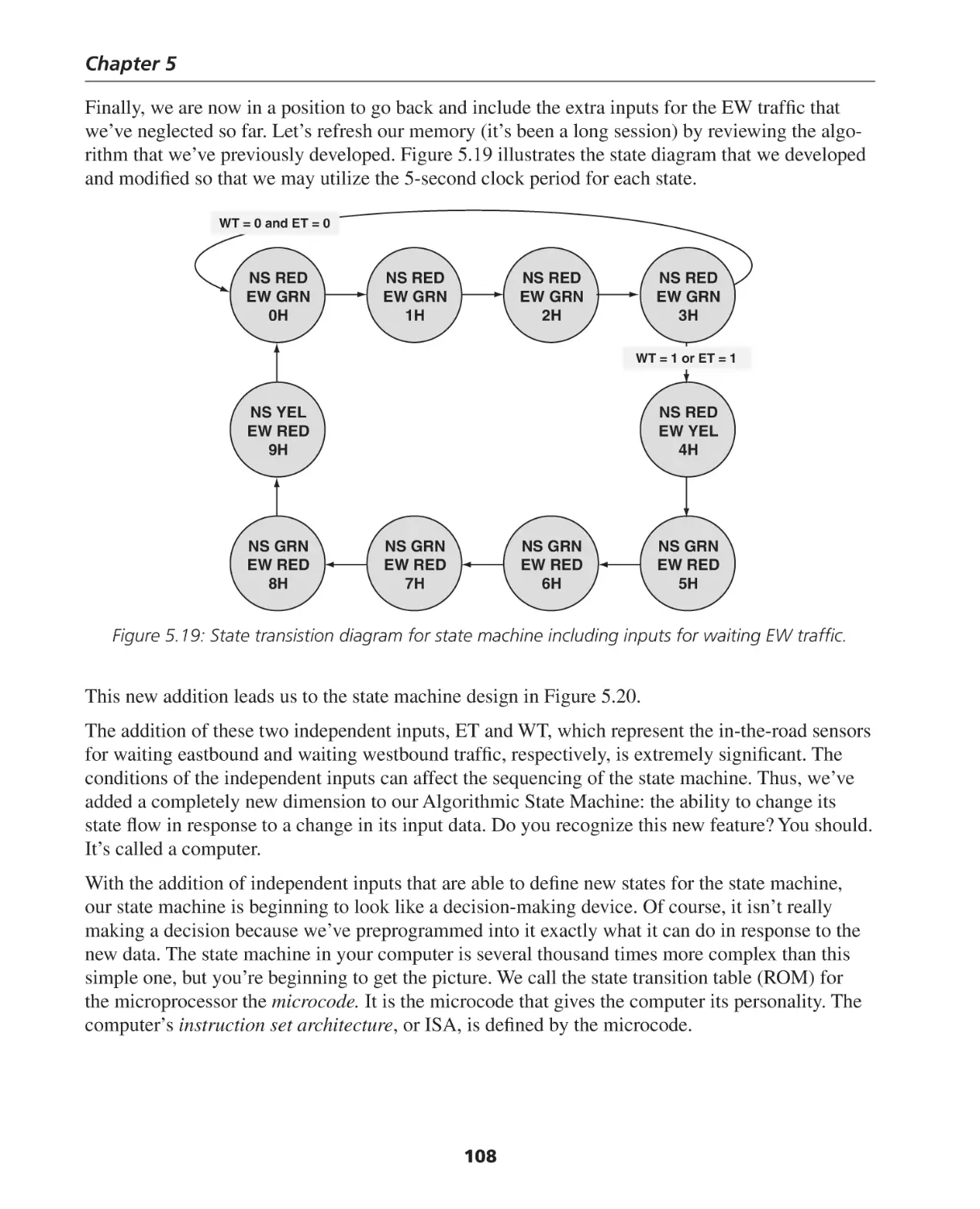
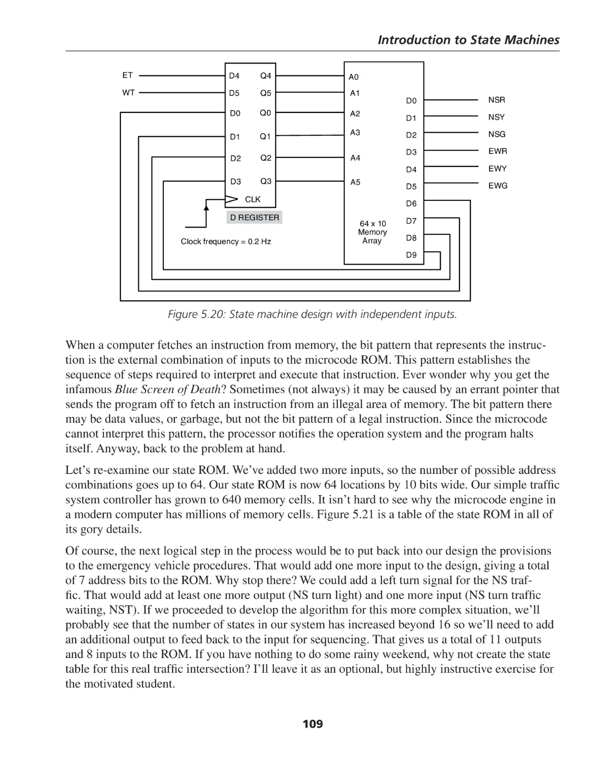
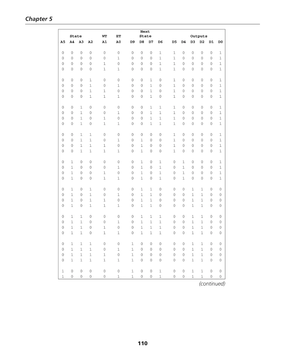
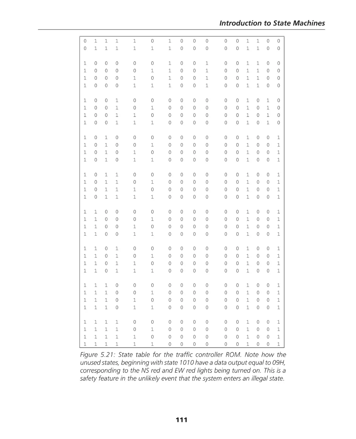
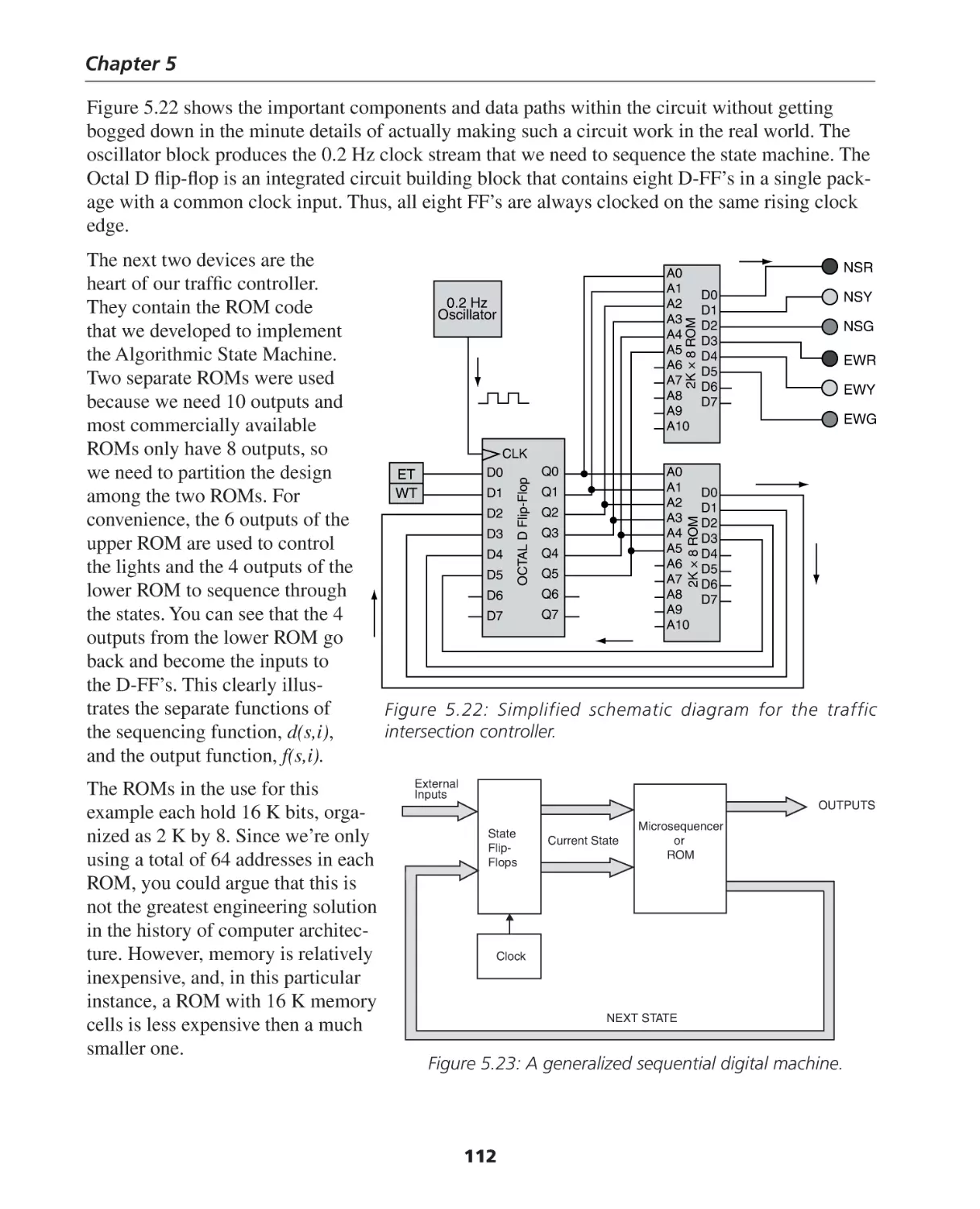
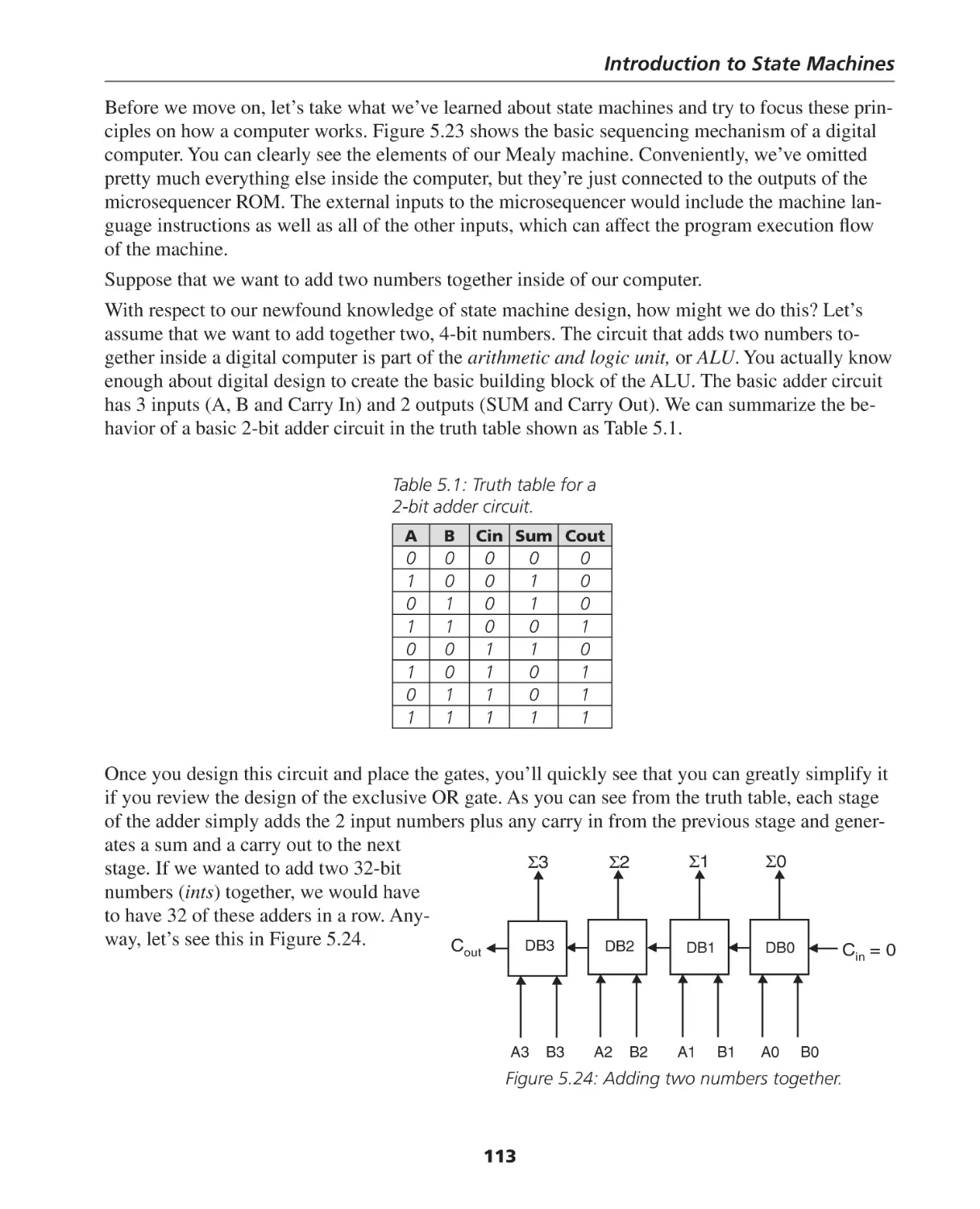
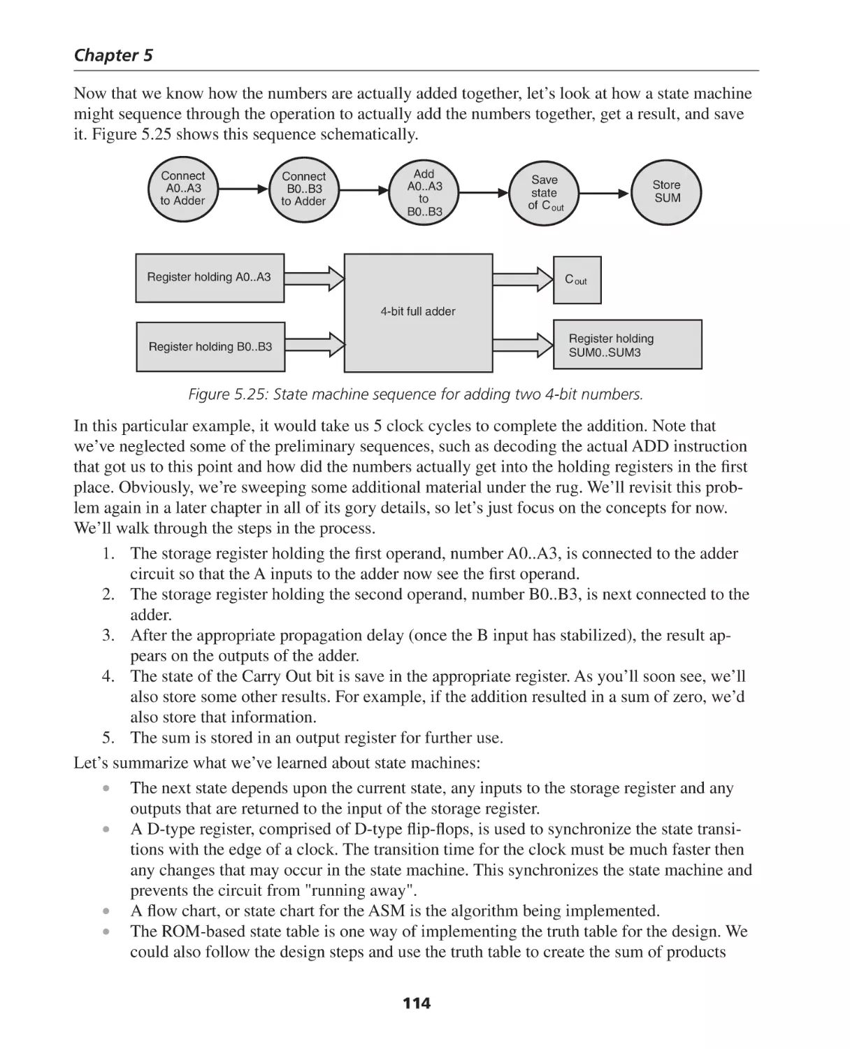
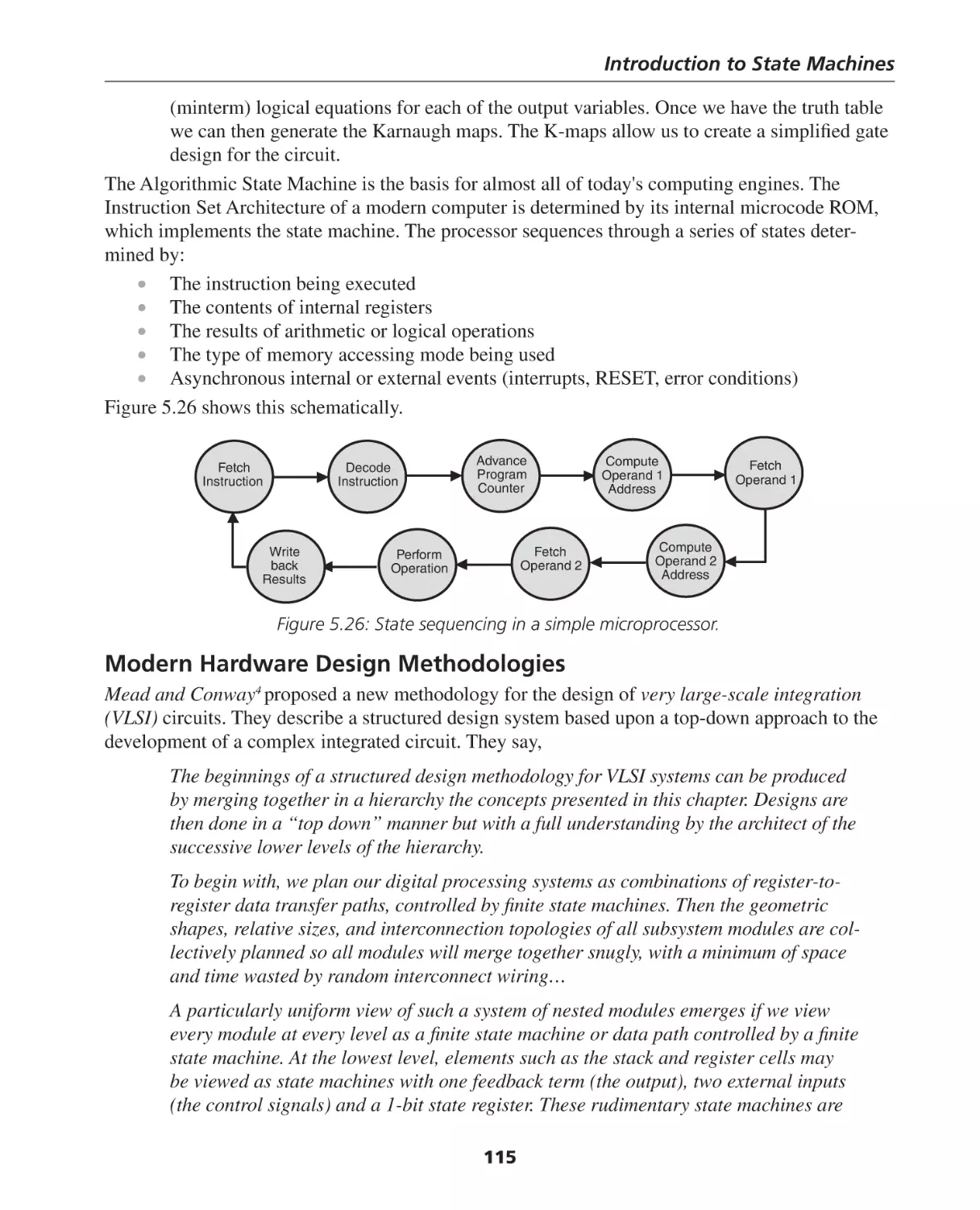
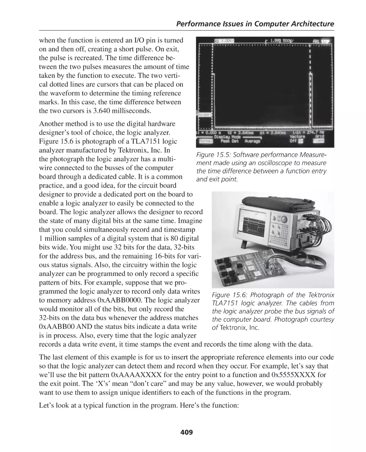
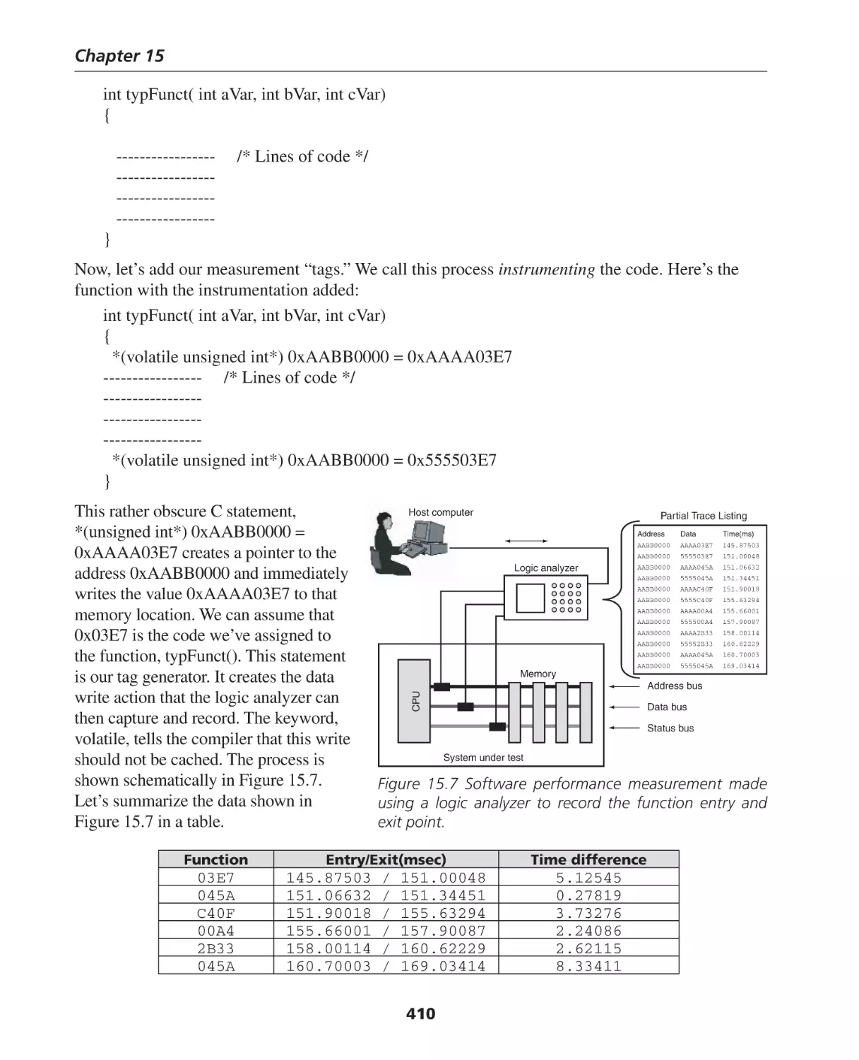
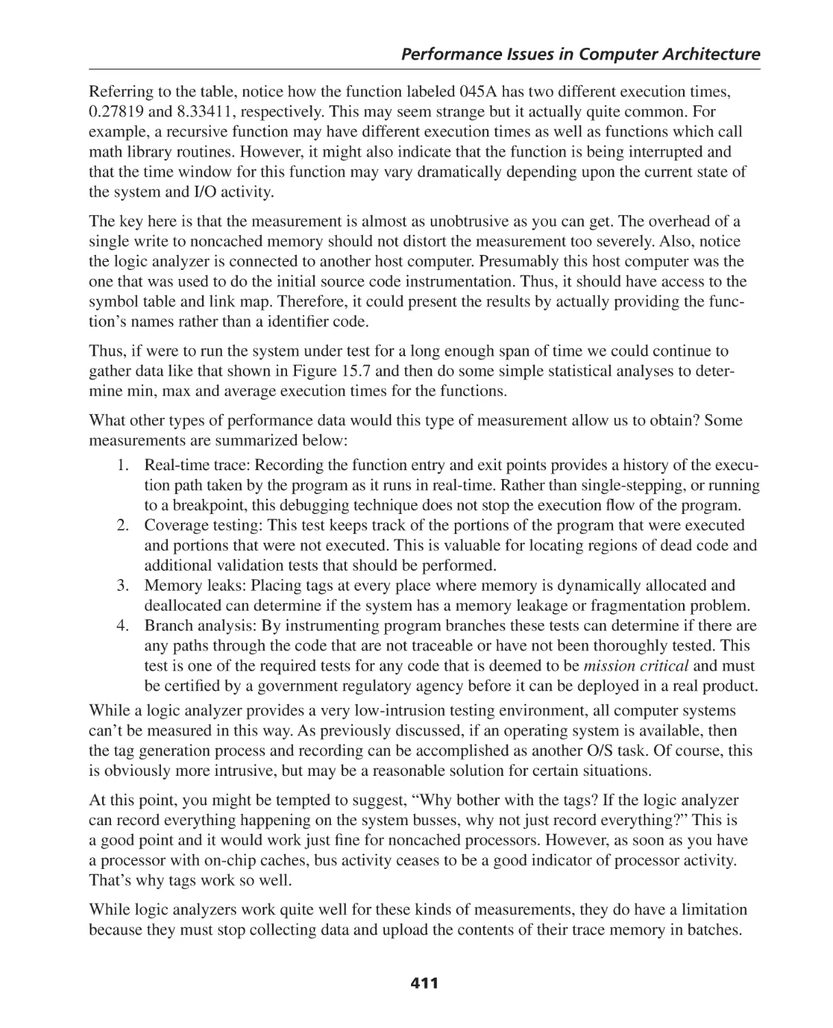
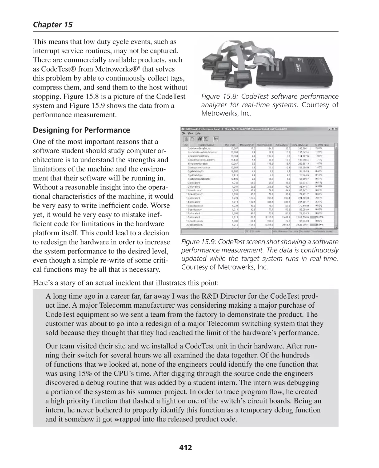
/


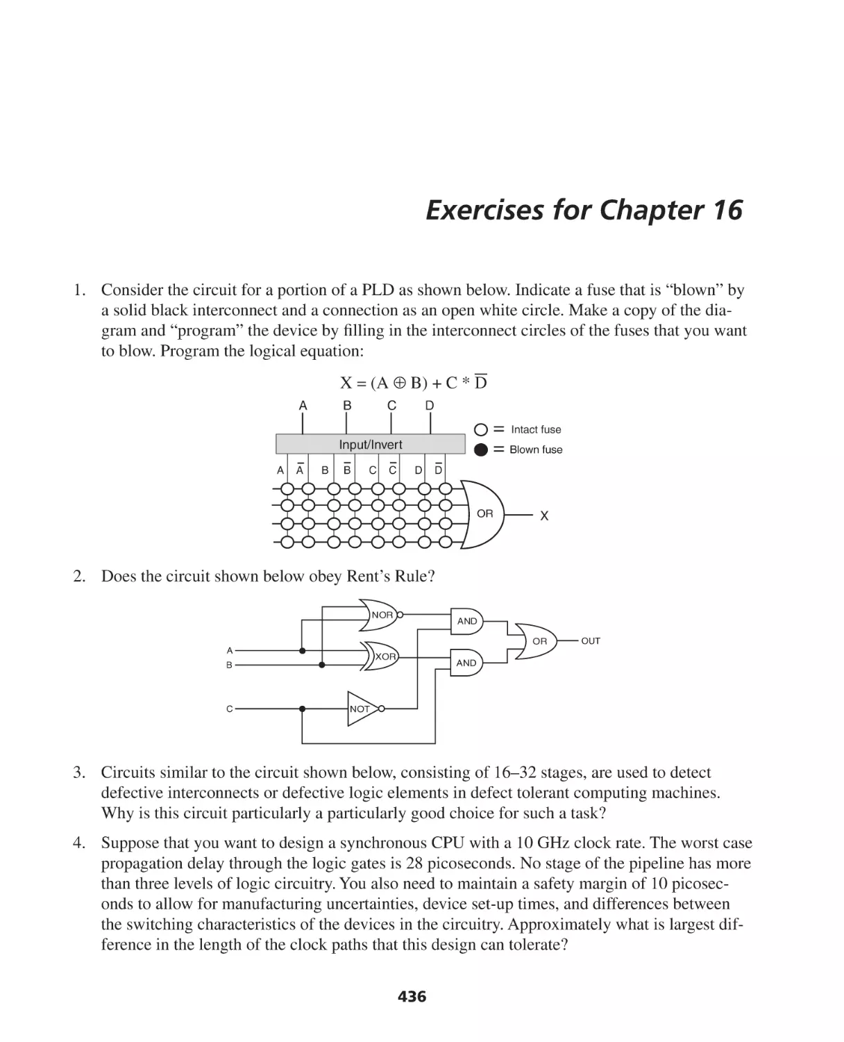


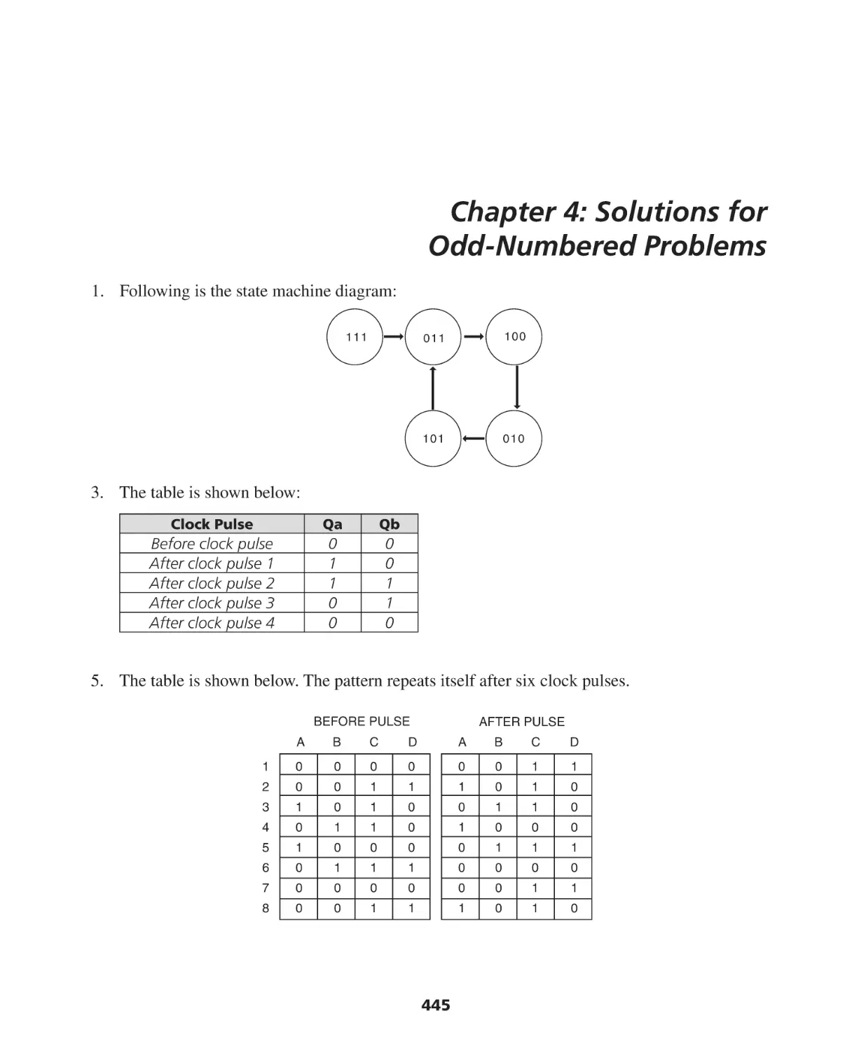


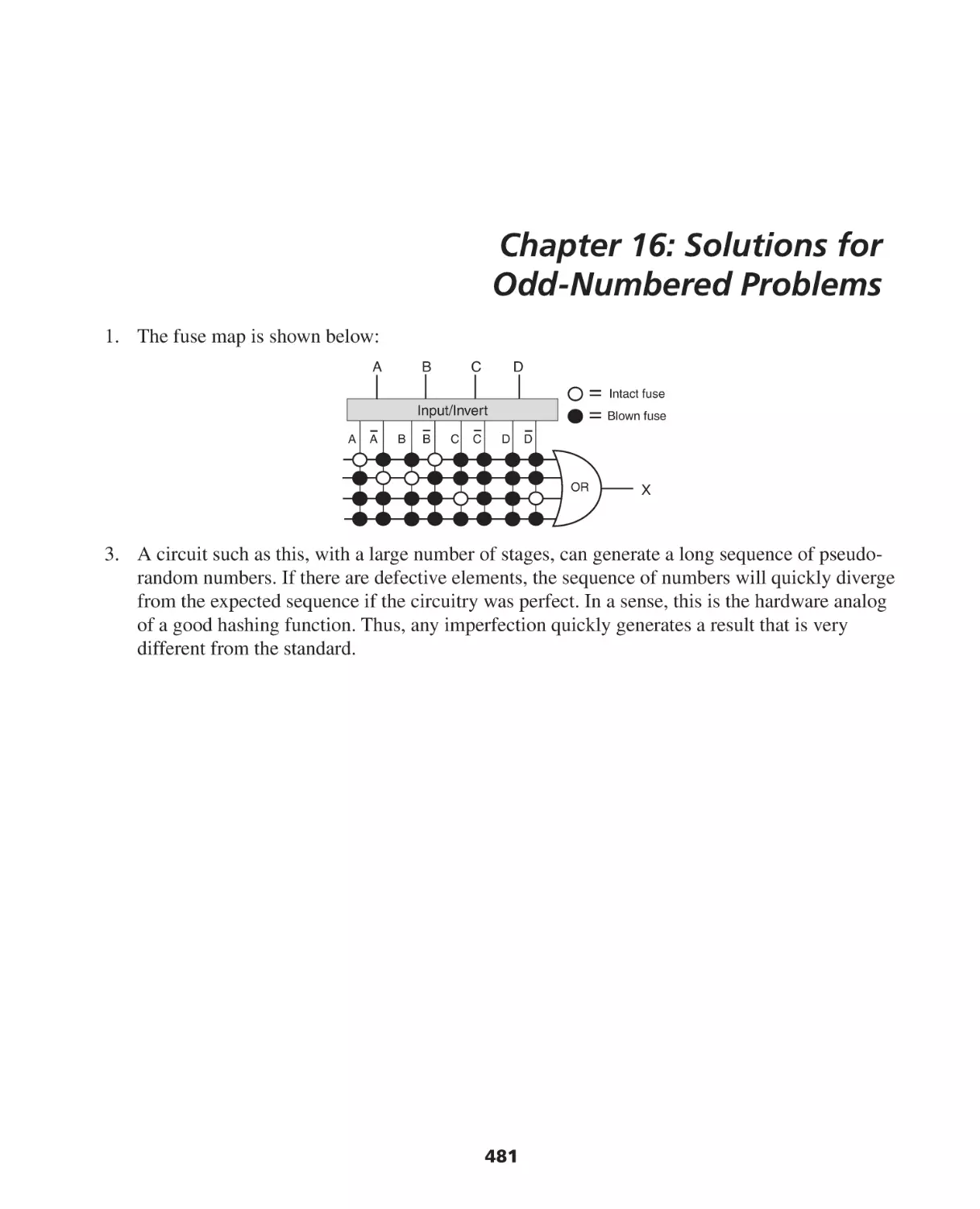


Автор: Berger Arnold S.
Теги: programming software computer systems computer technologies
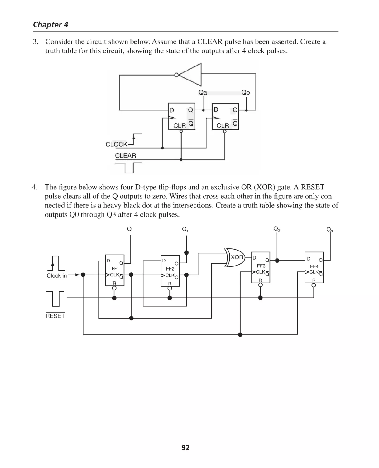
ISBN: 0-7506-7886-0
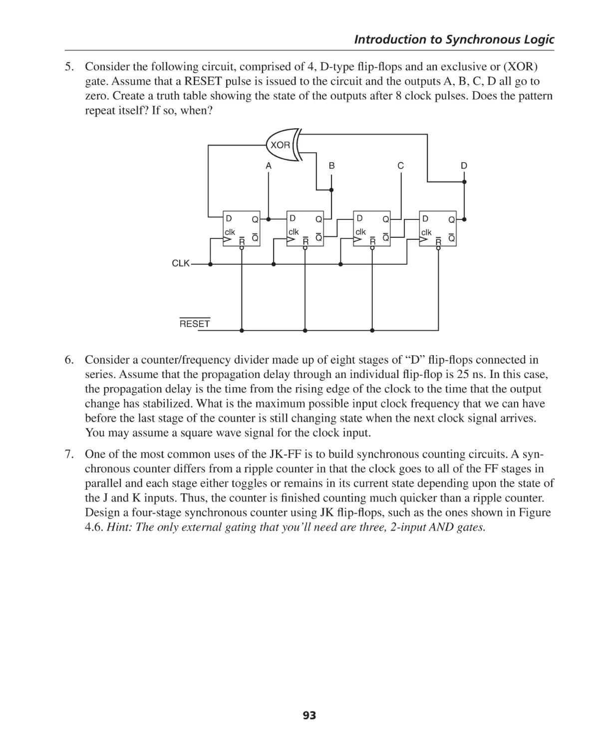
Год: 2005


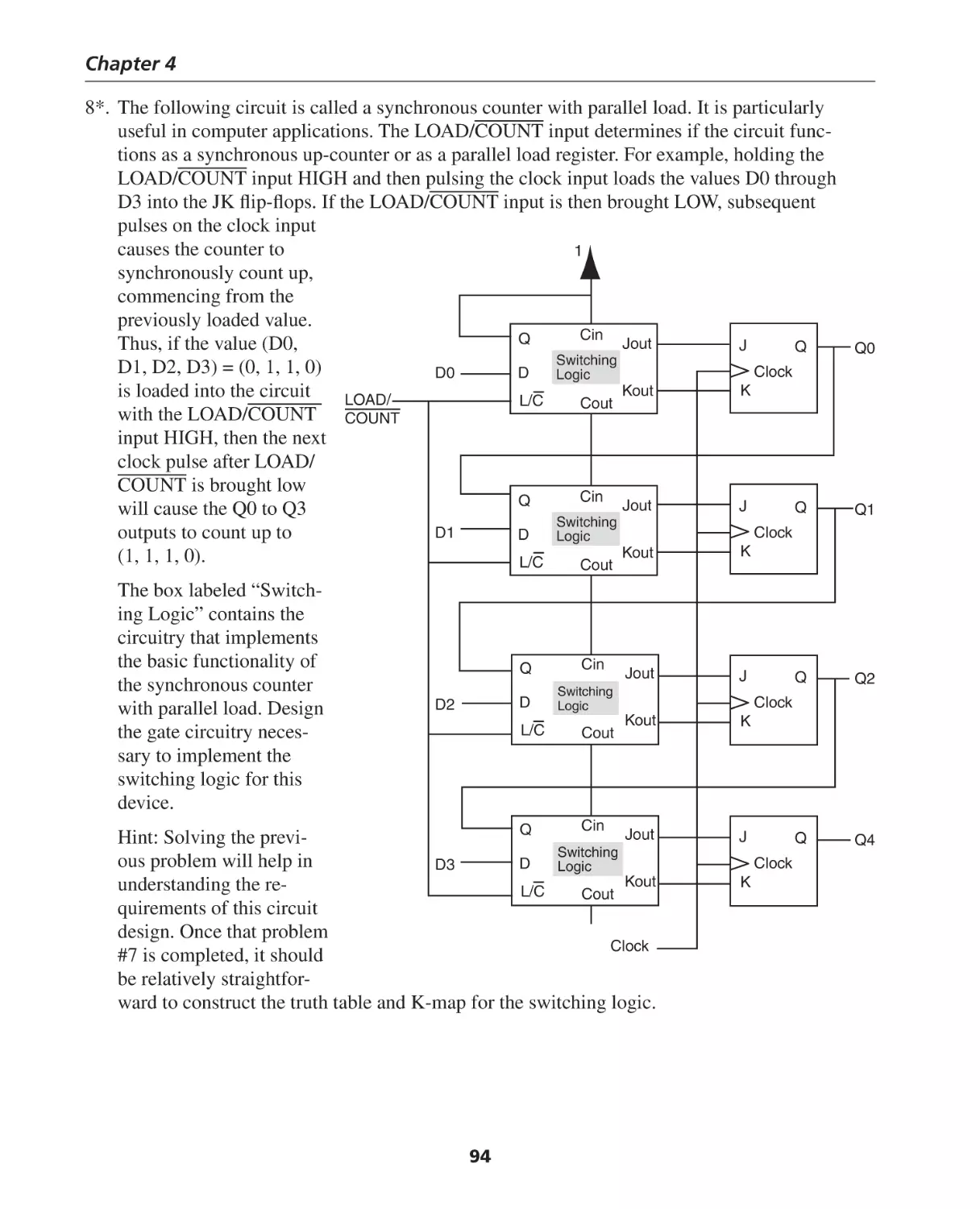
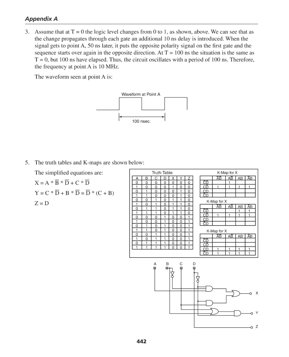
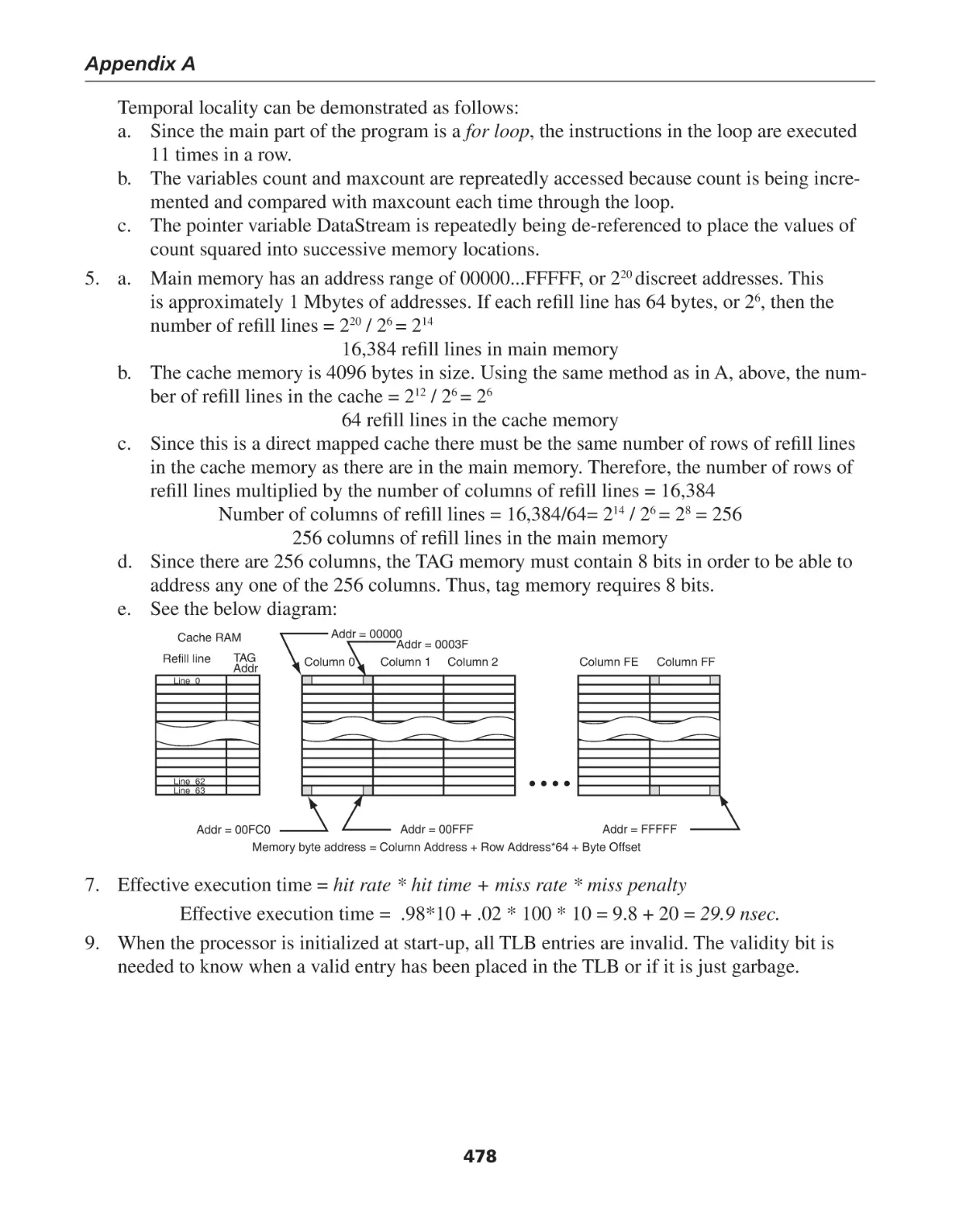
Текст
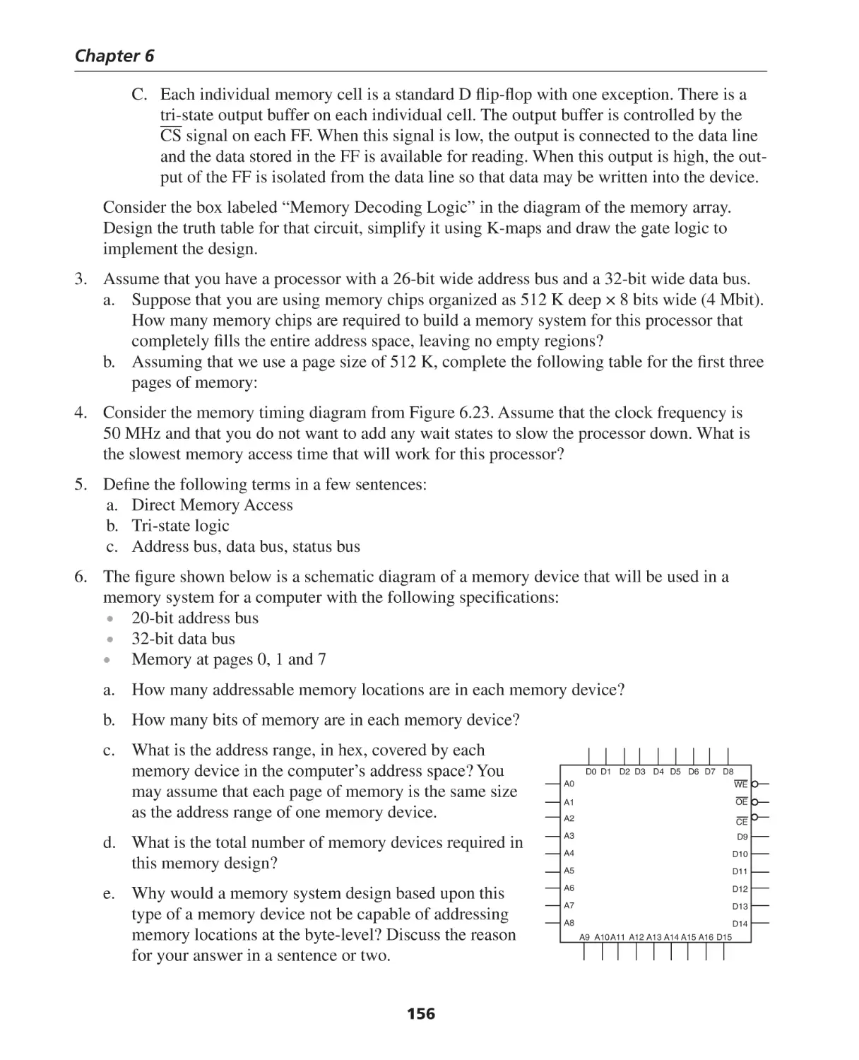
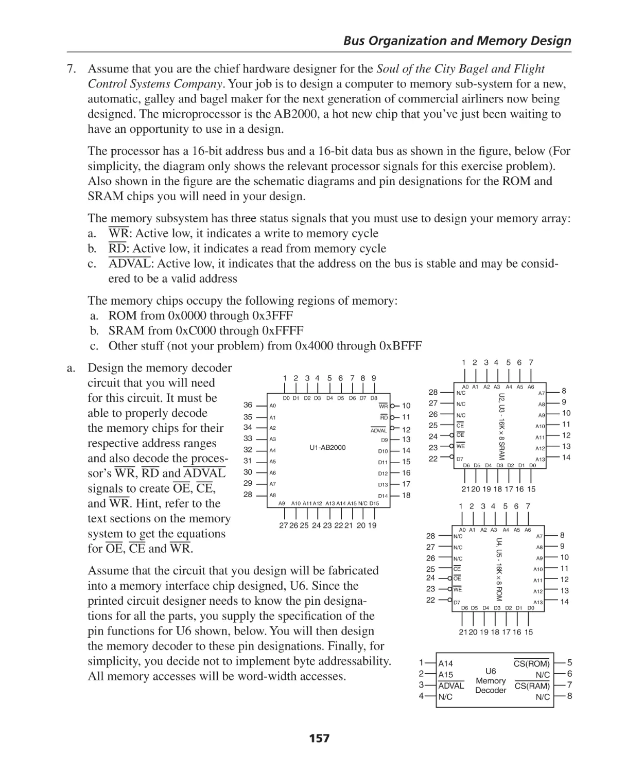
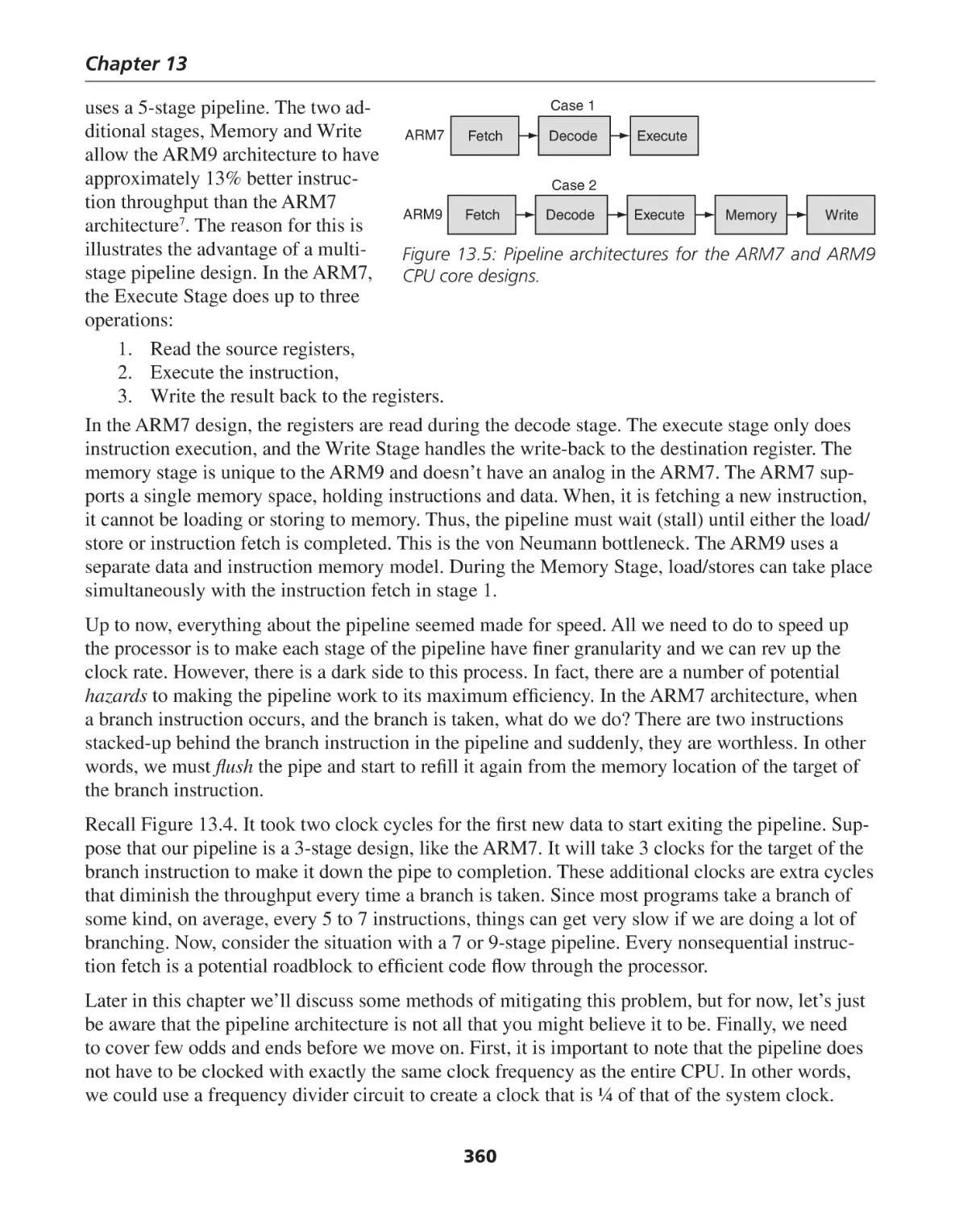
Hardware and Computer Organization
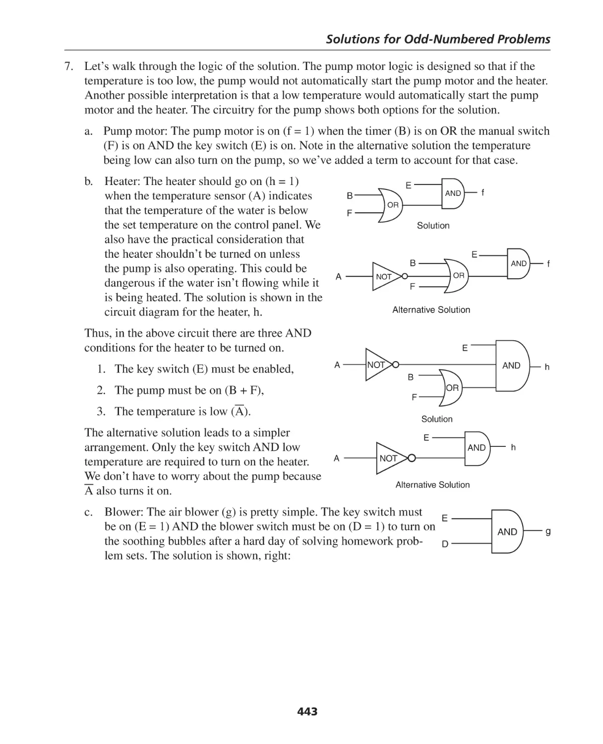
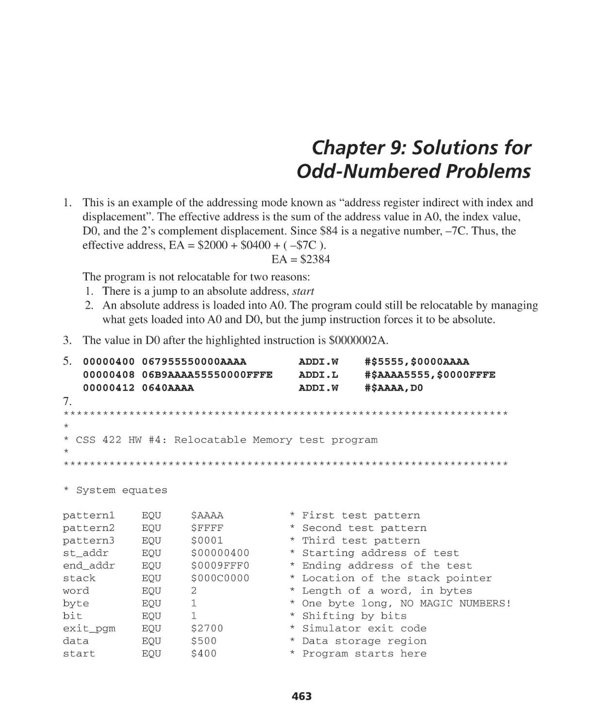
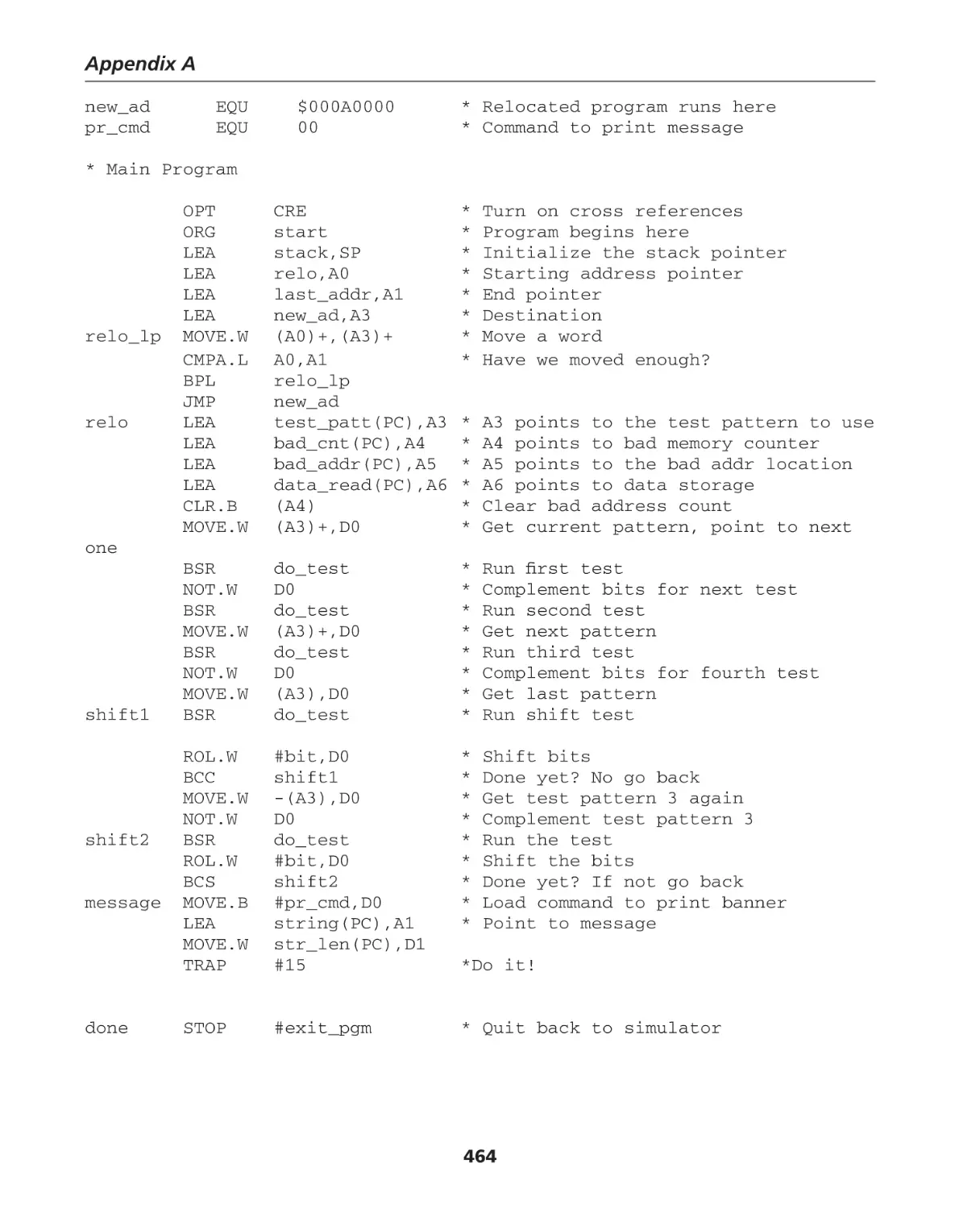
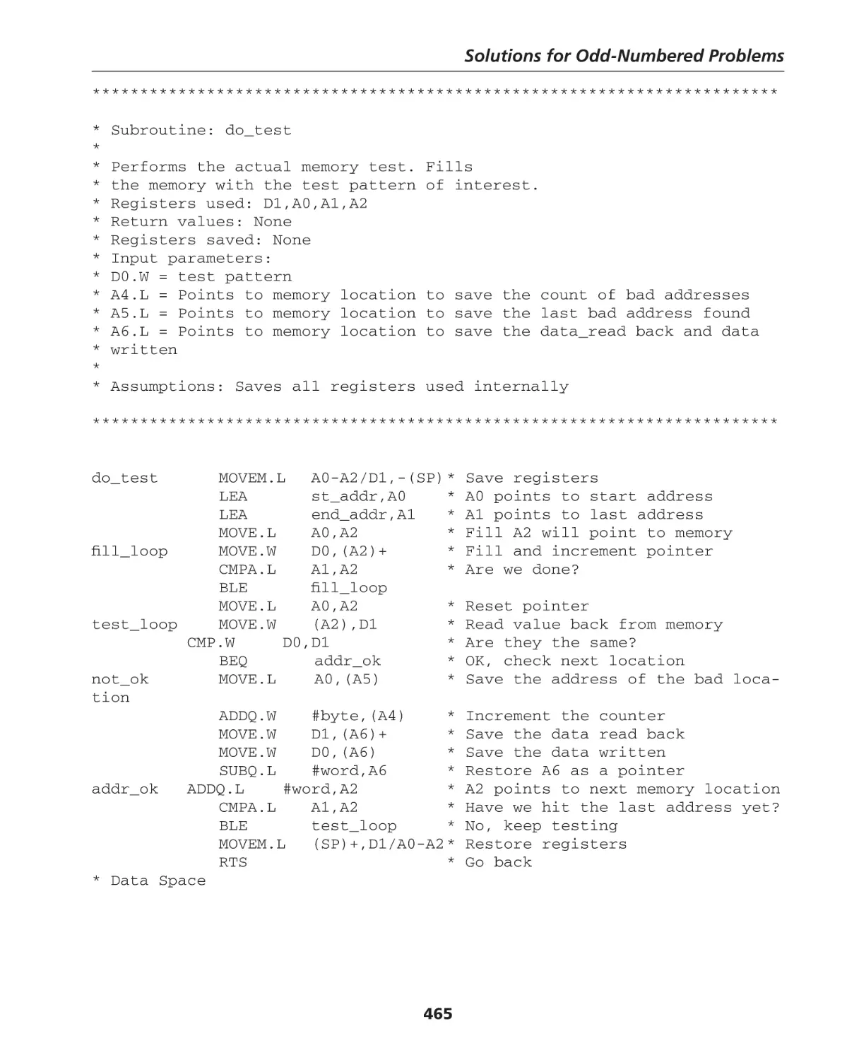
Hardware and Computer Organization
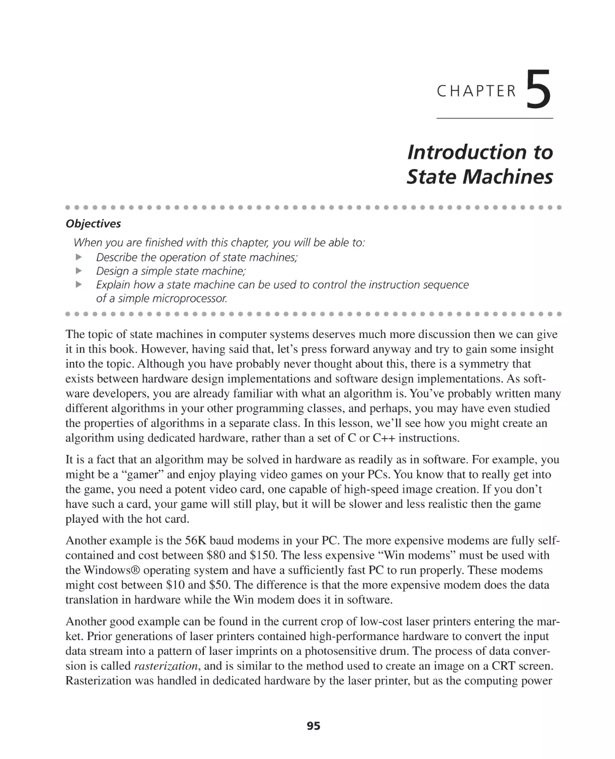
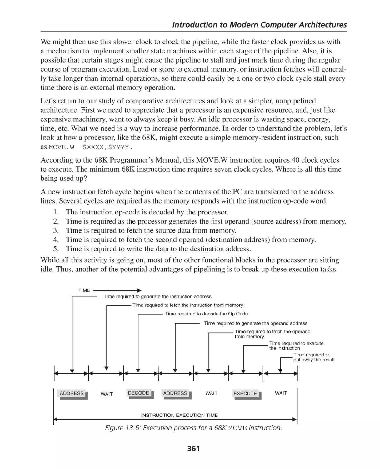
The Software Perspective
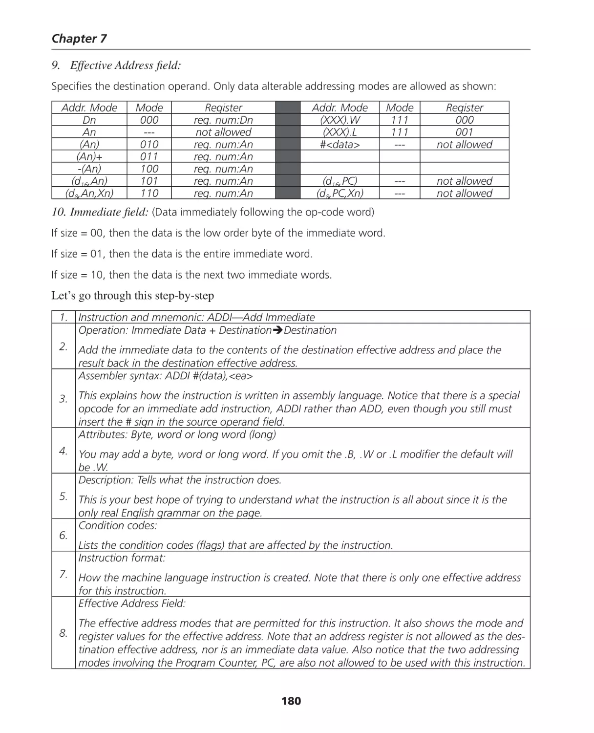
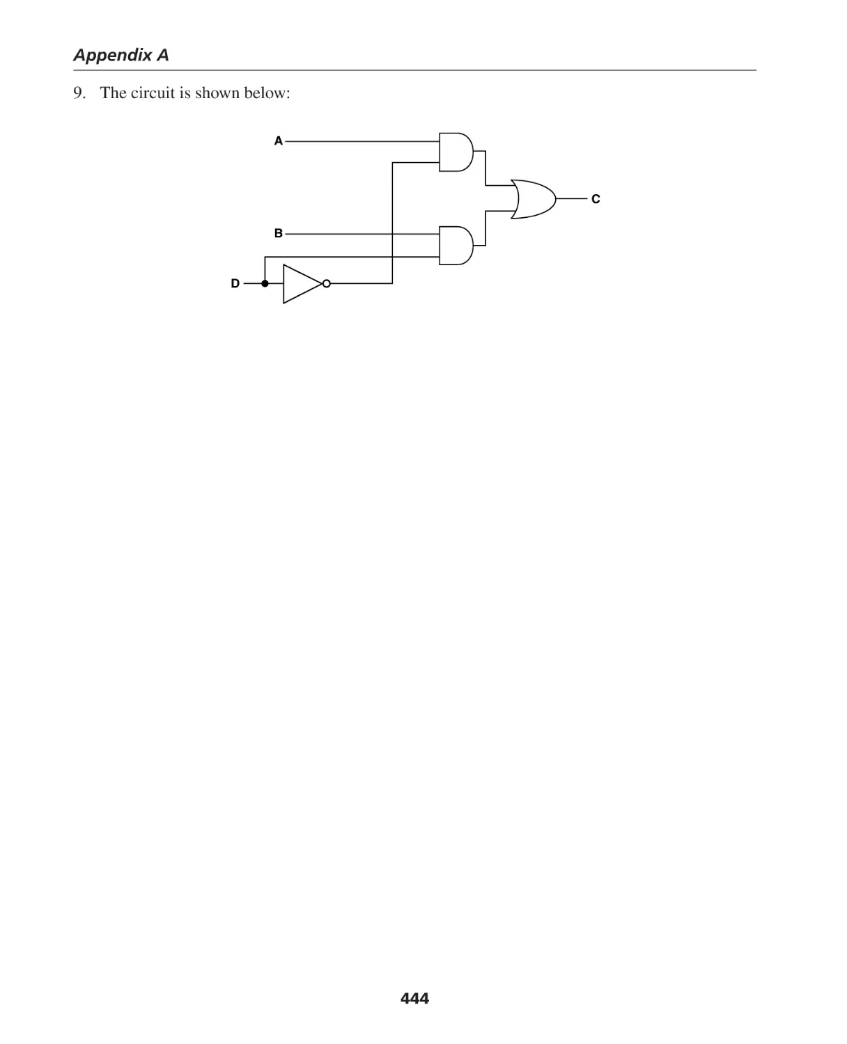
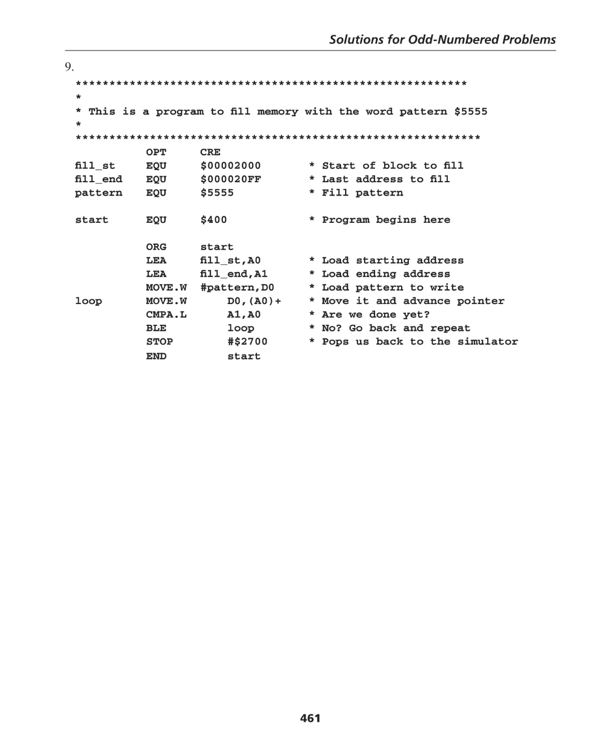
By
Arnold S. Berger
AMSTERDAM • BOSTON • HEIDELBERG • LONDON
NEW YORK • OXFORD • PARIS • SAN DIEGO
SAN FRANCISCO • SINGAPORE • SYDNEY • TOKYO
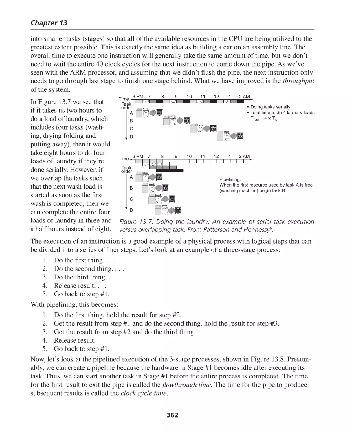
Newnes is an imprint of Elsevier
Newnes is an imprint of Elsevier
30 Corporate Drive, Suite 400, Burlington, MA 01803, USA
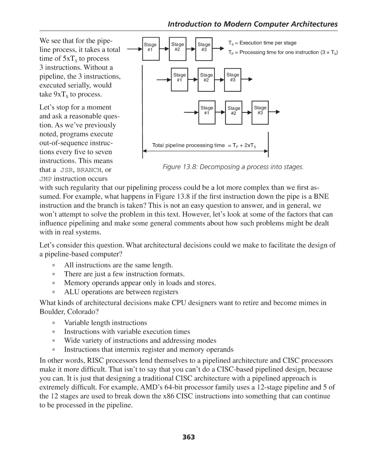
Linacre House, Jordan Hill, Oxford OX2 8DP, UK
Copyright © 2005, Elsevier Inc. All rights reserved.
No part of this publication may be reproduced, stored in a retrieval system, or
transmitted in any form or by any means, electronic, mechanical, photocopying,
recording, or otherwise, without the prior written permission of the publisher.
Permissions may be sought directly from Elsevier’s Science & Technology Rights
Department in Oxford, UK: phone: (+44) 1865 843830, fax: (+44) 1865 853333,
e-mail: permissions@elsevier.com.uk. You may also complete your request on-line via
the Elsevier homepage (http://elsevier.com), by selecting “Customer Support” and then
“Obtaining Permissions.”
Recognizing the importance of preserving what has been written,
Elsevier prints its books on acid-free paper whenever possible.
Library of Congress Cataloging-in-Publication Data
Berger, Arnold S.
Hardware and computer organization : a guide for software professionals / by Arnold S. Berger.
p. cm.
ISBN 0-7506-7886-0
1. Computer organization. 2. Computer engineering. 3. Computer interfaces. I. Title.
QA76.9.C643B47 2005
004.2'2--dc22
2005040553
British Library Cataloguing-in-Publication Data
A catalogue record for this book is available from the British Library.
For information on all Newnes publications
visit our Web site at www.books.elsevier.com
04 05 06 07 08 09
10 9 8 7 6 5 4 3 2 1
Printed in the United States of America
For Vivian and Andrea
Contents
Preface to the First Edition .................................................................................. xi
Acknowledgments ............................................................................................. xvi
What’s on the DVD-ROM? ................................................................................ xvii
CHAPTER 1: Introduction and Overview of Hardware Architecture ................. 1
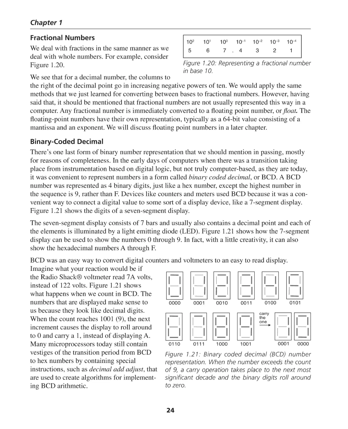
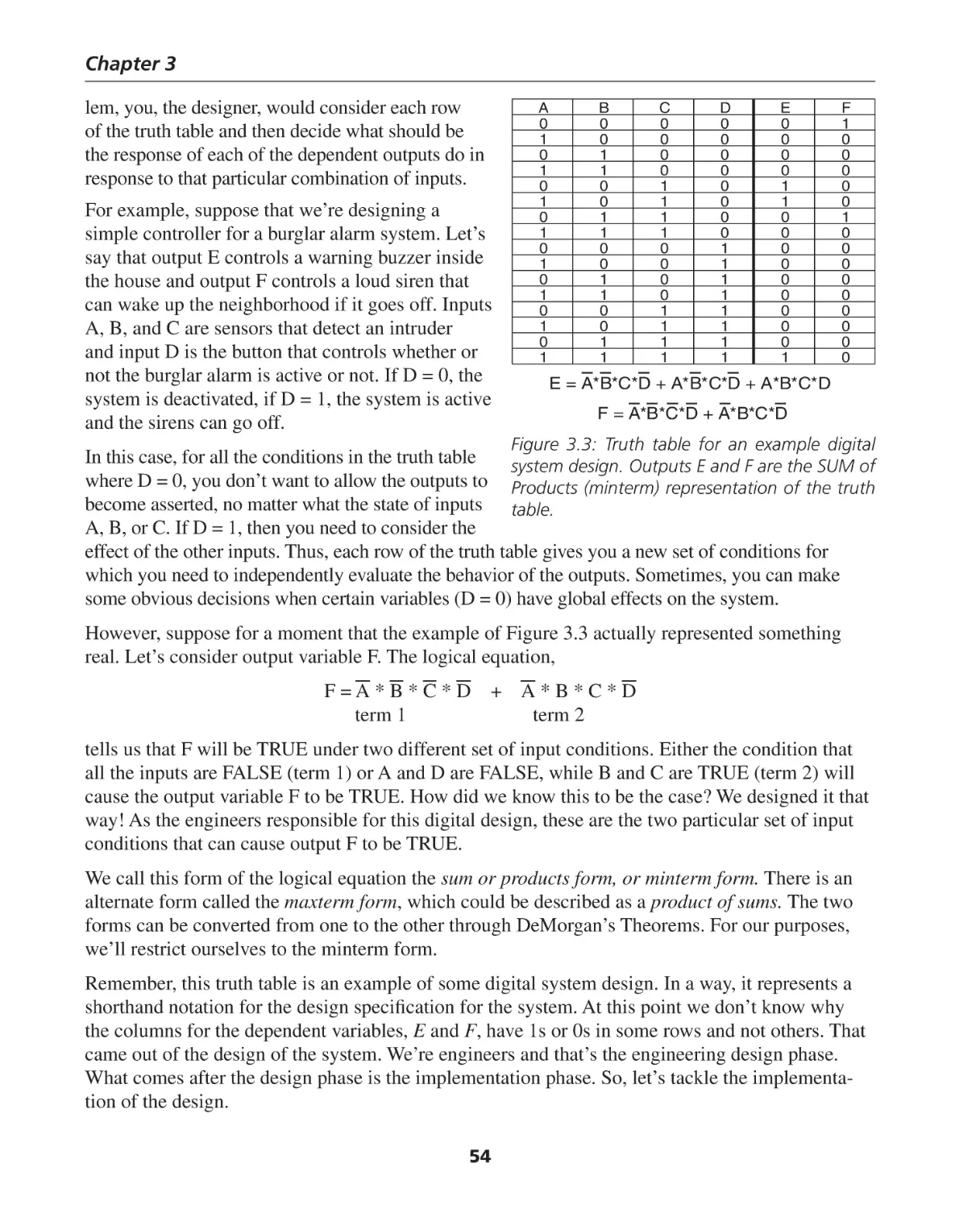
Introduction ................................................................................................................................ 1
A Brief History of Computing ...................................................................................................... 1
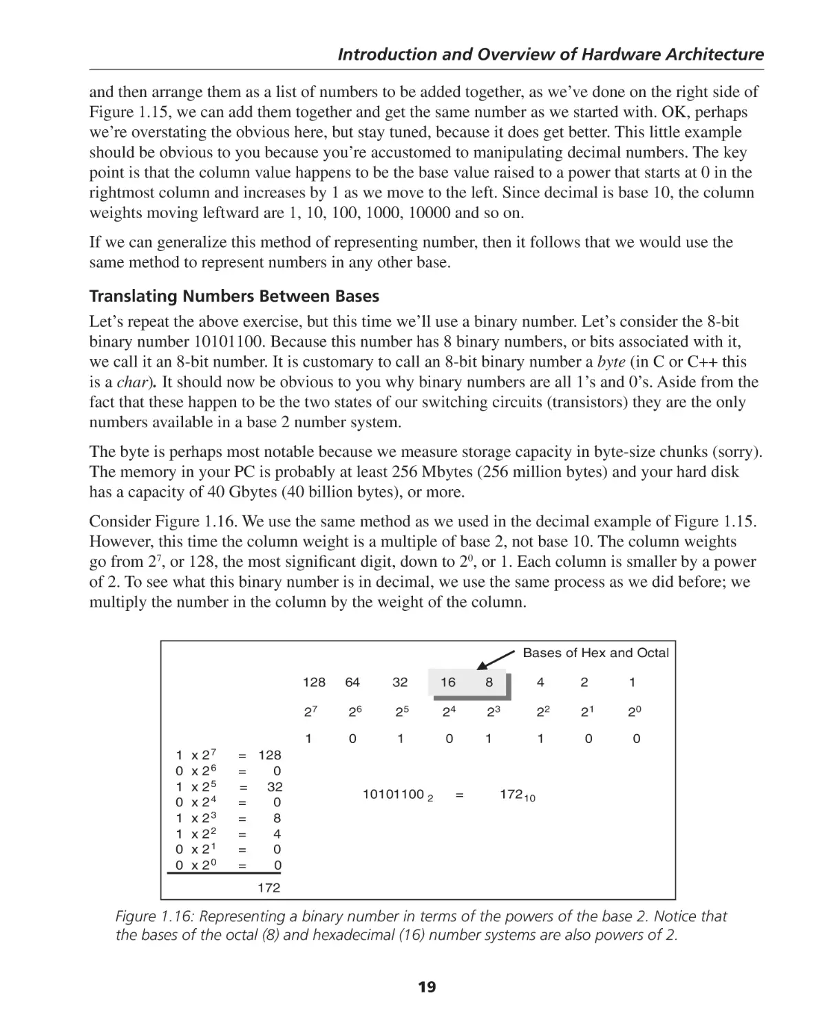
Number Systems ....................................................................................................................... 12
Converting Decimals to Bases .................................................................................................... 25
Engineering Notation ............................................................................................................... 26
Summary of Chapter 1 .............................................................................................................. 27
Exercises for Chapter 1 .............................................................................................................. 28
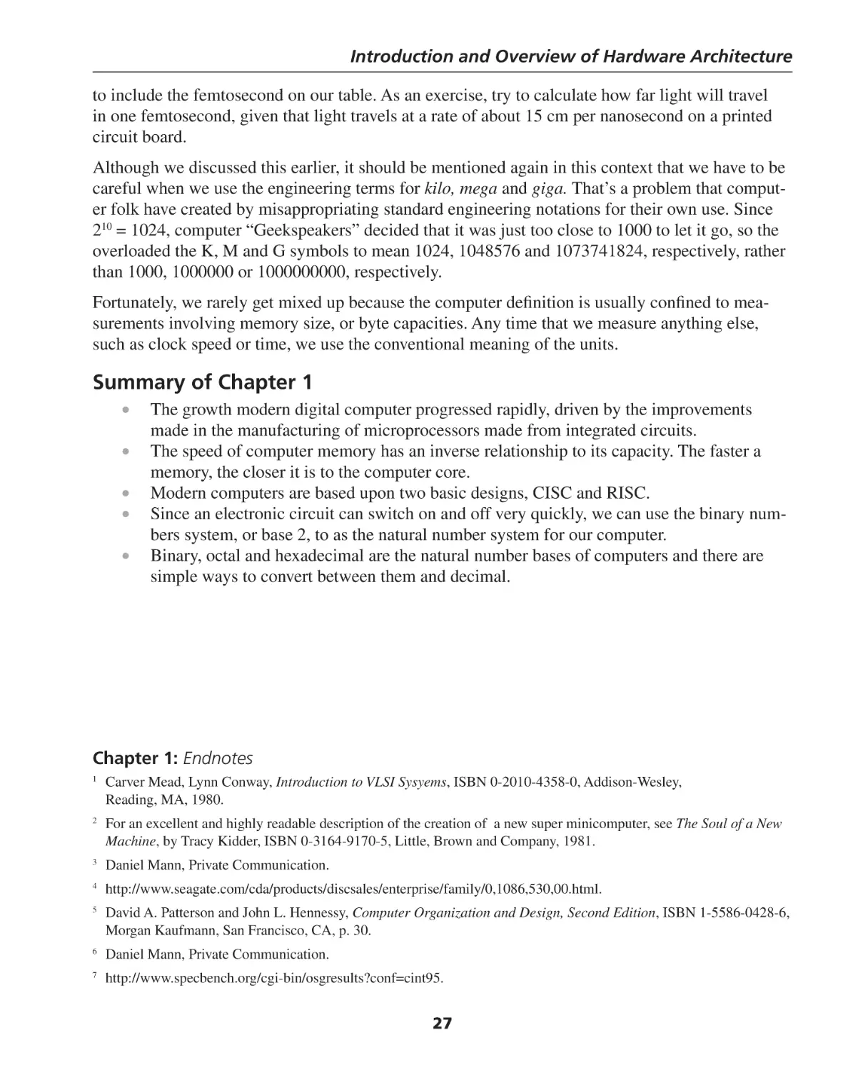
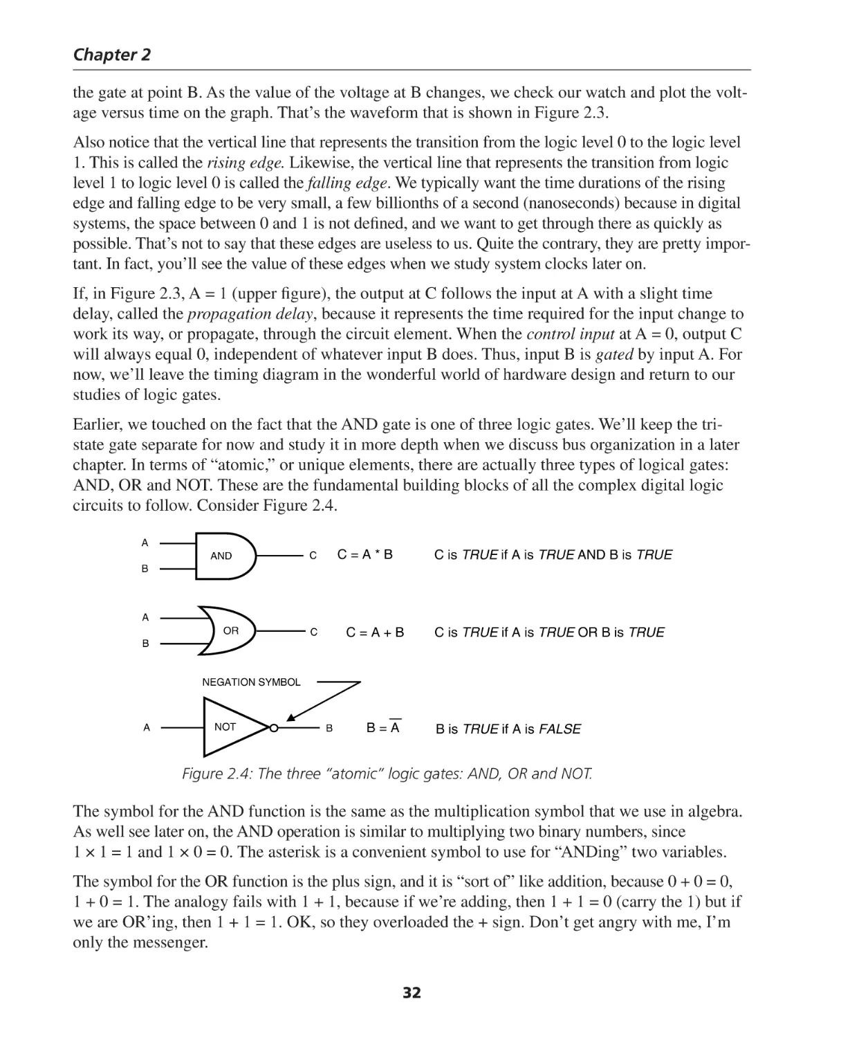
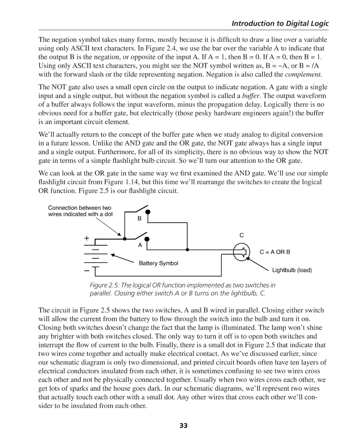
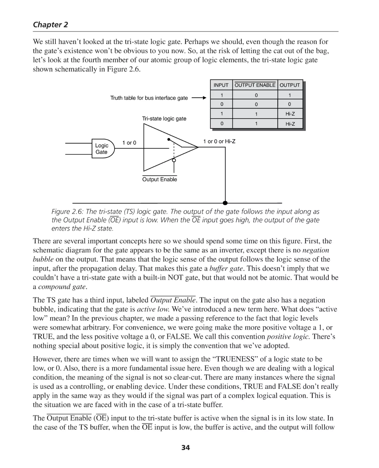
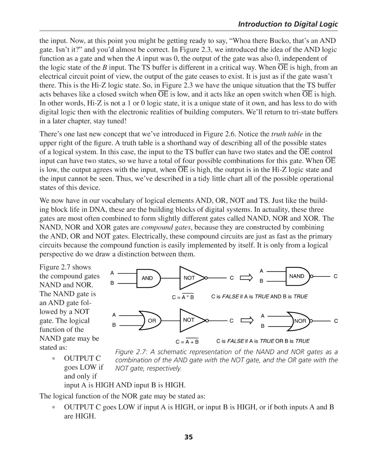
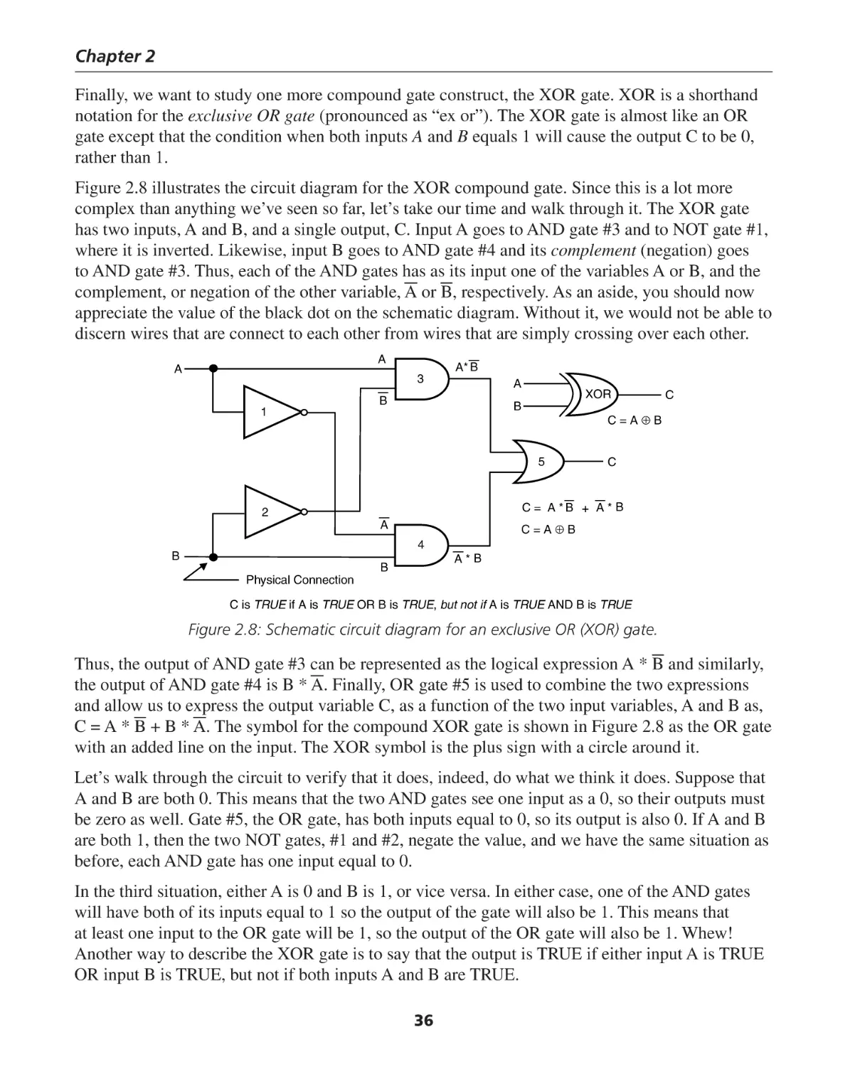
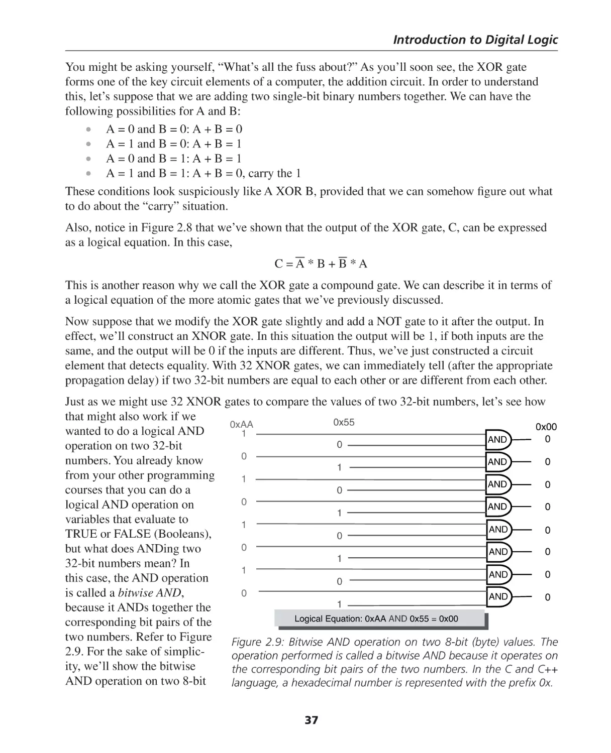
CHAPTER 2: Introduction to Digital Logic ......................................................... 29
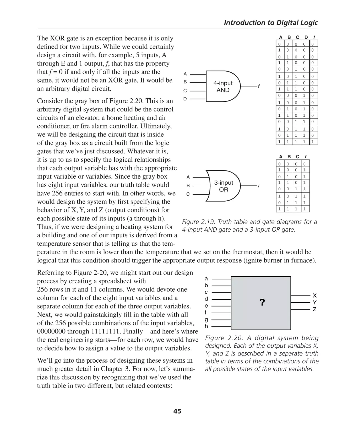
Electronic Gate Description ........................................................................................................ 39
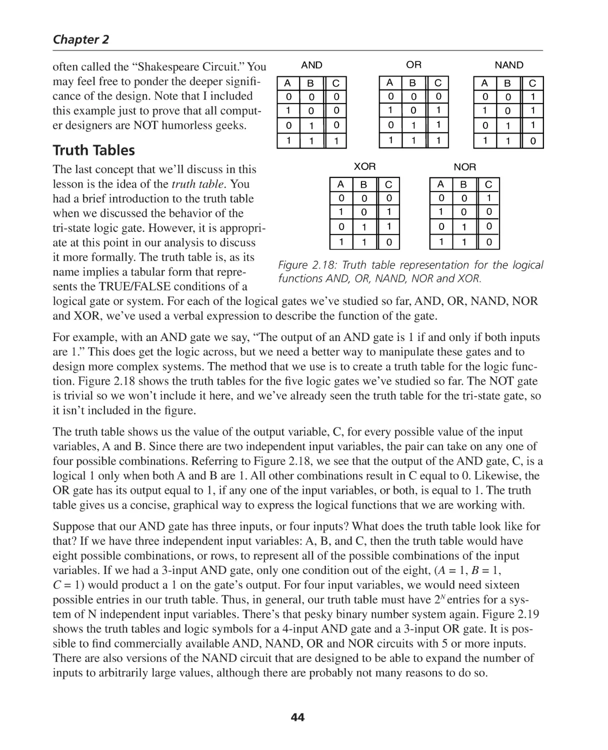
Truth Tables ............................................................................................................................... 44
Summary of Chapter 2 .............................................................................................................. 46
Exercises for Chapter 2 .............................................................................................................. 47
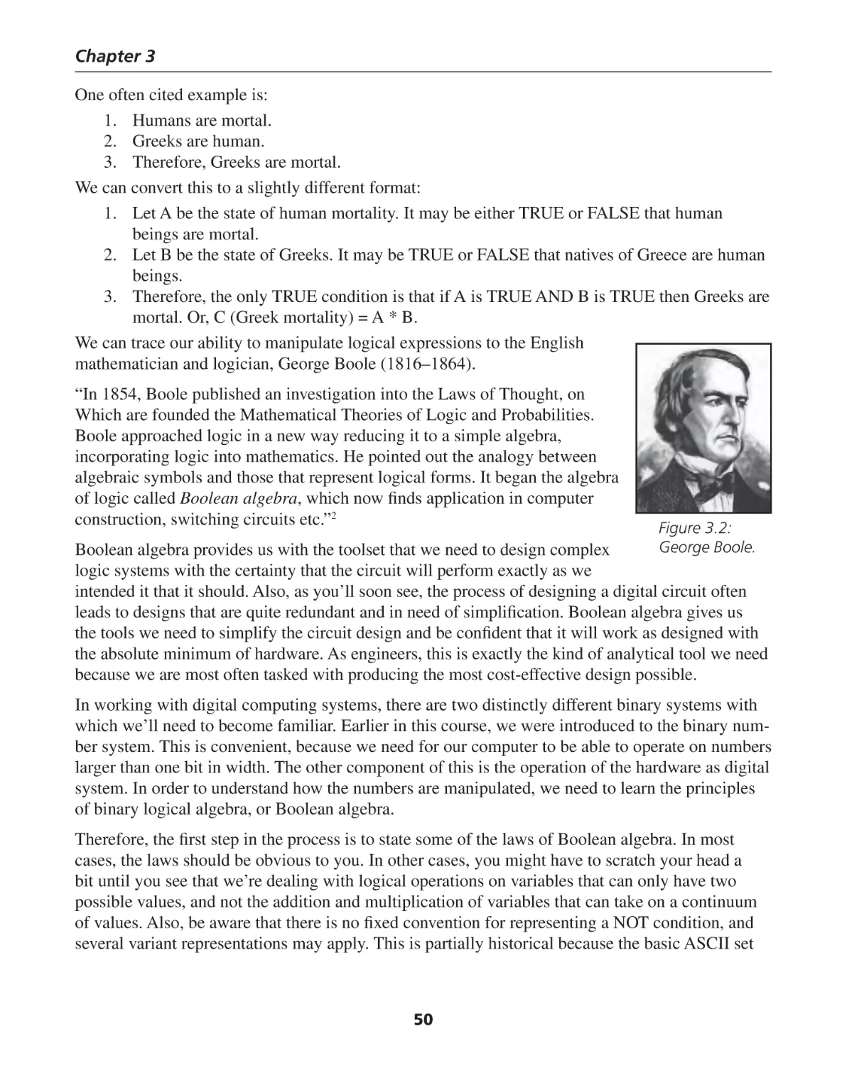
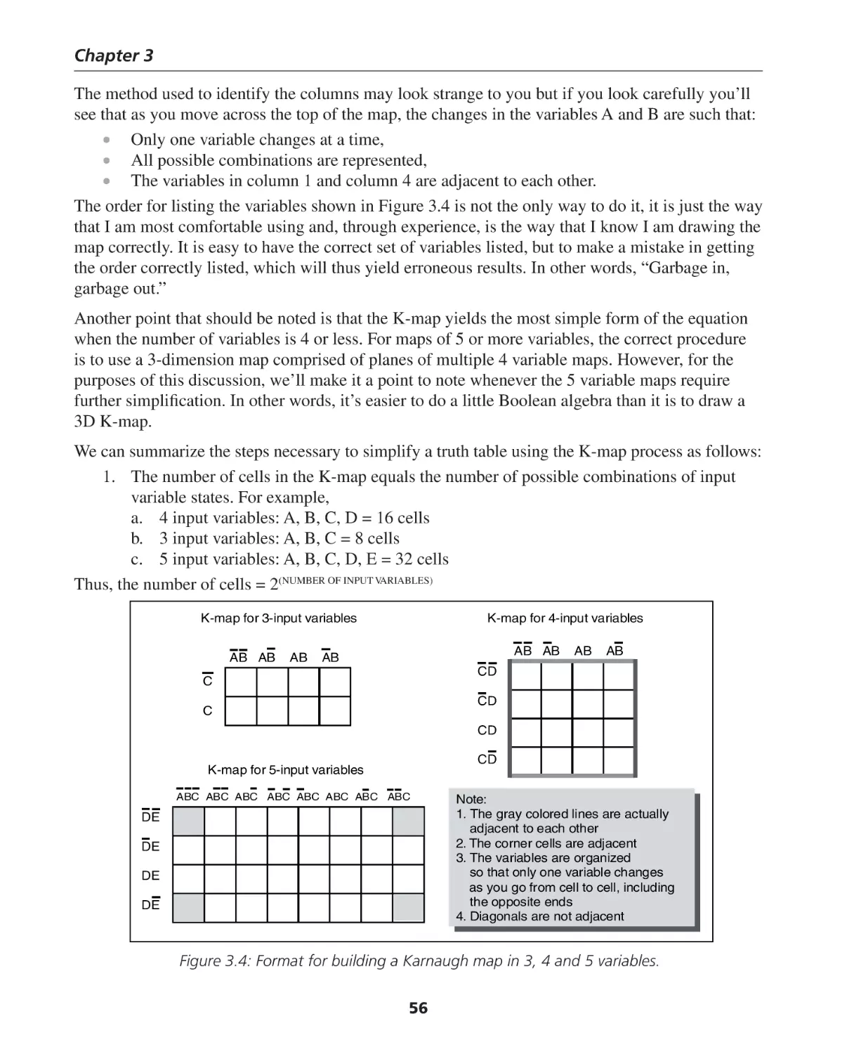
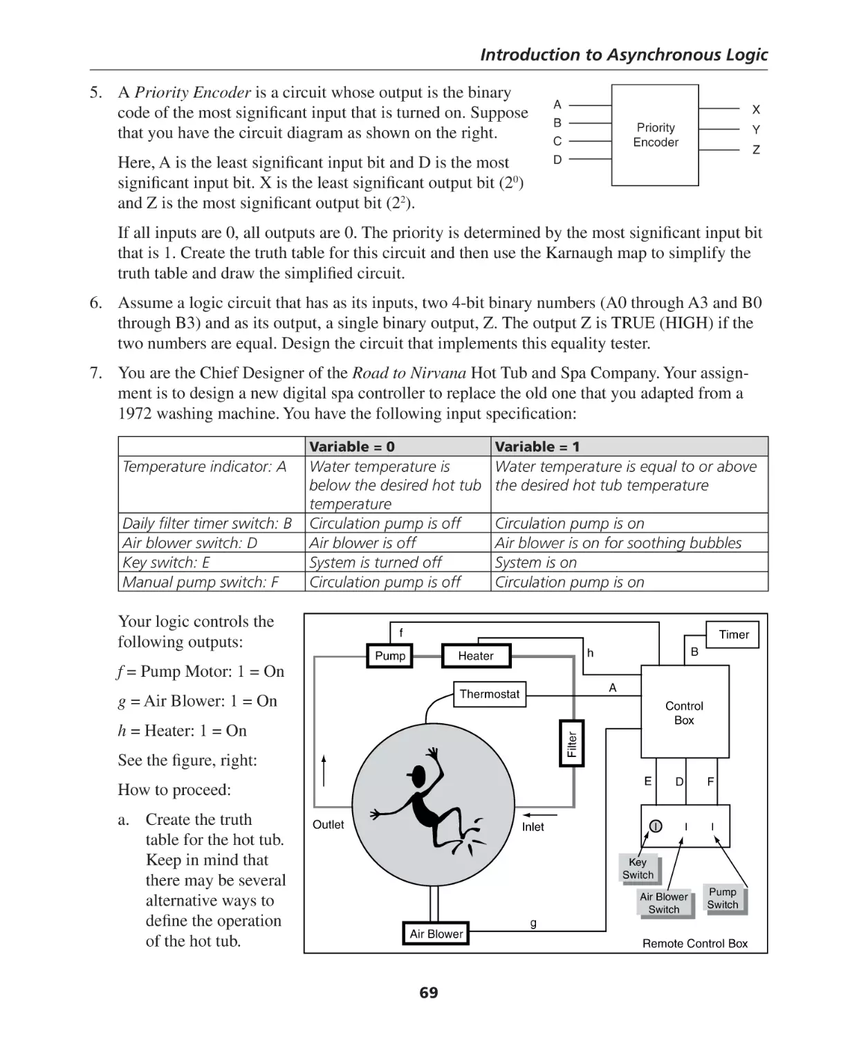
CHAPTER 3: Introduction to Asynchronous Logic............................................. 49
Introduction .............................................................................................................................. 49
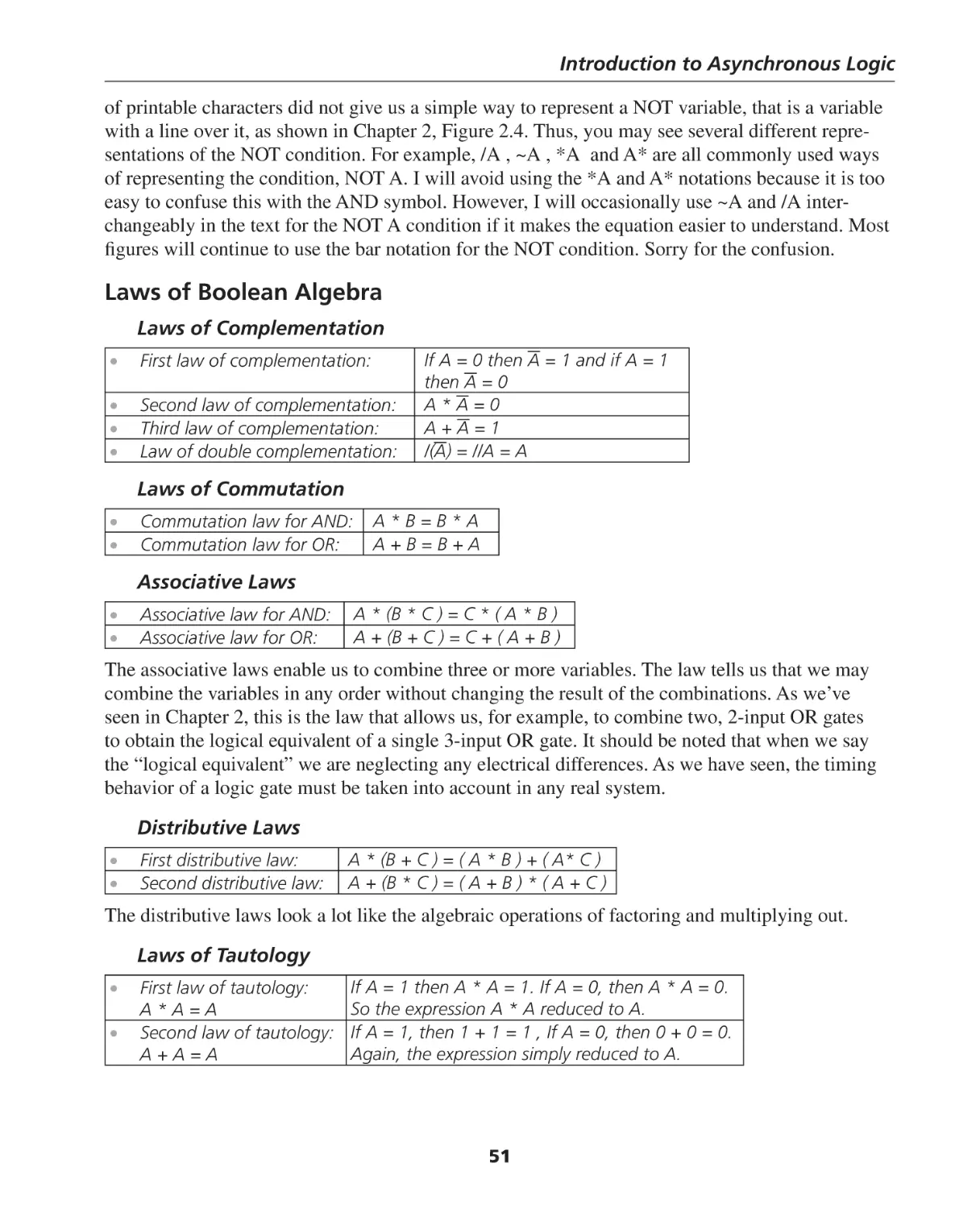
Laws of Boolean Algebra ........................................................................................................... 51
The Karnaugh Map ................................................................................................................... 55
Clocks and Pulses ...................................................................................................................... 62
Summary of Chapter 3 .............................................................................................................. 67
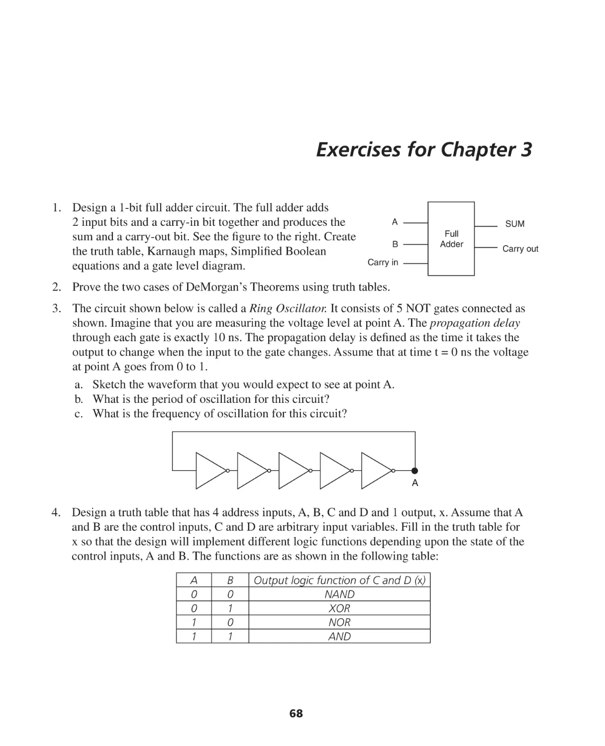
Exercises for Chapter 3 .............................................................................................................. 68
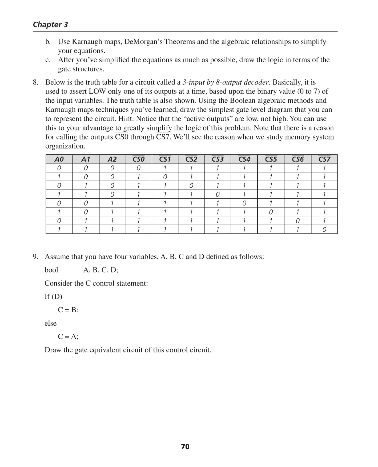
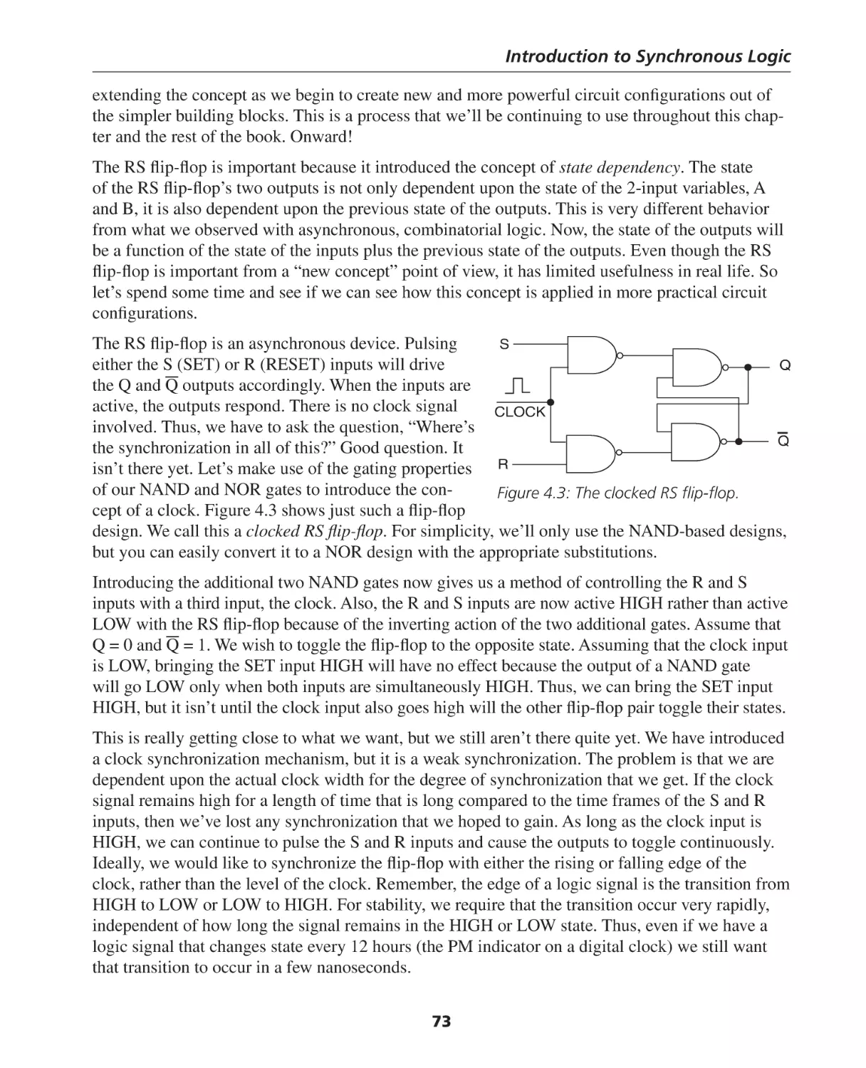
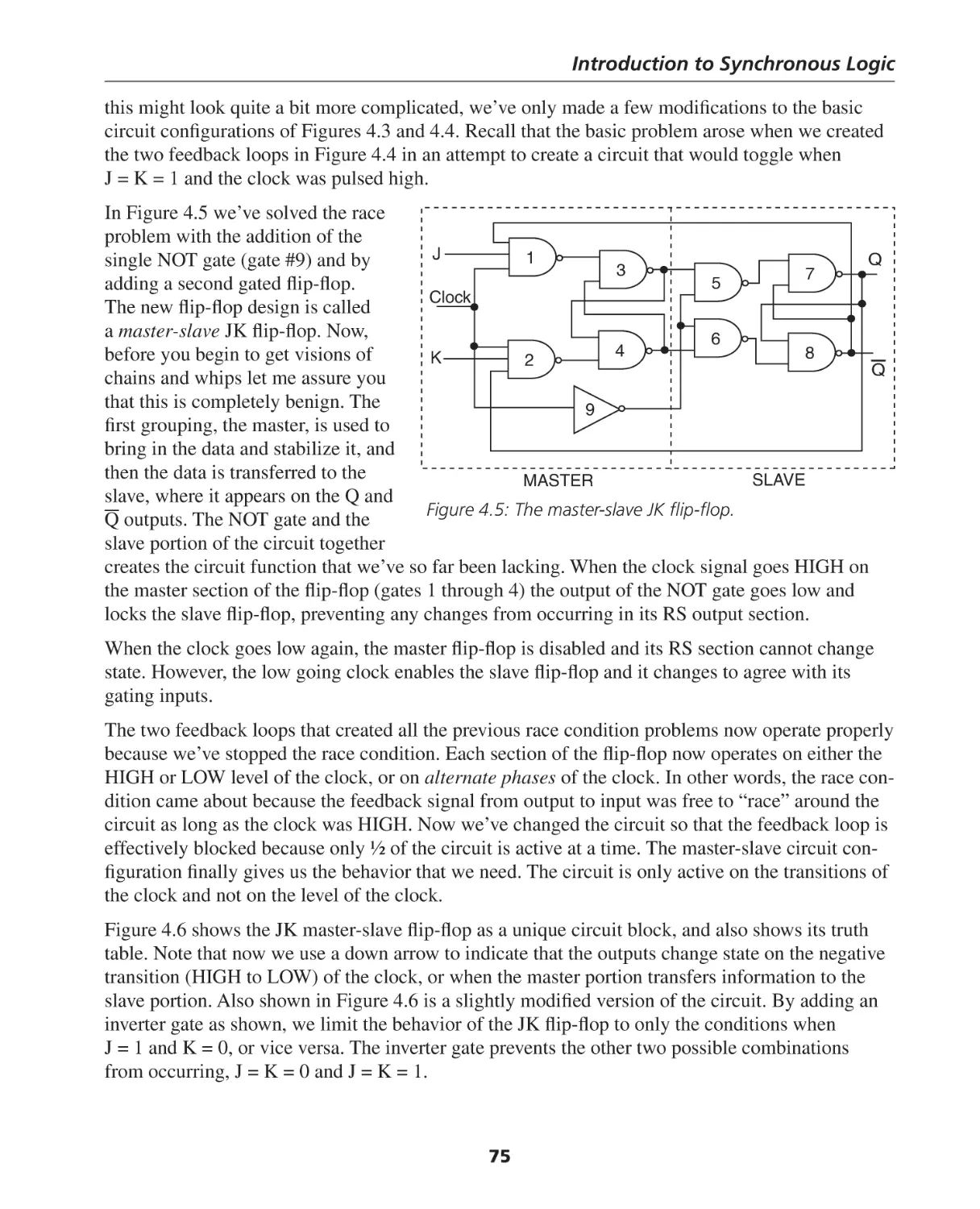
CHAPTER 4: Introduction to Synchronous Logic ............................................... 71
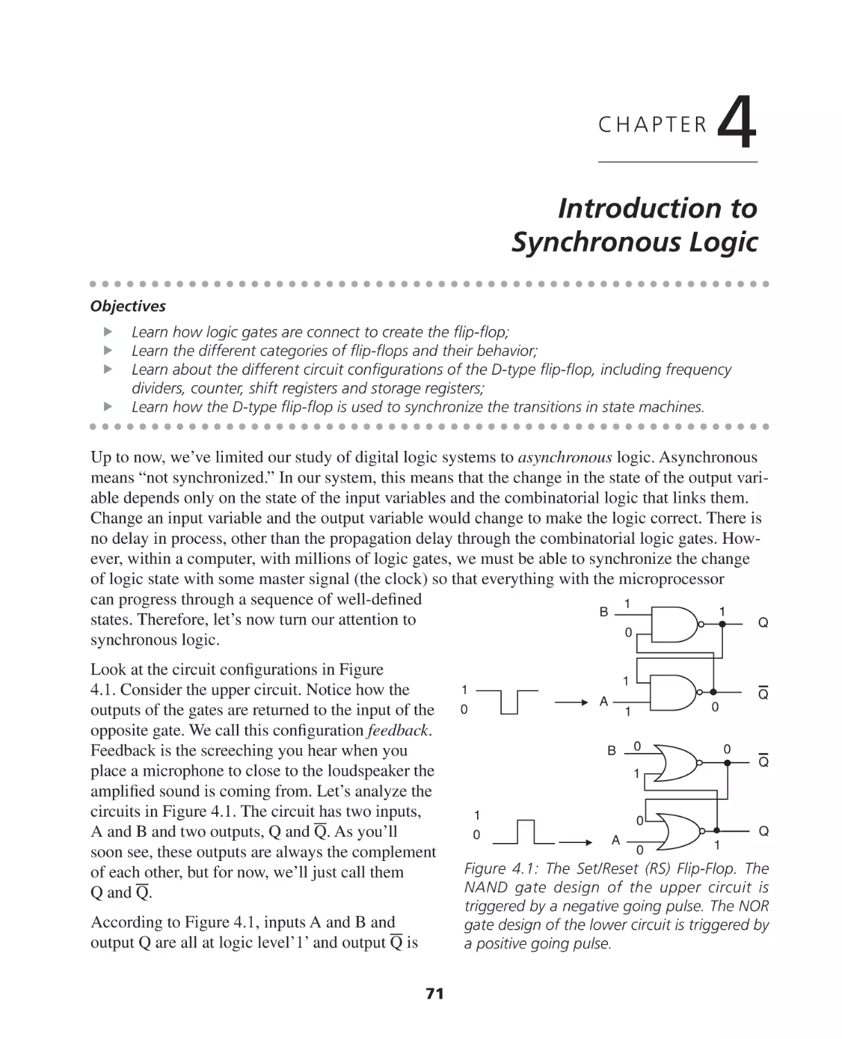
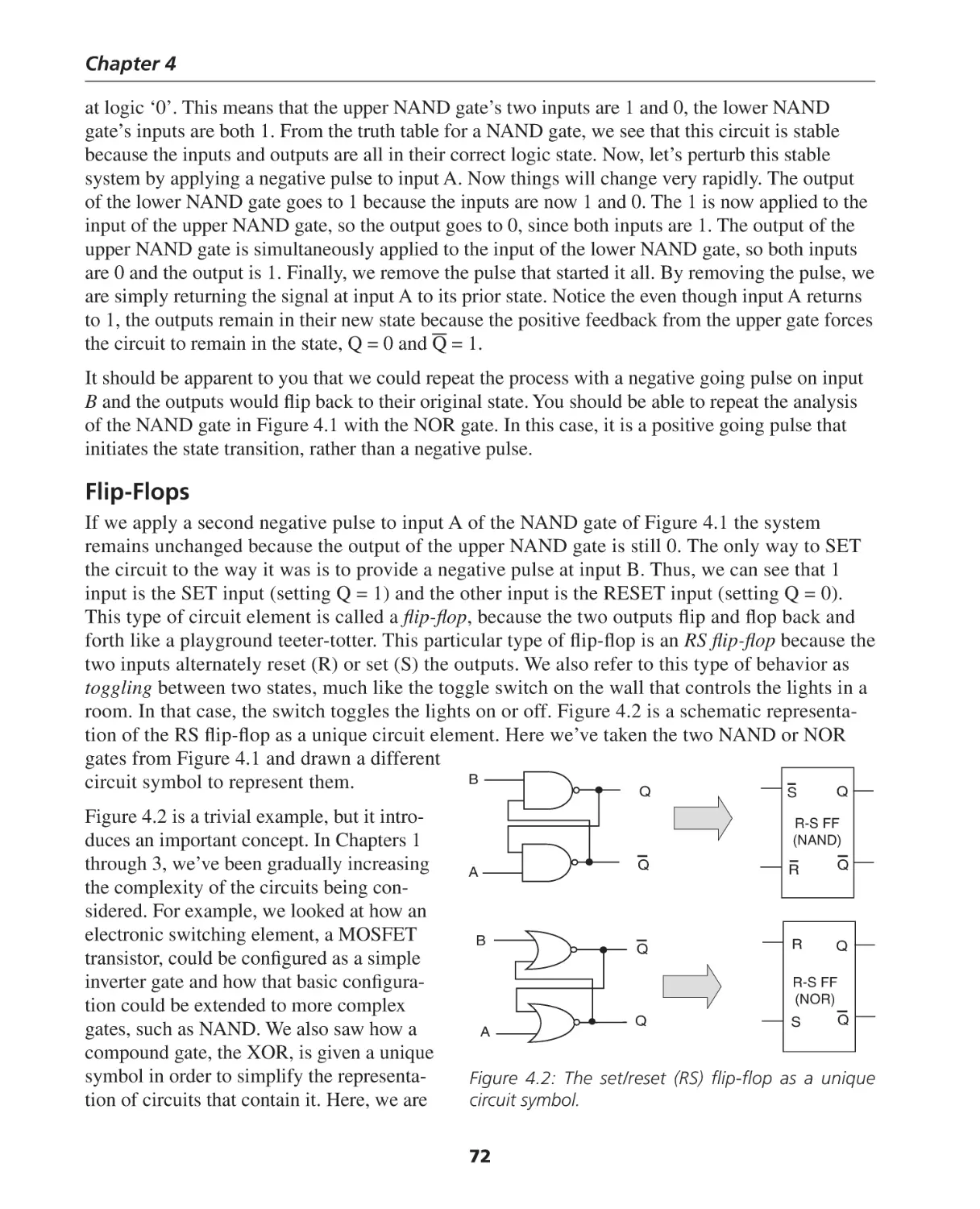
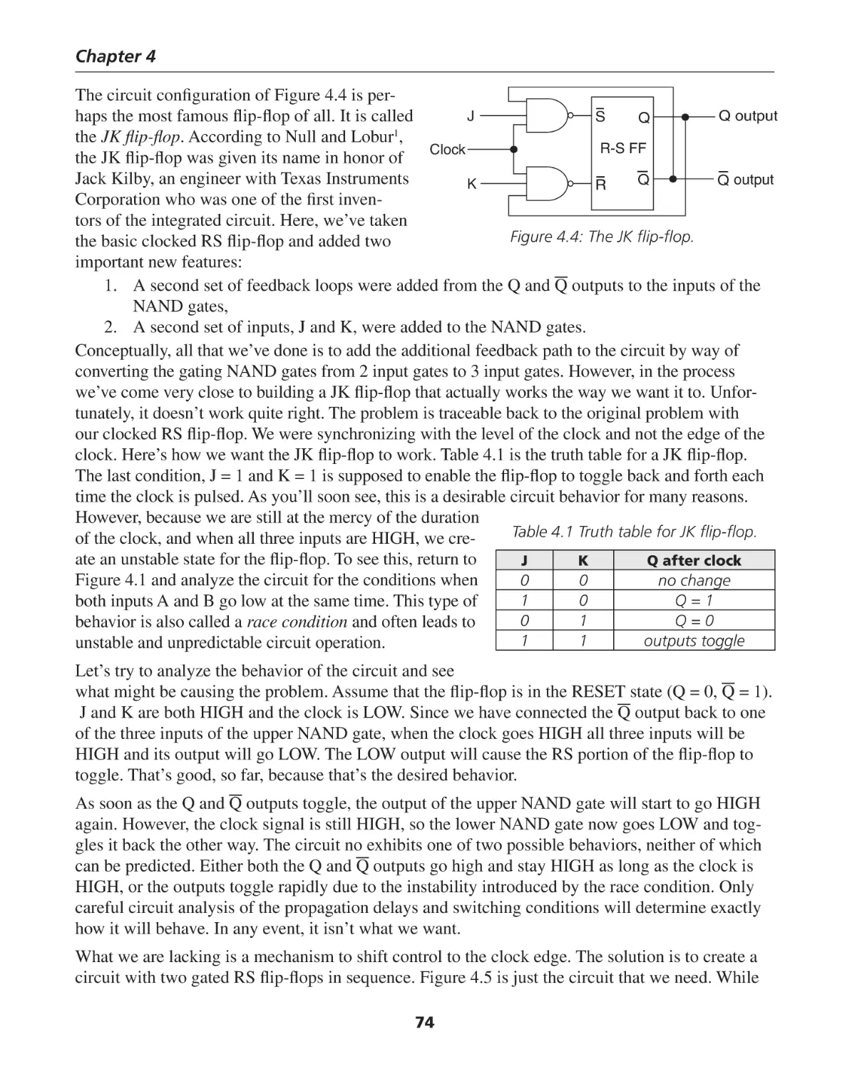
Flip-Flops ................................................................................................................................... 72
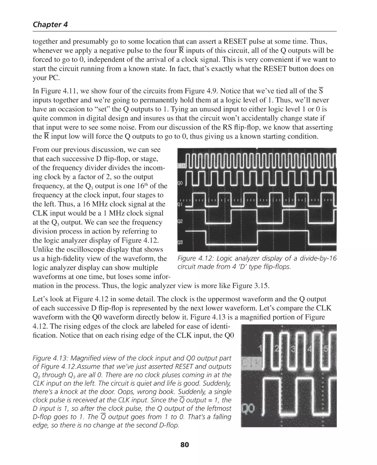
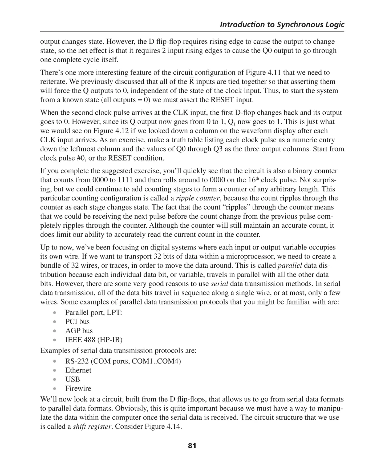
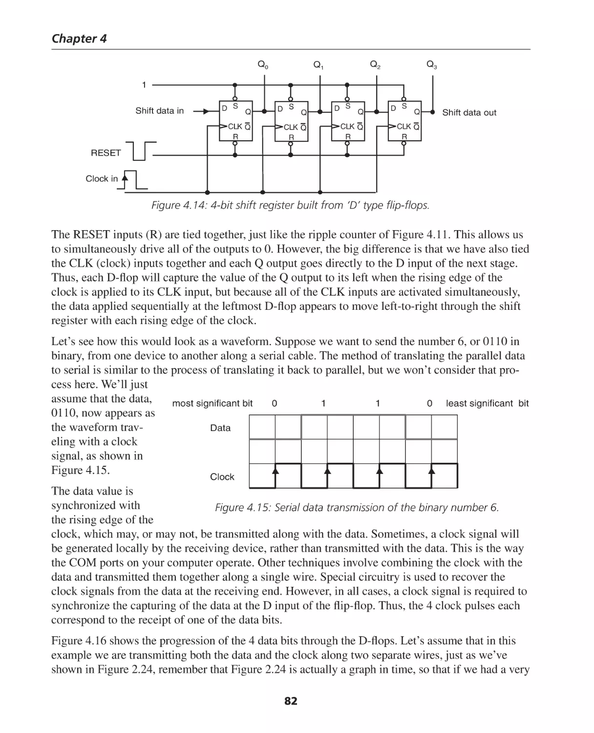
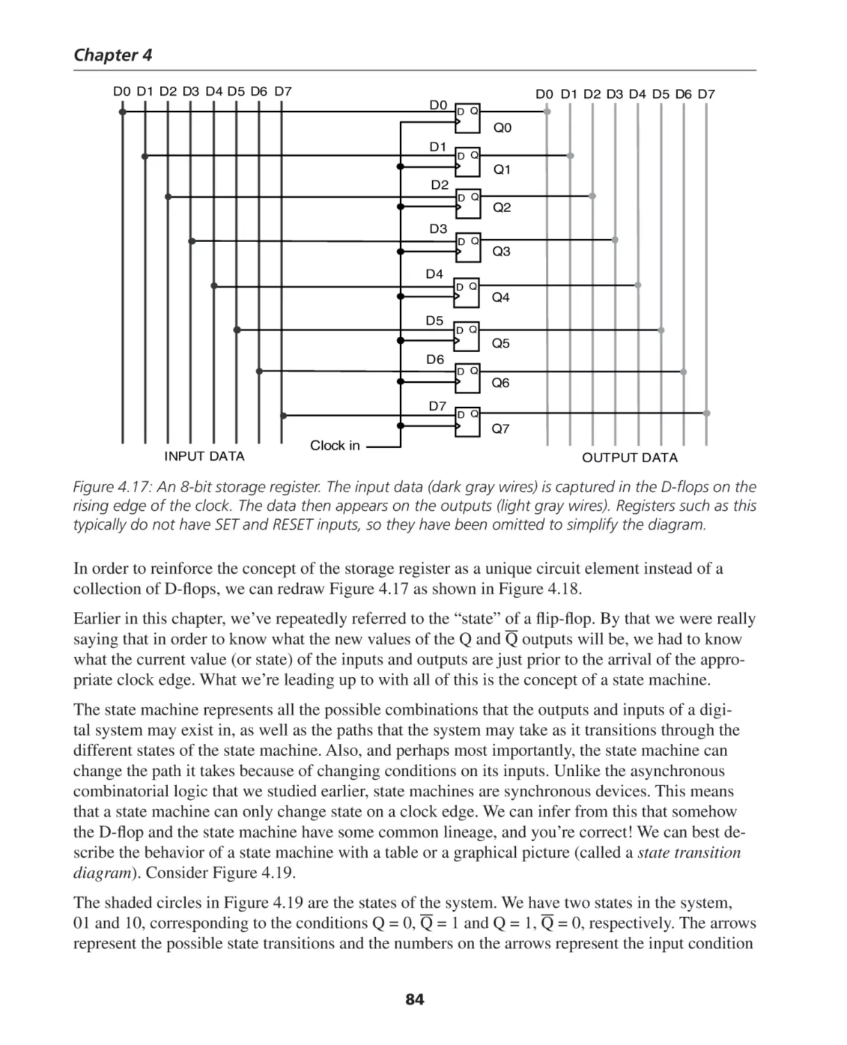
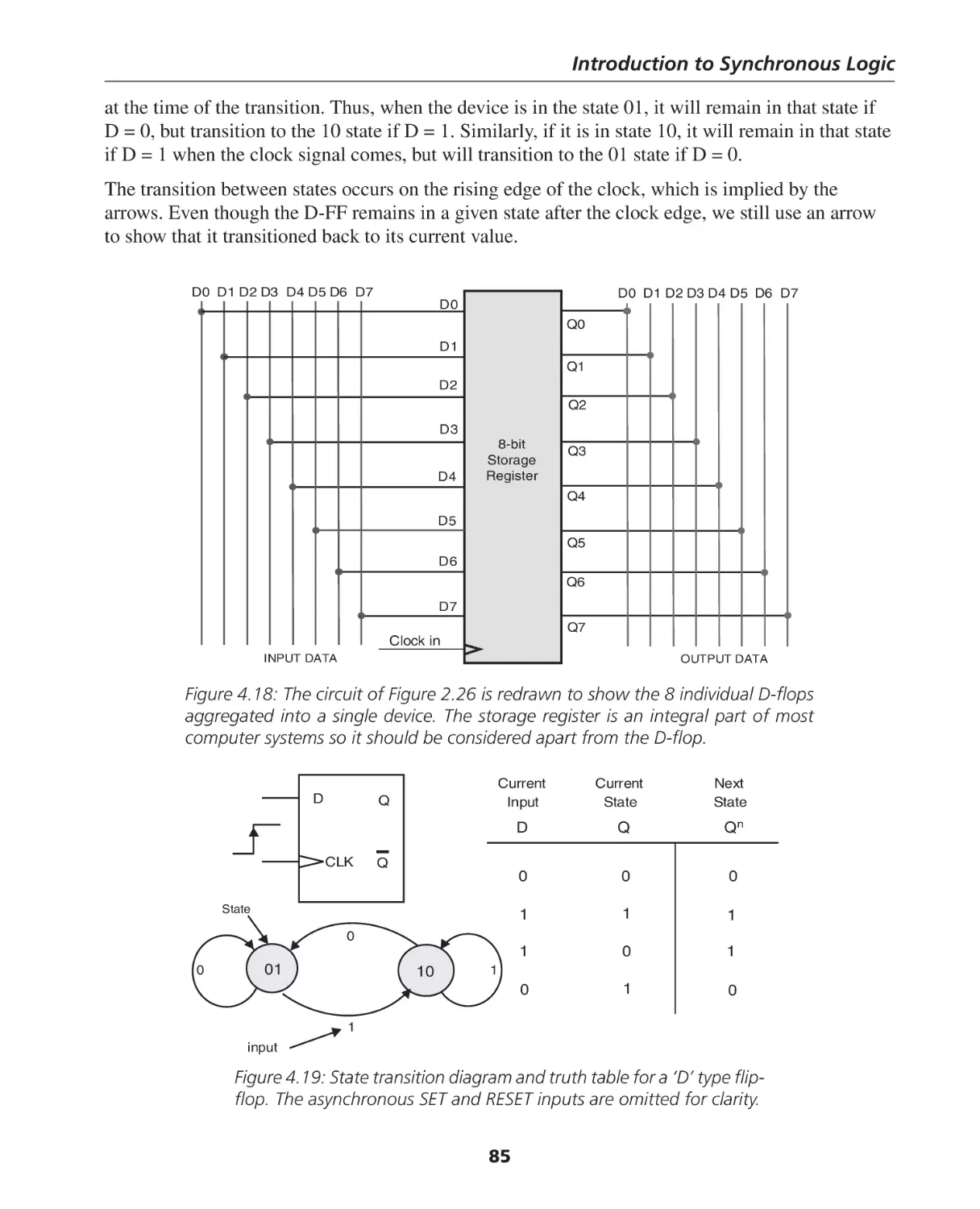
Storage Register ........................................................................................................................ 83
Summary of Chapter 4 .............................................................................................................. 90
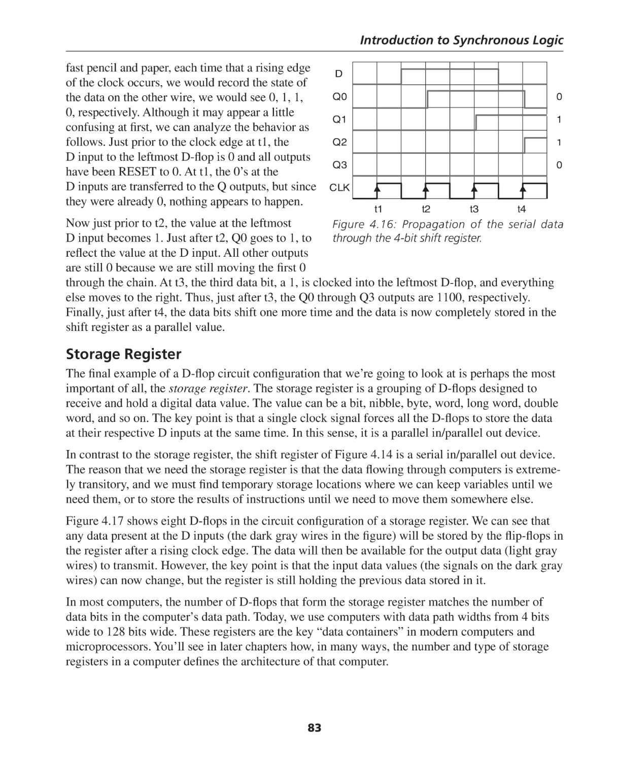
Exercises for Chapter 4 .............................................................................................................. 91
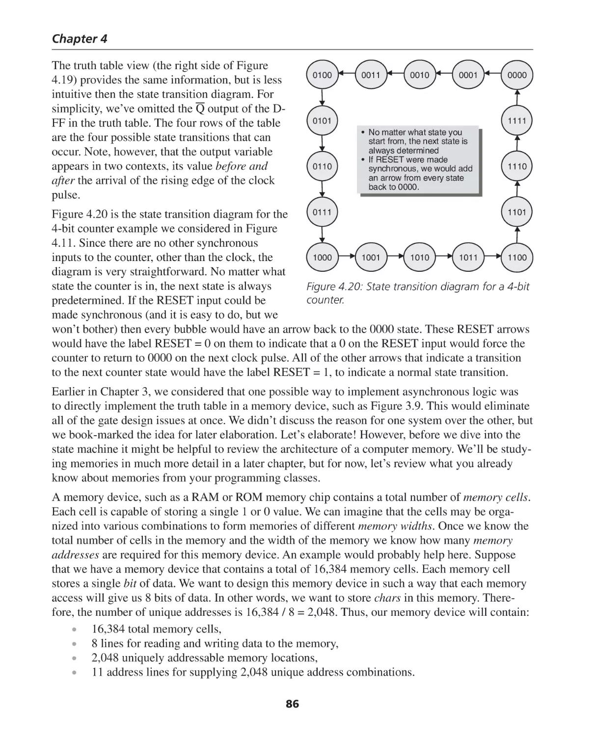
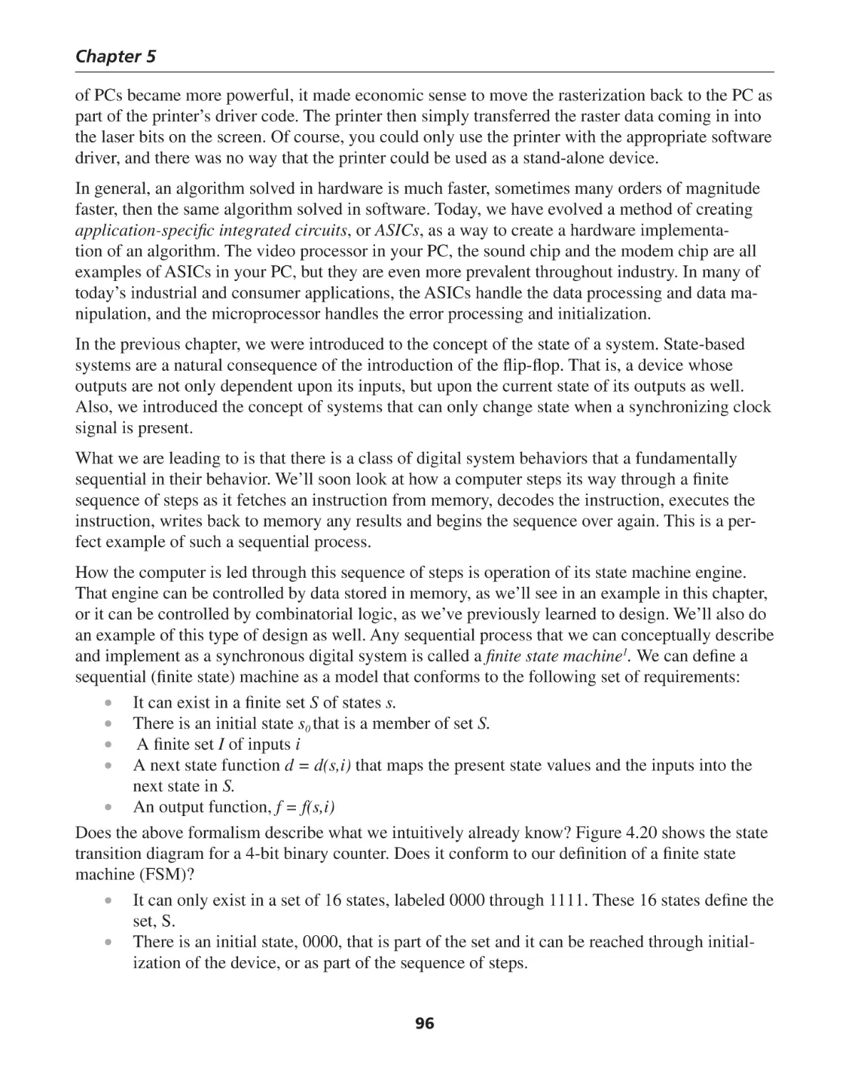
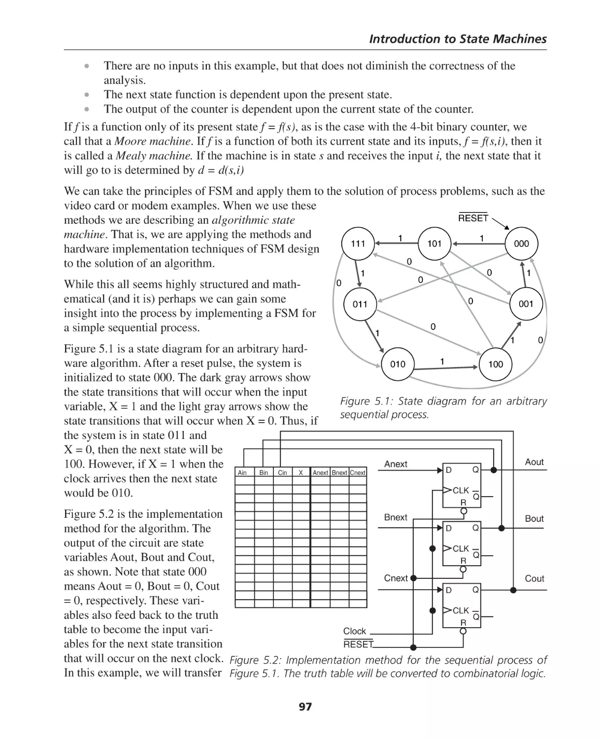
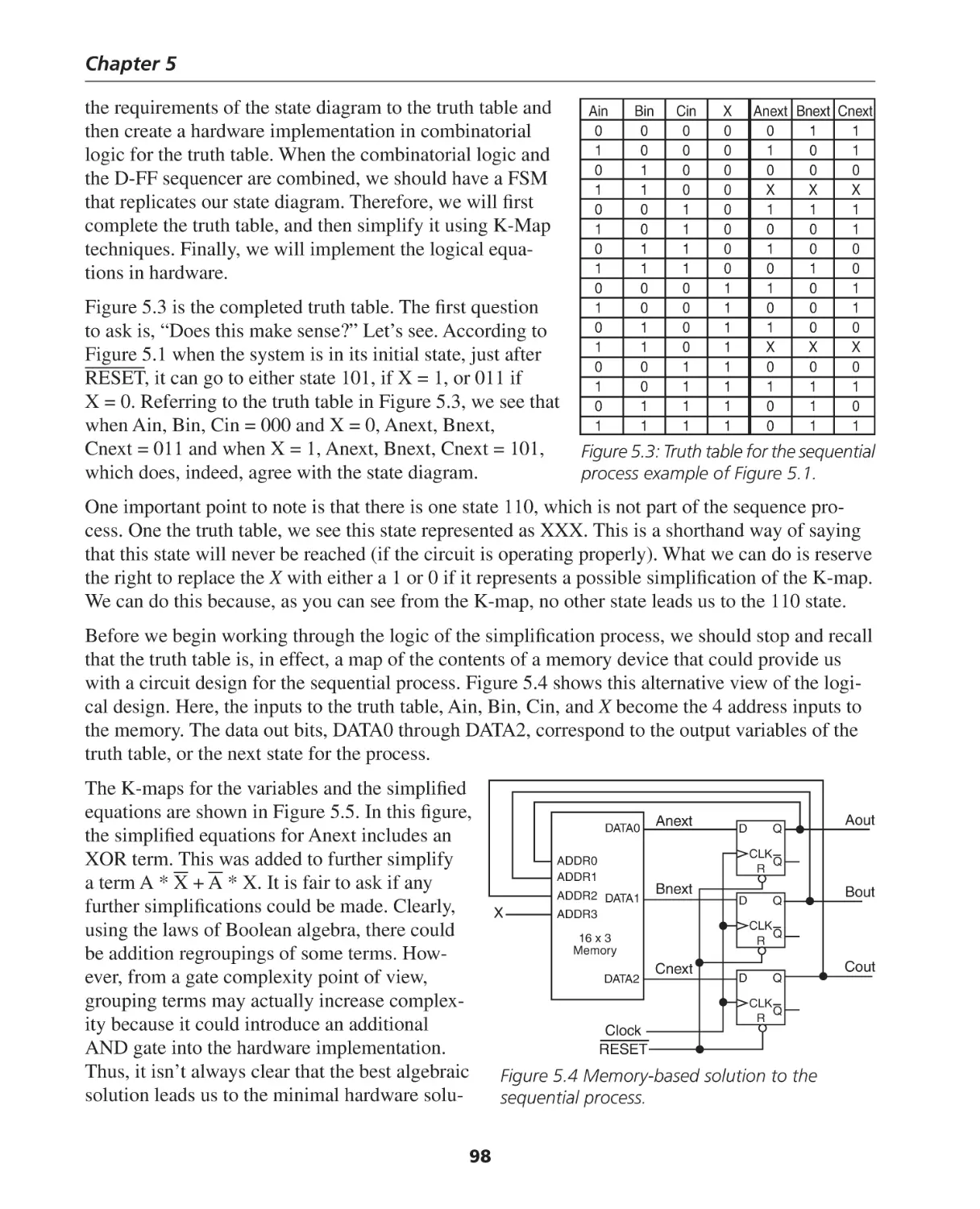
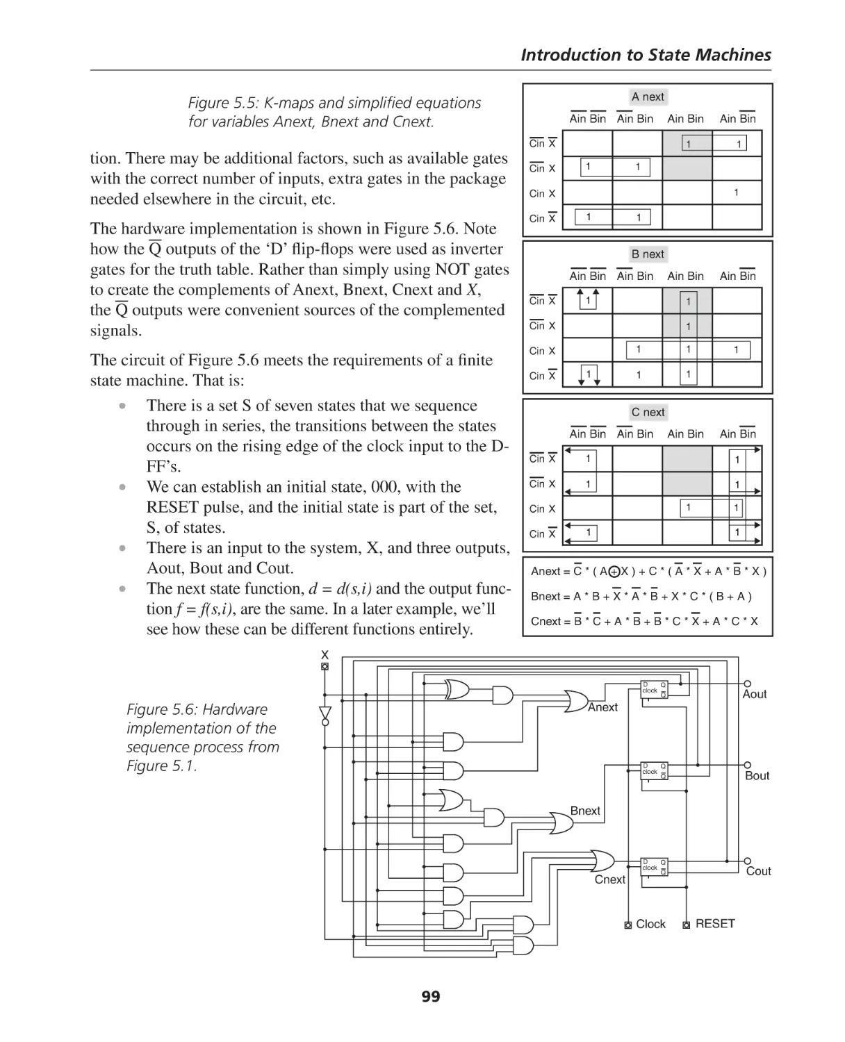
CHAPTER 5: Introduction to State Machines..................................................... 95
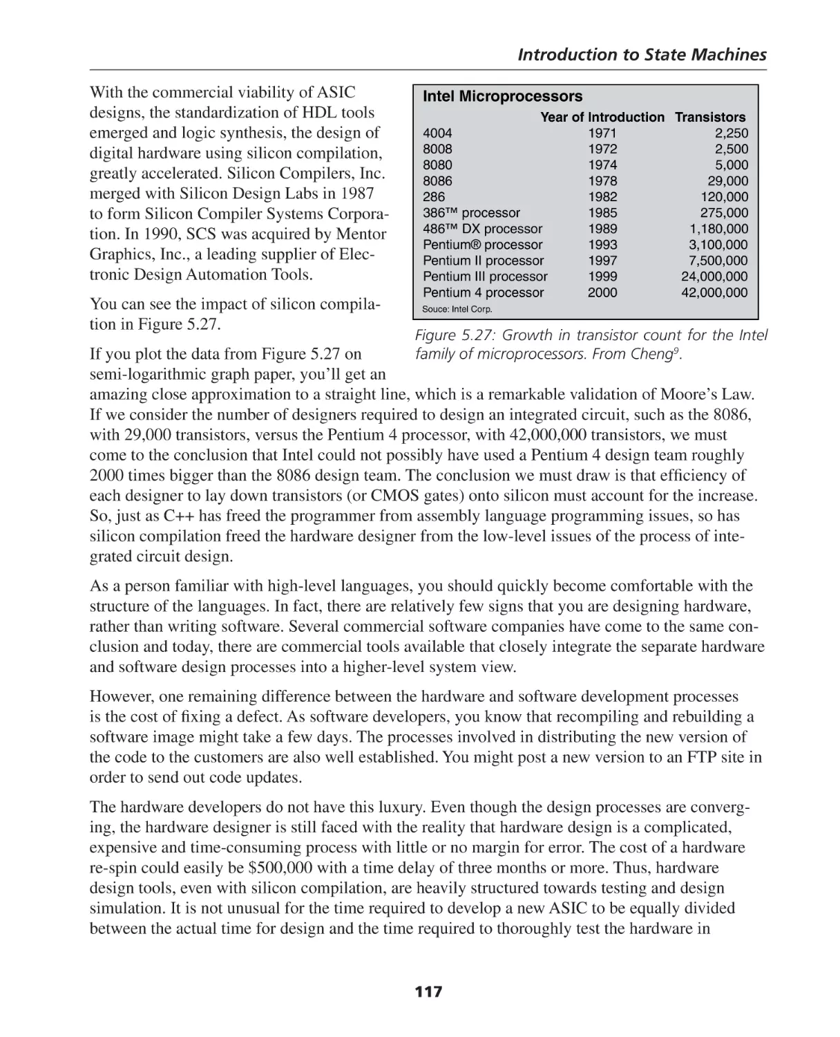
Modern Hardware Design Methodologies................................................................................ 115
Summary of Chapter 5 ............................................................................................................ 119
Exercises for Chapter 5 ............................................................................................................ 120
vii
Contents
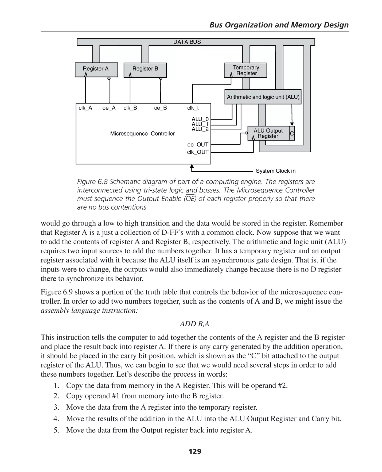
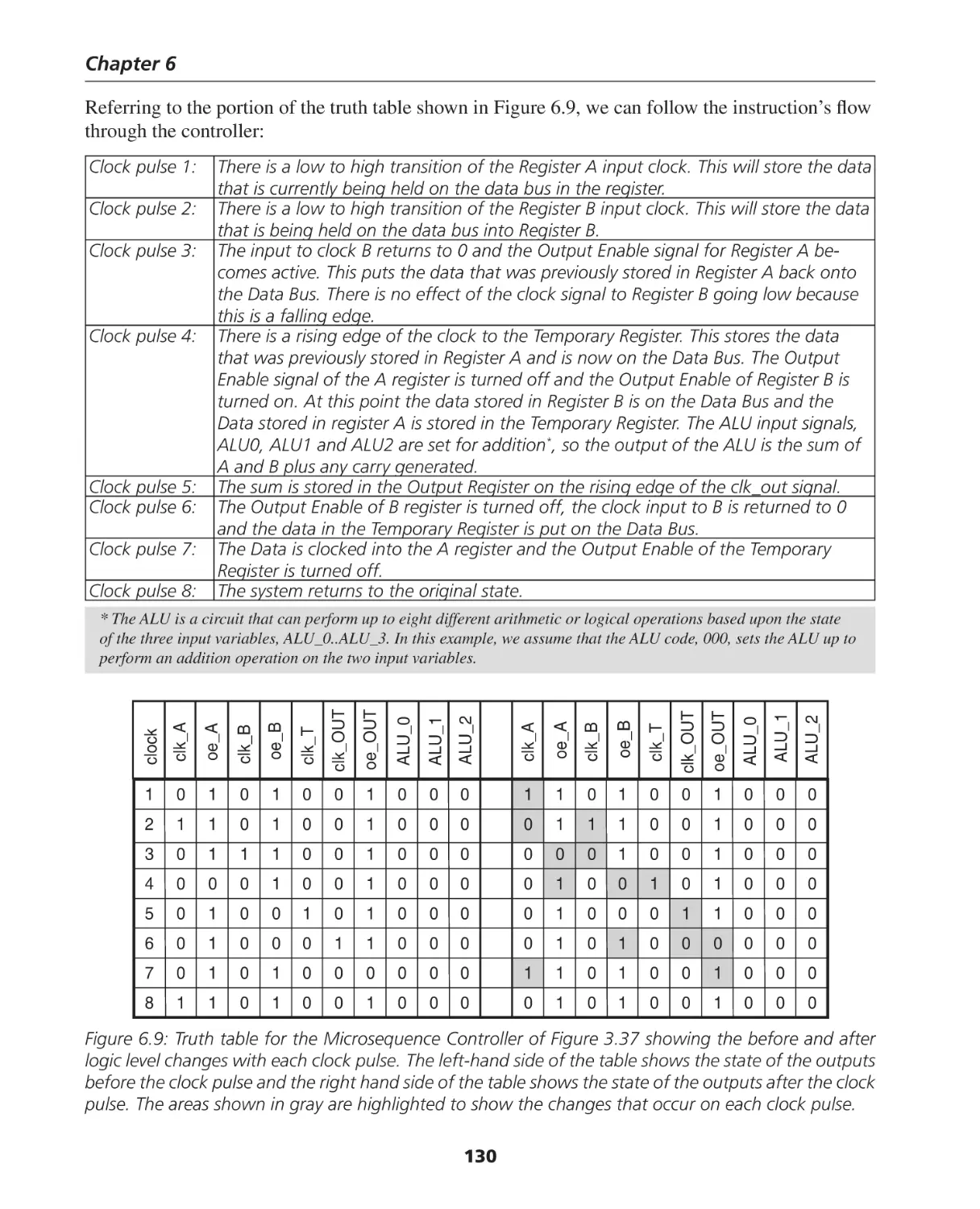
CHAPTER 6: Bus Organization and Memory Design....................................... 123
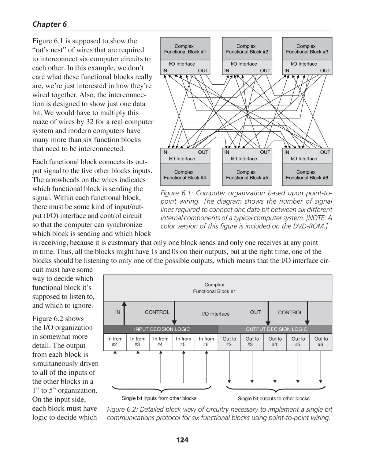
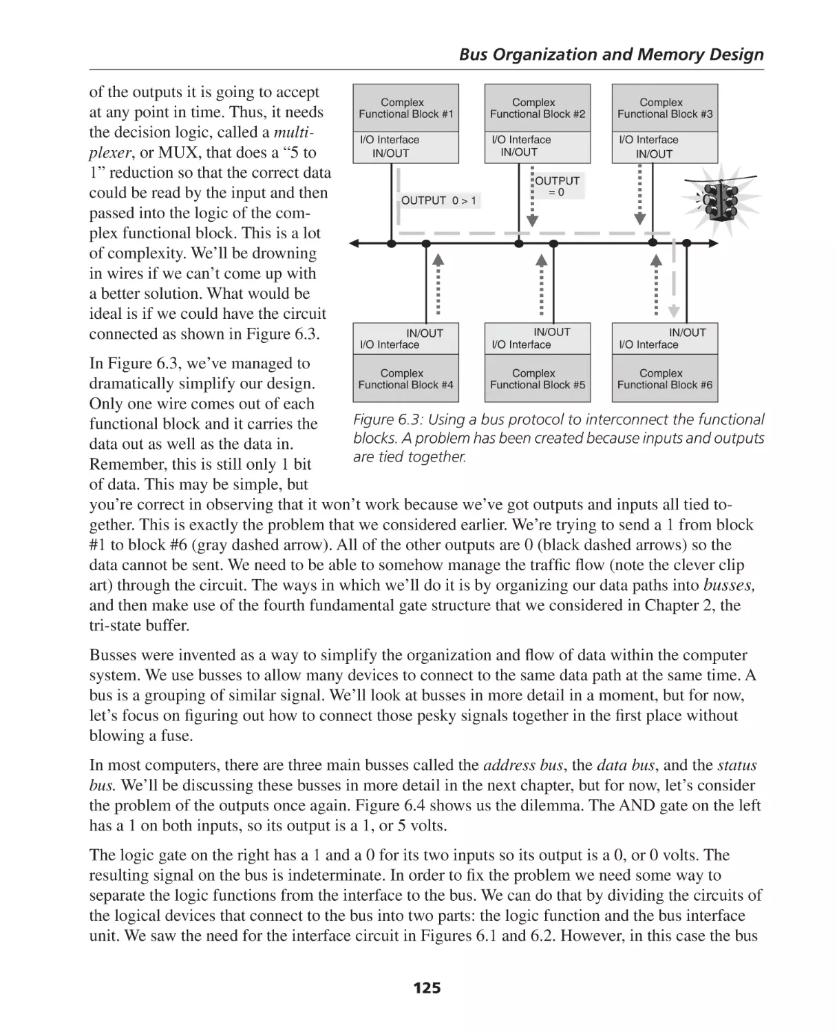
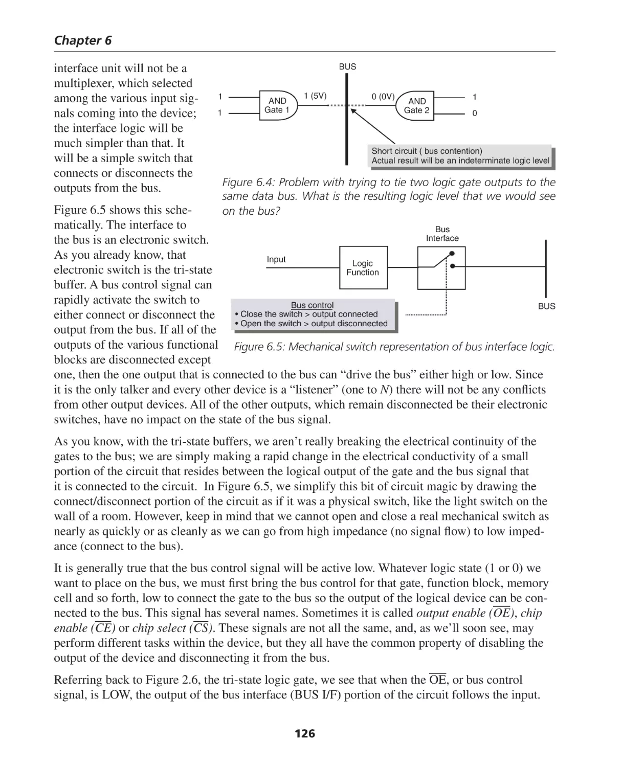
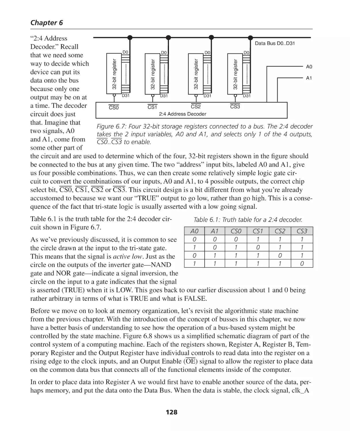
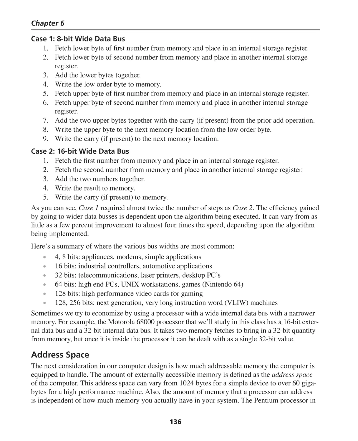
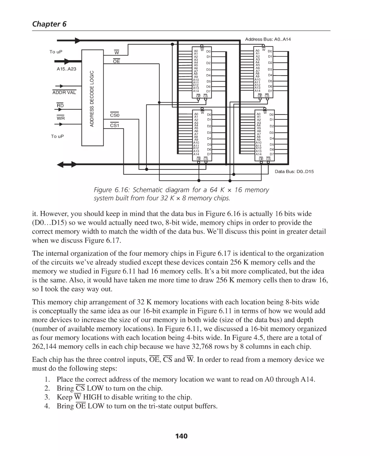
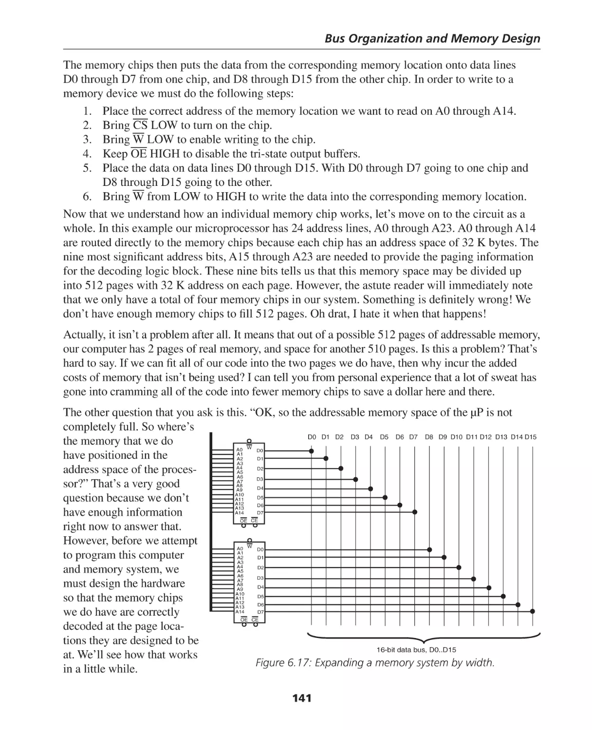
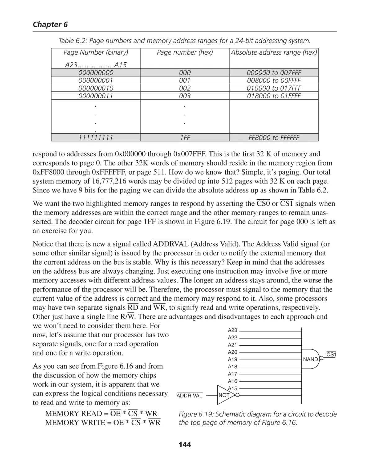
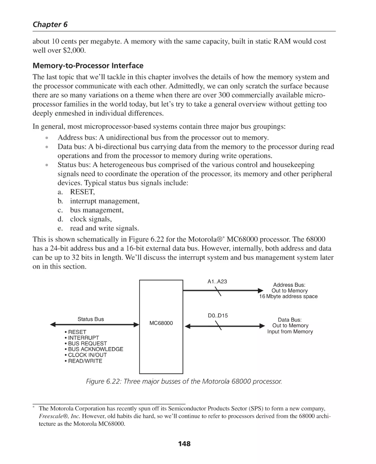
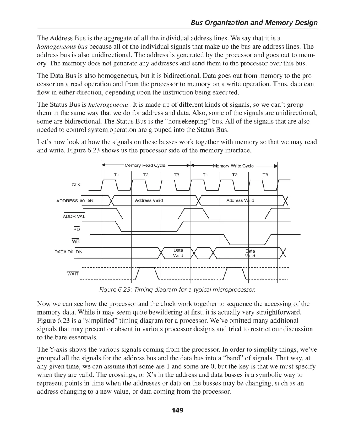
Bus Organization ..................................................................................................................... 123
Address Space ......................................................................................................................... 136
Direct Memory Access (DMA) .................................................................................................. 152
Summary of Chapter 6 ............................................................................................................ 153
Exercises for Chapter 6 ............................................................................................................ 155
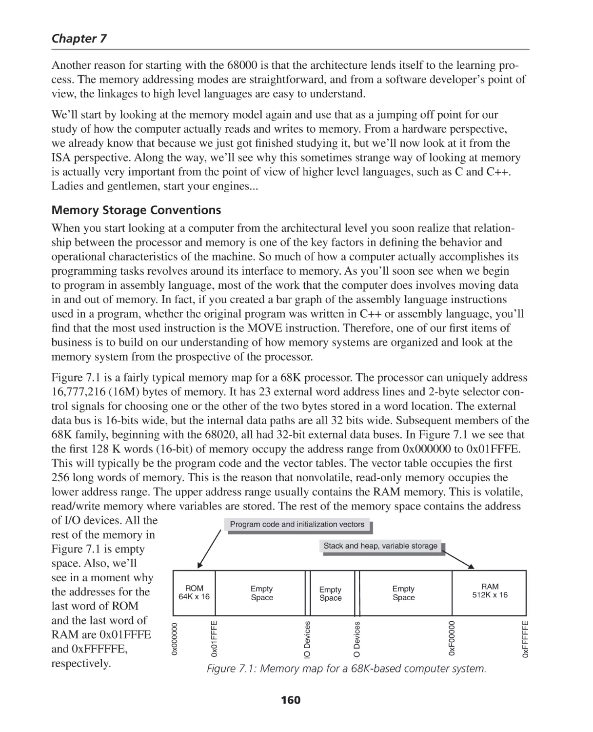
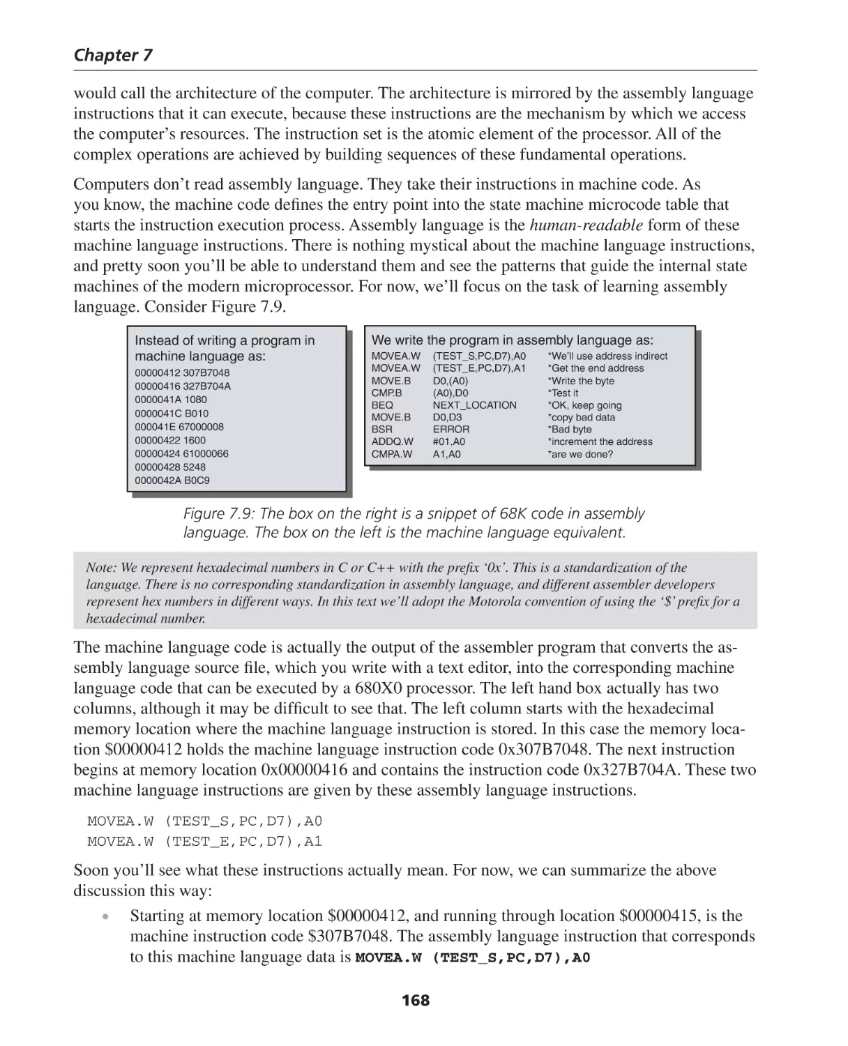
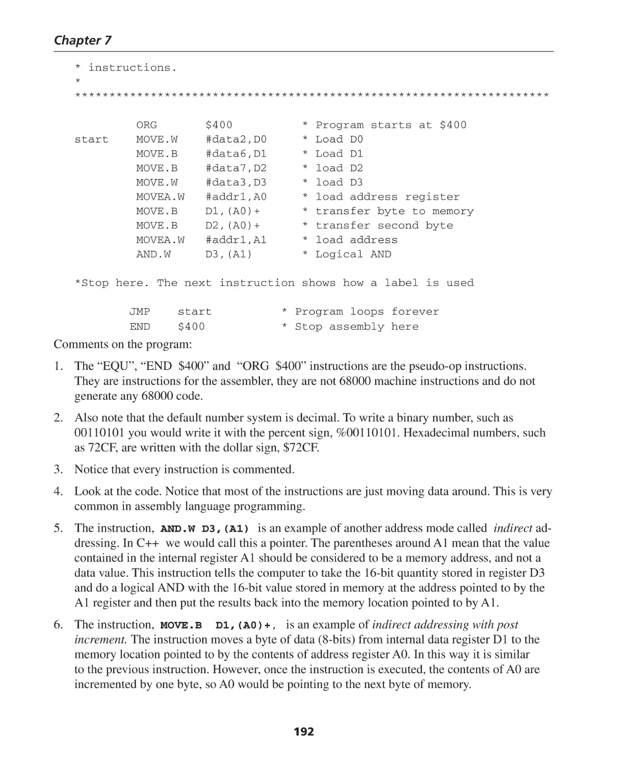
CHAPTER 7: Memory Organization and Assembly Language Programming .. 159
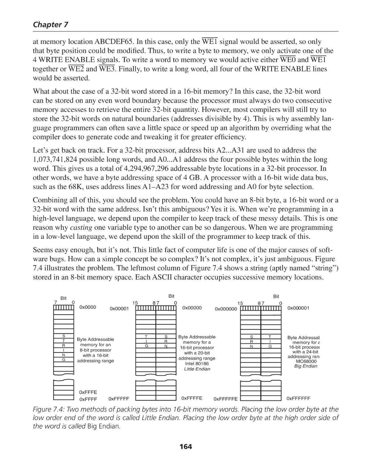
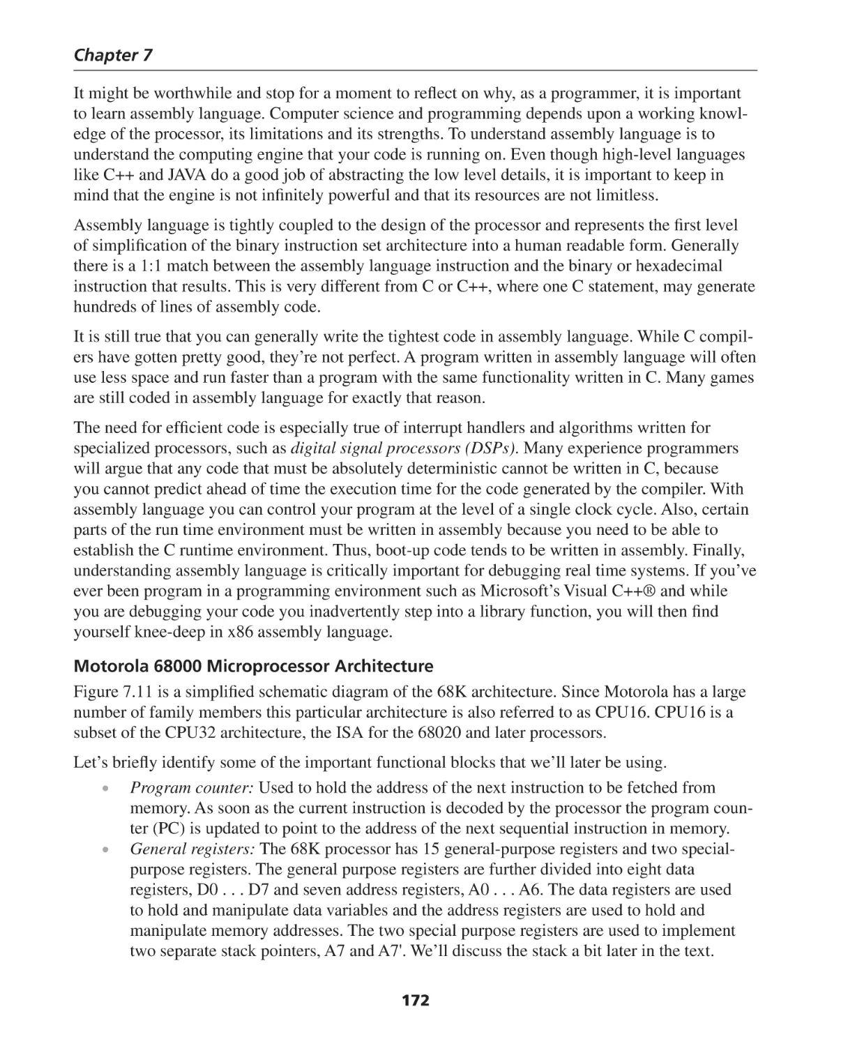
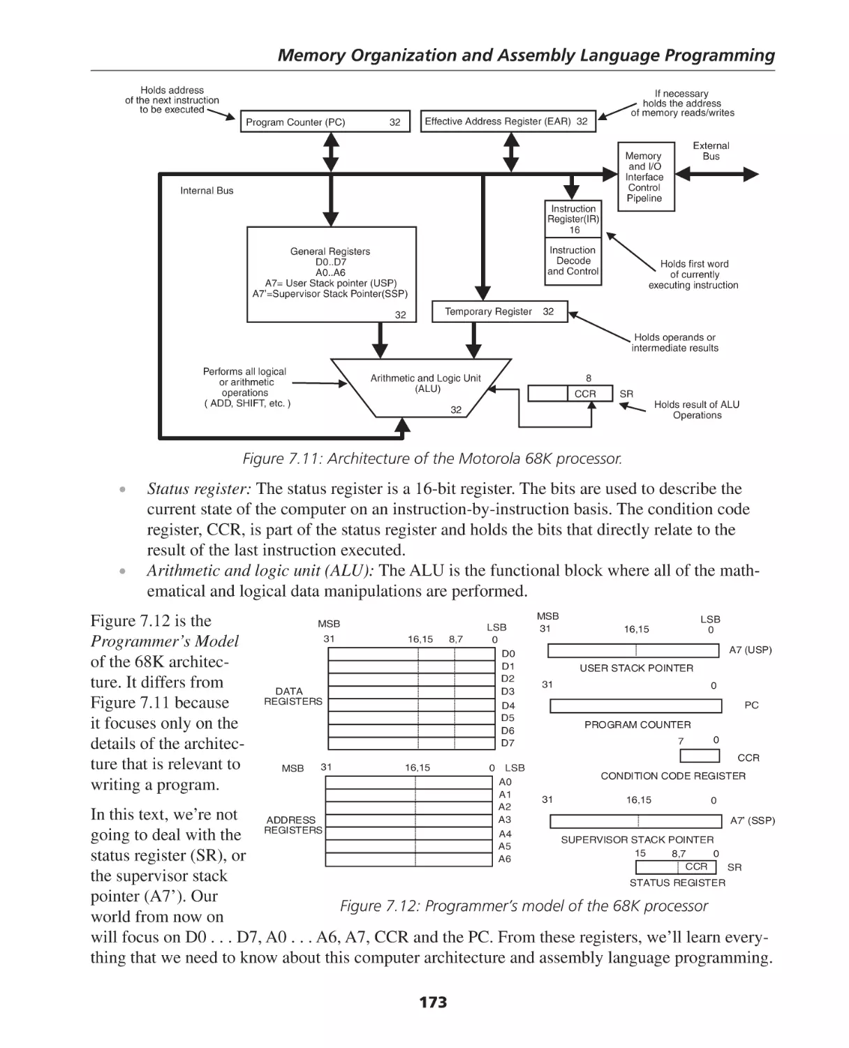
Introduction ............................................................................................................................ 159
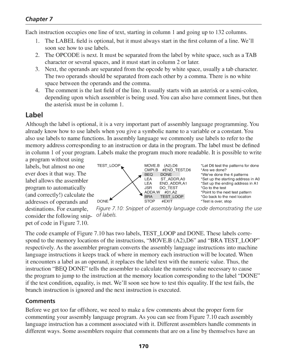
Label ....................................................................................................................................... 170
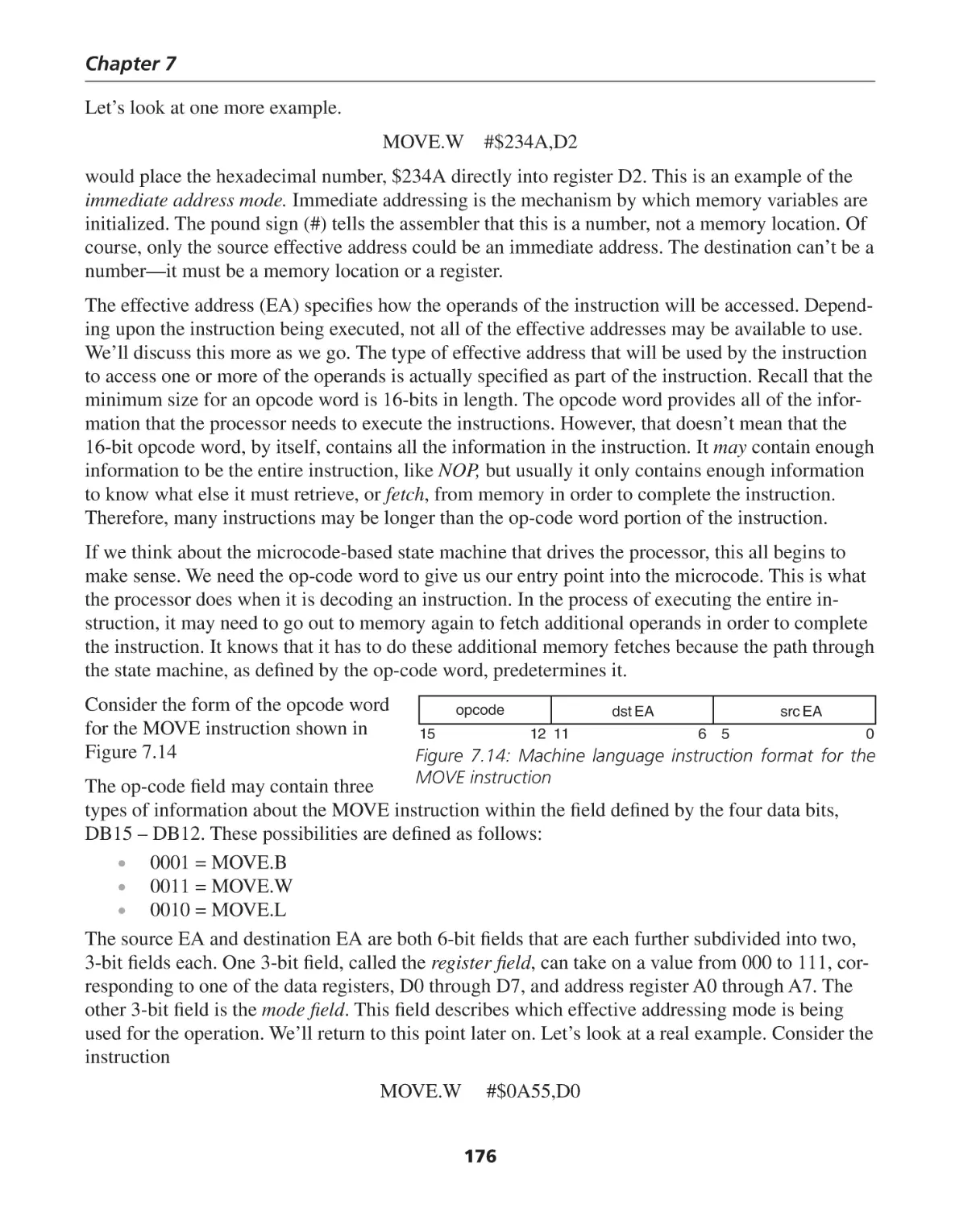
Effective Addresses .................................................................................................................. 174
Pseudo Opcodes ...................................................................................................................... 183
Data Storage Directives............................................................................................................ 184
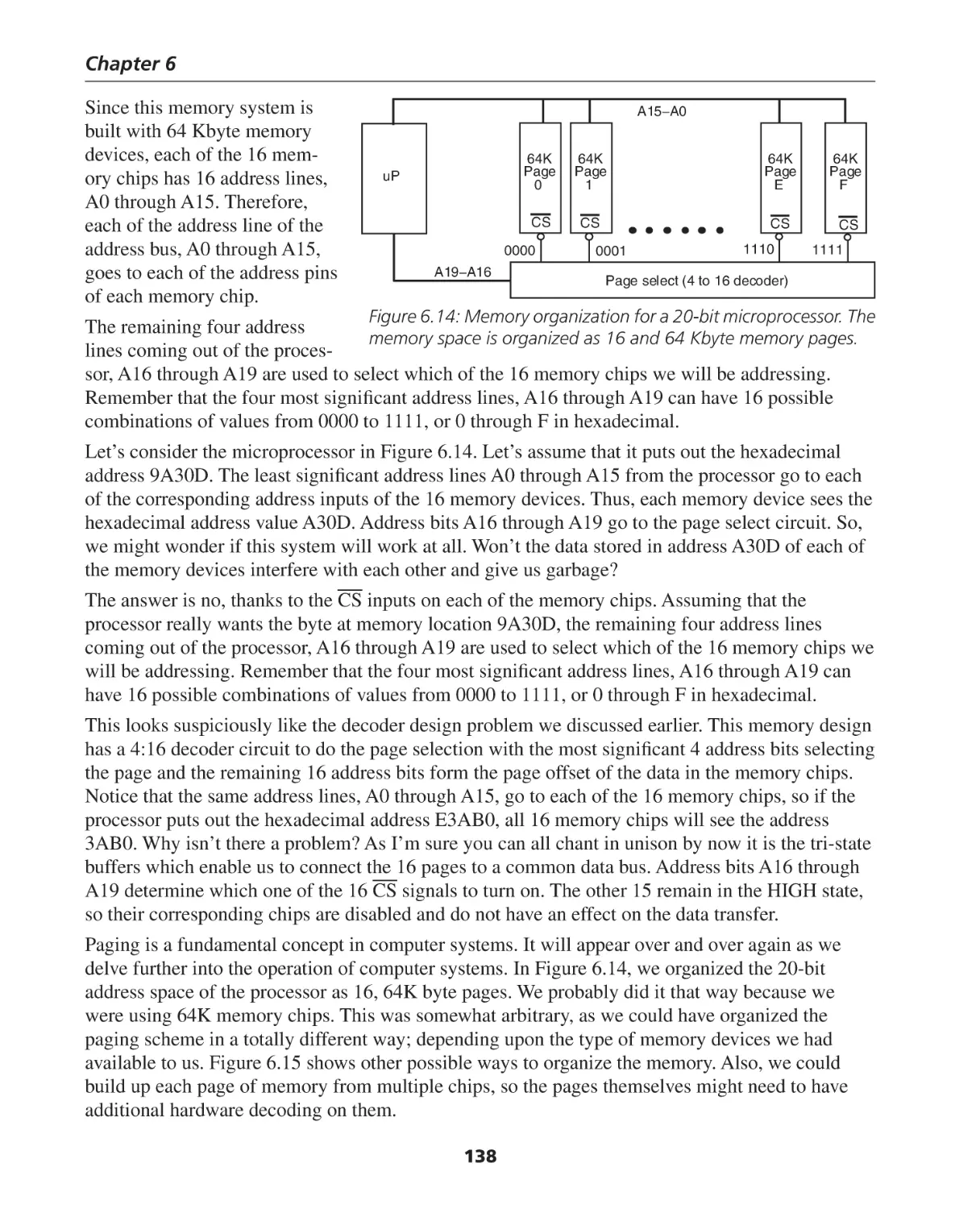
Analysis of an Assembly Language Program............................................................................. 186
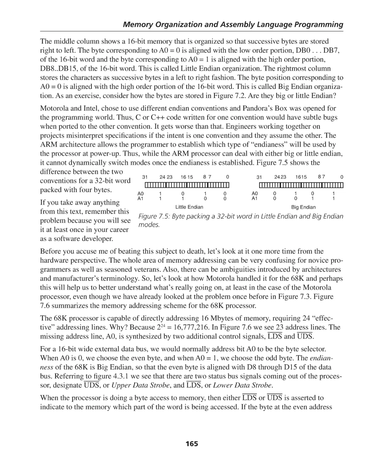
Summary of Chapter 7 ............................................................................................................ 188
Exercises for Chapter 7 ............................................................................................................ 189
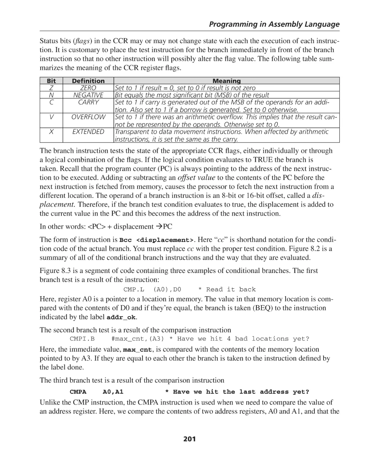
CHAPTER 8: Programming in Assembly Language ......................................... 193
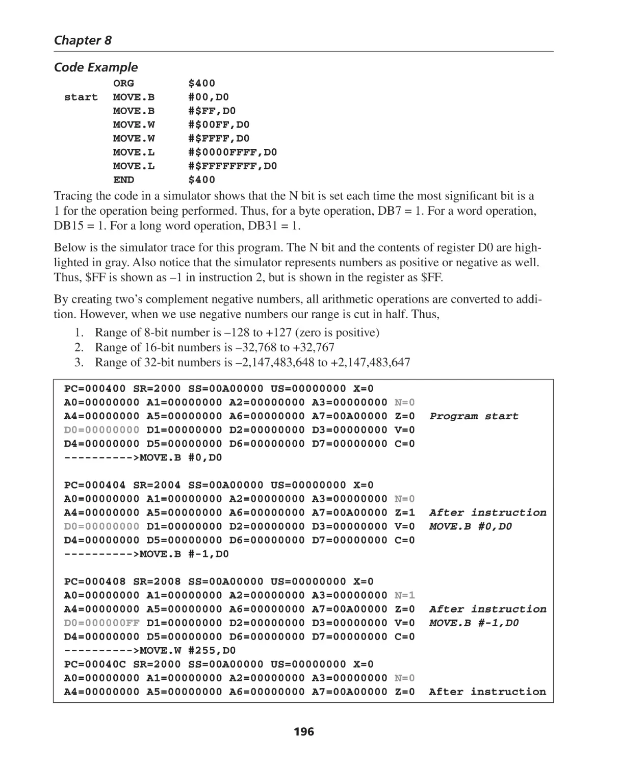
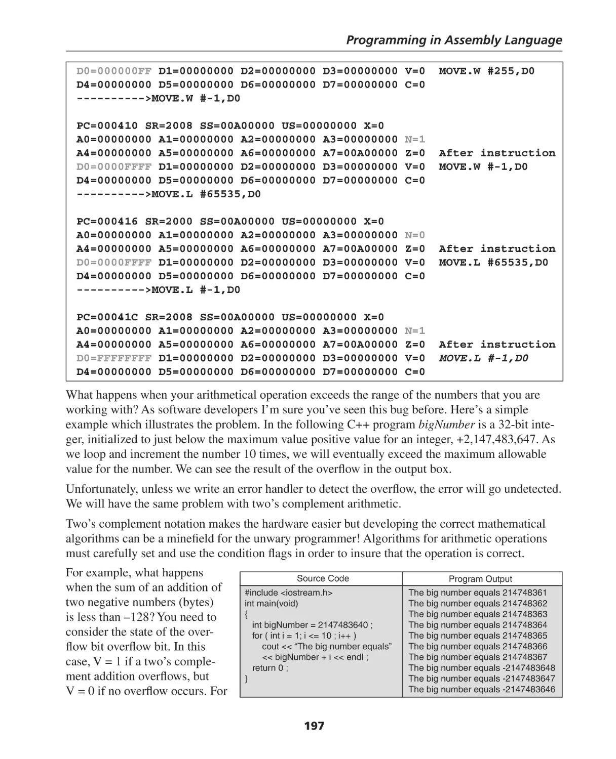
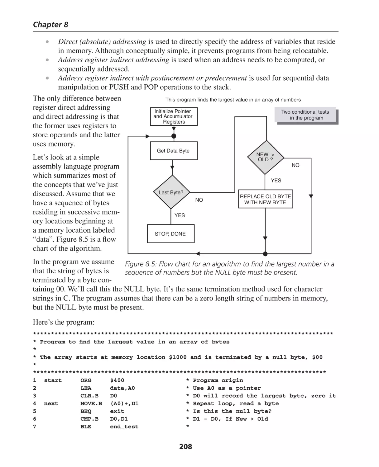
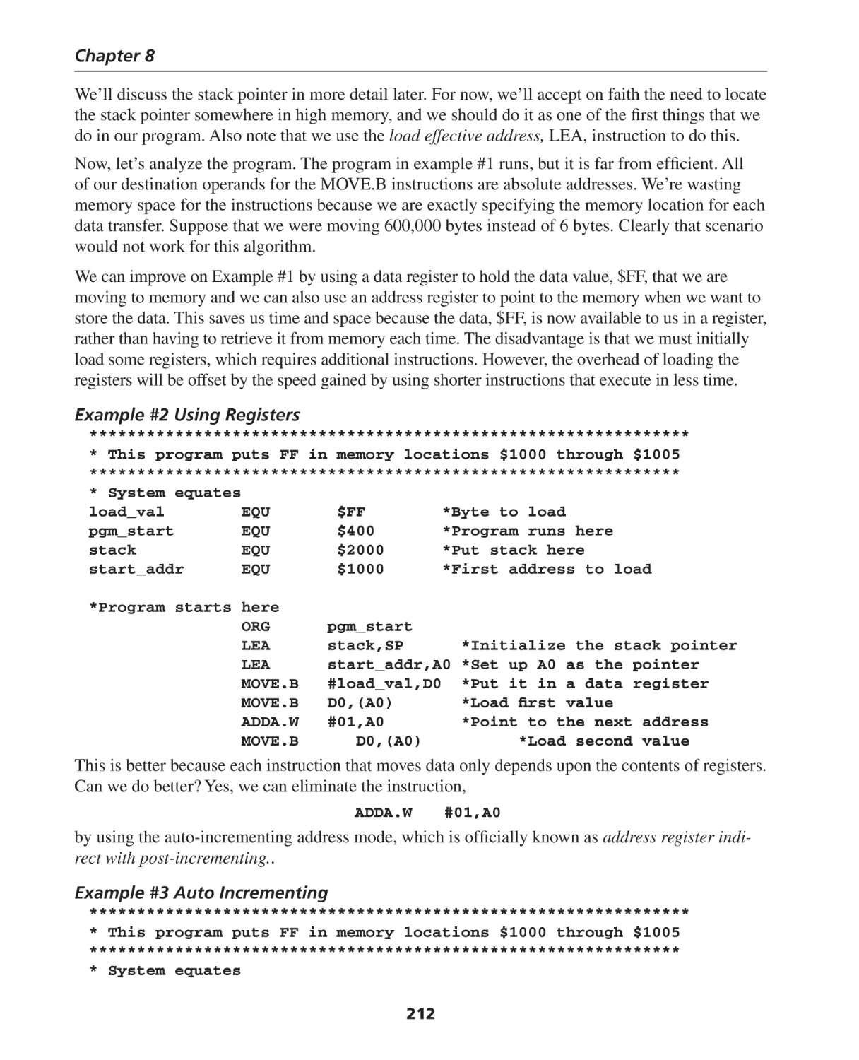
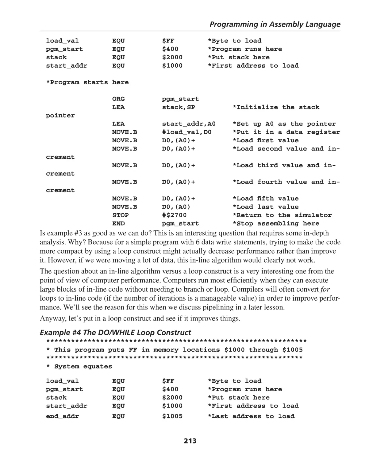
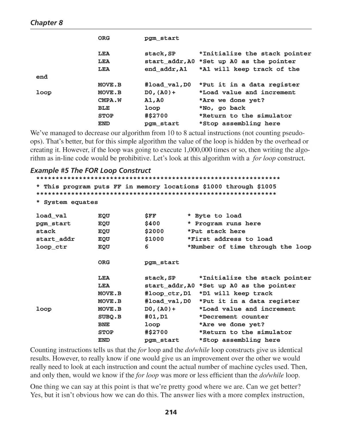
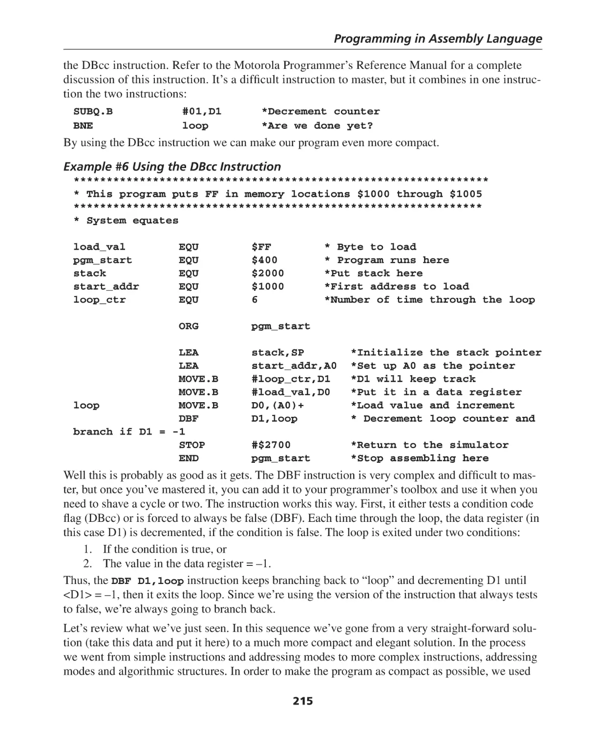
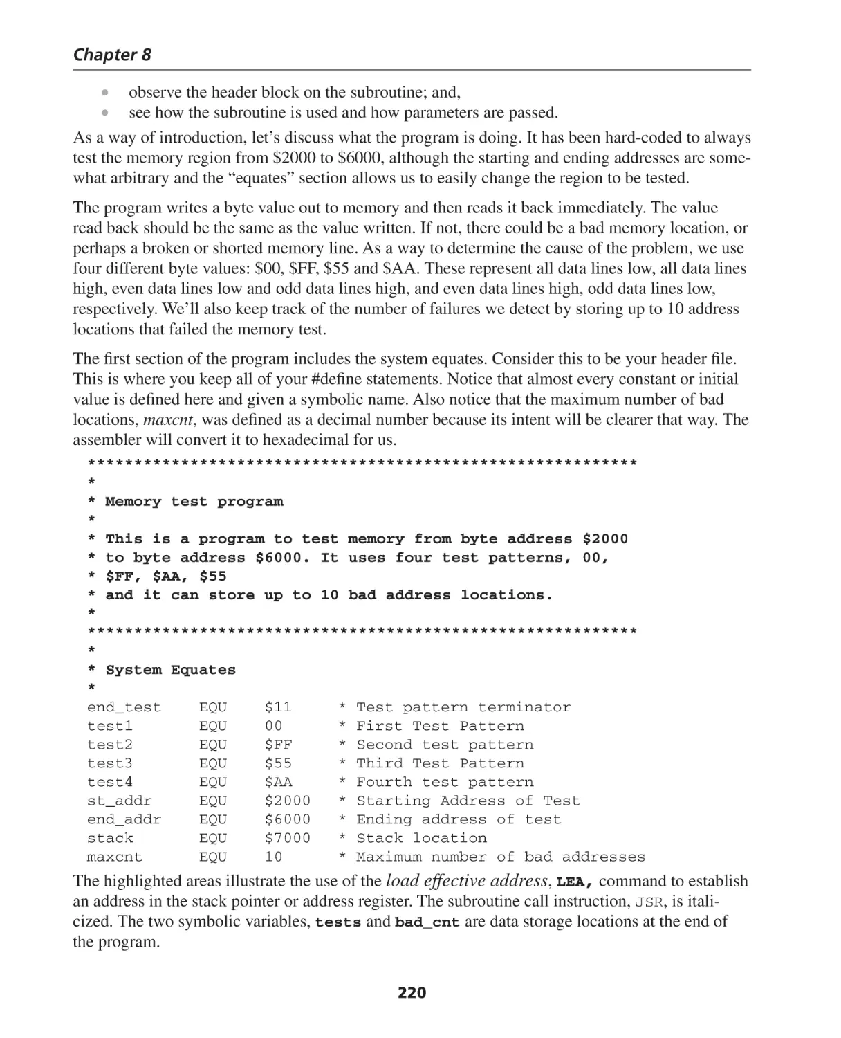
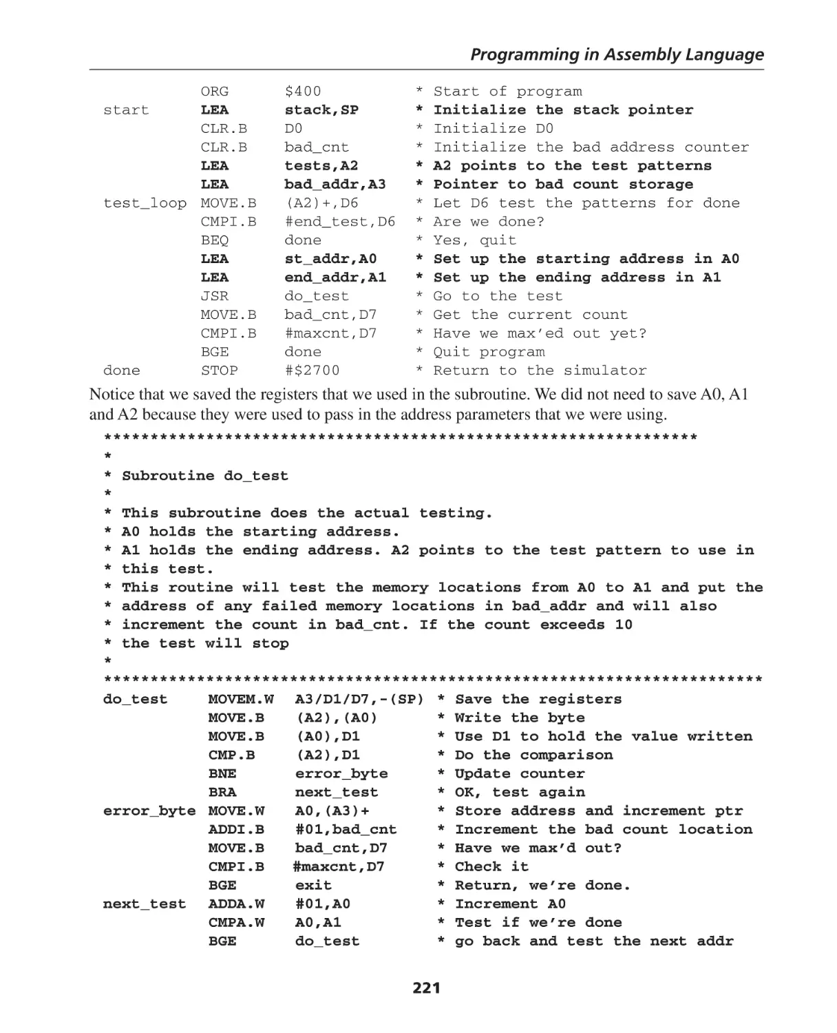
Introduction ............................................................................................................................ 193
Assembly Language and C++ .................................................................................................. 209
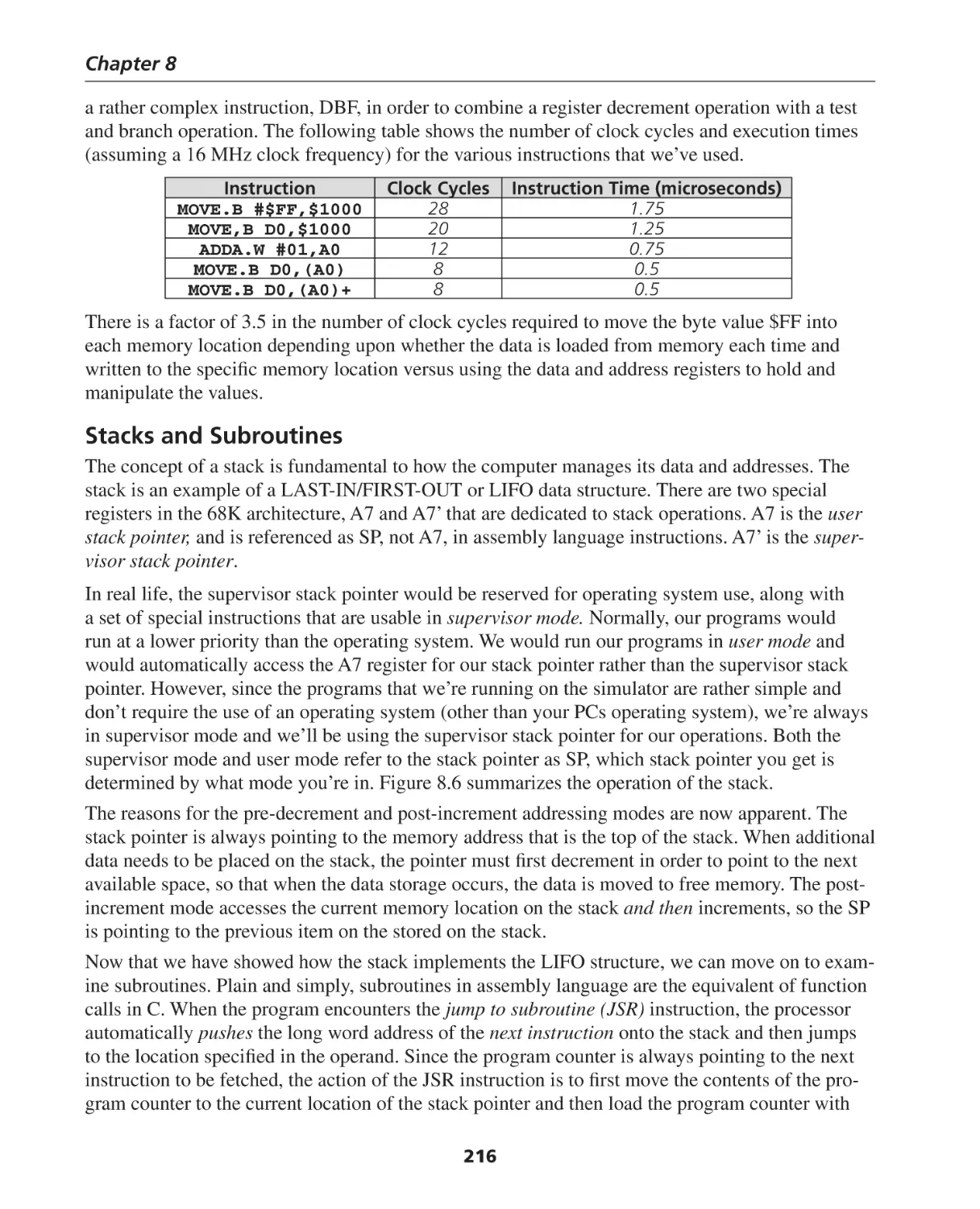
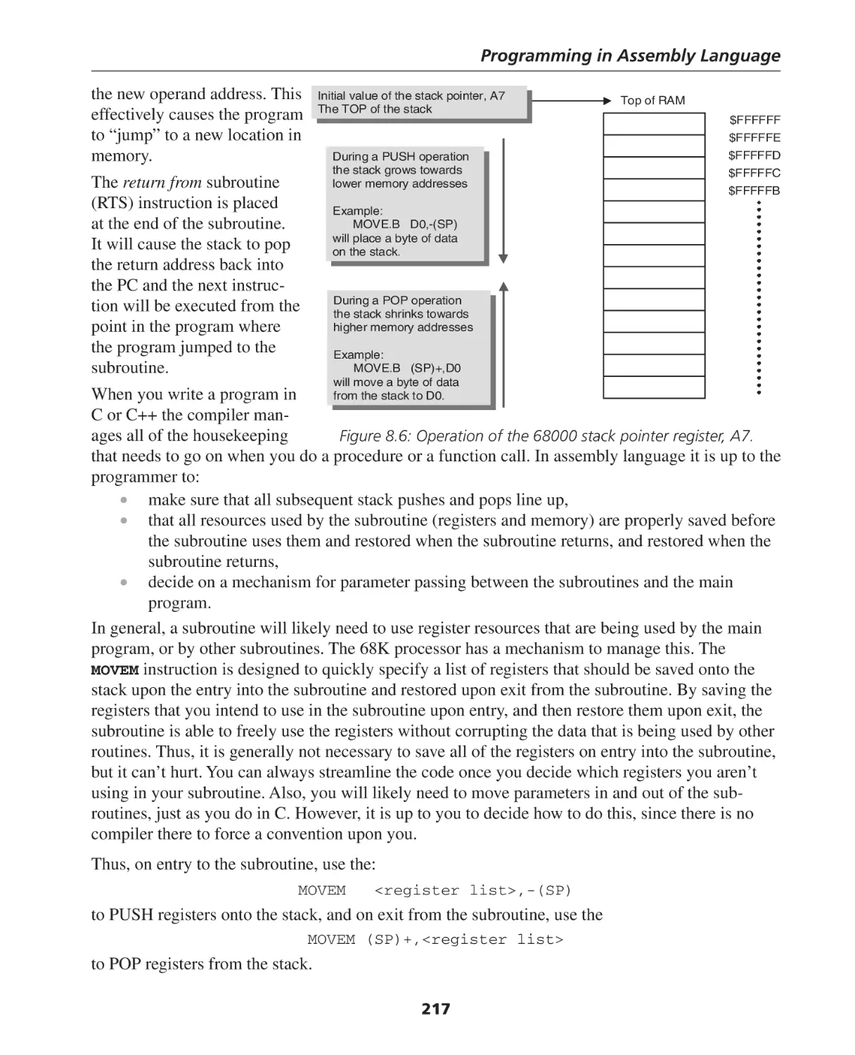
Stacks and Subroutines ........................................................................................................... 216
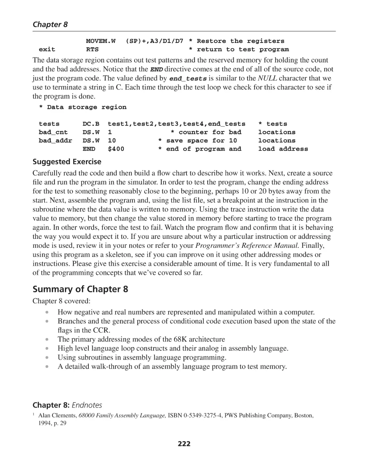
Summary of Chapter 8 ............................................................................................................ 222
Exercises for Chapter 8 ............................................................................................................ 223
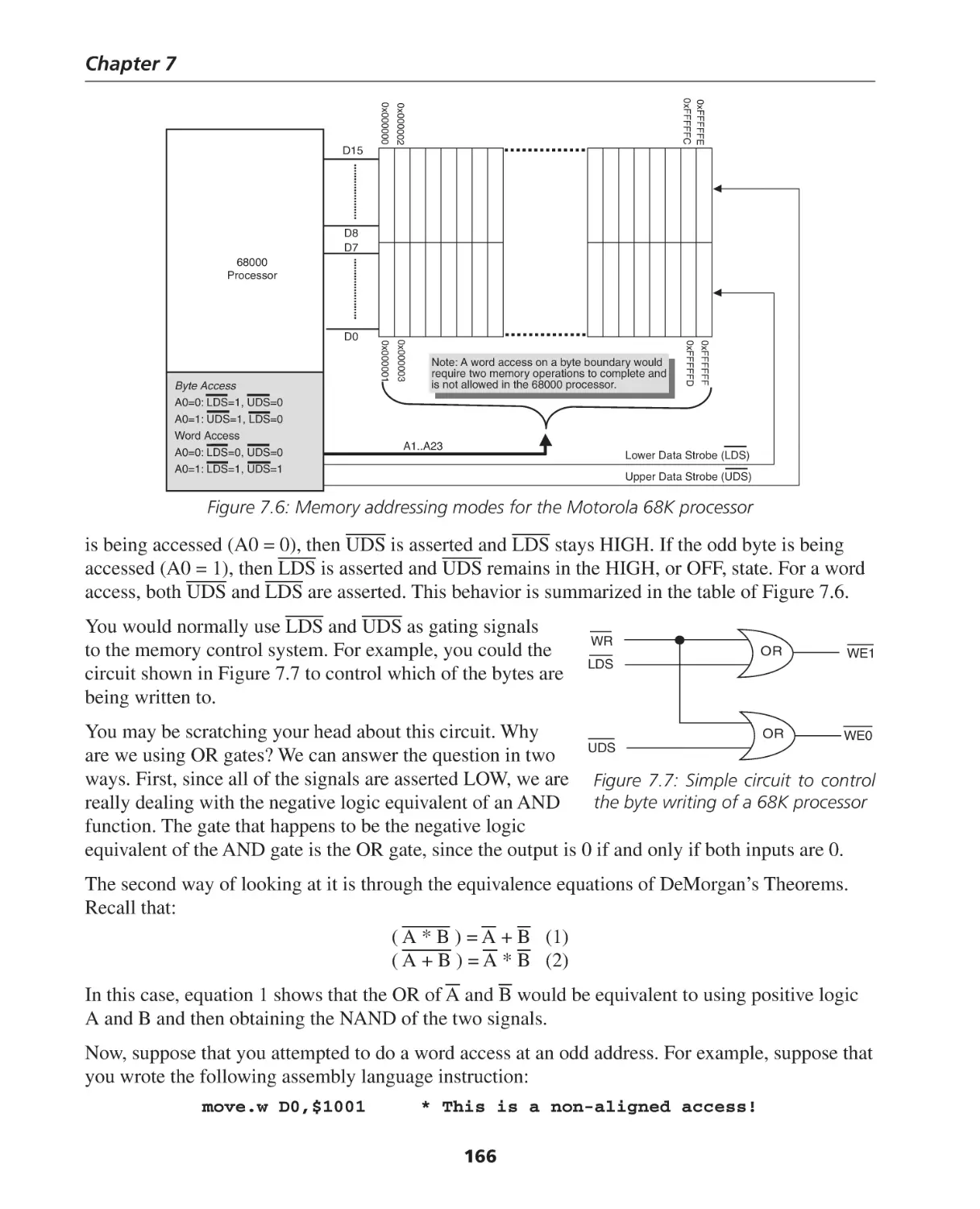
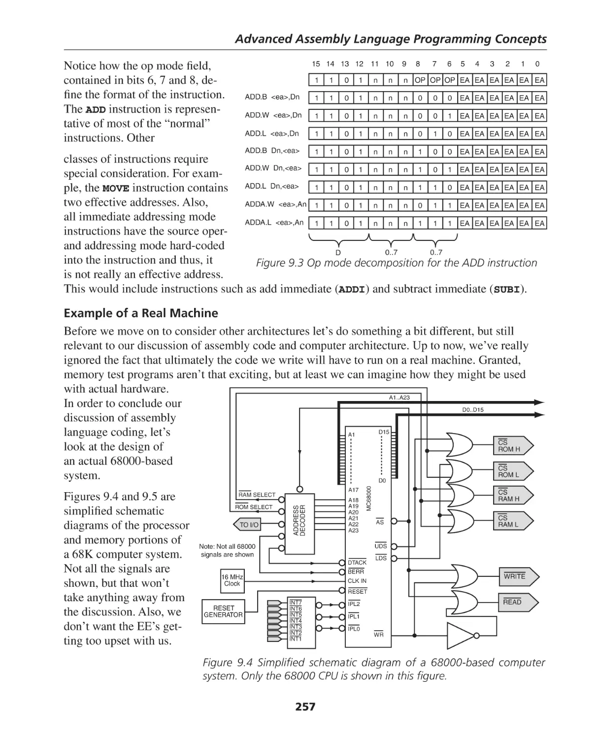
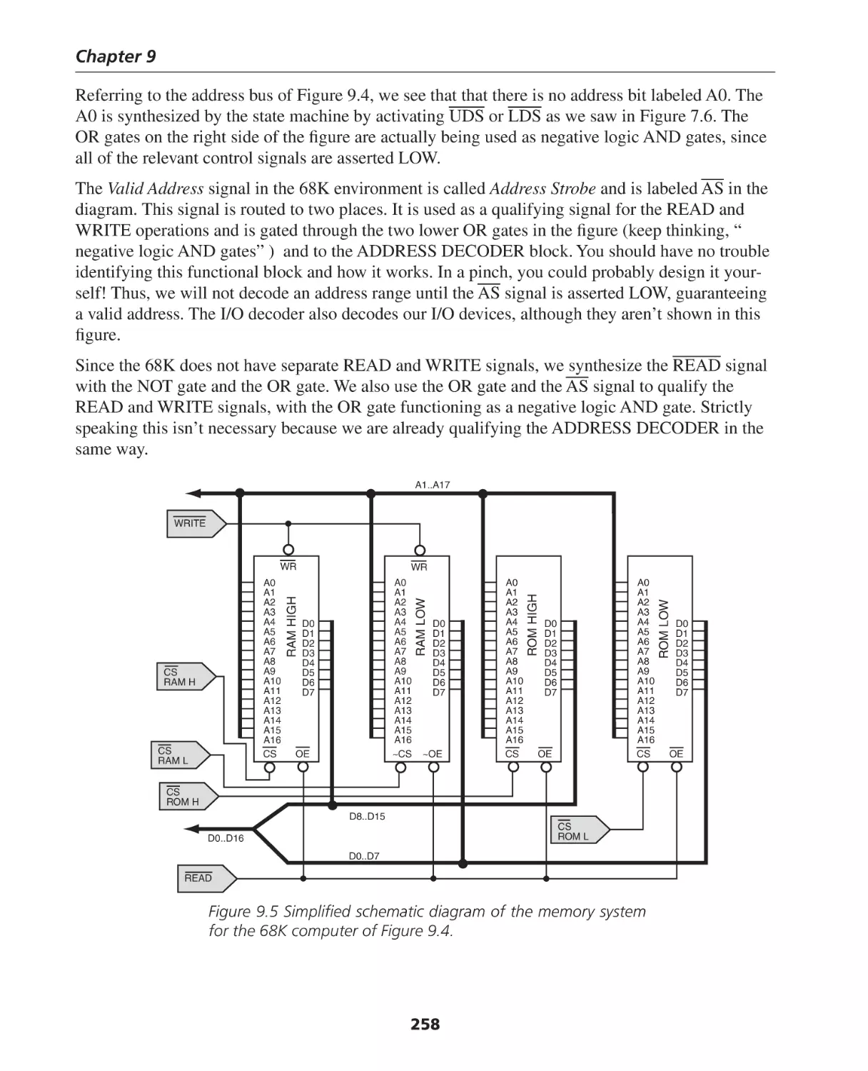
CHAPTER 9: Advanced Assembly Language Programming Concepts ........... 229
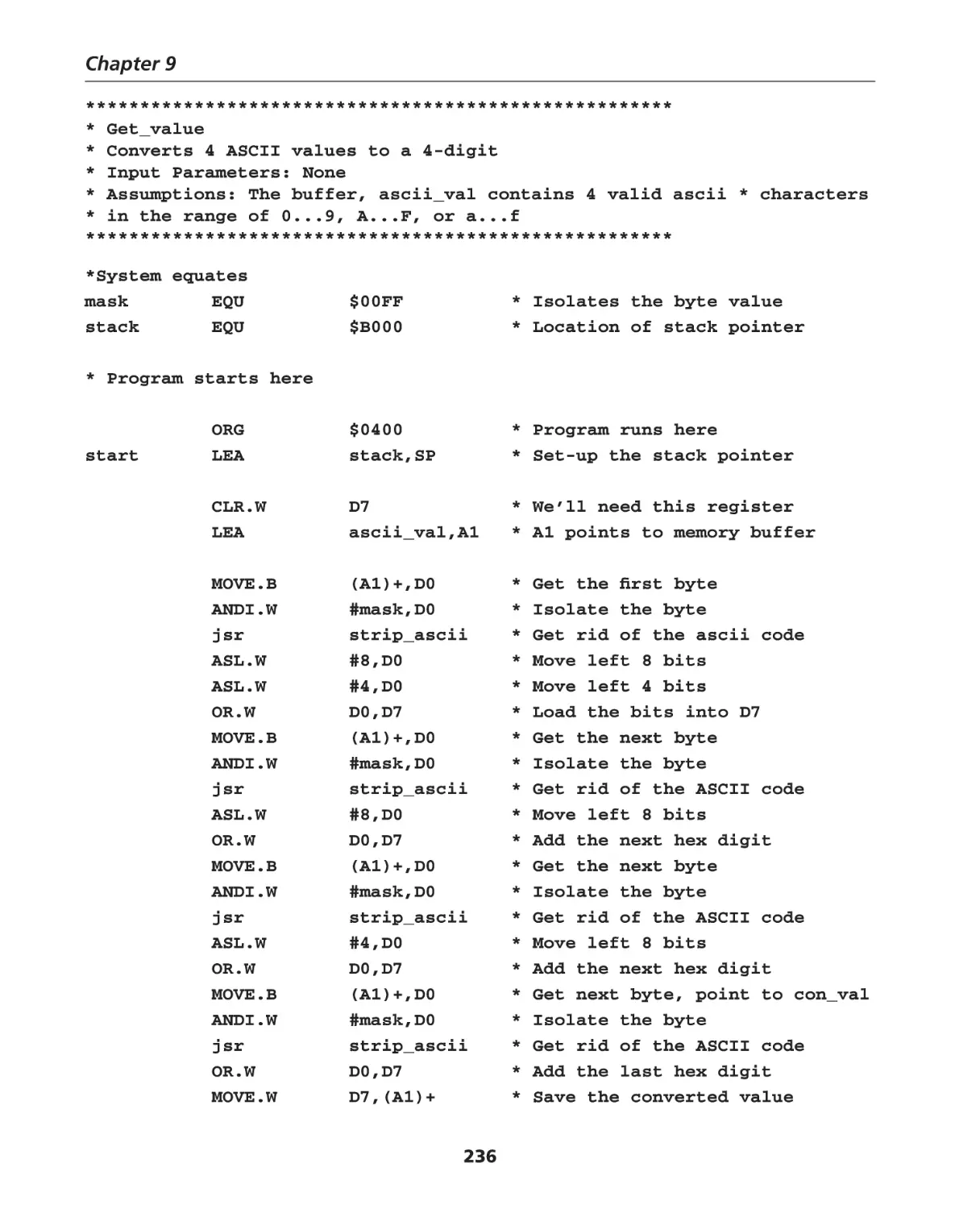
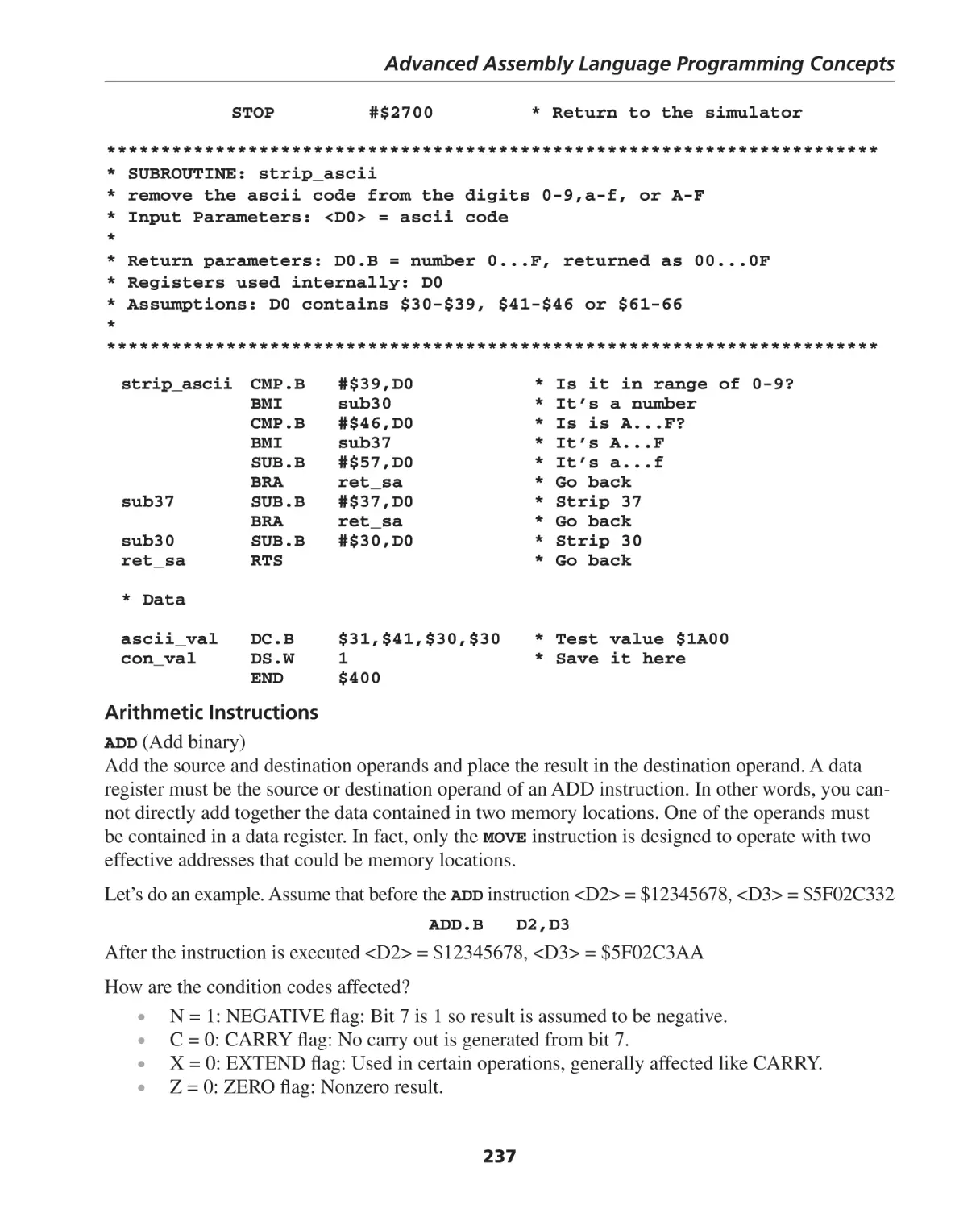
Introduction ............................................................................................................................ 229
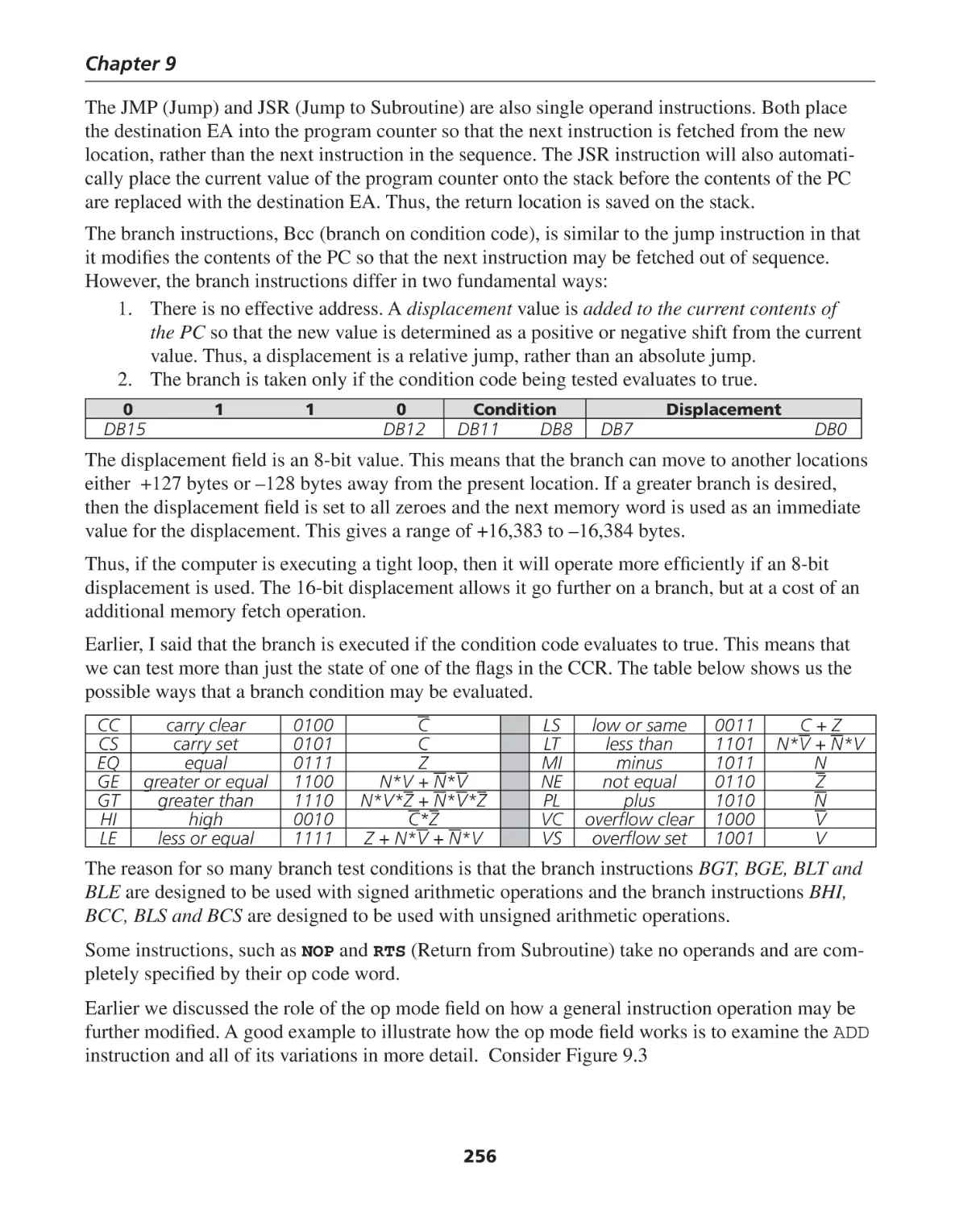
Advanced Addressing Modes................................................................................................... 230
68000 Instructions .................................................................................................................. 232
MOVE Instructions ................................................................................................................... 233
Logical Instructions .................................................................................................................. 233
Other Logical Instructions ........................................................................................................ 234
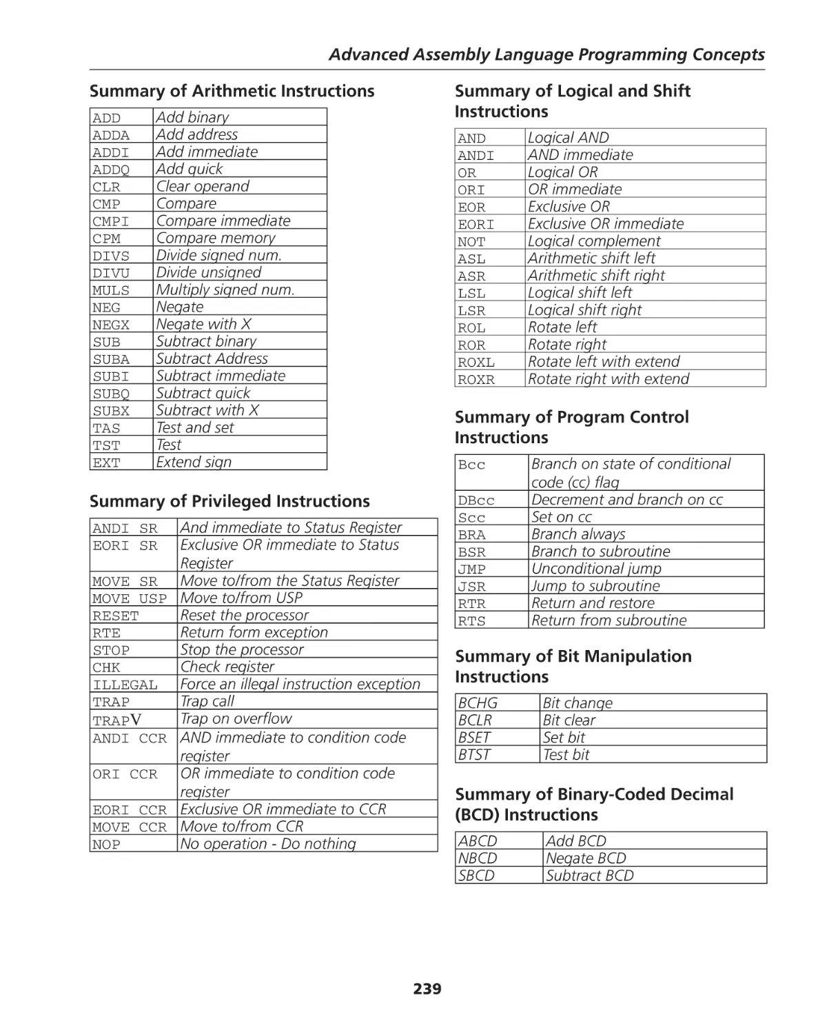
Summary of the 68K Instructions ............................................................................................. 238
Simulated I/O Using the TRAP #15 Instruction ....................................................................... 240
Compilers and Assemblers ....................................................................................................... 242
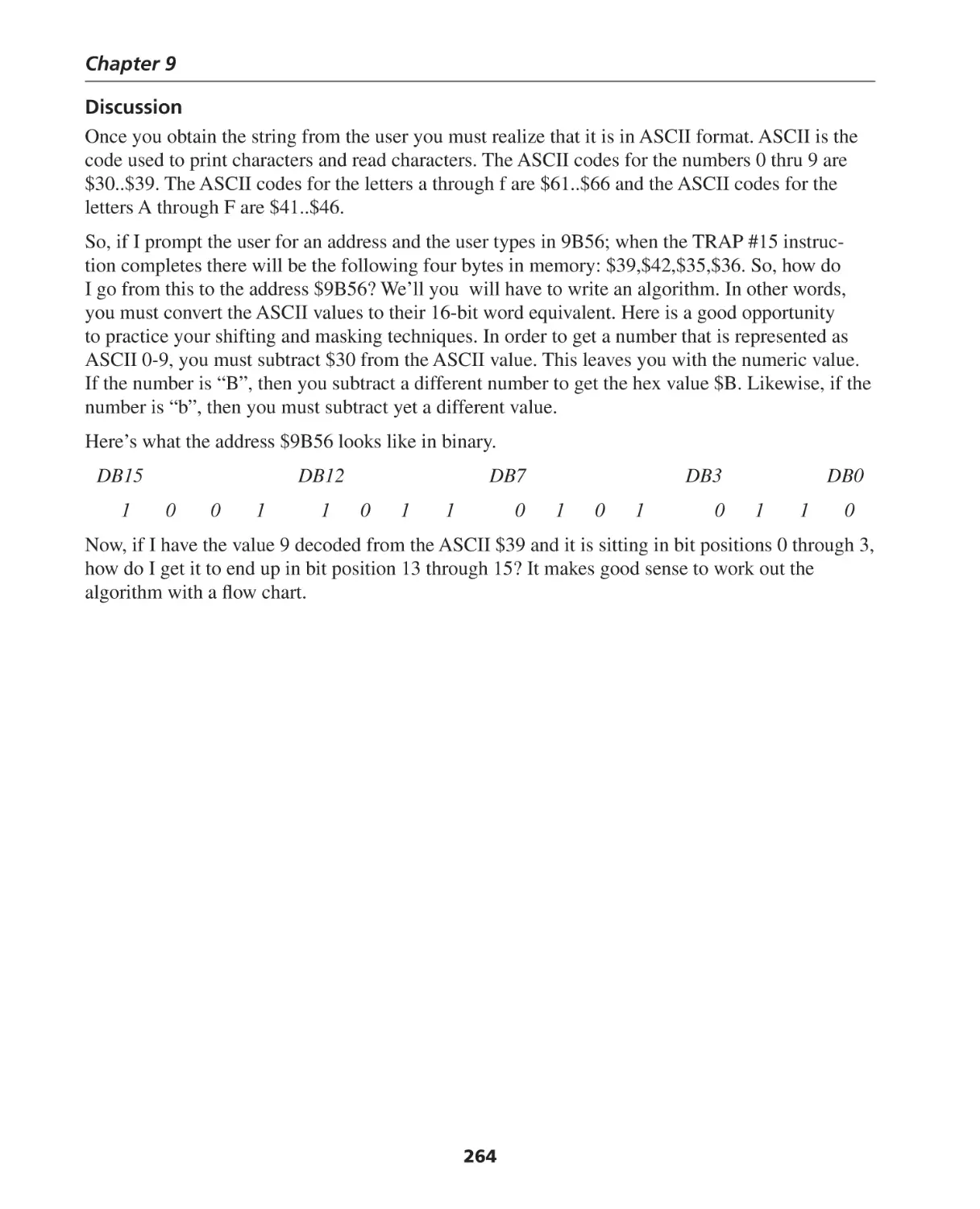
Summary of Chapter 9 ............................................................................................................ 259
Exercises for Chapter 9 ............................................................................................................ 260
CHAPTER 10: The Intel x86 Architecture ......................................................... 265
Introduction ............................................................................................................................ 265
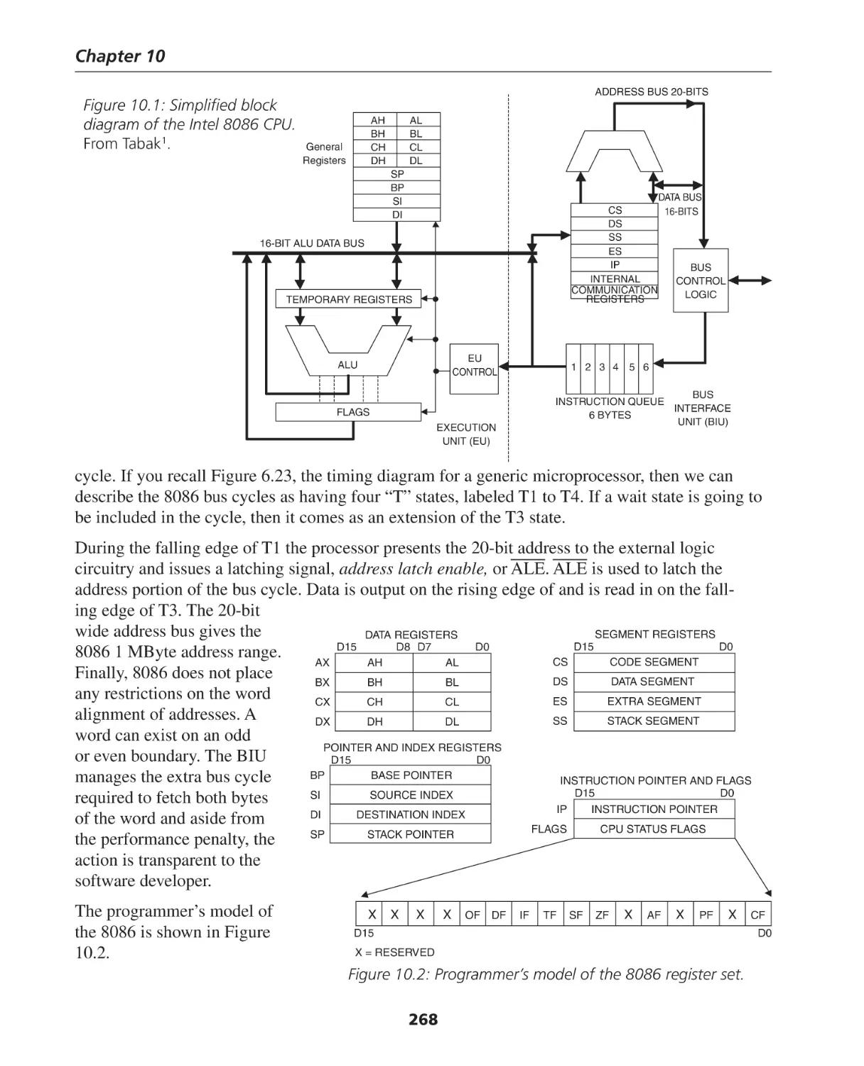
The Architecture of the 8086 CPU ........................................................................................... 267
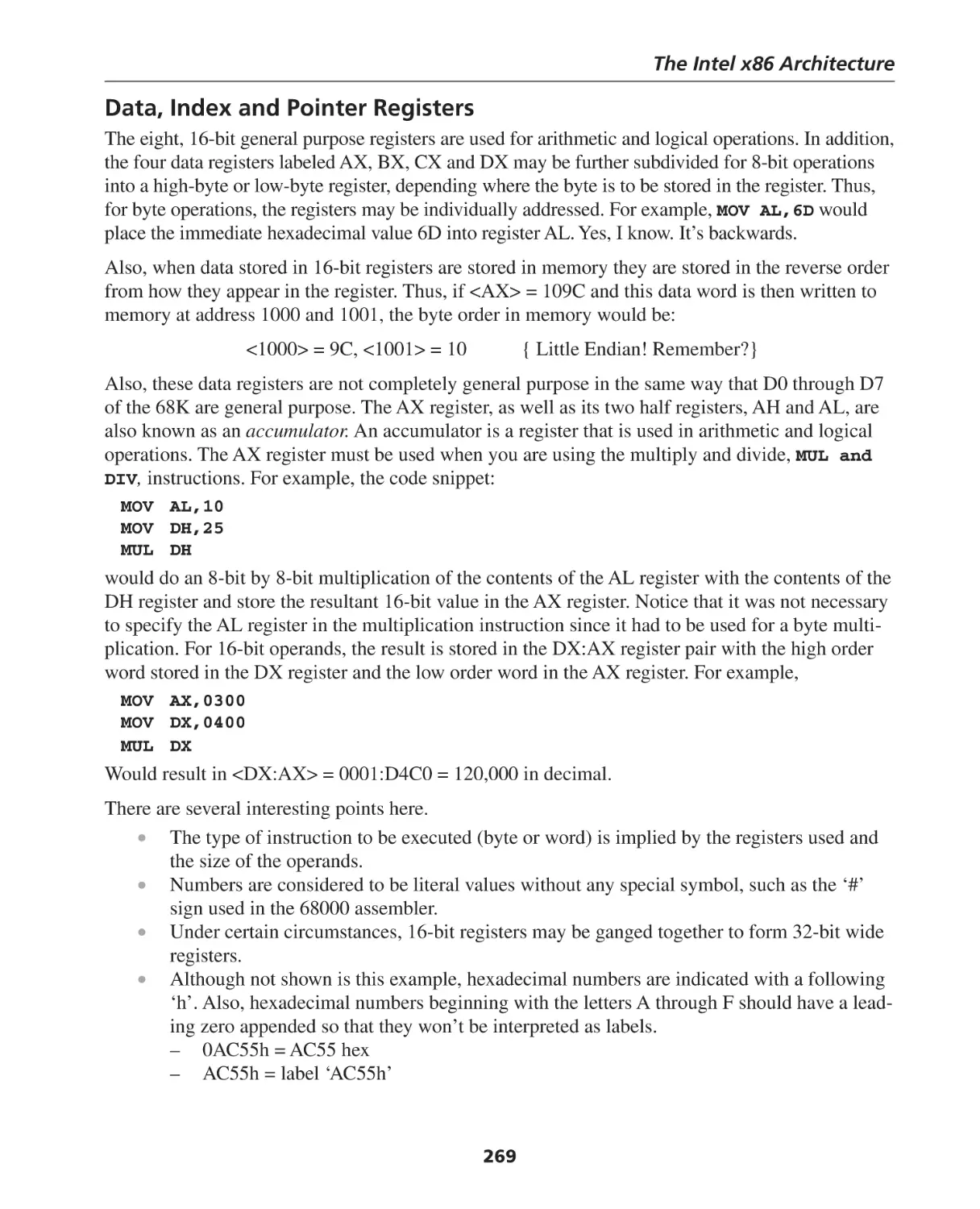
Data, Index and Pointer Registers ............................................................................................ 269
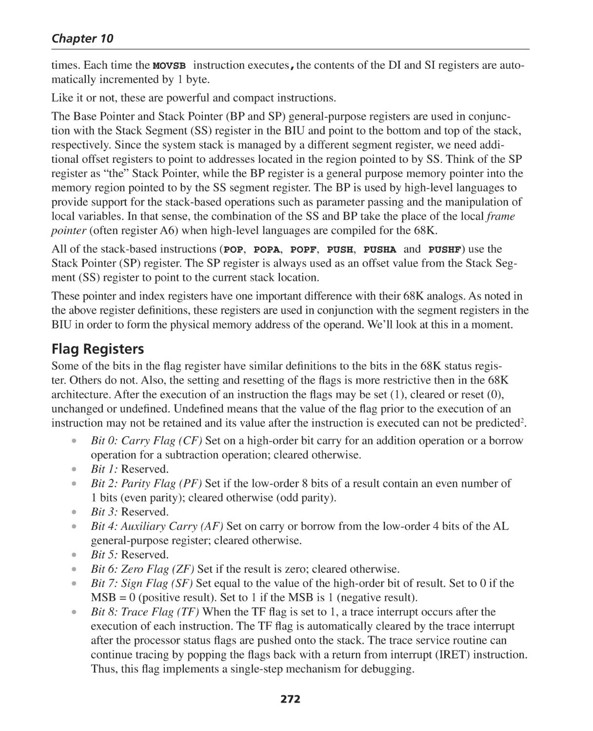
Flag Registers .......................................................................................................................... 272
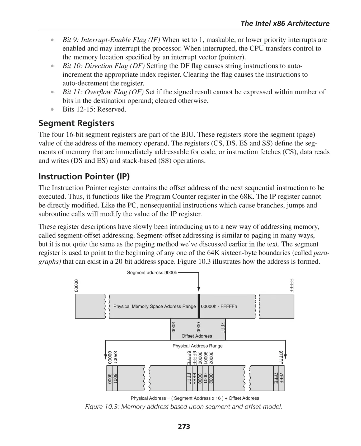
Segment Registers ................................................................................................................... 273
Instruction Pointer (IP) ............................................................................................................. 273
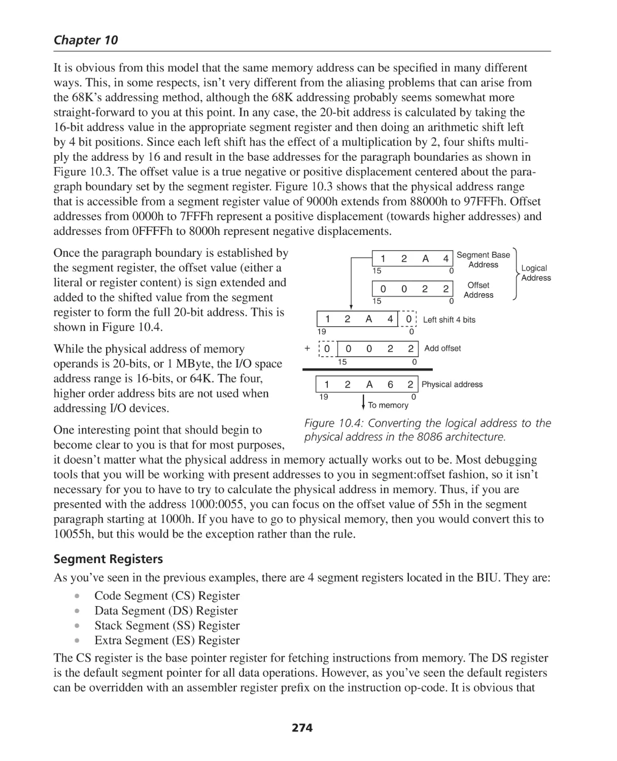
Memory Addressing Modes ..................................................................................................... 275
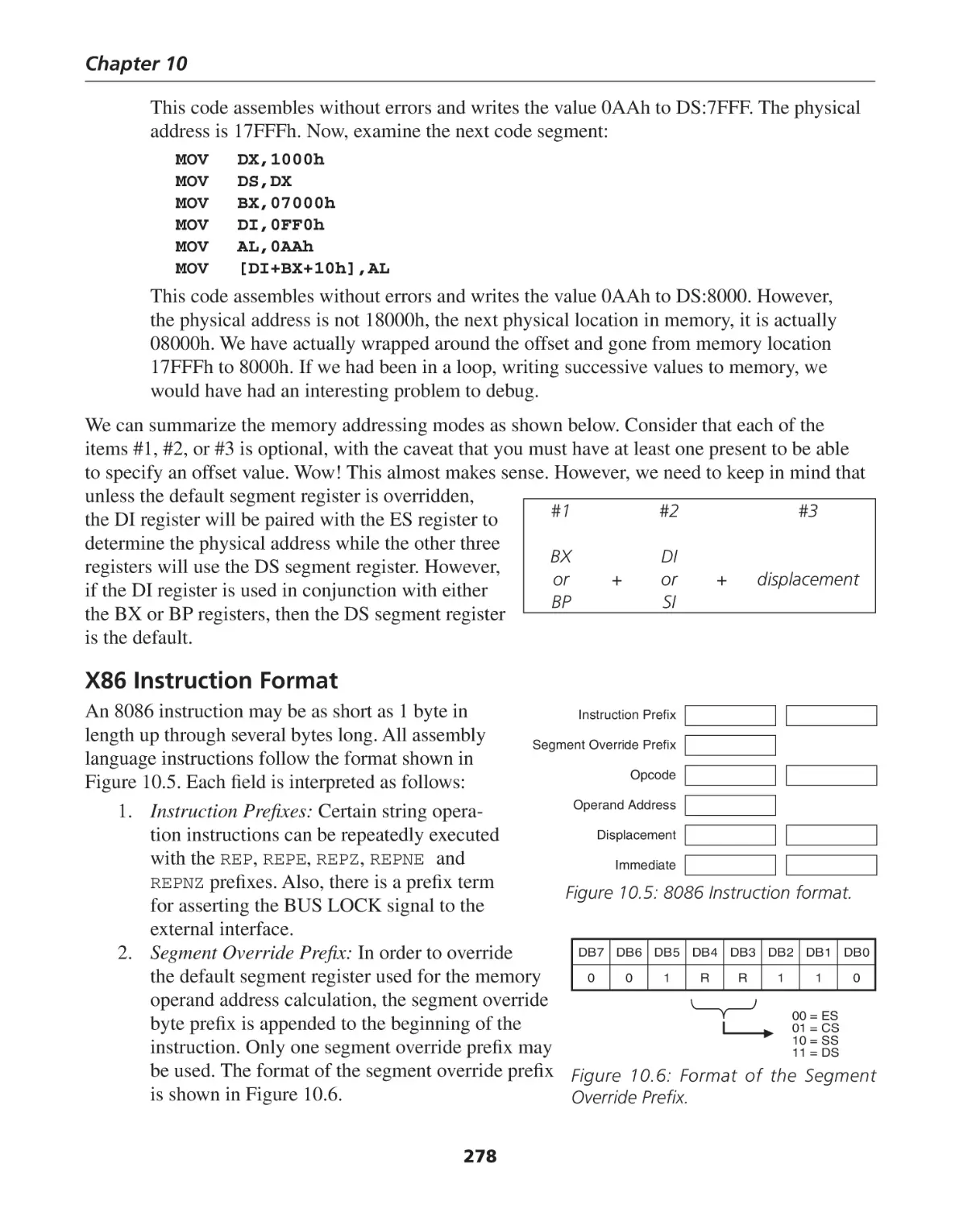
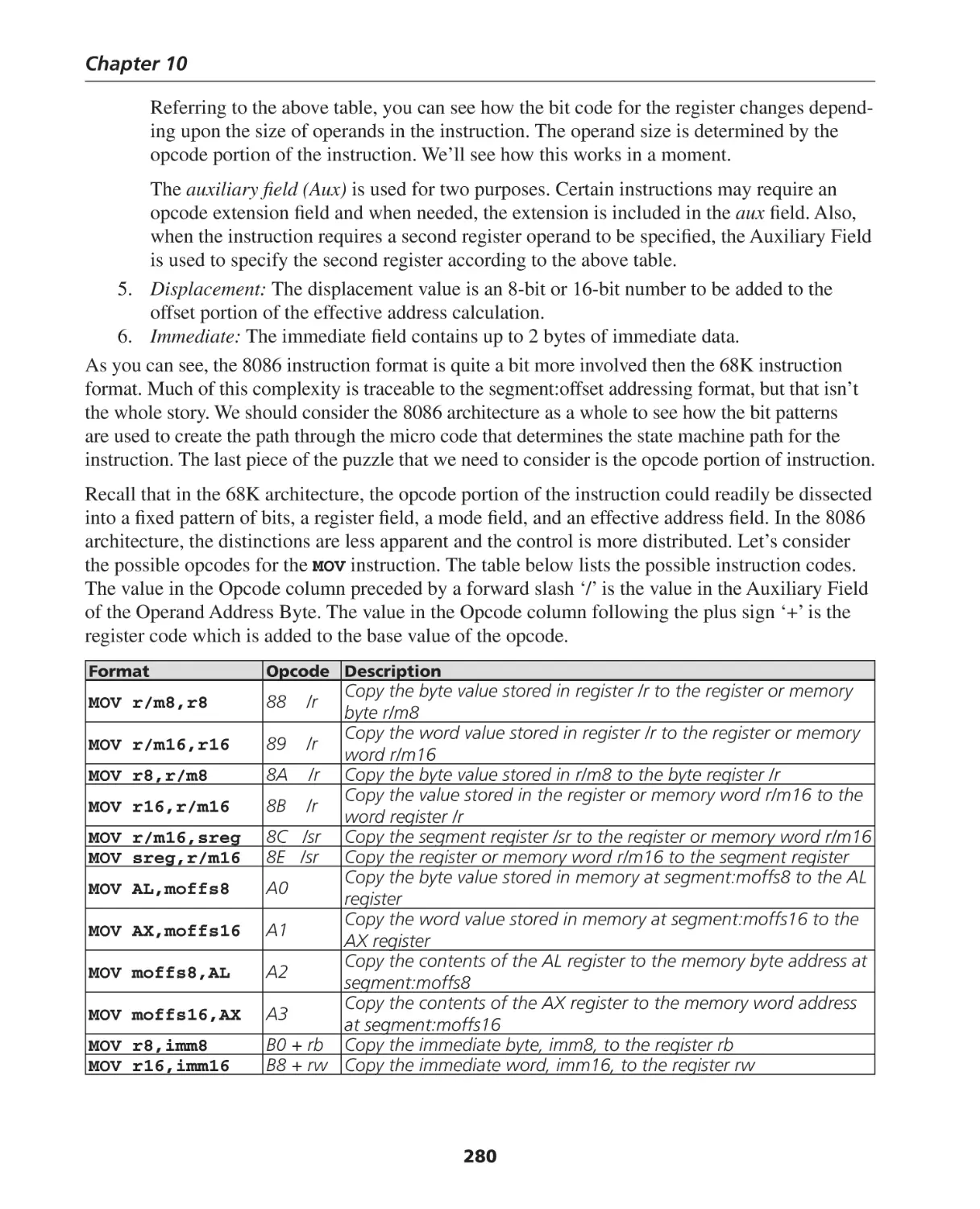
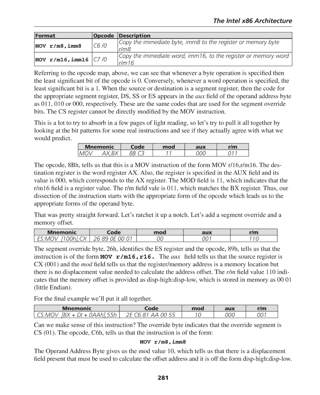
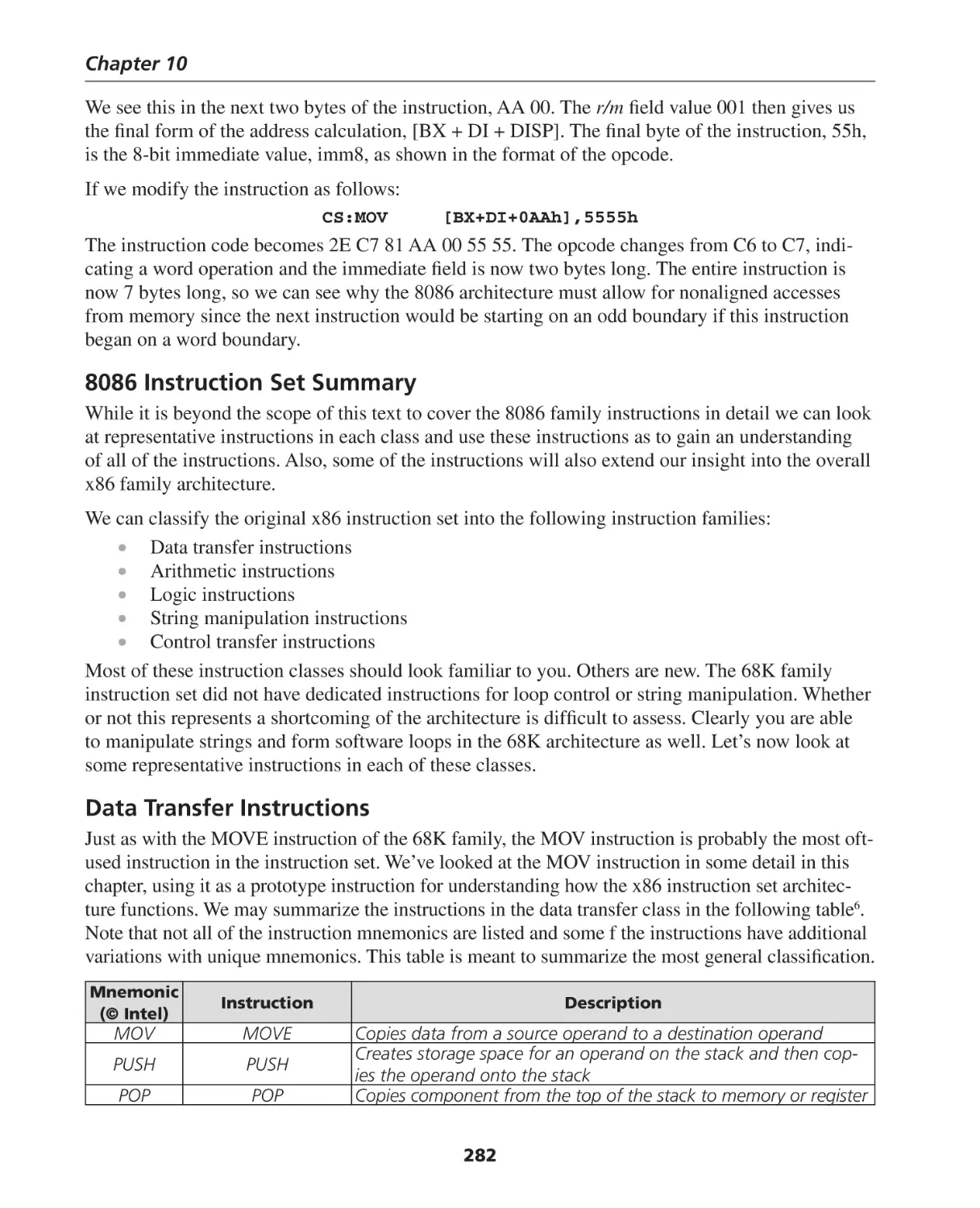
X86 Instruction Format ............................................................................................................ 278
viii
Contents
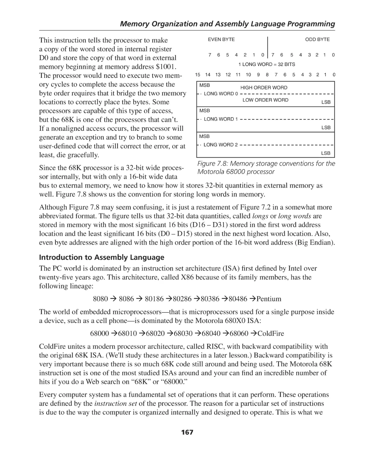
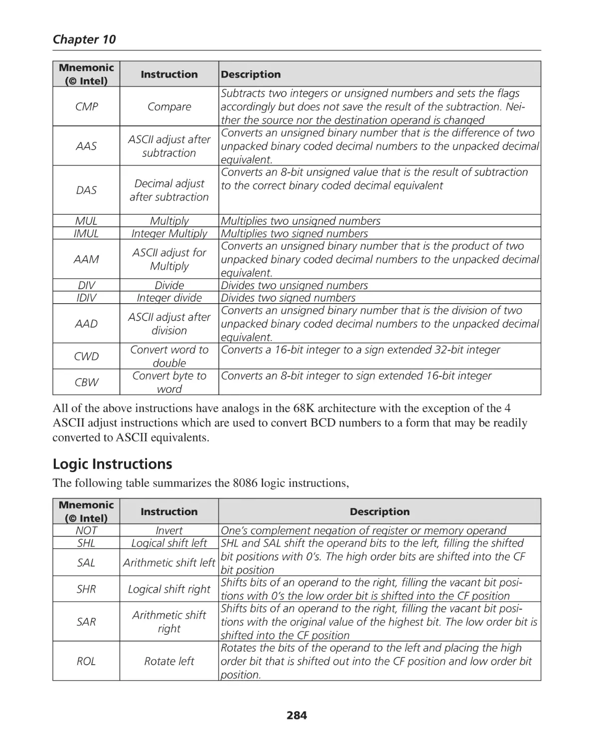
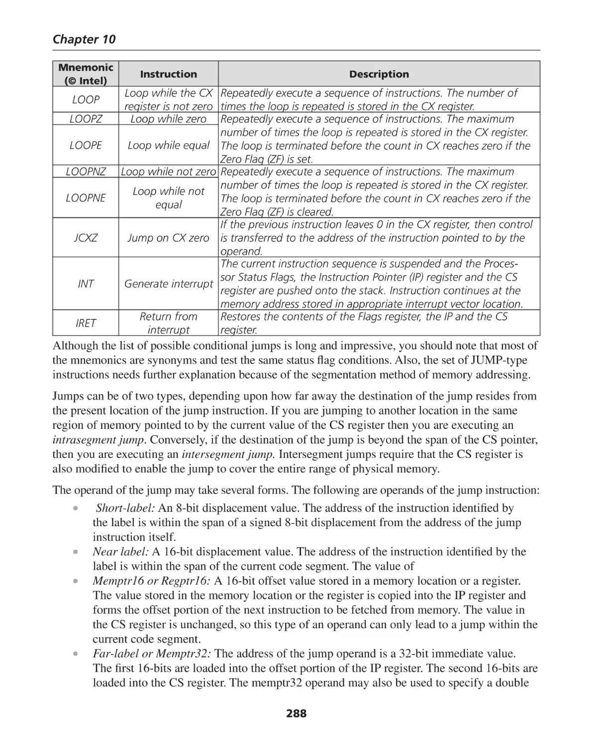
8086 Instruction Set Summary ................................................................................................. 282
Data Transfer Instructions ........................................................................................................ 282
Arithmetic Instructions ............................................................................................................ 283
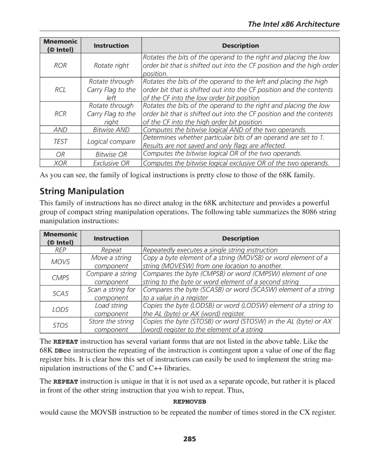
Logic Instructions .................................................................................................................... 284
String Manipulation ................................................................................................................. 285
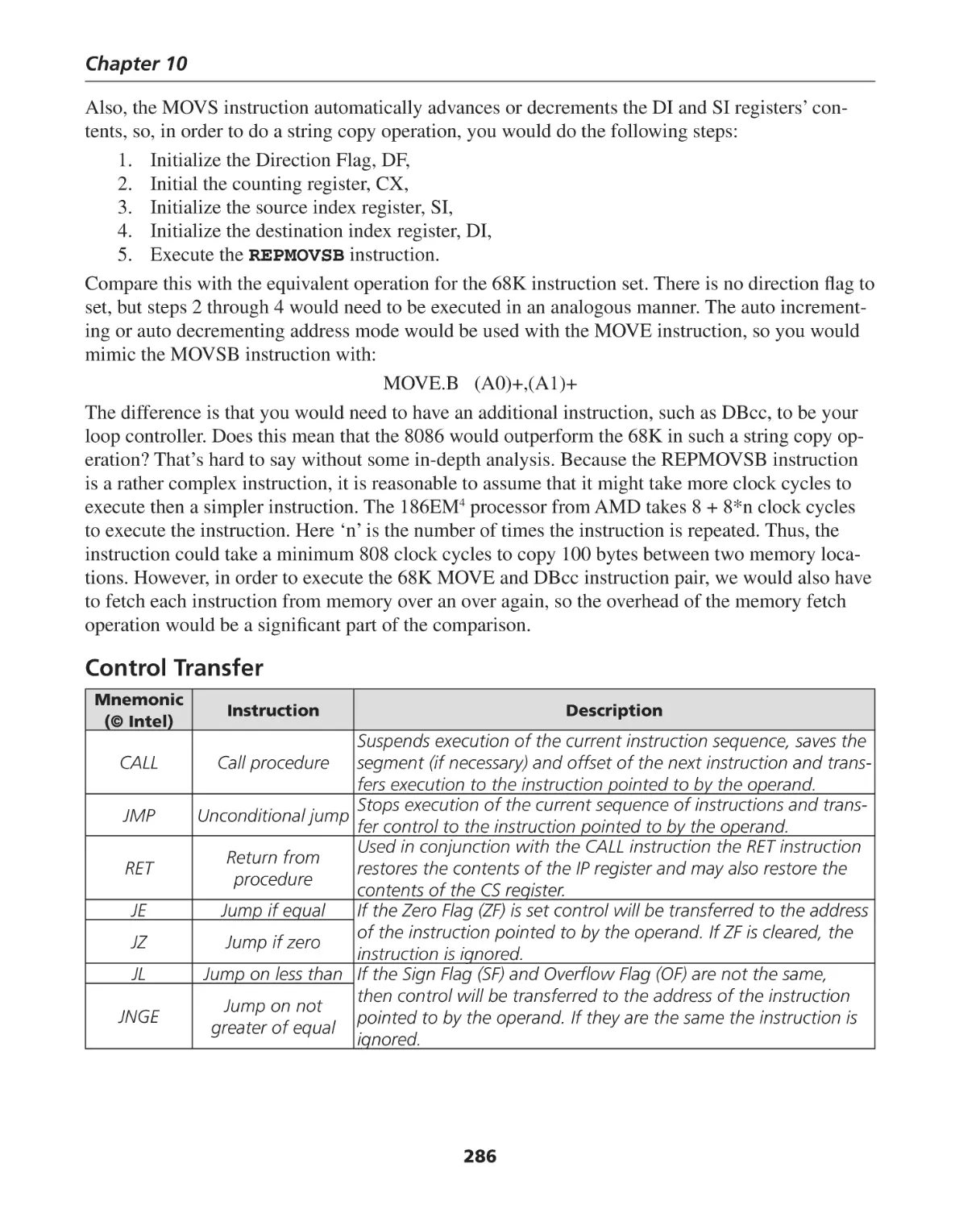
Control Transfer ...................................................................................................................... 286
Assembly Language Programming the 8086 Architecture ....................................................... 289
System Vectors ........................................................................................................................ 291
System Startup ........................................................................................................................ 292
Wrap-Up ................................................................................................................................. 292
Summary of Chapter 10 .......................................................................................................... 292
Exercises for Chapter 10 .......................................................................................................... 294
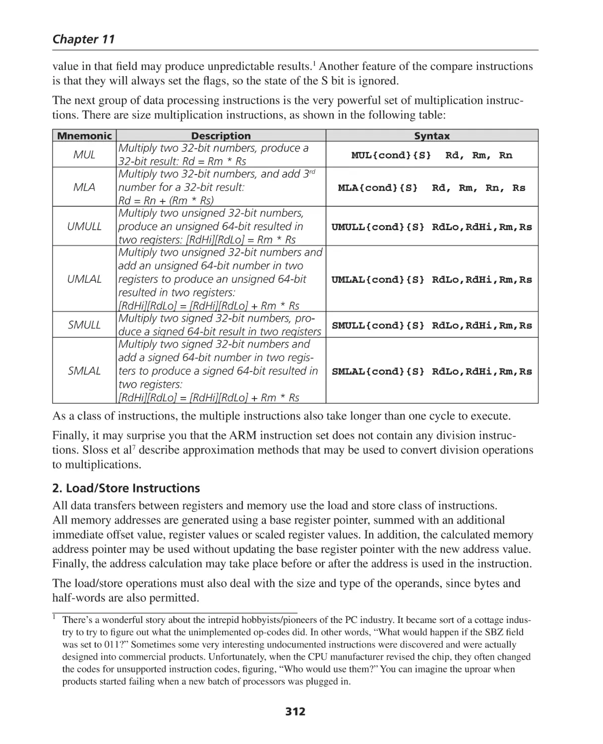
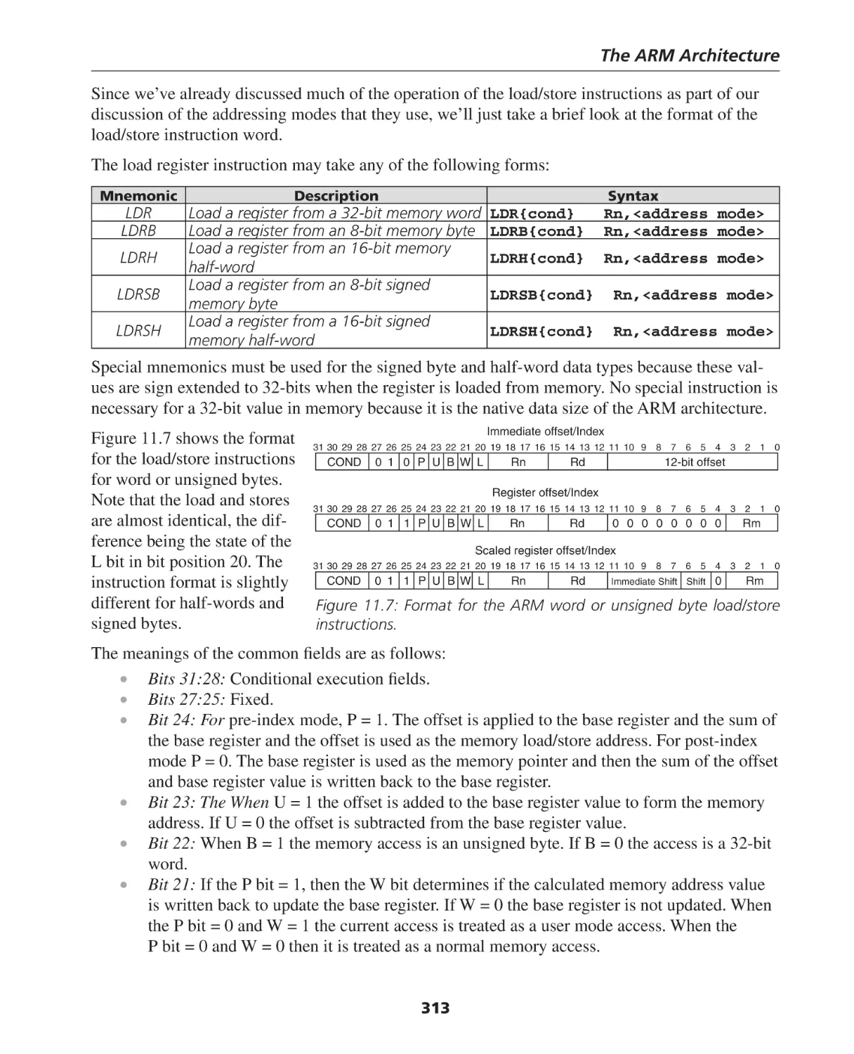
CHAPTER 11: The ARM Architecture ................................................................ 295
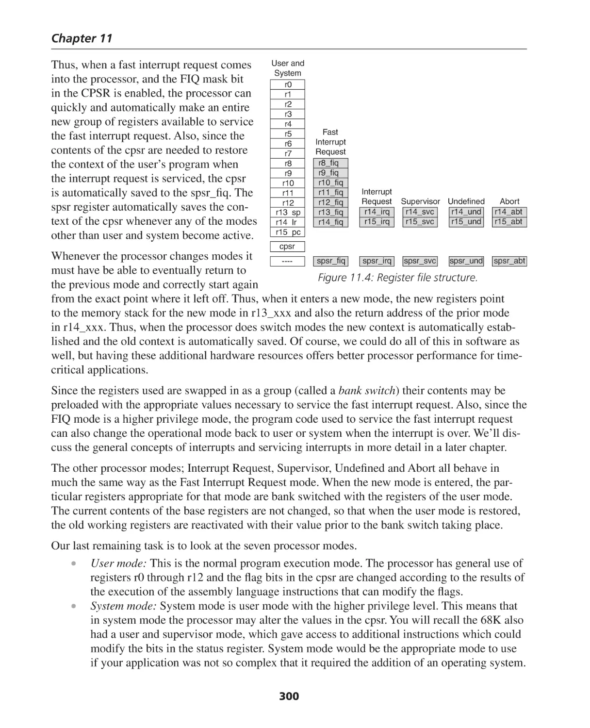
Introduction ............................................................................................................................ 295
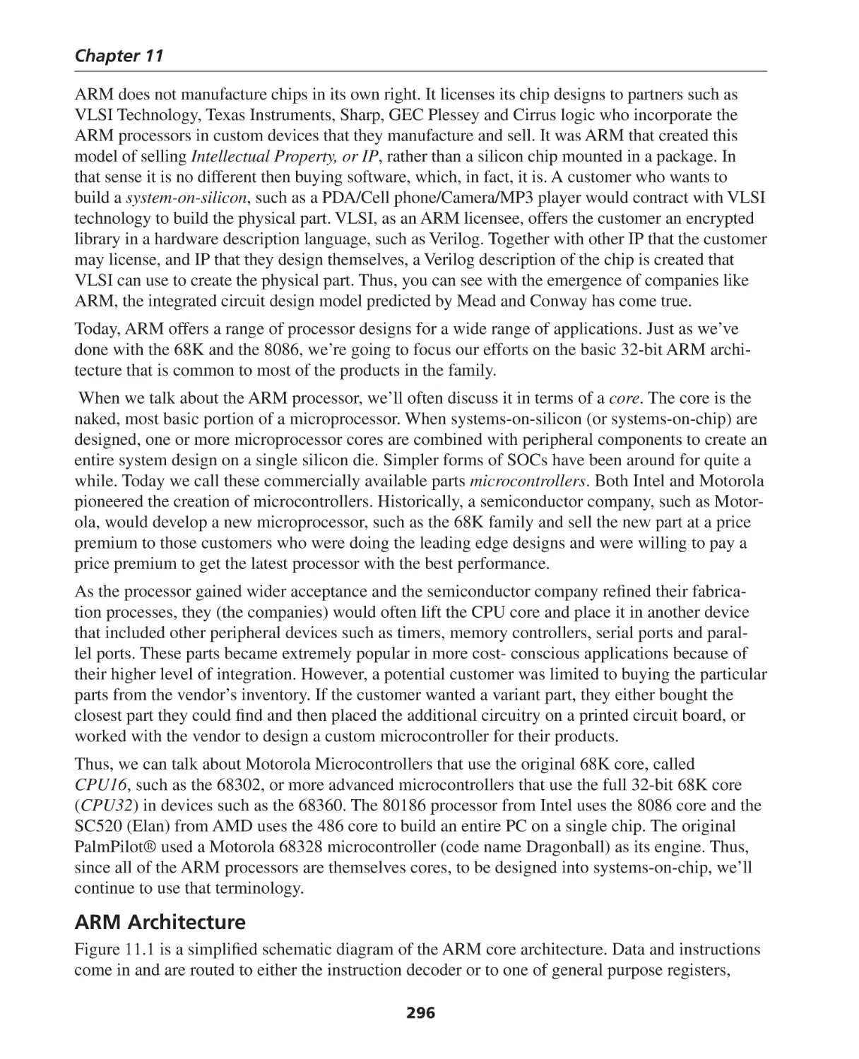
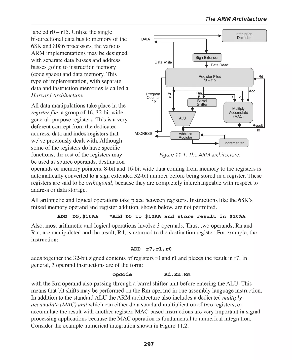
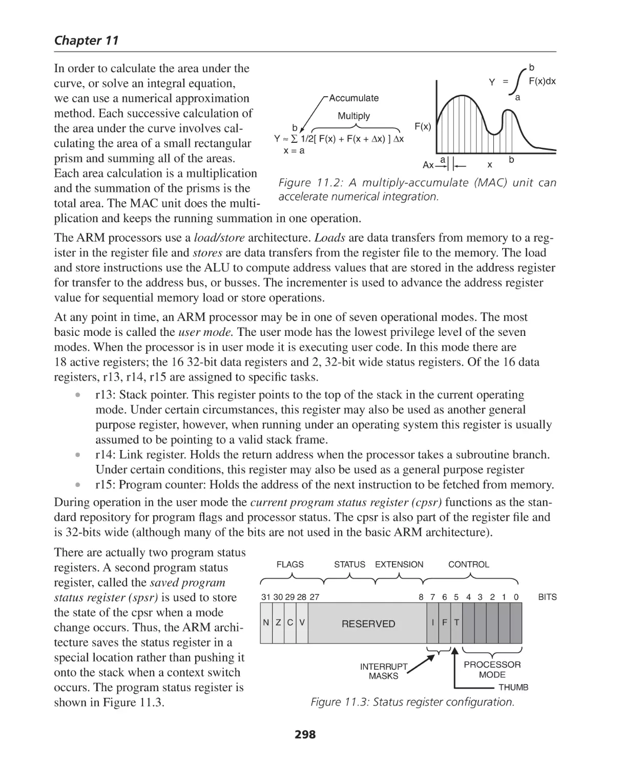
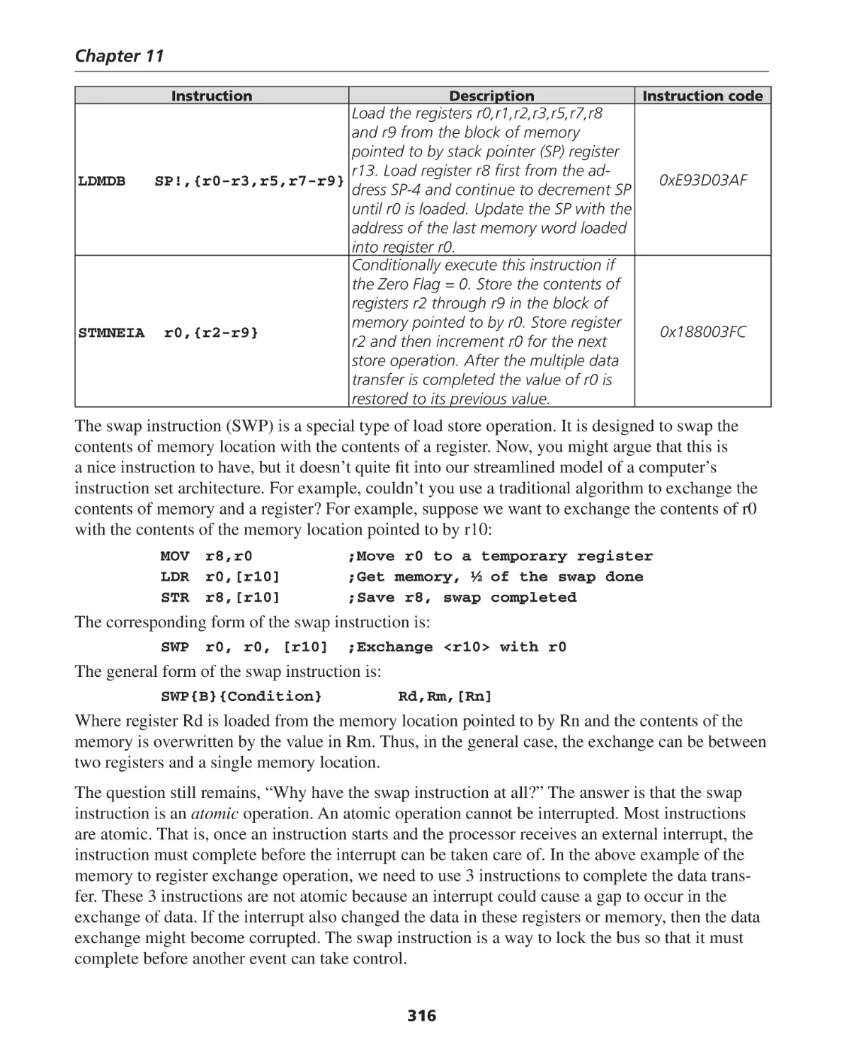
ARM Architecture .................................................................................................................... 296
Conditional Execution ............................................................................................................ 301
Barrel Shifter ........................................................................................................................... 302
Operand Size ........................................................................................................................... 303
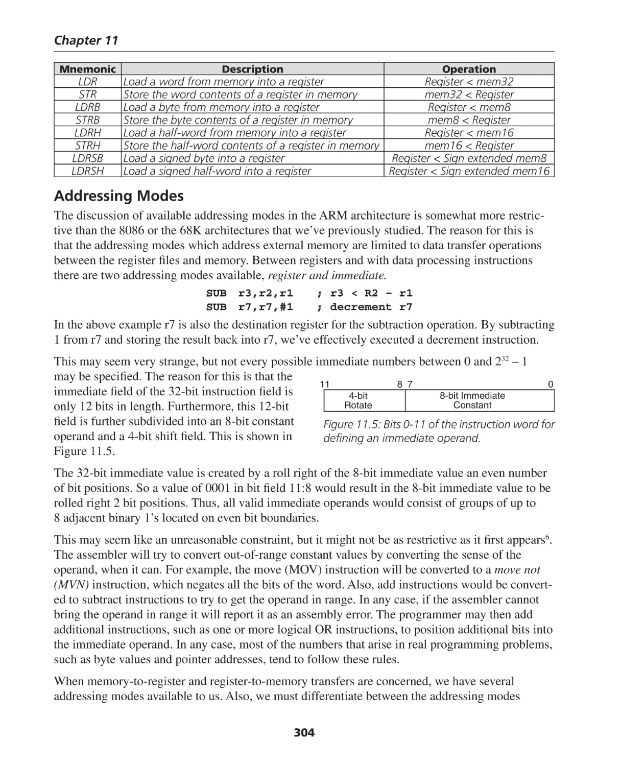
Addressing Modes ................................................................................................................... 304
Stack Operations ..................................................................................................................... 306
ARM Instruction Set ................................................................................................................ 309
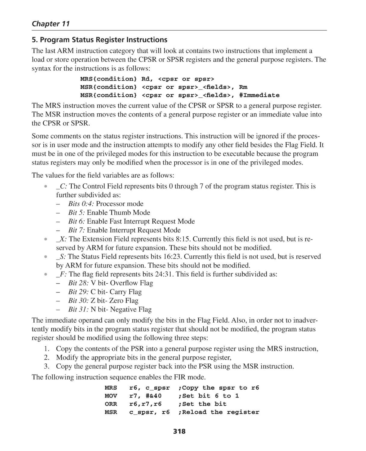
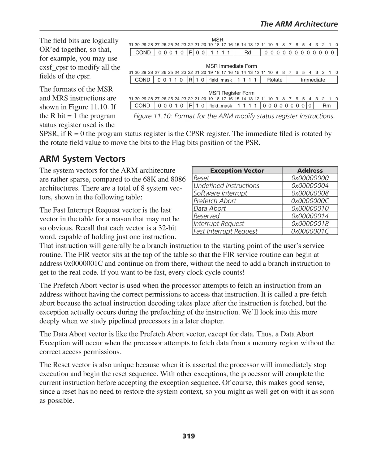
ARM System Vectors ............................................................................................................... 319
Summary and Conclusions ...................................................................................................... 320
Summary of Chapter 11 .......................................................................................................... 320
Exercises for Chapter 11 .......................................................................................................... 321
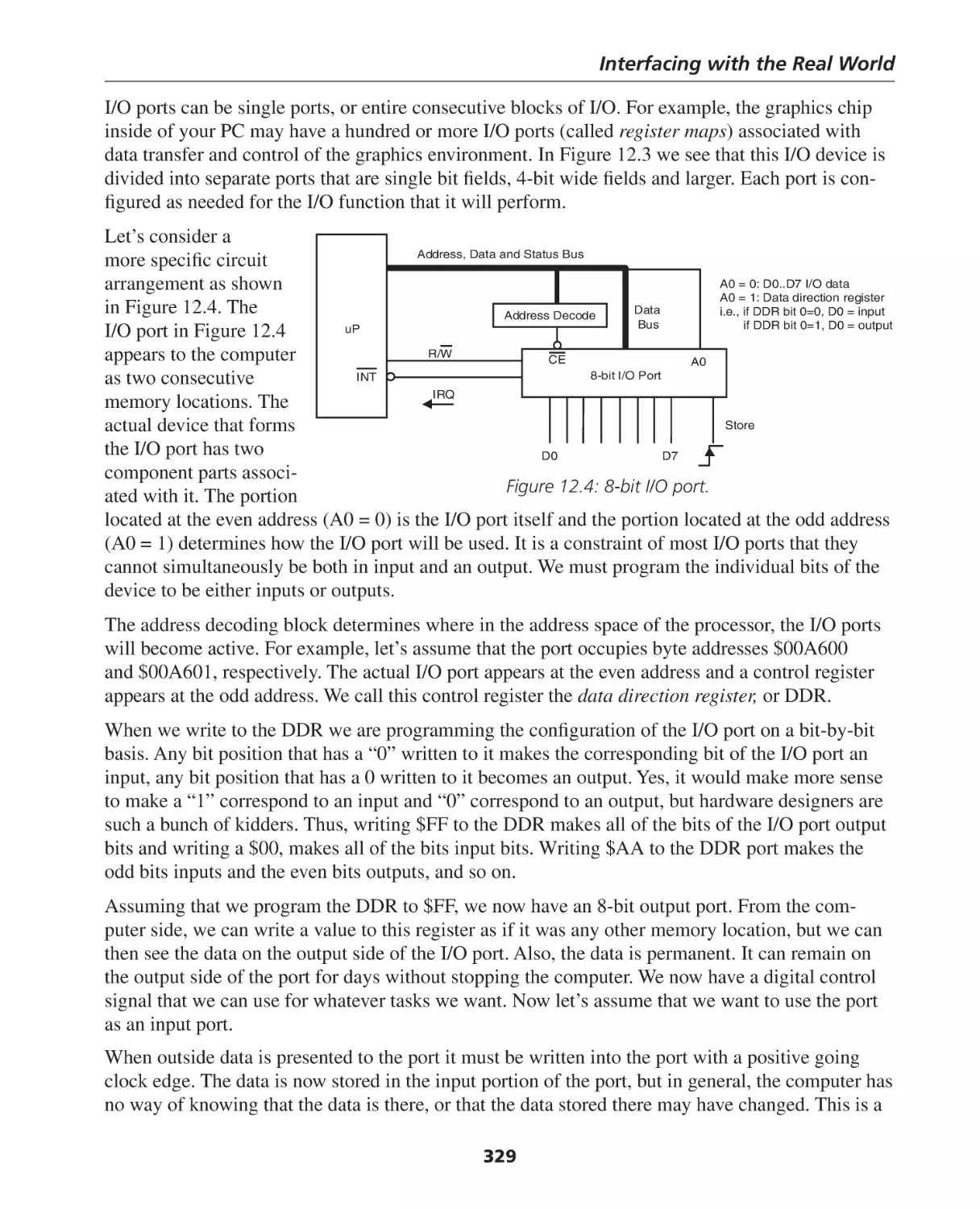
CHAPTER 12: Interfacing with the Real World ................................................ 322
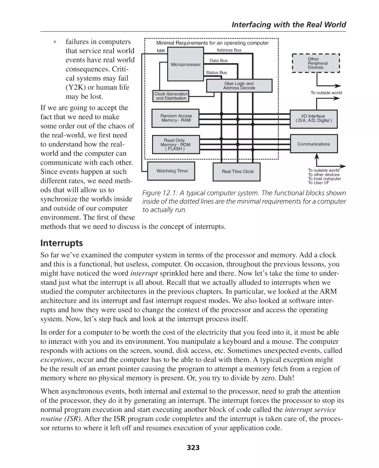
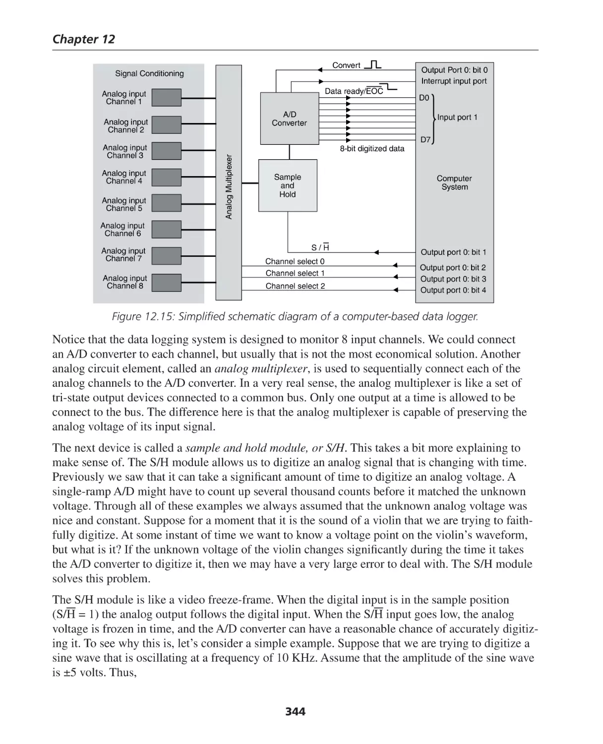
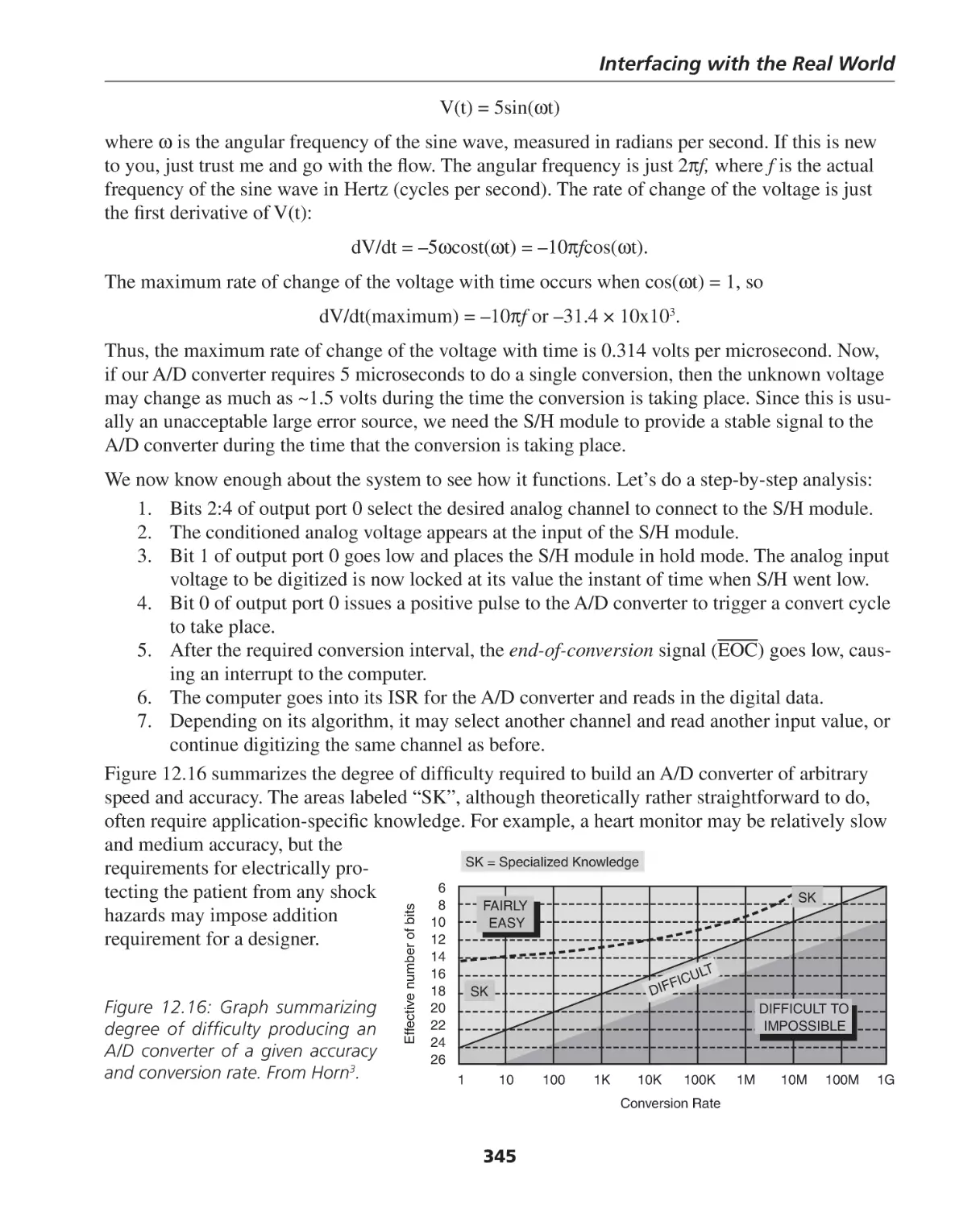
Introduction ............................................................................................................................ 322
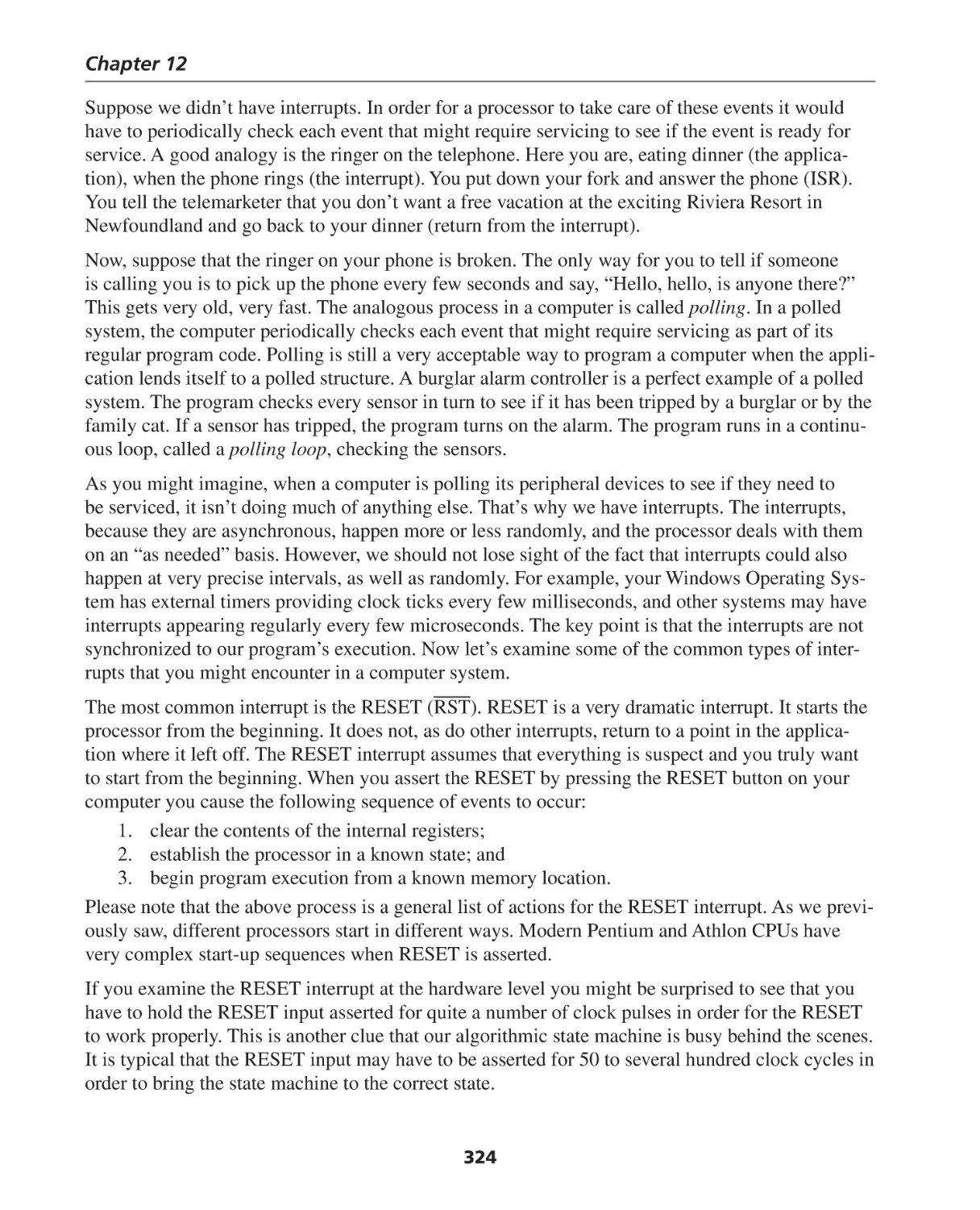
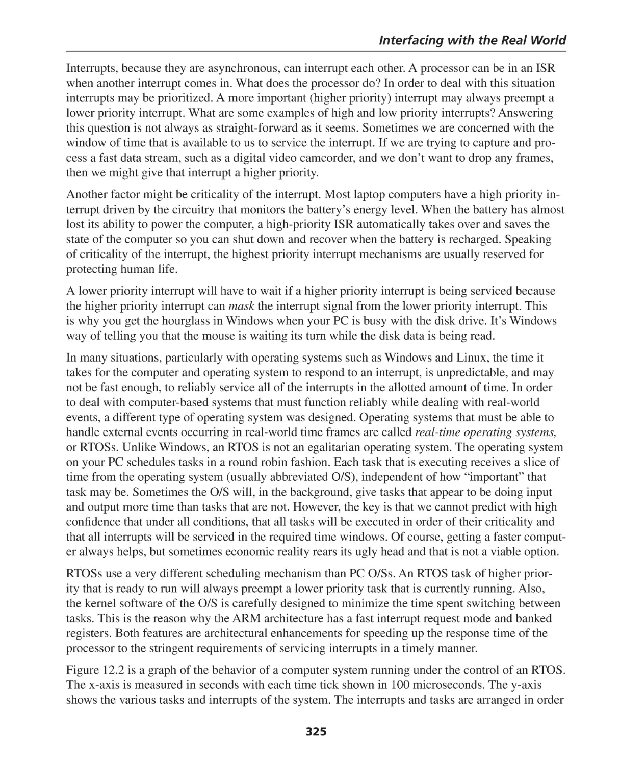
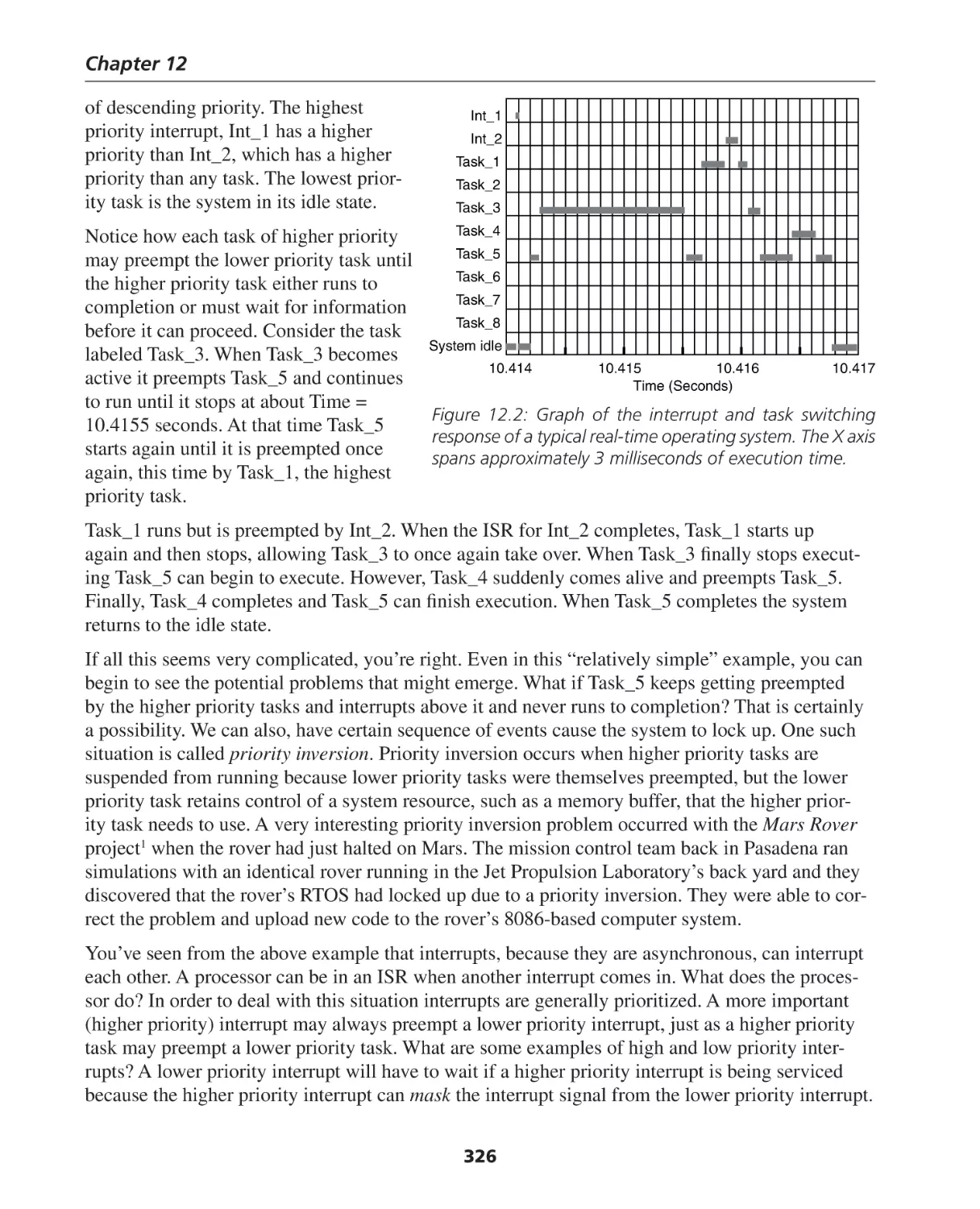
Interrupts ................................................................................................................................ 323
Exceptions ............................................................................................................................... 327
Motorola 68K Interrupts .......................................................................................................... 327
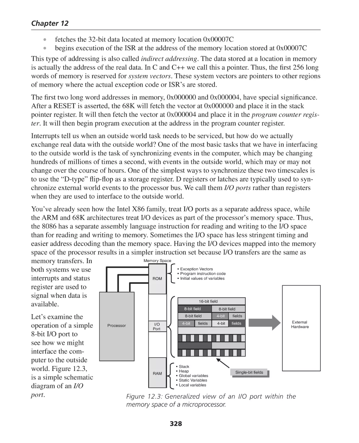
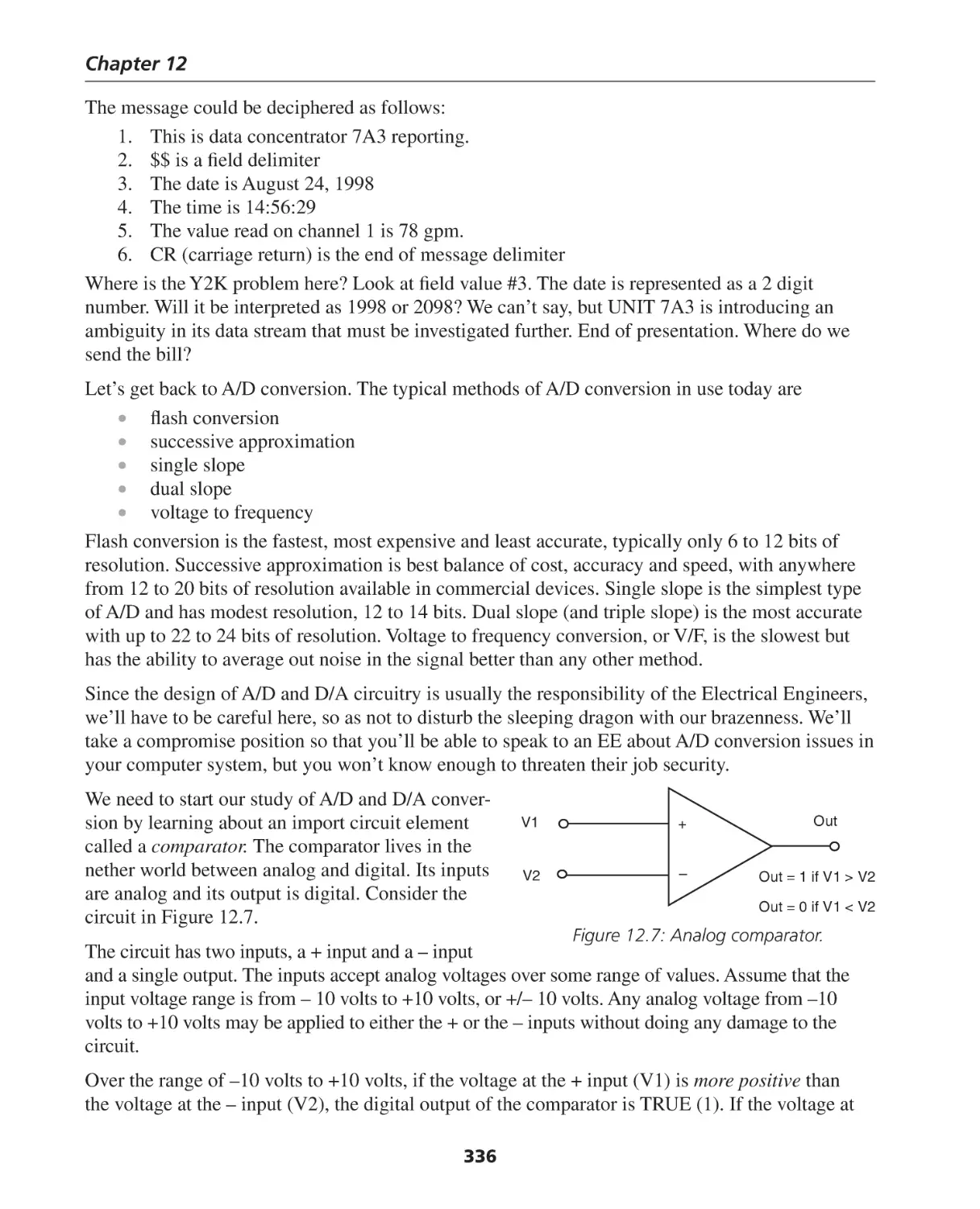
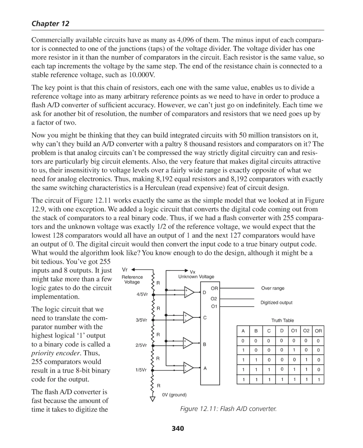
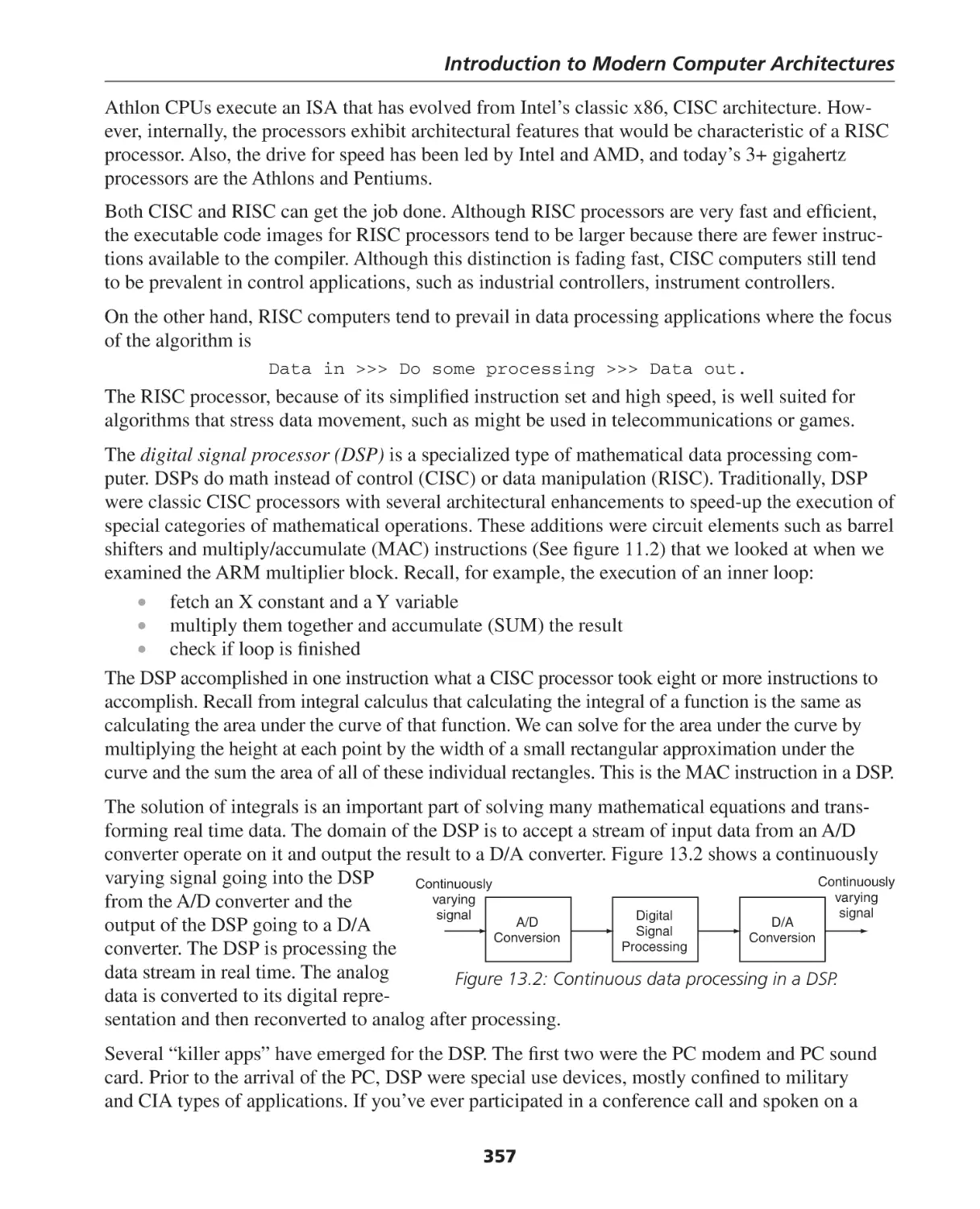
Analog-to-Digital (A/D) and Digital-to-Analog (D/A) Conversion ............................................... 332
The Resolution of A/D and D/A Converters .............................................................................. 346
Summary of Chapter 12 .......................................................................................................... 348
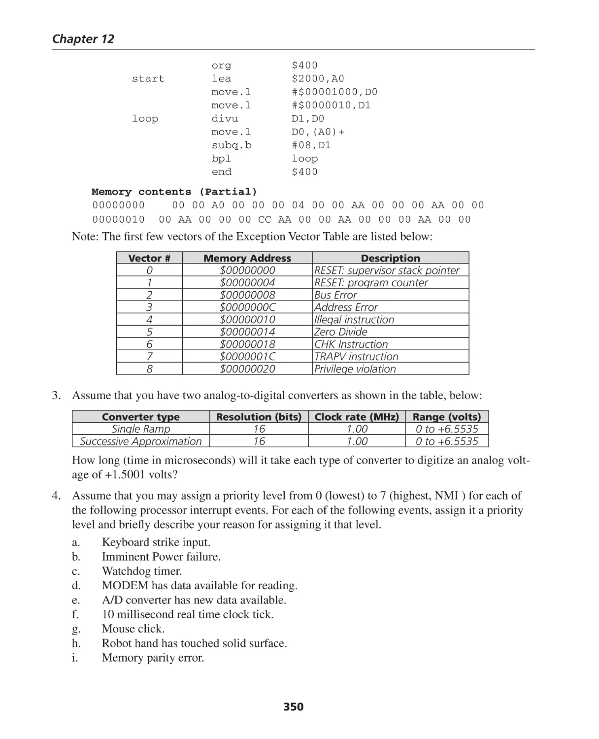
Exercises for Chapter 12 .......................................................................................................... 349
CHAPTER 13: Introduction to Modern Computer Architectures .................... 353
Processor Architectures, CISC, RISC and DSP ........................................................................... 354
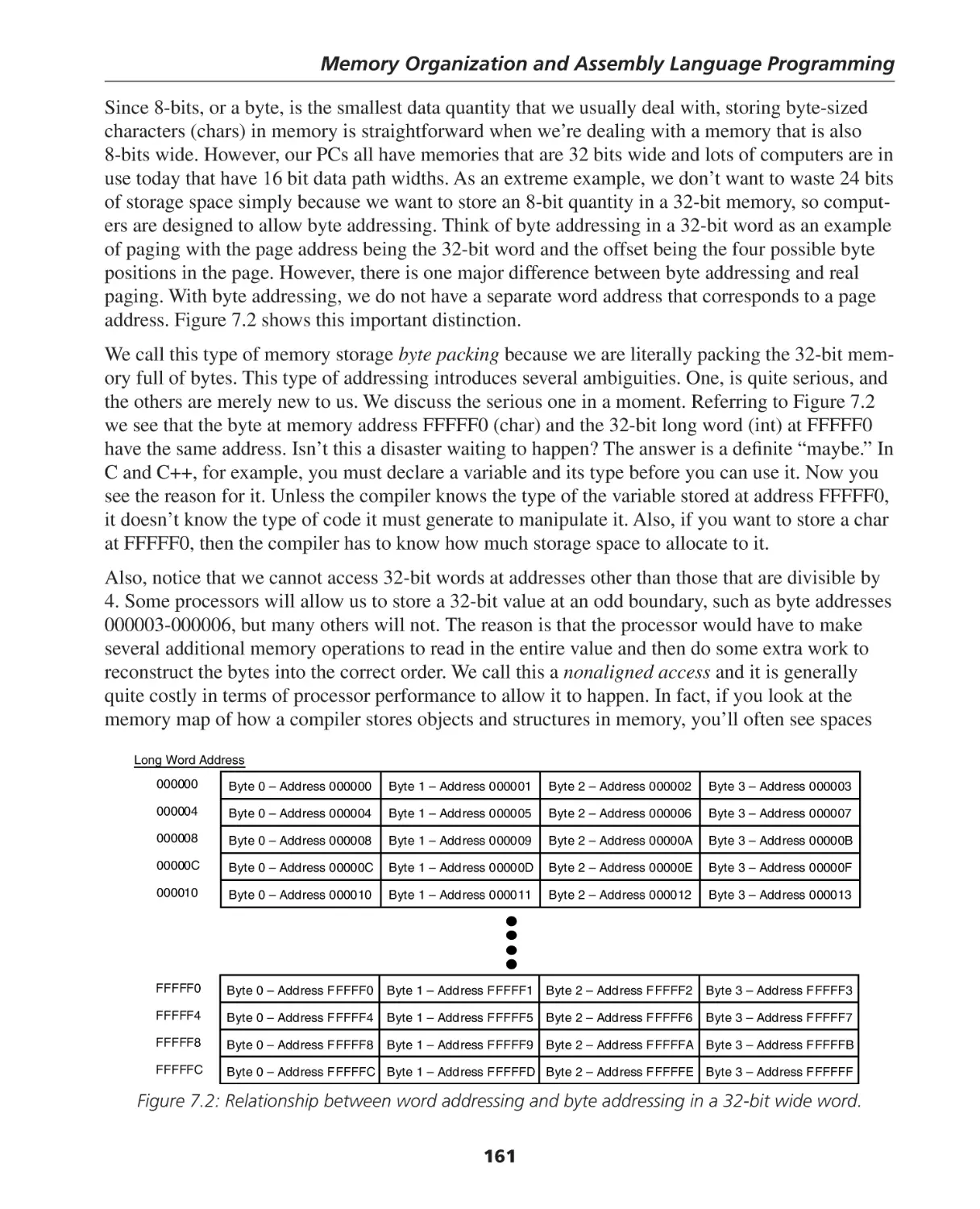
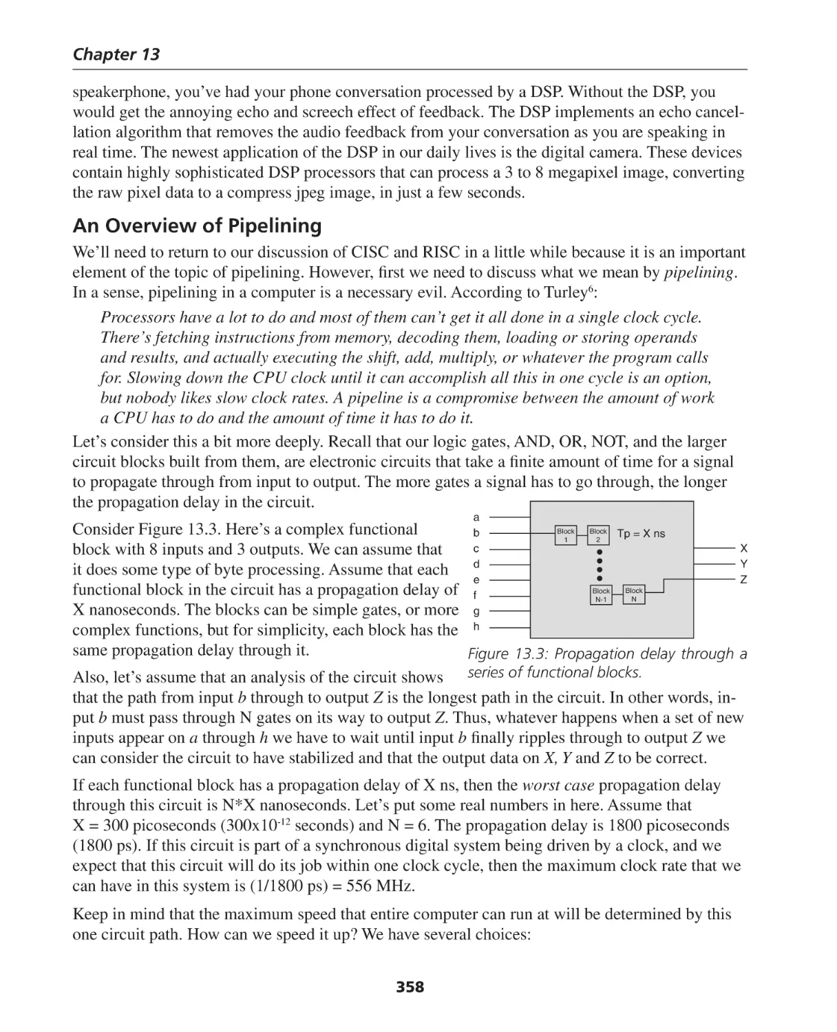
An Overview of Pipelining ....................................................................................................... 358
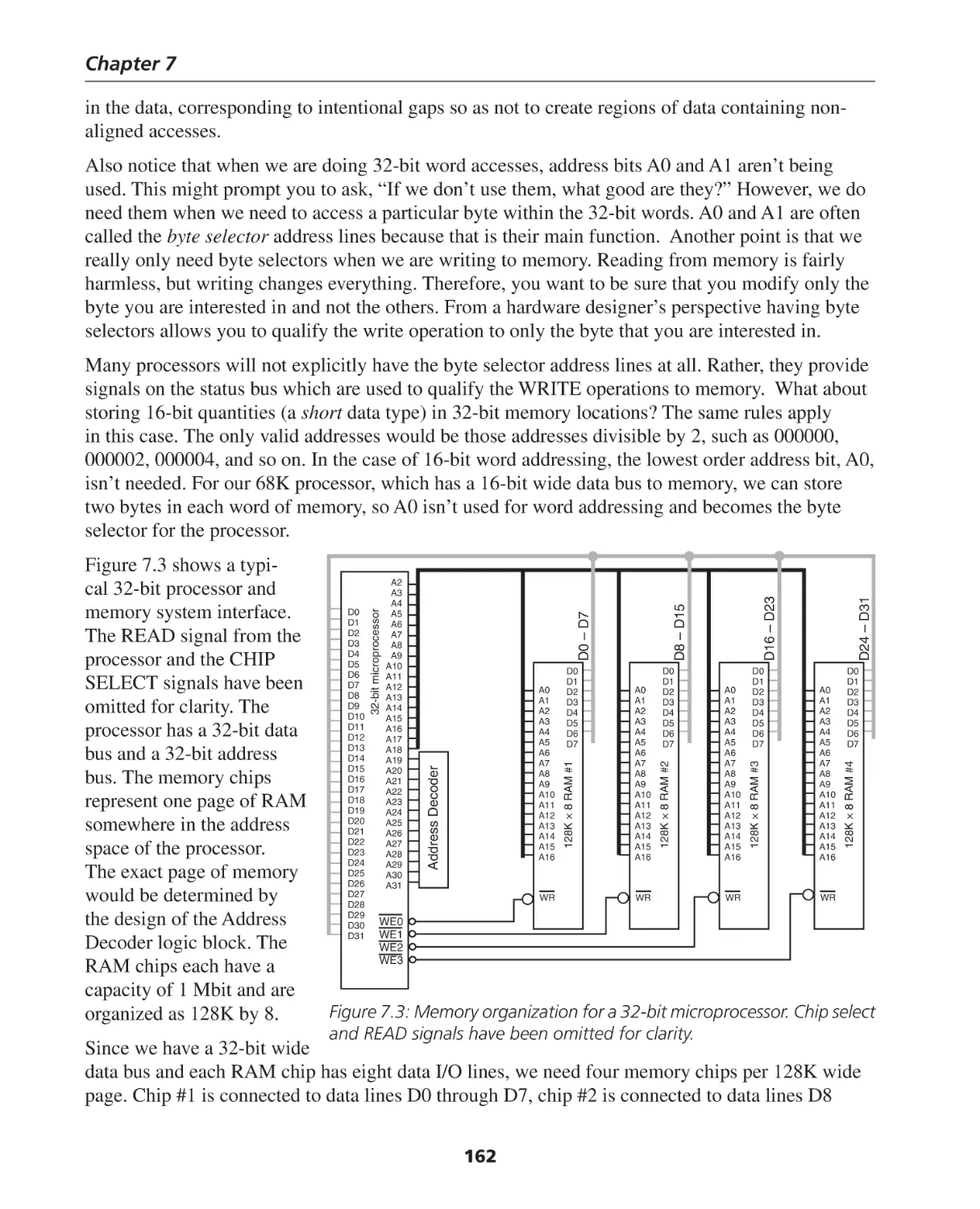
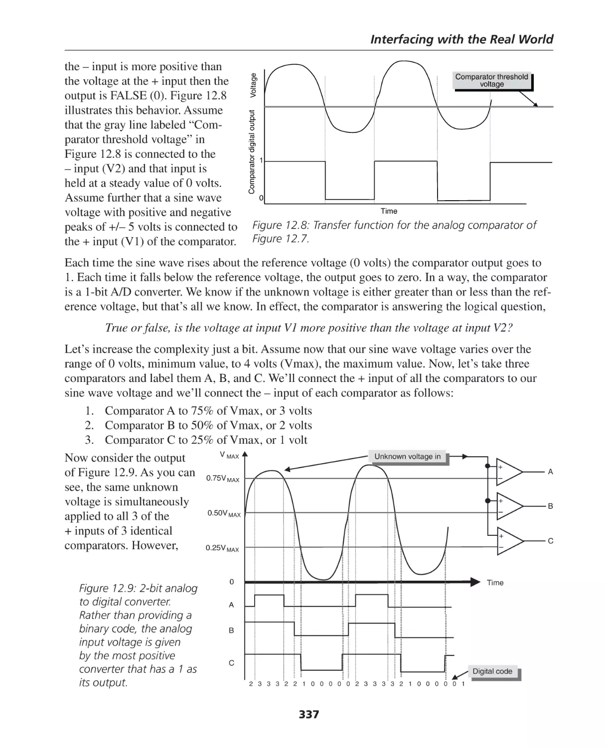
Summary of Chapter 13 .......................................................................................................... 369
Exercises for Chapter 13 .......................................................................................................... 370
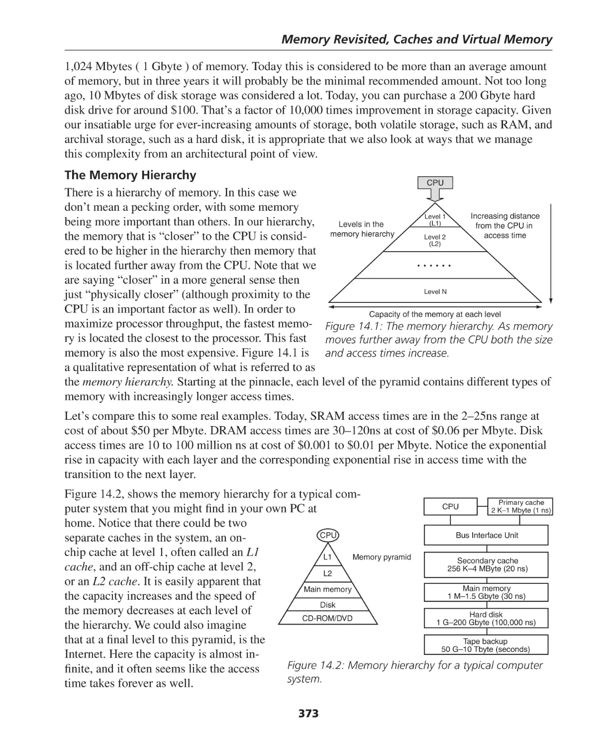
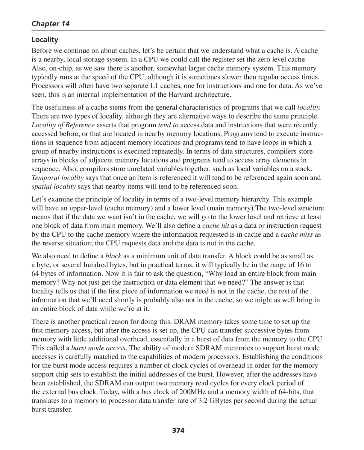
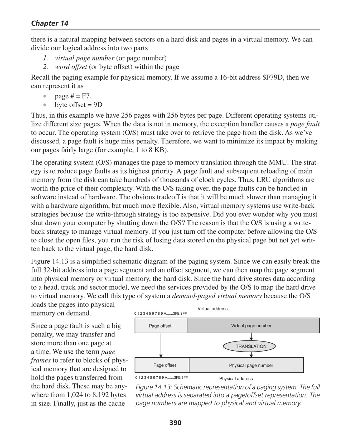
CHAPTER 14: Memory Revisited, Caches and Virtual Memory ...................... 372
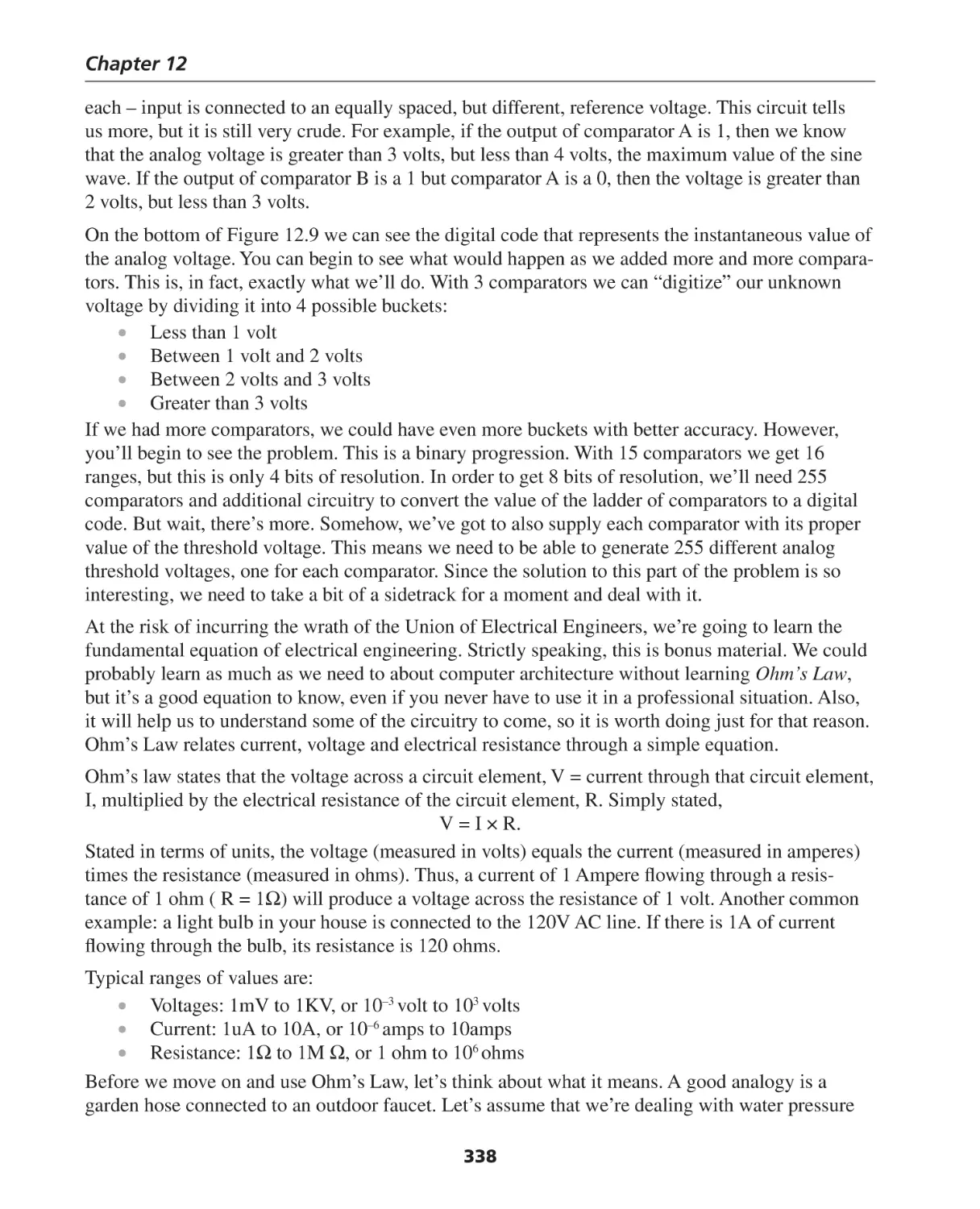
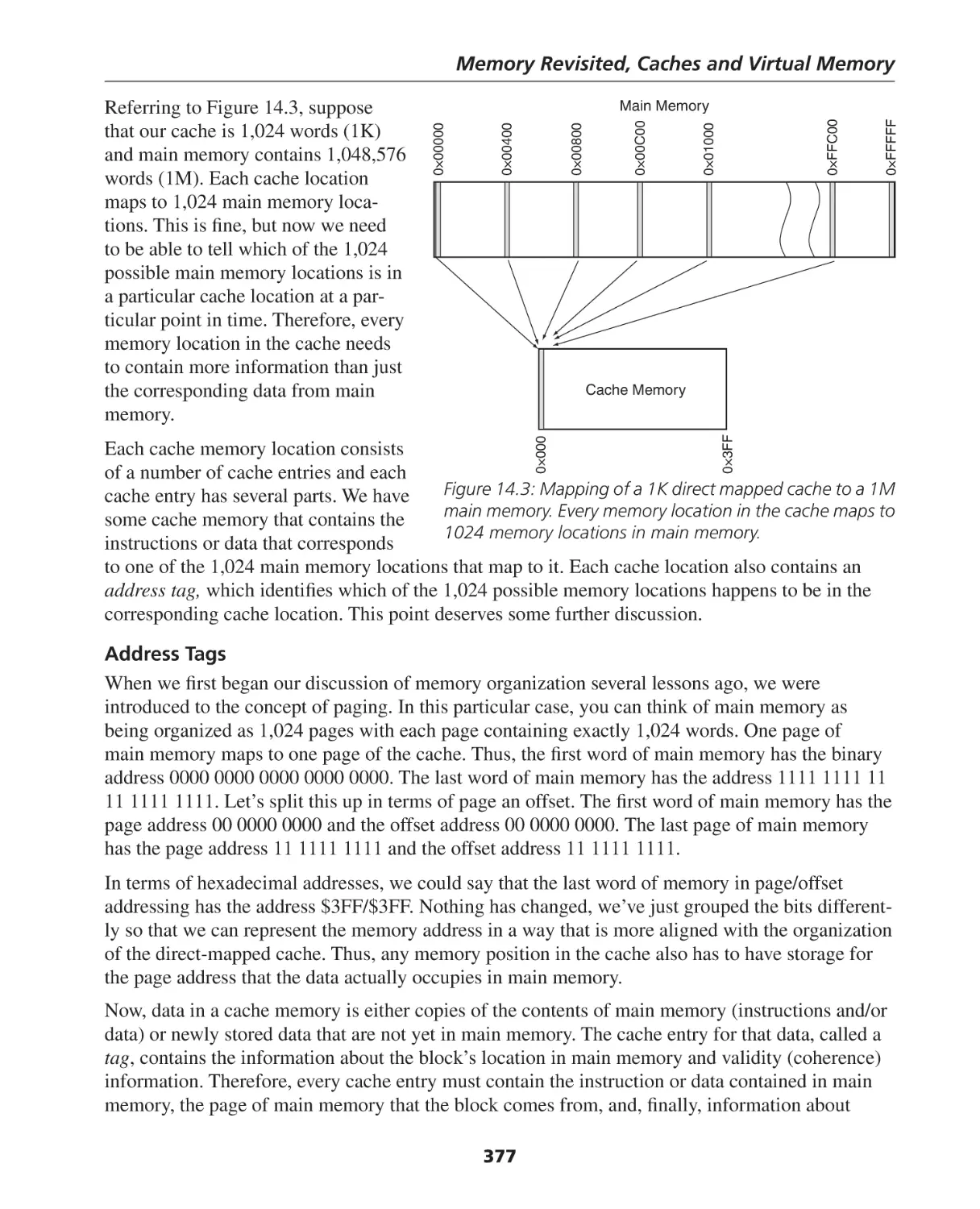
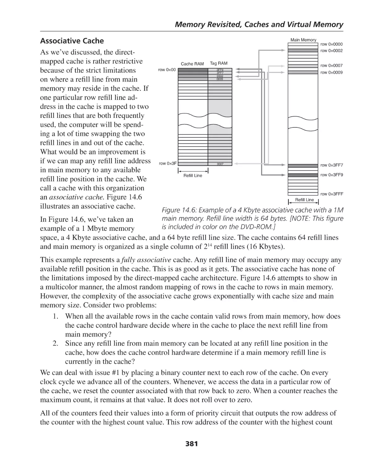
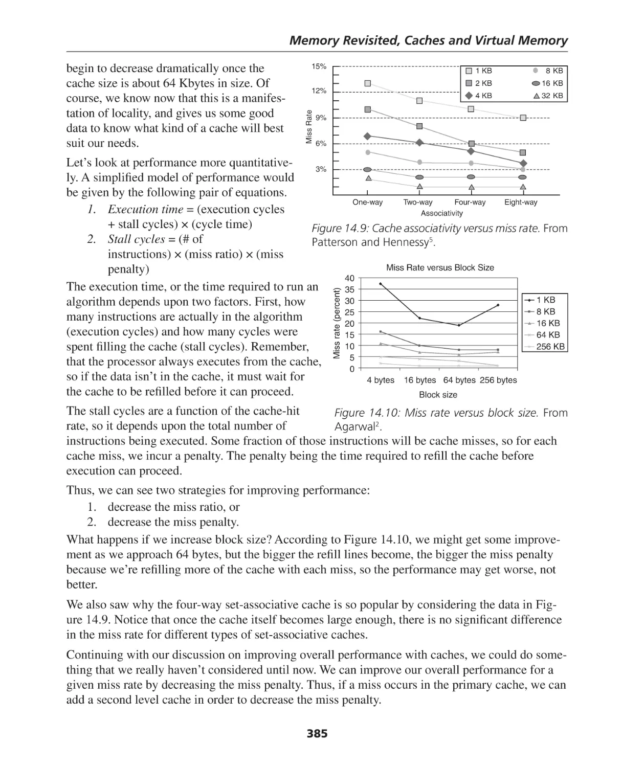
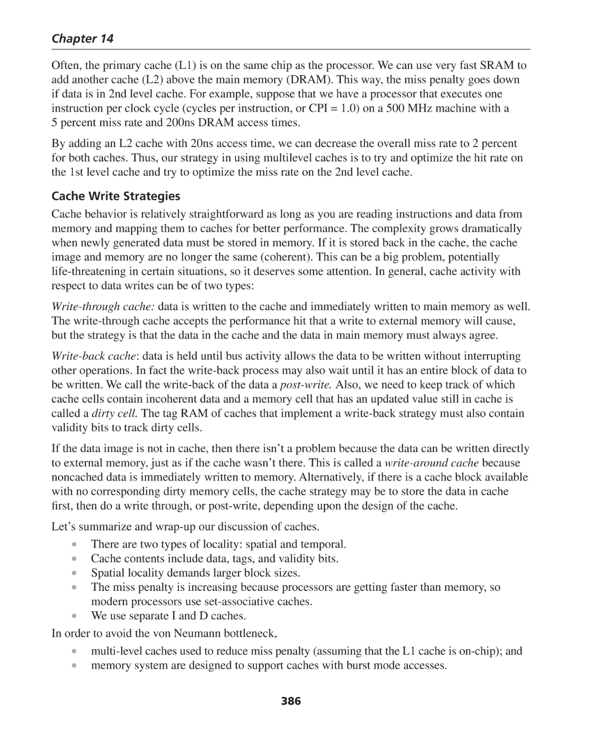
Introduction to Caches ............................................................................................................ 372
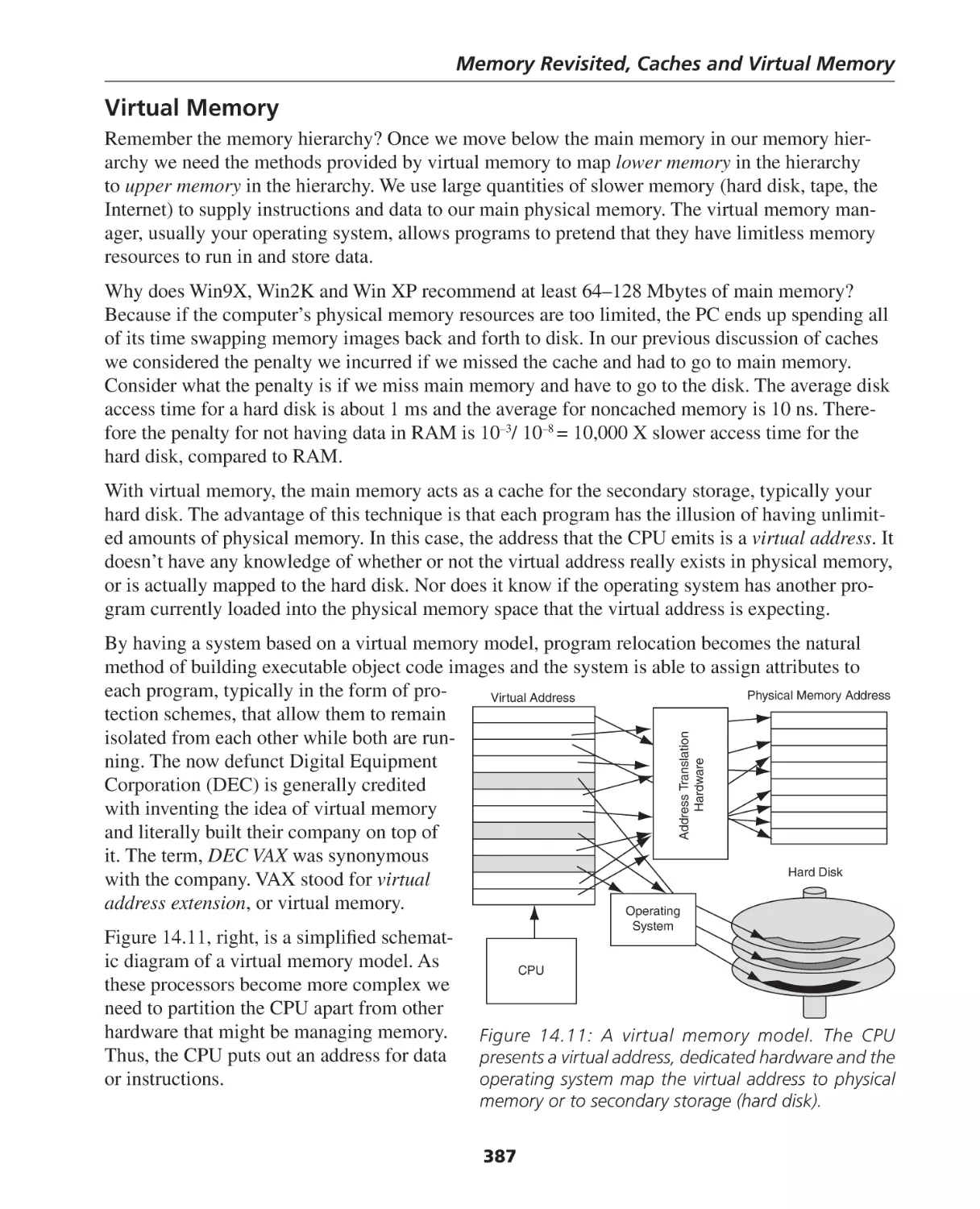
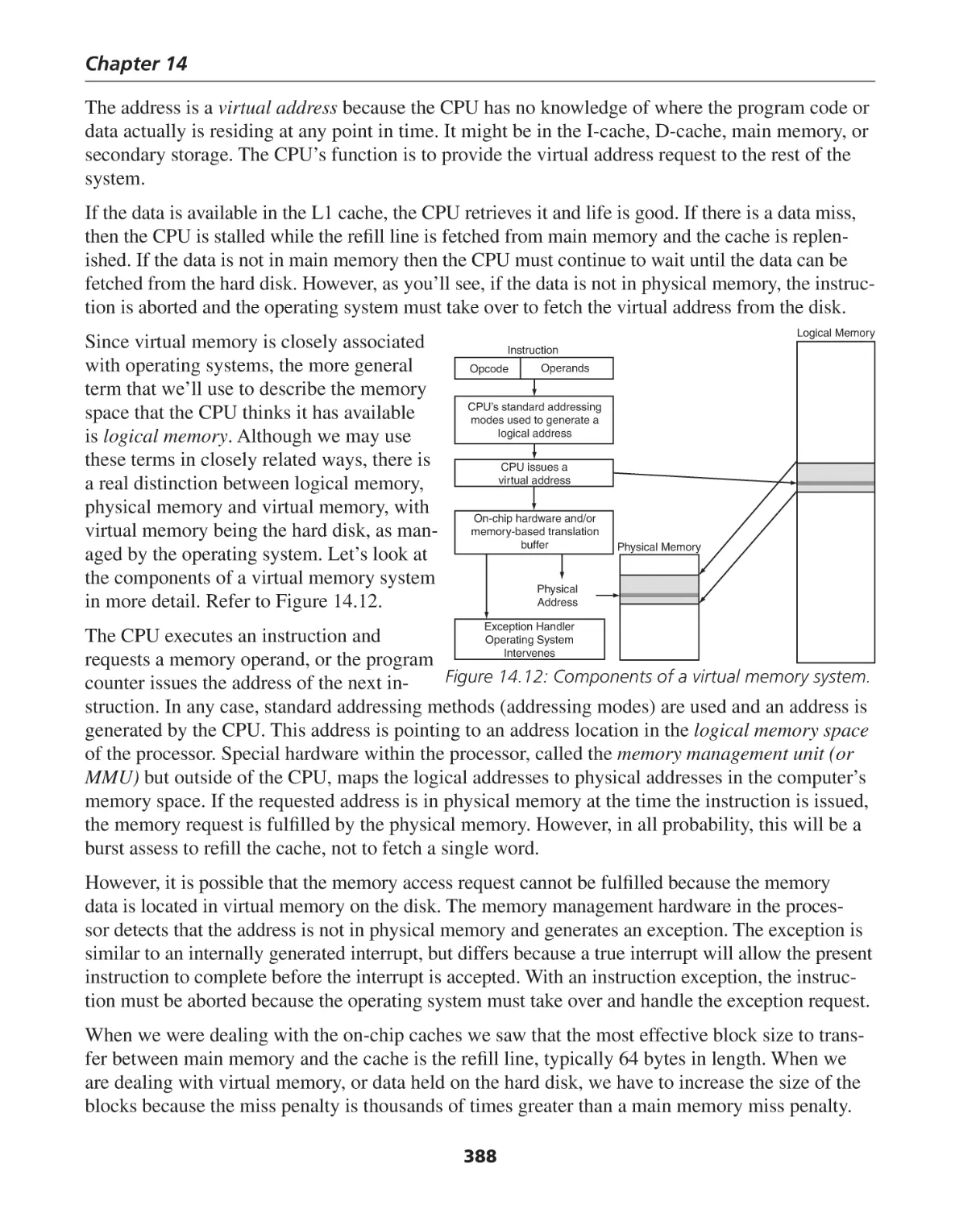
Virtual Memory ....................................................................................................................... 387
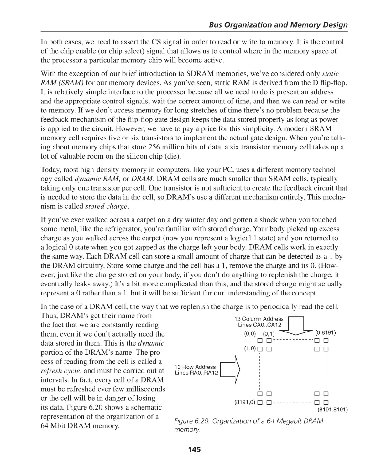
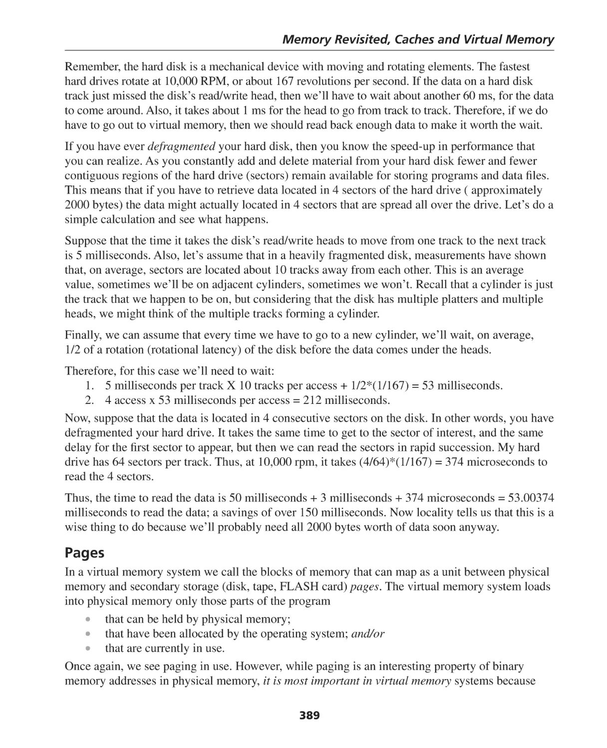
Pages ...................................................................................................................................... 389
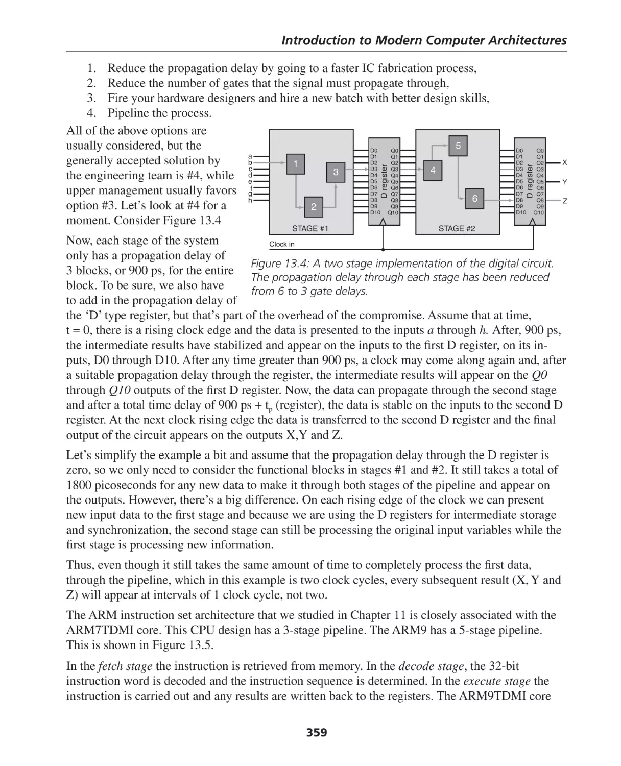
ix
Contents
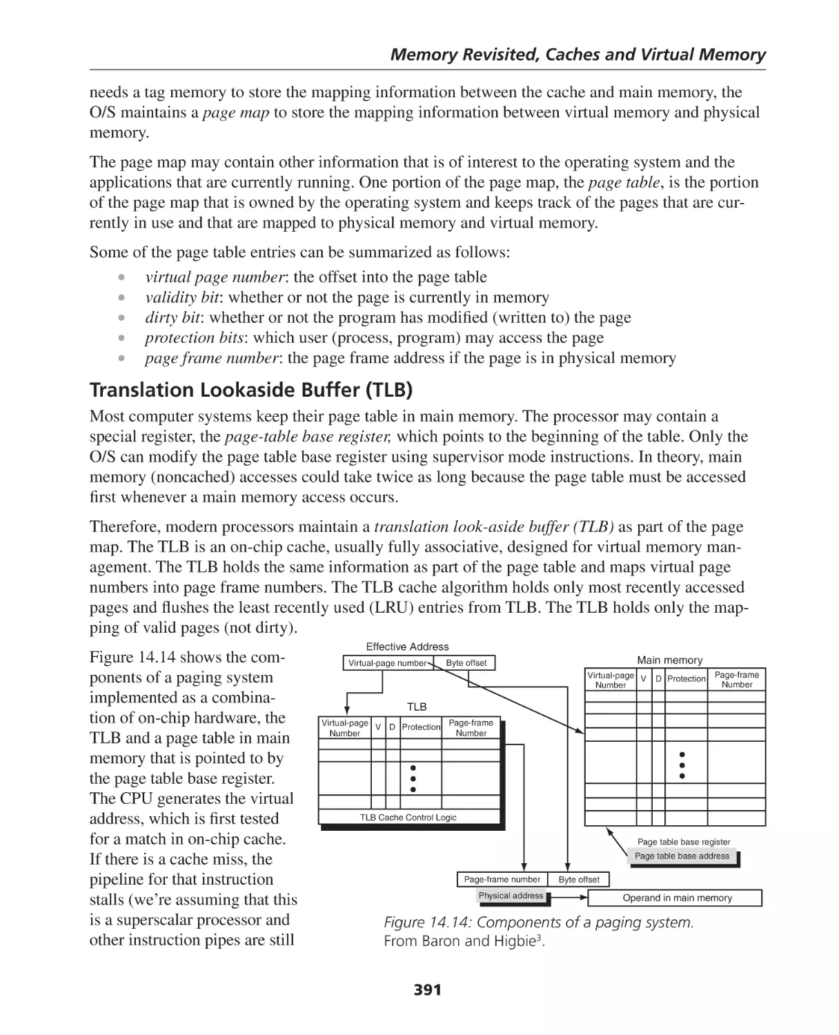
Translation Lookaside Buffer (TLB) ............................................................................................ 391
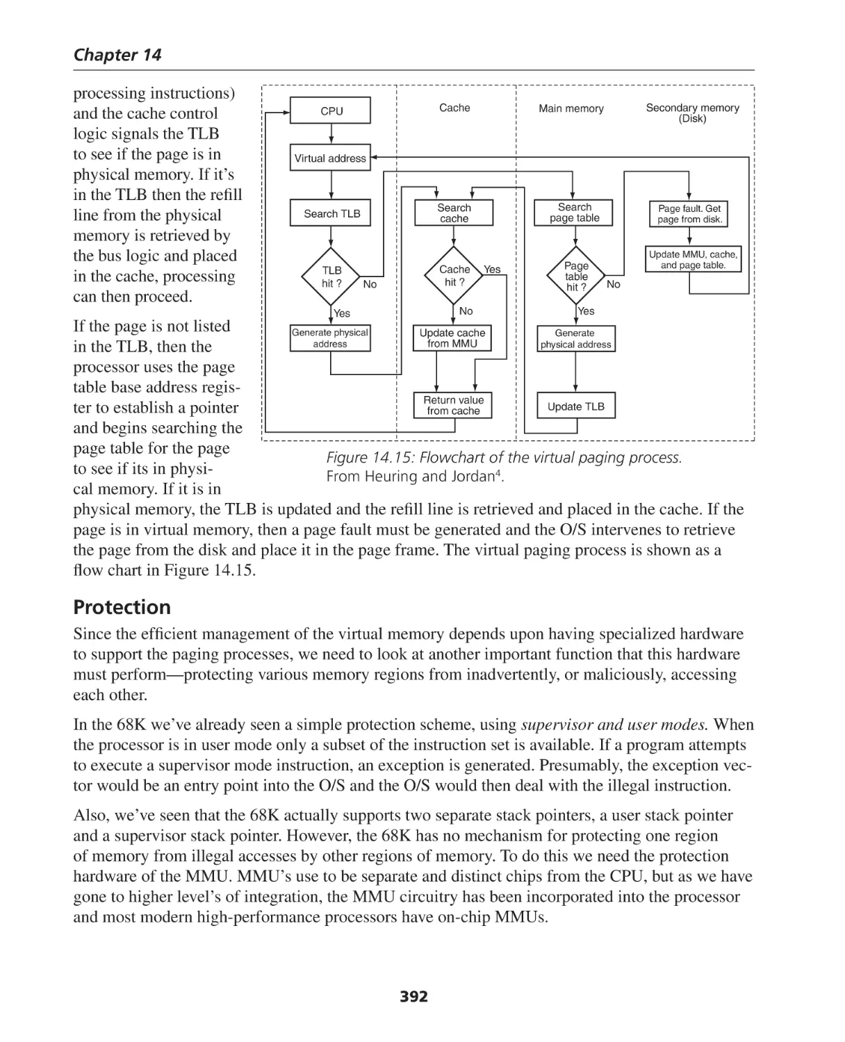
Protection................................................................................................................................ 392
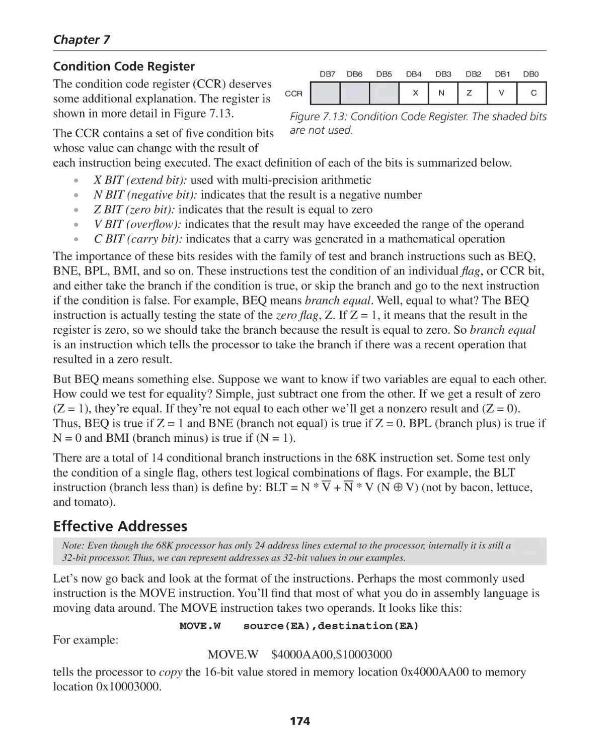
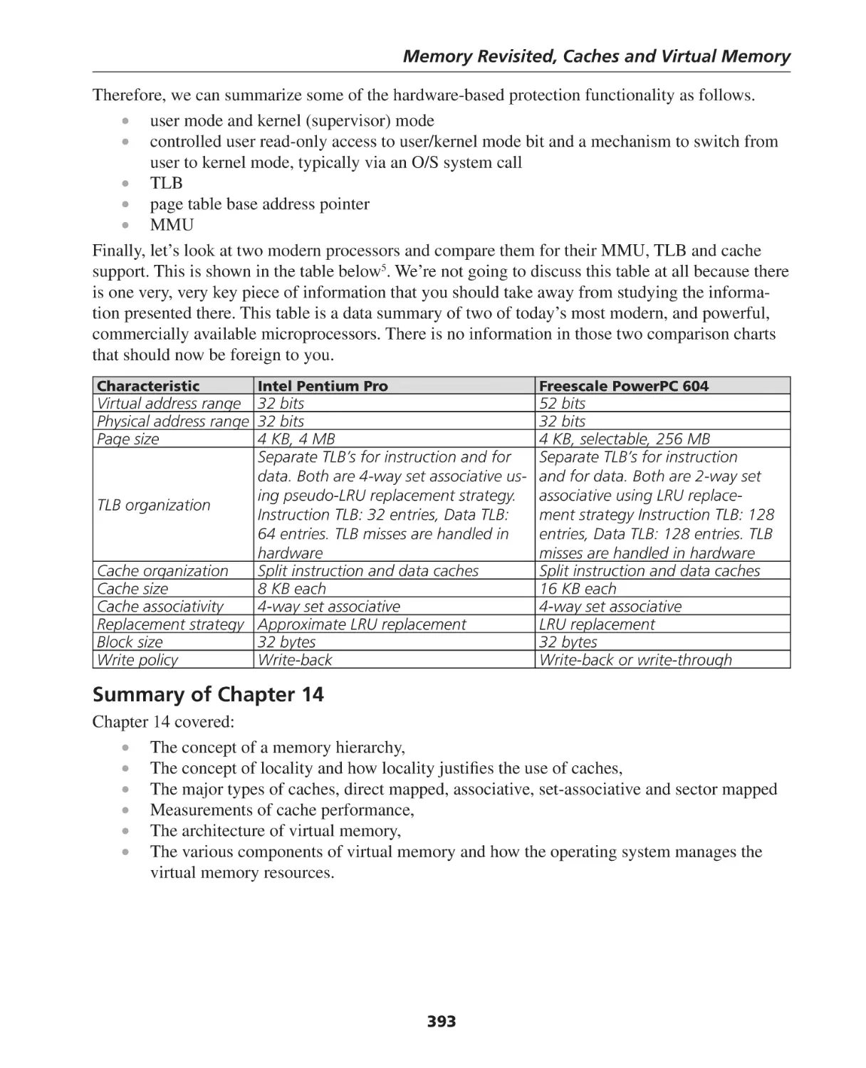
Summary of Chapter 14 .......................................................................................................... 393
Exercises for Chapter 14 .......................................................................................................... 395
CHAPTER 15: Performance Issues in Computer Architecture ......................... 397
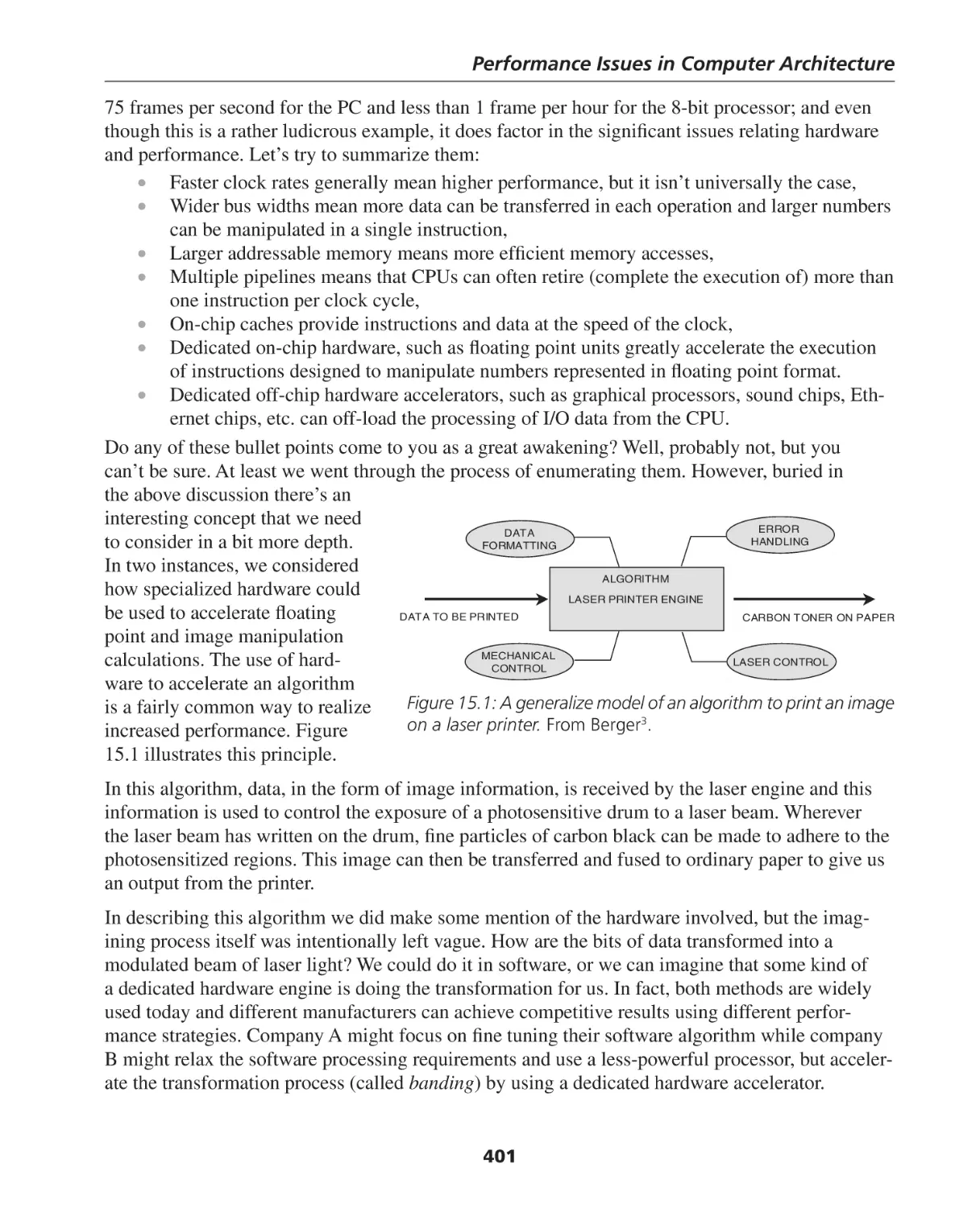
Introduction ............................................................................................................................ 397
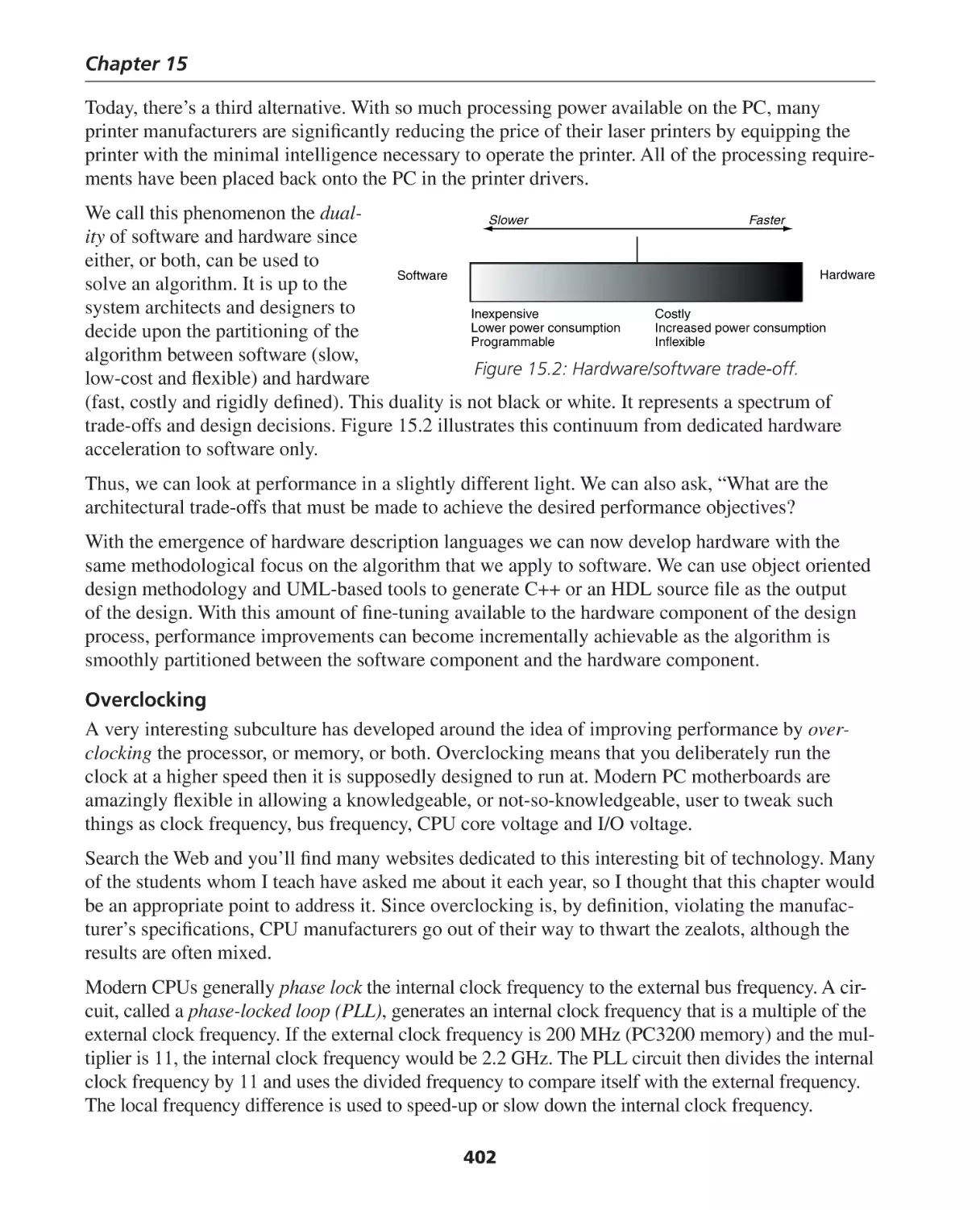
Hardware and Performance ..................................................................................................... 398
Best Practices .......................................................................................................................... 414
Summary of Chapter 15 .......................................................................................................... 416
Exercises for Chapter 15 .......................................................................................................... 417
CHAPTER 16: Future Trends and Reconfigurable Hardware .......................... 419
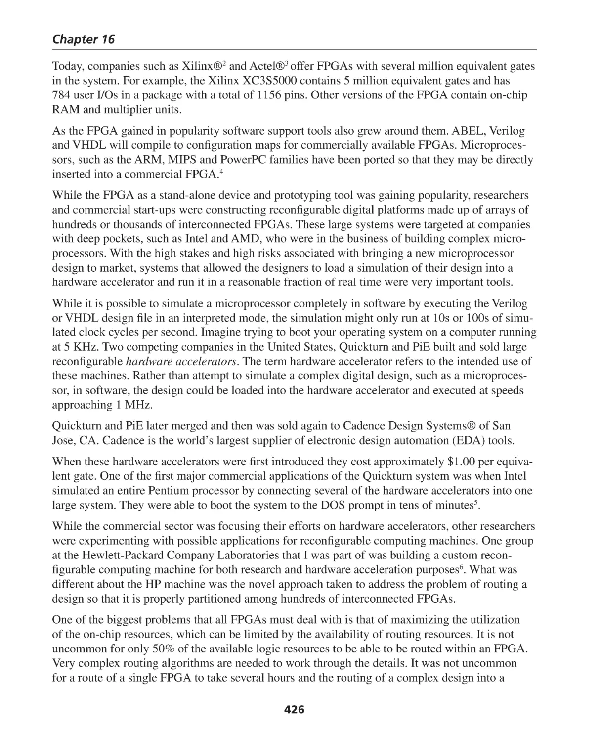
Introduction ............................................................................................................................ 419
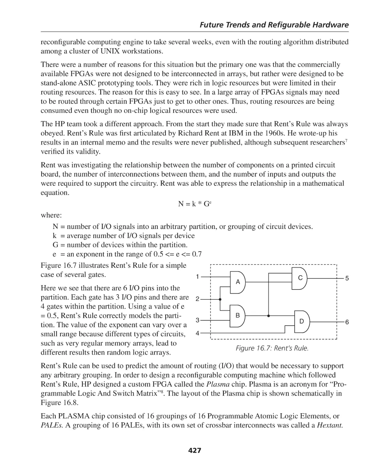
Reconfigurable Hardware ........................................................................................................ 419
Molecular Computing ............................................................................................................. 430
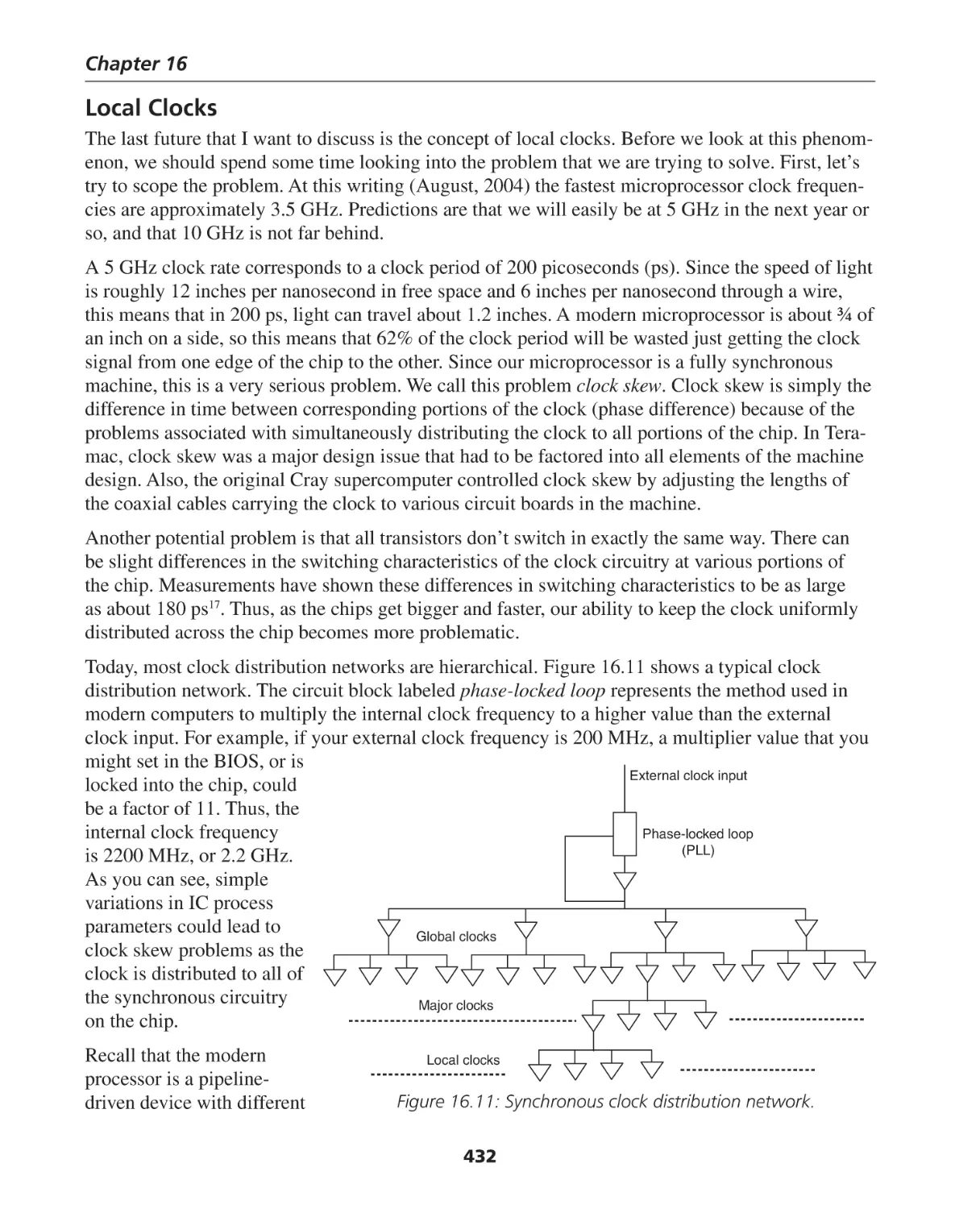
Local clocks ............................................................................................................................. 432
Summary of Chapter 16 .......................................................................................................... 434
Exercises for Chapter 16 .......................................................................................................... 436
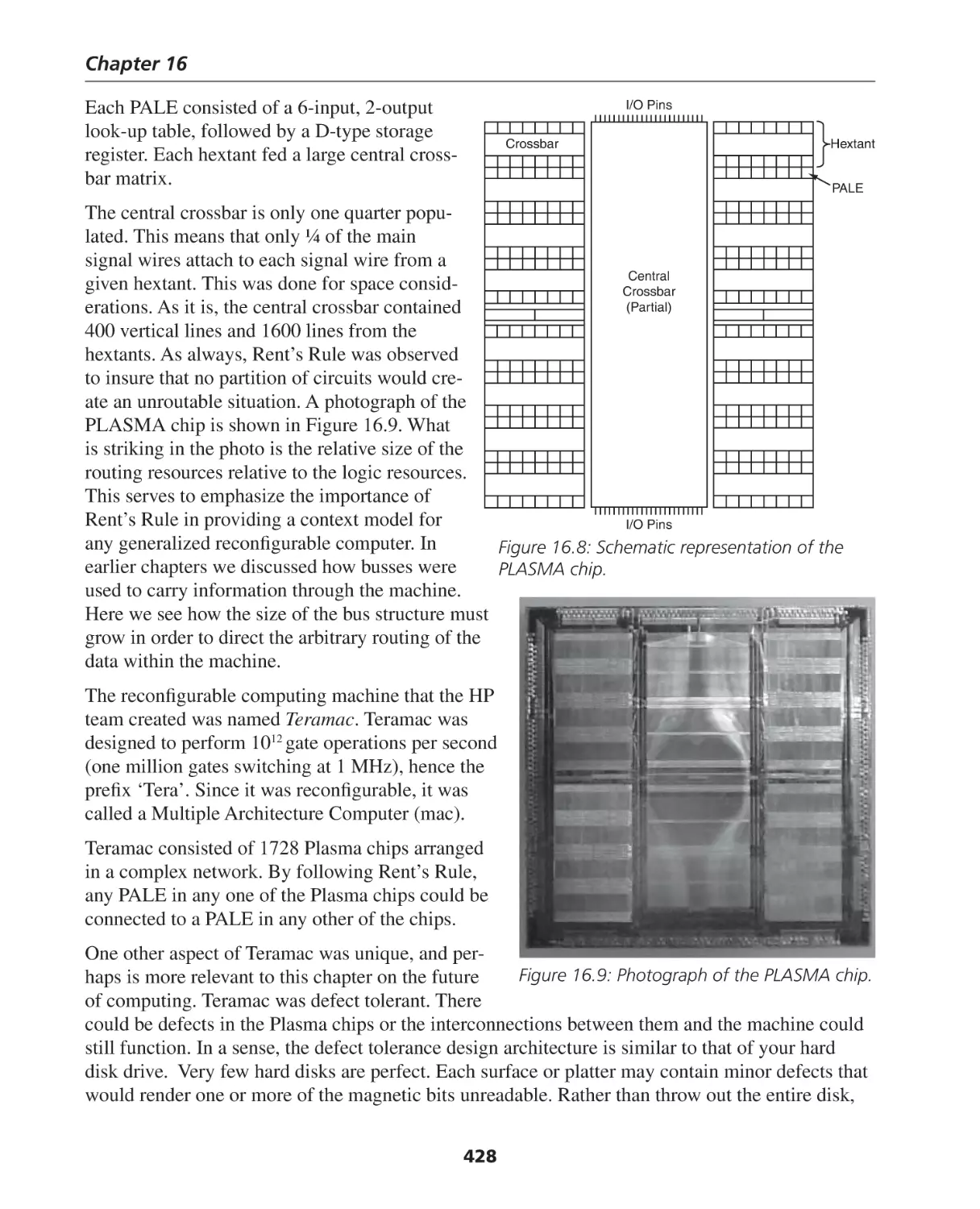
APPENDIX A: Solutions for Odd-Numbered Exercises ................................... 437
[Solutions to the even-numbered problems are available through the instructor’s resource website at http://www.elsevier.com/0750678860.]
About the Author ............................................................................................. 483
Index .................................................................................................................. 485
x
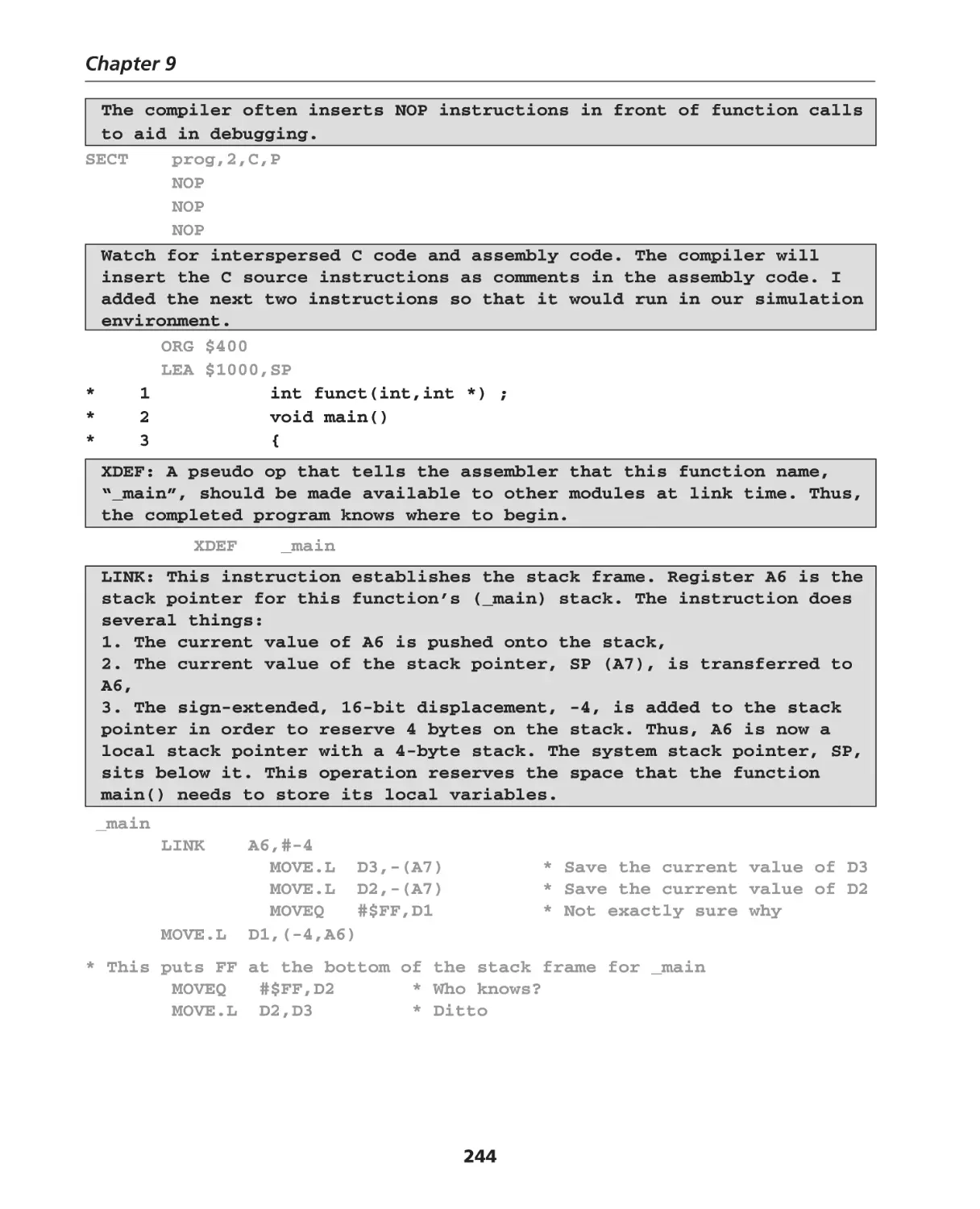
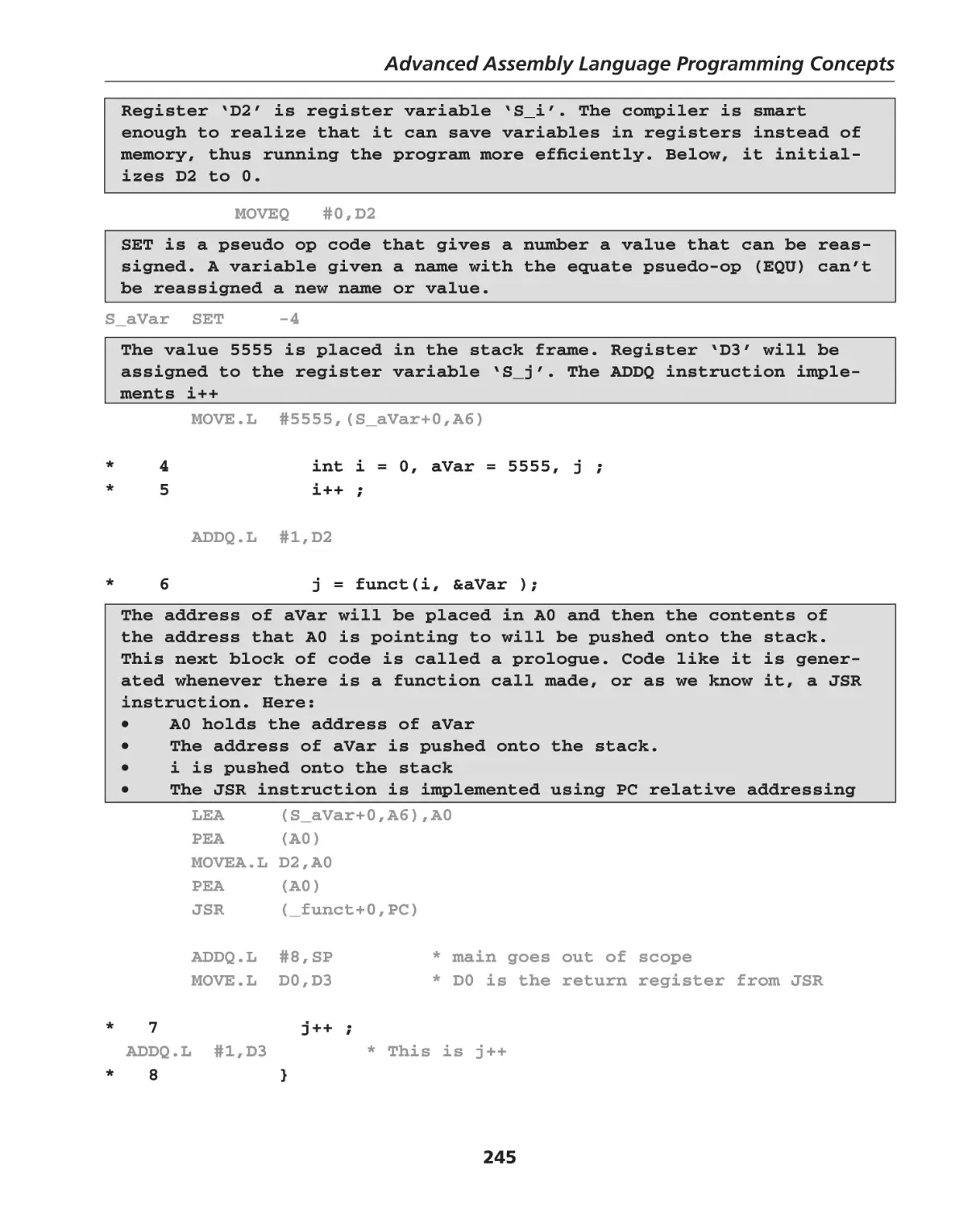
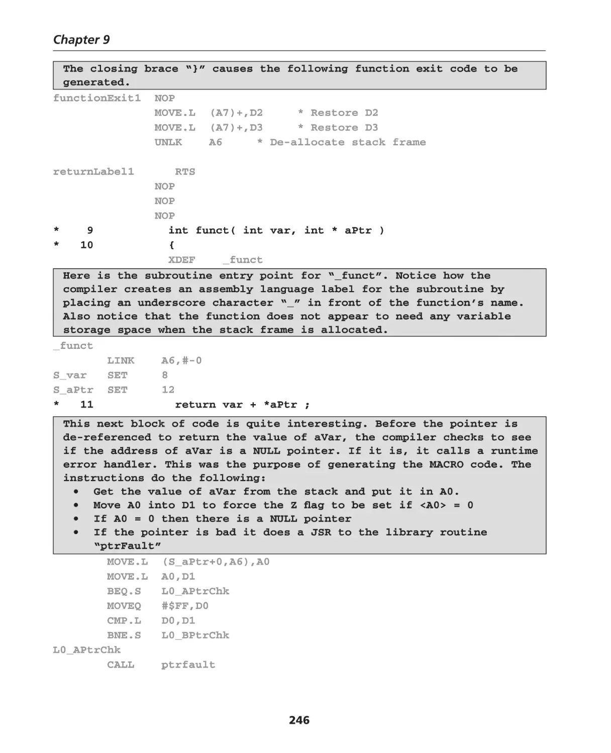
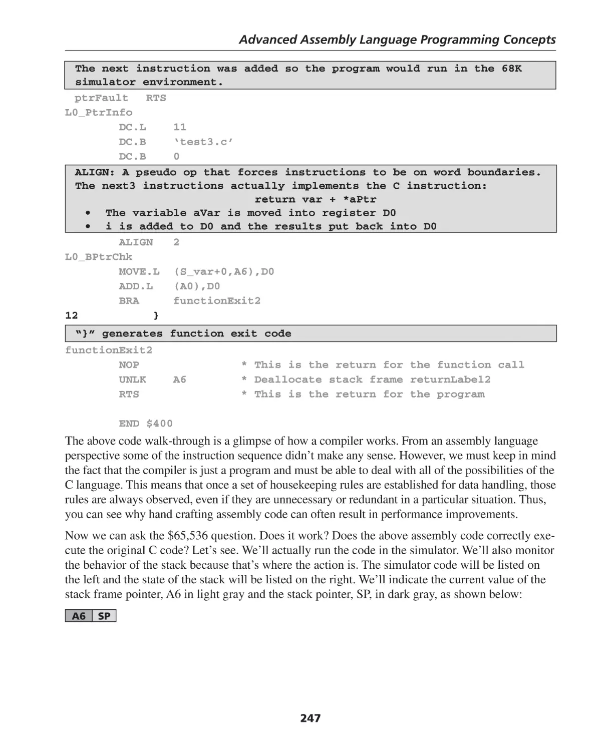
Preface to the First Edition
Thank you for buying my book. I know that may ring hollow if you are a poor student and your instructor made it the required text for your course, but I thank you nevertheless. I hope that you find
it informative and easy to read. At least that was one of my goals when I set out to write this book.
This text is an outgrowth of a course that I’ve been teaching in the Computing and Software
Systems Department of the University of Washington-Bothell. The course, CSS 422, Hardware
and Computer Organization, is one of the required core courses for our undergraduate students.
Also, it is the only required architecture course in our curriculum. While our students learn about
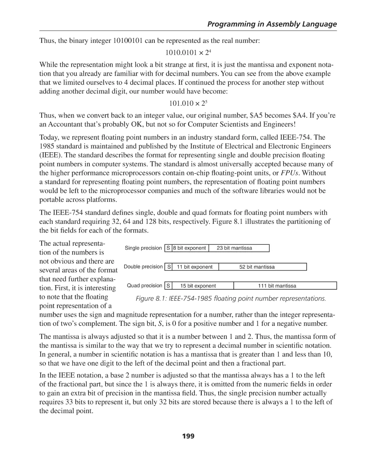
algorithms and data structures, comparative languages, numeric methods and operating systems,
this is their only exposure to “what’s under the hood.” Since the University of Washington is on
the quarter system, I’m faced with the uphill battle to teach as much about the architecture of
computers as I can in about 10 weeks.
The material that forms the core of this book was developed over a period of 5 years in the form
of about 500 Microsoft PowerPoint® slides. Later, I converted the material in the slides to HTML
so that I could also teach the course via a distance learning (DL) format. Since first teaching this
course in the fall of 1999, I’ve taught it 3 or 4 times each academic year. I’ve also taught it 3 times
via DL, with excellent results. In fact, the DL students as a whole have done equally well as the
students attending lectures in class. So, if you think that attending class is a highly overrated part
of the college experience, then this book is for you.
The text is appropriate for a first course in computer architecture at the sophomore through senior
level. It is reasonably self-contained so that it should be able to serve as the only hardware course
that CS students need to take in order to understand the implications of the code that they are
writing. At the University of Washington-Bothell (UWB), this course is predominantly taught
to seniors. As a faculty, we’ve found that the level of sophistication achieved through learning
programming concepts in other classes makes for an easier transition to low-level programming.
If the book is to be used with lower division students, then additional time should be allotted for
gaining fluency with assembly language programming concepts. For example, in introducing
certain assembly language branching and loop constructs, an advanced student will easily grasp
the similarity to WHILE, DO-WHILE, FOR and IF-THEN-ELSE constructs. A less sophisticated
student may need more concrete examples in order to see the similarities.
Why write a book on Computer Architecture? I’m glad you asked. In the 5+ years that I taught the
course, I changed the textbook 4 times. At the end of the quarter, when I held an informal course
xi
Preface
debriefing with the students, they universally panned every book that I used. The “gold standard”
textbooks, the texts that almost every Computer Science student uses in their architecture class,
were just not relevant to their needs. For the majority of these students, they were not going to go
on and study architecture in graduate schools, or design computers for Intel or AMD. They needed
to understand the architecture of a computer and its supporting hardware in order to write efficient
and defect-free code to run on the machines. Recently, I did find a text that at least approached the
subject matter in the same way that I thought it should be done, but I also found that text lacking
in several key areas. On the plus side, switching to the new text eliminated the complaints from
my students and it also reinforced my opinion that I wasn’t alone in seeing a need for a text with
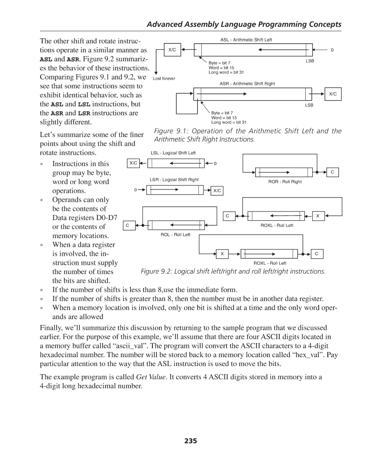
a different perspective. Unfortunately, this text, even though it was a great improvement, still did
not cover several areas that I considered to be very important, so I resolved to write one that did,
without losing the essence of what I think the new perspective correctly accomplished.
It’s not surprising that, given the UWB campus is less than 10 miles from Microsoft’s main
campus in Redmond, WA, we are strongly influenced by the Microsoft culture. The vast majority
of my students have only written software for Windows and the Intel architecture. The designers
of this architecture would have you believe that these computers are infinitely fast machines with
unlimited resources. How do you counter this view of the world?
Often, my students will cry out in frustration, “Why are you making me learn this (deleted)?” (Actually it is more of a whimper.) This usually happens right around the mid-term examination. Since
our campus is also approximately equidistant from where Boeing builds the 737 and 757 aircraft
in Renton, WA and the wide body 767 and 777 aircraft in Everett, WA, analogies to the aircraft
industry are usually very effective. I simply answer their question this way, “Would you fly on an
airplane that was designed by someone who is clueless about what keeps an airplane in the air?”
Sometimes it works.
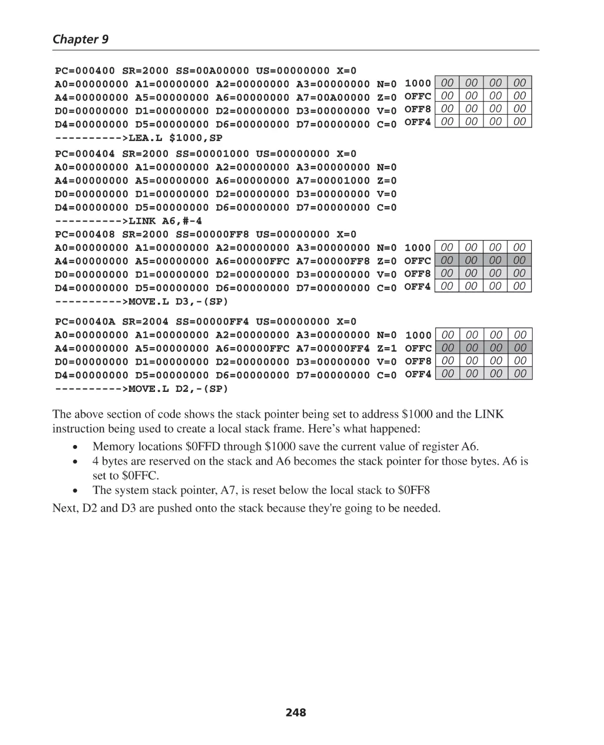
The book is divided into four major topic areas:
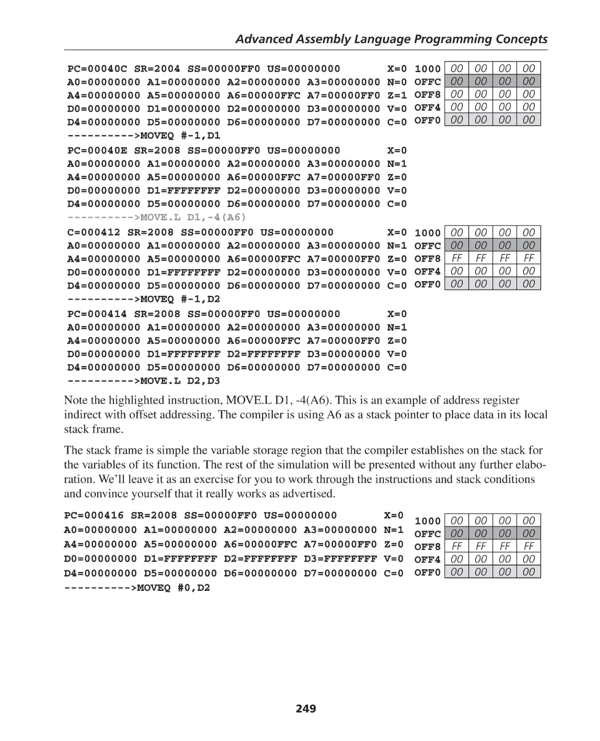
1. Introduction to hardware and asynchronous logic.
2. Synchronous logic, state machines and memory organization.
3. Modern computer architectures and assembly language programming.
4. I/O, computer performance, the hierarchy of memory and future directions of computer
organization.
There is no sharp line of demarcation between the subject areas, and the subject matter builds upon
the knowledge base from prior chapters. However, I’ve tried to limit the interdependencies so later
chapters may be skipped, depending upon the available time and desired syllabus.
Each chapter ends with some exercises. The solutions to the odd-numbered problems are located
in Appendix A, and the solutions to the even-numbered problems are available through the instructor’s resource website at http://www.elsevier.com/0750678860.
The text approach that we’ll take is to describe the hardware from the ground up. Just as a Geneticist can describe the most complex of organic beings in terms of a DNA molecule that contains
only four nucleotides, adenine, cytosine, guanine, and thymine, abbreviated, A, C, G and T, we can
describe the most complex computer or memory system in terms of four logical building blocks,
xii
Preface
AND, OR, NOT and TRI-STATE. Strictly speaking, TRI-STATE isn’t a logical building block like
AND, it is more like the “glue” that enables us to interconnect the elements of a computer in such
a way that the complexity doesn’t overwhelm us. Also, I really like the DNA analogy, so we’ll
need to have 4 electronic building blocks to keep up with the A, C, G and T idea.
I once gave a talk to a group of middle school teachers who were trying to earn some in-service
credits during their summer break. I was a volunteer with the Air Academy School District in
Colorado Springs, Colorado while I worked for the Logic Systems Division of Hewlett-Packard.
None of the teachers were computer literate and I had two hours to give them some appreciation
of the technology. I decided to start with Aristotle and concept of the logical operators as a branch
of philosophy and then proceeded with the DNA analogy up through the concept of registers. I
seemed to be getting through to them, but they may have been stroking my ego so I would signoff on their attendance sheets. Anyway, I think there is value in demonstrating that even the most
complex computer functionality can be described in terms of the logic primitives that we study in
the first part of the text.
We will take the DNA or building-block approach through most of the first half of the text. We
will start with the simplest of gates and build compound gates. From these compound gates we’ll
progress to the posing and solution of asynchronous logical equations. We’ll learn the methods
of truth table design and simplification using Boolean algebra and then Karnaugh Map (K-map)
methodology. The exercises and examples will stress the statement of the problem as a set of
specifications which are then translated into a truth table, and from there to K-maps and finally to
the gate design. At this point the student is encouraged to actually ”build” the circuit in simulation
using the Digital Works® software simulator (see the following) included on the DVD-ROM that
accompanies the text. I have found this combination of the abstract design and the actual simulation to be an extremely powerful teaching and learning combination.
One of the benefits of taking this approach is that the students become accustomed to dealing with
variables at the bit level. While most students are familiar with the C/C++ Boolean constructs, the
concept of a single wire carrying the state of a variable seems to be quite new.
Once the idea of creating arbitrarily complex, asynchronous algebraic functions is under control,
we add the dimension of the clock and of synchronous logic. Synchronous logic takes us to flipflops, counters, shifters, registers and state machines. We actually spend a lot of effort in this area,
and the concepts are reintroduced several times as we look at micro-code and instruction decomposition later on.
The middle part of the book focuses on the architecture of a computer system. In particular, the
memory to CPU interface will get a great deal of attention. We’ll design simple memory systems and
decoding circuits using our knowledge gained in the preceding chapters. We’ll also take a brief look
at memory timing in order to better understand some of the more global issues of system design.
We’ll then make the transition to looking at the architecture of the 68K, ARM and X86 processor
families. This will be our introduction to assembly language programming.
Each of the processor architectures will be handled separately so that it may be skipped without
creating too much discontinuity in the text.
xiii
Preface
This text does emphasize assembly language programming in the three architectures. The reason
for this is twofold: First, assembly language may or may not be taught as a part of a CS student’s
curriculum, and it may be their only exposure to programming at the machine level. Even though
you as a CS student may never have to write an assembly language program, there’s a high probability that you’ll have to debug some parts of your C++ program at the assembly language level,
so this is as good a time to learn it as any. Also, by looking at three very different instruction sets
we will actually reinforce the concept that once you understand the architecture of a processor, you
can program it in assembly language. This leads to the second reason to study assembly language.
Assembly language is a metaphor for studying computer architecture from the software developer’s point of view.
I’m a big fan of “Dr. Science.” He’s often on National Public Radio and does tours of college
campuses. His famous tag line is, “I have a Master’s degree...in science.” Anyway, I was at a Dr.
Science lecture when he said, “I like to scan columns of random numbers, looking for patterns.”
I remembered that line and I often use it in my lectures to describe how you can begin to see the
architecture of the computer emerging through the seeming randomness of the machine language
instruction set. I could just see in my mind’s eye a bunch of Motorola CPU architects and engineers sitting around a table in a restaurant, pizza trays scattered hither and yon, trying to figure out
the correct bit patterns for the last few instructions so that they don’t have a bloated and inefficient
microcode ROM table. If you are a student reading this and it doesn’t make any sense to you now,
don’t worry...yet.
The last parts of the text steps back and looks at general issues of computer architecture. We’ll
look at CISC versus RISC, modern techniques, such as pipelines and caches, virtual memory and
memory management. However, the overriding theme will be computer performance. We will keep
returning to the issues associated with the software-to-hardware interface and the implications of
coding methods on the hardware and of the hardware on the coding methods.
One unique aspect of the text is the material included on the accompanying DVD-ROM. I’ve included the following programs to use with the material in the text:
• Digital Works (freeware): A hardware design and simulation tool
• Easy68K: A freeware assembler/simulator/debugger package for the Motorola (Now
Freescale) 68,000 architecture.
• X86emul: A shareware assembler/simulator/debugger package for the X86 architecture.
• GNU ARM Tools: The ARM developers toolset with Instruction Set Simulator from the
Free Software Foundation.
The ARM company has an excellent tool suite that you can obtain directly from ARM. It comes
with a free 45-day evaluation license. This should be long enough to use in your course. Unfortunately, I was unable to negotiate a license agreement with ARM that would enable me to include
the ARM tools on the DVD-ROM that accompanies this text. This tool suite is excellent and easy
to use. If you want to spend some additional time examining the world’s most popular RISC
architecture, then contact ARM directly and ask them nicely for a copy of the ARM tools suite.
Tell them Arnie sent you.
xiv
Preface
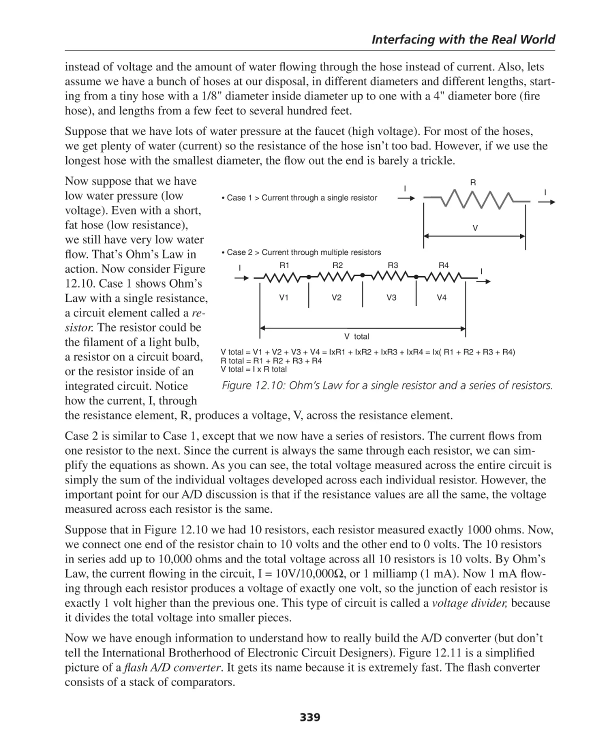
I have also used the Easy68K assembler/simulator extensively in my CSS 422 class. It works well
and has extensive debugging capabilities associated with it. Also, since it is freeware, the logistical
problems of licenses and evaluation periods need not be dealt with. However, we will be making some references to the other tools in the text, so it is probably a good idea to install them just
before you intend to use them, rather than at the beginning of your class.
Also included on the DVD-ROM are 10 short lectures on various topics of interest in this text
by experts in the field of computer architecture. These videos were made under a grant by the
Worthington Technology Endowment for 2004 at UWB. Each lecture is an informal 15 to 30
minute “chalk talk.” I hope you take the time to view them and integrate them into your learning
experience for this subject matter.
Even though the editors, my students and I have read through this material several times, Murphy’s
Law predicts that there is still a high probability of errors in the text. After all, it’s software. So
if you come across any “bugs” in the text, please let me know about it. Send your corrections to
aberger@u.washington.edu. I’ll see to it that the corrections will gets posted on my website at UW
(http://faculty.uwb.edu/aberger).
The last point I wanted to make is that textbooks can just go so far. Whether you are a student or
an instructor reading this, please try to seek out experts and original sources if you can. Professor
James Patterson, writing in the July, 2004 issue of Physics Today, writes,
When we want to know something, there is a tendency to seek a quick answer
in a textbook. This often works, but we need to get in the habit of looking at
original papers. Textbooks are often abbreviated second-or third-hand distortions of the facts...1
Let’s get started.
Arnold S. Berger
Sammamish, Washington
1
James D. Patterson, An Open Letter to the Next Generation, Physics Today, Vol. 57, No. 7, July, 2004, p. 56.
xv
Acknowledgments
First, and foremost, I would like to acknowledge the sponsorship and support of Professor William
Erdly, former Director of the Department of Computing and Software Systems at the University of
Washington-Bothell. Professor Erdly first hired me as an Adjunct Professor in the fall of 1999 and
asked me to teach a course called Hardware and Computer Organization, even though the course I
wanted to teach was on Embedded System Design.
Professor Erdly then provided me with financial support to convert my Hardware and Computer
Organization course from a series of lectures on PowerPoint slides to a series of online lessons in
HTML. These lessons became the core of the material that led to this book.
Professors Charles Jackels and Frank Cioch, in their capacities as Acting Directors, both supported
my work in perfecting the on-line material and bringing multimedia into the distance learning
experience. Their support helped me to see the educational value of technology in the classroom.
I would also like to thank the Richard P. and Lois M. Worthington Foundation for their 2004
Technology Grant Award which enabled me to travel around the United States and videotape short
talks in Computer Architecture. Also, I would like to thank the 13 speakers who gave of their time
to participate in this project.
Carol Lewis, my Acquisitions Editor at Newnes Books saw the value of my approach and I thank
her for it. I’m sorry that she had to leave Newnes before she could see this book finally completed.
Tiffany Gasbarrini of Elsevier Press and Kelly Johnson of Borrego Publishing brought the book to
life. Thank you both.
In large measure, this book was designed by the students who have taken my CSS 422 course.
Their end-of-Quarter evaluations and feedback were invaluable in helping me to see how this book
should be structured.
Finally, and most important, I want to thank my wife Vivian for her support and understanding. I
could not have written 500+ pages without it.
xvi
What’s on the DVD-ROM?
One unique aspect of the text is the material included on the accompanying DVD-ROM. I’ve included the following programs to use with the material in the text:
• Digital Works (freeware): A hardware design and simulation tool.
• Easy68K: A freeware assembler/simulator/debugger package for the Motorola (now
Freescale) 68,000 architecture.
• X86emul: A shareware assembler/simulator/debugger package for the X86 architecture.
• GNU ARM Tools: The ARM developers toolset with Instruction Set Simulator from the
Free Software Foundation.
• Ten industry expert video lectures on significant hardware design and development topics.
xvii
CHAPTER
1
Introduction and Overview
of Hardware Architecture
Learning Objectives
When you’ve finished this lesson, you will be able to:
Describe the evolution of computing devices and the way most computer-based devices
are organized;
Make simple conversions between the binary, octal and hexadecimal number systems, and
explain the importance of these systems to computing devices;
Demonstrate the way that the atomic elements of computer hardware and logic gates are
used, and detail the rules that govern their operation.
Introduction
Today, we often take for granted the impressive array of computing machinery that surrounds us
and helps us manage our daily lives. Because you are studying computer architecture and digital
hardware, you no doubt have a good understanding of these machines, and you’ve probably written countless programs on your PCs and workstations. However, it is very easy to become jaded
and forget the evolution of the technology that has led us to the point where every Nintendo Game
Boy® has 100 times the computing power of the computer systems on the first Mercury space missions.
A Brief History of Computing
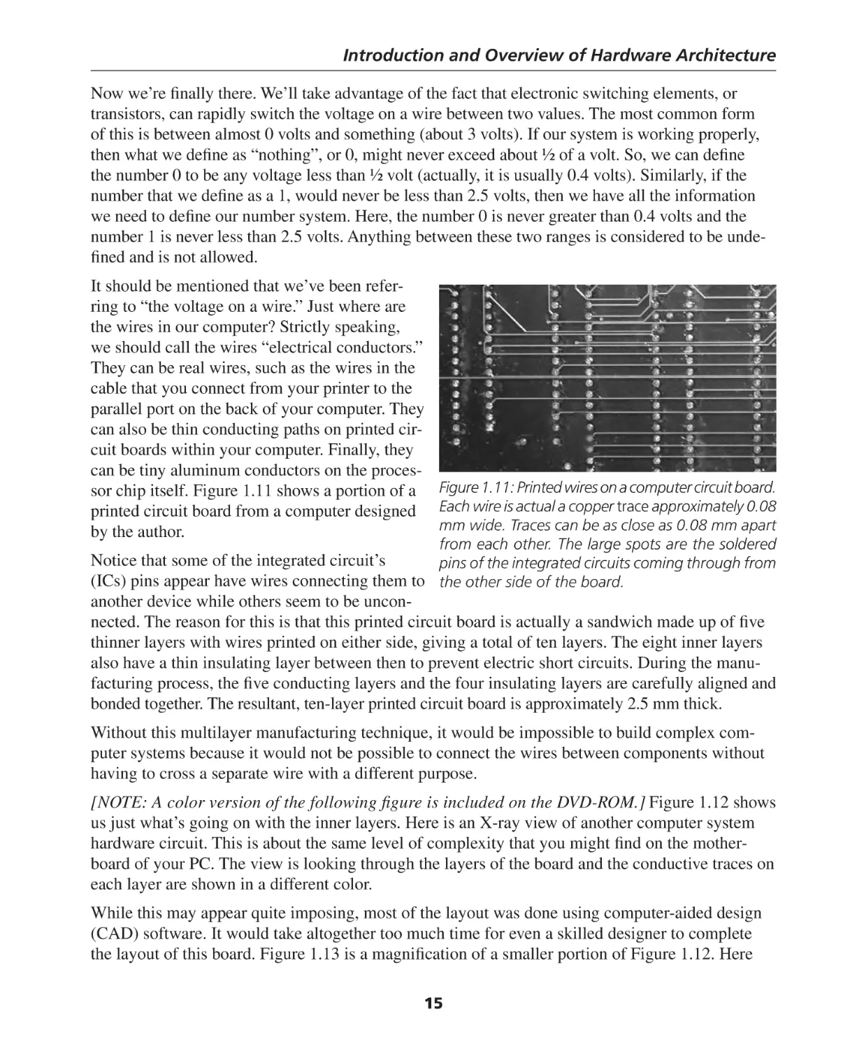
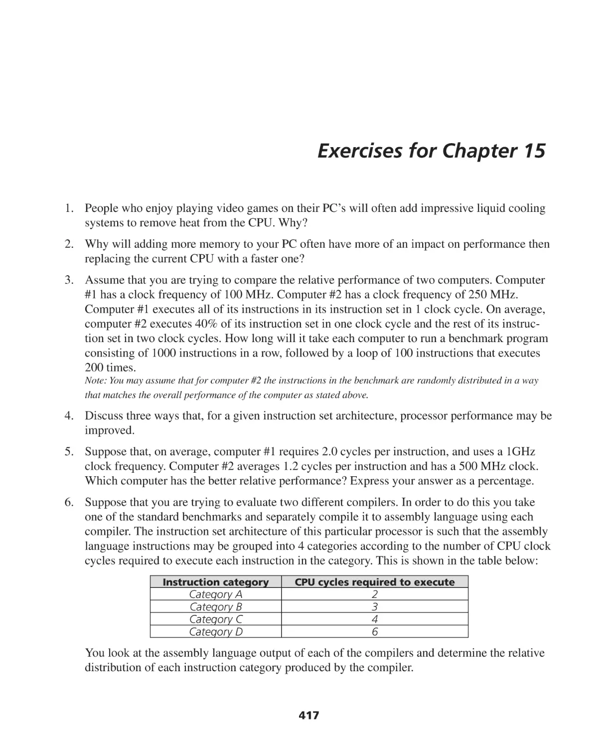
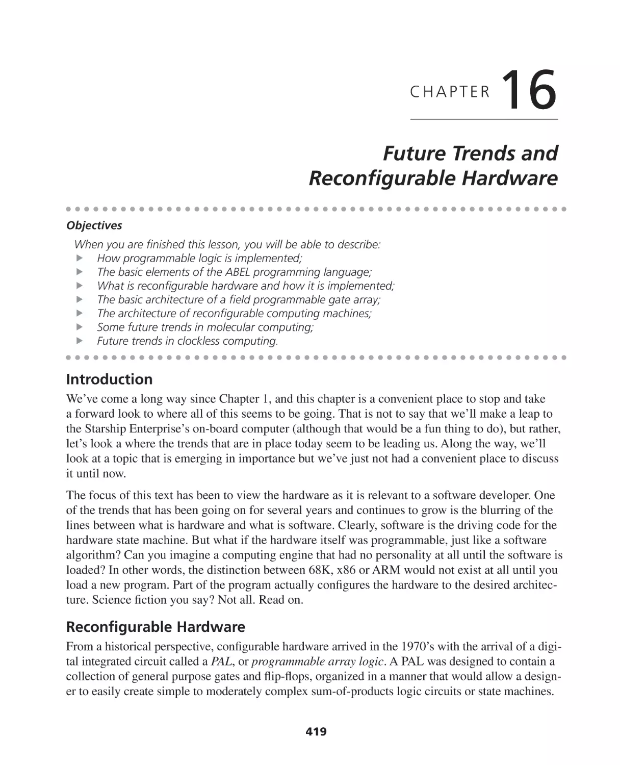
Computing machines have been around for a long time, hundreds of years. The Chinese abacus, the
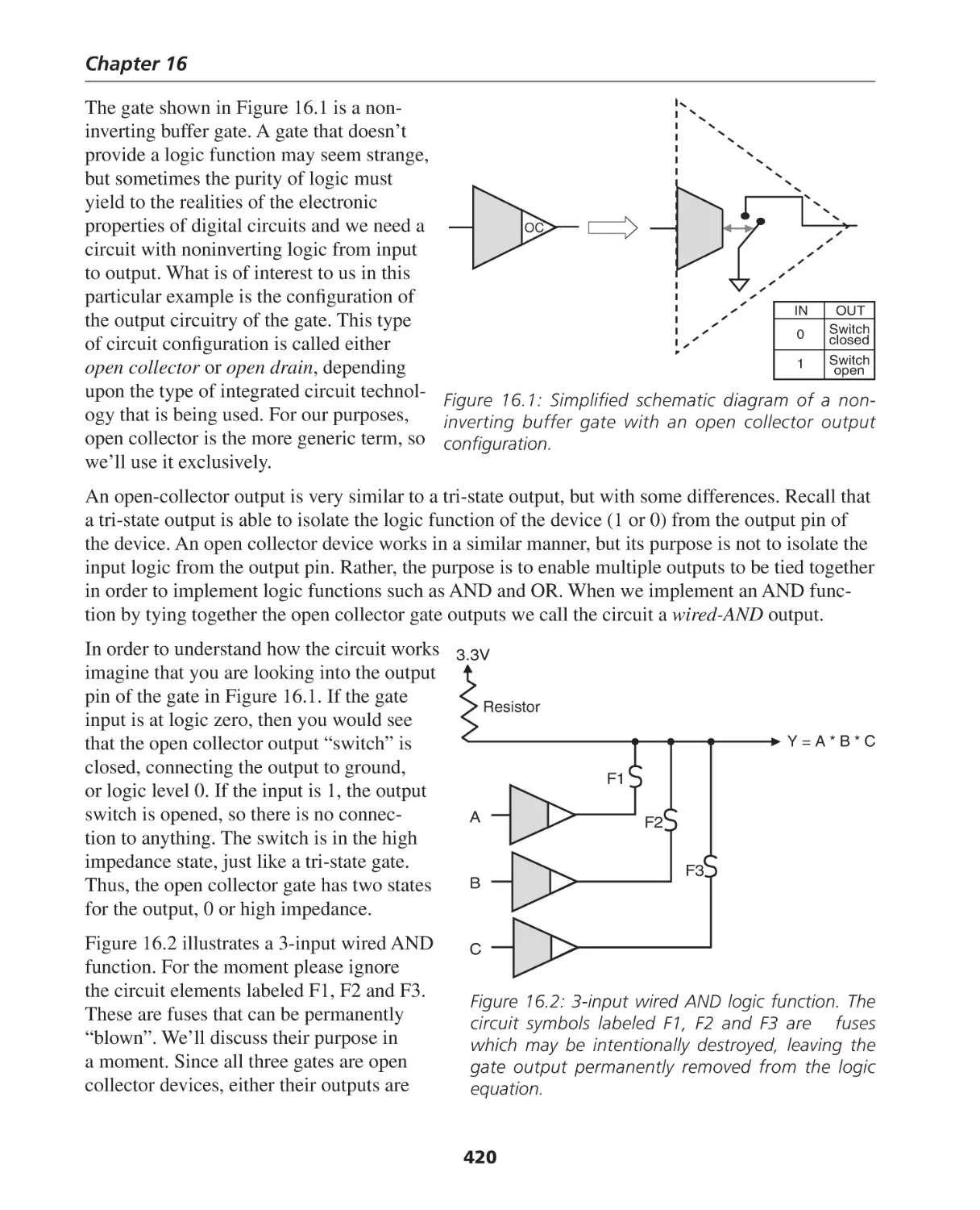
calculators with gears and wheels and the first analog computers are all examples of computing machinery; in some cases quite complex, that predates the introduction of digital computing systems.
The computing machines that we’re interested in came about in the 1940s because World War II
artillery needed a more accurate way to calculate the trajectories of the shells fired from battleships.
Today, the primary reason that computers have become so pervasive is the advances made in
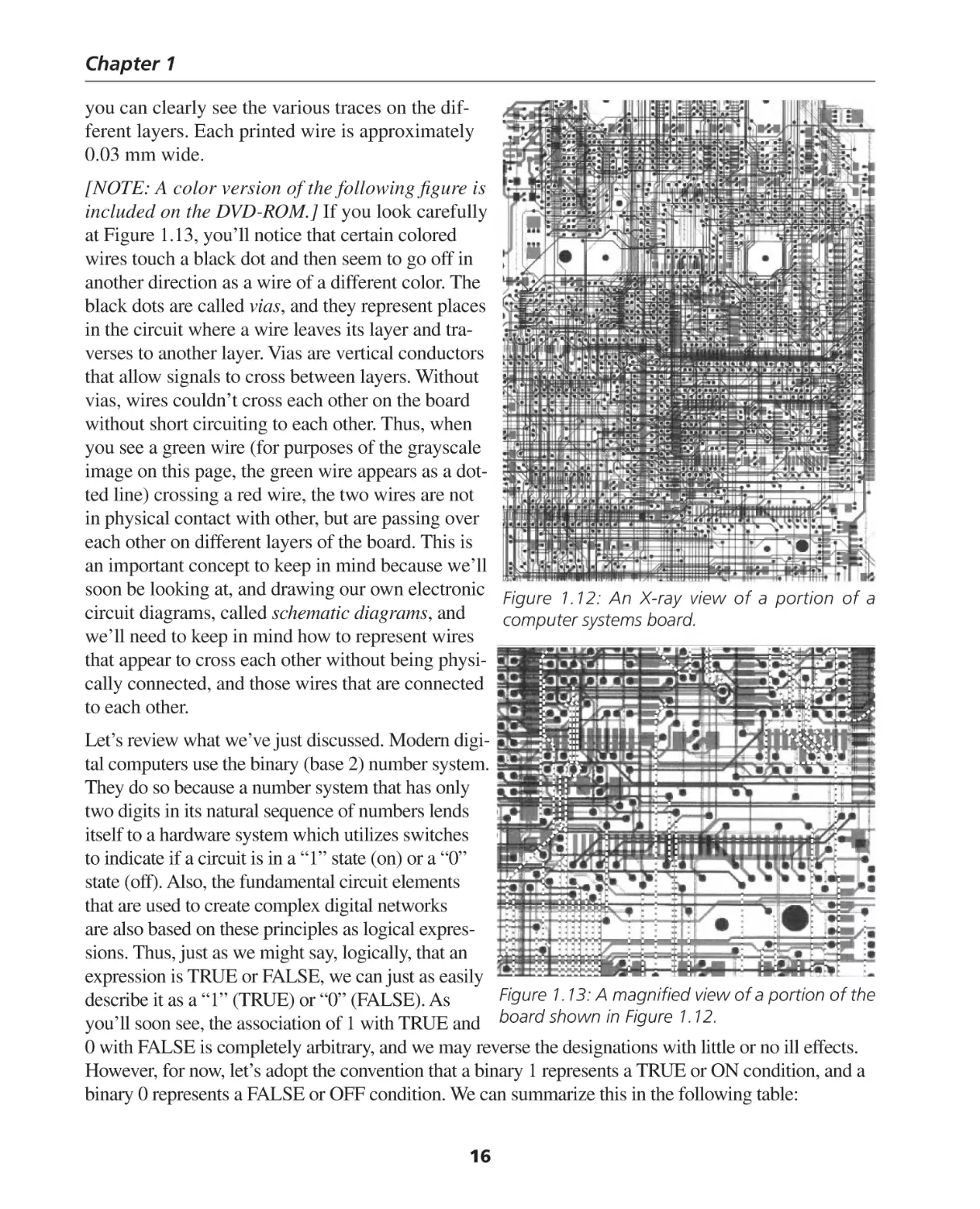
integrated circuit manufacturing technology. What was once primarily orange groves in California,
north of San Jose and south of Palo Alto, is today the region known as Silicon Valley. Silicon Valley is the home to many of the companies that are the locomotives of this technology. Intel, AMD,
Cypress, Cirrus Logic and so on are household names (if you live in a geek-speak household)
anywhere in the world.
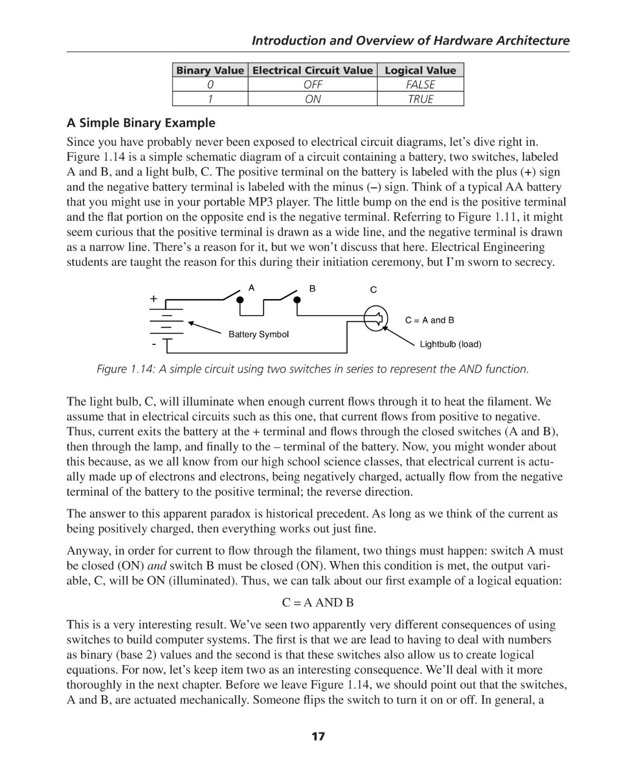
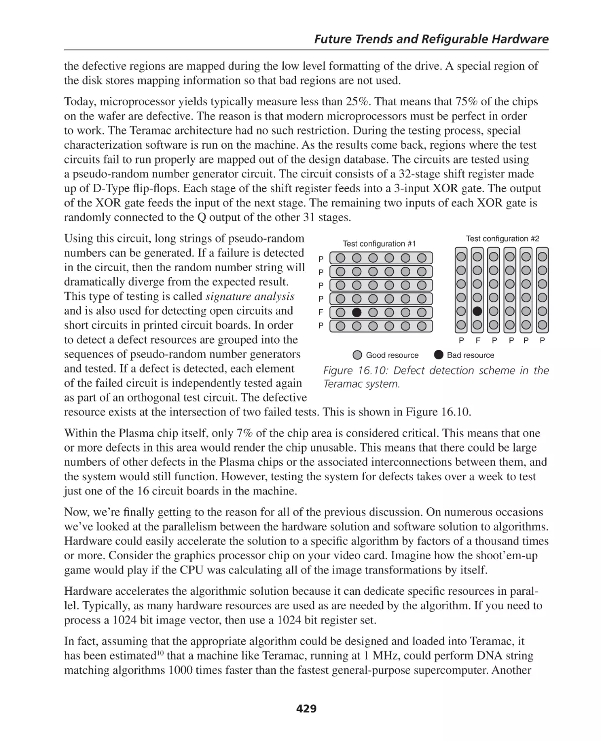
1
Chapter 1
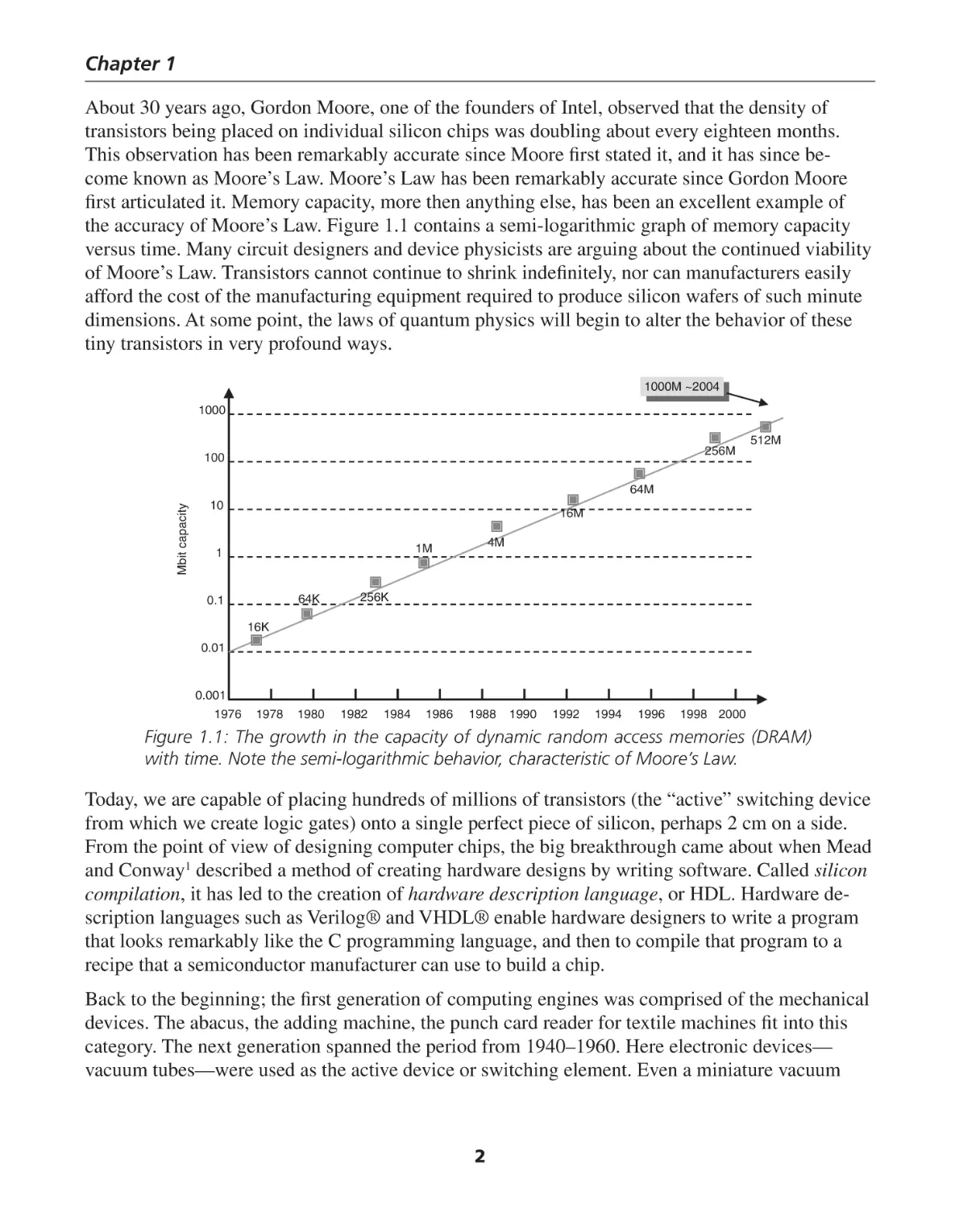
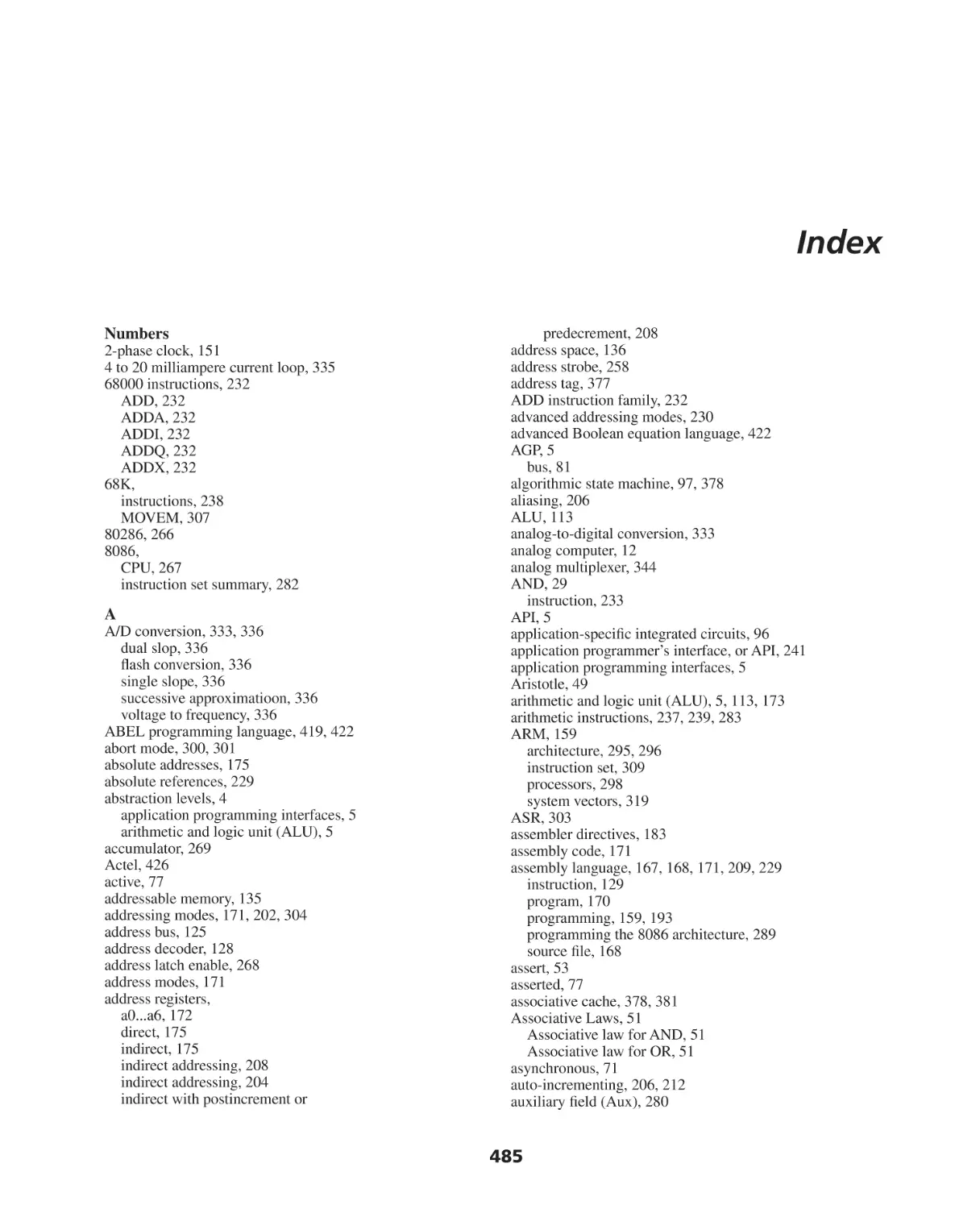
About 30 years ago, Gordon Moore, one of the founders of Intel, observed that the density of
transistors being placed on individual silicon chips was doubling about every eighteen months.
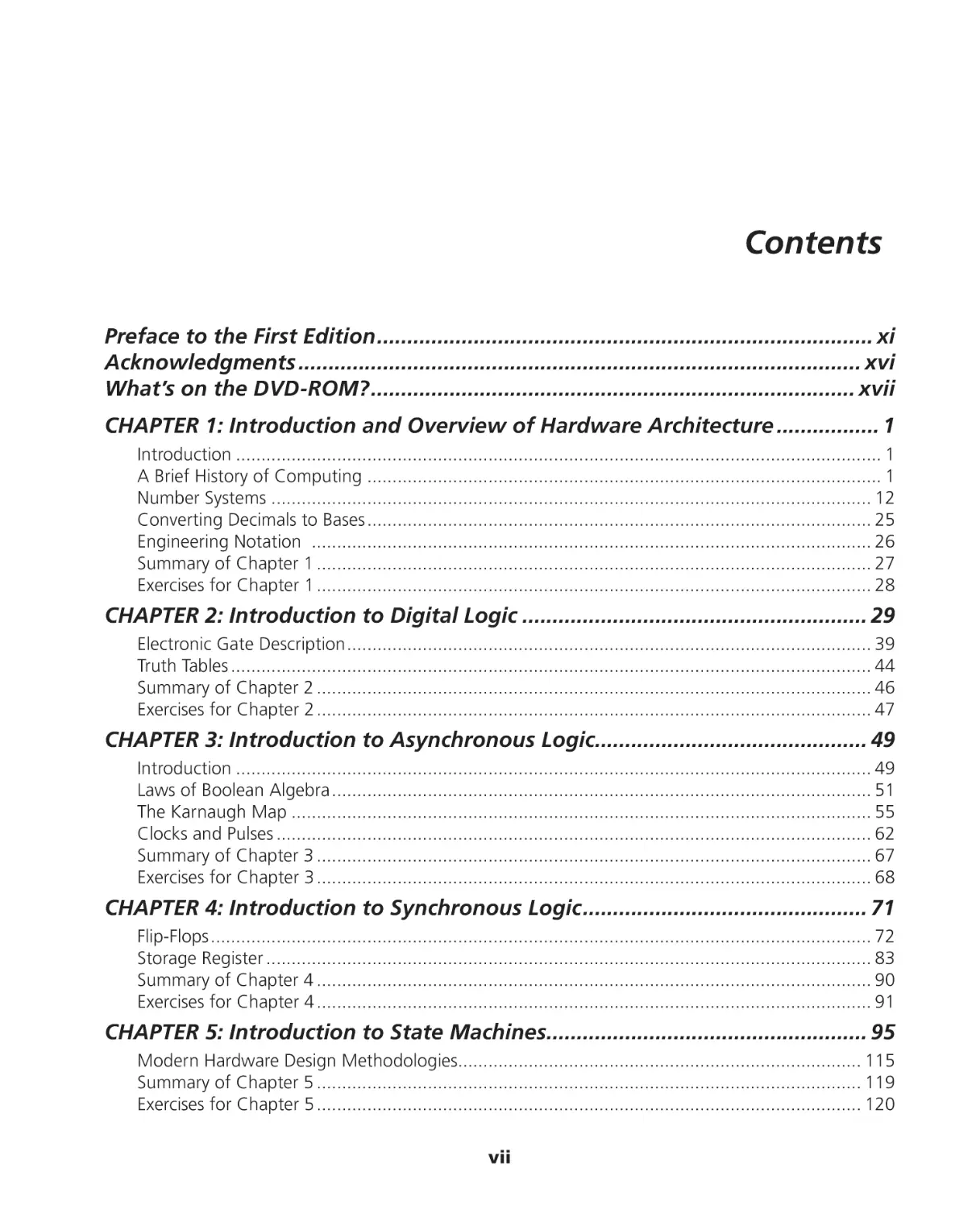
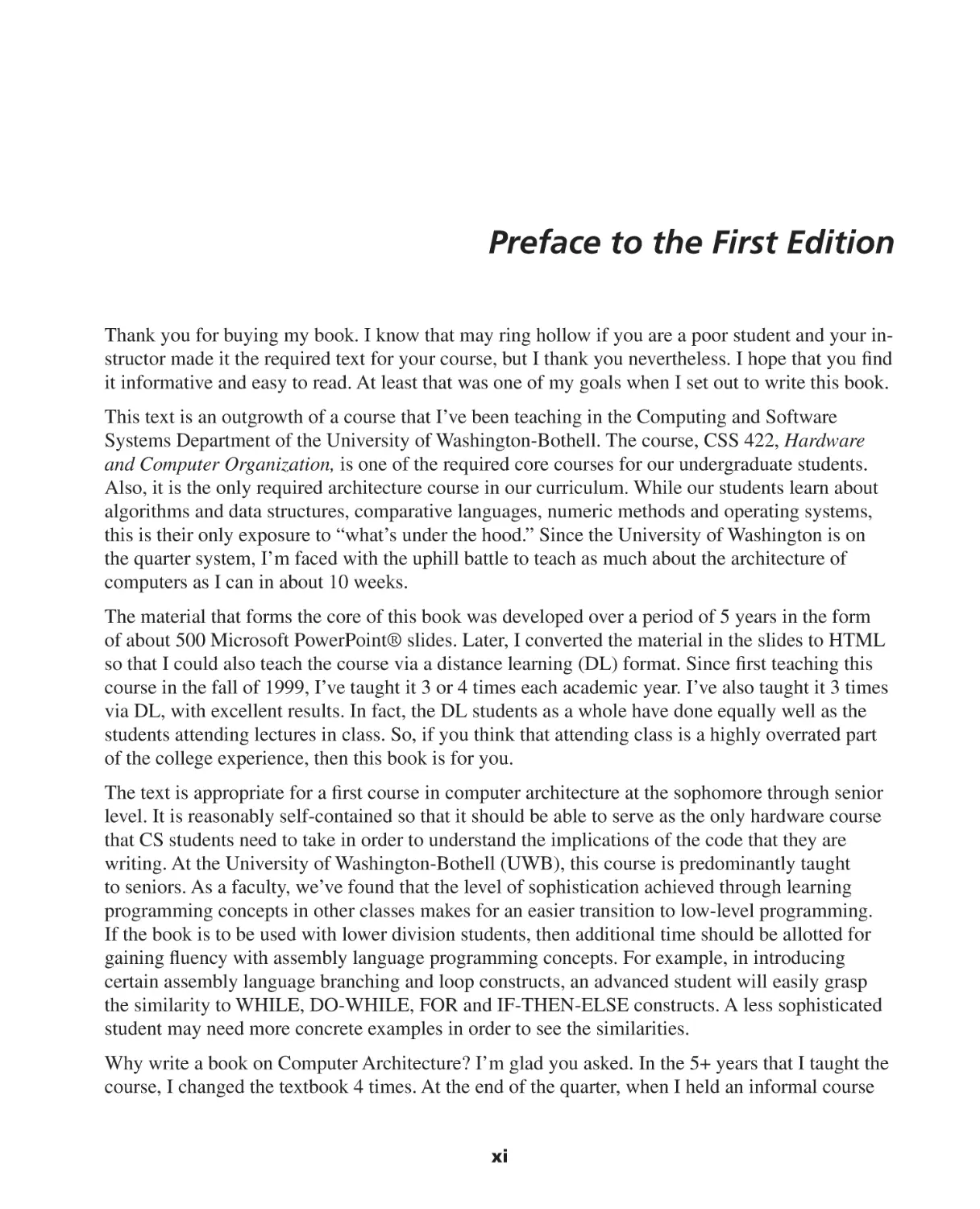
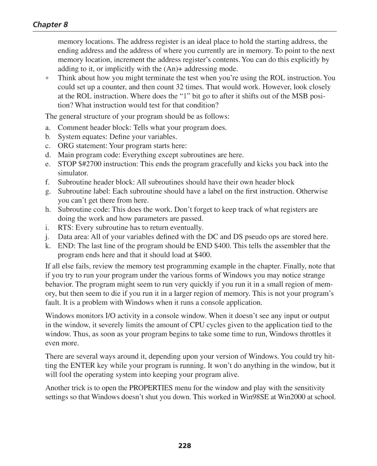
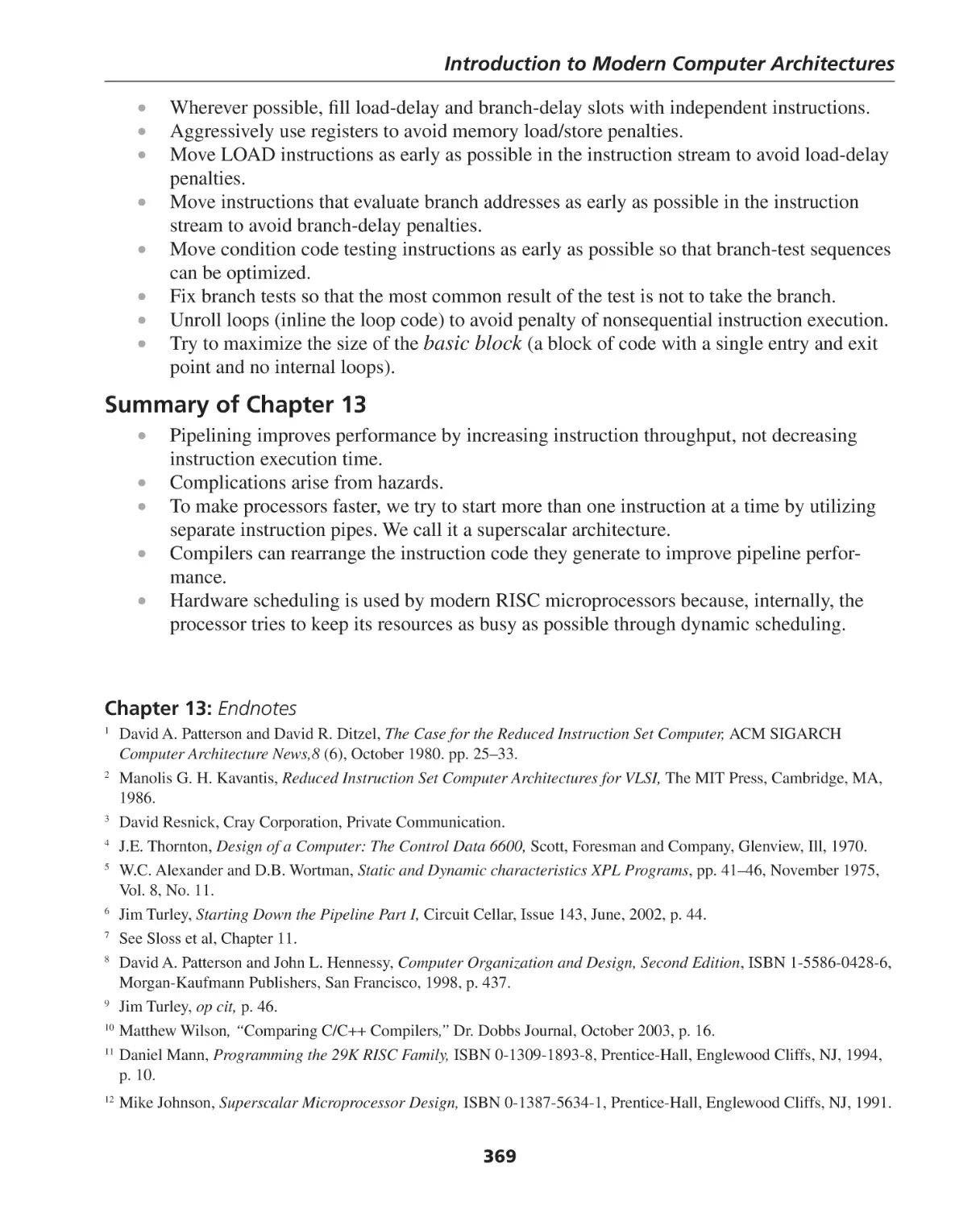
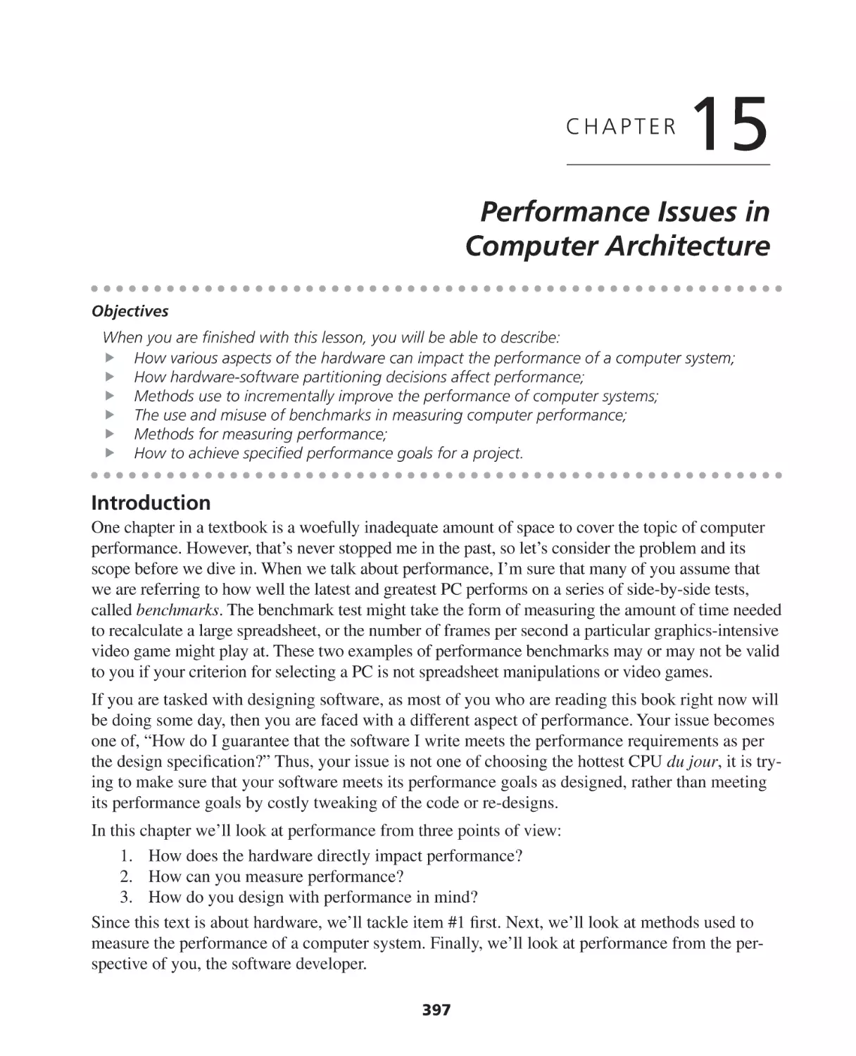
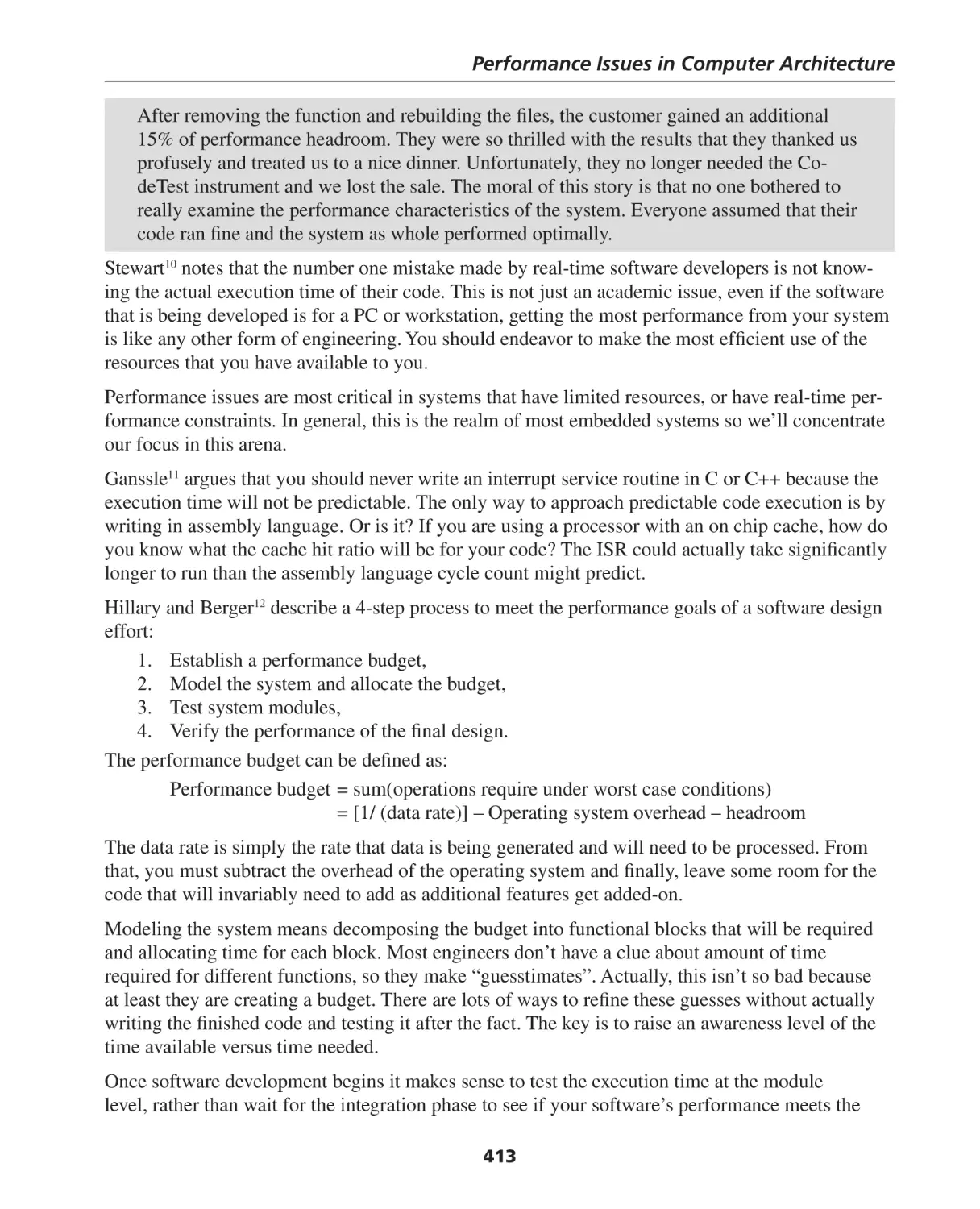
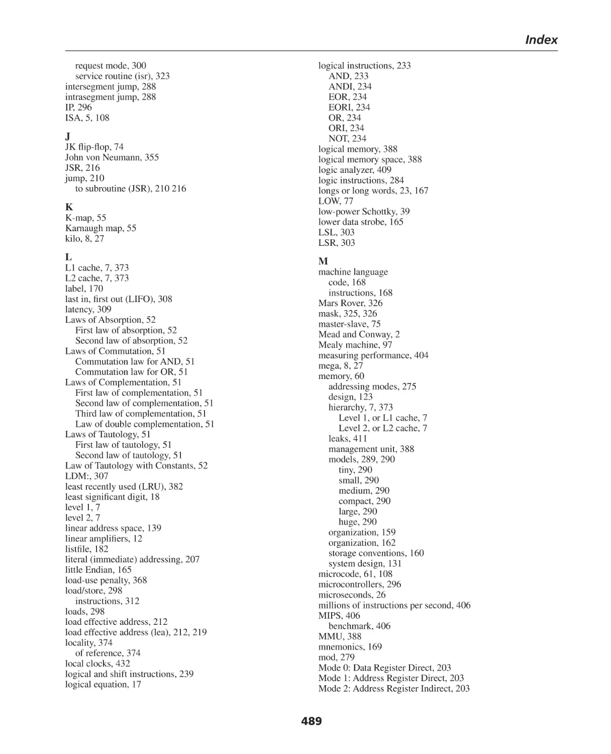
This observation has been remarkably accurate since Moore first stated it, and it has since become known as Moore’s Law. Moore’s Law has been remarkably accurate since Gordon Moore
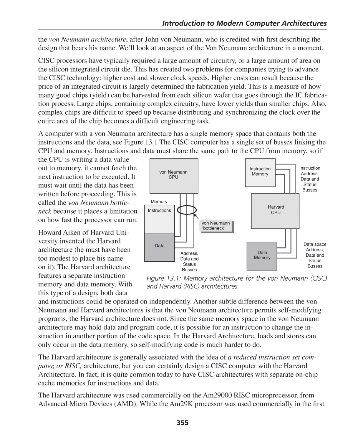
first articulated it. Memory capacity, more then anything else, has been an excellent example of
the accuracy of Moore’s Law. Figure 1.1 contains a semi-logarithmic graph of memory capacity
versus time. Many circuit designers and device physicists are arguing about the continued viability
of Moore’s Law. Transistors cannot continue to shrink indefinitely, nor can manufacturers easily
afford the cost of the manufacturing equipment required to produce silicon wafers of such minute
dimensions. At some point, the laws of quantum physics will begin to alter the behavior of these
tiny transistors in very profound ways.
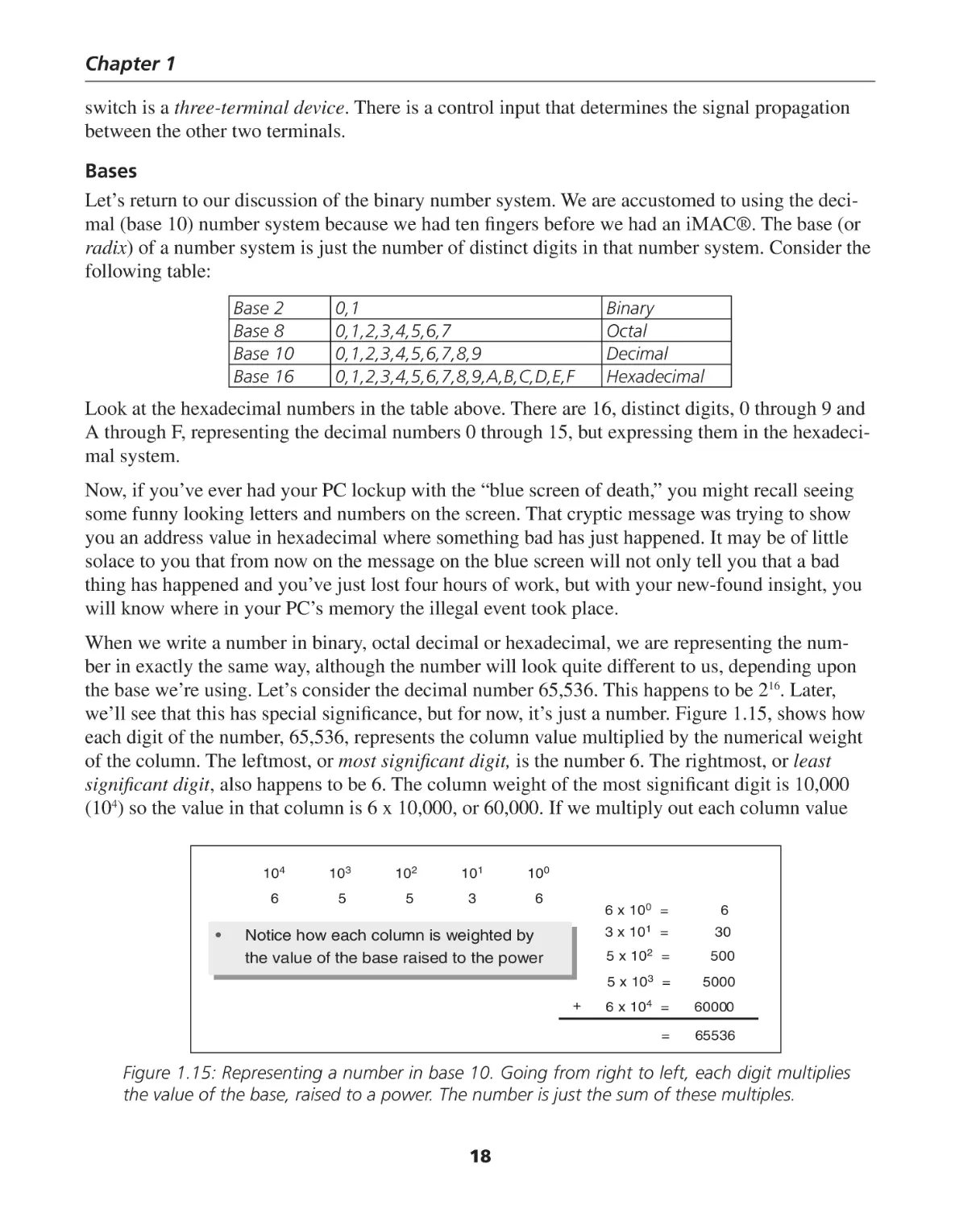
1000M
~2004
1000M ~2004
1000
256M
100
512M
Mbit capacity
64M
10
16M
4M
1M
1
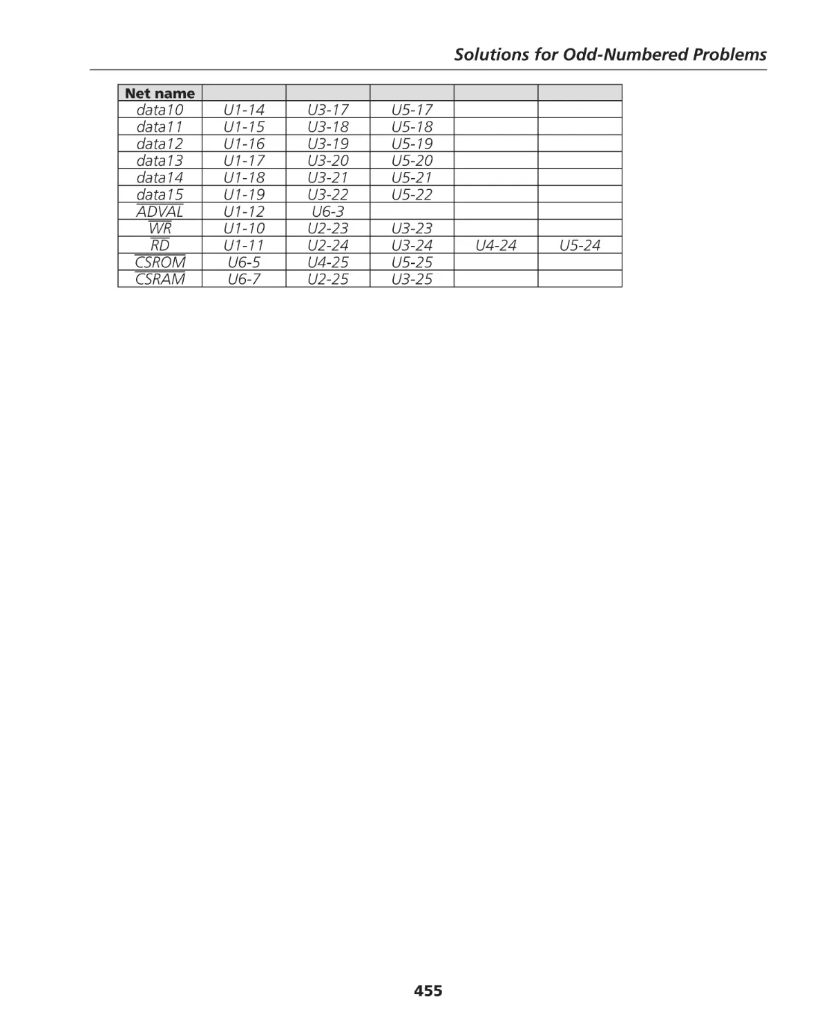
64K
0.1
256K
16K
0.01
0.001
1976
1978
1980
1982
1984
1986
1988
1990
1992
1994
1996
1998 2000
Figure 1.1: The growth in the capacity of dynamic random access memories (DRAM)
with time. Note the semi-logarithmic behavior, characteristic of Moore’s Law.
Today, we are capable of placing hundreds of millions of transistors (the “active” switching device
from which we create logic gates) onto a single perfect piece of silicon, perhaps 2 cm on a side.
From the point of view of designing computer chips, the big breakthrough came about when Mead
and Conway1 described a method of creating hardware designs by writing software. Called silicon
compilation, it has led to the creation of hardware description language, or HDL. Hardware description languages such as Verilog® and VHDL® enable hardware designers to write a program
that looks remarkably like the C programming language, and then to compile that program to a
recipe that a semiconductor manufacturer can use to build a chip.
Back to the beginning; the first generation of computing engines was comprised of the mechanical
devices. The abacus, the adding machine, the punch card reader for textile machines fit into this
category. The next generation spanned the period from 1940–1960. Here electronic devices—
vacuum tubes—were used as the active device or switching element. Even a miniature vacuum
2
Introduction and Overview of Hardware Architecture
tube is millions of times larger then the transistor on a silicon wafer. It consumes millions of times
the power of the transistor, and its useful lifetime is hundreds or thousands of times less then a
transistor. Although the vacuum tube computers were much faster then the mechanical computers
of the preceding generation, they are thousands of times slower then the computers of today. If you
are a fan of the grade B science fiction movies of the 1950’s, these computers were the ones that
filled the room with lights flashing and meters bouncing.
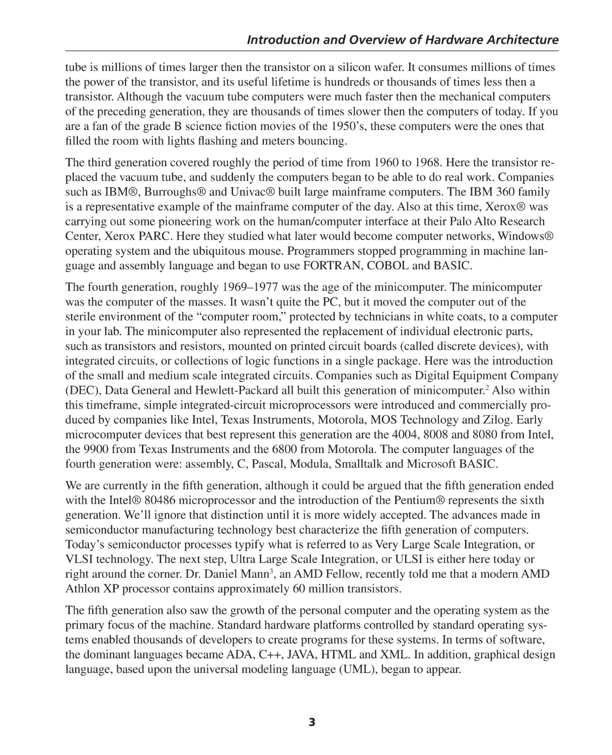
The third generation covered roughly the period of time from 1960 to 1968. Here the transistor replaced the vacuum tube, and suddenly the computers began to be able to do real work. Companies
such as IBM®, Burroughs® and Univac® built large mainframe computers. The IBM 360 family
is a representative example of the mainframe computer of the day. Also at this time, Xerox® was
carrying out some pioneering work on the human/computer interface at their Palo Alto Research
Center, Xerox PARC. Here they studied what later would become computer networks, Windows®
operating system and the ubiquitous mouse. Programmers stopped programming in machine language and assembly language and began to use FORTRAN, COBOL and BASIC.
The fourth generation, roughly 1969–1977 was the age of the minicomputer. The minicomputer
was the computer of the masses. It wasn’t quite the PC, but it moved the computer out of the
sterile environment of the “computer room,” protected by technicians in white coats, to a computer
in your lab. The minicomputer also represented the replacement of individual electronic parts,
such as transistors and resistors, mounted on printed circuit boards (called discrete devices), with
integrated circuits, or collections of logic functions in a single package. Here was the introduction
of the small and medium scale integrated circuits. Companies such as Digital Equipment Company
(DEC), Data General and Hewlett-Packard all built this generation of minicomputer.2 Also within
this timeframe, simple integrated-circuit microprocessors were introduced and commercially produced by companies like Intel, Texas Instruments, Motorola, MOS Technology and Zilog. Early
microcomputer devices that best represent this generation are the 4004, 8008 and 8080 from Intel,
the 9900 from Texas Instruments and the 6800 from Motorola. The computer languages of the
fourth generation were: assembly, C, Pascal, Modula, Smalltalk and Microsoft BASIC.
We are currently in the fifth generation, although it could be argued that the fifth generation ended
with the Intel® 80486 microprocessor and the introduction of the Pentium® represents the sixth
generation. We’ll ignore that distinction until it is more widely accepted. The advances made in
semiconductor manufacturing technology best characterize the fifth generation of computers.
Today’s semiconductor processes typify what is referred to as Very Large Scale Integration, or
VLSI technology. The next step, Ultra Large Scale Integration, or ULSI is either here today or
right around the corner. Dr. Daniel Mann3, an AMD Fellow, recently told me that a modern AMD
Athlon XP processor contains approximately 60 million transistors.
The fifth generation also saw the growth of the personal computer and the operating system as the
primary focus of the machine. Standard hardware platforms controlled by standard operating systems enabled thousands of developers to create programs for these systems. In terms of software,
the dominant languages became ADA, C++, JAVA, HTML and XML. In addition, graphical design
language, based upon the universal modeling language (UML), began to appear.
3
Chapter 1
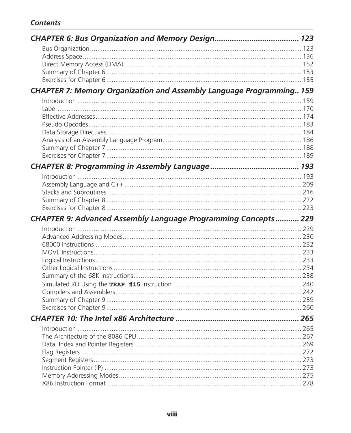
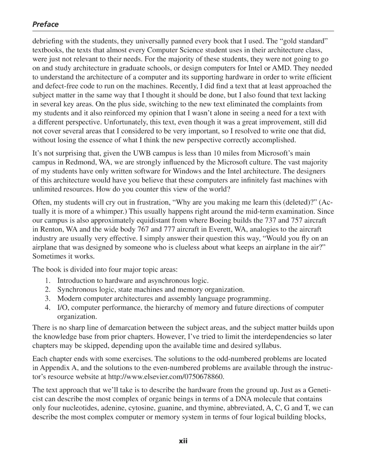
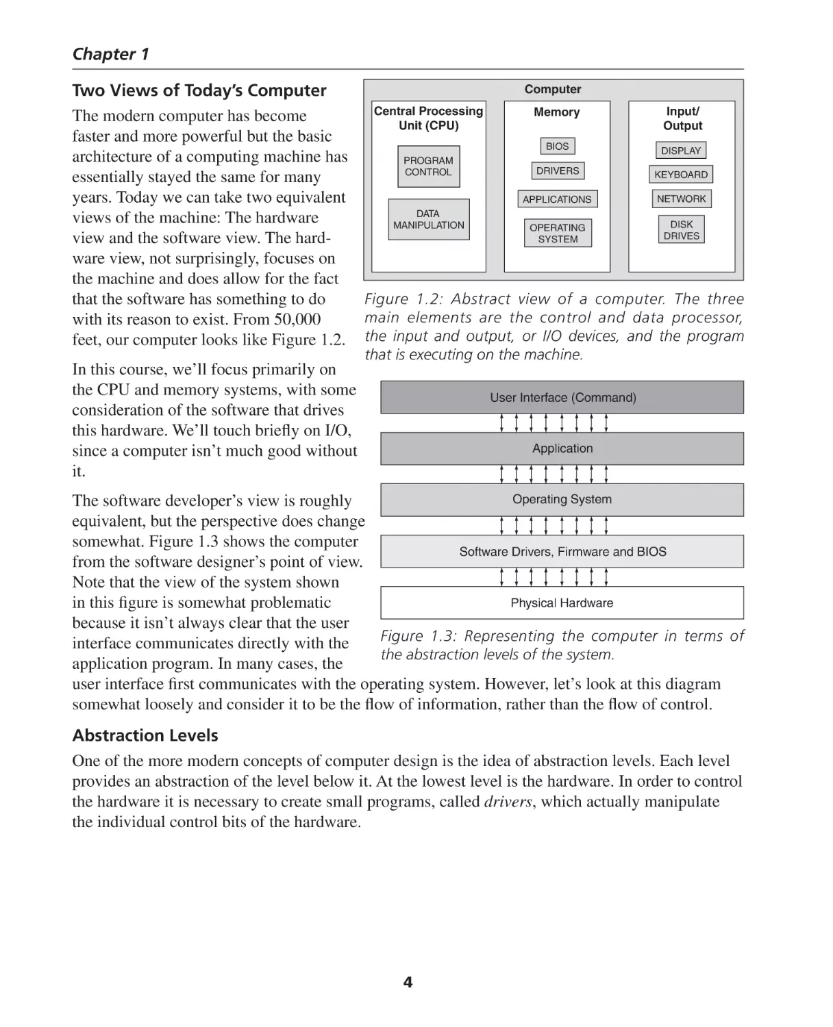
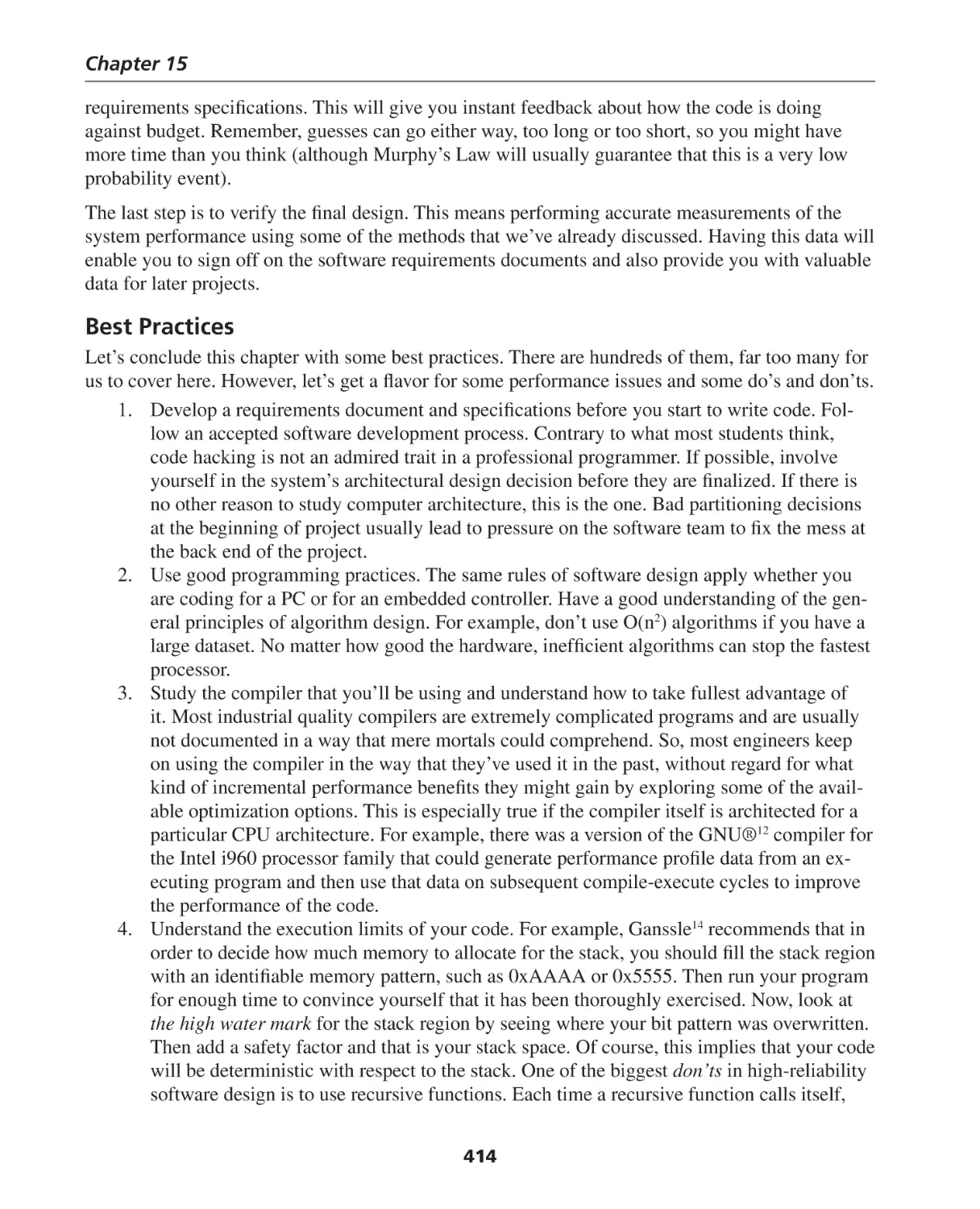
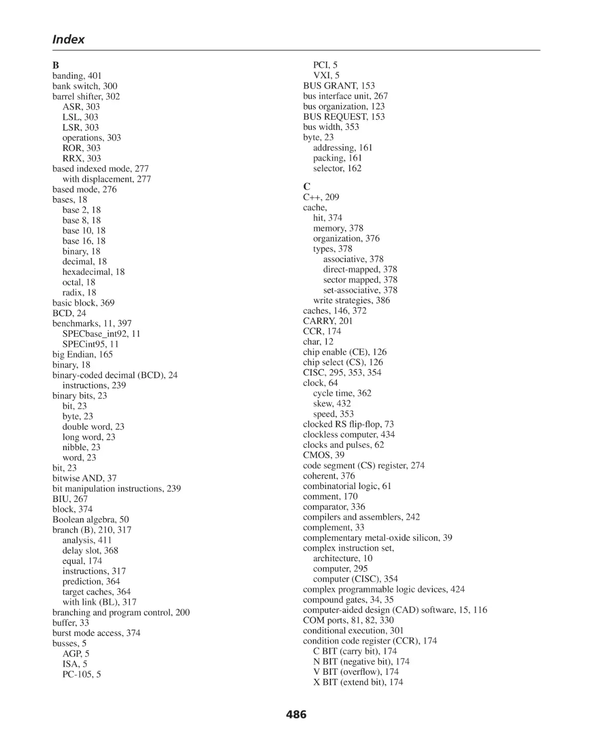
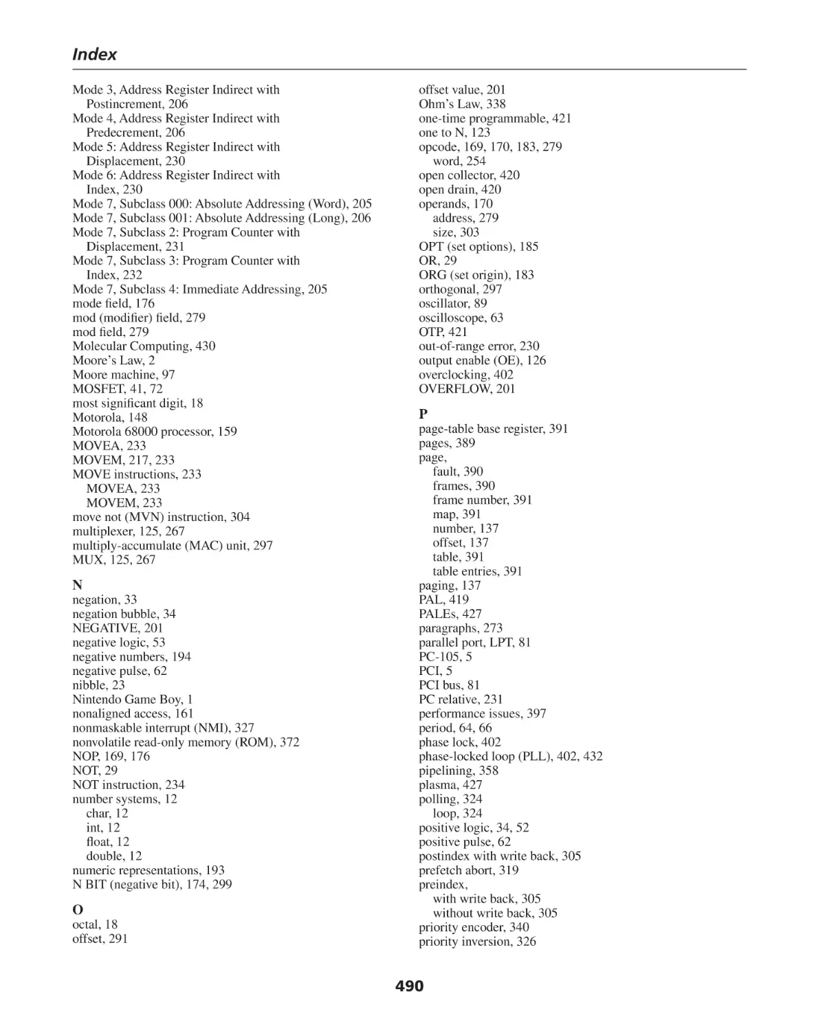
Computer
Two Views of Today’s Computer
Central
Processing
Input/
Memory
The modern computer has become
Unit (CPU)
Output
faster and more powerful but the basic
BIOS
DISPLAY
architecture of a computing machine has
PROGRAM
DRIVERS
CONTROL
KEYBOARD
essentially stayed the same for many
NETWORK
years. Today we can take two equivalent
APPLICATIONS
DATA
views of the machine: The hardware
DISK
MANIPULATION
OPERATING
DRIVES
SYSTEM
view and the software view. The hardware view, not surprisingly, focuses on
the machine and does allow for the fact
Figure 1.2: Abstract view of a computer. The three
that the software has something to do
main elements are the control and data processor,
with its reason to exist. From 50,000
feet, our computer looks like Figure 1.2. the input and output, or I/O devices, and the program
In this course, we’ll focus primarily on
the CPU and memory systems, with some
consideration of the software that drives
this hardware. We’ll touch briefly on I/O,
since a computer isn’t much good without
it.
that is executing on the machine.
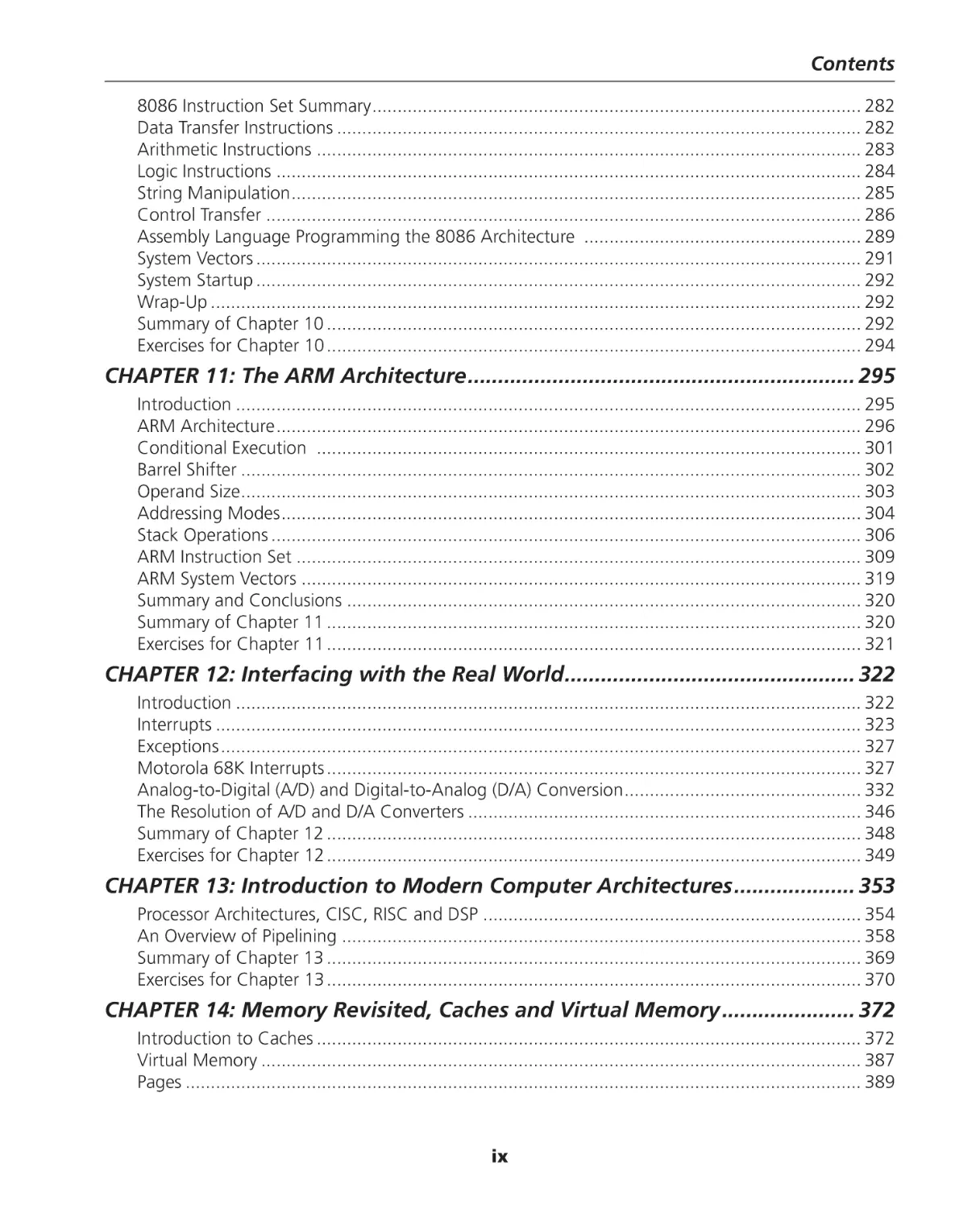
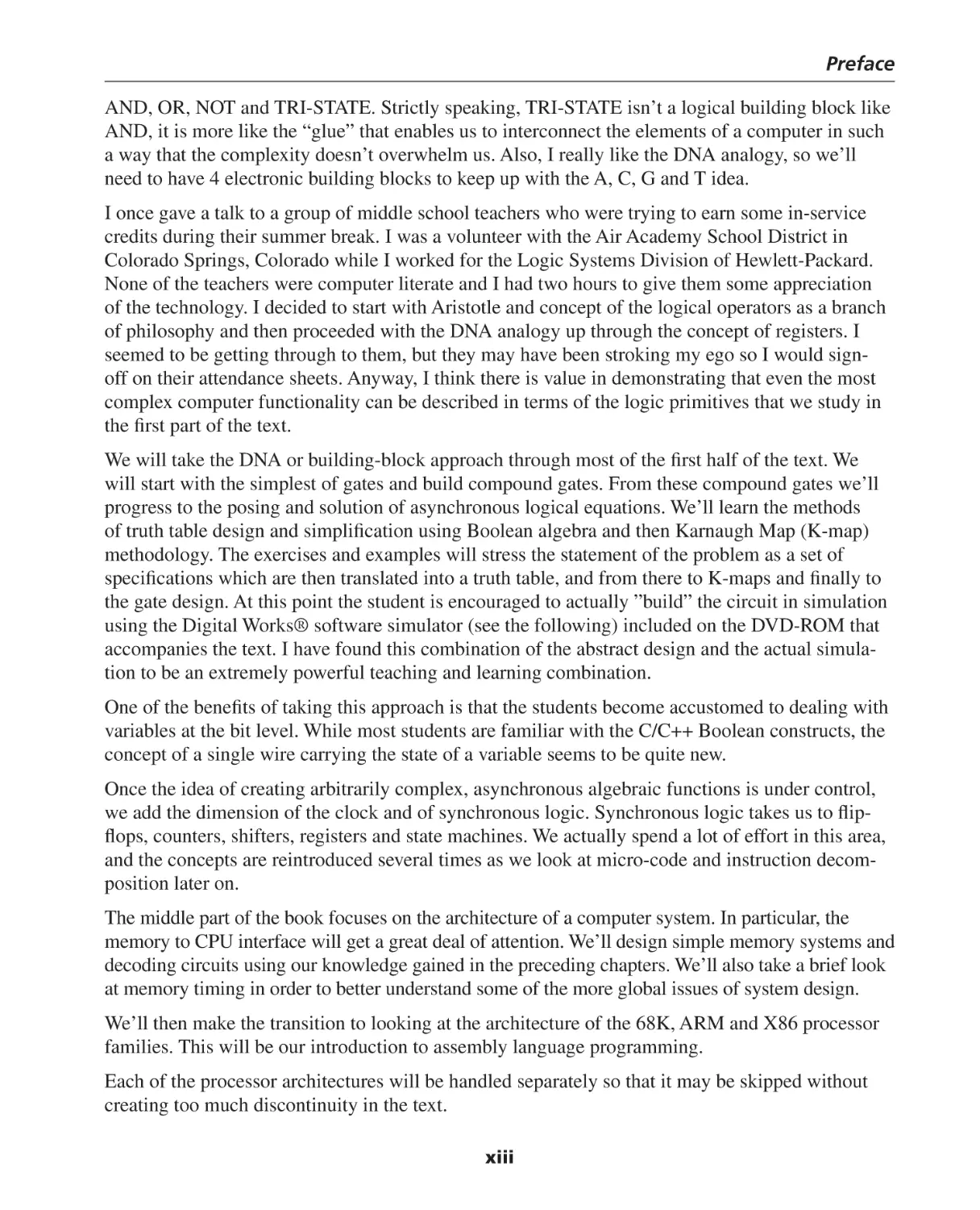
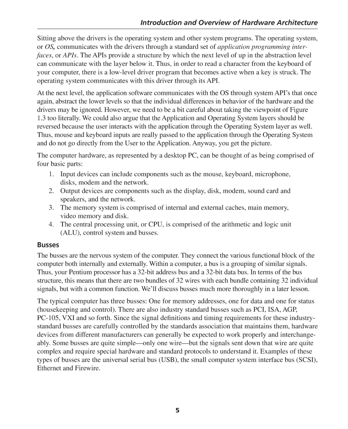
User Interface (Command)
Application
Operating System
The software developer’s view is roughly
equivalent, but the perspective does change
somewhat. Figure 1.3 shows the computer
Software Drivers, Firmware and BIOS
from the software designer’s point of view.
Note that the view of the system shown
Physical Hardware
in this figure is somewhat problematic
because it isn’t always clear that the user
Figure 1.3: Representing the computer in terms of
interface communicates directly with the
the abstraction levels of the system.
application program. In many cases, the
user interface first communicates with the operating system. However, let’s look at this diagram
somewhat loosely and consider it to be the flow of information, rather than the flow of control.
Abstraction Levels
One of the more modern concepts of computer design is the idea of abstraction levels. Each level
provides an abstraction of the level below it. At the lowest level is the hardware. In order to control
the hardware it is necessary to create small programs, called drivers, which actually manipulate
the individual control bits of the hardware.
4
Introduction and Overview of Hardware Architecture
Sitting above the drivers is the operating system and other system programs. The operating system,
or OS, communicates with the drivers through a standard set of application programming interfaces, or APIs. The APIs provide a structure by which the next level of up in the abstraction level
can communicate with the layer below it. Thus, in order to read a character from the keyboard of
your computer, there is a low-level driver program that becomes active when a key is struck. The
operating system communicates with this driver through its API.
At the next level, the application software communicates with the OS through system API’s that once
again, abstract the lower levels so that the individual differences in behavior of the hardware and the
drivers may be ignored. However, we need to be a bit careful about taking the viewpoint of Figure
1.3 too literally. We could also argue that the Application and Operating System layers should be
reversed because the user interacts with the application through the Operating System layer as well.
Thus, mouse and keyboard inputs are really passed to the application through the Operating System
and do not go directly from the User to the Application. Anyway, you get the picture.
The computer hardware, as represented by a desktop PC, can be thought of as being comprised of
four basic parts:
1. Input devices can include components such as the mouse, keyboard, microphone,
disks, modem and the network.
2. Output devices are components such as the display, disk, modem, sound card and
speakers, and the network.
3. The memory system is comprised of internal and external caches, main memory,
video memory and disk.
4. The central processing unit, or CPU, is comprised of the arithmetic and logic unit
(ALU), control system and busses.
Busses
The busses are the nervous system of the computer. They connect the various functional block of the
computer both internally and externally. Within a computer, a bus is a grouping of similar signals.
Thus, your Pentium processor has a 32-bit address bus and a 32-bit data bus. In terms of the bus
structure, this means that there are two bundles of 32 wires with each bundle containing 32 individual
signals, but with a common function. We’ll discuss busses much more thoroughly in a later lesson.
The typical computer has three busses: One for memory addresses, one for data and one for status
(housekeeping and control). There are also industry standard busses such as PCI, ISA, AGP,
PC-105, VXI and so forth. Since the signal definitions and timing requirements for these industrystandard busses are carefully controlled by the standards association that maintains them, hardware
devices from different manufacturers can generally be expected to work properly and interchangeably. Some busses are quite simple—only one wire—but the signals sent down that wire are quite
complex and require special hardware and standard protocols to understand it. Examples of these
types of busses are the universal serial bus (USB), the small computer system interface bus (SCSI),
Ethernet and Firewire.
5
Chapter 1
Memory
From the point of view of a software developer, the memory system is the most visible part of the
computer. If we didn’t have memory, we’d never have a problem with an errant pointer. But that’s
another story. The computer memory is the place where program code (instructions) and variables
(data) are stored. We can make a simple analogy about instructions and data. Consider a recipe to
bake a cake. The recipe itself is the collection of instructions that tell us how to create the cake.
The data represents the ingredients we need that the instructions manipulate. It doesn’t make much
sense to sift the flour if you don’t have flour to sift.
We may also describe memory as a hierarchy, based upon speed. In this case, speed means how
fast the data can be retrieved from the memory when the computer requests it. The fastest memory
is also the most expensive so as the memory access times become slower, the cost per bit decreases, so we can have more of it. The fastest memory is also the memory that’s closest to the CPU.
Thus, our CPU might have a small number of on-chip data registers, or storage locations, several
thousand locations of off-chip cache memory, several million locations of main memory and
several billion locations of disk storage. The ratio of the access time of the fastest on-chip memory
to the slowest memory, the hard disk, is about 10,000 to one. The ratio of the cost of the two
memories is somewhat more difficult to calculate because the fastest semiconductor memory is the
on-chip cache memory, and you cannot buy that separately from the microprocessor itself. However, if we estimate the ratio of the cost per gigabyte of the main memory in your PC to the cost
per gigabyte of hard disk storage (and taking into account the mail-in rebates) then we find that the
faster semiconductor storage with an average access time of 20–40 nanoseconds is 300 times more
costly then hard disk storage, with an average access time of 1 millisecond.
Today, because of the economy of scale provided by the PC industry, memory is incredibly
inexpensive. A standard memory module (SIMM) with a capacity of 512 million storage locations
costs about $60. PC memory is dominated by a memory technology called dynamic random access
memory, or DRAM. There are several variations of DRAM, and we’ll cover them in greater depth
later on. DRAM is characterized by the fact that it must be constantly accessed or it will lose its
stored data. This forces us to create highly specialized and complex support hardware to interface
the memory systems to the CPU. These devices are contained in support chipsets that have become as important to the modern PC as the CPU. Why use these complex memories? DRAM’s are
inherently very dense and can hold upwards of 512 million bits of information. In order to achieve
these densities, the complexity of accessing and controlling them was moved to the chipset.
Static RAM (SRAM)
The memory that we’ll focus on is called static random access memory or SRAM. Each memory
cell of an SRAM device is more complicated then the DRAM, but the overall operation of the
device is easier to understand, so we’ll focus on this type of memory in our discussions. The term,
static random access memory, or SRAM, refers to the fact that:
1. we may read from the chip or write data to it, and
2. any memory cell in the chip may be accessed at any time, once the appropriate address of
the cell is presented to the chip.
6
Introduction and Overview of Hardware Architecture
3. As long as power is applied to the memory, we only a required to provide an address to
the SRAM cell, together with a READ or a WRITE signal, in order to access, or modify,
the data in the cell. This is quite a bit different then the effort required to maintain data
integrity in DRAM cells. We’ll discuss this point in greater detail in a later chapter.
With a RAM memory there is no need to search through all the preceding memory cells in order to
get to the one you want to read. In other words, data can be read from the last cell of the RAM as
quickly as it could be read from the first cell. In contrast, a tape backup device must stream through
the entire tape before the last piece of data can be retrieved. That’s why the term “random access” is
used. Also note that when are discussing SRAM or DRAM in the general sense, as listed in items 1
and 2, we’ll just use the term RAM, without the SRAM or DRAM distinction.
Memory Hierarchy
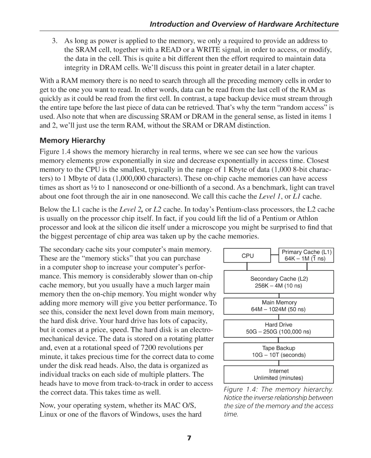
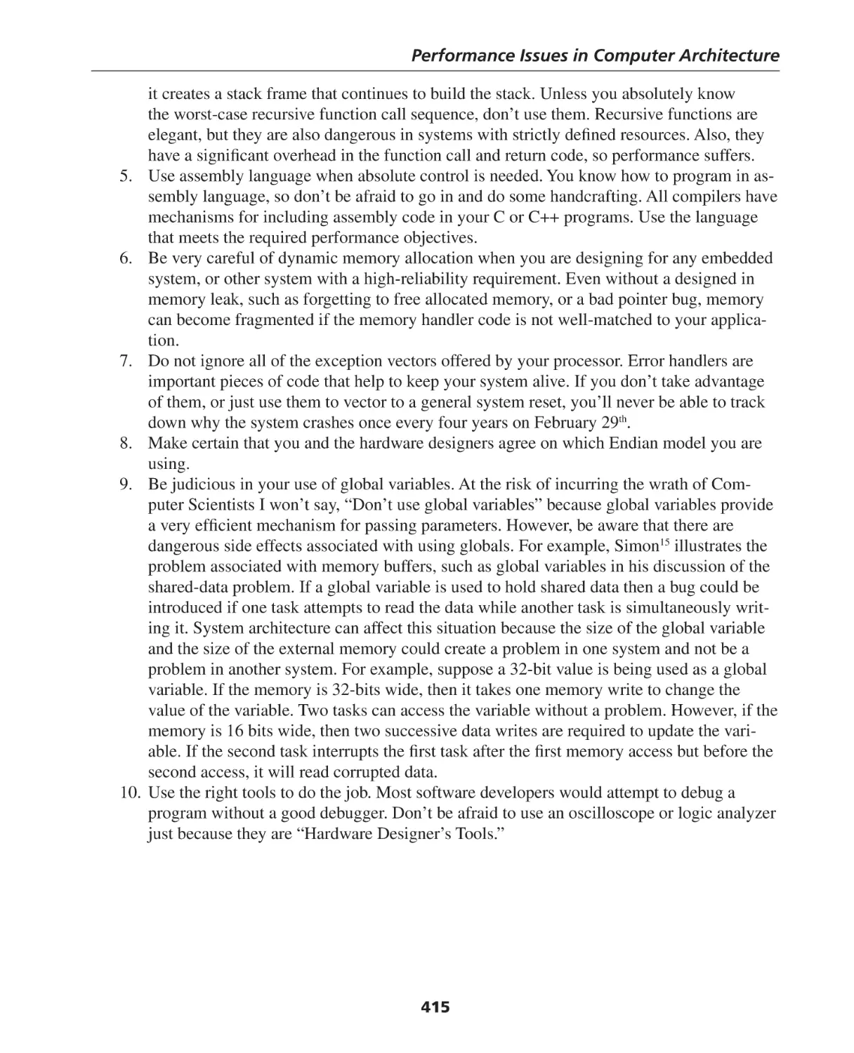
Figure 1.4 shows the memory hierarchy in real terms, where we see can see how the various
memory elements grow exponentially in size and decrease exponentially in access time. Closest
memory to the CPU is the smallest, typically in the range of 1 Kbyte of data (1,000 8-bit characters) to 1 Mbyte of data (1,000,000 characters). These on-chip cache memories can have access
times as short as ½ to 1 nanosecond or one-billionth of a second. As a benchmark, light can travel
about one foot through the air in one nanosecond. We call this cache the Level 1, or L1 cache.
Below the L1 cache is the Level 2, or L2 cache. In today’s Pentium-class processors, the L2 cache
is usually on the processor chip itself. In fact, if you could lift the lid of a Pentium or Athlon
processor and look at the silicon die itself under a microscope you might be surprised to find that
the biggest percentage of chip area was taken up by the cache memories.
The secondary cache sits your computer’s main memory.
Primary Cache (L1)
CPU
64K – 1M (1 ns)
These are the “memory sticks” that you can purchase
in a computer shop to increase your computer’s performance. This memory is considerably slower than on-chip
Secondary Cache (L2)
cache memory, but you usually have a much larger main
256K – 4M (10 ns)
memory then the on-chip memory. You might wonder why
Main Memory
adding more memory will give you better performance. To
64M – 1024M (50 ns)
see this, consider the next level down from main memory,
the hard disk drive. Your hard drive has lots of capacity,
Hard Drive
but it comes at a price, speed. The hard disk is an electro50G – 250G (100,000 ns)
mechanical device. The data is stored on a rotating platter
and, even at a rotational speed of 7200 revolutions per
Tape Backup
10G – 10T (seconds)
minute, it takes precious time for the correct data to come
under the disk read heads. Also, the data is organized as
Internet
individual tracks on each side of multiple platters. The
Unlimited (minutes)
heads have to move from track-to-track in order to access
Figure 1.4: The memory hierarchy.
the correct data. This takes time as well.
Now, your operating system, whether its MAC O/S,
Linux or one of the flavors of Windows, uses the hard
7
Notice the inverse relationship between
the size of the memory and the access
time.
Chapter 1
disk as a handy place to swap out programs or data that can’t fit in main memory at a particular
point in time. So, if you have several windows open on your computer, and only 64 megabytes of
main memory, you might see the hourglass form of the cursor appearing quite often because the
operating system is constantly swapping the different applications in and out of main memory.
From Figure 1.4, we see that the ratio of access times between the hard disk and main memory can
be 10,000 to one, so any time that we go to the hard disk, we will have to wait. The moral here is
that the best performance boost you can give to your computer is to add as much memory as it can
hold.
Finally, there are several symbols used in Figure 1.4 that might be strange to you. We’ll discuss
them in detail in due course, but in case you were wondering what it meant, here’s a little preview:
Symbol
Name
ns
K
M
G
T
nanosecond
kilobytes
megabytes
gigabytes
terabytes
Meaning
billionth of a second
210 or 1024 8-bit characters (bytes)
220 or 1,048,576 bytes
230 or 1,073,741,824 bytes
240 or 1,099,511,627,776 bytes
Hopefully, these numbers will soon become quite familiar to you because they are the dimensions
of modern computer technology. However, one note of caution: The terms kilo, mega, giga and
tera are often overloaded. Sometimes they are used in the strictly scientific sense of a shorthand
notation for a multiplication factor of 103, 106, 109 and 1012, respectively. So, how do you know the
computer-speak versions, 210, 220, 230, 240 are being used, or the traditional science and engineering
meaning is being used? That’s a good question. Sometimes it isn’t so obvious and mistakes could
be made. For example, whenever we are dealing with memory size and memory issues, we are
almost always using the base 2 sense of the terms. However, this isn’t always the case. Hard disk
drives, even though they are storage devices, use the terms in the engineering sense. Therefore, an
old 1 gigabyte hard drive does not hold the same amount of data as 1 gigabyte of memory because
the “giga” term is being used in two different senses. In any case, you are generally safe to assume
the base 2 versions of the term in this text, unless I specifically state otherwise. In the real world,
caveat emptor.
Hard Disk Drive
Let’s look a bit further into the dynamics of the hard disk drive. Disk drives are a marvel of engineering technology. For years, electronic industry analysts were predicting the demise of the hard
drive. Economical semiconductor memories that were as cost effective as a hard disk were always
“a few years away.” However, the disk drive manufacturers ignored the pundits and just continued
to increase the capacity and performance, improve the reliability and reduce the cost of the disk
drives. Today, an average disk drive costs about 60 cents per gigabyte of storage capacity.
Consider a modern, high-performance disk drive. Specifically, let’s look at the Model ST3146807LC
from Seagate Technology®4. Following are the relevant specifications for this drive:
8
Introduction and Overview of Hardware Architecture
•
•
•
•
•
•
•
•
•
•
Rotational Speed: 10,000 rpm
Interface: Ultra320 SCSI
Discs/Heads: 4/8
Formatted Capacity (512 bytes/sector) Gbytes: 146.8
Cylinders: 49,855
Sectors per drive: 286,749,488
External transfer rate: 320 Mbytes per second
Track-to-track Seek Read/Write (msec): 0.35/0.55
Average Seek Read/Write (msec): 4.7/5.3
Average Latency (msec): 2.99
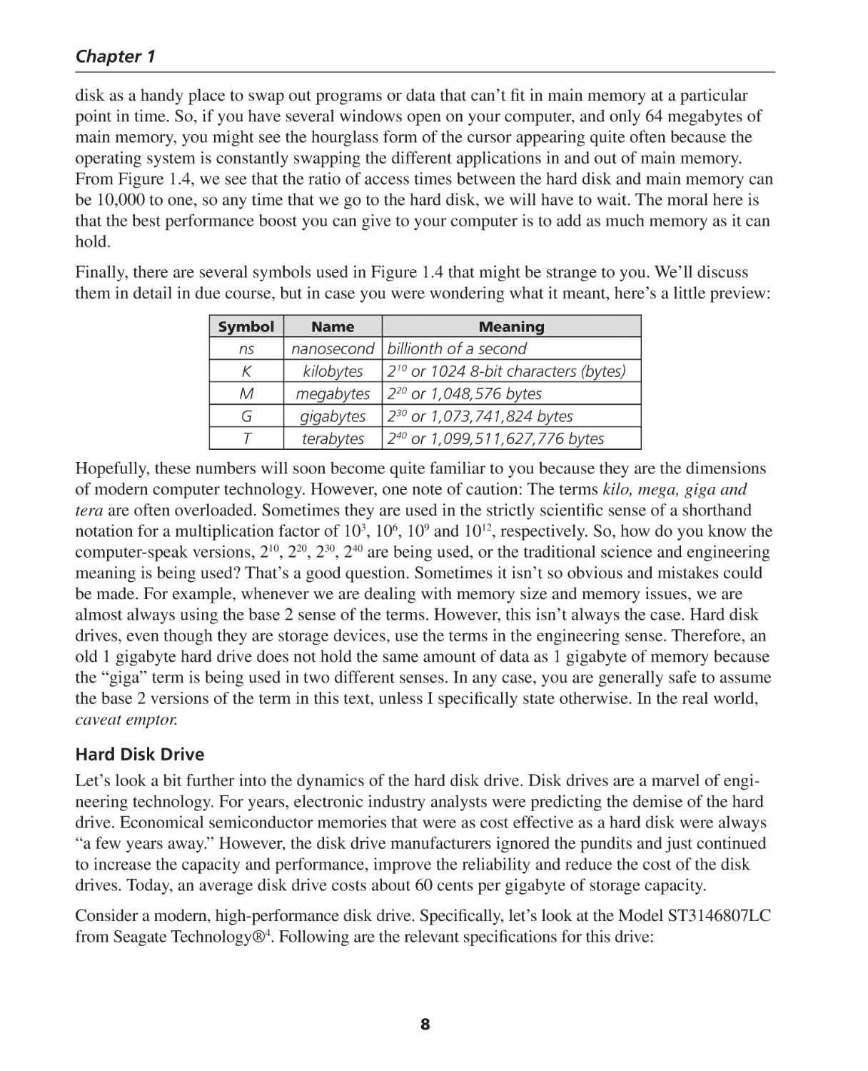
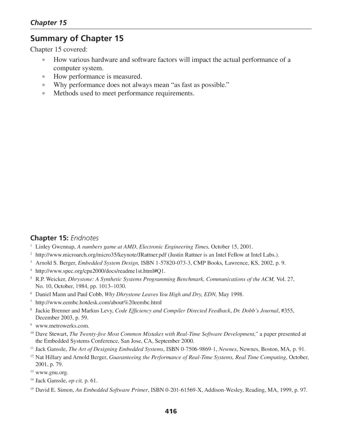
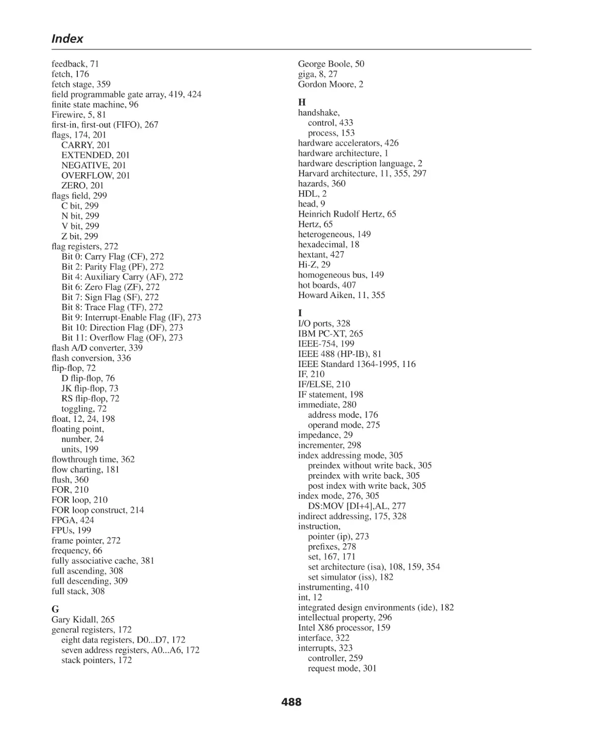
What does all this mean? Consider Figure 1.5. Here we see a highly simplified schematic diagram
of the Seagate Cheetah® disk drive discussed above. The hard disk is comprised of 4 aluminum
platters. Each side of the platter is coated with magnetic material that records the stored data.
Above each platter is a tiny magnetic pick-up, or head, that floats above the disk platter (disc) on
a cushion of air. In a very real sense, the head is flying over the surface of the platter, a distance
much less than the thickness of a human hair. Thus, when you get a disk crash, the results are quite
analogous to when an airplane crashes. In either case, the airplane or the read/write head loses
lift and hits the ground or the surface of the disk. When that happens, the magnetic material is
scrapped away and the disk is no longer usable.
TRACK 49854
10,000 RPM
TRACK 0
HEAD 0
HEAD 7
CYLINDER
.35/.55 track-to-track
Figure 1.5: Schematic diagram of the Seagate Cheetah® hard disk drive.
Each surface contains 49855 concentric tracks. Each track is discreet. It is not connected to the
adjacent track, as a spiral. Thus, in order to move from one track to an adjacent track, the head
must physically move a slight amount. All heads are connected to a common shaft that can quickly
and accurately rotate the heads to a new position. Since the tracks on all the surfaces are in vertical
alignment, we call this a cylinder. Thus, cylinder 0 contains 8 tracks from the 4 platters.
Now, how do we get a 146.8 Gbyte drive? First, each platter contains two surfaces and we have
four platters, so that the total capacity of the drive will be 8 times the capacity of one surface. Each
9
Chapter 1
sector holds 512 bytes of data. By dividing the total number of sectors by 8, we see that there are
35,843,686 sectors per surface. Dividing again by 49855, we see that there are approximately 719
sectors per track. It is interesting that the actual number is 718.96 sectors per track. Why isn’t this
value a whole number? In other words, how can we have a fractional number of sectors per track?
There are a number of possibilities and we need not dwell on it. However, one possibility is that
the number of sectors per track is not uniform across the disk surface because the sector spacing
changes as we move from the center of the disk to the outside. In a CD-ROM or DVD drive this
is corrected by changing the rotational speed of the drive as the laser moves in and out. But, since
the hard disk rotates at a fixed rate, changing the recording density as we move from inner to outer
tracks makes the most sense.
Anyway, back to our calculation. If each track holds 719 sectors and each sector is 512 bytes,
then each track holds 368,128 bytes of data. Since there are 8 tracks per cylinder, each cylinder
holds 2,945,024 bytes. Now, here’s where the big numbers come in. Since we have 49855 cylinders, our total capacity is 146,824,171,520 bytes, or 146.8 Gbytes.
Before we leave the subject of disk drives, let’s consider one more issue. Considering the hard
drive specifications, above, we see that access times are measured in units of milliseconds (msec),
or thousandths of a second. Thus, if your data sectors are spread out over the disk, then accessing
each block of 512 bytes can easily take seconds of time. Comparing this to the time required to
access data stored in main memory, it is easy to see why the hard drive is 10,000 times slower than
main memory.
Complex Instruction Set Architecture, and RISC
or Reduced Instruction Set Computer
Today we have two dominant computer architectures, complex instruction set architecture or CISC
and reduced instruction set computer, or RISC. CISC is typified by what is referred to as the von
Neumann Architecture, invented by John von Neumann of Princeton University. In the von Neumann architecture, both the instruction memory and the data memory share the same physical
memory space. This can lead to a condition called the von Neumann bottleneck, where the same external address and data busses must serve double duty, transferring instructions from memory to the
processor for program execution, and moving data to and from memory for the storage and retrieval
of program variables.
When the processor is moving data, it can’t fetch the next instruction, and vice versa. The solution to this dilemma, as we shall see
later, is the introduction of separate on-chip instruction and data
caches. Motorola’s 68000 processor and its successors, and Intel’s
8086 processor and its successors are all characteristic of CISC
processors. We’ll take a more in-depth look at the differences
between CISC and RISC processors again later when we study
pipelining.
10
Note: You will often see the
processor represented as 80X86,
or 680X0. The “X” is used as
a placeholder to represent a
member of a family of devices.
Thus, the 80X86 (often written as
X86) represents the 8086, 80186,
80286, 80386, 80486 and 80586
(the designation of the first Pentium processor). The Motorola
processors are the 68000, 68010,
68020, 68030, 68040 and 68060.
Introduction and Overview of Hardware Architecture
Howard Aiken of Harvard University designed an alternate computer architecture that we commonly associate today with the Reduced Instruction Set Computer, or RISC architecture. The
classic Harvard architecture computer has two entirely separate memory spaces, one for instructions and one for data. A processor with these memories could operate much more efficiently
because data and instructions could be fetched from the computer’s memory when needed, not just
when the busses were available. The first popular microprocessor that used the Harvard Architecture was the Am29000 from AMD. This device achieved reasonable popularity in the early
Hewlett-Packard laser printers, but later fell from favor because designing a computer with two
separate memories was just not cost effective. The obvious performance gain from the two memory spaces was the driving force to inspire the CPU designers to move the memory spaces onto the
chips, in the form of the instruction and data caches that are common in today’s high-performance
microprocessors.
The gains in CPU power are quite evident if we look at advances in workstation performance over
the past few years. It is interesting that just four years later, a high-end PC, such as a 2.4 GHz
Pentium 4 from Intel could easily outperform the DEC Alpha 21264/600 workstation.
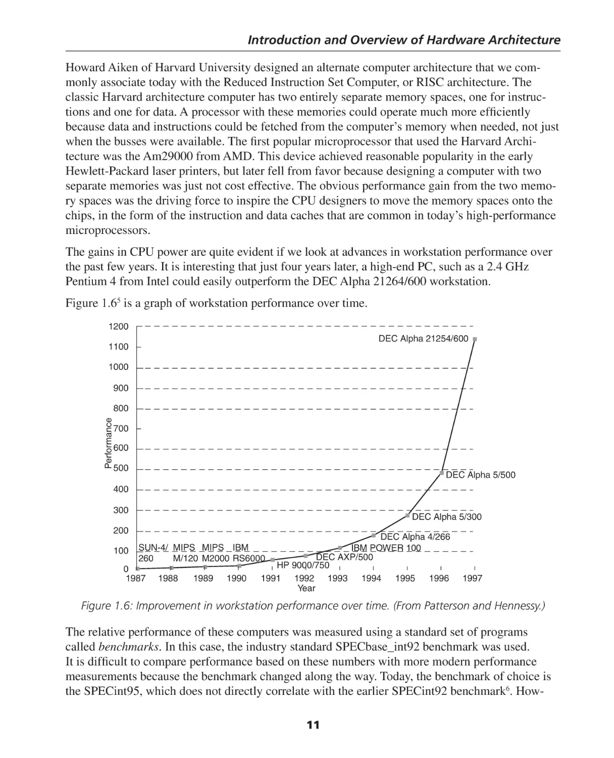
Figure 1.65 is a graph of workstation performance over time.
1200
DEC Alpha 21254/600
1100
1000
900
Performance
800
700
600
500
DEC Alpha 5/500
400
300
DEC Alpha 5/300
200
100
DEC Alpha 4/266
IBM POWER 100
DEC AXP/500
HP 9000/750
1991 1992 1993
1994
1995
1996
Year
SUN-4/ MIPS MIPS IBM
260
M/120 M2000 RS6000
0
1987
1988
1989
1990
1997
Figure 1.6: Improvement in workstation performance over time. (From Patterson and Hennessy.)
The relative performance of these computers was measured using a standard set of programs
called benchmarks. In this case, the industry standard SPECbase_int92 benchmark was used.
It is difficult to compare performance based on these numbers with more modern performance
measurements because the benchmark changed along the way. Today, the benchmark of choice is
the SPECint95, which does not directly correlate with the earlier SPECint92 benchmark6. How11
Chapter 1
ever, according to Mann, a conversion factor of about 38 allows for a rough comparison. Thus,
according to the published results7, a 1.0 GHz AMD Athlon processor achieved a SPECint95
benchmark result of 42.9, which roughly compares to a SPECint92 result of 1630. The Digital
Equipment Corporation (DEC) AlphaStation 5/300 is one workstation that has published results
for both benchmark tests. It measures about 280 in the graph of Figure 1.6 and 7.33 according to
the SPECint95 benchmark. Multiplying by 38, we get 278.5, which is in reasonable agreement
with the earlier result. We’ll return to the issue of performance measurements in a later chapter.
Number Systems
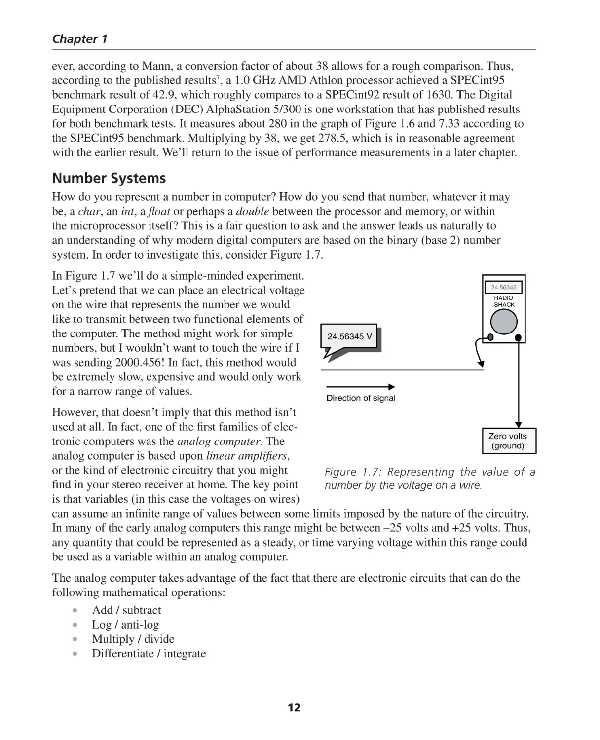
How do you represent a number in computer? How do you send that number, whatever it may
be, a char, an int, a float or perhaps a double between the processor and memory, or within
the microprocessor itself? This is a fair question to ask and the answer leads us naturally to
an understanding of why modern digital computers are based on the binary (base 2) number
system. In order to investigate this, consider Figure 1.7.
In Figure 1.7 we’ll do a simple-minded experiment.
Let’s pretend that we can place an electrical voltage
on the wire that represents the number we would
like to transmit between two functional elements of
the computer. The method might work for simple
numbers, but I wouldn’t want to touch the wire if I
was sending 2000.456! In fact, this method would
be extremely slow, expensive and would only work
for a narrow range of values.
24.56345
RADIO
SHACK
24.56345 V
Direction of signal
However, that doesn’t imply that this method isn’t
used at all. In fact, one of the first families of elecZero volts
tronic computers was the analog computer. The
(ground)
analog computer is based upon linear amplifiers,
or the kind of electronic circuitry that you might
Figure 1.7: Representing the value of a
find in your stereo receiver at home. The key point
number by the voltage on a wire.
is that variables (in this case the voltages on wires)
can assume an infinite range of values between some limits imposed by the nature of the circuitry.
In many of the early analog computers this range might be between –25 volts and +25 volts. Thus,
any quantity that could be represented as a steady, or time varying voltage within this range could
be used as a variable within an analog computer.
The analog computer takes advantage of the fact that there are electronic circuits that can do the
following mathematical operations:
• Add / subtract
• Log / anti-log
• Multiply / divide
• Differentiate / integrate
12
Introduction and Overview of Hardware Architecture
By combining this circuits one after another with intermediate amplification and scaling, real-time
systems could be easily modeled and the solution to complex linear differential equations could be
obtained as the system was operating.
However, the analog computer suffers from the same
limitations as does your stereo system. That is, its
amplification accuracy is not infinitely perfect, so the best
accuracy that could be hoped for is about 0.01%, or about
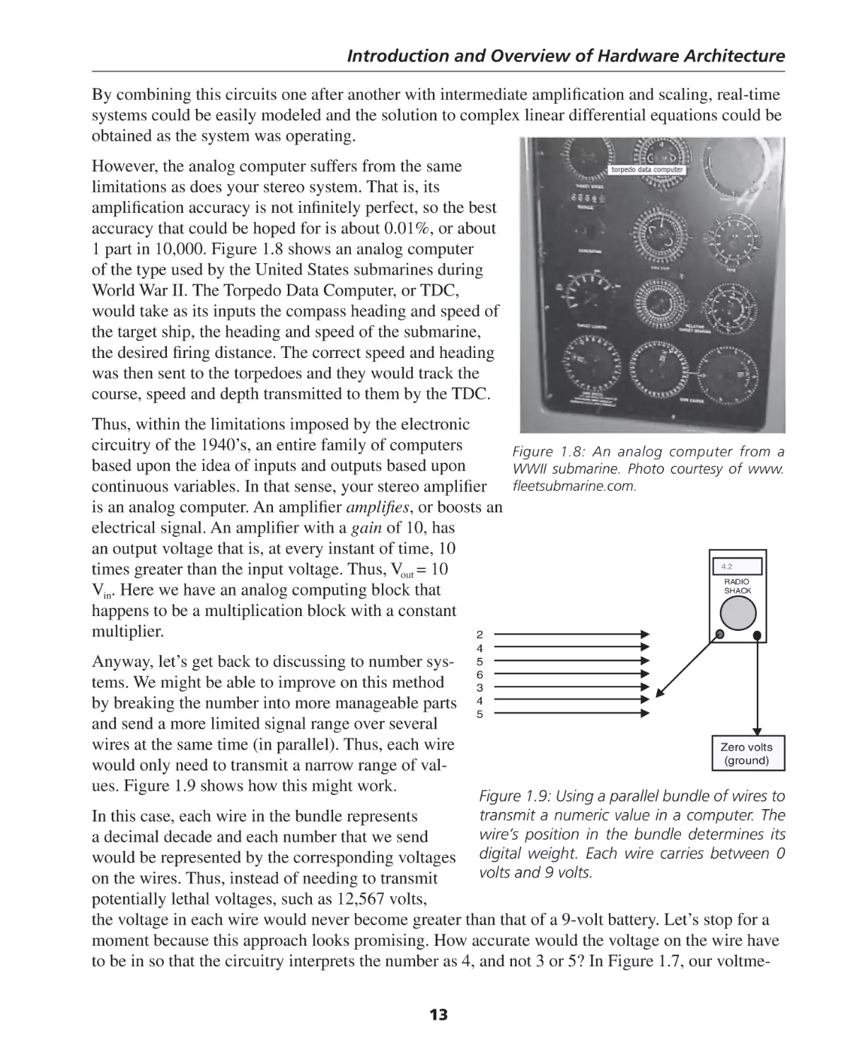
1 part in 10,000. Figure 1.8 shows an analog computer
of the type used by the United States submarines during
World War II. The Torpedo Data Computer, or TDC,
would take as its inputs the compass heading and speed of
the target ship, the heading and speed of the submarine,
the desired firing distance. The correct speed and heading
was then sent to the torpedoes and they would track the
course, speed and depth transmitted to them by the TDC.
Thus, within the limitations imposed by the electronic
circuitry of the 1940’s, an entire family of computers
Figure 1.8: An analog computer from a
based upon the idea of inputs and outputs based upon
WWII submarine. Photo courtesy of www.
continuous variables. In that sense, your stereo amplifier fleetsubmarine.com.
is an analog computer. An amplifier amplifies, or boosts an
electrical signal. An amplifier with a gain of 10, has
an output voltage that is, at every instant of time, 10
4.2
times greater than the input voltage. Thus, Vout = 10
RADIO
SHACK
Vin. Here we have an analog computing block that
happens to be a multiplication block with a constant
multiplier.
2
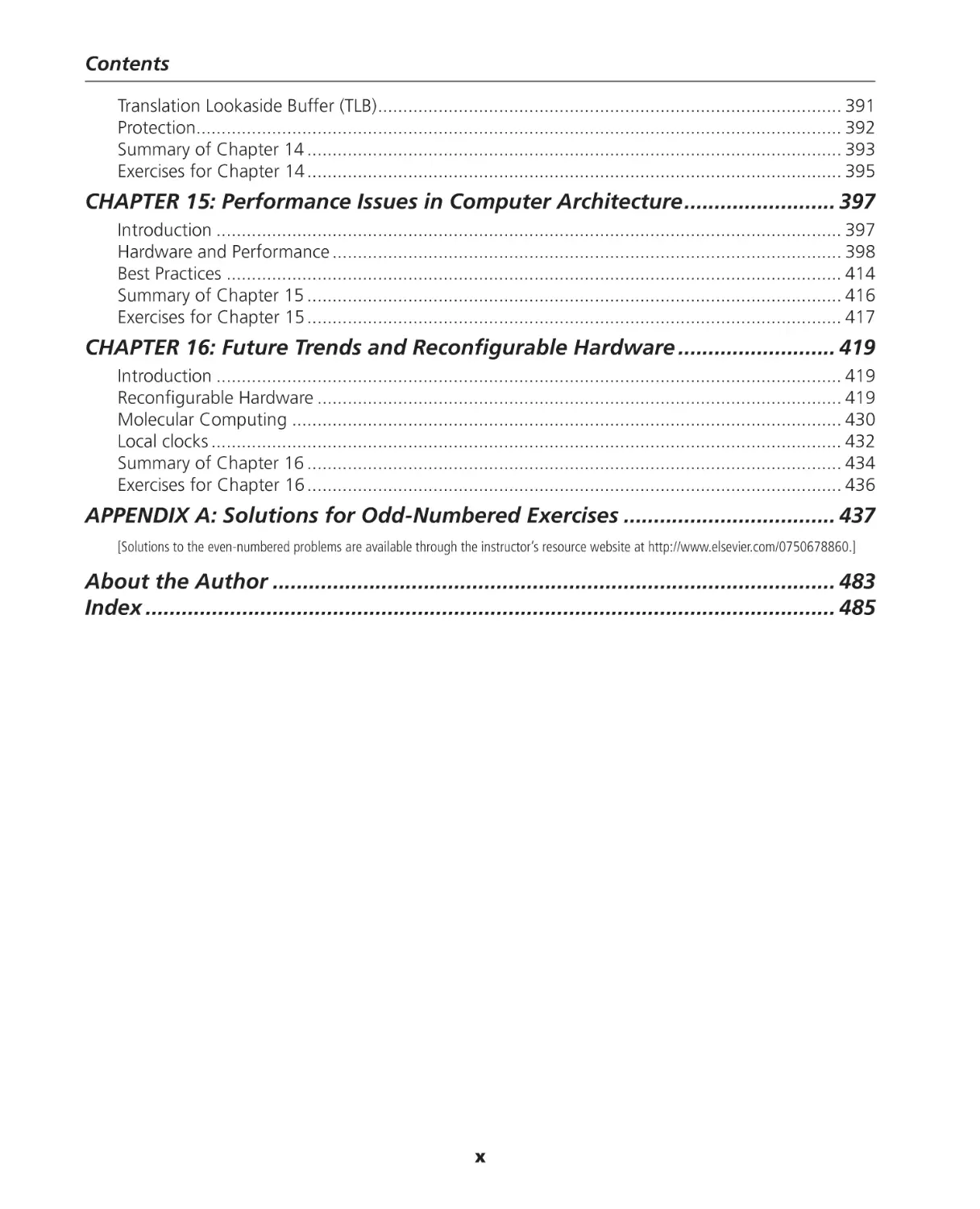
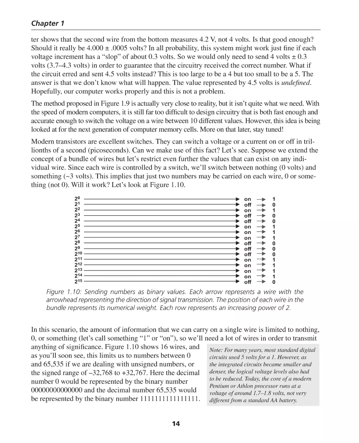
Anyway, let’s get back to discussing to number systems. We might be able to improve on this method
by breaking the number into more manageable parts
and send a more limited signal range over several
wires at the same time (in parallel). Thus, each wire
would only need to transmit a narrow range of values. Figure 1.9 shows how this might work.
4
5
6
3
4
5
Zero volts
(ground)
Figure 1.9: Using a parallel bundle of wires to
transmit a numeric value in a computer. The
In this case, each wire in the bundle represents
wire’s position in the bundle determines its
a decimal decade and each number that we send
would be represented by the corresponding voltages digital weight. Each wire carries between 0
volts and 9 volts.
on the wires. Thus, instead of needing to transmit
potentially lethal voltages, such as 12,567 volts,
the voltage in each wire would never become greater than that of a 9-volt battery. Let’s stop for a
moment because this approach looks promising. How accurate would the voltage on the wire have
to be in so that the circuitry interprets the number as 4, and not 3 or 5? In Figure 1.7, our voltme13
Chapter 1
ter shows that the second wire from the bottom measures 4.2 V, not 4 volts. Is that good enough?
Should it really be 4.000 ± .0005 volts? In all probability, this system might work just fine if each
voltage increment has a “slop” of about 0.3 volts. So we would only need to send 4 volts ± 0.3
volts (3.7–4.3 volts) in order to guarantee that the circuitry received the correct number. What if
the circuit erred and sent 4.5 volts instead? This is too large to be a 4 but too small to be a 5. The
answer is that we don’t know what will happen. The value represented by 4.5 volts is undefined.
Hopefully, our computer works properly and this is not a problem.
The method proposed in Figure 1.9 is actually very close to reality, but it isn’t quite what we need. With
the speed of modern computers, it is still far too difficult to design circuitry that is both fast enough and
accurate enough to switch the voltage on a wire between 10 different values. However, this idea is being
looked at for the next generation of computer memory cells. More on that later, stay tuned!
Modern transistors are excellent switches. They can switch a voltage or a current on or off in trillionths of a second (picoseconds). Can we make use of this fact? Let’s see. Suppose we extend the
concept of a bundle of wires but let’s restrict even further the values that can exist on any individual wire. Since each wire is controlled by a switch, we’ll switch between nothing (0 volts) and
something (~3 volts). This implies that just two numbers may be carried on each wire, 0 or something (not 0). Will it work? Let’s look at Figure 1.10.
20
21
22
23
24
25
26
27
28
29
210
211
212
213
214
215
on
off
on
off
off
on
on
on
off
off
off
on
on
on
on
off
1
0
1
0
0
1
1
1
0
0
0
1
1
1
1
0
Figure 1.10: Sending numbers as binary values. Each arrow represents a wire with the
arrowhead representing the direction of signal transmission. The position of each wire in the
bundle represents its numerical weight. Each row represents an increasing power of 2.
In this scenario, the amount of information that we can carry on a single wire is limited to nothing,
0, or something (let’s call something “1” or “on”), so we’ll need a lot of wires in order to transmit
anything of significance. Figure 1.10 shows 16 wires, and Note: For many years, most standard digital
as you’ll soon see, this limits us to numbers between 0
circuits used 5 volts for a 1. However, as
the integrated circuits became smaller and
and 65,535 if we are dealing with unsigned numbers, or
the signed range of –32,768 to +32,767. Here the decimal denser, the logical voltage levels also had
to be reduced. Today, the core of a modern
number 0 would be represented by the binary number
Pentium or Athlon processor runs at a
00000000000000 and the decimal number 65,535 would
voltage of around 1.7–1.8 volts, not very
be represented by the binary number 1111111111111111. different from a standard AA battery.
14
Introduction and Overview of Hardware Architecture
Now we’re finally there. We’ll take advantage of the fact that electronic switching elements, or
transistors, can rapidly switch the voltage on a wire between two values. The most common form
of this is between almost 0 volts and something (about 3 volts). If our system is working properly,
then what we define as “nothing”, or 0, might never exceed about ½ of a volt. So, we can define
the number 0 to be any voltage less than ½ volt (actually, it is usually 0.4 volts). Similarly, if the
number that we define as a 1, would never be less than 2.5 volts, then we have all the information
we need to define our number system. Here, the number 0 is never greater than 0.4 volts and the
number 1 is never less than 2.5 volts. Anything between these two ranges is considered to be undefined and is not allowed.
It should be mentioned that we’ve been referring to “the voltage on a wire.” Just where are
the wires in our computer? Strictly speaking,
we should call the wires “electrical conductors.”
They can be real wires, such as the wires in the
cable that you connect from your printer to the
parallel port on the back of your computer. They
can also be thin conducting paths on printed circuit boards within your computer. Finally, they
can be tiny aluminum conductors on the processor chip itself. Figure 1.11 shows a portion of a Figure 1.11: Printed wires on a computer circuit board.
printed circuit board from a computer designed Each wire is actual a copper trace approximately 0.08
mm wide. Traces can be as close as 0.08 mm apart
by the author.
from each other. The large spots are the soldered
Notice that some of the integrated circuit’s
pins of the integrated circuits coming through from
(ICs) pins appear have wires connecting them to the other side of the board.
another device while others seem to be unconnected. The reason for this is that this printed circuit board is actually a sandwich made up of five
thinner layers with wires printed on either side, giving a total of ten layers. The eight inner layers
also have a thin insulating layer between then to prevent electric short circuits. During the manufacturing process, the five conducting layers and the four insulating layers are carefully aligned and
bonded together. The resultant, ten-layer printed circuit board is approximately 2.5 mm thick.
Without this multilayer manufacturing technique, it would be impossible to build complex computer systems because it would not be possible to connect the wires between components without
having to cross a separate wire with a different purpose.
[NOTE: A color version of the following figure is included on the DVD-ROM.] Figure 1.12 shows
us just what’s going on with the inner layers. Here is an X-ray view of another computer system
hardware circuit. This is about the same level of complexity that you might find on the motherboard of your PC. The view is looking through the layers of the board and the conductive traces on
each layer are shown in a different color.
While this may appear quite imposing, most of the layout was done using computer-aided design
(CAD) software. It would take altogether too much time for even a skilled designer to complete
the layout of this board. Figure 1.13 is a magnification of a smaller portion of Figure 1.12. Here
15
Chapter 1
you can clearly see the various traces on the different layers. Each printed wire is approximately
0.03 mm wide.
[NOTE: A color version of the following figure is
included on the DVD-ROM.] If you look carefully
at Figure 1.13, you’ll notice that certain colored
wires touch a black dot and then seem to go off in
another direction as a wire of a different color. The
black dots are called vias, and they represent places
in the circuit where a wire leaves its layer and traverses to another layer. Vias are vertical conductors
that allow signals to cross between layers. Without
vias, wires couldn’t cross each other on the board
without short circuiting to each other. Thus, when
you see a green wire (for purposes of the grayscale
image on this page, the green wire appears as a dotted line) crossing a red wire, the two wires are not
in physical contact with other, but are passing over
each other on different layers of the board. This is
an important concept to keep in mind because we’ll
soon be looking at, and drawing our own electronic Figure 1.12: An X-ray view of a portion of a
circuit diagrams, called schematic diagrams, and
computer systems board.
we’ll need to keep in mind how to represent wires
that appear to cross each other without being physically connected, and those wires that are connected
to each other.
Let’s review what we’ve just discussed. Modern digital computers use the binary (base 2) number system.
They do so because a number system that has only
two digits in its natural sequence of numbers lends
itself to a hardware system which utilizes switches
to indicate if a circuit is in a “1” state (on) or a “0”
state (off). Also, the fundamental circuit elements
that are used to create complex digital networks
are also based on these principles as logical expressions. Thus, just as we might say, logically, that an
expression is TRUE or FALSE, we can just as easily
Figure 1.13: A magnified view of a portion of the
describe it as a “1” (TRUE) or “0” (FALSE). As
you’ll soon see, the association of 1 with TRUE and board shown in Figure 1.12.
0 with FALSE is completely arbitrary, and we may reverse the designations with little or no ill effects.
However, for now, let’s adopt the convention that a binary 1 represents a TRUE or ON condition, and a
binary 0 represents a FALSE or OFF condition. We can summarize this in the following table:
16
Introduction and Overview of Hardware Architecture
Binary Value Electrical Circuit Value
0
1
OFF
ON
Logical Value
FALSE
TRUE
A Simple Binary Example
Since you have probably never been exposed to electrical circuit diagrams, let’s dive right in.
Figure 1.14 is a simple schematic diagram of a circuit containing a battery, two switches, labeled
A and B, and a light bulb, C. The positive terminal on the battery is labeled with the plus (+) sign
and the negative battery terminal is labeled with the minus (–) sign. Think of a typical AA battery
that you might use in your portable MP3 player. The little bump on the end is the positive terminal
and the flat portion on the opposite end is the negative terminal. Referring to Figure 1.11, it might
seem curious that the positive terminal is drawn as a wide line, and the negative terminal is drawn
as a narrow line. There’s a reason for it, but we won’t discuss that here. Electrical Engineering
students are taught the reason for this during their initiation ceremony, but I’m sworn to secrecy.
+
A
B
C
C = A and B
-
Battery Symbol
Lightbulb (load)
Figure 1.14: A simple circuit using two switches in series to represent the AND function.
The light bulb, C, will illuminate when enough current flows through it to heat the filament. We
assume that in electrical circuits such as this one, that current flows from positive to negative.
Thus, current exits the battery at the + terminal and flows through the closed switches (A and B),
then through the lamp, and finally to the – terminal of the battery. Now, you might wonder about
this because, as we all know from our high school science classes, that electrical current is actually made up of electrons and electrons, being negatively charged, actually flow from the negative
terminal of the battery to the positive terminal; the reverse direction.
The answer to this apparent paradox is historical precedent. As long as we think of the current as
being positively charged, then everything works out just fine.
Anyway, in order for current to flow through the filament, two things must happen: switch A must
be closed (ON) and switch B must be closed (ON). When this condition is met, the output variable, C, will be ON (illuminated). Thus, we can talk about our first example of a logical equation:
C = A AND B
This is a very interesting result. We’ve seen two apparently very different consequences of using
switches to build computer systems. The first is that we are lead to having to deal with numbers
as binary (base 2) values and the second is that these switches also allow us to create logical
equations. For now, let’s keep item two as an interesting consequence. We’ll deal with it more
thoroughly in the next chapter. Before we leave Figure 1.14, we should point out that the switches,
A and B, are actuated mechanically. Someone flips the switch to turn it on or off. In general, a
17
Chapter 1
switch is a three-terminal device. There is a control input that determines the signal propagation
between the other two terminals.
Bases
Let’s return to our discussion of the binary number system. We are accustomed to using the decimal (base 10) number system because we had ten fingers before we had an iMAC®. The base (or
radix) of a number system is just the number of distinct digits in that number system. Consider the
following table:
Base 2
Base 8
Base 10
Base 16
0,1
0,1,2,3,4,5,6,7
0,1,2,3,4,5,6,7,8,9
0,1,2,3,4,5,6,7,8,9,A,B,C,D,E,F
Binary
Octal
Decimal
Hexadecimal
Look at the hexadecimal numbers in the table above. There are 16, distinct digits, 0 through 9 and
A through F, representing the decimal numbers 0 through 15, but expressing them in the hexadecimal system.
Now, if you’ve ever had your PC lockup with the “blue screen of death,” you might recall seeing
some funny looking letters and numbers on the screen. That cryptic message was trying to show
you an address value in hexadecimal where something bad has just happened. It may be of little
solace to you that from now on the message on the blue screen will not only tell you that a bad
thing has happened and you’ve just lost four hours of work, but with your new-found insight, you
will know where in your PC’s memory the illegal event took place.
When we write a number in binary, octal decimal or hexadecimal, we are representing the number in exactly the same way, although the number will look quite different to us, depending upon
the base we’re using. Let’s consider the decimal number 65,536. This happens to be 216. Later,
we’ll see that this has special significance, but for now, it’s just a number. Figure 1.15, shows how
each digit of the number, 65,536, represents the column value multiplied by the numerical weight
of the column. The leftmost, or most significant digit, is the number 6. The rightmost, or least
significant digit, also happens to be 6. The column weight of the most significant digit is 10,000
(104) so the value in that column is 6 x 10,000, or 60,000. If we multiply out each column value
••
104
103
102
101
100
6
5
5
3
6
Notice
Noticehow
howeach
eachcolumn
columnisisweighted
weightedby
by
the
value
of
the
base
raised
the value of the base raisedto
tothe
thepower
power
+
6 x 100 =
6
3 x 101 =
30
5 x 102 =
500
5 x 103 =
5000
6 x 104 =
60000
=
65536
Figure 1.15: Representing a number in base 10. Going from right to left, each digit multiplies
the value of the base, raised to a power. The number is just the sum of these multiples.
18
Introduction and Overview of Hardware Architecture
and then arrange them as a list of numbers to be added together, as we’ve done on the right side of
Figure 1.15, we can add them together and get the same number as we started with. OK, perhaps
we’re overstating the obvious here, but stay tuned, because it does get better. This little example
should be obvious to you because you’re accustomed to manipulating decimal numbers. The key
point is that the column value happens to be the base value raised to a power that starts at 0 in the
rightmost column and increases by 1 as we move to the left. Since decimal is base 10, the column
weights moving leftward are 1, 10, 100, 1000, 10000 and so on.
If we can generalize this method of representing number, then it follows that we would use the
same method to represent numbers in any other base.
Translating Numbers Between Bases
Let’s repeat the above exercise, but this time we’ll use a binary number. Let’s consider the 8-bit
binary number 10101100. Because this number has 8 binary numbers, or bits associated with it,
we call it an 8-bit number. It is customary to call an 8-bit binary number a byte (in C or C++ this
is a char). It should now be obvious to you why binary numbers are all 1’s and 0’s. Aside from the
fact that these happen to be the two states of our switching circuits (transistors) they are the only
numbers available in a base 2 number system.
The byte is perhaps most notable because we measure storage capacity in byte-size chunks (sorry).
The memory in your PC is probably at least 256 Mbytes (256 million bytes) and your hard disk
has a capacity of 40 Gbytes (40 billion bytes), or more.
Consider Figure 1.16. We use the same method as we used in the decimal example of Figure 1.15.
However, this time the column weight is a multiple of base 2, not base 10. The column weights
go from 27, or 128, the most significant digit, down to 20, or 1. Each column is smaller by a power
of 2. To see what this binary number is in decimal, we use the same process as we did before; we
multiply the number in the column by the weight of the column.
Bases of Hex and Octal
1
0
1
0
1
1
0
0
x
x
x
x
x
x
x
x
27
26
25
24
23
22
21
20
= 128
=
0
=
32
=
0
=
8
=
4
=
0
=
0
128
64
32
16
8
4
2
1
27
26
25
24
23
22
21
20
1
0
1
0
1
1
0
0
10101100 2
=
172 10
172
Figure 1.16: Representing a binary number in terms of the powers of the base 2. Notice that
the bases of the octal (8) and hexadecimal (16) number systems are also powers of 2.
19
Chapter 1
Thus, we can conclude that the decimal number 172 is equal to the binary number 10101100. It is
also noteworthy that the bases of the hexadecimal (Hex) number system, 16 and the octal number
system, 8, are also 24 and 23, respectively. This might give you a hint as to why we commonly use
the hexadecimal representation and the less common octal representation instead of binary when
we are dealing with our computer system. Quite simply, writing binary numbers gets extremely
tedious very quickly and is highly prone to human errors.
To see this in all of its stark reality, consider the binary equivalent of the decimal value:
2,098,236,812
In binary, this number would be written as:
1111101000100001000110110001100
Now, binary numbers are particularly easy to convert to decimal by this process because the
number is either 1 or 0. This makes the multiplication easy for those of us who can’t remember the
times tables because our PDA’s have allowed significant portions of our cerebral cortex to atrophy.
Since there seems to be a connection between the bases 2, 8 and 16, then it is reasonable to assume
that converting numbers between the three bases would be easier than converting to decimal, since
base 10 is not a natural power of base 2. To see how we convert from binary to octal consider
Figure 1.17.
82
26 (21
81
20 ) 23( 22
80
21
20 ) 20 ( 22
21
20)
128
64
32
16
8
4
2
1
27
26
25
24
23
22
21
20
1
0
1
0
1
1
0
0
0 thru 192
0 thru 56
4 x 80 =
4
5 x 8 1 = 40
2 x 8 2 = 128
172
0 thru 7
Figure 1.17: Translating a binary number into an octal number. By factoring
out the value of the base, we can combine the binary number into groups of
three and write down the octal number by inspection.
Figure 1.17 takes the example of Figure 1.16 one step further. Figure 1.17 starts with the same
binary number, 10101100, or 172 in base 10. However, simple arithmetic shows us that we can
factor out various powers of 2 that happen to also be powers of 8. Consider the dark gray highlighted stripe in Figure 1.17. We can make the following simplifications.
Since any number to the 0 power = 1,
(22 21 20 ) = 20 × (22 21 20 )
20
Introduction and Overview of Hardware Architecture
Thus,
20 = 80 = 1
We can perform the same simplification with the next group of three binary numbers:
(25 24 23 ) = 23 × (22 21 20 )
since 23 is a common factor of the group.
However, 23 = 81, which is the column weight of the next column in the octal number system.
If we repeat this exercise one more time with the final group of two numbers, we see that:
(27 26 ) = 26 × (21 20 )
since 26 is a common factor of the group. Again, 26 = 82, which is just the column weight of the
next column in the octal number system.
Since there is this natural relationship between base 8 and base 2, it is very easy to translate numbers
between the bases. Each group of three binary numbers, starting from the right side (least significant
digit) can be translated to an octal digit from 0 to 7 by simply looking at the binary value and writing
down the equivalent octal value. In Figure 1.14, the rightmost group of three binary numbers is 100.
Referring to the column weights this is just 1 * (1 * 4 + 0 * 2 + 0 * 1), or 4. The middle group of
three gives us 8 * (1 * 4 + 0 * 2 + 1 * 1), or 8 * 5 (40). The two remaining numbers gives us 64 *
(1 * 2 + 0 * 1) or 128. Thus, 4 + 40 + 128 = 172, our binary number from Figure 1.8. But where’s
the octal number? Simple, each group of three binary numbers gave us the column value of the
octal digit, so our binary number is 254. Therefore, 10101100 in binary is equal to 254 in octal,
which equals 172 in decimal.
Neat! Thus, we can convert between binary and octal as follows:
• If the number is in octal, write each octal digit in terms of three binary digits. For example:
256773 = 10 101 110 111 111 011
• If the number is in binary, then gather the binary digits into groups of three, starting from
the least significant digit and write down the octal (0 through 7) equivalent. For example:
1100010101001101112 = 110 001 010 100 110 111 = 6124678
• If the most significant grouping of binary digits has only 1 or 2 digits remaining, just pad
the group with 0’s to complete a group of three for the most significant octal digit.
Today, octal is not as commonly used as it once was, but you will still see it used occasionally. For
example, in the UNIX (Linux) command chmod 777, the number 777 is the octal representation of the individual bits that define file status. The command changes the file permissions for the
users who may then have access to the file.
We can now extend our discussion of the relationship between binary numbers and octal numbers
to consider the relationship between binary and hexadecimal. Hexadecimal (hex) numbers are converted to and from binary in exactly the same way as we did with octal numbers, except that now
we use 24, as the common factor rather than 23. Referring to Figure 1.18, we see the same process
for hex numbers as we used for octal.
21
Chapter 1
161
24(23
128
27
1
22
64
26
0
160
21
20)
20 ( 23
22
21
20 )
32
16
8
4
2
1
25
24
23
22
21
20
1
0
1
1
0
0
Figure 1.18: Converting a binary number to base 16 (hexadecimal). Binary
numbers are grouped by four, starting from the least significant digit, and the
hexadecimal equivalent is written down by inspection.
In this case, we factor out the common power of the base, 24, and we’re left with a repeating group
of binary numbers with column values represented as
23 22 21 20
It is simple to see that the binary number 1111 = 1510, so groups of four binary digits may be
used to represent a number between 0 and 15 in decimal, or 0 through F in hex. Referring back to
Figure 1.16, now that we know how to do the conversion, what’s the hex equivalent of 10101100?
Referring to the leftmost group of 4 binary digits, 1010, this is just 8 + 0 + 2 + 0, or A. The rightmost group, 1100 equals 8 + 4 + 0 + 0, or C. Therefore, our number in hex is AC.
Let’s do a 16-bit binary number conversion example.
Binary number:
0101111111010111
Octal:
Hex:
Decimal:
0 101 111 111 010 111 = 057727 (grouped by threes)
0101 1111 1101 0111 = 5FD7 (grouped by fours)
To convert to decimal, see below:
Octal to Decimal
Hex to Decimal
7 × 80 = 7
2 × 81 = 16
7 × 82 = 448
7 × 83 = 3584
5 × 84 = 20480
24,535
7 × 160 = 7
13 × 161 = 208
15 × 162 = 3840
5 × 163 = 20480
24,535
Definitions
Before we go full circle and consider the reverse process, converting from decimal to hex, octal and
binary, we should define some terms. These terms are particular to computer numbers and give us
a shorthand way to represent the size of the numbers that we’ll be working with later on. By size,
we don’t mean the magnitude of the number, we actually mean the number of binary bits that the
number refers to. You are already familiar with this concept because most compilers require that you
declare the type of a variable before you can use it. Declaring the type really means two things:
22
Introduction and Overview of Hardware Architecture
1. How much storage space will this variable occupy, and
2. What type of assembly language algorithms must be generated to manipulate this number?
The following table summarizes the various groupings of binary bits and defines them.
bit
nibble
byte
The simplest binary number is 1 digit long
A number comprised of four binary bits. A NIBBLE is also one hexadecimal digit
Eight binary bits taken together form a byte. A byte is the fundamental unit of measuring storage capacity in computer memories and disks. The byte is also equal to a
char in C and C++.
word
A word is 16 binary bits in length. It is also 4 hex digits in length or 2 bytes in length.
This will become more important when we discuss memory organization. In C or C++,
a word is sometimes called a short.
long word
Also called a LONG, the long word is 32 binary bits or 8 hex digits. Today, this is an int
in C or C++.
double word Also called DOUBLE, the double word is 64 binary bits in length, or 16 hex digits.
From the table you may get a clue as to why the octal number representation has been mostly supplanted by hex numbers. Since octal is formed by groups of three, we are usually left with those
pesky remainders to deal with. We always seem to have an extra 1, 2, or 3 as the most significant
octal digit. If the computer designers had settled on 15 and 33 bits for the bus widths instead of
16 and 32 bits, perhaps octal would still be alive and kicking. Also, hexadecimal representation is
a far more compact way of representing number, so it has become today’s standard. Figure 1.19
summarizes the various sizes of data elements as they stand today and as they’ll probably be in the
near future.
Bit (1)
Today we already have
D3
D0
computers that can maNibble (4)
nipulate 64-bit numbers
in one operation. The
D7
D0
Byte (8)
Athlon64® from Advanced
Micro Devices CorporaD15
D0
Word (16)
tion is one such processor.
Another example is the
D31
D0
processor in the Nintendo
Long (32)
N64 Game Cube®. Also,
if you consider yourself a
D63
D0
Double (64)
PC Gamer, and you like
to play fast action video
D127
D0
games on your PC, then
VLIW (128)
you likely have a highperformance video card in Figure 1.19: Size of the various data elements in a computer system.
your game machine. It is
likely that your video card has a video processing computer chip on it that can process 128 bits at
a time. Is a 256-bit processor far behind?
23
Chapter 1
Fractional Numbers
We deal with fractions in the same manner as we
deal with whole numbers. For example, consider
Figure 1.20.
102
101
100
5
6
7
.
10−1
10−2
10−3
10−4
4
3
2
1
Figure 1.20: Representing a fractional number
in base 10.
We see that for a decimal number, the columns to
the right of the decimal point go in increasing negative powers of ten. We would apply the same
methods that we just learned for converting between bases to fractional numbers. However, having
said that, it should be mentioned that fractional numbers are not usually represented this way in a
computer. Any fractional number is immediately converted to a floating point number, or float. The
floating-point numbers have their own representation, typically as a 64-bit value consisting of a
mantissa and an exponent. We will discuss floating point numbers in a later chapter.
Binary-Coded Decimal
There’s one last form of binary number representation that we should mention in passing, mostly
for reasons of completeness. In the early days of computers when there was a transition taking
place from instrumentation based on digital logic, but not truly computer-based, as they are today,
it was convenient to represent numbers in a form called binary coded decimal, or BCD. A BCD
number was represented as 4 binary digits, just like a hex number, except the highest number in
the sequence is 9, rather than F. Devices like counters and meters used BCD because it was a convenient way to connect a digital value to some sort of a display device, like a 7-segment display.
Figure 1.21 shows the digits of a seven-segment display.
The seven-segment display consists of 7 bars and usually also contains a decimal point and each of
the elements is illuminated by a light emitting diode (LED). Figure 1.21 shows how the 7-segment
display can be used to show the numbers 0 through 9. In fact, with a little creativity, it can also
show the hexadecimal numbers A through F.
BCD was an easy way to convert digital counters and voltmeters to an easy to read display.
Imagine what your reaction would be if
the Radio Shack® voltmeter read 7A volts,
instead of 122 volts. Figure 1.21 shows
what happens when we count in BCD. The
numbers that are displayed make sense to
0100
0101
0000
0001
0010
0011
us because they look like decimal digits.
carry
the
When the count reaches 1001 (9), the next
one
increment causes the display to roll around
to 0 and carry a 1, instead of displaying A.
0001
0000
0110
0111
1000
1001
Many microprocessors today still contain
vestiges of the transition period from BCD
Figure 1.21: Binary coded decimal (BCD) number
to hex numbers by containing special
representation. When the number exceeds the count
instructions, such as decimal add adjust, that of 9, a carry operation takes place to the next most
are used to create algorithms for implement- significant decade and the binary digits roll around
to zero.
ing BCD arithmetic.
24
Introduction and Overview of Hardware Architecture
Converting Decimals to Bases
Converting a decimal number to binary, octal or hex is a bit more involved because base 10 does
not have a natural relationship to any of the other bases. However, it is a rather straightforward
process to describe an algorithm to use to translate a number in decimal to another base. For example, let’s convert the decimal number, 38,070 to hexadecimal.
1. Find the largest value of the base (in this case 16), raised to an integer power that is still
less than the number that you are trying to convert. In order to do the conversion, we’ll
need to refer to the table of powers of 16, shown below. From the table we see that the
number 38,070 is greater than 4,096 but less than 65,536. Therefore, we know that the
largest column value for our conversion is 163.
160 = 1
164 = 65,536
161 = 16
165 = 1,048,576
162 = 256
166 = 16,777,216
163 = 4096
167 = 268,435,456
2. Perform an integer division on the number to convert:
a. 38,070 DIV 4096 = 9
b. 38,070 MOD 4096 = 1206
3. The most significant hex digit is 9. Repeat step 1 with the MOD (remainder) from step 1.
256 is less than 1206 and 4096 is greater than 1206.
a. 1206 DIV 256 = 4
b. 1206 MOD 256 = 182
4. The next most significant digit is 4. Repeat step 2 with the MOD from step 2. 182 is
greater than 16 but less than 256.
a. 182 DIV 16 = 11 (B)
b. 4b 182 MOD 16 = 6
5. The third most significant digit is B. We can stop here because the least significant digit is,
by inspection,
6. Therefore: 38,07010 = 94B616
Before we move on to the next topic, logic gates, it is worthwhile to summarize why we did what
we did. It wouldn’t take you very long, writing 32-bit numbers down in binary, to realize that
there has to be a better way. There is a better way, hex and octal. Hexadecimal and octal numbers,
because their bases, 16 and 8 respectively, have a natural relationship to binary numbers, base 2.
We can simplify our number manipulations by gathering the binary numbers into groups of three
or four. Thus, we can write a 32-bit binary value such as 10101010111101011110000010110110
in hex as AAF5E0B6.
However, remember that we are still dealing with binary values. Only the way we choose to represent these numbers is different. As you’ll see shortly, this natural relationship between binary and
hex also extends to arithmetic operations as well. To prove this to yourself, perform the following
hexadecimal addition:
0B + 1A = 25 (Remember, that’s 25 in hex, not decimal. 25 in hex is 37 in decimal.)
Now convert 0B and 1A to binary and perform the same addition. Remember that in binary
1 + 1 = 0, with a carry of 1.
25
Chapter 1
Since it is very easy to mistake numbers in hex, binary and octal, assemblers and compilers allow
you to easily specify the base of a number. In C and C++ we represent a hex number, such as
AA55, by 0xAA55. In assembly language, we use the dollar sign. So the same number in assembly language is $AA55. However, assembly language does not have a standard, such as ANSI C,
so different assemblers may use different notation. Another common method is to precede the hex
number with a zero, if the most significant digit is A through F, and append an “H” to the number.
Thus $AA55 could be represented as 0AA55H by a different vendor’s assembler.
Engineering Notation
While most students have learned the basics of using scientific notation to represent numbers
that are either very small or very large, not everyone has also learned to extend scientific notation
somewhat to simplify the expression of many of the common quantities that we deal with in digital
systems. Therefore, let’s take a very brief detour and cover this topic so that we’ll have a common
starting point. For those of you who already know this, you may take your bio break about
10 minutes earlier.
Engineering notation is just a shorthand way of representing very large or very small numbers in a
format that lends itself to communication simplicity among engineers. Let’s start with an example
that I remember from a nature program about bats that I saw on TV a number of years. Bats locate
insects in absolute blackness by using the echoes from ultrasonic sound wave that they emit. An
insect reflects the sound bursts and the bat is able to locate dinner. What I remember is the narrator
saying that the nervous system of the bat is so good at echo location that the bat can discern sound
pulses that arrive less than a few millionths of a second apart. Wow!
Anyway, what does a “few millionths” mean? Let’s say that a few millionths is 5 millionths. That’s
0.000005 seconds. In scientific notation 0.000005 seconds would be written as 5 × 10⁻⁶ seconds.
In engineering notation it would be written as 5 µs, and pronounced 5 microseconds. We use the
Greek symbol, µ (mu) to represent the micro portion of microseconds. What are the symbols that
we might commonly encounter? The table below lists the common values:
TERA
GIGA
MEGA
KILO
=
=
=
=
1012
109
106
103
(T)
(G)
(M)
(K)
PICO = 10-12 (p)
NANO = 10-9 (n)
MICRO = 10-6 (µ)
MILLI = 10-3 (m)
FEMTO = 10-15(f)
So, how do we change a number in scientific notation to an equivalent one in engineering notation? Here’s the recipe:
1. Adjust the mantissa and the exponent so that the exponent is divisible by 3 and the mantissa is not a fraction. Thus, 3.05 × 104 bytes becomes 30.5 × 10³ and not 0.03 × 10⁶.
2. Replace the exponent terms with the appropriate designation. Thus, 30.5 × 103 bytes
becomes 30.5 Kbytes, or 30.5 Kilobytes.
About 99.99% of the time, the unit will be within the exponent range of ±12. However, as computers get ever faster, we will be measuring times in the fractions of a picosecond, so it’s appropriate
26
Introduction and Overview of Hardware Architecture
to include the femtosecond on our table. As an exercise, try to calculate how far light will travel
in one femtosecond, given that light travels at a rate of about 15 cm per nanosecond on a printed
circuit board.
Although we discussed this earlier, it should be mentioned again in this context that we have to be
careful when we use the engineering terms for kilo, mega and giga. That’s a problem that computer folk have created by misappropriating standard engineering notations for their own use. Since
210 = 1024, computer “Geekspeakers” decided that it was just too close to 1000 to let it go, so the
overloaded the K, M and G symbols to mean 1024, 1048576 and 1073741824, respectively, rather
than 1000, 1000000 or 1000000000, respectively.
Fortunately, we rarely get mixed up because the computer definition is usually confined to measurements involving memory size, or byte capacities. Any time that we measure anything else,
such as clock speed or time, we use the conventional meaning of the units.
Summary of Chapter 1
•
•
•
•
•
The growth modern digital computer progressed rapidly, driven by the improvements
made in the manufacturing of microprocessors made from integrated circuits.
The speed of computer memory has an inverse relationship to its capacity. The faster a
memory, the closer it is to the computer core.
Modern computers are based upon two basic designs, CISC and RISC.
Since an electronic circuit can switch on and off very quickly, we can use the binary numbers system, or base 2, to as the natural number system for our computer.
Binary, octal and hexadecimal are the natural number bases of computers and there are
simple ways to convert between them and decimal.
Chapter 1: Endnotes
1
Carver Mead, Lynn Conway, Introduction to VLSI Sysyems, ISBN 0-2010-4358-0, Addison-Wesley,
Reading, MA, 1980.
2
For an excellent and highly readable description of the creation of a new super minicomputer, see The Soul of a New
Machine, by Tracy Kidder, ISBN 0-3164-9170-5, Little, Brown and Company, 1981.
3
Daniel Mann, Private Communication.
4
http://www.seagate.com/cda/products/discsales/enterprise/family/0,1086,530,00.html.
5
David A. Patterson and John L. Hennessy, Computer Organization and Design, Second Edition, ISBN 1-5586-0428-6,
Morgan Kaufmann, San Francisco, CA, p. 30.
6
Daniel Mann, Private Communication.
7
http://www.specbench.org/cgi-bin/osgresults?conf=cint95.
27
Exercises for Chapter 1
1. Define Moore’s Law. What is the implication of Moore’s Law in understanding trends in computer performance? Limit your answer to no more than two paragraphs.
2. Suppose that in January, 2004, AMD announces a new microprocessor with 100 million
transistors. According to Moore’s Law, when will AMD introduce a microprocessor with 200
million transistors?
3. Describe an advantage and a disadvantage of the organization of a computer around abstraction layers.
4. What are the industry standard busses in a typical PC?
5. Suppose that the average memory access time is 35 nanoseconds (ns) and the average access
time for a hard disk drive is 12 milliseconds (ms). How much faster is semiconductor memory
than the memory on the hard drive?
6. What is the decimal number 357 in base 9?
7. Convert the following hexadecimal numbers to decimal:
(a)
(b)
(c)
(d)
0xFE57
0xA3011
0xDE01
0x3AB2
8. Convert the following decimal numbers to binary:
(e)
(f)
(g)
(h)
510
64,200
4,001
255
9. Suppose that you were traveling at 14 furlongs per fortnight. How fast are you going in feet
per second? Express your answer in engineering notation.
28
CHAPTER
2
Introduction to
Digital Logic
Objectives
Learn the electronic circuit basis for digital logic gates;
Understand how modern CMOS logic works;
Become familiar with the basics of logic gates.
Remember the simple battery and flashlight circuit we saw in Figure 1.14? The two on/off
switches, wired as they were in series, implemented the logical AND function. We can express that
example as, “If switch A is closed AND switch B is closed, THEN lamp C will be illuminated.”
Admittedly, this is pretty far removed from your PC, but the logical function implemented by the
two switches in this circuit is one of the four key elements of a modern computer.
It may surprise you to know that all of the primary digital elements of a modern computer, the
central processing unit (CPU), memory and I/O can be constructed from four primary logical
functions: AND, OR, NOT and Tri-State (TS). Now TS is not a logical function, it is actually closer
to an electronic circuit implementation tool. However, without tri-state logic, modern computers
would be impossible to build.
As we’ll soon see, tri-state logic introduces a third logical condition called Hi-Z. “Z” is the electronic symbol for impedance, a measure of the easy by which electrical current can flow in a
circuit. So, Hi-Z, seems to imply a lot of resistance to current flow. As you’ll soon see, this is critical for building our system.
Having said that we could build a computer from the ground up using the four fundamental logic gates:
AND, OR, NOT and TS, it doesn’t necessarily follow that we would build it that way. This is because
engineers will usually take implementation shortcuts in designing more complex functions and these
design efficiencies will tend to blur the distinctions between the fundamental logic elements. However,
it does not diminish the conceptual importance of these four fundamental logical functions.
In writing this, I was struck by the similarity between the DNA molecule and its four nucleotides:
adenine, cytosine, guanine, and thymine; abbreviated, A, C, G and T, and the fact that a computer
can also be described by four “electronic nucleotides.” We shouldn’t look too deeply into this coincidence because the differences certainly far outweigh the similarities. Anyway, it’s fun to imagine
an “electronic DNA molecule” of the future that can be used as a blueprint for replicating itself.
Could there be a science-fiction novel in this somewhere? Anyway, Figure 2.1
29
Chapter 2
Enough of the DNA analogy! Let’s move on. Let
me make one last point before we do leave. The
key point of making the analogy is that everything
that we will be doing from now on in the realm of
digital hardware is based upon these four fundamental logic functions. That may not make it any
easier for you, but that’s where we’re headed.
AND
TS
OR AND
TS
NOT
OR TS
NOT OR
C
G
C
G
A
T
AT
G
AND NOT
C
G
C
TS AND
C
NOT OR
OR
TS
T
AND NOT
NOT TS
G
A T
A
A
T
Figure 2.2 is a schematic diagram of a digital
TA
logic gate, which can execute the logical “AND”
OR TS
G C
AND NOT
C
G
function. The symbol, represented by the label
OR AND
A
T
F(A,B) is the standard symbol that you would use
Figure 2.1: Thinking about a computer built from
to represent an AND gate in the schematic diagram for a digital circuit design. The output, C, is “logical DNA” on the left and schematic picture of
a function of the two binary input variables A and a portion of a real DNA molecule on the right. (DNA
B. A and B are binary variables, but in this circuit molecule picture from the Dolan1 Learning Center,
Cold Springs Harbor Laboratory .)
they are represented by values of voltage. In the
GATE FUNCTION
case of positive logic, where the more
A
positive (higher) voltage is a “1” and the
F(A,B)
C = F(A,B)
less positive (lower) voltage is a “0”, this
B
circuit element is most commonly used
in circuits where a logic “0” is repreOutput signal
Input signals to the gate
from the gate
sented by a voltage in the range of 0 to
0.8 volts and a “1” is a voltage between Figure 2.2: Logical AND gate. The gate is an electronic
approximately 3.0 and 5.0 volts.* From switching circuit that implements the logical AND function
0.8 volts to 3.0 volts is “no man’s land.” for the two input values A and B.
Signals travel through this region very quickly on their way up or down, but don’t dwell there. If a
logic value were to be measured in this region, there would be an electrical fault in the circuit.
G
C
The logical function of Figure 2.2 can be described in several equivalent ways:
• IF A is TRUE AND B is TRUE THEN C is TRUE
• IF A is HIGH AND B is HIGH THEN C is HIGH
• IF A is 1 AND B is 1 THEN C is 1
• IF A is ON AND B is ON THEN C is ON
• IF A is 5 volts AND B is 5 volts THEN C is 5 volts
The last bullet is a little iffy because we allow the values to exist in ranges, rather than absolute
numbers. It’s just easier to say “5 volts” instead of “a range of 3 to 5 volts.”
As we’ve discussed in the last chapter, in a real circuit, A and B are signals on individual wires.
These wires may be actual wires that are used to form a circuit, or they may be extremely fine copper paths (traces) on a printed circuit (PC) board, as in Figure 1.11, or they may be microscopic
paths on an integrated circuit. In all cases, it is a single wire conducting a digital signal that may
take on two digital values: “0” or “1”.
* Assuming that we are using the older 5-volt logic families, rather than the newer 3.3-volt families.
30
Introduction to Digital Logic
The next point that we want to consider is why we call this circuit element a “gate.” You can
imagine a real gate in front of your house. Someone has to open the gate in order to gain entrance.
The AND gate can be thought of in exactly the same way. It is a gate for the passage of the logical
signal. The previous bulleted statements describe the AND gate as a logic statement. However, we
can also describe it this way:
• IF A is 1 THEN C EQUALS B
• IF A is 0 THEN C EQUALS 0
Of course, we could exchange A and B because these inputs are equivalent. We can see this graphically in Figure 2.3. Notice the strange line at inputs B and output C. This is a way to represent a
digital signal that is varying with time. This is called a waveform representation, or a timing diagram. The idea is that the waveform is on some kind of graph paper, such as a strip chart recorder,
and time is changing on the horizontal axis. The vertical axis represents the logical value a point in
the circuit, in this case points B and C.
When A = 1, the same signal appears at output C that is input at B. The change that occurs at C as
a result of the change at B is not instantaneous because the speed of light is finite, and circuits are
not infinitely fast. However, in terms of a human scale, it’s pretty fast. In a typical circuit, if input
B went from a 0 value to a 1, the same change would occur at output C, delayed by about 5 billionths of a second (5 nanoseconds).
You’ve actually seen these timing diagrams before in the context of an EKG (electrocardiogram)
when a physician checks your heart. Each of the signals on the chart represents the electrical voltage at various parts of your heart muscles over time. Time is traveling along the long axis of the
chart and the voltage at any point in time is represented by the vertical displacement of the ink.
Since typical digital signals change much more rapidly than we could see on a strip chart recorder,
we need specialized equipment, such as oscilloscopes and logic analyzers to record the waveforms
and display them for us in a way that we can comprehend. We’ll discuss waveforms and timing
diagrams in the upcoming chapters.
A=1
1
AND
0
C
B
Timing Diagram
A=0
1
0
AND
C
B
Figure 2.3: The logical AND circuit represented as a gating device. When the input A = 1, output C
follows input B (the gate is open). When input A = 0, output C = 0, independent of how input B varies
with time (the gate is closed).
Thus, Figure 2.3 shows us an input waveform at B. If we could get really small, and we had a very
fast stopwatch and a fast voltmeter, we could imagine that we are sitting on the wire connected to
31
Chapter 2
the gate at point B. As the value of the voltage at B changes, we check our watch and plot the voltage versus time on the graph. That’s the waveform that is shown in Figure 2.3.
Also notice that the vertical line that represents the transition from the logic level 0 to the logic level
1. This is called the rising edge. Likewise, the vertical line that represents the transition from logic
level 1 to logic level 0 is called the falling edge. We typically want the time durations of the rising
edge and falling edge to be very small, a few billionths of a second (nanoseconds) because in digital
systems, the space between 0 and 1 is not defined, and we want to get through there as quickly as
possible. That’s not to say that these edges are useless to us. Quite the contrary, they are pretty important. In fact, you’ll see the value of these edges when we study system clocks later on.
If, in Figure 2.3, A = 1 (upper figure), the output at C follows the input at A with a slight time
delay, called the propagation delay, because it represents the time required for the input change to
work its way, or propagate, through the circuit element. When the control input at A = 0, output C
will always equal 0, independent of whatever input B does. Thus, input B is gated by input A. For
now, we’ll leave the timing diagram in the wonderful world of hardware design and return to our
studies of logic gates.
Earlier, we touched on the fact that the AND gate is one of three logic gates. We’ll keep the tristate gate separate for now and study it in more depth when we discuss bus organization in a later
chapter. In terms of “atomic,” or unique elements, there are actually three types of logical gates:
AND, OR and NOT. These are the fundamental building blocks of all the complex digital logic
circuits to follow. Consider Figure 2.4.
A
AND
C=A*B
C
C is TRUE if A is TRUE AND B is TRUE
B
A
OR
B
C=A+B
C
C is TRUE if A is TRUE OR B is TRUE
NEGATION SYMBOL
A
NOT
B
B=A
B is TRUE if A is FALSE
Figure 2.4: The three “atomic” logic gates: AND, OR and NOT.
The symbol for the AND function is the same as the multiplication symbol that we use in algebra.
As well see later on, the AND operation is similar to multiplying two binary numbers, since
1 × 1 = 1 and 1 × 0 = 0. The asterisk is a convenient symbol to use for “ANDing” two variables.
The symbol for the OR function is the plus sign, and it is “sort of” like addition, because 0 + 0 = 0,
1 + 0 = 1. The analogy fails with 1 + 1, because if we’re adding, then 1 + 1 = 0 (carry the 1) but if
we are OR’ing, then 1 + 1 = 1. OK, so they overloaded the + sign. Don’t get angry with me, I’m
only the messenger.
32
Introduction to Digital Logic
The negation symbol takes many forms, mostly because it is difficult to draw a line over a variable
using only ASCII text characters. In Figure 2.4, we use the bar over the variable A to indicate that
the output B is the negation, or opposite of the input A. If A = 1, then B = 0. If A = 0, then B = 1.
Using only ASCII text characters, you might see the NOT symbol written as, B = ~A, or B = /A
with the forward slash or the tilde representing negation. Negation is also called the complement.
The NOT gate also uses a small open circle on the output to indicate negation. A gate with a single
input and a single output, but without the negation symbol is called a buffer. The output waveform
of a buffer always follows the input waveform, minus the propagation delay. Logically there is no
obvious need for a buffer gate, but electrically (those pesky hardware engineers again!) the buffer
is an important circuit element.
We’ll actually return to the concept of the buffer gate when we study analog to digital conversion
in a future lesson. Unlike the AND gate and the OR gate, the NOT gate always has a single input
and a single output. Furthermore, for all of its simplicity, there is no obvious way to show the NOT
gate in terms of a simple flashlight bulb circuit. So we’ll turn our attention to the OR gate.
We can look at the OR gate in the same way we first examined the AND gate. We’ll use our simple
flashlight circuit from Figure 1.14, but this time we’ll rearrange the switches to create the logical
OR function. Figure 2.5 is our flashlight circuit.
Connection between two
wires indicated with a dot
+
B
C
A
C = A OR B
–
Battery Symbol
Lightbulb (load)
Figure 2.5: The logical OR function implemented as two switches in
parallel. Closing either switch A or B turns on the lightbulb, C.
The circuit in Figure 2.5 shows the two switches, A and B wired in parallel. Closing either switch
will allow the current from the battery to flow through the switch into the bulb and turn it on.
Closing both switches doesn’t change the fact that the lamp is illuminated. The lamp won’t shine
any brighter with both switches closed. The only way to turn it off is to open both switches and
interrupt the flow of current to the bulb. Finally, there is a small dot in Figure 2.5 that indicate that
two wires come together and actually make electrical contact. As we’ve discussed earlier, since
our schematic diagram is only two dimensional, and printed circuit boards often have ten layers of
electrical conductors insulated from each other, it is sometimes confusing to see two wires cross
each other and not be physically connected together. Usually when two wires cross each other, we
get lots of sparks and the house goes dark. In our schematic diagrams, we’ll represent two wires
that actually touch each other with a small dot. Any other wires that cross each other we’ll consider to be insulated from each other.
33
Chapter 2
We still haven’t looked at the tri-state logic gate. Perhaps we should, even though the reason for
the gate’s existence won’t be obvious to you now. So, at the risk of letting the cat out of the bag,
let’s look at the fourth member of our atomic group of logic elements, the tri-state logic gate
shown schematically in Figure 2.6.
INPUT
Truth table for bus interface gate
Tri-state logic gate
Logic
Gate
OUTPUT ENABLE OUTPUT
1
0
1
0
0
0
1
1
Hi-Z
0
1
Hi-Z
1 or 0 or Hi-Z
1 or 0
Output Enable
Figure 2.6: The tri-state (TS) logic gate. The output of the gate follows the input along as
the Output Enable (OE) input is low. When the OE input goes high, the output of the gate
enters the Hi-Z state.
There are several important concepts here so we should spend some time on this figure. First, the
schematic diagram for the gate appears to be the same as an inverter, except there is no negation
bubble on the output. That means that the logic sense of the output follows the logic sense of the
input, after the propagation delay. That makes this gate a buffer gate. This doesn’t imply that we
couldn’t have a tri-state gate with a built-in NOT gate, but that would not be atomic. That would be
a compound gate.
The TS gate has a third input, labeled Output Enable. The input on the gate also has a negation
bubble, indicating that the gate is active low. We’ve introduced a new term here. What does “active
low” mean? In the previous chapter, we made a passing reference to the fact that logic levels
were somewhat arbitrary. For convenience, we were going make the more positive voltage a 1, or
TRUE, and the less positive voltage a 0, or FALSE. We call this convention positive logic. There’s
nothing special about positive logic, it is simply the convention that we’ve adopted.
However, there are times when we will want to assign the “TRUENESS” of a logic state to be
low, or 0. Also, there is a more fundamental issue here. Even though we are dealing with a logical
condition, the meaning of the signal is not so clear-cut. There are many instances where the signal
is used as a controlling, or enabling device. Under these conditions, TRUE and FALSE don’t really
apply in the same way as they would if the signal was part of a complex logical equation. This is
the situation we are faced with in the case of a tri-state buffer.
The Output Enable (OE) input to the tri-state buffer is active when the signal is in its low state. In
the case of the TS buffer, when the OE input is low, the buffer is active, and the output will follow
34
Introduction to Digital Logic
the input. Now, at this point you might be getting ready to say, “Whoa there Bucko, that’s an AND
gate. Isn’t it?” and you’d almost be correct. In Figure 2.3, we introduced the idea of the AND logic
function as a gate and when the A input was 0, the output of the gate was also 0, independent of
the logic state of the B input. The TS buffer is different in a critical way. When OE is high, from an
electrical circuit point of view, the output of the gate ceases to exist. It is just as if the gate wasn’t
there. This is the Hi-Z logic state. So, in Figure 2.3 we have the unique situation that the TS buffer
acts behaves like a closed switch when OE is low, and it acts like an open switch when OE is high.
In other words, Hi-Z is not a 1 or 0 logic state, it is a unique state of it own, and has less to do with
digital logic then with the electronic realities of building computers. We’ll return to tri-state buffers
in a later chapter, stay tuned!
There’s one last new concept that we’ve introduced in Figure 2.6. Notice the truth table in the
upper right of the figure. A truth table is a shorthand way of describing all of the possible states
of a logical system. In this case, the input to the TS buffer can have two states and the OE control
input can have two states, so we have a total of four possible combinations for this gate. When OE
is low, the output agrees with the input, when OE is high, the output is in the Hi-Z logic state and
the input cannot be seen. Thus, we’ve described in a tidy little chart all of the possible operational
states of this device.
We now have in our vocabulary of logical elements AND, OR, NOT and TS. Just like the building block life in DNA, these are the building blocks of digital systems. In actuality, these three
gates are most often combined to form slightly different gates called NAND, NOR and XOR. The
NAND, NOR and XOR gates are compound gates, because they are constructed by combining
the AND, OR and NOT gates. Electrically, these compound circuits are just as fast as the primary
circuits because the compound function is easily implemented by itself. It is only from a logical
perspective do we draw a distinction between them.
Figure 2.7 shows
A
NAND
C
the compound gates A
NOT
C
NOT
AND
B
B
NAND and NOR.
The NAND gate is
C is FALSE if A is TRUE AND B is TRUE
C=A*B
an AND gate followed by a NOT
A
A
NOT
OR
C
NOR
C
gate. The logical
B
B
function of the
NAND gate may be
C is FALSE if A is TRUE OR B is TRUE
C=A+B
stated as:
Figure 2.7: A schematic representation of the NAND and NOR gates as a
• OUTPUT C
combination of the AND gate with the NOT gate, and the OR gate with the
goes LOW if
NOT gate, respectively.
and only if
input A is HIGH AND input B is HIGH.
The logical function of the NOR gate may be stated as:
• OUTPUT C goes LOW if input A is HIGH, or input B is HIGH, or if both inputs A and B
are HIGH.
35
Chapter 2
Finally, we want to study one more compound gate construct, the XOR gate. XOR is a shorthand
notation for the exclusive OR gate (pronounced as “ex or”). The XOR gate is almost like an OR
gate except that the condition when both inputs A and B equals 1 will cause the output C to be 0,
rather than 1.
Figure 2.8 illustrates the circuit diagram for the XOR compound gate. Since this is a lot more
complex than anything we’ve seen so far, let’s take our time and walk through it. The XOR gate
has two inputs, A and B, and a single output, C. Input A goes to AND gate #3 and to NOT gate #1,
where it is inverted. Likewise, input B goes to AND gate #4 and its complement (negation) goes
to AND gate #3. Thus, each of the AND gates has as its input one of the variables A or B, and the
complement, or negation of the other variable, A or B, respectively. As an aside, you should now
appreciate the value of the black dot on the schematic diagram. Without it, we would not be able to
discern wires that are connect to each other from wires that are simply crossing over each other.
A
A
3
1
A* B
A
B
XOR
B
C=A⊕B
5
2
Physical Connection
C
C = A *B + A * B
A
C=A⊕B
4
B
C
B
A*B
C is TRUE if A is TRUE OR B is TRUE, but not if A is TRUE AND B is TRUE
Figure 2.8: Schematic circuit diagram for an exclusive OR (XOR) gate.
Thus, the output of AND gate #3 can be represented as the logical expression A * B and similarly,
the output of AND gate #4 is B * A. Finally, OR gate #5 is used to combine the two expressions
and allow us to express the output variable C, as a function of the two input variables, A and B as,
C = A * B + B * A. The symbol for the compound XOR gate is shown in Figure 2.8 as the OR gate
with an added line on the input. The XOR symbol is the plus sign with a circle around it.
Let’s walk through the circuit to verify that it does, indeed, do what we think it does. Suppose that
A and B are both 0. This means that the two AND gates see one input as a 0, so their outputs must
be zero as well. Gate #5, the OR gate, has both inputs equal to 0, so its output is also 0. If A and B
are both 1, then the two NOT gates, #1 and #2, negate the value, and we have the same situation as
before, each AND gate has one input equal to 0.
In the third situation, either A is 0 and B is 1, or vice versa. In either case, one of the AND gates
will have both of its inputs equal to 1 so the output of the gate will also be 1. This means that
at least one input to the OR gate will be 1, so the output of the OR gate will also be 1. Whew!
Another way to describe the XOR gate is to say that the output is TRUE if either input A is TRUE
OR input B is TRUE, but not if both inputs A and B are TRUE.
36
Introduction to Digital Logic
You might be asking yourself, “What’s all the fuss about?” As you’ll soon see, the XOR gate
forms one of the key circuit elements of a computer, the addition circuit. In order to understand
this, let’s suppose that we are adding two single-bit binary numbers together. We can have the
following possibilities for A and B:
• A = 0 and B = 0: A + B = 0
• A = 1 and B = 0: A + B = 1
• A = 0 and B = 1: A + B = 1
• A = 1 and B = 1: A + B = 0, carry the 1
These conditions look suspiciously like A XOR B, provided that we can somehow figure out what
to do about the “carry” situation.
Also, notice in Figure 2.8 that we’ve shown that the output of the XOR gate, C, can be expressed
as a logical equation. In this case,
C=A*B+B*A
This is another reason why we call the XOR gate a compound gate. We can describe it in terms of
a logical equation of the more atomic gates that we’ve previously discussed.
Now suppose that we modify the XOR gate slightly and add a NOT gate to it after the output. In
effect, we’ll construct an XNOR gate. In this situation the output will be 1, if both inputs are the
same, and the output will be 0 if the inputs are different. Thus, we’ve just constructed a circuit
element that detects equality. With 32 XNOR gates, we can immediately tell (after the appropriate
propagation delay) if two 32-bit numbers are equal to each other or are different from each other.
Just as we might use 32 XNOR gates to compare the values of two 32-bit numbers, let’s see how
that might also work if we
0x55
0xAA
0x00
wanted to do a logical AND
1
0
AND
0
operation on two 32-bit
0
numbers. You already know
0
AND
1
from your other programming
1
AND
0
0
courses that you can do a
0
logical AND operation on
AND
0
1
variables that evaluate to
1
AND
0
TRUE or FALSE (Booleans),
0
0
but what does ANDing two
0
AND
1
32-bit numbers mean? In
1
0
AND
this case, the AND operation
0
0
is called a bitwise AND,
AND
0
1
because it ANDs together the
Logical Equation: 0xAA AND 0x55 = 0x00
corresponding bit pairs of the
two numbers. Refer to Figure
Figure 2.9: Bitwise AND operation on two 8-bit (byte) values. The
2.9. For the sake of simplicoperation performed is called a bitwise AND because it operates on
ity, we’ll show the bitwise
the corresponding bit pairs of the two numbers. In the C and C++
AND operation on two 8-bit
language, a hexadecimal number is represented with the prefix 0x.
37
Chapter 2
numbers, rather than two 32-bit numbers. The only difference in the two situations is the number
of AND gates used in the operation.
In Figure 2.9, we are performing the bitwise AND operation on the two byte values 0xAA and
0x55. Since each AND gate has one input equal to 1 and the other equal to 0, every AND gate has
a 0 for its output. In C/C++, the ampersand, &, is the bitwise AND operator, so we can write the
code snippet:
Code Example
char
inA = 0xAA;
char
inB = 0x55;
char
outC = inA & inB;
cout << “The bitwise ANDing of 0x55 and 0xAA = ,” outC << endl;
If we wrote a real program and ran it, the result would be 0. As a preview of 68,000 assembly language, this same equation would be written:
Code Example
MOVE.B
#$AA,D0
ANDI.B
#$55,D0
The first assembly language instruction copies the byte, 0xAA into an internal storage register, D0.
The second instruction does a bitwise AND of the byte 0x55 with the contents of D0, 0xAA. The
“ANDI.B” is interpreted as, “Do a logical AND operation on the byte value portion of register D0
with the immediate (literal) value $55.” We could have written “ANDI.W” or “ANDI.L” to indicate 16-bit or 32-bit operations, respectively. The result, 0, is now stored in the register D0. If this
doesn’t make any sense to you now, don’t worry. It might not make any sense to you later (but it
probably will).
A
Up to now the AND, OR and
their derivative gates were all
represented with two inputs
and one output. However, the
AND gate and the OR gate
may have an arbitrary number
of inputs. To see this, let’s
consider Figure 2.10.
Case 1 shows three, 2-input
AND gates connected such
that output C will be true if
and only if inputs A, B, G and
D are all true. This is simplified in Case 2. In fact, we can
AND
Case 1
B
AND
C = f(A,B,G,D)
G
AND
C
D
A
Case 2
C = f(A,B,G,D)
B
F(A,B,G,D)
G
C
D
Figure 2.10: Logical equivalence of AND gates with more than
2 inputs. Although Case 1 and Case 2 perform identical logical
functions, they are not identical when logic speed (propagation
delay) is taken into account.
38
Introduction to Digital Logic
design the electrical circuit of case two to be almost identical to the circuit of one of the gates in
Case 1, the exception being the number of inputs being AND’ed together. However, if we assume
that all the gates in Figure 2.10 have exactly the same propagation delay, then the 4-input gate in
Case 2 would have a propagation delay approximately 1/3 that of Case 1. You can apply the same
analysis to the OR gate. However, this fails with the XOR gate because the mathematical function
of exclusive OR is always applied to only 2-input variables at a time.
Electronic Gate Description
Today, most gates are electronic devices made from integrated circuits (ICs). You might be wondering what is inside of a gate. That’s a fair question. It’s not the purpose of this book to also
teach transistor theory or IC design, even though it might be fun to try. Let’s let the Electrical
Engineers have their mysteries, after all, you’ve seen what a mess they make when they to write
software. Let’s take a quick peek at such an IC. Figure 2.11 is a picture of an industry standard
part, the 74LS00. The number ‘74’ refers to the logic series of parts and the temperature range
over which these parts are designed to work. ‘74’ series parts are considered to be commercial
parts, while ‘54’ series are designated as “military specified parts and will operate over a wider
range of temperatures. The letTo 0 V
(Ground)
ters ‘LS’ are an abbreviation for
Pin 1
Pin 7
low-power Schottky, one of several
standard IC manufacturing techA
nologies. The last designation, ‘00’
B
is the designation for an IC package containing four NAND gates
C
D
with each NAND gate having two
inputs and a single output. The part
Pin 14
Pin 8
To +5 V
is contained in a plastic package
with 14 pins, 7 on each side. This
Figure 2.11: A quad, two-input NAND gate (Industry Standard
is called a DIP package, an abbreDesignation 74LS00). The plastic package contains four
viation for dual-inline plastic. ICs
independent NAND gates. The integrated circuit is encapsulated
like this are often called “bugs,” for
in a plastic package (shown on the right). The input pins for
obvious reasons.
gate A are 1 and 2, and the output pin is pin 3.
The integrated circuit, or IC, shown
in Figure 2.11 contains four independent NAND gates. Each gate has two inputs and one output.
Thus, the package requires twelve I/O pins for the gates themselves, plus one pin for power, in the
case of the LS logic family +5 volts, and one pin for ground. This package costs about 10 cents
to buy and any one of the gates has a propagation delay from input change to output response of
about 5 nanoseconds.
We still haven’t answered the question of what’s actually inside a gate. I did assert that transistors
make good switches and switches make good logic circuits, so let’s see how it works. Rather than
discuss the LS logic family, which is built on an older technology, let’s perform our analysis with
a more modern technology called CMOS, which is pronounced “sea moss.” CMOS is an abbreviation for complementary metal-oxide silicon. CMOS is the dominant integrated circuit technology
39
Chapter 2
today and will be into the foreseeable
future. Almost all modern microprocessors are built in CMOS technology. Also,
you may have heard about this technology in the context of the image sensors
for digital cameras. Since this is such an
important technology, we should spend a
few moments and try to understand it, at
least in a cursory way.
LOGIC LEVEL 1
OUTPUT = 0
LOGIC LEVEL 1
OUTPUT = 1
In order to understand the basic CMOS
construct, let’s return to something we
do understand, mechanical switches. See
Figure 2.12.
Try not to pay too much attention to
LOGIC LEVEL 0
LOGIC LEVEL 0
the quality of the artwork. Even with
Figure 2.12: Mechanical switch representation of a CMOS
my stick figures, the operation of the
switching circuit.
circuit should be clear. Image that we
have two mechanical switches connected in series (one after the other) between our logic level
1 and logic level 0. In a real circuit, logic 1 would be the power supply and logic 0 would be the
circuit ground, or 0 volts. Now, it should be obvious to you that you would never want to have
both switches closed at the same time, otherwise bad things could happen. This would be similar
to what happened when I was 5 years old and unbent a paper clip to see what would happen if I
stuck it into the light socket on the wall. Although my experiment was a bit more spectacular, and
perhaps more of a learning experience then Figure 2.12 might provide, conceptually we have the
same result.
In order to output a logic level 0, we close the switch to the logic 0 line and open the switch to the
logic 1 line. An observer looking into the output of the circuit would see a logic 0, because that
switch is connecting us to that logic level. The alternative situation gives us a logic 1 condition.
When we close the upper switch and open the lower switch, we “see” logic level 1.
Hopefully, one important fact should be coming clear now. When we first discussed the concept
of rising and falling edges for logic signals, I stated that these edges must be very rapid transitions
between the logic states. Figure 2.12 shows us why. We never want to have a situation where both
of these switches are closed at the same time. So, if the logic transition is somehow controlling
the opening and closing of these switches, then any overlap that might occur between one switch
opening and the other switch closing should be as brief as possible.
Figure 2.13 is an actual circuit configuration for a CMOS logic gate. It happens to be a NOT gate.
Let me first say that I’m showing you this figure with great trepidation. For one, I am concerned
that I am letting too much sacred information out of the bag and the brotherhood and sisterhood of
EE’s will seek retribution. Also, I’m not sure that in the greater subject area of Computer Architecture that this is a must-know kind of a discussion. Anyway, let’s forge ahead. You can be the judge.
40
Introduction to Digital Logic
The two circuit devices represented by the symbols in
the gray circles are called MOSFETs. MOSFET is an
abbreviation for Metal Oxide Silicon Field-Effect Transistor.
Whew! MOSFETs come in two flavors: n-type or n-channel,
and p-type or p-channel. The symbol for the n-channel
device has the arrowhead pointing towards the device and
the arrowhead in the p-channel device has the arrowhead
pointing away from the device. Whether you have an n-type
or p-type depends upon how the device is manufactured.
In particular, the resulting device depends upon what type
of impurities are added to the silicon in order to impart the
desired electrical characteristics.
Power Supply (Vcc)
G
S
P-Channel
D
INPUT
OUTPUT
D
N-Channel
G
S
GROUND
Figure 2.13: CMOS circuit
CMOS devices use the two MOSFETs in pairs. An n-type
configuration.
and a p-type are paired together. Aside from their manufacturing differences, the main distinguishing characteristic
is that the n-channel device is used in the sense of a positive voltage, and the p-channel device is
used in a negative voltage sense. If this doesn’t mean anything to you now, keep reading. I promise
that it gets better. Anyway, aside from the fact that one transistor is sort of a positive device and the
other is sort of a negative device, both transistors behave pretty nearly identically, so it is customary to call them complementary. Thus, by pairing an n-type MOSFET with a p-type MOSFET of
similar characteristics, we have a complementary pair, or a CMOS gate.
Each of the devices has three terminals of interest. The terminal labeled with a ‘G’ is the gate,
the terminal with the ‘D’ is the drain, and the terminal with the ‘S’ is called the source. There is
sometimes a fourth terminal, the substrate, or body (B). This terminal is sometimes brought out
as separate control, but in our circuit configuration it is connected to the source and we need not
be concerned about it. In order to see how the CMOS gate behaves the way it does, we should
take a quick peek at a simple graph of the
rDS
behavior of a MOSFET device. Figure 2.14
107
shows schematically the electrical resis106
tance from the drain to the source (RDS) of
105
a MOSFET device as a function of voltage
104
on the gate, relative to the source, or VGS.
103
Now, it’s true that we really haven’t defined
102
resistance yet, so I don’t expect that it
N-Channel
P-Channel
10
should mean much to you at this point, but
conceptually, it is the same as the electrical
VGS
impedance that we discussed earlier in the
More Negative
More Positive
context of the tri-state gate.
Consider the curve for the n-channel device
in Figure 2.14. We see that the resistance of
the device drops dramatically from a value
of several tens of millions of ohms to a
Figure 2.14: Electrical behavior of an n-channel and
p-channel MOSFET device. The electric resistance
across the device is plotted on a logarithmic scale as
a function of the voltage on the gate of the device.
From Watson2.
41
Chapter 2
value around 10 ohms as the voltage on the gate, relative to the source increases. In real terms, the
amount that the voltage on the gate has to vary to cause this dramatic change is exactly the voltage
swing from logic 0 to logic 1. As far as our electrical circuit analogy of Figure 2.12 is concerned,
this is equivalent to closing the switch as we raise the voltage on the gate. As you can see, the
p-channel device behaves in a similar manner as the voltage on the gate becomes more negative
then the voltage of the source. In other words, it exhibits complementary behavior. Now, we can
finally put this all together and understand CMOS gates in general and Figure 2.13 in particular.
Refer back to Figure 2.13. Recall that this is a NOT gate. Let’s see why. Assume that the voltage on the gate is a logic 0. The n-type transistor is essentially an open switch. The resistance
is extremely high (because VGS is nearly zero). However, the complementary device, the p-type
device has a very low resistance because the voltage on the gate is much lower then the voltage of
the source (–VGS is large). This is the closed switch of Figure 2.12.
Thus, at the output of the gate, we see a low resistance (closed switch) to logic 1 and a high resistance (open switch to logic 0) and the output of the gate is logic 1. So, when the input to the gate is
logic 0, the output from the gate is logic 1. You should be able to analyze the complementary situation for an input of logic level 1. So, we can summarize the behavior of the CMOS NOT gate as
follows. When the input is at logic 0, the output “sees” the power supply voltage, or logic 1. When
the input is logic 1, the output sees the ground reference voltage, or logic 0.
Figure 2.14 illustrates the electrical behavior of MOS transistors. Consider the N-channel device on
the right-hand side of the graph. As the voltage on the gate, measured relative to the source (Vgs)
becomes higher, or more positive, the electrical resistance between the drain and the source decreases
exponentially. Conversely, when Vgs approaches zero, or becomes negative, the resistance between
the drain and the source approaches infinity. Essentially, we have an open switch when Vgs is zero or
negative, and almost a closed switch when Vgs is a few volts. The behavior of the P-channel device is
identical to the N-channel device, except that the relative polarity of the voltages are reversed.
Before we leave this topic of the electrical
behavior of a CMOS gate, you might be asking
yourself, “What about the situation where the
voltage on the gate, relative to the source, isn’t all
one way or the other, but in the middle?” In other
words, what happens when the rising edge or the
falling edge of the logic input to the gate is transitioning between the two logic states? According
to the graph in Figure 2.14, if the resistance is
too high, and it isn’t too low, it is kind of like the
temperature of the porridge in “Goldilocks and
the Three Bears.” At that point, there is a path
for the current to flow from the power supply to
ground, so we do waste some energy. Fortunately,
the transition between states is fast, so we don’t
Figure 2.15: Power dissipation versus clock rate
for various AMD processor families. From
waste a lot of energy, but nevertheless, there is
www.tomshardware.com3.
some power dissipation occurring.
42
Introduction to Digital Logic
Well how bad is it. Recall that a modern processor has tens of millions of CMOS gates and a large
fraction of these gates are switching a billion or more times per second. Figure 2.15 should give you
some idea of how bad it could be.
Notice two things. First, these modern processors really run hot. In fact, they are dissipating as
much heat as an ordinary 60–75 watt lightbulb. Also, in each case, as we turn up the clock and
make the processors run faster, we see the power dissipation going up as well.
You might also be asking another question, “Suppose we turn the clock down until it is really slow,
or even stop it, will that have the reverse effect?” Absolutely, by slowing the clock, or shutting
down portions of the chip, we can decrease the power requirements accordingly. This is a very
important strategy in laptop computers, which have to make their batteries last for the duration
of an airplane flight from New York to Los Angeles. This is also the strategy of how many other
microprocessors, the kind that are used in embedded applications, can be attached to a collar
around the neck of a moose and track the animal’s movements for over two years on no more
power than a AAA battery. No wonder CMOS is so popular.
OK, we’ve seen a NOT gate. That’s a pretty simple
gate. How about something a little more
complicated? Let’s do a NAND gate in
CMOS.
Recall that for a NAND gate, the output
is 0 if all the inputs are logic 1. In Figure
2.16, we see that if all of the inputs are at
logic 1, then all of the n-channel devices
are turned on to the low resistance state.
All of the p-channel devices are turned
off, so, looking back into the device from
the output, we see a low resistance path
to the ground reference point (logic 0).
Now, if any one of the four inputs A, B, C
or D is in logic state 0, then its n-channel
MOSFET is in the high-resistance state
and its p-channel device is in the lowresistance state. This will effectively
block the ground reference point from the
output and open a low resistance path to
the power supply through the corresponding p-channel device.
Hopefully, at this point you are getting
to be a little more comfortable with
your burgeoning hardware skills and
insights. Let’s analyze a circuit configuration. Consider Figure 2.17. This is
VCC
A
B
C
D
X = ABCD
A
A
B
B
C
C
D
D
Figure 2.16: Schematic diagram of a CMOS, 4-input
NAND gate. From Fairchild Semiconductor.4
2B
OR
NOT
Figure 2.17: The Shakespeare circuit.
43
C=?
Chapter 2
often called the “Shakespeare Circuit.” You
may feel free to ponder the deeper significance of the design. Note that I included
this example just to prove that all computer designers are NOT humorless geeks.
Truth Tables
OR
AND
NAND
A
0
1
B
0
0
C
0
0
A
0
1
B
0
0
C
0
1
A
0
1
B
0
0
C
1
1
0
1
0
0
1
1
0
1
1
1
1
1
1
1
1
1
1
0
XOR
NOR
The last concept that we’ll discuss in this
A
A
B
C
lesson is the idea of the truth table. You
B
C
0
1
0
0
0
0
had a brief introduction to the truth table
1
0
1
1
0
0
when we discussed the behavior of the
0
1
0
0
1
1
tri-state logic gate. However, it is appropri1
1
1
0
1
0
ate at this point in our analysis to discuss
it more formally. The truth table is, as its
Figure 2.18: Truth table representation for the logical
name implies a tabular form that reprefunctions AND, OR, NAND, NOR and XOR.
sents the TRUE/FALSE conditions of a
logical gate or system. For each of the logical gates we’ve studied so far, AND, OR, NAND, NOR
and XOR, we’ve used a verbal expression to describe the function of the gate.
For example, with an AND gate we say, “The output of an AND gate is 1 if and only if both inputs
are 1.” This does get the logic across, but we need a better way to manipulate these gates and to
design more complex systems. The method that we use is to create a truth table for the logic function. Figure 2.18 shows the truth tables for the five logic gates we’ve studied so far. The NOT gate
is trivial so we won’t include it here, and we’ve already seen the truth table for the tri-state gate, so
it isn’t included in the figure.
The truth table shows us the value of the output variable, C, for every possible value of the input
variables, A and B. Since there are two independent input variables, the pair can take on any one of
four possible combinations. Referring to Figure 2.18, we see that the output of the AND gate, C, is a
logical 1 only when both A and B are 1. All other combinations result in C equal to 0. Likewise, the
OR gate has its output equal to 1, if any one of the input variables, or both, is equal to 1. The truth
table gives us a concise, graphical way to express the logical functions that we are working with.
Suppose that our AND gate has three inputs, or four inputs? What does the truth table look like for
that? If we have three independent input variables: A, B, and C, then the truth table would have
eight possible combinations, or rows, to represent all of the possible combinations of the input
variables. If we had a 3-input AND gate, only one condition out of the eight, (A = 1, B = 1,
C = 1) would product a 1 on the gate’s output. For four input variables, we would need sixteen
possible entries in our truth table. Thus, in general, our truth table must have 2N entries for a system of N independent input variables. There’s that pesky binary number system again. Figure 2.19
shows the truth tables and logic symbols for a 4-input AND gate and a 3-input OR gate. It is possible to find commercially available AND, NAND, OR and NOR circuits with 5 or more inputs.
There are also versions of the NAND circuit that are designed to be able to expand the number of
inputs to arbitrarily large values, although there are probably not many reasons to do so.
44
Introduction to Digital Logic
The XOR gate is an exception because it is only
defined for two inputs. While we could certainly
design a circuit with, for example, 5 inputs, A
through E and 1 output, f, that has the property
that f = 0 if and only if all the inputs are the
same, it would not be an XOR gate. It would be
an arbitrary digital circuit.
A
B
C
D
4-input
AND
f
A
0
1
0
1
0
B
0
0
1
1
0
C
0
0
0
0
1
D
0
0
0
0
0
f
0
0
0
0
0
1
0
1
0
0
1
1
0
1
1
1
0
0
0
0
1
0
0
0
0
Consider the gray box of Figure 2.20. This is an
1 0 0 1 0
0 1 0 1 0
arbitrary digital system that could be the control
1 1 0 1 0
circuits of an elevator, a home heating and air
0 0 1 1 0
conditioner, or fire alarm controller. Ultimately,
1 0 1 1 0
we will be designing the circuit that is inside
0 1 1 1 0
1 1 1 1 1
of the gray box as a circuit built from the logic
gates that we’ve just discussed. Whatever it is,
A B C f
it is up to us to specify the logical relationships
0 0 0 0
that each output variable has with the appropriate
1 0 0 1
0 1 0 1
A
input variable or variables. Since the gray box
1 1 0 1
3-input
has eight input variables, our truth table would
B
f
0 0 1 1
OR
have 256 entries to start with. In other words, we
C
1 0 1 1
would design the system by first specifying the
0 1 1 1
1 1 1 1
behavior of X, Y, and Z (output conditions) for
each possible state of its inputs (a through h).
Figure 2.19: Truth table and gate diagrams for a
Thus, if we were designing a heating system for 4-input AND gate and a 3-input OR gate.
a building and one of our inputs is derived from a
temperature sensor that is telling us that the temperature in the room is lower than the temperature that we set on the thermostat, then it would be
logical that this condition should trigger the appropriate output response (ignite burner in furnace).
Referring to Figure 2-20, we might start out our design
a
process by creating a spreadsheet with
b
256 rows in it and 11 columns. We would devote one
c
X
column for each of the eight input variables and a
d
Y
?
e
separate column for each of the three output variables.
Z
f
Next, we would painstakingly fill in the table with all
g
of the 256 possible combinations of the input variables, h
00000000 through 11111111. Finally—and here’s where
the real engineering starts—for each row, we would have Figure 2.20: A digital system being
designed. Each of the output variables X,
to decide how to assign a value to the output variables.
We’ll go into the process of designing these systems in
much greater detail in Chapter 3. For now, let’s summarize this discussion by recognizing that we’ve used the
truth table in two different, but related contexts:
45
Y, and Z is described in a separate truth
table in terms of the combinations of the
all possible states of the input variables.
Chapter 2
1. The truth table could be used as a tabular format for describing the logical behavior of one
of the standard gates (AND, OR, NAND, NOR, XOR or TS).
2. We can specify an arbitrarily complex digital system by using the truth table to describe
how we want the digital system to behave when we finally create it.
Summary of Chapter 2
Here’s what we’ve accomplished:
• Learned the basic logic gates, AND, OR and NOT and saw how more complex gates, such
as NAND, NOR and XOR could be derived from them, and
• Learned that logic values that are dynamic, or change with time, may be represented on a
graph of logic level or voltage versus time. This is called a waveform.
• Learned how CMOS logic gates are derived from electronic switching elements, MOSFET
transistors.
• Learned how to describe the logical behavior of a gate or digital circuit as a truth table.
Chapter 2: Endnotes
1
http://www.dnaftb.org/dnaftb/20/concept/index.html.
2
J. Watson, An Introduction to Field Effect Transistors, published by Siliconix, Inc., Santa Clara, CA, 1970, p. 91.
3
http://www.tomshardware.com.
4
Fairchild Semiconductor Corp., Application Note 77, CMOS, The Ideal Logic Family, January, 1983.
46
Exercises for Chapter 2
1. Consider the simple AND circuit of Figure 1.14 and the OR circuit of Figure 2.5. Change the
sense of the logic so that an open switch (no current flowing) is TRUE and a closed switch is
FALSE. Also, change the sense of the light bulb so that the output is TRUE if the light is not
shining and FALSE if it is turned on. Under these new conditions of negative logic, what logic
function does each circuit represent?
2. Draw the circuit for a 2-input AND gate using CMOS transistors. Hint: use the diagram in
Figure 2.16 as a starting point.
3. Construct the truth table for the following logical equations:
a. F = a * b * c + b * a
b. F = a * b + a * c + b * c
4. What is the effect on the signal
between points A and B when the
voltage at point X is raised to logic
level 1?
A
B
B
X
5. Construct a truth table for a parity
detection circuit. The circuit takes as
its input 4 variables, a through d, and
has one output, X. Input d is a control input. If d = 1, then the circuit measures odd parity; if
d = 0, the circuit measures even parity. Parity is measured on inputs a, b and c. Parity is odd
if there are an odd number of 1’s and parity is even if there is an even number of 1’s. For
example, if d = 1 and (a, b, c) = (1, 0, 0), then X = 1 because the parity is odd.
6. Draw the truth table that
corresponds to the logic gate
circuit shown, right:
NOR
AND
OR
A
XOR
B
C
NOT
47
AND
X
Chapter 2
7. The gate circuit for the XOR function, equation a ⊕ b = X, is shown in Figure 2.8. Given that
you can also express the XOR function as:
a ⊕ b = ~ [~ (a * b) * ~(a * b)].
Redesign this circuit using only NAND gates.
8. Consider the circuit of Figure 2.3. Suppose that we replace the AND gate shown in the figure
with (a) an OR gate and (b) and XOR gate. What would the output waveform look like for the
case where input A = 0 and the case where input A = 1?
48
CHAPTER
3
Introduction to
Asynchronous Logic
Objectives
Use the principles of Boolean algebra to simplify and manipulate logical equations and
turn them into logical gate designs;
Create truth tables to describe the behavior of a digital system;
Use the Karnaugh map to simplify your logical designs;
Describe the physical attribute of logic signals, such as rise time, fall time and pulse width;
Express system clock signals in terms of frequency and period;
Manipulate time and frequency in terms of commonly used engineering units such as Kilo,
Mega, Giga, milli, micro, and nano;
Understand the logical operation of the Type 'D' flip-flop (D-FF);
Describe how binary counters, frequency dividers, shift registers and storage registers can
be built from D-FF's.
Introduction
Before we immerse ourselves in the rigors of logical analysis and design, it’s fair to step back,
take a breath and reflect on where all of this came from. We’ve may have been given the erroneous
impression that logic sprang forth from Silicon Valley with the invention of the transistor switch.
We generally trace the birth of modern logical analysis to the Greek
philosopher, Aristotle, who was born in 384 B.C., is generally acknowledged
to be the father of modern logical thought. Thus, if we were to be completely accurate (and perhaps a bit generous), we might say that Aristotle is
the father of the modern digital computer. However, if we were to look at
the mathematics of the gates we’ve just been introduced to, we may find it
difficult to make the leap to Aristolean Logic. However, one simple example
might give us a hint.
Figure 3.1: Aristotle.
The basis of Aristotle’s logic revolves around the notion of deduction. You
may be more familiar with this concept from watching old Sherlock Holmes
movies, but Sherlock didn’t invent the idea of deductive reasoning, Aristotle did.
Aristotle proposes that a deductive argument has “things supposed,” or a premise of the argument,
and what “results of necessity” is the conclusion.1
49
Chapter 3
One often cited example is:
1. Humans are mortal.
2. Greeks are human.
3. Therefore, Greeks are mortal.
We can convert this to a slightly different format:
1. Let A be the state of human mortality. It may be either TRUE or FALSE that human
beings are mortal.
2. Let B be the state of Greeks. It may be TRUE or FALSE that natives of Greece are human
beings.
3. Therefore, the only TRUE condition is that if A is TRUE AND B is TRUE then Greeks are
mortal. Or, C (Greek mortality) = A * B.
We can trace our ability to manipulate logical expressions to the English
mathematician and logician, George Boole (1816–1864).
“In 1854, Boole published an investigation into the Laws of Thought, on
Which are founded the Mathematical Theories of Logic and Probabilities.
Boole approached logic in a new way reducing it to a simple algebra,
incorporating logic into mathematics. He pointed out the analogy between
algebraic symbols and those that represent logical forms. It began the algebra
of logic called Boolean algebra, which now finds application in computer
construction, switching circuits etc.”2
Figure 3.2:
George Boole.
Boolean algebra provides us with the toolset that we need to design complex
logic systems with the certainty that the circuit will perform exactly as we
intended it that it should. Also, as you’ll soon see, the process of designing a digital circuit often
leads to designs that are quite redundant and in need of simplification. Boolean algebra gives us
the tools we need to simplify the circuit design and be confident that it will work as designed with
the absolute minimum of hardware. As engineers, this is exactly the kind of analytical tool we need
because we are most often tasked with producing the most cost-effective design possible.
In working with digital computing systems, there are two distinctly different binary systems with
which we’ll need to become familiar. Earlier in this course, we were introduced to the binary number system. This is convenient, because we need for our computer to be able to operate on numbers
larger than one bit in width. The other component of this is the operation of the hardware as digital
system. In order to understand how the numbers are manipulated, we need to learn the principles
of binary logical algebra, or Boolean algebra.
Therefore, the first step in the process is to state some of the laws of Boolean algebra. In most
cases, the laws should be obvious to you. In other cases, you might have to scratch your head a
bit until you see that we’re dealing with logical operations on variables that can only have two
possible values, and not the addition and multiplication of variables that can take on a continuum
of values. Also, be aware that there is no fixed convention for representing a NOT condition, and
several variant representations may apply. This is partially historical because the basic ASCII set
50
Introduction to Asynchronous Logic
of printable characters did not give us a simple way to represent a NOT variable, that is a variable
with a line over it, as shown in Chapter 2, Figure 2.4. Thus, you may see several different representations of the NOT condition. For example, /A , ~A , *A and A* are all commonly used ways
of representing the condition, NOT A. I will avoid using the *A and A* notations because it is too
easy to confuse this with the AND symbol. However, I will occasionally use ~A and /A interchangeably in the text for the NOT A condition if it makes the equation easier to understand. Most
figures will continue to use the bar notation for the NOT condition. Sorry for the confusion.
Laws of Boolean Algebra
Laws of Complementation
•
First law of complementation:
•
•
•
Second law of complementation:
Third law of complementation:
Law of double complementation:
If A = 0 then A = 1 and if A = 1
then A = 0
A*A=0
A+A=1
/(A) = //A = A
Laws of Commutation
•
•
Commutation law for AND:
Commutation law for OR:
A*B=B*A
A+B=B+A
Associative Laws
•
•
Associative law for AND:
Associative law for OR:
A * (B * C ) = C * ( A * B )
A + (B + C ) = C + ( A + B )
The associative laws enable us to combine three or more variables. The law tells us that we may
combine the variables in any order without changing the result of the combinations. As we’ve
seen in Chapter 2, this is the law that allows us, for example, to combine two, 2-input OR gates
to obtain the logical equivalent of a single 3-input OR gate. It should be noted that when we say
the “logical equivalent” we are neglecting any electrical differences. As we have seen, the timing
behavior of a logic gate must be taken into account in any real system.
Distributive Laws
•
•
First distributive law:
Second distributive law:
A * (B + C ) = ( A * B ) + ( A* C )
A + (B * C ) = ( A + B ) * ( A + C )
The distributive laws look a lot like the algebraic operations of factoring and multiplying out.
Laws of Tautology
•
•
First law of tautology:
A*A=A
Second law of tautology:
A+A=A
If A = 1 then A * A = 1. If A = 0, then A * A = 0.
So the expression A * A reduced to A.
If A = 1, then 1 + 1 = 1 , If A = 0, then 0 + 0 = 0.
Again, the expression simply reduced to A.
51
Chapter 3
Law of Tautology with Constants
•
•
•
•
A+1=1
A*1=A
A*0=0
A+0=A
Laws of Absorption
•
•
First law of absorption:
Second law of absorption:
A*(A+B)=A
A+(A*B)=A
This one is a bit trickier to see. Consider the expression: A * (A + B).
If A = 1, then this becomes 1 * (1 + B). By the law of tautology with constants, 1 + B = 1 so we
are left with 1 + 1 = 1. If A = 0, the first expression now becomes 0 * (0 + B). Again, by the law of
tautology with constants, this reduces to 0 * B, which has to be 0. Thus, in both cases, the expression reduced to the value of A, the value of B does not figure in the result.
DeMorgan’s Theorems
•
•
Case 1: ( A * B ) = A + B
Case 2: ( A + B ) = A * B
DeMorgan’s theorems are very important because they show the relationship between the AND
and OR functions and the concepts of positive and negative logic. Also, DeMorgan’s theorems
show us that any logic function using AND gates and inverters (NOT gates) may be duplicated
using OR gates and inverters. Also notice that the left side of both of the above equations are just
the compound logic functions NAND and NOR, respectively.
Before we move on, we should discuss the relationship between DeMorgan’s theorems and logic
polarity. Up to now, we’ve adopted the convention that the more positive, or higher voltage signal
was a 1, and the lower voltage, or more negative voltage was a 0. This is a good way to introduce
the topic of logic because it’s easier to think about TRUE/FALSE, 1/0 and HIGH/LOW in a consistent manner. However, while TRUE and FALSE have a logical significance, from an electrical
circuit point of view it is rather arbitrary just how we define our logic.
This is not to say that the electrical circuit that is an AND gate would still be an AND gate if we
swapped 1 and 0 in the electrical sense. It wouldn’t. It would be an OR gate. Likewise, the OR gate
would become an AND gate if we swapped 1 and 0 so that the lower voltage became a 1 and the higher
voltage became a 0. You can verify this for yourself by reviewing the truth tables for the AND gate
and OR gate in Lesson 1. You can see that if you take the truth table for the AND gate and swap all of
the 1’s with 0’s and all of the 0’s with 1’s, you end up with the truth table for the OR gate (in negative
logic). Try it again for the OR gate and you’ll see that you now have an AND gate in negative logic.
An important point to keep in mind is that the same electronic circuit will give us the logical
behavior of an AND gate if we adopt the convention that logical 1 is the more positive voltage.
Thus, a logical 1 might be anything greater than about +3 volts and a logical 0 might be anything
less than about 0.5 V. We call this positive logic. However, if we reverse our definition of what
52
Introduction to Asynchronous Logic
voltage represents a 1 and what voltage represents a 0, the same circuit element now gives us the
logical OR function (negative logic).
Thus, in a digital system, we usually make TRUE and FALSE whatever we need it to be in order
to implement the most efficient circuit design. Since we can’t depend upon a consistent meaning
for TRUE and FALSE, we generally use the term assert. When a signal is asserted, it becomes
active. It may become active by changing from a logic level LOW to a logic level HIGH, or vice
versa. As you’ll see shortly when we discuss memory systems, most of the memory control signals
are asserted LOW, even though the address of the memory cells and the data stored in them are
asserted HIGH. You saw this in Chapter 2 when we discussed the logical behavior of the tri-state
gate. Recall that the tri-state gate’s output goes into the low-Z state when the output enable (OE)
input is asserted low. This does not mean that the OE signal is FALSE, or TRUE in the negative
logic sense, it simply means that the signal become active in the low state.
In Figure 2.20, we considered the most general case of a logical system design. Each of 3 output
variables is defined as a function of up to 8 input variables, i.e., X = f ( a, b, c, d, e, f, g, h), and so
on. Note that output variables X, Y and Z may each be a separate function of some or all of the
input variables, a through h. The problem that we must now solve is in four parts:
1. How do we use the truth table to describe the intended behavior of our digital system?
This is just specifying your design.
2. Once we have the behavior we want (as defined by the truth table), how do we use the
laws of Boolean algebra to transform the truth table into a Boolean algebraic description
of the system?
3. When we can describe the design as a system of equations, can we use some of the rules
of Boolean algebra to simplify the equations?
4. Finally, when we can describe the equations of our system in the simplest algebraic form,
then how can we convert the equations to a real circuit design?
In a moment, we’ll see how to slog through this, and using the rules of Boolean algebra, reduce it
to a simpler form. However, if we knew beforehand that output Y only depended upon inputs c, d,
and g, then we could immediately simplify the design task by limiting the truth table for Y to one
with only 3 input variables instead of eight. As we’ll soon see, the general case can be reduced
to the simplified case, so either path gets you to the end point. It is often the case that you won’t
know beforehand that there is no dependence of an output variable on certain input variables; you
only learn this after you go through all of the algebraic simplifications.
Figure 3.3, is an example of some arbitrary truth table design. It doesn’t describe a real system, at
least not one that I’m aware of. I just made it up to go through the simplification process.
Outputs E and F are the two dependent variables that are functions of input variables A through
D. Since there are 4 input variables, there are 24, or 16, possible combinations in the truth table,
representing all the possible combinations of the input variables. Also, note how each of the input
variables are written in each column. Using a method like this insures that there are no missing or
duplicate terms. Since this is a made-up example, there is no real relationship between the output
variables and the input variables. This means that I arbitrarily placed 1’s and 0’s in the E and F
columns to make the example look interesting. If this exercise was part of a real digital design prob53
Chapter 3
lem, you, the designer, would consider each row
of the truth table and then decide what should be
the response of each of the dependent outputs do in
response to that particular combination of inputs.
For example, suppose that we’re designing a
simple controller for a burglar alarm system. Let’s
say that output E controls a warning buzzer inside
the house and output F controls a loud siren that
can wake up the neighborhood if it goes off. Inputs
A, B, and C are sensors that detect an intruder
and input D is the button that controls whether or
not the burglar alarm is active or not. If D = 0, the
system is deactivated, if D = 1, the system is active
and the sirens can go off.
A
0
1
0
1
0
1
0
1
0
1
0
1
0
1
0
1
B
0
0
1
1
0
0
1
1
0
0
1
1
0
0
1
1
C
0
0
0
0
1
1
1
1
0
0
0
0
1
1
1
1
D
0
0
0
0
0
0
0
0
1
1
1
1
1
1
1
1
E
0
0
0
0
1
1
0
0
0
0
0
0
0
0
0
1
F
1
0
0
0
0
0
1
0
0
0
0
0
0
0
0
0
E = A*B*C*D + A*B*C*D + A*B*C*D
F = A*B*C*D + A*B*C*D
Figure 3.3: Truth table for an example digital
In this case, for all the conditions in the truth table
system design. Outputs E and F are the SUM of
where D = 0, you don’t want to allow the outputs to Products (minterm) representation of the truth
become asserted, no matter what the state of inputs table.
A, B, or C. If D = 1, then you need to consider the
effect of the other inputs. Thus, each row of the truth table gives you a new set of conditions for
which you need to independently evaluate the behavior of the outputs. Sometimes, you can make
some obvious decisions when certain variables (D = 0) have global effects on the system.
However, suppose for a moment that the example of Figure 3.3 actually represented something
real. Let’s consider output variable F. The logical equation,
F=A*B*C*D + A*B*C*D
term 1
term 2
tells us that F will be TRUE under two different set of input conditions. Either the condition that
all the inputs are FALSE (term 1) or A and D are FALSE, while B and C are TRUE (term 2) will
cause the output variable F to be TRUE. How did we know this to be the case? We designed it that
way! As the engineers responsible for this digital design, these are the two particular set of input
conditions that can cause output F to be TRUE.
We call this form of the logical equation the sum or products form, or minterm form. There is an
alternate form called the maxterm form, which could be described as a product of sums. The two
forms can be converted from one to the other through DeMorgan’s Theorems. For our purposes,
we’ll restrict ourselves to the minterm form.
Remember, this truth table is an example of some digital system design. In a way, it represents a
shorthand notation for the design specification for the system. At this point we don’t know why
the columns for the dependent variables, E and F, have 1s or 0s in some rows and not others. That
came out of the design of the system. We’re engineers and that’s the engineering design phase.
What comes after the design phase is the implementation phase. So, let’s tackle the implementation of the design.
54
Introduction to Asynchronous Logic
Referring to Figure 3.3, we see that that output variable, E, is TRUE for three possible combinations of the input variables, A through D:
1. A * B * C * D
2. A * B * C * D
3. A * B * C * D
We can express this relationship as a logical equation:
E= A * B * C * D + A * B * C * D + A * B * C * D
The OR’ing of the three AND terms means that any one of the three AND terms will cause E to be
TRUE. Thus, for the combination, we need to use AND. For the aggregation, we use OR. Likewise, we can express the value of F as
F=A*B*C*D+A*B*C*D
At this point it would be relatively easy to translate these equations to logic gates and we would
have our digital logic system done. Right? Actually, we’re sort of right. We still don’t know if the
terms have any redundancies in them that we could possibly eliminate and make the circuit easier
to build. The redundancies are natural consequences of the way we build the system from the truth
table. Each row is considered independently of the other, so it is natural to assume that certain
duplications will creep into our equations.
Using the laws of Boolean algebra, we could manipulate the equations and do the simplifications.
However, the most common form of redundant term is A * B + A * B.
It is easy to show that A * B + A * B = A. How?
1. First Distributive Law: A * B + A * B = A * (B + B)
2. Third Law of Complementation: B + B = 1
3. Finally, A * 1 = A
Thus, if we can group the terms in a way that allows us to “factor out” a set of common AND
terms and be left with an OR term appearing with its complement, then that term drops out.
The Karnaugh Map
In a classic paper, Karnaugh3 (pronounced CAR NO) described a graphical method of simplifying
the sum of products equation of the truth table without the need to resort to using Boolean algebra
directly. The Karnaugh map is a graphical solution to the Boolean algebraic simplification:
A*B+A*B=A
This simplification is one of the most commonly occurring ones because of the redundancies that
are inherent in the construction of a truth table.
There are a few simple rules to follow in building the Karnaugh map (K-map). Figure 3.4 shows
the construction of 3, 4 and 5 variable K-maps.
Refer to the K-map for 4 input variables. Note the vertical dark gray edges and the horizontal light
gray edges. These edges are considered to be adjacent to each other. In other words, the map can
be considered to be a cylinder wrapped either horizontally or vertically.
55
Chapter 3
The method used to identify the columns may look strange to you but if you look carefully you’ll
see that as you move across the top of the map, the changes in the variables A and B are such that:
• Only one variable changes at a time,
• All possible combinations are represented,
• The variables in column 1 and column 4 are adjacent to each other.
The order for listing the variables shown in Figure 3.4 is not the only way to do it, it is just the way
that I am most comfortable using and, through experience, is the way that I know I am drawing the
map correctly. It is easy to have the correct set of variables listed, but to make a mistake in getting
the order correctly listed, which will thus yield erroneous results. In other words, “Garbage in,
garbage out.”
Another point that should be noted is that the K-map yields the most simple form of the equation
when the number of variables is 4 or less. For maps of 5 or more variables, the correct procedure
is to use a 3-dimension map comprised of planes of multiple 4 variable maps. However, for the
purposes of this discussion, we’ll make it a point to note whenever the 5 variable maps require
further simplification. In other words, it’s easier to do a little Boolean algebra than it is to draw a
3D K-map.
We can summarize the steps necessary to simplify a truth table using the K-map process as follows:
1. The number of cells in the K-map equals the number of possible combinations of input
variable states. For example,
a. 4 input variables: A, B, C, D = 16 cells
b. 3 input variables: A, B, C = 8 cells
c. 5 input variables: A, B, C, D, E = 32 cells
Thus, the number of cells = 2(NUMBER OF INPUT VARIABLES)
K-map for 3-input variables
AB AB
AB
K-map for 4-input variables
AB AB
AB
AB
AB
CD
C
CD
C
CD
CD
K-map for 5-input variables
ABC ABC ABC ABC ABC ABC ABC ABC
DE
DE
DE
DE
Note:
Note:
colored
are actually
1.1-The
Thegray
colored
lineslines
are actually
adjacenttotoeach
eachother
other
adjacent
2.2-The
Thecorner
cornercells
cellsare
areadjacent
adjacent
3.3-The
variables
are
The variables areorganized
organized
thatonly
onlyone
onevariable
variablechanges
changes
sosothat
yougo
gofrom
fromcell
cellto
tocell,
cell,including
including
asasyou
theopposite
oppositeends
ends
the
4.4-Diagonals
Diagonalsare
arenot
notadjacent
adjacent
Figure 3.4: Format for building a Karnaugh map in 3, 4 and 5 variables.
56
Introduction to Asynchronous Logic
2. Construct the K-map so that
A
B
C
x
as you move across the colAB AB AB AB
1
0
0
0
umns or down the column,
C
1
1
1
only one variable changes.
1
1
0
0
Referring to Figure 3.5,
C
1
0
0
1
0
note that the first and last
1
1
1
0
columns are adjacent and
the top and bottom rows are
0
0
0
1
also adjacent. It is as if the
1
1
0
1
x = B*C + A*B + A*C
map is actually wrapped
on a cylinder. Note that the
0
1
1
0
Simplified equation
equation
Simplified
first and last cells along the
0
1
1
1
diagonals are not considered to be adjacent.
3. Construct a separate K-map Figure 3.5: Translating a truth table to a K-map. Each cell of the
K-map represents one combination of the independent variables.
for every output variable.
A ‘1’ is placed in each cell that contains a 1 in the corresponding
4. Place a “1” in every cell of row of the truth table.
the K-map that has a “1” in
the corresponding row of the truth table.
5. Draw a loop around the largest possible number of adjacent cells that contain a 1. You
can form loops of 2, 4, 8, 16, 32 and so on in adjacent cells.
6. You may form multiple loops and a cell in one loop may be in another loop, but each loop
must contain at least one cell that is not contained in any other loop. Inspect the map for
any loop whose terms are all enclosed in other loops and remove those loops.
7. Finally, simplify the loop by removing any variable that appears within that loop in both
its complemented and un-complemented form. The simplified equation is now the ORing
of the loops of the K-map where each loop represents the simplified minterm form.
Perhaps an example would help. Figure 3.5 demonstrates the process. We have a truth table with
three independent input variables—A, B, and C—and one dependent output variable, x. Three
input variables imply eight rows for the truth table. In Figure 2.5, there are four rows that have a 1
in the “x” column. We can thus write down the unsimplified logic equation for x:
x=A*B*C+A*B*C+A*B*C+A*B*C
• Now, refer to Figure 3.5. The K-map corresponding to the truth table is shown on the
right. Four cells contain a ‘1’ term for the output variable ‘x’, in agreement with the truth
table. We can draw three loops as follows:
• Light-gray loop around the term A * B * C, and the term A * B * C
• Medium-gray loop around the term A * B * C, and the term A* B * C
• Dark-gray loop around the term A * B * C, and the term A * B * C
We can thus remove the variable A from the light-gray loop, B from the medium-gray loop and
C from the dark-gray loop, respectively. The resulting equation: x = B * C + A * B + A * C is the
simplified version of our original equation.
57
Chapter 3
Note that in this example, the cell corresponding to the state of the input variables A * B * C
is common to the three loops and it appears in each loop. However, each of the loops also contains
one variable not contained in any other loop, so we can draw these three loops.
Before we go any further, it is reasonable to see if we could have achieved the same simplified
logical equation by just doing the algebra the way George Boole intended us to. Below are the
algebraic steps to simplifying the logical equation:
Step 1
x = A * B * C + A * B * C + A * B * C + A * B * C From the truth table
Step 2
x = A * B * C + A * B * C + A * B * (C + C )
First Law of Distribution
Step 3
x=A*B*C +A*B*C +A*B
First Law of Complementation
Step 4
x = A * B * C + A * (B * C + B)
First Law of Distribution
Step 5
x = A * B * C + A * [(B + C ) * (B + B)]
Second Law of Distribution
Step 6
x = A * B * C + A * (B + C )
Law of Complementation
Step 7
x=A*B*C +A*B+A*C
First Law of Distribution
Step 8
x = B * (A * C + A ) + A * C
First Law of Distribution
Step 9
x = B * [(A + A) * (C + A)] + A* C
Second Law of Distribution
Step 10 x = B * (C + A) + A * C
First Law of Distribution
Step 11 x = B * C + B * A + A * C
First Law of Distribution
Let’s consider a slightly more involved
example. Figure 3.6 shows a 4-input variable
problem with two dependent variables for the
outputs. Again, this is a made-up example,
as far as I know it doesn’t represent a real
system. If we were actually trying to build a
digital system, then the systems requirements
would dictate the state of each output variable
for a given set of input variables.
If you consider the K-map for variable ‘X’
you see that we are able to construct two
simplifying loops. The medium-gray loop
folds around the edges of the map because
those edges are adjacent. In a similar way, the
dark-gray loop folds around the top and bottom edges of the map. You might wonder why
we couldn’t also make a loop with the terms
A * B * C * D and A * B * C * D.
A
B
C
D
X
Y
0
0
0
0
1
0
1
0
0
0
0
0
0
1
0
0
1
1
1
1
0
0
1
0
0
1
0
1
0
1
0
0
1
1
1
1
0
K-map for X
AB
AB
CD
1
0
CD
1
1
0
CD
0
0
0
1
0
1
0
0
0
0
0
1
0
1
1
0
0
1
0
0
0
1
0
1
0
0
1
1
0
1
1
0
0
0
1
1
0
1
CD
1
0
1
1
0
1
CD
1
0
1
1
1
0
1
1
1
1
1
0
1
CD
1
CD
1
1
1
K-map for Y
AB
AB
AB
AB
1
CD
1
X = A*D + A*B*C
Y = C*D + A*B*D + A*B*C*D
58
AB
1
Simplified equations
Figure 3.6: Simplifying a 4-variable truth table
with two dependent variables.
AB
1
1
Introduction to Asynchronous Logic
We can’t make another loop because the both terms are already in other loops. In order to make a
third loop we would need to have one or more terms not contained in any other loop.
Using the K-map does not always result in the most simplification possible, but it comes pretty
close. This is particularly true of K-maps larger than four variables. In fact, the five variable
K-map should technically be represented as two four variable K-maps, one on top of the other.
Remember that you may always try to use Boolean algebra and DeMorgan’s Theorems to simplify
your equations to their final form.
As a final step, let’s convert our simplified logical equations to a real hardware gate implementation. We’ll take the logical equation that we simplified in Figure 3.5 and convert it to its gate
equivalent circuit. Figure 3.7 shows the implementation of the design using NOT, AND and OR
gates. This is not the way that you “must” design it. It is just a convenient way to show the hardware design. The 3 input signals are shown along the top left of the figure. For each input variable,
we also add a NOT gate because it will be convenient to assume that we’ll need to use either the
variable or its complement in the circuit design.
Also note that we use a black dot to indicate a point where two separate wires are physically
connected together. We need to do this so we can differentiate wires that cross each other in our
drawing, but are not connected together, from those wires that are connected together. The black
dot serves that purpose for us.
The circuit in Figure 3.7 also shows the input variables, their complements, the combinatorial
terms in the AND gate and the aggregation of the combinatorial terms using the OR gate. Notice
that we needed three, 2-input AND gates and one, 3-input OR gate to implement the design. If
we had a more complex problem we might choose to use AND and OR gates with more available
inputs or use several levels of gates with fewer inputs. Thus, we could create an equivalent 7-input
AND gate from three, 3-input AND gates.
A
A
NOT
B
B
NOT
C
C
NOT
B*C
AND
xx==B*C
B*C++A*B
A*B++A*C
A*C
A*B
AND
OR
X
A*C
AND
Figure 3.7: Circuit implementation of the logical equation X = B * C + A * B + A * C.
59
Chapter 3
Does the circuit of Figure 3.7 actually agree with the original design of our truth table? It might be
a good idea to do a quick check, just to build our confidence for the complexities to come. Let’s do
the first three terms of the truth table and we’ll leave it as an exercise for you to do the remaining
five terms.
1. Term 1: A = 0, B = 0, C = 0. Here the NOT gates for the variables B and C invert the
inputs and feed the values B = 1 and C = 1 to the first AND gate. Since both inputs are ‘1’,
the output of this AND gate is 1. The output of this AND gate is the input to the OR gate.
Since one of the inputs is ‘1’, the output is also ‘1’ and x = 1, just as required by the truth
table.
2. Term 2: A = 1, B = 0, C = 0. According to the truth table, ‘x’ should also equal ‘1’ for this
situation. Since the first AND gate does not require variable A as an input, variable B and
C are unchanged, so we also get x = 1 for this situation.
3. Term 3: A = 0, B = 1, C = 0. The first AND gate now gives us a ‘0’ because the complement of B = 1 is B = 0. Thus, 0 AND 1 = 0. The second AND gate has A and B as its
inputs. Since this condition has A = 0 and B = 0 as its inputs, it is also ‘0’. The third AND
gate has A = 0 and C = 1 as its inputs. Again, it results in an output of ‘0’. Since all three
inputs to the OR gate are ‘0’, x = 0.
Before we leave the topic of logic gates and begin to consider systems that depend upon a synchronization or clock signal, let’s examine how else we might build a digital system. The truth table is
an interesting format because it looks very close in form to how a memory is formed. Figure 3.8
is the truth table example from Figure 3.3 but shown as if it was a memory device. We have four
independent variables and two dependent variables.
A
0
1
0
1
0
1
0
1
0
1
0
1
0
1
0
1
B
0
0
1
1
0
0
1
1
0
0
1
1
0
0
1
1
C
0
0
0
0
1
1
1
1
0
0
0
0
1
1
1
1
D
0
0
0
0
0
0
0
0
1
1
1
1
1
1
1
1
E
0
0
0
0
1
1
0
0
0
0
0
0
0
0
0
1
F
1
0
0
0
0
0
1
0
0
0
0
0
0
0
0
0
A
B
C
D
E
32 Bit
Memory
F
Figure 3.8: Converting a truth table to a memory image. The independent variables, A through D
provides the address to the memory. The two dependent variables, E and F, are represented by the
data in the memory cell corresponding to the address of the memory (row of the truth table).
Let’s consider the implications of what we just did. Here we can imagine that we use a real
memory device and fill it so that when we give it the appropriate address bit values (in this case,
the appropriate combination of input variables A through D) the data out from the memory (the
60
Introduction to Asynchronous Logic
dependent variables E and F) is the circuit behavior that we have assigned to the truth table. Thus,
we can implement logical systems either by creating an electrical circuit design using logical
gates, or we can create a logically equivalent design by using a memory device to directly implement the contents of the truth table. In the case of memory as logic, we don’t do any logical
simplification as we would with a gate circuit design. Also, we might not get the speed that we
need using one or the other method.
To make this point even
stronger, let’s redraw
Figure 3.8 as Figure 3.9.
The only difference is
that we’ll represent it as a
real memory device. The
independent variables (A
through D in Figure 3.3)
are represented as address bits, A0–A3, to the
memory device. The dependent variables (E and
F in Figure 3.3) are now
the data bits stored in the
various pairs of memory
locations.
Thus, our memory needs
to be able to hold a total
of 32 bits, 16 bits for each
of the two dependent
variables. Each bit represents the state of that
variable for the combination of states of the input
variables forming the
address of the memory cell.
A0
A1
A2
A3
0000
0
1
0001
0
0
0010
0
0
0011
0100
0
1
0
0
0101
1
0
0110
0
1
0111
0
0
1000
0
0
1001
0
0
1010
1011
0
0
0
0
1100
0
0
1101
0
0
1110
0
0
1111
1
0
DATA BIT 1
DATA BIT 0
Figure 3.9: Converting a truth table to a memory image. The
independent variables, A through D provides the address to the memory.
The two dependent variables, E and F, are represented by the data in
the memory cell corresponding to the address of the memory (row of
the truth table).
Figures 3.8 and 3.9 represent an alternative way of creating a hardware implementation of the
logical design. In the prior example, we used the laws of Boolean algebra and the K-maps to build
a simplified set of logical equations that we could then implement as a combination of logic gates
(also called combinatorial logic). Figure 3.8 shows that we could simply take the truth table, as is,
and fill up a memory chip with all the possibilities and be done with it. It turns out that both methods are equally valid and are used where it’s most appropriate. The use of memory as logic, called
microcode, forms the basis for much of the control circuitry within a modern digital computer.
We’ll revisit this concept in a later chapter when we discuss state machines.
61
Chapter 3
Clocks and Pulses
In Chapter 2, we first saw digital signals as waveforms. That is, we represented the logical signals
as values that change over time. The waveform is a strip chart recorder view of the digital signal.
The simplest digital signal that we might want to consider is the simple positive pulse of Figure
3.10, which schematically shows a single positive pulse with a pulse height of about 3 volts.
We might stop for a moment and ask, “What’s a pulse?” You probably know the medical term for
your “pulse.” You feel, or should feel a pressure surge in your veins every time your heart beats.
What you are feeling is the blood creating a pressure pulse as it flows because the pumping is discontinuous, and happens in discrete pulses of blood. You also can see this when you get an EKG
done on your heart and you see the characteristic spikes of the electrical signals around your heart
(Figure 3.11).
Voltage (volts)
What is characteristic of any
pulse is that the system goes 3
from a relaxed state, such as
low pressure, to an excited
state (blood surge) and then
Pulse Width
back again. Electrically,
we can describe a pulse as
a signal going from low to
0
high and then back to low, or
Time (nsec)
vice versa. In other words,
Figure 3.10: Typical waveform for a positive pulse, approximately
we could have a pulse such
3 volts high.
that the system goes from
asserted, to nonasserted, and then back to an asserted state. We call a pulse that goes from low to
high and back to low a positive pulse a pulse that goes from high to low and back to high a negative pulse.
The pulse in Figure 3.10 is positive because
it starts from the LOW state, goes HIGH, and
then returns to the LOW state when it is completed. In this example, the width of the pulse,
or pulse width, is a measure of the amount of
time that the pulse exists, might be something
like 50 nanoseconds (often abbreviated as
50 ns), or 50 billionths of a second. The pulse
width is measure at a point mid way between
the base level of the pulse and its nominal
height. Thus, for a pulse that is 3 volts high,
the pulse width would be measured at the 1.5
volts portion of the waveform.
Figure 3.11: Part of an EKG showing the
characteristics pulses of the electrical signals
around the heart.
Figure 3.12 shows a, more or less, “real pulse.”
The real pulse is what you might see if you had
62
Introduction to Asynchronous Logic
a really fast stopwatch, a really fast voltmeter and you could scribble like crazy (remember, this
is a thought experiment). Real people, use analytical equipment called oscilloscopes to see this
waveform. We’ll look at some real oscilloscope waveforms later in the chapter. Notice how the
gray line, which represents the change in voltage of the pulse over time, has some slope to it as it
rises and falls. This is because the pulse can’t change state infinitely rapidly. It takes some time for
the voltage to rise to a 1, or fall back to 0. We call these times the rise time and fall time, respectively. Technically, for reasons that we don’t need to consider, the rise and fall times are measure at
the 10% and 90% points of the voltage.
2
Voltage (volts)
Figure 3.12 shows how the pulse
might be seen on the screen of
an oscilloscope. The horizontal
axis displays the elapsed time in
some convenient units (nanoseconds, in this example) and the
vertical axis displays how the
voltage signal changes with time.
0
Figure 3.13 shows an actual
0
10
20
30
Time (nsec)
rise time measurement from an
R&D laboratory oscilloscope.
Figure 3.12: A positive pulse as it might appear on the display of
an oscilloscope.
The oscilloscope can perform a
number of automatic measurements, such as rise time, fall time,
pulse width, pulse height, frequency
and period. The oscilloscope circuitry
automatically analyzes the shape of
the pulse waveform and locates the
10% and 90% points on the pulse and
then calculates the time difference
between those two points.
Before we move on to consider
clocks, we should discuss one last
point about gates. We’ve previously
defined the propagation delay of a
gate as time delay from a change
at the input of the gate to the corresponding change at the output of the
Figure 3.13: Oscilloscope rise time measurement. The
gate. Let’s see what an actual propavertical axis is 1 volt per division and the horizontal axis is
gation delay measurement might look
10 nanoseconds per division.
like on our lab oscilloscope. Figure
3.14 shows us what a propagation delay measurement might look like for a NOT gate. We connect
our oscilloscope probes to the input and output of the NOT gate as shown in the figure. To make
63
Chapter 3
this measurement we
start our oscilloscope
trace a few nanoseconds before the input
signal to the gate (the
falling edge) occurs.
This oscilloscope
can simultaneously
display the logic state
of both the input and
output waveforms
so we see the input
Figure 3.14: Oscilloscope trace of a propagation delay measurement. The
signal going low and
upper trace represents a measurement probe on the input side of the NOT
then slightly later in
time, the output signal gate and the lower trace shows the output of the gate. The display shows that
the output goes high 10.2 nanoseconds after the input goes low.
goes high. In fact, if
you look closely at
the oscilloscope display, you’ll see that the time interval between the falling edge of the input and
the riding edge of the output is 12.60 nanoseconds.
To this point, we’ve considered pulses as single events. However, just like the EKG shows, your
heart pumps continuously, so the EKG displays a string of pulses.
In Figure 3.15, we once again go back to the idealized view of the waveform. Note the absence of
any slope to the rising and falling edges of the waveform. We consider these pulses to have infinitely fast transitions from LOW to HIGH and HIGH to LOW. It doesn’t hurt anything to make
this assumption and it makes our diagrams easier to analyze and understand.
We refer to this continuous stream of
pulses, such as the waveform shown
in Figure 3.15, as a clock. The clock
is not the same as the clock in your
computer that gives you the time of
day. The clock that we are concerned
with in this context is a continuous
stream of tightly regulated pulses,
usually controlled by crystal oscillators. The crystals have the property
that they can create a tuned circuit
that resonates, or oscillates, at a very
predictable and stable frequency. For
example, even the cheapest digital
wristwatch can keep time to better
than 1 minute per month because it
Waveform A: Duty cycle = 50%
tPH
tPL
Waveform B: Duty cycle < 50%
tcycle
Figure 3.15: Examples of clock waveforms. When the pulse
width of the high portion of the waveform equals the pulse
width of the low portion of the waveform (waveform A), we
have a 50% duty cycle. Waveform B has a duty cycle below
50%. The time difference between the two black dots on
waveform B represent the period of the waveform.
64
Introduction to Asynchronous Logic
uses a crystal that oscillates at approximately 32K Hz. We use the term Hertz, to represent cycles
per second, or the oscillating frequency of a clock stream. The symbol is Hz. The unit, Hertz, was
named in honor of the German physicist, Heinrich Rudolf Hertz (1857–1894).
It’s easy to get lost in the minutia of clock and waveforms, but let’s stop for a second and consider
the question, “What really is a clock, anyhow?”
A clock is a constant stream of pulses that is usually quite accurately spaced in time. Even an inexpensive digital watch only gains or loses a few seconds a month. Considering that its pulse is about
32 thousand beats per second, that’s pretty impressive. We won’t spend any time discussing how
such accurate time signals are generated because we don’t want to offend the Electrical Engineers,
but we will try to understand what the clock is doing in our system.
Imagine that you are looking at the pendulum of an impressive old grandfather’s clock. If you
could start a stopwatch at the point where the pendulum just stops at one end of its travel and stop
the watch when it travels to the side and returns, you would measure the period of the pendulum.
The grandfather’s clock uses the fact that the period of the pendulum’s swing varies very little
from cycle to cycle to advance the clock’s time through a mechanism of gears. The point was to
show you that in real systems then pendulum provides us with an accurate synchronization mechanism that we can use to drive the clock’s internal timekeeping mechanism. Also, the action of the
pendulum provides the source of synchronization for the entire clock. Each time it swings back
and forth, it advances the gears that tell time.
Suppose it takes the pendulum 5 seconds to go from one extreme of its travel to the other and back
again. This is 1 cycle every 5 seconds, so the period is 5 seconds. The number of cycles in one
second is just the reciprocal of the period, or 0.2 Hz.
Within our digital systems, we use a clock signal to provide the same synchronization mechanism.
In most computer systems, a single clock signal is distributed throughout the circuitry to provide
one accurate timing source that all internal operations may be synchronized with. When you go
into your local computer store to buy the latest PC, the salesperson will try to convince you to buy
a PC with a 3.2 Gigahertz clock in order for you to get the maximum gaming experience. What are
you really being sold? Just that this super PC has a faster clock. This means more things happen in
one second, so it runs faster.
You’re probably already familiar with the term “Hertz” and the abbreviation “Hz” if you’ve ever
purchased a PC. The salesperson told you that this PC or that PC was a 3.0 “gigahertz” machine,
and it was clearly better than your old 500 “megahertz” boat anchor. What you now understand
is that the clock frequency of your old computer was 500 million cycles per second, or 500 MHz.
The computer that is only $1,000 away from being in the trunk of your car has a clock frequency
of 3 billion cycles per second, or 3 GHz. Since one billion is 1000 million, this is the same as
saying that the new computer has a clock frequency of 3000 MHz, or roughly six times the clock
speed of the old one.
What are we trying to show in Figure 3.16? Let’s try to imagine that we’re sitting on the clock
signal input on a typical computer or microprocessor. You’ve got a really fast Radio Shack®
voltmeter and you’re measuring the voltage (logic levels) at the clock input. The clock voltage is
65
Chapter 3
low for a while (logic level 0), then it goes high for a while (logic level 1) and then low again, over
and over. Each low-time interval is exactly the same as the previous one. Each high-time interval is also the same as every other one. The transitions from low to high and high to low are very
fast and also equal. Thus, the time period for one complete cycle (low to high and back to low) is
extremely repeatable.
1V
Logic 0 Not Defined
Logic 1
Figure 3.16 is an actual oscilloscope display of a 2.5 MHz clock signal. Notice that the clock
waveform of the figure is not as “clean” as our idealized waveforms, but it isn’t too far off. The
rising and falling edges are clearly visible in this view. We can also learn a valuable lesson from
looking at the figure. Even though the clock waveform isn’t as pretty as the idealized waveform, it
functions correctly in our circuit. The reason is simple. In our digital world of 1’s and 0’s, nothing
else counts. As long as the signal is less that than the zero threshold or greater than the threshold
for a 1, the voltage will be properly interpreted.
Figure 3.16: Oscilloscope image of a 2.5 MHz clock. Each vertical unit represents 1 volt and
each horizontal unit represents 100 nanoseconds. Notice that as long as the signal is above
the logic 1 threshold, or below the logic 0 threshold, it will be interpreted correctly.
Let’s define some terms:
• Frequency: The number of clock pulses per unit time, usually seconds. The frequency is
measured in Hertz, or Hz. One Hz is the same as one clock cycle per second.
• Period: The inverse of the frequency. It is the amount of time between two equal points
on adjacent waveforms. The two black dots on waveform B in Figure 3.15 represent the
period of the waveform, or the time for one cycle of the wave, tcycle. The frequency of the
clock equals the inverse of the period. A clock waveform with a period of one second has
a frequency of 1 Hz.
• Duty cycle: Ratio of the amount of time the clock is HIGH to the period. A 50% duty
cycle means that the clock is high for exactly ½ of the period, or the amount of time the
clock is HIGH equals the amount of time the clock is LOW. We can also use the equation:
Duty cycle = (tPH / (tPH + tPL)) × 100%.
66
Introduction to Asynchronous Logic
Figure 3.17, shows the relationship between
the common units of time (in computer lingo)
and units of frequency.
Figure 3.17 also shows us that a clock
frequency of 1 MHz has a clock period of
1 microsecond (µs) and a clock frequency of
1 GHz has a period of 1 nanosecond (1 ns).
Thus, your 1-GHz Athlon computer has a
clock that oscillates so quickly that light can
only travel about 1 foot in the time it takes for
one cycle of the clock to occur.
•
•
•
Common time (period) measurement
– 1 millisecond (msec) = 10–3 sec
– 1 microsecond (µsec) = 10–6 sec
– 1 nanosecond (nsec) = 10–9 sec
– 1 picosecond (psec) = 10–12 sec
– 1 femtosecond (fsec) = 10–15 sec
Figure of merit: The speed of light = 1 nsec/foot
in free space
Frequencies are the inverse of time
– 1 kilohertz (KHz) = 103 Hz (cycle per second)
– 1 megahertz (MHz) = 106 Hz
– 1 gigahertz (GHz) = 109 Hz
– 1 terahertz (THz) = 1012 Hz
Let’s review some useful relationships:
Figure 3.17: Common units of measurement of time
• A clock period of 1 ns has a frequency and frequency. The speed of light in air is amazingly
of 1 GHz.
close to 1 nanosecond per foot. The speed of light
through a conductor path on an integrated circuit is
• A clock frequency of 1 MHz has a
about half that, or about 6 inches per nanosecond.
period of 1 µsec (microsecond).
• A clock period of 1 msec (millisecond) has a frequency of 1 KHz.
• A clock period of 1 second has a frequency of 1 Hz.
Summary of Chapter 3
•
•
•
•
•
•
Boolean algebra provides the rules for manipulating and simplifying logical equations.
Truth tables provide a convenient method to describe the behavior of an arbitrary digital
system in terms of the state of input variables and the resulting state of the output variables.
The Karnaugh maps are a graphical method of simplifying the minterm form of truth tables.
Digital systems are driven by clocks which are continuous streams of pulses and pulses
may be describes in terms of their width, height, rise time and fall time.
Frequency and period have an inverse relationship to on another.
We use the engineering number system to describe the commonly occurring frequencies
and times that we will be dealing with in digital systems.
Chapter 3: Endnotes
1
Smith, Robin, “Aristotle’s Logic,” The Stanford Encyclopedia of Philosophy (Fall 2003 Edition), Edward N. Zalta (ed.),
http://plato.stanford.edu/archives/fall2003/entries/aristotle-logic/.
2
J. J. O’Connor and E. F. Robertson, http://www-gap.dcs.st-and.ac.uk/.
3
M. Karnaugh, The Map Method for Synthesis of Combinational Logic Circuits, taken from, Computer Design Development Principle Papers, Edited by Earl E. Swartzlander, Jr., ISBN 0-8104-5988-4, Hayden Book Company, Rochelle
Park, NJ, 1976, p. 25.
4
Gerald Williams, Digital Technology, Second Edition, Science Research Associates, Inc. ISBN 0-5742-1555-7, 1982.
67
Exercises for Chapter 3
1. Design a 1-bit full adder circuit. The full adder adds
2 input bits and a carry-in bit together and produces the
sum and a carry-out bit. See the figure to the right. Create
the truth table, Karnaugh maps, Simplified Boolean
equations and a gate level diagram.
A
Full
Adder
B
SUM
Carry out
Carry in
2. Prove the two cases of DeMorgan’s Theorems using truth tables.
3. The circuit shown below is called a Ring Oscillator. It consists of 5 NOT gates connected as
shown. Imagine that you are measuring the voltage level at point A. The propagation delay
through each gate is exactly 10 ns. The propagation delay is defined as the time it takes the
output to change when the input to the gate changes. Assume that at time t = 0 ns the voltage
at point A goes from 0 to 1.
a. Sketch the waveform that you would expect to see at point A.
b. What is the period of oscillation for this circuit?
c. What is the frequency of oscillation for this circuit?
A
4. Design a truth table that has 4 address inputs, A, B, C and D and 1 output, x. Assume that A
and B are the control inputs, C and D are arbitrary input variables. Fill in the truth table for
x so that the design will implement different logic functions depending upon the state of the
control inputs, A and B. The functions are as shown in the following table:
A
0
0
1
1
B
0
1
0
1
Output logic function of C and D (x)
NAND
XOR
NOR
AND
68
Introduction to Asynchronous Logic
5. A Priority Encoder is a circuit whose output is the binary
code of the most significant input that is turned on. Suppose
that you have the circuit diagram as shown on the right.
A
X
B
Priority
Encoder
C
Here, A is the least significant input bit and D is the most
significant input bit. X is the least significant output bit (20)
and Z is the most significant output bit (22).
Y
Z
D
If all inputs are 0, all outputs are 0. The priority is determined by the most significant input bit
that is 1. Create the truth table for this circuit and then use the Karnaugh map to simplify the
truth table and draw the simplified circuit.
6. Assume a logic circuit that has as its inputs, two 4-bit binary numbers (A0 through A3 and B0
through B3) and as its output, a single binary output, Z. The output Z is TRUE (HIGH) if the
two numbers are equal. Design the circuit that implements this equality tester.
7. You are the Chief Designer of the Road to Nirvana Hot Tub and Spa Company. Your assignment is to design a new digital spa controller to replace the old one that you adapted from a
1972 washing machine. You have the following input specification:
Temperature indicator: A
Daily filter timer switch: B
Air blower switch: D
Key switch: E
Manual pump switch: F
Variable = 0
Variable = 1
Water temperature is
below the desired hot tub
temperature
Circulation pump is off
Air blower is off
System is turned off
Circulation pump is off
Water temperature is equal to or above
the desired hot tub temperature
Your logic controls the
following outputs:
Circulation pump is on
Air blower is on for soothing bubbles
System is on
Circulation pump is on
f
Timer
Pump
f = Pump Motor: 1 = On
A
Thermostat
g = Air Blower: 1 = On
Control
Box
Filter
h = Heater: 1 = On
See the figure, right:
E
How to proceed:
a. Create the truth
table for the hot tub.
Keep in mind that
there may be several
alternative ways to
define the operation
of the hot tub.
B
h
Heater
Outlet
Inlet
D
I
F
I
I
Key
Switch
Air Blower
Switch
Air Blower
69
Pump
Switch
g
Remote Control Box
Chapter 3
b. Use Karnaugh maps, DeMorgan’s Theorems and the algebraic relationships to simplify
your equations.
c. After you’ve simplified the equations as much as possible, draw the logic in terms of the
gate structures.
8. Below is the truth table for a circuit called a 3-input by 8-output decoder. Basically, it is
used to assert LOW only one of its outputs at a time, based upon the binary value (0 to 7) of
the input variables. The truth table is also shown. Using the Boolean algebraic methods and
Karnaugh maps techniques you’ve learned, draw the simplest gate level diagram that you can
to represent the circuit. Hint: Notice that the “active outputs” are low, not high. You can use
this to your advantage to greatly simplify the logic of this problem. Note that there is a reason
for calling the outputs CS0 through CS7. We’ll see the reason when we study memory system
organization.
A0
0
1
0
1
0
1
0
1
A1
0
0
1
1
0
0
1
1
A2
0
0
0
0
1
1
1
1
CS0
0
1
1
1
1
1
1
1
CS1
1
0
1
1
1
1
1
1
CS2
1
1
0
1
1
1
1
1
CS3
1
1
1
0
1
1
1
1
CS4
1
1
1
1
0
1
1
1
9. Assume that you have four variables, A, B, C and D defined as follows:
bool
A, B, C, D;
Consider the C control statement:
If (D)
C = B;
else
C = A;
Draw the gate equivalent circuit of this control circuit.
70
CS5
1
1
1
1
1
0
1
1
CS6
1
1
1
1
1
1
0
1
CS7
1
1
1
1
1
1
1
0
CHAPTER
4
Introduction to
Synchronous Logic
Objectives
Learn how logic gates are connect to create the flip-flop;
Learn the different categories of flip-flops and their behavior;
Learn about the different circuit configurations of the D-type flip-flop, including frequency
dividers, counter, shift registers and storage registers;
Learn how the D-type flip-flop is used to synchronize the transitions in state machines.
Up to now, we’ve limited our study of digital logic systems to asynchronous logic. Asynchronous
means “not synchronized.” In our system, this means that the change in the state of the output variable depends only on the state of the input variables and the combinatorial logic that links them.
Change an input variable and the output variable would change to make the logic correct. There is
no delay in process, other than the propagation delay through the combinatorial logic gates. However, within a computer, with millions of logic gates, we must be able to synchronize the change
of logic state with some master signal (the clock) so that everything with the microprocessor
can progress through a sequence of well-defined
1
1
B
states. Therefore, let’s now turn our attention to
Q
0
synchronous logic.
Look at the circuit configurations in Figure
4.1. Consider the upper circuit. Notice how the
outputs of the gates are returned to the input of the
opposite gate. We call this configuration feedback.
Feedback is the screeching you hear when you
place a microphone to close to the loudspeaker the
amplified sound is coming from. Let’s analyze the
circuits in Figure 4.1. The circuit has two inputs,
A and B and two outputs, Q and Q. As you’ll
soon see, these outputs are always the complement
of each other, but for now, we’ll just call them
Q and Q.
According to Figure 4.1, inputs A and B and
output Q are all at logic level’1’ and output Q is
71
1
1
0
A
B
0
0
1
1
0
0
A
Q
0
1
0
1
Q
Q
Figure 4.1: The Set/Reset (RS) Flip-Flop. The
NAND gate design of the upper circuit is
triggered by a negative going pulse. The NOR
gate design of the lower circuit is triggered by
a positive going pulse.
Chapter 4
at logic ‘0’. This means that the upper NAND gate’s two inputs are 1 and 0, the lower NAND
gate’s inputs are both 1. From the truth table for a NAND gate, we see that this circuit is stable
because the inputs and outputs are all in their correct logic state. Now, let’s perturb this stable
system by applying a negative pulse to input A. Now things will change very rapidly. The output
of the lower NAND gate goes to 1 because the inputs are now 1 and 0. The 1 is now applied to the
input of the upper NAND gate, so the output goes to 0, since both inputs are 1. The output of the
upper NAND gate is simultaneously applied to the input of the lower NAND gate, so both inputs
are 0 and the output is 1. Finally, we remove the pulse that started it all. By removing the pulse, we
are simply returning the signal at input A to its prior state. Notice the even though input A returns
to 1, the outputs remain in their new state because the positive feedback from the upper gate forces
the circuit to remain in the state, Q = 0 and Q = 1.
It should be apparent to you that we could repeat the process with a negative going pulse on input
B and the outputs would flip back to their original state. You should be able to repeat the analysis
of the NAND gate in Figure 4.1 with the NOR gate. In this case, it is a positive going pulse that
initiates the state transition, rather than a negative pulse.
Flip-Flops
If we apply a second negative pulse to input A of the NAND gate of Figure 4.1 the system
remains unchanged because the output of the upper NAND gate is still 0. The only way to SET
the circuit to the way it was is to provide a negative pulse at input B. Thus, we can see that 1
input is the SET input (setting Q = 1) and the other input is the RESET input (setting Q = 0).
This type of circuit element is called a flip-flop, because the two outputs flip and flop back and
forth like a playground teeter-totter. This particular type of flip-flop is an RS flip-flop because the
two inputs alternately reset (R) or set (S) the outputs. We also refer to this type of behavior as
toggling between two states, much like the toggle switch on the wall that controls the lights in a
room. In that case, the switch toggles the lights on or off. Figure 4.2 is a schematic representation of the RS flip-flop as a unique circuit element. Here we’ve taken the two NAND or NOR
gates from Figure 4.1 and drawn a different
B
circuit symbol to represent them.
Q
Q
S
Figure 4.2 is a trivial example, but it introduces an important concept. In Chapters 1
through 3, we’ve been gradually increasing
the complexity of the circuits being considered. For example, we looked at how an
electronic switching element, a MOSFET
transistor, could be configured as a simple
inverter gate and how that basic configuration could be extended to more complex
gates, such as NAND. We also saw how a
compound gate, the XOR, is given a unique
symbol in order to simplify the representation of circuits that contain it. Here, we are
R-S FF
(NAND)
A
B
Q
R
Q
Q
R
Q
R-S FF
(NOR)
A
Q
S
Q
Figure 4.2: The set/reset (RS) flip-flop as a unique
circuit symbol.
72
Introduction to Synchronous Logic
extending the concept as we begin to create new and more powerful circuit configurations out of
the simpler building blocks. This is a process that we’ll be continuing to use throughout this chapter and the rest of the book. Onward!
The RS flip-flop is important because it introduced the concept of state dependency. The state
of the RS flip-flop’s two outputs is not only dependent upon the state of the 2-input variables, A
and B, it is also dependent upon the previous state of the outputs. This is very different behavior
from what we observed with asynchronous, combinatorial logic. Now, the state of the outputs will
be a function of the state of the inputs plus the previous state of the outputs. Even though the RS
flip-flop is important from a “new concept” point of view, it has limited usefulness in real life. So
let’s spend some time and see if we can see how this concept is applied in more practical circuit
configurations.
S
The RS flip-flop is an asynchronous device. Pulsing
either the S (SET) or R (RESET) inputs will drive
Q
the Q and Q outputs accordingly. When the inputs are
active, the outputs respond. There is no clock signal
CLOCK
involved. Thus, we have to ask the question, “Where’s
Q
the synchronization in all of this?” Good question. It
isn’t there yet. Let’s make use of the gating properties R
of our NAND and NOR gates to introduce the conFigure 4.3: The clocked RS flip-flop.
cept of a clock. Figure 4.3 shows just such a flip-flop
design. We call this a clocked RS flip-flop. For simplicity, we’ll only use the NAND-based designs,
but you can easily convert it to a NOR design with the appropriate substitutions.
Introducing the additional two NAND gates now gives us a method of controlling the R and S
inputs with a third input, the clock. Also, the R and S inputs are now active HIGH rather than active
LOW with the RS flip-flop because of the inverting action of the two additional gates. Assume that
Q = 0 and Q = 1. We wish to toggle the flip-flop to the opposite state. Assuming that the clock input
is LOW, bringing the SET input HIGH will have no effect because the output of a NAND gate
will go LOW only when both inputs are simultaneously HIGH. Thus, we can bring the SET input
HIGH, but it isn’t until the clock input also goes high will the other flip-flop pair toggle their states.
This is really getting close to what we want, but we still aren’t there quite yet. We have introduced
a clock synchronization mechanism, but it is a weak synchronization. The problem is that we are
dependent upon the actual clock width for the degree of synchronization that we get. If the clock
signal remains high for a length of time that is long compared to the time frames of the S and R
inputs, then we’ve lost any synchronization that we hoped to gain. As long as the clock input is
HIGH, we can continue to pulse the S and R inputs and cause the outputs to toggle continuously.
Ideally, we would like to synchronize the flip-flop with either the rising or falling edge of the
clock, rather than the level of the clock. Remember, the edge of a logic signal is the transition from
HIGH to LOW or LOW to HIGH. For stability, we require that the transition occur very rapidly,
independent of how long the signal remains in the HIGH or LOW state. Thus, even if we have a
logic signal that changes state every 12 hours (the PM indicator on a digital clock) we still want
that transition to occur in a few nanoseconds.
73
Chapter 4
The circuit configuration of Figure 4.4 is perQ output
J
haps the most famous flip-flop of all. It is called
S
Q
1
the JK flip-flop. According to Null and Lobur ,
R-S FF
Clock
the JK flip-flop was given its name in honor of
Jack Kilby, an engineer with Texas Instruments
Q
Q output
K
R
Corporation who was one of the first inventors of the integrated circuit. Here, we’ve taken
Figure 4.4: The JK flip-flop.
the basic clocked RS flip-flop and added two
important new features:
1. A second set of feedback loops were added from the Q and Q outputs to the inputs of the
NAND gates,
2. A second set of inputs, J and K, were added to the NAND gates.
Conceptually, all that we’ve done is to add the additional feedback path to the circuit by way of
converting the gating NAND gates from 2 input gates to 3 input gates. However, in the process
we’ve come very close to building a JK flip-flop that actually works the way we want it to. Unfortunately, it doesn’t work quite right. The problem is traceable back to the original problem with
our clocked RS flip-flop. We were synchronizing with the level of the clock and not the edge of the
clock. Here’s how we want the JK flip-flop to work. Table 4.1 is the truth table for a JK flip-flop.
The last condition, J = 1 and K = 1 is supposed to enable the flip-flop to toggle back and forth each
time the clock is pulsed. As you’ll soon see, this is a desirable circuit behavior for many reasons.
However, because we are still at the mercy of the duration
Table 4.1 Truth table for JK flip-flop.
of the clock, and when all three inputs are HIGH, we create an unstable state for the flip-flop. To see this, return to
J
K
Q after clock
Figure 4.1 and analyze the circuit for the conditions when
0
0
no change
1
0
Q=1
both inputs A and B go low at the same time. This type of
0
1
Q=0
behavior is also called a race condition and often leads to
1
1
outputs toggle
unstable and unpredictable circuit operation.
Let’s try to analyze the behavior of the circuit and see
what might be causing the problem. Assume that the flip-flop is in the RESET state (Q = 0, Q = 1).
J and K are both HIGH and the clock is LOW. Since we have connected the Q output back to one
of the three inputs of the upper NAND gate, when the clock goes HIGH all three inputs will be
HIGH and its output will go LOW. The LOW output will cause the RS portion of the flip-flop to
toggle. That’s good, so far, because that’s the desired behavior.
As soon as the Q and Q outputs toggle, the output of the upper NAND gate will start to go HIGH
again. However, the clock signal is still HIGH, so the lower NAND gate now goes LOW and toggles it back the other way. The circuit no exhibits one of two possible behaviors, neither of which
can be predicted. Either both the Q and Q outputs go high and stay HIGH as long as the clock is
HIGH, or the outputs toggle rapidly due to the instability introduced by the race condition. Only
careful circuit analysis of the propagation delays and switching conditions will determine exactly
how it will behave. In any event, it isn’t what we want.
What we are lacking is a mechanism to shift control to the clock edge. The solution is to create a
circuit with two gated RS flip-flops in sequence. Figure 4.5 is just the circuit that we need. While
74
Introduction to Synchronous Logic
this might look quite a bit more complicated, we’ve only made a few modifications to the basic
circuit configurations of Figures 4.3 and 4.4. Recall that the basic problem arose when we created
the two feedback loops in Figure 4.4 in an attempt to create a circuit that would toggle when
J = K = 1 and the clock was pulsed high.
In Figure 4.5 we’ve solved the race
problem with the addition of the
J
1
Q
single NOT gate (gate #9) and by
3
7
5
adding a second gated flip-flop.
Clock
The new flip-flop design is called
a master-slave JK flip-flop. Now,
6
4
8
before you begin to get visions of
K
2
Q
chains and whips let me assure you
that this is completely benign. The
9
first grouping, the master, is used to
bring in the data and stabilize it, and
then the data is transferred to the
SLAVE
MASTER
slave, where it appears on the Q and
Figure 4.5: The master-slave JK flip-flop.
Q outputs. The NOT gate and the
slave portion of the circuit together
creates the circuit function that we’ve so far been lacking. When the clock signal goes HIGH on
the master section of the flip-flop (gates 1 through 4) the output of the NOT gate goes low and
locks the slave flip-flop, preventing any changes from occurring in its RS output section.
When the clock goes low again, the master flip-flop is disabled and its RS section cannot change
state. However, the low going clock enables the slave flip-flop and it changes to agree with its
gating inputs.
The two feedback loops that created all the previous race condition problems now operate properly
because we’ve stopped the race condition. Each section of the flip-flop now operates on either the
HIGH or LOW level of the clock, or on alternate phases of the clock. In other words, the race condition came about because the feedback signal from output to input was free to “race” around the
circuit as long as the clock was HIGH. Now we’ve changed the circuit so that the feedback loop is
effectively blocked because only ½ of the circuit is active at a time. The master-slave circuit configuration finally gives us the behavior that we need. The circuit is only active on the transitions of
the clock and not on the level of the clock.
Figure 4.6 shows the JK master-slave flip-flop as a unique circuit block, and also shows its truth
table. Note that now we use a down arrow to indicate that the outputs change state on the negative
transition (HIGH to LOW) of the clock, or when the master portion transfers information to the
slave portion. Also shown in Figure 4.6 is a slightly modified version of the circuit. By adding an
inverter gate as shown, we limit the behavior of the JK flip-flop to only the conditions when
J = 1 and K = 0, or vice versa. The inverter gate prevents the other two possible combinations
from occurring, J = K = 0 and J = K = 1.
75
Chapter 4
This new configuration,
which we’ll call the D
flip-flop, is the most important version of the flip-flop
families and we will focus
our attention on this circuit
almost exclusively through
the rest of the book.
J
D
0
1
0
1
Q
Clock
K
Q
K
0
0
1
1
Clock � Q output
no change
1
0
toggle
JK Master-Slave flip-flop
D
J
Q
D Clock � Q output
If you look at the truth table
Clock
0
0
for the D flip-flop in the
1
1
lower portion of Figure 4.6
K
Q
you might notice an interJK flip-flop modified to a “D-type” configuration
esting fact. When the clock
goes low, Q output changes
Figure 4.6: The master-slave JK flip-flop slightly modified to a
to agree with the D input. An
‘D’-type configuration.
alternative was of describing
this is that, “On the falling
edge of the clock the data value appearing on the D input is stored in the cell and appears on the Q
output.” Now we know why it is called a “D” flip-flop. The ‘D’ means data. This is a memory cell.
Before we turn our exclusive attention to the D flip-flop (D-FF, for short), we need to make a few
introductory remarks. As previously stated, even though we are able to express more complex logical functions in terms of more primitive gates, it doesn’t necessarily follow that the actual design
of the more complex function will be truly represented by the logical gate design. Always keep in
mind that in most cases, there are circuit shortcuts that can be taken to reduce the overall complexity of the design. Therefore, we should always keep in mind that we are often looking at a logical,
rather than actual, circuit implementation. Also, we may want to add additional functionality to
a circuit block, or change slightly the behavior of the circuit we are dealing with. If you examine
the data book of any of the digital logic integrated circuit manufactures, you’ll see perhaps three
or four different variations of the standard circuits. For example, you may find a JK flip-flop that
changes state on the rising edge of the clock rather than the falling edge. The manufacturers do
this to broaden the appeal of the part to the circuit design community who uses them.
For example, if the only JK FF that your company offers is a negative edge triggered FF and a
large customer doesn’t want to incur the added expense of inserting an additional NOT gate into
their circuit just so they can convert a positive going clock edge to a negative going clock edge,
then you have an unhappy customer. The customer can beat on your Marketing Department and
convince them that you need to add a positive edge triggered JK FF to your product offerings, or
they can take their business elsewhere, to a company that does offer the parts that they want.
The D-FF is a good example of this. Almost all D flip-flops in use today are positive edge triggered devices. Data is transferred from the D input to the Q output on the rising edge of the clock.
In addition, the original functionality of the RS inputs has been retained to give an asynchronous
method of setting or resetting the device. We may summarize the behavior of the D-FF as follows:
76
Introduction to Synchronous Logic
The logic level present on the D input just prior to the rising edge of the clock is transferred to the
Q output on the low-to-high transition (rising edge) of the clock. The Q output will continue to
retain the data until the next rising edge on the clock input.
Figure 4.7 illustrates the behavior of the D flip-flop circuit.
SET ( Q =1 )
S
D
S
Q
R
D
CLK
R
CLK
Q
Q
Q
t0
t1
RESET ( Q = 0)
t2
t3
t4
t5
t6
t7
t8
t9 t10 t11
Timing Diagram
Figure 4.7: The D-type flip-flop. The shaded region represents the portion of the circuit
that replicates the functionality of the RS flip-flop. The clear portion is the master-slave
circuitry, which adds the clock and ‘D’ (data) inputs. The timing diagram for the ‘D’ flipflop is on the right.
The timing diagram is just a way of looking at the relationship of several signals with respect to
time. If you’ve ever seen a polygraph (lie detector) test administered on TV or in the movies (or
for real!) then you’ve seen that the strip chart recorder is simultaneously plotting several body conditions at the same time. In other words, our timing diagram is just a polygraph test of a D-FF.
Notice the up-arrow, , on the clock input. This indicates a rising edge. This means that only in
the briefest instant in time just prior to the transition on the clock (CLK) input will the value on the
D input be captured and transferred to the Q output. The symbol ‘’ at the clock input of the ‘D’
flip-flop indicates that the device is edge-triggered, and is not sensitive to the absolute value of the
logic level.
The R and S inputs use bubble notation on the inputs to indicate that they are active, or asserted,
LOW. We can see this in the timing diagram in Figure 2.17. Just after time t6, S goes low. After a
bit of a propagation delay, Q goes HIGH and Q goes LOW. Notice that no CLK input was present. R and S are asynchronous inputs. They can override the action of the clock. Similarly, R is
asserted after t8 and the outputs switch back.
The D flip-flop in Figure 4.7 is comprised of two separate circuit functions. We know from the
previous discussion that the device is actually a master-slave configuration. The R and S inputs,
combined with the Q and Q outputs, form an RS flip-flop like the one we studied in Figure 4.1.
These inputs can override the D and CLK inputs of the “D-type” portion of the circuit so that the
outputs may be forced to any state at anytime with the assertion of the appropriate low-going R or
S signal.
77
Chapter 4
Figure 4.8 shows the logical
implementation of a D-type
flip-flop. Although the masterslave relationship is clearly
visible, the circuit implementation is not as easy to discern as
the JK example that we looked
at earlier.
The circuit in Figure 4.8 uses
six NAND gates to implement
the design of the D flip-flop.
We needed eight gates, plus two
inverter gates, to convert the JK
flip-flop to a D flip-flop. Also,
notice that there is no feedback
from the outputs to the inputs to
implement the toggle
function. In the case
of the D-FF, it isn’t
one of its operational
modes, so the circuit
is not implemented
in a way that adds
the feedback.
SET
RESET
Q
Q
CLOCK
DATA
Figure 4.8: Gate level description of a D-type flip-flop.
1
D
CLK
S
Q
D
Q
CLK
R
Q
Q
1
The toggle function,
that is having the
outputs change state
Figure 4.9: ‘D’ flip-flop connected in a divide-by-two configuration.
each time there is
a pulse on the clock input, is a very useful feature to have in a digital system, so let’s look at it in
greater depth. Figure 4.9 shows a D-FF with the toggle function added back in. To add the toggle
function, the Q output is returned to the D input. In the JK FF the toggle function was implemented be returning the Q output to the K input and the Q output to the J input, respectively.
Referring to the timing diagram in Figure 4.9, we see that when the flip-flop is configured in the
toggle configuration, every two clock pulses results in one complete clock pulse on the Q or Q
outputs. Each time we have a clock pulse it takes on flips the outputs, so we need two clock pulses
to flip the outputs back and forth.
Another way of saying this is that the period of the waveform at the Q and Q outputs have a period
of twice that of the clock itself. Since the frequency is the reciprocal of the period, the frequency of
the waveform at the Q output is ½ that of the frequency of the waveform at the clock input. Thus,
if the clock input has a frequency of 1 MHz, the Q output has a frequency of 1/2 MHz, or 500
KHz.
78
Introduction to Synchronous Logic
Q1
Q2
If we placed another
1
1
one of these circuits
to the right of the one
in Figure 4.9 and feed
S
S
D
the Q output into the
D
Q2
Q1
clock input of the next
one, the frequency
CLK
CLK
CLOCK
would be halved
R Q2
R Q1
again. We can see this
in Figure 4.10. Refer1
1
ring to Figure 4.10,
the waveforms for the
input clock and the reCLOCK
sulting changes in the
Q1
Q1 and Q1 are shown
Q1
on the graph. This is
Q2
identical to the circuit
Q2
of Figure 4.9. Now, if
Figure 4.10: Two D-FF’s connected in series. The Q output of one FF becomes
we connect Q1 so that
the
clock input for the next FF. The resulting transitions of the clock input
it becomes the clock
and
Q outputs are shown in the timing diagram.
input for the second
D-FF on the right,
then the circuit behavior is exactly the same, except that the period of all the resulting waveforms
have been doubled (frequencies have been halved).
Clearly, we could continue to do this exercise with as many D-FF devices as we want to add. Each
time we add a D-FF, the output period of that device is twice the period of the device that feeds
it. In general, for a string of N D-FF’s, the period of the Nth FF is simply 2N times the period of
the input clock to the first flip-flop in the chain. With enough flip-flops in a chain, we could easily
reduce an input waveform of several megahertz to a leisurely 1 clock cycle per second.
Now let’s go a step further in order to better see another property of this chain of D-FF’s. In Figure
4.11, we see a chain of four D-FF’s. The only other difference is that the R inputs are all tied
Q1
Q0
Q2
Q3
1
Clock in
D S Q
D S Q
D S Q
D S Q
CLK Q
R
CLK Q
R
CLK Q
R
CLK Q
R
RESET
Figure 4.11: ‘D’ flip-flops configured as a 4-bit counter and divide-by-16 frequency divider.
79
Chapter 4
together and presumably go to some location that can assert a RESET pulse at some time. Thus,
whenever we apply a negative pulse to the four R inputs of this circuit, all of the Q outputs will be
forced to go to 0, independent of the arrival of a clock signal. This is very convenient if we want to
start the circuit running from a known state. In fact, that’s exactly what the RESET button does on
your PC.
In Figure 4.11, we show four of the circuits from Figure 4.9. Notice that we’ve tied all of the S
inputs together and we’re going to permanently hold them at a logic level of 1. Thus, we’ll never
have an occasion to “set” the Q outputs to 1. Tying an unused input to either logic level 1 or 0 is
quite common in digital design and insures us that the circuit won’t accidentally change state if
that input were to see some noise. From our discussion of the RS flip-flop, we know that asserting
the R input low will force the Q outputs to go to 0, thus giving us a known starting condition.
From our previous discussion, we can see
that each successive D flip-flop, or stage,
of the frequency divider divides the incoming clock by a factor of 2, so the output
frequency, at the Q3 output is one 16th of the
frequency at the clock input, four stages to
the left. Thus, a 16 MHz clock signal at the
CLK input would be a 1 MHz clock signal
at the Q3 output. We can see the frequency
division process in action by referring to
the logic analyzer display of Figure 4.12.
Unlike the oscilloscope display that shows
us a high-fidelity view of the waveform, the Figure 4.12: Logic analyzer display of a divide-by-16
circuit made from 4 ‘D’ type flip-flops.
logic analyzer display can show multiple
waveforms at one time, but loses some information in the process. Thus, the logic analyzer view is more like Figure 3.15.
Let’s look at Figure 4.12 in some detail. The clock is the uppermost waveform and the Q output
of each successive D flip-flop is represented by the next lower waveform. Let’s compare the CLK
waveform with the Q0 waveform directly below it. Figure 4.13 is a magnified portion of Figure
4.12. The rising edges of the clock are labeled for ease of identification. Notice that on each rising edge of the CLK input, the Q0
Figure 4.13: Magnified view of the clock input and Q0 output part
of Figure 4.12.Assume that we’ve just asserted RESET and outputs
Q0 through Q3 are all 0. There are no clock pluses coming in at the
CLK input on the left. The circuit is quiet and life is good. Suddenly,
there’s a knock at the door. Oops, wrong book. Suddenly, a single
clock pulse is received at the CLK input. Since the Q output = 1, the
D input is 1, so after the clock pulse, the Q output of the leftmost
D-flop goes to 1. The Q output goes from 1 to 0. That’s a falling
edge, so there is no change at the second D-flop.
80
Introduction to Synchronous Logic
output changes state. However, the D flip-flop requires rising edge to cause the output to change
state, so the net effect is that it requires 2 input rising edges to cause the Q0 output to go through
one complete cycle itself.
There’s one more interesting feature of the circuit configuration of Figure 4.11 that we need to
reiterate. We previously discussed that all of the R inputs are tied together so that asserting them
will force the Q outputs to 0, independent of the state of the clock input. Thus, to start the system
from a known state (all outputs = 0) we must assert the RESET input.
When the second clock pulse arrives at the CLK input, the first D-flop changes back and its output
goes to 0. However, since its Q output now goes from 0 to 1, Q1 now goes to 1. This is just what
we would see on Figure 4.12 if we looked down a column on the waveform display after each
CLK input arrives. As an exercise, make a truth table listing each clock pulse as a numeric entry
down the leftmost column and the values of Q0 through Q3 as the three output columns. Start from
clock pulse #0, or the RESET condition.
If you complete the suggested exercise, you’ll quickly see that the circuit is also a binary counter
that counts from 0000 to 1111 and then rolls around to 0000 on the 16th clock pulse. Not surprising, but we could continue to add counting stages to form a counter of any arbitrary length. This
particular counting configuration is called a ripple counter, because the count ripples through the
counter as each stage changes state. The fact that the count “ripples” through the counter means
that we could be receiving the next pulse before the count change from the previous pulse completely ripples through the counter. Although the counter will still maintain an accurate count, it
does limit our ability to accurately read the current count in the counter.
Up to now, we’ve been focusing on digital systems where each input or output variable occupies
its own wire. If we want to transport 32 bits of data within a microprocessor, we need to create a
bundle of 32 wires, or traces, in order to move the data around. This is called parallel data distribution because each individual data bit, or variable, travels in parallel with all the other data
bits. However, there are some very good reasons to use serial data transmission methods. In serial
data transmission, all of the data bits travel in sequence along a single wire, or at most, only a few
wires. Some examples of parallel data transmission protocols that you might be familiar with are:
• Parallel port, LPT:
• PCI bus
• AGP bus
• IEEE 488 (HP-IB)
Examples of serial data transmission protocols are:
• RS-232 (COM ports, COM1..COM4)
• Ethernet
• USB
• Firewire
We’ll now look at a circuit, built from the D flip-flops, that allows us to go from serial data formats
to parallel data formats. Obviously, this is quite important because we must have a way to manipulate the data within the computer once the serial data is received. The circuit structure that we use
is called a shift register. Consider Figure 4.14.
81
Chapter 4
Q0
Q2
Q1
Q3
1
Shift data in
D S Q
D S Q
D S Q
D S Q
CLK Q
R
CLK Q
R
CLK Q
R
CLK Q
R
Shift data out
RESET
Clock in
Figure 4.14: 4-bit shift register built from ‘D’ type flip-flops.
The RESET inputs (R) are tied together, just like the ripple counter of Figure 4.11. This allows us
to simultaneously drive all of the outputs to 0. However, the big difference is that we have also tied
the CLK (clock) inputs together and each Q output goes directly to the D input of the next stage.
Thus, each D-flop will capture the value of the Q output to its left when the rising edge of the
clock is applied to its CLK input, but because all of the CLK inputs are activated simultaneously,
the data applied sequentially at the leftmost D-flop appears to move left-to-right through the shift
register with each rising edge of the clock.
Let’s see how this would look as a waveform. Suppose we want to send the number 6, or 0110 in
binary, from one device to another along a serial cable. The method of translating the parallel data
to serial is similar to the process of translating it back to parallel, but we won’t consider that process here. We’ll just
assume that the data,
most significant bit
0
1
1
0 least significant bit
0110, now appears as
the waveform travData
eling with a clock
signal, as shown in
Figure 4.15.
Clock
The data value is
synchronized with
Figure 4.15: Serial data transmission of the binary number 6.
the rising edge of the
clock, which may, or may not, be transmitted along with the data. Sometimes, a clock signal will
be generated locally by the receiving device, rather than transmitted with the data. This is the way
the COM ports on your computer operate. Other techniques involve combining the clock with the
data and transmitted them together along a single wire. Special circuitry is used to recover the
clock signals from the data at the receiving end. However, in all cases, a clock signal is required to
synchronize the capturing of the data at the D input of the flip-flop. Thus, the 4 clock pulses each
correspond to the receipt of one of the data bits.
Figure 4.16 shows the progression of the 4 data bits through the D-flops. Let’s assume that in this
example we are transmitting both the data and the clock along two separate wires, just as we’ve
shown in Figure 2.24, remember that Figure 2.24 is actually a graph in time, so that if we had a very
82
Introduction to Synchronous Logic
fast pencil and paper, each time that a rising edge
of the clock occurs, we would record the state of
the data on the other wire, we would see 0, 1, 1,
0, respectively. Although it may appear a little
confusing at first, we can analyze the behavior as
follows. Just prior to the clock edge at t1, the
D input to the leftmost D-flop is 0 and all outputs
have been RESET to 0. At t1, the 0’s at the
D inputs are transferred to the Q outputs, but since
they were already 0, nothing appears to happen.
D
Q0
0
Q1
1
Q2
1
Q3
0
CLK
t1
t2
t3
t4
Now just prior to t2, the value at the leftmost
Figure 4.16: Propagation of the serial data
through the 4-bit shift register.
D input becomes 1. Just after t2, Q0 goes to 1, to
reflect the value at the D input. All other outputs
are still 0 because we are still moving the first 0
through the chain. At t3, the third data bit, a 1, is clocked into the leftmost D-flop, and everything
else moves to the right. Thus, just after t3, the Q0 through Q3 outputs are 1100, respectively.
Finally, just after t4, the data bits shift one more time and the data is now completely stored in the
shift register as a parallel value.
Storage Register
The final example of a D-flop circuit configuration that we’re going to look at is perhaps the most
important of all, the storage register. The storage register is a grouping of D-flops designed to
receive and hold a digital data value. The value can be a bit, nibble, byte, word, long word, double
word, and so on. The key point is that a single clock signal forces all the D-flops to store the data
at their respective D inputs at the same time. In this sense, it is a parallel in/parallel out device.
In contrast to the storage register, the shift register of Figure 4.14 is a serial in/parallel out device.
The reason that we need the storage register is that the data flowing through computers is extremely transitory, and we must find temporary storage locations where we can keep variables until we
need them, or to store the results of instructions until we need to move them somewhere else.
Figure 4.17 shows eight D-flops in the circuit configuration of a storage register. We can see that
any data present at the D inputs (the dark gray wires in the figure) will be stored by the flip-flops in
the register after a rising clock edge. The data will then be available for the output data (light gray
wires) to transmit. However, the key point is that the input data values (the signals on the dark gray
wires) can now change, but the register is still holding the previous data stored in it.
In most computers, the number of D-flops that form the storage register matches the number of
data bits in the computer’s data path. Today, we use computers with data path widths from 4 bits
wide to 128 bits wide. These registers are the key “data containers” in modern computers and
microprocessors. You’ll see in later chapters how, in many ways, the number and type of storage
registers in a computer defines the architecture of that computer.
83
Chapter 4
D0 D1 D2 D3 D4 D5 D6 D7
D0
D0 D1 D2 D3 D4 D5 D6 D7
D Q
Q0
D1
D Q
Q1
D2
D3
D4
D5
D6
D7
D Q
D Q
D Q
D Q
D Q
Q2
Q3
Q4
Q5
Q6
D Q
Q7
INPUT DATA
Clock in
OUTPUT DATA
Figure 4.17: An 8-bit storage register. The input data (dark gray wires) is captured in the D-flops on the
rising edge of the clock. The data then appears on the outputs (light gray wires). Registers such as this
typically do not have SET and RESET inputs, so they have been omitted to simplify the diagram.
In order to reinforce the concept of the storage register as a unique circuit element instead of a
collection of D-flops, we can redraw Figure 4.17 as shown in Figure 4.18.
Earlier in this chapter, we’ve repeatedly referred to the “state” of a flip-flop. By that we were really
saying that in order to know what the new values of the Q and Q outputs will be, we had to know
what the current value (or state) of the inputs and outputs are just prior to the arrival of the appropriate clock edge. What we’re leading up to with all of this is the concept of a state machine.
The state machine represents all the possible combinations that the outputs and inputs of a digital system may exist in, as well as the paths that the system may take as it transitions through the
different states of the state machine. Also, and perhaps most importantly, the state machine can
change the path it takes because of changing conditions on its inputs. Unlike the asynchronous
combinatorial logic that we studied earlier, state machines are synchronous devices. This means
that a state machine can only change state on a clock edge. We can infer from this that somehow
the D-flop and the state machine have some common lineage, and you’re correct! We can best describe the behavior of a state machine with a table or a graphical picture (called a state transition
diagram). Consider Figure 4.19.
The shaded circles in Figure 4.19 are the states of the system. We have two states in the system,
01 and 10, corresponding to the conditions Q = 0, Q = 1 and Q = 1, Q = 0, respectively. The arrows
represent the possible state transitions and the numbers on the arrows represent the input condition
84
Introduction to Synchronous Logic
at the time of the transition. Thus, when the device is in the state 01, it will remain in that state if
D = 0, but transition to the 10 state if D = 1. Similarly, if it is in state 10, it will remain in that state
if D = 1 when the clock signal comes, but will transition to the 01 state if D = 0.
The transition between states occurs on the rising edge of the clock, which is implied by the
arrows. Even though the D-FF remains in a given state after the clock edge, we still use an arrow
to show that it transitioned back to its current value.
D0 D1 D2 D3 D4 D5 D6 D7
D0 D1 D2 D3 D4 D5 D6 D7
D0
Q0
D1
Q1
D2
Q2
D3
D4
8-bit
Storage
Register
Q3
Q4
D5
Q5
D6
Q6
D7
Q7
Clock in
INPUT DATA
OUTPUT DATA
Figure 4.18: The circuit of Figure 2.26 is redrawn to show the 8 individual D-flops
aggregated into a single device. The storage register is an integral part of most
computer systems so it should be considered apart from the D-flop.
D
Current
Input
Q
CLK
Q
State
0
0
01
10
Current
State
Next
State
D
Q
Qn
0
0
0
1
1
1
1
0
1
0
1
0
1
1
input
Figure 4.19: State transition diagram and truth table for a ‘D’ type flipflop. The asynchronous SET and RESET inputs are omitted for clarity.
85
Chapter 4
The truth table view (the right side of Figure
4.19) provides the same information, but is less
intuitive then the state transition diagram. For
simplicity, we’ve omitted the Q output of the DFF in the truth table. The four rows of the table
are the four possible state transitions that can
occur. Note, however, that the output variable
appears in two contexts, its value before and
after the arrival of the rising edge of the clock
pulse.
0100
0011
0010
0001
0101
0110
0000
1111
• • No
No matter
matter what
what state
state you
you
startfrom,
from,the
thenext
nextstate
stateisis
start
always
determined
always determined
• • IfIf RESET
RESET were
were made
made
wewould
wouldadd
add
synchronous,we
synchronous,
arrow
from
every
state
an
an arrow from every state
backtoto0000.
0000.
back
1110
0111
1101
Figure 4.20 is the state transition diagram for the
4-bit counter example we considered in Figure
4.11. Since there are no other synchronous
1100
1001
1010
1011
1000
inputs to the counter, other than the clock, the
diagram is very straightforward. No matter what
state the counter is in, the next state is always
Figure 4.20: State transition diagram for a 4-bit
counter.
predetermined. If the RESET input could be
made synchronous (and it is easy to do, but we
won’t bother) then every bubble would have an arrow back to the 0000 state. These RESET arrows
would have the label RESET = 0 on them to indicate that a 0 on the RESET input would force the
counter to return to 0000 on the next clock pulse. All of the other arrows that indicate a transition
to the next counter state would have the label RESET = 1, to indicate a normal state transition.
Earlier in Chapter 3, we considered that one possible way to implement asynchronous logic was
to directly implement the truth table in a memory device, such as Figure 3.9. This would eliminate
all of the gate design issues at once. We didn’t discuss the reason for one system over the other, but
we book-marked the idea for later elaboration. Let’s elaborate! However, before we dive into the
state machine it might be helpful to review the architecture of a computer memory. We’ll be studying memories in much more detail in a later chapter, but for now, let’s review what you already
know about memories from your programming classes.
A memory device, such as a RAM or ROM memory chip contains a total number of memory cells.
Each cell is capable of storing a single 1 or 0 value. We can imagine that the cells may be organized into various combinations to form memories of different memory widths. Once we know the
total number of cells in the memory and the width of the memory we know how many memory
addresses are required for this memory device. An example would probably help here. Suppose
that we have a memory device that contains a total of 16,384 memory cells. Each memory cell
stores a single bit of data. We want to design this memory device in such a way that each memory
access will give us 8 bits of data. In other words, we want to store chars in this memory. Therefore, the number of unique addresses is 16,384 / 8 = 2,048. Thus, our memory device will contain:
• 16,384 total memory cells,
• 8 lines for reading and writing data to the memory,
• 2,048 uniquely addressable memory locations,
• 11 address lines for supplying 2,048 unique address combinations.
86
Introduction to Synchronous Logic
You might be wondering where the 11 address lines came from. Consider that we need to be able
to address 2,048 unique address locations. Thus, the first address location should be given address
0000 and the last address location is given the address 2,047. It might seem strange that all zeroes
is a valid address, but Computer Scientists are a hardy breed and we can deal with it!
In binary, the 2,048 unique addresses are represented as going from 000 0000 0000 to 111 1111
1111. Notice that we need 11 binary digits to represent all the possible addresses from 0000 to
2,047. It is a general rule that since 0000 is a valid address that the highest address number (all
binary digits equal 1) will be one less than the number of unique address.
So, you can think of this particular memory device as being organized as 2,048 by 8. We can
change our specification and say that we want to store 32-bit wide integers in this memory. Since
there are more memory cells per address location, there must be fewer addresses to deal with.
Since the memory is 4 times wider then before, we’ll have 4 times fewer addresses. Our new
memory device would have:
• 16,384 total memory cells
• 32 lines for reading and writing data to the memory
• 512 unique memory addresses
• 9 lines for supplying 512 unique address combinations.
So what does this have to do with state machines? Recall that Figure 3.9 was a truth table that looked
suspiciously like a memory. The truth table in Figure 3.9 had four independent input variables, A
through D and two dependent output variables, E and F. From our previous discussion, this is a
memory with 4 address lines and a 2-bit wide output. The memory contains 32 memory cells.
The above discussion is not meant to imply that a memory is the only method that we could use
to store the state transition information for our state machine. Since the memory is really an exact
mapping of truth table we could use the methods that we learned earlier in this chapter. That is,
build a Karnaugh map for each output variable and developed the simplified minterm equations
for each. Then, we could construct the gate representation of the truth table and have our state
machine. How exactly you choose to implement the design is determined by many factors. We’ll
put our trust in the hardware designer to do the right thing.
Now, suppose we wanted to really build a state machine. A microprocessor is a good example of a
state machine. How would we do it? Well first, we would probably need
to take a few more courses in Computer Science and Electrical Engineering, but we won’t let that stop us. We’ll look at the big picture. If we
really wanted to build a microprocessor, we would have to design a state
machine for its brain. The state machine would have thousands of possible states, with hundreds of input and output signals (variables). Such
a state machine would be difficult to design using logic gates, but would
be easier to design using a memory to implement the logical truth table.
Consider Figure 4.22.
There are 4 input variables, Ain through Din, and four output variables, Aout
through Dout, respectively. The input variables form the address of a par87
Figure 4.21: Generic
hardware designer2.
Chapter 4
16 by 4 memory array
Memory Cell Address
Ain
Bin
Cin
Din
0
1
0
1
0
1
0
1
0
1
0
1
0
1
0
1
0
0
1
1
0
0
1
1
0
0
1
1
0
0
1
1
0
0
0
0
1
1
1
1
0
0
0
0
1
1
1
1
Memory cell data
0
0
0
0
0
0
0
0
1
1
1
1
1
1
1
1
Aout
Bout
Cout
Dout
Figure 4.22: Organization of a 16 x 4 memory array as the truth table for a state machine.
ticular memory cell, 0000 through 1111 and output variables are just the data contained in the cell
with the input address. This is shown in Figure 4.23.
In Figure 4.23, A0 through A3 are the addresses of the memory cells and D1 through D3 are the
corresponding 4-bits of data stored in each cell. The outputs of the state machine, Q0 through
Q3 drive out to the rest of the circuit, and are also routed back to provide the address for the next
A0
D0
D0
Q0
Q0
A1
D1
D1
Q1
Q1
A2
D2
D2
Q2
Q2
A3
D3
D3
Q3
Q3
16 x 4 Memory
Array
CLK
Figure 4.23: State machine implementation using a 16 x 4 memory array and a 4-bit storage register.
The output variables are fed back to the input to provide the address value for the next state.
88
Introduction to Synchronous Logic
state. The 4-bit storage register
provides the critical synchronization function. Since the data
only transfers from the D inputs
to the Q outputs on the positive
clock edge, the register isolates
the input and output transitions
from each other and prevents
the circuit from running in an
uncontrollable fashion.
Case A
A
B
C
Case B
B
A
D
Q
C
The 4-bit ‘D’ storage register
DDFF
FF
provides exactly the same funcclk
Clock input
tionality in the state machine
as the master-slave circuit did
Figure 4.24: Case A: A circuit with a race condition. The signal
in the edge-triggered flip-flop.
that the output feeds back to the input is always the opposite
Without the D-FF to provide
polarity to the current input signal, the circuit can never establish
the appropriate synchronization,
a stable condition. Case B: The D-FF stabilizes the circuit and limits
our circuit would race uncontransitions to the rising edge of the clock.
trollably. To see why this is so,
consider the circuit shown in Figure 4.24.
In Case A, the circuit consists of three NOT gates (although any odd number of NOT gates greater
than 1would also work) connected in a loop. We can analyze the circuit as follows: Suppose that at
a particular instant of time the input to gate A goes high. After an appropriate time lag, determined
by the propagation delay of gate A (let’s assume that this is 10 ns), the output of gate A goes low.
Since this is the input to gate B the process repeats itself from gate B to gate C and back to gate A.
So, 30 ns after the input to gate A goes high, the input changes state to low, and the process repeats
itself again. After 60 ns, the input to gate ‘A’ goes high again and the cycle repeats itself. This is a
classical a race condition and generally it’s a bad thing to have happen.
Actually, it’s not that bad if we want it to work that way. This is one of the ways we can generate
clock pulses. We call this circuit an oscillator. With a few simple circuit manipulations we can add
a crystal to the circuit and the frequency and periods of the oscillation become very precise. In the
example circuit of Figure 4.24 the frequency would be the reciprocal of 60 ns, or approximately
16.7 MHz.
The circuit of Case B clearly stops the oscillations. Even though the value at the D input toggles with
every rising edge of the clock, the circuit is stable. There is no uncontrolled signals changing state
and all transitions in the system are limited to when the rising edge of the clock updates the D-FF.
What does this pleasant little diversion have to do with state machines? Well, everything! If we
didn’t have the D flip-flops in the circuit, then feeding the outputs of the memory back to the inputs
could create a race condition and the state machine would be useless to us. With the D flip-flop in
the circuit, we maintain control over the moment in time when we allow the outputs to feed back to
the inputs and change the address of the memory cell. This is the state transition that we desire.
89
Chapter 4
The design of this flip-flop isolates the current state (outputs Q0 through Qn) from the next state.
Only during the briefest of times when the clock edge rises can the outputs of the flip-flops change
state to agree with the D inputs. At that point, we have transitioned to the new state and the outputs
of the current are fed back to the address inputs of the memory to provide the address for the next
state. The data values stored in that address provide the values for the next state transition when
the next rising edge of the clock occurs.
Thus, we can summarize this circuit architecture as follows:
• The memory cells hold all the possible states of the system just as the truth table contains
all possible logical terms for the system.
• The output of the memory array (truth table) is the input to the D storage register and represents the next state of the state machine after the rising edge of the next clock pulse.
• The output of the D storage register is the current state of the system. The output is used to
control external inputs and also provides the address to the memory array for the next state.
• The D storage register isolates the output of the state machine from the inputs to the state
machine. State transitions can only occur on the rising edge of the clock signal.
Summary of Chapter 4
•
•
•
•
•
•
•
The action of feedback creates a circuit element that has a state dependency. The state of
the outputs depends not only on the state of the inputs but on a clock pulse and the present
state of the outputs,
The simplest form of this circuit, an RS flip-flop, is of limited usefulness.
Once we add the additional functionality of the master-slave flip-flop, then we can overcome many of the instabilities that are inherent in an RS design.
The JK flip-flop is the most versatile form of the device.
A derivative design, the D-type flip-flop has the added property of a data storage element.
The D-FF can be configured as a counter, a shift-register and a storage register.
The D-FF is the key element in the implementation of a state machine because it limits the
possible transitions of the system to only the instant in time during the rising edge of the
clock.
Chapter 4: Endnotes
1
Linda Null and Julia Lobur, the essentials of Computer Organization and Architecture, ISBN 0-7637-0444-X, Jones
and Bartlett Publishers, Sudbury, MA, 2003, p. 116.
2
The particular division of Hewlett-Packard®, where I was formerly employed for many years, had code names for
the hardware and software designers. Hardware Designers were called “Toads,” and Software Designers were called
“Turkeys.” I’m not sure where the naming convention came from; they just were Toads and Turkeys. Engineers who
could design hardware and software were sometimes called “Capons,” but we won’t go there.
Over the years, I’ve made some additional observations about hardware and software types. Hardware Designers tend
to wear Nike running shoes with untied laces, and Software Designers tend to wear sandals or Birkenstocks. I use to
wear running shoes but recently I noticed that I’m wearing my Birkenstocks more and more. Could teaching in a CS
Department be remolding my essence? Only time will tell.
90
Exercises for Chapter 4
(Note problems denoted by an asterisk are especially challenging.)
1. The circuit shown below consists of three D-type flip-flops. The black dots indicate those
wires that are physically connected to each other. The RESET inputs are permanently tied to
logic 1 and are never asserted. Before any clock pulses are received, all the SET inputs receive a negative pulse
Q0
Q1
Q2
to establish the initial
RESET
conditions for the circuit.
1
Draw the state transition
CLK
diagram for this circuit.
Please denote the states
in the order Q0, Q1 and
Q2. Be sure to show
the starting state, as
SET
indicated in the problem
specification, and all
subsequent states. Use
arrows to indicate the
transitions from one state to the next.
D
R
CLK
S
Q
D
R
CLK
Q
S
Q
D
R
CLK
Q
S
Q
Q
2. Shown below is a 3-bit counter made up of positive edge-triggered, D-type flip-flops:
Assume a RESET pulse has just been asserted so that the outputs Q0, Q1 and Q2 are in the
low state at time T0.
Q0
Q1
Draw the timing diagram
for outputs Q0, Q1 and
RESET = 1
Q2.
For simplicity sake, you
may assume that there is
no delay through a flipflop, so that the outputs
change state coincidentally with the rising edge
of the input clock.
Clock
Input
D
R
CLK
S
SET = 1
91
Q
Q
D
R
CLK
S
Q
Q
D
R
CLK
S
Q
Q
Q2
Chapter 4
3. Consider the circuit shown below. Assume that a CLEAR pulse has been asserted. Create a
truth table for this circuit, showing the state of the outputs after 4 clock pulses.
Qa
Q
D
CLR Q
Qb
D
Q
CLR Q
CLOCK
CLEAR
4. The figure below shows four D-type flip-flops and an exclusive OR (XOR) gate. A RESET
pulse clears all of the Q outputs to zero. Wires that cross each other in the figure are only connected if there is a heavy black dot at the intersections. Create a truth table showing the state of
outputs Q0 through Q3 after 4 clock pulses.
Q0
D
Q
FF1
Clock in
CLK Q
R
Q2
Q1
XOR
D
Q
FF2
CLK Q
D
Q
FF3
CLK Q
R
R
RESET
92
Q3
D
Q
FF4
CLK Q
R
Introduction to Synchronous Logic
5. Consider the following circuit, comprised of 4, D-type flip-flops and an exclusive or (XOR)
gate. Assume that a RESET pulse is issued to the circuit and the outputs A, B, C, D all go to
zero. Create a truth table showing the state of the outputs after 8 clock pulses. Does the pattern
repeat itself? If so, when?
XOR
A
D
clk
Q
R Q
B
D
clk
Q
R Q
C
D
clk
Q
R Q
D
D
clk
Q
R Q
CLK
RESET
6. Consider a counter/frequency divider made up of eight stages of “D” flip-flops connected in
series. Assume that the propagation delay through an individual flip-flop is 25 ns. In this case,
the propagation delay is the time from the rising edge of the clock to the time that the output
change has stabilized. What is the maximum possible input clock frequency that we can have
before the last stage of the counter is still changing state when the next clock signal arrives.
You may assume a square wave signal for the clock input.
7. One of the most common uses of the JK-FF is to build synchronous counting circuits. A synchronous counter differs from a ripple counter in that the clock goes to all of the FF stages in
parallel and each stage either toggles or remains in its current state depending upon the state of
the J and K inputs. Thus, the counter is finished counting much quicker than a ripple counter.
Design a four-stage synchronous counter using JK flip-flops, such as the ones shown in Figure
4.6. Hint: The only external gating that you’ll need are three, 2-input AND gates.
93
Chapter 4
8*. The following circuit is called a synchronous counter with parallel load. It is particularly
useful in computer applications. The LOAD/COUNT input determines if the circuit functions as a synchronous up-counter or as a parallel load register. For example, holding the
LOAD/COUNT input HIGH and then pulsing the clock input loads the values D0 through
D3 into the JK flip-flops. If the LOAD/COUNT input is then brought LOW, subsequent
pulses on the clock input
causes the counter to
1
synchronously count up,
commencing from the
previously loaded value.
Cin
Q
Jout
Thus, if the value (D0,
J
Q
Switching
D1, D2, D3) = (0, 1, 1, 0)
Clock
D0
D
Logic
K
Kout
is loaded into the circuit
LOAD/
L/C
Cout
with the LOAD/COUNT COUNT
input HIGH, then the next
clock pulse after LOAD/
COUNT is brought low
Cin
Q
Jout
J
Q
will cause the Q0 to Q3
Switching
Clock
D1
outputs to count up to
D
Logic
K
Kout
(1, 1, 1, 0).
L/C
Cout
The box labeled “Switching Logic” contains the
circuitry that implements
the basic functionality of
the synchronous counter
with parallel load. Design
the gate circuitry necessary to implement the
switching logic for this
device.
Q
D
D2
Cin
Switching
Logic
Jout
J
K
Q
Jout
Hint: Solving the previSwitching
ous problem will help in
D
D3
Logic
Kout
understanding the reL/C
Cout
quirements of this circuit
design. Once that problem
Clock
#7 is completed, it should
be relatively straightforward to construct the truth table and K-map for the switching logic.
J
Cout
Cin
94
Q1
Q
Q2
Q
Q4
Clock
Kout
L/C
Q0
Clock
K
CHAPTER
5
Introduction to
State Machines
Objectives
When you are finished with this chapter, you will be able to:
Describe the operation of state machines;
Design a simple state machine;
Explain how a state machine can be used to control the instruction sequence
of a simple microprocessor.
The topic of state machines in computer systems deserves much more discussion then we can give
it in this book. However, having said that, let’s press forward anyway and try to gain some insight
into the topic. Although you have probably never thought about this, there is a symmetry that
exists between hardware design implementations and software design implementations. As software developers, you are already familiar with what an algorithm is. You’ve probably written many
different algorithms in your other programming classes, and perhaps, you may have even studied
the properties of algorithms in a separate class. In this lesson, we’ll see how you might create an
algorithm using dedicated hardware, rather than a set of C or C++ instructions.
It is a fact that an algorithm may be solved in hardware as readily as in software. For example, you
might be a “gamer” and enjoy playing video games on your PCs. You know that to really get into
the game, you need a potent video card, one capable of high-speed image creation. If you don’t
have such a card, your game will still play, but it will be slower and less realistic then the game
played with the hot card.
Another example is the 56K baud modems in your PC. The more expensive modems are fully selfcontained and cost between $80 and $150. The less expensive “Win modems” must be used with
the Windows® operating system and have a sufficiently fast PC to run properly. These modems
might cost between $10 and $50. The difference is that the more expensive modem does the data
translation in hardware while the Win modem does it in software.
Another good example can be found in the current crop of low-cost laser printers entering the market. Prior generations of laser printers contained high-performance hardware to convert the input
data stream into a pattern of laser imprints on a photosensitive drum. The process of data conversion is called rasterization, and is similar to the method used to create an image on a CRT screen.
Rasterization was handled in dedicated hardware by the laser printer, but as the computing power
95
Chapter 5
of PCs became more powerful, it made economic sense to move the rasterization back to the PC as
part of the printer’s driver code. The printer then simply transferred the raster data coming in into
the laser bits on the screen. Of course, you could only use the printer with the appropriate software
driver, and there was no way that the printer could be used as a stand-alone device.
In general, an algorithm solved in hardware is much faster, sometimes many orders of magnitude
faster, then the same algorithm solved in software. Today, we have evolved a method of creating
application-specific integrated circuits, or ASICs, as a way to create a hardware implementation of an algorithm. The video processor in your PC, the sound chip and the modem chip are all
examples of ASICs in your PC, but they are even more prevalent throughout industry. In many of
today’s industrial and consumer applications, the ASICs handle the data processing and data manipulation, and the microprocessor handles the error processing and initialization.
In the previous chapter, we were introduced to the concept of the state of a system. State-based
systems are a natural consequence of the introduction of the flip-flop. That is, a device whose
outputs are not only dependent upon its inputs, but upon the current state of its outputs as well.
Also, we introduced the concept of systems that can only change state when a synchronizing clock
signal is present.
What we are leading to is that there is a class of digital system behaviors that a fundamentally
sequential in their behavior. We’ll soon look at how a computer steps its way through a finite
sequence of steps as it fetches an instruction from memory, decodes the instruction, executes the
instruction, writes back to memory any results and begins the sequence over again. This is a perfect example of such a sequential process.
How the computer is led through this sequence of steps is operation of its state machine engine.
That engine can be controlled by data stored in memory, as we’ll see in an example in this chapter,
or it can be controlled by combinatorial logic, as we’ve previously learned to design. We’ll also do
an example of this type of design as well. Any sequential process that we can conceptually describe
and implement as a synchronous digital system is called a finite state machine1. We can define a
sequential (finite state) machine as a model that conforms to the following set of requirements:
• It can exist in a finite set S of states s.
• There is an initial state s0 that is a member of set S.
• A finite set I of inputs i
• A next state function d = d(s,i) that maps the present state values and the inputs into the
next state in S.
• An output function, f = f(s,i)
Does the above formalism describe what we intuitively already know? Figure 4.20 shows the state
transition diagram for a 4-bit binary counter. Does it conform to our definition of a finite state
machine (FSM)?
• It can only exist in a set of 16 states, labeled 0000 through 1111. These 16 states define the
set, S.
• There is an initial state, 0000, that is part of the set and it can be reached through initialization of the device, or as part of the sequence of steps.
96
Introduction to State Machines
•
There are no inputs in this example, but that does not diminish the correctness of the
analysis.
• The next state function is dependent upon the present state.
• The output of the counter is dependent upon the current state of the counter.
If f is a function only of its present state f = f(s), as is the case with the 4-bit binary counter, we
call that a Moore machine. If f is a function of both its current state and its inputs, f = f(s,i), then it
is called a Mealy machine. If the machine is in state s and receives the input i, the next state that it
will go to is determined by d = d(s,i)
We can take the principles of FSM and apply them to the solution of process problems, such as the
video card or modem examples. When we use these
RESET
methods we are describing an algorithmic state
machine. That is, we are applying the methods and
1
1
111
101
000
hardware implementation techniques of FSM design
0
to the solution of an algorithm.
While this all seems highly structured and mathematical (and it is) perhaps we can gain some
insight into the process by implementing a FSM for
a simple sequential process.
Figure 5.1 is a state diagram for an arbitrary hardware algorithm. After a reset pulse, the system is
initialized to state 000. The dark gray arrows show
the state transitions that will occur when the input
variable, X = 1 and the light gray arrows show the
state transitions that will occur when X = 0. Thus, if
the system is in state 011 and
X = 0, then the next state will be
100. However, if X = 1 when the
Ain
Bin Cin
X
Anext
clock arrives then the next state
would be 010.
0
1
0
0
1
0
011
001
0
1
1
010
1
0
100
Figure 5.1: State diagram for an arbitrary
sequential process.
Bnext Cnext
Anext
D
Q
CLK
Q
R
Aout
Figure 5.2 is the implementation
Bnext
Bout
Q
D
method for the algorithm. The
output of the circuit are state
CLK
Q
variables Aout, Bout and Cout,
R
as shown. Note that state 000
Cnext
Cout
means Aout = 0, Bout = 0, Cout
Q
D
= 0, respectively. These variCLK
ables also feed back to the truth
Q
R
table to become the input variClock
RESET
ables for the next state transition
that will occur on the next clock. Figure 5.2: Implementation method for the sequential process of
In this example, we will transfer Figure 5.1. The truth table will be converted to combinatorial logic.
97
Chapter 5
the requirements of the state diagram to the truth table and
then create a hardware implementation in combinatorial
logic for the truth table. When the combinatorial logic and
the D-FF sequencer are combined, we should have a FSM
that replicates our state diagram. Therefore, we will first
complete the truth table, and then simplify it using K-Map
techniques. Finally, we will implement the logical equations in hardware.
Figure 5.3 is the completed truth table. The first question
to ask is, “Does this make sense?” Let’s see. According to
Figure 5.1 when the system is in its initial state, just after
RESET, it can go to either state 101, if X = 1, or 011 if
X = 0. Referring to the truth table in Figure 5.3, we see that
when Ain, Bin, Cin = 000 and X = 0, Anext, Bnext,
Cnext = 011 and when X = 1, Anext, Bnext, Cnext = 101,
which does, indeed, agree with the state diagram.
Ain
0
1
0
1
0
1
0
1
0
1
0
1
0
1
0
1
Bin
0
0
1
1
0
0
1
1
0
0
1
1
0
0
1
1
Cin
0
0
0
0
1
1
1
1
0
0
0
0
1
1
1
1
X
0
0
0
0
0
0
0
0
1
1
1
1
1
1
1
1
Anext Bnext Cnext
0
1
1
1
0
1
0
0
0
X
X
X
1
1
1
0
0
1
1
0
0
0
1
0
1
0
1
0
0
1
1
0
0
X
X
X
0
0
0
1
1
1
0
1
0
0
1
1
Figure 5.3: Truth table for the sequential
process example of Figure 5.1.
One important point to note is that there is one state 110, which is not part of the sequence process. One the truth table, we see this state represented as XXX. This is a shorthand way of saying
that this state will never be reached (if the circuit is operating properly). What we can do is reserve
the right to replace the X with either a 1 or 0 if it represents a possible simplification of the K-map.
We can do this because, as you can see from the K-map, no other state leads us to the 110 state.
Before we begin working through the logic of the simplification process, we should stop and recall
that the truth table is, in effect, a map of the contents of a memory device that could provide us
with a circuit design for the sequential process. Figure 5.4 shows this alternative view of the logical design. Here, the inputs to the truth table, Ain, Bin, Cin, and X become the 4 address inputs to
the memory. The data out bits, DATA0 through DATA2, correspond to the output variables of the
truth table, or the next state for the process.
The K-maps for the variables and the simplified
equations are shown in Figure 5.5. In this figure,
the simplified equations for Anext includes an
XOR term. This was added to further simplify
a term A * X + A * X. It is fair to ask if any
further simplifications could be made. Clearly,
using the laws of Boolean algebra, there could
be addition regroupings of some terms. However, from a gate complexity point of view,
grouping terms may actually increase complexity because it could introduce an additional
AND gate into the hardware implementation.
Thus, it isn’t always clear that the best algebraic
solution leads us to the minimal hardware solu98
DATA0
D
Q
Aout
CLK
Q
R
ADDR0
ADDR1
X
Anext
ADDR2 DATA1
ADDR3
Bnext
D
Clock
RESET
Bout
CLK
Q
R
16 x 3
Memory
DATA2
Q
Cnext
D
Q
CLK
Q
R
Figure 5.4 Memory-based solution to the
sequential process.
Cout
Introduction to State Machines
A next
Figure 5.5: K-maps and simplified equations
for variables Anext, Bnext and Cnext.
tion. There may be additional factors, such as available gates
with the correct number of inputs, extra gates in the package
needed elsewhere in the circuit, etc.
The hardware implementation is shown in Figure 5.6. Note
how the Q outputs of the ‘D’ flip-flops were used as inverter
gates for the truth table. Rather than simply using NOT gates
to create the complements of Anext, Bnext, Cnext and X,
the Q outputs were convenient sources of the complemented
signals.
The circuit of Figure 5.6 meets the requirements of a finite
state machine. That is:
• There is a set S of seven states that we sequence
through in series, the transitions between the states
occurs on the rising edge of the clock input to the DFF’s.
• We can establish an initial state, 000, with the
RESET pulse, and the initial state is part of the set,
S, of states.
• There is an input to the system, X, and three outputs,
Aout, Bout and Cout.
• The next state function, d = d(s,i) and the output function f = f(s,i), are the same. In a later example, we’ll
see how these can be different functions entirely.
Ain Bin Ain Bin
Cin X
Cin X
1
Ain Bin
Ain Bin
1
1
1
1
Cin X
Cin X
1
1
B next
Ain Bin Ain Bin
Cin X
1
Ain Bin
1
Cin X
1
Cin X
Cin X
Ain Bin
1
1
1
1
1
1
C next
Ain Bin Ain Bin
Cin X
1
Cin X
1
Ain Bin
1
1
1
Cin X
Cin X
Ain Bin
1
1
1
Anext = C * ( A + X ) + C * ( A * X + A * B * X )
Bnext = A * B + X * A * B + X * C * ( B + A )
Cnext = B * C + A * B + B * C * X + A * C * X
X
D
Q
clock
Q
Aout
Anext
Figure 5.6: Hardware
implementation of the
sequence process from
Figure 5.1.
D
Q
clock
Q
Bout
D
Q
clock
Q
Cout
Bnext
Cnext
Clock
99
RESET
Chapter 5
Obviously, this example was completely made up and doesn’t really represent a real-world digital
design (although I’m sure you could buy some parts at a surplus electronics store and, with some
simple instructions, build the circuit and watch it sequence through the states ad nauseum).
0/0
This is fun! Let’s do another example. This time we’ll do one that
might be actually useful. Let’s consider that we have a serial bit
stream coming into our system. Suppose that we need to detect
every time 3 or more successive 1 bits are received. Off hand, I
don’t know why you would want to do this, but given some time,
I’m sure we could figure out a circuit need for such a circuit. Figure
5.7 is the state diagram for this circuit.
Here we have four states, 00, 10, 01 and 11, respectively. The arrows
represent the state transitions on the clock edge. Associated with
each arrow are two numbers separated by a forward slash. The first
number is the state of the input bit at the time of the rising edge of
the clock and the second number is the output signal, T, which goes
TRUE if three or more successive 1’s are detected in the bit stream.
0/0
00
1/0
0/0
0/0
11
1/1
10
1/0
01
1/1
Figure 5.7: State transition
diagram for a circuit that
detects 3 or more successive
1’s in a serial bit stream.
In this case, the clock signal that we would use would likely be the
clock that the system is using to synchronize with the data bit stream. Thus, a new data bit would
appear on every rising edge of the clock. Every time that a 0 bit appears the circuit returns to the
00 state, waiting for the arrival of a 1 bit. With the arrival of the first 1 bit the circuit transitions to
state 10. If a second 1 bit arrives it transitions to state 01. If the second bit to arrive is a 0 bit, the
circuit returns to state 00. However, if a third 1 bit arrives, the circuit transitions to state 11 and the
T output bit is asserted, signaling three successive 1 bits. Now, with as long as the incoming bits
are 1’s, the circuit remains in state 11 with the T bit set to 1. As soon as the next 0 bit arrives, the
circuit returns to state 00. What is new in this example is the addition of an explicit output bit, T.
Figure 5.8 shows the truth table, K-map and simplified logical equations for the circuit.
The circuit diagram is
shown in Figure 5.9. This
problem is also an example
of a FSM where the output
bit, T, is a separate function of the inputs and the
combinatorial logic of the
problem. In fact, the state
bits, A and B, do not have
any role in the output condition, T. Clearly, the next
state function, d = d(s,i)
and the output function
f = f(s,i), are different.
AB AB AB AB
x
A
0
0
1
1
0
0
1
1
B
0
0
0
0
1
1
1
1
X
0
1
0
1
0
1
0
1
Anext Bnext T
0
0
0
1
0
0
0
0
0
0
1
0
0
0
0
1
1
1
0
0
0
1
1
1
x
1
1
Anext = X * ( A + B)
1
AB AB AB AB
x
x
1
1
1
Bnext = X * ( A + B)
AB AB AB AB
x
x
1
1
T=X*B
Figure 5.8: Truth table, Karnaugh Maps and simplified logical equations
for the state diagram of Figure 5.7.
100
Introduction to State Machines
Another interesting observation that we could
make is that this FSM is actually implementing an algorithm. It probably wouldn’t take
you very long to write an algorithm in C, C++
or Java that would mimic this hardware circuit
in software. In fact, we have implemented an
algorithmic state machine, or ASM.
A
B
Anext
Q
D
clock
Q
Q
D
clock
Q
Bnext
Algorithmic State Machine Example:
T
Q
D
A Traffic Intersection Controller
clock
T
Q
Input X
Let’s walk through the gory details (at least
once) of a real problem that might be typical
Clock
of a range of problems that could be solved
2, 3
using Algorithmic State Machines . In this
RESET
case, we’ll consider the problem of designFigure 5.9: Hardware implementation of the state
ing the control circuitry for the traffic lights
transition diagram of Figure 5.7.
in a typical traffic intersection. Figure 5.10
shows the intersection. Here:
• W = Signal light for westbound traffic
• E = Signal light for eastbound traffic
• N = Signal light for northbound traffic
• S = Signal light for southbound traffic
W
S
Since the N/S traffic is a busy four-lane road
and the E/W road is only two lanes, we can
WT
assume that the N/S road has a considerably
ET
higher traffic flow then the E/W road. ThereE
N
fore, we don’t want to stop the N/S traffic at this
intersection unless there is waiting E/W traffic.
For example, how many times have you sat in
your car at a red light at an intersection with
Figure 5.10: Traffic intersection with a four-lane
perhaps 20 or 30 other cars, waiting for the light
N/S roadway and a two-lane E/W roadway. The
to change and there is no cross traffic in the
E/W roadway has sensors to detect waiting traffic.
intersection? But I digress…
Here is a pseudo-code specification for our algorithm:
While (1)
{
timer = 20 seconds;
NS = green;
EW = red;
while ( timer != 0)
wait;
if (EW sensor != 0 )
{
101
Chapter 5
timer = 5 seconds;
NS = yellow;
while ( timer != 0)
wait;
timer = 20 seconds;
NS = red;
EW = green;
while ( timer != 0)
wait;
timer = 5 seconds;
EW = yellow;
while ( timer != 0)
wait;
}
}
Notice that there is a new wrinkle in this problem. The times are different. We are nominally in the
N/S state for 20 seconds, and then, if there is an EW car waiting, we have to transition for
5 seconds through a yellow light before turning on EW green for 20 seconds.
The statement, while(1), is often used in embedded systems to identify the portion of the program code that will run forever. Once the system, such as a printer, is initialized, the printer runs
forever (or until you turn off the power).
Let’s look at the state transition diagram, shown in Figure 5.11. The state of the EW traffic sensor is an input to our algorithm and it can modify the behavior of the system. We can represent
this condition by using the fact that there are two possible paths for the state machine to take once
it is in the state NS GRN/EW RED. As long as neither of the E/W sensors detects a waiting car,
the traffic control algorithm will remain in this
state. However, if a waiting car is detected at the
NS RED
NS RED
EW GRN
EW YEL
end of the time interval for NS GRN, then the
20 SEC
5 SEC
state machine transitions to the state NS YEL/
EW RED. Once in this state, the algoritm must
sequence through NS RED/EW GRN and NS
RED/EW YEL before it re-enters the state NS
GRN/EW RED. There are no possible inputs in
these other states that can change the sequence.
NS YEL
NS GRN
WT = 0
WT = 1
EW RED
5 SEC
or
ET = 1
EW RED
20 SEC
and
ET = 0
Figure 5.11: State transition diagram for the
traffic intersection.
102
Introduction to State Machines
Again, assuming we could take care of the time requirements, you could easily change the pseudo
code of this algorithm to a real program in C or C++. Of course, we’d need to supply an I/O port
to drive the lights and a timer mechanism, but these are simple implementation details. Let’s take a
brief diversion from our algorithmic state machine design and introduce a new concept (just when
you thought it was safe to go back into the water, bang!). Figure 5.12 shows us the state of the
outputs represented as a timing diagram. This timing diagram shows us the state of the input signals that control the lights versus time. Notice in Figure 5.12 that our horizontal axis is calibrated
in 5 second ticks. This just shows that the outputs can only change on the 5-second clock ticks.
The timing diagram of Figure 5.12 represents an alternative view of the system. In fact, this is
what the controller outputs to the traffic light power circuits would look like on the screen of a
logic analyzer. This kind of view is significant because it introduces us to another important concept, the idea of the states of the system represented as a set of state vectors. The state vectors are
just the combination of all of the possible states of the inputs and outputs that our system might be
in. Thus, if you create a table of all of the vectors, then you have an alternative way of representing all of the possible states of the system. Figure 5.13 is a representation of the timing diagram of
Figure 5.12, but now represented as a state vector set.
NS RED
1
0
NS YELLOW
1
0
NS GREEN
1
0
EW RED
1
0
EW YELLOW
1
0
EW GREEN
1
0
0
5
10
15
20
25
30
35
40
45
50
Time, seconds
Figure 5.12: Traffic light sequence represented as a timing diagram.
At each clock transition, the state of the system can be described by the binary vector set or by
the hexadecimal vector set. We have to be a bit careful here because the hexadecimal representation shouldn’t be confused with a number. It’s not. It is a collection of individual bits that are
represented as an ensemble of bits, or in other words, a state vector.
103
Chapter 5
The hexadecimal representation is convenient,
as you’ll see, for creating
the actual memory image
for the traffic controller,
but the more accurate
and informative representation would be to
leave the description in
terms of binary vectors.
Unfortunately, it’s just too
convenient not to use hex.
NS RED
NS YELLOW
NS GREEN
EW RED
EW YELLOW
EW GREEN
Hexadecimal
State
Time
0
5
1
1
0
0
0
0
0
0
0
0
1
1
21
21
10
1
0
0
0
0
1
21
15
1
0
0
0
0
1
21
20
0
1
0
0
0
1
11
25
0
0
1
1
0
0
0C
30
0
0
1
1
0
0
0C
35
0
0
1
1
0
0
0C
Let’s now begin the actual
0
0
1
1
0
0
0C
40
process of designing the
0
0
1
0
1
0
0A
45
1
0
0
0
0
1
21
50
controller. As a first pass
through, we’ll ignore the
Figure 5.13: Timing diagram represented as a set of state vectors. The
E/W traffic sensors and
Hexadecimal State representation on the right is a shorthand way of
just consider a simpler
collecting the individual binary states of the six light signals. Thus, the
hexadecimal numbers have no significance as unique number in their
model, one with each direction getting 20 seconds own right.
of time with a 5 second
yellow. Better to focus on the issues.
NS RED
NS RED
NS RED
NS RED
Figure 5.14 shows the simplified algoEW GRN
EW GRN
EW GRN
EW GRN
3H
2H
1H
0H
rithm converted to state variables. Also,
we’ve redrawn it so that every state lasts
5 seconds in duration. By increasing the
number of states, even though several of
NS RED
NS YEL
the states “seem to” represent the same
EW YEL
EW RED
4H
9H
condition, we can convert the problem to
one of equal time intervals. Actually, the
4 states that each represents a
20 second long time interval are not the
NS GRN
NS GRN
NS GRN
NS GRN
same. They just have the same output
EW RED
EW RED
EW RED
EW RED
5H
6H
7H
8H
function.
Now we’ve given each state a unique numerical identifier, numbering them from Figure 5.14 Algorithm for traffic intersection represented as
a set of state variables. Each state is numbered in sequence
0000 to 1001, or 0H to 9H. This may
look suspiciously like a memory address and the period is 5 seconds long.
to you, but my lips are sealed. I won’t
reveal the good part until the end. Let’s specify the
outputs and the binary weight of each bit. This is only
for convenience sake, but we’ll press on.
104
Introduction to State Machines
Consider the 6 outputs for the state 0000 (0 Hex).
•
NS red is on:
NSR or Data bit 0 (D0) = 1
•
NS yellow is off:
NSY or Data bit 1 (D1) = 0
•
NS green is off:
NSG or Data bit 2 (D2) = 0
•
EW red is off:
EWR or Data bit 3 (D3) = 0
•
EW yellow is off:
EWY or Data bit 4 (D4) = 0
•
EW green is on:
EWG or Data bit 5 (D5) = 1
Thus, the state variable for state 0000 is 100001, or state 0 hex = 21 hex. We also use the collective
term data bits to represent the ensemble of state variables. Also, it will be convenient to give the
individual bits that control the lights a collective identity so that we may deal with them as a group,
rather than as individual entities. However, we should keep in mind that each output variable really
is independent of the other. For example, in this instance, adding a number to the state value,
21 hex, has no logical significance. The next step is to convert our specification to a truth table.
Remember the 32-bit memory array that we looked at earlier. Let’s see it again, but this time we’ll
expand the number of outputs to 6 in order to account for all 6 outputs for the traffic signals. Thus,
we need a memory with a total of 96 memory cells, arranged as 16 by 6. Figure 5.15 shows the
memory (truth table) layout for this project.
State
variable
State Variable
provides
the
provides the
input
input
D0
Q0
A0
D0
NSR
D1
Q1
A1
D1
NSY
D2
Q2
A2
D2
NSG
D3
Q3
A3
D3
EWR
D4
EWY
D5
EWG
CLK
D REGISTER
16 × 6 Memory
Array
Clock frequency = 0.2 Hz
Figure 5.15: The state machine with the storage register added to provide the sequencing
mechanism. This circuit still lacks the mechanism for sequencing through the various
states in the system and for changing the algorithm if an E/W car is waiting.
Our clock generator is somewhere else in this system. Compared to the clock frequencies we’ve
been discussing so far, 0.2 Hz (one cycle every 5 seconds is positively glacial, but that’s the way
were solving it). As an aside, let’s consider the possibility of increasing the clock frequency to
1 Hz. This would have the apparent effect of increasing the number of states in the system, but
there are other ways we might be able to redesign the system to handle that. However, one advantage of increasing the number of states is that we lower the response time of the system.
105
Chapter 5
Suppose that we wanted to add an emergency vehicle detector to our intersection. That’s a photosensitive device that is designed to detect the strobe lights on the tops of emergency vehicles. If a police
car was rushing towards this intersection at 100 km per hour (~28 meters per second), then the police
car could travel as much as ~139 meters (with a 5 second clock period) before all the lights in the
intersection turned red. Clearly, there is room for improvements in our traffic intersection algorithm.
The output value from the D register is the address of the of the six memory cells that determine
the data for the next state of the system after the rising edge of the clock pulse arrives. We can
summarize the data by actually building the state table. This is just a convenient way of bringing all of the pieces together. Keep in mind that we still need to add a mechanism for sequencing
through the various states in the system.
Figure 5.16 is the state table for our preliminary design. We call it preliminary because we still
need to add the sequencing mechanism. That will come shortly. Referring to Figure 5.16, you can
see that we’ve let the cat out of the bag. The numerical state identifiers, 0000 through 1001 are,
indeed, the address in the READ ONLY MEMORY ROM that will become the truth table for our
design. You’re probably already familiar with the term “ROM” from your PC’s BIOS ROM. The
ROM is just a memory device that can be preprogrammed so that its data values are retained even
if power is turned off. This is just what we need for our traffic controller design.
State
Q3
0
0
0
0
0
0
0
0
1
1
1
1
1
1
1
1
Outputs
Q2
Q1
Q0
ROM
Address
D5
D4
D3
D2
D1
D0
0
0
0
0
1
1
1
1
0
0
0
0
1
1
1
1
0
0
1
1
0
0
1
1
0
0
1
1
0
0
1
1
0
1
0
1
0
1
0
1
0
1
0
1
0
1
0
1
0H
1H
2H
3H
4H
5H
6H
7H
8H
9H
AH
BH
CH
DH
EH
FH
1
1
1
1
0
0
0
0
0
0
X
X
X
X
X
X
0
0
0
0
1
0
0
0
0
0
X
X
X
X
X
X
0
0
0
0
0
1
1
1
1
1
X
X
X
X
X
X
0
0
0
0
0
1
1
1
1
0
X
X
X
X
X
X
0
0
0
0
0
0
0
0
0
1
X
X
X
X
X
X
1
1
1
1
1
0
0
0
0
0
X
X
X
X
X
X
ROM
Contents
21H
21H
21H
21H
11H
0CH
0CH
0CH
0CH
0AH
Don’t Care
Don’t Care
Don’t Care
Don’t Care
Don’t Care
Don’t Care
Figure 5.16 State table for the traffic controller showing the state variables (ROM addresses)
and the data contained in each ROM address. The values identified as “X” are referred to
as “Don’t Cares” because the state machine will never go to these states.
Notice that our ROM actually has memory cells without any data in them. These are the “Don’t
Cares” at address 0A hex through 0F hex. This is because our design only has a total of 10 valid
states (00 hex through 09 hex). Even though our memory has these extra states, we won’t be bothered by them as long as our sequencer never takes us to them.
106
Introduction to State Machines
NSR
Adding the state
D0
A0
Q0
D0
sequencing
NSY
D1
mechanism is quite
NSG
D2
A1
Q1
D1
straightforward. All
EWR
D3
A2
Q2
D2
we need to do is
EWY
D4
increase the number
A3
Q3
D3
D5
EWG
of data outputs to our
CLK
D6
state table that we
D REGISTER
D7
will feed back to the
16 x 10
Memory
D storage register.
D8
Array
Clock frequency = 0.2 Hz
Thus, we’ve generalD9
ized the concept of
the state machine to
show that it isn’t necessary to feed all of
Figure 5.17: State machine with the addition of extra data bits in the ROM in
the outputs back to
order to provide a mechanism for sequencing through the states.
the inputs. We only
need to bring enough
output states back to the inputs to provide a mechanism to sequence the state machine through its
state. We call these additional outputs the excitation outputs because their function is to provide the
sequencing (excitation) mechanism for the state machine. Figure 5.17 shows the new design.
Now, it will be necessary to expand the number of output bits in the ROM to provide the feedback
to the D register for the sequencing system. Our ROM still has the same number of memory addresses but we’ve added 4 more output bits. Thus, the data in each ROM address is now 10 binary
digits. Figure 5.18 shows the expanded state table.
Next State
Current State
ROM Address
0H
1H
2H
3H
4H
5H
6H
7H
8H
9H
AH
BH
CH
DH
EH
FH
Outputs
D9
D8
D7
D6
D5
D4
D3
D2
D1
D0
ROM
Contents
0
0
0
0
0
0
0
1
1
0
X
X
X
X
X
X
0
0
0
1
1
1
1
0
0
0
X
X
X
X
X
X
0
1
1
0
0
1
1
0
0
0
X
X
X
X
X
X
1
0
1
0
1
0
1
0
1
0
X
X
X
X
X
X
1
1
1
1
0
0
0
0
0
0
X
X
X
X
X
X
0
0
0
0
1
0
0
0
0
0
X
X
X
X
X
X
0
0
0
0
0
1
1
1
1
1
X
X
X
X
X
X
0
0
0
0
0
1
1
1
1
0
X
X
X
X
X
X
0
0
0
0
0
0
0
0
0
1
X
X
X
X
X
X
1
1
1
1
1
0
0
0
0
0
X
X
X
X
X
X
061H
0A1H
0E1H
121H
151H
18CH
1CCH
20CH
24CH
00AH
Don’t Care
Don’t Care
Don’t Care
Don’t Care
Don’t Care
Don’t Care
Figure 5.18: Modified state table now includes extra data bits for sequencing.
107
Chapter 5
Finally, we are now in a position to go back and include the extra inputs for the EW traffic that
we’ve neglected so far. Let’s refresh our memory (it’s been a long session) by reviewing the algorithm that we’ve previously developed. Figure 5.19 illustrates the state diagram that we developed
and modified so that we may utilize the 5-second clock period for each state.
WT = 0 and ET = 0
NS RED
EW GRN
0H
NS RED
EW GRN
1H
NS RED
EW GRN
2H
NS RED
EW GRN
3H
WT = 1 or ET = 1
NS YEL
EW RED
9H
NS GRN
EW RED
8H
NS RED
EW YEL
4H
NS GRN
EW RED
7H
NS GRN
EW RED
6H
NS GRN
EW RED
5H
Figure 5.19: State transistion diagram for state machine including inputs for waiting EW traffic.
This new addition leads us to the state machine design in Figure 5.20.
The addition of these two independent inputs, ET and WT, which represent the in-the-road sensors
for waiting eastbound and waiting westbound traffic, respectively, is extremely significant. The
conditions of the independent inputs can affect the sequencing of the state machine. Thus, we’ve
added a completely new dimension to our Algorithmic State Machine: the ability to change its
state flow in response to a change in its input data. Do you recognize this new feature? You should.
It’s called a computer.
With the addition of independent inputs that are able to define new states for the state machine,
our state machine is beginning to look like a decision-making device. Of course, it isn’t really
making a decision because we’ve preprogrammed into it exactly what it can do in response to the
new data. The state machine in your computer is several thousand times more complex than this
simple one, but you’re beginning to get the picture. We call the state transition table (ROM) for
the microprocessor the microcode. It is the microcode that gives the computer its personality. The
computer’s instruction set architecture, or ISA, is defined by the microcode.
108
Introduction to State Machines
ET
D4
Q4
A0
WT
D5
Q5
A1
D0
Q0
A2
D1
Q1
A3
D2
Q2
A4
D3
Q3
A5
CLK
D0
NSR
D1
NSY
D2
NSG
D3
EWR
D4
EWY
D5
EWG
D6
D REGISTER
64 x 10
Memory
Array
Clock frequency = 0.2 Hz
D7
D8
D9
Figure 5.20: State machine design with independent inputs.
When a computer fetches an instruction from memory, the bit pattern that represents the instruction is the external combination of inputs to the microcode ROM. This pattern establishes the
sequence of steps required to interpret and execute that instruction. Ever wonder why you get the
infamous Blue Screen of Death? Sometimes (not always) it may be caused by an errant pointer that
sends the program off to fetch an instruction from an illegal area of memory. The bit pattern there
may be data values, or garbage, but not the bit pattern of a legal instruction. Since the microcode
cannot interpret this pattern, the processor notifies the operation system and the program halts
itself. Anyway, back to the problem at hand.
Let’s re-examine our state ROM. We’ve added two more inputs, so the number of possible address
combinations goes up to 64. Our state ROM is now 64 locations by 10 bits wide. Our simple traffic
system controller has grown to 640 memory cells. It isn’t hard to see why the microcode engine in
a modern computer has millions of memory cells. Figure 5.21 is a table of the state ROM in all of
its gory details.
Of course, the next logical step in the process would be to put back into our design the provisions
to the emergency vehicle procedures. That would add one more input to the design, giving a total
of 7 address bits to the ROM. Why stop there? We could add a left turn signal for the NS traffic. That would add at least one more output (NS turn light) and one more input (NS turn traffic
waiting, NST). If we proceeded to develop the algorithm for this more complex situation, we’ll
probably see that the number of states in our system has increased beyond 16 so we’ll need to add
an additional output to feed back to the input for sequencing. That gives us a total of 11 outputs
and 8 inputs to the ROM. If you have nothing to do some rainy weekend, why not create the state
table for this real traffic intersection? I’ll leave it as an optional, but highly instructive exercise for
the motivated student.
109
Chapter 5
A5
State
A4 A3
A2
WT
A1
ET
A0
D9
Next
State
D8 D7
D6
D5
D4
Outputs
D3 D2 D1
D0
0
0
0
0
0
0
0
0
0
0
0
0
0
0
0
0
0
0
1
1
0
1
0
1
0
0
0
0
0
0
0
0
0
0
0
0
1
1
1
1
1
1
1
1
0
0
0
0
0
0
0
0
0
0
0
0
0
0
0
0
1
1
1
1
0
0
0
0
0
0
0
0
0
0
0
0
1
1
1
1
0
0
1
1
0
1
0
1
0
0
0
0
0
0
0
0
1
1
1
1
0
0
0
0
1
1
1
1
0
0
0
0
0
0
0
0
0
0
0
0
0
0
0
0
1
1
1
1
0
0
0
0
0
0
0
0
1
1
1
1
0
0
0
0
0
0
1
1
0
1
0
1
0
0
0
0
0
0
0
0
1
1
1
1
1
1
1
1
1
1
1
1
0
0
0
0
0
0
0
0
0
0
0
0
0
0
0
0
1
1
1
1
0
0
0
0
0
0
0
0
1
1
1
1
1
1
1
1
0
0
1
1
0
1
0
1
0
0
0
0
0
1
1
1
0
0
0
0
0
0
0
0
1
1
1
1
0
0
0
0
0
0
0
0
0
0
0
0
0
0
0
0
1
1
1
1
0
0
0
0
1
1
1
1
0
0
0
0
0
0
0
0
0
0
1
1
0
1
0
1
0
0
0
0
1
1
1
1
0
0
0
0
1
1
1
1
0
0
0
0
1
1
1
1
0
0
0
0
0
0
0
0
0
0
0
0
1
1
1
1
0
0
0
0
1
1
1
1
0
0
0
0
1
1
1
1
0
0
1
1
0
1
0
1
0
0
0
0
1
1
1
1
1
1
1
1
0
0
0
0
0
0
0
0
0
0
0
0
1
1
1
1
1
1
1
1
0
0
0
0
0
0
0
0
0
0
0
0
1
1
1
1
1
1
1
1
0
0
0
0
0
0
1
1
0
1
0
1
0
0
0
0
1
1
1
1
1
1
1
1
1
1
1
1
0
0
0
0
0
0
0
0
1
1
1
1
1
1
1
1
0
0
0
0
0
0
0
0
0
0
0
0
1
1
1
1
1
1
1
1
1
1
1
1
0
0
1
1
0
1
0
1
1
1
1
1
0
0
0
0
0
0
0
0
0
0
0
0
0
0
0
0
0
0
0
0
1
1
1
1
1
1
1
1
0
0
0
0
0
0
0
0
1
1
0
0
0
0
0
0
0
0
0
1
1
1
0
0
0
0
1
1
0
0
0
0
1
1
1
1
0
0
0
0
(continued)
110
Introduction to State Machines
0
0
1
1
1
1
1
1
1
1
0
1
1
1
0
0
0
0
0
0
0
0
0
0
1
1
1
1
0
0
0
0
1
1
1
1
0
0
0
0
0
0
0
0
0
0
0
0
0
0
1
1
0
1
0
1
1
1
1
1
0
0
0
0
0
0
0
0
1
1
1
1
0
0
0
0
0
0
0
0
1
1
1
1
1
1
1
1
0
0
0
0
0
0
0
0
1
1
1
1
0
0
0
0
0
0
0
0
1
1
1
1
0
0
1
1
0
1
0
1
0
0
0
0
0
0
0
0
0
0
0
0
0
0
0
0
0
0
0
0
0
0
0
0
1
1
1
1
0
0
0
0
1
1
1
1
0
0
0
0
1
1
1
1
0
0
0
0
1
1
1
1
0
0
0
0
0
0
1
1
0
1
0
1
0
0
0
0
0
0
0
0
0
0
0
0
0
0
0
0
0
0
0
0
0
0
0
0
1
1
1
1
0
0
0
0
0
0
0
0
1
1
1
1
1
1
1
1
0
0
0
0
1
1
1
1
1
1
1
1
0
0
1
1
0
1
0
1
0
0
0
0
0
0
0
0
0
0
0
0
0
0
0
0
0
0
0
0
0
0
0
0
1
1
1
1
0
0
0
0
0
0
0
0
1
1
1
1
1
1
1
1
1
1
1
1
0
0
0
0
0
0
0
0
0
0
1
1
0
1
0
1
0
0
0
0
0
0
0
0
0
0
0
0
0
0
0
0
0
0
0
0
0
0
0
0
1
1
1
1
0
0
0
0
0
0
0
0
1
1
1
1
1
1
1
1
1
1
1
1
0
0
0
0
1
1
1
1
0
0
1
1
0
1
0
1
0
0
0
0
0
0
0
0
0
0
0
0
0
0
0
0
0
0
0
0
0
0
0
0
1
1
1
1
0
0
0
0
0
0
0
0
1
1
1
1
1
1
1
1
1
1
1
1
1
1
1
1
0
0
0
0
0
0
1
1
0
1
0
1
0
0
0
0
0
0
0
0
0
0
0
0
0
0
0
0
0
0
0
0
0
0
0
0
1
1
1
1
0
0
0
0
0
0
0
0
1
1
1
1
1
1
1
1
1
1
1
1
1
1
1
1
1
1
1
1
0
0
1
1
0
1
0
1
0
0
0
0
0
0
0
0
0
0
0
0
0
0
0
0
0
0
0
0
0
0
0
0
1
1
1
1
0
0
0
0
0
0
0
0
1
1
1
1
Figure 5.21: State table for the traffic controller ROM. Note how the
unused states, beginning with state 1010 have a data output equal to 09H,
corresponding to the NS red and EW red lights being turned on. This is a
safety feature in the unlikely event that the system enters an illegal state.
111
Chapter 5
Figure 5.22 shows the important components and data paths within the circuit without getting
bogged down in the minute details of actually making such a circuit work in the real world. The
oscillator block produces the 0.2 Hz clock stream that we need to sequence the state machine. The
Octal D flip-flop is an integrated circuit building block that contains eight D-FF’s in a single package with a common clock input. Thus, all eight FF’s are always clocked on the same rising clock
edge.
The ROMs in the use for this
example each hold 16 K bits, organized as 2 K by 8. Since we’re only
using a total of 64 addresses in each
ROM, you could argue that this is
not the greatest engineering solution
in the history of computer architecture. However, memory is relatively
inexpensive, and, in this particular
instance, a ROM with 16 K memory
cells is less expensive then a much
smaller one.
CLK
D0
Q0
D1
Q1
D2
D3
D4
D5
D0
D1
D2
D3
D4
D5
D6
D7
A0
A1
A2
A3
A4
A5
A6
A7
A8
A9
A10
Q2
D0
D1
D2
D3
D4
D5
D6
D7
2K × 8 ROM
ET
WT
Q3
Q4
Q5
D6
Q6
D7
Q7
NSR
A0
A1
A2
A3
A4
A5
A6
A7
A8
A9
A10
2K × 8 ROM
0.2 Hz
Oscillator
OCTAL D Flip-Flop
The next two devices are the
heart of our traffic controller.
They contain the ROM code
that we developed to implement
the Algorithmic State Machine.
Two separate ROMs were used
because we need 10 outputs and
most commercially available
ROMs only have 8 outputs, so
we need to partition the design
among the two ROMs. For
convenience, the 6 outputs of the
upper ROM are used to control
the lights and the 4 outputs of the
lower ROM to sequence through
the states. You can see that the 4
outputs from the lower ROM go
back and become the inputs to
the D-FF’s. This clearly illustrates the separate functions of
the sequencing function, d(s,i),
and the output function, f(s,i).
NSY
NSG
EWR
EWY
EWG
Figure 5.22: Simplified schematic diagram for the traffic
intersection controller.
External
Inputs
OUTPUTS
State
FlipFlops
Current State
Microsequencer
or
ROM
Clock
NEXT STATE
Figure 5.23: A generalized sequential digital machine.
112
Introduction to State Machines
Before we move on, let’s take what we’ve learned about state machines and try to focus these principles on how a computer works. Figure 5.23 shows the basic sequencing mechanism of a digital
computer. You can clearly see the elements of our Mealy machine. Conveniently, we’ve omitted
pretty much everything else inside the computer, but they’re just connected to the outputs of the
microsequencer ROM. The external inputs to the microsequencer would include the machine language instructions as well as all of the other inputs, which can affect the program execution flow
of the machine.
Suppose that we want to add two numbers together inside of our computer.
With respect to our newfound knowledge of state machine design, how might we do this? Let’s
assume that we want to add together two, 4-bit numbers. The circuit that adds two numbers together inside a digital computer is part of the arithmetic and logic unit, or ALU. You actually know
enough about digital design to create the basic building block of the ALU. The basic adder circuit
has 3 inputs (A, B and Carry In) and 2 outputs (SUM and Carry Out). We can summarize the behavior of a basic 2-bit adder circuit in the truth table shown as Table 5.1.
Table 5.1: Truth table for a
2-bit adder circuit.
A
B
0
1
0
1
0
1
0
1
0
0
1
1
0
0
1
1
Cin Sum Cout
0
0
0
0
1
1
1
1
0
1
1
0
1
0
0
1
0
0
0
1
0
1
1
1
Once you design this circuit and place the gates, you’ll quickly see that you can greatly simplify it
if you review the design of the exclusive OR gate. As you can see from the truth table, each stage
of the adder simply adds the 2 input numbers plus any carry in from the previous stage and generates a sum and a carry out to the next
Σ1
Σ0
Σ3
Σ2
stage. If we wanted to add two 32-bit
numbers (ints) together, we would have
to have 32 of these adders in a row. Anyway, let’s see this in Figure 5.24.
DB3
DB2
C
DB1
DB0
Cin = 0
out
A3
B3
A2
B2
A1
B1
A0
B0
Figure 5.24: Adding two numbers together.
113
Chapter 5
Now that we know how the numbers are actually added together, let’s look at how a state machine
might sequence through the operation to actually add the numbers together, get a result, and save
it. Figure 5.25 shows this sequence schematically.
Connect
A0..A3
to Adder
Connect
B0..B3
to Adder
Add
A0..A3
to
B0..B3
Register holding A0..A3
Save
state
of C out
Store
SUM
C out
4-bit full adder
Register holding
SUM0..SUM3
Register holding B0..B3
Figure 5.25: State machine sequence for adding two 4-bit numbers.
In this particular example, it would take us 5 clock cycles to complete the addition. Note that
we’ve neglected some of the preliminary sequences, such as decoding the actual ADD instruction
that got us to this point and how did the numbers actually get into the holding registers in the first
place. Obviously, we’re sweeping some additional material under the rug. We’ll revisit this problem again in a later chapter in all of its gory details, so let’s just focus on the concepts for now.
We’ll walk through the steps in the process.
1. The storage register holding the first operand, number A0..A3, is connected to the adder
circuit so that the A inputs to the adder now see the first operand.
2. The storage register holding the second operand, number B0..B3, is next connected to the
adder.
3. After the appropriate propagation delay (once the B input has stabilized), the result appears on the outputs of the adder.
4. The state of the Carry Out bit is save in the appropriate register. As you’ll soon see, we’ll
also store some other results. For example, if the addition resulted in a sum of zero, we’d
also store that information.
5. The sum is stored in an output register for further use.
Let’s summarize what we’ve learned about state machines:
• The next state depends upon the current state, any inputs to the storage register and any
outputs that are returned to the input of the storage register.
• A D-type register, comprised of D-type flip-flops, is used to synchronize the state transitions with the edge of a clock. The transition time for the clock must be much faster then
any changes that may occur in the state machine. This synchronizes the state machine and
prevents the circuit from "running away".
• A flow chart, or state chart for the ASM is the algorithm being implemented.
• The ROM-based state table is one way of implementing the truth table for the design. We
could also follow the design steps and use the truth table to create the sum of products
114
Introduction to State Machines
(minterm) logical equations for each of the output variables. Once we have the truth table
we can then generate the Karnaugh maps. The K-maps allow us to create a simplified gate
design for the circuit.
The Algorithmic State Machine is the basis for almost all of today's computing engines. The
Instruction Set Architecture of a modern computer is determined by its internal microcode ROM,
which implements the state machine. The processor sequences through a series of states determined by:
• The instruction being executed
• The contents of internal registers
• The results of arithmetic or logical operations
• The type of memory accessing mode being used
• Asynchronous internal or external events (interrupts, RESET, error conditions)
Figure 5.26 shows this schematically.
Decode
Instruction
Fetch
Instruction
Write
back
Results
Advance
Program
Counter
Fetch
Operand 2
Perform
Operation
Compute
Operand 1
Address
Fetch
Operand 1
Compute
Operand 2
Address
Figure 5.26: State sequencing in a simple microprocessor.
Modern Hardware Design Methodologies
Mead and Conway4 proposed a new methodology for the design of very large-scale integration
(VLSI) circuits. They describe a structured design system based upon a top-down approach to the
development of a complex integrated circuit. They say,
The beginnings of a structured design methodology for VLSI systems can be produced
by merging together in a hierarchy the concepts presented in this chapter. Designs are
then done in a “top down” manner but with a full understanding by the architect of the
successive lower levels of the hierarchy.
To begin with, we plan our digital processing systems as combinations of register-toregister data transfer paths, controlled by finite state machines. Then the geometric
shapes, relative sizes, and interconnection topologies of all subsystem modules are collectively planned so all modules will merge together snugly, with a minimum of space
and time wasted by random interconnect wiring…
A particularly uniform view of such a system of nested modules emerges if we view
every module at every level as a finite state machine or data path controlled by a finite
state machine. At the lowest level, elements such as the stack and register cells may
be viewed as state machines with one feedback term (the output), two external inputs
(the control signals) and a 1-bit state register. These rudimentary state machines are
115
Chapter 5
grouped in a structured manner to form portions of a state machine, or data path controlled by a state machine, at the next level of the hierarchy.
Later5 they go on to describe a method of designing the actual integrated circuits by creating a
computer-aided design tool (CAD) that works like a macro assembler would work for software. If
the basic circuit elements could be expressed as few standard building blocks, or cells, then a symbolic layout language of some kind could, using the macro assembler analogy, create an IC layout
from these standard cells. They say,
The user defines symbols (macros) that describe the layout of the basic system cells.
The locations and orientations of instances of these symbols are described in the
language, as functions of the appropriate parameters. These symbolic descriptions
may then be mechanically processed in a manner similar to the expansion of a macro
assembly language program, to yield the intermediate form description of the system
layout, which is analogous to machine code for generating output files.
What Mead and Conway were describing were two concepts that should be very familiar to you.
One is the idea of a structured approach to the design of the hardware. You might call this “software engineering”. It starts with developing requirements documentation and then a set of formal
specifications. From there, the various functional components (blocks) are defined and by a processes of top-down decomposition, the software progresses through the development process
The second concept will be familiar to you if you’ve studied how modern compilers convert a
high-level language to an intermediate language (assembly language) and then to machine code.
Here the low-level machine code is represented by the standard low-level cells that represent the
transistor level circuits and interconnects between these cells.
What the authors were describing is what we today call Silicon Compilers and the process by
which modern integrated circuits are design is called silicon compilation. Hardware circuit designers use a high-level development language, either Verilog or VHDL. VHDL is officially defined in
IEEE Standard 1076-2001, IEEE Standard VHDL Reference Manual6. Verilog is considered to be
“the other” hardware description language. Verilog started out as proprietary simulation language
but was subsequently turned over to the IEEE and published as IEEE Standard 1364-1995, IEEE
Standard Description Language Based on the Verilog Hardware Description Language.7
In 1981, a company, Silicon Compilers, Inc. was founded to decouple the design description from
the implementation8. Their value proposition was to take care of the design implementation so
that the designers could focus on the algorithm. To do this, they would create libraries and code
modules which would be translatable to custom integrated circuit blocks, the same as if expert
designers were handcrafting those circuits.
In 1985, the CMOS process became commercially available and this was the breakthrough needed
to drive the ASIC industry. As we’ve seen, the CMOS gate is an almost ideal switch, and with it,
the commercial viability of integrated circuits designed using silicon compilation was realized.
Prior to the introduction of the CMOS process there was still too much hand-crafting needed to
make an integrated circuit work properly. According to Cheng,8 “power consumption went down,
noise margin went up, and a 1 was a 1 and a 0 was a 0”.
116
Introduction to State Machines
With the commercial viability of ASIC
designs, the standardization of HDL tools
emerged and logic synthesis, the design of
digital hardware using silicon compilation,
greatly accelerated. Silicon Compilers, Inc.
merged with Silicon Design Labs in 1987
to form Silicon Compiler Systems Corporation. In 1990, SCS was acquired by Mentor
Graphics, Inc., a leading supplier of Electronic Design Automation Tools.
You can see the impact of silicon compilation in Figure 5.27.
Intel Microprocessors
Year of Introduction Transistors
4004
1971
2,250
8008
1972
2,500
8080
1974
5,000
8086
1978
29,000
286
1982
120,000
386™ processor
1985
275,000
486™ DX processor
1989
1,180,000
Pentium® processor
1993
3,100,000
Pentium II processor
1997
7,500,000
1999
24,000,000
Pentium III processor
2000
42,000,000
Pentium 4 processor
Souce: Intel Corp.
Figure 5.27: Growth in transistor count for the Intel
family of microprocessors. From Cheng9.
If you plot the data from Figure 5.27 on
semi-logarithmic graph paper, you’ll get an
amazing close approximation to a straight line, which is a remarkable validation of Moore’s Law.
If we consider the number of designers required to design an integrated circuit, such as the 8086,
with 29,000 transistors, versus the Pentium 4 processor, with 42,000,000 transistors, we must
come to the conclusion that Intel could not possibly have used a Pentium 4 design team roughly
2000 times bigger than the 8086 design team. The conclusion we must draw is that efficiency of
each designer to lay down transistors (or CMOS gates) onto silicon must account for the increase.
So, just as C++ has freed the programmer from assembly language programming issues, so has
silicon compilation freed the hardware designer from the low-level issues of the process of integrated circuit design.
As a person familiar with high-level languages, you should quickly become comfortable with the
structure of the languages. In fact, there are relatively few signs that you are designing hardware,
rather than writing software. Several commercial software companies have come to the same conclusion and today, there are commercial tools available that closely integrate the separate hardware
and software design processes into a higher-level system view.
However, one remaining difference between the hardware and software development processes
is the cost of fixing a defect. As software developers, you know that recompiling and rebuilding a
software image might take a few days. The processes involved in distributing the new version of
the code to the customers are also well established. You might post a new version to an FTP site in
order to send out code updates.
The hardware developers do not have this luxury. Even though the design processes are converging, the hardware designer is still faced with the reality that hardware design is a complicated,
expensive and time-consuming process with little or no margin for error. The cost of a hardware
re-spin could easily be $500,000 with a time delay of three months or more. Thus, hardware
design tools, even with silicon compilation, are heavily structured towards testing and design
simulation. It is not unusual for the time required to develop a new ASIC to be equally divided
between the actual time for design and the time required to thoroughly test the hardware in
117
Chapter 5
simulation. Of course, the hardware designers always have a Plan B in their back pockets. The
universal solution to a hardware defect, is and will be for the foreseeable future, fix it in software.
Before we leave this topic, it is instructive to actually look at some VHDL code and compare it
to the languages we are already familiar with. Following is an example of an adder circuit (from
Ashenden10). We first need to declare an entity. This is analogous to declaring a variable.
entity adder is
port ( a : in word ;
b : in word ;
sum : out word ) ;
end entity adder ;
Next, we need to describe the internal operation of a module. In other words, we need to write the
statements describing the behavior of the variables. This is done in the architectural body of the code.
architecture abstract of adder is
begin
add_a_b : process ( a,b ) is
begin
sum <= a + b ;
end process add_a_b ;
end architecture abstract;
The architecture body is named abstract and it contains a process add_a_b, which describes the
operation of the entity. Like template functions in C++, this process assumes that the addition
operator ‘+’ has previously been defined for the addition of data type ‘word’.
We could easily picture how this code snippet could compile to a circuit comprised of 1-bit adder
primitives, as in Figure 5.24, except that it would be configured to add a 16-bit or larger variable
called a ‘word’.
118
Introduction to State Machines
Summary of Chapter 5
•
•
•
•
•
•
We started Chapter 5 with a discussion of the generalized concept of an algorithm being
either a solution based upon a set of software steps or a solution based in hardware.
We looked at the definition of a finite state machine an saw how we define a state machine
as either a Mealy Machine or a Moore Machine.
We saw how the feedback of the current state, combined with a ‘D’ type flip-flop, allows
us to synchronize and stabilize the state transitions.
We examined how to use our knowledge of building truth tables to construct the hardware
implementation of a state machine.
We walked through the problem of building an algorithm into a state machine by constructing a memory-based implementation of a traffic intersection controller.
Finally, we saw how hardware description languages are used to design hardware systems.
Chapter 5: Endnotes
1
Thomas Richard McCalla, Digital Logic and Computer Design, ISBN 0-6752-1170-0, Merrill, New York, 1992, p. 265.
2
Carver Mead and Lynn Conway, Introduction to VLSI Systems, ISBN 0-2010-4358-0, Addison-Wesley Publishing
Company, Reading, MA, 1980, pp. 85–87.
3
Claude A. Wiatrowski and Charles H. House, Logic Circuits and Microcomputer Systems, ISBN 0-0707-0090-7,
McGraw-Hill Book Company, New York, 1980, pp. 1–11.
4
Carver Mead and Lynn Conway, Introduction to VLSI Systems, ISBN 0-2010-4358-0, Addison-Wesley Publishing
Company, Reading, MA, 1980, p. 89.
5
Carver Mead and Lynn Conway, Introduction to VLSI Systems, ISBN 0-2010-4358-0, Addison-Wesley Publishing
Company, Reading, MA, 1980, p. 98.
6
Peter J. Ashenden, The Designer’s Guide to VHDL, Second Edition, ISBN 1-55860-674-2, Morgan-Kaufmann
Publishers, San Francisco, 2002, p. 671.
7
Ashenden, ibid., p. 677.
8
Ed Cheng, http://bwrc.eecs.berkeley.edu/Seminars/Cheng%20-%209.27.02/Silicon%20Compilation,%2021%20years
%20young.pdf.
9
Cheng, ibid.
10
Peter J. Ashenden, The Designer’s Guide to VHDL, Second Edition, ISBN 1-55860-674-2, Morgan-Kaufmann
Publishers, San Francisco, 2002, pp. 108–111.
119
Exercises for Chapter 5
1. The figure below is a state machine comprised of three D-type flip-flops and some logic gates.
You may assume that the
RESET inputs to the three
flip-flops have been asserted.
Complete the truth table, shown
below, for the state machine.
D
Q
clock
Q
D
Q
clock
Q
Z input
Draw the complete state
transition diagram for
Clock input
this state machine. For
Reset input
simplicity, it is not necessary to include the effect of
the RESET signal in your drawing. Hint: start with the partial
state transition diagram shown, right.
A in
B in
Z
0
1
0
1
0
1
0
1
0
0
1
1
0
0
1
1
0
0
0
0
1
1
1
1
A out
Aout
D
Q
clock
Q
Bout
Aout = 0
Bout = 0
Aout = 1
Bout = 0
B out
Z=0
Aout = 1
Bout = 1
Aout = 0
Bout = 1
2. The diagram shown at the right
is the State Machine for some
arbitrary algorithm.
NOR
Assume that the state machine
has received a RESET pulse and
is in state 000 (S0 = 0, S1 = 0,
S2 = 0). Complete the drawing of
the state transition diagram.
AND
OR
XOR
AND
NOT
CLOCK IN
120
D
Q
clock
Q
S0
D
Q
clock
Q
S1
D
Q
clock
Q
S2
Introduction to State Machines
Q0
Q1
3. The circuit shown to the
RESET
right consists of three D1
type flip-flops. The black
dots indicate those wires that CLK
R
R
are physically connected
D
D
Q
Q
to each other. The RESET
CLK
CLK
Q
Q
inputs are permanently tied
S
S
to logic 1 and are never
asserted. Before any clock
SET
pulses are received, the SET
input receives a negative
pulse to establish the initial
conditions for the circuit. Draw the state transition diagram for this circuit.
4. The figure, shown right, is a state diagram for a hardware algorithm.
Q2
D
R
CLK
S
Q
Q
111
001
100
After a reset pulse, the system is initialized to state
000. Shown below is the implementation method for
the algorithm. The outputs of the circuit are state variRESET
ABC
ables ABC, as shown. These variables also feed back
000
to the truth table to become the input variables for the
next state transition that will occur on the next clock.
Draw the truth table that corresponds to this hardware 101
110
algorithm. Simplify it, and then draw the entire circuit
with the gate equivalent circuit replacing the truth
011
table. Hint: Remember, there is one possible state that
you can add to the truth table that does not appear in
the algorithm. It may help you to include it in your truth table to get some added simplification.
5. You are the chief designer for the Happy Times Storm Door and Vending Machine Company.
You’ve been given the task of redesigning the company’s bestselling vending machine, a
simple wall model that installs in convenience store restrooms. Since electrical power is available, you decide to replace the old mechanical model with a spiffy new electronic device.
You decide to use a State Machine design format. The state machine is shown in the figure on
the following page.
The state machine can cycle through four possible states, S0–S3. In addition, it has two
external inputs a and b, and one output, z. Input a represents a quarter being deposited in the
coin slot. Input b represents a dime being deposited in the coin slot. The merchandise cost 30
cents and no change is given if the amount deposited is more than 30 cents. The output, z = 1,
causes the merchandise to be dispensed.
The four states are defined as follows:
• S0 = Quiescent state, no money deposited.
121
Chapter 5
• S1 = 10 cents deposited
00 / 0
• S2 = 20 cents deposited
00 / 0
a b = 01 / z = 0
• S3 = 25 cents deposited
10 / 1
S0
Assume that a customer deposits 10
cents (ab = 01). This takes it to state S1.
This isn’t enough money, so there is no
merchandise dispensed (z = 0) in this
transition. There are two possibilities. If
another 10 cents is deposited, it goes to
S2. Again, no merchandise is dispensed.
However, if 25 cents is deposited, it
dispenses the merchandise and returns to
state S0.
S1
01 / 1
10 / 1
01 / 0
01 / 1
10 / 1
10 / 0
S2
S3
00 / 0
00 / 0
If 25 cents is the first coin deposited,
then it goes to S3, but no merchandise is dispensed. Any other coin being deposited will
dispense the merchandise and return it to state S0.
It is not possible to deposit two coins at once, so the input, ab = 11, is not allowed. Also, the
state transitions label 00/0 just means that nothing happens on that clock pulse. Complete the
truth table, simplify the logical equations using the Karnaugh map and then draw the gate
design for this circuit.
6. Design a state machine circuit that will detect the occurrence of the serial bit pattern 1001.
7. The circuit shown below is made up of four D-type flip-flops and two exclusive OR gates. Note
that the SET input is not used. Only RESET may be asserted. Make a truth table showing:
a. The state of outputs Q0, Q1, Q2 and Q3 after a RESET pulse.
b. The state of the outputs after 16 clock pulses.
c. How many clock pulses are required before the outputs recycle to the same pattern again?
d. Redesign the circuit as a Finite State Machine. For simplicity, design it so that the pattern
repeats itself after 8 clock pulses. Create a truth table for each state and for the next state,
simplify it and draw the gate circuitry.
Qa
D
Q
clock
Q
Qb
D
Q
clock
Q
Qc
D
Q
clock
Q
CLOCK
RESET
122
Qd
D
Q
clock
Q
CHAPTER
6
Bus Organization and
Memory Design
Objectives
When you are finished with this chapter, you will be able to:
Understand the need for bus organization;
Use the principles of tri-state logic to design bus oriented systems;
Design the memory decoding circuitry for a modern microprocessor; and
Design a memory system of any width or depth using the address, data and control I/O
pins of modern memory circuits.
Bus Organization
In Chapter 2, we showed that the outputs of logic gates connect to the inputs of other logic gates. It
is a general rule; outputs must go to inputs. You can simultaneously connect one output to a number of inputs so that when the output changes its state, all of the inputs connected to that output see
the change at the same time (Of course, it still must be within the constraints imposed by the speed
of light.). This is called a one to N circuit configuration.
You cannot, however, connect a number of inputs together unless they are tied to an output,
because there needs to be a signal of some kind present to drive the inputs to either the 1 or 0
states. Without an output to drive them, inputs will tend to drift around, rattling from 1 or 0 and
creating noisy signals in the computer. In general, all unused inputs are “tied” to either ground or
the power supply voltage (Vcc). As you’ll see shortly, a similar problem exists if we try to connect
two or more outputs together. What do you think happens if an output that is in the logic 1 state is
connected to an output that is in the logic 0 state? Do we end up with the average, 0.5? To see what
might happen, you can take a 1.5 volt battery, such as a AA or AAA cell and, with a piece of wire,
quickly short-circuit the positive terminal to the negative terminal of the battery. If you have good
contact, you should see a spark and perhaps, even a puff of smoke. In general, computer designers
do not like little puffs of smoke coming from inside of their computers. So hopefully, this experiment has convinced you that connecting outputs together is not a good idea.
As you might surmise from the above discussion, connecting two outputs together is similar to an
electrical short circuit. In fact, we might actually damage the circuit elements because each one is
trying to force the other to change, sort of like when I first got married. But that’s another story.
Figure 6.1 introduces us to the basic dilemma of computer design. There are a lot of wires running
around.
123
Chapter 6
Figure 6.1 is supposed to show the
“rat’s nest” of wires that are required
to interconnect six computer circuits to
each other. In this example, we don’t
care what these functional blocks really
are, we’re just interested in how they’re
wired together. Also, the interconnection is designed to show just one data
bit. We would have to multiply this
maze of wires by 32 for a real computer
system and modern computers have
many more than six function blocks
that need to be interconnected.
Complex
Functional Block #1
Complex
Functional Block #2
I/O Interface
IN
IN
Complex
Functional Block #3
I/O Interface
OUT
IN
OUT
IN
I/O Interface
I/O Interface
OUT
IN
OUT
IN
I/O Interface
OUT
OUT
I/O Interface
Each functional block connects its output signal to the five other blocks inputs.
Complex
Complex
Complex
Functional Block #4
Functional Block #5
Functional Block #6
The arrowheads on the wires indicates
which functional block is sending the
Figure 6.1: Computer organization based upon point-tosignal. Within each functional block,
point wiring. The diagram shows the number of signal
there must be some kind of input/outlines required to connect one data bit between six different
put (I/O) interface and control circuit
internal components of a typical computer system. [NOTE: A
so that the computer can synchronize
color version of this figure is included on the DVD-ROM.]
which block is sending and which block
is receiving, because it is customary that only one block sends and only one receives at any point
in time. Thus, all the blocks might have 1s and 0s on their outputs, but at the right time, one of the
blocks should be listening to only one of the possible outputs, which means that the I/O interface circuit must have some
way to decide which
Complex
functional block it’s
Functional Block #1
supposed to listen to,
and which to ignore.
Figure 6.2 shows
the I/O organization
in somewhat more
detail. The output
from each block is
simultaneously driven
to all of the inputs of
the other blocks in a
1” to 5” organization.
On the input side,
each block must have
logic to decide which
IN
CONTROL
I/O Interface
INPUT DECISION LOGIC
In from
#2
In from
#3
In from
#4
In from
#5
Single bit inputs from other blocks
OUT
CONTROL
OUTPUT DECISION LOGIC
In from
#6
Out to
#2
Out to
#3
Out to
#4
Out to
#5
Out to
#6
Single bit outputs to other blocks
Figure 6.2: Detailed block view of circuitry necessary to implement a single bit
communications protocol for six functional blocks using point-to-point wiring.
124
Bus Organization and Memory Design
of the outputs it is going to accept
at any point in time. Thus, it needs
the decision logic, called a multiplexer, or MUX, that does a “5 to
1” reduction so that the correct data
could be read by the input and then
passed into the logic of the complex functional block. This is a lot
of complexity. We’ll be drowning
in wires if we can’t come up with
a better solution. What would be
ideal is if we could have the circuit
connected as shown in Figure 6.3.
Complex
Functional Block #1
Complex
Functional Block #2
Complex
Functional Block #3
I/O Interface
IN/OUT
I/O Interface
IN/OUT
I/O Interface
IN/OUT
OUTPUT 0 > 1
IN/OUT
I/O Interface
OUTPUT
=0
IN/OUT
I/O Interface
IN/OUT
I/O Interface
In Figure 6.3, we’ve managed to
Complex
Complex
Complex
Functional Block #4
Functional Block #5
Functional Block #6
dramatically simplify our design.
Only one wire comes out of each
Figure 6.3: Using a bus protocol to interconnect the functional
functional block and it carries the
blocks. A problem has been created because inputs and outputs
data out as well as the data in.
are tied together.
Remember, this is still only 1 bit
of data. This may be simple, but
you’re correct in observing that it won’t work because we’ve got outputs and inputs all tied together. This is exactly the problem that we considered earlier. We’re trying to send a 1 from block
#1 to block #6 (gray dashed arrow). All of the other outputs are 0 (black dashed arrows) so the
data cannot be sent. We need to be able to somehow manage the traffic flow (note the clever clip
art) through the circuit. The ways in which we’ll do it is by organizing our data paths into busses,
and then make use of the fourth fundamental gate structure that we considered in Chapter 2, the
tri-state buffer.
Busses were invented as a way to simplify the organization and flow of data within the computer
system. We use busses to allow many devices to connect to the same data path at the same time. A
bus is a grouping of similar signal. We’ll look at busses in more detail in a moment, but for now,
let’s focus on figuring out how to connect those pesky signals together in the first place without
blowing a fuse.
In most computers, there are three main busses called the address bus, the data bus, and the status
bus. We’ll be discussing these busses in more detail in the next chapter, but for now, let’s consider
the problem of the outputs once again. Figure 6.4 shows us the dilemma. The AND gate on the left
has a 1 on both inputs, so its output is a 1, or 5 volts.
The logic gate on the right has a 1 and a 0 for its two inputs so its output is a 0, or 0 volts. The
resulting signal on the bus is indeterminate. In order to fix the problem we need some way to
separate the logic functions from the interface to the bus. We can do that by dividing the circuits of
the logical devices that connect to the bus into two parts: the logic function and the bus interface
unit. We saw the need for the interface circuit in Figures 6.1 and 6.2. However, in this case the bus
125
Chapter 6
interface unit will not be a
multiplexer, which selected
among the various input signals coming into the device;
the interface logic will be
much simpler than that. It
will be a simple switch that
connects or disconnects the
outputs from the bus.
BUS
1
1
AND
Gate 1
1 (5V)
0 (0V)
AND
Gate 2
1
0
Short circuit
bus contention)
Short(circuit
( bus contention)
Actual
willbe
bean
anindeterminate
indeterminate
logic
Actual result
result will
logic
levellevel
Figure 6.4: Problem with trying to tie two logic gate outputs to the
same data bus. What is the resulting logic level that we would see
on the bus?
Figure 6.5 shows this schematically. The interface to
Bus
Interface
the bus is an electronic switch.
As you already know, that
Input
Logic
electronic switch is the tri-state
Function
buffer. A bus control signal can
rapidly activate the switch to
Bus
BUS
Buscontrol
control
• •Close
either connect or disconnect the
Closethe
theswitch
switch>>output
outputconnected
connected
• •Open
the
switch
>
output
disconnected
Open the switch > output disconnected
output from the bus. If all of the
outputs of the various functional Figure 6.5: Mechanical switch representation of bus interface logic.
blocks are disconnected except
one, then the one output that is connected to the bus can “drive the bus” either high or low. Since
it is the only talker and every other device is a “listener” (one to N) there will not be any conflicts
from other output devices. All of the other outputs, which remain disconnected be their electronic
switches, have no impact on the state of the bus signal.
As you know, with the tri-state buffers, we aren’t really breaking the electrical continuity of the
gates to the bus; we are simply making a rapid change in the electrical conductivity of a small
portion of the circuit that resides between the logical output of the gate and the bus signal that
it is connected to the circuit. In Figure 6.5, we simplify this bit of circuit magic by drawing the
connect/disconnect portion of the circuit as if it was a physical switch, like the light switch on the
wall of a room. However, keep in mind that we cannot open and close a real mechanical switch as
nearly as quickly or as cleanly as we can go from high impedance (no signal flow) to low impedance (connect to the bus).
It is generally true that the bus control signal will be active low. Whatever logic state (1 or 0) we
want to place on the bus, we must first bring the bus control for that gate, function block, memory
cell and so forth, low to connect the gate to the bus so the output of the logical device can be connected to the bus. This signal has several names. Sometimes it is called output enable (OE), chip
enable (CE) or chip select (CS). These signals are not all the same, and, as we’ll soon see, may
perform different tasks within the device, but they all have the common property of disabling the
output of the device and disconnecting it from the bus.
Referring back to Figure 2.6, the tri-state logic gate, we see that when the OE, or bus control
signal, is LOW, the output of the bus interface (BUS I/F) portion of the circuit follows the input.
126
Bus Organization and Memory Design
When the CS signal is HIGH, the output of the BUS I/F goes to Hi-Z, effectively removing the
gate from the circuit. One final point needs to be emphasized. The tri-state part of the circuit
doesn’t change the logical state of the gate, or memory device, or whatever else is connected to it.
Its only function is to isolate the output of the gate from the bus so that another device may take
control and send a signal on the bus.
DB0
Let’s now look at
how we can build our DB1
DB2
single bit bus into a
Connection
DB3
Connection
Symbol
real data bus. Refer
Symbol
DB4
to Figure 6.6. Here
DB5
we see that the bus is DB6
actually a grouping of DB7
eight similar signals.
In this case, it represents 8 data bits. So, if
Bus
Bus
Interface
Interface
we were to take apart
CE
our VCR and look at
Actual
Actual
Logic
inputs
the microprocessor
Logic inputs
inside of it, we might
DB7
DB6
DB5
DB4
DB3
DB2
DB1
DB0
find an 8-bit microprocessor inside. The
Figure 6.6: Tri-state bus organization for an 8-bit wide data bus.
number of bits of the
data bus refers to the size of a number that we can fetch in one operation. Recall that 8-bits allow
us to represent numbers from 0 to 255, or 28.
The bus is still made up of eight individual signal wires that are electrically isolated from each
other. This is important to remember because, in order to keep our drawings simple, we’ll usually draw a bus as one line, rather than 8, 16, or 32 lines. Each wire of the bus is labeled with the
corresponding data bit, DB0 through DB7, with DB0 representing the number 20, or 1, and DB7
representing the number 27, or 128.
Inside the dotted line is our device that is connected to the bus. Each data bit inside the device
connects with the corresponding data line on the bus through the tri-state buffer. Notice how the
CE signal is connected to all of the tri-state buffers at once. By bringing CE LOW, all 8 individual
data bits are simultaneously connected to the data bus. Also note that the eight tri-state buffers
(drawn as triangles with the circle on the side) in no way change the value of the data. They simply
connect the signals on the eight data bits, DB0 . . . DB7, inside of the functional block, to the corresponding data lines outside of the functional block. Don’t confuse the tri-state buffer with the
NOT gate. The NOT gate inverts the input signal while the tri-state buffer controls whether or not
the signal is allowed to propagate through the buffer.
Figure 6.7 takes this concept one step further. Here we have four 32-bit storage registers connected
to a 32-bit data bus. Notice how the data bits, D0 . . . D31 are drawn to show that the individual
bits become the 32-bit bus. Figure 3.36 also shows a new logic element, the block labeled
127
Chapter 6
Table 6.1 is the truth table for the 2:4 decoder circuit shown in Figure 6.7.
32-bit register
32-bit register
32-bit register
32-bit register
“2:4 Address
Data Bus D0..D31
Decoder.” Recall
D0
D0
D0
D0
that we need some
way to decide which
A0
device can put its
A1
data onto the bus
because only one
D31
D31
D31
D31
output may be on at
a time. The decoder
CS2
CS3
CS1
CS0
2:4 Address Decoder
circuit does just
that. Imagine that
Figure 6.7: Four 32-bit storage registers connected to a bus. The 2:4 decoder
two signals, A0
takes the 2 input variables, A0 and A1, and selects only 1 of the 4 outputs,
and A1, come from
CS0..CS3 to enable.
some other part of
the circuit and are used to determine which of the four, 32-bit registers shown in the figure should
be connected to the bus at any given time. The two “address” input bits, labeled A0 and A1, give
us four possible combinations. Thus, we can then create some relatively simple logic gate circuit to convert the combinations of our inputs, A0 and A1, to 4 possible outputs, the correct chip
select bit, CS0, CS1, CS2 or CS3. This circuit design is a bit different from what you’re already
accustomed to because we want our “TRUE” output to go low, rather than go high. This is a consequence of the fact that tri-state logic is usually asserted with a low going signal.
Table 6.1: Truth table for a 2:4 decoder.
A0
A1
CS0
CS1
CS2
CS3
0
0
0
1
1
1
As we’ve previously discussed, it is common to see
1
0
1
0
1
1
the circle drawn at the input to the tri-state gate.
0
1
1
1
0
1
This means that the signal is active low. Just as the
1
1
1
1
1
0
circle on the outputs of the inverter gate—NAND
gate and NOR gate—indicate a signal inversion, the
circle on the input to a gate indicates that the signal
is asserted (TRUE) when it is LOW. This goes back to our earlier discussion about 1 and 0 being
rather arbitrary in terms of what is TRUE and what is FALSE.
Before we move on to look at memory organization, let’s revisit the algorithmic state machine
from the previous chapter. With the introduction of the concept of busses in this chapter, we now
have a better basis of understanding to see how the operation of a bus-based system might be
controlled by the state machine. Figure 6.8 shows us a simplified schematic diagram of part of the
control system of a computing machine. Each of the registers shown, Register A, Register B, Temporary Register and the Output Register have individual controls to read data into the register on a
rising edge to the clock inputs, and an Output Enable (OE) signal to allow the register to place data
on the common data bus that connects all of the functional elements inside of the computer.
In order to place data into Register A we would first have to enable another source of the data, perhaps memory, and put the data onto the Data Bus. When the data is stable, the clock signal, clk_A
128
Bus Organization and Memory Design
DATA BUS
Temporary
Register
Register B
Register A
Arithmetic and logic unit (ALU)
clk_A
oe_A
clk_B
oe_B
Microsequence Controller
clk_t
ALU_0
ALU_1
ALU_2
ALU Output
Register
C
oe_OUT
clk_OUT
System Clock in
Figure 6.8 Schematic diagram of part of a computing engine. The registers are
interconnected using tri-state logic and busses. The Microsequence Controller
must sequence the Output Enable (OE) of each register properly so that there
are no bus contentions.
would go through a low to high transition and the data would be stored in the register. Remember
that Register A is a just a collection of D-FF’s with a common clock. Now suppose that we want
to add the contents of register A and Register B, respectively. The arithmetic and logic unit (ALU)
requires two input sources to add the numbers together. It has a temporary register and an output
register associated with it because the ALU itself is an asynchronous gate design. That is, if the
inputs were to change, the outputs would also immediately change because there is no D register
there to synchronize its behavior.
Figure 6.9 shows a portion of the truth table that controls the behavior of the microsequence controller. In order to add two numbers together, such as the contents of A and B, we might issue the
assembly language instruction:
ADD B,A
This instruction tells the computer to add together the contents of the A register and the B register
and place the result back into register A. If there is any carry generated by the addition operation,
it should be placed in the carry bit position, which is shown as the “C” bit attached to the output
register of the ALU. Thus, we can begin to see that we would need several steps in order to add
these numbers together. Let’s describe the process in words:
1. Copy the data from memory in the A Register. This will be operand #2.
2. Copy operand #1 from memory into the B register.
3. Move the data from the A register into the temporary register.
4. Move the results of the addition in the ALU into the ALU Output Register and Carry bit.
5. Move the data from the Output register back into register A.
129
Chapter 6
Referring to the portion of the truth table shown in Figure 6.9, we can follow the instruction’s flow
through the controller:
Clock pulse 1:
There is a low to high transition of the Register A input clock. This will store the data
that is currently being held on the data bus in the register.
There is a low to high transition of the Register B input clock. This will store the data
that is being held on the data bus into Register B.
The input to clock B returns to 0 and the Output Enable signal for Register A becomes active. This puts the data that was previously stored in Register A back onto
the Data Bus. There is no effect of the clock signal to Register B going low because
this is a falling edge.
There is a rising edge of the clock to the Temporary Register. This stores the data
that was previously stored in Register A and is now on the Data Bus. The Output
Enable signal of the A register is turned off and the Output Enable of Register B is
turned on. At this point the data stored in Register B is on the Data Bus and the
Data stored in register A is stored in the Temporary Register. The ALU input signals,
ALU0, ALU1 and ALU2 are set for addition*, so the output of the ALU is the sum of
A and B plus any carry generated.
The sum is stored in the Output Register on the rising edge of the clk_out signal.
The Output Enable of B register is turned off, the clock input to B is returned to 0
and the data in the Temporary Register is put on the Data Bus.
The Data is clocked into the A register and the Output Enable of the Temporary
Register is turned off.
The system returns to the original state.
Clock pulse 2:
Clock pulse 3:
Clock pulse 4:
Clock pulse 5:
Clock pulse 6:
Clock pulse 7:
Clock pulse 8:
clock
clk_A
oe_A
clk_B
oe_B
clk_T
clk_OUT
oe_OUT
ALU_0
ALU_1
ALU_2
clk_A
oe_A
clk_B
oe_B
clk_T
clk_OUT
oe_OUT
ALU_0
ALU_1
ALU_2
* The ALU is a circuit that can perform up to eight different arithmetic or logical operations based upon the state
of the three input variables, ALU_0..ALU_3. In this example, we assume that the ALU code, 000, sets the ALU up to
perform an addition operation on the two input variables.
1
0
1
0
1
0
0
1
0
0
0
1
1
0
1
0
0
1
0
0
0
2
1
1
0
1
0
0
1
0
0
0
0
1
1
1
0
0
1
0
0
0
3
0
1
1
1
0
0
1
0
0
0
0
0
0
1
0
0
1
0
0
0
4
0
0
0
1
0
0
1
0
0
0
0
1
0
0
1
0
1
0
0
0
5
0
1
0
0
1
0
1
0
0
0
0
1
0
0
0
1
1
0
0
0
6
0
1
0
0
0
1
1
0
0
0
0
1
0
1
0
0
0
0
0
0
7
0
1
0
1
0
0
0
0
0
0
1
1
0
1
0
0
1
0
0
0
8
1
1
0
1
0
0
1
0
0
0
0
1
0
1
0
0
1
0
0
0
Figure 6.9: Truth table for the Microsequence Controller of Figure 3.37 showing the before and after
logic level changes with each clock pulse. The left-hand side of the table shows the state of the outputs
before the clock pulse and the right hand side of the table shows the state of the outputs after the clock
pulse. The areas shown in gray are highlighted to show the changes that occur on each clock pulse.
130
Bus Organization and Memory Design
Now, before you go off and assume that you are a qualified CPU architect, let me warn you that
it’s a lot more involved then what we saw in this example. However, the principles are the same.
For starters, we did not discuss how the instruction itself, ADD B, A actually got into the computer and how the computer figured out that the bit pattern which represented the instruction code
was an ADD instruction and not something else. Also, we didn’t discuss how we established the
contents of the A and the B registers in the first place. However, for at least that portion of the state
machine that actually does the addition process, it probably is pretty close to how it really works.
You’ve now seen two examples of how the state machine is used to sequence a series of logical
operations and how these operations for the basis of the execution of an instruction in a computer.
Without the concept of a bus-based architecture and the tri-state logical gate design, this would be
very difficult or impossible to accomplish.
Memory System Design
We have already been introduced to the concept of the flip-flop. In particular we saw how the “D”
type flip-flop could be used to store a single bit of information. Recall that the data present at the
D input to the D-flop will be stored within the device and the stored value will be transferred to the
Q output on the rising edge of the clock signal. Now, if the clock signal goes away, we would still
have the data present on the Q output. In other words, we’ve just stored 1 bit of data. Our D-flop
circuit is a memory cell.
Historically, there have been a large number of different devices used to store information as a
computer’s random access memory, or RAM. Magnetic devices, such as core memories, were
very important until integrated circuits (IC) became widely available. Today, one IC memory
device can hold 512 million bits of data. With this type of miniaturization, magnetic devices
couldn’t keep up with the semiconductor memory in terms of speed or capacity. However, memories based on magnetic storage have one ongoing advantage over IC memories—they don’t forget
their data when the power is turned off. Thus, we still have hard disk drives and tape storage as our
secondary memory systems because they can hold onto their data even if the power is removed.
Many industry analysts are foretelling the demise of the hard drive. Modern FLASH memories,
such as the ones that you may use in your PDA, digital camera or MP3 players are already at
1 gigabyte of storage capacity. FLASH memories retain their information even with power
removed, and are faster and more rugged than disk drives. However, disk drives and tape drives
still win on capacity and price per bit. At the time of this writing (Summer of 2004), a modern disk
drive with a capacity of 160 gigabytes can be purchased for about $90 if you are willing to send
in all of the rebate information and the company actually sends you back your rebate check. But
that’s another story for another time.
Hard disks and tape systems are electromechanical systems, with motors and other moving parts.
The mechanical components cause them to be far less reliable and much slower than IC memories,
typically 10,000 times slower than an IC memory device. It is for this reason that we don’t use our
hard disks for the main memory in our computer system because they’re just too slow. However, as
you’ll see in a later lesson, the ability of the hard drive to provide almost limitless storage enables
an operating system such as Linux or Windows to give the user the impression that every application that is opened on your desktop always has as much memory as it needs.
131
Chapter 6
In this section, we will start from
the D-flop as an individual device
and see how we can interconnect
many of them to form a memory
array. In order to see how data
can be written to the memory and
read from the memory along the
same signal path (although not at
the same instant in time), consider
Figure 6.10.
A single bit memory cell
DATA
IN/OUT
D
W
Q
CLK
The black box is just a slightly
D-FF core without
Tri-state buffer
OE
S, R and Q
simplified version of the basic
D flip-flop. We’ve eliminated the Figure 6.10 Schematic representation of a single bit of memory.
The tri-state buffer on the output of the cell controls when the
S, R inputs and Q output. The
dark gray box is the tri-state buf- Q output may be connected to the bus.
fer, which is controlled by a separate OE (output enable) input. When OE is HIGH, the tri-state
buffer is disabled, and the Q output of the memory cell is isolated (Hi-Z state) from the data lines
(DATA I/O line). However, the Data line is still connected to the D input of the cell, so it is possible to write data to the cell, but the new data written to the cell is not immediately visible to
someone trying to read from the cell until the tri-state buffer is enabled. When we combine the
basic FF cell with the tri-state buffer, we have all that we need to make a 1-bit memory cell. This is
indicated by the light gray box surrounding the two elements that we’ve just discussed.
The write signal is a bit misleading, so we should discuss it. We know that data is written into the
D-FF on the rising edge of a pulse, which is indicated by the up-arrow on the write pulse (W) in
Figure 6.10. So why is the write signal, W, written as if it was an active low signal? The reason is
that we normally keep the write signal in a 1 state. In order to accomplish a write operation, the
W must be brought low, and then returned high again. It is the low-to-high transition that accomplishes the actual data write operation, but since we must bring the write line to a low state in order
to accomplish the actual writing of the data, we consider the write signal to be active low. Also,
you should infer from this discussion that you would never activate the W line and the OE lines at
the same time. Either you bring W low and keep OE high, or vice versa. They never are low at the
same time. Now, let’s return to our analysis of the memory array.
We’ll take another step forward in complexity and build a memory out of tri-state devices and
D-flops. Figure 6.11 shows a simple (well maybe not so simple) 16-bit memory organized as four,
4-bit nibbles. Each storage bit is a miniature D-flop that also has a tri-state buffer circuit inside of
it so that we can build a bus system with it.
Each row of four D-FF’s has two common control lines that provide the clock function (write)
and the output enable function for placing data onto the I/O bus. Notice how the corresponding
bit position from each row is physically tied to the same wire. This is why we need the tri-state
control signal, OE, on each bit cell (D-FF). For example, if we want to write data into row 2 of
D-FF’s the data must be place on the DB0 through DB3 from the outside device and the W2 signal
132
Bus Organization and Memory Design
DB0
DB1
DB2
DB3
A0
D
CLK
A1
CS
W
Memory decoding logic
must go high to store
the data. Also, to write
data into the cells, the
OE signal must be kept
in the HIGH state in
order to prevent the data
already stored in the
cell from being placed
on the data lines and
corrupting the new data
being written into a cell.
(W0)D0..D3
Q
OE
D
CLK
Q
D
OE
CLK
Q
OE
D
CLK
Q
OE
(OE0)D0..D3
D
CLK
(W1)D0..D3
(OE1)D0..D3
(W2)D0..D3
D
CLK
Q
OE
Q
OE
D
CLK
D
CLK
Q
D
OE
CLK
Q
D
OE
CLK
Q
OE
Q
OE
D
CLK
D
CLK
Q
OE
Q
OE
The control inputs to
(OE2)D0..D3
D
Q
Q
D
Q
D
D
Q
the 16-bit memory are
CLK
CLK
CLK OE
CLK
OE
OE
OE
shown on the left of
(W3)D0..D3
Figure 6.11. The data
(OE3)D0..D3
input and output, or I/O,
Figure 6.11: 16-bit memory built using discrete “D” flip-flops. We would
is shown on the top of
access the top row of the four possible rows if we set the address bits, A0
the device. Notice that
and A1 to 0. In a similar vein, (A0, A1) = (1, 0), (0, 1) or (1, 1) would select
there is only one I/O
rows 1, 2 and 3, respectively.
line for each data bit.
That’s because data can flow in or out on the same wire. In other words, we’ve used bus organization to simplify the data flow into and out of the device. Let’s define each of the control inputs:
A0 and A1
Address inputs used to select which row of the memory is being addressed for input or
output operations. Since we have four rows in the device, we need two address lines.
CS
Chip select. This active low signal is the master switch for the device. You cannot write
into it or read from it if CS is HIGH.
W
If the W line is HIGH, then the data in the chip may be read by the external device,
such as the computer chip. If the W line is low, data is going to be written into the
memory.
The signal CS (chip select) is, as you might suspect, the master control for the entire chip. Without
this signal, none of the Q outputs from any of the sixteen D-FF’s could be enabled, so the entire
chip would remain in the Hi-Z state, as far as any external circuitry was concerned. Thus, in order
to read the data in the first row, not only must (A0, A1) = (0, 0), we also need CS = 0. But wait,
there’s more!
We’re not quite done because we still have to decide if we want to read from the memory or write
to it. If we want to read from it, we would want to enable the Q output of each of the four D-flops
that make up one row of the memory cell. This means that in order to read from any row of the
memory, we need the following conditions to be TRUE:
• READ FROM ROW 0 > (A0 = 0) AND (A1 = 0 ) AND (CS = 0) AND (W = 1)
• READ FROM ROW 1 > (A0 = 1) AND (A1 = 0 ) AND (CS = 0) AND (W = 1)
133
Chapter 6
•
•
READ FROM ROW 2 > (A0 = 0) AND (A1 = 1 ) AND (CS = 0) AND (W = 1)
READ FROM ROW 3 > (A0 = 1) AND (A1 = 1 ) AND (CS = 0) AND (W = 1)
Suppose that we want to write four bits of data to ROW 1. In this case, we don’t want the individual OE inputs to the D-flops to be enabled because that would turn on the tri-state output buffers
and cause a conflict with the data we’re trying to write into the memory. However, we’ll still need
the master CS signal because that enables the chip to be written to. Thus, to write four bits of data
to ROW 1, we need the following equation:
WRITE TO ROW 1 > (A0 = 1) AND (A1 = 0) AND (CS = 0) AND (W = 0)
Row decoder
Address buffer
Figure 6.12 is a simplified schematic diagram of a commercially available memory circuit from
NEC®, a global electronics and semiconductor manufacturer headquartered in Japan. The device is a
µPD4440081 4M-Bit CMOS Fast Static RAM (SRAM) organized as 512 K × 8-bit wide words (bytes).
The actual memory array is composed of an X-Y matrix 4,194,304 individual memory cells. This is
just like the 16-bit memory that
we discussed earlier, only quite a
A0
Memory cell array
bit larger. The circuit has 19 ad|
4,194,304 bits
A18
dress lines going into it, labeled
A0 . . . A18. We need that many address lines because 219 = 524,288,
I/0
so 19 address lines will give us the
Sense amplifier /
Output data
Input data
|
controller
controller
switching circuit
I/08
right number of combinations that
Column decoder
we’ll need to access every memory
word in the array.
Address buffer
The signal named WE is the same
as the W signal of our earlier
example. It’s just labeled differently, but still required a LOW to
CS
HIGH transition to write the data.
The CS signal is the same as our
CE
CS in the earlier example. One
difference is that the commercial
WE
part also provides an explicit
Vcc
output enable signal (called CE
GND
in Figure 6.12) for controlling the
Truth Table
tri-state output buffers during a
CS
CE
WE
Mode
I/O
Supply current
read operation. In our example,
H
x
x
Not selected
High impedance
ICC
the OE operation is implied by
L
L
H
Read
DOUT
ICC
the state of the W input. In actual
L
x
L
Write
DIN
use, the ability to independently
L
H
H
Output Disable
High Impedance
control OE makes for a more
Remark x: Don’t care
flexible part, so it is commonly
Figure 6.12: Logical diagram of an NEC µPD444008 4 M-Bit CMOS
added to memory chips such as
Fast Static RAM. Diagram courtesy of NEC Corporation.
134
Bus Organization and Memory Design
this one. Thus, you can see that our 16-bit memory is operationally the same as the commercially
available part.
Let’s return to Figure 6.11 for a moment before we move on. Notice how each row of D-flops has
two control signals going to each of the chips. One signal goes to the OE tri-state controls and the
other goes to the CLK input. What would the circuit inside of the block on the left actually look
like? Right now, you have all of the knowledge and information that you need to design it.
Let’s see what the truth table
would look like for this circuit.
Figure 6.13 is the truth table.
You can see that the control logic
for a real memory device, such
as the µPD444008 in Figure 6.12
could become significantly more
complex as the number of bits
increases from 16 to 4 million,
but the principles are the same.
Also, if you refer to Figure 6.13
you should see that the decoding
logic is highly regular and scalable. This would make the design
of the hardware much more
straightforward.
A0
0
1
0
1
0
1
0
1
0
1
0
1
0
1
0
1
A1
0
0
1
1
0
0
1
1
0
0
1
1
0
0
1
1
R/W
0
0
0
0
1
1
1
1
0
0
0
0
1
1
1
1
CS
0
0
0
0
0
0
0
0
1
1
1
1
1
1
1
1
W0 OE0
0
1
1
1
1
1
1
1
1
0
1
1
1
1
1
1
1
1
1
1
1
1
1
1
1
1
1
1
1
1
1
1
W1 OE1
1
1
0
1
1
1
1
1
1
1
1
0
1
1
1
1
1
1
1
1
1
1
1
1
1
1
1
1
1
1
1
1
W2 OE2 W3
1
1
1
1
1
1
0
1
1
1
1
0
1
1
1
1
1
1
1
0
1
1
1
1
1
1
1
1
1
1
1
1
1
1
1
1
1
1
1
1
1
1
1
1
1
1
1
1
OE3
1
1
1
1
1
1
1
0
1
1
1
1
1
1
1
1
Figure 6.13: Truth table for 16-bit memory decoder.
Data Bus Width and
Addressable Memory
Before we move on to look at memory system designs of higher complexity, we need to stop and
catch our breath for a moment, and consider some additional information that will help to make
the upcoming sections more comprehensible. We need to put two pieces of information into their
proper perspective:
1. Data bus width, and
2. Addressable memory.
The width of a computer’s data bus determines the size of the number that it can deal with in one
operation or instruction. If we consider embedded systems as well as desktop PC’s, servers, workstations, and mainframe computers, we can see a spectrum of data bus widths going from 4 bits up
to 128 bits wide, with data buses of 256 bits in width just over the horizon. It’s fair to ask, “Why
is there such a variety?” The answer is speed versus cost. A computer with an 8-bit data path to
memory can be programmed to do everything a processor with a 16-bit data path can do, except it
will take longer to do it. Consider this example. Suppose that we want to add two 16-bit numbers
together to generate a 16-bit result. The numbers to be added are stored in memory and the result
will be stored in memory as well. In the case of the 8-bit wide memory, we’ll need to store each
16-bit word as two successive 8-bit bytes. Anyway, here’s the algorithm for adding the numbers.
135
Chapter 6
Case 1: 8-bit Wide Data Bus
1. Fetch lower byte of first number from memory and place in an internal storage register.
2. Fetch lower byte of second number from memory and place in another internal storage
register.
3. Add the lower bytes together.
4. Write the low order byte to memory.
5. Fetch upper byte of first number from memory and place in an internal storage register.
6. Fetch upper byte of second number from memory and place in another internal storage
register.
7. Add the two upper bytes together with the carry (if present) from the prior add operation.
8. Write the upper byte to the next memory location from the low order byte.
9. Write the carry (if present) to the next memory location.
Case 2: 16-bit Wide Data Bus
1. Fetch the first number from memory and place in an internal storage register.
2. Fetch the second number from memory and place in another internal storage register.
3. Add the two numbers together.
4. Write the result to memory.
5. Write the carry (if present) to memory.
As you can see, Case 1 required almost twice the number of steps as Case 2. The efficiency gained
by going to wider data busses is dependent upon the algorithm being executed. It can vary from as
little as a few percent improvement to almost four times the speed, depending upon the algorithm
being implemented.
Here’s a summary of where the various bus widths are most common:
• 4, 8 bits: appliances, modems, simple applications
• 16 bits: industrial controllers, automotive applications
• 32 bits: telecommunications, laser printers, desktop PC’s
• 64 bits: high end PCs, UNIX workstations, games (Nintendo 64)
• 128 bits: high performance video cards for gaming
• 128, 256 bits: next generation, very long instruction word (VLIW) machines
Sometimes we try to economize by using a processor with a wide internal data bus with a narrower
memory. For example, the Motorola 68000 processor that we’ll study in this class has a 16-bit external data bus and a 32-bit internal data bus. It takes two memory fetches to bring in a 32-bit quantity
from memory, but once it is inside the processor it can be dealt with as a single 32-bit value.
Address Space
The next consideration in our computer design is how much addressable memory the computer is
equipped to handle. The amount of externally accessible memory is defined as the address space
of the computer. This address space can vary from 1024 bytes for a simple device to over 60 gigabytes for a high performance machine. Also, the amount of memory that a processor can address
is independent of how much memory you actually have in your system. The Pentium processor in
136
Bus Organization and Memory Design
your PC can address over four billion bytes of memory, but most users rarely have more than 1 gigabyte of memory inside their computer. Here are some simple examples of addressable memory:
• A simple microcontroller, such as the one inside of your Mr. Coffee® machine, might have
10 address lines, A0 . . . A9, and is able to address 1024 bytes of memory (210 = 1024).
• A generic 8-bit microprocessor, such as the one inside your burglar alarm, has 16 address
lines, A0 . . . A15, and is able to address 65,536 bytes of memory (216 = 65,536).
• The original Intel 8086 microprocessor that started the PC revolution has 20 address lines,
A0 . . . A19, and is able to address 1,048,576 bytes of memory (220 = 1,048,576).
• The Motorola 68000 microprocessor has 24 address lines, A0 . . . A23, and is able to
address 16,777,216 bytes of memory (224 = 16,777,216).
• The Pentium microprocessor has 32 address lines, A0 . . . A31, and is able to address
4,294,967,296 bytes of memory (232 = 4,294,967,296).
As you’ll soon see, we generally refer to addressable memory in terms of bytes (8-bit values) even
though the memory width is greater than that. This creates all sorts of memory addressing ambiguities that we’ll soon get into.
Paging
Suppose that you’re reading a book. In particular, this book is a very strange book. It has exactly
100 words on every page and each word on each page is numbered from 0 to 99. The book has
exactly 100 pages, also numbered from 0 to 99. A quick calculation tells you that the book has
10,000 words (100 words/page × 100 pages). Also, next to every word on every page is the absolute number of that word in the book, with the first number on page 0 given the address 0000 and
the last number on the last page given the number 9,999. This is a very strange book indeed!
However, we notice something quite interesting. Every word on a page can be uniquely identified
in the book in one of two ways:
1. Give the absolute number of the word from 0000 to 9,999.
2. Give the page number that the word is on, from 00 to 99 and then give the position of the
word on the page, from 00 to 99.
Thus, the 45th word on page 36 could be numbered as 3644 in absolute addressing or as page = 36,
offset = 44. As you can see, however we choose to form the address, we get to the correct word.
As you might expect, this type of addressing is called paging. Paging requires that we supply two
numbers in order to form the correct address of the memory location we’re interested in.
1. Page number of the page in memory that contains the data,
2. Page offset of the memory location in that page.
Figure 6.14 shows such a scheme for a microprocessor (sometimes we’ll use the Greek letter “mu”
and the letter “P” together, µP, as a shorthand notation for microprocessor). The microprocessor
has 20 address lines, A0 . . . A19, so it can address 1,048,576 bytes of memory. Unfortunately,
we don’t have a memory chip that is just the right size to match the memory address space of the
processor. This is usually the case, so we’ll need to add additional circuitry (and multiple memory
devices) to provide enough memory so that every possible address coming out of the processor has
a corresponding memory location to link to.
137
Chapter 6
Since this memory system is
built with 64 Kbyte memory
devices, each of the 16 memory chips has 16 address lines,
A0 through A15. Therefore,
each of the address line of the
address bus, A0 through A15,
goes to each of the address pins
of each memory chip.
A15−A0
uP
64K
Page
0
64K
Page
1
CS
CS
0000
A19−A16
0001
64K
Page
E
64K
Page
F
CS
CS
1110
1111
Page select (4 to 16 decoder)
Figure 6.14: Memory organization for a 20-bit microprocessor. The
The remaining four address
memory space is organized as 16 and 64 Kbyte memory pages.
lines coming out of the processor, A16 through A19 are used to select which of the 16 memory chips we will be addressing.
Remember that the four most significant address lines, A16 through A19 can have 16 possible
combinations of values from 0000 to 1111, or 0 through F in hexadecimal.
Let’s consider the microprocessor in Figure 6.14. Let’s assume that it puts out the hexadecimal
address 9A30D. The least significant address lines A0 through A15 from the processor go to each
of the corresponding address inputs of the 16 memory devices. Thus, each memory device sees the
hexadecimal address value A30D. Address bits A16 through A19 go to the page select circuit. So,
we might wonder if this system will work at all. Won’t the data stored in address A30D of each of
the memory devices interfere with each other and give us garbage?
The answer is no, thanks to the CS inputs on each of the memory chips. Assuming that the
processor really wants the byte at memory location 9A30D, the remaining four address lines
coming out of the processor, A16 through A19 are used to select which of the 16 memory chips we
will be addressing. Remember that the four most significant address lines, A16 through A19 can
have 16 possible combinations of values from 0000 to 1111, or 0 through F in hexadecimal.
This looks suspiciously like the decoder design problem we discussed earlier. This memory design
has a 4:16 decoder circuit to do the page selection with the most significant 4 address bits selecting
the page and the remaining 16 address bits form the page offset of the data in the memory chips.
Notice that the same address lines, A0 through A15, go to each of the 16 memory chips, so if the
processor puts out the hexadecimal address E3AB0, all 16 memory chips will see the address
3AB0. Why isn’t there a problem? As I’m sure you can all chant in unison by now it is the tri-state
buffers which enable us to connect the 16 pages to a common data bus. Address bits A16 through
A19 determine which one of the 16 CS signals to turn on. The other 15 remain in the HIGH state,
so their corresponding chips are disabled and do not have an effect on the data transfer.
Paging is a fundamental concept in computer systems. It will appear over and over again as we
delve further into the operation of computer systems. In Figure 6.14, we organized the 20-bit
address space of the processor as 16, 64K byte pages. We probably did it that way because we
were using 64K memory chips. This was somewhat arbitrary, as we could have organized the
paging scheme in a totally different way; depending upon the type of memory devices we had
available to us. Figure 6.15 shows other possible ways to organize the memory. Also, we could
build up each page of memory from multiple chips, so the pages themselves might need to have
additional hardware decoding on them.
138
Bus Organization and Memory Design
Figure 6.15:
Possible paging
schemes for a
20-bit address
space.
Page address
Page address bits
Page offset
Offset address bits
NONE
NONE
0 to 1,048,575
A0 to A19
0 to 1
A19
0 to 524,287
A0 to A18
0 to 3
A19−A18
0 to 262,143
A0 to A17
0 to 7
A19−A17
0 to 131,071
A0 to A16
0 to 15
A19−A16
0 to 65,535
A0 to A15
0 to 31
A19−A15
0 to 32,767
A0 to A14
0 to 63
A19−A14
0 to 16,383
A0 to A13
Linear address
Our example
It should be emphasized that the type of memory organization used in the design of the computer
will, in general, be transparent to the software developer. The hardware design specification will
certainly provide a memory map to the software developer, providing the address range for each
type of memory, such as RAM, ROM, FLASH and so on. However, the software developer need
not worry about how the memory decoding is organized.
From the software designer’s point of view, the processor puts out a memory address and it is up to
the hardware design to correctly interpret it and assign it to the proper memory device or devices.
Paging is important because it is needed to map the linear address space of the microprocessor
into the physical capacity of the storage devices. Some microprocessors, such as the Intel 8086
and its successors, actually use paging as their primary addressing mode. The external address
is formed from a page value in one register and an offset value in another. The next time your
computer crashes and you see the infamous “Blue Screen of Death” look carefully at the funny
hexadecimal address that might look like
BD48:0056
This is a 32-bit address in page-offset representation.
Disk drives use paging as their only addressing mode. Each disk is divided into 512 byte sectors
(pages). A 4 gigabyte disk has 8,388,608 pages.
Designing a Memory System
You may not agree, but we’re ready to put it all together and design a real memory system for a
real computer. OK, maybe, we’re not quite ready, but we’re pretty close. Close enough to give it
try. Figure 6.16 is a schematic diagram for a computer system with a 16-bit wide data bus.
First, just a quick reminder that in binary arithmetic, we use the shorthand symbol “K” to represent 1024, and not 1000, as we do in most engineering applications. Thus, by saying 256 K you
really mean 262,144 and not 256,000. Usually, the context would eliminate the ambiguity; but not
always, so beware.
The circuit in Figure 6.16 looks a lot more complicated than anything we’ve considered so far,
but it really isn’t very different than what we’ve already studied. First, let’s look at the memory
chips. Each chip has 15 address lines going into it, implying that it has 32K unique memory
addresses because 215 = 32,768. Also, each chip has eight data input/output (I/O) lines going into
139
Chapter 6
Address Bus: A0..A14
To uP
W
ADDR VAL
RD
WR
ADDRESS DECODE LOGIC
OE
A15..A23
A0 W D0
A1
A2
D1
A3
A4
D2
A5
A6
D3
A7
A8
D4
A9
A10
D5
A11
A12
D6
A13
A14
D7
A0 W D0
A1
A2
D1
A3
A4
D2
A5
A6
D3
A7
A8
D4
A9
A10
D5
A11
A12
D6
A13
A14
D7
OE CS
OE CS
A0 W
A1
A2
A3
A4
A5
A6
A7
A8
A9
A10
A11
A12
A13
A14
CS0
CS1
To uP
D0
D1
D2
D3
D4
D5
D6
D7
OE CS
A0 W D0
A1
D1
A2
A3
A4
D2
A5
A6
D3
A7
A8
D4
A9
A10
D5
A11
A12
D6
A13
A14
D7
OE CS
Data Bus: D0..D15
Figure 6.16: Schematic diagram for a 64 K × 16 memory
system built from four 32 K × 8 memory chips.
it. However, you should keep in mind that the data bus in Figure 6.16 is actually 16 bits wide
(D0…D15) so we would actually need two, 8-bit wide, memory chips in order to provide the
correct memory width to match the width of the data bus. We’ll discuss this point in greater detail
when we discuss Figure 6.17.
The internal organization of the four memory chips in Figure 6.17 is identical to the organization
of the circuits we’ve already studied except these devices contain 256 K memory cells and the
memory we studied in Figure 6.11 had 16 memory cells. It’s a bit more complicated, but the idea
is the same. Also, it would have taken me more time to draw 256 K memory cells then to draw 16,
so I took the easy way out.
This memory chip arrangement of 32 K memory locations with each location being 8-bits wide
is conceptually the same idea as our 16-bit example in Figure 6.11 in terms of how we would add
more devices to increase the size of our memory in both wide (size of the data bus) and depth
(number of available memory locations). In Figure 6.11, we discussed a 16-bit memory organized
as four memory locations with each location being 4-bits wide. In Figure 4.5, there are a total of
262,144 memory cells in each chip because we have 32,768 rows by 8 columns in each chip.
Each chip has the three control inputs, OE, CS and W. In order to read from a memory device we
must do the following steps:
1. Place the correct address of the memory location we want to read on A0 through A14.
2. Bring CS LOW to turn on the chip.
3. Keep W HIGH to disable writing to the chip.
4. Bring OE LOW to turn on the tri-state output buffers.
140
Bus Organization and Memory Design
The memory chips then puts the data from the corresponding memory location onto data lines
D0 through D7 from one chip, and D8 through D15 from the other chip. In order to write to a
memory device we must do the following steps:
1. Place the correct address of the memory location we want to read on A0 through A14.
2. Bring CS LOW to turn on the chip.
3. Bring W LOW to enable writing to the chip.
4. Keep OE HIGH to disable the tri-state output buffers.
5. Place the data on data lines D0 through D15. With D0 through D7 going to one chip and
D8 through D15 going to the other.
6. Bring W from LOW to HIGH to write the data into the corresponding memory location.
Now that we understand how an individual memory chip works, let’s move on to the circuit as a
whole. In this example our microprocessor has 24 address lines, A0 through A23. A0 through A14
are routed directly to the memory chips because each chip has an address space of 32 K bytes. The
nine most significant address bits, A15 through A23 are needed to provide the paging information
for the decoding logic block. These nine bits tells us that this memory space may be divided up
into 512 pages with 32 K address on each page. However, the astute reader will immediately note
that we only have a total of four memory chips in our system. Something is definitely wrong! We
don’t have enough memory chips to fill 512 pages. Oh drat, I hate it when that happens!
Actually, it isn’t a problem after all. It means that out of a possible 512 pages of addressable memory,
our computer has 2 pages of real memory, and space for another 510 pages. Is this a problem? That’s
hard to say. If we can fit all of our code into the two pages we do have, then why incur the added
costs of memory that isn’t being used? I can tell you from personal experience that a lot of sweat has
gone into cramming all of the code into fewer memory chips to save a dollar here and there.
The other question that you ask is this. “OK, so the addressable memory space of the µP is not
completely full. So where’s
D0 D1 D2 D3 D4 D5 D6 D7 D8 D9 D10 D11 D12 D13 D14 D15
the memory that we do
have positioned in the
address space of the processor?” That’s a very good
question because we don’t
have enough information
right now to answer that.
However, before we attempt
to program this computer
and memory system, we
must design the hardware
so that the memory chips
we do have are correctly
decoded at the page locations they are designed to be
16-bit data bus, D0..D15
at. We’ll see how that works
Figure 6.17: Expanding a memory system by width.
in a little while.
A0 W
A1
A2
A3
A4
A5
A6
A7
A8
A9
A10
A11
A12
A13
A14
D0
D1
D2
D3
D4
D5
D6
D7
OE CE
A0 W
A1
A2
A3
A4
A5
A6
A7
A8
A9
A10
A11
A12
A13
A14
D0
D1
D2
D3
D4
D5
D6
D7
OE CE
141
Chapter 6
Let’s return to Figure 6.16. It’s important to understand that we really need two memory chips for
each page of memory because our data bus is 16-bits wide, but each memory chip is only 8 data
bits wide. Thus, in order to build a 16-bit wide memory, we need two chips. We can see this in
Figure 6.17. Notice how each memory device connects to a separate group of eight wires in the
data bus. Of course, the address bus pins, A0 through A14 must connect to the same wires of the
address bus, because we are addressing the same address location both memory chips.
Now that you’ve seen how the two memory chips are “stacked” to create a page in memory that is
32 K × 16. It should not be a problem for you to design a 32 K × 32 memory using four chips.
You may have noticed that the microprocessor’s clock was nowhere to be seen in this example
memory design. Surely, one of the most important links in a computer system, the memory to
processor, needs a clock signal in order to synchronize the processor to the memory. In fact, many
memory systems do not need a clock signal to insure reliable performance. The only thing that
needs to be considered is the timing relationship between the memory circuits and the processor’s
bus operation. In the next chapter, we’ll look at a processor bus cycle in more detail, but here’s a
preview. The NEC µPD444008 comes in three versions. The actual part numbers are:
• µPD444008-8
• µPD444008-10
• µPD444008-12
The numerical suffixes, 8, 10 and 12, refer to the maximum access time for each of the chips. The
access time is basically a specification which determines how quickly the chip is able to reliably
return data once the control inputs have been properly established. Thus, assuming that the address
to the chip has stabilized, CS and OE are asserted, then after a delay of 8, 10 or 12 nanoseconds
(depending upon the version of the chip being used), the data would be available for reading into
the processor. The chip manufacturer, NEC, guarantees that the access time will be met for the
entire temperature range that the chip is designed to operate over. For most electronics, the commercial temperature range is 0 degrees Celsius to 70 degrees Celsius.
Let’s do a simple example to see what this means. We’ll actually look into this in more detail later
on, but it can’t hurt to prepare ourselves for things to come. Suppose that we have a processor
with a 500 MHz clock. You know that this means that each clock period is 2 ns long. Our processor requires 5 clock cycles to do a memory read, with the data being read into the processor on the
falling edge of the 5th clock cycle. The address and control information comes out of the processor
on the rising edge of the first clock cycle. This means that the processor requires 4.5 × 2, or 9 ns
to do a memory read operation. However, we’re not quite done with our calculation. Our decoding logic circuit also introduces a time delay. Assume that it takes 1ns from the time the processor
asserts the control and address signal to the time that the decoding logic to provide the correct signals to the memory system. This means that we actually have 8 ns, not 9 ns, to get the data ready.
Thus, only the fastest version of the part (generally this means the most expensive version) would
work reliably in this design.
Is there anything that we can do? We could slow down the clock. Suppose that we changed the
clock frequency from 500 MHz to 400 MHz. This lengthens the period to 2.5 ns per clock cycle.
Now 4.5 clock cycles take 11.25 ns instead of 9 ns. Subtracting 1 ns for the propagation delay
142
Bus Organization and Memory Design
through the decoding logic, we would need a memory that was 10.25 ns or faster to work reliably.
That looks pretty encouraging. We could slow the clock down even more so we could use even
cheaper memory devices. Won’t the Project Manager be pleased! Unfortunately, we’ve just made
a trade-off. The trade-off is that we’ve just slowed our processor down by 20%. Everything the
processor does will now take 20% longer. Can we live with that? At this point, we probably don’t
know. We’ll need to do some careful measurements of code execution times and performance
requirements before we can answer the question completely; and even then we may have to make
some pretty rough assumptions.
Anyway, the key to the above discussion is that there is no explicit clock in the design of the
memory system. The clock dependency is implicit in the timing requirements of the memoryto-processor interface, but the clock itself is not required. In this particular design, our memory
system is asynchronously connected to the processor.
Today, most PC memory designs are synchronous designs. The clock signal is an integral part of
the control circuitry of the processor-to-memory interface. If you’ve ever added a memory “stick”
to your PC then you’ve upped the capacity of your PC using synchronous dynamic random access
memory or SDRAM chips. The printed circuit board (the stick) is a convenient way to mechanically connect the memory chips to the PC motherboard.
Figure 6.18 is a photograph of a 64 Megabyte (Mbyte) SDRAM memory module. This module holds 64 Mbytes of data organized as 1M × 64. There are a total of 16 memory chips on the
module (front and back) each
chip has a capacity of
32 Mbits, organized as
8M × 4. We’ll look at the
differences between asynchronous, or static memory
systems and synchronous,
Figure 6.18: 64 Mbyte SDRAM memory module.
dynamic, memory systems
later on in this chapter.
Paging in Real Memory Systems
Our four memory chips of Figure 6.16 will give us two 32K × 16 memory pages. This leaves us
510 possible memory pages that are empty. How do we know where we’ll have these two memory
pages and where we will just have empty space? The answer is that it is up to you (or the hardware
designer) to specify where the memory will be. As you’ll soon see, in the 68000 system we want
nonvolatile memory, such as ROM or FLASH to reside from the start of memory and go up from
there. Let’s state for the purpose of this exercise that we want to locate our two available pages of
real memory at page 0 and at page 511.
Let’s assume that the processor has 24 address bits. This corresponds to about 16M of addressable
memory (224 address locations). It is customary to locate RAM memory (read/write) at the top of
memory, but this isn’t required. In most cases, it will depend upon the processor architecture. In
any case, in this example we need to figure out how to make one of the two real memory pages
143
Chapter 6
Table 6.2: Page numbers and memory address ranges for a 24-bit addressing system.
Page Number (binary)
Page number (hex)
Absolute address range (hex)
A23…………….A15
000000000
000000001
000000010
000000011
000
001
002
003
000000 to 007FFF
008000 to 00FFFF
010000 to 017FFF
018000 to 01FFFF
111111111
1FF
FF8000 to FFFFFF
.
.
.
.
.
.
.
respond to addresses from 0x000000 through 0x007FFF. This is the first 32 K of memory and
corresponds to page 0. The other 32K words of memory should reside in the memory region from
0xFF8000 through 0xFFFFFF, or page 511. How do we know that? Simple, it’s paging. Our total
system memory of 16,777,216 words may be divided up into 512 pages with 32 K on each page.
Since we have 9 bits for the paging we can divide the absolute address up as shown in Table 6.2.
We want the two highlighted memory ranges to respond by asserting the CS0 or CS1 signals when
the memory addresses are within the correct range and the other memory ranges to remain unasserted. The decoder circuit for page 1FF is shown in Figure 6.19. The circuit for page 000 is left as
an exercise for you.
Notice that there is new a signal called ADDRVAL (Address Valid). The Address Valid signal (or
some other similar signal) is issued by the processor in order to notify the external memory that
the current address on the bus is stable. Why is this necessary? Keep in mind that the addresses
on the address bus are always changing. Just executing one instruction may involve five or more
memory accesses with different address values. The longer an address stays around, the worse the
performance of the processor will be. Therefore, the processor must signal to the memory that the
current value of the address is correct and the memory may respond to it. Also, some processors
may have two separate signals RD and WR, to signify read and write operations, respectively.
Other just have a single line R/W. There are advantages and disadvantages to each approach and
we won’t need to consider them here. For
A23
now, let’s assume that our processor has two
A22
separate signals, one for a read operation
A21
A20
and one for a write operation.
CS1
As you can see from Figure 6.16 and from
the discussion of how the memory chips
work in our system, it is apparent that we
can express the logical conditions necessary
to read and write to memory as:
MEMORY READ = OE * CS * WR
MEMORY WRITE = OE * CS * WR
ADDR VAL
A19
A18
A17
A16
A15
NOT
NAND
Figure 6.19: Schematic diagram for a circuit to decode
the top page of memory of Figure 6.16.
144
Bus Organization and Memory Design
In both cases, we need to assert the CS signal in order to read or write to memory. It is the control
of the chip enable (or chip select) signal that allows us to control where in the memory space of
the processor a particular memory chip will become active.
With the exception of our brief introduction to SDRAM memories, we’ve considered only static
RAM (SRAM) for our memory devices. As you’ve seen, static RAM is derived from the D flip-flop.
It is relatively simple interface to the processor because all we need to do is present an address
and the appropriate control signals, wait the correct amount of time, and then we can read or write
to memory. If we don’t access memory for long stretches of time there’s no problem because the
feedback mechanism of the flip-flop gate design keeps the data stored properly as long as power
is applied to the circuit. However, we have to pay a price for this simplicity. A modern SRAM
memory cell requires five or six transistors to implement the actual gate design. When you’re talking about memory chips that store 256 million bits of data, a six transistor memory cell takes up a
lot of valuable room on the silicon chip (die).
Today, most high-density memory in computers, like your PC, uses a different memory technology called dynamic RAM, or DRAM. DRAM cells are much smaller than SRAM cells, typically
taking only one transistor per cell. One transistor is not sufficient to create the feedback circuit that
is needed to store the data in the cell, so DRAM’s use a different mechanism entirely. This mechanism is called stored charge.
If you’ve ever walked across a carpet on a dry winter day and gotten a shock when you touched
some metal, like the refrigerator, you’re familiar with stored charge. Your body picked up excess
charge as you walked across the carpet (now you represent a logical 1 state) and you returned to
a logical 0 state when you got zapped as the charge left your body. DRAM cells work in exactly
the same way. Each DRAM cell can store a small amount of charge that can be detected as a 1 by
the DRAM circuitry. Store some charge and the cell has a 1, remove the charge and its 0. (However, just like the charge stored on your body, if you don’t do anything to replenish the charge, it
eventually leaks away.) It’s a bit more complicated than this, and the stored charge might actually
represent a 0 rather than a 1, but it will be sufficient for our understanding of the concept.
In the case of a DRAM cell, the way that we replenish the charge is to periodically read the cell.
Thus, DRAM’s get their name from
13 Column Address
Lines CA0..CA12
the fact that we are constantly reading
(0,8191)
(0,0) (0,1)
them, even if we don’t actually need the
data stored in them. This is the dynamic
(1,0)
portion of the DRAM’s name. The process of reading from the cell is called a
13 Row Address
refresh cycle, and must be carried out at Lines RA0..RA12
intervals. In fact, every cell of a DRAM
must be refreshed ever few milliseconds
or the cell will be in danger of losing
(8191,0)
its data. Figure 6.20 shows a schematic
(8191,8191)
representation of the organization of a
Figure 6.20: Organization of a 64 Megabit DRAM
64 Mbit DRAM memory.
memory.
145
Chapter 6
The memory is organized as a matrix with 8192 rows × 8192 columns (213). In order to uniquely
address any one of the DRAM memory cells, a 26-bit address is required. Since we’ve already
created it as a matrix, and 26 pins on the package would add a lot of extra complexity, the memory
is addressed by providing a separate row address and a separate column address to the XY matrix.
Fortunately for us, the process of creating these addresses is handled by the special chip sets on
your PC’s motherboard. Let’s return to the refresh problem. Suppose that we must refresh each of
the 64 million cells at least once every 10 milliseconds. Does that mean that we must do 64 million
refresh cycles? Actually no; it is sufficient to just issue the row address to the memory and that
guarantees that all of the 8192 cells in that row get refreshed at once. Now our problem is more
tractable. If, for example the specification allows us 16.384 milliseconds to refresh 8192 rows in
the memory, then we must, on average, refresh one row every 16.384 × 10⁻³ / 8.192 × 10³ seconds,
or one row every two microseconds.
If this all seems very complicated, it certainly is. Designing a DRAM memory system is not for
the beginning hardware designer. The DRAM introduces several new levels of complexity:
• We must break the full address down into a row address and a column address,
• We must stop accessing memory every microsecond or so and do a refresh cycle,
• If the processor needs to use the memory when a refresh also needs to access the memory,
we then need some way to synchronize the two competing processes.
This makes the interfacing DRAM to modern processors quite a complex operation. Fortunately,
the modern support chip sets have this complexity well in hand. Also, if the fact that we must
do a refresh every two microseconds seems excessive to you, remember that your 2 GHz Athlon
or Pentium processor issues 4,000 clock cycles every two microseconds. So we can do a lot of
processing before we need to do a refresh cycle.
The problem of conflicts arising because of competing memory access operations (read, write
and refresh) are mitigated to a very large degree because modern PC processors contain on-chip
memories called caches. Cache memories will be discussed in much more detail in a later chapter,
but for now, we can see the effect of the cache on our off-chip DRAM memories by greatly reducing the processor’s demands on the external memory system.
As we’ll see, the probability that the instruction or data that a processor requires will be in the
cache is usually greater than 90%, although the exact probability is influenced by the algorithms
being run at the time. Thus, only 10% of the time will the processor need to go to external memory
in order to access data or instructions not in the cache. In modern processors, data is transmitted
between the external memory systems and the processor in bursts, rather than one byte or word at
a time. Burst accesses can be very efficient ways to transfer data. In fact, you are probably already
very familiar with the concept because so many other systems in your PC rely on burst data transfers. For example, you hard drive transfers data to memory in bursts of a sector of data at a time. If
your computer is connected to a 10Base-T or 100Base-T network then it is processing packets of
256 bytes at time. It would be just too inefficient and wasteful of the system resources to transmit
data a byte at a time.
SDRAM memory is also design to efficiently interface to a processor with on-chip caches and
is specifically designed for burst accesses between the memory and the on-chip caches of the
146
Bus Organization and Memory Design
T0
T1
T2
T3
T4
T5
T6
processor. Figure 6.21 is
CLK
an excerpt from the data
sheet for an SDRAM
memory device from
READ
NOP
NOP
NOP
READ
NOP
NOP
COMMAND
Micron Technology, Inc.®,
X = 1 cycle
a semiconductor memory
BANK,
BANK,
ADDRESS
COL n
COL b
manufacturer located
in Boise, ID. The timD
D
D
D
D
DQ
ing diagram is for the
n
n+2
n+3
b
n+1
2
MT48LC128MXA2 family
CAS Latency = 2
of SDRAM memories. The
Figure 6.21: Timing diagram of a burst memory access for a Micron
devices are 512 Mbit parts
Technology Inc. part number MT48LC128MXA2 SDRAM memory chip.
organized as 4, 8 or 16-bit
Diagram courtesy of Micron Technology.
wide data paths. The ‘X’ is a
placeholder for the organization (4, 8 or 16 bit wide). Thus, the MT48LC128M4A2 is organized as
32 M × 4, while the MT48LC128M16A2 is organized as 8 M × 16.
OUT
OUT
OUT
OUT
OUT
These devices are far more complicated in their operation then the simple SRAM memories we’ve
looked at so far. However, we can see the fundamental burst behavior in Figure 6.21.
The fields marked COMMAND, ADDRESS and DQ are represented as bands of data, rather than
individual bits. This is a simplification that allows us to show a group of signals, such as 14
address bits, without having to show the state of each individual signal. The band is used to show
where the signal must be stable and where it is allowed to change. Notice how the signals are all
synchronized to the rising edge of the clock. Once the READ command is issued and the address
is provided for where the burst is to originate, there is a two clock cycle latency and sequentially
stored data in the chip will then be available on every successive clock cycle. Clearly, this is far
more efficient then reading one byte at a time.
When we consider cache memories in greater detail, we’ll see that the on-chip caches are also
designed to be filled from external memory in bursts of data. Thus, we incur a penalty in having to
set-up the initial conditions for the data transfer from external memory to the on-chip caches, but
once the data transfer parameters are loaded, the memory to memory data transfer can take place
quite rapidly. For this family of devices the data transfer takes place at a maximum clock rate of
133 MHz.
Newer SDRAM devices, called double data rate, or DDR chips, can transfer data on both the rising and falling edges of the clock. Thus, a DDR chip with a 133 MHz clock input can transfer data
at a speedy 266 MHz. These parts are designated, for reasons unknown, as PC2700 devices. Any
SDRAM chip capable of conforming to a 266 MHz clock rate are PC2700.
Modern DRAM design takes many different forms. We’ve been discussing SDRAM because
this is the most common form of DRAM in a modern PC. Your graphics card contains video
DRAM. Older PC’s contained extended data out, or EDO DRAM. Today, the most common type
of SDRAM is DDR SDRAM. The amazing thing about all of this is the incredibly low cost of this
type of memory. At this writing (summer of 2004), you can purchase 512 Mbytes of SDRAM for
147
Chapter 6
about 10 cents per megabyte. A memory with the same capacity, built in static RAM would cost
well over $2,000.
Memory-to-Processor Interface
The last topic that we’ll tackle in this chapter involves the details of how the memory system and
the processor communicate with each other. Admittedly, we can only scratch the surface because
there are so many variations on a theme when there are over 300 commercially available microprocessor families in the world today, but let’s try to take a general overview without getting too
deeply enmeshed in individual differences.
In general, most microprocessor-based systems contain three major bus groupings:
• Address bus: A unidirectional bus from the processor out to memory.
• Data bus: A bi-directional bus carrying data from the memory to the processor during read
operations and from the processor to memory during write operations.
• Status bus: A heterogeneous bus comprised of the various control and housekeeping
signals need to coordinate the operation of the processor, its memory and other peripheral
devices. Typical status bus signals include:
a. RESET,
b. interrupt management,
c. bus management,
d. clock signals,
e. read and write signals.
This is shown schematically in Figure 6.22 for the Motorola®∗ MC68000 processor. The 68000
has a 24-bit address bus and a 16-bit external data bus. However, internally, both address and data
can be up to 32 bits in length. We’ll discuss the interrupt system and bus management system later
on in this section.
A1..A23
Status Bus
D0..D15
MC68000
• RESET
• INTERRUPT
• BUS REQUEST
• BUS ACKNOWLEDGE
• CLOCK IN/OUT
• READ/WRITE
Address Bus:
Out to Memory
16 Mbyte address space
Data Bus:
Out to Memory
Input from Memory
Figure 6.22: Three major busses of the Motorola 68000 processor.
∗
The Motorola Corporation has recently spun off its Semiconductor Products Sector (SPS) to form a new company,
Freescale®, Inc. However, old habits die hard, so we’ll continue to refer to processors derived from the 68000 architecture as the Motorola MC68000.
148
Bus Organization and Memory Design
The Address Bus is the aggregate of all the individual address lines. We say that it is a
homogeneous bus because all of the individual signals that make up the bus are address lines. The
address bus is also unidirectional. The address is generated by the processor and goes out to memory. The memory does not generate any addresses and send them to the processor over this bus.
The Data Bus is also homogeneous, but it is bidirectional. Data goes out from memory to the processor on a read operation and from the processor to memory on a write operation. Thus, data can
flow in either direction, depending upon the instruction being executed.
The Status Bus is heterogeneous. It is made up of different kinds of signals, so we can’t group
them in the same way that we do for address and data. Also, some of the signals are unidirectional,
some are bidirectional. The Status Bus is the “housekeeping” bus. All of the signals that are also
needed to control system operation are grouped into the Status Bus.
Let’s now look at how the signals on these busses work together with memory so that we may read
and write. Figure 6.23 shows us the processor side of the memory interface.
Memory Read Cycle
T1
T2
Memory Write Cycle
T3
T1
T2
T3
CLK
ADDRESS A0..AN
Address Valid
Address Valid
ADDR VAL
RD
WR
DATA D0..DN
Data
Valid
Data
Valid
WAIT
Figure 6.23: Timing diagram for a typical microprocessor.
Now we can see how the processor and the clock work together to sequence the accessing of the
memory data. While it may seem quite bewildering at first, it is actually very straightforward.
Figure 6.23 is a “simplified” timing diagram for a processor. We’ve omitted many additional
signals that may present or absent in various processor designs and tried to restrict our discussion
to the bare essentials.
The Y-axis shows the various signals coming from the processor. In order to simplify things, we’ve
grouped all the signals for the address bus and the data bus into a “band” of signals. That way, at
any given time, we can assume that some are 1 and some are 0, but the key is that we must specify
when they are valid. The crossings, or X’s in the address and data busses is a symbolic way to
represent points in time when the addresses or data on the busses may be changing, such as an
address changing to a new value, or data coming from the processor.
149
Chapter 6
Since the microprocessor is a state machine, everything is synchronized with the edges of the
clock. Some events occur on the positive going edges and some may be synchronized with
the negative going edges. Also, for convenience, we’ll divide the bus cycles into identifiable
time signatures called “T states.” Not all processors work this way, but this is a reasonable
approximation of how many processors actually work. Keep in mind that the processor is always
running these bus cycles. These operations form the fundamental method of data exchange
between the processor and memory. Therefore, we can answer a question that was posed at the
beginning of this chapter. Recall that the state machine truth table for the operation, ADD B,
A, left out any explanation of how the data got into the registers in the first place, and how the
instruction itself got into the computer.
Thus, before we look at the timing diagram for the processor/memory interface, we need to remind
ourselves that the control of this interface is handled by another part of our state machine. In algorithmic terms, we do a “function call” to the portion of the state machine that handles the memory
interface, and the data is read or written by that algorithm.
Let’s start with a READ cycle. During the falling edge of the clock in T1 the address becomes
stable and the ADDR VAL signal is asserted LOW. Also, the RD signal goes LOW to indicate that
this is a read operation. During the falling edge of T3 the READ and ADDRESS VALID signals
are de-asserted indicating to memory that that the cycle is ending and the data from memory is
being read by the processor. Thus, the memory must be able to provide the data to the processor
within two full clock cycles (all of T2 plus half of T1 and half of T3).
Suppose the memory isn’t fast enough to guarantee that the data will be ready in time. We discussed this situation for the case of the NEC static RAM chip and decided that a possible solution
would be to slow the processor clock until the access time requirements for the memory could
be guaranteed to be within specs. Now we will consider another alternative. In this scenario, the
memory system may assert the WAIT signal back to the processor. The processor checks the state
of the WAIT signal on the on the falling edge of the clock during T2 cycle. If the WAIT signal is
asserted, the processor generates another T2 cycle and checks again. As long as the WAIT signal
is LOW, the processor keeps marking time in T2. Only when WAIT goes high will the processor
complete the bus cycle. This is called a wait state, and is used to synchronize slower memory to
faster processors.
The write cycle is similar to the read cycle. During the falling edge of the clock in T1 the address
becomes valid. During the rising edge of the clock in T2 the data to be written is put on the data
bus and the write signal goes low, indicating a memory write operation. WAIT signal has the same
function in T2 on the write cycle. During the falling edge of the clock in T3 the WR signal is
de-asserted, giving the memory a rising edge to store the data. ADDR VAL also is de-asserted and
the write cycle ends.
There are several interesting concepts buried in the previous discussion that require some explanation before we move on. The first is the idea of a state machine that operates on both edges of
the clock, so let’s consider that first. When we input a single clock signal to the processor in order
to synchronize its internal operations, we don’t really see what happens to the internal clock.
150
Many processors will internally convert
the clock to a 2-phase clock. A timing
diagram for a 2-phase clock is shown in
Figure 6.24.
CLK IN
Bus Organization and Memory Design
Ø1
The input clock, which is generated by
an external oscillator, is converted to a
Ø2
2-phase clock, labeled φ1 and φ2. The
Figure 6.24: Figure 4.9: A two-phase clock.
two clock phases now 180 degrees out
of phase from each other, so that every
rising or falling edge of the CLK IN signal CLK IN
D
Q
Ø1
clock
4
Q
3
2
1
generates an internal rising clock edge.
Ø2
How could we generate a 2-phase clock?
You actually already know how to do it,
Figure 6.25: A two-phase clock generation circuit.
but there’s a piece of information that we
first need to place in context. Figure 6.25 is a circuit that can be used to generate a 2-phase clock.
The 4 XOR gates are convenient to use because there is a common integrated circuit part which
contains 4 XOR gates in one package. This circuit makes use of the propagation delays that are
inherent in a logic gate. Suppose that each XOR gate has a propagation delay of 10 ns. Assume
that the clock input is LOW. One input of XOR gates 1 through 3 is permanently ties to ground
(logic LOW). Since both inputs of gate 1 are LOW, its output is also LOW. This situation carries
through to gates 2, 3 and 4. Now, the CLK IN input goes to logic state HIGH. The output of gate
#4 goes high 10 ns later and toggles the D-FF to change state. Since the Q and Q outputs are
opposite each other, we conveniently have a source of two alternating clock phases by nature of
the divide-by-two wiring of the D-FF.
This circuit works for any clock frequency that has a period greater than
4 XOR gate delays. Also, by using
both outputs of the D-FF, we are guaranteed a two-phase clock output that is
exactly 180 degrees out of phase from
each other.
Now we can revisit Figure 6.23 and
see the other subtle point that was
OUTPUT OF
XOR GATE #4 CLK IN
After a propagation delay of 30 ns the output of gate #3 also goes HIGH, which causes the output
of XOR gate #4 to go LOW again because the output of an XOR gate is LOW if both inputs are
the same and HIGH if the inputs are different. At some time later, the clock input goes low again
and we generate another 30 ns wide positive going pulse at the output of gate #4 because for 30 ns
both outputs are different. This cause the D-FF to toggle at both edges of the clock and the Q and
Q outputs give us the alternating phases that we need. Figure 6.26 shows the
relevant waveforms.
Ø1
Ø2
Figure 6.26: Waveforms for the 2-phase clock generation
circuit.
151
Chapter 6
buried in the diagram. Since we are apparently changing states on the
rising and falling edges of the clock, we now know that the internal state
machine of the processor is actually using a 2-phase clock and each of
the ‘T’ states is, in reality, two states. Thus, we can redraw the timing
diagram for a READ cycle as a state diagram. This will clearly demonstrate the way in which the WAIT state comes into play. Figure 6.27
shows the READ phase of the bus cycle, represented as a state diagram.
WAIT
T10
T11
T20
T31
T30
T21
Figure 6.27: State
diagram for a processor
READ cycle.
Referring to Figure 6.27 we can clearly see that in state T20 the processor tests the state of the WAIT input. If the input is asserted LOW, the processor remains in
state T20, effectively lengthening the total time for the bus cycle. The advantage of the wait state
over decreasing the clock frequency is that we can design our system such that a wait penalty is
incurred only when the processor accesses certain memory regions, rather than slowing it for all
operations. We can now summarize the entire bus READ cycle as follows:
• T10: READ cycle begins. Processor outputs new memory address for READ operation.
• T11: Address is now stable and AD VAL goes LOW. RD goes low indicating that a READ
cycle is beginning.
• T20: READ cycle continues.
• T21: Process samples WAIT input. If asserted T21 cycle continues.
• T30: READ cycle continues.
• T31: READ cycles terminates. AD VAL and RD are de-asserted and processor inputs the
data from memory.
Direct Memory Access (DMA)
We’ll conclude Chapter 6 with a brief discussion of another form of memory access called DMA,
or direct memory access. The need for a DMA system is a result of the fact that memory system
and the processor are connected to each other by busses. Since the bus is the only path in and out
of the system, conflicts will arise when peripheral devices, such as disk drives or network cards
have data for the processor, but the processor is busy executing program code.
In many systems, the peripheral devices and memory share the same busses with the processor.
When a device, such as a hard disk drive needs to transfer data to the processor, we could imagine
two scenarios.
Scenario #1
1
2
3
4
5
Disk drive:
Processor:
Disk drive:
Processor:
Disk drive:
“Sorry for the interrupt boss, I’ve got 512 bytes for you.”
“That’s a big 10-4 little disk buddy. Gimme the first byte.”
“Sure boss. Here it is.”
“Got it. Gimme the next one.”
“Here it is.”
Repeat steps 4 and 5 for 510 more times.
152
Bus Organization and Memory Design
Scenario #2
1
Disk drive:
2
Processor:
3
4
5
6
7
Disk drive:
Disk drive:
Disk drive:
Processor:
Disk drive:
“Yo, boss. I got 512 bytes and they’re burning a hole in my platter. I gotta go, I
gotta go.” (BUS REQUEST)
“OK, ok, pipe down lemme finish this instruction and I’ll get off the bus. OK,
I’m done, the bus is yours, and don’t dawdle, I’m busy.” (BUS GRANT)
“Thanks boss. You’re a pal. I owe you one. I’ve got it.” (BUS ACKNOWLEDGE)
“I’ll put the data in the usual spot.” (Said to itself)
“Hey boss! Wake up. I’m off the bus.”
Thanks disk. I’ll retrieve the data from the usual spot.”
“10-4. The usual spot. I’m off.”
As you might gather from these two scenarios, the second was more efficient because the peripheral device, the hard disk, was able to take over memory control from the processor and write all
of its data in a single burst of activity. The processor had placed its memory interface in a tri-state
condition and was waiting for the signal from the disk drive that it could return to the bus. Thus,
the DMA allows other devices to take over control of the busses and implement a data transfer
to or from memory while the processor idles, or processes from a separately cached memory.
Also, given that many modern processors have large on-chip caches, the processor looses almost
nothing by turning the external bus over to
Address, Data and Status Busses
the peripheral device. Let’s take the humorous discussion of the two scenarios and get
BUSREQ
serious for a moment. Figure 6.28 shows the
uP
MEMORY
PERIPHERAL
BUSGRA
simplified DMA process. You may also gather
ARRAY
DEVICE
that I shouldn’t quit my day job to become
a sitcom writer, but that’s a discussion for
Figure 6.28: Schematic representation of a DMA
another time.
transfer.
In the simplest form, there is a handshake process that takes place between the processor and the
peripheral device. A handshake is simply an action that expects a response to indicate the action
was accepted. The process can be described as follows:
• The peripheral device requests control of the bus from the processor by asserting the BUS
REQUEST (BUSREQ) signal input on the processor.
• When processor completes present instruction cycle, and no higher level interrupts are
pending, it sends out a BUS GRANT (BUSGRA), giving the requesting device permission
to begin its own memory cycles.
• Processor then idles, or continues to process data internally in cache, until BUSREQ
signal goes away
Summary of Chapter 6
•
•
We looked at the need for bus organization within a computer system and how busses are
organized into address, data and status busses.
Carrying on our discussion of the previous chapter, we saw how the microcode state
machine would work with the bus organization to control the flow of data on internal
busses.
153
Chapter 6
•
•
•
•
We saw how the tri-state buffer circuit enables individual memory cells to be organized
into larger memory arrays.
We introduced the concept of paging as a way to form memory addresses and as a method
to build memory systems.
We looked at the different types of modern memory technology to understand the use of
static RAM technology and dynamic RAM technology.
Finally, we concluded the overview of memory with a discussion of direct memory access
as an efficient way to move blocks of data between memory and peripheral devices.
Chapter 6: Endnotes
1
http://www.necel.com/memory/pdfs/M14428EJ5V0DS00.pdf.
2
http://download.micron.com/pdf/datasheets/dram/sdram/512MbSDRAM.pdf.
3
Ralph Tenny, Simple Gating Circuit Marks Both Pulse Edges, Designer’s Casebook, Prepared by the editors of
Electronics, McGraw Hill, p. 27.
154
Exercises for Chapter 6
1. Design a 2 input, 4-output memory decoder, given the truth table shown below:
A
Inputs
B
O1
O2
Outputs
O3
O4
0
1
0
1
0
0
1
1
0
1
1
1
1
0
1
1
1
1
0
1
1
1
1
0
2. Refer to Figure 6.11. The external input and output (I/O) signals defined as follows:
A0, A1: Address inputs for selecting which row of memory cells (D-flip flops) to read from, or
write to.
CE: Chip enable signal. When low, the memory is active and you read from it or write to it.
R/W: Read/Write line. When high, the appropriate row within the array may be read by an
external device. When low, an external device may write data into the appropriate row. The
appropriate row is defined by the state of address bits A0 and A1.
DB0, DB1, DB2, DB3: Bidirectional data bits. Data being written into the appropriate row, or
read from the appropriate row, as defined by A0 and A1, are defined by these 4 bits.
The array works as follows:
A. To read from a specific address (row) in the array:
a. Place the address on A0 and A1
b. Bring CE low
c. Bring R/W high.
d. The data will be available to read on D0..D3
B. To write to a specific address in the array:
a. Place the address on A0 and A1
b. Bring CE low
c. Bring R/W low.
d. Place the data on D0..D3.
e. Bring R/W high.
155
Chapter 6
C. Each individual memory cell is a standard D flip-flop with one exception. There is a
tri-state output buffer on each individual cell. The output buffer is controlled by the
CS signal on each FF. When this signal is low, the output is connected to the data line
and the data stored in the FF is available for reading. When this output is high, the output of the FF is isolated from the data line so that data may be written into the device.
Consider the box labeled “Memory Decoding Logic” in the diagram of the memory array.
Design the truth table for that circuit, simplify it using K-maps and draw the gate logic to
implement the design.
3. Assume that you have a processor with a 26-bit wide address bus and a 32-bit wide data bus.
a. Suppose that you are using memory chips organized as 512 K deep × 8 bits wide (4 Mbit).
How many memory chips are required to build a memory system for this processor that
completely fills the entire address space, leaving no empty regions?
b. Assuming that we use a page size of 512 K, complete the following table for the first three
pages of memory:
4. Consider the memory timing diagram from Figure 6.23. Assume that the clock frequency is
50 MHz and that you do not want to add any wait states to slow the processor down. What is
the slowest memory access time that will work for this processor?
5. Define the following terms in a few sentences:
a. Direct Memory Access
b. Tri-state logic
c. Address bus, data bus, status bus
6. The figure shown below is a schematic diagram of a memory device that will be used in a
memory system for a computer with the following specifications:
• 20-bit address bus
• 32-bit data bus
• Memory at pages 0, 1 and 7
a. How many addressable memory locations are in each memory device?
b. How many bits of memory are in each memory device?
c. What is the address range, in hex, covered by each
memory device in the computer’s address space? You
may assume that each page of memory is the same size
as the address range of one memory device.
D0 D1 D2 D3 D4 D5 D6 D7 D8
A0
WE
A1
OE
A2
CE
d. What is the total number of memory devices required in
this memory design?
A3
D9
A4
D10
A5
D11
e. Why would a memory system design based upon this
type of a memory device not be capable of addressing
memory locations at the byte-level? Discuss the reason
for your answer in a sentence or two.
A6
D12
A7
D13
156
A8
D14
A9 A10 A11 A12 A13 A14 A15 A16 D15
Bus Organization and Memory Design
7. Assume that you are the chief hardware designer for the Soul of the City Bagel and Flight
Control Systems Company. Your job is to design a computer to memory sub-system for a new,
automatic, galley and bagel maker for the next generation of commercial airliners now being
designed. The microprocessor is the AB2000, a hot new chip that you’ve just been waiting to
have an opportunity to use in a design.
The processor has a 16-bit address bus and a 16-bit data bus as shown in the figure, below (For
simplicity, the diagram only shows the relevant processor signals for this exercise problem).
Also shown in the figure are the schematic diagrams and pin designations for the ROM and
SRAM chips you will need in your design.
The memory subsystem has three status signals that you must use to design your memory array:
a. WR: Active low, it indicates a write to memory cycle
b. RD: Active low, it indicates a read from memory cycle
c. ADVAL: Active low, it indicates that the address on the bus is stable and may be considered to be a valid address
The memory chips occupy the following regions of memory:
a. ROM from 0x0000 through 0x3FFF
b. SRAM from 0xC000 through 0xFFFF
c. Other stuff (not your problem) from 0x4000 through 0xBFFF
1 2 3 4 5 6 7
1 2 3 4 5 6 7 8 9
D0 D1 D2 D3
D4 D5 D6 D7 D8
36
A0
WR
35
34
33
32
31
30
29
28
A1
RD
A2
ADVAL
A3
D9
U1-AB2000
A4
D10
A5
D11
A6
D12
A7
D13
A8
A9
D14
A10 A11 A12 A13 A14 A15 N/C D15
28
27
26
25
24
23
22
10
11
12
13
14
15
16
17
18
N/C
A7
N/C
CE
OE
WE
A8
A9
A10
A11
A12
D7
A13
D6 D5 D4 D3 D2 D1 D0
8
9
10
11
12
13
14
21 20 19 18 17 16 15
28
27
26
25
24
23
22
A0 A1 A2 A3
N/C
N/C
N/C
CE
OE
WE
D7
A4 A5 A6
A7
U4, U5 - 16K × 8 ROM
157
A4 A5 A6
1 2 3 4 5 6 7
27 26 25 24 23 22 21 20 19
Assume that the circuit that you design will be fabricated
into a memory interface chip designed, U6. Since the
printed circuit designer needs to know the pin designations for all the parts, you supply the specification of the
pin functions for U6 shown, below. You will then design
the memory decoder to these pin designations. Finally, for
simplicity, you decide not to implement byte addressability.
All memory accesses will be word-width accesses.
A0 A1 A2 A3
N/C
U2, U3 - 16K × 8 SRAM
a. Design the memory decoder
circuit that you will need
for this circuit. It must be
able to properly decode
the memory chips for their
respective address ranges
and also decode the processor’s WR, RD and ADVAL
signals to create OE, CE,
and WR. Hint, refer to the
text sections on the memory
system to get the equations
for OE, CE and WR.
A8
A9
A10
A11
A12
A13
D6 D5 D4 D3 D2 D1 D0
8
9
10
11
12
13
14
21 20 19 18 17 16 15
1
2
3
4
A14
A15
ADVAL
N/C
U6
Memory
Decoder
CS(ROM)
N/C
CS(RAM)
N/C
5
6
7
8
Chapter 6
b. Create a net list for your design. A sample net list is shown in the figure, below. The net list is
just a table of circuit interconnections or “nets”. A net is just the common connection of all I/O
pins on the circuit packages that are connected together. Thus, in this design, you might have a
net labeled “ADDR13”, which is common to: Pin #23 on chip number U1 (shorthand U1-23),
U2-14, U3-14, U4-14, U5-14. The net list is used by printed circuit board manufacturers to
actually build your PC board. A start for your net list is shown below:
Net name
addr0
addr1
addr2
addr3
•
•
data0
U1-36
U1-35
U1-34
U1-33
U2-1
U2-2
U2-3
U2-4
U3-1
U3-2
U3-3
U3-4
U1-14
U2-15
U4-15
U4-1
U4-2
U4-3
U4-4
U5-1
U5-2
U5-3
U5-4
8. Complete the analysis for each of the following situations:
a. A microprocessor with a 20-bit address range using eight memory chips with a capacity
of 128K each: Build a table showing the address ranges, in hexadecimal, covered by each
memory chip.
b. A microprocessor with a 24-bit address range and using four memory chips with a capacity of 64K each: Two of the memory chips occupy the first 128K of the address range and
two chips occupy the top 128K of the address range. Build a table showing the address
ranges, in hexadecimal, covered by each of the chips. Notice that there is a big address
range in the middle with no active memory in it. This is fairly common.
c. A microprocessor with a 32-bit address range and using eight memory chips with a capacity of 1M each (1M = 1,048,576): Two of the memory chips occupy the first 2M of the
address range and 6 chips occupy the top 6M of the address range. Build a table showing
the address ranges, in hexadecimal, covered by each of the chips.
d. A microprocessor with a 20-bit addressing range and using eight memory chips of different sizes. Four of the memory chips have a capacity of 128K each and occupy the first
512K consecutive addresses from 00000 on. The other four memory chips have a capacity
of 32K each and occupy the topmost 128 K of the addressing range.
158
CHAPTER
7
Memory Organization and
Assembly Language Programming
Objectives
When you are finished with this lesson, you will be able to:
Describe how a typical memory system is organized in terms of memory address modes;
Describe the relationship between a computer's instruction set architecture and its
assembly language instruction set; and
Use simple addressing modes to write a simple assembly language program.
Introduction
This lesson will begin our transition from hardware designers back to software engineers. We’ll
take what we’ve learned so far about the behavior of the hardware and see how it relates to the
instruction set architecture (ISA) of a typical microprocessor. Our study of the architecture will
be from the perspective of a software developer who needs to understand the architecture in order
to use it to its best advantage. In that sense, our study of assembly language will be a metaphor for
the study of the architecture of the computer. This perspective is quite different from that of someone who wants to be able to design computer hardware. Our focus throughout this book has been
on the understanding of the hardware and architectural issues in order to take make our software
developments complement the design of the underlying hardware.
We’re first going to investigate the architecture of the Motorola 68000 processor. The 68K ISA is a
very mature architecture, having first come out in the early 1980s. It is a fair question to ask, “Why
am I learning such an old computer architecture? Isn’t it obsolete?” The answer is a resounding,
“No!” The 68K architecture is one of the most popular computer architectures of all time and derivatives of the 68K are still being designed into new products all the time. Palm PDA’s still use a
68K derivative processor. Also, a completely new processor from Motorola, the ColdFire® family,
uses the 68K architecture, and today, it is one of the most popular processors in use. For example,
the ColdFire is used in many inkjet printers.
In subsequent chapters, we will also look at two other popular architectures, the Intel X86 processor family and the ARM family. With these three microprocessor architectures under our belts,
we’ll then be familiar with the three most popular computer architectures in the world today. Much
of what we’ll be discussing as we begin our investigation will be common to all three processor
families, so studying one architecture is as good as another when it comes to gaining an understanding of basic principles.
159
Chapter 7
Another reason for starting with the 68000 is that the architecture lends itself to the learning process. The memory addressing modes are straightforward, and from a software developer’s point of
view, the linkages to high level languages are easy to understand.
We’ll start by looking at the memory model again and use that as a jumping off point for our
study of how the computer actually reads and writes to memory. From a hardware perspective,
we already know that because we just got finished studying it, but we’ll now look at it from the
ISA perspective. Along the way, we’ll see why this sometimes strange way of looking at memory
is actually very important from the point of view of higher level languages, such as C and C++.
Ladies and gentlemen, start your engines...
Memory Storage Conventions
When you start looking at a computer from the architectural level you soon realize that relationship between the processor and memory is one of the key factors in defining the behavior and
operational characteristics of the machine. So much of how a computer actually accomplishes its
programming tasks revolves around its interface to memory. As you’ll soon see when we begin
to program in assembly language, most of the work that the computer does involves moving data
in and out of memory. In fact, if you created a bar graph of the assembly language instructions
used in a program, whether the original program was written in C++ or assembly language, you’ll
find that the most used instruction is the MOVE instruction. Therefore, one of our first items of
business is to build on our understanding of how memory systems are organized and look at the
memory system from the prospective of the processor.
160
0xFFFFFE
0xF00000
IO Devices
IO Devices
0x01FFFE
0x000000
Figure 7.1 is a fairly typical memory map for a 68K processor. The processor can uniquely address
16,777,216 (16M) bytes of memory. It has 23 external word address lines and 2-byte selector control signals for choosing one or the other of the two bytes stored in a word location. The external
data bus is 16-bits wide, but the internal data paths are all 32 bits wide. Subsequent members of the
68K family, beginning with the 68020, all had 32-bit external data buses. In Figure 7.1 we see that
the first 128 K words (16-bit) of memory occupy the address range from 0x000000 to 0x01FFFE.
This will typically be the program code and the vector tables. The vector table occupies the first
256 long words of memory. This is the reason that nonvolatile, read-only memory occupies the
lower address range. The upper address range usually contains the RAM memory. This is volatile,
read/write memory where variables are stored. The rest of the memory space contains the address
of I/O devices. All the
Program
codeand
andinitialization
initialization
vectors
Program code
vectors
rest of the memory in
Stack
and heap, variable storage
Stack and heap, variable storage
Figure 7.1 is empty
space. Also, we’ll
see in a moment why
RAM
ROM
Empty
Empty
Empty
the addresses for the
512K x 16
64K x 16
Space
Space
Space
last word of ROM
and the last word of
RAM are 0x01FFFE
and 0xFFFFFE,
respectively.
Figure 7.1: Memory map for a 68K-based computer system.
Memory Organization and Assembly Language Programming
Since 8-bits, or a byte, is the smallest data quantity that we usually deal with, storing byte-sized
characters (chars) in memory is straightforward when we’re dealing with a memory that is also
8-bits wide. However, our PCs all have memories that are 32 bits wide and lots of computers are in
use today that have 16 bit data path widths. As an extreme example, we don’t want to waste 24 bits
of storage space simply because we want to store an 8-bit quantity in a 32-bit memory, so computers are designed to allow byte addressing. Think of byte addressing in a 32-bit word as an example
of paging with the page address being the 32-bit word and the offset being the four possible byte
positions in the page. However, there is one major difference between byte addressing and real
paging. With byte addressing, we do not have a separate word address that corresponds to a page
address. Figure 7.2 shows this important distinction.
We call this type of memory storage byte packing because we are literally packing the 32-bit memory full of bytes. This type of addressing introduces several ambiguities. One, is quite serious, and
the others are merely new to us. We discuss the serious one in a moment. Referring to Figure 7.2
we see that the byte at memory address FFFFF0 (char) and the 32-bit long word (int) at FFFFF0
have the same address. Isn’t this a disaster waiting to happen? The answer is a definite “maybe.” In
C and C++, for example, you must declare a variable and its type before you can use it. Now you
see the reason for it. Unless the compiler knows the type of the variable stored at address FFFFF0,
it doesn’t know the type of code it must generate to manipulate it. Also, if you want to store a char
at FFFFF0, then the compiler has to know how much storage space to allocate to it.
Also, notice that we cannot access 32-bit words at addresses other than those that are divisible by
4. Some processors will allow us to store a 32-bit value at an odd boundary, such as byte addresses
000003-000006, but many others will not. The reason is that the processor would have to make
several additional memory operations to read in the entire value and then do some extra work to
reconstruct the bytes into the correct order. We call this a nonaligned access and it is generally
quite costly in terms of processor performance to allow it to happen. In fact, if you look at the
memory map of how a compiler stores objects and structures in memory, you’ll often see spaces
Long Word Address
000000
Byte 0 – Address 000000
Byte 1 – Address 000001
Byte 2 – Address 000002
Byte 3 – Address 000003
000004
Byte 0 – Address 000004
Byte 1 – Address 000005
Byte 2 – Address 000006
Byte 3 – Address 000007
000008
Byte 0 – Address 000008
Byte 1 – Address 000009
Byte 2 – Address 00000A
Byte 3 – Address 00000B
00000C
Byte 0 – Address 00000C
Byte 1 – Address 00000D
Byte 2 – Address 00000E
Byte 3 – Address 00000F
000010
Byte 0 – Address 000010
Byte 1 – Address 000011
Byte 2 – Address 000012
Byte 3 – Address 000013
FFFFF0
Byte 0 – Address FFFFF0
Byte 1 – Address FFFFF1
Byte 2 – Address FFFFF2
Byte 3 – Address FFFFF3
FFFFF4
Byte 0 – Address FFFFF4
Byte 1 – Address FFFFF5
Byte 2 – Address FFFFF6
Byte 3 – Address FFFFF7
FFFFF8
Byte 0 – Address FFFFF8
Byte 1 – Address FFFFF9
Byte 2 – Address FFFFFA Byte 3 – Address FFFFFB
FFFFFC
Byte 0 – Address FFFFFC Byte 1 – Address FFFFFD Byte 2 – Address FFFFFE Byte 3 – Address FFFFFF
Figure 7.2: Relationship between word addressing and byte addressing in a 32-bit wide word.
161
Chapter 7
in the data, corresponding to intentional gaps so as not to create regions of data containing nonaligned accesses.
Also notice that when we are doing 32-bit word accesses, address bits A0 and A1 aren’t being
used. This might prompt you to ask, “If we don’t use them, what good are they?” However, we do
need them when we need to access a particular byte within the 32-bit words. A0 and A1 are often
called the byte selector address lines because that is their main function. Another point is that we
really only need byte selectors when we are writing to memory. Reading from memory is fairly
harmless, but writing changes everything. Therefore, you want to be sure that you modify only the
byte you are interested in and not the others. From a hardware designer’s perspective having byte
selectors allows you to qualify the write operation to only the byte that you are interested in.
WR
WR
A0
A1
A2
A3
A4
A5
A6
A7
A8
A9
A10
A11
A12
A13
A14
A15
A16
WR
D0
D1
D2
D3
D4
D5
D6
D7
D24 – D31
A0
A1
A2
A3
A4
A5
A6
A7
A8
A9
A10
A11
A12
A13
A14
A15
A16
D0
D1
D2
D3
D4
D5
D6
D7
128K × 8 RAM #4
D0
D1
D2
D3
D4
D5
D6
D7
128K × 8 RAM #3
A0
A1
A2
A3
A4
A5
A6
A7
A8
A9
A10
A11
A12
A13
A14
A15
A16
128K × 8 RAM #2
D0
D1
D2
D3
D4
D5
D6
D7
D16 – D23
D8 – D15
D0 – D7
A0
A1
A2
A3
A4
A5
A6
A7
A8
A9
A10
A11
A12
A13
A14
A15
A16
128K × 8 RAM #1
D0
D1
D2
D3
D4
D5
D6
D7
D8
D9
D10
D11
D12
D13
D14
D15
D16
D17
D18
D19
D20
D21
D22
D23
D24
D25
D26
D27
D28
D29
D30
D31
A2
A3
A4
A5
A6
A7
A8
A9
A10
A11
A12
A13
A14
A15
A16
A17
A18
A19
A20
A21
A22
A23
A24
A25
A26
A27
A28
A29
A30
A31
Address Decoder
Figure 7.3 shows a typical 32-bit processor and
memory system interface.
The READ signal from the
processor and the CHIP
SELECT signals have been
omitted for clarity. The
processor has a 32-bit data
bus and a 32-bit address
bus. The memory chips
represent one page of RAM
somewhere in the address
space of the processor.
The exact page of memory
would be determined by
the design of the Address
Decoder logic block. The
RAM chips each have a
capacity of 1 Mbit and are
organized as 128K by 8.
32-bit microprocessor
Many processors will not explicitly have the byte selector address lines at all. Rather, they provide
signals on the status bus which are used to qualify the WRITE operations to memory. What about
storing 16-bit quantities (a short data type) in 32-bit memory locations? The same rules apply
in this case. The only valid addresses would be those addresses divisible by 2, such as 000000,
000002, 000004, and so on. In the case of 16-bit word addressing, the lowest order address bit, A0,
isn’t needed. For our 68K processor, which has a 16-bit wide data bus to memory, we can store
two bytes in each word of memory, so A0 isn’t used for word addressing and becomes the byte
selector for the processor.
WR
WE0
WE1
WE2
WE3
Figure 7.3: Memory organization for a 32-bit microprocessor. Chip select
and READ signals have been omitted for clarity.
Since we have a 32-bit wide
data bus and each RAM chip has eight data I/O lines, we need four memory chips per 128K wide
page. Chip #1 is connected to data lines D0 through D7, chip #2 is connected to data lines D8
162
Memory Organization and Assembly Language Programming
through D15, chip #3 is connected to data lines D6 through D23 and chip #4 is connected to data
lines D24 to D31, respectively.
The address bus from the processor contains 30 address lines, which means it is capable of address
230 long words (32-bit wide). The additional addressing bits needed to address the full address
space of 232 bytes are implicitly controlled by the processor internally and explicitly controlled
through the 4 WRITE ENABLE signals labeled WE0 through WE3.
Address lines A2 through A18 from the processor are connected to address inputs A0 through A16
of the RAM chips, with A2 from the processor being connected to A0 on each of the 4 chips, and
so on. This may seem odd at first, but it should make sense to you after you think about it. In fact,
there is no special reason that each address line from the processor must be connected to the same
address input pin on each of the memory devices. For example, A2 from the processor could be
connected to A14 of chip #1, A3 of chip #2, A8 of chip #3 and A16 of chip #4. The same address
from the processor would clearly be addressing different byte addresses in each of the 4 memory
chips, but as long as all of the 17 address lines are from the processor are connected to all 17
address lines of the memory devices, the memory should work properly.
The upper address bits from the processor, A19 through A31 are used for the page selection process. These signals are routed to the address decoding logic where the appropriate CHIP SELECT
signals are generated. These signals have been omitted from Figure 7.3. There are 13 higher order
address bits in this example. This gives us 213 or 8,192 pages of memory. Each page of memory
holds 128K 32-bit wide words, which works out to be 230 long words. In terms of addresses, each
page actually contains 512 Kbytes, so the byte address range on each page goes from byte address
(in HEX) 00000 through 7FFFF. Recall that in this memory scheme, there are 8,192 pages with
each page holding 512 Kbytes. Thus, page addresses go from 0000 through 1FFF. It may not seem
obvious to you to see how the page addresses and the offset addresses are related to reach other but
if you expand the hexadecimal addresses to binary and lay them next to each other you should see
the full 32-bit address.
Now, let’s see how the processor deals with data sizes smaller than long words. Assume that the
processor wants to read a long word from address ABCDEF64 and that this address is decoded to
be on the page of Figure 7.3. Since this address is on a 32 bit boundary, A0 and A1 = 0, and are not
used as part of the external address that goes to memory. However, if the processor wanted to do
a word access of either one of the words located at address ABCDEF64 or ABCDEF66, it would
still generate the same external address. When the data was read into the processor, the ½ of the
long word that was not needed would be discarded. Since this is a READ operation, the contents
of memory are not affected.
If the processor wanted to read any one of the 4 bytes located at byte address ABCDEF64,
ABCDEF65, ABCDEF66 or ABCDEF67, it would still perform the same read operation as before.
Again, only the byte of interest would be retained and the others would be discarded.
Now, let’s consider a write operation. In this case, we are concerned about possibly corrupting
memory, so we want to be sure that when we write a quantity smaller than a long word to memory,
we do not accidentally write more than we intend to. So, suppose that we want to write the byte
163
Chapter 7
at memory location ABCDEF65. In this case, only the WE1 signal would be asserted, so only
that byte position could be modified. Thus, to write a byte to memory, we only activate one of the
4 WRITE ENABLE signals. To write a word to memory we would active either WE0 and WE1
together or WE2 and WE3. Finally, to write a long word, all four of the WRITE ENABLE lines
would be asserted.
What about the case of a 32-bit word stored in a 16-bit memory? In this case, the 32-bit word
can be stored on any even word boundary because the processor must always do two consecutive
memory accesses to retrieve the entire 32-bit quantity. However, most compilers will still try to
store the 32-bit words on natural boundaries (addresses divisible by 4). This is why assembly language programmers can often save a little space or speed up an algorithm by overriding what the
compiler does to generate code and tweaking it for greater efficiency.
Let’s get back on track. For a 32-bit processor, address bits A2...A31 are used to address the
1,073,741,824 possible long words, and A0...A1 address the four possible bytes within the long
word. This gives us a total of 4,294,967,296 addressable byte locations in a 32-bit processor. In
other words, we have a byte addressing space of 4 GB. A processor with a 16-bit wide data bus,
such as the 68K, uses address lines A1–A23 for word addressing and A0 for byte selection.
Combining all of this, you should see the problem. You could have an 8-bit byte, a 16-bit word or a
32-bit word with the same address. Isn’t this ambiguous? Yes it is. When we’re programming in a
high-level language, we depend upon the compiler to keep track of these messy details. This is one
reason why casting one variable type to another can be so dangerous. When we are programming
in a low-level language, we depend upon the skill of the programmer to keep track of this.
Seems easy enough, but it’s not. This little fact of computer life is one of the major causes of software bugs. How can a simple concept be so complex? It’s not complex, it’s just ambiguous. Figure
7.4 illustrates the problem. The leftmost column of Figure 7.4 shows a string (aptly named “string”)
stored in an 8-bit memory space. Each ASCII character occupies successive memory locations.
7
Bit
S
T
R
I
N
G
0
0x0000
Bit
0
87
15
0x00001
Byte Addressable
memory for an
8-bit processor
with a 16-bit
addressing range
T
I
G
S
R
N
Bit
0x00000
87
15
0
0x000000
Byte Addressable
memory for a
16-bit processor
with a 20-bit
addressing range
Intel 80186
Little Endian
S
R
N
T
I
G
0x000001
Byte Addressable
memory for a
16-bit processor
with a 24-bit
addressing range
MC68000
Big Endian
0xFFFE
0xFFFF
0xFFFFF
0xFFFFE
0xFFFFFE
0xFFFFFF
Figure 7.4: Two methods of packing bytes into 16-bit memory words. Placing the low order byte at the
low order end of the word is called Little Endian. Placing the low order byte at the high order side of
the word is called Big Endian.
164
Memory Organization and Assembly Language Programming
The middle column shows a 16-bit memory that is organized so that successive bytes are stored
right to left. The byte corresponding to A0 = 0 is aligned with the low order portion, DB0 . . . DB7,
of the 16-bit word and the byte corresponding to A0 = 1 is aligned with the high order portion,
DB8..DB15, of the 16-bit word. This is called Little Endian organization. The rightmost column
stores the characters as successive bytes in a left to right fashion. The byte position corresponding to
A0 = 0 is aligned with the high order portion of the 16-bit word. This is called Big Endian organization. As an exercise, consider how the bytes are stored in Figure 7.2. Are they big or little Endian?
Motorola and Intel, chose to use different endian conventions and Pandora’s Box was opened for
the programming world. Thus, C or C++ code written for one convention would have subtle bugs
when ported to the other convention. It gets worse than that. Engineers working together on
projects misinterpret specifications if the intent is one convention and they assume the other. The
ARM architecture allows the programmer to establish which type of “endianess” will be used by
the processor at power-up. Thus, while the ARM processor can deal with either big or little endian,
it cannot dynamically switch modes once the endianess is established. Figure 7.5 shows the
difference between the two
87
8 7
0
24 23
16 15
0
31
24 23
16 15
31
conventions for a 32-bit word
packed with four bytes.
1
A0
0
1
0
A0
1
0
1
0
If you take away anything
from this text, remember this
problem because you will see
it at least once in your career
as a software developer.
A1
1
1
0
Little Endian
0
A1
0
0
1
1
Big Endian
Figure 7.5: Byte packing a 32-bit word in Little Endian and Big Endian
modes.
Before you accuse me of beating this subject to death, let’s look at it one more time from the
hardware perspective. The whole area of memory addressing can be very confusing for novice programmers as well as seasoned veterans. Also, there can be ambiguities introduced by architectures
and manufacturer’s terminology. So, let’s look at how Motorola handled it for the 68K and perhaps
this will help us to better understand what’s really going on, at least in the case of the Motorola
processor, even though we have already looked at the problem once before in Figure 7.3. Figure
7.6 summarizes the memory addressing scheme for the 68K processor.
The 68K processor is capable of directly addressing 16 Mbytes of memory, requiring 24 “effective” addressing lines. Why? Because 224 = 16,777,216. In Figure 7.6 we see 23 address lines. The
missing address line, A0, is synthesized by two additional control signals, LDS and UDS.
For a 16-bit wide external data bus, we would normally address bit A0 to be the byte selector.
When A0 is 0, we choose the even byte, and when A0 = 1, we choose the odd byte. The endianness of the 68K is Big Endian, so that the even byte is aligned with D8 through D15 of the data
bus. Referring to figure 4.3.1 we see that there are two status bus signals coming out of the processor, designate UDS, or Upper Data Strobe, and LDS, or Lower Data Strobe.
When the processor is doing a byte access to memory, then either LDS or UDS is asserted to
indicate to the memory which part of the word is being accessed. If the byte at the even address
165
Chapter 7
0x000002
0x000001
0x000003
0xFFFFFE
0xFFFFFC
0x000000
D15
D8
D7
68000
Processor
Note: A word access on a byte boundary would
Note: A word access on a byte boundary would
require
two memory operations to complete and
require two memory operations to complete and
is not
allowed in the 68000 processor.
is not allowed in the 68000 processor.
0xFFFFFF
Byte Access
0xFFFFFD
D0
A0=0: LDS=1, UDS=0
A0=1: UDS=1, LDS=0
Word Access
A0=0: LDS=0, UDS=0
A0=1: LDS=1, UDS=1
A1..A23
Lower Data Strobe (LDS)
Upper Data Strobe (UDS)
Figure 7.6: Memory addressing modes for the Motorola 68K processor
is being accessed (A0 = 0), then UDS is asserted and LDS stays HIGH. If the odd byte is being
accessed (A0 = 1), then LDS is asserted and UDS remains in the HIGH, or OFF, state. For a word
access, both UDS and LDS are asserted. This behavior is summarized in the table of Figure 7.6.
You would normally use LDS and UDS as gating signals
to the memory control system. For example, you could the
circuit shown in Figure 7.7 to control which of the bytes are
being written to.
WR
LDS
OR
WE1
You may be scratching your head about this circuit. Why
OR
WE0
UDS
are we using OR gates? We can answer the question in two
ways. First, since all of the signals are asserted LOW, we are Figure 7.7: Simple circuit to control
the byte writing of a 68K processor
really dealing with the negative logic equivalent of an AND
function. The gate that happens to be the negative logic
equivalent of the AND gate is the OR gate, since the output is 0 if and only if both inputs are 0.
The second way of looking at it is through the equivalence equations of DeMorgan’s Theorems.
Recall that:
( A * B ) = A + B (1)
( A + B ) = A * B (2)
In this case, equation 1 shows that the OR of A and B would be equivalent to using positive logic
A and B and then obtaining the NAND of the two signals.
Now, suppose that you attempted to do a word access at an odd address. For example, suppose that
you wrote the following assembly language instruction:
move.w D0,$1001
* This is a non-aligned access!
166
Memory Organization and Assembly Language Programming
This instruction tells the processor to make
a copy of the word stored in internal register
D0 and store the copy of that word in external
memory beginning at memory address $1001.
The processor would need to execute two memory cycles to complete the access because the
byte order requires that it bridge the two memory
locations to correctly place the bytes. Some
processors are capable of this type of access,
but the 68K is one of the processors that can’t.
If a nonaligned access occurs, the processor will
generate an exception and try to branch to some
user-defined code that will correct the error, or at
least, die gracefully.
EVEN BYTE
7
6
5
ODD BYTE
4
2
1
0
7
6
5
4
3
2
1
0
3
2
1
0
1 LONG WORD = 32 BITS
15
14
13
12
11
MSB
10
9
8
7
6
5
4
HIGH ORDER WORD
LONG WORD 0
LOW ORDER WORD
LSB
MSB
LONG WORD 1
LSB
MSB
LONG WORD 2
LSB
Figure 7.8: Memory storage conventions for the
Since the 68K processor is a 32-bit wide procesMotorola 68000 processor
sor internally, but with only a 16-bit wide data
bus to external memory, we need to know how it stores 32-bit quantities in external memory as
well. Figure 7.8 shows us the convention for storing long words in memory.
Although Figure 7.8 may seem confusing, it is just a restatement of Figure 7.2 in a somewhat more
abbreviated format. The figure tells us that 32-bit data quantities, called longs or long words are
stored in memory with the most significant 16 bits (D16 – D31) stored in the first word address
location and the least significant 16 bits (D0 – D15) stored in the next highest word location. Also,
even byte addresses are aligned with the high order portion of the 16-bit word address (Big Endian).
Introduction to Assembly Language
The PC world is dominated by an instruction set architecture (ISA) first defined by Intel over
twenty-five years ago. This architecture, called X86 because of its family members, has the
following lineage:
8080 8086 80186 80286 80386 80486 Pentium
The world of embedded microprocessors—that is microprocessors used for a single purpose inside
a device, such as a cell phone—is dominated by the Motorola 680X0 ISA:
68000 68010 68020 68030 68040 68060 ColdFire
ColdFire unites a modern processor architecture, called RISC, with backward compatibility with
the original 68K ISA. (We'll study these architectures in a later lesson.) Backward compatibility is
very important because there is so much 68K code still around and being used. The Motorola 68K
instruction set is one of the most studied ISAs around and your can find an incredible number of
hits if you do a Web search on “68K” or “68000.”
Every computer system has a fundamental set of operations that it can perform. These operations
are defined by the instruction set of the processor. The reason for a particular set of instructions
is due to the way the computer is organized internally and designed to operate. This is what we
167
Chapter 7
would call the architecture of the computer. The architecture is mirrored by the assembly language
instructions that it can execute, because these instructions are the mechanism by which we access
the computer’s resources. The instruction set is the atomic element of the processor. All of the
complex operations are achieved by building sequences of these fundamental operations.
Computers don’t read assembly language. They take their instructions in machine code. As
you know, the machine code defines the entry point into the state machine microcode table that
starts the instruction execution process. Assembly language is the human-readable form of these
machine language instructions. There is nothing mystical about the machine language instructions,
and pretty soon you’ll be able to understand them and see the patterns that guide the internal state
machines of the modern microprocessor. For now, we’ll focus on the task of learning assembly
language. Consider Figure 7.9.
Instead
Insteadofofwriting
writingaaprogram
programinin
machine
language
as:
machine language as:
00000412
00000412307B7048
307B7048
00000416 327B704A
00000416 327B704A
0000041A 1080
0000041A 1080
0000041C
0000041CB010
B010
000041E 67000008
000041E 67000008
00000422
1600
00000422 1600
00000424
0000042461000066
61000066
00000428 5248
00000428 5248
0000042A B0C9
0000042A B0C9
We write the program in assembly language as:
MOVEA.W
MOVEA.W
MOVE.B
CMP.B
BEQ
MOVE.B
BSR
ADDQ.W
CMPA.W
(TEST_S,PC,D7),A0
(TEST_E,PC,D7),A1
D0,(A0)
(A0),D0
NEXT_LOCATION
D0,D3
ERROR
#01,A0
A1,A0
*We’ll use address indirect
*Get the end address
*Write the byte
*Test it
*OK, keep going
*copy bad data
*Bad byte
*increment the address
*are we done?
Figure 7.9: The box on the right is a snippet of 68K code in assembly
language. The box on the left is the machine language equivalent.
Note: We represent hexadecimal numbers in C or C++ with the prefix ‘0x’. This is a standardization of the
language. There is no corresponding standardization in assembly language, and different assembler developers
represent hex numbers in different ways. In this text we’ll adopt the Motorola convention of using the ‘$’ prefix for a
hexadecimal number.
The machine language code is actually the output of the assembler program that converts the assembly language source file, which you write with a text editor, into the corresponding machine
language code that can be executed by a 680X0 processor. The left hand box actually has two
columns, although it may be difficult to see that. The left column starts with the hexadecimal
memory location where the machine language instruction is stored. In this case the memory location $00000412 holds the machine language instruction code 0x307B7048. The next instruction
begins at memory location 0x00000416 and contains the instruction code 0x327B704A. These two
machine language instructions are given by these assembly language instructions.
MOVEA.W (TEST_S,PC,D7),A0
MOVEA.W (TEST_E,PC,D7),A1
Soon you’ll see what these instructions actually mean. For now, we can summarize the above
discussion this way:
• Starting at memory location $00000412, and running through location $00000415, is the
machine instruction code $307B7048. The assembly language instruction that corresponds
to this machine language data is MOVEA.W (TEST_S,PC,D7),A0
168
Memory Organization and Assembly Language Programming
•
Starting at memory location $00000416, and running through location $00000419, is
the machine instruction code $327B704A. The assembly language instruction that corresponds to this machine language data is MOVEA.W (TEST_E,PC,D7),A1
Also, for the 68K instruction set, the smallest machine language instruction is 16-bits long (4 hex
digits). No instruction will be smaller than 16-bits long, although some instructions may be as long
as 5, 16-bit words long.
There is a 1:1 correspondence between assembly language instructions and machine language
instructions. The assembly
MOVE.B move a byte of data
language instructions are
MOVEA.W move a word of data to an address register
called mnemonics. They are
CMP.B
compare the magnitude of two bytes of data
designed to be a shorthand
BEQ
branch to a different instruction if the result equals zero
clue as to what the instruction ADDQ.W add (quickly) two values
BRA
always branch to a new location
actually does. For example:
You’ll notice that I’ve chosen a different font for the assembly language instructions. This is
because fonts with fixed spacing, like “courier”, keep the characters in column alignment, which
makes it easier to read assembly language instructions. There’s no law that you must use this font,
the assembler probably doesn’t care, but it might make it easier for you to read and understand
your programs if you do.
The part of the instruction that tells the computer what to do, is called the opcode (short for “operation code”). This is only one half of the instruction. The other half tells the computer how and
where this operation should be performed. The actual opcode, for example MOVE.B, is actually
an opcode and a modifier. The opcode is MOVE. It says that some data should be moved from one
place to another. The modifier is the “.B” suffix. This tells it to move a byte of data, rather than a
word or long word. In order to complete the instruction we must tell the processor:
1. where to find the data (this is called operand 1), and
2. where to put the result (operand 2).
A complete assembly language instruction must have an opcode and may have 0,1 or 2 operands.
Here’s your first assembly language instruction. It’s called NOP (pronounced No op). It means
do nothing. You might be questioning the sanity of this instruction but it is actually quite useful.
Compilers make very good use of them. The NOP instruction is an example of an instruction that
takes 0 operands.
The instruction CLR.L D4 is an example of an instruction that takes one operand. It means to
clear, or set to zero, all 32 bits (the “.L” modifier) of the internal register, D4.
The instruction MOVE.W D0,D3 is an example of an instruction that takes two operands. Note the
comma separating the two operands, D0 and D3. The instruction tells the processor to move 16
bits of data (the “.W” modifier) from data register D0 to data register D3. The contents of D0 are
not changed by the operation. All assembly language programs conform to the following structure:
Column 1 Column 2
LABEL
Column 3
OPCODE OPERAND1,OPERAND2
169
Column 4 . . . .
*COMMENT
Chapter 7
Each instruction occupies one line of text, starting in column 1 and going up to 132 columns.
1. The LABEL field is optional, but it must always start in the first column of a line. We’ll
soon see how to use labels.
2. The OPCODE is next. It must be separated from the label by white space, such as a TAB
character or several spaces, and it must start in column 2 or later.
3. Next, the operands are separated from the opcode by white space, usually a tab character.
The two operands should be separated from each other by a comma. There is no white
space between the operands and the comma.
4. The comment is the last field of the line. It usually starts with an asterisk or a semi-colon,
depending upon which assembler is being used. You can also have comment lines, but then
the asterisk must be in column 1.
Label
Although the label is optional, it is a very important part of assembly language programming. You
already know how to use labels when you give a symbolic name to a variable or a constant. You
also use labels to name functions. In assembly language we commonly use labels to refer to the
memory address corresponding to an instruction or data in the program. The label must be defined
in column 1 of your program. Labels make the program much more readable. It is possible to write
a program without using
TEST_LOOP
MOVE.B (A2),D6
*Let D6 test the patterns for done
labels, but almost no one
CMPI.B #END_TEST,D6
*Are we done?
ever does it that way. The
BEQ
DONE
*We've done the 4 patterns
LEA
ST_ADDR,A0
*Set up the starting address in A0
label allows the assembler
LEA
END_ADDR,A1
*Set up the ending address in A1
JSR
DO_TEST
*Go to the test
program to automatically
ADDA.W #01,A2
*Point to the next test pattern
(and correctly!) calculate the
BRA
TEST_LOOP
*Go back to the next location
DONE
STOP
#EXIT
*Test is over, stop
addresses of operands and
destinations. For example, Figure 7.10: Snippet of assembly language code demonstrating the use
consider the following snip- of labels.
pet of code in Figure 7.10.
The code example of Figure 7.10 has two labels, TEST_LOOP and DONE. These labels correspond to the memory locations of the instructions, “MOVE.B (A2),D6” and “BRA TEST_LOOP”
respectively. As the assembler program converts the assembly language instructions into machine
language instructions it keeps track of where in memory each instruction will be located. When
it encounters a label as an operand, it replaces the label text with the numeric value. Thus, the
instruction “BEQ DONE” tells the assembler to calculate the numeric value necessary to cause
the program to jump to the instruction at the memory location corresponding to the label “DONE”
if the test condition, equality, is met. We’ll soon see how to test this equality. If the test fails, the
branch instruction is ignored and the next instruction is executed.
Comments
Before we get too far offshore, we need to make a few comments about the proper form for
commenting your assembly language program. As you can see from Figure 7.10 each assembly
language instruction has a comment associated with it. Different assemblers handle comments in
different ways. Some assemblers require that comments that are on a line by themselves have an
170
Memory Organization and Assembly Language Programming
asterisk ‘*’ or a semicolon ‘;’ as the first character on the line. Comments that are associated with
instructions or assembler directives might need the semicolon or asterisk to begin the comment, or
they might not need any special character because the preceding white space defines the location
of the comment block. The important point is that assembly language code is not self-documenting, and it is easy for you to forget, after a day or so goes, exactly what you were trying to do with
that algorithm.
Assembly code should be profusely commented. Not only for your sanity, but for the people who
will have to maintain your code after you move on. There is no reason that assembly code cannot
be as easy to read as a well-document C++ program. Use equates and labels to eliminate magic
numbers and to help explain what the code is doing. Use comment blocks to explain what sections
of an algorithm are doing and what assumptions are being made. Finally comment each instruction, or small group of instructions, in order to make it absolutely clear what is going on.
In his book, Hackers: Heroes of the Computer Revolution, Steven Levy1 describes the coding style
of Peter Samson, an MIT student, and early programmer,
…Samson, though, was particularly obscure in refusing to add comments to his source
code, explaining what he was doing at a given time. One well-distributed program Samson
wrote went on for several hundreds of assembly language instructions, with only one comment beside an instruction which contained the number 1750. The comment was RIPJSB,
and people racked their brains about its meaning until someone figured out that 1750 was
the year that Bach died, and that Samson had written an abbreviation for Rest In Peace
Johann Sebastian Bach.
Programmer’s Model Architecture
In order to program in assembly language, we must be familiar with the basic architecture of the
processor. Our view of the architecture is called the Programmer’s Model of the processor. We
must understand two aspects of the architecture:
1. the instruction set, and
2. the addressing modes.
The addressing modes of a computer describe the different ways in which it accesses the operands,
or retrieves the data to be operated on. Then, the addressing modes describe what to do with the
data after the operation is completed. The address modes also tell the processor how to calculate
the destination of a nonsequential instruction fetch, such as a branch or jump to a new location.
Addressing modes are so important to the understanding of the computer we’ll need to study them
a bit before we can create an assembly language program. Thus, unlike C, C++ or JAVA, we’ll
need to develop a certain level of understanding for the machine that we’re programming before
we can actually write a program.
Unlike C or C++, assembly language is not portable between computers. An assembly language
program written for an Intel 80486 will not run on a Motorola 68000. A C program written to
run on an Intel 80486 might be able to run on a Motorola 68000 once the original source code is
recompiled for the 68000 instruction set, but differences in the architectures, such as big and little
endian, may cause errors to be introduced.
171
Chapter 7
It might be worthwhile and stop for a moment to reflect on why, as a programmer, it is important
to learn assembly language. Computer science and programming depends upon a working knowledge of the processor, its limitations and its strengths. To understand assembly language is to
understand the computing engine that your code is running on. Even though high-level languages
like C++ and JAVA do a good job of abstracting the low level details, it is important to keep in
mind that the engine is not infinitely powerful and that its resources are not limitless.
Assembly language is tightly coupled to the design of the processor and represents the first level
of simplification of the binary instruction set architecture into a human readable form. Generally
there is a 1:1 match between the assembly language instruction and the binary or hexadecimal
instruction that results. This is very different from C or C++, where one C statement, may generate
hundreds of lines of assembly code.
It is still true that you can generally write the tightest code in assembly language. While C compilers have gotten pretty good, they’re not perfect. A program written in assembly language will often
use less space and run faster than a program with the same functionality written in C. Many games
are still coded in assembly language for exactly that reason.
The need for efficient code is especially true of interrupt handlers and algorithms written for
specialized processors, such as digital signal processors (DSPs). Many experience programmers
will argue that any code that must be absolutely deterministic cannot be written in C, because
you cannot predict ahead of time the execution time for the code generated by the compiler. With
assembly language you can control your program at the level of a single clock cycle. Also, certain
parts of the run time environment must be written in assembly because you need to be able to
establish the C runtime environment. Thus, boot-up code tends to be written in assembly. Finally,
understanding assembly language is critically important for debugging real time systems. If you’ve
ever been program in a programming environment such as Microsoft’s Visual C++® and while
you are debugging your code you inadvertently step into a library function, you will then find
yourself knee-deep in x86 assembly language.
Motorola 68000 Microprocessor Architecture
Figure 7.11 is a simplified schematic diagram of the 68K architecture. Since Motorola has a large
number of family members this particular architecture is also referred to as CPU16. CPU16 is a
subset of the CPU32 architecture, the ISA for the 68020 and later processors.
Let’s briefly identify some of the important functional blocks that we’ll later be using.
• Program counter: Used to hold the address of the next instruction to be fetched from
memory. As soon as the current instruction is decoded by the processor the program counter (PC) is updated to point to the address of the next sequential instruction in memory.
• General registers: The 68K processor has 15 general-purpose registers and two specialpurpose registers. The general purpose registers are further divided into eight data
registers, D0 . . . D7 and seven address registers, A0 . . . A6. The data registers are used
to hold and manipulate data variables and the address registers are used to hold and
manipulate memory addresses. The two special purpose registers are used to implement
two separate stack pointers, A7 and A7'. We’ll discuss the stack a bit later in the text.
172
Memory Organization and Assembly Language Programming
Holds address
of the next instruction
to be executed
Program Counter (PC)
If necessary
holds the address
of memory reads/writes
Effective Address Register (EAR) 32
32
Internal Bus
Instruction
Register(IR)
16
Instruction
Decode
and Control
General Registers
D0..D7
A0..A6
A7= User Stack pointer (USP)
A7’=Supervisor Stack Pointer(SSP)
Temporary Register
32
External
Bus
Memory
and I/O
Interface
Control
Pipeline
Holds first word
of currently
executing instruction
32
Holds operands or
intermediate results
Performs all logical
or arithmetic
operations
( ADD, SHIFT, etc. )
Arithmetic and Logic Unit
(ALU)
8
CCR
SR
32
Holds result of ALU
Operations
Figure 7.11: Architecture of the Motorola 68K processor.
•
•
Status register: The status register is a 16-bit register. The bits are used to describe the
current state of the computer on an instruction-by-instruction basis. The condition code
register, CCR, is part of the status register and holds the bits that directly relate to the
result of the last instruction executed.
Arithmetic and logic unit (ALU): The ALU is the functional block where all of the mathematical and logical data manipulations are performed.
Figure 7.12 is the
Programmer’s Model
of the 68K architecture. It differs from
Figure 7.11 because
it focuses only on the
details of the architecture that is relevant to
writing a program.
MSB
31
16,15
DATA
REGISTERS
MSB
31
16,15
8,7
LSB
0
D0
D1
D2
D3
D4
D5
D6
D7
0
LSB
A0
A1
A2
A3
A4
A5
A6
MSB
31
LSB
0
16,15
A7 (USP)
USER STACK POINTER
31
0
PC
PROGRAM COUNTER
7
0
CCR
CONDITION CODE REGISTER
31
16,15
0
In this text, we’re not
ADDRESS
A7’ (SSP)
going to deal with the REGISTERS
SUPERVISOR STACK POINTER
15
8,7
0
status register (SR), or
CCR
SR
the supervisor stack
STATUS REGISTER
pointer (A7’). Our
Figure 7.12: Programmer’s model of the 68K processor
world from now on
will focus on D0 . . . D7, A0 . . . A6, A7, CCR and the PC. From these registers, we’ll learn everything that we need to know about this computer architecture and assembly language programming.
173
Chapter 7
Condition Code Register
The condition code register (CCR) deserves
some additional explanation. The register is
shown in more detail in Figure 7.13.
DB7
CCR
DB6
DB5
DB4
DB3
X
N
DB2
Z
DB1
DB0
V
C
Figure 7.13: Condition Code Register. The shaded bits
are not used.
The CCR contains a set of five condition bits
whose value can change with the result of
each instruction being executed. The exact definition of each of the bits is summarized below.
• X BIT (extend bit): used with multi-precision arithmetic
• N BIT (negative bit): indicates that the result is a negative number
• Z BIT (zero bit): indicates that the result is equal to zero
• V BIT (overflow): indicates that the result may have exceeded the range of the operand
• C BIT (carry bit): indicates that a carry was generated in a mathematical operation
The importance of these bits resides with the family of test and branch instructions such as BEQ,
BNE, BPL, BMI, and so on. These instructions test the condition of an individual flag, or CCR bit,
and either take the branch if the condition is true, or skip the branch and go to the next instruction
if the condition is false. For example, BEQ means branch equal. Well, equal to what? The BEQ
instruction is actually testing the state of the zero flag, Z. If Z = 1, it means that the result in the
register is zero, so we should take the branch because the result is equal to zero. So branch equal
is an instruction which tells the processor to take the branch if there was a recent operation that
resulted in a zero result.
But BEQ means something else. Suppose we want to know if two variables are equal to each other.
How could we test for equality? Simple, just subtract one from the other. If we get a result of zero
(Z = 1), they’re equal. If they’re not equal to each other we’ll get a nonzero result and (Z = 0).
Thus, BEQ is true if Z = 1 and BNE (branch not equal) is true if Z = 0. BPL (branch plus) is true if
N = 0 and BMI (branch minus) is true if (N = 1).
There are a total of 14 conditional branch instructions in the 68K instruction set. Some test only
the condition of a single flag, others test logical combinations of flags. For example, the BLT
instruction (branch less than) is define by: BLT = N * V + N * V (N ⊕ V) (not by bacon, lettuce,
and tomato).
Effective Addresses
Note: Even though the 68K processor has only 24 address lines external to the processor, internally it is still a
32-bit processor. Thus, we can represent addresses as 32-bit values in our examples.
Let’s now go back and look at the format of the instructions. Perhaps the most commonly used
instruction is the MOVE instruction. You’ll find that most of what you do in assembly language is
moving data around. The MOVE instruction takes two operands. It looks like this:
MOVE.W
source(EA),destination(EA)
For example:
MOVE.W $4000AA00,$10003000
tells the processor to copy the 16-bit value stored in memory location 0x4000AA00 to memory
location 0x10003000.
174
Memory Organization and Assembly Language Programming
Also, the MOVE mnemonic is a bit misleading. What the instruction does is to overwrite the contents of the destination operand with the source operand. The source operand isn’t changed by the
operation. Thus, after the instruction both memory locations contain the same data as $4000AA00
did before the instruction was executed.
In the previous example, the source operand and the destination operand are addresses in memory
that are exactly specified. These are absolute addresses. They are absolute because the instruction
specifies exactly where to retrieve the data from and where to place it. Absolute addressing is just
one of the possible addressing modes of the 68K. We call these addressing modes effective addresses. Thus, when we write the general form of the instruction:
MOVE.W
source(EA),destination(EA)
we are saying that the source and destination of the data to move will be independently determined
by the effective addressing mode for each.
For example:
MOVE.W
D0,$10003000
moves the contents of one of the processor’s eight internal data registers, in this case data register
D0, to memory location $10003000. In this example, the source effective address mode is called
data register direct and the destination effective address mode is absolute.
We could also write the MOVE instruction as
MOVE.W A0,D5
which would move the 16-bit word, currently stored in address register A0 to data register D5.
The source effective address is address register direct and the destination effective address is data
register direct.
Suppose that the contents of address register A0 is $4000AA00 (we can write this in a shorthand
notation as <A0> = $4000AA00). The instruction
MOVE.W
D5,(A0)
moves the contents of data register D5 to memory location $4000AA00. This is an example of
address register indirect addressing. You are probably already familiar with this addressing mode
because this is a pointer in C++. The contents of the address register become the address of the
memory operation. We call this an indirect addressing mode because the contents of the address
register are not the data we want, but rather the memory address of the data we want. Thus, we
aren’t storing the data directly to the register A0, but indirectly by using the contents of A0 as a
pointer to its ultimate destination, memory location $4000AA00. We indicate that the address register is being used as a pointer to memory by the parentheses around the address register. Suppose
that <A1> = $10003000 and <A6> = $4000AA00. The instruction
MOVE.W
(A1),(A6)
would copy the data located in memory location $10003000 to memory location $4000AA00.
Both source and destination effective address modes are the address register indirect mode.
175
Chapter 7
Let’s look at one more example.
MOVE.W
#$234A,D2
would place the hexadecimal number, $234A directly into register D2. This is an example of the
immediate address mode. Immediate addressing is the mechanism by which memory variables are
initialized. The pound sign (#) tells the assembler that this is a number, not a memory location. Of
course, only the source effective address could be an immediate address. The destination can’t be a
number—it must be a memory location or a register.
The effective address (EA) specifies how the operands of the instruction will be accessed. Depending upon the instruction being executed, not all of the effective addresses may be available to use.
We’ll discuss this more as we go. The type of effective address that will be used by the instruction
to access one or more of the operands is actually specified as part of the instruction. Recall that the
minimum size for an opcode word is 16-bits in length. The opcode word provides all of the information that the processor needs to execute the instructions. However, that doesn’t mean that the
16-bit opcode word, by itself, contains all the information in the instruction. It may contain enough
information to be the entire instruction, like NOP, but usually it only contains enough information
to know what else it must retrieve, or fetch, from memory in order to complete the instruction.
Therefore, many instructions may be longer than the op-code word portion of the instruction.
If we think about the microcode-based state machine that drives the processor, this all begins to
make sense. We need the op-code word to give us our entry point into the microcode. This is what
the processor does when it is decoding an instruction. In the process of executing the entire instruction, it may need to go out to memory again to fetch additional operands in order to complete
the instruction. It knows that it has to do these additional memory fetches because the path through
the state machine, as defined by the op-code word, predetermines it.
Consider the form of the opcode word
for the MOVE instruction shown in
Figure 7.14
opcode
15
dst EA
12 11
src EA
6
5
0
Figure 7.14: Machine language instruction format for the
MOVE instruction
The op-code field may contain three
types of information about the MOVE instruction within the field defined by the four data bits,
DB15 – DB12. These possibilities are defined as follows:
• 0001 = MOVE.B
• 0011 = MOVE.W
• 0010 = MOVE.L
The source EA and destination EA are both 6-bit fields that are each further subdivided into two,
3-bit fields each. One 3-bit field, called the register field, can take on a value from 000 to 111, corresponding to one of the data registers, D0 through D7, and address register A0 through A7. The
other 3-bit field is the mode field. This field describes which effective addressing mode is being
used for the operation. We’ll return to this point later on. Let’s look at a real example. Consider the
instruction
MOVE.W
#$0A55,D0
176
Memory Organization and Assembly Language Programming
What would this instruction look like after it is assembled? It may help you to refer to an assembly
language programming manual, such as the Programmer’s Reference Manual3 to better understand
what’s going on. Here’s what we know. It’s a MOVE instruction with the size of the data transfer
being 16-bits, or one word. Thus, the four most significant bits of the opcode word (D15 – D12)
are 0011. The source effective address (D5 – D0) is immediate, which decodes as 111 100. The
destination effective address (D11 – D6) is data register D0, which decodes as 000 000. Putting
this all together, the machine language opcode word is:
0011 000 000 111 100 , or $303C
The translation from 0011 000 000 111 100 (binary) to $303C (hex) may have seemed a bit
confusing to you because the bit fields of the instruction usually don’t align themselves on nice
4-bit boundaries. However, if you proceed from right to left, grouping by four, you’ll get it right
every time.
Is that all the elements of the instruction? No, because all we know at this point is that the source
is an immediate operand, but we still don’t know what the immediate number is. Thus, the opcode
word tells the processor that it has to go out to memory again and fetch another part of the source
operand. Since the effective addressing mode of the destination register D0, is Data Register
Direct, there is no need to retrieve any additional information from memory because all the information that is needed to determine the destination is contained in the op-code word itself. Thus,
the complete instruction in memory would be $303C 0A55. This is illustrated in Figure 7.15.
EVEN BYTE
7
6
5
15
14
13
4
ODD BYTE
2
1
12 11 10
0
9
8
7
6
7
6
5
5
4
4
3
3
2
2
0
1
1
OP CODE WORD
FIRST WORD SPECIFIES OPERATIONS AND MODES
0
• •It
It isis aa MOVE.W
MOVE.W instruction
instruction
• •The
Thesource
sourceoperand
operandisisimmediate
immediatedata
data
• •The
destination
operand
The destination operandisisregister
registerD0
D0
IMMEDIATE OPERAND
IF ANY, ONE OR TWO WORDS
• •The
$0A55
Theimmediate
immediate data
data value,
value, $0A55
SOURCE EFFECTIVE ADDRESS EXTENSION
IF ANY, ONE OR TWO WORDS
DESTINATION EFFECTIVE ADDRESS EXTENSION
IF ANY, ONE OR TWO WORDS
Not
Notused
used
Figure 7.15: Memory storage of the instruction MOVE.W #$0A55,D0
Now, suppose that the instruction uses two absolute addresses for the source effective address and
the destination effective address
MOVE.W $0A550000,$1000BB00
This machine language op-word would decode as 0011 001 111 111 001, or $33F9. Are we done?
Again, the answer is no. This is because there are still two absolute addresses that need to be
fetched from memory. The complete instruction looks like
$33F9 0A55 0000 1000 BB00.
177
Chapter 7
The complete instruction takes up a total of five 16-bit words of memory and requires the processor to make five separate memory-read operations to completely digest the instruction. This is
illustrated in Figure 7.16.
EVEN BYTE
7
6
5
15
14
13
4
ODD BYTE
2
1
12 11 10
0
9
8
7
6
7
6
5
5
4
4
3
3
2
2
1
1
OP CODE WORD
FIRST WORD SPECIFIES OPERATIONS AND MODES
SOURCE EFFECTIVE ADDRESS
HIGH ORDER WORD
0
0
• •It
It is
MOVE.W instruction
instruction
is aa MOVE.W
• •The
Thesource
sourceoperand
operandisisabsolute
absoluteaddress
address
• •The
destination
operand
absolute
The destination operandisisabsolute
address
address
SOURCE EFFECTIVE ADDRESS
LOW ORDER WORD
• •$0A55
$0A55
DESTINATION EFFECTIVE ADDRESS
HIGH ORDER WORD
DESTINATION EFFECTIVE ADDRESS
LOW ORDER WORD
• •$1000
$1000
• •$0000
$0000
• •$BB00
$BB00
Figure 7.16: Memory storage of the instruction MOVE.W $0A550000,$1000BB00
Word Alignment
The last topic that we need to cover in order to prepare ourselves for the programming tasks ahead
of us is that of word alignment in memory. We touched on this topic earlier in the lesson but it is
worthwhile to review the concept. Recall that we can
Low order byte
address individual bytes in a word by using the least
1
0
significant address bit, A0, to indicate which byte we’re 3
2
interested in. However, what would happen if we tried
High order byte
Figure 7.17: Difficulty due to nonaligned
to access a word or a long word value on an odd byte
access
boundary? Figure 7.17 illustrates the problem.
In order to fetch a word located on an odd-byte boundary the processor would have to make two
16-bit fetches and then discard parts of both words to correctly read the data. Some processors
can do this operation. It is an example of the nonaligned access mode that we discussed earlier. In
general, this type of access is very costly in terms of processor efficiency. The 68K cannot perform
this operation and it will generate an internal exception if it encounters it. The assembler will not
catch it. This is a run time error. The cure is to never program a word or long word operation on a
byte (odd) memory boundary.
Reading the Programmer’s Reference Manual
The most daunting task that you’ll face when you set out to write an assembly language program is
trying to comprehend the manufacturer’s data book. The Motorola 68K Programmer’s Reference
Manual is written in what we could generously call “a rather terse style.” It is a reference for
people who already know how to write an assembly language program rather than a learning tool
for programming students who are trying to learn the methods. From this point on you will need
the Programmer’s Reference Manual, or a good book on 68K assembly language programming,
178
Memory Organization and Assembly Language Programming
such as Clements2 textbook. However, the textbook isn’t particularly efficient when it comes to
writing a program and needing a handy reference, such as the Programmer’s Reference Manual.
Fortunately, it is easy to get a free copy of the reference manual, either from Freescale, or their
corporate website (see the chapter references for the URL).
So, assuming that you have the book in front of you, let’s take a quick course in understanding
what Motorola’s technical writing staff is trying to tell you. The following text is similar to the
layout of the reference pages for an instruction.
ADDI
1. Heading:
Add Immediate
ADDI
2. Operation: Immediate Data + Destination Destination
3. Syntax:
ADDI #<data>,<ea>
4. Attributes: Size = (Byte, Word, Long)
5. Description: Add the immediate data to the destination operand and store the result in the destination location. The size of the operation may be specified to be byte, word or long.
The size of the immediate data matches the operation size.
6. Condition Codes:
X
N
Z
V
C
N
Set if the result is negative. Cleared otherwise.
Z
Set if the result is zero. Cleared otherwise.
V
Set if an overflow is generated. Cleared otherwise.
C
Set if a carry is generated. Cleared otherwise.
X
Set the same as the carry bit.
7. Instruction format:
15 14 13 12 11 10
OP-CODE
0
0
0
0
0
1
9
1
8
0
7
6
Size
5
4
Word data
Immediate
Field
Long data word (includes previous word)
Size filed – Specifies the size of the operation:
DB 6
0
1
0
2
Byte data
8. Instruction fields:
DB 7
0
0
1
3
1
Effective Address
Mode
Register
Operation Size
Byte operation
Word operation
Long word operation
179
0
Chapter 7
9. Effective Address field:
Specifies the destination operand. Only data alterable addressing modes are allowed as shown:
Addr. Mode
Dn
An
(An)
(An)+
-(An)
(d16,An)
(d8,An,Xn)
Mode
000
--010
011
100
101
110
Register
reg. num:Dn
not allowed
reg. num:An
reg. num:An
reg. num:An
reg. num:An
reg. num:An
Addr. Mode
(XXX).W
(XXX).L
#<data>
Mode
111
111
---
Register
000
001
not allowed
(d16,PC)
(d8,PC,Xn)
-----
not allowed
not allowed
10. Immediate field: (Data immediately following the op-code word)
If size = 00, then the data is the low order byte of the immediate word.
If size = 01, then the data is the entire immediate word.
If size = 10, then the data is the next two immediate words.
Let’s go through this step-by-step
1. Instruction and mnemonic: ADDI—Add Immediate
Operation: Immediate Data + DestinationDestination
2. Add the immediate data to the contents of the destination effective address and place the
result back in the destination effective address.
Assembler syntax: ADDI #(data),<ea>
3. This explains how the instruction is written in assembly language. Notice that there is a special
opcode for an immediate add instruction, ADDI rather than ADD, even though you still must
insert the # sign in the source operand field.
Attributes: Byte, word or long word (long)
4. You may add a byte, word or long word. If you omit the .B, .W or .L modifier the default will
be .W.
Description: Tells what the instruction does.
5. This is your best hope of trying to understand what the instruction is all about since it is the
only real English grammar on the page.
Condition codes:
6.
Lists the condition codes (flags) that are affected by the instruction.
Instruction format:
7. How the machine language instruction is created. Note that there is only one effective address
for this instruction.
Effective Address Field:
The effective address modes that are permitted for this instruction. It also shows the mode and
8. register values for the effective address. Note that an address register is not allowed as the destination effective address, nor is an immediate data value. Also notice that the two addressing
modes involving the Program Counter, PC, are also not allowed to be used with this instruction.
180
Memory Organization and Assembly Language Programming
Flow Charting
Assembly language program, due to their highly structured nature, are good candidates for using
flow charts to help plan the structure of a program. In general, flow charts are not used to plan programs written in a high-level language such as C or C++, however, flow charts are still very useful
for assembly language program planning.
Set up
environment
TEST = FALSE
Keyboard
Input
Run Self-tests
TEST = TRUE
Scan key board
Interpret
keystroke
8
In creating a flow chart,
we use a rectangle to
represent an “operation.”
The operation could be
one instruction, several
instructions, or a subroutine (function call). The
rectangle is associated
with doing something.
We use a diamond to
represent a decision point
(program flow control), and use arrows to
represent program flow.
Figure 7.18 is a simple
flow chart example of a
computer starting up a
program.
Figure 7.18: Flow chart for a simple program to initialize a system.
The flow chart starts with
the operation “set-up environment.” This could be a few instructions or tens of instructions. Once
the environment is established the next operation is to “run the self-tests.” Again, this could mean a
few instructions or a lot of instructions, we don’t know. It depends upon the application. The decision point is waiting for a keyboard input. The program scans the keyboard and then tests to see
if a key has been struck. If not, it goes back (loops) and tries again. If a key has been struck, the
program then interprets the keystroke and moves on.
Flow-charting is a very powerful tool for helping you to plan your program. Unfortunately, most
students (and many professional programmers) take the “code hacking” approach and just jump in
and immediately start to write code, much like writing a novel. This probably explains why most
programmers wear sandals rather than basketball sneakers with the laces untied, but that’s another
issue entirely.
Writing an Assembly Language Program
Remember Leonardo DiCaprio’s famous line in the motion picture Titanic, “I’m king of the
world!” In assembly language programming you are the absolute monarch of the computer world.
There is nothing that can stop you from making incredible coding blunders. There are no type
checks or compiler warnings. Just you and the machine, mano a mano. In order to write a program
181
Chapter 7
in assembly language, you must be continuously aware of the state of the system. You must keep in
mind how much memory you have and where it is located; the locations of your peripheral devices
and how to access them. In short, you control everything and you are responsible for everything.
For the purposes of being able to write and execute programs in 68K assembly language, we will
not actually use a 68K processor. To do that you would need a computer that was based on a 68K
family processor, such as the original Apple MacIntosh® We’ll approach it in a different way. We’ll
use a program called an instruction set simulator (ISS) to take the place of the 68K processor.
Commercially available ISSs can cost as much as $10,000 but ours is free. We’re fortunate that
two very good simulators have been written for the 68000 processor. The first simulator, developed
by Clements4 and his colleagues at the University of Teesside, in the United Kingdom, may be
downloaded from his website.
Kelley5 developed a second simulator, called Easy68K. This is a much newer simulator and has
extensive debugging support that is lacking in the Easy68K version. Both simulators were designed
to run under the Windows® operating system Also, Easy68K was compiled for 32-bit Windows, so
it has a much better chance of running under Windows 2000, XP and so on, although, the Teesside
simulator seems to be reasonably well-behaved under the more modern versions of Windows.
The simulators are closer to integrated design environments (IDE). They include a text editor, assembler, simulator and debugger in a package. The simulators are like a computer and debugger
combined. You can do many of the debugger operations that you are use to, such as
• peek and poke memory
• examine and modify registers
• set breakpoints
• run from or to breakpoints
• single-step and watch the registers
In general, the steps to create and run an assembly language program are simple and straight forward.
1. Using your favorite ASCII-only text editor, or the one included with the ISS package,
create your source program and save it in the old DOS 8.3 file format. Be sure to use the
extension .x68. For example, save your program as myprog.x68. The editor that comes
with the program will automatically append the x68 suffix to your file.
2. Assemble the program using the included assembler. The assembler will create an absolute machine language file that you may run with the simulator. If your program assembles
without errors, you’ll then be able to run it in the simulator. The assembler actually creates
two files. The absolute binary file and a listfile. The listfile shows you your original source
program and the hexadecimal machine language file it creates. If there are any errors in
your source file, the error will be shown on the listfile output.
In the Teesside assembler, the assembly language program runs on a simulated computer with 1M
byte of memory occupying the virtual address range of $00000 . . . $FFFFF. The Easy68K simulator runs in a full 16M address space. The Teesside simulator package is not without some minor
quirks, but in general, it is well-behaved when running under Windows.
To program in assembly language you should already be a competent programmer. You should
have already had several programming classes and understand programming constructs and data
182
Memory Organization and Assembly Language Programming
structures. Assembly language programming may seem very strange at first, but it is still programming. While C and C++ are free form languages, assembly language is very structured. Also, it is
up to you to keep track of your resources. There is no compiler available to do resource allocation
for you.
Don’t be overwhelmed by the number of opcodes and operands that are part of the 68K, or any
processor’s ISA. The real point here is that you can write fairly reasonable programs using just a
subset of the possible instructions and addressing modes. Don’t be overwhelmed by the number of
instructions that you might be able to use. Get comfortable writing programs using a few instructions and addressing modes that you understand and then begin to integrate other instructions and
addressing modes when you need something more efficient, or just want to expand your repertoire.
As the programming problems that you will be working on become more involved you’ll naturally
look for more efficient instructions and effective addressing modes that will make your job easier
and result in a better program. As you’ll soon discover when we look at different computer architectures, very few programmers or compilers make use of all of the instructions in the instruction
set. Most of the time, a small subset of the instructions will get the job done quite nicely. However,
every once in a while, a problem arises that was just made for some obscure instruction to solve.
Happy coding.
Pseudo Opcodes
There are actually two types of opcodes that you can use in your programs. The first is the set of
opcodes that are the actual instructions used by the 68000 processor. They form the 68K ISA. The
second set is called pseudo-ops, or pseudo opcodes. These are placed in your program just like real
opcodes, but they are really instructions to the assembler telling it how to assemble the program.
Think of pseudo-ops just as you would think of compiler directives and #define statements.
Pseudo-ops are also called assembler directives. They are used to help make the program more
readable or to provide additional information to the assembler about how you want the program
handled. It is important to realize that commercially available, industrial-strength assemblers are
every bit as complex as any modern compiler. Let’s look at some of these pseudo-opcodes.
• ORG (set origin): The ORG pseudo-op tells the assembler where in memory to start
assembling the program. This is not necessarily where the program might be loaded into
memory, it is only telling the assembler where you intend for it to run. If you omit the
ORG statement, the program will be assembled to run starting at memory location $00000.
Since the memory range from $00000..$003FF is reserved for the system vectors, we will
generally “ORG” our program to begin at memory address $00400. Therefore, the first line
of you program should be
<label>
ORG
$400
<*comment>
The next pseudo-op directive is placed at the end of your source file. It has two functions. First, it
tells the assembler to stop assembling at this point and, second, it tells the simulator where to load
the program into memory.
• END (end of source file): Everything after END is ignored. Format:
<no label>
END
183
<address>
Chapter 7
Note that the ORG and END directives are complementary. The ORG directive tells the assembler
how to resolve address references; in effect, where you intend for the program to run. The END
directive instructs the loader program (part of the simulator) where to place the program code in
memory. Most of the time the addresses of ORG and END will be the same, but they don’t have to
be. It is quite possible for a program to be loaded in one place and then relocated to another when
it is time to run. For our purposes, you would generally start your program with:
•
ORG $400 and end it with: END $400
EQU (equate directive): The equate pseudo-op is identical to the #define in C. It allows
you to provide a symbolic name for a constant value. The format is
<label>
EQU
<expression>
<*comment>
The expression may be a mathematical expression, but most likely it will just be a number. You
may also use the equate directive to create a new symbolic value from other symbolic values.
However, the values of the other symbols must be known at the time the new symbol is being
evaluated. This means that you cannot have forward references.
The equate directive, like the “#define” directives in C and C++, are instruction to the C assembler
to substitute the numeric value for the symbolic name in your source file. For example,
Bit0_test
ANDI.B
EQU
$01
#Bit0_test,D0
* Isolate data bit 0
* Is bit 0 in D0 = 1?
will be more meaningful to you than:
ANDI.B
#$01,D0
* Magic numbers
especially after you haven’t looked at the code for several days.
• SET (set symbol): SET is like EQU except that set may be used to redefine a symbol to
another value later on. The format is
<label>
SET
<expression>
Data Storage Directives
The next group of pseudo-ops is called data storage directives. Their purpose is to instruct the
assembler to allocate blocks of memory and perhaps initialize the memory with values.
• DC (define constant): Creates a block of memory containing the data values listed in the
source file. The format is:
<label>
DC.<SIZE>
<item>,<item>,....
Example
error_msg
DC.B
‘Error 99’,$0D,$0A,$00
*error message
A text string that is placed inside of single quotation marks is interpreted by the assembler as a
string of ASCII characters. Thus, this directive is equivalent to writing
error_msg
DC.B
$45,$72,$72,$6F,$72,$20,$39,$39,$0D,$0A,$00
184
Memory Organization and Assembly Language Programming
As you can see, using the single quotes makes your intention much more understandable. In this
case, the memory location associated with the label, error_msg, will contain the first byte of the
string, $45.
• DCB (define constant block): Initialize a block of memory to the same value. The length is
the number of bytes, word or long words. The format is
<label>
•
DCB.<size>
<length>,<value>
DS (define storage): Generates an un-initialized block of memory. Use this if you need to
define a storage area that you will later use to store data. The format is:
<label>
DS.<size>
<length>
•
OPT (set options): Tells the assembler how you want the assembler to create your program
code in places where you have not explicitly directed it and on how you want the listfile
formatted.
The only option that is worth noting here is the CRE option. This option tells the assembler to create a list of cross-references on the listfile. This is an invaluable aid when it comes time to debug
your program. For example, examine the block of code in case 1.
CASE 1: Listfile without the CRE option
Source file: EXAMPLE.X68
Defaults: ORG $0/FORMAT/OPT A,BRL,CEX,CL,FRL,MC,MD,NOMEX,NOPCO
1
2 ************************
3 *
4
* This is an example of
5
* not using cross-references
6 *
7 ************************
8 00000400 ORG $400
9
10 00000400 103C0000
START:
MOVE.B #00,D0
11 00000404 66FA
TEST:
BNE
START
12 00000406 B640
COMPARE:
CMP.W D0,D3
13 00000408 6BFC
WAIT:
BMI
COMPARE
14 00000400
END
$400
Lines: 14, Errors: 0, Warnings: 0.
CASE 2: Listfile with the CRE option set
Source file: EXAMPLE.X68
Defaults: ORG $0/FORMAT/OPT A,BRL,CEX,CL,FRL,MC,MD,NOMEX,NOPCO
1
2 *********************
3 *
4 * This is an example of using cross-
185
Chapter 7
5 * references
6 **********************
7
8
OPT CRE
9 00000400
ORG $400
11 00000400 103C0000 START:
MOVE.B
12 00000404 66FA
TEST:
BNE
13 00000406 B640
COMPARE: CMP.W
14 00000408 6BFC
WAIT:
BMI
15 00000400
END
Lines: 15, Errors: 0, Warnings: 0.
#00,D0
START
D0,D3
COMPARE
$400
SYMBOL TABLE INFORMATION
Symbol-name Type Value Decl Cross reference line numbers
COMPARE LABEL 00000406 13 14.
START LABEL 00000400 11 12.
TEST LABEL 00000404 12 * * NOT USED * *
WAIT LABEL 00000408 14 * * NOT USED * *
Notice how the OPT CRE directive creates a symbol table of the labels that you’ve defined in your
program, their value, the line numbers where they are first defined and all the line numbers that
refer to them. As you’ll soon see, this will become an invaluable aid for your debugging process.
Analysis of an Assembly Language Program
Suppose that we want to implement the simple C assignment statement, Z = Y + 24, as an assembly language program. What would the program look like? Let’s examine the following simple
program. Assume that Y = 27. Here’s the program.
ORG
Y
Z
$400
MOVE.B
ADDI.B
MOVE.B
STOP
ORG
DC.B
DS.B
END
Y,D0
#24,D0
D0,Z
#$2700
$600
27
1
$400
*Start of code
*Get the first operand
*Do the addition
*Do the assignment
*Tell the simulator to stop
*Start of data area
*Store the constant 27 in memory
*Reserve a byte for Z
Notice that when we use the number 27 without the “$” preceding it, the assembler interprets it as
a decimal number. Also notice the multiple ORG statements. This defines a code space at address
$400 and a data space at address $600. Here’s the assembler listfile that we’ve created. The comments are omitted.
1 00000400
2 00000400
3 00000406
103900000600
06000018
ORG
MOVE.B
ADDI.B
186
$400
Y,D0
#24,D0
Memory Organization and Assembly Language Programming
4 0000040A
13C000000601
MOVE.B
D0,Z
5 00000410
4E722700
STOP
#$2700
ORG
$600
6 * Comment line
7 00000600
8 00000600
1B
Y: DC.B
27
9 00000601
00000001
Z: DS.B
1
10 00000400
END
$400
Let’s analyze the program line by line:
Line 1: The ORG statement defines the starting point for the program.
Line 2: MOVE the byte of data located at address $600 (Y) into the data register D0. This moves
the value 27 ($1B) into register D0.
Line 3: Adds the byte number 24 ($18) to the contents of D0 and store the result in D0.
Line 4: Move the byte of data from D0 to memory location $601.
Line 5: This instruction is used by the simulator to stop program execution. It is an artifact of the
ISS and would not be in most real programs.
Line 6: Comment
Line 7: The ORG statement resets the assembler instruction counter to begin counting again at
address $600. This effectively defines the data space for the program. If no ORG statement was issued, the data region would begin immediately after the STOP instruction.
Line 8: Defines memory location $600 with the label “Y” and initializes it to $1B. Note that even
though we use the directive DC, there is nothing to stop us from writing to this memory location
and changing its value.
Line 9: Defines memory location $601 with the label “Z” and reserves 1 byte of storage. There is
no need to initialize it because it will take on the result of the addition.
Line 10: END directive. The program will load beginning at address $400.
Notice that our actual program was only three instructions long, but two of the instructions were
MOVE instructions. This is fairly typical. You’ll find that most of your program code will be used to
move variables around, rather than do any operations on them.
187
Chapter 7
Summary of Chapter 7
•
•
•
•
•
•
How the memory of a typical computer system may be organized and addressed
How byte addressing is implemented and the ambiguity of the Big Endian versus Little
Endian methods of byte addressing
The basic organization of assembly language instructions and how the opcode word is
interpreted as part of a machine language instruction
The fundamentals of creating an assembly language program
The use of pseudo opcodes to control the operation of the assembler program
Analyzing a simple assembly language program.
Chapter 7: Endnotes
1
Steven Levy, Hackers: Heroes of the Computer Revolution, ISBN 0-385-19195—2, Anchor Press/Doubleday, Garden
City, 1984, p. 30.
2
Alan Clements, 68000 Family Assembly Language, ISBN 0-534-93275-4, PWS Publishing Company, Boston, 1994.
3
Motorola Corporation, Programmer’s Reference Manual, M68000PM/AD REV 1. This is also available on-line at:
http://e-www.motorola.com/files/archives/doc/ref_manual/M68000PRM.pdf.
4
Alan Clements, http://a.clements@uk.ac.tees.
5
Charles Kelley, http://www.monroeccc.edu/ckelly/tools68000.htm.
188
Exercises for Chapter 7
1. Does the external and internal widths of a processor’s data bus have to be the same? Discuss
why they might differ.
2. Explain why the Address bus and Data bus of a microprocessor are called homogeneous and
the Status bus is considered to be a heterogeneous bus.
3. All of the following instructions are either illegal or will cause a program to crash. For each
instruction, briefly state why the instruction is in error.
a. MOVE.W
$1000,A3
b. ADD.B
D0,#$A369
c. ORI.W
#$55AA007C,D4
d. MOVEA.L
D6,A8
e. MOVE.L
$1200F7,D3
4. Briefly explain in a few sentences each of the following terms or concepts.
a. Big Endian/Little Endian:
b. Nonaligned access:
c. Address bus, data bus, status bus:
5. Consider the following 68000 assembly language program. What is the byte value stored in
memory location $0000A002 after the program ends?
* System equates
foo
bar
mask
start
memory
plus
magic
EQU
EQU
EQU
EQU
EQU
EQU
EQU
$AAAA
$5555
$FFFF
$400
$0000A000
$00000001
$2700
* Program starts here
ORG
start
MOVE.W
#foo,D0
189
Chapter 7
MOVE.W
MOVEA.L
MOVEA.L
MOVE.B
ADDA.L
MOVE.B
ADDA.L
MOVE.W
MOVE.W
MOVE.L
SWAP
MOVE.L
MOVE.L
STOP
END
#bar,D7
#memory,A0
A0,A1
D0,(A0)
#plus,A0
D7,(A0)
#plus,A0
#mask,D3
D3,(A0)
(A1),D4
D4
D4,D6
D6,(A1)
#magic
start
6. Examine the code fragment listed below. What is the longword value stored in memory
location $4000?
Start
LEA
MOVE.L
MOVE.L
MOVE.W
SWAP
SWAP
MOVE.W
MOVE.L
$4000,A0
#$AAAAFFFF,D7
#$55550000,D6
D7,D0
D6
D0
D6,D0
D0,(A0)
*Initialize A0
*Initialize D7 and D6
*Load D0
*Shell game
*Load D0
*Save it
7. Examine each of the following Motorola 68,000 assembly language instructions. Indicate
which instructions are correct and which are incorrect. For those that are incorrect, write brief
explanation of why they are incorrect.
a.
b.
c.
d.
e.
MOVE.L
MOVE.B
MOVEA.B
MOVE.W
AND.L
D0,D7
D2,#$4A
D3,A4
A6,D8
$4000,$55AA
8. Four bytes of data are located in successive memory locations beginning at $4000. Without using
any additional memory locations for temporary storage, reverse the order of the bytes in memory.
9. Examine the following snippet of 68000 assembly language code. What are the word contents
of D0 after the ADDQ.B instruction? Hint, all logical operations are bit by bit.
MOVE.W
MOVE.W
EOR.W
ADDQ.B
#$FFFF,D1
#$AAAA,D0
D1,D0
#01,D0
*What are the word contents of D0?
190
Memory Organization and Assembly Language Programming
10. Consider the following snippet of assembly code. What is the longword value stored in register
D1 at the conclusion of the fourth instruction?
START
MOVE.L
MOVE.L
LSL.W
MOVE.L
#$FA865580,D0
D0,$4000
$4002
$4000,D1
* <D1> = ?
11. This problem is designed to expose you to the assembler and simulator. At the end of this
introduction is a sample program. You should create an assembly source file and then assemble
it without any errors. Once it assembles properly, you should then run it in the simulator of
your choice. It is best to single-step the simulator from the starting point of the program. The
ultimate objective of the exercise is to answer this question, “What is the WORD VALUE of the
data in memory location $4000 when the program is just about to loop back to the beginning
and start over again?”
*********************************************************************
*
* My first 68000 Assembly language program
*
*********************************************************************
* Comment lines begin with an asterisk
* Labels, such as “addr1” and “start”, if present, must begin in column
* 1 of a line.
* OP Codes, such as MOVE.W or Pseudo OP Codes, such as EQU, must begin
* in column two or later.
* Watch out for comments, if the text spills over to the next line and
* you forget to use an asterisk, you’ll get an assembler error.
*********************************************************************
*
* Beginning of EQUates section, just like #define in C
*
*********************************************************************
addr1
EQU
$4000
addr2
EQU
$4001
data2
EQU
$A7FF
data3
EQU
$5555
data4
EQU
$0000
data5
EQU
4678
data6
EQU
%01001111
data7
EQU
%00010111
*********************************************************************
*
* Beginning of code segment. This is the actual assembly language
191
Chapter 7
* instructions.
*
*********************************************************************
start
ORG
MOVE.W
MOVE.B
MOVE.B
MOVE.W
MOVEA.W
MOVE.B
MOVE.B
MOVEA.W
AND.W
$400
#data2,D0
#data6,D1
#data7,D2
#data3,D3
#addr1,A0
D1,(A0)+
D2,(A0)+
#addr1,A1
D3,(A1)
*
*
*
*
*
*
*
*
*
*
Program starts at $400
Load D0
Load D1
load D2
load D3
load address register
transfer byte to memory
transfer second byte
load address
Logical AND
*Stop here. The next instruction shows how a label is used
JMP
END
start
$400
* Program loops forever
* Stop assembly here
Comments on the program:
1. The “EQU”, “END $400” and “ORG $400” instructions are the pseudo-op instructions.
They are instructions for the assembler, they are not 68000 machine instructions and do not
generate any 68000 code.
2. Also note that the default number system is decimal. To write a binary number, such as
00110101 you would write it with the percent sign, %00110101. Hexadecimal numbers, such
as 72CF, are written with the dollar sign, $72CF.
3. Notice that every instruction is commented.
4. Look at the code. Notice that most of the instructions are just moving data around. This is very
common in assembly language programming.
5. The instruction, AND.W D3,(A1) is an example of another address mode called indirect addressing. In C++ we would call this a pointer. The parentheses around A1 mean that the value
contained in the internal register A1 should be considered to be a memory address, and not a
data value. This instruction tells the computer to take the 16-bit quantity stored in register D3
and do a logical AND with the 16-bit value stored in memory at the address pointed to by the
A1 register and then put the results back into the memory location pointed to by A1.
6. The instruction, MOVE.B D1,(A0)+, is an example of indirect addressing with post
increment. The instruction moves a byte of data (8-bits) from internal data register D1 to the
memory location pointed to by the contents of address register A0. In this way it is similar
to the previous instruction. However, once the instruction is executed, the contents of A0 are
incremented by one byte, so A0 would be pointing to the next byte of memory.
192
CHAPTER
8
Programming in
Assembly Language
Objectives
When you are finished with this lesson, you will be able to:
Deal with negative and real numbers as they are represented in a computer;
Write programs with loop constructs;
Use the most common of the addressing modes of the 68000 ISA to write assembly
language programs;
Express the standard program control constructs of the C++ language in terms of their
assembly language equivalents;
Use the program stack pointer register to write programs containing subroutine calls.
Introduction
In Chapter 7, we were introduced to the basic structure of assembly language programming. In this
lesson we’ll continue our examination of the addressing modes of the 68K and then examine some
more advanced assembly language programming constructs, such as loops and subroutines with
the objective of trying to use as much of these new methods as possible in order to improve our
ability to program in assembly language.
Since you already understand how to write programs in high-level languages, such as C, C++ and
Java, we’ll try to understand the assembly language analogs of these programming constructs in terms
of the corresponding structures that you’re already familiar with, such as DO, WHILE, and FOR
loops. Remember, any code that you write in C or C++ will ultimately be compiled down to machine
language, so there must be an assembly language analog for each high-level language construct.
One of the best ways to understand assembly language programming is to closely examine an
assembly language program. It actually doesn’t help very much to work through the various
instructions themselves, because once you’re familiar with the Programmer’s Model of the 68K
and the addressing modes, you should be able find the instruction that you need in the reference
manual and develop your program from there. Therefore, we’ll focus our efforts on trying to
understand how programs are designed and developed, and then look at several example programs
to try to understand how they work.
Numeric Representations
Before we move deeper into the mysteries of assembly language we need to pick-up a few loose
ends. In particular, we need to examine how different types of numbers are stored within a
193
Chapter 8
computer. Up to now, we’ve only looked at positive number from the perspective of the range of
the number in terms of the number of binary bits we have available to represent it.
The largest positive number that you can represent is given by:
2N – 1
where N is the number of binary bits.
Thus, we can represent a range of positive integers as follows:
Number of binary bits
4
8
16
32
64
Maximum value
15
255
65,535
4,294,967,295
18,446,744,073,709,551,616
Name
nibble
byte
word
long
long long
C equivalent
---char
short
int
----
Obviously, there are two missing numeric classes: negative numbers and real numbers. Let’s look
at negative numbers first; then we’ll move onto real numbers.
It may seem strange to you but there are no circuits inside of the 68K that are used to subtract one
number from another. Subtraction, however, is very important, not only because it is one of the
four commonly used arithmetic operations (add, subtract, multiply, and divide), but it is the basic
method to use to determine if one value is equal to another value, greater than the other value,
or less than the other value. These are all comparison operations. The purpose of a comparison
instruction, such as CMP or CMPA, is to set the appropriate flags in the condition control register
(CCR), but not change the value of either of the quantities used in the comparison. Thus, if we
executed the instruction:
test
CMP.W
D0,D1
* Does <DO> = <D1> ?
the zero bit would be set to 1 if <D0> = <D1> because this is equivalent to subtracting the two
values. If the result of the subtraction is equal to zero, then the two quantities must be equal. If this
doesn’t click with you right now, that’s OK. We’ll discuss the CCR in much more detail later on in
this lesson.
In order to subtract two numbers in the 68K architecture it is necessary to convert the number
being subtracted to a negative number and then the two numbers may be added together. Thus:
A – B = A + (–B)
The 68K processor always assumes that the numbers being added together may be positive or negative. The algorithm that you write must utilize the carry bit, C, the negative bit, N, the overflow
bit, V, and the extended bit, X, to decide upon the context of the operation. The processor also uses
negative numbers to branch backwards. It does this by adding a negative number to the contents of
the program counter, PC, which effectively causes a backwards branch in the program flow. Why
this is so deserves a bit of a diversion. Recall that once an op-code word is decoded the computer
knows how many words are contained in the instruction currently being executed. One of the first
things it does is to advance the value in the PC by that amount so that the value contained in the
PC is now the address of the next instruction to be executed.
194
Programming in Assembly Language
Branch instructions cause the processor to execute an instruction out-of-sequence by simply
adding the operand of the branch instruction to the value in the PC. If the operand, called a displacement, is positive, the branch is in the forward direction. If the displacement is a negative
number, the branch is backwards.
In order to convert a number from positive to negative we convert it to it’s two’s complement representation. This is a two-step process.
Step 1: Complement every bit of the byte, word or long word. To complement the bits, you
change every 1 to a 0 and every 0 to a 1. Thus, the complement of $55 is $AA because Complement(01010101) = 10101010. The complement of 00 if $FF, and so on.
Step 2: Add 1 to the complement. Thus, –$55 = $AB.
Two’s complement is a version a method of subtraction called radix complement. This method of
subtraction will still work properly if you are working base, 2, 8, 10, 16 or any other base system.
It has the advantage of retaining a single method of arithmetic (addition) and dealing with subtraction by converting the subtrahend to a negative number.
We define the radix complement of a number, N, represented in a particular base (radix) containing d digits as follows:
radix complement = rd – N for nonzero values of N and = 0 if N = 0. In other words, –0 = 0
Let’s see how this works for the decimal number 4,934. Thus, rd – N = 104 – 4,934 = 5,066
So 5,066 equals –4,934. Let’s subtract 4,934 from 8013 and see if it actually works. First, we’ll
just subtract the numbers in the old fashioned way:
8,013 – 4,934 = 3,079
Now, we’ll add together 8,013 and the radix complement of 4,934:
8,013 + 5,066 = 13,079 = >1 3079
Clearly, the least significant 4 digits are the same, but we’re left with a 1 in the most significant
digit position. This is an artifact of the radix complement method of subtraction and we would
discard it. Why we are left with this number can be seen if we just multiply out what we’ve done.
If x = a – b, then x = a – ( rd – b) = rd + ( a – b). Thus, we are left with a numeric result in two
parts: the radix to the power of the number of digits and the actual result of the subtraction. By discarding the radix to the power portion of the number, we are left with answer we want. Thus, two’s
complement arithmetic is just radix complement arithmetic; for the base two number system.
In order to convert a negative number back to its positive representation, perform the two’s complement transformation in exactly the same way. The most significant bit of the number is often
called the sign bit because a negative number will have a 1 in the most significant bit position, but
it isn’t strictly a sign bit, because the negative of +5 isn’t –5.
In any case, this is a minor point because the N flag is always set if result of the operation places a
1 in the most significant bit position for that byte, word or long word. Examine the following snippet of code.
195
Chapter 8
Code Example
start
ORG
MOVE.B
MOVE.B
MOVE.W
MOVE.W
MOVE.L
MOVE.L
END
$400
#00,D0
#$FF,D0
#$00FF,D0
#$FFFF,D0
#$0000FFFF,D0
#$FFFFFFFF,D0
$400
Tracing the code in a simulator shows that the N bit is set each time the most significant bit is a
1 for the operation being performed. Thus, for a byte operation, DB7 = 1. For a word operation,
DB15 = 1. For a long word operation, DB31 = 1.
Below is the simulator trace for this program. The N bit and the contents of register D0 are highlighted in gray. Also notice that the simulator represents numbers as positive or negative as well.
Thus, $FF is shown as –1 in instruction 2, but is shown in the register as $FF.
By creating two’s complement negative numbers, all arithmetic operations are converted to addition. However, when we use negative numbers our range is cut in half. Thus,
1. Range of 8-bit number is –128 to +127 (zero is positive)
2. Range of 16-bit numbers is –32,768 to +32,767
3. Range of 32-bit numbers is –2,147,483,648 to +2,147,483,647
PC=000400 SR=2000 SS=00A00000 US=00000000 X=0
A0=00000000 A1=00000000 A2=00000000 A3=00000000
A4=00000000 A5=00000000 A6=00000000 A7=00A00000
D0=00000000 D1=00000000 D2=00000000 D3=00000000
D4=00000000 D5=00000000 D6=00000000 D7=00000000
---------->MOVE.B #0,D0
N=0
Z=0
V=0
C=0
PC=000404 SR=2004 SS=00A00000 US=00000000 X=0
A0=00000000 A1=00000000 A2=00000000 A3=00000000
A4=00000000 A5=00000000 A6=00000000 A7=00A00000
D0=00000000 D1=00000000 D2=00000000 D3=00000000
D4=00000000 D5=00000000 D6=00000000 D7=00000000
---------->MOVE.B #-1,D0
N=0
Z=1
V=0
C=0
After instruction
MOVE.B #0,D0
N=1
Z=0
V=0
C=0
After instruction
MOVE.B #-1,D0
PC=000408 SR=2008 SS=00A00000 US=00000000 X=0
A0=00000000 A1=00000000 A2=00000000 A3=00000000
A4=00000000 A5=00000000 A6=00000000 A7=00A00000
D0=000000FF D1=00000000 D2=00000000 D3=00000000
D4=00000000 D5=00000000 D6=00000000 D7=00000000
---------->MOVE.W #255,D0
PC=00040C SR=2000 SS=00A00000 US=00000000 X=0
A0=00000000 A1=00000000 A2=00000000 A3=00000000
A4=00000000 A5=00000000 A6=00000000 A7=00A00000
196
N=0
Z=0
Program start
After instruction
Programming in Assembly Language
D0=000000FF D1=00000000 D2=00000000 D3=00000000 V=0
D4=00000000 D5=00000000 D6=00000000 D7=00000000 C=0
---------->MOVE.W #-1,D0
MOVE.W #255,D0
PC=000410 SR=2008 SS=00A00000 US=00000000 X=0
A0=00000000 A1=00000000 A2=00000000 A3=00000000
A4=00000000 A5=00000000 A6=00000000 A7=00A00000
D0=0000FFFF D1=00000000 D2=00000000 D3=00000000
D4=00000000 D5=00000000 D6=00000000 D7=00000000
---------->MOVE.L #65535,D0
N=1
Z=0
V=0
C=0
After instruction
MOVE.W #-1,D0
PC=000416 SR=2000 SS=00A00000 US=00000000 X=0
A0=00000000 A1=00000000 A2=00000000 A3=00000000
A4=00000000 A5=00000000 A6=00000000 A7=00A00000
D0=0000FFFF D1=00000000 D2=00000000 D3=00000000
D4=00000000 D5=00000000 D6=00000000 D7=00000000
---------->MOVE.L #-1,D0
N=0
Z=0
V=0
C=0
After instruction
MOVE.L #65535,D0
N=1
Z=0
V=0
C=0
After instruction
MOVE.L #-1,D0
PC=00041C SR=2008 SS=00A00000 US=00000000 X=0
A0=00000000 A1=00000000 A2=00000000 A3=00000000
A4=00000000 A5=00000000 A6=00000000 A7=00A00000
D0=FFFFFFFF D1=00000000 D2=00000000 D3=00000000
D4=00000000 D5=00000000 D6=00000000 D7=00000000
What happens when your arithmetical operation exceeds the range of the numbers that you are
working with? As software developers I’m sure you’ve seen this bug before. Here’s a simple
example which illustrates the problem. In the following C++ program bigNumber is a 32-bit integer, initialized to just below the maximum value positive value for an integer, +2,147,483,647. As
we loop and increment the number 10 times, we will eventually exceed the maximum allowable
value for the number. We can see the result of the overflow in the output box.
Unfortunately, unless we write an error handler to detect the overflow, the error will go undetected.
We will have the same problem with two’s complement arithmetic.
Two’s complement notation makes the hardware easier but developing the correct mathematical
algorithms can be a minefield for the unwary programmer! Algorithms for arithmetic operations
must carefully set and use the condition flags in order to insure that the operation is correct.
For example, what happens
when the sum of an addition of
two negative numbers (bytes)
is less than –128? You need to
consider the state of the overflow bit overflow bit. In this
case, V = 1 if a two’s complement addition overflows, but
V = 0 if no overflow occurs. For
Source Code
#include <iostream.h>
int main(void)
{
int bigNumber = 2147483640 ;
for ( int i = 1; i <= 10 ; i++ )
cout << “The big number equals”
<< bigNumber + i << endl ;
return 0 ;
}
197
Program Output
The big number equals 214748361
The big number equals 214748362
The big number equals 214748363
The big number equals 214748364
The big number equals 214748365
The big number equals 214748366
The big number equals 214748367
The big number equals -2147483648
The big number equals -2147483647
The big number equals -2147483646
Chapter 8
an n bit signed number, V=1 indicated that the true result is greater than 2n−1 – 1, or less than – 2n−1.
Without the overflow flag, positive results will be interpreted as negative numbers, and vice versa.
The expression N XOR V always gives the correct sign of a two’s complement result. This might
not be so obvious. Suppose that you added $6A and $7C as bytes. These are two positive numbers.
If we add these two numbers together we get $E6. However, $E6 is a negative number. The computer interprets this as -$1A, which is clearly incorrect. The overflow flag would have been set to
1 and the negative flag would have been set to 1, so we at least know that the sign of the result is
a positive number and that an overflow has occurred. How would you remedy the situation? The
same way that you do in C or C++: use a larger variable type. Now, if we add $006A and $007C
we get $00E6, but the number is properly interpreted as a positive number. If you were only adding positive numbers together then you would also need to watch the Carry Bit to tell you if you
overflowed on the addition.
We can see how using two’s complement to represent signed numbers maps the range of the
unsigned number to the range of the signed numbers. If we map the corresponding signed and
unsigned numbers, we can see how the negative numbers are represented.
Unsigned 32-bit number 0 .......... 2,147,483,647 | 2,147,483,648 ........... 4,294,967,295
Signed 32-bit number
0 .......... 2,147,483,647 | − 2,147,483,648...........................−1
Thus, the maximum value that the unsigned number can reach is equal to –1 as a two’s complement and the number that is one digit greater than the maximum value of the signed number is
equal to the maximum negative number in the range of the signed numbers.
Real numbers, or numbers containing a whole part and a fractional part, can only be approximated
within most computers. You are all familiar with the float and double data types. These can only
approximate a real number. In our computer, the question becomes one of, “How accurately do
you want to approximate the real number? I’m sure that you, as software professionals, would ever
write this kind of an if statement because you know that the test could erroneously pass or fail do
to progressive round-off and conversion errors.
float a;
float b;
if ( b < a)
[ do this ];
else
[do that];
Let’s see how real numbers are represented in a modern computer. Just as we represent the fractional part of a decimal number as the base, 10, to progressively larger negative powers of 10 as
we move to the right, away from the decimal point, we would use the same method for fractional
numbers in any base. Thus, the binary number 10100101 ($A5) is equivalent to:
case 1
case 2
case 3
case 4
case 5
27
1
26
0
1
25
1
0
1
24
0
1
0
1
23
0
0
1
0
1
22
1
0
0
1
0
21
0
1
0
0
1
198
20
1
0
1
0
0
•
•
•
•
•
•
2–1
1
0
1
0
2–2
1
0
1
2–3
1
0
2–4
1
X
X
X
X
X
20
21
22
23
24
Programming in Assembly Language
Thus, the binary integer 10100101 can be represented as the real number:
1010.0101 × 24
While the representation might look a bit strange at first, it is just the mantissa and exponent notation that you already are familiar with for decimal numbers. You can see from the above example
that we limited ourselves to 4 decimal places. If continued the process for another step without
adding another decimal digit, our number would have become:
101.010 × 25
Thus, when we convert back to an integer value, our original number, $A5 becomes $A4. If you’re
an Accountant that’s probably OK, but not so for Computer Scientists and Engineers!
Today, we represent floating point numbers in an industry standard form, called IEEE-754. The
1985 standard is maintained and published by the Institute of Electrical and Electronic Engineers
(IEEE). The standard describes the format for representing single and double precision floating
point numbers in computer systems. The standard is almost universally accepted because many of
the higher performance microprocessors contain on-chip floating-point units, or FPUs. Without
a standard for representing floating point numbers, the representation of floating point numbers
would be left to the microprocessor companies and much of the software libraries would not be
portable across platforms.
The IEEE-754 standard defines single, double and quad formats for floating point numbers with
each standard requiring 32, 64 and 128 bits, respectively. Figure 8.1 illustrates the partitioning of
the bit fields for each of the formats.
The actual representaSingle precision S 8 bit exponent
23 bit mantissa
tion of the numbers is
not obvious and there are
Double precision S 11 bit exponent
52 bit mantissa
several areas of the format
that need further explana111 bit mantissa
tion. First, it is interesting Quad precision S 15 bit exponent
to note that the floating
Figure 8.1: IEEE-754-1985 floating point number representations.
point representation of a
number uses the sign and magnitude representation for a number, rather than the integer representation of two’s complement. The sign bit, S, is 0 for a positive number and 1 for a negative number.
The mantissa is always adjusted so that it is a number between 1 and 2. Thus, the mantissa form of
the mantissa is similar to the way that we try to represent a decimal number in scientific notation.
In general, a number in scientific notation is has a mantissa that is greater than 1 and less than 10,
so that we have one digit to the left of the decimal point and then a fractional part.
In the IEEE notation, a base 2 number is adjusted so that the mantissa always has a 1 to the left
of the fractional part, but since the 1 is always there, it is omitted from the numeric fields in order
to gain an extra bit of precision in the mantissa field. Thus, the single precision number actually
requires 33 bits to represent it, but only 32 bits are stored because there is always a 1 to the left of
the decimal point.
199
Chapter 8
The exponent also requires a bit of investigation. There is no sign bit for the exponent, so it might
first appear that we are using two’s complement for the exponent. This is a pretty good guess
and the method used is similar in principle to using a two’s complement representation. Rather
than two’s complement, the range of the bit field is offset by a bias value. In the case of an 8-bit
exponent, the bias value is 127 (01111111). So, if the 8-bit value of the exponent is 10000001, the
value of the exponent would be calculated as:
129 – 127 = 2.
For a double precision number the bias value is 1023 and for a quad precision number the bias value is 32,767. We can thus combine these parts and define a floating point number, N, as follows:1
N = –1S × 1.F × 2E – B
Here, S is the sign bit, F is the fractional part of the mantissa, E is the exponent and B is the bias.
Thus, for a single precision number, we can represent the exponent in the range of 2–127 to 2128.
Branching and Program Control
Most programs only execute five to seven instructions before taking a branch (nonsequential program fetch). Most branches are usually paired with the test instructions (CMP instructions) within
the program so that a condition is tested and then the branch immediately follows the test. This
pairing of the test and branch is a general rule because you don’t want to lose the state of the flag,
which is set by the test instruction, by executing another instruction. However, while pairing the
test instruction with the branch instruction is the most common pairing, it isn’t always necessary.
Consider the follow two code snippets.
Snippet #1
MOVE.W #05,D0
loop
SUBI.W #01,D0
CMPI.W #00,D0
BNE
loop
loop
Snippet #2
MOVE.W
#05,D0
SUBI.W
#01,D0
BNE
loop
Both code snippets work equally well, but snippet #2 saves 1 instruction because the zero flag
would be automatically set by the SUBI.W instruction. It is redundant to test the state of the flag
with the CMPI.W instruction since it is already set by the subtraction instruction that precedes
it. Ok, you might think that this is a bit extreme, but we worry about these things in assembly
language. One of the primary reasons to program in assembly language is to gain absolute cycle
by cycle control over the system. Shaving one redundant instruction could translate to speeding-up
a time-critical routine by a few microseconds. Is that important? It’s hard to say right now, but I
can predict with some certainty that it might very well be important at some time in your future as
a software developer.
The state of flags inside the condition code register, or CCR, (Z,N,V,X,C ) determines if a particular branch will be taken. Sometimes, branches are taken as a result of exception processing, such
as interrupts, bus errors, trap instructions or other errors. TRAP instructions are important because
they are commonly used to interface the operating system, O/S, to the user’s application code.
We’ll be using the TRAP instruction later on when we interface assembly language program to the
keyboard and display for user I/O. The TRAP instructions provide a well-controlled method of
accessing the operating system services of the simulator.
200
Programming in Assembly Language
Status bits (flags) in the CCR may or may not change state with each the execution of each instruction. It is customary to place the test instruction for the branch immediately in front of the branch
instruction so that no other instruction will possibly alter the flag value. The following table summarizes the meaning of the CCR register flags.
Bit
Definition
V
OVERFLOW
X
EXTENDED
Z
N
C
ZERO
NEGATIVE
CARRY
Meaning
Set to 1 if result = 0, set to 0 if result is not zero
Bit equals the most significant bit (MSB) of the result
Set to 1 if carry is generated out of the MSB of the operands for an addition. Also set to 1 if a borrow is generated. Set to 0 otherwise.
Set to 1 if there was an arithmetic overflow. This implies that the result cannot be represented by the operands. Otherwise set to 0.
Transparent to data movement instructions. When affected by arithmetic
instructions, it is set the same as the carry.
The branch instruction tests the state of the appropriate CCR flags, either individually or through
a logical combination of the flags. If the logical condition evaluates to TRUE the branch is
taken. Recall that the program counter (PC) is always pointing to the address of the next instruction to be executed. Adding or subtracting an offset value to the contents of the PC before the
next instruction is fetched from memory, causes the processor to fetch the next instruction from a
different location. The operand of a branch instruction is an 8-bit or 16-bit offset, called a displacement. Therefore, if the branch test condition evaluates to true, the displacement is added to
the current value in the PC and this becomes the address of the next instruction.
In other words: <PC> + displacement PC
The form of instruction is Bcc <displacement>. Here “cc” is shorthand notation for the condition code of the actual branch. You must replace cc with the proper test condition. Figure 8.2 is a
summary of all of the conditional branch instructions and the way that they are evaluated.
Figure 8.3 is a segment of code containing three examples of conditional branches. The first
branch test is a result of the instruction:
CMP.L
(A0),D0
* Read it back
Here, register A0 is a pointer to a location in memory. The value in that memory location is compared with the contents of D0 and if they’re equal, the branch is taken (BEQ) to the instruction
indicated by the label addr_ok.
The second branch test is a result of the comparison instruction
CMPI.B
#max_cnt,(A3) * Have we hit 4 bad locations yet?
Here, the immediate value, max_cnt, is compared with the contents of the memory location
pointed to by A3. If they are equal to each other the branch is taken to the instruction defined by
the label done.
The third branch test is a result of the comparison instruction
CMPA
A0,A1
* Have we hit the last address yet?
Unlike the CMP instruction, the CMPA instruction is used when we need to compare the value of
an address register. Here, we compare the contents of two address registers, A0 and A1, and that the
201
Chapter 8
Figure 8.2: Summary of the
conditional branch instructions
and their meanings instructions
and the way that they are
evaluated.
tst_loop MOVE.L
CMP.L
BEQ
not_ok
MOVE.W
ADDQ.B
CMPI.B
BEQ
addr_ok
ADDQ.L
CMPA
BGE
BRA
done
STOP
Bcc
BCC
BCS
BEQ
BNE
BGE
BGT
BHI
BLE
BLS
BLT
BMI
BPL
BVS
BVC
MEANING
Branch if CARRY clear
Branch if CARRY set
Branch if result equals zero
Branch if result does not equal zero
Branch if result is greater or equal
Branch if result is greater than
Branch if result is HI
Branch if result is less than or equal
Branch if result is low or the same
Branch if result is less than
Branch if result is negative
Branch if result is positive
Branch if the resulted caused an overflow
Branch if no overflow resulted
D0,(A0)
(A0),D0
addr_ok
A0,(A4)
#1,(A3)
#max_cnt,(A3)
done
#inc_addr,A0
A0,A1
tst_loop
next_test
#exit_pgm
*
*
*
*
*
*
*
*
*
*
*
*
LOGICAL TEST
C=0
C=1
Z=1
Z=0
N*V+N*V=1
N*V *Z+N*V*Z=1
C*Z=1
Z+N*V+N*V =1
C+Z=1
N*V+N*V=1
N =1
N =0
V =1
V =0
Load value into memory
Read it back
Test passed, they're the same
Save the bad address location
Increment the counter
Have we hit 4 bad locations yet?
Yes, quit test
Increment Address pointer
Have we hit the last address yet?
No, keep testing
Yes, go to the next test
Quit back to simulator
IfIfthe
thecontents
contentsofofthe
thememory
memorylocation
locationcurrently
currentlybeing
beingpointed
pointedtotoby
byA3
A3equals
equals
willwill
bebe
setset
and
thethe
branch
willwill
bebe
taken
to the
the
thethe
Z flag
Z flag
and
branch
taken
to the
thenumber,
number,max_cnt,
max_cntthen
, then
instruction
“done”
instructionlabeled,
labeled,“done”
IfIfthe
thecontents
contentsofofthe
thememory
memorylocation
locationcurrently
currentlybeing
beingpointed
pointedtotoby
byA0
A0equals
equals
the
thecontents
contentsofofregister
registerD0,
D0,then
thenthe
theZZflag
flagwill
willbe
beset
setand
andthe
thebranch
branchwill
willbe
betaken
taken
totothe
“ addr_ok ”
theinstruction
instructionlabeled,
labeled,“addr_ok”
Figure 8.3: Code segment showing conditional and unconditional branches.
branch if A0 is greater than or equal to A1. You’ll find that there are a number of instructions that
are used only for address registers, or only for data registers. Finally, the branch always instruction (BRA) is an unconditional branch back to another instruction (not shown in this segment).
Addressing Modes
Up to now, we’ve focused on becoming comfortable with some of the fundamentals of assembly
language programming. In order to do that, we’ve neglected a systematic study of the addressing
modes of the 68K instruction set architecture. Before we go any further into other aspects of the
architecture, such as stacks and subroutines, we’ll need to at least have a single once-over of the
primary addressing modes.
You’re probably familiar with most of these right now from some of our examples. The following
list of addressing modes is based upon the effective address field of the opcode word. Thus, we’ll
202
Programming in Assembly Language
have a “mode/register” combination where that is appropriate; or a “mode/subclass” combination
if we need to further subdivide the mode. This will become clearer as we discuss the modes.
Mode 0, Data Register Direct
Source or destination is a data register (D0 . . . D7)
Mode 1, Address Register Direct
Source or destination is an address register (A0 . . . A6)
Register direct addressing is the simplest of the addressing mode. The source or destination of an
operand is a data register or an address register and the contents of the specified source register
provide the source operand. Similarly, if a register is a destination operand, it is loaded with the
value specified by the instruction. The following examples all use register direct addressing for
source and destination operands.
• MOVE.B D0,D3: Copies the source operand in register D0 to register D3
• SUB.L
A0,D3: Subtract the source operand in register A0 from register D3
• CMP.W
D2,D0: Compare the source operand in register D2 with register D0
• ADD.W
D3,D4: Add the source operand in register D3 to register D4
Registers are the most precious resource you have in a computer. They are part of the architecture
of the computer and they have the fastest access time in operations. Most arithmetic and logical
operations must use one of the data registers or one of the address registers as one of the operands
in the calculation. For example, the ADD instruction must use a data register as either the source or
destination operand. The other operand may be one of several effective address modes.
Register direct addressing is also efficient because it uses short instructions. It takes only three bits
to specify one of eight data registers. Register direct addressing is fast because the external memory does not have to be accessed. In general, programmers use register direct addressing to hold
variables that are frequently accessed (i.e., scratchpad storage).
Good compilers make use of register direct addressing to increase performance. In fact, the declaration in C or C++ uses the keyword “register”:
register int foo = 0;
tells the compiler that, if possible, you would like to keep “foo” available as a register variable rather than
as a memory location. The compiler might not be able to grant your wish, but you’ve requested it.
It’s pretty hard for assembly language programmers to keep track of registers and their contents,
and to make the most effective use of them. This will become more apparent when we look at the
architecture of the RISC processor. RISC processors have large register sets (the AMD 29000 has
256 registers) to give compilers plenty of fast, local storage.
Mode 2, Address Register Indirect
The address register, A0 through A6, contains the memory address of the source or destination of
the effective address. This is a pointer in C. We also call this indirect addressing because the contents of the address register is not the data we’re interested in, it is a pointer to the data, so it allows
us to indirectly access memory.
203
Chapter 8
Therefore, with indirect addressing the contents of the address register is the address of the data
we are trying to access.
Until now, we have always directly specified the source or destination memory location. Indirect
addressing allows us to manipulate addresses by using the contents of an address register to specify the effective address of the operand. If you examine the assembly language code produced by a
C compiler, you’ll see that pointers directly translate to address register indirect addressing modes.
Some processor architectures, such as those in the Intel 80X86 family, use indirect addressing
almost exclusively.
In address register indirect addressing, the
Registers
instruction specifies that one of the 68000’s
Memory
A0
address registers, A0 through A6, holds the
A1
A2
memory address of the data we need. In
MOVE.W (A3), D7
9AB4
A3
writing the assembly language instruction,
A4
parentheses mean the contents of. For
A5
example, the instruction MOVE.B (A0),D0
A6
instructs the processor to load data regisD0
ter D0 with the contents of the memory
9AB4
D645
D1
location pointed to by address register A0.
D2
The source address register contains the
D3
address of the operand. The processor then
D4
D5
accesses the operand pointed to by the
D6
address register and finally, the contents of
D645
D7
the address register pointed to by A0 are
copied to the data register. We can see this Figure 8.4: Example of the Address Register Indirect
addressing mode.
in Figure 8.4.
We can also interpret address register indirect addressing in terms of the behavior of the state
machine. Consider these two snippets of code:
Snippet #1
MOVE.W
$0600,D0
MOVE.W
D0,$4000
Snippet #2
MOVEA
#$600,A0
MOVEA
#$4000,A1
MOVE.W
(A0),(A1)
In Snippet #1 the opcode word is decoded to show that the source EA is an absolute word. This
means that the processor must do a few things:
Go out to memory and read the next word of the instruction. It reads in $0600.
1. Place $0600 on the address bus and read the contents of the memory location at address
$0600 into D0.
In the next instruction, it sees that the destination EA is an absolute address:
1. Go out to memory and read the next word of the instruction, It reads in $4000.
2. Place $4000 on the address bus and write the data stored in D0 out to address $4000.
The key is that the state machine must use the effective address mode in order to determine the
value of the address location of the source or destination. A large part of how it sequences through
204
Programming in Assembly Language
the state machine is basically the determination of these real memory addresses from the address
mode calculations. Once it has determined the real address value, the sequence to read or write to
memory is always the same.
In snippet #2, the task seems slightly more complex, but it actually is much more efficient. The
two MOVEA instructions are used to load the address registers, A0 and A1 with their initial values, then the process is much more efficient.
1. Place the contents of address register A0 onto the address bus and read the contents of the
memory location into a temporary holding register inside of the processor.
2. Place the contents of register A1 onto the address bus and write the contents of the temporary holding register out to that memory location.
Notice that in the above example once we loaded starting values into the address register we no
longer concerned ourselves with what those values were. We could do all sorts of incrementing and
decrementing of address values and our memory loads and stores would be handled appropriately.
I hope that you can see that address register indirect is a very powerful addressing mode. In fact,
you’ll probably use it more often than any other mode. The reason it is so important is that indirect
addressing enables us to compute a memory location during program execution instead of being
fixed when the program is assembled. Thus, if we are able to compute an address, then we can easily move up and down through tables and structures.
Mode 7, Subclass 4: Immediate Addressing
The source value, preceded by the # sign, is the data. It is not a memory address. An immediate
operand is also called a literal operand. We use the immediate addressing mode most often to initialize variables, or to provide commonly used numbers in the program. Keep these two important
points in mind when trying to use immediate addressing.
1. The immediate addressing mode can only be used to specify a source operand because
you cannot store a number (data) in a number.
2. You must place the pound sign, #, in front of the numeric value as an indicator to the
assembler that this is an immediate value. Otherwise, it may be interpreted as a memory
location. This may be a hard bug to find because you won’t get an assembler error for
specifying a memory location instead of a number.
For example, the instruction
MOVE.B #4,D0
uses a literal source operand and a register direct destination operand. The literal source operand, 4, is part of the instruction. The destination register, D0, is addressed using register direct
addressing. Each operand of the instruction can use a different addressing mode. The effect of the
instruction is to copy the literal value 4 to the data register, D0.
Mode 7, Subclass 000: Absolute Addressing (Word)
The memory location is explicitly specified as a 16-bit word. However, since the full address of
the 68K architecture is 32 bits long, this addressing mode uses a 16-bit sign extended address.
The most significant bit of the address operand is used to fill all the upper address bits from
205
Chapter 8
A15 . . . A31. If MSB = 0, then the address will be the lower 32k (A0 . . . A14). If MSB = 1, then
the address will be the upper 32K.
For example, if the 16-bit address is $B53C, or binary 1011 0101 0011 1100, then the “sign
extended” 32-bit address is $FFFFB53C. If the 16-bit address is $7ABC, or binary 0111 1010
1011 1100, then the sign extended address is $00007ABC.
You might be wondering, “Why bother?” Well, for one thing, the absolute short, or word, form
of the address saves memory space and is faster because it means that there is one less extension
word fetch to make from memory. Also, most ROM code is placed in low memory and RAM code
would be located in high memory. For example, the 68K Exception Vector Table is located in first
256 long words of memory.
Mode 7, Subclass 001: Absolute Addressing (Long)
The memory location is explicitly specified as a 32-bit word. The actual address of the operand is
contained in the two words following the instruction word. After reading the two address words
from memory, the data to be operated on is then read from the external 32-bit memory address
formed by concatenating the high-order word and low-order word to form the full memory address.
Since the 68K has only 24 external address bits, there exists a potential problem called aliasing.
Aliasing is a result of inadvertently duplicating an address. Remember that a full 32-bit address
may contain 256, 24-bit pages. The best solution is to try to keep all of the upper address bits, A24
through A31, equal to zero.
In direct or absolute addressing, the instruction provides the address of the operand in memory.
Direct addressing requires two memory accesses to fetch the complete instruction. The first is to
access the instruction and the second is to access the actual operand. For example, the instruction
CLR.B 1234 clears (sets to zero) the contents of memory location 1234.
Even though it seems pretty straightforward, absolute addressing is not used very often. In all but
the most simple computer systems we need the flexibility to move code around in memory without
regard to the absolute location that the code resides at. Absolute addressing prevents the code from
being relocated and it slows the processor because multiple memory accesses are required in order
to determine the memory address of the operand.
Mode 3, Address Register Indirect with Postincrement
The address register, A0 . . . A6, contains the address of the source or destination of the effective
address. After the instruction is executed the contents of the address register is incremented by
one. This is the 68K method of implementing the stack POP operation.
Mode 4, Address Register Indirect with Predecrement
The address register, A0 . . . A6, contains the address of the source or destination of the effective
address. Before the instruction is executed the contents of the address register is decremented by
one. This is the 68K method of implementing the stack PUSH operation. We’ll discuss the stack
PUSH and POP operation in a later section.
Mode 3 and mode 4 are examples of a general addressing method called auto-incrementing. If
the addressing mode is specified as (A0)+, the contents of the address register are incremented
206
Programming in Assembly Language
after they have been used. For example: Suppose that the address register, A3, contains the value
$9AB4. When used as an indirect pointer it points to memory location $00009AB4. Assume that
we’re going to execute the instruction:
ADD.L
(A3)+,D4
In words, this instruction will add the source effective address to the destination effective address
and store the results in the destination effective address. The contents of register A3, <A3> = $9AB4.
Thus, the long word content of memory location $9AB4 is added to the content of register D4
and the result is stored back into D4. The instruction is completed by incrementing the contents of
address register A3. How much will it be incremented by? If you say 1, keep it to yourself. Since the
operation is on a long word quantity, <A3> <A3 + 4> , or $9AB8. Thus, the size of the incrementing operation matches the size of the operand being manipulated.
If the instruction after the ADD.L (A3)+,D4 instruction resulted in a branch back of the program, then the result would keep adding the contents of successive memory locations to D0.
Auto-incrementing instructions are valuable because so much of memory is data in ordered lists,
and as you’ll see in a moment, they are also used to implement stack-based addressing operations.
Let’s examine the use of the address register indirect with post-incrementing (whew!) instruction mode with a piece of example code. The following fragment of code uses address register
indirect addressing with post-incrementing to add together five numbers stored in consecutive
memory locations. Note the use of the instruction, LEA (load effective address). This instruction
is designed expressly for the purpose of placing an address into an address register. The program
adds together 5 byte number values stored in memory.
Example
Loop
ORG
MOVE.B
LEA
CLR.B
ADD.B
SUB.B
BNE
STOP
$400
#5,D0
Table,A0
D1
(A0)+,D1
#1,D0
l
Loop
#$2700
DC.B
1,4,2,6,5
END
$400
*Five numbers to add
*A0 points to the numbers
*Clear the sum
*REPEAT
*Add number to the total
*UNTIL all numbers added
*Some dummy data
Table
The mode 3 and mode 4 address modes automatically increment the value in the address register
after operand is fetched from memory. The value in the register increments by one, two, or four
bytes if the corresponding operation is on bytes, words or long words, respectively.
Let’s summarize the primary addressing modes.
• Register direct addressing is used for variables that can be held in registers.
• Literal (immediate) addressing is used for constants that do not change. Its primary use is
to initializes variables.
207
Chapter 8
•
Direct (absolute) addressing is used to directly specify the address of variables that reside
in memory. Although conceptually simple, it prevents programs from being relocatable.
• Address register indirect addressing is used when an address needs to be computed, or
sequentially addressed.
• Address register indirect with postincrement or predecrement is used for sequential data
manipulation or PUSH and POP operations to the stack.
The only difference between
This program finds the largest value in an array of numbers
register direct addressing
Initialize Pointer
Two conditional tests
Two conditional tests
and Accumulator
and direct addressing is that
in the
the program
program
in
Registers
the former uses registers to
store operands and the latter
uses memory.
Let’s look at a simple
assembly language program
which summarizes most of
the concepts that we’ve just
discussed. Assume that we
have a sequence of bytes
residing in successive memory locations beginning at
a memory location labeled
“data”. Figure 8.5 is a flow
chart of the algorithm.
Get Data Byte
NEW >
OLD ?
NO
YES
Last Byte?
NO
REPLACE OLD BYTE
WITH NEW BYTE
YES
STOP, DONE
In the program we assume Figure 8.5: Flow chart for an algorithm to find the largest number in a
that the string of bytes is
sequence of numbers but the NULL byte must be present.
terminated by a byte containing 00. We’ll call this the NULL byte. It’s the same termination method used for character
strings in C. The program assumes that there can be a zero length string of numbers in memory,
but the NULL byte must be present.
Here’s the program:
************************************************************************************
* Program to find the largest value in an array of bytes
*
* The array starts at memory location $1000 and is terminated by a null byte, $00
*
**********************************************************************************
1 start
ORG
$400
* Program origin
2
LEA
data,A0
* Use A0 as a pointer
3
CLR.B
D0
* D0 will record the largest byte, zero it
4 next
MOVE.B (A0)+,D1
* Repeat loop, read a byte
5
BEQ
exit
* Is this the null byte?
6
CMP.B
D0,D1
* D1 - D0, If New > Old
7
BLE
end_test
*
208
Programming in Assembly Language
8
9 end_test
10 exit
11
12
13 data
14
MOVE.B
BRA
STOP
D1,D0
next
#$2700
* Then OLD = New
* Go back and get the next byte
* Return to simulator
ORG
DC.B
END
$1000
* Data region
12,13,5,6,4,8,4,10,0 * Sample data
$400
* Program terminator and entry point
Let’s analyze the program. Note that the numbers in the leftmost column shouldn’t be placed in an
actual program. They were placed there to aid in identifying each line of instructions. Also notice
the header block enclosed in asterisks before the actual program code. This is used to describe the
algorithm, much the way a comment block is placed at the beginning of a function in C++.
1. The ORG pseudo-opcode identifies the beginning of the program.
2. LEA (Load Effective Address) initializes address register A0, with the memory address
of the data. In effect, we are assigning a pointer to the array variable, data. We’ll keep the
pointer in the A0 register. In an earlier code snippet we used MOVEA instead of LEA to
load a value into an address register. If you are setting up an address register for later use,
LEA is the preferred instruction.
3. CLR.B is used to zero the contents of register D0 so that we can properly test for a larger
value. Also, in case the array is zero length, we won’t report a wrong value.
4. MOVE.B copies the byte pointed to by A0 into register D1. Since we are using the address
register indirect with post incrementing mode, the contents of A0 automatically increments to point to the next byte in the string after the data is retrieved.
5. BEQ tests to see if the byte we retrieved is the NULL byte. If it is, the branch is taken and
we go to the exit point of the program. If this test fails we fall through to the next instruction.
6. CMP.B checks to see if the new byte is larger than the currently largest byte.
7. BLE executes the result of the previous CMP.B instruction. If the new byte is not larger
than the current byte in D0, it jumps over the next instruction and returns to the beginning
of the loop. If it is larger, the next instruction is executed. Notice how lines 6 and 7 pair an
instruction that compares two value with an instruction that branches based upon the result
of the comparison.
8. MOVE.B replaces the value in D0 with the new largest value.
9. BRA always returns to the start of the loop.
10. STOP brings us back to the simulator.
11. ORG relocated the instruction counter to begin assembling code to be loaded in memory
at address $1000 and above.
12. DC.B is the pseudo-opcode to load the sample data into memory at the memory location
defined with the label “data”.
13. END tells the assembler to stop assembling and to load the program to run at $400.
Assembly Language and C++
Up to now, we’ve been considering assembly language in isolation, as if we’re learning to program
a new and cryptic programming language. That’s sort of true. However, let’s not lose sight of the
fact that many of the compilers of high-level languages output assembly language. The assembly
language output of these compilers is then assembled to object code. This means that the coding
209
Chapter 8
constructs that we’ve learned in our other programming classes must also translate to a comparable
assembly language construct.
C and C++ already have built-in constructs for changing the program flow. IF/ELSE, WHILE,
DO/WHILE, SWITCH, FOR, and function calls all can change the flow of the program. In assembly language we must build our own constructs using the assembly language instructions that are
available to us, Branch, Jump, Jump to Subroutine (function call).
Let’s look at how some very familiar C++ constructs survive when we look under the hood and see
what a compiler might do with them. First, recall that the assembly language comparison instructions (CMP, CMPI and CMPA) subtract one operand from the other in order to set the appropriate
condition code flags, but do not save the result. Thus, if <D0> = 10 and <D1> = 10, the instruction:
CMP.B D0,D1
will subtract the contents of data register D1 from the contents of data register D0. Since both
registers contain the number 10, the subtraction will equal zero, with a result that Z=1. However,
unlike the actual subtraction instruction,
SUB.B D0,D1
the contents of D0 and D1 are unchanged by the operation. Let’s compare two code segments. The
first, shown below, is a simple C++ IF construct:
int a = 3, b = 5;
if( a == b)
{ Execute this code };
else
{ Execute this code }
A compiler might convert this to this assembly language code segment:
MOVE.L
#3,D0
MOVE.L
#5,D1
CMP.L
D0,D1
BEQ
equal
not_equal {This code executes}
equal
{This code executes}
Loop construct in assembly language are similar to their C++ brethren. It is instructive to look at
the loop construct in some detail because loops are one of the more difficult assembly language
coding structures to wrap your mind around. Let’s look at a simple FOR loop construct:
for ( int counter = 1; counter < 10 ; counter++ )
{Execute these statements}
MOVE.L #1,D0
*D0 is the counter
MOVE.L #10,D1
*D1 holds terminal value
for_loop CMP.B
D0,D1
*Do the test
BEQ
next_code
*Are we done yet?
{ Execute some other loop instructions}*Increment the counter
ADDQ.B
#1,D0
BRA
for_loop
*Go back
next_code{ Execute the instructions after the loop }
210
Programming in Assembly Language
The DO/WHILE construct is also commonly used in C++. The form of the instruction is:
DO
{ Execute these statements }
WHILE ( The test condition is true }
The assembly language analog is shown below:
test_loop
MOVEA.W #start_addr,A2
JSR
subroutine
CMPI.B
#test_value,(A2)+
BNE
test_loop
{Next set of instructions
*Initalize the loop conditions
*This is a function call in C++
* Compare the new value
*The test condition is still true
* { This code after the loop}
Notice that the function call, JSR subroutine, happens at least once because this is a DO/WHILE
loop. The instruction,
CMPI.B #test_value,(A2)+
is the heart of the equality test. Here the value, test_value, is tested against the value in memory
pointed to by address register A2. After the instruction is executed, the value contained in register
A2 is automatically incremented to point to the next memory location. Thus, automatically incrementing our memory pointer, A2, gives us the next value to test when we re-enter the loop.
Let’s do one more exercise in the analysis of an assembly language algorithm. In this case, we’ll
take a very simple assembly language coding example and successively refine it to make it as
efficient as possible. In this case, efficiency will be measured by code compactness and execution
speed. Here’s the problem statement:
Write the data value, $FF, into memory locations $1000 through $1005, inclusive
Example #1 Brute Force Method
***************************************************************
* This program puts FF in memory locations $1000 through $1005
**************************************************************
* System equates
load_val
pgm_start
stack
EQU
EQU
EQU
$FF
$400
$2000
* Byte to load
* Program runs here
*Put stack here
ORG
LEA
MOVE.B
MOVE.B
MOVE.B
MOVE.B
pgm_start
stack,SP
#load_val,$1000
#load_val,$1001
#load_val,$1002
#load_val,$1003
*Initialize the stack pointer
*Load first value
*Load second value
*Load third value
*Load fourth value
Before we analyze the program, there is an instruction that might look strange to you. The instruction:
LEA
stack,SP
*Initialize the stack pointer
places the address of a variable that we’ve defined as stack (memory location $2000) into something called SP. SP is the way that our assembler designates register A7 or A7’, the stack pointer.
211
Chapter 8
We’ll discuss the stack pointer in more detail later. For now, we’ll accept on faith the need to locate
the stack pointer somewhere in high memory, and we should do it as one of the first things that we
do in our program. Also note that we use the load effective address, LEA, instruction to do this.
Now, let’s analyze the program. The program in example #1 runs, but it is far from efficient. All
of our destination operands for the MOVE.B instructions are absolute addresses. We’re wasting
memory space for the instructions because we are exactly specifying the memory location for each
data transfer. Suppose that we were moving 600,000 bytes instead of 6 bytes. Clearly that scenario
would not work for this algorithm.
We can improve on Example #1 by using a data register to hold the data value, $FF, that we are
moving to memory and we can also use an address register to point to the memory when we want to
store the data. This saves us time and space because the data, $FF, is now available to us in a register,
rather than having to retrieve it from memory each time. The disadvantage is that we must initially
load some registers, which requires additional instructions. However, the overhead of loading the
registers will be offset by the speed gained by using shorter instructions that execute in less time.
Example #2 Using Registers
***************************************************************
* This program puts FF in memory locations $1000 through $1005
**************************************************************
* System equates
load_val
EQU
$FF
*Byte to load
pgm_start
EQU
$400
*Program runs here
stack
EQU
$2000
*Put stack here
start_addr
EQU
$1000
*First address to load
*Program starts here
ORG
LEA
LEA
MOVE.B
MOVE.B
ADDA.W
MOVE.B
pgm_start
stack,SP
start_addr,A0
#load_val,D0
D0,(A0)
#01,A0
D0,(A0)
*Initialize the stack pointer
*Set up A0 as the pointer
*Put it in a data register
*Load first value
*Point to the next address
*Load second value
This is better because each instruction that moves data only depends upon the contents of registers.
Can we do better? Yes, we can eliminate the instruction,
ADDA.W
#01,A0
by using the auto-incrementing address mode, which is officially known as address register indirect with post-incrementing..
Example #3 Auto Incrementing
***************************************************************
* This program puts FF in memory locations $1000 through $1005
**************************************************************
* System equates
212
Programming in Assembly Language
load_val
pgm_start
stack
start_addr
EQU
EQU
EQU
EQU
$FF
$400
$2000
$1000
*Byte to load
*Program runs here
*Put stack here
*First address to load
*Program starts here
ORG
LEA
pgm_start
stack,SP
*Initialize the stack
LEA
MOVE.B
MOVE.B
MOVE.B
start_addr,A0
#load_val,D0
D0,(A0)+
D0,(A0)+
*Set up A0 as the pointer
*Put it in a data register
*Load first value
*Load second value and in-
MOVE.B
D0,(A0)+
*Load third value and in-
MOVE.B
D0,(A0)+
*Load fourth value and in-
MOVE.B
MOVE.B
STOP
END
D0,(A0)+
D0,(A0)
#$2700
pgm_start
*Load fifth value
*Load last value
*Return to the simulator
*Stop assembling here
pointer
crement
crement
crement
Is example #3 as good as we can do? This is an interesting question that requires some in-depth
analysis. Why? Because for a simple program with 6 data write statements, trying to make the code
more compact by using a loop construct might actually decrease performance rather than improve
it. However, if we were moving a lot of data, this in-line algorithm would clearly not work.
The question about an in-line algorithm versus a loop construct is a very interesting one from the
point of view of computer performance. Computers run most efficiently when they can execute
large blocks of in-line code without needing to branch or loop. Compilers will often convert for
loops to in-line code (if the number of iterations is a manageable value) in order to improve performance. We’ll see the reason for this when we discuss pipelining in a later lesson.
Anyway, let’s put in a loop construct and see if it improves things.
Example #4 The DO/WHILE Loop Construct
***************************************************************
* This program puts FF in memory locations $1000 through $1005
**************************************************************
* System equates
load_val
pgm_start
stack
start_addr
end_addr
EQU
EQU
EQU
EQU
EQU
$FF
$400
$2000
$1000
$1005
*Byte to load
*Program runs here
*Put stack here
*First address to load
*Last address to load
213
Chapter 8
ORG
pgm_start
LEA
LEA
LEA
stack,SP
*Initialize the stack pointer
start_addr,A0 *Set up A0 as the pointer
end_addr,A1
*A1 will keep track of the
MOVE.B
MOVE.B
CMPA.W
BLE
STOP
END
#load_val,D0
D0,(A0)+
A1,A0
loop
#$2700
pgm_start
end
loop
*Put it in a data register
*Load value and increment
*Are we done yet?
*No, go back
*Return to the simulator
*Stop assembling here
We’ve managed to decrease our algorithm from 10 to 8 actual instructions (not counting pseudoops). That’s better, but for this simple algorithm the value of the loop is hidden by the overhead or
creating it. However, if the loop was going to execute 1,000,000 times or so, then writing the algorithm as in-line code would be prohibitive. Let’s look at this algorithm with a for loop construct.
Example #5 The FOR Loop Construct
***************************************************************
* This program puts FF in memory locations $1000 through $1005
**************************************************************
* System equates
load_val
pgm_start
stack
start_addr
loop_ctr
loop
EQU
EQU
EQU
EQU
EQU
$FF
$400
$2000
$1000
6
* Byte to load
* Program runs here
*Put stack here
*First address to load
*Number of time through the loop
ORG
pgm_start
LEA
LEA
MOVE.B
MOVE.B
MOVE.B
SUBQ.B
BNE
STOP
END
stack,SP
start_addr,A0
#loop_ctr,D1
#load_val,D0
D0,(A0)+
#01,D1
loop
#$2700
pgm_start
*Initialize the stack pointer
*Set up A0 as the pointer
*D1 will keep track
*Put it in a data register
*Load value and increment
*Decrement counter
*Are we done yet?
*Return to the simulator
*Stop assembling here
Counting instructions tells us that the for loop and the do/while loop constructs give us identical
results. However, to really know if one would give us an improvement over the other we would
really need to look at each instruction and count the actual number of machine cycles used. Then,
and only then, would we know if the for loop was more or less efficient than the do/while loop.
One thing we can say at this point is that we’re pretty good where we are. Can we get better?
Yes, but it isn’t obvious how we can do this. The answer lies with a more complex instruction,
214
Programming in Assembly Language
the DBcc instruction. Refer to the Motorola Programmer’s Reference Manual for a complete
discussion of this instruction. It’s a difficult instruction to master, but it combines in one instruction the two instructions:
SUBQ.B
BNE
#01,D1
loop
*Decrement counter
*Are we done yet?
By using the DBcc instruction we can make our program even more compact.
Example #6 Using the DBcc Instruction
***************************************************************
* This program puts FF in memory locations $1000 through $1005
**************************************************************
* System equates
load_val
pgm_start
stack
start_addr
loop_ctr
EQU
EQU
EQU
EQU
EQU
$FF
$400
$2000
$1000
6
ORG
pgm_start
LEA
LEA
MOVE.B
MOVE.B
loop
MOVE.B
DBF
branch if D1 = -1
STOP
END
* Byte to load
* Program runs here
*Put stack here
*First address to load
*Number of time through the loop
stack,SP
start_addr,A0
#loop_ctr,D1
#load_val,D0
D0,(A0)+
D1,loop
*Initialize the stack pointer
*Set up A0 as the pointer
*D1 will keep track
*Put it in a data register
*Load value and increment
* Decrement loop counter and
#$2700
pgm_start
*Return to the simulator
*Stop assembling here
Well this is probably as good as it gets. The DBF instruction is very complex and difficult to master, but once you’ve mastered it, you can add it to your programmer’s toolbox and use it when you
need to shave a cycle or two. The instruction works this way. First, it either tests a condition code
flag (DBcc) or is forced to always be false (DBF). Each time through the loop, the data register (in
this case D1) is decremented, if the condition is false. The loop is exited under two conditions:
1. If the condition is true, or
2. The value in the data register = –1.
Thus, the DBF D1,loop instruction keeps branching back to “loop” and decrementing D1 until
<D1> = –1, then it exits the loop. Since we’re using the version of the instruction that always tests
to false, we’re always going to branch back.
Let’s review what we’ve just seen. In this sequence we’ve gone from a very straight-forward solution (take this data and put it here) to a much more compact and elegant solution. In the process
we went from simple instructions and addressing modes to more complex instructions, addressing
modes and algorithmic structures. In order to make the program as compact as possible, we used
215
Chapter 8
a rather complex instruction, DBF, in order to combine a register decrement operation with a test
and branch operation. The following table shows the number of clock cycles and execution times
(assuming a 16 MHz clock frequency) for the various instructions that we’ve used.
Instruction
MOVE.B #$FF,$1000
MOVE,B D0,$1000
ADDA.W #01,A0
MOVE.B D0,(A0)
MOVE.B D0,(A0)+
Clock Cycles
28
20
12
8
8
Instruction Time (microseconds)
1.75
1.25
0.75
0.5
0.5
There is a factor of 3.5 in the number of clock cycles required to move the byte value $FF into
each memory location depending upon whether the data is loaded from memory each time and
written to the specific memory location versus using the data and address registers to hold and
manipulate the values.
Stacks and Subroutines
The concept of a stack is fundamental to how the computer manages its data and addresses. The
stack is an example of a LAST-IN/FIRST-OUT or LIFO data structure. There are two special
registers in the 68K architecture, A7 and A7’ that are dedicated to stack operations. A7 is the user
stack pointer, and is referenced as SP, not A7, in assembly language instructions. A7’ is the supervisor stack pointer.
In real life, the supervisor stack pointer would be reserved for operating system use, along with
a set of special instructions that are usable in supervisor mode. Normally, our programs would
run at a lower priority than the operating system. We would run our programs in user mode and
would automatically access the A7 register for our stack pointer rather than the supervisor stack
pointer. However, since the programs that we’re running on the simulator are rather simple and
don’t require the use of an operating system (other than your PCs operating system), we’re always
in supervisor mode and we’ll be using the supervisor stack pointer for our operations. Both the
supervisor mode and user mode refer to the stack pointer as SP, which stack pointer you get is
determined by what mode you’re in. Figure 8.6 summarizes the operation of the stack.
The reasons for the pre-decrement and post-increment addressing modes are now apparent. The
stack pointer is always pointing to the memory address that is the top of the stack. When additional
data needs to be placed on the stack, the pointer must first decrement in order to point to the next
available space, so that when the data storage occurs, the data is moved to free memory. The postincrement mode accesses the current memory location on the stack and then increments, so the SP
is pointing to the previous item on the stored on the stack.
Now that we have showed how the stack implements the LIFO structure, we can move on to examine subroutines. Plain and simply, subroutines in assembly language are the equivalent of function
calls in C. When the program encounters the jump to subroutine (JSR) instruction, the processor
automatically pushes the long word address of the next instruction onto the stack and then jumps
to the location specified in the operand. Since the program counter is always pointing to the next
instruction to be fetched, the action of the JSR instruction is to first move the contents of the program counter to the current location of the stack pointer and then load the program counter with
216
Programming in Assembly Language
the new operand address. This
effectively causes the program
to “jump” to a new location in
memory.
Initial
Initialvalue
valueofofthe
thestack
stackpointer,
pointer,A7
A7
The
thestack
stack
TheTOP
TOPofofthe
Top of RAM
$FFFFFF
$FFFFFE
During
DuringaaPUSH
PUSHoperation
operation
the
growstowards
towards
thestack
stackgrows
addresses
lower
memory
lower memory addresses
The return from subroutine
(RTS) instruction is placed
at the end of the subroutine.
It will cause the stack to pop
the return address back into
the PC and the next instruction will be executed from the
point in the program where
the program jumped to the
subroutine.
$FFFFFD
$FFFFFC
$FFFFFB
Example:
Example:
MOVE.B
MOVE.B D0,-(SP)
D0,-(SP)
will
willplace
placeaabyte
byteofofdata
data
on
onthe
thestack.
stack.
During
DuringaaPOP
POPoperation
operation
the
shrinkstowards
towards
thestack
stackshrinks
higher
highermemory
memoryaddresses
addresses
Example:
Example:
MOVE.B
MOVE.B (SP)+,D0
(SP)+,D0
will
willmove
moveaabyte
byteofofdata
data
from
fromthe
thestack
stacktotoD0.
D0.
When you write a program in
C or C++ the compiler manages all of the housekeeping
Figure 8.6: Operation of the 68000 stack pointer register, A7.
that needs to go on when you do a procedure or a function call. In assembly language it is up to the
programmer to:
• make sure that all subsequent stack pushes and pops line up,
• that all resources used by the subroutine (registers and memory) are properly saved before
the subroutine uses them and restored when the subroutine returns, and restored when the
subroutine returns,
• decide on a mechanism for parameter passing between the subroutines and the main
program.
In general, a subroutine will likely need to use register resources that are being used by the main
program, or by other subroutines. The 68K processor has a mechanism to manage this. The
MOVEM instruction is designed to quickly specify a list of registers that should be saved onto the
stack upon the entry into the subroutine and restored upon exit from the subroutine. By saving the
registers that you intend to use in the subroutine upon entry, and then restore them upon exit, the
subroutine is able to freely use the registers without corrupting the data that is being used by other
routines. Thus, it is generally not necessary to save all of the registers on entry into the subroutine,
but it can’t hurt. You can always streamline the code once you decide which registers you aren’t
using in your subroutine. Also, you will likely need to move parameters in and out of the subroutines, just as you do in C. However, it is up to you to decide how to do this, since there is no
compiler there to force a convention upon you.
Thus, on entry to the subroutine, use the:
MOVEM
<register list>,-(SP)
to PUSH registers onto the stack, and on exit from the subroutine, use the
MOVEM (SP)+,<register list>
to POP registers from the stack.
217
Chapter 8
One caveat (Darn those caveats!). It is very convenient to use registers to pass parameters into
a subroutine and to use registers to return results from a subroutine. The C/C++ keyword return
generally causes the compiler to put the result of the function call into a designated register and
then return from the subroutine. Here’s the “gotcha”. If you intend to return a result in a register
then you better not have that particular register as member of the group of registers that you save
and restore upon subroutine entry and exit. Why? Because when you restore the register on exit
you will write over the result that you wanted to return. Many students have burned the midnight
oil trying to find that particular bug.
Creating a register list is made easy by the REG pseudo-opcode assembler directive. REG means
register range. It allows a list of registers to be defined. The format is:
<label>
REG
<register list>
Registers may be specified as a single register—A0 or D0—separated by slashes (i.e., A1/A5/A7/
D1/D3), or register ranges may also be specified, such as A0–A3. For example, this will define a
register list called “save_reg”
save_reg
REG
A0-A3/A5/D0-D7
Registers are automatically saved or restored in a fixed order, the ranges specified in the REG
directive does not specify the order. Refer to the MOVEM instruction in your programmer’s manuals
for a complete, although incomprehensible, explanation of the MOVEM instruction. Figure 8.7 summarizes the storing and restoring of resources when we enter and exit a subroutine.
……...
Main Program
Subroutines may be nested, just like
function calls in C. It is important to
Save current
keep in mind that subroutines require
State of processor
careful stack management because the
before starting
Subr1
JSR subr1
return path depends upon having the
correct sequences of return addresses
Restore state of
processor before
stored on the stack. Subroutines should
returning
always return to the point where they
RTS
were invoked, the next instruction after
Figure 8.7: Resource management with subroutines.
the JSR instruction. However, the jump
table is one of the few exceptions to this rule. We’ll study the jump table in a later lesson. Figure
8.8 illustrates the nesting of subroutines.
Subroutines result in efficient coding because the same block of code can be reused many times.
The alternative is to have all the code written in-line. Here are some guidelines for writing and using subroutines.
1. You must have the user stack established before attempting to execute a JSR instruction.
2. Locate the subroutines after the main part of your program, but before your data storage
area.
3. Each subroutine should have a comment block header listing:
a. Subroutine name
b. What it does
218
Programming in Assembly Language
4.
5.
6.
7.
8.
c. Registers used and saved Main program
d. Parameters input and
BAR
returned
The first instruction line of
the subroutine must have
RTS
label with the name of the
JSR FOO
subroutine. This is how the
assembler is able to insert
the effective address of the
destination operand.
FOO
Save the registers that you’ll
use on entry to the subroutine.
JSR BAR
Restore registers on exit
from the subroutine.
RTS
Always return to point in the
Figure 8.8: Nesting subroutines. The RTS instruction should
program where subroutine
always be used to return to the instruction after the last JSR
was called. In other words,
instruction.
don’t push a new return
address onto the stack and don’t jump or branch from the subroutine to somewhere else,
leaving the return address on the stack.
Nesting of subroutines is permitted, just like function calls in C.
A Sample Program: The Gory Details
We’ve spent a good bit of time analyzing the primary addressing modes and examining some
programming concepts. It’s time to get our hands dirty and look at two programs in some greater
detail. The program is a complete program that should put together all of the concepts that we’ve
learned so far.
For the next example program, let’s construct a program that really does something useful. It
checks the integrity of the memory in the system. This is a pretty common program and is widely
used in many computer systems, especially at boot-up time when the system is going through its
self-check. You PC does this every time you turn it on or press RESET. Here’s the plan. Let’s walk
through a sample memory test program to see all of the elements that we’ve discussed so far used
in a real example. Our goals will be to:
• examine the structure of the assembly language program;
• see how comments are used;
• see how equates (EQU) are used to define constants;
• see how labels are used to define memory locations;
• look at how the pseudo op directives (ORG, DS, DC, END ) are used in practice;
• see how the load effective address (LEA) command is used;
• observe the various addressing modes used in the program;
• see how the compare instruction is combined with the branch instruction to test and
modify program flow;
219
Chapter 8
• observe the header block on the subroutine; and,
• see how the subroutine is used and how parameters are passed.
As a way of introduction, let’s discuss what the program is doing. It has been hard-coded to always
test the memory region from $2000 to $6000, although the starting and ending addresses are somewhat arbitrary and the “equates” section allows us to easily change the region to be tested.
The program writes a byte value out to memory and then reads it back immediately. The value
read back should be the same as the value written. If not, there could be a bad memory location, or
perhaps a broken or shorted memory line. As a way to determine the cause of the problem, we use
four different byte values: $00, $FF, $55 and $AA. These represent all data lines low, all data lines
high, even data lines low and odd data lines high, and even data lines high, odd data lines low,
respectively. We’ll also keep track of the number of failures we detect by storing up to 10 address
locations that failed the memory test.
The first section of the program includes the system equates. Consider this to be your header file.
This is where you keep all of your #define statements. Notice that almost every constant or initial
value is defined here and given a symbolic name. Also notice that the maximum number of bad
locations, maxcnt, was defined as a decimal number because its intent will be clearer that way. The
assembler will convert it to hexadecimal for us.
***********************************************************
*
* Memory test program
*
* This is a program to test memory from byte address $2000
* to byte address $6000. It uses four test patterns, 00,
* $FF, $AA, $55
* and it can store up to 10 bad address locations.
*
***********************************************************
*
* System Equates
*
end_test
EQU
$11
* Test pattern terminator
test1
EQU
00
* First Test Pattern
test2
EQU
$FF
* Second test pattern
test3
EQU
$55
* Third Test Pattern
test4
EQU
$AA
* Fourth test pattern
st_addr
EQU
$2000
* Starting Address of Test
end_addr
EQU
$6000
* Ending address of test
stack
EQU
$7000
* Stack location
maxcnt
EQU
10
* Maximum number of bad addresses
The highlighted areas illustrate the use of the load effective address, LEA, command to establish
an address in the stack pointer or address register. The subroutine call instruction, JSR, is italicized. The two symbolic variables, tests and bad_cnt are data storage locations at the end of
the program.
220
Programming in Assembly Language
ORG
LEA
CLR.B
CLR.B
LEA
LEA
test_loop MOVE.B
CMPI.B
BEQ
LEA
LEA
JSR
MOVE.B
CMPI.B
BGE
done
STOP
start
$400
stack,SP
D0
bad_cnt
tests,A2
bad_addr,A3
(A2)+,D6
#end_test,D6
done
st_addr,A0
end_addr,A1
do_test
bad_cnt,D7
#maxcnt,D7
done
#$2700
*
*
*
*
*
*
*
*
*
*
*
*
*
*
*
*
Start of program
Initialize the stack pointer
Initialize D0
Initialize the bad address counter
A2 points to the test patterns
Pointer to bad count storage
Let D6 test the patterns for done
Are we done?
Yes, quit
Set up the starting address in A0
Set up the ending address in A1
Go to the test
Get the current count
Have we max’ed out yet?
Quit program
Return to the simulator
Notice that we saved the registers that we used in the subroutine. We did not need to save A0, A1
and A2 because they were used to pass in the address parameters that we were using.
****************************************************************
*
* Subroutine do_test
*
* This subroutine does the actual testing.
* A0 holds the starting address.
* A1 holds the ending address. A2 points to the test pattern to use in
* this test.
* This routine will test the memory locations from A0 to A1 and put the
* address of any failed memory locations in bad_addr and will also
* increment the count in bad_cnt. If the count exceeds 10
* the test will stop
*
***********************************************************************
do_test
MOVEM.W A3/D1/D7,-(SP) * Save the registers
MOVE.B
(A2),(A0)
* Write the byte
MOVE.B
(A0),D1
* Use D1 to hold the value written
CMP.B
(A2),D1
* Do the comparison
BNE
error_byte
* Update counter
BRA
next_test
* OK, test again
error_byte MOVE.W
A0,(A3)+
* Store address and increment ptr
ADDI.B
#01,bad_cnt
* Increment the bad count location
MOVE.B
bad_cnt,D7
* Have we max’d out?
CMPI.B
#maxcnt,D7
* Check it
BGE
exit
* Return, we’re done.
next_test ADDA.W
#01,A0
* Increment A0
CMPA.W
A0,A1
* Test if we’re done
BGE
do_test
* go back and test the next addr
221
Chapter 8
exit
MOVEM.W
RTS
(SP)+,A3/D1/D7 * Restore the registers
* return to test program
The data storage region contains out test patterns and the reserved memory for holding the count
and the bad addresses. Notice that the END directive comes at the end of all of the source code, not
just the program code. The value defined by end_tests is similar to the NULL character that we
use to terminate a string in C. Each time through the test loop we check for this character to see if
the program is done.
* Data storage region
tests
bad_cnt
bad_addr
DC.B
DS.W
DS.W
END
test1,test2,test3,test4,end_tests
1
* counter for bad
10
* save space for 10
$400
* end of program and
* tests
locations
locations
load address
Suggested Exercise
Carefully read the code and then build a flow chart to describe how it works. Next, create a source
file and run the program in the simulator. In order to test the program, change the ending address
for the test to something reasonably close to the beginning, perhaps 10 or 20 bytes away from the
start. Next, assemble the program and, using the list file, set a breakpoint at the instruction in the
subroutine where the data value is written to memory. Using the trace instruction write the data
value to memory, but then change the value stored in memory before starting to trace the program
again. In other words, force the test to fail. Watch the program flow and confirm that it is behaving
the way you would expect it to. If you are unsure about why a particular instruction or addressing
mode is used, review it in your notes or refer to your Programmer’s Reference Manual. Finally,
using this program as a skeleton, see if you can improve on it using other addressing modes or
instructions. Please give this exercise a considerable amount of time. It is very fundamental to all
of the programming concepts that we’ve covered so far.
Summary of Chapter 8
Chapter 8 covered:
• How negative and real numbers are represented and manipulated within a computer.
• Branches and the general process of conditional code execution based upon the state of the
flags in the CCR.
• The primary addressing modes of the 68K architecture
• High level language loop constructs and their analog in assembly language.
• Using subroutines in assembly language programming.
• A detailed walk-through of an assembly language program to test memory.
Chapter 8: Endnotes
1
Alan Clements, 68000 Family Assembly Language, ISBN 0-5349-3275-4, PWS Publishing Company, Boston,
1994, p. 29
222
Exercises for Chapter 8
1. Shown below on the right is a schematic diagram of a 7-segment display. The table on the
left represents the binary code that displays the corresponding digits on the display. Thus, to
illuminate the number ‘4’ on the display, you would set DB1, DB2,DB5 and DB6 to logic
level 1, and all the other data bits to logic level 0.
Bit Pattern-Binary
• The display is memory-mapped to byte
COUNT
DB7
DB0
address $1000.
0
00111111
DB0
• There is a hardware timer located at ad1
00000110
dress $1002.
2
01011011
• The timer is started by writing a 1 to
DB5
DB1
3
01001111
DB4. DB4 is a write-only bit and reading
4
01010110
from it always gives DB4=0.
DB6
5
01101101
DB2
• When the timer is started DB0 (BUSY)
DB4
6
01111101
goes low and stays low for 500 millisec7
00000111
onds. After 500 milliseconds, the timer
DB3
8
01111111
times-out and DB0 goes high again.
9
01100111
• DB0 is read-only and writing to it has no
effect on the timer. All other bit positions
DB7 DB6 DB5 DB4
DB3 DB2
DB1 DB0
may be ignored. The timer control register
X
X
X
START
X
X
X
BUSY
is shown schematically, right:
X = Don’t Care
Write a short 68K assembly language subroutine that will count down to zero from the
number passed into it in register D0.B. The current state of the count down is shown on the
seven-segment display. The count down rate is one digit every two seconds.
Notes:
• This is a subroutine. There is no need to ORG your program, set-up a stack pointer or use and END pseudo-op.
• You may assume that number passed-in is in the range of 1 to 9. You do not have to do any error checking.
The subroutine is exited when the counter reaches 0.
2. Assume that some external device has transmitted a sequence of byte values to your computer.
Along with the sequence of bytes the external device transmits a checksum value that you
will use to determine if the byte sequence that you received is exactly the same as the byte
sequence that was transmitted. To do this you will calculate the same checksum for the byte
stream that you received and then compare it with the checksum that was transmitted to you. If
they are equal, then it is extremely likely that there was no error in transmission.
223
Chapter 8
Part A: Write an assembly language subroutine, not a program, which will calculate a checksum for a sequence of bytes located in successive memory locations. The checksum is simply
a summation of the total value of the bytes, much like summing a column of numbers. The
checksum value is a 16-bit value. Any overflow or carry beyond 16-bits is ignored.
1. The information that the subroutine needs is passed into the subroutine as follows:
a. Register A0 = Pointer to the byte string in memory, represented as a long word.
b. Register D0 = Checksum passed to the subroutine for comparison, represented as a
word value.
c. Register D1 = Length of byte sequence, represented as a word value.
2. Any overflow or carry generated by the checksum calculation past 16 bits is ignored. Only
the word value obtained by the summation is relevant to the checksum.
3. If the calculated checksum agrees with the transmitted value, then address register A0
returns a pointer to the start of the string.
4. If the checksum comparison fails, the return value in A0 is set to 0.
5. With the exception of address register A0, all registers should return from the subroutine
with their original values intact.
Part B: What is the probability that if there was an error in the byte sequence, it wouldn’t be
detected by this method?
3. What is the value in register D0 after the highlighted instruction has completed?
00000400
00000404
00000408
0000040C
00000412
00000418
0000041A
0000041E
00000420
00000422
4FF84000
START
3F3C1CAA
3F3C8000
223C00000010
203C216E0000
E2A0
383C1000
2C1F
C086
60FE
STOP_HERE
LEA
MOVE.W
MOVE.W
MOVE.L
MOVE.L
ASR.L
MOVE.W
MOVE.L
AND.L
BRA
$4000,SP
#$1CAA,-(SP)
#$8000,-(SP)
#16,D1
#$216E0000,D0
D1,D0
#$1000,D4
(SP)+,D6
D6,D0
STOP_HERE
4. Write a subroutine that conforms to the following specification. The subroutine takes as its
input parameter list the following variables:
• A longword memory address in register A0, where A0 points to the first element of a
sequence of 32-bit integers already present in memory.
• A 32-bit longword value in register D1, where the value in D1 is a search key.
• A positive number between 1 and 65,535 in register D0, where the value in D0 determines
how many of the integer elements in the sequence pointed to by A0 will be searched.
• The subroutine returns in register D2 the value zero, if there is no match between the
search key and the numbers in the sequence being searched; or the numeric value of the
memory location where the first match is found
Note that once a match occurs there is no need to keep searching and you should assume that
you have no knowledge of the state of the rest of the program that is calling your subroutine.
224
Programming in Assembly Language
5. The memory map of a certain computer system consists of ROM at address 0000 through
0x7FFF and RAM at address 0x8000 through 0xFFFF. There is a bug in the following snippet
of code. What is it?
Code Snippet:
MOVE.W
MOVE.W
LEA.W
MOVEA.W
MOVE.W
$1000,D0
D0,$9000
$2000,A1
A1,A2
D0,(A2)
6. Write a short 68K assembly language program that will add together two separate 64-bit
values together and stores the result. The specifications are as follows:
a. Operand 1: High order 32-bits stored in memory location $1000
b. Operand 1: Low order 32-bits stored in memory location $1004
c. Operand 2: High order 32-bits stored in memory location $1008
d. Operand 2: Low order 32-bits stored in memory location $100C
Store the result as follows:
a. High order 32-bits in memory location $1020
b. Low order 32-bits in memory location $1024
Any carry out generated by the high order addition in memory location $101F.
7. The diagram shown below represents a circular array of eight lights that are connected to an
8-bit, memory mapped, I/O port of a 68K-based computer system. Each light is controlled by
a corresponding bit of the I/O port. Writing a 1 to a bit position will turn on the light, writing a
0 will turn it off.
Write a short 68K assembly language program that will turn on each lamp in succession, keep it
on for two seconds, turn it off and then turn on the next lamp. The specifications are as follows:
I/O PORT
• The 8-bit wide parallel I/O port is mapped at memory address $4000.
DB0 DB1 DB2 DB3 DB4 DB5 DB6
DB7
• There is a 16-bit wide time-delay port located
at memory address $8000. DB0 through DB11
represent a count-down timer that can generate
a time delay. Writing a value to DB0-DB11 will
cause DB15 to go from low to high. The timer
then counts down from the number stored in DB0DB11 to zero. When the timer reaches zero, DB15
goes low again and the timer stops counting. Each
timer tick represents 1 millisecond. Thus, writing
$00A to the timer will cause the timer to count down for 10 milliseconds.
• DB15 is a read-only bit, writing DB15
DB11
DB0
a value to it will not change it
ST X X X
T T
T
T T T T T T
T
T T
or cause any problems.
ST = Timer status, 1 = counting down, X = Not Used
T = Timer countdown value
225
Chapter 8
•
There is no interrupt from the timer, you will need to keep examining the memory location
to see when the timer stops counting.
8. Write a short 68K assembly language subroutine that will send a string of ASCII characters to
a serial port according to the following specification:
• The serial port is memory mapped as two successive byte locations at address $4000 and
$4001. The actual port for sending and receiving characters is at address $4000 and the
status port is located at address $4001.
• Data bit 0 ( DB0 ) of the Status Port is assigned to indicate the state of the Transmit Buffer. When the serial device is ready to transmit the next character TBE = 1, or the signal,
Transmit Buffer Empty is true. When the Transmit Buffer is empty the next character may
be sent. Writing a character to address $4000 starts the serial data transmission and sets
TBE = 0. The next character may be sent when TBE=1.
• On entry, the subroutine should save the values of any registers that it may use and restore
these registers on exit.
• The location of the string to print is passed into the subroutine in register A0.
• The string is terminated with the null character, $FF.
• The stack pointer has already been initialized, there is no need to establish a stack pointer
• Assume that this is a polling loop, there is no interrupt occurring. You must continually
test the state of TBE in order to know when to send the next character.
9. Write a program that fills all of memory between two specified addresses with the word pattern $5555 This is similar to what the block fill (BF) command does in the instruction set
simulator, (ISS), but you will do it with 68K assembly language code. The memory region that
you will fill is $2000 to $20FF, inclusive.
10. Write a memory test program that will be capable of testing memory as words (16-bits at
a time) in the region from $00001000 to $0003FFFF. It should test up to, and including
$0003FFFF, but not past it. A memory test program works as follows:
• Fill the every memory location in the region being tested with the word data value.
• Read back each memory location and compare it to the data value that you wrote.
• Compare the value that you read back with the value that you wrote. If they don’t agree,
then you have a bad memory location.
• Start testing the memory using two different test patterns: $FFFF and $AAAA.
• After you complete a memory test with one of the patterns, complement the bits (change
1’s to 0’s and 0’s to 1’s) and repeat the test with the new pattern. Thus, you’ll be cycling
through the test a total of 4 times using these patterns.
• Repeat the test one more time using the starting test pattern $0001. Use the ROL.L
instruction to move the 1 bit one position to the left each time through the memory test until
you’ve run the memory test 16 times, shifting the 1 to the left each time you repeat the test.
• Complement the test pattern that you just used and repeat the above bit shifting test.
• Here are the particulars for the assignment:
– The program should be ORG’ed to run at memory address $00000400.
– The program tests the memory from $00001000 to $0003FFFF, inclusive
– The stack pointer should be located at $000A0000.
226
Programming in Assembly Language
–
–
–
–
–
–
The starting memory test patterns are: $FFFF, $AAAA and $0001
The test will fill all the memory region of interest with one of the test patterns. Next,
it reads the pattern back and compares the value read to the value written. If you write
the program in a way that writes a word to memory and then reads it back immediately then you are not “adhering to the specifications”.
The test is repeated for each of the two starting test patterns, their complement and the
shifted bit pattern and finally, its complemented bit pattern.
If an error is detected, the address of the memory location where the error occurred,
the data written and the data read back is stored in memory variables.
If more than one error occurs the program should store the total error count (number
of bad locations found) and keep only the address and data information for the last
error detected.
You should allow for a count of up to 65,535 bad memory locations.
Discussion:
This program encompasses many of the fundamental aspects of assembly language programming. If you study the program, you’ll see that it lends itself to using a subroutine to actually
do the memory test. Imagine if you wrote it in C, what would it look like? How would you
pass the testing parameters to the function?
• Don’t forget to initialize the stack pointer!
• The program has several loops in it. What are they? How will you define the regions of
memory to test? How do you know when you’ve done all of the tests? How do you know
if you wrote all of the memory locations that you need to?
• Be sure that you understand how to use the pseudo-ops EQU, ORG, CRE, DC.L, DC.B,
DC.W and DS.L, DS.W, DS.B, END
• Understand the instructions JRS, RTS, LEA and the addressing modes, (An) and (An)+.
• This program can be done in less than 50 instructions, but you have to know what you are
trying to do. The Easy68K simulator counts cycles. The program that runs in the least number of clock cycles, even if it has more instructions, is generally the more efficient one.
• Try coding it in stages. Once you’ve completed the flow chart for the program, write the
assembly code for each block and test it. How do you test it? Well, you can assemble it. If
it assembles properly, you’ve made some progress. Next, run it in the simulator and verify
that it is doing what you want it to.
• When you test your program, one good programming trick is to use the EQUates to
change the region of memory that your testing to only a few words, not the entire space.
That way you can quickly walk through the code. So instead of testing from $00001000 to
$0003FFFF, you test from $00001000 to $0000100A.
• Check to see what happens if a memory location has bad data. Change the data value in a
memory location using the simulator after your program has filled it with the test pattern.
Did your program catch it? Did it deal with it? The Easy68K simulator has a nice memory
interface that you can access through the view window.
• This program is almost entirely comprised of three instructions, MOVE, Bcc, and CMP
(CMPA). The addressing mode will probably be address register indirect because you’ll
constantly be writing to successive memory locations and reading from successive
227
Chapter 8
memory locations. The address register is an ideal place to hold the starting address, the
ending address and the address of where you currently are in memory. To point to the next
memory location, increment the address register’s contents. You can do this explicitly by
adding to it, or implicitly with the (An)+ addressing mode.
• Think about how you might terminate the test when you’re using the ROL instruction. You
could set up a counter, and then count 32 times. That would work. However, look closely
at the ROL instruction. Where does the “1” bit go to after it shifts out of the MSB position? What instruction would test for that condition?
The general structure of your program should be as follows:
a. Comment header block: Tells what your program does.
b. System equates: Define your variables.
c. ORG statement: Your program starts here:
d. Main program code: Everything except subroutines are here.
e. STOP $#2700 instruction: This ends the program gracefully and kicks you back into the
simulator.
f. Subroutine header block: All subroutines should have their own header block
g. Subroutine label: Each subroutine should have a label on the first instruction. Otherwise
you can’t get there from here.
h. Subroutine code: This does the work. Don’t forget to keep track of what registers are
doing the work and how parameters are passed.
i. RTS: Every subroutine has to return eventually.
j. Data area: All of your variables defined with the DC and DS pseudo ops are stored here.
k. END: The last line of the program should be END $400. This tells the assembler that the
program ends here and that it should load at $400.
If all else fails, review the memory test programming example in the chapter. Finally, note that
if you try to run your program under the various forms of Windows you may notice strange
behavior. The program might seem to run very quickly if you run it in a small region of memory, but then seem to die if you run it in a larger region of memory. This is not your program’s
fault. It is a problem with Windows when it runs a console application.
Windows monitors I/O activity in a console window. When it doesn’t see any input or output
in the window, it severely limits the amount of CPU cycles given to the application tied to the
window. Thus, as soon as your program begins to take some time to run, Windows throttles it
even more.
There are several ways around it, depending upon your version of Windows. You could try hitting the ENTER key while your program is running. It won’t do anything in the window, but it
will fool the operating system into keeping your program alive.
Another trick is to open the PROPERTIES menu for the window and play with the sensitivity
settings so that Windows doesn’t shut you down. This worked in Win98SE at Win2000 at school.
228
CHAPTER
9
Advanced Assembly Language
Programming Concepts
Objectives
When you are finished with this lesson, you will be able to:
Program in assembly language using all addressing modes and instructions of the 68K
processor architecture;
Describe how assembly language instructions and addressing modes support high level
languages;
Disassemble memory images back to the instruction set architecture;
Describe the elements and functions of a single-board computer system.
Introduction
Now that we’re sufficiently grounded in most of the 68K programming fundamentals, let’s move
deeper into subject by examining more closely some additional instructions and addressing modes.
The addressing modes that we’ll examine now are more obscure from an assembly language
programmer’s point of view, but critically important if you’re programming for the 68K family
using C or C++ as your development language of choice.
Since the overwhelming majority of programmers write in C or C++, having addressing modes
that support the high-level language constructs are an important consideration for computer
designers. The addressing modes we’ll study now allow us to implement data structures and to
write code that is position independent, or relocatable.
Relocatable code can run anywhere in the address space of the processor because there are no
absolute references to memory locations containing instruction or data. Being able to be loaded
anywhere in the address space is important since operating systems have to be able to manage
tasks and memory in such a way that a task (program) might have to run from address $A30000
one time and $100000 another time. Also, programs that are written to be position-independent
tend to be more efficient in terms of memory size and speed because the destinations of jumps
and fetches are determined by the contents of the registers, rather than having to be retrieved from
memory as part of the instruction.
Now before we attack the advanced addressing modes you might be wondering about the idea of
relocatable code and absolute address references. Look at the following code segment:
start
LEA
MOVE.W
$4000,A0
D0,(A0)
229
Chapter 9
Are we making an absolute address reference? Absolutely (sorry)! However, once we have an
address in a register, even if it was initially derived from an absolute reference, we have the ability
to modify that address according to where that program is loaded in memory.
Advanced Addressing Modes
Mode 5, Address Register Indirect with Displacement
A signed (positive or negative value), 16-bit displacement is added to the contents of the address
register to form the effective address. Thus, the effective address, (EA) = (An) +/– 16-bit displacement. For example if <A6> = $1000, the instruction:
MOVE.L
$400(A6),D0
would fetch the long word located at memory address $1400 and copy it into data register D0. This
addressing mode is very important because it is used to locate local variables in C functions.
This is a “gotcha” in the above instruction. The form of the above instruction is represented in the
Programmer’s Reference Manual as d16(An), which would lead you to believe that the value in
the last example, $400, is a displacement value. However, most assembler programs do not expect
you to calculate a displacement yourself. The assembler expects that you will insert a label or an
absolute memory reference and it will calculate the displacement value for you. Thus, the number
$400 might not be interpreted as a displacement of $400, but rather, as the memory location that
you wish to calculate the displacement to. Therefore, if your assembler program is giving you errors, such as, displacement too large or out-of-range error, then it is likely expecting an absolute
address or label, rather than an offset.
When you make a function call in C or C++, the compiler establishes a stack frame using one of
the address registers as the stack pointer. The locations of the different variables are identified by
their displacements from the pointer. Thus, if A6 was pointing to the beginning of a stack frame
for a function, foo(), the local variable being fetched is located $400 bytes from the pointer.
Mode 6, Address Register Indirect with Index
The contents of the address register is added to the contents of an index register (A0 . . . A6 or
D0 . . . D6) plus an 8-bit displacement.
EA = (An) + (Xn) + d8
If <A5> = $00001000 and <D3> = $AAAA00C4, the instruction
MOVE.W $40(A5,D3.W),D4
would fetch the word contents of memory location $00001104 and copy the data into register D4.
To see this, try running this code fragment in the simulator.
Example
org
lea
move.l
move.w
move.w
stop
end
$400
$00001000,A5
#$AAAA00C4,D3
#$AAAA,D1
D1,$40(A5,D3.W)
#$2700
$400
230
Advanced Assembly Language Programming Concepts
At first, you might think that the effective address would be $AAAA1104. However, the index
register for this instruction, D3, is using only the word value, not the long word value, to calculate
the effective address.
This addressing mode may seem very strange to you, but assume for a moment that you’ve created
an array of compound data types (structure) in C. Each data type would have some fixed offset
from the beginning of the structure. In order to access a particular data element of a particular
structure, you must index into the array using D3 and then find the particular element with the
fixed offset of $40.
Mode 7, Subclass 2: Program Counter with Displacement
A signed, 16-bit displacement is added to the current contents of the program counter.
EA = (PC) + d16
This is an example of the general class of addressing modes known as PC relative. Please don’t
mistake it to mean something related to a PC, such as a Palm Pilot®. PC relative addressing is the
most important addressing mode for generating relocatable code. In PC relative addressing the
effective address of the operand is computed by adding the sign extended value in the extension
word to the current value of the PC. The resulting address is then placed on the address lines and
the data is fetched from external memory.
For example, assume that the <PC> = $D7584420
$7AFE = 0111 1010 1111 1110. Sign extending the most significant bit (underlined) to 32 bits
gives us 0000 0000 0000 0000 0111 1010 1111 1110.
EA = $D7584420 + $00007AFE = $D758BF1E
If <PC> = $00000400 at the point in the program when the instruction MOVE.W $100(PC),D4
is executed, the word contents of memory location $500 will be fetched from memory and copied
to D4. However, if this code segment was relocated to another place in memory and run again it
would still be fetched correctly, as long as the data to be fetched was located $100 bytes away
from the instruction.
The reason is that the current value of the program counter will be used to calculate the effective
address. The PC always points to the next instruction to be fetched from memory, regardless of
where that program code is residing in memory. As long as the effective address can be calculated
as being located a fixed distance from the current value of the PC, everything works properly.
The same holds true for JUMP and JUMP TO SUBROUTINE instructions. Up to now, we’ve always
considered the destinations of the JMP and JSR instructions to be absolute. However, consider the
following two code examples:
Example: Case 1
JSR
foo
*assembler generates absolute address for foo
231
Chapter 9
Example: Case 2
JSR
foo
foo(PC)
*assembler generates relative address
{More instructions here}
RTS
*Return from subroutine
In Case 1, the assembler calculates the absolute address for the label, foo. When the instruction is
executed, the address of the next instruction is placed on the stack and the absolute address of foo
is placed in the PC. The next instruction fetched from memory is the instruction located at address,
foo.
In Case 2, the assembler calculates the displacement (distance) from the current value of the PC to
foo. When the instruction is executed, the address of the next instruction (current value of the PC)
is placed on the stack and the displacement is added to the current value in the PC and the sum is
returned to the PC. The next instruction is fetched from the location at address, foo.
However, only Case 2 would allow the program (main code plus subroutines) to be moved to another location in memory without having to readjust all of the addresses.
Mode 7, Subclass 3: Program Counter with Index
The contents of the program counter is added to the contents of an index register (A0 . . . A6 or
D0 . . . D6) plus an 8-bit displacement. Thus, EA = (PC) + (Xn) + d8.
Example
MOVE.W $40(PC,D3.L),D6
This addressing mode is exactly the same as address register indirect with displacement, except
that the PC is used as the base register for the address calculation, rather than an address register.
In summary, indexing (using another register to provide a variable displacement) is a powerful
method of implementing algorithms based upon tables, strings, arrays, lists, etc. The displacement
value provides a constant offset from the current value of the program counter to the start of the
table (base address). The index register provides the variable pointer into the table. By making it
PC relative, the entire table automatically moves with the program. This is very useful in compiler
operations that need to address a variable with a constant offset (displacement) in a structure.
68000 Instructions
Within each category of instruction there are several variants. For example, the ADD instruction
family consists of:
• ADD: Adds an effective address to a data register or data register to an effective address.
• ADDA: Adds an effective address to an address register
• ADDI: Adds an immediate value to an effective address
• ADDQ: Adds an immediate data value from 1 to 8 to an effective address
• ADDX: Adds a data register value to a data register value and includes the value of the X bit.
As you know, the effective address may be some, or all of the addressing modes we’ve studied so
far. Obviously, there are a number of ways to formulate an instruction to do what you want. The
232
Advanced Assembly Language Programming Concepts
conclusion is that learning to program in assembly language is like learning to speak by using a
dictionary. Learn a few simple words first, and then broaden your vocabulary to add richness and
efficiency. Most algorithms can be written in many ways, but the most efficient algorithms may be
hard to code without lots of programming experience. First get your algorithm to run, then try to
tune it up!
MOVE Instructions
•
MOVE (Move data): Copies data from source to destination. You should know this one by
now.
MOVEA: (Move address): Copies data into an address register. The destination is always an address
register and the data size must be word or long word. Consider the formats of the MOVE and MOVEA
instructions below:
MOVE instruction:
15 14
0
0
13 12
SIZE
11
9
Destination
Register
8
6
Destination
Mode
5
3
Source Mode
2
0
Source Register
MOVEA instruction:
15 14 13 12
0 0
SIZE
11
9
Destination
Register
8
0
0
6
1
5
3
Source Mode
2
0
Source Register
They look different until you realize that bits 8,7,6 are just defining a mode 1 addressing mode,
which is the address register direct addressing mode. So we still don’t really have a reason for a
unique mnemonic. The reason is that we need to have a different representation is the size of the
operation. Since the MOVEA instruction can only move word or long word values into an address
register, we prevent the situation of inadvertently creating an illegal op-code.
MOVEM (Move multiple registers): The MOVEM instruction can only be used to move registers to
memory and vice versa. It is most often used with the postincrementing and predecrementing
addressing modes. Predecrementing is used to transfer registers to a stack structure in memory
and Postincrementing is used to transfer data from the memory stack back to the registers. The
stack pointer could be the SP register for a system stack, or one of the other address registers for a
user stack frame. The order of the register list is unimportant because the 68000 always writes to
memory in the order A7 to A0, then D7 to D0. It always reads from memory in the order D0 to D7,
then A0 to A7.
Logical Instructions
AND
The AND instruction performs the bit-wise, logical AND. For example, if <D0> = $3795AC5F and
<D1> = $B6D34B9D before the instruction AND.W D0,D1 is executed, then <D0> = $3795AC5F
and <D1>= $B6D3081D after the instruction. Note that only the lower 16-bits of each register are
used in the operation. To see why this is the result, let’s do the bit-wise AND in binary:
233
Chapter 9
Example
$3795AC5F = 0011 0111 1001 0101 1010 1100 0101 1111
AND
$B6D34B9D = 1011 0110 1101 0011 0100 1011 1001 1101
EQUALS
$3691081D = 0011 0110 1001 0001 0000 1000 0001 1101
A simple trick to remember is this:
• Any hex digit AND’ed with F returns the digit
• Any hex digit AND’ed with 0 returns 0
ANDI
ANDI: AND immediate data. Example, ANDI.B
#$5A,D7
Other Logical Instructions
•
•
•
•
•
OR: Perform the bit-wise logical OR
ORI: OR immediate data
EOR: Perform the bit-wise logical Exclusive OR
EORI: Exclusive OR the immediate data
NOT: Perform the bit-wise logical complement of the operand
The NOT instruction takes a single operand. If <D3> = $FF4567FF, then the instruction NOT.
B D3 would change the data in D3 such that, <D3> = $FF456700. Note that you cannot have a
NOT Immediate instruction because NOTI.B #$67 has no meaning.
Shift and Rotate Instruction
This group of instructions is rather involved in that they have different rules depending upon how
many positions the bits are shifted and whether the effective address is a register or memory. However, shift and rotate instructions are very important as part of the overall need to manipulate bits and
maneuver parts of data words to make them more accessible for arithmetic and logical operations.
For example, suppose that you have read four ASCII characters in from a modem. The characters
are $31, $41, $30, $30. Furthermore, the characters are supposed to be a 4-digit hexadecimal number. You consult a table of ASCII values, you’ll see that these ASCII values represent the number
$1A00, but how do we get from the four ASCII byte values to decode our number $1A00? We
need a conversion algorithm.
We’ll return to this problem in a moment and we’ll study an algorithm that solves it. For now, let’s
look at what shifting and rotating means. Consider Figure 9.1.
The ASL instruction moves each bit of the byte, word or long word one or more bit positions to the
left. Each time the bits are shifted, a 0 is inserted in the least significant bit position, DB0. The bit
occupying the most significant bit position, DB7, DB15 or DB31 is moved into the carry bit and
extended bit position of the condition code register, CCR. The bit that was in the CCR is discarded. Thus, if the instruction is ASL.B #3,D0 is executed and <D0> = $AB005501. After the byte
portion of D0 is shifted three times <D0> = $AB005508. The ASL instruction also has the effect of
multiplying the data by 2 each time the bits are shifted to the left.
234
Advanced Assembly Language Programming Concepts
The other shift and rotate instructions operate in a similar manner as
ASL and ASR. Figure 9.2 summarizes the behavior of these instructions.
Comparing Figures 9.1 and 9.2, we
see that some instructions seem to
exhibit identical behavior, such as
the ASL and LSL instructions, but
the ASR and LSR instructions are
slightly different.
ASL - Arithmetic Shift Left
X/C
0
Byte = bit 7
Word = bit 15
Long word = bit 31
LSB
Lost forever
ASR - Arithmetic Shift Right
X/C
LSB
Byte = bit 7
Word = bit 15
Long word = bit 31
Let’s summarize some of the finer Figure 9.1: Operation of the Arithmetic Shift Left and the
Arithmetic Shift Right Instructions.
points about using the shift and
LSL - Logical Shift Left
rotate instructions.
X/C
0
• Instructions in this
C
group may be byte,
LSR - Logical Shift Right
ROR - Roll Right
word or long word
0
X/C
operations.
• Operands can only
be the contents of
C
X
Data registers D0-D7
C
ROXL - Roll Left
or the contents of
ROL - Roll Left
memory locations.
• When a data register
X
C
is involved, the inROXL - Roll Left
struction must supply
Figure 9.2: Logical shift left/right and roll left/right instructions.
the number of times
the bits are shifted.
• If the number of shifts is less than 8,use the immediate form.
• If the number of shifts is greater than 8, then the number must be in another data register.
• When a memory location is involved, only one bit is shifted at a time and the only word operands are allowed
Finally, we’ll summarize this discussion by returning to the sample program that we discussed
earlier. For the purpose of this example, we’ll assume that there are four ASCII digits located in
a memory buffer called “ascii_val”. The program will convert the ASCII characters to a 4-digit
hexadecimal number. The number will be stored back to a memory location called “hex_val”. Pay
particular attention to the way that the ASL instruction is used to move the bits.
The example program is called Get Value. It converts 4 ASCII digits stored in memory into a
4-digit long hexadecimal number.
235
Chapter 9
******************************************************
* Get_value
* Converts 4 ASCII values to a 4-digit
* Input Parameters: None
* Assumptions: The buffer, ascii_val contains 4 valid ascii * characters
* in the range of 0...9, A...F, or a...f
******************************************************
*System equates
mask
EQU
stack
EQU
$00FF
$B000
* Isolates the byte value
* Location of stack pointer
ORG
LEA
$0400
stack,SP
* Program runs here
* Set-up the stack pointer
CLR.W
LEA
D7
ascii_val,A1
* We’ll need this register
* A1 points to memory buffer
MOVE.B
ANDI.W
jsr
ASL.W
ASL.W
OR.W
MOVE.B
ANDI.W
jsr
ASL.W
OR.W
MOVE.B
ANDI.W
jsr
ASL.W
OR.W
MOVE.B
ANDI.W
jsr
OR.W
MOVE.W
(A1)+,D0
#mask,D0
strip_ascii
#8,D0
#4,D0
D0,D7
(A1)+,D0
#mask,D0
strip_ascii
#8,D0
D0,D7
(A1)+,D0
#mask,D0
strip_ascii
#4,D0
D0,D7
(A1)+,D0
#mask,D0
strip_ascii
D0,D7
D7,(A1)+
*
*
*
*
*
*
*
*
*
*
*
*
*
*
*
*
*
*
*
*
*
* Program starts here
start
236
Get the first byte
Isolate the byte
Get rid of the ascii code
Move left 8 bits
Move left 4 bits
Load the bits into D7
Get the next byte
Isolate the byte
Get rid of the ASCII code
Move left 8 bits
Add the next hex digit
Get the next byte
Isolate the byte
Get rid of the ASCII code
Move left 8 bits
Add the next hex digit
Get next byte, point to con_val
Isolate the byte
Get rid of the ASCII code
Add the last hex digit
Save the converted value
Advanced Assembly Language Programming Concepts
STOP
#$2700
* Return to the simulator
***********************************************************************
* SUBROUTINE: strip_ascii
* remove the ascii code from the digits 0-9,a-f, or A-F
* Input Parameters: <D0> = ascii code
*
* Return parameters: D0.B = number 0...F, returned as 00...0F
* Registers used internally: D0
* Assumptions: D0 contains $30-$39, $41-$46 or $61-66
*
***********************************************************************
strip_ascii CMP.B
BMI
CMP.B
BMI
SUB.B
BRA
sub37
SUB.B
BRA
sub30
SUB.B
ret_sa
RTS
#$39,D0
sub30
#$46,D0
sub37
#$57,D0
ret_sa
#$37,D0
ret_sa
#$30,D0
*
*
*
*
*
*
*
*
*
*
Is it in range of 0-9?
It’s a number
Is is A...F?
It’s A...F
It’s a...f
Go back
Strip 37
Go back
Strip 30
Go back
$31,$41,$30,$30
1
$400
* Test value $1A00
* Save it here
* Data
ascii_val
con_val
DC.B
DS.W
END
Arithmetic Instructions
ADD (Add binary)
Add the source and destination operands and place the result in the destination operand. A data
register must be the source or destination operand of an ADD instruction. In other words, you cannot directly add together the data contained in two memory locations. One of the operands must
be contained in a data register. In fact, only the MOVE instruction is designed to operate with two
effective addresses that could be memory locations.
Let’s do an example. Assume that before the ADD instruction <D2> = $12345678, <D3> = $5F02C332
ADD.B
D2,D3
After the instruction is executed <D2> = $12345678, <D3> = $5F02C3AA
How are the condition codes affected?
• N = 1: NEGATIVE flag: Bit 7 is 1 so result is assumed to be negative.
• C = 0: CARRY flag: No carry out is generated from bit 7.
• X = 0: EXTEND flag: Used in certain operations, generally affected like CARRY.
• Z = 0: ZERO flag: Nonzero result.
237
Chapter 9
•
V = 1: OVERFLOW flag: This is tricky! The value in bit 7 of the destination register, D3,
changed, so an overflow condition may have occurred.
ADDA (Add Address)
Adds data to an address register. Only word and longword operations are allowed and the condition codes are not affected.
ADDI (Add Immediate)
Adds number to data register or memory. Byte, word or longword operations are permitted. Consider this question. If <D2> = $25C30F7, what is the result of executing these two instructions?
Note that they differ only in the size of the operation. To check your answer, write a test program
and execute it in the simulator.
Code Example
ADDI.B
ADDI.W
#$10,D2
#$10,D2
* <D2> = ??, C = ??
* <D2> = ??, C = ??
CLR (Clear an operand)
The CLR instruction may be used on bytes, words and long words. All of the condition codes,
except X, are affected.
CMP (Compare data with a data register)
The CMP instruction sets the condition codes accordingly. This instruction subtracts the source
operand from the destination operand, but does not place the result back into the destination
operand. Thus, neither operand is changed. Only the condition code flags are affected.
Summary of the 68K Instructions
Rather than continue to slog through every instruction in the instruction set of the 68K, let’s briefly
summarize the instructions by functional group.
Summary of Data Transfer Instructions
EXG
LEA
LINK
MOVE
MOVEA
MOVEM
MOVEP
MOVEQ
PEA
SWAP
UNLK
Exchange registers
Load effective address
Link and allocate
Move data
Move address
Move multiple registers
Move peripheral data
Move quick
Push effective address
Swap register halves
Unlink
Some of the data transfer instructions, such as LINK and UNLK, may seem rather strange to you.
These are special purpose instructions that only exist to support high-level languages. We’ll look at
these instructions in more detail later on in this chapter.
238
Advanced Assembly Language Programming Concepts
Summary of Arithmetic Instructions
ADD
ADDA
ADDI
ADDQ
CLR
CMP
CMPI
CPM
DIVS
DIVU
MULS
NEG
NEGX
SUB
SUBA
SUBI
SUBQ
SUBX
TAS
TST
EXT
Summary of Logical and Shift
Instructions
Add binary
Add address
Add immediate
Add quick
Clear operand
Compare
Compare immediate
Compare memory
Divide signed num.
Divide unsigned
Multiply signed num.
Negate
Negate with X
Subtract binary
Subtract Address
Subtract immediate
Subtract quick
Subtract with X
Test and set
Test
Extend sign
AND
ANDI
OR
ORI
EOR
EORI
NOT
ASL
ASR
LSL
LSR
ROL
ROR
ROXL
ROXR
Summary of Program Control
Instructions
Bcc
Summary of Privileged Instructions
ANDI SR
EORI SR
MOVE SR
MOVE USP
RESET
RTE
STOP
CHK
ILLEGAL
TRAP
TRAPV
ANDI CCR
ORI CCR
EORI CCR
MOVE CCR
NOP
Logical AND
AND immediate
Logical OR
OR immediate
Exclusive OR
Exclusive OR immediate
Logical complement
Arithmetic shift left
Arithmetic shift right
Logical shift left
Logical shift right
Rotate left
Rotate right
Rotate left with extend
Rotate right with extend
And immediate to Status Register
Exclusive OR immediate to Status
Register
Move to/from the Status Register
Move to/from USP
Reset the processor
Return form exception
Stop the processor
Check register
Force an illegal instruction exception
Trap call
Trap on overflow
AND immediate to condition code
register
OR immediate to condition code
register
Exclusive OR immediate to CCR
Move to/from CCR
No operation - Do nothing
239
DBcc
Scc
BRA
BSR
JMP
JSR
RTR
RTS
Branch on state of conditional
code (cc) flag
Decrement and branch on cc
Set on cc
Branch always
Branch to subroutine
Unconditional jump
Jump to subroutine
Return and restore
Return from subroutine
Summary of Bit Manipulation
Instructions
BCHG
BCLR
BSET
BTST
Bit change
Bit clear
Set bit
Test bit
Summary of Binary-Coded Decimal
(BCD) Instructions
ABCD
NBCD
SBCD
Add BCD
Negate BCD
Subtract BCD
Chapter 9
The BCD instructions deserve a word of explanation. They are a legacy from the early days of
computers when many instruments were still designed using digital logic circuits that computed
results and displayed them as decimal numbers, even though they were counting in binary. A BCD
number is the same as the 4-bit hexadecimal number from 0 to 9. A BCD instruction will then generate a carry when the count goes from 9 to A, and the digit is returned to 0. In other words, base
10 counting instead of base 16. These instructions are rarely used today.
As you can see, we have quite a variety of 68K instructions available to us to use to solve a wide
variety of real-world programming problems. The 68K instruction set architecture has stood
the test of time and is still being designed into new products. Many are designed for managing
applications running under operating systems, others to support high-level languages, and others
for handling programming exceptions. As we’ve discussed several times during this introduction
to assembly language processing, the important point is to first become comfortable with solving an algorithm using the instructions and addressing modes that you know well, and then move
towards more efficient (and perhaps, more difficult) instructions and addressing modes. In fact,
there is nothing sub-professional about consistently using a relatively small number of instructions. As you’ll see in the next lesson the fact that most problems are solved using a fraction of
the available instructions has led to the modern computer architecture, the reduced instruction set
computer, or RISC.
Simulated I/O Using the TRAP #15 Instruction
This section is included because we’ll need to be able to write meaningful programs using the 68K
simulator. So far, the programs that we’ve looked at and written have been totally self-contained.
There has not been any interaction with a user. Computer programs like this are nice for studying
architecture, but they are of very limited usefulness in the real world. For a computer to be useful, we have to be able to interact with it. In this short section we’ll introduce you to a very useful
feature of the simulator, the TRAP #15 family of I/O routines.
In the previous section you saw an instruction called TRAP. The TRAP instruction is like a software-generated interrupt. When the processor executes a TRAP instruction, it will automatically
pick up the TRAP address from a fixed location in the vector table, place the return address on the
stack and begin processing at that new location. TRAP #15 is just one of a list of TRAP locations
in the Exception Vector Table that is maintained by the processor in the memory region from $080
to $0BC.
If you enter the Teesside version of the 68K simulator and type “HE” in response to the prompt
you’ll be taken into the help facilities. The TRAP #15 instruction is a way that the designers of the
simulator have developed to facilitate I/O between the user and the program. You can read about
the TRAP #15 instructions by studying the HELP facility that comes with the E68K program.
Alternatively, you can read up on the TRAP #15 facility in Clements1.
Remember, the TRAP #15 instruction is an artifact of the simulator. It was designed to allow I/O
to take place between the simulator and the user. If you were really writing I/O routines, you probably would do some things differently, but lots of the things are the same.
240
Advanced Assembly Language Programming Concepts
Associated with the TRAP #15 instruction are various tasks. Each task is numbered. Associated
with each task is an application programmer’s interface, or API, that explains how it does its
work. For example, task #0 prints a string to the display and adds a newline character so that the
cursor advances to the beginning of the next line. In order to use task #0 you must set up the following registers (this is the API):
• D0 holds the task number as a byte,
• A1 holds the memory address of the beginning of the string,
• D1 holds the length of the of the string to print,
Once you’ve set-up the three registers, you call TRAP #15 as an instruction in your program and
you’re message will be printed to the display. Thus, the TRAP instructions are used as an interface
between the 68K simulator and your PCs operating system. Here’s a sample program that illustrates how it works. To output the string, “Hello world!” you could use the following code snippet.
“Hello World!” Example
*************************************************
*
* Test program to print a string to the display
*
*************************************************
OPT
CRE
task0
EQU
00
start
ORG
$400
MOVE.B
LEA
MOVE.W
TRAP
STOP
#task0,D0
string,A1
str_len,D1
#15
#$2700
*
*
*
*
*
‘Hello world’
str_len-string
$400
* Store the message here
* Get the length of the string
Load task number into D0
Get address of string
Length of the string in D1
Do it
Back to simulator
* Data area
string
str_len
DC.B
DC.W
END
Look at the line:
str_len
DC.W
str_len-string
* Get the length of the string
What’s going on? We’re letting the assembler do some work for us. The assembler is calculating the length of the string by subtracting the address of the start of the string (labeled “string”)
from the first address after the string, (labeled “str_len”). It is also a fairly common technique in
assembly language to use this method to calculate the distance (in memory locations) between two
places in the program. When you subtract pointers in C++ you’re doing the same thing.
241
Chapter 9
Task #1 is almost identical to task #0 except that it does not print the “newline” character. This is
handy when you want to prompt the user to enter information. So, you would issue a prompt using
task #1 rather than task #0 .
Also, you might want to get information from the user. Such as where do they want to run the
memory test and what test pattern do they want to use. You might also ask them if they want to run
the test again with a different pattern.
Task #2 is another very useful function. Upon executing this instruction the simulator will wait for
you to enter a string from the terminal, terminated by the ENTER key. The simulator will place the
character string that you entered into a memory buffer pointed to by A1.
The TRAP #15 has a number of facilities. The best way to understand how to use them is to read
about them first, and then write several small test programs to test your knowledge.
Compilers and Assemblers
Up to now we’ve been keeping our distance from higher level languages, like C and C++. We did
take a brief excursion to look at how we could mimic some typical C loop structures using assembly language, but for the most part, we’ve kept the two languages apart.
However, it should not come as a surprise that even though we might be writing a program in
C++, we may be debugging in assembly language. Also, from the point of view of a computer’s
architecture, to try to understand why certain instructions and addressing modes exist at all. While
a complete study of how a compiler does what it does and utilizes a computer’s instruction set
architecture is beyond the scope of this book, it can’t hurt to take a peek under the covers and look
at how the compiler does what it does. Therefore, we’re going to see how a C language crosscompiler converts a C source file into assembly language.
Consider the following simple C program:
int funct(int,int *) ;
void main()
{
int i = 0, aVar = 5555, j ;
i++ ;
j = funct(i, &aVar );
j++ ;
}
int funct( int var, int * aPtr )
{
return var + *aPtr ;
}
Here we declare 3 variables, i, j and aVar and do some simple manipulation. Of note, we pass two
variables into the function, funct. One variable, i, is passed by value and the other variable, aVar, is
passed by reference. This program was then compiled using a 68000 cross compiler manufactured
242
Advanced Assembly Language Programming Concepts
by the Hewlett-Packard Company® (HP) several years ago for use with its embedded software development tools. This compiler generates an assembly language source file that is then assembled
using a 68000 assembler, also manufactured by HP.
Here is the 68000 assembly language code created by the compiler for this program. The actual
assembly language instruction or pseudo instructions are shown in gray colored font. I’ve added
the gray colored blocks in order to explain why and what the compiler is doing. This assembly
language source file would then be assembled by a 68000 assembler and an object file would be
created. Modern C or C++ compilers generally skip the assembly language source file generation
process and go right to the object code. However, for our purposes, this “old-fashioned” compiler
allows to see exactly what is going on.
CHIP
68000 NAME
test3
CHIP: 68000 tells the assembler to use only 68000 conventions
NAME: tells assembler the name of the relocatable module to create
* Assembler options:
OPT
BRW,FRL,NOI,NOW
OPT BRW: All branches should use 16-bit displacements
OPT FRL: All forward references to absolute addresses should use
32-bit mode
OPT NOI: Do not list instructions that are not assembled due to
conditional variables
OPT NOW: Do not print warnings during assembly
*
* Macro definition for calling run-time libraries:
* bytes per call = 6
*
CALL: A macro that takes as a dummy input parameter “routine” and
generates the defined sequence of instructions each time it is used
in place of an instruction. Macro definitions are a convenient way to
group several assembly language instructions under the umbrella of a
new instruction. In this case, it will be used to access a run-time
subroutine that is located in a library module that will be pulled in
when the program is linked together.
XREF is a pseudo op code that tells the assembler that routine is
defined in another file.
CALL MACRO
routine
XREF routine
JSR
(routine,PC)
ENDM
SECT: A pseudo-op that indicates that is a relocatable code block
named “prog”. The C indicates it is a code segment (instructions) and
that it is section #2. The “P” is an internal HP type designator.
243
Chapter 9
The compiler often inserts NOP instructions in front of function calls
to aid in debugging.
SECT
prog,2,C,P
NOP
NOP
NOP
Watch for interspersed C code and assembly code. The compiler will
insert the C source instructions as comments in the assembly code. I
added the next two instructions so that it would run in our simulation
environment.
ORG $400
LEA $1000,SP
*
1
int funct(int,int *) ;
*
2
void main()
*
3
{
XDEF: A pseudo op that tells the assembler that this function name,
“_main”, should be made available to other modules at link time. Thus,
the completed program knows where to begin.
XDEF
_main
LINK: This instruction establishes the stack frame. Register A6 is the
stack pointer for this function’s (_main) stack. The instruction does
several things:
1. The current value of A6 is pushed onto the stack,
2. The current value of the stack pointer, SP (A7), is transferred to
A6,
3. The sign-extended, 16-bit displacement, -4, is added to the stack
pointer in order to reserve 4 bytes on the stack. Thus, A6 is now a
local stack pointer with a 4-byte stack. The system stack pointer, SP,
sits below it. This operation reserves the space that the function
main() needs to store its local variables.
_main
LINK
MOVE.L
A6,#-4
MOVE.L D3,-(A7)
MOVE.L D2,-(A7)
MOVEQ
#$FF,D1
D1,(-4,A6)
* Save the current value of D3
* Save the current value of D2
* Not exactly sure why
* This puts FF at the bottom of the stack frame for _main
MOVEQ
#$FF,D2
* Who knows?
MOVE.L D2,D3
* Ditto
244
Advanced Assembly Language Programming Concepts
Register ‘D2’ is register variable ‘S_i’. The compiler is smart
enough to realize that it can save variables in registers instead of
memory, thus running the program more efficiently. Below, it initializes D2 to 0.
MOVEQ
#0,D2
SET is a pseudo op code that gives a number a value that can be reassigned. A variable given a name with the equate psuedo-op (EQU) can’t
be reassigned a new name or value.
S_aVar
SET
-4
The value 5555 is placed in the stack frame. Register ‘D3’ will be
assigned to the register variable ‘S_j’. The ADDQ instruction implements i++
MOVE.L #5555,(S_aVar+0,A6)
*
*
4
5
int i = 0, aVar = 5555, j ;
i++ ;
ADDQ.L
*
#1,D2
6
j = funct(i, &aVar );
The address of aVar will be placed in A0 and then the contents of
the address that A0 is pointing to will be pushed onto the stack.
This next block of code is called a prologue. Code like it is generated whenever there is a function call made, or as we know it, a JSR
instruction. Here:
•
A0 holds the address of aVar
•
The address of aVar is pushed onto the stack.
•
i is pushed onto the stack
•
The JSR instruction is implemented using PC relative addressing
LEA
(S_aVar+0,A6),A0
PEA
(A0)
MOVEA.L D2,A0
PEA
(A0)
JSR
(_funct+0,PC)
ADDQ.L
MOVE.L
7
ADDQ.L
*
8
#8,SP
D0,D3
*
* main goes out of scope
* D0 is the return register from JSR
j++ ;
#1,D3
* This is j++
}
245
Chapter 9
The closing brace “}”
generated.
functionExit1 NOP
MOVE.L
MOVE.L
UNLK
causes the following function exit code to be
(A7)+,D2
* Restore D2
(A7)+,D3
* Restore D3
A6
* De-allocate stack frame
returnLabel1
RTS
NOP
NOP
NOP
*
9
int funct( int var, int * aPtr )
*
10
{
XDEF
_funct
Here is the subroutine entry point for “_funct”. Notice how the
compiler creates an assembly language label for the subroutine by
placing an underscore character “_” in front of the function’s name.
Also notice that the function does not appear to need any variable
storage space when the stack frame is allocated.
_funct
LINK
A6,#-0
S_var
SET
8
S_aPtr SET
12
*
11
return var + *aPtr ;
This next block of code is quite interesting. Before the pointer is
de-referenced to return the value of aVar, the compiler checks to see
if the address of aVar is a NULL pointer. If it is, it calls a runtime
error handler. This was the purpose of generating the MACRO code. The
instructions do the following:
• Get the value of aVar from the stack and put it in A0.
• Move A0 into D1 to force the Z flag to be set if <A0> = 0
• If A0 = 0 then there is a NULL pointer
• If the pointer is bad it does a JSR to the library routine
“ptrFault”
MOVE.L (S_aPtr+0,A6),A0
MOVE.L A0,D1
BEQ.S
L0_APtrChk
MOVEQ
#$FF,D0
CMP.L
D0,D1
BNE.S
L0_BPtrChk
L0_APtrChk
CALL
ptrfault
246
Advanced Assembly Language Programming Concepts
The next instruction was added so the program would run in the 68K
simulator environment.
ptrFault
RTS
L0_PtrInfo
DC.L
11
DC.B
‘test3.c’
DC.B
0
ALIGN: A pseudo op that forces instructions to be on word boundaries.
The next3 instructions actually implements the C instruction:
return var + *aPtr
• The variable aVar is moved into register D0
• i is added to D0 and the results put back into D0
ALIGN
2
L0_BPtrChk
MOVE.L (S_var+0,A6),D0
ADD.L
(A0),D0
BRA
functionExit2
12
}
“}” generates function exit code
functionExit2
NOP
* This is the return for the function call
UNLK
A6
* Deallocate stack frame returnLabel2
RTS
* This is the return for the program
END $400
The above code walk-through is a glimpse of how a compiler works. From an assembly language
perspective some of the instruction sequence didn’t make any sense. However, we must keep in mind
the fact that the compiler is just a program and must be able to deal with all of the possibilities of the
C language. This means that once a set of housekeeping rules are established for data handling, those
rules are always observed, even if they are unnecessary or redundant in a particular situation. Thus,
you can see why hand crafting assembly code can often result in performance improvements.
Now we can ask the $65,536 question. Does it work? Does the above assembly code correctly execute the original C code? Let’s see. We’ll actually run the code in the simulator. We’ll also monitor
the behavior of the stack because that’s where the action is. The simulator code will be listed on
the left and the state of the stack will be listed on the right. We’ll indicate the current value of the
stack frame pointer, A6 in light gray and the stack pointer, SP, in dark gray, as shown below:
A6
SP
247
Chapter 9
PC=000400 SR=2000 SS=00A00000 US=00000000 X=0
A0=00000000 A1=00000000 A2=00000000 A3=00000000
A4=00000000 A5=00000000 A6=00000000 A7=00A00000
D0=00000000 D1=00000000 D2=00000000 D3=00000000
D4=00000000 D5=00000000 D6=00000000 D7=00000000
---------->LEA.L $1000,SP
PC=000404 SR=2000 SS=00001000 US=00000000 X=0
A0=00000000 A1=00000000 A2=00000000 A3=00000000
A4=00000000 A5=00000000 A6=00000000 A7=00001000
D0=00000000 D1=00000000 D2=00000000 D3=00000000
D4=00000000 D5=00000000 D6=00000000 D7=00000000
---------->LINK A6,#-4
PC=000408 SR=2000 SS=00000FF8 US=00000000 X=0
A0=00000000 A1=00000000 A2=00000000 A3=00000000
A4=00000000 A5=00000000 A6=00000FFC A7=00000FF8
D0=00000000 D1=00000000 D2=00000000 D3=00000000
D4=00000000 D5=00000000 D6=00000000 D7=00000000
---------->MOVE.L D3,-(SP)
PC=00040A SR=2004 SS=00000FF4 US=00000000 X=0
A0=00000000 A1=00000000 A2=00000000 A3=00000000
A4=00000000 A5=00000000 A6=00000FFC A7=00000FF4
D0=00000000 D1=00000000 D2=00000000 D3=00000000
D4=00000000 D5=00000000 D6=00000000 D7=00000000
---------->MOVE.L D2,-(SP)
1000
OFFC
OFF8
OFF4
00
00
00
00
00
00
00
00
00
00
00
00
00
00
00
00
N=0
Z=0
V=0
C=0
1000
OFFC
OFF8
OFF4
00
00
00
00
00
00
00
00
00
00
00
00
00
00
00
00
N=0
Z=1
V=0
C=0
1000
OFFC
OFF8
OFF4
00
00
00
00
00
00
00
00
00
00
00
00
00
00
00
00
N=0
Z=0
V=0
C=0
N=0
Z=0
V=0
C=0
The above section of code shows the stack pointer being set to address $1000 and the LINK
instruction being used to create a local stack frame. Here’s what happened:
• Memory locations $0FFD through $1000 save the current value of register A6.
• 4 bytes are reserved on the stack and A6 becomes the stack pointer for those bytes. A6 is
set to $0FFC.
• The system stack pointer, A7, is reset below the local stack to $0FF8
Next, D2 and D3 are pushed onto the stack because they're going to be needed.
248
Advanced Assembly Language Programming Concepts
PC=00040C SR=2004 SS=00000FF0 US=00000000
A0=00000000 A1=00000000 A2=00000000 A3=00000000
A4=00000000 A5=00000000 A6=00000FFC A7=00000FF0
D0=00000000 D1=00000000 D2=00000000 D3=00000000
D4=00000000 D5=00000000 D6=00000000 D7=00000000
---------->MOVEQ #-1,D1
PC=00040E SR=2008 SS=00000FF0 US=00000000
A0=00000000 A1=00000000 A2=00000000 A3=00000000
A4=00000000 A5=00000000 A6=00000FFC A7=00000FF0
D0=00000000 D1=FFFFFFFF D2=00000000 D3=00000000
D4=00000000 D5=00000000 D6=00000000 D7=00000000
---------->MOVE.L D1,-4(A6)
C=000412 SR=2008 SS=00000FF0 US=00000000
A0=00000000 A1=00000000 A2=00000000 A3=00000000
A4=00000000 A5=00000000 A6=00000FFC A7=00000FF0
D0=00000000 D1=FFFFFFFF D2=00000000 D3=00000000
D4=00000000 D5=00000000 D6=00000000 D7=00000000
---------->MOVEQ #-1,D2
PC=000414 SR=2008 SS=00000FF0 US=00000000
A0=00000000 A1=00000000 A2=00000000 A3=00000000
A4=00000000 A5=00000000 A6=00000FFC A7=00000FF0
D0=00000000 D1=FFFFFFFF D2=FFFFFFFF D3=00000000
D4=00000000 D5=00000000 D6=00000000 D7=00000000
---------->MOVE.L D2,D3
X=0
N=0
Z=1
V=0
C=0
1000
OFFC
OFF8
OFF4
OFF0
00
00
00
00
00
00
00
00
00
00
00
00
00
00
00
00
00
00
00
00
1000
OFFC
OFF8
OFF4
OFF0
00
00
FF
00
00
00
00
FF
00
00
00
00
FF
00
00
00
00
FF
00
00
X=0
N=1
Z=0
V=0
C=0
X=0
N=1
Z=0
V=0
C=0
X=0
N=1
Z=0
V=0
C=0
Note the highlighted instruction, MOVE.L D1, -4(A6). This is an example of address register
indirect with offset addressing. The compiler is using A6 as a stack pointer to place data in its local
stack frame.
The stack frame is simple the variable storage region that the compiler establishes on the stack for
the variables of its function. The rest of the simulation will be presented without any further elaboration. We’ll leave it as an exercise for you to work through the instructions and stack conditions
and convince yourself that it really works as advertised.
PC=000416 SR=2008 SS=00000FF0 US=00000000
A0=00000000 A1=00000000 A2=00000000 A3=00000000
A4=00000000 A5=00000000 A6=00000FFC A7=00000FF0
D0=00000000 D1=FFFFFFFF D2=FFFFFFFF D3=FFFFFFFF
D4=00000000 D5=00000000 D6=00000000 D7=00000000
---------->MOVEQ #0,D2
249
X=0
N=1
Z=0
V=0
C=0
1000
OFFC
OFF8
OFF4
OFF0
00
00
FF
00
00
00
00
FF
00
00
00
00
FF
00
00
00
00
FF
00
00
Chapter 9
PC=000418 SR=2004 SS=00000FF0 US=00000000
A0=00000000 A1=00000000 A2=00000000 A3=00000000
A4=00000000 A5=00000000 A6=00000FFC A7=00000FF0
D0=00000000 D1=FFFFFFFF D2=00000000 D3=FFFFFFFF
D4=00000000 D5=00000000 D6=00000000 D7=00000000
---------->MOVE.L #5555,-4(A6)
PC=000420 SR=2000 SS=00000FF0 US=00000000
A0=00000000 A1=00000000 A2=00000000 A3=00000000
A4=00000000 A5=00000000 A6=00000FFC A7=00000FF0
D0=00000000 D1=FFFFFFFF D2=00000000 D3=FFFFFFFF
D4=00000000 D5=00000000 D6=00000000 D7=00000000
---------->ADDQ.L #1,D2
PC=000422 SR=2000 SS=00000FF0 US=00000000
A0=00000000 A1=00000000 A2=00000000 A3=00000000
A4=00000000 A5=00000000 A6=00000FFC A7=00000FF0
D0=00000000 D1=FFFFFFFF D2=00000001 D3=FFFFFFFF
D4=00000000 D5=00000000 D6=00000000 D7=00000000
---------->LEA.L -4(A6),A0
PC=000426 SR=2000 SS=00000FF0 US=00000000
A0=00000FF8 A1=00000000 A2=00000000 A3=00000000
A4=00000000 A5=00000000 A6=00000FFC A7=00000FF0
D0=00000000 D1=FFFFFFFF D2=00000001 D3=FFFFFFFF
D4=00000000 D5=00000000 D6=00000000 D7=00000000
---------->PEA (A0)
PC=000428 SR=2000 SS=00000FEC US=00000000
A0=00000FF8 A1=00000000 A2=00000000 A3=00000000
A4=00000000 A5=00000000 A6=00000FFC A7=00000FEC
D0=00000000 D1=FFFFFFFF D2=00000001 D3=FFFFFFFF
D4=00000000 D5=00000000 D6=00000000 D7=00000000
---------->MOVEA.L D2,A0
PC=00042A SR=2000 SS=00000FEC US=00000000
A0=00000001 A1=00000000 A2=00000000 A3=00000000
A4=00000000 A5=00000000 A6=00000FFC A7=00000FEC
D0=00000000 D1=FFFFFFFF D2=00000001 D3=FFFFFFFF
D4=00000000 D5=00000000 D6=00000000 D7=00000000
---------->PEA (A0)
PC=00042C SR=2000 SS=00000FE8 US=00000000
A0=00000001 A1=00000000 A2=00000000 A3=00000000
A4=00000000 A5=00000000 A6=00000FFC A7=00000FE8
D0=00000000 D1=FFFFFFFF D2=00000001 D3=FFFFFFFF
D4=00000000 D5=00000000 D6=00000000 D7=00000000
---------->JSR 28(PC)
250
X=0
N=0
Z=1
V=0
C=0
X=0
N=0
Z=0
V=0
C=0
1000
OFFC
OFF8
OFF4
OFF0
00
00
00
00
00
00
00
00
00
00
00
00
15
00
00
00
00
B3
00
00
1000
OFFC
OFF8
OFF4
OFF0
OFEC
00
00
00
00
00
00
00
00
00
00
00
00
00
00
15
00
00
0F
00
00
B3
00
00
F8
1000
OFFC
OFF8
OFF4
OFF0
OFEC
OFE8
00
00
00
00
00
00
00
00
00
00
00
00
00
00
00
00
15
00
00
0F
00
00
00
B3
00
00
F8
01
X=0
N=0
Z=0
V=0
C=0
X=0
N=0
Z=0
V=0
C=0
X=0
N=0
Z=0
V=0
C=0
X=0
N=0
Z=0
V=0
C=0
X=0
N=0
Z=0
V=0
C=0
Advanced Assembly Language Programming Concepts
C=00044A SR=2000 SS=00000FE4 US=00000000
A0=00000001 A1=00000000 A2=00000000 A3=00000000
A4=00000000 A5=00000000 A6=00000FFC A7=00000FE4
D0=00000000 D1=FFFFFFFF D2=00000001 D3=FFFFFFFF
D4=00000000 D5=00000000 D6=00000000 D7=00000000
---------->LINK A6,#0
PC=00044E SR=2000 SS=00000FE0 US=00000000
A0=00000001 A1=00000000 A2=00000000 A3=00000000
A4=00000000 A5=00000000 A6=00000FE0 A7=00000FE0
D0=00000000 D1=FFFFFFFF D2=00000001 D3=FFFFFFFF
D4=00000000 D5=00000000 D6=00000000 D7=00000000
---------->MOVEA.L 12(A6),A0
PC=000452 SR=2000 SS=00000FE0 US=00000000
A0=00000FF8 A1=00000000 A2=00000000 A3=00000000
A4=00000000 A5=00000000 A6=00000FE0 A7=00000FE0
D0=00000000 D1=FFFFFFFF D2=00000001 D3=FFFFFFFF
D4=00000000 D5=00000000 D6=00000000 D7=00000000
---------->MOVE.L A0,D1
PC=000454 SR=2000 SS=00000FE0 US=00000000
A0=00000FF8 A1=00000000 A2=00000000 A3=00000000
A4=00000000 A5=00000000 A6=00000FE0 A7=00000FE0
D0=00000000 D1=00000FF8 D2=00000001 D3=FFFFFFFF
D4=00000000 D5=00000000 D6=00000000 D7=00000000
---------->BEQ.S $0000045C
PC=000456 SR=2000 SS=00000FE0 US=00000000
A0=00000FF8 A1=00000000 A2=00000000 A3=00000000
A4=00000000 A5=00000000 A6=00000FE0 A7=00000FE0
D0=00000000 D1=00000FF8 D2=00000001 D3=FFFFFFFF
D4=00000000 D5=00000000 D6=00000000 D7=00000000
---------->MOVEQ #-1,D0
PC=000458 SR=2008 SS=00000FE0 US=00000000
A0=00000FF8 A1=00000000 A2=00000000 A3=00000000
A4=00000000 A5=00000000 A6=00000FE0 A7=00000FE0
D0=FFFFFFFF D1=00000FF8 D2=00000001 D3=FFFFFFFF
D4=00000000 D5=00000000 D6=00000000 D7=00000000
---------->CMP.L D0,D1
PC=00045A SR=2001 SS=00000FE0 US=00000000
A0=00000FF8 A1=00000000 A2=00000000 A3=00000000
A4=00000000 A5=00000000 A6=00000FE0 A7=00000FE0
D0=FFFFFFFF D1=00000FF8 D2=00000001 D3=FFFFFFFF
D4=00000000 D5=00000000 D6=00000000 D7=00000000
---------->BNE.S $00000470
PC=000470 SR=2001 SS=00000FE0 US=00000000
A0=00000FF8 A1=00000000 A2=00000000 A3=00000000
A4=00000000 A5=00000000 A6=00000FE0 A7=00000FE0
D0=FFFFFFFF D1=00000FF8 D2=00000001 D3=FFFFFFFF
251
X=0
N=0
Z=0
V=0
C=0
X=0
N=0
Z=0
V=0
C=0
X=0
N=0
Z=0
V=0
C=0
X=0
N=0
Z=0
V=0
C=0
X=0
N=0
Z=0
V=0
C=0
X=0
N=1
Z=0
V=0
C=0
X=0
N=0
Z=0
V=0
C=1
X=0
N=0
Z=0
V=0
1000
OFFC
OFF8
OFF4
OFF0
OFEC
OFE8
OFE4
OFE0
00
00
00
00
00
00
00
00
00
00
00
00
00
00
00
00
00
00
00
00
15
00
00
0F
00
04
00
00
00
B3
00
00
F8
01
30
00
1000
OFFC
OFF8
OFF4
OFF0
OFEC
OFE8
OFE4
OFE0
00
00
00
00
00
00
00
00
00
00
00
00
00
00
00
00
00
00
00
00
15
00
00
0F
00
04
00
00
00
B3
00
00
F8
01
30
00
1000
OFFC
OFF8
OFF4
OFF0
OFEC
OFE8
OFE4
OFE0
00
00
00
00
00
00
00
00
00
00
00
00
00
00
00
00
00
00
00
00
15
00
00
0F
00
04
0F
00
00
B3
00
00
F8
01
30
FC
Chapter 9
D4=00000000 D5=00000000 D6=00000000 D7=00000000
---------->MOVE.L 8(A6),D0
PC=000474 SR=2000 SS=00000FE0 US=00000000
A0=00000FF8 A1=00000000 A2=00000000 A3=00000000
A4=00000000 A5=00000000 A6=00000FE0 A7=00000FE0
D0=00000001 D1=00000FF8 D2=00000001 D3=FFFFFFFF
D4=00000000 D5=00000000 D6=00000000 D7=00000000
---------->ADD.L (A0),D0
PC=000476 SR=2000 SS=00000FE0 US=00000000
A0=00000FF8 A1=00000000 A2=00000000 A3=00000000
A4=00000000 A5=00000000 A6=00000FE0 A7=00000FE0
D0=000015B4 D1=00000FF8 D2=00000001 D3=FFFFFFFF
D4=00000000 D5=00000000 D6=00000000 D7=00000000
---------->BRA.L $0000047A
PC=00047A SR=2000 SS=00000FE0 US=00000000
A0=00000FF8 A1=00000000 A2=00000000 A3=00000000
A4=00000000 A5=00000000 A6=00000FE0 A7=00000FE0
D0=000015B4 D1=00000FF8 D2=00000001 D3=FFFFFFFF
D4=00000000 D5=00000000 D6=00000000 D7=00000000
---------->NOP
PC=00047C SR=2000 SS=00000FE0 US=00000000
A0=00000FF8 A1=00000000 A2=00000000 A3=00000000
A4=00000000 A5=00000000 A6=00000FE0 A7=00000FE0
D0=000015B4 D1=00000FF8 D2=00000001 D3=FFFFFFFF
D4=00000000 D5=00000000 D6=00000000 D7=00000000
---------->UNLK A6
PC=00047E SR=2000 SS=00000FE4 US=00000000
A0=00000FF8 A1=00000000 A2=00000000 A3=00000000
A4=00000000 A5=00000000 A6=00000FFC A7=00000FE4
D0=000015B4 D1=00000FF8 D2=00000001 D3=FFFFFFFF
D4=00000000 D5=00000000 D6=00000000 D7=00000000
---------->RTS
PC=000430 SR=2000 SS=00000FE8 US=00000000
A0=00000FF8 A1=00000000 A2=00000000 A3=00000000
A4=00000000 A5=00000000 A6=00000FFC A7=00000FE8
D0=000015B4 D1=00000FF8 D2=00000001 D3=FFFFFFFF
D4=00000000 D5=00000000 D6=00000000 D7=00000000
---------->ADDQ.L #8,SP
PC=000432 SR=2000 SS=00000FF0 US=00000000
A0=00000FF8 A1=00000000 A2=00000000 A3=00000000
A4=00000000 A5=00000000 A6=00000FFC A7=00000FF0
D0=000015B4 D1=00000FF8 D2=00000001 D3=FFFFFFFF
D4=00000000 D5=00000000 D6=00000000 D7=00000000
---------->MOVE.L D0,D3
PC=000434 SR=2000 SS=00000FF0 US=00000000
252
C=1
X=0
N=0
Z=0
V=0
C=0
X=0
N=0
Z=0
V=0
C=0
1000
OFFC
OFF8
OFF4
OFF0
OFEC
OFE8
OFE4
OFE0
00
00
00
00
00
00
00
00
00
00
00
00
00
00
00
00
00
00
00
00
15
00
00
0F
00
04
0F
00
00
B3
00
00
F8
01
30
FC
1000
OFFC
OFF8
OFF4
OFF0
OFEC
OFE8
OFE4
OFE0
00
00
00
00
00
00
00
00
00
00
00
00
00
00
00
00
00
00
00
00
15
00
00
0F
00
04
0F
00
00
B3
00
00
F8
01
30
FC
1000
OFFC
OFF8
OFF4
OFF0
OFEC
OFE8
OFE4
OFE0
00
00
00
00
00
00
00
00
00
00
00
00
00
00
00
00
00
00
00
00
15
00
00
0F
00
04
0F
00
00
B3
00
00
F8
01
30
FC
X=0
N=0
Z=0
V=0
C=0
X=0
N=0
Z=0
V=0
C=0
X=0
N=0
Z=0
V=0
C=0
X=0
N=0
Z=0
V=0
C=0
X=0
N=0
Z=0
V=0
C=0
X=0
Advanced Assembly Language Programming Concepts
A0=00000FF8 A1=00000000 A2=00000000 A3=00000000
A4=00000000 A5=00000000 A6=00000FFC A7=00000FF0
D0=000015B4 D1=00000FF8 D2=00000001 D3=000015B4
D4=00000000 D5=00000000 D6=00000000 D7=00000000
---------->ADDQ.L #1,D3
PC=000436 SR=2000 SS=00000FF0 US=00000000
A0=00000FF8 A1=00000000 A2=00000000 A3=00000000
A4=00000000 A5=00000000 A6=00000FFC A7=00000FF0
D0=000015B4 D1=00000FF8 D2=00000001 D3=000015B5
D4=00000000 D5=00000000 D6=00000000 D7=00000000
---------->NOP
PC=000438 SR=2000 SS=00000FF0 US=00000000
A0=00000FF8 A1=00000000 A2=00000000 A3=00000000
A4=00000000 A5=00000000 A6=00000FFC A7=00000FF0
D0=000015B4 D1=00000FF8 D2=00000001 D3=000015B5
D4=00000000 D5=00000000 D6=00000000 D7=00000000
---------->MOVE.L (SP)+,D2
N=0
Z=0
V=0
C=0
PC=00043A SR=2004 SS=00000FF4 US=00000000
A0=00000FF8 A1=00000000 A2=00000000 A3=00000000
A4=00000000 A5=00000000 A6=00000FFC A7=00000FF4
D0=000015B4 D1=00000FF8 D2=00000000 D3=000015B5
D4=00000000 D5=00000000 D6=00000000 D7=00000000
---------->MOVE.L (SP)+,D3
X=0
N=0
Z=1
V=0
C=0
PC=00043C SR=2004 SS=00000FF8 US=00000000
A0=00000FF8 A1=00000000 A2=00000000 A3=00000000
A4=00000000 A5=00000000 A6=00000FFC A7=00000FF8
D0=000015B4 D1=00000FF8 D2=00000000 D3=00000000
D4=00000000 D5=00000000 D6=00000000 D7=00000000
---------->UNLK A6
PC=00043E SR=2004 SS=00001000 US=00000000
A0=00000FF8 A1=00000000 A2=00000000 A3=00000000
A4=00000000 A5=00000000 A6=00000000 A7=00001000
D0=000015B4 D1=00000FF8 D2=00000000 D3=00000000
D4=00000000 D5=00000000 D6=00000000 D7=00000000
---------->RTS
X=0
N=0
Z=1
V=0
C=0
X=0
N=0
Z=0
V=0
C=0
1000
OFFC
OFF8
OFF4
OFF0
OFEC
X=0
OFE8
N=0 OFE4
Z=0 OFE0
V=0
C=0 1000
1000
OFFC
OFF8
OFF4
OFF0
X=0 OFEC
OFE8
N=0
OFE4
Z=1
OFE0
V=0
C=0
You may be curious why the last instruction is an RTS. If this program were running under an operating system, and the C compiler
expects that you are, this instruction would return the control to the
operating system.
There’s one last matter to discuss before we leave 68000 assembly
language and move on to other architectures. This is the subject of
instruction set decomposition. We’ve already looked at the architecture from the point of view of the instruction set, the addressing
253
OFFC
OFF8
OFF4
OFF0
OFEC
OFE8
OFE4
OFE0
1000
OFFC
OFF8
OFF4
OFF0
OFEC
OFE8
OFE4
OFE0
00
00
00
00
00
00
00
00
00
00
00
00
00
00
00
00
00
00
00
00
15
00
00
0F
00
04
0F
00
00
B3
00
00
F8
01
30
FC
00
00
00
00
00
00
00
00
00
00
00
00
00
00
00
00
00
00
00
00
15
00
00
0F
00
04
0F
00
00
B3
00
00
F8
01
30
FC
00
00
00
00
00
00
00
00
00
00
00
00
00
00
00
00
00
00
00
00
15
00
00
0F
00
04
0F
00
00
B3
00
00
F8
01
30
FC
00
00
00
00
00
00
00
00
00
00
00
00
00
00
00
00
00
00
00
00
15
00
00
0F
00
04
0F
00
00
B3
00
00
F8
01
30
FC
Chapter 9
modes and the internal register resources. Now, we’ll try to relate that back to our discussion of
state machines to see how the actual encoding of the instructions takes place.
The process of converting machine language back to assembly language is called disassembly. A
disassembler is a program that examines the machine code in memory and attempts to convert it
back to machine language. This is an extremely useful tool for debugging and, in fact, most debuggers have a built-in disassembly feature.
You may recall from our introduction to assembly language that the first word of an instruction is
called the opcode word. The op-code word contains an opcode, which tells the computer (what to
do), and it also contains zero, one or two effective address fields (EA). The effective address fields
contain the encoded information that tell the processor how to retrieve the operands from memory.
In other words, what is the effective address of the operand(s).
As you already know, an operand might be an address register or a data register. The operand
might be located in memory, but pointed to by the address register. Consider the form of the
instructions shown below:
DB15
OP Code
Destination EA
DB12 DB11
DB6 DB5
Source EA
DB0
The op code field consists of 4 bits, DB12 through DB15. This tells the computer that the instruction is a MOVE instruction. That is, move the contents of the memory location specified by the
source EA to the memory location specified by the destination EA. Furthermore, the effective
address field is further decomposed into a 3-bit Mode field and a 3-bit Subclass (register) field.
This information is sufficient to tell the computer everything it needs to know in order to complete the instruction, but the op-code word itself may or may not contain all of the information
necessary to complete the instruction. The computer may have to go out to memory one or more
additional times to fetch additional information about the source EA or the destination EA in order
to complete the instruction. This begins to make sense if we recall that the op-code word is the part
of the instruction that must be decoded by the microcode-driven state machine. Once the proper
state machine sequence has been established by the decoding of the op-code word, the additional
fetching of operands from memory, if necessary, can proceed.
For example, suppose that the source EA and destination EA are both data registers. In other
words, the instruction is:
MOVE.W
D0,D1
Since both the source and the destination are internal registers, there is no additional information
needed by the processor to execute the instruction. For this example, the instruction is the same
length as the op code, 16-bits long, or one word in length.
However, suppose that the instruction is:
MOVE.W
#$00D0,D1
Now the # sign tells us that the source EA is an immediate operand (the hexadecimal number
$00D0 ) and the destination EA is still register D1. In this case, the op code word would tell us that
the source is an immediate operand, but it can’t tell us what is the actual value of the immediate
operand. The computer must go out to memory again and retrieve (fetch) the next word in memory
after the op code word. This is the data value $00D0. If this instruction resided in memory at mem254
Advanced Assembly Language Programming Concepts
ory location $1000, the op code word would take up word address $1000 and the operand would
be at memory location $1002.
The effective address field is a 6-bit wide field that is further subdivided into two, 3-bit fields called
mode and register. The 3-bit wide mode field can specify one of 8 possible addressing modes and
the register filed can specify one of 8 possible registers, or a subclass for the mode field.
The MOVE instruction is unique in that it has two possible effective address fields. All of the other
instructions that may contain an effective address field have only one possible effective address.
This might seem strange to you at first, but as you’ll see, almost all of the other instructions that
use two operands must involve a register and a single effective address.
Let’s return our attention to the MOVE instruction. If we completely break it down to its constituent parts it would look like this:
0 0
DB15 DB14
Size
DB13 DB12
Destination Register
DB11 DB10 DB9
Destination Mode
DB8 DB7 DB6
Source Mode
DB5 DB4 DB3
Source Register
DB2 DB1 DB0
The subclasses are only used with mode 7 addressing modes. These modes are:
Mode 7 addressing
Subclass
You may have noticed the Move to Address
Absolute word
000
Register (MOVEA) instruction and wondered
Absolute
long
word
001
why we needed to create a special mnemonic for
Immediate
100
an ordinary MOVE instruction. Well first of all,
PC relative with displacement
010
address registers are extremely useful and imporPC relative with index
011
tant internal resources. Having an address register
means that we can do register arithmetic and manipulate pointers. We can also compare the values
in registers and make decisions based upon the address of data.
The MOVEA instruction is a more standard type of instruction because there is only one effective
address for the source operand. The destination operand is one of the 7 address registers. Thus, the
destination mode is hard coded to be an address register. However, we needed to create a special
instruction for the MOVEA operation because a word fetch on an odd byte boundary is an illegal
access and the MOVEA instruction prevents this from occuring.
The majority of the instructions take the form shown below.
Op Code
DB15
Register
DB12 DB11
Op Mode
DB9 DB8
DB6 DB5
Source or Destination EA
DB0
The op code field would specify whether the instruction is an ADD, AND, CMP, etc. The register field specifies which of the internal registers is the source or destination of the operation. The
op mode field is a new term. This specifies several one of 8 subdivisions for the instruction. For
example, this field would specify if the internal register was the source or the destination of the
operation and if the size was byte, word or long word. We’ll see this a bit later.
Single operand instructions, such as CLR (set the contents of the destination EA to zero) have a
slightly different form.
DB15
Op Code
Size
DB8 DB7
DB6 DB5
255
Destination EA
DB0
Chapter 9
The JMP (Jump) and JSR (Jump to Subroutine) are also single operand instructions. Both place
the destination EA into the program counter so that the next instruction is fetched from the new
location, rather than the next instruction in the sequence. The JSR instruction will also automatically place the current value of the program counter onto the stack before the contents of the PC
are replaced with the destination EA. Thus, the return location is saved on the stack.
The branch instructions, Bcc (branch on condition code), is similar to the jump instruction in that
it modifies the contents of the PC so that the next instruction may be fetched out of sequence.
However, the branch instructions differ in two fundamental ways:
1. There is no effective address. A displacement value is added to the current contents of
the PC so that the new value is determined as a positive or negative shift from the current
value. Thus, a displacement is a relative jump, rather than an absolute jump.
2. The branch is taken only if the condition code being tested evaluates to true.
0
DB15
1
1
0
DB12
Condition
DB11
DB8
DB7
Displacement
DB0
The displacement field is an 8-bit value. This means that the branch can move to another locations
either +127 bytes or –128 bytes away from the present location. If a greater branch is desired,
then the displacement field is set to all zeroes and the next memory word is used as an immediate
value for the displacement. This gives a range of +16,383 to –16,384 bytes.
Thus, if the computer is executing a tight loop, then it will operate more efficiently if an 8-bit
displacement is used. The 16-bit displacement allows it go further on a branch, but at a cost of an
additional memory fetch operation.
Earlier, I said that the branch is executed if the condition code evaluates to true. This means that
we can test more than just the state of one of the flags in the CCR. The table below shows us the
possible ways that a branch condition may be evaluated.
CC
CS
EQ
GE
GT
HI
LE
carry clear
carry set
equal
greater or equal
greater than
high
less or equal
0100
0101
0111
1100
1110
0010
1111
C
C
Z
N*V + N*V
N*V*Z + N*V*Z
C*Z
Z + N*V + N*V
LS
LT
MI
NE
PL
VC
VS
low or same
less than
minus
not equal
plus
overflow clear
overflow set
0011
1101
1011
0110
1010
1000
1001
C+Z
N*V + N*V
N
Z
N
V
V
The reason for so many branch test conditions is that the branch instructions BGT, BGE, BLT and
BLE are designed to be used with signed arithmetic operations and the branch instructions BHI,
BCC, BLS and BCS are designed to be used with unsigned arithmetic operations.
Some instructions, such as NOP and RTS (Return from Subroutine) take no operands and are completely specified by their op code word.
Earlier we discussed the role of the op mode field on how a general instruction operation may be
further modified. A good example to illustrate how the op mode field works is to examine the ADD
instruction and all of its variations in more detail. Consider Figure 9.3
256
Advanced Assembly Language Programming Concepts
Notice how the op mode field,
contained in bits 6, 7 and 8, define the format of the instruction.
The ADD instruction is representative of most of the “normal”
instructions. Other
15 14 13 12 11 10
9
8
7
6
5
4
3
2
1
0
1
1
0
1
n
n
n OP OP OP EA EA EA EA EA EA
ADD.B <ea>,Dn
1
1
0
1
n
n
n
0
0
0
EA EA EA EA EA EA
ADD.W <ea>,Dn
1
1
0
1
n
n
n
0
0
1
EA EA EA EA EA EA
ADD.L <ea>,Dn
1
1
0
1
n
n
n
0
1
0
EA EA EA EA EA EA
ADD.B Dn,<ea>
1
1
0
1
n
n
n
1
0
0
EA EA EA EA EA EA
classes of instructions require
ADD.W Dn,<ea>
1 1 0 1 n n n 1 0 1 EA EA EA EA EA EA
special consideration. For example, the MOVE instruction contains ADD.L Dn,<ea> 1 1 0 1 n n n 1 1 0 EA EA EA EA EA EA
two effective addresses. Also,
ADDA.W <ea>,An 1 1 0 1 n n n 0 1 1 EA EA EA EA EA EA
all immediate addressing mode
ADDA.L <ea>,An 1 1 0 1 n n n 1 1 1 EA EA EA EA EA EA
instructions have the source operand addressing mode hard-coded
0..7
0..7
D
into the instruction and thus, it
Figure 9.3 Op mode decomposition for the ADD instruction
is not really an effective address.
This would include instructions such as add immediate (ADDI) and subtract immediate (SUBI).
A17
RAM SELECT
ROM SELECT
TO I/O
ADDRESS
DECODER
Figures 9.4 and 9.5 are
simplified schematic
diagrams of the processor
and memory portions of
a 68K computer system.
Not all the signals are
shown, but that won’t
take anything away from
the discussion. Also, we
don’t want the EE’s getting too upset with us.
A18
A19
A20
A21
A22
A23
MC68000
Example of a Real Machine
Before we move on to consider other architectures let’s do something a bit different, but still
relevant to our discussion of assembly code and computer architecture. Up to now, we’ve really
ignored the fact that ultimately the code we write will have to run on a real machine. Granted,
memory test programs aren’t that exciting, but at least we can imagine how they might be used
with actual hardware.
A1..A23
In order to conclude our
D0..D15
discussion of assembly
D15
language coding, let’s
A1
CS
look at the design of
ROM H
an actual 68000-based
CS
ROM L
system.
D0
Note: Not all 68000
signals are shown
CS
RAM H
AS
CS
RAM L
UDS
DTACK
LDS
BERR
16 MHz
Clock
WRITE
CLK IN
RESET
RESET
GENERATOR
INT7
INT6
INT5
INT4
INT3
INT2
INT1
READ
IPL2
IPL1
IPL0
WR
Figure 9.4 Simplified schematic diagram of a 68000-based computer
system. Only the 68000 CPU is shown in this figure.
257
Chapter 9
Referring to the address bus of Figure 9.4, we see that that there is no address bit labeled A0. The
A0 is synthesized by the state machine by activating UDS or LDS as we saw in Figure 7.6. The
OR gates on the right side of the figure are actually being used as negative logic AND gates, since
all of the relevant control signals are asserted LOW.
The Valid Address signal in the 68K environment is called Address Strobe and is labeled AS in the
diagram. This signal is routed to two places. It is used as a qualifying signal for the READ and
WRITE operations and is gated through the two lower OR gates in the figure (keep thinking, “
negative logic AND gates” ) and to the ADDRESS DECODER block. You should have no trouble
identifying this functional block and how it works. In a pinch, you could probably design it yourself! Thus, we will not decode an address range until the AS signal is asserted LOW, guaranteeing
a valid address. The I/O decoder also decodes our I/O devices, although they aren’t shown in this
figure.
Since the 68K does not have separate READ and WRITE signals, we synthesize the READ signal
with the NOT gate and the OR gate. We also use the OR gate and the AS signal to qualify the
READ and WRITE signals, with the OR gate functioning as a negative logic AND gate. Strictly
speaking this isn’t necessary because we are already qualifying the ADDRESS DECODER in the
same way.
A1..A17
WRITE
CS
RAM H
CS
RAM L
OE
D0
D1
D2
D3
D4
D5
D6
D7
~OE
A0
A1
A2
A3
A4
A5
A6
A7
A8
A9
A10
A11
A12
A13
A14
A15
A16
CS
D0
D1
D2
D3
D4
D5
D6
D7
OE
CS
ROM H
D8..D15
CS
ROM L
D0..D16
D0..D7
READ
Figure 9.5 Simplified schematic diagram of the memory system
for the 68K computer of Figure 9.4.
258
ROM LOW
D0
D1
D2
D3
D4
D5
D6
D7
A0
A1
A2
A3
A4
A5
A6
A7
A8
A9
A10
A11
A12
A13
A14
A15
A16
CS
ROM HIGH
WR
A0
A1
A2
A3
A4
A5
A6
A7
A8
A9
A10
A11
A12
A13
A14
A15
A16
~CS
RAM LOW
RAM HIGH
WR
A0
A1
A2
A3
A4
A5
A6
A7
A8
A9
A10
A11
A12
A13
A14
A15
A16
CS
D0
D1
D2
D3
D4
D5
D6
D7
OE
Advanced Assembly Language Programming Concepts
The last block of note is the Interrupt Controller block at the bottom left hand side of the diagram.
The 68K uses 3 active LOW interrupt inputs labeled IP0, IP1 and IP2. All three lines going low
would signal a level 7 interrupt. We’ll study interrupts in the next chapter. The inputs to the Interrupt Controller are 7 active low inputs labels INT1 – INT7. If the INT7 line was brought LOW, all
of the output lines would also go LOW, indicating that INT7 is a level 7 interrupt. Now, if INT6 is
low ( IP0 = 1, IP1 = 0, IP2 = 0 ) and INT5 also went LOW, the outputs wouldn’t change because
the Interrupt controller both decodes the interrupt inputs and prioritizes them.
Figure 9.5 is the memory side of the computer. It is made up of two 128K × 8 RAM chips and two
128K x 8 ROM chips. Notice how the pairing of the devices and the two chip-select signals from
the processor gives us byte writing control. The rest of this circuit should look very familiar to you.
The memory system in this computer design consists of 256K bytes of ROM, located at address
$000000 through $3FFFF. The RAM is located at address $100000 through address $13FFFF. This
address mapping is not obvious from the simplified schematic diagrams because you do not know
the details of the circuit block labeled ‘Address Decoder” in Figure 9.4.
Summary of Chapter 9
Chapter 9 covered:
• The advanced addressing modes of the 68K architecture and their relationship to highlevel languages.
• An overview of the classes of instructions of the 68K architecture.
• Using the TRAP #15 instruction to simulated I/O.
• How a program, written in C executes in assembly language and how the C compiler
makes use of the advanced addressing modes of the 68K architecture.
• How program disassembly is implemented and its relation to the architecture.
• The functional blocks of a 68K-based computer system.
Chapter 9: Endnotes
1
Alan Clements, 68000 Family Assembly Language, ISBN 0-534-93275-4, PWS Publishing Company, Boston, 1994,
p. 704
259
Exercises for Chapter 9
1. Examine the block of assembly language code shown below.
a. What is the address of the memory location where the byte, FF, is stored in the indicated
instruction?
b. Is this code segment relocatable? Why?
start
org
movea.w
move.w
move.b
jmp
end
$400
#$2000,A0
#$0400,D0
#$ff,($84,A0,D0) *Where does ff go?
start
$400
Hint: Remember that displacements involve 2’s complement numbers. Also, this instruction
may also be written as:
move.b #$FF,$84(A0,D0)
2. Examine the following code segment and then answer the question about the operation performed by the code segment. You may assume that the stack has been properly initialized.
Briefly describe the effect of the highlighted instruction. What value is moved to what destination?
00001000 41F9 00001018
00001006 2C50
00001008 203C 00001B00
0000100E 2C00
00001010 2D80 6846
00001014 60FE
00001016 00AA0040 C8300000
$00AA0040,$C8300000
10
11
12
13
14
15
16
START:
STOP_IT:
LEA
MOVEA.L
MOVE.L
MOVE.L
MOVE.L
BRA
DATA:
DATA+2,A0
(A0),A6
#$00001B00,D0
D0,D6
D0,(70,A6,D6.L)
STOP_IT
DC.L
3. Examine the following code segment and then answer the question about the operation performed by the code segment. You may assume that the stack has been properly initialized.
Briefly describe the effect of the highlighted instruction. What is the value in register D0 after
the highlighted instruction has completed?
00000400 4FF84000
00000404 3F3C1CAA
00000408 3F3C8000
START:
LEA
MOVE.W
MOVE.W
260
$4000,SP
#$1CAA,-(SP)
#$8000,-(SP)
Advanced Assembly Language Programming Concepts
0000040C
00000412
00000418
0000041A
0000041E
00000420
00000422
223C00000010
MOVE.L
203C216E0000
MOVE.L
E2A0
ASR.L
383C1000
MOVE.W
2C1F
MOVE.L
C086
AND.L
60FE
STOP_HERE: BRA
#16,D1
#$216E0000,D0
D1,D0
#$1000,D4
(SP)+,D6
D6,D0
STOP_HERE
4. Answer the following questions in a sentence or two.
a. Why do local variables go out of scope when a C++ function is exited?
b. Give two reasons why variables in high level languages, such as C, must be declared before they can be used?
c. The 68000 assembly language instructions, LINK and UNLK would be representative of
instructions that are created in order to support a high-level language. Why?
5. The following is a display of 32 bytes of memory that you might see from a “display memory”
command in a debugger. What are the 3 instructions shown in this display?
00000400 06 79 55 55 00 00 AA AA 06 B9 AA AA 55 55 00 00
00000410 FF FE 06 40 AA AA 00 00 FF 00 00 00 00 00 00 00
6. Assume that you are trying to write a disassembler program for 68K instructions in memory.
Register A6 points to the opcode word of the next instruction that you are trying to disassemble. Examine the following algorithm. Describe in words how it works. For this example, you
may assume that <A6> = $00001A00 and <$00001A00> = %1101111001100001
shift
EQU
start
LEA
jmp_table,A0
*Index into the table
CLR.L D0
*Zero it
MOVE.W (A6),D0
*We’ll play with it here
MOVE.B #shift,D1
*Shift 12 bits to the right
LSR.W D1,D0
*Move the bits
MULU
#6,D0
*Form offset
JSR
00(A0,D0)
*Jump indirect with index
{ Other instructions }
jmp_table
JMP
JMP
JMP
JMP
JMP
JMP
JMP
JMP
JMP
JMP
JMP
12
* Shift 12 bits
code0000
code0001
code0010
code0011
code0100
code0101
code0110
code0111
code1000
code1001
code1010
261
Chapter 9
JMP
JMP
JMP
JMP
JMP
code1011
code1100
code1101
code1110
code1111
7. Convert the memory test program from Chapter 9, exercise #9, to be relocatable. In order to
see if you’ve succeeded write the program as follows:
a. ORG the program at $400.
b. Add some code at the beginning so when it begins to execute, it relocates itself to the
memory region beginning at $000A0000.
c. Test the memory region from $00000400 to $0009FFF0
d. Make sure that you locate your stack so that it is not overwritten.
8. This exercise will extend your mastery of the 68K with the introduction of several new concepts to the memory test exercise from chapter 8. It will also be a good exercise for structuring
your assembly code with appropriate subroutines. The exercise introduces the concept of
user I/O through the use of the TRAP #15 instruction. You should read up on the TRAP #15
instructions by studying the HELP facility that comes with the E68K program. Alternatively,
you can read up on the details of the TRAP #15 instruction on page 704 of the Clements1 text.
The TRAP #15 instruction is an artifact of the simulator. It was designed to allow I/O to take
place between the simulator and the user. If you were really writing I/O routines, you probably
would do some things differently, but lots of the things are the same.
Associated with the TRAP #15 instruction are various tasks. Each task is numbered and associated with each task is an API that explains how it does its work. For example, task #0 prints a
string to the display and adds a newline character so that the cursor advances to the beginning
of the next line. In order to use task #0 you must set up the following registers (this is the API):
• D0 holds the task number as a byte
• The address of the beginning of the string is held in A1
• The length of the string to print is stored as a word in D1
Once you’ve set-up the three registers you then call TRAP #15 as an instruction and you’re
message is printed to the display. Here’s a sample program that illustrates how it works. To
output the string, “Hello world!”, you might use the following code snippet:
*********************************************
*
Test program to print a string to the display
*
*********************************************
OPT
CRE
task0
EQU
00
start
ORG
$400
MOVE.B
LEA
#task0,D0
string,A1
*Load task number into D0
*Get address of string
262
Advanced Assembly Language Programming Concepts
MOVE.W
TRAP
STOP
str_len,D1
#15
#$2700
*Get the length of the string
*Do it
* Back to simulator
‘Hello world’
str_len-string
$400
* Store the message here
*Get the length of the string
* Data area
string
str_len
DC.B
DC.W
END
Task #1 is almost identical to task #0 except that it does not print the newline character. This is
handy when you want to prompt the user to enter information. So, you would issue a prompt
using task #1 rather than task #0.
Also, you might want to get information from the user. Such as, “Where do they want to run
the memory test and what test pattern do they want to use?” Also, you might ask them if they
want to run the test again with a different pattern.
Problem Statement
1. Extend the memory test program (Chapter 9, exercise #9) to enable a user to enter the starting
address of the memory test, the ending address of the memory test, and the word pattern to use
for the test. Only the input test pattern will be used. There is no need to complement the bits or
do any other tests.
2. The region of memory that may be tested will be between $00001000 and $000A0000.
3. The program first prints out a test summary heading with the following information:
ADDRESS
DATA WRITTEN
DATA READ
4. Every time an error occurs you will print the address of the failed location, the data pattern
that you wrote and the data pattern that you read back.
5. Locate your stack above $A0000.
6. When the program start running it prompts the user to enter the starting address (above
$00001000) of the test . The user enters the starting address for the test. The program then
prompts the user for the ending address of the test (below $FFFF). The user enters the address.
Finally, the program prompts the user for the word pattern to use for the test.
You must check to see that the ending address is at least 1 word lengths away from the starting address and is greater than the starting address. You do not have to test for valid numeric
entries. You may assume for this problem that only valid addresses and data values will be
entered. Valid entries are the numbers 0 through 9 the lower case letters a through f and the
upper case letters A through F.
Once this information is entered, the test summary heading line is printed to the display and the
testing beings. Any errors that are encountered are printed to the display as described above.
263
Chapter 9
Discussion
Once you obtain the string from the user you must realize that it is in ASCII format. ASCII is the
code used to print characters and read characters. The ASCII codes for the numbers 0 thru 9 are
$30..$39. The ASCII codes for the letters a through f are $61..$66 and the ASCII codes for the
letters A through F are $41..$46.
So, if I prompt the user for an address and the user types in 9B56; when the TRAP #15 instruction completes there will be the following four bytes in memory: $39,$42,$35,$36. So, how do
I go from this to the address $9B56? We’ll you will have to write an algorithm. In other words,
you must convert the ASCII values to their 16-bit word equivalent. Here is a good opportunity
to practice your shifting and masking techniques. In order to get a number that is represented as
ASCII 0-9, you must subtract $30 from the ASCII value. This leaves you with the numeric value.
If the number is “B”, then you subtract a different number to get the hex value $B. Likewise, if the
number is “b”, then you must subtract yet a different value.
Here’s what the address $9B56 looks like in binary.
DB15
1
DB12
0
0
1
1
DB7
0
1
1
0
DB3
1
0
1
0
DB0
1
1
0
Now, if I have the value 9 decoded from the ASCII $39 and it is sitting in bit positions 0 through 3,
how do I get it to end up in bit position 13 through 15? It makes good sense to work out the
algorithm with a flow chart.
264
CHAPTER
10
The Intel x86 Architecture
Objectives
When you are finished with this lesson, you will be able to:
Describe the processor architecture of the 8086 and 8088 microprocessors;
Describe the basic instruction set architecture of the 8086 and 8088 processors;
Address memory using segment:offset addressing techniques;
Describe the differences and similarities between the 8086 architecture and the 68000
architecture;
Write simple program in 8086 assembly language using all addressing modes and instructions
of the architecture.
Introduction
Intel is the largest semiconductor manufacturer in the world. It rose to this position because of its
supplier partnership with IBM. IBM needed a processor for its new PC-XT personal computer,
under development in Boca Raton, FL. IBM’s first choice was the Z-800 from Zilog, Inc., a rival
of Intel’s. Zilog was formed by Intel employees who worked on the original Intel 8080 processor.
Zilog produced a code-compatible enhancement of the 8080, the Z80. The Z80 executed all of the
8080 instructions plus some additional instructions. It was also somewhat easier to interface to
then the 8080.
Hobbyists embraced the Z80 and it became the processor of choice for almost all of the early PCs
built upon the CP/M operating system developed by Gary Kidall at Digital Research Corporation.
Zilog was rumored to be working on a 16-bit version of the Z80, the Z800, which promised
dramatic performance improvement over the 8-bit Z80. IBM initially approached Zilog as the
possible CPU supplier for the PC-XT. Today, it could be agued that Intel rose to that position of
prominence because Zilog could not deliver on its promised delivery date to IBM.
In 1978 Intel had a 16-bit successor to the 8080, the 8086/8088. The 8088 was internally identical
to the 8086 with the exception of an 8-bit eternal data bus, rather than 16-bit. Certainly this would
limit the performance of the device, but to IBM it had the attractive feature of significantly lowering the system cost. Intel was able to meet IBM’s schedule and a 4.077 MHz 8088 CPU deputed in
the original IBM PC-XT computer. For an operating system, IBM chose a 16-bit CP/M look-alike
from a small Seattle software company called, Microsoft. Although Zilog survived to this day, they
never recovered from their inability to deliver the Z800. This should be a lesson that all software
265
Chapter 10
developers who miss their delivery targets should take this classic example of a missed schedule
delivery to heart. As a post-script, the original Z80 also survives to this date and continues to be
used as an embedded controller. It is hard to estimate its impact, but there must be billions of lines
of Z80 code still being used in the world.
The growth of the PC industry essentially tracked Intel’s continued development and ongoing
refinement of the x86 architecture. Intel introduced the 80286 as a follow-on CPU and IBM introduced the PC-AT computer which used it. The 80286 introduced the concept of protected mode,
which enabled the operating system to begin to employ task management, so that MS-DOS, which
was a single tasking operating system, could now be extended to allow crude forms of multitasking to take place. The 80286 was still a 16-bit machine. During this period Intel also introduced
the 80186/80188 integrated microcontroller family. These were CPUs with 8086/8088 cores and
additional on-chip peripheral devices which made the device extremely attractive as a one-chip
solution for many embedded computer products. Among the on-chip peripherals are:
• 2 direct memory access controllers (DMA)
• Three 16-bit programmable timers
• Clock generator
• Chip select unit
• Programmable Control Registers
The 80186/188 family is still extremely popular to this day, with other semiconductor companies
building even more highly integrated variants, such as the E86™ family from Advanced Micro
Devices (AMD) and the V-series from NEC. In particular, the combination of peripheral devices
made the 186 families very attractive to disk drive manufacturers for controllers.
With the introduction of the 80386 the x86 architecture was finally extended to 32 bits. The PC
world responded with hardware and software ( Windows 3.0 ) which rallied around this architecture. The follow on processors to the 80386, the 80486 and Pentium families, continued to evolve
the basic architecture defined in the i386.
Our interest in this family leads us to step back from the i386 architecture and to focus on the
original 8086 family architecture. This architecture will provide us with a good point of reference
for trying to gain a comparative understanding of the 68000 versus the 8086. While the 68000 is
usually specified as a 16/32-bit architecture, the 8086 is also capable of doing many 32-bit operations as well. Also, the default operand size for the 68K is 16-bits, so the relative comparison of
the two architectures is reasonably valid.
Therefore, we will approach our look at the x86 family from the perspective of the 8086. There
are many other references available on the follow-on architectures to the 8086 and the interested
reader is encouraged to seek them out.
As we begin to study the 8086 architecture and instruction set architecture it will become obvious
that so much of focus is on the DOS operating system and the PC run time environment. From that
perspective, we have an interesting counter example to the 68K architecture. When we studied the
68K, we were running in an “emulation” environment because the native instruction set of your
PC and that of the 68K are incompatible. So, a virtual 68K is created programmatically and that
program creates the virtual 68K machine for your code to execute on.
266
The Intel x86 Architecture
In the case of the 8086 ISA, you are executing in a “native” environment where the instruction set
of your assembly language programs is compatible with the machine.
Thus, you can easily execute (well-behaved) 8086 programs that you create inside of DOS windows on your PC. In fact, the I/O from the keyboard and to the screen can easily be implemented
with calls to the DOS operating through the Basic Input Output System (BIOS) of your PC. This
is both a blessing and a curse because in trying to write and execute 8086 programs we will be
forced to have to deal with interfacing to the DOS environment itself. This means learning some
assembler directives that are new and are only applicable to a DOS environment.
Finally, mastering the basic instruction set architecture of the i86 requires a steeper learning curve
then the 68K architecture that we started with. I’m sure this will start several minor religious wars,
but please excuse me for allowing my personal bias to unveil itself.
In order to deal with these issues we’ll opt for the “KISS” approach (Keep It Simple, Stupid) and
keep our eyes on the ultimate objective. Since what we are trying to accomplish is a comparative understanding of modern computer architectures we will leave the issues of mastering the art
of programming the i86 architecture in assembly language for another time. Therefore, we will
place out emphasis on learning the addressing modes and instructions of the 8086 as our primary
objective and make the housekeeping rules of DOS assembly language programming a secondary
objective that we’ll deal with on an as-needed basis. However, you should be able to obtain any
additional information that I’ve omitted for the sake of clarity from any one of dozens of resources
on i86 or DOS assembly language programming. Onward!
The Architecture of the 8086 CPU
Figure 10.1 is a simplified block diagram of the 8086 CPU. Depending upon your perspective, the
block diagram may seem more complex to you than the block diagram of the 68000 processor in
Figure 7.11. Although it seems quite different, there are similarities between the two. The general
registers roughly correspond in purpose to the data registers of the 68K. The registers on the right
side of the diagram, which is labeled the bus interface unit, or BIU¸are called the segment registers, and roughly correspond to the address registers of the 68K.
The 8086 is strictly organized as two separate and autonomous functional blocks. The execution
unit, or EU, handles the arithmetic and logical operations on the data and has a 6 byte first-in,
first-out (FIFO) instruction queue (4 bytes on the 8088). The segment registers of the BIU are
responsible for access instructions and operands from memory. The main linkage between the two
functional blocks is the instruction queue, with the BIU looking ahead of the current instruction being executed in order to keep the queue filled with instructions for the EU to decode and operate on.
The symbol on the BIU side that looks like a carpenter’s saw horse is called a multiplexer, or
MUX, and its function is to combine the address and data information into a single, 20-bit external
bus. The multiplexed (or shared) bus allows the 8086 CPU to have only 40 pins on the package,
while the 68000 has 64 pins, primarily due to the extra pins required for the 23 address and 16
data pins. However, nothing is free. The multiplexed bus requires that systems using the 8086 must
have external logic on the board to latch the address into holding registers during the first part of
the bus cycle in order to have a stable address to present to memory during the second half of the
267
Chapter 10
Figure 10.1: Simplified block
diagram of the Intel 8086 CPU.
From Tabak1.
ADDRESS BUS 20-BITS
AH
BH
CH
DH
General
Registers
AL
BL
CL
DL
SP
BP
SI
DI
DATA BUS
CS
16-BITS
DS
SS
ES
IP
BUS
INTERNAL
CONTROL
COMMUNICATION
LOGIC
REGISTERS
16-BIT ALU DATA BUS
TEMPORARY REGISTERS
EU
CONTROL
ALU
1 2 3 4
5 6
BUS
INSTRUCTION QUEUE
INTERFACE
6 BYTES
UNIT (BIU)
FLAGS
EXECUTION
UNIT (EU)
cycle. If you recall Figure 6.23, the timing diagram for a generic microprocessor, then we can
describe the 8086 bus cycles as having four “T” states, labeled T1 to T4. If a wait state is going to
be included in the cycle, then it comes as an extension of the T3 state.
During the falling edge of T1 the processor presents the 20-bit address to the external logic
circuitry and issues a latching signal, address latch enable, or ALE. ALE is used to latch the
address portion of the bus cycle. Data is output on the rising edge of and is read in on the falling edge of T3. The 20-bit
wide address bus gives the
SEGMENT REGISTERS
DATA REGISTERS
D15
D0
D15
D8 D7
D0
8086 1 MByte address range.
CS
CODE SEGMENT
AX
AH
AL
Finally, 8086 does not place
DS
DATA SEGMENT
BX
BH
BL
any restrictions on the word
ES
EXTRA SEGMENT
CX
CH
CL
alignment of addresses. A
SS
STACK SEGMENT
DX
DH
DL
word can exist on an odd
POINTER AND INDEX REGISTERS
or even boundary. The BIU
D15
D0
BP
BASE POINTER
manages the extra bus cycle
INSTRUCTION POINTER AND FLAGS
D15
D0
SI
SOURCE INDEX
required to fetch both bytes
IP
INSTRUCTION POINTER
DI
DESTINATION
INDEX
of the word and aside from
FLAGS
CPU STATUS FLAGS
SP
STACK POINTER
the performance penalty, the
action is transparent to the
software developer.
The programmer’s model of
the 8086 is shown in Figure
10.2.
X
X
X
X
OF
DF
IF
TF
SF
ZF
X
AF
X
PF
X
D15
CF
D0
X = RESERVED
Figure 10.2: Programmer’s model of the 8086 register set.
268
The Intel x86 Architecture
Data, Index and Pointer Registers
The eight, 16-bit general purpose registers are used for arithmetic and logical operations. In addition,
the four data registers labeled AX, BX, CX and DX may be further subdivided for 8-bit operations
into a high-byte or low-byte register, depending where the byte is to be stored in the register. Thus,
for byte operations, the registers may be individually addressed. For example, MOV AL,6D would
place the immediate hexadecimal value 6D into register AL. Yes, I know. It’s backwards.
Also, when data stored in 16-bit registers are stored in memory they are stored in the reverse order
from how they appear in the register. Thus, if <AX> = 109C and this data word is then written to
memory at address 1000 and 1001, the byte order in memory would be:
<1000> = 9C, <1001> = 10
{ Little Endian! Remember?}
Also, these data registers are not completely general purpose in the same way that D0 through D7
of the 68K are general purpose. The AX register, as well as its two half registers, AH and AL, are
also known as an accumulator. An accumulator is a register that is used in arithmetic and logical
operations. The AX register must be used when you are using the multiply and divide, MUL and
DIV, instructions. For example, the code snippet:
MOV AL,10
MOV DH,25
MUL DH
would do an 8-bit by 8-bit multiplication of the contents of the AL register with the contents of the
DH register and store the resultant 16-bit value in the AX register. Notice that it was not necessary
to specify the AL register in the multiplication instruction since it had to be used for a byte multiplication. For 16-bit operands, the result is stored in the DX:AX register pair with the high order
word stored in the DX register and the low order word in the AX register. For example,
MOV AX,0300
MOV DX,0400
MUL DX
Would result in <DX:AX> = 0001:D4C0 = 120,000 in decimal.
There are several interesting points here.
• The type of instruction to be executed (byte or word) is implied by the registers used and
the size of the operands.
• Numbers are considered to be literal values without any special symbol, such as the ‘#’
sign used in the 68000 assembler.
• Under certain circumstances, 16-bit registers may be ganged together to form 32-bit wide
registers.
• Although not shown is this example, hexadecimal numbers are indicated with a following
‘h’. Also, hexadecimal numbers beginning with the letters A through F should have a leading zero appended so that they won’t be interpreted as labels.
– 0AC55h = AC55 hex
– AC55h = label ‘AC55h’
269
Chapter 10
The BX register can be used as a 16-bit offset memory pointer. The following code snippet loads
absolute memory location 1000Ah with the value 0AAh.
mov
mov
mov
mov
AX,1000h
DS,AX
BX,000Ah
[BX],0AAh
In this example we see that:
• The segment register, DS, must be loaded from a register, rather than with an immediate
value.
• Placing the BX register in parentheses changes the effective addressing mode to register
indirect. The complete memory load address is [DS:BX]. Notice how the DS register is
implied, it is not specified.
• The DS register is the default register used with data movement operations, just as the CS
register would be used for referencing instructions. However, it is possible to override the
default register by explicitly specifying the segment register to use. For example, this code
snippet overrides the DS segment register and forces the instruction to use the [ES:BX]
register for the operation.
mov AX,1000h
mov CX,2000h
mov DS,AX
mov ES,CX
mov BX,000Ah
es:mov w.[BX],055h
Also, notice how the ‘w.’ was used. This explicitly told the instruction to interpret the literal as a
word value, 0055h. Otherwise, the assembler would have interpreted it as a byte value because of
its representation as ‘055h’.
The CX register is used as the counter register. It is used for looping, shifting, repeating and counting operations. The following code snippet illustrated the CX register’s raison d’etre.
myLoop:
mov CX,5
nop
loop myLoop
The LOOP instruction functions like the DBcc instruction in 68K language. However, while the
DBcc instruction can use any of the data registers as the loop counter, the LOOP instruction can
only use the CX register as the loop counter. In the above snippet of code, the NOP instruction
will be executed 5 times. Each time through the loop the CX register will be automatically decremented and the loop instruction will stop executing when <CX> = 0. Also notice how the label,
‘myLoop’, is terminated with a colon ‘:’. The 8086 assemblers require a colon to indicate a label.
The label can also be placed on the line above the instruction or data:
myLoop:
nop
myLoop:
nop
These are equivalent.
270
The Intel x86 Architecture
The DX register is the only register than may be used to specify I/O addresses. There is no I/O
space segmentation required because the 8086 can only address 64K of I/O locations. The following
code snippet reads the I/O port at memory location A43Eh and places the data into the AX register.
MOV DX,0A43Eh
IN
AX,DX
Unlike the 68K, the i86 family handles I/O as a separate memory space with its own set of bus
signals and timing.
The DX register is also used for 16-bit and 32-bit multiplication and division operations. As
you’ve seen in a previous example, the DX register is ganged with the AX register when two 16bit numbers are multiplied to give a 32-bit result. Similarly, the two registers are ganged together
to form a 32-bit dividend when the divisor is 16-bits.
MOV
MOV
MOV
DIV
DX,0200
AX,0000
CX,4000
CX
This places the 32-bit number 00C80000h into DX:AX and this number is divided by 0FA0h in
the CX register. The quotient, 0CCCh, is stored in AX and the remainder, 0C80h, is stored in DX.
The Destination Index and Source Index registers, DI and SI, are used with data movement and
string operations. Each register has a specific purpose when indexing the source and destination
operands. The DI and SI pointers also differ in that during string operations, the SI register is
paired with the DS segment register and the SI register is paired with the ES segment register.
During nonstring operations both are paired with the DS segment register.
This may seem strange, but it is a reasonable thing to do when, for example, you are trying to copy
a string between two memory regions that are greater than 64K apart. Using two different segment
registers automatically gives you the greatest possible span in memory. The following code snippet
copies 5 bytes from the memory location initially pointed to by DS:SI to the memory location
pointed to by ES:DI.
myLoop:
MOV CX,0005
MOV AX,1000h
MOV BX,2000h
MOV DS,AX
MOV ES,BX
MOV DI,200h
MOV SI,100h
MOVSB
LOOP myLoop
The program initializes the DS segment register to 1000h and the SI register to 100h. Thus the
string to be copied is located at address <1000:0100>, or at the physical memory location 10100h.
The ES segment register is initialized to 2000h and the DI register is initialized to 0200h, so the
physical address in memory for the destination is 20200h. The CX register is initialized for a loop
count of 5, and the LOOP instruction causes the MOVSB (MOVStringByte) instruction to execute 5
271
Chapter 10
times. Each time the MOVSB instruction executes,the contents of the DI and SI registers are automatically incremented by 1 byte.
Like it or not, these are powerful and compact instructions.
The Base Pointer and Stack Pointer (BP and SP) general-purpose registers are used in conjunction with the Stack Segment (SS) register in the BIU and point to the bottom and top of the stack,
respectively. Since the system stack is managed by a different segment register, we need additional offset registers to point to addresses located in the region pointed to by SS. Think of the SP
register as “the” Stack Pointer, while the BP register is a general purpose memory pointer into the
memory region pointed to by the SS segment register. The BP is used by high-level languages to
provide support for the stack-based operations such as parameter passing and the manipulation of
local variables. In that sense, the combination of the SS and BP take the place of the local frame
pointer (often register A6) when high-level languages are compiled for the 68K.
All of the stack-based instructions (POP, POPA, POPF, PUSH, PUSHA and PUSHF) use the
Stack Pointer (SP) register. The SP register is always used as an offset value from the Stack Segment (SS) register to point to the current stack location.
These pointer and index registers have one important difference with their 68K analogs. As noted in
the above register definitions, these registers are used in conjunction with the segment registers in the
BIU in order to form the physical memory address of the operand. We’ll look at this in a moment.
Flag Registers
Some of the bits in the flag register have similar definitions to the bits in the 68K status register. Others do not. Also, the setting and resetting of the flags is more restrictive then in the 68K
architecture. After the execution of an instruction the flags may be set (1), cleared or reset (0),
unchanged or undefined. Undefined means that the value of the flag prior to the execution of an
instruction may not be retained and its value after the instruction is executed can not be predicted2.
• Bit 0: Carry Flag (CF) Set on a high-order bit carry for an addition operation or a borrow
operation for a subtraction operation; cleared otherwise.
• Bit 1: Reserved.
• Bit 2: Parity Flag (PF) Set if the low-order 8 bits of a result contain an even number of
1 bits (even parity); cleared otherwise (odd parity).
• Bit 3: Reserved.
• Bit 4: Auxiliary Carry (AF) Set on carry or borrow from the low-order 4 bits of the AL
general-purpose register; cleared otherwise.
• Bit 5: Reserved.
• Bit 6: Zero Flag (ZF) Set if the result is zero; cleared otherwise.
• Bit 7: Sign Flag (SF) Set equal to the value of the high-order bit of result. Set to 0 if the
MSB = 0 (positive result). Set to 1 if the MSB is 1 (negative result).
• Bit 8: Trace Flag (TF) When the TF flag is set to 1, a trace interrupt occurs after the
execution of each instruction. The TF flag is automatically cleared by the trace interrupt
after the processor status flags are pushed onto the stack. The trace service routine can
continue tracing by popping the flags back with a return from interrupt (IRET) instruction.
Thus, this flag implements a single-step mechanism for debugging.
272
The Intel x86 Architecture
•
•
•
•
Bit 9: Interrupt-Enable Flag (IF) When set to 1, maskable, or lower priority interrupts are
enabled and may interrupt the processor. When interrupted, the CPU transfers control to
the memory location specified by an interrupt vector (pointer).
Bit 10: Direction Flag (DF) Setting the DF flag causes string instructions to autoincrement the appropriate index register. Clearing the flag causes the instructions to
auto-decrement the register.
Bit 11: Overflow Flag (OF) Set if the signed result cannot be expressed within number of
bits in the destination operand; cleared otherwise.
Bits 12-15: Reserved.
Segment Registers
The four 16-bit segment registers are part of the BIU. These registers store the segment (page)
value of the address of the memory operand. The registers (CS, DS, ES and SS) define the segments of memory that are immediately addressable for code, or instruction fetches (CS), data reads
and writes (DS and ES) and stack-based (SS) operations.
Instruction Pointer (IP)
The Instruction Pointer register contains the offset address of the next sequential instruction to be
executed. Thus, it functions like the Program Counter register in the 68K. The IP register cannot
be directly modified. Like the PC, nonsequential instructions which cause branches, jumps and
subroutine calls will modify the value of the IP register.
These register descriptions have slowly been introducing us to a new way of addressing memory,
called segment-offset addressing. Segment-offset addressing is similar to paging in many ways,
but it is not quite the same as the paging method we’ve discussed earlier in the text. The segment
register is used to point to the beginning of any one of the 64K sixteen-byte boundaries (called paragraphs) that can exist in a 20-bit address space. Figure 10.3 illustrates how the address is formed.
Segment address 9000h
FFFFF
00000
Physical Memory Space Address Range
00000h - FFFFFh
7FFF
0000
8000
Offset Address
Physical Address Range
97FFF
0002
0001
0000
FFFF
FFFF
7FFF
7FFE
8001
8000
90002
90001
90000
8FFFF
8FFFE
88001
88000
Physical Address = ( Segment Address x 16 ) + Offset Address
Figure 10.3: Memory address based upon segment and offset model.
273
Chapter 10
It is obvious from this model that the same memory address can be specified in many different
ways. This, in some respects, isn’t very different from the aliasing problems that can arise from
the 68K’s addressing method, although the 68K addressing probably seems somewhat more
straight-forward to you at this point. In any case, the 20-bit address is calculated by taking the
16-bit address value in the appropriate segment register and then doing an arithmetic shift left
by 4 bit positions. Since each left shift has the effect of a multiplication by 2, four shifts multiply the address by 16 and result in the base addresses for the paragraph boundaries as shown in
Figure 10.3. The offset value is a true negative or positive displacement centered about the paragraph boundary set by the segment register. Figure 10.3 shows that the physical address range
that is accessible from a segment register value of 9000h extends from 88000h to 97FFFh. Offset
addresses from 0000h to 7FFFh represent a positive displacement (towards higher addresses) and
addresses from 0FFFFh to 8000h represent negative displacements.
Once the paragraph boundary is established by
the segment register, the offset value (either a
literal or register content) is sign extended and
added to the shifted value from the segment
register to form the full 20-bit address. This is
shown in Figure 10.4.
While the physical address of memory
operands is 20-bits, or 1 MByte, the I/O space
address range is 16-bits, or 64K. The four,
higher order address bits are not used when
addressing I/O devices.
1
2
A
4 Segment Base
15
0
0
0
2
15
1
2
A
0
4
0
19
+
0
1
Offset
Address
Logical
Address
Left shift 4 bits
0
0
0
2
2
15
19
2
Address
2
Add offset
0
A
6
2 Physical address
To memory
0
Figure 10.4: Converting the logical address to the
One interesting point that should begin to
physical address in the 8086 architecture.
become clear to you is that for most purposes,
it doesn’t matter what the physical address in memory actually works out to be. Most debugging
tools that you will be working with present addresses to you in segment:offset fashion, so it isn’t
necessary for you to have to try to calculate the physical address in memory. Thus, if you are
presented with the address 1000:0055, you can focus on the offset value of 55h in the segment
paragraph starting at 1000h. If you have to go to physical memory, then you would convert this to
10055h, but this would be the exception rather than the rule.
Segment Registers
As you’ve seen in the previous examples, there are 4 segment registers located in the BIU. They are:
• Code Segment (CS) Register
• Data Segment (DS) Register
• Stack Segment (SS) Register
• Extra Segment (ES) Register
The CS register is the base pointer register for fetching instructions from memory. The DS register
is the default segment pointer for all data operations. However, as you’ve seen the default registers
can be overridden with an assembler register prefix on the instruction op-code. It is obvious that
274
The Intel x86 Architecture
unlike the 68K, the architecture wants to have a clear division between what is to be fetched as
instructions and what is to be manipulated as data.
The Stack Segment register functions like the stack pointer register in the 68K architecture when it
is used with the SP register. The last register in the BIU is the Extra Segment Register, or ES. This
register provides the second segment pointer for string-based operations.
We can see from these discussions that the behavior of the segment registers is very strictly
defined. Since they are part of the BIU they cannot be used for arithmetic operations and their
contents can be modified only with register-to-register transfers. This makes sense in light of the
obvious division of the CPU into the EU and BIU.
In some respect we’ve been jumping ahead of ourselves with these code examples. The intent was
to give you a feel for the way the architecture works before we dive in and try to systematically
work through the instructions and effective addressing modes of the 8086 architecture.
Memory Addressing Modes
The 8086 architecture provides for 8 addressing modes. The first two modes operate on values that
are stored in internal registers or are part of the instruction (immediate values). These are:
1. Register Operand Mode: The operand is located in one of the 8 or 16 bit registers.
Example of Register Operand Mode instructions would be:
MOV
MOV
INC
AX,DX
AL,BH
AX
2. Immediate Operand Mode: The operand is part of the instruction. Examples of the
Immediate Operand Mode are:
MOV
ADD
AX,0AC10h
AL,0AAh
There is no prefix, such as the ‘#’ sign, to indicate that the operand is an immediate.
The next six addressing modes are used with memory operands, or data values that are stored in
memory. The effective addressing modes are used to calculate and construct the offset that is combined with the segment register to create the actual physical address used to retrieve or write the
memory data. The physical memory address is synthesized from the logical address contained in the
segment register and an offset value, which may or may not be contained in a register. The segment
registers are usually implicitly chosen by the type operation being performed. Thus, instructions
are fetched relative to the value in the CS register; data is read or written relative to the DS register;
stack operations are relative to the SP register and string operations are relative to the ES register.
Registers may be overridden by prefacing the instruction with the desired register. For example:
ES:MOV AX,[0005h]
will fetch the data from ES:00005, rather than from DS:0005. The effective address (offset address)
can be constructed by adding together any of the following three address elements:
a. An 8-bit or 16-bit immediate displacement value that is part of the instruction,
b. A base register value, contained in either the BX or BP register,
275
Chapter 10
c. An index value stored in the DI or SI registers.
3. Direct Mode: The memory offset value is contained as an 8-bit or 16-bit positive displacement value.
Unlike the 68K, the offset portion of the address is always a positive number since the displacement is referenced from the beginning of the segment. The Direct Mode is closest to
the 68K’s absolute addressing mode, however, the difference is that there is always the implied presence of the segment register need to complete the physical address. For example:
MOV
AX,[00AAh]
copies the data from DS:00AA into the AX register, while,
CS:MOV
DX,[0FCh]
copies the data from CS:00FC into the DX register.
Notice how the square brackets are used to symbolize a memory instruction and the
absence of brackets means an immediate value. Also, two memory operands are not permitted for the MOV instruction. The instruction,
MOV
[00AAh],[1000h]
is illegal. Unlike the 68K MOVE instruction, only one memory operand is permitted.
4. Register Indirect Mode: The operand offset is contained in one of the following registers:
• BP
• BX
• DI
• SI
The square brackets are used to indicate indirection. The following code snippet writes the
value 55h to memory address DS:0100.
MOV
MOV
MOV
BX,100h
AL,55h
[BX],AL
5. Based Mode: The memory operand is the sum of the contents of the base register, BX or
BP and the 8-bit or 16-bit displacement value. The following code snippet writes the value
0AAh to memory address DS:0104.
MOV
MOV
MOV
BX,100h
AL,0AAh
[BX]4,AL
The Based Mode instruction can also be written: MOV [BX-4],AL.
Since the displacement can be a positive or negative number, the above instruction is
equivalent to: MOV [BX + 0FFFCh],AL
6. Indexed Mode: The memory operand is the sum of the contents of an index register, DI or
SI, and the 8-bit or 16-bit displacement value. The following code snippet writes the value
055h to memory address ES:0104.
276
The Intel x86 Architecture
MOV
MOV
MOV
DI,100h
AL,0AAh
[DI]4,AL
The code snippet above illustrates another difference between using the index registers and
the base registers. The DI register defaults to ES register as its address segment source,
although the ES register may be overridden with a segment override prefix on the instruction. Thus, DS:MOV [DI+4],AL would force the instruction to use the DS register rather
than the ES register.
7. Based Indexed Mode: The memory operand offset is the sum of the contents of one of the
base registers, BP or BX and one of the displacement registers, DI or SI. The DI register is
normally paired with the ES register in the Indexed Mode, but when the DI register is used
in this mode, the DS register is the default segment register. The following code snippet
writes the value 0AAh to memory location DS:0200h
MOV
MOV
MOV
MOV
MOV
MOV
DX,1000h
DS,DX
DI,100h
BX,DI
AL,0AAh
[DI+BX],AL
The instruction MOV [DI+BX],AL may also be written: MOV [DI][BX],AL
8. Based Indexed Mode with Displacement: The memory operand offset is the sum of the
contents of one of the base registers, BP or BX, one of the displacement registers, DI or SI
and an 8-bit or 16-bit displacement. The DI register is normally paired with the ES register
in the Indexed Mode, but when the DI register is used in this mode, the DS register is the
default segment register. The following code snippet writes the value 0AAh to memory
location DS:0204h:
MOV
MOV
MOV
MOV
MOV
MOV
DX,1000h
DS,DX
DI,100h
BX,DI
AL,0AAh
[DI+BX]4,AL
The instruction MOV [DI+BX]4,AL may also be written: MOV [DI][BX]4,AL or MOV
[DI+BX+4],AL.
Offset calculations can lead to very interesting and subtle code defects. Examine the code
segment shown below:
MOV
MOV
MOV
MOV
MOV
MOV
DX,1000h
DS,DX
BX,07000h
DI,0FF0h
AL,0AAh
[DI+BX+0Fh],AL
277
Chapter 10
This code assembles without errors and writes the value 0AAh to DS:7FFF. The physical
address is 17FFFh. Now, examine the next code segment:
MOV
MOV
MOV
MOV
MOV
MOV
DX,1000h
DS,DX
BX,07000h
DI,0FF0h
AL,0AAh
[DI+BX+10h],AL
This code assembles without errors and writes the value 0AAh to DS:8000. However,
the physical address is not 18000h, the next physical location in memory, it is actually
08000h. We have actually wrapped around the offset and gone from memory location
17FFFh to 8000h. If we had been in a loop, writing successive values to memory, we
would have had an interesting problem to debug.
We can summarize the memory addressing modes as shown below. Consider that each of the
items #1, #2, or #3 is optional, with the caveat that you must have at least one present to be able
to specify an offset value. Wow! This almost makes sense. However, we need to keep in mind that
unless the default segment register is overridden,
#1
#2
#3
the DI register will be paired with the ES register to
determine the physical address while the other three
BX
DI
registers will use the DS segment register. However,
or
+
or
+
displacement
if the DI register is used in conjunction with either
BP
SI
the BX or BP registers, then the DS segment register
is the default.
X86 Instruction Format
An 8086 instruction may be as short as 1 byte in
Instruction Prefix
length up through several bytes long. All assembly
Segment Override Prefix
language instructions follow the format shown in
Opcode
Figure 10.5. Each field is interpreted as follows:
Operand Address
1. Instruction Prefixes: Certain string operaDisplacement
tion instructions can be repeatedly executed
with the REP, REPE, REPZ, REPNE and
Immediate
REPNZ prefixes. Also, there is a prefix term
Figure 10.5: 8086 Instruction format.
for asserting the BUS LOCK signal to the
external interface.
DB7 DB6 DB5 DB4 DB3 DB2 DB1 DB0
2. Segment Override Prefix: In order to override
0
0
1
R
R
1
1
0
the default segment register used for the memory
operand address calculation, the segment override
00 = ES
byte prefix is appended to the beginning of the
01 = CS
10 = SS
instruction. Only one segment override prefix may
11 = DS
be used. The format of the segment override prefix Figure 10.6: Format of the Segment
is shown in Figure 10.6.
Override Prefix.
278
The Intel x86 Architecture
3. Opcode: The op-code field specifies the machine
DB7 DB6 DB5 DB4 DB3 DB2 DB1 DB0
language op-code for the instruction. Most
op-codes are one byte in length, although there
are some instructions which require a second
MOD
AUX
r/m
op-code byte.
Figure 10.7: Format of the Operand
4. Operand Address: The operand address byte is
Address Byte.
somewhat involved. The form of the byte is shown
in Figure 10.7. There are three fields, labeled mod, aux and r/m, respectively. The operand
address byte controls the form of the addressing of the instruction.
The definition of the Mod Fields is as follows:
DB7
1
0
0
1
DB6
1
0
1
0
Description
r/m is treated as a register field
DISP Field = 0; disp-low and disp-high are absent
DISP Field = disp-low sign extended to 16-bits, disp-high is absent
DISP Field = disp-high:disp-low
The mod (modifier) field is used in conjunction with the r/m field to determine how the r/m
field is interpreted. If mod = 11, then the r/m field is interpreted as a register operand. For
a memory operand, the mod field determines if the memory operand is addressed directly
or indirectly. For indirectly addressed operands, the mod field specifies the number of
bytes of displacement that appears in the instruction.
The register/memory (r/m) field specifies if a register or a memory address is the operand.
The type of operand is specified by the mod field. If the mod bits are 11, then the r/m field
is treated as a register identifier. If the mod field has the values 00, 10 or 01, then the r/m
field specifies one of the effective addressing modes that we’ve previously discussed. The
r/m field values may be summarized as follows:
DB2
0
0
0
0
1
1
1
1
DB1
0
0
1
1
0
0
1
1
DB0
0
1
0
1
0
1
0
1
Effective address
[BX] + [SI] + DISP
[BX] + [DI] + DISP
[BP] + [SI] + DISP
[BP] + [DI] + DISP
[SI] + DISP
[DI] + DISP
[BP] + DISP (if mod = 00 then EA = disp-high:disp-low)
[BX] + DISP
When the r/m is used to specify a register then the bit code is as follows:
DB2
0
0
0
0
1
1
1
1
DB1
0
0
1
1
0
0
1
1
DB0
0
1
0
1
0
1
0
1
Word
AX
CX
DX
BX
SP
BP
SI
DI
Byte
AL
CL
DL
BL
AH
CH
DH
BH
279
Chapter 10
Referring to the above table, you can see how the bit code for the register changes depending upon the size of operands in the instruction. The operand size is determined by the
opcode portion of the instruction. We’ll see how this works in a moment.
The auxiliary field (Aux) is used for two purposes. Certain instructions may require an
opcode extension field and when needed, the extension is included in the aux field. Also,
when the instruction requires a second register operand to be specified, the Auxiliary Field
is used to specify the second register according to the above table.
5. Displacement: The displacement value is an 8-bit or 16-bit number to be added to the
offset portion of the effective address calculation.
6. Immediate: The immediate field contains up to 2 bytes of immediate data.
As you can see, the 8086 instruction format is quite a bit more involved then the 68K instruction
format. Much of this complexity is traceable to the segment:offset addressing format, but that isn’t
the whole story. We should consider the 8086 architecture as a whole to see how the bit patterns
are used to create the path through the micro code that determines the state machine path for the
instruction. The last piece of the puzzle that we need to consider is the opcode portion of instruction.
Recall that in the 68K architecture, the opcode portion of the instruction could readily be dissected
into a fixed pattern of bits, a register field, a mode field, and an effective address field. In the 8086
architecture, the distinctions are less apparent and the control is more distributed. Let’s consider
the possible opcodes for the MOV instruction. The table below lists the possible instruction codes.
The value in the Opcode column preceded by a forward slash ‘/’ is the value in the Auxiliary Field
of the Operand Address Byte. The value in the Opcode column following the plus sign ‘+’ is the
register code which is added to the base value of the opcode.
Format
Opcode Description
MOV r/m8,r8
88
MOV r/m16,r16
MOV r8,r/m8
MOV r16,r/m16
MOV r/m16,sreg
MOV sreg,r/m16
MOV AL,moffs8
MOV AX,moffs16
MOV moffs8,AL
MOV moffs16,AX
MOV r8,imm8
MOV r16,imm16
Copy the byte value stored in register /r to the register or memory
byte r/m8
Copy the word value stored in register /r to the register or memory
89 /r
word r/m16
8A /r Copy the byte value stored in r/m8 to the byte register /r
Copy the value stored in the register or memory word r/m16 to the
8B /r
word register /r
8C /sr Copy the segment register /sr to the register or memory word r/m16
8E /sr Copy the register or memory word r/m16 to the segment register
Copy the byte value stored in memory at segment:moffs8 to the AL
A0
register
Copy the word value stored in memory at segment:moffs16 to the
A1
AX register
Copy the contents of the AL register to the memory byte address at
A2
segment:moffs8
Copy the contents of the AX register to the memory word address
A3
at segment:moffs16
B0 + rb Copy the immediate byte, imm8, to the register rb
B8 + rw Copy the immediate word, imm16, to the register rw
/r
280
The Intel x86 Architecture
Format
Opcode Description
MOV r/m8,imm8
C6 /0
Copy the immediate byte, imm8 to the register or memory byte
r/m8
Copy the immediate word, imm16, to the register or memory word
r/m16
MOV r/m16,imm16 C7 /0
Referring to the opcode map, above, we can see that whenever a byte operation is specified then
the least significant bit of the opcode is 0. Conversely, whenever a word operation is specified, the
least significant bit is a 1. When the source or destination is a segment register, then the code for
the appropriate segment register, DS, SS or ES appears in the aux field of the operand address byte
as 011, 010 or 000, respectively. These are the same codes that are used for the segment override
bits. The CS register cannot be directly modified by the MOV instruction.
This is a lot to try to absorb in a few pages of light reading, so let’s try to pull it all together by
looking at the bit patterns for some real instructions and see if they actually agree with what we
would predict.
Mnemonic
MOV
AX,BX
Code
mod
8B C3
11
aux
000
r/m
011
The opcode, 8Bh, tells us that this is a MOV instruction of the form MOV r/16,r/m16. The destination register is the word register AX. Also, the register is specified in the AUX field and its
value is 000, which corresponds to the AX register. The MOD field is 11, which indicates that the
r/m16 field is a register value. The r/m field vale is 011, which matches the BX register. Thus, our
dissection of the instruction starts with the appropriate form of the opcode which leads us to the
appropriate forms of the operand byte.
That was pretty straight forward. Let’s ratchet it up a notch. Let’s add a segment override and a
memory offset.
Mnemonic
ES:MOV [100h],CX
Code
mod
26 89 0E 00 01
aux
00
r/m
001
110
The segment override byte, 26h, identifies the ES register and the opcode, 89h, tells us that the
instruction is of the form MOV r/m16,r16. The aux field tells us that the source register is
CX (001) and the mod field tells us that the register/memory address is a memory location but
there is no displacement value needed to calculate the address offset. The r/m field value 110 indicates that the memory offset is provided as disp-high:disp-low, which is stored in memory as 00 01
(little Endian).
For the final example we’ll put it all together.
Mnemonic
CS:MOV [BX + DI + 0AAh],55h
Code
2E C6 81 AA 00 55
mod
10
aux
000
r/m
001
Can we make sense of this instruction? The override byte indicates that the override segment is
CS (01). The opcode, C6h, tells us that the instruction is of the form:
MOV r/m8,imm8
The Operand Address Byte gives us the mod value 10, which tells us that there is a displacement
field present that must be used to calculate the offset address and it is off the form disp-high:disp-low.
281
Chapter 10
We see this in the next two bytes of the instruction, AA 00. The r/m field value 001 then gives us
the final form of the address calculation, [BX + DI + DISP]. The final byte of the instruction, 55h,
is the 8-bit immediate value, imm8, as shown in the format of the opcode.
If we modify the instruction as follows:
CS:MOV
[BX+DI+0AAh],5555h
The instruction code becomes 2E C7 81 AA 00 55 55. The opcode changes from C6 to C7, indicating a word operation and the immediate field is now two bytes long. The entire instruction is
now 7 bytes long, so we can see why the 8086 architecture must allow for nonaligned accesses
from memory since the next instruction would be starting on an odd boundary if this instruction
began on a word boundary.
8086 Instruction Set Summary
While it is beyond the scope of this text to cover the 8086 family instructions in detail we can look
at representative instructions in each class and use these instructions as to gain an understanding
of all of the instructions. Also, some of the instructions will also extend our insight into the overall
x86 family architecture.
We can classify the original x86 instruction set into the following instruction families:
• Data transfer instructions
• Arithmetic instructions
• Logic instructions
• String manipulation instructions
• Control transfer instructions
Most of these instruction classes should look familiar to you. Others are new. The 68K family
instruction set did not have dedicated instructions for loop control or string manipulation. Whether
or not this represents a shortcoming of the architecture is difficult to assess. Clearly you are able
to manipulate strings and form software loops in the 68K architecture as well. Let’s now look at
some representative instructions in each of these classes.
Data Transfer Instructions
Just as with the MOVE instruction of the 68K family, the MOV instruction is probably the most oftused instruction in the instruction set. We’ve looked at the MOV instruction in some detail in this
chapter, using it as a prototype instruction for understanding how the x86 instruction set architecture functions. We may summarize the instructions in the data transfer class in the following table6.
Note that not all of the instruction mnemonics are listed and some f the instructions have additional
variations with unique mnemonics. This table is meant to summarize the most general classification.
Mnemonic
(© Intel)
Instruction
Description
MOV
MOVE
PUSH
PUSH
POP
POP
Copies data from a source operand to a destination operand
Creates storage space for an operand on the stack and then copies the operand onto the stack
Copies component from the top of the stack to memory or register
282
The Intel x86 Architecture
Mnemonic
(© Intel)
XCHG
IN
OUT
XLAT
LEA
LDS
LES
LAHF
SAHF
PUSHF
POPF
Instruction
Description
EXCHANGE
INPUT
OUTPUT
Exchanges two operands.
Read data from address in I/O space
Write data to address in I/O space
Translates the offset address of byte in memory to the value of the
TRANSLATE
byte.
Load Effective
Calculates the effective address offset of a data element and loads
Address
the value into a register
Load DS with
Reads a full address pointer stored in memory as a 32-bit double
Segment and
word and stores the segment portion in DS and the offset portion
Register with Offset in a register
Load ES with
Same as LDS instruction with the exception that the ES register is
Segment and
loaded with the segment portion of the memory pointer rather
Register with Offset than DS
Copies the Flag portion of the Processor Status Register to the AH
Load AH with Flags
register
Copies the contents of the AH register to the Flag portion of the
Store AH in Flags
Processor Status Register
Push Flags onto Creates storage space on the stack and copies the flag portion of
stack
the Processor Status Register onto the stack.
Copies the data from the top of the stack to the Flag portion of
Pop Flags from
the Processor Status Register and removes the storage space from
stack
the stack.
Reviewing the set of data transfer instructions, we see that all have analogs in the 68K instruction
set except the XLAT, IN and OUT instructions.
Arithmetic Instructions
The following table summarizes the 8086 arithmetic instructions,
Mnemonic
(© Intel)
ADD
ADC
INC
AAA
DAA
SUB
SBB
DEC
NEG
Instruction
Description
Add
Add two integers or unsigned numbers
Add two integers or unsigned numbers and the contents of the
Add with carry
Carry Flag
Increment
Increment the contents of a register or memory value by 1
Converts an unsigned binary number that is the sum of two
ASCII adjust AL
unpacked binary coded decimal numbers to the unpack decimal
after addition
equivalent.
Converts an 8-bit unsigned value that is the result of addition to
Decimal Add Adjust
the correct binary coded decimal equivalent
Subtract
Subtract two integers or unsigned numbers
Subtract with
Subtracts an integer or an unsigned number and the contents of
borrow
the Carry Flag from a number of the same type
Decrement
Decrement the contents of a register or memory location by 1
Replaces the contents of a register or memory with its two’s
Negate
complement.
283
Chapter 10
Mnemonic
(© Intel)
CMP
AAS
DAS
MUL
IMUL
AAM
DIV
IDIV
AAD
CWD
CBW
Instruction
Description
Subtracts two integers or unsigned numbers and sets the flags
accordingly but does not save the result of the subtraction. Neither the source nor the destination operand is changed
Converts an unsigned binary number that is the difference of two
ASCII adjust after
unpacked binary coded decimal numbers to the unpacked decimal
subtraction
equivalent.
Converts an 8-bit unsigned value that is the result of subtraction
Decimal adjust to the correct binary coded decimal equivalent
after subtraction
Compare
Multiply
Integer Multiply
Multiplies two unsigned numbers
Multiplies two signed numbers
Converts an unsigned binary number that is the product of two
ASCII adjust for
unpacked binary coded decimal numbers to the unpacked decimal
Multiply
equivalent.
Divide
Divides two unsigned numbers
Integer divide
Divides two signed numbers
Converts an unsigned binary number that is the division of two
ASCII adjust after
unpacked binary coded decimal numbers to the unpacked decimal
division
equivalent.
Convert word to Converts a 16-bit integer to a sign extended 32-bit integer
double
Convert byte to Converts an 8-bit integer to sign extended 16-bit integer
word
All of the above instructions have analogs in the 68K architecture with the exception of the 4
ASCII adjust instructions which are used to convert BCD numbers to a form that may be readily
converted to ASCII equivalents.
Logic Instructions
The following table summarizes the 8086 logic instructions,
Mnemonic
(© Intel)
NOT
SHL
SAL
SHR
SAR
ROL
Instruction
Description
Invert
Logical shift left
One’s complement negation of register or memory operand
SHL and SAL shift the operand bits to the left, filling the shifted
bit positions with 0’s. The high order bits are shifted into the CF
Arithmetic shift left
bit position
Shifts bits of an operand to the right, filling the vacant bit posiLogical shift right
tions with 0’s the low order bit is shifted into the CF position
Shifts bits of an operand to the right, filling the vacant bit posiArithmetic shift
tions with the original value of the highest bit. The low order bit is
right
shifted into the CF position
Rotates the bits of the operand to the left and placing the high
Rotate left
order bit that is shifted out into the CF position and low order bit
position.
284
The Intel x86 Architecture
Mnemonic
(© Intel)
Instruction
ROR
Rotate right
AND
Rotate through
Carry Flag to the
left
Rotate through
Carry Flag to the
right
Bitwise AND
TEST
Logical compare
OR
XOR
Bitwise OR
Exclusive OR
RCL
RCR
Description
Rotates the bits of the operand to the right and placing the low
order bit that is shifted out into the CF position and the high order
position.
Rotates the bits of the operand to the left and placing the high
order bit that is shifted out into the CF position and the contents
of the CF into the low order bit position
Rotates the bits of the operand to the right and placing the low
order bit that is shifted out into the CF position and the contents
of the CF into the high order bit position
Computes the bitwise logical AND of the two operands.
Determines whether particular bits of an operand are set to 1.
Results are not saved and only flags are affected.
Computes the bitwise logical OR of the two operands.
Computes the bitwise logical exclusive OR of the two operands.
As you can see, the family of logical instructions is pretty close to those of the 68K family.
String Manipulation
This family of instructions has no direct analog in the 68K architecture and provides a powerful
group of compact string manipulation operations. The following table summarizes the 8086 string
manipulation instructions:
Mnemonic
(© Intel)
REP
MOVS
CMPS
SCAS
LODS
STOS
Instruction
Repeat
Move a string
component
Compare a string
component
Scan a string for
component
Load string
component
Store the string
component
Description
Repeatedly executes a single string instruction
Copy a byte element of a string (MOVSB) or word element of a
string (MOVESW) from one location to another.
Compares the byte (CMPSB) or word (CMPSW) element of one
string to the byte or word element of a second string
Compares the byte (SCASB) or word (SCASW) element of a string
to a value in a register
Copies the byte (LODSB) or word (LODSW) element of a string to
the AL (byte) or AX (word) register.
Copies the byte (STOSB) or word (STOSW) in the AL (byte) or AX
(word) register to the element of a string
The REPEAT instruction has several variant forms that are not listed in the above table. Like the
68K DBcc instruction the repeating of the instruction is contingent upon a value of one of the flag
register bits. It is clear how this set of instructions can easily be used to implement the string manipulation instructions of the C and C++ libraries.
The REPEAT instruction is unique in that it is not used as a separate opcode, but rather it is placed
in front of the other string instruction that you wish to repeat. Thus,
REPMOVSB
would cause the MOVSB instruction to be repeated the number of times stored in the CX register.
285
Chapter 10
Also, the MOVS instruction automatically advances or decrements the DI and SI registers’ contents, so, in order to do a string copy operation, you would do the following steps:
1. Initialize the Direction Flag, DF,
2. Initial the counting register, CX,
3. Initialize the source index register, SI,
4. Initialize the destination index register, DI,
5. Execute the REPMOVSB instruction.
Compare this with the equivalent operation for the 68K instruction set. There is no direction flag to
set, but steps 2 through 4 would need to be executed in an analogous manner. The auto incrementing or auto decrementing address mode would be used with the MOVE instruction, so you would
mimic the MOVSB instruction with:
MOVE.B (A0)+,(A1)+
The difference is that you would need to have an additional instruction, such as DBcc, to be your
loop controller. Does this mean that the 8086 would outperform the 68K in such a string copy operation? That’s hard to say without some in-depth analysis. Because the REPMOVSB instruction
is a rather complex instruction, it is reasonable to assume that it might take more clock cycles to
execute then a simpler instruction. The 186EM4 processor from AMD takes 8 + 8*n clock cycles
to execute the instruction. Here ‘n’ is the number of times the instruction is repeated. Thus, the
instruction could take a minimum 808 clock cycles to copy 100 bytes between two memory locations. However, in order to execute the 68K MOVE and DBcc instruction pair, we would also have
to fetch each instruction from memory over an over again, so the overhead of the memory fetch
operation would be a significant part of the comparison.
Control Transfer
Mnemonic
(© Intel)
CALL
JMP
RET
JE
JZ
JL
JNGE
Instruction
Description
Suspends execution of the current instruction sequence, saves the
segment (if necessary) and offset of the next instruction and transfers execution to the instruction pointed to by the operand.
Stops execution of the current sequence of instructions and transUnconditional jump
fer control to the instruction pointed to by the operand.
Used in conjunction with the CALL instruction the RET instruction
Return from
restores the contents of the IP register and may also restore the
procedure
contents of the CS register.
Jump if equal
If the Zero Flag (ZF) is set control will be transferred to the address
of the instruction pointed to by the operand. If ZF is cleared, the
Jump if zero
instruction is ignored.
Jump on less than If the Sign Flag (SF) and Overflow Flag (OF) are not the same,
then control will be transferred to the address of the instruction
Jump on not
pointed to by the operand. If they are the same the instruction is
greater of equal
ignored.
Call procedure
286
The Intel x86 Architecture
Mnemonic
(© Intel)
JB
JNAE
JC
JBE
Instruction
Description
Jump on below
Jump on not above
or equal
Jump on carry
Jump on below or
equal
If the Carry Flag (CF) is set control will be transferred to the address of the instruction pointed to by the operand. If CF is cleared,
the instruction is ignored.
JNA
Jump on not above
JP
Jump on parity
Jump on parity
even
JPE
JO
Jump on overflow
JS
Jump on sign
JNE
Jump on not equal
JNZ
Jump on not zero
JNL
Jump on not less
JGE
Jump on greater or
equal
JNLE
JG
JNB
JAE
JNC
JNBE
JA
JNP
JO
JNO
JNS
Jump on not less
than or equal
Jump on greater
than
Jump on not below
Jump on above or
equal
If the Carry Flag (CF) or the Zero Flag (ZF) is set control will be
transferred to the address of the instruction pointed to by the
operand. If CF and the CF are both cleared, the instruction is
ignored.
If the Parity Flag (PF) is set control will be transferred to the address of the instruction pointed to by the operand. If PF is cleared,
the instruction is ignored.
If the Overflow Flag (OF) is set control will be transferred to the
address of the instruction pointed to by the operand. If OF is
cleared, the instruction is ignored.
If the Sign Flag (SF) is set control will be transferred to the address
of the instruction pointed to by the operand. If SF is cleared, the
instruction is ignored.
If the Zero Flag (ZF) is cleared control will be transferred to the address of the instruction pointed to by the operand. If ZF is set, the
instruction is ignored.
If the Sign Flag (SF) and Overflow Flag (OF) are the same, then
control will be transferred to the address of the instruction
pointed to by the operand. If they are not the same, the instruction is ignored.
If the logical expression ZF * (SF XOR OF) evaluates to TRUE
then control will be transferred to the address of the instruction
pointed to by the operand. If the expression evaluates to FALSE,
the instruction is ignored.
If the Carry Flag (CF) is cleared control will be transferred to the
address of the instruction pointed to by the operand. If CF is set,
the instruction is ignored
Jump on not below
or equal
Jump on above
Jump on not parity
If the Carry Flag (CF) or the Zero Flag (ZF) are both cleared control
will be transferred to the address of the instruction pointed to by
the operand. If either flag is set, the instruction is ignored.
If the Parity Flag (PF) is cleared, control will be transferred to the
address of the instruction pointed to by the operand. If PF is set,
Jump on odd parity
the instruction is ignored.
If the Overflow Flag (OF) is cleared control will be transferred to
Jump on not
the address of the instruction pointed to by the operand. If OF is
overflow
set, the instruction is ignored.
If the Sign Flag (SF) is cleared control will be transferred to the
Jump on not sign address of the instruction pointed to by the operand. If SF is set,
the instruction is ignored.
287
Chapter 10
Mnemonic
(© Intel)
LOOP
LOOPZ
LOOPE
LOOPNZ
LOOPNE
JCXZ
INT
IRET
Instruction
Description
Loop while the CX Repeatedly execute a sequence of instructions. The number of
register is not zero times the loop is repeated is stored in the CX register.
Loop while zero Repeatedly execute a sequence of instructions. The maximum
number of times the loop is repeated is stored in the CX register.
Loop while equal The loop is terminated before the count in CX reaches zero if the
Zero Flag (ZF) is set.
Loop while not zero Repeatedly execute a sequence of instructions. The maximum
number of times the loop is repeated is stored in the CX register.
Loop while not
The loop is terminated before the count in CX reaches zero if the
equal
Zero Flag (ZF) is cleared.
If the previous instruction leaves 0 in the CX register, then control
Jump on CX zero is transferred to the address of the instruction pointed to by the
operand.
The current instruction sequence is suspended and the Processor Status Flags, the Instruction Pointer (IP) register and the CS
Generate interrupt
register are pushed onto the stack. Instruction continues at the
memory address stored in appropriate interrupt vector location.
Return from
Restores the contents of the Flags register, the IP and the CS
interrupt
register.
Although the list of possible conditional jumps is long and impressive, you should note that most of
the mnemonics are synonyms and test the same status flag conditions. Also, the set of JUMP-type
instructions needs further explanation because of the segmentation method of memory addressing.
Jumps can be of two types, depending upon how far away the destination of the jump resides from
the present location of the jump instruction. If you are jumping to another location in the same
region of memory pointed to by the current value of the CS register then you are executing an
intrasegment jump. Conversely, if the destination of the jump is beyond the span of the CS pointer,
then you are executing an intersegment jump. Intersegment jumps require that the CS register is
also modified to enable the jump to cover the entire range of physical memory.
The operand of the jump may take several forms. The following are operands of the jump instruction:
• Short-label: An 8-bit displacement value. The address of the instruction identified by
the label is within the span of a signed 8-bit displacement from the address of the jump
instruction itself.
• Near label: A 16-bit displacement value. The address of the instruction identified by the
label is within the span of the current code segment. The value of
• Memptr16 or Regptr16: A 16-bit offset value stored in a memory location or a register.
The value stored in the memory location or the register is copied into the IP register and
forms the offset portion of the next instruction to be fetched from memory. The value in
the CS register is unchanged, so this type of an operand can only lead to a jump within the
current code segment.
• Far-label or Memptr32: The address of the jump operand is a 32-bit immediate value.
The first 16-bits are loaded into the offset portion of the IP register. The second 16-bits are
loaded into the CS register. The memptr32 operand may also be used to specify a double
288
The Intel x86 Architecture
word length indirect jump. That is, the two successive 16-bit memory locations specified
by memptr32 contain the IP and CS values for the jump address. Also, certain register
pairs, such as DS and DX may be paired to provide the CS and IP values for the jump.
The type of jump instruction that you need to use is normally handled by the assembler, unless you
override the default values with assembler directives. Well discuss this point later on this chapter.
Assembly Language Programming the 8086 Architecture
The principles of assembly language programming that we’ve covered in the previous chapters
are no different then those of the 68K family. However, while the principles may be the same, the
implementation methods are somewhat different because:
1. the 8086 is so deeply linked to the architecture of the PC and its operating systems,
2. the segmented memory architecture requires that we declare the type of program that we
intend to write and specify a memory model for the opcodes that the assembler is going to
generate.
In order to write an executable assembly language program for the 8086 processor that will run
natively on your PC you must, at a minimum, follow the rules of MSDOS®. This requires that you
do not preset the values of the code segment register because it will be up to the operating system to
initialize this register value when it loads the program into memory. Thus, in the 68K environment
when we want to write relocatable code, we would use the PC or address register relative addressing modes. Here, we allow the operating system to specify the initial value of the CS register.
Assemblers such as Borland’s Turbo Assembler (TASM®) and Microsoft’s MASM® assembler
handle many of these housekeeping tasks for you. So, as long as you follow the rules you may still
be able to write assembly language programs that are well-behaved. Certainly these programs can
run on any machine that is still running the 16-bit compatible versions of the various PC operating
systems. The newer, 32-bit versions are more problematic because the run older DOS programs in
an emulation mode which may or may not recognize the older BIOS calls. However, most simple
assembly language programs which do simple console I/O should run without difficulty in a DOS
window. Being a true Luddite, I still have my trusty 486 machine running good old MS-DOS, even
though I’m writing this text on a system with Windows XP.
Let’s first look at the issue of the segment directives and memory models. In general, it is necessary to explicitly identify the portions of your program that will deal with the code, the data and
the stack. This is similar to what you’ve already seen. We use the directives:
• .code
• .stack
• .data
to denote the locations of these segments in your code (note that the directives are preceded by a
period). For example, if you use the directive:
.stack
100h
you are reserving 256 bytes of stack space for this program. You do not have to specify where the
stack itself is located because the operating system is managing that for you and the operating
system is already up and running when it is loading this program.
289
Chapter 10
The .data directive identifies the data space of your program. For example, you might have the
following variables in your program:
.data
var16
var8
initMsg
dw
db
db
0AAAAh
55h
‘Hello World’,0Ah,0Dh
This data space declares three variables, var16, var8 and initMsg and initializes them. In order for
you to use this data space in your program you must initialize the DS segment register to address
of the data segment. But since you don’t know where this is, you do it indirectly:
MOV
MOV
AX,@data
DS,AX
;Address of data segment
Here, @data is a reserved word that causes the assembler to calculate the correct DS segment value.
The .code directive identifies the beginning of your code segment. The CS register will initialized
to point to the beginning of this segment whenever the program is loaded into memory.
In addition to identifying where in memory the various program segments will reside you need to
provide the assembler (and the operating system with some idea of the type of addressing that will
be required and the amount of memory resources that your program will need. You do this with
the .model directive. Just as we’ve seen with the different types of pointers needed to execute
an intrasegment jump and an intersegment jump, specifying the model indicates the size of your
program and data space requirements. The available memory models are3:
• Tiny: Both program code and data fit within the same 64K segment. Also, both code and
data are defined as near, which means that they are branched to by reloading the IP register.
• Small: Program code fits entirely within a single 64K segment and the data fits entirely
within a separate 64K segment. Both code and data are near.
• Medium: Program code may be larger than 64K but program data must be small enough
to fit within a single 64K segment. Code is defined as far, which means that both segment
and offset must be specified while data accesses are all near.
• Compact: Program code fits within a single 64K segment but the size of the data may
exceed 64K, with no single data element, such as an array, being larger than 64K. Code
accesses are near and data accesses are far.
• Large: Both code and data spaces may be larger than 64K. However, no single data array
may be larger than 64K. All data and code accesses are far.
• Huge: Both code and data spaces may be larger than 64K and data arrays may be larger
than 64K. Far addressing modes are used for all code, data and array pointers.
The use of memory models is important because they are consistent with the memory models used
by compilers for the PC. It guarantees that an assembly language module that will be linked in
with modules written in a high level language will be compatible with each other.
Let’s examine a simple program that could run on in a DOS emulation window on your PC.
.MODEL
.STACK
small
100h
290
The Intel x86 Architecture
.DATA
PrnStrg
.CODE
Start:
mov
mov
mov
mov
int
mov
int
END
db
ax,@data
ds,ax
dx,OFFSET
ah,09
21h
ah,4Ch
21h
Start
‘Hello World$’
;String to print
;set data segment
;initialize data segment register
PrnStrg ;Load dx with offset to data
;DOS call to print string
;call DOS to print string
;prepare to exit
;quit and return to DOS
As you might guess, this program represents the first baby steps of 8086 assembly language programming. You should be all teary-eyed, recalling the very first C++ program that you actually got
to compile and run.
We are using the ‘small’ memory model, although the ‘tiny’ model would work just as well. We’ve
reserved 256 bytes for the stack space, but it is difficult to say if we’ve used any stack space at all,
since we didn’t make any subroutine calls.
The data space is defined with the .data directive and we define a byte string, “Hello World$”. The
‘$’ is used to tell DOS to terminate the string printing. Borland7 suggests that instruction labels
be on lines by themselves because it is easier to identify a label and if an instruction needs to be
added after the label it is marginally easier to do. However, the label may appear on the same line
as the instruction that it references. Labels which reference instructions must be terminated with
a colon and labels which reference data objects do not have colons. Colons are not used when the
label is the target in a program, such as a for a loop or jump instruction.
The reserved word, offset, is used to instruct the assembler to calculate the offset from the instruction to the label, ‘PrnStrg’ and place the value in the DX register. This completes the code that is
necessary to completely specify the segment and offset of the data string to print. Once we have
established the pointer to the string, we can load the AH register with the DOS function call to
print a string, 09. The call is made via a software interrupt, INT 21h, which has the same function
as the TRAP #15 instruction did for the 68K simulator.
The program is terminated by a DOS termination call (INT 21h with AH = 4Ch) and the END
reserved word tells the assembler to stop assembling. The label following the END directive tells
the assembler where program execution is to begin. This can be different from the beginning of the
code segment and is useful if you want to enter the program at some place other than the beginning of the code segment.
System Vectors
Like the 68K, the first 1K memory addresses are reserved for the system interrupt vectors and
exceptions. In the 8086 architecture, the interrupt number is an 8-bit unsigned value from 0 to 255.
The interrupt operand is shifted left 2 times (multiplied by 4) to obtain the address of the pointer
to the interrupt handler code. Thus, the INT 21h instruction would cause the processor to vector
through memory location 00084h to pick-up the 4 bytes of the segment and offset for the operating
291
Chapter 10
system entry point. In this case, the IP offset would be located at word address 00084h and the CS
pointer would be located at word address 00086h. The function code, 09 in the AH register cause
DOS to print the string pointed to by DS:DX.
System Startup
An 8086-based system comes out of RESET with all the registers set equal to zero with the
exception of the CS register, which is set equal to 0FFFFh. Thus, the physical address of the first
instruction fetch would be 0FFFFh:0000, or 0FFFF0h. This is an address located 16-bytes from
the top of physical memory. Thus, an 8086 system usually has nonvolatile memory located in high
memory so that it contains the boot code when the processor comes out of RESET. Once, out of
RESET, the 16 bytes is enough to execute a few instructions, including a jump to the beginning of
the actual initialization code. Once into the beginning of the ROM code, the system will usually
initialize the interrupt vectors in low memory by writing their values to RAM, which occupies the
low memory portion of the address space.
Wrap-Up
You may either be overjoyed or disappointed that this chapter is coming to an end. After all, we
dissected the 68K instruction set and looked at numerous assembly language programming examples. In this chapter we looked at numerous code fragments and only one, rather trivial, program.
What gives?
Earlier in the text we were both learning the fundamentals of assembly language programming
and learning a computer’s architecture at the same time. The architecture of the 68K family itself
is fairly straight-forward and allows us to focus on basic principles of addressing and algorithms.
The 8086 architecture is a more challenging architecture to absorb, so we delayed its introduction
until later in the text. Now that you’ve been exposed to the general methods of assembly language
programming, we could focus our efforts on mastering the intricacies of the 8086 architecture
itself. Anyway, that’s the theory.
In the next chapter we’ll examine a third architecture that, once again, you may find either very
refreshing or very frustrating, to work with. Frustrating because you don’t have all the powerful instructions and addressing modes to work with that you have with the 8086 architecture; and
refreshing because you don’t have all of the powerful and complex instructions and addressing
modes to master.
Summary of Chapter 10
Chapter 10 covered:
• The basic architecture of the 8086 and 8088 microprocessors
• 8086 memory models and addressing
• The instruction set architecture of the 8086 family
• The basics of 8086 assembly language programming
292
The Intel x86 Architecture
Chapter 10: Endnotes
1
Daniel Tabak, Advanced Microprocessors, Second Edition, ISBN 0-07-062843-2, McGraw-Hill, NY, 1995, p. 186.
2
Advanced Micro Devices, Inc, Am186™ES and Am188™ES User’s Manual, 1997, p. 2-2.
3
Borland,Turbo Assembler 2.0 User’s Guide, Borland International, Inc. Scotts Valley, 1988.
4
Advanced Micro Devices, Inc, Am186™ES and Am188™ES Instruction Set Manual, 1997.
5
Walter A. Triebel and Avatar Singh, The 8088 and 8086 Microprocessors, Third Edition, ISBN 0-13-010560-0,
Prentice-Hall, Upper Saddle River, NJ, 2000. Chapters 5 and 6.
6
Intel Corporation, 8086 16-Bit HMOS Microprocessor, Data Sheet Number 231455-005, September 1990, pp. 25–29.
7
Borland, op cit, p. 83.
293
Exercises for Chapter 10
1. The contents of memory location 0C0020h = 0C7h and the contents of memory location
0C0021h = 15h. What is the word stored at 0C0020h? Is it aligned or nonaligned?
2. Assume that you have a pointer (segment:offset) stored in memory at byte addresses 0A3004h
through 0A3007h as follows:
<0A3004h> = 00
<0A3005h> = 10h
<0A3006h> = 0C3h
<0A3007h> = 50h
Express this pointer in terms of segment:offset value.
3. What would the offset value be for the physical memory address 0A257Ch if the contents of
the segment register is 0A300h?
4. Convert the following assembly language instructions to their object code equivalents:
MOV AX,DX
MOV BX[SI],BX
MOV DX,0A34h
5. Write a simple code snippet that:
a. Loads the value 10 into the BX register and the value 4 into the CX register,
b. executes a loop that increments BX by 1 and decrements CX until the <CX> = 00
6. Load register AX with the value 0AA55h and then swap the bytes in the register.
7. What is are the contents of the AX register after the following two instructions are executed?
MOV AX,0AFF6h
ADD AL,47h
8. Suppose you want to perform the mathematical operation X = Y*Z, where:
X is a 32-bit unsigned variable located at offset address 200h,
Y is a 16-bit unsigned variable located at address 204h,
Z is a 16-bit unsigned variable located at address 206h,
write an 8086 assembly language code snippet that performs this operation.
9. Write a program snippet that moves 1000 bytes of data beginning at address 82000H to
address 82200H.
10. Modify the program of problem 9 so that the program moves 1000 bytes of data from 82000H
to C4000H.
294
CHAPTER
11
The ARM Architecture
Objectives
When you are finished with this lesson, you will be able to:
Describe the processor architecture of the ARM family;
Describe the basic instruction set architecture of the ARM7 processors;
Describe the differences and similarities between the ARM architecture and the 68000
architecture;
Write simple code snippets in ARM assembly language using all addressing modes and
instructions of the architecture.
Introduction
We’re going to turn our attention away from the 68K and 8086 architectures and head in a new
direction. You may find this change of direction to be quite refreshing because we’re going to look
at an architecture that may be characterized by how it removed all but the most essential instructions and addressing modes. We call a computer that is built around this architecture a RISC
computer, where RISC is an acronym for Reduced Instruction Set Computer. The 68K and the
8086 processors are characteristic of an architecture called Complex Instruction Set Computer, or
CISC. We’ll compare the two architectures in a later chapter. For now, let’s just march onward and
learn the ARM architecture as if we never heard of CISC and RISC.
In 1999 the ARM 32-bit architecture finally overtook the Motorola 68K architecture in terms of
popularity1. The 68K architecture had dominated the embedded systems world since it was first
invented, but the ARM architecture has emerged as today’s most popular, 32-bit embedded processor. Also, ARM processors today outsell the Intel Pentium family by a 3 to 1 margin2. Thus, you’ve
just seen my rationale for teaching these 3 microprocessor architectures.
If you happen to be in Austin, Texas you could head to the south side of town and visit AMD’s
impressive silicon foundry, FAB 25. In this modern, multibillion dollar factory, silicon wafers are
converted to Athlon microprocessors. A short distance away, Freescale’s (Motorola) FAB (fabrication
facility) cranks out PowerPC® processors. Intel builds its processors in FABs in Chandler, Arizona
and San Jose, CA, as well as other sites worldwide. Where’s ARM’s FAB located? Don’t fret, this is
a trick question. ARM doesn’t have a FAB. ARM is a FABless manufacturer of microprocessors.
ARM Holdings plc was founded in 1990 as Advanced RISC Machines Ltd.3 It was based in the
United Kingdom as a joint venture between Acorn Computer Group, Apple and VLSI Technology.
295
Chapter 11
ARM does not manufacture chips in its own right. It licenses its chip designs to partners such as
VLSI Technology, Texas Instruments, Sharp, GEC Plessey and Cirrus logic who incorporate the
ARM processors in custom devices that they manufacture and sell. It was ARM that created this
model of selling Intellectual Property, or IP, rather than a silicon chip mounted in a package. In
that sense it is no different then buying software, which, in fact, it is. A customer who wants to
build a system-on-silicon, such as a PDA/Cell phone/Camera/MP3 player would contract with VLSI
technology to build the physical part. VLSI, as an ARM licensee, offers the customer an encrypted
library in a hardware description language, such as Verilog. Together with other IP that the customer
may license, and IP that they design themselves, a Verilog description of the chip is created that
VLSI can use to create the physical part. Thus, you can see with the emergence of companies like
ARM, the integrated circuit design model predicted by Mead and Conway has come true.
Today, ARM offers a range of processor designs for a wide range of applications. Just as we’ve
done with the 68K and the 8086, we’re going to focus our efforts on the basic 32-bit ARM architecture that is common to most of the products in the family.
When we talk about the ARM processor, we’ll often discuss it in terms of a core. The core is the
naked, most basic portion of a microprocessor. When systems-on-silicon (or systems-on-chip) are
designed, one or more microprocessor cores are combined with peripheral components to create an
entire system design on a single silicon die. Simpler forms of SOCs have been around for quite a
while. Today we call these commercially available parts microcontrollers. Both Intel and Motorola
pioneered the creation of microcontrollers. Historically, a semiconductor company, such as Motorola, would develop a new microprocessor, such as the 68K family and sell the new part at a price
premium to those customers who were doing the leading edge designs and were willing to pay a
price premium to get the latest processor with the best performance.
As the processor gained wider acceptance and the semiconductor company refined their fabrication processes, they (the companies) would often lift the CPU core and place it in another device
that included other peripheral devices such as timers, memory controllers, serial ports and parallel ports. These parts became extremely popular in more cost- conscious applications because of
their higher level of integration. However, a potential customer was limited to buying the particular
parts from the vendor’s inventory. If the customer wanted a variant part, they either bought the
closest part they could find and then placed the additional circuitry on a printed circuit board, or
worked with the vendor to design a custom microcontroller for their products.
Thus, we can talk about Motorola Microcontrollers that use the original 68K core, called
CPU16, such as the 68302, or more advanced microcontrollers that use the full 32-bit 68K core
(CPU32) in devices such as the 68360. The 80186 processor from Intel uses the 8086 core and the
SC520 (Elan) from AMD uses the 486 core to build an entire PC on a single chip. The original
PalmPilot® used a Motorola 68328 microcontroller (code name Dragonball) as its engine. Thus,
since all of the ARM processors are themselves cores, to be designed into systems-on-chip, we’ll
continue to use that terminology.
ARM Architecture
Figure 11.1 is a simplified schematic diagram of the ARM core architecture. Data and instructions
come in and are routed to either the instruction decoder or to one of general purpose registers,
296
The ARM Architecture
labeled r0 – r15. Unlike the single
bi-directional data bus to memory of the
68K and 8086 processors, the various
ARM implementations may be designed
with separate data busses and address
busses going to instruction memory
(code space) and data memory. This
type of implementation, with separate
data and instruction memories is called a
Harvard Architecture.
Instruction
Decoder
DATA
Sign Extender
Data Write
Data Read
Rd
Register Files
r0 – r15
Program
Counter
r15
Rn
A
Rm
B
Barrel
Shifter
Acc
B
A
All data manipulations take place in the
Multiply
Accumulate
register file, a group of 16, 32-bit wide,
(MAC)
ALU
general- purpose registers. This is a very
Result
deferent concept from the dedicated
Rd
ADDRESS
Address
address, data and index registers that
Register
we’ve previously dealt with. Although
Incrementer
some of the registers do have specific
Figure 11.1: The ARM architecture.
functions, the rest of the registers may
be used as source operands, destination
operands or memory pointers. 8-bit and 16-bit wide data coming from memory to the registers is
automatically converted to a sign extended 32-bit number before being stored in a register. These
registers are said to be orthogonal, because they are completely interchangeable with respect to
address or data storage.
All arithmetic and logical operations take place between registers. Instructions like the 68K’s
mixed memory operand and register addition, shown below, are not permitted.
ADD
D5,$10AA
*Add D5 to $10AA and store result in $10AA
Also, most arithmetic and logical operations involve 3 operands. Thus, two operands, Rn and
Rm, are manipulated and the result, Rd, is returned to the destination register. For example, the
instruction:
ADD
r7,r1,r0
adds together the 32-bit signed contents of registers r0 and r1 and places the result in r7. In
general, 3 operand instructions are of the form:
opcode
Rd,Rn,Rm
with the Rm operand also passing through a barrel shifter unit before entering the ALU. This
means that bit shifts may be performed on the Rm operand in one assembly language instruction.
In addition to the standard ALU the ARM architecture also includes a dedicated multiplyaccumulate (MAC) unit which can either do a standard multiplication of two registers, or
accumulate the result with another register. MAC-based instructions are very important in signal
processing applications because the MAC operation is fundamental to numerical integration.
Consider the example numerical integration shown in Figure 11.2.
297
Chapter 11
b
In order to calculate the area under the
F(x)dx
Y =
curve, or solve an integral equation,
a
Accumulate
we can use a numerical approximation
method. Each successive calculation of
Multiply
F(x)
b
the area under the curve involves calY ≈ ∑ 1/2[ F(x) + F(x + ∆x) ] ∆x
culating the area of a small rectangular
x=a
prism and summing all of the areas.
a
b
x
Ax
Each area calculation is a multiplication
Figure 11.2: A multiply-accumulate (MAC) unit can
and the summation of the prisms is the
accelerate numerical integration.
total area. The MAC unit does the multiplication and keeps the running summation in one operation.
The ARM processors use a load/store architecture. Loads are data transfers from memory to a register in the register file and stores are data transfers from the register file to the memory. The load
and store instructions use the ALU to compute address values that are stored in the address register
for transfer to the address bus, or busses. The incrementer is used to advance the address register
value for sequential memory load or store operations.
At any point in time, an ARM processor may be in one of seven operational modes. The most
basic mode is called the user mode. The user mode has the lowest privilege level of the seven
modes. When the processor is in user mode it is executing user code. In this mode there are
18 active registers; the 16 32-bit data registers and 2, 32-bit wide status registers. Of the 16 data
registers, r13, r14, r15 are assigned to specific tasks.
• r13: Stack pointer. This register points to the top of the stack in the current operating
mode. Under certain circumstances, this register may also be used as another general
purpose register, however, when running under an operating system this register is usually
assumed to be pointing to a valid stack frame.
• r14: Link register. Holds the return address when the processor takes a subroutine branch.
Under certain conditions, this register may also be used as a general purpose register
• r15: Program counter: Holds the address of the next instruction to be fetched from memory.
During operation in the user mode the current program status register (cpsr) functions as the standard repository for program flags and processor status. The cpsr is also part of the register file and
is 32-bits wide (although many of the bits are not used in the basic ARM architecture).
There are actually two program status
registers. A second program status
register, called the saved program
status register (spsr) is used to store
the state of the cpsr when a mode
change occurs. Thus, the ARM architecture saves the status register in a
special location rather than pushing it
onto the stack when a context switch
occurs. The program status register is
shown in Figure 11.3.
FLAGS
STATUS
EXTENSION
31 30 29 28 27
N Z C V
CONTROL
8 7 6 5 4 3 2 1 0
RESERVED
INTERRUPT
MASKS
I F T
PROCESSOR
MODE
THUMB
Figure 11.3: Status register configuration.
298
BITS
The ARM Architecture
The processor status register is divided up into 4 fields; Flags, Status, Extension and Control. The
Status and Extension fields are not implemented in the basic ARM architecture and are reserved
for future expansion. The Flags field contains the four status flags:
• N bit: Negative flag. Set if bit 31 of the result is negative.
• Z bit: Zero flag. Set if the result is zero or equal.
• C bit: Carry flag. Set if the result causes an unsigned carry.
• V bit: Overflow flag. Set if the result causes a signed overflow.
The Interrupt Mask bits are used to enable or disable either of the two types of interrupt requests
to the processor. When enabled, the processor may accept normal interrupt requests (IRQ) or Fast
Interrupt Requests (FIQ). When either bit is set to 1 the corresponding type of interrupt is masked,
or blocked from allowing an interrupt source from stopping the processor’s current execution
thread and servicing the interrupt.
The Thumb Mode Bit has nothing to do with your hand. It is a special mode designed to improve
the code density of ARM instructions by compressing the original 32-bit ARM instruction set into
a 16-bit form; thus achieving a 2:1 reduction in the program memory space needed. Special
on-chip hardware does an on-the-fly decompression of the Thumb instructions back to the standard
32-bit instruction width. However, nothing comes for free, and there are some restrictions inherent
in using Thumb mode. For example, only the general purpose registers r0–r7 are available when
the processor is in Thumb mode.
Bit 0 through bit 4 define the current processor operating mode. The ARM processor may be in
one of seven modes as defined in the following table:
Mode
Abort
Fast Interrupt Request
Interrupt Request
Supervisor
System
Undefined
User
Abbreviation
abt
fiq
irq
svc
sys
und
usr
Privileged
yes
yes
yes
yes
yes
yes
no
Mode bits[4:0]
1
1
1
1
1
1
1
0
0
0
0
1
1
0
1
0
0
0
1
0
0
1
0
1
1
1
1
0
1
1
0
1
1
1
0
The user mode has the lowest privilege level, which means it cannot alter the contents of the processor status register. In other words, it cannot enable or disable interrupts, enter Thumb mode or
change the processor’s operating mode. Before we discuss each of the modes we need to look at
how each mode uses the register files. There are a total of 37 registers in the basic ARM architecture. We discussed the 18 that are accessible in user mode. The remaining 19 registers come into
play when the other operating modes become active. Figure 11.4 shows the register configuration
for each of the processor’s operating modes.
When the processor is running in User Mode or System Mode the 13 general-purpose registers,
sp ,lr, pc and cpsr registers are active. If the processor enters the Fast Interrupt Request Mode,
the registers labeled r8_fiq through r14_fiq are automatically exchanged with the corresponding
registers, r8 through r14. The contents of the current program status register, cpsr, are also automatically transferred to the saved program status register, spsr.
299
Chapter 11
Thus, when a fast interrupt request comes
into the processor, and the FIQ mask bit
in the CPSR is enabled, the processor can
quickly and automatically make an entire
new group of registers available to service
the fast interrupt request. Also, since the
contents of the cpsr are needed to restore
the context of the user’s program when
the interrupt request is serviced, the cpsr
is automatically saved to the spsr_fiq. The
spsr register automatically saves the context of the cpsr whenever any of the modes
other than user and system become active.
User and
System
r0
r1
r2
r3
r4
r5
r6
r7
r8
r9
r10
r11
r12
r13 sp
r14 lr
r15 pc
Fast
Interrupt
Request
r8_fiq
r9_fiq
r10_fiq
r11_fiq
r12_fiq
r13_fiq
r14_fiq
Interrupt
Request
r14_irq
r15_irq
Supervisor Undefined
r14_svc
r14_und
r15_svc
r15_und
Abort
r14_abt
r15_abt
cpsr
Whenever the processor changes modes it
spsr_fiq
spsr_irq
spsr_svc
spsr_und spsr_abt
---must have be able to eventually return to
Figure 11.4: Register file structure.
the previous mode and correctly start again
from the exact point where it left off. Thus, when it enters a new mode, the new registers point
to the memory stack for the new mode in r13_xxx and also the return address of the prior mode
in r14_xxx. Thus, when the processor does switch modes the new context is automatically established and the old context is automatically saved. Of course, we could do all of this in software as
well, but having these additional hardware resources offers better processor performance for timecritical applications.
Since the registers used are swapped in as a group (called a bank switch) their contents may be
preloaded with the appropriate values necessary to service the fast interrupt request. Also, since the
FIQ mode is a higher privilege mode, the program code used to service the fast interrupt request
can also change the operational mode back to user or system when the interrupt is over. We’ll discuss the general concepts of interrupts and servicing interrupts in more detail in a later chapter.
The other processor modes; Interrupt Request, Supervisor, Undefined and Abort all behave in
much the same way as the Fast Interrupt Request mode. When the new mode is entered, the particular registers appropriate for that mode are bank switched with the registers of the user mode.
The current contents of the base registers are not changed, so that when the user mode is restored,
the old working registers are reactivated with their value prior to the bank switch taking place.
Our last remaining task is to look at the seven processor modes.
• User mode: This is the normal program execution mode. The processor has general use of
registers r0 through r12 and the flag bits in the cpsr are changed according to the results of
the execution of the assembly language instructions that can modify the flags.
• System mode: System mode is user mode with the higher privilege level. This means that
in system mode the processor may alter the values in the cpsr. You will recall the 68K also
had a user and supervisor mode, which gave access to additional instructions which could
modify the bits in the status register. System mode would be the appropriate mode to use
if your application was not so complex that it required the addition of an operating system.
300
The ARM Architecture
•
•
•
•
•
For simpler applications, the accessibility of the processor modes would be an advantage,
so the system mode would be an obvious choice.
Fast Interrupt Request Mode: The FIQ and IRQ modes are designed for handling processor interrupts. The Fast Interrupt Request Mode provides more bank registers than the
standard interrupt request mode so that the processor has less overhead to deal with if
additional registers must be saved during the interrupt service routine. Also, the seven
banked registers used in the FIQ mode are sufficient for creating a software emulation of a
Direct Memory Access (DMA) controller.
Interrupt Request Mode: Like the FIQ mode, the IRQ mode is designed for the servicing
of processor interrupts. Two banked registers are available when the processor acknowledges the interrupt and switches context to the interrupt service routine.
Supervisor mode: Supervisor mode is designed to be used with an operating system
kernel. When in supervisor mode all the resources of the CPU are available. Supervisor
mode is the active mode when the processor first comes out of reset.
Undefined mode: This mode is reserved for illegal instructions or for instructions that are
not supported by the particular version of the ARM architecture that is in use.
Abort mode: Under certain conditions the processor may attempt to make an illegal
memory access. The abort mode is reserved for dealing with attempts to access restricted
memory. For example, special hardware might be designed to detect illegal write attempts
to memory that is supposed to be read-only.
Conditional Execution
The ARM architecture offers a rather unique feature that we’ve not previously considered. That is,
the ability to conditionally execute most instructions based upon the states, or logical combination
of states, of the condition flags. The condition codes and their logical definitions are shown in the
following table:
Code
EQ
NE
CS HS
CC LO
MI
PL
VS
VC
HI
LS
GE
LT
GT
LE
AL
NV
Description
Equal to zero
Not equal to zero
Carry set / unsigned higher or the same
Carry cleared / unsigned lower
Negative or minus
Positive or plus
Overflow set
Overflow cleared
unsigned higher
unsigned lower or the same
signed greater than or equal
signed less than
signed greater than
signed less than or equal
always (unconditional)
never (unconditional)
301
Flags
Z=1
Z=0
C=1
C=0
N=1
N=0
V=1
V=0
Z*C
Z+C
(N*V) + (N*V)
N xor V
(N*Z*V) + (N*Z*V)
Z + (N xor V)
not used
not used
OP-Code[31:28]
0
0
0
0
0
0
0
0
1
1
1
1
1
1
1
1
0
0
0
0
1
1
1
1
0
0
0
0
1
1
1
1
0
0
1
1
0
0
1
1
0
0
1
1
0
0
1
1
0
1
0
1
0
1
0
1
0
1
0
1
0
1
0
1
Chapter 11
The condition code may be appended to an instruction mnemonic to cause the instruction to be
conditionally executed, based upon the current state of the flags. For example:
SUB
r3,r10,r5
subtracts the contents of register r5 from register r10 and places the result in register r3. Writing
the instruction as:
SUBNE r3,r10,r5
would perform the subtraction operation only if the zero flag = 0.
Thus, conditional execution of instructions could be implemented without the necessity of requiring the insertion of a special branch or jump instruction. Since many assembly language constructs
involves jumping over the next instruction, the addition of a conditional execution mechanism
greatly improves the code density of the instruction set.
Another unique feature of the ARM architecture is that the classes of instructions know as data
processing instructions; including move instructions, arithmetic and logical instructions, comparison instructions and multiplication instructions, do not automatically change the state of the
condition code flags. Just as in the previous example of the option to conditionally execute an instruction based upon the state of the condition code flag, it is possible to control whether or not the
result of a data processing instruction will change the state of the appropriate flags. For example:
SUB
r3,r10,r5
performs the subtraction operation but does not change the state of the flags.
SUBS
r3,r10,r5
performs the same subtraction operation but does change the state of the flags.
SUBNES
r3,r10,r5
conditionally performs the same operation and changes the state of the flags. The conditional execution flag, ‘NE’, is appended first, followed by the conditional flag update, ‘S’. Thus,
SUBNES
r3,r10,r5
SUBSNE
r3,r10,r5
is a legal opcode, but
is not legal and will cause an unknown opcode error.
Barrel Shifter
Referring to Figure 11.1 we see that the Rm operand passes through a barrel shifter hardware
block before it enters the ALU. Thus, it is possible to execute both an arithmetic operation and a
shift operation in one instruction. The barrel shifter can shift the 32-bit Rm operand any number
of bit positions (up to 32 bits, left or right) before entering the ALU. The bit shift is entirely an
asynchronous operation, so no additional clock cycles are required to facilitate the shift operation.
We’ll leave it to you as an exercise to design the gate implementation of a bit shifter for various
degrees of shifts.
302
The ARM Architecture
For example, the MOV instruction is used for register to register data transfers and for loading
registers with immediate values. Consider the following instruction:
MOV
r6,r1
;Copy r1 to r6
Now, consider the same instruction using with the logical shift left operation added:
MOV
r6,r1, LSL #3
;Copies r1*8 to r6
In the second example, the contents of register r1 are shifted left by 3 bit positions (multiplied by
8) and then copied to register r6. The number of bits positions that are shifted may be specified
as an immediate value or the contents of a register. This code snippet performs the same shift and
load as in the previous example:
MOV r9,#3
MOV r6,r1, LSL R9
;Initialize r9
;Copies r1*8 to r6
The following table summarizes the barrel shifter operations:
Mnemonic
LSL
LSR
ASR
ROR
RRX
Operation
Logical Shift Left
Logical Shift Right
Arithmetic Shift Right
Rotate Right
Rotate Right Extended
Shift Amount
#0-31, or register
#1-32, or register
#1-32, or register
#1-32, or register
33
The Rotate Right Extended effectively shifts the bits right by 1 bit position and copies bit 31 into
the carry flag position. Note that the flag bits are conditionally updated based upon the state of the
S bit to the instruction mnemonic.
Operand Size
The ARM architecture permits operations on bytes (8-bit), half-words (16-bits) and words
(32-bits). Once again, you are confronted with a slightly different set of definitions. However,
being the most modern of the three architectures, the ARM definitions are probably the most
natural and in closer agreement with the C language standards.
Bytes may be addressed on any boundary, while half-words must be aligned on even address
boundaries (A0 = 0) and words must be aligned on quad byte boundaries (A0 and A1 = 0). This
is even more restrictive than the 68K architecture, but is understandable because most ARM
implementations would have a full 32-bit wide data path to memory. Thus, fetching a 32-bit wide
memory value from any address where A0=0 and A0=1 would require two access operations, or
the equivalent of a nonaligned access.
The ARM architecture supports both big endian and little endian data packing through the proper
configuration of the core. However, the architecture does default to little endian as the native
mode. Instructions for loading or storing data may optionally be modified by appending the
operand type and size to the load or store op-code. The following table lists the type of load/store
operations in the ARM architecture:
303
Chapter 11
Mnemonic
LDR
STR
LDRB
STRB
LDRH
STRH
LDRSB
LDRSH
Description
Operation
Load a word from memory into a register
Register < mem32
Store the word contents of a register in memory
mem32 < Register
Load a byte from memory into a register
Register < mem8
Store the byte contents of a register in memory
mem8 < Register
Load a half-word from memory into a register
Register < mem16
Store the half-word contents of a register in memory
mem16 < Register
Load a signed byte into a register
Register < Sign extended mem8
Load a signed half-word into a register
Register < Sign extended mem16
Addressing Modes
The discussion of available addressing modes in the ARM architecture is somewhat more restrictive than the 8086 or the 68K architectures that we’ve previously studied. The reason for this is
that the addressing modes which address external memory are limited to data transfer operations
between the register files and memory. Between registers and with data processing instructions
there are two addressing modes available, register and immediate.
SUB
SUB
r3,r2,r1
r7,r7,#1
; r3 < R2 – r1
; decrement r7
In the above example r7 is also the destination register for the subtraction operation. By subtracting
1 from r7 and storing the result back into r7, we’ve effectively executed a decrement instruction.
This may seem very strange, but not every possible immediate numbers between 0 and 232 – 1
may be specified. The reason for this is that the
11
8 7
0
immediate field of the 32-bit instruction field is
8-bit Immediate
4-bit
Constant
Rotate
only 12 bits in length. Furthermore, this 12-bit
field is further subdivided into an 8-bit constant
Figure 11.5: Bits 0-11 of the instruction word for
operand and a 4-bit shift field. This is shown in
defining an immediate operand.
Figure 11.5.
The 32-bit immediate value is created by a roll right of the 8-bit immediate value an even number
of bit positions. So a value of 0001 in bit field 11:8 would result in the 8-bit immediate value to be
rolled right 2 bit positions. Thus, all valid immediate operands would consist of groups of up to
8 adjacent binary 1’s located on even bit boundaries.
This may seem like an unreasonable constraint, but it might not be as restrictive as it first appears6.
The assembler will try to convert out-of-range constant values by converting the sense of the
operand, when it can. For example, the move (MOV) instruction will be converted to a move not
(MVN) instruction, which negates all the bits of the word. Also, add instructions would be converted to subtract instructions to try to get the operand in range. In any case, if the assembler cannot
bring the operand in range it will report it as an assembly error. The programmer may then add
additional instructions, such as one or more logical OR instructions, to position additional bits into
the immediate operand. In any case, most of the numbers that arise in real programming problems,
such as byte values and pointer addresses, tend to follow these rules.
When memory-to-register and register-to-memory transfers are concerned, we have several
addressing modes available to us. Also, we must differentiate between the addressing modes
304
The ARM Architecture
used for single register transfers to memory, and those instructions which result in block transfers
between memory and the registers. Also note that there is no absolute addressing allowed in the
ARM architecture. All memory addressing modes must involve one of the registers as the memory
pointer, either by itself, or as a base register for an indexed operation. You might be wondering why this is. Since all ARM instructions (except the Thumb subset) are a single 32-bit word
in length, we cannot use an absolute address as an operand, because exactly specifying a 32-bit
address would require a second instruction word.
Consider the following example:
LDR
r12,[r7]
This instruction loads register r12 with the word contents of memory pointed to by register r7. The
format of the load instruction is destination source. The store instruction has the same format:
STR
r12,[r7]
This instruction stores the word contents of r12 in the memory location pointed to by r7. The format is source destination. Confusing? Yes it is.
In both cases, the value stored in r7 is the base address for the memory access. If we were using an
indexed addressing mode, this register would provide the starting value for the address calculation.
We can summarize the index modes for words or unsigned bytes in the following table:
Index mode
Description
Preindex
Address calculated
without write
prior to being used
back
Address calculated
Preindex with
prior to being used;
write back
base <- base + offset
Address calculated
Postindex with
after being used;
write back
base <- base + offset
Register offset
[Rn,±Rm]
Immediate offset
Scaled register
[Rn,#±Imm12] [Rn,±Rm,shift #imm]
[Rn,±Rm]! [Rn,#±Imm12]! [Rn,±Rm,shift #imm]!
[Rn],±Rm
[Rn],#±Imm12 [Rn],#±Rm,shift #imm
If the operand size is halfword, signed halfword, signed byte or doubleword, then the available
indexing modes change slightly:
Index mode
Preindex without
write back
Preindex
with write back
Postindex with
write back
Description
register offset Immediate offset scaled register
Address calculated prior to
[Rn,±Rm]
[Rn,#±Imm8]
being used
Address calculated prior to being
[Rn,±Rm]! [Rn,#±Imm8]!
used; base <- base + offset
Address calculated after being
[Rn],±Rm
[Rn],#±Imm8
used; base <- base + offset
N/A
N/A
N/A
Here we have used the following nomenclature:
Rn : Base register
Rm: Index Register
Imm8: 8-bit immediate offset
Imm12: 12-bit offset
!: With write back
shift: Shift operator
The following set of instructions give examples of several of the index addressing modes in the
above tables:
305
Chapter 11
Example #1
LDR
r12,[r0,+r7]
The contents of the base register, r0 and the index register, r7, are added together to form a memory address pointer, addr that lies on a quad-byte boundary. The word memory contents at addr are
copied into register r12. The contents of r0 are not changed.
Example #2
LDRB r12,[r0,-#0x6A0]
The immediate value 0x6A0 is subtracted from the contents of the base register, r0, to form a
memory address pointer, addr. There is no restriction on the value of addr. The byte contents at
addr are copied into register r12. The contents of r0 are not changed.
Example #3
STR
r12,[r0],+#0x6A0
The word contents of register r12 are written to the memory location pointed to by r0. After the
data transfer takes place the immediate value 0x6A0 is added to the contents of r0 and the sum is
stored back into r0.
Example #4
STRH r12,[r0,+r7]!
The contents of the base register, r0, and the index register, r7, are added together to form a memory pointer, addr. The resultant address must be an on an even boundary. The halfword contents of
register r12 are written to the memory location, addr. The contents of the base register are updated
to contain the value addr.
Example #5
LDR
r12,[r0,-r7, LSL #3]!
Logical shift left of 3 bit positions is performed on the contents of the index register r7.
Thus, if <r7> = 0x00000AC4 before the scaling is performed, the value that is subtracted from r0
will be (0x00000AC4)x8 = 0x00005620.
The resulting value is subtracted from the contents of the base register r0 to form a memory
pointer, addr. The resultant address must lie on a quad-byte boundary. The word value stored in
memory at addr is copied into register r12 and register r0 is updated with the value, addr.
Example #6
LDREQ
r12,[r0,-r7, LSL #3]!
Execute Example #5 if the zero flag, Z, is set.
You may have missed something in all of this minute attention to detail so I’ll mention it here. If
the base register used in the address calculation is r15, the program counter register, then all of the
indexed addressing operations are pc relative and position independent. Recall that with the 68K
we had to explicitly choose a pc-relative addressing mode. With the ARM architecture pc-relative
is simply a byproduct of choosing r15 as the base register.
Stack Operations
The ARM architecture directly addresses the need to have an efficient mechanism to support stackbased, high-level languages, with the addition of two variants of the load and store instruction,
as well as additional addressing modes that support the push and pop behavior that we associate
with a memory stack. We should also mention that these instructions are not solely limited to stack
operations and are also very useful when multiple registers need to be saved.
306
The ARM Architecture
The two instructions are:
LDM: Load multiple registers
STM: Store multiple registers
The syntax used for these is quite similar to the syntax of the 68K’s MOVEM instruction. The
registers to be saved or restored are placed in brackets and either a hyphen is used to indicate a
contiguous range of registers or a comma-separated list of registers is used. The data transfers
occur from the address stored in a base register, Rn, pointing into memory. After the transfer takes
place the pointer register, Rn, can optionally be updated by adding the ‘!’ symbol to the instruction, just as is done the indexing address modes that we’ve just studied. What is different about
this addressing mode from the indexed modes is that the type of addressing mode to be used is
appended to the instruction op-code, rather than placed in the operand field. For example, in order
to load registers r0 through r3 from memory so that the memory pointer, r10, is incremented after
each data transfer, we use the form of the instruction:
(1) LDMIA
(2) LDMIA
r10, {r0-r3}
r10!, {r0-r3}
or
Assume that <r10> = 0xAABBCC00 before the instruction is executed. The first register, r0, is restored from memory address 0xAABBCC00. Register r1 is restored from address 0xAABBCC04,
register r2 is restored from address 0xAABBCC08, r3 from address 0xAABBCC0C. After the
instruction is executed:
Case (1) <r10> = 0xAABBCC00
Case (2) <r10> = 0xAABBCC0C
There are 4 addressing conditions for the multiple register transfer instructions:
Mnemonic
Description
IA
Increment After
IB
Increment Before
DA
Decrement After
DB
Decrement Before
Comments
First data transfer occurs at memory location pointed to in base
register, Rn. Subsequent transfers are from successively higher
memory locations.
First data transfer occurs at memory location 4 bytes higher
in memory than initial value in base register, Rn. Subsequent
transfers are from successively higher memory locations.
First data transfer occurs at memory location pointed to in base
register, Rn. Subsequent transfers are from successively lower
memory locations.
First data transfer occurs at memory location 4 bytes lower
in memory than initial value in base register, Rn. Subsequent
transfers are from successively lower memory locations.
The syntax of the multiple register data transfer operations may be summarized below:
LDM(optional conditional execution)(addressing mode) Rn(optional update), {reg. list}
STM(optional conditional execution)(addressing mode) Rn(optional update), {reg. list}
Thus, the instruction:
LDMNEIB
r11!, {r3,r5,r8}
Would load registers r3, r5 and r8 from the memory address pointed to by register r11+4 if the
Zero Flag is cleared. Assuming the instruction was executed, the value in r11 would be incremented by 12 bytes.
307
Chapter 11
In order to specifically implement the standard push and pop stack operations, ARM has defined
additional mnemonics aliases for the 4 addressing modes that we’ve just described. Before we
discuss them, we should spend a moment reviewing what we already know about stack operations.
Stacks are hardware implementations of last in, first out (LIFO) data structures. As we’ve seen
in the 68K and 8086 architectures, the stack grows from higher memory addresses towards lower
memory addresses. The stack pointer points to the data currently stored on the top of the stack.
When data is fetched from the stack during a pop operation, the current value of the stack pointer
is used and then the stack pointer is incremented by the size of the memory operand. When data is
stored on the stack during a push operation, the stack pointer is first decremented by the appropriate amount and then the new data is added to the stack. By ARM’s definition, this kind of a stack
would use the decrement before addressing mode for stack pushes and the increment after addressing mode for pop operations.
However, we don’t have to create a stack using that model. We could just as easily build a stack
that grows towards higher memory and shrinks towards lower memory. This would certainly give
more flexibility to hardware and software designers using the ARM processor. If we decided to
have the stack grow upwards into higher memory it might better fit the image in our mind’s eye of
a “growing” stack. Let’s consider this model for a stack. We would have to decide where we want
the stack pointer to be and how we wanted it to behave. Suppose that we want to push a data item
onto the stack. We have two choices:
1. The stack pointer points to the next available empty space on the stack. When we add an
item the current value of the stack pointer provides the data pointer, then the stack pointer
is incremented to prepare for the next data item.
2. The stack pointer points to the address of the last item placed on the stack. Before we
place another item onto the stack we must increment the pointer in order to point to the
next available memory address before we store the data.
Similarly, when we do a pop operation we also have two choices. Our choices for pop operations
are not independent of the push operation. When we chose one strategy for the push, the pop strategy is then determined, and vice versa. For a pop operation:
1. If the stack pointer is pointing to the next available free memory space on the stack we
must first decrement the stack pointer to point to the last item placed on the stack. Then
we can load the data into the registers.
2. If the stack pointer is pointing to the last item placed onto the stack, then we can load
memory immediately and then decrement the pointer value.
From the above discussion you can see that for the push operation, case #1 is an example of increment after and case #2 is an example of increment before. For the pop operations, case #1 is an
example of decrement before and case #2 is an example of decrement after.
Now back to the stacks. These four stack implementation options are given the following names:
1. Full Ascending: This is a full stack model. The stack pointer points an address that was the
last filled memory location on the stack. If the stack is growing up, then we need to use the
increment before approach. The stack mnemonic that is an alias for the IB model is FA.
308
The ARM Architecture
2. Full Descending: Still based upon the full model, we must decrement the stack pointer
before storing the data in memory. If the stack is growing down, then we need to use the
decrement before approach. The stack mnemonic that is an alias for the DB model is FD.
3. Empty Ascending: The empty stack model has the stack pointer pointing to the next available (empty) location on the stack. If the stack is growing up, then we need to use the
increment after approach. The stack mnemonic that is an alias for the IA model is EA.
4. Empty Descending: If the stack is growing down, then we need to use the decrement after
approach. The stack mnemonic that is an alias for the DA model is ED.
Thus, to push the 4 registers, r7 through r10, onto the stack using the full descending model, we
would use the instruction:
STMFD
SP!, {r7-r10}
Note that ‘SP’ is an acceptable alias for register r13.
In some applications we actually might choose not to take advantage of the multiple data transfer
instructions, even though they improve code density. Suppose that an interrupt comes into the
processor for an external device that is extremely time-critical. It must be serviced as soon as possible, and it must be highly predictable when it will get serviced, or alternately, what is the longest
amount of time that it would have to wait (latency) before it can be service. Most processors,
including the ARM, have to finish the instruction that they are processing before an interrupt can
be accepted. Using the multiple transfer instructions, we are increasing the latency for every register-to-memory data transfer operation taking place. Even though it may be more efficient to use the
multiple data transfer instructions, we would use a group of discreet single data transfer operations
so that the longest amount of time that the interrupt would have to wait is the executing time of a
simple instruction, which may be one or two clock cycles, rather than 20 or more clock cycles.
ARM Instruction Set
The ARM instruction set architecture has been continuously evolving since the introduction of the
ARM1 core and the ARMv1 instruction set architecture. The ARM family has been continuously
evolving and today the ARM11 core supports the ARMv6 ISA. For our purposes, we’ve been
focusing on, and will continue to focus on the ARMv4 architecture. This architecture also includes
the ARMv4T architecture, which includes the 16-bit compressed Thumb instructions. We won’t
consider the Thumb instruction set in this overview, but the interested student is encouraged to
consult the references at the end of the chapter in order to follow-up on the Thumb instruction set.
All ARM instructions are one 32-bit word long. Most, but not all, instructions execute in one clock
cycle. Exceptions to this are the load and store multiple registers (LDM and STM) instructions and
the loads and stores to slower memories when wait states must be added.
We can group the ARM instruction set into four general categories of instructions:
1. Data Processing Instructions
2. Load/Store Instructions
3. Branch Instructions
4. Control Instructions
309
Chapter 11
We’ll look at a representative sample of instructions in each of these categories.
1. Data Processing Instructions
The data processing instructions include the following two register data transfer instructions:
Mnemonic
MOV
MVN
Definition
Move a 32-bit value into a register
Move the complement of the 32-bit value into a register
Op Mode bits [25:21]
1 1 0 1
1 1 1 1
It may strike you as odd that a register move instruction is classified as a data processing instruction. Strictly speaking, it isn’t. However, the ARM architecture provides that all data processing
operations are between registers, while loads and stores are between memory and registers. So,
loading a value into a register, whether that value is an immediate, or the contents of another
register, classifies it as a data processing instruction.
The next group of data processing instructions contains the arithmetic instructions:
Mnemonic
ADD
ADC
SUB
SBC
RSB
RSC
Definition
Add two 32-bit numbers
Add two 32-bit numbers with carry
Subtract two 32-bit numbers
Subtract two 32-bit numbers with carry
Reverse subtract two 32-bit numbers
Reverse subtract two 32-bit numbers with carry
Op Mode bits [25:21]
0
0
0
0
0
0
1
1
0
1
0
1
0
0
1
1
1
1
0
1
0
0
1
1
The reverse subtract allow the two register operands used in the subtraction to be reversed, so
that if Rd = Rn – Rm for the SUB instruction the instruction RSB would perform the operation
Rn = Rm – Rn. Recall that the operand represented by Rm may also be a literal or a register shifted value, so the reverse subtract instructions provide further flexibility in the subtraction operation.
The logical operations are shown below:
Mnemonic
AND
ORR
EOR
BIC
Definition
Bitwise AND of two 32-bit operands
Bitwise ORR of two 32-bit operands
Bitwise Exclusive OR of two 32-bit operands
Bitwise logical clear ( AND NOT)
Op Mode bits [25:21]
0
1
0
1
0
1
0
1
0
0
0
1
0
0
1
0
The BIC instruction is unfamiliar to us. Logically, it is Rd = Rn * (Rm). Since the bits of Rm are
inverted, any bit position in Rm that contains a 1, will cause a corresponding 1 bit in Rn to be
cleared. Thus, if Rn = 0xAB and Rm = 0x01, then the BIC operation will result in Rd = 0xAA.
Mnemonic
CMP
CMN
TEQ
TST
Definition
Compare two 32-bit values
Compare negated
Test two 32-bit numbers for equality
Tests the bits of a 32-bit number (Logical AND)
Op Mode bits [25:21]
1
1
1
1
0
0
0
0
1
1
0
0
0
1
1
0
There are a total of 16 data processing instructions. The form of the instruction is as shown in one
of the three possible forms shown in Figure 11.6. There are three forms of the instruction, depending if a shift is involved, or if the third operand is an immediate. Bit 25 is called the immediate bit
310
The ARM Architecture
Immediate operand
Figure 11.6: Format
for the ARM
data processing
instructions.
31 30 29 28 27 26 25 24 23 22 21 20 19 18 17 16 15 14 13 12 11 10 9 8 7 6 5 4 3 2 1 0
COND
001
OPCODE S
Rn
Rd
Rotate
Immediate
Immediate shift operand
31 30 29 28 27 26 25 24 23 22 21 20 19 18 17 16 15 14 13 12 11 10 9 8 7 6 5 4 3 2 1 0
COND
000
OPCODE S
Rn
Rd
Shift Immediate
Shift 0
Rm
Register operand shift
31 30 29 28 27 26 25 24 23 22 21 20 19 18 17 16 15 14 13 12 11 10 9 8 7 6 5 4 3 2 1 0
COND
000
OPCODE S
Rn
Rd
Rs
0 Shift 1
Rm
and is 1 if the third operand is an immediate and 0 if it is a register. Let’s look at some examples. If
the instruction is of the form:
ADD
r0,r1,#0x00AC0000
;r0 = r1 + Immediate
The instruction takes the form of an immediate operand. The instruction code is 0xE28108AB. We
can see the breakdown as follows:
• Bits 31:28 = 1 1 1 0. Always execute.
• Bits 27:25 = 0 0 1. Fixed
• Bits 24:21 = 0 1 0 0. ADD opcode.
• Bit 20 = 0. Result of instruction sets flags. 1 = set flag, 0 = don’t set flag.
• Bits 19:16 = 0 0 0 1. Second operand register = r1.
• Bits 15:12 = 0 0 0 0. Result register = r0.
• Bits 11:8 = 1 0 0 0. Immediate operand 0xAC is rolled 16 times (2*<Rotate>) to the right.
• Bits 7:0 = 1 0 1 0 1 1 0 0, Immediate operand.
When a register is specified as the second operand, and a shift value is also specified as an immediate operand, then the Immediate Shift Operand form is used. The instruction:
ADD
r3,r7,r4
;r3 = r7 + r4
has the instruction code 0xE0873004. The least significant 3 hex digits mean that the shifted register is r7, the type of shift is logical shift left and the number of shifts performed is 0.
If we change the instruction to:
ADD
r3,r7,r4, LSL #4
;r3 = r7 + (r4*16)
the instruction code becomes 0xe0873204, which decodes to an LSL of 4 bits.
The last example uses a fourth register to provide the bit shift count.
ADD
r5,r6,r7, LSR r8
;r5 = r6 + shifted by r8
The instruction code is 0xe0865837. Let’s decode this one.
• Bits 3:0 = 0 1 1 1. Register r7 provides the bit shift count.
• Bits 6:4 = 0 1 1 . Logical shift right.
• Bit 7 = 0. Fixed value.
• All other bits are decoded in the same manner as the previous examples.
The compare group of instructions does not produce a result other than to set the flags. Therefore,
the result field is not used. In ARM jargon, that field is defined as SBZ (should be zero). Any other
311
Chapter 11
value in that field may produce unpredictable results.1 Another feature of the compare instructions
is that they will always set the flags, so the state of the S bit is ignored.
The next group of data processing instructions is the very powerful set of multiplication instructions. There are size multiplication instructions, as shown in the following table:
Mnemonic
MUL
MLA
UMULL
UMLAL
SMULL
SMLAL
Description
Multiply two 32-bit numbers, produce a
32-bit result: Rd = Rm * Rs
Multiply two 32-bit numbers, and add 3rd
number for a 32-bit result:
Rd = Rn + (Rm * Rs)
Multiply two unsigned 32-bit numbers,
produce an unsigned 64-bit resulted in
two registers: [RdHi][RdLo] = Rm * Rs
Multiply two unsigned 32-bit numbers and
add an unsigned 64-bit number in two
registers to produce an unsigned 64-bit
resulted in two registers:
[RdHi][RdLo] = [RdHi][RdLo] + Rm * Rs
Multiply two signed 32-bit numbers, produce a signed 64-bit result in two registers
Multiply two signed 32-bit numbers and
add a signed 64-bit number in two registers to produce a signed 64-bit resulted in
two registers:
[RdHi][RdLo] = [RdHi][RdLo] + Rm * Rs
Syntax
MUL{cond}{S}
MLA{cond}{S}
Rd, Rm, Rn
Rd, Rm, Rn, Rs
UMULL{cond}{S} RdLo,RdHi,Rm,Rs
UMLAL{cond}{S} RdLo,RdHi,Rm,Rs
SMULL{cond}{S} RdLo,RdHi,Rm,Rs
SMLAL{cond}{S} RdLo,RdHi,Rm,Rs
As a class of instructions, the multiple instructions also take longer than one cycle to execute.
Finally, it may surprise you that the ARM instruction set does not contain any division instructions. Sloss et al7 describe approximation methods that may be used to convert division operations
to multiplications.
2. Load/Store Instructions
All data transfers between registers and memory use the load and store class of instructions.
All memory addresses are generated using a base register pointer, summed with an additional
immediate offset value, register values or scaled register values. In addition, the calculated memory
address pointer may be used without updating the base register pointer with the new address value.
Finally, the address calculation may take place before or after the address is used in the instruction.
The load/store operations must also deal with the size and type of the operands, since bytes and
half-words are also permitted.
1
There’s a wonderful story about the intrepid hobbyists/pioneers of the PC industry. It became sort of a cottage industry to try to figure out what the unimplemented op-codes did. In other words, “What would happen if the SBZ field
was set to 011?” Sometimes some very interesting undocumented instructions were discovered and were actually
designed into commercial products. Unfortunately, when the CPU manufacturer revised the chip, they often changed
the codes for unsupported instruction codes, figuring, “Who would use them?” You can imagine the uproar when
products started failing when a new batch of processors was plugged in.
312
The ARM Architecture
Since we’ve already discussed much of the operation of the load/store instructions as part of our
discussion of the addressing modes that they use, we’ll just take a brief look at the format of the
load/store instruction word.
The load register instruction may take any of the following forms:
Mnemonic
LDR
LDRB
LDRH
LDRSB
LDRSH
Description
Load a register from a 32-bit memory word
Load a register from an 8-bit memory byte
Load a register from an 16-bit memory
half-word
Load a register from an 8-bit signed
memory byte
Load a register from a 16-bit signed
memory half-word
Syntax
LDR{cond}
LDRB{cond}
Rn,<address mode>
Rn,<address mode>
LDRH{cond}
Rn,<address mode>
LDRSB{cond}
Rn,<address mode>
LDRSH{cond}
Rn,<address mode>
Special mnemonics must be used for the signed byte and half-word data types because these values are sign extended to 32-bits when the register is loaded from memory. No special instruction is
necessary for a 32-bit value in memory because it is the native data size of the ARM architecture.
Figure 11.7 shows the format
for the load/store instructions
for word or unsigned bytes.
Note that the load and stores
are almost identical, the difference being the state of the
L bit in bit position 20. The
instruction format is slightly
different for half-words and
signed bytes.
Immediate offset/Index
31 30 29 28 27 26 25 24 23 22 21 20 19 18 17 16 15 14 13 12 11 10 9 8 7 6 5 4 3 2 1 0
COND
0 1 0 P U B W L
Rn
Rd
12-bit offset
Register offset/Index
31 30 29 28 27 26 25 24 23 22 21 20 19 18 17 16 15 14 13 12 11 10 9 8 7 6 5 4 3 2 1 0
COND
0 1 1 P U B W L
Rn
Rd
0 0 0 0 0 0 0 0
Rm
Scaled register offset/Index
31 30 29 28 27 26 25 24 23 22 21 20 19 18 17 16 15 14 13 12 11 10 9 8 7 6 5 4 3 2 1 0
COND
0 1 1 P U B W L
Rn
Rd
Immediate Shift Shift
0
Rm
Figure 11.7: Format for the ARM word or unsigned byte load/store
instructions.
The meanings of the common fields are as follows:
• Bits 31:28: Conditional execution fields.
• Bits 27:25: Fixed.
• Bit 24: For pre-index mode, P = 1. The offset is applied to the base register and the sum of
the base register and the offset is used as the memory load/store address. For post-index
mode P = 0. The base register is used as the memory pointer and then the sum of the offset
and base register value is written back to the base register.
• Bit 23: The When U = 1 the offset is added to the base register value to form the memory
address. If U = 0 the offset is subtracted from the base register value.
• Bit 22: When B = 1 the memory access is an unsigned byte. If B = 0 the access is a 32-bit
word.
• Bit 21: If the P bit = 1, then the W bit determines if the calculated memory address value
is written back to update the base register. If W = 0 the base register is not updated. When
the P bit = 0 and W = 1 the current access is treated as a user mode access. When the
P bit = 0 and W = 0 then it is treated as a normal memory access.
313
Chapter 11
•
Bit 20: If L = 1 then the operation is a memory load. If L = 0 then it is a memory store
operation.
• Bits 19:16: Base register pointer.
• Bits 15:12: Destination register for load operation or source register for store operation.
• Bits 11:0: Addressing mode dependent.
Let’s look at some examples of memory load and store operations.
Instruction
LDR
Description
Load r5 with the word pointed to by r8
Load register r5 with the signed half-word
pointed to by r0 – r2. Update r0 with comr6, [r0, -r2 ]!
puted address value after the memory load
operation.
Conditionally execute if the Zero Flag = 0.
Load register r0 with the word value pointed
r0,[r9,#-12]
to by register r3 minus 12 bytes. The value in
r9 is not changed.
Conditionally execute if the Overflow Flag =
0. Load register r11 with the unsigned byte
r11,[r4],r2,LSL #4
pointed to by r4. Then update r4 so that
r4 = r4 + r2*16
Load register r8 with the word value pointed
R8,[PC,r5]
to by the sum of the current value of the
program counter (r15) and r5.
Store an unsigned byte from register r7 to
the memory location pointed to by the sum
r7,[r3,#0xAA]!
of r3 + 0xAA. Write back the sum to
register r3.
Conditionally execute if the Carry Flag = 0.
Store the half-word in register r11 in the
r11,[r2,#-&A]
memory location pointed to by r2 – 10. r2 is
unchanged.
Conditionally execute if the Zero Flag = 1.
Store the word in r0 to the memory address
r0,[r4,r5,lsr #7]
pointed to by r4 + the result of r5 shifted
right 7 bit positions. r5 is unchanged.
Store the byte in register r6 to the memory
r6,[r4],r3
address pointed to by r4. Then add the contents of r3 to r4 and update r4 with the sum.
Conditionally execute if the Negative Flag
= 0. Store the half word contents of r11 to
r11,[r9,#-2]!
the memory address pointed to by r9 – 2.
Update r9 with the new address.
LDRSH
r5,[r8]
LDRNE
LDRVCB
LDR
STRB
STRCCH
STREQ
STRB
STRPLH
Instruction code
0xE5985000
0xE13060F2
0x1519000C
0x76D4B202
0xE79F8005
0xE5E370AA
0x3142B0BA
0x078403A5
0xE6C46003
0x5169B0B2
The above table should give you a sense of the syntax for the various forms of the single item data
transfer instructions work and how they are coded in a single 32-bit instruction.
Let’s now look at several forms of the load and store operations for multiple data items.
314
The ARM Architecture
31 30 29 28 27 26 25 24 23 22 21 20 19 18 17 16 15 14 13 12 11 10 9 8 7 6 5 4 3 2 1 0
The general form of the load
COND 1 0 0 P U S W L
Rn
Register List
multiple registers and store
Figure 11.8: Format for the ARM multiple register load/store
multiple registers is shown in
Figure 11.8. Each bit in the bit operation.
field 15:0 corresponds to a register to be loaded or stored. A 1 in the bit position indicates that the
corresponding register is to be loaded or stored. The lowest numbered register is stored at the lowest memory address and the highest numbered register is stored at the highest memory address.
The definition of the bit fields is as follows:
• Bits 31:28: Conditional execution fields.
• Bits 27:25: Fixed
• Bit 24: When P = 1 the address is incremented or decremented prior to the memory access
(pre-indexing). When P = 0 the current memory pointer address is used first, and then the
memory pointer is changed (post-indexing).
• Bit 23: When U = 1 the memory addresses are incremented with each transfer. When
U = 0 the memory addresses are decremented.
• Bit 22: When S = 1 and the LDM instruction is loading the program counter (r15), then
the current program status register (CPSR) will be loaded from the saved program status
register (SPSR). If the load operation does not involve r15 and for all STM instructions,
the S bit indicates that when the processor is in privileged mode, the standard user mode
registers are transferred and not the registers of the current mode. The state of the S bit is
set by appending the up-carat symbol, ‘^’, to the end of the instruction.
• Bit 21: If W=1, the pointer register will be permanently updated after the multiple register transfer occurs. Since each data transfer is 4 bytes long, the memory pointer will be
updates by 4 times the number of registers transferred. If W = 0, the register will not be
updated.
• Bit 20: If L = 1 then a memory to register (load) operation will take place. If L = 0 then a
register to memory (store) operation will occur.
• Bits 19:16: Denotes the pointer register.
• Bits 15:0: Register list.
The general syntax of the load multiple or store multiple instructions is shown below. The terms in
braces are optional.
LDM or STM{Condition}XY
Rn{!}, <register list>{^}
Here, XY represents:
• IA: Increment After
• IB: Increment Before
• DA: Decrement After
• DB: Decrement Before
The following are two representative forms of the load and store multiple instructions.
315
Chapter 11
Instruction
Description
Load the registers r0,r1,r2,r3,r5,r7,r8
and r9 from the block of memory
pointed to by stack pointer (SP) register
r13. Load register r8 first from the adLDMDB
SP!,{r0-r3,r5,r7-r9}
dress SP-4 and continue to decrement SP
until r0 is loaded. Update the SP with the
address of the last memory word loaded
into register r0.
Conditionally execute this instruction if
the Zero Flag = 0. Store the contents of
registers r2 through r9 in the block of
memory pointed to by r0. Store register
STMNEIA r0,{r2-r9}
r2 and then increment r0 for the next
store operation. After the multiple data
transfer is completed the value of r0 is
restored to its previous value.
Instruction code
0xE93D03AF
0x188003FC
The swap instruction (SWP) is a special type of load store operation. It is designed to swap the
contents of memory location with the contents of a register. Now, you might argue that this is
a nice instruction to have, but it doesn’t quite fit into our streamlined model of a computer’s
instruction set architecture. For example, couldn’t you use a traditional algorithm to exchange the
contents of memory and a register? For example, suppose we want to exchange the contents of r0
with the contents of the memory location pointed to by r10:
MOV
LDR
STR
r8,r0
r0,[r10]
r8,[r10]
;Move r0 to a temporary register
;Get memory, ½ of the swap done
;Save r8, swap completed
The corresponding form of the swap instruction is:
SWP
r0, r0, [r10]
;Exchange <r10> with r0
The general form of the swap instruction is:
SWP{B}{Condition}
Rd,Rm,[Rn]
Where register Rd is loaded from the memory location pointed to by Rn and the contents of the
memory is overwritten by the value in Rm. Thus, in the general case, the exchange can be between
two registers and a single memory location.
The question still remains, “Why have the swap instruction at all?” The answer is that the swap
instruction is an atomic operation. An atomic operation cannot be interrupted. Most instructions
are atomic. That is, once an instruction starts and the processor receives an external interrupt, the
instruction must complete before the interrupt can be taken care of. In the above example of the
memory to register exchange operation, we need to use 3 instructions to complete the data transfer. These 3 instructions are not atomic because an interrupt could cause a gap to occur in the
exchange of data. If the interrupt also changed the data in these registers or memory, then the data
exchange might become corrupted. The swap instruction is a way to lock the bus so that it must
complete before another event can take control.
316
The ARM Architecture
3. Branch Instructions
There are two forms of the branch instruction; branch (B) and branch with link (BL). The instructions are similar with the exception that the branch with link instruction automatically saves the
address of the next instruction after the BL instruction in the link register, r14. This is just a subroutine call. To return from the subroutine, you just copy the link register to the program counter:
MOV PC, LR.
31 30 29 28 27 26 25 24 23 22 21 20 19 18 17 16 15 14 13 12 11 10 9 8 7 6 5 4 3 2 1 0
The range of the branch inCOND
101 L
24-bit offset
struction is +/- 32 megabytes.
Figure 11.9: Format for the ARM branch and branch with link
Just like the 68K, the branch
instructions
instruction in the ARM architecture is a pc-relative displacement. The displacement is added or subtracted from the current
value of the pc and the pc is reloaded with this new value, causing a program branch to occur. The
form of the branch instruction is shown in Figure 11.9.
The branch address is calculated as follows:
1. The 24 bit offset value is sign-extended to 32 bits.
2. The result is shifted left by 2 bit positions (multiplied by 4) to provide a word-aligned
displacement value, or effectively, a 26-bit word address.
3. The displacement is added to the program counter and the result is stored back into the pc.
4. Software Interrupt Instructions
The software interrupt instruction is designed to allow application code to change the program
execution context through a vector stored in memory. This instruction is similar to the TRAP
instruction of the 68K and the INT instruction of the 8086. In general, the software interrupt (SWI)
is used by an application to make a call to operating system services.
Since the SWI instruction is used to change context, it must also save the current processor context
so that it can return after the interrupt. The action of the SWI is as follows:
1. Save the address of the instruction after the SWI instruction in register r14_svc.
2. Save the CPSR in SPSR_svc.
Enter supervisor mode and disable the normal interrupts, but not the fast interrupt request.
3. Load the PC with address 0x00000008 and execute the instruction there.
Rather than use the exception vector table as an indirect address to the start of the software interrupt service routine, the vector table location contains space for one instruction, which is then used
as a branch to the start of the code. This may seem strange if you think about the 68K’s vector table
organization, but with the ARM architecture it really doesn’t matter. Since all instructions are one
word long, you don’t need to use an indirect pointer to get to the start of the ISR code. Motorola
must use a vector because an unconditional jump instruction would take up too much space. However, since an ARM instruction fits into the same space as an address, either method would work.
The software interrupt instruction also contains a 24-bit immediate operand field that may be
used to pass parameters to the interrupt service routine. Thus, instead of using multiple software
interrupt vectors, a single vector is used, but information about the type of interrupt service being
requested can be passed in the operand field of the instruction.
317
Chapter 11
5. Program Status Register Instructions
The last ARM instruction category that will look at contains two instructions that implement a
load or store operation between the CPSR or SPSR registers and the general purpose registers. The
syntax for the instructions is as follows:
MRS{condition} Rd, <cpsr or spsr>
MSR{condition} <cpsr or spsr>_<fields>, Rm
MSR{condition} <cpsr or spsr>_<fields>, #Immediate
The MRS instruction moves the current value of the CPSR or SPSR to a general purpose register.
The MSR instruction moves the contents of a general purpose register or an immediate value into
the CPSR or SPSR.
Some comments on the status register instructions. This instruction will be ignored if the processor is in user mode and the instruction attempts to modify any other field besides the Flag Field. It
must be in one of the privileged modes for this instruction to be executable because the program
status registers may only be modified when the processor is in one of the privileged modes.
The values for the field variables are as follows:
• _C: The Control Field represents bits 0 through 7 of the program status register. This is
further subdivided as:
– Bits 0:4: Processor mode
– Bit 5: Enable Thumb Mode
– Bit 6: Enable Fast Interrupt Request Mode
– Bit 7: Enable Interrupt Request Mode
• _X: The Extension Field represents bits 8:15. Currently this field is not used, but is reserved by ARM for future expansion. These bits should not be modified.
• _S: The Status Field represents bits 16:23. Currently this field is not used, but is reserved
by ARM for future expansion. These bits should not be modified.
• _F: The flag field represents bits 24:31. This field is further subdivided as:
– Bit 28: V bit- Overflow Flag
– Bit 29: C bit- Carry Flag
– Bit 30: Z bit- Zero Flag
– Bit 31: N bit- Negative Flag
The immediate operand can only modify the bits in the Flag Field. Also, in order not to inadvertently modify bits in the program status register that should not be modified, the program status
register should be modified using the following three steps:
1. Copy the contents of the PSR into a general purpose register using the MRS instruction,
2. Modify the appropriate bits in the general purpose register,
3. Copy the general purpose register back into the PSR using the MSR instruction.
The following instruction sequence enables the FIR mode.
MRS
MOV
ORR
MSR
r6, c_spsr
r7, #&40
r6,r7,r6
c_spsr, r6
;Copy the spsr to r6
;Set bit 6 to 1
;Set the bit
;Reload the register
318
The ARM Architecture
The field bits are logically
OR’ed together, so that,
for example, you may use
cxsf_cpsr to modify all the
fields of the cpsr.
MSR
31 30 29 28 27 26 25 24 23 22 21 20 19 18 17 16 15 14 13 12 11 10 9 8 7 6 5 4 3 2 1 0
COND
0 0 0 1 0
R 0 0
1 1 1 1
Rd
0 0 0 0 0 0 0 0 0 0 0 0
MSR Immediate Form
31 30 29 28 27 26 25 24 23 22 21 20 19 18 17 16 15 14 13 12 11 10 9 8 7 6 5 4 3 2 1 0
COND
0 0 1 1 0
R 1 0 field_mask
1 1 1 1
Rotate
Immediate
The formats of the MSR
MSR Register Form
31 30 29 28 27 26 25 24 23 22 21 20 19 18 17 16 15 14 13 12 11 10 9 8 7 6 5 4 3 2 1 0
and MRS instructions are
COND
0 0 0 1 0 R 1 0 field_mask 1 1 1 1 0 0 0 0 0 0 0 0 0
Rm
shown in Figure 11.10. If
the R bit = 1 the program
Figure 11.10: Format for the ARM modify status register instructions.
status register used is the
SPSR, if R = 0 the program status register is the CPSR register. The immediate filed is rotated by
the rotate field value to move the bits to the Flag bits position of the PSR.
ARM System Vectors
The system vectors for the ARM architecture
are rather sparse, compared to the 68K and 8086
architectures. There are a total of 8 system vectors, shown in the following table:
Exception Vector
Reset
Undefined Instructions
Software Interrupt
Prefetch Abort
Data Abort
Reserved
Interrupt Request
Fast Interrupt Request
Address
0x00000000
0x00000004
0x00000008
0x0000000C
0x00000010
0x00000014
0x00000018
0x0000001C
The Fast Interrupt Request vector is the last
vector in the table for a reason that may not be
so obvious. Recall that each vector is a 32-bit
word, capable of holding just one instruction.
That instruction will generally be a branch instruction to the starting point of the user’s service
routine. The FIR vector sits at the top of the table so that the FIR service routine can begin at
address 0x0000001C and continue on from there, without the need to add a branch instruction to
get to the real code. If you want to be fast, every clock cycle counts!
The Prefetch Abort vector is used when the processor attempts to fetch an instruction from an
address without having the correct permissions to access that instruction. It is called a pre-fetch
abort because the actual instruction decoding takes place after the instruction is fetched, but the
exception actually occurs during the prefetching of the instruction. We’ll look into this more
deeply when we study pipelined processors in a later chapter.
The Data Abort vector is like the Prefetch Abort vector, except for data. Thus, a Data Abort
Exception will occur when the processor attempts to fetch data from a memory region without the
correct access permissions.
The Reset vector is also unique because when it is asserted the processor will immediately stop
execution and begin the reset sequence. With other exceptions, the processor will complete the
current instruction before accepting the exception sequence. Of course, this makes good sense,
since a reset has no need to restore the system context, so you might as well get on with it as soon
as possible.
319
Chapter 11
Summary and Conclusions
The ARM instruction set is a thoroughly modern, 32-bit RISC instruction set. Unlike the 8086
and 68K processors, all instructions are the same length and, with few, exceptions, execute in one
clock cycle. The register set is almost completely general-purpose. Only three of the 16 registers user mode registers have dedicated uses. All data processing instructions take place between
registers and all memory operations are restricted to memory-to-register load operations and register-to-memory store operations. All memory accesses use one of the general purpose registers as a
base address memory pointer. Additional effective addressing modes enhance this model by adding
incrementing, decrementing, index register, immediate offset values and scaled register modes.
While you might disagree with this, the ARM instruction set architecture is quite a bit simpler and
more restrictive than the architectures that we’ve previously examined. This simplicity places more
dependence upon the compiler to be able to generate the most optimal code flow, and hence, the
most efficient code.
With this chapter’s overview of the ARM architecture we will be leaving the study of common architectures and move on to other topics. We’ll return to the study of architecture once again when
we consider pipelines in detail in a later chapter. At that time we’ll return to the ARM architecture
once again, but hopefully, we’ll stay at a higher level the next time around. While a certain percentage of those of you reading these chapters may have found this as exciting as watching paint
dry, these is a method to the madness. In order to understand a computer’s architecture from a
software perspective, we must look at examples of how the various bit patterns are used to form
the instruction words.
Dr. Science, a performer on National Public Radio, once said,
“I like to read columns of random numbers, looking for patterns.”
Summary of Chapter 11
Chapter 11 covered:
• A brief history of the evolution of the ARM architecture
• An overview of the ARM7TDMI processor architecture
• An introduction to the ARM instruction set and addressing modes
Chapter 11: Endnotes
1
2
3
4
5
6
7
Jim Turley, RISCy Business, Embedded Systems Programming, March, 2003, p. 37.
Ibid.
ARM Corporate Backgrounder, http://www.arm.com/miscPDFs/3822.pdf, p. 1.
Andrew N. Sloss, Dominic Symes and Chris Wright, ARM System Developer’s Guide, ISBN 1-55860-874-5, MorganKaufmann, San Francisco, CA.
Dave Jagger, Editor, Advanced RISC Machines Architectural Reference Manual, ISBN 0-13-736299-4, Prentice-Hall,
London.
Steve Furber, ARM System-on-chip Architecture, ISBN 0-201-67519-6, Addison-Wesley, Harlow, England.
Andrew N. Sloss, Dominic Symes and Chris Wright, ibid, pp. 143–149.
320
Exercises for Chapter 11
1. What are the operating modes of the ARM system? How do they compare with the 68K?
2. Why is there a Fast Interrupt Request Mode and how is it implemented?
3. Compare the 16 base registers of the ARM architecture with the 16 registers of the 68K
architecture.
4. Is the instruction,
MOV r4,#&103
a legal or illegal instruction? Why? Note: &103 is the ARM notation for a hexadecimal number.
5. Write a code snippet that loads register r4 with the immediate value &103.
6. Initialize register r7 with the value &06AA4C01.
7. Suppose that the contents of register r8 = &0010AA00 and the contents of register
r6 = &0000CFD3. What will be the value stored in register r11 after the instruction:
ADD r11,r8,r6 LSL #2
8. Rewrite the following 68K instruction as an equivalent ARM operation. Hint: Don’t forget the
flags.
ADD.L
D3,$00001000
9. Assume that <r1> = &DEF02340. Describe as completely as you can the operation performed
by the instruction:
LDRNEH
r4,[r1,#4]!
321
CHAPTER
12
Interfacing with
the Real World
Objectives
When you are finished with this lesson, you will be able to:
Describe why interrupts are inherent in computer/real-world interaction;
Explain why interrupts are prioritized;
Understand the concept of I/O ports;
Explain how analog signals are converted to the digital domain and vice versa;
Understand the tradeoffs associated with speed versus accuracy in the analog to digital
conversion process.
Introduction
In the previous lesson we saw that a computer that operated only within its own environment,
and couldn’t interact with the real world is a rather useless computer. It is a nice environment for
studying architecture, but that’s about all its good for. It was somewhat refreshing (I hope) when
you were able to add input and output activity (I/O) to your programs using the TRAP #15 instructions. Now, let’s begin our discussion of computers and the real-world by consider Figure 12.1.
The drawing inside the dotted lines in the figure represents the minimum number of components
necessary to have an operating computer. Outside of the dotted lines is everything else that we
need to make it do useful work.
As you can see, a processor, memory array, glue logic (memory decoding and such) and clocks
form the basic computer, but this computer is relatively worthless in human terms. We somehow
need to be able to interact (interface) with external stimuli.
The external world (real world) has its own sets of constraints that we must be able to deal with.
The real world is a very messy place compared to the motherboard of your PC. Some of these
constraints are:
• real world events are generally not digital in nature;
• real world events happen at much different rates than the fundamental clock cycle in the
computer;
• real world events are transitory and may be lost if not serviced within the appropriate
timeframe;
• real world events often take place in environments that are dirty, wet, extremely hot or
cold, or have large amounts of background noise (electrical interference);
322
Interfacing with the Real World
•
failures in computers
Minimal Requirements for an operating computer
Address Bus
NMI
that service real world
Other
Data Bus
events have real world
Peripheral
Microprocessor
Devices
consequences. CritiStatus Bus
cal systems may fail
Glue Logic and
Address Decode
(Y2K) or human life
To outside world
Clock Generation
may be lost.
and Distribution
If we are going to accept the
Random Access
I/O Interface
fact that we need to make
Memory - RAM
( D/A, A/D, Digital )
some order out of the chaos of
the real-world, we first need
Read Only
Communications
Memory - ROM
to understand how the real( FLASH )
world and the computer can
communicate with each other.
To outside world
Watchdog Timer
Real Time Clock
Since events happen at such
To other devices
To host computer
different rates, we need methTo User I/F
ods that will allow us to
Figure 12.1: A typical computer system. The functional blocks shown
synchronize the worlds inside inside of the dotted lines are the minimal requirements for a computer
and outside of our computer
to actually run.
environment. The first of these
methods that we need to discuss is the concept of interrupts.
Interrupts
So far we’ve examined the computer system in terms of the processor and memory. Add a clock
and this is a functional, but useless, computer. On occasion, throughout the previous lessons, you
might have noticed the word interrupt sprinkled here and there. Now let’s take the time to understand just what the interrupt is all about. Recall that we actually alluded to interrupts when we
studied the computer architectures in the previous chapters. In particular, we looked at the ARM
architecture and its interrupt and fast interrupt request modes. We also looked at software interrupts and how they were used to change the context of the processor and access the operating
system. Now, let’s step back and look at the interrupt process itself.
In order for a computer to be worth the cost of the electricity that you feed into it, it must be able
to interact with you and its environment. You manipulate a keyboard and a mouse. The computer
responds with actions on the screen, sound, disk access, etc. Sometimes unexpected events, called
exceptions, occur and the computer has to be able to deal with them. A typical exception might
be the result of an errant pointer causing the program to attempt a memory fetch from a region of
memory where no physical memory is present. Or, you try to divide by zero. Duh!
When asynchronous events, both internal and external to the processor, need to grab the attention
of the processor, they do it by generating an interrupt. The interrupt forces the processor to stop its
normal program execution and start executing another block of code called the interrupt service
routine (ISR). After the ISR program code completes and the interrupt is taken care of, the processor returns to where it left off and resumes execution of your application code.
323
Chapter 12
Suppose we didn’t have interrupts. In order for a processor to take care of these events it would
have to periodically check each event that might require servicing to see if the event is ready for
service. A good analogy is the ringer on the telephone. Here you are, eating dinner (the application), when the phone rings (the interrupt). You put down your fork and answer the phone (ISR).
You tell the telemarketer that you don’t want a free vacation at the exciting Riviera Resort in
Newfoundland and go back to your dinner (return from the interrupt).
Now, suppose that the ringer on your phone is broken. The only way for you to tell if someone
is calling you is to pick up the phone every few seconds and say, “Hello, hello, is anyone there?”
This gets very old, very fast. The analogous process in a computer is called polling. In a polled
system, the computer periodically checks each event that might require servicing as part of its
regular program code. Polling is still a very acceptable way to program a computer when the application lends itself to a polled structure. A burglar alarm controller is a perfect example of a polled
system. The program checks every sensor in turn to see if it has been tripped by a burglar or by the
family cat. If a sensor has tripped, the program turns on the alarm. The program runs in a continuous loop, called a polling loop, checking the sensors.
As you might imagine, when a computer is polling its peripheral devices to see if they need to
be serviced, it isn’t doing much of anything else. That’s why we have interrupts. The interrupts,
because they are asynchronous, happen more or less randomly, and the processor deals with them
on an “as needed” basis. However, we should not lose sight of the fact that interrupts could also
happen at very precise intervals, as well as randomly. For example, your Windows Operating System has external timers providing clock ticks every few milliseconds, and other systems may have
interrupts appearing regularly every few microseconds. The key point is that the interrupts are not
synchronized to our program’s execution. Now let’s examine some of the common types of interrupts that you might encounter in a computer system.
The most common interrupt is the RESET (RST). RESET is a very dramatic interrupt. It starts the
processor from the beginning. It does not, as do other interrupts, return to a point in the application where it left off. The RESET interrupt assumes that everything is suspect and you truly want
to start from the beginning. When you assert the RESET by pressing the RESET button on your
computer you cause the following sequence of events to occur:
1. clear the contents of the internal registers;
2. establish the processor in a known state; and
3. begin program execution from a known memory location.
Please note that the above process is a general list of actions for the RESET interrupt. As we previously saw, different processors start in different ways. Modern Pentium and Athlon CPUs have
very complex start-up sequences when RESET is asserted.
If you examine the RESET interrupt at the hardware level you might be surprised to see that you
have to hold the RESET input asserted for quite a number of clock pulses in order for the RESET
to work properly. This is another clue that our algorithmic state machine is busy behind the scenes.
It is typical that the RESET input may have to be asserted for 50 to several hundred clock cycles in
order to bring the state machine to the correct state.
324
Interfacing with the Real World
Interrupts, because they are asynchronous, can interrupt each other. A processor can be in an ISR
when another interrupt comes in. What does the processor do? In order to deal with this situation
interrupts may be prioritized. A more important (higher priority) interrupt may always preempt a
lower priority interrupt. What are some examples of high and low priority interrupts? Answering
this question is not always as straight-forward as it seems. Sometimes we are concerned with the
window of time that is available to us to service the interrupt. If we are trying to capture and process a fast data stream, such as a digital video camcorder, and we don’t want to drop any frames,
then we might give that interrupt a higher priority.
Another factor might be criticality of the interrupt. Most laptop computers have a high priority interrupt driven by the circuitry that monitors the battery’s energy level. When the battery has almost
lost its ability to power the computer, a high-priority ISR automatically takes over and saves the
state of the computer so you can shut down and recover when the battery is recharged. Speaking
of criticality of the interrupt, the highest priority interrupt mechanisms are usually reserved for
protecting human life.
A lower priority interrupt will have to wait if a higher priority interrupt is being serviced because
the higher priority interrupt can mask the interrupt signal from the lower priority interrupt. This
is why you get the hourglass in Windows when your PC is busy with the disk drive. It’s Windows
way of telling you that the mouse is waiting its turn while the disk data is being read.
In many situations, particularly with operating systems such as Windows and Linux, the time it
takes for the computer and operating system to respond to an interrupt, is unpredictable, and may
not be fast enough, to reliably service all of the interrupts in the allotted amount of time. In order
to deal with computer-based systems that must function reliably while dealing with real-world
events, a different type of operating system was designed. Operating systems that must be able to
handle external events occurring in real-world time frames are called real-time operating systems,
or RTOSs. Unlike Windows, an RTOS is not an egalitarian operating system. The operating system
on your PC schedules tasks in a round robin fashion. Each task that is executing receives a slice of
time from the operating system (usually abbreviated O/S), independent of how “important” that
task may be. Sometimes the O/S will, in the background, give tasks that appear to be doing input
and output more time than tasks that are not. However, the key is that we cannot predict with high
confidence that under all conditions, that all tasks will be executed in order of their criticality and
that all interrupts will be serviced in the required time windows. Of course, getting a faster computer always helps, but sometimes economic reality rears its ugly head and that is not a viable option.
RTOSs use a very different scheduling mechanism than PC O/Ss. An RTOS task of higher priority that is ready to run will always preempt a lower priority task that is currently running. Also,
the kernel software of the O/S is carefully designed to minimize the time spent switching between
tasks. This is the reason why the ARM architecture has a fast interrupt request mode and banked
registers. Both features are architectural enhancements for speeding up the response time of the
processor to the stringent requirements of servicing interrupts in a timely manner.
Figure 12.2 is a graph of the behavior of a computer system running under the control of an RTOS.
The x-axis is measured in seconds with each time tick shown in 100 microseconds. The y-axis
shows the various tasks and interrupts of the system. The interrupts and tasks are arranged in order
325
Chapter 12
of descending priority. The highest
priority interrupt, Int_1 has a higher
priority than Int_2, which has a higher
priority than any task. The lowest priority task is the system in its idle state.
Int_1
Int_2
Task_1
Task_2
Task_3
Task_4
Notice how each task of higher priority
Task_5
may preempt the lower priority task until
Task_6
the higher priority task either runs to
Task_7
completion or must wait for information
Task_8
before it can proceed. Consider the task
System idle
labeled Task_3. When Task_3 becomes
10.414
10.415
10.416
10.417
active it preempts Task_5 and continues
Time (Seconds)
to run until it stops at about Time =
Figure 12.2: Graph of the interrupt and task switching
10.4155 seconds. At that time Task_5
response of a typical real-time operating system. The X axis
starts again until it is preempted once
spans approximately 3 milliseconds of execution time.
again, this time by Task_1, the highest
priority task.
Task_1 runs but is preempted by Int_2. When the ISR for Int_2 completes, Task_1 starts up
again and then stops, allowing Task_3 to once again take over. When Task_3 finally stops executing Task_5 can begin to execute. However, Task_4 suddenly comes alive and preempts Task_5.
Finally, Task_4 completes and Task_5 can finish execution. When Task_5 completes the system
returns to the idle state.
If all this seems very complicated, you’re right. Even in this “relatively simple” example, you can
begin to see the potential problems that might emerge. What if Task_5 keeps getting preempted
by the higher priority tasks and interrupts above it and never runs to completion? That is certainly
a possibility. We can also, have certain sequence of events cause the system to lock up. One such
situation is called priority inversion. Priority inversion occurs when higher priority tasks are
suspended from running because lower priority tasks were themselves preempted, but the lower
priority task retains control of a system resource, such as a memory buffer, that the higher priority task needs to use. A very interesting priority inversion problem occurred with the Mars Rover
project1 when the rover had just halted on Mars. The mission control team back in Pasadena ran
simulations with an identical rover running in the Jet Propulsion Laboratory’s back yard and they
discovered that the rover’s RTOS had locked up due to a priority inversion. They were able to correct the problem and upload new code to the rover’s 8086-based computer system.
You’ve seen from the above example that interrupts, because they are asynchronous, can interrupt
each other. A processor can be in an ISR when another interrupt comes in. What does the processor do? In order to deal with this situation interrupts are generally prioritized. A more important
(higher priority) interrupt may always preempt a lower priority interrupt, just as a higher priority
task may preempt a lower priority task. What are some examples of high and low priority interrupts? A lower priority interrupt will have to wait if a higher priority interrupt is being serviced
because the higher priority interrupt can mask the interrupt signal from the lower priority interrupt.
326
Interfacing with the Real World
This is why you get the hourglass in Windows when your PC is busy with the disk drive. It’s
Windows way of telling you that the mouse is waiting its turn while the disk data is being read.
Recall that the ARM processor did not have prioritized interrupts. The two interrupts, FIR and IRQ
were of equal priority and they could be always be asserted if they were enabled in the PSR.
However, in most computers there is always a highest priority interrupt. This is the interrupt that
cannot be ignored and must always be serviced immediately. This is the nonmaskable interrupt
(NMI). Generally we reserve the NMI for catastrophic events, like a power loss to the system, or
the detection of a memory failure. In an aircraft, the NMI might be reserved for an impending lifethreatening situation. The NMI is a true interrupt in the sense that once it is serviced, execution
can return to the point in your code where the interrupt first took place.
The remaining interrupts are prioritized and can be assigned their priority level through various
external and internal methods. We won’t be concerned with how that is accomplished in this text,
other than to realize that a lower priority interrupt must have to wait if a higher priority interrupt is
being service. In the Motorola 68K architecture, the lowest priority interrupt is a priority-1 interrupt.
The NMI interrupt is a priority-7 interrupt. When an interrupt is being serviced, only an interrupt
with a higher priority level can take over. Also note that we don’t associate an interrupt priority level
with a nonmaskable interrupt because it is hardwired into the state machine of the processor.
Exceptions
Exceptions are similar to interrupts but they are generated by program-related events, such as a
memory access error (no memory around), an illegal instruction (pointer error), divide by zero
error, or other program faults that require special handling. From a structural point of view they are
handled like an interrupt, except they cannot be masked out. If the exception-generating situation
occurs, the exception handling process begins immediately.
Motorola 68K Interrupts
The Motorola 68K handles interrupts in a fairly standard manner, so we’ll use this architecture
as our prototype and take a few moments to discuss it. In the address space of the 68K processor, the first 1024 bytes of memory are reserved for dealing with exceptions and interrupts. Thus,
byte addresses from 0x000000 to 0x0003FF are reserved for interrupts and exceptions and a user
program should not start below address 0x000400. We call each of these addresses vectors because
they point to the program code that is designed to service the exception pointed to by the appropriate vector. In other words, the contents of the memory locations associated with these interrupt
vectors are themselves addresses, the address of the location in memory where the ISR is located.
In each long word memory location the programmer places the address of the first instruction
for the corresponding ISR or exception. For example, the ISR for a NMI is stored at address
0x00007C. The processor executes the following sequence in response to the NMI.
• completes the current instruction
• saves a copy of the status register on the stack
• saves the address of the next instruction to be executed on the stack
• switches to supervisor mode
327
Chapter 12
• fetches the 32-bit data located at memory location 0x00007C
• begins execution of the ISR at the address of the memory location stored at 0x00007C
This type of addressing is also called indirect addressing. The data stored at a location in memory
is actually the address of the real data. In C and C++ we call this a pointer. Thus, the first 256 long
words of memory is reserved for system vectors. These system vectors are pointers to other regions
of memory where the actual exception code or ISR’s are stored.
The first two long word addresses in memory, 0x000000 and 0x000004, have special significance.
After a RESET is asserted, the 68K will fetch the vector at 0x000000 and place it in the stack
pointer register. It will then fetch the vector at 0x000004 and place it in the program counter register. It will then begin program execution at the address in the program counter register.
Interrupts tell us when an outside world task needs to be serviced, but how do we actually
exchange real data with the outside world? One of the most basic tasks that we have in interfacing
to the outside world is the task of synchronizing events in the computer, which may be changing
hundreds of millions of times a second, with events in the outside world, which may or may not
change over the course of hours. One of the simplest ways to synchronize these two timescales is
to use the “D-type” flip-flop as a storage register. D registers or latches are typically used to synchronize external world events to the processor bus. We call them I/O ports rather than registers
when they are used to interface to the outside world.
You’ve already seen how the Intel X86 family, treat I/O ports as a separate address space, while
the ARM and 68K architectures treat I/O devices as part of the processor’s memory space. Thus,
the 8086 has a separate assembly language instruction for reading and writing to the I/O space
than for reading and writing to memory. Sometimes the I/O space has less stringent timing and
easier address decoding than the memory space. Having the I/O devices mapped into the memory
space of the processor results in a simpler instruction set because I/O transfers are the same as
Memory Space
memory transfers. In
• Exception Vectors
both systems we use
• Program instruction code
• Initial values of variables
ROM
interrupts and status
register are used to
signal when data is
16-bit field
available.
8-bit field
Let’s examine the
operation of a simple
8-bit I/O port to
see how we might
interface the computer to the outside
world. Figure 12.3,
is a simple schematic
diagram of an I/O
port.
8-bit field
Processor
4-bit
I/O
Port
RAM
•
•
•
•
•
fields
Stack
Heap
Global variables
Static Variables
Local variables
8-bit field
4-bit
fields
4-bit
fields
External
Hardware
Single-bit fields
Single-bit fields
Figure 12.3: Generalized view of an I/O port within the
memory space of a microprocessor.
328
Interfacing with the Real World
I/O ports can be single ports, or entire consecutive blocks of I/O. For example, the graphics chip
inside of your PC may have a hundred or more I/O ports (called register maps) associated with
data transfer and control of the graphics environment. In Figure 12.3 we see that this I/O device is
divided into separate ports that are single bit fields, 4-bit wide fields and larger. Each port is configured as needed for the I/O function that it will perform.
Let’s consider a
Address, Data and Status Bus
more specific circuit
A0 = 0: D0..D7 I/O data
arrangement as shown
A0 = 1: Data direction register
in Figure 12.4. The
Data
i.e., if DDR bit 0=0, D0 = input
Address Decode
Bus
if DDR bit 0=1, D0 = output
uP
I/O port in Figure 12.4
R/W
appears to the computer
CE
A0
8-bit I/O Port
INT
as two consecutive
IRQ
memory locations. The
Store
actual device that forms
the I/O port has two
D0
D7
component parts associFigure 12.4: 8-bit I/O port.
ated with it. The portion
located at the even address (A0 = 0) is the I/O port itself and the portion located at the odd address
(A0 = 1) determines how the I/O port will be used. It is a constraint of most I/O ports that they
cannot simultaneously be both in input and an output. We must program the individual bits of the
device to be either inputs or outputs.
The address decoding block determines where in the address space of the processor, the I/O ports
will become active. For example, let’s assume that the port occupies byte addresses $00A600
and $00A601, respectively. The actual I/O port appears at the even address and a control register
appears at the odd address. We call this control register the data direction register, or DDR.
When we write to the DDR we are programming the configuration of the I/O port on a bit-by-bit
basis. Any bit position that has a “0” written to it makes the corresponding bit of the I/O port an
input, any bit position that has a 0 written to it becomes an output. Yes, it would make more sense
to make a “1” correspond to an input and “0” correspond to an output, but hardware designers are
such a bunch of kidders. Thus, writing $FF to the DDR makes all of the bits of the I/O port output
bits and writing a $00, makes all of the bits input bits. Writing $AA to the DDR port makes the
odd bits inputs and the even bits outputs, and so on.
Assuming that we program the DDR to $FF, we now have an 8-bit output port. From the computer side, we can write a value to this register as if it was any other memory location, but we can
then see the data on the output side of the I/O port. Also, the data is permanent. It can remain on
the output side of the port for days without stopping the computer. We now have a digital control
signal that we can use for whatever tasks we want. Now let’s assume that we want to use the port
as an input port.
When outside data is presented to the port it must be written into the port with a positive going
clock edge. The data is now stored in the input portion of the port, but in general, the computer has
no way of knowing that the data is there, or that the data stored there may have changed. This is a
329
Chapter 12
subtle, but very important difference between an I/O port and a memory location. Also, if I write a
data value to memory and then immediately read it back, I expect to see the data that I just wrote.
However, with an I/O port, the data that I write to the port (output) will generally not be the data
that I read from the port (input) because the output and input portions of the port are different.
With memory, we assume that the data stored there will not change unless we somehow change it.
You are all familiar, I assume, with the dangers of creating global variables. Global variables can
be so easily changed in unexpected ways that programmers are especially vigilant when dealing
with them. What about I/O port variables? We have the same problem, only worse. With an I/O
port we must assume that the data stored in the port (on the input side) can change spontaneously,
and all of the rules of memory integrity that we are accustomed to may no longer hold true.
Since I/O ports are often handled as if they are memory, but are not, compilers have to have special
instructions on how to deal with I/O ports. The most general way to tell a compiler not to assume a
memory location (variable) is simple memory is to use the key word volatile. For example:
volatile unsigned short int * foo;
would tell the compiler that foo is a pointer to a positive, 16-bit memory variable that may spontaneously change value without warning. This means that the compiler should not make any
assumptions about optimizing the code with that pointer. The value dereference by the pointer
should not be assigned to registers or any other form of optimization. The pointer is always used to
change the memory value or to read it, that’s all.
As an example, let’s consider a real-life I/O port. The example we’ll look at is a universal asynchronous receiver/transmitter, or UART. This name may not mean much to you because you most
likely know it as a com port on your PC, such as COM 1 or COM 2. A com port is a serial transmitting and receiving device. Suppose that we have a UART in our computer and the hardware
designer has designed it so that it is memory mapped as a 16-bit wide I/O port at address $006000.
Here are the operational specifications:
• 8 bits of serial data (one byte) is sent and received at bit positions DB8 – DB15.
• DB0 – DB7 provide status information about the device.
• DB0 = DATA READY (DR) status bit.
• DR = 1 means that data is available and may be read from DB8 – DB15.
• DR = 0 means that no data is currently waiting to be read.
• DB1 = TRANSMITTER BUFFER (TB) status bit.
• TB = 0 means that the transmitter buffer is currently idle and data may be transferred to it
to be sent.
• TB = 1 means that the transmitter buffer is currently sending data and new data should not
be written to it.
Looking at the above specification we know that:
• If we read DB8 – DB15 when DR = 0, we have no guarantee if the data is valid or garbage.
• If we read DB8 – DB15 when DR = 1, we will read valid data and the UART will automatically reset DR to 0.
• If we write to DB8 – DB15 when TB = 1 then we may overwrite the data being sent and
corrupt it.
330
Interfacing with the Real World
Figure 12.5 shows the
UART as it resides inside
of the computer.
Serial Data Out
ROM
To
Phone
UART
Control Register
Serial Data In
Let’s look at two small
snippets of 68K assembly language code that
15
87
0
$6000
UART
Processor
X X X X X X TB DR
Data
Byte
illustrates how we would
Port
read and write to the
• X = Don’t care
UART. Note that in this
• X= Don’t care
• •DR
DR==1,1,Data
Datais
is ready
ready
• DR = 0, No data
example we’ll use a poll• DR = 0, No data
• TB = 0 Transmitter buffer is empty
• TB = 0 Transmitter buffer is empty
• TB = 1 Transmitter buffer is busy sending data
ing loop rather than an
• TB = 1 Transmitter buffer is busy sending data
RAM
interrupt service routine.
This makes the coding
a bit easier to illustrate,
Figure 12.5: Schematic representation of a UART device. In this example, the
although you will see
UART sends serial data from the computer to a dial-up modem.
immediately how inefficient it is. A 50K baud modem, which is typical for a dial-up connection, sends and receives
approximately 5000 characters per second. How did I know this? Well BAUD is the telephone
jargon for bits per second. With the transmission overhead, it takes 10 bits to transmit an 8-bit
character, so 50K baud is really 5000 bytes per second of actual data flow.
If my computer is running at a 1GHz clock rate, then 200,000 computer clock pulses will transpire in the time it takes for the UART to send one character. If the computer can average about 1
instruction every 2 clock pulses, then it could have executed about 100,000 instructions while it
waited for the UART to send one character. At least with interrupts, it could be doing something
else while it waits, but with a polling loop, it will run around the loop several tens of thousands of
times waiting for the UART to finish. Sigh....
* A short program to test for serial
START
LEA
$00006000,A5
LOOP1
MOVE.W
(A5),D0
ANDI.W
#$0001,D0
BEQ
LOOP1
data ready to be read:
* Load address
* Get UART status
* Test DR
* Keep waiting
A short program to see if data can be sent
START
LOOP2
LEA
$00006000,A5
MOVE.W
(A5),D0
ANDI.W
#$0002,D0
BNE LOOP2
*
*
*
*
Load address
Get UART status
Test DR
Keep waiting
We’ve been sticking pretty much with assembly language to illustrate various aspects of computer
architecture. However, the majority of programmer program in the higher level languages. So, it
is fair to ask how a C++ programmer might deal with the hardware restrictions imposed by an I/O
port. Remember, an I/O port is at a fixed address in memory. A C++ compiler generally wants to
be able to manage the allocation of space for memory variables (or call upon the operating system
331
Chapter 12
for assistance). Therefore, we sort of have to beat the compiler into submission in order to assign
variables to a specific memory address.
Let’s look at the same assembly code example, but this time in C++.
char *p_status; // Pointer to the status port
char *p_data;
// Pointer to the data port
p_status = (char*) 0x6001; // Assign pointer to status port
p_data =
(char*) 0x6000; // Assign pointer to data port
do { } while (( *p_status & 0x01) == 0 ); // Wait
char inData = *p_data;
In order to assign a pointer to the I/O device addresses we had to explicitly cast the pointer to
0x6000 and 0x6001. This method of addressing hardware is fairly typical of how C++ is used in
embedded systems programming.
Analog-to-Digital (A/D) and Digital-to-Analog (D/A) Conversion
The real world is an analog world. What does that mean? It means that the physical events that
occur in the real world can take on an infinite number of possible values. The speed of the wind,
the temperature outside, the intensity of sunlight are all physical quantities that can vary smoothly, and infinitely over a range of values. For example, the outdoor temperature range over the
earth might vary from –100 degrees Fahrenheit at the South Pole in the winter to +140 degrees
Fahrenheit in Death Valley at noon on a summer day. Although we usually report the temperature
in whole degrees, there is nothing preventing the temperature from being 72.56435791 degrees
outside. Our problem is how accurately, quickly and cheaply do we want to measure it.
In order to measure these physical quantities we first need an electrical circuit or device that provides an electrical “analogy” of the physical quantity. Analog electronics is just the circuitry that
can be used to represent a smoothly varying electrical signal that is the analog of a physical quantity. For example, I might want to be able to control the temperature inside of a furnace. In order to
accurately maintain a fixed temperature, or a temperature profile that varies over time, I first need
to be able to measure the temperature in the furnace. Typically, a thermocouple or platinum resistance thermometer (PRT) would be used to measure the temperature in the furnace. Other circuits
would then be used to take the measured temperature as input signal and drive to power control to
the furnace as an output signal.
The PRT might have a range of resistance values that vary smoothly from 100 ohms at room
temperature to 2000 ohms at 800 degrees Fahrenheit. We would say that the PRT has a transfer
function of 2.6 ohms per degree. The important point is that for a smoothly varying physical quantity, temperature, analog electronics gives us a smoothly varying electrical signal. This is the essence
of analog electronics. Most of the time, although not all of the time, we’ll want to convert our
physical quantity to an analog voltage. This may take several steps because the sensor that we use
might first convert the physical signal to an electrical current or an electrical resistance. Also, the
magnitude of these signals may be too small to measure without using an amplifier of some kind.
332
Interfacing with the Real World
Our computer is a digital device. It deals with numbers in discrete quanta called bits. An 8-bit
number gives us a range of values from 0 to 255, or –128 to +127. A 16-bit number gives us
a range of values from 0 to 65,535 or from –32,768 to 32,767, and so on. The problem then
becomes, “How do we convert from an analog value to a digital equivalent and from a digital value
to its analog equivalent?” The former process is called analog-to-digital conversion, or A/D conversion, and the latter is called digital-to-analog conversion, or D/A conversion.
There are A/D and D/A converters in your PC. Where are they? Your sound card can digitize your
voice (A/D) and store it as a *.wav file. You can play the *.wav file through your speakers (D/A).
The video output to your monitor consists of rapidly changing analog voltages that drive the red,
green and blue “guns” inside of your monitor. Here are some examples of physical quantities that
we convert to voltages.
• Thermocouple: Measurement of temperature
• Resistance thermometer: Definition of temperature
• Strain gauge: Measurement of displacement or pressure
• Microphone: Measurement of sound level
• Magnetic pickup: Measurement of disk data
• Photocell: Measurement of light intensity
As you might expect, the more accurately we want to measure an analog voltage, the more time
consuming and expensive it becomes. Thus, when we talk about A/D conversion we tend to focus
our attention on the resolution and the speed of doing a conversion from analog to digital. An
A/D converter with 12-bit resolution might take 10 microseconds to convert an analog signal to a
digital representation. What does that mean? Suppose that the physical quantity that we are interested in measuring can be converted to an analog voltage over a range of 0 volts to 10 volts, with
0 volts being the lowest possible value that the physical quantity can measure to and 10 volts is
the highest voltage that we can use to measure the physical quantity. Note that this is over a range
of values. So, let’s assume that the physical quantity to be measured is temperature, our analog
circuitry might be designed so that:
1. If the temperature is anything less than 100 degrees Fahrenheit, the analog voltage is 0 volts.
2. If the temperature is between 100 degrees and 500 degrees Fahrenheit, the analog voltage
varies linearly with temperature from 0 volts to 10 volts. The transfer function in this case
is 40 degrees per volt.
3. At all temperatures above 500 degrees Fahrenheit the analog voltage remains at 10 volts.
Now, our 12-bit converter has 212 possible values from 0 to 4095, so our 10 volt analog range can
be divided into 4095 slices. Each increment of the digital signal represents a change of 10/4095
or about 2.44x10⁻³ volts per bit. Thus, the temperature could vary by (40 degrees per volt) x
(2.44x10⁻³ volts per bit) or about 0.01 degrees before we noticed a change in the temperature.
If we had used an 8-bit A/D then the temperature could vary by about 1.5 degrees before we could
detect any change. Thus, the resolution of an A/D converter is a function of the number of bits of
resolution in the digital output and the range of analog voltages representing the input span.
As our entry point into this discussion of real-world interfacing, let’s do a case study of a realworld situation2. It happens to be a situation that I was involved in during the Y2K changeover.
333
Chapter 12
Although there were only a few, isolated Y2K problems that actually occurred, that doesn’t mean
that the Y2K problem wasn’t a real one. In fact, the problem, and its potential for life-threatening
failures to occur, was very real indeed.
The situation we’ll study is part of the monitoring and control system for a nuclear power plant.
The plant’s Y2K Program Management Team is reviewing all of their computer systems, looking
for potential Y2K-related weaknesses in the systems. Let’s suppose that we were hired as very
high-priced consultants and asked to help them determine if they have a Y2K problem. We’ll do an
analysis and make a presentation to the Y2K Program Manager and his team.
Section of Pipe
Figure 12.6 is the
most important
Data Concentrator
1
Signal
Flow Sensor
Conditioner/
slide in the presenTransmitter
2
3
Step 1: 0 gpm flow = 100 ohms
tation. Let’s have
100 gpm = 10,000 ohms
Signal
A/D
Step 2: 100 ohms = 4ma
a look. Referring
Conditioner/ Converter
10,000 ohms = 20ma
Receiver
Step 3: 4 ma = 0 VDC
to Figure 12.6,
RTC
20 ma = 5 VDC
we see that the
Step 4: 0 VDC = 00000000
7
2.5 VDC = 10000000
Output Port 4
data concentrator
5 VDC = 11111111
6
is an embedded
Step 5:
Get A/D_data
Power
computer system
if FLOW_RATE <= 00001111
Driver
8
5
then OUTPUT_PORT = 1
that is designed to
else SEND_FLOW_RATE
Step 6: 0 = 0 VDC
monitor a number
RS232
1 = 5 VDC
Microprocessor
to
Step 7: 0 = 0 VAC
of remote sensing
1 = Warble tone, 50 VAC
Central
Step 8: FLOW_RATE = 78 GPM (ASCII )
Data
devices (approxiUNIT_7A3$$24AUG98$$14:56:29$$CH1=78CR Processor
mately 256 of
Figure 12.6: Schematic diagram of a data concentration system in a water cooling
them) and then
periodically update pipe of a nuclear reactor power plant. The characters in bold are the serial data
stream sent by the local data concentrator to the power plant’s central computer.
the central computer system with the status of these remote sensors. It does that by sending an ASCII character
stream over an RS-232 data loop.
The particular sensor that we’re interested in is shown at the top of the figure. We want to monitor
the flow rate of water in a pipe. The water is designed to keep the reactor cool. If water stops flowing through the pipe, we would then want to be able to shut down the reactor and warn the workers
before there is any damage or threat to human life.
Let’s follow the process as it actually works in the power plant:
1. A sensor in the water pipe measures the flow rate of water in the pipe. The transfer function of the sensor converts the pressure of the water in the pipe to an electrical resistance.
For this sensor, we already know that a resistance in the sensor of 100 ohms means that
there is no water flowing in the pipe. A resistance of 10,000 ohms means that the water
flow rate is 100 gallons per minute (G/M). The sensor’s resistance is linear over the range
of 100 ohms to 10,000 ohms. We can show that the flow rate can be expressed in terms of
the sensor’s resistance by the equation:
FLOW (G/M) = 0.01( RESISTANCE) –1
334
Interfacing with the Real World
2. Since the sensor is located several hundred meters away from the data concentrator it is
necessary to convert the resistance value to an electrical current value. The exact reason
for this is part of the EE’s secret oath, so my lips are sealed. Just take my word for it. A
standard transmission method in industrial environments is the 4 to 20 milliampere current
loop. This means that we use an electrical current that can vary from a low value of
4 milliamperes to a high value of 20 milliamperes (mA), with everything in between. This
conversion is done by a signal conditioner/transmitter device that is located close by the
sensor. The 4–20 mA transmitter converts the resistance with yet another transfer function:
100 ohms resistance 4 mA
10000 ohms resistance 20 mA
3. Back at the data concentrator, the signal from the water pipe is received as a 4–20 mA
current loop and once again goes through a conversion process to an electrical voltage in
another signal conditioner/receiver. Now, our transfer function is:
4 mA 0 volts
20 mA 5 volts
Therefore after 3 conversion processes we can say that within the data concentrator 0 volts means
no flow of water and 5 volts means 100 gallons per minute of flow.
4. Inside the data concentrator is an analog to digital converter with 8-bits of resolution. This
means that we have 256 unique digital codes, $00 through $FF, to represent an analog
voltage range of 0 volts to 5 volts with an infinite number of possible values within that
range. What does this mean? Assume that the analog voltage is 0 volts. Its pretty obvious
the digital code should be $00. Now let’s slowly raise the analog voltage. When will the
digital code flip from $00 to $01? That’s almost impossible to answer exactly, but we can
get some idea if we divide the analog range of 5 volts by the number of possible digital
ranges we can have. Thus, 5 volts / 255 = 0.0196 volts per digital range. So, very roughly,
we should expect that when the analog voltage rises to about 0.020 volts or so, out A/D
output should be $01. Thus, we have an uncertainty of around 0.020 volts in the A/D
conversion process, which also leads to an uncertainty in the actual flow rate in the pipe.
Want more accuracy? Use an A/D converter with more bits of resolution. Also, we know
that 2.5 volts should give us an A/D code of $80.
5. Now we’re ready to use the computer. The computer reads the output of the A/D converter.
If the digital code is $0F or lower, we have a serious problem. Go to step 6, else go to step
8 because if it is greater than $0F then there is no need to sound a warning siren.
6. The data concentrator has an output port that can send a signal to a siren. Sending a digital
0 or digital 1 to the output port places a voltage of 0 volts or 5 volts, respectively, on the
output of the port and that becomes an input to the warning siren.
7. An input voltage of 5 volts on the siren turns it on and it does what loud sirens do. The
nuclear plant immediately goes into emergency shutdown mode.
8. The data concentrator converts the output of the A/D converter to a flow rate and bundles
it with some identifying information, time stamps it, and sends it on to the control room
computer. The data stream from the concentrator looks like:
UNIT_7A3$$24AUG98$$14:56:29$$CH1=78CR
335
Chapter 12
The message could be deciphered as follows:
1. This is data concentrator 7A3 reporting.
2. $$ is a field delimiter
3. The date is August 24, 1998
4. The time is 14:56:29
5. The value read on channel 1 is 78 gpm.
6. CR (carriage return) is the end of message delimiter
Where is the Y2K problem here? Look at field value #3. The date is represented as a 2 digit
number. Will it be interpreted as 1998 or 2098? We can’t say, but UNIT 7A3 is introducing an
ambiguity in its data stream that must be investigated further. End of presentation. Where do we
send the bill?
Let’s get back to A/D conversion. The typical methods of A/D conversion in use today are
• flash conversion
• successive approximation
• single slope
• dual slope
• voltage to frequency
Flash conversion is the fastest, most expensive and least accurate, typically only 6 to 12 bits of
resolution. Successive approximation is best balance of cost, accuracy and speed, with anywhere
from 12 to 20 bits of resolution available in commercial devices. Single slope is the simplest type
of A/D and has modest resolution, 12 to 14 bits. Dual slope (and triple slope) is the most accurate
with up to 22 to 24 bits of resolution. Voltage to frequency conversion, or V/F, is the slowest but
has the ability to average out noise in the signal better than any other method.
Since the design of A/D and D/A circuitry is usually the responsibility of the Electrical Engineers,
we’ll have to be careful here, so as not to disturb the sleeping dragon with our brazenness. We’ll
take a compromise position so that you’ll be able to speak to an EE about A/D conversion issues in
your computer system, but you won’t know enough to threaten their job security.
We need to start our study of A/D and D/A conversion by learning about an import circuit element
called a comparator. The comparator lives in the
nether world between analog and digital. Its inputs
are analog and its output is digital. Consider the
circuit in Figure 12.7.
V1
+
V2
–
Out
Out = 1 if V1 > V2
Out = 0 if V1 < V2
Figure 12.7: Analog comparator.
The circuit has two inputs, a + input and a – input
and a single output. The inputs accept analog voltages over some range of values. Assume that the
input voltage range is from – 10 volts to +10 volts, or +/– 10 volts. Any analog voltage from –10
volts to +10 volts may be applied to either the + or the – inputs without doing any damage to the
circuit.
Over the range of –10 volts to +10 volts, if the voltage at the + input (V1) is more positive than
the voltage at the – input (V2), the digital output of the comparator is TRUE (1). If the voltage at
336
Interfacing with the Real World
Comparator threshold
voltage
Voltage
Comparator digital output
the – input is more positive than
the voltage at the + input then the
output is FALSE (0). Figure 12.8
illustrates this behavior. Assume
that the gray line labeled “Comparator threshold voltage” in
Figure 12.8 is connected to the
– input (V2) and that input is
held at a steady value of 0 volts.
Assume further that a sine wave
voltage with positive and negative
peaks of +/– 5 volts is connected to
the + input (V1) of the comparator.
1
0
Time
Figure 12.8: Transfer function for the analog comparator of
Figure 12.7.
Each time the sine wave rises about the reference voltage (0 volts) the comparator output goes to
1. Each time it falls below the reference voltage, the output goes to zero. In a way, the comparator
is a 1-bit A/D converter. We know if the unknown voltage is either greater than or less than the reference voltage, but that’s all we know. In effect, the comparator is answering the logical question,
True or false, is the voltage at input V1 more positive than the voltage at input V2?
Let’s increase the complexity just a bit. Assume now that our sine wave voltage varies over the
range of 0 volts, minimum value, to 4 volts (Vmax), the maximum value. Now, let’s take three
comparators and label them A, B, and C. We’ll connect the + input of all the comparators to our
sine wave voltage and we’ll connect the – input of each comparator as follows:
1. Comparator A to 75% of Vmax, or 3 volts
2. Comparator B to 50% of Vmax, or 2 volts
3. Comparator C to 25% of Vmax, or 1 volt
V MAX
Unknown
voltageinin
Now consider the output
Unknown voltage
+
of Figure 12.9. As you can 0.75V MAX
–
see, the same unknown
+
voltage is simultaneously
–
0.50V MAX
applied to all 3 of the
+ inputs of 3 identical
+
comparators. However,
–
0.25V MAX
Figure 12.9: 2-bit analog
to digital converter.
Rather than providing a
binary code, the analog
input voltage is given
by the most positive
converter that has a 1 as
its output.
0
Time
A
B
C
Digital
Digital code
code
2 3 3 3 2 2 1 0 0 0 0 0 2 3 3 3 3 2 1 0 0 0 0 0 1
337
A
B
C
Chapter 12
each – input is connected to an equally spaced, but different, reference voltage. This circuit tells
us more, but it is still very crude. For example, if the output of comparator A is 1, then we know
that the analog voltage is greater than 3 volts, but less than 4 volts, the maximum value of the sine
wave. If the output of comparator B is a 1 but comparator A is a 0, then the voltage is greater than
2 volts, but less than 3 volts.
On the bottom of Figure 12.9 we can see the digital code that represents the instantaneous value of
the analog voltage. You can begin to see what would happen as we added more and more comparators. This is, in fact, exactly what we’ll do. With 3 comparators we can “digitize” our unknown
voltage by dividing it into 4 possible buckets:
• Less than 1 volt
• Between 1 volt and 2 volts
• Between 2 volts and 3 volts
• Greater than 3 volts
If we had more comparators, we could have even more buckets with better accuracy. However,
you’ll begin to see the problem. This is a binary progression. With 15 comparators we get 16
ranges, but this is only 4 bits of resolution. In order to get 8 bits of resolution, we’ll need 255
comparators and additional circuitry to convert the value of the ladder of comparators to a digital
code. But wait, there’s more. Somehow, we’ve got to also supply each comparator with its proper
value of the threshold voltage. This means we need to be able to generate 255 different analog
threshold voltages, one for each comparator. Since the solution to this part of the problem is so
interesting, we need to take a bit of a sidetrack for a moment and deal with it.
At the risk of incurring the wrath of the Union of Electrical Engineers, we’re going to learn the
fundamental equation of electrical engineering. Strictly speaking, this is bonus material. We could
probably learn as much as we need to about computer architecture without learning Ohm’s Law,
but it’s a good equation to know, even if you never have to use it in a professional situation. Also,
it will help us to understand some of the circuitry to come, so it is worth doing just for that reason.
Ohm’s Law relates current, voltage and electrical resistance through a simple equation.
Ohm’s law states that the voltage across a circuit element, V = current through that circuit element,
I, multiplied by the electrical resistance of the circuit element, R. Simply stated,
V = I × R.
Stated in terms of units, the voltage (measured in volts) equals the current (measured in amperes)
times the resistance (measured in ohms). Thus, a current of 1 Ampere flowing through a resistance of 1 ohm ( R = 1Ω) will produce a voltage across the resistance of 1 volt. Another common
example: a light bulb in your house is connected to the 120V AC line. If there is 1A of current
flowing through the bulb, its resistance is 120 ohms.
Typical ranges of values are:
• Voltages: 1mV to 1KV, or 10–3 volt to 103 volts
• Current: 1uA to 10A, or 10–6 amps to 10amps
• Resistance: 1Ω to 1M Ω, or 1 ohm to 106 ohms
Before we move on and use Ohm’s Law, let’s think about what it means. A good analogy is a
garden hose connected to an outdoor faucet. Let’s assume that we’re dealing with water pressure
338
Interfacing with the Real World
instead of voltage and the amount of water flowing through the hose instead of current. Also, lets
assume we have a bunch of hoses at our disposal, in different diameters and different lengths, starting from a tiny hose with a 1/8" diameter inside diameter up to one with a 4" diameter bore (fire
hose), and lengths from a few feet to several hundred feet.
Suppose that we have lots of water pressure at the faucet (high voltage). For most of the hoses,
we get plenty of water (current) so the resistance of the hose isn’t too bad. However, if we use the
longest hose with the smallest diameter, the flow out the end is barely a trickle.
Now suppose that we have
R
I
I
low water pressure (low
• Case 1 > Current through a single resistor
voltage). Even with a short,
fat hose (low resistance),
V
we still have very low water
• Case 2 > Current through multiple resistors
flow. That’s Ohm’s Law in
R1
R2
R3
R4
I
action. Now consider Figure
I
12.10. Case 1 shows Ohm’s
V1
V2
V3
V4
Law with a single resistance,
a circuit element called a resistor. The resistor could be
V total
the filament of a light bulb,
V total = V1 + V2 + V3 + V4 = IxR1 + IxR2 + IxR3 + IxR4 = Ix( R1 + R2 + R3 + R4)
a resistor on a circuit board, R total = R1 + R2 + R3 + R4
V total = I x R total
or the resistor inside of an
Figure 12.10: Ohm’s Law for a single resistor and a series of resistors.
integrated circuit. Notice
how the current, I, through
the resistance element, R, produces a voltage, V, across the resistance element.
Case 2 is similar to Case 1, except that we now have a series of resistors. The current flows from
one resistor to the next. Since the current is always the same through each resistor, we can simplify the equations as shown. As you can see, the total voltage measured across the entire circuit is
simply the sum of the individual voltages developed across each individual resistor. However, the
important point for our A/D discussion is that if the resistance values are all the same, the voltage
measured across each resistor is the same.
Suppose that in Figure 12.10 we had 10 resistors, each resistor measured exactly 1000 ohms. Now,
we connect one end of the resistor chain to 10 volts and the other end to 0 volts. The 10 resistors
in series add up to 10,000 ohms and the total voltage across all 10 resistors is 10 volts. By Ohm’s
Law, the current flowing in the circuit, I = 10V/10,000Ω, or 1 milliamp (1 mA). Now 1 mA flowing through each resistor produces a voltage of exactly one volt, so the junction of each resistor is
exactly 1 volt higher than the previous one. This type of circuit is called a voltage divider, because
it divides the total voltage into smaller pieces.
Now we have enough information to understand how to really build the A/D converter (but don’t
tell the International Brotherhood of Electronic Circuit Designers). Figure 12.11 is a simplified
picture of a flash A/D converter. It gets its name because it is extremely fast. The flash converter
consists of a stack of comparators.
339
Chapter 12
Commercially available circuits have as many as 4,096 of them. The minus input of each comparator is connected to one of the junctions (taps) of the voltage divider. The voltage divider has one
more resistor in it than the number of comparators in the circuit. Each resistor is the same value, so
each tap increments the voltage by the same step. The end of the resistance chain is connected to a
stable reference voltage, such as 10.000V.
The key point is that this chain of resistors, each one with the same value, enables us to divide a
reference voltage into as many arbitrary reference points as we need to have in order to produce a
flash A/D converter of sufficient accuracy. However, we can’t just go on indefinitely. Each time we
ask for another bit of resolution, the number of comparators and resistors that we need goes up by
a factor of two.
Now you might be thinking that they can build integrated circuits with 50 million transistors on it,
why can’t they build an A/D converter with a paltry 8 thousand resistors and comparators on it? The
problem is that analog circuits can’t be compressed the way strictly digital circuitry can and resistors are particularly big circuit elements. Also, the very feature that makes digital circuits attractive
to us, their insensitivity to voltage levels over a fairly wide range is exactly opposite of what we
need for analog electronics. Thus, making 8,192 equal resistors and 8,192 comparators with exactly
the same switching characteristics is a Herculean (read expensive) feat of circuit design.
The circuit of Figure 12.11 works exactly the same as the simple model that we looked at in Figure
12.9, with one exception. We added a logic circuit that converts the digital code coming out from
the stack of comparators to a real binary code. Thus, if we had a flash converter with 255 comparators and the unknown voltage was exactly 1/2 of the reference voltage, we would expect that the
lowest 128 comparators would all have an output of 1 and the next 127 comparators would have
an output of 0. The digital circuit would then convert the input code to a true binary output code.
What would the algorithm look like? You know enough to do the design, although it might be a
bit tedious. You’ve got 255
inputs and 8 outputs. It just Vr
Vx
Unknown Voltage
might take more than a few Reference
Voltage
R
Over range
OR
logic gates to do the circuit
+
D
4/5Vr
implementation.
O2
The logic circuit that we
need to translate the comparator number with the
highest logical ‘1’ output
to a binary code is called a
priority encoder. Thus,
255 comparators would
result in a true 8-bit binary
code for the output.
The flash A/D converter is
fast because the amount of
time it takes to digitize the
+
-
3/5Vr
C
R
+
-
2/5Vr
Digitized output
O1
R
B
R
+
-
1/5Vr
A
Truth Table
A
B
C
D
O1
O2
OR
0
0
0
0
0
0
0
1
0
0
0
1
0
0
1
1
0
0
0
1
0
1
1
1
0
1
1
0
1
1
1
1
1
1
1
R
0V (ground)
Figure 12.11: Flash A/D converter.
340
Interfacing with the Real World
signal is simply a function of how fast the signal can ripple through the comparator and the priority
encoder circuit. It is common that flash A/D converters can digitize a sample every 10 nanoseconds,
or less, in some extreme cases. The flash converter is the favorite device for people doing research on
shock waves because you can obtain a lot of bomb blast data before the blast destroys all of your sensors.
Let’s summarize what we know about the flash converter:
• The range of allowable input voltages is 0V to 4/5Vr
• The resolution of our A/D converter is 2 bits
• Assuming that reference voltage, Vref = 5 Volts, we can only digitize the unknown voltage,
Vx, to an accuracy of 1 Volt
• In order to achieve 8-bit accuracy we require 256 equally matched resistors and 255
equally match comparators.
The flash A/D converter is the simplest to understand from a conceptual point of view, but it is not
the most commonly used type of A/D converter, due primarily to the exponential complexity that
arises when we try to get accuracy beyond 10-bits. Remember, each extra bit of resolution requires
double the amount of matched comparators and resistors.
In order to understand how the common A/D converters work, we need to understand the circuitry of a D/A converter. The digital-to-analog converter has the opposite functionality of an A/D
converter because it produces an analog output voltage that is based upon a digital input code. The
circuit shown below in Figure 12.12 is a simple 4-bit D/A converter.
The symbols that look like the number 8 are circuit elements called current sources. Each one generates constant
Vref
and stable flow
2i
8i
i
4i
Current
Source
of current as
Analog Switch
long as there is a
X
X
X
X
Sum of currents produce
complete circuit.
output voltage at this node
The magnitude
of the curQ1
Q2
Q3
Q0
D1
D2
D3
D0
rent from each
R
current source
I = (Q0 × i) + (Q1 × 2i) + (Q2 × 4i) + (Q3 × 8i)
increases in
Figure 12.12: A 4-bit digital to analog converter.
a binary progression, 1, 2, 4,
8, 16 and so on. Suppose that the value of ‘i’ in Figure 12.12 is 0.1 mA. The current being output
towards ground by the first current source is 0.1 mA. The current from the second current source
is 0.2 mA, and so on for each of the other current sources. Each current source also has a switch
(the switch is represented by the symbol of a circle with an “x” in the center) that is controlled by
a digital input signal, represented as a 4-bit output port. If the digital signal is 0, no current flows
from that current source. If the digital signal is 1, the current flows down through the common
conductor wire and through the resistor to ground.
All the current coming from each current source comes together and flows through a resistor, R. In
this circuit, if R = 1000 ohms and all of the current sources are turned on, then we have 15 × 0.1mA,
341
Chapter 12
or 1.5 mA flowing through a 1000 ohm resistor. This gives us a voltage of 1.5 volts. Thus, a digital
code from 0 to $F, will give us an analog voltage out from 0 to 1.5 volts in steps of 0.1 volts. Now
we’re ready to understand how real A/D converters actually work.
Vout = > Vx
Figure 12.13, is a
simplified diagram of a
Vx
+
16-bit analog to digital
Comp.
Vout
converter. At it’s heart is
16-bit D/A Converter
–
a 16-bit D/A converter
and a comparator. The
D0 ………………... D15
operation of the circuit
To I/O Port
is very straightforward.
We start by applying
the digital code $0000
TEST
to the D/A converter.
Figure 12.13: A 16-bit, single ramp analog to digital converter.
The output of the D/A
converter is 0 volts. The output is applied to the minus input of the comparator. The voltage that
we want to digitize is applied to the positive input of the comparator. We then add a count of 1 to
the digital code and apply the 16-bit code to the D/A converter. The output voltage will increase
slightly because we have 65,534 codes to go. However, we also check the output of the comparator
to see if it changed from 1 to 0. When the comparator’s output changes state, then we know that
the output voltage of the D/A converter is just slightly greater than the unknown voltage.
When it changes state we stop counting up and the digital code at the time the comparator changes
state is the digital value of the unknown analog voltage. We call this a single-ramp A/D converter
because we increase the test voltage in a linear ramp until the test voltage and the unknown voltage
are equal.
Imagine that you were building a single ramp A/D converter as part of a computer-based data logging system. You would have a 16-bit I/O port as your digital output port and a single bit (TEST)
input to sample the state of the comparator output. Starting from an initialized state you would
keep incrementing
the digital code and
Initialize
COUNT
TEST = TRUE
sampling the TEST
to zero
input until you saw
Vx
the TEST input go
low. The flow chart
Read
of this algorithm for
TEST
bit
the single ramp A/D
0000
COUNT
FFFF
is shown in Figure
12.14.
The single ramp has
the problem that the
digitizing time is
YES
COUNT = Digitized Voltage
IS
TEST
TRUE
NO
Increment
COUNT
Figure 12.14: Algorithm for the single ramp A/D converter.
342
Interfacing with the Real World
variable. A low voltage will digitize quickly, a high voltage will take longer. Also, the algorithm of
the single ramp is analogous to a linear search algorithm. We already known that a binary search is
more efficient than a linear search, so as you might imagine, we could also use this circuit to do a
binary progression to zero in on the unknown voltage. This is called the successive approximation
A/D converter and it is the most commonly used design today.
The algorithm for the successive approximation A/D converter is just as you would expect of a
binary search. Instead of starting at the digital code of 0x0000, we start at 0x8000. We check to see
if the comparator output is 1 or 0, and we either set the next most significant bit to 1 or to 0. Thus,
the 16-bit A/D can determine the unknown voltage in 16 tests, rather than as many as 65,535.
The last type of A/D converter is the voltage to frequency converter, or V/F converter. This converter converts the input voltage into a stream of digital pulses. The frequency of this pulse stream
is proportional to the analog voltage. For example, a V/F converter can have a transfer function of
10 KHz per volt. So at 1 volt in, it has a frequency output of 10,000 Hertz. At 10 volts input, the
output is 100,000 Hertz, and so on. Since we know how to accurately measure quantities related to
time, it is possible to very accurately measure frequency and count pulses, we are effectively doing
a voltage to time conversion.
The V/F converter has one very attractive feature. It is extremely effective in filtering out noise in
an input signal. Suppose that the output of the V/F converter is around 50,000 Hz. Every second,
the V/F emits approximately 50,000 pulses. If we keep counting and accumulating the count, in
10 seconds we count 500,000 pulses, in 100 seconds we count 5,000,000 pulses, and so forth.
On a finer scale, perhaps each second the count is sometimes slightly greater than 50,000, sometimes slightly less. The longer we keep counting, the more we are averaging out the noise in our
unknown voltage. Thus, if we are willing to wait long enough, and our input voltage is stable for
that period of time, we can average it to a very high accuracy.
Now that we understand how an analog to digital converter actually works, let’s look at a complete
data logging system that we might use to measure several analog inputs.
Figure 12.15 is a simplified schematic diagram of such a data logger. There are several circuit
elements in Figure 12.15 that we haven’t discussed before. For the purposes of this example it isn’t
necessary to go into a detailed analysis of how they work. We’ll just look at their overall operation
in the context of understanding how the process of data logging takes place.
The block marked ‘Signal Conditioning’ is usually a set of amplifiers or other form of signal converters. The purpose is to convert the analog signal from the sensor to a voltage that is in the range
of the A/D converter. For example, suppose that we are trying to measure the output signal from a
sensor whose output voltage range is 0 to 1 mV. If we were to feed this signal directly into an A/D
converter with an input range of 0–10 volts, we would never see the output of the sensor. Thus, it
is likely that we would use an analog amplifier to amplify the sensor’s signal from the range of
0 to 0.001 volts to a range of 0 to 10 volts.
Presumably each analog channel has different amplification requirements, so each channel is
handled individually with its own amplifier or other type of signal conditioner. The point is that we
want each channel’s sensor range to be optimally matched to the input range of the A/D converter.
343
Chapter 12
Convert
Signal Conditioning
Data ready/EOC
Analog input
Channel 1
Analog input
Channel 5
Input port 1
8-bit digitized data
Analog Multiplexer
Analog input
Channel 4
D0
A/D
Converter
Analog input
Channel 2
Analog input
Channel 3
Output Port 0: bit 0
Interrupt input port
Sample
and
Hold
D7
Computer
System
Analog input
Channel 6
Analog input
Channel 7
Analog input
Channel 8
S/H
Channel select 0
Channel select 1
Channel select 2
Output port 0: bit 1
Output port 0: bit 2
Output port 0: bit 3
Output port 0: bit 4
Figure 12.15: Simplified schematic diagram of a computer-based data logger.
Notice that the data logging system is designed to monitor 8 input channels. We could connect
an A/D converter to each channel, but usually that is not the most economical solution. Another
analog circuit element, called an analog multiplexer, is used to sequentially connect each of the
analog channels to the A/D converter. In a very real sense, the analog multiplexer is like a set of
tri-state output devices connected to a common bus. Only one output at a time is allowed to be
connect to the bus. The difference here is that the analog multiplexer is capable of preserving the
analog voltage of its input signal.
The next device is called a sample and hold module, or S/H. This takes a bit more explaining to
make sense of. The S/H module allows us to digitize an analog signal that is changing with time.
Previously we saw that it can take a significant amount of time to digitize an analog voltage. A
single-ramp A/D might have to count up several thousand counts before it matched the unknown
voltage. Through all of these examples we always assumed that the unknown analog voltage was
nice and constant. Suppose for a moment that it is the sound of a violin that we are trying to faithfully digitize. At some instant of time we want to know a voltage point on the violin’s waveform,
but what is it? If the unknown voltage of the violin changes significantly during the time it takes
the A/D converter to digitize it, then we may have a very large error to deal with. The S/H module
solves this problem.
The S/H module is like a video freeze-frame. When the digital input is in the sample position
(S/H = 1) the analog output follows the digital input. When the S/H input goes low, the analog
voltage is frozen in time, and the A/D converter can have a reasonable chance of accurately digitizing it. To see why this is, let’s consider a simple example. Suppose that we are trying to digitize a
sine wave that is oscillating at a frequency of 10 KHz. Assume that the amplitude of the sine wave
is ±5 volts. Thus,
344
Interfacing with the Real World
V(t) = 5sin(ωt)
where ω is the angular frequency of the sine wave, measured in radians per second. If this is new
to you, just trust me and go with the flow. The angular frequency is just 2πf, where f is the actual
frequency of the sine wave in Hertz (cycles per second). The rate of change of the voltage is just
the first derivative of V(t):
dV/dt = –5ωcost(ωt) = –10πfcos(ωt).
The maximum rate of change of the voltage with time occurs when cos(ωt) = 1, so
dV/dt(maximum) = –10πf or –31.4 × 10x103.
Thus, the maximum rate of change of the voltage with time is 0.314 volts per microsecond. Now,
if our A/D converter requires 5 microseconds to do a single conversion, then the unknown voltage
may change as much as ~1.5 volts during the time the conversion is taking place. Since this is usually an unacceptable large error source, we need the S/H module to provide a stable signal to the
A/D converter during the time that the conversion is taking place.
Figure 12.16: Graph summarizing
degree of difficulty producing an
A/D converter of a given accuracy
and conversion rate. From Horn3.
Effective number of bits
We now know enough about the system to see how it functions. Let’s do a step-by-step analysis:
1. Bits 2:4 of output port 0 select the desired analog channel to connect to the S/H module.
2. The conditioned analog voltage appears at the input of the S/H module.
3. Bit 1 of output port 0 goes low and places the S/H module in hold mode. The analog input
voltage to be digitized is now locked at its value the instant of time when S/H went low.
4. Bit 0 of output port 0 issues a positive pulse to the A/D converter to trigger a convert cycle
to take place.
5. After the required conversion interval, the end-of-conversion signal (EOC) goes low, causing an interrupt to the computer.
6. The computer goes into its ISR for the A/D converter and reads in the digital data.
7. Depending on its algorithm, it may select another channel and read another input value, or
continue digitizing the same channel as before.
Figure 12.16 summarizes the degree of difficulty required to build an A/D converter of arbitrary
speed and accuracy. The areas labeled “SK”, although theoretically rather straightforward to do,
often require application-specific knowledge. For example, a heart monitor may be relatively slow
and medium accuracy, but the
SK = Specialized Knowledge
requirements for electrically pro6
tecting the patient from any shock
SK
8
FAIRLY
hazards may impose addition
10
EASY
12
requirement for a designer.
14
16
18
20
22
24
26
DIF
SK
FIC
ULT
DIFFICULT TO
IMPOSSIBLE
1
10
100
1K
10K
100K
Conversion Rate
345
1M
10M
100M
1G
Chapter 12
The Resolution of A/D and D/A Converters
Before we leave the topic of analog-to-digital and digital-to-analog converters we should try
to summarize our discussion of what we mean by the resolution of a converter. The discussion
applies equally to the D/A converter, but is somewhat easier to explain from the perspective of the
A/D converter, so that’s what we’ll do. When we try to convert an analog voltage, or current or
resistance (remember Ohm’s Law?) to a corresponding digital value, we’re faced with a fundamental problem. The analog voltage is a continuously variable quantity while the digital value can only
be represented in discrete steps.
You’re already familiar with this problem from your C++ programming classes. You know, or
should know, that certain operations are potentially dangerous because they could result in erroneous results. In programming, we call this a “round-off error”. Consider the following example:
float A = 3.1415906732678;
float B = 3.1415906732566;
if ( A == B)
{do something}
else
{do something else}
What will it do? Unless you knew how many digits of precision you can represent with a float on
your computer, you may or may not get the result you expect. We have the same problem with A/D
converters. Suppose I have a precision voltage source. This is an electronic device that can provide
a very stable voltage for long periods of time. Typically, special batteries, called standard cells,
are used for this. Let’s say that we just spent $500 and sent our standard cell back to the National
Institute for Standards and Testing in Gaithersburg, MD.
After a few weeks we get the standard cell back from NIST with a calibration certificate stating
that the voltage on our standard cell is +1.542324567 volts at 23 degrees, Celsius (there is a slight
voltage versus temperature shift, but we can account for it ). Now we hook this cell up to our A/D
converter and take a reading. What will we measure?
Right now you don’t have enough information to answer that so let’s be a bit more specific:
A/D range: 0 volts – +2.00 volts
A/D resolution: 10 bits
A/D accuracy: +/– 1/2 least significant bit (LSB)
This means that over the analog input range of 0.00 to +2.00 volts, there are 1024 digital codes
available to us to represent the analog voltage. We know that 0.00 volts should give us a digital
value of 00 0000 0000 and that +2.00 volts should give us a digital value of 11 1111 1111, but
what about everything in between? At what point does the digital code change from 0x000 to
0x001? In other words, how sensitive is our A/D converter to changes, or fluctuations, in the analog input voltage?
Let’s try to figure this out. Since there are 1023 intervals between 0x000 and 0x3FF we can calculate what interval in the analog voltage corresponds 1 change of the digital voltage.
346
Interfacing with the Real World
011
010
Digital Code
Therefore 2.00 / 1023 = 1.9550 × 10⁻³
volts. Thus, every time the analog voltage
changes by about 2 millivolts (mV) we
should see that the digital code also changes by 1 unit. This value of 2 mV is also
what we would call the least significant
bit because this amount of voltage change
would cause the LSB to change by 1.
001
Consider Figure 12.17. The stair-step
looking curve represents the transfer
function for our A/D converter. It shows
us how the digital code will change as a
000
function of the analog input voltage. No0
1
2
3
4
tice how we get a digital code of 0x000 up
Analog Voltage (mV)
until the analog voltage rises to almost 1
Figure 12.17: Transfer function for a 10-bit A/D converter
mV. Since the accuracy is 1/2 of the LSB,
over a range of 0 to 2.00 volts. Accuracy is 1/2 LSB.
we have a range of analog voltage centered about each analog interval (vertical dotted lines). This is the region defined by the horizontal
portion of the line. For example, the digital code will be $001 for an analog voltage in the range of
just under 1 mV to just under 3 mV.
What happens if our analog voltage is right at the switching point? Suppose it is just about
0.9775 mV? Will the digital code be $000 or $001? The answer is, “Who knows?” Sometimes it
might digitize as $000 and other times it might digitize as $001.
Now back to our standard cell. Recall that the voltage on our standard cell is +1.542324567 volts.
What would the digital code be? Well +1.542324567 / 1.9550 × 10–3 = 788.913, which is almost
789. In hexadecimal, 78910 equals 0x315, so that’s the digital code that we’d probably see.
Is this resolution good enough? That’s a hard question to answer unless we know the context of
the question. Suppose that we’re given the task of writing a software package that will be used
to control a furnace in a manufacturing plant. The process that takes place in this furnace is quite
sensitive to temperature fluctuations, so we must exhibit very tight control. That is, the temperature
must be held at exactly 400 degrees Celsius, +/– 0.1 degree Celsius. Now the temperature in the
furnace is being monitored by a thermocouple whose voltage output is measured as follows:
Voltage output @ 400 degrees Celsius = 85.000 mV
Transfer function = .02 mV / degree Celsius
so far, this doesn’t look too promising. But we can do some things to improve the situation. The
first thing we can do is amplify the very low level voltages output by the thermocouple and raise it
to something more manageable. If we use an amplifier that can amplify the input voltage by a factor of 20 times (gain = 20 ) then our analog signal becomes:
Voltage output @ 400 degrees Celsius ( X 20 ) = 1.7000 V
Transfer function ( X 20 ) = .4 mV / degree Celsius
347
Chapter 12
Now the analog voltage range is OK. Our signal is 1.7 volts at 400 degrees Celsius. This is less than
the 2.00 maximum voltage of the A/D converter, so we’re not in any danger of going off scale. What
about our resolution? We know that our analog signal can vary over a range of almost 2 mV before
the A/D converter will detect a change. Referring back to the specifications for our amplified thermocouple, this means that the temperature could shift by about 5 degrees Celsius before the
A/D converter could detect a variation. Since we need to control the system to better than 0.1
degree, we need to use an A/D converter with better resolution. How much better? Well, we would
predict that a change in the temperature of 0.1 degree Celsius would cause a voltage change of
0.04 mV. Therefore, we’ve got to improve our resolution by a factor of 2 mV / 0.04 mV or 50 times!
Is this possible? Let’s see. Suppose we decided to sell our 10-bit A/D converter on eBay and use
the proceeds to buy a new one. How about a 12-bit converter? That would give us 4096 digital
codes. Going from 1024 codes to 4096 codes is only a 4× improvement in resolution. We need
50X. A 16-bit A/D converter gives us 65,536 codes. This is a 64× improvement. That should work
just fine! Now, we have:
A/D range: 0 volts – +2.00 volts
A/D resolution: 16 bits
A/D accuracy: +/– 1/2 least significant bit (LSB)
Our analog resolution is now 2.00 volts / 65,535 or 0.03 mV per digital code step. Since we need
to be able to detect a change of 0.04 mV, this new converter should do the job for us.
Summary of Chapter 12
Chapter 12 covered:
• The concepts of interrupts as a method of dealing with asynchronous events,
• How a computer system deals with the outside world through I/O ports
• How physical quantities in the real world events are converted to a computer-compatible
format and vice versa through the processes of analog-to-digital conversion and digital-toanalog conversion.
• The need for an analog to digital interface device called a comparator.
• How Ohm’s Law is used to establish fixed voltage points for A/D and D/A conversion.
• The different types of A/D converters and their advantages and disadvantages.
• How accuracy and resolution impact the A/D conversion process.
Chapter 12: Endnotes
1
Glenn E. Reeves, “Priority Inversion: How We Found It, How We Fixed It,” Dr. Dobb’s Journal, November, 1999, p. 21.
2
Arnold S. Berger, A Brief Introduction to Embedded Systems with a Focus on Y2K Issues, Presented at the Electric
Power Research Institute Workshop on the Year 2000 Problem in Embedded Systems, August 24–27, 1998,
San Diego, CA.
3
Jerry Horn, High-Performance Mixed-Signal Design, http://www.chipcenter.com/eexpert/jhorn/jhorn015.html.
348
Exercises for Chapter 12
1. Write a subroutine in Motorola 68000 assembly language that will enable a serial UART
device to transmit a string of ASCII characters according to the following specification:
a. The UART is memory mapped at byte address locations $2000 and $2001.
b. Writing a byte of data to address $2000 will automatically start the data transmission process and it will set the Transmitter Buffer Empty Flag (TBMT) in the STATUS register to 0.
c. When the data byte has been sent, the TBMT flag automatically returns to 1, indicating
that TBMT is TRUE.
d. The STATUS register is memory mapped at byte address $2001. It is a READ ONLY
register and the only bit of interest to you is DB0, the TBMT flag.
e. The memory address of the string to be transmitted is passed into the subroutine in
register A6.
f. The subroutine does not return any values.
g. All registers used inside the subroutine must be saved on entry and restored on return.
h. All strings consist of the printable ASCII character set, 00 thru $7F, located in successive
memory locations and the string is terminated by $FF.
The UART is shown schematically in the figure shown below:
Notes:
• Remember, you are only writing a subroutine. There is no need to add the pseudo-ops
that you would also add for a program.
• You may assume that the stack is already
defined.
• You may use EQUates in your program
source code to take advantage of symbolic
names.
DATA REGISTER
Shift out
Memory address $2000
DB7
DB0
STATUS REGISTER
x
DB7
x
x
x
x
x
x
TB
DB0
Memory address $2001
TB = TBMT FLAG
X = Don’t care
2. Examine the block of 68K assembly language code shown below. There is a serious error in
the code. Also shown is the content of the first 32-bytes memory.
a. What is the bug in the code?
b. What will the processor do when the error occurs? Explain as completely as possible,
given the information that you have.
349
Chapter 12
start
loop
org
lea
move.l
move.l
divu
move.l
subq.b
bpl
end
$400
$2000,A0
#$00001000,D0
#$0000010,D1
D1,D0
D0,(A0)+
#08,D1
loop
$400
Memory contents (Partial)
00000000
00 00 A0 00 00 00 04 00 00 AA 00 00 00 AA 00 00
00000010 00 AA 00 00 00 CC AA 00 00 AA 00 00 00 AA 00 00
Note: The first few vectors of the Exception Vector Table are listed below:
Vector #
0
1
2
3
4
5
6
7
8
Memory Address
$00000000
$00000004
$00000008
$0000000C
$00000010
$00000014
$00000018
$0000001C
$00000020
Description
RESET: supervisor stack pointer
RESET: program counter
Bus Error
Address Error
Illegal instruction
Zero Divide
CHK Instruction
TRAPV instruction
Privilege violation
3. Assume that you have two analog-to-digital converters as shown in the table, below:
Converter type
Single Ramp
Successive Approximation
Resolution (bits)
16
16
Clock rate (MHz)
1.00
1.00
Range (volts)
0 to +6.5535
0 to +6.5535
How long (time in microseconds) will it take each type of converter to digitize an analog voltage of +1.5001 volts?
4. Assume that you may assign a priority level from 0 (lowest) to 7 (highest, NMI ) for each of
the following processor interrupt events. For each of the following events, assign it a priority
level and briefly describe your reason for assigning it that level.
a.
Keyboard strike input.
b.
Imminent Power failure.
c.
Watchdog timer.
d.
MODEM has data available for reading.
e.
A/D converter has new data available.
f.
10 millisecond real time clock tick.
g.
Mouse click.
h.
Robot hand has touched solid surface.
i.
Memory parity error.
350
Interfacing with the Real World
5. Assume that you have an 11-bit A/D converter that can digitize an analog voltage over the
range of –10.28V to + 10.27volts. The output of the A/D converter is formatted as a 2’s complement positive or negative number, depending upon the polarity of the analog input signal.
a. What is the minimum voltage that an analog input voltage could change and be guaranteed to be detected by a change in the digital output value?
b. What is the binary number that represents an analog voltage of –5.11 volts?
c. Suppose that the A/D converter is connected to a microprocessor with a 16-bit wide data
bus. What would the hexadecimal number be for an analog voltage of +8.96V? Hint: It is
not necessary to do any rescaling of the 11-bit number to 16-bits.
d. Assume that the A/D converter is a successive approximation-type A/D converter. How
many samples must it take before it finally digitizes the analog voltage?
e. Suppose that the A/D converter is being controlled by a 1 MHz clock signal and a sample
occurs on the rising edge of every clock. How long will it take to digitize an analog voltage?
6. Assume that you are the lead software designer for a medical electronics company. Your new
project is to design the some of the key algorithms for a line of portable heart monitors. In
order to test some of your algorithms you set up a simple experiment with some of the preliminary hardware. The monitor will use a 10-bit analog to digital converter (A/D) with an input
range of 0 to 10 volts. An input voltage of 0 volts results in a binary output of 0000000000 and
an input voltage of 10 volts results in a binary output of 1111111111. It digitizes the analog
signal every 200 microseconds. You decide to take some data. Shown below is a list of the
digitized data values (in hex).
2C8, 33B, 398, 3DA, 3FC, 3FB, 3D7, 393, 334, 2BF, 23E, 1B8, 137, 0C4, 067, 025, 003, 004,
028, 06C, 0CB, 140, 1C1, 247
Once you collect the data you want to write it out to a strip chart meter and display it so a
doctor can read it. The strip chart meter has an input range of –2 volts to +2 volts. Fortunately,
your hardware engineer has designed a 10-bit digital to analog (D/A) circuit such that a binary
digital input value of 0000000000 cause an analog output of –2 volts and 1111111111 causes
an output of +2 volts. You write a simple algorithm that sends the digitized data to the chart so
you can see if everything is working properly.
a. Show what the chart recorder would output by plotting the above data set on graph paper.
b. Is there any periodicity to the waveform? If so, what is the period and frequency of the
waveform?
7. Suppose that you have a 14-bit, successive approximation, A/D converter with a conversion
time of 25 microseconds.
a. What is the maximum frequency of an AC waveform that you can measure, assuming that
you want to collect a minimum of 4 samples per cycle of the unknown waveform?
b. Suppose that the converter can convert an input voltage over the range of –5V to +5V,
what is the minimum voltage change that should be measurable by this converter?
c. Suppose that you want to use this A/D converter with a particular sample and hold circuit
(S/H) that has a droop rate of 1 volt per millisecond. Is this particular S/H circuit compatible with the A/D converter? If not, why?
351
Chapter 12
8. Match the applications with the best A/D converter for the job. The converters are listed below:
A. 28-bit successive approximation A/D converter, 2 samples per second
B.
12-bit, successive approximation A/D, 20 microsecond conversion time.
C.
0 – 10 KHz voltage to frequency converter, 0.005% accuracy.
D. 8-bit flash converter, 20 nanosecond conversion time.
a.
Artillery shell shock wave measurements at an Army research lab. ______
b.
General purpose data logger for weather telemetry.______
c.
7-digit laboratory quality digital voltmeter.______
d.
Molten steel temperature controller in a foundry.______
9. Below is a list of “C” function prototypes. Arrange them in the correct order to interface your
embedded processor to an 8-channel 12-bit A/D converter system.
a. boolean Wait( int )
b. int GetData ( void )
c. int ConfidenceCheck( void )
d. void Digitize( void )
e. void SelectChannel( int )
f. void InitializeHardware( void )
g. void SampleHold( boolean )
/* True = done, int defines # of
*/
/* milliseconds to wait before timeout */
/* Returns the digitized data value */
/* Perform a confidence check on the */
/* hardware */
/* Turn on A/D converter to digitize */
/* Select analog input channel to read */
/* Initialize the state of the hardware to a */
/* known condition */
/* True = sample, False = hold */
10. Assume that you have 16-bit D/A converter, similar in design to the one shown in
Figure 12.12. The current source for the least significant data bit, D0, produces a current of
0.1 microamperes. What is the value of the resistor needed so that the full scale output of the
D/A converter is 10.00 volts?
352
CHAPTER
13
Introduction to Modern
Computer Architectures
Objectives
When you are finished with this lesson, you will be able to:
Describe the basic properties of CISC and RISC architectures;
Explain why pipelines are used in modern computers;
Explain the advantages of pipelines and the performance issues they create;
Describe how processors can execute more than one instruction per clock cycle;
Explain methods used by compilers to take advantage of a computer’s architecture in
order to improve overall performance.
Today, microprocessors span a wide range of speed, power, functionality and cost. You can pay
less than 25 cents for a 4-bit microcontroller to over $10,000 for a space-qualified custom processor. There are over 300 different types of microprocessors in use today. How do we differentiate
among such a variety of computing devices? Also, for the purposes of this text we will not consider mainframe computers (IBM, VAX, Cray, Thinking Machines, and so forth), but rather, we’ll
confine our discussion to the world of the microprocessor.
There are three main microprocessor architectures in general use today. These are: CISC, RISC,
DSP. We’ll discuss what the acronyms stand for in a little while, but for now, how do we differentiate among these multiple devices? What factors identify or differentiate the various families? Let’s
first try to identify the various ways that we can rack and stack the various configurations.
1. Clock speed: Processors today may run at clock speeds from essentially zero, to multiple
gigahertz. With modern CMOS circuit design, the amount of power a device consumes is
generally proportional to its clock frequency. If you want a microprocessor to last 2 years
running on an AAA battery on the back of a whale, then don’t run the clock very fast, or
better yet, don’t run it at all, but wake up the processor every so often to do something useful and then let it go back to sleep.
2. Bus width: We can also differentiate processors by their data path width: 4, 8, 16, 32, 64,
VLIW (very long instruction word). In general, if you double the width of the bus, you can
roughly speed-up the processing of an algorithm between 2 and 4 times.
3. Processors have varying amounts of addressable address space, from 1 Kbyte for a simple
microcontroller to multi-gigabyte addressing capabilities in the Pentium, SPARC, Athlon
and Itanium class machines. A PowerPC processor from Freescale has 64-bit memory
addressing capabilities.
353
Chapter 13
4. Microcontroller/Microprocessor/ASIC: Is the device strictly a CPU, such as a Pentium or
Athlon? Is it an integrated CPU with peripheral devices, such as a 68360? Or is it a library
of encrypted Verilog or VHDL code, such as an ARM7TDMI, that will ultimately be
destined for a custom integrated circuit design?
As you’ve seen, we can also differentiate among processors by their instruction set architectures
(ISA). From a software developer’s perspective, this is the architecture of a processor and the differences between the ISA’s determine the usefulness of a particular architecture for the intended
application. In this text we’ve studied the Motorola 68K ISA, the Intel x86 and the ARM v4 ISAs,
but they are only three of many different ISA’s in use today. Other examples are 29K, PPC, SH,
MIPS and various DSP ISA’s. Even within one ISA we can have over 100 unique microprocessors or integrated device. For example, Motorola’s microprocessor family is designated by 680X0,
where the X substitutes for the numbers of various family members. If we take the microprocessor core of the 68000 and add some peripheral devices to it, it becomes the 6830X family. Other
companies have similar device strategies.
Modern processors also span a wide range of clock speeds, from 1MHz or less, to over 3 GHz
(3000 MHz). Not too long ago, the CRAY supercomputer cost over $1M and could reach the
unheard of clock speed of 1 GHz. In order to achieve those speeds the engineers at CRAY had to
construct exotic, liquid cooled circuit boards and control signal timing by the length of the cables
that carried them. Today, most of us have that kind of performance on our desktop. In fact, I’m
writing this text on a PC with a 2.0 GHz AMD Athlon processor that is now consider to be third
generation by AMD. Perhaps if this text is really successful, I can use my royalty checks to upgrade my PC to an Athlon™ 64. Sigh…
Processor Architectures, CISC, RISC and DSP
The 68K processor and its instruction set, the 8086 processor and its instruction set are examples
of the complex instruction set computer (CISC), architecture. CISC is characterized by having
many instructions and many addressing modes. You’ve certainly seen for yourself many assembly
language instructions and variations on those instructions we have. Also, these instructions could
vary greatly in the number of clock cycles that one instruction might need to execute. Recall, the
table shown below. The number of clock cycles to execute a single instruction varied from 8 to 28,
depending upon the type of MOVE being executed.
Instruction
MOVE.B
MOVE.B
MOVE.B
MOVE.B
Clock Cycles
#$FF,$1000
D0,$1000
D0,(A0)
D0,(A0)+
28
20
12
8
Instruction Time (usec)*
1.75
1.25
0.75
0.50
* Assuming a 16 MHz clock frequency
Having variable length instruction times is also characteristic of CISC architectures. The CISC
instruction set can be very compact because these complex instructions can each do multiple
operations. Recall the DBcc, or the test condition, decrement and branch on condition code
instruction. This is a classic example of a CISC instruction. The CISC architecture is also called
354
Introduction to Modern Computer Architectures
the von Neumann architecture, after John von Neumann, who is credited with first describing the
design that bears his name. We’ll look at an aspect of the Von Neumann architecture in a moment.
CISC processors have typically required a large amount of circuitry, or a large amount of area on
the silicon integrated circuit die. This has created two problems for companies trying to advance
the CISC technology: higher cost and slower clock speeds. Higher costs can result because the
price of an integrated circuit is largely determined the fabrication yield. This is a measure of how
many good chips (yield) can be harvested from each silicon wafer that goes through the IC fabrication process. Large chips, containing complex circuitry, have lower yields than smaller chips. Also,
complex chips are difficult to speed up because distributing and synchronizing the clock over the
entire area of the chip becomes a difficult engineering task.
A computer with a von Neumann architecture has a single memory space that contains both the
instructions and the data, see Figure 13.1 The CISC computer has a single set of busses linking the
CPU and memory. Instructions and data must share the same path to the CPU from memory, so if
the CPU is writing a data value
Instruction
out to memory, it cannot fetch the
Instruction
von Neumann
Address,
Memory
CPU
next instruction to be executed. It
Data and
Status
must wait until the data has been
Busses
written before proceeding. This is
Memory
called the von Neumann bottleHarvard
Instructions
neck because it places a limitation
CPU
on how fast the processor can run.
von Neumann
von Neumann
“bottleneck”
“bottleneck”
Howard Aiken of Harvard University invented the Harvard
Data space
Data
Address,
architecture (he must have been
Data
Address,
Data and
Memory
Data and
too modest to place his name
Status
Status
Busses
on it). The Harvard architecture
Busses
features a separate instruction
Figure 13.1: Memory architecture for the von Neumann (CISC)
memory and data memory. With
and Harvard (RISC) architectures.
this type of a design, both data
and instructions could be operated on independently. Another subtle difference between the von
Neumann and Harvard architectures is that the von Neumann architecture permits self-modifying
programs, the Harvard architecture does not. Since the same memory space in the von Neumann
architecture may hold data and program code, it is possible for an instruction to change the instruction in another portion of the code space. In the Harvard Architecture, loads and stores can
only occur in the data memory, so self-modifying code is much harder to do.
The Harvard architecture is generally associated with the idea of a reduced instruction set computer, or RISC, architecture, but you can certainly design a CISC computer with the Harvard
Architecture. In fact, it is quite common today to have CISC architectures with separate on-chip
cache memories for instructions and data.
The Harvard architecture was used commercially on the Am29000 RISC microprocessor, from
Advanced Micro Devices (AMD). While the Am29K processor was used commercially in the first
355
Chapter 13
LaserJet series of printers from Hewlett-Packard, designers soon complained to AMD that
29K-based designs were too costly because of the need to design two completely independent
memory spaces. In response, AMD’s follow-on processors all used a single memory space for
instructions and data, thus forgoing the advantages of the Harvard architecture. However, as we’ll
soon see, the Harvard architecture lives on in the inclusion of on-chip instruction and data caches
in many modern microprocessors. Today, you can design ARM processor implementations with
either a von Neumann or Harvard architecture.
In the early 1980’s a number of researchers were investigating the possibility of advancing the
state of the art by streamlining the microprocessor rather than continuing the spiral of more and
more complexity1,2. According to Resnick3, Thornton4 explored aspects of certain aspects of the
RISC architecture in the design of the CDC 6600 computer in the late 60’s. Among the early
research carried out by the computer scientists who were involved with the development of the
RISC computer were studies concerned with what fraction of the instruction sets were actually
being used by compiler designers and high-level languages. In one study5 the researchers found
that 10 instructions accounted for 80% of all the instructions executed and only 30 instructions
accounted for 99% of all the executed instructions. Thus, what the researchers found was that most
of the time, only a fraction of the instructions and addressing modes were actually being used.
Until then, the breadth and complexity of the ISA was a point of pride among CPU designers; sort
of a “My instruction set is bigger than your instruction set” rivalry developed.
In the introductory paragraph to their paper, Patterson and Ditzel note that,
Presumably this additional complexity has a positive tradeoff with regard to the costeffectiveness of newer models. In this paper we propose that this trend is not always
cost-effective, and in fact, may even do more harm than good. We shall examine the case
for a Reduced Instruction Set Computer (RISC) being as cost-effective as a Complex
Instruction Set Computer (CISC).
In their quest to create more and more complex and elegant instructions and addressing modes, the
CPU designers were creating more and more complex CPUs that were becoming choked by their
own complexity. The scientists asked the question, “Suppose we do away with all but the most
necessary instructions and addressing modes. Could the resultant simplicity outweigh the inevitable increase in program size?”
The answer was a resounding, “Yes!” Today RISC is the dominant architecture because the gains
over CISC were so dramatic that even the growth in code size of 1.5 to 2 times was far outweighed
by the speed improvement and overall streamlining of the design. Today, a modern RISC processor
can execute more than one instruction per clock cycle. This is called a superscalar architecture.
When we look at pipelines, we’ll see how this dramatic improvement is possible. The original
RISC designs used the Harvard architecture, but as caches grew in size, they all settled on a single
external memory space.
However, everything isn’t as simple as that. The ISA’s of some modern RISC designs, like the
PowerPC, has become every bit as complex as the CISC processor it was designed to improve
upon. Also, aspects of the CISC and RISC architectures have been morphing together, so drawing
distinctions between them is becoming more problematic. For example, the modern Pentium and
356
Introduction to Modern Computer Architectures
Athlon CPUs execute an ISA that has evolved from Intel’s classic x86, CISC architecture. However, internally, the processors exhibit architectural features that would be characteristic of a RISC
processor. Also, the drive for speed has been led by Intel and AMD, and today’s 3+ gigahertz
processors are the Athlons and Pentiums.
Both CISC and RISC can get the job done. Although RISC processors are very fast and efficient,
the executable code images for RISC processors tend to be larger because there are fewer instructions available to the compiler. Although this distinction is fading fast, CISC computers still tend
to be prevalent in control applications, such as industrial controllers, instrument controllers.
On the other hand, RISC computers tend to prevail in data processing applications where the focus
of the algorithm is
Data in >>> Do some processing >>> Data out.
The RISC processor, because of its simplified instruction set and high speed, is well suited for
algorithms that stress data movement, such as might be used in telecommunications or games.
The digital signal processor (DSP) is a specialized type of mathematical data processing computer. DSPs do math instead of control (CISC) or data manipulation (RISC). Traditionally, DSP
were classic CISC processors with several architectural enhancements to speed-up the execution of
special categories of mathematical operations. These additions were circuit elements such as barrel
shifters and multiply/accumulate (MAC) instructions (See figure 11.2) that we looked at when we
examined the ARM multiplier block. Recall, for example, the execution of an inner loop:
• fetch an X constant and a Y variable
• multiply them together and accumulate (SUM) the result
• check if loop is finished
The DSP accomplished in one instruction what a CISC processor took eight or more instructions to
accomplish. Recall from integral calculus that calculating the integral of a function is the same as
calculating the area under the curve of that function. We can solve for the area under the curve by
multiplying the height at each point by the width of a small rectangular approximation under the
curve and the sum the area of all of these individual rectangles. This is the MAC instruction in a DSP.
The solution of integrals is an important part of solving many mathematical equations and transforming real time data. The domain of the DSP is to accept a stream of input data from an A/D
converter operate on it and output the result to a D/A converter. Figure 13.2 shows a continuously
varying signal going into the DSP
Continuously
Continuously
varying
varying
from the A/D converter and the
signal
signal
Digital
A/D
D/A
output of the DSP going to a D/A
Signal
Conversion
Conversion
Processing
converter. The DSP is processing the
data stream in real time. The analog
Figure 13.2: Continuous data processing in a DSP.
data is converted to its digital representation and then reconverted to analog after processing.
Several “killer apps” have emerged for the DSP. The first two were the PC modem and PC sound
card. Prior to the arrival of the PC, DSP were special use devices, mostly confined to military
and CIA types of applications. If you’ve ever participated in a conference call and spoken on a
357
Chapter 13
speakerphone, you’ve had your phone conversation processed by a DSP. Without the DSP, you
would get the annoying echo and screech effect of feedback. The DSP implements an echo cancellation algorithm that removes the audio feedback from your conversation as you are speaking in
real time. The newest application of the DSP in our daily lives is the digital camera. These devices
contain highly sophisticated DSP processors that can process a 3 to 8 megapixel image, converting
the raw pixel data to a compress jpeg image, in just a few seconds.
An Overview of Pipelining
We’ll need to return to our discussion of CISC and RISC in a little while because it is an important
element of the topic of pipelining. However, first we need to discuss what we mean by pipelining.
In a sense, pipelining in a computer is a necessary evil. According to Turley6:
Processors have a lot to do and most of them can’t get it all done in a single clock cycle.
There’s fetching instructions from memory, decoding them, loading or storing operands
and results, and actually executing the shift, add, multiply, or whatever the program calls
for. Slowing down the CPU clock until it can accomplish all this in one cycle is an option,
but nobody likes slow clock rates. A pipeline is a compromise between the amount of work
a CPU has to do and the amount of time it has to do it.
Let’s consider this a bit more deeply. Recall that our logic gates, AND, OR, NOT, and the larger
circuit blocks built from them, are electronic circuits that take a finite amount of time for a signal
to propagate through from input to output. The more gates a signal has to go through, the longer
the propagation delay in the circuit.
a
Block Tp = X ns
Block
Consider Figure 13.3. Here’s a complex functional
b
2
1
c
X
block with 8 inputs and 3 outputs. We can assume that
•
•
Y
it does some type of byte processing. Assume that each d
•
e
Z
• Block
Block
functional block in the circuit has a propagation delay of f
N
N-1
X nanoseconds. The blocks can be simple gates, or more g
complex functions, but for simplicity, each block has the h
same propagation delay through it.
Figure 13.3: Propagation delay through a
Also, let’s assume that an analysis of the circuit shows series of functional blocks.
that the path from input b through to output Z is the longest path in the circuit. In other words, input b must pass through N gates on its way to output Z. Thus, whatever happens when a set of new
inputs appear on a through h we have to wait until input b finally ripples through to output Z we
can consider the circuit to have stabilized and that the output data on X, Y and Z to be correct.
If each functional block has a propagation delay of X ns, then the worst case propagation delay
through this circuit is N*X nanoseconds. Let’s put some real numbers in here. Assume that
X = 300 picoseconds (300x10-12 seconds) and N = 6. The propagation delay is 1800 picoseconds
(1800 ps). If this circuit is part of a synchronous digital system being driven by a clock, and we
expect that this circuit will do its job within one clock cycle, then the maximum clock rate that we
can have in this system is (1/1800 ps) = 556 MHz.
Keep in mind that the maximum speed that entire computer can run at will be determined by this
one circuit path. How can we speed it up? We have several choices:
358
Introduction to Modern Computer Architectures
STAGE #1
D0
D1
D2
D3
D4
D5
D6
D7
D8
D9
D10
Q0
Q1
Q2
Q3
Q4
Q5
Q6
Q7
Q8
Q9
Q10
D register
D register
1. Reduce the propagation delay by going to a faster IC fabrication process,
2. Reduce the number of gates that the signal must propagate through,
3. Fire your hardware designers and hire a new batch with better design skills,
4. Pipeline the process.
All of the above options are
5
usually considered, but the
D0
Q0
a
D1
Q1
generally accepted solution by
D2
b
Q2
1
D3
c
Q3
4
3
D4
Q4
the engineering team is #4, while de
D5
Q5
D6
Q6
upper management usually favors gf
D7
Q7
6
D8
Q8
h
D9
Q9
option #3. Let’s look at #4 for a
2
D10 Q10
moment. Consider Figure 13.4
X
Y
Z
STAGE #2
Now, each stage of the system
Clock in
only has a propagation delay of
Figure 13.4: A two stage implementation of the digital circuit.
3 blocks, or 900 ps, for the entire
The propagation delay through each stage has been reduced
block. To be sure, we also have
from 6 to 3 gate delays.
to add in the propagation delay of
the ‘D’ type register, but that’s part of the overhead of the compromise. Assume that at time,
t = 0, there is a rising clock edge and the data is presented to the inputs a through h. After, 900 ps,
the intermediate results have stabilized and appear on the inputs to the first D register, on its inputs, D0 through D10. After any time greater than 900 ps, a clock may come along again and, after
a suitable propagation delay through the register, the intermediate results will appear on the Q0
through Q10 outputs of the first D register. Now, the data can propagate through the second stage
and after a total time delay of 900 ps + tp (register), the data is stable on the inputs to the second D
register. At the next clock rising edge the data is transferred to the second D register and the final
output of the circuit appears on the outputs X,Y and Z.
Let’s simplify the example a bit and assume that the propagation delay through the D register is
zero, so we only need to consider the functional blocks in stages #1 and #2. It still takes a total of
1800 picoseconds for any new data to make it through both stages of the pipeline and appear on
the outputs. However, there’s a big difference. On each rising edge of the clock we can present
new input data to the first stage and because we are using the D registers for intermediate storage
and synchronization, the second stage can still be processing the original input variables while the
first stage is processing new information.
Thus, even though it still takes the same amount of time to completely process the first data,
through the pipeline, which in this example is two clock cycles, every subsequent result (X, Y and
Z) will appear at intervals of 1 clock cycle, not two.
The ARM instruction set architecture that we studied in Chapter 11 is closely associated with the
ARM7TDMI core. This CPU design has a 3-stage pipeline. The ARM9 has a 5-stage pipeline.
This is shown in Figure 13.5.
In the fetch stage the instruction is retrieved from memory. In the decode stage, the 32-bit
instruction word is decoded and the instruction sequence is determined. In the execute stage the
instruction is carried out and any results are written back to the registers. The ARM9TDMI core
359
Chapter 13
Case 1
uses a 5-stage pipeline. The two additional stages, Memory and Write
ARM7
Fetch
Decode
Execute
allow the ARM9 architecture to have
approximately 13% better instrucCase 2
tion throughput than the ARM7
ARM9
Fetch
Decode
Execute
Memory
Write
architecture7. The reason for this is
illustrates the advantage of a multiFigure 13.5: Pipeline architectures for the ARM7 and ARM9
stage pipeline design. In the ARM7, CPU core designs.
the Execute Stage does up to three
operations:
1. Read the source registers,
2. Execute the instruction,
3. Write the result back to the registers.
In the ARM7 design, the registers are read during the decode stage. The execute stage only does
instruction execution, and the Write Stage handles the write-back to the destination register. The
memory stage is unique to the ARM9 and doesn’t have an analog in the ARM7. The ARM7 supports a single memory space, holding instructions and data. When, it is fetching a new instruction,
it cannot be loading or storing to memory. Thus, the pipeline must wait (stall) until either the load/
store or instruction fetch is completed. This is the von Neumann bottleneck. The ARM9 uses a
separate data and instruction memory model. During the Memory Stage, load/stores can take place
simultaneously with the instruction fetch in stage 1.
Up to now, everything about the pipeline seemed made for speed. All we need to do to speed up
the processor is to make each stage of the pipeline have finer granularity and we can rev up the
clock rate. However, there is a dark side to this process. In fact, there are a number of potential
hazards to making the pipeline work to its maximum efficiency. In the ARM7 architecture, when
a branch instruction occurs, and the branch is taken, what do we do? There are two instructions
stacked-up behind the branch instruction in the pipeline and suddenly, they are worthless. In other
words, we must flush the pipe and start to refill it again from the memory location of the target of
the branch instruction.
Recall Figure 13.4. It took two clock cycles for the first new data to start exiting the pipeline. Suppose that our pipeline is a 3-stage design, like the ARM7. It will take 3 clocks for the target of the
branch instruction to make it down the pipe to completion. These additional clocks are extra cycles
that diminish the throughput every time a branch is taken. Since most programs take a branch of
some kind, on average, every 5 to 7 instructions, things can get very slow if we are doing a lot of
branching. Now, consider the situation with a 7 or 9-stage pipeline. Every nonsequential instruction fetch is a potential roadblock to efficient code flow through the processor.
Later in this chapter we’ll discuss some methods of mitigating this problem, but for now, let’s just
be aware that the pipeline architecture is not all that you might believe it to be. Finally, we need
to cover few odds and ends before we move on. First, it is important to note that the pipeline does
not have to be clocked with exactly the same clock frequency as the entire CPU. In other words,
we could use a frequency divider circuit to create a clock that is ¼ of that of the system clock.
360
Introduction to Modern Computer Architectures
We might then use this slower clock to clock the pipeline, while the faster clock provides us with
a mechanism to implement smaller state machines within each stage of the pipeline. Also, it is
possible that certain stages might cause the pipeline to stall and just mark time during the regular
course of program execution. Load or store to external memory, or instruction fetches will generally take longer than internal operations, so there could easily be a one or two clock cycle stall every
time there is an external memory operation.
Let’s return to our study of comparative architectures and look at a simpler, nonpipelined
architecture. First we need to appreciate that a processor is an expensive resource, and, just like
expensive machinery, want to always keep it busy. An idle processor is wasting space, energy,
time, etc. What we need is a way to increase performance. In order to understand the problem, let’s
look at how a processor, like the 68K, might execute a simple memory-resident instruction, such
as MOVE.W $XXXX,$YYYY.
According to the 68K Programmer’s Manual, this MOVE.W instruction requires 40 clock cycles
to execute. The minimum 68K instruction time requires seven clock cycles. Where is all this time
being used up?
A new instruction fetch cycle begins when the contents of the PC are transferred to the address
lines. Several cycles are required as the memory responds with the instruction op-code word.
1. The instruction op-code is decoded by the processor.
2. Time is required as the processor generates the first operand (source address) from memory.
3. Time is required to fetch the source data from memory.
4. Time is required to fetch the second operand (destination address) from memory.
5. Time is required to write the data to the destination address.
While all this activity is going on, most of the other functional blocks in the processor are sitting
idle. Thus, another of the potential advantages of pipelining is to break up these execution tasks
TIME
Time required to generate the instruction address
Time required to fetch the instruction from memory
Time required to decode the Op Code
Time required to generate the operand address
Time required to fetch the operand
from memory
Time required to execute
the instruction
Time required to
put away the result
ADDRESS
ADDRESS
WAIT
DECODE
DECODE
ADDRESS
ADDRESS
WAIT
EXECUTE
EXECUTE
WAIT
INSTRUCTION EXECUTION TIME
Figure 13.6: Execution process for a 68K MOVE instruction.
361
Chapter 13
into smaller tasks (stages) so that all of the available resources in the CPU are being utilized to the
greatest extent possible. This is exactly the same idea as building a car on an assembly line. The
overall time to execute one instruction will generally take the same amount of time, but we don’t
need to wait the entire 40 clock cycles for the next instruction to come down the pipe. As we’ve
seen with the ARM processor, and assuming that we didn’t flush the pipe, the next instruction only
needs to go through last stage to finish one stage behind. What we have improved is the throughput
of the system.
In Figure 13.7 we see that
if it takes us two hours to
do a load of laundry, which
includes four tasks (washing, drying folding and
putting away), then it would
take eight hours to do four
loads of laundry if they’re
done serially. However, if
we overlap the tasks such
that the next wash load is
started as soon as the first
wash is completed, then we
can complete the entire four
loads of laundry in three and
a half hours instead of eight.
Time 6 PM 7
Task
order
A
8
9
10
11
12
1
2 AM
• Doing tasks serially
• Total time to do 4 laundry loads
TTotal = 4 × TA
B
C
D
Time 6 PM 7
8
9
Task
order
A
10
11
12
1
2 AM
Pipelining:
When the first resource used by task A is free
(washing machine) begin task B
B
C
D
Figure 13.7: Doing the laundry: An example of serial task execution
versus overlapping task. From Patterson and Hennessy8.
The execution of an instruction is a good example of a physical process with logical steps that can
be divided into a series of finer steps. Let’s look at an example of a three-stage process:
1. Do the first thing. . . .
2. Do the second thing. . . .
3. Do the third thing. . . .
4. Release result. . . .
5. Go back to step #1.
With pipelining, this becomes:
1. Do the first thing, hold the result for step #2.
2. Get the result from step #1 and do the second thing, hold the result for step #3.
3. Get the result from step #2 and do the third thing.
4. Release result.
5. Go back to step #1.
Now, let’s look at the pipelined execution of the 3-stage processes, shown in Figure 13.8. Presumably, we can create a pipeline because the hardware in Stage #1 becomes idle after executing its
task. Thus, we can start another task in Stage #1 before the entire process is completed. The time
for the first result to exit the pipe is called the flowthrough time. The time for the pipe to produce
subsequent results is called the clock cycle time.
362
Introduction to Modern Computer Architectures
We see that for the pipeline process, it takes a total
time of 5xTS to process
3 instructions. Without a
pipeline, the 3 instructions,
executed serially, would
take 9xTS to process.
Stage
#1
Stage
#2
Stage
#1
Stage
#3
Stage
#2
TS = Execution time per stage
TP = Processing time for one instruction (3 × TS)
Stage
#3
Stage
Stage
Let’s stop for a moment
Stage
#3
#1
#2
and ask a reasonable question. As we’ve previously
noted, programs execute
out-of-sequence instrucTotal pipeline processing time = TP + 2xTS
tions every five to seven
instructions. This means
Figure 13.8: Decomposing a process into stages.
that a JSR, BRANCH, or
JMP instruction occurs
with such regularity that our pipelining process could be a lot more complex than we first assumed. For example, what happens in Figure 13.8 if the first instruction down the pipe is a BNE
instruction and the branch is taken? This is not an easy question to answer, and in general, we
won’t attempt to solve the problem in this text. However, let’s look at some of the factors that can
influence pipelining and make some general comments about how such problems might be dealt
with in real systems.
Let’s consider this question. What architectural decisions could we make to facilitate the design of
a pipeline-based computer?
• All instructions are the same length.
• There are just a few instruction formats.
• Memory operands appear only in loads and stores.
• ALU operations are between registers
What kinds of architectural decisions make CPU designers want to retire and become mimes in
Boulder, Colorado?
• Variable length instructions
• Instructions with variable execution times
• Wide variety of instructions and addressing modes
• Instructions that intermix register and memory operands
In other words, RISC processors lend themselves to a pipelined architecture and CISC processors
make it more difficult. That isn’t to say that you can’t do a CISC-based pipelined design, because
you can. It is just that designing a traditional CISC architecture with a pipelined approach is
extremely difficult. For example, AMD’s 64-bit processor family uses a 12-stage pipeline and 5 of
the 12 stages are used to break down the x86 CISC instructions into something that can continue
to be processed in the pipeline.
363
Chapter 13
Now we need to consider other hazards which have less to do with the type of architecture and
everything to do with the type of algorithm. These are hazards that are dependent upon how well
the architecture and code flow can cooperate. Pipelines are sensitive to three additional hazards:
• Structural hazards: Suppose we had only one memory and we need to fetch an instruction
from one pipeline when we're trying to read an operand from another pipeline.
• Control hazards: We need to worry about branch instructions.
• Data hazards: An instruction depends on the result of a previous instruction that is still in
the process of being executed.
We saw how the ARM architecture handled the structural hazard. By keeping two separate memory spaces and maintaining a separate data and instruction memory, data fetches and instruction
fetches could be isolated from each other and be allowed to overlap. Branches are a fact of life,
how can we mitigate the damage? Also, the bigger the pipeline, the bigger the problem caused by
branches. Now with a complex pipeline, you’ve got a sequence of instructions in various stages
of decoding and execution. It’s not unusual for the processor to discover that a branch needs to be
taken while the instruction after the branch is already executing, or nearly completed.
One method of solving this problem is with branch prediction. That is, build into the CPU some
intelligence to make educated guesses about the upcoming branch. Turley9 notes that studies have
shown that most backward branches are taken and most forward branches are not. You might have
already guessed this from some of the loops you’ve written in your assembly language programming exercises. Thus, when the CPU encounters a branch instruction with a target address less than
the current value in the PC, it automatically begins filling the pipeline from the new address. When
it sees a forward branch it ignores it and continues to load sequential instructions. There’s no real
down side to doing this. If the branch predictor fails, then the pipeline must be flushed and the correct instruction restarted. This certainly slows down execution, but does not create a fatal flaw.
Another technique is called dynamic branch prediction. Suppose that the processor maintained a
large number of small binary counters, i.e., two-bit counters. The counters have a minimum binary
value of 00 and a maximum binary value of 11. The minimum and maximum values are terminal
states, or saturation values. When the counter is in state 00 and it is decremented, it remains in
state 00. Likewise, when it is in state 11 and it is incremented, it remains in state 11.
Each of the 4 states is assigned a value:
• 00 = Strongly not taken
• 01 = Weakly not taken
• 10 = Weakly taken
• 11 = Strongly taken
Counters are associated with as many branch addresses as possible. Every time the corresponding branch is taken, the counter is incremented. Every time the branch is not taken, the counter
is decremented. Now the branch predicting logic has some statistical evidence available to make
decisions about how the branch instruction will be handled. Clearly this method may be scaled
with more bits for the counters and more counters in the prediction circuitry.
Some processors, such as AMD’s 29K family use special on-chip caches called branch target
caches9, to store the first four instructions of previously taken branches. In the next chapter we’ll
364
Introduction to Modern Computer Architectures
look at caches in more detail, but for now, let’s
just assume that there is a hardware-based
algorithm that constantly updates the branch
target cache memory with the most recently used
branches and overwrites the least recently used
branches in the cache. By combining the branch
prediction mechanism with the branch target
cache, the processor can mitigate the penalties
caused by out-of-sequence instruction execution.
Modern RISC processors are every bit as
complex as their CISC relatives, but it is the
instruction set architecture that allows them to
achieve the speed improvements of higher clock
speeds and pipelining. Figure 13.9 is a schematic
diagram of the Freescale (formerly Motorola)
603e PowerPC RISC processor.
You may be familiar with this processor because
the 603e is used in Apple Computer’s Macintosh
G series. The 603e is a superscalar processor.
It has 3 separate instruction processing systems that can concurrently execute instructions
through separate pipelines.
Completion
Unit
Branch
Unit
Dispatch
Unit
Integer Gen Gen
Unit Reg ReFile name
FPU
Reg
File
Load/
Store
Unit
Floating
Point
Unit
(MPC Versions Only)
D MMU
Data Cache
I MMU
Inst. Cache
Bus Interface Unit
32b
Address
32/64b
Data
System Bus
Figure 13.9: PowerPC 603e RISC processor.
Courtesy of the Freescale Corporation.
The concept of a pipelining architecture also leads us to the idea of a computer as a loose
assortment of internal resources, pipelines and control systems. Rather than a tightly-integrated
architecture of the 68K, we can look at a system like that of the PowerPC 603e. Although it isn’t
apparent from
Pipeline
Stage N
Stage 4
Stage 3
Stage 2
Stage 1
Pipeline11
Figure 13.9, we can
Pipeline
Stage N
Stage 4
Stage 3
Stage 2
Stage 1
Pipeline22
picture the processor as shown in
Pipeline
Stage N
Stage 4
Stage 3
Stage 2
Stage 1
Pipeline33
Figure 13.10.
As each instruction
progresses down
its pipe, the control
system continuously monitors for
available resources
that can be used
to execute the
instruction. A good
analogy is going to
the Laundromat to
Pipeline control, dispatch unit, branch unit, completion unit
Integer
register
resources
Integer
arithmetic
and logical
resources
Floating
point
arithmetic
resources
Floating
point
register
resources
Load/Store
Unit
Bus interface unit
Figure 13.10: A pipelined processor viewed as a collection of
resources and pipelines.
365
Chapter 13
do your laundry instead of doing it at home. The Laundromat has multiple washing machines, dryers and folding tables. If one resource is busy, another one is available, unless, of course, you’re in
a hurry, in which case Murphy’s Law dictates that all machines are either in use, or broken.
If our figure of merit is, “How many loads of laundry come in the door of the Laundromat and
how many leave the Laundromat per unit of time?”, it is clear that the Laundromat is a lot more
efficient at processing laundry than the washer and dryer in someone’s home. However, it is a lot
more expensive to equip a Laundromat than it is to put a washer and a dryer in your basement.
We call this process of dividing the instruction execution into resources and then using these
resources as they become available dynamic scheduling. Very complex hardware within the processor performs the scheduling tasks. The hardware tries to find instructions that it can execute.
In some cases, it will try to execute instructions out of order, or it might go ahead and execute the
instruction after a branch instruction under the assumption that the branch might not be taken. We
call this speculative execution.
Another aspect of pipeline efficiency that is often overlooked is the efficiency of the compiler that
is being used to support the processor. One of the original justifications of CISC processors is that
the complex instructions would make the job of compilers easier to do. However, that proved not
to be the case because compiler designers were not taking advantage of these specialized instructions.
RISC architectures, on the other hand, had a different strategy. Put more of the responsibility for
improving the processor’s throughput on the squarely onto the backs of the compilers. Many of the
advantages of the RISC architecture can be negated by the use of an inefficient compiler. Without
mentioning any names, there is a commercially available RISC microprocessor that is supported
by 3 separate C++ compilers. The difference between the best and the worst compiler in terms of
measured performance is a factor of 2. This is the same as running one processor at half the clock
speed of the other, a very significant difference.
Figure 13.11 presents some interesting compiler data. While the data was compiled (so to speak)
for the Intel x86 architecture executing on a PC, we can see how sensitive even this architecture is
Scenario
Dhrystones/s
Dhrystone
time (ms)
Int2string a (sprintf() )
Int2string b (STLSoft)
StringTok a (Boost)
StringTok b (STLSoft)
RectArr (1 iteration)
RectArr (10 iterations)
zlib (small)
zlib (large)
Compiler A Compiler B Compiler C Compiler D Compiler E Compiler F Compiler G Compiler H Compiler I
1,847,675 1,605,696 2,993,718 2,496,510
7642
3140
4746
636
1082
6922
92
8412
5704
1289
3272
809
910
3168
110
12,550
5808
3207
DNC
280
997
5589
88
8847
7714
1679
6809
385
1590
3853
92
11,310
2,606,319 2,490,718
7933
1156
1450
382
859
1649
87
9390
9419
1624
2705
579
915
1995
87
10,875
2,263,404 2,450,608
7802
1808
2641
383
824
1533
91
10,266
7813
1843
2341
406
887
1828
78
9117
484,132
5539
DNC
DNC
DNC
DNC
DNC
90
15,984
Figure 13.11: Execution times (in milliseconds) of nine benchmark scenarios for a range of X86 compilers.
The figures in bold are the best results. From Wilson10.
366
Introduction to Modern Computer Architectures
to the quality of the code generated by each of the compilers in the test. For the Dhrystone benchmark, there is more than a 6X difference in performance between Compiler I and Compiler C. The
interested reader is encouraged to read the original article in order to see the actual names of the
compilers and manufacturers.
Let’s look at some of the characteristics of the RISC architecture and see how it relates to our discussion of pipelining. Most RISC processors have many of the following characteristics.
• Instructions are conceptually simple.
• Memory/Register transfers are exclusively LOADS and STORES.
– LOAD = memory to register
– STORE = register to memory
• All arithmetic operations are between registers.
• Instructions are uniform in length.
• Instructions use one (or very few) instruction formats.
• Instruction sets are orthogonal (No special registers for addresses and data).
• Little or no overlapping functionality of instructions.
• One (or very few) addressing mode.
• Almost all instructions execute in 1 clock cycle (throughput).
• Optimized for speed.
• RISC processors tend to have many registers.
– The AM29K has 256 general-purpose registers.
– It is extremely useful for compiler optimizations not to have to store intermediate
results back to external memory.
• Multiple instruction pipes mean that more than one instruction can be executed per clock
cycle.
Today, the RISC architectures dominate most high-performance processors. Some examples of
modern RISC processors are
• Motorola, IBM: PowerPC 8XX, 7XX, 6XX, 4XX
• Sun: SPARC
• MIPS: RXXXX
• ARM: ARM7,9
• HP: PA-RISC
• Hitachi: SHX
Until about 10 years ago, computer professionals were still debating the relative merits of the
CISC and RISC architectures. Since then, however, the RISC architecture has won the performance war. The basic hardware architecture of RISC is simpler, cheaper and faster. The speed
increases have more than compensated for the increased number of instructions. It is easier to
compile for RISC than for CISC.
The compiler technology for the Intel X86 architecture is basically as good as it gets because a
huge effort by compiler designers (Microsoft) finally made it as efficient as RISC. Also, as you’ve
seen, it is easier to introduce parallelism into the RISC architecture. Pipelining can be more predictable because of the instruction uniformity. Also, today, modern applications are data intensive.
367
Chapter 13
Desktop computers are used for multimedia and games. Workstations are used for data intensive
applications such as design and simulation. Embedded systems are used for games (Nintendo) and
telecommunications applications (routers, bridges, switches).
Motorola stopped CISC development at the 68060 and designed two new RISC architectures,
ColdFire and PowerPC, to replace the 680X0 family. AMD stopped with the 586 and Intel stopped
with the original Pentium. The modern processors from AMD and from Intel are a merging of the
RISC and CISC technologies, and have been designed to be able to take in the original Intel X86
instruction set and translate it internally to a sequence of RISC-like instructions that the native
architecture can handle very rapidly.
As we’ve seen, RISC processors use pipelining to accelerate instruction decoding an program
execution. RISC’s usually do not allow self-modifying code; that is, overwriting the instruction
space to change an instruction. Pure RISC processors use Harvard architecture to eliminate the von
Neumann bottleneck due to instructions and data sharing a single address and data bus. However,
most modern processors still have one external memory bus, but substitute internal instruction and
data caches for the Harvard architecture.
RISC processors use large register sets to reduce memory to register latencies. These registers tend
to be general purpose, and any register could be used as a memory pointer for an indirect address.
Also, some RISC processors have separate floating point register sets. All RISC processors have
separate instruction decoding and instruction execution units and many have separate floatingpoint execution units.
RISC processors often use delayed branches in order to avoid the branch penalty. The CPU always
executes the instruction in the branch delay slot. If branch succeeds, the instruction is annulled.
RISC processors may also depend upon the compiler to avoid the load-use penalty. This penalty
arises because operations involving memory operands inherently take longer than operations
between internal registers. We must first load the memory operand before we can use it. Here’s
the problem. Suppose that we’re doing an arithmetic operation in which two operands are added
together to produce a result. The first instruction loads a memory operand into a register and the
next instruction takes that register and adds it to a second register to produce a result. Since most
memory operations take longer than operations between registers. The load operation will stall
the pipeline for at least one clock cycle while the data is brought to the register. Here’s where the
focus is on the compiler. A good compiler that is architecturally aware will see the load instruction
and move it up in the program so that both registers are loaded with the appropriate operands when
the instruction is to be executed. This is a good example of out-of-order execution. Of course, if by
moving an instruction up in the sequence we destroy the logical flow of the algorithm, we haven’t
saved anything at all.
We cannot discuss the performance improvements of the RISC architecture without discussing
some of the improvements in compiler technology that takes advantage of the RISC architecture.
RISC computers should use optimizing compilers to best take advantage of the speed-enhancing
features of the processor. Looking at the assembly-language output of an optimizing RISC compiler is an exercise in futility because the compiler will typically rearrange instructions to take best
advantage of the processor’s parallelism. Some compiler techniques are:
368
Introduction to Modern Computer Architectures
•
•
•
•
•
•
•
•
Wherever possible, fill load-delay and branch-delay slots with independent instructions.
Aggressively use registers to avoid memory load/store penalties.
Move LOAD instructions as early as possible in the instruction stream to avoid load-delay
penalties.
Move instructions that evaluate branch addresses as early as possible in the instruction
stream to avoid branch-delay penalties.
Move condition code testing instructions as early as possible so that branch-test sequences
can be optimized.
Fix branch tests so that the most common result of the test is not to take the branch.
Unroll loops (inline the loop code) to avoid penalty of nonsequential instruction execution.
Try to maximize the size of the basic block (a block of code with a single entry and exit
point and no internal loops).
Summary of Chapter 13
•
•
•
•
•
Pipelining improves performance by increasing instruction throughput, not decreasing
instruction execution time.
Complications arise from hazards.
To make processors faster, we try to start more than one instruction at a time by utilizing
separate instruction pipes. We call it a superscalar architecture.
Compilers can rearrange the instruction code they generate to improve pipeline performance.
Hardware scheduling is used by modern RISC microprocessors because, internally, the
processor tries to keep its resources as busy as possible through dynamic scheduling.
Chapter 13: Endnotes
1
2
3
4
5
6
7
8
9
10
11
12
David A. Patterson and David R. Ditzel, The Case for the Reduced Instruction Set Computer, ACM SIGARCH
Computer Architecture News,8 (6), October 1980. pp. 25–33.
Manolis G. H. Kavantis, Reduced Instruction Set Computer Architectures for VLSI, The MIT Press, Cambridge, MA,
1986.
David Resnick, Cray Corporation, Private Communication.
J.E. Thornton, Design of a Computer: The Control Data 6600, Scott, Foresman and Company, Glenview, Ill, 1970.
W.C. Alexander and D.B. Wortman, Static and Dynamic characteristics XPL Programs, pp. 41–46, November 1975,
Vol. 8, No. 11.
Jim Turley, Starting Down the Pipeline Part I, Circuit Cellar, Issue 143, June, 2002, p. 44.
See Sloss et al, Chapter 11.
David A. Patterson and John L. Hennessy, Computer Organization and Design, Second Edition, ISBN 1-5586-0428-6,
Morgan-Kaufmann Publishers, San Francisco, 1998, p. 437.
Jim Turley, op cit, p. 46.
Matthew Wilson, “Comparing C/C++ Compilers,” Dr. Dobbs Journal, October 2003, p. 16.
Daniel Mann, Programming the 29K RISC Family, ISBN 0-1309-1893-8, Prentice-Hall, Englewood Cliffs, NJ, 1994,
p. 10.
Mike Johnson, Superscalar Microprocessor Design, ISBN 0-1387-5634-1, Prentice-Hall, Englewood Cliffs, NJ, 1991.
369
Exercises for Chapter 13
1. Examine the 2 assembly language code segments. For simplicity, we’ll use 68K assembly
language instructions. One of the segments would lead to more efficient operation of a pipeline then the other segment. Which segment would result in the more efficient pipeline of the
code and why?
Segment A
MOVE.W
MOVE.W
ADDA.W
Segment B
D1,D0
#$3400,D2
D7,A2
MOVE.W
ADD.W
MULU
D1,D0
D0,D3
D3,D1
2. Discuss in a few sentences what problems might arise by increasing the number of stages in a
pipeline. Modern microprocessors, such as the Pentium from Intel and the Athlon from AMD
have similar benchmark results, but the AMD processors generally run at clock speeds that are
about 65% of the clock speed of the Pentium processor with a comparable benchmark score.
Discuss in a few sentences why this is the case.
3. For each of the following assembly language instructions, indicate whether or not it is generally characteristic of a RISC instruction. For simplicity, we’ll use 68000 mnemonics for the
instructions.
a. MOVE.L
$0A0055E0,$C0000000
b. ADD.L
D6,D7
c. MOVE.L
D5,(A5)
d. ANDI.W
#$AAAA,$10000000
e. MOVE.L
#$55555555,D3
4. The instruction:
MOVEM.L
D0-D3/D5/A0-A2,-(SP)
is typical of a CISC instruction (although the ARM ISA has a similar instruction). Rewrite this
instruction as a series of RISC instructions assuming that the only effective addressing modes
available are:
a. immediate
b. data register direct
c. address register direct
d. address register indirect
Remember: You must use only constructs that would be typical of a RISC instruction set architecture.
370
Introduction to Modern Computer Architectures
5. Assume that the mnemonic LD (LOAD) is used for a memory to register transfer and ST
(STORE) is used for a register to memory transfer. Assume that the following sequence of
instructions is part of the assembly language for an arbitrary RISC processor containing
64 general-purpose registers (R0 – R63), each register is capable of being used as an address
register (memory pointer) or a data register for arithmetic operations. Discuss in a sentence or
two why the instruction sequence is characteristic of a RISC processor.
Assume the instruction format is: op-code source operand, destination operand
****************************************
* This code sequence adds together two numbers stored in
* memory and writes the result back to a third memory
* location.
****************************************
addr1
EQU
$00001000
* First operand
addr2
EQU
$00001004
* Second operand
result
EQU
$00001006
* Result
start
LD
LD
LD
LD
LD
ADD
ST
#addr1,R0
#addr2,R1
#result,R3
(R0),R60
(R1),R61
R60,R61
R61,(R3)
*
*
*
*
*
*
*
Set up first address
Set up second address
Pointer to result
Get first operand
Get second operand
Do the add
Save the result
* End of code sequence.
6. One way that a compiler will try to optimize a program is to transform certain loop structures, such as the for loop, into a longer succession of in-line instructions. Why would this be
advantageous?
7. Suppose that a certain processor has a 7-stage pipeline and runs at 100 MHz. The pipeline is
designed so that 2 clock cycles are required at each stage. Also, assume that there is a basic
block of ten instructions about to enter the pipeline.
a. Assuming that no pipeline stalls occur, how much time will elapse from the time that the
first instruction enters the pipeline to when it is retired at the end of the pipeline?
b. What is the total elapsed execution time for all ten instructions in the basic block,
assuming that, at different times, two of the instructions each cause the pipeline to stall
for 4 clock cycles?
8. Consider the following snippet of 68K assembly language instructions. Reorder the instructions so that they may execute more efficiently in a pipelined microprocessor architecture.
MOVE.W
ADD.W
MULU
LEA
MOVE.W
ADDA.W
MOVE.W
D1,D0
D0,D3
D3,D1
(A4),A6
#$3400,D2
D7,A2
#$F6AA,D4
371
CHAPTER
14
Memory Revisited, Caches
and Virtual Memory
Objectives
When you are finished with this lesson, you will be able to:
Explain the reason for caches and how caches are organized;
Describe how various caches are organized;
Design a typical cache organization;
Discuss relative cache performance;
Explain how virtual memory is organized; and
Describe how computer architecture supports virtual memory management.
Introduction to Caches
As an introduction to the topic of caches and cache-based systems, let’s review the types of memories that we discussed before. The major types of memories are static random access memory
(SRAM), dynamic random access memory (DRAM), and nonvolatile read-only memory (ROM).
SRAM memory is based on the principle of the cross-coupled, inverting logic gates. The output
value feeds back to the input to keep the gate locked in one state or the other. SRAM memory is
very fast, but each memory cell required five or six transistors to implement the design, so it tends
to be more expensive than DRAM memory.
DRAM memory stores the logical value as charge on a tiny charge-storage element called a
capacitor. Since the charge can leak off the capacitor if it isn’t refreshed periodically, this type of
memory must be continually read from at regular intervals. This is why it is called dynamic RAM
rather than static RAM. The memory access cycles for DRAM is also more complicated than for
static RAM because these refresh cycles must be taken into account as well.
However, the big advantage of DRAM memory is its density and low cost. Today, you can buy
a single in-line memory module, or SIMM for your PC with 512 Mbytes of DRAM for $60. At
those prices, we can afford to put the complexity of managing the DRAM interface into specialized chips that sit between the CPU and the memory. If you’re a computer hobbyist who likes
to do your own PC upgrading, then you’ve no doubt purchased a new motherboard for your PC
featuring the AMD, nVidia, Intel or VIA “chipsets.” The chipsets have become as important a consideration as the CPU itself in determining the performance of your computer.
Our computer systems demand a growing amount of memory just to keep up with the growing
complexity of our applications and operating systems. This chapter is being written on a PC with
372
Memory Revisited, Caches and Virtual Memory
1,024 Mbytes ( 1 Gbyte ) of memory. Today this is considered to be more than an average amount
of memory, but in three years it will probably be the minimal recommended amount. Not too long
ago, 10 Mbytes of disk storage was considered a lot. Today, you can purchase a 200 Gbyte hard
disk drive for around $100. That’s a factor of 10,000 times improvement in storage capacity. Given
our insatiable urge for ever-increasing amounts of storage, both volatile storage, such as RAM, and
archival storage, such as a hard disk, it is appropriate that we also look at ways that we manage
this complexity from an architectural point of view.
The Memory Hierarchy
CPU
There is a hierarchy of memory. In this case we
don’t mean a pecking order, with some memory
Increasing distance
Level 1
being more important than others. In our hierarchy,
(L1)
Levels in the
from the CPU in
memory hierarchy
access time
Level 2
the memory that is “closer” to the CPU is consid(L2)
ered to be higher in the hierarchy then memory that
• • • • • •
is located further away from the CPU. Note that we
are saying “closer” in a more general sense then
Level N
just “physically closer” (although proximity to the
CPU is an important factor as well). In order to
Capacity of the memory at each level
maximize processor throughput, the fastest memo- Figure 14.1: The memory hierarchy. As memory
ry is located the closest to the processor. This fast
moves further away from the CPU both the size
memory is also the most expensive. Figure 14.1 is and access times increase.
a qualitative representation of what is referred to as
the memory hierarchy. Starting at the pinnacle, each level of the pyramid contains different types of
memory with increasingly longer access times.
Let’s compare this to some real examples. Today, SRAM access times are in the 2–25ns range at
cost of about $50 per Mbyte. DRAM access times are 30–120ns at cost of $0.06 per Mbyte. Disk
access times are 10 to 100 million ns at cost of $0.001 to $0.01 per Mbyte. Notice the exponential
rise in capacity with each layer and the corresponding exponential rise in access time with the
transition to the next layer.
Figure 14.2, shows the memory hierarchy for a typical comPrimary cache
CPU
puter system that you might find in your own PC at
2 K–1 Mbyte (1 ns)
home. Notice that there could be two
Bus Interface Unit
CPU
separate caches in the system, an onchip cache at level 1, often called an L1
L1
Memory pyramid
Secondary cache
cache, and an off-chip cache at level 2,
256 K–4 MByte (20 ns)
L2
or an L2 cache. It is easily apparent that
Main memory
Main memory
1 M–1.5 Gbyte (30 ns)
the capacity increases and the speed of
Disk
the memory decreases at each level of
Hard disk
CD-ROM/DVD
1 G–200 Gbyte (100,000 ns)
the hierarchy. We could also imagine
that at a final level to this pyramid, is the
Tape backup
50 G–10 Tbyte (seconds)
Internet. Here the capacity is almost inFigure 14.2: Memory hierarchy for a typical computer
finite, and it often seems like the access
system.
time takes forever as well.
373
Chapter 14
Locality
Before we continue on about caches, let’s be certain that we understand what a cache is. A cache
is a nearby, local storage system. In a CPU we could call the register set the zero level cache.
Also, on-chip, as we saw there is another, somewhat larger cache memory system. This memory
typically runs at the speed of the CPU, although it is sometimes slower then regular access times.
Processors will often have two separate L1 caches, one for instructions and one for data. As we’ve
seen, this is an internal implementation of the Harvard architecture.
The usefulness of a cache stems from the general characteristics of programs that we call locality.
There are two types of locality, although they are alternative ways to describe the same principle.
Locality of Reference asserts that program tend to access data and instructions that were recently
accessed before, or that are located in nearby memory locations. Programs tend to execute instructions in sequence from adjacent memory locations and programs tend to have loops in which a
group of nearby instructions is executed repeatedly. In terms of data structures, compilers store
arrays in blocks of adjacent memory locations and programs tend to access array elements in
sequence. Also, compilers store unrelated variables together, such as local variables on a stack.
Temporal locality says that once an item is referenced it will tend to be referenced again soon and
spatial locality says that nearby items will tend to be referenced soon.
Let’s examine the principle of locality in terms of a two-level memory hierarchy. This example
will have an upper-level (cache memory) and a lower level (main memory).The two-level structure
means that if the data we want isn’t in the cache, we will go to the lower level and retrieve at least
one block of data from main memory. We’ll also define a cache hit as a data or instruction request
by the CPU to the cache memory where the information requested is in cache and a cache miss as
the reverse situation; the CPU requests data and the data is not in the cache.
We also need to define a block as a minimum unit of data transfer. A block could be as small as
a byte, or several hundred bytes, but in practical terms, it will typically be in the range of 16 to
64 bytes of information. Now it is fair to ask the question, “Why load an entire block from main
memory? Why not just get the instruction or data element that we need?” The answer is that
locality tells us that if the first piece of information we need is not in the cache, the rest of the
information that we’ll need shortly is probably also not in the cache, so we might as well bring in
an entire block of data while we’re at it.
There is another practical reason for doing this. DRAM memory takes some time to set up the
first memory access, but after the access is set up, the CPU can transfer successive bytes from
memory with little additional overhead, essentially in a burst of data from the memory to the CPU.
This called a burst mode access. The ability of modern SDRAM memories to support burst mode
accesses is carefully matched to the capabilities of modern processors. Establishing the conditions
for the burst mode access requires a number of clock cycles of overhead in order for the memory
support chip sets to establish the initial addresses of the burst. However, after the addresses have
been established, the SDRAM can output two memory read cycles for every clock period of
the external bus clock. Today, with a bus clock of 200MHz and a memory width of 64-bits, that
translates to a memory to processor data transfer rate of 3.2 GBytes per second during the actual
burst transfer.
374
Memory Revisited, Caches and Virtual Memory
Let’s make one more analogy about a memory hierarchy that is common in your everyday life.
Imagine yourself, working away at your desk, solving another one of those interminable problem
sets that engineering professors seem to assign with depressing regularity. You exploit locality
keeping the books that you reference most often, say your required textbooks for your classes, on
your desk or bookshelf. They’re nearby, easily referenced when you need them, but there are only
a few books around.
Suppose that your assignment calls for you to go to the engineering library and borrow another
book. The engineering library certainly has a much greater selection than you do, but the retrieval
costs are greater as well. If the book isn’t in the engineering library, then the Library of Congress
in Washington, D.C. might be your next stop. At each level, in order to gain access to a greater
amount of stored material, we incur a greater penalty in our access time. Also, our unit of transfer
in this case is a book. So in this analogy, one block equals one book.
Let’s go back and redefine things in terms of this example:
• block: the unit of data transfer (one book),
• hit rate: the percentage of the data accesses that are in the cache (on your desk)
• miss rate: the percentage of accesses not in the cache (1 – hit rate)
• hit time: the time required to access data in the cache (grab the book on your desk)
• miss penalty: the time required to replace the block in the cache with the one you need (go
to the library and get the other book)
We can derive a simple equation for the effective execution time. That is the actual time, on average, that it takes an instruction to execute, given the probability that the instruction will, or will
not, be in the cache when you need it. There’s a subtle point here that should be made. The miss
penalty is the time delay imposed because the processor must execute all instructions out of the
cache. Although most cached processors allow you to enable or disable the on-chip caches, we’ll
assume that you are running with the cache on.
Effective Execution Time = hit rate × hit time + miss rate × miss penalty
If the instruction or data is not in the cache, then the processor must reload the cache before it can
fetch the next instruction. It cannot just go directly to memory to fetch the instruction. Thus, we
have the block of time penalty that is incurred because it must wait while the cache is reloaded
with a block from memory.
Let’s do a real example. Suppose that we have a cached processor with a 100 MHz clock. Instructions in cache execute in two clock cycles. Instructions that are not in cache must be loaded from
main memory in a 64-byte burst. Reading from main memory requires 10 clock cycles to set up
the data transfer but once set-up, the processor can read a 32-bit wide word at one word per clock
cycle. The cache hit rate is 90%.
1. The hard part of this exercise is calculating the miss penalty, so we’ll do that one first.
a. 100 MHz clock -> 10 ns clock period
b. 10 cycles to set up the burst = 10 × 10 ns = 100 ns
c. 32-bit wide word = 4 bytes -> 16 data transfers to load 64 bytes
d. 16 × 10 ns = 160 ns
e. Miss penalty = 100 ns + 160 ns = 260 ns
375
Chapter 14
2. Each instruction takes 2 clocks, or 20 ns to execute.
3. Effective execution time = 0.9x20 + 0.1x260 = 18 + 26 = 44 ns
Even this simple example illustrates the sensitivity of the effective execution time to the parameters surrounding the behavior of the cache. The effective execution time is more than twice the
in-cache execution time. So, whenever there are factors of 100% improvement floating around,
designers get busy.
We can thus ask some fundamental questions:
1. How can we increase the cache hit ratio?
2. How can we decrease the cache miss penalty?
For #1, we could make the caches bigger. A bigger cache holds more of main memory, so that
should increase the probability of a cache hit. We could change the design of the cache. Perhaps
there are ways to organize the cache such that we can make better use of the cache we already have.
Remember, memory takes up a lot of room on a silicon die, compared to random logic, so adding an
algorithm with a few thousand gates might get a better return then adding another 100K to the cache.
We could look to the compiler designers for help. Perhaps they could better structure the code so
that it would be able to have a higher proportion of cache hits. This isn’t an easy one to attack,
because cache behavior sometimes can become very counter-intuitive. Small changes in an
algorithm can sometimes lead to big fluctuations in the effective execution time. For example, in
my Embedded Systems Laboratory class the students do a lab experiment trying to fine tune an
algorithm to maximize the difference in measured execution time between the algorithm running
cache off and cache on. We turn it into a small contest. The best students can hand craft their code
to get a 15:1 ratio.
Cache Organization
The first issue that we will have to deal with is pretty simple: “How do we know if an item (instruction or data) is in the cache?” If it is in the cache, “How do we find it?” This is a very important
consideration. Remember that your program was written, compiled and linked to run in main
memory, not in the cache. In general, the compiler will not know about the cache, although there
are some optimizations that it can make to take advantage of cached processors. The addresses
associated with references are main memory addresses, not cache addresses. Therefore, we need to
devise a method that somehow maps the addresses in main memory to the addresses in the cache.
We also have another problem. What happens if we change a value such that we must now write a
new value back out to main memory? Efficiency tells us to write it to the cache, but this could lead
to a potentially disastrous situation where the data in the cache and the data in main memory are
no longer coherent (in agreement with each other). Finally, how do we design a cache such that we
can maximize our hit rate? We’ll try to answer these questions in the discussion to follow.
In our first example our block size will be exactly one word of memory. The cache design that
we’ll use is called a direct-mapped cache. In a direct-mapped cache, every word of memory at the
lower level has exactly one location in the cache where it might be found. Thus, there will be lots
of memory locations at the lower level for every memory location in the cache. This is shown in
Figure 14.3
376
Memory Revisited, Caches and Virtual Memory
0×FFFFF
0×FFC00
0×01000
0×00C00
0×00800
0×00400
Main Memory
0×3FF
Cache Memory
0×000
0×00000
Referring to Figure 14.3, suppose
that our cache is 1,024 words (1K)
and main memory contains 1,048,576
words (1M). Each cache location
maps to 1,024 main memory locations. This is fine, but now we need
to be able to tell which of the 1,024
possible main memory locations is in
a particular cache location at a particular point in time. Therefore, every
memory location in the cache needs
to contain more information than just
the corresponding data from main
memory.
Each cache memory location consists
of a number of cache entries and each
Figure 14.3: Mapping of a 1K direct mapped cache to a 1M
cache entry has several parts. We have
main memory. Every memory location in the cache maps to
some cache memory that contains the
1024 memory locations in main memory.
instructions or data that corresponds
to one of the 1,024 main memory locations that map to it. Each cache location also contains an
address tag, which identifies which of the 1,024 possible memory locations happens to be in the
corresponding cache location. This point deserves some further discussion.
Address Tags
When we first began our discussion of memory organization several lessons ago, we were
introduced to the concept of paging. In this particular case, you can think of main memory as
being organized as 1,024 pages with each page containing exactly 1,024 words. One page of
main memory maps to one page of the cache. Thus, the first word of main memory has the binary
address 0000 0000 0000 0000 0000. The last word of main memory has the address 1111 1111 11
11 1111 1111. Let’s split this up in terms of page an offset. The first word of main memory has the
page address 00 0000 0000 and the offset address 00 0000 0000. The last page of main memory
has the page address 11 1111 1111 and the offset address 11 1111 1111.
In terms of hexadecimal addresses, we could say that the last word of memory in page/offset
addressing has the address $3FF/$3FF. Nothing has changed, we’ve just grouped the bits differently so that we can represent the memory address in a way that is more aligned with the organization
of the direct-mapped cache. Thus, any memory position in the cache also has to have storage for
the page address that the data actually occupies in main memory.
Now, data in a cache memory is either copies of the contents of main memory (instructions and/or
data) or newly stored data that are not yet in main memory. The cache entry for that data, called a
tag, contains the information about the block’s location in main memory and validity (coherence)
information. Therefore, every cache entry must contain the instruction or data contained in main
memory, the page of main memory that the block comes from, and, finally, information about
377
Chapter 14
whether the data in the cache and the
data in main memory are coherent.
This is shown in Figure 14.4.
Assumptions:
Assumptions:
• • The
Thecache
cacheisis1K
1Kdeep
deep
• • Main
Mainmemory
memorycontains
contains1M
1Mwords
words
• • Memory
Memorywords
wordsare
are16
16bits
bitswide
wide
A9
A0 D15
D0
We can summarize the cache operation quite simply. We must maximize
the probability that whenever the
Address tag: 10 bits
Memory data: 16 bits
CPU does an instruction fetch or a
Validity bit: Has data been written to the cache but not to main memory?
data read, the instruction or data is
available in the cache. For many CPU Figure 14.4: Mapping of a 1K direct mapped cache to a 1M
designs, the algorithmic state machine main memory. Every memory location in the cache maps to
1024 memory locations in main memory.
design that is used to manage the
cache is one of the most jealously guarded secrets of the company. The design of this complex
hardware block will dramatically impact the cache hit rate, and consequently, the overall performance of the processor.
Most caches are really divided into three basic parts. Since we’ve already discussed each one, let’s
just take a moment to summarize our discussion.
• cache memory: holds the memory image
• tag memory: holds the address information and validity bit. Determines if the data is in the
cache and if the cache data and memory data are coherent.
• algorithmic state machine: the cache control mechanism. Its primary function is to guarantee that the data requested by the CPU is in the cache.
To this point, we’ve been using a model that the cache and memory transfer data in blocks and
our block size has been one memory word. In reality, caches and main memory are divided into
equally sized quantities called refill lines. A refill line is typically between four and 64 bytes long
(power of 2) and is the minimum quantity that the cache will deal with in terms of its interaction
with main memory. Missing a single byte from main memory will result in a full filling of the refill
line containing that byte. This is why most cached processors have burst modes to access memory
and usually never read a single byte from memory. The refill line is another name for the data
block that we previously discussed.
Today, there are four common cache types in general use. We call these:
1. direct-mapped
2. associative
3. set-associative
4. sector mapped
The one used most is the four-way set-associative cache, because it seems to have the best performance with acceptable cost and complexity. We’ll now look at each of these cache designs.
Direct-Mapped Cache
We’ve already studied the direct-mapped cache as our introduction to cache design. Let’s
re-examine it in terms of refill lines rather than single words of data. The direct-mapped cache
partitions main memory into an XY matrix consisting of K columns of N refill lines per column.
378
Memory Revisited, Caches and Virtual Memory
The cache is one-column wide and N refill lines long. The Nth row of the cache can hold the Nth
refill line of any one of the K columns of main memory. The tag address holds the address of the
memory column. For example, suppose that we have a processor with a 32-bit byte-addressable
address space and a 256K, direct-mapped cache. Finally, the cache reloads with 64 bytes long refill
line. What does this system look like?
1. Repartition the cache and main memory in terms of refill lines.
a. Main memory contains 232 bytes / 26 bytes per refill line = 226 refill lines
b. Cache memory contains 218 bytes / 26 bytes per refill line = 212 refill lines
2. Represent cache memory as single column with 212 rows and main memory as an XY
matrix of 212 rows by 226 / 212 = 214 columns. See Figure 14.5.
In Figure 14.5 we’ve divided main memory into three distinct regions:
• offset address in a refill line;
• row address in a column; and
• column address.
Main Memory
Cache Memory
column 0×0000 column 0×0001
column 0×3FFE column 0×3FFF
Address Tag
We map the corresponding
row 0×000
byte positions of a refill line
of main memory to the byte
position in the refill line of
the cache. In other words,
the offset addresses are the
••••
same in the cache and in main
memory. Next, every row
of the cache corresponds to
every row of main memory.
row 0×FFF
Finally, the same row (refill
Refill Line
line) within each column of
main memory maps to the
00 01 02 03 • • • • 3C 3D 3E 3F
Offset Addess
same row, or refill line, of the
Byte Address = Column Address, Row Address, Offset Address
cache memory and its column
Figure 14.5: Example of a 256Kbyte direct-mapped cache with a
address is stored in the tag
4Gbyte main memory. Refill line width is 64 bytes.
RAM of the cache.
The address tag field must be able to hold a 14-bit wide column address, corresponding to column
addresses from 0x0000 to 0x3FFF. The main memory and cache have 4096 rows, corresponding to
row addresses 0x000 through 0x3FF.
As an example, let’s take an arbitrary byte address and map it into this column/row/offset schema.
Byte address = 0xA7D304BE
Because not all of the boundaries of the column, row and offset address do not lie on the boundaries of hex digits (divisible by 4), it is will be easier to work the problem out in binary, rather than
hexadecimal. First we’ll write out the byte address 0xA7D304BE as a 32-bit wide number and then
group it according to the column, row and offset organization of the direct mapped cache example.
379
Chapter 14
1010 0111 1101 0011 0000 0100 1011 1110
Offset: 11 1110 = 0x3E
Row: 1100 0001 0010 = 0xC12
Column: 10 1001 1111 0100 = 0x29F4
* 8 hexadecimal digits
Therefore, the byte that resides in main memory at address 0xA7D304BE resides in main memory
at address 0x29F4, 0xC12, 0x3E when we remap main memory as an XY matrix of 64-byte wide
refill lines. Also, when the refill line containing this byte is in the cache, it resides at row 0xC12
and the address tag address is 0x29F4. Finally, the byte is located at offset 0x3E from the first byte
of the refill line.
The direct mapped cache is a relatively simple design to implement but it is rather limited in its
performance because of the restriction placed
10854BCA loop:
10894BC0 subroutine:
upon it that, at any point in time, only one refill
JSR subroutine
{some code}
line per row of main memory may be in the
{some code}
RTS
BNE loop
cache. In order to see how this restriction can
affect the performance of a processor, consider the following example.
The two addresses for the loop and for the subroutine called by the loop look vaguely similar.
If we break these down into their mappings in the cache example we see that for the loop, the
address maps to:
• Offset = 0x0A
• Row = 0x52F
• Column = 0x0421
The subroutine maps to:
• Offset = 0x00
• Row = 0x52F
• Column = 0x0422
Thus, in this particular situation, which just might occur, either through an assembly language
algorithm or as a result of how the compiler and linker organize the object code image, the loop,
and the subroutine called by the loop, are on the same cache row but in adjacent columns.
Every time the subroutine is called, the cache controller must refill row 0x52F from column 0x422
before it can begin to execute the subroutine. Likewise, when the RTS instruction is encountered,
the cache row must once again be refilled from the adjacent column. As we’ve previously seen in
the calculation for the effective execution time, this piece of code could easily run 10 times slower
then it might if the two code segments were in different rows.
The problem exists because of the limitations of the direct mapped cache. Since there is only one
place for each of the refill lines from a given row, we have no choice when another refill from the
same row needs to be accessed.
At the other end of the spectrum in terms of flexibility is the associative cache. We’ll consider this
cache organization next.
380
Memory Revisited, Caches and Virtual Memory
Associative Cache
As we’ve discussed, the directmapped cache is rather restrictive
because of the strict limitations
on where a refill line from main
memory may reside in the cache. If
one particular row refill line address in the cache is mapped to two
refill lines that are both frequently
used, the computer will be spending a lot of time swapping the two
refill lines in and out of the cache.
What would be an improvement is
if we can map any refill line address
in main memory to any available
refill line position in the cache. We
call a cache with this organization
an associative cache. Figure 14.6
illustrates an associative cache.
Main Memory
row 0×0000
row 0×0002
Cache RAM
row 0×00
Tag RAM
row 0×0007
3FF9
3FF7
0002
0009
row 0×3F
row 0×0009
0007
row 0×3FF7
row 0×3FF9
Refill Line
row 0×3FFF
Refill Line
Figure 14.6: Example of a 4 Kbyte associative cache with a 1M
main memory. Refill line width is 64 bytes. [NOTE: This figure
In Figure 14.6, we’ve taken an
is included in color on the DVD-ROM.]
example of a 1 Mbyte memory
space, a 4 Kbyte associative cache, and a 64 byte refill line size. The cache contains 64 refill lines
and main memory is organized as a single column of 214 refill lines (16 Kbytes).
This example represents a fully associative cache. Any refill line of main memory may occupy any
available refill position in the cache. This is as good as it gets. The associative cache has none of
the limitations imposed by the direct-mapped cache architecture. Figure 14.6 attempts to show in
a multicolor manner, the almost random mapping of rows in the cache to rows in main memory.
However, the complexity of the associative cache grows exponentially with cache size and main
memory size. Consider two problems:
1. When all the available rows in the cache contain valid rows from main memory, how does
the cache control hardware decide where in the cache to place the next refill line from
main memory?
2. Since any refill line from main memory can be located at any refill line position in the
cache, how does the cache control hardware determine if a main memory refill line is
currently in the cache?
We can deal with issue #1 by placing a binary counter next to each row of the cache. On every
clock cycle we advance all of the counters. Whenever, we access the data in a particular row of
the cache, we reset the counter associated with that row back to zero. When a counter reaches the
maximum count, it remains at that value. It does not roll over to zero.
All of the counters feed their values into a form of priority circuit that outputs the row address of
the counter with the highest count value. This row address of the counter with the highest count
381
Chapter 14
value is then the cache location where the next cache load will occur. In other words, we’ve implemented the hardware equivalent of a least recently used (LRU) algorithm.
The solution to issue #2 introduces a new type of memory design called a contents addressable
memory (CAM). A CAM memory can be thought of as a standard memory turned inside out. In a
CAM memory, the input to the CAM is the data, and the output is the address of the memory location in the CAM where that data is stored. Each memory cell of the CAM memory also contains a
data comparator circuit. When the tag address is sent to the CAM by the cache control unit all of
the comparators do a parallel search of their contents. If the input tag address matches the address
stored in a particular cache tag address location, the circuit indicates an address match (hit) and
outputs the cache row address of the main memory tag address.
As the size of the cache and the size of main memory increases, the number of bits that must be
handled by the cache control hardware grows rapidly in size and complexity. Thus, for real-life
cache situations, the fully associative cache is not an economically viable solution.
Set-Associative Cache
Practically speaking, the best compromise for flexibility and performance is the set-associative
cache design. The set-associative cache combines the properties of the direct-mapped and associative cache into one system. In fact, the four-way set-associative cache is the most commonly used
design in modern processors. It is equivalent to a multiple column direct mapping. For example, a
two-way set-associative cache has two direct mapped columns. Each column can hold any of the
refill lines of the corresponding row of main memory.
Thus, in our previous example with the direct-mapped cache, we saw that a shortcoming of that
design was the fact that only one refill line from the entire row of refill lines in main memory may
be in the corresponding refill line position in the cache. With a two-way set-associative cache,
there are two cache locations that are available at any point in time to hold two refill lines from the
corresponding row of main memory.
Figure 14.7 shows a two-way set-associative cache design.
Within a row, any two
of the refill lines in main
memory may be mapped
by the tag RAM to either
of the two refill line
locations in the cache. A
one-way set-associative
cache degenerates to a
direct-mapped cache.
The four-way set associative cache has become
the de facto standard
cache design for mod-
Main Memory
Cache Ram
Tag Ram
Column 0
Column 1
Column 2
Column 3
One
Refill
Line
One
Refill
Line
Column Numbers
Figure 14.7: Two-way set-associative cache design. From Baron and
Higbie1. [NOTE: This figure is included in color on the DVD-ROM.]
382
Memory Revisited, Caches and Virtual Memory
ern microprocessors. Most processors use this design, or variants of the design, for their on-chip
instruction and data caches.
Figure 14.8 shows a 4-way set associative cache design with the following specifications:
• 4 Gbyte main memory
• 1 Mbyte cache memory
• 64 byte refill line size
The row addresses go from 0x000 to 0xFFF (4,096 row addresses) and the column addresses go
from 0x0000 to 0x3FFF (16,384 column addresses). If we compare the direct mapped cache with
a 4-way set associative
Cache RAM
Address Tag RAM
column 0×3FFF
column 0×0000
cache of the same size,
0
1
2
3
0
1
2
3
row 0×000
we see that the direct
mapped cache has ¼
the number of columns and 4 times the
number of rows. This
is the consequence of
••••••••
redistributing the same
number of refill lines
from a single column
into a 4 × N matrix.
row 0×FFF
This means that in the
Refill Line
Refill Line
4-way set associative
Figure
14.8:
4-way
set
associative
cache
for
a 32-bit memory space
cache design each row
and
1
Mbyte
cache.
The
refill
line
size
is
64
bytes.
of the cache maps 4
times the number of main memory refill lines as with a direct-mapped cache. At first glance, this
may not seem like much of an improvement. However, the key is the associativity of the 4-way
design. Even though we have 4 times the number of columns, and 4 possible places in the cache to
map these rows, we have a lot more flexibility in which of the 4 locations in the cache the newest refill line may be placed. Thus, we can apply a simple LRU algorithm on the 4 possible cache
locations. This prevents the kind of thrashing situation that the direct mapped cache can create.
You can easily see the additional complexity that the 4-way set associative cache requires over
the direct mapped cache. We now require similar additional circuitry as with the fully associative
cache design to decide on cache replacement strategy and to detect address tag hits. However, the
fact that the associativity extends to only 4 possible locations makes the design much simpler to
implement. Finally, keep in mind that a direct-mapped cache is just a 1-way set associative cache.
The last cache design that we’ll look at is the sector-mapped cache. The sector-mapped cache is a
modified associative mapping. Main memory and refill lines are grouped into sectors (rows). Any
main memory sector can be mapped into a cache sector and the cache uses an associative memory
to perform the mapping. The address in tag RAM is sector address. One additional complexity
introduced by the sector mapping is the need for validity bits in the tag RAM. Validity bits keep
383
Chapter 14
track of the refill lines from main
memory that are presently contained
in the cache. Figure 14.8a illustrates
the sector-mapped cache design.
In this example we are mapping
a memory system with a 32-bit
address range into a cache of
arbitrary size. There are four refill
lines per sector and each refill line
contains 64 bytes. In this particular
example, we show that refill line 01
of sector 0x35D78E is valid, so the
validity bit is set for that refill line.
Sector Address
00
Main Memory
01
10
11
000000
Cache Memory Entry
Sector Address
0
0
35D78E
1
0
Validity
Bits
35D78E
35D78D
35D78F
FFFFFF
Refill line
Sector (4 refill lines)
Figure 14.8a: Schematic diagram of a sector mapped cache for
a memory system with a 32-bit address range. In this example
It may not be obvious why we need
there are 4 refills per sector and each refill line contains 64
the validity bits at all. This simple
bytes. Only the refill line at sector address 0x35D78E and
example should help to clarify the
position 10 is currently valid.
point. Remember, we map main
memory to the cache by sector address, refill lines within a sector maintain the same relative sector
position in main memory or the cache, and we refill a cache sector one refill line at a time. Whew!
Since the cache is fully associative with respect to the sectors of main memory, we use an LRU
algorithm of some kind to decide which refill line in the cache can be replaced. The first time that
a refill line from a new sector is mapped into the cache and the sector address is updated, only the
refill line that caused the cache entry to be updated is valid. The remaining three refill lines, in
positions 00, 01 and 11, correspond to the previous sector, and are do not correspond to the refill
lines of main memory at the new sector address. Thus, we need validity bits.
By grouping a row of refill lines together, we reduce some of the complexity of the purely associative cache design. In this case, we reduce the problem by a factor of four. Within the sector, each
refill line from main memory must map to the corresponding position in the cache. However, we
have another level of complexity because of the associative nature of the cache, when we load a
refill line from a sector into the cache, the address in the tag RAM must correspond to the sector address of the refill line just added. The other refill lines will probably have data from other
sectors. Thus, we need a validity bit to tell us which refill lines in a cache sector correspond to the
correct refill lines in main memory.
Figure 14.9 is a graph of the miss rate versus cache associativity for different cache sizes.
Clearly the added dimension of an associative cache greatly improves the cache hit ratio. Also, as
the cache size increases the sensitivity to the degree of associativity decreases, so there is apparently no improvement in the miss ratio by going from a 4-way cache to an 8-way cache.
Figure 14.10 shows how the cache miss rate decreases as we increase the cache size and the refill
line size. Notice, however, that the curves are asymptotic and there is not much improvement, if
any, if we increase the refill line size beyond 64 bytes. Also, the improvements in performance
384
Memory Revisited, Caches and Virtual Memory
15%
12%
Miss Rate
begin to decrease dramatically once the
cache size is about 64 Kbytes in size. Of
course, we know now that this is a manifestation of locality, and gives us some good
data to know what kind of a cache will best
suit our needs.
1 KB
8 KB
2 KB
16 KB
4 KB
32 KB
9%
6%
Miss rate (percent)
Let’s look at performance more quantitative3%
ly. A simplified model of performance would
be given by the following pair of equations.
One-way
Two-way
Four-way
Eight-way
1. Execution time = (execution cycles
Associativity
+ stall cycles) × (cycle time)
Figure 14.9: Cache associativity versus miss rate. From
2. Stall cycles = (# of
Patterson and Hennessy5.
instructions) × (miss ratio) × (miss
Miss Rate versus Block Size
penalty)
40
The execution time, or the time required to run an
35
1 KB
30
algorithm depends upon two factors. First, how
8 KB
25
many instructions are actually in the algorithm
16 KB
20
(execution cycles) and how many cycles were
× 64 KB
15
10
spent filling the cache (stall cycles). Remember,
* 256 KB
×
×
5
×
that the processor always executes from the cache,
*
*
*
*
0
so if the data isn’t in the cache, it must wait for
4 bytes 16 bytes 64 bytes 256 bytes
the cache to be refilled before it can proceed.
Block size
The stall cycles are a function of the cache-hit
Figure 14.10: Miss rate versus block size. From
rate, so it depends upon the total number of
Agarwal2.
instructions being executed. Some fraction of those instructions will be cache misses, so for each
cache miss, we incur a penalty. The penalty being the time required to refill the cache before
execution can proceed.
Thus, we can see two strategies for improving performance:
1. decrease the miss ratio, or
2. decrease the miss penalty.
What happens if we increase block size? According to Figure 14.10, we might get some improvement as we approach 64 bytes, but the bigger the refill lines become, the bigger the miss penalty
because we’re refilling more of the cache with each miss, so the performance may get worse, not
better.
We also saw why the four-way set-associative cache is so popular by considering the data in Figure 14.9. Notice that once the cache itself becomes large enough, there is no significant difference
in the miss rate for different types of set-associative caches.
Continuing with our discussion on improving overall performance with caches, we could do something that we really haven’t considered until now. We can improve our overall performance for a
given miss rate by decreasing the miss penalty. Thus, if a miss occurs in the primary cache, we can
add a second level cache in order to decrease the miss penalty.
385
Chapter 14
Often, the primary cache (L1) is on the same chip as the processor. We can use very fast SRAM to
add another cache (L2) above the main memory (DRAM). This way, the miss penalty goes down
if data is in 2nd level cache. For example, suppose that we have a processor that executes one
instruction per clock cycle (cycles per instruction, or CPI = 1.0) on a 500 MHz machine with a
5 percent miss rate and 200ns DRAM access times.
By adding an L2 cache with 20ns access time, we can decrease the overall miss rate to 2 percent
for both caches. Thus, our strategy in using multilevel caches is to try and optimize the hit rate on
the 1st level cache and try to optimize the miss rate on the 2nd level cache.
Cache Write Strategies
Cache behavior is relatively straightforward as long as you are reading instructions and data from
memory and mapping them to caches for better performance. The complexity grows dramatically
when newly generated data must be stored in memory. If it is stored back in the cache, the cache
image and memory are no longer the same (coherent). This can be a big problem, potentially
life-threatening in certain situations, so it deserves some attention. In general, cache activity with
respect to data writes can be of two types:
Write-through cache: data is written to the cache and immediately written to main memory as well.
The write-through cache accepts the performance hit that a write to external memory will cause,
but the strategy is that the data in the cache and the data in main memory must always agree.
Write-back cache: data is held until bus activity allows the data to be written without interrupting
other operations. In fact the write-back process may also wait until it has an entire block of data to
be written. We call the write-back of the data a post-write. Also, we need to keep track of which
cache cells contain incoherent data and a memory cell that has an updated value still in cache is
called a dirty cell. The tag RAM of caches that implement a write-back strategy must also contain
validity bits to track dirty cells.
If the data image is not in cache, then there isn’t a problem because the data can be written directly
to external memory, just as if the cache wasn’t there. This is called a write-around cache because
noncached data is immediately written to memory. Alternatively, if there is a cache block available
with no corresponding dirty memory cells, the cache strategy may be to store the data in cache
first, then do a write through, or post-write, depending upon the design of the cache.
Let’s summarize and wrap-up our discussion of caches.
• There are two types of locality: spatial and temporal.
• Cache contents include data, tags, and validity bits.
• Spatial locality demands larger block sizes.
• The miss penalty is increasing because processors are getting faster than memory, so
modern processors use set-associative caches.
• We use separate I and D caches.
In order to avoid the von Neumann bottleneck,
• multi-level caches used to reduce miss penalty (assuming that the L1 cache is on-chip); and
• memory system are designed to support caches with burst mode accesses.
386
Memory Revisited, Caches and Virtual Memory
Virtual Memory
Remember the memory hierarchy? Once we move below the main memory in our memory hierarchy we need the methods provided by virtual memory to map lower memory in the hierarchy
to upper memory in the hierarchy. We use large quantities of slower memory (hard disk, tape, the
Internet) to supply instructions and data to our main physical memory. The virtual memory manager, usually your operating system, allows programs to pretend that they have limitless memory
resources to run in and store data.
Why does Win9X, Win2K and Win XP recommend at least 64–128 Mbytes of main memory?
Because if the computer’s physical memory resources are too limited, the PC ends up spending all
of its time swapping memory images back and forth to disk. In our previous discussion of caches
we considered the penalty we incurred if we missed the cache and had to go to main memory.
Consider what the penalty is if we miss main memory and have to go to the disk. The average disk
access time for a hard disk is about 1 ms and the average for noncached memory is 10 ns. Therefore the penalty for not having data in RAM is 10–3/ 10–8 = 10,000 X slower access time for the
hard disk, compared to RAM.
With virtual memory, the main memory acts as a cache for the secondary storage, typically your
hard disk. The advantage of this technique is that each program has the illusion of having unlimited amounts of physical memory. In this case, the address that the CPU emits is a virtual address. It
doesn’t have any knowledge of whether or not the virtual address really exists in physical memory,
or is actually mapped to the hard disk. Nor does it know if the operating system has another program currently loaded into the physical memory space that the virtual address is expecting.
Address Translation
Hardware
By having a system based on a virtual memory model, program relocation becomes the natural
method of building executable object code images and the system is able to assign attributes to
each program, typically in the form of proPhysical Memory Address
Virtual Address
tection schemes, that allow them to remain
isolated from each other while both are running. The now defunct Digital Equipment
Corporation (DEC) is generally credited
with inventing the idea of virtual memory
and literally built their company on top of
it. The term, DEC VAX was synonymous
Hard Disk
with the company. VAX stood for virtual
address extension, or virtual memory.
Operating
Figure 14.11, right, is a simplified schematic diagram of a virtual memory model. As
these processors become more complex we
need to partition the CPU apart from other
hardware that might be managing memory.
Thus, the CPU puts out an address for data
or instructions.
System
CPU
Figure 14.11: A virtual memory model. The CPU
presents a virtual address, dedicated hardware and the
operating system map the virtual address to physical
memory or to secondary storage (hard disk).
387
Chapter 14
The address is a virtual address because the CPU has no knowledge of where the program code or
data actually is residing at any point in time. It might be in the I-cache, D-cache, main memory, or
secondary storage. The CPU’s function is to provide the virtual address request to the rest of the
system.
If the data is available in the L1 cache, the CPU retrieves it and life is good. If there is a data miss,
then the CPU is stalled while the refill line is fetched from main memory and the cache is replenished. If the data is not in main memory then the CPU must continue to wait until the data can be
fetched from the hard disk. However, as you’ll see, if the data is not in physical memory, the instruction is aborted and the operating system must take over to fetch the virtual address from the disk.
Since virtual memory is closely associated
with operating systems, the more general
term that we’ll use to describe the memory
space that the CPU thinks it has available
is logical memory. Although we may use
these terms in closely related ways, there is
a real distinction between logical memory,
physical memory and virtual memory, with
virtual memory being the hard disk, as managed by the operating system. Let’s look at
the components of a virtual memory system
in more detail. Refer to Figure 14.12.
Logical Memory
Instruction
Opcode
Operands
CPU’s standard addressing
modes used to generate a
logical address
CPU issues a
virtual address
On-chip hardware and/or
memory-based translation
buffer
Physical Memory
Physical
Address
Exception Handler
The CPU executes an instruction and
Operating System
Intervenes
requests a memory operand, or the program
Figure 14.12: Components of a virtual memory system.
counter issues the address of the next instruction. In any case, standard addressing methods (addressing modes) are used and an address is
generated by the CPU. This address is pointing to an address location in the logical memory space
of the processor. Special hardware within the processor, called the memory management unit (or
MMU) but outside of the CPU, maps the logical addresses to physical addresses in the computer’s
memory space. If the requested address is in physical memory at the time the instruction is issued,
the memory request is fulfilled by the physical memory. However, in all probability, this will be a
burst assess to refill the cache, not to fetch a single word.
However, it is possible that the memory access request cannot be fulfilled because the memory
data is located in virtual memory on the disk. The memory management hardware in the processor detects that the address is not in physical memory and generates an exception. The exception is
similar to an internally generated interrupt, but differs because a true interrupt will allow the present
instruction to complete before the interrupt is accepted. With an instruction exception, the instruction must be aborted because the operating system must take over and handle the exception request.
When we were dealing with the on-chip caches we saw that the most effective block size to transfer between main memory and the cache is the refill line, typically 64 bytes in length. When we
are dealing with virtual memory, or data held on the hard disk, we have to increase the size of the
blocks because the miss penalty is thousands of times greater than a main memory miss penalty.
388
Memory Revisited, Caches and Virtual Memory
Remember, the hard disk is a mechanical device with moving and rotating elements. The fastest
hard drives rotate at 10,000 RPM, or about 167 revolutions per second. If the data on a hard disk
track just missed the disk’s read/write head, then we’ll have to wait about another 60 ms, for the data
to come around. Also, it takes about 1 ms for the head to go from track to track. Therefore, if we do
have to go out to virtual memory, then we should read back enough data to make it worth the wait.
If you have ever defragmented your hard disk, then you know the speed-up in performance that
you can realize. As you constantly add and delete material from your hard disk fewer and fewer
contiguous regions of the hard drive (sectors) remain available for storing programs and data files.
This means that if you have to retrieve data located in 4 sectors of the hard drive ( approximately
2000 bytes) the data might actually located in 4 sectors that are spread all over the drive. Let’s do a
simple calculation and see what happens.
Suppose that the time it takes the disk’s read/write heads to move from one track to the next track
is 5 milliseconds. Also, let’s assume that in a heavily fragmented disk, measurements have shown
that, on average, sectors are located about 10 tracks away from each other. This is an average
value, sometimes we’ll be on adjacent cylinders, sometimes we won’t. Recall that a cylinder is just
the track that we happen to be on, but considering that the disk has multiple platters and multiple
heads, we might think of the multiple tracks forming a cylinder.
Finally, we can assume that every time we have to go to a new cylinder, we’ll wait, on average,
1/2 of a rotation (rotational latency) of the disk before the data comes under the heads.
Therefore, for this case we’ll need to wait:
1. 5 milliseconds per track X 10 tracks per access + 1/2*(1/167) = 53 milliseconds.
2. 4 access x 53 milliseconds per access = 212 milliseconds.
Now, suppose that the data is located in 4 consecutive sectors on the disk. In other words, you have
defragmented your hard drive. It takes the same time to get to the sector of interest, and the same
delay for the first sector to appear, but then we can read the sectors in rapid succession. My hard
drive has 64 sectors per track. Thus, at 10,000 rpm, it takes (4/64)*(1/167) = 374 microseconds to
read the 4 sectors.
Thus, the time to read the data is 50 milliseconds + 3 milliseconds + 374 microseconds = 53.00374
milliseconds to read the data; a savings of over 150 milliseconds. Now locality tells us that this is a
wise thing to do because we’ll probably need all 2000 bytes worth of data soon anyway.
Pages
In a virtual memory system we call the blocks of memory that can map as a unit between physical
memory and secondary storage (disk, tape, FLASH card) pages. The virtual memory system loads
into physical memory only those parts of the program
• that can be held by physical memory;
• that have been allocated by the operating system; and/or
• that are currently in use.
Once again, we see paging in use. However, while paging is an interesting property of binary
memory addresses in physical memory, it is most important in virtual memory systems because
389
Chapter 14
there is a natural mapping between sectors on a hard disk and pages in a virtual memory. We can
divide our logical address into two parts
1. virtual page number (or page number)
2. word offset (or byte offset) within the page
Recall the paging example for physical memory. If we assume a 16-bit address $F79D, then we
can represent it as
• page # = F7,
• byte offset = 9D
Thus, in this example we have 256 pages with 256 bytes per page. Different operating systems utilize different size pages. When the data is not in memory, the exception handler causes a page fault
to occur. The operating system (O/S) must take over to retrieve the page from the disk. As we’ve
discussed, a page fault is huge miss penalty. Therefore, we want to minimize its impact by making
our pages fairly large (for example, 1 to 8 KB).
The operating system (O/S) manages the page to memory translation through the MMU. The strategy is to reduce page faults as its highest priority. A page fault and subsequent reloading of main
memory from the disk can take hundreds of thousands of clock cycles. Thus, LRU algorithms are
worth the price of their complexity. With the O/S taking over, the page faults can be handled in
software instead of hardware. The obvious tradeoff is that it will be much slower than managing it
with a hardware algorithm, but much more flexible. Also, virtual memory systems use write-back
strategies because the write-through strategy is too expensive. Did you ever wonder why you must
shut down your computer by shutting down the O/S? The reason is that the O/S is using a writeback strategy to manage virtual memory. If you just turn off the computer before allowing the O/S
to close the open files, you run the risk of losing data stored on the physical page but not yet written back to the virtual page, the hard disk.
Figure 14.13 is a simplified schematic diagram of the paging system. Since we can easily break the
full 32-bit address into a page segment and an offset segment, we can then map the page segment
into physical memory or virtual memory, the hard disk. Since the hard drive stores data according
to a head, track and sector model, we need the services provided by the O/S to map the hard drive
to virtual memory. We call this type of system a demand-paged virtual memory because the O/S
loads the pages into physical
Virtual address
0 1 2 3 4 5 6 7 8 9 A.......3FE 3FF
memory on demand.
Since a page fault is such a big
penalty, we may transfer and
store more than one page at
a time. We use the term page
frames to refer to blocks of physical memory that are designed to
hold the pages transferred from
the hard disk. These may be anywhere from 1,024 to 8,192 bytes
in size. Finally, just as the cache
Page offset
Virtual page number
TRANSLATION
Page offset
0 1 2 3 4 5 6 7 8 9 A.......3FE 3FF
Physical page number
Physical address
Figure 14.13: Schematic representation of a paging system. The full
virtual address is separated into a page/offset representation. The
page numbers are mapped to physical and virtual memory.
390
Memory Revisited, Caches and Virtual Memory
needs a tag memory to store the mapping information between the cache and main memory, the
O/S maintains a page map to store the mapping information between virtual memory and physical
memory.
The page map may contain other information that is of interest to the operating system and the
applications that are currently running. One portion of the page map, the page table, is the portion
of the page map that is owned by the operating system and keeps track of the pages that are currently in use and that are mapped to physical memory and virtual memory.
Some of the page table entries can be summarized as follows:
• virtual page number: the offset into the page table
• validity bit: whether or not the page is currently in memory
• dirty bit: whether or not the program has modified (written to) the page
• protection bits: which user (process, program) may access the page
• page frame number: the page frame address if the page is in physical memory
Translation Lookaside Buffer (TLB)
Most computer systems keep their page table in main memory. The processor may contain a
special register, the page-table base register, which points to the beginning of the table. Only the
O/S can modify the page table base register using supervisor mode instructions. In theory, main
memory (noncached) accesses could take twice as long because the page table must be accessed
first whenever a main memory access occurs.
Therefore, modern processors maintain a translation look-aside buffer (TLB) as part of the page
map. The TLB is an on-chip cache, usually fully associative, designed for virtual memory management. The TLB holds the same information as part of the page table and maps virtual page
numbers into page frame numbers. The TLB cache algorithm holds only most recently accessed
pages and flushes the least recently used (LRU) entries from TLB. The TLB holds only the mapping of valid pages (not dirty).
Figure 14.14 shows the components of a paging system
implemented as a combination of on-chip hardware, the
TLB and a page table in main
memory that is pointed to by
the page table base register.
The CPU generates the virtual
address, which is first tested
for a match in on-chip cache.
If there is a cache miss, the
pipeline for that instruction
stalls (we’re assuming that this
is a superscalar processor and
other instruction pipes are still
Effective Address
Virtual-page number
Main memory
Byte offset
Virtual-page V
Number
D Protection
Page-frame
Number
TLB
Virtual-page V D Protection Page-frame
Number
Number
•
•
•
•
•
•
TLB Cache Control Logic
Page table base register
Page table base address
Page-frame number
Physical address
Byte offset
Operand in main memory
Figure 14.14: Components of a paging system.
From Baron and Higbie3.
391
Chapter 14
processing instructions)
and the cache control
logic signals the TLB
to see if the page is in
physical memory. If it’s
in the TLB then the refill
line from the physical
memory is retrieved by
the bus logic and placed
in the cache, processing
can then proceed.
Cache
CPU
Secondary memory
(Disk)
Main memory
Virtual address
Search TLB
Search
cache
TLB
hit ?
Cache
hit ?
No
No
Yes
Search
page table
Yes
Page
table
hit ?
Page fault. Get
page from disk.
Update MMU, cache,
and page table.
No
Yes
If the page is not listed
Generate physical
Generate
Update cache
from MMU
address
physical address
in the TLB, then the
processor uses the page
table base address regisReturn value
Update TLB
ter to establish a pointer
from cache
and begins searching the
page table for the page
Figure 14.15: Flowchart of the virtual paging process.
to see if its in physiFrom Heuring and Jordan4.
cal memory. If it is in
physical memory, the TLB is updated and the refill line is retrieved and placed in the cache. If the
page is in virtual memory, then a page fault must be generated and the O/S intervenes to retrieve
the page from the disk and place it in the page frame. The virtual paging process is shown as a
flow chart in Figure 14.15.
Protection
Since the efficient management of the virtual memory depends upon having specialized hardware
to support the paging processes, we need to look at another important function that this hardware
must perform—protecting various memory regions from inadvertently, or maliciously, accessing
each other.
In the 68K we’ve already seen a simple protection scheme, using supervisor and user modes. When
the processor is in user mode only a subset of the instruction set is available. If a program attempts
to execute a supervisor mode instruction, an exception is generated. Presumably, the exception vector would be an entry point into the O/S and the O/S would then deal with the illegal instruction.
Also, we’ve seen that the 68K actually supports two separate stack pointers, a user stack pointer
and a supervisor stack pointer. However, the 68K has no mechanism for protecting one region
of memory from illegal accesses by other regions of memory. To do this we need the protection
hardware of the MMU. MMU’s use to be separate and distinct chips from the CPU, but as we have
gone to higher level’s of integration, the MMU circuitry has been incorporated into the processor
and most modern high-performance processors have on-chip MMUs.
392
Memory Revisited, Caches and Virtual Memory
Therefore, we can summarize some of the hardware-based protection functionality as follows.
• user mode and kernel (supervisor) mode
• controlled user read-only access to user/kernel mode bit and a mechanism to switch from
user to kernel mode, typically via an O/S system call
• TLB
• page table base address pointer
• MMU
Finally, let’s look at two modern processors and compare them for their MMU, TLB and cache
support. This is shown in the table below5. We’re not going to discuss this table at all because there
is one very, very key piece of information that you should take away from studying the information presented there. This table is a data summary of two of today’s most modern, and powerful,
commercially available microprocessors. There is no information in those two comparison charts
that should now be foreign to you.
Characteristic
Intel Pentium Pro
Virtual address range 32 bits
Physical address range 32 bits
Page size
4 KB, 4 MB
Separate TLB’s for instruction and for
data. Both are 4-way set associative using pseudo-LRU replacement strategy.
TLB organization
Instruction TLB: 32 entries, Data TLB:
64 entries. TLB misses are handled in
hardware
Cache organization
Split instruction and data caches
Cache size
8 KB each
Cache associativity
4-way set associative
Replacement strategy Approximate LRU replacement
Block size
32 bytes
Write policy
Write-back
Freescale PowerPC 604
52 bits
32 bits
4 KB, selectable, 256 MB
Separate TLB’s for instruction
and for data. Both are 2-way set
associative using LRU replacement strategy Instruction TLB: 128
entries, Data TLB: 128 entries. TLB
misses are handled in hardware
Split instruction and data caches
16 KB each
4-way set associative
LRU replacement
32 bytes
Write-back or write-through
Summary of Chapter 14
Chapter 14 covered:
• The concept of a memory hierarchy,
• The concept of locality and how locality justifies the use of caches,
• The major types of caches, direct mapped, associative, set-associative and sector mapped
• Measurements of cache performance,
• The architecture of virtual memory,
• The various components of virtual memory and how the operating system manages the
virtual memory resources.
393
Chapter 14
Chapter 14: Endnotes
1
2
3
4
5
6
Robert J. Baron and Lee Higbie, Computer Architecture, ISBN 0-2015-0923-7, Addison-Wesley, Reading, MA, 1992,
p. 201.
A. Agarwal, Analysis of Cache Performance for Operating Systems and Multiprogramming, PhD Thesis, Stanford
University, Tech. Report No. CSL-TR-87-332 (May 1987).
Robert J. Baron and Lee Higbie, op cit, p. 207.
Vincent P. Heuring and Harry F. Jordan, Computer Systems Design and Architecture, ISBN 0-8053-4330-X, AddisonWesley Longman, Menlo Park, CA, 1997, p. 367.
Patterson and Hennessy, op cit, p. 613.
Daniel Mann, op cit.
394
Exercises for Chapter 14
1. a. What does the term “Memory Hierarchy mean”? Illustrate it and use some typical values
to make your point.
b. What is spatial and temporal “locality”? What is the significance of locality with respect to
on-chip caches.
c. Why does an on-chip cache get refilled with a “refill line” instead of just fetching just the
data or instruction of interest directly from memory?
d. Contrast the operation of a “write-back cache” architecture with the architecture of a
“write-through” cache.
2. On-chip caches are very small compared to the size of main memory, yet cache hit rates are
typically better than 90% for most programs. Explain why this is true.
3. Assume that the C++ program shown below has been compiled to run on a 68000-based
computer. The instruction code resides in the memory range of $00001000 to $00001020. The
variable, DataStream[10] is located in the heap memory and occupied the address range of
$00008000 to $00008028. All other variables are stored on the stack frame starting at address
$FFFFFF00. Explain as completely as you can how the following program would exhibit the
principles of temporal and spacial locality.
int main(void)
{
int count ;
const int maxcount = 10 ;
int DataStream[10] ;
for ( count = 0 ; count <= maxcount ; count++ )
*(DataStream + count) = count*count ;
return 0;
}
4. Consider the following C++ declaration and diagram. The numbers
represent the byte addresses in memory of the various array elements.
Briefly discuss whether or not this
declaration is an example of the
principle of locality.
const char *daysArray[7] = { “Sunday”, “Monday”, “Tuesday”,
“Wednesday”, “Thursday”, “Friday”, “Saturday”, “Sunday” };
daysArray[0]
daysArray[1]
daysArray[2]
daysArray[3]
daysArray[4]
daysArray[5]
daysArray[6]
395
4000
4007
400E
4016
4020
4029
4030
0×4000
S u n d a y
0×4010
e s d a y /0
0×4020
T h u r s d
0×4030
S a t u r d
0×400F
/0 M o n d a y /0 T u
0×401F
W e d n e s d a y /0
0×402F
a y /0 F r i d a y /0
0×403F
a y /0
Chapter 14
5. Assume that you have a microprocessor with a 20-bit byte addressing range and a 16-bit wide
data bus. The processor has an on-chip cache with the following properties:
• The cache is direct-mapped.
• The cache is 4096 bytes in size, excluding the Tag RAM.
• One refill line is 64 bytes long.
a. How many refill lines are there in the main memory?
b. How many refill lines are there in the cache memory?
c. How many rows and columns are there in the organization of the main memory in terms of
the organization of the direct-mapped cache?
d. How many addressing bits are required in the TAG memory associated with each cache
memory in order to address all the refill lines across one row of main memory? You may
neglect any other bits, such as a dirty-write bit.
e. Draw a sketch of this cache organization. Show the address components of the memory
organization as completely as you can.
6. Suppose that you have a microprocessor with 1 megabyte addressing range and a 4 kilobyte
direct mapped cache. The block size for a refill line in the cache is 64 bytes.
a. How many refill lines are in the cache?
b. How should main memory be organized (rows and columns) in order to be compatible
with this cache design?
c. How many bits are required for the tag memory?
d. Suppose that you are trying to fetch an instruction from address $3FB0A. What are the
row and column addresses of the refill line that contains this memory location?
7. Assume that the cache hit rate for the on-chip cache for a certain RISC processor is 98% and
instructions that are located in-cache execute in 1 clock cycle. Instructions that are not found
in the on-chip cache will cause the processor to stop program execution and refill a portion of
the cache. This operation takes 100 clock cycles to execute. What is the effective execution
time in nanoseconds for this RISC processor if the clock frequency is 100 MHz?
8. Assume that the cache hit rate for the on-chip cache for a certain 32-bit RISC processor is
98% and instructions that are located in-cache execute in 1 clock cycle. Instructions that are
not found in the on-chip cache will cause the processor to stop program execution and do a
burst memory read access of a single, 64-byte, refill line of the main memory and then write
it in the cache. All external memory fetches require 2 clock cycles per memory fetch. What
is the effective execution time in nanoseconds for an instruction on this processor if the clock
frequency is 100 MHz?
9. Consider the components of a virtual memory system. In particular, consider the structure of
the TLB. Why is it necessary to have a validity bit for each entry of the TLB since it is caching
the page table from memory and would routinely get updated when a virtual page operation
occurs?
396
CHAPTER
15
Performance Issues in
Computer Architecture
Objectives
When you are finished with this lesson, you will be able to describe:
How various aspects of the hardware can impact the performance of a computer system;
How hardware-software partitioning decisions affect performance;
Methods use to incrementally improve the performance of computer systems;
The use and misuse of benchmarks in measuring computer performance;
Methods for measuring performance;
How to achieve specified performance goals for a project.
Introduction
One chapter in a textbook is a woefully inadequate amount of space to cover the topic of computer
performance. However, that’s never stopped me in the past, so let’s consider the problem and its
scope before we dive in. When we talk about performance, I’m sure that many of you assume that
we are referring to how well the latest and greatest PC performs on a series of side-by-side tests,
called benchmarks. The benchmark test might take the form of measuring the amount of time needed
to recalculate a large spreadsheet, or the number of frames per second a particular graphics-intensive
video game might play at. These two examples of performance benchmarks may or may not be valid
to you if your criterion for selecting a PC is not spreadsheet manipulations or video games.
If you are tasked with designing software, as most of you who are reading this book right now will
be doing some day, then you are faced with a different aspect of performance. Your issue becomes
one of, “How do I guarantee that the software I write meets the performance requirements as per
the design specification?” Thus, your issue is not one of choosing the hottest CPU du jour, it is trying to make sure that your software meets its performance goals as designed, rather than meeting
its performance goals by costly tweaking of the code or re-designs.
In this chapter we’ll look at performance from three points of view:
1. How does the hardware directly impact performance?
2. How can you measure performance?
3. How do you design with performance in mind?
Since this text is about hardware, we’ll tackle item #1 first. Next, we’ll look at methods used to
measure the performance of a computer system. Finally, we’ll look at performance from the perspective of you, the software developer.
397
Chapter 15
Hardware and Performance
It may seem just slightly improbable that the same microprocessor that drives your DVD player
at home could also run some of the hottest video games on the market today. Why choose video
games? Well, we’ve come to associate video games with high-performance computers and video
gaming magazines are always comparing this computer to that, or this video card to that one. Of
course, just because I said we could run it, it doesn’t mean that you would want to play the video
game with it. Why? The action would be unacceptably slow. Compared to your 2 GHz Athlon or
Pentium, the frame rate would likely be significantly less than 1 frame per second, so you could
easily get a latte while the screen updates.
What are the factors that make the video game unacceptably slow in one situation, versus allowing
you to play it in real time in another? In order to answer this question, let’s actually go through the
exercise of trying to port a typical pc-based video game to an 8-bit computer.
For the sake of our experiment, we’ll assume that we have an 8-bit processor with a 10 MHz
clock. The processor is capable of directly addressing 1 MB of memory and the processor is part
of a single-board computer with 32 MB of RAM and a video chip that can drive a standard PC
monitor (VGA) to 1,024 by 768 pixel resolution at 8-bit color depth. The video memory is capable
of displaying one frame at a time and is memory mapped into a 3 MB block of memory. Special
hardware allows the memory to be dual-ported, so the video chip can read the memory in order to
display the current frame while the processor can update the video frame by writing to the memory
block and also read the data at a memory address. External hardware is I/O mapped as a base
memory pointer, so writing to this hardware register allows the processor to directly read and write
to memory on any 1 MB boundary. Finally, the video chip only supports the process of mapping
the video memory block to the screen. There is no graphics processing done in the video chip.
The first problem we face is that it is highly unlikely that the 8-bit microprocessor has the same
instruction set architecture as the PC (unless we choose a 4.77 MHz Intel 8088 processor), so we’ll
need to call the video game manufacturer and talk them into giving us the C++ source code to the
game. Of course, they’ll immediately agree to our request, so that problem is taken care of. Next,
we’ll need to rewrite any assembly language routines that were written for the game and re-write
them in our ISA.
All of the operating system calls and graphics routines will need to be re-written and recompiled
as well. Since we only have a 1 MB memory model, we’ll need to take the assembly language
output of the compiler and the linker map and insert assembly language instructions in the code
to form a bridge over the 1 MB boundaries. Each time that the code must traverse a boundary, we
insert the I/O call to remap the base address pointer.
Finally, we’ll need to write the graphics engine emulation drivers so that the video displays properly
on screen; and assuming that we accomplished all of these tasks, and by now you’re wondering what
moron thought up this coding problem, we can load the game onto the board and let it rip. Actually,
it doesn’t rip, it is painfully slow. So slow, that we can’t play it. But the point is, it runs. The code
does what it is designed to do and the program doesn’t crash, but the performance is abysmal.
Let’s compare the performance specifications of our PC to our 8-bit, single-board computer. The
table below lists the major differences between the two systems. We can see that the deck is really
398
Performance Issues in Computer Architecture
stacked against the 8-bit SBC. For starters, the PC clock is 200 times faster than the SBC clock.
Now, we need to be a little cautious here because the PC clock rate is the internal clock rate of the
CPU. The external memory typically clocks at 200 MHz for PC3200 DDR memory.
Parameter
Clock speed
Data bus width
Addressable memory
Clocks per instruction
Floating point calculations
Cache
External memory
Graphics acceleration
PC
SBC
Comment
2,000 MHz
10 MHz
32-bits
8-bits
4,096 MB
32 MB
<1
8-20 CPU on PC has multiple pipelines
In hardware
None FPU on-chip
On-chip I cache and D-cache
None
256 MB
32 MB Not a factor
On video card
None
Also, external PC memory will be SDRAM, so there is a penalty of several clock cycles each time
it does a burst memory load. However, the on-chip caches keep the external memory loads to a
minimum. We can’t say exactly what the cache hit ration is, but 90% is probably a fair guess.
Can we thus make the assumption that a faster clock equates to better performance? In this case
it certainly is a significant factor, but can we make the general statement that faster clock speeds
equate to better performance? An Intel Pentium 4 processor with a 3.2 GHz clock speed and an
AMD 3000+ Athlon processor have similar performance results on comparative benchmarks, but
the Athlon’s actual clock frequency is approximately 2.2 GHz.
This created a perception problem for AMD. For most PC purchasers, the clock frequency equates
to performance1. In order to remain competitive, AMD was forced to use a virtual clock frequency
rating of 3000+. It is virtual because it means that the AMD part performs a bit better (the +) than
the comparable Pentium processor running at a true clock frequency of 3,000 MHz.
Knowing what we know about pipelined processors we might surmise that AMD’s Athlon
architecture allows the processor to do “more” at each pipeline stage than the Intel Pentium architecture. However, because it does more, it has to run more slowly. Thus, there is a difference in the
clock frequencies between the two parts.
With the exception of the desktop computing environment, most computer systems try to run as
slowly as possible, not as fast as possible. For processors based upon the CMOS technology, speed
equates to power dissipation. Figure 2.15 showed the relatively linear increase in power dissipation
with clock frequency CMOS processors. With increased clock frequencies comes a corresponding
rise in system costs. A faster processor requires faster support chips and faster memories. As speed
goes up, so does the power requirements. Faster bus speeds also mean more potential for radio
frequency interference (RFI) and more work to incorporate electromagnetic shielding into the
product design to suppress RFI emissions. If you’ve ever wondered why all electronic equipment
in the passenger cabin on commercial airliners must be turned off below an altitude of 10,000 feet,
this is the reason. The airlines (and the FAA) are concerned about potential interference with their
navigational equipment during takeoffs and landings so they require all electronic devices (which
means anything with a clock oscillator) to be turned off.
Since most embedded systems are highly cost-sensitive, performance takes on an almost inverse
relationship to CPU clock speed. The question that an embedded design team will ask is, “How
399
Chapter 15
slow can we run the processor in order to still get the job done?” For them, performance is a measure of what is adequate, not what is the fastest.
Even Intel, the leader of the “clock frequency equals performance” group, is now looking at other
ways to address the future performance issues of their processors. Rattner2 describes a “righthand turn” at Intel. The company’s Centrino® processor uses the Banias CPU technology which
focused on limiting power consumption at every step of the process, rather than increasing the
speed of the clock. Rather than continually scaling- up the clock speed, Intel’s future processors
will feature multiple CPU cores operating in parallel.
The next place we lose performance is due to the data bus width. Our 8-bit wide data bus can only
deal with integers in the range of –128 to 127. Any numbers either more negative or more positive
will require multiple memory accesses. Thus, the wider the data bus, the more efficient the system
is at accessing memory and the more efficient the CPU is internally at moving the data values
around and operating on them. For most processing algorithms, excluding ASCII string manipulation, doubling the width of the data bus can improve performance anywhere between two times
and four times.
Having a wider memory bus means that more data can be moved between the CPU and memory
at each access. Even though the Pentium and Athlon processors are 32-bit machines, their external
memory bus is width is 64-bits, enabling it to achieve burst data rates of 3.2 GB per second. How
did we get that? Using PC3200 SDRAM memory, we are able to transfer data from memory on
each phase of the 200 MHz memory clock, or a 400 MHz data rate. Since we are sending or receiving 8 bytes in parallel during every memory cycle; which equates to 8 x 400 MHz, or 3200 MB/sec.
Also, having the ability to directly address 4 GB of memory means that memory accesses won’t
require the overhead of paging instructions every time a 1 MB memory boundary is crossed.
Since our 8-bit processor has no on-chip caches, external memory is the only memory, so all memory accesses take place according to the memory fetch model of the processor. We can assume that
the CPU requires a minimum of 4 clock cycles for each memory access. We’ll also assume, for
simplicity, that our 32 MB of memory is 0 wait state memory, so all memory accesses require just
4 clocks to complete a read or a write. Thus, reading data from memory takes place at 2.5 MB per
second, a factor of 1280 times slower than the PC. But wait, things keep getting worse. Since the
CPU on the PC has on-chip I-cache and D-caches, access to operands and instructions take place
at the full internal clock speed of the processor, or 2 GHz.
Next we have an interesting difference to consider. The PC’s CPU contains an on-chip floating
point math accelerator and dedicated floating point registers. The 8-bitter must emulate all floating point instructions using algorithms that perform integer arithmetic operations on numbers
represented in floating point. As we’ll soon see in the next chapter, dedicated hardware can greatly
accelerate an algorithm over general-purpose programming methods.
Finally, the off-chip support hardware, in the form of the graphics accelerator on the PC’s video
card allows it to off-load the graphics-intensive operations from the CPU. The 8-bit processor must
calculate all of the graphical transformations on its own.
It should be clear from this discussion that the effect of the hardware architecture on performance
cannot be minimized. A back-of-the envelope calculation could yield a video frame rate of
400
Performance Issues in Computer Architecture
75 frames per second for the PC and less than 1 frame per hour for the 8-bit processor; and even
though this is a rather ludicrous example, it does factor in the significant issues relating hardware
and performance. Let’s try to summarize them:
• Faster clock rates generally mean higher performance, but it isn’t universally the case,
• Wider bus widths mean more data can be transferred in each operation and larger numbers
can be manipulated in a single instruction,
• Larger addressable memory means more efficient memory accesses,
• Multiple pipelines means that CPUs can often retire (complete the execution of) more than
one instruction per clock cycle,
• On-chip caches provide instructions and data at the speed of the clock,
• Dedicated on-chip hardware, such as floating point units greatly accelerate the execution
of instructions designed to manipulate numbers represented in floating point format.
• Dedicated off-chip hardware accelerators, such as graphical processors, sound chips, Ethernet chips, etc. can off-load the processing of I/O data from the CPU.
Do any of these bullet points come to you as a great awakening? Well, probably not, but you
can’t be sure. At least we went through the process of enumerating them. However, buried in
the above discussion there’s an
interesting concept that we need
ERROR
DATA
HANDLING
to consider in a bit more depth.
FORMATTING
In two instances, we considered
ALGORITHM
how specialized hardware could
LASER PRINTER ENGINE
be used to accelerate floating
DATA TO BE PRINTED
CARBON TONER ON PAPER
point and image manipulation
MECHANICAL
LASER CONTROL
calculations. The use of hardCONTROL
ware to accelerate an algorithm
Figure 15.1: A generalize model of an algorithm to print an image
is a fairly common way to realize
on a laser printer. From Berger3.
increased performance. Figure
15.1 illustrates this principle.
In this algorithm, data, in the form of image information, is received by the laser engine and this
information is used to control the exposure of a photosensitive drum to a laser beam. Wherever
the laser beam has written on the drum, fine particles of carbon black can be made to adhere to the
photosensitized regions. This image can then be transferred and fused to ordinary paper to give us
an output from the printer.
In describing this algorithm we did make some mention of the hardware involved, but the imagining process itself was intentionally left vague. How are the bits of data transformed into a
modulated beam of laser light? We could do it in software, or we can imagine that some kind of
a dedicated hardware engine is doing the transformation for us. In fact, both methods are widely
used today and different manufacturers can achieve competitive results using different performance strategies. Company A might focus on fine tuning their software algorithm while company
B might relax the software processing requirements and use a less-powerful processor, but accelerate the transformation process (called banding) by using a dedicated hardware accelerator.
401
Chapter 15
Today, there’s a third alternative. With so much processing power available on the PC, many
printer manufacturers are significantly reducing the price of their laser printers by equipping the
printer with the minimal intelligence necessary to operate the printer. All of the processing requirements have been placed back onto the PC in the printer drivers.
We call this phenomenon the dualSlower
Faster
ity of software and hardware since
either, or both, can be used to
Hardware
Software
solve an algorithm. It is up to the
system architects and designers to
Inexpensive
Costly
Lower power consumption
Increased power consumption
decide upon the partitioning of the
Programmable
Inflexible
algorithm between software (slow,
Figure 15.2: Hardware/software trade-off.
low-cost and flexible) and hardware
(fast, costly and rigidly defined). This duality is not black or white. It represents a spectrum of
trade-offs and design decisions. Figure 15.2 illustrates this continuum from dedicated hardware
acceleration to software only.
Thus, we can look at performance in a slightly different light. We can also ask, “What are the
architectural trade-offs that must be made to achieve the desired performance objectives?
With the emergence of hardware description languages we can now develop hardware with the
same methodological focus on the algorithm that we apply to software. We can use object oriented
design methodology and UML-based tools to generate C++ or an HDL source file as the output
of the design. With this amount of fine-tuning available to the hardware component of the design
process, performance improvements can become incrementally achievable as the algorithm is
smoothly partitioned between the software component and the hardware component.
Overclocking
A very interesting subculture has developed around the idea of improving performance by overclocking the processor, or memory, or both. Overclocking means that you deliberately run the
clock at a higher speed then it is supposedly designed to run at. Modern PC motherboards are
amazingly flexible in allowing a knowledgeable, or not-so-knowledgeable, user to tweak such
things as clock frequency, bus frequency, CPU core voltage and I/O voltage.
Search the Web and you’ll find many websites dedicated to this interesting bit of technology. Many
of the students whom I teach have asked me about it each year, so I thought that this chapter would
be an appropriate point to address it. Since overclocking is, by definition, violating the manufacturer’s specifications, CPU manufacturers go out of their way to thwart the zealots, although the
results are often mixed.
Modern CPUs generally phase lock the internal clock frequency to the external bus frequency. A circuit, called a phase-locked loop (PLL), generates an internal clock frequency that is a multiple of the
external clock frequency. If the external clock frequency is 200 MHz (PC3200 memory) and the multiplier is 11, the internal clock frequency would be 2.2 GHz. The PLL circuit then divides the internal
clock frequency by 11 and uses the divided frequency to compare itself with the external frequency.
The local frequency difference is used to speed-up or slow down the internal clock frequency.
402
Performance Issues in Computer Architecture
You can overclock your processor by either:
1. Changing the internal multiplier of the CPU, or
2. Raising the external reference clock frequency.
CPU manufacturers deal with this issue by hard-wiring the multiplier to a fixed value, although
enterprising hobbyists have figured out how to break this code. Changing the external clock
frequency is relatively easy to do if the motherboard supports the feature, and may aftermarket
motherboard manufacturers have added features to cater to the overclocking community. In general,
when you change the external clock frequency you also change the frequency of the memory clock.
OK, so what’s the down side? Well, the easy answer is that the CPU is not designed to run faster
than it is specified to run at, so you are violating specifications when you run it faster than it is
designed to run. Let’s look at this a little deeper. An integrated circuit is designed to meet all of its
performance parameters over a specified range of temperature. For example the Athlon processor
from AMD is specified to meet its parametric specifications for temperatures less than 90 degrees
Celsius. Generally, every timing parameter is specified with three parameters, minimum, typical
and maximum (worst case) over the operating temperature range of the chip. Thus, if you took a
large number of chips and placed them on an expensive parametric testing machine, you would
discover a bell-shaped curve for most of the timing parameters of the chip. The peak of the curve
would be centered about the typical values and the maximum and minimum ranges define either
side of typical. Finally, the colder that you can maintain a chip, the faster it will go. Device physics
tells us that electronic transport properties in integrated circuits get slower as the chip gets hotter.
If you were to look closely at an IC wafer fully of just-processed Athlons or Pentiums, you would
also see a few different looking chips evenly distributed over the surface of the wafer. These chips
are the chips that are actually used to characterize the parameters of each wafer manufacturing batch.
Thus, if the manufacturing process happens to go really well, you get a batch of faster than typical
CPUs. If the process is marginally acceptable, you might get a batch of slower than typical chips.
Suppose that, as a manufacturer, you have really fine-tuned the manufacturing process to the point
that all of your chips are much better than average. What do you do? If you’ve ever purchased a
personal computer, or built one from parts, you know that faster computers cost more because the
CPU manufacturer charges more for the faster part. Thus, an Athlon XP processor that is rated at
3200+ is faster than an Athlon XP rated at 2800+ and should cost more. But suppose that all you
have been producing are the really fast ones. Since you still need to offer a spectrum of parts at
different price points, you mark the faster chips as slower ones.
Therefore, overclockers may use the following strategies:
1. Speed up the processor because it is likely to be either conservatively rated by the manufacturer or is intentionally rated below its actual performance capabilities for marketing
and sales reasons,
2. Speed up the processor and also increase the cooling capability of your system to keep the
chip as cool as possible and to allow for the additional heat generated by a higher clock
frequency.
3. Raise either or both the CPU core voltage and the I/O voltage to decrease the rise and fall
times of the logic signals. This has the effect of raising the heat generated by the chip.
403
Chapter 15
4. Keep raising the clock frequency until the computer becomes unstable, then back off a
notch or two,
5. Raise the clock frequency, core voltage, I/O voltage until the chip self-destructs.
The dangers of overclocking should now be obvious:
1. A chip that runs hotter is more likely to fail,
2. Depending upon typical specs does not guarantee performance over all temperatures and
parametric conditions,
3. Defeating the manufacturers thresholds will void your warranty,
4. Your computer may be marginally stable and have a higher sensitivity to failures and
glitches.
That said should you overclock your computer to increase performance? Here’s a guideline to help
you answer that question:
If your PC is hobby activity, such as game box, then by all means, experiment with it. However, if
you depend upon your PC to do real work, then don’t tempt fate by overclocking it. If you really
want to improve your PC’s performance, add some more memory.
Measuring Performance
In the world of the personal computer and the workstation, performance measurements are generally left to others. For example, most people are familiar with the SPEC series of software
benchmark suites. The SPECint and SPECfp benchmarks measured integer and floating point
performance, respectively. SPEC is an acronym for the Standard Performance Evaluation Corporation, a nonprofit consortium of computer manufacturers, system integrators, universities and other
research organizations. Their objective is to set, maintain and publish a set of relevant benchmarks
and benchmark results for computer systems4.
In response to the question, “Why use a benchmark?” The SPEC Frequently Asked Question page
notes,
Ideally, the best comparison test for systems would be your own application with your
own workload. Unfortunately, it is often very difficult to get a wide base of reliable,
repeatable and comparable measurements for comparisons of different systems on your
own application with your own workload. This might be due to time, money, confidentiality, or other constraints.
The key here is that best benchmark test is your actual computing environment. However, few
people who are about to purchase a PC have the time or the inclination to load all of their software
on several machines and spend a few days with each machine, running their own software applications in order to get a sense of relative strengths of each system. Therefore, we tend to let others,
usually the computer’s manufacturer, or a third-party reviewer, do the benchmarking for us. Even
then, it is almost impossible to be able to compare several machines on an absolutely even playing
field. Potential differences might include:
• Differences in the amount of memory in each machine,
• Differences in memory type in each machine, (PC2700 versus PC3200)
404
Performance Issues in Computer Architecture
• Different CPU clock rates,
• Different revisions of hardware drivers,
• Differences in the video cards,
• Differences in the hard disk drives (serial ATA or parallel ATA, SCSI or RAID)
In general, we will put more credence in benchmarks that are similar to the applications that we
are using, or intend to use. Thus, if you are interested in purchasing high-performance workstations for an animation studio you likely choose from the graphics suite of tests offered by SPEC.
In the embedded world, performance measurements and benchmarks are much more difficult to
acquire and make sense of. The basic reason is that embedded systems are not standard platforms
the way workstations and PCs are standard. Almost every embedded system is unique in terms of
the CPU, clock speed, memory, support chips, programming language used, compiler used and
operating system used.
Since most embedded systems are extremely cost sensitive, there is usually little or no margin
available to design the system with more theoretical performance then it actually needs “just to
be on the safe side”. Also, embedded systems are typically used in real time control applications,
rather than computational applications. Performance of the system is heavily impacted by the
nature and frequency of the real time events that must be serviced within a well-defined window of
time or the entire system could exhibit catastrophic failure.
Imagine that you are designing the flight control system for a new fly-by-wire jet fighter plane.
The pilot does not control the plane in the classical sense. The pilot, through the control stick
and rudder pedals, sends requests to the flight control computer (or computers) and the computer
adjusts the wings and tail surfaces in response to the requests. What makes the plane so highly
maneuverable in flight also makes it difficult to fly. Without the constant control changes to the
flight surfaces, the aircraft will spin out of control. Thus, the computer must constantly monitor
the state of the aircraft and the flight control surfaces and make constant adjustments to keep the
fighter flying.
Unless the computer can read all of its input sensors and make all of the required corrections in the
appropriate time window, the aircraft will not be stable in flight. We call this condition time critical. In other words, unless the system can respond within the allotted time, the system will fail.
Now, let’s change employers. This time you are designing some of the software for a color photo
printer. The Marketing Department has written a requirements document specifying a 4 page-perminute output delivery rate. The first prototypes actually deliver 3.5 pages per minute. The printer
keeps working, no one is injured, but it still fails to meet its design specifications. This is an example
of a time sensitive application. The system works, but not as desired. Most embedded applications
with real-time performance requirements fall into one or the other of these two categories.
The question still remains to be answered, “What benchmarks are relevant for embedded systems?” We could use the SPEC benchmark suites, but are they relevant to the application domain
that we are concerned with. In other words, “How significant would a benchmark that does a prime
number calculation be in comparing the potential use of one of three embedded processors in a
furnace control system?”
405
Chapter 15
For a very long time there were no benchmarks suitable for use by the embedded systems community. The available benchmarks were more marketing and sales devices then they were usable
technical evaluation tools. The most notorious among them was the MIPS benchmark. The MIPS
benchmark means millions of instructions per second. However, it came to mean,
Meaningless Indicator of Performance for Salesmen.
The MIPs benchmark is actually a relative measurement comparing the performance of your CPU
to a VAX 11/780 computer. The 11/780 is a 1 MIPS machine that can execute 1757 loops of the
Dhrystone5 benchmark in 1 second. Thus, if your computer executes 2400 loops of the benchmark,
it is a 2400/1757 = 1.36 MIPS machine. The Dhrystone benchmark is a small C, Pascal or Java
program which compiles to approximately 2000 lines of assembly code. It is designed to test the
integer performance of the processor and does not use any operating system services.
There is nothing inherently wrong with the Dhrystone benchmark, except that people started using
it to make technical decisions which created economic impacts. For example, if we choose processor A over processor B because its better Dhrystone benchmark results, that could result in the
customer using many thousands of A-type processors in their new design. How could you make
your processor look really good in a Dhrystone benchmark? Since the benchmark is written in a
high-level language, a compiler manufacturer could create specific optimizations for the Dhrystone
benchmark. Of course, compiler vendors would never do something like that, but everyone constantly accused each other of similar shortcuts. According to Mann and Cobb6,
Unfortunately, all too frequently benchmark programs used for processor evaluation are
relatively small and can have high instruction cache hit ratios. Programs such as Dhrystone have this characteristic. They also do not exhibit the large data movement activities
typical of many real applications.
Mann and Cobb cite the following example,
Suppose you run Dhrystone on a processor and find that the µP (microprocessor) executes
some number of iterations in P cycles with a cache hit ratio of nearly 100%. Now, suppose
you lift a code sequence of similar length from your application firmware and run this
code on the same µP. You would probably expect a similar execution time for this code.
To your dismay, you find that the cache hit rate becomes only 80%. In the target system,
each cache miss costs a penalty of 11 processor cycles while the system waits for the
cache line to refill from slow memory; 11 cycles for a 50 MHz CPU is only 220 ns. Execution time increases from P cycles for Dhrystone to (0.8 x P) + (0.2 x P x 11) = 3P. In other
words, dropping the cache hit rate to 80% cuts overall performance to just 33% of the
level you expected if you had based your projection purely on the Dhrystone result.
In order to address the benchmarking needs of the embedded systems industry, a consortium or
chip vendors and tool suppliers was formed in 1997 under the leadership of Marcus Levy, who
was a Technical Editor at EDN magazine. The group sought to create, meaningful performance
benchmarks for the hardware and software used in embedded systems7. The EDN Embedded
Microprocessor Benchmark Consortium (EEMBC, pronounced “Embassy”) uses real-world
benchmarks from various industry sectors.
406
Performance Issues in Computer Architecture
The sectors represented are:
• Automotive/Industrial
• Consumer
• Java
• Networking
• Office Automation
• Telecommunications
• 8 and 16-bit microcontrollers
For example, in the Telecommunications group there are five categories of tests; and within each
category there are several different tests. The categories are:
• Autocorrelation
• Convolution encoder
• Fixed-point bit allocation
• Fixed-point complex FFT
• Viterbi GSM decoder
If these seem a bit arcane to you, they most
EEMBC Autocorrelation benchmark
700
628
for the TMS320C64X
certainly are. These are algorithms that are
600
deeply ingrained into the technology of the
500
379.1
Telecommunications industry. Let’s look at
400
300
an example result for the EEMBC Autocor200
relation benchmark on a 750 MHz Texas
100
Instruments TMS320C4X Digital Signal
19.5
Processor (DSP) chip. The results are shown
out of
Assembly
C optimized
the box
Optimized
in Figure 15.3.
Figure 15.3: EEMBC benchmark results for the
The bar chart shows the benchmark using a
Telecommunications group Autocorrelation
C compiler without optimizations turned on;
benchmark8.
with aggressive optimization; and with handcrafted assembly language fine-tuning. The results are pretty impressive. There is a almost a 100%
improvement in the benchmark results when the already optimized C code is further refined by
hand crafting in assembly language. Also, both the optimized and assembly language benchmarks
outperformed the nonoptimized version by factors of 19.5 and 32.2, respectively.
Let’s put this in perspective. All other things being equal, we would need to increase the clock
speed of the out-of-the-box result from 750 MHz to 24 GHz to equal the performance of the handtuned assembly language program benchmark.
Even though the EEMBC benchmark is vast improvement there are still factors that can render
comparative results rather meaningless. For example, we just saw the effect of the compiler optimization on the benchmark result. Unless comparable compilers and optimizations are applied to
the benchmarks, the results could be heavily skewed and erroneously interpreted.
Another problem that is rather unique to embedded systems is the issue of hot boards. Manufacturers build evaluation boards with their processors on them so that embedded system designers
407
Chapter 15
who don’t yet have hardware available can execute
benchmark code or other evaluation programs on
the processor of interest. The evaluation board is
often priced above what a hobbyist would be willing to spend, but below what a first-level manager
can directly approve. Obviously, as a manufacturer, I
want my processor to look its best during a potential
design win test with my evaluation board. Therefore,
I will maximize the performance characteristics of
the evaluation board so that the benchmarks come out
looking as good as possible. Such boards are called
hot boards and they usually don’t represent the performance characteristics of the real hardware. Figure
15.4 is an evaluation board for the AMD AM186EM
microcontroller. Not surprising, it was priced at $186.
The evaluation board contained the fastest version
of the processor then available (40 MHz), and RAM
Figure 15.4: Evaluation board for the
memory that is fast enough to keep up without any
AM186EM-40 Microcontroller from AMD.
additional wait states. All that is necessary to begin
to use the board is to add a 5 volt DC power supply and an RS232 cable to the COM port on your
PC. The board comes with an on-board monitor program in ROM that initiates a communications
session on power-up. All very convenient, but you must be sure that this reflects the actual operating conditions of your target hardware.
Another significant factor to consider is whether or not your application will be running under an
operating system. An operating system introduces additional overhead and can decrease performance. Also, if your application is a low-priority task, it may become starved for CPU cycles as
higher priority tasks keep interrupting.
Generally, all benchmarks are measured relative to a timeline. Either we measure the amount of
time it takes for a benchmark to run, or we measure the number of iterations of the benchmark
that can run in a unit of time, day a second or a minute. Sometimes we can easily time events that
take enough time to execute that we can use a stopwatch to measure the time between writes to
the console. You can easily do this by inserting a printf() or cout statement in your code. But what
if the event that you’re trying to time takes milliseconds or microseconds to execute? If you have
operating system services available to you then you could use a high resolution timer to record
your entry and exit points. However, every call to an O/S service or to a library routine is a potentially large perturbation on the system that you are trying to measure; a sort of computer science
analog of Heisenberg’s Uncertainty Principle.
In some instances, evaluation boards may contain I/O ports that you could toggle on and off. With
an oscilloscope, or some other high-speed data recorder you could directly time the event or events
with minimal perturbation on the system. Figure 15.5 shows a software timing measurement made
using an oscilloscope to record the entry and exit points to a function. Referring to the figure,
408
Performance Issues in Computer Architecture
when the function is entered an I/O pin is turned
on and then off, creating a short pulse. On exit,
the pulse is recreated. The time difference between the two pulses measures the amount of time
taken by the function to execute. The two vertical dotted lines are cursors that can be placed on
the waveform to determine the timing reference
marks. In this case, the time difference between
the two cursors is 3.640 milliseconds.
Another method is to use the digital hardware
designer’s tool of choice, the logic analyzer.
Figure 15.6 is photograph of a TLA7151 logic
analyzer manufactured by Tektronix, Inc. In
Figure 15.5: Software performance Measurethe photograph the logic analyzer has a multiment made using an oscilloscope to measure
wire connected to the busses of the computer
the time difference between a function entry
board through a dedicated cable. It is a common
and exit point.
practice, and a good idea, for the circuit board
designer to provide a dedicated port on the board to
enable a logic analyzer to easily be connected to the
board. The logic analyzer allows the designer to record
the state of many digital bits at the same time. Imagine
that you could simultaneously record and timestamp
1 million samples of a digital system that is 80 digital
bits wide. You might use 32 bits for the data, 32-bits
for the address bus, and the remaining 16-bits for various status signals. Also, the circuitry within the logic
analyzer can be programmed to only record a specific
pattern of bits. For example, suppose that we programmed the logic analyzer to record only data writes
Figure 15.6: Photograph of the Tektronix
to memory address 0xAABB0000. The logic analyzer
TLA7151 logic analyzer. The cables from
would monitor all of the bits, but only record the
the logic analyzer probe the bus signals of
32-bits on the data bus whenever the address matches
the computer board. Photograph courtesy
0xAABB00 AND the status bits indicate a data write
of Tektronix, Inc.
is in process. Also, every time that the logic analyzer
records a data write event, it time stamps the event and records the time along with the data.
The last element of this example is for us to insert the appropriate reference elements into our code
so that the logic analyzer can detect them and record when they occur. For example, let’s say that
we’ll use the bit pattern 0xAAAAXXXX for the entry point to a function and 0x5555XXXX for
the exit point. The ‘X’s’ mean “don’t care” and may be any value, however, we would probably
want to use them to assign unique identifiers to each of the functions in the program.
Let’s look at a typical function in the program. Here’s the function:
409
Chapter 15
int typFunct( int aVar, int bVar, int cVar)
{
-----------------------------------------------------------------
/* Lines of code */
}
Now, let’s add our measurement “tags.” We call this process instrumenting the code. Here’s the
function with the instrumentation added:
int typFunct( int aVar, int bVar, int cVar)
{
*(volatile unsigned int*) 0xAABB0000 = 0xAAAA03E7
----------------- /* Lines of code */
------------------------------------------------*(volatile unsigned int*) 0xAABB0000 = 0x555503E7
}
Function
03E7
045A
C40F
00A4
2B33
045A
Host computer
Logic analyzer
Memory
Data
Time(ms)
AABB0000
AAAA03E7
145.87503
AABB0000
555503E7
151.00048
AABB0000
AAAA045A
151.06632
AABB0000
5555045A
151.34451
AABB0000
AAAAC40F
151.90018
AABB0000
5555C40F
155.63294
AABB0000
AAAA00A4
155.66001
AABB0000
555500A4
157.90087
AABB0000
AAAA2B33
158.00114
AABB0000
55552B33
160.62229
AABB0000
AAAA045A
160.70003
AABB0000
5555045A
169.03414
Address bus
Data bus
Status bus
System under test
Figure 15.7 Software performance measurement made
using a logic analyzer to record the function entry and
exit point.
Entry/Exit(msec)
145.87503
151.06632
151.90018
155.66001
158.00114
160.70003
Partial Trace Listing
Address
CPU
This rather obscure C statement,
*(unsigned int*) 0xAABB0000 =
0xAAAA03E7 creates a pointer to the
address 0xAABB0000 and immediately
writes the value 0xAAAA03E7 to that
memory location. We can assume that
0x03E7 is the code we’ve assigned to
the function, typFunct(). This statement
is our tag generator. It creates the data
write action that the logic analyzer can
then capture and record. The keyword,
volatile, tells the compiler that this write
should not be cached. The process is
shown schematically in Figure 15.7.
Let’s summarize the data shown in
Figure 15.7 in a table.
/
/
/
/
/
/
151.00048
151.34451
155.63294
157.90087
160.62229
169.03414
410
Time difference
5.12545
0.27819
3.73276
2.24086
2.62115
8.33411
Performance Issues in Computer Architecture
Referring to the table, notice how the function labeled 045A has two different execution times,
0.27819 and 8.33411, respectively. This may seem strange but it actually quite common. For
example, a recursive function may have different execution times as well as functions which call
math library routines. However, it might also indicate that the function is being interrupted and
that the time window for this function may vary dramatically depending upon the current state of
the system and I/O activity.
The key here is that the measurement is almost as unobtrusive as you can get. The overhead of a
single write to noncached memory should not distort the measurement too severely. Also, notice
the logic analyzer is connected to another host computer. Presumably this host computer was the
one that was used to do the initial source code instrumentation. Thus, it should have access to the
symbol table and link map. Therefore, it could present the results by actually providing the function’s names rather than a identifier code.
Thus, if were to run the system under test for a long enough span of time we could continue to
gather data like that shown in Figure 15.7 and then do some simple statistical analyses to determine min, max and average execution times for the functions.
What other types of performance data would this type of measurement allow us to obtain? Some
measurements are summarized below:
1. Real-time trace: Recording the function entry and exit points provides a history of the execution path taken by the program as it runs in real-time. Rather than single-stepping, or running
to a breakpoint, this debugging technique does not stop the execution flow of the program.
2. Coverage testing: This test keeps track of the portions of the program that were executed
and portions that were not executed. This is valuable for locating regions of dead code and
additional validation tests that should be performed.
3. Memory leaks: Placing tags at every place where memory is dynamically allocated and
deallocated can determine if the system has a memory leakage or fragmentation problem.
4. Branch analysis: By instrumenting program branches these tests can determine if there are
any paths through the code that are not traceable or have not been thoroughly tested. This
test is one of the required tests for any code that is deemed to be mission critical and must
be certified by a government regulatory agency before it can be deployed in a real product.
While a logic analyzer provides a very low-intrusion testing environment, all computer systems
can’t be measured in this way. As previously discussed, if an operating system is available, then
the tag generation process and recording can be accomplished as another O/S task. Of course, this
is obviously more intrusive, but may be a reasonable solution for certain situations.
At this point, you might be tempted to suggest, “Why bother with the tags? If the logic analyzer
can record everything happening on the system busses, why not just record everything?” This is
a good point and it would work just fine for noncached processors. However, as soon as you have
a processor with on-chip caches, bus activity ceases to be a good indicator of processor activity.
That’s why tags work so well.
While logic analyzers work quite well for these kinds of measurements, they do have a limitation
because they must stop collecting data and upload the contents of their trace memory in batches.
411
Chapter 15
This means that low duty cycle events, such as
interrupt service routines, may not be captured.
There are commercially available products, such
as CodeTest® from Metrowerks®9 that solves
this problem by able to continuously collect tags,
compress them, and send them to the host without
stopping. Figure 15.8 is a picture of the CodeTest
system and Figure 15.9 shows the data from a
performance measurement.
Designing for Performance
One of the most important reasons that a
software student should study computer architecture is to understand the strengths and
limitations of the machine and the environment that their software will be running in.
Without a reasonable insight into the operational characteristics of the machine, it would
be very easy to write inefficient code. Worse
yet, it would be very easy to mistake inefficient code for limitations in the hardware
platform itself. This could lead to a decision
to redesign the hardware in order to increase
the system performance to the desired level,
even though a simple re-write of some critical functions may be all that is necessary.
Figure 15.8: CodeTest software performance
analyzer for real-time systems. Courtesy of
Metrowerks, Inc.
Figure 15.9: CodeTest screen shot showing a software
performance measurement. The data is continuously
updated while the target system runs in real-time.
Courtesy of Metrowerks, Inc.
Here’s a story of an actual incident that illustrates this point:
A long time ago in a career far, far away I was the R&D Director for the CodeTest product line. A major Telecomm manufacturer was considering making a major purchase of
CodeTest equipment so we sent a team from the factory to demonstrate the product. The
customer was about to go into a redesign of a major Telecomm switching system that they
sold because they thought that they had reached the limit of the hardware’s performance.
Our team visited their site and we installed a CodeTest unit in their hardware. After running their switch for several hours we all examined the data together. Of the hundreds
of functions that we looked at, none of the engineers could identify the one function that
was using 15% of the CPU’s time. After digging through the source code the engineers
discovered a debug routine that was added by a student intern. The intern was debugging
a portion of the system as his summer project. In order to trace program flow, he created
a high priority function that flashed a light on one of the switch’s circuit boards. Being an
intern, he never bothered to properly identify this function as a temporary debug function
and it somehow it got wrapped into the released product code.
412
Performance Issues in Computer Architecture
After removing the function and rebuilding the files, the customer gained an additional
15% of performance headroom. They were so thrilled with the results that they thanked us
profusely and treated us to a nice dinner. Unfortunately, they no longer needed the CodeTest instrument and we lost the sale. The moral of this story is that no one bothered to
really examine the performance characteristics of the system. Everyone assumed that their
code ran fine and the system as whole performed optimally.
Stewart10 notes that the number one mistake made by real-time software developers is not knowing the actual execution time of their code. This is not just an academic issue, even if the software
that is being developed is for a PC or workstation, getting the most performance from your system
is like any other form of engineering. You should endeavor to make the most efficient use of the
resources that you have available to you.
Performance issues are most critical in systems that have limited resources, or have real-time performance constraints. In general, this is the realm of most embedded systems so we’ll concentrate
our focus in this arena.
Ganssle11 argues that you should never write an interrupt service routine in C or C++ because the
execution time will not be predictable. The only way to approach predictable code execution is by
writing in assembly language. Or is it? If you are using a processor with an on chip cache, how do
you know what the cache hit ratio will be for your code? The ISR could actually take significantly
longer to run than the assembly language cycle count might predict.
Hillary and Berger12 describe a 4-step process to meet the performance goals of a software design
effort:
1. Establish a performance budget,
2. Model the system and allocate the budget,
3. Test system modules,
4. Verify the performance of the final design.
The performance budget can be defined as:
Performance budget = sum(operations require under worst case conditions)
= [1/ (data rate)] – Operating system overhead – headroom
The data rate is simply the rate that data is being generated and will need to be processed. From
that, you must subtract the overhead of the operating system and finally, leave some room for the
code that will invariably need to add as additional features get added-on.
Modeling the system means decomposing the budget into functional blocks that will be required
and allocating time for each block. Most engineers don’t have a clue about amount of time
required for different functions, so they make “guesstimates”. Actually, this isn’t so bad because
at least they are creating a budget. There are lots of ways to refine these guesses without actually
writing the finished code and testing it after the fact. The key is to raise an awareness level of the
time available versus time needed.
Once software development begins it makes sense to test the execution time at the module
level, rather than wait for the integration phase to see if your software’s performance meets the
413
Chapter 15
requirements specifications. This will give you instant feedback about how the code is doing
against budget. Remember, guesses can go either way, too long or too short, so you might have
more time than you think (although Murphy’s Law will usually guarantee that this is a very low
probability event).
The last step is to verify the final design. This means performing accurate measurements of the
system performance using some of the methods that we’ve already discussed. Having this data will
enable you to sign off on the software requirements documents and also provide you with valuable
data for later projects.
Best Practices
Let’s conclude this chapter with some best practices. There are hundreds of them, far too many for
us to cover here. However, let’s get a flavor for some performance issues and some do’s and don’ts.
1. Develop a requirements document and specifications before you start to write code. Follow an accepted software development process. Contrary to what most students think,
code hacking is not an admired trait in a professional programmer. If possible, involve
yourself in the system’s architectural design decision before they are finalized. If there is
no other reason to study computer architecture, this is the one. Bad partitioning decisions
at the beginning of project usually lead to pressure on the software team to fix the mess at
the back end of the project.
2. Use good programming practices. The same rules of software design apply whether you
are coding for a PC or for an embedded controller. Have a good understanding of the general principles of algorithm design. For example, don’t use O(n2) algorithms if you have a
large dataset. No matter how good the hardware, inefficient algorithms can stop the fastest
processor.
3. Study the compiler that you’ll be using and understand how to take fullest advantage of
it. Most industrial quality compilers are extremely complicated programs and are usually
not documented in a way that mere mortals could comprehend. So, most engineers keep
on using the compiler in the way that they’ve used it in the past, without regard for what
kind of incremental performance benefits they might gain by exploring some of the available optimization options. This is especially true if the compiler itself is architected for a
particular CPU architecture. For example, there was a version of the GNU®12 compiler for
the Intel i960 processor family that could generate performance profile data from an executing program and then use that data on subsequent compile-execute cycles to improve
the performance of the code.
4. Understand the execution limits of your code. For example, Ganssle14 recommends that in
order to decide how much memory to allocate for the stack, you should fill the stack region
with an identifiable memory pattern, such as 0xAAAA or 0x5555. Then run your program
for enough time to convince yourself that it has been thoroughly exercised. Now, look at
the high water mark for the stack region by seeing where your bit pattern was overwritten.
Then add a safety factor and that is your stack space. Of course, this implies that your code
will be deterministic with respect to the stack. One of the biggest don’ts in high-reliability
software design is to use recursive functions. Each time a recursive function calls itself,
414
Performance Issues in Computer Architecture
5.
6.
7.
8.
9.
10.
it creates a stack frame that continues to build the stack. Unless you absolutely know
the worst-case recursive function call sequence, don’t use them. Recursive functions are
elegant, but they are also dangerous in systems with strictly defined resources. Also, they
have a significant overhead in the function call and return code, so performance suffers.
Use assembly language when absolute control is needed. You know how to program in assembly language, so don’t be afraid to go in and do some handcrafting. All compilers have
mechanisms for including assembly code in your C or C++ programs. Use the language
that meets the required performance objectives.
Be very careful of dynamic memory allocation when you are designing for any embedded
system, or other system with a high-reliability requirement. Even without a designed in
memory leak, such as forgetting to free allocated memory, or a bad pointer bug, memory
can become fragmented if the memory handler code is not well-matched to your application.
Do not ignore all of the exception vectors offered by your processor. Error handlers are
important pieces of code that help to keep your system alive. If you don’t take advantage
of them, or just use them to vector to a general system reset, you’ll never be able to track
down why the system crashes once every four years on February 29th.
Make certain that you and the hardware designers agree on which Endian model you are
using.
Be judicious in your use of global variables. At the risk of incurring the wrath of Computer Scientists I won’t say, “Don’t use global variables” because global variables provide
a very efficient mechanism for passing parameters. However, be aware that there are
dangerous side effects associated with using globals. For example, Simon15 illustrates the
problem associated with memory buffers, such as global variables in his discussion of the
shared-data problem. If a global variable is used to hold shared data then a bug could be
introduced if one task attempts to read the data while another task is simultaneously writing it. System architecture can affect this situation because the size of the global variable
and the size of the external memory could create a problem in one system and not be a
problem in another system. For example, suppose a 32-bit value is being used as a global
variable. If the memory is 32-bits wide, then it takes one memory write to change the
value of the variable. Two tasks can access the variable without a problem. However, if the
memory is 16 bits wide, then two successive data writes are required to update the variable. If the second task interrupts the first task after the first memory access but before the
second access, it will read corrupted data.
Use the right tools to do the job. Most software developers would attempt to debug a
program without a good debugger. Don’t be afraid to use an oscilloscope or logic analyzer
just because they are “Hardware Designer’s Tools.”
415
Chapter 15
Summary of Chapter 15
Chapter 15 covered:
• How various hardware and software factors will impact the actual performance of a
computer system.
• How performance is measured.
• Why performance does not always mean “as fast as possible.”
• Methods used to meet performance requirements.
Chapter 15: Endnotes
1
2
3
4
5
6
7
8
9
10
11
12
13
14
15
Linley Gwennap, A numbers game at AMD, Electronic Engineering Times, October 15, 2001.
http://www.microarch.org/micro35/keynote/JRattner.pdf (Justin Rattner is an Intel Fellow at Intel Labs.).
Arnold S. Berger, Embedded System Design, ISBN 1-57820-073-3, CMP Books, Lawrence, KS, 2002, p. 9.
http://www.spec.org/cpu2000/docs/readme1st.html#Q1.
R.P. Weicker, Dhrystone: A Synthetic Systems Programming Benchmark, Communications of the ACM, Vol. 27,
No. 10, October, 1984, pp. 1013–1030.
Daniel Mann and Paul Cobb, Why Dhrystone Leaves You High and Dry, EDN, May 1998.
http://www.eembc.hotdesk.com/about%20eembc.html
Jackie Brenner and Markus Levy, Code Efficiency and Compiler Directed Feedback, Dr. Dobb’s Journal, #355,
December 2003, p. 59.
www.metrowerks.com.
Dave Stewart, The Twenty-five Most Common Mistakes with Real-Time Software Development,” a paper presented at
the Embedded Systems Conference, San Jose, CA, September 2000.
Jack Ganssle, The Art of Designing Embedded Systems, ISBN 0-7506-9869-1, Newnes, Newnes, Boston, MA, p. 91.
Nat Hillary and Arnold Berger, Guaranteeing the Performance of Real-Time Systems, Real Time Computing, October,
2001, p. 79.
www.gnu.org.
Jack Ganssle, op cit, p. 61.
David E. Simon, An Embedded Software Primer, ISBN 0-201-61569-X, Addison-Wesley, Reading, MA, 1999, p. 97.
416
Exercises for Chapter 15
1. People who enjoy playing video games on their PC’s will often add impressive liquid cooling
systems to remove heat from the CPU. Why?
2. Why will adding more memory to your PC often have more of an impact on performance then
replacing the current CPU with a faster one?
3. Assume that you are trying to compare the relative performance of two computers. Computer
#1 has a clock frequency of 100 MHz. Computer #2 has a clock frequency of 250 MHz.
Computer #1 executes all of its instructions in its instruction set in 1 clock cycle. On average,
computer #2 executes 40% of its instruction set in one clock cycle and the rest of its instruction set in two clock cycles. How long will it take each computer to run a benchmark program
consisting of 1000 instructions in a row, followed by a loop of 100 instructions that executes
200 times.
Note: You may assume that for computer #2 the instructions in the benchmark are randomly distributed in a way
that matches the overall performance of the computer as stated above.
4. Discuss three ways that, for a given instruction set architecture, processor performance may be
improved.
5. Suppose that, on average, computer #1 requires 2.0 cycles per instruction, and uses a 1GHz
clock frequency. Computer #2 averages 1.2 cycles per instruction and has a 500 MHz clock.
Which computer has the better relative performance? Express your answer as a percentage.
6. Suppose that you are trying to evaluate two different compilers. In order to do this you take
one of the standard benchmarks and separately compile it to assembly language using each
compiler. The instruction set architecture of this particular processor is such that the assembly
language instructions may be grouped into 4 categories according to the number of CPU clock
cycles required to execute each instruction in the category. This is shown in the table below:
Instruction category
Category A
Category B
Category C
Category D
CPU cycles required to execute
2
3
4
6
You look at the assembly language output of each of the compilers and determine the relative
distribution of each instruction category produced by the compiler.
417
Chapter 15
Compiler A compiled the program to 1000 assembly language instructions and produced the
distribution of instructions shown below:
Instruction category
% of instructions in each category
Category A
Category B
Category C
Category D
40
10
30
20
Compiler B compiled the program to 1200 assembly language instructions and produced the
distribution of instructions shown below:
Instruction category
Category A
Category B
Category C
Category D
% of instructions in each category
60
20
10
10
Which compiler would you expect to give better performance with this benchmark program?
Why? Be as specific as possible.
7. Suppose that you are considering the design trade-offs for an extremely cost-sensitive product.
In order to reduce the hardware cost you consider using a version of the processor with an
8-bit wide external data bus instead of the version with the 16-bit wide data bus. Both versions
of the processor run at the same clock frequency and are fully 32-bits wide internally. What
type of performance difference would you expect to see if you were trying to sum 2, 32-bit
wide memory variables with the sum also stored in memory.
8. Why would a compiler try to optimize a program by maximizing the size and number of basic
blocks in the code? Recall that a basic block is a section of code with one entry point, one exit
point and no internal loops.
418
CHAPTER
16
Future Trends and
Reconfigurable Hardware
Objectives
When you are finished this lesson, you will be able to describe:
How programmable logic is implemented;
The basic elements of the ABEL programming language;
What is reconfigurable hardware and how it is implemented;
The basic architecture of a field programmable gate array;
The architecture of reconfigurable computing machines;
Some future trends in molecular computing;
Future trends in clockless computing.
Introduction
We’ve come a long way since Chapter 1, and this chapter is a convenient place to stop and take
a forward look to where all of this seems to be going. That is not to say that we’ll make a leap to
the Starship Enterprise’s on-board computer (although that would be a fun thing to do), but rather,
let’s look a where the trends that are in place today seem to be leading us. Along the way, we’ll
look at a topic that is emerging in importance but we’ve just not had a convenient place to discuss
it until now.
The focus of this text has been to view the hardware as it is relevant to a software developer. One
of the trends that has been going on for several years and continues to grow is the blurring of the
lines between what is hardware and what is software. Clearly, software is the driving code for the
hardware state machine. But what if the hardware itself was programmable, just like a software
algorithm? Can you imagine a computing engine that had no personality at all until the software is
loaded? In other words, the distinction between 68K, x86 or ARM would not exist at all until you
load a new program. Part of the program actually configures the hardware to the desired architecture. Science fiction you say? Not all. Read on.
Reconfigurable Hardware
From a historical perspective, configurable hardware arrived in the 1970’s with the arrival of a digital integrated circuit called a PAL, or programmable array logic. A PAL was designed to contain a
collection of general purpose gates and flip-flops, organized in a manner that would allow a designer to easily create simple to moderately complex sum-of-products logic circuits or state machines.
419
Chapter 16
The gate shown in Figure 16.1 is a noninverting buffer gate. A gate that doesn’t
provide a logic function may seem strange,
but sometimes the purity of logic must
yield to the realities of the electronic
properties of digital circuits and we need a
OC
OC
circuit with noninverting logic from input
to output. What is of interest to us in this
particular example is the configuration of
IN
OUT
the output circuitry of the gate. This type
Switch
0
closed
of circuit configuration is called either
Switch
1
open collector or open drain, depending
open
upon the type of integrated circuit technol- Figure 16.1: Simplified schematic diagram of a nonogy that is being used. For our purposes,
inverting buffer gate with an open collector output
open collector is the more generic term, so configuration.
we’ll use it exclusively.
An open-collector output is very similar to a tri-state output, but with some differences. Recall that
a tri-state output is able to isolate the logic function of the device (1 or 0) from the output pin of
the device. An open collector device works in a similar manner, but its purpose is not to isolate the
input logic from the output pin. Rather, the purpose is to enable multiple outputs to be tied together
in order to implement logic functions such as AND and OR. When we implement an AND function by tying together the open collector gate outputs we call the circuit a wired-AND output.
In order to understand how the circuit works
imagine that you are looking into the output
pin of the gate in Figure 16.1. If the gate
input is at logic zero, then you would see
that the open collector output “switch” is
closed, connecting the output to ground,
or logic level 0. If the input is 1, the output
switch is opened, so there is no connection to anything. The switch is in the high
impedance state, just like a tri-state gate.
Thus, the open collector gate has two states
for the output, 0 or high impedance.
Figure 16.2 illustrates a 3-input wired AND
function. For the moment please ignore
the circuit elements labeled F1, F2 and F3.
These are fuses that can be permanently
“blown”. We’ll discuss their purpose in
a moment. Since all three gates are open
collector devices, either their outputs are
3.3V
Resistor
Y=A*B*C
F1
A
B
F2
F3
C
Figure 16.2: 3-input wired AND logic function. The
circuit symbols labeled F1, F2 and F3 are fuses
which may be intentionally destroyed, leaving the
gate output permanently removed from the logic
equation.
420
Future Trends and Refigurable Hardware
connected to ground (logic 0) or in the Hi-Z state. If all three inputs A, B and C are logic 1, then
all three outputs are Hi-Z. This means that none of the outputs are connected to the common wire.
However, the resistor ties the wire to the system power supply, so you would see the wire as a
logic level 1. The difference is that the logic 1 is being supplied by the power supply through the
resistor, rather than the output of a gate. We refer to the resistor as a pull-up resistor because it is
pulling the voltage on the wire “up” to the voltage of the power supply.
If input A, B or C is at logic 0, then the wire is connected to ground. The resistor is needed to prevent the power supply from being directly connected to ground, causing a short circuit, with lots of
interesting circuit pyrotechnics and interesting odors. The key is that the resistor limits the current
that can flow from the power supply to ground to a safe value and also provides us with a reference
point to measure the logic level. Also, it doesn’t matter how many of the gates inputs are at logic 0,
the effect is still to connect the entire wire to ground, thus forcing the output to a logic 0.
The fuses, F1, F2 and F3 add another dimension to the circuit. If there was a way to vaporize the
wire that makes up the fuse, say with a large current pulse, then that particular open collector gate
would be entirely removed from the circuit. If we blow fuse F3, then the circuit is a 2-input and
gate, consisting of inputs A and B and output Y. Of course, once we decide to blow a fuse we can’t
put it back the way it was. We call such a device one-time programmable, or an OTP device.
A
B
C
D
Figure 16.3 shows how we can extend
the concept of the wired AND function
= Programmable
Interconnect
Input/Invert
to create a general purpose device that
A A
B B
C C
D D
is able to implement an arbitrary sum
a
of products logic function in four inputs
b
and two outputs within a single device.
OR
X
c
The circles in the figure represent prod
“Wired”
grammable cross-point switches. Each
AND
e
plane
switch could be an OTP fuse, as in Figf
Y
OR
ure 16.2, or an electronic switch, such as
g
the output switch of a tri-state gate. With
h
electronic switches we would also need
Figure 16.3: Simplified schematic diagram of a portion of
some kind of additional configuration
a programmable array logic, or PAL device.
memory to store the state of each crosspoint switch, or some other means to reprogram the switch when desired. Notice how each input is
converted to the input and its complement by the input/invert box. Each of the inputs and complements then connect to each of the horizontal wires in the array. The horizontal wires implement the
wired “AND’ function for the set of the vertical wires. By selectively programming the cross-point
switches of the AND plane, each OR gate output can be any single level sum of products term.
Figure 16.4 shows the pin outline diagram for two industry standard PAL devices, the 16R4 and
16L8. Referring to the 16L8 we see that the part has 10 dedicated inputs (pins 1 through 9 and pin
11), 6 pins that may be configured to be either inputs or outputs (pins 12 through 18), and two pins
that are strictly for outputs (12 and 19). The other device in Figure 16.4, the 16R4 is similar to the
16L8 but it includes 4 ‘D’ type flip-flop devices that facilitate the design of simple state machines.
421
Chapter 16
16R4
16L8
Even with relatively simple devices
such as these, the number of inter20 VCC
20 V
CP 1
I 1
connection points which must be
I 2
I 2
19 I/O
19 O
programmed quickly numbers in
18 I/O
18 I/O
I 3
I 3
the hundreds or thousands. In order
17 O
17 I/O
I 4
I 4
to bring the complexity under conAND
AND
16 O
16 I/O
I 5
I 5
OR
OR
trol, the Data I/O Corporation®1, a
GATE
GATE
15 O
15 I/O
I 6
I 6
manufacturer of programming tools
ARRAY
ARRAY
14
14
7
7
O
I/O
I
I
for programmable devices, invented
13 I/O
13 I/O
I 8
I 8
one of the earliest hardware descripI
I
I/O
12
O
12
9
9
tion languages, called ABEL, which
11 OE
11 I
GND 10
GND 10
is an acronym for Advanced Boolean
Equation Language. Today ABEL is an
Figure 16.4: Pin-out diagrams for the industry standard
industry-standard hardware description
16L8 and 16R4 PALs.
language. The rights to ABEL are now
owned by the Xilinx Corporation, a San Jose, California-based manufacturer of programmable
hardware devices and programming tools.
ABEL is a simpler language than Verilog or VHDL, however it is still capable of defining fairly
complex circuit configurations. Here’s a partial example of an ABEL source file. The process is as
follows:
1. Create an ASCII based source file, source.abl
2. Compiler the source file to create a programming map called source.jed.
3. The source.jed file is downloaded to a device programmer, such as the type built by
Data I/O, and the device is programmed by “blowing” (removing) the appropriate
fuses for a OTP part, or turning on the appropriate cross-point switches if the device is
reprogrammable.
Some of the appropriate declarations are shown below. The keywords are shown in bold.
module
AND-OR;
title
Designer
Arnold Berger
Revision
2
Company
University of Washington-Bothell
Part Number
U52
declarations
422
Future Trends and Refigurable Hardware
“ Inputs
AND-OR
Device
a1
b1
b2
b3
b4
c1
c2
c3
c4
a4
a3
a2
1
2
3
4
5
6
7
8
9
19
18
17
;
;
;
;
;
;
;
;
;
;
;
;
11
12
13
14
15
16
istype
istype
istype
istype
istype
istype
pin
pin
pin
pin
pin
pin
pin
pin
pin
pin
pin
pin
PAL20V10 ;
“Outputs
zc
yc
yb
zb
za
ya
pin
pin
pin
pin
pin
pin
‘com,buffer’
‘com,buffer’
‘com,buffer’
‘com,buffer’
‘com,buffer’
‘com,buffer’
;
;
;
;
;
;
Equations
ya
=
!za =
a1 # a2 # a3 ;
a1 # a2 # a3 ;
yb
=
!zb =
b1 # b2 # b3 # b4 ;
b1 # b2 # b3 # b4 ;
yc
=
!zc =
c1 # c2 # c3 # c4 ;
c1 # c2 # c3 # c4 ;
Test_vectors
( [ a1,a2,a3,a4,b1,b2,b3,b4,c1,c2,c3,c4]) -> [ya,za,yb,zb,yc,zc] ;
[1,1,1,x,1,1,1,1,1,1,1,1]
[0,1,1,x,0,1,1,1,0,1,1,1]
[1,0,1,x,1,0,1,1,1,0,1,1]
[1,1,0,x,1,1,0,1,1,1,0,1]
[1,1,1,x,1,1,1,0,1,1,1,0]
[0,0,0,x,0,0,0,0,0,0,0,0]
->
->
->
->
->
->
[1,0,1,0,1,0] ;
[1,0,1,0,1,0] ;
[1,0,1,0,1,0] ;
[1,0,1,0,1,0] ;
[1,0,1,0,1,0] ;
[0,1,0,1,0,1] ;
end ;
423
Chapter 16
Much of the structure of the ABEL file should be clear to you. However, there are certain portions
of the source file that require some elaboration:
• The device keyword is used to associate a physical part with the source module. In this
case, our AND-OR circuit will be mapped to a 20V10 PAL device.
• The pin keyword defines which local term is mapped to which physical input or output pin.
• The istype keyword is used to assign an unambiguous circuit function to a pin. In this case
the output pins are declared to be both combinatorial and noninverting (buffer)
• In the equations section, the ‘#’ symbol is used to represent the logical OR function. Even
though the device is called an AND-OR module, the AND part is actually AND in the
negative logic sense. DeMorgan’s theorem provides the bridge to using OR operators for
negative logic AND function.
• The test_vectors keyword allows us to provide a reference test for representative states of
the inputs and the corresponding outputs. This is used by the compiler and programmer to
verify the logical equations and programming results.
PLDs were soon surpassed by complex programmable logic devices, or CPLDs. CPLDs offered
higher gate counts and increased functionality. Both families of devices are still very popular in
programmable hardware applications. The key point here is that an industry standard hardware
description language (ABEL) has provides hardware developers the same design environment (or
nearly the same) as the software developers.
The next step in the evolutionary process was the introduction of the field programmable gate
array, or FPGA. The FPGA was introduced as a prototyping tool for engineers involved in the
design of custom integrated circuits, such as ASICs. ASIC designers faced a daunting task. The
stakes are very high when you design an ASIC. Unlike software, hardware is very unforgiving when it comes to bugs. Once the hardware manufacturing process is turned on, hundreds of
thousands of dollars and months of time become committed to fabricating the part. So, hardware
designers spend a great deal of time running simulations of their design in software. In short,
they construct reams of test vectors, like the ones shown above in the ABEL source file, and use
them to validate the design as much as possible before committing the design to fabrication. In
fact, hardware designers spend as much time testing their hardware design before transferring the
design to fabrication as they spend actually doing the design itself.
Worse still, the entire development team, must often wait until very late in the design cycle before
they actually have working hardware available to them. The FPGA was created to offer a solution
to this problem of prototyping hardware containing custom ASIC devices, but in the process, it
created an entirely new field of computer architecture called reconfigurable computing. Before we
discuss reconfigurable computing, we need to look at the FPGA in more detail. In Figure 16.3 we
introduced the concept of the cross-point switch. The technology of the individual switches can
vary. They may include:
• Fusible links: The switches are all initially ‘closed’. Programming is achieved by blowing
the fuses in order to disconnect unwanted connections.
• Anti-fusible links: The links are initially opened. Blowing the fuse cases the switching
element to be permanently turned on, closing the switch and connecting the two crossbar
conductors.
424
Future Trends and Refigurable Hardware
•
Electrically Programmable: The cross-point switch is reprogrammable device which, when
programmed with a current pulse, retains its state until it is reprogrammed. This technology is similar to the FLASH memory devices we use in our digital cameras, MP3 players
and BIOS ROMs in your computers.
• RAM-based: Each cross-point switch is connected to bit in a RAM memory array. The
state of the bit in the array determines whether the corresponding switch is on or off.
Obviously, RAM-based devices can be rapidly reprogrammed by re-writing the bits in the
configuration memory.
The FPGA introduced a second new concept, the look-up table. Unlike the PLD and CPLD devices which implemented logic using the wired AND architecture and combined the AND terms
with discrete OR gates, a look-up table is a small RAM memory element that may be programmed
to provide any combinatorial logical equation. In effect, the look-up table is a truth table directly
implemented in silicon. So, rather than use the truth table as a starting point for creating the gate
level, or HDL implementation of a logical equation, the look-up table simply takes the truth table
as a RAM memory and directly implements the logical function.
Figure 16.5 illustrates the concept of the lookup table. Thus, the FPGA could readily be
implemented using arrays of look-up tables,
usually presented as a 5-input, two-output table
combined with registers in the form of D-flip
flops and cross-point switch networks to route
the interconnections between the logical and
storage resources. Also, clock signals would
also need to be routed to provide synchronization to the circuit designs.
a
a
0
1
0
1
b
0
0
1
1
x
0
0
0
1
x
AND
b
X=A*B
Look-up Table
a
b
Address
0
1
0
1
0
0
1
1
Data
0
0
0
1
x
Figure 16.5: Logical equation implemented as a gate
or a look-up table.
In Figure 16.6 we see the complete architecture of the FPGA. What is remarkable
about this architecture is that it is
entirely RAM-based. All of the routing and combinatorial logic is realized
by programming memory tables within
the FPGA. The entire personality of
a b c
the device may be changed as easily as
Look-up
table
reprogramming the device.
Cross-point
switch array
x
y
D-type
latch or
flip-flop
The introduction of the FPGA had a
Routing configuration
memory
profound effect upon the way that ASICs
Clock
were designed. Even though FPGAs
Figure 16.6: Schematic diagram of a portion of a Field
were significantly more expensive than
Programmable Gate Array.
a custom ASIC device; could not be
clocked as fast, and had a much lower gate capacity, the ability to build working prototype hardware that ran nearly as fast as the finished product greatly reduced the inherent risks of ASIC
design and also, greatly reduced the time required to develop an ASIC-based product.
425
Chapter 16
Today, companies such as Xilinx®2 and Actel®3 offer FPGAs with several million equivalent gates
in the system. For example, the Xilinx XC3S5000 contains 5 million equivalent gates and has
784 user I/Os in a package with a total of 1156 pins. Other versions of the FPGA contain on-chip
RAM and multiplier units.
As the FPGA gained in popularity software support tools also grew around them. ABEL, Verilog
and VHDL will compile to configuration maps for commercially available FPGAs. Microprocessors, such as the ARM, MIPS and PowerPC families have been ported so that they may be directly
inserted into a commercial FPGA.4
While the FPGA as a stand-alone device and prototyping tool was gaining popularity, researchers
and commercial start-ups were constructing reconfigurable digital platforms made up of arrays of
hundreds or thousands of interconnected FPGAs. These large systems were targeted at companies
with deep pockets, such as Intel and AMD, who were in the business of building complex microprocessors. With the high stakes and high risks associated with bringing a new microprocessor
design to market, systems that allowed the designers to load a simulation of their design into a
hardware accelerator and run it in a reasonable fraction of real time were very important tools.
While it is possible to simulate a microprocessor completely in software by executing the Verilog
or VHDL design file in an interpreted mode, the simulation might only run at 10s or 100s of simulated clock cycles per second. Imagine trying to boot your operating system on a computer running
at 5 KHz. Two competing companies in the United States, Quickturn and PiE built and sold large
reconfigurable hardware accelerators. The term hardware accelerator refers to the intended use of
these machines. Rather than attempt to simulate a complex digital design, such as a microprocessor, in software, the design could be loaded into the hardware accelerator and executed at speeds
approaching 1 MHz.
Quickturn and PiE later merged and then was sold again to Cadence Design Systems® of San
Jose, CA. Cadence is the world’s largest supplier of electronic design automation (EDA) tools.
When these hardware accelerators were first introduced they cost approximately $1.00 per equivalent gate. One of the first major commercial applications of the Quickturn system was when Intel
simulated an entire Pentium processor by connecting several of the hardware accelerators into one
large system. They were able to boot the system to the DOS prompt in tens of minutes5.
While the commercial sector was focusing their efforts on hardware accelerators, other researchers
were experimenting with possible applications for reconfigurable computing machines. One group
at the Hewlett-Packard Company Laboratories that I was part of was building a custom reconfigurable computing machine for both research and hardware acceleration purposes6. What was
different about the HP machine was the novel approach taken to address the problem of routing a
design so that it is properly partitioned among hundreds of interconnected FPGAs.
One of the biggest problems that all FPGAs must deal with is that of maximizing the utilization
of the on-chip resources, which can be limited by the availability of routing resources. It is not
uncommon for only 50% of the available logic resources to be able to be routed within an FPGA.
Very complex routing algorithms are needed to work through the details. It was not uncommon
for a route of a single FPGA to take several hours and the routing of a complex design into a
426
Future Trends and Refigurable Hardware
reconfigurable computing engine to take several weeks, even with the routing algorithm distributed
among a cluster of UNIX workstations.
There were a number of reasons for this situation but the primary one was that the commercially
available FPGAs were not designed to be interconnected in arrays, but rather were designed to be
stand-alone ASIC prototyping tools. They were rich in logic resources but were limited in their
routing resources. The reason for this is easy to see. In a large array of FPGAs signals may need
to be routed through certain FPGAs just to get to other ones. Thus, routing resources are being
consumed even though no on-chip logical resources were used.
The HP team took a different approach. From the start they made sure that Rent’s Rule was always
obeyed. Rent’s Rule was first articulated by Richard Rent at IBM in the 1960s. He wrote-up his
results in an internal memo and the results were never published, although subsequent researchers7
verified its validity.
Rent was investigating the relationship between the number of components on a printed circuit
board, the number of interconnections between them, and the number of inputs and outputs the
were required to support the circuitry. Rent was able to express the relationship in a mathematical
equation.
N = k * Ge
where:
N = number of I/O signals into an arbitrary partition, or grouping of circuit devices.
k = average number of I/O signals per device
G = number of devices within the partition.
e = an exponent in the range of 0.5 <= e <= 0.7
Figure 16.7 illustrates Rent’s Rule for a simple
case of several gates.
1
C
5
Here we see that there are 6 I/O pins into the
partition. Each gate has 3 I/O pins and there are 2
4 gates within the partition. Using a value of e
= 0.5, Rent’s Rule correctly models the parti3
tion. The value of the exponent can vary over a
small range because different types of circuits, 4
such as very regular memory arrays, lead to
different results then random logic arrays.
A
B
D
6
Figure 16.7: Rent’s Rule.
Rent’s Rule can be used to predict the amount of routing (I/O) that would be necessary to support
any arbitrary grouping. In order to design a reconfigurable computing machine which followed
Rent’s Rule, HP designed a custom FPGA called the Plasma chip. Plasma is an acronym for “Programmable Logic And Switch Matrix”8. The layout of the Plasma chip is shown schematically in
Figure 16.8.
Each PLASMA chip consisted of 16 groupings of 16 Programmable Atomic Logic Elements, or
PALEs. A grouping of 16 PALEs, with its own set of crossbar interconnects was called a Hextant.
427
Chapter 16
Each PALE consisted of a 6-input, 2-output
look-up table, followed by a D-type storage
register. Each hextant fed a large central crossbar matrix.
I/O Pins
Crossbar
Hextant
PALE
The central crossbar is only one quarter populated. This means that only ¼ of the main
signal wires attach to each signal wire from a
Central
given hextant. This was done for space considCrossbar
(Partial)
erations. As it is, the central crossbar contained
400 vertical lines and 1600 lines from the
hextants. As always, Rent’s Rule was observed
to insure that no partition of circuits would create an unroutable situation. A photograph of the
PLASMA chip is shown in Figure 16.9. What
is striking in the photo is the relative size of the
routing resources relative to the logic resources.
This serves to emphasize the importance of
Rent’s Rule in providing a context model for
I/O Pins
any generalized reconfigurable computer. In
Figure 16.8: Schematic representation of the
earlier chapters we discussed how busses were
PLASMA chip.
used to carry information through the machine.
Here we see how the size of the bus structure must
grow in order to direct the arbitrary routing of the
data within the machine.
The reconfigurable computing machine that the HP
team created was named Teramac. Teramac was
designed to perform 1012 gate operations per second
(one million gates switching at 1 MHz), hence the
prefix ‘Tera’. Since it was reconfigurable, it was
called a Multiple Architecture Computer (mac).
Teramac consisted of 1728 Plasma chips arranged
in a complex network. By following Rent’s Rule,
any PALE in any one of the Plasma chips could be
connected to a PALE in any other of the chips.
One other aspect of Teramac was unique, and perFigure 16.9: Photograph of the PLASMA chip.
haps is more relevant to this chapter on the future
of computing. Teramac was defect tolerant. There
could be defects in the Plasma chips or the interconnections between them and the machine could
still function. In a sense, the defect tolerance design architecture is similar to that of your hard
disk drive. Very few hard disks are perfect. Each surface or platter may contain minor defects that
would render one or more of the magnetic bits unreadable. Rather than throw out the entire disk,
428
Future Trends and Refigurable Hardware
the defective regions are mapped during the low level formatting of the drive. A special region of
the disk stores mapping information so that bad regions are not used.
Today, microprocessor yields typically measure less than 25%. That means that 75% of the chips
on the wafer are defective. The reason is that modern microprocessors must be perfect in order
to work. The Teramac architecture had no such restriction. During the testing process, special
characterization software is run on the machine. As the results come back, regions where the test
circuits fail to run properly are mapped out of the design database. The circuits are tested using
a pseudo-random number generator circuit. The circuit consists of a 32-stage shift register made
up of D-Type flip-flops. Each stage of the shift register feeds into a 3-input XOR gate. The output
of the XOR gate feeds the input of the next stage. The remaining two inputs of each XOR gate is
randomly connected to the Q output of the other 31 stages.
Test configuration #2
Using this circuit, long strings of pseudo-random
Test configuration #1
numbers can be generated. If a failure is detected P
in the circuit, then the random number string will P
dramatically diverge from the expected result.
P
This type of testing is called signature analysis
P
and is also used for detecting open circuits and
F
P
short circuits in printed circuit boards. In order
P F P P P P
to detect a defect resources are grouped into the
Good resource
Bad resource
sequences of pseudo-random number generators
and tested. If a defect is detected, each element
Figure 16.10: Defect detection scheme in the
of the failed circuit is independently tested again
Teramac system.
as part of an orthogonal test circuit. The defective
resource exists at the intersection of two failed tests. This is shown in Figure 16.10.
Within the Plasma chip itself, only 7% of the chip area is considered critical. This means that one
or more defects in this area would render the chip unusable. This means that there could be large
numbers of other defects in the Plasma chips or the associated interconnections between them, and
the system would still function. However, testing the system for defects takes over a week to test
just one of the 16 circuit boards in the machine.
Now, we’re finally getting to the reason for all of the previous discussion. On numerous occasions
we’ve looked at the parallelism between the hardware solution and software solution to algorithms.
Hardware could easily accelerate the solution to a specific algorithm by factors of a thousand times
or more. Consider the graphics processor chip on your video card. Imagine how the shoot’em-up
game would play if the CPU was calculating all of the image transformations by itself.
Hardware accelerates the algorithmic solution because it can dedicate specific resources in parallel. Typically, as many hardware resources are used as are needed by the algorithm. If you need to
process a 1024 bit image vector, then use a 1024 bit register set.
In fact, assuming that the appropriate algorithm could be designed and loaded into Teramac, it
has been estimated10 that a machine like Teramac, running at 1 MHz, could perform DNA string
matching algorithms 1000 times faster than the fastest general-purpose supercomputer. Another
429
Chapter 16
area of application of machines like Teramac is in the field of data encryption and security. The
ability of future computers to perform massively parallel calculations is necessary to both break
codes and to create unbreakable codes. For example, today’s fastest computers would require
billions of years to decode a 300-digit encryption key.12 Of course, researchers today are also
working on ways to couple large numbers of conventional computers into parallel networks. The
SETI project (Search for Extraterrestrial Intelligence) is one such example of this. You can volunteer to “loan” SETI your PC when it is idling and the project will utilize it to analyze radio
telescope data.
Now, imagine that sometime in the future, our computers consist of large FPGA-like arrays of
uncommitted resources. A future compiler compiles both our object code and simultaneously, the
optimal computer architecture necessary to implement the solution. If the design of the hardware
is such that the configuration memory could be quickly loaded with a block memory move instruction, then it would be possible to reconfigure the hardware to its optimal configuration at every
function call.
While this may seem farfetched, companies are already building the early versions of this architecture. Triscend Corporation11, Mountain View, CA builds configurable systems-on-chip platforms.
These products consist of uncommitted logic and routing resources surrounding an industrystandard microprocessor core. The configuration memory is mapped to the memory space of the
microprocessor, so that it can reconfigure the peripheral hardware as necessary to implement I/O
devices, such as Ethernet controllers, timer, ports, etc. Also, the uncommitted gates can be configured as algorithmic accelerators, like floating point units, graphics processors a like. The Triscend
A7 family consists of an ARM7TDMI processor core surrounded by a sea of gates.
Molecular Computing
One of the most amazing constants of the computer industry has been the validity of Moore’s Law.
Since Intel founder Gordon Moore first proposed it in 196514, Moore’s Law has been amazingly
accurate at predicting the exponential rise in the density of integrated circuits. Advances in integrated circuit process technology have led the charge. The original Intel 4004 processor, introduced
in 1971 had 2,250 transistors and a Pentium 4 processor, introduced in 2000, has 42,000,000.15
Already device physicists are predicting that Moore’s Law may begin to break down in the near
future. This is not to say that computers will stop growing in complexity and processing power, but
it is a statement of the ability of semiconductor devices to continue to shrink indefinitely. Some of
these limitations are economic, and some have to do with the Laws of Physics.
Economic factors could easily force a change in direction. Each time that the integrated circuit
manufacturing process takes a step forward, the capital costs of the equipment rises as well. You
could say that Moore’s Law also holds for the manufacturing costs as well. Today, we are nearly
at the end of our ability to use light waves to sensitive the circuit masks. As the dimensions of the
integrated circuits continue to shrink, higher energy radiation sources, such as synchrotrons, will
be necessary to produce the kind of “light” needed to expose the silicon wafers.
The Laws of Physics are even more demanding. As the dimensions continue to shrink, quantum
mechanical effects will become more significant. We already make use of quantum effects to
430
Future Trends and Refigurable Hardware
program our FLASH memory devices. By applying a voltage pulse to the FLASH memory cell,
quantum mechanical effects allow us to “inject” charge carriers through an insulating barrier of
silicon dioxide. When the pulse is removed, the charge is trapped on the other side of the barrier.
As we continue to shrink the dimensions, less and less voltage will be necessary to lower the barrier, and the probability that the charge can escape will increase to the point that the circuit is no
longer reliable.
Another effect of the shrinkage process is called electromigration. Here the conductor paths become so small that the flow of electrons can actually cause impurities in the metal conductors to be
swept along with the current. This “electron wind” will move the impurities to regions where they
can aggregate and eventually cause the circuit to fail.
Certainly IC Process Engineers and Device Physicists will continue to address these fabrication
problems and we’ll continue to build even more dense circuits for years to come. However, it is
clear that we can’t keep shrinking the dimensions of the circuit elements until they are the size of
electrons and subatomic particles. Or can we?
What Teramac has shown in a very convincing way is that massively parallel, reconfigurable
computing machines can be built using a strategy of “less than perfect” will still work. Let’s take a
very brief look at this technology.
Molecular electronics is the premise that it is possible to build arrays of individual molecules that
can mimic the behavior of today’s logic and other electronic circuit components. Various teams
are working on methods to store charge within molecules and affect the electrical conductivity of
the molecule, much like a MOS transistor behaves today. Other groups have produced rudimentary
logic functions (an AND gate) using organic molecules.
The possible commercial viability of this research is hard to assess (at least for me) at this time.
What is clear is that the dimensions of these “devices” are at least 1000 times smaller than the
smallest integrated circuit of today. Of course, a roomful of very expensive apparatus is also needed to make the molecular switch “switch”, but that’s just because we are looking at a technology
in its infancy. It is reasonable to recall that the original Eniac computer had 17,000 vacuum tubes,
filled a room at the University of Pennsylvania, operated at a clock rate of 20 KHz and cause the
lights in Philadelphia to dim when it was turned on.
There are many huge hurdles that must be overcome in order to realize molecular computers. For
example, what is a wire? How do you interconnect the molecules so that electrical current can easily flow between them? Another problem, how do you detect the minute signals in these circuits?
A roomful of powerful analytical tools that are used today won’t fit in the dorm rooms with the
same ease of today’s laptops.
Thus, the basic problem reduces to finding molecular equivalents of these basic circuit elements:16
• Switching device: The molecular equivalent of a transistor.
• Memory cell.
• Interconnect technology.
• Signal amplification.
431
Chapter 16
Local Clocks
The last future that I want to discuss is the concept of local clocks. Before we look at this phenomenon, we should spend some time looking into the problem that we are trying to solve. First, let’s
try to scope the problem. At this writing (August, 2004) the fastest microprocessor clock frequencies are approximately 3.5 GHz. Predictions are that we will easily be at 5 GHz in the next year or
so, and that 10 GHz is not far behind.
A 5 GHz clock rate corresponds to a clock period of 200 picoseconds (ps). Since the speed of light
is roughly 12 inches per nanosecond in free space and 6 inches per nanosecond through a wire,
this means that in 200 ps, light can travel about 1.2 inches. A modern microprocessor is about ¾ of
an inch on a side, so this means that 62% of the clock period will be wasted just getting the clock
signal from one edge of the chip to the other. Since our microprocessor is a fully synchronous
machine, this is a very serious problem. We call this problem clock skew. Clock skew is simply the
difference in time between corresponding portions of the clock (phase difference) because of the
problems associated with simultaneously distributing the clock to all portions of the chip. In Teramac, clock skew was a major design issue that had to be factored into all elements of the machine
design. Also, the original Cray supercomputer controlled clock skew by adjusting the lengths of
the coaxial cables carrying the clock to various circuit boards in the machine.
Another potential problem is that all transistors don’t switch in exactly the same way. There can
be slight differences in the switching characteristics of the clock circuitry at various portions of
the chip. Measurements have shown these differences in switching characteristics to be as large
as about 180 ps17. Thus, as the chips get bigger and faster, our ability to keep the clock uniformly
distributed across the chip becomes more problematic.
Today, most clock distribution networks are hierarchical. Figure 16.11 shows a typical clock
distribution network. The circuit block labeled phase-locked loop represents the method used in
modern computers to multiply the internal clock frequency to a higher value than the external
clock input. For example, if your external clock frequency is 200 MHz, a multiplier value that you
might set in the BIOS, or is
External clock input
locked into the chip, could
be a factor of 11. Thus, the
internal clock frequency
Phase-locked loop
(PLL)
is 2200 MHz, or 2.2 GHz.
As you can see, simple
variations in IC process
parameters could lead to
Global clocks
clock skew problems as the
clock is distributed to all of
the synchronous circuitry
Major clocks
on the chip.
Recall that the modern
processor is a pipelinedriven device with different
Local clocks
Figure 16.11: Synchronous clock distribution network.
432
Future Trends and Refigurable Hardware
Combinatorial
Logic
D Register
Acknowledge
Combinatorial
Logic
Local
Clock
Control
Request
D Register
Acknowledge
Local
Clock
Control
Request
D Register
Local
Clock
Control
System clock
D Register
Now, let’s modify the
architecture slightly
to allow each combinatorial block to
execute at its own
pace. Figure 16.13
shows a schematic
diagram of an asynchronously clocked
pipeline.
D Register
D Register
combinatorial logic
circuits functioning
within the various
Combinatorial
Combinatorial
Combinatorial
Logic
Logic
Logic
stages of the pipe.
All of the stages are
driven from the same
synchronous clock,
as shown in Figure
Clock
16.12. Here we can
Figure 16.12: Pipeline with a synchronous clock.
see the reason why
limiting clock skew is so critical. Each stage of the pipeline must complete its work before the
clock arrives to latch the result into the next stage of the pipeline. The combinatorial logic within
each pipeline stage depends upon the time budget it has to complete its work before the next clock
edge comes along. Skewing of the clock edges means that some pipeline stages will be clocked
sooner than others, destroying the synchronicity of the pipeline.
Request
Acknowledge
Combinatorial
Logic
The system clock is
used to drive local
clock controllers
Figure 16.13: Pipeline with an asynchronous clocking architecture.
for each stage of the
pipeline. However, each pipeline stage is autonomous, and its local clock is not synchronized with
the clock of either the previous stage or the next stage of the pipeline.
When the combinatorial logic of a particular stage has completed its work, the stage logic outputs
a request to the local clock controller to latch the result to into the D register that feeds the next
stage. When the data is latched into the input register for the next stage, the local clock controller
issues an acknowledge signal to the next stage, indicating that valid data is now available to work
with. The net effect is that we’ve created a pipeline with handshake control between the stages.
Each stage must request a data transfer and the latch mechanism responds with an acknowledgement of the transfer to the next stage.
The drawback of this scheme is that because the local clocks are not synchronized, the handshake
may miss a clock edge and the data may have to wait another for clock cycle before the transfer
to the next stage may occur. Since each stage is waiting for the previous to complete, this delay in
433
Chapter 16
the pipe could easily propagate back and stall the pipe. However, the advantages of such a scheme
could far outweigh the disadvantages when we are asking our processors to run at clock speeds in
excess of 10 GHz. Given that we may still be able to build digital logic circuits capable of running
at such high clock rates, local clocking of the system is probably the only solution.
This raises an interesting question, “Why use clocks at all?” Can we build a completely asynchronous (clockless) computer. According to Marculescu et al17 fully asynchronous designs are probably
still a ways away. The computer-aided design (CAD) tools used for design and verification of modern processors still have not reached a level of sophistication that would allow them to deal with a
fully asynchronous design. Also, there’s the problem of inertia. We just don’t design computers this
way. However, the local clock remains a viable compromise to the problem of clock skew.
Several start-up companies have already formed
to exploit the idea of a fully asynchronous microprocessor design. Fulcrum Microsystems18
grew out of work done at Caltech. Figure 16.14
illustrates one of the potential advantages to
asynchronous processors.
Cycle time of clocked logic
Manufacturing margin
Logic Time
Clock jitter, skew margin
Worst case − average case
(logic execution time)
Cycle time of
clockless logic
Figure 16.14: Advantage of clockless logic over
With an asynchronous system, the data in the
traditionally clocked logic. Courtesy of Fulcrum
pipeline flows through at its own rate. Additional
Microsystems.
circuitry is needed to prevent the runaway condition that clocks and registers are used to prevent in traditional clocked microprocessor systems.
This concept is similar
to the use of local
clocks, but in this
case, additional logic
is necessary to detect when a stage has
completed its work so
that the next stage in
the pipeline may be
enabled. This is shown
in Figure 16.15.
Stage A
Input
Completion
Detection
Stage B
Stage C
Dual-Rail
Domino
Logic
Dual-Rail
Domino
Logic
Dual-Rail
Domino
Logic
Control
Control
Control
Output
Completion
Detection
Figure 16.15: Clockless pipeline. Courtesy of Fulcrum Microsystems.
Summary of Chapter 16
In Chapter 16, we covered:
• The architecture of programmable logic devices
• The architecture of field programmable gate arrays
• The development of reconfigurable computing machines based upon arrays of field
programmable gate arrays
• Future trends in molecular computing, local clocks and clockless computers.
434
Future Trends and Refigurable Hardware
Chapter 16: Endnotes
1
2
3
4
5
6
7
8
9
10
11
12
13
14
15
16
17
18
http://www.datio.com.
http://www.xilinx.com.
http://www.actel.com.
http://www.xilinx.com/company/press/kits/v2pro/backgrounder.pdf.
“Inside Intel: It’s Moving at Double-Time to Head Off Competitors,” Business Week, June 1, 1992.
Greg Snider, Philip Kuekes, W. Bruce Culbertson, Richard J. Carter, Arnold S. Berger, Rick Amerson, The Teramac
Configurable Computer Engine, Proceedings of the 5th International Workshop on Field-Programmable Logic and
Applications, edited by Will Moore and Wayne Luk, Oxford, UK, September 1995, p. 44.
B.S. Landman and R.L. Russo, IEEE Trans. Comp., C20, 1469, 1971.
Rick Anderson, Richard J. Carter, W. Bruce Culbertson, Philip Kuekes, Greg Snider, Lyle Albertson: Plasma: An
FPGA for Million Gate Systems. FPGA ‘96. Proceedings of the 1996 Fourth International Symposium on Field
Programmable Gate Arrays, February 11-13, 1996, Monterey, CA, USA. ACM, 1996, pp. 10–16.
B. Culbertson, R. Amerson, R. Carter, P. Kuekes, G. Snider, The Teramac Custom Computer: Extending the limits with
defect tolerance, IEEE International Symposium on Defect and Fault Tolerance in VLSI Systems, November 1996.
Barry Shakleford, HP Labs, Private Communication.
http://www.triscend.com.
Daniel Tynan, “Silicon is Slow,” Popular Science, June, 2002, p. 25.
http://setiathome.ssl.berkeley.edu/.
Gordon E. Moore, Cramming More Components onto Integrated Circuits, Electronics, Volume 28, Number 8,
April 19, 1965.
http://www.intel.com/research/silicon/mooreslaw.htm.
Mark A. Reed and James M. Tour, Computing with Molecules, Scientific American, June, 2000, p. 89.
Diana Marculescu, Dave Albonesi, Alper Buyuktosunoglu, Tutorial: Partially Asynchronous Microprocessors,
Micro-35, Istanbul, Turkey, Nov. 18, 2002.
http://www.fulcrummicro.com.
435
Exercises for Chapter 16
1. Consider the circuit for a portion of a PLD as shown below. Indicate a fuse that is “blown” by
a solid black interconnect and a connection as an open white circle. Make a copy of the diagram and “program” the device by filling in the interconnect circles of the fuses that you want
to blow. Program the logical equation:
X = (A ⊕ B) + C * D
A
B
C
D
= Intact fuse
= Blown fuse
Input/Invert
A
A
B
B
C
C
D
D
OR
X
2. Does the circuit shown below obey Rent’s Rule?
NOR
OR
A
XOR
B
C
AND
OUT
AND
NOT
3. Circuits similar to the circuit shown below, consisting of 16–32 stages, are used to detect
defective interconnects or defective logic elements in defect tolerant computing machines.
Why is this circuit particularly a particularly good choice for such a task?
4. Suppose that you want to design a synchronous CPU with a 10 GHz clock rate. The worst case
propagation delay through the logic gates is 28 picoseconds. No stage of the pipeline has more
than three levels of logic circuitry. You also need to maintain a safety margin of 10 picoseconds to allow for manufacturing uncertainties, device set-up times, and differences between
the switching characteristics of the devices in the circuitry. Approximately what is largest difference in the length of the clock paths that this design can tolerate?
436
APPENDIX
A
Chapter 1: Solutions for
Odd-Numbered Problems
1. Moore’s Law states that the number of transistors on an integrated circuit die doubles approximately every 18 months. Since the number of transistors that circuit designers can place on a
single die is constantly going up, this means that the complexity of the type of computers and
memories that they use is also going up. Also, since the numbers of transistors is increasing,
the size of the transistors is decreasing, so transistors are being packed more closely and the
distance that the electrical signals have to travel goes down. This means that circuits can run
faster.
Thus, there are two effects going on. Computers can achieve higher performance in areas such
as bus bandwidth and complexity because we can take advantage of the number of circuits we
can place on a single die. Also, these complex designs can run faster. Finally, complex circuit
designs allow even more complex software applications to run because we have memories
with higher speed and capacity to implement the algorithms.
3. An advantage of an abstraction layer concept is that you can hide the details and differences
of the lower level details so that programs at the upper level need only be written once and
will be able to run on a wide range of different machines. A disadvantage is that you may lose
efficiency as calls to the lower level functions must progress through the different layer and be
translated at each step.
5. On average, semiconductor memory is 34,286 times faster than the hard drive.
7. Convert the following hexadecimal numbers to decimal:
(i)
(j)
(k)
(l)
0xFE57 = 65,111
0xA3011 = 667,665
0xDE01 = 56,833
0x3AB2 = 15026
9. 545 microfeet per second or 545 × 10–6 feet per second.
[Solutions to the even-numbered problems are available through the instructor’s resource website at http://www.elsevier.com/0750678860.]
437
Chapter 2: Solutions for
Odd-Numbered Problems
1. The AND circuit becomes an OR circuit and the OR circuit becomes an AND circuit.
3.
Part a
a
0
1
0
1
0
1
0
1
b
0
0
1
1
0
0
1
1
c
0
0
0
0
1
1
1
1
Part b
F
0
1
1
0
0
0
1
0
a
0
1
0
1
0
1
0
1
b
0
0
1
1
0
0
1
1
c
0
0
0
0
1
1
1
1
F
0
0
0
1
1
0
1
1
5. The truth table is shown on the right.
7. The circuit is shown below:
a
X
b
439
a
0
1
0
1
0
1
0
1
0
1
0
1
0
1
0
1
b
0
0
1
1
0
0
1
1
0
0
1
1
0
0
1
1
c
0
0
0
0
1
1
1
1
0
0
0
0
1
1
1
1
d
0
0
0
0
0
0
0
0
1
1
1
1
1
1
1
1
X
1
0
0
1
0
1
1
0
0
1
1
0
1
0
0
1
Chapter 3: Solutions for
Odd-Numbered Problems
1. The truth table and K-maps are shown below:
A
B
Cin SUM Cout
0
0
0
0
0
1
0
0
1
0
0
1
0
1
0
1
1
0
0
1
Cin
0
0
1
1
0
*Cin
1
0
1
0
1
0
1
1
0
1
1
1
1
1
1
Karnaugh Map for SUM
*A*B *AB
AB
A*B
1
1
Cin
1
1
Karnaugh Map for Cout
*A*B *AB
AB
A*B
1
*Cin
1
1
1
SUM = A * B * Cin + A * B * Cin + A * B * Cin + A * B * Cin
SUM = Cin * (A * B + A * B ) + Cin * (A * B + A * B)
We can simplify the second term by realizing that A * B + A * B is just the equation for the
Exclusive OR (XOR) gate. Also, the first term, A * B + A * B is just the complement of the
exclusive OR function. Thus, there are two nested XOR terms.
SUM = Cin ⊕ [A ⊕ B]
We can Use the Karnaugh map to simplify the logic for Cout. There are three loops:
Cout = B * Cin + A * Cin + A *ABB
Cin
Following is the logic circuitry for SUM and Cout.
A
B
Cin
XOR
XOR
SUM
Cout
441
Appendix A
3. Assume that at T = 0 the logic level changes from 0 to 1, as shown, above. We can see that as
the change propagates through each gate an additional 10 ns delay is introduced. When the
signal gets to point A, 50 ns later, it puts the opposite polarity signal on the first gate and the
sequence starts over again in the opposite direction. At T = 100 ns the situation is the same as
T = 0, but 100 ns have elapsed. Thus, the circuit oscillates with a period of 100 ns. Therefore,
the frequency at point A is 10 MHz.
The waveform seen at point A is:
Waveform at Point A
100 nsec.
5. The truth tables and K-maps are shown below:
The simplified equations are:
X=A*B*D+C*D
Y = C * D + B * D = D * (C + B)
Z=D
Truth Table
A
0
1
0
1
0
1
0
1
0
1
0
1
0
1
0
1
B
0
0
1
1
0
0
1
1
0
0
1
1
0
0
1
1
C
0
0
0
0
1
1
1
1
0
0
0
0
1
1
1
1
A
D
0
0
0
0
0
0
0
0
1
1
1
1
1
1
1
1
B
X
0
1
0
0
1
1
1
1
0
0
0
0
0
0
0
0
Y
0
0
1
1
1
1
1
1
0
0
0
0
0
0
0
0
C
Z
0
0
0
0
0
0
0
0
1
1
1
1
1
1
1
1
CD
CD
CD
CD
K-Map for X
AB
AB AB
1
1
1
1
K-Map for X
AB
AB
CD
CD
1
1
CD
CD
K-Map for X
AB
AB
CD
CD
CD
1
1
CD
1
1
AB
1
AB
1
1
AB
1
1
AB
AB
1
1
1
1
D
X
Y
Z
442
Solutions for Odd-Numbered Problems
7. Let’s walk through the logic of the solution. The pump motor logic is designed so that if the
temperature is too low, the pump would not automatically start the pump motor and the heater.
Another possible interpretation is that a low temperature would automatically start the pump
motor and the heater. The circuitry for the pump shows both options for the solution.
a. Pump motor: The pump motor is on (f = 1) when the timer (B) is on OR the manual switch
(F) is on AND the key switch (E) is on. Note in the alternative solution the temperature
being low can also turn on the pump, so we’ve added a term to account for that case.
b. Heater: The heater should go on (h = 1)
when the temperature sensor (A) indicates
that the temperature of the water is below
the set temperature on the control panel. We
also have the practical consideration that
the heater shouldn’t be turned on unless
the pump is also operating. This could be
dangerous if the water isn’t flowing while it
is being heated. The solution is shown in the
circuit diagram for the heater, h.
E
B
F
Solution
E
B
A
AND
f
OR
NOT
F
Alternative Solution
Thus, in the above circuit there are three AND
conditions for the heater to be turned on.
E
A
1. The key switch (E) must be enabled,
f
AND
OR
NOT
AND
h
B
2. The pump must be on (B + F),
OR
F
3. The temperature is low (A).
Solution
The alternative solution leads to a simpler
arrangement. Only the key switch AND low
temperature are required to turn on the heater.
We don’t have to worry about the pump because
A also turns it on.
E
AND
A
Alternative Solution
c. Blower: The air blower (g) is pretty simple. The key switch must
be on (E = 1) AND the blower switch must be on (D = 1) to turn on
the soothing bubbles after a hard day of solving homework problem sets. The solution is shown, right:
443
h
NOT
E
AND
D
g
Appendix A
9. The circuit is shown below:
A
C
B
D
444
Chapter 4: Solutions for
Odd-Numbered Problems
1. Following is the state machine diagram:
111
011
100
101
010
3. The table is shown below:
Clock Pulse
Qa
Qb
Before clock pulse
After clock pulse 1
After clock pulse 2
After clock pulse 3
After clock pulse 4
0
1
1
0
0
0
0
1
1
0
5. The table is shown below. The pattern repeats itself after six clock pulses.
BEFORE PULSE
AFTER PULSE
A
B
C
D
A
B
C
D
1
0
0
0
0
0
0
1
1
2
0
0
1
1
1
0
1
0
3
1
0
1
0
0
1
1
0
4
0
1
1
0
1
0
0
0
5
1
0
0
0
0
1
1
1
6
0
1
1
1
0
0
0
0
7
0
0
0
0
0
0
1
1
8
0
0
1
1
1
0
1
0
445
Appendix A
7. The synchronous counting circuit is shown below:
1
J
K
J
K
J
K
J
K
CLK
446
Q
Clock
A
Q
Clock
B
Q
Clock
C
Q
Clock
D
Chapter 5: Solutions for
Odd-Numbered Problems
1. The truth table is shown below. The state diagram is shown
to the right:
A in
B in
Z
A out
B out
0
1
0
1
0
1
0
1
0
0
1
1
0
0
1
1
0
0
0
0
1
1
1
1
0
0
1
1
1
0
1
0
1
0
1
0
0
1
1
0
011
101
Z=0
Z=1
Aout = 0
Bout = 1
Z=0
Z=1
100
010
447
Aout = 0
Bout = 0
Z=1
Z=0
3. The solution is shown below:
111
Z=1
Aout = 1
Bout = 0
Z=0
Aout = 1
Bout = 1
Appendix A
5. We have four states, S0 through S3, so we need two variables, X and Y, to provide the outputs
to the register and to provide two inputs to the truth table. Thus, we can make the following
assertions:
S0 → X = 0, Y = 0
S1 → X = 1, Y = 0
S2 → X = 0, Y = 1
S4 → X = 1, Y = 1
Let’s first analyze the system in words. Once we do that, we can begin to fill in the truth table.
Suppose that the system is in state S0 and no money is deposited. It just stays there, so we can
describe that with the table entry shown below:
a
0
b
0
x
y
0
0
X
0
Y
0
Z
0
Now, assume that we’re in state S0 (S0 → X = 0, Y = 0). The possibilities are:
1. No coin is deposited, stay in S0.
2. A dime is deposited (a = 0, b = 1) transition to state S1.
3. A quarter is deposited (a = 1, b = 0) transition to state S3.
We can express this condition as follows:
a
0
0
1
b
0
1
0
x
y
0
0
0
0
0
0
X
0
1
1
Y
0
0
1
Z
0
0
0
Now, assume that we’re in state S1 (S1 → X = 1, Y = 0). The possibilities are:
1. No coin is deposited, it stays in S1.
2. A dime is deposited, it transitions to S2.
3. A quarter is deposited, it returns to S0 and dispenses the merchandise.
We can show this as the following conditions:
a
0
0
1
b
0
1
0
x
y
1
1
1
0
0
0
X
1
0
0
Y
0
1
0
Z
0
0
1
Now, assume that we’re in state S2 (S2 → X = 0, Y = 1). The possibilities are:
1. No coin is deposited, it stays in S2.
2. A dime is deposited, it transitions to S0 and dispenses merchandise.
3. A quarter is deposited, it returns to S0 and dispenses the merchandise.
We can show this as the following conditions:
a
0
0
1
b
0
1
0
x
0
0
0
y
1
1
1
X
0
0
0
Y
1
0
0
Z
0
1
1
448
Solutions for Odd-Numbered Problems
Now, assume that we’re in state S3 (S3 → X = 1, Y = 1). The possibilities are:
1. No coin is deposited, it stays in S3.
2. A dime is deposited, it transitions to S0 and dispenses merchandise.
3. A quarter is deposited, it returns to S0 and dispenses the merchandise.
We can show this as the following conditions:
a
0
0
1
b
x
0
1
0
y
1
1
1
X
1
1
1
Y
1
0
0
Z
1
0
0
0
1
1
That covers all the possibilities. Let’s now fill in the truth table with what we know:
S0
S0
S0
S0
S1
S1
S1
S1
S2
S2
S2
S2
S3
S3
S3
S3
a
0
0
1
1
0
0
1
1
0
0
1
1
0
0
1
1
b
0
1
0
1
0
1
0
1
0
1
0
1
0
1
0
1
x
0
0
0
0
1
1
1
1
0
0
0
0
1
1
1
1
y
0
0
0
0
0
0
0
0
1
1
1
1
1
1
1
1
X
0
1
1
X
1
0
0
X
0
0
0
X
1
0
0
X
Y
0
0
1
X
0
1
0
X
1
0
0
X
1
0
0
X
Z
0
0
0
X
0
0
1
X
0
1
1
X
0
1
1
X
The X’s indicate “don’t care conditions.” They’ll never occur in real operation, so we’ll save
them to see if they help us to simplify the K-map of the circuit.
The K-map of the state variable X, is shown below:
a*b
x*y
a*b a*b a*b
1
1
1
x*y
x*y
1
x*y
1
I added the term in gray (a * b * x * y) because it simplifies the equation by a bit.
X=a*b*x+b*x*y+a*x*y
The K-map of the state variable Y, is shown next:
449
Appendix A
a*b
a*b a*b a*b
x*y
1
x*y
1
x*y
1
x*y
1
1
1
Y=a*x*y+a*b*y+b*x*y
Finally, the K-map for the output variable Z, is shown below:
a*b
a*b a*b a*b
x*y
x*y
1
1
1
x*y
1
1
1
1
1
x*y
This gives us three loops:
Z=b*y+a*y+a*x*y
The gate diagram is shown below:
a
b
a
NOT
b
NOT
NOT
NOT
Clock in
AND
AND
X
OR
D0 Q0
x
AND
AND
Y
AND
OR
y
D1 Q1
AND
AND
Z
AND
AND
450
OR
D2 Q2
z
Solutions for Odd-Numbered Problems
7. After the RESET all of the outputs are zero. This guarantees that the machine starts from a
known state. The state of the system after each clock pulse is shown in the table, below:
Clock RESET
1
2
3
4
5
6
7
8
9
10
11
12
13
14
Output 0000 1100 1011 1000 1001 0001 0100 1110 0010 0101 0110 0111 1111 1010 0000
Thus, after 14 clock pulses the states begin to repeat.
D
Q
clock
Q
D
Q
clock
Q
Clock
RESET
451
QA
QB
D
Q
clock
Q
QC
D
Q
clock
Q
QD
Chapter 6: Solutions for
Odd-Numbered Problems
1. The gate design is shown below. Note that this is more a problem of conversion from negative
to positive logic then anything else.
A
B
00
01
02
03
3a. Since the memory width is 32 bits, we need 4 memory chips to form 1 32-bit page. We have
a total of 226 address bits. Each page is 512K, which requires 219 address lines per page. Thus,
226 – 219 = 27 , so we have 128 pages of memory. Since each page requires four devices, we
need a total of 512 memory chips.
3b.
Page number
0
1
2
Starting Address(hex) Ending Address (hex)
0000000
0080000
0100000
007FFFF
00FFFFF
017FFFF
5a. Direct memory access: A method of improving the efficiency of data transfers between a
peripheral device and the computer’s memory. The DMA process allows a peripheral device to
take control of the memory bus while the processor idles and the peripheral handles the data
transfer directly to memory, bypassing the processor.
5b. Tri-state logic: A circuit design that adds an additional output control to memory or other devices that enables their outputs to be tied together on busses. When the tri-state logic turns off
the output of the device, the output presents a high impedance to the bus. In other words, it is
as if it isn’t connected to the bus, thus enabling another output to drive the bus.
453
Appendix A
5c. Address bus, data bus, status bus: These are the three main busses of the processor. The address bus presents the address of the next memory operation to the memory system. It is
unidirectional, that is all signals are outputs from the processor to memory. The data bus is
bidirectional. Data flows into the processor and out to memory on the same bus signals. The
status bus is heterogeneous. Some signals are input only, some are output only and others are
bidirectional. The status bus carries all of the housekeeping signals of the processor.
7a. The circuit for the memory decoder is shown, right:
U6 MEMORY DECODING CIRCUIT “CHIP”
1
A14
2
A15
ADVAL 3
CS(ROM) 5
OR
NOT
NAND
7b. The net list is shown below:
Net name
addr0
addr1
addr2
addr3
addr4
addr5
addr6
addr7
addr8
addr9
addr10
addr11
addr12
addr13
addr14
addr15
data0
data1
data2
data3
data4
data5
data6
data7
data8
data9
U1-36
U1-35
U1-34
U1-33
U1-32
U1-31
U1-30
U1-29
U1-28
U1-27
U1-26
U1-25
U1-24
U1-23
U1-22
U1-21
U1-1
U1-2
U1-3
U1-4
U1-5
U1-6
U1-7
U1-8
U1-9
U1-13
U2-1
U2-2
U2-3
U2-4
U2-5
U2-6
U2-7
U2-8
U2-9
U2-10
U2-11
U2-12
U2-13
U2-14
U6-1
U6-3
U2-15
U2-16
U2-17
U2-18
U2-19
U2-20
U2-21
U2-22
U3-15
U3-16
U3-1
U3-2
U3-3
U3-4
U3-5
U3-6
U3-7
U3-8
U3-9
U3-10
U3-11
U3-12
U3-13
U3-14
U4-1
U4-2
U4-3
U4-4
U4-5
U4-6
U4-7
U4-8
U4-9
U4-10
U4-11
U4-12
U4-13
U4-14
U5-1
U5-2
U5-3
U5-4
U5-5
U5-6
U5-7
U5-8
U5-9
U5-10
U5-11
U5-12
U5-13
U5-14
U4-15
U4-16
U4-17
U4-18
U4-19
U4-20
U4-21
U4-22
U5-15
U5-16
(continued)
454
CS(RAM) 7
Solutions for Odd-Numbered Problems
Net name
data10
data11
data12
data13
data14
data15
ADVAL
WR
RD
CSROM
CSRAM
U1-14
U1-15
U1-16
U1-17
U1-18
U1-19
U1-12
U1-10
U1-11
U6-5
U6-7
U3-17
U3-18
U3-19
U3-20
U3-21
U3-22
U6-3
U2-23
U2-24
U4-25
U2-25
U5-17
U5-18
U5-19
U5-20
U5-21
U5-22
U3-23
U3-24
U5-25
U3-25
455
U4-24
U5-24
Chapter 7: Solutions for
Odd-Numbered Problems
1. The sizes do not have to match. There are plenty of examples exhibiting internal memory busses that
are either smaller or larger then the external busses. For example, the modern PC has a 64-bit wide
external memory bus but the current Athlon and Pentium processors are 32-bits wide internally.
In cost-sensitive systems, the external bus may be narrower than the internal data bus in order
to allow designers to build a more economical system. However, narrow memory width means
more memory fetches must occur and overall performance will go down.
3a. MOVE.W $1000,A3: You must use MOVEA.W to load an address register
3b. ADD.B
D0,#$A369: The destination operand can’t be a literal.
3c. ORI.W
#$55AA007C,D4: The size of the operation, in this case a word, must match the
size of the literal source operand.
3d. MOVEA.L D6,A8: There is no address register A8
3e. MOVE.L $1200F7,D3: This is a nonaligned access violation. For a word or long word access the source or destination must be on an even word address boundary.
5. $AA.
7a. MOVE.L
D0,D7
This is legal
7b. MOVE.B
D2, #$4A
Illegal: Can’t store a value to a literal
7c. MOVEA.B
D3,A4
Illegal: Can’t store an address value as a byte
7d. MOVE.W
A6,D8
Illegal: D8 is not a valid register
7e. AND.L
$4000,$55AA
Illegal: A data register must, at least, be the source or
destination operand of the AND operation
9. The logical operation of an XOR instruction is to bit-wise do the “EXCLUSIVE OR” of the
bits. Thus, any bit pairs that are both 1 will give a zero result, any bit pair that is a 1 and a
0 will give a 1 result. The FFFF word has the effect of causing the AAAA word to become
complemented to 5555. Adding 1 to it makes it 5556.
FFFF XOR AAAA = 5555 + 1 = 5556
11. <004000> = $4515
457
Chapter 8: Solutions for
Odd-Numbered Problems
1.
************************************************************
*
* Subroutine timer:
*
* This subroutine counts down from a number between 1 and 9
* passed into it in register D0.B.
* The count-down rate is one digit every two seconds, using a
* 500 millisecond hardware timer located at address $00001002
* The seven-segment display is located at address $00001000
*
* No error checking is done in the routine
*
* All registers used are save upon exit.
************************************************************
disp0
EQU
$3F
*Bit patterns for the display
disp1
EQU
$06
disp2
EQU
$5B
disp3
EQU
$4F
disp4
EQU
$56
disp5
EQU
$6D
disp6
EQU
$7D
disp7
EQU
$07
disp8
EQU
$7F
disp9
EQU
$67
trigger
EQU
$10
*This starts the timer
time_out
EQU
$01
*This test for done
display
EQU
$00001000
*Memory location of the display
delay
EQU
$00001002
*Memory location of the timer hardware
* Code begins here
timer
MOVEM.L
A0/A1/D1/D2/D3,-(SP) *Save the registers on
entry
LEA
patterns,A0
*A0 points to patterns to
display
MOVEA.L
#display,A1
*A1 points to the display
459
Appendix A
MOVEA.L
#delay,A2
*A2 points to the time delay
CLR.L
MOVE.B
MOVE.B
CMPI.B
BEQ
MOVE.B
D1
D0,D1
00(A0,D1),(A1)
#00,D1
return
#4,D2
circuit
loop1
*D1 is the index register
*Get index value
*Send pattern to the display
*Is D1 = 0 yet?
*Yes, go home
*Count down timer set-up
loop2
loop3
MOVE.B
#trigger,(A2)
*Start timer
MOVE.B
(A2),D3
*Get status
ANDI.B
#time_out,D3
*Isolate DB0
BEQ
loop3
*Keep waiting
SUBQ.B #1,D2
*Decrement D2
BNE
loop2
*Go back
SUBQ
#1,D1
*Point to next pattern
BRA
loop1
return
MOVEM.L
(SP)+,D3/D2/D1/A1/A0 *Restore the registers
RTS
patterns
DC.B
disp0,disp1,disp2,disp3,disp4,disp5,disp6,disp7,disp8,disp9
3. <D0> = $0000002A
5. The ROM is a read-only device. The last instruction, MOVE.W D0,(A2) is doing a write to
ROM. This is incorrect.
7.
delay
mask
bits
io_port
timer
equ
equ
equ
equ
equ
org
start
loop
wait
2000
$8000
01
$4000
$8000
*2 second delay
*timer status
*bit pattern
*location of I/O port
*timer port
$400
move.b
move.w
move.b
rol.b
move.b
move.w
andi.w
beq
bra
end $400
#bits,io_port
#delay,timer
io_port,d0
#bits,d0
d0,io_port
#delay,timer
#mask,timer
wait
loop
460
*load io port
*load timer
*get port
*roll it left
*put it back
*set delay
*check status
*not zero, keep waiting
*do it again
Solutions for Odd-Numbered Problems
9.
**********************************************************
*
* This is a program to fill memory with the word pattern $5555
*
************************************************************
OPT
CRE
fill_st
EQU
$00002000
* Start of block to fill
fill_end
EQU
$000020FF
* Last address to fill
pattern
EQU
$5555
* Fill pattern
start
EQU
$400
* Program begins here
loop
ORG
LEA
LEA
MOVE.W
MOVE.W
CMPA.L
BLE
STOP
END
start
fill_st,A0
fill_end,A1
#pattern,D0
D0,(A0)+
A1,A0
loop
#$2700
start
*
*
*
*
*
*
*
461
Load starting address
Load ending address
Load pattern to write
Move it and advance pointer
Are we done yet?
No? Go back and repeat
Pops us back to the simulator
Chapter 9: Solutions for
Odd-Numbered Problems
1. This is an example of the addressing mode known as “address register indirect with index and
displacement”. The effective address is the sum of the address value in A0, the index value,
D0, and the 2’s complement displacement. Since $84 is a negative number, –7C. Thus, the
effective address, EA = $2000 + $0400 + ( –$7C ).
EA = $2384
The program is not relocatable for two reasons:
1. There is a jump to an absolute address, start
2. An absolute address is loaded into A0. The program could still be relocatable by managing
what gets loaded into A0 and D0, but the jump instruction forces it to be absolute.
3. The value in D0 after the highlighted instruction is $0000002A.
5. 00000400 067955550000AAAA
ADDI.W
ADDI.L
ADDI.W
00000408 06B9AAAA55550000FFFE
00000412 0640AAAA
#$5555,$0000AAAA
#$AAAA5555,$0000FFFE
#$AAAA,D0
7.
********************************************************************
*
* CSS 422 HW #4: Relocatable Memory test program
*
********************************************************************
* System equates
pattern1
pattern2
pattern3
st_addr
end_addr
stack
word
byte
bit
exit_pgm
data
start
EQU
EQU
EQU
EQU
EQU
EQU
EQU
EQU
EQU
EQU
EQU
EQU
$AAAA
$FFFF
$0001
$00000400
$0009FFF0
$000C0000
2
1
1
$2700
$500
$400
*
*
*
*
*
*
*
*
*
*
*
*
First test pattern
Second test pattern
Third test pattern
Starting address of test
Ending address of the test
Location of the stack pointer
Length of a word, in bytes
One byte long, NO MAGIC NUMBERS!
Shifting by bits
Simulator exit code
Data storage region
Program starts here
463
Appendix A
new_ad
pr_cmd
EQU
EQU
$000A0000
00
* Relocated program runs here
* Command to print message
* Main Program
relo_lp
relo
OPT
ORG
LEA
LEA
LEA
LEA
MOVE.W
CMPA.L
BPL
JMP
LEA
LEA
LEA
LEA
CLR.B
MOVE.W
CRE
start
stack,SP
relo,A0
last_addr,A1
new_ad,A3
(A0)+,(A3)+
A0,A1
relo_lp
new_ad
test_patt(PC),A3
bad_cnt(PC),A4
bad_addr(PC),A5
data_read(PC),A6
(A4)
(A3)+,D0
*
*
*
*
*
*
*
*
Turn on cross references
Program begins here
Initialize the stack pointer
Starting address pointer
End pointer
Destination
Move a word
Have we moved enough?
*
*
*
*
*
*
A3 points to the test pattern to use
A4 points to bad memory counter
A5 points to the bad addr location
A6 points to data storage
Clear bad address count
Get current pattern, point to next
BSR
NOT.W
BSR
MOVE.W
BSR
NOT.W
MOVE.W
BSR
do_test
D0
do_test
(A3)+,D0
do_test
D0
(A3),D0
do_test
*
*
*
*
*
*
*
*
Run first test
Complement bits for next test
Run second test
Get next pattern
Run third test
Complement bits for fourth test
Get last pattern
Run shift test
ROL.W
BCC
MOVE.W
NOT.W
BSR
ROL.W
BCS
MOVE.B
LEA
MOVE.W
TRAP
#bit,D0
shift1
-(A3),D0
D0
do_test
#bit,D0
shift2
#pr_cmd,D0
string(PC),A1
str_len(PC),D1
#15
*
*
*
*
*
*
*
*
*
Shift bits
Done yet? No go back
Get test pattern 3 again
Complement test pattern 3
Run the test
Shift the bits
Done yet? If not go back
Load command to print banner
Point to message
STOP
#exit_pgm
* Quit back to simulator
one
shift1
shift2
message
done
*Do it!
464
Solutions for Odd-Numbered Problems
************************************************************************
*
*
*
*
*
*
*
*
*
*
*
*
*
*
*
Subroutine: do_test
Performs the actual memory test.
the memory with the test pattern
Registers used: D1,A0,A1,A2
Return values: None
Registers saved: None
Input parameters:
D0.W = test pattern
A4.L = Points to memory location
A5.L = Points to memory location
A6.L = Points to memory location
written
Fills
of interest.
to save the count of bad addresses
to save the last bad address found
to save the data_read back and data
Assumptions: Saves all registers used internally
************************************************************************
do_test
MOVEM.L
A0-A2/D1,-(SP) *
LEA
st_addr,A0
*
LEA
end_addr,A1
*
MOVE.L
A0,A2
*
fill_loop
MOVE.W
D0,(A2)+
*
CMPA.L
A1,A2
*
BLE
fill_loop
MOVE.L
A0,A2
*
test_loop
MOVE.W
(A2),D1
*
CMP.W
D0,D1
*
BEQ
addr_ok
*
not_ok
MOVE.L
A0,(A5)
*
tion
ADDQ.W
#byte,(A4)
*
MOVE.W
D1,(A6)+
*
MOVE.W
D0,(A6)
*
SUBQ.L
#word,A6
*
addr_ok
ADDQ.L
#word,A2
*
CMPA.L
A1,A2
*
BLE
test_loop
*
MOVEM.L
(SP)+,D1/A0-A2 *
RTS
*
* Data Space
465
Save registers
A0 points to start address
A1 points to last address
Fill A2 will point to memory
Fill and increment pointer
Are we done?
Reset pointer
Read value back from memory
Are they the same?
OK, check next location
Save the address of the bad locaIncrement the counter
Save the data read back
Save the data written
Restore A6 as a pointer
A2 points to next memory location
Have we hit the last address yet?
No, keep testing
Restore registers
Go back
Appendix A
test_patt
bad_cnt
bad_addr
data_read
data_wrt
string
str_len
last_addr
DC.W
DS.W
DS.L
DS.W
DS.W
DC.B
DC.W
DS.W
pattern1,pattern2,pattern3 * Memory test patterns
1
* Keep track of # of bad addresses
1
* Store last bad address found here
1
* What did I read back?
1
* What did I write?
‘End of test’
* Exit message
str_len-string
1
END
start
466
Chapter 10: Solutions for
Odd-Numbered Problems
1. <0C0020h> = 15C7h. The word is aligned.
3. 0F57Ch
5.
MOV CX,4
MOV BX,10
loop1:
inc BX
dec CX
jnz loop1
7.
<AX> = 0AF3DH
9.
MOV
MOV
MOV
MOV
MOV
loader:
MOV
MOV
INC
INC
DEC
JNZ
AX,8200H
DX,AX
SI,0000
DI,0200H
CX,1000
;Get segment value
;Load segment register
;Load source index register
;Load destination index register
;Load counter
AL,[SI]
[DI],AL
SI
DI
CX
loader
;Get byte
;Store byte
;advance pointers
467
Chapter 11: Solutions for
Odd-Numbered Problems
1. The 68K has two operational modes, user and supervisor. The ARM architecture allows for
7 operational modes. User mode is the lowest privilege level.. The other modes are: System,
Supervisor, Abort, Fast Interrupt Request, Interrupt Request and Undefined.
3. The biggest difference is that, with the exception of registers, r13-r15, all registers are completely general-purpose. Any register may be used as part of an arithmetic operation or as an
address pointer. This is in sharp contrast to the distinction that the 68K architecture makes
between the address registers, A0-A6 and the data registers, D0-D7.
5. MOV
ORR
r4,#&100
r4,r4,#3
7. <r11> = &0013E94C
9. If the Z flag = 0, then the value in register r1, &DEF02340, is incremented by 4 to
&DEF02344 and that value is used as an address pointer to retrieve the 16-bit data object
stored in that memory location. The 16-bit value is then loaded into general-purpose register
r4. If the Z flag = 1, then the instruction is not executed.
469
Chapter 12: Solutions for
Odd-Numbered Problems
1.
***********************************************************************
* Subroutine: xmitStr
* Purpose: Transmits a string of characters to the UART
* serial port.
* Input register list:
*
A6- Pointer to the data string to be sent.
* Return register list:
*
A6- Pointer to the character after the string terminating
* character.
* Register usage: All registers used by xmitStr will be saved and
* restored upon exit
*
* Assumptions:
*
- There is at least one character to transmit.
*
- String is terminated by $FF.
*
********************************************************************
* Data definitions
eom
status
xmit
tbmt_mask
EQU
EQU
EQU
EQU
$FF
$2001
$2000
$01
*End of message character
*Status register
*Transmit data register
*Isolate transmit buffer
* Subroutine starts here
xmitStr
MOVEM.L
LEA.L
LEA.L
xmit_loop MOVE.B
ANDI.B
D0/D1/A0/A1,-(SP)
xmit,A0
status,A1
(A1),D1
#tbmt_mask,D1
471
*Save the registers
*A0 points to transmitter
*A1 points to the status reg.
*Get status
*Isolate bit
Appendix A
quit
BEQ
MOVE.B
CMPI.B
BEQ
MOVE.B
BRA
xmit_loop
(A6)+,D0
#eom,D0
quit
D0,(A0)
xmit_loop
*Still busy, keep waiting
*Get byte
*Last byte?
*Yes, we’re done
*Ship it
*Go back
MOVEM.L
RTS
(SP)+,D0/D1/A0/A1 *Restore the registers
3. The successive approximation always takes the same number of clock cycles to digitize the
unknown signal. Since it is 16 bits of resolution, it takes 16 clock cycles. Since this is a 1 MHz
clock rate, it takes 16 microseconds to do the digitization.
The single ramp A/D must count up to the unknown voltage. Therefore, we need to determine
how many counts it takes to get to 1.5001 volts. However, we can easily see that the range of
a 16-bit converter is 0 through 65,535 ($0000 to $FFFF in hexadecimal). Thus, the minimum
voltage increment of the A/D converter is 0.0001 volts. Thus, it takes 15,001 clock cycles or
15,001 microseconds to digitize the unknown voltage.
5a. An 11-bit, 2’s complement number can represent a number in the range of –1028 to +1027,
so each change of 1 digital value corresponds to 0.010 volts. Anything smaller might not be
detectable.
5b. Since we know that each digital code increment represents 0.01 volts, we know that +5.11
volts would be represented as 511 ( 5.11 volts / 0.01 volts/count = 511 counts ). In binary, +511
would be 00011111111, so the 2’s complement negative value (–5.11) would be 11100000001.
5c. 8.96 volts would correspond to a digital value of 896, or 01110000000. In order to properly
represent this as a 16-bit number we need to add the appropriate number of leading zeros.
Thus, the result is 0000 0011 1000 0000 or 0x0380.
5d. In order to digitize an 11-bit value using successive approximation, which is the hardware
analogy of a binary search algorithm, we would need LOG2 211 or 11 samples.
5e. Since we take a sample on every rising edge of the clock and we need 11 samples, we need
11 rising edges. The clock frequency is 1 MHz, so the clock period is 1 microsecond. Thus, it
takes 11 microseconds to digitize the analog signal.
7a. 25 microseconds = 40 KHz frequency. In order to collect 4 samples per cycle, the maximum
frequency of the unknown waveform must be no greater than 10 KHz.
7b. 14 bit conversion = 1 part in 16,384. 10V/16,384 = .0006V
7c. In one millisecond it droops 1 volt. in 25 microseconds it droops. (25/1000) * 1 = .025 volts.
Since this is significantly greater than the 0.0006 resolution of the converter, the S/H would
introduce an unacceptably large error. Thus, it can’t be used.
472
Solutions for Odd-Numbered Problems
9. Solution:
A. f - Initialize hardware
B.
c - Confidence check
C.
e - Select channel
D. g - S/H
E.
d - Digitize
F.
a - Wait
G. b - Get data
Alternative solution:
A. c - Confidence check
B.
f - Initialize hardware
C.
e - Select channel
D. g - S/H
E.
d - Digitize
F.
a - Wait
G. b - Get data
473
Chapter 13: Solutions for
Odd-Numbered Problems
1. In this particular example, Segment A would be result in better pipeline efficiency. The reason
is that each of the instructions is independent of the others; there is no dependencies between
them. In Segment B, each instruction must complete before the next instruction has enough
information to complete. Thus, the MOVE.W D1,D0 must put the result in D0 before the
ADD.W instruction can begin to operate. Likewise, MULU, can’t begin until the result of the
ADD operation in the previous instruction has completed. Thus, in a pipelined operation, the
instructions must each complete before the next one can finish.
3. a. No, because it involves a memory to memory transfer.
b. Yes, the addition occurs between two registers.
c. Yes, the move is a store operation that transfers a register to memory.
d. No, The AND operation takes place between an immediate value and memory.
e. Yes, the operation is an immediate load operation that transfers data from memory to a
register.
5. There are several RISC characteristics illustrated here. The most important RISC characteristic
is that the ADD operation could only take place between data stored in the general purpose
registers. Also, there was no effective addressing mode that allowed the memory address to be
directly specified, the memory addresses had to be loaded as literals into the registers and then
the registers were used as memory pointers. Thus, we see only two addressing modes used.
7a. Since the pipeline has seven stages, and each stage requires 2 clock cycles, then it takes 14
clock cycles for the first instruction to move down the pipeline. Since each clock cycle takes
10 nanoseconds, the total time for the first instruction is 140 nanoseconds.
7b. If we assume no stalls, after the first instruction is retired, the next 9 instructions would follow
at intervals of 2 clock cycles, so we would have 9 times 20 nanoseconds, or 180 nanoseconds
for the basic block to completely execute. However, the pipeline will stall twice for 4 clock
cycles, this adds another 80 nanoseconds ( 2 × 4 × 10), so the total elapsed time is:
ET = 140 ns + 180 ns + 80 ns = 400 ns
475
Chapter 14: Solutions for
Odd-Numbered Problems
1. a. The memory hierarchy is often represented as a pyramid with the CPU at the top. It illustrates the point that the fastest memory, but least amount of memory, is closest to the CPU
and that as we get further from the CPU the amount of memory goes up, but the speed
goes down. Thus, there is a reciprocal relation between the access speed of memory and
the size of the memory. Also, the cost per bit goes down as you get further from the top.
b. Spatial locality refers to the fact that instructions and data tend to be grouped together.
Instructions are located in sequence and data tends to stored in clusters. For caches, this
means that a cache can be much smaller than main memory but still be efficient in terms
of the probability that if instructions or data are already in the cache, then it is likely that
successive instructions or data will be there as well.
Temporal locality refers to the fact that if an instruction or data was recently accessed, it is
likely to be accessed soon, again. Thus, if something is in the cache and has been recently
accessed, it is likely that it will be accessed again, thus improving the efficiency of the
cache.
c. With caches, we want to maximize the hit rate and minimize the miss penalty. One way to
minimize the miss penalty is to refill a portion of the cache in a burst, rather than one word
at a time whenever there is a cache miss. Modern SDRAM memory is designed to refill
the on-chip cache in a burst of data reads, thus minimizing the penalty or reloading.
d. A write through cache will always write the data into the cache and to main memory
at the same time, thus avoiding the problem of data differences between the cache and
main memory, but sacrificing some performance. The write back cache will hold the data
written only to the cache and then write it to main memory when the bus is available. Performance is improved but runs the risk of memory being corrupted.
3. Spatial locality can be demonstrated in three ways.
a. The compiled instructions occupy a very small region of memory, only 32 bytes in length.
Thus, we may assume that they are located close to each other.
b. Since the variables in the array DataStream are being accessed by de-referencing the
pointer variable, DataStream + an offset value, count, the individual elements of the array
must be located adjacent to each other in memory.
c. The variables, count and maxcount are local variables to the function, main(). As such
the compiler has created a stack frame on the system stack just large enough to hold two
integer values, so they must also be located near each other.
477
Appendix A
Temporal locality can be demonstrated as follows:
a. Since the main part of the program is a for loop, the instructions in the loop are executed
11 times in a row.
b. The variables count and maxcount are repreatedly accessed because count is being incremented and compared with maxcount each time through the loop.
c. The pointer variable DataStream is repeatedly being de-referenced to place the values of
count squared into successive memory locations.
5. a. Main memory has an address range of 00000...FFFFF, or 220 discreet addresses. This
is approximately 1 Mbytes of addresses. If each refill line has 64 bytes, or 26, then the
number of refill lines = 220 / 26 = 214
16,384 refill lines in main memory
b. The cache memory is 4096 bytes in size. Using the same method as in A, above, the number of refill lines in the cache = 212 / 26 = 26
64 refill lines in the cache memory
c. Since this is a direct mapped cache there must be the same number of rows of refill lines
in the cache memory as there are in the main memory. Therefore, the number of rows of
refill lines multiplied by the number of columns of refill lines = 16,384
Number of columns of refill lines = 16,384/64= 214 / 26 = 28 = 256
256 columns of refill lines in the main memory
d. Since there are 256 columns, the TAG memory must contain 8 bits in order to be able to
address any one of the 256 columns. Thus, tag memory requires 8 bits.
e. See the below diagram:
Cache RAM
Refill line
TAG
Addr
Addr = 00000
Addr = 0003F
Column 0
Column 1 Column 2
Column FE
Column FF
Line 0
••••
Line 62
Line 63
Addr = 00FFF
Addr = FFFFF
Addr = 00FC0
Memory byte address = Column Address + Row Address*64 + Byte Offset
7. Effective execution time = hit rate * hit time + miss rate * miss penalty
Effective execution time = .98*10 + .02 * 100 * 10 = 9.8 + 20 = 29.9 nsec.
9. When the processor is initialized at start-up, all TLB entries are invalid. The validity bit is
needed to know when a valid entry has been placed in the TLB or if it is just garbage.
478
Chapter 15: Solutions for
Odd-Numbered Problems
1. Video gamers are notorious for overclocking their CPUs to gain the last ounce of performance
from the machine. However, overclocking generates more heat, which slows down the internal
processes, and also causes the processor to run closer to its design limits. Liquid cooling is
more efficient at removing heat, so the CPU can run cooler with a higher heat load on the CPU.
3. For computer #1:
1. Each instruction executes in 1 clock cycle, or 1/100MHz = 10 nanoseconds.
2. It must execute a total of 1000 + 200 * 100 = 21000 instructions
3. Total execution time = 21000 × 10 nanoseconds = 2.1 × 104 times 10 × 10−9
= 21 × 10−5 = 0.210 × 10⁻⁶ or 210 microseconds.
For computer #2:
1. It must execute the same 21000 instructions, but some take twice as long as others. Therefore 40% of the 21000 instructions take 1 clock cycle and 60% of the 21000 instructions
take 2 clock cycles.
2. At 250 MHz, 1 clock cycle takes 4 nanoseconds and 2 clock cycles take 8 nanoseconds.
3. Therefore, the total execution time is 0.4 × 21000 × 4 ×10−9 + 0.6 × 21000 × 8 × 10−9
= (8.4 × 103) × (4 × 10−9) + (12.2 × 103) × (8 × 10−9)
= (33.6 × 10⁻⁶) + (97.6 × 10⁻⁶) = 131.2 × 10−6 = 131.2 microseconds.
5. Cycles per instruction x seconds per clock cycle = seconds per instruction
This is the measure we want:
Computer #1 requires 2 cycles per instruction and each clock cycle takes 1 ns (1/1GHz).
Therefore, computer #1 requires 2 nanoseconds to execute 1 instruction.
Computer #2 requires 1.2 cycles per instruction and each clock cycle takes 2 ns (1/500MHz).
Therefore, computer #2 requires 2.4 nanoseconds to execute 1 instruction.
Thus, performance = 2.4/2.0 = 1.2. Or computer #1 has 20% better performance.
7. Analyzing this problem requires that we consider the number of accesses required for both the
instructions and the actual add operation. Let’s use 68000 assembly language for this example.
Here’s a representative code snippet:
MOVE.L var1,D0
*6 bytes long
ADD.L
var2,D0
*6 bytes long
MOVE.L D0,var3
*6 bytes long
479
Appendix A
Thus, the add operation requires 18 bytes to be read from, or written to, memory. The 8-bit
wide bus would require 18 memory accesses and the 16-bit wide bus would require 9 accesses,
so in this case, the additional 9 accesses would have to be accounted for.
480
Chapter 16: Solutions for
Odd-Numbered Problems
1. The fuse map is shown below:
A
B
C
D
= Intact fuse
= Blown fuse
Input/Invert
A
A
B
B
C
C
D
D
OR
X
3. A circuit such as this, with a large number of stages, can generate a long sequence of pseudorandom numbers. If there are defective elements, the sequence of numbers will quickly diverge
from the expected sequence if the circuitry was perfect. In a sense, this is the hardware analog
of a good hashing function. Thus, any imperfection quickly generates a result that is very
different from the standard.
481
About the Author
Arnold S. Berger is a Senior Lecturer in the Computing and Software Systems Department at the
University of Washington-Bothell. He received his BS and PhD degrees from Cornell University.
Prior to joining UWB, Dr. Berger was an R&D Director at Applied Microsystems Corporation, a
manufacturer of specialized hardware and software tools for embedded systems developers. Prior
to coming to the Pacific Northwest 5 years ago, he was the Embedded Tools Marketing Manager at
Advanced Micro Devices and an R&D Project Manager at Hewlett-Packard’s Logic Systems Division in Colorado Springs, Colorado.
Dr. Berger has published over 40 papers on embedded systems development methods and the tools
needed to design them. He holds three patents in the area of embedded systems design tools and
embedded systems simulation. He is the author of Embedded Systems Design: An Introduction to
Processes, Tools and Techniques. During the two-year period prior to the Y2K date changeover,
Dr. Berger consulted for the electric power industry on testing and remediation of their embedded
systems.
When not teaching or consulting, Arnie is an avid cyclist, electronic hobbyist, and woodworker.
His stable of three bicycles collectively log more mileage in a year than does his car.
483
Index
Numbers
2-phase clock, 151
4 to 20 milliampere current loop, 335
68000 instructions, 232
ADD, 232
ADDA, 232
ADDI, 232
ADDQ, 232
ADDX, 232
68K,
instructions, 238
MOVEM, 307
80286, 266
8086,
CPU, 267
instruction set summary, 282
A
A/D conversion, 333, 336
dual slop, 336
flash conversion, 336
single slope, 336
successive approximatioon, 336
voltage to frequency, 336
ABEL programming language, 419, 422
abort mode, 300, 301
absolute addresses, 175
absolute references, 229
abstraction levels, 4
application programming interfaces, 5
arithmetic and logic unit (ALU), 5
accumulator, 269
Actel, 426
active, 77
addressable memory, 135
addressing modes, 171, 202, 304
address bus, 125
address decoder, 128
address latch enable, 268
address modes, 171
address registers,
a0...a6, 172
direct, 175
indirect, 175
indirect addressing, 208
indirect addressing, 204
indirect with postincrement or
predecrement, 208
address space, 136
address strobe, 258
address tag, 377
ADD instruction family, 232
advanced addressing modes, 230
advanced Boolean equation language, 422
AGP, 5
bus, 81
algorithmic state machine, 97, 378
aliasing, 206
ALU, 113
analog-to-digital conversion, 333
analog computer, 12
analog multiplexer, 344
AND, 29
instruction, 233
API, 5
application-specific integrated circuits, 96
application programmer’s interface, or API, 241
application programming interfaces, 5
Aristotle, 49
arithmetic and logic unit (ALU), 5, 113, 173
arithmetic instructions, 237, 239, 283
ARM, 159
architecture, 295, 296
instruction set, 309
processors, 298
system vectors, 319
ASR, 303
assembler directives, 183
assembly code, 171
assembly language, 167, 168, 171, 209, 229
instruction, 129
program, 170
programming, 159, 193
programming the 8086 architecture, 289
source file, 168
assert, 53
asserted, 77
associative cache, 378, 381
Associative Laws, 51
Associative law for AND, 51
Associative law for OR, 51
asynchronous, 71
auto-incrementing, 206, 212
auxiliary field (Aux), 280
485
Index
B
banding, 401
bank switch, 300
barrel shifter, 302
ASR, 303
LSL, 303
LSR, 303
operations, 303
ROR, 303
RRX, 303
based indexed mode, 277
with displacement, 277
based mode, 276
bases, 18
base 2, 18
base 8, 18
base 10, 18
base 16, 18
binary, 18
decimal, 18
hexadecimal, 18
octal, 18
radix, 18
basic block, 369
BCD, 24
benchmarks, 11, 397
SPECbase_int92, 11
SPECint95, 11
big Endian, 165
binary, 18
binary-coded decimal (BCD), 24
instructions, 239
binary bits, 23
bit, 23
byte, 23
double word, 23
long word, 23
nibble, 23
word, 23
bit, 23
bitwise AND, 37
bit manipulation instructions, 239
BIU, 267
block, 374
Boolean algebra, 50
branch (B), 210, 317
analysis, 411
delay slot, 368
equal, 174
instructions, 317
prediction, 364
target caches, 364
with link (BL), 317
branching and program control, 200
buffer, 33
burst mode access, 374
busses, 5
AGP, 5
ISA, 5
PC-105, 5
PCI, 5
VXI, 5
BUS GRANT, 153
bus interface unit, 267
bus organization, 123
BUS REQUEST, 153
bus width, 353
byte, 23
addressing, 161
packing, 161
selector, 162
C
C++, 209
cache,
hit, 374
memory, 378
organization, 376
types, 378
associative, 378
direct-mapped, 378
sector mapped, 378
set-associative, 378
write strategies, 386
caches, 146, 372
CARRY, 201
CCR, 174
char, 12
chip enable (CE), 126
chip select (CS), 126
CISC, 295, 353, 354
clock, 64
cycle time, 362
skew, 432
speed, 353
clocked RS flip-flop, 73
clockless computer, 434
clocks and pulses, 62
CMOS, 39
code segment (CS) register, 274
coherent, 376
combinatorial logic, 61
comment, 170
comparator, 336
compilers and assemblers, 242
complement, 33
complementary metal-oxide silicon, 39
complex instruction set,
architecture, 10
computer, 295
computer (CISC), 354
complex programmable logic devices, 424
compound gates, 34, 35
computer-aided design (CAD) software, 15, 116
COM ports, 81, 82, 330
conditional execution, 301
condition code register (CCR), 174
C BIT (carry bit), 174
N BIT (negative bit), 174
V BIT (overflow), 174
X BIT (extend bit), 174
486
Index
Z BIT (zero bit), 174
condition control register (CCR), 194
contents addressable memory, 382
converting,
decimals to bases, 25
numbers, 20
core, 296
memories, 131
coverage testing, 411
CPLD, 424
CPU16, 296
CPU32, 296
CRE option, 185
cross-point switches, 421
current program status register (CPSR), 298
current sources, 341
cylinder, 9
C and C++, 210, 229, 328
C BIT (carry bit), 174, 299
D
D/A conversion, 333
data abort, 319
data bus, 125
data bus width, 135
data direction register, 329
Data I/O Corporation, 422
data processing instructions, 310
data register direct, 175
data segment (DS) Register, 274
data storage directives, 184
DC (define constant), 184
DCB (define constant block), 185
DS (define storage), 185
CRE option, 185
OPT (set options), 185
data transfer instructions, 238, 282
DBcc Instruction, 215
DCB (define constant block), 185
DC (define constant), 184
DDR, 147
decimal, 18
decimal add adjust, 24
decode stage, 359
DEC VAX, 387
defect tolerant, 428
defragmented, 389
delayed branches, 368
demand-paged virtual memory, 390
DeMorgan’s Theorems, 52, 166
destination index (DI) register, 271
Dhrystone, 367
digital-to-analog (D/A) Conversion, 332
digital-to-analog conversion, 333
digital logic, 29
Digital Research Corporation, 265
digital signal processor (DSP), 172, 357
direct-mapped cache, 376, 378
directives, 183
direct (absolute) addressing, 208
direct memory access (DMA), 152, 301
direct mode, 276
dirty bit, 391
disassembly, 254
displacement, 195, 201, 280
too large, 230
Distributive Laws, 51
First distributive law, 51
Second distributive law, 51
DO/WHILE, and FOR loops, 193
DO/WHILE, 210, 211
DO/WHILE Loop Construct, 213
double, 12
double and quad formats for floating point
numbers, 199
double data rate, 147
double data type, 198
double word, 23
DRAM, 6, 145, 372
DRAM memory, 146
drivers, 4
DSP, 353, 354
DS (define storage), 185
duality, 402
dual slope, 336
duty cycle, 66
dynamic,
memory, 143
branch prediction, 364
RAM, 145
random access memory (DRAM), 6, 372
dynamic scheduling, 366
D flip-flop, 76
E
Easy68K, 182
edge-triggered, 77
EDO DRAM, 147
EEMBC, 406
effective address (EA), 175, 176, 254
effective execution time, 375
electromagnetic shielding, 399
electromigration, 431
empty ascending, 309
empty descending, 309
empty stack, 309
end-of-conversion, 345
END (end of source file), 183
engineering notation, 26
EQU (equate directive), 184
Ethernet, 5, 81
evaluation boards, 407
exceptions, 323, 327
excitation outputs, 107
EXTENDED, 201
extended data out, 147
extra segment (ES) register, 274
F
falling edge, 32
fall time, 63
fast interrupt request mode, 301, 319
487
Index
feedback, 71
fetch, 176
fetch stage, 359
field programmable gate array, 419, 424
finite state machine, 96
Firewire, 5, 81
first-in, first-out (FIFO), 267
flags, 174, 201
CARRY, 201
EXTENDED, 201
NEGATIVE, 201
OVERFLOW, 201
ZERO, 201
flags field, 299
C bit, 299
N bit, 299
V bit, 299
Z bit, 299
flag registers, 272
Bit 0: Carry Flag (CF), 272
Bit 2: Parity Flag (PF), 272
Bit 4: Auxiliary Carry (AF), 272
Bit 6: Zero Flag (ZF), 272
Bit 7: Sign Flag (SF), 272
Bit 8: Trace Flag (TF), 272
Bit 9: Interrupt-Enable Flag (IF), 273
Bit 10: Direction Flag (DF), 273
Bit 11: Overflow Flag (OF), 273
flash A/D converter, 339
flash conversion, 336
flip-flop, 72
D flip-flop, 76
JK flip-flop, 73
RS flip-flop, 72
toggling, 72
float, 12, 24, 198
floating point,
number, 24
units, 199
flowthrough time, 362
flow charting, 181
flush, 360
FOR, 210
FOR loop, 210
FOR loop construct, 214
FPGA, 424
FPUs, 199
frame pointer, 272
frequency, 66
fully associative cache, 381
full ascending, 308
full descending, 309
full stack, 308
G
Gary Kidall, 265
general registers, 172
eight data registers, D0...D7, 172
seven address registers, A0...A6, 172
stack pointers, 172
George Boole, 50
giga, 8, 27
Gordon Moore, 2
H
handshake,
control, 433
process, 153
hardware accelerators, 426
hardware architecture, 1
hardware description language, 2
Harvard architecture, 11, 355, 297
hazards, 360
HDL, 2
head, 9
Heinrich Rudolf Hertz, 65
Hertz, 65
heterogeneous, 149
hexadecimal, 18
hextant, 427
Hi-Z, 29
homogeneous bus, 149
hot boards, 407
Howard Aiken, 11, 355
I
I/O ports, 328
IBM PC-XT, 265
IEEE-754, 199
IEEE 488 (HP-IB), 81
IEEE Standard 1364-1995, 116
IF, 210
IF/ELSE, 210
IF statement, 198
immediate, 280
address mode, 176
operand mode, 275
impedance, 29
incrementer, 298
index addressing mode, 305
preindex without write back, 305
preindex with write back, 305
post index with write back, 305
index mode, 276, 305
DS:MOV [DI+4],AL, 277
indirect addressing, 175, 328
instruction,
pointer (ip), 273
prefixes, 278
set, 167, 171
set architecture (isa), 108, 159, 354
set simulator (iss), 182
instrumenting, 410
int, 12
integrated design environments (ide), 182
intellectual property, 296
Intel X86 processor, 159
interface, 322
interrupts, 323
controller, 259
request mode, 301
488
Index
request mode, 300
service routine (isr), 323
intersegment jump, 288
intrasegment jump, 288
IP, 296
ISA, 5, 108
K-map, 55
Karnaugh map, 55
kilo, 8, 27
logical instructions, 233
AND, 233
ANDI, 234
EOR, 234
EORI, 234
OR, 234
ORI, 234
NOT, 234
logical memory, 388
logical memory space, 388
logic analyzer, 409
logic instructions, 284
longs or long words, 23, 167
LOW, 77
low-power Schottky, 39
lower data strobe, 165
LSL, 303
LSR, 303
L
M
J
JK flip-flop, 74
John von Neumann, 355
JSR, 216
jump, 210
to subroutine (JSR), 210 216
K
L1 cache, 7, 373
L2 cache, 7, 373
label, 170
last in, first out (LIFO), 308
latency, 309
Laws of Absorption, 52
First law of absorption, 52
Second law of absorption, 52
Laws of Commutation, 51
Commutation law for AND, 51
Commutation law for OR, 51
Laws of Complementation, 51
First law of complementation, 51
Second law of complementation, 51
Third law of complementation, 51
Law of double complementation, 51
Laws of Tautology, 51
First law of tautology, 51
Second law of tautology, 51
Law of Tautology with Constants, 52
LDM:, 307
least recently used (LRU), 382
least significant digit, 18
level 1, 7
level 2, 7
linear address space, 139
linear amplifiers, 12
listfile, 182
literal (immediate) addressing, 207
little Endian, 165
load-use penalty, 368
load/store, 298
instructions, 312
loads, 298
load effective address, 212
load effective address (lea), 212, 219
locality, 374
of reference, 374
local clocks, 432
logical and shift instructions, 239
logical equation, 17
machine language
code, 168
instructions, 168
Mars Rover, 326
mask, 325, 326
master-slave, 75
Mead and Conway, 2
Mealy machine, 97
measuring performance, 404
mega, 8, 27
memory, 60
addressing modes, 275
design, 123
hierarchy, 7, 373
Level 1, or L1 cache, 7
Level 2, or L2 cache, 7
leaks, 411
management unit, 388
models, 289, 290
tiny, 290
small, 290
medium, 290
compact, 290
large, 290
huge, 290
organization, 159
organization, 162
storage conventions, 160
system design, 131
microcode, 61, 108
microcontrollers, 296
microseconds, 26
millions of instructions per second, 406
MIPS, 406
benchmark, 406
MMU, 388
mnemonics, 169
mod, 279
Mode 0: Data Register Direct, 203
Mode 1: Address Register Direct, 203
Mode 2: Address Register Indirect, 203
489
Index
Mode 3, Address Register Indirect with
Postincrement, 206
Mode 4, Address Register Indirect with
Predecrement, 206
Mode 5: Address Register Indirect with
Displacement, 230
Mode 6: Address Register Indirect with
Index, 230
Mode 7, Subclass 000: Absolute Addressing (Word), 205
Mode 7, Subclass 001: Absolute Addressing (Long), 206
Mode 7, Subclass 2: Program Counter with
Displacement, 231
Mode 7, Subclass 3: Program Counter with
Index, 232
Mode 7, Subclass 4: Immediate Addressing, 205
mode field, 176
mod (modifier) field, 279
mod field, 279
Molecular Computing, 430
Moore’s Law, 2
Moore machine, 97
MOSFET, 41, 72
most significant digit, 18
Motorola, 148
Motorola 68000 processor, 159
MOVEA, 233
MOVEM, 217, 233
MOVE instructions, 233
MOVEA, 233
MOVEM, 233
move not (MVN) instruction, 304
multiplexer, 125, 267
multiply-accumulate (MAC) unit, 297
MUX, 125, 267
N
negation, 33
negation bubble, 34
NEGATIVE, 201
negative logic, 53
negative numbers, 194
negative pulse, 62
nibble, 23
Nintendo Game Boy, 1
nonaligned access, 161
nonmaskable interrupt (NMI), 327
nonvolatile read-only memory (ROM), 372
NOP, 169, 176
NOT, 29
NOT instruction, 234
number systems, 12
char, 12
int, 12
float, 12
double, 12
numeric representations, 193
N BIT (negative bit), 174, 299
O
octal, 18
offset, 291
offset value, 201
Ohm’s Law, 338
one-time programmable, 421
one to N, 123
opcode, 169, 170, 183, 279
word, 254
open collector, 420
open drain, 420
operands, 170
address, 279
size, 303
OPT (set options), 185
OR, 29
ORG (set origin), 183
orthogonal, 297
oscillator, 89
oscilloscope, 63
OTP, 421
out-of-range error, 230
output enable (OE), 126
overclocking, 402
OVERFLOW, 201
P
page-table base register, 391
pages, 389
page,
fault, 390
frames, 390
frame number, 391
map, 391
number, 137
offset, 137
table, 391
table entries, 391
paging, 137
PAL, 419
PALEs, 427
paragraphs, 273
parallel port, LPT, 81
PC-105, 5
PCI, 5
PCI bus, 81
PC relative, 231
performance issues, 397
period, 64, 66
phase lock, 402
phase-locked loop (PLL), 402, 432
pipelining, 358
plasma, 427
polling, 324
loop, 324
positive logic, 34, 52
positive pulse, 62
postindex with write back, 305
prefetch abort, 319
preindex,
with write back, 305
without write back, 305
priority encoder, 340
priority inversion, 326
490
Index
privileged instructions, 239
processor architectures, 354
processor modes, 300
abort mode, 301
fast interrupt request mode, 301
interrupt request mode, 301
supervisor mode, 301
system mode, 300
undefined mode, 301
user mode, 300
processor status register, 299
programmable array logic, 419
programmer’s model, 171, 173
Programmer’s Reference Manual, 178
program control instructions, 239
program counter, 172
program counter register, 328
program status register instructions, 318
propagation delay, 32, 63
protected mode, 266
protection bits, 391
pseudo-ops, 183
pseudo opcodes, 183
END (end of source file), 183
EQU (equate directive), 184
ORG (set origin), 183
SET (set symbol), 183
pull-up resistor, 421
pulse width, 62
push and pop, 308
R
r13: stack pointer, 298
r14: link register, 298
r15: program counter, 298
race condition, 74, 75, 89
radio frequency interference (RFI), 399
radix, 18
radix complement, 195
RAM, 131
random access memory, 131
rasterization, 95
real-time,
operating systems, 325
trace, 411
real numbers, 194, 198
real world, 322
reconfigurable,
computing, 424
hardware, 419
reduced instruction set computer, or RISC, 240, 295, 355
refill lines, 378
refresh cycle, 145
register/memory (R/M), 279
register, 212
and immediate, 304
D0...D7, 172
direct addressing, 203, 207
field, 176
file, 297
indirect mode, 276
maps, 329
operand mode, 275
relocatable, 229
Rent’s Rule, 427
RESET, 81, 82, 324
resistor, 339
return, 218
return from subroutine (RTS), 217
ripple counter, 81
RISC, 295, 353, 354, 355
RISC processors, 368
RISC or Reduced Instruction Set Computer, 10
rise time, 63
rising edge, 32
ROM, 372
ROR, 303
RRX, 303
RS-232, 81
RS flip-flop, 72
clocked RS flip-flop, 73
state dependency, 73
RTOS, 325
S
S/H, 344
sample and hold module, 344
saved program status register (spsr), 298
SBZ, 311
schematic diagrams, 16
SDRAM memory, 143, 146
sector-mapped cache, 383
sectors (rows), 383
segment:offset, 280
segment override prefix, 278
segment registers, 267, 273, 274
code segment (CS), 274
data segment (DS), 274
stack segment (SS), 274
extra segment (ES), 274
self-modifying code, 355
set-associative cache, 382
SET (set symbol), 184
Shakespeare circuit, 44
shift and rotate instruction, 234
shift register, 81
signature analysis, 429
sign bit, 195
sign extended, 231
sign extended address, 205
silicon compilation, 2, 116
silicon compilers, 116
Silicon Valley, 1
SIMM, 6
single-ramp, 342
single slope, 336
software interrupt instructions, 317
SP, 211
spatial locality, 374
SPECbase_int92, 11
SPECint92, 11
SPECint95, 11
491
Index
speculative execution, 366
SRAM, 6, 372
stack, 211
and subroutines, 216
implementation options, 308
full ascending, 308
full descending, 309
empty ascending, 309
empty descending, 309
operations, 306
LDM, 307
STM, 307
pointer, 172
segment (SS) register, 274
standard cells, 346
standard memory module (SIMM), 6
Standard Performance Evaluation Corporation, 404
state dependency, 73
state machine, 61, 84
state transition diagram, 84
static,
memory, 143
RAM (SRAM), 6, 145
random access memory (SRAM), 6, 372
status bus, 125
status register, 173
STM:, 307
storage register, 83
stored charge, 145
stores, 298
string manipulation, 285
successive approximation, 336, 343
superscalar architecture, 356
supervisor mode, 216, 300, 301
supervisor stack pointer, 216
SWITCH, 210
synchronous dynamic random access memory, 143
system-on-silicon, 296
system interface bus (SCSI), 5
system mode, 300
system vectors, 291, 328
T
tag, 377
tag memory, 378
Teesside assembler, 182
Temporal locality, 374
tera, 8
Teramac, 428
text editor, 168
three-terminal device, 18
throughput, 362
thumb mode bit, 299
time critical, 405
time sensitive, 405
timing diagram, 77
toggling, 72
translation lookaside buffer (TLB), 391
TRAP #15 Instruction, 240
TRAP instructions, 200
tri-state (TS), 29
TRUE or FALSE, 16
truth tables, 35, 44
two’s complement, 195
U
UART, 330
undefined mode, 300, 301
universal asynchronous receiver/transmitter, 330
universal serial bus (USB), 5
upper data strobe, 165
USB, 81
user mode, 216, 298, 300, 392
r13: stack pointer, 298
r14: link register, 298
r15: program counter, 298
user stack pointer, 216
V
validity bit, 383, 391
vectors, 327
Verilog, 2
very large scale integration, 115
VHDL, 2
vias, 16
virtual,
address, 387, 388
extension, 387
memory, 372, 387
page number, 390, 391
VLSI, 115
volatile, 330
voltage divider, 339
voltage to frequency, 336
von Neumann architecture, 355
von Neumann bottleneck, 355
VXI, 5
V bit, 299
V BIT (overflow), 174
W
wait state, 150
WHILE, 210
wired-AND, 420
word, 23
alignment, 178
offset, 390
write-around cache, 386
write-back cache, 386
write-through cache, 386
X
X86 instruction format, 278
Xilinx, 426
X BIT (extend bit), 174
Z
Z80, 265
ZERO, 201
zero flag, 174
Zilog, Inc., 265
Z BIT (zero bit), 174, 299
492
ELSEVIER SCIENCE DVD-ROM LICENSE AGREEMENT
PLEASE READ THE FOLLOWING AGREEMENT CAREFULLY BEFORE USING THIS DVD-ROM PRODUCT. THIS DVD-ROM PRODUCT IS LICENSED UNDER THE TERMS CONTAINED IN THIS DVD-ROM LICENSE AGREEMENT (“Agreement”). BY USING
THIS DVD-ROM PRODUCT, YOU, AN INDIVIDUAL OR ENTITY INCLUDING EMPLOYEES, AGENTS AND REPRESENTATIVES
(“You” or “Your”), ACKNOWLEDGE THAT YOU HAVE READ THIS AGREEMENT, THAT YOU UNDERSTAND IT, AND THAT
YOU AGREE TO BE BOUND BY THE TERMS AND CONDITIONS OF THIS AGREEMENT. ELSEVIER SCIENCE INC. (“Elsevier
Science”) EXPRESSLY DOES NOT AGREE TO LICENSE THIS DVD-ROM PRODUCT TO YOU UNLESS YOU ASSENT TO THIS
AGREEMENT. IF YOU DO NOT AGREE WITH ANY OF THE FOLLOWING TERMS, YOU MAY, WITHIN THIRTY (30) DAYS AFTER
YOUR RECEIPT OF THIS DVD-ROM PRODUCT RETURN THE UNUSED DVD-ROM PRODUCT AND ALL ACCOMPANYING
DOCUMENTATION TO ELSEVIER SCIENCE FOR A FULL REFUND.
DEFINITIONS
As used in this Agreement, these terms shall have the following meanings:
“Proprietary Material” means the valuable and proprietary information content of this DVD-ROM Product including all
indexes and graphic materials and software used to access, index, search and retrieve the information content from this
DVD-ROM Product developed or licensed by Elsevier Science and/or its affiliates, suppliers and licensors.
“DVD-ROM Product” means the copy of the Proprietary Material and any other material delivered on DVD-ROM and any
other human-readable or machine-readable materials enclosed with this Agreement, including without limitation documentation relating to the same.
OWNERSHIP
This DVD-ROM Product has been supplied by and is proprietary to Elsevier Science and/or its affiliates, suppliers and licensors. The copyright in the DVD-ROM Product belongs to Elsevier Science and/or its affiliates, suppliers and licensors and is
protected by the national and state copyright, trademark, trade secret and other intellectual property laws of the United
States and international treaty provisions, including without limitation the Universal Copyright Convention and the Berne
Copyright Convention. You have no ownership rights in this DVD-ROM Product. Except as expressly set forth herein, no
part of this DVD-ROM Product, including without limitation the Proprietary Material, may be modified, copied or distributed
in hardcopy or machine-readable form without prior written consent from Elsevier Science. All rights not expressly granted
to You herein are expressly reserved. Any other use of this DVD-ROM Product by any person or entity is strictly prohibited
and a violation of this Agreement.
SCOPE OF RIGHTS LICENSED (PERMITTED USES)
Elsevier Science is granting to You a limited, non-exclusive, non-transferable license to use this DVD-ROM Product in accordance with the terms of this Agreement. You may use or provide access to this DVD-ROM Product on a single computer
or terminal physically located at Your premises and in a secure network or move this DVD-ROM Product to and use it on
another single computer or terminal at the same location for personal use only, but under no circumstances may You use
or provide access to any part or parts of this DVD-ROM Product on more than one computer or terminal simultaneously.
You shall not (a) copy, download, or otherwise reproduce the DVD-ROM Product in any medium, including, without
limitation, online transmissions, local area networks, wide area networks, intranets, extranets and the Internet, or in any
way, in whole or in part, except that You may print or download limited portions of the Proprietary Material that are the
results of discrete searches; (b) alter, modify, or adapt the DVD-ROM Product, including but not limited to decompiling,
disassembling, reverse engineering, or creating derivative works, without the prior written approval of Elsevier Science; (c)
sell, license or otherwise distribute to third parties the DVD-ROM Product or any part or parts thereof; or (d) alter, remove,
obscure or obstruct the display of any copyright, trademark or other proprietary notice on or in the DVD-ROM Product or
on any printout or download of portions of the Proprietary Materials.
RESTRICTIONS ON TRANSFER
This License is personal to You, and neither Your rights hereunder nor the tangible embodiments of this DVD-ROM Product,
including without limitation the Proprietary Material, may be sold, assigned, transferred or sub-licensed to any other person,
including without limitation by operation of law, without the prior written consent of Elsevier Science. Any purported sale,
assignment, transfer or sublicense without the prior written consent of Elsevier Science will be void and will automatically
terminate the License granted hereunder.
TERMS
This Agreement will remain in effect until terminated pursuant to the terms of this Agreement. You may terminate this
Agreement at any time by removing from Your system and destroying the DVD-ROM Product. Unauthorized copying of
the DVD-ROM Product, including without limitation, the Proprietary Material and documentation, or otherwise failing to
comply with the terms and conditions of this Agreement shall result in automatic termination of this license and will make
available to Elsevier Science legal remedies. Upon termination of this Agreement, the license granted herein will terminate
and You must immediately destroy the DVD-ROM Product and accompanying documentation. All provisions relating to
proprietary rights shall survive termination of this Agreement.
LIMITED WARRANTY AND LIMITATION OF LIABILITY
NEITHER ELSEVIER SCIENCE NOR ITS LICENSORS REPRESENT OR WARRANT THAT THE INFORMATION CONTAINED IN THE
PROPRIETARY MATERIALS IS COMPLETE OR FREE FROM ERROR, AND NEITHER ASSUMES, AND BOTH EXPRESSLY DISCLAIM,
ANY LIABILITY TO ANY PERSON FOR ANY LOSS OR DAMAGE CAUSED BY ERRORS OR OMISSIONS IN THE PROPRIETARY
MATERIAL, WHETHER SUCH ERRORS OR OMISSIONS RESULT FROM NEGLIGENCE, ACCIDENT, OR ANY OTHER CAUSE.
IN ADDITION, NEITHER ELSEVIER SCIENCE NOR ITS LICENSORS MAKE ANY REPRESENTATIONS OR WARRANTIES, EITHER
EXPRESS OR IMPLIED, REGARDING THE PERFORMANCE OF YOUR NETWORK OR COMPUTER SYSTEM WHEN USED IN
CONJUNCTION WITH THE DVD-ROM PRODUCT.
If this DVD-ROM Product is defective, Elsevier Science will replace it at no charge if the defective DVD-ROM Product is
returned to Elsevier Science within sixty (60) days (or the greatest period allowable by applicable law) from the date of
shipment.
Elsevier Science warrants that the software embodied in this DVD-ROM Product will perform in substantial compliance
with the documentation supplied in this DVD-ROM Product. If You report significant defect in performance in writing to
Elsevier Science, and Elsevier Science is not able to correct same within sixty (60) days after its receipt of Your notification,
You may return this DVD-ROM Product, including all copies and documentation, to Elsevier Science and Elsevier Science
will refund Your money.
YOU UNDERSTAND THAT, EXCEPT FOR THE 60-DAY LIMITED WARRANTY RECITED ABOVE, ELSEVIER SCIENCE, ITS AFFILIATES, LICENSORS, SUPPLIERS AND AGENTS, MAKE NO WARRANTIES, EXPRESSED OR IMPLIED, WITH RESPECT TO THE
DVD-ROM PRODUCT, INCLUDING, WITHOUT LIMITATION THE PROPRIETARY MATERIAL, AN SPECIFICALLY DISCLAIM ANY
WARRANTY OF MERCHANTABILITY OR FITNESS FOR A PARTICULAR PURPOSE.
If the information provided on this DVD-ROM contains medical or health sciences information, it is intended for professional
use within the medical field. Information about medical treatment or drug dosages is intended strictly for professional
use, and because of rapid advances in the medical sciences, independent verification f diagnosis and drug dosages should
be made.
IN NO EVENT WILL ELSEVIER SCIENCE, ITS AFFILIATES, LICENSORS, SUPPLIERS OR AGENTS, BE LIABLE TO YOU FOR ANY
DAMAGES, INCLUDING, WITHOUT LIMITATION, ANY LOST PROFITS, LOST SAVINGS OR OTHER INCIDENTAL OR CONSEQUENTIAL DAMAGES, ARISING OUT OF YOUR USE OR INABILITY TO USE THE DVD-ROM PRODUCT REGARDLESS OF
WHETHER SUCH DAMAGES ARE FORESEEABLE OR WHETHER SUCH DAMAGES ARE DEEMED TO RESULT FROM THE
FAILURE OR INADEQUACY OF ANY EXCLUSIVE OR OTHER REMEDY.
U.S. GOVERNMENT RESTRICTED RIGHTS
The DVD-ROM Product and documentation are provided with restricted rights. Use, duplication or disclosure by the U.S.
Government is subject to restrictions as set forth in subparagraphs (a) through (d) of the Commercial Computer Restricted
Rights clause at FAR 52.22719 or in subparagraph (c)(1)(ii) of the Rights in Technical Data and Computer Software clause
at DFARS 252.2277013, or at 252.2117015, as applicable. Contractor/Manufacturer is Elsevier Science Inc., 655 Avenue
of the Americas, New York, NY 10010-5107 USA.
GOVERNING LAW
This Agreement shall be governed by the laws of the State of New York, USA. In any dispute arising out of this Agreement,
you and Elsevier Science each consent to the exclusive personal jurisdiction and venue in the state and federal courts within
New York County, New York, USA.